tlvh431 family low voltage adjustable precision …. general description low voltage three-terminal...
TRANSCRIPT
1. General description
Low voltage three-terminal shunt regulator family with an output voltage range between Vref (1.24 V) and 18 V, to be set by two external resistors.
2. Features and benefits
Programmable output voltage up to 18 V
Three different reference voltage tolerances:
Standard grade: 1.5 %
A-Grade: 1 %
D-Grade: 0.75 %
Typical temperature drift: 4 mV (in a range of 40 C up to 125 C)
Low output noise
Typical output impedance: 0.1 Sink current capability: 0.08 mA to 70 mA
AEC-Q100 qualified (grade 1)
3. Applications
Shunt regulator
Precision current limiter
Precision constant current sink
Isolated feedback loop for Switch Mode Power Supply (SMPS)
TLVH431 familyLow voltage adjustable precision shunt regulatorsRev. 1 — 27 April 2012 Product data sheet
Table 1. Product overview
Reference voltage tolerance (Vref)
Package Temperature range (Tamb) Pinning configuration (see Table 5)0 C to 70 C 40 C to 85 C 40 C to 125 C
1.5 % SOT23 TLVH431CDBZR TLVH431IDBZR TLVH431QDBZR normal pinning
- - TLVH431MQDBZR mirrored pinning
SOT753 - - TLVH431QDBVR -
1 % SOT23 TLVH431ACDBZR TLVH431AIDBZR TLVH431AQDBZR normal pinning
- - TLVH431AMQDBZR mirrored pinning
SOT753 - - TLVH431AQDBVR -
0.75 % SOT23 - - TLVH431DQDBZR normal pinning
TLVH431DMQDBZR mirrored pinning
SOT753 - - TLVH431DQDBVR -
NXP Semiconductors TLVH431 familyLow voltage adjustable precision shunt regulators
4. Quick reference data
5. Ordering information
6. Marking
[1] * = placeholder for manufacturing site code.
Table 2. Quick reference data
Symbol Parameter Conditions Min Typ Max Unit
VKA cathode-anode voltage Vref - 18 V
IK cathode current 0.08 - 70 mA
Vref reference voltage VKA = Vref; IK = 10 mA; Tamb = 25 C
Standard-Grade (1.5 %) 1222 1240 1258 mV
A-Grade (1 %) 1228 1240 1252 mV
D-Grade (0.75 %) 1231 1240 1249 mV
Table 3. Ordering information
Type number Package
Name Description Version
TLVH431CDBZR TO-236AB plastic surface-mounted package; 3 leads SOT23
TLVH431IDBZR
TLVH431QDBZR
TLVH431MQDBZR
TLVH431ACDBZR
TLVH431AIDBZR
TLVH431AQDBZR
TLVH431AMQDBZR
TLVH431DQDBZR
TLVH431DMQDBZR
TLVH431QDBVR SC-74A plastic surface-mounted package; 5 leads SOT753
TLVH431AQDBVR
TLVH431DQDBVR
Table 4. Marking codes
Type number Marking code[1] Type number Marking code[1]
TLVH431CDBZR NM* TLVH431AMQDBZR NX*
TLVH431IDBZR NN* TLVH431DQDBZR *SE
TLVH431QDBZR NP* TLVH431DMQDBZR *SF
TLVH431MQDBZR NW* TLVH431QDBVR AB3
TLVH431ACDBZR NQ* TLVH431AQDBVR AB6
TLVH431AIDBZR NR* TLVH431DQDBVR AC1
TLVH431AQDBZR NS* - -
TLVH431_FAM All information provided in this document is subject to legal disclaimers. © NXP B.V. 2012. All rights reserved.
Product data sheet Rev. 1 — 27 April 2012 2 of 25
NXP Semiconductors TLVH431 familyLow voltage adjustable precision shunt regulators
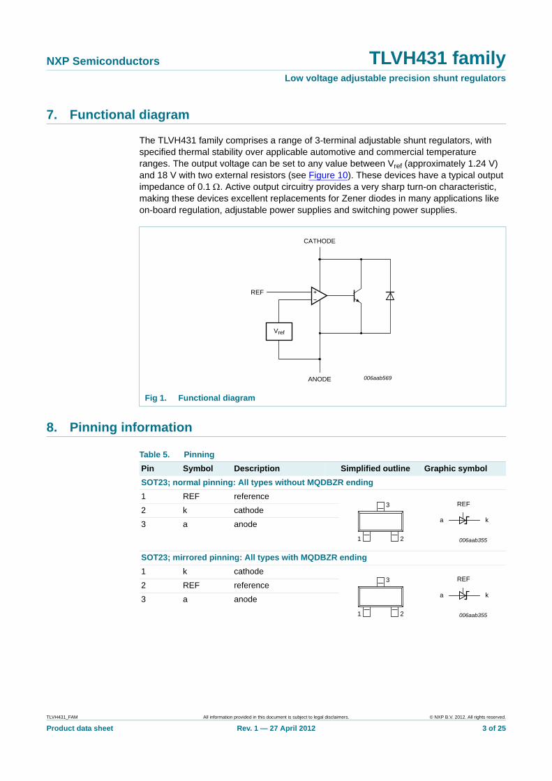
7. Functional diagram
The TLVH431 family comprises a range of 3-terminal adjustable shunt regulators, with specified thermal stability over applicable automotive and commercial temperature ranges. The output voltage can be set to any value between Vref (approximately 1.24 V) and 18 V with two external resistors (see Figure 10). These devices have a typical output impedance of 0.1 . Active output circuitry provides a very sharp turn-on characteristic, making these devices excellent replacements for Zener diodes in many applications like on-board regulation, adjustable power supplies and switching power supplies.
8. Pinning information
Fig 1. Functional diagram
Vref
ANODE
CATHODE
REF
006aab569
Table 5. Pinning
Pin Symbol Description Simplified outline Graphic symbol
SOT23; normal pinning: All types without MQDBZR ending
1 REF reference
2 k cathode
3 a anode
SOT23; mirrored pinning: All types with MQDBZR ending
1 k cathode
2 REF reference
3 a anode
1 2
3
006aab355
REF
a k
1 2
3
006aab355
REF
a k
TLVH431_FAM All information provided in this document is subject to legal disclaimers. © NXP B.V. 2012. All rights reserved.
Product data sheet Rev. 1 — 27 April 2012 3 of 25
NXP Semiconductors TLVH431 familyLow voltage adjustable precision shunt regulators
[1] Pin 1 and 2 can be connected to anode for better thermal performance.
9. Limiting values
[1] Device mounted on an FR4 Printed-Circuit Board (PCB), single-sided copper, tin-plated and standard footprint.
[2] Device mounted on an FR4 PCB, single-sided copper, tin-plated, mounting pad for anode 1 cm2.
[3] Device mounted on a ceramic PCB, Al2O3, standard footprint.
SOT753
1 n.c. not connected [1]
2 n.c. not connected [1]
3 k cathode
4 REF reference
5 a anode
Table 5. Pinning …continued
Pin Symbol Description Simplified outline Graphic symbol
1 32
45
006aab355
REF
a k
Table 6. Limiting valuesIn accordance with the Absolute Maximum Rating System (IEC 60134).
Symbol Parameter Conditions Min Max Unit
VKA cathode-anode voltage - 20 V
IK cathode current 25 80 mA
Iref reference current 0.05 3 mA
Ptot total power dissipation Tamb 25 C
SOT23 [1] - 390 mW[2] - 570 mW[3] - 800 mW
SOT753 [1] - 310 mW[2] - 460 mW[3] - 700 mW
Tj junction temperature - 150 C
Tamb ambient temperature
TLVH431XCDBZR 0 +70 C
TLVH431XIDBZR 40 +85 C
TLVH431XQDBZR TLVH431XQDBVR
40 +125 C
Tstg storage temperature 65 +150 C
TLVH431_FAM All information provided in this document is subject to legal disclaimers. © NXP B.V. 2012. All rights reserved.
Product data sheet Rev. 1 — 27 April 2012 4 of 25
NXP Semiconductors TLVH431 familyLow voltage adjustable precision shunt regulators
10. Recommended operating conditions
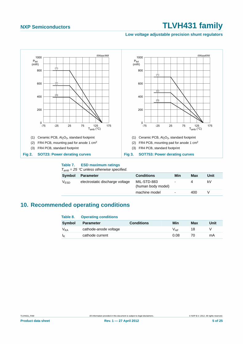
(1) Ceramic PCB, Al2O3, standard footprint
(2) FR4 PCB, mounting pad for anode 1 cm2
(3) FR4 PCB, standard footprint
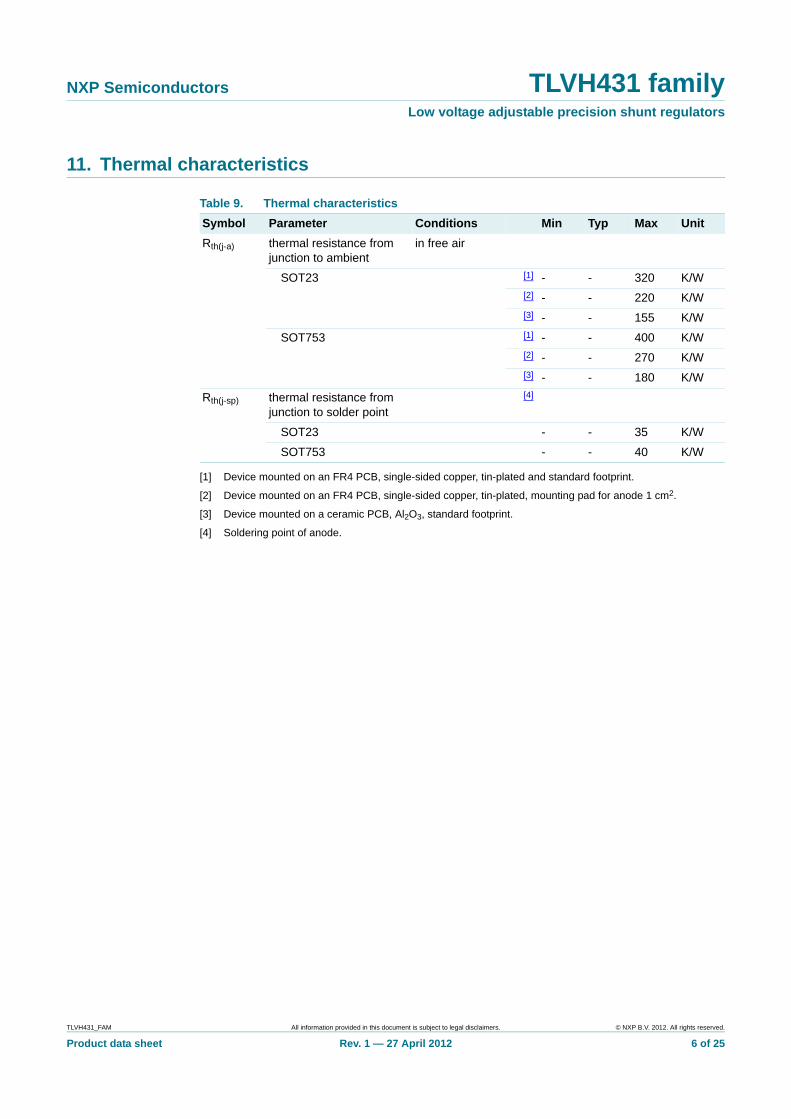
(1) Ceramic PCB, Al2O3, standard footprint
(2) FR4 PCB, mounting pad for anode 1 cm2
(3) FR4 PCB, standard footprint
Fig 2. SOT23: Power derating curves Fig 3. SOT753: Power derating curves
006aac968
-75 -25 25 75 125 1750
200
400
600
800
1000
Tamb (°C)
Ptot(mW)
(3)
(2)
(1)
006aad056
-75 -25 25 75 125 1750
200
400
600
800
1000
Tamb (°C)
Ptot(mW)
(3)
(2)
(1)
Table 7. ESD maximum ratingsTamb = 25 C unless otherwise specified.
Symbol Parameter Conditions Min Max Unit
VESD electrostatic discharge voltage MIL-STD-883 (human body model)
- 4 kV
machine model - 400 V
Table 8. Operating conditions
Symbol Parameter Conditions Min Max Unit
VKA cathode-anode voltage Vref 18 V
IK cathode current 0.08 70 mA
TLVH431_FAM All information provided in this document is subject to legal disclaimers. © NXP B.V. 2012. All rights reserved.
Product data sheet Rev. 1 — 27 April 2012 5 of 25
NXP Semiconductors TLVH431 familyLow voltage adjustable precision shunt regulators
11. Thermal characteristics
[1] Device mounted on an FR4 PCB, single-sided copper, tin-plated and standard footprint.
[2] Device mounted on an FR4 PCB, single-sided copper, tin-plated, mounting pad for anode 1 cm2.
[3] Device mounted on a ceramic PCB, Al2O3, standard footprint.
[4] Soldering point of anode.
Table 9. Thermal characteristics
Symbol Parameter Conditions Min Typ Max Unit
Rth(j-a) thermal resistance from junction to ambient
in free air
SOT23 [1] - - 320 K/W[2] - - 220 K/W[3] - - 155 K/W
SOT753 [1] - - 400 K/W[2] - - 270 K/W[3] - - 180 K/W
Rth(j-sp) thermal resistance from junction to solder point
[4]
SOT23 - - 35 K/W
SOT753 - - 40 K/W
TLVH431_FAM All information provided in this document is subject to legal disclaimers. © NXP B.V. 2012. All rights reserved.
Product data sheet Rev. 1 — 27 April 2012 6 of 25
NXP Semiconductors TLVH431 familyLow voltage adjustable precision shunt regulators
12. Characteristics
Table 10. CharacteristicsTamb = 25 C unless otherwise specified.
Symbol Parameter Conditions Min Typ Max Unit
Standard-Grade (1.5 %): TLVH431CDBZR; TLVH431IDBZR; TLVH431QDBZR; TLVH431MQDBRZ; TLVH431QDBVR
Vref reference voltage VKA = Vref; IK = 10 mA
Tamb = 25 C 1222 1240 1258 mV
TLVH431CDBZR Tamb = 0 C to 70 C 1210 - 1270 mV
TLVH431IDBZR Tamb = 40 C to 85 C 1202 - 1278 mV
TLVH431QDBZRTLVH431MQDBRZ TLVH431QDBVR
Tamb = 40 C to 125 C 1194 - 1286 mV
Vref reference voltage variation VKA = Vref; IK = 10 mA
TLVH431CDBZR Tamb = 0 C to 70 C - 2 10 mV
TLVH431IDBZR Tamb = 40 C to 85 C - 3 10 mV
TLVH431QDBZRTLVH431MQDBRZ TLVH431QDBVR
Tamb = 40 C to 125 C - 4 10 mV
Vref/VKA reference voltage variation to cathode-anode voltage variation ratio
IK = 10 mA; VKA = Vref to 18 V
- 0.5 1.5 mV/V
Iref reference current IK = 10 mA; R1 = 10 k; R2 = open
- 0.19 0.30 A
Iref reference current variation IK = 10 mA; R1 = 10 k; R2 = open
TLVH431CDBZR Tamb = 0 C to 70 C - 0.03 0.10 A
TLVH431IDBZR Tamb = 40 C to 85 C - 0.06 0.16 A
TLVH431QDBZRTLVH431MQDBRZ TLVH431QDBVR
Tamb = 40 C to 125 C - 0.07 0.24 A
IK(min) minimum cathode current VKA = Vref - 55 80 A
Ioff off-state current VKA = 18 V; Vref = 0 - 0.01 0.05 A
ZKA dynamic cathode-anode impedance
IK = 0.1 mA to 70 mA; VKA = Vref; f < 1 kHz
SOT23 - 0.10 0.15
SOT753 - 0.15 0.20
TLVH431_FAM All information provided in this document is subject to legal disclaimers. © NXP B.V. 2012. All rights reserved.
Product data sheet Rev. 1 — 27 April 2012 7 of 25
NXP Semiconductors TLVH431 familyLow voltage adjustable precision shunt regulators
A-Grade (1 %): TLVH431ACDBZR; TLVH431AIDBZR; TLVH431AQDBZR; TLVH431AMQDBZR; TLVH431AQDBVR
Vref reference voltage VKA = Vref; IK = 10 mA
Tamb = 25 C 1228 1240 1252 mV
TLVH431ACDBZR Tamb = 0 C to 70 C 1221 - 1259 mV
TLVH431AIDBZR Tamb = 40 C to 85 C 1215 - 1265 mV
TLVH431AQDBZRTLVH431AMQDBRZ TLVH431AQDBVR
Tamb = 40 C to 125 C 1209 - 1271 mV
Vref reference voltage variation VKA = Vref; IK = 10 mA
TLVH431ACDBZR Tamb = 0 C to 70 C - 2 10 mV
TLVH431AIDBZR Tamb = 40 C to 85 C - 3 10 mV
TLVH431AQDBZRTLVH431AMQDBRZ TLVH431AQDBVR
Tamb = 40 C to 125 C - 4 10 mV
Vref/VKA reference voltage variation to cathode-anode voltage variation ratio
IK = 10 mA; VKA = Vref to 18 V
- 0.5 1.5 mV/V
Iref reference current IK = 10 mA; R1 = 10 k; R2 = open
- 0.19 0.30 A
Iref reference current variation IK = 10 mA; R1 = 10 k; R2 = open
TLVH431ACDBZR Tamb = 0 C to 70 C - 0.03 0.10 A
TLVH431AIDBZR Tamb = 40 C to 85 C - 0.06 0.16 A
TLVH431AQDBZRTLVH431AMQDBRZ TLVH431AQDBVR
Tamb = 40 C to 125 C - 0.07 0.24 A
IK(min) minimum cathode current VKA = Vref - 55 80 A
Ioff off-state current VKA = 18 V; Vref = 0 - 0.01 0.05 A
ZKA dynamic cathode-anode impedance
IK = 0.1 mA to 70 mA; VKA = Vref; f < 1 kHz
SOT23 - 0.10 0.15
SOT753 - 0.15 0.20
Table 10. Characteristics …continuedTamb = 25 C unless otherwise specified.
Symbol Parameter Conditions Min Typ Max Unit
TLVH431_FAM All information provided in this document is subject to legal disclaimers. © NXP B.V. 2012. All rights reserved.
Product data sheet Rev. 1 — 27 April 2012 8 of 25
NXP Semiconductors TLVH431 familyLow voltage adjustable precision shunt regulators
D-Grade (0.75 %): TLVH431DQDBZR; TLVH431DMQDBZR; TLVH431DQDBVR
Vref reference voltage VKA = Vref; IK = 10 mA
Tamb = 25 C 1231 1240 1249 mV
Tamb = 40 C to 125 C 1215 - 1265 mV
Vref reference voltage variation VKA = Vref; IK = 10 mA
Tamb = 0 C to 70 C - 2 10 mV
Tamb = 40 C to 85 C - 3 10 mV
Tamb = 40 C to 125 C - 4 10 mV
Vref/VKA reference voltage variation to cathode-anode voltage variation ratio
IK = 10 mA; VKA = Vref to 18 V
- 0.5 1.5 mV/V
Iref reference current IK = 10 mA; R1 = 10 k; R2 = open
- 0.19 0.30 A
Iref reference current variation IK = 10 mA; R1 = 10 k; R2 = open; Tamb = 40 C to 125 C
- 0.07 0.24 A
IK(min) minimum cathode current VKA = Vref - 55 80 A
Ioff off-state current VKA = 18 V; Vref = 0 - 0.01 0.05 A
ZKA dynamic cathode-anode impedance
IK = 0.1 mA to 70 mA; VKA = Vref; f < 1 kHz
SOT23 - 0.10 0.15
SOT753 - 0.15 0.20
Table 10. Characteristics …continuedTamb = 25 C unless otherwise specified.
Symbol Parameter Conditions Min Typ Max Unit
TLVH431_FAM All information provided in this document is subject to legal disclaimers. © NXP B.V. 2012. All rights reserved.
Product data sheet Rev. 1 — 27 April 2012 9 of 25
NXP Semiconductors TLVH431 familyLow voltage adjustable precision shunt regulators
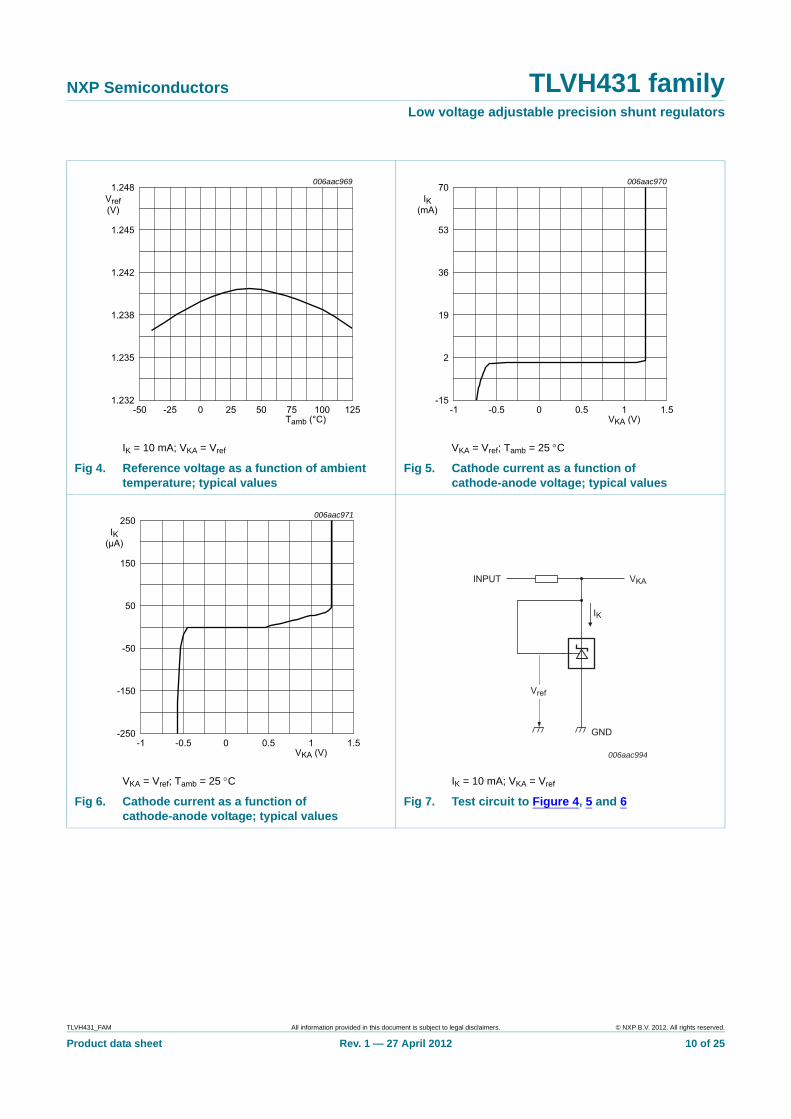
IK = 10 mA; VKA = Vref VKA = Vref; Tamb = 25 C
Fig 4. Reference voltage as a function of ambient temperature; typical values
Fig 5. Cathode current as a function of cathode-anode voltage; typical values
VKA = Vref; Tamb = 25 C IK = 10 mA; VKA = Vref
Fig 6. Cathode current as a function of cathode-anode voltage; typical values
Fig 7. Test circuit to Figure 4, 5 and 6
006aac969
-50 -25 0 25 50 75 100 1251.232
1.235
1.238
1.242
1.245
1.248
Tamb (°C)
Vref(V)
006aac970
-1 -0.5 0 0.5 1 1.5-15
2
19
36
53
70
VKA (V)
IK(mA)
006aac971
-1 -0.5 0 0.5 1 1.5-250
-150
-50
50
150
250
VKA (V)
IK(μA)
006aac994
GND
Vref
VKAINPUT
IK
TLVH431_FAM All information provided in this document is subject to legal disclaimers. © NXP B.V. 2012. All rights reserved.
Product data sheet Rev. 1 — 27 April 2012 10 of 25
NXP Semiconductors TLVH431 familyLow voltage adjustable precision shunt regulators
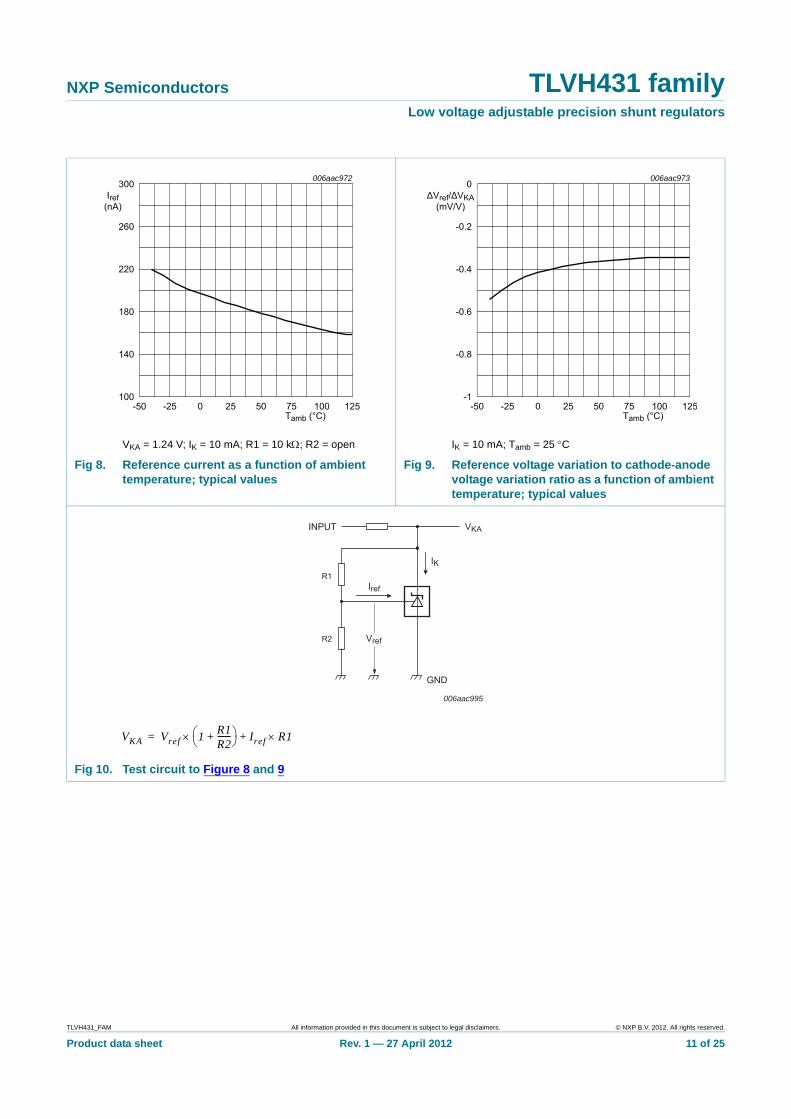
VKA = 1.24 V; IK = 10 mA; R1 = 10 k; R2 = open IK = 10 mA; Tamb = 25 C
Fig 8. Reference current as a function of ambient temperature; typical values
Fig 9. Reference voltage variation to cathode-anode voltage variation ratio as a function of ambient temperature; typical values
Fig 10. Test circuit to Figure 8 and 9
006aac972
-50 -25 0 25 50 75 100 125100
140
180
220
260
300
Tamb (°C)
Iref(nA)
006aac973
-50 -25 0 25 50 75 100 125-1
-0.8
-0.6
-0.4
-0.2
0
Tamb (°C)
ΔVref/ΔVKA(mV/V)
006aac995
GND
Vref
VKAINPUT
IK
IrefR1
R2
VKA Vref 1R1R2-------+
Iref R1+=
TLVH431_FAM All information provided in this document is subject to legal disclaimers. © NXP B.V. 2012. All rights reserved.
Product data sheet Rev. 1 — 27 April 2012 11 of 25
NXP Semiconductors TLVH431 familyLow voltage adjustable precision shunt regulators
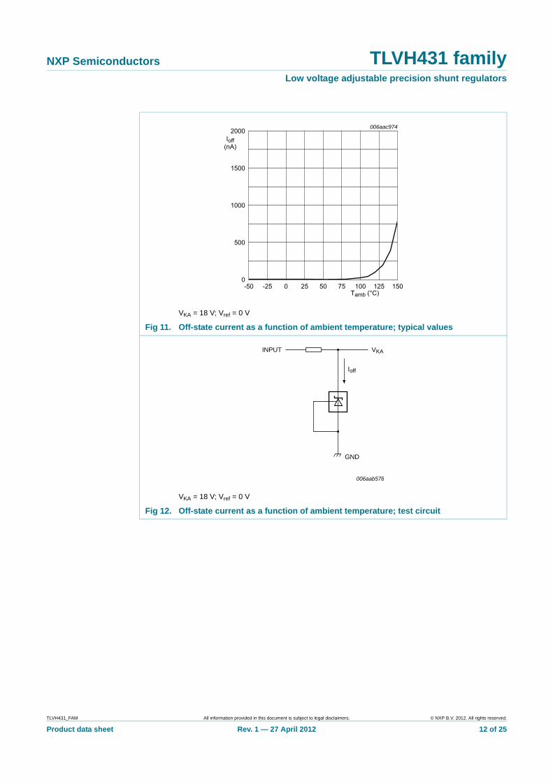
VKA = 18 V; Vref = 0 V
Fig 11. Off-state current as a function of ambient temperature; typical values
VKA = 18 V; Vref = 0 V
Fig 12. Off-state current as a function of ambient temperature; test circuit
006aac974
-50 -25 0 25 50 75 100 125 1500
500
1000
1500
2000
Tamb (°C)
Ioff(nA)
006aab578
GND
VKAINPUT
Ioff
TLVH431_FAM All information provided in this document is subject to legal disclaimers. © NXP B.V. 2012. All rights reserved.
Product data sheet Rev. 1 — 27 April 2012 12 of 25
NXP Semiconductors TLVH431 familyLow voltage adjustable precision shunt regulators
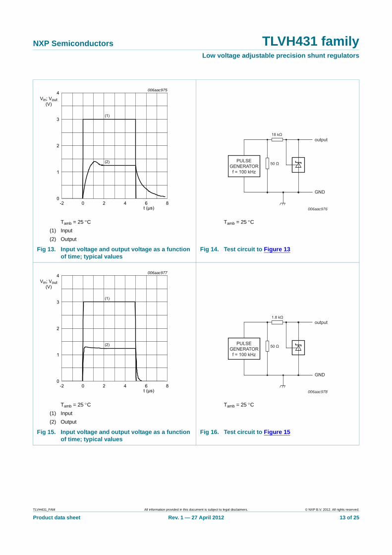
Tamb = 25 C
(1) Input
(2) Output
Tamb = 25 C
Fig 13. Input voltage and output voltage as a function of time; typical values
Fig 14. Test circuit to Figure 13
Tamb = 25 C
(1) Input
(2) Output
Tamb = 25 C
Fig 15. Input voltage and output voltage as a function of time; typical values
Fig 16. Test circuit to Figure 15
006aac975
-2 0 2 4 6 80
1
2
3
4
t (μs)
Vin; Vout(V)
(1)
(2)
006aac976
GND
output18 kΩ
50 ΩPULSE
GENERATORf = 100 kHz
006aac977
-2 0 2 4 6 80
1
2
3
4
t (μs)
Vin; Vout(V)
(1)
(2)
006aac978
GND
output1.8 kΩ
50 ΩPULSE
GENERATORf = 100 kHz
TLVH431_FAM All information provided in this document is subject to legal disclaimers. © NXP B.V. 2012. All rights reserved.
Product data sheet Rev. 1 — 27 April 2012 13 of 25
NXP Semiconductors TLVH431 familyLow voltage adjustable precision shunt regulators
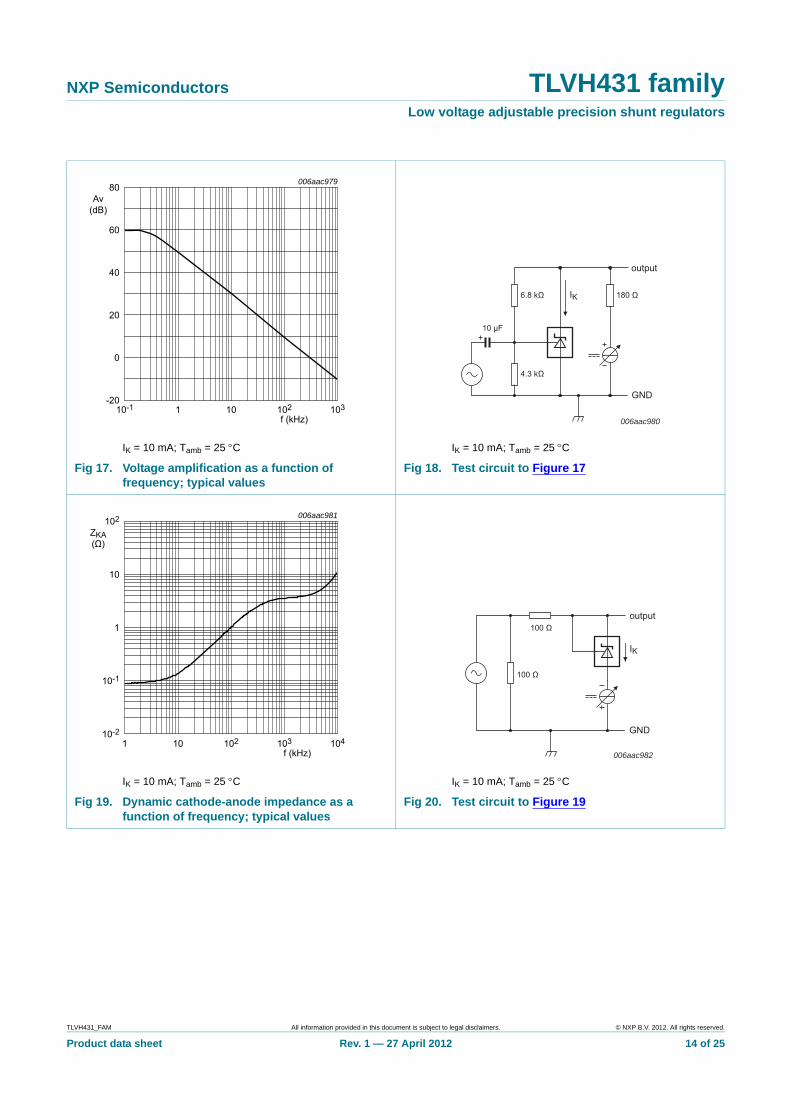
IK = 10 mA; Tamb = 25 C IK = 10 mA; Tamb = 25 C
Fig 17. Voltage amplification as a function of frequency; typical values
Fig 18. Test circuit to Figure 17
IK = 10 mA; Tamb = 25 C IK = 10 mA; Tamb = 25 C
Fig 19. Dynamic cathode-anode impedance as a function of frequency; typical values
Fig 20. Test circuit to Figure 19
006aac979
10-1 1 10 102 103-20
0
20
40
60
80
f (kHz)
Av(dB)
006aac980
GND
output
IK 180 Ω6.8 kΩ
4.3 kΩ
10 μF
006aac981
1 10 102 103 10410-2
10-1
1
10
102
f (kHz)
ZKA(Ω)
006aac982
GND
output
IK
100 Ω
100 Ω
TLVH431_FAM All information provided in this document is subject to legal disclaimers. © NXP B.V. 2012. All rights reserved.
Product data sheet Rev. 1 — 27 April 2012 14 of 25
NXP Semiconductors TLVH431 familyLow voltage adjustable precision shunt regulators
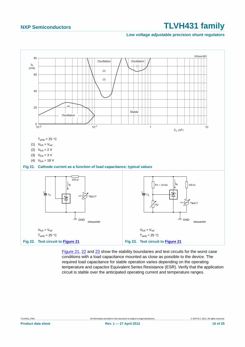
Figure 21, 22 and 23 show the stability boundaries and test circuits for the worst case conditions with a load capacitance mounted as close as possible to the device. The required load capacitance for stable operation varies depending on the operating temperature and capacitor Equivalent Series Resistance (ESR). Verify that the application circuit is stable over the anticipated operating current and temperature ranges.
Tamb = 25 C
(1) VKA = Vref
(2) VKA = 2 V
(3) VKA = 3 V
(4) VKA = 18 V
Fig 21. Cathode current as a function of load capacitance; typical values
VKA = Vref
Tamb = 25 C
VKA > Vref
Tamb = 25 C
Fig 22. Test circuit to Figure 21 Fig 23. Test circuit to Figure 21
006aac983
40
20
60
80
IK(mA)
0
CL (nF)10-2 10110-1
Oscillation
(1)
Oscillation
(2)
(4)
Oscillation
(3)
Stable
006aab589GND
CL
IK
150 Ω
VBATT
006aab590GND
CL
IK 150 Ω
VBATTR2
R1 = 10 kΩ
TLVH431_FAM All information provided in this document is subject to legal disclaimers. © NXP B.V. 2012. All rights reserved.
Product data sheet Rev. 1 — 27 April 2012 15 of 25
NXP Semiconductors TLVH431 familyLow voltage adjustable precision shunt regulators
13. Application information
Fig 24. Shunt regulator
;
Fig 25. Series pass regulator
Fig 26. Constant current source
006aab592
VOUT
R1
R2
V+
VOUT 1R1R2-------+
Vref=
006aab593
VOUT
R1
R2
V+
VOUT 1R1R2-------+
Vref= VOUT min Vref Vbe+=
006aab595
IOUT
RCLV+
IOUT
Vref
RCL---------=
TLVH431_FAM All information provided in this document is subject to legal disclaimers. © NXP B.V. 2012. All rights reserved.
Product data sheet Rev. 1 — 27 April 2012 16 of 25
NXP Semiconductors TLVH431 familyLow voltage adjustable precision shunt regulators
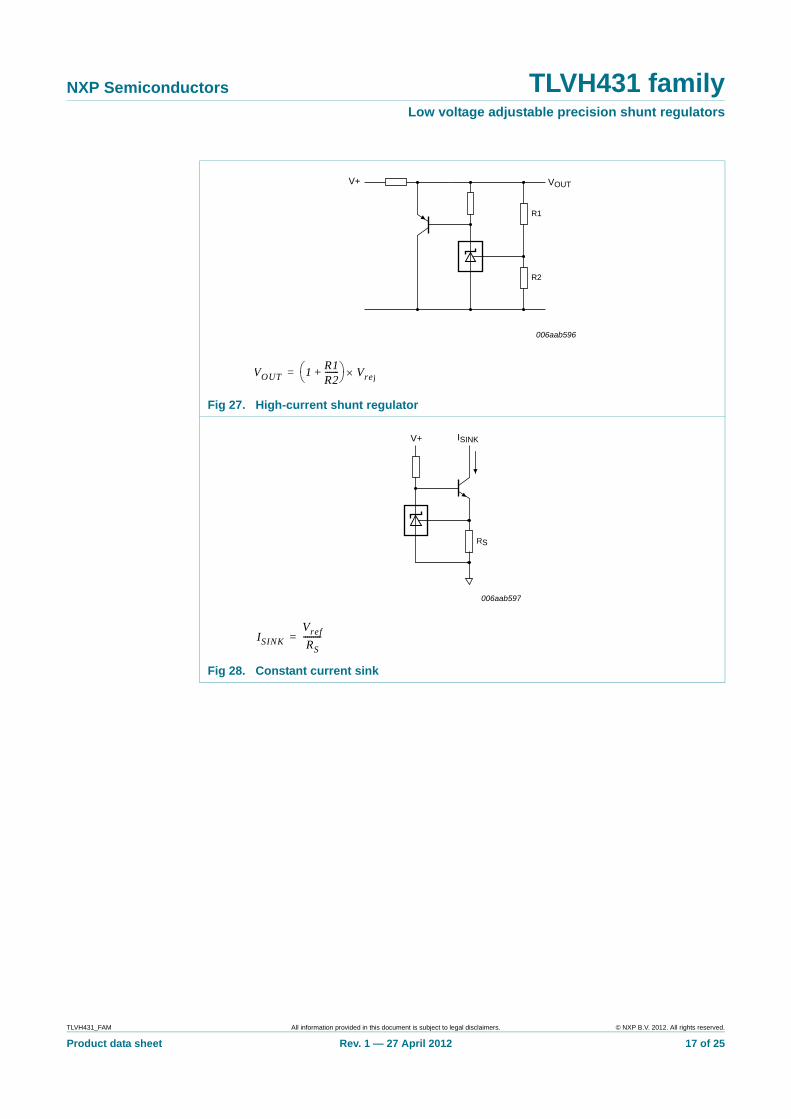
Fig 27. High-current shunt regulator
Fig 28. Constant current sink
006aab596
VOUT
R1
R2
V+
VOUT 1R1R2-------+
Vref=
006aab597
ISINK
RS
V+
ISINK
Vref
RS---------=
TLVH431_FAM All information provided in this document is subject to legal disclaimers. © NXP B.V. 2012. All rights reserved.
Product data sheet Rev. 1 — 27 April 2012 17 of 25
NXP Semiconductors TLVH431 familyLow voltage adjustable precision shunt regulators
14. Test information
14.1 Quality information
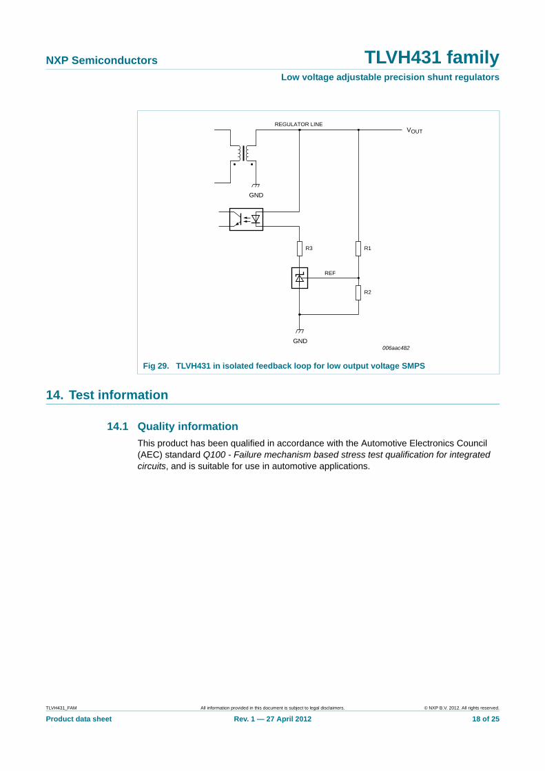
This product has been qualified in accordance with the Automotive Electronics Council (AEC) standard Q100 - Failure mechanism based stress test qualification for integrated circuits, and is suitable for use in automotive applications.
Fig 29. TLVH431 in isolated feedback loop for low output voltage SMPS
006aac482
VOUT
R1
R2
GND
R3
REF
GND
REGULATOR LINE
TLVH431_FAM All information provided in this document is subject to legal disclaimers. © NXP B.V. 2012. All rights reserved.
Product data sheet Rev. 1 — 27 April 2012 18 of 25
NXP Semiconductors TLVH431 familyLow voltage adjustable precision shunt regulators
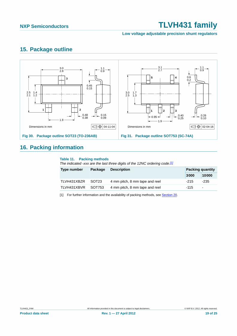
15. Package outline
16. Packing information
[1] For further information and the availability of packing methods, see Section 20.
Fig 30. Package outline SOT23 (TO-236AB) Fig 31. Package outline SOT753 (SC-74A)
04-11-04Dimensions in mm
0.450.15
1.9
1.10.9
3.02.8
2.52.1
1.41.2
0.480.38
0.150.09
1 2
3
02-04-16Dimensions in mm
3.02.5
1.71.3
3.12.7
1.10.9
0.260.10
0.400.25
1.9
0.95
0.60.2
1 32
45
Table 11. Packing methodsThe indicated -xxx are the last three digits of the 12NC ordering code.[1]
Type number Package Description Packing quantity
3000 10000
TLVH431XBZR SOT23 4 mm pitch, 8 mm tape and reel -215 -235
TLVH431XBVR SOT753 4 mm pitch, 8 mm tape and reel -115 -
TLVH431_FAM All information provided in this document is subject to legal disclaimers. © NXP B.V. 2012. All rights reserved.
Product data sheet Rev. 1 — 27 April 2012 19 of 25
NXP Semiconductors TLVH431 familyLow voltage adjustable precision shunt regulators
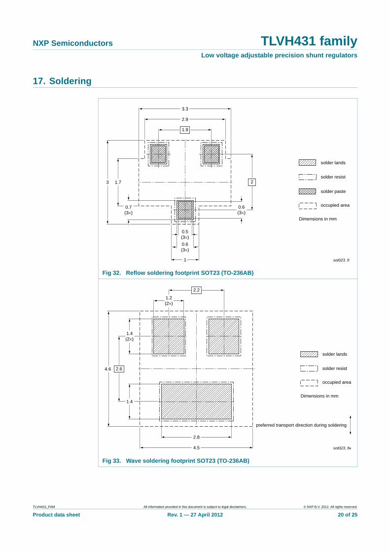
17. Soldering
Fig 32. Reflow soldering footprint SOT23 (TO-236AB)
Fig 33. Wave soldering footprint SOT23 (TO-236AB)
solder lands
solder resist
occupied area
solder paste
sot023_fr
0.5(3×)
0.6(3×)
0.6(3×)
0.7(3×)
3
1
3.3
2.9
1.7
1.9
2
Dimensions in mm
solder lands
solder resist
occupied area
preferred transport direction during soldering
sot023_fw
2.8
4.5
1.4
4.6
1.4(2×)
1.2(2×)
2.2
2.6
Dimensions in mm
TLVH431_FAM All information provided in this document is subject to legal disclaimers. © NXP B.V. 2012. All rights reserved.
Product data sheet Rev. 1 — 27 April 2012 20 of 25
NXP Semiconductors TLVH431 familyLow voltage adjustable precision shunt regulators
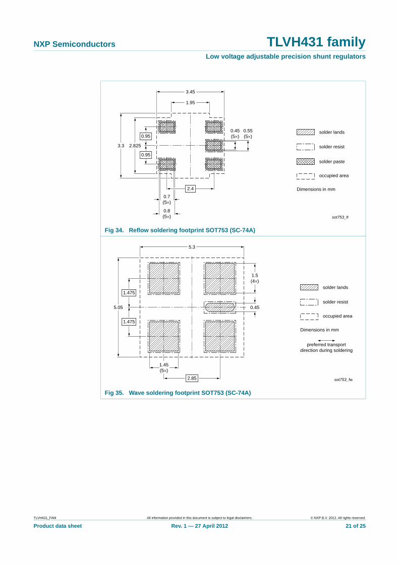
Fig 34. Reflow soldering footprint SOT753 (SC-74A)
Fig 35. Wave soldering footprint SOT753 (SC-74A)
solder lands
solder resist
occupied area
solder paste
sot753_fr
2.8253.3
0.45(5×)
0.55(5×)
0.7(5×)
0.8(5×)
3.45
1.95
0.95
0.95
2.4 Dimensions in mm
sot753_fw
5.3
5.05 0.45
1.5(4×)
1.45(5×)
2.85
1.475
1.475
solder lands
solder resist
occupied area
preferred transportdirection during soldering
Dimensions in mm
TLVH431_FAM All information provided in this document is subject to legal disclaimers. © NXP B.V. 2012. All rights reserved.
Product data sheet Rev. 1 — 27 April 2012 21 of 25
NXP Semiconductors TLVH431 familyLow voltage adjustable precision shunt regulators
18. Revision history
Table 12. Revision history
Document ID Release date Data sheet status Change notice Supersedes
TLVH431_FAM v.1 20120427 Product data sheet - -
TLVH431_FAM All information provided in this document is subject to legal disclaimers. © NXP B.V. 2012. All rights reserved.
Product data sheet Rev. 1 — 27 April 2012 22 of 25
NXP Semiconductors TLVH431 familyLow voltage adjustable precision shunt regulators
19. Legal information
19.1 Data sheet status
[1] Please consult the most recently issued document before initiating or completing a design.
[2] The term ‘short data sheet’ is explained in section “Definitions”.
[3] The product status of device(s) described in this document may have changed since this document was published and may differ in case of multiple devices. The latest product status information is available on the Internet at URL http://www.nxp.com.
19.2 Definitions
Draft — The document is a draft version only. The content is still under internal review and subject to formal approval, which may result in modifications or additions. NXP Semiconductors does not give any representations or warranties as to the accuracy or completeness of information included herein and shall have no liability for the consequences of use of such information.
Short data sheet — A short data sheet is an extract from a full data sheet with the same product type number(s) and title. A short data sheet is intended for quick reference only and should not be relied upon to contain detailed and full information. For detailed and full information see the relevant full data sheet, which is available on request via the local NXP Semiconductors sales office. In case of any inconsistency or conflict with the short data sheet, the full data sheet shall prevail.
Product specification — The information and data provided in a Product data sheet shall define the specification of the product as agreed between NXP Semiconductors and its customer, unless NXP Semiconductors and customer have explicitly agreed otherwise in writing. In no event however, shall an agreement be valid in which the NXP Semiconductors product is deemed to offer functions and qualities beyond those described in the Product data sheet.
19.3 Disclaimers
Limited warranty and liability — Information in this document is believed to be accurate and reliable. However, NXP Semiconductors does not give any representations or warranties, expressed or implied, as to the accuracy or completeness of such information and shall have no liability for the consequences of use of such information. NXP Semiconductors takes no responsibility for the content in this document if provided by an information source outside of NXP Semiconductors.
In no event shall NXP Semiconductors be liable for any indirect, incidental, punitive, special or consequential damages (including - without limitation - lost profits, lost savings, business interruption, costs related to the removal or replacement of any products or rework charges) whether or not such damages are based on tort (including negligence), warranty, breach of contract or any other legal theory.
Notwithstanding any damages that customer might incur for any reason whatsoever, NXP Semiconductors’ aggregate and cumulative liability towards customer for the products described herein shall be limited in accordance with the Terms and conditions of commercial sale of NXP Semiconductors.
Right to make changes — NXP Semiconductors reserves the right to make changes to information published in this document, including without limitation specifications and product descriptions, at any time and without notice. This document supersedes and replaces all information supplied prior to the publication hereof.
Suitability for use — NXP Semiconductors products are not designed, authorized or warranted to be suitable for use in life support, life-critical or safety-critical systems or equipment, nor in applications where failure or malfunction of an NXP Semiconductors product can reasonably be expected to result in personal injury, death or severe property or environmental damage. NXP Semiconductors and its suppliers accept no liability for inclusion and/or use of NXP Semiconductors products in such equipment or applications and therefore such inclusion and/or use is at the customer’s own risk.
Applications — Applications that are described herein for any of these products are for illustrative purposes only. NXP Semiconductors makes no representation or warranty that such applications will be suitable for the specified use without further testing or modification.
Customers are responsible for the design and operation of their applications and products using NXP Semiconductors products, and NXP Semiconductors accepts no liability for any assistance with applications or customer product design. It is customer’s sole responsibility to determine whether the NXP Semiconductors product is suitable and fit for the customer’s applications and products planned, as well as for the planned application and use of customer’s third party customer(s). Customers should provide appropriate design and operating safeguards to minimize the risks associated with their applications and products.
NXP Semiconductors does not accept any liability related to any default, damage, costs or problem which is based on any weakness or default in the customer’s applications or products, or the application or use by customer’s third party customer(s). Customer is responsible for doing all necessary testing for the customer’s applications and products using NXP Semiconductors products in order to avoid a default of the applications and the products or of the application or use by customer’s third party customer(s). NXP does not accept any liability in this respect.
Limiting values — Stress above one or more limiting values (as defined in the Absolute Maximum Ratings System of IEC 60134) will cause permanent damage to the device. Limiting values are stress ratings only and (proper) operation of the device at these or any other conditions above those given in the Recommended operating conditions section (if present) or the Characteristics sections of this document is not warranted. Constant or repeated exposure to limiting values will permanently and irreversibly affect the quality and reliability of the device.
Terms and conditions of commercial sale — NXP Semiconductors products are sold subject to the general terms and conditions of commercial sale, as published at http://www.nxp.com/profile/terms, unless otherwise agreed in a valid written individual agreement. In case an individual agreement is concluded only the terms and conditions of the respective agreement shall apply. NXP Semiconductors hereby expressly objects to applying the customer’s general terms and conditions with regard to the purchase of NXP Semiconductors products by customer.
No offer to sell or license — Nothing in this document may be interpreted or construed as an offer to sell products that is open for acceptance or the grant, conveyance or implication of any license under any copyrights, patents or other industrial or intellectual property rights.
Document status[1][2] Product status[3] Definition
Objective [short] data sheet Development This document contains data from the objective specification for product development.
Preliminary [short] data sheet Qualification This document contains data from the preliminary specification.
Product [short] data sheet Production This document contains the product specification.
TLVH431_FAM All information provided in this document is subject to legal disclaimers. © NXP B.V. 2012. All rights reserved.
Product data sheet Rev. 1 — 27 April 2012 23 of 25
NXP Semiconductors TLVH431 familyLow voltage adjustable precision shunt regulators
Export control — This document as well as the item(s) described herein may be subject to export control regulations. Export might require a prior authorization from competent authorities.
Quick reference data — The Quick reference data is an extract of the product data given in the Limiting values and Characteristics sections of this document, and as such is not complete, exhaustive or legally binding.
19.4 TrademarksNotice: All referenced brands, product names, service names and trademarks are the property of their respective owners.
20. Contact information
For more information, please visit: http://www.nxp.com
For sales office addresses, please send an email to: [email protected]
TLVH431_FAM All information provided in this document is subject to legal disclaimers. © NXP B.V. 2012. All rights reserved.
Product data sheet Rev. 1 — 27 April 2012 24 of 25
NXP Semiconductors TLVH431 familyLow voltage adjustable precision shunt regulators
21. Contents
1 General description . . . . . . . . . . . . . . . . . . . . . . 1
2 Features and benefits . . . . . . . . . . . . . . . . . . . . 1
3 Applications . . . . . . . . . . . . . . . . . . . . . . . . . . . . 1
4 Quick reference data . . . . . . . . . . . . . . . . . . . . . 2
5 Ordering information. . . . . . . . . . . . . . . . . . . . . 2
6 Marking . . . . . . . . . . . . . . . . . . . . . . . . . . . . . . . . 2
7 Functional diagram . . . . . . . . . . . . . . . . . . . . . . 3
8 Pinning information. . . . . . . . . . . . . . . . . . . . . . 3
9 Limiting values. . . . . . . . . . . . . . . . . . . . . . . . . . 4
10 Recommended operating conditions. . . . . . . . 5
11 Thermal characteristics . . . . . . . . . . . . . . . . . . 6
12 Characteristics. . . . . . . . . . . . . . . . . . . . . . . . . . 7
13 Application information. . . . . . . . . . . . . . . . . . 16
14 Test information. . . . . . . . . . . . . . . . . . . . . . . . 1814.1 Quality information . . . . . . . . . . . . . . . . . . . . . 18
15 Package outline . . . . . . . . . . . . . . . . . . . . . . . . 19
16 Packing information . . . . . . . . . . . . . . . . . . . . 19
17 Soldering . . . . . . . . . . . . . . . . . . . . . . . . . . . . . 20
18 Revision history. . . . . . . . . . . . . . . . . . . . . . . . 22
19 Legal information. . . . . . . . . . . . . . . . . . . . . . . 2319.1 Data sheet status . . . . . . . . . . . . . . . . . . . . . . 2319.2 Definitions. . . . . . . . . . . . . . . . . . . . . . . . . . . . 2319.3 Disclaimers . . . . . . . . . . . . . . . . . . . . . . . . . . . 2319.4 Trademarks. . . . . . . . . . . . . . . . . . . . . . . . . . . 24
20 Contact information. . . . . . . . . . . . . . . . . . . . . 24
21 Contents . . . . . . . . . . . . . . . . . . . . . . . . . . . . . . 25
© NXP B.V. 2012. All rights reserved.
For more information, please visit: http://www.nxp.comFor sales office addresses, please send an email to: [email protected]
Date of release: 27 April 2012
Document identifier: TLVH431_FAM
Please be aware that important notices concerning this document and the product(s)described herein, have been included in section ‘Legal information’.