tm 11-5820-801-30 technical manual - liberated · pdf filebefore working inside a module that...
TRANSCRIPT
TM 11-5820-801-30
TECHNICAL MANUAL
DIRECT SUPPORT MAINTENANCE MANUALAMPLIFIER, PARAMETRIC
AM-6602/MSC-46(V)(NSN 5895-00-100-4315)
H E A D Q U A R T E R S , D E P A R T M E N T O F T H E A R M Y
22 SEPTEMBER 1980

WARNINGHIGH VOLTAGE
High voltage is used in the operation of this equipment. DEATH CONTACT may result ifpersonnel fail to observe safety precautions. Learn the areas containing high voltage in eachpiece of equipment. Be careful not to contact high-voltage connections when installing oroperating this equipment. Before working inside the equipment, turn power off and groundpoints of high potential before touching them.
HIGH TEMPERATURE
Heaters are used in this equipment to maintain certain components at high temperatureduring operation. Before working inside a module that contains heated components, makesure that the power had been turned off long enough for the temperature to drop to a safelevel.
CRYOGENIC TEMPERATURE AND HIGH VACUUM
One module of this equipment contains components at a cryogenic temperature within avacuum. Before work can be performed the temperature must rise to room temperature.Before this module can be opened, the vacuum must be released after the temperature hasnormalized.
HIGH PRESSURE
Certain components are under high gas pressure. If it is necessary to open such acomponent, use precautions to release the pressure without damage.

TM 11-5820-801-30
TECHNICAL MANUAL HEADQUARTERSDEPARTMENT OF THE ARMY
No. 11-5820-801-30 WASHINGTON, DC, 22 September 1980
DIRECT SUPPORT MAINTENANCE MANUALAMPLIFIER, PARAMETRIC AM-6602/MSC-46(V)
(NSN 5895-00-100-4315)
REPORTING ERRORS AND RECOMMENDING IMPROVEMENTSYou can help improve this manual. If you find any mistakes or if you know of a way to
improve the procedures, please let us know. Mall your letter, DA Form 2028 (RecommendedChanges to Publications and Blank Forms), or DA Form 2028-2 located in back of thismanual direct to: Commander, US Army Communications and Electronics Materiel ReadinessCommand, ATTN: DRSEL-ME-MQ, Fort Monmouth, New Jersey 07703.
In either case, a reply will be furnished direct to you.
Paragraph Page
CHAPTER 1. INTRODUCTIONScope........................................................................................................... 1-1 1-1Indexes or publications ................................................................................ 1-2 1-1Maintenance forms, records, and reports .................................................... 1-3 1-1Reporting equipment improvement recommendations (EIR) ....................... 1-4 1-1
CHAPTER 2. FUNCTIONING OF EQUIPMENTSECTION I. Introduction and Signal Amplification
Introduction .................................................................................................. 2-1 2-1Block diagram of signal amplification circuit ................................................ 2-2 2-1Vacuum Vessel Module 2A3 (first stage amplifier) ...................................... 2-3 2-1Waveguide Filter Module 2A4 ...................................................................... 2-4 2-3Second Stage Paramp Module 2A2 (second stage amplifier) ..................... 2-5 2-3Pump Source Module 2A1 ........................................................................... 2-6 2-3Klystron Power Supply 1PS1 ....................................................................... 2-7 2-4Monitors in signal amplification circuits ........................................................ 2-8 2-4
II. Internal Temperature ControlsVacuum Vessel Module 2A3 Temperature .................................................. 2-9 2-5Second Stage Paramp Module 2A2 Temperature ....................................... 2-10 2-6Pump Source Module 2A1 Temperature ..................................................... 2-11 2-6
III. SwitchingGeneral ........................................................................................................ 2-12 2-7Safety interlock ............................................................................................ 2-13 2-9Channel switching........................................................................................ 2-14 2-9
IV. Circuit DescriptionsFirst stage amplifier circuits ......................................................................... 2-15 2-11Second stage amplifier circuits .................................................................... 2-16 2-13RF pump circuits .......................................................................................... 2-17 2-17Local Control and Monitoring circuits ........................................................... 2-18 2-20DC Power Supply circuits ............................................................................ 2-19 2-21Remote Control and Monitoring circuits ....................................................... 2-20 2-30
CHAPTER 3 DIRECT SUPPORT MAINTENANCE INSTRUCTIONSSECTION I. General
Introduction .................................................................................................. 3-1 3-1Unit 1 voltage and resistance measurements .............................................. 3-2 3-1Remote Control/Monitor Assembly 3A1 voltage and resistance measurements. 3-3 3-7
II. Tools and Test EquipmentTools ............................................................................................................ 3-4 3-9Test equipment ............................................................................................ 3-5 3-9
III. TroubleshootingFault isolation............................................................................................... 3-6 3-10Gain and bandwidth measurements ............................................................ 3-7 3-23Waveguide Assembly RF tests .................................................................... 3-8 3-28Pump frequency and power tests ................................................................ 3-9 3-28
i
TM 11-5820-801-30
Paragraph PageMain power failure........................................................................................ 3-10 3-32Module removal and replacement................................................................ 3-11 3-32System interconnections .............................................................................. 3-12 3-37
APPENDIX A. REFERENCES ............................................................................................................................ A-1
LIST OF ILLUSTRATIONSFigure Page2-1 Block Diagram of Signal Amplification Circuit, AM-6602/MSC-46(V) ....................................................... 2-22-2 Block Diagram of Module 2A3 Temperature and Pressure Sensors ........................................................ 2-52-3 Block Diagram of Temperature Controller Circuit ..................................................................................... 2-62-4 Front Panel View of Local Control Monitor Assembly Unit ....................................................................... 2-82-5 Block Diagram of Safety Interlock Circuit ................................................................................................. 2-92-6 Block Diagram of Channel Switching, + 28 V Control and Display Indicator Circuits ............................... 2-102-7 Block Diagram of Channel Switching, RF Switch Positions ..................................................................... 2-102-8 Vacuum Vessel Module 2A3, Schematic Diagram ................................................................................... 2-112-9 Temperature Monitor Card 1A1 (Sheet 1 of 2) ......................................................................................... 2-122-9 Temperature Monitor Card 1A1 (Sheet 2 of 2) ......................................................................................... 2-13
2-10 Vacuum Measurement Circuit, P/O Unit 1 ................................................................................................ 2-142-11 Second Stage Paramp Module 2A2, Schematic Diagram ........................................................................ 2-152-12 Temperature Controller, 2A2A1, 2A1A2, 2A1A3, 2A1A4, Schematic Diagram ........................................ 2-172-13 Pump Source Module 2A1, Schematic Diagram ...................................................................................... 2-182-14 PumpSourcePowerMonitor2A1A, Schematic Diagram............................................................................. 2-192-15 Varactor Bias Voltage Circuit, P/O Unit 1 ................................................................................................. 2-202-16 Voltage Measurement Circuit, P/O Unit 1 ................................................................................................. 2-222-17 Local Control/Monitor Assembly Unit 1, Schematic Diagram ................................................................... 2-232-18 KIystron Power Supply 1PS1, Schematic Diagram .................................................................................. 2-242-19 Rectifier Board 1PS1A7, Schematic Diagram .......................................................................................... 2-262-20 +6 3 V Regulator 1PS1A1, Schematic Diagram ....................................................................................... 2-272-21 Gate Assembly 1PS1A2-A6, Schematic Diagram .................................................................................... 2-282-22 -1000 V Regulator and Protect Circuit 1PS1A9, Schematic Diagram ...................................................... 2-292-23 Resistor Board IPSIA8, Schematic Diagram ............................................................................................ 2-302-24 Remote Control/Monitor Assembly 3A1, Schematic Diagram ................................................................. 2-312-25 Waveguide Switching Circuit, Schematic Diagram .................................................................................. 2-32
3-1 Unit 1 Parts Layout, Rear of Front Panel View ........................................................................................ 3-23-2 Unit 1 Parts Layout, Rear of Chassis View............................................................................................... 3-33-3 Unit 1 Parts Layout, Overall View ............................................................................................................. 3-43-4 Remote Control/Monitor Assembly 3A1 ................................................................................................... 3-83-5 Remote Control/Monitor Assembly 3A, Serial No. 001............................................................................. 3-93-6 Diagnostic Flow Chart for Amplifier, Parametric AM-6602/MSC-46 (V) (Sheet 1 of 7) ............................. 3-123-6 Diagnostic Flow Chart for Amplifier, Parametric AM-6602/MSC-46 (V) (Sheet 2 of 7) ............................. 3-133-6 Diagnostic Flow Chart for Amplifier, Parametric AM-6602/MSC-46 (V) (Sheet 3 of 7) ............................. 3-143-6 Diagnostic Flow Chart for Amplifier, Parametric AM-6602/MSC-46 (V) (Sheet 4 of 7) ............................. 3-153-6 Diagnostic Flow Chart for Amplifier, Parametric AM-6602/MSC-46 (V) (Sheet 5 of 7) ............................. 3-163-6 Diagnostic Flow Chart for Amplifier, Parametric AM-6602/MSC-46 (V) (Sheet 6 of 7) ............................. 3-173-6 Diagnostic Flow Chart for Amplifier, Parametric AM-6602/MSC-46 (V) (Sheet 7 of 7) ............................. 3-183-7 Diagnostic Flow Chart for Amplifier, Parametric AM-6602/MSC-46 (V) (Sheet 1 of 4) ............................. 3-193-7 Diagnostic Flow Chart for Amplifier, Parametric AM-6602/MSC-46 (V) (Sheet 2 of 4) ............................. 3-203-7 Diagnostic Flow Chart for Amplifier, Parametric AM-6602/MSC-46(V) (Sheet 3 of4) ............................... 3-213-7 Diagnostic Flow Chart for Amplifier, Parametric AM-6602/MSC-46(V) (Shee t 4 of4)............................... 3-223-8 Channel Gain-Bandwidth Test Setup ....................................................................................................... 3-243-9 Typical Gain-Bandwidth Response of AM-6602/MSC-46(V) .................................................................... 3-25
3-10 Out-of-Tolerance Gain-Bandwidth Response 3 ........................................................................................ 3-253-11 Location or Pump Attenuator Controls, Pump Source Module 2A1 ......................................................... 3-273-12 Pump Source Module 2A1........................................................................................................................ 3-303-13 Klystron Oscillator Test Setup .................................................................................................................. 3-313-14 Frame Assembly Unit 2, 2A4, 2A1, 2A2 Module Removal ....................................................................... 3-343-15 Frame Assembly Unit 2, 2A2, 2A3 Module Removal ................................................................................ 3-353-16 Interconnections to 1J1 ............................................................................................................................ 3-383-17 Interconnections to 1J2 ............................................................................................................................ 3-393-18 Interconnections to 1J3 ............................................................................................................................ 3-403-19 Interconnections to 3A1J1 ........................................................................................................................ 3-413-20 Interconnection Cables W1 andW2 .......................................................................................................... 3-423-21 Interconnection Cables W3, W4, and W5 ................................................................................................ 3-43
ii

TM 11-5820-801-30CHAPTER 1
INTRODUCTION
1-1. ScopeThis manual contains information for direct supportmaintenance for Amplifier, Parametric AM-6602/-MSC-46(V), part of the AN/MSC-46 satellite communicationsterminal.1-2. Indexes of Publications
a. DA Pam 310-4. Refer to the latest issue of DAPam 310-4 to determine whether there are new editions,changes, or additional publications pertaining to theequipment.
b. DA Pam 310-7. Refer to DA Pam 310-7 todetermine whether there are modification work orders(MWO’s) pertaining to the equipment.1-3. Maintenance Forms, Records, and Reports
a. Reports of Maintenance and UnsatisfactoryEquipment. Department of the Army forms andprocedures used for equipment maintenance will bethose described by TM 38-750, The Army MaintenanceManagement System.
b. Report of Packaging and HandlingDeficiencies. Fill out and forward DD Form 6 (PackagingImprovement Report) as prescribed in AR 735-11-2/NAVSUPINST 4440.127E/AFR 400-54/MCO 4430.3Eand DSAR 4140.55.
c. Discrepancy in Shipment Report (DISREP) (SF361). Fill out and forward Discrepancy in ShipmentReport (DISREP) (SF 361) as prescribed in AR 55-38/-NAVSUPINST 4610.33B/AFR 75-18/MCO P4610.19Cand DLAR 4500.15.1-4. Reporting Equipment ImprovementRecommendations (EIR)If your Amplifier, Parametric needs improvement, let usknow. Send us an EIR. You, the user are the only onewho can tell us what you don’t like about your equipment.Let us know why you don’t like the design. Tell us why aprocedure is hard to perform. Put it on an SF 368(Quality Deficiency Report). Mail it to us at U.S. ArmyCommunications and Electronics Materiel ReadinessCommand, ATTN: DRSEL-ME-MQ, Fort Monmouth, NJ07703. We’ll send you a reply.
1-1/(1-2 Blank)
TM 11-5820-801-30CHAPTER 2
FUNCTIONING OF EQUIPMENT
Section I. INTRODUCTION AND SIGNAL AMPLIFICATION
2-1. Introductiona. Amplifier, Parametric AM-6602/MSC-46(V) is a
two-stage RF preamplifier. The first stage is operated ata cryogenic temperature (about 18°K). The temperatureis obtained by the use of Helium Refrigerator, Unit 4.Unit 4 is government supplied under another contract;therefore, the functioning and maintenance of Unit 4 isnot described in this manual.
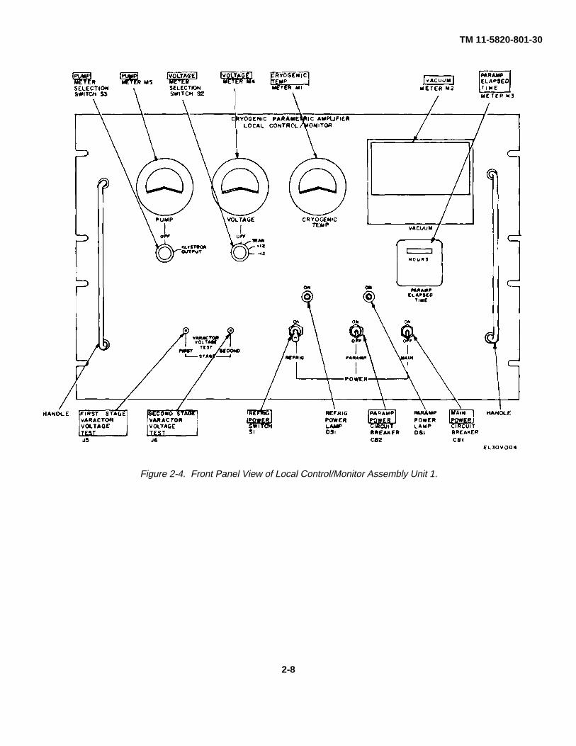
b. Functionally Amplifier, Parametric AM-6602/-MSC-46(V) can be divided into three parts: signalamplification, internal temperature control, and switching.Monitoring circuits with visual indicators are subcircuits ineach of the functional circuits. Visual monitors includemeters, panel and fuse lamps, and a temperature gage.The primary monitors are located on LocalControl/Monitor Assembly, Unit 1, front panel (fig. 2-4)and on Remote Control/Monitor Assembly, 3A1, frontpanel (fig. 3-4). There are, in addition, three panellamps, four fuse lamps, and a temperature gage onmodule panels in Frame Assembly, Unit 2 (fig. 3-14).2-2. Block Diagram of Signal Amplification CircuitFigure 2-1 is a block diagram of the signal amplificationcircuit. The circuit consists of two parametric amplifierstages (2A3 and 2A2) interconnected by band-pass filter2A4. A klystron pump source (2A1) supplies both
parametric amplifier stages. A power supply (1PS1)supplies the operating dc voltages. Monitors providevisual information on the dc voltages (VOLTAGE meter1M4), the relative pump power (PUMP meter 1M5) andoperating time (PARAMP ELAPSED TIME meter 1M3).Test points (FIRST STAGE and SECOND STAGEVARACTOR VOLTAGE TEST) provide convenientmethods of sampling varactor bias voltages on Unit 1.2-3. Vacuum Vessel Module 2A3 (First Stage
Amplifier)a. General. Vacuum Vessel Module 2A3 (first stageamplifier) consists of a ferrite paramp circulator (5 port, 3junction), a paramp varactor diode in a suitable mountand a bandpass pump filter through which the pumppower (from 2A1) enters the paramp varactor (fig. 2-1).To minimize resistive noise generation, the first stagecomponents (paramp circulator, paramp varactor andpump filter) are operated at an ambient temperature ofabout 18°K, cooled by means of Refrigerator UnitAssembly 4A3, part of Unit 4. The first stage amplifiertypically operates at a center frequency of 7.5 GHz, hasa bandwidth of 0.50 GHz and produces a net gain of 15.2dB.
2-1

TM 11-5820-801-30
Figure 2-1. Block Diagram of Signal Amplification Circuit, AM-6602/MSC-46(V).
2-2
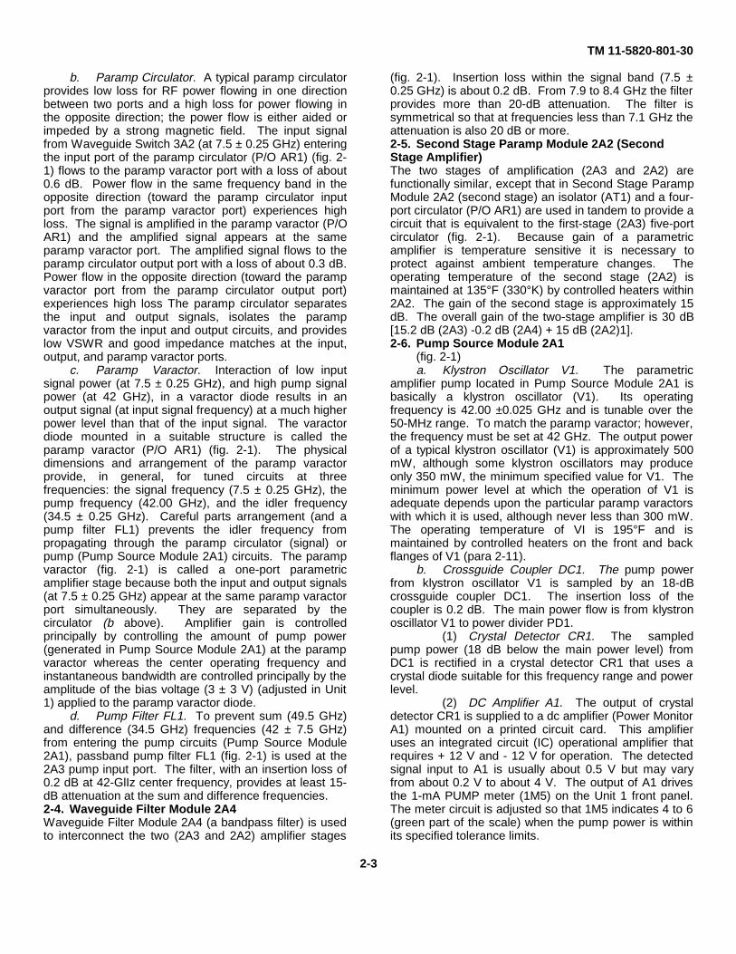
TM 11-5820-801-30
b. Paramp Circulator. A typical paramp circulatorprovides low loss for RF power flowing in one directionbetween two ports and a high loss for power flowing inthe opposite direction; the power flow is either aided orimpeded by a strong magnetic field. The input signalfrom Waveguide Switch 3A2 (at 7.5 ± 0.25 GHz) enteringthe input port of the paramp circulator (P/O AR1) (fig. 2-1) flows to the paramp varactor port with a loss of about0.6 dB. Power flow in the same frequency band in theopposite direction (toward the paramp circulator inputport from the paramp varactor port) experiences highloss. The signal is amplified in the paramp varactor (P/OAR1) and the amplified signal appears at the sameparamp varactor port. The amplified signal flows to theparamp circulator output port with a loss of about 0.3 dB.Power flow in the opposite direction (toward the parampvaractor port from the paramp circulator output port)experiences high loss The paramp circulator separatesthe input and output signals, isolates the parampvaractor from the input and output circuits, and provideslow VSWR and good impedance matches at the input,output, and paramp varactor ports.
c. Paramp Varactor. Interaction of low inputsignal power (at 7.5 ± 0.25 GHz), and high pump signalpower (at 42 GHz), in a varactor diode results in anoutput signal (at input signal frequency) at a much higherpower level than that of the input signal. The varactordiode mounted in a suitable structure is called theparamp varactor (P/O AR1) (fig. 2-1). The physicaldimensions and arrangement of the paramp varactorprovide, in general, for tuned circuits at threefrequencies: the signal frequency (7.5 ± 0.25 GHz), thepump frequency (42.00 GHz), and the idler frequency(34.5 ± 0.25 GHz). Careful parts arrangement (and apump filter FL1) prevents the idler frequency frompropagating through the paramp circulator (signal) orpump (Pump Source Module 2A1) circuits. The parampvaractor (fig. 2-1) is called a one-port parametricamplifier stage because both the input and output signals(at 7.5 ± 0.25 GHz) appear at the same paramp varactorport simultaneously. They are separated by thecirculator (b above). Amplifier gain is controlledprincipally by controlling the amount of pump power(generated in Pump Source Module 2A1) at the parampvaractor whereas the center operating frequency andinstantaneous bandwidth are controlled principally by theamplitude of the bias voltage (3 ± 3 V) (adjusted in Unit1) applied to the paramp varactor diode.
d. Pump Filter FL1. To prevent sum (49.5 GHz)and difference (34.5 GHz) frequencies (42 ± 7.5 GHz)from entering the pump circuits (Pump Source Module2A1), passband pump filter FL1 (fig. 2-1) is used at the2A3 pump input port. The filter, with an insertion loss of0.2 dB at 42-GlIz center frequency, provides at least 15-dB attenuation at the sum and difference frequencies.2-4. Waveguide Filter Module 2A4Waveguide Filter Module 2A4 (a bandpass filter) is usedto interconnect the two (2A3 and 2A2) amplifier stages
(fig. 2-1). Insertion loss within the signal band (7.5 ±0.25 GHz) is about 0.2 dB. From 7.9 to 8.4 GHz the filterprovides more than 20-dB attenuation. The filter issymmetrical so that at frequencies less than 7.1 GHz theattenuation is also 20 dB or more.2-5. Second Stage Paramp Module 2A2 (SecondStage Amplifier)The two stages of amplification (2A3 and 2A2) arefunctionally similar, except that in Second Stage ParampModule 2A2 (second stage) an isolator (AT1) and a four-port circulator (P/O AR1) are used in tandem to provide acircuit that is equivalent to the first-stage (2A3) five-portcirculator (fig. 2-1). Because gain of a parametricamplifier is temperature sensitive it is necessary toprotect against ambient temperature changes. Theoperating temperature of the second stage (2A2) ismaintained at 135°F (330°K) by controlled heaters within2A2. The gain of the second stage is approximately 15dB. The overall gain of the two-stage amplifier is 30 dB[15.2 dB (2A3) -0.2 dB (2A4) + 15 dB (2A2)1].2-6. Pump Source Module 2A1
(fig. 2-1)a. Klystron Oscillator V1. The parametric
amplifier pump located in Pump Source Module 2A1 isbasically a klystron oscillator (V1). Its operatingfrequency is 42.00 ±0.025 GHz and is tunable over the50-MHz range. To match the paramp varactor; however,the frequency must be set at 42 GHz. The output powerof a typical klystron oscillator (V1) is approximately 500mW, although some klystron oscillators may produceonly 350 mW, the minimum specified value for V1. Theminimum power level at which the operation of V1 isadequate depends upon the particular paramp varactorswith which it is used, although never less than 300 mW.The operating temperature of VI is 195°F and ismaintained by controlled heaters on the front and backflanges of V1 (para 2-11).
b. Crossguide Coupler DC1. The pump powerfrom klystron oscillator V1 is sampled by an 18-dBcrossguide coupler DC1. The insertion loss of thecoupler is 0.2 dB. The main power flow is from klystronoscillator V1 to power divider PD1.
(1) Crystal Detector CR1. The sampledpump power (18 dB below the main power level) fromDC1 is rectified in a crystal detector CR1 that uses acrystal diode suitable for this frequency range and powerlevel.
(2) DC Amplifier A1. The output of crystaldetector CR1 is supplied to a dc amplifier (Power MonitorA1) mounted on a printed circuit card. This amplifieruses an integrated circuit (IC) operational amplifier thatrequires + 12 V and - 12 V for operation. The detectedsignal input to A1 is usually about 0.5 V but may varyfrom about 0.2 V to about 4 V. The output of A1 drivesthe 1-mA PUMP meter (1M5) on the Unit 1 front panel.The meter circuit is adjusted so that 1M5 indicates 4 to 6(green part of the scale) when the pump power is withinits specified tolerance limits.
2-3
TM 11-5820-801-30
c. Power Divider PD1. The pump power fromcrossguide coupler DC1 is split into two channels bymeans of a waveguide power divider PD1. The dividerhas an insertion loss of about 0.1 dB.
d. Isolators AT1 and AT2. Each pump channel(output channels of PD1) has an isolator (insertion loss0.15 dB) to provide adequate channel isolation (20 dB)This helps prevent "crosstalk" between the two amplifierstages.
e. Variable Attenuators AT3 and AT4. The gain,and to some extent the bandwidth, of amplifier stages2A3 and 2A2 is affected by the pump power level at theparamp varactor diode. To adjust the power level ineach amplifier stage, a variable waveguide attenuator(AT3, AT4) is used in each pump powerline. A lossycard (100 ohms per square inch) is inserted into thevariable waveguide by a screw adjustment and is setduring gain-band-width alignment procedures (para 3-7).Attenuation is variable from 0 dB to more than 20 dB,insertion loss is about 0.1 dB. Attenuation variation isnot directly translated into gain variation. Operatingtemperature of AT3 and AT4 is maintained at about135°F by controlled heaters in a heat sink adjacent to theattenuators (para 2-11).2-7. Klystron Power Supply 1PS1
(fig. 2-1)a. General. Klystron Power Supply 1PS1
contains four regulated power supplies receiving theirinput power through a single transformer (T1) thataccepts the three-phase 120 ± 12 V, 55 ± 8 Hz primarypower. Four three-phase outputs of T1 are connected torectifier board A7, which supplies power to a -1000 Vregulator (A9) for the klystron oscillator beam voltage, toa 6.3-V regulator (A1) for the klystron oscillator filamentvoltage, to a + 12 V regulator (A10) for the varactor biasvoltage and the dc amplifiers, and to a - 12 V regulator(A11) for the dc amplifiers. Each 12-V regulator isseparated from rectifier board A7 by a preregulator.
b. Klystron Power. The outputs of - 1000 Vregulator A9 and 6.3-V regulator A1 are supplied directlyto klystron oscillator 2A1V1. The beam voltage (- 1000V) is variable ± 50 V via a trimpot on A9. The correctbeam voltage is that which provides the most pumppower and is originally set by the manufacturer duringinitial alignment procedures. The high side output line ofA1 is connected to the high side (- 1000 V) output line ofA9. Thus the filament voltage is floating on top of thebeam voltage and from a chassis ground point of view,the filament voltage is - 1000 V on the high side of A1output and - 1006 V on the low side of A1 output.
c. Paramp Varactor Bias Voltage. Bias voltagesfor the paramp varactor diodes in 2A3 and 2A2 arederived from the + 12 V regulator (A 10) output. Thebias voltage for each amplifier stage is passed through avoltage divider (1R5, 1E1R8 for first stage; 1R6, 1E1R9for second stage) network in Unit 1 having a trimpot 1R5,1R6 as half the divider. The bias voltage is taken off thewiper arm of the trimpot and is therefore
adjustable over a 0 to 6V range. Manually operatedswitches (54 for the first stage and 55 for the secondstage) permit the operator to connect either bias voltageline to the midpoint of the divider (instead of the wiperarm) thereby providing a 6-V bias. This effectively "turnsoff" (bypasses) the amplifier stage by biasing it out ofoperating frequency range and at the same timeprovides minimum insertion loss for that stage. Thecorrect bias voltage for each amplifier stage isdetermined during a gain-bandwidth alignment (para 3-7).
d. DC Amplifier Voltage. DC amplifiers in 2A1(2A1 Power Monitor, fig. 2-1) and Unit 1 (1A1Temperature Monitor, fig. 2-2) contain an IC operationalamplifier (U1) (fig. 2-9, 2-14) that requires + 12V and - 12V for operation. These voltages are obtained directlyfrom A10 and A11, the + 12 volt and - 12 volt regulators,respectively. The two regulators are identical. In thispower supply the positive end of A11 is connected to thenegative end of A10 thereby providing a common ± 12 Vreturn line. A trimpot on each 12-V regulator permitssome adjustment of the output voltage. The trimpot ispreset before installation to provide a 12 ± 0 12V output.2-8. Monitors in Signal Amplification Circuits
a. VOLTAGE Meter 1M4. By means of aVOLTAGE selection switch (1S2) on the front panel ofUnit 1 the operator can select 1PS1 output voltages to bedisplayed on VOLTAGE meter 1M4 (fig. 2-1) VOLTAGEmeter 1M4 provides a direct measurement of the outputof 1PS1A10 and 1PS1A11, the ± 12 V regulators. Thenegative voltage from A1 is reversed at the meterterminals so that a positive deflection is obtained Beamvoltage (-1000 V from A9) is sampled at 0.01 amplitude(by means of a voltage divider in Unit 1) so thatVOLTAGE meter 1M4 indicates 10 ± 0.5 when the beamvoltage is - 1000 ± 50 V The output of A1, the 6.3-Vregulator, is not monitored.
b. PUMP Meter 1M5. The output of (PowerMonitor) dc amplifier 2A1A1 (para 2-6b(2)) can bedisplayed on 1M5, PUMP meter, by use of PUMPselection switch 1S3 (fig. 2-1). Because the outputvoltage of crystal detectors (2A1CR1, fig. 2-1) variesover a wide range a meter adjustment (PUMP POWERMETER ADJ R7 on rear panel of Unit 1, fig. 3-3) isprovided to align PUMP meter 1M5 to indicate in thegreen area of the scale (4 to 6) when pump power (para2-6a) is adequate. The manufacturer aligns 1M5 tooperate with the 2A1 module with which it is shippedInterchanging Unit 1's or 2A1 modules may necessitaterealignment of PUMP meter 1M5. Replacement of pieceparts or subassemblies in either the 2A1 portion or Unit 1portion of the pump power monitoring (and generation)circuit may also necessitate realignment.
c. PARAMP ELAPSED) TIME Meter IM3.PARAMP ELAPSED TIME meter 1M3 is a time totalizingmeter operating on 120 ± 12 V, 55 ± 8 Hz. The meterindi-
2-4

TM 11-5820-801-30
cates total hours and tenths of hours that primary voltagehas been applied to 1PS1 (fig. 2-1). The meter dial hasa digital movement; that is, the 0.1-hour indicator movesonce in 6 minutes and the hour indicator advances oneunit each hour. Klystron oscillator 2A1V1 is a limited lifeitem (5000 hours, minimum). The purpose of 1M3 is toindicate when 2A1V1 is approaching its expected lifelimit.
d. VARACTOR VOLTAGE TEST Points. Twomonitor points, VARACTOR VOLTAGE TEST FIRST
STAGE and SECOND STAGE, on the front panel of Unit1 permit measurement of the bias voltages to the 2A3paramp varactor and the 2A2 paramp varactor (fig. 2-1).The voltage will be in the range 3 ± 3 V. The precisevalue is not important (para 2-7c). These monitor pointspermit maintenance personnel to determine easilywhether bias voltage is present in Unit 1 and therefore(assuming circuit continuity) at the paramp varactors inModules 2A2 and 2A3. The presence or absence of biasvoltages is an important maintenance factor.
Section II. INTERNAL TEMPERATURE CONTROLS
2-9. Vacuum Vessel Module 2A3 Temperaturea. General. The interior of Vacuum Vessel
Module 2A3 is operated at an ambient temperature ofabout 18°K (- 427°F). This is accomplished by use of aclosed cycle Helium Refrigerator, Unit 4, of whichRefrigeration Unit Assembly 4A3 is inserted into 2A3. Avacuum is used to insulate the cold parts of 2A3 (and4A3). Because the cryogenic temperature is well belowthe freezing point of air, the temperature helps maintain
the vacuum at a much lower pressure than that initiallyobtained by operating the vacuum pump duringpreliminary adjustment procedures. Thus a hardvacuum indicates suitably low temperature andunsatisfactorily high temperature results in a softvacuum. Unit 1 monitors are used to indicate the internalcryogenic temperature (CRYOGENIC TEMP meter 1M1)and pressure (VACUUM meter 1M2) in 2A3 (fig. 2-2).
Figure 2-2. Block Diagram of Module 2A3 Temperature and Pressure Sensors.
b. CRYOGENIC TEMP Meter 1M1. Refrigerator UnitAssembly 4A3 (fig. 2-2) has two independenttemperature sensors.
One is a hydrogen bulb that operates a hydrogenpressure gage (temperature gage) mounted on
2-5
TM 11-5820-801-30
4A3. When the temperature is below 26°K (60 psia ongage) the hydrogen pressure gage is an accuratetemperature gage and is so calibrated. A second sensoris a thermocouple mounted at the same cold station of4A3 as is the hydrogen bulb. The voltage on thethermocouple leads is brought out to a connector(2A3J1). The voltage is then applied through cableconnections to Temperature Monitor 1A1 (a dc amplifier)located in Unit 1. The thermocouple voltage is amplifiedsufficiently in 1A1 to drive CRYOGENIC TEMP meter1M1. Temperature Monitor 1A1 utilizes an ICoperational amplifier (para 2-7d) that requires + 12 voltsand -12 volts for operation. The amplification is adjustedso that CRYOGENIC TEMP meter 1M1 indicates 20°Kwhen the temperature gage on 4A3 also indicates 20°K.The two temperature indicators may not track preciselyat other temperatures (20° ± 5°K) but the 4A3temperature gage is the more accurate of the two.
c. VACUUM Meter IM2. The vacuum sensorconsists of a thermopile bridge tube (J2, fig. 2-2) that isinserted into 2A3. The sensor uses 0.20 Vac to heat thehot junc- tions of the thermopile; the cold junctions areheld at ambient vessel (2A3) temperature. Thetemperature differential between the hot and coldjunctions is about 10°C at atmospheric pressure butrises to perhaps 400°C in a hard vacuum. Thethermopile (vacuum sensor) then generates anincreasing voltage as the pressure decreases. Thethermopile voltage is applied to a vacuum gage circuitthat drives VACUUM meter 1M2. The complete sensor(thermopile tube 2A3J2 and VACUUM meter 1M2 with its
associated circuit) is a pre-calibrated part. Either section(1M2 or 2A3J2) can be separately replaced, but notrepaired.2-10. Second Stage Paramp Module 2A2
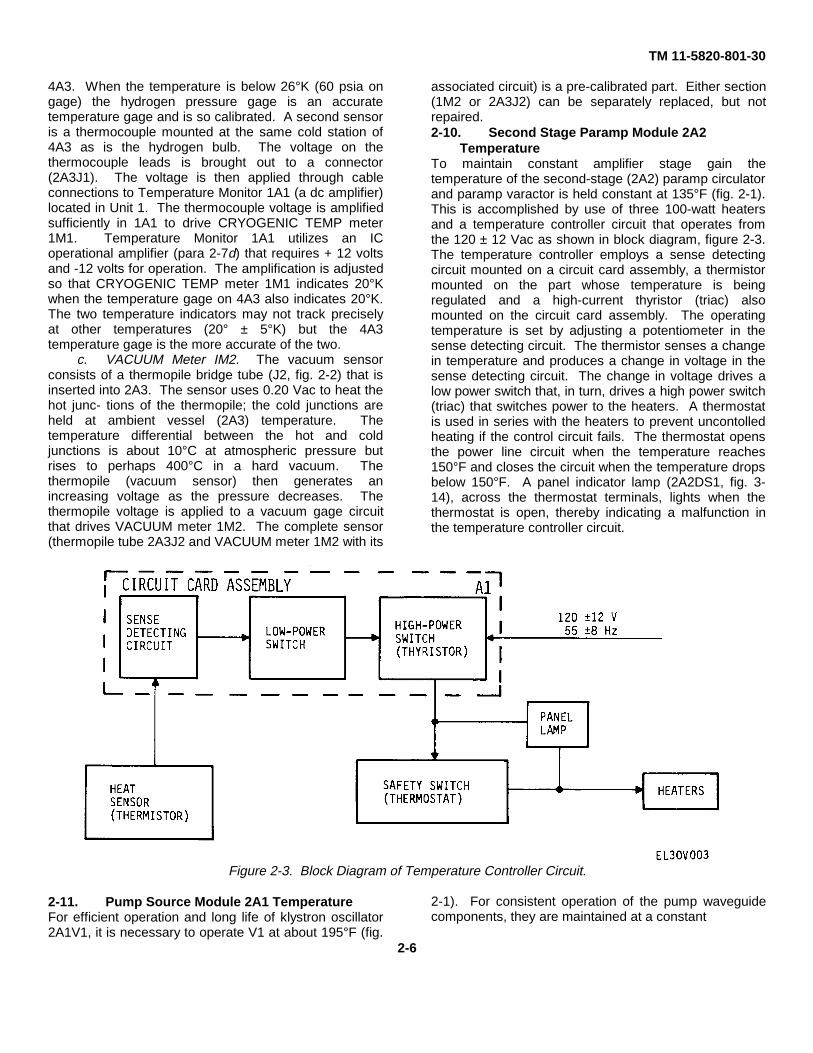
TemperatureTo maintain constant amplifier stage gain thetemperature of the second-stage (2A2) paramp circulatorand paramp varactor is held constant at 135°F (fig. 2-1).This is accomplished by use of three 100-watt heatersand a temperature controller circuit that operates fromthe 120 ± 12 Vac as shown in block diagram, figure 2-3.The temperature controller employs a sense detectingcircuit mounted on a circuit card assembly, a thermistormounted on the part whose temperature is beingregulated and a high-current thyristor (triac) alsomounted on the circuit card assembly. The operatingtemperature is set by adjusting a potentiometer in thesense detecting circuit. The thermistor senses a changein temperature and produces a change in voltage in thesense detecting circuit. The change in voltage drives alow power switch that, in turn, drives a high power switch(triac) that switches power to the heaters. A thermostatis used in series with the heaters to prevent uncontolledheating if the control circuit fails. The thermostat opensthe power line circuit when the temperature reaches150°F and closes the circuit when the temperature dropsbelow 150°F. A panel indicator lamp (2A2DS1, fig. 3-14), across the thermostat terminals, lights when thethermostat is open, thereby indicating a malfunction inthe temperature controller circuit.
Figure 2-3. Block Diagram of Temperature Controller Circuit.
2-11. Pump Source Module 2A1 TemperatureFor efficient operation and long life of klystron oscillator2A1V1, it is necessary to operate V1 at about 195°F (fig.
2-1). For consistent operation of the pump waveguidecomponents, they are maintained at a constant
2-6
TM 11-5820-801-30
temperature. The interior of the Pump Source Module2A1 is maintained at about 135° by means of two 50-wattheaters and a fan to circulate the hot air The back flangeof V1 has two 100-watt heaters and the front flange, a100-watt heater. The temperature controller cards forthese heater banks are electrically identical to the card(2A2A1) used in the Second Stage Paramp Module 2A2(para 2-10, fig 2-3). Only their temperature settings are
different. Thermostats to protect against uncontrolledtemperature rise are used with each heater bank. Panelindicator lamps are placed across the terminals of S2and S4, the thermostats in the back flange and frontflange heater circuits, respectively. The lamps light whenthe thermostats are open, thereby indicatingmalfunctions in the temperature control circuits forklystron oscillator V1.
Section III. SWITCHING
2-12. GeneralRedundantly installed Parametric Amplifier system AM-6602/MSC-46(V) contains two Waveguide Switches, 3A2and 3A3, and switches on Unit 1, Module 2A1, andRemote Control/Monitor Assembly 3A1 Unit 1 (fig 2-4)contains three power switches:
MAIN POWER circuit breaker CB1PARAMP POWER circuit breaker CB2REFRIG POWER switch S1,
two meter switches:VOLTAGE meter selection switch S2PUMP meter selection switch S3,
and two amplifier stage switches:
first stage switch S4 (fig. 3-3)second stage switch S5 (fig. 3-3).
These switches are described in paragraphs 2-7 and 2-8a and b. Remote Control/Monitor Assembly Serial No.001 contains a NOISE DIODE switch (S2, fig. 3-5) usedto switch 28 Vdc to Noise Diode Assembly 3A13. Switch2A1S1 is a safety interlock. Waveguide switches 3A2,3A3 and CHANNEL SELECT pushbutton switch 3A1S1comprise the channel switching system. The safetyinterlock and channel switching are described inparagraphs 2-13 and 2-14, respectively. Noise signalgeneration is discussed in paragraphs 2-20c and 2-14c.
2-7
TM 11-5820-801-30
Figure 2-4. Front Panel View of Local Control/Monitor Assembly Unit 1.
2-8
TM 11-5820-801-30
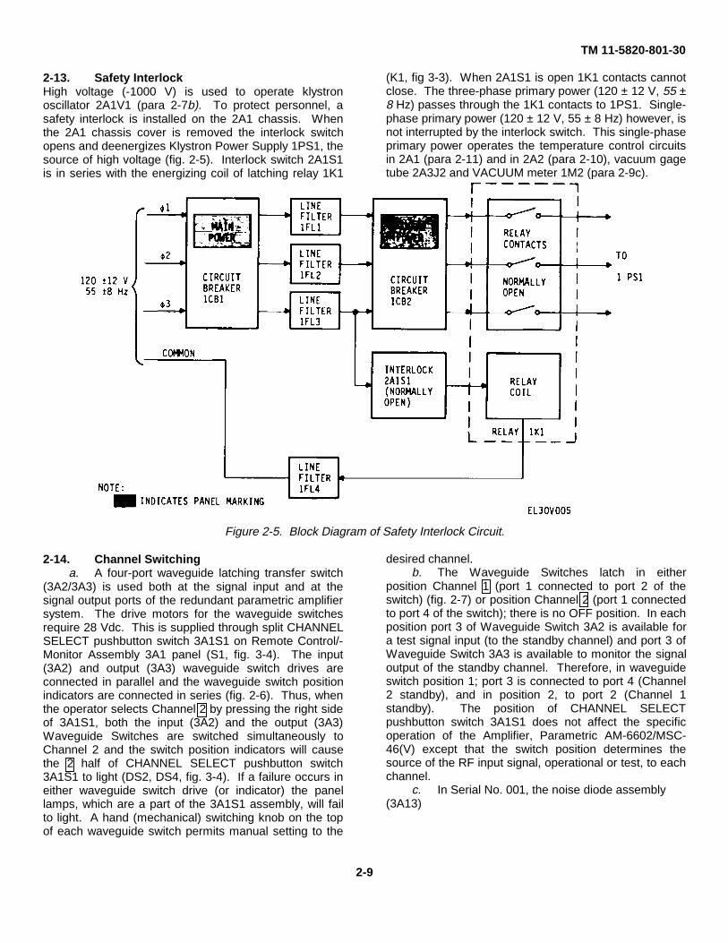
2-13. Safety InterlockHigh voltage (-1000 V) is used to operate klystronoscillator 2A1V1 (para 2-7b). To protect personnel, asafety interlock is installed on the 2A1 chassis. Whenthe 2A1 chassis cover is removed the interlock switchopens and deenergizes Klystron Power Supply 1PS1, thesource of high voltage (fig. 2-5). Interlock switch 2A1S1is in series with the energizing coil of latching relay 1K1
(K1, fig 3-3). When 2A1S1 is open 1K1 contacts cannotclose. The three-phase primary power (120 ± 12 V, 55 ±8 Hz) passes through the 1K1 contacts to 1PS1. Single-phase primary power (120 ± 12 V, 55 ± 8 Hz) however, isnot interrupted by the interlock switch. This single-phaseprimary power operates the temperature control circuitsin 2A1 (para 2-11) and in 2A2 (para 2-10), vacuum gagetube 2A3J2 and VACUUM meter 1M2 (para 2-9c).
Figure 2-5. Block Diagram of Safety Interlock Circuit.
2-14. Channel Switchinga. A four-port waveguide latching transfer switch
(3A2/3A3) is used both at the signal input and at thesignal output ports of the redundant parametric amplifiersystem. The drive motors for the waveguide switchesrequire 28 Vdc. This is supplied through split CHANNELSELECT pushbutton switch 3A1S1 on Remote Control/-Monitor Assembly 3A1 panel (S1, fig. 3-4). The input(3A2) and output (3A3) waveguide switch drives areconnected in parallel and the waveguide switch positionindicators are connected in series (fig. 2-6). Thus, whenthe operator selects Channel 2 by pressing the right sideof 3A1S1, both the input (3A2) and the output (3A3)Waveguide Switches are switched simultaneously toChannel 2 and the switch position indicators will causethe 2 half of CHANNEL SELECT pushbutton switch3A1S1 to light (DS2, DS4, fig. 3-4). If a failure occurs ineither waveguide switch drive (or indicator) the panellamps, which are a part of the 3A1S1 assembly, will failto light. A hand (mechanical) switching knob on the topof each waveguide switch permits manual setting to the
desired channel.b. The Waveguide Switches latch in either
position Channel 1 (port 1 connected to port 2 of theswitch) (fig. 2-7) or position Channel 2 (port 1 connectedto port 4 of the switch); there is no OFF position. In eachposition port 3 of Waveguide Switch 3A2 is available fora test signal input (to the standby channel) and port 3 ofWaveguide Switch 3A3 is available to monitor the signaloutput of the standby channel. Therefore, in waveguideswitch position 1; port 3 is connected to port 4 (Channel2 standby), and in position 2, to port 2 (Channel 1standby). The position of CHANNEL SELECTpushbutton switch 3A1S1 does not affect the specificoperation of the Amplifier, Parametric AM-6602/MSC-46(V) except that the switch position determines thesource of the RF input signal, operational or test, to eachchannel.
c. In Serial No. 001, the noise diode assembly(3A13)
2-9

TM 11-5820-801-30
is mounted on 3A2 port 3. A switch (NOISE DIODE) onSerial No. 001, 3A1, permits the operator to activate thenoise diode by switching on + 28 V (S2, fig. 3-5). A noisesignal is then supplied via the decoupled port ofdirectional coupler 3A13A1 to the standby channel andcan be monitored at 3A3 port 3.
d. In all systems during gain-bandwidth test and
alignment procedures, the RF output of a sweepgenerator is connected to 3A2 port 3 and the amplifiedsignal is monitored by test equipment attached to 3A3port 3 (fig. 3-8). In Serial No. 001, the sweep generatoris connected to 3A2 port 3 via the main port of directionalcoupler 3A13A1.
Figure 2-7. Block Diagram of Channel Switching, RF Switch Positions.
Figure 2-6. Block Diagram of Channel Switching, +28 V Control and Display Indicator Circuits.
2-10
TM 11-5820-801-30
Section IV. CIRCUIT DESCRIPTIONS
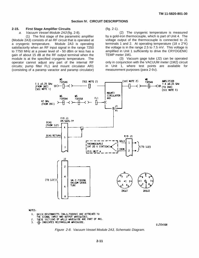
2-15. First Stage Amplifier Circuitsa. Vacuum Vessel Module 2A3 (fig. 2-8).
(1) The first stage of the parametric amplifier(Module 2A3) consists of an RF circuit that is operated ata cryogenic temperature. Module 2A3 is operatingsatisfactorily when an RF input signal in the range 7250to 7750 MHz at a power level of - 50 dBm or less has again of about 15 dB at the RF output terminal when themodule is at the specified cryogenic temperature. Theoperator cannot adjust any part of the internal RFcircuits; pump filter FL1 and mount circulator AR1(consisting of a paramp varactor and paramp circulator)
(fig. 2-1).(2) The cryogenic temperature is measured
by a gold-iron thermocouple, which is part of Unit 4. Thevoltage output of the thermocouple is connected to J1terminals 1 and 2. At operating temperature (18 ± 2°K)the voltage is in the range 2.5 to 7.5 mV. This voltage isamplified in Unit 1 sufficiently to drive the CRYOGENICTEMP meter 1M1.
(3) Vacuum gage tube (J2) can be operatedonly in conjunction with the VACUUM meter (1M2) circuitin Unit 1, where test points are available formeasurement purposes (para 2-9c).
Figure 2-8. Vacuum Vessel Module 2A3, Schematic Diagram.
2-11

TM 11-5820-801-30
(4) The varactor bias voltage (J1 terminals 4and 5) is set in Unit 1 during gain-bandwidth alignment.The presence of the voltage, not its value, is theimportant factor. Because the bias circuit cannot tolerateany appreciable dc current (10 microamp, maximum) noimpedance measurements can be made. Current willcause irreparable damage to the varactor diode mountedwithin the paramp varactor. The varactor diode is thedevice that provides parametric amplification. Biasvoltage can be measured on Unit 1 at 1J5, FIRSTSTAGE VARACTOR VOLTAGE TEST.b. Temperature Monitor 1A1 (fig. 2-9). Circuit cardassembly 1A1, Temperature Monitor, is a dc amplifierused to amplify the thermocouple output voltage (aabove) to a level sufficient to drive a 1-mil meter,
CRYOGENIC TEMP meter 1M1. An integrated circuitoperational amplifier (U1) is used as the active element.This operational amplifier requires + 12 V on terminal 7and - 12 V on terminal 4, supplied through card (P1)terminals C and E, respectively. The input signal (2.5 to7.5 mV) is applied to U1 terminals 2 and 3 via P1terminals F and B, respectively. A bridge circuit (R1, R2,R7, R8, R6) is used to balance the input voltage withrespect to circuit ground and center the output meter.Variable resistor R12 is a feedback resistor used to setthe overall gain of the amplifier. Meter 1M1 is connecteddirectly across P1 terminals J and H. R4, in the metercircuit, is a limiting resistor used to protect the meter.Assembly 1A1 provides a gain of about 13 dB.
Figure 2-9. Temperature Monitor Card 1A1 (Sheet 1 of 2).
2-12
TM 11-5820-801-30
Figure 2-9. Temperature Monitor Card 1A1 (Sheet 2 of 2).
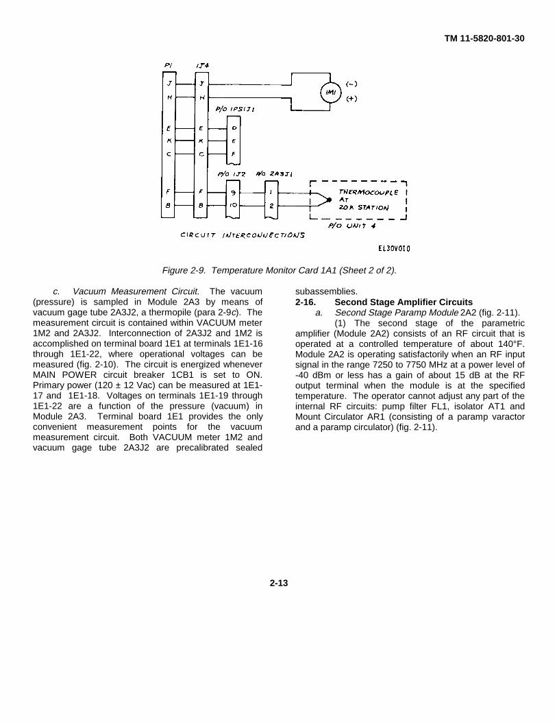
c. Vacuum Measurement Circuit. The vacuum(pressure) is sampled in Module 2A3 by means ofvacuum gage tube 2A3J2, a thermopile (para 2-9c). Themeasurement circuit is contained within VACUUM meter1M2 and 2A3J2. Interconnection of 2A3J2 and 1M2 isaccomplished on terminal board 1E1 at terminals 1E1-16through 1E1-22, where operational voltages can bemeasured (fig. 2-10). The circuit is energized wheneverMAIN POWER circuit breaker 1CB1 is set to ON.Primary power (120 ± 12 Vac) can be measured at 1E1-17 and 1E1-18. Voltages on terminals 1E1-19 through1E1-22 are a function of the pressure (vacuum) inModule 2A3. Terminal board 1E1 provides the onlyconvenient measurement points for the vacuummeasurement circuit. Both VACUUM meter 1M2 andvacuum gage tube 2A3J2 are precalibrated sealed
subassemblies.2-16. Second Stage Amplifier Circuits
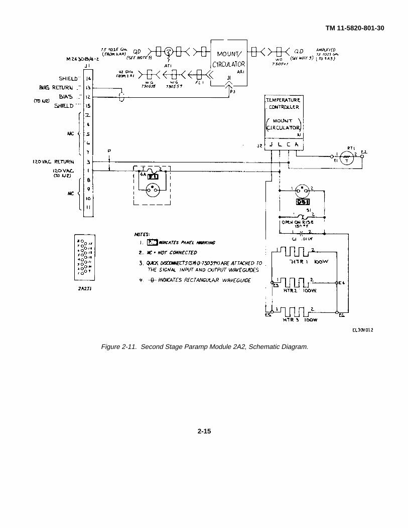
a. Second Stage Paramp Module 2A2 (fig. 2-11).(1) The second stage of the parametric
amplifier (Module 2A2) consists of an RF circuit that isoperated at a controlled temperature of about 140°F.Module 2A2 is operating satisfactorily when an RF inputsignal in the range 7250 to 7750 MHz at a power level of-40 dBm or less has a gain of about 15 dB at the RFoutput terminal when the module is at the specifiedtemperature. The operator cannot adjust any part of theinternal RF circuits: pump filter FL1, isolator AT1 andMount Circulator AR1 (consisting of a paramp varactorand a paramp circulator) (fig. 2-11).
2-13

TM 11-5820-801-30
Figure 2-10. Vacuum Measurement Circuit, P/O Unit 1.
2-14
TM 11-5820-801-30
Figure 2-11. Second Stage Paramp Module 2A2, Schematic Diagram.
2-15
TM 11-5820-801-30
(2) The varactor bias voltage (J1 terminals 12and 13) is set in Unit 1 during gain-bandwidth alignment.The presence of the voltage, not its value, is theimportant factor. Because the bias circuit cannot tolerateany appreciable dc current (10 microamp, maximum) noimpedance measurements can be made. Current willcause irreparable damage to the varactor diode mountedwithin the paramp varactor. The varactor diode is thedevice that provides parametric amplification. Biasvoltage can be measured on Unit 1 at 1J6, SECONDSTAGE VARACTOR VOLTAGE TEST.
(3) The temperature of Module 2A2 ismaintained by controlling power to three 100-W heaterslocated in heat sinks adjacent to AR1. The heaters arewired in parallel with a thermostat in series with theheaters. The thermostat is normally closed but will openif the temperature reaches 150°F. This is a safety deviceto prevent overheating. Capacitor C1 across thethermostat terminals is used to suppress transients whenthe thermostat switches. Thermistor RT1 senses achange in temperature of the heat sink on which it islocated and is the controlling device for temperaturecontroller A1. Temperature controller A1, in response toAT1 resistance variations, switches on and off power(120 ± 12 Vac) to the heaters to maintain thetemperature at 140 ± 4°F. Primary power to the heatersenters through J1 terminals 1 and 3. This power comesfrom the output side of Unit 1 line filters 1 FL2 and 1 FL4and is present whenever MAIN POWER circuit breaker1CB1 is set to ON (fig. 2-17). An indicating fuse, F1, inthe 120-V power line is mounted on the panel of Module2A2.
b. Temperature Controller Circuit (fig. 2-12). U1 is anintegrated circuit zero-voltage switch. Q1 is a thyristorthat, when triggered on, conducts current for the heatercircuits. The function of U1 is to trigger on Q1 when heatis needed. The pulse output to Q1 is at U1 terminal 4.This pulse is produced when the ac voltage crosses zerovoltage line. The thyristor then conducts until the voltageagain returns to the zero line (a half cycle). The processis repeated until the heat produced is at the preset level.The thermistor RT1 (a negative temperature coefficientresistor) is connected across card terminals C and A andU1 terminals 7 and 13. On U1, terminal 7 is the commonterminal. The pulsing of Q1 occurs when the resistanceof RT1 is greater than the resistance of R2 plus R3.Resistor R2 is variable and is preset to provide therequired temperature. As the heat sink on which RT1 ismounted becomes warmer, the resistance of RT1decreases and when it matches that of R1 + R2 U1 doesnot produce a pulse and the thyristor is not pulsed on;hence, no current flows through the heaters. R2 is aseries limiting resistor used to protect U1. C1 is an inputcapacitor and C2 is an output capacitor, both for U1.Because of the nature of U1 and Q1, impedancemeasurements are not practical. Voltage measurements(120 ± 12 Vac) can be made be- tween card terminals Land C (power input) and J and L (load-heater circuit).Under normal operating conditions, the J-L voltage isintermittent. One temperature controller is used inModule 2A2 and three, in Module 2A1. The circuits areidentical; the settings of the variable resistor R2 differ ineach to provide a different control temperature.
2-16

TM 11-5820-801-30
Figure 2-12. Temperature Controller; 2A2A1, 2A1A2, 2A1A3, 2A1A4, Schematic Diagram.
2-17. RF Pump Circuitsa. Pump Source Module 2A1 (fig. 2-13).
(1) The primary subassembly of Module 2A1is the klystron oscillator V1. This tube operates with -1000 V beam voltage and +6.3 V (with respect to thebeam voltage) filament voltage. These voltages aregenerated in 1PS1 and supplied to Module 2A1 throughterminals J, K, and H of J1. The output power of V1 is at42.00 GHz. The RF power is divided into two channelsin power divider PD1, one channel for each stage of theparametric amplifier. The RF power control is thevariable attenuator (AT3 in fist stage channel and AT4 in
second stage channel). The variable attenuators aremounted behind a cover plate on the panel of Module2A1. The required adjustments can be made when thecover plate is removed. Each variable attenuator is setduring gain-bandwidth alignment. A crossguide coupler(DC1) is inserted between V1 and PD1 so that the outputpower of V1 can be sampled. The decoupled power isrectified in crystal detector CR1 and the dc output issupplied to a dc amplifier, Power Monitor A1, where it isamplified sufficiently to operate meter 1M5, PUMP meteron Unit 1.
2-17

TM 11-5820-801-30
Figure 2-13. Pump Source Module 2A1, Schematic Diagram.
2-18
TM 11-5820-801-30
(2) Module 2A1 uses three temperaturecontrol circuits and a fan for precise temperature control.Temperature controllers A2, A3 and A4 are identical to2A2A1 except for the setting of the control resistor R2(fig. 2-12). The thermostats mounted on the heat sinkfor V1, S2 and S4, have panel lamps, DS1 and DS2,respectively, across their terminals. These lamps,mounted on Module 2A1 panel, light when thethermostats are open thereby indicating malfunctions inthe temperature control circuits. (Refer to para 2-11.)Capacitors to suppress transients are placed across theterminals of all three thermostats (S2, S3, S4). Primarypower (120 ± 12 V) to the heaters enters through J1terminals A and B. This power comes from the outputsides of Unit 1 line filters 1 FL3 and 1 FL4 and is presentwhenever MAIN POWER circuit breaker 1CB1 is set toON (fig. 2-17). An indicating fuse, F1, in the 120-vpowerline, is mounted on the panel of Module 2A1.
(3) Safety switch S1 is described inparagraph 2-13 (fig. 2-5). Because S1 is connected tothe 120-V line behind fuse F1, the interlock relay (1K1)will not close when F1 is open as well as when S1 isopen. This prevents the applicator of dc power toModule 2A1 when all of the temperature control circuitsare disabled.
(4) The dc amplifier, Power Monitor A1,requires +12 V and -12 V for operation. These lines areprotected by indicating fuses F2 and F3, respectively.The fuses are mounted on the panel of Module 2A1.
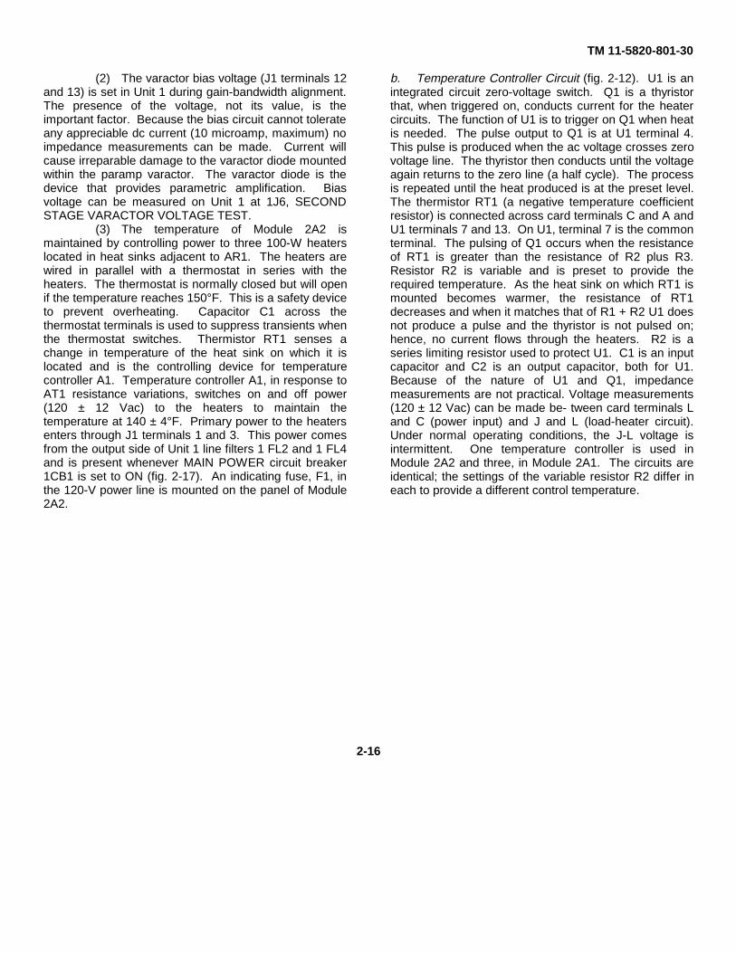
b. Power Monitor 2A1A1 (fig. 2-14). Circuit card
assembly 2A1A1, Power Monitor, is a dc amplifier usedto amplify the detected pump power voltage to a levelsufficient to drive a 1-mil meter, PUMP meter 1M5. Anintegrated circuit operational amplifier (U1) is used as theactive element. This operational amplifier is identical tothat used in 1A1, Temperature Monitor, dc amplifier(para 2-15b). This operational amplifier requires +12 Von terminal 7 and -12 V on terminal 4, supplied throughcard (P1) terminals B and H, respectively. The inputsignal from 2A1CR1 (0.2 to 4 V) is applied to U1 terminal2 via card terminal K. PUMP meter selection switch 1S3is connected across card terminals D and A. When 1S3is set to KLYSTRON OUTPUT, PUMP meter 1M5 isconnected across these terminals; when 1S3 is set toOFF the circuit is open. A variable resistor(potentiometer) mounted in Unit 1 (R7 PUMP POWERMETER ADJ) is connected across card terminals C, Land J. Terminal L is connected to the wiper arm of 1R7,which is adjusted (screwdriver adjustment) to center themeter (1M5) deflection. Variable resistor R5 in thefeedback circuit permits adjustment of the gain of the dcamplifier. Whenever the gain is changed the meterdeflection may require adjustment via 1R7. The requiredgain depends on the detected voltage from the particularcrystal detector (2A1CR1) with which it is used. Theinput RF power to the crystal detector depends on theparticular klystron oscillator (2A1V1) with which it isused.
Figure 2-14. Pump Source Power Monitor 2A1A1, Schematic Diagram.
2-19

TM 11-5820-801-30
2-18. Local Control and Monitoring Circuitsa. Varactor Bias Voltage Circuit (fig. 2-15). The
source of the varactor bias voltage is the + 12 voltregulator in Regulated Power Supply 1PS1. A voltagedivider consisting of a 1-kilohm fixed resistor (E1R8 orE1R9) and a 1-kilohm variable resistor (R5 or R6) isconnected across the + 12 volt regulator output. Thebias voltage is taken off the low side of the divider (12-volt return line) and either the wiper arm of the variableresistor or the center of the voltage divider. The biasvoltage can therefore be varied from 0 to +6 V. Thewiper arm line and the line to the voltage divider midpoint
are connected to two poles of a single throw switch (S4or S5). The common terminal of the switch (S4-2 or S5-2) is connected to the panel test jack J5 or J6) and to thevaractor diode in the parametric amplifier stage (2A3,first stage or 2A2, second stage). The varactor diode,then, always has a bias voltage applied: either from thewiper arm of the variable resistor (normal operation) orfrom the midpoint (+6 V) of the voltage divider (BYPASSoperation). E1R8 and E1R9 are mounted on terminalboard 1E1; R5 and R6, S4 and S5 are mounted on therear panel of Unit 1 (fig. 3-2).
Figure 2-15. Varactor Bias Voltage Circuit , P/O Unit 1.
b. Voltage Measurement Circuit (fig. 2-16).During normal operation selection switch S2 forVOLTAGE meter M4 is set to OFF, in which condition
the M4 circuit is open. When S2 is set to BEAM thevoltage drop across
2-20

TM 11-5820-801-30
E1R1 is measured, this is 0.01 of the total beam voltage.The other two voltages, + 12 V and -12 V, are measureddirectly The measured voltages are the outputs ofKlystron Power Supply PS1 (except the + 6.3 V voltagefor the klystron oscillator filament, which is notmonitored).c. Local Control Monitor Assembly, Unit 1, Schematic
Diagram. Various monitor and control sections ofUnit 1 have been described along with the functionalcircuits to which they belong (para 2- 15b and c, 2-17b, and a and b above). Figure 2-17 shows thecomplete schematic diagram Klystron Power SupplyPS1 circuits are described in paragraph 2-19.
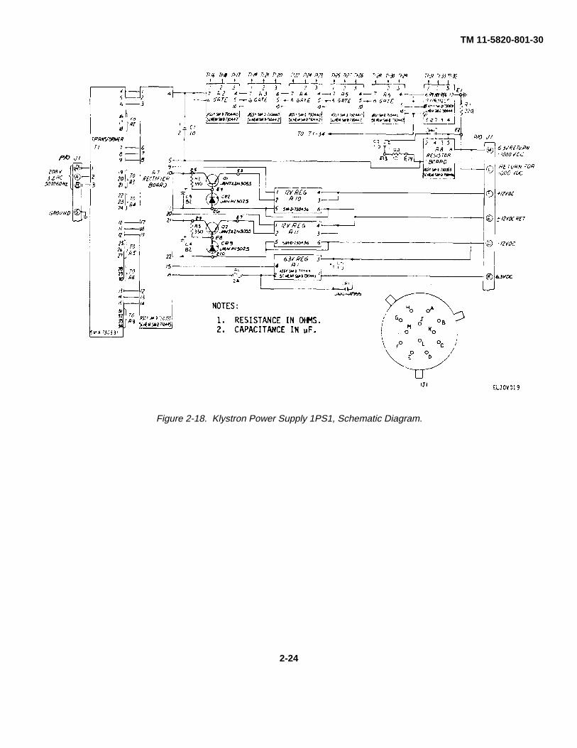
2-19. DC Power Supply Circuitsa. Klystron Power Supply (fig. 2-18).
(1) Primary power (120 ± 12 V, 3 phase, 55 ±8 Hz) is supplied to Klystron Power Supply PS1 throughconnector 1J1 terminals A, L, E, G, circuit breaker 1CB1,line filters 1FL1, 1FL2, 1FL3, circuit breaker 1CB2, andlatching relay 1K1 contacts A1, B1, and C1 (fig 2-17).Output power from PS1 is provided at four voltage levels:-1000 V, +6.3 V, +12 V, and -12 V. Each voltage isobtained from an independent voltage regulator circuitA9, A1, A10 and A11, respectively. A commontransformer (T1) and rectifier board (A7) are used toprovide the inputs to the voltage regulators.
2-21

TM 11-5820-801-30
Figure 2-16. Voltage Measurement Circuits, P/O Unit 1.
2-22

TM 11-5820-801-30
Figure 2-17. Local Control/Monitor Assembly Unit 1, Schematic Diagram.
2-23
TM 11-5820-801-30
Figure 2-18. Klystron Power Supply 1PS1, Schematic Diagram.
2-24

TM 11-5820-801-30
(2) Transformer TI has four three-phasesecondary windings, one for each voltage regulator, andsix singlephase secondary windings that supply theinternal bias voltage (when rectified in the individualcircuits) to the five gate circuits (A2, A3, A4, A5, A6) andto the 1000 V regulator A9.
(3) Capacitor C1 is across the high voltageoutput of the rectifier board and capacitor C2 is acrossthe high voltage (-1000 V) output of PSI A small (10-ohm) resistor is in series with C2. Circuit ground of thehigh voltage supply is separated from chassis ground byRI (220 ohms). This is a safety device to ensure that thechassis never rises more than 30 V above ground,regardless of internal circuit failures such as ground shortof a high voltage circuit (1000 V regulator or 6.3 Vregulator).
(4) Because the drift, ripple, and regulation ofthe 12-V regulators (A10, A 1) are very stringent,preregulators are employed between the regulators (A10,A 11) and rectifier board A7. These preregulators utilize afilter capacitor (C3, C4), a 7Zener diode (CR2, CR3), anda power transistor emitter follower (Q1, Q2) to providelow ripple input to the 12-V regulators The 12-Vregulators are identical and, because they are potted inepoxy, they are nonreparable They are capable ofproducing several times the power required in thissystem. The regulated voltage is constant within + 0. I V.
The low side of the + 12 V output and the high side ofthe 12 V output are tied together to provide a common +12 V return line
b. Rectifier Board A 7 (fig. 2-19). Rectifier Board A7contains four three-phase full-wave bridge rectifiers. The+ 12 V and 12 V rectifiers have an RC filter in the outputcircuit. These two bridge rectifiers are identical andsupply the 12-V preregulators. They employ 1N4245diodes. The -1000 V bridge rectifier utilizes 1N3647diodes and the +6.3 V bridge rectifier, IN5550 diodesc. +6.3 V Regulator A1 (fig. 2-20). The input voltage topower transistor Q1 is unregulated 12 V at terminals E2and E4. The output voltage of Q1 is 6.3 V at terminals E1and E3. Transistors Q2 and Q3 supply the drive to Q1and U1, an integrated circuit voltage regulator, drives Q2and Q3. Resistor R4 produces a voltage dropproportional to output current. When this drop reachesabout 0.6 V the drive current to Q2 and Q3 is depleted.Variable resistor R6 (a trimpot) permits adjustment of theoutput voltage to 6.3 V. If the output is shorted theregulator will produce about 2.5 amps which will, in time,cause Q1 to overheat and fail Short duration shorts,however, will not cause failure. To prevent cold turn-onsurges from causing damage the input line (E2) has a 2-amp fuse (F1) and the circuit is bridged by Zener diodeCR1 and capacitor C1 (fig 2-18).
2-25

TM 11-5820-801-30
Figure 2-19. Rectifier Board 1PS1A7, Schematic Diagram.
2-26

TM 11-5820-801-30
Figure 2-20. +6.3 V regulator 1PS1A1, Schematic Diagram
d. Gate Assemblies (fig. 2-21). Five gateassemblies (A2, A3, A4, A5, A6) are used between thehigh voltage bridge rectifier (on A7) and the 1000 Vregulator A9. Each gate consists of a series passtransistor Q1 and an emitter follower driver Q2.Maximum gate voltage (360 V) is set by Zener diodesCR4 and CR5. Diodes CR1 and CR2 and capacitor C1provide the bias voltage (about 10 V) for the gate.
Resistor R4 is connected in series from gate to gate sothat equal voltage drop per gate Is provided from thebridge rectifier to the 1000 V regulator (A2R4 isconnected to A7E4 and A6R4 is connected to A9E1 I1,the return line of the 1000 V regulator). Normally thisvoltage drop is about 60 V per gate but during breakdown(short on 1000 V line) the voltage drop may be as high as300 V per gate. This is why five gates are used.
2-27

TM 11-5820-801-30
Figure 2-21. Gate Assembly 1PS1A2-A6, SchematicDiagram
e. - 1000 V Regulator and Protect Circuit IPSIA9(fig. 2-22). The voltage from T1 at E1 and E2 of A9 isabout 48 Vac (center tapped at E3). The rectified voltageis about 30 V. Zener diodes CR5 and CR6 reduce thisvoltage to 15 V and + 15 V, the operating voltagerequired by integrated circuit operational amplifier Z1.Zener diode CR7 reduces the voltage to 6.2 V, thereference voltage. Diodes CR9 and CR 10 protect Z1from excessive voltage. Capacitor C5 and diode CR8compensate for drift in the base voltage at transistor Q1.A small fraction of the output voltage (1000 + 50 V) issensed across variable resistor R4 (1000 V ADJ). Thevoltage across R4 varies from about + I V at one end toabout I V at the other end. The wiper arm (1000 V AD1)is set the null point. The positive end of R4 is connectedto the 6.2 V reference voltage through resistor R3. Thewiper arm of R4 is connected to the noninverting input ofZ1 while the inverting input is connected to ground, the1000 V return line. Any error voltage is amplified in Z1,which has a gain of 50 dB or more. The output of Z1drives the lowest potential gate, IA6, through A9 terminalE8 to A6 terminal ES, to correct the output voltage to thedesired value (wiper arm at voltage null). If the outputcurrent becomes excessive (about 125 ma) the outputdrive (at E8) to gate A6 is reduced because Q1 startsconducting and removes drive power. Thereafter theoutput current is limited to about 20 ma. This protects thepower supply under sustained short circuit in the highvoltage line.
2-28

TM 11-5820-801-30
Figure 2-22. - 1000 V Regulator and Protect Circuit 1PS1A9, Schematic Diagram.
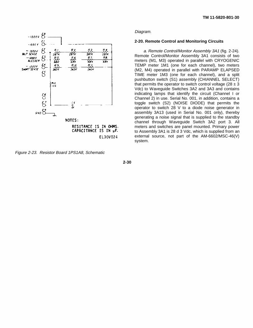
f: Resistor Board A8 (fig. 2-23). Resistor board A8 isa convenient mounting board for resistors required by A9circuits. The high voltage terminals are on AS. TerminalsEl/E8 of A8 are the 1000 V output to J1, terminal M (fig.2-18). Resistors R1, R2, R3, and R4 provide part of thevoltage divider for the -1000 V output from which theerror voltage (A9R4, 1000 V ADJ) is picked off. ResistorsR5, R6, R7, and R8 are bleeder resistors to discharge
capacitors when power is turned off. These resistors arein series with A9R9. The voltage drop across R9 is 0.01that of the output voltage. Resistors R9, R10, and R11provide a bias voltage at the base of A9Q1 in the currentsense circuit. Resistor R12 and capacitor R5 feed backany ripple voltage to the error sense circuit of A9R4. Thishas the effect of canceling ripple voltage.
2-29
TM 11-5820-801-30
Figure 2-23. Resistor Board 1PS1A8, Schematic
Diagram.
2-20. Remote Control and Monitoring Circuits
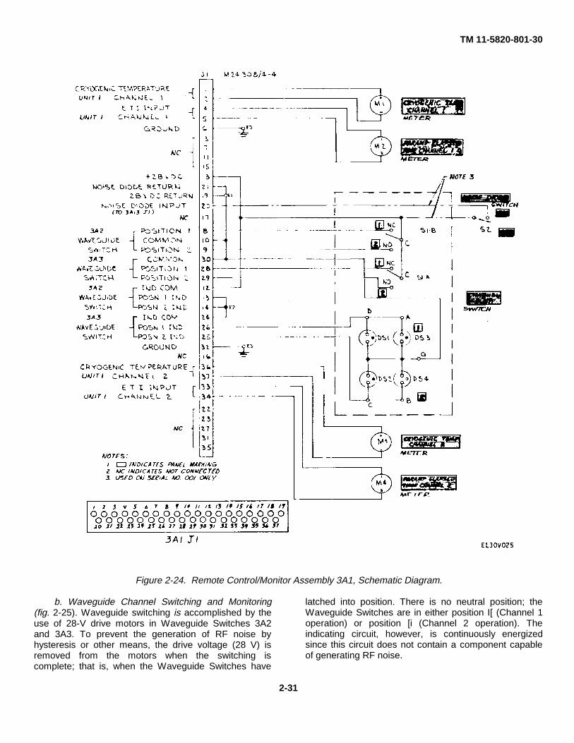
a. Remote Control/Monitor Assembly 3A1 (fig. 2-24).Remote Control/Monitor Assembly 3A1 consists of twometers (M1, M3) operated in parallel with CRYOGENICTEMP meter 1M1 (one for each channel), two meters(M2, M4) operated in parallel with PARAMP ELAPSEDTIME meter 1M3 (one for each channel), and a splitpushbutton switch (S1) assembly (CHIANNEL SELECT)that permits the operator to switch control voltage (28 ± 3Vdc) to Waveguide Switches 3A2 and 3A3 and containsindicating lamps that identify the circuit (Channel I orChannel 2) in use. Serial No. 001, in addition, contains atoggle switch (S2) (NOISE DIODE) that permits theoperator to switch 28 V to a diode noise generator inassembly 3A13 (used in Serial No. 001 only), therebygenerating a noise signal that is supplied to the standbychannel through Waveguide Switch 3A2 port 3. Allmeters and switches are panel mounted. Primary powerto Assembly 3A1 is 28 d 3 Vdc, which is supplied from anexternal source, not part of the AM-6602/MSC-46(V)system.
2-30
TM 11-5820-801-30
Figure 2-24. Remote Control/Monitor Assembly 3A1, Schematic Diagram.
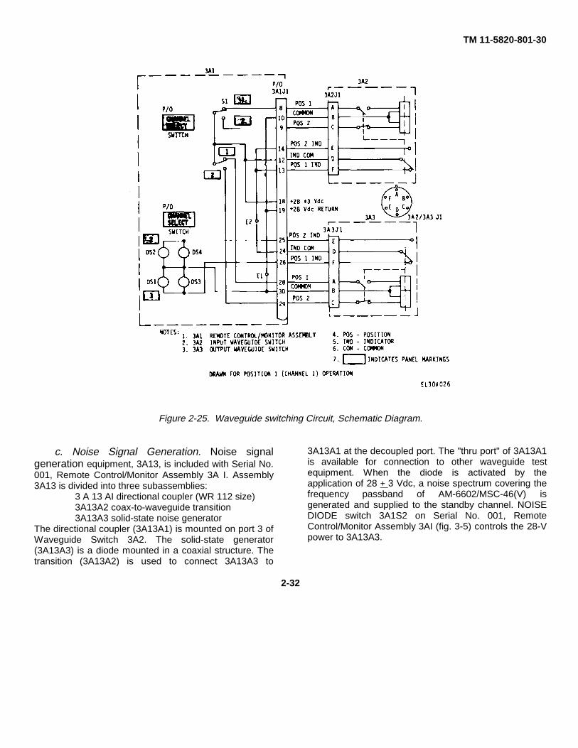
b. Waveguide Channel Switching and Monitoring(fig. 2-25). Waveguide switching is accomplished by theuse of 28-V drive motors in Waveguide Switches 3A2and 3A3. To prevent the generation of RF noise byhysteresis or other means, the drive voltage (28 V) isremoved from the motors when the switching iscomplete; that is, when the Waveguide Switches have
latched into position. There is no neutral position; theWaveguide Switches are in either position I[ (Channel 1operation) or position [i (Channel 2 operation). Theindicating circuit, however, is continuously energizedsince this circuit does not contain a component capableof generating RF noise.
2-31
TM 11-5820-801-30
Figure 2-25. Waveguide switching Circuit, Schematic Diagram.
c. Noise Signal Generation. Noise signalgeneration equipment, 3A13, is included with Serial No.001, Remote Control/Monitor Assembly 3A I. Assembly3A13 is divided into three subassemblies:
3 A 13 AI directional coupler (WR 112 size)3A13A2 coax-to-waveguide transition3A13A3 solid-state noise generator
The directional coupler (3A13A1) is mounted on port 3 ofWaveguide Switch 3A2. The solid-state generator(3A13A3) is a diode mounted in a coaxial structure. Thetransition (3A13A2) is used to connect 3A13A3 to
3A13A1 at the decoupled port. The "thru port" of 3A13A1is available for connection to other waveguide testequipment. When the diode is activated by theapplication of 28 + 3 Vdc, a noise spectrum covering thefrequency passband of AM-6602/MSC-46(V) isgenerated and supplied to the standby channel. NOISEDIODE switch 3A1S2 on Serial No. 001, RemoteControl/Monitor Assembly 3AI (fig. 3-5) controls the 28-Vpower to 3A13A3.
2-32

TM 11-5820-801-30
CHAPTER 3DIRECT SUPPORT MAINTENANCE INSTRUCTIONS
Section I. GENERAL
3-1. Introductiona. Direct Support Maintenance Requirements. Direct
support personnel shall isolate faults in Amplifier,Parametric AM-6602/MSC-46(V) (in dual channelinstallation) to a replaceable module or part in Units 1, 2and 3 and shall remove and replace the faulty item. InUnit 1, faulty parts shall be removed and replaced exceptfor circuit card assembly 1A1 (Temperature Monitor) andKlystron Power Supply I PS I, which shall be removedand replaced as subassemblies. In Unit 2, Modules 2A1,2A2, 2A3, and 2A4 shall be removed and replaced, iffaulty. In Unit 3, faulty parts of 3A1 shall be removed andreplaced; all other Unit 3 subassemblies-3A2, 3A3, 3A4,3A5, 3A6, 3A7, 3A8, 3A9, 3A10, 3A11, 3A12-shall beremoved and replaced as necessary. In addition, anapparent fault in AM-6602/MSC-46(V) may be isolated toa fault in Unit 4 or to a fault in primary power input.Correction of these two types of faults is not discussed inthis manual.
b. Outline of CHAPTER 3 Material Voltage andresistance measurements for Unit I are given inparagraph 3-2, and for subassembly 3A1, in paragraph3-3 Tools and test equipment are listed in paragraphs 3-4 and 3-5, respectively. Fault isolation to a replaceablemodule or part is described in paragraph 3-6. Adiagnostic chart is provided as the principal aid introubleshooting. Gain and bandwidth RF test proceduresare described in paragraph 3-7. RF tests of waveguideassemblies are given in paragraph 3-8. Pump frequencyand power RF tests are given in paragraph 3-9. Mainpower failure troubleshooting is discussed in paragraph3-10 Removal and replacement of Modules 2AI, 2A2,2A3, 2A4, subassembly IPSI and Unit 3 waveguide
assemblies (3A2 through 3A12) are described inparagraph 3-1 1. System interconnections (cable) areillustrated in paragraph 3-12.
3-2. Unit 1 Voltage and Resistance Measurementsa. Introduction. Faults in Unit I can be isolated to a
replaceable part or subassembly by the use of systemmonitors and a multimeter to measure voltages andresistances. The diagnostic troubleshooting chart (para3-6) is a principal aid in isolating faults to Unit I part level.The chart requires that some voltage checks be made inaddition to those provided by the system monitors. Whena fault is apparently located, either a voltage check or aresistance check of the suspected part will confirm itsoperability. Always check the part to ensure that it isfaulty before removal. Voltage checks are made with allcables connected (to J1, J2, J3) and the POWER switchand circuit breakers (REFRIG, PARAMP, MAIN) set toON; that is, with normal operating power. Resistancechecks are made with all cables removed (from J1, J2,J3) and Klystron Power Supply connector P1disconnected.
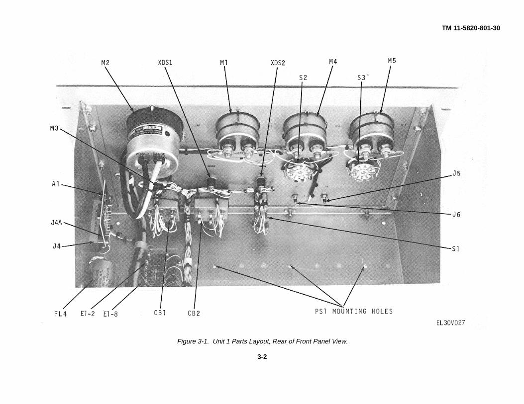
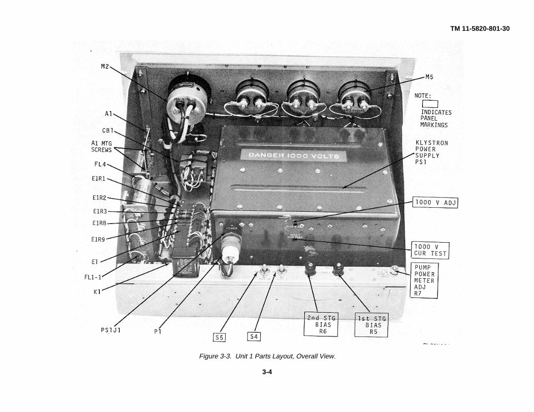
b. Parts Identification. Unit I parts layout is shown infigures 3-1, 3-2 and 3-3. Principal areas for separatevoltage-resistance checking are the five E1 resistors (RI,R2, R3, R8, R9) connected to tie points E1-1 through E1-10, on terminal board E1, the vacuum gage circuit for M2connected to tie points E1-16 through E1-22, circuit cardassembly Al including socket connector labeled j4 (fig. 2-17), and circuit breakers CBI and CB2. The systemmonitors (meters M1, M2, M3, M4, MS, switches S2, S3,panel lamps DSI, DS2, test points J5, J6) are used tocheck the remainder of the circuit.
3-1
TM 11-5820-801-30
Figure 3-1. Unit 1 Parts Layout, Rear of Front Panel View.
3-2

TM 11-5820-801-30
Figure 3-2. Unit 1 Parts Layout, rear of Chassis View.
3-3
TM 11-5820-801-30
Figure 3-3. Unit 1 Parts Layout, Overall View.
3-4
TM 11-5820-801-30
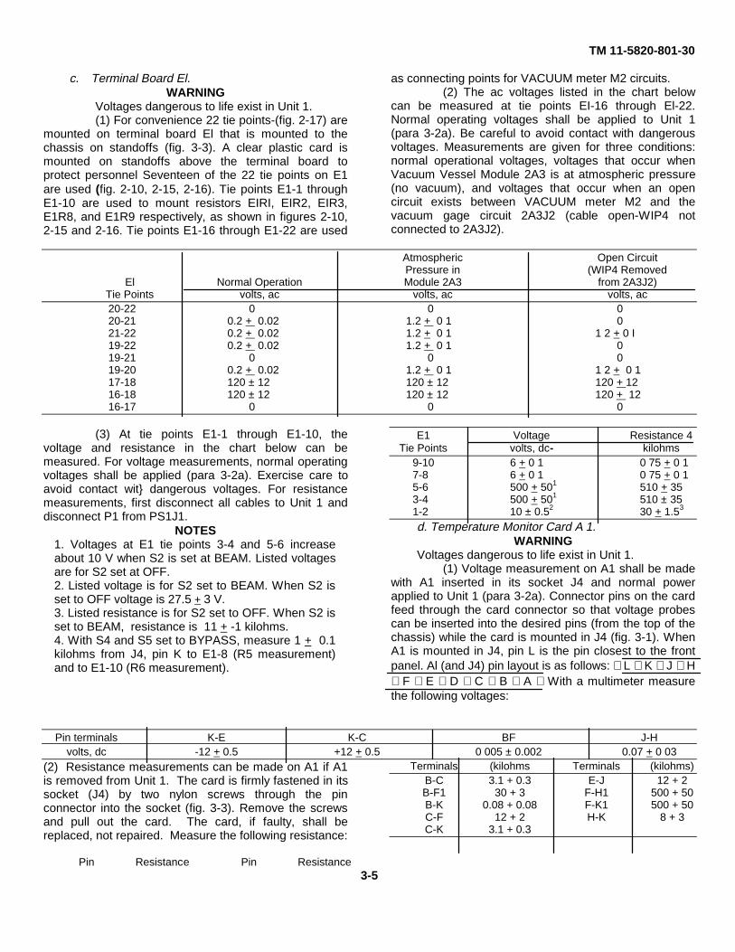
c. Terminal Board El.WARNING
Voltages dangerous to life exist in Unit 1.(1) For convenience 22 tie points-(fig. 2-17) are
mounted on terminal board El that is mounted to thechassis on standoffs (fig. 3-3). A clear plastic card ismounted on standoffs above the terminal board toprotect personnel Seventeen of the 22 tie points on E1are used (fig. 2-10, 2-15, 2-16). Tie points E1-1 throughE1-10 are used to mount resistors EIRI, EIR2, EIR3,E1R8, and E1R9 respectively, as shown in figures 2-10,2-15 and 2-16. Tie points E1-16 through E1-22 are used
as connecting points for VACUUM meter M2 circuits.(2) The ac voltages listed in the chart below
can be measured at tie points EI-16 through El-22.Normal operating voltages shall be applied to Unit 1(para 3-2a). Be careful to avoid contact with dangerousvoltages. Measurements are given for three conditions:normal operational voltages, voltages that occur whenVacuum Vessel Module 2A3 is at atmospheric pressure(no vacuum), and voltages that occur when an opencircuit exists between VACUUM meter M2 and thevacuum gage circuit 2A3J2 (cable open-WIP4 notconnected to 2A3J2).
Atmospheric Open CircuitPressure in (WIP4 Removed
El Normal Operation Module 2A3 from 2A3J2)Tie Points volts, ac volts, ac volts, ac20-22 0 0 020-21 0.2 + 0.02 1.2 + 0 1 021-22 0.2 + 0.02 1.2 + 0 1 1 2 + 0 I19-22 0.2 + 0.02 1.2 + 0 1 019-21 0 0 019-20 0.2 + 0.02 1.2 + 0 1 1 2 + 0 117-18 120 ± 12 120 ± 12 120 + 1216-18 120 ± 12 120 ± 12 120 + 1216-17 0 0 0
(3) At tie points E1-1 through E1-10, thevoltage and resistance in the chart below can bemeasured. For voltage measurements, normal operatingvoltages shall be applied (para 3-2a). Exercise care toavoid contact wit} dangerous voltages. For resistancemeasurements, first disconnect all cables to Unit 1 anddisconnect P1 from PS1J1.
NOTES1. Voltages at E1 tie points 3-4 and 5-6 increaseabout 10 V when S2 is set at BEAM. Listed voltagesare for S2 set at OFF.2. Listed voltage is for S2 set to BEAM. When S2 isset to OFF voltage is 27.5 + 3 V.3. Listed resistance is for S2 set to OFF. When S2 isset to BEAM, resistance is 11 + -1 kilohms.4. With S4 and S5 set to BYPASS, measure 1 + 0.1kilohms from J4, pin K to E1-8 (R5 measurement)and to E1-10 (R6 measurement).
E1 Voltage Resistance 4Tie Points volts, dc- kilohms
9-10 6 + 0 1 0 75 + 0 17-8 6 + 0 1 0 75 + 0 15-6 500 + 501 510 + 353-4 500 + 501 510 ± 351-2 10 ± 0.52 30 + 1.53
d. Temperature Monitor Card A 1.WARNING
Voltages dangerous to life exist in Unit 1.(1) Voltage measurement on A1 shall be made
with A1 inserted in its socket J4 and normal powerapplied to Unit 1 (para 3-2a). Connector pins on the cardfeed through the card connector so that voltage probescan be inserted into the desired pins (from the top of thechassis) while the card is mounted in J4 (fig. 3-1). WhenA1 is mounted in J4, pin L is the pin closest to the frontpanel. Al (and J4) pin layout is as follows: L K J H F E D C B A With a multimeter measurethe following voltages:
Pin terminals K-E K-C BF J-Hvolts, dc -12 + 0.5 +12 + 0.5 0 005 ± 0.002 0.07 + 0 03
(2) Resistance measurements can be made on A1 if A1is removed from Unit 1. The card is firmly fastened in itssocket (J4) by two nylon screws through the pinconnector into the socket (fig. 3-3). Remove the screwsand pull out the card. The card, if faulty, shall bereplaced, not repaired. Measure the following resistance:
Pin Resistance Pin Resistance
Terminals (kilohms Terminals (kilohms)B-C 3.1 + 0.3 E-J 12 + 2B-F1 30 + 3 F-H1 500 + 50B-K 0.08 + 0.08 F-K1 500 + 50C-F 12 + 2 H-K 8 + 3C-K 3.1 + 0.3
3-5

TM 11-5820-801-30CAUTION
The card is aligned to drive CRYOGENIC TEMPmeter MI Do not change the settings of A1R6 orA1R12 (fig. 2-9).e. Meters M1, M4. M5. Meters M1, M4, and M5 can
be checked for open circuits or short circuit if diagnosticprocedures (para 3-6) indicate a faulty meter. With allpower off (para 3-2a) remove leads to one terminal of thesuspect meter. With ohmmeter (multimeter) set onX1000 scale, check resistance across meter terminals. Ifthe ohmmeter indicates infinite resistance the metercircuit is open; if it indicates zero resistance, the metercircuit is shorted; if it indicates a small resistance (orderof 100 ohms) the meter circuit is likely in satisfactoryoperating condition.
f Power Switches. The diagnostic procedure (para3-6) requires voltage measurements at the terminals ofCB1 (MAIN POWER circuit breaker), CB2 (PARAMPPOWER circuit breaker) and S1(REFRIG POWERswitch). Terminal layouts are sketched here so that theappropriate terminal (fig. 31) can be easily located. Theterminal layout for CB1and CB2 is as follows:
1• 3• 5•2• 4• 6•
The terminal layout for S1is as follows-
2• 5•3• 6•
When all power is removed from Unit 1 (para 3-2a)(cable to J1 disconnected) the following resistancechecks can be made on CB1, CB2, and SI.
(1) CB1, CB2 Resistance MeasurementsMeasure across 1-2 3-4 5-6
terminals (ohms) (ohms) (ohms)CB1, CB2 set to ON O O OCB1, CB2 set to OFF Infinite infinite infinite
(2) S1Resistance Measurements:Measure across 2-3 5-6
terminals (ohms) (ohms)S1 set to ON 0 0S1 set to OFF infinite infinite
(3) CB1 CB2 S2 Voltage Measurements.WARNING
Voltages dangerous to life exist in Unit IWith power cable connected to J1 the following acvoltages can be measured with a multimeter:
From ToFL4-1 CBI-2 CBI-4 CBI-6(fig 3-21 120 + 12 120 + 12 120 + 12FtL4-1 CBI-l CBI-3 CBI-5CB1 set to OFF 0 O OCB1 set to ON 120 + 12 120 + 12 120 + 12FL4-1 CB2-2 CB2-4 CB2-6CBI set to ON 120 + 12 120 + 12 120 + 12FL4-1 CB2-1 CB2-3 CB2-5CB2 set to OFF O O 0FL4-1 CB2-1 CB2-32 CB2-51
CB1/CB2 set to ON 120 + 12 120 + 12 120 + 121CB2-5 to FL4-1 also measures voltage across DS2-1 to DS2-22CB2-3 to FL4-1 also measures voltage across M3.
With CB1set to ON and S1 set to OFF measure fromS1-2 to S1-5: 208 + 21 VS1-3 to S1-6: O
With CB1set to ON and S1set to ON measure fromS1-3 to 51-6: 208 + 21 VS13 to FL4-1: 120 + 12 V (this is equivalent to
measuring DS1Ito DS1-2)g. Switches S4 and S5. Switch S4 (fig. 3-2) and
switch S5 can be checked when all cables to Unit 1(atJ1, J2, J3) are disconnected and P1 is disconnectedfrom PSIJI. Make the following resistance checks:
Measure S4 S5 Resistancefrom Set to Set to (ohms)
J5 to E1-8 BYPASS -J5 to E1-8 IST STG ON - 600 + 600J6 to EI-10 - BYPASS O
J6 to El-10 - 2ND STG ON 600 + 600
CAUTIONDo not change the settings of R5 (BIAS 1STSTG) and R6 (BIAS 2ND STG). If R5 or R6 isreset, then a gain-bandwidth realignment mustbe performed.
h. Line Filter Voltage Measurements.WARNING
Voltages dangerous to life exist in Unit 1. Thevoltage across line filters FL1 FL2, FL3 and FL4can be measured between terminals I and 2 ofeach filter (fig. 3-2, 3-3). When CBI is set to OFFthe voltage is zero. When CBI is set to ON the(ac) voltage drop will be less than 5 V per filter.
3-6

TM 11-5820-801-30
3-3. Remote Control/Monitor Assembly 3A1 Voltageand Resistance Measurements
WARNINGWhen 1 CB1 and 1CB2 are set to ON thisassembly contains dangerous voltages.a. Display Meters. The meters used in 3A1 to
display temperature (M1 and M3) are identical to 1M1(para 3-2e and para 2-9b) The time totalizing meters(NM2 and M4) are identical to 1M3 (para 2-8c) These3A1 meters are connected in parallel with thecorresponding Unit 1 meters so that indications on Unit 1front panel and 3A1 front panel are identical When the3A1 meters do not track the Unit 1 meters then check the3A1 subassembly. CRYOGENIC TEMP CHANNEL 1meter M1 and CRYOGENIC TEMP CIIANNEL 2 meterM3 can be checked in the same manner that 1M1 ischecked. If the time totalizing meters--1M3, 3A1M2,3A1M4-do not operate when 120 + 12 V, 55 + 8 Hz isapplied across their terminals (normal operating voltageswhen 1CB1 and 1CB2 are set to ON) they should bereplaced (para 3-6 and fig 3-6)
b. Parts Layout and CHANNEL SELECT Switch S1.Parts layout of Remote Control/Monitor Assembly 3A1 isshown in figures 3-4 and 3-5. Serial No 001 is shownbecause it has a toggle switch (S2, fig. 3-5) to switch +28 Vdc to noise generator 3A13A3 used in Serial No. 001installation only (para 2-20c). Tie points E1 and E3 are
on the bracket mount for connector J1. Subassembly S1contains several parts including a split pushbutton switchand four indicator lamps DS1, DS2, DS3, DS4. The panellamps can be separately replaced, when faulty. Adefective switch, however, requires replacement of thecomplete subassembly. With W5P1 connected to J1 andnormal operating voltages applied (para 3-2a) makevoltage checks on CHANNEL SELECT pushbuttonswitch S1 as shown below and in figure 3-4: (Also referto figure 2-24.)
S1 in S1 InPosition 1 Position oMeasure Measure
C to E1: 28 + 3V C to E1: 28t 3 vNO to E1: 0V NO to E1: 281 3 VNC to E1: 283V NC to E1: OVG to A: 2873V G to B: 28t3VG to B: OV G to A: OV
With cable removed from JI measure the followingresistance.
S1 TerminalsC-NC C-NO
SI Position (ohms) (ohms)1 0 infinite2 infinite 0
3-7

TM 11-5820-801-30
Figure 3-4. Remote Control/Monitor Assembly 3A1 3-8

TM 11-5820-801-30
Figure 3-5. Remote Control/Monitor Assembly 3A1, Serial No. 001
Section II. TOOLS AND TEST EQUIPMENT
3-4. ToolsThe following tools, as listed in the maintenanceallocation chart (MAC) for Amplifier, Parametric AM-6602/- MSC-46(V) and TM 1-5820-801-30P, DirectSupport Repair Parts and Special Tools List (IncludingDepot Maintenance Repair Parts) for Amplifier,Parametric AM-6602/MSC-46(V) (NSN 5895-00-100-4315) are required for direct support maintenance:
Name Mfr/ModelOperator, valve 80063/SM-C-730301Pump, vacuum 64484/ 1402Rubber Tubing, vacuum 11273/18240 size No 11Kit, Tool, Electronic Equipment TK-
100/-GAdapter, evacuating and charging, 75629/Unit 4 Kit, tool, Unit 4 75629/
3-5. Test Equipment
The following test equipments, as listed in MAC, are re-quired for direct support maintenance of Amplifier, Para-metric AM-6602/MSC-46(V):
Name Type Designation Mfr/ModelAdapter, coax to wave- VG-1054/U 28480OH281A
guideAttenuator, 20 dB 28480/8491 AAttenuator, variable CN-1367/U 28480/H382ABridge, power AN/USM-260 28480/431CCoupler, 20 dB 80063/SM-D-748724Detector, crystal 28480/420AGenerator, sweep 28480/H01-694CMeter, frequency FR-194/U 28480/H532AMeter, frequency 14059/B551Mount, bolometer 28480/R486AMultimeter 60741/630NAOscilloscope AN/USM-273 80009/453Termination, RF 14059/B580
3-9
TM 11-5820-801-30Section III. TROUBLESHOOTING
3-6. Fault Isolationa. Circuits Covered in Diagnostic Flow Charts.
Troubleshooting procedures as detailed in the diagnosticflow charts (fig 3-6 and 3-7) are designed to locate andisolate a fault to a replaceable module, subassembly, orcomponent in the signal amplification circuits and thetemperature and pressure (vacuum) monitor and controlcircuits. The faulty item shall be removed from thesystem and replaced with a spare These circuitscomprise Amplifier, Parametric AM-6602/MSC-46(V).The redundancy kit, Unit 3, is not included
b. Unit 3 Subassembles. The redundancy kit, Unit 3,is not directly involved in the troubleshooting procedurebecause it does not affect the normal operation of theparametric amplifier If, however, a fault is isolated to IMIor IM3, the corresponding 3AI meters (para 3-3a) may befaulty because 3A1 meters are operated in parallel withthe Unit I meters. When a IMI or IM3 fault is indicated,remove the cable at 3AIJI. If the fault remains, it is in UnitI. If the fault clears, it is in 3AI, then refer to paragraph 3-3a for procedure. Waveguide assemblies 3A2, 3A3, 3A4,3A5, 3A6, 3A7, 3A8, 3A9, 3A10, 3AII and 3 A 12 arehighly unlikely to cause RF faults unless waveguideinterconnections are not tight or unless the waveguideshave become physically deformed Refer to organizationalmaintenance checks and services for interconnectioninformation. Waveguide assemblies or waveguide runs(3A2, 3A4, 3A5, 3A6; 3A2, 3A9, 3A5, 3A10; 3A3, 3A8,3A5, 3A7, 3A3, 3A12, 3A5, 3AI I) can be measured forinsertion loss by the procedure given in paragraph 3-8.Insertion loss per assembly shall be 0. I1 dB or less If afailure occurs in the drive motor or indicator section ofWaveguide Switch 3A2 or 3A3, 3AI indicator DSI, DS3,or DS2, DS4 (fig 2-25 and 3-4) will not switch when theunlit half of the 3 A I S I pushbutton switch (CIIANNELSELECT) is depressed Remove and replace 3A2 or 3A3Refer to paragraph 3-3h for checkout of 3AISI.
c Diagnostic Flow Charts (fig 3-6 and 3-7)(1) Initial Conditions. Diagnostic flow charts are
presented for two sets of initial conditions: normal (fig. 3-6) and initial start-up (fig. 3-7). Figure 3-6 applies whenthe system is in operation (one channel operating andone channel in standby) as will normally be the case Forthis condition the two Unit 1 circuit breakers and powerswitches (MAIN, PARAMP and REFRIG POWER) areset to ON and Module 2A3 is (or had been) at its ambientenvironmental conditions internal temperature of 20° +2°K and internal pressure of 40 millitorr or less. Modules2A2 and 2Ai will be at their normal elevatedtemperatures. Figure 3-7 applies when Module 2A3 is atroom temperature and room pressure and the two circuitbreakers and switch (MAIN, PARAMP, REFRIGPOWER) are set to OFF. This condition can occur whenModule 2A3 has been replaced, or Unit 4 has been out ofoperation, or when primary power has been shut off foran hour or more. Figure 3-7 could be used also duringpreliminary adjustment at initial installation The two
charts differ in monitor checking procedures because oftime delays encountered in start-up procedures whilevacuum and temperature equilibriums are beingestablished The time required for Modules 2AI and 2A2to reach their operating temperatures is less than thatrequired for Module 2A3 to reach its environmentalconditions, therefore, when Module 2A3 is ready tooperate the other two modules are also ready to operate
(2) Chart Sections. The diagnostic procedure isconveniently divided into two sections the first sectionutili7es system monitors and a multimeter for faultisolation, the second section utilizes RF signal generationand detection equipment for evaluating system operationand for isolating faults RF tests should not be made untilthe monitors have been checked Since the two chartsdiffer only in the monitor checking procedures but are thesame for RF test procedures, figure 3-7 refers to figure3-6 for RF test procedures.
(3) Systematic Troubleshooting. The direct-support maintenance technician should always use adiagnostic flow chart for troubleshooting so that asystematic method of fault isolation is maintained. Spotchecking at random of the several circuits may or maynot isolate the cause of trouble and is therefore notrecommended
(4) Chart Use. The diagnostic flow charts (fig 3-6 and 3-7) are designed to test a module, subassembly,or component sufficiently to verify that the item is faultybefore it is removed and replaced The charts assumethat only one fault has occurred and provide the methodof isolating and correcting the fault The technician entersthe chart at the upper left comer START and readsfrom left to right along the top line only, verifying themonitor indications or performing the required test until afault (no-go condition) is encountered If a fault isdiscovered he reads down the branch line (top to bottom)performing the tests as indicated until he isolates andcorrects the fault This is usually the removal andreplacement (R/R) of a component, subassembly, ormodule but may be a voltage or attenuator adjustment.lie then returns to the top line where he discovered thefault and continues to read and check from left to right Ifno faults are encountered along the top line of the flowchart, the equipment is satisfactory and no further testingshall be made. No branch (down) line of the flow chartshall be checked unless a no-go condition has beenindicated in the top line The primary requirement of thesystem is to provide 29.5 + 1 dB gain over the 7.5 + 0.25GHz frequency range. All other requirements aresecondary.
(5) Items Not Checked By Chart. Thediagnostic flow charts assume that any malfunction is ina replaceable
3-10

TM 11-5820-801-30
part, subassembly, or module and not in the cables orharnesses used for interconnection The charts do notcover point-to-point wiring or interconnection cables,plugs, and connectors. Ordinarily, visual observation forabrasion will indicate possible shorts or opens in thewiring Chassis harnesses can be checked from the
schematic diagrams. Refer to paragraph 3-12 for cableinterconnections If necessary, perform continuity checkswith all power off, that is, with cable W5 not connected tothe power sources but interconnected with Amplifier,Parametric AM-6602/MSC-46(V) and all otherinterconnecting cables (W1, W2, W3, W4) connected.
3-11

TM 11-5820-801-30
Figure 3-6. Diagnostic Flow Chart for Amplifier, Parametric AM-6602/MSC-46(V) (Sheet 1 of 7).
3-12

TM 11-5820-801-30
Figure 3-6. Diagnostic Flow Chart for Amplifier, Parametric AM-6602/MSC-46(V) (Sheet 2 of 7).
3-13
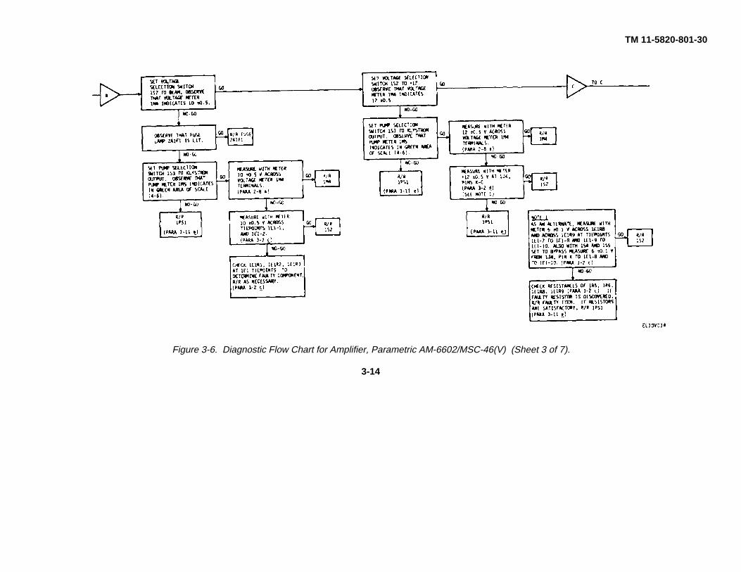
TM 11-5820-801-30
Figure 3-6. Diagnostic Flow Chart for Amplifier, Parametric AM-6602/MSC-46(V) (Sheet 3 of 7).
3-14

TM 11-5820-801-30
Figure 3-6. Diagnostic Flow Chart for Amplifier, Parametric AM-6602/MSC-46(V) (Sheet 4 of 7).
3-15

TM 11-5820-801-30
Figure 3-6. Diagnostic Flow Chart for Amplifier, Parametric AM-6602/MSC-46(V) (Sheet 5 of 7).
3-16

TM 11-5820-801-30
Figure 3-6. Diagnostic Flow Chart for Amplifier, Parametric AM-6602/MSC-46(V) (Sheet 6 of 7).
3-17

TM 11-5820-801-30
Figure 3-6. Diagnostic Flow Chart for Amplifier, Parametric AM-6602/MSC-46(V) (Sheet 7 of 7).
3-18

TM 11-5820-801-30
Figure 3-7. Diagnostic Flow Chart for Amplifier, Parametric AM-6602/MSC-46(V) (Sheet 1 of 4).
3-19

TM 11-5820-801-30
Figure 3-7. Diagnostic Flow Chart for Amplifier, Parametric AM-6602/MSC-46(V) (Sheet 2 of 4).
3-20
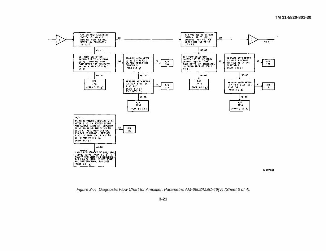
TM 11-5820-801-30
Figure 3-7. Diagnostic Flow Chart for Amplifier, Parametric AM-6602/MSC-46(V) (Sheet 3 of 4).
3-21

TM 11-5820-801-30
Figure 3-7. Diagnostic Flow Chart for Amplifier, Parametric AM-6602/MSC-46(V) (Sheet 4 of 4).
3-22

TM 11-5820-801-30
3-7. RF Gain and Bandwidth Measurementsa Introduction.
(1) Types of Measurements. Gain-bandwidthmeasurements are divided into two parts: test andalignment The technician first tests the channel(Amplifier, Parametric AM-6602/MSC-46(V)) todetermine if a fault exists, and, if so, which stage (2A3 or2A2) is at fault A fault is defined as gain not withinspecified limits (29 5 t I dB) or bandwidth less than 500MIDz (7250 to 7750 MITz) After a fault has been isolatedto the first stage (2A3) or the second stage (2A2), thetechnician then performs an alignment procedure tocorrect the fault. If realignment does not eliminate thefault, then module removal and replacement isnecessary (para 3-11) The steps are outlined on sheets6 and 7 of figure 3-6.
(2) Initial Conditions. The channel to betested shall be in normal standby condition (Refer to IM11-5895-539-12 ). This implies that CRYOGENIC TEMPmeter 1M1 indicates 20o±5°K, that VACUUM meter 1M2indicates 20 millitorr or less, that MAIN (ICBI) andPARAMP (1CB2) circuit breakers and REFRIG (1S1)switch have been set to ON for at least 15 minutes (fig.2-4). CHANNEL SELECT pushbutton switch 3A1S1 (fig3-4) shall indicate that the channel is in standby, that is,the channel not under test shall be illuminated on the3A1SI display A diagnostic check of the monitoring
system according to figure 3-6, sheets 1, 2, 3, 4, and 5,shall have been completed.
(3) Test Setup. One test setup is used forboth gain bandwidth test and alignment procedures. Thetwo procedures are continuous. If during system gain-band- width test a fault is indicated, the techniciancontinues with the test to isolate the fault and then withthe alignment to eliminate the fault. No change in testequipment or test setup is required. Initially use the TestReference Connection (CN-1367/U connected to VG-1054/U), which is used to calibrate the test equipmentAfter the test equipment is calibrated, the equipment tobe tested is connected. Using the test equipment in thechart below, make the test setup illustrated in figure 3-8:
Item Reference
Adapter. VG-1054/U (2) HP H281AAttenuator, 20 dB HP 8491 AAttenuator, Variable HP 1t382ACN- 1 367/UDetector, Crystal HP 420AGenerator, Signal, Sweep HP 1O01-694CMeter, Frequency FR-194/U HP If523AOscilloscope AN/USM-273 Tek 453
3-23

TM 11-5820-801-30
Figure 3-8. Channel Gain-Bandwidth Test Setup.
b RF Gain-Bandwidth Test Procedure.(1) After the test setup is made using Test
Reference Connection (para 3-7a) (fig. 3-8) energizetest equipment (sweep generator and oscilloscope) andpermit a 15- minute warmup period.
(2) Set the sweep generator to sweep thefrequency band 7.20 to 7.80 GHz. Set frequencymarkers at 7.25 and 7.75 GItz. Check markerfrequencies with FR-194/U.
(3) Set CN-1367/U at 10 dB.(4) Set AN/USM-273 for maximum sensitivity
and obtain a convenient reference trace on the
oscilloscope face. Mark the trace with a grease pencil.This is the upper reference level.
(5) Increase the attenuation 2 dB (CN-1367/Uset to 12 dB) and mark this trace also on theoscilloscope face.This is the lower reference level. The test equipment isnow calibrated.
(6) Remove the Test Reference Connectionand make the Test Connections. Connect CN- 1367/Uto Port 3 of input Waveguide Switch 3A2 and connectVG-1054/U to Port 3 of output Waveguide Switch 3A3.
3-24

TM 11-5820-801-30(7) Increase the attenuation in CN-1367/U
until the oscilloscope trace is at approximately the upperreference level but does not go above the upper
reference level. (Refer to fig. 3-9.) The CN-1367/U dialindication minus 10 is the system gain in dB.
Figure 3-9. Typical Gain-Bandwidth Response of AM-6602/MSC-46(V).
Figure 3-10. Out-of-Tolerance Gain-Bandwidth Response.
(8) Measure the bandwidth between theoscilloscope reference traces with FR-194/U.
(9) For acceptable performance, themeasurements taken in steps (7) and (8) shall indicate again of 29.5 ±1 dB over the frequency band 7250 to 7750MHz. For comparison, a typical gain-bandwidthmeasurement as displayed on an oscilloscope issketched in figure 3-9. If channel gain and bandwidthare acceptable, terminate test here. Continue only ifchannel measurements are out of tolerance.
(10) To measure the response of the firststage (2A3) of the amplifier continue as follows. Settoggle switch ISS5 to BYPASS (fig. 3-3).
(11) Decrease the attenuation (from that set instep(7) until the oscilloscope trace approaches the upperreference level (fig. 3-9). The CN- 1367/U dial indicationminus 10 is the first stage (2A3) gain in dB less thesecond stage (2A2) insertion loss of 1.5 ±0.5 dB.
(12) The measured gain in step (11) shall bebetween 12.5 dB and 14.5 dB and the bandwidth shall be
500 MHz minimum.(13) To measure the response of the second
stage (2A2) of the amplifier continue as follows. Settoggle switch 1S5 to 2ND STG ON and set toggle switch154 to BYPASS (fig. 3-3).
(14) Vary the attenuation (from that in (10)above) until the oscilloscope trace approaches the upperreference level (fig. 3-9). The CN-1367/U dial indicationminus 10 is the second stage (2A2) gain in dB less thefirst stage (2A3) insertion loss of 2.0 : 0.5 dB.
(15) The measured gain in (14) above shall bebetween 12.5 dB and 14.5 dB and the bandwidth shall be500 MHz minimum.
(16) To measure system insertion loss,continue as follows. Set both IS4 and ISS to BYPASS(fig. 3-3).
(a) Reduce the attenuation until theoscilloscope
3-25

TM 11-5820-801-30
trace approaches the upper reference level (fig. 3-9).The CN-1367/U dial indication minus 10 is the coldinsertion loss of Amplifier, Parametric AM-6602/MSC-46(V) It shall be 4 dB or less and is assumed to be 0.5dB greater in the first stage (2A3) than in the secondstage (2A2) (for gain computation purposes).
(b) Reset toggle switches 1S4 and IS5 to 1STSTG ON and 2ND STG ON, respectively.
c. Gain-Bandwlth .Alignment Procedure.(1) Gain-bandwidth alignment shall be made
after the gain-bandwidth tests indicate that either the firststage (2A3) (b(l), (11), and (12) above) or the secondstage (2A2) (b(13), (14), and (16) above) gain-bandwidthcharacteristics are out of tolerance Maintain the testsetup of figure 3-8 (b(6) above).
(2) If the first stage (2A3) characteristics areout of tolerance proceed as follows. Set toggle switch1S5 to BYPASS (fig. 3-3) Display the gain-bandwidthresponse curve on AN/USM-273 as in b(l 1) above Anexample of an out-of-tolerance gain-bandwidth responseis shown in figure 3-10
(3) On Pump Source Module 2A1 front panel,remove the cover plate by removing four Phillips headscrews, thereby exposing attenuator controls AT3 andAT4 (fig 3-11).
(4) Unlock 2A1AT3 attenuator control byloosening the lock thumbscrew (right angles to theattenuator control) Then, with a hex wrench, turn AT3attenuator control while observing the oscilloscopeAdjust for optimum gain (approximately that shown infigure 3-9).
(5) Turn the IST STG BIAS IR5 adjustmentcontrol (fig 3-3) with a screwdriver while observing theoscilloscope Adjust for optimum bandwidth(approximately that shown in figure 3-9).
(6) Because the effects of the 2A1AT3 and1R5 adjustments react on each other to some extent itmay be necessary to repeat (4) and (5) above one ormore times to obtain the optimum gain-bandwidthresponse Stage gain shall be 13.5 ± 1 dB over 500 .MHzband Refer to b(12) above.
3-26
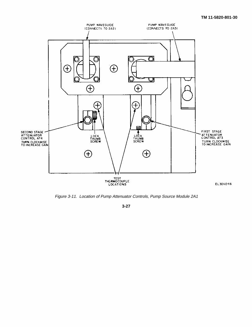
TM 11-5820-801-30
Figure 3-11. Location of Pump Attenuator Controls, Pump Source Module 2A1
3-27
TM 11-5820-801-30
(7) When the optimum gain-bandwidthresponse has been obtained, carefully relock the AT3attenuator control with the lock thumbscrew whileobserving the oscilloscope to make certain that thelocking procedure does not change the control settingsand, therefore, the amplifier response.
(8) Reset toggle switch 1S5 to 2ND STG ON(fig. 3-3) Check the channel gain-bandwidth responseper b(7), (8), and (9) above If the response is notcompletely satisfactory, make minor adjustments bymeans of the second stage controls while observing thechannel response on the oscilloscope. Second stagecontrols are de scribed in (9) through (13) below.Operational requirement is for adequate channelresponse. How this response is divided between the twostages of amplification is irrelevant.
(9) If the second stage (2A2) characteristicsare out of tolerance, set toggle switch 1S4 to BYPASSand display the gain-bandwidth response curve onAN/USM-273 as in b(14) above (fig. 3-10).
(10) Perform (3) above (Remove cover plateover attenuator controls) (fig. 3-11).
(11) Unlock 2A1AT4 attenuator control andadjust the gain as in (4) above, using the AT4adjustment.
(12) Adjust 2ND STG BIAS control 1R6 (fig. 3-3) using the procedure in (5) above.
(13) Continue the alignment procedure asgiven in (6) and (7) above, but using 2A1AT4 and 1R6adjustments. Stage gain shall be 13.5±dB over 500 MHzband Refer to b(15) above.
(14) Reset toggle switch 1S4 to 1ST STG ON.Check the channel gain-bandwidth response as per b(7),(8), and (9) above. Minor adjustments of this first stagecontrols ((4) through (7) above) may be necessary foroptimum channel response.
(15) Remove the test equipment and replacethe cover plate (with four Phillips head screws removedin (3) above) on the Pump Source Module 2A1 frontpanel.3-8. Waveguide Assembly RF Tests
a. Assemblies That Can Be Tested. RF insertionloss over the amplifier passband (7.5 i 0.25 GHz) can bemeasured on any waveguide assembly that can readilybe removed from the system. Waveguide Switches 3A2and 3A3 can be tested in place, if necessary. Other Unit3 waveguide assemblies (3A4, 3A5, 3A6, 3A7, 3A8, 3A9,3A10, 3AI 1, 3A12) can be removed and testedindividually or tested in sections. Refer to paragraph 3-6b. The procedure given here is specifically forWaveguide Filter Module 2A4. Any other waveguideassembly (WR 112 size) can be measured by the sameprocedures c(l) through (7) below. The additional stepsin c below are for out-of-band signal rejection tests of thefilter.
b. Test Setup. The test equipment and test setupshown in figure 3-8 shall be used except that the itemunder test is Waveguide Filter Module 2A4 instead ofAmplifier, Parametric AM-6602/MSC-46(V). The test
setup can be made at any convenient location. Remove2A4 from 2A2 and 2A3 by flipping open the waveguidequick disconnects (para 3-11a) (fig. 3-14) and lifting out2A4 The initial test setup shall contain the item undertest (2A4) connected to the test equipment, that is, usethe Test Connection of figure 3-8 first, connecting 2A4between CN-1367/U and V’G- 1054/U.
c. Test Procedure(1) After the test setup is made using Test
Connection (fig. 3-8), energize the test equipment(sweep generator and oscilloscope) and permit 15-minute warmup period.
(2) Set the sweep generator to sweep thefrequency band 7.20 to 7 80 GHz. Set frequencymarkers at 7.25 and 7.75 GHz Check to see that markerfrequencies are correct with FR-194/U.
(3) Set CN-1367/U at 1.0 dB.(4) Set AN/USM-273 for maximum sensitivity
and obtain a convenient reference trace on theoscilloscope face. Mark the trace with a grease pencil.
(5) Remove 2A4 from the test setup andmake the Test Reference Connection, that is, connectCN-I 367/U to VG- 1054/U.
(6) Decrease the attenuation to return theoscilloscope trace to the reference trace level.
(7) The difference in CN-1367/U settings of(4) above and (6) above is the insertion loss ofWaveguide Filter Module 2A4. The loss shall bebetween 0.0 dB and 0 3 dB.
(8) Remove the grease pencil trace marksfrom the oscilloscope scope face.
(9) Set CN-1 367/U at 25 dB. Obtain a traceon the oscilloscope and mark the trace with a greasepencil.
(10) Set the sweep generator to sweep thefrequency band 7.0 to 8.4 GHz. Set frequency markersat 7.1 and 7.9 GHz.
(11) Insert Module 2A4 in the test setup, thatis, between CN-1367/U and VG-1054/U.
(12) Set CN-1367/U to 5 dB. ((9) setting minusstep in (12) above setting = 20 dB.)
(13) Observe the oscilloscope for responses in thefrequency bands 7.0 to 7.1 GHz and 7.9 to 8.4 GHz. Noresponse shall reach the reference trace levels set in (9)above. The specified filter rejection is 20 dB or more inthese two frequency bands.
(14) Remove Module 2A4 from the test setupand reconnect it in Frame Assembly Unit 2 to Modules2A2 and 2A3.3-9. Pump Frequency and Power Tests
WARNINGModule 2A1 contains a 1000-V line and a 120- V line Donot open the chassis cover.
CAUTIONDo not perform these tests unless gain-band- width tests(para 3-7) provide unsatisfactory results and theapparent cause is inadequate pump power. Refer tofigure 3-6, sheets 6 and 7.
3-28

TM 11-5820-801-30
a. RF Tests.(1) Remove Pump Source Module 2A1 from
Unit 2 as follows.(a) Remove the four cap screws in each of
the two pump waveguide interface flanges at theinterfaces with 2A2 and 2A3 pump waveguides Refer tofigure 3-12.
(b) Slide open the four mounting slideclips on 2A1 (fig. 3-12) and lift Module 2A1 out ofSupport Frame 2A5.
(c) Place 2A1 in a convenient position toconnect test equipment to the pump waveguide flanges.
(d) Do not remove W2P2 from 2A1JI.
3-29

TM 11-5820-801-30
Figure 3-12. Pump Source Module 2A1.
3-30

TM 11-5820-801-30
(2) With the following test equipment listed inthe chart below, make the test setup illustrated in figure3-13. Two successive test setups shall be made one withthe 20- dB coupler connected to the 2A3 pumpwaveguide interface (with the other pump waveguide(2A1/2A2 inter- face) terminated) and a second with the20-dB coupler connected to the 2A1/2A2 waveguideinterface (with the other pump waveguide (2A 1/2A3interface) terminated). There is no preference in testorder. The channel under test shall be in normal standbycondition. Refer to para- graph 3-7a(2).
(3) Make sure that the MAIN (1CB1) andPAR- AMP (ICB2) POWER circuit breakers are set toON. Energize power bridge; allow 30 minutes for test
equipment warmup.(4) The power bridge (AN/USM-260) shall
indicate 150 mW or more (per channel). With the 20-dBcoupler in the measurement line, the bridge actuallymeasures 0.01 times the total power; that is, 1.5 mW (ormore).
Item Reference
Bridge, Power AN/IUSM-260 SIP 431CCoupler, 20-dB SM-D-748724
Mount, Bolometer HP R486A
Figure 3-13. Klystron Oscillator Test Setup.
(5) If the power is below 150 mW, adjust theklystron ocsillator beam voltage by means of the
screwdriver adjustment on the rear of 1PS1 (1000 VADJ) (fig. 3-3). Turn the control to obtain maximum
3-31
TM 11-5820-801-30
pump power as indicated on the power bridge.CAUTION
Do not perform this step if the channel gainbandwidth response is satisfactory per test ofparagraph 3-7b.
(6) If step (5) is accomplished then (after 2A1is re- mounted in 2A5) a gain-bandwidth alignment mustbe made per paragraph 3-7( The prime operationalcriterion is for adequate channel gain-bandwidthresponse. The precise power and frequency of 2A1NVI,the klystron oscillator, is incidental if that criterion is met.
(7) If steps (5) and (6) above do not giveadequate results, replace Module 2A1 (para 3-1 1 b.). Ifthey provide satisfactory operation, disconnect the testequipment, replace 2A1 in 2A5, slide shut the fourmounting slide clips., and replace the eight cap screwsremoved in (1) (a) above.
b. Beam Voltage Adjustment.(1) A direct test of pump frequency and power
is de scribed in a above Another test and adjustmentdescribed here is useful under certain conditions Overthe life of the klystron oscillator 2A1NV1 (pump) (rated at5000 hours) its output power as measured on the PUMPmeter 1M5 may drop toward the minimum tolerance levelThis may be caused by a small change in the beamvoltage requirements of the klystron oscillator Regularweekly preventive maintenance checks of the pumppower (as indicated by meter 1M5) will provideinformation as to power decrease which, in turn, willindicate the need for remedial action There are twocauses for reduced PUMP meter indications- klystronoscillator 2A1V1 output power had dropped or the pumppower measurement circuit has deteriorated The pumppower measurement circuit condition is covered in thediagnostic flow charts by the 1R7, PUMP POWER ADJprocedure (fig. 3-6, sheet 4). Also refer to paragraph 2-17b. The procedure here is valid only when outputpower of klystron oscillator 2A1VI has decreasedProceed as follows.
(2) Set PUMP selection switch 1S3 (fig 2-4)to KLYSTRON OUTPUT
(3) Record PUMP meter 1M5 indication.(4) Compare indication with that recorded
during the previous weekly check.(5) If the output power has decreased 0 5 to
1.0 unit (on meter scale) and the cause is pump power,insert screwdriver into hole marked 1000 V ADJ on 1PS1(fig. 3-3).
(6) While observing PUMP meter 1M5, slowlyturn adjustment to increase meter indication. The turndirection that increases power can be either clockwise orcounterclockwise. Adjust for maximum pump power.
(7) Set PUMP selection switch 1S3 to OFFand per form a gain-bandwidth test and alignmentaccording to the procedures of paragraph 3-7b and c.3-10. Main Power Failure a. GeneralDescription. Protection against primary power (120 Vac)overload (shorts) is obtained by means of MAINPOWER circuit breaker 1CB2 (fig 2-4) All power to Units
1, 2, and 4 is controlled by 1CB1 Power to 1PS1 andPARAMP ELAPSED TIME meters 1M3, 3A1M2, 3A1M4is controlled by 1CB2. When an overload exists thecircuit breaker cannot be set to ON.
b. MAIN POWER 1CRB1 Overload. If 1CB2 and1S1 are set to OFF and if 1CB1 cannot be set to ON thefailure can be isolated by successively removing cableplugs as follows:
Fault clears onremoval of plug From Fault is in Module
W2P1 2A1J1 2A1W1P2 2A2J1 2A2W1P4 2A3J2 2A3
If a fault is located in one of the above modules, removeand replace the module (para 3-11b., c and d. If the faultremains after the three plugs are removed, the fault is inUnit 1. Remove W5P2/W5P3 from 1J1 and makecontinuity checks from 1J11 terminals A, C, F, F toterminal 2 of line filters 1FL1, 1FL2, 1FL3, 1FL4,respectively, with 1CB1 both ON and OFF Refer to figure3-2 and paragraph 3-2 Replace fault)’ items asnecessary.
c. Paramp Power 1C82 Overloaod If PARAMPPOWER circuit breaker 1CB2 cannot be set to ON (but1CB1 operates normally) the fault is likely in 1PS1.Remove 1P1 from 1PS1J1 and if the fault clears, removeand replace 1PS1 (para 3-11e,). If the fault does notclear remove W5P1 from 3A1J1. If the fault clears,meter 3A1M2 or 3A1M4 is at fault. Remove and replacethe faulty meter. If the fault does not clear removeWUP2/- W5P3 from 1J1. Make continuity checks from1CB2 to 1PS1 to isolate the fault. Make the necessaryrepairs.
d. REFRIG POUEFR 1S1 Overload. If 1CB1operates normally but trips when 1S1 is set to ON,remove W5P4/W5P5 from 4A1J2. If the fault clears thefault is in Unit 4. Refer to paragraph 2-1a . If the faultremains, remove W5P2/W5P3 from 1J1 and continuitycheck from 1CB1 terminals 1and 3 to 1S1 terminals 6and 3, respectively Refer to paragraph 3-2f’ Makenecessary repairs.3-11. Module Removal and Replacement
a.. Waveguide Filter 2A4. Refer to figures 3-14and 3-15.
(1) Snap open the waveguide quickdisconnects atthe 2A4/2A2 and the 2A4/2A3 interfaces
(2) Lift out Waveguide Filter Module 2A4.(3) To reinstall 2A4, place the module on the
quick disconnects and snap shut the connectors.h. Pump Source .Module. Refer to figures 3-14 and
3-12(1) Remove four cap screws from the pump
wave- guide interface flange that interfaces 2A1 and 2A2(2) Remove four cap screws from the pump
wave- guide interface flange that interfaces 2A1 and2A3.
3-32

TM 11-5820-801-30
(3) Remove cable plug W2P2 from 2A1J1.(4) Slide open the four mounting slide clips
that hold 2A1 in 2A5.(5) Lift out Pump Source Module 2A1.(6) To reinstall 2A1, place the module in 2A5.
Slide closed the four mounting slide clips, reconnectW2P2 to 2A1J1 and replace the eight cap screws in the
two pump waveguide interface flanges removed in (1)and (2) above.
c. Second Stage Paramp Module 2A 2. Refer tofigures 3-14 and 3-15.(1) Remove Waveguide Filter Module 2A4 (a above).
3-33

TM 11-5820-801-30
Figure 3-14. Frame Assembly Unit 2, 2A4, 2A1, 2A2 Module Removal.3-34
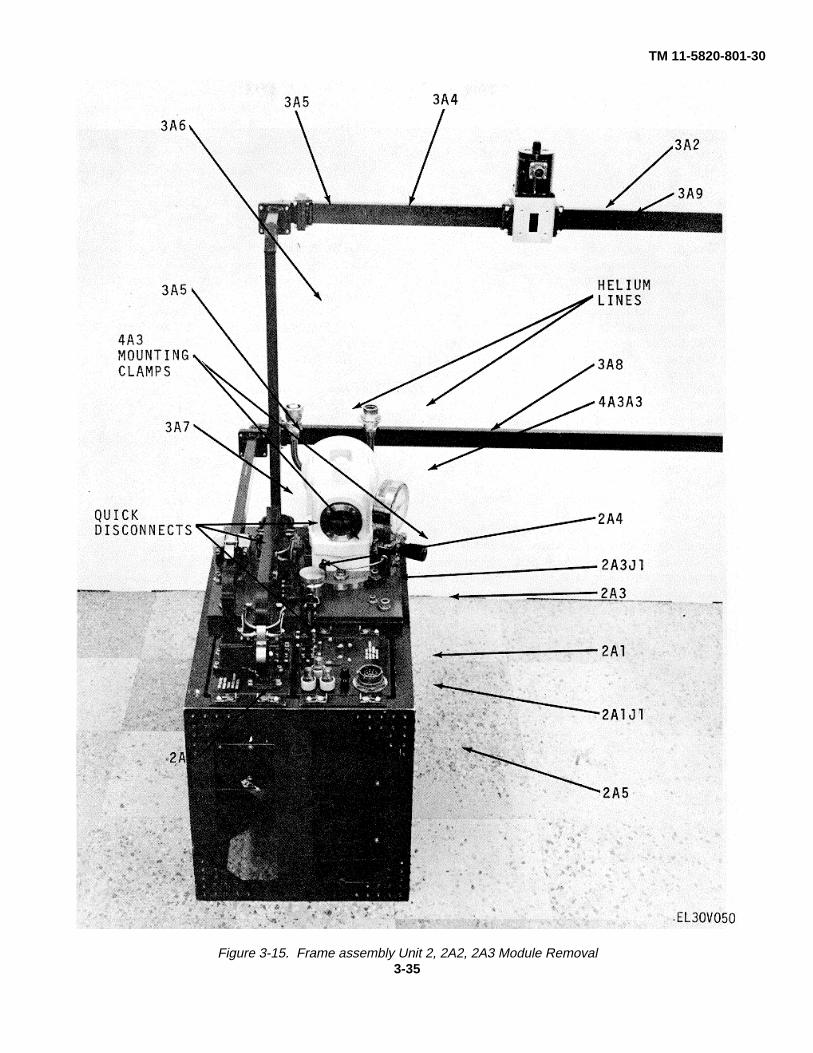
TM 11-5820-801-30
Figure 3-15. Frame assembly Unit 2, 2A2, 2A3 Module Removal3-35

TM 11-5820-801-30
(2) For a Channel 1 installation, remove fourcap screws at waveguide bend 3A5 interface withwaveguide 3A7 For a Channel 2 installation, remove fourcap screws at waveguide bend 3A5 interface withwaveguide 3A11.
(3) Remove four cap screws from the pumpwave guide interface flange that interfaces 2A2 and 2A1.
(4) Snap open the quick disconnects at the2A2 signal output port thereby freeing 3A7 or 3A11waveguide. Lift out the waveguide 3A7 or 3A11.
(5) Remove cable plug WIP2 from 2A2J1.(6) Slide open the four mounting slide clips
(snap slide latch on figure 3-14) that hold 2A2 in 2A5.(7) Lift out Second Stage Paramp Module
2A2.(8) To reinstall 2A2, place the module in 2A5,
slide closed the four mounting slide clips, reconnectW1P2 to 2A2J1, place 3A7/3A11 waveguide on the quickdisconnects at the 2A2 signal output port, snap closedthe connector, replace the four cap screws removed instep (2) above, in the flange that connects 3A5 to3A7/3A11 and replace the four cap screws in the pumpwaveguide inter face flange 2A2/2A1 removed in (3)above. Reinstall Module 2A4 (a above).
d. Vacuum Vessel (Module 2A3. Refer to figures3-14 and 3-15.
(1) Remove Waveguide Filter Module 2A4 (aabove).
(2) Remove four cap screws from the pumpwave guide interface flange that interfaces 2A3 and 2A1.
(3) For a Channel 1 installation, remove fourcap screws at the waveguide bend 3A5 interface withwave guide 3A6 For a Channel 2 installation, removefour cap screws at the waveguide bend 3A5 interfacewith wave guide 3A10.
(4) Snap open the quick disconnects at the2A3 signal input port thereby freeing the 3A6 or 3A10wave guide Lift out the 3A6 or 3A10 waveguide.
(5) Disconnect the helium lines toRefrigerator Unit Assembly 4A3.
(6) Remove W1P3 from 2A3J1, W1P4 from2A3J2, and W3P2 from 4A3A3J6.
(7) Remove four mounting bolts (cap screws)at corners of 2A3 front panel.
(8) Lift Vacuum Vessel Module 2A3 andRefrigerator Unit Assembly 4A3 out of Frame Assembly2A5.
(9) To remove 4A3A2 and 4A3A3 from 2A3,attach evacuating and charging adapter (para 3-4) to4A3A3 helium lines.
(10) Open vacuum valve on the evacuatingand charging adapter (90" turn) to release the heliumpressure in Refrigerator Unit Assembly 4A3.
(11) Loosen two bolts (cap screws) on each ofthe two mounting clamps that mount 4A3A3 to 4A3A1.Remove the clamps.
(12) Lift out the Refrigerator Unit Drive Unit Assembly 4A3A3 and Displacer Assembly 4A3A2.
(13) Reinstall Refrigerator Unit DisplacerAssembly 4A3A2 and Drive Unit Assembly 4A3A3.
(14) Refasten the mounting clamps removedin (11) above.
(15) To reinstall 2A3 place the module in 2A5and fasten the four bolts removed in (7) above.
(16) Make the refrigerator piping connections.(17) Reconnect WIP3 to 2A3J1, W1P4 to
2A3J2 and W3P2 to 4A3A3J6.(18) Reconnect waveguide 3A6 or 3A10 to the
signal input port quick disconnect. Connect waveguidebend 3A5 flange to 3A6 or 3A 10 with four cap screwsremoved in (2) above.
(19) Reconnect pump waveguide flange at the2A2/2A1 interface with four cap screws removed in (3)above.
(20) Remount Module 2A4 (a above).(21) If it is unnecessary to remove the
Refrigerator Unit Assembly 4A3 from Module 2A3, omit(9) through (14) above.
e. Klystron Power Supply 1PS1 Refer to figure 3-3.
(1) Remove W5P2/W5P3 from 1J1, W1P1from 1J2, and W2P1 from 1J3.
(2) Disconnect 1P1 from 1PS1J1.(3) Remove Unit 1 from its rack by removing
eight mounting screws from the front panel and place itupside down on a bench.
(4) Remove nine bolts from bottom of Unit 1chassis.
(5) Carefully lift Unit 1 off of 1PS1.(6) To reinstall 1PS1, place 1PS1 on a bench
with the side stenciled "DANGER 1000 VOLTS" down.(7) Align the Unit 1 chassis (turned upside
down) over 1PS1 so that 1PS1J1 is at the rear of thechassis Lower Unit 1 over 1PS1.
(8) Align the nine mounting holes and replacethe nine bolts removed in (4) above.
(9) Rack mount Unit 1 with the eight mountingscrews removed in step (3) above.
(10) Reconnect 1P1 to 1PS1J1.(11) Reconnect W1P1 to 1J2, W2P1 to 1J3,
and W5P2/W5P3 to 1J1.f. Waveguide Switch 3A2. Refer to figure 3-15.
(1) Remove W5P6 from 3A2J1.(2) Remove four cap screws at 3A2/3A4
interface (Port 2 of 3A2).(3) Remove four cap screws at 3A2/3A9
interface (Port 4 of 3A2).(4) Remove four cap screws at 3A2 Port 1
interface and remove 3A2.(5) To replace 3A2, connect the antenna
waveguide to Port 1 of 3A2 with four cap screwsremoved in (4) above, connect 3A9 to Port 4 with fourcap screws removed in (3) above and connect 3A4 toPort 2 with four cap screws removed in (2) aboveReconnect W5P6 and 3A2J1.
3-36

TM 11-5820-801-30
g. Waveguide Switch 3A 3.(1) Remove W5P8 from 3A3J1.(2) Remove four cap screws at the 3A3/3A8
inter face (Port 2 of 3A3).(3) Remove four cap screws at the 3A3/3A 12
inter face (Port 4 of 3A3).(4) Remove four cap screws at 3A3 Port 1
interface and remove 3A3.(5) To replace 3A3, connect the output
waveguide to 3A3 Port 1 with four cap screws removedin (4) above, connect 3A12 to Port 4 of 3A3 with four capscrews removed in (3) above, and connect 3A8 to Port 2of 3A3 with four cap screws removed in (2) above.Reconnect W5P8 and 3A3J1.
h. Other Unit 3 Waveguide Assembles. Toremove other Unit 3 waveguide assemblies (3A4, 3A6,3A7, 3A8, 3A9, 3A10, 3A11, 3A12) start bydisconnecting at the waveguide bend 3A5 (fig. 3-15)Then release the other end of the assembly, asnecessary.
3-12. System InterconnectionsLocal Control/Monitor Assembly, Unit 1, is connected bycable to Modules 2A1, 2A2, 2A3, 3A1 and 4A1 and to theprimary input power (3 phase, 120 ± 12 V, 55 ± 8 Hz).Remote Control/Monitor Assembly 3A1I is connected bycable to Unit 1, Modules 3A2, 3A3 and to + 28 V primarypower. Four cables (W1, W2, W3, W4) are used perchannel and one cable (W5) interconnects bothchannels. (W3 and W4 provide Unit 4 interconnections.)Four illustrations show the cable interconnections fromUnit 1 (1J1, fig. 3-16; 1J2, fig. 3-17, 1J3, fig. 3-18) andfrom 3A1 (3A1J1, fig. 3-19). Two illustrations show thecable wiring (W1, W2, fig. 3-20 and W3, W4, W5, fig 3-21). These illustrations are presented as aids in systemcontinuity checking, should such become necessary.These illustrations along with the appropriate schematicdiagrams (fig. 2-17, 2-24, 2-8, 2-11, 2-13) show allsystem cable interconnections and facilitate checkingfrom one unit or module to another. Continuity checkingis accomplished with primary power disconnected (W5not connected to 120 V and 28 V sources).
3-37

TM 11-5820-801-30
Figure 3-16. Interconnections to 1J13-38

TM 11-5820-801-30
Figure 3-17. Interconnections to 1J2.
3-39

TM 11-5820-801-30
Figure 3-18. Interconnections to 1J3
3-40

TM 11-5820-801-30
Figure 3-19. Interconnections to 3A1J1.
3-41

TM 11-5820-801-30
Figure 3-20. Interconnection Cables W1 and W2.
3-42

TM 11-5820-801-30
Figure 3-21. Interconnection Cables W3, W4, and W5.
3-43
TM 11-5820-801-30
APPENDIX AREFERENCES
The following publications contain information applicable to the maintenance of Amplifier, Parametric AM-6602/MSC-46(V) .
DA Pam 310-4 Index of Technical Publications: Technical Manuals, Technical Bulletins, SupplyManuals (Types 7, 8, and 9), Supply Bulletins, and Lubrication Orders.
DA Pam 310-7 US Army Equipment Index of Modification Work Orders.TM 11-5820-801-30P Direct Support Repair Parts and Special Tools List (Including Depot
Maintenance Repair Parts) for Amplifier, Parametric AM-6602/MSC-46(V).TM 38-750 The Army Maintenance Management System (TAMMS).
*U.S. GOVERNMENT PRINTING OFFICE I994 - 300-42l/83070
A-1

By Order of the Secretary of the Army:
E.C. MEYERGeneral, United States Army
Chief of Staff
Official:J.C. PENNINGTON
Major General, United States ArmyThe Adjutant General
DISTRIBUTION:Active Army
HISA (Ft Monmouth) (21 USAES (2)USAINSCOM (2) USAICS (3)COE (1) MAAG (1)TSG (1) USARMIS (1)USA ARENBD (1) USAERDAA (1)DARCOM (1) USAERDAWTRADOC (2) Ft Gordon (10)OS Maj Cmd (4) Ft Carson (5)TECOM (2) Army Dep (1) exceptUSACC (4) SAAD (30)MDW (1) TOAD (14)Armies (2) SHAD (2)Corps (2) Ft Gillem (10)Svc Colleges (1) USA Dep (1)USASIGS (5) Sig Sec USA Dep (1)USAADS (2) Ft Richardson (CERCOM Ofc) (2)USAFAS (2) Units org under fol TOE:USAARMS (2) 29-207 (2)USAIS (2) 29-610 (2)
NG: NoneUSAR: NoneFor explanation of abbreviations used, see AR 310-50.

PIN: 046677-000

This fine document...
Was brought to you by me:
Liberated Manuals -- free army and government manuals
Why do I do it? I am tired of sleazy CD-ROM sellers, who take publicly available information, slap “watermarks” and other junk on it, and sell it. Those masters of search engine manipulation make sure that their sites that sell free information, come up first in search engines. They did not create it... They did not even scan it... Why should they get your money? Why are not letting you give those free manuals to your friends?
I am setting this document FREE. This document was made by the US Government and is NOT protected by Copyright. Feel free to share, republish, sell and so on.
I am not asking you for donations, fees or handouts. If you can, please provide a link to liberatedmanuals.com, so that free manuals come up first in search engines:
<A HREF=http://www.liberatedmanuals.com/>Free Military and Government Manuals</A>
– SincerelyIgor Chudovhttp://igor.chudov.com/
– Chicago Machinery Movers