tms320c50/tms320c51 evaluation module … evaluation module technical reference 503481-0001 rev. c...
TRANSCRIPT
TMS320C50/TMS320C51Evaluation Module
1998 DSP Development Systems
TechnicalReference
TMS320C50/TMS320C51 Evaluation Module
Technical Reference
503481-0001 Rev. C March 1998
SPECTRUM DIGITAL, INC.10853 Rockley Road Houston, TX. 77099
Tel: 281/561-6952 Fax: 281/[email protected] www.spectrumdigital.com

IMPORTANT NOTICE
Spectrum Digital, Inc. reserves the right to make changes to its products or to discontinue anyproduct or service without notice, and advises its customers to obtain the latest version of relevantinformation to verify, before placing orders, that the information being relied on is current.
Spectrum Digital, Inc. warrants performance of its products and related software to currentspecifications in accordance with Spectrum Digital’s standard warranty. Testing and other qualitycontrol techniques are utilized to the extent deemed necessary to support this warranty.
Please be aware that the products described herein are not intended for use in life-support appliances, devices, or systems. Spectrum Digital does not warrant nor is liable for the product described herein to be used in other than a development environment.
Spectrum Digital, Inc. assumes no liability for applications assistance, customer product design, software performance, or infringement of patents or services described herein. Nor does SpectrumDigital warrant or represent any license, either express or implied, is granted under any patent right,copyright, or other intellectual property right of Spectrum Digital, Inc. covering or relating to anycombination, machine, or process in which such Digital Signal Processing development products orservices might be or are used.
WARNING
This equipment is intended for use in a laboratory test environment only. It generates, uses, and canradiate radio frequency energy and has not been tested for compliance with the limits of computingdevices pursuant to subpart J of part 15 of FCC rules, which are designed to provide reasonableprotection against radio frequency interference. Operation of this equipment in other environmentsmay cause interference with radio communications, in which case the user at his own expense will berequired to take whatever measures may be required to correct this interference.
TRADEMARKSMS-DOS, MS-Windows, and Windows 95 are registered trademarks of Microsoft Corp.
Copyright © 1998 Spectrum Digital, Inc.
Contents
1 Introduction to the TMS320C5X Evaluation Module . . . . . . . . . . . . . . . . . . . . . . . . . . . . . 1-1 Provides you with a description of the TMS320C5X Evaluation Module, key features, and board outline. 1.0 Overview of the TMS320C5X EVM . . . . . . . . . . . . . . . . . . . . . . . . . . . . . . . . . . . . . . . . . . 1-2 1.1 Key Features of the TMS320C5X EVM . . . . . . . . . . . . . . . . . . . . . . . . . . . . . . . . . . . . . . 1-2 1.2 Functional Overview of the TMS320C5X EVM . . . . . . . . . . . . . . . . . . . . . . . . . . . . . . . . 1-32 TMS320C5X EVM Operation . . . . . . . . . . . . . . . . . . . . . . . . . . . . . . . . . . . . . . . . . . . . . . . . . . 2-1 Describes the operation of the EVM320C5X. Information is provided on the EVM’s various interfaces. 2.0 The EVM320C5X Operation . . . . . . . . . . . . . . . . . . . . . . . . . . . . . . . . . . . . . . . . . . . . . . . 2-2 2.1 The EVM320C5X Board . . . . . . . . . . . . . . . . . . . . . . . . . . . . . . . . . . . . . . . . . . . . . . . . 2-2 2.1.1 Power Connector, J1 . . . . . . . . . . . . . . . . . . . . . . . . . . . . . . . . . . . . . . . . . . . . . . . . . . 2-2 2.2 TMS320C5X Memory Interface . . . . . . . . . . . . . . . . . . . . . . . . . . . . . . . . . . . . . . . . . . . . 2-3 2.2.1 Memory Mapping . . . . . . . . . . . . . . . . . . . . . . . . . . . . . . . . . . . . . . . . . . . . . . . . . . . . . . 2-8 2.3 Expansion Bus . . . . . . . . . . . . . . . . . . . . . . . . . . . . . . . . . . . . . . . . . . . . . . . . . . . . . . . . 2-10 2.3.1 Expansion I/O Connector, P1 . . . . . . . . . . . . . . . . . . . . . . . . . . . . . . . . . . . . . . . . . . 2-11 2.3.2 Expansion Analog Connector, P2 . . . . . . . . . . . . . . . . . . . . . . . . . . . . . . . . . . . . . . 2-12 2.3.3 Expansion Address and Data Connector, P3 . . . . . . . . . . . . . . . . . . . . . . . . . . . . . . 2-13 2.3.4 Expansion Control Connector, P4 . . . . . . . . . . . . . . . . . . . . . . . . . . . . . . . . . . . . . . . 2-14 2.4 Analog Interface . . . . . . . . . . . . . . . . . . . . . . . . . . . . . . . . . . . . . . . . . . . . . . . . . . . . . . 2-15 2.4.1 Analog Input, J2 . . . . . . . . . . . . . . . . . . . . . . . . . . . . . . . . . . . . . . . . . . . . . . . . . . . . . 2-15 2.4.2 Analog Output, J3 . . . . . . . . . . . . . . . . . . . . . . . . . . . . . . . . . . . . . . . . . . . . . . . . . . . . 2-15 2.5 JTAG Interface, P7 . . . . . . . . . . . . . . . . . . . . . . . . . . . . . . . . . . . . . . . . . . . . . . . . . . . . . 2-16 2.6 On Board Serial Interface, P5 . . . . . . . . . . . . . . . . . . . . . . . . . . . . . . . . . . . . . . . . . . . . 2-16
2.7 Jumpers . . . . . . . . . . . . . . . . . . . . . . . . . . . . . . . . . . . . . . . . . . . . . . . . . . . . . . . . . . . . . . . . . . . 2-18 2.7.1 J2 Coupling Select Jumper, JP1 . . . . . . . . . . . . . . . . . . . . . . . . . . . . . . . . . . . . . . . . . . . . . . 2-19 2.7.2 UART Reset Jumper, JP2 . . . . . . . . . . . . . . . . . . . . . . . . . . . . . . . . . . . . . . . . . . . . . . . . . . . . 2-19 2.7.3 Onboard UART CTS Routing Jumper, JP3 . . . . . . . . . . . . . . . . . . . . . . . . . . . . . . . . . . . . . . 2-19 2.7.4 Synchronous Serial Port Routing Jumper, JP4 . . . . . . . . . . . . . . . . . . . . . . . . . . . . . . . . . . 2-20 2.7.5 AD55 Reset Jumper, JP5 . . . . . . . . . . . . . . . . . . . . . . . . . . . . . . . . . . . . . . . . . . . . . . . . . . . . . 2-20 2.7.6 CLKIN Source Select Jumper, JP6, JP7, and JP10 . . . . . . . . . . . . . . . . . . . . . . . . . . . . . . . . 2-20 2.7.7 Ready Routing Jumper, JP8 . . . . . . . . . . . . . . . . . . . . . . . . . . . . . . . . . . . . . . . . . . . . . . . . . . 2-21 2.7.8 Onboard UART Interrupt Select Jumper, JP9 . . . . . . . . . . . . . . . . . . . . . . . . . . . . . . . . . . . . 2-21 2.7.9 C50 Bootloader Jumper, JP11 . . . . . . . . . . . . . . . . . . . . . . . . . . . . . . . . . . . . . . . . . . . . . . . . 2-21 2.7.10 Pseudo Boot Loader Enable Jumper, JP12 . . . . . . . . . . . . . . . . . . . . . . . . . . . . . . . . . . . . . 2-22 2.8 LEDs . . . . . . . . . . . . . . . . . . . . . . . . . . . . . . . . . . . . . . . . . . . . . . . . . . . . . . . . . . . . . . . . . . . . . . . 2-22 2.9 Resets . . . . . . . . .. . . . . . . . . . . . . . . . . . . . . . . . . . . . . . . . . . . . . . . . . . . . . . . . . . . . . . . . . . . . . 2-22A TMS320C5X EVM PAL Equations . . . . . . . . . . . . . . . . . . . . . . . . . . . . . . . . . . . . . . . . . . . . . . . . . . . A-1 Lists the PAL equations that are used on the TMS320C5X EVM A.1 Memory Decode PAL Equations . . . . . . . . . . . . . . . . . . . . . . . . . . . . . . . . . . . . . . . . . . . . . . . . . . . A-2 A.2 I/O Control PAL Equations . . . . . . . . . . . . . . . . . . . . . . . . . . . . . . . . . . . . . . . . . . . . . . . . . . . . . . . . A-6B TMS320C5X Schematics . . . . . . . . . . . . . . . . . . . . . . . . . . . . . . . . . . . . . . . . . . . . . . . . . . . . . . . . . . B-1 Contains the schematics for the TMS320C5X EVMC TL16C550 Data Sheet . . . . . . . . . . . . . . . . . . . . . . . . . . . . . . . . . . . . . . . . . . . . . . . . . . . . . . . . . . . . . C-1 Contains the technical information for the TL16C550D TLC320AD55 Data Sheet . . . . . . . . . . . . . . . . . . . . . . . . . . . . . . . . . . . . . . . . . . . . . . . . . . . . . . . . . . D-1 Contains the technical information for the TLC320AD55E EVM320 Mechanical Information . . . . . . . . . . . . . . . . . . . . . . . . . . . . . . . . . . . . . . . . . . . . . . . . . . . E-1 Contains the mechanical information about the TMS320C5X EVM
About This Manual
This document describes the board level operations of the TMS320C50/TMS320C51evaluation module (EVM). The EVM is based on the Texas Instruments TMS320C50and TMS320C51Digital Signal Processor.
The TMS320C5X EVM is a table top card to allow engineers and software developersto evaluate certain characteristics of the TMS320C50 and TMS320C51 DSP todetermine if the processor meets the designers application requirements. Evaluatorscan create software to execute onboard or expand the system in a variety of ways.
Notational Conventions
This document uses the following conventions.
The TMS320C50 will sometimes be referred to as the C50 or C5X.
The TMS320C51 will sometimes be referred to as the C51 or C5X.
Program listings, program examples, and interactive displays are shown is a specialitalic typeface. Here is a sample program listing.
equations!rd = !strobe&rw;
Information About Cautions
This book may contain cautions.This is an example of a caution statement.A caution statement describes a situation that could potentially damage your software,or hardware, or other equipment. The information in a caution is provided for yourprotection. Please read each caution carefully.
Related Documents
Texas Instruments TMS320C5X Users GuideTexas Instruments TMS320 Fixed Point Assembly Language Users GuideTexas Instruments TMS320 Fixed Point C Language Users GuideTexas Instruments TMS320 Fixed Point C Source Debugger Users GuideTexas Instruments TLC320AD55C Data Manual - SLAS085Texas Instruments TLC320AD55 Evaluation Board Application Report - SLAE11

1-1
Chapter 1
Introduction to the TMS320C5X Evaluation Module
This chapter provides you with a description of the TMS32C5X EvaluationModule along with the key features and a block diagram of the circuitboard.
Topic Page
1.0 Overview of the TMS320C5X EVM 1-21.1 Key Features of the TMS320C5X EVM 1-21.2 Functional Overview of the TMS320C5X EVM 1-3
Spectrum Digital, Inc
1-2 TMS320C5X Evaluation Module Technical Reference
1.0 Overview of the TMS320C5X EVM
The TMS320C5X evaluation module(EVM) is a stand-alone card that lets evaluatorsexamine certain characteristics of the TMS320C50 or TMS320C51 digital signalprocessor(DSP) to determine if this DSP meets their application requirements.Furthermore, the module is an excellent platform to develop and run software on theC5X family of processors.
The C5X EVM is shipped with a choice of DSPs; the TMS320C50, the TMS320C51,the TMS320BC51, or other pin compatible family members as they become available.The EVM allows full speed verification of C5X code. With at least 544 words of onchipmemory, 128K words of onboard memory, onchip/onboard boot flash rom, on chipUART, on board UART, and a TLC320AD55 sigma delta codec the board can solve avariety of problems as shipped. Four expansion connectors are provided for anynecessary evaluation circuitry not provided on the as shipped configuration.
To simplify code development and shorten debugging time a number of optional userinterfaces are provided.
1.1 Key Features of the TMS320C5X EVM
The C5X EVM has the following features:
• C50 operating at 40 Mips with 128K words of zero wait state memory C51/BC51 operating at 40 Mips
• TLC320AD55 Sigma Delta Codec with RCA Jack input and output
• On board UART with RS232 Drivers
• 32K words on board Flash ROM
• 4 Expansion Connectors
• On board IEEE 1149.1 JTAG Connection for Optional Emulation
• 5 Volt Only Operation
Spectrum Digital, Inc
1-3
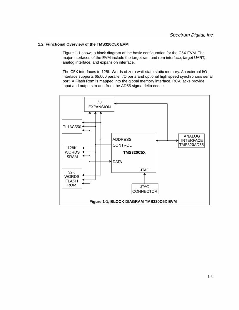
1.2 Functional Overview of the TMS320C5X EVM
Figure 1-1 shows a block diagram of the basic configuration for the C5X EVM. Themajor interfaces of the EVM include the target ram and rom interface, target UART,analog interface, and expansion interface.
The C5X interfaces to 128K Words of zero wait-state static memory. An external I/Ointerface supports 65,000 parallel I/O ports and optional high speed synchronous serialport. A Flash Rom is mapped into the global memory interface. RCA jacks provideinput and outputs to and from the AD55 sigma delta codec.
TMS320C5X
JTAG
DATA
CONTROL
ADDRESS
I/OEXPANSION
128KWORDSSRAM
FLASHROM
ANALOGINTERFACE
TMS320AD55
JTAGCONNECTOR
Figure 1-1, BLOCK DIAGRAM TMS320C5X EVM
32KWORDS
TL16C550

Spectrum Digital, Inc
1-4 TMS320C5X Evaluation Module Technical Reference
2-1
Chapter 2
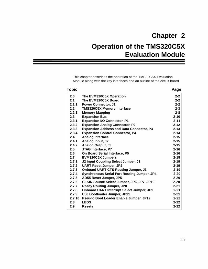
Operation of the TMS320C5X Evaluation Module
This chapter describes the operation of the TMS32C5X EvaluationModule along with the key interfaces and an outline of the circuit board.
Topic Page
2.0 The EVM320C5X Operation 2-22.1 The EVM320C5X Board 2-22.1.1 Power Connector, J1 2-22.2 TMS320C5X Memory Interface 2-32.2.1 Memory Mapping 2-82.3 Expansion Bus 2-102.3.1 Expansion I/O Connector, P1 2-112.3.2 Expansion Analog Connector, P2 2-122.3.3 Expansion Address and Data Connector, P3 2-132.3.4 Expansion Control Connector, P4 2-142.4 Analog Interface 2-152.4.1 Analog Input, J2 2-152.4.2 Analog Output, J3 2-152.5 JTAG Interface, P7 2-162.6 On Board Serial Interface, P5 2-162.7 EVM320C5X Jumpers 2-182.7.1 J2 Input Coupling Select Jumper, J1 2-192.7.2 UART Reset Jumper, JP2 2-192.7.3 Onboard UART CTS Routing Jumper, J3 2-192.7.4 Synchronous Serial Port Routing Jumper, JP4 2-202.7.5 AD55 Reset Jumper, JP5 2-202.7.6 CLKIN Source Select Jumper, JP6, JP7, JP10 2-202.7.7 Ready Routing Jumper, JP8 2-212.7.8 Onboard UART Interrupt Select Jumper, JP9 2-212.7.9 C50 Bootloader Jumper, JP11 2-212.7.10 Pseudo Boot Loader Enable Jumper, JP12 2-222.8 LEDS 2-222.9 Resets 2-22
Spectrum Digital, Inc
2-2 TMS320C5X Evaluation Module Technical Reference
2.0 The EVM320C5X Operation
This chapter describes the C5X Evaluation module, its key components, and how theyoperate. It also provides information on the EVM’s various interfaces.The C5X EVMconsists of five major blocks of logic.
• C5X memory interface• Analog Interface• On board serial interface• Expansion connector interface• JTAG interface
2.1 The TMS320C5X EVM Board
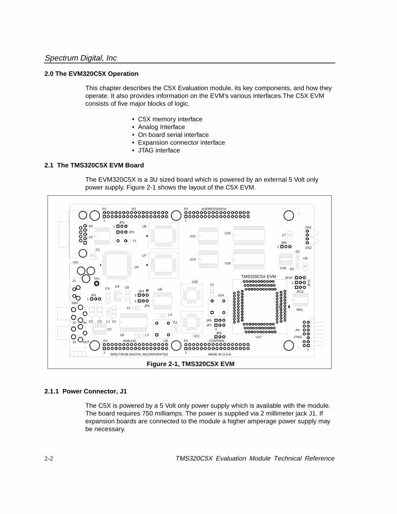
The EVM320C5X is a 3U sized board which is powered by an external 5 Volt onlypower supply. Figure 2-1 shows the layout of the C5X EVM.
2.1.1 Power Connector, J1
The C5X is powered by a 5 Volt only power supply which is available with the module.The board requires 750 milliamps. The power is supplied via 2 millimeter jack J1. Ifexpansion boards are connected to the module a higher amperage power supply maybe necessary.
Figure 2-1, TMS320C5X EVM
MADE IN U.S.A.
1
1
1
J2
J3
L5
JP6
JP10
JP11
JP7
JP8
1
C8
U14
+5V
IN
OUT
JTAGU11
L4
U8
U9
U2
J1
Y1
SW1
U18
U6
U7
U16
DS2C1
C4 C6U4
CONTROLANALOG
ADDRESS/DATAI/O P3P1
P2 P4
U5
U1
L2
L3
U12
U13
P5
U3
C5
DS1
D2
D3
JP1
C2 C3 L1
C7
D1
1 1
1 1
11
1
1
SPECTRUM DIGITAL INCORPORATED
TMS320C5X EVM
JP4
JP5
U10
U15
U17
JP9
RN1
JP12
JP2
JP3
P6
TP1
Spectrum Digital, Inc
2-3
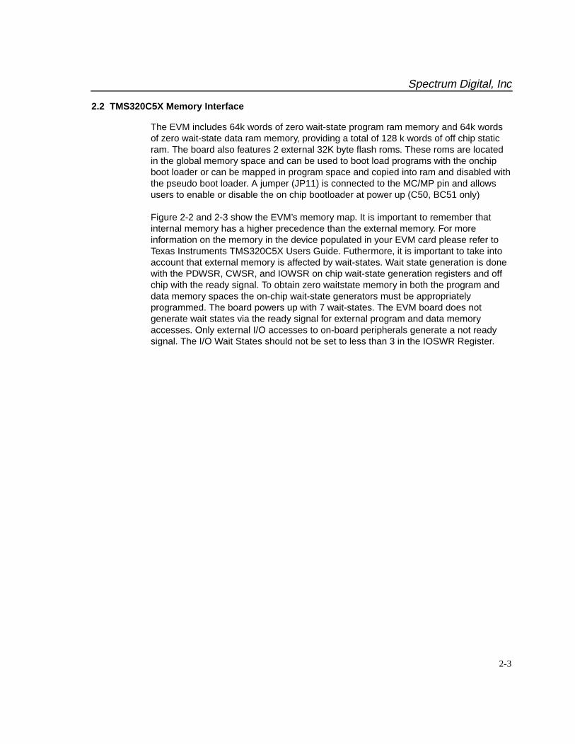
2.2 TMS320C5X Memory Interface
The EVM includes 64k words of zero wait-state program ram memory and 64k wordsof zero wait-state data ram memory, providing a total of 128 k words of off chip staticram. The board also features 2 external 32K byte flash roms. These roms are locatedin the global memory space and can be used to boot load programs with the onchipboot loader or can be mapped in program space and copied into ram and disabled withthe pseudo boot loader. A jumper (JP11) is connected to the MC/MP pin and allowsusers to enable or disable the on chip bootloader at power up (C50, BC51 only)
Figure 2-2 and 2-3 show the EVM’s memory map. It is important to remember thatinternal memory has a higher precedence than the external memory. For moreinformation on the memory in the device populated in your EVM card please refer toTexas Instruments TMS320C5X Users Guide. Futhermore, it is important to take intoaccount that external memory is affected by wait-states. Wait state generation is donewith the PDWSR, CWSR, and IOWSR on chip wait-state generation registers and offchip with the ready signal. To obtain zero waitstate memory in both the program anddata memory spaces the on-chip wait-state generators must be appropriatelyprogrammed. The board powers up with 7 wait-states. The EVM board does notgenerate wait states via the ready signal for external program and data memoryaccesses. Only external I/O accesses to on-board peripherals generate a not readysignal. The I/O Wait States should not be set to less than 3 in the IOSWR Register.
Spectrum Digital, Inc
2-4 TMS320C5X Evaluation Module Technical Reference
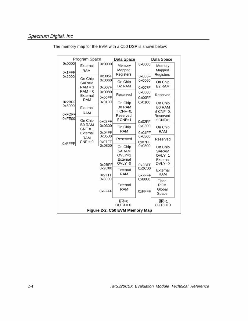
The memory map for the EVM with a C50 DSP is shown below:
Program Space Data Space0x0000
0xFFFF
External RAM
Figure 2-2, C50 EVM Memory MapOUT3 = 0
0xFFFF
0x80000x7FFF
0x0000
RAMExternal
External
OUT3 = 0BR=0 BR=1
Data Space
RAMExternal
MemoryMapped
Registers
On ChipB2 RAM
Reserved
0x005F0x0060
0x007F0x0080
0x00FF0x0100
0x02FF0x0300
0x04FF0x0500
0x07FF0x0800
0x2BFF
On ChipB0 RAM
if CNF=0,Reserved if CNF=1
On ChipRAM
Reserved
On ChipSARAMOVLY=1ExternalOVLY=0
0x2C00
RAM 0xFFFF
0x80000x7FFF
0x0000
RAMExternal
MemoryMapped
Registers
On ChipB2 RAM
Reserved
0x005F0x0060
0x007F0x0080
0x00FF0x0100
0x02FF0x0300
0x04FF0x0500
0x07FF0x0800
0x2BFF
On ChipB0 RAM
if CNF=0,Reserved if CNF=1
On ChipRAM
Reserved
On ChipSARAMOVLY=1ExternalOVLY=0
0x2C00
FlashROM
GlobalSpace
On ChipSARAMRAM = 1RAM = 0External
RAM
0x1FFF0x2000
0x2BFF0x3000
0xFDFF0xFE00 On Chip
B0 RAMCNF = 1External
RAMCNF = 0
Spectrum Digital, Inc
2-5
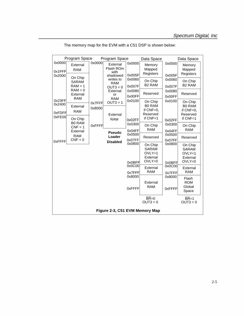
The memory map for the EVM with a C51 DSP is shown below:
Program Space Data Space0x0000
0xFFFF
Figure 2-3, C51 EVM Memory Map
0x7FFF0x8000
OUT3 = 0
0xFFFF
0x80000x7FFF
0x0000
RAMExternal
External
OUT3 = 0BR=0 BR=1
Data Space
RAMExternal
MemoryMapped
Registers
On ChipB2 RAM
Reserved
0x005F0x0060
0x007F0x0080
0x00FF0x0100
0x02FF0x0300
0x04FF0x0500
0x07FF0x0800
0x0BFF
On ChipB0 RAM
if CNF=0,Reserved if CNF=1
On ChipRAM
Reserved
On ChipSARAMOVLY=1ExternalOVLY=0
0x0C00
RAM 0xFFFF
0x80000x7FFF
0x0000
RAMExternal
MemoryMapped
Registers
On ChipB2 RAM
Reserved
0x005F0x0060
0x007F0x0080
0x00FF0x0100
0x02FF0x0300
0x04FF0x0500
0x07FF0x0800
0x0BFF
On ChipB0 RAM
if CNF=0,Reserved if CNF=1
On ChipRAM
Reserved
On ChipSARAMOVLY=1ExternalOVLY=0
0x0C00
FlashROM
GlobalSpace
ExternalFlash ROm
withshadowedwrites to
RAMOUT3 = 0
orExternal
RAMOUT3 = 1
0x0000
0xFFFF
External RAM
RAMExternal
On ChipSARAMRAM = 1RAM = 0External
RAM
0x1FFF0x2000
0x23FF0x2400
0xFDFF0xFE00 On Chip
B0 RAMCNF = 1External
RAMCNF = 0
Program Space
PseudoLoader
Disabled
Spectrum Digital, Inc
2-6 TMS320C5X Evaluation Module Technical Reference
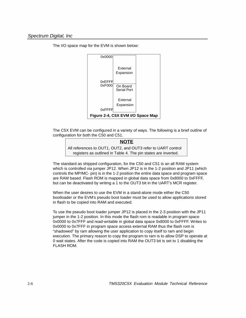
The I/O space map for the EVM is shown below:
The C5X EVM can be configured in a variety of ways. The following is a brief outline ofconfiguration for both the C50 and C51.
The standard as shipped configuration, for the C50 and C51 is an all RAM systemwhich is controlled via jumper JP12. When JP12 is in the 1-2 position and JP11 (whichcontrols the MP/MC- pin) is in the 1-2 position the entire data space and program spaceare RAM based. Flash ROM is mapped in global data space from 0x8000 to 0xFFFF,but can be deactivated by writing a 1 to the OUT3 bit in the UART’s MCR register.
When the user desires to use the EVM in a stand-alone mode either the C50bootloader or the EVM’s pseudo boot loader must be used to allow applications storedin flash to be copied into RAM and executed.
To use the pseudo boot loader jumper JP12 is placed in the 2-3 position with the JP11jumper in the 1-2 position. In this mode the flash rom is readable in program space0x0000 to 0x7FFF and read-writable in global data space 0x8000 to 0xFFFF. Writes to0x0000 to 0x7FFF in program space access external RAM thus the flash rom is“shadowed” by ram allowing the user application to copy itself to ram and beginexecution. The primary reason to copy the program to ram is to allow DSP to operate at0 wait states. After the code is copied into RAM the OUT3 bit is set to 1 disabling theFLASH ROM.
0x0000
0xFFFF
0xEFFF
ExternalExpansion
On Board0xF000Serial Port
ExternalExpansion
Figure 2-4, C5X EVM I/O Space Map
NOTEAll references to OUT1, OUT2, and OUT3 refer to UART control
registers as outlined in Table 4. The pin states are inverted.
Spectrum Digital, Inc
2-7
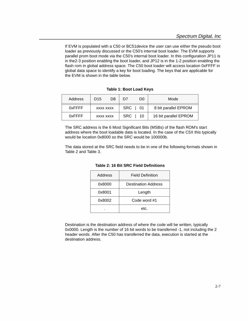
If EVM is populated with a C50 or BC51device the user can use either the pseudo bootloader as previously discussed or the C50’s internal boot loader. The EVM supportsparallel prom boot mode via the C50’s internal boot loader. In this configuration JP11 isin the2-3 position enabling the boot loader, and JP12 is in the 1-2 position enabling theflash rom in global address space. The C50 boot loader will access location 0xFFFF inglobal data space to identify a key for boot loading. The keys that are applicable forthe EVM is shown in the table below.
The SRC address is the 6 Most Significant Bits (MSBs) of the flash ROM’s startaddress where the boot loadable data is located. In the case of the C5X this typicallywould be location 0x8000 so the SRC would be 100000b.
The data stored at the SRC field needs to be in one of the following formats shown inTable 2 and Table 3.
Destination is the destination address of where the code will be written, typically0x0000. Length is the number of 16 bit words to be transferred -1, not including the 2header words. After the C50 has transferred the data, execution is started at thedestination address.
Table 1: Boot Load Keys
Address D15 D8 D7 D0 Mode
0xFFFF xxxx xxxx SRC | 01 8 bit parallel EPROM
0xFFFF xxxx xxxx SRC | 10 16 bit parallel EPROM
Table 2: 16 Bit SRC Field Definitions
Address Field Definition
0x8000 Destination Address
0x8001 Length
0x8002 Code word #1
. etc.
Spectrum Digital, Inc
2-8 TMS320C5X Evaluation Module Technical Reference
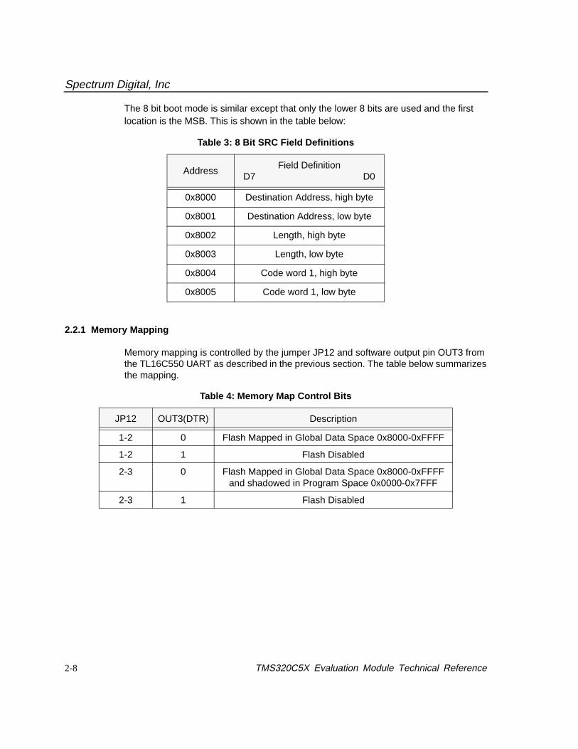
The 8 bit boot mode is similar except that only the lower 8 bits are used and the firstlocation is the MSB. This is shown in the table below:
2.2.1 Memory Mapping
Memory mapping is controlled by the jumper JP12 and software output pin OUT3 fromthe TL16C550 UART as described in the previous section. The table below summarizesthe mapping.
Table 3: 8 Bit SRC Field Definitions
AddressField Definition
D7 D0
0x8000 Destination Address, high byte
0x8001 Destination Address, low byte
0x8002 Length, high byte
0x8003 Length, low byte
0x8004 Code word 1, high byte
0x8005 Code word 1, low byte
Table 4: Memory Map Control Bits
JP12 OUT3(DTR) Description
1-2 0 Flash Mapped in Global Data Space 0x8000-0xFFFF
1-2 1 Flash Disabled
2-3 0 Flash Mapped in Global Data Space 0x8000-0xFFFFand shadowed in Program Space 0x0000-0x7FFF
2-3 1 Flash Disabled
Spectrum Digital, Inc
2-9
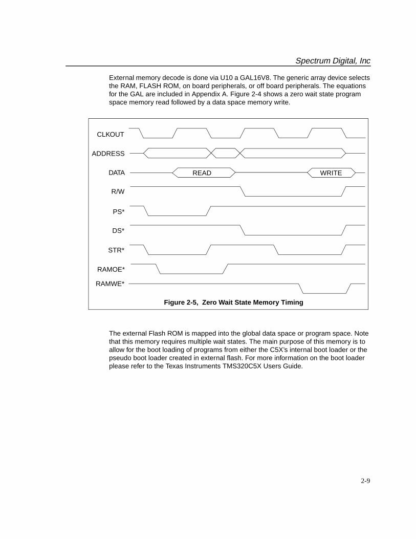
External memory decode is done via U10 a GAL16V8. The generic array device selectsthe RAM, FLASH ROM, on board peripherals, or off board peripherals. The equationsfor the GAL are included in Appendix A. Figure 2-4 shows a zero wait state programspace memory read followed by a data space memory write.
The external Flash ROM is mapped into the global data space or program space. Notethat this memory requires multiple wait states. The main purpose of this memory is toallow for the boot loading of programs from either the C5X’s internal boot loader or thepseudo boot loader created in external flash. For more information on the boot loaderplease refer to the Texas Instruments TMS320C5X Users Guide.
CLKOUT
ADDRESS
DATA
R/W
PS*
DS*
STR*
RAMOE*
Figure 2-5, Zero Wait State Memory Timing
READ WRITE
RAMWE*
Spectrum Digital, Inc
2-10 TMS320C5X Evaluation Module Technical Reference
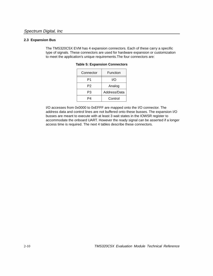
2.3 Expansion Bus
The TMS320C5X EVM has 4 expansion connectors. Each of these carry a specifictype of signals. These connectors are used for hardware expansion or customizationto meet the application’s unique requirements.The four connectors are:
I/O accesses from 0x0000 to 0xEFFF are mapped onto the I/O connector. Theaddress data and control lines are not buffered onto these busses. The expansion I/Obusses are meant to execute with at least 3 wait states in the IOWSR register toaccommodate the onboard UART. However the ready signal can be asserted if a longeraccess time is required. The next 4 tables describe these connectors.
Table 5: Expansion Connectors
Connector Function
P1 I/O
P2 Analog
P3 Address/Data
P4 Control

Spectrum Digital, Inc
2-11
2.3.1 Expansion I/O Connector, P1
The definition of P1, which has the I/O signals is shown below.
Table 6: P1 I/O
Pin # Signal Pin # Signal
1 VCC, +5 Volts 2 VCC, +5 Volts
3 TOUT 4 Reserved
5 TDR 6 Reserved
7 TDX 8 Reserved
9 TFSR 10 Reserved
11 TCLKR 12 Reserved
13 TCLKX 14 OUT2
15 3 16 Reserved
17 GND 18 GND
19 XF 20 BIO
21 Resreved 22 Reserved
23 OUT1(UART) 24 OUT3(UART)
25 OUT2(UART) 26 Reserved
27 Reserved 28 Reserved
29 IN1(UART) 30 IN3(UART)
31 IN2(UART) 32 Reserved
33 GND 34 GND
Spectrum Digital, Inc
2-12 TMS320C5X Evaluation Module Technical Reference
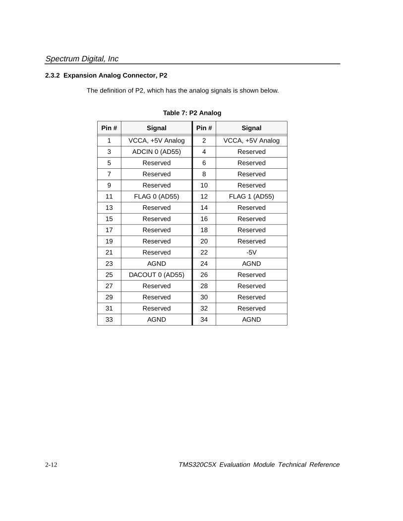
2.3.2 Expansion Analog Connector, P2
The definition of P2, which has the analog signals is shown below.
Table 7: P2 Analog
Pin # Signal Pin # Signal
1 VCCA, +5V Analog 2 VCCA, +5V Analog
3 ADCIN 0 (AD55) 4 Reserved
5 Reserved 6 Reserved
7 Reserved 8 Reserved
9 Reserved 10 Reserved
11 FLAG 0 (AD55) 12 FLAG 1 (AD55)
13 Reserved 14 Reserved
15 Reserved 16 Reserved
17 Reserved 18 Reserved
19 Reserved 20 Reserved
21 Reserved 22 -5V
23 AGND 24 AGND
25 DACOUT 0 (AD55) 26 Reserved
27 Reserved 28 Reserved
29 Reserved 30 Reserved
31 Reserved 32 Reserved
33 AGND 34 AGND
Spectrum Digital, Inc
2-13
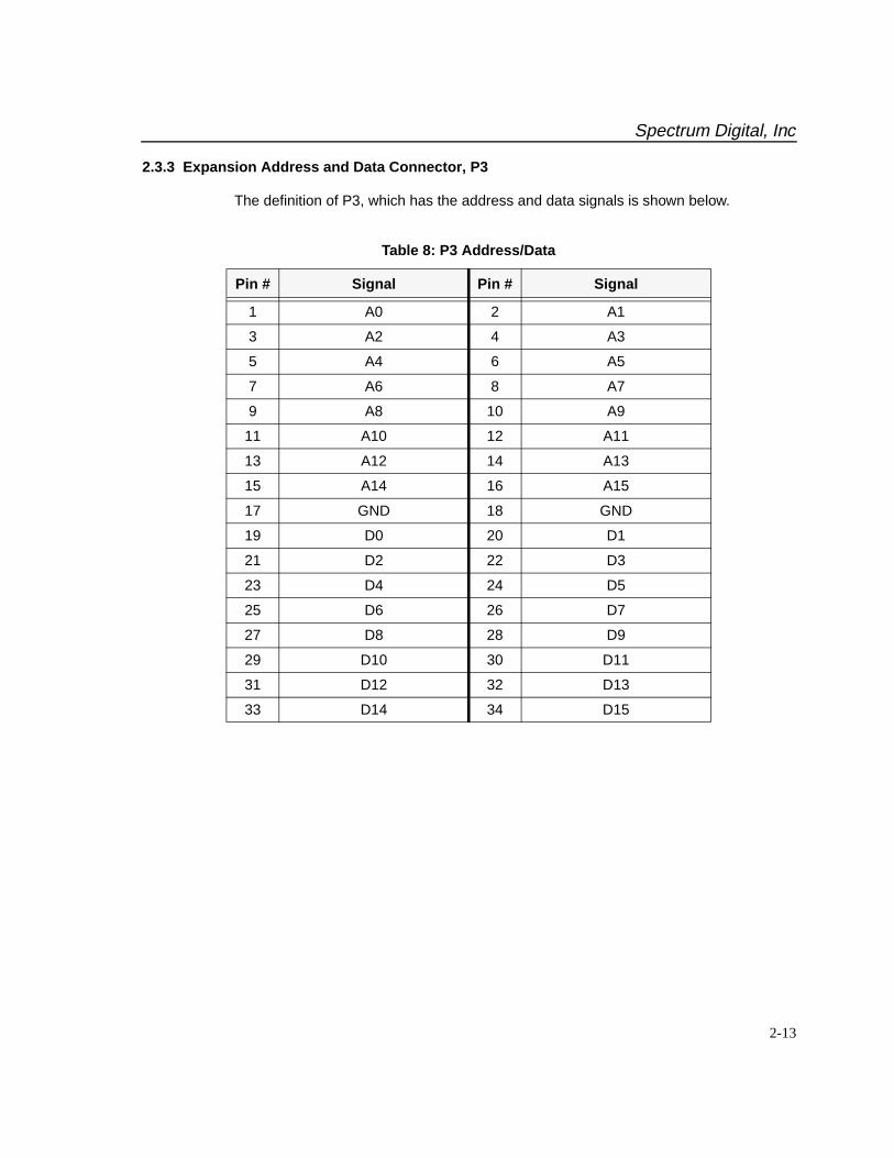
2.3.3 Expansion Address and Data Connector, P3
The definition of P3, which has the address and data signals is shown below.
Table 8: P3 Address/Data
Pin # Signal Pin # Signal
1 A0 2 A1
3 A2 4 A3
5 A4 6 A5
7 A6 8 A7
9 A8 10 A9
11 A10 12 A11
13 A12 14 A13
15 A14 16 A15
17 GND 18 GND
19 D0 20 D1
21 D2 22 D3
23 D4 24 D5
25 D6 26 D7
27 D8 28 D9
29 D10 30 D11
31 D12 32 D13
33 D14 34 D15
Spectrum Digital, Inc
2-14 TMS320C5X Evaluation Module Technical Reference
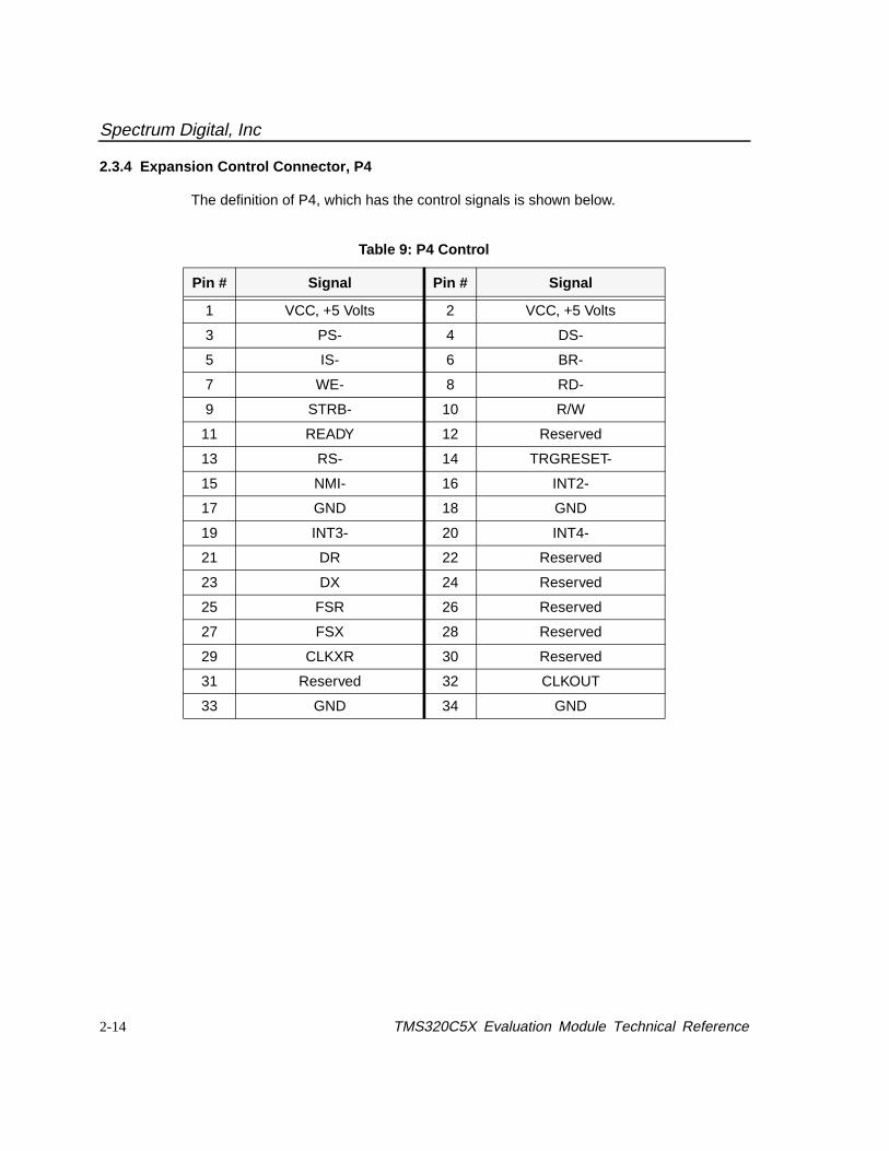
2.3.4 Expansion Control Connector, P4
The definition of P4, which has the control signals is shown below.
Table 9: P4 Control
Pin # Signal Pin # Signal
1 VCC, +5 Volts 2 VCC, +5 Volts
3 PS- 4 DS-
5 IS- 6 BR-
7 WE- 8 RD-
9 STRB- 10 R/W
11 READY 12 Reserved
13 RS- 14 TRGRESET-
15 NMI- 16 INT2-
17 GND 18 GND
19 INT3- 20 INT4-
21 DR 22 Reserved
23 DX 24 Reserved
25 FSR 26 Reserved
27 FSX 28 Reserved
29 CLKXR 30 Reserved
31 Reserved 32 CLKOUT
33 GND 34 GND
Spectrum Digital, Inc
2-15
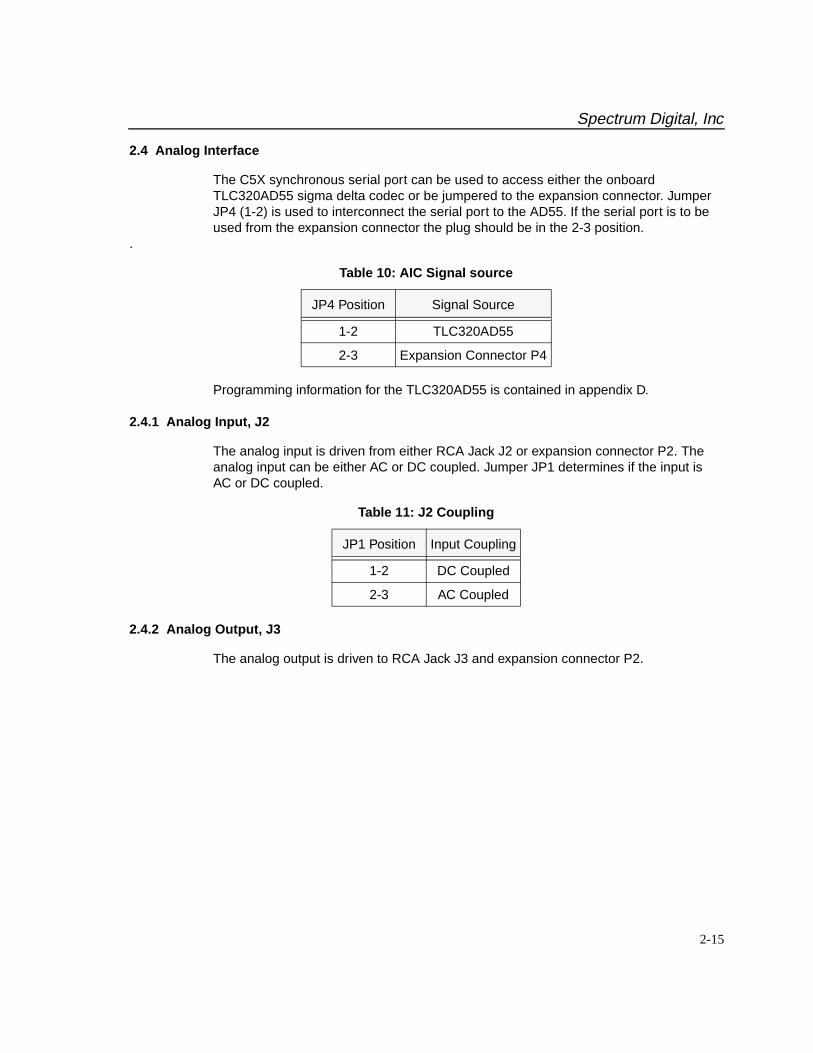
2.4 Analog Interface
The C5X synchronous serial port can be used to access either the onboardTLC320AD55 sigma delta codec or be jumpered to the expansion connector. JumperJP4 (1-2) is used to interconnect the serial port to the AD55. If the serial port is to beused from the expansion connector the plug should be in the 2-3 position.
.
Programming information for the TLC320AD55 is contained in appendix D.
2.4.1 Analog Input, J2
The analog input is driven from either RCA Jack J2 or expansion connector P2. Theanalog input can be either AC or DC coupled. Jumper JP1 determines if the input isAC or DC coupled.
2.4.2 Analog Output, J3
The analog output is driven to RCA Jack J3 and expansion connector P2.
Table 10: AIC Signal source
JP4 Position Signal Source
1-2 TLC320AD55
2-3 Expansion Connector P4
Table 11: J2 Coupling
JP1 Position Input Coupling
1-2 DC Coupled
2-3 AC Coupled
Spectrum Digital, Inc
2-16 TMS320C5X Evaluation Module Technical Reference
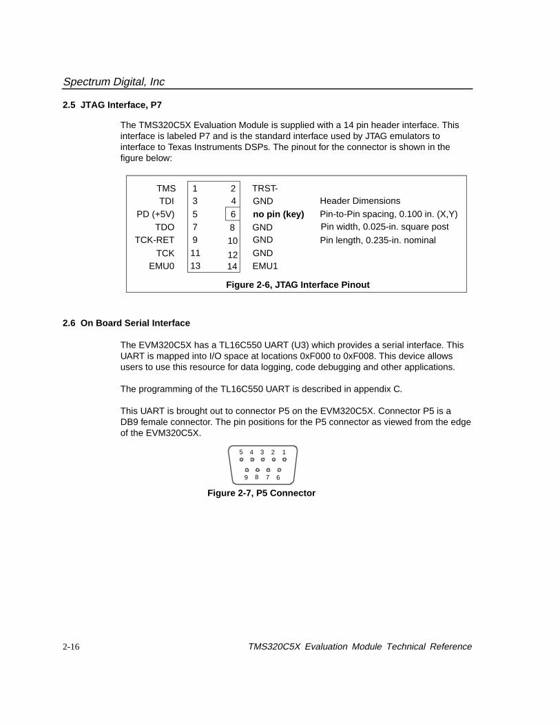
2.5 JTAG Interface, P7
The TMS320C5X Evaluation Module is supplied with a 14 pin header interface. Thisinterface is labeled P7 and is the standard interface used by JTAG emulators tointerface to Texas Instruments DSPs. The pinout for the connector is shown in thefigure below:
2.6 On Board Serial Interface
The EVM320C5X has a TL16C550 UART (U3) which provides a serial interface. ThisUART is mapped into I/O space at locations 0xF000 to 0xF008. This device allowsusers to use this resource for data logging, code debugging and other applications.
The programming of the TL16C550 UART is described in appendix C.
This UART is brought out to connector P5 on the EVM320C5X. Connector P5 is aDB9 female connector. The pin positions for the P5 connector as viewed from the edgeof the EVM320C5X.
1 23 4
5 67 89 1011 1213 14
TMSTDI
PD (+5V)TDO
TCK-RET
TCKEMU0
TRST-GNDno pin (key)GNDGND
GNDEMU1
Header Dimensions
Pin-to-Pin spacing, 0.100 in. (X,Y)Pin width, 0.025-in. square post
Pin length, 0.235-in. nominal
Figure 2-6, JTAG Interface Pinout
Figure 2-7, P5 Connector
9
5 4 3 2 1
8 7 6
Spectrum Digital, Inc
2-17
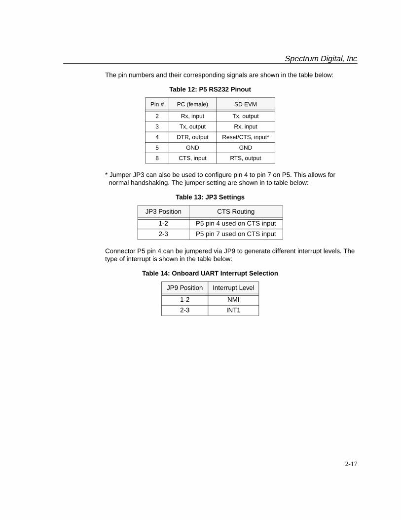
The pin numbers and their corresponding signals are shown in the table below:
* Jumper JP3 can also be used to configure pin 4 to pin 7 on P5. This allows for normal handshaking. The jumper setting are shown in to table below:
Connector P5 pin 4 can be jumpered via JP9 to generate different interrupt levels. Thetype of interrupt is shown in the table below:
Table 12: P5 RS232 Pinout
Pin # PC (female) SD EVM
2 Rx, input Tx, output
3 Tx, output Rx, input
4 DTR, output Reset/CTS, input*
5 GND GND
8 CTS, input RTS, output
Table 13: JP3 Settings
JP3 Position CTS Routing
1-2 P5 pin 4 used on CTS input
2-3 P5 pin 7 used on CTS input
Table 14: Onboard UART Interrupt Selection
JP9 Position Interrupt Level
1-2 NMI
2-3 INT1
Spectrum Digital, Inc
2-18 TMS320C5X Evaluation Module Technical Reference
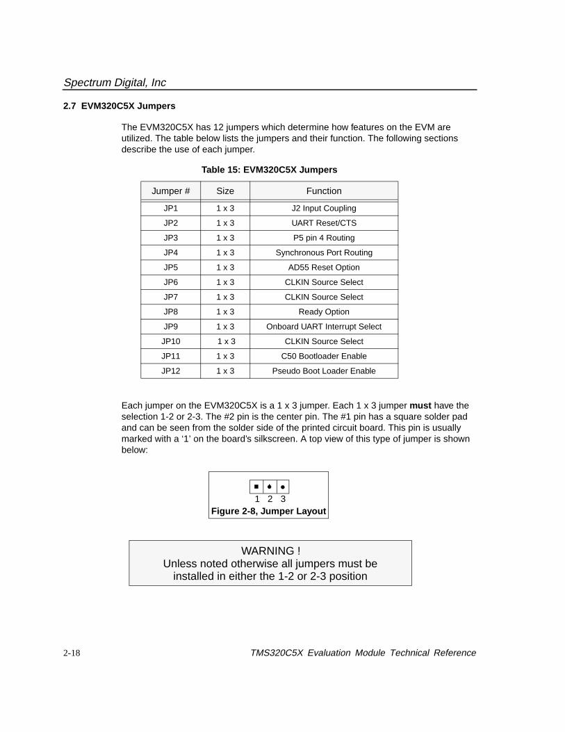
2.7 EVM320C5X Jumpers
The EVM320C5X has 12 jumpers which determine how features on the EVM areutilized. The table below lists the jumpers and their function. The following sectionsdescribe the use of each jumper.
Each jumper on the EVM320C5X is a 1 x 3 jumper. Each 1 x 3 jumper must have theselection 1-2 or 2-3. The #2 pin is the center pin. The #1 pin has a square solder padand can be seen from the solder side of the printed circuit board. This pin is usuallymarked with a ‘1’ on the board’s silkscreen. A top view of this type of jumper is shownbelow:
Table 15: EVM320C5X Jumpers
Jumper # Size Function
JP1 1 x 3 J2 Input Coupling
JP2 1 x 3 UART Reset/CTS
JP3 1 x 3 P5 pin 4 Routing
JP4 1 x 3 Synchronous Port Routing
JP5 1 x 3 AD55 Reset Option
JP6 1 x 3 CLKIN Source Select
JP7 1 x 3 CLKIN Source Select
JP8 1 x 3 Ready Option
JP9 1 x 3 Onboard UART Interrupt Select
JP10 1 x 3 CLKIN Source Select
JP11 1 x 3 C50 Bootloader Enable
JP12 1 x 3 Pseudo Boot Loader Enable
31 2Figure 2-8, Jumper Layout
WARNING !Unless noted otherwise all jumpers must be
installed in either the 1-2 or 2-3 position
Spectrum Digital, Inc
2-19
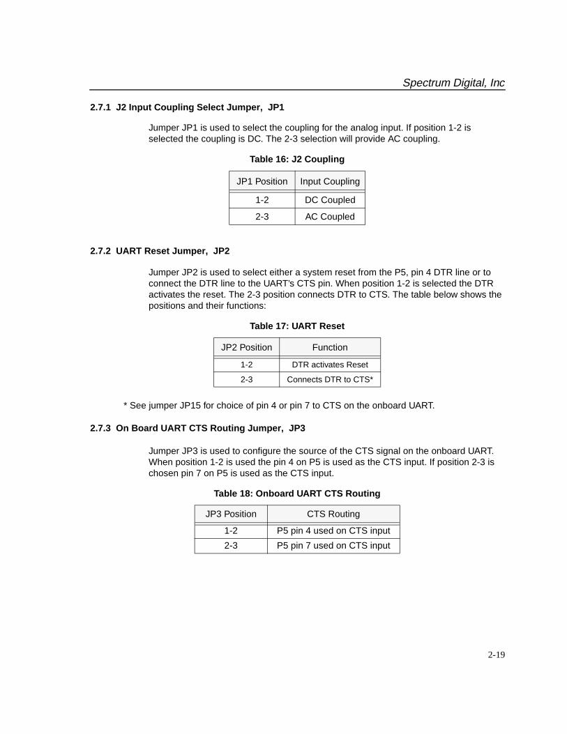
2.7.1 J2 Input Coupling Select Jumper, JP1
Jumper JP1 is used to select the coupling for the analog input. If position 1-2 isselected the coupling is DC. The 2-3 selection will provide AC coupling.
2.7.2 UART Reset Jumper, JP2
Jumper JP2 is used to select either a system reset from the P5, pin 4 DTR line or toconnect the DTR line to the UART’s CTS pin. When position 1-2 is selected the DTRactivates the reset. The 2-3 position connects DTR to CTS. The table below shows thepositions and their functions:
* See jumper JP15 for choice of pin 4 or pin 7 to CTS on the onboard UART.
2.7.3 On Board UART CTS Routing Jumper, JP3
Jumper JP3 is used to configure the source of the CTS signal on the onboard UART.When position 1-2 is used the pin 4 on P5 is used as the CTS input. If position 2-3 ischosen pin 7 on P5 is used as the CTS input.
Table 16: J2 Coupling
JP1 Position Input Coupling
1-2 DC Coupled
2-3 AC Coupled
Table 17: UART Reset
JP2 Position Function
1-2 DTR activates Reset
2-3 Connects DTR to CTS*
Table 18: Onboard UART CTS Routing
JP3 Position CTS Routing
1-2 P5 pin 4 used on CTS input
2-3 P5 pin 7 used on CTS input
Spectrum Digital, Inc
2-20 TMS320C5X Evaluation Module Technical Reference
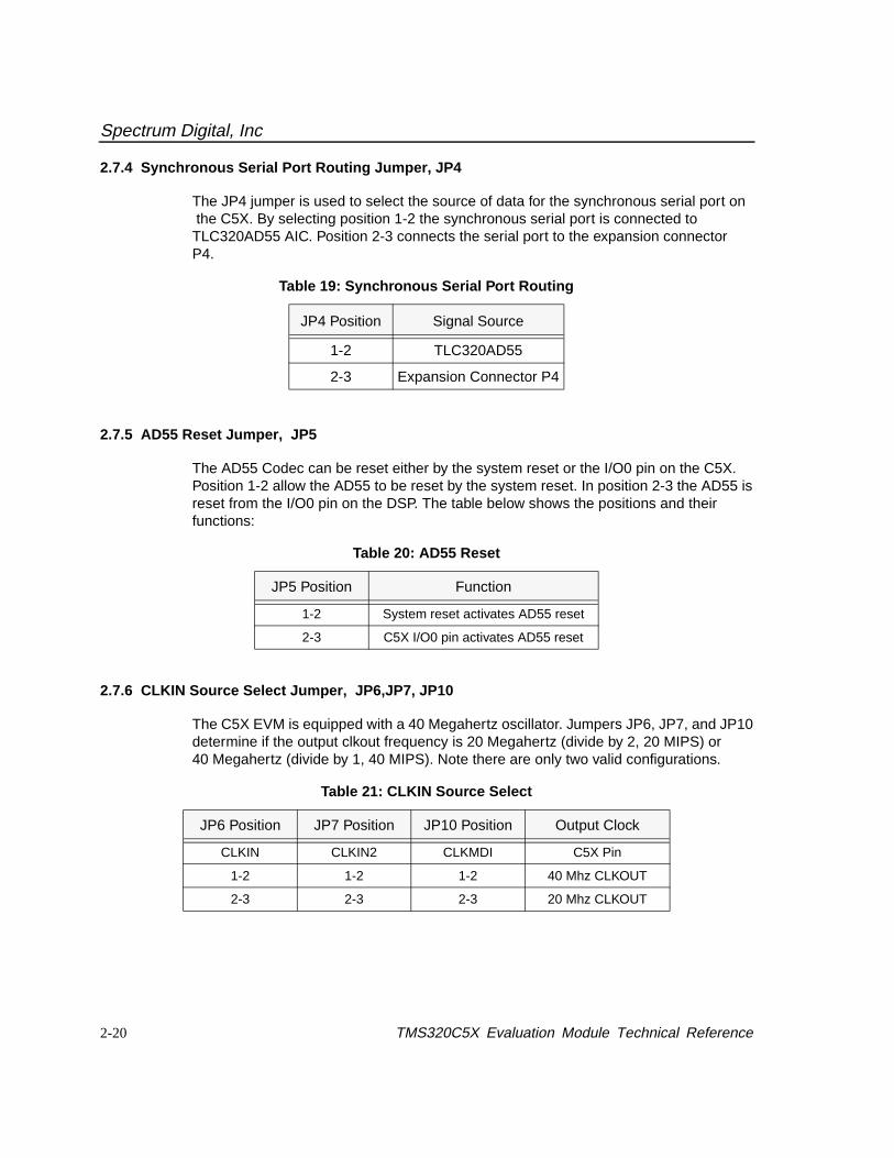
2.7.4 Synchronous Serial Port Routing Jumper, JP4
The JP4 jumper is used to select the source of data for the synchronous serial port on the C5X. By selecting position 1-2 the synchronous serial port is connected toTLC320AD55 AIC. Position 2-3 connects the serial port to the expansion connectorP4.
2.7.5 AD55 Reset Jumper, JP5
The AD55 Codec can be reset either by the system reset or the I/O0 pin on the C5X.Position 1-2 allow the AD55 to be reset by the system reset. In position 2-3 the AD55 isreset from the I/O0 pin on the DSP. The table below shows the positions and theirfunctions:
2.7.6 CLKIN Source Select Jumper, JP6,JP7, JP10
The C5X EVM is equipped with a 40 Megahertz oscillator. Jumpers JP6, JP7, and JP10determine if the output clkout frequency is 20 Megahertz (divide by 2, 20 MIPS) or40 Megahertz (divide by 1, 40 MIPS). Note there are only two valid configurations.
Table 19: Synchronous Serial Port Routing
JP4 Position Signal Source
1-2 TLC320AD55
2-3 Expansion Connector P4
Table 20: AD55 Reset
JP5 Position Function
1-2 System reset activates AD55 reset
2-3 C5X I/O0 pin activates AD55 reset
Table 21: CLKIN Source Select
JP6 Position JP7 Position JP10 Position Output Clock
CLKIN CLKIN2 CLKMDI C5X Pin
1-2 1-2 1-2 40 Mhz CLKOUT
2-3 2-3 2-3 20 Mhz CLKOUT
Spectrum Digital, Inc
2-21
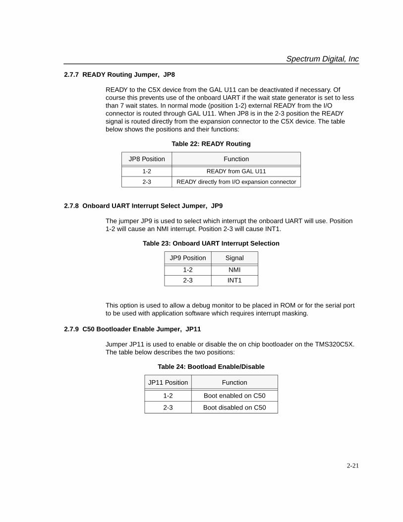
2.7.7 READY Routing Jumper, JP8
READY to the C5X device from the GAL U11 can be deactivated if necessary. Ofcourse this prevents use of the onboard UART if the wait state generator is set to lessthan 7 wait states. In normal mode (position 1-2) external READY from the I/Oconnector is routed through GAL U11. When JP8 is in the 2-3 position the READYsignal is routed directly from the expansion connector to the C5X device. The tablebelow shows the positions and their functions:
2.7.8 Onboard UART Interrupt Select Jumper, JP9
The jumper JP9 is used to select which interrupt the onboard UART will use. Position1-2 will cause an NMI interrupt. Position 2-3 will cause INT1.
This option is used to allow a debug monitor to be placed in ROM or for the serial portto be used with application software which requires interrupt masking.
2.7.9 C50 Bootloader Enable Jumper, JP11
Jumper JP11 is used to enable or disable the on chip bootloader on the TMS320C5X.The table below describes the two positions:
Table 22: READY Routing
JP8 Position Function
1-2 READY from GAL U11
2-3 READY directly from I/O expansion connector
Table 23: Onboard UART Interrupt Selection
JP9 Position Signal
1-2 NMI
2-3 INT1
Table 24: Bootload Enable/Disable
JP11 Position Function
1-2 Boot enabled on C50
2-3 Boot disabled on C50
Spectrum Digital, Inc
2-22 TMS320C5X Evaluation Module Technical Reference
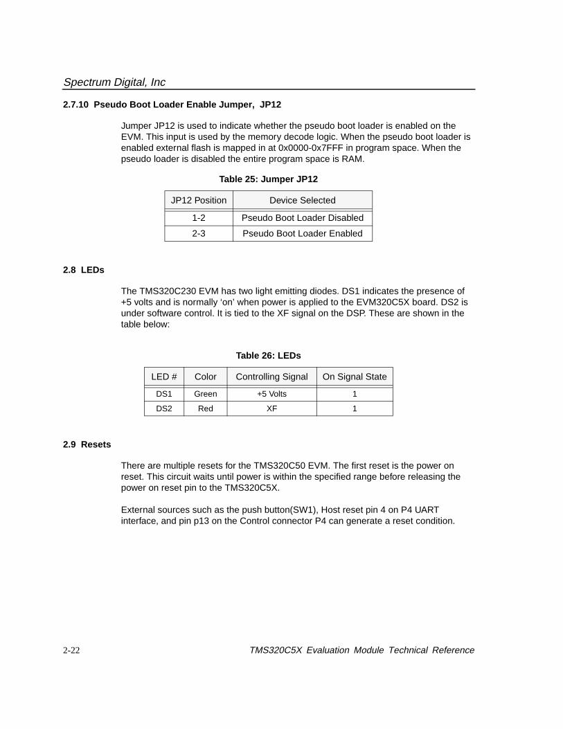
2.7.10 Pseudo Boot Loader Enable Jumper, JP12
Jumper JP12 is used to indicate whether the pseudo boot loader is enabled on theEVM. This input is used by the memory decode logic. When the pseudo boot loader isenabled external flash is mapped in at 0x0000-0x7FFF in program space. When thepseudo loader is disabled the entire program space is RAM.
2.8 LEDs
The TMS320C230 EVM has two light emitting diodes. DS1 indicates the presence of+5 volts and is normally ‘on’ when power is applied to the EVM320C5X board. DS2 isunder software control. It is tied to the XF signal on the DSP. These are shown in thetable below:
2.9 Resets
There are multiple resets for the TMS320C50 EVM. The first reset is the power onreset. This circuit waits until power is within the specified range before releasing thepower on reset pin to the TMS320C5X.
External sources such as the push button(SW1), Host reset pin 4 on P4 UARTinterface, and pin p13 on the Control connector P4 can generate a reset condition.
Table 25: Jumper JP12
JP12 Position Device Selected
1-2 Pseudo Boot Loader Disabled
2-3 Pseudo Boot Loader Enabled
Table 26: LEDs
LED # Color Controlling Signal On Signal State
DS1 Green +5 Volts 1
DS2 Red XF 1
A-1
Appendix A
TMS320C5X EVM PAL Equations
This appendix lists the two PAL logic equations that are used on theTMS320C5X Evaluation Module (EVM).
Topic Page
A.1 Memory Decode Equations A-2A.2 I/O Control Equations A-4
Spectrum Digital, Inc
A-2 TMS320C5X Evaluation Module Technical Reference
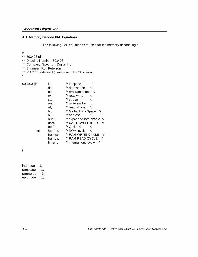
A.1 Memory Decode PAL Equations
The following PAL equations are used for the memory decode logic
/*** 503403.tdl** Drawing Number: 503403** Company: Spectrum Digital Inc** Engineer: Ron Peterson** ‘G16V8’ is defined (usually with the /D option).*/
503403 (in is, /* io space */ds, /* data space */ps, /* program space */rw, /* read write */stb, /* strobe */we, /* write strobe */rd, /* read strobe */br, /* Global Data Space */a15, /* address */out3, /* expanded rom enable */uart, /* UART CYCLE INPUT */opt0; /* Option 0 */
out !eprom, /* ROM cycle */!ramwe, /* RAM WRITE CYCLE */!ramoe, /* RAM READ CYCLE */!intern; /* internal long cycle */
){
intern.oe = 1;ramoe.oe = 1;ramwe.oe = 1;eprom.oe = 1;
Spectrum Digital, Inc
A-3
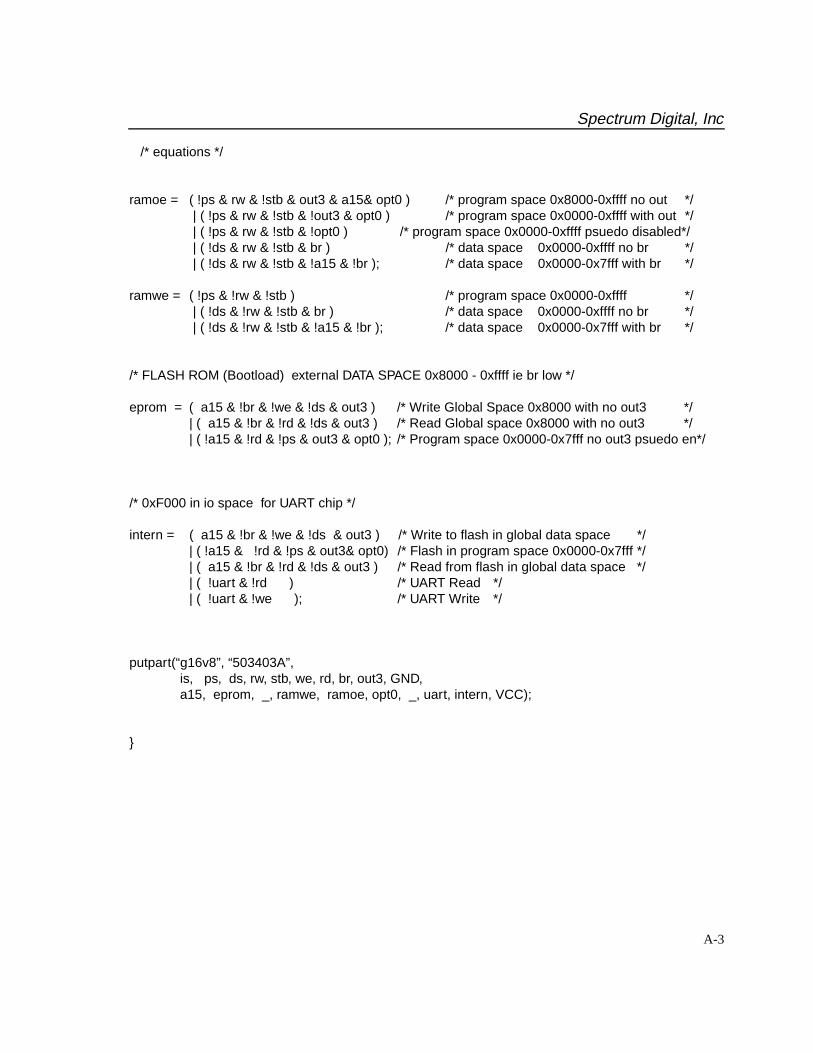
/* equations */
ramoe = ( !ps & rw & !stb & out3 & a15& opt0 ) /* program space 0x8000-0xffff no out */ | ( !ps & rw & !stb & !out3 & opt0 ) /* program space 0x0000-0xffff with out */ | ( !ps & rw & !stb & !opt0 ) /* program space 0x0000-0xffff psuedo disabled*/ | ( !ds & rw & !stb & br ) /* data space 0x0000-0xffff no br */ | ( !ds & rw & !stb & !a15 & !br ); /* data space 0x0000-0x7fff with br */
ramwe = ( !ps & !rw & !stb ) /* program space 0x0000-0xffff */ | ( !ds & !rw & !stb & br ) /* data space 0x0000-0xffff no br */ | ( !ds & !rw & !stb & !a15 & !br ); /* data space 0x0000-0x7fff with br */
/* FLASH ROM (Bootload) external DATA SPACE 0x8000 - 0xffff ie br low */
eprom = ( a15 & !br & !we & !ds & out3 ) /* Write Global Space 0x8000 with no out3 */| ( a15 & !br & !rd & !ds & out3 ) /* Read Global space 0x8000 with no out3 */| ( !a15 & !rd & !ps & out3 & opt0 ); /* Program space 0x0000-0x7fff no out3 psuedo en*/
/* 0xF000 in io space for UART chip */
intern = ( a15 & !br & !we & !ds & out3 ) /* Write to flash in global data space */| ( !a15 & !rd & !ps & out3& opt0) /* Flash in program space 0x0000-0x7fff */| ( a15 & !br & !rd & !ds & out3 ) /* Read from flash in global data space */| ( !uart & !rd ) /* UART Read */| ( !uart & !we ); /* UART Write */
putpart(“g16v8”, “503403A”, is, ps, ds, rw, stb, we, rd, br, out3, GND, a15, eprom, _, ramwe, ramoe, opt0, _, uart, intern, VCC);
}
Spectrum Digital, Inc
A-4 TMS320C5X Evaluation Module Technical Reference
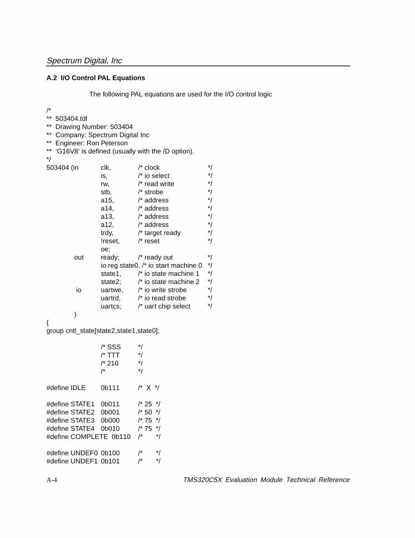
A.2 I/O Control PAL Equations
The following PAL equations are used for the I/O control logic
/*** 503404.tdl** Drawing Number: 503404** Company: Spectrum Digital Inc** Engineer: Ron Peterson** ‘G16V8’ is defined (usually with the /D option).*/503404 (in clk, /* clock */
is, /* io select */rw, /* read write */stb, /* strobe */a15, /* address */a14, /* address */a13, /* address */a12, /* address */trdy, /* target ready */!reset, /* reset */oe;
out ready; /* ready out */io reg state0, /* io start machine 0 */state1, /* io state machine 1 */state2; /* io state machine 2 */
io uartwe, /* io write strobe */uartrd, /* io read strobe */uartcs; /* uart chip select */
){group cntl_state[state2,state1,state0];
/* SSS *//* TTT *//* 210 *//* */
#define IDLE 0b111 /* X */
#define STATE1 0b011 /* 25 */#define STATE2 0b001 /* 50 */#define STATE3 0b000 /* 75 */#define STATE4 0b010 /* 75 */#define COMPLETE 0b110 /* */
#define UNDEF0 0b100 /* */#define UNDEF1 0b101 /* */
Spectrum Digital, Inc
A-5
#define UART ( !is & !stb & a15 & a14 & a13 & a12 )
cntl_state.oe = !oe; /* hook up output enables */cntl_state.ck = clk; /* hook up clocks */
/* state machines */
switch( cntl_state[] ) {
case IDLE:if ( reset) cntl_state = IDLE;else
{ if( UART ) cntl_state = STATE1; else cntl_state = IDLE;}
break;
case STATE1:
if ( reset ) cntl_state = IDLE;else{ cntl_state = STATE2;}break;
case STATE2:
if ( reset ) cntl_state = IDLE;else{ cntl_state = STATE3;}break;

Spectrum Digital, Inc
A-6 TMS320C5X Evaluation Module Technical Reference
case STATE3:
if ( reset ) cntl_state = IDLE;else{ cntl_state = STATE4;}break;
case STATE4:
if ( reset ){ cntl_state = IDLE;}else{ cntl_state = COMPLETE;}break;
case COMPLETE:if( reset ){ cntl_state = IDLE;}else{ if( UART ) cntl_state = COMPLETE; else cntl_state = IDLE;}break;
case UNDEF0:cntl_state = IDLE;break;
case UNDEF1: cntl_state = IDLE; break;
default:cntl_state = IDLE;break;
}
Spectrum Digital, Inc
A-7
/* equations */
!uartcs = UART;
!ready = ((cntl_state == STATE2) &UART ) | ((cntl_state == STATE3) & UART ) | ((cntl_state == STATE4) & UART ) | (!trdy );
!uartwe = ((cntl_state == STATE2) & !rw & UART ) | ((cntl_state == STATE3) & !rw & UART ) | ((cntl_state == STATE4) & !rw & UART );
!uartrd = (( cntl_state == STATE2) & rw & UART ) | (( cntl_state == STATE3) & rw & UART ) | (( cntl_state == STATE4) & rw & UART ) | ( !uartrd & UART /*rw & !stb*/ );
putpart(“g16v8r”, “503404A”, clk, is, rw, stb, a15, a14, a13, a12, trdy, GND, oe, uartwe, uartcs, state0, uartrd, state1, state2, reset, ready, VCC);
}

Spectrum Digital, Inc
A-8 TMS320C5X Evaluation Module Technical Reference

B-1
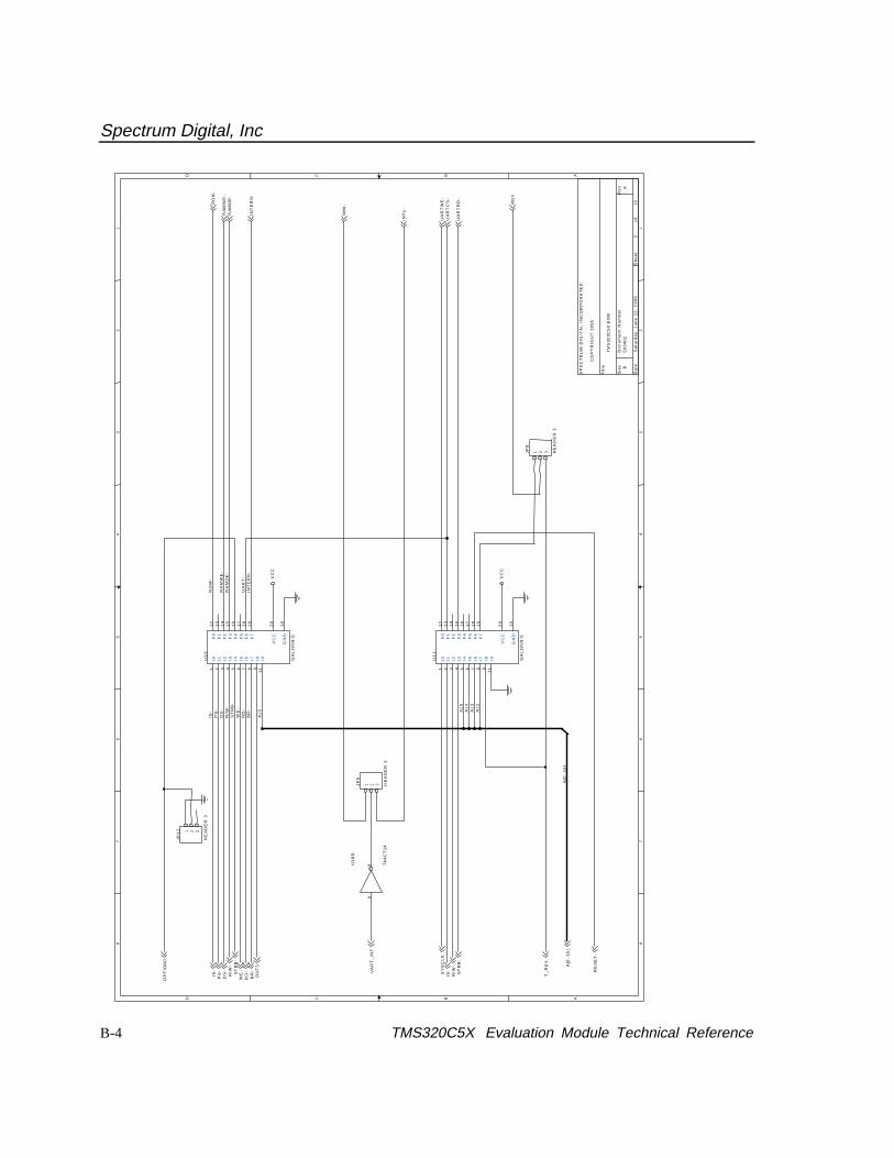
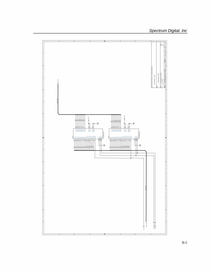
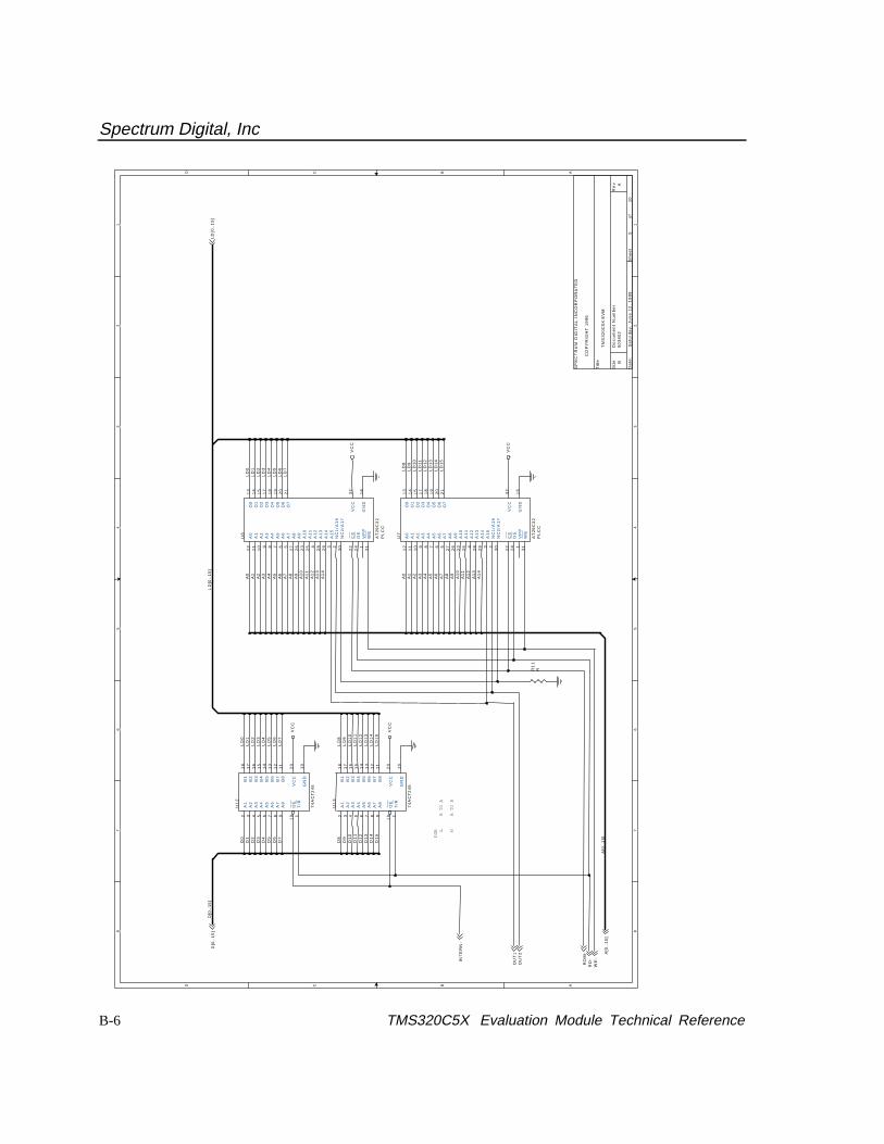
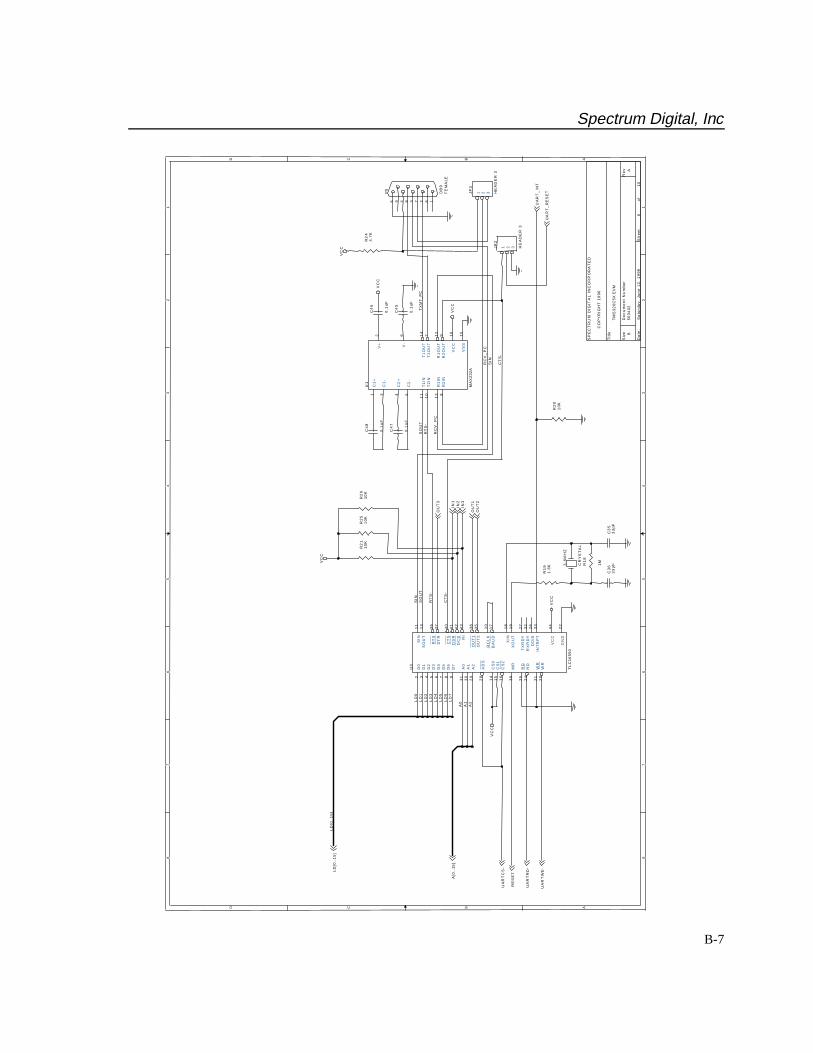
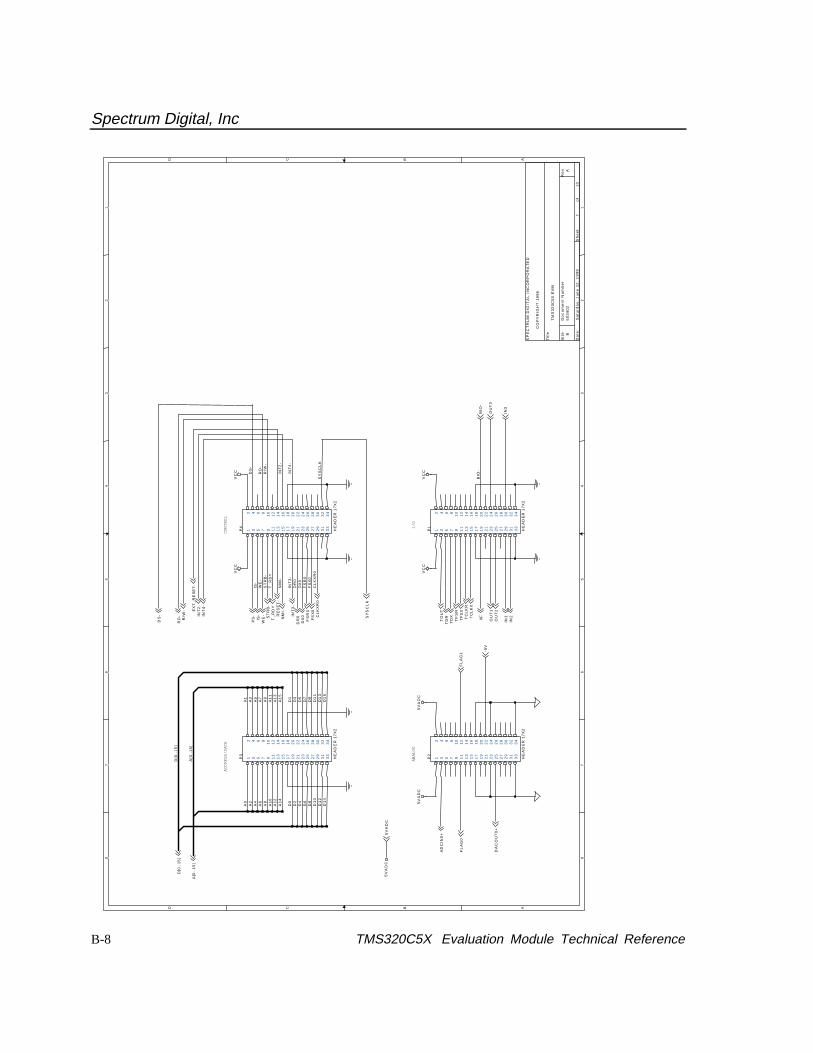
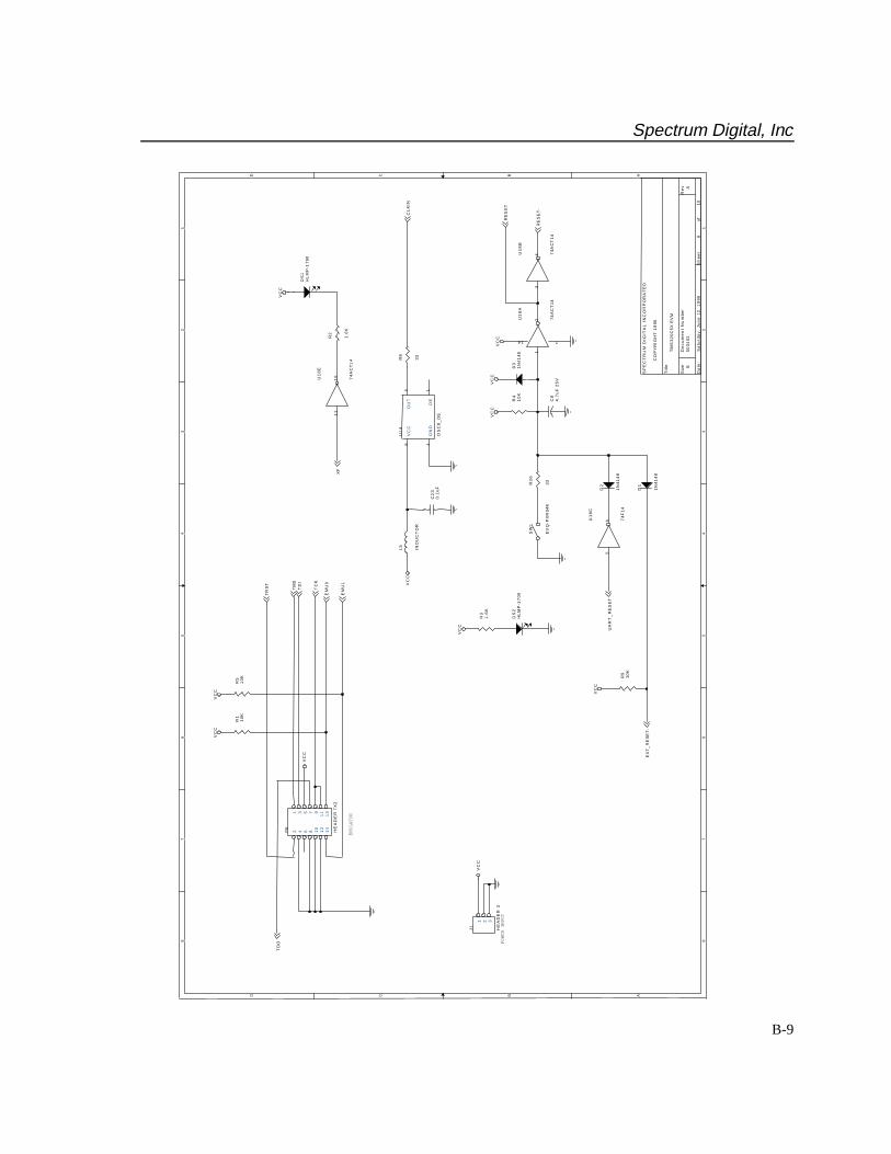
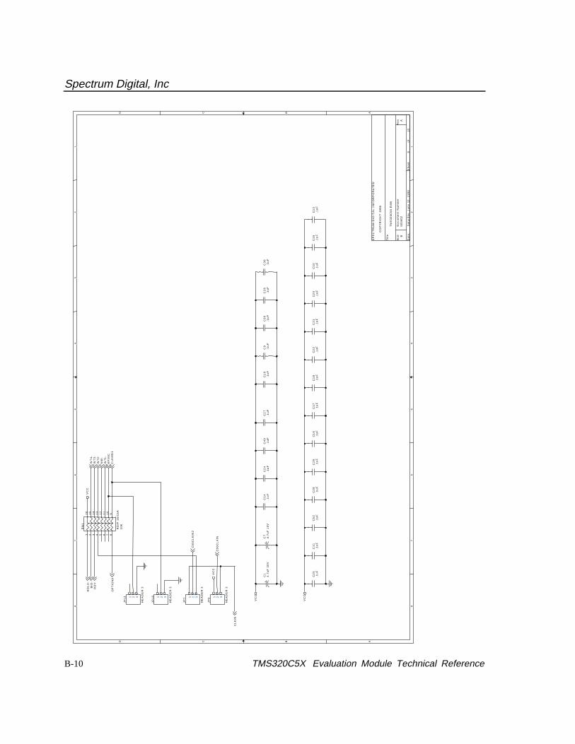
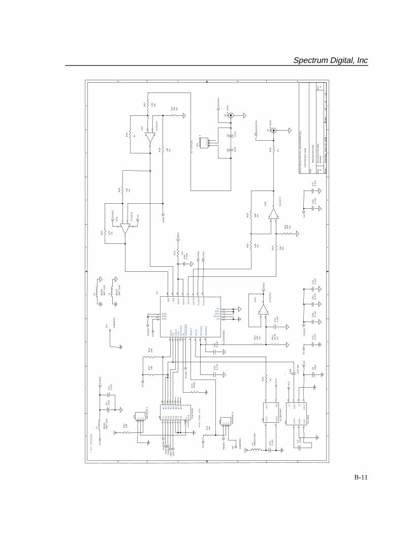
Appendix B
TMS320C5X EVM Schematics
This appendix contains the schematics for the TMS320C5X EVM. Theschematics were drawn on ORCAD.
Spectrum Digital, Inc
B-2 TMS320C5X Evaluation Module Technical Reference
8 8
7 7
6 6
5 5
4 4
3 3
2 2
1 1
DD
CC
BB
AA
RE
VIS
ION
SR
EV
AP
PR
OV
ED
DA
TE
DE
SC
RIP
TIO
NN
OT
ES
. UN
LES
S O
TH
ER
WIS
E S
PE
CIF
IED
DW
N
CH
K
EN
GR
AP
VD
EN
GR
QA
AP
VD
MF
G
RLS
E
DA
TE
DA
TE
DA
TE
DA
TE
DA
TE
DA
TE
DA
TE
SC
AL
E
DR
AW
ING
NU
MB
ER
RE
VS
IZE
AP
PLI
CA
TIO
N
US
ED
ON
NE
XT
AS
SE
MB
LY
RE
VS
HT
RE
VS
HT
RE
VS
HT
RE
VS
HT
RE
VIS
ION
ST
AT
US
OF
SH
EE
TS
AP
VD
CU
ST
DA
TE
LOG
IC D
IAG
RA
M
503
402
AB
NO
NE
SH
EE
T1
OF
12
503
120
1.
All
resi
stor
val
ues
are
5% .1
25 W
AT
T
3
S P
E C
T R
U M
D I
G I
T A
L
I N C
O R
P O
R A
T E
D
XX
XX
X
4
11/
02/9
6
11/
02/9
6
A8
76
5
SP
AR
ES
9A
AA
AA
AA
A
R.R
.P.
R.R
.P.
10
A1
0
CO
PY
RIG
HT
199
6
TM
S32
0C5X
EV
M B
OA
RD
GN
D
U1
8F
74
AC
T1
4
13
12
Spectrum Digital, Inc
B-3
8 8
7 7
6 6
5 5
4 4
3 3
2 2
1 1
DD
CC
BB
AA
*
* N
OT
INS
TA
LLE
D
50
34
02
A
TM
S3
20
C5
X E
VM
SP
EC
TR
UM
DIG
ITA
L I
NC
OR
PO
RA
TE
D
CO
PY
RIG
HT
19
95
B
21
0S
atu
rda
y,
Ju
ne
12
, 1
99
9
Tit
le
Siz
eD
oc
um
en
t N
um
be
rR
ev
Da
te:
Sh
ee
to
f
D0
A0
D1
A1
D2
A2
D3
A3
D4
A4
D5
A5
D6
A6
D7
A7
D8
A8
D9
A9
D1
0A
10
D1
1A
11
D1
2A
12
D1
3A
13
D1
4A
14
D1
5A
15
TC
KT
DI
TM
ST
RS
TE
MU
1E
MU
0
TD
O
A[0
..1
5]
D[0
..1
5]
A[0
..1
5]
D[0
..1
5]
IS-
DS
-
TC
KT
DI
TM
ST
RS
T
EM
U0
EM
U1
RD
Y
SY
SC
LK
TD
O
R/W
-
RE
SE
T-
CL
KM
D1
XF
TC
LK
R
TD
XT
FS
R
TD
RT
CL
KX
TF
SX
MP
/MC
NM
I-IN
T4
-
INT
1-
INT
2-
INT
3-
BIO
-H
OL
D-
ST
RB
- RD
-W
E-
BR
-
TO
UT
C5
0C
LK
IN2
DR
0CL
KX
R0
FS
R0
DX
0
FS
X0
C5
0C
LK
IN
PS
-
VC
C
R6
33
C1
3C
AP
NP
R7
33
U1
7
TM
S3
20
C5
X
30
29
28
27
26
25
24
23
13
12
11
10 9 8 7 6
12
8
12
91
30
38
39
40
41
42
12
7 57
11
03
96
97
95
46
12
64
34
44
51
25
34
67
31 2
11
91
18
55
56
57
58
59
60
61
62
63
64
72
73
74
75
76
77
90
89
91
92
93
82
83
10
89
41 1
09
11
2
11
0
12
2
11
11
24
12
31
06
10
71
04
10
51
00
141532334748656680819899113114131132
3420213536535468698687101102120121
D0
D1
D2
D3
D4
D5
D6
D7
D8
D9
D1
0D
11
D1
2D
13
D1
4D
15
RE
AD
Y
HO
LD
BIO
INT
1IN
T2
INT
3IN
T4
NM
IR
SM
P/M
CC
LK
MD
1C
LK
MD
2X
2/C
LK
INX
1C
LK
IN2
CL
KR
TC
LK
RD
RT
DR
FS
RT
FS
R/T
AD
DT
CK
TD
IT
MX
TR
ST
EM
U1
/OF
FE
MU
0
A0
A1
A2
A3
A4
A5
A6
A7
A8
A9
A1
0A
11
A1
2A
13
A1
4A
15 IS DS
PS
R/W
ST
BR
DW
E
HO
LD
AB
RIA
QX
F
IAC
K
CL
KO
UT
1
TO
UT
MS
CC
LK
XT
CL
KX
DX
TD
XF
SX
TF
SX
/TF
RM
TD
OVCCVCCVCCVCCVCCVCCVCCVCCVCCVCCVCCVCCVCCVCCVCCVCC
VSSVSSVSSVSSVSSVSSVSSVSSVSSVSSVSSVSSVSSVSSVSSVSS
Spectrum Digital, Inc
B-4 TMS320C5X Evaluation Module Technical Reference
8 8
7 7
6 6
5 5
4 4
3 3
2 2
1 1
DD
CC
BB
AA
50
34
02
A
TM
S3
20
C5
X E
VM
SP
EC
TR
UM
DIG
ITA
L I
NC
OR
PO
RA
TE
D
CO
PY
RIG
HT
19
95
B
31
0S
atu
rda
y,
Ju
ne
12
, 1
99
9
Tit
le
Siz
eD
oc
um
en
t N
um
be
rR
ev
Da
te:
Sh
ee
to
f
IS-
RO
M-
DS
-P
S-
RA
MW
E-
R/W
-R
AM
OE
-S
TR
B-
WE
-R
D-
UA
RT
-B
R-
INT
ER
N-
A1
5 A1
5A
14
A1
3A
12
A[0
..1
5]
RO
M-
INT
ER
N-
RA
MO
E-
RA
MW
E-
A[0
..1
5]
IS-
DS
-P
S-
R/W
-
RD
-W
E-
BR
-ST
RB
-
IS-
R/W
-S
TR
B-
SY
SC
LK
T_
RD
Y
NM
I-
INT
1-
OU
T3
UA
RT
RD
-
UA
RT
CS
-
UA
RT
_IN
T
RE
SE
T-
UA
RT
WE
-
RD
Y
OP
TIO
N0
VC
C
VC
C
JP
8
HE
AD
ER
3
1 2 3
JP
12
HE
AD
ER
3
1 2 3
JP
9
HE
AD
ER
3
1 2 3
U1
1
GA
L1
6V
8-5
1 2 3 4 5 6 7 8 91
1
12
13
14
15
16
17
18
19
20
10
I0 I1 I2 I3 I4 I5 I6 I7 I8 I9
F0
F1
F2
F3
F4
F5
F6
F7
VC
C
GN
D
U1
8D
74
AC
T1
4
98
U1
0
GA
L1
6V
8-5
1 2 3 4 5 6 7 8 91
1
12
13
14
15
16
17
18
19
20
10
I0 I1 I2 I3 I4 I5 I6 I7 I8 I9
F0
F1
F2
F3
F4
F5
F6
F7
VC
C
GN
D
Spectrum Digital, Inc
B-5
8 8
7 7
6 6
5 5
4 4
3 3
2 2
1 1
DD
CC
BB
AA
50
34
02
A
TM
S3
20
C5
X E
VM
SP
EC
TR
UM
DIG
ITA
L I
NC
OR
PO
RA
TE
D
CO
PY
RIG
HT
19
96
B
41
0S
atu
rda
y,
Ju
ne
12
, 1
99
9
Tit
le
Siz
eD
oc
um
en
t N
um
be
rR
ev
Da
te:
Sh
ee
to
f
A0
A1
D0
A2
D1
A3
D2
A4
D3
A5
D4
A6
D5
A7
D6
A8
D7
A9
A1
0A
11
A1
2A
13
A1
4A
15
A0
A1
D8
A2
D9
A3
D1
0A
4D
11
A5
D1
2A
6D
13
A7
D1
4A
8D
15
A9
A1
0A
11
A1
2A
13
A1
4A
15
D[0
..1
5]
A[0
..1
5]
A[0
..1
5]
D[0
..1
5]
PS
- RA
MW
E-
RA
MO
E-
VC
C
VC
C
U1
5
CX
K5
81
12
0J
30
29
21
20
14
13 4 3
19
18
17
16
15 2 1
32
31 5
12
28
27
26
23
22
11
10
7 6 8 24
9 25
A0
A1
A2
A3
A4
A5
A6
A7
A8
A9
A1
0A
11
A1
2A
13
A1
4A
15
A1
6
CE
WE
OE
I/O
1I/
O2
I/O
3I/
O4
I/O
5I/
O6
I/O
7I/
O8
VC
CV
CC
GN
DG
ND
U1
6
CX
K5
81
12
0J
30
29
21
20
14
13 4 3
19
18
17
16
15 2 1
32
31 5
12
28
27
26
23
22
11
10
7 6 8 24
9 25
A0
A1
A2
A3
A4
A5
A6
A7
A8
A9
A1
0A
11
A1
2A
13
A1
4A
15
A1
6
CE
WE
OE
I/O
1I/
O2
I/O
3I/
O4
I/O
5I/
O6
I/O
7I/
O8
VC
CV
CC
GN
DG
ND
Spectrum Digital, Inc
B-6 TMS320C5X Evaluation Module Technical Reference
8 8
7 7
6 6
5 5
4 4
3 3
2 2
1 1
DD
CC
BB
AA
DIR
B T
O A
A T
O B
L H
50
34
02
A
TM
S3
20
C5
X E
VM
SP
EC
TR
UM
DIG
ITA
L I
NC
OR
PO
RA
TE
D
CO
PY
RIG
HT
19
96
B
51
0S
atu
rda
y,
Ju
ne
12
, 1
99
9
Tit
le
Siz
eD
oc
um
en
t N
um
be
rR
ev
Da
te:
Sh
ee
to
f
D0
LD
0D
1L
D1
A0
LD
0D
2L
D2
A1
LD
1D
3L
D3
A2
LD
2D
4L
D4
A3
LD
3D
5L
D5
A4
LD
4D
6L
D6
A5
LD
5D
7L
D7
A6
LD
6A
7L
D7
A8
A9
A1
0A
11
A1
2A
13
A1
4
D8
LD
8D
9L
D9
D1
0L
D1
0D
11
LD
11
D1
2L
D1
2D
13
LD
13
D1
4L
D1
4D
15
LD
15
A0
LD
8A
1L
D9
A2
LD
10
A3
LD
11
A4
LD
12
A5
LD
13
A6
LD
14
A7
LD
15
A8
A9
A1
0A
11
A1
2A
13
A1
4
D[0
..1
5]
LD
[0..
15
]
A[0
..1
5]
D[0
..1
5]
INT
ER
N-
RO
M- A
[0..
15
]
RD
-W
E-
OU
T1
OU
T2
LD
[0..
15
]
VC
C
VC
C
VC
C
VC
C
U6
AT
29
C3
2P
LC
C
12
11
10 9 8 7 6 5
27
26
23
25 4
28
29 3 2
30
22
24 1
31
13
14
15
17
18
19
20
21
32
16
A0
A1
A2
A3
A4
A5
A6
A7
A8
A9
A1
0A
11
A1
2A
13
A1
4A
15
NC
1/A
16
NC
2/A
17
CE
OE
VP
PW
E
O0
O1
O2
O3
O4
O5
O6
O7
VC
C
GN
D
U1
2
74
AC
T2
45
2 3 4 5 6 7 8 9
19 1
18
17
16
15
14
13
12
11
20
10
A1
A2
A3
A4
A5
A6
A7
A8
OE
T/R
B1
B2
B3
B4
B5
B6
B7
B8
VC
C
GN
D
U1
3
74
AC
T2
45
2 3 4 5 6 7 8 9
19 1
18
17
16
15
14
13
12
11
20
10
A1
A2
A3
A4
A5
A6
A7
A8
OE
T/R
B1
B2
B3
B4
B5
B6
B7
B8
VC
C
GN
D
R1
1R
U7
AT
29
C3
2P
LC
C
12
11
10 9 8 7 6 5
27
26
23
25 4
28
29 3 2
30
22
24 1
31
13
14
15
17
18
19
20
21
32
16
A0
A1
A2
A3
A4
A5
A6
A7
A8
A9
A1
0A
11
A1
2A
13
A1
4A
15
NC
1/A
16
NC
2/A
17
CE
OE
VP
PW
E
O0
O1
O2
O3
O4
O5
O6
O7
VC
C
GN
D
Spectrum Digital, Inc
B-7
8 8
7 7
6 6
5 5
4 4
3 3
2 2
1 1
DD
CC
BB
AA
50
34
02
A
TM
S3
20
C5
X E
VM
SP
EC
TR
UM
DIG
ITA
L I
NC
OR
PO
RA
TE
D
CO
PY
RIG
HT
19
96
B
61
0S
atu
rda
y,
Ju
ne
12
, 1
99
9
Tit
le
Siz
eD
oc
um
en
t N
um
be
rR
ev
Da
te:
Sh
ee
to
f
LD
0S
INL
D1
SO
UT
SO
UT
TX
MT
_P
CL
D2
RT
S-
LD
3R
TS
-L
D4
RC
V_
PC
LD
5L
D6
CT
S-
LD
7
A0
A1
A2
RC
V_
PC
SIN
CT
S-
LD
[0..
15
]
A[0
..1
5]
RE
SE
T
UA
RT
_IN
T
IN2
LD
[0..
15
]
OU
T1
OU
T2
IN1
IN3
OU
T3
UA
RT
_R
ES
ET
UA
RT
CS
-
UA
RT
RD
-
UA
RT
WE
-
VC
C
VC
C
VC
C
VC
C
VC
C
VC
C
P5
DB
9F
EM
AL
E
5 9 4 8 3 7 2 6 1
C4
5
0.1
uF
C4
6
0.1
uF
C4
8
0.1
uF
C4
7
0.1
uF
U1
MA
X2
32
A
1 3 4 5
11
10
13 8
2 6 14
7 12
9 16
15
C1
+
C1
-
C2
+
C2
-
T1
INT
2IN
R1
INR
2IN
V+ V-
T1
OU
TT
2O
UT
R1
OU
TR
2O
UT
VC
C
VS
S
JP
3
HE
AD
ER
3
1 2 3
R2
11
0K
R2
51
0K
R2
61
0K
C3
63
3p
F
R2
01
0K
C3
53
3p
F
JP
2
HE
AD
ER
3
1 2 3
R2
44
.7K
R1
8
1M
3.8
MH
Z
CR
YS
TA
L
U3
TL
C1
65
50
2 3 4 5 6 7 8 9
31
30
29
28
14
15
16
39
25
24
21
20
11
13
36
37
40
41
42
43
38
35
10
17
18
19
27
32
26
33
44
22
D0
D1
D2
D3
D4
D5
D6
D7
A0
A1
A2
AD
S
CS
0C
S1
CS
2
MR
RD
RD
WR
WR
SIN
SO
UT
RT
SD
TR
CT
SD
SR
DC
D RI
OU
T1
OU
T2
RC
LK
BA
UD
XIN
XO
UT
TX
RD
YR
XR
DY
DD
ISIN
TR
PT
VC
C
GN
D
R1
91
.6K
Spectrum Digital, Inc
B-8 TMS320C5X Evaluation Module Technical Reference
8 8
7 7
6 6
5 5
4 4
3 3
2 2
1 1
DD
CC
BB
AA
AD
DR
ES
S/D
AT
A
AN
AL
OG
CO
NT
RO
L
I/O
50
34
02
A
TM
S3
20
C5
X E
VM
SP
EC
TR
UM
DIG
ITA
L I
NC
OR
PO
RA
TE
D
CO
PY
RIG
HT
19
96
B
71
0S
atu
rda
y,
Ju
ne
12
, 1
99
9
Tit
le
Siz
eD
oc
um
en
t N
um
be
rR
ev
Da
te:
Sh
ee
to
f
A0
A1
A2
A3
DS
-A
4A
5IS
-A
6A
7W
E-
RD
-A
8A
9S
TR
B-
R/W
-A
10
A1
1T
_R
DY
A1
2A
13
A1
4A
15
NM
I-IN
T2
-
D0
D1
INT
3-
INT
4-
D2
D3
DR
0D
4D
5D
X0
D6
D7
FS
R0
D8
D9
FS
X0
D1
0D
11
CL
KX
R0
D1
2D
13
SY
SC
LK
D1
4D
15
BIO
-
D[0
..1
5]
A[0
..1
5]
A[0
..1
5]
DS
-
IS-
WE
-
NM
I-
PS
-
RD
-R
/W-
SY
SC
LK
BIO
-
TO
UT
XF
-5V
FL
AG
0F
LA
G1
AD
CIN
0+
DA
CO
UT
0+
INT
3-
INT
2-
INT
4-
TD
RT
DX
TF
SR
TF
SX
TC
LK
RT
CL
KX
IN1
IN2
IN3
T_
RD
Y
OU
T1
OU
T2
OU
T3
5V
AD
C
RE
SE
T-
EX
T_
RE
SE
T-
D[0
..1
5]
ST
RB
-
DR
0D
X0
FS
R0
FS
X0
CL
KX
R0
VC
CV
CC
VC
CV
CC
5V
AD
C5
VA
DC
5V
AD
C
P3
HE
AD
ER
17
X2
12
34
56
78
91
01
11
21
31
41
51
61
71
81
92
02
12
22
32
42
52
62
72
82
93
03
13
23
33
4
P4
HE
AD
ER
17
X2
12
34
56
78
91
01
11
21
31
41
51
61
71
81
92
02
12
22
32
42
52
62
72
82
93
03
13
23
33
4
P1
HE
AD
ER
17
X2
12
34
56
78
91
01
11
21
31
41
51
61
71
81
92
02
12
22
32
42
52
62
72
82
93
03
13
23
33
4
P2
HE
AD
ER
17
X2
12
34
56
78
91
01
11
21
31
41
51
61
71
81
92
02
12
22
32
42
52
62
72
82
93
03
13
23
33
4
Spectrum Digital, Inc
B-9
8 8
7 7
6 6
5 5
4 4
3 3
2 2
1 1
DD
CC
BB
AA
EM
UL
AT
OR
PO
WE
R IN
PU
T
50
34
02
A
TM
S3
20
C5
X E
VM
SP
EC
TR
UM
DIG
ITA
L I
NC
OR
PO
RA
TE
D
CO
PY
RIG
HT
19
96
B
81
0S
atu
rda
y,
Ju
ne
12
, 1
99
9
Tit
le
Siz
eD
oc
um
en
t N
um
be
rR
ev
Da
te:
Sh
ee
to
f
TM
S
TR
ST
TC
K
EM
U0
EM
U1
TD
O
TD
I
RE
SE
T-
XF
RE
SE
T
CL
KIN
UA
RT
_R
ES
ET
EX
T_
RE
SE
T-
VC
C
VC
C
VC
CV
CC
VC
C
VC
CV
CC
VC
C
VC
C
VC
C
VC
C
R8
33
C2
30
.1u
F
U1
8A
74
AC
T1
4
12
14 7
R2
1.6
K
R3
1.6
K
DS
1H
LM
P-1
79
0
DS
2H
LM
P-1
70
0U
18
B
74
AC
T1
4
34
R9
10
K
D2
1N
41
48
J1
HE
AD
ER
3
1 2 3
L5
IND
UC
TO
R
U1
8C
74
F1
4
56
P6
HE
AD
ER
7X
2
12
34
56
78
91
01
11
21
31
4
R4
10
KD
31
N4
14
8
C8
4.7
uF
25
V
SW
1
EV
Q-P
XR
04
K
R1
10
KR
51
0K
R3
6
33
D1
1N
41
48
U1
8E
74
AC
T1
4
11
10
U1
4
OS
C8
_O
E
8 415
VC
C
GN
DO
E
OU
T
Spectrum Digital, Inc
B-10 TMS320C5X Evaluation Module Technical Reference
8 8
7 7
6 6
5 5
4 4
3 3
2 2
1 1
DD
CC
BB
AA
50
34
02
A
TM
S3
20
C5
X E
VM
SP
EC
TR
UM
DIG
ITA
L I
NC
OR
PO
RA
TE
D
CO
PY
RIG
HT
19
96
B
91
0S
atu
rda
y,
Ju
ne
12
, 1
99
9
Tit
le
Siz
eD
oc
um
en
t N
um
be
rR
ev
Da
te:
Sh
ee
to
f
BIO
-H
OL
D-
RD
Y
NM
I-IN
T2
-IN
T3
-
INT
1-
CL
KM
D1
MP
/MC
INT
4-
C5
0C
LK
IN
CL
KIN
C5
0C
LK
IN2
OP
TIO
N0
VC
C
VC
C
VC
C
VC
C
JP
10
HE
AD
ER
3
1 2 3
JP
6
HE
AD
ER
3
1 2 3
+C
14
.7u
F 1
0V
C1
6.1
uF
C2
5.1
uF
C2
9.1
uF
C2
8.1
uF
C5
2.1
uF
C1
1.1
uF
C1
7.1
uF
C1
8.1
uF
JP
11
HE
AD
ER
3
1 2 3
+C
74
.7u
F 1
0V
C3
0.1
uF
C2
6.1
uF
C3
9.1
uF
C2
7.1
uF
C4
9.1
uF
C2
4.1
uF
C1
4.1
uF
C9
.1u
FC
19
.1u
F
RN
1
RD
IP 1
6/1
5A
10
K
11
62
15
31
44
13
51
26
11
71
08
9
JP
7
HE
AD
ER
3
1 2 3
C1
2.1
uF
C1
5.1
uF
C1
0.1
uF
C2
0.1
uF
C2
1.1
uF
C2
2.1
uF
Spectrum Digital, Inc
B-11
8 8
7 7
6 6
5 5
4 4
3 3
2 2
1 1
DD
CC
BB
AA
DC
CO
UP
LE
D
*
*N
OT
INS
TA
LLE
D
SH
OW
PO
WE
R P
INS
50
34
02
A
TM
S3
20
C5
X E
VM
SP
EC
TR
UM
DIG
ITA
L I
NC
OR
PO
RA
TE
D
CO
PY
RIG
HT
19
95
B
10
12
Sa
turd
ay
, J
un
e 1
2,
19
99
Tit
le
Siz
eD
oc
um
en
t N
um
be
rR
ev
Da
te:
Sh
ee
to
f
5V
AD
C
5V
AD
C
VM
ID
VM
ID
VM
ID
DA
CO
UT
0+
RE
SE
T-
-5V
FL
AG
0
FL
AG
1
AD
CIN
0+
5V
AD
C
-5V
-5V
5V
AD
C 5V
AD
C
CL
KX
R0
FS
X0
FS
R0
DR
0D
X0 V
CC
VC
C
VC
C
VC
C
VC
C
VC
C
VC
C
VC
C
VC
C
R3
2
10
K
1%
R3
3
33
+
C2
22
uF J
3R
CA
JA
CK
J2
RC
A J
AC
K
R2
9
10
K1
%
R2
71
0k
1%
JP
4
HE
AD
ER
3
1 2 3
+C3
22
uF
R3
7
10
k1
%
R3
8
10
k1
%R
30
R
R3
4
10
K1
%
R1
0
33
R3
11
0K
1%
JP
5
HE
AD
ER
3
1 2 3
L4
IND
UC
TO
R
+C
51
0u
F
U9
16
.38
4 M
HZ
8 415
VC
C
GN
DO
E
OU
T
C3
40
.1u
FC
42
0.1
uF
R1
21
0K
C4
40
.1u
FC
40
0.1
uF
C3
30
.1u
F
C4
10
.1u
F
R2
21
0K
1%
R1
44
9.9
K1
%
+-
U2
C
TL
C2
27
4
109
8
R2
3
10
K
- +
U2
A
TL
C2
27
4
321
4 11
C4
30
.1u
F
C3
20
.1u
F
R2
8
10
k1
%
R3
5
10
k1
%
+
C6
10
uF
C3
70
.1u
FC
50
0.1
uF
C3
8
CA
P N
P
TP
1
JU
MP
ER
1
U8
74
AL
S2
45
21
83
17
41
65
15
61
47
13
81
29
11
19 1
A1
B1
A2
B2
A3
B3
A4
B4
A5
B5
A6
B6
A7
B7
A8
B8
G DIR
JP
1H
EA
DE
R 3
123
U4
ICL
76
60
8
432
567
V+
CA
P-
GN
D
CA
P+
VO
UT
LV
OS
C
+C
41
0u
F
- +
U2
B
TL
C2
27
4
567
- +
U2
D
TL
C2
27
4
12
13
14
C3
10
.1u
F
tp2
JU
MP
ER
1
U5
TL
C3
20
AD
55
C
13
12
11
10
18
15 2 8
14
23 6
26
25
28
27
3 4 17
16
9245
192072122
SC
LK
FS
DO
UT
DIN
AL
TD
AT
AF
CP
WR
DW
N
RE
SE
T
MC
LK
RF
CA
DC
RF
CD
AC
INP
INM
AU
XP
AU
XM
OU
TP
OU
TM
FL
AG
0
FL
AG
1
VDDVDDVDD
VDDVSSVSSVSSVA
C5
10
.1u
F
R1
61
0K
R1
71
0K
R1
5R
10
K
L1
BE
AD
SM
T 1
21
0
R1
31
0K
L3
BE
AD
SM
T 1
21
0
L2
BE
AD
SM
T 1
21
0

Spectrum Digital, Inc
B-12 TMS320C5X Evaluation Module Technical Reference
C-1
Appendix C
TL16C550 Data Sheet
This appendix contains the programming data sheet for the TL16C550Asynchronous Communications Element (ACE) used on the TMS320C5XEvaluation Module (EVM).
Topic Page
C.1 TL16C550 Serial Controller C-2C.1.1 Detailed Description C-2C.1.2 Line Control Register C-4C.1.3 Line Status Register C-6C.1.4 FIFO Control Register C-8C.1.5 Modem Control Register C-9C.1.6 Modem Status Register C-10C.1.7 Divisor Latches C-12C.1.8 Scratchpad Register C-13C.1.9 Interrupt Identification Register C-13C.1.10 Interrupt Enable Register C-15C.1.11 Receiver C-16C.1.12 Master Reset C-16C.1.13 Programming C-18C.1.14 FIFO Polled Mode Operation C-19
Spectrum Digital, Inc
C-2 TMS320C5X Evaluation Module Technical Reference
C.1 TL16C550 SERIAL CONTROLLER
The EVM320C5X uses a TL16C550 serial controller. The following sections describethe functionality of this device as it is used in the EVM320C5X.
The TL16C550 UART resides at address 0xF000 in the I/O address space on theEVM320C5X.
C.1.1 DETAILED DESCRIPTION
Individual bits within the registers are referred to by the register mnemonic and the bitnumber in parenthesis. As an example, LCR (7) refers to line control register bit 7.
The transmitter buffer register and receiver buffer register are data registers that holdfrom five to eight bits of data. If less than eight data bits are transmitted, data is rightjustified to the LSB. Bit 0 of a data word is always the first serial data bit received andtransmitted. The ACE data registers are double buffered so that read and writeoperations may be performed when the ACE is performing the parallel-to-serial orserial-to-parallel conversion.
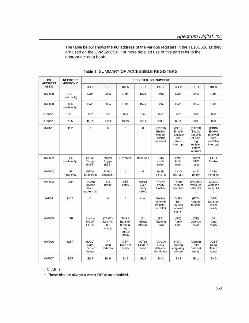
Spectrum Digital, Inc
C-3
The table below shows the I/O address of the various registers in the TL16C550 as theyare used on the EVM320C5X. For more detailed use of this part refer to theappropriate data book.
t DLAB 1 tt These bits are always 0 when FIFOs are disabled.
Table 1: SUMMARY OF ACCESSIBLE REGISTERS
I/O ADDRESS
RS232
REGISTERMNEMONIC
REGISTER BIT NUMBERS
BIT 7 BIT 6 BIT 5 BIT 4 BIT 3 BIT 2 BIT 1 BIT 0
0xF000 RBR(read only)
Data Data Data Data Data Data Data Data
0xF000 THR(write only)
Data Data Data Data Data Data Data Data
0xF000 t DLL Bit7 Bit6 Bit5 Bit4 Bit3 Bit2 Bit1 Bit0
0xF000 t DLM Bit15 Bit14 Bit13 Bit12 Bit11 Bit10 Bit9 Bit8
0xF001 IER 0 0 0 0 (EDSSI)Enable Modem Status
Interrupt
(ELSI)Enable
Receiver line
status interrupt
(ETBEI)Enable
Transmit-ter hold-
ing register empty
interrupt
(ERBI) Enable
received data
available interrupt
0xF002 FCR(write only)
RCVRTrigger(MSB)
RCVRTrigger(LSB)
Reserved Reserved DMAmode select
XMITFIFOreset
RCVRFIFOreset
FIFOEnable
0xF002 IIR(read only)
FIFOsEnabled tt
FIFOsEnabled tt
0 0 Int IDBit (2) tt
Int IDBit (1) tt
Int IDBit (0)
0 if IntPending
0xF003 LCR (DLAB)Divisor latch
access bit
Setbreak
Stickparity
(EPS)Evenparityselect
(PEN)Parity
Enable
(STB)Num ofstop bits
(WLSB1)Word lenselect bit
1
(WLSB0)Word len select bit
0
0xF04 MCR 0 0 0 Loop Enable external int (INT0 or INT1)
OUT1(an
unused internal signal)
(RTS)Request to send
(DTR)Data ter-
minal ready
0xF005 LSR Error in RCVR FIFOtt
(TEMT)transmit-
ter empty
(THRE)Transmit-ter hold-
ing register empty
(BI)Break
interrupt
(FE)Framing
Error
(PE)Parity Error
(OE)Overrun
error
(DR)Data ready
0xF006 MSR (DCD)Data
carrier detect
(RI)Ring
Indicator
(DSR)Data set
ready
(CTS)Clear to
send
(DDCD)Delta
data car-rier detect
(TERI)Trailing
edge ring indicator
(DDSR)Delta
data set ready
(DCTS)Delta
clear to send
0xF007 SCR Bit 7 Bit 6 Bit 5 Bit 4 Bit 3 Bit 2 Bit 1 Bit 0
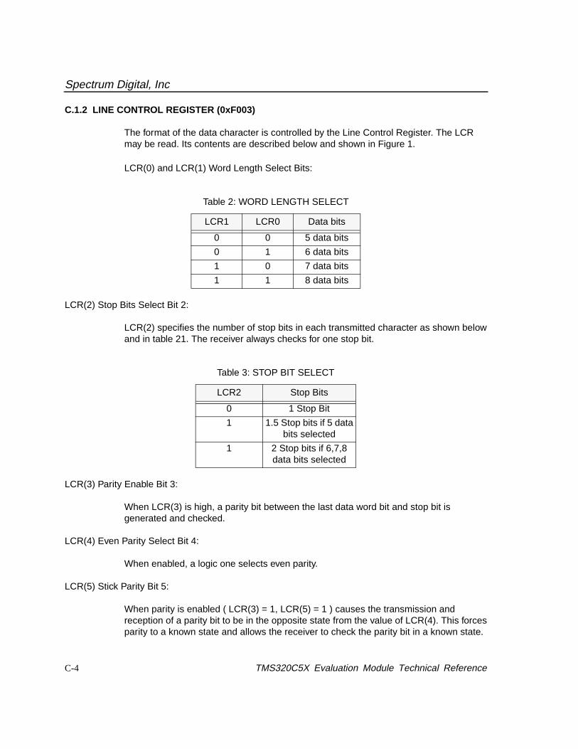
Spectrum Digital, Inc
C-4 TMS320C5X Evaluation Module Technical Reference
C.1.2 LINE CONTROL REGISTER (0xF003)
The format of the data character is controlled by the Line Control Register. The LCRmay be read. Its contents are described below and shown in Figure 1.
LCR(0) and LCR(1) Word Length Select Bits:
LCR(2) Stop Bits Select Bit 2:
LCR(2) specifies the number of stop bits in each transmitted character as shown belowand in table 21. The receiver always checks for one stop bit.
LCR(3) Parity Enable Bit 3:
When LCR(3) is high, a parity bit between the last data word bit and stop bit isgenerated and checked.
LCR(4) Even Parity Select Bit 4:
When enabled, a logic one selects even parity.
LCR(5) Stick Parity Bit 5:
When parity is enabled ( LCR(3) = 1, LCR(5) = 1 ) causes the transmission andreception of a parity bit to be in the opposite state from the value of LCR(4). This forcesparity to a known state and allows the receiver to check the parity bit in a known state.
Table 2: WORD LENGTH SELECT
LCR1 LCR0 Data bits
0 0 5 data bits
0 1 6 data bits
1 0 7 data bits
1 1 8 data bits
Table 3: STOP BIT SELECT
LCR2 Stop Bits
0 1 Stop Bit
1 1.5 Stop bits if 5 databits selected
1 2 Stop bits if 6,7,8data bits selected

Spectrum Digital, Inc
C-5
LCR(6) Break Control Bit 6:
When LCR(6) is set to a logic 1, the serial output (SOUT1/SOUT0) is for forced to thespacing state (low). The break control bit acts only on the serial output and does notaffect the transmitter logic. If the following sequence is used, no invalid characters willbe transmitted because of the break:
Step 1. Load a zero byte in response to the Transmitter Holding RegisterEmpty (THRE) status indication.
Step 2. Set the break in response to the next THRE status indication.
Step 3. Wait for the transmitter to be idle when transmitter empty status signalis set high (TEMT=1). Then clear the break when the normal transmissionhas to be restored.
LCR(7) Divisor Latch Access Bit (DLAB) bit 7:
Bit 7 must be set high (logic 1) to access the divisor latches DLL and DLM of the baudrate generator during a read or write operation. LCR(7) must be input low (logic 0) toaccess the receiver buffer register, the transmitter holding register or the interruptenable register.
Spectrum Digital, Inc
C-6 TMS320C5X Evaluation Module Technical Reference
C.1.3 LINE STATUS REGISTER (0xF005)
The line status register (LSR) is a single register that provides status indications. Theline status register shown in table 21 and described below:
LSR(0) Data Ready (DR) Bit 0:
Data Ready is set high when an incoming character has been received and transferredinto the receiver buffer register or the FIFO. LSR(O) is reset low by a CPU read of thedata in the receiver buffer register or the FIFO.
LSR(1) Overrun Error (OE) bit 1:
Overrun Error indicates that data in the receiver buffer register was not read by theCPU before the next character was transferred into the receiver buffer registeroverwriting the previous character. The OE indicator is reset whenever the CPU readsthe contents of the line status register. An overrun error will occur in the FIFO modeafter the FIFO is full and the next character is completely received. The overrun error isdetected by the CPU on the first LSR read after it happens. The character in the shiftregister is not transferred to the FIFO but it is overwritten.
LSR(2) Parity Error (PE) bit 2:
Parity Error indicates that the received data character does not have the correct parityas selected by LCR(3) and LCR(4). The PE bit is set high upon detection of a parityerror and is reset low when the CPU reads the contents of the LSR. In the FIFO mode,the parity error is associated with a particular character in the FIFO, LSR(2) resets theerror when the character is at the top of the FIFO.
LSR(3) Framing Error (FE) bit 3:
Framing error indicates that the received character did not have a valid stop bit. LSR(3)is set high when the stop bit following the last data bit or parity bit is detected as a zerobit (spacing level). The FE indicator is reset low when the CPU reads the contents ofthe LSR. In the FIFO mode, the framing error is associated with a particular characterin the FIFO. LSR(3) reflects the error when the character is at the top of the FIFO.
Spectrum Digital, Inc
C-7
LSR(4) Break Interrupt (BI) bit 4:
Break Interrupt is set high when the received data input is held in the spacing (logic 0)state for longer than a full word transmission time (start bit + data bits + parity + stop bits). The BI indicator is reset when the CPU reads the contents of the line statusregister. In the FIFO mode, this is associated with a particular character in the FIFO.LSR(2) reflects the BI when the break character is at the top of the FIFO. The error isdetected by the CPU when its associated character is at the top of the FIFO during thefirst LSR read. Only one zero character is loaded into the FIFO when BI occurs.
LSR(4) - LSR(1) are the error conditions that produce a receiver line status interrupt (priority 1 interrupt in the Interrupt Identification register(IIR)) when any of theconditions are detected. This interrupt is enabled by setting IER(2) = 1 in the interruptenable register.
LSR(5) Transmitter Holding Register Empty (THRE) bit 5:
THRE Indicates that the ACE is ready to accept a new character for transmission. TheTHRE bit is set high when a character is transferred from the transmitter holdingregister into the transmitter shift register. LSR(5) is reset low by the loading of thetransmitter holding register by the CPU. LSR(5) is not reset by a CPU read of the LSR.In the FIFO mode when the XMIT FIFO is empty, this bit is set. It is cleared when onebyte is written to the XMIT FIFO. When the THRE Interrupt is enabled by IER(1), THREcauses a priority 3 interrupt in the IIR. If THRE is the interrupt source indicated In IIR,INTRPT is cleared by a read of the IIR.
LSR(6) Transmitter Empty (TEMT) bit 6:
TEMT is set high when the Transmitter Holding Register(THR) and the Transmitter ShiftRegister(TSR) are both empty. LSR(6) is reset low when a character is loaded into theTHR and remains low until the character is transferred out of SOUT. TEMT is not resetlow by a CPU read of the LSR. In FIFO mode, when both the transmitter FIFO and shift register are empty, this bit is set to one.
LSR(7) RCVR FIFO error bit 7:
The LSR(7) bit is always 0 in the TL16C450 mode. In FIFO mode, it is set when at leastone of the following data errors is in the FIFO: parity error, framing error, or breakinterrupt indication. It is cleared when the CPU reads the LSR if there are nosubsequent errors in the FIFO.
NOTE: The line status register may be written. However, this function is intended only forfactory test. It should be considered as read only by applications software.
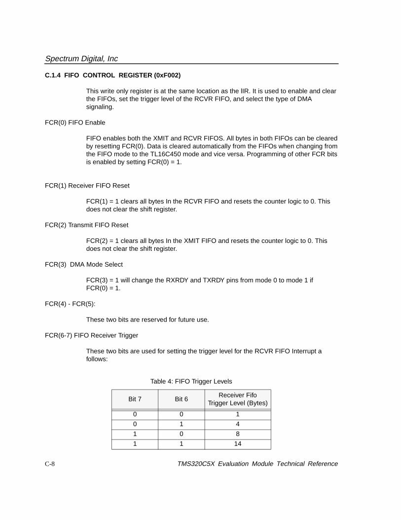
Spectrum Digital, Inc
C-8 TMS320C5X Evaluation Module Technical Reference
C.1.4 FIFO CONTROL REGISTER (0xF002)
This write only register is at the same location as the lIR. It is used to enable and clearthe FIFOs, set the trigger level of the RCVR FIFO, and select the type of DMAsignaling.
FCR(0) FIFO Enable
FIFO enables both the XMIT and RCVR FIFOS. All bytes in both FIFOs can be clearedby resetting FCR(0). Data is cleared automatically from the FIFOs when changing fromthe FIFO mode to the TL16C450 mode and vice versa. Programming of other FCR bitsis enabled by setting FCR(0) = 1.
FCR(1) Receiver FIFO Reset
FCR(1) = 1 clears all bytes In the RCVR FIFO and resets the counter logic to 0. Thisdoes not clear the shift register.
FCR(2) Transmit FIFO Reset
FCR(2) = 1 clears all bytes In the XMIT FIFO and resets the counter logic to 0. Thisdoes not clear the shift register.
FCR(3) DMA Mode Select
FCR(3) = 1 will change the RXRDY and TXRDY pins from mode 0 to mode 1 if FCR(0) = 1.
FCR(4) - FCR(5):
These two bits are reserved for future use.
FCR(6-7) FIFO Receiver Trigger
These two bits are used for setting the trigger level for the RCVR FIFO Interrupt afollows:
Table 4: FIFO Trigger Levels
Bit 7 Bit 6Receiver Fifo
Trigger Level (Bytes)
0 0 1
0 1 4
1 0 8
1 1 14
Spectrum Digital, Inc
C-9
C.1.5 MODEM CONTROL REGISTER (0xF004)
The Modem Control Register (MCR) controls the interface with the modem or data setas described in Figure 2. MCR can be written and read. The RTS and DTR outputs aredirectly controlled by their control bits in this register. A high input asserts a low(true) atthe output pins. MCR bits 0, 1, 2, 3, and 4 are shown as follows:
MCR(0) Data Terminal Ready
When MCR(0) is set high, the DTR output is forced low. When MCR(0) is reset low, theDTR output is forced high. The DTR output of the serial channel may be input into an inverting line driver in order to obtain the proper polarity input at the modem or data set.
MCR(1) Request to Send
When MCR(1) is set high, the RTS output is forced low. When MCR(1) is reset low, the RTS output is forced high. The RTS output of the serial channel may be input into an inverting line driver to obtain the proper polarity input at the modem or data set.
MCR(2) OUT1
When MCR(2) is set high, OUT1 is forced low.
MCR(3) OUT2
When MCR(3) is set high, the OUT2 output is forced low.
MCR(4) Loop
MCR(4) provides a local loopback feature for diagnostic testing of the channel. When MCR(4) is set high, serial output (SOUT) is set to the marking (logic 1) state, and the receiver data input serial input (SIN) is disconnected. The output of the transmitter shift register is looped back into the receiver shift register input. The four modem controlinputs (CTS, DSR, DCD, and RI) are disconnected. The modem control outputs (DTR,RTS, OUT1, and OUT2) are internally connected to the four modem control inputs. Themodem control outputs pins are forced to their inactive state(high) on the TL16C550. Inthe diagnostic mode, data transmitted is immediately received. This allows theprocessor to verify the transmission and receive data paths of the selected serialchannel. Interrupt control is fully operational. However, interrupts are generated bycontrolling the lower four MCR bits internally. Interrupts are not generated by activity onthe external pins represented by those four bits.
MCR(5) - MCR(7) are permanently set to logic 0.
Spectrum Digital, Inc
C-10 TMS320C5X Evaluation Module Technical Reference
C.1.6 MODEM STATUS REGISTER (0xF006)
The MSR provides the CPU with status of the modem input lines from the modem orperipheral devices The MSR allows the CPU to read the serial channel modem signalinputs by accessing the data bus interface of the ACE in addition to the current status offour bits of the MSR that indicate whether the modem in inputs changed since the lastreading of the MSR. The delta status bits are set high when a control input from themodem changes state and reset low when the CPU reads the MSR.
The modem input lines CTS, DSR, RI and DCD. MSR(4) - MSR(7) are statusindications of these lines. A status bit = 1 indicates the input is a low. A status bit = 0indicates the input is high. If the modem status interrupt in the interrupt enable registeris enabled IER(3), an interrupt is generated whenever MSR(0) - MSR(3) is set to a one.The MSR is a priority 4 interrupt. The contents of the Modem Status Register aredescribed in Table 3.
MSR(0) Delta Clear to Send (DCTS) bit 0:
DCTS displays that the CTS input to the serial channel has changed state since it waslast read by the CPU.
MSR(1) Delta Data Set Ready (DDSR) bit 1:
DDSR indicates that the DSR input to the serial channel has changed state since thelast time it was read by the CPU.
MSR(2) Trailing Edge of Ring Indicator (TERI) bit 2:
TERI indicates that the RI input to the serial channel has changed state from low tohigh since the last time it was read by the CPU. High-to-low transitions on RI do notactivate TERI.
MSR(3) Delta Data Carrier Detect (DDCD) bit 3:
DDCD indicates that the DCD input to the serial channel has changed state since thelast time it was read by the CPU.
MSR(4) Clear to Send (CTS) bit 4:
CTS is the complement of the CTS input from the modem indicating to the serialchannel that the modem is ready to receive data from the serial channel’s transmitteroutput(SOUT). If the serial channel is in the loop mode MCR(4) = 1, MSR(4) reflectsthe value of RTS in the MCR.

Spectrum Digital, Inc
C-11
MSR(5) Data Set Ready (DSR) bit 5:
DSR is the complement of the DSR input from the modem to the serial channel that indicates that the modem is ready to provide received data to the serial channelreceiver circuitry, If the channel is in the loop mode MCR(4) = 1, MSR(5) reflects thevalue of DTR in the MCR.
MSR(6) Ring Indicator (RI) bit 6:
RI is the complement of the RI input. If the channel is in the loop mode MCR(4) = 1,MSR(6) reflects the value of OUT1 in the MCR.
MSR(7) Data Carrier Detect (DCD) bit 7:
Data carrier detect indicates the status of the data carrier detect DCD input. If thechannel is in the loop mode MCR(4) = 1, MSR(7) reflects the value of OUT2 in theMCR.
Reading the MSR register clears the delta modem status indications but has no effecton the other status bits. For LSR and MSR, the setting of status bits is inhibited duringstatus register read operations. If a status condition is generated during a readoperation, the status bit is not set until the trailing edge of the read. If a status bit is setduring a read operation, and the same status condition occurs, that status bit will becleared at the trailing edge of the read instead of being set again. In the loop backmode, when modem status interrupts are enabled, the CTS, DSR, RI and DCD inputpins are ignored. However a modem status interrupt may still be generated by writing toMCR3 - MCR0. Applications software should not write to the modem status register.
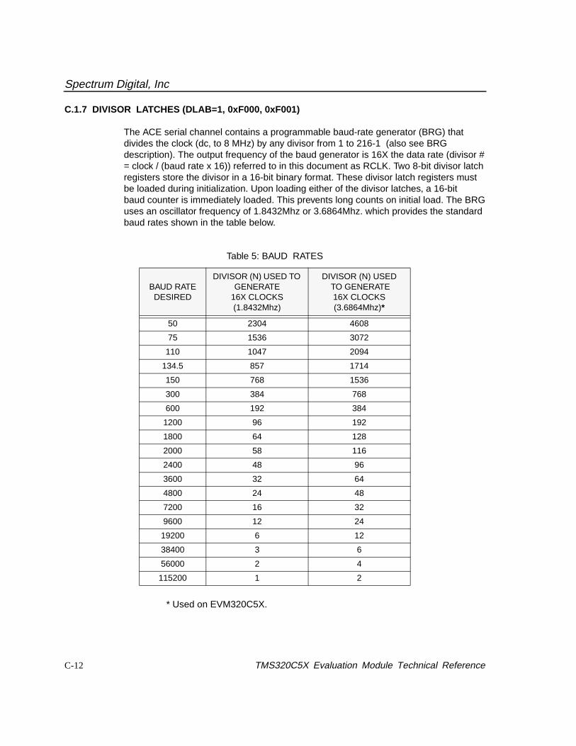
Spectrum Digital, Inc
C-12 TMS320C5X Evaluation Module Technical Reference
C.1.7 DIVISOR LATCHES (DLAB=1, 0xF000, 0xF001)
The ACE serial channel contains a programmable baud-rate generator (BRG) thatdivides the clock (dc, to 8 MHz) by any divisor from 1 to 216-1 (also see BRGdescription). The output frequency of the baud generator is 16X the data rate (divisor #= clock / (baud rate x 16)) referred to in this document as RCLK. Two 8-bit divisor latchregisters store the divisor in a 16-bit binary format. These divisor latch registers mustbe loaded during initialization. Upon loading either of the divisor latches, a 16-bitbaud counter is immediately loaded. This prevents long counts on initial load. The BRGuses an oscillator frequency of 1.8432Mhz or 3.6864Mhz. which provides the standardbaud rates shown in the table below.
* Used on EVM320C5X.
Table 5: BAUD RATES
BAUD RATEDESIRED
DIVISOR (N) USED TO GENERATE
16X CLOCKS(1.8432Mhz)
DIVISOR (N) USED TO GENERATE
16X CLOCKS(3.6864Mhz)*
50 2304 4608
75 1536 3072
110 1047 2094
134.5 857 1714
150 768 1536
300 384 768
600 192 384
1200 96 192
1800 64 128
2000 58 116
2400 48 96
3600 32 64
4800 24 48
7200 16 32
9600 12 24
19200 6 12
38400 3 6
56000 2 4
115200 1 2
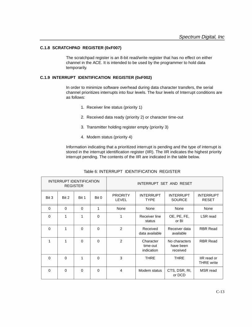
Spectrum Digital, Inc
C-13
C.1.8 SCRATCHPAD REGISTER (0xF007)
The scratchpad register is an 8-bit read/write register that has no effect on eitherchannel in the ACE. It is intended to be used by the programmer to hold datatemporarily.
C.1.9 INTERRUPT IDENTIFICATION REGISTER (0xF002)
In order to minimize software overhead during data character transfers, the serialchannel prioritizes interrupts into four levels. The four levels of Interrupt conditions areas follows:
1. Receiver line status (priority 1)
2. Received data ready (priority 2) or character time-out
3. Transmitter holding register empty (priority 3)
4. Modem status (priority 4)
Information indicating that a prioritized interrupt is pending and the type of interrupt isstored in the interrupt identification register (IIR). The IIR indicates the highest priorityinterrupt pending. The contents of the IIR are indicated in the table below.
Table 6: INTERRUPT IDENTIFICATION REGISTER
INTERRUPT IDENTIFICATIONREGISTER
INTERRUPT SET AND RESET
Bit 3 Bit 2 Bit 1 Bit 0PRIORITY
LEVELINTERRUPT
TYPEINTERRUPT
SOURCEINTERRUPT
RESET
0 0 0 1 None None None None
0 1 1 0 1 Receiver linestatus
OE, PE, FE,or BI
LSR read
0 1 0 0 2 Receiveddata available
Receiver dataavailable
RBR Read
1 1 0 0 2 Charactertime-out
indication
No charactershave beenreceived
RBR Read
0 0 1 0 3 THRE THRE IIR read orTHRE write
0 0 0 0 4 Modem status CTS, DSR, RI,or DCD
MSR read

Spectrum Digital, Inc
C-14 TMS320C5X Evaluation Module Technical Reference
IIR(0) can be used to indicate whether an interrupt is pending. When IIR(0) is low, anInterrupt is pending.
IIR(1) and IIR(2) are used to identify the highest priority interrupt pending as indicatedin the table above.
IIR(3): This bit is always logic 0 when in the TL16C450 mode. This bit is set along withbit2 when in the FIFO mode and a trigger change level interrupt is pending.
IIR(4) - IIR(5): These two bits are always set to a logic 0.
IIR(6) - IIR(7): These two bits are always cleared in the TL16C450 mode. They are setwhen bit 0 of the FCR is set..
Spectrum Digital, Inc
C-15
C.1.10 INTERRUPT ENABLE REGISTER (0xF001)
The interrupt enable register (IER) is used to independently enable the four serialchannel interrupt sources that activate the interrupt (INT0 or INT1) output. All interruptsare disabled by resetting IER(0) - IER(3) of the interrupt enable register. Interrupts areenabled by setting the appropriate bits of the IER high. Disabling the interrupt systeminhibits the interrupt identification register and the active (high) interrupt output. Allother system functions operate in, their normal manner, including the setting of the linestatus and modem status registers. The contents of the interrupt enable register aredescribed below:
IER(0) Enable Received Data Available Interrupt
When set to one, IER(0) enables the received data available interrupt and the time-outinterrupts in the FIFO mode.
IER(1) Enable Transmitter Holding Register Empty Interrupt
When set to one, IER(1) enables the transmitter holding register empty interrupt.
IER(2) Enable Receiver Line Status Interrupt
When set to one IER(2) enables the receiver line status interrupt.
IER(3) Enable Modem Status Interrupt
When set to one, IER(3) enables the modem status Interrupt.
IER(4) - IER(7).
These four bits of the IER are logic 0.
Spectrum Digital, Inc
C-16 TMS320C5X Evaluation Module Technical Reference
C.1.11 RECIEVER
Serial asynchronous data is input into the SIN pin. The ACE continually searches for ahigh-to-low transition from the idle state. When the transition is detected, a counter isreset, and counts the 16X clock to 7 1/2, which is the center of the start bit. The start bitis valid if the SIN is still low. Verifying the start bits prevents the receiver fromassembling a false data character due to a low-going noise spike on the SIN Input.
The Line Control Register determines the number of data bits in a character [LCR(0),LCR(1)]. If parity is used LCR(3) and the polarity of parity LCR(4) are needed. Statusfor the receiver is provided in the line status register. When a full character is received,including parity and stop bits, the data received indication in LSR(0) is set high. TheCPU reads the receiver buffer register, which resets LSR(0). If the character is not readprior to a new character transfer from the RSR to the RBR, the overrun error statusindication is set in LSR(1). If there is a parity error, the parity error is set in LSR(2). If astop bit is not detected, a framing error indication is set in LSR(3).
If the data into SIN is a symmetrical square wave, the center of the data cells will occurwith +/-3.125% of the actual center, providing an error margin of 46.875%. The start bitcan begin as much as one 1 6X clock cycle prior to being detected.
C.1.12 MASTER RESET
After power up, the ACE Reset Input should be held low for one microsecond to resetthe ACE circuits to an Idle mode until initialization. A low on RESET causes thefollowing:
1 . Initializes the transmitter and receiver clock counters.
2. Clears the Line Status Register (LSR), except for the transmitter shift register empty(TEMT) and transmit holding register empty (THRE), which are set. The Modem Control Register (MCR) is also cleared. All of the discrete lines, memory elements, and miscellaneous logic associated with these register bits are also cleared or turned off. The Line Control Register (LCR), divisor latches, receiver buffer register, and transmitter buffer register are not affected.
Following the removal of the reset condition (Reset high), the ACE remains in the idlemode until programmed.
A hardware reset of the ACE sets the THRE and TEMT status bit in the LSR. Wheninterrupts are subsequently enabled, an interrupt occurs due to THRE.
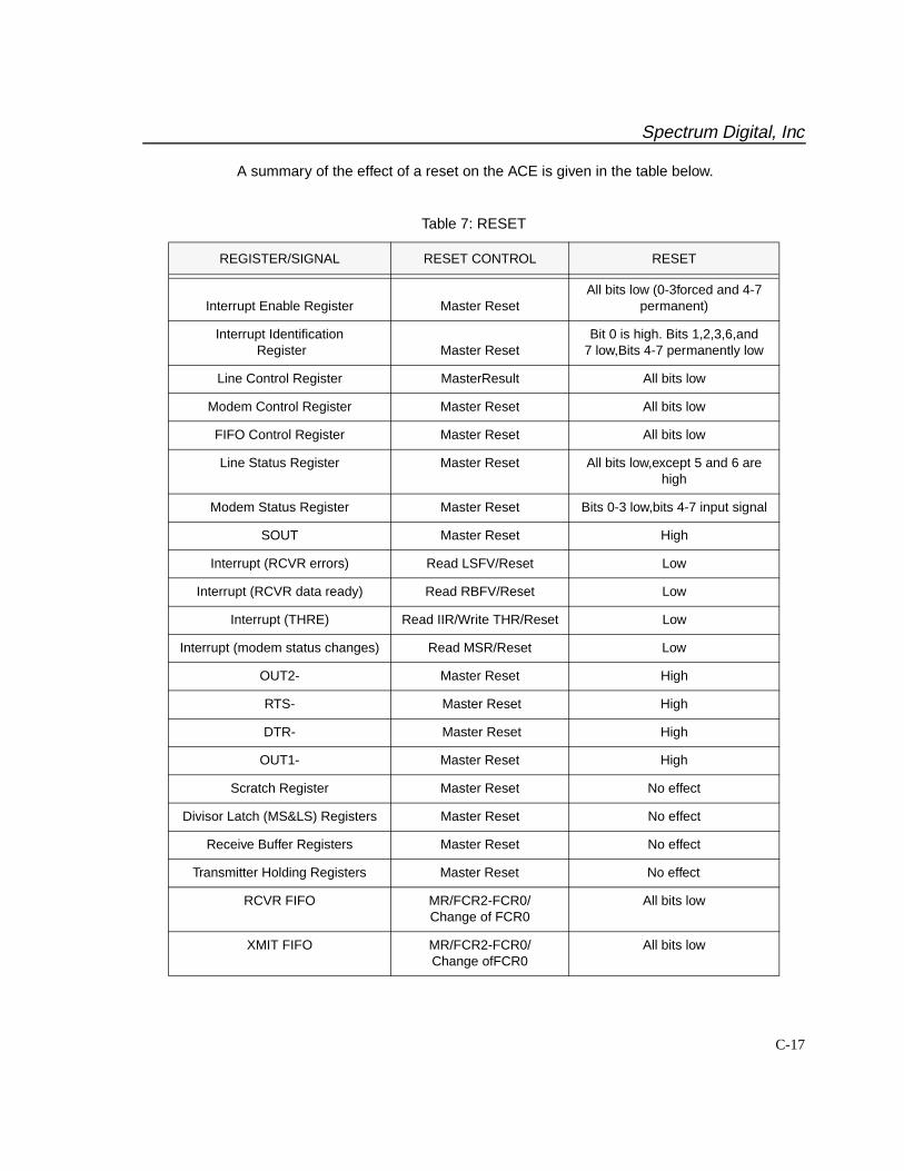
Spectrum Digital, Inc
C-17
A summary of the effect of a reset on the ACE is given in the table below.
Table 7: RESET
REGISTER/SIGNAL RESET CONTROL RESET
Interrupt Enable Register Master ResetAll bits low (0-3forced and 4-7
permanent)
Interrupt Identification Register Master Reset
Bit 0 is high. Bits 1,2,3,6,and7 low,Bits 4-7 permanently low
Line Control Register MasterResult All bits low
Modem Control Register Master Reset All bits low
FIFO Control Register Master Reset All bits low
Line Status Register Master Reset All bits low,except 5 and 6 arehigh
Modem Status Register Master Reset Bits 0-3 low,bits 4-7 input signal
SOUT Master Reset High
Interrupt (RCVR errors) Read LSFV/Reset Low
Interrupt (RCVR data ready) Read RBFV/Reset Low
Interrupt (THRE) Read IIR/Write THR/Reset Low
Interrupt (modem status changes) Read MSR/Reset Low
OUT2- Master Reset High
RTS- Master Reset High
DTR- Master Reset High
OUT1- Master Reset High
Scratch Register Master Reset No effect
Divisor Latch (MS&LS) Registers Master Reset No effect
Receive Buffer Registers Master Reset No effect
Transmitter Holding Registers Master Reset No effect
RCVR FIFO MR/FCR2-FCR0/Change of FCR0
All bits low
XMIT FIFO MR/FCR2-FCR0/Change ofFCR0
All bits low
Spectrum Digital, Inc
C-18 TMS320C5X Evaluation Module Technical Reference
C.1.13 PROGRAMMING
The serial channel of the ACE is programmed by the control registers: LCR, IER, DLL,DLM, MCR, and FCR. These control words define the character length, number of stopbits, parity, baud rate, and modem interface.
While the control registers can be written in any order, the IER should be written lastbecause it controls the Interrupt enables. Once the serial channel is programmed andoperational, these registers can be updated any time the ACE serial channel is nottransmitting or receiving data.
FIFO Interrupt Mode Operation
The following RCVR status occurs when the RCVR FIFO and receiver Interrupts areenabled:
1. LSR(0) is set when a character is transferred from the shift register to the RCVR FIFO. When the FIFO is empty, It is reset.
2. IIR = 06 receiver line status interrupt has higher priority than the received data available Interrupt IIR = 04.
3. Receive data available interrupt will be issued to the CPU when the programmed trigger level is reached by the FIFO. As soon as the FIFO drops below its programmed trigger level, it will be cleared.
4. IIR = 04 (receive data available indication) also occurs when the FIFO reaches its trigger level. It is cleared when the FIFO drops below the programmed trigger level.
The following RCVR FIFO character time-out status occurs when RCVR FIFO andreceiver interrupts are enabled.
1. If the following conditions exist, a FIFO character time-out interrupt occurs.
– Minimum of one character in FIFO
– Last received serial character was longer than 4 continuous previous character times ago (If two stop bits are programmed, the second one is included in the time delay).
Spectrum Digital, Inc
C-19
– The last CPU read of the FIFO was more than 4 continuous character times earlier. At 300 baud and 12-bit characters, the FIFO time-out interrupt causes a latency of 160 ms maximum from received character to interrupt issued.
2. By using the RCLK input for a clock signal, the character times can be calculated. (The delay is proportional to the baud rate.)
3. The time-out timer is reset after the CPU reads the RCVR FIFO or after a new character is received, when there has been no time-out interrupt.
4. A time-out interrupt is cleared and the timer is reset when the CPU reads a character from the RCVR FIFO.
XMIT Interrupts occur as follows when the transmitter and XMIT FIFO interrupts areenabled (FCR0 = 1, IER = 1).
1. When the transmitter FIFO is empty, the transmitter holding register interrupt (IIR = 02)occurs. The interrupt is cleared as soon as the transmitter holding register is written to or the IIR is read. One to sixteen characters may be written to the transmit FIFO when servicing this interrupt.
2. The XMIT FIFO empty indications will be delayed one character time minus the last stop bit time whenever the following occurs:
THRE = 1 and there has not been a minimum of two bytes at the same time in XMITFIFO, since the last THRE = 1. The first transmitter interrupt after changing FCR0 willbe immediate, however, assuming it is enabled.
RCVR FIFO trigger level and character time-out interrupts have the same priority as the received data available interrupt. The transmitter holding register empty interrupt hasthe same priority as the transmitter FIFO empty interrupt.
C.1.14 FIFO POLLED MODE OPERATION
Resetting IER0, IER1, IER2, IER3, or all to zero, with FCR0 = 1, puts the ACE into theFIFO polled mode. RCVR and XMITER are controlled separately. Therefore, either orboth can be in the polled mode. In the FIFO polled mode there is no time-out conditionindicated or trigger level reached. However, the RCVR and XMIT FIFOs still have thecapability of holding characters. The LSR must be read to determine the ACE status.

Spectrum Digital, Inc
C-20 TMS320C5X Evaluation Module Technical Reference
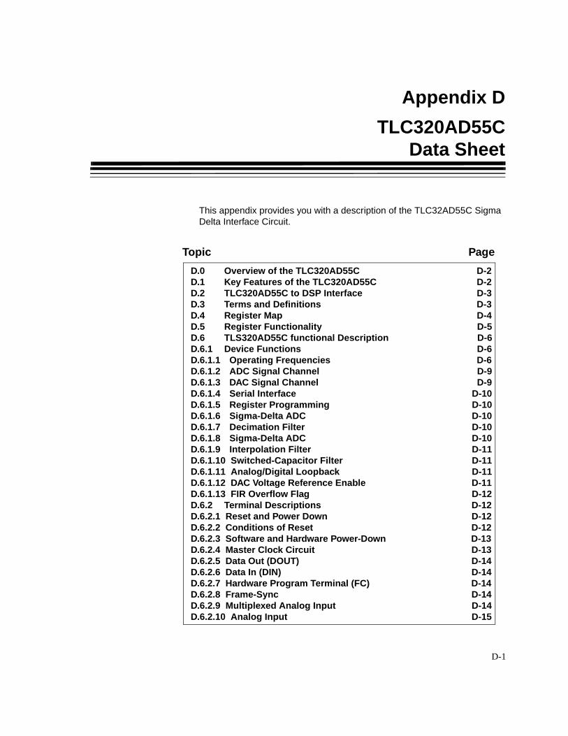
D-1
Appendix D
TLC320AD55C Data Sheet
This appendix provides you with a description of the TLC32AD55C SigmaDelta Interface Circuit.
Topic Page
D.0 Overview of the TLC320AD55C D-2D.1 Key Features of the TLC320AD55C D-2D.2 TLC320AD55C to DSP Interface D-3D.3 Terms and Definitions D-3D.4 Register Map D-4D.5 Register Functionality D-5D.6 TLS320AD55C functional Description D-6D.6.1 Device Functions D-6D.6.1.1 Operating Frequencies D-6D.6.1.2 ADC Signal Channel D-9D.6.1.3 DAC Signal Channel D-9D.6.1.4 Serial Interface D-10D.6.1.5 Register Programming D-10D.6.1.6 Sigma-Delta ADC D-10D.6.1.7 Decimation Filter D-10D.6.1.8 Sigma-Delta ADC D-10D.6.1.9 Interpolation Filter D-11D.6.1.10 Switched-Capacitor Filter D-11D.6.1.11 Analog/Digital Loopback D-11D.6.1.12 DAC Voltage Reference Enable D-11D.6.1.13 FIR Overflow Flag D-12D.6.2 Terminal Descriptions D-12D.6.2.1 Reset and Power Down D-12D.6.2.2 Conditions of Reset D-12D.6.2.3 Software and Hardware Power-Down D-13D.6.2.4 Master Clock Circuit D-13D.6.2.5 Data Out (DOUT) D-14D.6.2.6 Data In (DIN) D-14D.6.2.7 Hardware Program Terminal (FC) D-14D.6.2.8 Frame-Sync D-14D.6.2.9 Multiplexed Analog Input D-14D.6.2.10 Analog Input D-15
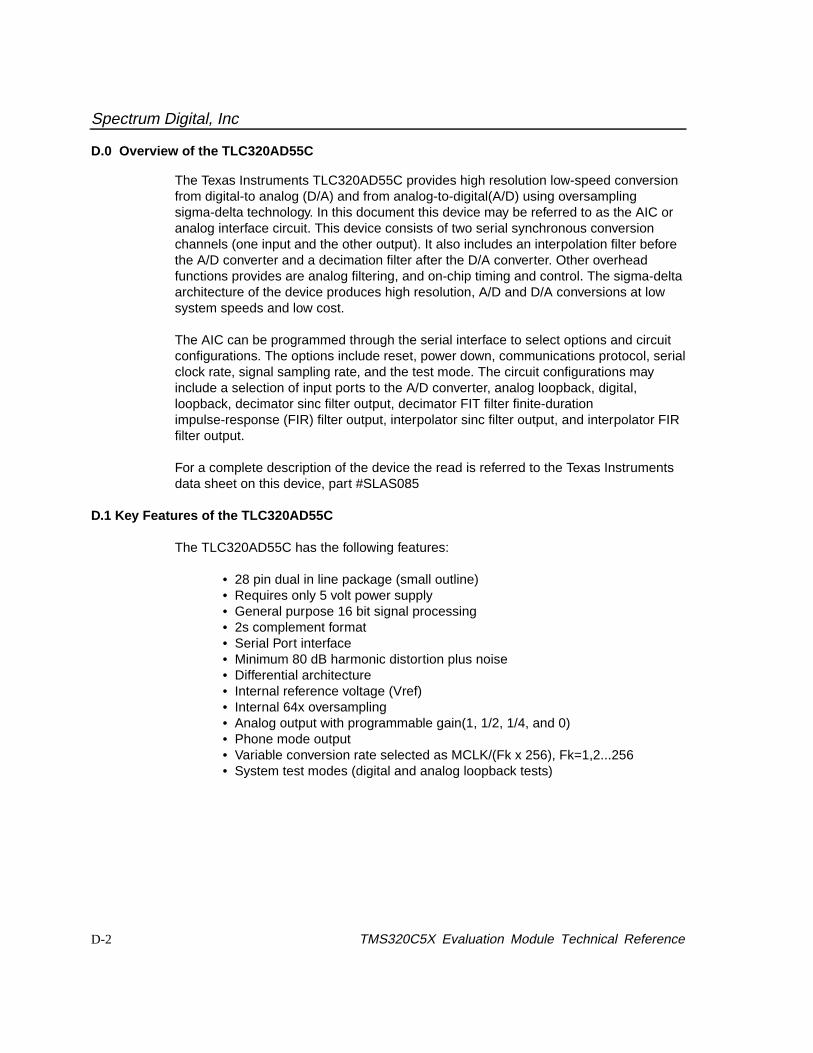
Spectrum Digital, Inc
D-2 TMS320C5X Evaluation Module Technical Reference
D.0 Overview of the TLC320AD55C
The Texas Instruments TLC320AD55C provides high resolution low-speed conversionfrom digital-to analog (D/A) and from analog-to-digital(A/D) using oversamplingsigma-delta technology. In this document this device may be referred to as the AIC oranalog interface circuit. This device consists of two serial synchronous conversionchannels (one input and the other output). It also includes an interpolation filter beforethe A/D converter and a decimation filter after the D/A converter. Other overheadfunctions provides are analog filtering, and on-chip timing and control. The sigma-deltaarchitecture of the device produces high resolution, A/D and D/A conversions at lowsystem speeds and low cost.
The AIC can be programmed through the serial interface to select options and circuitconfigurations. The options include reset, power down, communications protocol, serialclock rate, signal sampling rate, and the test mode. The circuit configurations mayinclude a selection of input ports to the A/D converter, analog loopback, digital,loopback, decimator sinc filter output, decimator FIT filter finite-durationimpulse-response (FIR) filter output, interpolator sinc filter output, and interpolator FIRfilter output.
For a complete description of the device the read is referred to the Texas Instrumentsdata sheet on this device, part #SLAS085
D.1 Key Features of the TLC320AD55C
The TLC320AD55C has the following features:
• 28 pin dual in line package (small outline)• Requires only 5 volt power supply• General purpose 16 bit signal processing• 2s complement format• Serial Port interface• Minimum 80 dB harmonic distortion plus noise• Differential architecture• Internal reference voltage (Vref)• Internal 64x oversampling• Analog output with programmable gain(1, 1/2, 1/4, and 0)• Phone mode output• Variable conversion rate selected as MCLK/(Fk x 256), Fk=1,2...256• System test modes (digital and analog loopback tests)
Spectrum Digital, Inc
D-3
D.2 TLC320AD55C to DSP Interface
TLC320AD55C interfaces to the C5X DSP through the synchronous serial port. The5 position jumper platform JP8 on the EVM320C5X is used to connect the serialport to the AIC. These 5 jumpers must be installed to connect the TLS320AD55C tothe synchronous serial port of the DSP.
The analog input (INM or INP) is driven from either RCA Jack J2 and the analog output(OUTM or OUTP) is driven to RCA Jack J3.
D.3 Terms and Definitions
The following terms and definitions are used in the explanation of the functionality ofthis device:
Data Transfer Interval The time during which data is transferred from DOUT and toDIN. The interval is 16 shift clocks and this data transfer isinitiated by the falling edge of the frame-sync signal
Signal Data The input signal and all of the converted representationsthrough the ADC channel and return through the DACchannel to the analog output. This is contrasted with thepurely digital software control data
Primary The digital data transfer interval. Since the device is Communications synchronous, the signal data words from the ADC channel
and to the DAC channel occur simultaneously.
Secondary The digital control and configuration data transfer intervalCommunications into DIN and the register read data cycle from DOUT. The data
transfer interval occurs when requested by the hardware orsoftware.
Frame Sync The falling edge of the signal that initiates the data transferinterval. The primary frame sync starts the primarycommunications, and the secondary frame sync starts thesecondary communications.
Frame Sync and The time between falling edges of successive primarySampling Period frame-sync signals.
fs The sampling frequency that is the reciprocal of the samplingperiod.
Frame-sync Interval The period occupied by 16 shift clocks. It goes high on thesixteenth rising edge of SCLK after the falling edge of theframe sync.
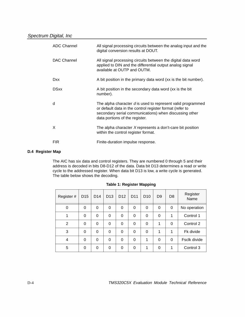
Spectrum Digital, Inc
D-4 TMS320C5X Evaluation Module Technical Reference
ADC Channel All signal processing circuits between the analog input and thedigital conversion results at DOUT.
DAC Channel All signal processing circuits between the digital data wordapplied to DIN and the differential output analog signalavailable at OUTP and OUTM.
Dxx A bit position in the primary data word (xx is the bit number).
DSxx A bit position in the secondary data word (xx is the bitnumber).
d The alpha character d is used to represent valid programmedor default data in the control register format (refer tosecondary serial communications) when discussing otherdata portions of the register.
X The alpha character X represents a don’t-care bit positionwithin the control register format.
FIR Finite-duration impulse response.
D.4 Register Map
The AIC has six data and control registers. They are numbered 0 through 5 and theiraddress is decoded in bits D8-D12 of the data. Data bit D13 determines a read or writecycle to the addressed register. When data bit D13 is low, a write cycle is generated.The table below shows the decoding.
Table 1: Register Mapping
Register # D15 D14 D13 D12 D11 D10 D9 D8Register Name
0 0 0 0 0 0 0 0 0 No operation
1 0 0 0 0 0 0 0 1 Control 1
2 0 0 0 0 0 0 1 0 Control 2
3 0 0 0 0 0 0 1 1 Fk divide
4 0 0 0 0 0 1 0 0 Fsclk divide
5 0 0 0 0 0 1 0 1 Control 3
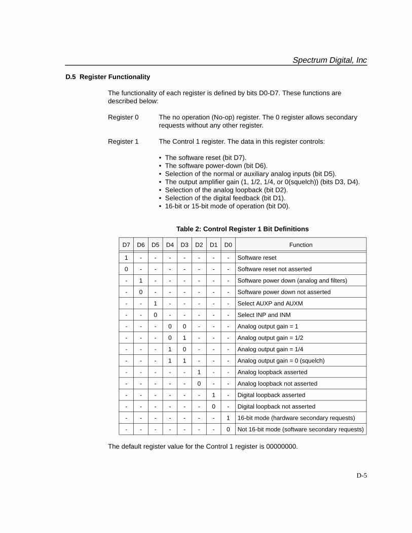
Spectrum Digital, Inc
D-5
D.5 Register Functionality
The functionality of each register is defined by bits D0-D7. These functions aredescribed below:
Register 0 The no operation (No-op) register. The 0 register allows secondaryrequests without any other register.
Register 1 The Control 1 register. The data in this register controls:
• The software reset (bit D7).• The software power-down (bit D6).• Selection of the normal or auxiliary analog inputs (bit D5).• The output amplifier gain (1, 1/2, 1/4, or 0(squelch)) (bits D3, D4).• Selection of the analog loopback (bit D2).• Selection of the digital feedback (bit D1).• 16-bit or 15-bit mode of operation (bit D0).
The default register value for the Control 1 register is 00000000.
Table 2: Control Register 1 Bit Definitions
D7 D6 D5 D4 D3 D2 D1 D0 Function
1 - - - - - - - Software reset
0 - - - - - - - Software reset not asserted
- 1 - - - - - - Software power down (analog and filters)
- 0 - - - - - - Software power down not asserted
- - 1 - - - - - Select AUXP and AUXM
- - 0 - - - - - Select INP and INM
- - - 0 0 - - - Analog output gain = 1
- - - 0 1 - - - Analog output gain = 1/2
- - - 1 0 - - - Analog output gain = 1/4
- - - 1 1 - - - Analog output gain = 0 (squelch)
- - - - - 1 - - Analog loopback asserted
- - - - - 0 - - Analog loopback not asserted
- - - - - - 1 - Digital loopback asserted
- - - - - - 0 - Digital loopback not asserted
- - - - - - - 1 16-bit mode (hardware secondary requests)
- - - - - - - 0 Not 16-bit mode (software secondary requests)
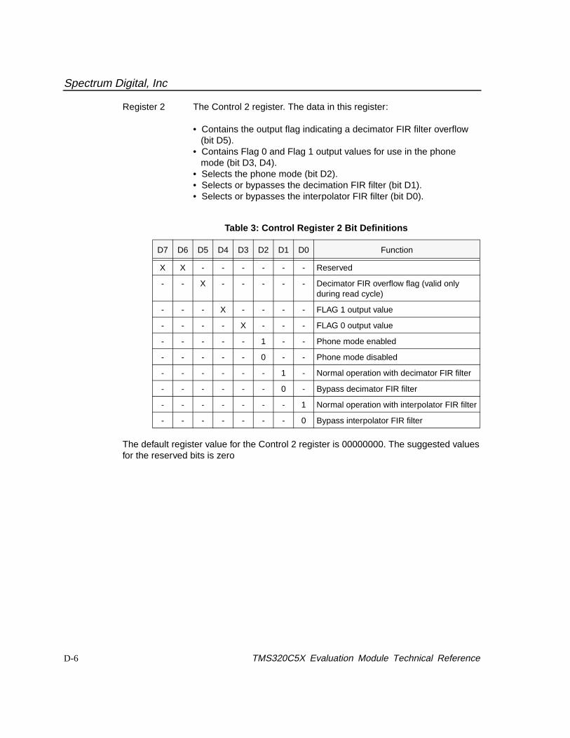
Spectrum Digital, Inc
D-6 TMS320C5X Evaluation Module Technical Reference
Register 2 The Control 2 register. The data in this register:
• Contains the output flag indicating a decimator FIR filter overflow (bit D5).• Contains Flag 0 and Flag 1 output values for use in the phone mode (bit D3, D4).• Selects the phone mode (bit D2).• Selects or bypasses the decimation FIR filter (bit D1).• Selects or bypasses the interpolator FIR filter (bit D0).
The default register value for the Control 2 register is 00000000. The suggested valuesfor the reserved bits is zero
Table 3: Control Register 2 Bit Definitions
D7 D6 D5 D4 D3 D2 D1 D0 Function
X X - - - - - - Reserved
- - X - - - - - Decimator FIR overflow flag (valid onlyduring read cycle)
- - - X - - - - FLAG 1 output value
- - - - X - - - FLAG 0 output value
- - - - - 1 - - Phone mode enabled
- - - - - 0 - - Phone mode disabled
- - - - - - 1 - Normal operation with decimator FIR filter
- - - - - - 0 - Bypass decimator FIR filter
- - - - - - - 1 Normal operation with interpolator FIR filter
- - - - - - - 0 Bypass interpolator FIR filter
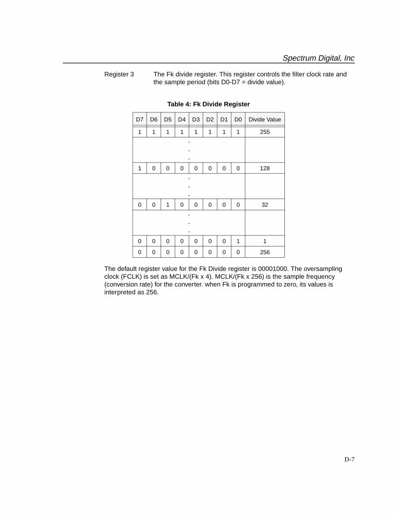
Spectrum Digital, Inc
D-7
Register 3 The Fk divide register. This register controls the filter clock rate andthe sample period (bits D0-D7 = divide value).
The default register value for the Fk Divide register is 00001000. The oversamplingclock (FCLK) is set as MCLK/(Fk x 4). MCLK/(Fk x 256) is the sample frequency(conversion rate) for the converter. when Fk is programmed to zero, its values isinterpreted as 256.
Table 4: Fk Divide Register
D7 D6 D5 D4 D3 D2 D1 D0 Divide Value
1 1 1 1 1 1 1 1 255
•
•
•
1 0 0 0 0 0 0 0 128
•
•
•
0 0 1 0 0 0 0 0 32
•
•
•
0 0 0 0 0 0 0 1 1
0 0 0 0 0 0 0 0 256
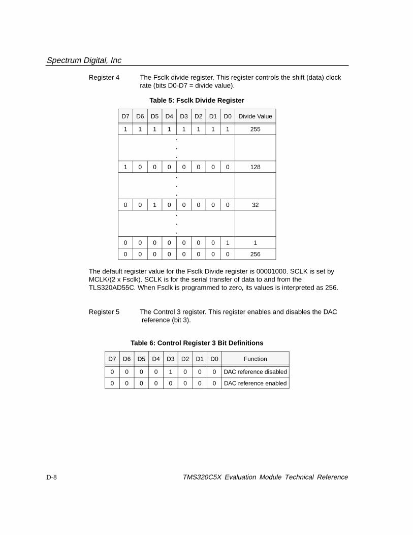
Spectrum Digital, Inc
D-8 TMS320C5X Evaluation Module Technical Reference
Register 4 The Fsclk divide register. This register controls the shift (data) clockrate (bits D0-D7 = divide value).
The default register value for the Fsclk Divide register is 00001000. SCLK is set byMCLK/(2 x Fsclk). SCLK is for the serial transfer of data to and from theTLS320AD55C. When Fsclk is programmed to zero, its values is interpreted as 256.
Register 5 The Control 3 register. This register enables and disables the DAC reference (bit 3).
Table 5: Fsclk Divide Register
D7 D6 D5 D4 D3 D2 D1 D0 Divide Value
1 1 1 1 1 1 1 1 255
•
•
•
1 0 0 0 0 0 0 0 128
•
•
•
0 0 1 0 0 0 0 0 32
•
•
•
0 0 0 0 0 0 0 1 1
0 0 0 0 0 0 0 0 256
Table 6: Control Register 3 Bit Definitions
D7 D6 D5 D4 D3 D2 D1 D0 Function
0 0 0 0 1 0 0 0 DAC reference disabled
0 0 0 0 0 0 0 0 DAC reference enabled
Spectrum Digital, Inc
D-9
D.6 TLC320AD55C Functional Description
D.6.1 Device Functions
The following sections describe the functions of the device
D.6.1.1 Operating Frequencies
The sampling (conversion) frequency is derived from the master clock (MCLK) input bythe following equation:
fs = Sampling (conversion) frequency = MLCK frequency/((Fk register value) x 256)
The inverse is the time between the falling edges of two successive primaryframe-synchronization signals and it is the conversion period.
The input and output data clock (SCLK) is given by the following equation:
SCLK frequency = MCLK frequency /((Fsclk register value) x 2)
D.6.1.2 ADC Signal Channel
To produce excellent common-mode rejection of unwanted signals, the analog signal isprocessed differentially until it is converted to digital data.
The ADC converts the signal into discrete output digital words in 2s-complementformat, corresponding to the analog-signal value at the sampling time. These 16-bitdigital words, representing sampled values of the analog input signal, are clocked out ofthe serial port, DOUT, during the frame-sync interval (one word for each primarycommunication interval). During secondary communications, the data previouslyprogrammed into the registers can be read out with the appropriate register address,and the read bit (D13) set to 1. When a register read is requested, all 16 bits are 0 inthe secondary word.
D.6.1.3 DAC Signal Channel
DIN receives the 16-bit serial data word (2s complement) from the host processorduring the primary communications interval and latches the data on the 17th risingedge of SCLK. The data is converted to an analog voltage by the DAC and then passedthrough a (sin x)/x correction circuit and smoothing filter. An output buffer with threesoftware-programmable gains (0 dB, -6 dB, and -12 dB) drives the differential outputsOUTP and OUTM. A squelch mode can also be programmed for the output buffer.During secondary communications, the configuration program data is read into thedevice control registers.
Spectrum Digital, Inc
D-10 TMS320C5X Evaluation Module Technical Reference
D.6.1.4 Serial Interface
The digital serial interface consists of a shift clock, the frame synchronization signal, theADC-channel data output, and the DAC-channel data input. During the primary 16-bitframe synchronization interval, SCLK transfers the ADC channel results from DOUTand transfers 16-bit DAC data into DIN.
During the secondary frame-synchronization interval, the SCLK transfers the registerread data from the DOUT when the read bit (D13) is set to a 1. In addition, SCLKtransfers control and device parameter information into DIN.
D.6.1.5 Register Programming
All register programming occurs during secondary communications, and data is latchedand valid on the rising edge of the frame-sync signal. When the default value for aparticular register is desired, that register does not need to be addressed during thesecondary communications. The no-op command addresses the no-op register(register 0), and register programming does not take place during the communication.
DOUT is released from the high impedance state on the falling edge of the primary orsecondary frame-sync interval. In addition, each register can be read back duringDOUT secondary communications by setting the read bit D13 to a 1 in the addressedregister. When the register is in the read mode, no data can be written to the registerduring this cycle. To return the register to the write mode requires a subsequentsecondary communication.
D.6.1.6 Sigma-Delta ADC
The sigma-delta ADC is a fourth order, sigma-delta modulator with 64-timesoversampling. The ADC provides high resolution, low noise performance usingoversampling techniques.
D.6.1.7 Decimation Filter
The decimation filter reduces the digital filter rate to the sampling rate. This isaccomplished by decimating with a ratio of 1:64. The output of this filter is a sixteen-bit,2s complement data word clocking the sample rate.
NOTE:The sample rate is determined through a programmable
relationship of MCLK/(Fk x 256), Fk= 1,2,3...,256
Spectrum Digital, Inc
D-11
D.6.1.8 Sigma-Delta DAC
The sigma-delta ADC is a fourth order, sigma-delta modulator with 64-timesoversampling. The ADC provides high resolution, low noise performance from a one-bitconverter using oversampling techniques.
D.6.1.9 Interpolation Filter
The interpolation filter samples the digital data at the rate of 64 times the incomingsample rate. The high speed data output from this filter is then used in the sigma-deltaDAC.
D.6.1.10 Switched-Capacitor Filter
A switch-capacitor filter network is implemented on the analog output to provide a lowpass operation with high rejection in the stop band.
D.6.1.11 Analog/Digital Loopback
The loopbacks provide a means of testing the ADC/DAC channels and can be used forin-circuit system level tests. The loopbacks feed the appropriate output back to thecorresponding input on the device.
The test capabilities include an analog loopback between the two analog paths and adigital loopback between two digital paths. Each loopback is enabled by setting D1 orD2 in the Control 1 register.
D.6.1.12 DAC Voltage Reference Enable
The DAC voltage reference can be disabled through the Control 3 register. This allowsthe use of an external voltage reference applied to the DAC channel modulator. Bysupplying the external reference, the user can scale the output range of this channel.The internal reference value is 3.6 volts which provides a 6 volt peak-to-peak,differential output. The ratio of an external reference to the internal referencedetermines the output voltage range of the DAC channel as shown in the followingequation:
VO(PP) = V(External Reference) x 6 volts / 3.6
NOTE:The distortion and noise specifications listed in the hardware
specifications apply only under the following condition
V(External Reference) / 3.6 ≤ 1
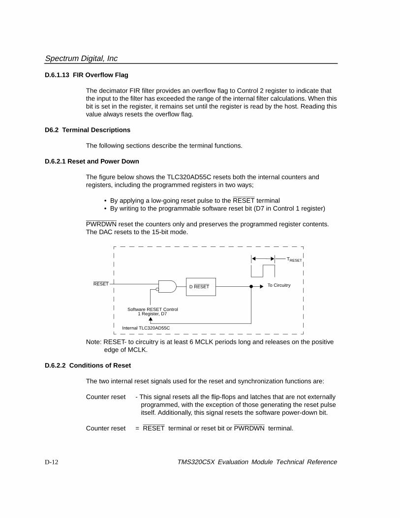
Spectrum Digital, Inc
D-12 TMS320C5X Evaluation Module Technical Reference
D.6.1.13 FIR Overflow Flag
The decimator FIR filter provides an overflow flag to Control 2 register to indicate thatthe input to the filter has exceeded the range of the internal filter calculations. When thisbit is set in the register, it remains set until the register is read by the host. Reading thisvalue always resets the overflow flag.
D6.2 Terminal Descriptions
The following sections describe the terminal functions.
D.6.2.1 Reset and Power Down
The figure below shows the TLC320AD55C resets both the internal counters andregisters, including the programmed registers in two ways;
• By applying a low-going reset pulse to the RESET terminal • By writing to the programmable software reset bit (D7 in Control 1 register)
PWRDWN reset the counters only and preserves the programmed register contents.The DAC resets to the 15-bit mode.
Note: RESET- to circuitry is at least 6 MCLK periods long and releases on the positive edge of MCLK.
D.6.2.2 Conditions of Reset
The two internal reset signals used for the reset and synchronization functions are:
Counter reset - This signal resets all the flip-flops and latches that are not externally programmed, with the exception of those generating the reset pulse itself. Additionally, this signal resets the software power-down bit.
Counter reset = RESET terminal or reset bit or PWRDWN terminal.
D RESET
Software RESET Control1 Register, D7
To Circuitry
TRESET
RESET
Internal TLC320AD55C
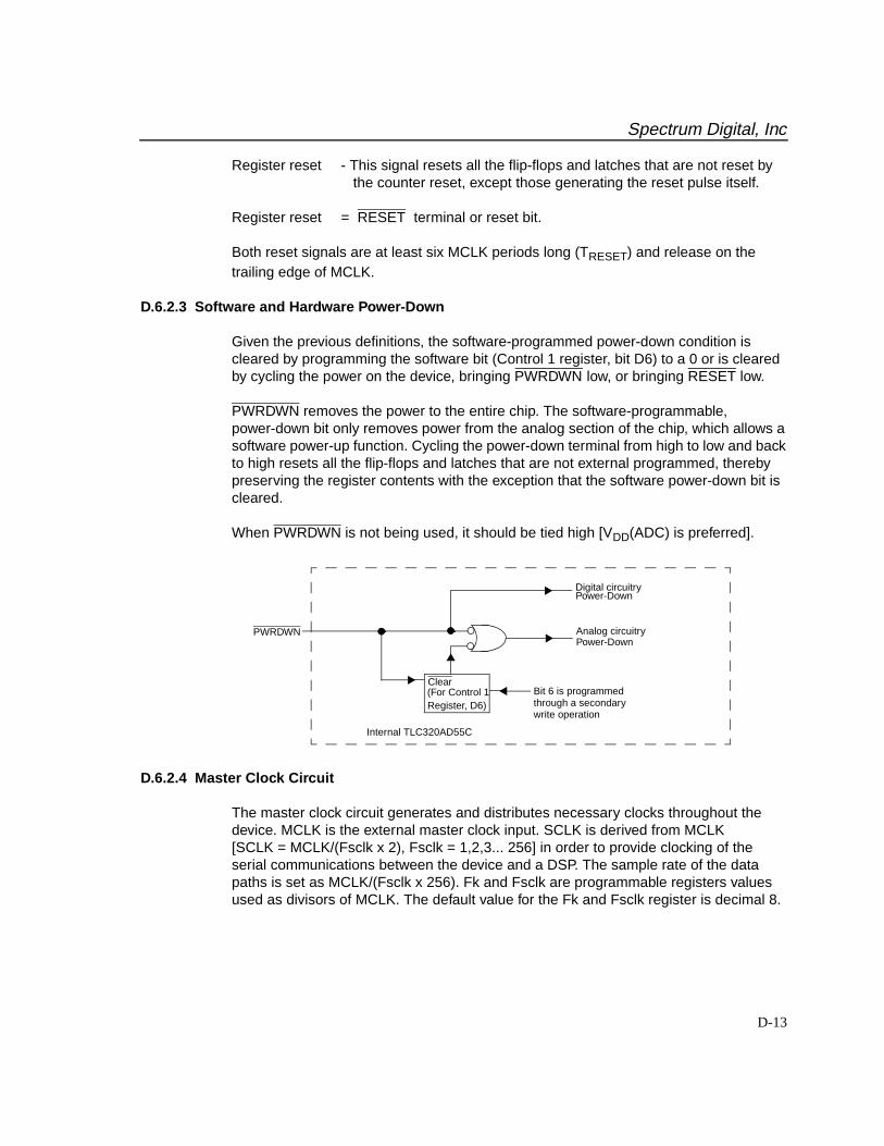
Spectrum Digital, Inc
D-13
Register reset - This signal resets all the flip-flops and latches that are not reset by the counter reset, except those generating the reset pulse itself.
Register reset = RESET terminal or reset bit.
Both reset signals are at least six MCLK periods long (TRESET) and release on thetrailing edge of MCLK.
D.6.2.3 Software and Hardware Power-Down
Given the previous definitions, the software-programmed power-down condition iscleared by programming the software bit (Control 1 register, bit D6) to a 0 or is clearedby cycling the power on the device, bringing PWRDWN low, or bringing RESET low.
PWRDWN removes the power to the entire chip. The software-programmable, power-down bit only removes power from the analog section of the chip, which allows asoftware power-up function. Cycling the power-down terminal from high to low and backto high resets all the flip-flops and latches that are not external programmed, therebypreserving the register contents with the exception that the software power-down bit iscleared.
When PWRDWN is not being used, it should be tied high [VDD(ADC) is preferred].
D.6.2.4 Master Clock Circuit
The master clock circuit generates and distributes necessary clocks throughout thedevice. MCLK is the external master clock input. SCLK is derived from MCLK[SCLK = MCLK/(Fsclk x 2), Fsclk = 1,2,3... 256] in order to provide clocking of theserial communications between the device and a DSP. The sample rate of the datapaths is set as MCLK/(Fsclk x 256). Fk and Fsclk are programmable registers valuesused as divisors of MCLK. The default value for the Fk and Fsclk register is decimal 8.
Internal TLC320AD55C
Bit 6 is programmedthrough a secondarywrite operation
Analog circuitryPower-Down
Digital circuitryPower-Down
Clear(For Control 1Register, D6)
PWRDWN
Spectrum Digital, Inc
D-14 TMS320C5X Evaluation Module Technical Reference
D.6.2.5 Data Out (DOUT)
DOUT is taken from the high impedance state by the falling edge of the frame-sync.The most significant bit of data then appears on DOUT.
DOUT is placed in a high impedance state on the sixteenth rising edge of SCLK(internal or external) after the falling edge of the frame-sync signal. In the primarycommunication, the data word is the ADC conversion result. In the secondarycommunication, the data is the register read results when requested by the read/write(R/W) bit with the eight MSBs set to zero. when a register read is not requested, thesecondary word is all zeros
D.6.2.6 Data In (DIN)
In the primary communication, the data word is the input signal to the DAC channel. Inthe secondary communication, the data is the control and configuration data to set upthe device for a particular function.
D.6.2.7 Hardware Program Terminal (FC)
The input provides for hardware programming requests for secondary communication.It works in conjunction with the control bit D0 of the secondary data word. The signal onthe FC is latched 1/2 shift clock after the rising edge of the next internally generatedprimary frame-sync interval. FC should be tied low when not being used.
D.6.2.8 Frame-Sync
The frame-sync signal indicates that the device is ready to send and receive data. Thedata transfer from DOUT and into DIN begins on the falling edge of the frame-syncsignal.
The frame sync is generated internally and goes low on the rising edge of SCLK andremains low during the 16 bit transfer.
D6.2.9 Multiplexed Analog Input
The two differential analog inputs (INP and INM or AUXP and AUXM) are multiplexedinto the sigma-delta modulator. The performance of the AUX channel is similar to thenormal input channel.
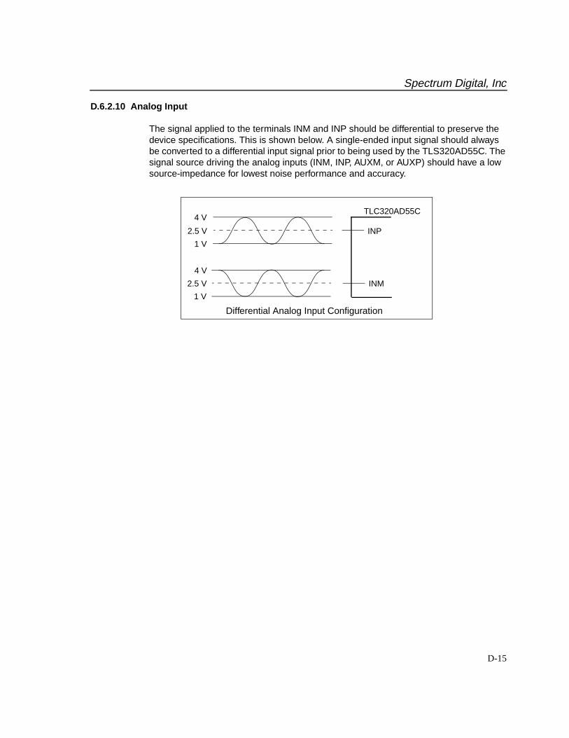
Spectrum Digital, Inc
D-15
D.6.2.10 Analog Input
The signal applied to the terminals INM and INP should be differential to preserve thedevice specifications. This is shown below. A single-ended input signal should alwaysbe converted to a differential input signal prior to being used by the TLS320AD55C. Thesignal source driving the analog inputs (INM, INP, AUXM, or AUXP) should have a lowsource-impedance for lowest noise performance and accuracy.
4 V
1 V
2.5 V
4 V
1 V
2.5 V
INP
INM
TLC320AD55C
Differential Analog Input Configuration

Spectrum Digital, Inc
D-16 TMS320C5X Evaluation Module Technical Reference

E-1
Appendix E
EVM320 Mechanical Information
This appendix contains the mechanical information about the EVM andWire Wrap Protoype Modules produced by Spectrum Digital.
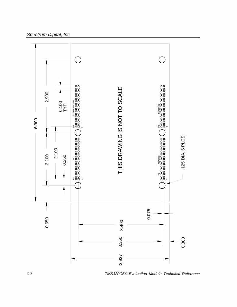
Spectrum Digital, Inc
E-2 TMS320C5X Evaluation Module Technical Reference
P4
P2
P1
P3
I/OA
DD
RE
SS
/DA
TA
AN
ALO
GC
ON
TR
OL
11
11
3.35
0
.125
DIA
.,6 P
LCS
.
0.07
5
3.40
0
0.30
0
3.93
7
0.65
02.
100 2.10
0
0.25
0
2.90
0
6.30
0
0.10
0T
YP
.
TH
IS D
RA
WIN
G IS
NO
T T
O S
CA
LE

503481-0001 Rev. BPrinted in U.S.A., November 1997