tms320c54x chip support library api reference guide (rev. d)
TRANSCRIPT

TMS320C54xChip Support LibraryAPI Reference Guide
SPRU420DMay 2003
Printed on Recycled Paper

IMPORTANT NOTICE
Texas Instruments Incorporated and its subsidiaries (TI) reserve the right to make corrections,modifications, enhancements, improvements, and other changes to its products and services atany time and to discontinue any product or service without notice. Customers should obtain thelatest relevant information before placing orders and should verify that such information is currentand complete. All products are sold subject to TI’s terms and conditions of sale supplied at thetime of order acknowledgment.
TI warrants performance of its hardware products to the specifications applicable at the time ofsale in accordance with TI’s standard warranty. Testing and other quality control techniques areused to the extent TI deems necessary to support this warranty. Except where mandated bygovernment requirements, testing of all parameters of each product is not necessarily performed.
TI assumes no liability for applications assistance or customer product design. Customers areresponsible for their products and applications using TI components. To minimize the risksassociated with customer products and applications, customers should provide adequate designand operating safeguards.
TI does not warrant or represent that any license, either express or implied, is granted under anyTI patent right, copyright, mask work right, or other TI intellectual property right relating to anycombination, machine, or process in which TI products or services are used. Informationpublished by TI regarding third party products or services does not constitute a license from TIto use such products or services or a warranty or endorsement thereof. Use of such informationmay require a license from a third party under the patents or other intellectual property of that thirdparty, or a license from TI under the patents or other intellectual property of TI.
Reproduction of information in TI data books or data sheets is permissible only if reproductionis without alteration and is accompanied by all associated warranties, conditions, limitations, andnotices. Reproduction of this information with alteration is an unfair and deceptive businesspractice. TI is not responsible or liable for such altered documentation.
Resale of TI products or services with statements different from or beyond the parameters statedby TI for that product or service voids all express and any implied warranties for the associatedTI product or service and is an unfair and deceptive business practice. TI is not responsible orliable for any such statements.
Mailing Address:
Texas InstrumentsPost Office Box 655303Dallas, Texas 75265
Copyright 2003, Texas Instruments Incorporated

iiiRead This First
Preface
Read This First
About This Manual
The TMS320C54x �DSP Chip Support Library (CSL) provides C-programfunctions to configure and control on-chip peripherals, which makes it easierfor algorithms to run in a real system. The CSL provides peripheral ease of use,shortened development time, portability, and hardware abstraction, along withsome level of standardization and compatibility among devices. A version ofthe CSL is available for all TMS320C54x DSP devices.
How to Use This Manual
The contents of the TMS320C5000 DSP Chip Support Library (CSL) are asfollows:
� Chapter 1, CSL Overview, provides an overview of the CSL, includestables showing CSL module support for various C5000 devices, and liststhe CSL modules.
� Chapter 2, How To Use CSL, provides basic examples of how to use CSLfunctions with or without using the DSP/BIOS Configuration Tool, andshows how to define Build options for the CSL in the Code Composer Stu-dio environment.
� Chapters 3-16 provide basic examples, functions, macros, and CSL GUIconfigurations for the individual CSL modules.
� Appendix A provides examples of how to use CSL C5000 Registers.
Notational Conventions
iv
Notational Conventions
This document uses the following conventions:
� Program listings, program examples, and interactive displays are shownin a special typeface.
� In syntax descriptions, the function or macro appears in a bold typefaceand the parameters appear in plainface within parentheses. Portions of asyntax that are in bold should be entered as shown; portions of a syntaxthat are within parentheses describe the type of information that should beentered.
� Macro names are written in uppercase text; function names are written inlowercase.
� TMS320C54x DSP devices are referred to throughout this referenceguide as C5401, C5402, etc.

Related Documentation From Texas Instruments
vRead This First
Related Documentation From Texas Instruments
The following books describe the TMS320C54x DSP and related supporttools. To obtain a copy of any of these TI documents, call the Texas Instru-ments Literature Response Center at (800) 477-8924. When ordering, pleaseidentify the book by its title and literature number. Many of these documentsare located on the internet at http://www.ti.com.
TMS320C54x Assembly Language Tools User’s Guide (literature numberSPRU102) describes the assembly language tools (assembler, linker,and other tools used to develop assembly language code), assembler di-rectives, macros, common object file format, and symbolic debugging di-rectives for the C54x generation of devices.
TMS320C54x Optimizing C Compiler User’s Guide (literature numberSPRU103) describes the C54x C compiler. This C compiler acceptsANSI standard C source code and produces TMS320 assembly lan-guage source code for the C54x generation of devices.
TMS320C54x Simulator Getting Started (literature number SPRU137) de-scribes how to install the TMS320C54x simulator and the C sourcedebugger for the C54x. The installation for MS-DOS , PC-DOS ,SunOS , Solaris , and HP-UX systems is covered.
TMS320C54x Evaluation Module Technical Reference (literature numberSPRU135) describes the C54x evaluation module, its features, designdetails and external interfaces.
TMS320C54x Simulator Getting Started Guide (literature numberSPRU137) describes how to install the TMS320C54x simulator and theC source debugger for the C54x. The installation for Windows 3.1,SunOS , and HP-UX systems is covered.
TMS320C54x Code Generation Tools Getting Started Guide (literaturenumber SPRU147) describes how to install the TMS320C54x assemblylanguage tools and the C compiler for the C54x devices. The installationfor MS-DOS , OS/2 , SunOS , Solaris , and HP-UX 9.0x systemsis covered.
TMS320C54x Simulator Addendum (literature number SPRU170) tells youhow to define and use a memory map to simulate ports for the C54x. Thisaddendum to the TMS320C5xx C Source Debugger User’s Guide dis-cusses standard serial ports, buffered serial ports, and time division mul-tiplexed (TDM) serial ports.

Trademarks
vi
Trademarks
The Texas Instruments logo and Texas Instruments are registered trademarksof Texas Instruments. Trademarks of Texas Instruments include: TI, CodeComposer, DSP/BIOS, and TMS320C5000.
All other brand or product names are trademarks or registered trademarks oftheir respective companies or organizations.

Contents
vii
Contents
1 CSL Overview 1-1. . . . . . . . . . . . . . . . . . . . . . . . . . . . . . . . . . . . . . . . . . . . . . . . . . . . . . . . . . . . . . . . . . . Overview of the features and architecture of the Chip Support Library.
1.1 Introduction to the CSL 1-2. . . . . . . . . . . . . . . . . . . . . . . . . . . . . . . . . . . . . . . . . . . . . . . . . . . . . . 1.1.1 Benefits of the CSL 1-2. . . . . . . . . . . . . . . . . . . . . . . . . . . . . . . . . . . . . . . . . . . . . . . . . . 1.1.2 CSL Architecture 1-2. . . . . . . . . . . . . . . . . . . . . . . . . . . . . . . . . . . . . . . . . . . . . . . . . . . .
1.2 Naming Conventions 1-6. . . . . . . . . . . . . . . . . . . . . . . . . . . . . . . . . . . . . . . . . . . . . . . . . . . . . . . . 1.3 Data Types 1-7. . . . . . . . . . . . . . . . . . . . . . . . . . . . . . . . . . . . . . . . . . . . . . . . . . . . . . . . . . . . . . . . 1.4 Functions 1-8. . . . . . . . . . . . . . . . . . . . . . . . . . . . . . . . . . . . . . . . . . . . . . . . . . . . . . . . . . . . . . . . . .
1.4.1 Peripheral Initialization via Registers 1-10. . . . . . . . . . . . . . . . . . . . . . . . . . . . . . . . . . 1.5 Macros 1-11. . . . . . . . . . . . . . . . . . . . . . . . . . . . . . . . . . . . . . . . . . . . . . . . . . . . . . . . . . . . . . . . . . . 1.6 Symbolic Constant Values 1-14. . . . . . . . . . . . . . . . . . . . . . . . . . . . . . . . . . . . . . . . . . . . . . . . . . 1.7 Resource Management and the Use of CSL Handles 1-15. . . . . . . . . . . . . . . . . . . . . . . . . . .
1.7.1 Using CSL Handles 1-15. . . . . . . . . . . . . . . . . . . . . . . . . . . . . . . . . . . . . . . . . . . . . . . . . 1.8 Support for Device-Specific Features 1-17. . . . . . . . . . . . . . . . . . . . . . . . . . . . . . . . . . . . . . . . .
2 How To Use CSL 2-1. . . . . . . . . . . . . . . . . . . . . . . . . . . . . . . . . . . . . . . . . . . . . . . . . . . . . . . . . . . . . . . . . This chapter explains the features of the CSL GUI. Instructions and examples are included.
2.1 Overview 2-2. . . . . . . . . . . . . . . . . . . . . . . . . . . . . . . . . . . . . . . . . . . . . . . . . . . . . . . . . . . . . . . . . . 2.2 Using CSL with the CSL GUI 2-3. . . . . . . . . . . . . . . . . . . . . . . . . . . . . . . . . . . . . . . . . . . . . . . . .
2.2.1 CSL GUI: The CSL Tree 2-3. . . . . . . . . . . . . . . . . . . . . . . . . . . . . . . . . . . . . . . . . . . . . . 2.2.2 Steps to configuring a peripheral using CSL GUI 2-7. . . . . . . . . . . . . . . . . . . . . . . . 2.2.3 TIMER Configuration Example 2-9. . . . . . . . . . . . . . . . . . . . . . . . . . . . . . . . . . . . . . . . 2.2.4 Files Generated by the CSL GUI 2-11. . . . . . . . . . . . . . . . . . . . . . . . . . . . . . . . . . . . . 2.2.5 Modifying Your Application Code (main.c) 2-15. . . . . . . . . . . . . . . . . . . . . . . . . . . . . .
2.3 Using CSL without the CSL GUI 2-17. . . . . . . . . . . . . . . . . . . . . . . . . . . . . . . . . . . . . . . . . . . . . 2.3.1 Using the DMA_config() function 2-18. . . . . . . . . . . . . . . . . . . . . . . . . . . . . . . . . . . . . 2.3.2 Compiling and Linking With CSL using Code Composer Studio (CCStudio) 2-19
2.4 Rebuilding CSL 2-26. . . . . . . . . . . . . . . . . . . . . . . . . . . . . . . . . . . . . . . . . . . . . . . . . . . . . . . . . . . .
3 CHIP Module 3-1. . . . . . . . . . . . . . . . . . . . . . . . . . . . . . . . . . . . . . . . . . . . . . . . . . . . . . . . . . . . . . . . . . . . General description of the CSL CHIP module, its functions, and macros.
3.1 Overview 3-2. . . . . . . . . . . . . . . . . . . . . . . . . . . . . . . . . . . . . . . . . . . . . . . . . . . . . . . . . . . . . . . . . . 3.2 Functions 3-3. . . . . . . . . . . . . . . . . . . . . . . . . . . . . . . . . . . . . . . . . . . . . . . . . . . . . . . . . . . . . . . . . .

Contents
viii
4 DAA Module 4-1. . . . . . . . . . . . . . . . . . . . . . . . . . . . . . . . . . . . . . . . . . . . . . . . . . . . . . . . . . . . . . . . . . . . This section include API functions for the DAA module.
4.1 Overview 4-2. . . . . . . . . . . . . . . . . . . . . . . . . . . . . . . . . . . . . . . . . . . . . . . . . . . . . . . . . . . . . . . . . . 4.1.1 Configuration Structures 4-2. . . . . . . . . . . . . . . . . . . . . . . . . . . . . . . . . . . . . . . . . . . . . . 4.1.2 Functions 4-3. . . . . . . . . . . . . . . . . . . . . . . . . . . . . . . . . . . . . . . . . . . . . . . . . . . . . . . . . . . 4.1.3 Macros 4-3. . . . . . . . . . . . . . . . . . . . . . . . . . . . . . . . . . . . . . . . . . . . . . . . . . . . . . . . . . . . .
4.2 Configuration Structures 4-4. . . . . . . . . . . . . . . . . . . . . . . . . . . . . . . . . . . . . . . . . . . . . . . . . . . . . 4.3 Functions 4-7. . . . . . . . . . . . . . . . . . . . . . . . . . . . . . . . . . . . . . . . . . . . . . . . . . . . . . . . . . . . . . . . . . 4.4 Macros 4-11. . . . . . . . . . . . . . . . . . . . . . . . . . . . . . . . . . . . . . . . . . . . . . . . . . . . . . . . . . . . . . . . . . .
5 DAT Module 5-1. . . . . . . . . . . . . . . . . . . . . . . . . . . . . . . . . . . . . . . . . . . . . . . . . . . . . . . . . . . . . . . . . . . . . General description of the DAT module and its functions.
5.1 Overview 5-2. . . . . . . . . . . . . . . . . . . . . . . . . . . . . . . . . . . . . . . . . . . . . . . . . . . . . . . . . . . . . . . . . . 5.2 Functions 5-4. . . . . . . . . . . . . . . . . . . . . . . . . . . . . . . . . . . . . . . . . . . . . . . . . . . . . . . . . . . . . . . . . .
6 DMA Module 6-1. . . . . . . . . . . . . . . . . . . . . . . . . . . . . . . . . . . . . . . . . . . . . . . . . . . . . . . . . . . . . . . . . . . . General description of the DMA module, its configuration structures, functions, and macros.
6.1 Overview 6-2. . . . . . . . . . . . . . . . . . . . . . . . . . . . . . . . . . . . . . . . . . . . . . . . . . . . . . . . . . . . . . . . . . 6.2 Configuration Structure 6-4. . . . . . . . . . . . . . . . . . . . . . . . . . . . . . . . . . . . . . . . . . . . . . . . . . . . . . 6.3 Functions 6-7. . . . . . . . . . . . . . . . . . . . . . . . . . . . . . . . . . . . . . . . . . . . . . . . . . . . . . . . . . . . . . . . . .
6.3.1 DMA Primary Functions 6-7. . . . . . . . . . . . . . . . . . . . . . . . . . . . . . . . . . . . . . . . . . . . . . 6.3.2 DMA Global Register Function 6-12. . . . . . . . . . . . . . . . . . . . . . . . . . . . . . . . . . . . . . . 6.3.3 DMA Auxiliary Functions 6-18. . . . . . . . . . . . . . . . . . . . . . . . . . . . . . . . . . . . . . . . . . . .
6.4 Macros 6-20. . . . . . . . . . . . . . . . . . . . . . . . . . . . . . . . . . . . . . . . . . . . . . . . . . . . . . . . . . . . . . . . . . . 6.5 Configuring the DMA Module Using CSL GUI 6-32. . . . . . . . . . . . . . . . . . . . . . . . . . . . . . . . .
6.5.1 DMA Configuration Manager 6-32. . . . . . . . . . . . . . . . . . . . . . . . . . . . . . . . . . . . . . . . . 6.5.2 DMA Resource Manager 6-35. . . . . . . . . . . . . . . . . . . . . . . . . . . . . . . . . . . . . . . . . . . . 6.5.3 C Code Generation for DMA Module 6-37. . . . . . . . . . . . . . . . . . . . . . . . . . . . . . . . . .
6.6 Examples 6-40. . . . . . . . . . . . . . . . . . . . . . . . . . . . . . . . . . . . . . . . . . . . . . . . . . . . . . . . . . . . . . . . .
7 EBUS Module 7-1. . . . . . . . . . . . . . . . . . . . . . . . . . . . . . . . . . . . . . . . . . . . . . . . . . . . . . . . . . . . . . . . . . . Features and description of the external bus interface (EBUS) module.
7.1 Overview 7-2. . . . . . . . . . . . . . . . . . . . . . . . . . . . . . . . . . . . . . . . . . . . . . . . . . . . . . . . . . . . . . . . . . 7.2 Configuration Structure 7-3. . . . . . . . . . . . . . . . . . . . . . . . . . . . . . . . . . . . . . . . . . . . . . . . . . . . . . 7.3 Functions 7-4. . . . . . . . . . . . . . . . . . . . . . . . . . . . . . . . . . . . . . . . . . . . . . . . . . . . . . . . . . . . . . . . . . 7.4 Macros 7-6. . . . . . . . . . . . . . . . . . . . . . . . . . . . . . . . . . . . . . . . . . . . . . . . . . . . . . . . . . . . . . . . . . . .
8 GPIO Module 8-1. . . . . . . . . . . . . . . . . . . . . . . . . . . . . . . . . . . . . . . . . . . . . . . . . . . . . . . . . . . . . . . . . . . . General description of the GPIO module and its macros.
8.1 Overview 8-2. . . . . . . . . . . . . . . . . . . . . . . . . . . . . . . . . . . . . . . . . . . . . . . . . . . . . . . . . . . . . . . . . . 8.2 Functions 8-3. . . . . . . . . . . . . . . . . . . . . . . . . . . . . . . . . . . . . . . . . . . . . . . . . . . . . . . . . . . . . . . . . . 8.3 Macros 8-5. . . . . . . . . . . . . . . . . . . . . . . . . . . . . . . . . . . . . . . . . . . . . . . . . . . . . . . . . . . . . . . . . . . . 8.4 Configuring the GPIO Module Using CSL GUI 8-7. . . . . . . . . . . . . . . . . . . . . . . . . . . . . . . . . .
8.4.1 Non-Multiplexed GPIO Configuration Manager 8-7. . . . . . . . . . . . . . . . . . . . . . . . . . 8.4.2 C Code Generation for GPIO Module 8-8. . . . . . . . . . . . . . . . . . . . . . . . . . . . . . . . . .

Contents
ixContents
9 HPI Module 9-1. . . . . . . . . . . . . . . . . . . . . . . . . . . . . . . . . . . . . . . . . . . . . . . . . . . . . . . . . . . . . . . . . . . . . Descriptions for macros available in the HPI module.
9.1 Macros 9-2. . . . . . . . . . . . . . . . . . . . . . . . . . . . . . . . . . . . . . . . . . . . . . . . . . . . . . . . . . . . . . . . . . . .
10 IRQ Module 10-1. . . . . . . . . . . . . . . . . . . . . . . . . . . . . . . . . . . . . . . . . . . . . . . . . . . . . . . . . . . . . . . . . . . . Overview of the IRQ module, including the configuration structure, functions, and examples ofinterrupts.
10.1 Overview 10-2. . . . . . . . . . . . . . . . . . . . . . . . . . . . . . . . . . . . . . . . . . . . . . . . . . . . . . . . . . . . . . . . . 10.1.1 The Event ID Concept 10-4. . . . . . . . . . . . . . . . . . . . . . . . . . . . . . . . . . . . . . . . . . . . . . .
10.2 Using Interrupts with CSL 10-7. . . . . . . . . . . . . . . . . . . . . . . . . . . . . . . . . . . . . . . . . . . . . . . . . . . 10.3 Configuration Structure 10-8. . . . . . . . . . . . . . . . . . . . . . . . . . . . . . . . . . . . . . . . . . . . . . . . . . . . . 10.4 Functions 10-9. . . . . . . . . . . . . . . . . . . . . . . . . . . . . . . . . . . . . . . . . . . . . . . . . . . . . . . . . . . . . . . . .
11 McBSP Module 11-1. . . . . . . . . . . . . . . . . . . . . . . . . . . . . . . . . . . . . . . . . . . . . . . . . . . . . . . . . . . . . . . . . General description of the McBSP Module, its configuration structure, functions and macros.
11.1 Overview 11-2. . . . . . . . . . . . . . . . . . . . . . . . . . . . . . . . . . . . . . . . . . . . . . . . . . . . . . . . . . . . . . . . . 11.2 Configuration Structure 11-4. . . . . . . . . . . . . . . . . . . . . . . . . . . . . . . . . . . . . . . . . . . . . . . . . . . . . 11.3 Functions 11-6. . . . . . . . . . . . . . . . . . . . . . . . . . . . . . . . . . . . . . . . . . . . . . . . . . . . . . . . . . . . . . . . . 11.4 Macros 11-24. . . . . . . . . . . . . . . . . . . . . . . . . . . . . . . . . . . . . . . . . . . . . . . . . . . . . . . . . . . . . . . . . . 11.5 Configuring the McBSP Module Using CSL GUI 11-42. . . . . . . . . . . . . . . . . . . . . . . . . . . . . .
11.5.1 Overview 11-42. . . . . . . . . . . . . . . . . . . . . . . . . . . . . . . . . . . . . . . . . . . . . . . . . . . . . . . . . 11.5.2 McBSP Configuration Manager 11-42. . . . . . . . . . . . . . . . . . . . . . . . . . . . . . . . . . . . . . 11.5.3 McBSP Resource Manager 11-46. . . . . . . . . . . . . . . . . . . . . . . . . . . . . . . . . . . . . . . . . 11.5.4 C Code Generation for McBSP Module 11-47. . . . . . . . . . . . . . . . . . . . . . . . . . . . . . .
11.6 Examples 11-50. . . . . . . . . . . . . . . . . . . . . . . . . . . . . . . . . . . . . . . . . . . . . . . . . . . . . . . . . . . . . . . .
12 PLL Module 12-1. . . . . . . . . . . . . . . . . . . . . . . . . . . . . . . . . . . . . . . . . . . . . . . . . . . . . . . . . . . . . . . . . . . . Describes the structure, functions, and macros of the PLL module.
12.1 Overview 12-2. . . . . . . . . . . . . . . . . . . . . . . . . . . . . . . . . . . . . . . . . . . . . . . . . . . . . . . . . . . . . . . . . 12.2 Configuration Structure 12-3. . . . . . . . . . . . . . . . . . . . . . . . . . . . . . . . . . . . . . . . . . . . . . . . . . . . . 12.3 Functions 12-4. . . . . . . . . . . . . . . . . . . . . . . . . . . . . . . . . . . . . . . . . . . . . . . . . . . . . . . . . . . . . . . . . 12.4 Macros 12-6. . . . . . . . . . . . . . . . . . . . . . . . . . . . . . . . . . . . . . . . . . . . . . . . . . . . . . . . . . . . . . . . . . . 12.5 Configuring the PLL Module Using CSL GUI 12-8. . . . . . . . . . . . . . . . . . . . . . . . . . . . . . . . . .
12.5.1 Overview 12-8. . . . . . . . . . . . . . . . . . . . . . . . . . . . . . . . . . . . . . . . . . . . . . . . . . . . . . . . . . 12.5.2 PLL Configuration Manager 12-8. . . . . . . . . . . . . . . . . . . . . . . . . . . . . . . . . . . . . . . . . . 12.5.3 PLL Resource Manager 12-10. . . . . . . . . . . . . . . . . . . . . . . . . . . . . . . . . . . . . . . . . . . . 12.5.4 C Code Generation for PLL Module 12-11. . . . . . . . . . . . . . . . . . . . . . . . . . . . . . . . . .
13 PWR Module 13-1. . . . . . . . . . . . . . . . . . . . . . . . . . . . . . . . . . . . . . . . . . . . . . . . . . . . . . . . . . . . . . . . . . . General description of the PWR module and its functions.
13.1 Overview 13-2. . . . . . . . . . . . . . . . . . . . . . . . . . . . . . . . . . . . . . . . . . . . . . . . . . . . . . . . . . . . . . . . . 13.2 Functions 13-3. . . . . . . . . . . . . . . . . . . . . . . . . . . . . . . . . . . . . . . . . . . . . . . . . . . . . . . . . . . . . . . . .

Contents
x
14 TIMER Module 14-1. . . . . . . . . . . . . . . . . . . . . . . . . . . . . . . . . . . . . . . . . . . . . . . . . . . . . . . . . . . . . . . . . . General description of the structure and functions for the TIMER module.
14.1 Overview 14-2. . . . . . . . . . . . . . . . . . . . . . . . . . . . . . . . . . . . . . . . . . . . . . . . . . . . . . . . . . . . . . . . . 14.2 Configuration Structure 14-3. . . . . . . . . . . . . . . . . . . . . . . . . . . . . . . . . . . . . . . . . . . . . . . . . . . . . 14.3 Functions 14-4. . . . . . . . . . . . . . . . . . . . . . . . . . . . . . . . . . . . . . . . . . . . . . . . . . . . . . . . . . . . . . . . . 14.4 Macros 14-9. . . . . . . . . . . . . . . . . . . . . . . . . . . . . . . . . . . . . . . . . . . . . . . . . . . . . . . . . . . . . . . . . . . 14.5 Configuring the TIMER Module Using CSL GUI 14-12. . . . . . . . . . . . . . . . . . . . . . . . . . . . . . .
14.5.1 Overview 14-12. . . . . . . . . . . . . . . . . . . . . . . . . . . . . . . . . . . . . . . . . . . . . . . . . . . . . . . . . 14.5.2 TIMER Configuration Manager 14-12. . . . . . . . . . . . . . . . . . . . . . . . . . . . . . . . . . . . . . 14.5.3 TIMER Resource Manager 14-14. . . . . . . . . . . . . . . . . . . . . . . . . . . . . . . . . . . . . . . . . 14.5.4 C Code Generation for TIMER 14-16. . . . . . . . . . . . . . . . . . . . . . . . . . . . . . . . . . . . . .
15 UART Module 15-1. . . . . . . . . . . . . . . . . . . . . . . . . . . . . . . . . . . . . . . . . . . . . . . . . . . . . . . . . . . . . . . . . . This chapter describes the UART module, lists the API structure, functions, macros, and in-structions for configuring using CSL GUI.
15.1 Overview 15-2. . . . . . . . . . . . . . . . . . . . . . . . . . . . . . . . . . . . . . . . . . . . . . . . . . . . . . . . . . . . . . . . . 15.2 Configuration Structures 15-5. . . . . . . . . . . . . . . . . . . . . . . . . . . . . . . . . . . . . . . . . . . . . . . . . . . . 15.3 Functions 15-8. . . . . . . . . . . . . . . . . . . . . . . . . . . . . . . . . . . . . . . . . . . . . . . . . . . . . . . . . . . . . . . . .
15.3.1 CSL Primary Functions 15-8. . . . . . . . . . . . . . . . . . . . . . . . . . . . . . . . . . . . . . . . . . . . . . 15.4 Macros 15-15. . . . . . . . . . . . . . . . . . . . . . . . . . . . . . . . . . . . . . . . . . . . . . . . . . . . . . . . . . . . . . . . . .
15.4.1 General Macros 15-15. . . . . . . . . . . . . . . . . . . . . . . . . . . . . . . . . . . . . . . . . . . . . . . . . . . 15.4.2 UART Control Signal Macros 15-16. . . . . . . . . . . . . . . . . . . . . . . . . . . . . . . . . . . . . . . .
15.5 Configuring the UART Module Using CSL GUI 15-21. . . . . . . . . . . . . . . . . . . . . . . . . . . . . . . 15.5.1 UART Configuration Manager 15-21. . . . . . . . . . . . . . . . . . . . . . . . . . . . . . . . . . . . . . . 15.5.2 UART Resource Manager 15-23. . . . . . . . . . . . . . . . . . . . . . . . . . . . . . . . . . . . . . . . . . 15.5.3 C Code Generation for UART Module 15-24. . . . . . . . . . . . . . . . . . . . . . . . . . . . . . . .
16 WDTIM Module 16-1. . . . . . . . . . . . . . . . . . . . . . . . . . . . . . . . . . . . . . . . . . . . . . . . . . . . . . . . . . . . . . . . . General description of the WDTIM module, its configuration structure, functions, and macros.
16.1 Overview 16-2. . . . . . . . . . . . . . . . . . . . . . . . . . . . . . . . . . . . . . . . . . . . . . . . . . . . . . . . . . . . . . . . . 16.2 Configuration Structure 16-3. . . . . . . . . . . . . . . . . . . . . . . . . . . . . . . . . . . . . . . . . . . . . . . . . . . . . 16.3 Functions 16-4. . . . . . . . . . . . . . . . . . . . . . . . . . . . . . . . . . . . . . . . . . . . . . . . . . . . . . . . . . . . . . . . . 16.4 Macros 16-6. . . . . . . . . . . . . . . . . . . . . . . . . . . . . . . . . . . . . . . . . . . . . . . . . . . . . . . . . . . . . . . . . . . 16.5 Configuring the WATCHDOG TIMER Module Using CSL GUI 16-8. . . . . . . . . . . . . . . . . . .
16.5.1 Overview 16-8. . . . . . . . . . . . . . . . . . . . . . . . . . . . . . . . . . . . . . . . . . . . . . . . . . . . . . . . . . 16.5.2 WATCHDOG TIMER Configuration Manager 16-8. . . . . . . . . . . . . . . . . . . . . . . . . . . 16.5.3 WATCHDOG TIMER Resource Manager 16-10. . . . . . . . . . . . . . . . . . . . . . . . . . . . . 16.5.4 C Code Generation for WATCHDOG TIMER 16-11. . . . . . . . . . . . . . . . . . . . . . . . . .

Contents
xiContents
A Peripheral Registers A-1. . . . . . . . . . . . . . . . . . . . . . . . . . . . . . . . . . . . . . . . . . . . . . . . . . . . . . . . . . . . . Provides symbolic constants for the peripheral registers.
A.1 DMA Registers A-2. . . . . . . . . . . . . . . . . . . . . . . . . . . . . . . . . . . . . . . . . . . . . . . . . . . . . . . . . . . . . A.1.1 DMA Channel Priority and Enable Control Register (DMPREC) A-2. . . . . . . . . . . . A.1.2 DMA Channel n Sync Select and Frame Count Register (DMSFCn) A-3. . . . . . . . A.1.3 DMA Channel n Transfer Mode Control Register (DMMCRn) A-6. . . . . . . . . . . . . . A.1.4 DMA Channel n Source Address Register (DMSRCn) A-9. . . . . . . . . . . . . . . . . . . . A.1.5 DMA Global Source Address Reload Register (DMGSA) A-9. . . . . . . . . . . . . . . . . A.1.6 DMA Source Program Page Address Register (DMSRCP) A-9. . . . . . . . . . . . . . . . A.1.7 DMA Channel n Destination Address Register (DMDSTn) A-10. . . . . . . . . . . . . . . A.1.8 DMA Global Destination Address Reload Register (DMGDA) A-10. . . . . . . . . . . . . A.1.9 DMA Destination Program Page Address Register (DMDSTP) A-11. . . . . . . . . . . A.1.10 DMA Channel n Element Count Register (DMCTRn) A-11. . . . . . . . . . . . . . . . . . . . A.1.11 DMA Global Element Count Reload Register (DMGCR) A-12. . . . . . . . . . . . . . . . . A.1.12 DMA Global Frame Count Reload Register (DMGFR) A-12. . . . . . . . . . . . . . . . . . . A.1.13 DMA Element Address Index Register 0 (DMIDX0) A-13. . . . . . . . . . . . . . . . . . . . . A.1.14 DMA Element Address Index Register 1 (DMIDX1) A-13. . . . . . . . . . . . . . . . . . . . . A.1.15 DMA Frame Address Index Register 0 (DMFRI0) A-14. . . . . . . . . . . . . . . . . . . . . . . A.1.16 DMA Frame Address Index Register 1 (DMFRI1) A-14. . . . . . . . . . . . . . . . . . . . . . . A.1.17 DMA Global Extended Source Data Page Register (DMSRCDP) A-15. . . . . . . . . A.1.18 DMA Global Extended Destination Data Page Register (DMDSTDP) A-15. . . . . .
A.2 EBUS Registers A-16. . . . . . . . . . . . . . . . . . . . . . . . . . . . . . . . . . . . . . . . . . . . . . . . . . . . . . . . . . . A.2.1 Software Wait-State Register (SWWSR) A-16. . . . . . . . . . . . . . . . . . . . . . . . . . . . . . . A.2.2 Software Wait-State Control Register (SWCR) A-17. . . . . . . . . . . . . . . . . . . . . . . . . A.2.3 Bank-Switching Control Register (BSCR) A-17. . . . . . . . . . . . . . . . . . . . . . . . . . . . . .
A.3 GPIO Registers (C5440 and C5441) A-22. . . . . . . . . . . . . . . . . . . . . . . . . . . . . . . . . . . . . . . . . A.3.1 General Purpose I/O Register (GPIO) A-22. . . . . . . . . . . . . . . . . . . . . . . . . . . . . . . . .
A.4 HPI Registers A-24. . . . . . . . . . . . . . . . . . . . . . . . . . . . . . . . . . . . . . . . . . . . . . . . . . . . . . . . . . . . . A.4.1 General Purpose I/O Control Register (GPIOCR) A-24. . . . . . . . . . . . . . . . . . . . . . . A.4.2 General Purpose I/O Status Register (GPIOSR) A-25. . . . . . . . . . . . . . . . . . . . . . . . A.4.3 HPI Control Register (HPIC) (for 5401, 5402, 5409, and 5410 only) A-25. . . . . . .
A.5 Multichannel BSP (McBSP) Registers A-26. . . . . . . . . . . . . . . . . . . . . . . . . . . . . . . . . . . . . . . . A.5.1 McBSP Serial Port Control Register (SPCR1) A-26. . . . . . . . . . . . . . . . . . . . . . . . . . A.5.2 McBSP Serial Port Control Register 2 (SPCR2) A-28. . . . . . . . . . . . . . . . . . . . . . . . A.5.3 McBSP Pin Control Register (PCR) A-30. . . . . . . . . . . . . . . . . . . . . . . . . . . . . . . . . . . A.5.4 Receive Control Register 1 (RCR1) A-33. . . . . . . . . . . . . . . . . . . . . . . . . . . . . . . . . . . A.5.5 Receive Control Register 2 (RCR2) A-34. . . . . . . . . . . . . . . . . . . . . . . . . . . . . . . . . . . A.5.6 Transmit Control Register 1 (XCR1) A-35. . . . . . . . . . . . . . . . . . . . . . . . . . . . . . . . . . . A.5.7 Transmit Control Register 2 (XCR2) A-36. . . . . . . . . . . . . . . . . . . . . . . . . . . . . . . . . . . A.5.8 Sample Rate Generator Register 1 (SRGR1) A-38. . . . . . . . . . . . . . . . . . . . . . . . . . . A.5.9 Sample Rate Generator Register 2 (SRGR2) A-38. . . . . . . . . . . . . . . . . . . . . . . . . . . A.5.10 Multichannel Control Register 1 (MCR1) A-40. . . . . . . . . . . . . . . . . . . . . . . . . . . . . . . A.5.11 Multichannel Control Register 2 (MCR2) A-41. . . . . . . . . . . . . . . . . . . . . . . . . . . . . . .

Contents
xii
A.5.12 Receive Channel Enable Register (RCERn) A-43. . . . . . . . . . . . . . . . . . . . . . . . . . . A.5.13 Transmit Channel Enable Register (XCERn) A-45. . . . . . . . . . . . . . . . . . . . . . . . . . .
A.6 PLL Registers (CLKMD) A-47. . . . . . . . . . . . . . . . . . . . . . . . . . . . . . . . . . . . . . . . . . . . . . . . . . . . A.7 Timer Registers A-49. . . . . . . . . . . . . . . . . . . . . . . . . . . . . . . . . . . . . . . . . . . . . . . . . . . . . . . . . . .
A.7.1 Timer Control Register (TCR) A-49. . . . . . . . . . . . . . . . . . . . . . . . . . . . . . . . . . . . . . . . A.7.2 Timer Secondary Control Register (TSCR) A-51. . . . . . . . . . . . . . . . . . . . . . . . . . . . . A.7.3 Timer Period Register (PRD) A-51. . . . . . . . . . . . . . . . . . . . . . . . . . . . . . . . . . . . . . . . .
A.8 Watchdog Timer Registers (C5441) A-52. . . . . . . . . . . . . . . . . . . . . . . . . . . . . . . . . . . . . . . . . . A.8.1 Watchdog Timer Control Register (WDTCR) A-52. . . . . . . . . . . . . . . . . . . . . . . . . . . A.8.2 Watchdog Timer Secondary Control Register (WDTSCR) A-54. . . . . . . . . . . . . . . . A.8.3 Watchdog Timer Period Register (WDPRD) A-55. . . . . . . . . . . . . . . . . . . . . . . . . . . .

Figures
xiiiContents
Figures
1–1 API Modules 1-3. . . . . . . . . . . . . . . . . . . . . . . . . . . . . . . . . . . . . . . . . . . . . . . . . . . . . . . . . . . . . . . . . 2–1 CSL Tree (for 5402) 2-3. . . . . . . . . . . . . . . . . . . . . . . . . . . . . . . . . . . . . . . . . . . . . . . . . . . . . . . . . . . 2–2 Expanded CSL Tree (for C5402) 2-4. . . . . . . . . . . . . . . . . . . . . . . . . . . . . . . . . . . . . . . . . . . . . . . . 2–3 Insert Configuration Object 2-5. . . . . . . . . . . . . . . . . . . . . . . . . . . . . . . . . . . . . . . . . . . . . . . . . . . . . 2–4 Delete/Rename Options 2-5. . . . . . . . . . . . . . . . . . . . . . . . . . . . . . . . . . . . . . . . . . . . . . . . . . . . . . . 2–5 Show Dependency Option 2-6. . . . . . . . . . . . . . . . . . . . . . . . . . . . . . . . . . . . . . . . . . . . . . . . . . . . . . 2–6 Code Composer Studio IDE Project Window 2-8. . . . . . . . . . . . . . . . . . . . . . . . . . . . . . . . . . . . . . 2–7 Code Composer Studio IDE Project Window with .cdb Project File Added 2-8. . . . . . . . . . . . 2–8 CCStudio IDE Project View 2-9. . . . . . . . . . . . . . . . . . . . . . . . . . . . . . . . . . . . . . . . . . . . . . . . . . . . . 2–9 Configuring the TIMER1 Device 2-10. . . . . . . . . . . . . . . . . . . . . . . . . . . . . . . . . . . . . . . . . . . . . . . . 2–10 Header File mytimercfg.h 2-12. . . . . . . . . . . . . . . . . . . . . . . . . . . . . . . . . . . . . . . . . . . . . . . . . . . . . 2–11 Resource Manager Properties Page 2-14. . . . . . . . . . . . . . . . . . . . . . . . . . . . . . . . . . . . . . . . . . . . 2–12 Source File mytimercfg_c.c 2-15. . . . . . . . . . . . . . . . . . . . . . . . . . . . . . . . . . . . . . . . . . . . . . . . . . . . 2–13 Example of main.c File Using Data Generated by the CSL GUI 2-16. . . . . . . . . . . . . . . . . . . . 2–14 Defining the Target Device in the Build Options Dialog 2-21. . . . . . . . . . . . . . . . . . . . . . . . . . . . 2–15 Defining Far Mode 2-22. . . . . . . . . . . . . . . . . . . . . . . . . . . . . . . . . . . . . . . . . . . . . . . . . . . . . . . . . . . 2–16 Defining Large Memory Model 2-23. . . . . . . . . . . . . . . . . . . . . . . . . . . . . . . . . . . . . . . . . . . . . . . . . 2–17 Defining Library Paths 2-24. . . . . . . . . . . . . . . . . . . . . . . . . . . . . . . . . . . . . . . . . . . . . . . . . . . . . . . . 6–1 DMA Sections Menu 6-32. . . . . . . . . . . . . . . . . . . . . . . . . . . . . . . . . . . . . . . . . . . . . . . . . . . . . . . . . . 6–2 DMA Properties Page 6-34. . . . . . . . . . . . . . . . . . . . . . . . . . . . . . . . . . . . . . . . . . . . . . . . . . . . . . . . 6–3 DMA Resource Manager Menu 6-35. . . . . . . . . . . . . . . . . . . . . . . . . . . . . . . . . . . . . . . . . . . . . . . . 6–4 DMA Properties Page With Handle Object Accessible 6-36. . . . . . . . . . . . . . . . . . . . . . . . . . . . . 6–5 DMA Channel Initialization Using DMA_config() 6-41. . . . . . . . . . . . . . . . . . . . . . . . . . . . . . . . . 8–1 GPIO Sections Menu 8-7. . . . . . . . . . . . . . . . . . . . . . . . . . . . . . . . . . . . . . . . . . . . . . . . . . . . . . . . . . 8–2 GPIO Properties Page 8-7. . . . . . . . . . . . . . . . . . . . . . . . . . . . . . . . . . . . . . . . . . . . . . . . . . . . . . . . . 11–1 McBSP Sections Menu 11-42. . . . . . . . . . . . . . . . . . . . . . . . . . . . . . . . . . . . . . . . . . . . . . . . . . . . . . 11–2 McBSP Properties Page 11-45. . . . . . . . . . . . . . . . . . . . . . . . . . . . . . . . . . . . . . . . . . . . . . . . . . . . . 11–3 McBSP Resource Manager Menu 11-46. . . . . . . . . . . . . . . . . . . . . . . . . . . . . . . . . . . . . . . . . . . . . 11–4 McBSP Properties Page With Handle Object Accessible 11-47. . . . . . . . . . . . . . . . . . . . . . . . . 12–1 PLL Sections Menu 12-8. . . . . . . . . . . . . . . . . . . . . . . . . . . . . . . . . . . . . . . . . . . . . . . . . . . . . . . . . . 12–2 PLL Properties Page 12-9. . . . . . . . . . . . . . . . . . . . . . . . . . . . . . . . . . . . . . . . . . . . . . . . . . . . . . . . . 12–3 PLL Resource Manager Menu 12-10. . . . . . . . . . . . . . . . . . . . . . . . . . . . . . . . . . . . . . . . . . . . . . . . 12–4 PLL Properties Page 12-11. . . . . . . . . . . . . . . . . . . . . . . . . . . . . . . . . . . . . . . . . . . . . . . . . . . . . . . . 14–1 Timer Sections Menu 14-12. . . . . . . . . . . . . . . . . . . . . . . . . . . . . . . . . . . . . . . . . . . . . . . . . . . . . . . . 14–2 TIMER Properties Page 14-14. . . . . . . . . . . . . . . . . . . . . . . . . . . . . . . . . . . . . . . . . . . . . . . . . . . . . . 14–3 Timer Resource Manager Menu 14-14. . . . . . . . . . . . . . . . . . . . . . . . . . . . . . . . . . . . . . . . . . . . . . . 14–4 Timer Properties Page With Handle Object Accessible 14-15. . . . . . . . . . . . . . . . . . . . . . . . . . .

Figures
xiv
15–1 UART Sections Menu 15-21. . . . . . . . . . . . . . . . . . . . . . . . . . . . . . . . . . . . . . . . . . . . . . . . . . . . . . . . 15–2 UART Properties Page 15-23. . . . . . . . . . . . . . . . . . . . . . . . . . . . . . . . . . . . . . . . . . . . . . . . . . . . . . 15–3 UART Resource Manager Menu 15-23. . . . . . . . . . . . . . . . . . . . . . . . . . . . . . . . . . . . . . . . . . . . . . 15–4 UART Resource Manager Properties Page 15-24. . . . . . . . . . . . . . . . . . . . . . . . . . . . . . . . . . . . . 16–1 WATCHDOG TIMER Sections Menu 16-8. . . . . . . . . . . . . . . . . . . . . . . . . . . . . . . . . . . . . . . . . . . . 16–2 WATCHDOG TIMER Properties Page 16-10. . . . . . . . . . . . . . . . . . . . . . . . . . . . . . . . . . . . . . . . . 16–3 WATCHDOG TIMER Resource Manager Menu 16-10. . . . . . . . . . . . . . . . . . . . . . . . . . . . . . . . . 16–4 WATCHDOG TIMER Properties Page 16-11. . . . . . . . . . . . . . . . . . . . . . . . . . . . . . . . . . . . . . . . . A–1 DMA Channel Priority and Enable Control Register (DMPREC) A-2. . . . . . . . . . . . . . . . . . . . . A–2 DMA Channel n Sync Select and Frame Count Register (DMSFCn) A-3. . . . . . . . . . . . . . . . . A–3 DMA Channel n Transfer Mode Control Register (DMMCRn) A-6. . . . . . . . . . . . . . . . . . . . . . . A–4 DMA Channel n Source Address Register (DMSRCn) A-9. . . . . . . . . . . . . . . . . . . . . . . . . . . . . . A–5 DMA Global Source Address Reload Register (DMGSA) A-9. . . . . . . . . . . . . . . . . . . . . . . . . . . A–6 DMA Source Program Page Address Register (DMSRCP) A-9. . . . . . . . . . . . . . . . . . . . . . . . . . A–7 DMA Channel n Destination Address Register (DMDSTn) A-10. . . . . . . . . . . . . . . . . . . . . . . . . A–8 DMA Global Destination Address Reload Register (DMGDA) A-10. . . . . . . . . . . . . . . . . . . . . . A–9 DMA Destination Program Page Address Register (DMDSTP) A-11. . . . . . . . . . . . . . . . . . . . . A–10 DMA Channel n Element Count Register (DMCTRn) A-11. . . . . . . . . . . . . . . . . . . . . . . . . . . . . . A–11 DMA Global Element Count Reload Register (DMGCR) A-12. . . . . . . . . . . . . . . . . . . . . . . . . . . A–12 DMA Global Frame Count Reload Register (DMGFR) A-12. . . . . . . . . . . . . . . . . . . . . . . . . . . . . A–13 DMA Element Address Index Register 0 (DMIDX0) A-13. . . . . . . . . . . . . . . . . . . . . . . . . . . . . . . A–14 DMA Element Address Index Register 1 (DMIDX1) A-13. . . . . . . . . . . . . . . . . . . . . . . . . . . . . . . A–15 DMA Frame Address Index Register 0 (DMFRI0) A-14. . . . . . . . . . . . . . . . . . . . . . . . . . . . . . . . . A–16 DMA Frame Address Index Register 1 (DMFRI1) A-14. . . . . . . . . . . . . . . . . . . . . . . . . . . . . . . . . A–17 DMA Global Extended Source Data Page Register (DMSRCDP) A-15. . . . . . . . . . . . . . . . . . . A–18 DMA Global Extended Destination Data Page Register (DMDSTDP) A-15. . . . . . . . . . . . . . . . A–19 Software Wait-State Register(SWWSR)-All devices except C5440 and C5441 A-16. . . . . . . A–20 Software Wait-State Control Register (SWCR)-All devices except
C5440 and C5441 A-17. . . . . . . . . . . . . . . . . . . . . . . . . . . . . . . . . . . . . . . . . . . . . . . . . . . . . . . . . . . . A–21 Bank-Switching Control Register (BSCR) — C5401, C5402, C5409, C5420,
C5421, and 5471 A-17. . . . . . . . . . . . . . . . . . . . . . . . . . . . . . . . . . . . . . . . . . . . . . . . . . . . . . . . . . . . A–22 Bank-Switching Control Register (BSCR) — C5410, C5410A, and C5416 A-19. . . . . . . . . . . A–23 Bank-Switching Control Register (BSCR) — C5440 and C5441 A-21. . . . . . . . . . . . . . . . . . . . A–24 General Purpose I/O Register (GPIO) A-22. . . . . . . . . . . . . . . . . . . . . . . . . . . . . . . . . . . . . . . . . . . A–25 General Purpose I/O Control Register (GPIOCR) A-24. . . . . . . . . . . . . . . . . . . . . . . . . . . . . . . . . A–26 General Purpose Status Register (GPIOSR) A-25. . . . . . . . . . . . . . . . . . . . . . . . . . . . . . . . . . . . . A–27 HPI Control Register (HPIC) (for 5410) A-25. . . . . . . . . . . . . . . . . . . . . . . . . . . . . . . . . . . . . . . . . . A–28 McBSP Serial Port Control Register 1 (SPCR1) A-26. . . . . . . . . . . . . . . . . . . . . . . . . . . . . . . . . . A–29 McBSP Serial Port Control Register 2 (SPCR2) A-28. . . . . . . . . . . . . . . . . . . . . . . . . . . . . . . . . . A–30 McBSP Pin Control Register (PCR) A-30. . . . . . . . . . . . . . . . . . . . . . . . . . . . . . . . . . . . . . . . . . . . . A–31 Receive Control Register 1 (RCR1) A-33. . . . . . . . . . . . . . . . . . . . . . . . . . . . . . . . . . . . . . . . . . . . . A–32 Receive Control Register 2 (RCR2) A-34. . . . . . . . . . . . . . . . . . . . . . . . . . . . . . . . . . . . . . . . . . . . . A–33 Transmit Control Register 1 (XCR1) A-35. . . . . . . . . . . . . . . . . . . . . . . . . . . . . . . . . . . . . . . . . . . . A–34 Transmit Control Register 2 (XCR2) A-36. . . . . . . . . . . . . . . . . . . . . . . . . . . . . . . . . . . . . . . . . . . .

Figures
xvContents
A–35 Sample Rate Generator Register 1 (SRGR1) A-38. . . . . . . . . . . . . . . . . . . . . . . . . . . . . . . . . . . . A–36 Sample Rate Generator Register 2 (SRGR2) A-38. . . . . . . . . . . . . . . . . . . . . . . . . . . . . . . . . . . . A–37 Multichannel Control Register 1 (MCR1) A-40. . . . . . . . . . . . . . . . . . . . . . . . . . . . . . . . . . . . . . . . A–38 Multichannel Control Register 2 (MCR2) A-41. . . . . . . . . . . . . . . . . . . . . . . . . . . . . . . . . . . . . . . . A–39 Receive Channel Enable Register (RCERn) A-43. . . . . . . . . . . . . . . . . . . . . . . . . . . . . . . . . . . . . A–40 Transmit Channel Enable Register (XCERn) A-45. . . . . . . . . . . . . . . . . . . . . . . . . . . . . . . . . . . . . A–41 Clock Mode Register (CLKMD) A-47. . . . . . . . . . . . . . . . . . . . . . . . . . . . . . . . . . . . . . . . . . . . . . . . A–42 Timer Control Register (TCR) A-49. . . . . . . . . . . . . . . . . . . . . . . . . . . . . . . . . . . . . . . . . . . . . . . . . . A–43 Timer Secondary Control Register (TSCR) — C5440, C5441, and C5471 A-51. . . . . . . . . . . A–44 Timer Period Register (PRD) A-51. . . . . . . . . . . . . . . . . . . . . . . . . . . . . . . . . . . . . . . . . . . . . . . . . . A–45 Watchdog Timer Control Register (WDTCR) A-52. . . . . . . . . . . . . . . . . . . . . . . . . . . . . . . . . . . . . A–46 Watchdog Timer Secondary Control Register (WDTSCR) A-54. . . . . . . . . . . . . . . . . . . . . . . . . A–47 Watchdog Timer Period Register (WDPRD) A-55. . . . . . . . . . . . . . . . . . . . . . . . . . . . . . . . . . . . .

Tables
xvi
Tables
1–1 CSL Modules and Include Files 1-4. . . . . . . . . . . . . . . . . . . . . . . . . . . . . . . . . . . . . . . . . . . . . . . . . 1–2 CSL Device Support 1-5. . . . . . . . . . . . . . . . . . . . . . . . . . . . . . . . . . . . . . . . . . . . . . . . . . . . . . . . . . . 1–3 CSL Naming Conventions 1-6. . . . . . . . . . . . . . . . . . . . . . . . . . . . . . . . . . . . . . . . . . . . . . . . . . . . . . 1–4 CSL Data Types 1-7. . . . . . . . . . . . . . . . . . . . . . . . . . . . . . . . . . . . . . . . . . . . . . . . . . . . . . . . . . . . . . 1–5 Generic CSL Functions 1-9. . . . . . . . . . . . . . . . . . . . . . . . . . . . . . . . . . . . . . . . . . . . . . . . . . . . . . . . 1–6 Generic CSL Macros 1-12. . . . . . . . . . . . . . . . . . . . . . . . . . . . . . . . . . . . . . . . . . . . . . . . . . . . . . . . . 1–7 Generic CSL Macros (Handle-based) 1-13. . . . . . . . . . . . . . . . . . . . . . . . . . . . . . . . . . . . . . . . . . . 1–8 Generic CSL Symbolic Constants 1-14. . . . . . . . . . . . . . . . . . . . . . . . . . . . . . . . . . . . . . . . . . . . . . 1–9 Device-Specific Features Support 1-17. . . . . . . . . . . . . . . . . . . . . . . . . . . . . . . . . . . . . . . . . . . . . 2–1 CSL Directory Structure 2-20. . . . . . . . . . . . . . . . . . . . . . . . . . . . . . . . . . . . . . . . . . . . . . . . . . . . . . . 3–1 CHIP Functions 3-2. . . . . . . . . . . . . . . . . . . . . . . . . . . . . . . . . . . . . . . . . . . . . . . . . . . . . . . . . . . . . . . 4–1 DAA Configuration Structures 4-2. . . . . . . . . . . . . . . . . . . . . . . . . . . . . . . . . . . . . . . . . . . . . . . . . . . 4–2 DAA Functions 4-3. . . . . . . . . . . . . . . . . . . . . . . . . . . . . . . . . . . . . . . . . . . . . . . . . . . . . . . . . . . . . . . 4–3 DAA Macros 4-3. . . . . . . . . . . . . . . . . . . . . . . . . . . . . . . . . . . . . . . . . . . . . . . . . . . . . . . . . . . . . . . . . . 5–1 DAT Functions 5-3. . . . . . . . . . . . . . . . . . . . . . . . . . . . . . . . . . . . . . . . . . . . . . . . . . . . . . . . . . . . . . . . 6–1 DMA Configuration Structure 6-2. . . . . . . . . . . . . . . . . . . . . . . . . . . . . . . . . . . . . . . . . . . . . . . . . . . 6–2 DMA Functions 6-2. . . . . . . . . . . . . . . . . . . . . . . . . . . . . . . . . . . . . . . . . . . . . . . . . . . . . . . . . . . . . . . 6–3 DMA CSL Macros (using channel number) 6-20. . . . . . . . . . . . . . . . . . . . . . . . . . . . . . . . . . . . . . 6–4 DMA CSL Macros (using handles) 6-21. . . . . . . . . . . . . . . . . . . . . . . . . . . . . . . . . . . . . . . . . . . . . . 7–1 EBUS Configuration Structure 7-2. . . . . . . . . . . . . . . . . . . . . . . . . . . . . . . . . . . . . . . . . . . . . . . . . . 7–2 EBUS Functions 7-2. . . . . . . . . . . . . . . . . . . . . . . . . . . . . . . . . . . . . . . . . . . . . . . . . . . . . . . . . . . . . . 7–3 EBUS Macros 7-6. . . . . . . . . . . . . . . . . . . . . . . . . . . . . . . . . . . . . . . . . . . . . . . . . . . . . . . . . . . . . . . . 8–1 GPIO Functions 8-2. . . . . . . . . . . . . . . . . . . . . . . . . . . . . . . . . . . . . . . . . . . . . . . . . . . . . . . . . . . . . . . 8–2 GPIO Macros (C544x devices only) 8-5. . . . . . . . . . . . . . . . . . . . . . . . . . . . . . . . . . . . . . . . . . . . . 9–1 HPI Macros 9-2. . . . . . . . . . . . . . . . . . . . . . . . . . . . . . . . . . . . . . . . . . . . . . . . . . . . . . . . . . . . . . . . . . 10–1 IRQ Configuration Structure 10-3. . . . . . . . . . . . . . . . . . . . . . . . . . . . . . . . . . . . . . . . . . . . . . . . . . . 10–2 IRQ Functions 10-3. . . . . . . . . . . . . . . . . . . . . . . . . . . . . . . . . . . . . . . . . . . . . . . . . . . . . . . . . . . . . . 10–3 IRQ_EVT_NNNN Event List 10-4. . . . . . . . . . . . . . . . . . . . . . . . . . . . . . . . . . . . . . . . . . . . . . . . . . . 11–1 McBSP Configuration Structure 11-2. . . . . . . . . . . . . . . . . . . . . . . . . . . . . . . . . . . . . . . . . . . . . . . . 11–2 McBSP Functions 11-2. . . . . . . . . . . . . . . . . . . . . . . . . . . . . . . . . . . . . . . . . . . . . . . . . . . . . . . . . . . 11–3 MCBSP CSL Macros (using port number) 11-24. . . . . . . . . . . . . . . . . . . . . . . . . . . . . . . . . . . . . . 11–4 MCBSP CSL Macros (using handle) 11-25. . . . . . . . . . . . . . . . . . . . . . . . . . . . . . . . . . . . . . . . . . . 12–1 PLL Configuration Structure 12-2. . . . . . . . . . . . . . . . . . . . . . . . . . . . . . . . . . . . . . . . . . . . . . . . . . . 12–2 PLL Functions 12-2. . . . . . . . . . . . . . . . . . . . . . . . . . . . . . . . . . . . . . . . . . . . . . . . . . . . . . . . . . . . . . . 12–3 PLL CSL Macros 12-6. . . . . . . . . . . . . . . . . . . . . . . . . . . . . . . . . . . . . . . . . . . . . . . . . . . . . . . . . . . . . 13–1 PWR Functions 13-2. . . . . . . . . . . . . . . . . . . . . . . . . . . . . . . . . . . . . . . . . . . . . . . . . . . . . . . . . . . . . .

Tables
xviiContents
14–1 TIMER Configuration Structure 14-2. . . . . . . . . . . . . . . . . . . . . . . . . . . . . . . . . . . . . . . . . . . . . . . . 14–2 TIMER Functions 14-2. . . . . . . . . . . . . . . . . . . . . . . . . . . . . . . . . . . . . . . . . . . . . . . . . . . . . . . . . . . . 14–3 TIMER CSL Macros Using Timer Port Number 14-10. . . . . . . . . . . . . . . . . . . . . . . . . . . . . . . . . . 14–4 TIMER CSL Macros Using Handle 14-11. . . . . . . . . . . . . . . . . . . . . . . . . . . . . . . . . . . . . . . . . . . . 15–1 UART APIs 15-2. . . . . . . . . . . . . . . . . . . . . . . . . . . . . . . . . . . . . . . . . . . . . . . . . . . . . . . . . . . . . . . . . 15–2 UART CSL Macros 15-15. . . . . . . . . . . . . . . . . . . . . . . . . . . . . . . . . . . . . . . . . . . . . . . . . . . . . . . . . 16–1 WDTIM Configuration Structure 16-2. . . . . . . . . . . . . . . . . . . . . . . . . . . . . . . . . . . . . . . . . . . . . . . . 16–2 WDTIM Functions 16-2. . . . . . . . . . . . . . . . . . . . . . . . . . . . . . . . . . . . . . . . . . . . . . . . . . . . . . . . . . . . 16–3 WDTIM CSL Macros Using Timer Port Number 16-7. . . . . . . . . . . . . . . . . . . . . . . . . . . . . . . . . . A–1 DMA Channel Priority and Enable Control Register (DMPREC)
Field Values (DMA_DMPREC_field_symval) A-2. . . . . . . . . . . . . . . . . . . . . . . . . . . . . . . . . . . . . A–2 DMA Channel n Sync Select and Frame Count Register (DMSFCn)
Field Values (DMA_DMSFC_field_symval) A-3. . . . . . . . . . . . . . . . . . . . . . . . . . . . . . . . . . . . . . A–3 DMA Channel n Transfer Mode Control Register (DMMCRn) Field Values
(DMA_DMMCR_field_symval) A-7. . . . . . . . . . . . . . . . . . . . . . . . . . . . . . . . . . . . . . . . . . . . . . . . . A–4 DMA Channel n Source Address Register (DMSRCn) Field Values
(DMA_DMSRC_field_symval) A-9. . . . . . . . . . . . . . . . . . . . . . . . . . . . . . . . . . . . . . . . . . . . . . . . . . A–5 DMA Global Source Address Reload Register (DMGSA) Field Values
(DMA_DMGSA_field_symval) A-9. . . . . . . . . . . . . . . . . . . . . . . . . . . . . . . . . . . . . . . . . . . . . . . . . . A–6 DMA Source Program Page Address Register (DMSRCP) Field Values
(DMA_DMSRCP_field_symval) A-10. . . . . . . . . . . . . . . . . . . . . . . . . . . . . . . . . . . . . . . . . . . . . . . . A–7 DMA Channel n Destination Address Register (DMDSTn) Field Values
(DMA_DMDST_field_symval) A-10. . . . . . . . . . . . . . . . . . . . . . . . . . . . . . . . . . . . . . . . . . . . . . . . . . A–8 DMA Global Destination Address Reload Register (DMGDA) Field Values
(DMA_DMGDA_field_symval) A-10. . . . . . . . . . . . . . . . . . . . . . . . . . . . . . . . . . . . . . . . . . . . . . . . . A–9 DMA Destination Program Page Address Register (DMDSTP) Field Values
(DMA_DMDSTP_field_symval) A-11. . . . . . . . . . . . . . . . . . . . . . . . . . . . . . . . . . . . . . . . . . . . . . . . A–10 DMA Channel n Element Count Register (DMCTRn) Field Values
(DMA_DMCTR_field_symval) A-11. . . . . . . . . . . . . . . . . . . . . . . . . . . . . . . . . . . . . . . . . . . . . . . . . . A–11 DMA Global Element Count Reload Register (DMGCR) Field Values
(DMA_DMGCR_field_symval) A-12. . . . . . . . . . . . . . . . . . . . . . . . . . . . . . . . . . . . . . . . . . . . . . . . . A–12 DMA Global Frame Count Reload Register (DMGFR) Field Values
(DMA_DMGFR_field_symval) A-12. . . . . . . . . . . . . . . . . . . . . . . . . . . . . . . . . . . . . . . . . . . . . . . . . A–13 DMA Element Address Index Register 0 (DMIDX0) Field Values
(DMA_DMIDX0_field_symval) A-13. . . . . . . . . . . . . . . . . . . . . . . . . . . . . . . . . . . . . . . . . . . . . . . . . A–14 DMA Element Address Index Register 1 (DMIDX1) Field Values
(DMA_DMIDX1_field_symval) A-13. . . . . . . . . . . . . . . . . . . . . . . . . . . . . . . . . . . . . . . . . . . . . . . . . A–15 DMA Frame Address Index Register 0 (DMFRI0) Field Values
(DMA_DMFRI0_field_symval) A-14. . . . . . . . . . . . . . . . . . . . . . . . . . . . . . . . . . . . . . . . . . . . . . . . . A–16 DMA Frame Address Index Register 1 (DMFRI1) Field Values
(DMA_DMFRI1_field_symval) A-14. . . . . . . . . . . . . . . . . . . . . . . . . . . . . . . . . . . . . . . . . . . . . . . . . A–17 DMA Global Extended Source Data Page Register (DMSRCDP)
Field Values (DMA_DMSRCDP_field_symval) A-15. . . . . . . . . . . . . . . . . . . . . . . . . . . . . . . . . . . A–18 DMA Global Extended Destination Data Page Register (DMDSTDP)
Field Values (DMA_DMDSTDP_field_symval) A-15. . . . . . . . . . . . . . . . . . . . . . . . . . . . . . . . . . . A–19 Software Wait-State Register (SWWSR) Field Values
(EBUS_SWWSR_field_symval) A-16. . . . . . . . . . . . . . . . . . . . . . . . . . . . . . . . . . . . . . . . . . . . . . . A–20 Software Wait-State Control Register (SWCR) Field Values
(EBUS_SWCR_field_symval) A-17. . . . . . . . . . . . . . . . . . . . . . . . . . . . . . . . . . . . . . . . . . . . . . . . .

Tables
xviii
A–21 Bank-Switching Control Register (BSCR) Field Values — C5401, C5402, C5409, and C5420, and C5471 (EBUS_BSCR_field_symval) A-18. . . . . . . . . . . . . . . . . . . . .
A–22 Bank-Switching Control Register (BSCR) Field Values — C5410, and C5416 (EBUS_BSCR_field_symval) A-20. . . . . . . . . . . . . . . . . . . . . . . . . . . . . . . . . . . . . . . . . . . . . . . . . .
A–23 Bank-Switching Control Register (BSCR) Field Values — C5440 and C5441 (EBUS_BSCR_field_symval) A-21. . . . . . . . . . . . . . . . . . . . . . . . . . . . . . . . . . . . . . . . . . .
A–24 General Purpose I/O Register (GPIO) Field Values (GPIO_GPIO_field_symval) A-22. . . . . A–25 General Purpose I/O Control Register (GPIOCR) Field Values
(HPI_GPIOCR_field_symval) A-24. . . . . . . . . . . . . . . . . . . . . . . . . . . . . . . . . . . . . . . . . . . . . . . . . A–26 General Purpose I/O Status Register (GPIOSR) Field Values
(HPI_GPIOSR_field_symval) A-25. . . . . . . . . . . . . . . . . . . . . . . . . . . . . . . . . . . . . . . . . . . . . . . . . . A–27 McBSP Serial Port Control Register 1 (SPCR1) Field Values
(MCBSP_SPCR1_field_symval) A-26. . . . . . . . . . . . . . . . . . . . . . . . . . . . . . . . . . . . . . . . . . . . . . A–28 McBSP Serial Port Control Register 2 (SPCR2) Field Values
(MCBSP_SPCR2_field_symval) A-28. . . . . . . . . . . . . . . . . . . . . . . . . . . . . . . . . . . . . . . . . . . . . . A–29 McBSP Pin Control Register (PCR) Field Values (MCBSP_PCR_field_symval) A-30. . . . . A–30 Receive Control Register 1 (RCR1) Field Values (MCBSP_RCR1_field_symval) A-33. . . . . A–31 Receive Control Register 2 (RCR2) Field Values (MCBSP_RCR2_field_symval) A-34. . . . A–32 Transmit Control Register 1 (XCR1) Field Values (MCBSP_XCR1_field_symval) A-35. . . . . A–33 Transmit Control Register 2 (XCR2) Field Values (MCBSP_XCR2_field_symval) A-36. . . . A–34 Sample Rate Generator Register 1 (SRGR1) Field Values
(MCBSP_SRGR1_field_symval) A-38. . . . . . . . . . . . . . . . . . . . . . . . . . . . . . . . . . . . . . . . . . . . . . . A–35 Sample Rate Generator Register 2 (SRGR2) Field Values
(MCBSP_SRGR2_field_symval) A-38. . . . . . . . . . . . . . . . . . . . . . . . . . . . . . . . . . . . . . . . . . . . . . . A–36 Multichannel Control Register 1 (MCR1) Field Values
(MCBSP_MCR1_field_symval) A-40. . . . . . . . . . . . . . . . . . . . . . . . . . . . . . . . . . . . . . . . . . . . . . . . A–37 Multichannel Control Register 2 (MCR2) Field Values
(MCBSP_MCR2_field_symval) A-42. . . . . . . . . . . . . . . . . . . . . . . . . . . . . . . . . . . . . . . . . . . . . . . . A–38 Receive Channel Enable Register (RCERn) Field Values
(MCBSP_RCERn_field_symval) A-43. . . . . . . . . . . . . . . . . . . . . . . . . . . . . . . . . . . . . . . . . . . . . . . A–39 Transmit Channel Enable Register (XCERn) Field Values
(MCBSP_XCERn_field_symval) A-45. . . . . . . . . . . . . . . . . . . . . . . . . . . . . . . . . . . . . . . . . . . . . . . A–40 Clock Mode Register (CLKMD) Field Values
(PLL_CLKMD_field_symval) A-47. . . . . . . . . . . . . . . . . . . . . . . . . . . . . . . . . . . . . . . . . . . . . . . . . . A–41 Timer Control Register (TCR) Field Values
(TIMER_TCR_field_symval) A-49. . . . . . . . . . . . . . . . . . . . . . . . . . . . . . . . . . . . . . . . . . . . . . . . . . A–42 Timer Secondary Control Register (TSCR) Field Values
(TIMER_TSCR_field_symval) A-51. . . . . . . . . . . . . . . . . . . . . . . . . . . . . . . . . . . . . . . . . . . . . . . . . A–43 Timer Period Register (PRD) A-51. . . . . . . . . . . . . . . . . . . . . . . . . . . . . . . . . . . . . . . . . . . . . . . . . . A–44 Watchdog Timer Control Register (WDTCR) Field Values
(WDTIM_WDTCR_field_symval) A-52. . . . . . . . . . . . . . . . . . . . . . . . . . . . . . . . . . . . . . . . . . . . . . A–45 Watchdog Timer Secondary Control Register (WDTSCR) Field Values
(WDTIM_WDTSCR_field_symval) A-54. . . . . . . . . . . . . . . . . . . . . . . . . . . . . . . . . . . . . . . . . . . . . A–46 Watchdog Timer Period Register (WDPRD) A-55. . . . . . . . . . . . . . . . . . . . . . . . . . . . . . . . . . . . .

Examples
xixContents
Examples
1–1 Using PER_config or PER_configArgs 1-10. . . . . . . . . . . . . . . . . . . . . . . . . . . . . . . . . . . . . . . . . . 2–1 Using a Linker Command File 2-25. . . . . . . . . . . . . . . . . . . . . . . . . . . . . . . . . . . . . . . . . . . . . . . . . 6–1 DMA Header File 6-37. . . . . . . . . . . . . . . . . . . . . . . . . . . . . . . . . . . . . . . . . . . . . . . . . . . . . . . . . . . . 6–2 DMA Source File (Declaration Section) 6-38. . . . . . . . . . . . . . . . . . . . . . . . . . . . . . . . . . . . . . . . . 6–3 DMA Source File (Body Section) 6-39. . . . . . . . . . . . . . . . . . . . . . . . . . . . . . . . . . . . . . . . . . . . . . . 8–1 GPIO Source File (Body Section) 8-8. . . . . . . . . . . . . . . . . . . . . . . . . . . . . . . . . . . . . . . . . . . . . . . 10–1 Manual Setting Outside DSPBIOS HWIs 10-7. . . . . . . . . . . . . . . . . . . . . . . . . . . . . . . . . . . . . . . . 11–1 McBSP Header File 11-48. . . . . . . . . . . . . . . . . . . . . . . . . . . . . . . . . . . . . . . . . . . . . . . . . . . . . . . . . 11–2 McBSP Source File (Declaration Section) 11-48. . . . . . . . . . . . . . . . . . . . . . . . . . . . . . . . . . . . . . 11–3 McBSP Source File (Body Section) 11-49. . . . . . . . . . . . . . . . . . . . . . . . . . . . . . . . . . . . . . . . . . . . 11–4 McBSP Port Initialization using MCBSP_config 11-50. . . . . . . . . . . . . . . . . . . . . . . . . . . . . . . . . 12–1 PLL Header File 12-11. . . . . . . . . . . . . . . . . . . . . . . . . . . . . . . . . . . . . . . . . . . . . . . . . . . . . . . . . . . . 12–2 PLL Source File (Declaration Section) 12-11. . . . . . . . . . . . . . . . . . . . . . . . . . . . . . . . . . . . . . . . . 12–3 PLL Source File (Body Section) 12-12. . . . . . . . . . . . . . . . . . . . . . . . . . . . . . . . . . . . . . . . . . . . . . . 14–1 Timer Header File 14-16. . . . . . . . . . . . . . . . . . . . . . . . . . . . . . . . . . . . . . . . . . . . . . . . . . . . . . . . . . . 14–2 Timer Source File (Declaration Section) 14-16. . . . . . . . . . . . . . . . . . . . . . . . . . . . . . . . . . . . . . . . 14–3 Timer Source File (Body Section) 14-17. . . . . . . . . . . . . . . . . . . . . . . . . . . . . . . . . . . . . . . . . . . . . 15–1 UART Header File 15-24. . . . . . . . . . . . . . . . . . . . . . . . . . . . . . . . . . . . . . . . . . . . . . . . . . . . . . . . . . 15–2 UART Source File (Declaration Section) 15-25. . . . . . . . . . . . . . . . . . . . . . . . . . . . . . . . . . . . . . . 15–3 UART Source File (Body Section) 15-25. . . . . . . . . . . . . . . . . . . . . . . . . . . . . . . . . . . . . . . . . . . . . 16–1 WATCHDOG TIMER Header File 16-12. . . . . . . . . . . . . . . . . . . . . . . . . . . . . . . . . . . . . . . . . . . . . 16–2 WATCHDOG TIMER Source File (Declaration Section) 16-12. . . . . . . . . . . . . . . . . . . . . . . . . . 16–3 WATCHDOG TIMER Source File (Body Section) 16-12. . . . . . . . . . . . . . . . . . . . . . . . . . . . . . . .

1-1
CSL Overview
This chapter introduces the Chip Support Library(CSL), briefly describes its ar-chitecture, and provides a generic overview of the collection of functions, mac-ros, and constants that are needed to program DSP peripherals.
Topic Page
1.1 Introduction to the CSL 1-2. . . . . . . . . . . . . . . . . . . . . . . . . . . . . . . . . . . . . . . .
1.2 Naming Conventions 1-6. . . . . . . . . . . . . . . . . . . . . . . . . . . . . . . . . . . . . . . . . .
1.3 Data Types 1-7. . . . . . . . . . . . . . . . . . . . . . . . . . . . . . . . . . . . . . . . . . . . . . . . . . .
1.4 Functions 1-8. . . . . . . . . . . . . . . . . . . . . . . . . . . . . . . . . . . . . . . . . . . . . . . . . . . .
1.5 Macros 1-11. . . . . . . . . . . . . . . . . . . . . . . . . . . . . . . . . . . . . . . . . . . . . . . . . . . . . .
1.6 Symbolic Constant Values 1-14. . . . . . . . . . . . . . . . . . . . . . . . . . . . . . . . . . . .
1.7 Resource Management and the Use of CSL Handles 1-15. . . . . . . . . . . .
1.8 Support for Device-Specific Features 1-17. . . . . . . . . . . . . . . . . . . . . . . . . .
Chapter 1

Introduction to the CSL
1-2
1.1 Introduction to the CSLThe Chip Support Library(CSL) is a collection of functions, macros, and sym-bols used to configure and control on-chip peripherals. The goal is peripheralease of use, shortened development time, portability, hardware abstraction,and some level of standardization and compatibility among TI devices.
The CSL is a fully scalable component of DSP/BIOS , however, it does notrequire the use of other DSP/BIOS components to operate.
1.1.1 Benefits of the CSL
� Standard Protocol to Program Peripherals
The CSL provides you with a standard protocol to use each time youprogram on-chip peripherals. This protocol includes specific data typesand macros to define peripheral configurations, and standard functions toimplement the various operations of each peripheral.
� Automated Peripheral Pre-initialization via the CSL GUI
The CSL integrates a graphical user interface (GUI) into the DSP/BIOSconfiguration tool. The CSL GUI pre-initializes peripherals by generatingcorrect peripheral register values and C files. The C files initialize peripher-als by using functions provided in the CSL.
Section 2.2, Using CSL with the CSL GUI, details the available CSL mod-ules found in the CSL DSP/BIOS Configuration Tool.
� Basic Resource Management
Basic resource management is provided through the use of open andclose functions for many of the peripherals. This is especially helpful forperipherals that support multiple channels.
� Symbol Peripheral Descriptions
As a side benefit to the creation of CSL, a complete symbolic description ofall peripheral registers and register fields has been created. It is suggestedthat you use the higher level protocols described in the first two benefits,as these are less device specific, thus making it easier to migrate yourcode to newer versions of DSPs.
1.1.2 CSL Architecture
The CSL consists of modules that are built and archived into a library file. Eachperipheral is covered by a single module while additional modules providegeneral programming support.
Figure 1–1 illustrates the individual CSL modules. This architecture allows forfuture expansion because new modules can be added as new peripherals em-erge.

Introduction to the CSL
1-3CSL Overview
Figure 1–1. API Modules
...TIMERMcBSP...DMADEVDATCSL
Although each CSL module provides a unique set of functions, some interde-pendency exists between the modules. For example, the DMA module de-pends on the IRQ module because of DMA interrupts; as a result, when youlink code that uses the DMA module, a portion of the IRQ module is linked auto-matically.
Each module has a compile-time support symbol that denotes whether or notthe module is supported for a given device. For example, the symbol_DMA_SUPPORT has a value of 1 if the current device supports it and a valueof 0 otherwise. The available symbols are located in Table 1–1. You can usethese support symbols in your application code to make decisions.
Table 1–1 lists general and peripheral modules with their associated includefile, the module support symbol, and a column that specifies which modulesare/are not supported by the CSL GUI. These components must be includedin your application.

Introduction to the CSL
1-4
Table 1–1. CSL Modules and Include Files
PeripheralModule (PER) Description Include File Module Support Symbol
CSL GUISupport
CHIP General device module csl_chip.h _CHIP_SUPPORT NO
DAA Digital Access Arrangement csl_daa.h _DAA_SUPPORT NO
DAT A data copy/fill modulebased on the DMA
csl_dat.h _DAT_SUPPORT NO
DMA DMA Peripheral csl_dma.h _DMA_SUPPORT YES
EBUS External bus interface csl_ebus.h _EBUS_SUPPORT YES
GPIO Non-multiplexed general pur-pose I/O
csl_gpio.h _GPIO_SUPPORT YES
HPI HPI peripheral csl_hpi.h _HPI_SUPPORT NO
IRQ Interrupt controller csl_irq.h _IRQ_SUPPORT NO
MCBSP Multi-channel buffered serialport
csl_mcbsp.h _MCBSP_SUPPORT YES
PLL PLL csl_pll.h _PLL_SUPPORT YES
PWR Power savings control csl_pwr.h _PWR_SUPPORT NO
TIMER Timer peripheral csl_timer.h _TIMER_SUPPORT YES
UART Universal AsynchronousReceiver/Transmitter
csl_uart.h _UART_SUPPORT YES
WDTIM Watchdog Timer csl_wdtim.h _WDT_SUPPORT YES
Table 1–2 lists the C54x devices that the CSL supports and the far and near-mode libraries included in the CSL. The device support symbol must be usedwith the compiler (–d option), for the correct peripheral configuration to beused in your code.
Note:
Devices C541 to C549 are NOT supported by CSL.

Introduction to the CSL
1-5CSL Overview
Table 1–2. CSL Device Support
Device Near-Mode Library Far-Mode Library Device Support Symbol
C5401 csl5401.lib csl5401x.lib CHIP_5401
C5402 csl5402.lib csl5402x.lib CHIP_5402
C5404 csl5404.lib csl5404x.lib CHIP_5404
C5407 csl5407.lib csl5407x.lib CHIP_5407
C5409 csl5409.lib csl5409x.lib CHIP_5409
C5409A csl5409A.lib csl5409Ax.lib CHIP_5409A
C5410 csl5410.lib csl5410x.lib CHIP_5410
C5410A csl5410A.lib csl5410Ax.lib CHIP_5410A
C5416 csl5416.lib csl5416x.lib CHIP_5416
C5420 csl5420.lib csl5420x.lib CHIP_5420
C5421 csl5421.lib csl5421x.lib CHIP_5421
C5440 csl5440.lib csl5440x.lib CHIP_55440
C5441 csl5441.lib csl5441x.lib CHIP_5441
C5471 csl5471.lib csl5471x.lib CHIP_5471
C54cst cslcst.lib cslcstx.lib CHIP_54CST

Naming Conventions
1-6
1.2 Naming Conventions
The following conventions are used when naming CSL functions, macros anddata types.
Table 1–3. CSL Naming Conventions
Object Type Naming Convention
Function PER_funcName()†
Variable PER_varName()†
Macro PER_MACRO_NAME†
Typedef PER_Typename†
Function Argument funcArg
Structure Member memberName
† PER is the placeholder for the module name.
� All functions, macros and data types start with PER_ (where PER—all incapital letters—is the Peripheral module name listed in Table 1–1).
� Function names use all small letters. Capital letters are used only if thefunction name consists of two separate words (e.g., PER_getConfig()).
� Macro names use all capital letters (e.g., DMA_DMPREC_RMK).
� Data types begin with a capital letter, followed by small letters(e.g., DMA_Handle).

Data Types
1-7CSL Overview
1.3 Data Types
The CSL provides its own set of data types. Table 1–4 lists the CSL data typesas defined in the stdinc.h file.
Table 1–4. CSL Data Types
Data Type Description
CSLBool unsigned short
PER_Handle void *
Int16 short
Int32 long
Uchar unsigned char
Uint16 unsigned short
Uint32
DMA_AdrPtr
unsigned long
void (*DMA_AdrPtr)()pointer to a void function

Functions
1-8
1.4 Functions
Table 1–5 provides a generic description of the most common CSL functionswhere PER indicates a peripheral module as listed in Table 1–1.
Note:
Not all of the peripheral functions are available for all the modules. See thespecific module chapter for specific module information. Also, each peripher-al module may offer additional peripheral specific functions.
The following conventions are used in Table 1–5:
� Italics indicate variable names.
� Brackets [...] indicate optional parameters.
� [handle] is required only for the handle-based peripherals: DAT, DMA,MCBSP, and TIMER. See section 1.7.1.
� [priority] is required only for the DAT peripheral module.
CSL functions provide a way to program peripherals by direct register initiali-zation using the PER_config() or PER_configArgs() functions (see sec-tion 1.4.1). This method is used by the CSL GUI.

Functions
1-9CSL Overview
Table 1–5. Generic CSL Functions
Function Description
handle = PER_open(channelNumber,[priority,]flags
)
Opens a peripheral channel and then performs the operation indicated byflags; must be called before using a channel. The return value is a unique de-vice handle that is used in subsequent API calls.
The priority parameter applies only to the DAT module.
PER_config([handle,]*configStructure)
Writes the values of the configuration structure to the peripheral registers. Youcan initialize the configuration structure with:� Integer constants� Integer variables� CSL symbolic constants, PER_REG_DEFAULT (see section 1.6, CSL Sym-
bolic Constant Values)� Merged field values created with the PER_REG_RMK macro
PER_configArgs([handle,]regval_1,...
regval_n)
Writes the individual values (regval_n) to the peripheral registers. These val-ues can be any of the following:� Integer constants� Integer variables� CSL symbolic constants, PER_REG_DEFAULT� Merged field values created with the PER_REG_RMK macro
PER_start([handle,])[txrx,]
[delay] )
Starts the peripheral after using PER_config() or PER_configArgs(). [txrx] and[delay] apply only to MCBSP.
PER_reset([handle]
)
Resets the peripheral to its power-on default values.
PER_close(handle)
Closes a peripheral channel previously opened with PER_open(). The regis-ters for the channel are set to their power-on defaults, and any pending inter-rupt is cleared.

Functions
1-10
1.4.1 Peripheral Initialization via Registers
The CSL provides two generic functions for initializing the registers of a periph-eral: PER_config and PER_configArgs (where PER is the peripheral as listedin Table 1–1).
� PER_config allows you to initialize a configuration structure with theappropriate register values and pass the address of that structure to thefunction, which then writes the values to the register. The CSL GUI usesthis function to initialize peripherals. Example 1–1 shows an example ofthis method.
� PER_configArgs allows you to pass the individual register values asarguments to the function, which then writes those individual values to theregister. Example 1–1 shows an example of this method.
You can use these two initialization functions interchangeably, but you stillneed to generate the register values. To simplify the process of defining thevalues to write to the peripheral registers, the CSL offers you a GUI that pro-duces these register values. CSL also provides the PER_REG_RMK (make)macros, which form merged values from a list of field arguments. Macros arecovered in section 1.5, CSL Macros.
Example 1–1. Using PER_config or PER_configArgs
PER_Config MyConfig = { reg0, reg1, …};main() {…PER_config(&MyConfig);…;or...;PER_configArgs (reg0, reg1, ...);}
Macros
1-11CSL Overview
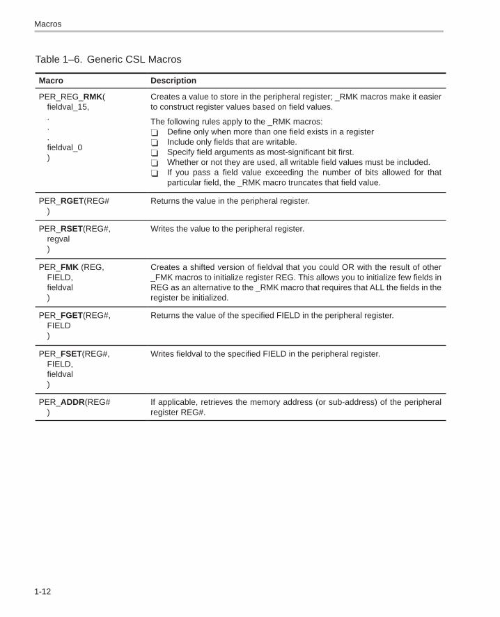
1.5 Macros
Table 1–6 provides a generic description of the most common CSL macros.The following naming conventions are used:
� PER indicates a peripheral module as listed in Table 1–1.
� REG indicates a register name (without the channel number).
� REG# indicates, if applicable, a register with the channel number.(e.g., DMPREC, DMSRC1, ...)
� FIELD indicates a field in a register.
� regval indicates an integer constant, an integer variable, a symbolicconstant (PER_REG_DEFAULT), or a merged field value created with thePER_REG_RMK() macro.
� fieldval indicates an integer constant, integer variable, macro, or symbolicconstant (PER_REG_FIELD_SYMVAL) as explained in section 1.6; allfield values are right justified.
CSL also offers equivalent macros to those listed in Table 1–6, but instead ofusing REG# to identify which channel the register belongs to, it uses the Han-dle value. The Handle value is returned by the PER_open() function. Theequivalent macros are shown in Table 1–7. Please note that REG is the regis-ter name without the channel number.
Macros
1-12
Table 1–6. Generic CSL Macros
Macro Description
PER_REG_RMK(fieldval_15,...fieldval_0)
Creates a value to store in the peripheral register; _RMK macros make it easierto construct register values based on field values.
The following rules apply to the _RMK macros:� Define only when more than one field exists in a register� Include only fields that are writable.� Specify field arguments as most-significant bit first.� Whether or not they are used, all writable field values must be included.� If you pass a field value exceeding the number of bits allowed for that
particular field, the _RMK macro truncates that field value.
PER_RGET(REG#)
Returns the value in the peripheral register.
PER_RSET(REG#,regval)
Writes the value to the peripheral register.
PER_FMK (REG,FIELD,fieldval)
Creates a shifted version of fieldval that you could OR with the result of other_FMK macros to initialize register REG. This allows you to initialize few fields inREG as an alternative to the _RMK macro that requires that ALL the fields in theregister be initialized.
PER_FGET(REG#,FIELD)
Returns the value of the specified FIELD in the peripheral register.
PER_FSET(REG#,FIELD,fieldval)
Writes fieldval to the specified FIELD in the peripheral register.
PER_ADDR(REG#)
If applicable, retrieves the memory address (or sub-address) of the peripheralregister REG#.

Macros
1-13CSL Overview
Table 1–7. Generic CSL Macros (Handle-based)
Macro Description
PER_RGETH(handle, REG)
Returns the value of the peripheral register REG associated with Handle.
PER_RSETH(handle, REG,regval)
Writes the value to the peripheral register REG associated with Handle.
PER_ADDRH(handle, REG)
If applicable, retrieves the memory address (or sub-address) of the peripheralregister REG associated with Handle.
PER_FGETH(handle, REG,FIELD)
Returns the value of the specified FIELD in the peripheral register REGassociated with Handle.
PER_FSETH(handle, REG,FIELD,fieldval)
Sets the value of the specified FIELD in the peripheral register REG to fieldval.

Symbolic Constant Values
1-14
1.6 Symbolic Constant Values
To initialize values in your application code, the CSL provides symbolicconstants for registers and writable field values as described in Table 1–8. Thefollowing naming conventions are used:
� PER indicates a peripheral module as listed in Table 1–1.
� REG indicates a peripheral register.
� FIELD indicates a field in the register.
� SYMVAL indicates the symbolic value of a register field as listed inAppendix A.
Table 1–8. Generic CSL Symbolic Constants
(a) Constant Values for Registers
Constant Description
PER_REG_DEFAULT Default value for a register; corresponds to the register value after areset or to 0 if a reset has no effect.
(b) Constant Values for Fields
PER_REG_FIELD_SYMVAL Symbolic constant to specify values for individual fields in the indicatedperipheral register. See Appendix A for the symbolic values.
PER_REG_FIELD_DEFAULT Default value for a field; corresponds to the field value after a reset or to0 if a reset has no effect.

Resource Management and the Use of CSL Handles
1-15CSL Overview
1.7 Resource Management and the Use of CSL Handles
The CSL provides limited support for resource management in applicationsthat involve multiple threads, reusing the same multichannel peripheral de-vice.
Resource management in the CSL is achieved through calls to the PER_openand PER_close functions. The PER_open function normally takes a channel/port number as the primary argument. It then returns a pointer to a Handlestructure that contains information about which channel (DMA) or port(MCBSP) was opened.
When given a specific channel/port number, the open function checks a globalflag to determine its availability. If the port/channel is available, it returns apointer to a predefined Handle structure for this device.
If the device has already been opened by another process, an invalid Handleis returned with a value equal to the CSL symbolic constant, INV.
Calling PER_close frees a port/channel for use by other processes.PER_close clears the in_use flag and resets the port/channel.
Note:
All CSL modules that support multiple ports or channels, such as MCBSP,TIMER, DAT, and DMA, require a device Handle as primary argument tomost functions. For these functions, the definition of a PER_Handle objectis required.
1.7.1 Using CSL Handles
CSL Handle objects are used to uniquely identify an opened peripheral chan-nel/port or device. Handle objects must be declared in the C source, and initial-ized by a call to a PER_open function before calling any other API functionsthat require a handle object as argument.For example:
DMA_Handle myDma; /* Defines a DMA_Handle object, myDma */
Once defined, the CSL Handle object is initialized by a call to PER_open:
.
.myDma = DMA_open(DMA_CHA0,DMA_OPEN_RESET);
/* Open DMA channel 0 */

Resource Management and the Use of CSL Handles
1-16
The call to DMA_open initializes the handle, myDma. This handle can then beused in calls to other API functions:
DMA_start(myDma); /* Begin transfer */...DMA_close(myDma); /* Free DMA channel */

Support for Device-Specific Features
1-17CSL Overview
1.8 Support for Device-Specific Features
Not all C54x peripherals offer the same type of features across the C54x de-vices. Table 1–9 lists specific features that are not common across the C54xfamily and the devices that support these features. References to Table 1–9will be found across the CSL documentation.
Table 1–9. Device-Specific Features Support
(a) DMA Module-Channel Reload
Individual Channel RegisterReload Support
Global Channel Register ReloadSupport
5416, 5421, 5409a, 5410a, 5440,5441
All other C54x supported devices
(b) DMA Module-Extended Data Reach
Individual Channel ExtendedData Memory Support
Global Extended Data MemorySupport
No Extended Data MemorySupport
5440, 5441 5409, 5416, 5421, 5409a, 5410a 5402, 5404, 5407, 5410, 5420,5455
(c) MCBSP Module-Channel Support
MCBSP 128–Channel Support MCBSP 32-Channel Support
5416, 5421, 5440, 5409a, 5410a,5441
All other C54x supported devices
(d) Watchdog Module
Watchdog Timer Support No Watchdog Timer Support
5440, 5441 All other C54x supported devices
(e) Timer Module
Timer Extended Pre-Scaler Support
No Timer Extended Pre-ScalerSupport
5471, 5441 All other C54x supported devices
(f) Chip Module
Device ID Support No Device ID Support
5416, 5409A, 5410A, 5441, 5421 All other C54x supported devices

2-1
How To Use CSL
This chapter provides instructions on how to:
� Use the TMS320C54x CSL Graphic User Interface (GUI) integrated intothe DSP/BIOS Configuration Tool. It describes a detailed work-flow for set-ting and accessing the CSL GUI data via the generation of C code files.The examples shown in this chapter include a complete procedure forcreating configuration objects and generating peripheral pre-initialization.
� Use the CSL library without the use of the CSL GUI (see section 2.3).
Topic Page
2.1 Overview 2-2. . . . . . . . . . . . . . . . . . . . . . . . . . . . . . . . . . . . . . . . . . . . . . . . . . . . .
2.2 Using CSL with the CSL GUI 2-3. . . . . . . . . . . . . . . . . . . . . . . . . . . . . . . . . . .
2.3 Using CSL without the CSL GUI 2-17. . . . . . . . . . . . . . . . . . . . . . . . . . . . . . .
2.4 Rebuilding CSL 2-26. . . . . . . . . . . . . . . . . . . . . . . . . . . . . . . . . . . . . . . . . . . . . .
Chapter 2

Overview
2-2
2.1 Overview
There are two methods to configure peripherals when using CSL:
� Manually configure the peripherals by declaring/initializing objects andinvoking the CSL functions inside your C source code.
� Configure peripherals by using the CSL GUI.
The CSL GUI, integrated under the DSP/BIOS configuration tool, provides thebenefit of a visual tool that allows you to view the chosen register settings, anddetermine which flags/options have been set by a particular mode selection.With CSL GUI, code for the configuration settings is automatically created andstored in a C source file that is integrated directly into your application.
It is not possible to configure all peripherals via the CSL GUI. Only peripheralsrequiring initial static configurations are supported. Please refer to Table 1–1,on page 1-4, for the list of peripherals supported by the CSL GUI.

Using CSL with the CSL GUI
2-3How To Use CSL
2.2 Using CSL with the CSL GUI
2.2.1 CSL GUI: The CSL Tree
The CSL GUI, integrated under the DSP/BIOS Configuration tool tree, allowsyou to configure some, but not all, of the on-chip peripherals. Each peripheralis represented as a subdirectory of the CSL Tree as shown in Figure 2–1.
Figure 2–1. CSL Tree (for 5402)
Figure 2–2 shows an example of the expanded CSL Tree.

CSL GUI: The CSL Tree
2-4
Figure 2–2. Expanded CSL Tree (for C5402)
Each peripheral is organized into two sections (see Figure 2–2):
� PERIPHERAL Configuration Manager allows you to build and configureperipheral objects using the CSL PER_Config structure (see Table 1–5 onpage 1-9). You can set the peripheral register values by selecting theoptions through the Properties pages. Several configuration objects canbe created by selecting the Insert PERCfg option from the right-click menu(see Figure 2–3). The menu options allow you to rename and delete theconfiguration object (see Figure 2–4), and to display the DependencyDialog box that allows you to determine which peripheral is using theconfiguration (see Figure 2–5).
� PERIPHERAL Resource Manager allows you to bind a peripheralconfiguration to a specific on-chip device, i.e., a DMA channel, a MCBSPport , or a TIMER device. The devices are displayed as pre-defined objectsand cannot be deleted or renamed. However, the Handles to these objectscan be renamed.

CSL GUI: The CSL Tree
2-5How To Use CSL
Figure 2–3. Insert Configuration Object
The Insert option allows the user to create the configuration objects. Once theobject is created, you can access the Properties Page of this configuration,which allows you to set the register values.
Figure 2–4. Delete/Rename Options

CSL GUI: The CSL Tree
2-6
The Delete option allows you to delete a configuration object. The Delete op-tion is not accessible if the configuration is used by a physical peripheral of theassociated Resource manager.
Figure 2–5. Show Dependency Option
The Show Dependency menu option shows which device/channel is usingwhat specific configuration. Once a configuration has been bound to a periph-eral, the Show Dependency option can be used to indicate which peripheralis using what particular configuration. In Figure 2–5, the “timerCfg0” configura-tion is bound to the physical timer device “Timer1” at design time (in the config-uration tool).
Note:
A configuration object cannot be deleted if there is a dependency present.

Using CSL with the CSL GUI
2-7How To Use CSL
2.2.2 Steps to configuring a peripheral using CSL GUI
This section provides an example using the 5402 device that demonstrateshow to create, open and define a configuration for a TIMER device using theCSL GUI.
When configuring a peripheral using the CSL GUI, the steps below must befollowed:
Step 1: Create the DSP/BIOS configuration file (.cdb file). In CodeComposer Studio, select File → New → DSP/BIOS Configuration(select template.cdb). Default name, Config1.cdb.
Step 2: Configure the on-chip peripherals using the CSL hierarchy tree. (seesection 2.2.3)
Step 3: Save the configuration file (.cdb file). Select File → Save as: enterthe .cdb name; for example, mytimer.cdb. This automaticallygenerates several files requested to build your project. (see section2.2.4)
Step 4: Add the .cdb file to your project:
Click on Project → Add Files to Project. Select the mytimer.cdb file.
Step 5: Add the linker command file associated with the .cdb file:
Click on Project → Add Files to Project. Select the mytimer.cmd file.
Figure 2–6 shows the project layout before and Figure 2–7 showsthe project layout after a .cdb file is created and the mytimer.cmd,mytimer.s54, and mytimer_c.c files have been added to the project.
Step 6: Modify your application code (main.c) (see section 2.2.5)

Using CSL with the CSL GUI
2-8
Figure 2–6. Code Composer Studio IDE Project Window
Figure 2–7. Code Composer Studio IDE Project Window with .cdb Project File Added

Using CSL with the CSL GUI
2-9How To Use CSL
2.2.3 TIMER Configuration Example
Because the default values (device power-on reset) are differentfrom one chip to another, it is recommended that you delete anyexisting config objects before changing the chip type under theGlobal Setting (system). This ensures that you get the right resetvalue when you want to use the default setting of the registers.
The configuration file mytimer.cdb is assumed to be created previously andopened (see section 2.2.2).
In the CCStudio Project View window (see Figure 2–8) open mytimer.cdb, andgo to the sub-folder TIMER module (CSL Folder).
Figure 2–8. CCStudio IDE Project View
Using Figure 2–9 follow these steps:
Step 1: Right-click on the TIMER Configuration Manager, insert a new con-figuration object.
Step 2: Right-click on timerCfg0 and select Properties to open the timerCfg0Properties window (as shown in Figure 2–9). Set the configurationby clicking on any of the tabs.
Step 3: Under the Timer Resource Manager, right-click on Timer1 and selectProperties to open the Timer1 Properties window (see Figure 2–9).
� Check the Open Handle to Timer and Enable pre-initialization

Using CSL with the CSL GUI
2-10
� From the pre-initialize drop-down list, select the configuration,timerCfg0.
Figure 2–9. Configuring the TIMER1 Device

Using CSL with the CSL GUI
2-11How To Use CSL
2.2.4 Files Generated by the CSL GUI
After saving the configuration file mytimer.cdb, there are a number of files gen-erated by the configuration tool:
� mytimer.cdb - An updated configuration database containing all insertedobjects and all current property settings.
� mytimercfg.h - An extern declaration of all created objects, definition ofCHIP_XXXX, plus #include of CSL module headers.
� mytimercfg_c.c - Definition and initialization of created objects. Containsfunction calls to TIMER_open and TIMER_config forpre-opened/pre-initialized objects.
� mytimercfg.sXX - Defines which DSP/BIOS elements are present andprovides initialization for those elements.
� mytimercfg.cmd - A Linker command file. Includes the CSL library and.csldata placements.
Two of these files are dedicated to the CSL and use the CSL API:
� Header file: mytimercfg.h
� Source file: mytimercfg_c.c
In this example, mytimer is your .cdb file name. The bold characters are at-tached automatically.
2.2.4.1 Header File: mytimercfg.h
This header file must be added to one of the user’s source files in order to ac-cess the CSL functions and/or objects predefined in the DSP/BIOS configura-tion tool.
This header file contains several elements:
� The definition of the chip:
#define CHIP_5402 1
� The csl header files used by the CSL tree
� The declaration list of the CSL handle objects and configuration namesdefined in the mytimer_c.c
These are declared external, and can be applied in the user’s code:
extern TIMER_Config timerCfg1;
extern TIMER_Handle hTimer1;
#include <projectcfg.h>
Figure 2–10 illustrates the setup of mytimercfg_c.c

Using CSL with the CSL GUI
2-12
Figure 2–10. Header File mytimercfg.h
/* Do *not* directly modify this file. It was *//* generated by the Configuration Tool; any *//* changes risk being overwritten. */
/* INPUT mytimer.cdb */#define CHIP_5402 1/* Include Header Files */#include <std.h>#include <hst.h>#include <swi.h>#include <tsk.h>#include <log.h>#include <sts.h>#include <csl_timer.h>
#ifdef __cplusplusextern ”C” {#endif
extern far HST_Obj RTA_fromHost;extern far HST_Obj RTA_toHost;extern far SWI_Obj KNL_swi;extern far TSK_Obj TSK_idle;extern far LOG_Obj LOG_system;extern far STS_Obj IDL_busyObj;extern far TIMER_Config timerCfg0;extern far TIMER_Handle htimer1;extern far void CSL_cfgInit();
#ifdef __cplusplus}#endif /* extern ”C” */
csl header files of the peripheralsimplemented under the CSL tree
The Handle and Configuration objects aredefined and can be used by other C files(user’s files).
2.2.4.2 Source File: mytimercfg_c.c
This source file consists of the Include section, the Declaration section, andthe Code section:
� Include section
This section defines the project header file. This allows mytimercfg_c.caccess to the data declared in the header file.
#include <mytimercfg.h>

Using CSL with the CSL GUI
2-13How To Use CSL
Note:
This line is added before the other CSL header files (csl_emif.h, csl_timer.h,...). This is done so that you are not required to specify the device numberunder the Project option (that –dCHIP_54xx is not required).
� Declaration section
This section defines the peripheral registration configuration structuresand the Handle objects previously defined in the CSL GUI.
� Code section
The code section is composed of a unique function, CSL_cfgInit(), asshown in Figure 2–11, which is automatically called by the DSP/BIOS bootroutine if the project.cdb is added to your project. Otherwise, you can call itlater in your main.c file.
CSL_cfgInit() prompts the tool to implement the open and configurationoptions you specify in the CSL GUI, via calls to the TIMER_open and TIM-ER_config functions.
Calls to TIMER_open() and TIMER_config() are generated when theOpen Handle to Peripheral and Enable pre-initialization options arechecked in the Properties page of the related Resource Manager (see thetimer example illustrated in Figure 2–11).
Note:
A device can be allocated/opened without being configured.
In the example shown in Figure 2–11,
� If Enable pre-initialization is checked, a call to the TIMER_config()function is generated.
� If Enable Pre-initialization is unchecked, a call to theTIMER_config()is not generated, but the configuration structure timerCfg1 is createdand available for you to use at a later time.

Using CSL with the CSL GUI
2-14
Figure 2–11.Resource Manager Properties Page
Figure 2–12 illustrates the mytimercfg_c.c file.

Using CSL with the CSL GUI
2-15How To Use CSL
Figure 2–12. Source File mytimercfg_c.c
/* generated by the Configuration Tool; any *//* changes risk being overwritten. */
/* INPUT mytimer.cdb */
/* Include Header File */#include <mytimercfg.h>
/* Config Structures */TIMER_Config timerCfg0 = { 0x0020, /* Timer Control Register */ 0x0300 /* Timer Period Register */};
/* Handles */TIMER_Handle hTimer1;
/* ======== CSL_cfgInit() ======== */void CSL_cfgInit(){ CSL_init();
hTimer1 = TIMER_open(TIMER_DEV1, TIMER_OPEN_RESET); TIMER_config(hTimer1, &timerCfg0);}
TIMER Configuration structure timerCfg0with full TIMER peripheral register values
The TIMER_open() function returns thehandle value in the handle variable hTimer1 previously declared.
TIMER_config() function sets the registervalues defined by the configuration objecttimerCfg0.
Handle hTimer1 declaration
2.2.5 Modifying Your Application Code (main.c)
The following line of code is required to access the CSL objects you predefinedwith the CSL GUI:
#include “mytimercfg.h”
This includes CSL handle and configuration declarations to your code.
mytimercfg.h automatically includes the required csl.h and csl_timer.h files.
This header file must be included before other CSL files are added.
Figure 2–13 illustrates how to access the files generated by the CSL GUI inyour application code (main.c)

Using CSL with the CSL GUI
2-16
Figure 2–13. Example of main.c File Using Data Generated by the CSL GUI
#include <mytimercfg.h>
static Uint32 TIMEREventId1;
void main() { /* Obtain the event IDs for the TIMER devices */ TIMEREventId1 = TIMER_getEventId(hTimer1); /* Enable the TIMER events */ IRQ_enable(TIMEREventId1);
/* Start the TIMERs – */ TIMER_start(hTimer1); /* Waiting for TIMER Interrupt: */ while( !IRQ_test(TIMEREventId1)); /* Close TIMER */ TIMER_close(hTimer1); }
Handle object “hTimer1” is used directly bythe TIMER CSL APIs.
This line allows the objects created with theCSL GUI tool to be referenced here.The header file must be included beforeany other CSL header files; otherwise,the -dCHIP_XXXX option must be set inthe compiler option window.

Using CSL without the CSL GUI
2-17How To Use CSL
2.3 Using CSL without the CSL GUI
You may choose to manually declare and initialize the peripheral configurationobjects within the C source. This means that you are not required to use theCSL GUI when working with the CSL library. However, it is highly recom-mended that you use the CSL GUI, particularly if your application involves in-terrupt management, and there are other components of DSP/BIOS present.
This section provides an example of using CSL without the CSL GUI and with-out a .cdb file. The CSL GUI merely assists in generation of the CSL configura-tion structures and provides the option to open and configure peripherals. Thiscan equally be done using the CSL macros and functions directly.
There are two ways to program peripherals using CSL:
� Register-based configuration (PER_config()): Configures peripheralsby setting the full values of memory-map registers. Compared to function-al parameter-based configurations, register-based configurations requireless cycles and code size, but are not abstracted.
� Functional parameter-based configuration (PER_setup()): Config-ures peripherals via a set of parameters. Compared to register-based con-figurations, functional parameter-based configurations require morecycles and code size, but are more abstracted.
The following example illustrates the use of CSL to initialize DMA channel 0and to copy a table from address 0x3000 to address 0x2000 using the registerbased configuration (DMA_config())
Source address: 2000h in data spaceDestination address: 3000h in data spaceTransfer size: Sixteen 16-bit single words

Using CSL without the CSL GUI
2-18
2.3.1 Using the DMA_config() functionThe steps below use the DMA_config() function to initialize the registers:
Step 1: Include the csl.h and the header file of the module/peripheral you willuse <csl_dma.h>. The different header files are shown in Table 1–1.
#include <csl.h>
#include <csl_dma.h>
// Example-specific initialization#define N 16 // block size to transfer
#pragma DATA_SECTION(src,”table1”) /* scr data table address */Uint16 src[N] = { 0xBEEFu, 0xBEEFu, 0xBEEFu, 0xBEEFu, 0xBEEFu, 0xBEEFu, 0xBEEFu, 0xBEEFu, 0xBEEFu, 0xBEEFu, 0xBEEFu, 0xBEEFu, 0xBEEFu, 0xBEEFu, 0xBEEFu, 0xBEEFu };
#pragma DATA_SECTION(dst, ”table2”)/* dst data table address */Uint16 dst[N];
Step 2: Define and initialize the DMA channel configuration structure.
DMA_Config myconfig = { DMA_DMACSDP_RMK(0 , 0 ,0 ,0 , 0, 0 ,1), /* DMACSDP */DMA_DMACCR_RMK(1, 1, 0, 0, 0, 0, 0, 0, 0), /* DMACCR */DMA_DMACICR_RMK(1, 1,1 , 1, 1, 1), /* DMACICR */(DMA_AdrPtr) &src, /* DMACSSAL */
0, /* DMACSSAU */ (DMA_AdrPtr)&dst, /* DMACDSAL */ 0, /* DMACDSAU */ N, /* DMACEN */ 1, /* DMACFN */ 0, /* DMACFI */ 0}; /* DMACEI */
Step 3: Define a DMA_Handle pointer. DMA_open will initialize this handlewhen a DMA channel is opened.
DMA_Handle myhDma;
void main(void) {
// .....

Using CSL without the CSL GUI
2-19How To Use CSL
Step 4: Initialize the CSL Library. A one-time only initialization of the CSLlibrary must be done before calling any CSL module API:
CSL_init(); /* Init CSL */
Step 5: For multi-resource peripherals such as McBSP and DMA, callPER_open to reserve resources (MCBSP_open(), DMA_open()...):
myhDma = DMA_open(DMA_CHA0, 0);/* Open DMA Channel 0 */
By default, the TMS320C54xx compiler assigns all data symbols wordaddresses. The DMA however, expects all addresses to be byteaddresses. Therefore, you must shift the address by 2 in order to changethe word address to a byte address for the DMA transfer.
Step 6: Configure the DMA channel by calling DMA_config() function:
myconfig.dmacssal = (DMA_AdrPtr)(((Uint16)(myconfig.dmacssal)<<1)&0xFFFF); myconfig.dmacdsal = ( DMA_AdrPtr)(((Uint16)(myconfig.dmacdsal)<<1)&0xFFFF); DMA_config(myhDma, &myConfig); /* Configure Channel */
Step 7: Call DMA_start() to begin DMA transfers:
DMA_start(myhDma); /* Begin Transfer */
Step 8: Close DMA channel
DMA_close(myhDma); /* Close channel (Optional) */ }
2.3.2 Compiling and Linking With CSL using Code Composer Studio (CCStudio)
To compile and link with CSL, you must configure the CCStudio project envi-ronment. To complete this process, follow these steps:
Step 1: Specify the target device. (Refer to section 2.3.2.1)
Step 2: Determine whether or not you are using small or large memorymodel and specify the CSL and RTS libraries you require. (Refer tosection 2.3.2.3)
Step 3: Create the linker command file (with a special .csldata section) andadd the file to the project. (Refer to section 2.3.2.4)
Step 4: Determine if you must enable inlining. (Refer to section 2.3.2.5)
The remaining sections in this chapter will provide more details and explana-tions for the steps above.

Using CSL without the CSL GUI
2-20
Note:
CCStudio will automatically define the search paths for include files and li-braries as defined in Table 2–1. You are not required to set the –i option.
Table 2–1. CSL Directory Structure
This CSL component... Is located in this directory...
Libraries c:\ti\c5400\bios\lib
Source Library c:\ti\c5400\bios\lib
Include files c:\ti\c5400\bios\include
Examples c:\ti\examples\<target>\csl
Documentation c:\ti\docs
2.3.2.1 Specifying Your Target Device
Use the following steps to specify the target device you are configuring:
Step 1: In Code Composer Studio, select Project → Options.
Step 2: In the Build Options dialog box, select the Compiler tab (seeFigure 2–14).
Step 3: In the Category list box, highlight Preprocessor.
Step 4: In the Define Symbols field, enter one of the device support symbolsin Table 1–2, on page 1-5.
For example, if you are using the 5402PG1.2 device, enterCHIP_5402PG1_2.
Step 5: Click OK.

Using CSL without the CSL GUI
2-21How To Use CSL
Figure 2–14. Defining the Target Device in the Build Options Dialog
2.3.2.2 Selecting Far/Near Mode
If you use an far-mode libraries, define far-mode for the compiler, and link withthe far-mode library (rts_ext.lib), use the following steps. Use Figure 2–15 tocomplete these steps.
Step 1: In Code Composer Studio, select Project → Options
Step 2: In the Build Options dialog box, select the Compiler Tab.
Step 3: In the Category list box, highlight advanced.
Step 4: Select Use Far Calls.
Step 5: In the Processor Version (-v) field, type 548.
Step 6: Click OK.

Using CSL without the CSL GUI
2-22
Figure 2–15. Defining Far Mode
Step 7: If you use any far-mode libraries, define far mode for the compilerand link with the far mode runtime library (rts_ext.lib). Then, youmust specify which CSL and RTS libraries will be linked in yourproject.
Step 8: In Code Composer Studio, select Project → Options
Step 9: In the Build Options dialog box, Select the Linker Tab (seeFigure 2–17).
Step 10: In the Category list, highlight Basic.
The Library search Path field (-l), should show:c:\ti\c5400\bios\lib (automatically configured by CCS)
Step 11: In the Include Libraries (-l) field, enter the correct library fromTable 1–2, on page 1-5.
For example, if you are using the 5402 device, enter csl5402.lib fornear mode or csl5402x.lib for far mode. In addition, you must includethe corresponding rts.lib or rts_ext.lib compiler runtime support li-braries.
Step 12: Click OK.

Using CSL without the CSL GUI
2-23How To Use CSL
2.3.2.3 Large/Small Memory Model Selection
If you use any large memory model libraries, define the -ml option for the com-piler and link with the large memory model runtime library (rts54x.lib) using thefollowing steps:
Step 1: In Code Composer Studio, select Project → Options.
Step 2: In the Build Options dialog box, select the Compiler Tab(Figure 2–16).
Step 3: In the Category list box, highlight advanced.
Step 4: Select Use Large memory model (-ml).
Step 5: Click OK.
Figure 2–16. Defining Large Memory Model

Using CSL without the CSL GUI
2-24
Then, you must specify which CSL and RTS libraries will be linked in your proj-ect.
� In Code Composer Studio, select Project → Options
� In the Build Options dialog box, Select the Linker Tab (see Figure 2–17).
� In the Category list, highlight Basic.
� The Library search Path field (-l), should show:c:\ti\c5400\bios\lib (automatically configured by CCStudio)
� In the Include Libraries (-l) field, enter the correct library from Table 1–2,on page 1-5.
� For example, if you are using the 5402 device, enter csl5402.lib for nearmode or csl5402x.lib for far mode. In addition, you must include the corre-sponding rts54.lib or rts54x.lib compiler runtime support libraries.
� Click OK.
Figure 2–17. Defining Library Paths

Using CSL without the CSL GUI
2-25How To Use CSL
2.3.2.4 Creating a Linker Command File
The CSL has two requirements for the linker command file:
� You must allocate the .csldata section.
CSL creates a .csl data section to maintain global data that CSL uses toimplement functions with configurable data. You must allocate this sectionwithin the base 64K address space of the data space.
� You must reserve address 0x7b in scratch pad memory
The CSL uses address 0x7b in the data space as a pointer to the .csldatasection, which is initialized during the execution of CSL_init(). For thisreason, you must call CSL_init() before calling any other CSL functions.Overwriting memory location 0x7b can cause the CSL functions to fail.
Example 2–1 illustrates these requirements which must be included in the link-er command file.
Example 2–1. Using a Linker Command File
MEMORY{
PROG0: origin = 8000h, length = 0D000hPROG1: origin = 18000h, length = 08000h
DATA: origin = 1000h, length = 04000h}
SECTIONS{
.text > PROG0
.cinit > PROG0
.switch > PROG0
.data > DATA
.bss > DATA
.const > DATA
.sysmem > DATA
.stack > DATA
.csldata > DATA
table1 : load = 6000htable2 : load = 4000h
}
2.3.2.5 Using Function Inlining
Because some CSL functions are short (they may set only a single bit field),incurring the overhead of a C function call is not always necessary. If you en-able inline, the CSL declares these functions as static inline. Using this tech-nique helps you improve code performance.

Rebuilding CSL
2-26
2.4 Rebuilding CSL
All CSL source code is archived in the file csl54xx.src located in the\C5400\bios\lib\ folder. For example, to rebuild csl5402x.lib, type the followingon the command line:
mk500 csl54xx.src -dCHIP_5402 -v548 -mf

3-1
CHIP Module
The CSL CHIP module offers general CPU functions and macros for C54x reg-ister accesses. The CHIP module is not handle-based.
Topic Page
3.1 Overview 3-2. . . . . . . . . . . . . . . . . . . . . . . . . . . . . . . . . . . . . . . . . . . . . . . . . . . . .
3.2 Functions 3-3. . . . . . . . . . . . . . . . . . . . . . . . . . . . . . . . . . . . . . . . . . . . . . . . . . . .
Chapter 3

Overview
3-2
3.1 Overview
The CSL CHIP module offers general CPU functions. The CHIP module is nothandle-based.
Table 3–1 lists the functions available as part of the CHIP module.
Table 3–1. CHIP Functions
Function Purpose See page ...
CHIP_getCpuId Returns the CPU ID field of the CSIDR register. 3-3
CHIP_getMapMode Returns the current MAP mode of the device. 3-3
CHIP_getRevId Returns the CPU revision ID. 3-4
CHIP_getSubsysId Returns sub-system ID (or core) for a multi-core device. 3-4

CHIP_getMapMode
3-3 CHIP Module
3.2 Functions
This section lists the functions in the CHIP module.
Get CPU ID (C5416, C5421, C5440, C5441 only)CHIP_getCpuId
Function Uint32 CHIP_getCpuId();
Arguments None
Return Value CPU ID Returns the CPU (CHIP) ID Field
Description This function returns the CPU (CHIP) ID field of the CSIDR register.
Example Uint32 CpuId;
CpuId = CHIP_getCpuId();
Reads the map mode bitsCHIP_getMapMode
Function Uint16 CHIP_getMapMode();
Arguments None
Return Value map mode Returns current device MAP mode, which will be one of thefollowing:� CHIP_MAP_0: MP/MC DROM and OVLY bits are OFF� CHIP_MAP_1: DROM bit is on� CHIP_MAP_2: OVLY bit is on� CHIP_MAP_3: Both DROM and OVLY Bits are on� CHIP_MAP_4: MP/MC bit is on� CHIP_MAP_5: MP/MC and DROM are on� CHIP_MAP_6: MP/MC and OVLY bits are on� CHIP_MAP_7: MP/MC, DROM, and OVLY bits are on
Description Reads the map mode bits (OVLY, DROM, MPMC) from the device. In devicesnot supported by a specific map-mode bit, the value returned is invalid. Seethe specific device data sheet for the availability of map mode bits. Thisfunction is useful for debugging purposes.
Example Uint16 MapMode;
…MapMode = CHIP_getMapMode();
if (MapMode == CHIP_MAP_0) {
/* do map 0 tasks /
} else {
/* do map 1 tasks */
}

CHIP_getRevId
3-4
Get revision ID (C5416, C5421 only)CHIP_getRevId
Function Uint32 CHIP_getRevId();
Arguments None
Return Value Revision ID Returns CPU revision ID
Description This function returns the CPU revision ID as determined by the Revision IDfield of the CSIDR register.
Example Uint32 RevId;
RevId = CHIP_getRevId();
Get subsystem ID (C5421, C5440, C5441 only)CHIP_getSubsysId
Function Uint32 CHIP_getSubsysId();
Arguments None
Return Value Subsytem ID
Description Get the sub-system ID (or core) from a multi-core device from the CSIDRregister.
Example Uint32 RevId;
RevId = CHIP_getSubsysId();

4-1
DAA Module
This chapter contains general descriptions for the DAA (Data Access Arrange-ment) configuration structures, functions, and macros.
Topic Page
4.1 Overview 4-2. . . . . . . . . . . . . . . . . . . . . . . . . . . . . . . . . . . . . . . . . . . . . . . . . . . . .
4.2 Configuration Structures 4-4. . . . . . . . . . . . . . . . . . . . . . . . . . . . . . . . . . . . . .
4.3 Functions 4-7. . . . . . . . . . . . . . . . . . . . . . . . . . . . . . . . . . . . . . . . . . . . . . . . . . . .
4.4 Macros 4-11. . . . . . . . . . . . . . . . . . . . . . . . . . . . . . . . . . . . . . . . . . . . . . . . . . . . . .
Chapter 4

Overview
4-2
4.1 Overview
The on-chip DAA (Data Access Arrangement) is the system (digital) side of atwo-chip integrated DAA solution that provides a programmable line interfaceto meet global telephone line requirements. The DAA has built in A/D and D/Aconverters for telephone line data and these converters interface to the DSPcore through a dedicated DSP serial port (McBSP #2).
Programming of the DAA registers is implemented through the same serialport. This eliminates the need for an isolation transformer, relays, opto–isola-tors, and a 2 to 4-wire hybrid, and reduces the cost of discrete componentsrequired to achieve compliance with global regulatory requirements.
Note:
This DAA chip requires the line (analog) side DAA (Silicon Labs Si3016) foroperation.
4.1.1Configuration Structures
Table 4–1. DAA Configuration Structures
Configuration Structure Purpose See page ...
DAA_CircBufCtrl Circular buffer control structure 4-4
DAA_Params Parameters structure 4-4
DAA_PrivateObject/DAA/DAA_Handle
Private object/Handle structure 4-5
DAA_DevSetup Device setup structure 4-6
DAA_Setup DAA setup structure 4-6

Overview
4-3DAA Module
4.1.2 Functions
Table 4–2. DAA Functions
Functions Purpose See page ...
DAA_setup Sets up DAA devices 4-7
DAA_close Stops a DAA function 4-8
DAA_reset Hardware reset function for the on-chip DAA 4-8
DAA_readWrite DAA read/write function 4-9
DAA_availability Returns available words in the circular buffer 4-9
DAA_resetInternalBuffer Resets the pointers of the internal circular buffer 4-9
DAA_delay Implements a delay count of McBSP frame syncs 4-10
DAA_isr DAA interrupt service routine 4-10
4.1.3 Macros
Table 4–3. DAA Macros
Macros Purpose See page ...
DAA_RGETH Macro to read DAA register 4-11
DAA_RSETH Macro to write a value to a DAA register 4-11
DAA_ADDR Returns a DAA register address 4-12
DAA_FMK Returns a 16-bit register value for REG with FIELD set to VAL 4-12

DAA_CircBufCtrl
4-4
4.2 Configuration Structures
(Example of structures are included in the Functions section)
DAA Circular Buffer Control StructureDAA_CircBufCtrl
MembersInt16 *pBuffer /* pointer to the beginning of the circular buffer */Uint16 bufSize /* size of the circular buffer */Int16 *pHead /* pointer for reading data from Rx Interrupt */Int16 *pTail /* pointer for writing data from Tx Interrupt */Int16 *pCurrent /* pointer for reading/writing data for the user */Uint16 isOverflow /* private flag for overflow */Uint16 circBufOffset /* initial circular buffer offset */
Description The user must create this circular buffer control structure, and include it in theDAA private object structure (DAA_PrivateObject). The structure is initializedby the DAA_setup(…) function. One circular buffer control structure must becreated for each DAA device.
DAA Parameters StructureDAA_Params
MembersUint16 txAttenuation /* analog transmit attenuation, valid attenuation
/* values are: */DAA_GCR_ATX_ATT_0dbDAA_GCR_ATX_ATT_3dbDAA_GCR_ATX_ATT_6dbDAA_GCR_ATX_ATT_9dbDAA_GCR_ATX_ATT_12dbUint16 rxGain /* cid receive attenuation/analog receive gain,
/* valid *//* attenuation/gain values are: */
DAA_GCR_ARX_ATT_0dbDAA_GCR_ARX_ATT_1dbDAA_GCR_ARX_ATT_2.2dbDAA_GCR_ARX_ATT_3.5dbDAA_GCR_ARX_ATT_5dbDAA_GCR_ARX_GAIN_0dbDAA_GCR_ARX_GAIN_3dbDAA_GCR_ARX_GAIN_6dbDAA_GCR_ARX_GAIN_9dbDAA_GCR_ARX_GAIN_12dbUint16 sampleRateReg7 /* sample rate control – register 7,
/* valid values are: */DAA_SRCTRL_SRC_7200

DAA_PrivateObject/DAA_Handle
4-5
DAA_SRCTRL_SRC_8000DAA_SRCTRL_SRC_8229DAA_SRCTRL_SRC_8400DAA_SRCTRL_SRC_9000DAA_SRCTRL_SRC_9600DAA_SRCTRL_SRC_10286Uint16 sampleRateReg8 /* sample rate control – register 8 */Uint16 sampleRateReg9 /* sample rate control – register 9 */Uint16 sampleRateReg10 /* sample rate control – register 10*/Uint16 ictrl1 /* international control register 1 value */Uint16 ictrl2 /* international control register 2 value */Uint16 ictrl3 /* international control register 3 value */
/* pre-defined country-specific macros for the three *//* international control registers are: */
DAA_AUSTRALIADAA_BULGARIADAA_CHINADAA_CTR21 (Europe)DAA_ CZECH_REPUBLICDAA_FCC (same as DAA_USA)DAA_ HUNGARYDAA_JAPANDAA_ MALAYSIADAA_ NEW_ZEALANDDAA_ PHILIPPINESDAA_ POLANDDAA_ SINGAPOREDAA_ SLOVAKIADAA_SLOVENIADAA_SOUTH_AFRICADAA_SOUTH_KOREADAA_USA
Description The user must create this DAA parameters structure, initialize all members,and include it in the DAA single device setup structure (DAA_DevSetup). Oneparameter structure may be used for multiple DAA devices.
Private Object/Handle StructureDAA_PrivateObject/DAA_Handle
MembersMCBSP_Handle mcbspHandle /* McBSP 2 Handle */Int16 state /* current control and read/write state */Uint16 regRequest /* DAA register request – read or write */CSLBool isIORegReady /* Flag to indicate register IO complete */Uint16 regValue /* Value of DAA register value just read or to
/* be written */Uint16 regIndex /* Index of DAA register value just read or to
/* be written */Uint16 buffLength /* buffer length for DAA read/write function */

DAA_DevSetup
4-6
Int16 delayCount /* counter used to implement delay based on/* sampling rate */
Void *pID /* void pointer to channel ID */DAA_CallBack dataCallBack /* DAA data callback function pointer */DAA_CallBack ctrlCallBack /* DAA control callback function pointer */DAA_CircBufCtrl daaCircBufCtrl /* circular buffer ctrl structure */
Description The user must create this private object/handle structure, initialize allmembers, and include it in the DAA single device setup structure(DAA_DevSetup). One private object structure must be created for each DAAdevice. This private object/handle serves as the state machine for the DAAdevice.
DAA Single Device Setup StructureDAA_DevSetup
MembersDAA_Params *params /* DAA parameters (initial register values) */DAA_Handle daaHandle /* pointer to DAA private object created by user */Uint16 mcbspPort /* MCBSP port the DAA is connected to */
/* MCBSP_PORT2 (for internal DAA) */Int16 *pCircBuf /* pointer to the user-allocated circular buffer */Uint16 circBufSize /* circular buffer size */Uint16 circBufOffset /* Initial circular buffer offset */Uint16 dataLength /* Length of data buffer (callback size) */Void *pID /* void pointer to device ID */DAA_CallBack dataCallBack /* pointer to user-defined data callback function */DAA_CallBack ctrlCallBack /* pointer to user-defined control callback function */DAA_RstFxn reset /* pointer to DAA hardware reset control function */
/* for internal DAA, use &DAA_reset */
Description The user must create this single device setup structure, initialize all members,and include it in the DAA setup structure (DAA_Setup). One device structuremust be created for each DAA device. The DAA setup structure is passed tothe function DAA_setup(..).
DAA Setup StructureDAA_Setup
MembersUint16 numDevs /* number of devices to be set up, must be greater
/* that 0 */DAA_DevSetup **dev /* pointer to array of device setup structure
/* pointers */
Description The user must create DAA setup structure, initialize all members, and pass itto the DAA setup function, DAA_setup(..).

void DAA_setup
4-7
4.3 Functions
Pointer to DAA setup structurevoid DAA_setup
Arguments DAA_Setup *
Return Value None
Description This function sets up a number of DAA devices according to the value ofnumDevs in the setup structure and initializes the state machines. Thefunction enables the IMR fields for the DAA interrupts. However, it is theresponsibility of the user to plug the corresponding DAA ISRs into the vectortable. Each of these user ISRs must call the function DAA_isr(…). Note thatthis function takes a pointer to a DAA private object as it’s argument. Thisfunction makes calls to the CSL MCBSP module.
Important: The DAA_DevSetup structure passed through the DAA_Setupstructure to this function defines a data callback length.As soon as interruptsare globally enabled, following a call to this function, the state machine startsinvoking data callbacks whenever it has the specified number of words in thecircular buffer.
Example DAA_DevSetup setupStruct ={
&daaParams,
&daaPrivateObject,
MCBSP_PORT2,
circBuff,
40,
5,
10,
(void *)0,
(DAA_CallBack)&dataCB,
(DAA_CallBack)&ctrlCB,
&DAA_reset
};
DAA_DevSetup *devArray[] = {&devSetup};
DAA_Setup setup = {
1,
devArray

DAA_close
4-8
};
DAA_setup(&setup);
void dataCB(void* pID, Arg task, Uns result)
{
/* submit next readwrite request */
DAA_readWrite(handle, dataBuff, 10);
/* Post buffer processing function */
}
Handle to DAA deviceDAA_close
Arguments DAA_Handle
Return Value None
Description This function stops the DAA device operation. The function also closes thecorresponding McBSP port.
Example DAA_Handle handle;
DAA_close(handle);
DAA flag to select hardwareDAA_reset
Arguments Uint16 Flag to select hardware reset (1) /unreset (0).
Return Value None
Description Flag to select hardware reset (1) /unreset (0). It is used during the setupoperation (DAA_setup(…)). This address of this function should be passed tothe setup function for the on-chip DAA.
Example See example in 2.0.

DAA_resetInternalBuffer
4-9
Copies size words from the data read/write bufferDAA_readWrite
Arguments DAA_Handle Handle to DAA deviceInt16 * Pointer to data read/write bufferUint16 Size of data read/write buffer
Return Value Int16 Number of received words in buffer. Zero is returned if there is an errorin dataBuff or size arguments.
Description This function copies size words from the data read/write buffer into the internalcircular buffer for transmission and fills the buffer with size received data fromthe circular buffer. Note: This function does not check for how much data is inthe circular buffer. Therefore, the user must call DAA_availability to determinehow much data is available in the circular buffer before calling the function.
Example DAA_Handle handle;
Int16 buff[20];
Uint16 size = 20;
DAA_readWrite(handle, buff, size);
Returns available words in the circular bufferDAA_availabilty
Arguments DAA_Handle Handle to DAA device
Return Value Int16 Number of available words in circular buffer.
Description This function returns the number of available (received) words in the circularbuffer.
Example DAA_Handle handle;
Int16 bufCount;
BufCount = DAA_availability(handle);
Resets the pointers of the internal circular bufferDAA_resetInternalBuffer
Arguments DAA_Handle Handle to DAA device
Return Value None.
Description This function resets the pointers of the internal circular buffer. This action isequivalent to clearing out the buffer.
Example DAA_Handle handle;
DAA_resetInternalBuffer(handle);

DAA_delay
4-10
Implements a delay of count McBSP frame syncsDAA_delay
Arguments DAA_Handle Handle to DAA deviceUint16 Number of McBSP frame-syncs to delay for
Return Value CSLBool TRUE Indicates “Accepted” and FALSE “rejected”.
Description This function requests a delay of length count McBSP frame syncs. Thefunction returns immediately with an indication of whether the request wasaccepted (TRUE) or rejected (FALSE). If accepted, the user defined controlcallback will be invoked when the delay is done with a flag of“_DAA_DELAY”.If not, the user must keep invoking the function until it is accepted.
Example Void main(void)
{
DAA_Handle handle;
Uint16 delay;
While(!DAA_delay(handle, delay));
……
}
void ctrlCB(void* pID, Uint16 task, Uint16 arg)
{
if (task & _DAA_DELAY)
{
printf(“delay is done!\n”);
}
}
DAA interrupt service routineDAA_isr
Arguments DAA_Handle Handle to DAA device
Return Value None.
Description This is the DAA state machine and must be invoked on every DAA receiveinterrupt.
Example DAA_Handle handle;
Interrupt void myDAAIsr(void)
{
DAA_isr(handle);
}

DAA_RSETH
4-11
4.4 Macros
Macros used to read a DAA registerDAA_RGETH
Arguments DAA_Handle Handle to DAA deviceReg DAA register name
Return Type CSLBool TRUE Indicates “Accepted” and FALSE “rejected”.
Description This macro reads a DAA register. The macro returns immediately with anindication of whether the request was accepted (TRUE) or rejected (FALSE).If accepted, the user defined control callback will be invoked when the registerread is done with a flag of “_DAA_REG_READ”. If not, the user must keepinvoking the macro until it is accepted.
Example Void main(void)
{
DAA_Handle handle;
While(!DAA_RGETH(handle, DAACTRL1));
……}
void ctrlCB(void* pID, Uint16 task, Uint16 arg)
{
if (task & _DAA_REG_READ)
{
printf(“DAA control 1 register has a value of
%d\n”, &arg);
}
}
Macro used to write a value to a DAA registerDAA_RSETH
Arguments DAA_Handle Handle to DAA deviceREG DAA register nameVAL Register value to be written
Return Type CSLBool TRUE Indicates “Accepted” and FALSE “rejected”.
Description This macro writes a value to a DAA register. The macro returns immediatelywith an indication of whether the request was accepted (TRUE) or rejected(FALSE). If accepted, the user defined control callback will be invoked whenthe register write is done with a flag of “_DAA_REG_WRITE”. If not, the usermust keep invoking the macro until it is accepted.

DAA_ADDR
4-12
Example Void main(void)
{
DAA_Handle handle;
Uint16 val = DAA_DAACTRL1_OH_OFFHOOK;
/* Take DAA off-hook */
While(!DAA_RSETH(handle, DAACTRL1, val));
…
…
}
void ctrlCB(void* pID, Uint16 task, Uint16 arg)
{
if (task & _DAA_REG_WRITE)
{
printf(“DAA control 1 register write
complete!\n”);
}
}
Macro used to return the address of a DAA registerDAA_ADDR
Arguments REG DAA register name e.g SRCTRL
Return Type REGADDR Register address
Description This macro returns the address of a DAA register.
Example reg5Addr = DAA_ADDR(DAACTRL1);
Macro used to return 16-bit register valuesDAA_FMK
Arguments REG DAA register nameFIELD Field nameVAL Field value
Return Type REGADDR Register address
Description This macro returns a 16-bit register value for REG with FIELD set to VAL.
Example offHook = DAA_FMK(DAACTRL1, OH, 1);

5-1
DAT Module
The handle-based DAT (data) module allows you to use DMA hardware tomove data.
Topic Page
5.1 Overview 5-2. . . . . . . . . . . . . . . . . . . . . . . . . . . . . . . . . . . . . . . . . . . . . . . . . . . . .
5.2 Functions 5-4. . . . . . . . . . . . . . . . . . . . . . . . . . . . . . . . . . . . . . . . . . . . . . . . . . . .
Chapter 5

Overview
5-2
5.1 Overview
The handle-based DAT (data) module allows you to use DMA hardware tomove data. This module works the same for all devices that support DMA re-gardless of the type of DMA controller; therefore, any application code usingthe DAT module is compatible across all devices as long as the DMA supportsthe specific address reach and memory space.
The DAT copy operations occur on dedicated DMA hardware independent ofthe CPU. Because of this asynchronous nature, you can submit an operationto be performed in the background while the CPU performs other tasks in theforeground. Then you can use the DAT_wait() function to block completion ofthe operation before moving to the next task.
Since the DAT module uses the DMA peripheral, it cannot use a DMA channelthat is already allocated by the application. To ensure this does not happen,you must call the DAT_open() function to allocate a DMA channel for exclusiveuse. When the module is no longer needed, you can free the DMA resourceby calling DAT_close().
Table 5–1 lists the functions for use with the DAT modules. The functions arepresented in the order that they will typically be used in an application.
Note:
1) Multiplexing Across Different Devices:To simplify the Interrupt multiplexing across different devices, the C54xDAT module uses only DMA channels 2 and 3.
2) Memory Spaces:The DAT module contains functions to copy data from one location toanother and to fill a region of memory in program, data, or I/O space validfor the specific device (Refer to the C54x data sheets). CSL does not per-form any searches for invalid memory addresses.

Overview
5-3DAT Module
Table 5–1. DAT Functions
Function Purpose See page ...
DAT_close() Closes a DAT channel 5-4
DAT_copy() Copies a linear block of data from src to dst using DMA hardware 5-4
DAT_copy2D() Copies 2D data from src to dst using DMA hardware 5-6
DAT_fill() Fills a linear block of memory with the specified fill value using DMAhardware
5-8
DAT_open() Opens a DAT channel 5-9
DAT_wait() Waits for a previous transfer to complete 5-10

DAT_close
5-4
5.2 FunctionsThis section describes, in alphabetical order, the functions in the DAT module.
Closes the DAT moduleDAT_close
Function void DAT_close(DAT_Handle hDat
);
Arguments hDat Handle to a DAT channel (obtained via DAT_open)
Return Value None
Description Closes a DAT channel previously opened with DAT_open(). Any pendingrequests are first allowed to complete.
Example DAT_close(hDat);
Copies linear block of data from src to dstDAT_copy
Function Uint16 DAT_copy(DAT_Handle hDat,
Uint32 src, Uint32 dst, Uint16 ElemCnt);
Arguments hDat Handle to a DAT channel (obtained via DAT_open)src Source address ORed with any of the following memory space symbols:
� DAT_PROGRAM_SPACE�(Not valid for devices 5402, 5471,and 5472)
� DAT_DATA_SPACE� DAT_IO_SPACE�(Not valid for devices 5402, 5471,
and 5472)
For example: � 0x10000 | DAT_PROGRAM_SPACE indicates address 0x10000 in program space � 0x10000 | DAT_DATA_SPACE indicates address 0x10000 in
data space � 0x100 | DAT_IO_SPACE indicates address 0x100 in I/O space;

DAT_copy
5-5 DAT Module
dst Destination address ORed with a memory space symbolElemCnt Number of 16-bit words to copy
Return Value DMA status Returns status of data transfer at the moment of exiting theroutine:
0: transfer complete1: on-going transfer
Description Copies a linear block of data from src to dst using DMA hardware.
You must open the DAT channel with DAT_open() before calling this function.You can use the DAT_wait() function to poll for the completed transfer of data.
Example #define DATA_SIZE 256 // number of 16-bit elements to transfer
Uint16 BuffA[DATA_SIZE];
Uint16 BuffB[DATA_SIZE];
DAT_Handle hDat;
main() {
…hDat = DAT_open(DAT_CHA_ANY,DAT_PRI_LOW,0);
DAT_copy(
hDat,
(Uint32) (&BuffA) | DAT_DATA_SPACE,
(Uint32) (&BuffB) | DAT_DATA_SPACE,
DATA_SIZE
);
…}

DAT_copy2D
5-6
Copies data from src to dstDAT_copy2D
Function Uint16 DAT_copy2D(DAT_Handle hDat,Uint16 Type,
Uint32 src,Uint32 dst,
Uint16 LineLen, Uint16 LineCnt, Uint16 LinePitch);
Arguments hDat Handle to a DAT channel (obtained via DAT_open)Type Type of 2D DMA transfer, must be one of the following:
� DAT_1D2D : 1D to 2D transfer� DAT_2D1D : 2D to 1D transfer� DAT_2D2D : 2D to 2D transfer
src Pointer to source ORed with any of the following memory space symbols:
� DAT_PROGRAM_SPACE�(Not valid for devices 5402, 5471,and 5472)
� DAT_DATA_SPACE� DAT_IO_SPACE�(Not valid for devices 5402, 5471,
and 5472)
For example:
� 0x10000 | DAT_PROGRAM_SPACE indicates address0x10000 in program space;
� 0x10000 | DAT_DATA_SPACE indicates address 0x10000 in data space;
� 0x100 | DAT_IO_SPACE indicates address 0x100 in I/Ospace;
dst Pointer to destination address ORed with a memory space symbol
LineLen Number of 16-bit words to copy for each line LineCnt Number of lines to copyLinePitch Pitch of each line, number of 16-bit words
Return Value DMA status Returns status of data transfer at the moment of exiting the

DAT_copy2D
5-7 DAT Module
routine: 0: transfer complete
1: on-going transfer
Description This function copies 2D data from src to dst using DMA hardware.
You must open the DAT channel with DAT_open() before calling this function.You can use the DAT_wait() function to poll for the completed transfer of data.
Example #define DATA_SIZE 256
Uint16 BuffA[DATA_SIZE];
Uint16 BuffB[DATA_SIZE];
DAT_Handle hDat;
main(){
…hDat = DAT_open(DAT_CHA_ANY,DAT_PRI_LOW,0);
DAT_copy2D(
hDat,
DAT_2D2D,
(Uint32) (&BuffA) | DAT_DATA_SPACE,
(Uint32) (&BuffB) | DAT_DATA_SPACE,
10,20,10
);
…}

DAT_fill
5-8
Fills linear block of memory with specified fill valueDAT_fill
Function Uint16 DAT_fill(DAT_Handle hDat;
Uint32 dst, Uint16 ElemCnt, Uint32 Value);
Arguments hDat Handle to a DAT channeldst Destination address ORed with any of the following memoryspace symbols: � DAT_PROGRAM_SPACE
� DAT_DATA_SPACE� DAT_IO_SPACE
For example:� 0x10000 | DAT_PROGRAM_SPACE indicates address
0x1000 in program space; � 0x10000 | DAT_DATA_SPACE indicates address
0x10000 in data space; � 0x100 | DAT_IO_SPACE indicates address 0x100 in
I/Ospace;
ElemCnt Number of bytes to fill (must be power of 2)Value fill value
Return Value DMA status Returns status of data transfer at the moment of exiting theroutine:
0: transfer complete1: on-going transfer
Description Fills a linear block of memory with the specified fill value using DMA hardware.
You must open the DAT channel with DAT_open() before calling this function.You can use the DAT_wait() function to poll for the completed transfer of data.
Example #define BUFF_SIZE 256;
Uint16 Buff[BUFF_SIZE];
Uint32 FillValue = 0xA5A5;
DAT_Handle hDat;
…hDat = DAT_open(DAT_CHA_ANY,DAT_PRI_LOW,0);
DAT_fill(
hDat, (Uint32)(&Buff) | DAT_DATA_SPACE, BUFF_SIZE,
FillValue
);

DAT_open
5-9 DAT Module
Opens a DAT moduleDAT_open
Function DAT_Handle DAT_open( int ChaNum, int Priority, Uint32 Flags);
Arguments ChaNum Specifies which DMA channel to allocate; must be one of thefollowing:� DAT_CHA_ANY (allocates Channel 2 or 3)� DAT_CHA2� DAT_CHA3
Priority Specifies the priority of the DMA channel, must be one of thefollowing:� DAT_PRI_LOW sets the DMA channel for low priority level� DAT_PRI_HIGH sets the DMA channel for high priority level
Flags Miscellaneous open flags (currently None available).
Return Value Handle for DAT channel. If the requested DMA channel is currently being used,an INV(-1) value is returned.
Description Opens the DAT module. You must call this function before using any of theother DAT API functions. The ChaNum argument specifies which DMAchannel to open for exclusive use by the DAT module. Currently, no flags aredefined and the argument should be set to zero.
Example 1 To open a DAT channel using any available DMA channel (2 or 3 only) in lowpriority mode:DAT_Handle hdat;
hdat = DAT_open(DAT_CHA_ANY,DAT_PRI_LOW,0);
Example 2 To open the DAT channel using DMA channel 2 in high priority mode:DAT_Handle hdat;
hdat = DAT_open(DAT_CHA2,DAT_PRI_HIGH,0);

DAT_wait
5-10
Waits for previous transfer to completeDAT_wait
Function void DAT_wait( DAT_Handle hDat);
Arguments hDat Handle to a DAT channel
Return Value None
Description This function polls the IFR flag to see if the DMA channel has completed atransfer. If the transfer is already completed, the function returns immediately.If the transfer is not complete, the function waits for completion of the transferas identified by the handle; interrupts are not disabled during the wait.
Example Uint16 TransferStat;
DAT_Handle hDat;
main(){
…hDat = DAT_open(DAT_CHA_ANY, DAT_PRI_LOW, 0);
…TransferStat = DAT_copy(hDat, src,dst,len);
/* custom DAT configuration */
if (TransferStat)
DAT_wait(hDat);
...
}

6-1
DMA Module
This chapter describes the structure, functions, and macros of the DMA mod-ule.
Topic Page
6.1 Overview 6-2. . . . . . . . . . . . . . . . . . . . . . . . . . . . . . . . . . . . . . . . . . . . . . . . . . . . .
6.2 Configuration Structure 6-4. . . . . . . . . . . . . . . . . . . . . . . . . . . . . . . . . . . . . . .
6.3 Functions 6-7. . . . . . . . . . . . . . . . . . . . . . . . . . . . . . . . . . . . . . . . . . . . . . . . . . . .
6.4 Macros 6-20. . . . . . . . . . . . . . . . . . . . . . . . . . . . . . . . . . . . . . . . . . . . . . . . . . . . . .
6.5 Configuring the DMA Module Using CSL GUI 6-32. . . . . . . . . . . . . . . . . . .
6.6 Examples 6-40. . . . . . . . . . . . . . . . . . . . . . . . . . . . . . . . . . . . . . . . . . . . . . . . . . .
Chapter 6

Overview
6-2
6.1 Overview
The DMA module is a handle-based module that requires a call toDMA_open() to obtain a handle before any other functions are called.
The CSL module is not the same for all C54x devices. The differences mainlyrelate to:
� Individual channel register reload support� Extended Data Memory Support
For more information regarding the DMA support in the C54x family, refer toTable 1–9 on page 1-17.
Table 6–1 lists the configuration structure for use with the DMA functions.Table 6–2 lists the functions available in the CSL DMA module.
Table 6–1. DMA Configuration Structure
Structure Purpose See page ...
DMA_Config DMA structure that contains all local registers required to set up aspecific DMA channel.
6-4
DMA_GblConfig Global DMA structure that contains all global registers that you mayneed to initialize a DMA channel
6-5
Table 6–2. DMA Functions
(a) DMA Primary Functions
Function Purpose See page ...
DMA_close() Closes a DMA channel 6-7
DMA_config() Sets up the DMA channel using the configuration structure 6-7
DMA_configArgs() Sets up the DMA channel using the register values passed in 6-8
DMA_open() Opens a DMA channel 6-10
DMA_pause() Pauses a DMA channel. Identical to DMA_stop(). 6-11
DMA_reset() Resets DMA channel register to their power-on reset value 6-11
DMA_start() Starts a DMA channel 6-11
DMA_stop() Disables a DMA channel 6-12

Overview
6-3DMA Module
Table 6–2. DMA Functions (Continued)
(b) DMA Global Register Function
Function Purpose See page ...
DMA_globalAlloc() Allocates a global DMA register 6-12
DMA_globalConfig() Sets up the DMA channel using the configuration structure 6-14
DMA_globalConfigArgs() Sets up the DMA channel using the register values passed in 6-15
DMA_globalFree() Frees a global DMA register that was previously allocated 6-16
DMA_globalGetConfig() Gets DMA global register configuration 6-17
DMA_resetGbl() Resets the DMA global registers 6-17
(c) DMA Auxiliary Functions
Function Purpose See page ...
DMA_autostart() Enables a DMA channel 6-18
DMA_getConfig() Get DMA channel configuration 6-18
DMA_getEventId() Returns the IRQ Event ID for the DMA completion interrupt 6-19

DMA_Config
6-4
6.2 Configuration StructureBecause the DMA has both local and global registers to each channel, the CSLDMA Module has two configuration structures:
� DMA_Config (channel configuration structure) contains all the localregisters required to set up a specific DMA channel.
� DMA_GblConfig (global configuration structure) contains all theglobal registers that you may need to initialize a DMA channel. Theseglobal registers are resources shared across the different DMA channelsand include element/frame indexes, reload registers, as well as src/dstpage registers.
You can use literal values or the _RMK macros to create the structure membervalues.
DMA channel configuration structureDMA_Config
Structure DMA_Config
Members Uint16 priority DMA channel priority
For devices supporting individual channel reload registers (see note) add:Uint16 autoix Provided for compatibility with older versions of DMA
For all devices add:Uint16 dmmcr DMA transfer mode control registerUint16 dmsfc DMA sync select and frame count registerDMA_AdrPtr dmsrc DMA source address registerDMA_AdrPtr dmdst DMA destination address registerUint16 dmctr DMA element count register
For devices supporting individual channel reload registers (see note) add:DMA_AdrPtr dmgsa DMA source address reloadDMA_AdrPtr dmgda DMA destination address reloadUint16 dmgcr DMA element count reloadUint16 dmgfr DMA frame count reload
For devices supporting individual channel extended data memory addressing(see note), add:Uint16 dmsrcdp data page for srcUint16 dmdstdp data page for dst
Note:
For more information concerning these devices, see section 1.8 Device-Specific Features Support.

DMA_GblConfig
6-5 DMA Module
Description This DMA configuration structure is used to set up a DMA channel. You createand initialize this structure then pass its address to the DMA_config()function. You can use literal values or the DMA_REG_RMK macros to createthe structure member values.
Example DMA_Config MyConfig = {
0, /* priority */
0x0000, /* xfrctrl */
0x0000, /* syncframe */
(DMA_AdrPtr) 0x0300, /* src */
(DMA_AdrPtr) 0x0400, /* dst */
0x00FF /* xfrcnt */
};
DMA global configuration structureDMA_GblConfig
Structure DMA_GblConfig
Members Uint16 free run free under emulation control
For devices supporting individual channel reload registers (see note) add:Uint16 autoix For compatibility with older versions of DMA
For all devices add:Uint16 gbldmsrcp global program page for srcUint16 gbldmdstp global program page for dstUint16 gbldmidx0 global element index 0Uint16 gbldmfri0 global frame index 0Uint16 gbldmidx1 global element index 1Uint16 gbldmfri1 global frame index 1
For devices not offering global channel reload registers (see note), add:DMA_AdrPtr gbldmgsa global src address reloadDMA_AdrPtr gbldmgda global dst address reloadUint16 gbldmgcr global element count reloadUint16 gbldmgfr global frame count reload
For devices supporting global extended data memory addressing (see note),add:Uint16 gbldmsrcdp; global data page for srcUint16 gbldmdstdp; global data page for dst

DMA_GblConfig
6-6
Note:
For more information concerning these devices, see section 1.8, Device-Specific Features Support.
Description You can use literal values or the DMA_REG_RMK macros to create thestructure member values.
Example 1 DMA_GblConfig MyGblConfig = {
0, /* stop under emulation control */
10, /* src program page */
20, /* dst program page */
0x1, /* index 0 */
0x4 /* frame index 0 */
0, /* index 1 */
0, /* frame index 1 */
0, /* src data page */
0 /* dst data page */
}
In this example, source and destination pages are hard-coded.
For a complete example, see Example 2 in section 6.6.
Example 2 extern DMA_AdrPtr mySrc;
extern myDst;
DMA_gblConfig myGblConfig = {
0,
0,
0,
0x1,
0x4
0,
0
};
....
myGblConfig.gbldmsrcp = (((Uint32)(&mySrc)>>16)&0xFFFFu);
myGblConfig.gbldmdstp = (((Uint32)(&myDst)>>16)&0xFFFFu);

DMA_config
6-7 DMA Module
6.3 Functions
This section describes the functions in the DMA CSL module.
6.3.1 DMA Primary Functions
Closes DMA channelDMA_close
Function void DMA_close(DMA_Handle hDma
);
Arguments hDma Handle to DMA channel; see DMA_open()..
Return Value None
Description Closes a DMA channel previously opened with DMA_open(). The registers forthe DMA channel are set to their power-on reset defaults, then the completioninterrupt is disabled and cleared.
Example DMA_close(hDma);
Sets up DMA channel using configuration structureDMA_config
Function void DMA_config(DMA_handle hDma,DMA_Config *Config
);
Arguments hDma Handle to DMA channel; see DMA_open().Config Pointer to an initialized configuration structure (See DMA_Config)
Return Value None
Description Sets up the DMA channel using the configuration structure. The values of thestructure are written to the DMA registers. To start the DMA channel, call theDMA_start() function. DMA_Config() initializes the DMA channel register, butdoes not start the DMA channel.

DMA_configArgs
6-8
Example DMA_Config MyConfig = {
0x0, /*priority */0x0000, /* mcr */
0x0000, /* sfc */
(DMA_AdrPtr) 0x0300, /* src */
(DMA_AdrPtr) 0x0400, /* dst */
0x00FF /* ctr */
};
… DMA_config(hDma,&MyConfig);
For complete examples, please refer to section 6.6, Examples.
Sets up DMA channel with register valuesDMA_configArgs
Function void DMA_configArgs(DMA_Handle hDma,Uint16 priority,
For devices supporting individual channel reload registers (see note) add:Uint16 autoix (Provided for compatibility with older versions of DMA)
For all devices add:Uint16 dmmcr,Uint16 dmsfc,Uint16 dmsrc,Uint16 dmdst,Uint16 dmctr,
For devices supporting individual channel reload registers (see note), add:Uint16 dmgsa,Uint16 dmgda,Uint16 dmgcr,Uint16 dmgfr,
For devices supporting individual channel extended data memory addressing(see note), add:
Uint16 dmsrcdp,Uint16 dmdstdp
);
Note:
For more information concerning these devices, see section 1.8, Device-Specific Features Support.

DMA_configArgs
6-9 DMA Module
Arguments hDma Handle to DMA channel; see DMA_open()priority DMA channel priority
For devices supporting individual channel reload registers (see note) add:Uint16 autoix (Provided for compatibility with older versions of DMA)
dmmcr DMA transfer mode control register valuedmsfc DMA sync select and frame count register valuedmsrc DMA source address register valuedmdst DMA destination address register valuedmctr DMA element count register value
For devices supporting individual channel reload registers (see note):dmgsa Pointer to DMA source address reload valuedmgda Pointer to DMA destination address reload valuedmgcr DMA element count reload valuedmgfr DMA frame count reload value
For devices supporting individual channel extended data memory addressing(see note), add:Uint16 dmsrcdp data page for srcUint16 dmdstdp data page for dst
Return Value None
Description Sets up the DMA channel with the register values passed to the function. Theregister values are written to the DMA registers. To start the DMA channel, youmust call the DMA_start() function. DMA_Config() initializes the DMA channelregister, but does not start the DMA channel.
You may use literal values for the arguments; or for readability, you may usethe MK macros to create the register values based on field values.
Example DMA_configArgs(hDma,
0x0000, /* channel priority */
0x0000, /* mcr */
0x0000, /* sfc */
0x0300, /* src */
0x0400, /* dst */
0x00FF /* ctr */
);
For a complete example, see Section 5.4, Example 1B.

DMA_open
6-10
Opens DMA channelDMA_open
Function DMA_Handle DMA_open(int ChaNum,Uint32 Flags
);
Arguments ChaNum DMA channel to open:DMA_CHA_ANYDMA_CHA0DMA_CHA1DMA_CHA2DMA_CHA3DMA_CHA4DMA_CHA5
Flags Open flags (logical OR of any of the following):DMA_OPEN_RESET
Return Value Device handle Handle to newly opened device
Description Opens a DMA channel. Before a DMA channel can be used, you must first callthis function to open the channel. Once opened, it cannot be opened againbefore you call DMA_close(). The return value is a unique device handle foruse in subsequent DMA API calls. If the open fails, INV is returned.
You can use this function in either of the following ways:
� Specify exactly which physical channel to open.� Use DMA_CHA_ANY to allow the library pick an unused channel.
If you specify the DMA_OPEN_RESET flag, the DMA channel registers are setto the power-on reset defaults and the channel interrupt is disabled andcleared. Use this flag when the DMA channel has been running to clean pre-viously set status and interrupt flags.
Example DMA_Handle hDma;
… hDma = DMA_open(DMA_CHA_ANY,DMA_OPEN_RESET);

DMA_start
6-11 DMA Module
Pauses DMA channelDMA_pause
Function void DMA_pause(DMA_Handle hDma
);
Arguments hDma Handle to DMA channel; see DMA_open().
Return Value None
Description Identical to DMA_stop(). This is provided for compatibility with other TMS320devices only.
Example DMA_pause(hDma);
Resets DMA channelDMA_reset
Function void DMA_reset(DMA_Handle hDma
);
Arguments hDma Handle to DMA channel; see DMA_open()..or INV (If you want to reset all DMA channel registers)
Return Value None
Description Resets the DMA channel by setting its registers to the power-on defaults anddisables and clears the channel interrupt. You can use INV as the devicehandle to reset all channels.
Example /* reset an open DMA channel /
DMA_reset(hDma);
/* reset all DMA channels */
DMA_reset(INV);
Starts DMA channelDMA_start
Function void DMA_start(DMA_Handle hDma
);
Arguments hDma Handle to DMA channel; see DMA_open().
Return Value None
Description Starts a DMA channel by setting the enable channel bits in the DMA priorityand enable control register (DMPREC) accordingly to 1. See DMA_stop().
Example DMA_start(hDma);

DMA_stop
6-12
Disables DMA channelDMA_stop
Function void DMA_stop(DMA_Handle hDma
);
Arguments hDma Handle to DMA channel; see DMA_open().
Return Value None
Description Disables the DMA channel by resetting the enable channel bits in the DMApriority and enable control (DMPREC) register accordingly. See DMA_start().
Example DMA_stop(hDma);
6.3.2 DMA Global Register Function
Performs global register allocationDMA_globalAlloc
Function Uint16 DMA_globalAlloc (Uint16 RegMask
);
Arguments RegMask Mask that indicates which global registers you want to use;must be one of the following:DMA_GBL_DMIDXANY (any global index register)DMA_GBL_DMIDX0 (global index 0)DMA_GBL_DMIDX1 (global index 1)DMA_GBL_DMFRI0 (global frame index 0)DMA_GBL_DMFRI1 (global frame index 1)DMA_GBL_RLDR (global reload registers)DMA_GBL_SRCP (global program page for src)DMA_GBL_DSTP (global program page for dst)DMA_GBL_SRCDP (global data page for src)DMA_GBL_DSTDP (global data page for dst)DMA_GBL_ALL (all global registers)
Note:
In the C54x, the DMA_GBL_DMFRIx and DMA_GBL_DMIDXx masksshould used in pairs. For example, when you use DMA_GBL_DMFRI0, youshould also use DMA_GBL_DMIDX0. Similarly both DMA_GBL_DMFRI1and DMA_GBL_DMIDX1 should be used. If you do not follow this guideline,the function allocates all registers (DMA_GBL_DMFRI0,DMA_GBL_DMFRI1, DMA_GBL_DMIDX0, DMA_GBL_DMIDX1). If youuse DMA_GBL_DMIDXANY, the function allocates any of the availableDMA_GBL_DMFRIx/DMA_GBL_DMIDXx pairs.

DMA_globalAlloc
6-13 DMA Module
Return Value RegMaskalloc Mask that indicates the global registers that are being allocated as a response to the current RegMask requests. This mask does NOT include registers requested via previous calls to DMA_globalAlloc().
If ANY of the RegMask requests cannot be fulfilled, then RegMaskAlloc equals zero.
Description Performs Global register allocation. This function returns a mask that indicatesto the DMA_global Config/ConfigArgs functions which global registers arebeing allocated for the DMA channel. If you request via RegMask a globalregister that has been previously allocated the function returns a zero.
The use of this function is considered optional. It can be used to prevent doubleallocation of registers to DMA channels. If not used, you can pass off theDMA_GBL_ALL (0xffff value) as the RegMaskAlloc parameter for theDMA_global Config/Args functions.
Example #define NOTUSED 0
DMA_GblConfig MyGblConfig = {
0, /* free emulator control */
10, /* src program page */
20, /* dst program page */
0x1, /* index 0 */
0x4 /* frame index 0 */
NOTUSED, /* index 1 */
NOTUSED /* frame index 1 */
};
.....
mask = DMA_globalAlloc (DMA_GBL_DMIDX1|DMA_GBL_DMFRI1);
DMA_globalConfig (mask, &MyGblConfig);
For a complete example, see Section 6.6, Example 2.

DMA_globalConfig
6-14
Sets up DMA global registers using configuration structureDMA_globalConfig
Function void DMA_globalConfig (Uint16 RegMaskAlloc,DMA_GblConfig *Config);
Arguments RegMaskAlloc Mask to indicate global registers to initialize. This argumentis produced by the DMA_GlobalAlloc function. A value of DMA_GBL_ALL(0xffff value) allocates all the global registersspecified in Config.
Config Pointer to an initialized global configuration structure
Return Value None
Description Sets up the DMA global registers using the global configuration structure. Thevalues of the structure are written to the DMA global registers. Since the DMAglobal registers are shared, this function will ONLY initialize the registers thathave been allocated via a DMA_globalAlloc routine and passed to this functionvia the RegMaskAlloc value. See DMA_globalAlloc.
This function is optional. It may not be necessary to use this function if noglobal resource register initialization (element/frame indexes, reload registers,and src/dst page registers) is required for the DMA transfer.
Example #define NOTUSED 0
DMA_GblConfig MyGblConfig = {
0, /* free emulator control */
10, /* src program page */
20, /* dst program page */
0x1, /* index 0 */
0x4 /* frame index 0 */
NOTUSED, /* index 1 */
NOTUSED, /* frame index 1 */
(DMA_AdrPtr) 100, /* src data page */
(DMA_AdrPtr) 101, /* dst data page */
}
.....
mask = DMA_globalAlloc (DMA_GBL_DMIDX1|DMA_GBL_DMFRI1);
DMA_globalConfig (mask, &MyGblConfig);
For a complete example, see Section 6.6, Example 2.

DMA_globalConfigArgs
6-15 DMA Module
Sets up DMA global registers using argumentsDMA_globalConfigArgs
Function void DMA_globalConfigArgs(Uint16 RegMask,Uint16 free,
For devices supporting individual channel reload registers (see note) add:Uint16 autoix, (Provided for compatibility with older versions of DMA)
For all devices add:Uint16 intosel,Uint16 dmidx0,Uint16 dmfri0,Uint16 dmidx1,Uint16 dmfri1,
For devices not supporting global channel reload registers,(see section 1.8)add:
Uint16 dmgsa,Uint16 dmgda,Uint16 dmgc,Uint16 dmgcr,Uint16 dmgfr,
For all devices, add:Uint16 dmsrcp,Uint16 dmdstp,
For devices supporting extended DMA data support, (see section 1.8) add:Uint16 dmsrcdp,Uint16 dmdstdp
Arguments RegMask Mask to indicate global registers to initialize. This argument is produced by the DMA_GlobalAlloc function. A value of 0xffff (DMA_GBL_ALL) allocates all the global registers specified inConfig.
For devices supporting individual channel reload registers (see note) add:autoix (Provided for compatibility with older versions of DMA)free; Response to emulation controldmidx0; Global element index 0dmfri0; Global frame index 0dmidx1; Global element index 1dmfri1; Global frame index 1

DMA_globalFree
6-16
For devices supporting global channel reload registers,(see section 1.8):dmgsa; Pointer to global src address reloaddmgda; Pointer to global dst address reloaddmgcr; Global element count reloaddmgfr; Global frame count reload
For all devices:dmsrcp; Global program page for srcdmdstp; Global program page for dst
For devices supporting extended data addressing (see section 1.8):dmsrcdp; Global data page for srcdmdstdp; Global data page for dst
Return Value None
Description Sets up the DMA global registers with the register values passed to thefunction. The register values are written to the DMA global registers. Since theDMA global registers are shared, this function will ONLY initialize the registersthat have been allocated via a DMA_globalAlloc routine and passed to thisfunction via the RegMaskAlloc value. See DMA_globalAlloc().
Example None
Frees global DMA register that was previously allocatedDMA_globalFree
Function void DMA_globalFree(Uint16 regMask
);
Arguments regMask Global register mask that can be obtained from DMA_globalAlloc(). A value of 0xffff (DMA_GBL_ALL) frees allof the global DMA registers.
Return Value None
Description Frees global DMA registers that were previously allocated by callingDMA_globalAlloc(). Once freed, the register is again available for allocation.
Example Uint16 RegMask;
…RegMask = DMA_globalAlloc(DMA_GBL_DMIDX0, DMA_GBL_DMIDX0);
… /* some time later on when you’re done with it */
DMA_globalFree(RegMask);

DMA_resetGbl
6-17 DMA Module
Gets a DMA global configuration registerDMA_globalGetConfig
Function void DMA_globalGetConfig (Uint16 RegMaskAlloc,DMA_GblConfig *Config);
Arguments RegMaskAlloc Mask that indicates which global register to get. Refer to DMA_globalAlloc for valid values. DMA_GBL_ALL will get allglobal registers
Config Pointer to an un-initialized global configuration structure
Return Value None
Description Specifies the current configuration for the DMA global registers specified byRegMask. This is accomplished by reading the actual DMA global registersand fields and storing them back in the config structure.
Example DMA_GblConfig ConfigRead;
...
DMA_globalGetConfig (DMA_GBL_ALL, &ConfigRead);
Resets a DMA global registerDMA_resetGbl
Function void DMA_resetGbl(DMA_Handle hDma
);
Arguments hDma Handle to DMA channel; see DMA_open(),Or INV (-1) if you want to reset all DMA channel registers.
Return Value None
Description Resets the DMA global register by setting all global registers to the power-ondefaults. You must use INV (-1) as the device handle to reset all the globalregisters.
Example DMA_resetGbl(hDma);
/* or */
DMA_resetGbl(INV);

DMA_autostart
6-18
6.3.3 DMA Auxiliary Functions
Enables the specified DMA channel and sets the AUTOINIT bitDMA_autostart
Function void DMA_autostart(DMA_Handle hDma
);
Arguments hDma Handle to DMA channel; see DMA_open().
Return Value None
Description Enables the specified DMA channel and sets the AUTOINIT bit.
Example DMA_autostart(hDma);
Gets a DMA channel configurationDMA_getConfig
Function void DMA_getConfig(DMA_Handle hDmaDMA_Config *Config);
Arguments hDma Handle to DMA channel; see DMA_open().Config Pointer to an un-initialized configuration structure (see
DMA_Config)
Return Value None
Description Gets the current configuration for the DMA channel used by handle. This is accomplished by reading the actual DMA channel registers and fields andstoring them back in the Config structure.
Example DMA_Config ConfigRead;
...
myHdma = DMA_open (DMA_CHA0, 0);
DMA_getConfig (myHdma, &ConfigRead);

DMA_getStatus
6-19 DMA Module
Returns IRQ Event ID for DMA completion interruptDMA_getEventId
Function Uint16 DMA_getEventId( DMA_Handle hDma
);
Arguments hDma Handle to DMA channel; see DMA_open().
Return Value Event ID IRQ Event ID for DMA Channel
Description Returns the IRQ Event ID for the DMA completion interrupt. Use this ID tomanage the event using the IRQ module.
Example EventId = DMA_getEventId(hDma);
IRQ_enable(EventId);
For a complete example, see Section 6.6, Example 2.
Gets DMA channel statusDMA_getStatus
Function Uint16 DMA_getStatus (DMA_Handle hDma
);
Arguments hDma
Return Value 1: if DMA channel is still running 0: if DMA channel has stopped (transfer completed)
Description Returns the status of the DMA channel used by handle. Use as a indicationof transfer complete.
Example while (DMA_getStatus(myHdma)); /*wait for transfer to complete */
For a complete example of DMA_getStatus, see Section 5.4 (Example 1a)

DMA_getStatus
6-20
6.4 Macros
As covered in section 1.5, the CSL offers a collection of macros that allow indi-vidual access to the peripheral registers and fields. To use the DMA macrosinclude “csl_dma.h” in your project.
Because the DMA has several channels, the macros identify the channel usedby either the channel number or the handle used. Table 6–3 lists the macrosavailable for a DMA channel, using the channel number as part of the registername. Table 6–4 lists the macros available for a DMA channel using its corre-sponding handle.
Table 6–3. DMA CSL Macros (using channel number)
(a) Macros to read/write DMA register values
DMA_RGET()
DMA_RSET()
(b) Macros to read/write DMA register field values(Applicable only to registers with more than one field)
DMA_FGET()
DMA_FSET()
(c) Macros to create value to write to a DMA register and fields (Applicable only to registers with more thanone field)
DMA_REG_RMK()
DMA_FMK()
(d) Macros to read a register address
DMA_ADDR()
Macros

DMA_getStatus
6-21 DMA Module
Table 6–4. DMA CSL Macros (using handles)
(a) Macros to read/write DMA register values
DMA_RGETH()
DMA_RSETH()
(b) Macros to read/write DMA register field values(Applicable only to registers with more than 1-field)
DMA_FGETH()
DMA_FSETH()
(c) Macros to read a register address
DMA_ADDRH()
Macros

DMA_RGET
6-22
Get value of DMA registerDMA_RGET
Macro Uint16 DMA_RGET (REG)
Arguments REG LOCALREG# or GLOBALREG, where:� LOCALREG# Local register name with channel number (#),
where # = 0, 1, 2 ,3, 4, 5, DMSRC#DMDST#DMCTR#DMSFC#DMMCR#
For devices supporting individual channel reload registers, add:DMGSA#DMGDA#DMGCR#DMGFR#
For devices supporting individual channel extended data memory space support, add:DMSRCDP#DMDSTDP#
� GLOBALREG Global register nameDMPRECDMSRCPDMDSTP
For devices not supporting individual channel extended data memory space support, add:DMSRCDPDMDSTDP
For devices supporting global channel reload registers, add:DMGSADMGDADMGCRDMGFR
For devices supporting global extended data memory space support, add:DMSRCDP#DMDSTDP#

DMA_RSET
6-23 DMA Module
Return Value value of register
Description Returns the DMA register value
Example 1 For local registers:
Uint16 myvar;
myVar = DMA_RGET(DMSRC1); /* read DMSRC for channel 1 */
Example 2 For global registers:
Uint16 myVar;
...
myVar = DMA_RGET(DMPREC);
Set value of DMA registerDMA_RSET
Macro Void DMA_RSET (REG, Uint16 regval)
Arguments REG LOCALREG# or GLOBALREG, as listed in DMA_RGET() macro
regval register value that wants to write to register REG
Return Value value of register
Description Set the DMA register REG value to regval
Example 1 For local registers:
DMA_RSET(DMSRC1, 0x8000); /*DMSRC for channel 1 = 0x8000 */
Example 2 For global registers:
DMA_RSET(DMSRCP, 3); /* DMSRCP = 3 */

DMA_REG_RMK
6-24
Creates register value based on individual field valuesDMA_REG_RMK
Macro Uint16 DMA_REG_RMK (fieldval_n,...,fieldval_0)
Arguments REG Only writable registers containing more than one field aresupported by this macro. Also notice that the channel number is not used as part of the register name.For example:DMSFCDMMCRDMPREC
fieldval Field values to be assigned to the writable register fields. Rules to follow:� Only writable fields are allowed� Start from Most-significant field first� Value should be a right-justified contant. If fieldval_n
value exceeds the number of bits allowed for that field,fieldval_n is truncated accordingly.
Return Value Value of register that corresponds to the concatenation of values passed forthe fields.
Description Returns the DMA register value given specific field values. You can useconstants or the CSL symbolic constants covered in Section 1.6.
Example Uint16 myregval;
myregval = DMA_DMSFC_RMK (0,0,3); /* dsyn,dblw,framecount fiel
ds */
or you can use the PER_REG_FIELD_SYMVAL symbolic constants providedin CSL (see section 1.6).
myregval=DMA_DMSFC_RMK
(DMA_DMSFC_DSYN_NONE, DMA_DMSFC_DBLW_OFF, 3);
DMA_REG_RMK are typically used to initialize a DMA configuration structureused for the DMA_config() function (see section 6.6).

DMA_FMK
6-25 DMA Module
Creates register value based on individual field valuesDMA_FMK
Macro Uint16 DMA_FMK (REG, FIELD, fieldval)
Arguments REG Only writable registers containing more than one field aresupported by this macro. Also notice that for local registers, thechannel number is not used as part of the register name.For example:DMPRECDMSFCDMMCR
FIELD Symbolic name for field of register REG Possible values: Field namesas listed in the C54x Register Reference Guide. (see Appendix A)Only writable fields are allowed.
fieldval Field values to be assigned to the writable register fields. Rules to follow:� Only writable fields are allowed� Start from Most-significant field first� Value should be a right-justified contant. If fieldval_n
value exceeds the number of bits allowed for that field,fieldval_n is truncated accordingly.
Return Value Shifted version of fieldval. fieldval is shifted to the bit numbering appropriatefor FIELD.
Description Returns the shifted version of fieldval. Fieldval is shifted to the bit numberingappropriate for FIELD within register REG. This macro allows the user toinitialize few fields in REG as an alternative to the DMA_REG_RMK() macrothat requires ALL the fields in the register to be initialized. The returned valuecould be ORed with the result of other _FMK macros, as show below.
Example Uint16 myregval;
myregval = DMA_FMK (DMSFC, DBLW, 1) | DMA_FMK (DMSFC, DSYN,
2);

DMA_FGET
6-26
Get value of register fieldDMA_FGET
Macro Uint16 DMA_FGET (REG, FIELD)
Arguments REG Only writable registers containing more than one field aresupported by this macro. Also notice that for local registers, thechannel number is used as part of the register name.For example:DMPRECDMSFC#DMMCR#
FIELD Symbolic name for field of register REG. Possible values: Field namesas listed in the C54x Register Reference Guide (see Appendix A).Only writable fields are allowed.
Return Value Value of register field
Description Gets the DMA register field value
Example 1 For local registers:Uint16 myvar;
...
myregval = DMA_FGET (DMMCR1, CTMOD);
Example 2 For global registers:Uint16 myvar;
...
myregval = DMA_FGET (DMPREC, INTOSEL);

DMA_FSET
6-27 DMA Module
Set value of register fieldDMA_FSET
Macro Void DMA_FSET (REG, FIELD, fieldval)
Arguments REG Only writable registers containing more than one field aresupported by this macro. Also notice that for local registers, thechannel number is used as part of the register name.For example:DMPRECDMSFC#DMMCR#
FIELD Symbolic name for field of register REG Possible values: Field namesas listed in the C54x Register Reference Guide. (see Appendix A).Only writable fields are allowed.
fieldval Field values to be assigned to the writable register fields. Rules to follow:� Only writable fields are allowed� If fieldval value exceeds the number of bits allowed for field,
fieldval is truncated accordingly.
Return Value None
Description Set the DMA register value to regval
Example 1 For Local Registers:DMA_FSET (DMMCR1, CTMOD, 1);
Example 2 For global registers:DMA_FSET (DMPREC, INTOSEL, 1);

DMA_ADDR
6-28
Get address of given registerDMA_ADDR
Macro Uint16 DMA_ADDR (REG)
Arguments REG LOCALREG# or GLOBALREG as listed in DMA_RGET() macro
Return Value Address of register LOCALREG and GLOBALREG
Description Get the address of a DMA register. In the case of LOCALREG (sub-addressedregisters), the function returns the sub-address. For example:DMA_ADDR (DMSRC1) returns a value of 5.
Example 1 For local registers:myvar = DMA_ADDR (DMMCR1);
Example 2 For global registers:myvar = DMA_ADDR (DMPREC);
Get value of DMA register used in handleDMA_RGETH
Macro Uint16 DMA_RGETH (DMA_Handle hDma, LOCALREG)
Arguments hDma Handle to DMA channel that identifies the specific DMA channel used.
LOCALREG Same register as in DMA_RGET(), but without channel number (#). Example: DMSRC (instead of DMSRC#)
Return Value Value of register
Description Returns the DMA value for register LOCALREG for the channel associatedwith handle.
Example DMA_Handle myHandle;
Uint16 myVar;
...
myHandle = DMA_open (DMA_CHA0, DMA_OPEN_RESET);
...
myVar = DMA_RGETH (myHandle, DMMCR);

DMA_FGETH
6-29 DMA Module
Set value of DMA registerDMA_RSETH
Macro void DMA_RSETH (DMA_Handle hDma, LOCALREG, Uint16 regval)
Arguments hDma Handle to DMA channel that identifies the specific DMA channel used.
LOCALREG Same register as in DMA_RSET(), but without channel number (#). Example: DMSRC (instead of DMSRC#)
regval value to write to register LOCALREG for the channel associated with handle.
Return Value None
Description Set the DMA register LOCALREG for the channel associated with handle tothe value regval.
Example DMA_Handle myHandle;
...
myHandle = DMA_open (DMA_CHA0, DMA_OPEN_RESET);
...
DMA_RSETH (myHandle, DMMCR, 0x123);
Get value of register fieldDMA_FGETH
Macro Uint16 DMA_FGETH (DMA_Handle hDma, LOCALREG, FIELD)
Arguments hDma Handle to DMA channel that identifies the specific DMA channel used.
LOCALREG Same register as in DMA_RSET(), but without channel number (#). Example: DMSRC (instead of DMSRC#)Only registers containing more than one field are supported by this macro.
FIELD Symbolic name for field of register REG. Possible values: Field names as listed in the C54x Register Reference Guide(see Appendix A). Only readable references are allowed.
Return Value Value of register field given by FIELD, of LOCALREG use by handle.
Description Gets the DMA register field value
Example DMA_Handle myHandle;
...
myHandle = DMA_open (DMA_CHA0, DMA_OPEN_RESET);
...
myVar = DMA_FGETH (myHandle, DMMCR, CTMOD);

DMA_FSETH
6-30
Set value of register fieldDMA_FSETH
Macro void DMA_FSETH (DMA_Handle hDma, LOCALREG, FIELD, fieldval)
Arguments hDma Handle to DMA channel that identifies the specific DMA channel used.
LOCALREG Same register as in DMA_RSET(), but without channel number (#). Example: DMSRC (instead of DMSRC#)Only registers containing more than one field are supported by this macro.
FIELD Symbolic name for field of register REG. Possible values: Field names as listed in the C54x Register Reference Guide(see Appendix A). Only readable references are allowed.
fieldval Field values to be assigned to the writable register fields. Rules to follow:� Only writable fields are allowed� Start from Most-significant field first� Value should be a right-justified contant. If fieldval
value exceeds the number of bits allowed for that field,fieldval is truncated accordingly.
Return Value None
Description Set the DMA register field FIELD of the LOCALREG register for the channelassociated with handle to the value fieldval.
Example DMA_Handle myHandle;
Uint16 myVar;
...
myHandle = DMA_open (DMA_CHA0, DMA_OPEN_RESET);
...
DMA_FSETH (myHandle, DMMCR, CTMOD, 1);

DMA_ADDRH
6-31 DMA Module
Get address of given registerDMA_ADDRH
Macro Uint16 DMA_ADDR_H (DMA_Handle hDma, LOCALREG,)
Arguments hDma Handle to DMA channel that identifies the specific DMA channel used.
LOCALREG Same register as in DMA_RSET(), but without channel number (#). Example: DMSRC (instead of DMSRC#)
Return Value Address of register LOCALREG
Description Get the address of a DMA local register (sub-address) for channel used inhDma
Example DMA_Handle myHandle;
Uint16 myVar;
...
myVar = DMA_ADDRH (myHandle, DMMCR);
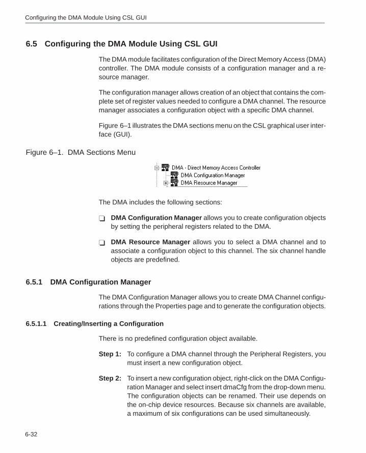
Configuring the DMA Module Using CSL GUI
6-32
6.5 Configuring the DMA Module Using CSL GUI
The DMA module facilitates configuration of the Direct Memory Access (DMA)controller. The DMA module consists of a configuration manager and a re-source manager.
The configuration manager allows creation of an object that contains the com-plete set of register values needed to configure a DMA channel. The resourcemanager associates a configuration object with a specific DMA channel.
Figure 6–1 illustrates the DMA sections menu on the CSL graphical user inter-face (GUI).
Figure 6–1. DMA Sections Menu
The DMA includes the following sections:
� DMA Configuration Manager allows you to create configuration objectsby setting the peripheral registers related to the DMA.
� DMA Resource Manager allows you to select a DMA channel and toassociate a configuration object to this channel. The six channel handleobjects are predefined.
6.5.1 DMA Configuration Manager
The DMA Configuration Manager allows you to create DMA Channel configu-rations through the Properties page and to generate the configuration objects.
6.5.1.1 Creating/Inserting a Configuration
There is no predefined configuration object available.
Step 1: To configure a DMA channel through the Peripheral Registers, youmust insert a new configuration object.
Step 2: To insert a new configuration object, right-click on the DMA Configu-ration Manager and select insert dmaCfg from the drop-down menu.The configuration objects can be renamed. Their use depends onthe on-chip device resources. Because six channels are available,a maximum of six configurations can be used simultaneously.

Configuring the DMA Module Using CSL GUI
6-33 DMA Module
Note:
A maximum of six configurations may be inserted. This is due to the associa-tion that each configuration has with a pre-defined global configuration. Theglobal configuration is dynamically updated with changes made to the asso-ciated DMA configuration. One DMA configuration (and its associated globalconfiguration) can be used by more than one DMA channel.
6.5.1.2 Deleting/Renaming an Object
To delete or rename an object, right-click on the configuration object you wantto delete or rename. Select Delete to delete a configuration object. Select Re-name to rename the object.
If a configuration object is used by one of the predefined handle objects of theDMA Resource Manager, the Delete and Rename options are grayed-out andnon-usable. The Show Dependency option is accessible and shows which de-vice is using the configuration object (see Figure 2–1, The CSL Tree, on page2-3).
6.5.1.3 Configuring the Object Properties
You can configure object properties through the Properties dialog box. (SeeFigure 6–2). To access the Properties dialog box, right-click on a configurationobject and select Properties. By default, the General page of the Propertiesdialog box is displayed.
The Properties pages allow you to set the Peripheral registers related to theDMA. You can set the configuration options through the following Tab pages:
� General: Breakpoint emulation behavior.
� Transfer Modes: Allows you to configure the Priority, Sync Events,ABU/Multi-frame
� Source/Destination: Allows you to configure the Address, Index,Element/Frame Count
� Autoinit: Allows you to configure the Reload Registers
� Advanced A and B Pages: These pages contains the full hexadecimalregister values and reflects the option setting of the previous pages. Also,the full register values can be entered directly and the new options aremirrored in the related pages automatically.
Configuring the DMA Module Using CSL GUI
6-34
Figure 6–2. DMA Properties Page
Each page is composed of several options that are set to a default value (atdevice reset).
6.5.1.4 Specifying Address Formats
The source, destination, and addresses can be specified in either a numericformat (hard coded address) or a symbolic format. Before setting any address-es, ensure that the right format is selected in the Source Address Format andDestination Address Format pull-down menus located on the Source and Des-tination tabs of the Properties page.

Configuring the DMA Module Using CSL GUI
6-35 DMA Module
6.5.2 DMA Resource Manager
The DMA Resource Manager allows you to generate the DMA_open() andDMA_config() CSL functions.
Figure 6–3 illustrates the DMA Resource Manager menu on the CSL graphicaluser interface (GUI).
Figure 6–3. DMA Resource Manager Menu
6.5.2.1 Predefined Objects
The six channel handle objects are predefined and each is associated with asupported on-chip DMA channel as follows:
DMA0 – Default handle name: hDma0
DMA1 – Default handle name: hDma1
DMA2 – Default handle name: hDma2
DMA3 Default handle name: hDma3
DMA4 Default handle name: hDma4
DMA5 Default handle name: hDma5
6.5.2.2 Properties Page
You can generate the DMA_open() and DMA_config() CSL functions throughthe Properties page.
To access the Properties page, right-click on a predefined DMA channel andselect Properties from the drop-down menu (see Figure 6–4).
The first time the Properties page appears, only the Open Handle to DMAcheck-box can be selected. Select this to open the DMA channel, allowing pre-initialization.

Configuring the DMA Module Using CSL GUI
6-36
DMA_NOTHING is used to indicate that there is no configuration object se-lected for this DMA.
To pre-initialize the DMA channel, check the Enable pre-initialization check-box. You can then select one of the available configuration objects (see section6.5.1 , DMA Configuration Manager ) for this channel through the pre-initializedrop-down list.
If DMA_NOTHING is selected, no configuration object is generated for the re-lated DMA handle (see section 6.5.3, C Code Generation for DMA Module).
In the example shown in Figure 6–4, the Open DMA Channel option ischecked and the handle object hDma1 is now accessible (The handle objectcan be renamed by typing the new name in the box provided). TheDMA_open() function is now generated with hDma1 containing the returnedhandle address.
Figure 6–4. DMA Properties Page With Handle Object Accessible

Configuring the DMA Module Using CSL GUI
6-37 DMA Module
6.5.3 C Code Generation for DMA Module
Two C files are generated from the configuration tool:
� Header file
� Source file
6.5.3.1 Header File
The header file includes all the CSL header files of the modules and containsthe DMA handles, and configuration objects generated by the configurationtool (see Example 6–1).
Example 6–1. DMA Header File
extern DMA_Config dmaCfg0;extern DMA_GblConfig gDMAConfig0;;extern DMA_Handle hDma1;

Configuring the DMA Module Using CSL GUI
6-38
6.5.3.2 Source File
The source file includes the declaration of the channel handle objects and theconfiguration structures (see Example 6–2).
Example 6–2. DMA Source File (Declaration Section)
/* Config Structures */
DMA_Config dmaCfg0 = {
0x0000, /* Channel Priority (0x0000 or 0x0001 */
0x0000, /* Global Reload Register Usage in Autoinit Mode (AUTO IX : 0x0000 or 0x0001) */
0x0000, /* Transfer Mode Control Register (DMMCR) */
0x0000, /* Sync Event and Frame Count Register (DMSFC) */
NULL, /* Source Address Register (DMSRC) - Symbolic */
NULL, /* Destination Address Register (DMDST) - Symbolic */
0x0000 /* Element Count Register (DMCTR) */
};
DMA_GblConfig gDMAConfig0 = {
0x0, /* Breakpoint Emulation Behavior (FREE) */
0x0000, /* Global Reload Register Usage in Autoinit Mode (AUTO IX : 0x0000 or 0x0001) */
NULL, /* Source Program Page Address Register (DMSRCP) - Symbolic */
NULL, /* Destination Program Page Address Register (DMDSTP) - Symbolic*/
0x0000, /* Element Address Index Register 0 (DMIDX0) */
0x0000, /* Frame Address Index Register 0 (DMFRI0) */
0x0000, /* Element Address Index Register 1 (DMIDX1)
0x0000, /* Frame Address Index Register 1 (DMFRI1)
NULL, /* Global Source Address Reload Register (DMGSA) - Symbolic */
NULL, /* Global Destination Address Reload Register (DMGDA) - Symbolic*/
0x0000, /* Global Element Count Reload Register (DMGCR) */
0x0000 /* Global Frame Count Reload Register B (DMGFR) */
};
/* Handles */
DMA_Handle hDma1;
The source file contains the Handle and Configuration Pre-Initialization usingthe CSL DMA API functions, DMA_open() and DMA_config() (seeExample 6–3).

Configuring the DMA Module Using CSL GUI
6-39 DMA Module
These two functions are encapsulated in a unique function, CSL_cfgInit(),which is called from your main C file. DMA_open() and DMA_config() are gen-erated only if Open Handle to DMA and Enable pre-initialization (with a se-lected configuration other than DMA_NOTHING) are checked under the DMAResource Manager Properties page.
Example 6–3. DMA Source File (Body Section)
void CSL_cfgInit()
{
hDma1 = DMA_open(DMA_CHA1, DMA_OPEN_RESET);
DMA_config(hDma1, &dmaCfg0);
DMA_globalConfig(0x0FFFF, &gDMAConfig0);
}

Examples
6-40
6.6 Examples
The following CSL DMA initialization examples are provided under the directo-ries:
c:\ti\examples\<target>\csl\manual_config\dma1a, dma1b, dma2,dma3, dma4
Example 1A DMA channel initialization using DMA_config()
Example 1B DMA channel initialization using DMA_configArgs()
Example 2 DMA channel auto-initialization with interrupt ontransfer completion using DMA_config(). This exam-ple also illustrates the usage of globalConfig() to con-figure DMA global registers.
Example 3 DMA channel data transfer from/to MCBSP.
Example 4 DMA channel data transfer from/to MCBSP in ABUand digital loopback mode.
For illustration purposes, Example 1A is covered in detail below, and is illus-trated in Figure 6–5.
Example 1A explains how DMA Channel 0 is initialized to transfer the datatable at 0x3000@data space to 0x2000@data space. This example does notuse any DMA global registers resources. Basic initialization values are as fol-lows:
� Source address: 2000h in data space
� Destination address: 3000h in data space
� Transfer size: 10h words single words
The following two macros are used to create the initialization values forDMMCR and DMSFC respectively:
DMA_DMMCR_RMK(autoinit, dinm, imod, ctmod, sind, dms, dind, dmd) 0 0 0 0 1 1 1 1
DMA_DMSFC_RMK(dsyn, dblw, framecount) 0 0 0 (single-frame, Nframes-1)
The settings needed for the DMMCR are:
DMMCR0 = 0x0145u
#0000000100000101b

Examples
6-41 DMA Module
;0~~~~~~~~~~~~~~~ (AUTOINIT) Autoinitialization disabled
;~0~~~~~~~~~~~~~~ (DINM) Interrupts masked
;~~0~~~~~~~~~~~~~ (IMOD) N/A
;~~~0~~~~~~~~~~~~ (CTMOD) Multi-frame mode
;~~~~0~~~~~~~~~~~ Reserved
;~~~~~001~~~~~~~~ (SIND) Post increment source address
;~~~~~~~~01~~~~~~ (DMS) Source in data space
;~~~~~~~~~~0~~~~~ Reserved
;~~~~~~~~~~~001~~ (DIND) Post increment destination address
;~~~~~~~~~~~~~~01 (DMD) Destination in data space
The settings needed for the DMSFC are:
DMSFC0 = 0x0000u
#0000000000000000b
;0000~~~~~~~~~~~~ (DSYN) No sync event
;~~~~0~~~~~~~~~~~ (DBLW) Single-word mode
;~~~~~000~~~~~~~~ Reserved
;~~~~~~~~00000000 (Frame Count) FrameCount = 0h (one frame)
Figure 6–5. DMA Channel Initialization Using DMA_config()
#include <csl_dma.h>
/*––––––––––––––––––––––––––––––––––––––––––––––––––––––––––––––––––––––––––––*//* create a data from DMA transfer */
#define N 16
/* Place data in separate section to ensure placement *//* within the DMA memory space defined for the device.*//* The address ranges chosen for this example in the *//* linker command file place src and dst within the *//* DMA memory map for the TMS320C5402. When modifying *//* this example to run on a different C54x target, *//* please check the datasheet for your specific *//* device to make sure that the src and dst addresses *//* for your transfer are assigned to a valid DMA *//* memory space. */
Examples
6-42
Figure 6–5. DMA Channel Initialization Using DMA_config() (Continued)
#pragma DATA_SECTION(src,”dmaMem”)Uint16 src[N]; #pragma DATA_SECTION(dst, ”dmaMem”)Uint16 dst[N];
/* In this example, we will be effecting a DMA *//* transfer from DATA to DATA space in internal *//* memory. The DMA will operate in multi–frame *//* mode and we will poll for DMA operation *//* complete. */
/* These are the settings we need for the DMA *//* mode control register, DMMCR, in order to *//* perform the transfer */
/* DMMCR0 = 0x0145u *//* #0000000101000101b *//* ;0~~~~~~~~~~~~~~~ (AUTOINIT) No Autoinit *//* ;~0~~~~~~~~~~~~~~ (DINM) No Interrupts *//* ;~~0~~~~~~~~~~~~~ (IMOD) N/A *//* ;~~~0~~~~~~~~~~~~ (CTMOD) Multi–frame on *//* ;~~~~0~~~~~~~~~~~ (SLAXS) Src not in extended mem */ /* ;~~~~~001~~~~~~~~ (SIND) Src addr Post–incr *//* ;~~~~~~~~01~~~~~~ (DMS) Src in data space *//* ;~~~~~~~~~~0~~~~~ (DLAXS) Dst not in extended mem *//* ;~~~~~~~~~~~001~~ (DIND) Dst addr Post–incr *//* ;~~~~~~~~~~~~~~01 (DMD) Dst in data space */
/* These are the settings required for DMA sync and *//* frame count register, DMSFC */
/* DMSFC0 = 0x0000u *//* #0000000000000000b *//* ;0000~~~~~~~~~~~~ (DSYN) No sync event *//* ;~~~~0~~~~~~~~~~~ (DBLW) Single–word mode *//* ;~~~~~000~~~~~~~~ N/A *//* ;~~~~~~~~00000000 (Frame Count) = 0 (one frame) */ /* Create a DMA configuration structure for the transfer *//* using predefined CSL macros and symbolic constants */

Examples
6-43 DMA Module
Figure 6–5. DMA Channel Initialization Using DMA_config() (Continued)
DMA_Config myconfig = { 1, /* Set Priority */ 0, /* Autoix off */ DMA_DMMCR_RMK( DMA_DMMCR_AUTOINIT_OFF, DMA_DMMCR_DINM_OFF, DMA_DMMCR_IMOD_FULL_ONLY, DMA_DMMCR_CTMOD_MULTIFRAME, DMA_DMMCR_SLAXS_OFF, DMA_DMMCR_SIND_POSTINC, DMA_DMMCR_DMS_DATA, DMA_DMMCR_DLAXS_OFF, DMA_DMMCR_DIND_POSTINC, DMA_DMMCR_DMD_DATA ), /* DMMCR */ DMA_DMSFC_RMK( DMA_DMSFC_DSYN_NONE, DMA_DMSFC_DBLW_OFF, DMA_DMSFC_FRAMECNT_OF(0) ), /* DMSFC */ (DMA_AdrPtr) &src[0], /* DMSRC */ (DMA_AdrPtr) &dst[0], /* DMDST */ (Uint16)(N–1), /* DMCTR */ 0, /* DMGSA */ 0, /* DMGDA */ 0, /* DMGCR */ 0, /* DMGFR */ };
/*––––––––––––––––––––––––––––––––––––––––––––––––––––––––––––––––––––––––––––*/void main() { Uint16 i;
/* Initialize CSL library, this step is required */ CSL_init();
/* Set Src values and Clear destination */ for (i=0; i<= N–1; i++) { src[i] = 0xBEEF; dst[i] = 0; }}
/*––––––––––––––––––––––––––––––––––––––––––––––––––––––––––––––––––––––––––––*/void taskFunc() {

Examples
6-44
Figure 6–5. DMA Channel Initialization Using DMA_config() (Continued)
DMA_Handle myhDma; /* Create a DMA handle pointer */ Uint16 err = 0; Uint16 i;
LOG_printf(&LogMain,”<DMA1A>”);
/* Open DMA channel 0, to use for this transfer */
myhDma = DMA_open(DMA_CHA0, 0);
/* Call DMA_config function to write your configuration */ /* values to DMA channel control registers */ DMA_config(myhDma, &myconfig);
/* Call DMA_start to begin the data transfer */ DMA_start(myhDma);
/* Poll DMA status too see if its done */ while(DMA_getStatus(myhDma));
/* Check the values to make sure DMA transfer is */ /* correct. */ for (i = 0; i <= N–1; i++) { if (dst[i] != 0xBEEFu) { ++err; } }
/* We are done, so close DMA channel */ DMA_close(myhDma);
LOG_printf(&LogMain,”%s”,err?”DMA Example 1A FAILED”:”DMA Example 1A PASSED”); LOG_printf(&LogMain,”<DONE>”);}

7-1
EBUS Module
This chapter describes the configuration structure, functions, and macrosused in the external bus interface (EBUS) module.
Topic Page
7.1 Overview 7-2. . . . . . . . . . . . . . . . . . . . . . . . . . . . . . . . . . . . . . . . . . . . . . . . . . . . .
7.2 Configuration Structure 7-3. . . . . . . . . . . . . . . . . . . . . . . . . . . . . . . . . . . . . . .
7.3 Functions 7-4. . . . . . . . . . . . . . . . . . . . . . . . . . . . . . . . . . . . . . . . . . . . . . . . . . . .
7.4 Macros 7-6. . . . . . . . . . . . . . . . . . . . . . . . . . . . . . . . . . . . . . . . . . . . . . . . . . . . . . .
Chapter 7

Overview
7-2
7.1 Overview
The EBUS module provides a configuration structure, functions, macros, andconstants that allow you to control the external bus interface through the CSL.
Table 7–1 summarizes the configuration structure. Table 7–2 lists the EBUSfunctions.
Use the following guidelines for the EBUS functions:
� You can perform configuration by calling either EBUS_config(),EBUS_configArgs(), or any of the SET register macros.
� Because EBUS_config() and EBUS_configArgs() initialize all three exter-nal bus control registers, macros are provided to enable efficient accessto individual registers when you need to set only one or two.
� The recommended approach is to initialize the external bus by usingEBUS_config() with the EBUS_Config structure.
Table 7–1. EBUS Configuration Structure
Structure Purpose See page...
EBUS_Config EBUS configuration structure used to setup the EBUS interface 7-3
Table 7–2. EBUS Functions
Function Purpose See page ...
EBUS_config() Sets up EBUS using configuration structure (EBUS_Config) 7-4
EBUS_configArgs() Sets up EBUS using register values passed to the function 7-5

EBUS_Config
7-3 EBUS Module
7.2 Configuration Structure
This section describes the configuration structure that you can use to set upthe EBUS interface.
EBUS configuration structure used to set up EBUS interfaceEBUS_Config
Structure EBUS_Config
Members For 544x devices:Uint16 bscr Bank-switching control register
For other C54x devices:Uint16 swwsr Software wait-state register Uint16 bscr Bank-switching control registerUint16 swcr Sofware wait-state control register
Description The EBUS configuration structure is used to set up the EBUS Interface. Youcreate and initialize this structure and then pass its address to theEBUS_config() function. You can use literal values or the EBUS_REG_RMKmacros to create the structure member values.
Example EBUS_Config Config1 = {
0x7FFF, /* swwsr */
0xF800, /* bscr */
0x0000 /* swcr */
};

EBUS_config
7-4
7.3 Functions
This section describes the EBUS API functions.
Writes value to set up EBUS using configuration structureEBUS_config
Function void EBUS_config( EBUS_Config *Config);
Arguments Config Pointer to an initialized configuration structure
Return Value None
Description Writes a value to set up the EBUS using the configuration structure. The valuesof the structure are written to the port registers (see also EBUS_configArgs()and EBUS_Config).
Example EBUS_Config MyConfig = {
0x7FFF, /* swwsr */
0xF800, /* bscr */
0x0000 /* swcr */
};
…EBUS_config(&MyConfig);

EBUS_configArgs
7-5 EBUS Module
Writes to EBUS using register values passed to the functionEBUS_configArgs
Function For C544x devices: EBUS_configArgs (Uint16 bscr);
For other C54x devices:void EBUS_configArgs( Uint16 swwsr, Uint16 bscr, Uint16 swcr);
Arguments swwsr Software wait-state registerbscr Bank-switching control registerswcr Software wait-state control register
Return Value None
Description Writes to the EBUS using the register values passed to the function. Theregister values are written to the EBUS registers.
You may use literal values for the arguments; or for readability, you may usethe EBUS_REG_RMK macros to create the register values based on field val-ues.
Example EBUS_configArgs (
0x7FFF, /* swwsr */
0xF800, /* bscr */
0x0000 /* swcr */
);

Macros
7-6
7.4 MacrosAs covered in section 1.3, CSL offers a collection of macros to gain individualaccess to the EBUS peripheral registers and fields.
Table 7–3 contains a list of macros available for the EBUS module. To usethem, include “csl_ebus.h.”
Table 7–3. EBUS Macros
(a) Macros to read/write EBUS register values
Macro Syntax
EBUS_RGET() Uint16 EBUS_RGET(REG)
EBUS_RSET() void EBUS_RSET(REG, Uint16 regval)
(b) Macros to read/write EBUS register field values (Applicable only to registers with more than one field)
Macro Syntax
EBUS_FGET() Uint16 EBUS_FGET(REG, FIELD)
EBUS_FSET() Void EBUS_FSET(REG,FIELD, Uint16 fieldval)
(c) Macros to read/write EBUS register field values (Applicable only to registers with more than one field)
Macro Syntax
EBUS_REG_RMK() Uint16 EBUS_REG_RMK(fieldval_n,...fieldval_0)
Note: *Start with field values with most significant field positions:field_n: MSB fieldfield_0: LSB field* only writeable fields allowed
EBUS_FMK() Uint16 EBUS_FMK(REG, FIELD, fieldval)
(d) Macros to read a register address
Macro Syntax
EBUS_ADDR() Uint16 EBUS_ADDR(REG)

Macros
7-7 EBUS Module
Where:
REG: SWWSR (except in C544x), SWCR (except in C544x), BSCR
FIELD: register field name as specified in Appendix A.
� For _FSET and _FMK, field should be a writable field.
� _FGET, this field should, at least, be readable.
regVal: value to write in register REG
fieldVal: value to write in field FIELD of register REG. Rules to follow:
� Only writable fields are allowed.
� Value should be a right-justified constant. If fieldval_n valueexceeds the number of bits allowed for that field, fieldval_nis truncated accordingly.
For examples on how to use macros, refer to macro sections 6.4 (DMA) and11.4 (McBSP).

8-1
GPIO Module
The GPIO module is designed to allow central control of non-multiplexedGPIO pins available in the C54x devices. (C544x devices only)
Topic Page
8.1 Overview 8-2. . . . . . . . . . . . . . . . . . . . . . . . . . . . . . . . . . . . . . . . . . . . . . . . . . . . .
8.2 Functions 8-3. . . . . . . . . . . . . . . . . . . . . . . . . . . . . . . . . . . . . . . . . . . . . . . . . . . .
8.3 Macros 8-5. . . . . . . . . . . . . . . . . . . . . . . . . . . . . . . . . . . . . . . . . . . . . . . . . . . . . . .
8.4 Configuring the GPIO Module Using CSL GUI 8-7. . . . . . . . . . . . . . . . . . .
Chapter 8

Overview
8-2
8.1 Overview
The GPIO module is designed to allow central control of the four non-multi-plexed GPIO pins (GPIO 0 to GPIO 3) available in each of the C54x core de-vices (C544x devices only).
Functions that allow you to manipulate the C54x GPIO pins are listed inTable 8–1.
Macros that allows access to registers have been provided on page 8-5 (seeTable 8–2).
Table 8–1. GPIO Functions
Function Description See page...
GPIO _pinDirection Sets the GPIO pins as either an input or output pin 8-3
GPIO_pinRead Reads the GPIO pin value 8-3
GPIO_pinWrite Writes a value to a GPIO pin 8-4

GPIO_pinRead
8-3 GPIO Module
8.2 Functions
The following are functions available for use with the GPIO module.
Sets the GPIO pin as input or outputGPIO_pinDirection
Function int GPIO_pinDirection (Uint32 pinId, Uint16 direction);
Arguments pinId IDs of the GPIO pins to enable. It will have oneone of the following values:GPIO_PIN0...GPIO_PIN3
Direction pin directionGPIO_INPUT //inputGPIO_OUTPUT //output
Return Value None
Description Sets the direction for a general-purpose I/O pin (input or output)
Example /* sets the pin gpio1 as an input */
GPIO_pinDirection (GPIO_PIN1, GPIO_INPUT);
Reads the GPIO pin valueGPIO_pinRead
Function int GPIO_pinRead (Uint32 pinId);
Arguments pinId IDs of the GPIO pins to enable. It will have one of the following values:GPIO_PIN0...GPIO_PIN3
Return Value Value Value read in GPIO pin (1 or 0)
Description Reads the value in a general purpose input pin.
Example int val;
val = GPIO_pinRead (GPIO_PIN3);

GPIO_pinWrite
8-4
Writes a value to a GPIO pinGPIO_pinWrite
Function int GPIO_pinWrite (Uint32 pinId, Unit16 val);
Arguments pinId IDs of the GPIO pins to enable. It will have one of the following values:GPIO_PIN0...GPIO_PIN3
val Value to write to the pinID.
Return Value None
Description Writes a value to a general purpose output pin.
Example GPIO_pinWrite (GPIO_PIN1, 1); /* sets iopin1 to ”1” */

Macros
8-5 GPIO Module
8.3 MacrosAs covered in section 1.3, CSL offers a collection of macros to gain individualaccess to a GPIO specific register (GPIO) in C544x devices.
Table 8–2 contains a list of macros available for the GPIO module. To usethem, include “csl_gpio.h.”
Table 8–2. GPIO Macros (C544x devices only)
(a) Macros to read/write GPIO register values
Macro Syntax
GPIO_RGET() Uint16 GPIO_RGET(REG)
GPIO_RSET() void GPIO_RSET(REG, Uint16 regval)
(b) Macros to read/write GPIO register field values (Applicable only to registers with more than one field)
Macro Syntax
GPIO_FGET() Uint16 GPIO_FGET(REG, FIELD)
GPIO_FSET() Void GPIO_FSET(REG,FIELD, Uint16 fieldval)
(c) Macros to read/write GPIO register field values (Applicable only to registers with more than one field)
Macro Syntax
GPIO_REG_RMK() Uint16 GPIO_REG_RMK(fieldval_n,...fieldval_0)
Note: *Start with field values with most significant field positions:field_n: MSB fieldfield_0: LSB field* only writable fields allowed
GPIO_FMK() Uint16 GPIO_FMK(REG, FIELD, fieldval)
(d) Macros to read a register address
Macro Syntax
GPIO_ADDR() Uint16 GPIO_ADDR(REG)

Macros
8-6
Where:
REG: GPIO
FIELD: register field name as specified in Appendix A.
� For _FSET and _FMK, field should be a writable field.
� _FGET, this field should, at least, be readable.
regVal: value to write in register REG
fieldVal: value to write in field FIELD of register REG. Rules to follow:
� Only writable fields are allowed.
� Value should be a right-justified constant. If fieldval_n valueexceeds the number of bits allowed for that field, fieldval_nis truncated accordingly.
For examples on how to use macros, refer to the macro sections 6.4 (DMA)and 11.4 (McBSP).

Configuring the GPIO Module Using CSL GUI
8-7 GPIO Module
8.4 Configuring the GPIO Module Using CSL GUI
The GPIO module facilitates configuration/control of the General-Purpose I/Oon the C54x. The module consists of a configuration manager. The configura-tion manager allows you to configure the directions to either the input or outputof the GPIO pins.
Figure 8–1 illustrates the GPIO sections menu on the CSL graphical user in-terface (GUI)
Figure 8–1. GPIO Sections Menu
The Non-Multiplexed GPIO includes the following section:
Non-Multiplexed GPIO Configuration Manager allows you to configurethe GPIO Pin directions.
8.4.1 Non-Multiplexed GPIO Configuration Manager
The Non-Multiplexed GPIO Configuration Manager allows you to configure theGPIO pin directions.
8.4.1.1 Properties Pages of the Non-Multiplexed GPIO Configuration
The Properties pages allow you to set the Peripheral registers related to theGPIO. The configuration options are divided into the following Tab page:
Settings allows you to configure the Input/Output settings of GPIO Pins.
Figure 8–2 depicts the Properties Page dialog box.
Figure 8–2. GPIO Properties Page

Configuring the GPIO Module Using CSL GUI
8-8
The Settings Tab is composed of several options that are set to a default value(at device reset).
The options represent the fields of the GPIO register direction. For further de-tails of the fields and registers, refer to the GPIO section of the TMS320C54xDSP Enhanced Peripherals Reference Set (literature number SPRU302).
8.4.2 C Code Generation for GPIO Module
Two C files are generated from the configuration tool:
� Header file
� Source file
8.4.2.1 Header File
The header file includes all the csl header files of the modules.
8.4.2.2 Source File
The source file contains the GPIO Register set macro invocation. This macroinvocation is encapsulated in a unique function, CSL_cfgInit(), which is calledfrom your main C file.
GPIO_RSET() will be generated only if Configure Non-Multiplexed GPIO ischecked under the Non-multiplexed GPIO Configuration Properties page.See Figure 8–2.
Example 8–1. GPIO Source File (Body Section)
void CSL_cfgInit(){
GPIO_RSET(GPIO, 3840);}

9-1
HPI Module
This chapter contains descriptions for macros available in the HPI module.
Topic Page
9.1 Macros 9-2. . . . . . . . . . . . . . . . . . . . . . . . . . . . . . . . . . . . . . . . . . . . . . . . . . . . . . .
Chapter 9

Macros
9-2
9.1 MacrosAs covered in section 1.3, the CSL offers a collection of macros to gain individ-ual access to the peripheral registers and fields.
Table 9–1 contains a list of macros available for the HPI module. To use them,include “csl_hpi.h.”
Table 9–1. HPI Macros
(a) Macros to read/write HPI register values
Macro Syntax
HPI_RGET() Uint16 HPI_RGET(REG)
HPI_RSET() void HPI_RSET(REG, Uint16 regval)
(b) Macros to read/write HPI register field values (Applicable only to registers with more than one field)
Macro Syntax
HPI_FGET() Uint16 HPI_FGET(REG, FIELD)
HPI_FSET() Void HPI_FSET(REG,FIELD, Uint16 fieldval)
(c) Macros to read/write HPI register field values (Applicable only to registers with more than one field)
Macro Syntax
HPI_REG_RMK() Uint16 HPI_REG_RMK(fieldval_n,...fieldval_0)
Note:
� Start with field values with most significant field positions:field_n: MSB fieldfield_0: LSB field
� only writable fields allowed
HPI_FMK() Uint16 HPI_FMK(REG, FIELD, fieldval)
(d) Macros to read a register address
Macro Syntax
HPI_ADDR() Uint16 HPI_ADDR(REG)

Macros
9-3HPI Module
Where:
REG: include HPIC, GPIOCR, GPIOSR
FIELD: register field name as specified in Appendix A.
� For _FSET and _FMK, field should be a writable field.
� For _FGET, this field should, at least, be readable.
regVal: value to write in register REG
fieldVal: value to write in field FIELD of register REG. Rules to follow:
� Only writable fields are allowed
� Value should be a right-justified constant. If fieldval_n valueexceeds the number of bits allowed for that field, fieldval_nis truncated accordingly.
For examples on how to use macros, refer to macro sections 6.4 (DMA) and11.4 (McBSP).

10-1
IRQ Module
The IRQ module provides an easy to use interface for enabling/disabling andmanaging interrupts.
Topic Page
10.1 Overview 10-2. . . . . . . . . . . . . . . . . . . . . . . . . . . . . . . . . . . . . . . . . . . . . . . . . . . .
10.2 Using Interrupts with CSL 10-7. . . . . . . . . . . . . . . . . . . . . . . . . . . . . . . . . . . .
10.3 Configuration Structure 10-8. . . . . . . . . . . . . . . . . . . . . . . . . . . . . . . . . . . . . .
10.4 Functions 10-9. . . . . . . . . . . . . . . . . . . . . . . . . . . . . . . . . . . . . . . . . . . . . . . . . . .
Chapter 10

Overview
10-2
10.1 Overview
The IRQ module provides an interface for managing peripheral interrupts tothe CPU. This module provides the following functionality:
� Masking an interrupt in the IMRx register.
� Polling for the interrupt status from the IFRx register.
� Setting the interrupt vector table address and placing the necessary codein the interrupt vector table to branch to a user-defined interrupt serviceroutine (ISR).
� Enabling/Disabling Global Interrupts in the ST1 (INTM) bit.
� Reading and writing to parameters in the DSP/BIOS dispatch table.(When the DPS BIOS dispatcher option is enabled in DSP BIOS.)
The DSP BIOS dispatcher is responsible for dynamically handlinginterrupts and maintains a table of ISRs to be executed for specificinterrupts. The IRQ module has a set of APIs that update the dispatchtable.
Table 10–1 lists the IRQ configuration structure.
Table 10–2 lists the functions available in the IRQ module.
Table 10–2(a) and (b) list the primary and auxiliary IRQ functions.
Table 10–2(c) lists the API functions that enable DSP/BIOS dispatcher com-munication.
The IRQ functions in Table 10–2(a) can be used with or without DSP/BIOS;however, if DSP/BIOS is present, do not disable interrupts for long periods oftime, as this could disrupt the DSP/BIOS environment.
Table 10–2(b) lists the only API functions that cannot be used when DSP/BIOSdispatcher is present or DSP/BIOS HWI module is used to configure the inter-rupt vectors. This function, IRQ_plug(), dynamically places code at the inter-rupt vector location to branch to a user-defined ISR for a specified event. If youcall IRQ_plug() when DSP/BIOS dispatcher is present or HWI module hasbeen used to configure interrupt vectors, this could disrupt the DSP/BIOS op-erating environment.
Table 10–2(c) lists the API functions that enable DSP/BIOS dispatcher com-munications. These functions should be used only when DSP/BIOS is presentand the DSP/BIOS dispatcher is enabled.
Table 10–3 lists all IRQ logical interrupt events for this module.

Overview
10-3IRQ Module
Table 10–1. IRQ Configuration Structure
Structure Purpose See page ...
IRQ_Config IRQ structure that contains all local registers required to set up aspecific IRQ channel.
10-8
Table 10–2. IRQ Functions
(a) Primary Functions
Function Purpose See page ...
IRQ_clear() Clears the interrupt flag in the IFR register for the specified event. 10-9
IRQ_disable() Disables the specified event in the IMR register. 10-10
IRQ_enable() Enables the specified event in the IMR register flag. 10-11
IRQ_globalDisable() Globally disables all maskable interrupts. (INTM = 1) 10-12
IRQ_globalEnable() Globally enables all maskable interrupts. (INTM = 0) 10-13
IRQ_globalRestore() Restores the status of global interrupt enable/disable (INTM). 10-13
IRQ_restore() Restores the status of the specified event. 10-15
IRQ_setVecs() Sets the base address of the interrupt vector table. 10-16
IRQ_test() Polls the interrupt flag in IFR register the specified event. 10-16
(b) Auxiliary Functions
Function Purpose See page ...
IRQ_plug() Writes the necessary code in the interrupt vector location to branchto the interrupt service routine for the specified event.
Caution: Do not use this function when DSP/BIOS is present andthe dispatcher is enabled.
10-14

Overview
10-4
Table 10–2. IRQ Functions (Continued)
(c) DSP/BIOS Dispatcher Communication Functions
Function Purpose See page ...
IRQ_config() Updates the DSP/BIOS dispatch table with a new configuration forthe specified event.
10-9
IRQ_configArgs() Updates the DSP/BIOS dispatch table with a new configuration forthe specified event.
10-10
IRQ_getArg() Returns value of the argument to the interrupt service routine thatthe DSP/BIOS dispatcher passes when the interrupt occurs.
10-11
IRQ_getConfig() Returns current DSP/BIOS dispatch table entries for the specifiedevent.
10-12
IRQ_map() Maps a logical event to its physical interrupt. 10-14
IRQ_setArg() Sets the value of the argument for DSP/BIOS dispatch to pass tothe interrupt service routine for the specified event.
10-15
10.1.1 The Event ID Concept
The IRQ module assigns an event ID to each of the possible physical inter-rupts. Because there are more events possible than can be masked in the IMRregister, many of the events share a common physical interrupt. Therefore, itis necessary in some cases to map the logical events to the correspondingphysical interrupt. The IRQ module defines a set of constantsIRQ_EVT_NNNN that uniquely identify each of the possible logical interrupts.A list of these event IDs is listed in Table 10–3. All of the IRQ APIs operate onlogical events.
Table 10–3. IRQ_EVT_NNNN Event List
Constant Purpose
IRQ_EVT_RS Reset
IRQ_EVT_SINTR Software Interrupt
IRQ_EVT_NMI Non-Maskable Interrupt (NMI)
IRQ_EVT_SINT16 Software Interrupt #16
IRQ_EVT_SINT17 Software Interrupt #17
IRQ_EVT_SINT18 Software Interrupt #18

Overview
10-5IRQ Module
Table 10–3. IRQ_EVT_NNNN Event List (Continued)
Constant Purpose
IRQ_EVT_SINT19 Software Interrupt #19
IRQ_EVT_SINT20 Software Interrupt #20
IRQ_EVT_SINT21 Software Interrupt #21
IRQ_EVT_SINT22 Software Interrupt #22
IRQ_EVT_SINT23 Software Interrupt #23
IRQ_EVT_SINT24 Software Interrupt #24
IRQ_EVT_SINT25 Software Interrupt #25
IRQ_EVT_SINT26 Software Interrupt #26
IRQ_EVT_SINT27 Software Interrupt #27
IRQ_EVT_SINT28 Software Interrupt #28
IRQ_EVT_SINT29 Software Interrupt #29
IRQ_EVT_SINT30 Software Interrupt #30
IRQ_EVT_SINT0 Software Interrupt #0
IRQ_EVT_SINT1 Software Interrupt #1
IRQ_EVT_SINT2 Software Interrupt #2
IRQ_EVT_SINT3 Software Interrupt #3
IRQ_EVT_SINT4 Software Interrupt #4
IRQ_EVT_SINT5 Software Interrupt #5
IRQ_EVT_SINT6 Software Interrupt #6
IRQ_EVT_SINT7 Software Interrupt #7
IRQ_EVT_SINT8 Software Interrupt #8
IRQ_EVT_SINT9 Software Interrupt #9
IRQ_EVT_SINT10 Software Interrupt #10
IRQ_EVT_SINT11 Software Interrupt #11
IRQ_EVT_SINT12 Software Interrupt #12
IRQ_EVT_SINT13 Software Interrupt #13

Overview
10-6
Table 10–3. IRQ_EVT_NNNN Event List (Continued)
Constant Purpose
IRQ_EVT_INT0 External User Interrupt #0
IRQ_EVT_INT1 External User Interrupt #1
IRQ_EVT_INT2 External User Interrupt #2
IRQ_EVT_INT3 External User Interrupt #3
IRQ_EVT_TINT0 Timer 0 Interrupt
IRQ_EVT_HINT Host Interrupt (HPI)
IRQ_EVT_DMA0 DMA Channel 0 Interrupt
IRQ_EVT_DMA1 DMA Channel 1 Interrupt
IRQ_EVT_DMA2 DMA Channel 2 Interrupt
IRQ_EVT_DMA3 DMA Channel 3 Interrupt
IRQ_EVT_DMA4 DMA Channel 4 Interrupt
IRQ_EVT_DMA5 DMA Channel 5 Interrupt
IRQ_EVT_RINT0 MCBSP Port #0 Receive Interrupt
IRQ_EVT_XINT0 MCBSP Port #0 Transmit Interrupt
IRQ_EVT_RINT2 MCBSP Port #2 Receive Interrupt
IRQ_EVT_XINT2 MCBSP Port #2 Transmit Interrupt
IRQ_EVT_TINT1 Timer #1 Interrupt
IRQ_EVT_HPINT Host Interrupt (HPI)
IRQ_EVT_RINT1 MCBSP Port #1 Receive Interrupt
IRQ_EVT_XINT1 MCBSP Port #1 Transmit Interrupt
IRQ_EVT_IPINT FIFO Full Interrupt
IRQ_EVT_SINT14 Software Interrupt #14
IRQ_EVT_WDTINT Watchdog Timer Interrupt
IRQ_EVT_UART UART Interrupt
IRQ_EVT_DAARCV DAA Receive Interrupt
IRQ_EVT_DAAXMT DAA Transmit Interrupt

Using Interrupts with CSL
10-7IRQ Module
10.2 Using Interrupts with CSL
Interrupts within CSL can be managed in the following methods:
� Manual setting outside DSPBIOS HWIs
� Using DSPBIOS HWIs
� Using DSPBIOS Dispatcher
Example 10–1. Manual Setting Outside DSPBIOS HWIs
#define NVECTORS 256
#pragma DATA_SECTION (myIvtTable, ”myvec”)int myIvtTable[NVECTORS];
; ...interrupt void myIsr();
; ...main (){
; ...; Option 1: use Event IDs directly; ...
IRQ_setVecs ((Uint16)myIvtTable);IRQ_plug (IRQ_EVT_TINT0,&myIsr);IRQ_enable(IRQ_EVT_TINT0);IRQ_globalEnable();
; ...; Option 2: Use the PER_getEventId() function (TIMER as an example)for a better abstraction; ...
IRQ_setVecs ((Uint16)myIvtTable);eventId = TIMER_getEventId (hTimer);IRQ_plug (eventId,&myIsr);IRQ_enable (eventId);IRQ_globalEnable();; ...
}
interrupt void myISR()
{
//....;
}

IRQ_Config
10-8
10.3 Configuration Structure
IRQ configuration structureIRQ_Config
Structure IRQ_Config
Members IRQ_IsrPtr FuncAddr Function to be calledUint16 funcArg Argument to pass to ISR when invokedUint32 ierMask Mask for the interrupts to be disabled when
the current interrupt is handled.
Description This is the IRQ configuration structure used to update a DSP/BIOS table entry.You create and initialize this structure then pass its address to theIRQ_config() function.
Example IRQ_Config MyConfig = {
0x0000, /* funcAddr */
0x0000, /* funcArg */
0x0300 /* ierMask */
};

IRQ_config
10-9 IRQ Module
10.4 Functions
This section describes the primary, auxiliary, and DSP/BIOS Dispatcher Com-munications IRQ functions.
Clears event flag from IFR registerIRQ_clear
Function void IRQ_clear(Uint16 EventId
);
Arguments EventId Event ID, see IRQ_EVT_NNNN (Table 10–3) for a complete list
of events. Or, use the PER_getEventId() function to get the EventID.
Return Value None
Description Clears the event flag from the IFR register
Example IRQ_clear(IRQ_EVT_TINT0);
Updates Entry in DSPBIOS dispatch tableIRQ_config
Function void IRQ_config( Uint16 EventId,
IRQ_Config *Config);
Arguments EventID Event ID, see IRQ_EVT_NNNN for a complete list of events.
Config Pointer to an initialized configuration structure
Return Value None
Description Updates the entry in the DSPBIOS dispatch table for the specified event.
Example IRQ_Config MyConfig = {
0x0000, /* funcAddr */
0x0000, /* funcArg */
0x0300 /* ierMask */
};
...
IRQ_config(IRQ_EVT_TINT0,&MyConfig);

IRQ_configArgs
10-10
Updates entry in DSPBIOS dispatch tableIRQ_configArgs
Function void IRQ_configArgs( Uint16 EventId,
IRQ_IsrPtr funcAddr, Uint16 funcArg, Uint32 ierMask
);
Arguments EventId Event ID, see IRQ_EVT_NNNN for a complete list of events.
funcAddr Interrupt service routine address
funcArg Argument to pass to interrupt service routine when it is invokedby DSPBIOS dispatcher
ierMask Interrupts to disable while processing the ISR for this event (Mask for IER0, IER1)
Return Value None
Description Updates DSPBIOS dispatch table entry for the specified event.
Example IRQ_configArgs(EventID, funcAddr, funcArg, ierMask);
Disables specified eventIRQ_disable
Function int IRQ_disable(Uint16 EventId
);
Arguments EventId Event ID, see IRQ_EVT_NNNN (Table 10-3) for a complete list
of events. Or, use the PER_getEventId() function to get the EventID.
Return Value intm Old value of the specified mask bit in the IMR register.
Description Disables the specified event, by modifying the IMR register.
Example int intm;
intm = IRQ_disable(IRQ_EVT_TINT0);

IRQ_getArg
10-11 IRQ Module
Enables specified eventIRQ_enable
Function int IRQ_enable(Uint16 EventId
);
Arguments EventId Event ID, see IRQ_EVT_NNNN (Table 10-3) for a complete list
of events. Or, use the PER_getEventId() function to get the EventID.
Return Value intm Old value of the specified mask bit in the IMR register.
Description Enables the specified event.
Example int intm;
intm = IRQ_enable(IRQ_EVT_TINT0);
Gets value for specified eventIRQ_getArg
Function Uint32 IRQ_getArg(Uint16 EventId
);
Arguments EventId Event ID, see IRQ_EVT_NNNN (Table 10-3) for a complete list
of events. Or, use the PER_getEventId() function to get the EventID.
Return Value Value of argument
Description Gets the value for specified event.
Example Uint32 arg;
arg = IRQ_getArg(IRQ_EVT_TINT0);

IRQ_getConfig
10-12
Gets DSP/BIOS dispatch table entryIRQ_getConfig
Function void IRQ_getConfig( Uint16 EventId,
IRQ_Config *Config);
Arguments EventId Event ID, see IRQ_EVT_NNNN (Table 10–3) for a complete list
of events. Or, use the PER_getEventId() function to get the EventID.
Config Pointer to configuration structure
Return Value None
Description Reads the current configuration for the IRQ event.
Example IRQ_Config ConfigRead;
...
IRQ_getConfig(IRQ_EVT_TINT0, &ConfigRead);
Globally Disables InterruptsIRQ_globalDisable
Function int IRQ_globalDisable();
Arguments None
Return Value intm Returns the old INTM value
Description This function globally disables interrupts by setting the INTM of the ST1register. The old value of INTM is returned. This is useful for temporarilydisabling global interrupts, then enabling them again.
Example int oldgie;
oldgie = IRQ_globalDisable();
IRQ_globalRestore
10-13 IRQ Module
Globally enables all eventsIRQ_globalEnable
Function int IRQ_globalEnable();
Arguments None
Return Value intm Returns the old INTM value
Description This function globally enables all interrupts by setting the INTM of the ST1register. The old value of INTM is returned. This is useful for temporarilyenabling global interrupts, then disabling them again.
Example Uint32 intm;
intm = IRQ_globalEnable();
...
IRQ_globalRestore (intm);
Restores The Global Interrupt Mask StateIRQ_globalRestore
Function void IRQ_globalRestore(int intm
);
Arguments intm Value to restore the INTM value to (0 = enable, 1 = disable)
Return Value gie Previously saved value
Description This function restores the INTM state to the value passed in by writing to theINTM bit of the ST1 register. This is useful for temporarily disabling/enablingglobal interrupts, then restoring them back to its previous state.
Example int intm;
intm = IRQ_globalDisable();
...
IRQ_globalRestore (intm);

IRQ_map
10-14
Maps Event To Physical Interrupt NumberIRQ_map
Function void IRQ_map(Uint16 EventId
);
Arguments EventId Event ID, see IRQ_EVT_NNNN (Table 10–3) for a complete list
of events. Or, use the PER_getEventId() function to get the EventID.
Return Value None
Description This function maps a logical event to a physical interrupt number for use byDSPBIOS dispatch.
Example IRQ_map(IRQ_EVT_TINT0);
Initializes An Interrupt Vector Table VectorIRQ_plug
Function void IRQ_plug( Uint16 EventId,
IRQ_IsrPtr funcAddr, );
Arguments EventId Event ID, see IRQ_EVT_NNNN (Table 10–3) for a complete list
of events. Or, use the PER_getEventId() function to get the EventID.
funcAddr Address of the interrupt service routine to be called when the interrupt happens. This function must be C-callable and if implemented in C, it must be declared using the interrupt keyword.
Return Value None
Description Initializes an interrupt vector table vector with the necessary code to branchto the specified ISR. Caution: Do not use this function when DSP/BIOS is presentand the dispatcher is enabled.
Example IRQ_IsrPtr funcAddr;
.
.
.
IRQ_plug (IRQ_EVT_TINT0, funcAddr);

IRQ_setArg
10-15 IRQ Module
Restores the status of the specified eventIRQ_restore
Function void IRQ_restore(Uint16 EventId,Uint16 Val
);
Arguments EventId Event ID, see IRQ_EVT_NNNN (Table 10–3 on page 10-4)for a complete list of events.
Val Value to restore the specified event to
Return Value None
Description Restores the status of the specified event.
Example Uint16 intm = IRQ_disable(IRQ_EVT_TINT0);
....
IRQ_restore(IRQ_EVT_TINT0,intm);
Sets value of argument for DSPBIOS dispatch entryIRQ_setArg
Function void IRQ_setArg(Uint16 EventId,Uint32 val
);
Arguments EventId Event ID, see IRQ_EVT_NNNN (Table 10–3) for a complete list
of events. Or, use the PER_getEventId() function to get the EventID.
Return Value None
Description Sets the argument that DSP/BIOS dispatcher will pass to the interrupt serviceroutine for the specified event.
Example Uint32 val;
IRQ_setArg(IRQ_EVT_TINT0, val);

IRQ_setVecs
10-16
Sets the base address of the interrupt vectorsIRQ_setVecs
Function int IRQ_setVecs(Uint32 iptr
);
Arguments iptr IVPD pointer to the DSP interrupt vector table
Return Value oldVecs Returns the old IVPD Pointer to the DSP interrupt Vector table
Description Use this function to set the base address of the interrupt vector table in theIVPD register.
Caution: Changing the interrupt vector table base can have adverse effectson your system because you will be effectively eliminating all previous interruptsettings. There is a strong chance that the DSP/BIOS kernel and RTDX will failif this function is not used with care.
Example IRQ_setVecs (0x8000);
Tests event to see if its flag is set in IFR registerIRQ_test
Function CSLBool IRQ_test(Uint16 EventId
);
Arguments EventId Event ID, see IRQ_EVT_NNNN (Table 10–3) for a complete list
of events. Or, use the PER_getEventId() function to get the EventID.
Return Value Event flag, 0 or 1
Description Tests an event to see if its flag is set in the IFR register.
Example while (!IRQ_test(IRQ_EVT_TINT0);

11-1
McBSP Module
The chapter describes the structure, functions, and macros of the McBSPmodule.
Topic Page
11.1 Overview 11-2. . . . . . . . . . . . . . . . . . . . . . . . . . . . . . . . . . . . . . . . . . . . . . . . . . . .
11.2 Configuration Structure 11-4. . . . . . . . . . . . . . . . . . . . . . . . . . . . . . . . . . . . . .
11.3 Functions 11-6. . . . . . . . . . . . . . . . . . . . . . . . . . . . . . . . . . . . . . . . . . . . . . . . . . .
11.4 Macros 11-24. . . . . . . . . . . . . . . . . . . . . . . . . . . . . . . . . . . . . . . . . . . . . . . . . . . . .
11.5 Configuring the MCBSP Module Using CSL GUI 11-42. . . . . . . . . . . . . . .
11.6 Examples 11-50. . . . . . . . . . . . . . . . . . . . . . . . . . . . . . . . . . . . . . . . . . . . . . . . . .
Chapter 11

Overview
11-2
11.1 Overview
THE McBSP is a handle-based module that requires you to callMCBSP_open() to obtain a handle before calling any other functions.Table 11–1 lists the structure for use with the McBSP modules. Table 11–2 liststhe functions for use with the McBSP modules.
Table 11–1. McBSP Configuration Structure
Structure Purpose See page...
MCBSP_Config McBSP configuration structure used to setup a McBSP port 11-4
Table 11–2. McBSP Functions
(a) Primary Functions
Function Purpose See page ...
MCBSP_close() Closes a McBSP port 11-10
MCBSP_config() Sets up the McBSP port using the configuration structure(MCBSP_Config)
11-10
MCBSP_configArgs() Sets up the McBSP port using the register values passed to thefunction
11-12
MCBSP_open() Opens a McBSP port 11-17
MCBSP_start() Start a transmit and/or receive for a MCBSP port 11-20

Overview
11-3McBSP Module
Table 11–2. McBSP Functions (Continued)
(b) Auxiliary Functions
Function Purpose See page ...
MCBSP_getConfig() Get MCBSP channel configuration 11-15
MCBSP_getPort() Get MCBSP Port number used in given handle 11-15
MCBSP_read16() Performs a direct 16-bit read from the data receive registerDRR1
11-17
MCBSP_read32() Performs two direct 16-bit reads: data receive register 2 DRR2(MSB) and data receive register 1 DRR1 (LSB)
11-18
MCBSP_reset() Resets the given serial port 11-18
MCBSP_rfull() Reads the RFULL bit SPCR1 register 11-18
MCBSP_rrdy() Reads the RRDY status bit of the SPCR1 register 11-19
MCBSP_write16() Writes a 16-bit value to the serial port data transmit register,DXR1
11-22
MCBSP_write32() Writes two 16-bit values to the two serial port data transmitregisters, DXR2 (16-bit MSB) and DXR1 (16-bit LSB)
11-22
MCBSP_xempty() Reads the XEMPTY bit from the SPCR2 register 11-23
MCBSP_xrdy() Reads the XRDY status bit of the SPCR2 register 11-23
(c) Interrupt Control Functions
Function Purpose See page ...
MCBSP_getRcvEventId() Retrieves the receive event ID for the given port 11-16
MCBSP_getXmtEventId() Retrieves the transmit event ID for the given port 11-16
(d) Multichannel Control Functions
Function Purpose See page ...
MCBSP_channelDisable() Disables one or several McBSP channels 11-6
MCBSP_channelEnable() Enables one or several McBSP channels of the selectedregister
11-7
MCBSP_channelStatus() Returns the channel status 11-9

MCBSP_Config
11-4
11.2 Configuration Structure
This section lists the configuration structure for the McBSP module.
McBSP configuration structure used to setup McBSP portMCBSP_Config
Structure MCBSP_Config
Members Uint16 spcr1 Serial port control register 1 valueUint16 spcr2 Serial port control register 2 valueUint16 rcr1 Receive control register 1 valueUint16 rcr2 Receive control register 2 valueUint16 xcr1 Transmit control register 1 valueUint16 xcr2 Transmit control register 2 valueUint16 srgr1 Sample rate generator register 1 valueUint16 srgr2 Sample rate generator register 2 valueUint16 mcr1 Multi-channel control register 1 valueUint16 mcr2 Multi-channel control register 2 valueUint16 pcr Pin control register value
For devices supporting 128 channels:Uint16 rcera Receive channel enable register partition A valueUint16 rcerb Receive channel enable register partition B valueUint16 rcerc Receive channel enable register partition C valueUint16 rcerd Receive channel enable register partition D valueUint16 rcere Receive channel enable register partition E valueUint16 rcerf Receive channel enable register partition F valueUint16 rcerg Receive channel enable register partition G valueUint16 rcerh Receive channel enable register partition H valueUint16 xcera Transmit channel enable register partition A valueUint16 xcerb Transmit channel enable register partition B valueUint16 xcerc Transmit channel enable register partition C valueUint16 xcerd Transmit channel enable register partition D valueUint16 xcere Transmit channel enable register partition E valueUint16 xcerf Transmit channel enable register partition F valueUint16 xcerg Transmit channel enable register partition G valueUint16 xcerh Transmit channel enable register partition H value
For devices that do not support 128 channels:Uint16 rceraUint16 rcerbUint16 xceraUint16 xcerb

MCBSP_Config
11-5 McBSP Module
Description McBSP configuration structure used to setup a McBSP port. You create andinitialize this structure then pass its address to the MCBSP_config() function.You can use literal values or the MCBSP_RMK macros to create the structuremember values.
Example MCBSP_Config MyConfig = {
0x8001, /* spcr1 */
0x0001, /* spcr2 */
0x0000, /* rcr1 */
0x0000, /* rcr2 */
0x0000, /* xcr1 */
0x0000, /* xcr2 */
0x0001, /* srgr1 */
0x2000, /* srgr2 */
0x0000, /* mcr1 */
0x0000, /* mcr2 */
0x0000, /* pcr */
0x0000, /* rcera */
0x0000, /* rcerb */
0x0000, /* xcera */
0x0000, /* xcerb */
};
...
hMcbsp = MCBSP_open(MCBSP_PORT0, MCBSP_OPEN_RESET)
...
MCBSP_config(hMcbsp,&MyConfig);

MCBSP_channelDisable
11-6
11.3 Functions
This section lists the primary, auxiliary, interrupt control, and multi-channelfunctions available for use in the McBSP module.
Disables one or several McBSP channelsMCBSP_channelDisable
Function void MCBSP_channelDisable( MCBSP_Handle hMcbsp, Uint16 RegName, Uint16 Channels );
Arguments hMcbsp Handle to McBSP port obtained by MCBSP_open()
RegName Receive and Transmit Channel Enable Registers:RCERARCERBXCERAXCERB
For devices supporting 128 channels (see section 1.8) add:RCERCRCERDRCERERCERFRCERGRCERHXCERCXCERDXCEREXCERFXCERGXCERH
Channels Available values for the specific RegName are:MCBSP_CHAN0MCBSP_CHAN1MCBSP_CHAN2MCBSP_CHAN3MCBSP_CHAN4

MCBSP_channelEnable
11-7 McBSP Module
MCBSP_CHAN5MCBSP_CHAN6 MCBSP_CHAN7MCBSP_CHAN8MCBSP_CHAN9MCBSP_CHAN10MCBSP_CHAN11MCBSP_CHAN12MCBSP_CHAN13MCBSP_CHAN14MCBSP_CHAN15
Return Value None
Description Disables one or several McBSP channels of the selected register. To disableseveral channels at the same time,the sign “|” OR has to be added in between.
To see if there is pending data in the receive or transmit buffers beforedisabling a channel, use MCBSP_rrdy() or MCBSP_xrdy().
Example /* Disables Channel 0 of the partition A */
MCBSP_channelDisable(hMcbsp,RCERA, MCBSP_CHAN0);
/* Disables Channels 1, 2 and 8 of the partition B with “|”*/
MCBSP_channelDisable(hMcbsp,RCERB,(MCBSP_CHAN1 | MCBSP_CHAN2 |
MCBSP_CHAN8));
Enables one or several McBSP channels of selected registerMCBSP_channelEnable
Function void MCBSP_channelEnable( MCBSP_Handle hMcbsp, Uint16 RegName, Uint16 Channels );
Arguments hMcbsp Handle to McBSP port obtained by MCBSP_open()
RegName Receive and Transmit Channel Enable Registers:RCERARCERBXCERAXCERB

MCBSP_channelEnable
11-8
For devices supporting 128 channels (see section 1.8) add:RCERCRCERDRCERERCERFRCERGRCERHXCERCXCERDXCEREXCERFXCERGXCERH
Channels Available values for the specificReg Addr are:MCBSP_CHAN0MCBSP_CHAN1MCBSP_CHAN2MCBSP_CHAN3MCBSP_CHAN4MCBSP_CHAN5MCBSP_CHAN6MCBSP_CHAN7MCBSP_CHAN8MCBSP_CHAN9MCBSP_CHAN10MCBSP_CHAN11MCBSP_CHAN12MCBSP_CHAN13MCBSP_CHAN14MCBSP_CHAN15
Return Value None
Description Enables one or several McBSP channels of the selected register.
To enabling several channels at the same time, the sign “|” OR has to be addedin between.
Example /* Enables Channel 0 of the partition A */
MCBSP_channelEnable(hMcbsp,RCERA, MCBSP_CHAN0);
/* Enables Channel 1, 4 and 6 of the partition B with “|” */
MCBSP_channelEnable(hMcbsp,RCERB,(MCBSP_CHAN1| MCBSP_CHAN4 |
MCBSP_CHAN6));

MCBSP_channelStatus
11-9 McBSP Module
Returns channel statusMCBSP_channelStatus
Function Uint16 MCBSP_channelStatus( MCBSP_Handle hMcbsp, Uint16 RegName, Uint16 Channel );
Arguments hMcbsp Handle to McBSP port obtained by MCBSP_open()
RegName Receive and Transmit Channel Enable Registers:RCERARCERBXCERAXCERB
For devices supporting 128 channels (see section 1.8) add:RCERCRCERDRCERERCERFRCERGRCERHXCERCXCERDXCEREXCERFXCERGXCERH
Channel Selectable Channels for the specific RegName are:MCBSP_CHAN0MCBSP_CHAN1MCBSP_CHAN2MCBSP_CHAN3MCBSP_CHAN4MCBSP_CHAN5MCBSP_CHAN6MCBSP_CHAN7MCBSP_CHAN8MCBSP_CHAN9MCBSP_CHAN10

MCBSP_close
11-10
MCBSP_CHAN11CHAN12CHAN13CHAN14CHAN15
Return Value Channel status 0 - Disabled1 - Enabled
Description Returns the channel status by reading the associated bit into the selectedregister (RegName). Only one channel can be observed.
Example Uint16 C1, C4;
/* Returns Channel Status of the channel 1 of the partition B
*/
C1=MCBSP_channelStatus(hMcbsp,RCERB,MCBSP_CHAN1);
/* Returns Channel Status of the channel 4 of the partition A
*/
C4=MCBSP_channelStatus(hMcbsp,RCERA,MCBSP_CHAN4);
Closes McBSP portMCBSP_close
Function void MCBSP_close( MCBSP_Handle hMcbsp);
Arguments hMcbsp Handle to McBSP port obtained by MCBSP_open()
Return Value None
Description Closes a McBSP port previously opened via MCBSP_open(). The registers forthe McBSP port are set to their power-on defaults and any associatedinterrupts are disabled and cleared.
Example MCBSP_close(hMcbsp);
Sets up McBSP port using configuration structureMCBSP_config
Function void MCBSP_config( MCBSP_Handle hMcbsp, MCBSP_Config *Config);

MCBSP_config
11-11 McBSP Module
Arguments hMcbsp Handle to McBSP port obtained by MCBSP_open()
Config Pointer to an initialized configuration structure
Return Value None
Description Sets up the McBSP port identified by hMcbsp handle using the configurationstructure. The values of the structure are written to the MCBSP port registers.
Note:
If you want to configure all MCBSP registers without starting the MCBSPport, use MCBSP_config() without setting the SPCR2 (XRST, RRST, GRST,and FRST) fields. Then,
� Step 1: Start Transmit and receive
� Step 2: Write the first data valid to the DXR registers
� Step 3: Start Sample rate generator and framesync
This guarantees that the correct value is transmitted/received.
Example MCBSP_Config MyConfig = {
0x8001, /* spcr1 */
0x0001, /* spcr2 */
0x0000, /* rcr1 */
0x0000, /* rcr2 */
0x0000, /* xcr1 */
0x0000, /* xcr2 */
0x0001, /* srgr1 */
0x2000, /* srgr2 */
0x0000, /* mcr1 */
0x0000, /* mcr2 */
0x0000, /* pcr */
0x0000, /* rcera */
0x0000, /* rcerb */
0x0000, /* xcera */
0x0000 /* xcerb */
};
…MCBSP_config(hMcbsp,&MyConfig);
For complete examples, refer to section 11.4.

MCBSP_configArgs
11-12
Sets up McBSP port using register values passed inMCBSP_configArgs
Function void MCBSP_configArgs( MCBSP_Handle hMcbsp, Uint16 spcr1, Uint16 spcr2, Uint16 rcr1, Uint16 rcr2, Uint16 xcr1, Uint16 xcr2, Uint16 srgr1, Uint16 srgr2, Uint16 mcr1, Uint16 mcr2, Uint16 pcr,
For devices that support 128 channels: Uint16 rcera, Uint16 rcerb, Uint16 rcerc, Uint16 rcerd, Uint16 rcere, Uint16 rcerf, Uint16 rcerg, Uint16 rcerh, Uint16 xcera, Uint16 xcerb, Uint16 xcerc, Uint16 xcerd, Uint16 xcere, Uint16 xcerf, Uint16 xcerg, Uint16 xcerh,
For devices that do not support 128 channels: Uint16 rcera, Uint16 rcerb, Uint16 xcera, Uint16 xcerb );

MCBSP_configArgs
11-13 McBSP Module
Arguments hMcbsp Handle to McBSP port obtained by MCBSP_open()
spcr1 Serial port control register 1 value
spcr2 Serial port control register 2 value
rcr1 Receive control register 1 value
rcr2 Receive control register 2 value
xcr1 Transmit control register 1 value
xcr2 Transmit control register 2 value
srgr1 Sample rate generator register 1 value
srgr2 Sample rate generator register 2 value
mcr1 Multi-channel control register 1 value
mcr2 Multi-channel control register 2 value
pcr Pin control register value
rcerx Receive channel enable register partition x value
xcerx Transmit channel enable register partition x value
Where x= A, B, C, D, E, F, G, HReturn Value None

MCBSP_configArgs
11-14
Description Sets up the McBSP port using the register values that are passed. The registervalues are written to the port registers.
Note:
If you want to configure all MCBSP registers without starting the MCBSPport, use MCBSP_config() without setting the SPCR2 (XRST, RRST, GRST,and FRST) fields. Then,
� Step 1: Start Transmit and receive
� Step 2: Write the first data valid to the DXR registers
� Step 3: Start Sample rate generator and framesync
This guarantees that the correct value is transmitted/received.
You may use literal values for the arguments or for readability, you may usethe MCBSP_RMK macros to create the register values based on field values.
Example MCBSP_configArgs(hMcbsp,
0x8001, /* spcr1 */
0x0001, /* spcr2 */
0x0000, /* rcr1 */
0x0000, /* rcr2 */
0x0000, /* xcr1 */
0x0000, /* xcr2 */
0x0001, /* srgr1 */
0x2000, /* srgr2 */
0x0000, /* mcr1 */
0x0000, /* mcr2 */
0x0000 /* pcr */
0x0000, /* rcera*/
0x0000, /* rcerb*/
0x0000, /* xcera*/
0x0000 /* xcerb*/
);

MCBSP_getPort
11-15 McBSP Module
Get MCBSP channel configurationMCBSP_getConfig
Function void MCBSP_getConfig ( MCBSP_Handle hMcbsp, MCBSP_Config *Config );
Arguments hMcbsp Handle to McBSP port; (see MCBSP_open())
Config Pointer to an initialized configuration structure (see MCBSP_Config)
Return Value None
Description Get the current configuration for the McBSP port used by handle. This isaccomplished by reading the actual McBSP port registers and fields andstoring them back in the Config structure.
Example MCBSP_Config ConfigRead;
...
myHandle = MCBSP_open (MCBSP_PORT0, 0);
MCBSP_getConfig (myHandle, &ConfigRead);
Get McBSP port number used in given handleMCBSP_getPort
Function Uint16 MCBSP_getPort (MCBSP_Handle hMcbsp);
Arguments hMcbsp Handle to McBSP port given by MCBSP_open()
Return Value Port number
Description Get Port number used by specific handle
Example Uint16 PortNum;
...
PortNum = MCBSP_getPort (hMcbsp);

MCBSP_getRcvEventId
11-16
Retrieves receive event ID for given portMCBSP_getRcvEventId
Function Uint16 MCBSP_getRcvEventId( MCBSP_Handle hMcbsp );
Arguments hMcbsp Handle to McBSP port obtained by MCBSP_open()
Return Value Receiver event ID
Description Retrieves the IRQ receive event ID for the given port. Use this ID to managethe event using the IRQ module.
Example Uint16 RecvEventId;
...
RecvEventId = MCBSP_getRcvEventId(hMcbsp);
IRQ_enable(RecvEventId);
Retrieves transmit event ID for given portMCBSP_getXmt EventID
Function Uint16 MCBSP_getXmtEventId( MCBSP_Handle hMcbsp );
Arguments hMcbsp Handle to McBSP port obtained by MCBSP_open()
Return Value Transmitter event ID
Description Simple replace receive for transmit. Use this ID to manage the event using theIRQ module.
Example Uint16 XmtEventId;
...
XmtEventId = MCBSP_getXmtEventId(hMcbsp);
IRQ_enable(XmtEventId);

MCBSP_read16
11-17 McBSP Module
Opens McBSP portMCBSP_open
Function MCBSP_Handle MCBSP_open( int devNum, Uint32 flags );
Arguments devNum McBSP device (port) number:� MCBSP_PORT0� MCBSP_PORT1� MCBSP_PORT2 (if available in the device)� MCBSP_PORT_ANY
flags Open flags, may be logical OR of any of the following:� MCBSP_OPEN_RESET
Return Value Device Handle
Description Before a McBSP port can be used, it must first be opened by this function.Once opened, it cannot be opened again until closed, see MCBSP_close().The return value is a unique device handle that you use in subsequent MCBSPAPI calls. If the open fails, INV (-1) is returned.
If the MCBSP_OPEN_RESET is specified, the McBSP port registers are setto their power-on defaults and any associated interrupts are disabled andcleared.
Example MCBSP_Handle hMcbsp;
…hMcbsp = MCBSP_open(MCBSP_PORT0,MCBSP_OPEN_RESET);
Performs16-bit data readMCBSP_read16
Function Uint16 MCBSP_read16( MCBSP_Handle hMcbsp );
Arguments hMcbsp Handle to McBSP port obtained by MCBSP_open()
Return Value Data read for MCBSP receive port.
Description Directly reads a 16-bit value from the McBSP data receive register DRR1.Depending on the receive word data length you have selected in theRCR1/RCR2 registers, the actual data could be 8, 12, or 16 bits long.This function does not verify if new valid data as been received. UseMCBSP_rrdy() prior to calling MCBSP_read32() for this purpose.
Example Uint16 Data;
...
Data = MCBSP_read16(hMcbsp);

MCBSP_read32
11-18
Performs 32-bit data readMCBSP_read32
Function Uint32 MCBSP_read32( MCBSP_Handle hMcbsp );
Arguments hMcbsp Handle to McBSP port obtained by MCBSP_open()
Return Value Data (MSW-LSW ordering)
Description A 32-bit read. First, the 16-bit MSW (Most significant word) is read fromregister DRR2. Then, the 16-bit LSW (least significant word) is read fromregister DRR1. Depending on the receive word data length you haveselected in the RCR1/RCR2 register, the actual data could be 20, 24, or32 bits. This function does not verify that new valid data has beenreceived. Use MCBSP_rrdy() prior to calling MCBSP_read32() for thispurpose.
Example Uint32 Data;
...
Data = MCBSP_read32(hMcbsp);
Resets given serial portMCBSP_reset
Function void MCBSP_reset( MCBSP_Handle hMcbsp );
Arguments hMcbsp Handle to McBSP port obtained by MCBSP_open()
Return Value None
Description Resets the given serial port. If you use INV (-1) for hMcbsp, all serial ports arereset. Actions Taken:
� All serial port registers are set to their power-on defaults.
� All associated interrupts are disabled and cleared.
Example MCBSP_reset(hMcbsp);
MCBSP_reset(INV);

MCBSP_rrdy
11-19 McBSP Module
Reads RFULL bit of serial port control register 1MCBSP_rfull
Function CSLBool MCBSP_rfull( MCBSP_Handle hMcbsp );
Arguments hMcbsp Handle to McBSP port obtained by MCBSP_open()
Return Value RFULL Returns RFULL status bit of SPCR1 register, 0 (receive bufferempty) or 1(receive buffer full)
Description Reads the RFULL bit of the serial port control register 1. (Both RBR and RSRare full. A receive overrun error could have occured.)
Example if (MCBSP_rfull(hMcbsp)) {
…}
Reads RRDY status bit of SPCR1 registerMCBSP_rrdy
Function CSLBool MCBSP_rrdy( MCBSP_Handle hMcbsp );
Arguments hMcbsp Handle to McBSP port obtained by MCBSP_open()
Return Value RRDY Returns RRDY status bit of SPCR1, 0 (no new data to be received) or 1 (new data has been received)
Description Reads the RRDY status bit of the SPCR1 register. A 1 indicates the receiveris ready with data to be read.
Example if (MCBSP_rrdy(hMcbsp)) {
val = MCBSP_read16(hMcbsp);
}

MCBSP_start
11-20
Starts transmit and/or receive operation for a McBSP portMCBSP_start
Function void MCBSP_start( MCBSP_Handle hMcbsp, Uint16 startMask, Uint16 SampleRateGenDelay );
Arguments hMcbsp Handle to McBSP port obtained by MCBSP_open()
startMask Start mask. It could be any of the following values (ortheir logical OR):MCBSP_XMIT_START: start transmit (XRST field)MCBSP_RCV_START: start receive (RRST field)MCBSP_SRGR_START: start sample rate generator(GRST field)MCBSP_SRGR_FRAMESYNC: start framesync generation (FRST field)
SampleRateGenDelay Sample rate generates delay. MCBSP logic requirestwo sample_rate generator clock_periods after enabling the sample rate generator for its logic tostabilize. Use this parameter to provide the appropriate delay before starting the MCBSP. A conservative value should be equal to:
SampleRateGenDelay �
2 x Sample_Rate_Generator_Clock_period
4 x C54x_Instruction_Cycle
A default value of:
MCBSP_SAMPLE_RATE_DELAY_DEFAULT (0xFFFF value)
can be used (maximum value).
Return Value None

MCBSP_start
11-21 McBSP Module
Description Starts a transmit and/or a receive operation for a MCBSP port.
Note:
If you want to configure all MCBSP registers without starting the MCBSPport, use MCBSP_config() without setting the SPCR2 (XRST, RRST, GRST,and FRST) fields. Then,
� Step 1: Start Transmit and receive
� Step 2: Write the first data valid to the DXR registers
� Step 3: Start Sample rate generator and framesync
This guarantees that the correct value is transmitted/received (see exam-ple 2).
Example 1 MCBSP_start(hMcbsp,
MCBSP_SRGR_START|MCBSP_RCV_START,
0x200
);
Example 2 /* Step 1 */
MCBSP_config(hMcbsp, &MyConfig);
MCBSP_start(hMcbsp, MCBSP_RCV_START|MCBSP_XMIT_START, 0x200);
/* Step 2 */
MCBSP_write16(hMcbsp, 0x1234);
/* Step 3 */
MCBSP_start(hMcbsp, MCBSP_SRGR_START|MCBSP_SRGR_FRAMESYNC,
0x200);

MCBSP_write16
11-22
Writes a 16-bit data valueMCBSP_write16
Function void MCBSP_write16( MCBSP_Handle hMcbsp, Uint16 Val );
Arguments hMcbsp Handle to McBSP port obtained by MCBSP_open()
Val 16-bit data value to be written to MCBSP transmit register.
Return Value None
Description Directly writes a 16-bit value to the serial port data transmit register; DXR1.Depending on the receive word data length you have selected in theRCR1/RCR2 registers, the actual data could be 8, 12, or 16 bits long. Thisfunction does not check if the transmitter is ready. Use MCBSP_xrdy()prior to calling MCBSP_write16() for this purpose.
Example MCBSP_write16(hMcbsp,0x1234);
Writes a 32-bit data valueMCBSP_write32
Function Void MCBSP_write32( MCBSP_Handle hMcbsp, Uint32 Val );
Arguments hMcbsp Handle to McBSP port obtained by MCBSP_open()
Val 32-bit data value
Return Value None
Description Depending on the transmit word data length you have selected in theXCR1|XCR2 registers, the actual data could be 20, 24, or 32 bits long. Thisfunction does not verify that all valid data has been transmitted. UseMCBSP_xrdy(), prior to calling MCBSP_write32(), for this purpose.
Example MCBSP_write32(hMcbsp,0x12345678);

MCBSP_xrdy
11-23 McBSP Module
Reads XEMPTY bit from SPCR2 registerMCBSP_xempty
Function CSLBool MCBSP_xempty( MCBSP_Handle hMcbsp );
Arguments hMcbsp Handle to McBSP port obtained by MCBSP_open()
Return Value XEMPTY Returns XEMPTY bit of SPCR2 register, 0(transmit buffer empty)or 1(transmit buffer full)
Description Reads the XEMPTY bit from the SPCR2 register. A 0 indicates the transmit shift (XSR) is empty.
Example if (MCBSP_xempty(hMcbsp)) {
…}
Reads XRDY status bit of SPCR2 registerMCBSP_xrdy
Function CSLBool MCBSP_xrdy( MCBSP_Handle hMcbsp );
Arguments hMcbsp Handle to McBSP port obtained by MCBSP_open()
Return Value XRDY Returns XRDY status bit of SPCR2, 0 (not ready to transmit) and 1 (ready to transmit).
Description Reads the XRDY status bit of the SPCR2 register. A “1” indicates that thetransmitter is ready to transmit a new word. A ”0” indicates that the transmitteris not ready to transmit a new word.
Example if (MCBSP_xrdy(hMcbsp)) {
...
MCBSP_write16 (hMcbsp, 0x1234);
...
}

Macros
11-24
11.4 Macros
As covered in section 1.5, the CSL offers a collection of macros to get individu-al access to the peripheral registers and fields.
The following are the list of macros available for the MCBSP. To use thesemacros, include “csl_mcbsp.h”.
Because the MCBSP has several channels, macros identify the channel by ei-ther the channel number or the handle used.
Table 11–3 lists the macros available for a MCBSP channel using the channelnumber as part of the register name.
Table 11–4 lists the macros available for a MCBSP channel using its corre-sponding handle.
Table 11–3. MCBSP CSL Macros (using port number)
(a) Macros to read/write MCBSP register values
Macro
MCBSP_RGET()
MCBSP_RSET()
(b) Macros to read/write MCBSP register field values (Applicable only to registers with more than one field)
Macro
MCBSP_FGET()
MCBSP_FSET()
(c) Macros to read/write MCBSP register field values (Applicable only to registers with more than one field)
Macro
MCBSP_REG_RMK()
MCBSP_FMK()
(d) Macros to read a register address
Macro
MCBSP_ADDR()

Macros
11-25 McBSP Module
Table 11–4. MCBSP CSL Macros (using handle)
(a) Macros to read/write MCBSP register values
Macro See page...
MCBSP_RGETH() 11-34
MCBSP_RSETH() 11-36
(b) Macros to read/write register field values (Applicable only to registers with more than one field)
Macro See page...
MCBSP_FGETH() 11-37
MCBSP_FSETH() 11-38
(c) Macros to read a register address
Macro See page...
MCBSP_ADDRH() 11-40

MCBSP_RGET
11-26
Get the value of a MCBSP registerMCBSP_RGET
Macro Uint16 MCBSP_RGET (REG#)
Arguments REG# Register name with channel number (#) where # = 0,1, (2: depending on the device)DRR1#DRR2#DXR1#DXR2#SPCR1#SPCR2#RCR1#RCR2#XCR1#XCR2#SRGR1#SRGR2#MCR1#MCR2#PCR#RCERA#RCERB#XCERA#XCERB#
For devices supporting 128-channels, add:RCERC#XCERC#RCERD#XCERD#RCERE#XCERE#RCERF#XCERF#RCERG#XCERG#RCERH#XCERH#
Return Value value of register

MCBSP_RSET
11-27
Description Returns the MCBSP register value
Example Uint16 myVar;
...
myVar = MCBSP_RGET(RCR10); /*get register RCR1 of channel 0 */
Set the value of a MCBSP registerMCBSP_RSET
Macro Void MCBSP_REG_SET (MCBSP_Handle hMcbsp, Uint16 RegVal)
Arguments REG# Register name with channel number (#) where # = 0,1, (2: depending on the device)DRR1#DRR2#DXR1#DXR2#SPCR1#SPCR2#RCR1#RCR2#XCR1#XCR2#SRGR1#SRGR2#MCR1#MCR2#PCR#RCERA#RCERB#XCERA#XCERB#
For devices supporting 128-channels, add:RCERC#XCERC#RCERD#XCERD#RCERE#XCERE#RCERF#XCERF#RCERG#

MCBSP_REG_RMK
11-28
XCERG#RCERH#XCERH#
regval Register value needed to write to register REG
Return Value None
Description Set the MCBSP register REG value to regval
Example MCBSP_RSET(RCR10, 0x4); /* RCR1C for channel 0 = 0x4 */
Creates a register value based on individual field valuesMCBSP_REG_RMK
Macro Uint16 MCBSP_REG_RMK (fieldval_n,...,fieldval_0)
Arguments REG Only writable registers containing more than one field are supported by this macro. Please note that the channelnumber is not used as part of the register name.SPCR1SPCR2RCR1RCR2XCR1XCR2SRGR1SRGR2MCR1MCR2PCRRCERARCERBXCERAXCERB
For devices supporting 128-channels, add:RCERCXCERCRCERDXCERDRCEREXCERERCERFXCERF

MCBSP_FMK
11-29
RCERGXCERGRCERHXCERH
fieldval_n field values to be assigned to the register fields rules to follow:� Only writable fields are allowed� Start from Most-significat field first� Value should be a right-justified constant. If fieldval_n value
exceeds the number of bits allowed for that field, thenfieldval_n is truncated accordingly.
Return Value value of register that corresponds to the concatenation of values passed forthe fields. (writable fields only)
Description Returns the MCBSP register value given to specific field values. You can useconstants or the CSL symbolic constants covered in section 1.6.
Example /* frame length, word length */
myVal = MCBSP_RCR1_RMK Uint16 myVal (4,3);
or you can use the PER_REG_FIELD_SYMVAL symbolic constants
provided in CSL (See section 1.6)
MCBSP_REG_RMK macros are typically used to initialize a MCBSP configu-ration structure used for the MCBSP_config() function. For more examplessee section 11.6.
Creates a register value based on individual field valuesMCBSP_FMK
Macro Uint16 MCBSP_FMK (REG, FIELD, fieldval)
Arguments REG Only writable registers containing more than one field are supported by this macro. Please note that the channelnumber is not used as part of the register name.SPCR1SPCR2RCR1RCR2XCR1XCR2SRGR1

MCBSP_FMK
11-30
SRGR2MCR1MCR2PCRRCERARCERBXCERAXCERB
For devices supporting 128-channels, add:RCERCXCERCRCERDXCERDRCEREXCERERCERFXCERFRCERGXCERGRCERHXCERH
FIELD Symbolic name for field of register REG. Possible values are thefield names as listed in the C54x Register Reference Guide.Only writable fields are allowed.
fieldval field values to be assigned to the register fields rules to follow:� Only writable fields are allowed� Start from Most-significat field first� Value should be a right-justified constant. If fieldval_n value
exceeds the number of bits allowed for that field, thenfieldval_n is truncated accordingly.
Return Value Shifted version of fieldval. fieldval is shifted to the bit numbering appropriatefor FIELD.
Description Returns the shifted version of fieldval. fieldval is shifted to the bit numberingappropriate for FIELD within register REG. This macro allows the user toinitialize few fields in REG as an alternative to the MCBSP_REG_RMK()macro that requires ALL the fields in the register to be initialized. The returnedvalue could be ORed with the result of other _FMK macros, as shown in theexample below.

MCBSP_FGET
11-31
Example Uint16 myregval;
Myregval = MCBSP_FMK (RCR1, RFRLEN1, 1) | MCBSP_FMK (RCR1,
RWDLEN1,2);
Gets the value of a register fieldMCBSP_FGET
Macro Uint16 MCBSP_FGET (REG#, FIELD)
Arguments REG# Register name with channel number (#) where # = 0,1, (2: depending on the device)DRR1#DRR2#DXR1#DXR2#SPCR1#SPCR2#RCR1#RCR2#XCR1#XCR2#SRGR1#SRGR2#MCR1#MCR2#PCR#RCERA#RCERB#XCERA#XCERB#
For devices supporting 128-channels, add:RCERC#XCERC#RCERD#XCERD#RCERE#XCERE#RCERF#XCERF#RCERG#XCERG#RCERH#XCERH#

MCBSP_FSET
11-32
FIELD symbolic name for field of register REG. Possible values are the field names listed in the C54x Register Reference Guide(Appendix x) Only readable fields are allowed.
Return Value Value of register field
Description Gets the MCBSP register FIELD value
Example Uint16 myVar;
...
myVar = MCBSP_FGET(RCR20,RPHASE);
Sets the value of a register fieldMCBSP_FSET
Macro Void MCBSP_FSET (REG#, FIELD, fieldval)Arguments REG# Register name with channel number (#) where
# = 0,1, (2: depending on the device)DRR1#DRR2#DXR1#DXR2#SPCR1#SPCR2#RCR1#RCR2#XCR1#XCR2#SRGR1#SRGR2#MCR1#MCR2#PCR#RCERA#RCERB#XCERA#XCERB#
For devices supporting 128-channels, add:RCERC#XCERC#RCERD#XCERD#

MCBSP_ADDR
11-33
RCERE#XCERE#RCERF#XCERF#RCERG#XCERG#RCERH#XCERH#
FIELD Symbolic name for field of register REG. Possible values: Field names as listed in the C54x Register Reference Guide.Only writable fields are allowed.
fieldval field values to be assigned to the register fields rules to follow:� Only writable fields are allowed� Start from Most-significat field first� Value should be a right-justified constant. If fieldval_n value
exceeds the number of bits allowed for that field, then fieldval_n is truncated accordingly.
Return Value None
Description Set the MCBSP register value to regval
Example For Registers:MCBSP_FSET(RCR20,RPHASE,2);
Get the address of a given registerMCBSP_ADDR
Macro Uint16 MCBSP_ADDR (REG#)
Arguments REG# Register name with channel number (#) where # = 0,1, (2: depending on the device)DRR1#DRR2#DXR1#DXR2#SPCR1#SPCR2#RCR1#RCR2#XCR1#

MCBSP_RGETH
11-34
XCR2#SRGR1#SRGR2#MCR1#MCR2#PCR#RCERA#RCERB#XCERA#XCERB#
For devices supporting 128-channels, add:RCERC#XCERC#RCERD#XCERD#RCERE#XCERE#RCERF#XCERF#RCERG#XCERG#RCERH#XCERH#
Return Value Address of register REG
Description Get the address of a given MCBSP register.
Example For Registers:myVar = MCBSP_ADDR(RCR10); /*get register RCR1 of channel 0 */
Get the value of a MCBSP register used in a handleMCBSP_RGETH
Macro Uint16 MCBSP_RGETH (MCBSP_Handle hMcbsp, REG)
Arguments hMcbsp Handle to MCBSP channel that identifies the MCBSPchannel used.
REG Similar to register in MCBSP_RGET(), but without channelnumber (#).DRR1

MCBSP_RGETH
11-35
DRR2DXR1DXR2SPCR1SPCR2RCR1RCR2XCR1XCR2SRGR1SRGR2MCR1MCR2PCRRCERARCERBXCERAXCERB
For devices supporting 128-channels, add:RCERCXCERCRCERDXCERDRCEREXCERERCERFXCERFRCERGXCERGRCERHXCERH
Return Value value of register
Description Returns the MCBSP register value for register REG for the channel associatedwith handle.
Example MCBSP_Handle myHandle;
Uint16 myVar;
...
myHandle = MCBSP_open (MCBSP_PORT0, MCBSP_OPEN_RESET);
...
myVar = MCBSP_RGETH(myHandle, RCR1);

MCBSP_RSETH
11-36
Set the value of a MCBSP registerMCBSP_RSETH
Macro Void MCBSP_RSETH (MCBSP_Handle hMcbsp, REG, Uint16 RegVal)
Arguments hMcbsp Handle to McBSP port that identifies specific McBSP port being used.
REG# Similar to register in MCBSP_RGET(), but without channel number (#).DRR1DRR2DXR1DXR2SPCR1SPCR2RCR1RCR2XCR1XCR2SRGR1SRGR2MCR1MCR2PCRRCERARCERBXCERAXCERB
For devices supporting 128-channels, add:RCERCXCERCRCERDXCERDRCEREXCERERCERFXCERFRCERGXCERGRCERHXCERH

MCBSP_FGETH
11-37
regval value to write to register REG for the channel associated with handle.
Return Value None
Description Set the MCBSP register REG for the channel associated with handle to the value regval.
Example MCBSP_Handle myHandle;
...
myHandle = MCBSP_open (MCBSP_PORT0, MCBSP_OPEN_RESET);
...
MCBSP_RSETH(myHandle, RCR1, 0x4);
Get the value of a register fieldMCBSP_FGETH
Macro Uint16 MCBSP_FGETH (MCBSP_Handle Hmcbsp, REG, FIELD)
Arguments hMcbsp Handle to McBSP port that identifies specific McBSP port being used.
REG Similar to register in MCBSP_RGET(), but without channel number (#).DRR1DRR2DXR1DXR2SPCR1SPCR2RCR1RCR2XCR1XCR2SRGR1SRGR2MCR1MCR2PCRRCERARCERBXCERA

MCBSP_FSETH
11-38
XCERB
For devices supporting 128-channels, add:RCERCXCERCRCERDXCERDRCEREXCERERCERFXCERFRCERGXCERGRCERHXCERH
FIELD symbolic name for field of register REG Possible values: Field names listed in the C54x Register Reference Guide Only readable fields are allowed.
Return Value Value of register field given by FIELD and of REG used by handle.
Description Gets the MCBSP register FIELD value
Example MCBSP_Handle myHandle;
Uint16 myVar;
...
myHandle = MCBSP_open (MCBSP_PORT0, MCBSP_OPEN_RESET);
...
myVar = MCBSP_FGETH(myHandle, RCR2, RPHASE);
Set the value of a register fieldMCBSP_FSETH
Macro Void MCBSP_FSETH (MCBSP_Handle hMcbsp, REG, FIELD, fieldval)
Arguments hMcbsp Handle to McBSP port that identifies specific McBSP port being used.
REG# Similar to register in MCBSP_RGET(), but without channel number (#).DRR1DRR2DXR1

MCBSP_FSETH
11-39
DXR2SPCR1SPCR2RCR1RCR2XCR1XCR2SRGR1SRGR2MCR1MCR2PCRRCERARCERBXCERAXCERB
For devices supporting 128-channels, add:RCERCXCERCRCERDXCERDRCEREXCERERCERFXCERFRCERGXCERGRCERHXCERH
FIELD Symbolic name for field of register REG. Possible values are thefield names as listed the C54x Register Reference Guide.Only writable fields are allowed.
fieldval field values to be assigned to the register fields rules to follow:� Only writable fields are allowed� Value should be a right-justified constant. If fieldval_n value
exceeds the number of bits allowed for that field, then fieldval is truncated accordingly.
Return Value None

MCBSP_ADDRH
11-40
Description Set the MCBSP register field FIELD of the REG register for the channelassociated with handle to the value fieldval.
Example MCBSP_Handle myHandle;
...
myHandle = MCBSP_open (MCBSP_PORT0, MCBSP_OPEN_RESET);
...
MCBSP_FSETH(myHandle, RCR2, RPHASE,1);
Get the address of a given registerMCBSP_ADDRH
Macro Uint16 MCBSP_ADDR (REG#)
Arguments hMcbsp Handle to MCBSP channel that identifies the MCBSP channelused. Use only for MCBSP channel registers. Registers are listedas part of the MCBSP_RGETH macro description.
REG Similar to register in MCBSP_RGET(), but without channel number (#).DRR1DRR2DXR1DXR2SPCR1SPCR2RCR1RCR2XCR1XCR2SRGR1SRGR2MCR1MCR2PCRRCERARCERBXCERAXCERB
For devices supporting 128-channels, add:RCERC

MCBSP_ADDRH
11-41
XCERCRCERDXCERDRCEREXCERERCERFXCERFRCERGXCERGRCERHXCERH
Return Value Address of register REG
Description Gets the address of the MCBSP register associated with handle hMCBSP
Example 1 MCBSP_Handle myHandle;
Uint16 myVar;
...
myVar = MCBSP_ADDRH(myHandle, RCR1);

Configuring the McBSP Module Using CSL GUI
11-42
11.5 Configuring the McBSP Module Using CSL GUI
11.5.1 Overview
The McBSP module facilitates configuration/control of the Multichannel Buf-fered Serial Port (McBSP). The module consists of a configuration managerand a resource manager. The configuration manager allows creation of oneor more configuration objects. The configuration objects contain all of the datanecessary to set the McBSP Control Registers. The resource manager associ-ates a configuration object with a specified port.
Figure 11–1 illustrates the GPIO sections menu on the CSL graphical user in-terface (GUI).
Figure 11–1.McBSP Sections Menu
The McBSP includes the following two sections:
� McBSP Configuration Manager allows you to create configurationobjects. No predefined configuration objects.
� McBSP Resource Manager allows you to select a device and toassociate a configuration object to that device. Three handle objects arepredefined.
11.5.2 McBSP Configuration Manager
The McBSP Configuration Manager allows you to create device configurationsthrough the Properties page and to generate the configuration objects.
11.5.2.1 Creating/Inserting a Configuration Object
There is no predefined configuration object available.
To configure a McBSP port through the peripheral registers, you must inserta new configuration object.
To insert a new configuration object, right-click on the McBSP ConfigurationManager and select insert mcbspCfg from the drop-down menu. The configu-ration objects can be renamed. Their use depends upon the on-chip deviceresources.

Configuring the McBSP Module Using CSL GUI
11-43 McBSP Module
Note:
The number of configuration objects is unlimited. Several configurations canbe created and the user can select the right one for a specific port and canchange the configuration later just by selecting a new one under the McBSPResource Manager. The goal is to provide more flexibility and to reduce thetime required to modify register values.
11.5.2.2 Deleting/Renaming an Object
To delete or to rename an object, right-click on the configuration object youwant to delete or rename. Select Delete to delete a configuration object. SelectRename to rename the object.
If a configuration object is used by one of the predefined handle objects of theMcBSP Resource Manager, the Delete and Rename options are grayed outand non-usable. The Show Dependency option is accessible and shows whichdevice is using the configuration object (see Figure 2–1, The CSL Tree, onpage 2-3).
11.5.2.3 Configuring the Object Properties
The Properties pages allow you to set the Peripheral registers related to theMcBSP Port (see Figure 11–2). To access the Properties dialog box, right-clickon a configuration object and select Properties. By default, the General pageof the Properties dialog box is displayed.
The Properties pages allow you to set the Peripheral registers related to theMcBSP. You can set the configuration options through the following pages:
� General: Allows you to configure the Digital Loopback, ABIS Mode,Breakpoint Emulation.
� Transmit Modes: Allows you to configure the Transmit Interrupt mode,Frame Sync, Clock control.
� Transmit Lengths: Allows you to configure the Transmit Phase,elements-per-word, elements per frame.
� Receive Modes: Allows you to configure the Receive Interrupt mode,Frame Sync, Clock control.
� Receive Lengths: Allows you to configure the Receive Phase,elements-per-word, elements per frame.
� Sample-Rate Generator: Allows you to configure the Sample-RateGenerator (Frame Setup).

Configuring the McBSP Module Using CSL GUI
11-44
� Receive Multichannel: Allows you to configure the Receive Element andBlock partitioning.
� Transmit Multichannel: Allows you to configure the Transmit Element andBlock partitioning.
� GPIO: General Purpose I/O pin configuration.
� ABIS: Allows you to configure the McBSP ABIS mode.
� Some fields are activated according to the setup of the Transmitter,Receiver, and Sample-rate generator options.
� Advanced A and B: Summary of the previous pages. These pages containthe full hexadecimal register values and reflects the setting of the optionsdone under the previous pages.
� The full register values can be entered directly and the new options will bemirrored on the corresponding pages automatically.
Figure 11–2 depicts the Properties Page.

Configuring the McBSP Module Using CSL GUI
11-45 McBSP Module
Figure 11–2.McBSP Properties Page
Each Tab page is composed of several options that are set to a default value(at device reset).

Configuring the McBSP Module Using CSL GUI
11-46
11.5.3 McBSP Resource Manager
The McBSP Resource Manager allows you to generate the MCBSP_open()and the MCBSP_config() CSL functions.
Figure 11–3 illustrates the McBSP Resource Manager menu on the CSLgraphical user interface (GUI).
Figure 11–3.McBSP Resource Manager Menu
11.5.3.1 Predefined Objects
Three handle objects are predefined and each of them is associated with asupported on-chip McBSP port.
� McBSP0 – Default handle name: hMcbsp0
� McBSP1 – Default handle name: hMcbsp1
� McBSP2 – Default handle name: hMcbsp2
Note:
The above objects cannot be deleted. They can be renamed only.
A configuration can be enabled if at least one configuration object was definedpreviously. See section 11.5.2, McBSP Configuration Manager.
11.5.3.2 Properties Page
You can generate the MCBSP_open() and MCBSP_config() CSL functionsthrough the Properties page.
To access the Properties page, right-click on a predefined McBSP channel andselect Properties from the drop-down menu (see Figure 11–4).
The first time the Properties page appears, only the Open Handle to McBSPcheck-box can be selected. Select this to open the McBSP channel, allowingpre-initialization.
MCBSP_NOTHING is used to indicate that there is no configuration object se-lected for this serial port.

Configuring the McBSP Module Using CSL GUI
11-47 McBSP Module
To pre-initialize a McBSP port, check the Enable Pre-Initialization box. You canthen select one of the available configuration objects (see section 11.5.2,McBSP Configuration Manager) for this channel through the pre-initializedrop-down list.
If MCBSP_NOTHING is selected, no configuration object is generated for therelated McBSP handle. (see section 11.5.4, C Code Generation for McBSPModule).
In the example shown in Figure 11–4, the Open Handle to McBSP option ischecked and the handle object hMcbsp1 is now accessible (The handle objectcan be renamed by typing the new name in the box provided). TheMCBSP_open() function is now generated with hMcbsp0 containing the re-turned handle address.
Figure 11–4.McBSP Properties Page With Handle Object Accessible
11.5.4 C Code Generation for McBSP Module
Two C files are generated from the configuration tool:
� Header file
� Source file.
11.5.4.1 Header File
The header file includes all the csl header files of the modules and containsthe McBSP handle and configuration objects defined from the configurationtool (see Example 11–1).

Configuring the McBSP Module Using CSL GUI
11-48
Example 11–1. McBSP Header File
extern MCBSP_Config mcbsCfg0;
extern MCBSP_Handle hMcbsp1;
11.5.4.2 Source File
The source file includes the declaration of the handle object and the configura-tion structures (see Example 11–2).
Example 11–2. McBSP Source File (Declaration Section)
/* Config Structures */
MCBSP_Config mcbspCfg0 = {
0x0000, /* Serial Port Control Register 1 */
0x0000, /* Serial Port Control Register 2 */
0x0000, /* Receive Control Register 1 */
0x0000, /* Receive Control Register 2 */
0x0000, /* Transmit Control Register 1 */
0x0000, /* Transmit Control Register 2 */
0x0000, /* Sample Rate Generator Register 1 */
0x0000, /* Sample Rate Generator Register 2 */
0x0000, /* Multi–channel Control Register 1 */
0x0000, /* Multi–channel Control Register 2 */
0x0000, /* Pin Control Register */
0x0000, /* Receive Channel Enable Register Partition A */
0x0000, /* Receive Channel Enable Register Partition B */
0x0000, /* Transmit Channel Enable Register Partition A */
0x0000 /* Transmit Channel Enable Register Partition B */
};
/* Handles */
MCBSP_Handle hMcbsp1;
The source file contains the Handle and Configuration Pre-Initialization usingthe CSL McBSP functions, MCBSP_open() and MCBSP_config() (seeExample 11–3).

Configuring the McBSP Module Using CSL GUI
11-49 McBSP Module
These two functions are encapsulated in a unique function, CSL_cfgInit(),which is called from your main C file. MCBSP_open() and MCBSP_config()are generated only if Open Handle to McBSP and Enable pre-initialization(with a selected configuration other than MCBSP_NOTHING) are, respective-ly, checked under the McBSP Resource Manager Properties page.
You must use MCBSP_start() in your code to start the McBSP. TheMCBSP_Config structure generated by the CSL GUI does not start theMcBSP port transmit or receive operations (unless you force this behav-ior through the McBSP GUI Advance Tab settings). In the case of a write,this is typically done after you write your first data to the DXR register(s)to guarantee a valid data transfer (see note in MCBSP_start() descriptionon page 11-20).
Example 11–3. McBSP Source File (Body Section)
void CSL_cfgInit(){
hMcbsp1 = MCBSP_open(MCBSP_PORT1, MCBSP_OPEN_RESET);
MCBSP_config(hMcbsp1, &mcbspCfg0);
}

Examples
11-50
11.6 Examples
Examples for the McBSP module are found in the CCS examples\<target>\csldirectory.
Example 11–4 illustrates the McBSP port initialization using MCBSP_config().The example also explains how to set the McBSP into digital loopback modeand perform 32-bit reads/writes from/to the serial port.
Example 11–4. McBSP Port Initialization using MCBSP_config
#include <csl.h>#include <csl_mcbsp.h>
/* Step 0: This is your MCBSP register configuration */
static MCBSP_Config ConfigLoopBack32= { ....}; void main(void) { MCBSP_Handle mhMcbsp; Uint32 xmt[n], rcv[n]; ....
/* Step 1: Initialize CSL */
CSL_init();
/* Step 2: Open and configure the MCBSP port */
mhMcbsp = MCBSP_open(MCBSP_PORT0, MCBSP_OPEN_RESET); MCBSP_config(mhMcbsp, &ConfigLoopBack32);
/* Step 3: Write the first data value and start *//* the sample rate genterator in the MCBSP */
MCBSP_write32(mhMcbsp, xmt[0]; MCBSP_start(mhMcbsp,MCBSP_SRGR_START|MCBSP_SRGR_FRAMESYNC,0x300u);
......
while (!MCBSP_rrdy((mhMcbsp)); rcv[0] = MCBSP_read32(mhMcbsp);

Examples
11-51 McBSP Module
Example 11–4. McBSP Port Initialization using MCBSP_config (Continued)
/* Begin the data transfer loop of the remaining (N-1) values. */for (i=1; i<N-1;i++) {
/* Wait for XRDY signal before writing data to DXR */ while (!MCBSP_xrdy(mhMcbsp));
/* Write 32 bit data value to DXR */ MCBSP_write32(mhMcbsp,xmt[i]);
/* Wait for RRDY signal to read data from DRR */ while (!MCBSP_rrdy(mhMcbsp));
/* Read 32 bit value from DRR */ rcv[i] = MCBSP_read32(mhMcbsp);} MCBSP_close(mhMcbsp);
} /* main */

12-1
PLL Module
This chapter describes the structure, functions, and macros of the PLL mod-ule.
Topic Page
12.1 Overview 12-2. . . . . . . . . . . . . . . . . . . . . . . . . . . . . . . . . . . . . . . . . . . . . . . . . . . .
12.2 Configuration Structure 12-3. . . . . . . . . . . . . . . . . . . . . . . . . . . . . . . . . . . . . .
12.3 Functions 12-4. . . . . . . . . . . . . . . . . . . . . . . . . . . . . . . . . . . . . . . . . . . . . . . . . . .
12.4 Macros 12-6. . . . . . . . . . . . . . . . . . . . . . . . . . . . . . . . . . . . . . . . . . . . . . . . . . . . . .
12.5 Configuring the PLL Module Using CSL GUI 12-8. . . . . . . . . . . . . . . . . . .
Chapter 12

Overview
12-2
12.1 Overview
The CSL PLL module offers functions and macros to control the Phase LockedLoop fo the C54xx clock.
The PLL module is not handle-based.
Table 12–1 lists the configuration structure to use with the PLL functions.
Table 12–2 lists the functions available as part of the PLL module.
Section 12.4 includes a description of available PLL macros.
Table 12–1. PLL Configuration Structure
Structure Purpose See page...
PLL_Config PLL structure that contains the register required to setup thePLL.
12-3
Table 12–2. PLL Functions
Function Purpose See page ...
PLL_config() Configure the PLL with the values provided in a configurationstructure.
12-4
PLL_configArgs() Configures the PLL with values provided as function arguments. 12-4
PLL_setFreq() Initializes the PLL to produce the desired CPU output frequency(clkout)
12-5

PLL_Config
12-3 PLL Module
12.2 Configuration Structure
This section describes the structure in the PLL module.
PLL configuration structure used to set up PLL interfacePLL_Config
Structure PLL_Config
Members Uint16 pllmode available valuesPLL_MODE_DIV = 1 (divide mode)PLL_MODE_MUL = 2 (pll multiplier mode)This value combines the effect of the PLLNDIV and PLLDIV fields.
Uint16 pllcount internal lockup counter (number of PLL clock input cyclesthat the PLL logic should wait before “locking” in the newfrequency.)
Uint16 pllmul PLL multiplier register field value.
For CHIP_5410 and CHIP_5416 add:Uint16 divfct divide down factor
Description PLL configuration structure used to set up the PLL Interface. You create andinitialize this structure and then pass its address to the PLL_config() function.
Example /* clock_out freq = clock_in freq * final multiplier */
PLL_Config myconfig = {
PLL_MODE_DIV,
20,
1 /* final multiplier = 0.5 */
}

PLL_config
12-4
12.3 Functions
This section describes the functions in the PLL module.
Writes a value to set up PLL using configuration structurePLL_config
Function void PLL_config (PLL_Config *config);
Arguments Config Pointer to an initialized configuration structure
Return Value none
Description Writes a value to up the PLL using the configuration structure. The values ofthe structure are written to the port registers. See also PLL_configArgs() andPLL_Config.
Example PLL_Config MyConfig {
PLL_MODE_DIV,
20,
1
};
PLL_config (&MyConfig);
Writes to PLL using register values passed to functionPLL_configArgs
Function void PLL_configArgs (Uint16 pllmode, Uint16 pllmul, Uint16 pllcount); For 5410 and 5416 add: Uint16 divfct);
Arguments Uint16 pllmode available values:PLL_MODE_DIV = 1 (divide mode)PLL_MODE_MUL = 2 (pll multiplier mode)This value combines the effect of the PLLNDIVand PLLDIV fields.
Uint16 pllcount Internal lockup counter (number of PLL clock input cycles that the PLL logic should wait before “locking”in the new frequency.)
Uint16 pllmul PLL multiplier register field value.
Uint16 divfct Divide down factor

PLL_configArgs
12-5 PLL Module
Return Value none
Description Writes to the PLL using the register values passed to the function. The registervalues are written to the PLL registers. You may use literal values for thearguments.
Clock out frequency is determined as follows:
Example PLL_configArgs (PLL_MODE_DIV, 1, 20);
Initializes the PLL to produce the desired CPU output frequencyPLL_setFreq
Function void PLL_setFreq (Uint16 mul, Uint16 div);
Arguments mul integer multiplierdiv integer divisor
Where mul should not be further divisible by div. The table belowshows valid ranges for mul and div:
Rangemul [1,15]div {1,2,4}
This function does not verify that arguments passed are within valid ranges.
Return Value None
Description Initializes the PLL to produce the desired CPU output frequency (clkout)
Example PLL_setFreq (1, 2); // set clkout = 1/2 clkin

Macros
12-6
12.4 Macros
As covered in section 1.5, CSL offers a collection of macros to get individualaccess to the peripheral registers (CLKMD) and fields.
The following is a list of macros available for the PLL module. To use them,include “csl_pll.h”.
Table 12–3. PLL CSL Macros
(a) Macros to read/write PLL register values
Macro Syntax
PLL_RGET() Uint16 PLL_RGET(REG)
PLL_RSET() Void PLL_RSET(REG, Uint16 regval)
(b) Macros to read/write PLL register field values (Applicable only to registers with more than one field)
Macro Syntax
PLL_FGET() Uint16 PLL_FGET(REG, FIELD)
PLL_FSET() Void PLL_FSET(REG, FIELD, Uint16 fieldval)
(c) Macros to create value to PLL registers and fields (Applies only to registers with more than one field)
Macro Syntax
PLL_REG_RMK() Uint16 PLL_REG_RMK(fieldval_n,…fieldval_0)
Note: *Start with field values with most significant field positions:field_n: MSB fieldfield_0: LSB field*only writable fields allowed
PLL_FMK() Uint16 PLL_FMK(REG, FIELD, fieldval)
(d) Macros to read a register address
Macro Syntax
PLL_ADDR() Uint16 PLL_ADDR(REG)
Where:
REG: CLKMD
FIELD: register field name as specified in Appendix A.
� For REG_FSET and REG_FMK, FIELD should be a writablefield.
� REG_FGET, the field must be a readable field.
Macros
12-7 PLL Module
regVal: value to write in register (REG)
fieldVal: value to write in field (FIELD)
For examples on how to use macros, refer macro sections 6.4 (DMA) and11.4 (McBSP).

Configuring the PLL Module Using CSL GUI
12-8
12.5 Configuring the PLL Module Using CSL GUI
12.5.1 Overview
The PLL module facilitates programming of the Phase Locked Loop controllingC54xx clock. The PLL module consists of a configuration manager and a re-source manager. The configuration manager allows creation of one or moreconfiguration objects. A configuration object consists of the necessary registersettings to control the PLL. The resource manager associates a selected con-figuration with the PLL.
Figure 12–1 illustrates the PLL sections menu on the CSL graphical user inter-face (GUI).
Figure 12–1. PLL Sections Menu
The PLL includes the following two sections:
� PLL Configuration Manager allows you to create configuration objectsby setting the Peripheral registers related to the PLL.
� PLL Resource Manager allows you to associate a configuration objectto the PLL.
12.5.2 PLL Configuration Manager
The PLL Configuration Manager allows you to create PLL configurationsthrough the Properties page and to generate the configuration objects.
12.5.2.1 Creating/Inserting a configuration
There is no predefined configuration object.
To configure a PLL setting through the Peripheral Registers, you must inserta new configuration object.
To insert a new configuration object, right-click on the PLL Configuration Man-ager and select Insert pllCfg. The configuration objects can be renamed.
Note:
The number of configuration objects is unlimited. Several configurations canbe created. You user can select one for the PLL and can change the configu-ration later just by selecting another configuration under the PLL ResourceManager. This feature allows you more flexibility and reduces the time re-quired to modify register values.

Configuring the PLL Module Using CSL GUI
12-9 PLL Module
12.5.2.2 Deleting/Renaming and Object
To delete or rename an object, right-click on the configuration object you wantto delete or rename. Select Delete to delete a configuration object. Select Re-name to rename the object.
If a configuration object is used by the predefined object of the PLL ResourceManager, the Delete and Rename options are grayed out and non-usable. TheShow Dependency option is accessible and shows which device is using theconfiguration object (see Figure 2–1, The CSL Tree, on page 2-3).
12.5.2.3 Configuring the Object Properties
You can configure object properties through the Properties dialog box (seeFigure 12–2). To access the Properties dialog box, right-click on a configura-tion object and select Properties. By default, the General page of the Proper-ties dialog box is displayed.
The Properties pages allow you to set the Peripheral registers related to thePLL. You can set the configuration options through the following tab page:
� Settings: Allows you to configure the Counter Value, Multiplier, DivideFactor
Figure 12–2 depicts the Properties Page dialog box.
Figure 12–2. PLL Properties Page
Each Tab page is composed of several options that are set to a default value(at device reset).
The options represent the fields of the PLL registers; the associated field nameis shown in parenthesis. For further details concerning the fields and registersfor 5416, refer to the Expansion Bus chapter of the TMS320C54x DSP CPUand Peripherals References Set (SPRU131F).

Configuring the PLL Module Using CSL GUI
12-10
12.5.3 PLL Resource Manager
The PLL Resource Manager allows you to generate the PLL_config() CSLfunction.
Because only one PLL is supported, only one resource is available and usedas the default.
Figure 12–3 illustrates the PLL Resource Manager menu on the CSL graphi-cal user interface (GUI).
Figure 12–3. PLL Resource Manager Menu
12.5.3.1 Properties Page
You can generate the PLL_config() CSL function through the Properties page.
To access the Properties page, right-click on a predefined PLL channel andselect Properties from the drop-down menu (see Figure 12–4).
The first time the properties page appears, only the Enable Configuration ofPLL check box can be selected. Select this to enable the PLL configuration.
PLL_NOTHING is used to indicate that there is no configuration object se-lected for this peripheral.
To pre-initialize the PLL channel, check the Enable Configuration of PLL box.One of the available configuration objects (see section 6.5.1, PLL Configura-tion Manager ) can then be selected for this channel through the Pre-Initializedrop-down list.
If PLL_NOTHING remains selected, The PLL_config() function will not be gen-erated for the PLL.
In Figure 12–4, the Enable Configuration of PLL option is checked and thePLL_config function will be generated (See section 12.5.4, C Code Genera-tion for PLL Module).

Configuring the PLL Module Using CSL GUI
12-11 PLL Module
Figure 12–4. PLL Properties Page
12.5.4 C Code Generation for PLL Module
Two C files are generated from the configuration tool:
� Header file
� Source file.
12.5.4.1 Header File
The header file includes all the csl header files of the modules and containsthe PLL configuration objects defined from the configuration tool (seeExample 12–1).
Example 12–1. PLL Header File
extern PLL_Config pllCfg0;
12.5.4.2 Source File
The source file includes the declaration of the configuration structures (valuesof the peripheral registers) (see Example 12–2).
Example 12–2. PLL Source File (Declaration Section)
/* Config Structures */
PLL_Config pllCfg0 = {
0x2, /* PLL Multiplier/Divider Mode */
0x0, /* PLL Counter Value (PLLCOUNT) */
0x0, /* PLL Multiplier Value (PLLMUL) */
};

Configuring the PLL Module Using CSL GUI
12-12
The source file contains the Pre-Initialization PLL API function, PLL_config().This function is encapsulated into a unique function, CSL_cfgInit(), which iscalled from your main C file (see Example 12–3).
PLL_config() is generated only if Enable Configuration of PLL is checked un-der the PLL Resource Manager Properties page (with a selected configurationother than PLL_NOTHING) (see Figure 12–4).
Example 12–3. PLL Source File (Body Section)
void CSL_cfgInit()
{
PLL_config(&pllCfg0);
}

13-1
PWR Module
The CSL PWR module offers functions to control the power consumption ofdifferent sections in the C54x device.
Topic Page
13.1 Overview 13-2. . . . . . . . . . . . . . . . . . . . . . . . . . . . . . . . . . . . . . . . . . . . . . . . . . . .
13.2 Functions 13-3. . . . . . . . . . . . . . . . . . . . . . . . . . . . . . . . . . . . . . . . . . . . . . . . . . .
Chapter 13

Overview
13-2
13.1 Overview
The CSL PWR module offers functions to control the power consumption ofdifferent sections in the C54x device. The PWR module is not handle-based.
Currently, there are no macros available for the power-down module.
Table 13–1 lists the functions for use with the PWR modules that order specificparts of the C54x to power down.
Table 13–1. PWR Functions
Function Purpose See page ...
PWR_powerDown Forces the DSP to enter a power-down(IDLE) state 13-3

PWR_powerDown
13-3 PWR Module
13.2 Functions
This section lists the functions in the PWR module.
Forces the DSP to enter a power-down statePWR_powerDown
Function void PWR_powerDown (Uint16 pwrMode, Uint16 wakeMode);
Arguments mode pwrMode:� PWR_CPU_DOWN: CPU goes idle, but peripherals keep
running. This corresponds to the IDLE #1 instruction.� PWR_CPU_PER_DOWN: Both CPU and peripherals power-
down. This corresponds to the IDLE #2 instruction.� PWR_CPU_PER_PLL_DOWN: CPU, peripherals, and PLL
power-down. This corresponds to the IDLE #3 instruction.
wakeMode (Valid for all pwrdModes above)� PWR_WAKEUP_MI: Wakes up with an unmasked interrupt
and jumps to execute the ISRs executed.� PWR_WAKEUP_NMI: Wakes up with an unmasked interrupt
and executes the next instruction (interrupt is not taken).
Return Value None
Description Power-down the device in different power-down and wake-up modes. In theC54x, power-down is achieved by executing an IDLE K instruction.
Example PWR_powerDown (PWR_CPU_DOWN, PWR_WAKEUP_MI);

14-1
TIMER Module
This chapter describes the structure and functions for the TIMER Module.
Topic Page
14.1 Overview 14-2. . . . . . . . . . . . . . . . . . . . . . . . . . . . . . . . . . . . . . . . . . . . . . . . . . . .
14.2 Configuration Structure 14-3. . . . . . . . . . . . . . . . . . . . . . . . . . . . . . . . . . . . . .
14.3 Functions 14-4. . . . . . . . . . . . . . . . . . . . . . . . . . . . . . . . . . . . . . . . . . . . . . . . . . .
14.4 Macros 14-9. . . . . . . . . . . . . . . . . . . . . . . . . . . . . . . . . . . . . . . . . . . . . . . . . . . . . .
14.5 Configuring the TIMER Module Using CSL GUI 14-12. . . . . . . . . . . . . . . .
Chapter 14

Overview
14-2
14.1 Overview
Table 14–1 lists the configuration structure for the TIMER module.
Table 14–2 lists, in the order in which they are typically called, the functionsavailable for use with the TIMER modules.
Section 14.4 includes descriptions for available TIMER macros.
Table 14–1. TIMER Configuration Structure
Structure Purpose See page...
TIMER_Config TIMER configuration structure used to setup a timer device 14-3
Table 14–2. TIMER Functions
Function Purpose See page ...
TIMER_close() Closes a previously opened TIMER device 14-4
TIMER_config() Sets up the TIMER register using the configuration structure 14-4
TIMER_configArgs() Sets up the TIMER using the register values passed in 14-5
TIMER_getConfig() Gets the TIMER configuration 14-5
TIMER_getEventId() Obtains IRQ event ID for the timer device 14-6
TIMER_open() Opens a TIMER device 14-6
TIMER_reload() Reloads the TIMER 14-7
TIMER_reset() Resets the TIMER device 14-7
TIMER_start() Starts the TIMER device running 14-7
TIMER_stop() Stops the TIMER device running 14-8

TIMER_Config
14-3
14.2 Configuration Structure
This section lists the structure in the TIMER module.
TIMER configuration structure used to setup Timer deviceTIMER_Config
Structure TIMER_Config
Members Uint16 tcr Control register value
Uint16 prd Period register value
For C5440, C5441, and C5471 devices only:Uint16 tscr Timer scaler register
Description The TIMER configuration structure is used to setup a timer device. You createand initialize this structure then pass its address to the TIMER_config()function. You can use literal values or the TIMER_RMK macros to create thestructure member values.
Example TIMER_Config MyConfig = {
0x0000, /* tcr */
0x1000 /* prd */
};
…TIMER_config(hTimer,&MyConfig);

TIMER_close
14-4
14.3 Functions
This section lists the functions in the TIMER module.
Closes previously opened TIMER deviceTIMER_close
Function void TIMER_close(TIMER_Handle hTimer
);
Arguments hTimer Device handle (see TIMER_open()).
Return Value None
Description Closes a previously opened timer device (see TIMER_open()).
The following tasks are performed:
� The timer IRQ event is disabled and cleared
� The timer registers are set to their default values
Example TIMER_close(hTimer);
Sets up TIMER register using configuration structureTIMER_config
Function void TIMER_config(TIMER_Handle hTimer,TIMER_Config *Config
);
Arguments hTimer Device handle, (see TIMER_open()).
config Pointer to an initialized configuration structure
Return Value None
Description Sets up the TIMER register using the configuration structure. The values of thestructure are written to the registers TCR, PRD, TIM, (see alsoTIMER_configArgs() and TIMER_Config.)
Example TIMER_Config MyConfig = {
...
};
…TIMER_config(hTimer,&MyConfig);

TIMER_configArgs
14-5
Sets up TIMER using register values passed inTIMER_configArgs
Function void TIMER_configArgs(TIMER_Handle hTimer,Uint16 tcr,
For 5440, 5441, and 5471:Uint16 tscr,
For all devices:Uint16 prd);
Arguments hTimer Device handle (see TIMER_open()).
tcr Control register value
tscr Secondary control register
prd Period register value
Return Value None
Description Sets up the timer using the register values passed in. The register values arewritten to the timer registers. The timer control register (tcr) is written last (seealso TIMER_config()).
You may use literal values for the arguments or for readability, you may usethe TIMER_RMK macros to create the register values based on field values.
Example TIMER_configArgs (hTimer,
0x0010, /* tcr */
0x1000 /* prd */
);
Gets the TIMER configuration structure for the specified deviceTIMER_getConfig
Function void TIMER_getConfig(TIMER_Handle hTimer,TIMER_Config *Config
);
Arguments hTimer Device handle, see TIMER_open()
Config Pointer to a TIMER configuration structure
Return Value None
Description Gets the Timer configuration structure for the specified device.
Example TIMER_Config MyConfig;
TIMER_getConfig(hTimer, &MyConfig);

TIMER_getEventId
14-6
Obtains IRQ event ID for TIMER deviceTIMER_getEventId
Function Uint16 TIMER_getEventId(TIMER_Handle hTimer
);
Arguments hTimer Device handle (see TIMER_open()).
Return Value Event ID IRQ Event ID for the timer device
Description Obtains the IRQ event ID for the timer device (see IRQ Module, Chapter 9).
Example Uint16 TimerEventId;
TimerEventId = TIMER_getEventId(hTimer);
IRQ_enable(TimerEventId);
Opens TIMER deviceTIMER_open
Function TIMER_Handle TIMER_open(int DevNum,Uint16 Flags
);
Arguments DevNum Device Number:TIMER_DEV_ANYTIMER_DEV0TIMER_DEV1
Flags Open flags, logical OR of any of the following:TIMER_OPEN_RESET
Return Value Device Handle Device handle
Description Before a TIMER device can be used, it must first be opened by this function.Once opened, it cannot be opened again until closed (seeTIMER_close()).The return value is a unique device handle that is used insubsequent TIMER API calls. If the open fails, INV (–1) is returned.
If the TIMER_OPEN_RESET is specified, the timer device registers are set totheir power-on defaults and any associated interrupts are disabled andcleared.
Example TIMER_Handle hTimer;
…hTimer = TIMER_open(TIMER_DEV0,0);

TIMER_start
14-7
Reloads TIMERTIMER_reload
Function void TIMER_reload(TIMER_Handle hTimer
);
Arguments hTimer Device handle (see TIMER_open()).
Return Value None
Description Reloads the timer, TIM loaded with PRD and PSC loaded with TDDR value.
Example TIMER_reload(hTimer);
Resets TIMER deviceTIMER_reset
Function void TIMER_reset(TIMER_Handle hTimer
);
Arguments hTimer Device handle (see TIMER_open()).
Return Value None
Description Resets the timer device. Disables and clears the interrupt event and sets thetimer registers to default values. If INV (–1) is specified, all timer devices arereset.
Example TIMER_reset(hTimer);
TIMER_reset(INV);
Starts TIMER device runningTIMER_start
Function void TIMER_start(TIMER_Handle hTimer
);
Arguments hTimer Device handle (see TIMER_open()).
Return Value None
Description Starts the timer device running. TSS field =0.
Example TIMER_start(hTimer);

TIMER_stop
14-8
Stops TIMER device runningTIMER_stop
Function void TIMER_stop(TIMER_Handle hTimer
);
Arguments hTimer Device handle (see TIMER_open()).
Return Value None
Description Stops the timer device running. TSS field =1.
Example TIMER_stop(hTimer);

Macros
14-9 TIMER Module
14.4 Macros
CSL offers a collection of macros to access CPU control registers and fields.For additional details, see section 1.5.
Because the TIMER peripheral typically has two independent timers in some,but not all C54x devices, the macros identify the correct timer through eitherthe device number or the handle.
� Table 14–3 lists the TIMER macros available that use the device numberas part of the register name.
� Table 14–4 lists the TIMER macros available that use a handle.
Both Table 14–3 and Table 14–4 use the following conventions:
To use the TIMER macros, include csl_timer.h and follow these restrictions:
� Only writable fields are allowed
� Values should be a right-justified constants.
� If fieldval_n value exceeds the number of bits allowed for that field,fieldval_n is truncated accordingly
For examples that are similar to the TIMER macros, see section 6.4 in the DMAchapter or section 11.4 in the McBSP chapter.

Macros
14-10
Table 14–3. TIMER CSL Macros Using Timer Port Number
(a) Macros to read/write TIMER register values
Macro Syntax
TIMER_RGET() Uint16 TIMER_RGET(REG#)
TIMER_RSET() void TIMER_RSET(REG#, Uint16 regval)
(b) Macros to read/write TIMER register field values (Applicable only to registers with more than one field)
Macro Syntax
TIMER_FGET() Uint16 TIMER_FGET(REG#, FIELD)
TIMER_FSET() Void TIMER_FSET(REG#, FIELD, Uint16 fieldval)
(c) Macros to create value to write to TIMER registers and fields (Applies only to registers with more thanone field)
Macro Syntax
TIMER_REG_RMK() Uint16 TIMER_REG_RMK(fieldval_n,...fieldval_0)
Note: *Start with field values with most significant field positions:field_n: MSB fieldfield_0: LSB field* only writable fields allowed
TIMER_FMK() Uint16 TIMER_FMK(REG, FIELD, fieldval)
(d) Macros to read a register address
Macro Syntax
TIMER_ADDR() Uint16 TIMER_ADDR(REG#)
Notes: 1) REG indicates the register, TCR, PRD, TSCR (C5440, C5441, C5471 only), or TIM.2) REG# indicates, if applicable, a register name with the channel number (example: TCR0)
3) FIELD indicates the register field name as specified in Appendix A.
� For REG_FSET and REG_FMK, FIELD must be a writable field.
� For REG_FGET, the field must be a readable field.
4) regval indicates the value to write in the register (REG)
5) fieldval indicates the value to write in the field (FIELD)

Macros
14-11 TIMER Module
Table 14–4. TIMER CSL Macros Using Handle
(a) Macros to read/write TIMER register values
Macro Syntax
TIMER_RGETH() Uint16 TIMER_RGETH(TIMER_Handle hTimer, REG)
TIMER_RSETH() void TIMER_RSETH(TIMER_Handle hTimer, REG, Uint16 regval)
(b) Macros to read/write TIMER register field values (Applicable only to registers with more than one field)
Macro Syntax
TIMER_FGETH() Uint16 TIMER_FGETH(TIMER_Handle hTimer, REG, FIELD)
TIMER_FSETH() Void TIMER_FSETH(TIMER_Handle hTimer, REG, FIELD, fieldval)
(c) Macros to read a register address
Macro Syntax
TIMER_ADDRH() Uint16 TIMER_ADDRH(TIMER_Handle hTimer, REG)
Notes: 1) REG indicates the register, TCR, PRD, TSCR (C5440, C5441, C5471 only), or TIM.2) FIELD indicates the register field name as specified in Appendix A.
� For REG_FSET and REG_FMK, FIELD must be a writable field.
� For REG_FGET, the field must be a readable field.
3) regVal indicates the value to write in the register (REG)
4) fieldVal indicates the value to write in the field (FIELD)

Configuring the TIMER Module Using CSL GUI
14-12
14.5 Configuring the TIMER Module Using CSL GUI
14.5.1 Overview
The Timer module facilitates configuration/control of the on-chip Timer. Thetimer module consists of a configuration manager and a resource manager.The configuration manager allows the creation of one or more configurationobjects. The configuration object consists of the necessary data to set the Tim-er control registers. The resource manager associates a selected configura-tion with a timer.
Figure 14–1 illustrates the Timer sections menu on the CSL graphical user in-terface (GUI).
Figure 14–1. Timer Sections Menu
The TIMER includes the following two sections:
� TIMER Configuration Manager allows you to create configuration ob-jects. There are no predefined configuration objects.
� TIMER Resource Manager allows you to select a device that will be usedand to associate a configuration object with that device. Two handle ob-jects are predefined for some devices and just one for other devices.
14.5.2 TIMER Configuration Manager
The TIMER Configuration Manager allows you to create device configurationsthrough the Properties page and generate the configuration objects.
14.5.2.1 Creating/Inserting a configuration
There are no predefined configuration objects available.
To configure a TIMER device through the peripheral, you must insert a newconfiguration object.
To insert a new configuration object, right-click on the TIMER ConfigurationManager and select Insert timerCfg from the drop-down menu. The configura-tion objects can be renamed. Their use depends on the on-chip device re-sources.

Configuring the TIMER Module Using CSL GUI
14-13 TIMER Module
Note:
The number of configuration objects is unlimited. Several configurations canbe created and you can select the right one for a specific device and changethe configuration later just by selecting a new one under the TIMER Re-source Manager. This feature provides you with more flexibility and reducesthe time required to modify register values.
14.5.2.2 Deleting/Renaming an Object
To delete or to rename an object, right-click on the configuration object youwant to delete or rename. Select Delete to delete a configuration object. SelectRename to rename the object.
If a configuration object is used by one of the predefined handle objects of theTIMER Resource Manager (see section 14.5.3, Timer Resource Manager),the Delete and Rename options are grayed out and non-usable. The Show De-pendency option is accessible and shows which device is using the configura-tion object (see Figure 2–1, The CSL Tree, on page 2-3).
14.5.2.3 Configuring the Object Properties
You can configure object properties through the Properties dialog box (seeFigure 14–2). To access the Properties dialog box, right-click on a configura-tion object and select Properties. By default, the General page of the Proper-ties dialog box is displayed.
The Properties pages allow you to set the Peripheral registers related to theTIMER. You can set the configuration options through the following tab pages:
� General: Allows you to configure the Breakpoint Emulation
� Counter Control: Allows you to configure the Counter configuration
� GPIO: General Purpose I/O pin configuration
� Advanced Page: Allows you to configure the Summary of the previouspages
� This page contains the full hexadecimal register values and reflects thesetting of the previous pages
� The full register values can be entered directly and the new options will bemirrored on the previous three pages automatically
Figure 14–2 depicts the Properties Page dialog box.

Configuring the TIMER Module Using CSL GUI
14-14
Figure 14–2. TIMER Properties Page
Each Tab page is composed of several options that are set to a default value(at device reset).
The options represent the fields of the TIMER registers; the associated fieldname is shown in parenthesis.
14.5.3 TIMER Resource Manager
The TIMER Resource Manager allows you to generate the TIMER_open() andthe TIMER_config() CSL functions.
Figure 14–3 illustrates the DMA Resource Manager menu.
Figure 14–3. Timer Resource Manager Menu
14.5.3.1 Predefined Objects
Two handle objects are predefined and each of them is associated with a sup-ported on-chip TIMER device.
� TIMER0 – Default handle name: hTimer0
� TIMER1 – Default handle name: hTimer1
Note:
The above objects can neither be deleted nor renamed.

Configuring the TIMER Module Using CSL GUI
14-15 TIMER Module
A configuration is enabled if at least one configuration object is defined pre-viously in section 14.5.2.
14.5.3.2 Properties Page
You can generate the TIMER_config and TIMER_open CSL functions throughthe Properties page.
To access the Properties page, right-click on a predefined TIMER handle ob-ject and select Properties from the drop-down menu (see Figure 14–4).
The first time the properties page appears, only the Open Handle to Timercheck-box can be selected. Select this to open the TIMER configuration, al-lowing pre-initialization.
TIMER_NOTHING is used to indicate that there is no configuration object se-lected for this device.
To pre-initialize the TIMER channel, check the Enable Pre-Initialization box.One of the available configuration objects (see section 14.5.2 , TIMER Config-uration Manager ) can then be selected for this channel through the Pre-initial-ize drop-down list.
If TIMER_NOTHING is selected, no configuration object will be generated forthe related TIMER handle (see section 14.5.4, C Code Generation for TIM-ER.)
In Figure 14–4, the Open Handle to TIMER option is checked and the handleobject hTimer1 is now accessible (renaming allowed). The TIMER_open()function will be generated with hTimer1 containing the return handle address.
Figure 14–4. Timer Properties Page With Handle Object Accessible

Configuring the TIMER Module Using CSL GUI
14-16
14.5.4 C Code Generation for TIMER
Two C files are generated from the configuration tool:
� Header file
� Source file.
14.5.4.1 Header File
The header file includes all the csl header files of the modules and containsthe TIMER handle and configuration objects defined from the configurationtool (see Example 14–1).
Example 14–1. Timer Header File
extern TIMER_Config timerCfg0;
extern TIMER_Handle hTimer1;
14.5.4.2 Source File
The source file includes the declaration of the handle object and the configura-tion structures (see Example 14–2).
Example 14–2. Timer Source File (Declaration Section)
/* Config Structures */
TIMER_Config timerCfg1 = {
0x0000, /* Timer Control Register */
0x0000 /* Timer Period Register */
};
/* Handles */
TIMER_Handle hTimer1;
The source file contains the Handle and Configuration Pre-Initialization usingCSL TIMER API functions TIMER_open() and TIMER_config() (seeExample 14–3). These two functions are encapsulated into a unique function,CSL_cfgInit(), which is called from your main C file.
TIMER_open() and TIMER_config() will be generated only if Open Handle toTIMER and Enable-Pre-Initialization (with timerCfg0) are, respectively,checked on the TIMER Resource Manager Properties page.

Configuring the TIMER Module Using CSL GUI
14-17 TIMER Module
Note:
You must use TIMER_start() in your code to start the TIMER. TheTIMER_Config structure generated by the CSL GUI does not start theTIMER port.
Example 14–3. Timer Source File (Body Section)
void CSL_cfgInit()
{
hTimer1 = TIMER_open(TIMER_DEV1, TIMER_OPEN_RESET);
TIMER_config(hTimer1, &timerCfg1);
}

15-1
UART Module
This chapter describes the UART module, lists the API structure, functions,and macros within the module, and provides a UART API reference section.
Topic Page
15.1 Overview 15-2. . . . . . . . . . . . . . . . . . . . . . . . . . . . . . . . . . . . . . . . . . . . . . . . . . . .
15.2 Configuration Structures 15-5. . . . . . . . . . . . . . . . . . . . . . . . . . . . . . . . . . . . .
15.3 Functions 15-8. . . . . . . . . . . . . . . . . . . . . . . . . . . . . . . . . . . . . . . . . . . . . . . . . . .
15.4 Macros 15-15. . . . . . . . . . . . . . . . . . . . . . . . . . . . . . . . . . . . . . . . . . . . . . . . . . . . .
15.5 Configuring the UART Module Using CSL GUI 15-21. . . . . . . . . . . . . . . . .
Chapter 15

Overview
15-2
15.1 Overview
The Universal Asynchronous Receiver/Transmitter (UART) controller is thekey component of the serial communications subsystem of a computer. Asyn-chronous transmission allows data to be transmitted without a clock signal tothe receiver. Instead, the sender and receiver must agree on timing parame-ters in advance. Special bits are added to each word that is used to synchro-nize the sending and receiving units.
The configuration of UART can be performed by using one of the followingmethods:
1) Register-based configuration
A register-based configuration can be performed by calling eitherUART_config(), UART_configArgs(), or any of the SET register fieldmacros.
2) Parameter-based configuration (Recommended)
A parameter-based configuration can be performed by callingUART_setup(). Compared to the register-based approach, this methodprovides a higher level of abstraction.
Table 15–1 lists the configuration structures and functions used with the UARTmodule.
Table 15–1. UART APIs
Structure Type Purpose See page ...
UART_Config S UART configuration structure used to setup the UART 15-5
UART_config F Sets up the UART using the configuration structure 15-8
UART_configArgs F Sets up the UART using regsiter values 15-8
UART_eventDisable F Disable UART interrupts 15-9
UART_eventEnable F Enable UART interrupts 15-9
UART_fgetc F Read a character from UART by polling 15-11
UART_fgets F This routine reads a string from the uart 15-12
UART_fputc F Write a character from UART by polling 15-12
UART_fputs F This routine writes a string from the uart 15-12
UART_getConfig F Reads the UART configuration 15-12
Note: F = Function; S = Structure
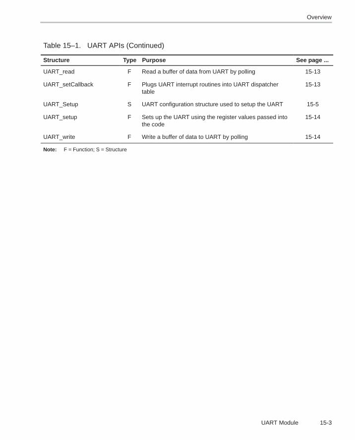
Overview
15-3UART Module
Table 15–1. UART APIs (Continued)
Structure See page ...PurposeType
UART_read F Read a buffer of data from UART by polling 15-13
UART_setCallback F Plugs UART interrupt routines into UART dispatchertable
15-13
UART_Setup S UART configuration structure used to setup the UART 15-5
UART_setup F Sets up the UART using the register values passed intothe code
15-14
UART_write F Write a buffer of data to UART by polling 15-14
Note: F = Function; S = Structure

UART_Setup
15-5UART Module
15.2 Configuration Structures
Configuration Structure for UARTUART_Config
Members
Uint16 dll Divisor Latch Register (low 8 bits)
Uint16 dlm Divisor Latch Register (high 8 bits)
Uint16 lcr Line Control Register
Uint16 fcr FIFO Control Register
Uint16 mcr Modem Control Register
Description UART configuration structure. This structure is created and initialized, andthen passed to the UART_Config() function.
Structure used to initialize the UARTUART_Setup
Members
Uint16 clkInput UART input clock frequency. Valid
symbolic values are:
UART_CLK_INPUT_58 // Input clock =
58.9824MHz
UART_CLK_INPUT_117 // Input clock =
117.9684MHz
Uint16 baud Baud Rate (Range: 150 – 115200). Valid
symbolic values are:
UART_BAUD_150
UART_BAUD_300
UART_BAUD_600
UART_BAUD_1200
UART_BAUD_1800
UART_BAUD_2000
UART_BAUD_2400
UART_BAUD_3600
UART_BAUD_4800
UART_BAUD_7200

UART_Setup
15-6
UART_BAUD_9600
UART_BAUD_19200
UART_BAUD_38400
UART_BAUD_57600
UART_BAUD_115200
Uint16 wordLength bits per word (Range: 5,6,7,8).
Valid symbolic values are:
UART_WORD5 5 bits per word
UART_WORD6 6 bits per word
UART_WORD7 7 bits per word
UART_WORD8 8 bits per word
Uint16 stopBits stop bits in a word (1, 1.5, and 2)
Valid symbolic values are:
UART_STOP1 1 stop bit
UART_STOP1_PLUS_HALF
1 and 1/2 stop bits
UART_STOP2 2 stop bits
Uint16 parity parity setups
Valid symbolic values are:
UART_DISABLE_PARITY
UART_ODD_PARITY odd parity
UART_EVEN_PARITY even parity
UART_MARK_PARITY mark parity
(the parity bit is always ‘1’)
UART_SPACE_PARITY space parity
(the parity bit is always ‘0’)
Uint16 fifoControl FIFO Control
Valid symbolic values are:
UART_FIFO_DISABLE
UART_FIFO_DMA0_TRIG01
UART_FIFO_DMA0_TRIG04
UART_FIFO_DMA0_TRIG08
UART_FIFO_DMA0_TRIG14
DMA mode0: always be 0

UART_Setup
15-7UART Module
RCVR FIFO trigger level: There are four
trigger levels for the RCVR FIFO
interrupt.
TRIG01 – 1 byte
TRIG04 – 4 bytes
TRIG08 – 8 byte
TRIG14 – 14 bytes
Uint16 loopbackEnable loopback Enable Valid Symbolic values are:
UART_NO_LOOPBACKUART_LOOPBACK
Description Structure used to init the UART. After created and initialized, it is passed to theUART_init() function.

UART_config
15-8
15.3 Functions
15.3.1 CSL Primary Functions
Initializes the UART using the configuration structureUART_config
Function void UART_config (UART_Config *Config);
Arguments Configure pointer to an initialized configuration structure (containing values forall registers that are visible to the user)
Description Writes a value to initialize the UART using the configuration structure.
Example UART_Config Config = {
0x00, /* DLL */
0x06, /* DLM – baud rate 150 */
0x18, /* LCR – even parity, 1 stop bit, 5
bits word length */
0x00, /* Disable FIFO */
0x00 /* No Loop Back */
};
UART_config(&Config);
Setups up the UART using register valuesUART_confi-gArgs
Function void UART_configArgs(Uint16 dll, Uint16 dlm, Uint16 lcr, Uint16 Fcr, Uint16 mcr);
Arguments dll value to setup DLL register
dlm value to setup DLM register
lcr value to setup LCR register
fcr value to setup FCR register
mcr value to setup MCR register
Description Sets up the UART using the register values passed.

UART_eventEnable
15-9UART Module
Example Uint16 tDll = 0x00 /* DLL */
Uint16 tDlm = 0x06 /* DLM */
Uint16 tLcrl = 0x18 /* LCR */
Uint16 tFcr = 0x00 /* FCR */
Uint16 tMcr = 0x00 /* MCR */
UART_configArgs(tDLL, tDlm, tLcr, tFcr, tMcr);
Disables UART interruptsUART_eventDisable
Function void UART_eventDisable(Uint16 ierMask);
Arguments ierMask can be one or a combination of the following:
UART_RINT 0x01 // Enable rx data available
interrupt
UART_TINT 0x02 // Enable tx hold register
empty interrupt
UART_LSINT 0x04 // Enable rx line status
interrupt
UART_MSINT 0x08 // Enable modem status
interrupt
UART_ALLINT 0x0f // Enable all interrupts
Description It disables the interrupt specified by the ierMask.
Example UART_eventDisable(UART_TINT);
Enables a UART interruptUART_eventEnable
Function void UART_eventEnable (Uint16 isrMask);
Arguments isrMask can be one or a combination of the following:
UART_RINT 0x01 // Enable rx data available interrupt
UART_TINT 0x02 // Enable tx hold register
empty interrupt
UART_LSINT 0x04 // Enable rx line status interrupt
UART_MSINT 0x08 // Enable modem status interrupt
UART_ALLINT 0x0f // Enable all interrupts

UART_eventEnable
15-10
Description It enables the UART interrupt specified by the isrMask.
Example UART_eventEnable(UART_RINT|UART_TINT);

UART_fgets
15-11UART Module
Reads UART charactersUART_fgetc
Function CSLBool UART_fgetc(int *c, Uint32 timeout);
Arguments c Character read from UARTtimeout Time out for data ready.
If it is setup as 0, means there will be no time out count. The function will block forever until DR bit is set.
Description Read a character from UART by polling.
Example Int retChar;CSLBool returnFlag
returnFlag = UART_fgetc(&retChar,0);
Reads UART stringsUART_fgets
Function CSLBool UART_fgets(char* pBuf, int bufSize, Uint32 timeout);
Arguments pBuf Pointer to a bufferbufSize Length of the buffertimeout Time out for data ready.
If it is setup as 0, means there will be no time out count. The function will block forever until DR bit is set.
Description This routine reads a string from the uart. The string will be read upto a newlineor until the buffer is filled. The string is always NULL terminated and does nothave any newline character removed.
Example char readBuf[10];CSLBool returnFlag
returnFlag = UART_fgets(&readBuf[0], 10, 0);

UART_fputc
15-12
Writes characters to the UARTUART_fputc
Function CSLBool UART_fputc(const int c, Uint32 timeout);
Arguments c The character, as an int, to be sent to the uart.timeout Time out for data ready.
If it is setup as 0, means there will be no time out count. The function will block forever if THRE bit is not set.
Description This routine writes a character out through UART.
Example Example const int putchar = ‘A’;CSLBool returnFlag;
ReturnFlag = UART_fputc(putchar, 0);
Writes strings to the UARTUART_fputs
Function CSLBool UART_fputs(const char* pBuf, Uint32 timeout);
Arguments pBuf Pointer to a buffertimeout Time out for data ready.
If it is setup as 0, means there will be no time out count. The function will block forever if THRE bit is not set.
Description This routine writes a string to the uart. The NULL terminator is not written anda newline is not added to the output.
Example UART_fputs(”\n\rthis is a test!\n\r”);
Reads the UART Configuration StructureUART_getConfig
Function void UART_getConfig (UART_Config *Config);
Arguments Config Pointer to an initialized configuration structure (including all registersthat are visible to the user)
Description Reads the UART configuration structure.
Example UART_Config Config;
UART_getConfig(&Config);

UART_setCallback
15-13UART Module
Reads received dataUART_read
Function CSLBool UART_read(char *pBuf, Uint16 length, Uint32 timeout);
Arguments pbuf Pointer to a bufferlength Length of data to be receivedtimeout Time out for data ready.
If it is setup as 0, means there will be no time out count. The function will block forever until DR bit is set.
Description Receive and put the received data to the buffer pointed by pbuf.
Example Uint16 length = 10;char pbuf[length];CSLBool returnFlag;
ReturnFlag = UART_read(&pbuf[0],length, 0);
Associates a function to the UART dispatch tableUART_setCallback
Function void UART_setCallback(UART_IsrAddr *isrAddr);
Arguments isrAddr is a structure containing pointers to the 5 functions that will be executedwhen the corresponding events is enabled.
Description It associates each function specified in the isrAddr structure to the UART dis-patch table.
Example UART_IsrAddr MyIsrAddr= {
NULL, // Receiver line status
UartRxIsr, // received data available
UartTxIsr, // transmiter holding register empty
NULL // character time-out indication
};
UART_setCallback(&MyIsrAddr);

UART_setup
15-14
Sets the UART based on the UART_Setup configuration structureUART_setup
Function void UART_setup (UART_Setup *Params);
Arguments Params Pointer to an initialized configuration structure that contains values forUART setup.
Description Sets UART based on UART_Setup structure.
Example UART_Setup Params = {
UART_CLK_INPUT_58, /* input clock freq */
UART_BAUD_115200, /* baud rate */
UART_WORD8, /* word length */
UART_STOP1, /* stop bits */
UART_DISABLE_PARITY, /* parity */
UART_FIFO_DISABLE, /* FIFO enable/disable */
UART_FIFO_DMA_MODE0, /* DMA mode */
UART_FIFO_TRIG01, /* FIFO trigger level */
UART_NO_LOOPBACK, /* Loop Back enable/disable */
};
UART_setup(&Params);
Transmits buffers of data by pollingUART_write
Function CSLBool UART_write(char *pBuf, Uint16 length, Uint32 timeout);
Arguments pbuf Pointer to a data bufferLength Length of the data buffertimeout Time out for data ready.
If it is setup as 0, means there will be no time out count. The function will block forever if THRE bit is not set.
Description Transmit a buffer of data by polling.
Example Uint16 length = 4;char pbuf[4] = {0x74, 0x65, 0x73, 0x74};CSLBool returnFlag;
ReturnFlag = UART_write(&pbuf[0],length,0);

UART_write
15-15UART Module
15.4 Macros
15.4.1 General Macros
Table 15–2. UART CSL Macros
Macro Syntax
(a) Macros to read/write UART register values
UART_RGET() Uint16 UART_RGET(REG)
UART_RSET() void UART_RSET(REG, Uint16 regval)
(b) Macros to read/write UART register field values (Applicable only to registers with more than one field)
UART_FGET() Uint16 UART_FGET(REG, FIELD)
UART_FSET() void UART_FSET(REG, FIELD, Uint16 fieldval)
(c) Macros to create value to write to UART registers and fields (Applicable only to registers withmore than one field)
UART_REG_RMK() Uint16 UART_REG_RMK(fieldval_n,...fieldval_0)
Note: *Start with field values with most significant field positions:
field_n: MSB fieldfield_0: LSB field* only writable fields allowed
UART_FMK() Uint16 UART_FMK(REG, FIELD, fieldval)
Notes: 1) REG indicates the registers: URIER, URIIR, URBRB, URTHR, URFCR, URLCR, URMCR, URLSR, URMSR,URDLL or URDLM.
2) FIELD indicates the register field name.
3) – or REG_FSET and REG__FMK, FIELD must be a writable field.
4) – For REG_FGET, the field must be a readable field.
5) regval indicates the value to write in the register (REG)
6) fieldval indicates the value to write in the field (FIELD)

UART_write
15-16
Table 15–2. UART CSL Macros (Continued)
Macro Syntax
(d) Macros to read a register address
UART_ADDR() Uint16 UART_ADDR(REG)
Notes: 1) REG indicates the registers: URIER, URIIR, URBRB, URTHR, URFCR, URLCR, URMCR, URLSR, URMSR,URDLL or URDLM.
2) FIELD indicates the register field name.
3) – or REG_FSET and REG__FMK, FIELD must be a writable field.
4) – For REG_FGET, the field must be a readable field.
5) regval indicates the value to write in the register (REG)
6) fieldval indicates the value to write in the field (FIELD)
15.4.2 UART Control Signal Macros
All the UART control signals are mapped through HPIGPIO pins. They areconfigurable through GPIOCR and GPIOSR registers. Since C54x DSP arecommonly used as DCE (Data Communication Equipment), these signals areconfigured as following:
HD0 – DTR – Input
HD1 – RTS – Input
HD2 – CTS – Output
HD3 – DSR – Output
HD4 – DCD – Output
HD5 – RI – Output

UART_dtcOff
15-17UART Module
Sets a CTS signal to OFFUART_ctsOff
Macro UART_ctsOff
Arguments None
Description Set CTS signal off.
Example UART_ctsOff;
Sets a CTS signal to ONUART_ctsOn
Macro UART_ctsOn
Arguments None
Description Set CTS signal on.
Example UART_ctsOn;
Initializes the HPIGPIO registers for flow controlUART_flowCtrlInit
Macro UART_flowCtrlInit
Arguments None
Description Initialize HPIGPIO registers for flow control.
Example UART_flowCtrlInit;
Verifies that RTS is ONUART_isRts
Macro UART_isRts
Arguments None
Description Check if RTS is on. Return RTS value.
Example CSLBool rtsSignal;
rtsSignal = UART_isRts;
Sets a DTC signal to OFFUART_dtcOff
Macro UART_dtcOff
Arguments None
Description Set DTC signal off.
Example UART_dtcOff;

UART_dtcOn
15-18
Sets a DTC signal to ONUART_dtcOn
Macro UART_dtcOn
Arguments None
Description Set DTC signal on.
Example UART_dtcOn;
Sets an RI signal to OFFUART_riOff
Macro UART_riOff
Arguments None
Description Set RI signal off.
Example UART_riOff;
Sets an RI signal to ONUART_riOn
Macro UART_riOn
Arguments None
Description Set RI signal on.
Example UART_riOn;
Sets a DSR signal to OFFUART_dsrOff
Macro UART_dsrOff
Arguments None
Description Set DSR signal off.
Example UART_dsrOff;
Sets a DSR signal to ONUART_dsrOn
Macro UART_dsrOn
Arguments None
Description Set DSR signal on.
Example UART_dsrOn;

UART_isDtr
15-19UART Module
Verifies that DTR is ONUART_isDtr
Macro UART_isDtr
Arguments Nobe
Description Check if DTR is on. Return DTR value.
Example CSLBool dtrSignal;
dtrSignal = UART_isDtr;

Configuring the UART Module Using CSL GUI
15-21UART Module
15.5 Configuring the UART Module Using CSL GUI
The Universal Asynchronous Receiver/Transmitter (UART) controller is thekey component of the serial communications subsystem of a computer. Asyn-chronous transmission allows data to be transmitted without a clock signal tothe receiver.
The configuration manager allows creation of one or more configuration ob-jects. The configuration objects contain all of the data necessary to set theUART Control Registers.
The resource manager allows the user to choose a configuration object to touse in configuring the UART.
Figure 15–1 illustrates the UART sections menu on the CSL graphical user in-terface (GUI)
Figure 15–1. UART Sections Menu
The UART includes the following two sections:
� UART Configuration Manager allows you to create configurationobjects. No predefined configuration objects.
� UART Resource Manager allows you to select a configuration andenable that configuration within the object.
15.5.1 UART Configuration Manager
The UART Configuration Manager allows you to create UART configurationsthrough the Properties page and to generate the configuration objects.
15.5.1.1 Inserting a Configuration Object
There is no predefined configuration object available.
To configure the UART registers, you must insert a new configuration object.
To insert a new configuration object, right-click on the UART ConfigurationManager and select insert uartCfg from the drop-down menu. The configura-tion objects can be renamed. Their use depends upon the on-chip device re-sources.

Configuring the UART Module Using CSL GUI
15-22
Note:
The number of configuration objects is unlimited. Several configurations canbe created and the user can select the right one for this application and canchange the configuration later just by selecting a new one under the UARTResource Manager. The goal is to provide more flexibility and to reduce thetime required to modify register values.
15.5.1.2 Deleting/Renaming a Configuration Object
To delete or to rename an object, right-click on the configuration object youwant to delete or rename. Select Delete to delete a configuration object. SelectRename to rename the object.
If the Delete and Rename options are grayed out and non-usable, use theUART Resource Manager to configure the UART. The Show Dependency op-tion is accessible and shows which device is using the configuration object(see Figure 2–1, The CSL Tree, on page 2-3).
15.5.1.3 Configuring the Object Properties
The Properties pages allow you to set the UART registers (see Figure 15–2).To access the Properties dialog box, right-click on a configuration object andselect Properties. By default, the General page of the Properties dialog box isdisplayed.
The Properties pages allow you to set the time, date, and alarm registers ofthe UART. You can set the configuration options through the following pages:
� Setup: Allows you to configure the UART based on a set of parameters.
� Advanced: Allows you to configure the values of the previous pages bydirectly setting the UART registers.
This page contains the full 8-bit register values; the full register values canbe entered directly and the new options will be mirrored on the previouspage automatically.
Figure 15–2 depicts the properties page.

Configuring the UART Module Using CSL GUI
15-23UART Module
Figure 15–2. UART Properties Page
Each Tab page is composed of several options that are set to a default value(at device reset).
15.5.2 UART Resource Manager
The UART Resource Manager allows you to generate the UART_config() CSLfunction.
Figure 15–3 illustrates the UART Resource Manager menu on the CSL graph-ical user interface (GUI).
Figure 15–3. UART Resource Manager Menu
15.5.2.1 Properties Page
You can generate the UART_Config() CSL function through the Propertiespage.
To access the Properties page, right-click on the predefined UART peripheraland select Properties from the drop-down menu (see Figure 15–4).
The first time the Properties page appears, only the Enable UART Configura-tion check-box can be selected. Select this to enable the UART configuration.

Configuring the UART Module Using CSL GUI
15-24
UART_NOTHING is used to indicate that there is no configuration object se-lected for this serial port.
To pre-initialize the UART peripheral, check the Enable UART Configurationbox. You can then select one of the available configuration objects (see sec-tion 15.5.1) for this peripheral through the pre-initialize drop-down list.
If UART_NOTHING remains selected, the UART_config() function will not begenerated for the UART. (see section 15.5.3).
In the example shown in Figure 15–4, the uartCfg0 is selected, UART and theUART_config() function will be generated, thereby setting the UART toUARTfg0 configuration settings.
Figure 15–4. UART Resource Manager Properties Page
15.5.3 C Code Generation for UART Module
The two C files generated from the configuration tool are a header file and asource file.
15.5.3.1 Header File
The header file includes all the csl header files of the modules and containsthe configuration objects defined from the configuration tool (seeExample 15–1).
Example 15–1. UART Header File
extern UART_Config uartCfg0;

Configuring the UART Module Using CSL GUI
15-25UART Module
15.5.3.2 Source File
The source file includes the declaration of the handle object and the configura-tion structures (see Example 15–2).
Example 15–2. UART Source File (Declaration Section)
/* Config Structures */
UART_Config uartCfg0 = {
0x80, /* Divisor Latch (URDLL – LSB) */0x01, /* Divisor Latch (URDLL – MSB) */0x00, /* Line Control Register (URLCR) */0x00, /* FIFO Control Register (URFCR) */0x00 /* Modem Control Register (URMCR) */
};
The source file contains the Configuration Pre-Initialization using the CSLUART API function UART_config() (see Example 15–3).
This function is encapsulated into a unique function, CSL_cfgInit(), which iscalled from your main C file. UART_config() is generated only if Enable UARTconfiguration (with a selected configuration other than UART_NOTHING) ischecked under the UART Resource Manager Properties page.
Example 15–3. UART Source File (Body Section)
void CSL_cfgInit()
{
UART_config(&uartCfg0);
}

16-1
WDTIM Module
This chapter lists the configuration structure, functions, and macros availablefor use with the WDTIM modules.
Topic Page
16.1 Overview 16-2. . . . . . . . . . . . . . . . . . . . . . . . . . . . . . . . . . . . . . . . . . . . . . . . . . . .
16.2 Configuration Structure 16-3. . . . . . . . . . . . . . . . . . . . . . . . . . . . . . . . . . . . . .
16.3 Functions 16-4. . . . . . . . . . . . . . . . . . . . . . . . . . . . . . . . . . . . . . . . . . . . . . . . . . .
16.4 Macros 16-6. . . . . . . . . . . . . . . . . . . . . . . . . . . . . . . . . . . . . . . . . . . . . . . . . . . . . .
16.5 Configuring the WATCHDOG TIMER Module Using CSL GUI 16-8. . . . .
Chapter 16

Overview
16-2
16.1 Overview
Table 16–1 and Table 16–2 list the configuration structures and functions usedwith the WDTIM module.
Table 16–1. WDTIM Configuration Structure
Structure Purpose See page...
WDTIM_Config WDTIM configuration structure used to setup a watchdog timerdevice
16-3
Table 16–2. WDTIM Functions
Function Purpose See page ...
WDTIM_config Sets up the WDTIM register using the configuration structure 16-4
WDTIM_configArgs Sets up the WDTIM using the register values passed in 16-4
WDTIM_getConfig Reads the current register values of the watchdog timer andstores the result in the configuration structure
16-5
WDTIM_service Writes to the watchdog key of the timer 16-5
WDTIM_start Starts the WDTIM device running 16-5

WDTIM_Config
16-3
16.2 Configuration Structure
This section lists the structure in the WDTIM module.
WDTIM configuration structure used to setup timer deviceWDTIM_Config
Structure WDTIM_Config
Members Uint16 wdtcr control
Uint16 wdtscr secondary control
Uint16 wdprd period
Description The WDTIM configuration structure is used to setup a watchdog timer device.You create and initialize this structure then pass its address to theWDTIM_config() function. You can use literal values or the WDTIM_RMKmacros to create the structure member values.
Example WDTIM_Config MyConfig = {
0x0000, /* control */
0x1000, /* secondary control */
0x1000 /* period */
};
…WDTIM_config(&MyConfig);

WDTIM_config
16-4
16.3 FunctionsThis section lists the functions in the WDTIM module.
Sets up WDTIM register using configuration structureWDTIM_config
Function void WDTIM_config(WDTIM_Config *Config
);
Arguments config Pointer to an initialized configuration structure
Return Value None
Description Sets up the WDTIM register using the configuration structure. The values ofthe structure are written to the registers TCR, PRD, and TIM (see alsoWDTIM_configArgs() and WDTIM_Config).
Example WDTIM_Config MyConfig = {
};
…WDTIM_config(&MyConfig);
Sets up WDTIM using register values passed inWDTIM_configArgs
Function void WDTIM_configArgs(Uint16 wdtcr,Uint16 wdtscr,Uint16 wdprd
);
Arguments wdtcr Control register value
wdtscr Secondary Control register value
wdprd Period register value
Return Value None
Description Sets up the timer using the register values passed in. The register values arewritten to the timer registers. The timer control register (wdtcr) is written last(see also WDTIM_config()).
You may use literal values for the arguments or for readability, you may usethe WDTIM_RMK macros to create the register values based on field values.
Example WDTIM_configArgs (
0x0010, /* wdtcr */
0x0000, /* wdtscr */
0x1000 /* wdprd */
);

WDTIM_start
16-5
Gets the WDTIM configuration structure for a specified deviceWDTIM_getConfig
Function void WDTIM_getConfig(WDTIM_Config *Config
);
Arguments Config Pointer to a WDTIM configuration structure
Return Value None
Description Gets the WDTIM configuration structure for a specified device.
Example WDTIM_Config MyConfig;
WDTIM_getConfig(&MyCOnfig);
Writes to the watchdog key of the timerWDTIM_service
Function void WDTIM_service();
Arguments None
Return Value None
Description Services the watchdog timer by writing a sequence of A5C6h, followed by anA7Eh to the WDKEY field of the WDTSCR register, before the watchdog timertimes out. This function must be called periodically to prevent awatchdog timeout.
Example WDTIM_service();
Starts WDTIM device runningWDTIM_start
Function void WDTIM_start();
Arguments None
Return Value None
Description Starts the timer device running. TSS field =0.
Example WDTIM_start();

Macros
16-6
16.4 Macros
CSL offers a collection of macros to access CPU control registers and fields.For additional details (see section 1.5).
Table 16–3 lists the available WDTIM macros.
Table 16–3 uses the following conventions:
To use the WDTIM macros, include csl_wdtim.h and follow these restrictions:
� Only writable fields are allowed
� Values should be a right-justified constants.
� If fieldval_n value exceeds the number of bits allowed for that field,fieldval_n is truncated accordingly
For examples that are similar to the WDTIM macros, see section 6.4 in theDMA chapter or section 11.4 in the McBSP chapter.

Macros
16-7 WDTIM Module
Table 16–3. WDTIM CSL Macros Using Timer Port Number
(a) Macros to read/write WDTIM register values
Macro Syntax
WDTIM_RGET() Uint16 WDTIM_RGET(REG)
WDTIM_RSET() void WDTIM_RSET(REG, Uint16 regval)
(b) Macros to read/write WDTIM register field values (Applicable only to registers with more than one field)
Macro Syntax
WDTIM_FGET() Uint16 WDTIM_FGET(REG, FIELD)
WDTIM_FSET() void WDTIM_FSET(REG, FIELD, Uint16 fieldval)
(c) Macros to create value to write to WDTIM registers and fields (Applicable only to registers with more thanone field)
Macro Syntax
WDTIM_REG_RMK() Uint16 WDTIM_REG_RMK(fieldval_n,...fieldval_0)
Note: *Start with field values with most significant field positions:field_n: MSB fieldfield_0: LSB field* only writable fields allowed
WDTIM_FMK() Uint16 WDTIM_FMK(REG, FIELD, fieldval)
(d) Macros to read a register address
Macro Syntax
WDTIM_ADDR() Uint16 WDTIM_ADDR(REG)
Notes: 1) REG indicates the register, WDTCR, WDPRD, WDTSCR, or WDTIM.2) FIELD indicates the register field name as specified in Appendix A.
� For REG_FSET and REG_FMK, FIELD must be a writable field.
� For REG_FGET, the field must be a readable field.
3) regval indicates the value to write in the register (REG)
4) fieldval indicates the value to write in the field (FIELD)

Configuring the WATCHDOG TIMER Module Using CSL GUI
16-8
16.5 Configuring the WATCHDOG TIMER Module Using CSL GUI
16.5.1 Overview
The WATCHDOG TIMER module facilitates configuration/control of the on-chip WATCHDOG TIMER. The WATCHDOG TIMER module consists of a con-figuration manager and a resource manager. The configuration manager al-lows the creation of one or more configuration objects. The configuration ob-ject consists of the necessary data to set the WATCHDOG TIMER control reg-isters. The resource manager associates a selected configuration with a timer.
Figure 16–1 illustrates the WATCHDOG TIMER sections menu on the CSLgraphical user interface (GUI).
Figure 16–1. WATCHDOG TIMER Sections Menu
The WATCHDOG TIMER includes the following two sections:
� WATCHDOG TIMER Configuration Manager: Allows you to createconfiguration objects. (There are no predefined configuration objects.)
� WATCHDOG TIMER Resource Manager: Allows you to associate aconfiguration object to the Watchdog Timer. The WATCHDOG TIMER isonly available in the TMS320C5440 and TMS320C5441 devices.
16.5.2 WATCHDOG TIMER Configuration Manager
The WATCHDOG TIMER Configuration Manager allows you to create deviceconfigurations through the Properties page and generate the configuration ob-jects.
16.5.2.1 Creating/Inserting a configuration
There are no predefined configuration objects available.
To configure a WATCHDOG TIMER device through the peripheral, you mustinsert a new configuration object.
To insert a new configuration object, right-click on the WATCHDOG TIMERConfiguration Manager and select Insert wdtimCfg from the drop-down menu.The configuration objects can be renamed. Their use depends on the on-chipdevice resources.

Configuring the WATCHDOG TIMER Module Using CSL GUI
16-9 WDTIM Module
Note:
The number of configuration objects is unlimited. Several configurations canbe created and you can select the right one for a specific device and changethe configuration later just by selecting a new one under the WATCHDOGTIMER Resource Manager. This feature provides you with more flexibilityand reduces the time required to modify register values.
16.5.2.2 Deleting/Renaming an Object
To delete or to rename an object, right-click on the configuration object youwant to delete or rename. Select Delete to delete a configuration object. SelectRename to rename the object.
If a configuration object is used by one of the predefined handle objects of theWATCHDOG TIMER Resource Manager, the Delete and Rename options aregrayed out and non-usable. The Show Dependency option is accessible andshows which device is using the configuration object (see Figure 2–1, TheCSL Tree, on page 2-3).
16.5.2.3 Configuring the Object Properties
You can configure object properties through the Properties dialog box (seeFigure 16–2). To access the Properties dialog box, right-click on a configura-tion object and select Properties. By default, the General page of the Proper-ties dialog box is displayed.
The Properties pages allow you to set the Peripheral registers related to theWATCHDOG TIMER. You can set the configuration options through the follow-ing tab pages:
� General: Allows you to configure the Breakpoint Emulation
� Counter Control: Allows you to configure the Breakpoint EmulationCounter configuration
� Advanced Page: Allows you to configure the Summary of the previous twopages
� This page contains the full hexadecimal register values and reflects thesetting of the two pages
� The full register values can be entered directly and the new options will bemirrored on the previous two pages automatically
Figure 16–2 depicts the Properties Page dialog box.

Configuring the WATCHDOG TIMER Module Using CSL GUI
16-10
Figure 16–2. WATCHDOG TIMER Properties Page
Each Tab page is composed of several options that are set to a default value(at device reset).
The options represent the fields of the WATCHDOG TIMER registers; the as-sociated field name is shown in parenthesis.
16.5.3 WATCHDOG TIMER Resource Manager
The WATCHDOG TIMER Resource Manager allows you to generate theWDTIM_config() CSL function.
Figure 16–3 illustrates the WATCHDOG TIMER Resource Manager Menu.
Figure 16–3. WATCHDOG TIMER Resource Manager Menu
16.5.3.1 Properties Page
You can generate the WDTIM_config() csl function through the Propertiespage.
To access the Properties page, right-click on a predefined TIMER handle ob-ject and select Properties from the drop-down menu (see Figure 16–4).
The first time the properties page appears, only the Enable Configuration ofWATCHDOG TIMER check-box can be selected. Select this to open theWATCHDOG TIMER configuration, allowing pre-initialization.

Configuring the WATCHDOG TIMER Module Using CSL GUI
16-11 WDTIM Module
WDTIM_NOTHING is used to indicate that there is no configuration object se-lected for this device.
To pre-initialize the Watchdog Timer, check the Enable Configuration ofWATCHDOG TIMER box. One of the available configuration objects (see sec-tion 16.5.2) can then be selected for this channel through the Pre-Initializedrop-down list.
If WDTIM_NOTHING remains selected, no WDTIM_config() function call willbe generated for the WATCHDOG TIMER. (See section 16.5.4.)
In Figure 16–4, the Enable Configuration of Watchdog Timer option is checkedand wdtimCfg0 is now accessible. The WDTIM_config() function will be gener-ated.
Figure 16–4. WATCHDOG TIMER Properties Page
16.5.4 C Code Generation for WATCHDOG TIMER
Two C files are generated from the configuration tool:
� Header file
� Source file.
16.5.4.1 Header File
The header file includes all the csl header files of the modules and containsthe WATCHDOG TIMER configuration objects defined from the configurationtool (see Example 16–1).

Configuring the WATCHDOG TIMER Module Using CSL GUI
16-12
Example 16–1. WATCHDOG TIMER Header File
extern WDTIM_Config wdtimCfg0;
16.5.4.2 Source File
The source file includes the declaration of the configuration structures (seeExample 16–2).
Example 16–2. WATCHDOG TIMER Source File (Declaration Section)
/* Config Structures */
WDTIM_Config wdtimCfg0 = {
0x0000, /* Timer Control Register */
0x0000, /* Timer Period Register */
0x0000 /* Timer Scale Register (TSCR) */
};
The source file contains the Configuration Pre-Initialization using the CSLWATCHDOG TIMER API WDTIM_config() (see Example 16–3). This functionis encapsulated into a unique function, CSL_cfgInit(), which is called from yourmain C file.
WDTIM_config() will be generated only if Enable Configuration of WATCH-DOG TIMER is checked and a configuration other than WDTIM_NOTHING isselected on the Watchdog Timer Resource Manager Properties page.
Note:
You must use WDTIM_start() in your code to start the WATCHDOG TIMER.The WDTIM_Config structure generated by the CSL GUI does not start theWATCHDOG TIMER port.
Example 16–3. WATCHDOG TIMER Source File (Body Section)
void CSL_cfgInit()
{
WDTIM_config(&wdtimCfg0);
}

A-1
Appendix A
Peripheral Registers
This appendix provides symbolic constants for the peripheral registers.
Topic Page
A.1 DMA Registers A-2. . . . . . . . . . . . . . . . . . . . . . . . . . . . . . . . . . . . . . . . . . . . . . . .
A.2 EBUS Registers A-16. . . . . . . . . . . . . . . . . . . . . . . . . . . . . . . . . . . . . . . . . . . . . .
A.3 GPIO Registers (C5440 and C5441) A-22. . . . . . . . . . . . . . . . . . . . . . . . . . . .
A.4 HPI Registers A-24. . . . . . . . . . . . . . . . . . . . . . . . . . . . . . . . . . . . . . . . . . . . . . . .
A.5 Multichannel BSP (McBSP) Registers A-26. . . . . . . . . . . . . . . . . . . . . . . . . .
A.6 PLL Register (CLKMD) A-47. . . . . . . . . . . . . . . . . . . . . . . . . . . . . . . . . . . . . . .
A.7 Timer Registers A-49. . . . . . . . . . . . . . . . . . . . . . . . . . . . . . . . . . . . . . . . . . . . . .
A.8 Watchdog Timer Registers (C5441) A-52. . . . . . . . . . . . . . . . . . . . . . . . . . . .
Appendix A

DMA Registers
A-2
A.1 DMA Registers
A.1.1 DMA Channel Priority and Enable Control Register (DMPREC)
Figure A–1. DMA Channel Priority and Enable Control Register (DMPREC)
15 14 13 8
FREE AUTOIX† DPRC
R/W-0 R/W-0 R/W-0
7 6 5 0
INTOSEL DE
R/W-0 R/W-0† Only available on specific devices.
Legend: R/W-x = Read/Write-Reset value
Table A–1. DMA Channel Priority and Enable Control Register (DMPREC)Field Values (DMA_DMPREC_field_symval)
Bit field symval Value Description
15 FREE Controls the behavior of the DMA controller during emulation.
OFF 0 DMA transfers are suspended when the emulator stops
ON 1 DMA transfers continue even during emulation stop
14 AUTOIX For C5409A, C54010A, C5416, C5440, and C5441: Selectswhich DMA global reload registers are used to reload the DMAchannels.
USE_DMA0 0 All DMA channels use DMGSA0, DMGDA0, DMGCR0, andDMGFR0 as their reload registers.
USE_CHAN 1 Each DMA channel uses its local set of reload registers duringautoinitialization mode.
13-8 DPRC OF(value) 0-63 DMA channel priority control bit. Each bit specifies the priority ofa DMA channel. When the bit is cleared to 0, the channel is a lowpriority; when the bit is set to 1, the channel is a high priority.
7-6 INTOSEL Interrupt multiplex control bits. The INTOSEL bits control howthe DMA interrupts are assigned in the interrupt vector table andIMR/IMF registers. The effects of this field on the operation aredevice-specific.
For C5401, C5402, C5409, C5409A, C5420, 5421, and 5471
NONE 00 Interrupts available: Timer 1, McBSP 1 RINT/XINT
CH2_CH3 01 Interrupts available: Timer 1, DMA channel 2, DMA channel 3
CH0_TO_CH3 10 Interrupts available: DMA channel 0, DMA channel 1,DMA channel 2, DMA channel 3
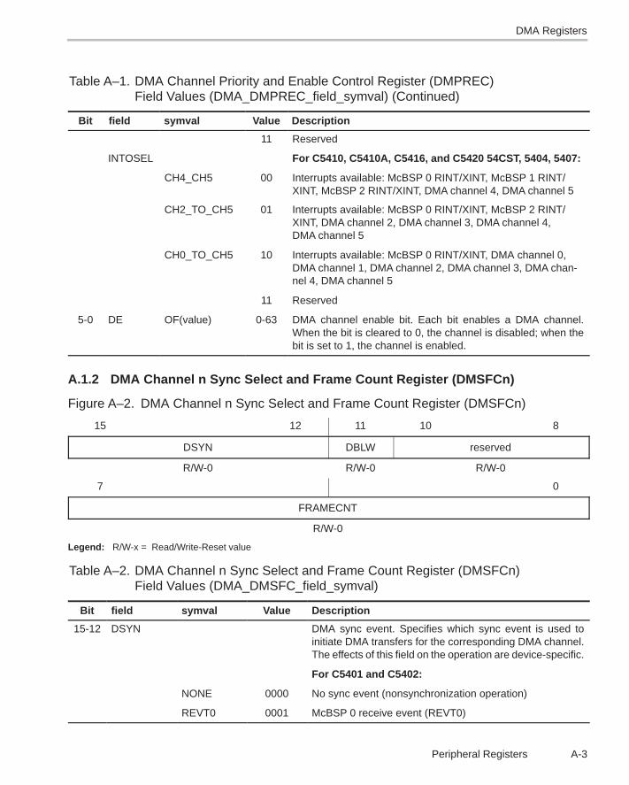
DMA Registers
A-3Peripheral Registers
Table A–1. DMA Channel Priority and Enable Control Register (DMPREC)Field Values (DMA_DMPREC_field_symval) (Continued)
Bit DescriptionValuesymvalfield
11 Reserved
INTOSEL For C5410, C5410A, C5416, and C5420 54CST, 5404, 5407:
CH4_CH5 00 Interrupts available: McBSP 0 RINT/XINT, McBSP 1 RINT/XINT, McBSP 2 RINT/XINT, DMA channel 4, DMA channel 5
CH2_TO_CH5 01 Interrupts available: McBSP 0 RINT/XINT, McBSP 2 RINT/XINT, DMA channel 2, DMA channel 3, DMA channel 4,DMA channel 5
CH0_TO_CH5 10 Interrupts available: McBSP 0 RINT/XINT, DMA channel 0,DMA channel 1, DMA channel 2, DMA channel 3, DMA chan-nel 4, DMA channel 5
11 Reserved
5-0 DE OF(value) 0-63 DMA channel enable bit. Each bit enables a DMA channel.When the bit is cleared to 0, the channel is disabled; when thebit is set to 1, the channel is enabled.
A.1.2 DMA Channel n Sync Select and Frame Count Register (DMSFCn)
Figure A–2. DMA Channel n Sync Select and Frame Count Register (DMSFCn)
15 12 11 10 8
DSYN DBLW reserved
R/W-0 R/W-0 R/W-0
7 0
FRAMECNT
R/W-0
Legend: R/W-x = Read/Write-Reset value
Table A–2. DMA Channel n Sync Select and Frame Count Register (DMSFCn)Field Values (DMA_DMSFC_field_symval)
Bit field symval Value Description
15-12 DSYN DMA sync event. Specifies which sync event is used toinitiate DMA transfers for the corresponding DMA channel.The effects of this field on the operation are device-specific.
For C5401 and C5402:
NONE 0000 No sync event (nonsynchronization operation)
REVT0 0001 McBSP 0 receive event (REVT0)

DMA Registers
A-4
Table A–2. DMA Channel n Sync Select and Frame Count Register (DMSFCn)Field Values (DMA_DMSFC_field_symval) (Continued)
Bit DescriptionValuesymvalfield
XEVT0 0010 McBSP 0 transmit event (XEVT0)
0011 Reserved
0100 Reserved
DSYN REVT1 0101 McBSP 1 receive event (REVT1)
XEVT1 0110 McBSP 1 transmit event (XEVT1)
0111-1100 Reserved
TINT0 1101 Timer 0 interrupt event
INT3 1110 External interrupt 3 event
TINT1 1111 Timer 1 interrupt event
For C5409, C5409A, and C5471:
NONE 0000 No sync event (nonsynchronization operation)
REVT0 0001 McBSP 0 receive event (REVT0)
XEVT0 0010 McBSP 0 transmit event (XEVT0)
REVT2 0011 McBSP 2 receive event (REVT2)
XEVT2 0100 McBSP 2 transmit event (XEVT2)
REVT1 0101 McBSP 1 receive event (REVT1)
XEVT1 0110 McBSP 1 transmit event (XEVT1)
0111-1100 Reserved
TINT0 1101 Timer interrupt event
INT3 1110 External interrupt 3 event
For C5410, C5410A, and C5416:
NONE 0000 No sync event (nonsynchronization operation)
REVT0 0001 McBSP 0 receive event (REVT0)
XEVT0 0010 McBSP 0 transmit event (XEVT0)
REVT2 0011 McBSP 2 receive event (REVT2)
XEVT2 0100 McBSP 2 transmit event (XEVT2)
REVT1 0101 McBSP 1 receive event (REVT1)
XEVT1 0110 McBSP 1 transmit event (XEVT1)
REVTA0 0111 McBSP 0 receive event — ABIS mode (REVTA0)
XEVTA0 1000 McBSP 0 transmit event — ABIS mode (XEVTA0)

DMA Registers
A-5Peripheral Registers
Table A–2. DMA Channel n Sync Select and Frame Count Register (DMSFCn)Field Values (DMA_DMSFC_field_symval) (Continued)
Bit DescriptionValuesymvalfield
REVTA2 1001 McBSP 2 receive event — ABIS mode (REVTA2)
XEVTA2 1010 McBSP 2 transmit event — ABIS mode (XEVTA2)
DSYN REVTA1 1011 McBSP 1 receive event — ABIS mode (REVTA1)
XEVTA1 1100 McBSP 1 transmit event — ABIS mode (XEVTA1)
TINT0 1101 Timer interrupt event
INT3 1110 External interrupt 3 event
1111 Reserved
For C5420 and C5421:
NONE 0000 No sync event (nonsynchronization operation)
REVT0 0001 McBSP 0 receive event (REVT0)
XEVT0 0010 McBSP 0 transmit event (XEVT0)
REVT2 0011 McBSP 2 receive event (REVT2)
XEVT2 0100 McBSP 2 transmit event (XEVT2)
REVT1 0101 McBSP 1 receive event (REVT1)
XEVT1 0110 McBSP 1 transmit event (XEVT1)
FIFO_REVT 0111 FIFO receive buffer not empty event
FIFO_XEVT 1000 FIFO transmit buffer not full event
1001-1111 Reserved
For C5440 and C5441:
NONE 0000 No sync event (nonsynchronization operation)
REVT0 0001 McBSP 0 receive event (REVT0)
XEVT0 0010 McBSP 0 transmit event (XEVT0)
REVT2 0011 McBSP 2 receive event (REVT2)
XEVT2 0100 McBSP 2 transmit event (XEVT2)
REVT1 0101 McBSP 1 receive event (REVT1)
XEVT1 0110 McBSP 1 transmit event (XEVT1)
0111-1100 Reserved
For C54CST, 5404, and 5407:
NONE 0000 No sync event (nonsynchronization operation)
REVT0 0001 McBSP 0 receive event (REVT0)

DMA Registers
A-6
Table A–2. DMA Channel n Sync Select and Frame Count Register (DMSFCn)Field Values (DMA_DMSFC_field_symval) (Continued)
Bit DescriptionValuesymvalfield
XEVT0 0010 McBSP 0 transmit event (XEVT0)
REVT2 0011 McBSP 2 receive event (REVT2)
XEVT2 0100 McBSP 2 transmit event (XEVT2)
REVT1 0101 McBSP 1 receive event (REVT1)
XEVT1 0110 McBSP 1 transmit event (XEVT1)
0611-1100 Reserved
1000-1101 Reserved
UART 0111 UART interrupt event
TINT0 1101 Timer interrupt event
TINT1 111 Timer1 interrupt event
TINT3 1110 External interrupt 3 event
11 DBLW Double-word mode enable bit.
OFF 0 Single-word mode. DMA transfers 16-bit words.
ON 1 Double-word mode. Allows the DMA to transfer 32-bitwords in any index mode. Two consecutive 16-bit trans-fers are initiated and the source and destination address-es are automatically updated following each transfer.
10-8 reserved Reserved. The reserved bit location is always read as zero.A value written to this field has no effect.
7-0 FRAMECNT OF(value) 0-255 Frame count. Specifies the number of frames to be includedin a block transfer. The frame count is initialized to 1 lessthan the desired number of frames.
A.1.3 DMA Channel n Transfer Mode Control Register (DMMCRn)
Figure A–3. DMA Channel n Transfer Mode Control Register (DMMCRn)
15 14 13 12 11 10 8
AUTOINIT DINM IMOD CTMOD SLAXS† SIND
R/W-0 R/W-0 R/W-0 R/W-0 R/W-0 R/W-0
7 6 5 4 2 1 0
DMS DLAXS† DIND DMD
R/W-0 R/W-0 R/W-0 R/W-0† Only available on specific devices with DMA extended data memory.
Legend: R/W-x = Read/Write-Reset value

DMA Registers
A-7Peripheral Registers
Table A–3. DMA Channel n Transfer Mode Control Register (DMMCRn) Field Values(DMA_DMMCR_field_symval)
Bit field symval Value Description
15 AUTOINIT DMA autoinitialization mode enable bit.
OFF 0 Autoinitialization is disabled.
ON 1 Autoinitialization is enabled.
14 DINM DMA interrupt generation mask bit.
OFF 0 No interrupt is generated
ON 1 Interrupt is generated based on IMOD bit
13 IMOD DMA interrupt generation mode bit operates inconjunction with CTMOD bit.
In ABU mode (CTMOD = 1):
FULL_ONLY 0 Interrupt at buffer full only.
HALF_AND_FULL 1 Interrupt at half full buffer and buffer full.
In multiframe mode (CTMOD = 0):
BLOCK_ONLY 0 Interrupt at completion of block transfer.
FRAME_AND_BLOCK 1 Interrupt at end of frame and end of block.
12 CTMOD DMA transfer counter mode control bit.
MULTIFRAME 0 Multiframe mode
ABU 1 ABU mode
11 SLAXS For devices with DMA extended data memory:DMA source space select bit.
OFF 0 No external access
ON 1 External access
10-8 SIND DMA source address transfer index mode bit.
NOMOD 000 No modification
POSTINC 001 Postincrement
POSTDEC 010 Postdecrement
DMIDX0 011 Postincrement with index offset (DMIDX0)
DMIDX1 100 Postincrement with index offset (DMIDX1)
DMFRI0 101 Postincrement with index offset (DMIDX0 andDMFRI0)
DMFRI1 110 Postincrement with index offset (DMIDX1 andDMFRI1)
111 Reserved

DMA Registers
A-8
Table A–3. DMA Channel n Transfer Mode Control Register (DMMCRn) Field Values(DMA_DMMCR_field_symval) (Continued)
Bit DescriptionValuesymvalfield
7-6 DMS DMA source address space select bit.
PROGRAM 00 Program space
DATA 01 Data space
IO 10 I/O space
11 Reserved
5 DLAXS For devices with DMA extended data memory:DMA destination space select bit.
OFF 0 No external access
ON 1 External access
4-2 DIND DMA destination address transfer index mode bit.
NOMOD 000 No modification
POSTINC 001 Postincrement
POSTDEC 010 Postdecrement
DMIDX0 011 Postincrement with index offset (DMIDX0)
DMIDX1 100 Postincrement with index offset (DMIDX1)
DMFRI0 101 Postincrement with index offset (DMIDX0 andDMFRI0)
DMFRI1 110 Postincrement with index offset (DMIDX1 andDMFRI1)
111 Reserved
1-0 DMD DMA destination address space select bit.
PROGRAM 00 Program space
DATA 01 Data space
IO 10 I/O space
11 Reserved

DMA Registers
A-9Peripheral Registers
A.1.4 DMA Channel n Source Address Register (DMSRCn)
Figure A–4. DMA Channel n Source Address Register (DMSRCn)
15 0
Source Address (SRC)
R/W-0
Legend: R/W-x = Read/Write-Reset value
Table A–4. DMA Channel n Source Address Register (DMSRCn) Field Values(DMA_DMSRC_field_symval)
Bit field symval Value Description
15-0 SRC OF(value) 0-FFFFh Specifies the 16 least-significant bits of the extended address for thesource location. The source address register is initialized prior tostarting the DMA transfer in software, and updated automaticallyduring transfers by the DMA controller.
A.1.5 DMA Global Source Address Reload Register (DMGSA)
Figure A–5. DMA Global Source Address Reload Register (DMGSA)
15 0
Global Source Address (GSA)
R/W-0
Legend: R/W-x = Read/Write-Reset value
Table A–5. DMA Global Source Address Reload Register (DMGSA) Field Values(DMA_DMGSA_field_symval)
Bit field symval Value Description
15-0 GSA OF(value) 0-FFFFh A 16-bit source address used to reload DMSRCn.
A.1.6 DMA Source Program Page Address Register (DMSRCP)
Figure A–6. DMA Source Program Page Address Register (DMSRCP)
15 7 6 0
reserved Source Program Page Address (PAGE)
R/W-0 R/W-0
Legend: R/W-x = Read/Write-Reset value

DMA Registers
A-10
Table A–6. DMA Source Program Page Address Register (DMSRCP) Field Values(DMA_DMSRCP_field_symval)
Bit field symval Value Description
15-7 reserved Reserved. The reserved bit location is always read as zero. Avalue written to this field has no effect.
6-0 PAGE OF(value) 0-127 Specifies the 7 most-significant bits of the extended program pageaddress for the source location.
A.1.7 DMA Channel n Destination Address Register (DMDSTn)
Figure A–7. DMA Channel n Destination Address Register (DMDSTn)
15 0
Destination Address (DST)
R/W-0
Legend: R/W-x = Read/Write-Reset value
Table A–7. DMA Channel n Destination Address Register (DMDSTn) Field Values(DMA_DMDST_field_symval)
Bit field symval Value Description
15-0 DST OF(value) 0-FFFFh Specifies the 16 least-significant bits of the extended address for thedestination location. The destination address register is initializedprior to starting the DMA transfer in software, and updatedautomatically during transfers by the DMA controller.
A.1.8 DMA Global Destination Address Reload Register (DMGDA)
Figure A–8. DMA Global Destination Address Reload Register (DMGDA)
15 0
Global Destination Address (GDA)
R/W-0
Legend: R/W-x = Read/Write-Reset value
Table A–8. DMA Global Destination Address Reload Register (DMGDA) Field Values(DMA_DMGDA_field_symval)
Bit field symval Value Description
15-0 GDA OF(value) 0-FFFFh A 16-bit destination address used to reload DMDSTn.

DMA Registers
A-11Peripheral Registers
A.1.9 DMA Destination Program Page Address Register (DMDSTP)
Figure A–9. DMA Destination Program Page Address Register (DMDSTP)
15 7 6 0
reserved Destination Program Page Address (PAGE)
R/W-0 R/W-0
Legend: R/W-x = Read/Write-Reset value
Table A–9. DMA Destination Program Page Address Register (DMDSTP) Field Values(DMA_DMDSTP_field_symval)
Bit field symval Value Description
15-7 reserved Reserved. The reserved bit location is always read as zero. Avalue written to this field has no effect.
6-0 PAGE OF(value) 0-127 Specifies the 7 most-significant bits of the extended program pageaddress for the destination location.
A.1.10 DMA Channel n Element Count Register (DMCTRn)
Figure A–10. DMA Channel n Element Count Register (DMCTRn)
15 0
Element Count (ELECNT)
R/W-0
Legend: R/W-x = Read/Write-Reset value
Table A–10. DMA Channel n Element Count Register (DMCTRn) Field Values(DMA_DMCTR_field_symval)
Bit field symval Value Description
15-0 ELECNT OF(value) 0-FFFFh A 16-bit element counter that keeps track of the number of DMAtransfers to be performed. The element count register should beinitialized to 1 less than the desired number of element transfers.

DMA Registers
A-12
A.1.11 DMA Global Element Count Reload Register (DMGCR)
Figure A–11. DMA Global Element Count Reload Register (DMGCR)
15 0
Element Count (ELECNT)
R/W-0
Legend: R/W-x = Read/Write-Reset value
Table A–11. DMA Global Element Count Reload Register (DMGCR) Field Values(DMA_DMGCR_field_symval)
Bit field symval Value Description
15-0 ELECNT OF(value) 0-FFFFh A 16-bit unsigned element count value used to reload DMCTR.
A.1.12 DMA Global Frame Count Reload Register (DMGFR)
Figure A–12. DMA Global Frame Count Reload Register (DMGFR)
15 8 7 0
reserved Frame Count (FRAMECNT)
R/W-0 R/W-0
Legend: R/W-x = Read/Write-Reset value
Table A–12. DMA Global Frame Count Reload Register (DMGFR) Field Values(DMA_DMGFR_field_symval)
Bit field symval Value Description
15-8 reserved Reserved. The reserved bit location is always read as zero. Avalue written to this field has no effect.
7-0 FRAMECNT OF(value) 0-FFFFh An 8-bit unsigned frame count value used to reload the FrameCount field of DMSFCn.
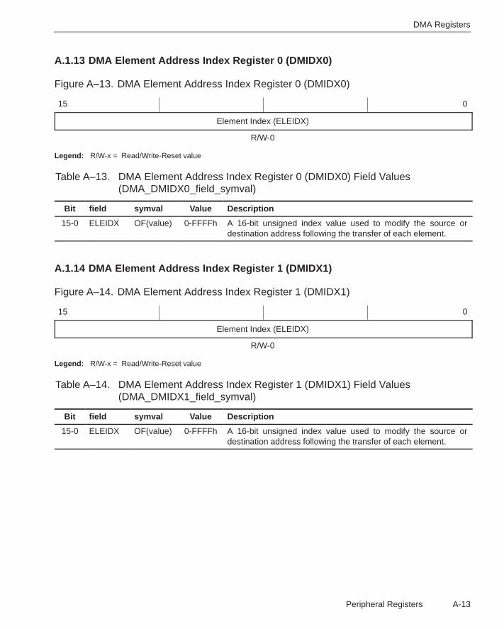
DMA Registers
A-13Peripheral Registers
A.1.13 DMA Element Address Index Register 0 (DMIDX0)
Figure A–13. DMA Element Address Index Register 0 (DMIDX0)
15 0
Element Index (ELEIDX)
R/W-0
Legend: R/W-x = Read/Write-Reset value
Table A–13. DMA Element Address Index Register 0 (DMIDX0) Field Values(DMA_DMIDX0_field_symval)
Bit field symval Value Description
15-0 ELEIDX OF(value) 0-FFFFh A 16-bit unsigned index value used to modify the source ordestination address following the transfer of each element.
A.1.14 DMA Element Address Index Register 1 (DMIDX1)
Figure A–14. DMA Element Address Index Register 1 (DMIDX1)
15 0
Element Index (ELEIDX)
R/W-0
Legend: R/W-x = Read/Write-Reset value
Table A–14. DMA Element Address Index Register 1 (DMIDX1) Field Values(DMA_DMIDX1_field_symval)
Bit field symval Value Description
15-0 ELEIDX OF(value) 0-FFFFh A 16-bit unsigned index value used to modify the source ordestination address following the transfer of each element.

DMA Registers
A-14
A.1.15 DMA Frame Address Index Register 0 (DMFRI0)
Figure A–15. DMA Frame Address Index Register 0 (DMFRI0)
15 0
Frame Index (FRAMEIDX)
R/W-0
Legend: R/W-x = Read/Write-Reset value
Table A–15. DMA Frame Address Index Register 0 (DMFRI0) Field Values(DMA_DMFRI0_field_symval)
Bit field symval Value Description
15-0 FRAMEIDX OF(value) 0-FFFFh A 16-bit unsigned index value used to modify the source ordestination address following the completion of blocks (orframes) of element transfers. When both element and frameindexes are used, the address is modified by the element indexafter each transfer and then modified by the frame index at theend of each frame.
A.1.16 DMA Frame Address Index Register 1 (DMFRI1)
Figure A–16. DMA Frame Address Index Register 1 (DMFRI1)
15 0
Frame Index (FRAMEIDX)
R/W-0
Legend: R/W-x = Read/Write-Reset value
Table A–16. DMA Frame Address Index Register 1 (DMFRI1) Field Values(DMA_DMFRI1_field_symval)
Bit field symval Value Description
15-0 FRAMEIDX OF(value) 0-FFFFh A 16-bit unsigned index value used to modify the source ordestination address following the completion of blocks (orframes) of element transfers. When both element and frameindexes are used, the address is modified by the element indexafter each transfer and then modified by the frame index at theend of each frame.

DMA Registers
A-15Peripheral Registers
A.1.17 DMA Global Extended Source Data Page Register (DMSRCDP)
Figure A–17. DMA Global Extended Source Data Page Register (DMSRCDP)
15 7 6 0
reserved Extended Source Data Page (DMSRCDP)
R/W-0 R/W-0
Legend: R/W-x = Read/Write-Reset value
Table A–17. DMA Global Extended Source Data Page Register (DMSRCDP)Field Values (DMA_DMSRCDP_field_symval)
Bit field symval Value Description
15-7 reserved Reserved. The reserved bit location is always read as zero. A valuewritten to this field has no effect.
6-0 DMSRCDP OF(value) 0-127 Specifies 1 of the 128 extended source data pages.
A.1.18 DMA Global Extended Destination Data Page Register (DMDSTDP)
Figure A–18. DMA Global Extended Destination Data Page Register (DMDSTDP)
15 7 6 0
reserved Extended Destination Data Page (DMDSTDP)
R/W-0 R/W-0
Legend: R/W-x = Read/Write-Reset value
Table A–18. DMA Global Extended Destination Data Page Register (DMDSTDP)Field Values (DMA_DMDSTDP_field_symval)
Bit field symval Value Description
15-7 reserved Reserved. The reserved bit location is always read as zero. A valuewritten to this field has no effect.
6-0 DMDSTDP OF(value) 0-127 Specifies 1 of the 128 extended destination data pages.

EBUS Registers
A-16
A.2 EBUS Registers
A.2.1 Software Wait-State Register (SWWSR)
Figure A–19. Software Wait-State Register(SWWSR)-All devices exceptC5440 and C5441
15 14 12 11 9 8
XPA† IO DATAHI DATALO
R/W-0 R/W-111b R/W-111b R/W-111b
6 5 3 2 0
DATALO PROGHI PROGLO
R/W-111b R/W-111b R/W-111b
† XPA bit only on selected devices with extended program memory.
Legend: R/W-x = Read/Write-Reset value
Table A–19. Software Wait-State Register (SWWSR) Field Values(EBUS_SWWSR_field_symval)
Bit field symval Value Description
15 XPA For devices with extended program memory: Extendedprogram address control bit. Selects the address ranges selectedby the program fields.
ADDRLO 0 Address range: xx0000 - xxFFFFh
ADDREXT 1 Address range: 000000h-7FFFFF
14-12 IO OF(value) 0-7 The value corresponds to the number of wait states for I/O space0000-FFFFh.
11-9 DATAHI OF(value) 0-7 The value corresponds to the number of wait states for data space8000-FFFFh.
8-6 DATALO OF(value) 0-7 The value corresponds to the number of wait states for data space0000-7FFFh.
5-3 PROGHI OF(value) 0-7 The value corresponds to the number of wait states for programspace 8000-FFFFh.
2-0 PROGLO OF(value) 0-7 The value corresponds to the number of wait states for programspace 0000-7FFFh.

Bank-Switching Control Register (BSCR)
A-17Peripheral Registers
A.2.2 Software Wait-State Control Register (SWCR)
Figure A–20. Software Wait-State Control Register (SWCR)-All devices exceptC5440 and C5441
15 1 0
reserved SWSM
R/W-0 R/W-0
Legend: R/W-x = Read/Write-Reset value
Table A–20. Software Wait-State Control Register (SWCR) Field Values(EBUS_SWCR_field_symval)
Bit field symval Value Description
15-1 reserved Reserved. The reserved bit location is always read as zero. A valuewritten to this field has no effect.
0 SWSM Software wait-state multiplier bit.
NOMULT 0 The wait states specified in SWWSR are unchanged (not multiplied).
MULTBY2 1 The wait states specified in SWWSR are multiplied by 2, extendingthe maximum number of wait states from 7 to 14.
A.2.3 Bank-Switching Control Register (BSCR)
Figure A–21. Bank-Switching Control Register (BSCR) — C5401, C5402, C5409, C5420,C5421, and 5471
15 12 11 10 9 8
BNKCMP PSDS reserved IPIRQ†
R/W-1111b R/W-1 R/W-0 R/W-0
7 3 2 1 0
reserved HBH† BH EXIO
R/W-0 R/W-0 R/W-0 R/W-0
† HBH, IPIRQ, and EXIO bits only on selected devices.
Legend: R/W-x = Read/Write-Reset value

Bank-Switching Control Register (BSCR)
A-18
Table A–21. Bank-Switching Control Register (BSCR) Field Values — C5401, C5402,C5409, and C5420, and C5471 (EBUS_BSCR_field_symval)
Bit field symval Value Description
15-12 BNKCMP Bank compare bit determines the number of MSBs of an ad-dress to be compared and the external memory-bank size.Bank sizes from 4K words to 64K words are allowed.
64K 0000 No bits are compared, resulting in a bank size of 64K words.
0001-0111 Reserved
32K 1000 The MSB (bit 15) is compared, resulting in a bank size of 32Kwords.
1001-1011 Reserved
16K 1100 The 2 MSBs (bits 15-14) are compared, resulting in a bank sizeof 16K words.
1101 Reserved
8K 1110 The 3 MSBs (bits 15-13) are compared, resulting in a bank sizeof 8K words.
4K 1111 The 4 MSBs (bits 15-12) are compared, resulting in a bank sizeof 4K words.
11 PSDS Program read-data read access bit controls the insertion of anextra cycle between consecutive program and data reads, ordata and program reads.
NOEXCY 0 No extra cycles are inserted by this feature except when banksare crossed.
INSCY 1 One extra cycle is inserted between consecutive program anddata reads, or data and program reads.
10-9 reserved Reserved. The reserved bit location is always read as zero. Avalue written to this field has no effect.
8 IPIRQ For C5420: Interprocessor interrupt request enable bit is used tosend an interprocessor interrupt to the other subsystem. IPIRQmust be cleared before any subsequent interrupts can be made.
CLR 0 No interprocessor interrupt request is sent.
INTR 1 An interprocessor interrupt request is sent.
7-3 reserved Reserved. The reserved bit location is always read as zero. Avalue written to this field has no effect.
2 HBH For C5401, C5402, C5409, and 5416: HPI data bus holder en-able bit.
DISABLE 0 The HPI data bus holder is disabled. When HPI16 pin is set to alogic high, HPI data bus holder is enabled.
ENABLE 1 The HPI data bus holder is enabled. When not driven, the HPIdata bus, HD(7-0), is held in the previous logic level.

Bank-Switching Control Register (BSCR)
A-19Peripheral Registers
Table A–21. Bank-Switching Control Register (BSCR) Field Values — C5401, C5402,C5409, and C5420, and C5471 (EBUS_BSCR_field_symval) (Continued)
Bit DescriptionValuesymvalfield
BH For C5420: Data bus holder enable bit.
DISABLE 0 The data bus holder is disabled.
ENABLE 1 The data bus holder is enabled. When not driven, the data bus,PPD(15-0), is held in the previous logic level.
1 BH For C5401, C5402, C5409, and 5416: Bus holder enable bit.
DISABLE 0 The bus holder is disabled. When HPI16 pin is set to a logic high,address bus holder is enabled.
ENABLE 1 The data bus holder is enabled. When not driven, the data bus,D(15-0), is held in the previous logic level. When HPI16 pin is setto a logic high, address bus holder is enabled.
0 EXIO Hot any call on C5420 External bus interface off enable bit con-trols the external-bus-off function.
NORMAL 0 The external-bus-off function is disabled.
INACTIF 1 The external-bus-off function is enabled. The address bus, databus, and control signals become inactive after completing the cur-rent bus cycle. The DROM, MP/MC, and OVLY bits in PMST andthe HM bit in ST1 cannot be modified.
Figure A–22. Bank-Switching Control Register (BSCR) — C5410, C5410A, and C5416
15 14 13 12 11
CONSEC DIVFCT IACK reserved
R/W-1 R/W-11b R/W-0 R/W-0
3 2 1 0
reserved HBH† BH† reserved
R/W-0 R/W-0 R/W-0 R/W-0
† BH and HBH bits only on selected devices.
Legend: R/W-x = Read/Write-Reset value

Bank-Switching Control Register (BSCR)
A-20
Table A–22. Bank-Switching Control Register (BSCR) Field Values — C5410, and C5416(EBUS_BSCR_field_symval)
Bit field symval Value Description
15 CONSEC Consecutive bank switching bit specifies the bank-switchingmode. This bit is cleared if fast access is desired for continu-ous memory reads (that is, no starting and trailing cyclesbetween read cycles).
32KFASTREAD 0 Bank-switching on 32K bank boundaries only.
EXTMEM 1 Consecutive bank switches on external memory reads. Eachread cycle consists of 3 cycles: starting, read, and trailing.
14-13 DIVFCT CLKOUT output divide factor. The CLKOUT output is drivenby an on-chip source having a frequency equal to1/(DIVFCT + 1) of the DSP clock.
ZERO 00 CLKOUT is not divided.
CLKBYTWO 01 CLKOUT is divided by 2 from the DSP clock.
CLKBYTHREE 10 CLKOUT is divided by 3 from the DSP clock.
CLKBYFOUR 11 CLKOUT is divided by 4 from the DSP clock.
12 IACK IACK signal output off enable bit controls the IACK signaloutput off function.
ON 0 IACK signal output off function is disabled.
OFF 1 IACK signal output off function is enabled.
11-3 reserved Reserved. The reserved bit location is always read as zero. Avalue written to this field has no effect.
2 HBH For C5416: HPI data bus holder enable bit.
DISABLE 0 The HPI data bus holder is disabled. When HPI16 pin is set toa logic high, HPI data bus holder is enabled.
ENABLE 1 The HPI data bus holder is enabled. When not driven, the HPIdata bus, HD(7-0), is held in the previous logic level.
1 BH For C5416: Bus holder enable bit.
DISABLE 0 The bus holder is disabled. When HPI16 pin is set to a logichigh, address bus holder is enabled.
ENABLE 1 The data bus holder is enabled. When not driven, the data bus,D(15-0), is held in the previous logic level. When HPI16 pin isset to a logic high, address bus holder is enabled.
0 reserved Reserved. The reserved bit location is always read as zero. Avalue written to this field has no effect.
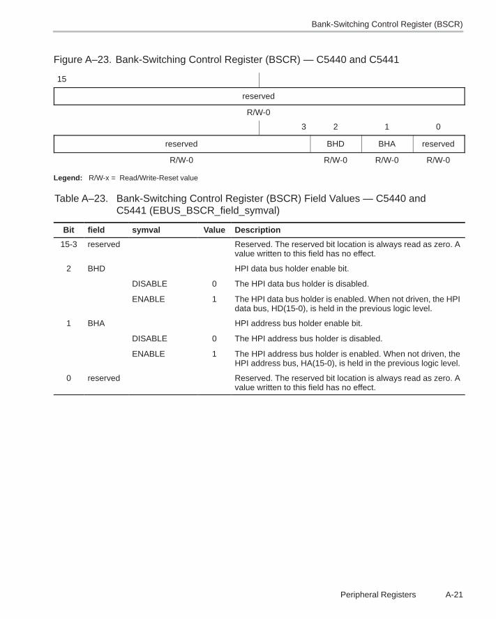
Bank-Switching Control Register (BSCR)
A-21Peripheral Registers
Figure A–23. Bank-Switching Control Register (BSCR) — C5440 and C5441
15
reserved
R/W-0
3 2 1 0
reserved BHD BHA reserved
R/W-0 R/W-0 R/W-0 R/W-0
Legend: R/W-x = Read/Write-Reset value
Table A–23. Bank-Switching Control Register (BSCR) Field Values — C5440 andC5441 (EBUS_BSCR_field_symval)
Bit field symval Value Description
15-3 reserved Reserved. The reserved bit location is always read as zero. Avalue written to this field has no effect.
2 BHD HPI data bus holder enable bit.
DISABLE 0 The HPI data bus holder is disabled.
ENABLE 1 The HPI data bus holder is enabled. When not driven, the HPIdata bus, HD(15-0), is held in the previous logic level.
1 BHA HPI address bus holder enable bit.
DISABLE 0 The HPI address bus holder is disabled.
ENABLE 1 The HPI address bus holder is enabled. When not driven, theHPI address bus, HA(15-0), is held in the previous logic level.
0 reserved Reserved. The reserved bit location is always read as zero. Avalue written to this field has no effect.
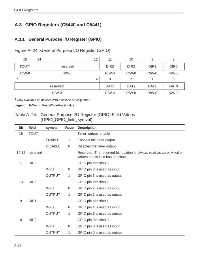
GPIO Registers
A-22
A.3 GPIO Registers (C5440 and C5441)
A.3.1 General Purpose I/O Register (GPIO)
Figure A–24. General Purpose I/O Register (GPIO)
15 14 12 11 10 9 8
TOUT† reserved DIR3 DIR2 DIR1 DIR0
R/W-0 R/W-0 R/W-0 R/W-0 R/W-0 R/W-0
7 4 3 2 1 0
reserved DAT3 DAT2 DAT1 DAT0
R/W-0 R/W-0 R/W-0 R/W-0 R/W-0
† Only available on devices with a second on-chip timer.
Legend: R/W-x = Read/Write-Reset value
Table A–24. General Purpose I/O Register (GPIO) Field Values(GPIO_GPIO_field_symval)
Bit field symval Value Description
15 TOUT Timer output enable
ENABLE 1 Enables the timer output
DISABLE 0 Disables the timer output
14-12 reserved Reserved. The reserved bit location is always read as zero. A valuewritten to this field has no effect.
11 DIR3 GPIO pin direction 3
INPUT 0 GPIO pin 3 is used as input
OUTPUT 1 GPIO pin 3 is used as output
10 DIR2 GPIO pin direction 2
INPUT 0 GPIO pin 2 is used as input
OUTPUT 1 GPIO pin 2 is used as output
9 DIR1 GPIO pin direction 1
INPUT 0 GPIO pin 1 is used as input
OUTPUT 1 GPIO pin 1 is used as output
8 DIR0 GPIO pin direction 0
INPUT 0 GPIO pin 0 is used as input
OUTPUT 1 GPIO pin 0 is used as output

GPIO Registers
A-23Peripheral Registers
Table A–24. General Purpose I/O Register (GPIO) Field Values(GPIO_GPIO_field_symval) (Continued)
Bit DescriptionValuesymvalfield
7-4 reserved Reserved. The reserved but location is always read as zero. A valuewritten to this field has no effect.
3 DAT3 GPIO data bit 3
LOW 0 GPIO0 is driven with a 0 (DIR3 = 1)
GPIO0 is read as 0 (DIR3 = 0)
HI 1 GPIO0 is driven with a 1 (DIR3 = 1)
GPIO0 is read as 1 (DIR3 = 0)
2 DAT2 GPIO data bit 2
LOW 0 GPIO0 is driven with a 0 (DIR2 = 1)
GPIO0 is read as 0 (DIR2 = 0)
HI 1 GPIO0 is driven with a 1 (DIR2 = 1)
GPIO0 is read as 1 (DIR2 = 0)
1 DAT1 GPIO data bit 1
LOW 0 GPIO0 is driven with a 0 (DIR1 = 1)
GPIO0 is read as 0 (DIR1 = 0)
HI 1 GPIO0 is driven with a 1 (DIR1 = 1)
GPIO0 is read as 1 (DIR1 = 0)
0 DAT0 GPIO data bit 0
LOW 0 GPIO0 is driven with a 0 (DIR0 = 1)
GPIO0 is read as 0 (DIR0 = 0)
HI 1 GPIO0 is driven with a 1 (DIR0 = 1)
GPIO0 is read as 1 (DIR0 = 0)

HPI Registers
A-24
A.4 HPI Registers
A.4.1 General Purpose I/O Control Register (GPIOCR)
Figure A–25. General Purpose I/O Control Register (GPIOCR)
15 14 8
TOUT1† reserved
R/W-0
7 0
DIR
R/W-0
† Only available on devices with a second on-chip timer.
Legend: R/W-x = Read/Write-Reset value
Table A–25. General Purpose I/O Control Register (GPIOCR) Field Values(HPI_GPIOCR_field_symval)
Bit field symval Value Description
15 TOUT1 For C5402: Timer1 output enable bit enables or disables the timer1output on the HINT pin. The timer1 output is only available when theHPI-8 is disabled. This bit is reserved on devices that have only onetimer.
0 The timer1 output is not available externally.
MASK 1 The timer1 output is driven on the HINT pin.
14-8 reserved Reserved. The reserved bit location is always read as zero. A valuewritten to this field has no effect.
7-0 DIR I/O pins direction field to configure the HD pins as inputs or outputs.Bit 7-Bit 0 corresponds to the direction for PIN7 to 0 respectively.
0 The HD corresponding pin is configured as an input.
MASK 1 The HD corresponding pin is configured as an output. When theHPI-8 is enabled, this bit is forced to 0 and is not affected by writes.

HPI Registers
A-25Peripheral Registers
A.4.2 General Purpose I/O Status Register (GPIOSR)
Figure A–26. General Purpose Status Register (GPIOSR)
15 0
IO
R/W-x
Legend: R/W-x = Read/Write-Reset value
Table A–26. General Purpose I/O Status Register (GPIOSR) Field Values(HPI_GPIOSR_field_symval)
Bit field† symval Value Description
15-0 IO I/O pin status bit reflects the logic level on the HD pin. When the HD pinis configured as an input (DIR = 0 in GPIOCR), the IO bit latches thelogic value (1 or 0) of the HD pin. Writes to the IO bit have no effectwhen the HD pin is configured as an input. When the HD pin isconfigured as an output (DIR = 1 in GPIOCR), the HD pin is driven tothe logic level (1 or 0) written in the IO bit.
0 The HD input is externally driven low, or the HD output is internally drivenlow.
MASK 1 The HD input is externally driven high, or the HD output is internallydriven high.
† The GPIOSR register can be treated as a single field register (IO).
A.4.3 HPI Control Register (HPIC) (for 5401, 5402, 5409, and 5410 only)
Figure A–27. HPI Control Register (HPIC) (for 5410)
15 1 0
X HINT X SMOD X
Note: X = Any value can be written
Refer to the specific device data sheet for an explanation fo the fields of thisregister.

Multichannel BSP (McBSP) Registers
A-26
A.5 Multichannel BSP (McBSP) Registers
A.5.1 McBSP Serial Port Control Register (SPCR1)
Figure A–28. McBSP Serial Port Control Register 1 (SPCR1)
15 14 13 12 11 10 8
DLB RJUST CLKSTP reserved
R/W-0 R/W-0 R/W-0 R/W-0
7 6 5 4 3 2 1 0
DXENA ABIS† RINTM RSYNCERR RFULL RRDY RRST
R/W-0 R/W-0 R/W-0 R/W-0 R-0 R-0 R/W-0† Only available on specific devices.
Legend: R/W-x = Read/Write-Reset value
Table A–27. McBSP Serial Port Control Register 1 (SPCR1) Field Values(MCBSP_SPCR1_field_symval)
Bit field symval Value Description
15 DLB Digital loop back mode enable bit.
OFF 0 Digital loop back mode is disabled.
ON 1 Digital loop back mode is enabled.
14-13 RJUST Receive sign-extension and justification mode bit.
RZF 00 Right-justify and zero-fill MSBs in DRR[1, 2].
RSE 01 Right-justify and sign-extend MSBs in DRR[1, 2].
LZF 10 Left-justify and zero-fill LSBs in DRR[1, 2].
11 Reserved
12-11 CLKSTP Clock stop mode bit. In SPI mode, operates in conjunction withCLKXP bit of Pin Control Register (PCR).
DISABLE 0x Clock stop mode is disabled. Normal clocking for non-SPImode.
In SPI mode with data sampled on rising edge (CLKXP = 0):
NODELAY 10 Clock starts with rising edge without delay.
DELAY 11 Clock starts with rising edge with delay.
In SPI mode with data sampled on falling edge (CLKXP = 1):
NODELAY 10 Clock starts with falling edge without delay.
DELAY 11 Clock starts with falling edge with delay.
10-8 reserved Reserved. The reserved bit location is always read as zero. Avalue written to this field has no effect.

Multichannel BSP (McBSP) Registers
A-27Peripheral Registers
Table A–27. McBSP Serial Port Control Register 1 (SPCR1) Field Values(MCBSP_SPCR1_field_symval) (Continued)
Bit DescriptionValuesymvalfield
7 DXENA DX enabler bit.
OFF 0 DX enabler is off.
ON 1 DX enabler is on.
6 ABIS For C5410, C5410A, and C5416: A-bis enable mode bit.
DISABLE 0 A-bis mode is disabled.
ENABLE 1 A-bis mode is enabled.
5-4 RINTM Receive interrupt (RINT) mode bit.
RRDY 00 RINT is driven by RRDY (end-of-word) and end-of-frame inA-bis mode.
EOS 01 RINT is generated by end-of-block or end-of-frame inmultichannel operation.
FRM 10 RINT is generated by a new frame synchronization.
RSYNCERR 11 RINT is generated by RSYNCERR.
3 RSYNCERR Receive synchronization error bit.
NO 0 No synchronization error is detected.
YES 1 Synchronization error is detected.
2 RFULL Receive shift register full bit.
NO 0 RBR[1, 2] is not in overrun condition.
YES 1 DRR[1, 2] is not read, RBR[1, 2] is full, and RSR[1, 2] is alsofull with new word.
1 RRDY Receiver ready bit.
NO 0 Receiver is not ready.
YES 1 Receiver is ready with data to be read from DRR[1, 2].
0 RRST Receiver reset bit resets or enables the receiver.
DISABLE 0 The serial port receiver is disabled and in reset state.
ENABLE 1 The serial port receiver is enabled.

Multichannel BSP (McBSP) Registers
A-28
A.5.2 McBSP Serial Port Control Register 2 (SPCR2)
Figure A–29. McBSP Serial Port Control Register 2 (SPCR2)
15 10 9 8
reserved FREE SOFT
R/W-0 R/W-0 R/W-0
7 6 5 4 3 2 1 0
FRST GRST XINTM XSYNCERR† XEMPTY XRDY XRST
R/W-0 R/W-0 R/W-0 R/W-0 R-0 R-0 R/W-0
† Caution: Writing a 1 to this bit sets the error condition; thus, it is mainly used for testing purposes or if this operation is desired.
Legend: R/W-x = Read/Write-Reset value
Table A–28. McBSP Serial Port Control Register 2 (SPCR2) Field Values(MCBSP_SPCR2_field_symval)
Bit field symval Value Description
15-10 reserved Reserved. The reserved bit location is always read as zero. Avalue written to this field has no effect.
9 FREE Free-running enable mode bit.
NO 0 Free-running mode is disabled.
YES 1 Free-running mode is enabled.
8 SOFT Soft bit enable mode bit.
NO 0 Soft mode is disabled.
YES 1 Soft mode is enabled.
7 FRST Frame-sync generator reset.
RESET 0 Frame-synchronization logic is reset. Frame-sync signal (FSG)is not generated by the sample-rate generator.
FSG 1 Frame-sync signal (FSG) is generated after (FPER + 1)number of CLKG clocks; that is, all frame counters are loadedwith their programmed values.
6 GRST Sample-rate generator reset.
RESET 0 Sample-rate generator is reset.
CLKG 1 Sample-rate generator is taken out of reset. CLKG is driven asper programmed value in sample-rate generator registers(SRGR[1, 2]).
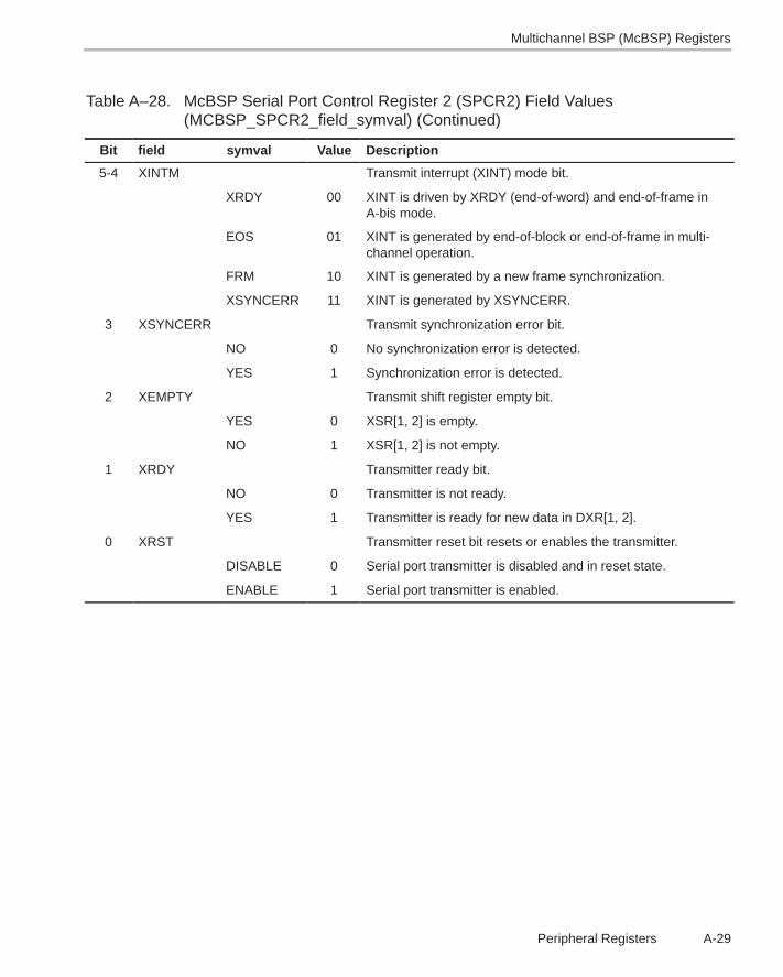
Multichannel BSP (McBSP) Registers
A-29Peripheral Registers
Table A–28. McBSP Serial Port Control Register 2 (SPCR2) Field Values(MCBSP_SPCR2_field_symval) (Continued)
Bit DescriptionValuesymvalfield
5-4 XINTM Transmit interrupt (XINT) mode bit.
XRDY 00 XINT is driven by XRDY (end-of-word) and end-of-frame inA-bis mode.
EOS 01 XINT is generated by end-of-block or end-of-frame in multi-channel operation.
FRM 10 XINT is generated by a new frame synchronization.
XSYNCERR 11 XINT is generated by XSYNCERR.
3 XSYNCERR Transmit synchronization error bit.
NO 0 No synchronization error is detected.
YES 1 Synchronization error is detected.
2 XEMPTY Transmit shift register empty bit.
YES 0 XSR[1, 2] is empty.
NO 1 XSR[1, 2] is not empty.
1 XRDY Transmitter ready bit.
NO 0 Transmitter is not ready.
YES 1 Transmitter is ready for new data in DXR[1, 2].
0 XRST Transmitter reset bit resets or enables the transmitter.
DISABLE 0 Serial port transmitter is disabled and in reset state.
ENABLE 1 Serial port transmitter is enabled.

Multichannel BSP (McBSP) Registers
A-30
A.5.3 McBSP Pin Control Register (PCR)
Figure A–30. McBSP Pin Control Register (PCR)
15 14 13 12 11 10 9 8
reserved XIOEN RIOEN FSXM FSRM CLKXM CLKRM
R/W-0 R/W-0 R/W-0 R/W-0 R/W-0 R/W-0 R/W-0
7 6 5 4 3 2 1 0
SCLKME† CLKSSTAT DXSTAT DRSTAT FSXP FSRP CLKXP CLKRP
R/W-0 R-0 R-0 R-0 R/W-0 R/W-0 R/W-0 R/W-0
† Only available on specific devices with 128-channel selection capability.
Legend: R/W-x = Read/Write-Reset value
Table A–29. McBSP Pin Control Register (PCR) Field Values(MCBSP_PCR_field_symval)
Bit field symval Value Description
15-14 reserved Reserved. The reserved bit location is always read as zero. Avalue written to this field has no effect.
13 XIOEN Transmit general-purpose I/O mode only when transmitter isdisabled (XRST = 0 in SPCR2).
SP 0 DX, FSX, and CLKX pins are configured as serial port pins anddo not function as general-purpose I/O pins.
GPIO 1 DX pin is configured as general-purpose output pin; FSX andCLKX pins are configured as general-purpose I/O pins. Theseserial port pins do not perform serial port operations.
12 RIOEN Receive general-purpose I/O mode only when receiver isdisabled (RRST = 0 in SPCR1).
SP 0 DR, FSR, CLKR, and CLKS pins are configured as serial portpins and do not function as general-purpose I/O pins.
GPIO 1 DR and CLKS pins are configured as general-purpose inputpins; FSR and CLKR pins are configured as general-purposeI/O pins. These serial port pins do not perform serial portoperations.
11 FSXM Transmit frame-synchronization mode bit.
EXTERNAL 0 Frame-synchronization signal is derived from an externalsource.
INTERNAL 1 Frame-synchronization signal is determined by FSGM bit inSRGR2.

Multichannel BSP (McBSP) Registers
A-31Peripheral Registers
Table A–29. McBSP Pin Control Register (PCR) Field Values(MCBSP_PCR_field_symval) (Continued)
Bit DescriptionValuesymvalfield
10 FSRM Receive frame-synchronization mode bit.
EXTERNAL 0 Frame-synchronization signal is derived from an externalsource. FSR is an input pin.
INTERNAL 1 Frame-synchronization signal is generated internally by thesample-rate generator. FSR is an output pin, except whenGSYNC = 1 in SRGR2.
9 CLKXM Transmitter clock mode bit.
INPUT 0 CLKX is an input pin and is driven by an external clock.
OUTPUT 1 CLKX is an output pin and is driven by the internal sample-rategenerator.
In SPI mode when CLKSTP in SPCR1 is a non-zero value:
INPUT 0 McBSP is a slave and clock (CLKX) is driven by the SPI masterin the system. CLKR is internally driven by CLKX.
OUTPUT 1 McBSP is a master and generates the clock (CLKX) to driveits receive clock (CLKR) and the shift clock of theSPI-compliant slaves in the system.
8 CLKRM Receiver clock mode bit.
Digital loop back mode is disabled (DLB = 0 in SPCR1):
INPUT 0 CLKR is an input pin and is driven by an external clock.
OUTPUT 1 CLKR is an output pin and is driven by the internal sample-rategenerator.
Digital loop back mode is enabled (DLB = 1 in SPCR1):
INPUT 0 Receive clock (not the CLKR pin) is driven by transmit clock(CLKX) that is based on CLKXM bit. CLKR pin is inhigh-impedance state.
OUTPUT 1 CLKR is an output pin and is driven by the transmit clock. Thetransmit clock is based on CLKXM bit.
7 SCLKME For devices with 128-channel selection capability:Sample-rate clock mode extended enable bit.
NO 0 BCLKR and BCLKX are not used by the sample-rategenerator for external synchronization.
BCLK 1 BCLKR and BCLKX are used by the sample-rate generator forexternal synchronization.

Multichannel BSP (McBSP) Registers
A-32
Table A–29. McBSP Pin Control Register (PCR) Field Values(MCBSP_PCR_field_symval) (Continued)
Bit DescriptionValuesymvalfield
6 CLKSSTAT CLKS pin status reflects value on CLKS pin when configuredas a general-purpose input pin.
0 0 CLKS pin reflects a logic low.
1 1 CLKS pin reflects a logic high.
5 DXSTAT DX pin status reflects value driven to DX pin when configuredas a general-purpose output pin.
0 0 DX pin reflects a logic low.
1 1 DX pin reflects a logic high.
4 DRSTAT DR pin status reflects value on DR pin when configured as ageneral-purpose input pin.
0 0 DR pin reflects a logic low.
1 1 DR pin reflects a logic high.
3 FSXP Transmit frame-synchronization polarity bit.
ACTIVEHIGH 0 Transmit frame-synchronization pulse is active high.
ACTIVELOW 1 Transmit frame-synchronization pulse is active low.
2 FSRP Receive frame-synchronization polarity bit.
ACTIVEHIGH 0 Receive frame-synchronization pulse is active high.
ACTIVELOW 1 Receive frame-synchronization pulse is active low.
1 CLKXP Transmit clock polarity bit.
RISING 0 Transmit data sampled on rising edge of CLKX.
FALLING 1 Transmit data sampled on falling edge of CLKX.
0 CLKRP Receive clock polarity bit.
FALLING 0 Receive data sampled on falling edge of CLKR.
RISING 1 Receive data sampled on rising edge of CLKR.

Multichannel BSP (McBSP) Registers
A-33Peripheral Registers
A.5.4 Receive Control Register 1 (RCR1)
Figure A–31. Receive Control Register 1 (RCR1)
15 14 8
reserved RFRLEN1
R/W-0 R/W-0
7 5 4 0
RWDLEN1 reserved
R/W-0 R/W-0
Legend: R/W-x = Read/Write-Reset value
Table A–30. Receive Control Register 1 (RCR1) Field Values(MCBSP_RCR1_field_symval)
Bit field symval Value Description
15 reserved Reserved. The reserved bit location is always read as zero. A valuewritten to this field has no effect.
14-8 RFRLEN1 OF(value) 0-127 Specifies the number of words (length) in the receive frame.
7-5 RWDLEN1 Specifies the number of bits (length) in the receive word.
8BIT 000 Receive word length is 8 bits.
12BIT 001 Receive word length is 12 bits.
16BIT 010 Receive word length is 16 bits.
20BIT 011 Receive word length is 20 bits.
24BIT 100 Receive word length is 24 bits.
32BIT 101 Receive word length is 32 bits.
110 Reserved
111 Reserved
4-0 reserved Reserved. The reserved bit location is always read as zero. A valuewritten to this field has no effect.

Multichannel BSP (McBSP) Registers
A-34
A.5.5 Receive Control Register 2 (RCR2)
Figure A–32. Receive Control Register 2 (RCR2)
15 14 8
RPHASE RFRLEN2
R/W-0 R/W-0
7 5 4 3 2 1 0
RWDLEN2 RCOMPAND RFIG RDATDLY
R/W-0 R/W-0 R/W-0 R/W-0
Legend: R/W-x = Read/Write-Reset value
Table A–31. Receive Control Register 2 (RCR2) Field Values(MCBSP_RCR2_field_symval)
Bit field symval Value Description
15 RPHASE Receive phases bit.
SINGLE 0 Single-phase frame
DUAL 1 Dual-phase frame
14-8 RFRLEN2 OF(value) 0-127 Specifies the number of words (length) in the receive frame.
7-5 RWDLEN2 Specifies the number of bits (length) in the receive word.
8BIT 000 Receive word length is 8 bits.
12BIT 001 Receive word length is 12 bits.
16BIT 010 Receive word length is 16 bits.
20BIT 011 Receive word length is 20 bits.
24BIT 100 Receive word length is 24 bits.
32BIT 101 Receive word length is 32 bits.
110 Reserved
111 Reserved
4-3 RCOMPAND Receive companding mode. Modes other than 00 are onlyenabled when RWDLEN[1, 2] bit is 000 (indicating 8-bit data).
MSB 00 No companding, data transfer starts with MSB first.
8BITLSB 01 No companding, 8-bit data transfer starts with LSB first.
ULAW 10 Compand using µ-law for receive data.
ALAW 11 Compand using A-law for receive data.

Multichannel BSP (McBSP) Registers
A-35Peripheral Registers
Table A–31. Receive Control Register 2 (RCR2) Field Values(MCBSP_RCR2_field_symval) (Continued)
Bit DescriptionValuesymvalfield
2 RFIG Receive frame ignore bit.
YES 0 Receive frame-synchronization pulses after the first pulserestarts the transfer.
NO 1 Receive frame-synchronization pulses after the first pulse areignored.
1-0 RDATDLY Receive data delay bit.
0BIT 00 0-bit data delay
1BIT 01 1-bit data delay
2BIT 10 2-bit data delay
11 Reserved
A.5.6 Transmit Control Register 1 (XCR1)
Figure A–33. Transmit Control Register 1 (XCR1)
15 14 8
reserved XFRLEN1
R/W-0 R/W-0
7 5 4 0
XWDLEN1 reserved
R/W-0 R/W-0
Legend: R/W-x = Read/Write-Reset value
Table A–32. Transmit Control Register 1 (XCR1) Field Values(MCBSP_XCR1_field_symval)
Bit field symval Value Description
15 reserved Reserved. The reserved bit location is always read as zero. A valuewritten to this field has no effect.
14-8 XFRLEN1 OF(value) 0-127 Specifies the number of words (length) in the transmit frame.
7-5 XWDLEN1 Specifies the number of bits (length) in the transmit word.
8BIT 000 Transmit word length is 8 bits.
12BIT 001 Transmit word length is 12 bits.
16BIT 010 Transmit word length is 16 bits.

Multichannel BSP (McBSP) Registers
A-36
Table A–32. Transmit Control Register 1 (XCR1) Field Values(MCBSP_XCR1_field_symval)
Bit DescriptionValuesymvalfield
20BIT 011 Transmit word length is 20 bits.
24BIT 100 Transmit word length is 24 bits.
32BIT 101 Transmit word length is 32 bits.
110 Reserved
111 Reserved
4-0 reserved Reserved. The reserved bit location is always read as zero. A valuewritten to this field has no effect.
A.5.7 Transmit Control Register 2 (XCR2)
Figure A–34. Transmit Control Register 2 (XCR2)
15 14 8
XPHASE XFRLEN2
R/W-0 R/W-0
7 5 4 3 2 1 0
XWDLEN2 XCOMPAND XFIG XDATDLY
R/W-0 R/W-0 R/W-0 R/W-0
Legend: R/W-x = Read/Write-Reset value
Table A–33. Transmit Control Register 2 (XCR2) Field Values(MCBSP_XCR2_field_symval)
Bit field symval Value Description
15 XPHASE Transmit phases bit.
SINGLE 0 Single-phase frame
DUAL 1 Dual-phase frame
14-8 XFRLEN2 OF(value) 0-127 Specifies the number of words (length) in the transmit frame.
7-5 XWDLEN2 Specifies the number of bits (length) in the transmit word.
8BIT 000 Transmit word length is 8 bits.
12BIT 001 Transmit word length is 12 bits.
16BIT 010 Transmit word length is 16 bits.
20BIT 011 Transmit word length is 20 bits.
24BIT 100 Transmit word length is 24 bits.

Multichannel BSP (McBSP) Registers
A-37Peripheral Registers
Table A–33. Transmit Control Register 2 (XCR2) Field Values(MCBSP_XCR2_field_symval) (Continued)
Bit DescriptionValuesymvalfield
32BIT 101 Transmit word length is 32 bits.
110 Reserved
111 Reserved
4-3 XCOMPAND Transmit companding mode. Modes other than 00 are onlyenabled when XWDLEN[1, 2] bit is 000 (indicating 8-bit data).
MSB 00 No companding, data transfer starts with MSB first.
8BITLSB 01 No companding, 8-bit data transfer starts with LSB first.
ULAW 10 Compand using µ-law for transmit data.
ALAW 11 Compand using A-law for transmit data.
2 XFIG Transmit frame ignore bit.
YES 0 Transmit frame-synchronization pulses after the first pulserestarts the transfer.
NO 1 Transmit frame-synchronization pulses after the first pulse areignored.
1-0 XDATDLY Transmit data delay bit.
0BIT 00 0-bit data delay
1BIT 01 1-bit data delay
2BIT 10 2-bit data delay
11 Reserved

Multichannel BSP (McBSP) Registers
A-38
A.5.8 Sample Rate Generator Register 1 (SRGR1)
Figure A–35. Sample Rate Generator Register 1 (SRGR1)
15 8 7 0
FWID CLKGDV
R/W-0 R/W-0000 0001b
Legend: R/W-x = Read/Write-Reset value
Table A–34. Sample Rate Generator Register 1 (SRGR1) Field Values(MCBSP_SRGR1_field_symval)
Bit field symval Value Description
15-8 FWID OF(value) 0-255 The value plus 1 specifies the width of the frame-sync pulse (FSG)during its active period.
7-0 CLKGDV OF(value) 0-255 The value is used as the divide-down number to generate therequired sample-rate generator clock frequency.
A.5.9 Sample Rate Generator Register 2 (SRGR2)
Figure A–36. Sample Rate Generator Register 2 (SRGR2)
15 14 13 12 11
GSYNC CLKSP CLKSM FSGM FPER
R/W-0 R/W-0 R/W-1 R/W-0 R/W-0
0
FPER
R/W-0
Legend: R/W-x = Read/Write-Reset value
Table A–35. Sample Rate Generator Register 2 (SRGR2) Field Values(MCBSP_SRGR2_field_symval)
Bit field symval Value Description
15 GSYNC Sample-rate generator clock synchronization bit only used when theexternal clock (CLKS) drives the sample-rate generator clock(CLKSM = 0).
FREE 0 The sample-rate generator clock (CLKG) is free running.
SYNC 1 The sample-rate generator clock (CLKG) is running; however, CLKGis resynchronized and frame-sync signal (FSG) is generated onlyafter detecting the receive frame-synchronization signal (FSR). Also,frame period (FPER) is a don’t care because the period is dictated bythe external frame-sync pulse.

Multichannel BSP (McBSP) Registers
A-39Peripheral Registers
Table A–35. Sample Rate Generator Register 2 (SRGR2) Field Values(MCBSP_SRGR2_field_symval) (Continued)
Bit DescriptionValuesymvalfield
14 CLKSP CLKS polarity clock edge select bit only used when the external clock(CLKS) drives the sample-rate generator clock (CLKSM = 0).
RISING 0 Rising edge of CLKS generates CLKG and FSG.
FALLING 1 Falling edge of CLKS generates CLKG and FSG.
13 CLKSM McBSP sample-rate generator clock mode bit.
CLKS 0 Sample-rate generator clock derived from the CLKS pin.
INTERNAL 1 Sample-rate generator clock derived from CPU clock.
12 FSGM Sample-rate generator transmit frame-synchronization mode bitused when FSXM = 1 in PCR.
DXR2XSR 0 Transmit frame-sync signal (FSX) due to DXR[1, 2]-to-XSR[1, 2]copy. When FSGM = 0, FWID bit in SRGR1 and FPER bit areignored.
FSG 1 Transmit frame-sync signal (FSX) driven by the sample-rategenerator frame-sync signal (FSG).
11-0 FPER OF(value) 0-4095 The value plus 1 specifies when the next frame-sync signal be-comes active. Range: 1 to 4096 sample-rate generator clock(CLKG) periods.

Multichannel BSP (McBSP) Registers
A-40
A.5.10 Multichannel Control Register 1 (MCR1)
Figure A–37. Multichannel Control Register 1 (MCR1)
15 10 9 8
reserved RMCME† RPBBLK
R/W-0 R/W-0 R/W-0
7 6 5 4 2 1 0
RPBBLK RPABLK RCBLK reserved RMCM
R/W-0 R/W-0 R-0 R/W-0 R/W-0† Only available on specific devices that provide 128-channel selection capability.
Legend: R/W-x = Read/Write-Reset value
Table A–36. Multichannel Control Register 1 (MCR1) Field Values(MCBSP_MCR1_field_symval)
Bit field symval Value Description
15-10 reserved Reserved. The reserved bit location is always read as zero. A valuewritten to this field has no effect.
9 RMCME For devices with 128-channel selection capability: Receive128-channel selection enable bit.
NO 0 Normal 32-channel selection is enabled.
ATOH 1 Six additional registers (RCERC-RCERH) are used to enable128-channel selection.
8-7 RPBBLK Receive partition B block bit. Enables 16 contiguous channels ineach block.
SF1 00 Block 1. Channel 16 to channel 31
SF3 01 Block 3. Channel 48 to channel 63
SF5 10 Block 5. Channel 80 to channel 95
SF7 11 Block 7. Channel 112 to channel 127
6-5 RPABLK Receive partition A block bit. Enables 16 contiguous channels ineach block.
SF0 00 Block 0. Channel 0 to channel 15
SF2 01 Block 2. Channel 32 to channel 47
SF4 10 Block 4. Channel 64 to channel 79
SF6 11 Block 6. Channel 96 to channel 111
4-2 RCBLK Receive current block bit.
SF0 000 Block 0. Channel 0 to channel 15
SF1 001 Block 1. Channel 16 to channel 31

Multichannel BSP (McBSP) Registers
A-41Peripheral Registers
Table A–36. Multichannel Control Register 1 (MCR1) Field Values(MCBSP_MCR1_field_symval) (Continued)
Bit DescriptionValuesymvalfield
SF2 010 Block 2. Channel 32 to channel 47
SF3 011 Block 3. Channel 48 to channel 63
SF4 100 Block 4. Channel 64 to channel 79
RCBLK SF5 101 Block 5. Channel 80 to channel 95
SF6 110 Block 6. Channel 96 to channel 111
SF7 111 Block 7. Channel 112 to channel 127
1 reserved Reserved. The reserved bit location is always read as zero. A valuewritten to this field has no effect.
0 RMCM Receive multichannel selection enable bit.
CHENABLE 0 All 128 channels enabled.
ELDISABLE 1 All channels disabled by default. Required channels are selectedby enabling RP[A, B]BLK and RCER[A, B] appropriately.
A.5.11 Multichannel Control Register 2 (MCR2)
Figure A–38. Multichannel Control Register 2 (MCR2)
15 10 9 8
reserved XMCME† XPBBLK
R/W-0 R/W-0 R/W-0
7 6 5 4 2 1 0
XPBBLK XPABLK XCBLK XMCM
R/W-0 R/W-0 R-0 R/W-0
† Only available on specific devices that provide 128-channel selection capability.
Legend: R/W-x = Read/Write-Reset value

Multichannel BSP (McBSP) Registers
A-42
Table A–37. Multichannel Control Register 2 (MCR2) Field Values(MCBSP_MCR2_field_symval)
Bit field symval Value Description
15-10 reserved Reserved. The reserved bit location is always read as zero. A valuewritten to this field has no effect.
9 XMCME For devices with 128-channel selection capability: Transmit128-channel selection enable bit.
NO 0 Normal 32-channel selection is enabled.
ATOH 1 Six additional registers (XCERC-XCERH) are used to enable128-channel selection.
8-7 XPBBLK Transmit partition B block bit. Enables 16 contiguous channels ineach block.
SF1 00 Block 1. Channel 16 to channel 31
SF3 01 Block 3. Channel 48 to channel 63
SF5 10 Block 5. Channel 80 to channel 95
SF7 11 Block 7. Channel 112 to channel 127
6-5 XPABLK Transmit partition A block bit. Enables 16 contiguous channels ineach block.
SF0 00 Block 0. Channel 0 to channel 15
SF2 01 Block 2. Channel 32 to channel 47
SF4 10 Block 4. Channel 64 to channel 79
SF6 11 Block 6. Channel 96 to channel 111
4-2 XCBLK Transmit current block bit.
SF0 000 Block 0. Channel 0 to channel 15
SF1 001 Block 1. Channel 16 to channel 31
SF2 010 Block 2. Channel 32 to channel 47
SF3 011 Block 3. Channel 48 to channel 63
SF4 100 Block 4. Channel 64 to channel 79
SF5 101 Block 5. Channel 80 to channel 95
SF6 110 Block 6. Channel 96 to channel 111
SF7 111 Block 7. Channel 112 to channel 127

Multichannel BSP (McBSP) Registers
A-43Peripheral Registers
Table A–37. Multichannel Control Register 2 (MCR2) Field Values(MCBSP_MCR2_field_symval) (Continued)
Bit DescriptionValuesymvalfield
1-0 XMCM Transmit multichannel selection enable bit.
ENNOMASK 00 All channels enabled without masking (DX is always driven duringtransmission of data�).
DISXP 01 All channels disabled and, therefore, masked by default. Requiredchannels are selected by enabling XP[A, B]BLK and XCER[A, B]appropriately. Also, these selected channels are not masked and,therefore, DX is always driven.
ENMASK 10 All channels enabled, but masked. Selected channels enabledusing XP[A, B]BLK and XCER[A, B] are unmasked.
DISRP 11 All channels disabled and, therefore, masked by default. Requiredchannels are selected by enabling RP[A, B]BLK and RCER[A, B]appropriately. Selected channels can be unmasked byRP[A, B]BLK and XCER[A, B]. This mode is used for symmetrictransmit and receive operation.
† DX is masked or driven to a high-impedance state during (a) interpacket intervals, (b) when a channel is masked regardlessof whether it is enabled, or (c) when a channel is disabled.
A.5.12 Receive Channel Enable Register (RCERn)
Figure A–39. Receive Channel Enable Register (RCERn)
15 14 13 12 11 10 9 8
RCE15 RCE14 RCE13 RCE12 RCE11 RCE10 RCE9 RCE8
R/W-0 R/W-0 R/W-0 R/W-0 R/W-0 R/W-0 R/W-0 R/W-0
7 6 5 4 3 2 1 0
RCE7 RCE6 RCE5 RCE4 RCE3 RCE2 RCE1 RCE0
R/W-0 R/W-0 R/W-0 R/W-0 R/W-0 R/W-0 R/W-0 R/W-0
Legend: R/W-x = Read/Write-Reset value
Table A–38. Receive Channel Enable Register (RCERn) Field Values(MCBSP_RCERn_field_symval)
Bit field† symval Value Description
For devices with only 32-channel selection capability:
15-0 RCEA OF(value) 0-FFFFh A 16-bit unsigned value used to disable (bit value = 0) or enable (bitvalue = 1) reception of the nth channel within the 16-channel-wideblock in partition A. The 16-channel-wide block is selected by theRPABLK bit in MCR1.
† The register is also treated as having a single field (RCEn).

Multichannel BSP (McBSP) Registers
A-44
Table A–38. Receive Channel Enable Register (RCERn) Field Values(MCBSP_RCERn_field_symval) (Continued)
Bit DescriptionValuesymvalfield†
15-0 RCEB OF(value) 0-FFFFh A 16-bit unsigned value used to disable (bit value = 0) or enable (bitvalue = 1) reception of the nth channel within the 16-channel-wideblock in partition B. The 16-channel-wide block is selected by theRPBBLK bit in MCR1.
For devices with 128-channel selection capability:
15-0 RCEA OF(value) 0-FFFFh A 16-bit unsigned value used to disable (bit value = 0) or enable (bitvalue = 1) reception of channels 0-15 within the 16-channel-wideblock.
15-0 RCEB OF(value) 0-FFFFh A 16-bit unsigned value used to disable (bit value = 0) or enable (bitvalue = 1) reception of channels 16-31 within the 16-channel-wideblock.
15-0 RCEC OF(value) 0-FFFFh A 16-bit unsigned value used to disable (bit value = 0) or enable (bitvalue = 1) reception of channels 32-47 within the 16-channel-wideblock.
15-0 RCED OF(value) 0-FFFFh A 16-bit unsigned value used to disable (bit value = 0) or enable (bitvalue = 1) reception of channels 48-63 within the 16-channel-wideblock.
15-0 RCEE OF(value) 0-FFFFh A 16-bit unsigned value used to disable (bit value = 0) or enable (bitvalue = 1) reception of channels 64-79 within the 16-channel-wideblock.
15-0 RCEF OF(value) 0-FFFFh A 16-bit unsigned value used to disable (bit value = 0) or enable (bitvalue = 1) reception of channels 80-95 within the 16-channel-wideblock.
15-0 RCEG OF(value) 0-FFFFh A 16-bit unsigned value used to disable (bit value = 0) or enable (bitvalue = 1) reception of channels 96-111 within the 16-channel-wideblock.
15-0 RCEH OF(value) 0-FFFFh A 16-bit unsigned value used to disable (bit value = 0) or enable (bitvalue = 1) reception of channels 112-127 within the 16-channel-wideblock.
† The register is also treated as having a single field (RCEn).

Multichannel BSP (McBSP) Registers
A-45Peripheral Registers
A.5.13 Transmit Channel Enable Register (XCERn)
Figure A–40. Transmit Channel Enable Register (XCERn)
15 14 13 12 11 10 9 8
XCE15 XCE14 XCE13 XCE12 XCE11 XCE10 XCE9 XCE8
R/W-0 R/W-0 R/W-0 R/W-0 R/W-0 R/W-0 R/W-0 R/W-0
7 6 5 4 3 2 1 0
XCE7 XCE6 XCE5 XCE4 XCE3 XCE2 XCE1 XCE0
R/W-0 R/W-0 R/W-0 R/W-0 R/W-0 R/W-0 R/W-0 R/W-0
Legend: R/W-x = Read/Write-Reset value
Table A–39. Transmit Channel Enable Register (XCERn) Field Values(MCBSP_XCERn_field_symval)
Bit field† symval Value Description
For devices with only 32-channel selection capability:
15-0 XCEA OF(value) 0-FFFFh A 16-bit unsigned value used to disable (bit value = 0) or enable (bitvalue = 1) transmission of the nth channel within the 16-channel-wideblock in partition A. The 16-channel-wide block is selected by theXPABLK bit in MCR2.
15-0 XCEB OF(value) 0-FFFFh A 16-bit unsigned value used to disable (bit value = 0) or enable (bitvalue = 1) transmission of the nth channel within the 16-channel-wideblock in partition B. The 16-channel-wide block is selected by theXPBBLK bit in MCR2.
For devices with 128-channel selection capability:
15-0 XCEA OF(value) 0-FFFFh A 16-bit unsigned value used to disable (bit value = 0) or enable (bitvalue = 1) transmission of channels 0-15 within the 16-channel-wideblock.
15-0 XCEB OF(value) 0-FFFFh A 16-bit unsigned value used to disable (bit value = 0) or enable (bitvalue = 1) transmission of channels 16-31 within the 16-channel-wideblock.
15-0 XCEC OF(value) 0-FFFFh A 16-bit unsigned value used to disable (bit value = 0) or enable (bitvalue = 1) transmission of channels 32-47 within the 16-channel-wideblock.
15-0 XCED OF(value) 0-FFFFh A 16-bit unsigned value used to disable (bit value = 0) or enable (bitvalue = 1) transmission of channels 48-63 within the 16-channel-wideblock.
15-0 XCEE OF(value) 0-FFFFh A 16-bit unsigned value used to disable (bit value = 0) or enable (bitvalue = 1) transmission of channels 64-79 within the 16-channel-wideblock.
† The registers are also treated as having a single field (XCEn).

Multichannel BSP (McBSP) Registers
A-46
Table A–39. Transmit Channel Enable Register (XCERn) Field Values(MCBSP_XCERn_field_symval) (Continued)
Bit DescriptionValuesymvalfield†
15-0 XCEF OF(value) 0-FFFFh A 16-bit unsigned value used to disable (bit value = 0) or enable (bitvalue = 1) transmission of channels 80-95 within the 16-channel-wideblock.
15-0 XCEG OF(value) 0-FFFFh A 16-bit unsigned value used to disable (bit value = 0) or enable (bitvalue = 1) transmission of channels 96-111 within the16-channel-wide block.
15-0 XCEH OF(value) 0-FFFFh A 16-bit unsigned value used to disable (bit value = 0) or enable (bitvalue = 1) transmission of channels 112-127 within the16-channel-wide block.
† The registers are also treated as having a single field (XCEn).

PLL Registers (CLKMD)
A-47Peripheral Registers
A.6 PLL Registers (CLKMD)
Figure A–41. Clock Mode Register (CLKMD)
15 12 11 10
PLLMUL PLLDIV PLLCOUNT
R/W-0 R/W-0 R/W-0
3 2 1 0
PLLCOUNT PLLONOFF PLLNDIV PLLSTATUS†
R/W-0 R/W-0 R/W-0 R-0
† When in DIV mode (PLLSTATUS is low), PLLMUL, PLLDIV, PLLCOUNT, and PLLONOFF are don’t cares, and their contentsare indeterminate.
Legend: R/W-x = Read/Write-Reset value
Table A–40. Clock Mode Register (CLKMD) Field Values(PLL_CLKMD_field_symval)
Bit field symval Value Description
15-12 PLLMUL OF(value) 0-15 This PLL multiplier value defines the frequency multiplier inconjunction with the PLLDIV and PLLNDIV bits.
11 PLLDIV PLL divider. Defines the frequency multiplier in conjunction withthe PLLMUL and PLLNDIV bits.
OFF 0
ON 1
10-3 PLLCOUNT OF(value) 0-255 This PLL counter value specifies the number of input clock cycles(in increments of 16 cycles) for the PLL lock timer to count beforethe PLL begins clocking the processor after the PLL is started.The PLL counter is a down-counter, which is driven by the inputclock divided by 16; therefore, for every 16 input clocks, the PLLcounter decrements by 1.
The PLL counter can be used to ensure that the processor is notclocked until the PLL is locked, so that only valid clock signals aresent to the device.
2 PLLONOFF PLL on/off mode bit. Enables or disables the PLL part of the clockgenerator in conjunction with the PLLNDIV bit.
OFF 0 PLL is off unless PLLNDIV = 1.
ON 1 PLL is on regardless of the PLLNDIV bit status.

PLL Registers (CLKMD)
A-48
Table A–40. Clock Mode Register (CLKMD) Field Values(PLL_CLKMD_field_symval) (Continued)
Bit DescriptionValuesymvalfield
1 PLLNDIV PLL clock generator mode select bit. Determines whether theclock generator works in PLL mode or in divider (DIV) mode, thusdefining the frequency multiplier in conjunction with the PLLMULand PLLDIV bits.
OFF 0 DIV mode is used.
ON 1 PLL mode is used.
0 PLLSTATUS This read-only bit indicates the mode that the clock generator isoperating.
0 Divider (DIV) mode
1 PLL mode

Timer Registers
A-49Peripheral Registers
A.7 Timer Registers
A.7.1 Timer Control Register (TCR)
Figure A–42. Timer Control Register (TCR)
15 12 11 10 9
reserved SOFT FREE PSC
R/W-0 R/W-0 R/W-0 R-0
6 5 4 3 0
PSC TRB TSS TDDR
R-0 R/W-0 R/W-0 R/W-0
Legend: R/W-x = Read/Write-Reset value
Table A–41. Timer Control Register (TCR) Field Values(TIMER_TCR_field_symval)
Bit field symval Value Description
15-12 reserved Reserved. The reserved bit location is always read as zero. A valuewritten to this field has no effect.
11 SOFT Used in conjunction with FREE bit to determine the state of the tim-er when a breakpoint is encountered in the HLL debugger. WhenFREE bit is cleared, SOFT bit selects the timer mode.
BRKPTNOW 0 The timer stops immediately.
WAITZERO 1 The timer stops when the counter decrements to 0.
10 FREE Used in conjunction with SOFT bit to determine the state of thetimer when a breakpoint is encountered in the HLL debugger. WhenFREE bit is cleared, SOFT bit selects the timer mode.
WITHSOFT 0 SOFT bit selects the timer mode.
NOSOFT 1 The timer runs free regardless of SOFT bit status.
9-6 PSC Timer prescalar counter. This read-only bit specifies the count forthe on-chip timer when in direct mode (PREMD bit is cleared in theTSCR). When PSC bit is decremented past 0 or the timer is reset,PSC bit is loaded with the contents of TDDR bit and the TIM isdecremented.
5 TRB Timer reload bit. TRB bit is always read as a 0.
NORESET 0 The on-chip timer is not reset.
RESET 1 The on-chip timer is reset. When TRB bit is set, the TIM is loadedwith the value in the PRD and PSC bit is loaded with the value inTDDR bit when in direct mode (PREMD bit is cleared in the TSCR).

Timer Registers
A-50
Table A–41. Timer Control Register (TCR) Field Values(TIMER_TCR_field_symval) (Continued)
Bit DescriptionValuesymvalfield
4 TSS Timer stop status bit. Stops or starts the on-chip timer. At reset, TSSbit is cleared and the timer immediately starts timing.
START 0 The timer is started.
STOP 1 The timer is stopped.
3-0 TDDR The timer prescalar for the on-chip timer.
In prescalar direct mode (PREMD = 0 in TSCR):
OF(value) 0-15 This value specifies the prescalar count for the on-chip timer. WhenPSC bit is decremented past 0, PSC bit is loaded with this TDDRcontent.
In prescalar indirect mode (PREMD = 1 in TSCR):
OF(value) This value relates to an indirect prescalar count, up to 65535, forthe on-chip timer. When PSC bit is decremented past 0, PSC bit isloaded with this prescalar value.
0000 Prescalar value: 0001h
0001 Prescalar value: 0003h
0010 Prescalar value: 0007h
0011 Prescalar value: 000Fh
0100 Prescalar value: 001Fh
0101 Prescalar value: 003Fh
0110 Prescalar value: 007Fh
0111 Prescalar value: 00FFh
1000 Prescalar value: 01FFh
1001 Prescalar value: 03FFh
1010 Prescalar value: 07FFh
1011 Prescalar value: 0FFFh
1100 Prescalar value: 1FFFh
1101 Prescalar value: 3FFFh
1110 Prescalar value: 7FFFh
1111 Prescalar value: FFFFh

Timer Registers
A-51Peripheral Registers
A.7.2 Timer Secondary Control Register (TSCR)
Figure A–43. Timer Secondary Control Register (TSCR) — C5440, C5441, and C5471
15 13 12 11 0
reserved PREMD reserved
R/W-0 R/W-0 R/W-0
Legend: R/W-x = Read/Write-Reset value
Table A–42. Timer Secondary Control Register (TSCR) Field Values(TIMER_TSCR_field_symval)
Bit field symval Value Description
15-13 reserved Reserved. The reserved bit location is always read as zero. A valuewritten to this field has no effect.
12 PREMD Prescalar mode select bit.
DIRECT 0 Direct mode. When PSC bit in TCR is decremented past 0, PSC bitis loaded with TDDR content in TCR.
INDIRECT 1 Indirect mode. When PSC bit in TCR is decremented past 0, PSC bitis loaded with the prescalar value associated with TDDR bit in TCR.
11-0 reserved Reserved. The reserved bit location is always read as zero. A valuewritten to this field has no effect.
A.7.3 Timer Period Register (PRD)
Figure A–44. Timer Period Register (PRD)
15 0
PRD
R/W-0
Legend: R/W-x = Read/Write-Reset value
Table A–43. Timer Period Register (PRD)
Bit field symval Value Description
15-0 PRD 0F(value) 0-FFFFh Used to store a 16-bit value that is used to load the timer register (TIM).Set to FFFFh at reset.

Watchdog Timer Registers (C5441)
A-52
A.8 Watchdog Timer Registers (C5441)
A.8.1 Watchdog Timer Control Register (WDTCR)
Figure A–45. Watchdog Timer Control Register (WDTCR)
15 12 11 10 9
reserved SOFT FREE PSC
R/W-0 R/W-0 R/W-0 R-0
6 5 4 3 0
PSC reserved TDDR
R-0 R/W-0 R/W-1111b
Legend: R/W-x = Read/Write-Reset value
Table A–44. Watchdog Timer Control Register (WDTCR) Field Values(WDTIM_WDTCR_field_symval)
Bit field symval Value Description
15-12 reserved Reserved. The reserved bit location is always read as zero. A valuewritten to this field has no effect.
11 SOFT Used in conjunction with FREE bit to determine the state of thewatchdog timer when a breakpoint is encountered in the HLL de-bugger. When FREE bit is cleared, SOFT bit selects the watchdogtimer mode.
BRKPTNOW 0 The watchdog timer stops immediately.
WAITZERO 1 The watchdog timer stops when the counter decrements to 0.
10 FREE Used in conjunction with SOFT bit to determine the state of thewatchdog timer when a breakpoint is encountered in the HLLdebugger. When FREE bit is cleared, SOFT bit selects thewatchdog timer mode.
WITHSOFT 0 SOFT bit selects the watchdog timer mode.
NOSOFT 1 The watchdog timer runs free regardless of SOFT bit status.
9-6 PSC Timer prescalar counter. This read-only bit specifies the count forthe on-chip watchdog timer when in direct mode (PREMD bit iscleared in the WDTSCR). When PSC bit is decremented past 0 orthe watchdog timer is reset, PSC bit is loaded with the contents ofTDDR bit and the WDTIM is decremented.
5-4 reserved Reserved. The reserved bit location is always read as zero. A valuewritten to this field has no effect.

Watchdog Timer Registers (C5441)
A-53Peripheral Registers
Table A–44. Watchdog Timer Control Register (WDTCR) Field Values(WDTIM_WDTCR_field_symval) (Continued)
Bit DescriptionValuesymvalfield
3-0 TDDR The timer prescalar for the on-chip watchdog timer.
In prescalar direct mode (PREMD = 0 in WDTSCR):
OF(value) 0-15 This value specifies the prescalar count for the on-chip watchdogtimer. When PSC bit is decremented past 0, PSC bit is loaded withthis TDDR content.
TDDR In prescalar indirect mode (PREMD = 1 in WDTSCR):
OF(value) This value relates to an indirect prescalar count, up to 65535, forthe on-chip watchdog timer. When PSC bit is decremented past 0,PSC bit is loaded with this prescalar value.
0000 Prescalar value: 0001h
0001 Prescalar value: 0003h
0010 Prescalar value: 0007h
0011 Prescalar value: 000Fh
0100 Prescalar value: 001Fh
0101 Prescalar value: 003Fh
0110 Prescalar value: 007Fh
0111 Prescalar value: 00FFh
1000 Prescalar value: 01FFh
1001 Prescalar value: 03FFh
1010 Prescalar value: 07FFh
1011 Prescalar value: 0FFFh
1100 Prescalar value: 1FFFh
1101 Prescalar value: 3FFFh
1110 Prescalar value: 7FFFh
1111 Prescalar value: FFFFh

Watchdog Timer Registers (C5441)
A-54
A.8.2 Watchdog Timer Secondary Control Register (WDTSCR)
Figure A–46. Watchdog Timer Secondary Control Register (WDTSCR)
15 14 13 12 11 0
WDFLAG WDEN reserved PREMD WDKEY
R/W-0 R/W-0 R/W-0 R/W-1 R/W-0
Legend: R/W-x = Read/Write-Reset value
Table A–45. Watchdog Timer Secondary Control Register (WDTSCR) Field Values(WDTIM_WDTSCR_field_symval)
Bit field symval Value Description
15 WDFLAG Watchdog timer flag bit. This bit can be cleared by enabling thewatchdog timer, by a device reset, or by being written with a 1.
TIMEOUT 0 No watchdog timer time-out event occurred.
NOTIMEOUT 1 Watchdog timer time-out event occurred.
14 WDEN Watchdog timer enable bit.
DISABLE 0 Watchdog timer is disabled. Watchdog timer output pin is discon-nected from the watchdog timer time-out event and the counterstarts to run.
ENABLE 1 Watchdog timer is enabled. Watchdog timer output pin isconnected to the watchdog timer time-out event. Watchdog timercan be disabled by a watchdog timer time-out event or by a devicereset.
13 reserved Reserved. The reserved bit location is always read as zero. Avalue written to this field has no effect.
12 PREMD Prescalar mode select bit.
DIRECT 0 Direct mode. When PSC bit in WDTCR is decremented past 0,PSC bit is loaded with TDDR content in WDTCR.
INDIRECT 1 Indirect mode. When PSC bit in WDTCR is decremented past 0,PSC bit is loaded with the prescalar value associated with TDDRbit in WDTCR.
11-0 WDKEY Watchdog timer reset key. A 12-bit value that before a watchdogtimer times out, only a write sequence of a 5C6h followed by anA7Eh services the watchdog timer. Any other writes triggers awatchdog timer time-out event immediately.
PREACTIVE 5C6h
ACTIVE A7Eh

Watchdog Timer Registers (C5441)
A-55Peripheral Registers
A.8.3 Watchdog Timer Period Register (WDPRD)
Figure A–47. Watchdog Timer Period Register (WDPRD)
15 0
PRD
R/W-0
Legend: R/W-x = Read/Write-Reset value
Table A–46. Watchdog Timer Period Register (WDPRD)
Bit field symval Value Description
15-0 PRD 0F(value) 0-FFFFh Stores a value that is used to reload the Watchdog timer counter register.(WDTIM)

Index
Index-1
Index
Aaccessing data
as defined under the CSL GUI, 2-11header file mytimercfg.h, 2-12source file mytimercfg.c, 2-15
adding a .cdb file to your project, 2-7
adding a linker command file associated with the.cdb file, 2-7
advanced A and B pages, 6-33
API modules, illustration of, 1-3
architecture, of the CSL, 1-2
autoinit, 6-33
Bbank-switching control register (BSCR), A-17
breakpoint emulation behavior, 6-33
BSCR (bank-switching control register), A-17
build optionsdefining a target device, 2-21defining far mode, 2-22defining large memory model, 2-23defining library paths, 2-24
CC code generation for DMA module, 6-37
header file, 6-37source file, 6-38
C code generation for GPIO module, 8-8header file, 8-8source file, 8-8
C code generation for McBSP module, 11-47header file, 11-47source file, 11-48
C code generation for PLL module, 12-11header file, 12-11source file, 12-11
C code generation for TIMER, 14-16C code generation for TIMER module
header file, 14-16source file, 14-16
C code generation for UART module, 15-24header file, 15-24source file, 15-25
C code generation for WATCHDOG TIMER module,16-11header file, 16-11source file, 16-12
CCStudio project view, illustration of, 2-9CCStudio project window, illustration of, 2-8CHIP, functions, 3-2CHIP functions
CHIP_getCpuld, 3-3CHIP_getMapMode, 3-3CHIP_getRevId, 3-4CHIP_getSubsysld, 3-4
CHIP moduledevice-specific support, 1-17functions, 3-3include file, 1-4module support symbol, 1-4overview, 3-2
chip support library, 1-2CLKMD (clock mode register), A-47clock mode register (CLKMD), A-47Code Composer Studio
defining a target device, 2-21defining far mode, 2-22defining large memory model, 2-23defining library paths, 2-24
code section, 2-13compiling, with CSL, 2-19

Index
Index-2
compiling and linking with CSL, 2-19configuration structure, WDTIM, 16-3configuring peripherals using CSL GUI
DMA module, 6-32McBSP module, 11-42PLL module, 12-8TIMER module, 14-12WATCHDOG TIMER module, 16-8
configuring peripherals using CSL GUI, GPIO mod-ule, 8-7
configuring TIMER1, 2-9illustration of, 2-10
constant values for fields, 1-14constant values for registers, 1-14CSL
architecture, 1-2benefits of, 1-2data types, 1-7device support, 1-5functions, 1-8introduction to, 1-2macros, 1-11
generic, 1-12macros, generic, handle-based, 1-13modules and include files, 1-4naming conventions, 1-6symbolic constants, 1-14using interrupts with, 10-7
CSL , generic functions, 1-9CSL
compiling and linking with, 2-19configuration methods, 2-2configuring without the use of the CSL GUI, 2-17destination address, 2-17directory structure, 2-20how to use
introduction to the DSP/BIOS configurationtool, 2-3
overview, 2-2linking with, 2-19rebuilding CSL, 2-26source address, 2-17transfer size, 2-17
CSL GUIaccessing data defined in files under, 2-11configuring a peripheral, basic workflow, 2-7configuring peripherals without the use of, 2-17how to use, 2-3introduction to, 2-3
CSL bool. See data typesCSL tree (for 5510), illustration of, 2-3CSL tree (for C5510), expanded, illustration of, 2-4CSL_cfgInit, 2-13, 6-39, 8-8, 11-49, 12-12, 15-25CSL_init, 2-25.csldata, allocation of, 2-25
DDAA Module
Configuration Structures, 4-4DAA_CircBufCtrl, 4-4DAA_DevSetup, 4-6DAA_Params, 4-4DAA_PrivateObject/DAA_Handle, 4-5DAA_Setup, 4-6
Functions, 4-7DAA_availability, 4-9DAA_delay, 4-10DAA_Handle, 4-8DAA_isr, 4-10DAA_readWrite, 4-9DAA_reset, 4-8DAA_resetInternalBuffer, 4-9DAA_setup, 4-7
Macros, 4-11DAA_ADDR, 4-12DAA_FMK, 4-12DAA_RGETH, 4-11DAA_RSETH, 4-11
Overview, 4-2DAT, 5-2
functions, 5-3module support symbol, 1-4
DAT functionsDAT_close, 5-4DAT_copy, 5-4DAT_copy2D, 5-6DAT_fill, 5-8DAT_open, 5-9DAT_wait, 5-10
DAT modulefunctions, 5-4include file, 1-4overview, 5-2
DAT_close(), 5-2DAT_open(), 5-2DAT_wait(), 5-2data types, 1-7

Index
Index-3
declaration list, variables handle and configurationnames, 2-11
declaration section, description of, 2-13delete/rename options, illustration of, 2-5device-specific features, support for, 1-17device Sspport symbols, 1-5device support, 1-5devices. See CSL device supportdirect register initialization, 1-8directory structure, 2-20
documentation, 2-20examples, 2-20include files, 2-20libraries, 2-20source library, 2-20
DMA, configuration structure, 6-2DMA channel n destination address register
(DMDSTn), A-10DMA channel n element count register (DMCTRn),
A-11DMA channel n source address register (DMMCRn),
A-9DMA channel n sync event and frame count register
(DMSFCn), A-3DMA channel n transfer mode control register
(DMMCRn), A-6DMA channel priority and enable control register
(DMPREC), A-2DMA Configuration Manager, address formats, 6-34DMA configuration manager, 6-32
configuring the object properties, 6-33creating/inserting a configuration, 6-32deleting/renaming an object, 6-33description of, 6-32
DMA configuration structureDMA_Config, 6-4DMA_GblConfig, 6-5
DMA destination program page address register(DMDSTP), A-11
DMA element address index register 0 (DMIDX0),A-13
DMA element address index register 1 (DMIDX1),A-13
DMA frame address index register 0 (DMFRI0),A-14
DMA frame address index register 1 (DMFRI1),A-14
DMA functionsDMA_autostart, 6-18DMA_close, 6-7DMA_config, 6-7DMA_configArgs, 6-8DMA_getConfig, 6-18DMA_getEventId, 6-19DMA_getStatus, 6-19DMA_globalAlloc, 6-12DMA_globalConfig, 6-14DMA_globalConfigArgs, 6-15DMA_globalFree, 6-16DMA_globalGetConfig, 6-17DMA_open, 6-10DMA_pause, 6-11DMA_reset, 6-11DMA_resetGbl, 6-17DMA_start, 6-11DMA_stop, 6-12primary summary, 6-2
DMA global destination address reload register(DMGDA), A-10
DMA global element count reload register(DMGCR), A-12
DMA global extended destination data page register(DMDSTDP), A-15
DMA global extended source data page register(DMSRCDP), A-15
DMA global frame count reload register (DMGFR),A-12
DMA global source address reload register(DMGSA), A-9
DMA header file, example of, 6-37
DMA MacrosDMA_ADDR, 6-28DMA_RGETH, 6-28
DMA macrosDMA_ADDRH, 6-31DMA_FGET, 6-26DMA_FGETH, 6-29DMA_FMK, 6-25DMA_FSET, 6-27DMA_FSETH, 6-30DMA_REG_RMK, 6-24DMA_RGET, 6-22DMA_RSET, 6-23DMA_RSETH, 6-29to read a register address, 6-20to read a register address (using handles), 6-21

Index
Index-4
to read/write register field values, 6-20to read/write register field values (using handles),
6-21to read/write register values, 6-20to read/write register values (using handles),
6-21
DMA moduleC code generation for, 6-37channel reload support, 1-17configuration manager, 6-32configuration structure, 6-4configuring using CSL GUI, 6-32extended data reach, 1-17functions, 6-7include file, 1-4initialization examples, 6-40
using DMA_config(), 6-41macros, 6-20
using channel number, 6-20module support symbol, 1-4overview, 6-2, 6-32resource manager, 6-35
DMA properties pageillustration of, 6-34with handle object accessible, illustration of, 6-36
DMA registers, A-2channel n destination address register
(DMDSTn), A-10channel n element count register (DMCTRn),
A-11channel n source address register (DMSRCn),
A-9channel n sync event and frame count register
(DMSFCn), A-3channel n transfer mode control register
(DMMCRn), A-6channel priority and enable control register
(DMPREC), A-2destination program page address register
(DMDSTP), A-11element address index register 0 (DMIDX0), A-13element address index register 1 (DMIDX1), A-13frame address index register 0 (DMFRI0), A-14frame address index register 1 (DMFRI1), A-14global destination address reload register
(DMGDA), A-10global element count reload register (DMGCR),
A-12
global extended destination data page register(DMDSTDP), A-15
global extended source data page register(DMSRCDP), A-15
global frame count reload register (DMGFR),A-12
global source address reload register (DMGSA),A-9
source program page address register(DMSRCP), A-9
DMA resource manager, 6-35description of, 6-32predefined objects, 6-35properties page, 6-35
DMA resource manager menu, illustration of, 6-35
DMA sections menu, illustration of, 6-32
DMA source file, example of, 6-38, 6-39
DMA source program page address register(DMSRCP), A-9
DMA_AdrPtr, 1-7
DMA_config, 6-38
DMA_config(), using, 2-18
DMA_open(), 6-38
DMA0, 6-35
DMA1, 6-35
DMA2, 6-35
DMA3, 6-35
DMA4, 6-35
DMA5, 6-35
DMCTRn (channel n element count register, A-11
DMDSTDP (DMA global extended destination datapage register), A-15
DMDSTn (DMA channel n destination address reg-ister), A-10
DMDSTP (DMA destination program page addressregister), A-11
DMFRI0 (DMA frame address index register 0),A-14
DMFRI1 (DMA frame address index register 1),A-14
DMGCR (DMA global element count reload regis-ter), A-12
DMGDA (DMA global destination address reloadregister), A-10
DMGFR (DMA global frame count reload register),A-12

Index
Index-5
DMGSA (DMA global source address reload regis-ter), A-9
DMIDX0 (DMA element address index register 0),A-13
DMIDX1 (DMA element address index register 1),A-13
DMMCRn (DMA channel n transfer mode controlregister), A-6
DMPREC (DMA channel priority and enable controlregister), A-2
DMSFCn (DMA channel n sync event and framecount register), A-3
DMSRCDP (DMA global extended source data pageregister), A-15
DMSRCn (DMA channel n source address register),A-9
DMSRCP (DMA source program page address reg-ister), A-9
documentation. See directory structure
EEBUS
configuration structure, 7-2functions, 7-2macros, 7-6
EBUS configuration structure, EBUS_Config, 7-3EBUS functions
EBUS_config, 7-4EBUS_configArgs, 7-5
for C544X devices, 7-5for C54X devices, 7-5
EBUS moduleconfiguration structure, 7-3functions, 7-4include file, 1-4macros, 7-6module support symbol, 1-4overview, 7-2
examples. See directory structure
Ffar–mode library. See CSL device supportfar/near mode selection, instructions, 2-21FIELD, 1-14
explanation of, 1-11
fieldval, explanation of, 1-11funcArg. See naming conventionsfunction, naming conventions, 1-6function argument, naming conventions, 1-6function inlining, using, 2-25functions, 1-8
generic, 1-9WDTIM, 16-4
Ggeneral purpose I/O control register (GPIOCR),
A-22, A-24general purpose I/O registers, A-22, A-24
general purpose I/O control register (GPIOCR),A-22, A-24
general purpose I/O status register (GPIOSR),A-25
general purpose I/O status register (GPIOSR), A-25generation of the C files
header files, 2-11source files, 2-11
generic CSL functions, 1-9GPIO, macros, 8-5GPIO configuration manager, 8-7
description of, 8-7GPIO functions, listing of, 8-2GPIO module
configuring using CSL GUI, 8-7functions, 8-3include file, 1-4macros, 8-5module support symbol, 1-4overview, 8-2
GPIO properties page, illustration of, 8-7GPIO source file (body section), example of, 8-8GPIO_pinDirection, 8-3GPIO_pinRead, 8-3GPIO_pinWrite, 8-4GPIO_RSET(), 8-8GPIOCR (general purpose I/O control register),
A-22, A-24GPIOSR (general purpose I/O status register), A-25graphical user interface. See CSL GUIGUI. See CSL GUIguidelines, EBUS, 7-2

Index
Index-6
Hhandles
resource management, 1-15use of, 1-15
header file, mytimercfg.h, 2-11
header file mytimercfg.h. See accessing data
HPI, macros, 9-2
HPI moduleinclude file, 1-4macros, 9-2module support symbol, 1-4
Iinclude Files. See directory structure
include files, for CSL modules, 1-4
include section, description of, 2-12
inserting a configuration object, illustration of, 2-5
Int16, 1-7
Int32, 1-7
interruptsSee also IRQ moduleexample of a manual interrupt setting outside
DSP/BIOS HWIs, 10-7using with CSL, 10-7
IRQconfiguration structure, 10-3functions, 10-3
IRQ configuration structure, IRQ_Config, 10-3, 10-8
IRQ functionsIRQ_clear, 10-9IRQ_config, 10-9IRQ_configArgs, 10-10IRQ_disable, 10-10IRQ_enable, 10-11IRQ_getArg, 10-11IRQ_getConfig, 10-12IRQ_globalDisable, 10-12IRQ_globalEnable, 10-13IRQ_globalRestore, 10-13IRQ_map, 10-14IRQ_plug, 10-14IRQ_restore, 10-15IRQ_setArg, 10-15IRQ_setVecs, 10-16IRQ_test, 10-16
IRQ moduleconfiguration structure, 10-8functions, 10-9include file, 1-4module support symbol, 1-4overview, 10-2using interrupts with CSL, 10-7
IRQ_EVT_NNNN, 10-4event list, 10-4
Llarge/small memory model selection, instructions,
2-23libraries
See also directory structurelinking to a project, 2-22, 2-24
linker command filecreating. See compiling and linking with CSLusing, 2-25
linking, with CSL, 2-19
Mmacro, naming conventions, 1-6macros, generic, 1-12
handle-based, 1-13macros, generic description of
CSL, 1-11FIELD, 1-11fieldval, 1-11PER, 1-11REG, 1-11REG#, 1-11regval, 1-11
main.c file, example of. See using data generated bythe DSP/BIOS configuration tool
McBSPconfiguration manager, 11-42configuration structure, 11-2functions, 11-2macros using handle, 11-25macros using port number, 11-24
McBSP configuration manager, 11-42configuring the object properties, 11-43creating/inserting a configuration object, 11-42deleting/renaming an object, 11-43
McBSP configuration structure, MCBSP_Config,11-4

Index
Index-7
McBSP functionsauxillary, 11-3channel control, 11-3interrupt control, 11-3MCBSP_channelDisable, 11-6MCBSP_channelEnable, 11-7MCBSP_channelStatus, 11-9MCBSP_close, 11-10MCBSP_config, 11-10MCBSP_configArgs, 11-12MCBSP_getConfig, 11-15MCBSP_getPort, 11-15MCBSP_getRcvEventID, 11-16MCBSP_getXmtEventID, 11-16MCBSP_open, 11-17MCBSP_read16, 11-17MCBSP_read32, 11-18MCBSP_reset, 11-18MCBSP_rfull, 11-19MCBSP_rrdy, 11-19MCBSP_start, 11-20MCBSP_write16, 11-22MCBSP_write32, 11-22MCBSP_xempty, 11-23MCBSP_xrdy, 11-23primary, 11-2
McBSP header file, example of, 11-48
McBSP macrosMCBSP_ADDR, 11-24, 11-33MCBSP_ADDRH, 11-40MCBSP_FGET, 11-24, 11-31MCBSP_FGET_H, 11-37MCBSP_FMK, 11-24, 11-29MCBSP_FSET, 11-24, 11-32MCBSP_FSETH, 11-38MCBSP_REG_RMK, 11-24, 11-28MCBSP_RGET, 11-24, 11-26MCBSP_RGETH, 11-34MCBSP_RSET, 11-24, 11-27MCBSP_RSETH, 11-36
McBSP moduleC code generation for, 11-47configuration structure, 11-4configuring using the CSL GUI, 11-42
overview, 11-42examples, 11-50functions, 11-6include file, 1-4macros, 11-24
module channel support, 1-17module support symbol, 1-4overview, 11-2
McBSP properties pageillustration of, 11-45with handle object accessible, illustration of,
11-47McBSP registers, A-26
multichannel control register 1 (MCR1), A-40multichannel control register 2 (MCR2), A-41pin control register (PCR), A-30receive channel enable register (RCERn), A-43receive control register 1 (RCR1), A-33receive control register 2 (RCR2), A-34sample rate generator register 1 (SRGR1), A-38sample rate generator register 2 (SRGR2), A-38serial port control register 1 (SPCR1), A-26serial port control register 2 (SPCR2), A-28transmit channel enable register (XCERn), A-45transmit control register 1 (XCR1), A-35transmit control register 2 (XCR2), A-36
McBSP resource manager, 11-42, 11-46description of, 11-42predefined objects, 11-46properties page, 11-46
McBSP resource manager menu, illustration of,11-46
McBSP sections menu, illustration of, 11-42McBSP source file (body section), example of, 11-49McBSP source file (declaration section), example of,
11-48MCBSP_config, 11-48MCBSP_open, 11-49McBSP0, 11-46McBSP1, 11-46McBSP2, 11-46mcbspCfg, 11-42, 15-21MCR1 (multichannel control register 1), A-40MCR2 (multichannel control register 2), A-41memberName. See naming conventionsmemory spaces, DAT module, 5-2modifying your user code (main.c), 2-15module support symbols, for CSL modules, 1-4multichannel control register 1 (MCR1), A-40multichannel control register 2 (MCR2), A-41multiplexing across different devices, DAT module,
5-2

Index
Index-8
Nnaming conventions, 1-6near–mode library. See CSL device support
Oobject types. See naming conventions
PPCR (pin control register), A-30PER, 1-14
explanation of, 1-11PER_ADDR, 1-12PER_ADDRH, 1-13PER_close, 1-9PER_config, 1-9
initialization of registers, 1-10PER_config(), 1-9PER_configArgs, 1-9
initialization of registers, 1-10PER_configArgs(), 1-9PER_FGET, 1-12PER_FGETH, 1-13PER_FMK, 1-12PER_FSET, 1-12PER_FSETH, 1-13PER_funcName(). See naming conventionsPER_Handle, 1-7PER_MACRO_NAME. See naming conventionsPER_open, 1-9PER_open(), 1-9PER_REG_DEFAULT, 1-14PER_REG_FIELD_DEFAULT, 1-14PER_REG_FIELD_SYMVAL, 1-14PER_REG_RMK, 1-12PER_reset, 1-9PER_RGET, 1-12PER_RGETH, 1-13PER_RSET, 1-12PER_RSETH, 1-13PER_start, 1-9PER_Typename. See naming conventions
PER_varName(). See naming conventionsperipheral configuration
basic workflow, 2-7using CSL GUI, 2-7
peripheral configuration manager, description of, 2-4peripheral initialization via registers, 1-10
using PER_config or PER_configArgs, 1-10peripheral modules
descriptions of, 1-4include files, 1-4
peripheral resource manager, description of, 2-4pin control register (PCR), A-30PLL, macros, 12-6PLL
configuration structure, 12-2functions, 12-2
PLL module, overview, 12-2PLL configuration manager, 12-8
configuring the object properties, 12-9creating/inserting a configuration, 12-8deleting/renaming an object, 12-9description of, 12-8
PLL configuration structure, PLL_Config, 12-3PLL functions
PLL_config, 12-4PLL_configArgs, 12-4PLL_setFreq, 12-5
PLL header file, example of, 12-11PLL macros
PLL_ADDR, 12-6PLL_FGET, 12-6PLL_FMK, 12-6PLL_FSET, 12-6PLL_REG_RMK, 12-6PLL_RGET, 12-6PLL_RSET, 12-6
PLL moduleconfiguration structure, 12-3configuring using the CSL GUI, 12-8functions, 12-4include file, 1-4macros, 12-6module support symbol, 1-4
PLL properties page, illustration of, 12-9PLL resource manager, 12-10
description of, 12-8properties page, 12-10
PLL resource manager menu, illustration of, 12-10

Index
Index-9
PLL sections menu, illustration of, 8-7, 12-8PLL source file (body section), example of, 12-12PLL source file (declaration section), example of,
12-11PLL_config, 12-12predefined objects, 11-46
DMA0, 6-35DMA1, 6-35DMA2, 6-35DMA3, 6-35DMA4, 6-35DMA5, 6-35McBSP0, 11-46McBSP1, 11-46McBSP2, 11-46TIMER, 14-14TIMER0, 14-14TIMER1, 14-14
project.cdb, 2-11projectcfg.h, 2-11projectcfg_c.c, 2-11properties page
TIMER, 14-15WATCHDOG TIMER, 16-10
properties pagesadvanced A and B pages, 6-33autoinit, 6-33breakpoint emulation behavior, 6-33source/destination, 6-33
properties pages of the non-multiplexed GPIO con-figuration, GPIO, 8-7
PWR, functions, 13-2PWR functions, PWR_powerDown, 13-2, 13-3PWR module
functions, 13-3include file, 1-4module support symbol, 1-4overview, 13-2
RRCERn (receive channel enable register), A-43RCR1 (receive control register 1), A-33RCR2 (receive control register 2), A-34receive channel enable register (RCERn), A-43receive control register 1 (RCR1), A-33receive control register 2 (RCR2), A-34
REG, 1-14explanation of, 1-11
REG#, explanation of, 1-11registers, peripheral initialization, 1-10regval, explanation of, 1-11resource management, using CSL handles, 1-15resource manager
McBSP, 11-46TIMER, 14-14WATCHDOG TIMER, 16-10
resource manager properties page, illustration of,2-14
Ssample rate generator register 1 (SRGR1), A-38sample rate generator register 2 (SRGR2), A-38scratch pad memory, 2-25serial port control register 1 (SPCR1), A-26serial port control register 2 (SPCR2), A-28show dependency option, illustration of, 2-6software wait-state control register (SWCR), A-17software wait-state register (SWWSR), A-16software wait-state registers, A-16
software wait-state control register (SWCR), A-17software wait-state register (SWWSR), A-16
source file, 11-48mytimercfg_c.c, 2-12
source file mytimercfg.c. See accessing datasource file projectcfg_c.c
code section , 2-13declaration section, 2-13include section, 2-12
source library. See directory structuresource/destination, 6-33SPCR1 (serial port control register 1), A-26SPCR2 (serial port control register 2), A-28SRGR1 (sample rate generator register 1), A-38SRGR2 (sample rate generator register 2), A-38static inline. See function inliningstructure member, naming conventions, 1-6SWCR (software wait-state control register), A-17SWWSR (software wait-state register), A-16symbolic constant values, 1-14symbolic constants, generic, 1-14SYMVAL, 1-14

Index
Index-10
Ttarget device, specifying. See compiling and linking
with CSL
TCR (timer control register), A-49
TIMERC code generation for, 14-16configuration structure, 14-2functions, 14-2
TIMER configuration manager, 14-12configuring the object properties, 14-13creating/inserting a configuration, 14-12deleting/renaming an object, 14-13description of, 14-12
TIMER configuration structure, TIMER_Config, 14-3for C5440, C541, and C5472 devices only, 14-3
timer control register (TCR), A-49
TIMER functionsTIMER_close, 14-4TIMER_config, 14-4TIMER_configArgs, 14-5TIMER_getEventID, 14-6TIMER_open, 14-6TIMER_reload, 14-7TIMER_reset, 14-7TIMER_start, 14-7TIMER_stop, 14-8
timer header file, example of, 14-16
TIMER macrosTIMER_ADDR, 14-10TIMER_ADDRH, 14-11TIMER_FGET, 14-10TIMER_FGETH, 14-11TIMER_FMK, 14-10TIMER_FSET, 14-10TIMER_FSETH, 14-11TIMER_REG_RMK, 14-10TIMER_RGET, 14-10TIMER_RGETH, 14-11TIMER_RSET, 14-10TIMER_RSETH, 14-11using handle, 14-11using timer port number, 14-10
TIMER module, 14-12configuration structure, 14-3configuring using the CSL GUI, 14-12device-specific support, 1-17functions, 14-4
include file, 1-4macros, 14-9module support symbol, 1-4overview, 14-2
TIMER properties page, illustration of, 14-14timer properties page with handle object accessible,
illustration of, 14-15timer registers, A-49
timer control register (TCR), A-49timer secondary control register (TSCR), A-51,
A-55TIMER resource manager, 14-14
description of, 14-12timer resource manager menu, illustration of, 14-14timer secondary control register (TSCR), A-51, A-55timer sections menu, illustration of, 14-12timer source file (body section), example of, 14-17timer source file (declaration section), example of,
14-16TIMER0, 14-14TIMER1, 14-14
configuration of, 2-9transfer modes, 6-33transmit channel enable register (XCERn), A-45transmit control register 1 (XCR1), A-35transmit control register 2 (XCR2), A-36TSCR (timer secondary control register), A-51, A-55typedef, naming conventions, 1-6
UUART
C code generation for, 15-24Control Signal Macros, 15-16
UART configuration manager, 15-21configuring the object properties, 15-22creating/inserting a configuration object, 15-21deleting/renaming an object, 15-22
UART FunctionsUART_config, 15-8UART_configArgs, 15-8UART_eventDisable, 15-9UART_eventEnable, 15-9UART_fgetc, 15-11UART_fgets, 15-11UART_fputc, 15-12UART_fputs, 15-12UART_getConfig, 15-12

Index
Index-11
UART_read, 15-13UART_setCallback, 15-13UART_setup, 15-14UART_write, 15-14
UART header file, example of, 15-24
UART macrosUART_ctsOff, 15-17UART_ctsOn, 15-17UART_dsrOff, 15-18UART_dsrOn, 15-18UART_dtcOff, 15-17UART_dtcOn, 15-18UART_flowCtrlInit, 15-17UART_isDtr, 15-19UART_isRts, 15-17UART_riOff, 15-18UART_riOn, 15-18WDTIM_ADDR, 15-16WDTIM_FGET, 15-15WDTIM_FMK, 15-15WDTIM_FSET, 15-15WDTIM_REG_RMK, 15-15WDTIM_RGET, 15-15WDTIM_RSET, 15-15
UART moduleconfiguration structure, 15-2configuration structures, 15-5
UART_Config, 15-5UART_Setup, 15-5
configuring using CSL GUI, 15-21functions, 15-2, 15-8include file, 1-4macros, 15-15module support symbol, 1-4overview, 15-2
UART properties page, illustration of, 15-23
UART resource manager, 15-23properties page, illustration of, 15-24
UART resource manager menuillustration of, 15-23properties page, 15-23
UART sections menu, illustration of, 15-21
UART source file (body section), example of, 15-25
UART source file (declaration section), example of,15-25
UART_config, 15-25
Uchar, 1-7
Uint16, 1-7
Uint32, 1-7using CSL without the CSL GUI, 2-17using data generated by the DSP/BIOS configura-
tion tool, main.c file, example of, 2-16
Vvariable, naming conventions, 1-6
WWatchdog module, device-specific support, 1-17WATCHDOG TIMER, overview, 16-8WATCHDOG TIMER configuration manager, 16-8
configuring the object properties, 16-9creating/inserting a configuration, 16-8deleting/renaming an object, 16-9description of, 16-8
watchdog timer control register (WDTCR), A-52WATCHDOG TIMER header file, example of, 16-12WATCHDOG TIMER module
configuring using the CSL GUI, 16-8macros, 16-6
Watchdog Timer moduleinclude file, 1-4module support symbol, 1-4
WATCHDOG TIMER properties page, illustration of,16-10
WATCHDOG TIMER properties page with handleobject accessible, illustration of, 16-11
watchdog timer registers, A-52watchdog timer control register (WDTCR), A-52watchdog timer secondary control register
(WDTSCR), A-54WATCHDOG TIMER resource manager, 16-10
description of, 16-8illustration of, 16-10
watchdog timer secondary control register(WDTSCR), A-54
WATCHDOG TIMER sections menu, illustration of,16-8
WATCHDOG TIMER source file (body section), ex-ample of, 16-12
WATCHDOG TIMER source file (declaration sec-tion), example of, 16-12
WDTCR (watchdog timer control register), A-52WDTIM
configuration structure, 16-2functions, 16-2

Index
Index-12
WDTIM configuration structure, WDTIM_Config,16-3
WDTIM functionsWDTIM_config, 16-4WDTIM_configArgs, 16-4WDTIM_getConfig, 16-5WDTIM_service, 16-5WDTIM_start, 16-5
WDTIM macrosusing timer port number, 16-7WDTIM_ADDR, 16-7WDTIM_FGET, 16-7WDTIM_FMK, 16-7WDTIM_FSET, 16-7
WDTIM_REG_RMK, 16-7WDTIM_RGET, 16-7WDTIM_RSET, 16-7
WDTIM module, overview, 16-2WDTIMER_config, 16-12WDTSCR (watchdog timer secondary control regis-
ter), A-54
XXCERn (transmit channel enable register), A-45XCR1 (transmit control register 1), A-35XCR2 (transmit control register 2), A-36