tms320c5515 fixed-point digital signal processor (rev. f)
TRANSCRIPT

TMS320C5515
www.ti.com SPRS645F –AUGUST 2010–REVISED OCTOBER 2013
TMS320C5515 Fixed-Point Digital Signal ProcessorCheck for Samples: TMS320C5515
1 Fixed-Point Digital Signal Processor1.1 Features12
• High-Performance, Low-Power, TMS320C55x™ • Universal Asynchronous Receiver/TransmitterFixed-Point Digital Signal Processor (UART)– 16.67-, 13.33-, 10-, 8.33-ns Instruction Cycle • Serial-Port Interface (SPI) With Four Chip-
Time Selects– 60-, 75-, 100-, 120-MHz Clock Rate • Master/Slave Inter-Integrated Circuit (I2C Bus™)– One/Two Instructions Executed per Cycle • Four Inter-IC Sound (I2S Bus™) for Data
Transport– Dual Multipliers [Up to 200 or 240 MillionMultiply-Accumulates per Second (MMACS)] • Device USB Port With Integrated 2.0 High-
Speed PHY that Supports:– Two Arithmetic/Logic Units (ALUs)– USB 2.0 Full- and High-Speed Device– Three Internal Data/Operand Read Buses
and Two Internal Data/Operand Write Buses • LCD Bridge With Asynchronous Interface– Software-Compatible With C55x Devices • Tightly-Coupled FFT Hardware Accelerator– Industrial Temperature Devices Available • 10-Bit 4-Input Successive Approximation (SAR)
ADC• 320K Bytes Zero-Wait State On-Chip RAM,Composed of: • Real-Time Clock (RTC) With Crystal Input, With
Separate Clock Domain and Power Supply– 64K Bytes of Dual-Access RAM (DARAM),8 Blocks of 4K x 16-Bit • Four Core Isolated Power Supply Domains:
Analog, RTC, CPU and Peripherals, and USB– 256K Bytes of Single-Access RAM (SARAM),32 Blocks of 4K x 16-Bit • Four I/O Isolated Power Supply Domains: RTC
I/O, EMIF I/O, USB PHY, and DVDDIO• 128K Bytes of Zero Wait-State On-Chip ROM(4 Blocks of 16K x 16-Bit) • Three integrated LDOs (DSP_LDO, ANA_LDO,
and USB_LDO) to power the isolated domains:• 4M x 16-Bit Maximum Addressable ExternalDSP Core, Analog, and USB Core, respectivelyMemory Space (SDRAM/mSDRAM)
• Low-Power S/W Programmable Phase-Locked• 16-/8-Bit External Memory Interface (EMIF) withLoop (PLL) Clock GeneratorGlueless Interface to:
• On-Chip ROM Bootloader (RBL) to Boot From– 8-/16-Bit NAND Flash, 1- and 4-Bit ECCNAND Flash, NOR Flash, SPI EEPROM, SPI– 8-/16-Bit NOR FlashSerial Flash or I2C EEPROM– Asynchronous Static RAM (SRAM)
• IEEE-1149.1 (JTAG)– SDRAM/mSDRAM (1.8-, 2.5-, 2.75-, and 3.3-V) Boundary-Scan-Compatible• Direct Memory Access (DMA) Controller • Up to 26 General-Purpose I/O (GPIO) Pins
– Four DMA With 4 Channels Each (16- (Multiplexed With Other Device Functions)Channels Total) • 196-Terminal Pb-Free Plastic BGA (Ball Grid
• Three 32-Bit General-Purpose Timers Array) (ZCH Suffix)– One Selectable as a Watchdog and/or GP • 1.05-V Core (60 or 75 MHz), 1.8-V, 2.5-V, 2.75-V,
• Two MultiMedia Card/Secure Digital (MMC/SD) or 3.3-V I/OsInterfaces • 1.3-V Core (100, 120 MHz), 1.8-V, 2.5-V, 2.75-V,
or 3.3-V I/Os
1
Please be aware that an important notice concerning availability, standard warranty, and use in critical applications ofTexas Instruments semiconductor products and disclaimers thereto appears at the end of this data sheet.
2All trademarks are the property of their respective owners.PRODUCTION DATA information is current as of publication date. Products conform to Copyright © 2010–2013, Texas Instruments Incorporatedspecifications per the terms of the Texas Instruments standard warranty. Productionprocessing does not necessarily include testing of all parameters.

TMS320C5515
SPRS645F –AUGUST 2010–REVISED OCTOBER 2013 www.ti.com
1.2 Applications• Wireless Audio Devices (Headsets, Microphones, Speakerphones)• Echo Cancellation Headphones• Portable Medical Devices• Voice Applications• Industrial Controls• Fingerprint Biometrics• Software Defined Radio
1.3 DescriptionThe device is a member of TI's TMS320C5000™ fixed-point Digital Signal Processor (DSP) product familyand is designed for low-power applications.
The fixed-point DSP is based on the TMS320C55x™ DSP generation CPU processor core. The C55x™DSP architecture achieves high performance and low power through increased parallelism and total focuson power savings. The CPU supports an internal bus structure that is composed of one program bus, one32-bit data read bus and two 16-bit data read buses, two 16-bit data write buses, and additional busesdedicated to peripheral and DMA activity. These buses provide the ability to perform up to four 16-bit datareads and two 16-bit data writes in a single cycle. The device also includes four DMA controllers, eachwith 4 channels, providing data movement for 16-independent channel contexts without CPU intervention.Each DMA controller can perform one 32-bit data transfer per cycle, in parallel and independent of theCPU activity.
The C55x CPU provides two multiply-accumulate (MAC) units, each capable of 17-bit x 17-bitmultiplication and a 32-bit add in a single cycle. A central 40-bit arithmetic/logic unit (ALU) is supported byan additional 16-bit ALU. Use of the ALUs is under instruction set control, providing the ability to optimizeparallel activity and power consumption. These resources are managed in the Address Unit (AU) and DataUnit (DU) of the C55x CPU.
The C55x CPU supports a variable byte width instruction set for improved code density. The InstructionUnit (IU) performs 32-bit program fetches from internal or external memory and queues instructions for theProgram Unit (PU). The Program Unit decodes the instructions, directs tasks to the Address Unit (AU) andData Unit (DU) resources, and manages the fully protected pipeline. Predictive branching capability avoidspipeline flushes on execution of conditional instructions.
The general-purpose input and output functions along with the 10-bit SAR ADC provide sufficient pins forstatus, interrupts, and bit I/O for LCD displays, keyboards, and media interfaces. Serial media is supportedthrough two MultiMedia Card/Secure Digital (MMC/SD) peripherals, four Inter-IC Sound (I2S Bus™)modules, one Serial-Port Interface (SPI) with up to 4 chip selects, one I2C multi-master and slaveinterface, and a Universal Asynchronous Receiver/Transmitter (UART) interface.
The device peripheral set includes an external memory interface (EMIF) that provides glueless access toasynchronous memories like EPROM, NOR, NAND, and SRAM, as well as to high-speed, high-densitymemories such as synchronous DRAM (SDRAM) and mobile SDRAM (mSDRAM). Additional peripheralsinclude: a high-speed Universal Serial Bus (USB2.0) device mode only, and a real-time clock (RTC). Thisdevice also includes three general-purpose timers with one configurable as a watchdog timer, and ananalog phase-locked loop (APLL) clock generator.
In addition, the device includes a tightly-coupled FFT Hardware Accelerator. The tightly-coupled FFTHardware Accelerator supports 8 to 1024-point (in power of 2) real and complex-valued FFTs.
2 Fixed-Point Digital Signal Processor Copyright © 2010–2013, Texas Instruments IncorporatedSubmit Documentation Feedback
Product Folder Links: TMS320C5515

TMS320C5515
www.ti.com SPRS645F –AUGUST 2010–REVISED OCTOBER 2013
Furthermore, the device includes three integrated LDOs (DSP_LDO, ANA_LDO, and USB_LDO) to powerdifferent sections of the device. The DSP_LDO can provide 1.3 V or 1.05 V to the DSP core (CVDD),selectable on-the-fly by software as long as operating frequency ranges are observed. To allow for lowestpower operation, the programmer can shutdown the internal DSP_LDO cutting power to the DSP core(CVDD) while an external supply provides power to the RTC (CVDDRTC and DVDDRTC). The ANA_LDO isdesigned to provide 1.3 V to the DSP PLL (VDDA_PLL), SAR, and power management circuits (VDDA_ANA).The USB_LDO provides 1.3 V to USB core digital (USB_VDD1P3) and PHY circuits (USB_VDDA1P3). TheRTC alarm interrupt or the WAKEUP pin can re-enable the internal DSP_LDO and re-apply power to theDSP core.
The device is supported by the industry’s award-winning eXpressDSP™, Code Composer Studio™Integrated Development Environment (IDE), DSP/BIOS™, Texas Instruments’ algorithm standard, and theindustry’s largest third-party network. Code Composer Studio IDE features code generation tools includinga C Compiler and Linker, RTDX™, XDS100™, XDS510™, XDS560™ emulation device drivers, andevaluation modules. The device is also supported by the C55x DSP Library which features more than 50foundational software kernels (FIR filters, IIR filters, FFTs, and various math functions) as well as chipsupport libraries.
Copyright © 2010–2013, Texas Instruments Incorporated Fixed-Point Digital Signal Processor 3Submit Documentation Feedback
Product Folder Links: TMS320C5515

PLL/ClockGenerator
PowerManagement
PinMultiplexing
JTAG Interface
64 KB DARAM
256 KB SARAM
128 KB ROM
Switched Central Resource (SCR)
InputClock(s)
FFT HardwareAccelerator
C55x™ DSP CPU
DSP System
LCDBridge
Display
I S(x4)
2
I C2 SPI UART
Serial Interfaces
10-BitSARADC
App-Spec
USB 2.0PHY (HS)[DEVICE]
Connectivity
Peripherals
DMA(x4)
Interconnect
NAND, NOR,SRAM, mSDRAM
Program/Data Storage
MMC/SD(x2)
System
GP Timer(x2)RTC
GP Timeror WD
LDOs
TMS320C5515
SPRS645F –AUGUST 2010–REVISED OCTOBER 2013 www.ti.com
1.4 Functional Block DiagramFigure 1-1 shows the functional block diagram of the device.
Figure 1-1. Functional Block Diagram
4 Fixed-Point Digital Signal Processor Copyright © 2010–2013, Texas Instruments IncorporatedSubmit Documentation Feedback
Product Folder Links: TMS320C5515

TMS320C5515
www.ti.com SPRS645F –AUGUST 2010–REVISED OCTOBER 2013
5.2 Recommended Clock and Control Signal Transition1 Fixed-Point Digital Signal Processor ............... 1Behavior ............................................ 721.1 Features ............................................. 1
5.3 Power Supplies ..................................... 731.2 Applications .......................................... 25.4 External Clock Input From RTC_XI, CLKIN, and1.3 Description ........................................... 2
USB_MXI Pins ...................................... 761.4 Functional Block Diagram ........................... 4
5.5 Clock PLLs ......................................... 80Revision History .............................................. 6
5.6 Direct Memory Access (DMA) Controller ........... 822 Device Overview ........................................ 7
5.7 Reset ............................................... 832.1 Device Characteristics ............................... 7
5.8 Wake-up Events, Interrupts, and XF ............... 872.2 C55x CPU ............................................ 9
5.9 External Memory Interface (EMIF) ................. 892.3 Memory Map Summary ............................ 13
5.10 Multimedia Card/Secure Digital (MMC/SD) ....... 1032.4 Pin Assignments .................................... 14
5.11 Real-Time Clock (RTC) ........................... 1082.5 Terminal Functions ................................. 15
5.12 Inter-Integrated Circuit (I2C) ...................... 1123 Device Configuration ................................. 48 5.13 Universal Asynchronous Receiver/Transmitter
3.1 System Registers ................................... 48 (UART) ............................................ 1163.2 Power Considerations .............................. 49 5.14 Inter-IC Sound (I2S) ............................... 1183.3 Clock Considerations ............................... 52 5.15 Liquid Crystal Display Controller (LCDC) ......... 1253.4 Boot Sequence ..................................... 54 5.16 10-Bit SAR ADC ................................... 1343.5 Configurations at Reset ............................ 57 5.17 Serial Port Interface (SPI) ......................... 1353.6 Configurations After Reset ......................... 58 5.18 Universal Serial Bus (USB) 2.0 Controller ........ 1383.7 Multiplexed Pin Configurations ..................... 61 5.19 General-Purpose Timers .......................... 1453.8 Debugging Considerations ......................... 65 5.20 General-Purpose Input/Output .................... 147
4 Device Operating Conditions ....................... 67 5.21 IEEE 1149.1 JTAG ................................ 1514.1 Absolute Maximum Ratings Over Operating Case 6 Device and Documentation Support ............. 153
Temperature Range (Unless Otherwise Noted) .... 676.1 Device Support .................................... 153
4.2 Recommended Operating Conditions .............. 686.2 Community Resources ............................ 154
4.3 Electrical Characteristics Over Recommended7 Mechanical Packaging and OrderableRanges of Supply Voltage and Operating
Information ............................................ 155Temperature (Unless Otherwise Noted) ........... 697.1 Thermal Data for ZCH ............................ 1555 Peripheral Information and Electrical
Specifications .......................................... 72 7.2 Packaging Information ............................ 1555.1 Parameter Information .............................. 72
Copyright © 2010–2013, Texas Instruments Incorporated Contents 5Submit Documentation Feedback
Product Folder Links: TMS320C5515

TMS320C5515
SPRS645F –AUGUST 2010–REVISED OCTOBER 2013 www.ti.com
Revision HistoryNOTE: Page numbers for previous revisions may differ from page numbers in the current version.
This data manual revision history highlights the technical changes made to the document.
Scope: Applicable updates to the TMS320C5000 device family, specifically relating to the device (SiliconRevisions 2.0) which is now in the production data (PD) stage of development have been incorporated.
SEE ADDITIONS/MODIFICATIONS/DELETIONSGlobal • Added notes to clarify that CVDDRTC must always be powered by an external power supply and
none of the on-chip LDOs can power CVDDRTC.Section 2 Table 2-1, Characteristics of the C5515 Processor:Device Overview • Deleted Power Characterization
• Updated addresses for MMC/SD0 and MMC/SD1 in Table 2-4, Peripheral I/O-Space ControlRegisters.
Section 2.5 Table 2-7, RESET, Interrupts, and JTAG Terminal Functions:Terminal Functions • Deleted duplicate note on board design guidelines.
Table 2-8, External Memory Interface (EMIF) Terminal Functions:• Changed note for 16-bit asynchronous memory to connect EM_A[20:0] to memory address pins
[21:1].Table 2-13, USB2.0 Terminal Functions• Added power-on information for USB_VBUS, USB_VDDA3P3, USB_VDDA1P3, and USB_VDD1P3.Table 2-20, Reserved and No Connects Terminal Functions:• Updated RSV16 description to tie directly to VSS.
Section 3 • Added note stating Device ID registers are reserved.Device Configuration • Updated reset value for WU_DOUT from 0 to 1.
Section 3.4, Boot Sequence:• Added steps to set register configuration and copy boot image sections (steps 15 and 16).• Changed Figure 3-2, Bootloader Software Architecture.• Added reset default to pin multiplexing tables.
Section 4 Section 4.3Device Operating • Added note for core (CVDD) supply power (P).Conditions • Updated ESD Stress Voltage value for HBM to > 1000 V and CDM to > 250 V.Section 5.3 • Updated Section 5.3.1, Power-Supply Sequencing.Power SuppliesSection 5.5.1 Table 5-3, PLL Clock Frequency Ranges:PLL Device-Specific • Updated maximum value for PLL_LOCKTIME.InformationSection 5.8.2 Table 5-8, Timing Requirements for Wake-Up From IDLE:Wake-Up From IDLE • Changed minimum value to 30.5 µs from 10 ns.Electrical Data/Timing
Table 5-9, Switching Characteristics Over Recommended Operating Conditions For Wake-Up FromIDLE:• Changed parameter description to, "Delay time, WAKEUP pulse complete to CPU active."
• Moved 2 to WAKEUP pulse complete from wake-up event high in Figure 5-14, Wake-Up FromIDLE Timings.
Section 5.9 Global:External Memory • Updated device limitations on EM_SDCLK when DVDDEMIF = 1.8 V and 1.3 V.Interface (EMIF) • Added notes to timing and switching tables.Section 5.11 • Added to wake-up sequence in Section 5.11.1, RTC Only Mode.Real-Time Clock (RTC)Section 6 Moved documentation support to Section 7 from Section 3.6 and 3.7.Device andDocumentation Support
6 Contents Copyright © 2010–2013, Texas Instruments IncorporatedSubmit Documentation Feedback
Product Folder Links: TMS320C5515

TMS320C5515
www.ti.com SPRS645F –AUGUST 2010–REVISED OCTOBER 2013
2 Device Overview
2.1 Device CharacteristicsTable 2-1, provides an overview of the TMS320C5515 DSP. The tables show significant features of thedevice, including the capacity of on-chip RAM, the peripherals, the CPU frequency, and the package typewith pin count. For more detailed information on the actual device part number and maximum deviceoperating frequency, see Section 6.1.2, Device and Development-Support Tool Nomenclature.
Table 2-1. Characteristics of the C5515 Processor
HARDWARE FEATURES C5515Peripherals Asynchronous (8/16-bit bus width) SRAM,
External Memory Interface (EMIF) Flash (NOR, NAND),Not all peripheral pins are SDRAM and Mobile SDRAM (16-bit bus width) (1)available at the same time(for more detail, see the Four DMA controllers each with four channels,DMADevice Configuration for a total of 16 channelssection).
2 32-Bit General-Purpose (GP) TimersTimers 1 Additional Timer Configurable as a 32-Bit GP Timer and/or a
WatchdogUART 1 (with RTS/CTS flow control)SPI 1 with 4 chip selectsI2C 1 (Master/Slave)I2S 4 (Two Channel, Full Duplex Communication)USB 2.0 (Device only) High- and Full-Speed Device
2 MMC/SD, 256 byte read/write buffer, max 50-MHz clock forMMC/SD SD cards, and signaling for DMA transfersLCD Bridge 1 (8-bit or 16-bit asynchronous parallel bus)ADC (Successive Approximation [SAR]) 1 (10-bit, 4-input, 16-μs conversion time)Real-Time Clock (RTC) 1 (Crystal Input, Separate Clock Domain and Power Supply)FFT Hardware Accelerator 1 (Supports 8 to 1024-point 16-bit real and complex FFT)
Up to 26 pins (with 1 Additional General-Purpose Output (XF)General-Purpose Input/Output Port (GPIO) and 4 Special-Purpose Outputs for Use With SAR)Size (Bytes) 320KB RAM, 128KB ROM
• 64KB On-Chip Dual-Access RAM (DARAM)On-Chip MemoryOrganization • 256KB On-Chip Single-Access RAM (SARAM)
• 128KB On-Chip Single-Access ROM (SAROM)JTAGID RegisterJTAG BSDL_ID see Figure 5-45(Value is: 0x1B8F E02F)
1.05-V Core 60 or 75 MHzCPU Frequency MHz
1.3-V Core 100 or 120 MHz1.05-V Core 16.67, 13.3 ns
Cycle Time ns1.3-V Core 10, 8.33 ns
1.05 V (60, 75 MHz)Core (V)
Voltage 1.3 V (100, 120 MHz)I/O (V) 1.8 V, 2.5 V, 2.75 V, 3.3 V
LDOs DSP_LDO 1.3 V or 1.05 V, 250 mA max current for DSP CPU (CVDD)1.3 V, 4 mA max current for PLL (VDDA_PLL), SAR, and powerANA_LDO management circuits (VDDA_ANA)1.3 V, 25 mA max current for USB core digital (USB_VDD1P3)USB_LDO and PHY circuits (USB_VDDA1P3)
PLL Options Software Programmable Multiplier x4 to x4099 multiplierBGA Package 10 x 10 mm 196-Pin BGA (ZCH)
(1) For more information on SDRAM devices support, see Section 5.9, External Memory Interface (EMIF).
Copyright © 2010–2013, Texas Instruments Incorporated Device Overview 7Submit Documentation Feedback
Product Folder Links: TMS320C5515

TMS320C5515
SPRS645F –AUGUST 2010–REVISED OCTOBER 2013 www.ti.com
Table 2-1. Characteristics of the C5515 Processor (continued)HARDWARE FEATURES C5515
Process Technology μm 0.09 μmProduct Preview (PP),
Product Status (2) Advance Information (AI), PDor Production Data (PD)
(2) PRODUCTION DATA information is current as of publication date. Products conform to specifications per the terms of the TexasInstruments standard warranty. Production processing does not necessarily include testing of all parameters.
8 Device Overview Copyright © 2010–2013, Texas Instruments IncorporatedSubmit Documentation Feedback
Product Folder Links: TMS320C5515

TMS320C5515
www.ti.com SPRS645F –AUGUST 2010–REVISED OCTOBER 2013
2.2 C55x CPUThe TMS320C5515 fixed-point digital signal processor (DSP) is based on the C55x CPU 3.3 generationprocessor core. The C55x DSP architecture achieves high performance and low power through increasedparallelism and total focus on power savings. The CPU supports an internal bus structure that iscomposed of one program bus, three data read buses (one 32-bit data read bus and two 16-bit data readbuses), two 16-bit data write buses, and additional buses dedicated to peripheral and DMA activity. Thesebuses provide the ability to perform up to four data reads and two data writes in a single cycle. Each DMAcontroller can perform one 32-bit data transfer per cycle, in parallel and independent of the CPU activity.
The C55x CPU provides two multiply-accumulate (MAC) units, each capable of 17-bit x 17-bitmultiplication in a single cycle. A central 40-bit arithmetic/logic unit (ALU) is supported by an additional 16-bit ALU. Use of the ALUs is under instruction set control, providing the ability to optimize parallel activityand power consumption. These resources are managed in the Address Unit (AU) and Data Unit (DU) ofthe C55x CPU.
The C55x DSP generation supports a variable byte width instruction set for improved code density. TheInstruction Unit (IU) performs 32-bit program fetches from internal or external memory, stores them in a128-byte Instruction Buffer Queue, and queues instructions for the Program Unit (PU). The Program Unitdecodes the instructions, directs tasks to AU and DU resources, and manages the fully protected pipeline.Predictive branching capability avoids pipeline flushes on execution of conditional instruction calls.
For more detailed information on the CPU, see the TMS320C55x CPU 3.0 CPU Reference Guide(literature number SWPU073).
The C55x core of the device can address 16M bytes of unified data and program space. It also addresses64K words of I/O space and includes three types of on-chip memory: 128 KB read-only memory (ROM),256 KB single-access random access memory (SARAM), 64 KB dual-access random access memory(DARAM). The memory map is shown in Figure 2-1.
2.2.1 On-Chip Dual-Access RAM (DARAM)The DARAM is located in the byte address range 000000h − 00FFFFh and is composed of eight blocks of4K words each (see Table 2-2). Each DARAM block can perform two accesses per cycle (two reads, twowrites, or a read and a write). The DARAM can be accessed by the internal program, data, or DMA buses.
Table 2-2. DARAM Blocks
CPU DMA CONTROLLER MEMORY BLOCKBYTE ADDRESS RANGE BYTE ADDRESS RANGE000000h – 001FFFh 0001 0000h – 0001 1FFFh DARAM 0 (1)
002000h – 003FFFh 0001 2000h – 0001 3FFFh DARAM 1004000h – 005FFFh 0001 4000h – 0001 5FFFh DARAM 2006000h – 007FFFh 0001 6000h – 0001 7FFFh DARAM 3008000h – 009FFFh 0001 8000h – 0001 9FFFh DARAM 400A000h – 00BFFFh 0001 A000h – 0001 BFFFh DARAM 500C000h – 00DFFFh 0001 C000h – 0001 DFFFh DARAM 600E000h – 00FFFFh 0001 E000h – 0001 FFFFh DARAM 7
(1) The first 192 bytes are reserved for memory-mapped registers (MMRs). See Figure 2-1, Memory MapSummary.
Copyright © 2010–2013, Texas Instruments Incorporated Device Overview 9Submit Documentation Feedback
Product Folder Links: TMS320C5515

TMS320C5515
SPRS645F –AUGUST 2010–REVISED OCTOBER 2013 www.ti.com
2.2.2 On-Chip Single-Access RAM (SARAM)The SARAM is located at the byte address range 010000h – 04FFFFh and is composed of 32 blocks of4K words each (see Table 2-3). Each SARAM block can perform one access per cycle (one read or onewrite). SARAM can be accessed by the internal program, data, or DMA buses. SARAM is also accessedby the USB and LCD DMA buses.
Table 2-3. SARAM Blocks
CPU DMA/USB CONTROLLER MEMORY BLOCKBYTE ADDRESS RANGE BYTE ADDRESS RANGE010000h − 011FFFh 0009 0000h – 0009 1FFFh SARAM 0012000h − 013FFFh 0009 2000h – 0009 3FFFh SARAM 1014000h − 015FFFh 0009 4000h – 0009 5FFFh SARAM 2016000h − 017FFFh 0009 6000h – 0009 7FFFh SARAM 3018000h − 019FFFh 0009 8000h – 0009 9FFFh SARAM 401A000h − 01BFFFh 0009 A000h – 0009 BFFFh SARAM 501C000h − 01DFFFh 0009 C000h – 0009 DFFFh SARAM 601E000h − 01FFFFh 0009 E000h – 0009 FFFFh SARAM 7020000h − 021FFFh 000A 0000h – 000A 1FFFh SARAM 8022000h − 023FFFh 000A 2000h – 000A 3FFFh SARAM 9024000h − 025FFFh 000A 4000h – 000A 5FFFh SARAM 10026000h − 027FFFh 000A 6000h – 000A 7FFFh SARAM 11028000h − 029FFFh 000A 8000h – 000A 9FFFh SARAM 1202A000h − 02BFFFh 000A A000h – 000A BFFFh SARAM 1302C000h − 02DFFFh 000A C000h – 000A DFFFh SARAM 1402E000h − 02FFFFh 000A E000h – 000A FFFFh SARAM 15030000h − 031FFFh 000B 0000h – 000B 1FFFh SARAM 16032000h − 033FFFh 000B 2000h – 000B 3FFFh SARAM 17034000h − 035FFFh 000B 4000h – 000B 5FFFh SARAM 18036000h − 037FFFh 000B 6000h – 000B 7FFFh SARAM 19038000h − 039FFFh 000B 8000h – 000B 9FFFh SARAM 2003A000h − 03BFFFh 000B A000h – 000B BFFFh SARAM 2103C000h − 03DFFFh 000B C000h – 000B DFFFh SARAM 2203E000h − 03FFFFh 000B E000h – 000B FFFFh SARAM 23040000h – 041FFFh 000C 0000h – 000C 1FFFh SARAM 24042000h – 043FFFh 000C 2000h – 000C 3FFFh SARAM 25044000h – 045FFFh 000C 4000h – 000C 5FFFh SARAM 26046000h – 047FFFh 000C 6000h – 000C 7FFFh SARAM 27048000h – 049FFFh 000C 8000h – 000C 9FFFh SARAM 2804A000h – 04BFFFh 000C A000h – 000C BFFFh SARAM 2904C000h – 04DFFFh 000C C000h – 000C DFFFh SARAM 3004E000h – 04FFFFh 000C E000h – 000C FFFFh SARAM 31 (1)
(1) SARAM31 (byte address range: 0x4E000 – 0x4EFFF) is reserved for the bootloader. After the bootprocess is complete, this memory space can be used.
2.2.3 On-Chip Read-Only Memory (ROM)The zero-wait-state ROM is located at the byte address range FE0000h – FFFFFFh. The ROM iscomposed of four 16K-word blocks, for a total of 128K bytes of ROM. The ROM address space can bemapped by software to the external memory or to the internal ROM.
The standard device includes a Bootloader program resident in the ROM.
10 Device Overview Copyright © 2010–2013, Texas Instruments IncorporatedSubmit Documentation Feedback
Product Folder Links: TMS320C5515

TMS320C5515
www.ti.com SPRS645F –AUGUST 2010–REVISED OCTOBER 2013
When the MPNMC bit field of the ST3 status register is cleared (by default), the byte address rangeFE0000h – FFFFFFh is reserved for the on-chip ROM. When the MPNMC bit field of the ST3 statusregister is set through software, the on-chip ROM is disabled and not present in the memory map, andbyte address range FE0000h – FFFFFFh is unmapped. A hardware reset always clears the MPNMC bit,so it is not possible to disable the ROM at reset. However, the software reset instruction does not affectthe MPNMC bit. The ROM can be accessed by the program and data buses. Each on-chip ROM block isa one cycle per word access memory.
2.2.4 External MemoryThe external memory space of the device is located at the byte address range 050000h – FFFFFFh. Theexternal memory space is divided into five chip select spaces: one dedicated to SDRAM and mobileSDRAM (EMIF CS0 or CS[1:0] space), and the remainder (EMIF CS2 through CS5 space) dedicated toasynchronous devices including flash. Each chip select space has a corresponding chip select pin (calledEM_CSx) that is activated during an access to the chip select space.
The external memory interface (EMIF) provides the means for the DSP to access external memories andother devices including: mobile single data rate (SDR) synchronous dynamic RAM (SDRAM andmSDRAM), NOR Flash, NAND Flash, and asynchronous static RAM (SRAM). Before accessing externalmemory, you must configure the EMIF through its memory-mapped registers.
The EMIF provides a configurable 16- or 8-bit data bus, an address bus width of up to 21-bits, and 5dedicated chip selects, along with memory control signals. To maximize power savings, the I/O pins of theEMIF can be operated at an independent voltage from the other I/O pins on the device.
2.2.5 I/O MemoryThe device includes a 64K byte I/O space for the memory-mapped registers of the DSP peripherals andsystem registers used for idle control, status monitoring and system configuration. I/O space is separatefrom program/memory space and is accessed with separate instruction opcodes or via the DMA's.
Table 2-4 lists the memory-mapped registers of the device. Note that not all addresses in the 64K byte I/Ospace are used; these addresses should be treated as RESERVED and not accessed by the CPU norDMA. For the expanded tables of each peripheral, see Section 5, Peripheral Information and ElectricalSpecifications of this document.
Some of the DMA controllers have access to the I/O-Space memory-mapped registers of the followingperipherals registers: I2C, UART, I2S, MMC/SD, EMIF, USB, and SAR ADC.
Before accessing any peripheral memory-mapped register, make sure the peripheral being accessed isnot held in reset via the Peripheral Reset Control Register (PRCR) and its internal clock is enabled via thePeripheral Clock Gating Control Registers (PCGCR1 and PCGCR2).
Copyright © 2010–2013, Texas Instruments Incorporated Device Overview 11Submit Documentation Feedback
Product Folder Links: TMS320C5515

TMS320C5515
SPRS645F –AUGUST 2010–REVISED OCTOBER 2013 www.ti.com
Table 2-4. Peripheral I/O-Space Control Registers
WORD ADDRESS PERIPHERAL0x0000 – 0x0004 Idle Control
0x0005 – 0x000D through 0x0803 – 0x0BFF Reserved0x0C00 – 0x0C7F DMA00x0C80 – 0x0CFF Reserved0x0D00 – 0x0D7F DMA10x0D80 – 0x0DFF Reserved0x0E00 – 0x0E7F DMA20x0E80 – 0x0EFF Reserved0x0F00 – 0x0F7F DMA30x0F80 – 0x0FFF Reserved0x1000 – 0x10DD EMIF
0x10EE – 0x10FF through 0x1300 – 0x17FF Reserved0x1800 – 0x181F Timer00x1820 – 0x183F Reserved0x1840 – 0x185F Timer10x1860 – 0x187F Reserved0x1880 – 0x189F Timer20x1900 – 0x197F RTC0x1980 – 0x19FF Reserved0x1A00 – 0x1A6C I2C0x1A6D – 0x1AFF Reserved0x1B00 – 0x1B1F UART0x1B80 – 0x1BFF Reserved0x1C00 – 0x1CFF System Control
0x1D00 – 0x1FFF through 0x2600 – 0x27FF Reserved0x2800 – 0x2840 I2S00x2900 – 0x2940 I2S10x2A00 – 0x2A40 I2S20x2B00 – 0x2B40 I2S30x2C41 – 0x2DFF Reserved0x2E00 – 0x2E40 LCD0x2E41 – 0x2FFF Reserved0x3000 – 0x300F SPI0x3010 – 0x39FF Reserved0x3A00 – 0x3A7F MMC/SD00x3A80 – 0x3AFF Reserved0x3B00 – 0x3B7F MMC/SD10x3B80 – 0x6FFF Reserved0x7000 – 0x70FF SAR and Analog Control Registers0x7100 – 0x7FFF Reserved0x8000 – 0xFFFF USB
12 Device Overview Copyright © 2010–2013, Texas Instruments IncorporatedSubmit Documentation Feedback
Product Folder Links: TMS320C5515

0001 0000h
64K Minus 192 BytesDARAM(D)
0009 0000h
SARAM 256K Bytes
External-CS2 Space(C)
0200 0000h
0300 0000h
0400 0000h
0500 0000h
050E 0000h
Unmapped (if MPNMC=1)128K Bytes ROM (if MPNMC=0)
External-CS3 Space(C)
External-CS4 Space(C)
External-CS5 Space(C)
BLOCK SIZE
DMA/USB/LCD
BYTE ADDRESS(A)
ROM(if MPNMC=0)
Reservedf MPNMC=1)(i
1M Minus 128K Bytes Asynchronous
1M Bytes Asynchronous
2M Bytes Asynchronous
4M Bytes Asynchronous
MEMORY BLOCKS
0001 00C0h
MMR (Reserved)(B)
0100 0000h
External-CS0 Space(C)(E) 8M Minus 320K Bytes SDRAM/mSDRAM
050F FFFFh
000000h
010000h
800000h
C00000h
E00000h
F00000h
FE0000h
CPU BYTE
ADDRESS(A)
0000C0h
050000h
FFFFFFh
TMS320C5515
www.ti.com SPRS645F –AUGUST 2010–REVISED OCTOBER 2013
2.3 Memory Map SummaryThe device provides 16M bytes of total memory space composed of on-chip RAM, on-chip ROM, andexternal memory space supporting a variety of memory types. The on-chip, dual-access RAM allows twoaccesses to a given block during the same cycle. There are 8 blocks of 8K bytes of dual-access RAM.The on-chip, single-access RAM allows one access to a given block per cycle. In addition, there are 32blocks of 8K bytes of single-access RAM.
The remainder of the memory map is divided into five external spaces, and on-chip ROM. Each externalspace has a chip select decode signal (called EM_CS0, EM_CS[2:5]) that indicates an access to theselected space. The external memory interface (EMIF) supports access to asynchronous memories suchas SRAM, NAND, or NOR and Flash, and mobile single data rate (mSDR) and single data rate (SDR)SDRAM.
The DSP memory is accessible by different master modules within the DSP, including the C55x CPU, thefour DMA controllers, LCD, and the CDMA of USB (see Figure 2-1).
A. Address shown represents the first byte address in each block.B. The first 192 bytes are reserved for memory-mapped registers (MMRs).C. Reading/Writing to/from unmapped returns zeros.D. The USB and LCD controllers do not have access to DARAM.E. The CS0 space can be accessed by CS0 only or by CS0 and CS1.
Figure 2-1. Memory Map Summary
Copyright © 2010–2013, Texas Instruments Incorporated Device Overview 13Submit Documentation Feedback
Product Folder Links: TMS320C5515

DVDDEMIF EM_CS5 EM_CS1 EM_SDRAS CLKOUT CLKIN
1 2 3 4 5 6 7 8 9 10 11 12 13 14
EM_BA[0]
EM_BA[1]
EM_A[4]
EM_A[5]
EM_A[2]
EM_A[6]
EM_WAIT4
A
B
C
D
E
F
G
EM_A[7] EM_D[7] EM_WAIT5EM_WE
EM_A[8]
EM_A[12]/(CLE)
EM_A[13]
EM_A[14]
EM_A[15]/GP[21]
EM_DQM1
H
J
K
L
M
N
P
DVDDEMIF
DVDDEMIF
DVDDEMIF
DVDDEMIF
DVDDEMIF
DVDDEMIF
CVDD
VSS VSS
VSS VSS
VSS VSS VSS VSS VSS
VSS VSS
VSS VSS
VSS
VSS VSSVSS
VSS VSS VSS VSS
DVDDEMIF
DVDDEMIF
DVDDIO
DVDDIO
DVDDIO
DVDDIO
DVDDIO
DVDDIO
CVDD
CVDD
CVDD
CVDD
CLK_SEL
RESET
TMS
TDO
TDI
TCK TRSTEMU1
EMU0
WAKEUP
RSV0
EM_A[20]/GP[26]
EM_A[19]/GP[25]
EM_A[18]/GP[24]
EM_A[17]/GP[23]
EM_A[16]/GP[22]
EM_A[11]/(ALE)
EM_A[10]
EM_A[9]
EM_A[3]
EM_A[1]
EM_A[0]
EM_D[15]
EM_D[14] EM_D[13]
EM_D[12]
EM_D[11]
EM_D[10]
EM_D[9]
EM_D[8]
EM_D[6]
EM_D[5]
EM_D[4]
EM_D[3]
EM_D[2]
EM_D[1]
EM_D[0]
EM_CS4
EM_OE
EM_R/W
EM_CS3
EM_CS2
EM_CS0
EM_SDCLK
EM_SDCKE
EM_SDCAS SCL SDA
MMC0_D0/I2S0_DX/
GP[2]
MMC0_CLK/I2S0_CLK/
GP[0]
MMC0_D1/I2S0_RX/
GP[3]
MMC0_CMD/I2S0_FS/
GP[1]
MMC1_D0/I2S1_DX/
GP[8]
MMC1_CLK/I2S1_CLK/
GP[6]
MMC1_D1/I2S1_RX/
GP[9]
MMC1_CMD/I2S1_FS/
GP[7]
LCD_D[11]/I2S2_DX/GP[27]/SPI_TX
LCD_D[8]/I2S2_CLK/
GP[18]/SPI_CLK
LCD_D[10]/I2S2_RX/GP[20]/SPI_RX
LCD_D[9]/I2S2_FS/GP[19]/
SPI_CS0
LCD_D[15]/UART_TXD/
GP[31]/I2S3_DX
LCD_D[12]/UART_RTS/
GP[28]/I2S3_CLK
LCD_D[14]/UART_RXD/
GP[30]/I2S3_RX
LCD_D[13]/UART_CTS/
GP[29]/I2S3_FS
LCD_CS0_E0/SPI_CS0
LCD_CS1_EN1/SPI_CS1
LCD_RW_WRB/SPI_CS2
LCD_RS/SPI_CS3
LCD_EN_RDB/SPI_CLK
LCD_D[1]/SPI_TX
LCD_D[0]/SPI_RX
LCD_D[2]/GP[12]
LCD_D[5]/GP[15]
LCD_D[3]/GP[13]
LCD_D[4]/GP[14]
LCD_D[6]/GP[16]
XF
MMC0_D3/GP[5]
MMC0_D2/GP[4]
MMC1_D3/GP[11]
MMC1_D2/GP[10]
RSV1 RSV2 USB_VBUS
LCD_D[7]/GP[17]
INT0
EM_DQM0
EM_WAIT3
EM_WAIT2
INT1
USB_VDD1P3 USB_DM
USB_VDDA1P3
USB_VSSA3P3
USB_VDDA3P3
USB_VSS1P3 USB_DPUSB_
VSSA1P3
USB_VDDPLL USB_R1 USB_VSSREF USB_VSSPLL USB_VDDOSC USB_MXI USB_MXO
USB_VSSOSC USB_LDOO LDOIDVDDRTC LDOI
DSP_LDOO
RTC_CLKOUT
VSSA_PLL GPAIN0 DSP_LDO_EN
RSV16 RSV3
VSSRTC VDDA_PLL GPAIN3CVDDRTC
VSSA_ANA GPAIN2RTC_XI
RTC_XO VDDA_ANA GPAIN1 ANA_LDOO
LDOI
RSV5 RSV4
BG_CAP VSSA_ANA
TMS320C5515
SPRS645F –AUGUST 2010–REVISED OCTOBER 2013 www.ti.com
2.4 Pin AssignmentsExtensive pin multiplexing is used to accommodate the largest number of peripheral functions in thesmallest possible package. Pin multiplexing is controlled using software programmable register settings.For more information on pin muxing, see Section 3.7, Multiplexed Pin Configurations of this document.
2.4.1 Pin Map (Bottom View)Figure 2-2 shows the bottom view of the package pin assignments.
Figure 2-2. Pin Map
14 Device Overview Copyright © 2010–2013, Texas Instruments IncorporatedSubmit Documentation Feedback
Product Folder Links: TMS320C5515

TMS320C5515
www.ti.com SPRS645F –AUGUST 2010–REVISED OCTOBER 2013
2.5 Terminal FunctionsThe terminal functions tables (Table 2-5 through Table 2-22) identify the external signal names, theassociated pin (ball) numbers along with the mechanical package designator, the pin type, whether the pinhas any internal pullup or pulldown resistors or bus-holders, and a functional pin description. For moredetailed information on device configuration, peripheral selection, multiplexed/shared pins, and debuggingconsiderations, see Section 3, Device Configuration.
For proper device operation, external pullup/pulldown resistors may be required on some pins.Section 3.8.1, Pullup/Pulldown Resistors, discusses situations where external pullup/pulldown resistorsare required.
Copyright © 2010–2013, Texas Instruments Incorporated Device Overview 15Submit Documentation Feedback
Product Folder Links: TMS320C5515

TMS320C5515
SPRS645F –AUGUST 2010–REVISED OCTOBER 2013 www.ti.com
2.5.1 Oscillator and PLL Terminal Functions
Table 2-5. Oscillator and PLL Terminal FunctionsSIGNAL TYPE (1)
OTHER (3) (4) DESCRIPTION(2)NAME NO.DSP clock output signal. For debug purposes, the CLKOUT pin can be used to tapdifferent clocks within the system clock generator. The SRC bits in the CLKOUTControl Source Register (CCSSR) can be used to specify the CLKOUT pin source.Additionally, the slew rate of the CLKOUT pin can be controlled by the OutputSlew Rate Control Register (OSRCR) [0x1C16].
– The CLKOUT pin is enabled/disabled through the CLKOFF bit in the CPU ST3_55CLKOUT A7 O/Z DVDDIO register. When disabled, the CLKOUT pin is placed in high-impedance (Hi-Z). At
BH reset the CLKOUT pin is enabled until the beginning of the boot sequence, whenthe on-chip Bootloader sets CLKOFF = 1 and the CLKOUT pin is disabled (Hi-Z).For more information on the ST3_55 register, see the TMS320C55x 3.0 CPUReference Guide (literature number: SWPU073).
Note: This pin may consume static power if configured as Hi-Z and not pulled highor low. Prevent current drain by externally terminating the pin.Input clock. This signal is used to input an external clock when the 32-KHz on-chiposcillator is not used as the DSP clock (pin CLK_SEL = 1). For boot purposes, theCLKIN frequency is assumed to be either 11.2896, 12, or 12.288 MHz.
The CLK_SEL pin (C7) selects between the 32-KHz crystal clock or CLKIN.– When the CLK_SEL pin is low, this pin should be tied to ground (VSS). When
CLKIN A8 I DVDDIO CLK_SEL is high, this pin should be driven by an external clock source.BH
If CLK_SEL is high, this pin is used as the reference clock for the clock generatorand during bootup the bootloader bypasses the PLL and assumes the CLKINfrequency is one of the following frequencies: 11.2896-, 12-, or 12.288-MHz. Withthese frequencies in mind, the bootloader sets the SPI clock rates at 500 KHz andthe I2C clock rate at 400 KHz.Clock input select. This pin selects between the 32-KHz crystal clock or CLKIN.
0 = 32-KHz on-chip oscillator drives the RTC timer and the system clock generatorwhile CLKIN is ignored.–
CLK_SEL C7 I DVDDIO 1 = CLKIN drives the system clock generator and the 32-KHz on-chip oscillatorBH drives only the RTC timer.
This pin is not allowed to change during device operation; it must be tied high orlow at the board.1.3-V Analog PLL power supply for the system clock generator (PLLOUT ≤ 120
see Section 4.2, MHz).VDDA_PLL C10 PWR ROCThis signal can be powered from the ANA_LDOO pin.
see Section 4.2,VSSA_PLL D9 GND Analog PLL ground for the system clock generator.ROC
(1) I = Input, O = Output, Z = High impedance, S = Supply voltage, GND = Ground, A = Analog signal, BH = Bus Holder(2) Input pins of type I, I/O, and I/O/Z are required to be driven at all times. To achieve the lowest power, these pins must not be allowed to
float. When they are configured as input or high-impedance state, and not driven to a known state, they may cause an excessive IO-supply current. Prevent this current by externally terminating it or enabling IPD/IPU, if applicable.
(3) IPD = Internal pulldown, IPU = Internal pullup. For more detailed information on pullup/pulldown resistors and situations where externalpullup/pulldown resistors are required, see Section 3.8.1, Pullup/Pulldown Resistors.
(4) Specifies the operating I/O supply voltage for each signal
16 Device Overview Copyright © 2010–2013, Texas Instruments IncorporatedSubmit Documentation Feedback
Product Folder Links: TMS320C5515

TMS320C5515
www.ti.com SPRS645F –AUGUST 2010–REVISED OCTOBER 2013
2.5.2 RTC Terminal Functions
Table 2-6. Real-Time Clock (RTC) Terminal FunctionsSIGNAL TYPE (1)
OTHER (3) (4) DESCRIPTION(2)NAME NO.Real-time clock oscillator output. This pin operates at the RTC core voltage,CVDDRTC, and supports a 32.768-kHz crystal.
If the RTC oscillator is not used, it can be disabled by connecting RTC_XI to– CVDDRTC and RTC_XO to floating or grounded. A voltage must still be applied toRTC_XO A9 O/Z CVDDRTC CVDDRTC by an external power source (see Section 4.2, Recommended Operating
Conditions). None of the on-chip LDOs can power CVDDRTC.
Note: When RTC oscillator is disabled, the RTC registers (I/O address range1900h – 197Fh) are not accessible.Real-time clock oscillator input.
If the RTC oscillator is not used, it can be disabled by connecting RTC_XI toCVDDRTC and RTC_XO to ground (VSS). A voltage must still be applied to CVDDRTC–RTC_XI B9 I by an external power source (see Section 4.2, Recommended OperatingCVDDRTC Conditions). None of the on-chip LDOs can power CVDDRTC.
Note: When RTC oscillator is disabled, the RTC registers (I/O address range1900h – 197Fh) are not accessible.Real-time clock output pin. This pin operates at DVDDRTC voltage. The
– RTC_CLKOUT pin is enabled/disabled through the RTCCLKOUTEN bit in the RTCRTC_CLKOUT D8 O/Z DVDDRTC Power Management Register (RTCPMGT). At reset, the RTC_CLKOUT pin isdisabled (high-impedance [Hi-Z]).The pin is used to WAKEUP the core from idle condition. This pin defaults to an–WAKEUP E8 I/O/Z input at CVDDRTC powerup, but can also be configured as an active-low open-drainDVDDRTC output signal to wakeup an external device from an RTC alarm.
(1) I = Input, O = Output, Z = High impedance, S = Supply voltage, GND = Ground, A = Analog signal, BH = Bus Holder(2) Input pins of type I, I/O, and I/O/Z are required to be driven at all times. To achieve the lowest power, these pins must not be allowed to
float. When they are configured as input or high-impedance state, and not driven to a known state, they may cause an excessive IO-supply current. Prevent this current by externally terminating it or enabling IPD/IPU, if applicable.
(3) IPD = Internal pulldown, IPU = Internal pullup. For more detailed information on pullup/pulldown resistors and situations where externalpullup/pulldown resistors are required, see Section 3.8.1, Pullup/Pulldown Resistors.
(4) Specifies the operating I/O supply voltage for each signal
Copyright © 2010–2013, Texas Instruments Incorporated Device Overview 17Submit Documentation Feedback
Product Folder Links: TMS320C5515

TMS320C5515
SPRS645F –AUGUST 2010–REVISED OCTOBER 2013 www.ti.com
2.5.3 RESET, Interrupts, and JTAG Terminal Functions
Table 2-7. RESET, Interrupts, and JTAG Terminal FunctionsSIGNAL
TYPE (1) (2) OTHER (3) (4) DESCRIPTIONNAME NO.
RESET
External Flag Output. XF is used for signaling other processors inmultiprocessor configurations or XF can be used as a fast general-purpose output pin.
XF is set high by the BSET XF instruction and XF is set low by theBCLR XF instruction or by writing to bit 13 of the ST1_55 register. For
– more information on the ST1_55 register, see the TMS320C55x 3.0XF M8 O/Z DVDDIO CPU Reference Guide (literature number: SWPU073).
BHFor XF pin behavior at reset, see Section 5.7.2, Pin Behaviors at Reset.
Note: This pin may consume static power if configured as Hi-Z and notexternally pulled low or high. Prevent current drain by externallyterminating the pin. XF pin is ONLY in the Hi-Z state when doingboundary scan. Therefore, external termination is probably not requiredfor most applications.Device reset. RESET causes the DSP to terminate execution and loadsthe program counter with the contents of the reset vector. WhenRESET is brought to a high level, the reset vector in ROM at FFFF00hforces the program execution to branch to the location of the on-chipIPUROM bootloader.RESET D6 I DVDDIO
BH RESET affects the various registers and status bits.
The IPU resistor on this pin can be enabled or disabled via thePDINHIBR2 register but will be forced ON when RESET is asserted.
JTAG[For more detailed information on emulation header design guidelines, see the XDS560 Emulator Technical Reference (literature number:SPRU589).]
IEEE standard 1149.1 test mode select. This serial control input isclocked into the TAP controller on the rising edge of TCK.
If the emulation header is located greater than 6 inches from thedevice, TMS must be buffered. In this case, the input buffer for TMS
IPU needs a pullup resistor connected to DVDDIO to hold the signal at aTMS L8 I DVDDIO known value when the emulator is not connected. A resistor value of
BH 4.7 kΩ or greater is suggested. For board design guidelines related tothe emulation header, see the XDS560 Emulator Technical Reference(literature number: SPRU589).
The IPU resistor on this pin can be enabled or disabled via thePDINHIBR2 register.
(1) I = Input, O = Output, Z = High impedance, S = Supply voltage, GND = Ground, A = Analog signal, BH = Bus Holder(2) Input pins of type I, I/O, and I/O/Z are required to be driven at all times. To achieve the lowest power, these pins must not be allowed to
float. When they are configured as input or high-impedance state, and not driven to a known state, they may cause an excessive IO-supply current. Prevent this current by externally terminating it or enabling IPD/IPU, if applicable.
(3) IPD = Internal pulldown, IPU = Internal pullup. For more detailed information on pullup/pulldown resistors and situations where externalpullup/pulldown resistors are required, see Section 3.8.1, Pullup/Pulldown Resistors.
(4) Specifies the operating I/O supply voltage for each signal
18 Device Overview Copyright © 2010–2013, Texas Instruments IncorporatedSubmit Documentation Feedback
Product Folder Links: TMS320C5515

TMS320C5515
www.ti.com SPRS645F –AUGUST 2010–REVISED OCTOBER 2013
Table 2-7. RESET, Interrupts, and JTAG Terminal Functions (continued)SIGNAL
TYPE (1) (2) OTHER (3) (4) DESCRIPTIONNAME NO.
IEEE standard 1149.1 test data output. The contents of the selectedregister (instruction or data) are shifted out of TDO on the falling edgeof TCK. TDO is in the high-impedance (Hi-Z) state except when thescanning of data is in progress.
For board design guidelines related to the emulation header, see the– XDS560 Emulator Technical Reference (literature number: SPRU589).
TDO M7 O/Z DVDDIOIf the emulation header is located greater than 6 inches from theBHdevice, TDO must be buffered.
Note: This pin may consume static power if configured as Hi-Z and notpulled high or low. Prevent current drain by externally terminating thepin. TDO pin will be Hi-Z whenever not doing emulation/boundary scan,so an external pullup is highly recommended.IEEE standard 1149.1 test data input. TDI is clocked into the selectedregister (instruction or data) on a rising edge of TCK.
If the emulation header is located greater than 6 inches from theIPU device, TDI must be buffered. In this case, the input buffer for TDI
TDI L7 I DVDDIO needs a pullup resistor connected to DVDDIO to hold this signal at aBH known value when the emulator is not connected. A resistor value of
4.7 kΩ or greater is suggested.
The IPU resistor on this pin can be enabled or disabled via thePDINHIBR2 register.IEEE standard 1149.1 test clock. TCK is normally a free-running clocksignal with a 50% duty cycle. The changes on input signals TMS andTDI are clocked into the TAP controller, instruction register, or selectedtest data register on the rising edge of TCK. Changes at the TAP outputsignal (TDO) occur on the falling edge of TCK.
IPUIf the emulation header is located greater than 6 inches from theTCK M6 I DVDDIO device, TCK must be buffered.BHFor board design guidelines related to the emulation header, see theXDS560 Emulator Technical Reference (literature number: SPRU589).
The IPU resistor on this pin can be enabled or disabled via thePDINHIBR2 register.IEEE standard 1149.1 reset signal for test and emulation logic. TRST,when high, allows the IEEE standard 1149.1 scan and emulation logicto take control of the operations of the device. If TRST is not connectedor is driven low, the device operates in its functional mode, and theIEEE standard 1149.1 signals are ignored. The device will not operate
IPD properly if this reset pin is never asserted low.TRST M9 I DVDDIO
BH For board design guidelines related to the emulation header, see theXDS560 Emulator Technical Reference (literature number: SPRU589).
It is recommended that an external pulldown resistor be used inaddition to the IPD -- especially if there is a long trace to an emulationheader.Emulator 1 pin. EMU1 is used as an interrupt to or from the emulatorsystem and is defined as input/output by way of the emulation logic.
An external pullup to DVDDIO is required to provide a signal rise time ofIPU less than 10 μsec. A 4.7-kΩ resistor is suggested for most applications.
EMU1 M5 I/O/Z DVDDIOFor board design guidelines related to the emulation header, see theBHXDS560 Emulator Technical Reference (literature number: SPRU589).
The IPU resistor on this pin can be enabled or disabled via thePDINHIBR2 register.
Copyright © 2010–2013, Texas Instruments Incorporated Device Overview 19Submit Documentation Feedback
Product Folder Links: TMS320C5515

TMS320C5515
SPRS645F –AUGUST 2010–REVISED OCTOBER 2013 www.ti.com
Table 2-7. RESET, Interrupts, and JTAG Terminal Functions (continued)SIGNAL
TYPE (1) (2) OTHER (3) (4) DESCRIPTIONNAME NO.
Emulator 0 pin. When TRST is driven low and then high, the state ofthe EMU0 pin is latched and used to connect the JTAG pins (TCK,TMS, TDI, TDO) to either the IEEE1149.1 Boundary-Scan TAP (whenthe latched value of EMU0 = 0) or to the DSP Emulation TAP (when thelatched value of EMU0 = 1). Once TRST is high, EMU0 is used as aninterrupt to or from the emulator system and is defined as input/output
IPU by way of the emulation logic.EMU0 L6 I/O/Z DVDDIO An external pullup to DVDDIO is required to provide a signal rise time ofBH
less than 10 μsec. A 4.7-kΩ resistor is suggested for most applications.
For board design guidelines related to the emulation header, see theXDS560 Emulator Technical Reference (literature number: SPRU589).
The IPU resistor on this pin can be enabled or disabled via thePDINHIBR2 register.
EXTERNAL INTERRUPTSIPU External interrupt inputs (INT1 and INT0). These pins are maskable via
INT1 E7 I DVDDIO their specific Interrupt Mask Register (IMR1, IMR0) and the interruptBH mode bit. The pins can be polled and reset by their specific Interrupt
Flag Register (IFR1, IFR0).IPUINT0 C6 I DVDDIO The IPU resistor on these pins can be enabled or disabled via the
BH PDINHIBR2 register.
20 Device Overview Copyright © 2010–2013, Texas Instruments IncorporatedSubmit Documentation Feedback
Product Folder Links: TMS320C5515

TMS320C5515
www.ti.com SPRS645F –AUGUST 2010–REVISED OCTOBER 2013
2.5.4 EMIF Terminal Functions
Table 2-8. External Memory Interface (EMIF) Terminal FunctionsSIGNAL TYPE (1)
OTHER (3) (4) DESCRIPTION(2)NAME NO.EMIF FUNCTIONAL PINS: ASYNC (NOR, SRAM, and NAND)
Note: When accessing 8-bit Asynchronous memory:• Connect EM_A[20:0] to memory address pins [22:2]• Connect EM_BA[1:0] to memory address pins [1:0]For 16-bit Asynchronous memory:• Connect EM_A[20:0] to memory address pins [21:1]• Connect EM_BA[1] to memory address pin [0]This pin is multiplexed between EMIF and GPIO. For EMIF, this pin is the EMIFexternal address pin 20.IPD
EM_A[20]/GP[26] J3 I/O/Z DVDDEMIF Mux control via the A20_MODE bit in the EBSR (see Figure 3-3).BHThe IPD resistor on this pin can be enabled or disabled via the PDINHIBR2 register.This pin is multiplexed between EMIF and GPIO. For EMIF, this pin is the EMIFexternal address pin 19.IPD
EM_A[19]/GP[25] G4 I/O/Z DVDDEMIF Mux control via the A19_MODE bit in the EBSR (see Figure 3-3).BHThe IPD resistor on this pin can be enabled or disabled via the PDINHIBR2 register.This pin is multiplexed between EMIF and GPIO. For EMIF, this pin is the EMIFexternal address pin 18.IPD
EM_A[18]/GP[24] G2 I/O/Z DVDDEMIF Mux control via the A18_MODE bit in the EBSR (see Figure 3-3).BHThe IPD resistor on this pin can be enabled or disabled via the PDINHIBR2 register.This pin is multiplexed between EMIF and GPIO. For EMIF, this pin is the EMIFexternal address pin 17.IPD
EM_A[17]/GP[23] F2 I/O/Z DVDDEMIF Mux control via the A17_MODE bit in the EBSR (see Figure 3-3).BHThe IPD resistor on this pin can be enabled or disabled via the PDINHIBR2 register.This pin is multiplexed between EMIF and GPIO. For EMIF, this pin is the EMIFexternal address pin 16.IPD
EM_A[16]/GP[22] E2 I/O/Z DVDDEMIF Mux control via the A16_MODE bit in the EBSR (see Figure 3-3).BHThe IPD resistor on this pin can be enabled or disabled via the PDINHIBR2 register.This pin is multiplexed between EMIF and GPIO. For EMIF, this pin is the EMIFexternal address pin 15.IPD
EM_A[15]/GP[21] N1 I/O/Z DVDDEMIF Mux control via the A15_MODE bit in the EBSR (see Figure 3-3).BHThe IPD resistor on this pin can be enabled or disabled via the PDINHIBR2 register.
DVDDEMIFEM_A[14] M1 I/O/Z This pin is the EMIF external address pin 14.BHDVDDEMIFEM_A[13] L1 I/O/Z This pin is the EMIF external address pin 13.BHDVDDEMIF This pin is the EMIF external address pin 12. When interfacing with NAND Flash,EM_A[12]/(CLE) K1 I/O/Z BH this pin also acts as Command Latch Enable (CLE).DVDDEMIF This pin is the EMIF external address pin 11. When interfacing with NAND Flash,EM_A[11]/(ALE) K2 I/O/Z BH this pin also acts as Address Latch Enable (ALE).DVDDEMIFEM_A[10] L2 I/O/Z This pin is the EMIF external address pin 10.BH
(1) I = Input, O = Output, Z = High impedance, S = Supply voltage, GND = Ground, A = Analog signal, BH = Bus Holder(2) Input pins of type I, I/O, and I/O/Z are required to be driven at all times. To achieve the lowest power, these pins must not be allowed to
float. When they are configured as input or high-impedance state, and not driven to a known state, they may cause an excessive IO-supply current. Prevent this current by externally terminating it or enabling IPD/IPU, if applicable.
(3) IPD = Internal pulldown, IPU = Internal pullup. For more detailed information on pullup/pulldown resistors and situations where externalpullup/pulldown resistors are required, see Section 3.8.1, Pullup/Pulldown Resistors.
(4) Specifies the operating I/O supply voltage for each signal
Copyright © 2010–2013, Texas Instruments Incorporated Device Overview 21Submit Documentation Feedback
Product Folder Links: TMS320C5515

TMS320C5515
SPRS645F –AUGUST 2010–REVISED OCTOBER 2013 www.ti.com
Table 2-8. External Memory Interface (EMIF) Terminal Functions (continued)SIGNAL TYPE (1)
OTHER (3) (4) DESCRIPTION(2)NAME NO.DVDDEMIFEM_A[9] J2 I/O/Z This pin is the EMIF external address pin 9.BHDVDDEMIFEM_A[8] J1 I/O/Z This pin is the EMIF external address pin 8.BHDVDDEMIFEM_A[7] H2 I/O/Z This pin is the EMIF external address pin 7.BHDVDDEMIFEM_A[6] F1 I/O/Z This pin is the EMIF external address pin 6.BHDVDDEMIFEM_A[5] D1 I/O/Z This pin is the EMIF external address pin 5.BHDVDDEMIFEM_A[4] C1 I/O/Z This pin is the EMIF external address pin 4.BHDVDDEMIFEM_A[3] D2 I/O/Z This pin is the EMIF external address pin 3.BHDVDDEMIFEM_A[2] E1 I/O/Z This pin is the EMIF external address pin 2.BHDVDDEMIFEM_A[1] C2 I/O/Z This pin is the EMIF external address pin 1.BHDVDDEMIFEM_A[0] B2 I/O/Z This pin is the EMIF external address pin 0.BH
EM_D[15] J4EM_D[14] K3EM_D[13] K4EM_D[12] L3EM_D[11] C4EM_D[10] D3EM_D[9] F4EM_D[8] E3 DVDDEMIFI/O/Z EMIF 16-bit bi-directional bus.BHEM_D[7] H3EM_D[6] K5EM_D[5] M2EM_D[4] L4EM_D[3] D4EM_D[2] F3EM_D[1] E5EM_D[0] G3
EMIF chip select 5 output for use with asynchronous memories (i.e., NOR flash,NAND flash, or SRAM).DVDDEMIFEM_CS5 A3 O/Z BH Note: This pin may consume static power if configured as Hi-Z and not pulled highor low. Prevent current drain by externally terminating the pin.EMIF chip select 4 output for use with asynchronous memories (i.e., NOR flash,NAND flash, or SRAM).DVDDEMIFEM_CS4 C3 O/Z BH Note: This pin may consume static power if configured as Hi-Z and not pulled highor low. Prevent current drain by externally terminating the pin.EMIF NAND chip select 3 output for use with asynchronous memories (i.e., NORflash, NAND flash, or SRAM).DVDDEMIFEM_CS3 M4 O/Z BH Note: This pin may consume static power if configured as Hi-Z and not pulled highor low. Prevent current drain by externally terminating the pin.
22 Device Overview Copyright © 2010–2013, Texas Instruments IncorporatedSubmit Documentation Feedback
Product Folder Links: TMS320C5515

TMS320C5515
www.ti.com SPRS645F –AUGUST 2010–REVISED OCTOBER 2013
Table 2-8. External Memory Interface (EMIF) Terminal Functions (continued)SIGNAL TYPE (1)
OTHER (3) (4) DESCRIPTION(2)NAME NO.EMIF NAND chip select 2 output for use with asynchronous memories (i.e., NORflash, NAND flash, or SRAM).DVDDEMIFEM_CS2 C5 O/Z BH Note: This pin may consume static power if configured as Hi-Z and not pulled highor low. Prevent current drain by externally terminating the pin.EMIF asynchronous memory write enable output
DVDDEMIFEM_WE H1 O/Z Note: This pin may consume static power if configured as Hi-Z and not pulled highBHor low. Prevent current drain by externally terminating the pin.EMIF asynchronous memory read enable output
DVDDEMIFEM_OE E4 O/Z Note: This pin may consume static power if configured as Hi-Z and not pulled highBHor low. Prevent current drain by externally terminating the pin.EMIF asynchronous read/write output
DVDDEMIFEM_R/W B6 O/Z Note: This pin may consume static power if configured as Hi-Z and not pulled highBHor low. Prevent current drain by externally terminating the pin.
DVDDEMIFEM_DQM1 P1 O/Z EMIF asynchronous data write strobes and byte enables or EMIF SDRAM andBHmSDRAM data mask bits.
DVDDEMIF Note: These pins may consume static power if configured as Hi-Z and not pulledEM_DQM0 B5 O/Z BH high or low. Prevent current drain by externally terminating the pins.DVDDEMIFEM_BA[1] B1 O/Z EMIF asynchronous bank addressBH
16-bit wide memory: EM_BA[1] forms the device address[0] and BA[0] forms deviceaddress [23].
8-bit wide memory: EM_BA[1] forms the device address[1] and BA[0] forms deviceDVDDEMIF address [0].EM_BA[0] A1 O/Z BH
EMIF SDRAM and mSDRAM bank address.
Note: These pins may consume static power if configured as Hi-Z and not pulledhigh or low. Prevent current drain by externally terminating the pins.EMIF wait state extension input 5 for EM_CS5
DVDDEMIFEM_WAIT5 H4 I Note: This pin may consume static power through the input buffer if not externallyBHdriven. Prevent current drain by externally terminating the pin.EMIF wait state extension input 4 for EM_CS4
DVDDEMIFEM_WAIT4 G1 I Note: This pin may consume static power through the input buffer if not externallyBHdriven. Prevent current drain by externally terminating the pin.EMIF wait state extension input 3 for EM_CS3
DVDDEMIFEM_WAIT3 K6 I Note: This pin may consume static power through the input buffer if not externallyBHdriven. Prevent current drain by externally terminating the pin.EMIF wait state extension input 2 for EM_CS2
DVDDEMIFEM_WAIT2 D5 I Note: This pin may consume static power through the input buffer if not externallyBHdriven. Prevent current drain by externally terminating the pin.
Copyright © 2010–2013, Texas Instruments Incorporated Device Overview 23Submit Documentation Feedback
Product Folder Links: TMS320C5515

TMS320C5515
SPRS645F –AUGUST 2010–REVISED OCTOBER 2013 www.ti.com
Table 2-8. External Memory Interface (EMIF) Terminal Functions (continued)SIGNAL TYPE (1)
OTHER (3) (4) DESCRIPTION(2)NAME NO.EMIF FUNCTIONAL PINS: SDRAM and mSDRAM ONLY
EMIF SDRAM/mSDRAM chip select 1 outputDVDDEMIFEM_CS1 A4 O/Z Note: This pin may consume static power if configured as Hi-Z and not pulled highBH
or low. Prevent current drain by externally terminating the pin.EMIF SDRAM/mSDRAM chip select 0 output
DVDDEMIFEM_CS0 B3 O/Z Note: This pin may consume static power if configured as Hi-Z and not pulled highBHor low. Prevent current drain by externally terminating the pin.EMIF SDRAM/mSDRAM clock
DVDDEMIFEM_SDCLK M3 O/Z Note: This pin may consume static power if configured as Hi-Z and not pulled highBHor low. Prevent current drain by externally terminating the pin.EMIF SDRAM/mSDRAM clock enable
DVDDEMIFEM_SDCKE N2 O/Z Note: This pin may consume static power if configured as Hi-Z and not pulled highBHor low. Prevent current drain by externally terminating the pin.EMIF SDRAM/mSDRAM row address strobe
DVDDEMIFEM_SDRAS A6 O/Z Note: This pin may consume static power if configured as Hi-Z and not pulled highBHor low. Prevent current drain by externally terminating the pin.EMIF SDRAM/mSDRAM column strobe
DVDDEMIFEM_SDCAS B4 O/Z Note: This pin may consume static power if configured as Hi-Z and not pulled highBHor low. Prevent current drain by externally terminating the pin.
24 Device Overview Copyright © 2010–2013, Texas Instruments IncorporatedSubmit Documentation Feedback
Product Folder Links: TMS320C5515

TMS320C5515
www.ti.com SPRS645F –AUGUST 2010–REVISED OCTOBER 2013
2.5.5 I2C Terminal Functions
Table 2-9. Inter-Integrated Circuit (I2C) Terminal FunctionsSIGNAL TYPE (1)
OTHER (3) (4) DESCRIPTION(2)NAME NO.I2C
DVDDIO This pin is the I2C clock output. Per the I2C standard, an external pullup is requiredSCL B7 I/O/Z BH on this pin.DVDDIO This pin is the I2C bidirectional data signal. Per the I2C standard, an external pullupSDA B8 I/O/Z BH is required on this pin.
(1) I = Input, O = Output, Z = High impedance, S = Supply voltage, GND = Ground, A = Analog signal, BH = Bus Holder(2) Input pins of type I, I/O, and I/O/Z are required to be driven at all times. To achieve the lowest power, these pins must not be allowed to
float. When they are configured as input or high-impedance state, and not driven to a known state, they may cause an excessive IO-supply current. Prevent this current by externally terminating it or enabling IPD/IPU, if applicable.
(3) IPD = Internal pulldown, IPU = Internal pullup. For more detailed information on pullup/pulldown resistors and situations where externalpullup/pulldown resistors are required, see Section 3.8.1, Pullup/Pulldown Resistors.
(4) Specifies the operating I/O supply voltage for each signal
Copyright © 2010–2013, Texas Instruments Incorporated Device Overview 25Submit Documentation Feedback
Product Folder Links: TMS320C5515
TMS320C5515
SPRS645F –AUGUST 2010–REVISED OCTOBER 2013 www.ti.com
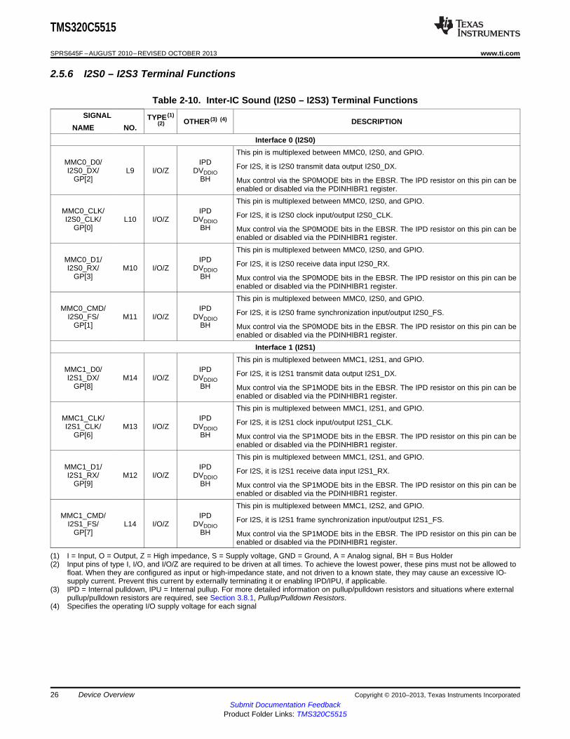
2.5.6 I2S0 – I2S3 Terminal Functions
Table 2-10. Inter-IC Sound (I2S0 – I2S3) Terminal FunctionsSIGNAL TYPE (1)
OTHER (3) (4) DESCRIPTION(2)NAME NO.Interface 0 (I2S0)
This pin is multiplexed between MMC0, I2S0, and GPIO.MMC0_D0/ IPD For I2S, it is I2S0 transmit data output I2S0_DX.I2S0_DX/ L9 I/O/Z DVDDIO
GP[2] BH Mux control via the SP0MODE bits in the EBSR. The IPD resistor on this pin can beenabled or disabled via the PDINHIBR1 register.This pin is multiplexed between MMC0, I2S0, and GPIO.
MMC0_CLK/ IPD For I2S, it is I2S0 clock input/output I2S0_CLK.I2S0_CLK/ L10 I/O/Z DVDDIOGP[0] BH Mux control via the SP0MODE bits in the EBSR. The IPD resistor on this pin can be
enabled or disabled via the PDINHIBR1 register.This pin is multiplexed between MMC0, I2S0, and GPIO.
MMC0_D1/ IPD For I2S, it is I2S0 receive data input I2S0_RX.I2S0_RX/ M10 I/O/Z DVDDIOGP[3] BH Mux control via the SP0MODE bits in the EBSR. The IPD resistor on this pin can be
enabled or disabled via the PDINHIBR1 register.This pin is multiplexed between MMC0, I2S0, and GPIO.
MMC0_CMD/ IPD For I2S, it is I2S0 frame synchronization input/output I2S0_FS.I2S0_FS/ M11 I/O/Z DVDDIOGP[1] BH Mux control via the SP0MODE bits in the EBSR. The IPD resistor on this pin can be
enabled or disabled via the PDINHIBR1 register.Interface 1 (I2S1)
This pin is multiplexed between MMC1, I2S1, and GPIO.MMC1_D0/ IPD For I2S, it is I2S1 transmit data output I2S1_DX.I2S1_DX/ M14 I/O/Z DVDDIO
GP[8] BH Mux control via the SP1MODE bits in the EBSR. The IPD resistor on this pin can beenabled or disabled via the PDINHIBR1 register.This pin is multiplexed between MMC1, I2S1, and GPIO.
MMC1_CLK/ IPD For I2S, it is I2S1 clock input/output I2S1_CLK.I2S1_CLK/ M13 I/O/Z DVDDIOGP[6] BH Mux control via the SP1MODE bits in the EBSR. The IPD resistor on this pin can be
enabled or disabled via the PDINHIBR1 register.This pin is multiplexed between MMC1, I2S1, and GPIO.
MMC1_D1/ IPD For I2S, it is I2S1 receive data input I2S1_RX.I2S1_RX/ M12 I/O/Z DVDDIOGP[9] BH Mux control via the SP1MODE bits in the EBSR. The IPD resistor on this pin can be
enabled or disabled via the PDINHIBR1 register.This pin is multiplexed between MMC1, I2S2, and GPIO.
MMC1_CMD/ IPD For I2S, it is I2S1 frame synchronization input/output I2S1_FS.I2S1_FS/ L14 I/O/Z DVDDIOGP[7] BH Mux control via the SP1MODE bits in the EBSR. The IPD resistor on this pin can be
enabled or disabled via the PDINHIBR1 register.
(1) I = Input, O = Output, Z = High impedance, S = Supply voltage, GND = Ground, A = Analog signal, BH = Bus Holder(2) Input pins of type I, I/O, and I/O/Z are required to be driven at all times. To achieve the lowest power, these pins must not be allowed to
float. When they are configured as input or high-impedance state, and not driven to a known state, they may cause an excessive IO-supply current. Prevent this current by externally terminating it or enabling IPD/IPU, if applicable.
(3) IPD = Internal pulldown, IPU = Internal pullup. For more detailed information on pullup/pulldown resistors and situations where externalpullup/pulldown resistors are required, see Section 3.8.1, Pullup/Pulldown Resistors.
(4) Specifies the operating I/O supply voltage for each signal
26 Device Overview Copyright © 2010–2013, Texas Instruments IncorporatedSubmit Documentation Feedback
Product Folder Links: TMS320C5515

TMS320C5515
www.ti.com SPRS645F –AUGUST 2010–REVISED OCTOBER 2013
Table 2-10. Inter-IC Sound (I2S0 – I2S3) Terminal Functions (continued)SIGNAL TYPE (1)
OTHER (3) (4) DESCRIPTION(2)NAME NO.Interface 2 (I2S2)
This pin is multiplexed between LCD Bridge, I2S2, GPIO, and SPI.LCD_D[11]/ IPDI2S2_DX/ For I2S, it is I2S2 transmit data output I2S2_DX.P12 I/O/Z DVDDIOGP[27]/ BH Mux control via the PPMODE bits in the EBSR. The IPD resistor on this pin can beSPI_TX
enabled or disabled via the PDINHIBR3 register.This pin is multiplexed between LCD Bridge, I2S2, GPIO, and SPI.
LCD_D8]/ IPDI2S2_CLK/ For I2S, it is I2S2 clock input/output I2S2_CLK.N10 I/O/Z DVDDIOGP[18]/ BH Mux control via the PPMODE bits in the EBSR. The IPD resistor on this pin can beSPI_CLKenabled or disabled via the PDINHIBR3 register.This pin is multiplexed between LCD Bridge, I2S2, GPIO, and SPI.
LCD_D[10]/ IPDI2S2_RX/ For I2S, it is I2S2 receive data input I2S2_RX.N11 I/O/Z DVDDIOGP[20]/ BH Mux control via the PPMODE bits in the EBSR. The IPD resistor on this pin can beSPI_RXenabled or disabled via the PDINHIBR3 register.This pin is multiplexed between LCD Bridge, I2S2, and GPIO.
LCD_D[9]/ IPDI2S2_FS/ For I2S, it is I2S2 frame synchronization input/output I2S2_FS.P11 I/O/Z DVDDIOGP[19]/ BH Mux control via the PPMODE bits in the EBSR. The IPD resistor on this pin can beSPI_CS0enabled or disabled via the PDINHIBR3 register.
Interface 3 (I2S3)This pin is multiplexed between LCD Bridge, UART, GPIO, and I2S3.
LCD_D[15]/ IPDUART_TXD/ For I2S, it is I2S3 transmit data output I2S3_DX.P14 I/O/Z DVDDIOGP[31]/ BH Mux control via the PPMODE bits in the EBSR. The IPD resistor on this pin can beI2S3_DXenabled or disabled via the PDINHIBR3 register.This pin is multiplexed between LCD Bridge, UART, GPIO, and I2S3.
LCD_D[12]/ IPDUART_RTS/ For I2S, it is I2S3 clock input/output I2S3_CLK.N12 I/O/Z DVDDIOGP[28]/ BH Mux control via the PPMODE bits in the EBSR. The IPD resistor on this pin can beI2S3_CLKenabled or disabled via the PDINHIBR3 register.This pin is multiplexed between LCD Bridge, UART, GPIO, and I2S3.
LCD_D[14]/ IPDUART_RXD/ For I2S, it is I2S3 receive data input I2S3_RX.N13 I/O/Z DVDDIOGP[30]/ BH Mux control via the PPMODE bits in the EBSR. The IPD resistor on this pin can beI2S3_RXenabled or disabled via the PDINHIBR3 register.This pin is multiplexed between LCD Bridge, UART, GPIO, and I2S3.
LCD_D[13]/ IPDUART_CTS/ For I2S, it is I2S3 frame synchronization input/output I2S3_FS.P13 I/O/Z DVDDIOGP[29]/ BH Mux control via the PPMODE bits in the EBSR. The IPD resistor on this pin can beI2S3_FSenabled or disabled via the PDINHIBR3 register.
Copyright © 2010–2013, Texas Instruments Incorporated Device Overview 27Submit Documentation Feedback
Product Folder Links: TMS320C5515

TMS320C5515
SPRS645F –AUGUST 2010–REVISED OCTOBER 2013 www.ti.com
2.5.7 SPI Terminal Functions
Table 2-11. Serial Peripheral Interface (SPI) Terminal FunctionsSIGNAL TYPE (1)
OTHER (3) (4) DESCRIPTION(2)NAME NO.Serial Port Interface (SPI)
This pin is multiplexed between LCD Bridge and SPI.LCD_CS0_E0/ DVDDIOP4 I/O/Z Mux control via the PPMODE bits in the EBSR.SPI_CS0 BH
For SPI, this pin is SPI chip select SPI_CS0.This pin is multiplexed between LCD Bridge, I2S2, GPIO, and SPI.
LCD_D[9]/ IPD Mux control via the PPMODE bits in the EBSR.I2S2_FS/ P11 I/O/Z DVDDIOGP[19]/ For SPI, this pin is SPI chip select SPI_CS0.BHSPI_CS0The IPD resistor on this pin can be enabled or disabled via the PDINHIBR3 register.This pin is multiplexed between LCD Bridge and SPI.
LCD_CS1_E1/ DVDDION4 I/O/Z Mux control via the PPMODE bits in the EBSR.SPI_CS1 BHFor SPI, this pin is SPI chip select SPI_CS1.This pin is multiplexed between LCD Bridge and SPI.
LCD_RW_WRB/ DVDDIOP5 I/O/Z Mux control via the PPMODE bits in the EBSR.SPI_CS2 BHFor SPI, this pin is SPI chip select SPI_CS2.This pin is multiplexed between LCD Bridge and SPI.
LCD_RS/ DVDDION5 I/O/Z Mux control via the PPMODE bits in the EBSR.SPI_CS3 BHFor SPI, this pin is SPI chip select SPI_CS3.This pin is multiplexed between LCD Bridge and SPI.
Mux control via the PPMODE bits in the EBSR.For SPI, this pin is clock output SPI_CLK.
LCD_EN_RDB/ DVDDION3 O/Z Note: This pin may consume static power if configured as Hi-Z and not pulled highSPI_CLK BHor low. Prevent current drain by externally terminating the pin.
This pin is ONLY in the Hi-Z state when doing boundary scan. Therefore, externaltermination is probably not required for most applications.This pin is multiplexed between LCD Bridge, I2S2, GPIO, and SPI.
LCD_D8]/ IPD Mux control via the PPMODE bits in the EBSR.I2S2_CLK/ N10 I/O/Z DVDDIOGP[18]/ For SPI, this pin is clock output SPI_CLK.BHSPI_CLKThe IPD resistor on this pin can be enabled or disabled via the PDINHIBR3 register.This pin is multiplexed between LCD Bridge and SPI.
LCD_D[1]/ DVDDION6 I/O/Z Mux control via the PPMODE bits in the EBSR.SPI_TX BHFor SPI, this pin is SPI transmit data output.This pin is multiplexed between LCD Bridge, I2S2, GPIO, and SPI.
LCD_D[11]/ IPD Mux control via the PPMODE bits in the EBSR.I2S2_DX/ P12 I/O/Z DVDDIOGP[27]/ For SPI, this pin is SPI transmit data output.BHSPI_TXThe IPD resistor on this pin can be enabled or disabled via the PDINHIBR3 register.This pin is multiplexed between LCD Bridge and SPI.
LCD_D[0]/ DVDDIOP6 I/O/Z Mux control via the PPMODE bits in the EBSR.SPI_RX BHFor SPI this pin is SPI receive data input.
(1) I = Input, O = Output, Z = High impedance, S = Supply voltage, GND = Ground, A = Analog signal, BH = Bus Holder(2) Input pins of type I, I/O, and I/O/Z are required to be driven at all times. To achieve the lowest power, these pins must not be allowed to
float. When they are configured as input or high-impedance state, and not driven to a known state, they may cause an excessive IO-supply current. Prevent this current by externally terminating it or enabling IPD/IPU, if applicable.
(3) IPD = Internal pulldown, IPU = Internal pullup. For more detailed information on pullup/pulldown resistors and situations where externalpullup/pulldown resistors are required, see Section 3.8.1, Pullup/Pulldown Resistors.
(4) Specifies the operating I/O supply voltage for each signal
28 Device Overview Copyright © 2010–2013, Texas Instruments IncorporatedSubmit Documentation Feedback
Product Folder Links: TMS320C5515

TMS320C5515
www.ti.com SPRS645F –AUGUST 2010–REVISED OCTOBER 2013
Table 2-11. Serial Peripheral Interface (SPI) Terminal Functions (continued)SIGNAL TYPE (1)
OTHER (3) (4) DESCRIPTION(2)NAME NO.This pin is multiplexed between LCD Bridge, I2S2, GPIO, and SPI.
LCD_D[10]/ IPD Mux control via the PPMODE bits in the EBSR.I2S2_RX/ N11 I/O/Z DVDDIOGP[20]/ For SPI this pin is SPI receive data input.BHSPI_RXThe IPD resistor on this pin can be enabled or disabled via the PDINHIBR3 register.
Copyright © 2010–2013, Texas Instruments Incorporated Device Overview 29Submit Documentation Feedback
Product Folder Links: TMS320C5515

TMS320C5515
SPRS645F –AUGUST 2010–REVISED OCTOBER 2013 www.ti.com
2.5.8 UART Terminal Functions
Table 2-12. UART Terminal FunctionsSIGNAL TYPE (1)
OTHER (3) (4) DESCRIPTION(2)NAME NO.UART
This pin is multiplexed between LCD Bridge, UART, GPIO, and I2S3.LCD_D[14]/ IPDUART_RXD/ When used by UART, it is the receive data input UART_RXD.N13 I/O/Z DVDDIOGP[30]/ BH Mux control via the PPMODE bits in the EBSR. The IPD resistor on this pin can beI2S3_RX
enabled or disabled via the PDINHIBR3 register.This pin is multiplexed between LCD Bridge, UART, GPIO, and I2S3.
LCD_D[15]/ IPDUART_TXD/ In UART mode, it is the transmit data output UART_TXD.P14 I/O/Z DVDDIOGP[31]/ BH Mux control via the PPMODE bits in the EBSR. The IPD resistor on this pin can beI2S3_DXenabled or disabled via the PDINHIBR3 register.This pin is multiplexed between LCD Bridge, UART, GPIO, and I2S3.
LCD_D[13]/ IPDUART_CTS/ In UART mode, it is the clear to send input UART_CTS.P13 I/O/Z DVDDIOGP[29]/ BH Mux control via the PPMODE bits in the EBSR. The IPD resistor on this pin can beI2S3_FSenabled or disabled via the PDINHIBR3 register.This pin is multiplexed between LCD Bridge, UART, GPIO, and I2S3.
LCD_D[12]/ IPDUART_RTS/ In UART mode, it is the ready to send output UART_RTS.N12 I/O/Z DVDDIOGP[28]/ BH Mux control via the PPMODE bits in the EBSR. The IPD resistor on this pin can beI2S3_CLKenabled or disabled via the PDINHIBR3 register.
(1) I = Input, O = Output, Z = High impedance, S = Supply voltage, GND = Ground, A = Analog signal, BH = Bus Holder(2) Input pins of type I, I/O, and I/O/Z are required to be driven at all times. To achieve the lowest power, these pins must not be allowed to
float. When they are configured as input or high-impedance state, and not driven to a known state, they may cause an excessive IO-supply current. Prevent this current by externally terminating it or enabling IPD/IPU, if applicable.
(3) IPD = Internal pulldown, IPU = Internal pullup. For more detailed information on pullup/pulldown resistors and situations where externalpullup/pulldown resistors are required, see Section 3.8.1, Pullup/Pulldown Resistors.
(4) Specifies the operating I/O supply voltage for each signal
30 Device Overview Copyright © 2010–2013, Texas Instruments IncorporatedSubmit Documentation Feedback
Product Folder Links: TMS320C5515

TMS320C5515
www.ti.com SPRS645F –AUGUST 2010–REVISED OCTOBER 2013
2.5.9 USB 2.0 Terminal Functions
Table 2-13. USB2.0 Terminal FunctionsSIGNAL TYPE (1)
OTHER (3) (4) DESCRIPTION(2)NAME NO.USB 2.0
12-MHz crystal oscillator input.
When the USB peripheral is not used, USB_MXI should be connected to ground(VSS).
USB_MXI G13 I USB_VDDOSC When using an external 12-MHz oscillator, the external oscillator clock signal shouldbe connected to the USB_MXI pin and the amplitude of the oscillator clock signalmust meet the VIH requirement (see Section 4.2, Recommended OperatingConditions). The USB_MXO is left unconnected and the USB_VSSOSC signal isconnected to board ground (VSS).12-MHz crystal oscillator output.
When the USB peripheral is not used, USB_MXO should be left unconnected.
When using an external 12-MHz oscillator, the external oscillator clock signal shouldUSB_MXO G14 O/Z USB_VDDOSC be connected to the USB_MXI pin and the amplitude of the oscillator clock signalmust meet the VIH requirement (see Section 4.2, Recommended OperatingConditions). The USB_MXO is left unconnected and the USB_VSSOSC signal isconnected to board ground (VSS).3.3-V power supply for USB oscillator.see
USB_VDDOSC G12 S Section 4.2, When the USB peripheral is not used, USB_VDDOSC should be connected to groundROC (VSS).
Ground for USB oscillator. When using a 12-MHz crystal, this pin is a local groundfor the crystal and must not be connected to the board ground (See Figure 5-7).
see When using an external 12-MHz oscillator, the external oscillator clock signal shouldUSB_VSSOSC F11 S Section 4.2, be connected to the USB_MXI pin and the amplitude of the oscillator clock signal
ROC must meet the VIH requirement (see Section 4.2, Recommended OperatingConditions). The USB_MXO is left unconnected and the USB_VSSOSC signal isconnected to board ground (VSS).
USB power detect. 5-V input that signifies that VBUS is connected.see This signal must be powered on in the order listed in Section 5.3.1, Power-Supply
USB_VBUS J12 A I/O Section 4.2, Sequencing.ROC
When the USB peripheral is not used, the USB_VBUS signal should be connectedto ground (VSS).
USB_DP H14 A I/O USB_VDDA3P3 USB bi-directional Data Differential signal pair [positive/negative].
When the USB peripheral is not used, the USB_DP and USB_DM signals shouldUSB_DM J14 A I/O USB_VDDA3P3 both be tied to ground (VSS).External resistor connect. Reference current output. This must be connected via a10-kΩ ±1% resistor to USB_VSSREF and be placed as close to the device aspossible.USB_R1 G9 A I/O USB_VDDA3P3
When the USB peripheral is not used, the USB_R1 signal should be connected viaa 10-kΩ resistor to USB_VSSREF.Ground for reference current. This must be connected via a 10-kΩ ±1% resistor to
see USB_R1.USB_VSSREF G10 GND Section 4.2,
When the USB peripheral is not used, the USB_VSSREF signal should be connectedROCdirectly to ground (Vss).
(1) I = Input, O = Output, Z = High impedance, S = Supply voltage, GND = Ground, A = Analog signal, BH = Bus Holder(2) Input pins of type I, I/O, and I/O/Z are required to be driven at all times. To achieve the lowest power, these pins must not be allowed to
float. When they are configured as input or high-impedance state, and not driven to a known state, they may cause an excessive IO-supply current. Prevent this current by externally terminating it or enabling IPD/IPU, if applicable.
(3) IPD = Internal pulldown, IPU = Internal pullup. For more detailed information on pullup/pulldown resistors and situations where externalpullup/pulldown resistors are required, see Section 3.8.1, Pullup/Pulldown Resistors.
(4) Specifies the operating I/O supply voltage for each signal
Copyright © 2010–2013, Texas Instruments Incorporated Device Overview 31Submit Documentation Feedback
Product Folder Links: TMS320C5515

TMS320C5515
SPRS645F –AUGUST 2010–REVISED OCTOBER 2013 www.ti.com
Table 2-13. USB2.0 Terminal Functions (continued)SIGNAL TYPE (1)
OTHER (3) (4) DESCRIPTION(2)NAME NO.
Analog 3.3 V power supply for USB PHY.see This signal must be powered on in the order listed in Section 5.3.1, Power-Supply
USB_VDDA3P3 H12 S Section 4.2, Sequencing.ROC
When the USB peripheral is not used, the USB_VDDA3P3 signal should beconnected to ground (VSS).
seeUSB_VSSA3P3 H11 GND Section 4.2, Analog ground for USB PHY.
ROC
Analog 1.3 V power supply for USB PHY. [For high-speed sensitive analog circuits]see This signal must be powered on in the order listed in Section 5.3.1, Power-Supply
USB_VDDA1P3 H10 S Section 4.2, Sequencing.ROC
When the USB peripheral is not used, the USB_VDDA1P3 signal should beconnected to ground (VSS).
seeUSB_VSSA1P3 H9 GND Section 4.2, Analog ground for USB PHY [For high speed sensitive analog circuits].
ROC
1.3-V digital core power supply for USB PHY.see This signal must be powered on in the order listed in Section 5.3.1, Power-Supply
USB_VDD1P3 J13 S Section 4.2, Sequencing.ROC
When the USB peripheral is not used, the USB_VDD1P3 signal should be connectedto ground (VSS).
seeUSB_VSS1P3 H13 GND Section 4.2, Digital core ground for USB phy.
ROC3.3 V USB Analog PLL power supply.see
USB_VDDPLL G8 S Section 4.2, When the USB peripheral is not used, the USB_VDDPLL signal should be connectedROC to ground (VSS).see
USB_VSSPLL G11 GND Section 4.2, USB Analog PLL ground.ROC
32 Device Overview Copyright © 2010–2013, Texas Instruments IncorporatedSubmit Documentation Feedback
Product Folder Links: TMS320C5515

TMS320C5515
www.ti.com SPRS645F –AUGUST 2010–REVISED OCTOBER 2013
2.5.10 LCD Bridge Terminal Functions
Table 2-14. LCD Bridge Terminal FunctionsSIGNAL TYPE (1)
OTHER (3) (4) DESCRIPTION(2)NAME NO.This pin is multiplexed between LCD Bridge and SPI.
For LCD Bridge, this pin is either LCD Bridge read/write enable (MPU68 mode) orread strobe (MPU80 mode).LCD_EN_RDB/ DVDDION3 O/ZSPI_CLK BH Mux control via the PPMODE bits in the EBSR.
Note: This pin may consume static power if configured as Hi-Z and not pulled high orlow. Prevent current drain by externally terminating the pin.This pin is multiplexed between LCD Bridge and SPI.
LCD_CS0_E0/ DVDDIO For LCD Bridge, this pin is either LCD Bridge chip select 0 (MPU68 and MPU80P4 I/O/ZSPI_CS0 BH modes) or enable 0 (HD44780 mode).
Mux control via the PPMODE bits in the EBSR.This pin is multiplexed between LCD Bridge and SPI.
LCD_CS1_E1/ DVDDIO For LCD Bridge, this pin is either LCD Bridge chip select 1 (MPU68 and MPU80N4 I/O/ZSPI_CS1 BH modes) or enable 1 (HD44780 mode).
Mux control via the PPMODE bits in the EBSR.This pin is multiplexed between LCD Bridge and SPI.
LCD_RW_WRB/ DVDDIO For LCD, this pin is either LCD Bridge read/write select (HD44780 and MPU68P5 I/O/ZSPI_CS2 BH modes) or write strobe (MPU80 mode).
Mux control via the PPMODE bits in the EBSR.This pin is multiplexed between LCD Bridge and SPI.
LCD_RS/ DVDDION5 I/O/Z For LCD, this pin is the LCD Bridge address set-up.SPI_CS3 BHMux control via the PPMODE bits in the EBSR.This pin is multiplexed between LCD Bridge, UART, GPIO, and I2S3.
LCD_D[15]/ IPDUART_TXD/ For LCD Bridge, it is LCD data pin 15.P14 I/O/Z DVDDIOGP[31]/ BH Mux control via the PPMODE bits in the EBSR. The IPD resistor on this pin can beI2S3_DXenabled or disabled via the PDINHIBR3 register.This pin is multiplexed between LCD Bridge, UART, GPIO, and I2S3.
LCD_D[14]/ IPDUART_RXD/ For LCD Bridge, it is LCD data pin 14.N13 I/O/Z DVDDIOGP[30]/ BH Mux control via the PPMODE bits in the EBSR. The IPD resistor on this pin can beI2S3_RXenabled or disabled via the PDINHIBR3 register.This pin is multiplexed between LCD Bridge, UART, GPIO, and I2S3.
LCD_D[13]/ IPDUART_CTS/ For LCD Bridge, it is LCD data pin 13.P13 I/O/Z DVDDIOGP[29]/ BH Mux control via the PPMODE bits in the EBSR. The IPD resistor on this pin can beI2S3_FSenabled or disabled via the PDINHIBR3 register.This pin is multiplexed between LCD Bridge, I2S2, and GPIO.
LCD_D[12]/ IPDUART_RTS/ For LCD Bridge, it is LCD data pin 12.N12 I/O/Z DVDDIOGP[28]/ BH Mux control via the PPMODE bits in the EBSR. The IPD resistor on this pin can beI2S3_CLKenabled or disabled via the PDINHIBR3 register.
(1) I = Input, O = Output, Z = High impedance, S = Supply voltage, GND = Ground, A = Analog signal, BH = Bus Holder(2) Input pins of type I, I/O, and I/O/Z are required to be driven at all times. To achieve the lowest power, these pins must not be allowed to
float. When they are configured as input or high-impedance state, and not driven to a known state, they may cause an excessive IO-supply current. Prevent this current by externally terminating it or enabling IPD/IPU, if applicable.
(3) IPD = Internal pulldown, IPU = Internal pullup. For more detailed information on pullup/pulldown resistors and situations where externalpullup/pulldown resistors are required, see Section 3.8.1, Pullup/Pulldown Resistors.
(4) Specifies the operating I/O supply voltage for each signal
Copyright © 2010–2013, Texas Instruments Incorporated Device Overview 33Submit Documentation Feedback
Product Folder Links: TMS320C5515

TMS320C5515
SPRS645F –AUGUST 2010–REVISED OCTOBER 2013 www.ti.com
Table 2-14. LCD Bridge Terminal Functions (continued)SIGNAL TYPE (1)
OTHER (3) (4) DESCRIPTION(2)NAME NO.This pin is multiplexed between LCD Bridge, I2S2, GPIO, and SPI.
LCD_D[11]/ IPDI2S2_DX/ For LCD Bridge, it is LCD data pin 11.P12 I/O/Z DVDDIOGP[27]/ BH Mux control via the PPMODE bits in the EBSR. The IPD resistor on this pin can beSPI_TXenabled or disabled via the PDINHIBR3 register.This pin is multiplexed between LCD Bridge, I2S2, GPIO, and SPI.
LCD_D[10]/ IPDI2S2_RX/ For LCD Bridge, it is LCD data pin 10.N11 I/O/Z DVDDIOGP[20]/ BH Mux control via the PPMODE bits in the EBSR. The IPD resistor on this pin can beSPI_RXenabled or disabled via the PDINHIBR3 register.This pin is multiplexed between LCD Bridge, I2S2, GPIO, and SPI.
LCD_D[9]/ IPDI2S2_FS/ For LCD Bridge, it is LCD data pin 9.P11 I/O/Z DVDDIOGP[19]/ BH Mux control via the PPMODE bits in the EBSR. The IPD resistor on this pin can beSPI_CS0enabled or disabled via the PDINHIBR3 register.This pin is multiplexed between LCD Bridge, I2S2, GPIO, and SPI.
LCD_D[8]/ IPDI2S2_CLK For LCD Bridge, it is LCD data pin 8.N10 I/O/Z DVDDIOGP[18]/ BH Mux control via the PPMODE bits in the EBSR. The IPD resistor on this pin can beSPI_CLKenabled or disabled via the PDINHIBR3 register.This pin is multiplexed between LCD Bridge and GPIO.
IPDLCD_D[7]/ For LCD Bridge, it is LCD data pin 7.P10 I/O/Z DVDDIOGP[17] BH Mux control via the PPMODE bits in the EBSR. The IPD resistor on this pin can beenabled or disabled via the PDINHIBR3 register.This pin is multiplexed between LCD Bridge and GPIO.
IPDLCD_D[6]/ For LCD Bridge, it is LCD data pin 6.N9 I/O/Z DVDDIOGP[16] BH Mux control via the PPMODE bits in the EBSR. The IPD resistor on this pin can beenabled or disabled via the PDINHIBR3 register.This pin is multiplexed between LCD Bridge and GPIO.
IPDLCD_D[5]/ For LCD Bridge, it is LCD data pin 5.P9 I/O/Z DVDDIOGP[15] BH Mux control via the PPMODE bits in the EBSR. The IPD resistor on this pin can beenabled or disabled via the PDINHIBR3 register.This pin is multiplexed between LCD Bridge and GPIO.
IPDLCD_D[4]/ For LCD Bridge, it is LCD data pin 4.N8 I/O/Z DVDDIOGP[14] BH Mux control via the PPMODE bits in the EBSR. The IPD resistor on this pin can beenabled or disabled via the PDINHIBR3 register.This pin is multiplexed between LCD Bridge and GPIO.
IPDLCD_D[3]/ For LCD Bridge, it is LCD data pin 3.N7 I/O/Z DVDDIOGP[13] BH Mux control via the PPMODE bits in the EBSR. The IPD resistor on this pin can beenabled or disabled via the PDINHIBR3 register.This pin is multiplexed between LCD Bridge and GPIO.
IPDLCD_D[2]/ For LCD Bridge, it is LCD data pin 2.P7 I/O/Z DVDDIOGP[12] BH Mux control via the PPMODE bits in the EBSR. The IPD resistor on this pin can beenabled or disabled via the PDINHIBR3 register.This pin is multiplexed between LCD Bridge and SPI.
LCD_D[1]/ DVDDION6 I/O/Z For LCD Bridge, it is LCD data pin 1.SPI_TX BHMux control via the PPMODE bits in the EBSR.This pin is multiplexed between LCD Bridge and SPI.
LCD_D[0]/ DVDDIOP6 I/O/Z For LCD Bridge, it is LCD data pin 0.SPI_RX BHMux control via the PPMODE bits in the EBSR.
34 Device Overview Copyright © 2010–2013, Texas Instruments IncorporatedSubmit Documentation Feedback
Product Folder Links: TMS320C5515

TMS320C5515
www.ti.com SPRS645F –AUGUST 2010–REVISED OCTOBER 2013
2.5.11 MMC/SD Terminal Functions
Table 2-15. MMC1/SD Terminal FunctionsSIGNAL TYPE (1)
OTHER (3) (4) DESCRIPTION(2)NAME NO.MMC/SD
This pin is multiplexed between MMC1, I2S1, and GPIO.MMC1_CLK/ IPD For MMC/SD, this is the MMC1 data clock output MMC1_CLK.I2S1_CLK/ M13 I/O/Z DVDDIO
GP[6] BH Mux control via the SP1MODE bits in the EBSR. The IPD resistor on this pin can beenabled or disabled via the PDINHIBR1 register.This pin is multiplexed between MMC1, I2S1, and GPIO.
MMC1_CMD/ IPD For MMC/SD, this is the MMC1 command I/O output MMC1_CMD.I2S1_FS/ L14 I/O/Z DVDDIOGP[7] BH Mux control via the SP1MODE bits in the EBSR. The IPD resistor on this pin can be
enabled or disabled via the PDINHIBR1 register.IPDMMC1_D3/ L13 I/O/Z DVDDIOGP[11] The MMC1_D3 and MMC1_D2 pins are multiplexed between MMC1 and GPIO.BHIPD The MMC1_D1 and MMC1_D0 pins are multiplexed between MMC1, I2S1, andMMC1_D2/ K14 I/O/Z DVDDIO GPIO.GP[10] BH
In MMC/SD mode, all these pins are the MMC1 nibble wide bi-directional data bus.MMC1_D1/ IPD
Mux control via the SP1MODE bits in the EBSR.I2S1_RX/ M12 I/O/Z DVDDIOGP[9] BH
The IPD resistor on these pins can be enabled or disabled via the PDINHIBR1MMC1_D0/ IPD register.I2S1_DX/ M14 I/O/Z DVDDIO
GP[8] BH
(1) I = Input, O = Output, Z = High impedance, S = Supply voltage, GND = Ground, A = Analog signal, BH = Bus Holder(2) Input pins of type I, I/O, and I/O/Z are required to be driven at all times. To achieve the lowest power, these pins must not be allowed to
float. When they are configured as input or high-impedance state, and not driven to a known state, they may cause an excessive IO-supply current. Prevent this current by externally terminating it or enabling IPD/IPU, if applicable.
(3) IPD = Internal pulldown, IPU = Internal pullup. For more detailed information on pullup/pulldown resistors and situations where externalpullup/pulldown resistors are required, see Section 3.8.1, Pullup/Pulldown Resistors.
(4) Specifies the operating I/O supply voltage for each signal
Copyright © 2010–2013, Texas Instruments Incorporated Device Overview 35Submit Documentation Feedback
Product Folder Links: TMS320C5515

TMS320C5515
SPRS645F –AUGUST 2010–REVISED OCTOBER 2013 www.ti.com
Table 2-16. MMC0/SD Terminal FunctionsSIGNAL TYPE (1)
OTHER (3) (4) DESCRIPTION(2)NAME NO.MMC/SD
This pin is multiplexed between MMC0, I2S0, and GPIO.MMC0_CLK/ IPD For MMC/SD, this is the MMC0 data clock output MMC0_CLK.I2S0_CLK/ L10 I/O/Z DVDDIO
GP[0] BH Mux control via the SP0MODE bits in the EBSR. The IPD resistor on this pin can beenabled or disabled via the PDINHIBR1 register.This pin is multiplexed between MMC0, I2S0, and GPIO.
MMC0_CMD/ IPD For MMC/SD, this is the MMC0 command I/O output MMC0_CMD.I2S0_FS/ M11 I/O/Z DVDDIOGP[1] BH Mux control via the SP0MODE bits in the EBSR. The IPD resistor on this pin can be
enabled or disabled via the PDINHIBR1 register.IPDMMC0_D3/ L11 I/O/Z DVDDIOGP[5] The MMC0_D3 and MMC0_D2 pins are multiplexed between MMC0 and GPIO.BHIPD The MMC0_D1 and MMC0_D0 pins are multiplexed between MMC0, I2S0, andMMC0_D2/ L12 I/O/Z DVDDIO GPIO.GP[4] BH
In MMC/SD mode, these pins are the MMC0 nibble wide bi-directional data bus.MMC0_D1/ IPD
Mux control via the SP0MODE bits in the EBSR.I2S0_RX/ M10 I/O/Z DVDDIOGP[3] BH
The IPD resistor on these pins can be enabled or disabled via the PDINHIBR1MMC0_D0/ IPD register.I2S0_DX/ L9 I/O/Z DVDDIO
GP[2] BH
(1) I = Input, O = Output, Z = High impedance, S = Supply voltage, GND = Ground, A = Analog signal, BH = Bus Holder(2) Input pins of type I, I/O, and I/O/Z are required to be driven at all times. To achieve the lowest power, these pins must not be allowed to
float. When they are configured as input or high-impedance state, and not driven to a known state, they may cause an excessive IO-supply current. Prevent this current by externally terminating it or enabling IPD/IPU, if applicable.
(3) IPD = Internal pulldown, IPU = Internal pullup. For more detailed information on pullup/pulldown resistors and situations where externalpullup/pulldown resistors are required, see Section 3.8.1, Pullup/Pulldown Resistors.
(4) Specifies the operating I/O supply voltage for each signal
36 Device Overview Copyright © 2010–2013, Texas Instruments IncorporatedSubmit Documentation Feedback
Product Folder Links: TMS320C5515

TMS320C5515
www.ti.com SPRS645F –AUGUST 2010–REVISED OCTOBER 2013
2.5.12 SAR ADC Terminal Functions
Table 2-17. 10-Bit SAR ADC Terminal FunctionsSIGNAL TYPE (1)
OTHER (3) (4) DESCRIPTION(2)NAME NO.SAR ADC
GPAIN0: General -Purpose Output and Analog Input pin 0. This pin is demuxedinternally into ADC Channels 0, 1, & 2. GPAIN0 can also be used as a general-purpose open-drain output. This pin is unique among the GPAIN pins in that it is the
GPAIN0 D10 I/O VDDA_ANA only pin that is 3.6 V-tolerant to support measuring a battery voltage. GPAIN0 canaccommodate input voltages from 0 V to 3.6 V; although, the ADC is unable toaccept signals greater than VDDA_ANA without clamping. ADC Channel 1 is capableof switching in an internal resistor divider that has a divide ratio of approximately 1/8.GPAIN1: General -Purpose Output and Analog Input pin 1. This pin is connected toADC Channel 3. GPAIN1 can be used as a general-purpose output if certainrequirements are met (see the following note). GPAIN1 can accommodate inputvoltages from 0 V to VDDA_ANA.
Note: If the ANA_LDO is used to supply power to VDDA_ANA, this pin must not beGPAIN1 A11 I/O VDDA_ANAused as a general-purpose output (driving high) since the max current capability(see the ISD parameter in Section 4.3, Electrical Characteristics Over RecommendedRanges of Supply Voltage and Operating Temperature) of the ANA_LDO can beexceeded. Doing so may result in the on-chip power-on reset (POR) resetting thechip.GPAIN2: General -Purpose Output and Analog Input pin 2. This pin is connected toADC Channel 4. GPAIN2 can be used as a general-purpose output if certainrequirements are met (see the following note). GPAIN2 can accommodate inputvoltages from 0 V to VDDA_ANA.
GPAIN2 B11 I/O VDDA_ANA Note: If the ANA_LDO is used to supply power to VDDA_ANA, this pin must not beused as a general-purpose output (driving high) since the max current capability(see the ISD parameter in Section 4.3, Electrical Characteristics Over RecommendedRanges of Supply Voltage and Operating Temperature) of the ANA_LDO can beexceeded. Doing so may result in the on-chip POR resetting the chip.GPAIN3: General -Purpose Output and Analog Input pin 3. This pin is connected toADC Channel 5. GPAIN3 can be used as a general-purpose output if certainrequirements are met (see the following note). GPAIN3 can accommodate inputvoltages from 0 V to VDDA_ANA.
GPAIN3 C11 I/O VDDA_ANA Note: If the ANA_LDO is used to supply power to VDDA_ANA, this pin must not beused as a general-purpose output (driving high) since the max current capability(see the ISD parameter in Section 4.3, Electrical Characteristics Over RecommendedRanges of Supply Voltage and Operating Temperature) of the ANA_LDO can beexceeded. Doing so may result in the on-chip POR resetting the chip.
(1) I = Input, O = Output, Z = High impedance, S = Supply voltage, GND = Ground, A = Analog signal, BH = Bus Holder(2) Input pins of type I, I/O, and I/O/Z are required to be driven at all times. To achieve the lowest power, these pins must not be allowed to
float. When they are configured as input or high-impedance state, and not driven to a known state, they may cause an excessive IO-supply current. Prevent this current by externally terminating it or enabling IPD/IPU, if applicable.
(3) IPD = Internal pulldown, IPU = Internal pullup. For more detailed information on pullup/pulldown resistors and situations where externalpullup/pulldown resistors are required, see Section 3.8.1, Pullup/Pulldown Resistors.
(4) Specifies the operating I/O supply voltage for each signal
Copyright © 2010–2013, Texas Instruments Incorporated Device Overview 37Submit Documentation Feedback
Product Folder Links: TMS320C5515

TMS320C5515
SPRS645F –AUGUST 2010–REVISED OCTOBER 2013 www.ti.com
2.5.13 GPIO Terminal Functions
Table 2-18. GPIO Terminal FunctionsSIGNAL TYPE (1)
OTHER (3) (4) DESCRIPTION(2)NAME NO.General-Purpose Input/Output
External Flag Output. XF is used for signaling other processors in multiprocessorconfigurations or XF can be used as a fast general-purpose output pin.
XF is set high by the BSET XF instruction and XF is set low by the BCLR XFinstruction or by writing to bit 13 of the ST1_55 register. For more information on the
– ST1_55 register, see the TMS320C55x 3.0 CPU Reference Guide (literatureXF M8 O/Z DVDDIO number: SWPU073).
BHFor XF pin behavior at reset, see Section 5.7.2, Pin Behaviors at Reset.
Note: This pin may consume static power if configured as Hi-Z and not externallypulled low or high. Prevent current drain by externally terminating the pin. XF pin isONLY in the Hi-Z state when doing boundary scan. Therefore, external terminationis probably not required for most applications.This pin is multiplexed between MMC0, I2S0, and GPIO.
MMC0_CLK/ IPD For GPIO, it is general-purpose input/output pin 0 (GP[0]).I2S0_CLK/ L10 I/O/Z DVDDIOGP[0] BH Mux control via the SP0MODE bits in the EBSR. The IPD resistor on this pin can be
enabled or disabled via the PDINHIBR1 register.This pin is multiplexed between MMC0, I2S0, and GPIO.
MMC0_CMD/ IPD For GPIO, it is general-purpose input/output pin 1 (GP[1]).I2S0_FS/ M11 I/O/Z DVDDIOGP[1] BH Mux control via the SP0MODE bits in the EBSR. The IPD resistor on this pin can be
enabled or disabled via the PDINHIBR1 register.This pin is multiplexed between MMC0, I2S0, and GPIO.
MMC0_D0/ IPD For GPIO, it is general-purpose input/output pin 2 (GP[2]).I2S0_DX/ L9 I/O/Z DVDDIOGP[2] BH Mux control via the SP0MODE bits in the EBSR. The IPD resistor on this pin can be
enabled or disabled via the PDINHIBR1 register.This pin is multiplexed between MMC0, I2S0, and GPIO.
MMC0_D1/ IPD For GPIO, it is general-purpose input/output pin 3 (GP[3]).I2S0_RX/ M10 I/O/Z DVDDIOGP[3] BH Mux control via the SP0MODE bits in the EBSR. The IPD resistor on this pin can be
enabled or disabled via the PDINHIBR1 register.This pin is multiplexed between MMC0 and GPIO.
IPDMMC0_D2/ For GPIO, it is general-purpose input/output pin 4 (GP[4]).L12 I/O/Z DVDDIOGP[4] BH Mux control via the SP0MODE bits in the EBSR. The IPD resistor on this pin can beenabled or disabled via the PDINHIBR1 register.This pin is multiplexed between MMC0 and GPIO.
IPDMMC0_D3/ For GPIO, it is general-purpose input/output pin 5 (GP[5]).L11 I/O/Z DVDDIOGP[5] BH Mux control via the SP0MODE bits in the EBSR. The IPD resistor on this pin can beenabled or disabled via the PDINHIBR1 register.This pin is multiplexed between MMC1, I2S1, and GPIO.
MMC1_CLK/ IPDI2S1_CLK/ M13 I/O/Z DVDDIO For GPIO, it is general-purpose input/output pin 6 (GP[6]).
GP[6] BHMux control via the SP1MODE bits in the EBSR.
(1) I = Input, O = Output, Z = High impedance, S = Supply voltage, GND = Ground, A = Analog signal, BH = Bus Holder(2) Input pins of type I, I/O, and I/O/Z are required to be driven at all times. To achieve the lowest power, these pins must not be allowed to
float. When they are configured as input or high-impedance state, and not driven to a known state, they may cause an excessive IO-supply current. Prevent this current by externally terminating it or enabling IPD/IPU, if applicable.
(3) IPD = Internal pulldown, IPU = Internal pullup. For more detailed information on pullup/pulldown resistors and situations where externalpullup/pulldown resistors are required, see Section 3.8.1, Pullup/Pulldown Resistors.
(4) Specifies the operating I/O supply voltage for each signal
38 Device Overview Copyright © 2010–2013, Texas Instruments IncorporatedSubmit Documentation Feedback
Product Folder Links: TMS320C5515

TMS320C5515
www.ti.com SPRS645F –AUGUST 2010–REVISED OCTOBER 2013
Table 2-18. GPIO Terminal Functions (continued)SIGNAL TYPE (1)
OTHER (3) (4) DESCRIPTION(2)NAME NO.This pin is multiplexed between MMC1, I2S1, and GPIO.
MMC1_CMD/ IPD For GPIO, it is general-purpose input/output pin 7 (GP[7]).I2S1_FS/ L14 I/O/Z DVDDIOGP[7] BH Mux control via the SP1MODE bits in the EBSR. The IPD resistor on this pin can be
enabled or disabled via the PDINHIBR1 register.This pin is multiplexed between MMC1, I2S1, and GPIO.
MMC1_D0/ IPD For GPIO, it is general-purpose input/output pin 8 (GP[8]).I2S1_DX/ M14 I/O/Z DVDDIOGP[8] BH Mux control via the SP1MODE bits in the EBSR. The IPD resistor on this pin can be
enabled or disabled via the PDINHIBR1 register.This pin is multiplexed between MMC1, I2S1, and GPIO.
MMC1_D1/ IPD For GPIO, it is general-purpose input/output pin 9 (GP[9]).I2S1_RX/ M12 I/O/Z DVDDIOGP[9] BH Mux control via the SP1MODE bits in the EBSR. The IPD resistor on this pin can be
enabled or disabled via the PDINHIBR1 register.This pin is multiplexed between MMC1 and GPIO.
IPDMMC1_D2/ For GPIO, it is general-purpose input/output pin 10 (GP[10]).K14 I/O/Z DVDDIOGP[10] BH Mux control via the SP1MODE bits in the EBSR. The IPD resistor on this pin can beenabled or disabled via the PDINHIBR1 register.This pin is multiplexed between MMC1 and GPIO.
IPDMMC1_D3/ For GPIO, it is general-purpose input/output pin 11 (GP[11]).L13 I/O/Z DVDDIOGP[11] BH Mux control via the SP1MODE bits in the EBSR. The IPD resistor on this pin can beenabled or disabled via the PDINHIBR1 register.This pin is multiplexed between LCD Bridge and GPIO.
IPDLCD_D[2]/ For GPIO, it is general-purpose input/output pin 12 (GP[12]).P7 I/O/Z DVDDIOGP[12] BH Mux control via the PPMODE bits in the EBSR. The IPD resistor on this pin can beenabled or disabled via the PDINHIBR3 register.This pin is multiplexed between LCD Bridge and GPIO.
IPDLCD_D[3]/ For GPIO, it is general-purpose input/output pin 13 (GP[13]).N7 I/O/Z DVDDIOGP[13] BH Mux control via the PPMODE bits in the EBSR. The IPD resistor on this pin can beenabled or disabled via the PDINHIBR3 register.This pin is multiplexed between LCD Bridge and GPIO.
IPDLCD_D[4]/ For GPIO, it is general-purpose input/output pin 14 (GP[14]).N8 I/O/Z DVDDIOGP[14] BH Mux control via the PPMODE bits in the EBSR. The IPD resistor on this pin can beenabled or disabled via the PDINHIBR3 register.This pin is multiplexed between LCD Bridge and GPIO.
IPDLCD_D[5]/ For GPIO, it is general-purpose input/output pin 15 (GP[15]).P9 I/O/Z DVDDIOGP[15] BH Mux control via the PPMODE bits in the EBSR. The IPD resistor on this pin can beenabled or disabled via the PDINHIBR3 register.This pin is multiplexed between LCD Bridge and GPIO.
IPDLCD_D[6]/ For GPIO, it is general-purpose input/output pin 16 (GP[16]).N9 I/O/Z DVDDIOGP[16] BH Mux control via the PPMODE bits in the EBSR. The IPD resistor on this pin can beenabled or disabled via the PDINHIBR3 register.This pin is multiplexed between LCD Bridge and GPIO.
IPDLCD_D[7]/ For GPIO, it is general-purpose input/output pin 17 (GP[17]).P10 I/O/Z DVDDIOGP[17] BH Mux control via the PPMODE bits in the EBSR. The IPD resistor on this pin can beenabled or disabled via the PDINHIBR3 register.
Copyright © 2010–2013, Texas Instruments Incorporated Device Overview 39Submit Documentation Feedback
Product Folder Links: TMS320C5515

TMS320C5515
SPRS645F –AUGUST 2010–REVISED OCTOBER 2013 www.ti.com
Table 2-18. GPIO Terminal Functions (continued)SIGNAL TYPE (1)
OTHER (3) (4) DESCRIPTION(2)NAME NO.This pin is multiplexed between LCD Bridge and GPIO.
LCD_D8]/ IPDI2S2_CLK/ For GPIO, it is general-purpose input/output pin 18 (GP[18]).N10 I/O/Z DVDDIOGP[18]/ BH Mux control via the PPMODE bits in the EBSR. The IPD resistor on this pin can beSPI_CLKenabled or disabled via the PDINHIBR3 register.This pin is multiplexed between LCD Bridge, I2S2, and GPIO.
LCD_D[9]/ IPDI2S2_FS/ For GPIO, it is general-purpose input/output pin 19 (GP[19]).P11 I/O/Z DVDDIOGP[19]/ BH Mux control via the PPMODE bits in the EBSR. The IPD resistor on this pin can beSPI_CS0enabled or disabled via the PDINHIBR3 register.This pin is multiplexed between LCD Bridge, I2S2, GPIO and SPI.
LCD_D[10]/ IPDI2S2_RX/ For GPIO, it is general-purpose input/output pin 20 (GP[20]).N11 I/O/Z DVDDIOGP[20]/ BH Mux control via the PPMODE bits in the EBSR. The IPD resistor on this pin can beSPI_RXenabled or disabled via the PDINHIBR3 register.This pin is multiplexed between EMIF and GPIO.
IPD For GPIO, it is general-purpose input/output pin 21 (GP[21]).EM_A[15]/GP[21] N1 I/O/Z DVDDEMIF
Mux control via the A15_MODE bit in the EBSR.BH
The IPD resistor on this pin can be enabled or disabled via the PDINHIBR2 register.This pin is multiplexed between EMIF and GPIO.
IPD For GPIO, it is general-purpose input/output pin 22 (GP[22]).EM_A[16]/GP[22] E2 I/O/Z DVDDEMIF
Mux control via the A16_MODE bit in the EBSR.BH
The IPD resistor on this pin can be enabled or disabled via the PDINHIBR2 register.This pin is multiplexed between EMIF and GPIO.
IPD For GPIO, it is general-purpose input/output pin 23 (GP[23]).EM_A[17]/GP[23] F2 I/O/Z DVDDEMIF
Mux control via the A17_MODE bit in the EBSR.BH
The IPD resistor on this pin can be enabled or disabled via the PDINHIBR2 register.This pin is multiplexed between EMIF and GPIO.
IPD For GPIO, it is general-purpose input/output pin 24 (GP[24]).EM_A[18]/GP[24] G2 I/O/Z DVDDEMIF
Mux control via the A18_MODE bit in the EBSR.BH
The IPD resistor on this pin can be enabled or disabled via the PDINHIBR2 register.This pin is multiplexed between EMIF and GPIO.
IPD For GPIO, it is general-purpose input/output pin 25 (GP[25]).EM_A[19]/GP[25] G4 I/O/Z DVDDEMIF
Mux control via the A19_MODE bit in the EBSR.BH
The IPD resistor on this pin can be enabled or disabled via the PDINHIBR2 register.This pin is multiplexed between EMIF and GPIO.
IPD For GPIO, it is general-purpose input/output pin 26 (GP[26]).EM_A[20]/GP[26] J3 I/O/Z DVDDEMIF
Mux control via the A20_MODE bit in the EBSR.BH
The IPD resistor on this pin can be enabled or disabled via the PDINHIBR2 register.This pin is multiplexed between LCD Bridge, I2S2, GPIO, and SPI.
LCD_D[11]/ IPDI2S2_DX/ For GPIO, it is general-purpose input/output pin 27 (GP[27]).P12 I/O/Z DVDDIOGP[27]/ BH Mux control via the PPMODE bits in the EBSR. The IPD resistor on this pin can beSPI_TXenabled or disabled via the PDINHIBR3 register.This pin is multiplexed between LCD Bridge, UART, GPIO, and I2S3.
LCD_D[12]/ IPDUART_RTS/ For GPIO, it is general-purpose input/output pin 28 (GP[28]).N12 I/O/Z DVDDIOGP[28]/ BH Mux control via the PPMODE bits in the EBSR. The IPD resistor on this pin can beI2S3_CLKenabled or disabled via the PDINHIBR3 register.
40 Device Overview Copyright © 2010–2013, Texas Instruments IncorporatedSubmit Documentation Feedback
Product Folder Links: TMS320C5515

TMS320C5515
www.ti.com SPRS645F –AUGUST 2010–REVISED OCTOBER 2013
Table 2-18. GPIO Terminal Functions (continued)SIGNAL TYPE (1)
OTHER (3) (4) DESCRIPTION(2)NAME NO.This pin is multiplexed between LCD Bridge, UART, GPIO, and I2S3.
LCD_D[13]/ IPDUART_CTS/ For GPIO, it is general-purpose input/output pin 29 (GP[29]).P13 I/O/Z DVDDIOGP[29]/ BH Mux control via the PPMODE bits in the EBSR. The IPD resistor on this pin can beI2S3_FSenabled or disabled via the PDINHIBR3 register.This pin is multiplexed between LCD Bridge, UART, GPIO, and I2S3.
LCD_D[14]/ IPDUART_RXD/ For GPIO, it is general-purpose input/output pin 30 (GP[30]).N13 I/O/Z DVDDIOGP[30]/ BH Mux control via the PPMODE bits in the EBSR. The IPD resistor on this pin can beI2S3_RXenabled or disabled via the PDINHIBR3 register.This pin is multiplexed between LCD Bridge, UART, GPIO, and I2S3.
LCD_D[15]/ IPDUART_TXD/ For GPIO, it is general-purpose input/output pin 31 (GP[31]).P14 I/O/Z DVDDIOGP[31]/ BH Mux control via the PPMODE bits in the EBSR. The IPD resistor on this pin can beI2S3_DXenabled or disabled via the PDINHIBR3 register.
Copyright © 2010–2013, Texas Instruments Incorporated Device Overview 41Submit Documentation Feedback
Product Folder Links: TMS320C5515

TMS320C5515
SPRS645F –AUGUST 2010–REVISED OCTOBER 2013 www.ti.com
2.5.14 Regulators and Power Management Terminal Functions
Table 2-19. Regulators and Power Management Terminal FunctionsSIGNAL TYPE (1)
OTHER (3) (4) DESCRIPTION(2)NAME NO.Regulators
DSP_LDO output. When enabled, this output provides a regulated 1.3 V or 1.05 Voutput and up to 250 mA of current (see the ISD parameter in Section 4.3, ElectricalCharacteristics Over Recommended Ranges of Supply Voltage and OperatingTemperature). The DSP_LDO is intended to supply current to the digital core circuitsDSP_LDOO E10 S only (CVDD) and not external devices. For proper device operation, the externaldecoupling capacitor of this pin should be 5µF ~ 10µF. For more detailedinformation, see Section 5.3.4, Power-Supply Decoupling.When disabled, this pin is in the high-impedance (Hi-Z) state.LDO inputs. For proper device operation, LDOI must always be powered. The LDOIF14, pins must be connected to the same power supply source with a voltage range ofLDOI F13, S 1.8 V to 3.6 V. These pins supply power to the internal LDOs, the bandgapB12 reference generator circuits, and serve as the I/O supply for some input pins.DSP_LDO enable input. This signal is not intended to be dynamically switched.
0 = DSP_LDO is enabled. The internal POR monitors the DSP_LDOO pin voltageand generates the internal POWERGOOD signal.
–DSP_LDO_EN D12 I 1 = DSP_LDO is disabled. The internal POR voltage monitoring is also disabled.LDOIThe internal POWERGOOD signal is forced high and the external reset signal onthe RESET pin (D6) is the only source of the device reset. Note, the device'sinternal reset signal is generated as the logical AND of the RESET pin and theinternal POWERGOOD signal.USB_LDO output. This output provides a regulated 1.3 V output and up to 25 mA ofcurrent (see the ISD parameter in Section 4.3, Electrical Characteristics OverRecommended Ranges of Supply Voltage and Operating Temperature). For proper
USB_LDOO F12 S device operation, this pin must be connected to a 1 μF ~ 2 μF decoupling capacitorto VSS. For more detailed information, see Section 5.3.4, Power-Supply Decoupling.This LDO is intended to supply power to the USB_ VDD1P3, USB_VDDA1P3 pins andnot external devices.ANA_LDO output. This output provides a regulated 1.3 V output and up to 4 mA ofcurrent (see the ISD parameter in Section 4.3, Electrical Characteristics OverRecommended Ranges of Supply Voltage and Operating Temperature).
ANA_LDOO A12 S For proper device operation, this pin must be connected to an ~ 1.0 μF decouplingcapacitor to VSS. For more detailed information, see Section 5.3.4, Power-SupplyDecoupling. This LDO is intended to supply power to the VDDA_ANA and VDDA_PLLpins and not external devices.Bandgap reference filter signal. For proper device operation, this pin needs to bebypassed with a 0.1 μF capacitor to analog ground (VSSA_ANA).
BG_CAP B13 A, I/O This external capacitor provides filtering for stable reference voltages & currentsgenerated by the bandgap circuit. The bandgap produces the references for use bythe System PLL, SAR, and POR circuits.
(1) I = Input, O = Output, Z = High impedance, S = Supply voltage, GND = Ground, A = Analog signal, BH = Bus Holder(2) Input pins of type I, I/O, and I/O/Z are required to be driven at all times. To achieve the lowest power, these pins must not be allowed to
float. When they are configured as input or high-impedance state, and not driven to a known state, they may cause an excessive IO-supply current. Prevent this current by externally terminating it or enabling IPD/IPU, if applicable.
(3) IPD = Internal pulldown, IPU = Internal pullup. For more detailed information on pullup/pulldown resistors and situations where externalpullup/pulldown resistors are required, see Section 3.8.1, Pullup/Pulldown Resistors.
(4) Specifies the operating I/O supply voltage for each signal
42 Device Overview Copyright © 2010–2013, Texas Instruments IncorporatedSubmit Documentation Feedback
Product Folder Links: TMS320C5515

TMS320C5515
www.ti.com SPRS645F –AUGUST 2010–REVISED OCTOBER 2013
2.5.15 Reserved and No Connects Terminal Functions
Table 2-20. Reserved and No Connects Terminal FunctionsSIGNAL TYPE (1)
OTHER (3) (4) DESCRIPTION(2)NAME NO.Reserved
–RSV0 C12 I Reserved. For proper device operation, this pin must be tied directly to VSS.LDOIRSV1 J10 PWR Reserved. For proper device operation, this pin must be tied directly to CVDD.RSV2 J11 PWR Reserved. For proper device operation, this pin must be tied directly to CVDD.
–RSV3 D14 I Reserved. For proper device operation, this pin must be tied directly to VSS.LDOI–RSV4 C14 I Reserved. For proper device operation, this pin must be tied directly to VSS.LDOI–RSV5 C13 I Reserved. For proper device operation, this pin must be tied directly to VSS.LDOI–RSV16 D13 I Reserved. For proper device operation, this pin must be directly tied to VSS.LDOI
(1) I = Input, O = Output, Z = High impedance, S = Supply voltage, GND = Ground, A = Analog signal, BH = Bus Holder(2) Input pins of type I, I/O, and I/O/Z are required to be driven at all times. To achieve the lowest power, these pins must not be allowed to
float. When they are configured as input or high-impedance state, and not driven to a known state, they may cause an excessive IO-supply current. Prevent this current by externally terminating it or enabling IPD/IPU, if applicable.
(3) IPD = Internal pulldown, IPU = Internal pullup. For more detailed information on pullup/pulldown resistors and situations where externalpullup/pulldown resistors are required, see Section 3.8.1, Pullup/Pulldown Resistors.
(4) Specifies the operating I/O supply voltage for each signal
Copyright © 2010–2013, Texas Instruments Incorporated Device Overview 43Submit Documentation Feedback
Product Folder Links: TMS320C5515

TMS320C5515
SPRS645F –AUGUST 2010–REVISED OCTOBER 2013 www.ti.com
2.5.16 Supply Voltage Terminal Functions
Table 2-21. Supply Voltage Terminal FunctionsSIGNAL TYPE (1)
OTHER (3) (4) DESCRIPTION(2)NAME NO.SUPPLY VOLTAGES
F6H8
1.05-V Digital Core supply voltage (60 or 75 MHz)CVDD J6 PWR
1.3-V Digital Core supply voltage (100 or 120 MHz)K10L5F7K7K12 1.8-V, 2.5-V, 2.75-V, or 3.3-V I/O power supply for non-EMIF and non-RTC I/OsDVDDIO PWR The DVDDIO must always be powered for proper operation.N14P3P8A2 1.8-V, 2.5-V, 2.75-V, or 3.3-V EMIF I/O power supply
Note: When EMIF is not used, it is permissable to ground the DVDDEMIF supply pinsA5if the following conditions are all met:
E6• At least one DVDDEMIF package ball (A2, A5, E6, F5, G5, H5, H7, J5, P2) is
F5 grounded. The others must be either floating or grounded.• All signal pins that use DVDDEMIF as their I/O supply voltage (i.e., all pins listedDVDDEMIF G5 PWR
in Table 2-8, External Memory Interface Terminal Functions), regardless ofH5 multiplexing options, are either:H7 – all grounded
– all floating (not driven by any external source), orJ5– any combination of grounded or floating.P2
1.05-V thru 1.3-V RTC digital core and RTC oscillator power supply.CVDDRTC C8 PWR
Note: The CVDDRTC must always be powered by an external power source eventhough RTC is not used. CVDDRTC cannot be powered by any of the on-chip LDOs.1.8-V, 2.5-V, 2.75-V, or 3.3-V I/O power supply for RTC_CLOCKOUT and WAKEUPpins.Note: The DVDDRTC can be tied to ground (VSS) when the RTC_CLKOUT andDVDDRTC F8 PWR WAKEUP pins are not permanently used. In this case, the WAKEUP pin must beconfigured as output by software (see Table 5-24, RTCPMGT Register BitDescriptions).1.3-V Analog PLL power supply for the system clock generator (PLLOUT ≤ 120seeMHz).VDDA_PLL C10 PWR Section 4.2,
ROC This signal can be powered from the ANA_LDOO pin.3.3 V USB Analog PLL power supply.see
USB_VDDPLL G8 S Section 4.2, When the USB peripheral is not used, the USB_VDDPLL signal should be connectedROC to ground (VSS).
1.3-V digital core power supply for USB PHY.seeUSB_VDD1P3 J13 S Section 4.2, When the USB peripheral is not used, the USB_VDD1P3 signal should be connected
ROC to ground (VSS).
(1) I = Input, O = Output, Z = High impedance, S = Supply voltage, GND = Ground, A = Analog signal, BH = Bus Holder(2) Input pins of type I, I/O, and I/O/Z are required to be driven at all times. To achieve the lowest power, these pins must not be allowed to
float. When they are configured as input or high-impedance state, and not driven to a known state, they may cause an excessive IO-supply current. Prevent this current by externally terminating it or enabling IPD/IPU, if applicable.
(3) IPD = Internal pulldown, IPU = Internal pullup. For more detailed information on pullup/pulldown resistors and situations where externalpullup/pulldown resistors are required, see Section 3.8.1, Pullup/Pulldown Resistors.
(4) Specifies the operating I/O supply voltage for each signal
44 Device Overview Copyright © 2010–2013, Texas Instruments IncorporatedSubmit Documentation Feedback
Product Folder Links: TMS320C5515

TMS320C5515
www.ti.com SPRS645F –AUGUST 2010–REVISED OCTOBER 2013
Table 2-21. Supply Voltage Terminal Functions (continued)SIGNAL TYPE (1)
OTHER (3) (4) DESCRIPTION(2)NAME NO.Analog 1.3 V power supply for USB PHY. [For high-speed sensitive analog circuits]see
USB_VDDA1P3 H10 S Section 4.2, When the USB peripheral is not used, the USB_VDDA1P3 signal should beROC connected to ground (VSS).
Analog 3.3 V power supply for USB PHY.seeUSB_VDDA3P3 H12 S Section 4.2, When the USB peripheral is not used, the USB_VDDA3P3 signal should be
ROC connected to ground (VSS).3.3-V power supply for USB oscillator.see
USB_VDDOSC G12 S Section 4.2, When the USB peripheral is not used, USB_VDDOSC should be connected toROC ground (VSS).
1.3-V supply for power management and 10-bit SAR ADCVDDA_ANA A10 PWR This signal can be powered from the ANA_LDOO pin.
Copyright © 2010–2013, Texas Instruments Incorporated Device Overview 45Submit Documentation Feedback
Product Folder Links: TMS320C5515

TMS320C5515
SPRS645F –AUGUST 2010–REVISED OCTOBER 2013 www.ti.com
2.5.17 Ground Terminal Functions
Table 2-22. Ground Terminal FunctionsSIGNAL TYPE (1)
OTHER (3) (4) DESCRIPTION(2)NAME NO.A13A14D7
D11E9E11E12E13E14F9
VSS F10 GND Ground pinsG6G7H6J7J8J9K8K9K11K13
Ground for RTC oscillator. When using a 32.768-KHz crystal, this pin is a localground for the crystal and must not be connected to the board ground (SeeVSSRTC C9 GND Figure 5-4 and Figure 5-5). When not using RTC and the crystal is not populated onthe board, this pin is connected to the board ground.
seeVSSA_PLL D9 GND Section 4.2, Analog PLL ground for the system clock generator.
ROCsee
USB_VSSPLL G11 GND Section 4.2, USB Analog PLL ground.ROCsee
USB_VSS1P3 H13 GND Section 4.2, Digital core ground for USB phy.ROCsee
USB_VSSA1P3 H9 GND Section 4.2, Analog ground for USB PHY [For high speed sensitive analog circuits].ROCsee
USB_VSSA3P3 H11 GND Section 4.2, Analog ground for USB PHY.ROCsee
USB_VSSOSC F11 S Section 4.2, Ground for USB oscillator.ROC
(1) I = Input, O = Output, Z = High impedance, S = Supply voltage, GND = Ground, A = Analog signal, BH = Bus Holder(2) Input pins of type I, I/O, and I/O/Z are required to be driven at all times. To achieve the lowest power, these pins must not be allowed to
float. When they are configured as input or high-impedance state, and not driven to a known state, they may cause an excessive IO-supply current. Prevent this current by externally terminating it or enabling IPD/IPU, if applicable.
(3) IPD = Internal pulldown, IPU = Internal pullup. For more detailed information on pullup/pulldown resistors and situations where externalpullup/pulldown resistors are required, see Section 3.8.1, Pullup/Pulldown Resistors.
(4) Specifies the operating I/O supply voltage for each signal
46 Device Overview Copyright © 2010–2013, Texas Instruments IncorporatedSubmit Documentation Feedback
Product Folder Links: TMS320C5515

TMS320C5515
www.ti.com SPRS645F –AUGUST 2010–REVISED OCTOBER 2013
Table 2-22. Ground Terminal Functions (continued)SIGNAL TYPE (1)
OTHER (3) (4) DESCRIPTION(2)NAME NO.Ground for reference current. This must be connected via a 10-kΩ ±1% resistor to
see USB_R1.USB_VSSREF G10 GND Section 4.2,
When the USB peripheral is not used, the USB_VSSREF signal should be connectedROCdirectly to ground (Vss).
B10VSSA_ANA GND Ground pins for power management (POR & Bandgap circuits) and 10-bit SAR ADC
B14
Copyright © 2010–2013, Texas Instruments Incorporated Device Overview 47Submit Documentation Feedback
Product Folder Links: TMS320C5515

TMS320C5515
SPRS645F –AUGUST 2010–REVISED OCTOBER 2013 www.ti.com
3 Device Configuration
3.1 System RegistersThe system registers in Table 3-1 configure the device and monitor its status.
Table 3-1. Idle Control, Status, and System Registers
CPU WORD ACRONYM COMMENTSRegister DescriptionADDRESS0001h ICR Idle Control Register0002h ISTR Idle Status Register1C00h EBSR External Bus Selection Register see Section 3.6.1.1C02h PCGCR1 Peripheral Clock Gating Control Register 11C03h PCGCR2 Peripheral Clock Gating Control Register 21C04h PSRCR Peripheral Software Reset Counter Register1C05h PRCR Peripheral Reset Control Register1C14h TIAFR Timer Interrupt Aggregation Flag Register1C16h ODSCR Output Drive Strength Control Register1C17h PDINHIBR1 Pull-Down Inhibit Register 11C18h PDINHIBR2 Pull-Down Inhibit Register 21C19h PDINHIBR3 Pull-Down Inhibit Register 31C1Ah DMA0CESR1 DMA0 Channel Event Source Register 11C1Bh DMA0CESR2 DMA0 Channel Event Source Register 21C1Ch DMA1CESR1 DMA1 Channel Event Source Register 11C1Dh DMA1CESR2 DMA1 Channel Event Source Register 21C26h ECDR EMIF Clock Divider Register1C28h RAMSLPMDCNTLR1 DARAM Sleep Mode Control Register 11C2Ah RAMSLPMDCNTLR2 SARAM Sleep Mode Control Register 21C2Bh RAMSLPMDCNTLR3 SARAM Sleep Mode Control Register 31C2Ch RAMSLPMDCNTLR4 SARAM Sleep Mode Control Register 41C2Dh RAMSLPMDCNTLR5 SARAM Sleep Mode Control Register 51C30h DMAIFR DMA Interrupt Flag Aggregation Register1C31h DMAIER DMA Interrupt Enable Register1C32h USBSCR USB System Control Register1C33h ESCR EMIF System Control Register1C36h DMA2CESR1 DMA2 Channel Event Source Register 11C37h DMA2CESR2 DMA2 Channel Event Source Register 21C38h DMA3CESR1 DMA3 Channel Event Source Register 11C39h DMA3CESR2 DMA3 Channel Event Source Register 21C3Ah CLKSTOP Peripheral Clock Stop Request/Acknowledge Register1C40h DIEIDR0 (1) Die ID Register 01C41h DIEIDR1 (1) Die ID Register 11C42h DIEIDR2 (1) Die ID Register 21C43h DIEIDR3 (1) Die ID Register 31C44h DIEIDR4 (1) Die ID Register 41C45h DIEIDR5 (1) Die ID Register 51C46h DIEIDR6 (1) Die ID Register 61C47h DIEIDR7 (1) Die ID Register 77004h LDOCNTL LDO Control Register see Figure 3-1.
(1) This register is reserved.
48 Device Configuration Copyright © 2010–2013, Texas Instruments IncorporatedSubmit Documentation Feedback
Product Folder Links: TMS320C5515
TMS320C5515
www.ti.com SPRS645F –AUGUST 2010–REVISED OCTOBER 2013
3.2 Power ConsiderationsThe device provides several means of managing power consumption.
To minimize power consumption, the device divides its circuits into nine main isolated supply domains:• LDOI (LDOs and Bandgap Power Supply)• Analog POR, SAR, and PLL (VDDA_ANA and VDDA_PLL)• RTC Core (CVDDRTC) — Note: CVDDRTC must always be powered by an external power source and
none of the on-chip LDOs can be used to power CVDDRTC.• Digital Core (CVDD)• USB Core (USB_ VDD1P3 and USB_VDDA1P3)• USB PHY and USB PLL (USB_VDDOSC, USB_VDDA3P3, and USB_VDDPLL)• EMIF I/O (DVDDEMIF)• RTC I/O (DVDDRTC)• Rest of the I/O (DVDDIO)
3.2.1 LDO ConfigurationThe device includes three Low-Dropout Regulators (LDOs) which can be used to regulate the powersupplies of the analog PLL and SAR ADC/Power Management (ANA_LDO), Digital Core (DSP_LDO), andUSB Core (USB_LDO).
These LDOs are controlled by a combination of pin configuration and register settings. For more detailedinformation see the following sections.
3.2.1.1 LDO Inputs
The LDOI pins (B12, F13, F14) provide power to the internal Analog LDO, DSP LDO, USB LDO, thebandgap reference generator, and some I/O input pins, and can range from 1.8 V to 3.6 V. The bandgapprovides accurate voltage and current references to the POR, LDOs, PLL, and SAR; therefore, for properdevice operation, power must always be applied to the LDOI pins even if the LDO outputs are not used.
3.2.1.2 LDO Outputs
The ANA_LDOO pin (A12) is the output of the internal ANA_LDO and can provide regulated 1.3 V powerof up to 4 mA. The ANA_LDOO pin is intended to be connected, on the board, to the VDDA_ANA andVDDA_PLL pins to provide a regulated 1.3 V to the 10-bit SAR ADC, Power Management Circuits, andSystem PLL. VDDA_ANA and VDDA_PLL may be powered by this LDO output, which is recommended, to takeadvantage of the device's power management techniques, or by an external power supply. The ANA_LDOcannot be disabled individually (see Section 3.2.1.3, LDO Control).
The DSP_LDOO pin (E10) is the output of the internal DSP_LDO and provides software-selectableregulated 1.3 V or regulated 1.05 V power of up to 250 mA. The DSP_LDOO pin is intended to beconnected, on the board, to the CVDD pins. In this configuration, the DSP_LDO_EN pin should be tied tothe board VSS, thus enabling the DSP_LDO. Optionally, the CVDD pins may be powered by an externalpower supply; in this configuration the DSP_LDO_EN pin should be tied (high) to LDOI, disablingDSP_LDO. The DSP_LDO_EN also affects how reset is generated to the chip (for more details, see theDSP_LDO_EN pin description in Table 2-19, Regulators and Power Management Terminal Functions).When the DSP_LDO is disabled, its output pin is in a high-impedance state. Note: DSP_LDO_EN is notintended to be changed dynamically.
The USB_LDOO pin (F12) is the output of the internal USB_LDO and provides regulated 1.3 V, software-switchable (on/off) power of up to 25 mA. The USB_LDOO pin is intended to be connected, on the board,to the USB_VDD1P3 and USB_VDDA1P3 pins to provide power to portions of the USB. Optionally, theUSB_VDD1P3 and USB_VDDA1P3 may be powered by an external power supply and the USB_LDO can beleft disabled. When the USB_LDO is disabled, its output pin is in a high-impedance state.
Copyright © 2010–2013, Texas Instruments Incorporated Device Configuration 49Submit Documentation Feedback
Product Folder Links: TMS320C5515

TMS320C5515
SPRS645F –AUGUST 2010–REVISED OCTOBER 2013 www.ti.com
3.2.1.3 LDO Control
All three LDOs can be simultaneously disabled via software by writing to either the BG_PD bit or theLDO_PD bit in the RTCPMGT register (see Figure 5-26). When the LDOs are disabled via thismechanism, the only way to re-enable them is by asserting the WAKEUP signal pin (which must also havebeen previously enabled to allow wakeup), or by a previously enabled and configured RTC alarm, or bycycling power to the CVDDRTC pin. Note: CVDDRTC must be externally powered. None of the on-chip LDOscan be used to power CVDDRTC.
ANA_LDO: The ANA_LDO is only disabled by the BG_PD and the LDO_PD mechanism described above.Otherwise, it is always enabled.
DSP_LDO: The DSP_LDO can be statically disabled by the DSP_LDO_EN pin as described inSection 3.2.1.2, LDO Outputs. It can be also dynamically disabled via the BG_PD and the LDO_PDmechanism described above. The DSP_LDO can change its output voltage dynamically by software viathe DSP_LDO_V bit in the LDOCNTL register (see Figure 3-1). The DSP_LDO output voltage is set to 1.3V at reset.
USB_LDO: The USB_LDO can be independently and dynamically enabled or disabled by software via theUSB_LDO_EN bit in the LDOCNTL register (see Figure 3-1). The USB _LDO is disabled at reset.
Table 3-3 shows the ON/OFF control of each LDO and its register control bit configurations.
50 Device Configuration Copyright © 2010–2013, Texas Instruments IncorporatedSubmit Documentation Feedback
Product Folder Links: TMS320C5515

TMS320C5515
www.ti.com SPRS645F –AUGUST 2010–REVISED OCTOBER 2013
Figure 3-1. LDO Control Register (LDOCNTL) [7004h]
15 8Reserved
R-0
7 2 1 0Reserved DSP_LDO_V USB_LDO_EN
R-0LEGEND: R/W = Read/Write; R = Read only; -n = value after reset
Table 3-2. LDOCNTL Register Bit DescriptionsBIT NAME DESCRIPTION15:2 RESERVED Reserved. Read-only, writes have no effect.
DSP_LDO voltage select bit.1 DSP_LDO_V 0 = DSP_LDOO is regulated to 1.3 V.
1 = DSP_LDOO is regulated to 1.05 V.USB_LDO enable bit.
0 USB_LDO_EN 0 = USB_LDO output is disabled. USB_LDOO pin is placed in high-impedance (Hi-Z) state.1 = USB_LDO output is enabled. USB_LDOO is regulated to 1.3 V.
Table 3-3. LDO Controls Matrix
RTCPMGT Register LDOCNTL RegisterDSP_LDO_EN(0x1930) (0x7004) ANA_LDO DSP_LDO USB_LDO(Pin D12)
BG_PD Bit LDO_PD Bit USB_LDO_EN Bit1 Don't Care Don't Care Don't Care OFF OFF OFF
Don't Care 1 Don't Care Don't Care OFF OFF OFF0 0 0 Low ON ON OFF0 0 0 High ON OFF OFF0 0 1 Low ON ON ON
Copyright © 2010–2013, Texas Instruments Incorporated Device Configuration 51Submit Documentation Feedback
Product Folder Links: TMS320C5515

TMS320C5515
SPRS645F –AUGUST 2010–REVISED OCTOBER 2013 www.ti.com
3.3 Clock ConsiderationsThe system clock, which is used by the CPU and most of the DSP peripherals, is controlled by the systemclock generator. The system clock generator features a software-programmable PLL multiplier and severaldividers. The clock generator accepts an input reference clock from the CLKIN pin or the output clock ofthe 32.768-KHz real-time clock (RTC) oscillator. The selection of the input reference clock is based on thestate of the CLK_SEL pin. The CLK_SEL pin is required to be statically tied high or low and cannotchange dynamically after reset.
In addition, the DSP requires a reference clock for USB applications. The USB reference clock isgenerated using a dedicated on-chip oscillator with a 12-MHz external crystal connected to the USB_MXIand USB_MXO pins.
The USB reference clock is not required if the USB peripheral is not being used. To completely disable theUSB oscillator, connect the USB_MXI pin to ground (VSS) and leave the USB_MXO pin unconnected. TheUSB oscillator power pins (USB_VDDOSC and USB_VSSOSC) should also be connected to ground.
The RTC oscillator generates a clock when a 32.768-KHz crystal is connected to the RTC_XI andRTC_XO pins. The 32.768-KHz crystal can be disabled if CLKIN is used as the clock source for the DSP.However, when the RTC oscillator is disabled, the RTC peripheral will not operate and the RTC registers(I/O address range 1900h – 197Fh) will not be accessible. This includes the RTC power managementregister (RTCPMGT) which controls the RTCLKOUT and WAKEUP pins. To disable the RTC oscillator,connect the RTC_XI pin to CVDDRTC and the RTC_XO pin to ground.
For more information on crystal specifications for the RTC oscillator and the USB oscillator, seeSection 5.4, External Clock Input From RTC_XI, CLKIN, and USB_MXI Pins.
3.3.1 Clock Configurations After Device ResetAfter reset, the on-chip Bootloader programs the system clock generator based on the input clock selectedvia the CLK_SEL pin. If CLK_SEL = 0, the Bootloader programs the system clock generator and sets thesystem clock to 12.288 MHz (multiply the 32.768-kHz RTC oscillator clock by 375). If CLK_SEL = 1, theBootloader bypasses the system clock generator altogether and the system clock is driven by the CLKINpin. In this case, the CLKIN frequency is expected to be 11.2896 MHz, 12.0 MHz, or 12.288 MHz. Whilethe bootloader tries to boot from the USB, the clock generator will be programmed to output approximately36 MHz.
3.3.1.1 Device Clock Frequency
After the boot process is complete, the user is allowed to re-program the system clock generator to bringthe device up to the desired clock frequency and the desired peripheral clock state (clock gating or not).The user must adhere to various clock requirements when programming the system clock generator. Formore information, see Section 5.5, Clock PLLs.
Note: The on-chip Bootloader allows for DSP registers to be configured during the boot process.However, this feature must not be used to change the output frequency of the system clock generatorduring the boot process. Timer0 is also used by the bootloader to allow for 200 ms of BG_CAP settlingtime. The bootloader register modification feature must not modify the Timer0 registers.
52 Device Configuration Copyright © 2010–2013, Texas Instruments IncorporatedSubmit Documentation Feedback
Product Folder Links: TMS320C5515
TMS320C5515
www.ti.com SPRS645F –AUGUST 2010–REVISED OCTOBER 2013
3.3.1.2 Peripheral Clock State
The clock and reset state of each of peripheral is controlled through a set of system registers. Theperipheral clock gating control registers (PCGCR1 and PCGCR2) are used to enable and disableperipheral clocks. The peripheral software reset counter register (PSRCR) and the peripheral reset controlregister (PRCR) are used to assert and de-assert peripheral reset signals.
At hardware reset, all of the peripheral clocks are off to conserve power. After hardware reset, the DSPboots via the bootloader code in ROM. During the boot process, the bootloader queries each peripheral todetermine if it can boot from that peripheral. In other words, it reads each peripheral looking for a validboot image file. At that time, the individual peripheral clocks will be enabled for the query and thendisabled again when the bootloader is finished with the peripheral. By the time the bootloader releasescontrol to the user code, all peripheral clocks will be off and all domains in the ICR, except the CPUdomain, will be idled.
3.3.1.3 USB Oscillator Control
The USB oscillator is controlled through the USB system control register (USBSCR). To enable theoscillator, the USBOSCDIS and USBOSCBIASDIS bits must be cleared to 0. The user must wait until theUSB oscillator stabilizes before proceeding with the USB configuration. The USB oscillator stabilizationtime is typically 100 μs, with a 10 ms maximum (Note: the startup time is highly dependent on the ESRand capacitive load on the crystal).
Copyright © 2010–2013, Texas Instruments Incorporated Device Configuration 53Submit Documentation Feedback
Product Folder Links: TMS320C5515

TMS320C5515
SPRS645F –AUGUST 2010–REVISED OCTOBER 2013 www.ti.com
3.4 Boot SequenceThe boot sequence is a process by which the device's on-chip memory is loaded with program and datasections from an external image file (in flash memory, for example). The boot sequence also allows,optionally, for some of the device's internal registers to be programmed with predetermined values. Theboot sequence is started automatically after each device reset. For more details on device reset, seeSection 5.7, Reset.
There are several methods by which the memory and register initialization can take place. Each of thesemethods is referred to as a boot mode. At reset, the device cycles through different boot modes until animage is found with a valid boot signature. The on-chip Bootloader allows the DSP registers to beconfigured during the boot process, if the optional register configuration section is present in the bootimage (see Figure 3-2). For more information on the boot modes supported, see Section 3.4.1, BootModes.
The device Bootloader follows the following steps as shown in Figure 3-21. Immediately after reset, the CPU fetches the reset vector from 0xFFFF00. MP/MC is 0 by default, so
0xFFFF00 is mapped to internal ROM. The PLL is in bypass mode.2. Set CLKOUT slew rate control to slow slew rate.3. Idle all peripherals, MPORT and HWA.4. If CLK_SEL = 0, the Bootloader powers up the PLL and sets its output frequency to 12.288 MHz (with
a 375x multiplier using VP = 749, VS = 0, input divider disabled, output divide-by-8 enabled, and outputdivider enabled with VO = 0). If CLK_SEL = 1, the Bootloader keeps the PLL bypassed.
5. Apply manufacturing trim to the bandgap references.6. Disable CLKOUT.7. Test for NOR boot on all asynchronous CS spaces (EM_CS[2:5]) with 16-bit access:
(a) Check the first 2 bytes read from boot signature.(b) If the boot signature is not valid, go to step 8.(c) Set Register Configuration, if present in boot image.(d) Attempt NOR boot, go to step 17.
8. Test for NAND boot on all asynchronous CS spaces (EM_CS[2:5]) with 8-bit access:(a) Check the first 2 bytes read from boot table for a boot signature match.(b) If the boot signature is not valid, go to step 9.(c) Set Register Configuration, if present in boot image.(d) Attempt NAND boot, go to step 17.
9. Test for 16-bit and 24-bit SPI EEPROM boot on SPI_CS[0] with 500-KHz clock rate and for ParallelPort Mode on External bus Selection Register set to 5, then set to 6:(a) Check the first 2 bytes read from boot table for a boot signature match using 16-bit address mode.(b) If the boot signature is not valid, read the first 2 bytes again using 24-bit address mode.(c) If the boot signature is not valid from either case (16-bit and 24-bit address modes), go to step 10.(d) Set Register Configuration, if present in boot image.(e) Attempt SPI Serial Memory boot, go to step 17.
10. Test for I2C EEPROM boot with a 7-bit slave address 0x50 and 400-kHz clock rate.(a) Check the first 2 bytes read from boot table for a boot signature match.(b) If the boot signature is not valid, go to step 11.(c) Set Register Configuration, if present in boot image.(d) Attempt I2C EEPROM boot, go to step 17.
11. Test for MMC/SD boot — For more information on MMC/SD boot, contact your local salesrepresentative.
12. Set the PLL output to approximately 36 MHz. If CLK_SEL = 1, CLKIN multiplied by 3x, ; if CLK_SEL =0, CLKIN is multiplied by 1125x.
13. Test for USB boot — For more information on USB boot, contact your local sales representative.
54 Device Configuration Copyright © 2010–2013, Texas Instruments IncorporatedSubmit Documentation Feedback
Product Folder Links: TMS320C5515

CLK SEL = 1?
Internal Configuration
Setup PLL tox375
Start Timer0 to Count200 ms
NOR Boot?
Yes
NAND Boot?
Yes
No
SPI Boot?
Yes
No
I2C Boot?
Yes
MMC/SD0 Boot?
No
USB Boot?
Set RegisterConfiguration
Copy BootImage Sections
to SystemMemory
Has Timer0Counter Expired
?
No
Yes
Jump to StoredExecution Point
No
Yes
No
Yes
Yes
No
No
TMS320C5515
www.ti.com SPRS645F –AUGUST 2010–REVISED OCTOBER 2013
14. If the boot signature is not valid, then go back to step 14 and repeat.15. Set register configuration.16. Copy boot image sections to system memory.17. Enable TIMER0 to start counting 200 ms.18. Ensure a minimum of 200 ms has elapsed since step 17 before proceeding to execute the bootloaded
code.19. Jump to the entry point specified in the boot image.
Figure 3-2. Bootloader Software Architecture
Copyright © 2010–2013, Texas Instruments Incorporated Device Configuration 55Submit Documentation Feedback
Product Folder Links: TMS320C5515
TMS320C5515
SPRS645F –AUGUST 2010–REVISED OCTOBER 2013 www.ti.com
3.4.1 Boot ModesThe device DSP supports the following boot modes in the following device order: NOR Flash, NANDFlash, SPI 16-bit EEPROM, SPI 24-bit Flash, I2C EEPROM, and MMC/SD card. The boot mode isdetermined by checking for a valid boot signature on each supported boot device. The first boot devicewith a valid boot signature will be used to load and execute the user code. If none of the supported bootdevices have a valid boot signature, the Bootloader goes into an endless loop checking the USB bootmode and the device must be reset to look for another valid boot image in the supported boot modes.
Note: For detailed information on MMC/SD and USB boot modes, contact your local sales representative.
3.4.2 Boot ConfigurationAfter reset, the on-chip Bootloader programs the system clock generator based on the input clock selectedvia the CLK_SEL pin. If CLK_SEL = 0, the Bootloader programs the system clock generator and sets thesystem clock to 12.288 MHz (multiply the 32.768-KHz RTC oscillator clock by 375). If CLK_SEL = 1, theBootloader bypasses the system clock generator altogether and the system clock is driven by the CLKINpin.
Note:• When CLK_SEL =1, the CLKIN frequency is expected to be 11.2896 MHz, 12.0 MHz, or 12.288 MHz.• The on-chip Bootloader allows for DSP registers to be configured during the boot process. However,
this feature must not be used to change the output frequency of the system clock generator during theboot process. Timer0 is also used by the bootloader to allow for 200 ms of BG_CAP settling time. Thebootloader register modification feature must not modify the Timer0 registers.
After hardware reset, the DSP boots via the bootloader code in ROM. During the boot process, thebootloader queries each peripheral to determine if it can boot from that peripheral. At that time, theindividual peripheral clocks will be enabled for the query and then disabled when the bootloader is finishedwith the peripheral. By the time the bootloader releases control to the user code, all peripheral clocks willbe "off" and all domains in the ICR, except the CPU domain, will be idled.
3.4.3 DSP Resources Used By the BootloaderThe Bootloader uses SARAM block 31 for the storing of temporary data. This block of memory is reservedduring the boot process. However, after the boot process is complete, it can be used by the userapplication.
56 Device Configuration Copyright © 2010–2013, Texas Instruments IncorporatedSubmit Documentation Feedback
Product Folder Links: TMS320C5515

TMS320C5515
www.ti.com SPRS645F –AUGUST 2010–REVISED OCTOBER 2013
3.5 Configurations at Reset
Some device configurations are determined at reset. The following subsections give more details.
3.5.1 Device and Peripheral Configurations at Device ResetTable 3-4 summarizes the device boot and configuration pins that are required to be statically tied high,tied low, or left unconnected during device operation. For proper device operation, a device reset shouldbe initiated after changing any of these pin functions.
Table 3-4. Default Functions Affected by Device Configuration Pins
CONFIGURATION PINS SIGNAL NO. IPU/IPD FUNCTIONAL DESCRIPTIONDSP_LDO_EN D12 – DSP_LDO enable input.
This signal is not intended to be dynamicallyswitched.0 = DSP_LDO is enabled. The internal DSP LDOis enabled to regulate power on the DSP_LDOOpin at either 1.3 V or 1.05 V according to theLDO_DSP_V bit in the LDOCNTL register, seeFigure 3-1). At power-on-reset, the internal PORmonitors the DSP_LDOO pin voltage andgenerates the internal POWERGOOD signalwhen the DSP_LDO voltage is above a minimumthreshold voltage. The internal device reset isgenerated by the AND of POWERGOOD and theRESET pin.1 = DSP_LDO is disabled and the DSP_LDOOpin is in high-impedance (Hi-Z). The internalvoltage monitoring on the DSP_LDOO isbypassed and the internal POWERGOOD signalis immediately set high. The RESET pin (D6) willact as the sole reset source for the device. If anexternal power supply is used to provide power toCVDD, then DSP_LDO_EN should be tied toLDOI, DSP_LDOO should be left unconnected,and the RESET pin must be assertedappropriately for device initialization afterpowerup.
Note: to pullup this pin, connect it to the samesupply as LDOI pins.
CLK_SEL C7 – Clock input select.0 = 32-KHz on-chip oscillator drives the RTCtimer and the system clock generator. CLKIN isignored.1 = CLKIN drives the system clock generator andthe 32-KHz on-chip oscillator drives only the RTCtimer.
This pin is not allowed to change during deviceoperation; it must be tied to DVDDIO or GND atthe board.
For proper device operation, external pullup/pulldown resistors may be required on these deviceconfiguration pins. For discussion on situations where external pullup/pulldown resistors are required, seeSection 3.8.1, Pullup/Pulldown Resistors.
This device also has RESERVED pins that need to be configured correctly for proper device operation(statically tied high, tied low, or left unconnected at all times). For more details on these pins, see Table 2-20, Reserved and No Connects Terminal Functions.
Copyright © 2010–2013, Texas Instruments Incorporated Device Configuration 57Submit Documentation Feedback
Product Folder Links: TMS320C5515

TMS320C5515
SPRS645F –AUGUST 2010–REVISED OCTOBER 2013 www.ti.com
3.6 Configurations After ResetThe following sections provide details on configuring the device after reset. Multiplexed pin functions areselected by software after reset. For more details on multiplexed pin function control, see Section 3.7,Multiplexed Pin Configurations.
3.6.1 External Bus Selection Register (EBSR)The External Bus Selection Register (EBSR) determines the mapping of the LCD controller, I2S2, I2S3,UART, SPI, and GPIO signals to 21 signals of the external parallel port pins. It also determines themapping of the I2S or MMC/SD ports to serial port 1 pins and serial port 2 pins. The EBSR register islocated at port address 0x1C00. Once the bit fields of this register are changed, the routing of the signalstakes place on the next CPU clock cycle.
Additionally, the EBSR controls the function of the upper bits of the EMIF address bus. PinsEM_A[20:15]/GP[26:21] can be individually configured as GPIO pins through the Axx_MODE bits. WhenAxx_MODE = 1, the EM_A[xx] pin functions as a GPIO pin. When Axx_MODE = 0, the EM_A[xx] pinretains its EMIF functionality.
Before modifying the values of the external bus selection register, you must clock gate all affectedperipherals through the Peripheral Clock Gating Control Register. After the external bus selection registerhas been modified, you must reset the peripherals before using them through the Peripheral SoftwareReset Counter Register.
Figure 3-3. External Bus Selection Register (EBSR) [1C00h]
15 14 12 11 10 9 8Reserved PPMODE SP1MODE SP0MODE
R-0 R/W-000 R/W-00 R/W-00
7 6 5 4 3 2 1 0Reserved Reserved A20_MODE A19_MODE A18_MODE A17_MODE A16_MODE A15_MODE
R-0 R-0 R/W-0 R/W-0 R/W-0 R/W-0 R/W-0 R/W-0LEGEND: R/W = Read/Write; R = Read only; -n = value after reset
Table 3-5. EBSR Register Bit DescriptionsBIT NAME DESCRIPTION15 RESERVED Reserved. Read-only, writes have no effect.
Parallel Port Mode Control Bits. These bits control the pin multiplexing of the LCD Controller, SPI,UART, I2S2, I2S3, and GP[31:27, 20:18] pins on the parallel port. For more details, see Table 3-6,LCD Controller, SPI, UART, I2S2, I2S3, and GP[31:27, 20:18] Pin Multiplexing.000 = Mode 0 (16-bit LCD Controller). All 21 signals of the LCD Bridge module are routed to the 21external signals of the parallel port.001 = Mode 1 (SPI, GPIO, UART, and I2S2). 7 signals of the SPI module, 6 GPIO signals, 4signals of the UART module and 4 signals of the I2S2 module are routed to the 21 external signalsof the parallel port.010 = Mode 2 (8-bit LCD Controller and GPIO). 8-bits of pixel data of the LCD Controller moduleand 8 GPIO are routed to the 21 external signals of the parallel port.011 = Mode 3 (8-bit LCD Controller, SPI, and I2S3). 8-bits of pixel data of the LCD Controller
14:12 PPMODE module, 4 signals of the SPI module, and 4 signals of the I2S3 module are routed to the 21 externalsignals of the parallel port.100 = Mode 4 (8-bit LCD Controller, I2S2, and UART). 8-bits of pixel data of the LCD Controllermodule, 4 signals of the I2S2 module, and 4 signals of the UART module are routed to the 21external signals of the parallel port.101 = Mode 5 (8-bit LCD Controller,SPI, and UART). 8-bits of pixel data of the LCD Controllermodule, 4 signals of the SPI module, and 4 signals of the UART module are routed to the 21external signals of the parallel port.110 = Mode 6 (SPI, I2S2, I2S3, and GPIO). 7 signals of the SPI module, 4 signals of the I2S2module, 4 signals of the I2S3 module, and 6 GPIO are routed to the 21 external signals of theparallel port.111 = Reserved.
58 Device Configuration Copyright © 2010–2013, Texas Instruments IncorporatedSubmit Documentation Feedback
Product Folder Links: TMS320C5515
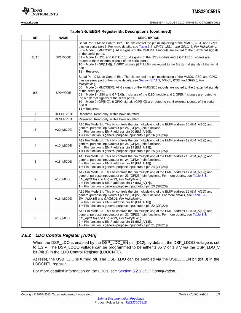
TMS320C5515
www.ti.com SPRS645F –AUGUST 2010–REVISED OCTOBER 2013
Table 3-5. EBSR Register Bit Descriptions (continued)BIT NAME DESCRIPTION
Serial Port 1 Mode Control Bits. The bits control the pin multiplexing of the MMC1, I2S1, and GPIOpins on serial port 1. For more details, see Table 3-7, MMC1, I2S1 , and GP[11:6] Pin Multiplexing.00 = Mode 0 (MMC/SD1). All 6 signals of the MMC/SD1 module are routed to the 6 external signalsof the serial port 1.
11:10 SP1MODE 01 = Mode 1 (I2S1 and GP[11:10]). 4 signals of the I2S1 module and 2 GP[11:10] signals arerouted to the 6 external signals of the serial port 1.10 = Mode 2 (GP[11:6]). 6 GPIO signals (GP[11:6]) are routed to the 6 external signals of the serialport 1.11 = Reserved.Serial Port 0 Mode Control Bits. The bits control the pin multiplexing of the MMC0, I2S0, and GPIOpins on serial port 0. For more details, see Section 3.7.1.3, MMC0, I2S0, and GP[5:0] PinMultiplexing.00 = Mode 0 (MMC/SD0). All 6 signals of the MMC/SD0 module are routed to the 6 external signalsof the serial port 0.9:8 SP0MODE 01 = Mode 1 (I2S0 and GP[5:0]). 4 signals of the I2S0 module and 2 GP[5:4] signals are routed tothe 6 external signals of the serial port 0.10 = Mode 2 (GP[5:0]). 6 GPIO signals (GP[5:0]) are routed to the 6 external signals of the serialport 0.11 = Reserved.
7 RESERVED Reserved. Read-only, writes have no effect.6 RESERVED Reserved. Read-only, writes have no effect.
A20 Pin Mode Bit. This bit controls the pin multiplexing of the EMIF address 20 (EM_A[20]) andgeneral-purpose input/output pin 26 (GP[26]) pin functions.5 A20_MODE 0 = Pin function is EMIF address pin 20 (EM_A[20]).1 = Pin function is general-purpose input/output pin 26 (GP[26]).A19 Pin Mode Bit. This bit controls the pin multiplexing of the EMIF address 19 (EM_A[19]) andgeneral-purpose input/output pin 25 (GP[25]) pin functions.4 A19_MODE 0 = Pin function is EMIF address pin 19 (EM_A[19]).1 = Pin function is general-purpose input/output pin 25 (GP[25]).A18 Pin Mode Bit. This bit controls the pin multiplexing of the EMIF address 18 (EM_A[18]) andgeneral-purpose input/output pin 24 (GP[24]) pin functions.3 A18_MODE 0 = Pin function is EMIF address pin 18 (EM_A[18]).1 = Pin function is general-purpose input/output pin 24 (GP[24]).A17 Pin Mode Bit. This bit controls the pin multiplexing of the EMIF address 17 (EM_A[17]) andgeneral-purpose input/output pin 23 (GP[23]) pin functions. For more details, see Table 3-8,
2 A17_MODE EM_A[20:16] and GP[26:21] Pin Multiplexing.0 = Pin function is EMIF address pin 17 (EM_A[17]).1 = Pin function is general-purpose input/output pin 23 (GP[23]).A16 Pin Mode Bit. This bit controls the pin multiplexing of the EMIF address 16 (EM_A[16]) andgeneral-purpose input/output pin 22 (GP[22]) pin functions. For more details, see Table 3-8,
1 A16_MODE EM_A[20:16] and GP[26:21] Pin Multiplexing.0 = Pin function is EMIF address pin 16 (EM_A[16]).1 = Pin function is general-purpose input/output pin 22 (GP[22]).A15 Pin Mode Bit. This bit controls the pin multiplexing of the EMIF address 15 (EM_A[15]) andgeneral-purpose input/output pin 21 (GP[21]) pin functions. For more details, see Table 3-8,
0 A15_MODE EM_A[20:16] and GP[26:21] Pin Multiplexing.0 = Pin function is EMIF address pin 15 (EM_A[15]).1 = Pin function is general-purpose input/output pin 21 (GP[21]).
3.6.2 LDO Control Register [7004h]When the DSP_LDO is enabled by the DSP_LDO_EN pin [D12], by default, the DSP_LDOO voltage is setto 1.3 V. The DSP_LDOO voltage can be programmed to be either 1.05 V or 1.3 V via the DSP_LDO_Vbit (bit 1) in the LDO Control Register (LDOCNTL).
At reset, the USB_LDO is turned off. The USB_LDO can be enabled via the USBLDOEN bit (bit 0) in theLDOCNTL register.
For more detailed information on the LDOs, see Section 3.2.1 LDO Configuration.
Copyright © 2010–2013, Texas Instruments Incorporated Device Configuration 59Submit Documentation Feedback
Product Folder Links: TMS320C5515

TMS320C5515
SPRS645F –AUGUST 2010–REVISED OCTOBER 2013 www.ti.com
3.6.3 EMIF and USB System Control Registers (ESCR and USBSCR) [1C33h and 1C32h]After reset, by default, the CPU performs 16-bit accesses to the EMIF and USB registers and data space.To perform 8-bit accesses to the EMIF data space, the user must set the BYTEMODE bits to 01b for the"high byte" or 10b for the "low byte" in the EMIF System Control Register (ESCR). Similarly, theBYTEMODE bits in the USB System Control Register (USBSCR) must also be configured for byte access.
3.6.4 Peripheral Clock Gating Control Registers (PCGCR1 and PCGCR2) [1C02h and 1C03h]After hardware reset, the DSP executes the on-chip bootloader from ROM. As the bootloader executes, itselectively enables the clock of the peripheral being queried for a valid boot. If a valid boot source is notfound, the bootloader disables the clock to that peripheral and moves on to the next peripheral in the bootorder. After the boot process is complete, all of the peripheral clocks will be off and all domains in the ICR,except for the CPU domain, will be idled (this includes the MPORT and HWA). The user must enable theclocks to the peripherals and CPU ports that are going to be used. The peripheral clock gating controlregisters (PCGCR1 and PCGCR2) are used to enable and disable the peripheral clocks.
3.6.5 Pullup/Pulldown Inhibit Registers (PDINHIBR1/2/3) [1C17h, 1C18h, and 1C19h,respectively]
Each internal pullup and pulldown (IPU/IPD) resistor on the device DSP, except for the IPD on TRST, canbe individually controlled through the IPU/IPD registers (PDINHIBR1 [1C17h] , PDINHIBR2 [1C18h], andPDINHIBR3 [1C19h]). To minimize power consumption, internal pullup or pulldown resistors should bedisabled in the presence of an external pullup or pulldown resistor or external driver. Section 3.8.1,Pullup/Pulldown Resistors, describes other situations in which an pullup and pulldown resistors arerequired.
When CVDD is powered down, pullup and pulldown resistors will be forced disabled and an internal bus-holder will be enabled. For more detailed information, see Section 5.3.2, Digital I/O Behavior When CorePower (CVDD) is Down.
3.6.6 Output Slew Rate Control Register (OSRCR) [1C16h]To provide the lowest power consumption setting, the DSP has configurable slew rate control on the EMIFand CLKOUT output pins. The output slew rate control register (OSRCR) is used to set a subset of thedevice I/O pins, namely CLKOUT and EMIF pins, to either fast or slow slew rate. The slew rate feature isimplemented by staging/delaying turn-on times of the parallel p-channel drive transistors and parallel n-channel drive transistors of the output buffer. In the slow slew rate configuration, the delay is longer, butultimately the same number of parallel transistors are used to drive the output high or low. Thus, the drivestrength is ultimately the same. The slower slew rate control can be used for power savings and has thegreatest effect at lower DVDDIO and DVDDEMIF voltages.
60 Device Configuration Copyright © 2010–2013, Texas Instruments IncorporatedSubmit Documentation Feedback
Product Folder Links: TMS320C5515

TMS320C5515
www.ti.com SPRS645F –AUGUST 2010–REVISED OCTOBER 2013
3.7 Multiplexed Pin ConfigurationsThe device DSP uses pin multiplexing to accommodate a larger number of peripheral functions in thesmallest possible package, providing the ultimate flexibility for end applications. The external bus selectionregister (EBSR) controls all the pin multiplexing functions on the device.
3.7.1 Pin Multiplexing DetailsThis section discusses how to program the external bus selection register (EBSR) to select the desiredperipheral functions and pin muxing. See the individual pin mux sections for pin muxing details for aspecific muxed pin. After changing any of the pin mux control registers, it will be necessary to reset theperipherals that are affected.
3.7.1.1 LCD Controller, SPI, UART, I2S2, I2S3, and GP[31:27, 20:18] Pin Multiplexing [EBSR.PPMODEBits]
The LCD Controller, SPI, UART, I2S2, I2S3, and GPIO signal muxing is determined by the value of thePPMODE bit fields in the External Bus Selection Register (EBSR) register. For more details on the actualpin functions, see Table 3-6.
Copyright © 2010–2013, Texas Instruments Incorporated Device Configuration 61Submit Documentation Feedback
Product Folder Links: TMS320C5515

TMS320C5515
SPRS645F –AUGUST 2010–REVISED OCTOBER 2013 www.ti.com
Table 3-6. LCD Controller, SPI, UART, I2S2, I2S3, and GP[31:27, 20:18] Pin Multiplexing
EBSR PPMODE BITSPDINHIBR3REGISTER MODE 0 MODE 1 MODE 2 MODE 3 MODE 4 MODE 5 MODE 6PIN NAMEBIT 000 001 010 011 100 101 110FIELDS (1)
(Reset Default)LCD_EN_RDB/SPI_CLK LCD_EN_RDB SPI_CLK LCD_EN_RDB LCD_EN_RDB LCD_EN_RDB LCD_EN_RDB SPI_CLKLCD_D[0]/SPI_RX LCD_D[0] SPI_RX LCD_D[0] LCD_D[0] LCD_D[0] LCD_D[0] SPI_RXLCD_D[1]/SPI_TX LCD_D[1] SPI_TX LCD_D[1] LCD_D[1] LCD_D[1] LCD_D[1] SPI_TX
P2PD LCD_D[2]/GP[12] LCD_D[2] GP[12] LCD_D[2] LCD_D[2] LCD_D[2] LCD_D[2] GP[12]P3PD LCD_D[3]/GP[13] LCD_D[3] GP[13] LCD_D[3] LCD_D[3] LCD_D[3] LCD_D[3] GP[13]P4PD LCD_D[4]/GP[14] LCD_D[4] GP[14] LCD_D[4] LCD_D[4] LCD_D[4] LCD_D[4] GP[14]P5PD LCD_D[5]/GP[15] LCD_D[5] GP[15] LCD_D[5] LCD_D[5] LCD_D[5] LCD_D[5] GP[15]P6PD LCD_D[6]/GP[16] LCD_D[6] GP[16] LCD_D[6] LCD_D[6] LCD_D[6] LCD_D[6] GP[16]P7PD LCD_D[7]/GP[17] LCD_D[7] GP[17] LCD_D[7] LCD_D[7] LCD_D[7] LCD_D[7] GP[17]P8PD LCD_D[8]/I2S2_CLK/GP[18]/SPI_CLK LCD_D[8] I2S2_CLK GP[18] SPI_CLK I2S2_CLK SPI_CLK I2S2_CLKP9PD LCD_D[9]/I2S2_FS/GP[19]/SPI_CS0 LCD_D[9] I2S2_FS GP[19] SPI_CS0 I2S2_FS SPI_CS0 I2S2_FS
P10PD LCD_D[10]/I2S2_RX/GP[20]/SPI_RX LCD_D[10] I2S2_RX GP[20] SPI_RX I2S2_RX SPI_RX I2S2_RXP11PD LCD_D[11]/I2S2_DX/GP[27]/SPI_TX LCD_D[11] I2S2_DX GP[27] SPI_TX I2S2_DX SPI_TX I2S2_DXP12PD LCD_D[12]/UART_RTS/GP[28]/I2S3_CLK LCD_D[12] UART_RTS GP[28] I2S3_CLK UART_RTS UART_RTS I2S3_CLKP13PD LCD_D[13]/UART_CTS/GP[29]/I2S3_FS LCD_D[13] UART_CTS GP[29] I2S3_FS UART_CTS UART_CTS I2S3_FSP14PD LCD_D[14]/UART_RXD/GP[30]/I2S3_RX LCD_D[14] UART_RXD GP[30] I2S3_RX UART_RXD UART_RXD I2S3_RXP15PD LCD_D[15]/UART_TXD/GP[31]/I2S3_DX LCD_D[15] UART_TXD GP[31] I2S3_DX UART_TXD UART_TXD I2S3_DX
LCD_CS0_E0/SPI_CS0 LCD_CS0_E0 SPI_CS0 LCD_CS0_E0 LCD_CS0_E0 LCD_CS0_E0 LCD_CS0_E0 SPI_CS0LCD_CS1_E1/SPI_CS1 LCD_CS1_E1 SPI_CS1 LCD_CS1_E1 LCD_CS1_E1 LCD_CS1_E1 LCD_CS1_E1 SPI_CS1LCD_RW_WRB/SPI_CS2 LCD_RW_WRB SPI_CS2 LCD_RW_WRB LCD_RW_WRB LCD_RW_WRB LCD_RW_WRB SPI_CS2LCD_RS/SPI_CS3 LCD_RS SPI_CS3 LCD_RS LCD_RS LCD_RS LCD_RS SPI_CS3
(1) The pin names with PDINHIBR3 register bit field references can have the pulldown resistor enabled or disabled via this register.
62 Device Configuration Copyright © 2010–2013, Texas Instruments IncorporatedSubmit Documentation Feedback
Product Folder Links: TMS320C5515

TMS320C5515
www.ti.com SPRS645F –AUGUST 2010–REVISED OCTOBER 2013
3.7.1.2 MMC1, I2S1, and GP[11:6] Pin Multiplexing [EBSR.SP1MODE Bits]
The MMC1, I2S1, and GPIO signal muxing is determined by the value of the SP1MODE bit fields in the External Bus Selection Register (EBSR)register. For more details on the actual pin functions, see Table 3-7.
Table 3-7. MMC1, I2S1, and GP[11:6] Pin Multiplexing
EBSR SP1MODE BITSPDINHIBR1 MODE 0 MODE 1 MODE 2REGISTER PIN NAME
00BIT FIELDS (1)01 10(Reset Default)
S10PD MMC1_CLK/I2S1_CLK/GP[6] MMC1_CLK I2S1_CLK GP[6]S11PD MMC1_CMD/I2S1_FS/GP[7] MMC1_CMD I2S1_FS GP[7]S12PD MMC1_D0/I2S1_DX/GP[8] MMC1_D0 I2S1_DX GP[8]S13PD MMC1_D1/I2S1_RX/GP[9] MMC1_D1 I2S1_RX GP[9]S14PD MMC1_D2/GP[10] MMC1_D2 GP[10] GP[10]S15PD MMC1_D3/GP[11] MMC1_D3 GP[11] GP[11]
(1) The pin names with PDINHIBR1 register bit field references can have the pulldown register enabled or disabled via this register.
Copyright © 2010–2013, Texas Instruments Incorporated Device Configuration 63Submit Documentation Feedback
Product Folder Links: TMS320C5515

TMS320C5515
SPRS645F –AUGUST 2010–REVISED OCTOBER 2013 www.ti.com
3.7.1.3 MMC0, I2S0, and GP[5:0] Pin Multiplexing [EBSR.SP0MODE Bits]
The MMC0, I2S0, and GPIO signal muxing is determined by the value of the SP0MODE bit fields in theExternal Bus Selection Register (EBSR) register. For more details on the actual pin functions, seeTable 3-8.
Table 3-8. MMC0, I2S0, and GP[5:0] Pin Multiplexing
EBSR SP0MODE BITSPDINHIBR1 MODE 0 MODE 1 MODE 2REGISTER PIN NAME
00BIT FIELDS (1)01 10(Reset Default)
S00PD MMC0_CLK/I2S0_CLK/GP[0] MMC0_CLK I2S0_CLK GP[0]S01PD MMC0_CMD/I2S0_FS/GP[1] MMC0_CMD I2S0_FS GP[1]S02PD MMC0_D0/I2S0_DX/GP[2] MMC0_D0 I2S0_DX GP[2]S03PD MMC0_D1/I2S0_RX/GP[3] MMC0_D1 I2S0_RX GP[3]S04PD MMC0_D2/GP[4] MMC0_D2 GP[4] GP[4]S05PD MMC0_D3/GP[5] MMC0_D3 GP[5] GP[5]
(1) The pin names with PDINHIBR1 register bit field references can have the pulldown register enabled or disabled via this register.
3.7.1.4 EMIF EM_A[20:15] and GP[26:21] Pin Multiplexing [EBSR.Axx_MODE bits]
The EMIF Address and GPIO signal muxing is determined by the value of the A20_MODE, A19_MODE,A18_MODE, A17_MODE, A16_MODE, and A15_MODE bit fields in the External Bus Selection Register(EBSR) register. For more details on the actual pin functions, see Table 3-9.
Table 3-9. EM_A[20:16] and GP[26:21] Pin Multiplexing
Axx_MODE BITPIN NAME
0 1EM_A[15]/GP[21] EM_A[15] GP[21]EM_A[16]/GP[22] EM_A[16] GP[22]EM_A[17]/GP[23] EM_A[17] GP[23]EM_A[18]/GP[24] EM_A[18] GP[24]EM_A[19]/GP[25] EM_A[19] GP[25]EM_A[20]/GP[26] EM_A[20] GP[26]
64 Device Configuration Copyright © 2010–2013, Texas Instruments IncorporatedSubmit Documentation Feedback
Product Folder Links: TMS320C5515

TMS320C5515
www.ti.com SPRS645F –AUGUST 2010–REVISED OCTOBER 2013
3.8 Debugging Considerations
3.8.1 Pullup/Pulldown ResistorsProper board design should ensure that input pins to the device DSP always be at a valid logic level andnot floating. This may be achieved via pullup/pulldown resistors. The DSP features internal pullup (IPU)and internal pulldown (IPD) resistors on many pins, including all GPIO pins, to eliminate the need, unlessotherwise noted, for external pullup/pulldown resistors.
An external pullup/pulldown resistor may need to be used in the following situations:• Configuration Pins: An external pullup/pulldown resistor is recommended to set the desired value/state
(see the configuration pins listed in Table 3-4, Default Functions Affected by Device ConfigurationPins). Note that some configuration pins must be connected directly to ground or to a specific supplyvoltage.
• Other Input Pins: If the IPU/IPD does not match the desired value/state, use an externalpullup/pulldown resistor to pull the signal to the opposite rail.
For the configuration pins (listed in Table 3-4, Default Functions Affected by Device Configuration Pins), ifthey are both routed out and in a high-impedance state (not driven), it is strongly recommended that anexternal pullup/pulldown resistor be implemented. In addition, applying external pullup/pulldown resistorson the configuration pins adds convenience to the user in debugging and flexibility in switching operatingmodes.
When an external pullup or pulldown resistor is used on a pin, the pin’s internal pullup or pulldown resistorshould be disabled through the Pullup/Pulldown Inhibit Registers (PDINHIBR1/2/3) [1C17h, 1C18h, and1C19h, respectively] to minimize power consumption.
Tips for choosing an external pullup/pulldown resistor:• Consider the total amount of current that may pass through the pullup or pulldown resistor. Make sure
to include the leakage currents of all the devices connected to the net, as well as any internal pullup orpulldown (IPU/IPD) resistors.
• Decide a target value for the net. For a pulldown resistor, this should be below the lowest VIL level ofall inputs connected to the net. For a pullup resistor, this should be above the highest VIH level of allinputs on the net. A reasonable choice would be to target the VOL or VOH levels for the logic family ofthe limiting device; which, by definition, have margin to the VIL and VIH levels.
• Select a pullup/pulldown resistor with the largest possible value; but, which can still ensure that the netwill reach the target pulled value when maximum current from all devices on the net is flowing throughthe resistor. The current to be considered includes leakage current plus, any other internal andexternal pullup/pulldown resistors on the net.
• For bidirectional nets, there is an additional consideration which sets a lower limit on the resistancevalue of the external resistor. Verify that the resistance is small enough that the weakest output buffercan drive the net to the opposite logic level (including margin).
• Remember to include tolerances when selecting the resistor value.• For pullup resistors, also remember to include tolerances on the DVDD rail.
For most systems, a 1-kΩ resistor can be used to oppose the IPU/IPD while meeting the above criteria.Users should confirm this resistor value is correct for their specific application.
For most systems, a 20-kΩ resistor can be used to compliment the IPU/IPD on the configuration pinswhile meeting the above criteria. Users should confirm this resistor value is correct for their specificapplication.
For more detailed information on input current (II), and the low-/high-level input voltages (VIL and VIH) forthe device DSP, see Section 4.3, Electrical Characteristics Over Recommended Ranges of SupplyVoltage and Operating Temperature.
For the internal pullup/pulldown resistors for all device pins, see the peripheral/system-specific terminalfunctions table in Section 2.5.
Copyright © 2010–2013, Texas Instruments Incorporated Device Configuration 65Submit Documentation Feedback
Product Folder Links: TMS320C5515

TMS320C5515
SPRS645F –AUGUST 2010–REVISED OCTOBER 2013 www.ti.com
3.8.2 Bus HoldersThe device has special I/O bus-holder structures to ensure pins are not left floating when CVDD power isremoved while I/O power is applied. When CVDD is "ON", the bus-holders are disabled and the internalpullups or pulldowns, if applicable, function normally. But when CVDD is "OFF" and the I/O supply is "ON",the bus-holders become enabled and any applicable internal pullups and pulldowns are disabled.
The bus-holders are weak drivers on the pin and, for as long as CVDD is "OFF" and I/O power is "ON",they hold the last state on the pin. If an external device is strongly driving the device I/O pin to theopposite state then the bus-holder will flip state to match the external driver and DC current will stop.
This bus-holder feature prevents unnecessary power consumption when CVDD is "OFF"and I/O supply is"ON". For example, current caused by undriven pins (input buffer oscillation) and/or DC current flowingthrough pullups or pulldowns.
If external pullup or pulldown resistors are implemented, then care should be taken that thosepullup/pulldown resistors can exceed the internal bus-holder's max current and thereby cause the bus-holder to flip state to match the state of the external pullup or pulldown. Otherwise, DC current will flowunnecessarily. When CVDD power is applied, the bus holders are disabled (for further details on busholders, see Section 5.3.2, Digital I/O Behavior When Core Power (CVDD) is Down).
3.8.3 CLKOUT PinFor debug purposes, the DSP includes a CLKOUT pin which can be used to tap different clocks within theclock generator. The SRC bits of the CLKOUT Control Source Register (CCSSR) can be used to specifythe source for the CLKOUT pin.
Note: The bootloader disables the CLKOUT pin via CLKOFF bit in the ST3_55 CPU register.
For more information on the ST3_55 CPU register, see the TMS320C55x 3.0 CPU Reference Guide(literature number: SWPU073).
66 Device Configuration Copyright © 2010–2013, Texas Instruments IncorporatedSubmit Documentation Feedback
Product Folder Links: TMS320C5515

TMS320C5515
www.ti.com SPRS645F –AUGUST 2010–REVISED OCTOBER 2013
4 Device Operating Conditions
For the device maximum operating frequency, see Section 6.1.2, Device and Development-Support ToolNomenclature.
4.1 Absolute Maximum Ratings Over Operating Case Temperature Range (UnlessOtherwise Noted) (1)
Supply voltage ranges: Digital Core (CVDD, CVDDRTC, USB_VDD1P3) (2) –0.5 V to 1.7 VI/O, 1.8 V, 2.5 V, 2.75 V, 3.3 V (DVDDIO, DVDDEMIF, –0.5 V to 4.2 VDVDDRTC) 3.3V USB supplies USB PHY (USB_VDDOSC,USB_VDDPLL, USB_VDDA3P3) (2)
LDOI –0.5 V to 4.2 VAnalog, 1.3 V (VDDA_PLL, USB_VDDA1P3, VDDA_ANA) (2) –0.5 V to 1.7 V
Input and Output voltage ranges: VI I/O, All pins with DVDDIO or DVDDEMIF or USB_VDDOSC or –0.5 V to 4.2 VUSB_VDDPLL or USB_VDDA3P3 as supply sourceVO I/O, All pins with DVDDIO or DVDDEMIF or USB_VDDOSC or –0.5 V to 4.2 VUSB_VDDPLLor USB_VDDA3P3 as supply sourceRTC_XI and RTC_XO –0.5 V to 1.7 VUSB_VBUS Input –0.5 V to 5.5 VVI and VO, GPAIN[0] –0.5 V to 4.2 VVI and VO, GPAIN[3:1] –0.5 V to 1.7 VVO, BG_CAP –0.5 V to 1.7 VANA_LDOO, DSP_LDOO, and USB_LDOO –0.5 V to 1.7 V
Operating case temperature ranges, Tc: Commercial Temperature (default) -10°C to 70°CIndustrial Temperature -40°C to 85°C
Storage temperature range, Tstg (default) –65°C to 150°CDevice Operating Life DSP Operating Frequency <70 °C 100,000 POHPower-On Hours (POH) (3) (SYSCLK ) ≤100 MHz ≥70 °C - ≤85 °C 100,000 POH
DSP Operating Frequency <70 °C 100,000 POH(SYSCLK): ≥70 °C - ≤85 °C 80,000 POH>100 MHz - ≤120 MHz
ESD Stress Voltage (4) Human Body Model (HBM) (5) > 1000 VCharged Device Model (CDM) (6) > 250 V
(1) Stresses beyond those listed under "absolute maximum ratings" may cause permanent damage to the device. These are stress ratingsonly, and functional operation of the device at these or any other conditions beyond those indicated under "recommended operatingconditions" is not implied. Exposure to absolute-maximum-rated conditions for extended periods may affect device reliability.
(2) All voltage values are with respect to VSS.(3) This information is provided solely for your convenience and does not extend or modify the warranty provided under TI’s standard terms
and conditions for TI semiconductor products.(4) Electrostatic discharge (ESD) to measure device sensitivity/immunity to damage caused by electrostatic discharges into the device.(5) Level listed is the passing level per ANSI/ESDA/JEDEC JS-001-2010. JEDEC document JEP155 states that 500 V HBM allows safe
manufacturing with a standard ESD control process, and manufacturing with less than 500 V HBM is possible if necessary precautionsare taken. Pins listed as 1000 V may actually have higher performance.
(6) Level listed is the passing level per EIA-JEDEC JESD22-C101E. JEDEC document JEP157 states that 250 V CDM allows safemanufacturing with a standard ESD control process. Pins listed as 250 V may actually have higher performance.
Copyright © 2010–2013, Texas Instruments Incorporated Device Operating Conditions 67Submit Documentation Feedback
Product Folder Links: TMS320C5515

TMS320C5515
SPRS645F –AUGUST 2010–REVISED OCTOBER 2013 www.ti.com
4.2 Recommended Operating ConditionsMIN NOM MAX UNIT
60 or 75 MHz 0.998 1.05 1.15 VCVDD Supply voltage, Digital Core
100 or 120 MHz 1.24 1.3 1.43 V
CVDDRTC Supply voltage, RTC and RTC OSC 32.768 KHz 0.998 1.43 V
USB_VDD1P3 Supply voltage, Digital USB 1.24 1.3 1.43 VCore Supplies
USB_VDDA1P3 Supply voltage, 1.3 V Analog USB 1.24 1.3 1.43 V
VDDA_ANA Supply voltage, 1.3 V SAR and Pwr Mgmt 1.24 1.3 1.43 V
VDDA_PLL Supply voltage, System PLL 1.24 1.3 1.43 V
USB_VDDPLL Supply voltage, 3.3 V USB PLL 2.97 3.3 3.63 V
Supply voltage, I/O, 3.3 V 2.97 3.3 3.63 VDVDDIO Supply voltage, I/O, 2.75 V 2.48 2.75 3.02 VDVDDEMIF
Supply voltage, I/O, 2.5 V 2.25 2.5 2.75 VDVDDRTC
I/O Supplies Supply voltage, I/O, 1.8 V 1.65 1.8 1.98 V
USB_VDDOSC Supply voltage, I/O, 3.3 V USB OSC 2.97 3.3 3.63 V
USB_VDDA3P3 Supply voltage, I/O, 3.3 V Analog USB PHY 2.97 3.3 3.63 V
LDOI Supply voltage, Analog Pwr Mgmt and LDO Inputs 1.8 3.6 V
VSS Supply ground, Digital I/O
VSSRTC Supply ground, RTC
USB_VSSOSC Supply ground, USB OSC
USB_VSSPLL Supply ground, USB PLL
USB_VSSA3P3 Supply ground, 3.3 V Analog USB PHYGND 0 0 0 V
USB_VSSA1P3 Supply ground, USB 1.3 V Analog USB PHY
USB_VSSREF Supply ground, USB Reference Current
VSSA_PLL Supply ground, System PLL
USB_VSS1P3 Supply ground, 1.3 V Digital USB PHY
VSSA_ANA Supply ground, SAR and Pwr Mgmt
High-level input voltage, 3.3, 2.75, 2.5, 1.8 V I/O (exceptVIH(1) 0.7 * DVDD DVDD + 0.3 VGPAIN[3:0] pins) (2)
Low-level input voltage, 3.3, 2.75, 2.5, 1.8 V I/O (exceptVIL(1) -0.3 0.3 * DVDD VGPAIN[3:0] pins) (2)
Input voltage, GPAIN0 pin (3) -0.3 3.6 VVIN
Input voltage, GPAIN[3:1] pins -0.3 VDDA_ANA + 0.3 V
Default -10 70 °C(Commercial)Tc Operating case temperature(Industrial) -40 85 °C
1.05 V 0 60 or 75 (4) MHzFSYSCLK DSP Operating Frequency (SYSCLK)
1.3 V 0 100 or 120 (4) MHz
(1) DVDD refers to the pin I/O supply voltage. To determine the I/O supply voltage for each pin, see Section 2.5, Terminal Functions.(2) The I2C pin SDA and SCL do not feature fail-safe I/O buffers. These pin could potentially draw current when the DVDDIO is powered
down. Due to the fact that different voltage devices can be connected to I2C bus and the I2C inputs are LVCMOS, the level of logic 0(low) and logic 1 (high) are not fixed and depend on DVDDIO.
(3) The GNDON bit in the SARPINCTRL register should be set to "1" before SAR channels 0, 1, or 2 are enabled via the CHSEL bit in theSARCTRL register, when VIN greater than VDDA_ANA.
(4) For the device maximum operating frequency, see Section 6.1.2, Device and Development-Support Tool Nomenclature.
68 Device Operating Conditions Copyright © 2010–2013, Texas Instruments IncorporatedSubmit Documentation Feedback
Product Folder Links: TMS320C5515

TMS320C5515
www.ti.com SPRS645F –AUGUST 2010–REVISED OCTOBER 2013
4.3 Electrical Characteristics Over Recommended Ranges of Supply Voltage andOperating Temperature (Unless Otherwise Noted)
PARAMETER TEST CONDITIONS (1) MIN TYP MAX UNIT
Full speed: USB_DN and 2.8 USB_VDDA3P3 VUSB_DP (2)
High speed: USB_DN and 360 440 mVUSB_DP (2)
VOH High-level output voltage, 3.3,2.75, 2.5, 1.8 V I/O (except IO = IOH 0.8 * DVDD VGPAIN[3:0] pins)
High-level output voltage, 0.8 *IO = IOH VGPAIN[3:1] pins VDDA_ANA
Full speed: USB_DN and 0.0 0.3 VUSB_DP (2)
High speed: USB_DN and –10 10 mVUSB_DP (2)
Low-level output voltage, 3.3,VOL 2.75, 2.5, 1.8V I/O (except I2C IO = IOL 0.2 * DVDD V
and GPAIN[3:0] pins)
Low-level output voltage, I2C VDD > 2 V, IOL = 3 mA 0 0.4 Vpins (3)
Low-level output voltage, IO = IOL 0.2 * VDDA_ANA VGPAIN[3:0] pins
DVDD = 3.3 V 162 mV
VHYS Input hysteresis (4) DVDD = 2.5 V 141 mV
DVDD = 1.8 V 122 mV
USB_LDOO voltage 1.24 1.3 1.43 V
ANA_LDOO voltage 1.24 1.3 1.43 VVLDO
DSP_LDO_V bit in the LDOCNTL register = 1 1.24 1.3 1.43 VDSP_LDOO voltage
DSP_LDO_V bit in the LDOCNTL register = 0 0.998 1.05 1.15 V
DSP_LDO shutdown current (5) LDOI = VMIN 250 mA
ISD ANA_LDO shutdown current (5) LDOI = VMIN 4 mA
USB_LDO shutdown current (5) LDOI = VMIN 25 mA
Input only pin, internal pulldown or pullup disabled -5 +5 μA
-59 to -Input current [DC] (except DVDD = 3.3 V with internal pullup enabled (8) μA161IILPU(6) (7) WAKEUP, I2C, and GPAIN[3:0]
pins) DVDD = 2.5 V with internal pullup enabled (8) -31 to -93 μA
DVDD = 1.8 V with internal pullup enabled (8) -14 to -44 μA
Input only pin, internal pulldown or pullup disabled -5 +5 μAInput current [DC] (except DVDD = 3.3 V with internal pulldown enabled (8) 52 to 158 μA
IIHPD(6) (7) WAKEUP, I2C, and GPAIN[3:0]
DVDD = 2.5 V with internal pulldown enabled (8) 27 to 83 μApins)DVDD = 1.8 V with internal pulldown enabled (8) 11 to 35 μA
IIH/ VI = VSS to DVDD with internal pullups and pulldownsInput current [DC], ALL pins -5 +5 μAIIL (7) disabled.
(1) For test conditions shown as MIN, MAX, or TYP, use the appropriate value specified in the recommended operating conditions table.(2) The USB I/Os adhere to the Universal Bus Specification Revision 2.0 (USB2.0 spec).(3) VDD is the voltage to which the I2C bus pullup resistors are connected.(4) Applies to all input pins except WAKEUP, I2C pins, GPAIN[3:0], RTC_XI, and USB_MXI.(5) ISD is the amount of current the LDO is ensured to deliver before shutting down to protect itself.(6) II applies to input-only pins and bi-directional pins. For input-only pins, II indicates the input leakage current. For bi-directional pins, II
indicates the input leakage current and off-state (Hi-Z) output leakage current.(7) When CVDD power is "ON", the pin bus-holders are disabled. For more detailed information, see Section 5.3.2, Digital I/O Behavior
When Core Power (CVDD) is Down.(8) Applies only to pins with an internal pullup (IPU) or pulldown (IPD) resistor.
Copyright © 2010–2013, Texas Instruments Incorporated Device Operating Conditions 69Submit Documentation Feedback
Product Folder Links: TMS320C5515

TMS320C5515
SPRS645F –AUGUST 2010–REVISED OCTOBER 2013 www.ti.com
Electrical Characteristics Over Recommended Ranges of Supply Voltage and Operating Temperature(Unless Otherwise Noted) (continued)
PARAMETER TEST CONDITIONS (1) MIN TYP MAX UNIT
All Pins (except USB, EMIF, CLKOUT, and -4 mAGPAIN[3:0] pins)
DVDD = 3.3 V -6 mAEMIF pins
DVDD = 1.8 V -5 mA
DVDD = 3.3 V -6 mAIOH(7) High-level output current [DC] CLKOUT pin
DVDD = 1.8 V -4 mA
DVDD = VDDA_ANA = 1.3 V,GPAIN[3:1] pins -4 mAExternal Regulator (9)
(GPAIN0 is open-drain DVDD = VDDA_ANA = 1.3 V, -100 μAand cannot drive high) Internal Regulator (9)
All Pins (except USB, EMIF, CLKOUT, and +4 mAGPAIN[3:0] pins)
DVDD = 3.3 V +6 mAEMIF pins
DVDD = 1.8 V +5 mA
DVDD = 3.3 V +6 mAIOL(7) Low-level output current [DC] CLKOUT pin
DVDD = 1.8 V +4 mA
DVDD = VDDA_ANA = 1.3 V, +4 mAexternal regulatorGPAIN[3:0]
DVDD = VDDA_ANA = 1.3 V, +4 mAinternal regulator (9)
All Pins (except USB and GPAIN[3:0]) -10 +10 μAIOZ
(10) I/O Off-state output currentGPAIN[3:0] pins -10 +10 μA
Supply voltage, I/O, 3.3 V 2.2 mA
Supply voltage, I/O, 2.75 V 1.6 mABus Holder pull low current whenIOLBH(11)
CVDD is powered "OFF" Supply voltage, I/O, 2.5 V 1.4 mA
Supply voltage, I/O, 1.8 V 0.72 mA
Supply voltage, I/O, 3.3 V -1.3 mA
Supply voltage, I/O, 2.75 V -0.97 mABus Holder pull high currentIOHBH(11)
when CVDD is powered "OFF" Supply voltage, I/O, 2.5 V -0.83 mA
Supply voltage, I/O, 1.8 V -0.46 mA
(9) When the ANA_LDO supplies VDDA_ANA, it is not recommended to use the GPAIN[3:1] signals for general-purpose outputs (driving high).The ISD parameter of the ANA_LDO is too low to drive any realistic load on the GPAIN[3:1] pins while also supplying the PLL throughVDDA_PLL and the SAR through VDDA_ANA.
(10) IOZ applies to output-only pins, indicating off-state (Hi-Z) output leakage current.(11) This parameter specifies the maximum strength of the Bus Holder and is needed to calculate the minimum strength of external pull-ups
and pull-downs.
70 Device Operating Conditions Copyright © 2010–2013, Texas Instruments IncorporatedSubmit Documentation Feedback
Product Folder Links: TMS320C5515

TMS320C5515
www.ti.com SPRS645F –AUGUST 2010–REVISED OCTOBER 2013
Electrical Characteristics Over Recommended Ranges of Supply Voltage and Operating Temperature(Unless Otherwise Noted) (continued)
PARAMETER TEST CONDITIONS (1) MIN TYP MAX UNIT
Active, CVDD = 1.3 V, DSP clock = 100 or 120 MHz,Clock source = RTC on-chip Oscillator
0.22 mW/MHzRoom Temp (25 °C), 75% DMAC + 25% ADD(typical sine wave data switching)
Active, CVDD = 1.05 V, DSP clock = 60 or 75 MHz,Clock source = RTC on-chip Oscillator
0.15 mW/MHzRoom Temp (25 °C), 75% DMAC + 25% ADD(typical data switching)
Active, CVDD = 1.3 V, DSP clock = 100 or 120 MHz,Clock source = RTC on-chip Oscillator
0.22 mW/MHzRoom Temp (25 °C), 75% DMAC + 25% NOP(typical sine wave data switching)
Active, CVDD = 1.05 V, DSP clock = 60 or 75 MHz,Clock source = RTC on-chip Oscillator
0.14 mW/MHzRoom Temp (25 °C), 75% DMAC + 25% NOP(typical data switching)
Standby, CVDD = 1.3 V, Master clock disabled, Clocksource = RTC on-chip Oscillator
0.44 mWRoom Temp (25 °C), DARAM and SARAM in activemode
P Core (CVDD) supply power (12)
Standby, CVDD = 1.05 V, Master clock disabled, Clocksource = RTC on-chip Oscillator
0.26 mWRoom Temp (25 °C), DARAM and SARAM in activemode
Standby, CVDD = 1.3 V, Master clock disabled, Clocksource = RTC on-chip Oscillator
0.40 mWRoom Temp (25 °C), DARAM in retention andSARAM in active mode
Standby, CVDD = 1.05 V, Master clock disabled, Clocksource = RTC on-chip Oscillator
0.23 mWRoom Temp (25 °C), DARAM in retention andSARAM in active mode
Standby, CVDD = 1.3 V, Master clock disabled, Clocksource = RTC on-chip Oscillator
0.28 mWRoom Temp (25 °C), DARAM in active mode andSARAM in retention
Standby, CVDD = 1.05 V, Master clock disabled, Clocksource = RTC on-chip Oscillator
0.15 mWRoom Temp (25 °C), DARAM in active mode andSARAM in retention
VDDA_PLL = 1.3 VAnalog PLL (VDDA_PLL) supply 0.7 mARoom Temp (25 °C), Phase detector = 170 kHz,current
VCO = 120 MHzIVDDA_ANA = 1.3 V, SAR clock = 2 MHz, TempSAR Analog (VDDA_ANA) supply 1 mAcurrent (70 °C)
CI Input capacitance 4 pF
Co Output capacitance 4 pF
(12) Measured under the following conditions:• At room temperature using units representative of a typical process.• I/O pins are properly terminated.The actual current draw varies across manufacturing processes and is highly application-dependent.For more details on core and I/O activity, as well as information relevant to board power supply design,see Estimating Power Consumption on the TMS320C5504/05/14/15/32/33/34/35 DSPs (literature number SPRABM0).
Copyright © 2010–2013, Texas Instruments Incorporated Device Operating Conditions 71Submit Documentation Feedback
Product Folder Links: TMS320C5515

V = V MAX (or V MAX)ref IL OL
V = V MIN (or V MIN)ref IH OH
Transmission Line
4.0 pF 1.85 pF
Z0 = 50(see Note)
Ω
Tester Pin Electronics Data Sheet Timing Reference Point
OutputUnderTest
NOTE: The data sheet provides timing at the device pin. For output timing analysis, the tester pin electronics and its transmission line effects must betaken into account.A transmission line with a delay of 2 ns can be used to produce the desired transmission line effect. The transmission line isintended as a load only. It is not necessary to add or subtract the transmission line delay (2 ns) from the data sheet timings.
Input requirements in this data sheet are tested with an input slew rate of < 4 Volts per nanosecond (4 V/ns) at the device pin.
42 Ω 3.5 nH
Device Pin(see Note)
TMS320C5515
SPRS645F –AUGUST 2010–REVISED OCTOBER 2013 www.ti.com
5 Peripheral Information and Electrical Specifications
5.1 Parameter Information
Figure 5-1. 3.3-V Test Load Circuit for AC Timing Measurements
The load capacitance value stated is only for characterization and measurement of AC timing signals. Thisload capacitance value does not indicate the maximum load the device is capable of driving.
5.1.1 1.8-V, 2.5-V, 2.75-V, and 3.3-V Signal Transition LevelsAll rise and fall transition timing parameters are referenced to VIL MAX and VIH MIN for input clocks, VOLMAX and VOH MIN for output clocks.
Figure 5-2. Rise and Fall Transition Time Voltage Reference Levels
5.1.2 3.3-V Signal Transition RatesAll timings are tested with an input edge rate of 4 volts per nanosecond (4 V/ns).
5.1.3 Timing Parameters and Board Routing AnalysisThe timing parameter values specified in this data manual do not include delays by board routing. As agood board design practice, such delays must always be taken into account. Timing values may beadjusted by increasing/decreasing such delays. TI recommends utilizing the available I/O bufferinformation specification (IBIS) models to analyze the timing characteristics correctly. To properly use IBISmodels to attain accurate timing analysis for a given system, see the Using IBIS Models for TimingAnalysis application report (literature number SPRA839). If needed, external logic hardware such asbuffers may be used to compensate any timing differences.
5.2 Recommended Clock and Control Signal Transition BehaviorAll clocks and control signals must transition between VIH and VIL (or between VIL and VIH) in a monotonicmanner.
72 Peripheral Information and Electrical Specifications Copyright © 2010–2013, Texas Instruments IncorporatedSubmit Documentation Feedback
Product Folder Links: TMS320C5515

TMS320C5515
www.ti.com SPRS645F –AUGUST 2010–REVISED OCTOBER 2013
5.3 Power SuppliesThe device includes four core voltage-level supplies (CVDD, CVDDRTC, USB_VDD1P3, USB_VDDA1P3), andseveral I/O supplies (DVDDIO, DVDDEMIF, DVDDRTC, USB_VDDOSC, and USB_VDDA3P3), as well as severalanalog supplies (LDOI, VDDA_PLL, VDDA_ANA, and USB_VDDPLL).
Note: CVDDRTC must be externally powered. None of the on-chip LDOs can be used to power CVDDRTC.
Some TI power-supply devices include features that facilitate power sequencing—for example, Auto-Trackand Slow-Start/Enable features. For more information regarding TI's power management products andsuggested devices to power TI DSPs, visit www.ti.com/processorpower.
5.3.1 Power-Supply SequencingThe device includes four core voltage-level supplies (CVDD, CVDDRTC, USB_VDD1P3, USB_VDDA1P3), andseveral I/O supplies including DVDDIO, DVDDEMIF, DVDDRTC, USB_VDDOSC, and USB_VDDA3P3.
If the DSP_LDO is disabled (DSP_LDO_EN = high) and an external regulator supplies power to the CPUCore (CVDD), the external reset signal (RESET) must be held asserted until all of the supply voltagesreach their valid operating ranges.
Note: the external reset signal on the RESET pin must be held low until all of the power supplies reachtheir operating voltage conditions.
The I/O design allows either the core supplies (CVDD, CVDDRTC, USB_VDD1P3, USB_VDDA1P3) or the I/Osupplies (DVDDIO, DVDDEMIF, DVDDRTC, USB_VDDOSC, and USB_VDDA3P3) to be powered up for an indefiniteperiod of time while the other supply is not powered if the following constraints are met:1. All maximum ratings and recommended operating conditions are satisfied.2. All warnings about exposure to maximum rated and recommended conditions, particularly junction
temperature are satisfied. These apply to power transitions as well as normal operation.3. Bus contention while core supplies are powered must be limited to 100 hours over the projected
lifetime of the device.4. Bus contention while core supplies are powered down does not violate the absolute maximum ratings.
If the USB subsystem is used, the subsystem must be powered up in the following sequence:1. USB_VDDA1P3 and USB_VDD1P3
2. USB_VDDA3P3
3. USB_VBUS
If the USB subsystem is not used, the following can be powered off:• USB Core
– USB_VDD1P3
– USB_VDDA1P3
• USB PHY and I/O Level Supplies– USB_VDDOSC
– USB_VDDA3P3
– USB_VDDPLL
A supply bus is powered up when the voltage is within the recommended operating range. It is powereddown when the voltage is below that range, either stable or while in transition.
Copyright © 2010–2013, Texas Instruments Incorporated Peripheral Information and Electrical Specifications 73Submit Documentation Feedback
Product Folder Links: TMS320C5515

hhvgz
ORGZ
HHV
A
Y
OR
PI
HHV
DVDD
PAD
hhvpi
HHV
TMS320C5515
SPRS645F –AUGUST 2010–REVISED OCTOBER 2013 www.ti.com
5.3.2 Digital I/O Behavior When Core Power (CVDD) is DownWith some exceptions (listed below), all digital I/O pins on the device have special features to allowpowering down of the Digital Core Domain (CVDD) without causing I/O contentions or floating inputs at thepins (see Figure 5-3). The device asserts the internal signal called HHV high when power has beenremoved from the Digital Core Domain (CVDD). Asserting the internal HHV signal causes the followingconditions to occur in any order:• All output pin strong drivers to go to the high-impedance (Hi-Z) state• Weak bus holders to be enabled to hold the pin at a valid high or low• The internal pullups or pulldowns (IPUs/IPDs) on the I/O pins will be disabled
The exception pins that do not have this special feature are:• Pins driven by the CVDDRTC Power Domain [This power domain is "Always On"; therefore, the pins
driven by CVDDRTC do not need these special features]:– RTC_XI, RTC_XO, RTC_CLKOUT, and WAKEUP
• USB Pins:– USB_DP, USB_DM, USB_R1, USB_VBUS, USB_MXI, and USB_MXO
• Pins for the Analog Block:– GPAIN[3:0], DSP_LDO_EN, and BG_CAP
Figure 5-3. Bus Holder I/O Circuit
NOTEFigure 5-3 shows both a pullup and pulldown but pins only have one, not both.
PI = Pullup/Pulldown InhibitGZ = Output Enable (active low)HHV = Described in Section 5.3.2
74 Peripheral Information and Electrical Specifications Copyright © 2010–2013, Texas Instruments IncorporatedSubmit Documentation Feedback
Product Folder Links: TMS320C5515

TMS320C5515
www.ti.com SPRS645F –AUGUST 2010–REVISED OCTOBER 2013
5.3.3 Power-Supply Design ConsiderationsCore and I/O supply voltage regulators should be located close to the DSP (or DSP array) to minimizeinductance and resistance in the power delivery path. Additionally, when designing for high-performanceapplications utilizing the device, the PC board should include separate power planes for core, I/O,VDDA_ANA and VDDA_PLL (which can share the same PCB power plane), and ground; all bypassed withhigh–quality low–ESL/ESR capacitors.
5.3.4 Power-Supply DecouplingIn order to properly decouple the supply planes from system noise, place capacitors (caps) as close aspossible to the device. These caps need to be no more than 1.25 cm maximum distance from the devicepower pins to be effective. Physically smaller caps, such as 0402, are better but need to be evaluatedfrom a yield/manufacturing point-of-view. Parasitic inductance limits the effectiveness of the decouplingcapacitors, therefore physically smaller capacitors should be used while maintaining the largest availablecapacitance value.
Larger caps for each supply can be placed further away for bulk decoupling. Large bulk caps (on the orderof 10 μF) should be furthest away, but still as close as possible. Large caps for each supply should beplaced outside of the BGA footprint.
As with the selection of any component, verification of capacitor availability over the product's productionlifetime should be considered.
The recommended decoupling capacitance for the DSP core supplies should be 1 μF in parallel with 0.01-μF capacitor per supply pin.
5.3.5 LDO Input DecouplingThe LDO inputs should follow the same decoupling guidelines as other power-supply pins above.
5.3.6 LDO Output DecouplingThe LDO circuits implement a voltage feedback control system which has been designed to optimize gainand stability tradeoffs. As such, there are design assumptions for the amount of capacitance on the LDOoutputs. For proper device operation, the following external decoupling capacitors should be used whenthe on-chip LDOs are enabled:• ANA_LDOO– 1μF• DSP_LDOO – 5μF ~ 10μF• USB_LDOO – 1μF ~ 2μF
Copyright © 2010–2013, Texas Instruments Incorporated Peripheral Information and Electrical Specifications 75Submit Documentation Feedback
Product Folder Links: TMS320C5515

RTC_XI RTC_XO
C1 C2
Crystal32.768 kHz
VSSRTC CVDDRTC
0.998-1.43 V 1.05/1.3 V
CVDDVSS
TMS320C5515
SPRS645F –AUGUST 2010–REVISED OCTOBER 2013 www.ti.com
5.4 External Clock Input From RTC_XI, CLKIN, and USB_MXI PinsThe device DSP includes two options to provide an external clock input to the system clock generator:• Use the on-chip real-time clock (RTC) oscillator with an external 32.768-kHz crystal connected to the
RTC_XI and RTC_XO pins.• Use an external 11.2896-, 12.0-, or 12.288-MHz LVCMOS clock input fed into the CLKIN pin that
operates at the same voltage as the DVDDIO supply (1.8-, 2.5-, 2.75-, or 3.3-V).
The CLK_SEL pin determines which input is used as the clock source for the system clock generator. Formore details, see Section 3.5.1, Device and Peripheral Configurations at Device Reset. The crystal for theRTC oscillator is not required if CLKIN is used as the system reference clock; however, the RTC must stillbe powered by an external power source. None of the on-chip LDOs can power CVDDRTC. The RTCregisters starting at I/O address 1900h will not be accessible without an RTC clock. This includes the RTCPower Management Register which provides control to the on-chip LDOs and WAKEUP andRTC_CLKOUT pins. Section 5.4.1, Real-Time Clock (RTC) On-Chip Oscillator With External Crystalprovides more details on using the RTC on-chip oscillator with an external crystal. Section 5.4.2, CLKINPin With LVCMOS-Compatible Clock Input provides details on using an external LVCMOS-compatibleclock input fed into the CLKIN pin.
Additionally, the USB requires a reference clock generated using a dedicated on-chip oscillator with a 12-MHz external crystal connected to the USB_MXI and USB_MXO pins. The USB reference clock is notrequired if the USB peripheral is not being used. Section 5.4.3, USB On-Chip Oscillator With ExternalCrystal provides details on using the USB on-chip oscillator with an external crystal.
5.4.1 Real-Time Clock (RTC) On-Chip Oscillator With External CrystalThe on-chip oscillator requires an external 32.768-kHz crystal connected across the RTC_XI and RTC_XOpins, along with two load capacitors, as shown in Figure 5-4. The external crystal load capacitors must beconnected only to the RTC oscillator ground pin (VSSRTC). Do not connect to board ground (VSS). Positionthe VSS lead on the board between RTC_XI and RTC_XO as a shield to reduce direct capacitancebetween RTC_XI and RTC_XO leads on the board. The CVDDRTC pin can be connected to the samepower supply as CVDD , or may be connected to a different supply that meets the recommended operatingconditions (see Section 4.2, Recommended Operating Conditions), if desired.
Figure 5-4. 32.768-kHz RTC Oscillator
76 Peripheral Information and Electrical Specifications Copyright © 2010–2013, Texas Instruments IncorporatedSubmit Documentation Feedback
Product Folder Links: TMS320C5515

( )C C1 2
CLC C1 2
=+
TMS320C5515
www.ti.com SPRS645F –AUGUST 2010–REVISED OCTOBER 2013
The crystal should be in fundamental-mode function, and parallel resonant, with a maximum effectiveseries resistance (ESR) specified in Table 5-1. The load capacitors, C1 and C2, are the total capacitanceof the circuit board and components, excluding the IC and crystal. The load capacitors values are usuallyapproximately twice the value of the crystal's load capacitance, CL, which is specified in the crystalmanufacturer's datasheet and should be chosen such that the equation is satisfied. All discretecomponents used to implement the oscillator circuit should be placed as close as possible to theassociated oscillator pins (RTC_XI and RTC_XO) and to the VSSRTC pin.
Table 5-1. Input Requirements for Crystal on the 32.768-kHz RTC OscillatorPARAMETER MIN NOM MAX UNIT
Start-up time (from power up until oscillating at stable frequency of 32.768-kHz) (1) 0.2 2 secOscillation frequency 32.768 kHzESR 100 kΩMaximum shunt capacitance 1.6 pFMaximum crystal drive 1.0 μW
(1) The startup time is highly dependent on the ESR and the capacitive load of the crystal.
5.4.2 CLKIN Pin With LVCMOS-Compatible Clock Input (Optional)Note: If CLKIN is not used, the pin must be tied low.
A LVCMOS-compatible clock input of a frequency less than 24 MHz can be fed into the CLKIN pin for useby the DSP system clock generator. The external connections are shown in Figure 5-5 and Figure 5-6.The bootloader assumes that the CLKIN pin is connected to the LVCMOS-compatible clock source with afrequency of 11.2896-, 12.0-, or 12.288-MHz. These frequencies were selected to support boot modeperipheral speeds of 500 KHz for SPI and 400 KHz for I2C. These clock frequencies are achieved bydividing the CLKIN value by 25 for SPI and by 32 for I2C. If a faster external clock is input, then theseboot modes will run at faster clock speeds. If the system design utilizes faster peripherals or these bootmodes are not used, CLKIN values higher than 12.288 MHz can be used. Note: The CLKIN pin operatesat the same voltage as the DVDDIO supply (1.8-, 2.5-, 2.75-, or 3.3-V).
In this configuration the RTC oscillator can be optionally disabled by connecting RTC_XI to CVDDRTC andRTC_XO to ground (VSS). However, when the RTC oscillator is disabled the RTC registers starting at I/Oaddress 1900h will not be accessible. This includes the RTC Power Management Register which providescontrol to the on-chip LDOs and WAKEUP and RTC_CLKOUT pins. Note: the RTC must still be poweredby an external power source even if the RTC oscillator is disabled. None of the on-chip LDOs can powerCVDDRTC.
For more details on the RTC on-chip oscillator, see Section 5.4.1, Real-Time Clock (RTC) On-ChipOscillator With External Crystal.
Copyright © 2010–2013, Texas Instruments Incorporated Peripheral Information and Electrical Specifications 77Submit Documentation Feedback
Product Folder Links: TMS320C5515

RTC_XI RTC_XOCVDDRTC
0.998-1.43 V 1.05/1.3 V
CVDDVSSCLKIN VSSRTC
RTC_XI RTC_XO
C1 C2
Crystal32.768 kHz
VSSRTC CVDDRTC
0.998-1.43 V 1.05/1.3 V
CVDDVSSCLKIN
TMS320C5515
SPRS645F –AUGUST 2010–REVISED OCTOBER 2013 www.ti.com
Figure 5-5. LVCMOS-Compatible Clock Input With RTC Oscillator Enabled
Figure 5-6. LVCMOS-Compatible Clock Input With RTC Oscillator Disabled
5.4.3 USB On-Chip Oscillator With External Crystal (Optional)When using the USB, the USB on-chip oscillator requires an external 12-MHz crystal connected acrossthe USB_MXI and USB_MXO pins, along with two load capacitors, as shown in Figure 5-7. The externalcrystal load capacitors must be connected only to the USB oscillator ground pin (USB_VSSOSC). Do notconnect to board ground (VSS). The USB_VDDOSC pin can be connected to the same power supply asUSB_VDDA3P3.
The USB on-chip oscillator can be permanently disabled, via tie-offs, if the USB peripheral is not beingused. To permanently disable the USB oscillator, connect the USB_MXI pin to ground (VSS) and leave theUSB_MXO pin unconnected. The USB oscillator power pins (USB_VDDOSC and USB_VSSOSC) should alsobe connected to ground, as shown in Figure 5-8.
When using an external 12-MHz oscillator, the external oscillator clock signal should be connected to theUSB_MXI pin and the amplitude of the oscillator clock signal must meet the VIH requirement (seeSection 4.2, Recommended Operating Conditions). The USB_MXO is left unconnected and theUSB_VSSOSC signal is connected to board ground (VSS).
78 Peripheral Information and Electrical Specifications Copyright © 2010–2013, Texas Instruments IncorporatedSubmit Documentation Feedback
Product Folder Links: TMS320C5515

( )C C1 2
CLC C1 2
=+
USB_MXI USB_MXO USB_VSSOSC USB_VDDOSC USB_VDDA3P3VSS
USB_MXI USB_MXO
C1 C2
Crystal12 MHz
USB_VSSOSC USB_VDDOSC
3.3 V 3.3 V
USB_VDDA3P3VSS
TMS320C5515
www.ti.com SPRS645F –AUGUST 2010–REVISED OCTOBER 2013
Figure 5-7. 12-MHz USB Oscillator
Figure 5-8. Connections when USB Oscillator is Permanently Disabled
The crystal should be in fundamental-mode operation, and parallel resonant, with a maximum effectiveseries resistance (ESR) specified in Table 5-2. The load capacitors, C1 and C2 are the total capacitanceof the circuit board and components, excluding the IC and crystal. The load capacitor value is usuallyapproximately twice the value of the crystal's load capacitance, CL, which is specified in the crystalmanufacturer's datasheet and should be chosen such that the equation below is satisfied. All discretecomponents used to implement the oscillator circuit should be placed as close as possible to theassociated oscillator pins (USB_MXI and USB_MXO) and to the USB_VSSOSC pin.
Table 5-2. Input Requirements for Crystal on the 12-MHz USB OscillatorPARAMETER MIN NOM MAX UNIT
Start-up time (from power up until oscillating at stable frequency of 12 MHz) (1) 0.100 10 msOscillation frequency 12 MHzESR 100 ΩFrequency stability (2) ±100 ppmMaximum shunt capacitance 5 pFMaximum crystal drive 330 μW
(1) The startup time is highly dependent on the ESR and the capacitive load of the crystal.(2) If the USB is used, a 12-MHz, ±100-ppm crystal is recommended.
Copyright © 2010–2013, Texas Instruments Incorporated Peripheral Information and Electrical Specifications 79Submit Documentation Feedback
Product Folder Links: TMS320C5515
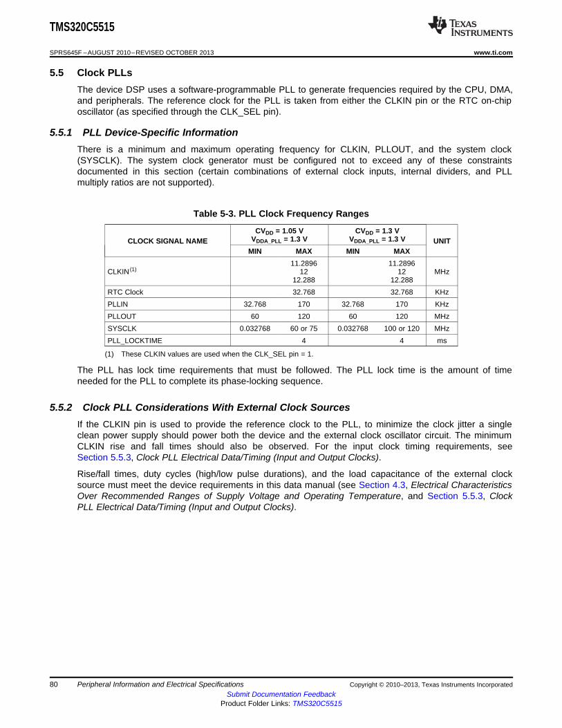
TMS320C5515
SPRS645F –AUGUST 2010–REVISED OCTOBER 2013 www.ti.com
5.5 Clock PLLsThe device DSP uses a software-programmable PLL to generate frequencies required by the CPU, DMA,and peripherals. The reference clock for the PLL is taken from either the CLKIN pin or the RTC on-chiposcillator (as specified through the CLK_SEL pin).
5.5.1 PLL Device-Specific InformationThere is a minimum and maximum operating frequency for CLKIN, PLLOUT, and the system clock(SYSCLK). The system clock generator must be configured not to exceed any of these constraintsdocumented in this section (certain combinations of external clock inputs, internal dividers, and PLLmultiply ratios are not supported).
Table 5-3. PLL Clock Frequency Ranges
CVDD = 1.05 V CVDD = 1.3 VVDDA_PLL = 1.3 V VDDA_PLL = 1.3 VCLOCK SIGNAL NAME UNIT
MIN MAX MIN MAX11.2896 11.2896
CLKIN (1) 12 12 MHz12.288 12.288
RTC Clock 32.768 32.768 KHzPLLIN 32.768 170 32.768 170 KHzPLLOUT 60 120 60 120 MHzSYSCLK 0.032768 60 or 75 0.032768 100 or 120 MHzPLL_LOCKTIME 4 4 ms
(1) These CLKIN values are used when the CLK_SEL pin = 1.
The PLL has lock time requirements that must be followed. The PLL lock time is the amount of timeneeded for the PLL to complete its phase-locking sequence.
5.5.2 Clock PLL Considerations With External Clock SourcesIf the CLKIN pin is used to provide the reference clock to the PLL, to minimize the clock jitter a singleclean power supply should power both the device and the external clock oscillator circuit. The minimumCLKIN rise and fall times should also be observed. For the input clock timing requirements, seeSection 5.5.3, Clock PLL Electrical Data/Timing (Input and Output Clocks).
Rise/fall times, duty cycles (high/low pulse durations), and the load capacitance of the external clocksource must meet the device requirements in this data manual (see Section 4.3, Electrical CharacteristicsOver Recommended Ranges of Supply Voltage and Operating Temperature, and Section 5.5.3, ClockPLL Electrical Data/Timing (Input and Output Clocks).
80 Peripheral Information and Electrical Specifications Copyright © 2010–2013, Texas Instruments IncorporatedSubmit Documentation Feedback
Product Folder Links: TMS320C5515

CLKOUT
1
2
5
4
3
CLKIN
2
3
4
4
1
1
TMS320C5515
www.ti.com SPRS645F –AUGUST 2010–REVISED OCTOBER 2013
5.5.3 Clock PLL Electrical Data/Timing (Input and Output Clocks)
Table 5-4. Timing Requirements for CLKIN (1) (2) (see Figure 5-9)CVDD = 1.05 V CVDD = 1.3 V
NO. UNITMIN NOM MAX MIN NOM MAX
88.577, 88.577,Cycle time, external clock driven on 83.333, 83.333,1 tc(CLKIN) nsCLKIN or or
81.380 81.3800.466 * 0.466 *2 tw(CLKINH) Pulse width, CLKIN high nstc(CLKIN) tc(CLKIN)
0.466 * 0.466 *3 tw(CLKINL) Pulse width, CLKIN low nstc(CLKIN) tc(CLKIN)
4 tt(CLKIN) Transition time, CLKIN 4 4 ns
(1) The CLKIN frequency and PLL multiply factor should be chosen such that the resulting clock frequency is within the specific range forCPU operating frequency.
(2) The reference points for the rise and fall transitions are measured at VIL MAX and VIH MIN.
Figure 5-9. CLKIN Timing
Table 5-5. Switching Characteristics Over Recommended Operating Conditions for CLKOUT (1) (2)
(see Figure 5-10)CVDD = 1.05 V CVDD = 1.3 V
VDDA_PLL = 1.3 V VDDA_PLL = 1.3 VNO. PARAMETER UNITMIN MAX MIN MAX
16.67 or1 tc(CLKOUT) Cycle time, CLKOUT P P 10 or 8.3 ns13.330.466 * 0.466 *2 tw(CLKOUTH) Pulse duration, CLKOUT high nstc(CLKOUT) tc(CLKOUT)
0.466 * 0.466 *3 tw(CLKOUTL) Pulse duration, CLKOUT low nstc(CLKOUT) tc(CLKOUT)
4 tt(CLKOUTR) Transition time (rise), CLKOUT 5 5 ns5 tt(CLKOUTF) Transition time (fall), CLKOUT 5 5 ns
(1) The reference points for the rise and fall transitions are measured at VOL MAX and VOH MIN.(2) P = 1/SYSCLK clock frequency in nanoseconds (ns). For example, when SYSCLK frequency is 100 MHz, use P = 10 ns.
Figure 5-10. CLKOUT Timing
Copyright © 2010–2013, Texas Instruments Incorporated Peripheral Information and Electrical Specifications 81Submit Documentation Feedback
Product Folder Links: TMS320C5515

TMS320C5515
SPRS645F –AUGUST 2010–REVISED OCTOBER 2013 www.ti.com
5.6 Direct Memory Access (DMA) ControllerThe DMA controller is used to move data among internal memory, external memory, and peripheralswithout intervention from the CPU and in the background of CPU operation.
The DSP includes a total of four DMA controllers. Aside from the DSP resources they can access, all fourDMA controllers are identical.
The DMA controller has the following features:• Operation that is independent of the CPU.• Four channels, which allow the DMA controller to keep track of the context of four independent block
transfers.• Event synchronization. DMA transfers in each channel can be made dependent on the occurrence of
selected events.• An interrupt for each channel. Each channel can send an interrupt to the CPU on completion of the
programmed transfer.• Ping-Pong mode allows the DMA controller to keep track of double buffering context without CPU
intervention.• A dedicated clock idle domain. The four device DMA controllers can be put into a low-power state by
independently turning off their input clocks.
5.6.1 DMA Channel Synchronization EventsThe DMA controllers allow activity in their channels to be synchronized to selected events. The DSPsupports 20 separate synchronization events and each channel can be tied to separate sync eventsindependent of the other channels. Synchronization events are selected by programming the CHnEVTfield in the DMAn channel event source registers (DMAnCESR1 and DMAnCESR2).
82 Peripheral Information and Electrical Specifications Copyright © 2010–2013, Texas Instruments IncorporatedSubmit Documentation Feedback
Product Folder Links: TMS320C5515

TMS320C5515
www.ti.com SPRS645F –AUGUST 2010–REVISED OCTOBER 2013
5.7 ResetThe device has two main types of reset: hardware reset and software reset.
Hardware reset is responsible for initializing all key states of the device. It occurs whenever the RESETpin is asserted or when the internal power-on-reset (POR) circuit deasserts an internal signal calledPOWERGOOD. The device's internal POR is a voltage comparator that monitors the DSP_LDOO pinvoltage and generates the internal POWERGOOD signal when the DSP_LDO is enabled externally by theDSP_LDO_EN pin. POWERGOOD is asserted when the DSP_LDOO voltage is above a minimumthreshold voltage provided by the bandgap. When the DSP_LDO is disabled (DSP_LDO_EN is high), theinternal voltage comparator becomes inactive, and the POWERGOOD signal logic level is immediately sethigh. The RESET pin and the POWERGOOD signal are internally combined with a logical AND gate toproduce an (active low) hardware reset (see Figure 5-11, Power-On Reset Timing Requirements andFigure 5-12, Reset Timing Requirements).
There are two types of software reset: the CPU's software reset instruction and the software control of theperipheral reset signals. For more information on the CPU's software reset instruction, see theTMS320C55x CPU 3.0 CPU Reference Guide (literature number: SWPU073). In all the devicedocumentation, all references to "reset" refer to hardware reset. Any references to software reset willexplicitly state software reset.
The device RTC has one additional type of reset, a power-on-reset (POR) for the registers in the RTCcore. This POR monitors the voltage of CVDDRTC and resets the RTC registers when power is first appliedto the RTC core.
5.7.1 Power-On Reset (POR) CircuitsThe device includes two power-on reset (POR) circuits, one for the RTC (RTC POR) and another for therest of the chip (MAIN POR).
5.7.1.1 RTC Power-On Reset (POR)
The RTC POR ensures that the flip-flops in the CVDDRTC power domain have an initial state uponpowerup. In particular, the RTCNOPWR register is reset by this POR and is used to indicate that the RTCtime registers need to be initialized with the current time and date when power is first applied.
5.7.1.2 Main Power-On Reset (POR)
The device includes an analog power-on reset (POR) circuit that keeps the DSP in reset until specificvoltages have reached predetermined levels. When the DSP_LDO is enabled externally by theDSP_LDO_EN pin, the output of the POR circuit, POWERGOOD, is held low until the following conditionsare satisfied:• LDOI is powered and the bandgap is active for at least approximately 8 ms• VDD_ANA is powered for at least approximately 4 ms• DSP_LDOO is above a threshold of approximately 950 mV (see Note:)
Note: The POR comparator has hysteresis, so the threshold voltage becomes approximately 850 mV afterPOWERGOOD signal is set high.
Once these conditions are met, the internal POWERGOOD signal is set high. The POWERGOOD signalis internally combined with the RESET pin signal, via an AND-gate, to produce the DSP subsystem'sglobal reset. This global reset is the hardware reset for the whole chip, except the RTC. When the globalreset is deasserted (high), the boot sequence starts. For more detailed information on the boot sequence,see Section 3.4, Boot Sequence.
When the DSP_LDO is disabled (DSP_LDO_EN pin = 1), the voltage monitoring on the DSP_LDOO pin isde-activated and the POWERGOOD signal is immediately set high. The RESET pin will be the solesource of hardware reset.
Copyright © 2010–2013, Texas Instruments Incorporated Peripheral Information and Electrical Specifications 83Submit Documentation Feedback
Product Folder Links: TMS320C5515

TMS320C5515
SPRS645F –AUGUST 2010–REVISED OCTOBER 2013 www.ti.com
5.7.1.3 Reset Pin (RESET)
The device can receive an external reset signal on the RESET pin. As specified above in Section 5.7.1.2,Main Power-On Reset, the RESET pin is combined with the internal POWERGOOD signal, that isgenerated by the MAIN POR, via an AND-gate. The output of the AND gate provides the hardware resetto the chip. The RESET pin may be tied high and the MAIN POR can provide the hardware reset in caseDSP_LDO is enabled (DSP_LDO_EN = 0), but an external hardware reset must be provided via theRESET pin when the DSP_LDO is disabled (DSP_LDO_EN = 1).
Once the hardware reset is applied, the system clock generator is enabled and the DSP starts the bootsequence. For more information on the boot sequence, see Section 3.4, Boot Sequence.
5.7.2 Pin Behavior at ResetDuring normal operation, pins are controlled by the respective peripheral selected in the External BusSelection Register (EBSR) register. During power-on reset and reset, the behavior of the output pinschanges and is categorized as follows:
High Group: EM_CS4, EM_CS5, EM_CS2, EM_CS3, EM_DQM0, EM_DQM1, EM_OE, EM_WE,•LCD_RS/SPI_CS3, EM_SDCAS, EM_SDRASLow Group: LCD_EN_RDB/SPI_CLK, EM_R/W, MMC0_CLK/I2S0_CLK/GP[0],•MMC1_CLK/I2S1_CLK/GP[6], EM_SDCLKZ Group: EM_D[15:0], EMU[1:0], SCL, SDA, LCD_D[0]/SPI_RX, LCD_D[1]/SPI_TX,•LCD_D[10]/I2S2_RX/GP[20]/SPI_RX, LCD_D[11]/I2S2_DX/GP[27]/SPI_TX,LCD_D[12]/I2S2_RTS/GP[28]/I2S3_CLK, LCD_D[13]/I2S2_CTS/GP[29]/I2S3_RS,LCD_D[14]/I2S2_RXD/GP[30]/I2S3_RX, LCD_D[15]/I2S2_TXD/GP[31]/I2S3_DX, LCD_D[2]/GP[12],LCD_D[3]/GP[13], LCD_D[4]/GP[14], LCD_D[5]/GP[15], LCD_D[6]/GP[16], LCD_D[7]/GP[17],LCD_D[8]/I2S2_CLK/GP[18]/SPI_CLK,LCD_D[9]/I2S2_FS/GP[19]/SPI_CS0, RTC_CLKOUT,MMC0_CMD/I2S0_FS/GP[1], MMC0_D0/I2S0_DX/GP[2], MMC0_D1/I2S0_RX/GP[3],MMC0_D2/GP[4], MMC0_D3/GP[5], MMC1_CMD/I2S1_FS/GP[7], MMC1_D0/2S1_DX/GP[8],MMC1_D1/I2S1_RX/GP[9], MMC1_D2/GP[10], MMC1_D3/GP[11], TDO, WAKEUPCLKOUT Group: CLKOUT, LCD_CS1_E1/SPI_CS1•SYNCH 0→1 Group: LCD_CS0_E0/SPI_CS0, LCD_RW_WRB/SPI_CS2, EM_SDCKE•SYNCH 1→0 Group: EM_CS0, EM_CS1•SYNCH X→1 Group: EM_BA[1:0], XF•SYNCH X→0 Group: EM_A[20:0]•
84 Peripheral Information and Electrical Specifications Copyright © 2010–2013, Texas Instruments IncorporatedSubmit Documentation Feedback
Product Folder Links: TMS320C5515

LOW Group
HIGH Group
Z Group
RESET
SYNCH X 0®
Group
SYNCH X 1®
Group
SYNCH 0 1®
Group
SYNCH 1 0®
Group
65536 + 38 clocks if CLK_SEL = 1,
32 + 38 clocks if CLK_SEL = 0
CLKOUT
POWERGOOD(Internal)
POWERGOOD(Internal)
and RESET
Valid Clock
TMS320C5515
www.ti.com SPRS645F –AUGUST 2010–REVISED OCTOBER 2013
5.7.3 Reset Electrical Data/Timing
Table 5-6. Timing Requirements for Reset (1) (see Figure 5-11 and Figure 5-12)CVDD = 1.05 V CVDD = 1.3 V
NO. UNITMIN MAX MIN MAX
1 tw(RSTL) Pulse duration, RESET low 3P 3P ns
(1) P = 1/SYSCLK clock frequency in ns. For example, if SYSCLK = 12 MHz, use P = 83.3 ns. In IDLE3 mode the system clock generator isbypassed and the SYSCLK frequency is equal to either CLKIN or the RTC clock frequency depending on CLK_SEL.
Figure 5-11. Power-On Reset Timing Requirements
Copyright © 2010–2013, Texas Instruments Incorporated Peripheral Information and Electrical Specifications 85Submit Documentation Feedback
Product Folder Links: TMS320C5515

POWERGOOD
(Internal)
LOW Group
HIGH Group
Z Group
RESET
POWERGOOD and RESET
(I )nternal
SYNCH X 0®
Group
SYNCH X 1®
Group
SYNCH 0 1®
Group
SYNCH 1 0®
Group
65536 + 38 clocks if CLK_SEL = 1,
32 + 38 clocks if CLK_SEL = 0
CLKOUT
tw(RSTL)
Valid Clock
TMS320C5515
SPRS645F –AUGUST 2010–REVISED OCTOBER 2013 www.ti.com
Figure 5-12. Reset Timing Requirements
86 Peripheral Information and Electrical Specifications Copyright © 2010–2013, Texas Instruments IncorporatedSubmit Documentation Feedback
Product Folder Links: TMS320C5515

1
2
INTx
TMS320C5515
www.ti.com SPRS645F –AUGUST 2010–REVISED OCTOBER 2013
5.8 Wake-up Events, Interrupts, and XFThe device has a number of interrupts to service the needs of its peripherals. The interrupts can beselectively enabled or disabled.
5.8.1 Interrupts Electrical Data/Timing
Table 5-7. Timing Requirements for Interrupts (1) (see Figure 5-13)CVDD = 1.05 VCVDD = 1.3 VNO. UNIT
MIN MAX1 tw(INTH) Pulse duration, interrupt high CPU active 2P ns2 tw(INTL) Pulse duration, interrupt low CPU active 2P ns
(1) P = 1/SYSCLK clock frequency in ns. For example, when the CPU core is clocked at 100 MHz, use P = 10 ns. For example, when theCPU core is clocked att 120 MHz, use P = 8.3 ns.
Figure 5-13. External Interrupt Timings
5.8.2 Wake-Up From IDLE Electrical Data/Timing
Table 5-8. Timing Requirements for Wake-Up From IDLE (see Figure 5-14)CVDD = 1.05 VCVDD = 1.3 VNO. UNIT
MIN MAX1 tw(WKPL) Pulse duration, WAKEUP or INTx low, SYSCLKDIS = 1 30.5 µs
Table 5-9. Switching Characteristics Over Recommended Operating Conditions For Wake-Up FromIDLE (1) (2) (3) (4) (see Figure 5-14)
CVDD = 1.05 VCVDD = 1.3 VNO. PARAMETER UNIT
MIN TYP MAXIDLE3 Mode with SYSCLKDIS = 1,WAKEUP or INTx event, CLK_SEL = D ns1
td(WKEVTH-C Delay time, WAKEUP pulse complete to2 IDLE3 Mode with SYSCLKDIS = 1,KLGEN) CPU active WAKEUP or INTx event, CLK_SEL = C ns
0IDLE2 Mode; INTx event 3P ns
(1) D = 1/ External Clock Frequency (CLKIN).(2) C = 1/RTCCLK= 30.5 μs. RTCCLK is the clock output of the 32.768-kHz RTC oscillator.(3) P = 1/SYSCLK clock frequency in ns. For example, when the CPU core is clocked at 100 MHz, use P = 10 ns.(4) Assumes the internal LDOs are used with a 0.1uF bandgap capacitor.
Copyright © 2010–2013, Texas Instruments Incorporated Peripheral Information and Electrical Specifications 87Submit Documentation Feedback
Product Folder Links: TMS320C5515

1
CLKOUT(A)
XF
2
CLKOUT
INTx
WAKEUP
1
TMS320C5515
SPRS645F –AUGUST 2010–REVISED OCTOBER 2013 www.ti.com
A. INT[1:0] can only be used as a wake-up event for IDLE3 and IDLE2 modes.B. RTC interrupt (internal signal) can be used as wake-up event for IDLE3 and IDLE2 modes.C. Any unmasked interrupt can be used to exit the IDLE2 mode.D. CLKOUT reflects either the CPU clock, SAR, USB PHY, or PLL clock dependent on the setting of the CLOCKOUT
Clock Source Register. For this diagram, CLKOUT refers to the CPU clock.
Figure 5-14. Wake-Up From IDLE Timings
5.8.3 XF Electrical Data/Timing
Table 5-10. Switching Characteristics Over Recommended Operating Conditions For XF (1) (2)
(see Figure 5-15)CVDD = 1.05 VCVDD = 1.3 VNO. PARAMETER UNIT
MIN MAX1 td(XF) Delay time, CLKOUT high to XF high 0 10.2 ns
(1) P = 1/SYSCLK clock frequency in ns. For example, when the CPU core is clocked at 100 MHz, use P = 10 ns.(2) C = 1/RTCCLK= 30.5 μs. RTCCLK is the clock output of the 32.768-kHz RTC oscillator.
A. CLKOUT reflects either the CPU clock, SAR, USB PHY, or PLL clock dependent on the setting of the CLOCKOUTClock Source Register. For this diagram, CLKOUT refers to the CPU clock.
Figure 5-15. XF Timings
88 Peripheral Information and Electrical Specifications Copyright © 2010–2013, Texas Instruments IncorporatedSubmit Documentation Feedback
Product Folder Links: TMS320C5515

TMS320C5515
www.ti.com SPRS645F –AUGUST 2010–REVISED OCTOBER 2013
5.9 External Memory Interface (EMIF)The device supports several memories and external device interfaces, including: NOR Flash, NANDFlash, SRAM, Non-Mobile SDRAM, and Mobile SDRAM (mSDRAM).
Note: The device can support non-mobile SDRAM under certain circumstances. The device also alwaysuses mobile SDRAM initialization, but it is able to support SDRAM memories that ignore the BA0 and BA1pins for the 'load mode register' command. During the mobile SDRAM initialization, the device issues the'load mode register' initialization command to two different addresses that differ in only the BA0 and BA1address bits. These registers are the Extended Mode register and the Mode register. The Extended moderegister exists only in mSDRAM and not in non-mSDRAM. If a non-mobile SDRAM memory ignores bitsBA0 and BA1, the second loaded register value overwrites the first, leaving the desired value in the Moderegister and the non-mobile SDRAM will work with the device.
The EMIF provides an 8-bit or 16-bit data bus, an address bus width up to 21 bits, and 6 chip selects,along with memory control signals.
The EM_A[20:15] address signals are multiplexed with the GPIO peripheral and controlled by the ExternalBus Selection Register (EBSR). For more detail on the pin muxing, see the Section 3.6.1, External BusSelection Register (EBSR).
5.9.1 EMIF Asynchronous Memory SupportThe EMIF supports asynchronous:• SRAM memories• NAND Flash memories• NOR Flash memories
The EMIF data bus can be configured for both 8- or 16-bit width. The device supports up to 21 addresslines and four external wait/interrupt inputs. Up to four asynchronous chip selects are supported by EMIF(EM_CS[5:2]).
Each chip select has the following individually programmable attributes:• Data bus width• Read cycle timings: setup, hold, strobe• Write cycle timings: setup, hold, strobe• Bus turn around time• Extended Wait Option With Programmable Timeout• Select Strobe Option• NAND flash controller supports 1-bit and 4-bit ECC calculation on blocks of 512 bytes
5.9.2 EMIF Non-Mobile and Mobile Synchronous DRAM Memory SupportedThe EMIF supports 16-bit non-mobile and mobile single data rate (SDR) SDRAM in addition to theasynchronous memories listed in Section 5.9.1, EMIF Asynchronous Memory Support. The supportedSDRAM and mobile SDRAM configurations are:• One, two, and four bank SDRAM/mSDRAM devices• Supports devices with eight, nine, ten, and eleven column addresses• CAS latency of two or three clock cycles• 16-bit data-bus width• 3.3/2.75/2.5/1.8 -V LVCMOS interface that is separate from the rest of the chip I/Os.• One (EM_CS0) or two (EM_CS[1:0]) chip selects
Copyright © 2010–2013, Texas Instruments Incorporated Peripheral Information and Electrical Specifications 89Submit Documentation Feedback
Product Folder Links: TMS320C5515

TMS320C5515
SPRS645F –AUGUST 2010–REVISED OCTOBER 2013 www.ti.com
Additionally, the SDRAM/mSDRAM interface of EMIF supports placing the SDRAM/mSDRAM in "Self-Refresh" and "Powerdown Modes". Self-Refresh mode allows the SDRAM/mSDRAM to be put into a low-power state while still retaining memory contents; since the SDRAM/mSDRAM will continue to refreshitself even without clocks from the DSP. Powerdown mode achieves even lower power, except the DSPmust periodically wake the SDRAM/mSDRAM up and issue refreshes if data retention is required. Toachieve the lowest power consumption, the SDRAM/mSDRAM interface has configurable slew rate on theEMIF pins.
The device has limitations to the clock frequency on the EM_SDCLK pin based on the CVDD andDVDDEMIF.• The clock frequency on the EM_SDCLK pin can be configured either as SYSCLK (DSP Operating
Frequency) or SYSCLK/2 via bit 0 of the ECDR Register (0x1C26h)• When CVDD = 1.3 V and DVDDEMIF = 3.3 V, 2.75 V, or 2.5 V, the max clock frequency on the
EM_SDCLK pin is limited to 100 MHz (EM_SDCLK ≤ 100 MHz). Therefore, if SYSCLK ≤ 100 MHz, theEM_SDCLK can be configured either as SYSCLK or SYSCLK/2, but if SYSCLK > 100 MHz, theEM_SDCLK must be configured as SYSCLK/2.
• When CVDD =1.05 V, and DVDDEMIF = 3.3 V, 2.75 V, or 2.5 V, the max clock frequency on theEM_SDCLK pin is limited to 60 MHz (EM_SDCLK ≤ 60 MHz). Therefore, if SYSCLK ≤ 60 MHz, theEM_SDCLK can be configured as either SYSCLK or SYSCLK/2, but if SYSCLK > 60 MHz, theEM_SDCLK must be configured as SYSCLK/2.
• When DVDDEMIF = 1.8 V, regardless of the CVDD voltage, the clock frequency on the EM_SDCLK pinmust be configured as SYSCLK/2 and ≤ 50 MHz.
5.9.3 EMIF Peripheral Register DescriptionsTable 5-11 shows the EMIF registers.
Table 5-11. External Memory Interface (EMIF) Peripheral Registers (1)
HEX ADDRESS ACRONYM REGISTER NAMERANGE1000h REV Revision Register1001h STATUS Status Register1004h AWCCR1 Asynchronous Wait Cycle Configuration Register 11005h AWCCR2 Asynchronous Wait Cycle Configuration Register 21008h SDCR1 SDRAM/mSDRAM Configuration Register 11009h SDCR2 SDRAM/mSDRAM Configuration Register 2100Ch SDRCR SDRAM/mSDRAM Refresh Control Register1010h ACS2CR1 Asynchronous CS2 Configuration Register 11011h ACS2CR2 Asynchronous CS2 Configuration Register 21014h ACS3CR1 Asynchronous CS3 Configuration Register 11015h ACS3CR2 Asynchronous CS3 Configuration Register 21018h ACS4CR1 Asynchronous CS4 Configuration Register 11019h ACS4CR2 Asynchronous CS4 Configuration Register 2101Ch ACS5CR1 Asynchronous CS5 Configuration Register 1101Dh ACS5CR2 Asynchronous CS5 Configuration Register 21020h SDTIMR1 SDRAM/mSDRAM Timing Register 11021h SDTIMR2 SDRAM/mSDRAM Timing Register 2103Ch SDSRETR SDRAM/mSDRAM Self Refresh Exit Timing Register1040h EIRR EMIF Interrupt Raw Register1044h EIMR EMIF Interrupt Mask Register1048h EIMSR EMIF Interrupt Mask Set Register
(1) Before reading or writing to the EMIF registers, be sure to set the BYTEMODE bits to 00b in the EMIF system control register to enableword accesses to the EMIF registers.
90 Peripheral Information and Electrical Specifications Copyright © 2010–2013, Texas Instruments IncorporatedSubmit Documentation Feedback
Product Folder Links: TMS320C5515

TMS320C5515
www.ti.com SPRS645F –AUGUST 2010–REVISED OCTOBER 2013
Table 5-11. External Memory Interface (EMIF) Peripheral Registers(1) (continued)HEX ADDRESS ACRONYM REGISTER NAMERANGE
104Ch EIMCR EMIF Interrupt Mask Clear Register1060h NANDFCR NAND Flash Control Register1064h NANDFSR1 NAND Flash Status Register 11065h NANDFSR2 NAND Flash Status Register 21068h PGMODECTRL1 Page Mode Control Register 11069h PGMODECTRL2 Page Mode Control Register 21070h NCS2ECC1 NAND Flash CS2 1-Bit ECC Register 11071h NCS2ECC2 NAND Flash CS2 1-Bit ECC Register 21074h NCS3ECC1 NAND Flash CS3 1-Bit ECC Register 11075h NCS3ECC2 NAND Flash CS3 1-Bit ECC Register 21078h NCS4ECC1 NAND Flash CS4 1-Bit ECC Register 11079h NCS4ECC2 NAND Flash CS4 1-Bit ECC Register 2107Ch NCS5ECC1 NAND Flash CS5 1-Bit ECC Register 1107Dh NCS5ECC2 NAND Flash CS5 1-Bit ECC Register 210BCh NAND4BITECCLOAD NAND Flash 4-Bit ECC Load Register10C0h NAND4BITECC1 NAND Flash 4-Bit ECC Register 110C1h NAND4BITECC2 NAND Flash 4-Bit ECC Register 210C4h NAND4BITECC3 NAND Flash 4-Bit ECC Register 310C5h NAND4BITECC4 NAND Flash 4-Bit ECC Register 410C8h NAND4BITECC5 NAND Flash 4-Bit ECC Register 510C9h NAND4BITECC6 NAND Flash 4-Bit ECC Register 610CCh NAND4BITECC7 NAND Flash 4-Bit ECC Register 710CDh NAND4BITECC8 NAND Flash 4-Bit ECC Register 810D0h NANDERRADD1 NAND Flash 4-Bit ECC Error Address Register 110D1h NANDERRADD2 NAND Flash 4-Bit ECC Error Address Register 210D4h NANDERRADD3 NAND Flash 4-Bit ECC Error Address Register 310D5h NANDERRADD4 NAND Flash 4-Bit ECC Error Address Register 410D8h NANDERRVAL1 NAND Flash 4-Bit ECC Error Value Register 110D9h NANDERRVAL2 NAND Flash 4-Bit ECC Error Value Register 210DCh NANDERRVAL3 NAND Flash 4-Bit ECC Error Value Register 310DDh NANDERRVAL4 NAND Flash 4-Bit ECC Error Value Register 4
Copyright © 2010–2013, Texas Instruments Incorporated Peripheral Information and Electrical Specifications 91Submit Documentation Feedback
Product Folder Links: TMS320C5515

TMS320C5515
SPRS645F –AUGUST 2010–REVISED OCTOBER 2013 www.ti.com
5.9.4 EMIF Electrical Data/Timing CVDD = 1.05 V, DVDDEMIF = 3.3/2.75/2.5/1.8 V, ExternalLoading = 10 pF
Table 5-12. Timing Requirements for EMIF SDRAM/mSDRAM Interface (1) (see Figure 5-16 and Figure 5-17)
CVDD = 1.05 V CVDD = 1.05 VDVDDEMIF = DVDDEMIF = 1.8 VNO. UNIT3.3/2.75/2.5 VMIN MAX MIN MAX
Input setup time, read data valid on EM_D[15:0] before19 tsu(DV-CLKH) 3.4 3.4 nsEM_SDCLK risingInput hold time, read data valid on EM_D[15:0] after EM_SDCLK20 th(CLKH-DIV) 1.2 1.2 nsrising
(1) Timing parameters are obtained with 10pF loading on the EMIF pins.
Table 5-13. Switching Characteristics Over Recommended Operating Conditions for EMIFSDRAM/mSDRAM Interface (1) (2) (see Figure 5-16 and Figure 5-17)
CVDD = 1.05 V CVDD = 1.05 VDVDDEMIF = 3.3/2.75/2.5 V DVDDEMIF = 1.8 VNO. PARAMETER UNITMIN NOM MAX MIN NOM MAX
1 tc(CLK) Cycle time, EMIF clock EM_SDCLK 16.67 (3) 20 (4) nsPulse width, EMIF clock EM_SDCLK high or2 tw(CLK) 8.34 10 nslowDelay time, EM_SDCLK rising to3 td(CLKH-CSV) 1.1 13.2 1.1 13.2 nsEMA_CS[1:0] validDelay time, EM_SDCLK rising to5 td(CLKH-DQMV) 1.1 13.2 1.1 13.2 nsEM_DQM[1:0] validDelay time, EM_SDCLK rising to EM_A[20:0]7 td(CLKH-AV) 1.1 13.2 1.1 13.2 nsand EM_BA[1:0] validDelay time, EM_SDCLK rising to EM_D[15:0]9 td(CLKH-DV) 1.1 13.2 1.1 13.2 nsvalidDelay time, EM_SDCLK rising to EM_SDRAS11 td(CLKH-RASV) 1.1 13.2 1.1 13.2 nsvalidDelay time, EM_SDCLK rising to EM_SDCAS13 td(CLKH-CASV) 1.1 13.2 1.1 13.2 nsvalidDelay time, EM_SDCLK rising to EM_WE15 td(CLKH-WEV) 1.1 13.2 1.1 13.2 nsvalidDelay time, EM_SDCLK rising to EM_SDCKE21 td(CLKH-CKEV) 1.1 13.2 1.1 13.2 nsvalid
(1) Timing parameters are obtained with 10pF loading on the EMIF pins.(2) E = SYSCLK period in ns. For example, when SYSCLK is set to 60 or 100 MHz, E = 16.67 or 10 ns, respectively. For more detail on the
EM_SDCLK speed see Section 5.9.2, EMIF Non-Mobile and Mobile Synchronous DRAM Memory Supported.(3) When CVDD = 1.05 V, and DVDDEMIF = 3.3 V, 2.75 V or 2.5 V, the max clock frequency on the EM_SDCLK pin is limited to 60 MHz
(EM_SDCLK = 60 MHz). For more information, see TMS320C5515/14/05/04 DSP External Memory Interface (EMIF) User's Guide(literature number SPRUGU6).
(4) When DVDDEMIF = 1.8 V, the max clock frequency on the EM_SDCLK pin is limited to 50 MHz (EM_SDCLK = 50 MHz). For moreinformation, see TMS320C5515/14/05/04 DSP External Memory Interface (EMIF) User's Guide (literature number SPRUGU6).
92 Peripheral Information and Electrical Specifications Copyright © 2010–2013, Texas Instruments IncorporatedSubmit Documentation Feedback
Product Folder Links: TMS320C5515

TMS320C5515
www.ti.com SPRS645F –AUGUST 2010–REVISED OCTOBER 2013
Table 5-14. Timing Requirements for EMIF Asynchronous Memory (1) (2) (see Figure 5-18, Figure 5-20, andFigure 5-21)
CVDD = 1.05 VDVDDEMIF = 3.3/2.75/2.5/1.8 VNO. UNITMIN NOM MAX
READS and WRITES2 tw(EM_WAIT) Pulse duration, EM_WAITx assertion and deassertion 2E ns
READS12 tsu(EMDV-EMOEH) Setup time, EM_D[15:0] valid before EM_OE high 14.5 ns13 th(EMOEH-EMDIV) Hold time, EM_D[15:0] valid after EM_OE high 0 ns14 tsu (EMOEL-EMWAIT) Setup time, EM_WAITx asserted before end of Strobe Phase (3) 4E + 13 ns
WRITES28 tsu (EMWEL-EMWAIT) Setup time, EM_WAITx asserted before end of Strobe Phase (3) 4E + 13 ns
(1) E = SYSCLK period in ns. For example, when SYSCLK is set to 100/120 MHz, E = 10/8.33 ns, respectively.(2) Timing parameters are obtained with 10pF loading on the EMIF pins.(3) Setup before end of STROBE phase (if no extended wait states are inserted) by which EM_WAITx must be asserted to add extended
wait states. Figure 5-20 and Figure 5-21 describe EMIF transactions that include extended wait states inserted during the STROBEphase. However, cycles inserted as part of this extended wait period should not be counted; the 4E requirement is to the start of wherethe HOLD phase would begin if there were no extended wait cycles.
Copyright © 2010–2013, Texas Instruments Incorporated Peripheral Information and Electrical Specifications 93Submit Documentation Feedback
Product Folder Links: TMS320C5515

TMS320C5515
SPRS645F –AUGUST 2010–REVISED OCTOBER 2013 www.ti.com
Table 5-15. Switching Characteristics Over Recommended Operating Conditions for EMIF Asynchronous Memory (1) (2) (3) (see Figure 5-19 andFigure 5-21) (4)
CVDD = 1.05 VDVDDEMIF = 3.3/2.75/2.5/1.8 VNO. PARAMETER UNIT
MIN NOM MAX
READS and WRITES
1 td(TURNAROUND) Turn around time (TA)*E - 13 (TA)*E (TA)*E + 13 ns
READS
EMIF read cycle time (EW = 0) (RS+RST+RH)*E - 13 (RS+RST+RH)*E (RS+RST+RH)*E + 13 ns3 tc(EMRCYCLE)
EMIF read cycle time (EW = 1) (RS+RST+RH+(EWC*16))*E - 13 (RS+RST+RH+(EWC*16))*E (RS+RST+RH+(EWC*16))*E +139 ns
Output setup time, EM_CS[5:2] low to EM_OE low (SS = 0) (RS)*E-13 (RS)*E (RS)*E+13 ns4 tsu(EMCEL-EMOEL)
Output setup time, EM_CS[5:2] low to EM_OE low (SS = 1) -13 0 +13 ns
Output hold time, EM_OE high to EM_CS[5:2] high (SS = 0) (RH)*E - 13 (RH)*E (RH)*E + 13 ns5 th(EMOEH-EMCEH)
Output hold time, EM_OE high to EM_CS[5:2] high (SS = 1) -13 0 +13 ns
6 tsu(EMBAV-EMOEL) Output setup time, EM_BA[1:0] valid to EM_OE low (RS)*E-13 (RS)*E (RS)*E+13 ns
7 th(EMOEH-EMBAIV) Output hold time, EM_OE high to EM_BA[1:0] invalid (RH)*E-13 (RH)*E (RH)*E+13 ns
8 tsu(EMBAV-EMOEL) Output setup time, EM_A[20:0] valid to EM_OE low (RS)*E-13 (RS)*E (RS)*E+13 ns
9 th(EMOEH-EMAIV) Output hold time, EM_OE high to EM_A[20:0] invalid (RH)*E-13 (RH)*E (RH)*E+13 ns
EM_OE active low width (EW = 0) (RST)*E-13 (RST)*E (RST)*E+13 ns10 tw(EMOEL)
EM_OE active low width (EW = 1) (RST+(EWC*16))*E-13 (RST+(EWC*16))*E (RST+(EWC*16))*E+13 ns
11 td(EMWAITH-EMOEH) Delay time from EM_WAITx deasserted to EM_OE high 4E-13 4E 4E+13 ns
WRITES
EMIF write cycle time (EW = 0) (WS+WST+WH)*E-13 (WS+WST+WH)*E (WS+WST+WH)*E+13 ns15 tc(EMWCYCLE) (WS+WST+WH+(EWC*16))*E +EMIF write cycle time (EW = 1) (WS+WST+WH+(EWC*16))*E - 13 (WS+WST+WH+(EWC*16))*E ns13
Output setup time, EM_CS[5:2] low to EM_WE low (SS = 0) (WS)*E - 13 (WS)*E (WS)*E + 13 ns16 tsu(EMCSL-EMWEL)
Output setup time, EM_CS[5:2] low to EM_WE low (SS = 1) -13 0 +13 ns
Output hold time, EM_WE high to EM_CS[5:2] high (SS = 0) (WH)*E-13 (WH)*E (WH)*E+13 ns17 th(EMWEH-EMCSH)
Output hold time, EM_WE high to EM_CS[5:2] high (SS = 1) -13 0 +13 ns
18 tsu(EMBAV-EMWEL) Output setup time, EM_BA[1:0] valid to EM_WE low (WS)*E-13 (WS)*E (WS)*E+13 ns
19 th(EMWEH-EMBAIV) Output hold time, EM_WE high to EM_BA[1:0] invalid (WH)*E-13 (WH)*E (WH)*E+13 ns
20 tsu(EMAV-EMWEL) Output setup time, EM_A[20:0] valid to EM_WE low (WS)*E-13 (WS)*E (WS)*E+13 ns
21 th(EMWEH-EMAIV) Output hold time, EM_WE high to EM_A[20:0] invalid (WH)*E-13 (WH)*E (WH)*E+13 ns
(1) Timing parameters are obtained with 10pF loading on the EMIF pins.(2) TA = Turn around, RS = Read setup, RST = Read strobe, RH = Read hold, WS = Write setup, WST = Write strobe, WH = Write hold, MEWC = Maximum external wait cycles. These
parameters are programmed via the Asynchronous Configuration and Asynchronous Wait Cycle Configuration Registers.(3) E = SYSCLK period in ns. For example, when SYSCLK is set to 100/120 MHz, E = 10/8.33 ns, respectively.(4) EWC = external wait cycles determined by EM_WAITx input signal. EWC supports the following range of values EWC[256-1]. Note that the maximum wait time before timeout is specified
by bit field MEWC in the Asynchronous Wait Cycle Configuration Register.
94 Peripheral Information and Electrical Specifications Copyright © 2010–2013, Texas Instruments IncorporatedSubmit Documentation Feedback
Product Folder Links: TMS320C5515

TMS320C5515
www.ti.com SPRS645F –AUGUST 2010–REVISED OCTOBER 2013
Table 5-15. Switching Characteristics Over Recommended Operating Conditions for EMIF Asynchronous Memory(1)(2) (3) (see Figure 5-19 andFigure 5-21)(4) (continued)
CVDD = 1.05 VDVDDEMIF = 3.3/2.75/2.5/1.8 VNO. PARAMETER UNIT
MIN NOM MAX
EM_WE active low width (EW = 0) (WST)*E-13 (WST)*E (WST)*E+13 ns22 tw(EMWEL)
EM_WE active low width (EW = 1) (WST+(EWC*16))*E-13 (WST+(EWC*16))*E (WST+(EWC*16))*E+13 ns
23 td(EMWAITH-EMWEH) Delay time from EM_WAITx deasserted to EM_WE high 3E-13 4E 4E+13 ns
24 tsu(EMDV-EMWEL) Output setup time, EM_D[15:0] valid to EM_WE low (WS)*E-13 (WS)*E (WS)*E+13 ns
25 th(EMWEH-EMDIV) Output hold time, EM_WE high to EM_D[15:0] invalid (WH)*E-13 (WH)*E (WH)*E+13 ns
Copyright © 2010–2013, Texas Instruments Incorporated Peripheral Information and Electrical Specifications 95Submit Documentation Feedback
Product Folder Links: TMS320C5515
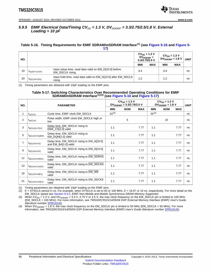
TMS320C5515
SPRS645F –AUGUST 2010–REVISED OCTOBER 2013 www.ti.com
5.9.5 EMIF Electrical Data/Timing CVDD = 1.3 V, DVDDEMIF = 3.3/2.75/2.5/1.8 V, ExternalLoading = 10 pF
Table 5-16. Timing Requirements for EMIF SDRAM/mSDRAM Interface (1) (see Figure 5-16 and Figure 5-17)
CVDD = 1.3 V CVDD = 1.3 VDVDDEMIF = DVDDEMIF = 1.8 VNO. UNIT3.3/2.75/2.5 VMIN MAX MIN MAX
Input setup time, read data valid on EM_D[15:0] before19 tsu(DV-CLKH) 3.4 3.4 nsEM_SDCLK risingInput hold time, read data valid on EM_D[15:0] after EM_SDCLK20 th(CLKH-DIV) 1.2 1.2 nsrising
(1) Timing parameters are obtained with 10pF loading on the EMIF pins.
Table 5-17. Switching Characteristics Over Recommended Operating Conditions for EMIFSDRAM/mSDRAM Interface (1) (2) (see Figure 5-16 and Figure 5-17)
CVDD = 1.3 V CVDD = 1.3 VDVDDEMIF = 3.3/2.75/2.5 V DVDDEMIF = 1.8 VNO. PARAMETER UNITMIN NOM MAX MIN NOM MAX
1 tc(CLK) Cycle time, EMIF clock EM_SDCLK 10 (3) 20 (4) nsPulse width, EMIF clock EM_SDCLK high or2 tw(CLK) 5 10 nslowDelay time, EM_SDCLK rising to3 td(CLKH-CSV) 1.1 7.77 1.1 7.77 nsEMA_CS[1:0] validDelay time, EM_SDCLK rising to5 td(CLKH-DQMV) 1.1 7.77 1.1 7.77 nsEM_DQM[1:0] validDelay time, EM_SDCLK rising to EM_A[20:0]7 td(CLKH-AV) 1.1 7.77 1.1 7.77 nsand EM_BA[1:0] validDelay time, EM_SDCLK rising to EM_D[15:0]9 td(CLKH-DV) 1.1 7.77 1.1 7.77 nsvalidDelay time, EM_SDCLK rising to EM_SDRAS11 td(CLKH-RASV) 1.1 7.77 1.1 7.77 nsvalidDelay time, EM_SDCLK rising to EM_SDCAS13 td(CLKH-CASV) 1.1 7.77 1.1 7.77 nsvalidDelay time, EM_SDCLK rising to EM_WE15 td(CLKH-WEV) 1.1 7.77 1.1 7.77 nsvalidDelay time, EM_SDCLK rising to EM_SDCKE21 td(CLKH-CKEV) 1.1 7.77 1.1 7.77 nsvalid
(1) Timing parameters are obtained with 10pF loading on the EMIF pins.(2) E = SYSCLK period in ns. For example, when SYSCLK is set to 60 or 100 MHz, E = 16.67 or 10 ns, respectively. For more detail on the
EM_SDCLK speed see Section 5.9.2, EMIF Non-Mobile and Mobile Synchronous DRAM Memory Supported.(3) When CVDD = 1.3 V, and DVDDEMIF = 3.3 V, 2.75 V or 2.5 V, the max clock frequency on the EM_SDCLK pin is limited to 100 MHz
(EM_SDCLK = 100 MHz). For more information, see TMS320C5515/14/05/04 DSP External Memory Interface (EMIF) User's Guide(literature number SPRUGU6).
(4) When DVDDEMIF = 1.8 V, the max clock frequency on the EM_SDCLK pin is limited to 50 MHz (EM_SDCLK = 50 MHz). For moreinformation, see TMS320C5515/14/05/04 DSP External Memory Interface (EMIF) User's Guide (literature number SPRUGU6).
96 Peripheral Information and Electrical Specifications Copyright © 2010–2013, Texas Instruments IncorporatedSubmit Documentation Feedback
Product Folder Links: TMS320C5515

TMS320C5515
www.ti.com SPRS645F –AUGUST 2010–REVISED OCTOBER 2013
Table 5-18. Timing Requirements for EMIF Asynchronous Memory (1) (2) (see Figure 5-18, Figure 5-20, andFigure 5-21)
CVDD = 1.3 VDVDDEMIF = 3.3/2.75/2.5/1.8 VNO. UNITMIN NOM MAX
READS and WRITES2 tw(EM_WAIT) Pulse duration, EM_WAITx assertion and deassertion 2E ns
READS12 tsu(EMDV-EMOEH) Setup time, EM_D[15:0] valid before EM_OE high 11 ns13 th(EMOEH-EMDIV) Hold time, EM_D[15:0] valid after EM_OE high 0 ns14 tsu (EMOEL-EMWAIT) Setup Time, EM_WAITx asserted before end of Strobe Phase (3) 4E + 7.5 ns
WRITES28 tsu (EMWEL-EMWAIT) Setup Time, EM_WAITx asserted before end of Strobe Phase (3) 4E + 7.5 ns
(1) Timing parameters are obtained with 10pF loading on the EMIF pins.(2) E = SYSCLK period in ns. For example, when SYSCLK is set to 100/120 MHz, E = 10/8.33 ns, respectively.(3) Setup before end of STROBE phase (if no extended wait states are inserted) by which EM_WAITx must be asserted to add extended
wait states. Figure 5-20 and Figure 5-21 describe EMIF transactions that include extended wait states inserted during the STROBEphase. However, cycles inserted as part of this extended wait period should not be counted; the 4E requirement is to the start of wherethe HOLD phase would begin if there were no extended wait cycles.
Copyright © 2010–2013, Texas Instruments Incorporated Peripheral Information and Electrical Specifications 97Submit Documentation Feedback
Product Folder Links: TMS320C5515

TMS320C5515
SPRS645F –AUGUST 2010–REVISED OCTOBER 2013 www.ti.com
Table 5-19. Switching Characteristics Over Recommended Operating Conditions for EMIF Asynchronous Memory (1) (2) (3) (4) (see Figure 5-18,Figure 5-20, and Figure 5-21)
CVDD = 1.3 VDVDDEMIF = 3.3/2.75/2.5/1.8 VNO. PARAMETER UNIT
MIN NOM MAX
READS and WRITES
1 td(TURNAROUND) Turn around time (TA)*E - 7.5 (TA)*E (TA)*E + 7.5 ns
READS
EMIF read cycle time (EW = 0) (RS+RST+RH)*E - 7.5 (RS+RST+RH)*E (RS+RST+RH)*E + 7.5 ns3 tc(EMRCYCLE)
EMIF read cycle time (EW = 1) (RS+RST+RH+(EWC*16))*E - 7.5 (RS+RST+RH+(EWC*16))*E (RS+RST+RH+(EWC*16))*E + 7.5 ns
Output setup time, EM_CS[5:2] low to EM_OE low (SS = 0) (RS)*E - 7.5 (RS)*E (RS)*E + 7.5 ns4 tsu(EMCSL-EMOEL)
Output setup time, EM_CS[5:2] low to EM_OE low (SS = 1) -7.5 0 +7.5 ns
Output hold time, EM_OE high to EM_CS[5:2] high (SS = 0) (RH)*E - 7.5 (RH)*E (RH)*E + 7.5 ns5 th(EMOEH-EMCSH)
Output hold time, EM_OE high to EM_CE[5:2] high (SS = 1) -7.5 0 +7.5 ns
6 tsu(EMBAV-EMOEL) Output setup time, EM_BA[1:0] valid to EM_OE low (RS)*E - 7.5 (RS)*E (RS)*E + 7.5 ns
7 th(EMOEH-EMBAIV) Output hold time, EM_OE high to EM_BA[1:0] invalid (RH)*E - 7.5 (RH)*E (RH)*E + 7.5 ns
8 tsu(EMAV-EMOEL) Output setup time, EM_A[20:0] valid to EM_OE low (RS)*E - 7.5 (RS)*E (RS)*E + 7.5 ns
9 th(EMOEH-EMAIV) Output hold time, EM_OE high to EM_A[20:0] invalid (RH)*E - 7.5 (RH)*E (RH)*E + 7.5 ns
EM_OE active low width (EW = 0) (RST)*E - 7.5 (RST)*E (RST)*E + 7.5 ns10 tw(EMOEL)
EM_OE active low width (EW = 1) (RST+(EWC*16))*E - 7.5 (RST+(EWC*16))*E (RST+(EWC*16))*E + 7.5 ns
11 td(EMWAITH-EMOEH) Delay time from EM_WAITx deasserted to EM_OE high 4E - 7.5 4E 4E + 7.5 ns
WRITES
EMIF write cycle time (EW = 0) (WS+WST+WH)*E - 7.5 (WS+WST+WH)*E (WS+WST+WH)*E + 7.5 ns15 tc(EMWCYCLE) (WS+WST+WH+(EWC*16))*E - (WS+WST+WH+(EWC*16))*E +EMIF write cycle time (EW = 1) (WS+WST+WH+(EWC*16))*E ns7.5 7.5
Output setup time, EM_CS[5:2] low to EM_WE low (SS = 0) (WS)*E - 7.5 (WS)*E (WS)*E +7. 5 ns16 tsu(EMCSL-EMWEL)
Output setup time, EM_CS[5:2] low to EM_WE low (SS = 1) -7.5 0 +7.5 ns
Output hold time, EM_WE high to EM_CS[5:2] high (SS = 0) (WH)*E - 7.5 (WH)*E (WH)*E + 7.5 ns17 th(EMWEH-EMCSH)
Output hold time, EM_WE high to EM_CS[5:2] high (SS = 1) -7.5 0 +7.5 ns
18 tsu(EMBAV-EMWEL) Output setup time, EM_BA[1:0] valid to EM_WE low (WS)*E - 7.5 (WS)*E (WS)*E + 7.5 ns
19 th(EMWEH-EMBAIV) Output hold time, EM_WE high to EM_BA[1:0] invalid (WH)*E - 7.5 (WH)*E (WH)*E + 7.5 ns
20 tsu(EMAV-EMWEL) Output setup time, EM_A[20:0] valid to EM_WE low (WS)*E - 7.5 (WS)*E (WS)*E + 7.5 ns
21 th(EMWEH-EMAIV) Output hold time, EM_WE high to EM_A[20:0] invalid (WH)*E - 7.5 (WH)*E (WH)*E + 7.5 ns
(1) Timing parameters are obtained with 10pF loading on the EMIF pins.(2) TA = Turn around, RS = Read setup, RST = Read strobe, RH = Read hold, WS = Write setup, WST = Write strobe, WH = Write hold, MEWC = Maximum external wait cycles. These
parameters are programmed via the Asynchronous Configuration and Asynchronous Wait Cycle Configuration Registers.(3) E = SYSCLK period in ns. For example, when SYSCLK is set to 100/120 MHz, E = 10/8.33 ns, respectively.(4) EWC = external wait cycles determined by EM_WAITx input signal. EWC supports the following range of values EWC[256-1]. Note that the maximum wait time before timeout is specified
by bit field MEWC in the Asynchronous Wait Cycle Configuration Register.
98 Peripheral Information and Electrical Specifications Copyright © 2010–2013, Texas Instruments IncorporatedSubmit Documentation Feedback
Product Folder Links: TMS320C5515

EM_SDCLK
EM_BA[1:0]
EM_A[20:0]
EM_D[15:0]
1
2 2
3
5
7
7
11
9
15
3
5
7
7
11
13
15
9
BASIC mSDRAM
WRITE OPERATION
EM_CS[1:0]
EM_DQM[1:0]
EM_SDRAS
EM_SDCAS
EM_WE
TMS320C5515
www.ti.com SPRS645F –AUGUST 2010–REVISED OCTOBER 2013
Table 5-19. Switching Characteristics Over Recommended Operating Conditions for EMIF Asynchronous Memory(1)(2) (3) (4) (see Figure 5-18,Figure 5-20, and Figure 5-21) (continued)
CVDD = 1.3 VDVDDEMIF = 3.3/2.75/2.5/1.8 VNO. PARAMETER UNIT
MIN NOM MAX
EM_WE active low width (EW = 0) (WST)*E - 7.5 (WST)*E (WST)*E + 7.5 ns22 tw(EMWEL)
EM_WE active low width (EW = 1) (WST+(EWC*16))*E - 7.5 (WST+(EWC*16))*E (WST+(EWC*16))*E + 7.5 ns
23 td(EMWAITH-EMWEH) Delay time from EM_WAITx deasserted to EM_WE high 3E - 7.5 4E 4E + 7.5 ns
24 tsu(EMDV-EMWEL) Output setup time, EM_D[15:0] valid to EM_WE low (WS)*E - 7.5 (WS)*E (WS)*E + 7.5 ns
25 th(EMWEH-EMDIV) Output hold time, EM_WE high to EM_D[15:0] invalid (WH)*E - 7.5 (WH)*E (WH)*E + 7.5 ns
Figure 5-16. EMIF Basic SDRAM/mSDRAM Write Operation
Copyright © 2010–2013, Texas Instruments Incorporated Peripheral Information and Electrical Specifications 99Submit Documentation Feedback
Product Folder Links: TMS320C5515

EM_CS[5:2]
EM_BA[1:0]
13
12
EM_A[20:0]
EM_OE
EM_D[15:0]
EM_WE
10
5
9
7
4
8
6
3
1
EM_SDCLK
EM_BA[1:0]
EM_A[20:0]
EM_D[15:0]
1
2 2
3
5
7
7
11
13
19
20
3
5
7
7
11
13
17 172 EM_CLK Delay
BASIC mSDRAM
READ OPERATION
EM_CS[1:0]
EM_DQM[1:0]
EM_SDRAS
EM_SDCAS
EM_WE
TMS320C5515
SPRS645F –AUGUST 2010–REVISED OCTOBER 2013 www.ti.com
Figure 5-17. EMIF Basic SDRAM/mSDRAM Read Operation
Figure 5-18. Asynchronous Memory Read Timing for EMIF
100 Peripheral Information and Electrical Specifications Copyright © 2010–2013, Texas Instruments IncorporatedSubmit Documentation Feedback
Product Folder Links: TMS320C5515

EM_CS[5:2]
11
Asserted Deasserted
22
EM_BA[1:0]
EM_A[20:0]
EM_D[15:0]
EM_OE
EM_WAITx
SETUP S ROBET Extended Due to EM_WAITx S ROBET HOLD
14
EM_CS[5:2]
EM_BA[1:0]
EM_A[20:0]
EM_WE
EM_D[15:0]
EM_OE
15
1
16
18
2022
17
19
21
24
25
TMS320C5515
www.ti.com SPRS645F –AUGUST 2010–REVISED OCTOBER 2013
Figure 5-19. Asynchronous Memory Write Timing for EMIF
Figure 5-20. EM_WAITx Read Timing Requirements
Copyright © 2010–2013, Texas Instruments Incorporated Peripheral Information and Electrical Specifications 101Submit Documentation Feedback
Product Folder Links: TMS320C5515

EM_CS[5:2]
25
Asserted Deasserted
22
EM_BA[1:0]
EM_A[20:0]
EM_D[15:0]
EM_WE
EM_WAITx
SETUP STROBE Extended Due to EM_WAITx STROBE HOLD
28
TMS320C5515
SPRS645F –AUGUST 2010–REVISED OCTOBER 2013 www.ti.com
Figure 5-21. EM_WAITx Write Timing Requirements
102 Peripheral Information and Electrical Specifications Copyright © 2010–2013, Texas Instruments IncorporatedSubmit Documentation Feedback
Product Folder Links: TMS320C5515

TMS320C5515
www.ti.com SPRS645F –AUGUST 2010–REVISED OCTOBER 2013
5.10 Multimedia Card/Secure Digital (MMC/SD)The device includes two MMC/SD controllers which are compliant with MMC V3.31, Secure Digital Part 1Physical Layer Specification V2.0, and Secure Digital Input Output (SDIO) V3.3 specifications. TheMMC/SD card controller supports these industry standards and assumes the reader is familiar with thesestandards.
Each MMC/SD Controller in the device has the following features:• Multimedia Card/Secure Digital (MMC/SD) protocol support• Programmable clock frequency• 512 bit Read/Write FIFO to lower system overhead• Slave DMA transfer capability
The MMC/SD card controller transfers data between the CPU and DMA controller on one side andMMC/SD card on the other side. The CPU and DMA controller can read/write the data in the card byaccessing the registers in the MMC/SD controller.
The MMC/SD controller on this device, does not support the SPI mode of operation.
5.10.1 MMC/SD Peripheral Register DescriptionsTable 5-20 and Table 5-21 show the MMC/SD registers. The MMC/SD0 registers start at address 0x3A00and the MMC/SD1 registers start at address 0x3B00.
Copyright © 2010–2013, Texas Instruments Incorporated Peripheral Information and Electrical Specifications 103Submit Documentation Feedback
Product Folder Links: TMS320C5515

TMS320C5515
SPRS645F –AUGUST 2010–REVISED OCTOBER 2013 www.ti.com
Table 5-20. MMC/SD0 Registers
HEX ADDRESS ACRONYM REGISTER NAMERANGE3A00h MMCCTL MMC Control Register3A04h MMCCLK MMC Memory Clock Control Register3A08h MMCST0 MMC Status Register 03A0Ch MMCST1 MMC Status Register 13A10h MMCIM MMC Interrupt Mask Register3A14h MMCTOR MMC Response Time-Out Register3A18h MMCTOD MMC Data Read Time-Out Register3A1Ch MMCBLEN MMC Block Length Register3A20h MMCNBLK MMC Number of Blocks Register3A24h MMCNBLC MMC Number of Blocks Counter Register3A28h MMCDRR1 MMC Data Receive 1 Register3A29h MMCDRR2 MMC Data Receive 2 Register3A2Ch MMCDXR1 MMC Data Transmit 1 Register3A2Dh MMCDXR2 MMC Data Transmit 2 Register3A30h MMCCMD MMC Command Register3A34h MMCARGHL MMC Argument Register3A38h MMCRSP0 MMC Response Register 03A39h MMCRSP1 MMC Response Register 13A3Ch MMCRSP2 MMC Response Register 23A3Dh MMCRSP3 MMC Response Register 33A40h MMCRSP4 MMC Response Register 43A41h MMCRSP5 MMC Response Register 53A44h MMCRSP6 MMC Response Register 63A45h MMCRSP7 MMC Response Register 73A48h MMCDRSP MMC Data Response Register3A50h MMCCIDX MMC Command Index Register
3A64h – 3A70h – Reserved3A74h MMCFIFOCTL MMC FIFO Control Register
104 Peripheral Information and Electrical Specifications Copyright © 2010–2013, Texas Instruments IncorporatedSubmit Documentation Feedback
Product Folder Links: TMS320C5515

TMS320C5515
www.ti.com SPRS645F –AUGUST 2010–REVISED OCTOBER 2013
Table 5-21. MMC/SD1 Registers
HEX ADDRESS ACRONYM REGISTER NAMERANGE3B00h MMCCTL MMC Control Register3B04h MMCCLK MMC Memory Clock Control Register3B08h MMCST0 MMC Status Register 03B0Ch MMCST1 MMC Status Register 13B10h MMCIM MMC Interrupt Mask Register3B14h MMCTOR MMC Response Time-Out Register3B18h MMCTOD MMC Data Read Time-Out Register3B1Ch MMCBLEN MMC Block Length Register3B20h MMCNBLK MMC Number of Blocks Register3B24h MMCNBLC MMC Number of Blocks Counter Register3B28h MMCDRR1 MMC Data Receive 1 Register3B29h MMCDRR2 MMC Data Receive 2 Register3B2Ch MMCDXR1 MMC Data Transmit 1 Register3B2Dh MMCDXR2 MMC Data Transmit 2 Register3B30h MMCCMD MMC Command Register3B34h MMCARGHL MMC Argument Register3B38h MMCRSP0 MMC Response Register 03B39h MMCRSP1 MMC Response Register 13B3Ch MMCRSP2 MMC Response Register 23B3Dh MMCRSP3 MMC Response Register 33B40h MMCRSP4 MMC Response Register 43B41h MMCRSP5 MMC Response Register 53B44h MMCRSP6 MMC Response Register 63B45h MMCRSP7 MMC Response Register 73B48h MMCDRSP MMC Data Response Register3B50h MMCCIDX MMC Command Index Register3B74h MMCFIFOCTL MMC FIFO Control Register
Copyright © 2010–2013, Texas Instruments Incorporated Peripheral Information and Electrical Specifications 105Submit Documentation Feedback
Product Folder Links: TMS320C5515

Start D0 D1 Dx End
7
MMCx_CLK
MMCx_Dx
910
4
3 3
4
MMCx_CLK
MMCx_CMD
7 9 10
14 13
VALID
TMS320C5515
SPRS645F –AUGUST 2010–REVISED OCTOBER 2013 www.ti.com
5.10.2 MMC/SD Electrical Data/Timing
Table 5-22. Timing Requirements for MMC/SD (see Figure 5-22 and Figure 5-25)CVDD = 1.3 V CVDD = 1.05 V
NO FAST MODE STD MODE UNIT.MIN MAX MIN MAX
1 tsu(CMDV-CLKH) Setup time, MMCx_CMD data input valid before MMCx_CLK high 3 3 ns2 th(CLKH-CMDV) Hold time, MMCx_CMD data input valid after MMCx_CLK high 3 3 ns3 tsu(DATV-CLKH) Setup time, MMC_Dx data input valid before MMCx_CLK high 3 3 ns4 th(CLKH-DATV) Hold time, MMC_Dx data input valid after MMCx_CLK high 3 3 ns
Table 5-23. Switching Characteristics Over Recommended Operating Conditions for MMC Output (1) (seeFigure 5-22 and Figure 5-25)
CVDD = 1.3 V CVDD = 1.05 VNO PARAMETER FAST MODE STD MODE UNIT.
MIN MAX MIN MAX7 f(CLK) Operating frequency, MMCx_CLK 0 50 (2) 0 25 (2) MHz8 f(CLK_ID) Identification mode frequency, MMCx_CLK 0 400 0 400 kHz9 tw(CLKL) Pulse width, MMCx_CLK low 7 10 ns10 tw(CLKH) Pulse width, MMCx_CLK high 7 10 ns11 tr(CLK) Rise time, MMCx_CLK 3 3 ns12 tf(CLK) Fall time, MMCx_CLK 3 3 ns13 td(MDCLKL-CMDIV) Delay time, MMCx_CLK low to MMC_CMD data output invalid -4 -4.1 ns14 td(MDCLKL-CMDV) Delay time, MMCx_CLK low to MMC_CMD data output valid 4 5.1 ns15 td(MDCLKL-DATIV) Delay time, MMCx_CLK low to MMC_Dx data output invalid -4 -4.1 ns16 td(MDCLKL-DATV) Delay time, MMCx_CLK low to MMC_Dx data output valid 4 5.1 ns
(1) For MMC/SD, the parametric values are measured at DVDDIO = 3.3 V and 2.75 V.(2) Use this value or SYS_CLK/2 whichever is smaller.
Figure 5-22. MMC/SD Host Command Write Timing
Figure 5-23. MMC/SD Card Response Timing
106 Peripheral Information and Electrical Specifications Copyright © 2010–2013, Texas Instruments IncorporatedSubmit Documentation Feedback
Product Folder Links: TMS320C5515
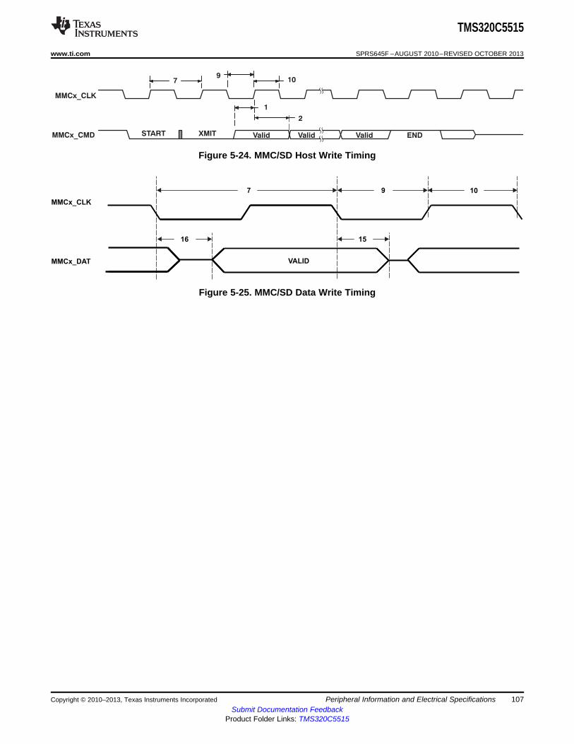
7 9 10
16 15
MMCx_CLK
MMCx_DAT VALID
START XMIT Valid Valid Valid END
MMCx_CLK
MMCx_CMD
109
7
1
2
TMS320C5515
www.ti.com SPRS645F –AUGUST 2010–REVISED OCTOBER 2013
Figure 5-24. MMC/SD Host Write Timing
Figure 5-25. MMC/SD Data Write Timing
Copyright © 2010–2013, Texas Instruments Incorporated Peripheral Information and Electrical Specifications 107Submit Documentation Feedback
Product Folder Links: TMS320C5515

TMS320C5515
SPRS645F –AUGUST 2010–REVISED OCTOBER 2013 www.ti.com
5.11 Real-Time Clock (RTC)The device includes a Real-Time Clock (RTC) with its own separated power supply and isolation circuits.The separate supply and isolation circuits allow the RTC to run with the least possible power consumption,called RTC only mode. The RTC only mode requires CVDDRTC, LDOI, and DVDDRTC power domains to bepowered, but other power domains can be shut off. See Section 5.11.1, RTC Only Mode for details. AllRTC registers are preserved (except for RTC Control and RTC Update Registers) and the countercontinues to operate when the device is powered off. The RTC also has the capability to wakeup thedevice from idle states via alarms, periodic interrupts, or an external WAKEUP input. Additionally, the RTCis able to output an alarm or periodic interrupt on the WAKEUP pin to cause external power managementto re-enable power to the DSP Core and I/O. Note: The RTC Core (CVDDRTC) must be powered by anexternal power source even though RTC is not used. None of the on-chip LDOs can power CVDDRTC.
The device RTC provides the following features:• 100-year calendar up to year 2099.• Counts seconds, minutes, hours, day of the week, date, month, and year with leap year compensation• Millisecond time correction• Binary-coded-decimal (BCD) representation of time, calendar, and alarm• 24-hour clock mode• Second, minute, hour, day, or week alarm interrupt• Periodic interrupt: every millisecond, second, minute, hour, or day• Alarm interrupt: precise time of day• Single interrupt to the DSP CPU• 32.768-kHz crystal oscillator with frequency calibration
Control of the RTC is maintained through a set of I/O memory mapped registers (see Table 5-25). Notethat any write to these registers will be synchronized to the RTC 32.768-KHz clock; thus, the CPU mustrun at least 3X faster than the RTC. Writes to these registers will not be evident until the next two 32.768-KHz clock cycles later. Furthermore, if the RTC Oscillator is disabled, no RTC register can be written to.
The RTC has its own power-on-reset (POR) circuit which resets the registers in the RTC core domainwhen power is first applied to the CVDDRTC power pin. The RTC flops are not reset by the device's RESETpin nor the digital core's POR (powergood signal).
The scratch registers in the RTC can be used to take advantage of this unique reset domain to keep trackof when the DSP boots and whether the RTC time registers have already been initialized to the currentclock time or whether the software needs to go into a routine to prompt the user to set the time/date.
5.11.1 RTC Only ModeThe maximum power saving can be achieved by using the RTC only mode. There are hardware andsoftware requirements to use the RTC only mode.
Hardware Requirements:• The DSP_LDO_EN pin must be tied to GND or pulled down to GND.• The RTC Core (CVDDRTC), RTC I/O (DVDDRTC), and LDO inputs (LDOI) must always be powered.• VDDA_ANA is recommended to be powered from the ANA_LDOO pin. If VDDA_ANA is powered
externally, then it must always be powered.• All other power domains can be totally shut down during the RTC only mode.• A high pulse for a minimum of one RTC clock period (30.5 µs) to the WAKEUP pin is required to wake
up the device from the RTC only mode.
108 Peripheral Information and Electrical Specifications Copyright © 2010–2013, Texas Instruments IncorporatedSubmit Documentation Feedback
Product Folder Links: TMS320C5515

TMS320C5515
www.ti.com SPRS645F –AUGUST 2010–REVISED OCTOBER 2013
Power Down Sequence:1. CPU must set the LDO_PD bit or the BG_PD bit in the RTCPMGT register (See Figure 5-26). Once
the LDO_PD bit or the BG_PD bit is set to 1, the DSP_LDOO will be internally shut off and it will causethe internal POR holds the internal POWERGOOD signal low, which creates isolation for RTC.
2. All of the device power domains can be shut down except RTC Core (CVDDRTC), RTC I/O(DVDDRTC), and LDO inputs (LDOI).
Wake-Up Sequence:1. When waking up the device, all power domains must be turned back on before or upon applying a
pulse to WAKEUP.2. A pulse (≥ 30.5 µs) must be applied to the WAKEUP pin (active high). When the WAKEUP pin is
asserted, the voltage on the DSP_LDOO pin will start ramping up at the positive level of WAKEUP andit is monitored by the internal POR. Until the voltage reaches to the threshold level, the internal PORwill hold the internal POWERGOOD signal low, which provides isolation to RTC during transitionperiod. Once the voltage reaches to the threshold level, the internal POR asserts the internalPOWERGOOD signal (logic level high) and it resets reset of the system and disables RTC isolationand enables CPU to communicate with RTC.
Figure 5-26. RTC Power Management Register (RTCPMGT) [1930h]
15 8Reserved
R-0
7 5 4 3 2 1 0Reserved WU_DOUT WU_DIR BG_PD LDO_PD RTCCLKOUTEN
R-0 R/W-1 R/W-0 R/W-0 R/W-0 R/W-0LEGEND: R/W = Read/Write; R = Read only; -n = value after reset
Table 5-24. RTCPMGT Register Bit DescriptionsBIT NAME DESCRIPTION15:5 RESERVED Reserved. Read-only, writes have no effect.
Wakeup output, active low/open-drain.4 WU_DOUT 0 = WAKEUP pin driven low.
1 = WAKEUP pin is in high-impedance (Hi-Z).Wakeup pin direction control.0 = WAKEUP pin configured as a input.1 = WAKEUP pin configured as a output.
3 WU_DIR Note: When the WAKEUP pin is configured as an input, it is active high. When the WAKEUP pin isconfigured as an output, is an open-drain that is active low and should be externally pulled-up via a10-kΩ resistor to DVDDRTC. WU_DIR must be configured as an input to allow the WAKEUP pin towake the device up from idle modes.Bandgap, on-chip LDOs, and the analog POR power down bit.This bit shuts down the on-chip LDOs (ANA_LDO, DSP_LDO, and USB_LDO), the Analog POR,and Bandgap reference. BG_PD and LDO_PD are only intended to be used when the internalLDOs supply power to the chip. If the internal LDOs are bypassed and not used then the BG_PDand LDO_PD power down mechanisms should not be used since POR gets powered down and thePOWERGOOD signal is not generated properly.
2 BG_PDAfter this bit is asserted, the on-chip LDOs, Analog POR, and the Bandgap reference can be re-enabled by the WAKEUP pin (high) or the RTC alarm interrupt. The Bandgap circuit will take about100 msec to charge the external 0.1 uF capacitor via the internal 326-kΩ resistor.
0 = On-chip LDOs, Analog POR, and Bandgap reference are enabled.1 = On-chip LDOs, Analog POR, and Bandgap reference are disabled (shutdown).
Copyright © 2010–2013, Texas Instruments Incorporated Peripheral Information and Electrical Specifications 109Submit Documentation Feedback
Product Folder Links: TMS320C5515

TMS320C5515
SPRS645F –AUGUST 2010–REVISED OCTOBER 2013 www.ti.com
Table 5-24. RTCPMGT Register Bit Descriptions (continued)BIT NAME DESCRIPTION
On-chip LDOs and Analog POR power down bit.This bit shuts down the on-chip LDOs (ANA_LDO, DSP_LDO, and USB_LDO) and the AnalogPOR. BG_PD and LDO_PD are only intended to be used when the internal LDOs supply power tothe chip. If the internal LDOs are bypassed and not used then the BG_PD and LDO_PD powerdown mechanisms should not be used since POR gets powered down and the POWERGOODsignal is not generated properly.1 LDO_PDAfter this bit is asserted, the on-chip LDOs and Analog POR can be re-enabled by the WAKEUPpin (high) or the RTC alarm interrupt. This bit keeps the Bandgap reference turned on to allow afaster wake-up time with the expense power consumption of the Bandgap reference.0 = On-chip LDOs and Analog POR are enabled.1 = On-chip LDOs and Analog POR are disabled (shutdown).Clockout output enable bit.
0 RTCCLKOUTEN 0 = Clock output disabled.1 = Clock output enabled.
110 Peripheral Information and Electrical Specifications Copyright © 2010–2013, Texas Instruments IncorporatedSubmit Documentation Feedback
Product Folder Links: TMS320C5515

TMS320C5515
www.ti.com SPRS645F –AUGUST 2010–REVISED OCTOBER 2013
5.11.2 RTC Peripheral Register DescriptionsTable 5-25 shows the RTC registers.
Table 5-25. Real-Time Clock (RTC) Registers
HEX ADDRESS ACRONYM REGISTER NAMERANGE1900h RTCINTEN RTC Interrupt Enable Register1901h RTCUPDATE RTC Update Register1904h RTCMIL Milliseconds Register1905h RTCMILA Milliseconds Alarm Register1908h RTCSEC Seconds Register1909h RTCSECA Seconds Alarm Register190Ch RTCMIN Minutes Register190Dh RTCMINA Minutes Alarm Register1910h RTCHOUR Hours Register1911h RTCHOURA Hours Alarm Register1914h RTCDAY Days Register1915h RTCDAYA Days Alarm Register1918h RTCMONTH Months Register1919h RTCMONTHA Months Alarm Register191Ch RTCYEAR Years Register191Dh RTCYEARA Years Alarm Register1920h RTCINTFL RTC Interrupt Flag Register1921h RTCNOPWR RTC Lost Power Status Register1924h RTCINTREG RTC Interrupt Register1928h RTCDRIFT RTC Compensation Register192Ch RTCOSC RTC Oscillator Register1930h RTCPMGT RTC Power Management Register1960h RTCSCR1 RTC LSW Scratch Register 11961h RTCSCR2 RTC MSW Scratch Register 21964h RTCSCR3 RTC LSW Scratch Register 31965h RTCSCR4 RTC MSW Scratch Register 4
5.11.2.1 RTC Electrical Data/Timing
For more detailed information on RTC electrical timings, specifically WAKEUP, see the Section 5.7.3,Reset Electrical Data/Timing.
Copyright © 2010–2013, Texas Instruments Incorporated Peripheral Information and Electrical Specifications 111Submit Documentation Feedback
Product Folder Links: TMS320C5515

TMS320C5515
SPRS645F –AUGUST 2010–REVISED OCTOBER 2013 www.ti.com
5.12 Inter-Integrated Circuit (I2C)The inter-integrated circuit (I2C) module provides an interface between the device and other devicescompliant with Philips Semiconductors Inter-IC bus (I2C-bus™) specification version 2.1. Externalcomponents attached to this 2-wire serial bus can transmit/receive 2 to 8-bit data to/from the DSP throughthe I2C module. The I2C port does not support CBUS compatible devices.
The I2C port supports the following features:• Compatible with Philips I2C Specification Revision 2.1 (January 2000)• Data Transfer Rate from 10 kbps to 400 kbps (Philips Fast-Mode Rate)• Noise Filter to Remove Noise 50 ns or Less• Seven- and Ten-Bit Device Addressing Modes• Master (Transmit/Receive) and Slave (Transmit/Receive) Functionality• One Read DMA Event and One Write DMA Event, which can be used by the DMA Controller• One Interrupt that can be used by the CPU• Slew-Rate Limited Open-Drain Output Buffers
The I2C module clock must be in the range from 6.7 MHz to 13.3 MHz. This is necessary for properoperation of the I2C module. With the I2C module clock in this range, the noise filters on the SDA andSCL pins suppress noise that has a duration of 50 ns or shorter. The I2C module clock is derived from theDSP clock divided by a programmable prescaler.
112 Peripheral Information and Electrical Specifications Copyright © 2010–2013, Texas Instruments IncorporatedSubmit Documentation Feedback
Product Folder Links: TMS320C5515

TMS320C5515
www.ti.com SPRS645F –AUGUST 2010–REVISED OCTOBER 2013
5.12.1 I2C Peripheral Register DescriptionsTable 5-26 shows the Inter-Integrated Circuit (I2C) registers.
Table 5-26. Inter-Integrated Circuit (I2C) Registers
HEX ADDRESS ACRONYM REGISTER NAMERANGE1A00h ICOAR I2C Own Address Register1A04h ICIMR I2C Interrupt Mask Register1A08h ICSTR I2C Interrupt Status Register1A0Ch ICCLKL I2C Clock Low-Time Divider Register1A10h ICCLKH I2C Clock High-Time Divider Register1A14h ICCNT I2C Data Count Register1A18h ICDRR I2C Data Receive Register1A1Ch ICSAR I2C Slave Address Register1A20h ICDXR I2C Data Transmit Register1A24h ICMDR I2C Mode Register1A28h ICIVR I2C Interrupt Vector Register1A2Ch ICEMDR I2C Extended Mode Register1A30h ICPSC I2C Prescaler Register1A34h ICPID1 I2C Peripheral Identification Register 11A38h ICPID2 I2C Peripheral Identification Register 2
Copyright © 2010–2013, Texas Instruments Incorporated Peripheral Information and Electrical Specifications 113Submit Documentation Feedback
Product Folder Links: TMS320C5515

10
8
4
3
7
12
5
6 14
2
3
13
Stop Start RepeatedStart
Stop
SDA
SCL
1
11 9
TMS320C5515
SPRS645F –AUGUST 2010–REVISED OCTOBER 2013 www.ti.com
5.12.2 I2C Electrical Data/Timing
Table 5-27. Timing Requirements for I2C Timings (1) (see Figure 5-27)CVDD = 1.05 VCVDD = 1.3 V
NO. STANDARD UNITFAST MODEMODEMIN MAX MIN MAX
1 tc(SCL) Cycle time, SCL 10 2.5 µsSetup time, SCL high before SDA low (for a repeated START2 tsu(SCLH-SDAL) 4.7 0.6 µscondition)Hold time, SCL low after SDA low (for a START and a3 th(SCLL-SDAL) 4 0.6 µsrepeated START condition)
4 tw(SCLL) Pulse duration, SCL low 4.7 1.3 µs5 tw(SCLH) Pulse duration, SCL high 4 0.6 µs6 tsu(SDAV-SCLH) Setup time, SDA valid before SCL high 250 100 (2) ns7 th(SDA-SCLL) Hold time, SDA valid after SCL low 0 (3) 0 (3) 0.9 (4) µs
Pulse duration, SDA high between STOP and START8 tw(SDAH) 4.7 1.3 µsconditions9 tr(SDA) Rise time, SDA (5) 1000 20 + 0.1Cb
(6) 300 ns10 tr(SCL) Rise time, SCL (5) 1000 20 + 0.1Cb
(6) 300 ns11 tf(SDA) Fall time, SDA (5) 300 20 + 0.1Cb
(6) 300 ns12 tf(SCL) Fall time, SCL (5) 300 20 + 0.1Cb
(6) 300 ns13 tsu(SCLH-SDAH) Setup time, SCL high before SDA high (for STOP condition) 4 0.6 µs14 tw(SP) Pulse duration, spike (must be suppressed) 0 50 ns15 Cb
(6) Capacitive load for each bus line 400 400 pF
(1) The I2C pins SDA and SCL do not feature fail-safe I/O buffers. These pins could potentially draw current when the device is powereddown. Also these pins are not 3.6 V-tolerant (their VIH cannot go above DVDDIO + 0.3 V).
(2) A Fast-mode I2C-bus™ device can be used in a Standard-mode I2C-bus system, but the requirement tsu(SDA-SCLH)≥ 250 ns must then bemet. This will automatically be the case if the device does not stretch the LOW period of the SCL signal. If such a device does stretchthe LOW period of the SCL signal, it must output the next data bit to the SDA line tr max + tsu(SDA-SCLH)= 1000 + 250 = 1250 ns(according to the Standard-mode I2C-Bus Specification) before the SCL line is released.
(3) A device must internally provide a hold time of at least 300 ns for the SDA signal (referred to the VIHmin of the SCL signal) to bridge theundefined region of the falling edge of SCL.
(4) The maximum th(SDA-SCLL) has only to be met if the device does not stretch the low period [tw(SCLL)] of the SCL signal.(5) The rise/fall times are measured at 30% and 70% of DVDDIO. The fall time is only slightly influenced by the external bus load (Cb) and
external pullup resistor. However, the rise time (tr) is mainly determined by the bus load capacitance and the value of the pullup resistor.The pullup resistor must be selected to meet the I2C rise and fall time values specified.
(6) Cb = total capacitance of one bus line in pF. If mixed with HS-mode devices, faster fall-times are allowed.
Figure 5-27. I2C Receive Timings
114 Peripheral Information and Electrical Specifications Copyright © 2010–2013, Texas Instruments IncorporatedSubmit Documentation Feedback
Product Folder Links: TMS320C5515

25
23
19
18
22
27
20
21
17
18
28
Stop Start RepeatedStart
Stop
SDA
SCL
16
26 24
TMS320C5515
www.ti.com SPRS645F –AUGUST 2010–REVISED OCTOBER 2013
Table 5-28. Switching Characteristics for I2C Timings (1) (see Figure 5-28)CVDD = 1.05 VCVDD = 1.3 V
NO. PARAMETER STANDARD UNITFAST MODEMODEMIN MAX MIN MAX
16 tc(SCL) Cycle time, SCL 10 2.5 µsDelay time, SCL high to SDA low (for a repeated START17 td(SCLH-SDAL) 4.7 0.6 µscondition)Delay time, SDA low to SCL low (for a START and a18 td(SDAL-SCLL) 4 0.6 µsrepeated START condition)
19 tw(SCLL) Pulse duration, SCL low 4.7 1.3 µs20 tw(SCLH) Pulse duration, SCL high 4 0.6 µs21 td(SDAV-SCLH) Delay time, SDA valid to SCL high 250 100 ns22 tv(SCLL-SDAV) Valid time, SDA valid after SCL low 0 0 0.9 µs
Pulse duration, SDA high between STOP and START23 tw(SDAH) 4.7 1.3 µsconditions24 tr(SDA) Rise time, SDA (2) 1000 20 + 0.1Cb
(1) 300 ns25 tr(SCL) Rise time, SCL (2) 1000 20 + 0.1Cb
(1) 300 ns26 tf(SDA) Fall time, SDA (2) 300 20 + 0.1Cb
(1) 300 ns27 tf(SCL) Fall time, SCL (2) 300 20 + 0.1Cb
(1) 300 ns28 td(SCLH-SDAH) Delay time, SCL high to SDA high (for STOP condition) 4 0.6 µs29 Cp Capacitance for each I2C pin 10 10 pF
(1) Cb = total capacitance of one bus line in pF. If mixed with HS-mode devices, faster fall-times are allowed.(2) The rise/fall times are measured at 30% and 70% of DVDDIO. The fall time is only slightly influenced by the external bus load (Cb) and
external pullup resistor. However, the rise time (tr) is mainly determined by the bus load capacitance and the value of the pullup resistor.The pullup resistor must be selected to meet the I2C rise and fall time values specified.
Figure 5-28. I2C Transmit Timings
Copyright © 2010–2013, Texas Instruments Incorporated Peripheral Information and Electrical Specifications 115Submit Documentation Feedback
Product Folder Links: TMS320C5515

TMS320C5515
SPRS645F –AUGUST 2010–REVISED OCTOBER 2013 www.ti.com
5.13 Universal Asynchronous Receiver/Transmitter (UART)The UART performs serial-to-parallel conversions on data received from an external peripheral device andparallel-to-serial conversions on data transmitted to an external peripheral device via a serial bus.
The device has one UART peripheral with the following features:• Programmable baud rates (frequency pre-scale values from 1 to 65535)• Fully programmable serial interface characteristics:
– 5, 6, 7, or 8-bit characters– Even, odd, or no PARITY bit generation and detection– 1, 1.5, or 2 STOP bit generation
• 16-byte depth transmitter and receiver FIFOs:– The UART can be operated with or without the FIFOs– 1, 4, 8, or 14 byte selectable receiver FIFO trigger level for autoflow control and DMA
• DMA signaling capability for both received and transmitted data• CPU interrupt capability for both received and transmitted data• False START bit detection• Line break generation and detection• Internal diagnostic capabilities:
– Loopback controls for communications link fault isolation– Break, parity, overrun, and framing error simulation
• Programmable autoflow control using CTS and RTS signals
5.13.1 UART Peripheral Register DescriptionsTable 5-29 shows the UART registers.
Table 5-29. UART Registers
HEX ADDRESS ACRONYM REGISTER NAMERANGE1B00h RBR Receiver Buffer Register (read only)1B00h THR Transmitter Holding Register (write only)1B02h IER Interrupt Enable Register1B04h IIR Interrupt Identification Register (read only)1B04h FCR FIFO Control Register (write only)1B06h LCR Line Control Register1B08h MCR Modem Control Register1B0Ah LSR Line Status Register1B0Ch MSR Modem Status Register1B0Eh SCR Scratch Register1B10h DLL Divisor LSB Latch1B12h DLH Divisor MSB Latch1B18h PWREMU_MGMT Power and Emulation Management Register
116 Peripheral Information and Electrical Specifications Copyright © 2010–2013, Texas Instruments IncorporatedSubmit Documentation Feedback
Product Folder Links: TMS320C5515

3
2
Start
Bit
Data Bits
UART_TXD
5
Data Bits
Bit
Start
4
UART_RXD
TMS320C5515
www.ti.com SPRS645F –AUGUST 2010–REVISED OCTOBER 2013
5.13.2 UART Electrical Data/Timing [Receive/Transmit]
Table 5-30. Timing Requirements for UART Receive (1) (2) (see Figure 5-29)CVDD = 1.05 V CVDD = 1.3 V
NO. UNITMIN MAX MIN MAX
4 tw(URXDB) Pulse duration, receive data bit (UART_RXD) [15/30/100 pF] U - 3.5 U + 3 U - 3.5 U + 3 ns5 tw(URXSB) Pulse duration, receive start bit [15/30/100 pF] U - 3.5 U + 3 U - 3.5 U + 3 ns
(1) U = UART baud time = 1/programmed baud rate.(2) These parametric values are measured at DVDDIO = 3.3 V, 2.75 V, and 2.5 V
Table 5-31. Switching Characteristics Over Recommended Operating Conditions for UART Transmit (1) (2)
(see Figure 5-29)CVDD = 1.05 V CVDD = 1.3V
NO. PARAMETER UNITMIN MAX MIN MAX
1 f(baud) Maximum programmable bit rate 3.75 6.25 MHz2 tw(UTXDB) Pulse duration, transmit data bit (UART_TXD) [15/30/100 pF] U - 3.5 U + 4 U - 3.5 U + 4 ns3 tw(UTXSB) Pulse duration, transmit start bit [15/30/100 pF] U - 3.5 U + 4 U - 3.5 U + 4 ns
(1) U = UART baud time = 1/programmed baud rate.(2) These parametric values are measured at DVDDIO = 3.3 V, 2.75 V, and 2.5 V
Figure 5-29. UART Transmit/Receive Timing
Copyright © 2010–2013, Texas Instruments Incorporated Peripheral Information and Electrical Specifications 117Submit Documentation Feedback
Product Folder Links: TMS320C5515

TMS320C5515
SPRS645F –AUGUST 2010–REVISED OCTOBER 2013 www.ti.com
5.14 Inter-IC Sound (I2S)The device I2S peripherals allow serial transfer of full-duplex streaming data, usually audio data, betweenthe device and an external I2S peripheral device such as an audio codec.
The device supports 4 independent dual-channel I2S peripherals, each with the following features:• Full-duplex (transmit and receive) dual-channel communication• Double buffered data registers that allow for continuous data streaming• I2S/Left-justified and DSP data format with a data delay of 1 or 2 bits• Data word-lengths of 8, 10, 12, 14, 16, 18, 20, 24, or 32 bits• Ability to sign-extend received data samples for easy use in signal processing algorithms• Programmable polarity for both frame synchronization and bit clocks• Stereo (in I2S/Left-justified or DSP data formats) or mono (in DSP data format) mode• Detection of over-run, under-run, and frame-sync error conditions
5.14.1 I2S Peripheral Register DescriptionsTable 5-32 through Table 5-35 show the I2S0 through I2S3 registers.
Table 5-32. I2S0 Registers
HEX ADDRESS ACRONYM REGISTER NAMERANGE2800h I2S0SCTRL I2S0 Serializer Control Register2804h I2S0SRATE I2S0 Sample Rate Generator Register2808h I2S0TXLT0 I2S0 Transmit Left Data 0 Register2809h I2S0TXLT1 I2S0 Transmit Left Data 1 Register280Ch I2S0TXRT0 I2S0 Transmit Right Data 0 Register280Dh I2S0TXRT1 I2S0 Transmit Right Data 1 Register2810h I2S0INTFL I2S0 Interrupt Flag Register2814h I2S0INTMASK I2S0 Interrupt Mask Register2828h I2S0RXLT0 I2S0 Receive Left Data 0 Register2829h I2S0RXLT1 I2S0 Receive Left Data 1 Register282Ch I2S0RXRT0 I2S0 Receive Right Data 0 Register282Dh I2S0RXRT1 I2S0 Receive Right Data 1 Register
Table 5-33. I2S1 Registers
HEX ADDRESS ACRONYM REGISTER NAMERANGE2900h I2S1SCTRL I2S1 Serializer Control Register2904h I2S1SRATE I2S1 Sample Rate Generator Register2908h I2S1TXLT0 I2S1 Transmit Left Data 0 Register2909h I2S1TXLT1 I2S1 Transmit Left Data 1 Register290Ch I2S1TXRT0 I2S1 Transmit Right Data 0 Register290Dh I2S1TXRT1 I2S1 Transmit Right Data 1 Register2910h I2S1INTFL I2S1 Interrupt Flag Register2914h I2S1INTMASK I2S1 Interrupt Mask Register2928h I2S1RXLT0 I2S1 Receive Left Data 0 Register2929h I2S1RXLT1 I2S1 Receive Left Data 1 Register292Ch I2S1RXRT0 I2S1 Receive Right Data 0 Register292Dh I2S1RXRT1 I2S1 Receive Right Data 1 Register
118 Peripheral Information and Electrical Specifications Copyright © 2010–2013, Texas Instruments IncorporatedSubmit Documentation Feedback
Product Folder Links: TMS320C5515

TMS320C5515
www.ti.com SPRS645F –AUGUST 2010–REVISED OCTOBER 2013
Table 5-34. I2S2 Registers
HEX ADDRESS ACRONYM REGISTER NAMERANGE2A00h I2S2SCTRL I2S2 Serializer Control Register2A04h I2S2SRATE I2S2 Sample Rate Generator Register2A08h I2S2TXLT0 I2S2 Transmit Left Data 0 Register2A09h I2S2TXLT1 I2S2 Transmit Left Data 1 Register2A0Ch I2S2TXRT0 I2S2 Transmit Right Data 0 Register2A0Dh I2S2TXRT1 I2S2 Transmit Right Data 1 Register2A10h I2S2INTFL I2S2 Interrupt Flag Register2A14h I2S2INTMASK I2S2 Interrupt Mask Register2A28h I2S2RXLT0 I2S2 Receive Left Data 0 Register2A29h I2S2RXLT1 I2S2 Receive Left Data 1 Register2A2Ch I2S2RXRT0 I2S2 Receive Right Data 0 Register2A2Dh I2S2RXRT1 I2S2 Receive Right Data 1 Register
Table 5-35. I2S3 Registers
HEX ADDRESS ACRONYM REGISTER NAMERANGE2B00h I2S3SCTRL I2S3 Serializer Control Register2B04h I2S3SRATE I2S3 Sample Rate Generator Register2B08h I2S3TXLT0 I2S3 Transmit Left Data 0 Register2B09h I2S3TXLT1 I2S3 Transmit Left Data 1 Register2B0Ch I2S3TXRT0 I2S3 Transmit Right Data 0 Register2B0Dh I2S3TXRT1 I2S3 Transmit Right Data 1 Register2B10h I2S3INTFL I2S3 Interrupt Flag Register2B14h I2S3INTMASK I2S3 Interrupt Mask Register2B28h I2S3RXLT0 I2S3 Receive Left Data 0 Register2B29h I2S3RXLT1 I2S3 Receive Left Data 1 Register2B2Ch I2S3RXRT0 I2S3 Receive Right Data 0 Register2B2Dh I2S3RXRT1 I2S3 Receive Right Data 1 Register
Copyright © 2010–2013, Texas Instruments Incorporated Peripheral Information and Electrical Specifications 119Submit Documentation Feedback
Product Folder Links: TMS320C5515
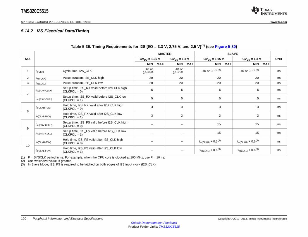
TMS320C5515
SPRS645F –AUGUST 2010–REVISED OCTOBER 2013 www.ti.com
5.14.2 I2S Electrical Data/Timing
Table 5-36. Timing Requirements for I2S [I/O = 3.3 V, 2.75 V, and 2.5 V] (1) (see Figure 5-30)
MASTER SLAVENO. CVDD = 1.05 V CVDD = 1.3 V CVDD = 1.05 V CVDD = 1.3 V UNIT
MIN MAX MIN MAX MIN MAX MIN MAX40 or 40 or1 tc(CLK) Cycle time, I2S_CLK 40 or 2P (1) (2) 40 or 2P (1) (2) ns2P (1) (2) 2P (1) (2)
2 tw(CLKH) Pulse duration, I2S_CLK high 20 20 20 20 ns3 tw(CLKL) Pulse duration, I2S_CLK low 20 20 20 20 ns
Setup time, I2S_RX valid before I2S CLK hightsu(RXV-CLKH) 5 5 5 5 ns(CLKPOL = 0)7
Setup time, I2S_RX valid before I2S_CLK lowtsu(RXV-CLKL) 5 5 5 5 ns(CLKPOL = 1)Hold time, I2S_RX valid after I2S_CLK highth(CLKH-RXV) 3 3 3 3 ns(CLKPOL = 0)
8Hold time, I2S_RX valid after I2S_CLK lowth(CLKL-RXV) 3 3 3 3 ns(CLKPOL = 1)Setup time, I2S_FS valid before I2S_CLK hightsu(FSV-CLKH) – – 15 15 ns(CLKPOL = 0)
9Setup time, I2S_FS valid before I2S_CLK lowtsu(FSV-CLKL) – – 15 15 ns(CLKPOL = 1)Hold time, I2S_FS valid after I2S_CLK highth(CLKH-FSV) – – tw(CLKH) + 0.6 (3) tw(CLKH) + 0.6 (3) ns(CLKPOL = 0)
10Hold time, I2S_FS valid after I2S_CLK lowth(CLKL-FSV) – – tw(CLKL) + 0.6 (3) tw(CLKL) + 0.6 (3) ns(CLKPOL = 1)
(1) P = SYSCLK period in ns. For example, when the CPU core is clocked at 100 MHz, use P = 10 ns.(2) Use whichever value is greater.(3) In Slave Mode, I2S_FS is required to be latched on both edges of I2S input clock (I2S_CLK).
120 Peripheral Information and Electrical Specifications Copyright © 2010–2013, Texas Instruments IncorporatedSubmit Documentation Feedback
Product Folder Links: TMS320C5515

TMS320C5515
www.ti.com SPRS645F –AUGUST 2010–REVISED OCTOBER 2013
Table 5-37. Timing Requirements for I2S [I/O = 1.8 V] (1) (see Figure 5-30)
MASTER SLAVENO. CVDD = 1.05 V CVDD = 1.3 V CVDD = 1.05 V CVDD = 1.3 V UNIT
MIN MAX MIN MAX MIN MAX MIN MAX50 or 2P (1) 40 or 2P (1)
1 tc(CLK) Cycle time, I2S_CLK 50 or 2P (1) (2) 40 or 2P (1) (2) ns(2) (2)
2 tw(CLKH) Pulse duration, I2S_CLK high 25 20 25 20 ns3 tw(CLKL) Pulse duration, I2S_CLK low 25 20 25 20 ns
Setup time, I2S_RX valid before I2S CLKtsu(RXV-CLKH) 5 5 5 5 nshigh (CLKPOL = 0)7
Setup time, I2S_RX valid before I2S_CLKtsu(RXV-CLKL) 5 5 5 5 nslow (CLKPOL = 1)Hold time, I2S_RX valid after I2S_CLK highth(CLKH-RXV) 3 3 3 3 ns(CLKPOL = 0)
8Hold time, I2S_RX valid after I2S_CLK lowth(CLKL-RXV) 3 3 3 3 ns(CLKPOL = 1)Setup time, I2S_FS valid before I2S_CLKtsu(FSV-CLKH) – – 15 15 nshigh (CLKPOL = 0)
9Setup time, I2S_FS valid before I2S_CLKtsu(FSV-CLKL) – – 15 15 nslow (CLKPOL = 1)Hold time, I2S_FS valid after I2S_CLK high tw(CLKH) + tw(CLKH) +th(CLKH-FSV) – – ns(CLKPOL = 0) 0.6 (3) 0.6 (3)
10Hold time, I2S_FS valid after I2S_CLK low tw(CLKL) + tw(CLKL) +th(CLKL-FSV) – – ns(CLKPOL = 1) 0.6 (3) 0.6 (3)
(1) P = SYSCLK period in ns. For example, when the CPU core is clocked at 100 MHz, use P = 10 ns.(2) Use whichever value is greater.(3) In Slave Mode, I2S_FS is required to be latched on both edges of I2S input clock (I2S_CLK).
Copyright © 2010–2013, Texas Instruments Incorporated Peripheral Information and Electrical Specifications 121Submit Documentation Feedback
Product Folder Links: TMS320C5515

TMS320C5515
SPRS645F –AUGUST 2010–REVISED OCTOBER 2013 www.ti.com
Table 5-38. Switching Characteristics Over Recommended Operating Conditions for I2S Output[I/O = 3.3 V, 2.75 V, or 2.5 V] (see Figure 5-30)
MASTER SLAVENO. PARAMETER CVDD = 1.05 V CVDD = 1.3 V CVDD = 1.05 V CVDD = 1.3 V UNIT
MIN MAX MIN MAX MIN MAX MIN MAX40 or 40 or 40 or 40 or1 tc(CLK) Cycle time, I2S_CLK ns2P (1) (2) 2P (1) (2) 2P (1) (2) 2P (1) (2)
tw(CLKH) Pulse duration, I2S_CLK high (CLKPOL = 0) 20 20 20 20 ns2
tw(CLKL) Pulse duration, I2S_CLK low (CLKPOL = 1) 20 20 20 20 nstw(CLKL) Pulse duration, I2S_CLK low (CLKPOL = 0) 20 20 20 20 ns
3tw(CLKH) Pulse duration, I2S_CLK high (CLKPOL = 1) 20 20 20 20 nstdmax(CLKL-DXV) Output Delay time, I2S_CLK low to I2S_DX valid (CLKPOL = 0) 0 15 0 14 0 15 0 15 ns
4tdmax(CLKH-DXV) Output Delay time, I2S_CLK high to I2S_DX valid (CLKPOL = 1) 0 15 0 14 0 15 0 15 nstdmax(CLKL-FSV) Delay time, I2S_CLK low to I2S_FS valid (CLKPOL = 0) -1.1 14 -1.1 14 – – ns
5tdmax(CLKH-FSV) Delay time, I2S_CLK high to I2S_FS valid (CLKPOL = 1) -1.1 14 -1.1 14 – – ns
(1) P = SYSCLK period in ns. For example, when the CPU core is clocked at 100 MHz, use P = 10 ns.(2) Use whichever value is greater.
122 Peripheral Information and Electrical Specifications Copyright © 2010–2013, Texas Instruments IncorporatedSubmit Documentation Feedback
Product Folder Links: TMS320C5515

TMS320C5515
www.ti.com SPRS645F –AUGUST 2010–REVISED OCTOBER 2013
Table 5-39. Switching Characteristics Over Recommended Operating Conditions for I2S Output[I/O = 1.8 V] (see Figure 5-30)
MASTER SLAVENO. PARAMETER CVDD = 1.05 V CVDD = 1.3 V CVDD = 1.05 V CVDD = 1.3 V UNIT
MIN MAX MIN MAX MIN MAX MIN MAX50 or 40 or 50 or 40 or1 tc(CLK) Cycle time, I2S_CLK ns2P (1) (2) 2P (1) (2) 2P (1) (2) 2P (1) (2)
tw(CLKH) Pulse duration, I2S_CLK high (CLKPOL = 0) 25 20 25 20 ns2
tw(CLKL) Pulse duration, I2S_CLK low (CLKPOL = 1) 25 20 25 20 nstw(CLKL) Pulse duration, I2S_CLK low (CLKPOL = 0) 25 20 25 20 ns
3tw(CLKH) Pulse duration, I2S_CLK high (CLKPOL = 1) 25 20 25 20 nstdmax(CLKL-DXV) Output Delay time, I2S_CLK low to I2S_DX valid (CLKPOL = 0) 0 19 0 14 0 19 0 16.5 ns
4tdmax(CLKH-DXV) Output Delay time, I2S_CLK high to I2S_DX valid (CLKPOL = 1) 0 19 0 14 0 19 0 16.5 nstdmax(CLKL-FSV) Delay time, I2S_CLK low to I2S_FS valid (CLKPOL = 0) -1.1 14 -1.1 14 – – ns
5tdmax(CLKH-FSV) Delay time, I2S_CLK high to I2S_FS valid (CLKPOL = 1) -1.1 14 -1.1 14 – – ns
(1) P = SYSCLK period in ns. For example, when the CPU core is clocked at 100 MHz, use P = 10 ns.(2) Use whichever value is greater.
Copyright © 2010–2013, Texas Instruments Incorporated Peripheral Information and Electrical Specifications 123Submit Documentation Feedback
Product Folder Links: TMS320C5515

I2S_CLK(CLKPOL = 0)
I2S_CLK(CLKPOL = 1)
I2S_RX
I2S_DX
1 3 2
5
7 8
9
4
I2S_FS(Output, MODE = 1)
I2S_FS(Input, MODE = 0)
10
TMS320C5515
SPRS645F –AUGUST 2010–REVISED OCTOBER 2013 www.ti.com
Figure 5-30. I2S Input and Output Timings
124 Peripheral Information and Electrical Specifications Copyright © 2010–2013, Texas Instruments IncorporatedSubmit Documentation Feedback
Product Folder Links: TMS320C5515

TMS320C5515
www.ti.com SPRS645F –AUGUST 2010–REVISED OCTOBER 2013
5.15 Liquid Crystal Display Controller (LCDC)The device includes a LCD Interface Display Driver (LIDD) controller.
The LIDD Controller supports the asynchronous LCD interface and has the following features:• Provides full-timing programmability of control signals and output data
Note: Raster mode is not supported on this device.
The LCD controller is responsible for generating the correct external timing. The DMA engine provides aconstant flow of data from the frame buffers to the external LCD panel via the LIDD controller. In addition,CPU access is provided to read and write registers.
5.15.1 LCDC Peripheral Register DescriptionsTable 5-40 shows the LCDC peripheral registers.
Table 5-40. LCD Controller Registers
CPU WORD ACRONYM REGISTER DESCRIPTIONADDRESS2E00h LCDREVMIN LCD Minor Revision Register2E01h LCDREVMAJ LCD Major Revision Register2E04h LCDCR LCD Control Register2E08h LCDSR LCD Status Register2E0Ch LCDLIDDCR LCD LIDD Control Register2E10h LCDLIDDCS0CONFIG0 LCD LIDD CS0 Configuration Register 02E11h LCDLIDDCS0CONFIG1 LCD LIDD CS0 Configuration Register 12E14h LCDLIDDCS0ADDR LCD LIDD CS0 Address Read/Write Register2E18h LCDLIDDCS0DATA LCD LIDD CS0 Data Read/Write Register2E1Ch LCDLIDDCS1CONFIG0 LCD LIDD CS1 Configuration Register 02E1Dh LCDLIDDCS1CONFIG1 LCD LIDD CS1 Configuration Register 12E20h LCDLIDDCS1ADDR LCD LIDD CS1 Address Read/Write Register2E24h LCDLIDDCS1DATA LCD LIDD CS1 Data Read/Write Register
2E28h – 2E3Ah — Reserved2E40h LCDDMACR LCD DMA Control Register2E44h LCDDMAFB0BAR0 LCD DMA Frame Buffer 0 Base Address Register 02E45h LCDDMAFB0BAR1 LCD DMA Frame Buffer 0 Base Address Register 12E48h LCDDMAFB0CAR0 LCD DMA Frame Buffer 0 Ceiling Address Register 02E49h LCDDMAFB0CAR1 LCD DMA Frame Buffer 0 Ceiling Address Register 12E4Ch LCDDMAFB1BAR0 LCD DMA Frame Buffer 1 Base Address Register 02E4Dh LCDDMAFB1BAR1 LCD DMA Frame Buffer 1 Base Address Register 12E50h LCDDMAFB1CAR0 LCD DMA Frame Buffer 1 Ceiling Address Register 02E51h LCDDMAFB1CAR1 LCD DMA Frame Buffer 1 Ceiling Address Register 1
Copyright © 2010–2013, Texas Instruments Incorporated Peripheral Information and Electrical Specifications 125Submit Documentation Feedback
Product Folder Links: TMS320C5515

TMS320C5515
SPRS645F –AUGUST 2010–REVISED OCTOBER 2013 www.ti.com
5.15.2 LCDC Electrical Data/Timing
Table 5-41. Timing Requirements for LCD LIDD Mode (1) (see Figure 5-31 through Figure 5-38)
CVDD = 1.05 V CVDD = 1.3 VNO. UNIT
MIN MAX MIN MAXSetup time, LCD_D[15:0] valid16 tsu(LCD_D-CLK) 27 42 nsbefore LCD_CLK rising edgeHold time, LCD_D[15:0] valid after17 th(CLK-LCD_D) 0 0 nsLCD_CLK rising edge
(1) Over operating free-air temperature range (unless otherwise noted)
Table 5-42. Switching Characteristics Over Recommended Operating Conditions for LCD LIDD Mode (seeFigure 5-31 through Figure 5-38)
CVDD = 1.05 V CVDD = 1.3 VNO. PARAMETER UNIT
MIN MAX MIN MAXDelay time, LCD_CLK rising edge4 td(LCD_D_V) 5 7 nsto LCD_D[15:0] valid (write)Delay time, LCD_CLK rising edge5 td(LCD_D_I) -6 -6 nsto LCD_D[15:0] invalid (write)Delay time, LCD_CLK rising edge6 td(LCD_E_A) 5 7 nsto LCD_CSx_Ex lowDelay time, LCD_CLKrising edge7 td(LCD_E_I) -6 -6 nsto LCD_CSx_Ex highDelay time, LCD_CLKrising edge8 td(LCD_A_A) 5 7 nsto LCD_RS lowDelay time, LCD_CLK rising edge9 td(LCD_A_I) -6 -6 nsto LCD_RS highDelay time, LCD_CLK rising edge10 td(LCD_W_A) 5 7 nsto LCD_RW_WRB lowDelay time, LCD_CLK rising edge11 td(LCD_W_I) -6 -6 nsto LCD_RW_WRB highDelay time, LCD_CLK rising edge12 td(LCD_STRB_A) 5 7 nsto LCD_EN_RDB highDelay time, LCD_CLK rising edge13 td(LCD_STRB_I) -6 -6 nsto LCD_EN_RDB lowDelay time, LCD_CLK rising edge14 td(LCD_D_Z) 5 7 nsto LCD_D[15:0] in 3-stateDelay time, LCD_CLK rising edge15 td(Z_LCD_D) -6 -6 nsto LCD_D[15:0] valid from 3-state
126 Peripheral Information and Electrical Specifications Copyright © 2010–2013, Texas Instruments IncorporatedSubmit Documentation Feedback
Product Folder Links: TMS320C5515

LCD_CSx_Ex
LCD_RS
LCD_RW_WRB
R_SU
R_STROBE R_HOLD
(0–31)
(1–63) (1–5)
CS_DELAY
(0-3)
RS
R/W
W_SU W_STROBE
W_HOLD
(0–31) (1–63)
(1–15)
CS_DELAY
(0 - 3)
8 9
12 13
10 11
LCD_D[7:0]
14 1716
Read
Data
15 4 5
E0E1
12 13
Data[7:0]Write Instruction
LCD_CLK[Internal]
LCD_CSx_Ex
W_SU(0 to 31) W_STROBE
(1 to 63) W_HOLD(1 to 15)
CS_DELAY
(0 to 3)R_SU
(0 to 31)R_STROBE
(1 to 63)
R_HOLD(1 to 15) CS_DELAY
(0 to 3)
4
Write Data
5 14
16
17
15
Data[7:0]
8 9
10 11
12
13
12
13
RS
R/W
E0E1
LCD_D[15:0]
LCD_RS
LCD_RW_WRB
Read Status
LCD_CLK[Internal]
TMS320C5515
www.ti.com SPRS645F –AUGUST 2010–REVISED OCTOBER 2013
Figure 5-31. Character Display HD44780 Write
Figure 5-32. Character Display HD44780 Read
Copyright © 2010–2013, Texas Instruments Incorporated Peripheral Information and Electrical Specifications 127Submit Documentation Feedback
Product Folder Links: TMS320C5515

LCD_D[15:0]
LCD_CSx_Ex
(async mode)
LCD_RS
LCD_RW_WRB
LCD_EN_RDB
4
W_SU W_STROBE
W_HOLD
(0-31) (1-63)
(1-15)
CS_DELAY
(0-3)
CS0CS1
RS
R/W
EN
W_SU W_STROBE
W_HOLD
(0-31) (1-63)
(1-15)
CS_DELAY
(0-3)
5 4 5
6 7 6 7
8 9
12 13
Write Address Write Data
12 13
10 11 10 11
Data[15:0]
LCD_CLK[Internal]
TMS320C5515
SPRS645F –AUGUST 2010–REVISED OCTOBER 2013 www.ti.com
Figure 5-33. Micro-Interface Graphic Display 6800 Write
128 Peripheral Information and Electrical Specifications Copyright © 2010–2013, Texas Instruments IncorporatedSubmit Documentation Feedback
Product Folder Links: TMS320C5515

LCD_D[15:0]
LCD_CSx_Ex
(Async Mode)
LCD_RS
LCD_RW_WRB
LCD_EN_RDB
4
W_SU W_STROBE
W_HOLD
(0-31) (1-63)
(1-15)
CS_DELAY
(0-3)
CS0CS1
RS
R/W
EN
R_SU
R_STROBE R_HOLD
(0-31)
(1-63 (1-15)
CS_DELAY
(0-3)
5 14 15
6 7 6 7
8 9
12 13
1716
Write Address
Read
Data
10 11
1213
Data[15:0]
LCD_CLK[Internal]
TMS320C5515
www.ti.com SPRS645F –AUGUST 2010–REVISED OCTOBER 2013
Figure 5-34. Micro-Interface Graphic Display 6800 Read
Copyright © 2010–2013, Texas Instruments Incorporated Peripheral Information and Electrical Specifications 129Submit Documentation Feedback
Product Folder Links: TMS320C5515

ReadData
LCD_D[15:0]
LCD_CSx_Ex
(Async Mode)
LCD_RS
LCD_RW_WRB
LCD_EN_RDB
R_SU
R_STROBE R_HOLD
(0-31)
(1-63) (1-15)
CS_DELAY
(0-3)
CS0
CS1
RS
R/W
EN
R_STROBE R_HOLD
(1-63) (1-15)
CS_DELAY
(0-3)
14 15
6 7 6 7
8 9
12 13
171614 1716 15
12 13
Data[15:0]
R_SU(0-31)
Read
Status
LCD_CLK[Internal]
TMS320C5515
SPRS645F –AUGUST 2010–REVISED OCTOBER 2013 www.ti.com
Figure 5-35. Micro-Interface Graphic Display 6800 Status
130 Peripheral Information and Electrical Specifications Copyright © 2010–2013, Texas Instruments IncorporatedSubmit Documentation Feedback
Product Folder Links: TMS320C5515

LCD_D[15:0]
LCD_CSx_Ex
(Async Mode)
LCD_RS
LCD_RW_WRB
LCD_EN_RDB
4
W_SU W_STROBE
W_HOLD
(0-31) (1-63)
(1-15)
CS_DELAY
(0-3)
DATA[15:0]
CS0
CS1
RS
WRB
RDB
W_SU W_STROBE
W_HOLD
(0-31) (1-63)
(1-15)
CS_DELAY
(0 - 3)
5 4 5
6 7 6 7
8 9
10 11
Write Address Write Data
10 11
LCD_CLK[Internal]
TMS320C5515
www.ti.com SPRS645F –AUGUST 2010–REVISED OCTOBER 2013
Figure 5-36. Micro-Interface Graphic Display 8080 Write
Copyright © 2010–2013, Texas Instruments Incorporated Peripheral Information and Electrical Specifications 131Submit Documentation Feedback
Product Folder Links: TMS320C5515

LCD_D[15:0]
LCD_CSx_Ex
(async mode)
LCD_RS
LCD_RW_WRB
LCD_EN_RDB
4
W_SU W_STROBE
W_HOLD
(0-31) (1-63)
(1-15)
CS_DELAY
(0-3)
CS0
CS1
RS
WRB
RDB
R_SU
R_STROBE R_HOLD
(0-31)
(1-63) (1-15)
CS_DELAY
(0-3)
5 14 15
6 7 6 7
8 9
12 13
1716
ReadData
10 11
Data[15:0]Write Address
LCD_CLK[Internal]
TMS320C5515
SPRS645F –AUGUST 2010–REVISED OCTOBER 2013 www.ti.com
Figure 5-37. Micro-Interface Graphic Display 8080 Read
132 Peripheral Information and Electrical Specifications Copyright © 2010–2013, Texas Instruments IncorporatedSubmit Documentation Feedback
Product Folder Links: TMS320C5515

LCD_D[15:0]
LCD_CSx_Ex
LCD_RS
LCD_RW_WRB
LCD_PCLK
R_SU
R_STROBE R_HOLD
(0-31)
(1-63) (1-15)
CS_DELAY
(0-3)
CS0
CS1
RS
WRB
RDB
R_STROBE R_HOLD
(1-63) (1-15)
CS_DELAY
(0-3)
14 15
6 7 6
8
12 13
1716
Read Status
14 1716
Read Data
15
12 13
Data[15:0]
7
9
R_SU(0-31)
LCD_CLK[Internal]
TMS320C5515
www.ti.com SPRS645F –AUGUST 2010–REVISED OCTOBER 2013
Figure 5-38. Micro-Interface Graphic Display 8080 Status
Copyright © 2010–2013, Texas Instruments Incorporated Peripheral Information and Electrical Specifications 133Submit Documentation Feedback
Product Folder Links: TMS320C5515

TMS320C5515
SPRS645F –AUGUST 2010–REVISED OCTOBER 2013 www.ti.com
5.16 10-Bit SAR ADCThe device includes a 10-bit SAR ADC using a switched capacitor architecture which converts an analoginput signal to a digital value at a maximum rate of 62.5-k samples per second (ksps) for use by the DSP.This SAR module supports six channels that are connected to four general purpose analog pins (GPAIN[3:0]) which can be used as general purpose outputs.
The device SAR supports the following features:• Up to 62.5 ksps (2-MHz clock with 32 cycles per conversion)• Single conversion and continuous back-to-back conversion modes• Interrupt driven or polling conversion or DMA event generation• Internal configurable bandgap reference voltages of 1 V or 0.8 V; or external Vref of VDDA_ANA
• One 3.6-V Tolerant analog input (GPAIN0) with internal voltage division for conversion of batteryvoltage
• Software controlled power down• Individually configurable general-purpose digital outputs
5.16.1 SAR ADC Peripheral Register DescriptionsTable 5-43 shows the SAR ADC peripheral registers.
Table 5-43. SAR Analog Control Registers
CPU WORD ACRONYM REGISTER DESCRIPTIONADDRESS7012h SARCTRL SAR A/D Control Register7014h SARDATA SAR A/D Data Register7016h SARCLKCTRL SAR A/D Clock Control Register7018h SARPINCTRL SAR A/D Reference and Pin Control Register701Ah SARGPOCTRL SAR A/D GPO Control Register
5.16.2 SAR ADC Electrical Data/Timing
Table 5-44. Switching Characteristics Over Recommended Operating Conditions for ADC CharacteristicsCVDD = 1.3 VCVDD = 1.05 VNO. PARAMETER UNIT
MIN TYP MAX1 tC(SCLC) Cycle time, ADC internal conversion clock 2 MHz3 td(CONV) Delay time, ADC conversion time 32tC(SCLC) ns4 SDNL Static differential non-linearity error (DNL measured for 9 bits) ±0.6 LSB5 SINL Static integral non-linearity error ±1 LSB6 Zset Zero-scale offset error (INL measured for 9 bits) 2 LSB7 Fset Full-scale offset error 2 LSB8 Analog input impedance 1 MΩ9 Signal-to-noise ratio 54 dB
134 Peripheral Information and Electrical Specifications Copyright © 2010–2013, Texas Instruments IncorporatedSubmit Documentation Feedback
Product Folder Links: TMS320C5515

TMS320C5515
www.ti.com SPRS645F –AUGUST 2010–REVISED OCTOBER 2013
5.17 Serial Port Interface (SPI)The device serial port interface (SPI) is a high-speed synchronous serial input/output port that allows aserial bit stream of programmed length (1 to 32 bits) to be shifted into and out of the device at aprogrammed bit-transfer rate. The SPI supports multi-chip operation of up to four SPI slave devices. TheSPI can operate as a master device only, slave mode is not supported. Note: The SPI is not supported bythe device DMA controller, so DMA cannot be used in transferring data between the SPI and the on-chipRAM.
The SPI is normally used for communication between the DSP and external peripherals. Typicalapplications include an interface to external I/O or peripheral expansion via devices such as shift registers,display drivers, SPI EEPROMs, and analog-to-digital converters.
The SPI has the following features:• Programmable divider for serial data clock generation• Four pin interface (SPI_CLK, SPI_CSn, SPI_RX, and SPI_TX)• Programmable data length (1 to 32 bits)• 4 external chip select signals• Programmable transfer or frame size (1 to 4096 characters)• Optional interrupt generation on character completion• Programmable SPI_CSn to SPI_TX delay from 0 to 3 SPI_CLK cycles• Programmable signal polarities• Programmable active clock edge• Internal loopback mode for testing
5.17.1 SPI Peripheral Register DescriptionsTable 5-45 shows the SPI registers.
Table 5-45. SPI Module Registers
CPUWORD ACRONYM REGISTER NAME
ADDRESS3000h SPICDR Clock Divider Register3001h SPICCR Clock Control Register3002h SPIDCR1 Device Configuration Register 13003h SPIDCR2 Device Configuration Register 23004h SPICMD1 Command Register 13005h SPICMD2 Command Register 23006h SPISTAT1 Status Register 13007h SPISTAT2 Status Register 23008h SPIDAT1 Data Register 13009h SPIDAT2 Data Register 2
Copyright © 2010–2013, Texas Instruments Incorporated Peripheral Information and Electrical Specifications 135Submit Documentation Feedback
Product Folder Links: TMS320C5515

SPI_CS
SPI_TX
SPI_CLK
SPI_RX
2 8 3
B0
1
B0
B1
B1
7
Bn-2
Bn-2
Bn-1
Bn-1
65
4
TMS320C5515
SPRS645F –AUGUST 2010–REVISED OCTOBER 2013 www.ti.com
5.17.2 SPI Electrical Data/Timing
Table 5-46. Timing Requirements for SPI Inputs (see Figure 5-39 through Figure 5-42)CVDD = 1.05 V CVDD = 1.3 V
NO. UNITMIN MAX MIN MAX
66.4 or 40 or4 tC(SCLK) Cycle time, SPI_CLK ns4P (1) (2) 4P (1) (2)
5 tw(SCLKH) Pulse duration, SPI_CLK high 30 19 ns6 tw(SCLKL) Pulse duration, SPI_CLK low 30 19 ns
Setup time, SPI_RX valid before SPI_CLK high, SPI Mode 0 16.1 13.9 nsSetup time, SPI_RX valid before SPI_CLK low, SPI Mode 1 16.1 13.9 ns
7 tsu(SRXV-SCLK) Setup time, SPI_RX valid before SPI_CLK high, SPI Mode 2 16.1 13.9 nsSetup time, SPI_RX valid before SPI_CLK high, SPI Mode 3 16.1 13.9 nsHold time, SPI_RX valid after SPI_CLK high, SPI Mode 0 0 0 nsHold time, SPI_RX valid after SPI_CLK low, SPI Mode 1 0 0 ns
8 th(SCLK-SRXV) Hold time, SPI_RX valid after SPI_CLK low, SPI Mode 2 0 0 nsHold time, SPI_RX valid after SPI_CLK high, SPI Mode 3 0 0 ns
(1) P = SYSCLK period in ns. For example, when the CPU core is clocked at 100 MHz, use P = 10 ns.(2) Use whichever value is greater.
Table 5-47. Switching Characteristics Over Recommended Operating Conditions for SPI Outputs(see Figure 5-39 through Figure 5-42)
CVDD = 1.05 V CVDD = 1.3 VNO. PARAMETER UNIT
MIN MAX MIN MAXDelay time, SPI_CLK low to SPI_TX valid, SPI -4.2 8.9 -4.9 5.3 nsMode 0Delay time, SPI_CLK high to SPI_TX valid, SPI -4.2 8.9 -4.9 5.3 nsMode 1
1 td(SCLK-STXV) Delay time, SPI_CLK high to SPI_TX valid, SPI -4.2 8.9 -4.9 5.3 nsMode 2Delay time, SPI_CLK low to SPI_TX valid, SPI -4.2 8.9 -4.9 5.3 nsMode 3
2 td(SPICS-SCLK) Delay time, SPI_CS active to SPI_CLK active tC - 8 + D (1) tC - 8 + D (1) nsOutput hold time, SPI_CS inactive to SPI_CLK3 toh(SCLKI-SPICSI) 0.5tC - 2.2 0.5tC - 2.2 nsinactive
(1) D is the programable data delay in ns. Data delay can be programmed to 0, 1, 2, or 3 SPICLK clock cycles.
A. Character length is programmable between 1 and 32 bits; 8-bit character length shown.B. Polarity of SPI_CSn is configurable, active-low polarity is shown.
Figure 5-39. SPI Mode 0 Transfer (CKPn = 0, CKPHn = 0)
136 Peripheral Information and Electrical Specifications Copyright © 2010–2013, Texas Instruments IncorporatedSubmit Documentation Feedback
Product Folder Links: TMS320C5515

7 82 3
B0 B1 Bn-2 Bn-1
SPI_CS
SPI_TX
SPI_CLK
SPI_RX
56
4
1
B0 B1 Bn-2 Bn-1
SPI_CS
SPI_TX
SPI_CLK
SPI_RX
6
B0
1
B1 Bn-2 Bn-1
5
4
87 3
B0 B1 Bn-2 Bn-1
2
7 82 3
B0 B1 Bn-2 Bn-1
SPI_CS
SPI_TX
SPI_CLK
SPI_RX
65
4
1
B1 B1 Bn-2 Bn-1
TMS320C5515
www.ti.com SPRS645F –AUGUST 2010–REVISED OCTOBER 2013
A. Character length is programmable between 1 and 32 bits; 8-bit character length shown.B. Polarity of SPI_CSn is configurable, active-low polarity is shown.
Figure 5-40. SPI Mode 1 Transfer (CKPn = 0, CKPHn = 1)
A. Character length is programmable between 1 and 32 bits; 8-bit character length shown.B. Polarity of SPI_CSn is configurable, active-low polarity is shown.
Figure 5-41. SPI Mode 2 Transfer (CKPn = 1, CKPHn = 0)
A. Character length is programmable between 1 and 32 bits; 8-bit character length shown.B. Polarity of SPI_CSn is configurable, active-low polarity is shown.
Figure 5-42. SPI Mode 3 Transfer (CKPn = 1, CKPHn = 1)
Copyright © 2010–2013, Texas Instruments Incorporated Peripheral Information and Electrical Specifications 137Submit Documentation Feedback
Product Folder Links: TMS320C5515

TMS320C5515
SPRS645F –AUGUST 2010–REVISED OCTOBER 2013 www.ti.com
5.18 Universal Serial Bus (USB) 2.0 ControllerThe device USB2.0 peripheral supports the following features:• USB2.0 peripheral at speeds high-speed (480 Mb/s) and full-speed (12 Mb/s)• All transfer modes (control, bulk, interrupt, and isochronous asynchronous mode)• 4 Transmit (TX) and 4 Receive (RX) Endpoints in addition to Control Endpoint 0• FIFO RAM
– 4K endpoint– Programmable size
• Integrated USB2.0 High Speed PHY• RNDIS mode for accelerating RNDIS type protocols using short packet termination over USB
The USB2.0 peripheral on this device, does not support:• Host Mode (Peripheral/Device Modes supported only)• On-Chip Charge Pump• On-the-Go (OTG) Mode
138 Peripheral Information and Electrical Specifications Copyright © 2010–2013, Texas Instruments IncorporatedSubmit Documentation Feedback
Product Folder Links: TMS320C5515

TMS320C5515
www.ti.com SPRS645F –AUGUST 2010–REVISED OCTOBER 2013
5.18.1 USB2.0 Peripheral Register DescriptionsTable 5-48 lists of the USB2.0 peripheral registers.
Table 5-48. Universal Serial Bus (USB) Registers (1)
CPU WORD ACRONYM REGISTER DESCRIPTIONADDRESS8000h REVID1 Revision Identification Register 18001h REVID2 Revision Identification Register 28004h CTRLR Control Register8008h STATR Status Register800Ch EMUR Emulation Register8010h MODER1 Mode Register 18011h MODER2 Mode Register 28014h AUTOREQ Auto Request Register8018h SRPFIXTIME1 SRP Fix Time Register 18019h SRPFIXTIME2 SRP Fix Time Register 2801Ch TEARDOWN1 Teardown Register 1801Dh TEARDOWN2 Teardown Register 28020h INTSRCR1 USB Interrupt Source Register 18021h INTSRCR2 USB Interrupt Source Register 28024h INTSETR1 USB Interrupt Source Set Register 18025h INTSETR2 USB Interrupt Source Set Register 28028h INTCLRR1 USB Interrupt Source Clear Register 18029h INTCLRR2 USB Interrupt Source Clear Register 2802Ch INTMSKR1 USB Interrupt Mask Register 1802Dh INTMSKR2 USB Interrupt Mask Register 28030h INTMSKSETR1 USB Interrupt Mask Set Register 18031h INTMSKSETR2 USB Interrupt Mask Set Register 28034h INTMSKCLRR1 USB Interrupt Mask Clear Register 18035h INTMSKCLRR2 USB Interrupt Mask Clear Register 28038h INTMASKEDR1 USB Interrupt Source Masked Register 18039h INTMASKEDR2 USB Interrupt Source Masked Register 2803Ch EOIR USB End of Interrupt Register8040h INTVECTR1 USB Interrupt Vector Register 18041h INTVECTR2 USB Interrupt Vector Register 28050h GREP1SZR1 Generic RNDIS EP1Size Register 18051h GREP1SZR2 Generic RNDIS EP1Size Register 28054h GREP2SZR1 Generic RNDIS EP2 Size Register 18055h GREP2SZR2 Generic RNDIS EP2 Size Register 28058h GREP3SZR1 Generic RNDIS EP3 Size Register 18059h GREP3SZR2 Generic RNDIS EP3 Size Register 2805Ch GREP4SZR1 Generic RNDIS EP4 Size Register 1805Dh GREP4SZR2 Generic RNDIS EP4 Size Register 2
(1) Before reading or writing to the USB registers, be sure to set the BYTEMODE bits to "00b" in the USB system control register to enableword accesses to the USB registers .
Copyright © 2010–2013, Texas Instruments Incorporated Peripheral Information and Electrical Specifications 139Submit Documentation Feedback
Product Folder Links: TMS320C5515

TMS320C5515
SPRS645F –AUGUST 2010–REVISED OCTOBER 2013 www.ti.com
Table 5-48. Universal Serial Bus (USB) Registers(1) (continued)CPU WORD ACRONYM REGISTER DESCRIPTIONADDRESS
Common USB Registers8401h FADDR_POWER Function Address Register, Power Management Register8402h INTRTX Interrupt Register for Endpoint 0 plus Transmit Endpoints 1 to 48405h INTRRX Interrupt Register for Receive Endpoints 1 to 48406h INTRTXE Interrupt enable register for INTRTX8409h INTRRXE Interrupt Enable Register for INTRRX840Ah INTRUSB_INTRUSBE Interrupt Register for Common USB Interrupts, Interrupt Enable Register840Dh FRAME Frame Number Register840Eh Index Register for Selecting the Endpoint Status and Control Registers, Register toINDEX_TESTMODE Enable the USB 2.0 Test Modes
USB Indexed Registers8411h Maximum Packet Size for Peripheral/Host Transmit Endpoint. (Index register set toTXMAXP_INDX select Endpoints 1-4)8412h Control Status Register for Endpoint 0 in Peripheral Mode. (Index register set toPERI_CSR0_INDX select Endpoint 0)
Control Status Register for Peripheral Transmit Endpoint. (Index register set to selectPERI_TXCSR_INDX Endpoints 1-4)8415h Maximum Packet Size for Peripheral/Host Receive Endpoint. (Index register set toRXMAXP_INDX select Endpoints 1-4)8416h Control Status Register for Peripheral Receive Endpoint. (Index register set to selectPERI_RXCSR_INDX Endpoints 1-4)8419h Number of Received Bytes in Endpoint 0 FIFO. (Index register set to select EndpointCOUNT0_INDX 0)
Number of Bytes in Host Receive Endpoint FIFO. (Index register set to selectRXCOUNT_INDX Endpoints 1- 4)841Ah - Reserved841Dh - Reserved841Eh CONFIGDATA_INDC Returns details of core configuration. (index register set to select Endpoint 0)
(Upper byte of 841Eh)USB FIFO Registers
8421h FIFO0R1 Transmit and Receive FIFO Register 1 for Endpoint 08422h FIFO0R2 Transmit and Receive FIFO Register 2 for Endpoint 08425h FIFO1R1 Transmit and Receive FIFO Register 1 for Endpoint 18426h FIFO1R2 Transmit and Receive FIFO Register 2 for Endpoint 18429h FIFO2R1 Transmit and Receive FIFO Register 1 for Endpoint 2842Ah FIFO2R2 Transmit and Receive FIFO Register 2 for Endpoint 2842Dh FIFO3R1 Transmit and Receive FIFO Register 1 for Endpoint 3842Eh FIFO3R2 Transmit and Receive FIFO Register 2 for Endpoint 38431h FIFO4R1 Transmit and Receive FIFO Register 1 for Endpoint 48432h FIFO4R2 Transmit and Receive FIFO Register 2 for Endpoint 4
Dynamic FIFO Control Registers8461h - Reserved8462h Transmit Endpoint FIFO Size, Receive Endpoint FIFO Size (Index register set toTXFIFOSZ_RXFIFOSZ select Endpoints 1-4)8465h TXFIFOADDR Transmit Endpoint FIFO Address (Index register set to select Endpoints 1-4)8466h RXFIFOADDR Receive Endpoint FIFO Address (Index register set to select Endpoints 1-4)846Dh - Reserved
140 Peripheral Information and Electrical Specifications Copyright © 2010–2013, Texas Instruments IncorporatedSubmit Documentation Feedback
Product Folder Links: TMS320C5515

TMS320C5515
www.ti.com SPRS645F –AUGUST 2010–REVISED OCTOBER 2013
Table 5-48. Universal Serial Bus (USB) Registers(1) (continued)CPU WORD ACRONYM REGISTER DESCRIPTIONADDRESS
Control and Status Register for Endpoint 08501h - Reserved8502h PERI_CSR0 Control Status Register for Peripheral Endpoint 08505h - Reserved8506h - Reserved8509h COUNT0 Number of Received Bytes in Endpoint 0 FIFO850Ah - Reserved850Dh - Reserved
CONFIGDATA Returns details of core configuration.850Eh (Upper byte of 850Eh)Control and Status Register for Endpoint 1
8511h TXMAXP Maximum Packet Size for Peripheral/Host Transmit Endpoint8512h PERI_TXCSR Control Status Register for Peripheral Transmit Endpoint (peripheral mode)8515h RXMAXP Maximum Packet Size for Peripheral/Host Receive Endpoint8516h PERI_RXCSR Control Status Register for Peripheral Receive Endpoint (peripheral mode)8519h RXCOUNT Number of Bytes in the Receiving Endpoint's FIFO851Ah - Reserved851Dh - Reserved851Eh - Reserved
Control and Status Register for Endpoint 28521h TXMAXP Maximum Packet Size for Peripheral/Host Transmit Endpoint8522h PERI_TXCSR Control Status Register for Peripheral Transmit Endpoint (peripheral mode)8525h RXMAXP Maximum Packet Size for Peripheral/Host Receive Endpoint8526h PERI_RXCSR Control Status Register for Peripheral Receive Endpoint (peripheral mode)8529h RXCOUNT Number of Bytes in Host Receive endpoint FIFO852Ah - Reserved852Dh - Reserved852Eh - Reserved
Control and Status Register for Endpoint 38531h TXMAXP Maximum Packet Size for Peripheral/Host Transmit Endpoint8532h PERI_TXCSR Control Status Register for Peripheral Transmit Endpoint (peripheral mode)8535h RXMAXP Maximum Packet Size for Peripheral/Host Receive Endpoint8536h PERI_RXCSR Control Status Register for Peripheral Receive Endpoint (peripheral mode)8539h RXCOUNT Number of Bytes in Host Receive endpoint FIFO853Ah - Reserved853Dh - Reserved853Eh - Reserved
Control and Status Register for Endpoint 48541h TXMAXP Maximum Packet Size for Peripheral/Host Transmit Endpoint8542h PERI_TXCSR Control Status Register for Peripheral Transmit Endpoint (peripheral mode)8545h RXMAXP Maximum Packet Size for Peripheral/Host Receive Endpoint8546h PERI_RXCSR Control Status Register for Peripheral Receive Endpoint (peripheral mode)8549h RXCOUNT Number of Bytes in Host Receive endpoint FIFO854Ah - Reserved854Dh - Reserved854Eh - Reserved
Copyright © 2010–2013, Texas Instruments Incorporated Peripheral Information and Electrical Specifications 141Submit Documentation Feedback
Product Folder Links: TMS320C5515

TMS320C5515
SPRS645F –AUGUST 2010–REVISED OCTOBER 2013 www.ti.com
Table 5-48. Universal Serial Bus (USB) Registers(1) (continued)CPU WORD ACRONYM REGISTER DESCRIPTIONADDRESS
CPPI DMA (CMDA) Registers9000h - Reserved9001h - Reserved9004h TDFDQ CDMA Teardown Free Descriptor Queue Control Register9008h DMAEMU CDMA Emulation Control Register9800h TXGCR1[0] Transmit Channel 0 Global Configuration Register 19801h TXGCR2[0] Transmit Channel 0 Global Configuration Register 29808h RXGCR1[0] Receive Channel 0 Global Configuration Register 19809h RXGCR2[0] Receive Channel 0 Global Configuration Register 2980Ch RXHPCR1A[0] Receive Channel 0 Host Packet Configuration Register 1 A980Dh RXHPCR2A[0] Receive Channel 0 Host Packet Configuration Register 2 A9810h RXHPCR1B[0] Receive Channel 0 Host Packet Configuration Register 1 B9811h RXHPCR2B[0] Receive Channel 0 Host Packet Configuration Register 2 B9820h TXGCR1[1] Transmit Channel 1 Global Configuration Register 19821h TXGCR2[1] Transmit Channel 1 Global Configuration Register 29828h RXGCR1[1] Receive Channel 1 Global Configuration Register 19829h RXGCR2[1] Receive Channel 1 Global Configuration Register 2982Ch RXHPCR1A[1] Receive Channel 1 Host Packet Configuration Register 1 A982Dh RXHPCR2A[1] Receive Channel 1 Host Packet Configuration Register 2 A9830h RXHPCR1B[1] Receive Channel 1 Host Packet Configuration Register 1 B9831h RXHPCR2B[1] Receive Channel 1 Host Packet Configuration Register 2 B9840h TXGCR1[2] Transmit Channel 2 Global Configuration Register 19841h TXGCR2[2] Transmit Channel 2 Global Configuration Register 29848h RXGCR1[2] Receive Channel 2 Global Configuration Register 19849h RXGCR2[2] Receive Channel 2 Global Configuration Register 2984Ch RXHPCR1A[2] Receive Channel 2 Host Packet Configuration Register 1 A984Dh RXHPCR2A[2] Receive Channel 2 Host Packet Configuration Register 2 A9850h RXHPCR1B[2] Receive Channel 2 Host Packet Configuration Register 1 B9851h RXHPCR2B[2] Receive Channel 2 Host Packet Configuration Register 2 B9860h TXGCR1[3] Transmit Channel 3 Global Configuration Register 19861h TXGCR2[3] Transmit Channel 3 Global Configuration Register 29868h RXGCR1[3] Receive Channel 3 Global Configuration Register 19869h RXGCR2[3] Receive Channel 3 Global Configuration Register 2986Ch RXHPCR1A[3] Receive Channel 3 Host Packet Configuration Register 1 A986Dh RXHPCR2A[3] Receive Channel 3 Host Packet Configuration Register 2 A9870h RXHPCR1B[3] Receive Channel 3 Host Packet Configuration Register 1 B9871h RXHPCR2B[3] Receive Channel 3 Host Packet Configuration Register 2 BA000h DMA_SCHED_CTRL1 CDMA Scheduler Control Register 1A001h DMA_SCHED_CTRL2 CDMA Scheduler Control Register 1
A800h + 4 × N ENTRYLSW[N] CDMA Scheduler Table Word N Registers LSW (N = 0 to 63)A801h + 4 × N ENTRYMSW[N] CDMA Scheduler Table Word N Registers MSW (N = 0 to 63)
142 Peripheral Information and Electrical Specifications Copyright © 2010–2013, Texas Instruments IncorporatedSubmit Documentation Feedback
Product Folder Links: TMS320C5515

TMS320C5515
www.ti.com SPRS645F –AUGUST 2010–REVISED OCTOBER 2013
Table 5-48. Universal Serial Bus (USB) Registers(1) (continued)CPU WORD ACRONYM REGISTER DESCRIPTIONADDRESS
Queue Manager (QMGR) RegistersC000h - ReservedC001h - ReservedC008h DIVERSION1 Queue Manager Queue Diversion Register 1C009h DIVERSION2 Queue Manager Queue Diversion Register 2C020h FDBSC0 Queue Manager Free Descriptor/Buffer Starvation Count Register 0C021h FDBSC1 Queue Manager Free Descriptor/Buffer Starvation Count Register 1C024h FDBSC2 Queue Manager Free Descriptor/Buffer Starvation Count Register 2C025h FDBSC3 Queue Manager Free Descriptor/Buffer Starvation Count Register 3C028h FDBSC4 Queue Manager Free Descriptor/Buffer Starvation Count Register 4C029h FDBSC5 Queue Manager Free Descriptor/Buffer Starvation Count Register 5C02Ch FDBSC6 Queue Manager Free Descriptor/Buffer Starvation Count Register 6C02Dh FDBSC7 Queue Manager Free Descriptor/Buffer Starvation Count Register 7C080h LRAM0BASE1 Queue Manager Linking RAM Region 0 Base Address Register 1C081h LRAM0BASE2 Queue Manager Linking RAM Region 0 Base Address Register 2C084h LRAM0SIZE Queue Manager Linking RAM Region 0 Size RegisterC085h - ReservedC088h LRAM1BASE1 Queue Manager Linking RAM Region 1 Base Address Register 1C089h LRAM1BASE2 Queue Manager Linking RAM Region 1 Base Address Register 2C090h PEND0 Queue Manager Queue Pending 0C091h PEND1 Queue Manager Queue Pending 1C094h PEND2 Queue Manager Queue Pending 2C095h PEND3 Queue Manager Queue Pending 3C098h PEND4 Queue Manager Queue Pending 4C099h PEND5 Queue Manager Queue Pending 5
D000h + 16 × R QMEMRBASE1[R] Queue Manager Memory Region R Base Address Register 1 (R = 0 to 15)D001h + 16 × R QMEMRBASE2[R] Queue Manager Memory Region R Base Address Register 2 (R = 0 to 15)D004h + 16 × R QMEMRCTRL1[R] Queue Manager Memory Region R Control Register (R = 0 to 15)D005h + 16 × R QMEMRCTRL2[R] Queue Manager Memory Region R Control Register (R = 0 to 15)E000h + 16 × N CTRL1A Queue Manager Queue N Control Register 1A (N = 0 to 63)E001h + 16 × N CTRL2A Queue Manager Queue N Control Register 2A (N = 0 to 63)E004h + 16 × N CTRL1B Queue Manager Queue N Control Register 1B (N = 0 to 63)E005h + 16 × N CTRL2B Queue Manager Queue N Control Register 2B (N = 0 to 63)E008h + 16 × N CTRL1C Queue Manager Queue N Control Register 1C (N = 0 to 63)E009h + 16 × N CTRL2C Queue Manager Queue N Control Register 2C (N = 0 to 63)E00Ch + 16 × N CTRL1D Queue Manager Queue N Control Register 1D (N = 0 to 63)E00Dh + 16 × N CTRL2D Queue Manager Queue N Control Register 2D (N = 0 to 63)E800h + 16 × N QSTAT1A Queue Manager Queue N Status Register 1A (N = 0 to 63)E801h + 16 × N QSTAT2A Queue Manager Queue N Status Register 2A (N = 0 to 63)E804h + 16 × N QSTAT1B Queue Manager Queue N Status Register 1B (N = 0 to 63)E805h + 16 × N QSTAT2B Queue Manager Queue N Status Register 2B (N = 0 to 63)E808h + 16 × N QSTAT1C Queue Manager Queue N Status Register 1C (N = 0 to 63)E809h + 16 × N QSTAT1C Queue Manager Queue N Status Register 2C (N = 0 to 63)
Copyright © 2010–2013, Texas Instruments Incorporated Peripheral Information and Electrical Specifications 143Submit Documentation Feedback
Product Folder Links: TMS320C5515

trtf
VCRS90% VOH
10% VOL
USB_DM
USB_DP
tper - tjr
TMS320C5515
SPRS645F –AUGUST 2010–REVISED OCTOBER 2013 www.ti.com
5.18.2 USB 2.0 Electrical Data/Timing
Table 5-49. Switching Characteristics Over Recommended Operating Conditions for USB 2.0 (seeFigure 5-43)
CVDD = 1.05 VCVDD = 1.3 V
NO. PARAMETER FULL SPEED HIGH SPEED UNIT12 Mbps 480 Mbps (1)
MIN MAX MIN MAX1 tr(D) Rise time, USB_DP and USB_DM signals (2) 4 20 0.5 ns2 tf(D) Fall time, USB_DP and USB_DM signals (2) 4 20 0.5 ns3 trfM Rise/Fall time, matching (3) 90 111 – – %4 VCRS Output signal cross-over voltage (2) 1.3 2 – – V7 tw(EOPT) Pulse duration, EOP transmitter (4) 160 175 – – ns8 tw(EOPR) Pulse duration, EOP receiver (4) 82 – ns9 t(DRATE) Data Rate 12 480 Mb/s10 ZDRV Driver Output Resistance 40.5 49.5 40.5 49.5 Ω11 ZINP Receiver Input Impedance 100k - - Ω
(1) For more detailed information, see the Universal Serial Bus Specification, Revision 2.0, Chapter 7.(2) Full Speed and High Speed CL = 50 pF(3) tRFM = (tr/tf) x 100. [Excluding the first transaction from the Idle state.](4) Must accept as valid EOP
Figure 5-43. USB2.0 Integrated Transceiver Interface Timing
144 Peripheral Information and Electrical Specifications Copyright © 2010–2013, Texas Instruments IncorporatedSubmit Documentation Feedback
Product Folder Links: TMS320C5515

TMS320C5515
www.ti.com SPRS645F –AUGUST 2010–REVISED OCTOBER 2013
5.19 General-Purpose TimersThe device has three 32-bit software programmable Timers. Each timer can be used as a general-purpose (GP) timer. Timer2 can be configured as either a GP or a Watchdog (WD) or both. General-
purpose timers are typically used to provide interrupts to the CPU to schedule periodic tasks or a delayedtask. A watchdog timer is used to reset the CPU in case it gets into an infinite loop. The GP timers are 32-bit timers with a 13-bit prescaler that can divide the CPU clock and uses this scaled value as a referenceclock. These timers can be used to generate periodic interrupts. The Watchdog Timer is a 16-bit counterwith a 16-bit prescaler used to provide a recovery mechanism for the device in the event of a faultcondition, such as a non-exiting code loop.
The device Timers support the following:• 32-bit Programmable Countdown Timer• 13-bit Prescaler Divider• Timer Modes:
– 32-bit General-Purpose Timer– 32-bit Watchdog Timer (Timer2 only)
• Auto Reload Option• Generates Single Interrupt to CPU (The interrupt is individually latched to determine which timer
triggered the interrupt.)• Generates Active Low Pulse to the Hardware Reset (Watchdog only)• Interrupt can be used for DMA Event
5.19.1 Timers Peripheral Register DescriptionsTable 5-50 through Table 5-53 show the Timer and Watchdog registers.
Table 5-50. Watchdog Timer Registers (Timer2 only)
CPU WORD ACRONYM REGISTER DESCRIPTIONADDRESS1880h WDKCKLK Watchdog Kick Lock Register1882h WDKICK Watchdog Kick Register1884h WDSVLR Watchdog Start Value Lock Register1886h WDSVR Watchdog Start Value Register1888h WDENLOK Watchdog Enable Lock Register188Ah WDEN Watchdog Enable Register188Ch WDPSLR Watchdog Prescale Lock Register188Eh WDPS Watchdog Prescale Register
Table 5-51. General-Purpose Timer 0 Registers
CPU WORD ACRONYM REGISTER DESCRIPTIONADDRESS1810h TCR Timer 0 Control Register1812h TIMPRD1 Timer 0 Period Register 11813h TIMPRD2 Timer 0 Period Register 21814h TIMCNT1 Timer 0 Counter Register 11815h TIMCNT2 Timer 0 Counter Register 2
Copyright © 2010–2013, Texas Instruments Incorporated Peripheral Information and Electrical Specifications 145Submit Documentation Feedback
Product Folder Links: TMS320C5515

TMS320C5515
SPRS645F –AUGUST 2010–REVISED OCTOBER 2013 www.ti.com
Table 5-52. General-Purpose Timer 1 Registers
CPU WORD ACRONYM REGISTER DESCRIPTIONADDRESS1850h TCR Timer 1 Control Register1852h TIMPRD1 Timer 1 Period Register 11853h TIMPRD2 Timer 1 Period Register 21854h TIMCNT1 Timer 1 Counter Register 11855h TIMCNT2 Timer 1 Counter Register 2
Table 5-53. General-Purpose Timer 2 Registers
CPU WORD ACRONYM REGISTER DESCRIPTIONADDRESS1890h TCR Timer 2 Control Register1892h TIMPRD1 Timer 2 Period Register 11893h TIMPRD2 Timer 2 Period Register 21894h TIMCNT1 Timer 2 Counter Register 11895h TIMCNT2 Timer 2 Counter Register 2
146 Peripheral Information and Electrical Specifications Copyright © 2010–2013, Texas Instruments IncorporatedSubmit Documentation Feedback
Product Folder Links: TMS320C5515

TMS320C5515
www.ti.com SPRS645F –AUGUST 2010–REVISED OCTOBER 2013
5.20 General-Purpose Input/OutputThe GPIO peripheral provides general-purpose pins that can be configured as either inputs or outputs.When configured as an output, you can write to an internal register to control the state driven on theoutput pin. When configured as an input, you can detect the state of the input by reading the state of theinternal register. The GPIO can also be used to send interrupts to the CPU.
The GPIO peripheral supports the following:• Up to 26 GPIOs plus 1 general-purpose output (XF) and 4 Special-Purpose Outputs for Use With SAR• The 26 GPIO pins have internal pulldowns (IPDs) which can be individually disabled• The 26 GPIOs can be configured to generate edge detected interrupts to the CPU on either the rising
or falling edge
The device GPIO pin functions are multiplexed with various other signals. For more detailed informationon what signals are multiplexed with the GPIO and how to configure them, see Section 2.5, TerminalFunctions and Section 3, Device Configuration of this document.
Copyright © 2010–2013, Texas Instruments Incorporated Peripheral Information and Electrical Specifications 147Submit Documentation Feedback
Product Folder Links: TMS320C5515

TMS320C5515
SPRS645F –AUGUST 2010–REVISED OCTOBER 2013 www.ti.com
5.20.1 General-Purpose Input/Output Peripheral Register DescriptionsThe external parallel port interface includes a 16-bit general purpose I/O that can be individuallyprogrammed as input or output with interrupt capability. Control of the general purpose I/O is maintainedthrough a set of I/O memory-mapped registers shown in Table 5-54.
Table 5-54. GPIO Registers
HEX ADDRESS ACRONYM REGISTER NAMERANGE1C06h IODIR1 GPIO Direction Register 11C07h IODIR2 GPIO Direction Register 21C08h IOINDATA1 GPIO Data In Register 11C09h IOINDATA2 GPIO Data In Register 21C0Ah IODATAOUT1 GPIO Data Out Register 11C0Bh IODATAOUT2 GPIO Data Out Register 21C0Ch IOINTEDG1 GPIO Interrupt Edge Trigger Enable Register 11C0Dh IOINTEDG2 GPIO Interrupt Edge Trigger Enable Register 21C0Eh IOINTEN1 GPIO Interrupt Enable Register 11C0Fh IOINTEN2 GPIO Interrupt Enable Register 21C10h IOINTFLG1 GPIO Interrupt Flag Register 11C11h IOINTFLG2 GPIO Interrupt Flag Register 2
148 Peripheral Information and Electrical Specifications Copyright © 2010–2013, Texas Instruments IncorporatedSubmit Documentation Feedback
Product Folder Links: TMS320C5515

GP[x] Input
(With IOINTEDGy = 0)
4
3
2
1
GP[x] Output
GP[x] Input
(With IOINTEDGy = 1)
2
1
TMS320C5515
www.ti.com SPRS645F –AUGUST 2010–REVISED OCTOBER 2013
5.20.2 GPIO Peripheral Input/Output Electrical Data/Timing
Table 5-55. Timing Requirements for GPIO Inputs (1) (see Figure 5-44)CVDD = 1.05 VCVDD = 1.3 VNO. UNIT
MIN MAX1 tw(ACTIVE) Pulse duration, GPIO input/external interrupt pulse active 2C (1) (2) ns2 tw(INACTIVE) Pulse duration, GPIO input/external interrupt pulse inactive C (1) (2) ns
(1) The pulse width given is sufficient to get latched into the GPIO_IFR register and to generate an interrupt. However, if a user wants tohave the device recognize the GPIO changes through software polling of the GPIO Data In (GPIO_DIN) register, the GPIO durationmust be extended to allow the device enough time to access the GPIO register through the internal bus.
(2) C = SYSCLK period in ns. For example, when running parts at 100 MHz, use C = 10 ns.
Table 5-56. Switching Characteristics Over Recommended Operating Conditions for GPIO Outputs(see Figure 5-44)
CVDD = 1.05 VCVDD = 1.3 VNO. PARAMETER UNIT
MIN MAX3 tw(GPOH) Pulse duration, GP[x] output high 3C (1) (2) ns4 tw(GPOL) Pulse duration, GP[x] output low 3C (1) (2) ns
(1) This parameter value should not be used as a maximum performance specification. Actual performance of back-to-back accesses of theGPIO is dependent upon internal bus activity.
(2) C = SYSCLK period in ns. For example, when running parts at 100 MHz, use C = 10 ns.
Figure 5-44. GPIO Port Timing
Copyright © 2010–2013, Texas Instruments Incorporated Peripheral Information and Electrical Specifications 149Submit Documentation Feedback
Product Folder Links: TMS320C5515

TMS320C5515
SPRS645F –AUGUST 2010–REVISED OCTOBER 2013 www.ti.com
5.20.3 GPIO Peripheral Input Latency Electrical Data/Timing
Table 5-57. Timing Requirements for GPIO Input Latency (1)
CVDD = 1.05 VCVDD = 1.3 VNO. UNIT
MIN MAXPolling GPIO_DIN register 5 cyc
1 tL(GPI) Latency, GP[x] input Polling GPIO_IFR register 7 cycInterrupt Detection 8 cyc
(1) The pulse width given is sufficient to generate a CPU interrupt. However, if a user wants to have the device recognize the GP[x] inputchanges through software polling of the GPIO register, the GP[x] input duration must be extended to allow device enough time to accessthe GPIO register through the internal bus.
150 Peripheral Information and Electrical Specifications Copyright © 2010–2013, Texas Instruments IncorporatedSubmit Documentation Feedback
Product Folder Links: TMS320C5515

TMS320C5515
www.ti.com SPRS645F –AUGUST 2010–REVISED OCTOBER 2013
5.21 IEEE 1149.1 JTAGThe JTAG interface is used for Boundary-Scan testing and emulation of the device.
TRST should only to be deasserted when it is necessary to use a JTAG controller to debug the device orexercise the device's boundary scan functionality.
The device includes an internal pulldown (IPD) on the TRST pin to ensure that TRST will always beasserted upon power up and the device's internal emulation logic will always be properly initialized. It isalso recommended that an external pulldown be added to ensure proper device operation when anemulation or boundary scan JTAG controller is not connected to the JTAG pins. JTAG controllers fromTexas Instruments actively drive TRST high. However, some third-party JTAG controllers may not driveTRST high but expect the use of a pullup resistor on TRST. When using this type of JTAG controller,assert TRST to initialize the device after powerup and externally drive TRST high before attempting anyemulation or boundary scan operations. The device will not operate properly if TRST is not asserted lowduring powerup.
5.21.1 JTAG ID (JTAGID) Register Descriptions
Table 5-58. JTAG ID Register
HEX ADDRESS RANGE ACRONYM REGISTER NAME COMMENTSRead-only. Provides 32-bitN/A JTAGID JTAG Identification Register JTAG ID of the device.
The JTAG ID register is a read-only register that identifies to the customer the JTAG/Device ID. Theregister hex value for the device is: 0x01B8F E02F. For the actual register bit names and their associatedbit field descriptions, see Figure 5-45 and Table 5-59.
31-28 27-12 11-1 0VARIANT (4-Bit) PART NUMBER (16-Bit) MANUFACTURER (11-Bit) LSB
R-0001 R-1011 1000 1111 1110 R-0000 0010 111 R-1LEGEND: R = Read, W = Write, n = value at reset
Figure 5-45. JTAG ID Register Description - C5515 Register Value - 0x01B8F E02F
Copyright © 2010–2013, Texas Instruments Incorporated Peripheral Information and Electrical Specifications 151Submit Documentation Feedback
Product Folder Links: TMS320C5515

TCK
TDO
TDI
2
1
5
7
1
43
TMS
68
TMS320C5515
SPRS645F –AUGUST 2010–REVISED OCTOBER 2013 www.ti.com
Table 5-59. JTAG ID Register Selection Bit Descriptions
BIT NAME DESCRIPTION31:28 VARIANT Variant (4-Bit) value: 0001.27:12 PART NUMBER Part Number (16-Bit) value: 1011 1000 1111 1110.11:1 MANUFACTURER Manufacturer (11-Bit) value: 0000 0010 111.
0 LSB LSB. This bit is read as a "1".
5.21.2 JTAG Test_port Electrical Data/Timing
Table 5-60. Timing Requirements for JTAG Test Port (see Figure 5-46)CVDD = 1.05 VCVDD = 1.3 VNO. UNIT
MIN MAX2 tc(TCK) Cycle time, TCK 60 ns3 tw(TCKH) Pulse duration, TCK high 24 ns4 tw(TCKL) Pulse duration, TCK low 24 ns5 tsu(TDIV-TCKH) Setup time, TDI valid before TCK high 10 ns6 tsu(TMSV-TCKH) Setup time, TMS valid before TCK high 6 ns7 th(TCKH-TDIV) Hold time, TDI valid after TCK high 5 ns8 th(TCKH-TDIV) Hold time, TMS valid after TCK high 4 ns
Table 5-61. Switching Characteristics Over Recommended Operating Conditions for JTAG Test Port(see Figure 5-46)
CVDD = 1.05 VCVDD = 1.3 VNO. PARAMETER UNIT
MIN MAX1 td(TCKL-TDOV) Delay time, TCK low to TDO valid 30.5 ns
Figure 5-46. JTAG Test-Port Timing
152 Peripheral Information and Electrical Specifications Copyright © 2010–2013, Texas Instruments IncorporatedSubmit Documentation Feedback
Product Folder Links: TMS320C5515

TMS320C5515
www.ti.com SPRS645F –AUGUST 2010–REVISED OCTOBER 2013
6 Device and Documentation Support
6.1 Device Support
6.1.1 Development SupportTI offers an extensive line of development tools for the TMS320C55x DSP platform, including tools toevaluate the performance of the processors, generate code, develop algorithm implementations, and fullyintegrate and debug software and hardware modules. The tool's support documentation is electronicallyavailable within the Code Composer Studio™ Integrated Development Environment (IDE).
The following products support development of TMS320C55x fixed-point DSP-based applications:
Software Development Tools:Code Composer Studio™ Integrated Development Environment (IDE): Version 3.3 or laterC/C++/Assembly Code Generation, and Debug plus additional development toolsScalable, Real-Time Foundation Software (DSP/BIOS™ Version 5.33 or later), which provides thebasic run-time target software needed to support any DSP application.
Hardware Development Tools:Extended Development System (XDS™) EmulatorFor a complete listing of development-support tools for the TMS320C55x DSP platform, visit the TexasInstruments web site on the Worldwide Web at http://www.ti.com uniform resource locator (URL). Forinformation on pricing and availability, contact the nearest TI field sales office or authorized distributor.
6.1.2 Device and Development-Support Tool NomenclatureTo designate the stages in the product development cycle, TI assigns prefixes to the part numbers of allDSP devices and support tools. Each DSP commercial family member has one of three prefixes: TMX,TMP, or TMS (e.g.,TMS320C5515AZCHA12). Texas Instruments recommends two of three possible prefixdesignators for its support tools: TMDX and TMDS. These prefixes represent evolutionary stages ofproduct development from engineering prototypes (TMX/TMDX) through fully qualified productiondevices/tools (TMS/TMDS).
Device development evolutionary flow:
TMX Experimental device that is not necessarily representative of the final device's electricalspecifications.
TMP Final silicon die that conforms to the device's electrical specifications but has not completedquality and reliability verification.
TMS Fully-qualified production device.
Support tool development evolutionary flow:
TMDX Development-support product that has not yet completed Texas Instruments internalqualification testing.
TMDS Fully qualified development-support product.
TMX and TMP devices and TMDX development-support tools are shipped against the followingdisclaimer:
"Developmental product is intended for internal evaluation purposes."
TMS devices and TMDS development-support tools have been characterized fully, and the quality andreliability of the device have been demonstrated fully. TI's standard warranty applies.
Copyright © 2010–2013, Texas Instruments Incorporated Device and Documentation Support 153Submit Documentation Feedback
Product Folder Links: TMS320C5515

TMS 320 C 5515 A ZCH A
PREFIX
TMX = Experimental deviceTMS = Qualified device
DEVICE FAMILY
320 = TMS320™ DSP family
DEVICE
C55x™ DSP:
TECHNOLOGY
C = Dual-supply CMOS
SILICON REVISION
Revision 2.0
TEMPERATURE RANGE
Blank =A =
0–40° C to 85° C, Industrial Temperature–1 ° C to 70° C, Commercial Temperature
PACKAGE TYPE
ZCH = 196-pin plastic BGA, with Pb-Freesoldered balls [Green]5515
12
DEVICE MAXIMUM OPERATING FREQUENCY
10 =12 = 75
60 MHz at 1.05 V, 100 MHz at 1.3 VMHz at 1.05 V, 120 MHz at 1.3 V
5514
TMS320C5515
SPRS645F –AUGUST 2010–REVISED OCTOBER 2013 www.ti.com
Predictions show that prototype devices (TMX or TMP) have a greater failure rate than the standardproduction devices. Texas Instruments recommends that these devices not be used in any productionsystem because their expected end-use failure rate still is undefined. Only qualified production devices areto be used.
TI device nomenclature also includes a suffix with the device family name. This suffix indicates thepackage type (for example, ZCH), and the temperature range (for example, "Blank" is the commercialtemperature range).
Figure 6-1 provides a legend for reading the complete device name for any DSP platform member.
A. For actual device part numbers (P/Ns) and ordering information, see the TI website (http://www.ti.com)
Figure 6-1. Device Nomenclature
6.2 Community ResourcesThe following links connect to TI community resources. Linked contents are provided "AS IS" by therespective contributors. They do not constitute TI specifications and do not necessarily reflect TI's views;see TI's Terms of Use.
TI E2E Community TI's Engineer-to-Engineer (E2E) Community. Created to foster collaborationamong engineers. At e2e.ti.com, you can ask questions, share knowledge, explore ideas andhelp solve problems with fellow engineers.
TI Embedded Processors Wiki Texas Instruments Embedded Processors Wiki. Established to helpdevelopers get started with Embedded Processors from Texas Instruments and to fosterinnovation and growth of general knowledge about the hardware and software surroundingthese devices.
154 Device and Documentation Support Copyright © 2010–2013, Texas Instruments IncorporatedSubmit Documentation Feedback
Product Folder Links: TMS320C5515

TMS320C5515
www.ti.com SPRS645F –AUGUST 2010–REVISED OCTOBER 2013
7 Mechanical Packaging and Orderable Information
The following table shows the thermal resistance characteristics for the PBGA–ZCH mechanical package.
7.1 Thermal Data for ZCH
Table 7-1. Thermal Resistance Characteristics (PBGA Package) [ZCH]
NO. °C/W (1) AIR FLOW(m/s) (2)
1 RΘJC Junction-to-case 1S0P 6.74 N/A2 1S0P 14.5 N/A
RΘJB Junction-to-board2S2P 13.8
3 1S0P 57.0 0.00RΘJA Junction-to-free air
2S2P 33.44 0.505 1.00
RΘJMA Junction-to-moving air6 2.007 3.008 0.09 0.009 0.5010 PsiJT Junction-to-package top 1.0011 2.0012 3.0013 13.7 0.0014 0.5015 PsiJB Junction-to-board 1.0016 2.0017 3.00
(1) These measurements were conducted in a JEDEC defined 2S2P system and will change based on environment as well as application.For more information, see these EIA/JEDEC standards – EIA/JESD51-2, Integrated Circuits Thermal Test Method EnvironmentConditions - Natural Convection (Still Air) and JESD51-7, High Effective Thermal Conductivity Test Board for Leaded Surface MountPackages.
(2) m/s = meters per second
7.2 Packaging InformationThe following packaging information and addendum reflect the most current data available for thedesignated device. This data is subject to change without notice and without revision of this document.
Copyright © 2010–2013, Texas Instruments Incorporated Mechanical Packaging and Orderable Information 155Submit Documentation Feedback
Product Folder Links: TMS320C5515
PACKAGE OPTION ADDENDUM
www.ti.com 28-Mar-2018
Addendum-Page 1
PACKAGING INFORMATION
Orderable Device Status(1)
Package Type PackageDrawing
Pins PackageQty
Eco Plan(2)
Lead/Ball Finish(6)
MSL Peak Temp(3)
Op Temp (°C) Device Marking(4/5)
Samples
TMS320C5515AZCH10 ACTIVE NFBGA ZCH 196 184 Green (RoHS& no Sb/Br)
SNAGCU Level-3-260C-168 HR -10 to 70 15AZCH10
TMS320C5515AZCH12 ACTIVE NFBGA ZCH 196 184 Green (RoHS& no Sb/Br)
SNAGCU Level-3-260C-168 HR -10 to 70 15AZCH12
TMS320C5515AZCHA10 ACTIVE NFBGA ZCH 196 184 Green (RoHS& no Sb/Br)
SNAGCU Level-3-260C-168 HR -40 to 85 15AZCHA10
TMS320C5515AZCHA12 ACTIVE NFBGA ZCH 196 184 Green (RoHS& no Sb/Br)
SNAGCU Level-3-260C-168 HR -40 to 85 15AZCHA12
TMX320C5515AZCH12 OBSOLETE NFBGA ZCH 196 TBD Call TI Call TI -10 to 70 TMX320VC5515A12
(1) The marketing status values are defined as follows:ACTIVE: Product device recommended for new designs.LIFEBUY: TI has announced that the device will be discontinued, and a lifetime-buy period is in effect.NRND: Not recommended for new designs. Device is in production to support existing customers, but TI does not recommend using this part in a new design.PREVIEW: Device has been announced but is not in production. Samples may or may not be available.OBSOLETE: TI has discontinued the production of the device.
(2) RoHS: TI defines "RoHS" to mean semiconductor products that are compliant with the current EU RoHS requirements for all 10 RoHS substances, including the requirement that RoHS substancedo not exceed 0.1% by weight in homogeneous materials. Where designed to be soldered at high temperatures, "RoHS" products are suitable for use in specified lead-free processes. TI mayreference these types of products as "Pb-Free".RoHS Exempt: TI defines "RoHS Exempt" to mean products that contain lead but are compliant with EU RoHS pursuant to a specific EU RoHS exemption.Green: TI defines "Green" to mean the content of Chlorine (Cl) and Bromine (Br) based flame retardants meet JS709B low halogen requirements of <=1000ppm threshold. Antimony trioxide basedflame retardants must also meet the <=1000ppm threshold requirement.
(3) MSL, Peak Temp. - The Moisture Sensitivity Level rating according to the JEDEC industry standard classifications, and peak solder temperature.
(4) There may be additional marking, which relates to the logo, the lot trace code information, or the environmental category on the device.
(5) Multiple Device Markings will be inside parentheses. Only one Device Marking contained in parentheses and separated by a "~" will appear on a device. If a line is indented then it is a continuationof the previous line and the two combined represent the entire Device Marking for that device.
(6) Lead/Ball Finish - Orderable Devices may have multiple material finish options. Finish options are separated by a vertical ruled line. Lead/Ball Finish values may wrap to two lines if the finishvalue exceeds the maximum column width.

PACKAGE OPTION ADDENDUM
www.ti.com 28-Mar-2018
Addendum-Page 2
Important Information and Disclaimer:The information provided on this page represents TI's knowledge and belief as of the date that it is provided. TI bases its knowledge and belief on informationprovided by third parties, and makes no representation or warranty as to the accuracy of such information. Efforts are underway to better integrate information from third parties. TI has taken andcontinues to take reasonable steps to provide representative and accurate information but may not have conducted destructive testing or chemical analysis on incoming materials and chemicals.TI and TI suppliers consider certain information to be proprietary, and thus CAS numbers and other limited information may not be available for release.
In no event shall TI's liability arising out of such information exceed the total purchase price of the TI part(s) at issue in this document sold by TI to Customer on an annual basis.


IMPORTANT NOTICE
Texas Instruments Incorporated (TI) reserves the right to make corrections, enhancements, improvements and other changes to itssemiconductor products and services per JESD46, latest issue, and to discontinue any product or service per JESD48, latest issue. Buyersshould obtain the latest relevant information before placing orders and should verify that such information is current and complete.TI’s published terms of sale for semiconductor products (http://www.ti.com/sc/docs/stdterms.htm) apply to the sale of packaged integratedcircuit products that TI has qualified and released to market. Additional terms may apply to the use or sale of other types of TI products andservices.Reproduction of significant portions of TI information in TI data sheets is permissible only if reproduction is without alteration and isaccompanied by all associated warranties, conditions, limitations, and notices. TI is not responsible or liable for such reproduceddocumentation. Information of third parties may be subject to additional restrictions. Resale of TI products or services with statementsdifferent from or beyond the parameters stated by TI for that product or service voids all express and any implied warranties for theassociated TI product or service and is an unfair and deceptive business practice. TI is not responsible or liable for any such statements.Buyers and others who are developing systems that incorporate TI products (collectively, “Designers”) understand and agree that Designersremain responsible for using their independent analysis, evaluation and judgment in designing their applications and that Designers havefull and exclusive responsibility to assure the safety of Designers' applications and compliance of their applications (and of all TI productsused in or for Designers’ applications) with all applicable regulations, laws and other applicable requirements. Designer represents that, withrespect to their applications, Designer has all the necessary expertise to create and implement safeguards that (1) anticipate dangerousconsequences of failures, (2) monitor failures and their consequences, and (3) lessen the likelihood of failures that might cause harm andtake appropriate actions. Designer agrees that prior to using or distributing any applications that include TI products, Designer willthoroughly test such applications and the functionality of such TI products as used in such applications.TI’s provision of technical, application or other design advice, quality characterization, reliability data or other services or information,including, but not limited to, reference designs and materials relating to evaluation modules, (collectively, “TI Resources”) are intended toassist designers who are developing applications that incorporate TI products; by downloading, accessing or using TI Resources in anyway, Designer (individually or, if Designer is acting on behalf of a company, Designer’s company) agrees to use any particular TI Resourcesolely for this purpose and subject to the terms of this Notice.TI’s provision of TI Resources does not expand or otherwise alter TI’s applicable published warranties or warranty disclaimers for TIproducts, and no additional obligations or liabilities arise from TI providing such TI Resources. TI reserves the right to make corrections,enhancements, improvements and other changes to its TI Resources. TI has not conducted any testing other than that specificallydescribed in the published documentation for a particular TI Resource.Designer is authorized to use, copy and modify any individual TI Resource only in connection with the development of applications thatinclude the TI product(s) identified in such TI Resource. NO OTHER LICENSE, EXPRESS OR IMPLIED, BY ESTOPPEL OR OTHERWISETO ANY OTHER TI INTELLECTUAL PROPERTY RIGHT, AND NO LICENSE TO ANY TECHNOLOGY OR INTELLECTUAL PROPERTYRIGHT OF TI OR ANY THIRD PARTY IS GRANTED HEREIN, including but not limited to any patent right, copyright, mask work right, orother intellectual property right relating to any combination, machine, or process in which TI products or services are used. Informationregarding or referencing third-party products or services does not constitute a license to use such products or services, or a warranty orendorsement thereof. Use of TI Resources may require a license from a third party under the patents or other intellectual property of thethird party, or a license from TI under the patents or other intellectual property of TI.TI RESOURCES ARE PROVIDED “AS IS” AND WITH ALL FAULTS. TI DISCLAIMS ALL OTHER WARRANTIES ORREPRESENTATIONS, EXPRESS OR IMPLIED, REGARDING RESOURCES OR USE THEREOF, INCLUDING BUT NOT LIMITED TOACCURACY OR COMPLETENESS, TITLE, ANY EPIDEMIC FAILURE WARRANTY AND ANY IMPLIED WARRANTIES OFMERCHANTABILITY, FITNESS FOR A PARTICULAR PURPOSE, AND NON-INFRINGEMENT OF ANY THIRD PARTY INTELLECTUALPROPERTY RIGHTS. TI SHALL NOT BE LIABLE FOR AND SHALL NOT DEFEND OR INDEMNIFY DESIGNER AGAINST ANY CLAIM,INCLUDING BUT NOT LIMITED TO ANY INFRINGEMENT CLAIM THAT RELATES TO OR IS BASED ON ANY COMBINATION OFPRODUCTS EVEN IF DESCRIBED IN TI RESOURCES OR OTHERWISE. IN NO EVENT SHALL TI BE LIABLE FOR ANY ACTUAL,DIRECT, SPECIAL, COLLATERAL, INDIRECT, PUNITIVE, INCIDENTAL, CONSEQUENTIAL OR EXEMPLARY DAMAGES INCONNECTION WITH OR ARISING OUT OF TI RESOURCES OR USE THEREOF, AND REGARDLESS OF WHETHER TI HAS BEENADVISED OF THE POSSIBILITY OF SUCH DAMAGES.Unless TI has explicitly designated an individual product as meeting the requirements of a particular industry standard (e.g., ISO/TS 16949and ISO 26262), TI is not responsible for any failure to meet such industry standard requirements.Where TI specifically promotes products as facilitating functional safety or as compliant with industry functional safety standards, suchproducts are intended to help enable customers to design and create their own applications that meet applicable functional safety standardsand requirements. Using products in an application does not by itself establish any safety features in the application. Designers mustensure compliance with safety-related requirements and standards applicable to their applications. Designer may not use any TI products inlife-critical medical equipment unless authorized officers of the parties have executed a special contract specifically governing such use.Life-critical medical equipment is medical equipment where failure of such equipment would cause serious bodily injury or death (e.g., lifesupport, pacemakers, defibrillators, heart pumps, neurostimulators, and implantables). Such equipment includes, without limitation, allmedical devices identified by the U.S. Food and Drug Administration as Class III devices and equivalent classifications outside the U.S.TI may expressly designate certain products as completing a particular qualification (e.g., Q100, Military Grade, or Enhanced Product).Designers agree that it has the necessary expertise to select the product with the appropriate qualification designation for their applicationsand that proper product selection is at Designers’ own risk. Designers are solely responsible for compliance with all legal and regulatoryrequirements in connection with such selection.Designer will fully indemnify TI and its representatives against any damages, costs, losses, and/or liabilities arising out of Designer’s non-compliance with the terms and provisions of this Notice.
Mailing Address: Texas Instruments, Post Office Box 655303, Dallas, Texas 75265Copyright © 2018, Texas Instruments Incorporated