tms320c6745,47 - texas · pdf filetms320c6745, tms320c6747 sprs377f –september...
TRANSCRIPT

Product
Folder
Sample &Buy
Technical
Documents
Tools &
Software
Support &Community
TMS320C6745, TMS320C6747www.ti.com SPRS377F –SEPTEMBER 2008–REVISED JUNE 2014
TMS320C6745, TMS320C6747 Fixed- and Floating-Point Digital Signal Processor1 TMS320C6745, TMS320C6747 Fixed- and Floating-Point Digital Signal Processor
1.1 Features1
Bit Multiplies, Four 16 x 16-Bit Multiplies, or• Software SupportEight 8 x 8-Bit Multiplies per Clock Cycle,– TI DSP/BIOS™and Complex Multiples– Chip Support Library and DSP Library
– Instruction Packing Reduces Code Size• 375- and 456-MHz TMS320C674x VLIW DSP– All Instructions Conditional• C674x Instruction Set Features– Hardware Support for Modulo Loop– Superset of the C67x+ and C64x+ ISAs Operation
– Up to 3648 MIPS and 2736 MFLOPS C674x – Protected Mode Operation– Byte-Addressable (8-, 16-, 32-, and 64-Bit Data) – Exceptions Support for Error Detection and– 8-Bit Overflow Protection Program Redirection– Bit-Field Extract, Set, Clear • 128KB of RAM Shared Memory (TMS320C6747– Normalization, Saturation, Bit-Counting Only)– Compact 16-Bit Instructions • 3.3-V LVCMOS I/Os (Except for USB Interfaces)
• C674x Two-Level Cache Memory Architecture • Two External Memory Interfaces:– 32KB of L1P Program RAM/Cache – EMIFA– 32KB of L1D Data RAM/Cache • NOR (8- or 16-Bit-Wide Data)– 256KB of L2 Unified Mapped RAM/Cache • NAND (8- or 16-Bit-Wide Data)– Flexible RAM/Cache Partition (L1 and L2) • 16-Bit SDRAM with 128-MB Address Space
• Enhanced Direct Memory Access Controller 3 (TMS320C6747 Only)(EDMA3): – EMIFB– 2 Transfer Controllers • 32-Bit or 16-Bit SDRAM with 256-MB– 32 Independent DMA Channels Address Space (TMS320C6747)– 8 Quick DMA Channels • 16-Bit SDRAM with 128-MB Address Space
(TMS320C6745)– Programmable Transfer Burst Size• Three Configurable 16550-Type UART Modules:• TMS320C674x Fixed- and Floating-Point VLIW
DSP Core – UART0 with Modem Control Signals– Load-Store Architecture with Nonaligned – Autoflow Control Signals (CTS, RTS) on UART0
Support Only– 64 General-Purpose Registers (32-Bit) – 16-Byte FIFO– Six ALU (32- and 40-Bit) Functional Units – 16x or 13x Oversampling Option
• Supports 32-Bit Integer, SP (IEEE Single • LCD Controller (TMS320C6747 Only)Precision/32-Bit) and DP (IEEE Double • Two Serial Peripheral Interfaces (SPIs) Each withPrecision/64-Bit) Floating Point One Chip Select
• Supports up to Four SP Additions Per Clock, • Multimedia Card (MMC)/Secure Digital (SD) CardFour DP Additions Every 2 Clocks Interface with Secure Data I/O (SDIO)
• Supports up to Two Floating-Point (SP or • Two Master and Slave Inter-Integrated Circuit (I2CDP) Reciprocal Approximation (RCPxP) and Bus™)Square-Root Reciprocal Approximation • One Host-Port Interface (HPI) with 16-Bit-Wide(RSQRxP) Operations Per Cycle Muxed Address/Data Bus for High Bandwidth
– Two Multiply Functional Units (TMS320C6747 Only)• Mixed-Precision IEEE Floating Point Multiply • Programmable Real-Time Unit Subsystem
Supported up to: (PRUSS)– 2 SP x SP -> SP Per Clock – Two Independent Programmable Realtime Unit– 2 SP x SP -> DP Every Two Clocks (PRU) Cores– 2 SP x DP -> DP Every Three Clocks • 32-Bit Load and Store RISC Architecture– 2 DP x DP -> DP Every Four Clocks • 4KB of Instruction RAM per Core
• Fixed-Point Multiply Supports Two 32 x 32- • 512 Bytes of Data RAM per Core1
An IMPORTANT NOTICE at the end of this data sheet addresses availability, warranty, changes, use in safety-critical applications,intellectual property matters and other important disclaimers. PRODUCTION DATA.

TMS320C6745, TMS320C6747SPRS377F –SEPTEMBER 2008–REVISED JUNE 2014 www.ti.com
• PRUSS can be Disabled via Software to – RMII Media-Independent InterfaceSave Power – Management Data I/O (MDIO) Module
– Standard Power-Management Mechanism • Real-Time Clock with 32-kHz Oscillator andSeparate Power Rail (TMS320C6747 Only)• Clock Gating
• One 64-Bit General-Purpose Timer (Configurable• Entire Subsystem Under a Single PSC Clockas Two 32-Bit Timers)Gating Domain
• One 64-Bit General-Purpose Watchdog Timer– Dedicated Interrupt Controller(Configurable as Two 32-Bit General-Purpose– Dedicated Switched Central ResourceTimers)• USB 1.1 OHCI (Host) with Integrated PHY (USB1)
• Three Enhanced Pulse Width Modulators(TMS320C6747 Only)(eHRPWMs):• USB 2.0 OTG Port with Integrated PHY (USB0)– Dedicated 16-Bit Time-Base Counter with– USB 2.0 High- and Full-Speed Client
Period and Frequency Control(TMS320C6747)– 6 Single Edge, 6 Dual Edge Symmetric, or 3– USB 2.0 Full-Speed Client (TMS320C6745)
Dual Edge Asymmetric Outputs– USB 2.0 High-, Full-, and Low-Speed Host– Dead-Band Generation(TMS320C6747)– PWM Chopping by High-Frequency Carrier– USB 2.0 Full- and Low-Speed Host– Trip Zone Input(TMS320C6745)
• Three 32-Bit Enhanced Capture (eCAP) Modules:– High-Speed Functionality Available on– Configurable as 3 Capture Inputs or 3 AuxiliaryTMS320C6747 Device Only
Pulse Width Modulator (APWM) Outputs– End Point 0 (Control)– Single-Shot Capture of up to Four Event Time-– End Points 1,2,3,4 (Control, Bulk, Interrupt or
StampsISOC) RX and TX• Two 32-Bit Enhanced Quadrature Encoder Pulse• Three Multichannel Audio Serial Ports (McASPs):
(eQEP) Modules– TMS320C6747 Supports 3 McASPs• TMS320C6747 Device:– TMS320C6745 Supports 2 McASPs
– 256-Ball Pb-Free Plastic Ball Grid Array (PBGA)– Six Clock Zones and 28 Serial Data Pins[ZKB Suffix], 1.0-mm Ball Pitch– Supports TDM, I2S, and Similar Formats
• TMS320C6745 Device:– DIT-Capable (McASP2)– 176-pin PowerPAD™ Plastic Quad Flat Pack– FIFO Buffers for Transmit and Receive [PTP suffix], 0.5-mm Pin Pitch
• 10/100 Mbps Ethernet MAC (EMAC): • Commercial, Industrial, Extended, or Automotive– IEEE 802.3 Compliant (3.3-V I/O Only) Temperature
1.2 Applications• A/V Receivers • Home Theatre Systems• Automotive Amplifiers • Professional Audio• Soundbars • Network Streaming Audio
1.3 DescriptionThe TMS320C6745/6747 device is a low-power digital signal processor based on a TMS320C674x DSPcore. It consumes significantly lower power than other members of the TMS320C6000™ platform ofDSPs.
The TMS320C6745/6747 device enables original-equipment manufacturers (OEMs) and original-designmanufacturers (ODMs) to quickly bring to market devices featuring high processing performance .
The TMS320C6745/6747 DSP core uses a two-level cache-based architecture. The Level 1 programcache (L1P) is a 32-KB direct mapped cache and the Level 1 data cache (L1D) is a 32-KB 2-way set-associative cache. The Level 2 program cache (L2P) consists of a 256-KB memory space that is sharedbetween program and data space. L2 memory can be configured as mapped memory, cache, orcombinations of the two. Although the DSP L2 is accessible by other hosts in the system, an additional128KB of RAM shared memory (TMS320C6747 only) is available for use by other hosts without affectingDSP performance.
2 TMS320C6745, TMS320C6747 Fixed- and Floating-Point Digital Signal Copyright © 2008–2014, Texas Instruments IncorporatedProcessor Submit Documentation Feedback
Product Folder Links: TMS320C6745 TMS320C6747
TMS320C6745, TMS320C6747www.ti.com SPRS377F –SEPTEMBER 2008–REVISED JUNE 2014
The peripheral set includes: a 10/100 Mbps Ethernet MAC (EMAC) with a management data input/output(MDIO) module; two I2C Bus interfaces; 3 multichannel audio serial ports (McASPs) with 16/9 serializersand FIFO buffers; two 64-bit general-purpose timers each configurable (one configurable as watchdog); aconfigurable 16-bit host-port interface (HPI) [TMS320C6747 only]; up to 8 banks of 16 pins of general-purpose input/output (GPIO) with programmable interrupt/event generation modes, multiplexed with otherperipherals; 3 UART interfaces (one with both RTS and CTS); three enhanced high-resolution pulse widthmodulator (eHRPWM) peripherals; three 32-bit enhanced capture (eCAP) module peripherals which canbe configured as 3 capture inputs or 3 auxiliary pulse width modulator (APWM) outputs; two 32-bitenhanced quadrature encoded pulse (eQEP) peripherals; and 2 external memory interfaces: anasynchronous and SDRAM external memory interface (EMIFA) for slower memories or peripherals, and ahigher speed memory interface (EMIFB) for SDRAM.
The Ethernet Media Access Controller (EMAC) provides an efficient interface between theTMS320C6745/6747 device and the network. The EMAC supports both 10Base-T and 100Base-TX, or 10Mbps and 100 Mbps in either half- or full-duplex mode. Additionally, an MDIO interface is available forPHY configuration.
The rich peripheral set provides the ability to control external peripheral devices and communicate withexternal processors. For details on each of the peripherals, see the related sections later in this documentand the associated peripheral reference guides.
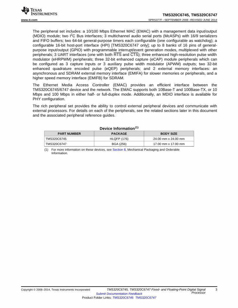
Device Information (1)
PART NUMBER PACKAGE BODY SIZETMS320C6745 HLQFP (176) 24.00 mm x 24.00 mmTMS320C6747 BGA (256) 17.00 mm x 17.00 mm
(1) For more information on these devices, see Section 8, Mechanical Packaging and OrderableInformation.
Copyright © 2008–2014, Texas Instruments Incorporated TMS320C6745, TMS320C6747 Fixed- and Floating-Point Digital Signal 3ProcessorSubmit Documentation Feedback
Product Folder Links: TMS320C6745 TMS320C6747

Switched Central Resource (SCR)
BOOT ROM
256KB L2 RAM
32KBL1 RAM
32KBL1 Pgm
AET
C674xDSP CPU
DSP SubsystemJTAG Interface
Serial Interfaces
I C(2)
2 SPI(2)
UART(3)
Audio Ports
McASPw/FIFO
(2)
DMA
Peripherals
External Memory InterfacesConnectivity
EDMA3
Control Timers
eHRPWM(3)
eCAP(3)
eQEP(2)
(10/100)EMAC(RMII)
MDIOUSB2.0
OTG CtlrPHY
MMC/SD(8b)
EMIFA(8b)NAND/Flash
EMIFBSDRAM Only
(16b)
GPIOPRU
Subsystem
System Control
InputClock(s)
Power/SleepController
MemoryProtection
PinMultiplexing
PLL/ClockGenerator
w/OSC
General-Purpose
Timer
General-Purpose
Timer(Watchdog)
Switched Central Resource (SCR)
BOOT ROM
256KB L2 RAM
32KBL1 RAM
32KBL1 Pgm
AET
C674xDSP CPU
DSP SubsystemJTAG Interface
Serial Interfaces
I C(2)
2 SPI(2)
UART(3)
Audio Ports
McASPw/FIFO
(3)
DMA
Peripherals
Display Internal Memory
LCDCtlr
128KBRAM
External Memory InterfacesConnectivity
EDMA3
Control Timers
eHRPWM(3)
eCAP(3)
eQEP(2)
(10/100)EMAC(RMII)
MDIOUSB1.1
OHCI CtlrPHY
USB2.0OTG Ctlr
PHYHPI
MMC/SD(8b)
EMIFA(8b/16B)NAND/Flash16b SDRAM
EMIFBSDRAM Only
(16b/32b)
GPIOPRU
Subsystem
System Control
InputClock(s)
Power/SleepController
MemoryProtection
PinMultiplexing
RTC/32-kHzOSC
PLL/ClockGenerator
w/OSC
General-Purpose
Timer
General-Purpose
Timer(Watchdog)
TMS320C6745, TMS320C6747SPRS377F –SEPTEMBER 2008–REVISED JUNE 2014 www.ti.com
1.4 Functional Block Diagram
Note: Not all peripherals are available at the same time due to multiplexing. See Table 3-1 for details on which devicecomponents are available on each device.
Figure 1-1. TMS320C6747 Functional Block Diagram
Note: Not all peripherals are available at the same time due to multiplexing. See Table 3-1 for details on which devicecomponents are available on each device.
Figure 1-2. TMS320C6745 Functional Block Diagram
4 TMS320C6745, TMS320C6747 Fixed- and Floating-Point Digital Signal Copyright © 2008–2014, Texas Instruments IncorporatedProcessor Submit Documentation Feedback
Product Folder Links: TMS320C6745 TMS320C6747
TMS320C6745, TMS320C6747www.ti.com SPRS377F –SEPTEMBER 2008–REVISED JUNE 2014
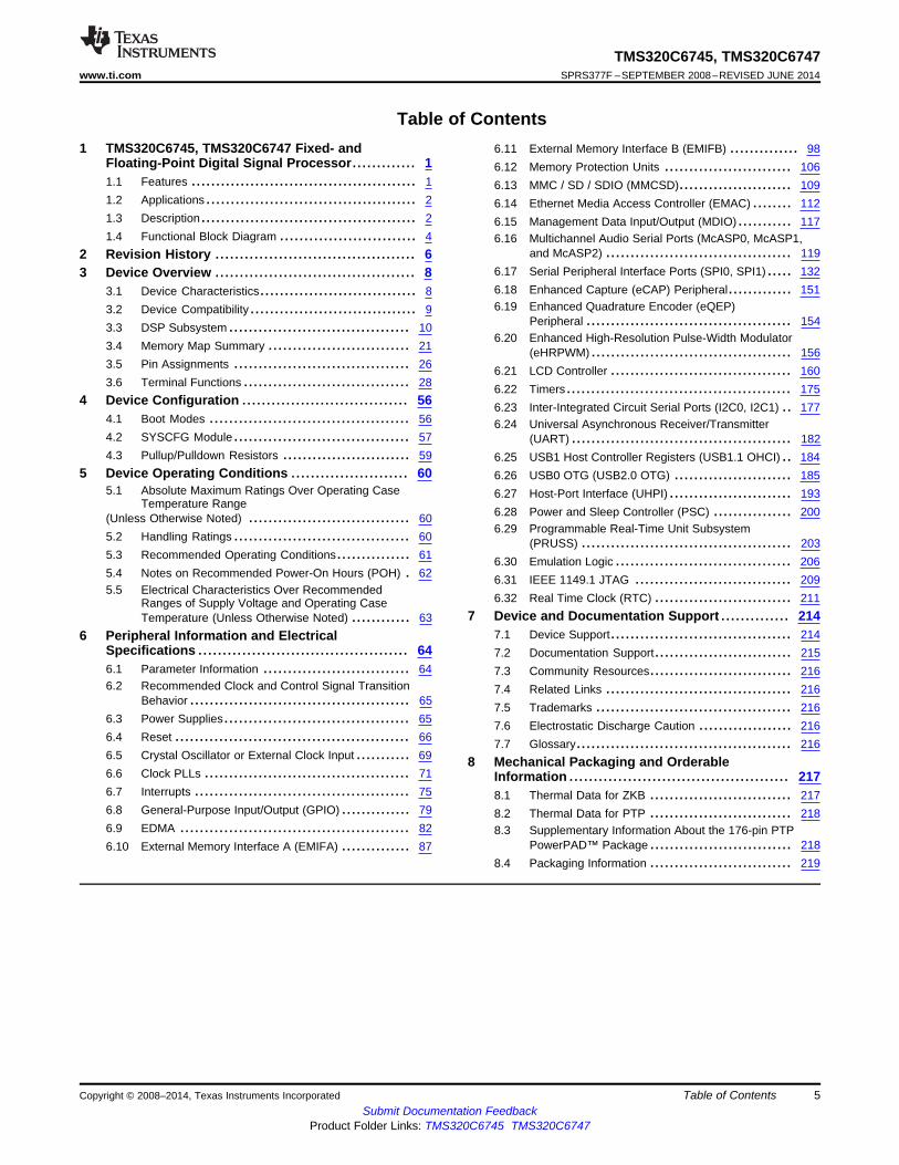
Table of Contents1 TMS320C6745, TMS320C6747 Fixed- and 6.11 External Memory Interface B (EMIFB) .............. 98
Floating-Point Digital Signal Processor............. 1 6.12 Memory Protection Units .......................... 1061.1 Features .............................................. 1 6.13 MMC / SD / SDIO (MMCSD)....................... 1091.2 Applications........................................... 2 6.14 Ethernet Media Access Controller (EMAC) ........ 1121.3 Description............................................ 2 6.15 Management Data Input/Output (MDIO)........... 1171.4 Functional Block Diagram ............................ 4 6.16 Multichannel Audio Serial Ports (McASP0, McASP1,
and McASP2) ...................................... 1192 Revision History ......................................... 66.17 Serial Peripheral Interface Ports (SPI0, SPI1)..... 1323 Device Overview ......................................... 86.18 Enhanced Capture (eCAP) Peripheral............. 1513.1 Device Characteristics................................ 86.19 Enhanced Quadrature Encoder (eQEP)3.2 Device Compatibility.................................. 9
Peripheral .......................................... 1543.3 DSP Subsystem ..................................... 106.20 Enhanced High-Resolution Pulse-Width Modulator
3.4 Memory Map Summary ............................. 21 (eHRPWM)......................................... 1563.5 Pin Assignments .................................... 26 6.21 LCD Controller ..................................... 1603.6 Terminal Functions .................................. 28 6.22 Timers.............................................. 175
4 Device Configuration .................................. 56 6.23 Inter-Integrated Circuit Serial Ports (I2C0, I2C1) .. 1774.1 Boot Modes ......................................... 56 6.24 Universal Asynchronous Receiver/Transmitter4.2 SYSCFG Module.................................... 57 (UART) ............................................. 1824.3 Pullup/Pulldown Resistors .......................... 59 6.25 USB1 Host Controller Registers (USB1.1 OHCI) .. 184
5 Device Operating Conditions ........................ 60 6.26 USB0 OTG (USB2.0 OTG) ........................ 1855.1 Absolute Maximum Ratings Over Operating Case 6.27 Host-Port Interface (UHPI)......................... 193
Temperature Range6.28 Power and Sleep Controller (PSC) ................ 200(Unless Otherwise Noted) ................................. 606.29 Programmable Real-Time Unit Subsystem
5.2 Handling Ratings .................................... 60 (PRUSS) ........................................... 2035.3 Recommended Operating Conditions............... 61 6.30 Emulation Logic .................................... 2065.4 Notes on Recommended Power-On Hours (POH) . 62 6.31 IEEE 1149.1 JTAG ................................ 2095.5 Electrical Characteristics Over Recommended
6.32 Real Time Clock (RTC) ............................ 211Ranges of Supply Voltage and Operating Case7 Device and Documentation Support .............. 214Temperature (Unless Otherwise Noted) ............ 63
7.1 Device Support..................................... 2146 Peripheral Information and ElectricalSpecifications ........................................... 64 7.2 Documentation Support............................ 2156.1 Parameter Information .............................. 64 7.3 Community Resources............................. 2166.2 Recommended Clock and Control Signal Transition 7.4 Related Links ...................................... 216
Behavior ............................................. 65 7.5 Trademarks ........................................ 2166.3 Power Supplies...................................... 65 7.6 Electrostatic Discharge Caution ................... 2166.4 Reset ................................................ 66 7.7 Glossary............................................ 2166.5 Crystal Oscillator or External Clock Input ........... 69 8 Mechanical Packaging and Orderable6.6 Clock PLLs .......................................... 71 Information ............................................. 2176.7 Interrupts ............................................ 75 8.1 Thermal Data for ZKB ............................. 2176.8 General-Purpose Input/Output (GPIO) .............. 79 8.2 Thermal Data for PTP ............................. 2186.9 EDMA ............................................... 82 8.3 Supplementary Information About the 176-pin PTP
PowerPAD™ Package ............................. 2186.10 External Memory Interface A (EMIFA) .............. 878.4 Packaging Information ............................. 219
Copyright © 2008–2014, Texas Instruments Incorporated Table of Contents 5Submit Documentation Feedback
Product Folder Links: TMS320C6745 TMS320C6747

TMS320C6745, TMS320C6747SPRS377F –SEPTEMBER 2008–REVISED JUNE 2014 www.ti.com
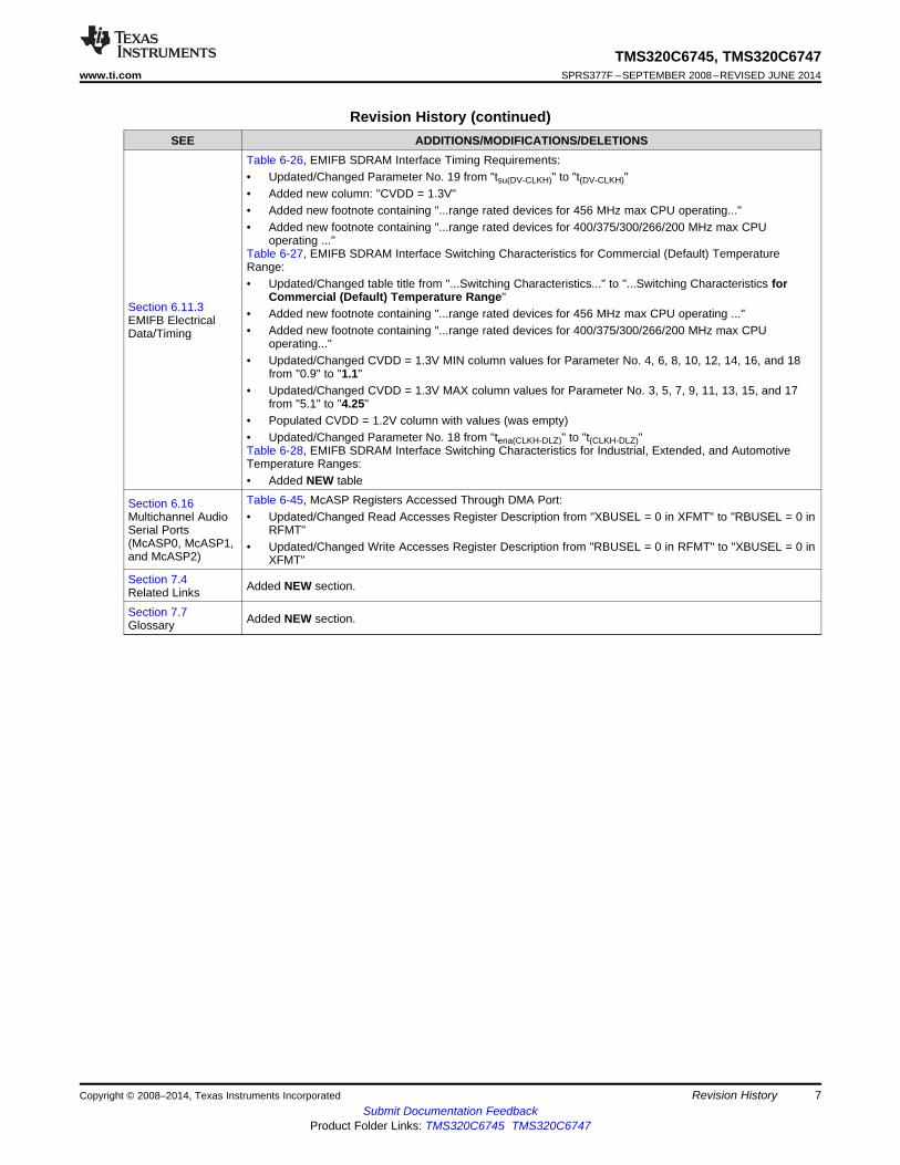
2 Revision HistoryNOTE: Page numbers for previous revisions may differ from page numbers in the current version.
This data manual revision history highlights the changes made to the SPRS377E device-specific datamanual to make it an SPRS377F revision.
Scope: Applicable updates to the TMS320C6747/C6745 Fixed- and Floating-Point Digital SignalProcessor device family, specifically relating to the TMS320C6747 and TMS320C6745 devices, which areall now in the production data (PD) stage of development, have been incorporated.
Revision HistorySEE ADDITIONS/MODIFICATIONS/DELETIONS
• Turned on Navigation Icons on top of first page.• Updated Features, Applications, and Description for consistency and translation.Global• Moved Trademarks information from first page to within Section 7, Device and Documentation Support.• Moved ESDS Warning to within Section 7, Device and Documentation Support.
Section 1.1 Deleted Highlights section. Information was duplicated elsewhere in Features.FeaturesSection 1.2 Added NEW section.ApplicationsSection 1.3 Added NEW Device Information Table.Description
Table 3-2, C674x Cache Registers:Section 3.3.2.3
• Updated/Changed REGISTER DESCRIPTION for BYTE ADDRESSES 0000, 0020, and 0040 fromC674x CPU"...See the System reference Guide..." to "See the Technical Reference Manual..."
Table 3-21, Universal Serial Bus (USB) Terminal Functions:Section 3.6
• Updated/Changed USB0_VDDA12 DESCRIPTION from "...must always be connected via a 1 μFTerminal Functionscapacitor..." to "...is recommended to be connected via a 0.22-μF capacitor..."
Section 3.6.11Universal Table 3-16, Universal Asynchronous Receiver/Transmitter (UART) Terminal Functions:Asynchronous
• Updated/Changed footnote from "...DSP Reference Guide - Literature Number SPRUFK4..." to "...DSPReceiver/TransmitterTechnical Reference Manual (SPRUH91)..."s (UART0, UART1,
UART2)Table 3-26, Reserved and No Connect Terminal Functions:Section 3.6.21
Reserved and No • Updated/Changed RSV4 DESCRIPTION from "...This pin may be tied high or low." to "...For properConnect device operation, this pin must be tied low or to CVDD."Section 3.6.23 Moved to within Section 3.6, Terminal FunctionsUnused USB0
Table 3-28, Unused USB0 and USB1 Pin Configurations:(USB2.0) and USB1• Updated/Changed USB0_VDDA12 Configuration by combining both Configuration columns and(USB1.1) Pin
changing text to "Internal USB0 PHY output connected to an external..."ConfigurationsSection 5.2, Handling Ratings:Section 5
Device Operating • Split handling, ratings, and certifications from the Abs Max table and placed in NEW Handling RatingsConditions table.Section 5.4Notes on Table 5-1, Recommended Power-On Hours:Recommended
• Added Silicon Revision column.Power-On Hours(POH)
Table 6-22, EMIFA Asynchronous Memory Switching Characteristics:Section 6.10.6 • Updated/Changed the MIN, NOM, and MAX equations for NO. 3, 10, 15, and 24 from "...(EWC*16)..." toEMIFA Electrical "...EWC..."Data/Timing Section 5.3, Recommended Operating Conditions:
• Added "Unless specifically indicated" to "These I/O specifications apply to ..." footnote
6 Revision History Copyright © 2008–2014, Texas Instruments IncorporatedSubmit Documentation Feedback
Product Folder Links: TMS320C6745 TMS320C6747
TMS320C6745, TMS320C6747www.ti.com SPRS377F –SEPTEMBER 2008–REVISED JUNE 2014
Revision History (continued)SEE ADDITIONS/MODIFICATIONS/DELETIONS
Table 6-26, EMIFB SDRAM Interface Timing Requirements:• Updated/Changed Parameter No. 19 from "tsu(DV-CLKH)" to "t(DV-CLKH)"• Added new column: "CVDD = 1.3V"• Added new footnote containing "...range rated devices for 456 MHz max CPU operating..."• Added new footnote containing "...range rated devices for 400/375/300/266/200 MHz max CPU
operating ..."Table 6-27, EMIFB SDRAM Interface Switching Characteristics for Commercial (Default) TemperatureRange:• Updated/Changed table title from "...Switching Characteristics..." to "...Switching Characteristics for
Commercial (Default) Temperature Range"Section 6.11.3 • Added new footnote containing "...range rated devices for 456 MHz max CPU operating ..."EMIFB Electrical
• Added new footnote containing "...range rated devices for 400/375/300/266/200 MHz max CPUData/Timingoperating..."
• Updated/Changed CVDD = 1.3V MIN column values for Parameter No. 4, 6, 8, 10, 12, 14, 16, and 18from "0.9" to "1.1"
• Updated/Changed CVDD = 1.3V MAX column values for Parameter No. 3, 5, 7, 9, 11, 13, 15, and 17from "5.1" to "4.25"
• Populated CVDD = 1.2V column with values (was empty)• Updated/Changed Parameter No. 18 from "tena(CLKH-DLZ)" to "t(CLKH-DLZ)"Table 6-28, EMIFB SDRAM Interface Switching Characteristics for Industrial, Extended, and AutomotiveTemperature Ranges:• Added NEW tableTable 6-45, McASP Registers Accessed Through DMA Port:Section 6.16
Multichannel Audio • Updated/Changed Read Accesses Register Description from "XBUSEL = 0 in XFMT" to "RBUSEL = 0 inSerial Ports RFMT"(McASP0, McASP1, • Updated/Changed Write Accesses Register Description from "RBUSEL = 0 in RFMT" to "XBUSEL = 0 inand McASP2) XFMT"Section 7.4 Added NEW section.Related LinksSection 7.7 Added NEW section.Glossary
Copyright © 2008–2014, Texas Instruments Incorporated Revision History 7Submit Documentation Feedback
Product Folder Links: TMS320C6745 TMS320C6747
TMS320C6745, TMS320C6747SPRS377F –SEPTEMBER 2008–REVISED JUNE 2014 www.ti.com
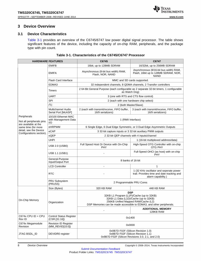
3 Device Overview
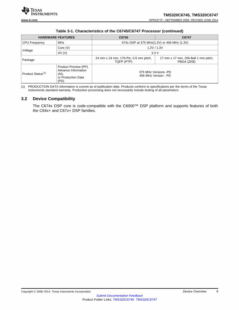
3.1 Device CharacteristicsTable 3-1 provides an overview of the C6745/6747 low power digital signal processor. The table showssignificant features of the device, including the capacity of on-chip RAM, peripherals, and the packagetype with pin count.
Table 3-1. Characteristics of the C6745/C6747 Processor
HARDWARE FEATURES C6745 C6747EMIFB 16bit, up to 128MB SDRAM 16/32bit, up to 256MB SDRAM
Asynchronous (8/16-bit bus width) RAM,Asynchronous (8-bit bus width) RAM,EMIFA Flash, 16bit up to 128MB SDRAM, NOR,Flash, NOR, NAND NANDFlash Card Interface MMC and SD cards supported.EDMA3 32 independent channels, 8 QDMA channels, 2 Transfer controllers
2 64-Bit General Purpose (each configurable as 2 separate 32-bit timers, 1 configurableTimers as Watch Dog)UART 3 (one with RTS and CTS flow control)SPI 2 (each with one hardware chip select)I2C 2 (both Master/Slave)Multichannel Audio 2 (each with transmit/receive, FIFO buffer, 3 (each with transmit/receive, FIFO buffer,Serial Port [McASP] 16/9 serializers) 16/9 serializers)
Peripherals 10/100 Ethernet MACwith Management Data 1 (RMII Interface)Not all peripherals pins I/Oare available at theeHRPWM 6 Single Edge, 6 Dual Edge Symmetric, or 3 Dual Edge Asymmetric Outputssame time (for more
detail, see the Device eCAP 3 32-bit capture inputs or 3 32-bit auxiliary PWM outputsConfigurations section).
eQEP 2 32-bit QEP channels with 4 inputs/channelUHPI - 1 (16-bit multiplexed address/data)
Full Speed Host Or Device with On-Chip High-Speed OTG Controller with on-chipUSB 2.0 (USB0) PHY OTG PHYFull-Speed OHCI (as host) with on-chipUSB 1.1 (USB1) - PHY
General-Purpose 8 banks of 16-bitInput/Output PortLCD Controller - 1
1 (32 KHz oscillator and seperate powerRTC - trail. Provides time and date tracking and
alarm capability.)PRU Subsystem 2 Programmable PRU Cores(PRUSS)Size (Bytes) 320 KB RAM 448 KB RAM
DSP32KB L1 Program (L1P)/Cache (up to 32KB)
32KB L1 Data (L1D)/Cache (up to 32KB)On-Chip Memory 256KB Unified Mapped RAM/Cache (L2)OrganizationDSP Memories can be made accessible to EDMA3, and other peripherals.
ADDITIONAL MEMORY- 128KB RAMC674x CPU ID + CPU Control Status Register 0x1400Rev ID (CSR.[31:16])C674x Megamodule Revision ID Register 0x0000Revision (MM_REVID[15:0])
0x0B7D F02F (Silicon Revision 1.0)JTAG BSDL_ID DEVIDR0 register 0x8B7D F02F (Silicon Revision 1.1)
0x9B7D F02F (Silicon Revisions 3.0, 2.1, and 2.0)
8 Device Overview Copyright © 2008–2014, Texas Instruments IncorporatedSubmit Documentation Feedback
Product Folder Links: TMS320C6745 TMS320C6747
TMS320C6745, TMS320C6747www.ti.com SPRS377F –SEPTEMBER 2008–REVISED JUNE 2014
Table 3-1. Characteristics of the C6745/C6747 Processor (continued)HARDWARE FEATURES C6745 C6747
CPU Frequency MHz 674x DSP at 375 MHz(1.2V) or 456 MHz (1.3V)Core (V) 1.2V / 1.3V
VoltageI/O (V) 3.3 V
24 mm x 24 mm, 176-Pin, 0.5 mm pitch, 17 mm x 17 mm, 256-Ball 1 mm pitch,Package TQFP (PTP) PBGA (ZKB)Product Preview (PP),Advance Information 375 MHz Versions -PDProduct Status (1) (AI), 456 MHz Version - PDor Production Data(PD)
(1) PRODUCTION DATA information is current as of publication date. Products conform to specifications per the terms of the TexasInstruments standard warranty. Production processing does not necessarily include testing of all parameters.
3.2 Device CompatibilityThe C674x DSP core is code-compatible with the C6000™ DSP platform and supports features of boththe C64x+ and C67x+ DSP families.
Copyright © 2008–2014, Texas Instruments Incorporated Device Overview 9Submit Documentation Feedback
Product Folder Links: TMS320C6745 TMS320C6747

Instruction Fetch
C674xFixed/Floating Point CPU
RegisterFile A
RegisterFile B
Cache Control
Memory Protect
Bandwidth Mgmt
L1P
256
Cache Control
Memory Protect
Bandwidth Mgmt
L1D
64 64
8 x 32
32K BytesL1D RAM/
Cache
32K BytesL1P RAM/
Cache
256
Cache Control
Memory Protect
Bandwidth Mgmt
L2
256K BytesL2 RAM
256
Boot ROM
256
CFG
MDMA SDMA
EMC
Power Down
InterruptController
IDMA
256
256
256
256
256
64
HighPerformanceSwitch Fabric
64 64 64
ConfigurationPeripherals
Bus
32
TMS320C6745, TMS320C6747SPRS377F –SEPTEMBER 2008–REVISED JUNE 2014 www.ti.com
3.3 DSP SubsystemThe DSP Subsystem includes the following features:• C674x DSP CPU• 32KB L1 Program (L1P)/Cache (up to 32KB)• 32KB L1 Data (L1D)/Cache (up to 32KB)• 256KB Unified Mapped RAM/Cache (L2)• Boot ROM (cannot be used for application code)• Little endian
Figure 3-1. C674x Megamodule Block Diagram
10 Device Overview Copyright © 2008–2014, Texas Instruments IncorporatedSubmit Documentation Feedback
Product Folder Links: TMS320C6745 TMS320C6747

TMS320C6745, TMS320C6747www.ti.com SPRS377F –SEPTEMBER 2008–REVISED JUNE 2014
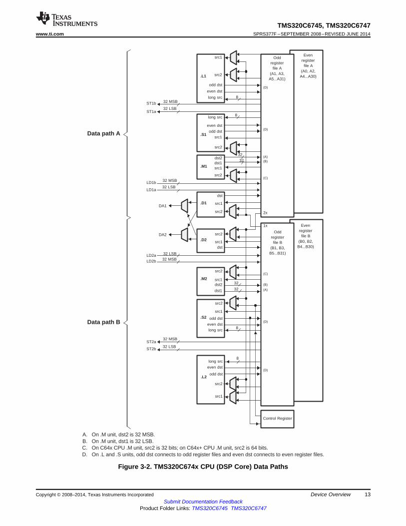
3.3.1 C674x DSP CPU DescriptionThe C674x Central Processing Unit (CPU) consists of eight functional units, two register files, and twodata paths as shown in Figure 3-2. The two general-purpose register files (A and B) each contain 32 32-bit registers for a total of 64 registers. The general-purpose registers can be used for data or can be dataaddress pointers. The data types supported include packed 8-bit data, packed 16-bit data, 32-bit data, 40-bit data, and 64-bit data. Values larger than 32 bits, such as 40-bit-long or 64-bit-long values are stored inregister pairs, with the 32 LSBs of data placed in an even register and the remaining 8 or 32 MSBs in thenext upper register (which is always an odd-numbered register).
The eight functional units (.M1, .L1, .D1, .S1, .M2, .L2, .D2, and .S2) are each capable of executing oneinstruction every clock cycle. The .M functional units perform all multiply operations. The .S and .L unitsperform a general set of arithmetic, logical, and branch functions. The .D units primarily load data frommemory to the register file and store results from the register file into memory.
The C674x CPU combines the performance of the C64x+ core with the floating-point capabilities of theC67x+ core.
Each C674x .M unit can perform one of the following each clock cycle: one 32 x 32 bit multiply, one 16 x32 bit multiply, two 16 x 16 bit multiplies, two 16 x 32 bit multiplies, two 16 x 16 bit multiplies withadd/subtract capabilities, four 8 x 8 bit multiplies, four 8 x 8 bit multiplies with add operations, and four16 x 16 multiplies with add/subtract capabilities (including a complex multiply). There is also support forGalois field multiplication for 8-bit and 32-bit data. Many communications algorithms such as FFTs andmodems require complex multiplication. The complex multiply (CMPY) instruction takes four 16-bit inputsand produces a 32-bit real and a 32-bit imaginary output. There are also complex multiplies with roundingcapability that produces one 32-bit packed output that contain 16-bit real and 16-bit imaginary values. The32 x 32 bit multiply instructions provide the extended precision necessary for high-precision algorithms ona variety of signed and unsigned 32-bit data types.
The .L Unit (or Arithmetic Logic Unit) now incorporates the ability to do parallel add/subtract operations ona pair of common inputs. Versions of this instruction exist to work on 32-bit data or on pairs of 16-bit dataperforming dual 16-bit add and subtracts in parallel. There are also saturated forms of these instructions.
The C674x core enhances the .S unit in several ways. On the previous cores, dual 16-bit MIN2 and MAX2comparisons were only available on the .L units. On the C674x core they are also available on the .S unitwhich increases the performance of algorithms that do searching and sorting. Finally, to increase datapacking and unpacking throughput, the .S unit allows sustained high performance for the quad 8-bit/16-bitand dual 16-bit instructions. Unpack instructions prepare 8-bit data for parallel 16-bit operations. Packinstructions return parallel results to output precision including saturation support.
Other new features include:• SPLOOP - A small instruction buffer in the CPU that aids in creation of software pipelining loops where
multiple iterations of a loop are executed in parallel. The SPLOOP buffer reduces the code sizeassociated with software pipelining. Furthermore, loops in the SPLOOP buffer are fully interruptible.
• Compact Instructions - The native instruction size for the C6000™ devices is 32 bits. Many commoninstructions such as MPY, AND, OR, ADD, and SUB can be expressed as 16 bits if the C674xcompiler can restrict the code to use certain registers in the register file. This compression isperformed by the code generation tools.
• Instruction Set Enhancement - As noted above, there are new instructions such as 32-bitmultiplications, complex multiplications, packing, sorting, bit manipulation, and 32-bit Galois fieldmultiplication.
• Exceptions Handling - Intended to aid the programmer in isolating bugs. The C674x CPU is able todetect and respond to exceptions, both from internally detected sources (such as illegal op-codes) andfrom system events (such as a watchdog time expiration).
• Privilege - Defines user and supervisor modes of operation, allowing the operating system to give abasic level of protection to sensitive resources. Local memory is divided into multiple pages, each withread, write, and execute permissions.
Copyright © 2008–2014, Texas Instruments Incorporated Device Overview 11Submit Documentation Feedback
Product Folder Links: TMS320C6745 TMS320C6747

TMS320C6745, TMS320C6747SPRS377F –SEPTEMBER 2008–REVISED JUNE 2014 www.ti.com
• Time-Stamp Counter - Primarily targeted for Real-Time Operating System (RTOS) robustness, a free-running time-stamp counter is implemented in the CPU which is not sensitive to system stalls.
For more details on the C674x CPU and its enhancements over the C64x architecture, see the followingdocuments:• TMS320C64x/C64x+ DSP CPU and Instruction Set Reference Guide (SPRU732)• TMS320C64x Technical Overview (SPRU395)
12 Device Overview Copyright © 2008–2014, Texas Instruments IncorporatedSubmit Documentation Feedback
Product Folder Links: TMS320C6745 TMS320C6747
src2
src2
ÁÁÁÁÁÁÁ .D1
.M1 ÁÁÁÁÁÁÁÁÁÁ ÁÁÁ.S1
ÁÁÁÁÁÁÁ ÁÁÁ.L1
long src
odd dst
src2
src1 ÁÁÁÁÁÁÁÁÁÁÁÁÁÁÁÁÁÁÁÁÁsrc1
src1
src1
even dst
even dst
odd dst
dst1
dst
src2
src2
src2
long src
DA1
ST1b
LD1b
LD1a
ST1a
Data path A
Oddregister
file A(A1, A3,
A5...A31)ÁÁÁOdd
registerfile B
(B1, B3,B5...B31)
ÁÁÁ.D2
ÁÁÁÁsrc1dst
src2DA2
LD2aLD2b
src2
.M2 src1
ÁÁÁdst1
ÁÁÁ.S2
src1
ÁÁÁÁeven dstlong src
odd dst
ST2a
ST2b
long src
.L2
ÁÁÁÁeven dst
odd dst
ÁÁÁsrc1
Data path B
Control Register
32 MSB
32 LSB
dst2 (A)
32 MSB
32 LSB
2x
1x
32 LSB32 MSB
32 LSB
32 MSB
dst2
(B)
(B)
(A)
8
8
8
8
32
32
3232
(C)
(C)
Evenregister
file A(A0, A2,
A4...A30)
Evenregister
file B(B0, B2,
B4...B30)
(D)
(D)
(D)
(D)
A. On .M unit, dst2 is 32 MSB.B. On .M unit, dst1 is 32 LSB.C. On C64x CPU .M unit, src2 is 32 bits; on C64x+ CPU .M unit, src2 is 64 bits.D. On .L and .S units, odd dst connects to odd register files and even dst connects to even register files.
TMS320C6745, TMS320C6747www.ti.com SPRS377F –SEPTEMBER 2008–REVISED JUNE 2014
Figure 3-2. TMS320C674x CPU (DSP Core) Data Paths
Copyright © 2008–2014, Texas Instruments Incorporated Device Overview 13Submit Documentation Feedback
Product Folder Links: TMS320C6745 TMS320C6747

TMS320C6745, TMS320C6747SPRS377F –SEPTEMBER 2008–REVISED JUNE 2014 www.ti.com
3.3.2 DSP Memory MappingThe DSP memory map is shown in Section 3.4.
3.3.2.1 External Memories
The DSP has access to the following External memories:• Asynchronous EMIF / SDRAM / NAND / NOR Flash (EMIFA)• SDRAM (EMIFB)
3.3.2.2 DSP Internal Memories
The DSP has access to the following DSP memories:• L2 RAM• L1P RAM• L1D RAM
3.3.2.3 C674x CPU
The C674x core uses a two-level cache-based architecture. The Level 1 Program cache (L1P) is 32 KBdirect mapped cache and the Level 1 Data cache (L1D) is 32 KB 2-way set associated cache. The Level 2memory/cache (L2) consists of a 256 KB memory space that is shared between program and data space.L2 memory can be configured as mapped memory, cache, or a combination of both.
Table 3-2 shows a memory map of the C674x CPU cache registers for the device.
Table 3-2. C674x Cache Registers
BYTE ADDRESS ACRONYM REGISTER DESCRIPTIONL2 Cache configuration register (See the Technical Reference Manual0x0184 0000 L2CFG SPRUH91 for the reset configuration)L1P Size Cache configuration register (See the Technical Reference0x0184 0020 L1PCFG Manual SPRUH91 for the reset configuration)
0x0184 0024 L1PCC L1P Freeze Mode Cache configuration registerL1D Size Cache configuration register (See the Technical Reference0x0184 0040 L1DCFG Manual SPRUH91 for the reset configuration)
0x0184 0044 L1DCC L1D Freeze Mode Cache configuration register0x0184 0048 - 0x0184 0FFC - Reserved
0x0184 1000 EDMAWEIGHT L2 EDMA access control register0x0184 1004 - 0x0184 1FFC - Reserved
0x0184 2000 L2ALLOC0 L2 allocation register 00x0184 2004 L2ALLOC1 L2 allocation register 10x0184 2008 L2ALLOC2 L2 allocation register 20x0184 200C L2ALLOC3 L2 allocation register 3
0x0184 2010 - 0x0184 3FFF - Reserved0x0184 4000 L2WBAR L2 writeback base address register0x0184 4004 L2WWC L2 writeback word count register0x0184 4010 L2WIBAR L2 writeback invalidate base address register0x0184 4014 L2WIWC L2 writeback invalidate word count register0x0184 4018 L2IBAR L2 invalidate base address register0x0184 401C L2IWC L2 invalidate word count register0x0184 4020 L1PIBAR L1P invalidate base address register0x0184 4024 L1PIWC L1P invalidate word count register0x0184 4030 L1DWIBAR L1D writeback invalidate base address register0x0184 4034 L1DWIWC L1D writeback invalidate word count register
14 Device Overview Copyright © 2008–2014, Texas Instruments IncorporatedSubmit Documentation Feedback
Product Folder Links: TMS320C6745 TMS320C6747

TMS320C6745, TMS320C6747www.ti.com SPRS377F –SEPTEMBER 2008–REVISED JUNE 2014
Table 3-2. C674x Cache Registers (continued)BYTE ADDRESS ACRONYM REGISTER DESCRIPTION
0x0184 4038 - Reserved0x0184 4040 L1DWBAR L1D writeback base address register0x0184 4044 L1DWWC L1D writeback word count register0x0184 4048 L1DIBAR L1D invalidate base address register0x0184 404C L1DIWC L1D invalidate word count register
0x0184 4050 - 0x0184 4FFF - Reserved0x0184 5000 L2WB L2 writeback all register0x0184 5004 L2WBINV L2 writeback invalidate all register0x0184 5008 L2INV L2 Global Invalidate without writeback
0x0184 500C - 0x0184 5027 - Reserved0x0184 5028 L1PINV L1P Global Invalidate
0x0184 502C - 0x0184 5039 - Reserved0x0184 5040 L1DWB L1D Global Writeback0x0184 5044 L1DWBINV L1D Global Writeback with Invalidate0x0184 5048 L1DINV L1D Global Invalidate without writeback
0x0184 8000 – 0x0184 80FF MAR0 - MAR63 Reserved 0x0000 0000 – 0x3FFF FFFFMemory Attribute Registers for EMIFA SDRAM Data (CS0)0x0184 8100 – 0x0184 817F MAR64 – MAR95 0x4000 0000 – 0x5FFF FFFFMemory Attribute Registers for EMIFA Async Data (CS2)0x0184 8180 – 0x0184 8187 MAR96 - MAR97 0x6000 0000 – 0x61FF FFFFMemory Attribute Registers for EMIFA Async Data (CS3)0x0184 8188 – 0x0184 818F MAR98 – MAR99 0x6200 0000 – 0x63FF FFFFMemory Attribute Registers for EMIFA Async Data (CS4)0x0184 8190 – 0x0184 8197 MAR100 – MAR101 0x6400 0000 – 0x65FF FFFFMemory Attribute Registers for EMIFA Async Data (CS5)0x0184 8198 – 0x0184 819F MAR102 – MAR103 0x6600 0000 – 0x67FF FFFF
0x0184 81A0 – 0x0184 81FF MAR104 – MAR127 Reserved 0x6800 0000 – 0x7FFF FFFFMemory Attribute Register for Shared RAM 0x8000 0000 – 0x8001 FFFF
0x0184 8200 MAR128Reserved 0x8002 0000 – 0x81FF FFFF
0x0184 8204 – 0x0184 82FF MAR129 – MAR191 Reserved 0x8200 0000 – 0xBFFF FFFFMemory Attribute Registers for EMIFB SDRAM Data (CS0)0x0184 8300 – 0x0184 837F MAR192 – MAR223 0xC000 0000 – 0xDFFF FFFF
0x0184 8380 – 0x0184 83FF MAR224 – MAR255 Reserved 0xE000 0000 – 0xFFFF FFFF
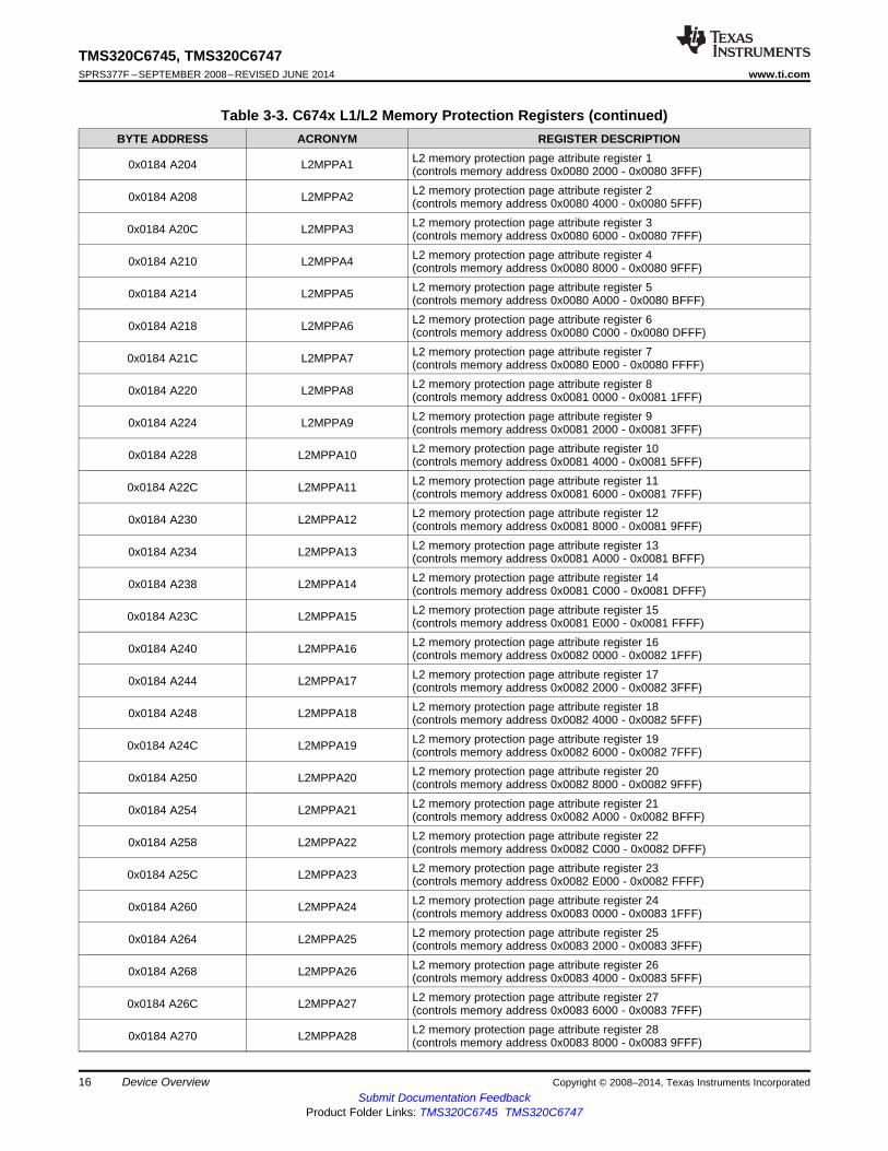
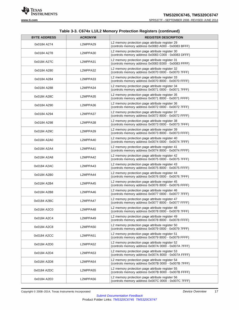
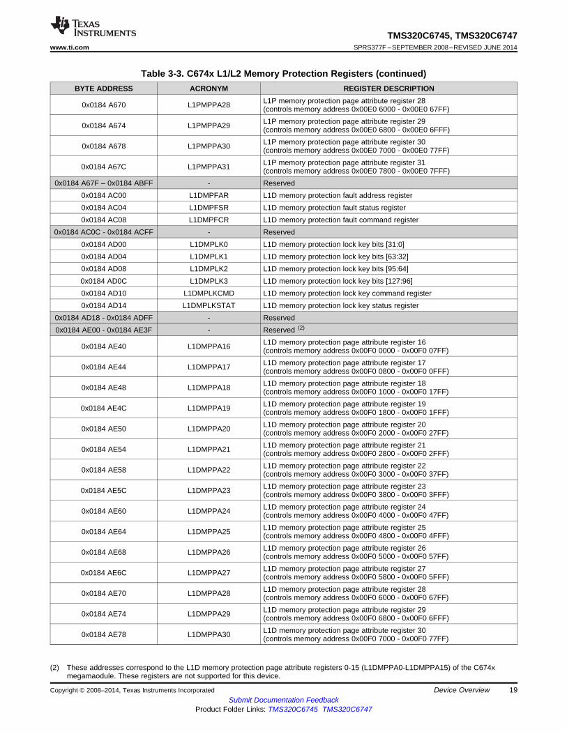
Table 3-3. C674x L1/L2 Memory Protection Registers
BYTE ADDRESS ACRONYM REGISTER DESCRIPTION0x0184 A000 L2MPFAR L2 memory protection fault address register0x0184 A004 L2MPFSR L2 memory protection fault status register0x0184 A008 L2MPFCR L2 memory protection fault command register
0x0184 A00C - 0x0184 A0FF - Reserved0x0184 A100 L2MPLK0 L2 memory protection lock key bits [31:0]0x0184 A104 L2MPLK1 L2 memory protection lock key bits [63:32]0x0184 A108 L2MPLK2 L2 memory protection lock key bits [95:64]0x0184 A10C L2MPLK3 L2 memory protection lock key bits [127:96]0x0184 A110 L2MPLKCMD L2 memory protection lock key command register0x0184 A114 L2MPLKSTAT L2 memory protection lock key status register
0x0184 A118 - 0x0184 A1FF - ReservedL2 memory protection page attribute register 00x0184 A200 L2MPPA0 (controls memory address 0x0080 0000 - 0x0080 1FFF)
Copyright © 2008–2014, Texas Instruments Incorporated Device Overview 15Submit Documentation Feedback
Product Folder Links: TMS320C6745 TMS320C6747
TMS320C6745, TMS320C6747SPRS377F –SEPTEMBER 2008–REVISED JUNE 2014 www.ti.com
Table 3-3. C674x L1/L2 Memory Protection Registers (continued)BYTE ADDRESS ACRONYM REGISTER DESCRIPTION
L2 memory protection page attribute register 10x0184 A204 L2MPPA1 (controls memory address 0x0080 2000 - 0x0080 3FFF)L2 memory protection page attribute register 20x0184 A208 L2MPPA2 (controls memory address 0x0080 4000 - 0x0080 5FFF)L2 memory protection page attribute register 30x0184 A20C L2MPPA3 (controls memory address 0x0080 6000 - 0x0080 7FFF)L2 memory protection page attribute register 40x0184 A210 L2MPPA4 (controls memory address 0x0080 8000 - 0x0080 9FFF)L2 memory protection page attribute register 50x0184 A214 L2MPPA5 (controls memory address 0x0080 A000 - 0x0080 BFFF)L2 memory protection page attribute register 60x0184 A218 L2MPPA6 (controls memory address 0x0080 C000 - 0x0080 DFFF)L2 memory protection page attribute register 70x0184 A21C L2MPPA7 (controls memory address 0x0080 E000 - 0x0080 FFFF)L2 memory protection page attribute register 80x0184 A220 L2MPPA8 (controls memory address 0x0081 0000 - 0x0081 1FFF)L2 memory protection page attribute register 90x0184 A224 L2MPPA9 (controls memory address 0x0081 2000 - 0x0081 3FFF)L2 memory protection page attribute register 100x0184 A228 L2MPPA10 (controls memory address 0x0081 4000 - 0x0081 5FFF)L2 memory protection page attribute register 110x0184 A22C L2MPPA11 (controls memory address 0x0081 6000 - 0x0081 7FFF)L2 memory protection page attribute register 120x0184 A230 L2MPPA12 (controls memory address 0x0081 8000 - 0x0081 9FFF)L2 memory protection page attribute register 130x0184 A234 L2MPPA13 (controls memory address 0x0081 A000 - 0x0081 BFFF)L2 memory protection page attribute register 140x0184 A238 L2MPPA14 (controls memory address 0x0081 C000 - 0x0081 DFFF)L2 memory protection page attribute register 150x0184 A23C L2MPPA15 (controls memory address 0x0081 E000 - 0x0081 FFFF)L2 memory protection page attribute register 160x0184 A240 L2MPPA16 (controls memory address 0x0082 0000 - 0x0082 1FFF)L2 memory protection page attribute register 170x0184 A244 L2MPPA17 (controls memory address 0x0082 2000 - 0x0082 3FFF)L2 memory protection page attribute register 180x0184 A248 L2MPPA18 (controls memory address 0x0082 4000 - 0x0082 5FFF)L2 memory protection page attribute register 190x0184 A24C L2MPPA19 (controls memory address 0x0082 6000 - 0x0082 7FFF)L2 memory protection page attribute register 200x0184 A250 L2MPPA20 (controls memory address 0x0082 8000 - 0x0082 9FFF)L2 memory protection page attribute register 210x0184 A254 L2MPPA21 (controls memory address 0x0082 A000 - 0x0082 BFFF)L2 memory protection page attribute register 220x0184 A258 L2MPPA22 (controls memory address 0x0082 C000 - 0x0082 DFFF)L2 memory protection page attribute register 230x0184 A25C L2MPPA23 (controls memory address 0x0082 E000 - 0x0082 FFFF)L2 memory protection page attribute register 240x0184 A260 L2MPPA24 (controls memory address 0x0083 0000 - 0x0083 1FFF)L2 memory protection page attribute register 250x0184 A264 L2MPPA25 (controls memory address 0x0083 2000 - 0x0083 3FFF)L2 memory protection page attribute register 260x0184 A268 L2MPPA26 (controls memory address 0x0083 4000 - 0x0083 5FFF)L2 memory protection page attribute register 270x0184 A26C L2MPPA27 (controls memory address 0x0083 6000 - 0x0083 7FFF)L2 memory protection page attribute register 280x0184 A270 L2MPPA28 (controls memory address 0x0083 8000 - 0x0083 9FFF)
16 Device Overview Copyright © 2008–2014, Texas Instruments IncorporatedSubmit Documentation Feedback
Product Folder Links: TMS320C6745 TMS320C6747
TMS320C6745, TMS320C6747www.ti.com SPRS377F –SEPTEMBER 2008–REVISED JUNE 2014
Table 3-3. C674x L1/L2 Memory Protection Registers (continued)BYTE ADDRESS ACRONYM REGISTER DESCRIPTION
L2 memory protection page attribute register 290x0184 A274 L2MPPA29 (controls memory address 0x0083 A000 - 0x0083 BFFF)L2 memory protection page attribute register 300x0184 A278 L2MPPA30 (controls memory address 0x0083 C000 - 0x0083 DFFF)L2 memory protection page attribute register 310x0184 A27C L2MPPA31 (controls memory address 0x0083 E000 - 0x0083 FFFF)L2 memory protection page attribute register 320x0184 A280 L2MPPA32 (controls memory address 0x0070 0000 - 0x0070 7FFF)L2 memory protection page attribute register 330x0184 A284 L2MPPA33 (controls memory address 0x0070 8000 - 0x0070 FFFF)L2 memory protection page attribute register 340x0184 A288 L2MPPA34 (controls memory address 0x0071 0000 - 0x0071 7FFF)L2 memory protection page attribute register 350x0184 A28C L2MPPA35 (controls memory address 0x0071 8000 - 0x0071 FFFF)L2 memory protection page attribute register 360x0184 A290 L2MPPA36 (controls memory address 0x0072 0000 - 0x0072 7FFF)L2 memory protection page attribute register 370x0184 A294 L2MPPA37 (controls memory address 0x0072 8000 - 0x0072 FFFF)L2 memory protection page attribute register 380x0184 A298 L2MPPA38 (controls memory address 0x0073 0000 - 0x0073 7FFF)L2 memory protection page attribute register 390x0184 A29C L2MPPA39 (controls memory address 0x0073 8000 - 0x0073 FFFF)L2 memory protection page attribute register 400x0184 A2A0 L2MPPA40 (controls memory address 0x0074 0000 - 0x0074 7FFF)L2 memory protection page attribute register 410x0184 A2A4 L2MPPA41 (controls memory address 0x0074 8000 - 0x0074 FFFF)L2 memory protection page attribute register 420x0184 A2A8 L2MPPA42 (controls memory address 0x0075 0000 - 0x0075 7FFF)L2 memory protection page attribute register 430x0184 A2AC L2MPPA43 (controls memory address 0x0075 8000 - 0x0075 FFFF)L2 memory protection page attribute register 440x0184 A2B0 L2MPPA44 (controls memory address 0x0076 0000 - 0x0076 7FFF)L2 memory protection page attribute register 450x0184 A2B4 L2MPPA45 (controls memory address 0x0076 8000 - 0x0076 FFFF)L2 memory protection page attribute register 460x0184 A2B8 L2MPPA46 (controls memory address 0x0077 0000 - 0x0077 7FFF)L2 memory protection page attribute register 470x0184 A2BC L2MPPA47 (controls memory address 0x0077 8000 - 0x0077 FFFF)L2 memory protection page attribute register 480x0184 A2C0 L2MPPA48 (controls memory address 0x0078 0000 - 0x0078 7FFF)L2 memory protection page attribute register 490x0184 A2C4 L2MPPA49 (controls memory address 0x0078 8000 - 0x0078 FFFF)L2 memory protection page attribute register 500x0184 A2C8 L2MPPA50 (controls memory address 0x0079 0000 - 0x0079 7FFF)L2 memory protection page attribute register 510x0184 A2CC L2MPPA51 (controls memory address 0x0079 8000 - 0x0079 FFFF)L2 memory protection page attribute register 520x0184 A2D0 L2MPPA52 (controls memory address 0x007A 0000 - 0x007A 7FFF)L2 memory protection page attribute register 530x0184 A2D4 L2MPPA53 (controls memory address 0x007A 8000 - 0x007A FFFF)L2 memory protection page attribute register 540x0184 A2D8 L2MPPA54 (controls memory address 0x007B 0000 - 0x007B 7FFF)L2 memory protection page attribute register 550x0184 A2DC L2MPPA55 (controls memory address 0x007B 8000 - 0x007B FFFF)L2 memory protection page attribute register 560x0184 A2E0 L2MPPA56 (controls memory address 0x007C 0000 - 0x007C 7FFF)
Copyright © 2008–2014, Texas Instruments Incorporated Device Overview 17Submit Documentation Feedback
Product Folder Links: TMS320C6745 TMS320C6747

TMS320C6745, TMS320C6747SPRS377F –SEPTEMBER 2008–REVISED JUNE 2014 www.ti.com
Table 3-3. C674x L1/L2 Memory Protection Registers (continued)BYTE ADDRESS ACRONYM REGISTER DESCRIPTION
L2 memory protection page attribute register 570x0184 A2E4 L2MPPA57 (controls memory address 0x007C 8000 - 0x007C FFFF)L2 memory protection page attribute register 580x0184 A2E8 L2MPPA58 (controls memory address 0x007D 0000 - 0x007D 7FFF)L2 memory protection page attribute register 590x0184 A2EC L2MPPA59 (controls memory address 0x007D 8000 - 0x007D FFFF)L2 memory protection page attribute register 600x0184 A2F0 L2MPPA60 (controls memory address 0x007E 0000 - 0x007E 7FFF)L2 memory protection page attribute register 610x0184 A2F4 L2MPPA61 (controls memory address 0x007E 8000 - 0x007E FFFF)L2 memory protection page attribute register 620x0184 A2F8 L2MPPA62 (controls memory address 0x007F 0000 - 0x007F 7FFF)L2 memory protection page attribute register 630x0184 A2FC L2MPPA63 (controls memory address 0x007F 8000 - 0x007F FFFF)
0x0184 A300 - 0x0184 A3FF - Reserved0x0184 A400 L1PMPFAR L1P memory protection fault address register0x0184 A404 L1PMPFSR L1P memory protection fault status register0x0184 A408 L1PMPFCR L1P memory protection fault command register
0x0184 A40C - 0x0184 A4FF - Reserved0x0184 A500 L1PMPLK0 L1P memory protection lock key bits [31:0]0x0184 A504 L1PMPLK1 L1P memory protection lock key bits [63:32]0x0184 A508 L1PMPLK2 L1P memory protection lock key bits [95:64]0x0184 A50C L1PMPLK3 L1P memory protection lock key bits [127:96]0x0184 A510 L1PMPLKCMD L1P memory protection lock key command register0x0184 A514 L1PMPLKSTAT L1P memory protection lock key status register
0x0184 A518 - 0x0184 A5FF - Reserved0x0184 A600 - 0x0184 A63F - Reserved (1)
L1P memory protection page attribute register 160x0184 A640 L1PMPPA16 (controls memory address 0x00E0 0000 - 0x00E0 07FF)L1P memory protection page attribute register 170x0184 A644 L1PMPPA17 (controls memory address 0x00E0 0800 - 0x00E0 0FFF)L1P memory protection page attribute register 180x0184 A648 L1PMPPA18 (controls memory address 0x00E0 1000 - 0x00E0 17FF)L1P memory protection page attribute register 190x0184 A64C L1PMPPA19 (controls memory address 0x00E0 1800 - 0x00E0 1FFF)L1P memory protection page attribute register 200x0184 A650 L1PMPPA20 (controls memory address 0x00E0 2000 - 0x00E0 27FF)L1P memory protection page attribute register 210x0184 A654 L1PMPPA21 (controls memory address 0x00E0 2800 - 0x00E0 2FFF)L1P memory protection page attribute register 220x0184 A658 L1PMPPA22 (controls memory address 0x00E0 3000 - 0x00E0 37FF)L1P memory protection page attribute register 230x0184 A65C L1PMPPA23 (controls memory address 0x00E0 3800 - 0x00E0 3FFF)L1P memory protection page attribute register 240x0184 A660 L1PMPPA24 (controls memory address 0x00E0 4000 - 0x00E0 47FF)L1P memory protection page attribute register 250x0184 A664 L1PMPPA25 (controls memory address 0x00E0 4800 - 0x00E0 4FFF)L1P memory protection page attribute register 260x0184 A668 L1PMPPA26 (controls memory address 0x00E0 5000 - 0x00E0 57FF)L1P memory protection page attribute register 270x0184 A66C L1PMPPA27 (controls memory address 0x00E0 5800 - 0x00E0 5FFF)
(1) These addresses correspond to the L1P memory protection page attribute registers 0-15 (L1PMPPA0-L1PMPPA15) of the C674xmegamaodule. These registers are not supported for this device.
18 Device Overview Copyright © 2008–2014, Texas Instruments IncorporatedSubmit Documentation Feedback
Product Folder Links: TMS320C6745 TMS320C6747
TMS320C6745, TMS320C6747www.ti.com SPRS377F –SEPTEMBER 2008–REVISED JUNE 2014
Table 3-3. C674x L1/L2 Memory Protection Registers (continued)BYTE ADDRESS ACRONYM REGISTER DESCRIPTION
L1P memory protection page attribute register 280x0184 A670 L1PMPPA28 (controls memory address 0x00E0 6000 - 0x00E0 67FF)L1P memory protection page attribute register 290x0184 A674 L1PMPPA29 (controls memory address 0x00E0 6800 - 0x00E0 6FFF)L1P memory protection page attribute register 300x0184 A678 L1PMPPA30 (controls memory address 0x00E0 7000 - 0x00E0 77FF)L1P memory protection page attribute register 310x0184 A67C L1PMPPA31 (controls memory address 0x00E0 7800 - 0x00E0 7FFF)
0x0184 A67F – 0x0184 ABFF - Reserved0x0184 AC00 L1DMPFAR L1D memory protection fault address register0x0184 AC04 L1DMPFSR L1D memory protection fault status register0x0184 AC08 L1DMPFCR L1D memory protection fault command register
0x0184 AC0C - 0x0184 ACFF - Reserved0x0184 AD00 L1DMPLK0 L1D memory protection lock key bits [31:0]0x0184 AD04 L1DMPLK1 L1D memory protection lock key bits [63:32]0x0184 AD08 L1DMPLK2 L1D memory protection lock key bits [95:64]0x0184 AD0C L1DMPLK3 L1D memory protection lock key bits [127:96]0x0184 AD10 L1DMPLKCMD L1D memory protection lock key command register0x0184 AD14 L1DMPLKSTAT L1D memory protection lock key status register
0x0184 AD18 - 0x0184 ADFF - Reserved0x0184 AE00 - 0x0184 AE3F - Reserved (2)
L1D memory protection page attribute register 160x0184 AE40 L1DMPPA16 (controls memory address 0x00F0 0000 - 0x00F0 07FF)L1D memory protection page attribute register 170x0184 AE44 L1DMPPA17 (controls memory address 0x00F0 0800 - 0x00F0 0FFF)L1D memory protection page attribute register 180x0184 AE48 L1DMPPA18 (controls memory address 0x00F0 1000 - 0x00F0 17FF)L1D memory protection page attribute register 190x0184 AE4C L1DMPPA19 (controls memory address 0x00F0 1800 - 0x00F0 1FFF)L1D memory protection page attribute register 200x0184 AE50 L1DMPPA20 (controls memory address 0x00F0 2000 - 0x00F0 27FF)L1D memory protection page attribute register 210x0184 AE54 L1DMPPA21 (controls memory address 0x00F0 2800 - 0x00F0 2FFF)L1D memory protection page attribute register 220x0184 AE58 L1DMPPA22 (controls memory address 0x00F0 3000 - 0x00F0 37FF)L1D memory protection page attribute register 230x0184 AE5C L1DMPPA23 (controls memory address 0x00F0 3800 - 0x00F0 3FFF)L1D memory protection page attribute register 240x0184 AE60 L1DMPPA24 (controls memory address 0x00F0 4000 - 0x00F0 47FF)L1D memory protection page attribute register 250x0184 AE64 L1DMPPA25 (controls memory address 0x00F0 4800 - 0x00F0 4FFF)L1D memory protection page attribute register 260x0184 AE68 L1DMPPA26 (controls memory address 0x00F0 5000 - 0x00F0 57FF)L1D memory protection page attribute register 270x0184 AE6C L1DMPPA27 (controls memory address 0x00F0 5800 - 0x00F0 5FFF)L1D memory protection page attribute register 280x0184 AE70 L1DMPPA28 (controls memory address 0x00F0 6000 - 0x00F0 67FF)L1D memory protection page attribute register 290x0184 AE74 L1DMPPA29 (controls memory address 0x00F0 6800 - 0x00F0 6FFF)L1D memory protection page attribute register 300x0184 AE78 L1DMPPA30 (controls memory address 0x00F0 7000 - 0x00F0 77FF)
(2) These addresses correspond to the L1D memory protection page attribute registers 0-15 (L1DMPPA0-L1DMPPA15) of the C674xmegamaodule. These registers are not supported for this device.
Copyright © 2008–2014, Texas Instruments Incorporated Device Overview 19Submit Documentation Feedback
Product Folder Links: TMS320C6745 TMS320C6747
TMS320C6745, TMS320C6747SPRS377F –SEPTEMBER 2008–REVISED JUNE 2014 www.ti.com
Table 3-3. C674x L1/L2 Memory Protection Registers (continued)BYTE ADDRESS ACRONYM REGISTER DESCRIPTION
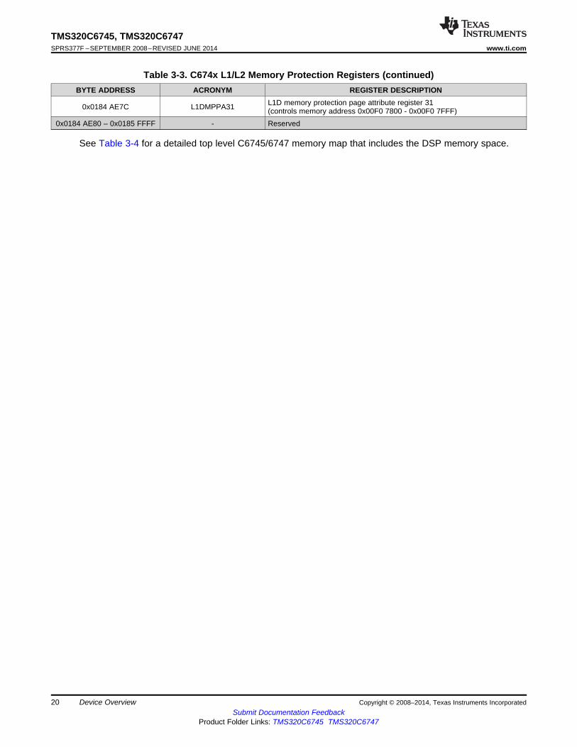
L1D memory protection page attribute register 310x0184 AE7C L1DMPPA31 (controls memory address 0x00F0 7800 - 0x00F0 7FFF)0x0184 AE80 – 0x0185 FFFF - Reserved
See Table 3-4 for a detailed top level C6745/6747 memory map that includes the DSP memory space.
20 Device Overview Copyright © 2008–2014, Texas Instruments IncorporatedSubmit Documentation Feedback
Product Folder Links: TMS320C6745 TMS320C6747
TMS320C6745, TMS320C6747www.ti.com SPRS377F –SEPTEMBER 2008–REVISED JUNE 2014
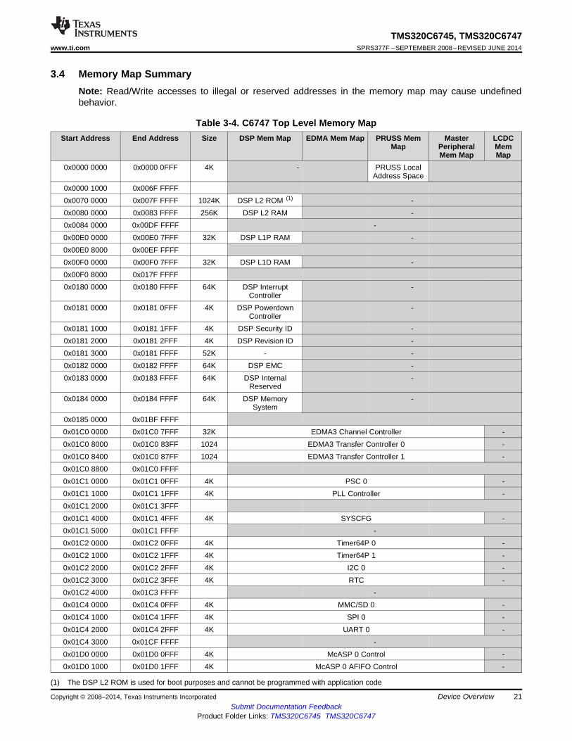
3.4 Memory Map SummaryNote: Read/Write accesses to illegal or reserved addresses in the memory map may cause undefinedbehavior.
Table 3-4. C6747 Top Level Memory MapStart Address End Address Size DSP Mem Map EDMA Mem Map PRUSS Mem Master LCDC
Map Peripheral MemMem Map Map
0x0000 0000 0x0000 0FFF 4K - PRUSS LocalAddress Space
0x0000 1000 0x006F FFFF0x0070 0000 0x007F FFFF 1024K DSP L2 ROM (1) -0x0080 0000 0x0083 FFFF 256K DSP L2 RAM -0x0084 0000 0x00DF FFFF -0x00E0 0000 0x00E0 7FFF 32K DSP L1P RAM -0x00E0 8000 0x00EF FFFF0x00F0 0000 0x00F0 7FFF 32K DSP L1D RAM -0x00F0 8000 0x017F FFFF0x0180 0000 0x0180 FFFF 64K DSP Interrupt -
Controller0x0181 0000 0x0181 0FFF 4K DSP Powerdown -
Controller0x0181 1000 0x0181 1FFF 4K DSP Security ID -0x0181 2000 0x0181 2FFF 4K DSP Revision ID -0x0181 3000 0x0181 FFFF 52K - -0x0182 0000 0x0182 FFFF 64K DSP EMC -0x0183 0000 0x0183 FFFF 64K DSP Internal -
Reserved0x0184 0000 0x0184 FFFF 64K DSP Memory -
System0x0185 0000 0x01BF FFFF0x01C0 0000 0x01C0 7FFF 32K EDMA3 Channel Controller -0x01C0 8000 0x01C0 83FF 1024 EDMA3 Transfer Controller 0 -0x01C0 8400 0x01C0 87FF 1024 EDMA3 Transfer Controller 1 -0x01C0 8800 0x01C0 FFFF0x01C1 0000 0x01C1 0FFF 4K PSC 0 -0x01C1 1000 0x01C1 1FFF 4K PLL Controller -0x01C1 2000 0x01C1 3FFF0x01C1 4000 0x01C1 4FFF 4K SYSCFG -0x01C1 5000 0x01C1 FFFF -0x01C2 0000 0x01C2 0FFF 4K Timer64P 0 -0x01C2 1000 0x01C2 1FFF 4K Timer64P 1 -0x01C2 2000 0x01C2 2FFF 4K I2C 0 -0x01C2 3000 0x01C2 3FFF 4K RTC -0x01C2 4000 0x01C3 FFFF -0x01C4 0000 0x01C4 0FFF 4K MMC/SD 0 -0x01C4 1000 0x01C4 1FFF 4K SPI 0 -0x01C4 2000 0x01C4 2FFF 4K UART 0 -0x01C4 3000 0x01CF FFFF -0x01D0 0000 0x01D0 0FFF 4K McASP 0 Control -0x01D0 1000 0x01D0 1FFF 4K McASP 0 AFIFO Control -
(1) The DSP L2 ROM is used for boot purposes and cannot be programmed with application code
Copyright © 2008–2014, Texas Instruments Incorporated Device Overview 21Submit Documentation Feedback
Product Folder Links: TMS320C6745 TMS320C6747

TMS320C6745, TMS320C6747SPRS377F –SEPTEMBER 2008–REVISED JUNE 2014 www.ti.com
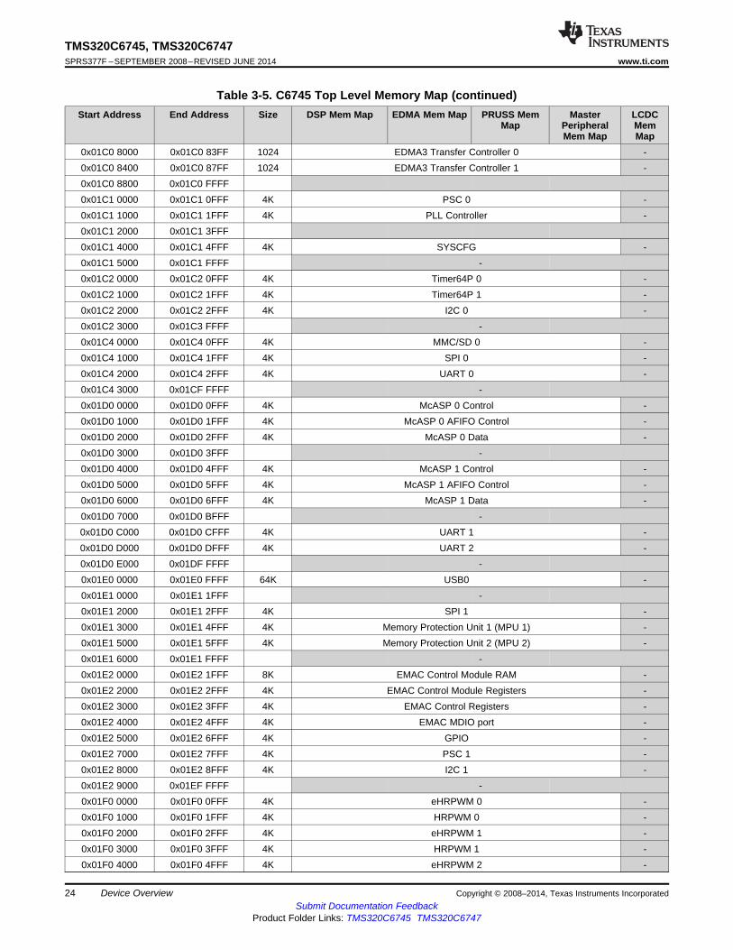
Table 3-4. C6747 Top Level Memory Map (continued)Start Address End Address Size DSP Mem Map EDMA Mem Map PRUSS Mem Master LCDC
Map Peripheral MemMem Map Map
0x01D0 2000 0x01D0 2FFF 4K McASP 0 Data -0x01D0 3000 0x01D0 3FFF -0x01D0 4000 0x01D0 4FFF 4K McASP 1 Control -0x01D0 5000 0x01D0 5FFF 4K McASP 1 AFIFO Control -0x01D0 6000 0x01D0 6FFF 4K McASP 1 Data -0x01D0 7000 0x01D0 7FFF -0x01D0 8000 0x01D0 8FFF 4K McASP 2 Control -0x01D0 9000 0x01D0 9FFF 4K McASP 2 AFIFO Control -0x01D0 A000 0x01D0 AFFF 4K McASP 2 Data -0x01D0 B000 0x01D0 BFFF -0x01D0 C000 0x01D0 CFFF 4K UART 1 -0x01D0 D000 0x01D0 DFFF 4K UART 2 -0x01D0 E000 0x01DF FFFF -0x01E0 0000 0x01E0 FFFF 64K USB0 -0x01E1 0000 0x01E1 0FFF 4K UHPI -0x01E1 1000 0x01E1 1FFF -0x01E1 2000 0x01E1 2FFF 4K SPI 1 -0x01E1 3000 0x01E1 3FFF 4K LCD Controller -0x01E1 4000 0x01E1 4FFF 4K Memory Protection Unit 1 (MPU 1) -0x01E1 5000 0x01E1 5FFF 4K Memory Protection Unit 2 (MPU 2) -0x01E1 6000 0x01E1 FFFF -0x01E2 0000 0x01E2 1FFF 8K EMAC Control Module RAM -0x01E2 2000 0x01E2 2FFF 4K EMAC Control Module Registers -0x01E2 3000 0x01E2 3FFF 4K EMAC Control Registers -0x01E2 4000 0x01E2 4FFF 4K EMAC MDIO port -0x01E2 5000 0x01E2 5FFF 4K USB1 -0x01E2 6000 0x01E2 6FFF 4K GPIO -0x01E2 7000 0x01E2 7FFF 4K PSC 1 -0x01E2 8000 0x01E2 8FFF 4K I2C 1 -0x01E2 9000 0x01EF FFFF -0x01F0 0000 0x01F0 0FFF 4K eHRPWM 0 -0x01F0 1000 0x01F0 1FFF 4K HRPWM 0 -0x01F0 2000 0x01F0 2FFF 4K eHRPWM 1 -0x01F0 3000 0x01F0 3FFF 4K HRPWM 1 -0x01F0 4000 0x01F0 4FFF 4K eHRPWM 2 -0x01F0 5000 0x01F0 5FFF 4K HRPWM 2 -0x01F0 6000 0x01F0 6FFF 4K ECAP 0 -0x01F0 7000 0x01F0 7FFF 4K ECAP 1 -0x01F0 8000 0x01F0 8FFF 4K ECAP 2 -0x01F0 9000 0x01F0 9FFF 4K EQEP 0 -0x01F0 A000 0x01F0 AFFF 4K EQEP 1 -0x01F0 B000 0x116F FFFF -0x1170 0000 0x117F FFFF 1024K DSP L2 ROM (2) -0x1180 0000 0x1183 FFFF 256K DSP L2 RAM -0x1184 0000 0x11DF FFFF -
(2) The DSP L2 ROM is used for boot purposes and cannot be programmed with application code
22 Device Overview Copyright © 2008–2014, Texas Instruments IncorporatedSubmit Documentation Feedback
Product Folder Links: TMS320C6745 TMS320C6747

TMS320C6745, TMS320C6747www.ti.com SPRS377F –SEPTEMBER 2008–REVISED JUNE 2014
Table 3-4. C6747 Top Level Memory Map (continued)Start Address End Address Size DSP Mem Map EDMA Mem Map PRUSS Mem Master LCDC
Map Peripheral MemMem Map Map
0x11E0 0000 0x11E0 7FFF 32K DSP L1P RAM -0x11E0 8000 0x11EF FFFF -0x11F0 0000 0x11F0 7FFF 32K DSP L1D RAM -0x11F0 8000 0x3FFF FFFF -0x4000 0000 0x47FF FFFF 128M EMIFA SDRAM data (CS0) -0x4800 0000 0x5FFF FFFF0x6000 0000 0x61FF FFFF 32M EMIFA async data (CS2) -0x6200 0000 0x63FF FFFF 32M EMIFA async data (CS3) -0x6400 0000 0x65FF FFFF 32M EMIFA async data (CS4) -0x6600 0000 0x67FF FFFF 32M EMIFA async data (CS5) -0x6800 0000 0x6800 7FFF 32K EMIFA Control Registers -0x6800 8000 0x7FFF FFFF -0x8000 0000 0x8001 FFFF 128K Shared RAM -0x8002 0000 0xAFFF FFFF -0xB000 0000 0xB000 7FFF 32K EMIFB Control Registers0xB000 8000 0xBFFF FFFF -0xC000 0000 0xCFFF FFFF 256M EMIFB SDRAM Data0xD000 0000 0xDFFF FFFF -
Table 3-5. C6745 Top Level Memory MapStart Address End Address Size DSP Mem Map EDMA Mem Map PRUSS Mem Master LCDC
Map Peripheral MemMem Map Map
0x0000 0000 0x0000 0FFF 4K - PRUSS LocalAddress Space
0x0000 1000 0x006F FFFF0x0070 0000 0x007F FFFF 1024K DSP L2 ROM (1) -0x0080 0000 0x0083 FFFF 256K DSP L2 RAM -0x0084 0000 0x00DF FFFF -0x00E0 0000 0x00E0 7FFF 32K DSP L1P RAM -0x00E0 8000 0x00EF FFFF0x00F0 0000 0x00F0 7FFF 32K DSP L1D RAM -0x00F0 8000 0x017F FFFF0x0180 0000 0x0180 FFFF 64K DSP Interrupt -
Controller0x0181 0000 0x0181 0FFF 4K DSP Powerdown -
Controller0x0181 1000 0x0181 1FFF 4K DSP Security ID -0x0181 2000 0x0181 2FFF 4K DSP Revision ID -0x0181 3000 0x0181 FFFF 52K - -0x0182 0000 0x0182 FFFF 64K DSP EMC -0x0183 0000 0x0183 FFFF 64K DSP Internal -
Reserved0x0184 0000 0x0184 FFFF 64K DSP Memory -
System0x0185 0000 0x01BF FFFF0x01C0 0000 0x01C0 7FFF 32K EDMA3 Channel Controller -
(1) The DSP L2 ROM is used for boot purposes and cannot be programmed with application code
Copyright © 2008–2014, Texas Instruments Incorporated Device Overview 23Submit Documentation Feedback
Product Folder Links: TMS320C6745 TMS320C6747
TMS320C6745, TMS320C6747SPRS377F –SEPTEMBER 2008–REVISED JUNE 2014 www.ti.com
Table 3-5. C6745 Top Level Memory Map (continued)Start Address End Address Size DSP Mem Map EDMA Mem Map PRUSS Mem Master LCDC
Map Peripheral MemMem Map Map
0x01C0 8000 0x01C0 83FF 1024 EDMA3 Transfer Controller 0 -0x01C0 8400 0x01C0 87FF 1024 EDMA3 Transfer Controller 1 -0x01C0 8800 0x01C0 FFFF0x01C1 0000 0x01C1 0FFF 4K PSC 0 -0x01C1 1000 0x01C1 1FFF 4K PLL Controller -0x01C1 2000 0x01C1 3FFF0x01C1 4000 0x01C1 4FFF 4K SYSCFG -0x01C1 5000 0x01C1 FFFF -0x01C2 0000 0x01C2 0FFF 4K Timer64P 0 -0x01C2 1000 0x01C2 1FFF 4K Timer64P 1 -0x01C2 2000 0x01C2 2FFF 4K I2C 0 -0x01C2 3000 0x01C3 FFFF -0x01C4 0000 0x01C4 0FFF 4K MMC/SD 0 -0x01C4 1000 0x01C4 1FFF 4K SPI 0 -0x01C4 2000 0x01C4 2FFF 4K UART 0 -0x01C4 3000 0x01CF FFFF -0x01D0 0000 0x01D0 0FFF 4K McASP 0 Control -0x01D0 1000 0x01D0 1FFF 4K McASP 0 AFIFO Control -0x01D0 2000 0x01D0 2FFF 4K McASP 0 Data -0x01D0 3000 0x01D0 3FFF -0x01D0 4000 0x01D0 4FFF 4K McASP 1 Control -0x01D0 5000 0x01D0 5FFF 4K McASP 1 AFIFO Control -0x01D0 6000 0x01D0 6FFF 4K McASP 1 Data -0x01D0 7000 0x01D0 BFFF -0x01D0 C000 0x01D0 CFFF 4K UART 1 -0x01D0 D000 0x01D0 DFFF 4K UART 2 -0x01D0 E000 0x01DF FFFF -0x01E0 0000 0x01E0 FFFF 64K USB0 -0x01E1 0000 0x01E1 1FFF -0x01E1 2000 0x01E1 2FFF 4K SPI 1 -0x01E1 3000 0x01E1 4FFF 4K Memory Protection Unit 1 (MPU 1) -0x01E1 5000 0x01E1 5FFF 4K Memory Protection Unit 2 (MPU 2) -0x01E1 6000 0x01E1 FFFF -0x01E2 0000 0x01E2 1FFF 8K EMAC Control Module RAM -0x01E2 2000 0x01E2 2FFF 4K EMAC Control Module Registers -0x01E2 3000 0x01E2 3FFF 4K EMAC Control Registers -0x01E2 4000 0x01E2 4FFF 4K EMAC MDIO port -0x01E2 5000 0x01E2 6FFF 4K GPIO -0x01E2 7000 0x01E2 7FFF 4K PSC 1 -0x01E2 8000 0x01E2 8FFF 4K I2C 1 -0x01E2 9000 0x01EF FFFF -0x01F0 0000 0x01F0 0FFF 4K eHRPWM 0 -0x01F0 1000 0x01F0 1FFF 4K HRPWM 0 -0x01F0 2000 0x01F0 2FFF 4K eHRPWM 1 -0x01F0 3000 0x01F0 3FFF 4K HRPWM 1 -0x01F0 4000 0x01F0 4FFF 4K eHRPWM 2 -
24 Device Overview Copyright © 2008–2014, Texas Instruments IncorporatedSubmit Documentation Feedback
Product Folder Links: TMS320C6745 TMS320C6747

TMS320C6745, TMS320C6747www.ti.com SPRS377F –SEPTEMBER 2008–REVISED JUNE 2014
Table 3-5. C6745 Top Level Memory Map (continued)Start Address End Address Size DSP Mem Map EDMA Mem Map PRUSS Mem Master LCDC
Map Peripheral MemMem Map Map
0x01F0 5000 0x01F0 5FFF 4K HRPWM 2 -0x01F0 6000 0x01F0 6FFF 4K ECAP 0 -0x01F0 7000 0x01F0 7FFF 4K ECAP 1 -0x01F0 8000 0x01F0 8FFF 4K ECAP 2 -0x01F0 9000 0x01F0 9FFF 4K EQEP 0 -0x01F0 A000 0x01F0 AFFF 4K EQEP 1 -0x01F0 B000 0x116F FFFF -0x1170 0000 0x117F FFFF 1024K DSP L2 ROM (2) -0x1180 0000 0x1183 FFFF 256K DSP L2 RAM -0x1184 0000 0x11DF FFFF -0x11E0 0000 0x11E0 7FFF 32K DSP L1P RAM -0x11E0 8000 0x11EF FFFF -0x11F0 0000 0x11F0 7FFF 32K DSP L1D RAM -0x11F0 8000 0x3FFF FFFF -0x4000 0000 0x5FFF FFFF0x6000 0000 0x61FF FFFF 32M EMIFA async data (CS2) -0x6200 0000 0x63FF FFFF 32M EMIFA async data (CS3) -0x6400 0000 0x65FF FFFF 32M EMIFA async data (CS4) -0x6600 0000 0x67FF FFFF 32M EMIFA async data (CS5) -0x6800 0000 0x6800 7FFF 32K EMIFA Control Registers -0x6800 8000 0xAFFF FFFF -0xB000 0000 0xB000 7FFF 32K EMIFB Control Registers0xB000 8000 0xBFFF FFFF -0xC000 0000 0xC7FF FFFF 128M EMIFB SDRAM Data0xC800 0000 0xDFFF FFFF -
(2) The DSP L2 ROM is used for boot purposes and cannot be programmed with application code
Copyright © 2008–2014, Texas Instruments Incorporated Device Overview 25Submit Documentation Feedback
Product Folder Links: TMS320C6745 TMS320C6747

VSS VSST AXR1[0]/
GP4[0]AXR1[11]/GP5[11]
SPI0_CLK/EQEP1I/GP5[2]/BOOT[2]
SPI1_CLK/EQEP1S/GP5[7]/BOOT[7]
1 2 3 4 5 6
EMA_CS[3]/AMUTE2/
GP2[6]
7
EMA_CS[0]UHPI_HAS
//
GP2[4]
8
EMA_A[0]/LCD_D[7]/
GP1[0]
9
EMA_A[4]/LCD_D[3]/
GP1[4]
10
EMA_A[8]/LCD_PCLK/
GP1[8]
11
EMA_SDCKE/GP2[0]
12
EMA_D[0]/MMCSD_DAT[0]/
UHPI_HD[0]/GP0[0]/
BOOT[12]
13
EMA_D[9]/UHPI_HD[9]/LCD_D[9]/
GP0[9]
14
VSS VSS
15 16
DVDDR AXR1[1]/
GP4[1]
UART0_RXD/I2C0_SDA/
TM64P0_IN12/GP5[8]/BOOT[8]
SPI1_ENA/UART2_RXD/
GP5[12]
SPI0_ENAUART0_CTS
//
EQEP0A/GP5[3]/BOOT[3]
SPIO_SOMI[0]/EQEPOI/GP5[0]/BOOT[0]
EMA_OEUHPI_HDS1
//
AXR0[13]/GP2[7]
EMA_BA[0]/LCD_D[4]/GP1[14]
EMA_A[1]/MMCSD_CLK/UHPI_HCNTL0/
GP1[1]
EMA_A[5]/LCD_D[2]/
GP1[5]
EMA_A[9]/LCD_HSYNC/
GP1[9]
EMA_CLK/OBSCLK/AHCLKR2/
GP1[15]
EMA_D[2]/MMCSD_DAT[2]/
UHPI_HD[2]/GP0[2]
EMA_D[10]/UHPI_HD[10]/LCD_D[10]/
GP0[10]
EMA_D[1]/MMCSD_DAT[1]/
UHPI_HD[1]/GP0[1]
DVDD
PAXR1[3]/EQEP1A/
GP4[3]
AXR1[2]/GP4[2]
UART0_TXD/I2C0_SCL/
TM64P0_OUT12/GP5[9]/BOOT[9]
SPI1_SCS[0]/UART2_TXD/
GP5[13]
SPI1_SOMI[0]/I2C1_SCL/
GP5[5]/BOOT[5]
SPI0_SIMO[0]/EQEP0S/GP5[1]/BOOT[1]
EMA_CS[2]UHPI_HCS
//
GP2[5]/BOOT[15]
EMA_BA[1]/LCD_D[5]/
UHPI_HHWIL/GP1[13]
EMA_A[2]/MMCSD_CMD/UHPI_HCNTL1/
GP1[2]
EMA_A[6]/LCD_D[1]/
GP1[6]
EMA_A[11]/
/GP1[11]
LCD_AC_ENB_CS
EMA_WE_DQM[1]
UHPI_HDS2/
/AXR0[14]/
GP2[8]
EMA_D[4]/MMCSD_DAT[4]/
UHPI_HD[4]/GP0[4]
EMA_D[12]/UHPI_HD[12]/LCD_D[12]/
GP0[12]
EMA_D[3]/MMCSD_DAT[3]/
UHPI_HD[3]/GP0[3]
EMA_D[11]/UHPI_HD[11]/
LCD_D[11]GP0[11]
NAXR1[5]/
EPWM2B/GP4[5]
AXR1[4]/EQEP1B/
GP4[4]
AXR1[10]/GP5[10]
SPI0_SCS[0]UART0_RTS
//
EQEP0B/GP5[4]/BOOT[4]
SPI1_SIMO[0]/I2C1_SDA/
GP5[6]/BOOT[6]
EMA_WAIT[0]//
GP2[10]UHPI_HRDY
EMA_RAS/EMA_CS[5]/
GP2[2]
EMA_A[10]/LCD_VSYNC/
GP1[10]
EMA_A[3]/LCD_D[6]/
GP1[3]
EMA_A[7]/LCD_D[0]/
GP1[7]
EMA_A[12]/LCD_MCLK/
GP1[12]
EMA_D[8]/UHPI_HD[8]/LCD_D[8]/
GP0[8]
EMA_D[6]/MMCSD_DAT[6]/
UHPI_HD[6]/GP0[6]
EMA_D[14]/UHPI_HD[14]/LCD_D[14]/
GP0[14]
EMA_D[5]/MMCSD_DAT[5]/
UHPI_HD[5]/GP0[5]
EMA_D[13]/UHPI_HD[13]/LCD_D[13]/
GP0[13]
M AXR1[9]/GP4[9]
AXR1[8]/EPWM1A/
GP4[8]
AXR1[7]/EPWM1B/
GP4[7]
AXR1[6]/EPWM2A/
GP4[6]DVDD VSS VSS DVDD DVDD VSS VSS DVDD
EMA_WEW/
UHPI_HR /AXR0[12]/
GP2[3]/BOOT[14]
EMA_WE_DQM[0]
UHPI_HINT/
/AXR0[15]/
GP2[9]
EMA_D[7]/MMCSD_DAT[7]/
UHPI_HD[7]/GP0[7]/
BOOT[13]
EMA_D[15]/UHPI_HD[15]/LCD_D[15]/
GP0[15]
L AHCLKR1/GP4[11]
ACLKR1/ECAP2/APWM2/GP4[12]
AFSR1/GP4[13]
AMUTE0/RESETOUT
DVDD CVDD VSS VSS VSS VSS DVDD DVDD EMB_CAS EMB_D[22] EMB_D[23]EMA_CASEMA_CS[4]
//
GP2[1]
K GP7[14]
AHCLKX1/EPWM0B/GP3[14]
ACLKX1/EPWM0A/GP3[15]
AFSX1/EPWMSYNCI/EPWMSYNCO/
GP4[10]
DVDD CVDD VSS VSS CVDD CVDD DVDD EMB_D[20]EMB_WE_
DQM[0]/GP5[15]
EMB_WE EMB_D[21]CVDD
TMSJ TDI TDO TRSTEMU[0]/GP7[15]
CVDD CVDD VSS VSS CVDD CVDD CVDDEMB_D[5]/
GP6[5]EMB_D[19]
EMB_D[6]/GP6[6]
EMB_D[7]/GP6[7]
RTC_XIH RTC_XO TCK NCUSB0_
VDDA33CVDD VSS VSS CVDD CVDD
EMB_D[3]/GP6[3]
EMB_D[17] EMB_D[18]EMB_D[4]/
GP6[4]
RTC_CVDDG RTC_VSS RESET USB0_DM DVDD CVDD VSS VSS CVDD CVDD DVDDCVDD
EMB_D[1]/GP6[1]
EMB_D[31] EMB_D[16]EMB_D[2]/
GP6[2]
OSCOUTF OSCIN NC USB0_DP DVDD CVDD RSV1 VSS VSS VSS DVDD DVDDEMB_D[15]/
GP6[15]EMB_D[29] EMB_D[30]
EMB_D[0]/GP6[0]
PLL0_VSSAE OSCVSSUSB0_
VDDA18
USB0_DRVVBUS/
GP4[15]DVDD VSS VSS DVDD VSS VSSDVDD DVDD
EMB_D[13]/GP6[13]
EMB_D[27] EMB_D[28]EMB_D[14]/
GP6[14]
PLL0_VDDAD USB0_ID USB0_VBUSAMUTE1/EPWMTZ/GP4[14]
AFSX0/GP2[13]/BOOT[10]
UART1_TXD/AXR0[10]/GP3[10]
AXR0[6]/RMII_RXER/
ACLKR2/GP3[6]
AXR0[2]/RMII_TXEN/
AXR2[3]/GP3[2]
EMB_CS[0]EMB_A[0]/
GP7[2]EMB_A[4]/
GP7[6]EMB_A[8]/GP7[10]
EMB_D[9]/GP6[9]
EMB_D[10]/GP6[10]
EMB_D[11]/GP6[11]
EMB_D[12]/GP6[12]
USB1_VDDA33
C USB1_VDDA18
USB0_VDDA12
AFSR0/GP3[12]
ACLKX0/ECAP0/APWM0/GP2[12]
UART1_RXD/AXR0[9]/GP3[9]
AXR0[5]/RMII_RXD[1]/
AFSX2/GP3[5]
AXR0[1]/RMII_TXD[1]/
ACLKX2/GP3[1]
EMB_BA[0]/GP7[1]
EMB_A[1]/GP7[3]
EMB_A[5]/GP7[7]
EMB_A[9]/GP7[11]
EMB_SDCKE EMB_CLKEMB_WE_
DQM[1]/GP5[14]
EMB_D[8]/GP6[8]
B RSV2 VSS USB1_DM
ACLKR0/ECAP1/APWM1/GP2[15]
AHCLKX0/AHCLKX2/
USB_REFCLKIN/
GP2[11]
AXR0[8]/MDIO_D/GP3[8]
AXR0[4]/RMII_RXD[0]/
AXR2[1]/GP3[4]
AXR0[0]/RMII_TXD[0]/
AFSR2/GP3[0]
1 2 3 4 5 6 7 8 9 10 11 12 13 14 15 16
EMB_BA[1]/GP7[0]
EMB_A[2]/GP7[4]
EMB_A[6]/GP7[8]
EMB_A[11]/GP7[13]
EMB_WE_DQM[2]
EMB_D[25]EMB_A[12]/
GP3[13]DVDD
A VSS VSS USB1_DP
AHCLKR0/RMII_MHZ_
50_CLK/GP2[14]/BOOT[11]
AXR0[11]/AXR2[0]/GP3[11]
AXR0[7]/MDIO_CLK/
GP3[7]
AXR0[3]/RMII_CRS_DV/
AXR2[2]/GP3[3]
EMB_RASEMB_A[10]/
GP7[12]EMB_A[3]/
GP7[5]EMB_A[7]/
GP7[9]EMB_WE_
DQM[3]EMB_D[24] EMB_D[26] VSS VSS
T
R
P
N
M
L
K
J
H
G
F
E
D
C
B
A
RVDD RVDD
TMS320C6745, TMS320C6747SPRS377F –SEPTEMBER 2008–REVISED JUNE 2014 www.ti.com
3.5 Pin AssignmentsExtensive use of pin multiplexing is used to accommodate the largest number of peripheral functions inthe smallest possible package. Pin multiplexing is controlled using a combination of hardwareconfiguration at device reset and software programmable register settings.
3.5.1 Pin Map (Bottom View)Figure 3-3 and Figure 3-4 show the pin assignments for ZKB package and PTP package, respectively.
Figure 3-3. Pin Map (ZKB)
26 Device Overview Copyright © 2008–2014, Texas Instruments IncorporatedSubmit Documentation Feedback
Product Folder Links: TMS320C6745 TMS320C6747

133RSV2
134USB0_VDDA12
135USB0_VDDA18
136NC
137USB0_DP
138USB0_DM
139NC
140USB0_VDDA33
141PLL0_VDDA
142
143OSCIN
144
145OSCOUT
146RESET
147
148RSV4
149RSV3
150
GP7[14]
152
153
154
155
156
157
158
159
160
161
162
163
164
165
166
167
168
169
170
171
172
173
174
175
176
PLL0_VSSA
OSCVSS
CVDD
TRST
TMS
TDI
TCK
TDO
RVDD
AFSX1/EPWMSYNCI/EPWMSYNC0/GP4[10]
DVDD
AFSR1/GP4[13]
AXR1[8]/EPWM1A/GP4[8]
AXR1[7]/EPWM1B/GP4[7]
AXR1[6]/EPWM2A/GP4[6]
AXR1[5]/EPWM2B/GP4[5]
1A
XR
1[0
]/G
P4
[0]
2U
AR
T0_R
XD
/I2
C0_
SD
A/T
M64P
0_IN
12/G
P5[8
]/B
OO
T[8
]
3U
AR
T0
_T
XD
/I2
C0_
SC
L/T
M64
P0_O
UT
12/G
P5[9
]/B
OO
T[9
]
4A
XR
1[1
0]/G
P5
[10]
5D
VD
D
6A
XR
1[1
1]/G
P5[1
1]
7S
PI1
_E
NA
/UA
RT
2_R
XD
/GP
5[1
2]
8S
PI1
_S
CS
[0]/U
AR
T2_T
XD
/GP
5[1
3]
9S
PI0
_S
CS
[0]
UA
RT
0_R
TS
//E
QE
P0
B/G
P5
[4]/B
OO
T[4
]
10
11
SP
I0_C
LK
/EQ
EP
1I/G
P5[2
]/B
OO
T[2
]
12
13
SP
I1_
SO
MI[0]/
I2C
1_S
CL/G
P5[5
]/B
OO
T[5
]
14
SP
I1_S
IMO
[0]/
I2C
1_S
DA
/GP
5[6
]/B
OO
T[6
]
15
16
SP
I1_C
LK
/EQ
EP
1S
/GP
5[7
]/B
OO
T[7
]
17
SP
I0_
SO
MI[0]/
EQ
EP
0I/G
P5[0
]/B
OO
T[0
]
18
19
EM
A_W
AIT
[0]/G
P2[1
0]
20
21
22
23
24
25
EM
A_B
A[0
]/G
P1[1
4]
26
27
28
29
30
31
32
33
34
35
36
37
38
39
40
41
CV
DD
SP
I0_E
NA
UA
RT
0_C
TS
//E
QE
P0A
/GP
5[3
]/B
OO
T[3
]
DV
DD
SP
I0_
SIM
O[0
]/E
QE
P0
S/G
P5[1
]/B
OO
T[1
]
CV
DD
EM
A_C
S[3
]/G
P2[6
]
EM
A_
OE
/AX
R0[1
3]/G
P2
[7]
EM
A_C
S[2
]/G
P2
[5]/B
OO
T[1
5]
DV
DD
EM
A_
BA
[1]/G
P1[1
3]
EM
A_
A[1
0]/G
P1[1
0]
CV
DD
EM
A_A
[0]/G
P1[0
]
EM
A_A
[1]/M
MC
SD
_C
LK
/GP
1[1
]
EM
A_A
[2]/M
MC
SD
_C
MD
/GP
1[2
]
EM
A_
A[3
]/G
P1[3
]
DV
DD
EM
A_A
[4]/G
P1[4
]
EM
A_A
[5]/G
P1[5
]
EM
A_A
[6]/G
P1
[6]
EM
A_
A[7
]/G
P1[7
]
CV
DD
EM
A_A
[8]/G
P1[8
]
EM
A_A
[9]/G
P1[9
]
EM
A_
A[1
1]/G
P1[1
1]
EM
A_
A[1
2]/G
P1[1
2]
DV
DD
EM
A_D
[0]/M
MC
SD
_D
AT
[0]/G
P0[0
]/B
OO
T[1
2]
151DVDD
CVDD
DVDD
AHCLKX1/EPWM0B/GP3[14]
CVDD
ACLKX1/EPWM0A/GP3[15]
ACLKR1/ECAP2/APWM2/GP4[12]
CVDD
DVDD
AXR1[4]/EQEP1B/GP4[4]
AXR1[3]/EQEP1A/GP4[3]
AXR1[2]/GP4[2]
AXR1[1]/GP4[1]
42
43
44
88 EMB_SDCKE
87 DVDD
86 EMB_CLK
85 EMB_WE_DQM[1]/GP5[14]
84 EMB_D[8]/GP6[8]
83 EMB_D[9]/GP6[9]
82 EMB_D[10]/GP6[10]
81 DVDD
80 EMB_D[11]/GP6[11]
79 EMB_D[12]/GP6[12]
78 EMB_D[13]/GP6[13]
77 CVDD
76 EMB_D[14]/GP6[14]
75
74 EMB_D[15]/GP6[15]
73 EMB_D[0]/GP6[0]
72 EMB_D[1]/GP6[1]
71 DVDD
70 EMB_D[2]/GP6[2]
69 CVDD
68 EMB_D[3]/GP6[3]
67 RVDD
66 EMB_D[4]/GP6[4]
65 DVDD
64 EMB_D[5]/GP6[5]
63 EMB_D[6]/GP6[6]
62 EMB_D[7]/GP6[7]
61 CVDD
60 EMB_WE_DQM[0]/GP5[15]
59 EMB_WE
58 DVDD
57 EMB_CAS
56 CVDD
55 EMA_WE/AXR0[12]/GP2[3]/BOOT[14]
54 EMA_D[7]/MMCSD_DAT[7]/GP0[7]/BOOT[13]
53 DVDD
52 EMA_D[6]/MMCSD_DAT[6]/GP0[6]
51 EMA_D[5]/MMCSD_DAT[5]/GP0[5]
50 CVDD
49 EMA_D[4]/MMCSD_DAT[4]/GP0[4]
48 EMA_D[3]/MMCSD_DAT[3]/GP0[3]
47 DVDD
46 EMA_D[2]/MMCSD_DAT[2]/GP0[2]
45 EMA_D[1]/MMCSD_DAT[1]/GP0[1]
DVDD
132
AM
UT
E1/E
PW
MT
Z/G
P4[1
4]
131
AF
SR
0/G
P3[1
2]
130
AC
LK
R0/E
CA
P1/A
PW
M1/G
P2[1
5]
129
AH
CLK
R0/R
MII_M
HZ
_50_C
LK
/GP
2[1
4]/B
OO
T[1
1]
128
DV
DD
127
AF
SX
0/G
P2[1
3]/B
OO
T[1
0]
126
AC
LK
X0/E
CA
P0/A
PW
M0/G
P2[1
2]
125
AH
CLK
X0/U
SB
_R
EF
CLK
IN/G
P2[1
1]
124
AX
R0[1
1]/G
P3[1
1]
123
UA
RT
1_T
XD
/AX
R0[1
0]/G
P3[1
0]
122
UA
RT
1_R
XD
/AX
R0[9
]/G
P3[9
]
121
AX
R0[8
]/M
DIO
_D
/GP
3[8
]
120
AX
R0[7
]/M
DIO
_C
LK
/GP
3[7
]
119
118
AX
R0[6
]/R
MII_R
XE
R/G
P3[6
]
117
AX
R0[5
]/R
MII_R
XD
[1]/G
P3[5
]
116
AX
R0[4
]/R
MII_R
XD
[0]/G
P3[4
]
115
AX
R0[3
]/R
MII_C
RS
_D
V/G
P3[3
]
114
113
AX
R0[2
]/R
MII_T
XE
N/G
P3[2
]
112
AX
R0[1
]/R
MII_T
XD
[1]/G
P3[1
]
111
AX
R0[0
]/R
MII_T
XD
[0]/G
P3[0
]
110
EM
B_R
AS
109
DV
DD
108
EM
B_C
S[0
]
107
EM
B_B
A[0
]/G
P7[1
]
106
EM
B_B
A[1
]/G
P7[0
]
105
EM
B_A
[10]/G
P7[1
2]
104
103
EM
B_A
[0]/G
P7[2
]
102
EM
B_A
[1]/G
P7[3
]
101
EM
B_A
[2]/G
P7[4
]
100
EM
B_A
[3]/G
P7[5
]
99
98
EM
B_A
[4]/G
P7[6
]
97
EM
B_A
[5]/G
P7[7
]
96
EM
B_A
[6]/G
P7[8
]
95
EM
B_A
[7]/G
P7[9
]
94
EM
B_A
[8]/G
P7[1
0]
93
92
EM
B_A
[9]/G
P7[1
1]
91
EM
B_A
[11]/G
P7[1
3]
90
89
EM
B_A
[12]/G
P3[1
3]
DV
DD
DV
DD
CV
DD
DV
DD
CV
DD
CV
DD
V
(177)
SS
Thermal Pad
TMS320C6745, TMS320C6747www.ti.com SPRS377F –SEPTEMBER 2008–REVISED JUNE 2014
Figure 3-4. Pin Map (PTP)
Copyright © 2008–2014, Texas Instruments Incorporated Device Overview 27Submit Documentation Feedback
Product Folder Links: TMS320C6745 TMS320C6747

TMS320C6745, TMS320C6747SPRS377F –SEPTEMBER 2008–REVISED JUNE 2014 www.ti.com
3.6 Terminal Functionsto identify the external signal names, the associated pin/ball numbers along with the mechanical packagedesignator, the pin type (I, O, IO, OZ, or PWR), whether the pin/ball has any internal pullup/pulldownresistors, whether the pin/ball is configurable as an IO in GPIO mode, and a functional pin description.
3.6.1 Device Reset and JTAG
Table 3-6. Reset and JTAG Terminal Functions
PIN NOSIGNAL NAME TYPE (1) PULL (2) DESCRIPTION
PTP ZKBRESET
RESET 146 G3 I Device reset inputAMUTE0/ RESETOUT - L4 O (3) IPD Reset output
JTAGTMS 152 J1 I IPU JTAG test mode selectTDI 153 J2 I IPU JTAG test data inputTDO 156 J3 O IPD JTAG test data outputTCK 155 H3 I IPU JTAG test clockTRST 150 J4 I IPD JTAG test resetEMU[0]/GP7[15] - J5 I/O IPU Emulation Signal
(1) I = Input, O = Output, I/O = Bidirectional, Z = High impedance, PWR = Supply voltage, GND = Ground, A = Analog signal.Note: For multiplexed pins where functions have different types (ie., input versus output), the table reflects the pin function direction forthat particular peripheral.
(2) IPD = Internal Pulldown resistor, IPU = Internal Pullup resistor(3) Open drain mode for RESETOUT function.
3.6.2 High-Frequency Oscillator and PLL
Table 3-7. High-Frequency Oscillator and PLL Terminal Functions
PIN NOSIGNAL NAME TYPE (1) PULL (2) DESCRIPTION
PTP ZKBEMA_CLK/OBSCLK/AHCLKR - R12 O IPU PLL Observation Clock2/GP1[15]
1.2-V OSCILLATOROSCIN 143 F2 I Oscillator inputOSCOUT 145 F1 O Oscillator outputOSCVSS 144 E2 GND Oscillator ground (for filter only)
1.2-V PLLPLL0_VDDA 141 D1 PWR PLL analog VDD (1.2-V filtered supply)PLL0_VSSA 142 E1 GND PLL analog VSS (for filter)
(1) I = Input, O = Output, I/O = Bidirectional, Z = High impedance, PWR = Supply voltage, GND = Ground, A = Analog signal.Note: For multiplexed pins where functions have different types (ie., input versus output), the table reflects the pin function direction forthat particular peripheral.
(2) IPD = Internal Pulldown resistor, IPU = Internal Pullup resistor
28 Device Overview Copyright © 2008–2014, Texas Instruments IncorporatedSubmit Documentation Feedback
Product Folder Links: TMS320C6745 TMS320C6747

TMS320C6745, TMS320C6747www.ti.com SPRS377F –SEPTEMBER 2008–REVISED JUNE 2014
3.6.3 Real-Time Clock and 32-kHz Oscillator
Table 3-8. Real-Time Clock (RTC) and 1.2-V, 32-kHz Oscillator Terminal Functions
PIN NOSIGNAL NAME TYPE (1) PULL (2) DESCRIPTION
PTP ZKBRTC_CVDD - G1 PWR RTC module core power (isolated from rest of chip CVDD)RTC_XI - H1 I Low-frequency (32-kHz) oscillator receiver for real-time clockRTC_XO - H2 O Low-frequency (32-kHz) oscillator driver for real-time clockRTC_Vss - G2 GND Oscillator ground (for filter)
(1) I = Input, O = Output, I/O = Bidirectional, Z = High impedance, PWR = Supply voltage, GND = Ground, A = Analog signal.Note: For multiplexed pins where functions have different types (ie., input versus output), the table reflects the pin function direction forthat particular peripheral.
(2) IPD = Internal Pulldown resistor, IPU = Internal Pullup resistor
3.6.4 External Memory Interface A (ASYNC, SDRAM)
Table 3-9. External Memory Interface A (EMIFA) Terminal Functions
PIN NOSIGNAL NAME TYPE (1) PULL (2) MUXED DESCRIPTION
PTP ZKBEMA_D[15]/UHPI_HD[15]/LCD_D[15]/GP0[15] - M16 I/O IPDEMA_D[14]/UHPI_HD[14]/LCD_D[14]/GP0[14] - N14 I/O IPDEMA_D[13]/UHPI_HD[13]/LCD_D[13]/GP0[13] - N16 I/O IPDEMA_D[12]/UHPI_HD[12]/LCD_D[12]/GP0[12] - P14 I/O IPD UHPI, LCD,
GPIOEMA_D[11]/UHPI_HD[11]/LCD_D[11]/GP0[11] - P16 I/O IPDEMA_D[10]/UHPI_HD[10]/LCD_D[10]/GP0[10] - R14 I/O IPDEMA_D[9]/UHPI_HD[9]/LCD_D[9]/GP0[9] - T14 I/O IPDEMA_D[8]/UHPI_HD[8]/LCD_D[8]/GP0[8] - N12 I/O IPD
MMC/SD,EMA_D[7]/MMCSD_DAT[7]/UHPI_HD[7]/GP0[7]/BOOT[13] 54 M15 I/O IPU UHPI, GPIO, EMIFA data bus
BOOTEMA_D[6]/MMCSD_DAT[6]/UHPI_HD[6]/GP0[6] 52 N13 I/O IPUEMA_D[5]/MMCSD_DAT[5]/UHPI_HD[5]/GP0[5] 51 N15 I/O IPUEMA_D[4]/MMCSD_DAT[4]/UHPI_HD[4]/GP0[4] 49 P13 I/O IPU MMC/SD,
UHPI, GPIOEMA_D[3]/MMCSD_DAT[3]/UHPI_HD[3]/GP0[3] 48 P15 I/O IPUEMA_D[2]/MMCSD_DAT[2]/UHPI_HD[2]/GP0[2] 46 R13 I/O IPUEMA_D[1]/MMCSD_DAT[1]/UHPI_HD[1]/GP0[1] 45 R15 I/O IPU
MMC/SD,EMA_D[0]/MMCSD_DAT[0]/UHPI_HD[0]/GP0[0]/BOOT[12] 44 T13 I/O IPU UHPI, GPIO,
BOOT
(1) I = Input, O = Output, I/O = Bidirectional, Z = High impedance, PWR = Supply voltage, GND = Ground, A = Analog signal.Note: The pin type shown refers to the input, output or high-impedance state of the pin function when configured as the the signal namehighlighted in bold. All multiplexed signals may enter a high-impedance state when the configured function is input-only or the configuredfunction supports high-Z operation. All GPIO signals can be used as input or output. For multiplexed pins where functions have differenttypes (ie., input versus output), the table reflects the pin function direction for that particular peripheral.
(2) IPD = Internal Pulldown resistor, IPU = Internal Pullup resistor
Copyright © 2008–2014, Texas Instruments Incorporated Device Overview 29Submit Documentation Feedback
Product Folder Links: TMS320C6745 TMS320C6747

TMS320C6745, TMS320C6747SPRS377F –SEPTEMBER 2008–REVISED JUNE 2014 www.ti.com
Table 3-9. External Memory Interface A (EMIFA) Terminal Functions (continued)PIN NO
SIGNAL NAME TYPE (1) PULL (2) MUXED DESCRIPTIONPTP ZKB
EMA_A[12]/LCD_MCLK/GP1[12] 42 N11 O IPUEMA_A[11] /LCD_AC_ENB_CS/GP1[11] 41 P11 O IPUEMA_A[10]/LCD_VSYNC/GP1[10] 27 N8 O IPUEMA_A[9]/LCD_HSYNC/GP1[9] 40 R11 O IPUEMA_A[8]/LCD_PCLK/GP1[8] 39 T11 O IPU
LCD, GPIO EMIFA address busEMA_A[7]/LCD_D[0]/GP1[7] 37 N10 O IPDEMA_A[6]/LCD_D[1]/GP1[6] 36 P10 O IPDEMA_A[5]/LCD_D[2]/GP1[5] 35 R10 O IPDEMA_A[4]/LCD_D[3]/GP1[4] 34 T10 O IPDEMA_A[3]/LCD_D[6]/GP1[3] 32 N9 O IPDEMA_A[2]/MMCSD_CMD/UHPI_HCNTL1/GP1[2] 31 P9 O IPU MMCSD,
UHPI, GPIOEMA_A[1]/MMCSD_CLK/UHPI_HCNTL0/GP1[1] 30 R9 O IPU EMIFA address busEMA_A[0]/LCD_D[7]/GP1[0] 29 T9 O IPD LCD, GPIO
LCD, UHPI,EMA_BA[1]/LCD_D[5]/UHPI_HHWIL/GP1[13] 26 P8 O IPU GPIO EMIFA bank addressEMA_BA[0]/LCD_D[4]/GP1[14] 25 R8 O IPU LCD, GPIO
McASP2,EMA_CLK/OBSCLK/AHCLKR2/GP1[15] - R12 O IPU EMIFA clockGPIOEMIFA SDRAM clockEMA_SDCKE/GP2[0] - T12 O IPU GPIO enableEMIFA SDRAM rowEMA_RAS/EMA_CS[5]/GP2[2] - N7 O IPU address strobe
EMIF A chipEMIFA SDRAMselect, GPIO
EMA_CAS/EMA_CS[4]/GP2[1] - L16 O IPU column addressstrobe
EMA_RAS/EMA_CS[5] /GP2[2] - N7 O IPU EMIF ASDRAM, GPIOEMA_CAS/EMA_CS[4] /GP2[1] - L16 O IPU
EMIFA Async ChipMcASP2,EMA_CS[3]/AMUTE2/GP2[6] 21 T7 O IPU SelectGPIOUHPI, GPIO,EMA_CS[2]/UHPI_HCS/GP2[5]/BOOT[15] 23 P7 O IPU BOOT
EMIFA SDRAM chipEMA_CS[0]/UHPI_HAS/GP2[4] - T8 O IPU UHPI, GPIO selectUHPI, EMIFA SDRAM writeEMA_WE/UHPI_HRW/AXR0[12]/GP2[3]/BOOT[14] 55 M13 O IPU MCASP0, enableGOPIO, BOOT
EMIFA writeEMA_WE_DQM[1] /UHPI_HDS2/AXR0[14]/GP2[8] - P12 O IPU enable/data mask for
EMA_D[15:8]UHPI, McASP,GPIO EMIFA write
EMA_WE_DQM[0] /UHPI_HINT/AXR0[15]/GP2[9] - M14 O IPU enable/data mask forEMA_D[7:0]
UHPI,EMA_OE/UHPI_HDS1/AXR0[13]/GP2[7] 22 R7 O IPU McASP0, EMIFA output enable
GPIOEMIFA waitEMA_WAIT[0]/ UHPI_HRDY/GP2[10] 19 N6 I IPU UHPI, GPIO input/interrupt
30 Device Overview Copyright © 2008–2014, Texas Instruments IncorporatedSubmit Documentation Feedback
Product Folder Links: TMS320C6745 TMS320C6747

TMS320C6745, TMS320C6747www.ti.com SPRS377F –SEPTEMBER 2008–REVISED JUNE 2014
3.6.5 External Memory Interface B (only SDRAM)
Table 3-10. External Memory Interface B (EMIFB) Terminal Functions
PIN NOSIGNAL NAME TYPE (1) PULL (2) MUXED DESCRIPTION
PTP ZKBEMB_D[31] - G14 I/O IPDEMB_D[30] - F15 I/O IPDEMB_D[29] - F14 I/O IPDEMB_D[28] - E15 I/O IPDEMB_D[27] - E14 I/O IPDEMB_D[26] - A14 I/O IPDEMB_D[25] - B14 I/O IPDEMB_D[24] - A13 I/O IPDEMB_D[23] - L15 I/O IPDEMB_D[22] - L14 I/O IPDEMB_D[21] - K16 I/O IPDEMB_D[20] - K13 I/O IPDEMB_D[19] - J14 I/O IPDEMB_D[18] - H15 I/O IPDEMB_D[17] - H14 I/O IPDEMB_D[16] - G15 I/O IPD
EMIFB SDRAM data busEMB_D[15]/GP6[15] 74 F13 I/O IPDEMB_D[14]/GP6[14] 76 E16 I/O IPDEMB_D[13]/GP6[13] 78 E13 I/O IPDEMB_D[12]/GP6[12] 79 D16 I/O IPDEMB_D[11]/GP6[11] 80 D15 I/O IPDEMB_D[10]/GP6[10] 82 D14 I/O IPDEMB_D[9]/GP6[9] 83 D13 I/O IPDEMB_D[8]/GP6[8] 84 C16 I/O IPD
GPIOEMB_D[7]/GP6[7] 62 J16 I/O IPDEMB_D[6]/GP6[6] 63 J15 I/O IPDEMB_D[5]/GP6[5] 64 J13 I/O IPDEMB_D[4]/GP6[4] 66 H16 I/O IPDEMB_D[3]/GP6[3] 68 H13 I/O IPDEMB_D[2]/GP6[2] 70 G16 I/O IPDEMB_D[1]/GP6[1] 72 G13 I/O IPDEMB_D[0]/GP6[0] 73 F16 I/O IPDEMB_A[12]/GP3[13] 89 B15 O IPDEMB_A[11]/GP7[13] 91 B12 O IPDEMB_A[10]/GP7[12] 105 A9 O IPDEMB_A[9]/GP7[11] 92 C12 O IPD EMIFB SDRAM row/columnGPIO address busEMB_A[8]/GP7[10] 94 D12 O IPDEMB_A[7]/GP7[9] 95 A11 O IPDEMB_A[6]/GP7[8] 96 B11 O IPDEMB_A[5]/GP7[7] 97 C11 O IPD
(1) I = Input, O = Output, I/O = Bidirectional, Z = High impedance, PWR = Supply voltage, GND = Ground, A = Analog signal.Note: The pin type shown refers to the input, output or high-impedance state of the pin function when configured as the the signal namehighlighted in bold. All multiplexed signals may enter a high-impedance state when the configured function is input-only or the configuredfunction supports high-Z operation. All GPIO signals can be used as input or output. For multiplexed pins where functions have differenttypes (ie., input versus output), the table reflects the pin function direction for that particular peripheral.
(2) IPD = Internal Pulldown resistor, IPU = Internal Pullup resistor
Copyright © 2008–2014, Texas Instruments Incorporated Device Overview 31Submit Documentation Feedback
Product Folder Links: TMS320C6745 TMS320C6747

TMS320C6745, TMS320C6747SPRS377F –SEPTEMBER 2008–REVISED JUNE 2014 www.ti.com
Table 3-10. External Memory Interface B (EMIFB) Terminal Functions (continued)PIN NO
SIGNAL NAME TYPE (1) PULL (2) MUXED DESCRIPTIONPTP ZKB
EMB_A[4]/GP7[6] 98 D11 O IPDEMB_A[3]/GP7[5] 100 A10 O IPD
EMIFB SDRAM row/columnEMB_A[2]/GP7[4] 101 B10 O IPD addressEMB_A[1]/GP7[3] 102 C10 O IPD GPIOEMB_A[0]/GP7[2] 103 D10 O IPDEMB_BA[1]/GP7[0] 106 B9 O IPU
EMIFB SDRAM bank addressEMB_BA[0]/GP7[1] 107 C9 O IPUEMB_CLK 86 C14 O IPU EMIF SDRAM clockEMB_SDCKE 88 C13 O IPU EMIFB SDRAM clock enableEMB_WE 59 K15 O IPU EMIFB write enable
EMIFB SDRAM row addressEMB_RAS 110 A8 O IPU strobeEMIFB column addressEMB_CAS 57 L13 O IPU strobe
EMB_CS[0] 108 D9 O IPU EMIFB SDRAM chip select 0EMB_WE_DQM[3] - A12 O IPUEMB_WE_DQM[2] - B13 O IPU EMIFB write enable/data
mask for EMB_DEMB_WE_DQM[1] /GP5[14] 85 C15 O IPUGPIO
EMB_WE_DQM[0] /GP5[15] 60 K14 O IPU
32 Device Overview Copyright © 2008–2014, Texas Instruments IncorporatedSubmit Documentation Feedback
Product Folder Links: TMS320C6745 TMS320C6747

TMS320C6745, TMS320C6747www.ti.com SPRS377F –SEPTEMBER 2008–REVISED JUNE 2014
3.6.6 Serial Peripheral Interface Modules (SPI0, SPI1)
Table 3-11. Serial Peripheral Interface (SPI) Terminal Functions
PIN NOSIGNAL NAME TYPE (1) PULL (2) MUXED DESCRIPTION
PTP ZKBSPI0
UART0, EQEP0B,SPI0_SCS[0] /UART0_RTS/EQEP0B/GP5[4]/BOOT[4] 9 N4 I/O IPU SPI0 chip selectGPIO, BOOTUART0, EQEP0A,SPI0_ENA /UART0_CTS/EQEP0A/GP5[3]/BOOT[3] 12 R5 I/O IPU SPI0 enableGPIO, BOOT
SPI0_CLK/EQEP1I/GP5[2]/BOOT[2] 11 T5 I/O IPD eQEP1, GPIO, BOOT SPI0 clockSPI0 data slave-in-SPI0_SIMO[0]/EQEP0S/GP5[1]/BOOT[1] 18 P6 I/O IPD master-out
eQEP0, GPIO, BOOTSPI0 data slave-SPI0_SOMI[0]/EQEP0I/GP5[0]/BOOT[0] 17 R6 I/O IPD out-master-in
SPI1SPI1_SCS[0] /UART2_TXD/GP5[13] 8 P4 I/O IPU SPI1 chip select
UART2, GPIOSPI1_ENA /UART2_RXD/GP5[12] 7 R4 I/O IPU SPI1 enableSPI1_CLK/EQEP1S/GP5[7]/BOOT[7] 16 T6 I/O IPD eQEP1, GPIO, BOOT SPI1 clock
SPI1 data slave-in-SPI1_SIMO[0]/I2C1_SDA/GP5[6]/BOOT[6] 14 N5 I/O IPU master-outI2C1, GPIO, BOOT
SPI1 data slave-SPI1_SOMI[0]/I2C1_SCL/GP5[5]/BOOT[5] 13 P5 I/O IPU out-master-in
(1) I = Input, O = Output, I/O = Bidirectional, Z = High impedance, PWR = Supply voltage, GND = Ground, A = Analog signal.Note: The pin type shown refers to the input, output or high-impedance state of the pin function when configured as the the signal namehighlighted in bold. All multiplexed signals may enter a high-impedance state when the configured function is input-only or the configuredfunction supports high-Z operation. All GPIO signals can be used as input or output. For multiplexed pins where functions have differenttypes (ie., input versus output), the table reflects the pin function direction for that particular peripheral.
(2) IPD = Internal Pulldown resistor, IPU = Internal Pullup resistor
Copyright © 2008–2014, Texas Instruments Incorporated Device Overview 33Submit Documentation Feedback
Product Folder Links: TMS320C6745 TMS320C6747
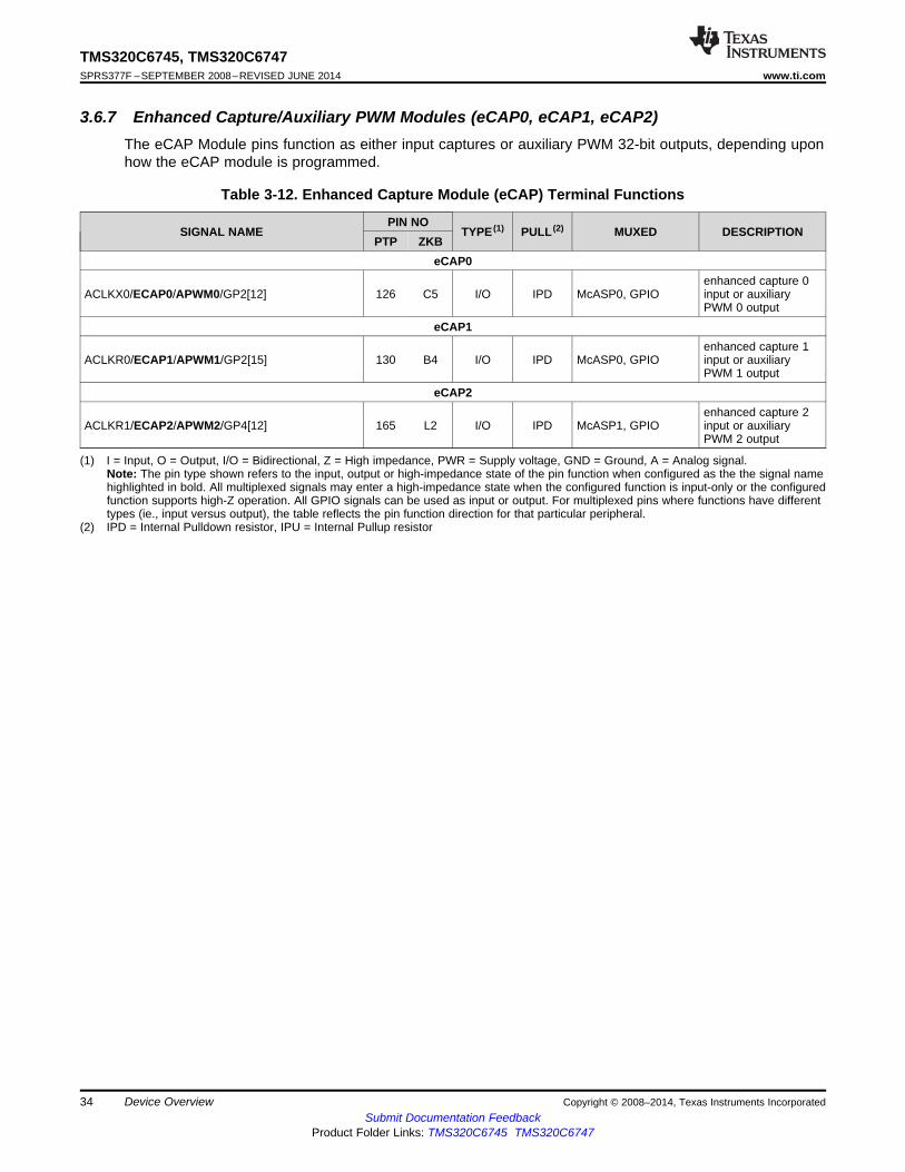
TMS320C6745, TMS320C6747SPRS377F –SEPTEMBER 2008–REVISED JUNE 2014 www.ti.com
3.6.7 Enhanced Capture/Auxiliary PWM Modules (eCAP0, eCAP1, eCAP2)The eCAP Module pins function as either input captures or auxiliary PWM 32-bit outputs, depending uponhow the eCAP module is programmed.
Table 3-12. Enhanced Capture Module (eCAP) Terminal Functions
PIN NOSIGNAL NAME TYPE (1) PULL (2) MUXED DESCRIPTION
PTP ZKBeCAP0
enhanced capture 0ACLKX0/ECAP0/APWM0/GP2[12] 126 C5 I/O IPD McASP0, GPIO input or auxiliary
PWM 0 outputeCAP1
enhanced capture 1ACLKR0/ECAP1/APWM1/GP2[15] 130 B4 I/O IPD McASP0, GPIO input or auxiliary
PWM 1 outputeCAP2
enhanced capture 2ACLKR1/ECAP2/APWM2/GP4[12] 165 L2 I/O IPD McASP1, GPIO input or auxiliary
PWM 2 output
(1) I = Input, O = Output, I/O = Bidirectional, Z = High impedance, PWR = Supply voltage, GND = Ground, A = Analog signal.Note: The pin type shown refers to the input, output or high-impedance state of the pin function when configured as the the signal namehighlighted in bold. All multiplexed signals may enter a high-impedance state when the configured function is input-only or the configuredfunction supports high-Z operation. All GPIO signals can be used as input or output. For multiplexed pins where functions have differenttypes (ie., input versus output), the table reflects the pin function direction for that particular peripheral.
(2) IPD = Internal Pulldown resistor, IPU = Internal Pullup resistor
34 Device Overview Copyright © 2008–2014, Texas Instruments IncorporatedSubmit Documentation Feedback
Product Folder Links: TMS320C6745 TMS320C6747

TMS320C6745, TMS320C6747www.ti.com SPRS377F –SEPTEMBER 2008–REVISED JUNE 2014
3.6.8 Enhanced Pulse Width Modulators (eHRPWM0, eHRPWM1, eHRPWM2)
Table 3-13. Enhanced Pulse Width Modulator (eHRPWM) Terminal Functions
PIN NOSIGNAL NAME TYPE (1) PULL (2) MUXED DESCRIPTION
PTP ZKBeHRPWM0
eHRPWM0 A outputACLKX1/EPWM0A/GP3[15] 162 K3 I/O IPD (with high-resolution)McASP1, GPIOAHCLKX1/EPWM0B/GP3[14] 160 K2 I/O IPD eHRPWM0 B output.
McASP1, eHRPWM1, eHRPWM0 trip zoneAMUTE1/EPWMTZ/GP4[14] 132 D4 I/O IPD GPIO, eHRPWM2 inputSync input to
McASP1, eHRPWM0, eHRPWM0 module orAFSX1/EPWMSYNCI/EPWMSYNCO/GP4[10] 163 K4 I/O IPD GPIO sync output toexternal PWM
eHRPWM1eHRPWM1 A (withAXR1[8]/EPWM1A/GP4[8] 168 M2 I/O IPD high-resolution)McASP1, GPIO
AXR1[7]/EPWM1B/GP4[7] 169 M3 I/O IPD eHRPWM1 B outputMcASP1, eHRPWM0, eHRPWM1 trip zoneAMUTE1/EPWMTZ/GP4[14] 132 D4 I/O IPD GPIO, eHRPWM2 input
eHRPWM2eHRPWM2 A (withAXR1[6]/EPWM2A/GP4[6] 170 M4 I/O IPD high-resolution)McASP1, GPIO
AXR1[5]/EPWM2B/GP4[5] 171 N1 I/O IPD eHRPWM2 B outputMcASP1, eHRPWM0, eHRPWM2 trip zoneAMUTE1/EPWMTZ/GP4[14] 132 D4 I/O IPD GPIO, eHRPWM2 input
(1) I = Input, O = Output, I/O = Bidirectional, Z = High impedance, PWR = Supply voltage, GND = Ground, A = Analog signal.Note: The pin type shown refers to the input, output or high-impedance state of the pin function when configured as the the signal namehighlighted in bold. All multiplexed signals may enter a high-impedance state when the configured function is input-only or the configuredfunction supports high-Z operation. All GPIO signals can be used as input or output. For multiplexed pins where functions have differenttypes (ie., input versus output), the table reflects the pin function direction for that particular peripheral.
(2) IPD = Internal Pulldown resistor, IPU = Internal Pullup resistor
Copyright © 2008–2014, Texas Instruments Incorporated Device Overview 35Submit Documentation Feedback
Product Folder Links: TMS320C6745 TMS320C6747

TMS320C6745, TMS320C6747SPRS377F –SEPTEMBER 2008–REVISED JUNE 2014 www.ti.com
3.6.9 Enhanced Quadrature Encoder Pulse Module (eQEP)
Table 3-14. Enhanced Quadrature Encoder Pulse Module (eQEP) Terminal Functions
PIN NOSIGNAL NAME TYPE (1) PULL (2) MUXED DESCRIPTION
PTP ZKBeQEP0
eQEP0A quadratureSPI0_ENA/UART0_CTS/EQEP0A/GP5[3]/BOOT[3] 12 R5 I IPU inputSPI0, UART0,GPIO, BOOT eQEP0B quadratureSPI0_SCS[0]/UART0_RTS/EQEP0B/GP5[4]/BOOT[4] 9 N4 I IPU input
SPI0_SOMI[0]/EQEP0I/GP5[0]/BOOT[0] 17 R6 I IPD eQEP0 indexSPI0, GPIO, BOOT
SPI0_SIMO[0]/EQEP0S/GP5[1]/BOOT[1] 18 P6 I IPD eQEP0 strobeeQEP1
eQEP1A quadratureAXR1[3]/EQEP1A/GP4[3] 174 P1 I IPD inputMcASP1, GPIO
eQEP1B quadratureAXR1[4]/EQEP1B/GP4[4] 173 N2 I IPD inputSPI0_CLK/EQEP1I/GP5[2]/BOOT[2] 11 T5 I IPD SPI0, GPIO, BOOT eQEP1 indexSPI1_CLK/EQEP1S/GP5[7]/BOOT[7] 16 T6 I IPD SPI1, GPIO, BOOT eQEP1 strobe
(1) I = Input, O = Output, I/O = Bidirectional, Z = High impedance, PWR = Supply voltage, GND = Ground, A = Analog signal.Note: The pin type shown refers to the input, output or high-impedance state of the pin function when configured as the the signal namehighlighted in bold. All multiplexed signals may enter a high-impedance state when the configured function is input-only or the configuredfunction supports high-Z operation. All GPIO signals can be used as input or output. For multiplexed pins where functions have differenttypes (ie., input versus output), the table reflects the pin function direction for that particular peripheral.
(2) IPD = Internal Pulldown resistor, IPU = Internal Pullup resistor
36 Device Overview Copyright © 2008–2014, Texas Instruments IncorporatedSubmit Documentation Feedback
Product Folder Links: TMS320C6745 TMS320C6747
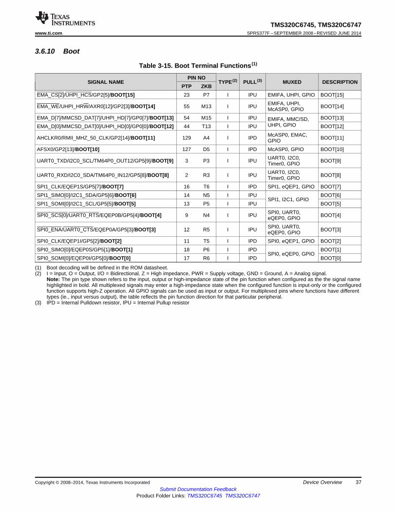
TMS320C6745, TMS320C6747www.ti.com SPRS377F –SEPTEMBER 2008–REVISED JUNE 2014
3.6.10 Boot
Table 3-15. Boot Terminal Functions (1)
PIN NOSIGNAL NAME TYPE (2) PULL (3) MUXED DESCRIPTION
PTP ZKBEMA_CS[2]/UHPI_HCS/GP2[5]/BOOT[15] 23 P7 I IPU EMIFA, UHPI, GPIO BOOT[15]
EMIFA, UHPI,EMA_WE/UHPI_HRW/AXR0[12]/GP2[3]/BOOT[14] 55 M13 I IPU BOOT[14]McASP0, GPIOEMA_D[7]/MMCSD_DAT[7]/UHPI_HD[7]/GP0[7]/BOOT[13] 54 M15 I IPU BOOT[13]EMIFA, MMC/SD,
UHPI, GPIOEMA_D[0]/MMCSD_DAT[0]/UHPI_HD[0]/GP0[0]/BOOT[12] 44 T13 I IPU BOOT[12]McASP0, EMAC,AHCLKR0/RMII_MHZ_50_CLK/GP2[14]/BOOT[11] 129 A4 I IPD BOOT[11]GPIO
AFSX0/GP2[13]/BOOT[10] 127 D5 I IPD McASP0, GPIO BOOT[10]UART0, I2C0,UART0_TXD/I2C0_SCL/TM64P0_OUT12/GP5[9]/BOOT[9] 3 P3 I IPU BOOT[9]Timer0, GPIOUART0, I2C0,UART0_RXD/I2C0_SDA/TM64P0_IN12/GP5[8]/BOOT[8] 2 R3 I IPU BOOT[8]Timer0, GPIO
SPI1_CLK/EQEP1S/GP5[7]/BOOT[7] 16 T6 I IPD SPI1, eQEP1, GPIO BOOT[7]SPI1_SIMO[0]/I2C1_SDA/GP5[6]/BOOT[6] 14 N5 I IPU BOOT[6]
SPI1, I2C1, GPIOSPI1_SOMI[0]/I2C1_SCL/GP5[5]/BOOT[5] 13 P5 I IPU BOOT[5]
SPI0, UART0,SPI0_SCS[0]/UART0_RTS/EQEP0B/GP5[4]/BOOT[4] 9 N4 I IPU BOOT[4]eQEP0, GPIOSPI0, UART0,SPI0_ENA/UART0_CTS/EQEP0A/GP5[3]/BOOT[3] 12 R5 I IPU BOOT[3]eQEP0, GPIO
SPI0_CLK/EQEP1I/GP5[2]/BOOT[2] 11 T5 I IPD SPI0, eQEP1, GPIO BOOT[2]SPI0_SIMO[0]/EQEP0S/GP5[1]/BOOT[1] 18 P6 I IPD BOOT[1]
SPI0, eQEP0, GPIOSPI0_SOMI[0]/EQEP0I/GP5[0]/BOOT[0] 17 R6 I IPD BOOT[0]
(1) Boot decoding will be defined in the ROM datasheet.(2) I = Input, O = Output, I/O = Bidirectional, Z = High impedance, PWR = Supply voltage, GND = Ground, A = Analog signal.
Note: The pin type shown refers to the input, output or high-impedance state of the pin function when configured as the the signal namehighlighted in bold. All multiplexed signals may enter a high-impedance state when the configured function is input-only or the configuredfunction supports high-Z operation. All GPIO signals can be used as input or output. For multiplexed pins where functions have differenttypes (ie., input versus output), the table reflects the pin function direction for that particular peripheral.
(3) IPD = Internal Pulldown resistor, IPU = Internal Pullup resistor
Copyright © 2008–2014, Texas Instruments Incorporated Device Overview 37Submit Documentation Feedback
Product Folder Links: TMS320C6745 TMS320C6747

TMS320C6745, TMS320C6747SPRS377F –SEPTEMBER 2008–REVISED JUNE 2014 www.ti.com
3.6.11 Universal Asynchronous Receiver/Transmitters (UART0, UART1, UART2)
Table 3-16. Universal Asynchronous Receiver/Transmitter (UART) Terminal Functions
PIN NOSIGNAL NAME TYPE (1) PULL (2) MUXED DESCRIPTION
PTP ZKBUART0
I2C0, BOOT, UART0 receiveUART0_RXD/I2C0_SDA/TM64P0_IN12/GP5[8]/BOOT[8] 2 R3 I IPU Timer0, GPIO, dataI2C0, Timer0, UART0 transmitUART0_TXD/I2C0_SCL/TM64P0_OUT12/GP5[9]/BOOT[9] 3 P3 O IPU GPIO, BOOT data
UART0 ready-to-SPI0_SCS[0]/ UART0_RTS /EQEP0B/GP5[4]/BOOT[4] 9 N4 O IPU send outputSPI0, eQEP0,GPIO, BOOT UART0 clear-to-SPI0_ENA/ UART0_CTS /EQEP0A/GP5[3]/BOOT[3] 12 R5 I IPU send input
UART1UART1 receiveUART1_RXD/AXR0[9]/GP3[9] (3) 122 C6 I IPD data
McASP0, GPIOUART1 transmitUART1_TXD/AXR0[10]/GP3[10] (3) 123 D6 O IPD data
UART2UART2 receiveSPI1_ENA/UART2_RXD/GP5[12] 7 R4 I IPU data
SPI1, GPIOUART2 transmitSPI1_SCS[0]/UART2_TXD/GP5[13] 8 P4 O IPU data
(1) I = Input, O = Output, I/O = Bidirectional, Z = High impedance, PWR = Supply voltage, GND = Ground, A = Analog signal.Note: The pin type shown refers to the input, output or high-impedance state of the pin function when configured as the the signal namehighlighted in bold. All multiplexed signals may enter a high-impedance state when the configured function is input-only or the configuredfunction supports high-Z operation. All GPIO signals can be used as input or output. For multiplexed pins where functions have differenttypes (ie., input versus output), the table reflects the pin function direction for that particular peripheral.
(2) IPD = Internal Pulldown resistor, IPU = Internal Pullup resistor(3) As these signals are internally pulled down while the device is in reset, it is necessary to externally pull them high with resistors if
UART1 boot mode is used. Please see the TMS320C6745/C6747 DSP Technical Reference Manual (SPRUH91) for more for details onentering UART1 boot mode.
38 Device Overview Copyright © 2008–2014, Texas Instruments IncorporatedSubmit Documentation Feedback
Product Folder Links: TMS320C6745 TMS320C6747

TMS320C6745, TMS320C6747www.ti.com SPRS377F –SEPTEMBER 2008–REVISED JUNE 2014
3.6.12 Inter-Integrated Circuit Modules (I2C0, I2C1)
Table 3-17. Inter-Integrated Circuit (I2C) Terminal Functions
PIN NOSIGNAL NAME TYPE (1) PULL (2) MUXED DESCRIPTION
PTP ZKBI2C0
UART0, Timer0,UART0_RXD/I2C0_SDA/TM64P0_IN12/GP5[8]/BOOT[8] 2 R3 I/O IPU I2C0 serial dataGPIO, BOOTUART0, Timer0,UART0_TXD/I2C0_SCL/TM64P0_OUT12/GP5[9]/BOOT[9] 3 P3 I/O IPU I2C0 serial clockGPIO, BOOT
I2C1SPI1_SIMO[0]/I2C1_SDA/GP5[6]/BOOT[6] 14 N5 I/O IPU I2C1 serial dataSPI1, GPIO,
BOOTSPI1_SOMI[0]/I2C1_SCL/GP5[5]/BOOT[5] 13 P5 I/O IPU I2C1 serial clock
(1) I = Input, O = Output, I/O = Bidirectional, Z = High impedance, PWR = Supply voltage, GND = Ground, A = Analog signal.Note: The pin type shown refers to the input, output or high-impedance state of the pin function when configured as the the signal namehighlighted in bold. All multiplexed signals may enter a high-impedance state when the configured function is input-only or the configuredfunction supports high-Z operation. All GPIO signals can be used as input or output. For multiplexed pins where functions have differenttypes (ie., input versus output), the table reflects the pin function direction for that particular peripheral.
(2) IPD = Internal Pulldown resistor, IPU = Internal Pullup resistor
Copyright © 2008–2014, Texas Instruments Incorporated Device Overview 39Submit Documentation Feedback
Product Folder Links: TMS320C6745 TMS320C6747
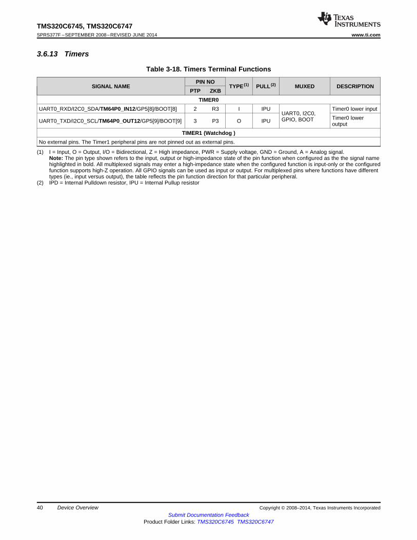
TMS320C6745, TMS320C6747SPRS377F –SEPTEMBER 2008–REVISED JUNE 2014 www.ti.com
3.6.13 Timers
Table 3-18. Timers Terminal Functions
PIN NOSIGNAL NAME TYPE (1) PULL (2) MUXED DESCRIPTION
PTP ZKBTIMER0
UART0_RXD/I2C0_SDA/TM64P0_IN12/GP5[8]/BOOT[8] 2 R3 I IPU Timer0 lower inputUART0, I2C0,
Timer0 lowerGPIO, BOOTUART0_TXD/I2C0_SCL/TM64P0_OUT12/GP5[9]/BOOT[9] 3 P3 O IPU outputTIMER1 (Watchdog )
No external pins. The Timer1 peripheral pins are not pinned out as external pins.
(1) I = Input, O = Output, I/O = Bidirectional, Z = High impedance, PWR = Supply voltage, GND = Ground, A = Analog signal.Note: The pin type shown refers to the input, output or high-impedance state of the pin function when configured as the the signal namehighlighted in bold. All multiplexed signals may enter a high-impedance state when the configured function is input-only or the configuredfunction supports high-Z operation. All GPIO signals can be used as input or output. For multiplexed pins where functions have differenttypes (ie., input versus output), the table reflects the pin function direction for that particular peripheral.
(2) IPD = Internal Pulldown resistor, IPU = Internal Pullup resistor
40 Device Overview Copyright © 2008–2014, Texas Instruments IncorporatedSubmit Documentation Feedback
Product Folder Links: TMS320C6745 TMS320C6747

TMS320C6745, TMS320C6747www.ti.com SPRS377F –SEPTEMBER 2008–REVISED JUNE 2014
3.6.14 Universal Host-Port Interface (UHPI)Note:
The UHPI module requires 16 data pins for the host port interface to function. Therefore on the PTP, theUHPI is not available.
Table 3-19. Universal Host-Port Interface (UHPI) Terminal Functions
PIN NO TYPE (SIGNAL NAME PULL (2) MUXED DESCRIPTION1)PTP ZKB
EMA_D[15]/UHPI_HD[15]/LCD_D[15]/GP0[15] - M16 I/O IPDEMA_D[14]/UHPI_HD[14]/LCD_D[14]/GP0[14] - N14 I/O IPDEMA_D[13]/UHPI_HD[13]/LCD_D[13]/GP0[13] - N16 I/O IPDEMA_D[12]/UHPI_HD[12]/LCD_D[12]/GP0[12] - P14 I/O IPD
EMIFA, LCD, GPIOEMA_D[11]/UHPI_HD[11]/LCD_D[11]/GP0[11] - P16 I/O IPDEMA_D[10]/UHPI_HD[10]/LCD_D[10]/GP0[10] - R14 I/O IPDEMA_D[9]/UHPI_HD[9]/LCD_D[9]/GP0[9] - T14 I/O IPDEMA_D[8]/UHPI_HD[8]/LCD_D[8]/GP0[8] - N12 I/O IPDEMA_D[7]/MMCSD_DAT[7]/UHPI_HD[7]/GP0[7]/ EMIFA, MMC/SD, UHPI data bus- M15 I/O IPUBOOT[13] GPIO, BOOTEMA_D[6]/MMCSD_DAT[6]/UHPI_HD[6]/GP0[6] - N13 I/O IPUEMA_D[5]/MMCSD_DAT[5]/UHPI_HD[5]/GP0[5] - N15 I/O IPUEMA_D[4]/MMCSD_DAT[4]/UHPI_HD[4]/GP0[4] - P13 I/O IPU EMIFA, MMC/SD,
GPIOEMA_D[3]/MMCSD_DAT[3]/UHPI_HD[3]/GP0[3] - P15 I/O IPUEMA_D[2]/MMCSD_DAT[2]/UHPI_HD[2]/GP0[2] - R13 I/O IPUEMA_D[1]/MMCSD_DAT[1]/UHPI_HD[1]/GP0[1] - R15 I/O IPUEMA_D[0]/MMCSD_DAT[0]/UHPI_HD[0]/GP0[0]/ EMIFA, MMC/SD,- T13 I/O IPUBOOT[12] GPIO, BOOTEMA_A[2]/MMCSD_CMD/UHPI_HCNTL1/GP1[2] - P9 I/O IPU EMIFA,
MMCSD_CMD, UHPI access controlEMA_A[1]/MMCSD_CLK/UHPI_HCNTL0/GP1[1] - R9 I/O IPU GPIO
UHPI half-wordEMA_BA[1]/LCD_D[5]/UHPI_HHWIL/GP1[13] - P8 I/O IPU EMIFA, LCD, GPIO identification controlEMIFA, McASP,EMA_WE/UHPI_HRW /AXR0[12]/GP2[3]/BOOT[14] - M13 I/O IPU UHPI read/writeGPIO, BOOTEMIFA, GPIO,EMA_CS[2]/ UHPI_HCS /GP2[5]/BOOT[15] - P7 I/O IPU UHPI chip selectBOOT
EMA_WE_DQM[1]/ UHPI_HDS2 /AXR0[14]/GP2[8] - P12 I/O IPUUHPI data strobeEMIFA, McASP0,EMA_OE/ UHPI_HDS1 /AXR0[13]/GP2[7] - R7 I/O IPU GPIO
EMA_WE_DQM[0]/ UHPI_HINT /AXR0[15]/GP2[9] - M14 I/O IPU UHPI host interruptEMA_WAIT[0]/ UHPI_HRDY /GP2[10] - N6 I/O IPU UHPI ready
EMIFA, GPIO UHPI addressEMA_CS[0]/ UHPI_HAS /GP2[4] - T8 I/O IPU strobe
(1) I = Input, O = Output, I/O = Bidirectional, Z = High impedance, PWR = Supply voltage, GND = Ground, A = Analog signal.Note: The pin type shown refers to the input, output or high-impedance state of the pin function when configured as the the signal namehighlighted in bold. All multiplexed signals may enter a high-impedance state when the configured function is input-only or the configuredfunction supports high-Z operation. All GPIO signals can be used as input or output. For multiplexed pins where functions have differenttypes (ie., input versus output), the table reflects the pin function direction for that particular peripheral.
(2) IPD = Internal Pulldown resistor, IPU = Internal Pullup resistor
Copyright © 2008–2014, Texas Instruments Incorporated Device Overview 41Submit Documentation Feedback
Product Folder Links: TMS320C6745 TMS320C6747

TMS320C6745, TMS320C6747SPRS377F –SEPTEMBER 2008–REVISED JUNE 2014 www.ti.com
3.6.15 Multichannel Audio Serial Ports (McASP0, McASP1, McASP2)
Table 3-20. Multichannel Audio Serial Ports (McASPs) Terminal Functions
PIN NOSIGNAL NAME TYPE (1) PULL (2) MUXED DESCRIPTION
PTP ZKBMcASP0
EMA_WE_DQM[0]/UHPI_HINT/AXR0[15]/GP2[9] - M14 I/O IPUEMIFA, UHPI,EMA_WE_DQM[1]/UHPI_HDS2/AXR0[14]/GP2[8] - P12 I/O IPU GPIO
EMA_OE/UHPI_HDS1/AXR0[13]/GP2[7] 22 R7 I/O IPUEMIFA, UHPI,EMA_WE/UHPI_HRW/AXR0[12]/GP2[3]/BOOT[14] 55 M13 I/O IPU GPIO, BOOTMcASP2,AXR0[11]/AXR2[0]/GP3[11] 124 A5 I/O IPD GPIO
UART1_TXD/AXR0[10]/GP3[10] 123 D6 I/O IPD UART1, GPIOUART1_RXD/AXR0[9]/GP3[9] 122 C6 I/O IPD UART1, GPIO
McASP0 serialAXR0[8]/MDIO_D/GP3[8] 121 B6 I/O IPU dataMDIO, GPIOAXR0[7]/MDIO_CLK/GP3[7] 120 A6 I/O IPDAXR0[6]/RMII_RXER/ACLKR2/GP3[6] 118 D7 I/O IPDAXR0[5]/RMII_RXD[1]/AFSX2/GP3[5] 117 C7 I/O IPDAXR0[4]/RMII_RXD[0]/AXR2[1]/GP3[4] 116 B7 I/O IPD EMAC,AXR0[3]/RMII_CRS_DV/AXR2[2]/GP3[3] 115 A7 I/O IPD McASP2,
GPIOAXR0[2]/RMII_TXEN/AXR2[3]/GP3[2] 113 D8 I/O IPDAXR0[1]/RMII_TXD[1]/ACLKX2/GP3[1] 112 C8 I/O IPDAXR0[0]/RMII_TXD[0]/AFSR2/GP3[0] 111 B8 I/O IPD
McASP0McASP2, USB,AHCLKX0/AHCLKX2/USB_REFCLKIN/GP2[11] 125 B5 I/O IPD transmit masterGPIO clockMcASP0
ACLKX0/ECAP0/APWM0/GP2[12] 126 C5 I/O IPD eCAP0, GPIO transmit bitclockMcASP0
AFSX0/GP2[13]/BOOT[10] 127 D5 I/O IPD GPIO, BOOT transmit framesync
EMAC, GPIO, McASP0 receiveAHCLKR0/RMII_MHZ_50_CLK/GP2[14]/BOOT[11] 129 A4 I/O IPD BOOT master clockMcASP0 receiveACLKR0/ECAP1/APWM1/GP2[15] 130 B4 I/O IPD eCAP1, GPIO bit clockMcASP0 receiveAFSR0/GP3[12] 131 C4 I/O IPD GPIO frame syncMcASP0 muteAMUTE0/RESETOUT - L4 O IPD RESETOUT output
(1) I = Input, O = Output, I/O = Bidirectional, Z = High impedance, PWR = Supply voltage, GND = Ground, A = Analog signal.Note: The pin type shown refers to the input, output or high-impedance state of the pin function when configured as the the signal namehighlighted in bold. All multiplexed signals may enter a high-impedance state when the configured function is input-only or the configuredfunction supports high-Z operation. All GPIO signals can be used as input or output. For multiplexed pins where functions have differenttypes (ie., input versus output), the table reflects the pin function direction for that particular peripheral.
(2) IPD = Internal Pulldown resistor, IPU = Internal Pullup resistor
42 Device Overview Copyright © 2008–2014, Texas Instruments IncorporatedSubmit Documentation Feedback
Product Folder Links: TMS320C6745 TMS320C6747
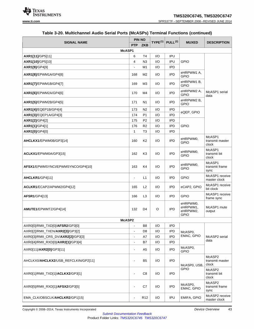
TMS320C6745, TMS320C6747www.ti.com SPRS377F –SEPTEMBER 2008–REVISED JUNE 2014
Table 3-20. Multichannel Audio Serial Ports (McASPs) Terminal Functions (continued)PIN NO
SIGNAL NAME TYPE (1) PULL (2) MUXED DESCRIPTIONPTP ZKB
McASP1AXR1[11]/GP5[11] 6 T4 I/O IPUAXR1[10]/GP5[10] 4 N3 I/O IPU GPIOAXR1[9]/GP4[9] - M1 I/O IPD
eHRPWM1 A,AXR1[8]/EPWM1A/GP4[8] 168 M2 I/O IPD GPIOeHRPWM1 B,AXR1[7]/EPWM1B/GP4[7] 169 M3 I/O IPD GPIOeHRPWM2 A, McASP1 serialAXR1[6]/EPWM2A/GP4[6] 170 M4 I/O IPD GPIO dataeHRPWM2 B,AXR1[5]/EPWM2B/GP4[5] 171 N1 I/O IPD GPIO
AXR1[4]/EQEP1B/GP4[4] 173 N2 I/O IPDeQEP, GPIO
AXR1[3]/EQEP1A/GP4[3] 174 P1 I/O IPDAXR1[2]/GP4[2] 175 P2 I/O IPDAXR1[1]/GP4[1] 176 R2 I/O IPD GPIOAXR1[0]/GP4[0] 1 T3 I/O IPD
McASP1eHRPWM0,AHCLKX1/EPWM0B/GP3[14] 160 K2 I/O IPD transmit masterGPIO clockMcASP1eHRPWM0,ACLKX1/EPWM0A/GP3[15] 162 K3 I/O IPD transmit bitGPIO clockMcASP1eHRPWM0,AFSX1/EPWMSYNCI/EPWMSYNCO/GP4[10] 163 K4 I/O IPD transmit frameGPIO syncMcASP1 receiveAHCLKR1/GP4[11] - L1 I/O IPD GPIO master clockMcASP1 receiveACLKR1/ECAP2/APWM2/GP4[12] 165 L2 I/O IPD eCAP2, GPIO bit clockMcASP1 receiveAFSR1/GP4[13] 166 L3 I/O IPD GPIO frame sync
eHRPWM0,eHRPWM1, McASP1 muteAMUTE1/EPWMTZ/GP4[14] 132 D4 O IPD eHRPWM2, outputGPIO
McASP2AXR0[0]/RMII_TXD[0]/AFSR2/GP3[0] - B8 I/O IPDAXR0[2]/RMII_TXEN/AXR2[3]/GP3[2] - D8 I/O IPD McASP0,
EMAC, GPIOAXR0[3]/RMII_CRS_DV/AXR2[2]/GP3[3] - A7 I/O IPD McASP2 serialdataAXR0[4]/RMII_RXD[0]/AXR2[1]/GP3[4] - B7 I/O IPD
McASP0,AXR0[11]/AXR2[0]/GP3[11] - A5 I/O IPD GPIOMcASP2
AHCLKX0/AHCLKX2/USB_REFCLKIN/GP2[11] - B5 I/O IPD transmit masterclockMcASP0, USB,
GPIO McASP2AXR0[1]/RMII_TXD[1]/ACLKX2/GP3[1] - C8 I/O IPD transmit bit
clockMcASP2McASP0,AXR0[5]/RMII_RXD[1]/AFSX2/GP3[5] - C7 I/O IPD transmit frameEMAC, GPIO syncMcASP2 receiveEMA_CLK/OBSCLK/AHCLKR2/GP1[15] - R12 I/O IPU EMIFA, GPIO master clock
Copyright © 2008–2014, Texas Instruments Incorporated Device Overview 43Submit Documentation Feedback
Product Folder Links: TMS320C6745 TMS320C6747
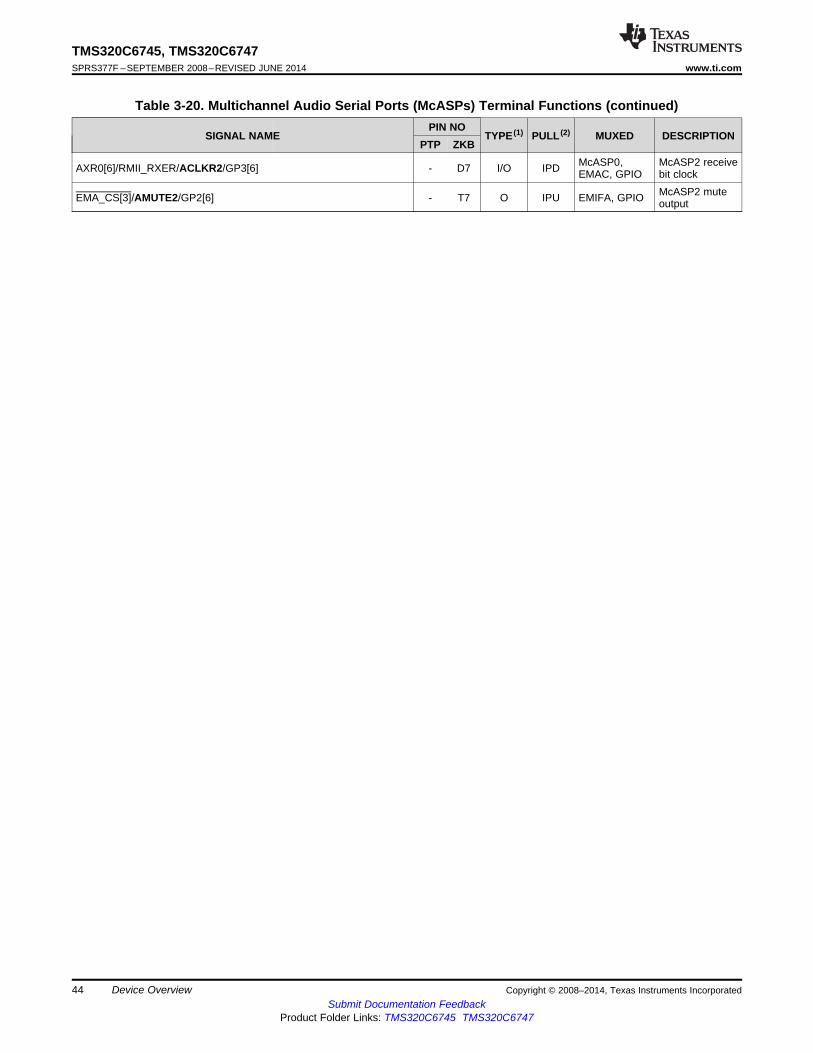
TMS320C6745, TMS320C6747SPRS377F –SEPTEMBER 2008–REVISED JUNE 2014 www.ti.com
Table 3-20. Multichannel Audio Serial Ports (McASPs) Terminal Functions (continued)PIN NO
SIGNAL NAME TYPE (1) PULL (2) MUXED DESCRIPTIONPTP ZKB
McASP0, McASP2 receiveAXR0[6]/RMII_RXER/ACLKR2/GP3[6] - D7 I/O IPD EMAC, GPIO bit clockMcASP2 muteEMA_CS[3]/AMUTE2/GP2[6] - T7 O IPU EMIFA, GPIO output
44 Device Overview Copyright © 2008–2014, Texas Instruments IncorporatedSubmit Documentation Feedback
Product Folder Links: TMS320C6745 TMS320C6747

TMS320C6745, TMS320C6747www.ti.com SPRS377F –SEPTEMBER 2008–REVISED JUNE 2014
3.6.16 Universal Serial Bus Modules (USB0, USB1)
Table 3-21. Universal Serial Bus (USB) Terminal Functions
PIN NOSIGNAL NAME TYPE (1) PULL (2) DESCRIPTION
PTP ZKBUSB0 2.0 OTG (USB0)
USB0_DM 138 G4 A USB0 PHY data minusUSB0_DP 137 F4 A USB0 PHY data plusUSB0_VDDA33 140 H5 PWR USB0 PHY 3.3-V supplyUSB0_VDDA18 135 E3 PWR USB0 PHY 1.8-V supply input
USB0 PHY 1.2-V LDO output for bypass cap
For proper device operation, this pin isUSB0_VDDA12 (3) 134 C3 PWR recommended to be connected via a 0.22-μF
capacitor to VSS (GND), even if USB0 is notbeing used.
USB0_ID - D2 A USB0 PHY identification (mini-A or mini-B plug)USB0_VBUS - D3 A USB0 bus voltageUSB0_DRVVBUS/GP4[15] - E4 O IPD USB0 controller VBUS control outputAHCLKX0/AHCLKX2/USB_REFCLKIN/GP2[11] 125 B5 I IPD USB_REFCLKIN. Optional clock input
USB1 1.1 OHCI (USB1)USB1_DM - B3 A USB1 PHY data minusUSB1_DP - A3 A USB1 PHY data plusUSB1_VDDA33 - C1 PWR USB1 PHY 3.3-V supplyUSB1_VDDA18 - C2 PWR USB1 PHY 1.8-V supplyAHCLKX0/AHCLKX2/USB_REFCLKIN/GP2[11] 125 B5 I IPD USB_REFCLKIN. Optional clock input.
(1) I = Input, O = Output, I/O = Bidirectional, Z = High impedance, PWR = Supply voltage, GND = Ground, A = Analog signal.Note: The pin type shown refers to the input, output or high-impedance state of the pin function when configured as the the signal namehighlighted in bold. All multiplexed signals may enter a high-impedance state when the configured function is input-only or the configuredfunction supports high-Z operation. All GPIO signals can be used as input or output. For multiplexed pins where functions have differenttypes (ie., input versus output), the table reflects the pin function direction for that particular peripheral.
(2) IPD = Internal Pulldown resistor, IPU = Internal Pullup resistor(3) Core power supply LDO output for USB PHY.
Copyright © 2008–2014, Texas Instruments Incorporated Device Overview 45Submit Documentation Feedback
Product Folder Links: TMS320C6745 TMS320C6747

TMS320C6745, TMS320C6747SPRS377F –SEPTEMBER 2008–REVISED JUNE 2014 www.ti.com
3.6.17 Ethernet Media Access Controller (EMAC)
Table 3-22. Ethernet Media Access Controller (EMAC) Terminal Functions
PIN NOSIGNAL NAME TYPE (1) PULL (2) MUXED DESCRIPTION
PTP ZKBRMII
EMAC 50-MHzAHCLKR0/RMII_MHZ_50_CLK/GP2[14]/BOOT[11] 129 A4 I/O IPD McASP0, GPIO, BOOT clock input or
outputEMAC RMIIAXR0[6]/RMII_RXER/ACLKR2/GP3[6] 118 D7 I IPD receiver error
AXR0[5]/RMII_RXD[1]/AFSX2/GP3[5] 117 C7 I IPD EMAC RMIIreceive dataAXR0[4]/RMII_RXD[0]/AXR2[1]/GP3[4] 116 B7 I IPDEMAC RMII carrierAXR0[3]/RMII_CRS_DV/AXR2[2]/GP3[3] 115 A7 I IPD McASP0, McASP2, GPIO sense data validEMAC RMIIAXR0[2]/RMII_TXEN/AXR2[3]/GP3[2] 113 D8 O IPD transmit enable
AXR0[1]/RMII_TXD[1]/ACLKX2/GP3[1] 112 C8 O IPD EMAC RMII trasmitdataAXR0[0]/RMII_TXD[0]/AFSR2/GP3[0] 111 B8 O IPD
MDIOAXR0[8]/MDIO_D/GP3[8] 121 B6 I/O IPU
McASP0, GPIO MDIO data clockAXR0[7]/MDIO_CLK/GP3[7] 120 A6 O IPD
(1) I = Input, O = Output, I/O = Bidirectional, Z = High impedance, PWR = Supply voltage, GND = Ground, A = Analog signal.Note: The pin type shown refers to the input, output or high-impedance state of the pin function when configured as the the signal namehighlighted in bold. All multiplexed signals may enter a high-impedance state when the configured function is input-only or the configuredfunction supports high-Z operation. All GPIO signals can be used as input or output. For multiplexed pins where functions have differenttypes (ie., input versus output), the table reflects the pin function direction for that particular peripheral.
(2) IPD = Internal Pulldown resistor, IPU = Internal Pullup resistor
46 Device Overview Copyright © 2008–2014, Texas Instruments IncorporatedSubmit Documentation Feedback
Product Folder Links: TMS320C6745 TMS320C6747

TMS320C6745, TMS320C6747www.ti.com SPRS377F –SEPTEMBER 2008–REVISED JUNE 2014
3.6.18 Multimedia Card/Secure Digital (MMC/SD)
Table 3-23. Multimedia Card/Secure Digital (MMC/SD) Terminal Functions
PIN NOSIGNAL NAME TYPE (1) PULL (2) MUXED DESCRIPTION
PTP ZKBEMA_A[1]/MMCSD_CLK/UHPI_HCNTL0/GP1[1] 30 R9 O IPU MMCSD Clock
EMIFA, UHPI, GPIO MMCSDEMA_A[2]/MMCSD_CMD/UHPI_HCNTL1/GP1[2] 31 P9 I/O IPU CommandEMIFA, UHPI, GPIO,EMA_D[7]/MMCSD_DAT[7]/UHPI_HD[7]/GP0[7]/BOOT[13] 54 M15 I/O IPU BOOT
EMA_D[6]/MMCSD_DAT[6]/UHPI_HD[6]/GP0[6] 52 N13 I/O IPUEMA_D[5]/MMCSD_DAT[5]/UHPI_HD[5]/GP0[5] 51 N15 I/O IPUEMA_D[4]/MMCSD_DAT[4]/UHPI_HD[4]/GP0[4] 49 P13 I/O IPU
EMIFA, UHPI, GPIO MMC/SD dataEMA_D[3]/MMCSD_DAT[3]/UHPI_HD[3]/GP0[3] 48 P15 I/O IPUEMA_D[2]/MMCSD_DAT[2]/UHPI_HD[2]/GP0[2] 46 R13 I/O IPUEMA_D[1]/MMCSD_DAT[1]/UHPI_HD[1]/GP0[1] 45 R15 I/O IPU
EMIFA, UHPI, GPIO,EMA_D[0]/MMCSD_DAT[0]/UHPI_HD[0]/GP0[0]/BOOT[12] 44 T13 I/O IPU BOOT
(1) I = Input, O = Output, I/O = Bidirectional, Z = High impedance, PWR = Supply voltage, GND = Ground, A = Analog signal.Note: The pin type shown refers to the input, output or high-impedance state of the pin function when configured as the the signal namehighlighted in bold. All multiplexed signals may enter a high-impedance state when the configured function is input-only or the configuredfunction supports high-Z operation. All GPIO signals can be used as input or output. For multiplexed pins where functions have differenttypes (ie., input versus output), the table reflects the pin function direction for that particular peripheral.
(2) IPD = Internal Pulldown resistor, IPU = Internal Pullup resistor
Copyright © 2008–2014, Texas Instruments Incorporated Device Overview 47Submit Documentation Feedback
Product Folder Links: TMS320C6745 TMS320C6747
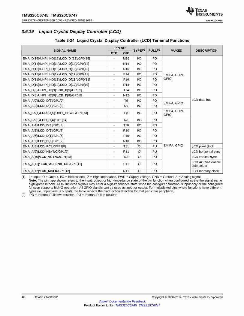
TMS320C6745, TMS320C6747SPRS377F –SEPTEMBER 2008–REVISED JUNE 2014 www.ti.com
3.6.19 Liquid Crystal Display Controller (LCD)
Table 3-24. Liquid Crystal Display Controller (LCD) Terminal Functions
PIN NOSIGNAL NAME TYPE (1) PULL (2) MUXED DESCRIPTION
PTP ZKBEMA_D[15]/UHPI_HD[15]/LCD_D [15]/GP0[15] - M16 I/O IPDEMA_D[14]/UHPI_HD[14]/LCD_D[14]/GP0[14] - N14 I/O IPDEMA_D[13]/UHPI_HD[13]/LCD_D[13]/GP0[13] - N16 I/O IPDEMA_D[12]/UHPI_HD[12]/LCD_D[12]/GP0[12] - P14 I/O IPD EMIFA, UHPI,
GPIOEMA_D[11]/UHPI_HD[11]/LCD_D[11 ]/GP0[11] - P16 I/O IPDEMA_D[10]/UHPI_HD[10]/LCD_D[10]/GP0[10] - R14 I/O IPDEMA_D[9]/UHPI_HD[9]/LCD_D[9]/GP0[9] - T14 I/O IPDEMA_D[8]/UHPI_HD[8]/LCD_D[8]/GP0[8] - N12 I/O IPD
LCD data busEMA_A[0]/LCD_D[7]/GP1[0] - T9 I/O IPDEMIFA, GPIO
EMA_A[3]/LCD_D[6]/GP1[3] - N9 I/O IPDEMIFA, UHPI,EMA_BA[1]/LCD_D[5]/UHPI_HHWIL/GP1[13] - P8 I/O IPU GPIO
EMA_BA[0]/LCD_D[4]/GP1[14] - R8 I/O IPUEMA_A[4]/LCD_D[3]/GP1[4] - T10 I/O IPDEMA_A[5]/LCD_D[2]/GP1[5] - R10 I/O IPDEMA_A[6]/LCD_D[1]/GP1[6] - P10 I/O IPDEMA_A[7]/LCD_D[0]/GP1[7] - N10 I/O IPD
EMIFA, GPIOEMA_A[8]/LCD_PCLK/GP1[8] - T11 O IPU LCD pixel clockEMA_A[9]/LCD_HSYNC/GP1[9] - R11 O IPU LCD horizontal syncEMA_A[10]/LCD_VSYNC/GP1[10] - N8 O IPU LCD vertical sync
LCD AC bias enableEMA_A[11]/ LCD_AC_ENB_CS /GP1[11] - P11 O IPU chip selectEMA_A[12]/LCD_MCLK/GP1[12] - N11 O IPU LCD memory clock
(1) I = Input, O = Output, I/O = Bidirectional, Z = High impedance, PWR = Supply voltage, GND = Ground, A = Analog signal.Note: The pin type shown refers to the input, output or high-impedance state of the pin function when configured as the the signal namehighlighted in bold. All multiplexed signals may enter a high-impedance state when the configured function is input-only or the configuredfunction supports high-Z operation. All GPIO signals can be used as input or output. For multiplexed pins where functions have differenttypes (ie., input versus output), the table reflects the pin function direction for that particular peripheral.
(2) IPD = Internal Pulldown resistor, IPU = Internal Pullup resistor
48 Device Overview Copyright © 2008–2014, Texas Instruments IncorporatedSubmit Documentation Feedback
Product Folder Links: TMS320C6745 TMS320C6747

TMS320C6745, TMS320C6747www.ti.com SPRS377F –SEPTEMBER 2008–REVISED JUNE 2014
3.6.20 General Purpose Input Output (GPIO)
Table 3-25. General Purpose Input Output Terminal Functions
PIN NOSIGNAL NAME TYPE (1) PULL (2) MUXED DESCRIPTION
PTP ZKBGP0
EMA_D[15]/UHPI_HD[15]/LCD_D[15]/GP0[15] - M16 I/O IPDEMA_D[14]/UHPI_HD[14]/LCD_D[14]/GP0[14] - N14 I/O IPDEMA_D[13]/UHPI_HD[13]/LCD_D[13]/GP0[13] - N16 I/O IPDEMA_D[12]/UHPI_HD[12]/LCD_D[12]/GP0[12] - P14 I/O IPD EMIFA, UHPI,
LCDEMA_D[11]/UHPI_HD[11]/LCD_D[11]/GP0[11] - P16 I/O IPDEMA_D[10]/UHPI_HD[10]/LCD_D[10]/GP0[10] - R14 I/O IPDEMA_D[9]/UHPI_HD[9]/LCD_D[9]/GP0[9] - T14 I/O IPDEMA_D[8]/UHPI_HD[8]/LCD_D[8]/GP0[8] - N12 I/O IPD
EMIFA, MMC/SD, GPIO Bank 0EMA_D[7]/MMCSD_DAT[7]/UHPI_HD[7]/GP0[7]/BOOT[13] 54 M15 I/O IPU UHPI, BOOTEMA_D[6]/MMCSD_DAT[6]/UHPI_HD[6]/GP0[6] 52 N13 I/O IPUEMA_D[5]/MMCSD_DAT[5]/UHPI_HD[5]/GP0[5] 51 N15 I/O IPUEMA_D[4]/MMCSD_DAT[4]/UHPI_HD[4]/GP0[4] 49 P13 I/O IPU EMIFA, MMC/SD,
UHPIEMA_D[3]/MMCSD_DAT[3]/UHPI_HD[3]/GP0[3] 48 P15 I/O IPUEMA_D[2]/MMCSD_DAT[2]/UHPI_HD[2]/GP0[2] 46 R13 I/O IPUEMA_D[1]/MMCSD_DAT[1]/UHPI_HD[1]/GP0[1] 45 R15 I/O IPU
EMIFA, MMC/SD,EMA_D[0]/MMCSD_DAT[0]/UHPI_HD[0]/GP0[0]/BOOT[12] 44 T13 I/O IPU UHPI, BOOTGP1
EMA_CLK/OBSCLK/AHCLKR2/GP1[15] - R12 O IPU EMIFA, McASP2EMA_BA[0]/LCD_D[4]/GP1[14] 25 R8 O IPU EMIFA, LCD
EMIFA, LCD,EMA_BA[1]/LCD_D[5]/UHPI_HHWIL/GP1[13] 26 P8 O IPU UHPIEMA_A[12]/LCD_MCLK/GP1[12] 42 N11 O IPUEMA_A[11]/ LCD_AC_ENB_CS/GP1[11] 41 P11 O IPUEMA_A[10]/LCD_VSYNC/GP1[10] 27 N8 O IPUEMA_A[9]/LCD_HSYNC/GP1[9] 40 R11 O IPUEMA_A[8]/LCD_PCLK/GP1[8] 39 T11 O IPU GPIO Bank 1EMIFA, LCDEMA_A[7]/LCD_D[0]/GP1[7] 37 N10 O IPDEMA_A[6]/LCD_D[1]/GP1[6] 36 P10 O IPDEMA_A[5]/LCD_D[2]/GP1[5] 35 R10 O IPDEMA_A[4]/LCD_D[3]/GP1[4] 34 T10 O IPDEMA_A[3]/LCD_D[6]/GP1[3] 32 N9 O IPDEMA_A[2]/MMCSD_CMD/UHPI_HCNTL1/GP1[2] 31 P9 O IPU EMIFA, MMCSD,
UHPIEMA_A[1]/MMCSD_CLK/UHPI_HCNTL0/GP1[1] 30 R9 O IPUEMA_A[0]/LCD_D[7]/GP1[0] 29 T9 O IPD EMIFA, LCD
(1) I = Input, O = Output, I/O = Bidirectional, Z = High impedance, PWR = Supply voltage, GND = Ground, A = Analog signal.Note: The pin type shown refers to the input, output or high-impedance state of the pin function when configured as the the signal namehighlighted in bold. All multiplexed signals may enter a high-impedance state when the configured function is input-only or the configuredfunction supports high-Z operation. All GPIO signals can be used as input or output. For multiplexed pins where functions have differenttypes (ie., input versus output), the table reflects the pin function direction for that particular peripheral.
(2) IPD = Internal Pulldown resistor, IPU = Internal Pullup resistor
Copyright © 2008–2014, Texas Instruments Incorporated Device Overview 49Submit Documentation Feedback
Product Folder Links: TMS320C6745 TMS320C6747
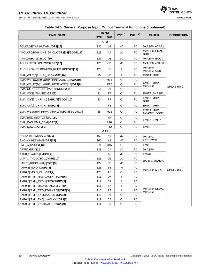
TMS320C6745, TMS320C6747SPRS377F –SEPTEMBER 2008–REVISED JUNE 2014 www.ti.com
Table 3-25. General Purpose Input Output Terminal Functions (continued)PIN NO
SIGNAL NAME TYPE (1) PULL (2) MUXED DESCRIPTIONPTP ZKB
GP2ACLKR0/ECAP1/APWM1/GP2[15] 130 b4 I/O IPD McASP0, eCAP1
McASP0, EMAC,AHCLKR0/RMII_MHZ_50_CLK/GP2[14]/BOOT[11] 129 A4 I/O IPD BOOTAFSX0/GP2[13]/BOOT[10] 127 D5 I/O IPD McASP0, BOOTACLKX0/ECAP0/APWM0/GP2[12] 126 CD I/O IPD McASP0, eCAP0
McASP0,AHCLKX0/AHCLKX2/USB_REFCLKIN/GP2[11] 125 B5 I IPD McASP2, USBEMA_WAIT[0]/ UHPI_HRDY/GP2[10] 19 N6 I IPU EMIFA, UHPIEMA_WE_DQM[0] /UHPI_HINT/AXR0[15]/GP2[9] - M14 O IPU
EMIFA, UHPI,EMA_WE_DQM[1] /UHPI_HDS2/AXR0[14]/GP2[8] - P12 O IPU McASP0 GPIO Bank 2EMA_OE /UHPI_HDS1/AXR0[13]/GP2[7] 22 R7 O IPUEMA_CS[3] /AMUTE2/GP2[6] 21 T7 O IPU EMIFA, McASP2
EMIFA, UHPI,EMA_CS[2] /UHPI_HCS/GP2[5]/BOOT[15] 23 P7 O IPU BOOTEMA_CS[0] /UHPI_HAS/GP2[4] - T8 O IPU EMIFA, UHPI
EMIFA, UHPI,EMA_WE /UHPI_HRW/AXR0[12]/GP2[3]/BOOT[14] 55 M13 O IPU MCASP0, BOOTEMA_RAS /EMA_CS[5]/GP2[2] - N7 O IPU
EMIFA, EMIFAEMA_CAS /EMA_CS[4]/GP2[1] - L16 O IPUEMA_SDCKE/GP2[0] - T12 O IPU EMIFA
GP3ACLKX1/EPWM0A/GP3[15] 162 K3 I/O IPD McASP1,
eHRPWM0AHCLKX1/EPWM0B/GP3[14] 160 K2 I/O IPDEMB_A[12]/GP3[13] 89 B15 O IPD EMIFBAFSR0/GP3[12] 131 C4 I/O IPD McASP0AXR0[11]/AXR2[0]/GP3[11] - A5 I/O IPD EMAC,UART1_TXD/AXR0[10]/GP3[10] 123 D6 I/O IPD
UART1, McASP0UART1_RXD/AXR0[9]/GP3[9] 122 C6 I/O IPDAXR0[8]/MDIO_D/GP3[8] 121 B6 I/0 IPU
McASP0, MDIO GPIO Bank 3AXR0[7]/MDIO_CLK/GP3[7] 120 A6 O IPDAXR0[6]/RMII_RXER/ACLKR2/GP3[6] 118 D7 I IPDAXR0[5]/RMII_RXD[1]/AFSX2/GP3[5] 117 C7 I IPDAXR0[4]/RMII_RXD[0]/AXR2[1]/GP3[4] 116 B7 I IPD
McASP0, EMAC,AXR0[3]/RMII_CRS_DV/AXR2[2]/GP3[3] 115 A7 I IPD McASP2AXR0[2]/RMII_TXEN/AXR2[3]/GP3[2] 113 D8 O IPDAXR0[1]/RMII_TXD[1]/ACLKX2/GP3[1] 112 C8 O IPDAXR0[0]/RMII_TXD[0]/AFSR2/GP3[0] 111 B8 O IPD
50 Device Overview Copyright © 2008–2014, Texas Instruments IncorporatedSubmit Documentation Feedback
Product Folder Links: TMS320C6745 TMS320C6747

TMS320C6745, TMS320C6747www.ti.com SPRS377F –SEPTEMBER 2008–REVISED JUNE 2014
Table 3-25. General Purpose Input Output Terminal Functions (continued)PIN NO
SIGNAL NAME TYPE (1) PULL (2) MUXED DESCRIPTIONPTP ZKB
GP4USB0_DRVVBUS/GP4[15] - E4 O IPD USB0
McASP1,eHRPWM0,AMUTE1/EPWMTZ/GP4[14] 132 D4 O IPD eHRPWM1,eHRPWM2
AFSR1/GP4[13] 166 L3 I/O IPD McASP1ACLKR1/ECAP2/APWM2/GP4[12] 165 L2 I/O IPD McASP1, eCAP2AHCLKR1/GP4[11] - L1 I/O IPD McASP1
McASP1,AFSX1/EPWMSYNCI/EPWMSYNCO/GP4[10] 163 K4 I/O IPD eHRPWM0AXR1[9]/GP4[9] - M1 I/O IPD McASP1
McASP1,AXR1[8]/EPWM1A/GP4[8] 168 M2 I/O IPD GPIO Bank 4eHRPWM1 AMcASP1,AXR1[7]/EPWM1B/GP4[7] 169 M3 I/O IPD eHRPWM1 BMcASP1,AXR1[6]/EPWM2A/GP4[6] 170 M4 I/O IPD eHRPWM2 AMcASP1,AXR1[5]/EPWM2B/GP4[5] 171 N1 I/O IPD eHRPWM2 B
AXR1[4]/EQEP1B/GP4[4] 173 N2 I/O IPDMcASP1, eQEP
AXR1[3]/EQEP1A/GP4[3] 174 P1 I/O IPDAXR1[2]/GP4[2] 175 P2 I/O IPDAXR1[1]/GP4[1] 176 R2 I/O IPD McASP1AXR1[0]/GP4[0] 1 T3 I/O IPD
GP5EMB_WE_DQM[0]/GP5[15] 60 K14 O IPU
EMIFBEMB_WE_DQM[1]/GP5[14] 85 C15 O IPUSPI1_SCS[0]/UART2_TXD/GP5[13] 8 P4 O IPU
SPI1, UART2SPI1_ENA/UART2_RXD/GP5[12] 7 R4 I IPUAXR1[11]/GP5[11] 6 T4 I/O IPU
McASP1AXR1[10]/GP5[10] 4 N3 I/O IPUUART0_TXD/I2C0_SCL/TM64P0_OUT12/GP5[9]/BOOT[9] 2 R3 I IPU UART0, I2C0,
BOOTUART0_RXD/I2C0_SDA/TM64P0_IN12/GP5[8]/BOOT[8] 3 P3 O IPUSPI1, eQEP1, GPIOBank 5SPI1_CLK/EQEP1S/GP5[7]/BOOT[7] 16 T6 I IPD BOOT
SPI1_SIMO[0]/I2C1_SDA/GP5[6]/BOOT[6] 14 N5 I/O IPU SPI1, I2C1,BOOTSPI1_SOMI[0]/I2C1_SCL/GP5[5]/BOOT[5] 13 P5 I/O IPU
SPI0_SCS[0]/UART0_RTS/EQEP0B/GP5[4]/BOOT[4] 9 N4 I IPU SPI0, UART0,eQEP0, BOOTSPI0_ENA/UART0_CTS/EQEP0A/GP5[3]/BOOT[3] 12 R5 I IPUSPI0, eQEP1,SPI0_CLK/EQEP1I/GP5[2]/BOOT[2] 11 T5 I IPD BOOT
SPI0_SIMO[0]/EQEP0S/GP5[1]/BOOT[1] 18 P6 I IPD SPI0, eQEP0,BOOTSPI0_SOMI[0]/EQEP0I/GP5[0]/BOOT[0] 17 R6 I IPD
Copyright © 2008–2014, Texas Instruments Incorporated Device Overview 51Submit Documentation Feedback
Product Folder Links: TMS320C6745 TMS320C6747

TMS320C6745, TMS320C6747SPRS377F –SEPTEMBER 2008–REVISED JUNE 2014 www.ti.com
Table 3-25. General Purpose Input Output Terminal Functions (continued)PIN NO
SIGNAL NAME TYPE (1) PULL (2) MUXED DESCRIPTIONPTP ZKB
GP6EMB_D[15]/GP6[15] 74 F13 I/O IPDEMB_D[14]/GP6[14] 76 E`6 I/O IPDEMB_D[13]/GP6[13] 78 E13 I/O IPDEMB_D[12]/GP6[12] 79 D16 I/O IPDEMB_D[11]/GP6[11] 80 D15 I/O IPDEMB_D[10]/GP6[10] 82 D14 I/O IPDEMB_D[9]/GP6[9] 83 D13 I/O IPDEMB_D[8]/GP6[8] 84 C16 I/O IPD
EMIFB GPIO Bank 6EMB_D[7]/GP6[7] 62 J16 I/O IPDEMB_D[6]/GP6[6] 63 J15 I/O IPDEMB_D[5]/GP6[5] 64 J13 I/O IPDEMB_D[4]/GP6[4] 66 H16 I/O IPDEMB_D[3]/GP6[3] 68 H13 I/O IPDEMB_D[2]/GP6[2] 70 G16 I/O IPDEMB_D[1]/GP6[1] 72 G13 I/O IPDEMB_D[0]/GP6[0] 73 F16 I/O IPD
GP7EMU[0]/GP7[15] - J5 I/O IPU JTAG
General-PurposeRTCK/ GP7[14] (1) 157 K1 I/O IPD IO signalEMB_A[11]/GP7[13] 91 B12 O IPDEMB_A[10]/GP7[12] 105 A9 O IPDEMB_A[9]/GP7[11] 92 C12 O IPDEMB_A[8]/GP7[10] 94 D12 O IPDEMB_A[7]/GP7[9] 95 A11 O IPDEMB_A[6]/GP7[8] 96 B11 O IPDEMB_A[5]/GP7[7] 97 C11 O IPD
EMIFB GPIO Bank 7EMB_A[4]/GP7[6] 98 D11 O IPDEMB_A[3]/GP7[5] 100 A10 O IPDEMB_A[2]/GP7[4] 101 B10 O IPDEMB_A[1]/GP7[3] 102 C10 O IPDEMB_A[0]/GP7[2] 103 D10 O IPDEMB_BA[0]/GP7[1] 107 C9 O IPUEMB_BA[1]/GP7[0] 106 B9 O IPU
(1) GP7[14] is initially configured as a reserved function after reset and will not be in a predictable state. This signal will only be stable afterthe GPIO configuration for this pin has been completed. Users should carefully consider the system implications of this pin being in anunknown state after reset.
3.6.21 Reserved and No Connect
Table 3-26. Reserved and No Connect Terminal Functions
PIN NOSIGNAL NAME TYPE (1) DESCRIPTION
PTP ZKBReserved. (Leave unconnected, do not connect to power orRSV1 - F7 - ground.)
(1) PWR = Supply voltage.
52 Device Overview Copyright © 2008–2014, Texas Instruments IncorporatedSubmit Documentation Feedback
Product Folder Links: TMS320C6745 TMS320C6747

TMS320C6745, TMS320C6747www.ti.com SPRS377F –SEPTEMBER 2008–REVISED JUNE 2014
Table 3-26. Reserved and No Connect Terminal Functions (continued)PIN NO
SIGNAL NAME TYPE (1) DESCRIPTIONPTP ZKB
Reserved. For proper device operation, this pin must be tied eitherRSV2 133 B1 PWR directly to CVDD or left unconnected [do not connect to ground
(VSS)].Reserved. For proper device operation, this pin must be tiedRSV3 149 - PWR directly to CVDD.Reserved. For proper device operation, this pin must be tied low orRSV4 148 - I to CVDD.
NC 136 F3 - No Connect (leave unconnected)NC 139 H4 - No Connect (leave unconnected)
Copyright © 2008–2014, Texas Instruments Incorporated Device Overview 53Submit Documentation Feedback
Product Folder Links: TMS320C6745 TMS320C6747

TMS320C6745, TMS320C6747SPRS377F –SEPTEMBER 2008–REVISED JUNE 2014 www.ti.com
3.6.22 Supply and Ground
Table 3-27. Supply and Ground Terminal Functions
PIN NOSIGNAL NAME TYPE (1) DESCRIPTION
PTP ZKBF6,G6, G7,10, 20, 28, G10, G11,38, 50, 56, H7, H10,61, 69, 77,CVDD (Core supply) H11, J6, J7, PWR Core supply voltage pins93, 104, 114, J10, J11,147, 154, J12, K6, K7,161, 167 K10, K11,L6
RVDD (Internal RAM supply) 67, 159 H6, H12 PWR Internal ram supply voltage pins5, 15, 24, 33, B16, E5, E8,43, 47, 53, E9, E12, F5,58, 65, 71, F11, F12,75, 81, 87, G5, G12, K5,DVDD (I/O supply) PWR I/O supply voltage pins90, 99, 109, K12, L5, L11,119, 128, L12, M5, M8,151, 158, M9, M12, R1,164, 172 R16
A1, A2, A15,A16,B2,E6, E7, E10,E11,F8, F9, F10,G8, G9,H8, H9,VSS (Ground) 177 GND Ground pinsJ8, J9,K8, K9,L7, L8, L9,L10,M6, M7, M10,M11,T1, T2, T15,T16
(1) PWR = Supply voltage, GND - Ground.
54 Device Overview Copyright © 2008–2014, Texas Instruments IncorporatedSubmit Documentation Feedback
Product Folder Links: TMS320C6745 TMS320C6747

TMS320C6745, TMS320C6747www.ti.com SPRS377F –SEPTEMBER 2008–REVISED JUNE 2014
3.6.23 Unused USB0 (USB2.0) and USB1 (USB1.1) Pin ConfigurationsIf one or both USB modules on the device are not used, then some of the power supplies to thosemodules may not be required. This can eliminate the requirement for a 1.8V power supply to the USBmodules. The required pin configurations for unused USB modules are shown below.
Table 3-28. Unused USB0 and USB1 Pin Configurations
SIGNAL NAME Configuration Configuration(When USB0 and USB1 are not used) (When USB0 is used
and USB1 is not used)USB0_DM No connect Use as USB0 functionUSB0_DP No connect Use as USB0 function
USB0_VDDA33 No connect 3.3VUSB0_VDDA18 No connect 1.8V
USB0_ID No connect Use as USB0 functionUSB0_VBUS No connect Use as USB0 function
USB0_DRVVBUS/GP4[15] No connect or use as alternate function Use as USB0 or alternate functionUSB0_VDDA12 Internal USB0 PHY output connected to an external 0.22μF filter capacitor
USB1_DM No connect VSSUSB1_DP No connect VSS
USB1_VDDA33 No connect No connectUSB1_VDDA18 No connect No connect
AHCLKX0/AHCLKX2/USB_REFCLKIN/ No connect or use as alternate function Use as USB0 or alternate functionGP2[11]
Copyright © 2008–2014, Texas Instruments Incorporated Device Overview 55Submit Documentation Feedback
Product Folder Links: TMS320C6745 TMS320C6747

TMS320C6745, TMS320C6747SPRS377F –SEPTEMBER 2008–REVISED JUNE 2014 www.ti.com
4 Device Configuration
4.1 Boot ModesThis device supports a variety of boot modes through an internal ROM bootloader. This device does notsupport dedicated hardware boot modes; therefore, all boot modes utilize the internal ROM. The inputstates of the BOOT pins are sampled and latched into the BOOTCFG register, which is part of the systemconfiguration (SYSCFG) module, when device reset is deasserted. Boot mode selection is determined bythe values of the BOOT pins.
The following boot modes are supported:• NAND Flash boot
– 8-bit NAND– 16-bit NAND
• NOR Flash boot– NOR Direct boot (8-bit or 16-bit)– NOR Legacy boot (8-bit or 16-bit)– NOR AIS boot (8-bit or 16-bit)
• HPI Boot [C6747 only]• I2C0 / I2C1 Boot
– EEPROM (Master Mode)– External Host (Slave Mode)
• SPI0 / SPI1 Boot– Serial Flash (Master Mode)– SERIAL EEPROM (Master Mode)– External Host (Slave Mode)
• UART0 / UART1 / UART2 Boot– External Host
56 Device Configuration Copyright © 2008–2014, Texas Instruments IncorporatedSubmit Documentation Feedback
Product Folder Links: TMS320C6745 TMS320C6747
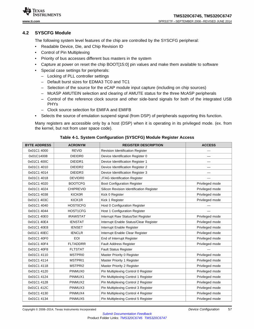
TMS320C6745, TMS320C6747www.ti.com SPRS377F –SEPTEMBER 2008–REVISED JUNE 2014
4.2 SYSCFG ModuleThe following system level features of the chip are controlled by the SYSCFG peripheral:• Readable Device, Die, and Chip Revision ID• Control of Pin Multiplexing• Priority of bus accesses different bus masters in the system• Capture at power on reset the chip BOOT[15:0] pin values and make them available to software• Special case settings for peripherals:
– Locking of PLL controller settings– Default burst sizes for EDMA3 TC0 and TC1– Selection of the source for the eCAP module input capture (including on chip sources)– McASP AMUTEIN selection and clearing of AMUTE status for the three McASP peripherals– Control of the reference clock source and other side-band signals for both of the integrated USB
PHYs– Clock source selection for EMIFA and EMIFB
• Selects the source of emulation suspend signal (from DSP) of peripherals supporting this function.
Many registers are accessible only by a host (DSP) when it is operating in its privileged mode. (ex. fromthe kernel, but not from user space code).
Table 4-1. System Configuration (SYSCFG) Module Register Access
BYTE ADDRESS ACRONYM REGISTER DESCRIPTION ACCESS0x01C1 4000 REVID Revision Identification Register —0x01C14008 DIEIDR0 Device Identification Register 0 —0x01C1 400C DIEIDR1 Device Identification Register 1 —0x01C1 4010 DIEIDR2 Device Identification Register 2 —0x01C1 4014 DIEIDR3 Device Identification Register 3 —0x01C1 4018 DEVIDR0 JTAG Identification Register —0x01C1 4020 BOOTCFG Boot Configuration Register Privileged mode0x01C1 4024 CHIPREVID Silicon Revision Identification Register Privileged mode0x01C1 4038 KICK0R Kick 0 Register Privileged mode0x01C1 403C KICK1R Kick 1 Register Privileged mode0x01C1 4040 HOST0CFG Host 0 Configuration Register —0x01C1 4044 HOST1CFG Host 1 Configuration Register —0x01C1 40E0 IRAWSTAT Interrupt Raw Status/Set Register Privileged mode0x01C1 40E4 IENSTAT Interrupt Enable Status/Clear Register Privileged mode0x01C1 40E8 IENSET Interrupt Enable Register Privileged mode0x01C1 40EC IENCLR Interrupt Enable Clear Register Privileged mode0x01C1 40F0 EOI End of Interrupt Register Privileged mode0x01C1 40F4 FLTADDRR Fault Address Register Privileged mode0x01C1 40F8 FLTSTAT Fault Status Register —0x01C1 4110 MSTPRI0 Master Priority 0 Register Privileged mode0x01C1 4114 MSTPRI1 Master Priority 1 Register Privileged mode0x01C1 4118 MSTPRI2 Master Priority 2 Register Privileged mode0x01C1 4120 PINMUX0 Pin Multiplexing Control 0 Register Privileged mode0x01C1 4124 PINMUX1 Pin Multiplexing Control 1 Register Privileged mode0x01C1 4128 PINMUX2 Pin Multiplexing Control 2 Register Privileged mode0x01C1 412C PINMUX3 Pin Multiplexing Control 3 Register Privileged mode0x01C1 4130 PINMUX4 Pin Multiplexing Control 4 Register Privileged mode0x01C1 4134 PINMUX5 Pin Multiplexing Control 5 Register Privileged mode
Copyright © 2008–2014, Texas Instruments Incorporated Device Configuration 57Submit Documentation Feedback
Product Folder Links: TMS320C6745 TMS320C6747
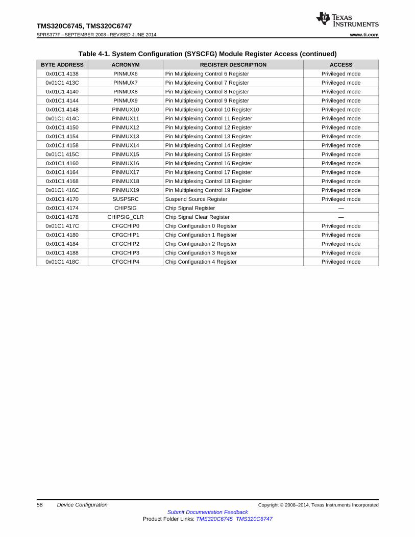
TMS320C6745, TMS320C6747SPRS377F –SEPTEMBER 2008–REVISED JUNE 2014 www.ti.com
Table 4-1. System Configuration (SYSCFG) Module Register Access (continued)BYTE ADDRESS ACRONYM REGISTER DESCRIPTION ACCESS
0x01C1 4138 PINMUX6 Pin Multiplexing Control 6 Register Privileged mode0x01C1 413C PINMUX7 Pin Multiplexing Control 7 Register Privileged mode0x01C1 4140 PINMUX8 Pin Multiplexing Control 8 Register Privileged mode0x01C1 4144 PINMUX9 Pin Multiplexing Control 9 Register Privileged mode0x01C1 4148 PINMUX10 Pin Multiplexing Control 10 Register Privileged mode0x01C1 414C PINMUX11 Pin Multiplexing Control 11 Register Privileged mode0x01C1 4150 PINMUX12 Pin Multiplexing Control 12 Register Privileged mode0x01C1 4154 PINMUX13 Pin Multiplexing Control 13 Register Privileged mode0x01C1 4158 PINMUX14 Pin Multiplexing Control 14 Register Privileged mode0x01C1 415C PINMUX15 Pin Multiplexing Control 15 Register Privileged mode0x01C1 4160 PINMUX16 Pin Multiplexing Control 16 Register Privileged mode0x01C1 4164 PINMUX17 Pin Multiplexing Control 17 Register Privileged mode0x01C1 4168 PINMUX18 Pin Multiplexing Control 18 Register Privileged mode0x01C1 416C PINMUX19 Pin Multiplexing Control 19 Register Privileged mode0x01C1 4170 SUSPSRC Suspend Source Register Privileged mode0x01C1 4174 CHIPSIG Chip Signal Register —0x01C1 4178 CHIPSIG_CLR Chip Signal Clear Register —0x01C1 417C CFGCHIP0 Chip Configuration 0 Register Privileged mode0x01C1 4180 CFGCHIP1 Chip Configuration 1 Register Privileged mode0x01C1 4184 CFGCHIP2 Chip Configuration 2 Register Privileged mode0x01C1 4188 CFGCHIP3 Chip Configuration 3 Register Privileged mode0x01C1 418C CFGCHIP4 Chip Configuration 4 Register Privileged mode
58 Device Configuration Copyright © 2008–2014, Texas Instruments IncorporatedSubmit Documentation Feedback
Product Folder Links: TMS320C6745 TMS320C6747

TMS320C6745, TMS320C6747www.ti.com SPRS377F –SEPTEMBER 2008–REVISED JUNE 2014
4.3 Pullup/Pulldown ResistorsProper board design should ensure that input pins to the device always be at a valid logic level and notfloating. This may be achieved via pullup/pulldown resistors. The device features internal pullup (IPU) andinternal pulldown (IPD) resistors on most pins to eliminate the need, unless otherwise noted, for externalpullup/pulldown resistors.
An external pullup/pulldown resistor needs to be used in the following situations:• Boot and Configuration Pins: If the pin is both routed out and 3-stated (not driven), an external
pullup/pulldown resistor is strongly recommended, even if the IPU/IPD matches the desired value/state.• Other Input Pins: If the IPU/IPD does not match the desired value/state, use an external
pullup/pulldown resistor to pull the signal to the opposite rail.
For the boot and configuration pins, if they are both routed out and 3-stated (not driven), it is stronglyrecommended that an external pullup/pulldown resistor be implemented. Although, internalpullup/pulldown resistors exist on these pins and they may match the desired configuration value,providing external connectivity can help ensure that valid logic levels are latched on these device boot andconfiguration pins. In addition, applying external pullup/pulldown resistors on the boot and configurationpins adds convenience to the user in debugging and flexibility in switching operating modes.
Tips for choosing an external pullup/pulldown resistor:• Consider the total amount of current that may pass through the pullup or pulldown resistor. Make sure
to include the leakage currents of all the devices connected to the net, as well as any internal pullup orpulldown resistors.
• Decide a target value for the net. For a pulldown resistor, this should be below the lowest VIL level ofall inputs connected to the net. For a pullup resistor, this should be above the highest VIH level of allinputs on the net. A reasonable choice would be to target the VOL or VOH levels for the logic family ofthe limiting device; which, by definition, have margin to the VIL and VIH levels.
• Select a pullup/pulldown resistor with the largest possible value; but, which can still ensure that the netwill reach the target pulled value when maximum current from all devices on the net is flowing throughthe resistor. The current to be considered includes leakage current plus, any other internal andexternal pullup/pulldown resistors on the net.
• For bidirectional nets, there is an additional consideration which sets a lower limit on the resistancevalue of the external resistor. Verify that the resistance is small enough that the weakest output buffercan drive the net to the opposite logic level (including margin).
• Remember to include tolerances when selecting the resistor value.• For pullup resistors, also remember to include tolerances on the IO supply rail.• For most systems, a 1-kΩ resistor can be used to oppose the IPU/IPD while meeting the above
criteria. Users should confirm this resistor value is correct for their specific application.• For most systems, a 20-kΩ resistor can be used to compliment the IPU/IPD on the boot and
configuration pins while meeting the above criteria. Users should confirm this resistor value is correctfor their specific application.
• For more detailed information on input current (II), and the low-/high-level input voltages (VIL and VIH)for the device, see Section 5.3, Recommended Operating Conditions.
• For the internal pullup/pulldown resistors for all device pins, see the peripheral/system-specific terminalfunctions table.
Copyright © 2008–2014, Texas Instruments Incorporated Device Configuration 59Submit Documentation Feedback
Product Folder Links: TMS320C6745 TMS320C6747

TMS320C6745, TMS320C6747SPRS377F –SEPTEMBER 2008–REVISED JUNE 2014 www.ti.com
5 Device Operating Conditions
5.1 Absolute Maximum Ratings Over Operating Case Temperature Range(Unless Otherwise Noted) (1)
Core -0.5 V to 1.4 V(CVDD, RVDD, RTC_CVDD, PLL0_VDDA ) (2)
I/O, 1.8V -0.5 V to 2 VSupply voltage ranges (USB0_VDDA18, USB1_VDDA18) (2)
I/O, 3.3V -0.5 V to 3.8V(DVDD, USB0_VDDA33, USB1_VDDA33) (2)
VI I/O, 1.2V -0.3 V to CVDD + 0.3V(OSCIN, RTC_XI)VI I/O, 3.3V -0.3V to DVDD + 0.35V(Steady State)VI I/O, 3.3V DVDD + 20%Input voltage ranges (Transient) up to 20% of Signal
PeriodVI I/O, USB 5V Tolerant Pins: 5.25V (3)
(USB0_DM, USB0_DP, USB0_ID, USB1_DM, USB1_DP)VI I/O, USB0 VBUS 5.50V (3)
VO I/O, 3.3V -0.5 V to DVDD + 0.3V(Steady State)
Output voltage rangesVO I/O, 3.3V 20% of DVDD for up to(Transient Overshoot/Undershoot) 20% of the signal periodInput or Output Voltages 0.3V above or below their respective power ±20mA
Clamp Current rails. Limit clamp current that flows through the I/O's internal diodeprotection cells.Commercial 0°C to 90°CIndustrial (D suffix ) -40°C to 90°COperating Junction Temperature ranges,
TJ Extended (A suffix) -40°C to 105°CAutomotive (T suffix) -40°C to 125°C
(1) Stresses beyond those listed under "absolute maximum ratings" may cause permanent damage to the device. These are stress ratingsonly, and functional operation of the device at these or any other conditions beyond those indicated under "recommended operatingconditions" is not implied. Exposure to absolute-maximum-rated conditions for extended periods may affect device reliability.
(2) All voltage values are with respect to VSS, PLL0_VSSA, OSCVSS, RTC_VSS(3) Up to a max of 24 hours.
5.2 Handling RatingsUNIT
Storage temperature (default) -55 to 150 °Crange, Tstg
Human Body Model (HBM) (2) >2000 VESD Stress Voltage,VESD
(1) Charged Device Model (CDM) (3) >500 V
(1) Electrostatic discharge (ESD) to measure device sensitivity/immunity to damage caused by electrostatic discharges into the device.(2) Level listed above is the passing level per ANSI/ESDA/JEDEC JS-001-2010. JEDEC document JEP155 states that 500V HBM allows
safe manufacturing with a standard ESD control process, and manufacturing with less than 500V HBM is possible if necessaryprecautions are taken. Pins listed as 1000V may actually have higher performance.
(3) Level listed above is the passing level per EIA-JEDEC JESD22-C101E. JEDEC document JEP157 states that 250V CDM allows safemanufacturing with a standard ESD control process. Pins listed as 250V may actually have higher performance.
60 Device Operating Conditions Copyright © 2008–2014, Texas Instruments IncorporatedSubmit Documentation Feedback
Product Folder Links: TMS320C6745 TMS320C6747
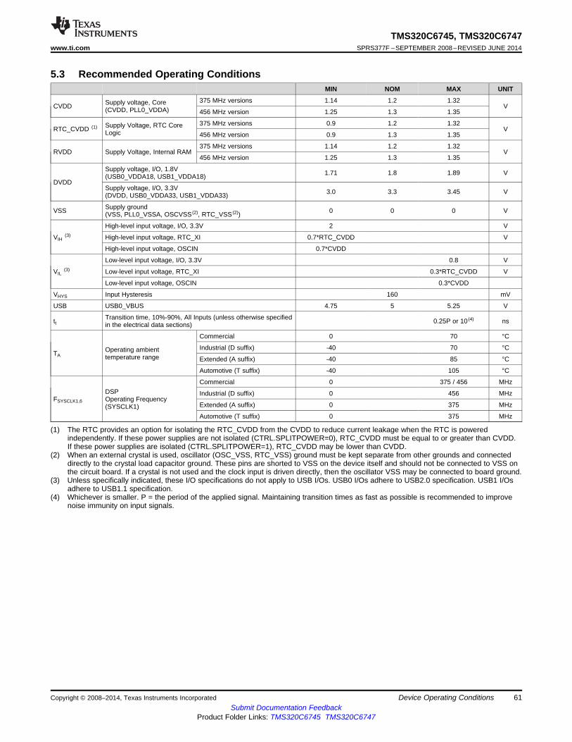
TMS320C6745, TMS320C6747www.ti.com SPRS377F –SEPTEMBER 2008–REVISED JUNE 2014
5.3 Recommended Operating ConditionsMIN NOM MAX UNIT
375 MHz versions 1.14 1.2 1.32Supply voltage, CoreCVDD V(CVDD, PLL0_VDDA) 456 MHz version 1.25 1.3 1.35
375 MHz versions 0.9 1.2 1.32Supply Voltage, RTC CoreRTC_CVDD (1) VLogic 456 MHz version 0.9 1.3 1.35
375 MHz versions 1.14 1.2 1.32RVDD Supply Voltage, Internal RAM V
456 MHz version 1.25 1.3 1.35
Supply voltage, I/O, 1.8V 1.71 1.8 1.89 V(USB0_VDDA18, USB1_VDDA18)DVDD
Supply voltage, I/O, 3.3V 3.0 3.3 3.45 V(DVDD, USB0_VDDA33, USB1_VDDA33)
Supply groundVSS 0 0 0 V(VSS, PLL0_VSSA, OSCVSS (2), RTC_VSS (2))
High-level input voltage, I/O, 3.3V 2 V
VIH(3) High-level input voltage, RTC_XI 0.7*RTC_CVDD V
High-level input voltage, OSCIN 0.7*CVDD
Low-level input voltage, I/O, 3.3V 0.8 V
VIL(3) Low-level input voltage, RTC_XI 0.3*RTC_CVDD V
Low-level input voltage, OSCIN 0.3*CVDD
VHYS Input Hysteresis 160 mV
USB USB0_VBUS 4.75 5 5.25 V
Transition time, 10%-90%, All Inputs (unless otherwise specifiedtt 0.25P or 10 (4) nsin the electrical data sections)
Commercial 0 70 °C
Industrial (D suffix) -40 70 °COperating ambientTA temperature range Extended (A suffix) -40 85 °C
Automotive (T suffix) -40 105 °C
Commercial 0 375 / 456 MHzDSP Industrial (D suffix) 0 456 MHz
FSYSCLK1,6 Operating FrequencyExtended (A suffix) 0 375 MHz(SYSCLK1)Automotive (T suffix) 0 375 MHz
(1) The RTC provides an option for isolating the RTC_CVDD from the CVDD to reduce current leakage when the RTC is poweredindependently. If these power supplies are not isolated (CTRL.SPLITPOWER=0), RTC_CVDD must be equal to or greater than CVDD.If these power supplies are isolated (CTRL.SPLITPOWER=1), RTC_CVDD may be lower than CVDD.
(2) When an external crystal is used, oscillator (OSC_VSS, RTC_VSS) ground must be kept separate from other grounds and connecteddirectly to the crystal load capacitor ground. These pins are shorted to VSS on the device itself and should not be connected to VSS onthe circuit board. If a crystal is not used and the clock input is driven directly, then the oscillator VSS may be connected to board ground.
(3) Unless specifically indicated, these I/O specifications do not apply to USB I/Os. USB0 I/Os adhere to USB2.0 specification. USB1 I/Osadhere to USB1.1 specification.
(4) Whichever is smaller. P = the period of the applied signal. Maintaining transition times as fast as possible is recommended to improvenoise immunity on input signals.
Copyright © 2008–2014, Texas Instruments Incorporated Device Operating Conditions 61Submit Documentation Feedback
Product Folder Links: TMS320C6745 TMS320C6747

TMS320C6745, TMS320C6747SPRS377F –SEPTEMBER 2008–REVISED JUNE 2014 www.ti.com
5.4 Notes on Recommended Power-On Hours (POH)The information in the section below is provided solely for your convenience and does not extend ormodify the warranty provided under TI’s standard terms and conditions for TI semiconductor products.
To avoid significant degradation, the device power-on hours (POH) must be limited to the following:
Table 5-1. Recommended Power-On Hours
Silicon Operating Junction Power-On Hours [POH]Speed Grade Nominal CVDD Voltage (V)Revision Temperature (Tj) (hours)D 300 MHz 0 to 90 °C 1.2V 100,000D 300 MHz 0 to 90 °C 1.2V 100,000D 375 MHz 0 to 90 °C 1.2V 100,000D 375 MHz -40 to 105 °C 1.2V 75,000 (1)
D 375 MHz -40 to 125 °C 1.2V 20,000D 456 MHz 0 to 90 °C 1.3V 100,000D 456 MHz -40 to 90 °C 1.3V 100,000
(1) 100,000 POH can be achieved at this temperature condition if the device operation is limited to 345 MHz.
Note: Logic functions and parameter values are not assured out of the range specified in the recommendedoperating conditions.
The above notations cannot be deemed a warranty or deemed to extend or modify the warranty underTI’s standard terms and conditions for TI semiconductor products.
62 Device Operating Conditions Copyright © 2008–2014, Texas Instruments IncorporatedSubmit Documentation Feedback
Product Folder Links: TMS320C6745 TMS320C6747
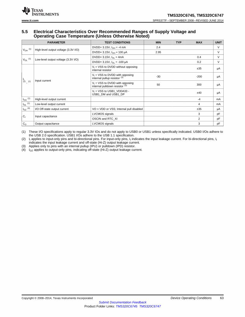
TMS320C6745, TMS320C6747www.ti.com SPRS377F –SEPTEMBER 2008–REVISED JUNE 2014
5.5 Electrical Characteristics Over Recommended Ranges of Supply Voltage andOperating Case Temperature (Unless Otherwise Noted)
PARAMETER TEST CONDITIONS MIN TYP MAX UNIT
DVDD= 3.15V, IOH = -4 mA 2.4 VVOH
(1) High-level output voltage (3.3V I/O)DVDD= 3.15V, IOH = 100 μA 2.95 V
DVDD= 3.15V, IOL = 4mA 0.4 VVOL
(1) Low-level output voltage (3.3V I/O)DVDD= 3.15V, IOL = -100 μA 0.2 V
VI = VSS to DVDD without opposing ±35 μAinternal resistor
VI = VSS to DVDD with opposing -30 -200 μAinternal pullup resistor (3)II Input current(2) , (1)
VI = VSS to DVDD with opposing 50 300 μAinternal pulldown resistor (3)
VI = VSS to USB1_VDDA33 - ±40 μAUSB1_DM and USB1_DP
IOH(1) High-level output current -4 mA
IOL(1) Low-level output current 4 mA
IOZ(4) I/O Off-state output current VO = VDD or VSS; Internal pull disabled ±35 μA
LVCMOS signals 3 pFCI Input capacitance
OSCIN and RTC_XI 2 pF
CO Output capacitance LVCMOS signals 3 pF
(1) These I/O specifications apply to regular 3.3V IOs and do not apply to USB0 or USB1 unless specifically indicated. USB0 I/Os adhere tothe USB 2.0 specification. USB1 I/Os adhere to the USB 1.1 specification.
(2) II applies to input-only pins and bi-directional pins. For input-only pins, II indicates the input leakage current. For bi-directional pins, IIindicates the input leakage current and off-state (Hi-Z) output leakage current.
(3) Applies only to pins with an internal pullup (IPU) or pulldown (IPD) resistor.(4) IOZ applies to output-only pins, indicating off-state (Hi-Z) output leakage current.
Copyright © 2008–2014, Texas Instruments Incorporated Device Operating Conditions 63Submit Documentation Feedback
Product Folder Links: TMS320C6745 TMS320C6747

Vref = VIL MAX (or VOL MAX)
Vref = VIH MIN (or VOH MIN)
Vref
Transmission Line
4.0 pF 1.85 pF
Z0 = 50 Ω
(see note)
Tester Pin Electronics Data Sheet Timing Reference Point
OutputUnderTest
42 Ω 3.5 nH
Device Pin(see note)
TMS320C6745, TMS320C6747SPRS377F –SEPTEMBER 2008–REVISED JUNE 2014 www.ti.com
6 Peripheral Information and Electrical Specifications
6.1 Parameter Information
6.1.1 Parameter Information Device-Specific Information
A. The data sheet provides timing at the device pin. For output timing analysis, the tester pin electronics and itstransmission line effects must be taken into account. A transmission line with a delay of 2 ns or longer can be used toproduce the desired transmission line effect. The transmission line is intended as a load only. It is not necessary toadd or subtract the transmission line delay (2 ns or longer) from the data sheet timings.Input requirements in this data sheet are tested with an input slew rate of < 4 Volts per nanosecond (4 V/ns) at thedevice pin and the input signals are driven between 0V and the appropriate IO supply rail for the signal.
Figure 6-1. Test Load Circuit for AC Timing Measurements
The load capacitance value stated is only for characterization and measurement of AC timing signals. Thisload capacitance value does not indicate the maximum load the device is capable of driving.
6.1.1.1 Signal Transition Levels
All input and output timing parameters are referenced to Vref for both "0" and "1" logic levels. For 3.3 V I/O,Vref = 1.65 V. For 1.8 V I/O, Vref = 0.9 V. For 1.2 V I/O, Vref = 0.6 V.
Figure 6-2. Input and Output Voltage Reference Levels for AC Timing Measurements
All rise and fall transition timing parameters are referenced to VIL MAX and VIH MIN for input clocks,VOLMAX and VOH MIN for output clocks.
Figure 6-3. Rise and Fall Transition Time Voltage Reference Levels
64 Peripheral Information and Electrical Specifications Copyright © 2008–2014, Texas Instruments IncorporatedSubmit Documentation Feedback
Product Folder Links: TMS320C6745 TMS320C6747
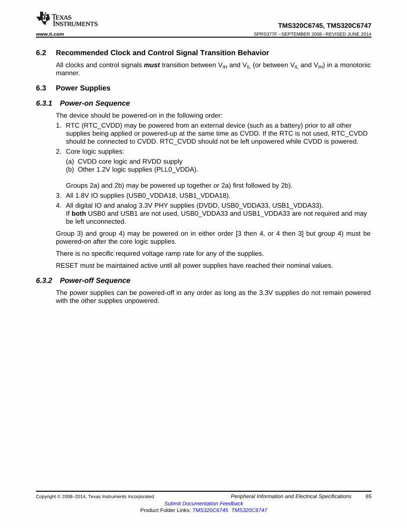
TMS320C6745, TMS320C6747www.ti.com SPRS377F –SEPTEMBER 2008–REVISED JUNE 2014
6.2 Recommended Clock and Control Signal Transition BehaviorAll clocks and control signals must transition between VIH and VIL (or between VIL and VIH) in a monotonicmanner.
6.3 Power Supplies
6.3.1 Power-on SequenceThe device should be powered-on in the following order:1. RTC (RTC_CVDD) may be powered from an external device (such as a battery) prior to all other
supplies being applied or powered-up at the same time as CVDD. If the RTC is not used, RTC_CVDDshould be connected to CVDD. RTC_CVDD should not be left unpowered while CVDD is powered.
2. Core logic supplies:(a) CVDD core logic and RVDD supply(b) Other 1.2V logic supplies (PLL0_VDDA).
Groups 2a) and 2b) may be powered up together or 2a) first followed by 2b).3. All 1.8V IO supplies (USB0_VDDA18, USB1_VDDA18).4. All digital IO and analog 3.3V PHY supplies (DVDD, USB0_VDDA33, USB1_VDDA33).
If both USB0 and USB1 are not used, USB0_VDDA33 and USB1_VDDA33 are not required and maybe left unconnected.
Group 3) and group 4) may be powered on in either order [3 then 4, or 4 then 3] but group 4) must bepowered-on after the core logic supplies.
There is no specific required voltage ramp rate for any of the supplies.
RESET must be maintained active until all power supplies have reached their nominal values.
6.3.2 Power-off SequenceThe power supplies can be powered-off in any order as long as the 3.3V supplies do not remain poweredwith the other supplies unpowered.
Copyright © 2008–2014, Texas Instruments Incorporated Peripheral Information and Electrical Specifications 65Submit Documentation Feedback
Product Folder Links: TMS320C6745 TMS320C6747
TMS320C6745, TMS320C6747SPRS377F –SEPTEMBER 2008–REVISED JUNE 2014 www.ti.com
6.4 Reset
6.4.1 Power-On Reset (POR)A power-on reset (POR) is required to place the device in a known good state after power-up. Power-OnReset is initiated by bringing RESET and TRST low at the same time. POR sets all of the device internallogic to its default state. All pins are tri-stated with the exception of RESETOUT, which remains activethrough the reset sequence, and GP7[14]. During reset, GP7[14] is configured as a reserved function, andits behavior is not deterministic; the user should be aware that this pin will drive a level, and in fact maytoggle, during reset. RESETOUT is an output for use by other controllers in the system that indicates thedevice is currently in reset.
While both TRST and RESET need to be asserted upon power up, only RESET needs to be released forthe device to boot properly. TRST may be asserted indefinitely for normal operation, keeping the JTAGport interface and device's emulation logic in the reset state.
. TRST only needs to be released when it is necessary to use a JTAG controller to debug the device orexercise the device's boundary scan functionality. Note: TRST is synchronous and must be clocked byTCK; otherwise, the boundary scan logic may not respond as expected after TRST is asserted.
. RESET must be released only in order for boundary-scan JTAG to read the variant field of IDCODEcorrectly. Other boundary-scan instructions work correctly independent of current state of RESET. Formaximum reliability, the device includes an internal pulldown on the TRST pin to ensure that TRST willalways be asserted upon power up and the device's internal emulation logic will always be properlyinitialized.
JTAG controllers from Texas Instruments actively drive TRST high. However, some third-party JTAGcontrollers may not drive TRST high but expect the use of a pullup resistor on TRST. When using this typeof JTAG controller, assert TRST to intialize the device after powerup and externally drive TRST highbefore attempting any emulation or boundary scan operations.
A summary of the effects of Power-On Reset is given below:• All internal logic (including emulation logic and the PLL logic) is reset to its default state• Internal memory is not maintained through a POR• RESETOUT goes active• All device pins go to a high-impedance state• The RTC peripheral is not reset during a POR. A software sequence is required to reset the RTC.
CAUTION: A watchdog reset triggers a POR.
6.4.2 Warm ResetA warm reset provides a limited reset to the device. Warm Reset is initiated by bringing only RESET low(TRST is maintained high through a warm reset). Warm reset sets certain portions of the device to theirdefault state while leaving others unaltered. All pins are tri-stated with the exception of RESETOUT, whichremains active through the reset sequence, and GP7[14]. During reset, GP7[14] is configured as areserved function, and its behavior is not deterministic; the user should be aware that this pin will drive alevel, and in fact may toggle, during reset. RESETOUT is an output for use by other controllers in thesystem that indicates the device is currently in reset.
During emulation, the emulator will maintain TRST high and hence only warm reset (not POR) is availableduring emulation debug and development.
A summary of the effects of Warm Reset is given below:• All internal logic (except for the emulation logic and the PLL logic) is reset to its default state• Internal memory is maintained through a warm reset• RESETOUT goes active• All device pins go to a high-impedance state
66 Peripheral Information and Electrical Specifications Copyright © 2008–2014, Texas Instruments IncorporatedSubmit Documentation Feedback
Product Folder Links: TMS320C6745 TMS320C6747

OSCIN
RESET
RESETOUT
Boot Pins Config
PowerSuppliesRamping
Power Supplies Stable
Clock Source Stable
1
2 3
4
TRST
TMS320C6745, TMS320C6747www.ti.com SPRS377F –SEPTEMBER 2008–REVISED JUNE 2014
• The RTC peripheral is not reset during a warm reset. A software sequence is required to reset theRTC.
6.4.3 Reset Electrical Data TimingsTable 6-1 assumes testing over the recommended operating conditions.
Table 6-1. Reset Timing Requirements (1) (2)
No. MIN MAX UNIT1 tw(RSTL) Pulse width, RESET/TRST low 100 ns2 tsu(BPV-RSTH) Setup time, boot pins valid before RESET/TRST high 20 ns3 th(RSTH-BPV) Hold time, boot pins valid after RESET/TRST high 20 ns4 td(RSTH- RESET high to RESETOUT high; Warm reset 4096 cycles (3)
RESETOUTH) RESET high to RESETOUT high; Power-on Reset 6192
(1) RESETOUT is multiplexed with other pin functions. See the Terminal Functions table, Table 3-6 for details.(2) For power-on reset (POR), the reset timings in this table refer to RESET and TRST together. For warm reset, the reset timings in this
table refer to RESET only (TRST is held high).(3) OSCIN cycles.
Figure 6-4. Power-On Reset (RESET and TRST active) Timing
Copyright © 2008–2014, Texas Instruments Incorporated Peripheral Information and Electrical Specifications 67Submit Documentation Feedback
Product Folder Links: TMS320C6745 TMS320C6747

OSCIN
TRST
RESET
RESETOUT
Boot Pins Config
Power Supplies Stable
1
23
4
Driven or Hi-Z
TMS320C6745, TMS320C6747SPRS377F –SEPTEMBER 2008–REVISED JUNE 2014 www.ti.com
Figure 6-5. Warm Reset (RESET active, TRST high) Timing
68 Peripheral Information and Electrical Specifications Copyright © 2008–2014, Texas Instruments IncorporatedSubmit Documentation Feedback
Product Folder Links: TMS320C6745 TMS320C6747

C2
C1
X1
OSCOUT
OSCIN
OSCVSS
Clock Inputto PLL
TMS320C6745, TMS320C6747www.ti.com SPRS377F –SEPTEMBER 2008–REVISED JUNE 2014
6.5 Crystal Oscillator or External Clock InputThe C6745/6747 device includes two choices to provide an external clock input, which is fed to the on-chip PLL to generate high-frequency system clocks. These options are illustrated in Figure 6-6 andFigure 6-7. For input clock frequencies between 12 and 20 MHz, a crystal with 80 ohm max ESR isrecommended. For input clock frequencies between 20 and 30 MHz, a crystal with 60 ohm max ESR isrecommended. Typical load capacitance values are 10-20 pF, where the load capacitance is the seriescombination of C1 and C2.
The CLKMODE bit in the PLLCTL register must be 0 to use the on-chip oscillator. If CLKMODE is set to 1,the internal oscillator is disabled.• Figure 6-6 illustrates the option that uses on-chip 1.2V oscillator with external crystal circuit.• Figure 6-7 illustrates the option that uses an external 1.2V clock input.
Figure 6-6. On-Chip 1.2V Oscillator
Table 6-2. Oscillator Timing Requirements
PARAMETER MIN MAX UNITfosc Oscillator frequency range (OSCIN/OSCOUT) 12 30 MHz
Copyright © 2008–2014, Texas Instruments Incorporated Peripheral Information and Electrical Specifications 69Submit Documentation Feedback
Product Folder Links: TMS320C6745 TMS320C6747

OSCOUT
OSCIN
OSCVSS
ClockInputto PLL
NC
TMS320C6745, TMS320C6747SPRS377F –SEPTEMBER 2008–REVISED JUNE 2014 www.ti.com
Figure 6-7. External 1.2V Clock Source
Table 6-3. OSCIN Timing Requirements
PARAMETER MIN MAX UNITfOSCIN OSCIN frequency range (OSCIN) 12 50 MHztc(OSCIN) Cycle time, external clock driven on OSCIN 20 nstw(OSCINH) Pulse width high, external clock on OSCIN 0.4 tc(OSCIN) nstw(OSCINL) Pulse width low, external clock on OSCIN 0.4 tc(OSCIN) nstt(OSCIN) Transition time, OSCIN 0.25P or 10 (1) nstj(OSCIN) Period jitter, OSCIN 0.02P ns
(1) Whichever is smaller. P = the period of the applied signal. Maintaining transition times as fast as possible is recommended to improvenoise immunity on input signals.
70 Peripheral Information and Electrical Specifications Copyright © 2008–2014, Texas Instruments IncorporatedSubmit Documentation Feedback
Product Folder Links: TMS320C6745 TMS320C6747
0.1µF
0.01µF
50R1.14V - 1.32V
50RVSS
PLL0_VDDA
PLL0_VSSA
Ferrite Bead: Murata BLM31PG500SN1L or Equivalent
TMS320C6745, TMS320C6747www.ti.com SPRS377F –SEPTEMBER 2008–REVISED JUNE 2014
6.6 Clock PLLsThe C6745/6747 has one PLL controller that provides clock to different parts of the system. PLL0 providesclocks (though various dividers) to most of the components of the device.
The PLL controller provides the following:• Glitch-Free Transitions (on changing clock settings)• Domain Clocks Alignment• Clock Gating• PLL power down
The various clock outputs given by the controller are as follows:• Domain Clocks: SYSCLK [1:n]• Auxiliary Clock from reference clock source: AUXCLK
Various dividers that can be used are as follows:• Post-PLL Divider: POSTDIV• SYSCLK Divider: D1, ¼, Dn
Various other controls supported are as follows:• PLL Multiplier Control: PLLM• Software programmable PLL Bypass: PLLEN
6.6.1 PLL Device-Specific InformationThe C6745/6747 DSP generates the high-frequency internal clocks it requires through an on-chip PLL.
The PLL requires some external filtering components to reduce power supply noise as shown in Figure 6-8.
Figure 6-8. PLL External Filtering Components
The input to the PLL is either from the on-chip oscillator (OSCIN pin) or from an external clock on theOSCIN pin. The PLL outputs seven clocks that have programmable divider options. Figure 6-9 illustratesthe PLL Topology.
The PLL is disabled by default after a device reset. It must be configured by software according to theallowable operating conditions listed in Table 6-4 before enabling the DSP to run from the PLL by settingPLLEN = 1.
Copyright © 2008–2014, Texas Instruments Incorporated Peripheral Information and Electrical Specifications 71Submit Documentation Feedback
Product Folder Links: TMS320C6745 TMS320C6747

PLLDIV1 (/1) SYSCLK1
PLLDIV2 (/2) SYSCLK2
PLLDIV3 (/3) SYSCLK3
PLLDIV4 (/4) SYSCLK4
PLLDIV5 (/3) SYSCLK5
PLLDIV6 (/1) SYSCLK6
PLLDIV7 (/6) SYSCLK7
DIV4.5 1
0 EMIFAInternalClock
Source
CFGCHIP3[EMA_CLKSRC]
DIV4.5 EMIFBInternalClock
Source
CFGCHIP3[EMB_CLKSRC]
1
0
Pre-Div
PLLM
PLLEN
AUXCLK
0
1
PLL Post-Div
CLKMODE
1
0
SquareWave
Crystal
OSCIN
OBSCLK Pin14h
17h
18h
19h
1Ah
1Bh
1Ch
1Dh
SYSCLK1SYSCLK2
SYSCLK3
SYSCLK4
SYSCLK5
SYSCLK6
SYSCLK7
OCSEL[OCSRC]
OSCDIV
TMS320C6745, TMS320C6747SPRS377F –SEPTEMBER 2008–REVISED JUNE 2014 www.ti.com
Figure 6-9. PLL Topology
72 Peripheral Information and Electrical Specifications Copyright © 2008–2014, Texas Instruments IncorporatedSubmit Documentation Feedback
Product Folder Links: TMS320C6745 TMS320C6747
2000 NMax PLL Lock Time =
m
where N = Pre-Divider Ratio
M = PLL Multiplier
TMS320C6745, TMS320C6747www.ti.com SPRS377F –SEPTEMBER 2008–REVISED JUNE 2014
Table 6-4. Allowed PLL Operating Conditions
DefaultNo. PARAMETER MIN MAX UNITValuePLLRST: Assertion time during1 N/A 1000 N/A nsinitialization
Lock time: The time that the applicationhas to wait for the PLL to acquire locks OSCIN2 N/A N/Abefore setting PLLEN, after changing cycles
PREDIV, PLLM, or OSCIN
3 PREDIV /1 /1 /32PLL input frequency 30 (if internal oscillator is used)4 12 MHz( PLLREF) 50 (if external clock source is used)
5 PLL multiplier values (PLLM) (1) x20 x4 x326 PLL output frequency. ( PLLOUT ) N/A 300 600 MHz7 POSTDIV /1 /1 /32
(1) The multiplier values must be chosen such that the PLL output frequency (at PLLOUT) is between 300 and 600 MHz, but the frequencygoing into the SYSCLK dividers (after the post divider) cannot exceed the maximum clock frequency defined for the device at a givenvoltage operating point.
6.6.2 Device Clock GenerationPLL0 is controlled by PLL Controller 0. The PLLC0 manages the clock ratios, alignment, and gating for thesystem clocks to the chip. The PLLC is responsible for controlling all modes of the PLL through software,in terms of pre-division of the clock inputs, multiply factor within the PLL, and post-division for each of thechip-level clocks from the PLL output. The PLLC also controls reset propagation through the chip, clockalignment, and test points.
Copyright © 2008–2014, Texas Instruments Incorporated Peripheral Information and Electrical Specifications 73Submit Documentation Feedback
Product Folder Links: TMS320C6745 TMS320C6747

TMS320C6745, TMS320C6747SPRS377F –SEPTEMBER 2008–REVISED JUNE 2014 www.ti.com
6.6.3 PLL Controller 0 Registers
Table 6-5. PLL Controller 0 Registers
BYTE ACRONYM REGISTER DESCRIPTIONADDRESS0x01C1 1000 REVID Revision Identification Register0x01C1 10E4 RSTYPE Reset Type Status Register0x01C1 1100 PLLCTL PLL Control Register0x01C1 1104 OCSEL OBSCLK Select Register0x01C1 1110 PLLM PLL Multiplier Control Register0x01C1 1114 PREDIV PLL Pre-Divider Control Register0x01C1 1118 PLLDIV1 PLL Controller Divider 1 Register0x01C1 111C PLLDIV2 PLL Controller Divider 2 Register0x01C1 1120 PLLDIV3 PLL Controller Divider 3 Register0x01C1 1124 OSCDIV Oscillator Divider 1 Register (OBSCLK)0x01C1 1128 POSTDIV PLL Post-Divider Control Register0x01C1 1138 PLLCMD PLL Controller Command Register0x01C1 113C PLLSTAT PLL Controller Status Register0x01C1 1140 ALNCTL PLL Controller Clock Align Control Register0x01C1 1144 DCHANGE PLLDIV Ratio Change Status Register0x01C1 1148 CKEN Clock Enable Control Register0x01C1 114C CKSTAT Clock Status Register0x01C1 1150 SYSTAT SYSCLK Status Register0x01C1 1160 PLLDIV4 PLL Controller Divider 4 Register0x01C1 1164 PLLDIV5 PLL Controller Divider 5 Register0x01C1 1168 PLLDIV6 PLL Controller Divider 6 Register0x01C1 116C PLLDIV7 PLL Controller Divider 7 Register
74 Peripheral Information and Electrical Specifications Copyright © 2008–2014, Texas Instruments IncorporatedSubmit Documentation Feedback
Product Folder Links: TMS320C6745 TMS320C6747

TMS320C6745, TMS320C6747www.ti.com SPRS377F –SEPTEMBER 2008–REVISED JUNE 2014
6.7 InterruptsThe C6745/6747 devices have a large number of interrupts to service the needs of its many peripheralsand subsystems.
6.7.1 DSP InterruptsThe C674x DSP interrupt controller combines device events into 12 prioritized interrupts. The source foreach of the 12 CPU interrupts is user programmable and is listed in Table 6-6. Also, the interruptcontroller controls the generation of the CPU exception, NMI, and emulation interrupts. Table 6-7summarizes the C674x interrupt controller registers and memory locations.
Table 6-6. C6745/6747 DSP Interrupts
EVT# INTERRUPT NAME SOURCE0 EVT0 C674x Int Ctl 01 EVT1 C674x Int Ctl 12 EVT2 C674x Int Ctl 23 EVT3 C674x Int Ctl 34 T64P0_TINT12 Timer64P0 - TINT125 SYSCFG_CHIPINT2 SYSCFG_CHIPSIG Register6 PRU_EVTOUT0 PRU Interrupt7 EHRPWM0 HiResTimer/PWM0 Interrupt8 EDMA3_CC0_INT1 EDMA3 Channel Controller 0 Region 1 interrupt9 EMU-DTDMA C674x-ECM
10 EHRPWM0TZ HiResTimer/PWM0 Trip Zone Interrupt11 EMU-RTDXRX C674x-RTDX12 EMU-RTDXTX C674x-RTDX13 IDMAINT0 C674x-EMC14 IDMAINT1 C674x-EMC15 MMCSD_INT0 MMCSD MMC/SD Interrupt16 MMCSD_INT1 MMCSD SDIO Interrupt17 PRU_EVTOUT1 PRU Interrupt18 EHRPWM1 HiResTimer/PWM1 Interrupt19 USB0_INT USB0 Interrupt20 USB1_HCINT USB1 OHCI Host Controller Interrupt21 USB1_RWAKEUP USB1 Remote Wakeup Interrupt22 PRU_EVTOUT2 PRU Interrupt23 EHRPWM1TZ HiResTimer/PWM1 Trip Zone Interrupt24 EHRPWM2 HiResTimer/PWM2 Interrupt25 EHRPWM2TZ HiResTimer/PWM2 Trip Zone Interrupt26 EMAC_C0RXTHRESH EMAC - Core 0 Receive Threshold Interrupt27 EMAC_C0RX EMAC - Core 0 Receive Interrupt28 EMAC_C0TX EMAC - Core 0 Transmit Interrupt29 EMAC_C0MISC EMAC - Core 0 Miscellaneous Interrupt30 EMAC_C1RXTHRESH EMAC - Core 1 Receive Threshold Interrupt31 EMAC_C1RX EMAC - Core 1 Receive Interrupt32 EMAC_C1TX EMAC - Core 1 Transmit Interrupt33 EMAC_C1MISC EMAC - Core 1 Miscellaneous Interrupt34 UHPI_DSPINT UHPI DSP Interrupt35 PRU_EVTOUT3 PRU Interrupt36 IIC0_INT I2C0
Copyright © 2008–2014, Texas Instruments Incorporated Peripheral Information and Electrical Specifications 75Submit Documentation Feedback
Product Folder Links: TMS320C6745 TMS320C6747
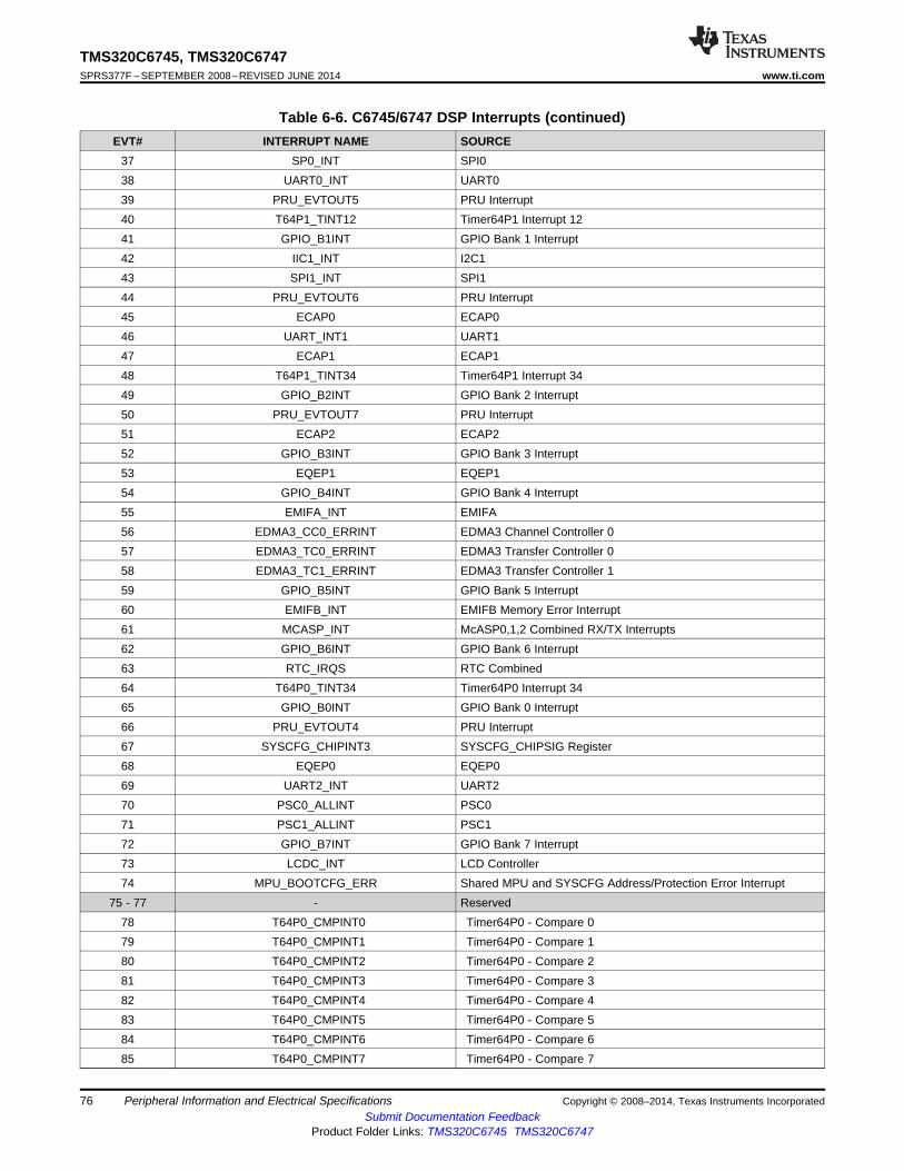
TMS320C6745, TMS320C6747SPRS377F –SEPTEMBER 2008–REVISED JUNE 2014 www.ti.com
Table 6-6. C6745/6747 DSP Interrupts (continued)EVT# INTERRUPT NAME SOURCE
37 SP0_INT SPI038 UART0_INT UART039 PRU_EVTOUT5 PRU Interrupt40 T64P1_TINT12 Timer64P1 Interrupt 1241 GPIO_B1INT GPIO Bank 1 Interrupt42 IIC1_INT I2C143 SPI1_INT SPI144 PRU_EVTOUT6 PRU Interrupt45 ECAP0 ECAP046 UART_INT1 UART147 ECAP1 ECAP148 T64P1_TINT34 Timer64P1 Interrupt 3449 GPIO_B2INT GPIO Bank 2 Interrupt50 PRU_EVTOUT7 PRU Interrupt51 ECAP2 ECAP252 GPIO_B3INT GPIO Bank 3 Interrupt53 EQEP1 EQEP154 GPIO_B4INT GPIO Bank 4 Interrupt55 EMIFA_INT EMIFA56 EDMA3_CC0_ERRINT EDMA3 Channel Controller 057 EDMA3_TC0_ERRINT EDMA3 Transfer Controller 058 EDMA3_TC1_ERRINT EDMA3 Transfer Controller 159 GPIO_B5INT GPIO Bank 5 Interrupt60 EMIFB_INT EMIFB Memory Error Interrupt61 MCASP_INT McASP0,1,2 Combined RX/TX Interrupts62 GPIO_B6INT GPIO Bank 6 Interrupt63 RTC_IRQS RTC Combined64 T64P0_TINT34 Timer64P0 Interrupt 3465 GPIO_B0INT GPIO Bank 0 Interrupt66 PRU_EVTOUT4 PRU Interrupt67 SYSCFG_CHIPINT3 SYSCFG_CHIPSIG Register68 EQEP0 EQEP069 UART2_INT UART270 PSC0_ALLINT PSC071 PSC1_ALLINT PSC172 GPIO_B7INT GPIO Bank 7 Interrupt73 LCDC_INT LCD Controller74 MPU_BOOTCFG_ERR Shared MPU and SYSCFG Address/Protection Error Interrupt
75 - 77 - Reserved78 T64P0_CMPINT0 Timer64P0 - Compare 079 T64P0_CMPINT1 Timer64P0 - Compare 180 T64P0_CMPINT2 Timer64P0 - Compare 281 T64P0_CMPINT3 Timer64P0 - Compare 382 T64P0_CMPINT4 Timer64P0 - Compare 483 T64P0_CMPINT5 Timer64P0 - Compare 584 T64P0_CMPINT6 Timer64P0 - Compare 685 T64P0_CMPINT7 Timer64P0 - Compare 7
76 Peripheral Information and Electrical Specifications Copyright © 2008–2014, Texas Instruments IncorporatedSubmit Documentation Feedback
Product Folder Links: TMS320C6745 TMS320C6747

TMS320C6745, TMS320C6747www.ti.com SPRS377F –SEPTEMBER 2008–REVISED JUNE 2014
Table 6-6. C6745/6747 DSP Interrupts (continued)EVT# INTERRUPT NAME SOURCE
86 T64P1_CMPINT0 Timer64P1 - Compare 087 T64P1_CMPINT1 Timer64P1 - Compare 188 T64P1_CMPINT2 Timer64P1 - Compare 289 T64P1_CMPINT3 Timer64P1 - Compare 390 T64P1_CMPINT4 Timer64P1 - Compare 491 T64P1_CMPINT5 Timer64P1 - Compare 592 T64P1_CMPINT6 Timer64P1 - Compare 693 T64P1_CMPINT7 Timer64P1 - Compare 7
94 - 95 - Reserved96 INTERR C674x-Int Ctl97 EMC_IDMAERR C674x-EMC
98 - 112 - Reserved113 PMC_ED C674x-PMC
114 - 115 - Reserved116 UMC_ED1 C674x-UMC117 UMC_ED2 C674x-UMC118 PDC_INT C674x-PDC119 SYS_CMPA C674x-SYS120 PMC_CMPA C674x-PMC121 PMC_CMPA C674x-PMC122 DMC_CMPA C674x-DMC123 DMC_CMPA C674x-DMC124 UMC_CMPA C674x-UMC125 UMC_CMPA C674x-UMC126 EMC_CMPA C674x-EMC127 EMC_BUSERR C674x-EMC
Copyright © 2008–2014, Texas Instruments Incorporated Peripheral Information and Electrical Specifications 77Submit Documentation Feedback
Product Folder Links: TMS320C6745 TMS320C6747

TMS320C6745, TMS320C6747SPRS377F –SEPTEMBER 2008–REVISED JUNE 2014 www.ti.com
Table 6-7. C674x DSP Interrupt Controller Registers
BYTE ADDRESS ACRONYM REGISTER DESCRIPTION0x0180 0000 EVTFLAG0 Event flag register 00x0180 0004 EVTFLAG1 Event flag register 10x0180 0008 EVTFLAG2 Event flag register 20x0180 000C EVTFLAG3 Event flag register 30x0180 0020 EVTSET0 Event set register 00x0180 0024 EVTSET1 Event set register 10x0180 0028 EVTSET2 Event set register 20x0180 002C EVTSET3 Event set register 30x0180 0040 EVTCLR0 Event clear register 00x0180 0044 EVTCLR1 Event clear register 10x0180 0048 EVTCLR2 Event clear register 20x0180 004C EVTCLR3 Event clear register 30x0180 0080 EVTMASK0 Event mask register 00x0180 0084 EVTMASK1 Event mask register 10x0180 0088 EVTMASK2 Event mask register 20x0180 008C EVTMASK3 Event mask register 30x0180 00A0 MEVTFLAG0 Masked event flag register 00x0180 00A4 MEVTFLAG1 Masked event flag register 10x0180 00A8 MEVTFLAG2 Masked event flag register 20x0180 00AC MEVTFLAG3 Masked event flag register 30x0180 00C0 EXPMASK0 Exception mask register 00x0180 00C4 EXPMASK1 Exception mask register 10x0180 00C8 EXPMASK2 Exception mask register 20x0180 00CC EXPMASK3 Exception mask register 30x0180 00E0 MEXPFLAG0 Masked exception flag register 00x0180 00E4 MEXPFLAG1 Masked exception flag register 10x0180 00E8 MEXPFLAG2 Masked exception flag register 20x0180 00EC MEXPFLAG3 Masked exception flag register 30x0180 0104 INTMUX1 Interrupt mux register 10x0180 0108 INTMUX2 Interrupt mux register 20x0180 010C INTMUX3 Interrupt mux register 3
0x0180 0140 - 0x0180 0144 - Reserved0x0180 0180 INTXSTAT Interrupt exception status0x0180 0184 INTXCLR Interrupt exception clear0x0180 0188 INTDMASK Dropped interrupt mask register0x0180 01C0 EVTASRT Event assert register
78 Peripheral Information and Electrical Specifications Copyright © 2008–2014, Texas Instruments IncorporatedSubmit Documentation Feedback
Product Folder Links: TMS320C6745 TMS320C6747
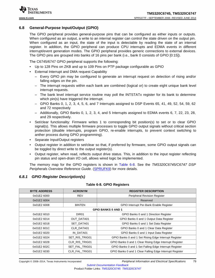
TMS320C6745, TMS320C6747www.ti.com SPRS377F –SEPTEMBER 2008–REVISED JUNE 2014
6.8 General-Purpose Input/Output (GPIO)The GPIO peripheral provides general-purpose pins that can be configured as either inputs or outputs.When configured as an output, a write to an internal register can control the state driven on the output pin.When configured as an input, the state of the input is detectable by reading the state of an internalregister. In addition, the GPIO peripheral can produce CPU interrupts and EDMA events in differentinterrupt/event generation modes. The GPIO peripheral provides generic connections to external devices.The GPIO pins are grouped into banks of 16 pins per bank (i.e., bank 0 consists of GPIO [0:15]).
The C6745/6747 GPIO peripheral supports the following:• Up to 128 Pins on ZKB and up to 109 Pins on PTP package configurable as GPIO• External Interrupt and DMA request Capability
– Every GPIO pin may be configured to generate an interrupt request on detection of rising and/orfalling edges on the pin.
– The interrupt requests within each bank are combined (logical or) to create eight unique bank levelinterrupt requests.
– The bank level interrupt service routine may poll the INTSTATx register for its bank to determinewhich pin(s) have triggered the interrupt.
– GPIO Banks 0, 1, 2, 3, 4, 5, 6, and 7 Interrupts assigned to DSP Events 65, 41, 49, 52, 54, 59, 62and 72 respectively
– Additionally, GPIO Banks 0, 1, 2, 3, 4, and 5 Interrupts assigned to EDMA events 6, 7, 22, 23, 28,and 29 respectively.
• Set/clear functionality: Firmware writes 1 to corresponding bit position(s) to set or to clear GPIOsignal(s). This allows multiple firmware processes to toggle GPIO output signals without critical sectionprotection (disable interrupts, program GPIO, re-enable interrupts, to prevent context switching toanther process during GPIO programming).
• Separate Input/Output registers• Output register in addition to set/clear so that, if preferred by firmware, some GPIO output signals can
be toggled by direct write to the output register(s).• Output register, when read, reflects output drive status. This, in addition to the input register reflecting
pin status and open-drain I/O cell, allows wired logic be implemented.
The memory map for the GPIO registers is shown in Table 6-8. See the TMS320C6745/C6747 DSPPeripherals Overview Reference Guide. (SPRUFK9) for more details.
6.8.1 GPIO Register Description(s)
Table 6-8. GPIO Registers
BYTE ADDRESS ACRONYM REGISTER DESCRIPTION0x01E2 6000 REV Peripheral Revision Register0x01E2 6004 - Reserved0x01E2 6008 BINTEN GPIO Interrupt Per-Bank Enable Register
GPIO BANKS 0 AND 10x01E2 6010 DIR01 GPIO Banks 0 and 1 Direction Register0x01E2 6014 OUT_DATA01 GPIO Banks 0 and 1 Output Data Register0x01E2 6018 SET_DATA01 GPIO Banks 0 and 1 Set Data Register0x01E2 601C CLR_DATA01 GPIO Banks 0 and 1 Clear Data Register0x01E2 6020 IN_DATA01 GPIO Banks 0 and 1 Input Data Register0x01E2 6024 SET_RIS_TRIG01 GPIO Banks 0 and 1 Set Rising Edge Interrupt Register0x01E2 6028 CLR_RIS_TRIG01 GPIO Banks 0 and 1 Clear Rising Edge Interrupt Register0x01E2 602C SET_FAL_TRIG01 GPIO Banks 0 and 1 Set Falling Edge Interrupt Register0x01E2 6030 CLR_FAL_TRIG01 GPIO Banks 0 and 1 Clear Falling Edge Interrupt Register
Copyright © 2008–2014, Texas Instruments Incorporated Peripheral Information and Electrical Specifications 79Submit Documentation Feedback
Product Folder Links: TMS320C6745 TMS320C6747
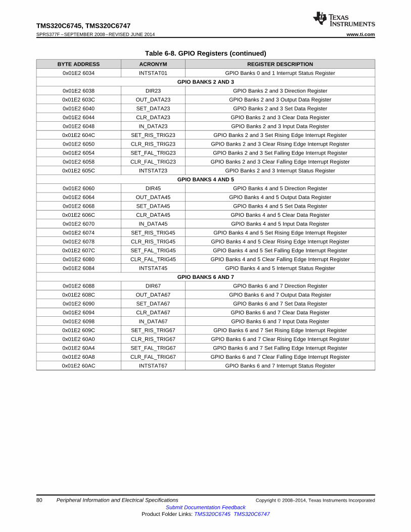
TMS320C6745, TMS320C6747SPRS377F –SEPTEMBER 2008–REVISED JUNE 2014 www.ti.com
Table 6-8. GPIO Registers (continued)BYTE ADDRESS ACRONYM REGISTER DESCRIPTION
0x01E2 6034 INTSTAT01 GPIO Banks 0 and 1 Interrupt Status RegisterGPIO BANKS 2 AND 3
0x01E2 6038 DIR23 GPIO Banks 2 and 3 Direction Register0x01E2 603C OUT_DATA23 GPIO Banks 2 and 3 Output Data Register0x01E2 6040 SET_DATA23 GPIO Banks 2 and 3 Set Data Register0x01E2 6044 CLR_DATA23 GPIO Banks 2 and 3 Clear Data Register0x01E2 6048 IN_DATA23 GPIO Banks 2 and 3 Input Data Register0x01E2 604C SET_RIS_TRIG23 GPIO Banks 2 and 3 Set Rising Edge Interrupt Register0x01E2 6050 CLR_RIS_TRIG23 GPIO Banks 2 and 3 Clear Rising Edge Interrupt Register0x01E2 6054 SET_FAL_TRIG23 GPIO Banks 2 and 3 Set Falling Edge Interrupt Register0x01E2 6058 CLR_FAL_TRIG23 GPIO Banks 2 and 3 Clear Falling Edge Interrupt Register0x01E2 605C INTSTAT23 GPIO Banks 2 and 3 Interrupt Status Register
GPIO BANKS 4 AND 50x01E2 6060 DIR45 GPIO Banks 4 and 5 Direction Register0x01E2 6064 OUT_DATA45 GPIO Banks 4 and 5 Output Data Register0x01E2 6068 SET_DATA45 GPIO Banks 4 and 5 Set Data Register0x01E2 606C CLR_DATA45 GPIO Banks 4 and 5 Clear Data Register0x01E2 6070 IN_DATA45 GPIO Banks 4 and 5 Input Data Register0x01E2 6074 SET_RIS_TRIG45 GPIO Banks 4 and 5 Set Rising Edge Interrupt Register0x01E2 6078 CLR_RIS_TRIG45 GPIO Banks 4 and 5 Clear Rising Edge Interrupt Register0x01E2 607C SET_FAL_TRIG45 GPIO Banks 4 and 5 Set Falling Edge Interrupt Register0x01E2 6080 CLR_FAL_TRIG45 GPIO Banks 4 and 5 Clear Falling Edge Interrupt Register0x01E2 6084 INTSTAT45 GPIO Banks 4 and 5 Interrupt Status Register
GPIO BANKS 6 AND 70x01E2 6088 DIR67 GPIO Banks 6 and 7 Direction Register0x01E2 608C OUT_DATA67 GPIO Banks 6 and 7 Output Data Register0x01E2 6090 SET_DATA67 GPIO Banks 6 and 7 Set Data Register0x01E2 6094 CLR_DATA67 GPIO Banks 6 and 7 Clear Data Register0x01E2 6098 IN_DATA67 GPIO Banks 6 and 7 Input Data Register0x01E2 609C SET_RIS_TRIG67 GPIO Banks 6 and 7 Set Rising Edge Interrupt Register0x01E2 60A0 CLR_RIS_TRIG67 GPIO Banks 6 and 7 Clear Rising Edge Interrupt Register0x01E2 60A4 SET_FAL_TRIG67 GPIO Banks 6 and 7 Set Falling Edge Interrupt Register0x01E2 60A8 CLR_FAL_TRIG67 GPIO Banks 6 and 7 Clear Falling Edge Interrupt Register0x01E2 60AC INTSTAT67 GPIO Banks 6 and 7 Interrupt Status Register
80 Peripheral Information and Electrical Specifications Copyright © 2008–2014, Texas Instruments IncorporatedSubmit Documentation Feedback
Product Folder Links: TMS320C6745 TMS320C6747

2
1
GP [ ] as inputn m
GP [ ] as inputn m
43
2
1
GP [ ] as outputn m
TMS320C6745, TMS320C6747www.ti.com SPRS377F –SEPTEMBER 2008–REVISED JUNE 2014
6.8.2 GPIO Peripheral Input/Output Electrical Data/Timing
Table 6-9. Timing Requirements for GPIO Inputs (1) (see Figure 6-10)No. PARAMETER MIN MAX UNIT1 tw(GPIH) Pulse duration, GPn[m] as input high 2C (1) (2) ns2 tw(GPIL) Pulse duration, GPn[m] as input low 2C (1) (2) ns
(1) The pulse width given is sufficient to generate a CPU interrupt or an EDMA event. However, if a user wants to have C6745/6747recognize the GPIx changes through software polling of the GPIO register, the GPIx duration must be extended to allow C6745/6747enough time to access the GPIO register through the internal bus.
(2) C=SYSCLK4 period in ns.
Table 6-10. Switching Characteristics Over Recommended Operating Conditions for GPIO Outputs(see Figure 6-10)
No. PARAMETER MIN MAX UNIT3 tw(GPOH) Pulse duration, GPn[m] as output high 2C (1) (2) ns4 tw(GPOL) Pulse duration, GPn[m] as output low 2C (1) (2) ns
(1) This parameter value should not be used as a maximum performance specification. Actual performance of back-to-back accesses of theGPIO is dependent upon internal bus activity.
(2) C=SYSCLK4 period in ns.
Figure 6-10. GPIO Port Timing
6.8.3 GPIO Peripheral External Interrupts Electrical Data/Timing
Table 6-11. Timing Requirements for External Interrupts (1) (see Figure 6-11)No. PARAMETER MIN MAX UNIT1 tw(ILOW) Width of the external interrupt pulse low 2C (1) (2) ns2 tw(IHIGH) Width of the external interrupt pulse high 2C (1) (2) ns
(1) The pulse width given is sufficient to generate an interrupt or an EDMA event. However, if a user wants to have C6745/6747 recognizethe GPIO changes through software polling of the GPIO register, the GPIO duration must be extended to allow C6745/6747 enoughtime to access the GPIO register through the internal bus.
(2) C=SYSCLK4 period in ns.
Figure 6-11. GPIO External Interrupt Timing
Copyright © 2008–2014, Texas Instruments Incorporated Peripheral Information and Electrical Specifications 81Submit Documentation Feedback
Product Folder Links: TMS320C6745 TMS320C6747

TMS320C6745, TMS320C6747SPRS377F –SEPTEMBER 2008–REVISED JUNE 2014 www.ti.com
6.9 EDMATable 6-12 is the list of EDMA3 Channel Contoller Registers and Table 6-13 is the list of EDMA3 TransferController registers.
Table 6-12. EDMA3 Channel Controller (EDMA3CC) Registers
BYTE ADDRESS ACRONYM REGISTER DESCRIPTION0x01C0 0000 PID Peripheral Identification Register0x01C0 0004 CCCFG EDMA3CC Configuration Register
GLOBAL REGISTERS0x01C0 0200 QCHMAP0 QDMA Channel 0 Mapping Register0x01C0 0204 QCHMAP1 QDMA Channel 1 Mapping Register0x01C0 0208 QCHMAP2 QDMA Channel 2 Mapping Register0x01C0 020C QCHMAP3 QDMA Channel 3 Mapping Register0x01C0 0210 QCHMAP4 QDMA Channel 4 Mapping Register0x01C0 0214 QCHMAP5 QDMA Channel 5 Mapping Register0x01C0 0218 QCHMAP6 QDMA Channel 6 Mapping Register0x01C0 021C QCHMAP7 QDMA Channel 7 Mapping Register0x01C0 0240 DMAQNUM0 DMA Channel Queue Number Register 00x01C0 0244 DMAQNUM1 DMA Channel Queue Number Register 10x01C0 0248 DMAQNUM2 DMA Channel Queue Number Register 20x01C0 024C DMAQNUM3 DMA Channel Queue Number Register 30x01C0 0260 QDMAQNUM QDMA Channel Queue Number Register0x01C0 0284 QUEPRI Queue Priority Register (1)
0x01C0 0300 EMR Event Missed Register0x01C0 0308 EMCR Event Missed Clear Register0x01C0 0310 QEMR QDMA Event Missed Register0x01C0 0314 QEMCR QDMA Event Missed Clear Register0x01C0 0318 CCERR EDMA3CC Error Register0x01C0 031C CCERRCLR EDMA3CC Error Clear Register0x01C0 0320 EEVAL Error Evaluate Register0x01C0 0340 DRAE0 DMA Region Access Enable Register for Region 00x01C0 0348 DRAE1 DMA Region Access Enable Register for Region 10x01C0 0350 DRAE2 DMA Region Access Enable Register for Region 20x01C0 0358 DRAE3 DMA Region Access Enable Register for Region 30x01C0 0380 QRAE0 QDMA Region Access Enable Register for Region 00x01C0 0384 QRAE1 QDMA Region Access Enable Register for Region 10x01C0 0388 QRAE2 QDMA Region Access Enable Register for Region 20x01C0 038C QRAE3 QDMA Region Access Enable Register for Region 3
0x01C0 0400 - 0x01C0 043C Q0E0-Q0E15 Event Queue Entry Registers Q0E0-Q0E150x01C0 0440 - 0x01C0 047C Q1E0-Q1E15 Event Queue Entry Registers Q1E0-Q1E15
0x01C0 0600 QSTAT0 Queue 0 Status Register0x01C0 0604 QSTAT1 Queue 1 Status Register0x01C0 0620 QWMTHRA Queue Watermark Threshold A Register0x01C0 0640 CCSTAT EDMA3CC Status Register
GLOBAL CHANNEL REGISTERS0x01C0 1000 ER Event Register0x01C0 1008 ECR Event Clear Register
(1) On previous architectures, the EDMA3TC priority was controlled by the queue priority register (QUEPRI) in the EDMA3CC memory-map. However for this device, the priority control for the transfer controllers is controlled by the chip-level registers in the SystemConfiguration Module. You should use the chip-level registers and not QUEPRI to configure the TC priority.
82 Peripheral Information and Electrical Specifications Copyright © 2008–2014, Texas Instruments IncorporatedSubmit Documentation Feedback
Product Folder Links: TMS320C6745 TMS320C6747

TMS320C6745, TMS320C6747www.ti.com SPRS377F –SEPTEMBER 2008–REVISED JUNE 2014
Table 6-12. EDMA3 Channel Controller (EDMA3CC) Registers (continued)BYTE ADDRESS ACRONYM REGISTER DESCRIPTION
0x01C0 1010 ESR Event Set Register0x01C0 1018 CER Chained Event Register0x01C0 1020 EER Event Enable Register0x01C0 1028 EECR Event Enable Clear Register0x01C0 1030 EESR Event Enable Set Register0x01C0 1038 SER Secondary Event Register0x01C0 1040 SECR Secondary Event Clear Register0x01C0 1050 IER Interrupt Enable Register0x01C0 1058 IECR Interrupt Enable Clear Register0x01C0 1060 IESR Interrupt Enable Set Register0x01C0 1068 IPR Interrupt Pending Register0x01C0 1070 ICR Interrupt Clear Register0x01C0 1078 IEVAL Interrupt Evaluate Register0x01C0 1080 QER QDMA Event Register0x01C0 1084 QEER QDMA Event Enable Register0x01C0 1088 QEECR QDMA Event Enable Clear Register0x01C0 108C QEESR QDMA Event Enable Set Register0x01C0 1090 QSER QDMA Secondary Event Register0x01C0 1094 QSECR QDMA Secondary Event Clear Register
SHADOW REGION 0 CHANNEL REGISTERS0x01C0 2000 ER Event Register0x01C0 2008 ECR Event Clear Register0x01C0 2010 ESR Event Set Register0x01C0 2018 CER Chained Event Register0x01C0 2020 EER Event Enable Register0x01C0 2028 EECR Event Enable Clear Register0x01C0 2030 EESR Event Enable Set Register0x01C0 2038 SER Secondary Event Register0x01C0 2040 SECR Secondary Event Clear Register0x01C0 2050 IER Interrupt Enable Register0x01C0 2058 IECR Interrupt Enable Clear Register0x01C0 2060 IESR Interrupt Enable Set Register0x01C0 2068 IPR Interrupt Pending Register0x01C0 2070 ICR Interrupt Clear Register0x01C0 2078 IEVAL Interrupt Evaluate Register0x01C0 2080 QER QDMA Event Register0x01C0 2084 QEER QDMA Event Enable Register0x01C0 2088 QEECR QDMA Event Enable Clear Register0x01C0 208C QEESR QDMA Event Enable Set Register0x01C0 2090 QSER QDMA Secondary Event Register0x01C0 2094 QSECR QDMA Secondary Event Clear Register
SHADOW REGION 1 CHANNEL REGISTERS0x01C0 2200 ER Event Register0x01C0 2208 ECR Event Clear Register0x01C0 2210 ESR Event Set Register0x01C0 2218 CER Chained Event Register0x01C0 2220 EER Event Enable Register
Copyright © 2008–2014, Texas Instruments Incorporated Peripheral Information and Electrical Specifications 83Submit Documentation Feedback
Product Folder Links: TMS320C6745 TMS320C6747
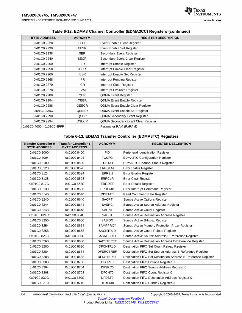
TMS320C6745, TMS320C6747SPRS377F –SEPTEMBER 2008–REVISED JUNE 2014 www.ti.com
Table 6-12. EDMA3 Channel Controller (EDMA3CC) Registers (continued)BYTE ADDRESS ACRONYM REGISTER DESCRIPTION
0x01C0 2228 EECR Event Enable Clear Register0x01C0 2230 EESR Event Enable Set Register0x01C0 2238 SER Secondary Event Register0x01C0 2240 SECR Secondary Event Clear Register0x01C0 2250 IER Interrupt Enable Register0x01C0 2258 IECR Interrupt Enable Clear Register0x01C0 2260 IESR Interrupt Enable Set Register0x01C0 2268 IPR Interrupt Pending Register0x01C0 2270 ICR Interrupt Clear Register0x01C0 2278 IEVAL Interrupt Evaluate Register0x01C0 2280 QER QDMA Event Register0x01C0 2284 QEER QDMA Event Enable Register0x01C0 2288 QEECR QDMA Event Enable Clear Register0x01C0 228C QEESR QDMA Event Enable Set Register0x01C0 2290 QSER QDMA Secondary Event Register0x01C0 2294 QSECR QDMA Secondary Event Clear Register
0x01C0 4000 - 0x01C0 4FFF — Parameter RAM (PaRAM)
Table 6-13. EDMA3 Transfer Controller (EDMA3TC) Registers
Transfer Controller 0 Transfer Controller 1 ACRONYM REGISTER DESCRIPTIONBYTE ADDRESS BYTE ADDRESS
0x01C0 8000 0x01C0 8400 PID Peripheral Identification Register0x01C0 8004 0x01C0 8404 TCCFG EDMA3TC Configuration Register0x01C0 8100 0x01C0 8500 TCSTAT EDMA3TC Channel Status Register0x01C0 8120 0x01C0 8520 ERRSTAT Error Status Register0x01C0 8124 0x01C0 8524 ERREN Error Enable Register0x01C0 8128 0x01C0 8528 ERRCLR Error Clear Register0x01C0 812C 0x01C0 852C ERRDET Error Details Register0x01C0 8130 0x01C0 8530 ERRCMD Error Interrupt Command Register0x01C0 8140 0x01C0 8540 RDRATE Read Command Rate Register0x01C0 8240 0x01C0 8640 SAOPT Source Active Options Register0x01C0 8244 0x01C0 8644 SASRC Source Active Source Address Register0x01C0 8248 0x01C0 8648 SACNT Source Active Count Register0x01C0 824C 0x01C0 864C SADST Source Active Destination Address Register0x01C0 8250 0x01C0 8650 SABIDX Source Active B-Index Register0x01C0 8254 0x01C0 8654 SAMPPRXY Source Active Memory Protection Proxy Register0x01C0 8258 0x01C0 8658 SACNTRLD Source Active Count Reload Register0x01C0 825C 0x01C0 865C SASRCBREF Source Active Source Address B-Reference Register0x01C0 8260 0x01C0 8660 SADSTBREF Source Active Destination Address B-Reference Register0x01C0 8280 0x01C0 8680 DFCNTRLD Destination FIFO Set Count Reload Register0x01C0 8284 0x01C0 8684 DFSRCBREF Destination FIFO Set Source Address B-Reference Register0x01C0 8288 0x01C0 8688 DFDSTBREF Destination FIFO Set Destination Address B-Reference Register0x01C0 8300 0x01C0 8700 DFOPT0 Destination FIFO Options Register 00x01C0 8304 0x01C0 8704 DFSRC0 Destination FIFO Source Address Register 00x01C0 8308 0x01C0 8708 DFCNT0 Destination FIFO Count Register 00x01C0 830C 0x01C0 870C DFDST0 Destination FIFO Destination Address Register 00x01C0 8310 0x01C0 8710 DFBIDX0 Destination FIFO B-Index Register 0
84 Peripheral Information and Electrical Specifications Copyright © 2008–2014, Texas Instruments IncorporatedSubmit Documentation Feedback
Product Folder Links: TMS320C6745 TMS320C6747

TMS320C6745, TMS320C6747www.ti.com SPRS377F –SEPTEMBER 2008–REVISED JUNE 2014
Table 6-13. EDMA3 Transfer Controller (EDMA3TC) Registers (continued)Transfer Controller 0 Transfer Controller 1 ACRONYM REGISTER DESCRIPTION
BYTE ADDRESS BYTE ADDRESS0x01C0 8314 0x01C0 8714 DFMPPRXY0 Destination FIFO Memory Protection Proxy Register 00x01C0 8340 0x01C0 8740 DFOPT1 Destination FIFO Options Register 10x01C0 8344 0x01C0 8744 DFSRC1 Destination FIFO Source Address Register 10x01C0 8348 0x01C0 8748 DFCNT1 Destination FIFO Count Register 10x01C0 834C 0x01C0 874C DFDST1 Destination FIFO Destination Address Register 10x01C0 8350 0x01C0 8750 DFBIDX1 Destination FIFO B-Index Register 10x01C0 8354 0x01C0 8754 DFMPPRXY1 Destination FIFO Memory Protection Proxy Register 10x01C0 8380 0x01C0 8780 DFOPT2 Destination FIFO Options Register 20x01C0 8384 0x01C0 8784 DFSRC2 Destination FIFO Source Address Register 20x01C0 8388 0x01C0 8788 DFCNT2 Destination FIFO Count Register 20x01C0 838C 0x01C0 878C DFDST2 Destination FIFO Destination Address Register 20x01C0 8390 0x01C0 8790 DFBIDX2 Destination FIFO B-Index Register 20x01C0 8394 0x01C0 8794 DFMPPRXY2 Destination FIFO Memory Protection Proxy Register 20x01C0 83C0 0x01C0 87C0 DFOPT3 Destination FIFO Options Register 30x01C0 83C4 0x01C0 87C4 DFSRC3 Destination FIFO Source Address Register 30x01C0 83C8 0x01C0 87C8 DFCNT3 Destination FIFO Count Register 30x01C0 83CC 0x01C0 87CC DFDST3 Destination FIFO Destination Address Register 30x01C0 83D0 0x01C0 87D0 DFBIDX3 Destination FIFO B-Index Register 30x01C0 83D4 0x01C0 87D4 DFMPPRXY3 Destination FIFO Memory Protection Proxy Register 3
Table 6-14 shows an abbreviation of the set of registers which make up the parameter set for each of 128EDMA events. Each of the parameter register sets consist of 8 32-bit word entries. Table 6-15 shows theparameter set entry registers with relative memory address locations within each of the parameter sets.
Table 6-14. EDMA Parameter Set RAM
BYTE ADDRESS RANGE DESCRIPTION0x01C0 4000 - 0x01C0 401F Parameters Set 0 (8 32-bit words)0x01C0 4020 - 0x01C0 403F Parameters Set 1 (8 32-bit words)0x01C0 4040 - 0x01cC0 405F Parameters Set 2 (8 32-bit words)0x01C0 4060 - 0x01C0 407F Parameters Set 3 (8 32-bit words)0x01C0 4080 - 0x01C0 409F Parameters Set 4 (8 32-bit words)0x01C0 40A0 - 0x01C0 40BF Parameters Set 5 (8 32-bit words)
... ...0x01C0 4FC0 - 0x01C0 4FDF Parameters Set 126 (8 32-bit words)0x01C0 4FE0 - 0x01C0 4FFF Parameters Set 127 (8 32-bit words)
Table 6-15. Parameter Set Entries
BYTE OFFSET ADDRESS ACRONYM PARAMETER ENTRYWITHIN THE PARAMETER SET0x0000 OPT Option0x0004 SRC Source Address0x0008 A_B_CNT A Count, B Count0x000C DST Destination Address0x0010 SRC_DST_BIDX Source B Index, Destination B Index0x0014 LINK_BCNTRLD Link Address, B Count Reload0x0018 SRC_DST_CIDX Source C Index, Destination C Index0x001C CCNT C Count
Copyright © 2008–2014, Texas Instruments Incorporated Peripheral Information and Electrical Specifications 85Submit Documentation Feedback
Product Folder Links: TMS320C6745 TMS320C6747

TMS320C6745, TMS320C6747SPRS377F –SEPTEMBER 2008–REVISED JUNE 2014 www.ti.com
Table 6-16. EDMA Events
Event Event Name / Source Event Event Name / Source0 McASP0 Receive 16 MMCSD Receive1 McASP0 Transmit 17 MMCSD Transmit2 McASP1 Receive 18 SPI1 Receive3 McASP1 Transmit 19 SPI1 Transmit4 McASP2 Receive 20 PRU_EVENTOUT65 McASP2 Transmit 21 PRU_EVENTOUT76 GPIO Bank 0 Interrupt 22 GPIO Bank 2 Interrupt7 GPIO Bank 1 Interrupt 23 GPIO Bank 3 Interrupt8 UART0 Receive 24 I2C0 Receive9 UART0 Transmit 25 I2C0 Transmit10 Timer64P0 Event Out 12 26 I2C1 Receive11 Timer64P0 Event Out 34 27 I2C1 Transmit12 UART1 Receive 28 GPIO Bank 4 Interrupt13 UART1 Transmit 29 GPIO Bank 5 Interrupt14 SPI0 Receive 30 UART2 Receive15 SPI0 Transmit 31 UART2 Transmit
86 Peripheral Information and Electrical Specifications Copyright © 2008–2014, Texas Instruments IncorporatedSubmit Documentation Feedback
Product Folder Links: TMS320C6745 TMS320C6747

TMS320C6745, TMS320C6747www.ti.com SPRS377F –SEPTEMBER 2008–REVISED JUNE 2014
6.10 External Memory Interface A (EMIFA)EMIFA is one of two external memory interfaces supported on the C6745/6747. It is primarily intended tosupport asynchronous memory types, such as NAND and NOR flash and Asynchronous SRAM. Howeveron C6745/6747 EMIFA also provides a secondary interface to SDRAM.
6.10.1 EMIFA Asynchronous Memory SupportEMIFA supports asynchronous:• SRAM memories• NAND Flash memories• NOR Flash memories
The EMIFA data bus width is up to 16-bits on the ZKB packageand 8 bits on the PTP package. Bothdevices support up to fifteen address lines and an external wait/interrupt input. Up to four asynchronouschip selects are supported by EMIFA (EMA_CS[5:2]) . All four chip selects are available on the ZKBpackage. Two of the four are available on the PTP package (EMA_CS[3:2]).
Each chip select has the following individually programmable attributes:• Data Bus Width• Read cycle timings: setup, hold, strobe• Write cycle timings: setup, hold, strobe• Bus turn around time• Extended Wait Option With Programmable Timeout• Select Strobe Option• NAND flash controller supports 1-bit and 4-bit ECC calculation on blocks of 512 bytes.
6.10.2 EMIFA Synchronous DRAM Memory SupportThe C6745/6747 ZKB package supports 16-bit SDRAM in addition to the asynchronous memories listed inSection 6.10.1. It has a single SDRAM chip select (EMA_CS[0]). SDRAM configurations that aresupported are:• One, Two, and Four Bank SDRAM devices• Devices with Eight, Nine, Ten, and Eleven Column Address• CAS Latency of two or three clock cycles• Sixteen Bit Data Bus Width• 3.3V LVCMOS Interface
Additionally, the SDRAM interface of EMIFA supports placing the SDRAM in Self Refresh and PowerdownModes. Self Refresh mode allows the SDRAM to be put into a low power state while still retaining memorycontents; since the SDRAM will continue to refresh itself even without clocks from the DSP. Powerdownmode achieves even lower power, except the DSP must periodically wake the SDRAM up and issuerefreshes if data retention is required.
Finally, note that the EMIFA does not support Mobile SDRAM devices. Table 6-17 below shows thesupported SDRAM configurations for EMIFA.
Copyright © 2008–2014, Texas Instruments Incorporated Peripheral Information and Electrical Specifications 87Submit Documentation Feedback
Product Folder Links: TMS320C6745 TMS320C6747
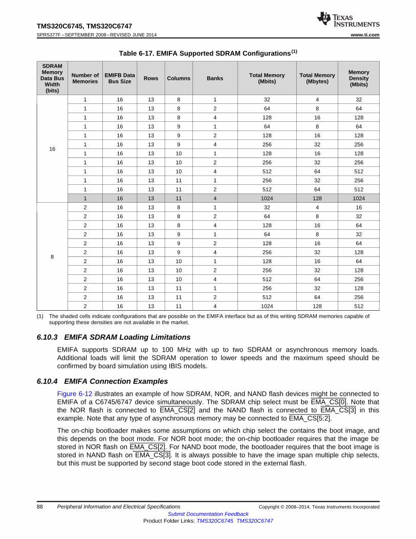
TMS320C6745, TMS320C6747SPRS377F –SEPTEMBER 2008–REVISED JUNE 2014 www.ti.com
Table 6-17. EMIFA Supported SDRAM Configurations (1)
SDRAMMemory MemoryNumber of EMIFB Data Total Memory Total MemoryData Bus Rows Columns Banks DensityMemories Bus Size (Mbits) (Mbytes)Width (Mbits)
(bits)1 16 13 8 1 32 4 321 16 13 8 2 64 8 641 16 13 8 4 128 16 1281 16 13 9 1 64 8 641 16 13 9 2 128 16 1281 16 13 9 4 256 32 256
161 16 13 10 1 128 16 1281 16 13 10 2 256 32 2561 16 13 10 4 512 64 5121 16 13 11 1 256 32 2561 16 13 11 2 512 64 5121 16 13 11 4 1024 128 10242 16 13 8 1 32 4 162 16 13 8 2 64 8 322 16 13 8 4 128 16 642 16 13 9 1 64 8 322 16 13 9 2 128 16 642 16 13 9 4 256 32 128
82 16 13 10 1 128 16 642 16 13 10 2 256 32 1282 16 13 10 4 512 64 2562 16 13 11 1 256 32 1282 16 13 11 2 512 64 2562 16 13 11 4 1024 128 512
(1) The shaded cells indicate configurations that are possible on the EMIFA interface but as of this writing SDRAM memories capable ofsupporting these densities are not available in the market.
6.10.3 EMIFA SDRAM Loading LimitationsEMIFA supports SDRAM up to 100 MHz with up to two SDRAM or asynchronous memory loads.Additional loads will limit the SDRAM operation to lower speeds and the maximum speed should beconfirmed by board simulation using IBIS models.
6.10.4 EMIFA Connection ExamplesFigure 6-12 illustrates an example of how SDRAM, NOR, and NAND flash devices might be connected toEMIFA of a C6745/6747 device simultaneously. The SDRAM chip select must be EMA_CS[0]. Note thatthe NOR flash is connected to EMA_CS[2] and the NAND flash is connected to EMA_CS[3] in thisexample. Note that any type of asynchronous memory may be connected to EMA_CS[5:2].
The on-chip bootloader makes some assumptions on which chip select the contains the boot image, andthis depends on the boot mode. For NOR boot mode; the on-chip bootloader requires that the image bestored in NOR flash on EMA_CS[2]. For NAND boot mode, the bootloader requires that the boot image isstored in NAND flash on EMA_CS[3]. It is always possible to have the image span multiple chip selects,but this must be supported by second stage boot code stored in the external flash.
88 Peripheral Information and Electrical Specifications Copyright © 2008–2014, Texas Instruments IncorporatedSubmit Documentation Feedback
Product Folder Links: TMS320C6745 TMS320C6747

EMA_CLK
EMA_BA[1:0]
EMA_CS[0]
EMA_CAS
EMA_RAS
EMA_WE
CLK
CE
WE
EMIFA
SDRAM2M x 16 x 4
BankEMA_SDCKE
CAS
RAS
CKE
BA[1:0]
LDQM
UDQM
DQ[15:0]
A[11:0]EMA_A[12:0]
EMA_WE_DQM[0]
EMA_WE_DQM[1]
EMA_D[15:0]
EMA_CS[2]
EMA_CS[3]
EMA_WAIT
EMA_OE
GPIO(6 Pins)RESET
A[0]
A[12:1]
DQ[15:0]
CE
WE
OE
RESET
A[18:13]
RY/ YB
NORFLASH
512K x 16
ALE
CLE
DQ[15:0]
CE
WE
RE
RB
NANDFLASH
1Gb x 16
EM
A_B
A[1
]
EMA_A[1]
EMA_A[2]
...
DVDD
RESET
TMS320C6745, TMS320C6747www.ti.com SPRS377F –SEPTEMBER 2008–REVISED JUNE 2014
A likely use case with more than one EMIFA chip select used for NAND flash is illustrated in Figure 6-13.This figure shows how two multiplane NAND flash devices with two chip selects each would connect to theEMIFA. In this case if NAND is the boot memory, then the boot image needs to be stored in the NANDarea selected by EMA_CS[3]. Part of the application image could spill over into the NAND regionsselected by other EMIFA chip selects; but would rely on the code stored in the EMA_CS[3] area tobootload it. Note that this example could also apply to the C6745 device; except only one multiplaneNAND could be supported with only EMA_CS[3:2] available.
Figure 6-12. C6745/6747 Connection Diagram: SDRAM, NOR, NAND
Copyright © 2008–2014, Texas Instruments Incorporated Peripheral Information and Electrical Specifications 89Submit Documentation Feedback
Product Folder Links: TMS320C6745 TMS320C6747

EMA_A[1]
EMA_A[2]
EMA_D[7:0]
EMA_CS[2]
EMA_CS[3]
EMA_WE
EMA_OE
ALE
CLE
DQ[7:0]
CE1
CE2
WE
RE
R/ 1B
R/ 2B
EMIFA
NANDFLASH
x8,MultiPlane
ALE
CLE
DQ[7:0]
CE1
CE2
WE
RE
R/ 1B
R/ 2B
NANDFLASH
x8,MultiPlane
DVDD
EMA_WAIT
EMA_CS[4]
EMA_CS[5]
TMS320C6745, TMS320C6747SPRS377F –SEPTEMBER 2008–REVISED JUNE 2014 www.ti.com
Figure 6-13. C6745/6747 EMIFA Connection Diagram: Multiple NAND Flash Planes
90 Peripheral Information and Electrical Specifications Copyright © 2008–2014, Texas Instruments IncorporatedSubmit Documentation Feedback
Product Folder Links: TMS320C6745 TMS320C6747

TMS320C6745, TMS320C6747www.ti.com SPRS377F –SEPTEMBER 2008–REVISED JUNE 2014
6.10.5 External Memory Interface A (EMIFA) RegistersTable 6-18 is a list of the EMIF registers. For more information about these registers, see the C674x DSPExternal Memory Interface (EMIF) User's Guide (SPRUFL6).
Table 6-18. External Memory Interface (EMIFA) Registers
BYTE ADDRESS ACRONYM REGISTER DESCRIPTION0x6800 0000 MIDR Module ID Register0x6800 0004 AWCC Asynchronous Wait Cycle Configuration Register0x6800 0008 SDCR SDRAM Configuration Register0x6800 000C SDRCR SDRAM Refresh Control Register0x6800 0010 CE2CFG Asynchronous 1 Configuration Register0x6800 0014 CE3CFG Asynchronous 2 Configuration Register0x6800 0018 CE4CFG Asynchronous 3 Configuration Register0x6800 001C CE5CFG Asynchronous 4 Configuration Register0x6800 0020 SDTIMR SDRAM Timing Register0x6800 003C SDSRETR SDRAM Self Refresh Exit Timing Register0x6800 0040 INTRAW EMIFA Interrupt Raw Register0x6800 0044 INTMSK EMIFA Interrupt Mask Register0x6800 0048 INTMSKSET EMIFA Interrupt Mask Set Register0x6800 004C INTMSKCLR EMIFA Interrupt Mask Clear Register0x6800 0060 NANDFCR NAND Flash Control Register0x6800 0064 NANDFSR NAND Flash Status Register0x6800 0070 NANDF1ECC NAND Flash 1 ECC Register (CS2 Space)0x6800 0074 NANDF2ECC NAND Flash 2 ECC Register (CS3 Space)0x6800 0078 NANDF3ECC NAND Flash 3 ECC Register (CS4 Space)0x6800 007C NANDF4ECC NAND Flash 4 ECC Register (CS5 Space)0x6800 00BC NAND4BITECCLOAD NAND Flash 4-Bit ECC Load Register0x6800 00C0 NAND4BITECC1 NAND Flash 4-Bit ECC Register 10x6800 00C4 NAND4BITECC2 NAND Flash 4-Bit ECC Register 20x6800 00C8 NAND4BITECC3 NAND Flash 4-Bit ECC Register 30x6800 00CC NAND4BITECC4 NAND Flash 4-Bit ECC Register 40x6800 00D0 NANDERRADD1 NAND Flash 4-Bit ECC Error Address Register 10x6800 00D4 NANDERRADD2 NAND Flash 4-Bit ECC Error Address Register 20x6800 00D8 NANDERRVAL1 NAND Flash 4-Bit ECC Error Value Register 10x6800 00DC NANDERRVAL2 NAND Flash 4-Bit ECC Error Value Register 2
Copyright © 2008–2014, Texas Instruments Incorporated Peripheral Information and Electrical Specifications 91Submit Documentation Feedback
Product Folder Links: TMS320C6745 TMS320C6747

TMS320C6745, TMS320C6747SPRS377F –SEPTEMBER 2008–REVISED JUNE 2014 www.ti.com
6.10.6 EMIFA Electrical Data/TimingTable 6-19 through Table 6-22 assume testing over recommended operating conditions.
Table 6-19. EMIFA SDRAM Interface Timing RequirementsNo. PARAMETER MIN MAX UNIT19 tsu(DV-CLKH) Input setup time, read data valid on EMA_D[15:0] before EMA_CLK rising 1.3 ns20 th(CLKH-DIV) Input hold time, read data valid on EMA_D[15:0] after EMA_CLK rising 1.5 ns
Table 6-20. EMIFA SDRAM Interface Switching CharacteristicsNo. PARAMETER MIN MAX UNIT1 tc(CLK) Cycle time, EMIF clock EMA_CLK 10 ns2 tw(CLK) Pulse width, EMIF clock EMA_CLK high or low 3 ns3 td(CLKH-CSV) Delay time, EMA_CLK rising to EMA_CS[0] valid 7 ns4 toh(CLKH-CSIV) Output hold time, EMA_CLK rising to EMA_CS[0] invalid 1 ns5 td(CLKH-DQMV) Delay time, EMA_CLK rising to EMA_WE_DQM[1:0] valid 7 ns6 toh(CLKH-DQMIV) Output hold time, EMA_CLK rising to EMA_WE_DQM[1:0] invalid 1 ns7 td(CLKH-AV) Delay time, EMA_CLK rising to EMA_A[12:0] and EMA_BA[1:0] valid 7 ns
Output hold time, EMA_CLK rising to EMA_A[12:0] and EMA_BA[1:0]8 toh(CLKH-AIV) 1 nsinvalid9 td(CLKH-DV) Delay time, EMA_CLK rising to EMA_D[15:0] valid 7 ns10 toh(CLKH-DIV) Output hold time, EMA_CLK rising to EMA_D[15:0] invalid 1 ns11 td(CLKH-RASV) Delay time, EMA_CLK rising to EMA_RAS valid 7 ns12 toh(CLKH-RASIV) Output hold time, EMA_CLK rising to EMA_RAS invalid 1 ns13 td(CLKH-CASV) Delay time, EMA_CLK rising to EMA_CAS valid 7 ns14 toh(CLKH-CASIV) Output hold time, EMA_CLK rising to EMA_CAS invalid 1 ns15 td(CLKH-WEV) Delay time, EMA_CLK rising to EMA_WE valid 7 ns16 toh(CLKH-WEIV) Output hold time, EMA_CLK rising to EMA_WE invalid 1 ns17 tdis(CLKH-DHZ) Delay time, EMA_CLK rising to EMA_D[15:0] 3-stated 7 ns18 tena(CLKH-DLZ) Output hold time, EMA_CLK rising to EMA_D[15:0] driving 1 ns
92 Peripheral Information and Electrical Specifications Copyright © 2008–2014, Texas Instruments IncorporatedSubmit Documentation Feedback
Product Folder Links: TMS320C6745 TMS320C6747

EMA_CLK
EMA_BA[1:0]
EMA_A[12:0]
EMA_D[15:0]
1
2 2
4
6
8
8
12
14
19
20
3
5
7
7
11
13
17 182 EM_CLK Delay
BASIC SDRAMREAD OPERATION
EMA_CS[0]
EMA_WE_DQM[1:0]
EMA_RAS
EMA_CAS
EMA_WE
EMA_CLK
EMA_BA[1:0]
EMA_A[12:0]
EMA_D[15:0]
1
2 2
4
6
8
8
12
10
16
3
5
7
7
11
13
15
9
BASIC SDRAMWRITE OPERATION
EMA_CS[0]
EMA_WE_DQM[1:0]
EMA_RAS
EMA_CAS
EMA_WE
TMS320C6745, TMS320C6747www.ti.com SPRS377F –SEPTEMBER 2008–REVISED JUNE 2014
Figure 6-14. EMIFA Basic SDRAM Write Operation
Figure 6-15. EMIFA Basic SDRAM Read Operation
Copyright © 2008–2014, Texas Instruments Incorporated Peripheral Information and Electrical Specifications 93Submit Documentation Feedback
Product Folder Links: TMS320C6745 TMS320C6747
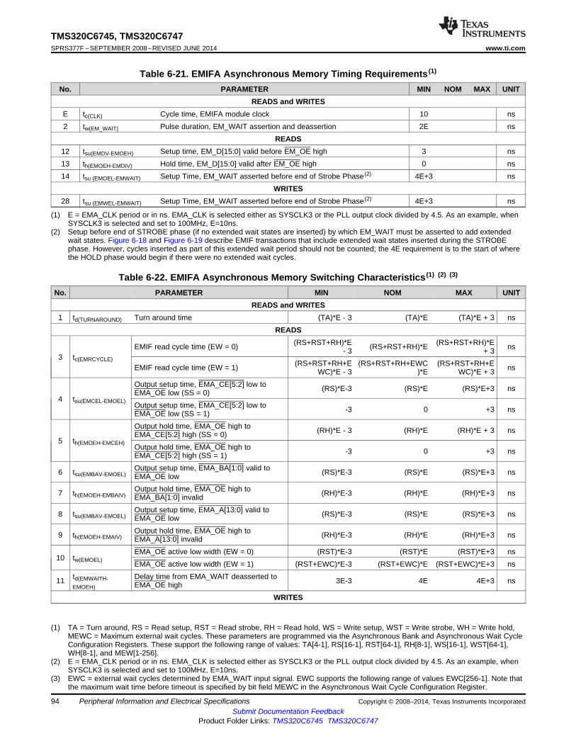
TMS320C6745, TMS320C6747SPRS377F –SEPTEMBER 2008–REVISED JUNE 2014 www.ti.com
Table 6-21. EMIFA Asynchronous Memory Timing Requirements (1)
No. PARAMETER MIN NOM MAX UNITREADS and WRITES
E tc(CLK) Cycle time, EMIFA module clock 10 ns2 tw(EM_WAIT) Pulse duration, EM_WAIT assertion and deassertion 2E ns
READS12 tsu(EMDV-EMOEH) Setup time, EM_D[15:0] valid before EM_OE high 3 ns13 th(EMOEH-EMDIV) Hold time, EM_D[15:0] valid after EM_OE high 0 ns14 tsu (EMOEL-EMWAIT) Setup Time, EM_WAIT asserted before end of Strobe Phase (2) 4E+3 ns
WRITES28 tsu (EMWEL-EMWAIT) Setup Time, EM_WAIT asserted before end of Strobe Phase (2) 4E+3 ns
(1) E = EMA_CLK period or in ns. EMA_CLK is selected either as SYSCLK3 or the PLL output clock divided by 4.5. As an example, whenSYSCLK3 is selected and set to 100MHz, E=10ns.
(2) Setup before end of STROBE phase (if no extended wait states are inserted) by which EM_WAIT must be asserted to add extendedwait states. Figure 6-18 and Figure 6-19 describe EMIF transactions that include extended wait states inserted during the STROBEphase. However, cycles inserted as part of this extended wait period should not be counted; the 4E requirement is to the start of wherethe HOLD phase would begin if there were no extended wait cycles.
Table 6-22. EMIFA Asynchronous Memory Switching Characteristics (1) (2) (3)
No. PARAMETER MIN NOM MAX UNITREADS and WRITES
1 td(TURNAROUND) Turn around time (TA)*E - 3 (TA)*E (TA)*E + 3 nsREADS
(RS+RST+RH)*E (RS+RST+RH)*EEMIF read cycle time (EW = 0) (RS+RST+RH)*E ns- 3 + 33 tc(EMRCYCLE) (RS+RST+RH+E (RS+RST+RH+EWC (RS+RST+RH+EEMIF read cycle time (EW = 1) nsWC)*E - 3 )*E WC)*E + 3
Output setup time, EMA_CE[5:2] low to (RS)*E-3 (RS)*E (RS)*E+3 nsEMA_OE low (SS = 0)4 tsu(EMCEL-EMOEL) Output setup time, EMA_CE[5:2] low to -3 0 +3 nsEMA_OE low (SS = 1)
Output hold time, EMA_OE high to (RH)*E - 3 (RH)*E (RH)*E + 3 nsEMA_CE[5:2] high (SS = 0)5 th(EMOEH-EMCEH) Output hold time, EMA_OE high to -3 0 +3 nsEMA_CE[5:2] high (SS = 1)
Output setup time, EMA_BA[1:0] valid to6 tsu(EMBAV-EMOEL) (RS)*E-3 (RS)*E (RS)*E+3 nsEMA_OE lowOutput hold time, EMA_OE high to7 th(EMOEH-EMBAIV) (RH)*E-3 (RH)*E (RH)*E+3 nsEMA_BA[1:0] invalidOutput setup time, EMA_A[13:0] valid to8 tsu(EMBAV-EMOEL) (RS)*E-3 (RS)*E (RS)*E+3 nsEMA_OE lowOutput hold time, EMA_OE high to9 th(EMOEH-EMAIV) (RH)*E-3 (RH)*E (RH)*E+3 nsEMA_A[13:0] invalidEMA_OE active low width (EW = 0) (RST)*E-3 (RST)*E (RST)*E+3 ns
10 tw(EMOEL) EMA_OE active low width (EW = 1) (RST+EWC)*E-3 (RST+EWC)*E (RST+EWC)*E+3 nstd(EMWAITH- Delay time from EMA_WAIT deasserted to11 3E-3 4E 4E+3 nsEMOEH) EMA_OE high
WRITES
(1) TA = Turn around, RS = Read setup, RST = Read strobe, RH = Read hold, WS = Write setup, WST = Write strobe, WH = Write hold,MEWC = Maximum external wait cycles. These parameters are programmed via the Asynchronous Bank and Asynchronous Wait CycleConfiguration Registers. These support the following range of values: TA[4-1], RS[16-1], RST[64-1], RH[8-1], WS[16-1], WST[64-1],WH[8-1], and MEW[1-256].
(2) E = EMA_CLK period or in ns. EMA_CLK is selected either as SYSCLK3 or the PLL output clock divided by 4.5. As an example, whenSYSCLK3 is selected and set to 100MHz, E=10ns.
(3) EWC = external wait cycles determined by EMA_WAIT input signal. EWC supports the following range of values EWC[256-1]. Note thatthe maximum wait time before timeout is specified by bit field MEWC in the Asynchronous Wait Cycle Configuration Register.
94 Peripheral Information and Electrical Specifications Copyright © 2008–2014, Texas Instruments IncorporatedSubmit Documentation Feedback
Product Folder Links: TMS320C6745 TMS320C6747

TMS320C6745, TMS320C6747www.ti.com SPRS377F –SEPTEMBER 2008–REVISED JUNE 2014
Table 6-22. EMIFA Asynchronous Memory Switching Characteristics(1) (2) (3) (continued)No. PARAMETER MIN NOM MAX UNIT
(WS+WST+WH)* (WS+WST+WH)*EMIF write cycle time (EW = 0) (WS+WST+WH)*E nsE-3 E+315 tc(EMWCYCLE) (WS+WST+WH+ (WS+WST+WH+EW (WS+WST+WH+EMIF write cycle time (EW = 1) nsEWC)*E - 3 C)*E EWC)*E + 3
Output setup time, EMA_CE[5:2] low to (WS)*E - 3 (WS)*E (WS)*E + 3 nsEMA_WE low (SS = 0)16 tsu(EMCEL-EMWEL) Output setup time, EMA_CE[5:2] low to -3 0 +3 nsEMA_WE low (SS = 1)
Output hold time, EMA_WE high to (WH)*E-3 (WH)*E (WH)*E+3 nsEMA_CE[5:2] high (SS = 0)17 th(EMWEH-EMCEH) Output hold time, EMA_WE high to -3 0 +3 nsEMA_CE[5:2] high (SS = 1)
tsu(EMDQMV- Output setup time, EMA_BA[1:0] valid to18 (WS)*E-3 (WS)*E (WS)*E+3 nsEMWEL) EMA_WE lowth(EMWEH- Output hold time, EMA_WE high to19 (WH)*E-3 (WH)*E (WH)*E+3 nsEMDQMIV) EMA_BA[1:0] invalid
Output setup time, EMA_BA[1:0] valid to20 tsu(EMBAV-EMWEL) (WS)*E-3 (WS)*E (WS)*E+3 nsEMA_WE lowOutput hold time, EMA_WE high to21 th(EMWEH-EMBAIV) (WH)*E-3 (WH)*E (WH)*E+3 nsEMA_BA[1:0] invalidOutput setup time, EMA_A[13:0] valid to22 tsu(EMAV-EMWEL) (WS)*E-3 (WS)*E (WS)*E+3 nsEMA_WE lowOutput hold time, EMA_WE high to23 th(EMWEH-EMAIV) (WH)*E-3 (WH)*E (WH)*E+3 nsEMA_A[13:0] invalidEMA_WE active low width (EW = 0) (WST)*E-3 (WST)*E (WST)*E+3 ns
24 tw(EMWEL) EMA_WE active low width (EW = 1) (WST+EWC)*E-3 (WST+EWC)*E (WST+EWC)*E+3 nstd(EMWAITH- Delay time from EMA_WAIT deasserted to25 3E-3 4E 4E+3 nsEMWEH) EMA_WE high
Output setup time, EMA_D[15:0] valid to26 tsu(EMDV-EMWEL) (WS)*E-3 (WS)*E (WS)*E+3 nsEMA_WE lowOutput hold time, EMA_WE high to27 th(EMWEH-EMDIV) (WH)*E-3 (WH)*E (WH)*E+3 nsEMA_D[15:0] invalid
Copyright © 2008–2014, Texas Instruments Incorporated Peripheral Information and Electrical Specifications 95Submit Documentation Feedback
Product Folder Links: TMS320C6745 TMS320C6747

EMA_CS[5:2]
EMA_BA[1:0]
EMA_A[12:0]
EMA_WE
EMA_D[15:0]
EMA_OE
151
16
18
20
2224
17
19
21
23
26 27
EMA_ _DQM[1:0]WE
EMA_CS[5:2]
EMA_BA[1:0]
13
12
EMA_A[12:0]
EMA_OE
EMA_D[15:0]
EMA_WE
10
5
9
7
4
8
6
31
EMA_ _DQM[1:0]WE
TMS320C6745, TMS320C6747SPRS377F –SEPTEMBER 2008–REVISED JUNE 2014 www.ti.com
Figure 6-16. Asynchronous Memory Read Timing for EMIFA
Figure 6-17. Asynchronous Memory Write Timing for EMIFA
96 Peripheral Information and Electrical Specifications Copyright © 2008–2014, Texas Instruments IncorporatedSubmit Documentation Feedback
Product Folder Links: TMS320C6745 TMS320C6747

EMA_CS[5:2]
11
Asserted Deasserted
22
EMA_BA[1:0]
EMA_A[12:0]
EMA_D[15:0]
EMA_OE
EMA_WAIT
SETUP STROBE Extended Due to EMA_WAIT STROBE HOLD
14
TMS320C6745, TMS320C6747www.ti.com SPRS377F –SEPTEMBER 2008–REVISED JUNE 2014
Figure 6-18. EMA_WAIT Read Timing Requirements
Figure 6-19. EMA_WAIT Write Timing Requirements
Copyright © 2008–2014, Texas Instruments Incorporated Peripheral Information and Electrical Specifications 97Submit Documentation Feedback
Product Folder Links: TMS320C6745 TMS320C6747

EMB_CS
EMB_CAS
EMB_RAS
EMB_WE
EMB_CLK
EMB_SDCKE
EMB_BA[1:0]
EMB_A[x:0]
EMB_D[x:0]
EMB_WE_DQM[x:0]
SDRAMInterface
Cmd/WriteFIFO
Registers
ReadFIFO
Crossbar
EMIFB
MasterPeripherals
(USB, UHPI...)
EDMA
CPU
MPU2
TMS320C6745, TMS320C6747SPRS377F –SEPTEMBER 2008–REVISED JUNE 2014 www.ti.com
6.11 External Memory Interface B (EMIFB)Figure 6-20 illustrates a high-level view of the EMIFB and its connections within the device. Multiplerequesters have access to EMIFB through a switched central resource (indicated as crossbar in thefigure). The EMIFB implements a split transaction internal bus, allowing concurrence between reads andwrites from the various requesters.
Figure 6-20. EMIFB Functional Block Diagram
EMIFB supports a 3.3V LVCMOS Interface.
6.11.1 EMIFB SDRAM Loading LimitationsEMIFB supports SDRAM up to 152MHz with up to two SDRAM or asynchronous memory loads. Additionalloads will limit the SDRAM operation to lower speeds and the maximum speed should be confirmed byboard simulation using IBIS models.
98 Peripheral Information and Electrical Specifications Copyright © 2008–2014, Texas Instruments IncorporatedSubmit Documentation Feedback
Product Folder Links: TMS320C6745 TMS320C6747

TMS320C6745, TMS320C6747www.ti.com SPRS377F –SEPTEMBER 2008–REVISED JUNE 2014
6.11.2 Interfacing to SDRAMThe EMIFB supports a glueless interface to SDRAM devices with the following characteristics:• Pre-charge bit is A[10]• Supports 8, 9, 10 or 11 column address bits• Supports up to 13 row address bits• Supports 1, 2 or 4 internal banks
Table 6-23 shows the supported SDRAM configurations for EMIFB.
Table 6-23. EMIFB Supported SDRAM Configurations (1)
SDRAMMemory MemoryNumber of EMIFB Data Total Memory Total MemoryData Bus Rows Columns Banks DensityMemories Bus Size (Mbits) (Mbytes)Width (Mbits)
(bits)1 32 13 8 1 64 8 641 32 13 8 2 128 16 1281 32 13 8 4 256 32 2561 32 13 9 1 128 16 1281 32 13 9 2 256 32 2561 32 13 9 4 512 64 512
321 32 13 10 1 256 32 2561 32 13 10 2 512 64 5121 32 13 10 4 1024 128 10241 32 13 11 1 512 64 5121 32 13 11 2 1024 128 10241 32 13 11 4 2048 256 20482 32 13 8 1 64 8 322 32 13 8 2 128 16 642 32 13 8 4 256 32 1282 32 13 9 1 128 16 642 32 13 9 2 256 32 1282 32 13 9 4 512 64 256
162 32 13 10 1 256 32 1282 32 13 10 2 512 64 2562 32 13 10 4 1024 128 5122 32 13 11 1 512 64 2562 32 13 11 2 1024 128 5122 32 13 11 4 2048 256 1024
(1) The shaded cells indicate configurations that are possible on the EMIFB interface but as of this writing SDRAM memories capable ofsupporting these densities are not available in the market.
Figure 6-21 shows an interface between the EMIFB and a 2M × 16 × 4 bank SDRAM device. In addition,Figure 6-22 shows an interface between the EMIFB and a 2M × 32 × 4 bank SDRAM device and Figure 6-23 shows an interface between the EMIFB and two 4M × 16 × 4 bank SDRAM devices. Refer to Table 6-24, as an example that shows additional list of commonly-supported SDRAM devices and the requiredconnections for the address pins. Note that in Table 6-24, page size/column size (not indicated in thetable) is varied to get the required addressability range.
Copyright © 2008–2014, Texas Instruments Incorporated Peripheral Information and Electrical Specifications 99Submit Documentation Feedback
Product Folder Links: TMS320C6745 TMS320C6747
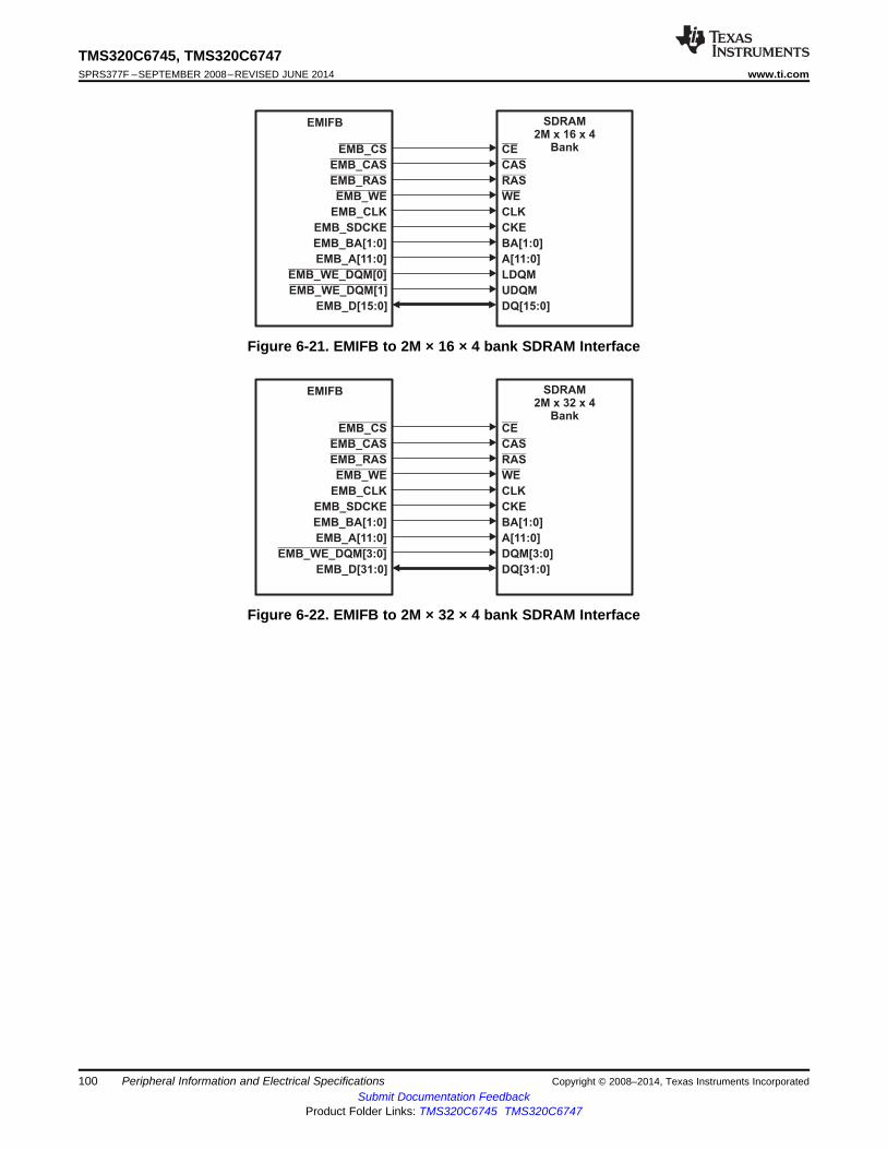
EMB_CS
EMB_CAS
EMB_RAS
EMB_WE
EMB_CLK
EMB_SDCKE
EMB_BA[1:0]
EMB_A[11:0]
EMB_WE_DQM[3:0]
EMB_D[31:0]
EMIFB
CE
CAS
RAS
WE
CLK
CKE
BA[1:0]
A[11:0]
DQM[3:0]
DQ[31:0]
SDRAM2M x 32 x 4
Bank
EMB_CS
EMB_CAS
EMB_RAS
EMB_WE
EMB_CLK
EMB_SDCKE
EMB_BA[1:0]
EMB_A[11:0]
EMB_WE_DQM[0]
EMB_WE_DQM[1]
EMB_D[15:0]
EMIFB
CE
CAS
RAS
WE
CLK
CKE
BA[1:0]
A[11:0]
LDQM
UDQM
DQ[15:0]
SDRAM2M x 16 x 4
Bank
TMS320C6745, TMS320C6747SPRS377F –SEPTEMBER 2008–REVISED JUNE 2014 www.ti.com
Figure 6-21. EMIFB to 2M × 16 × 4 bank SDRAM Interface
Figure 6-22. EMIFB to 2M × 32 × 4 bank SDRAM Interface
100 Peripheral Information and Electrical Specifications Copyright © 2008–2014, Texas Instruments IncorporatedSubmit Documentation Feedback
Product Folder Links: TMS320C6745 TMS320C6747

EMB_CS
EMB_CAS
EMB_RAS
EMB_WE
EMB_CLK
EMB_SDCKE
EMB_BA[1:0]
EMB_A[12:0]
EMB_WE_DQM[0]
EMB_D[15:0]
EMIFB
CE
CAS
RAS
WE
CLK
CKE
BA[1:0]
A[12:0]
LDQM
DQ[15:0]
SDRAM4M x 16 x 4
Bank
EMB_WE_DQM[1] UDQM
EMB_WE_DQM[2]
EMB_D[31:16]
EMB_WE_DQM[3]
CE
CAS
RAS
WE
CLK
CKE
BA[1:0]
A[12:0]
LDQM
DQ[15:0]
SDRAM4M x 16 x 4
Bank
UDQM
TMS320C6745, TMS320C6747www.ti.com SPRS377F –SEPTEMBER 2008–REVISED JUNE 2014
Figure 6-23. EMIFB to Dual 4M × 16 × 4 bank SDRAM Interface
Table 6-24. Example of 16/32-bit EMIFB Address Pin Connections
SDRAM SIZE WIDTH BANKS MEMORY ADDRESS PINS64M bits ×16 4 SDRAM A[11:0]
EMIFB EMB_A[11:0]×32 4 SDRAM A[10:0]
EMIFB EMB_A[10:0]128M bits ×16 4 SDRAM A[11:0]
EMIFB EMB_A[11:0]×32 4 SDRAM A[11:0]
EMIFB EMB_A[11:0]256M bits ×16 4 SDRAM A[12:0]
EMIFB EMB_A[12:0]×32 4 SDRAM A[11:0]
EMIFB EMB_A[11:0]512M bits ×16 4 SDRAM A[12:0]
EMIFB EMB_A[12:0]×32 4 SDRAM A[12:0]
EMIFB EMB_A[12:0]
Table 6-25 is a list of the EMIFB registers.
Table 6-25. EMIFB Base Controller Registers
BYTE ADDRESS ACRONYM REGISTER DESCRIPTION0xB000 0000 MIDR Module ID Register
Copyright © 2008–2014, Texas Instruments Incorporated Peripheral Information and Electrical Specifications 101Submit Documentation Feedback
Product Folder Links: TMS320C6745 TMS320C6747

TMS320C6745, TMS320C6747SPRS377F –SEPTEMBER 2008–REVISED JUNE 2014 www.ti.com
Table 6-25. EMIFB Base Controller Registers (continued)BYTE ADDRESS ACRONYM REGISTER DESCRIPTION
0xB000 0008 SDCFG SDRAM Configuration Register0xB000 000C SDRFC SDRAM Refresh Control Register0xB000 0010 SDTIM1 SDRAM Timing Register 10xB000 0014 SDTIM2 SDRAM Timing Register 20xB000 001C SDCFG2 SDRAM Configuration 2 Register0xB000 0020 BPRIO Peripheral Bus Burst Priority Register0xB000 0040 PC1 Performance Counter 1 Register0xB000 0044 PC2 Performance Counter 2 Register0xB000 0048 PCC Performance Counter Configuration Register0xB000 004C PCMRS Performance Counter Master Region Select Register0xB000 0050 PCT Performance Counter Time Register0xB000 00C0 IRR Interrupt Raw Register0xB000 00C4 IMR Interrupt Mask Register0xB000 00C8 IMSR Interrupt Mask Set Register0xB000 00CC IMCR Interrupt Mask Clear Register
102 Peripheral Information and Electrical Specifications Copyright © 2008–2014, Texas Instruments IncorporatedSubmit Documentation Feedback
Product Folder Links: TMS320C6745 TMS320C6747

TMS320C6745, TMS320C6747www.ti.com SPRS377F –SEPTEMBER 2008–REVISED JUNE 2014
6.11.3 EMIFB Electrical Data/Timing
Table 6-26. EMIFB SDRAM Interface Timing RequirementsCVDD = 1.3 V (1) CVDD = 1.2V (2) UNNO. ITMIN MAX MIN MAX
Input setup time, read data valid on EMB_D[31:0] before19 t(DV-CLKH) 0.59 0.8 nsEMB_CLK risingInput hold time, read data valid on EMB_D[31:0] after20 th(CLKH-DIV) 1.25 1.5 nsEMB_CLK rising
(1) Commercial (default), Industrial and Extended temperature range rated devices for 456 MHz max CPU operating frequency asapplicable to the device
(2) Commercial (default), Industrial, Extended and Automotive temperature range rated devices for 400/375/300/266/200 MHz max CPUoperating frequencies as applicable to the device
Table 6-27. EMIFB SDRAM Interface Switching Characteristics for Commercial (Default) TemperatureRange
CVDD = 1.3 V (1) CVDD = 1.2V (2) UNNO. PARAMETER ITMIN MAX MIN MAX1 tc(CLK) Cycle time, EMIF clock EMB_CLK 6.579 7.5 ns2 tw(CLK) Pulse width, EMIF clock EMB_CLK high or low 2.63 3 ns3 td(CLKH-CSV) Delay time, EMB_CLK rising to EMB_CS[0] valid 4.25 5.1 ns4 toh(CLKH-CSIV) Output hold time, EMB_CLK rising to EMB_CS[0] invalid 1.1 1.1 ns5 td(CLKH-DQMV) Delay time, EMB_CLK rising to EMB_WE_DQM[3:0] valid 4.25 5.1 ns
Output hold time, EMB_CLK rising to6 toh(CLKH-DQMIV) 1.1 1.1 nsEMB_WE_DQM[3:0] invalidDelay time, EMB_CLK rising to EMB_A[12:0] and7 td(CLKH-AV) 4.25 5.1 nsEMB_BA[1:0] validOutput hold time, EMB_CLK rising to EMB_A[12:0] and8 toh(CLKH-AIV) 1.1 1.1 nsEMB_BA[1:0] invalid
9 td(CLKH-DV) Delay time, EMB_CLK rising to EMB_D[31:0] valid 4.25 5.1 nsOutput hold time, EMB_CLK rising to EMB_D[31:0]10 toh(CLKH-DIV) 1.1 1.1 nsinvalid
11 td(CLKH-RASV) Delay time, EMB_CLK rising to EMB_RAS valid 4.25 5.1 ns12 toh(CLKH-RASIV) Output hold time, EMB_CLK rising to EMB_RAS invalid 1.1 1.1 ns13 td(CLKH-CASV) Delay time, EMB_CLK rising to EMB_CAS valid 4.25 5.1 ns14 toh(CLKH-CASIV) Output hold time, EMB_CLK rising to EMB_CAS invalid 1.1 1.1 ns15 td(CLKH-WEV) Delay time, EMB_CLK rising to EMB_WE valid 4.25 5.1 ns16 toh(CLKH-WEIV) Output hold time, EMB_CLK rising to EMB_WE invalid 1.1 1.1 ns17 tdis(CLKH-DHZ) Delay time, EMB_CLK rising to EMB_D[31:0] tri-stated 4.25 5.1 ns
Output hold time, EMB_CLK rising to EMB_D[31:0]18 t(CLKH-DLZ) 1.1 1.1 nsdriving
(1) Commercial (default) temperature range rated devices for 456 MHz max CPU operating frequency as applicable to the device(2) Commercial (default) temperature range rated devices for 400/375/300/266/200 MHz max CPU operating frequencies as applicable to
the device
Copyright © 2008–2014, Texas Instruments Incorporated Peripheral Information and Electrical Specifications 103Submit Documentation Feedback
Product Folder Links: TMS320C6745 TMS320C6747
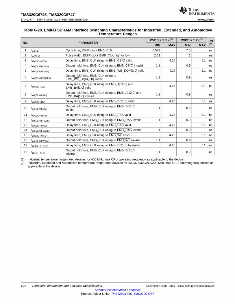
TMS320C6745, TMS320C6747SPRS377F –SEPTEMBER 2008–REVISED JUNE 2014 www.ti.com
Table 6-28. EMIFB SDRAM Interface Switching Characteristics for Industrial, Extended, and AutomotiveTemperature Ranges
CVDD = 1.3 V (1) CVDD = 1.2V (2) UNNO. PARAMETER ITMIN MAX MIN MAX1 tc(CLK) Cycle time, EMIF clock EMB_CLK 6.579 7.5 ns2 tw(CLK) Pulse width, EMIF clock EMB_CLK high or low 2.63 3 ns3 td(CLKH-CSV) Delay time, EMB_CLK rising to EMB_CS[0] valid 4.25 5.1 ns4 toh(CLKH-CSIV) Output hold time, EMB_CLK rising to EMB_CS[0] invalid 1.1 0.9 ns5 td(CLKH-DQMV) Delay time, EMB_CLK rising to EMB_WE_DQM[3:0] valid 4.25 5.1 ns
Output hold time, EMB_CLK rising to6 toh(CLKH-DQMIV) 1.1 0.9 nsEMB_WE_DQM[3:0] invalidDelay time, EMB_CLK rising to EMB_A[12:0] and7 td(CLKH-AV) 4.25 5.1 nsEMB_BA[1:0] validOutput hold time, EMB_CLK rising to EMB_A[12:0] and8 toh(CLKH-AIV) 1.1 0.9 nsEMB_BA[1:0] invalid
9 td(CLKH-DV) Delay time, EMB_CLK rising to EMB_D[31:0] valid 4.25 5.1 nsOutput hold time, EMB_CLK rising to EMB_D[31:0]10 toh(CLKH-DIV) 1.1 0.9 nsinvalid
11 td(CLKH-RASV) Delay time, EMB_CLK rising to EMB_RAS valid 4.25 5.1 ns12 toh(CLKH-RASIV) Output hold time, EMB_CLK rising to EMB_RAS invalid 1.1 0.9 ns13 td(CLKH-CASV) Delay time, EMB_CLK rising to EMB_CAS valid 4.25 5.1 ns14 toh(CLKH-CASIV) Output hold time, EMB_CLK rising to EMB_CAS invalid 1.1 0.9 ns15 td(CLKH-WEV) Delay time, EMB_CLK rising to EMB_WE valid 4.25 5.1 ns16 toh(CLKH-WEIV) Output hold time, EMB_CLK rising to EMB_WE invalid 1.1 0.9 ns17 tdis(CLKH-DHZ) Delay time, EMB_CLK rising to EMB_D[31:0] tri-stated 4.25 5.1 ns
Output hold time, EMB_CLK rising to EMB_D[31:0]18 t(CLKH-DLZ) 1.1 0.9 nsdriving
(1) Industrial temperature range rated devices for 456 MHz max CPU operating frequency as applicable to the device(2) Industrial, Extended and Automotive temperature range rated devices for 400/375/300/266/200 MHz max CPU operating frequencies as
applicable to the device
104 Peripheral Information and Electrical Specifications Copyright © 2008–2014, Texas Instruments IncorporatedSubmit Documentation Feedback
Product Folder Links: TMS320C6745 TMS320C6747
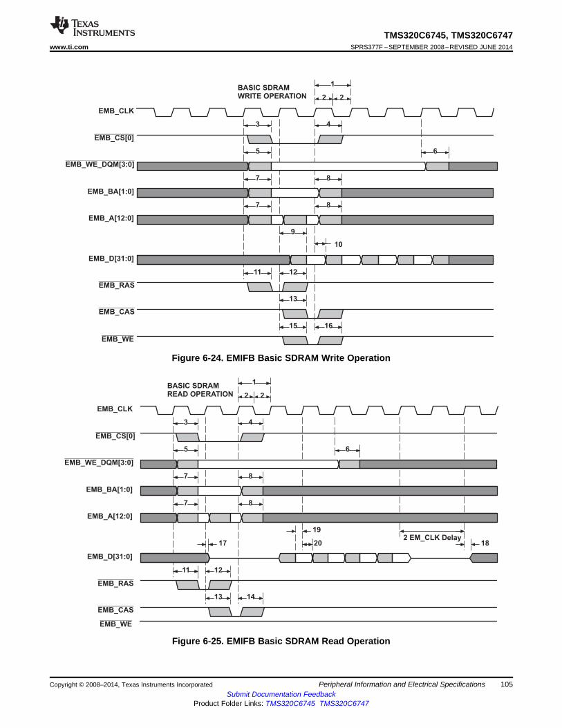
EMB_CLK
EMB_BA[1:0]
EMB_A[12:0]
EMB_D[31:0]
1
2 2
4
6
8
8
12
14
19
20
3
5
7
7
11
13
17 182 EM_CLK Delay
BASIC SDRAMREAD OPERATION
EMB_CS[0]
EMB_WE_DQM[3:0]
EMB_RAS
EMB_CAS
EMB_WE
EMB_CLK
EMB_BA[1:0]
EMB_A[12:0]
EMB_D[31:0]
1
2 2
4
6
8
8
12
10
16
3
5
7
7
11
13
15
9
BASIC SDRAMWRITE OPERATION
EMB_CS[0]
EMB_WE_DQM[3:0]
EMB_RAS
EMB_CAS
EMB_WE
TMS320C6745, TMS320C6747www.ti.com SPRS377F –SEPTEMBER 2008–REVISED JUNE 2014
Figure 6-24. EMIFB Basic SDRAM Write Operation
Figure 6-25. EMIFB Basic SDRAM Read Operation
Copyright © 2008–2014, Texas Instruments Incorporated Peripheral Information and Electrical Specifications 105Submit Documentation Feedback
Product Folder Links: TMS320C6745 TMS320C6747
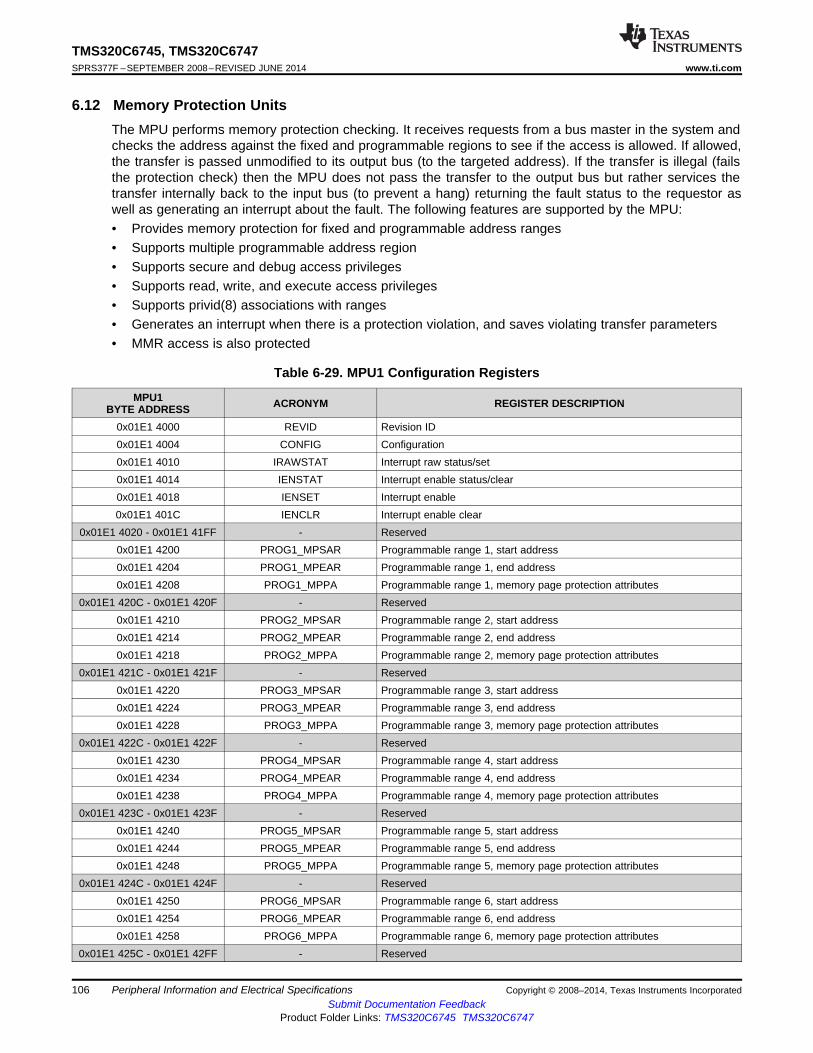
TMS320C6745, TMS320C6747SPRS377F –SEPTEMBER 2008–REVISED JUNE 2014 www.ti.com
6.12 Memory Protection UnitsThe MPU performs memory protection checking. It receives requests from a bus master in the system andchecks the address against the fixed and programmable regions to see if the access is allowed. If allowed,the transfer is passed unmodified to its output bus (to the targeted address). If the transfer is illegal (failsthe protection check) then the MPU does not pass the transfer to the output bus but rather services thetransfer internally back to the input bus (to prevent a hang) returning the fault status to the requestor aswell as generating an interrupt about the fault. The following features are supported by the MPU:• Provides memory protection for fixed and programmable address ranges• Supports multiple programmable address region• Supports secure and debug access privileges• Supports read, write, and execute access privileges• Supports privid(8) associations with ranges• Generates an interrupt when there is a protection violation, and saves violating transfer parameters• MMR access is also protected
Table 6-29. MPU1 Configuration Registers
MPU1 ACRONYM REGISTER DESCRIPTIONBYTE ADDRESS0x01E1 4000 REVID Revision ID0x01E1 4004 CONFIG Configuration0x01E1 4010 IRAWSTAT Interrupt raw status/set0x01E1 4014 IENSTAT Interrupt enable status/clear0x01E1 4018 IENSET Interrupt enable0x01E1 401C IENCLR Interrupt enable clear
0x01E1 4020 - 0x01E1 41FF - Reserved0x01E1 4200 PROG1_MPSAR Programmable range 1, start address0x01E1 4204 PROG1_MPEAR Programmable range 1, end address0x01E1 4208 PROG1_MPPA Programmable range 1, memory page protection attributes
0x01E1 420C - 0x01E1 420F - Reserved0x01E1 4210 PROG2_MPSAR Programmable range 2, start address0x01E1 4214 PROG2_MPEAR Programmable range 2, end address0x01E1 4218 PROG2_MPPA Programmable range 2, memory page protection attributes
0x01E1 421C - 0x01E1 421F - Reserved0x01E1 4220 PROG3_MPSAR Programmable range 3, start address0x01E1 4224 PROG3_MPEAR Programmable range 3, end address0x01E1 4228 PROG3_MPPA Programmable range 3, memory page protection attributes
0x01E1 422C - 0x01E1 422F - Reserved0x01E1 4230 PROG4_MPSAR Programmable range 4, start address0x01E1 4234 PROG4_MPEAR Programmable range 4, end address0x01E1 4238 PROG4_MPPA Programmable range 4, memory page protection attributes
0x01E1 423C - 0x01E1 423F - Reserved0x01E1 4240 PROG5_MPSAR Programmable range 5, start address0x01E1 4244 PROG5_MPEAR Programmable range 5, end address0x01E1 4248 PROG5_MPPA Programmable range 5, memory page protection attributes
0x01E1 424C - 0x01E1 424F - Reserved0x01E1 4250 PROG6_MPSAR Programmable range 6, start address0x01E1 4254 PROG6_MPEAR Programmable range 6, end address0x01E1 4258 PROG6_MPPA Programmable range 6, memory page protection attributes
0x01E1 425C - 0x01E1 42FF - Reserved
106 Peripheral Information and Electrical Specifications Copyright © 2008–2014, Texas Instruments IncorporatedSubmit Documentation Feedback
Product Folder Links: TMS320C6745 TMS320C6747
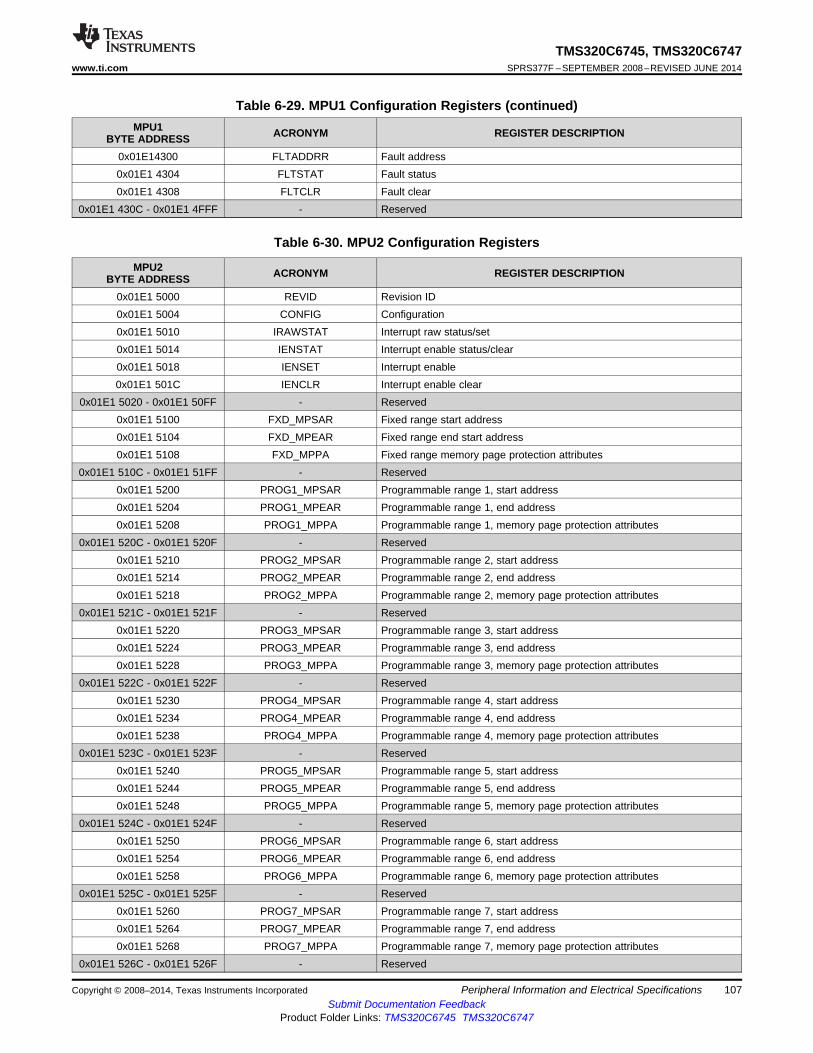
TMS320C6745, TMS320C6747www.ti.com SPRS377F –SEPTEMBER 2008–REVISED JUNE 2014
Table 6-29. MPU1 Configuration Registers (continued)MPU1 ACRONYM REGISTER DESCRIPTIONBYTE ADDRESS
0x01E14300 FLTADDRR Fault address0x01E1 4304 FLTSTAT Fault status0x01E1 4308 FLTCLR Fault clear
0x01E1 430C - 0x01E1 4FFF - Reserved
Table 6-30. MPU2 Configuration Registers
MPU2 ACRONYM REGISTER DESCRIPTIONBYTE ADDRESS0x01E1 5000 REVID Revision ID0x01E1 5004 CONFIG Configuration0x01E1 5010 IRAWSTAT Interrupt raw status/set0x01E1 5014 IENSTAT Interrupt enable status/clear0x01E1 5018 IENSET Interrupt enable0x01E1 501C IENCLR Interrupt enable clear
0x01E1 5020 - 0x01E1 50FF - Reserved0x01E1 5100 FXD_MPSAR Fixed range start address0x01E1 5104 FXD_MPEAR Fixed range end start address0x01E1 5108 FXD_MPPA Fixed range memory page protection attributes
0x01E1 510C - 0x01E1 51FF - Reserved0x01E1 5200 PROG1_MPSAR Programmable range 1, start address0x01E1 5204 PROG1_MPEAR Programmable range 1, end address0x01E1 5208 PROG1_MPPA Programmable range 1, memory page protection attributes
0x01E1 520C - 0x01E1 520F - Reserved0x01E1 5210 PROG2_MPSAR Programmable range 2, start address0x01E1 5214 PROG2_MPEAR Programmable range 2, end address0x01E1 5218 PROG2_MPPA Programmable range 2, memory page protection attributes
0x01E1 521C - 0x01E1 521F - Reserved0x01E1 5220 PROG3_MPSAR Programmable range 3, start address0x01E1 5224 PROG3_MPEAR Programmable range 3, end address0x01E1 5228 PROG3_MPPA Programmable range 3, memory page protection attributes
0x01E1 522C - 0x01E1 522F - Reserved0x01E1 5230 PROG4_MPSAR Programmable range 4, start address0x01E1 5234 PROG4_MPEAR Programmable range 4, end address0x01E1 5238 PROG4_MPPA Programmable range 4, memory page protection attributes
0x01E1 523C - 0x01E1 523F - Reserved0x01E1 5240 PROG5_MPSAR Programmable range 5, start address0x01E1 5244 PROG5_MPEAR Programmable range 5, end address0x01E1 5248 PROG5_MPPA Programmable range 5, memory page protection attributes
0x01E1 524C - 0x01E1 524F - Reserved0x01E1 5250 PROG6_MPSAR Programmable range 6, start address0x01E1 5254 PROG6_MPEAR Programmable range 6, end address0x01E1 5258 PROG6_MPPA Programmable range 6, memory page protection attributes
0x01E1 525C - 0x01E1 525F - Reserved0x01E1 5260 PROG7_MPSAR Programmable range 7, start address0x01E1 5264 PROG7_MPEAR Programmable range 7, end address0x01E1 5268 PROG7_MPPA Programmable range 7, memory page protection attributes
0x01E1 526C - 0x01E1 526F - Reserved
Copyright © 2008–2014, Texas Instruments Incorporated Peripheral Information and Electrical Specifications 107Submit Documentation Feedback
Product Folder Links: TMS320C6745 TMS320C6747

TMS320C6745, TMS320C6747SPRS377F –SEPTEMBER 2008–REVISED JUNE 2014 www.ti.com
Table 6-30. MPU2 Configuration Registers (continued)MPU2 ACRONYM REGISTER DESCRIPTIONBYTE ADDRESS
0x01E1 5270 PROG8_MPSAR Programmable range 8, start address0x01E1 5274 PROG8_MPEAR Programmable range 8, end address0x01E1 5278 PROG8_MPPA Programmable range 8, memory page protection attributes
0x01E1 527C - 0x01E1 527F - Reserved0x01E1 5280 PROG9_MPSAR Programmable range 9, start address0x01E1 5284 PROG9_MPEAR Programmable range 9, end address0x01E1 5288 PROG9_MPPA Programmable range 9, memory page protection attributes
0x01E1 528C - 0x01E1 528F - Reserved0x01E1 5290 PROG10_MPSAR Programmable range 10, start address0x01E1 5294 PROG10_MPEAR Programmable range 10, end address0x01E1 5298 PROG10_MPPA Programmable range 10, memory page protection attributes
0x01E1 529C - 0x01E1 529F - Reserved0x01E1 52A0 PROG11_MPSAR Programmable range 11, start address0x01E1 52A4 PROG11_MPEAR Programmable range 11, end address0x01E1 52A8 PROG11_MPPA Programmable range 11, memory page protection attributes
0x01E1 52AC - 0x01E1 52AF - Reserved0x01E1 52B0 PROG12_MPSAR Programmable range 12, start address0x01E1 52B4 PROG12_MPEAR Programmable range 12, end address0x01E1 52B8 PROG12_MPPA Programmable range 12, memory page protection attributes
0x01E1 52BC - 0x01E1 52FF - Reserved0x01E1 5300 FLTADDRR Fault address0x01E1 5304 FLTSTAT Fault status0x01E1 5308 FLTCLR Fault clear
0x01E1 530C - 0x01E1 5FFF - Reserved
108 Peripheral Information and Electrical Specifications Copyright © 2008–2014, Texas Instruments IncorporatedSubmit Documentation Feedback
Product Folder Links: TMS320C6745 TMS320C6747

TMS320C6745, TMS320C6747www.ti.com SPRS377F –SEPTEMBER 2008–REVISED JUNE 2014
6.13 MMC / SD / SDIO (MMCSD)
6.13.1 MMCSD Peripheral DescriptionThe C6745/6747 includes an MMCSD controller which is compliant with MMC V4.0, Secure Digital Part 1Physical Layer Specification V1.1 and Secure Digital Input Output (SDIO) V2.0 specifications.
The MMC/SD Controller has following features:• MultiMediaCard (MMC) support• Secure Digital (SD) Memory Card support• MMC/SD protocol support• SD high capacity support• SDIO protocol support• Programmable clock frequency• 512 bit Read/Write FIFO to lower system overhead• Slave EDMA transfer capability
The C6745/6747 MMC/SD Controller does not support SPI mode.
6.13.2 MMCSD Peripheral Register Description(s)
Table 6-31. Multimedia Card/Secure Digital (MMC/SD) Card Controller Registers
BYTE ACRONYM REGISTER DESCRIPTIONADDRESS
0x01C4 0000 MMCCTL MMC Control Register0x01C4 0004 MMCCLK MMC Memory Clock Control Register0x01C4 0008 MMCST0 MMC Status Register 00x01C4 000C MMCST1 MMC Status Register 10x01C4 0010 MMCIM MMC Interrupt Mask Register0x01C4 0014 MMCTOR MMC Response Time-Out Register0x01C4 0018 MMCTOD MMC Data Read Time-Out Register0x01C4 001C MMCBLEN MMC Block Length Register0x01C4 0020 MMCNBLK MMC Number of Blocks Register0x01C4 0024 MMCNBLC MMC Number of Blocks Counter Register0x01C4 0028 MMCDRR MMC Data Receive Register0x01C4 002C MMCDXR MMC Data Transmit Register0x01C4 0030 MMCCMD MMC Command Register0x01C4 0034 MMCARGHL MMC Argument Register0x01C4 0038 MMCRSP01 MMC Response Register 0 and 10x01C4 003C MMCRSP23 MMC Response Register 2 and 30x01C4 0040 MMCRSP45 MMC Response Register 4 and 50x01C4 0044 MMCRSP67 MMC Response Register 6 and 70x01C4 0048 MMCDRSP MMC Data Response Register0x01C4 0050 MMCCIDX MMC Command Index Register0x01C4 0064 SDIOCTL SDIO Control Register0x01C4 0068 SDIOST0 SDIO Status Register 00x01C4 006C SDIOIEN SDIO Interrupt Enable Register0x01C4 0070 SDIOIST SDIO Interrupt Status Register0x01C4 0074 MMCFIFOCTL MMC FIFO Control Register
Copyright © 2008–2014, Texas Instruments Incorporated Peripheral Information and Electrical Specifications 109Submit Documentation Feedback
Product Folder Links: TMS320C6745 TMS320C6747

TMS320C6745, TMS320C6747SPRS377F –SEPTEMBER 2008–REVISED JUNE 2014 www.ti.com
6.13.3 MMC/SD Electrical Data/Timing
Table 6-32. Timing Requirements for MMC/SD Module(see Figure 6-27 and Figure 6-29)
No. PARAMETER MIN MAX UNIT1 tsu(CMDV-CLKH) Setup time, MMCSD_CMD valid before MMCSD_CLK high 3.2 ns2 th(CLKH-CMDV) Hold time, MMCSD_CMD valid after MMCSD_CLK high 1.5 ns3 tsu(DATV-CLKH) Setup time, MMCSD_DATx valid before MMCSD_CLK high 3.2 ns4 th(CLKH-DATV) Hold time, MMCSD_DATx valid after MMCSD_CLK high 1.5 ns
Table 6-33. Switching Characteristics Over Recommended Operating Conditions for MMC/SD Module(see Figure 6-26 through Figure 6-29)
No. PARAMETER MIN MAX UNIT7 f(CLK) Operating frequency, MMCSD_CLK 0 52 MHz8 f(CLK_ID) Identification mode frequency, MMCSD_CLK 0 400 KHz9 tW(CLKL) Pulse width, MMCSD_CLK low 6.5 ns
10 tW(CLKH) Pulse width, MMCSD_CLK high 6.5 ns11 tr(CLK) Rise time, MMCSD_CLK 3 ns12 tf(CLK) Fall time, MMCSD_CLK 3 ns13 td(CLKL-CMD) Delay time, MMCSD_CLK low to MMCSD_CMD transition -4.5 2.5 ns14 td(CLKL-DAT) Delay time, MMCSD_CLK low to MMCSD_DATx transition -4.5 2.5 ns
110 Peripheral Information and Electrical Specifications Copyright © 2008–2014, Texas Instruments IncorporatedSubmit Documentation Feedback
Product Folder Links: TMS320C6745 TMS320C6747

Start D0 D1 Dx End
7
MMCSD_CLK
MMCSD_DATx
910
4
3 3
4
START D0 D1 Dx END
MMCSD_CLK
MMCSD_DATx
7
1414
10
9
14 14
START XMIT Valid Valid Valid END
MMCSD_CLK
MMCSD_CMD
109
7
1
2
START XMIT Valid Valid Valid END
MMCSD_CLK
MMCSD_CMD
13
7
109
13 13 13
TMS320C6745, TMS320C6747www.ti.com SPRS377F –SEPTEMBER 2008–REVISED JUNE 2014
Figure 6-26. MMC/SD Host Command Timing
Figure 6-27. MMC/SD Card Response Timing
Figure 6-28. MMC/SD Host Write Timing
Figure 6-29. MMC/SD Host Read and Card CRC Status Timing
Copyright © 2008–2014, Texas Instruments Incorporated Peripheral Information and Electrical Specifications 111Submit Documentation Feedback
Product Folder Links: TMS320C6745 TMS320C6747
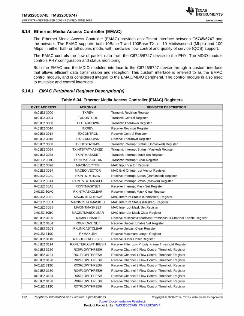
TMS320C6745, TMS320C6747SPRS377F –SEPTEMBER 2008–REVISED JUNE 2014 www.ti.com
6.14 Ethernet Media Access Controller (EMAC)The Ethernet Media Access Controller (EMAC) provides an efficient interface between C6745/6747 andthe network. The EMAC supports both 10Base-T and 100Base-TX, or 10 Mbits/second (Mbps) and 100Mbps in either half- or full-duplex mode, with hardware flow control and quality of service (QOS) support.
The EMAC controls the flow of packet data from the C6745/6747 device to the PHY. The MDIO modulecontrols PHY configuration and status monitoring.
Both the EMAC and the MDIO modules interface to the C6745/6747 device through a custom interfacethat allows efficient data transmission and reception. This custom interface is referred to as the EMACcontrol module, and is considered integral to the EMAC/MDIO peripheral. The control module is also usedto multiplex and control interrupts.
6.14.1 EMAC Peripheral Register Description(s)
Table 6-34. Ethernet Media Access Controller (EMAC) Registers
BYTE ADDRESS ACRONYM REGISTER DESCRIPTION0x01E2 3000 TXREV Transmit Revision Register0x01E2 3004 TXCONTROL Transmit Control Register0x01E2 3008 TXTEARDOWN Transmit Teardown Register0x01E2 3010 RXREV Receive Revision Register0x01E2 3014 RXCONTROL Receive Control Register0x01E2 3018 RXTEARDOWN Receive Teardown Register0x01E2 3080 TXINTSTATRAW Transmit Interrupt Status (Unmasked) Register0x01E2 3084 TXINTSTATMASKED Transmit Interrupt Status (Masked) Register0x01E2 3088 TXINTMASKSET Transmit Interrupt Mask Set Register0x01E2 308C TXINTMASKCLEAR Transmit Interrupt Clear Register0x01E2 3090 MACINVECTOR MAC Input Vector Register0x01E2 3094 MACEOIVECTOR MAC End Of Interrupt Vector Register0x01E2 30A0 RXINTSTATRAW Receive Interrupt Status (Unmasked) Register0x01E2 30A4 RXINTSTATMASKED Receive Interrupt Status (Masked) Register0x01E2 30A8 RXINTMASKSET Receive Interrupt Mask Set Register0x01E2 30AC RXINTMASKCLEAR Receive Interrupt Mask Clear Register0x01E2 30B0 MACINTSTATRAW MAC Interrupt Status (Unmasked) Register0x01E2 30B4 MACINTSTATMASKED MAC Interrupt Status (Masked) Register0x01E2 30B8 MACINTMASKSET MAC Interrupt Mask Set Register0x01E2 30BC MACINTMASKCLEAR MAC Interrupt Mask Clear Register0x01E2 3100 RXMBPENABLE Receive Multicast/Broadcast/Promiscuous Channel Enable Register0x01E2 3104 RXUNICASTSET Receive Unicast Enable Set Register0x01E2 3108 RXUNICASTCLEAR Receive Unicast Clear Register0x01E2 310C RXMAXLEN Receive Maximum Length Register0x01E2 3110 RXBUFFEROFFSET Receive Buffer Offset Register0x01E2 3114 RXFILTERLOWTHRESH Receive Filter Low Priority Frame Threshold Register0x01E2 3120 RX0FLOWTHRESH Receive Channel 0 Flow Control Threshold Register0x01E2 3124 RX1FLOWTHRESH Receive Channel 1 Flow Control Threshold Register0x01E2 3128 RX2FLOWTHRESH Receive Channel 2 Flow Control Threshold Register0x01E2 312C RX3FLOWTHRESH Receive Channel 3 Flow Control Threshold Register0x01E2 3130 RX4FLOWTHRESH Receive Channel 4 Flow Control Threshold Register0x01E2 3134 RX5FLOWTHRESH Receive Channel 5 Flow Control Threshold Register0x01E2 3138 RX6FLOWTHRESH Receive Channel 6 Flow Control Threshold Register0x01E2 313C RX7FLOWTHRESH Receive Channel 7 Flow Control Threshold Register
112 Peripheral Information and Electrical Specifications Copyright © 2008–2014, Texas Instruments IncorporatedSubmit Documentation Feedback
Product Folder Links: TMS320C6745 TMS320C6747

TMS320C6745, TMS320C6747www.ti.com SPRS377F –SEPTEMBER 2008–REVISED JUNE 2014
Table 6-34. Ethernet Media Access Controller (EMAC) Registers (continued)BYTE ADDRESS ACRONYM REGISTER DESCRIPTION
0x01E2 3140 RX0FREEBUFFER Receive Channel 0 Free Buffer Count Register0x01E2 3144 RX1FREEBUFFER Receive Channel 1 Free Buffer Count Register0x01E2 3148 RX2FREEBUFFER Receive Channel 2 Free Buffer Count Register0x01E2 314C RX3FREEBUFFER Receive Channel 3 Free Buffer Count Register0x01E2 3150 RX4FREEBUFFER Receive Channel 4 Free Buffer Count Register0x01E2 3154 RX5FREEBUFFER Receive Channel 5 Free Buffer Count Register0x01E2 3158 RX6FREEBUFFER Receive Channel 6 Free Buffer Count Register0x01E2 315C RX7FREEBUFFER Receive Channel 7 Free Buffer Count Register0x01E2 3160 MACCONTROL MAC Control Register0x01E2 3164 MACSTATUS MAC Status Register0x01E2 3168 EMCONTROL Emulation Control Register0x01E2 316C FIFOCONTROL FIFO Control Register0x01E2 3170 MACCONFIG MAC Configuration Register0x01E2 3174 SOFTRESET Soft Reset Register0x01E2 31D0 MACSRCADDRLO MAC Source Address Low Bytes Register0x01E2 31D4 MACSRCADDRHI MAC Source Address High Bytes Register0x01E2 31D8 MACHASH1 MAC Hash Address Register 10x01E2 31DC MACHASH2 MAC Hash Address Register 20x01E2 31E0 BOFFTEST Back Off Test Register0x01E2 31E4 TPACETEST Transmit Pacing Algorithm Test Register0x01E2 31E8 RXPAUSE Receive Pause Timer Register0x01E2 31EC TXPAUSE Transmit Pause Timer Register
0x01E2 3200 - 0x01E2 32FC (see Table 6-35) EMAC Statistics Registers0x01E2 3500 MACADDRLO MAC Address Low Bytes Register, Used in Receive Address Matching0x01E2 3504 MACADDRHI MAC Address High Bytes Register, Used in Receive Address Matching0x01E2 3508 MACINDEX MAC Index Register0x01E2 3600 TX0HDP Transmit Channel 0 DMA Head Descriptor Pointer Register0x01E2 3604 TX1HDP Transmit Channel 1 DMA Head Descriptor Pointer Register0x01E2 3608 TX2HDP Transmit Channel 2 DMA Head Descriptor Pointer Register0x01E2 360C TX3HDP Transmit Channel 3 DMA Head Descriptor Pointer Register0x01E2 3610 TX4HDP Transmit Channel 4 DMA Head Descriptor Pointer Register0x01E2 3614 TX5HDP Transmit Channel 5 DMA Head Descriptor Pointer Register0x01E2 3618 TX6HDP Transmit Channel 6 DMA Head Descriptor Pointer Register0x01E2 361C TX7HDP Transmit Channel 7 DMA Head Descriptor Pointer Register0x01E2 3620 RX0HDP Receive Channel 0 DMA Head Descriptor Pointer Register0x01E2 3624 RX1HDP Receive Channel 1 DMA Head Descriptor Pointer Register0x01E2 3628 RX2HDP Receive Channel 2 DMA Head Descriptor Pointer Register0x01E2 362C RX3HDP Receive Channel 3 DMA Head Descriptor Pointer Register0x01E2 3630 RX4HDP Receive Channel 4 DMA Head Descriptor Pointer Register0x01E2 3634 RX5HDP Receive Channel 5 DMA Head Descriptor Pointer Register0x01E2 3638 RX6HDP Receive Channel 6 DMA Head Descriptor Pointer Register0x01E2 363C RX7HDP Receive Channel 7 DMA Head Descriptor Pointer Register0x01E2 3640 TX0CP Transmit Channel 0 Completion Pointer Register0x01E2 3644 TX1CP Transmit Channel 1 Completion Pointer Register0x01E2 3648 TX2CP Transmit Channel 2 Completion Pointer Register0x01E2 364C TX3CP Transmit Channel 3 Completion Pointer Register0x01E2 3650 TX4CP Transmit Channel 4 Completion Pointer Register
Copyright © 2008–2014, Texas Instruments Incorporated Peripheral Information and Electrical Specifications 113Submit Documentation Feedback
Product Folder Links: TMS320C6745 TMS320C6747
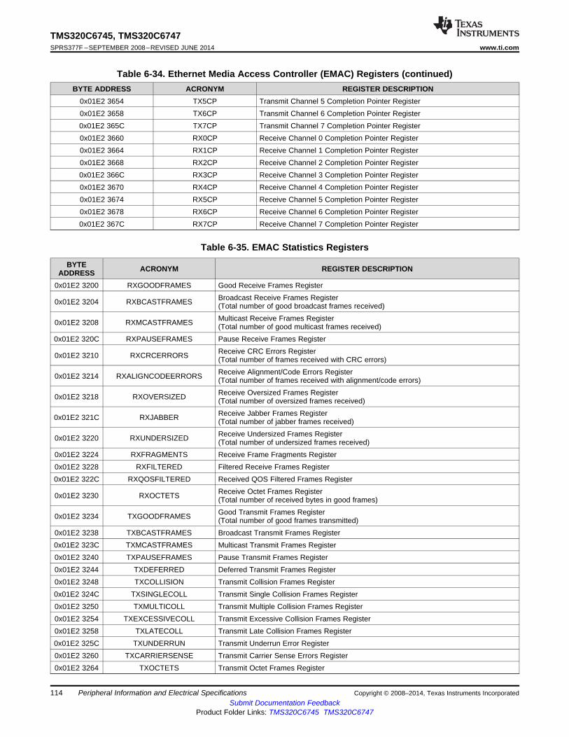
TMS320C6745, TMS320C6747SPRS377F –SEPTEMBER 2008–REVISED JUNE 2014 www.ti.com
Table 6-34. Ethernet Media Access Controller (EMAC) Registers (continued)BYTE ADDRESS ACRONYM REGISTER DESCRIPTION
0x01E2 3654 TX5CP Transmit Channel 5 Completion Pointer Register0x01E2 3658 TX6CP Transmit Channel 6 Completion Pointer Register0x01E2 365C TX7CP Transmit Channel 7 Completion Pointer Register0x01E2 3660 RX0CP Receive Channel 0 Completion Pointer Register0x01E2 3664 RX1CP Receive Channel 1 Completion Pointer Register0x01E2 3668 RX2CP Receive Channel 2 Completion Pointer Register0x01E2 366C RX3CP Receive Channel 3 Completion Pointer Register0x01E2 3670 RX4CP Receive Channel 4 Completion Pointer Register0x01E2 3674 RX5CP Receive Channel 5 Completion Pointer Register0x01E2 3678 RX6CP Receive Channel 6 Completion Pointer Register0x01E2 367C RX7CP Receive Channel 7 Completion Pointer Register
Table 6-35. EMAC Statistics Registers
BYTE ACRONYM REGISTER DESCRIPTIONADDRESS0x01E2 3200 RXGOODFRAMES Good Receive Frames Register
Broadcast Receive Frames Register0x01E2 3204 RXBCASTFRAMES (Total number of good broadcast frames received)Multicast Receive Frames Register0x01E2 3208 RXMCASTFRAMES (Total number of good multicast frames received)
0x01E2 320C RXPAUSEFRAMES Pause Receive Frames RegisterReceive CRC Errors Register0x01E2 3210 RXCRCERRORS (Total number of frames received with CRC errors)Receive Alignment/Code Errors Register0x01E2 3214 RXALIGNCODEERRORS (Total number of frames received with alignment/code errors)Receive Oversized Frames Register0x01E2 3218 RXOVERSIZED (Total number of oversized frames received)Receive Jabber Frames Register0x01E2 321C RXJABBER (Total number of jabber frames received)Receive Undersized Frames Register0x01E2 3220 RXUNDERSIZED (Total number of undersized frames received)
0x01E2 3224 RXFRAGMENTS Receive Frame Fragments Register0x01E2 3228 RXFILTERED Filtered Receive Frames Register0x01E2 322C RXQOSFILTERED Received QOS Filtered Frames Register
Receive Octet Frames Register0x01E2 3230 RXOCTETS (Total number of received bytes in good frames)Good Transmit Frames Register0x01E2 3234 TXGOODFRAMES (Total number of good frames transmitted)
0x01E2 3238 TXBCASTFRAMES Broadcast Transmit Frames Register0x01E2 323C TXMCASTFRAMES Multicast Transmit Frames Register0x01E2 3240 TXPAUSEFRAMES Pause Transmit Frames Register0x01E2 3244 TXDEFERRED Deferred Transmit Frames Register0x01E2 3248 TXCOLLISION Transmit Collision Frames Register0x01E2 324C TXSINGLECOLL Transmit Single Collision Frames Register0x01E2 3250 TXMULTICOLL Transmit Multiple Collision Frames Register0x01E2 3254 TXEXCESSIVECOLL Transmit Excessive Collision Frames Register0x01E2 3258 TXLATECOLL Transmit Late Collision Frames Register0x01E2 325C TXUNDERRUN Transmit Underrun Error Register0x01E2 3260 TXCARRIERSENSE Transmit Carrier Sense Errors Register0x01E2 3264 TXOCTETS Transmit Octet Frames Register
114 Peripheral Information and Electrical Specifications Copyright © 2008–2014, Texas Instruments IncorporatedSubmit Documentation Feedback
Product Folder Links: TMS320C6745 TMS320C6747
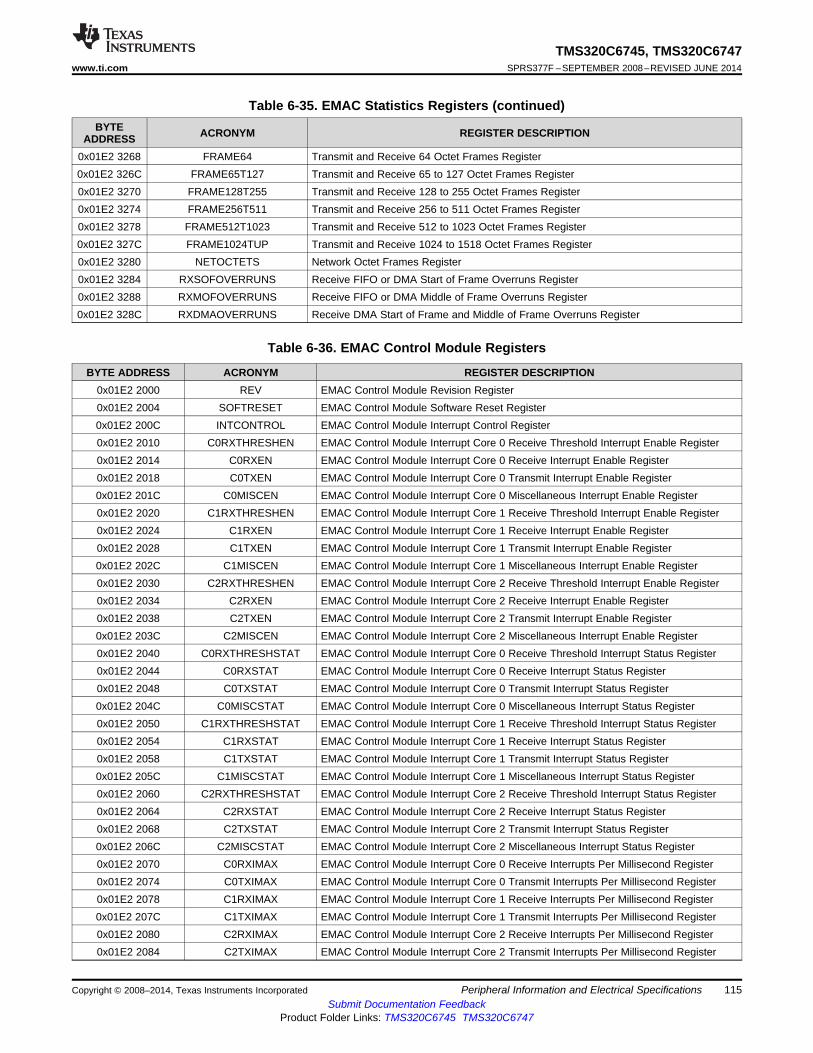
TMS320C6745, TMS320C6747www.ti.com SPRS377F –SEPTEMBER 2008–REVISED JUNE 2014
Table 6-35. EMAC Statistics Registers (continued)BYTE ACRONYM REGISTER DESCRIPTIONADDRESS
0x01E2 3268 FRAME64 Transmit and Receive 64 Octet Frames Register0x01E2 326C FRAME65T127 Transmit and Receive 65 to 127 Octet Frames Register0x01E2 3270 FRAME128T255 Transmit and Receive 128 to 255 Octet Frames Register0x01E2 3274 FRAME256T511 Transmit and Receive 256 to 511 Octet Frames Register0x01E2 3278 FRAME512T1023 Transmit and Receive 512 to 1023 Octet Frames Register0x01E2 327C FRAME1024TUP Transmit and Receive 1024 to 1518 Octet Frames Register0x01E2 3280 NETOCTETS Network Octet Frames Register0x01E2 3284 RXSOFOVERRUNS Receive FIFO or DMA Start of Frame Overruns Register0x01E2 3288 RXMOFOVERRUNS Receive FIFO or DMA Middle of Frame Overruns Register0x01E2 328C RXDMAOVERRUNS Receive DMA Start of Frame and Middle of Frame Overruns Register
Table 6-36. EMAC Control Module Registers
BYTE ADDRESS ACRONYM REGISTER DESCRIPTION0x01E2 2000 REV EMAC Control Module Revision Register0x01E2 2004 SOFTRESET EMAC Control Module Software Reset Register0x01E2 200C INTCONTROL EMAC Control Module Interrupt Control Register0x01E2 2010 C0RXTHRESHEN EMAC Control Module Interrupt Core 0 Receive Threshold Interrupt Enable Register0x01E2 2014 C0RXEN EMAC Control Module Interrupt Core 0 Receive Interrupt Enable Register0x01E2 2018 C0TXEN EMAC Control Module Interrupt Core 0 Transmit Interrupt Enable Register0x01E2 201C C0MISCEN EMAC Control Module Interrupt Core 0 Miscellaneous Interrupt Enable Register0x01E2 2020 C1RXTHRESHEN EMAC Control Module Interrupt Core 1 Receive Threshold Interrupt Enable Register0x01E2 2024 C1RXEN EMAC Control Module Interrupt Core 1 Receive Interrupt Enable Register0x01E2 2028 C1TXEN EMAC Control Module Interrupt Core 1 Transmit Interrupt Enable Register0x01E2 202C C1MISCEN EMAC Control Module Interrupt Core 1 Miscellaneous Interrupt Enable Register0x01E2 2030 C2RXTHRESHEN EMAC Control Module Interrupt Core 2 Receive Threshold Interrupt Enable Register0x01E2 2034 C2RXEN EMAC Control Module Interrupt Core 2 Receive Interrupt Enable Register0x01E2 2038 C2TXEN EMAC Control Module Interrupt Core 2 Transmit Interrupt Enable Register0x01E2 203C C2MISCEN EMAC Control Module Interrupt Core 2 Miscellaneous Interrupt Enable Register0x01E2 2040 C0RXTHRESHSTAT EMAC Control Module Interrupt Core 0 Receive Threshold Interrupt Status Register0x01E2 2044 C0RXSTAT EMAC Control Module Interrupt Core 0 Receive Interrupt Status Register0x01E2 2048 C0TXSTAT EMAC Control Module Interrupt Core 0 Transmit Interrupt Status Register0x01E2 204C C0MISCSTAT EMAC Control Module Interrupt Core 0 Miscellaneous Interrupt Status Register0x01E2 2050 C1RXTHRESHSTAT EMAC Control Module Interrupt Core 1 Receive Threshold Interrupt Status Register0x01E2 2054 C1RXSTAT EMAC Control Module Interrupt Core 1 Receive Interrupt Status Register0x01E2 2058 C1TXSTAT EMAC Control Module Interrupt Core 1 Transmit Interrupt Status Register0x01E2 205C C1MISCSTAT EMAC Control Module Interrupt Core 1 Miscellaneous Interrupt Status Register0x01E2 2060 C2RXTHRESHSTAT EMAC Control Module Interrupt Core 2 Receive Threshold Interrupt Status Register0x01E2 2064 C2RXSTAT EMAC Control Module Interrupt Core 2 Receive Interrupt Status Register0x01E2 2068 C2TXSTAT EMAC Control Module Interrupt Core 2 Transmit Interrupt Status Register0x01E2 206C C2MISCSTAT EMAC Control Module Interrupt Core 2 Miscellaneous Interrupt Status Register0x01E2 2070 C0RXIMAX EMAC Control Module Interrupt Core 0 Receive Interrupts Per Millisecond Register0x01E2 2074 C0TXIMAX EMAC Control Module Interrupt Core 0 Transmit Interrupts Per Millisecond Register0x01E2 2078 C1RXIMAX EMAC Control Module Interrupt Core 1 Receive Interrupts Per Millisecond Register0x01E2 207C C1TXIMAX EMAC Control Module Interrupt Core 1 Transmit Interrupts Per Millisecond Register0x01E2 2080 C2RXIMAX EMAC Control Module Interrupt Core 2 Receive Interrupts Per Millisecond Register0x01E2 2084 C2TXIMAX EMAC Control Module Interrupt Core 2 Transmit Interrupts Per Millisecond Register
Copyright © 2008–2014, Texas Instruments Incorporated Peripheral Information and Electrical Specifications 115Submit Documentation Feedback
Product Folder Links: TMS320C6745 TMS320C6747

RMII_MHz_50_CLK
RMII_TXEN
RMII_TXD[1:0]
RMII_RXD[1:0]
RMII_CRS_DV
RMII_RXER
1
2 3
5 5
4
6
7
8 9
10
11
TMS320C6745, TMS320C6747SPRS377F –SEPTEMBER 2008–REVISED JUNE 2014 www.ti.com
Table 6-37. EMAC Control Module RAM
BYTE ADRESS REGISTER DESCRIPTION0x01E2 0000 - 0x01E2 1FFF EMAC Local Buffer Descriptor Memory
Table 6-38. RMII Timing Requirements
No. PARAMETER MIN TYP MAX UNIT1 tc(REFCLK) Cycle Time, RMII_MHZ_50_CLK 20 ns2 tw(REFCLKH) Pulse Width, RMII_MHZ_50_CLK High 7 13 ns3 tw(REFCLKL) Pulse Width, RMII_MHZ_50_CLK Low 7 13 ns6 tsu(RXD-REFCLK) Input Setup Time, RXD Valid before RMII_MHZ_50_CLK High 4 ns7 th(REFCLK-RXD) Input Hold Time, RXD Valid after RMII_MHZ_50_CLK High 2 ns8 tsu(CRSDV-REFCLK) Input Setup Time, CRSDV Valid before RMII_MHZ_50_CLK High 4 ns9 th(REFCLK-CRSDV) Input Hold Time, CRSDV Valid after RMII_MHZ_50_CLK High 2 ns10 tsu(RXER-REFCLK) Input Setup Time, RXER Valid before RMII_MHZ_50_CLK High 4 ns11 th(REFCLKR-RXER) Input Hold Time, RXER Valid after RMII_MHZ_50_CLK High 2 ns
Note: Per the RMII industry specification, the RMII reference clock (RMII_MHZ_50_CLK) must have jittertolerance of 50 ppm or less.
Table 6-39. RMII Switching Characteristics
No. PARAMETER MIN TYP MAX UNIT4 td(REFCLK-TXD) Output Delay Time, RMII_MHZ_50_CLK High to TXD Valid 2.5 13 ns5 td(REFCLK-TXEN) Output Delay Time, RMII_MHZ_50_CLK High to TXEN Valid 2.5 13 ns
Figure 6-30. RMII Timing Diagram
116 Peripheral Information and Electrical Specifications Copyright © 2008–2014, Texas Instruments IncorporatedSubmit Documentation Feedback
Product Folder Links: TMS320C6745 TMS320C6747

TMS320C6745, TMS320C6747www.ti.com SPRS377F –SEPTEMBER 2008–REVISED JUNE 2014
6.15 Management Data Input/Output (MDIO)The Management Data Input/Output (MDIO) module continuously polls all 32 MDIO addresses in order toenumerate all PHY devices in the system.
The Management Data Input/Output (MDIO) module implements the 802.3 serial management interface tointerrogate and control Ethernet PHY(s) using a shared two-wire bus. Host software uses the MDIOmodule to configure the auto-negotiation parameters of each PHY attached to the EMAC, retrieve thenegotiation results, and configure required parameters in the EMAC module for correct operation. Themodule is designed to allow almost transparent operation of the MDIO interface, with very littlemaintenance from the core processor. Only one PHY may be connected at any given time.
For more detailed information on the MDIO peripheral, see the TMS320C6745/C6747 DSP PeripheralsOverview Reference Guide. (SPRUFK9).
6.15.1 MDIO RegistersFor a list of supported MDIO registers see Table 6-40 [MDIO Registers].
Table 6-40. MDIO Register Memory Map
BYTE ADDRESS ACRONYM REGISTER DESCRIPTION0x01E2 4000 REV Revision Identification Register0x01E2 4004 CONTROL MDIO Control Register0x01E2 4008 ALIVE MDIO PHY Alive Status Register0x01E2 400C LINK MDIO PHY Link Status Register0x01E2 4010 LINKINTRAW MDIO Link Status Change Interrupt (Unmasked) Register0x01E2 4014 LINKINTMASKED MDIO Link Status Change Interrupt (Masked) Register0x01E2 4018 – Reserved0x01E2 4020 USERINTRAW MDIO User Command Complete Interrupt (Unmasked) Register0x01E2 4024 USERINTMASKED MDIO User Command Complete Interrupt (Masked) Register0x01E2 4028 USERINTMASKSET MDIO User Command Complete Interrupt Mask Set Register0x01E2 402C USERINTMASKCLEAR MDIO User Command Complete Interrupt Mask Clear Register
0x01E2 4030 - 0x01E2 407C – Reserved0x01E2 4080 USERACCESS0 MDIO User Access Register 00x01E2 4084 USERPHYSEL0 MDIO User PHY Select Register 00x01E2 4088 USERACCESS1 MDIO User Access Register 10x01E2 408C USERPHYSEL1 MDIO User PHY Select Register 1
0x01E2 4090 - 0x01E2 47FF – Reserved
Copyright © 2008–2014, Texas Instruments Incorporated Peripheral Information and Electrical Specifications 117Submit Documentation Feedback
Product Folder Links: TMS320C6745 TMS320C6747

MDIO_CLK
MDIO_D(output)
7
1
MDIO_CLK
MDIO_D(input)
3 3
4
5
1
TMS320C6745, TMS320C6747SPRS377F –SEPTEMBER 2008–REVISED JUNE 2014 www.ti.com
6.15.2 Management Data Input/Output (MDIO) Electrical Data/Timing
Table 6-41. Timing Requirements for MDIO Input (see Figure 6-31 and Figure 6-32)No. PARAMETER MIN MAX UNIT1 tc(MDIO_CLK) Cycle time, MDIO_CLK 400 ns2 tw(MDIO_CLK) Pulse duration, MDIO_CLK high/low 180 ns3 tt(MDIO_CLK) Transition time, MDIO_CLK 5 ns4 tsu(MDIO-MDIO_CLKH) Setup time, MDIO_D data input valid before MDIO_CLK high 10 ns5 th(MDIO_CLKH-MDIO) Hold time, MDIO_D data input valid after MDIO_CLK high 0 ns
Figure 6-31. MDIO Input Timing
Table 6-42. Switching Characteristics Over Recommended Operating Conditions for MDIO Output(see Figure 6-32)
No. PARAMETER MIN MAX UNIT7 td(MDIO_CLKL-MDIO) Delay time, MDIO_CLK low to MDIO_D data output valid 0 100 ns
Figure 6-32. MDIO Output Timing
118 Peripheral Information and Electrical Specifications Copyright © 2008–2014, Texas Instruments IncorporatedSubmit Documentation Feedback
Product Folder Links: TMS320C6745 TMS320C6747

Receive LogicClock/Frame Generator
State Machine
Clock Check and
Serializer 0
Serializer 1
Serializer y
GIOControl
DIT RAM384 C384 U
Optional
TransmitFormatter
ReceiveFormatter
Transmit LogicClock/Frame Generator
State Machine
McASPx (x = 0, 1, 2)
PeripheralConfiguration
Bus
McASPDMA Bus
(Dedicated)
AHCLKRxACLKRxAFSRx
AMUTEINxAMUTEx
AFSXxACLKXxAHCLKXx
AXRx[0]
AXRx[1]
AXRx[y]
Pins Function
Receive Master ClockReceive Bit ClockReceive Left/Right Clock or Frame Sync
Transmit Master ClockTransmit Bit ClockTransmit Left/Right Clock or Frame Sync
Transmit/Receive Serial Data Pin
Transmit/Receive Serial Data Pin
Transmit/Receive Serial Data Pin
Error DetectionThe McASPs DO NOT havededicated AMUTEINx pins.
TMS320C6745, TMS320C6747www.ti.com SPRS377F –SEPTEMBER 2008–REVISED JUNE 2014
6.16 Multichannel Audio Serial Ports (McASP0, McASP1, and McASP2)The McASP serial port is specifically designed for multichannel audio applications. Its key features are:• Flexible clock and frame sync generation logic and on-chip dividers• Up to sixteen transmit or receive data pins and serializers• Large number of serial data format options, including:
– TDM Frames with 2 to 32 time slots per frame (periodic) or 1 slot per frame (burst)– Time slots of 8,12,16, 20, 24, 28, and 32 bits– First bit delay 0, 1, or 2 clocks– MSB or LSB first bit order– Left- or right-aligned data words within time slots
• DIT Mode (optional) with 384-bit Channel Status and 384-bit User Data registers• Extensive error checking and mute generation logic• All unused pins GPIO-capable
Additionally, while the C674x McASP modules are backward compatible with the McASP on previousdevices; the C674x McASP includes the following new features:• Transmit & Receive FIFO Buffers for each McASP. Allows the McASP to operate at a higher sample
rate by making it more tolerant to DMA latency.• Dynamic Adjustment of Clock Dividers
– Clock Divider Value may be changed without resetting the McASP
The three McASPs on the C6745/6747 are configured with the following options:
Table 6-43. C6745/6747 McASP Configurations (1)
Module Serializers AFIFO DIT C6745/6747 Pins64 Word RX AXR0[15:0], AHCLKR0, ACLKR0, AFSR0, AHCLKX0, ACLKX0,McASP0 16 N64 Word TX AFSX0, AMUTE064 Word RX AXR1[11:10], AXR1[8:0], AHCLKR1, ACLKR1, AFSR1, AHCLKX1,McASP1 12 N64 Word TX ACLKX1, AFSX1, AMUTE116 Word RX AXR2[3:0], AHCLKR2, ACLKR2, AFSR2, AHCLKX2, ACLKX2,McASP2 4 Y16 Word TX AFSX2, AMUTE2
(1) Pins available are the maximum number of pins that may be configured for a particular McASP; not including pin multiplexing.
Figure 6-33. McASP Block Diagram
Copyright © 2008–2014, Texas Instruments Incorporated Peripheral Information and Electrical Specifications 119Submit Documentation Feedback
Product Folder Links: TMS320C6745 TMS320C6747

TMS320C6745, TMS320C6747SPRS377F –SEPTEMBER 2008–REVISED JUNE 2014 www.ti.com
6.16.1 McASP Peripheral Registers Description(s)Registers for the McASP are summarized in Table 6-44. The registers are accessed through theperipheral configuration port. The receive buffer registers (RBUF) and transmit buffer registers (XBUF) canalso be accessed through the DMA port, as listed in Table 6-45
Registers for the McASP Audio FIFO (AFIFO) are summarized in Table 6-46. Note that the AFIFO WriteFIFO (WFIFO) and Read FIFO (RFIFO) have independent control and status registers. The AFIFO controlregisters are accessed through the peripheral configuration port.
Table 6-44. McASP Registers Accessed Through Peripheral Configuration Port
McASP0 McASP1 McASP2 ACRONYM REGISTER DESCRIPTIONBYTE BYTE BYTE
ADDRESS ADDRESS ADDRESS0x01D0 0000 0x01D0 4000 0x01D0 8000 REV Revision identification register0x01D0 0010 0x01D0 4010 0x01D0 8010 PFUNC Pin function register0x01D0 0014 0x01D0 4014 0x01D0 8014 PDIR Pin direction register0x01D0 0018 0x01D0 4018 0x01D0 8018 PDOUT Pin data output register0x01D0 001C 0x01D0 401C 0x01D0 801C PDIN Read returns: Pin data input register0x01D0 001C 0x01D0 401C 0x01D0 801C PDSET Writes affect: Pin data set register
(alternate write address: PDOUT)0x01D0 0020 0x01D0 4020 0x01D0 8020 PDCLR Pin data clear register (alternate write address: PDOUT)0x01D0 0044 0x01D0 4044 0x01D0 8044 GBLCTL Global control register0x01D0 0048 0x01D0 4048 0x01D0 8048 AMUTE Audio mute control register0x01D0 004C 0x01D0 404C 0x01D0 804C DLBCTL Digital loopback control register0x01D0 0050 0x01D0 4050 0x01D0 8050 DITCTL DIT mode control register0x01D0 0060 0x01D0 4060 0x01D0 8060 RGBLCTL Receiver global control register: Alias of GBLCTL, only receive bits
are affected - allows receiver to be reset independently fromtransmitter
0x01D0 0064 0x01D0 4064 0x01D0 8064 RMASK Receive format unit bit mask register0x01D0 0068 0x01D0 4068 0x01D0 8068 RFMT Receive bit stream format register0x01D0 006C 0x01D0 406C 0x01D0 806C AFSRCTL Receive frame sync control register0x01D0 0070 0x01D0 4070 0x01D0 8070 ACLKRCTL Receive clock control register0x01D0 0074 0x01D0 4074 0x01D0 8074 AHCLKRCTL Receive high-frequency clock control register0x01D0 0078 0x01D0 4078 0x01D0 8078 RTDM Receive TDM time slot 0-31 register0x01D0 007C 0x01D0 407C 0x01D0 807C RINTCTL Receiver interrupt control register0x01D0 0080 0x01D0 4080 0x01D0 8080 RSTAT Receiver status register0x01D0 0084 0x01D0 4084 0x01D0 8084 RSLOT Current receive TDM time slot register0x01D0 0088 0x01D0 4088 0x01D0 8088 RCLKCHK Receive clock check control register0x01D0 008C 0x01D0 408C 0x01D0 808C REVTCTL Receiver DMA event control register0x01D0 00A0 0x01D0 40A0 0x01D0 80A0 XGBLCTL Transmitter global control register. Alias of GBLCTL, only transmit
bits are affected - allows transmitter to be reset independently fromreceiver
0x01D0 00A4 0x01D0 40A4 0x01D0 80A4 XMASK Transmit format unit bit mask register0x01D0 00A8 0x01D0 40A8 0x01D0 80A8 XFMT Transmit bit stream format register0x01D0 00AC 0x01D0 40AC 0x01D0 80AC AFSXCTL Transmit frame sync control register0x01D0 00B0 0x01D0 40B0 0x01D0 80B0 ACLKXCTL Transmit clock control register0x01D0 00B4 0x01D0 40B4 0x01D0 80B4 AHCLKXCTL Transmit high-frequency clock control register0x01D0 00B8 0x01D0 40B8 0x01D0 80B8 XTDM Transmit TDM time slot 0-31 register0x01D0 00BC 0x01D0 40BC 0x01D0 80BC XINTCTL Transmitter interrupt control register0x01D0 00C0 0x01D0 40C0 0x01D0 80C0 XSTAT Transmitter status register0x01D0 00C4 0x01D0 40C4 0x01D0 80C4 XSLOT Current transmit TDM time slot register0x01D0 00C8 0x01D0 40C8 0x01D0 80C8 XCLKCHK Transmit clock check control register
120 Peripheral Information and Electrical Specifications Copyright © 2008–2014, Texas Instruments IncorporatedSubmit Documentation Feedback
Product Folder Links: TMS320C6745 TMS320C6747
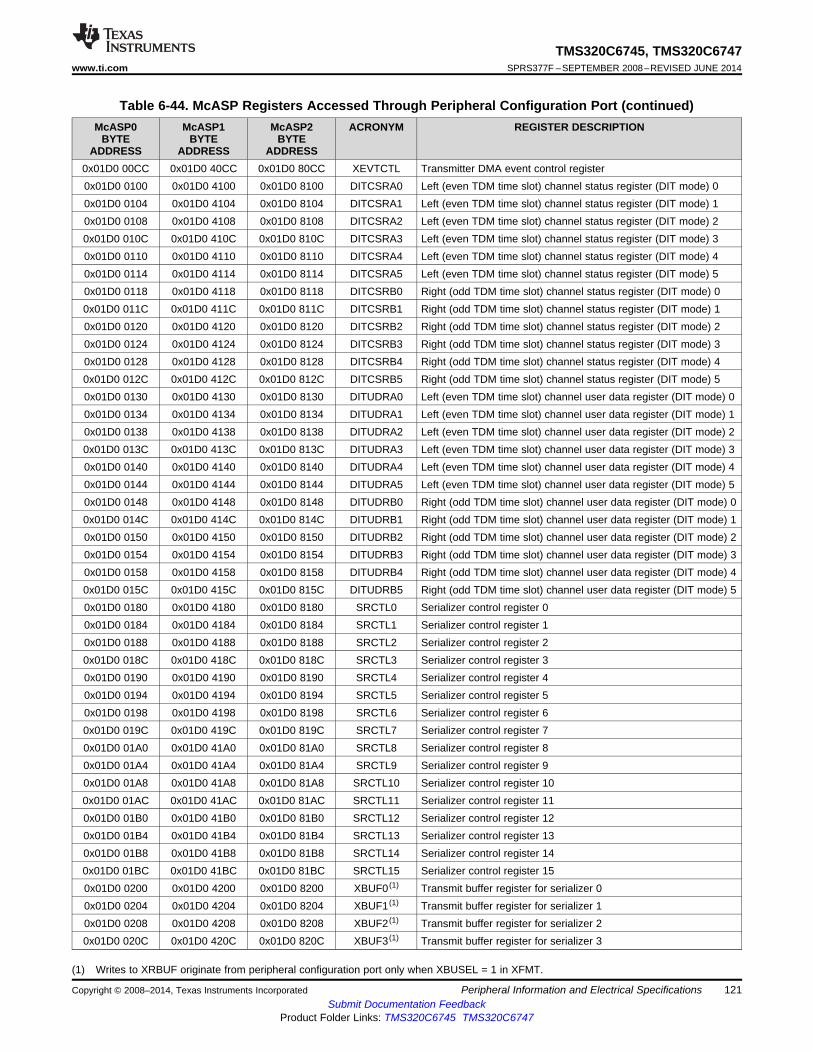
TMS320C6745, TMS320C6747www.ti.com SPRS377F –SEPTEMBER 2008–REVISED JUNE 2014
Table 6-44. McASP Registers Accessed Through Peripheral Configuration Port (continued)McASP0 McASP1 McASP2 ACRONYM REGISTER DESCRIPTION
BYTE BYTE BYTEADDRESS ADDRESS ADDRESS
0x01D0 00CC 0x01D0 40CC 0x01D0 80CC XEVTCTL Transmitter DMA event control register0x01D0 0100 0x01D0 4100 0x01D0 8100 DITCSRA0 Left (even TDM time slot) channel status register (DIT mode) 00x01D0 0104 0x01D0 4104 0x01D0 8104 DITCSRA1 Left (even TDM time slot) channel status register (DIT mode) 10x01D0 0108 0x01D0 4108 0x01D0 8108 DITCSRA2 Left (even TDM time slot) channel status register (DIT mode) 20x01D0 010C 0x01D0 410C 0x01D0 810C DITCSRA3 Left (even TDM time slot) channel status register (DIT mode) 30x01D0 0110 0x01D0 4110 0x01D0 8110 DITCSRA4 Left (even TDM time slot) channel status register (DIT mode) 40x01D0 0114 0x01D0 4114 0x01D0 8114 DITCSRA5 Left (even TDM time slot) channel status register (DIT mode) 50x01D0 0118 0x01D0 4118 0x01D0 8118 DITCSRB0 Right (odd TDM time slot) channel status register (DIT mode) 00x01D0 011C 0x01D0 411C 0x01D0 811C DITCSRB1 Right (odd TDM time slot) channel status register (DIT mode) 10x01D0 0120 0x01D0 4120 0x01D0 8120 DITCSRB2 Right (odd TDM time slot) channel status register (DIT mode) 20x01D0 0124 0x01D0 4124 0x01D0 8124 DITCSRB3 Right (odd TDM time slot) channel status register (DIT mode) 30x01D0 0128 0x01D0 4128 0x01D0 8128 DITCSRB4 Right (odd TDM time slot) channel status register (DIT mode) 40x01D0 012C 0x01D0 412C 0x01D0 812C DITCSRB5 Right (odd TDM time slot) channel status register (DIT mode) 50x01D0 0130 0x01D0 4130 0x01D0 8130 DITUDRA0 Left (even TDM time slot) channel user data register (DIT mode) 00x01D0 0134 0x01D0 4134 0x01D0 8134 DITUDRA1 Left (even TDM time slot) channel user data register (DIT mode) 10x01D0 0138 0x01D0 4138 0x01D0 8138 DITUDRA2 Left (even TDM time slot) channel user data register (DIT mode) 20x01D0 013C 0x01D0 413C 0x01D0 813C DITUDRA3 Left (even TDM time slot) channel user data register (DIT mode) 30x01D0 0140 0x01D0 4140 0x01D0 8140 DITUDRA4 Left (even TDM time slot) channel user data register (DIT mode) 40x01D0 0144 0x01D0 4144 0x01D0 8144 DITUDRA5 Left (even TDM time slot) channel user data register (DIT mode) 50x01D0 0148 0x01D0 4148 0x01D0 8148 DITUDRB0 Right (odd TDM time slot) channel user data register (DIT mode) 00x01D0 014C 0x01D0 414C 0x01D0 814C DITUDRB1 Right (odd TDM time slot) channel user data register (DIT mode) 10x01D0 0150 0x01D0 4150 0x01D0 8150 DITUDRB2 Right (odd TDM time slot) channel user data register (DIT mode) 20x01D0 0154 0x01D0 4154 0x01D0 8154 DITUDRB3 Right (odd TDM time slot) channel user data register (DIT mode) 30x01D0 0158 0x01D0 4158 0x01D0 8158 DITUDRB4 Right (odd TDM time slot) channel user data register (DIT mode) 40x01D0 015C 0x01D0 415C 0x01D0 815C DITUDRB5 Right (odd TDM time slot) channel user data register (DIT mode) 50x01D0 0180 0x01D0 4180 0x01D0 8180 SRCTL0 Serializer control register 00x01D0 0184 0x01D0 4184 0x01D0 8184 SRCTL1 Serializer control register 10x01D0 0188 0x01D0 4188 0x01D0 8188 SRCTL2 Serializer control register 20x01D0 018C 0x01D0 418C 0x01D0 818C SRCTL3 Serializer control register 30x01D0 0190 0x01D0 4190 0x01D0 8190 SRCTL4 Serializer control register 40x01D0 0194 0x01D0 4194 0x01D0 8194 SRCTL5 Serializer control register 50x01D0 0198 0x01D0 4198 0x01D0 8198 SRCTL6 Serializer control register 60x01D0 019C 0x01D0 419C 0x01D0 819C SRCTL7 Serializer control register 70x01D0 01A0 0x01D0 41A0 0x01D0 81A0 SRCTL8 Serializer control register 80x01D0 01A4 0x01D0 41A4 0x01D0 81A4 SRCTL9 Serializer control register 90x01D0 01A8 0x01D0 41A8 0x01D0 81A8 SRCTL10 Serializer control register 100x01D0 01AC 0x01D0 41AC 0x01D0 81AC SRCTL11 Serializer control register 110x01D0 01B0 0x01D0 41B0 0x01D0 81B0 SRCTL12 Serializer control register 120x01D0 01B4 0x01D0 41B4 0x01D0 81B4 SRCTL13 Serializer control register 130x01D0 01B8 0x01D0 41B8 0x01D0 81B8 SRCTL14 Serializer control register 140x01D0 01BC 0x01D0 41BC 0x01D0 81BC SRCTL15 Serializer control register 150x01D0 0200 0x01D0 4200 0x01D0 8200 XBUF0 (1) Transmit buffer register for serializer 00x01D0 0204 0x01D0 4204 0x01D0 8204 XBUF1 (1) Transmit buffer register for serializer 10x01D0 0208 0x01D0 4208 0x01D0 8208 XBUF2 (1) Transmit buffer register for serializer 20x01D0 020C 0x01D0 420C 0x01D0 820C XBUF3 (1) Transmit buffer register for serializer 3
(1) Writes to XRBUF originate from peripheral configuration port only when XBUSEL = 1 in XFMT.
Copyright © 2008–2014, Texas Instruments Incorporated Peripheral Information and Electrical Specifications 121Submit Documentation Feedback
Product Folder Links: TMS320C6745 TMS320C6747
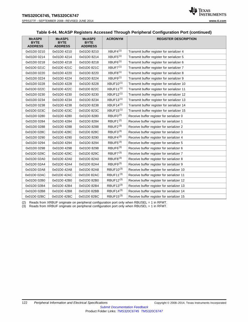
TMS320C6745, TMS320C6747SPRS377F –SEPTEMBER 2008–REVISED JUNE 2014 www.ti.com
Table 6-44. McASP Registers Accessed Through Peripheral Configuration Port (continued)McASP0 McASP1 McASP2 ACRONYM REGISTER DESCRIPTION
BYTE BYTE BYTEADDRESS ADDRESS ADDRESS
0x01D0 0210 0x01D0 4210 0x01D0 8210 XBUF4 (1) Transmit buffer register for serializer 40x01D0 0214 0x01D0 4214 0x01D0 8214 XBUF5 (1) Transmit buffer register for serializer 50x01D0 0218 0x01D0 4218 0x01D0 8218 XBUF6 (1) Transmit buffer register for serializer 60x01D0 021C 0x01D0 421C 0x01D0 821C XBUF7 (1) Transmit buffer register for serializer 70x01D0 0220 0x01D0 4220 0x01D0 8220 XBUF8 (1) Transmit buffer register for serializer 80x01D0 0224 0x01D0 4224 0x01D0 8224 XBUF9 (1) Transmit buffer register for serializer 90x01D0 0228 0x01D0 4228 0x01D0 8228 XBUF10 (1) Transmit buffer register for serializer 100x01D0 022C 0x01D0 422C 0x01D0 822C XBUF11 (1) Transmit buffer register for serializer 110x01D0 0230 0x01D0 4230 0x01D0 8230 XBUF12 (1) Transmit buffer register for serializer 120x01D0 0234 0x01D0 4234 0x01D0 8234 XBUF13 (1) Transmit buffer register for serializer 130x01D0 0238 0x01D0 4238 0x01D0 8238 XBUF14 (1) Transmit buffer register for serializer 140x01D0 023C 0x01D0 423C 0x01D0 823C XBUF15 (1) Transmit buffer register for serializer 150x01D0 0280 0x01D0 4280 0x01D0 8280 RBUF0 (2) Receive buffer register for serializer 00x01D0 0284 0x01D0 4284 0x01D0 8284 RBUF1 (2) Receive buffer register for serializer 10x01D0 0288 0x01D0 4288 0x01D0 8288 RBUF2 (3) Receive buffer register for serializer 20x01D0 028C 0x01D0 428C 0x01D0 828C RBUF3 (3) Receive buffer register for serializer 30x01D0 0290 0x01D0 4290 0x01D0 8290 RBUF4 (3) Receive buffer register for serializer 40x01D0 0294 0x01D0 4294 0x01D0 8294 RBUF5 (3) Receive buffer register for serializer 50x01D0 0298 0x01D0 4298 0x01D0 8298 RBUF6 (3) Receive buffer register for serializer 60x01D0 029C 0x01D0 429C 0x01D0 829C RBUF7 (3) Receive buffer register for serializer 70x01D0 02A0 0x01D0 42A0 0x01D0 82A0 RBUF8 (3) Receive buffer register for serializer 80x01D0 02A4 0x01D0 42A4 0x01D0 82A4 RBUF9 (3) Receive buffer register for serializer 90x01D0 02A8 0x01D0 42A8 0x01D0 82A8 RBUF10 (3) Receive buffer register for serializer 100x01D0 02AC 0x01D0 42AC 0x01D0 82AC RBUF11 (3) Receive buffer register for serializer 110x01D0 02B0 0x01D0 42B0 0x01D0 82B0 RBUF12 (3) Receive buffer register for serializer 120x01D0 02B4 0x01D0 42B4 0x01D0 82B4 RBUF13 (3) Receive buffer register for serializer 130x01D0 02B8 0x01D0 42B8 0x01D0 82BB RBUF14 (3) Receive buffer register for serializer 140x01D0 02BC 0x01D0 42BC 0x01D0 82BC RBUF15 (3) Receive buffer register for serializer 15
(2) Reads from XRBUF originate on peripheral configuration port only when RBUSEL = 1 in RFMT.(3) Reads from XRBUF originate on peripheral configuration port only when RBUSEL = 1 in RFMT.
122 Peripheral Information and Electrical Specifications Copyright © 2008–2014, Texas Instruments IncorporatedSubmit Documentation Feedback
Product Folder Links: TMS320C6745 TMS320C6747

TMS320C6745, TMS320C6747www.ti.com SPRS377F –SEPTEMBER 2008–REVISED JUNE 2014
Table 6-45. McASP Registers Accessed Through DMA Port
Hex Register McASP0 McASP1 McASP2 REGISTER DESCRIPTIONAddress Name BYTE BYTE BYTE
ADDRESS ADDRESS ADDRESSRead RBUF 01D0 2000 01D0 6000 01D0 A000 Receive buffer DMA port address. Cycles through receive serializers,
Accesses skipping over transmit serializers and inactive serializers. Starts at thelowest serializer at the beginning of each time slot. Reads from DMA port
only if RBUSEL = 0 in RFMT.Write XBUF 01D0 2000 01D0 6000 01D0 A000 Transmit buffer DMA port address. Cycles through transmit serializers,
Accesses skipping over receive and inactive serializers. Starts at the lowestserializer at the beginning of each time slot. Writes to DMA port only if
XBUSEL = 0 in XFMT.
Table 6-46. McASP AFIFO Registers Accessed Through Peripheral Configuration Port
McASP0 McASP1 McASP2 ACRONYM REGISTER DESCRIPTIONBYTE ADDRESS BYTE ADDRESS BYTE ADDRESS
0x01D0 1000 0x01D0 5000 0x01D0 9000 AFIFOREV AFIFO revision identification register0x01D0 1010 0x01D0 5010 0x01D0 9010 WFIFOCTL Write FIFO control register0x01D0 1014 0x01D0 5014 0x01D0 9014 WFIFOSTS Write FIFO status register0x01D0 1018 0x01D0 5018 0x01D0 9018 RFIFOCTL Read FIFO control register0x01D0 101C 0x01D0 501C 0x01D0 901C RFIFOSTS Read FIFO status register
Copyright © 2008–2014, Texas Instruments Incorporated Peripheral Information and Electrical Specifications 123Submit Documentation Feedback
Product Folder Links: TMS320C6745 TMS320C6747

TMS320C6745, TMS320C6747SPRS377F –SEPTEMBER 2008–REVISED JUNE 2014 www.ti.com
6.16.2 McASP Electrical Data/Timing
6.16.2.1 Multichannel Audio Serial Port 0 (McASP0) Timing
Table 6-47 and Table 6-48 assume testing over recommended operating conditions (see Figure 6-34 andFigure 6-35).
Table 6-47. McASP0 Timing Requirements (1) (2)
No. PARAMATER MIN MAX UNITCycle time, AHCLKR0 external, AHCLKR0 input 25
1 tc(AHCLKRX) nsCycle time, AHCLKX0 external, AHCLKX0 input 25Pulse duration, AHCLKR0 external, AHCLKR0 input 12.5
2 tw(AHCLKRX) nsPulse duration, AHCLKX0 external, AHCLKX0 input 12.5Cycle time, ACLKR0 external, ACLKR0 input greater of 2P or 25
3 tc(ACLKRX) nsCycle time, ACLKX0 external, ACLKX0 input greater of 2P or 25Pulse duration, ACLKR0 external, ACLKR0 input 12.5
4 tw(ACLKRX) nsPulse duration, ACLKX0 external, ACLKX0 input 12.5Setup time, AFSR0 input to ACLKR0 internal (3) 9.4Setup time, AFSX0 input to ACLKX0 internal 9.4Setup time, AFSR0 input to ACLKR0 external input (3) 2.9
5 tsu(AFSRX-ACLKRX) nsSetup time, AFSX0 input to ACLKX0 external input 2.9Setup time, AFSR0 input to ACLKR0 external output (3) 2.9Setup time, AFSX0 input to ACLKX0 external output 2.9Hold time, AFSR0 input after ACLKR0 internal (3) -1.2Hold time, AFSX0 input after ACLKX0 internal -1.2Hold time, AFSR0 input after ACLKR0 external input (3) 0.9
6 th(ACLKRX-AFSRX) nsHold time, AFSX0 input after ACLKX0 external input 0.9Hold time, AFSR0 input after ACLKR0 external output (3) 0.9Hold time, AFSX0 input after ACLKX0 external output 0.9Setup time, AXR0[n] input to ACLKR0 internal (3) 9.4Setup time, AXR0[n] input to ACLKX0 internal (4) 9.4Setup time, AXR0[n] input to ACLKR0 external input (3) 2.9
7 tsu(AXR-ACLKRX) nsSetup time, AXR0[n] input to ACLKX0 external input (4) 2.9Setup time, AXR0[n] input to ACLKR0 external output (3) 2.9Setup time, AXR0[n] input to ACLKX0 external output (4) 2.9Hold time, AXR0[n] input after ACLKR0 internal (3) -1.3Hold time, AXR0[n] input after ACLKX0 internal (4) -1.3Hold time, AXR0[n] input after ACLKR0 external input (3) 0.5
8 th(ACLKRX-AXR) nsHold time, AXR0[n] input after ACLKX0 external input (4) 0.5Hold time, AXR0[n] input after ACLKR0 external output (3) 0.5Hold time, AXR0[n] input after ACLKX0 external output (4) 0.5
(1) ACLKX0 internal – McASP0 ACLKXCTL.CLKXM = 1, PDIR.ACLKX = 1ACLKX0 external input – McASP0 ACLKXCTL.CLKXM = 0, PDIR.ACLKX = 0ACLKX0 external output – McASP0 ACLKXCTL.CLKXM = 0, PDIR.ACLKX = 1ACLKR0 internal – McASP0 ACLKRCTL.CLKRM = 1, PDIR.ACLKR =1ACLKR0 external input – McASP0 ACLKRCTL.CLKRM = 0, PDIR.ACLKR = 0ACLKR0 external output – McASP0 ACLKRCTL.CLKRM = 0, PDIR.ACLKR = 1
(2) P = SYSCLK2 period(3) McASP0 ACLKXCTL.ASYNC=1: Receiver is clocked by its own ACLKR0(4) McASP0 ACLKXCTL.ASYNC=0: Receiver is clocked by transmitter's ACLKX0
124 Peripheral Information and Electrical Specifications Copyright © 2008–2014, Texas Instruments IncorporatedSubmit Documentation Feedback
Product Folder Links: TMS320C6745 TMS320C6747
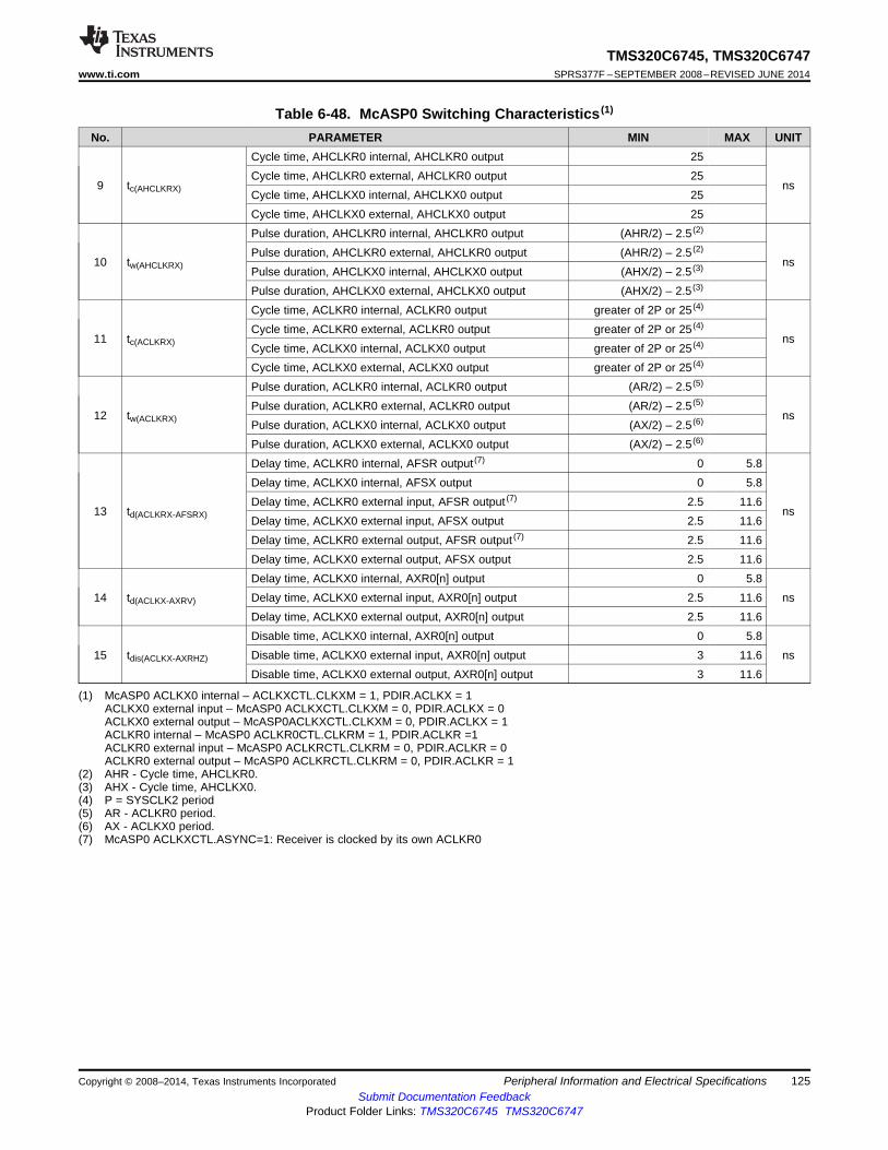
TMS320C6745, TMS320C6747www.ti.com SPRS377F –SEPTEMBER 2008–REVISED JUNE 2014
Table 6-48. McASP0 Switching Characteristics (1)
No. PARAMETER MIN MAX UNITCycle time, AHCLKR0 internal, AHCLKR0 output 25Cycle time, AHCLKR0 external, AHCLKR0 output 25
9 tc(AHCLKRX) nsCycle time, AHCLKX0 internal, AHCLKX0 output 25Cycle time, AHCLKX0 external, AHCLKX0 output 25Pulse duration, AHCLKR0 internal, AHCLKR0 output (AHR/2) – 2.5 (2)
Pulse duration, AHCLKR0 external, AHCLKR0 output (AHR/2) – 2.5 (2)10 tw(AHCLKRX) ns
Pulse duration, AHCLKX0 internal, AHCLKX0 output (AHX/2) – 2.5 (3)
Pulse duration, AHCLKX0 external, AHCLKX0 output (AHX/2) – 2.5 (3)
Cycle time, ACLKR0 internal, ACLKR0 output greater of 2P or 25 (4)
Cycle time, ACLKR0 external, ACLKR0 output greater of 2P or 25 (4)11 tc(ACLKRX) ns
Cycle time, ACLKX0 internal, ACLKX0 output greater of 2P or 25 (4)
Cycle time, ACLKX0 external, ACLKX0 output greater of 2P or 25 (4)
Pulse duration, ACLKR0 internal, ACLKR0 output (AR/2) – 2.5 (5)
Pulse duration, ACLKR0 external, ACLKR0 output (AR/2) – 2.5 (5)12 tw(ACLKRX) ns
Pulse duration, ACLKX0 internal, ACLKX0 output (AX/2) – 2.5 (6)
Pulse duration, ACLKX0 external, ACLKX0 output (AX/2) – 2.5 (6)
Delay time, ACLKR0 internal, AFSR output (7) 0 5.8Delay time, ACLKX0 internal, AFSX output 0 5.8Delay time, ACLKR0 external input, AFSR output (7) 2.5 11.6
13 td(ACLKRX-AFSRX) nsDelay time, ACLKX0 external input, AFSX output 2.5 11.6Delay time, ACLKR0 external output, AFSR output (7) 2.5 11.6Delay time, ACLKX0 external output, AFSX output 2.5 11.6Delay time, ACLKX0 internal, AXR0[n] output 0 5.8
14 td(ACLKX-AXRV) Delay time, ACLKX0 external input, AXR0[n] output 2.5 11.6 nsDelay time, ACLKX0 external output, AXR0[n] output 2.5 11.6Disable time, ACLKX0 internal, AXR0[n] output 0 5.8
15 tdis(ACLKX-AXRHZ) Disable time, ACLKX0 external input, AXR0[n] output 3 11.6 nsDisable time, ACLKX0 external output, AXR0[n] output 3 11.6
(1) McASP0 ACLKX0 internal – ACLKXCTL.CLKXM = 1, PDIR.ACLKX = 1ACLKX0 external input – McASP0 ACLKXCTL.CLKXM = 0, PDIR.ACLKX = 0ACLKX0 external output – McASP0ACLKXCTL.CLKXM = 0, PDIR.ACLKX = 1ACLKR0 internal – McASP0 ACLKR0CTL.CLKRM = 1, PDIR.ACLKR =1ACLKR0 external input – McASP0 ACLKRCTL.CLKRM = 0, PDIR.ACLKR = 0ACLKR0 external output – McASP0 ACLKRCTL.CLKRM = 0, PDIR.ACLKR = 1
(2) AHR - Cycle time, AHCLKR0.(3) AHX - Cycle time, AHCLKX0.(4) P = SYSCLK2 period(5) AR - ACLKR0 period.(6) AX - ACLKX0 period.(7) McASP0 ACLKXCTL.ASYNC=1: Receiver is clocked by its own ACLKR0
Copyright © 2008–2014, Texas Instruments Incorporated Peripheral Information and Electrical Specifications 125Submit Documentation Feedback
Product Folder Links: TMS320C6745 TMS320C6747

TMS320C6745, TMS320C6747SPRS377F –SEPTEMBER 2008–REVISED JUNE 2014 www.ti.com
6.16.2.2 Multichannel Audio Serial Port 1 (McASP1) Timing
Table 6-49 and Table 6-50 assume testing over recommended operating conditions (see Figure 6-34 andFigure 6-35).
Table 6-49. McASP1 Timing Requirements (1) (2)
No. PARAMATER MIN MAX UNITCycle time, AHCLKR1 external, AHCLKR1 input 25
1 tc(AHCLKRX) nsCycle time, AHCLKX1 external, AHCLKX1 input 25Pulse duration, AHCLKR1 external, AHCLKR1 input 12.5
2 tw(AHCLKRX) nsPulse duration, AHCLKX1 external, AHCLKX1 input 12.5Cycle time, ACLKR1 external, ACLKR1 input greater of 2P or 25
3 tc(ACLKRX) nsCycle time, ACLKX1 external, ACLKX1 input greater of 2P or 25Pulse duration, ACLKR1 external, ACLKR1 input 12.5
4 tw(ACLKRX) nsPulse duration, ACLKX1 external, ACLKX1 input 12.5Setup time, AFSR1 input to ACLKR1 internal (3) 10.4Setup time, AFSX1 input to ACLKX1 internal 10.4Setup time, AFSR1 input to ACLKR1 external input (3) 2.6
5 tsu(AFSRX-ACLKRX) nsSetup time, AFSX1 input to ACLKX1 external input 2.6Setup time, AFSR1 input to ACLKR1 external output (3) 2.6Setup time, AFSX1 input to ACLKX1 external output 2.6Hold time, AFSR1 input after ACLKR1 internal (3) -1.9Hold time, AFSX1 input after ACLKX1 internal -1.9Hold time, AFSR1 input after ACLKR1 external input (3) 0.7
6 th(ACLKRX-AFSRX) nsHold time, AFSX1 input after ACLKX1 external input 0.7Hold time, AFSR1 input after ACLKR1 external output (3) 0.7Hold time, AFSX1 input after ACLKX1 external output 0.7Setup time, AXR1[n] input to ACLKR1 internal (3) 10.4Setup time, AXR1[n] input to ACLKX1 internal (4) 10.4Setup time, AXR1[n] input to ACLKR1 external input (3) 2.6
7 tsu(AXR-ACLKRX) nsSetup time, AXR1[n] input to ACLKX1 external input (4) 2.6Setup time, AXR1[n] input to ACLKR1 external output (3) 2.6Setup time, AXR1[n] input to ACLKX1 external output (4) 2.6Hold time, AXR1[n] input after ACLKR1 internal (3) -1.8Hold time, AXR1[n] input after ACLKX1 internal (4) -1.8Hold time, AXR1[n] input after ACLKR1 external input (3) 0.5
8 th(ACLKRX-AXR) nsHold time, AXR1[n] input after ACLKX1 external input (4) 0.5Hold time, AXR1[n] input after ACLKR1 external output (3) 0.5Hold time, AXR1[n] input after ACLKX1 external output (4) 0.5
(1) ACLKX1 internal – McASP1 ACLKXCTL.CLKXM = 1, PDIR.ACLKX = 1ACLKX1 external input – McASP1 ACLKXCTL.CLKXM = 0, PDIR.ACLKX = 0ACLKX1 external output – McASP1 ACLKXCTL.CLKXM = 0, PDIR.ACLKX = 1ACLKR1 internal – McASP1 ACLKRCTL.CLKRM = 1, PDIR.ACLKR =1ACLKR1 external input – McASP1 ACLKRCTL.CLKRM = 0, PDIR.ACLKR = 0ACLKR1 external output – McASP1 ACLKRCTL.CLKRM = 0, PDIR.ACLKR = 1
(2) P = SYSCLK2 period(3) McASP1 ACLKXCTL.ASYNC=1: Receiver is clocked by its own ACLKR1(4) McASP1 ACLKXCTL.ASYNC=0: Receiver is clocked by transmitter's ACLKX1
126 Peripheral Information and Electrical Specifications Copyright © 2008–2014, Texas Instruments IncorporatedSubmit Documentation Feedback
Product Folder Links: TMS320C6745 TMS320C6747
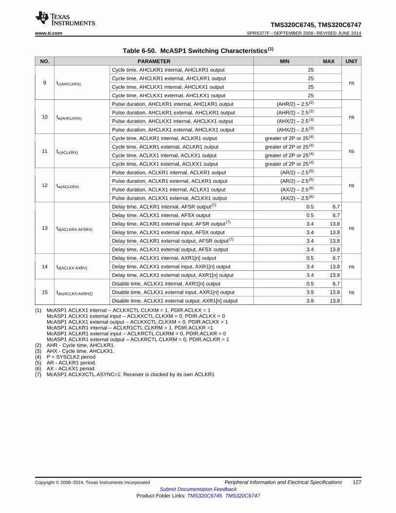
TMS320C6745, TMS320C6747www.ti.com SPRS377F –SEPTEMBER 2008–REVISED JUNE 2014
Table 6-50. McASP1 Switching Characteristics (1)
NO. PARAMETER MIN MAX UNITCycle time, AHCLKR1 internal, AHCLKR1 output 25Cycle time, AHCLKR1 external, AHCLKR1 output 25
9 tc(AHCLKRX) nsCycle time, AHCLKX1 internal, AHCLKX1 output 25Cycle time, AHCLKX1 external, AHCLKX1 output 25Pulse duration, AHCLKR1 internal, AHCLKR1 output (AHR/2) – 2.5 (2)
Pulse duration, AHCLKR1 external, AHCLKR1 output (AHR/2) – 2.5 (2)10 tw(AHCLKRX) ns
Pulse duration, AHCLKX1 internal, AHCLKX1 output (AHX/2) – 2.5 (3)
Pulse duration, AHCLKX1 external, AHCLKX1 output (AHX/2) – 2.5 (3)
Cycle time, ACLKR1 internal, ACLKR1 output greater of 2P or 25 (4)
Cycle time, ACLKR1 external, ACLKR1 output greater of 2P or 25 (4)11 tc(ACLKRX) ns
Cycle time, ACLKX1 internal, ACLKX1 output greater of 2P or 25 (4)
Cycle time, ACLKX1 external, ACLKX1 output greater of 2P or 25 (4)
Pulse duration, ACLKR1 internal, ACLKR1 output (AR/2) – 2.5 (5)
Pulse duration, ACLKR1 external, ACLKR1 output (AR/2) – 2.5 (5)12 tw(ACLKRX) ns
Pulse duration, ACLKX1 internal, ACLKX1 output (AX/2) – 2.5 (6)
Pulse duration, ACLKX1 external, ACLKX1 output (AX/2) – 2.5 (6)
Delay time, ACLKR1 internal, AFSR output (7) 0.5 6.7Delay time, ACLKX1 internal, AFSX output 0.5 6.7Delay time, ACLKR1 external input, AFSR output (7) 3.4 13.8
13 td(ACLKRX-AFSRX) nsDelay time, ACLKX1 external input, AFSX output 3.4 13.8Delay time, ACLKR1 external output, AFSR output (7) 3.4 13.8Delay time, ACLKX1 external output, AFSX output 3.4 13.8Delay time, ACLKX1 internal, AXR1[n] output 0.5 6.7
14 td(ACLKX-AXRV) Delay time, ACLKX1 external input, AXR1[n] output 3.4 13.8 nsDelay time, ACLKX1 external output, AXR1[n] output 3.4 13.8Disable time, ACLKX1 internal, AXR1[n] output 0.5 6.7
15 tdis(ACLKX-AXRHZ) Disable time, ACLKX1 external input, AXR1[n] output 3.9 13.8 nsDisable time, ACLKX1 external output, AXR1[n] output 3.9 13.8
(1) McASP1 ACLKX1 internal – ACLKXCTL.CLKXM = 1, PDIR.ACLKX = 1McASP1 ACLKX1 external input – ACLKXCTL.CLKXM = 0, PDIR.ACLKX = 0McASP1 ACLKX1 external output – ACLKXCTL.CLKXM = 0, PDIR.ACLKX = 1McASP1 ACLKR1 internal – ACLKR1CTL.CLKRM = 1, PDIR.ACLKR =1McASP1 ACLKR1 external input – ACLKRCTL.CLKRM = 0, PDIR.ACLKR = 0McASP1 ACLKR1 external output – ACLKRCTL.CLKRM = 0, PDIR.ACLKR = 1
(2) AHR - Cycle time, AHCLKR1.(3) AHX - Cycle time, AHCLKX1.(4) P = SYSCLK2 period(5) AR - ACLKR1 period.(6) AX - ACLKX1 period.(7) McASP1 ACLKXCTL.ASYNC=1: Receiver is clocked by its own ACLKR1
Copyright © 2008–2014, Texas Instruments Incorporated Peripheral Information and Electrical Specifications 127Submit Documentation Feedback
Product Folder Links: TMS320C6745 TMS320C6747

TMS320C6745, TMS320C6747SPRS377F –SEPTEMBER 2008–REVISED JUNE 2014 www.ti.com
6.16.2.3 Multichannel Audio Serial Port 2 (McASP2) Timing
Table 6-51 and Table 6-52 assume testing over recommended operating conditions (see Figure 6-34 andFigure 6-35).
Table 6-51. McASP2 Timing Requirements (1) (2)
NO. MIN MAX UNITCycle time, AHCLKR2 external, AHCLKR2 input 15
1 tc(AHCLKRX) nsCycle time, AHCLKX2 external, AHCLKX2 input 15Pulse duration, AHCLKR2 external, AHCLKR2 input 7.5
2 tw(AHCLKRX) nsPulse duration, AHCLKX2 external, AHCLKX2 input 7.5Cycle time, ACLKR2 external, ACLKR2 input greater of 2P or 15
3 tc(ACLKRX) nsCycle time, ACLKX2 external, ACLKX2 input greater of 2P or 15Pulse duration, ACLKR2 external, ACLKR2 input 7.5
4 tw(ACLKRX) nsPulse duration, ACLKX2 external, ACLKX2 input 7.5Setup time, AFSR2 input to ACLKR2 internal (3) 10Setup time, AFSX2 input to ACLKX2 internal 10Setup time, AFSR2 input to ACLKR2 external input (3) 1.6
5 tsu(AFSRX-ACLKRX) nsSetup time, AFSX2 input to ACLKX2 external input 1.6Setup time, AFSR2 input to ACLKR2 external output (3) 1.6Setup time, AFSX2 input to ACLKX2 external output 1.6Hold time, AFSR2 input after ACLKR2 internal (3) -1.7Hold time, AFSX2 input after ACLKX2 internal -1.7Hold time, AFSR2 input after ACLKR2 external input (3) 1.3
6 th(ACLKRX-AFSRX) nsHold time, AFSX2 input after ACLKX2 external input 1.3Hold time, AFSR2 input after ACLKR2 external output (3) 1.3Hold time, AFSX2 input after ACLKX2 external output 1.3Setup time, AXR2[n] input to ACLKR2 internal (3) 10Setup time, AXR2[n] input to ACLKX2 internal (4) 10Setup time, AXR2[n] input to ACLKR2 external input (3) 1.6
7 tsu(AXR-ACLKRX) nsSetup time, AXR2[n] input to ACLKX2 external input (4) 1.6Setup time, AXR2[n] input to ACLKR2 external output (3) 1.6Setup time, AXR2[n] input to ACLKX2 external output (4) 1.6Hold time, AXR2[n] input after ACLKR2 internal (3) -1.7Hold time, AXR2[n] input after ACLKX2 internal (4) -1.7Hold time, AXR2[n] input after ACLKR2 external input (3) 1.3
8 th(ACLKRX-AXR) nsHold time, AXR2[n] input after ACLKX2 external input (4) 1.3Hold time, AXR2[n] input after ACLKR2 external output (3) 1.3Hold time, AXR2[n] input after ACLKX2 external output (4) 1.3
(1) ACLKX2 internal – McASP2 ACLKXCTL.CLKXM = 1, PDIR.ACLKX = 1ACLKX2 external input – McASP2 ACLKXCTL.CLKXM = 0, PDIR.ACLKX = 0ACLKX2 external output – McASP2 ACLKXCTL.CLKXM = 0, PDIR.ACLKX = 1ACLKR2 internal – McASP2 ACLKRCTL.CLKRM = 1, PDIR.ACLKR =1ACLKR2 external input – McASP2 ACLKRCTL.CLKRM = 0, PDIR.ACLKR = 0ACLKR2 external output – McASP2 ACLKRCTL.CLKRM = 0, PDIR.ACLKR = 1
(2) P = SYSCLK2 period(3) McASP2 ACLKXCTL.ASYNC=1: Receiver is clocked by its own ACLKR2(4) McASP2 ACLKXCTL.ASYNC=0: Receiver is clocked by transmitter's ACLKX2
128 Peripheral Information and Electrical Specifications Copyright © 2008–2014, Texas Instruments IncorporatedSubmit Documentation Feedback
Product Folder Links: TMS320C6745 TMS320C6747

TMS320C6745, TMS320C6747www.ti.com SPRS377F –SEPTEMBER 2008–REVISED JUNE 2014
Table 6-52. McASP2 Switching Characteristics (1)
NO. PARAMETER MIN MAX UNITCycle time, AHCLKR2 internal, AHCLKR2 output 15Cycle time, AHCLKR2 external, AHCLKR2 output 15
9 tc(AHCLKRX) nsCycle time, AHCLKX2 internal, AHCLKX2 output 15Cycle time, AHCLKX2 external, AHCLKX2 output 15Pulse duration, AHCLKR2 internal, AHCLKR2 output (AHR/2) – 2.5 (2)
Pulse duration, AHCLKR2 external, AHCLKR2 output (AHR/2) – 2.5 (2)10 tw(AHCLKRX) ns
Pulse duration, AHCLKX2 internal, AHCLKX2 output (AHX/2) – 2.5 (3)
Pulse duration, AHCLKX2 external, AHCLKX2 output (AHX/2) – 2.5 (3)
Cycle time, ACLKR2 internal, ACLKR2 output greater of 2P or 15 (4)
Cycle time, ACLKR2 external, ACLKR2 output greater of 2P or 15 (4)11 tc(ACLKRX) ns
Cycle time, ACLKX2 internal, ACLKX2 output greater of 2P or 15 (4)
Cycle time, ACLKX2 external, ACLKX2 output greater of 2P or 15 (4)
Pulse duration, ACLKR2 internal, ACLKR2 output (AR/2) – 2.5 (5)
Pulse duration, ACLKR2 external, ACLKR2 output (AR/2) – 2.5 (5)12 tw(ACLKRX) ns
Pulse duration, ACLKX2 internal, ACLKX2 output (AX/2) – 2.5 (6)
Pulse duration, ACLKX2 external, ACLKX2 output (AX/2) – 2.5 (6)
Delay time, ACLKR2 internal, AFSR output (7) -1.4 2.8Delay time, ACLKX2 internal, AFSX output -1.4 2.8Delay time, ACLKR2 external input, AFSR output (7) 2.1 10
13 td(ACLKRX-AFSRX) nsDelay time, ACLKX2 external input, AFSX output 2.1 10Delay time, ACLKR2 external output, AFSR output (7) 2.1 10Delay time, ACLKX2 external output, AFSX output 2.1 10Delay time, ACLKX2 internal, AXR2[n] output -1.4 2.8
14 td(ACLKX-AXRV) Delay time, ACLKX2 external input, AXR2[n] output 2.1 10 nsDelay time, ACLKX2 external output, AXR2[n] output 2.1 10Disable time, ACLKX2 internal, AXR2[n] output -1.4 2.8
15 tdis(ACLKX-AXRHZ) Disable time, ACLKX2 external input, AXR2[n] output 2.9 10 nsDisable time, ACLKX2 external output, AXR2[n] output 2.9 10
(1) McASP2 ACLKX2 internal – ACLKXCTL.CLKXM = 1, PDIR.ACLKX = 1McASP2 ACLKX2 external input – ACLKXCTL.CLKXM = 0, PDIR.ACLKX = 0McASP2 ACLKX2 external output – ACLKXCTL.CLKXM = 0, PDIR.ACLKX = 1McASP2 ACLKR2 internal – ACLKR2CTL.CLKRM = 1, PDIR.ACLKR =1McASP2 ACLKR2 external input – ACLKRCTL.CLKRM = 0, PDIR.ACLKR = 0McASP2 ACLKR2 external output – ACLKRCTL.CLKRM = 0, PDIR.ACLKR = 1
(2) AHR - Cycle time, AHCLKR2.(3) AHX - Cycle time, AHCLKX2.(4) P = SYSCLK2 period(5) AR - ACLKR2 period.(6) AX - ACLKX2 period.(7) McASP2 ACLKXCTL.ASYNC=1: Receiver is clocked by its own ACLKR2
Copyright © 2008–2014, Texas Instruments Incorporated Peripheral Information and Electrical Specifications 129Submit Documentation Feedback
Product Folder Links: TMS320C6745 TMS320C6747

8
7
4
43
2
21
A0 A1 B0 B1A30 A31 B30 B31 C0 C1 C2 C3 C31
AHCLKR/X (Falling Edge Polarity)
AHCLKR/X (Rising Edge Polarity)
AFSR/X (Bit Width, 0 Bit Delay)
AFSR/X (Bit Width, 1 Bit Delay)
AFSR/X (Bit Width, 2 Bit Delay)
AFSR/X (Slot Width, 0 Bit Delay)
AFSR/X (Slot Width, 1 Bit Delay)
AFSR/X (Slot Width, 2 Bit Delay)
AXR[n] (Data In/Receive)
6
5
ACLKR/X (CLKRP = CLKXP = 0)(A)
ACLKR/X (CLKRP = CLKXP = 1)(B)
TMS320C6745, TMS320C6747SPRS377F –SEPTEMBER 2008–REVISED JUNE 2014 www.ti.com
A. For CLKRP = CLKXP = 0, the McASP transmitter is configured for rising edge (to shift data out) and the McASPreceiver is configured for falling edge (to shift data in).
B. For CLKRP = CLKXP = 1, the McASP transmitter is configured for falling edge (to shift data out) and the McASPreceiver is configured for rising edge (to shift data in).
Figure 6-34. McASP Input Timings
130 Peripheral Information and Electrical Specifications Copyright © 2008–2014, Texas Instruments IncorporatedSubmit Documentation Feedback
Product Folder Links: TMS320C6745 TMS320C6747

1514
131313
1313
1313
12
1211
1010
9
A0 A1 B0 B1A30 A31 B30 B31 C0 C1 C2 C3 C31
AHCLKR/X (Falling Edge Polarity)
AHCLKR/X (Rising Edge Polarity)
AFSR/X (Bit Width, 0 Bit Delay)
AFSR/X (Bit Width, 1 Bit Delay)
AFSR/X (Bit Width, 2 Bit Delay)
AFSR/X (Slot Width, 0 Bit Delay)
AFSR/X (Slot Width, 1 Bit Delay)
AFSR/X (Slot Width, 2 Bit Delay)
AXR[n] (Data Out/Transmit)
ACLKR/X (CLKRP = CLKXP = 0)(B)
ACLKR/X (CLKRP = CLKXP = 1)(A)
TMS320C6745, TMS320C6747www.ti.com SPRS377F –SEPTEMBER 2008–REVISED JUNE 2014
A. For CLKRP = CLKXP = 1, the McASP transmitter is configured for falling edge (to shift data out) and the McASPreceiver is configured for rising edge (to shift data in).
B. For CLKRP = CLKXP = 0, the McASP transmitter is configured for rising edge (to shift data out) and the McASPreceiver is configured for falling edge (to shift data in).
Figure 6-35. McASP Output Timings
Copyright © 2008–2014, Texas Instruments Incorporated Peripheral Information and Electrical Specifications 131Submit Documentation Feedback
Product Folder Links: TMS320C6745 TMS320C6747

Peripheral
Configuration Bus
Interrupt and
DMA Requests
16-Bit Shift Register
16-Bit Buffer
GPIOControl(all pins)
StateMachine
ClockControl
SPIx_SIMO
SPIx_SOMI
SPIx_ENA
SPIx_SCS
SPIx_CLK
TMS320C6745, TMS320C6747SPRS377F –SEPTEMBER 2008–REVISED JUNE 2014 www.ti.com
6.17 Serial Peripheral Interface Ports (SPI0, SPI1)Figure 6-36 is a block diagram of the SPI module, which is a simple shift register and buffer plus controllogic. Data is written to the shift register before transmission occurs and is read from the buffer at the endof transmission. The SPI can operate either as a master, in which case, it initiates a transfer and drivesthe SPIx_CLK pin, or as a slave. Four clock phase and polarity options are supported as well as manydata formatting options.
Figure 6-36. Block Diagram of SPI Module
The SPI supports 3-, 4-, and 5-pin operation with three basic pins (SPIx_CLK, SPIx_SIMO, andSPIx_SOMI) and two optional pins (SPIx_SCS, SPIx_ENA).
The optional SPIx_SCS (Slave Chip Select) pin is most useful to enable in slave mode when there areother slave devices on the same SPI port. The C6745/6747 will only shift data and drive the SPIx_SOMIpin when SPIx_SCS is held low.
In slave mode, SPIx_ENA is an optional output. The SPIx_ENA output provides the status of the internaltransmit buffer (SPIDAT0/1 registers). In four-pin mode with the enable option, SPIx_ENA is asserted onlywhen the transmit buffer is full, indicating that the slave is ready to begin another transfer. In five-pinmode, the SPIx_ENA is additionally qualified by SPIx_SCS being asserted. This allows a singlehandshake line to be shared by multiple slaves on the same SPI bus.
In master mode, the SPIx_ENA pin is an optional input and the master can be configured to delay the startof the next transfer until the slave asserts SPIx_ENA. The addition of this handshake signal simplifies SPIcommunications and, on average, increases SPI bus throughput since the master does not need to delayeach transfer long enough to allow for the worst-case latency of the slave device. Instead, each transfercan begin as soon as both the master and slave have actually serviced the previous SPI transfer.
Although the SPI module supports two interrupt outputs, SPIx_INT1 is the only interrupt connected on thisdevice.
132 Peripheral Information and Electrical Specifications Copyright © 2008–2014, Texas Instruments IncorporatedSubmit Documentation Feedback
Product Folder Links: TMS320C6745 TMS320C6747
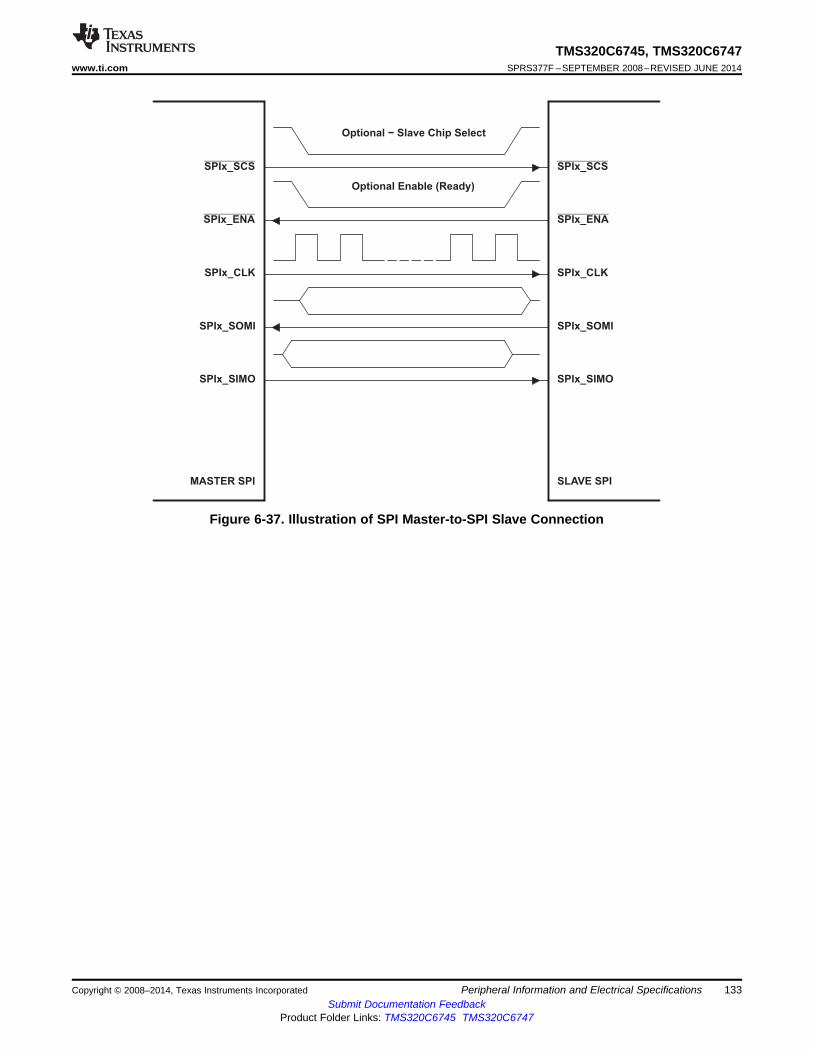
Optional − Slave Chip Select
Optional Enable (Ready)
SLAVE SPIMASTER SPI
SPIx_SIMOSPIx_SIMO
SPIx_SOMI SPIx_SOMI
SPIx_CLK SPIx_CLK
SPIx_ENA SPIx_ENA
SPIx_SCS SPIx_SCS
TMS320C6745, TMS320C6747www.ti.com SPRS377F –SEPTEMBER 2008–REVISED JUNE 2014
Figure 6-37. Illustration of SPI Master-to-SPI Slave Connection
Copyright © 2008–2014, Texas Instruments Incorporated Peripheral Information and Electrical Specifications 133Submit Documentation Feedback
Product Folder Links: TMS320C6745 TMS320C6747

TMS320C6745, TMS320C6747SPRS377F –SEPTEMBER 2008–REVISED JUNE 2014 www.ti.com
6.17.1 SPI Peripheral Registers Description(s)Table 6-53 is a list of the SPI registers.
Table 6-53. SPIx Configuration Registers
SPI0 SPI1 ACRONYM REGISTER DESCRIPTIONBYTE ADDRESS BYTE ADDRESS0x01C4 1000 0x01E1 2000 SPIGCR0 Global Control Register 00x01C4 1004 0x01E1 2004 SPIGCR1 Global Control Register 10x01C4 1008 0x01E1 2008 SPIINT0 Interrupt Register0x01C4 100C 0x01E1 200C SPILVL Interrupt Level Register0x01C4 1010 0x01E1 2010 SPIFLG Flag Register0x01C4 1014 0x01E1 2014 SPIPC0 Pin Control Register 0 (Pin Function)0x01C4 1018 0x01E1 2018 SPIPC1 Pin Control Register 1 (Pin Direction)0x01C4 101C 0x01E1 201C SPIPC2 Pin Control Register 2 (Pin Data In)0x01C4 1020 0x01E1 2020 SPIPC3 Pin Control Register 3 (Pin Data Out)0x01C4 1024 0x01E1 2024 SPIPC4 Pin Control Register 4 (Pin Data Set)0x01C4 1028 0x01E1 2028 SPIPC5 Pin Control Register 5 (Pin Data Clear)0x01C4 102C 0x01E1 202C Reserved Reserved - Do not write to this register0x01C4 1030 0x01E1 2030 Reserved Reserved - Do not write to this register0x01C4 1034 0x01E1 2034 Reserved Reserved - Do not write to this register0x01C4 1038 0x01E1 2038 SPIDAT0 Shift Register 0 (without format select)0x01C4 103C 0x01E1 203C SPIDAT1 Shift Register 1 (with format select)0x01C4 1040 0x01E1 2040 SPIBUF Buffer Register0x01C4 1044 0x01E1 2044 SPIEMU Emulation Register0x01C4 1048 0x01E1 2048 SPIDELAY Delay Register0x01C4 104C 0x01E1 204C SPIDEF Default Chip Select Register0x01C4 1050 0x01E1 2050 SPIFMT0 Format Register 00x01C4 1054 0x01E1 2054 SPIFMT1 Format Register 10x01C4 1058 0x01E1 2058 SPIFMT2 Format Register 20x01C4 105C 0x01E1 205C SPIFMT3 Format Register 30x01C4 1060 0x01E1 2060 Reserved Reserved - Do not write to this register0x01C4 1064 0x01E1 2064 INTVEC1 Interrupt Vector for SPI INT1
134 Peripheral Information and Electrical Specifications Copyright © 2008–2014, Texas Instruments IncorporatedSubmit Documentation Feedback
Product Folder Links: TMS320C6745 TMS320C6747
TMS320C6745, TMS320C6747www.ti.com SPRS377F –SEPTEMBER 2008–REVISED JUNE 2014
6.17.2 SPI Electrical Data/Timing
6.17.2.1 Serial Peripheral Interface (SPI) Timing
Table 6-54 through Table 6-69 assume testing over recommended operating conditions (see Figure 6-38through Figure 6-41).
Table 6-54. General Timing Requirements for SPI0 Master Modes (1)
No. PARAMETER MIN MAX UNIT1 tc(SPC)M Cycle Time, SPI0_CLK, All Master Modes greater of 3P or 20 256P ns2 tw(SPCH)M Pulse Width High, SPI0_CLK, All Master Modes 0.5tc(SPC)M - 1 ns3 tw(SPCL)M Pulse Width Low, SPI0_CLK, All Master Modes 0.5tc(SPC)M - 1 ns
Polarity = 0, Phase = 0, 5to SPI0_CLK risingPolarity = 0, Phase = 1, - 0.5tc(SPC)M + 5Delay, initial data bit valid on to SPI0_CLK rising
4 td(SIMO_SPC)M SPI0_SIMO after initial edge nsPolarity = 1, Phase = 0,on SPI0_CLK (2) 5to SPI0_CLK fallingPolarity = 1, Phase = 1, - 0.5tc(SPC)M + 5to SPI0_CLK fallingPolarity = 0, Phase = 0, 5from SPI0_CLK risingPolarity = 0, Phase = 1, 5Delay, subsequent bits valid from SPI0_CLK falling
5 td(SPC_SIMO)M on SPI0_SIMO after transmit nsPolarity = 1, Phase = 0,edge of SPI0_CLK 5from SPI0_CLK fallingPolarity = 1, Phase = 1, 5from SPI0_CLK risingPolarity = 0, Phase = 0, 0.5tc(SPC)M -3from SPI0_CLK fallingPolarity = 0, Phase = 1, 0.5tc(SPC)M -3Output hold time, SPI0_SIMO from SPI0_CLK rising
6 toh(SPC_SIMO)M valid after nsPolarity = 1, Phase = 0,receive edge of SPI0_CLK 0.5tc(SPC)M -3from SPI0_CLK risingPolarity = 1, Phase = 1, 0.5tc(SPC)M -3from SPI0_CLK fallingPolarity = 0, Phase = 0, 0to SPI0_CLK fallingPolarity = 0, Phase = 1, 0Input Setup Time, SPI0_SOMI to SPI0_CLK rising
7 tsu(SOMI_SPC)M valid before nsPolarity = 1, Phase = 0,receive edge of SPI0_CLK 0to SPI0_CLK risingPolarity = 1, Phase = 1, 0to SPI0_CLK fallingPolarity = 0, Phase = 0, 5from SPI0_CLK fallingPolarity = 0, Phase = 1, 5Input Hold Time, SPI0_SOMI from SPI0_CLK rising
8 tih(SPC_SOMI)M valid after nsPolarity = 1, Phase = 0,receive edge of SPI0_CLK 5from SPI0_CLK risingPolarity = 1, Phase = 1, 5from SPI0_CLK falling
(1) P = SYSCLK2 period(2) First bit may be MSB or LSB depending upon SPI configuration. MO(0) refers to first bit and MO(n) refers to last bit output on
SPI0_SIMO. MI(0) refers to the first bit input and MI(n) refers to the last bit input on SPI0_SOMI.
Copyright © 2008–2014, Texas Instruments Incorporated Peripheral Information and Electrical Specifications 135Submit Documentation Feedback
Product Folder Links: TMS320C6745 TMS320C6747

TMS320C6745, TMS320C6747SPRS377F –SEPTEMBER 2008–REVISED JUNE 2014 www.ti.com
Table 6-55. General Timing Requirements for SPI0 Slave Modes (1)
No. PARAMETER MIN MAX UNIT9 tc(SPC)S Cycle Time, SPI0_CLK, All Slave Modes greater of 3P or 40 ns10 tw(SPCH)S Pulse Width High, SPI0_CLK, All Slave Modes 18 ns11 tw(SPCL)S Pulse Width Low, SPI0_CLK, All Slave Modes 18 ns
Polarity = 0, Phase = 0, 2Pto SPI0_CLK risingPolarity = 0, Phase = 1, 2PSetup time, transmit data written to to SPI0_CLK rising
12 tsu(SOMI_SPC)S SPI before initial clock edge from nsPolarity = 1, Phase = 0,master. (2) (3) 2Pto SPI0_CLK fallingPolarity = 1, Phase = 1, 2Pto SPI0_CLK fallingPolarity = 0, Phase = 0, 18.5from SPI0_CLK risingPolarity = 0, Phase = 1, 18.5Delay, subsequent bits valid on from SPI0_CLK falling
13 td(SPC_SOMI)S SPI0_SOMI after transmit edge of nsPolarity = 1, Phase = 0,SPI0_CLK 18.5from SPI0_CLK fallingPolarity = 1, Phase = 1, 18.5from SPI0_CLK risingPolarity = 0, Phase = 0, 0.5tc(SPC)S -3from SPI0_CLK fallingPolarity = 0, Phase = 1, 0.5tc(SPC)S -3Output hold time, SPI0_SOMI valid from SPI0_CLK rising
14 toh(SPC_SOMI)S after nsPolarity = 1, Phase = 0,receive edge of SPI0_CLK 0.5tc(SPC)S -3from SPI0_CLK risingPolarity = 1, Phase = 1, 0.5tc(SPC)S -3from SPI0_CLK fallingPolarity = 0, Phase = 0, 0to SPI0_CLK fallingPolarity = 0, Phase = 1, 0Input Setup Time, SPI0_SIMO valid to SPI0_CLK rising
15 tsu(SIMO_SPC)S before nsPolarity = 1, Phase = 0,receive edge of SPI0_CLK 0to SPI0_CLK risingPolarity = 1, Phase = 1, 0to SPI0_CLK fallingPolarity = 0, Phase = 0, 5from SPI0_CLK fallingPolarity = 0, Phase = 1, 5Input Hold Time, SPI0_SIMO valid from SPI0_CLK rising
16 tih(SPC_SIMO)S after nsPolarity = 1, Phase = 0,receive edge of SPI0_CLK 5from SPI0_CLK risingPolarity = 1, Phase = 1, 5from SPI0_CLK falling
(1) P = SYSCLK2 period(2) First bit may be MSB or LSB depending upon SPI configuration. SO(0) refers to first bit and SO(n) refers to last bit output on
SPI0_SOMI. SI(0) refers to the first bit input and SI(n) refers to the last bit input on SPI0_SIMO.(3) Measured from the termination of the write of new data to the SPI module, In analyzing throughput requirements, additional internal bus
cycles must be accounted for to allow data to be written to the SPI module by the DSP CPU.
136 Peripheral Information and Electrical Specifications Copyright © 2008–2014, Texas Instruments IncorporatedSubmit Documentation Feedback
Product Folder Links: TMS320C6745 TMS320C6747

TMS320C6745, TMS320C6747www.ti.com SPRS377F –SEPTEMBER 2008–REVISED JUNE 2014
Table 6-56. Additional (1) SPI0 Master Timings, 4-Pin Enable Option (2) (3)
No. PARAMATER MIN MAX UNITPolarity = 0, Phase = 0, 3P + 3.6to SPI0_CLK risingPolarity = 0, Phase = 1, 0.5tc(SPC)M + 3P + 3.6Delay from slave assertion of to SPI0_CLK rising
17 td(ENA_SPC)M SPI0_ENA active to first SPI0_CLK nsPolarity = 1, Phase = 0,from master. (4) 3P + 3.6to SPI0_CLK fallingPolarity = 1, Phase = 1, 0.5tc(SPC)M + 3P + 3.6to SPI0_CLK fallingPolarity = 0, Phase = 0, 0.5tc(SPC)M + P + 5from SPI0_CLK fallingPolarity = 0, Phase = 1,Max delay for slave to deassert P + 5from SPI0_CLK fallingSPI0_ENA after final SPI0_CLK edge18 td(SPC_ENA)M nsto ensure master does not begin the Polarity = 1, Phase = 0, 0.5tc(SPC)M + P + 5next transfer. (5) from SPI0_CLK risingPolarity = 1, Phase = 1, P + 5from SPI0_CLK rising
(1) These parameters are in addition to the general timings for SPI master modes (Table 6-54).(2) P = SYSCLK2 period(3) Figure shows only Polarity = 0, Phase = 0 as an example. Table gives parameters for all four master clocking modes.(4) In the case where the master SPI is ready with new data before SPI0_ENA assertion.(5) In the case where the master SPI is ready with new data before SPI0_EN A deassertion.
Table 6-57. Additional (1) SPI0 Master Timings, 4-Pin Chip Select Option (2) (3)
No. PARAMATER MIN MAX UNITPolarity = 0, Phase = 0, 2P - 5to SPI0_CLK risingPolarity = 0, Phase = 1, 0.5tc(SPC)M + 2P - 5to SPI0_CLK risingDelay from SPI0_SCS active to first19 td(SCS_SPC)M nsSPI0_CLK (4) (5) Polarity = 1, Phase = 0, 2P - 5to SPI0_CLK fallingPolarity = 1, Phase = 1, 0.5tc(SPC)M + 2P - 5to SPI0_CLK fallingPolarity = 0, Phase = 0, 0.5tc(SPC)M + P - 3from SPI0_CLK fallingPolarity = 0, Phase = 1, P - 3from SPI0_CLK fallingDelay from final SPI0_CLK edge to20 td(SPC_SCS)M nsmaster deasserting SPI0_SCS (6) (7) Polarity = 1, Phase = 0, 0.5tc(SPC)M + P - 3from SPI0_CLK risingPolarity = 1, Phase = 1, P - 3from SPI0_CLK rising
(1) These parameters are in addition to the general timings for SPI master modes (Table 6-54).(2) P = SYSCLK2 period(3) Figure shows only Polarity = 0, Phase = 0 as an example. Table gives parameters for all four master clocking modes.(4) In the case where the master SPI is ready with new data before SPI0_SCS assertion.(5) This delay can be increased under software control by the register bit field SPIDELAY.C2TDELAY[4:0].(6) Except for modes when SPIDAT1.CSHOLD is enabled and there is additional data to transmit. In this case, SPI0_SCS will remain
asserted.(7) This delay can be increased under software control by the register bit field SPIDELAY.T2CDELAY[4:0].
Copyright © 2008–2014, Texas Instruments Incorporated Peripheral Information and Electrical Specifications 137Submit Documentation Feedback
Product Folder Links: TMS320C6745 TMS320C6747
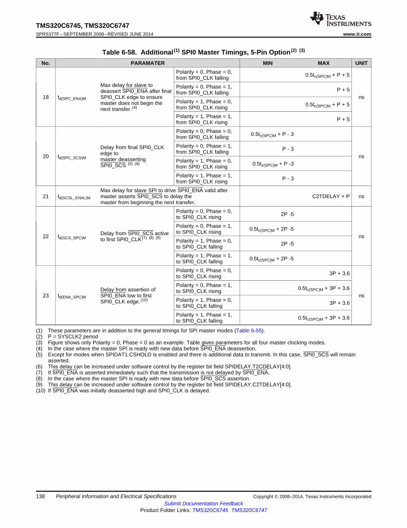
TMS320C6745, TMS320C6747SPRS377F –SEPTEMBER 2008–REVISED JUNE 2014 www.ti.com
Table 6-58. Additional (1) SPI0 Master Timings, 5-Pin Option (2) (3)
No. PARAMATER MIN MAX UNITPolarity = 0, Phase = 0, 0.5tc(SPC)M + P + 5from SPI0_CLK falling
Max delay for slave to Polarity = 0, Phase = 1, P + 5deassert SPI0_ENA after final from SPI0_CLK falling18 td(SPC_ENA)M SPI0_CLK edge to ensure ns
Polarity = 1, Phase = 0,master does not begin the 0.5tc(SPC)M + P + 5from SPI0_CLK risingnext transfer. (4)
Polarity = 1, Phase = 1, P + 5from SPI0_CLK risingPolarity = 0, Phase = 0, 0.5tc(SPC)M + P - 3from SPI0_CLK fallingPolarity = 0, Phase = 1,Delay from final SPI0_CLK P - 3from SPI0_CLK fallingedge to20 td(SPC_SCS)M nsmaster deasserting Polarity = 1, Phase = 0, 0.5tc(SPC)M + P -3SPI0_SCS (5) (6) from SPI0_CLK risingPolarity = 1, Phase = 1, P - 3from SPI0_CLK rising
Max delay for slave SPI to drive SPI0_ENA valid after21 td(SCSL_ENAL)M master asserts SPI0_SCS to delay the C2TDELAY + P ns
master from beginning the next transfer,Polarity = 0, Phase = 0, 2P -5to SPI0_CLK risingPolarity = 0, Phase = 1, 0.5tc(SPC)M + 2P -5to SPI0_CLK risingDelay from SPI0_SCS active22 td(SCS_SPC)M nsto first SPI0_CLK (7) (8) (9) Polarity = 1, Phase = 0, 2P -5to SPI0_CLK fallingPolarity = 1, Phase = 1, 0.5tc(SPC)M + 2P -5to SPI0_CLK fallingPolarity = 0, Phase = 0, 3P + 3.6to SPI0_CLK risingPolarity = 0, Phase = 1, 0.5tc(SPC)M + 3P + 3.6Delay from assertion of to SPI0_CLK rising
23 td(ENA_SPC)M SPI0_ENA low to first nsPolarity = 1, Phase = 0,SPI0_CLK edge. (10) 3P + 3.6to SPI0_CLK fallingPolarity = 1, Phase = 1, 0.5tc(SPC)M + 3P + 3.6to SPI0_CLK falling
(1) These parameters are in addition to the general timings for SPI master modes (Table 6-55).(2) P = SYSCLK2 period(3) Figure shows only Polarity = 0, Phase = 0 as an example. Table gives parameters for all four master clocking modes.(4) In the case where the master SPI is ready with new data before SPI0_ENA deassertion.(5) Except for modes when SPIDAT1.CSHOLD is enabled and there is additional data to transmit. In this case, SPI0_SCS will remain
asserted.(6) This delay can be increased under software control by the register bit field SPIDELAY.T2CDELAY[4:0].(7) If SPI0_ENA is asserted immediately such that the transmission is not delayed by SPI0_ENA.(8) In the case where the master SPI is ready with new data before SPI0_SCS assertion.(9) This delay can be increased under software control by the register bit field SPIDELAY.C2TDELAY[4:0].(10) If SPI0_ENA was initially deasserted high and SPI0_CLK is delayed.
138 Peripheral Information and Electrical Specifications Copyright © 2008–2014, Texas Instruments IncorporatedSubmit Documentation Feedback
Product Folder Links: TMS320C6745 TMS320C6747

TMS320C6745, TMS320C6747www.ti.com SPRS377F –SEPTEMBER 2008–REVISED JUNE 2014
Table 6-59. Additional (1) SPI0 Slave Timings, 4-Pin Enable Option (2) (3)
No. PARAMATER MIN MAX UNITPolarity = 0, Phase = 0, 1.5 P -3 2.5 P + 18.5from SPI0_CLK fallingPolarity = 0, Phase = 1,Delay from final – 0.5tc(SPC)M + 1.5 P -3 – 0.5tc(SPC)M + 2.5 P + 18.5from SPI0_CLK fallingSPI0_CLK edge to24 td(SPC_ENAH)S nsslave deasserting Polarity = 1, Phase = 0, 1.5 P -3 2.5 P + 18.5SPI0_ENA. from SPI0_CLK risingPolarity = 1, Phase = 1, – 0.5tc(SPC)M + 1.5 P -3 – 0.5tc(SPC)M + 2.5 P + 18.5from SPI0_CLK rising
(1) These parameters are in addition to the general timings for SPI slave modes (Table 6-55).(2) P = SYSCLK2 period(3) Figure shows only Polarity = 0, Phase = 0 as an example. Table gives parameters for all four slave clocking modes.
Table 6-60. Additional (1) SPI0 Slave Timings, 4-Pin Chip Select Option (2) (3)
No. PARAMATER MIN MAX UNITRequired delay from SPI0_SCS asserted at slave to first25 td(SCSL_SPC)S 2P nsSPI0_CLK edge at slave.
Polarity = 0, Phase = 0, 0.5tc(SPC)M + P+5from SPI0_CLK fallingPolarity = 0, Phase = 1, P+5Required delay from final from SPI0_CLK falling
26 td(SPC_SCSH)S SPI0_CLK edge before nsPolarity = 1, Phase = 0,SPI0_SCS is deasserted. 0.5tc(SPC)M + P+5from SPI0_CLK risingPolarity = 1, Phase = 1, P+5from SPI0_CLK rising
Delay from master asserting SPI0_SCS to slave driving27 tena(SCSL_SOMI)S P + 18.5 nsSPI0_SOMI validDelay from master deasserting SPI0_SCS to slave 3-stating28 tdis(SCSH_SOMI)S P + 18.5 nsSPI0_SOMI
(1) These parameters are in addition to the general timings for SPI slave modes (Table 6-55).(2) P = SYSCLK2 period(3) Figure shows only Polarity = 0, Phase = 0 as an example. Table gives parameters for all four slave clocking modes.
Copyright © 2008–2014, Texas Instruments Incorporated Peripheral Information and Electrical Specifications 139Submit Documentation Feedback
Product Folder Links: TMS320C6745 TMS320C6747
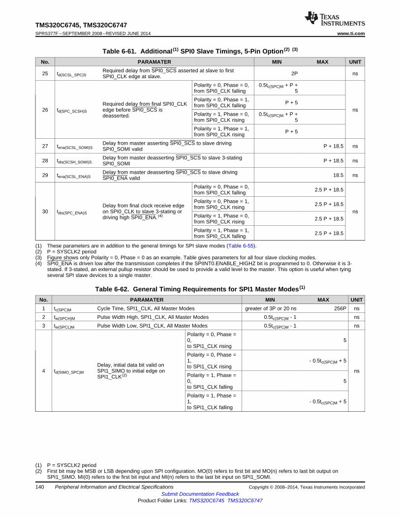
TMS320C6745, TMS320C6747SPRS377F –SEPTEMBER 2008–REVISED JUNE 2014 www.ti.com
Table 6-61. Additional (1) SPI0 Slave Timings, 5-Pin Option (2) (3)
No. PARAMATER MIN MAX UNITRequired delay from SPI0_SCS asserted at slave to first25 td(SCSL_SPC)S 2P nsSPI0_CLK edge at slave.
Polarity = 0, Phase = 0, 0.5tc(SPC)M + P +from SPI0_CLK falling 5Polarity = 0, Phase = 1, P + 5Required delay from final SPI0_CLK from SPI0_CLK falling
26 td(SPC_SCSH)S edge before SPI0_SCS is nsPolarity = 1, Phase = 0, 0.5tc(SPC)M + P +deasserted.from SPI0_CLK rising 5Polarity = 1, Phase = 1, P + 5from SPI0_CLK rising
Delay from master asserting SPI0_SCS to slave driving27 tena(SCSL_SOMI)S P + 18.5 nsSPI0_SOMI validDelay from master deasserting SPI0_SCS to slave 3-stating28 tdis(SCSH_SOMI)S P + 18.5 nsSPI0_SOMIDelay from master deasserting SPI0_SCS to slave driving29 tena(SCSL_ENA)S 18.5 nsSPI0_ENA valid
Polarity = 0, Phase = 0, 2.5 P + 18.5from SPI0_CLK fallingPolarity = 0, Phase = 1, 2.5 P + 18.5Delay from final clock receive edge from SPI0_CLK rising
30 tdis(SPC_ENA)S on SPI0_CLK to slave 3-stating or nsPolarity = 1, Phase = 0,driving high SPI0_ENA. (4) 2.5 P + 18.5from SPI0_CLK risingPolarity = 1, Phase = 1, 2.5 P + 18.5from SPI0_CLK falling
(1) These parameters are in addition to the general timings for SPI slave modes (Table 6-55).(2) P = SYSCLK2 period(3) Figure shows only Polarity = 0, Phase = 0 as an example. Table gives parameters for all four slave clocking modes.(4) SPI0_ENA is driven low after the transmission completes if the SPIINT0.ENABLE_HIGHZ bit is programmed to 0. Otherwise it is 3-
stated. If 3-stated, an external pullup resistor should be used to provide a valid level to the master. This option is useful when tyingseveral SPI slave devices to a single master.
Table 6-62. General Timing Requirements for SPI1 Master Modes (1)
No. PARAMATER MIN MAX UNIT1 tc(SPC)M Cycle Time, SPI1_CLK, All Master Modes greater of 3P or 20 ns 256P ns2 tw(SPCH)M Pulse Width High, SPI1_CLK, All Master Modes 0.5tc(SPC)M - 1 ns3 tw(SPCL)M Pulse Width Low, SPI1_CLK, All Master Modes 0.5tc(SPC)M - 1 ns
Polarity = 0, Phase =0, 5to SPI1_CLK risingPolarity = 0, Phase =1, - 0.5tc(SPC)M + 5
Delay, initial data bit valid on to SPI1_CLK rising4 td(SIMO_SPC)M SPI1_SIMO to initial edge on ns
Polarity = 1, Phase =SPI1_CLK (2)0, 5to SPI1_CLK fallingPolarity = 1, Phase =1, - 0.5tc(SPC)M + 5to SPI1_CLK falling
(1) P = SYSCLK2 period(2) First bit may be MSB or LSB depending upon SPI configuration. MO(0) refers to first bit and MO(n) refers to last bit output on
SPI1_SIMO. MI(0) refers to the first bit input and MI(n) refers to the last bit input on SPI1_SOMI.
140 Peripheral Information and Electrical Specifications Copyright © 2008–2014, Texas Instruments IncorporatedSubmit Documentation Feedback
Product Folder Links: TMS320C6745 TMS320C6747

TMS320C6745, TMS320C6747www.ti.com SPRS377F –SEPTEMBER 2008–REVISED JUNE 2014
Table 6-62. General Timing Requirements for SPI1 Master Modes(1) (continued)No. PARAMATER MIN MAX UNIT
Polarity = 0, Phase =0, 5from SPI1_CLK risingPolarity = 0, Phase =1, 5
Delay, subsequent bits valid on from SPI1_CLK falling5 td(SPC_SIMO)M SPI1_SIMO after transmit edge of ns
Polarity = 1, Phase =SPI1_CLK0, 5from SPI1_CLK fallingPolarity = 1, Phase =1, 5from SPI1_CLK risingPolarity = 0, Phase =0, 0.5tc(SPC)M -3from SPI1_CLK fallingPolarity = 0, Phase =1, 0.5tc(SPC)M -3
Output hold time, SPI1_SIMO valid from SPI1_CLK rising6 toh(SPC_SIMO)M after ns
Polarity = 1, Phase =receive edge of SPI1_CLK0, 0.5tc(SPC)M -3from SPI1_CLK risingPolarity = 1, Phase =1, 0.5tc(SPC)M -3from SPI1_CLK fallingPolarity = 0, Phase =0, 0to SPI1_CLK fallingPolarity = 0, Phase =1, 0
Input Setup Time, SPI1_SOMI valid to SPI1_CLK rising7 tsu(SOMI_SPC)M before ns
Polarity = 1, Phase =receive edge of SPI1_CLK0, 0to SPI1_CLK risingPolarity = 1, Phase =1, 0to SPI1_CLK fallingPolarity = 0, Phase =0, 5from SPI1_CLK fallingPolarity = 0, Phase =1, 5
Input Hold Time, SPI1_SOMI valid from SPI1_CLK rising8 tih(SPC_SOMI)M after ns
Polarity = 1, Phase =receive edge of SPI1_CLK0, 5from SPI1_CLK risingPolarity = 1, Phase =1, 5from SPI1_CLK falling
Table 6-63. General Timing Requirements for SPI1 Slave Modes (1)
No. PARAMATER MIN MAX UNIT9 tc(SPC)S Cycle Time, SPI1_CLK, All Slave Modes greater of 3P or 40 ns ns10 tw(SPCH)S Pulse Width High, SPI1_CLK, All Slave Modes 18 ns11 tw(SPCL)S Pulse Width Low, SPI1_CLK, All Slave Modes 18 ns
(1) P = SYSCLK2 period
Copyright © 2008–2014, Texas Instruments Incorporated Peripheral Information and Electrical Specifications 141Submit Documentation Feedback
Product Folder Links: TMS320C6745 TMS320C6747

TMS320C6745, TMS320C6747SPRS377F –SEPTEMBER 2008–REVISED JUNE 2014 www.ti.com
Table 6-63. General Timing Requirements for SPI1 Slave Modes(1) (continued)No. PARAMATER MIN MAX UNIT
Polarity = 0, Phase = 0, 2Pto SPI1_CLK risingPolarity = 0, Phase = 1, 2PSetup time, transmit data written to to SPI1_CLK rising
12 tsu(SOMI_SPC)S SPI before initial clock edge from nsPolarity = 1, Phase = 0,master. (2) (3) 2Pto SPI1_CLK fallingPolarity = 1, Phase = 1, 2Pto SPI1_CLK fallingPolarity = 0, Phase = 0, 19from SPI1_CLK risingPolarity = 0, Phase = 1, 19Delay, subsequent bits valid on from SPI1_CLK falling
13 td(SPC_SOMI)S SPI1_SOMI after transmit edge of nsPolarity = 1, Phase = 0,SPI1_CLK 19from SPI1_CLK fallingPolarity = 1, Phase = 1, 19from SPI1_CLK risingPolarity = 0, Phase = 0, 0.5tc(SPC)S -3from SPI1_CLK fallingPolarity = 0, Phase = 1, 0.5tc(SPC)S -3Output hold time, SPI1_SOMI valid from SPI1_CLK rising
14 toh(SPC_SOMI)S after nsPolarity = 1, Phase = 0,receive edge of SPI1_CLK 0.5tc(SPC)S -3from SPI1_CLK risingPolarity = 1, Phase = 1, 0.5tc(SPC)S -3from SPI1_CLK fallingPolarity = 0, Phase = 0, 0to SPI1_CLK fallingPolarity = 0, Phase = 1, 0Input Setup Time, SPI1_SIMO valid to SPI1_CLK rising
15 tsu(SIMO_SPC)S before nsPolarity = 1, Phase = 0,receive edge of SPI1_CLK 0to SPI1_CLK risingPolarity = 1, Phase = 1, 0to SPI1_CLK fallingPolarity = 0, Phase = 0, 5from SPI1_CLK fallingPolarity = 0, Phase = 1, 5Input Hold Time, SPI1_SIMO valid from SPI1_CLK rising
16 tih(SPC_SIMO)S after nsPolarity = 1, Phase = 0,receive edge of SPI1_CLK 5from SPI1_CLK risingPolarity = 1, Phase = 1, 5from SPI1_CLK falling
(2) First bit may be MSB or LSB depending upon SPI configuration. SO(0) refers to first bit and SO(n) refers to last bit output onSPI1_SOMI. SI(0) refers to the first bit input and SI(n) refers to the last bit input on SPI1_SIMO.
(3) Measured from the termination of the write of new data to the SPI module, In analyzing throughput requirements, additional internal buscycles must be accounted for to allow data to be written to the SPI module by the DSP CPU.
142 Peripheral Information and Electrical Specifications Copyright © 2008–2014, Texas Instruments IncorporatedSubmit Documentation Feedback
Product Folder Links: TMS320C6745 TMS320C6747

TMS320C6745, TMS320C6747www.ti.com SPRS377F –SEPTEMBER 2008–REVISED JUNE 2014
Table 6-64. Additional (1) SPI1 Master Timings, 4-Pin Enable Option (2) (3)
No. PARAMETER MIN MAX UNITPolarity = 0, Phase = 0, 3P + 3to SPI1_CLK risingPolarity = 0, Phase = 1, 0.5tc(SPC)M + 3P + 3Delay from slave assertion of to SPI1_CLK rising
17 td(EN A_SPC)M SPI1_ENA active to first SPI1_CLK nsPolarity = 1, Phase = 0,from master. (4) 3P + 3to SPI1_CLK fallingPolarity = 1, Phase = 1, 0.5tc(SPC)M + 3P + 3to SPI1_CLK fallingPolarity = 0, Phase = 0, 0.5tc(SPC)M + P + 5from SPI1_CLK fallingPolarity = 0, Phase = 1,Max delay for slave to deassert P + 5from SPI1_CLK fallingSPI1_ENA after final SPI1_CLK edge18 td(SPC_ENA)M nsto ensure master does not begin the Polarity = 1, Phase = 0, 0.5tc(SPC)M + P + 5next transfer. (5) from SPI1_CLK risingPolarity = 1, Phase = 1, P + 5from SPI1_CLK rising
(1) These parameters are in addition to the general timings for SPI master modes (Table 6-62).(2) P = SYSCLK2 period(3) Figure shows only Polarity = 0, Phase = 0 as an example. Table gives parameters for all four master clocking modes.(4) In the case where the master SPI is ready with new data before SPI1_ENA assertion.(5) In the case where the master SPI is ready with new data before SPI1_ENA deassertion.
Table 6-65. Additional (1) SPI1 Master Timings, 4-Pin Chip Select Option (2) (3)
No. PARAMATER MIN MAX UNITPolarity = 0, Phase = 0, 2P -5to SPI1_CLK risingPolarity = 0, Phase = 1, 0.5tc(SPC)M + 2P -5to SPI1_CLK risingDelay from SPI1_SCS active to first19 td(SCS_SPC)M nsSPI1_CLK (4) (5) Polarity = 1, Phase = 0, 2P -5to SPI1_CLK fallingPolarity = 1, Phase = 1, 0.5tc(SPC)M + 2P -5to SPI1_CLK fallingPolarity = 0, Phase = 0, 0.5tc(SPC)M + P - 3from SPI1_CLK fallingPolarity = 0, Phase = 1, P - 3from SPI1_CLK fallingDelay from final SPI1_CLK edge to20 td(SPC_SCS)M nsmaster deasserting SPI1_SCS (6) (7) Polarity = 1, Phase = 0, 0.5tc(SPC)M + P -3from SPI1_CLK risingPolarity = 1, Phase = 1, P - 3from SPI1_CLK rising
(1) These parameters are in addition to the general timings for SPI master modes (Table 6-62).(2) P = SYSCLK2 period(3) Figure shows only Polarity = 0, Phase = 0 as an example. Table gives parameters for all four master clocking modes.(4) In the case where the master SPI is ready with new data before SPI1_SCS assertion.(5) This delay can be increased under software control by the register bit field SPIDELAY.C2TDELAY[4:0].(6) Except for modes when SPIDAT1.CSHOLD is enabled and there is additional data to transmit. In this case, SPI1_SCS will remain
asserted.(7) This delay can be increased under software control by the register bit field SPIDELAY.T2CDELAY[4:0].
Copyright © 2008–2014, Texas Instruments Incorporated Peripheral Information and Electrical Specifications 143Submit Documentation Feedback
Product Folder Links: TMS320C6745 TMS320C6747

TMS320C6745, TMS320C6747SPRS377F –SEPTEMBER 2008–REVISED JUNE 2014 www.ti.com
Table 6-66. Additional (1) SPI1 Master Timings, 5-Pin Option (2) (3)
No. PARAMATER MIN MAX UNITPolarity = 0, Phase = 0, 0.5tc(SPC)M+P+5from SPI1_CLK falling
Max delay for slave to Polarity = 0, Phase = 1, P+5deassert SPI1_ENA after final from SPI1_CLK falling18 td(SPC_ENA)M SPI1_CLK edge to ensure ns
Polarity = 1, Phase = 0,master does not begin the 0.5tc(SPC)M+P+5from SPI1_CLK risingnext transfer. (4)
Polarity = 1, Phase = 1, P+5from SPI1_CLK risingPolarity = 0, Phase = 0, 0.5tc(SPC)M + P -3from SPI1_CLK fallingPolarity = 0, Phase = 1,Delay from final SPI1_CLK P - 3from SPI1_CLK fallingedge to20 td(SPC_SCS)M nsmaster deasserting Polarity = 1, Phase = 0, 0.5tc(SPC)M+ P -3SPI1_SCS (5) (6) from SPI1_CLK risingPolarity = 1, Phase = 1, P - 3from SPI1_CLK rising
Max delay for slave SPI to drive SPI1_ENA valid after21 td(SCSL_ENAL)M master asserts SPI1_SCS to delay the C2TDELAY + P ns
master from beginning the next transfer,Polarity = 0, Phase = 0, 2P -5to SPI1_CLK risingPolarity = 0, Phase = 1, 0.5tc(SPC)M + 2P -5to SPI1_CLK risingDelay from SPI1_SCS active22 td(SCS_SPC)M nsto first SPI1_CLK (7) (8) (9) Polarity = 1, Phase = 0, 2P -5to SPI1_CLK fallingPolarity = 1, Phase = 1, 0.5tc(SPC)M + 2P -5to SPI1_CLK fallingPolarity = 0, Phase = 0, 3P + 3to SPI1_CLK risingPolarity = 0, Phase = 1, 0.5tc(SPC)M + 3P + 3Delay from assertion of to SPI1_CLK rising
23 td(ENA_SPC)M SPI1_ENA low to first nsPolarity = 1, Phase = 0,SPI1_CLK edge. (10) 3P + 3to SPI1_CLK fallingPolarity = 1, Phase = 1, 0.5tc(SPC)M + 3P + 3to SPI1_CLK falling
(1) These parameters are in addition to the general timings for SPI master modes (Table 6-63).(2) P = SYSCLK2 period(3) Figure shows only Polarity = 0, Phase = 0 as an example. Table gives parameters for all four master clocking modes.(4) In the case where the master SPI is ready with new data before SPI1_ENA deassertion.(5) Except for modes when SPIDAT1.CSHOLD is enabled and there is additional data to transmit. In this case, SPI1_SCS will remain
asserted.(6) This delay can be increased under software control by the register bit field SPIDELAY.T2CDELAY[4:0].(7) If SPI1_ENA is asserted immediately such that the transmission is not delayed by SPI1_ENA.(8) In the case where the master SPI is ready with new data before SPI1_SCS assertion.(9) This delay can be increased under software control by the register bit field SPIDELAY.C2TDELAY[4:0].(10) If SPI1_ENA was initially deasserted high and SPI1_CLK is delayed.
144 Peripheral Information and Electrical Specifications Copyright © 2008–2014, Texas Instruments IncorporatedSubmit Documentation Feedback
Product Folder Links: TMS320C6745 TMS320C6747

TMS320C6745, TMS320C6747www.ti.com SPRS377F –SEPTEMBER 2008–REVISED JUNE 2014
Table 6-67. Additional (1) SPI1 Slave Timings, 4-Pin Enable Option (2) (3)
No. PARAMETER MIN MAX UNITPolarity = 0, Phase = 0, 1.5 P -3 2.5 P + 19from SPI1_CLK fallingPolarity = 0, Phase = 1,Delay from final – 0.5tc(SPC)M + 1.5 P -3 – 0.5tc(SPC)M + 2.5 P + 19from SPI1_CLK fallingSPI1_CLK edge to24 td(SPC_ENAH)S nsslave deasserting Polarity = 1, Phase = 0, 1.5 P -3 2.5 P + 19SPI1_ENA. from SPI1_CLK risingPolarity = 1, Phase = 1, – 0.5tc(SPC)M + 1.5 P -3 – 0.5tc(SPC)M + 2.5 P + 19from SPI1_CLK rising
(1) These parameters are in addition to the general timings for SPI slave modes (Table 6-63).(2) P = SYSCLK2 period(3) Figure shows only Polarity = 0, Phase = 0 as an example. Table gives parameters for all four slave clocking modes.
Table 6-68. Additional (1) SPI1 Slave Timings, 4-Pin Chip Select Option (2) (3)
No. PARAMETER MIN MAX UNITRequired delay from SPI1_SCS asserted at slave to first25 td(SCSL_SPC)S 2P nsSPI1_CLK edge at slave.
Polarity = 0, Phase = 0, 0.5tc(SPC)M + P + 5from SPI1_CLK fallingPolarity = 0, Phase = 1, P + 5Required delay from final from SPI1_CLK falling
26 td(SPC_SCSH)S SPI1_CLK edge before nsPolarity = 1, Phase = 0,SPI1_SCS is deasserted. 0.5tc(SPC)M + P + 5from SPI1_CLK risingPolarity = 1, Phase = 1, P + 5from SPI1_CLK rising
Delay from master asserting SPI1_SCS to slave driving27 tena(SCSL_SOMI)S P + 19 nsSPI1_SOMI validDelay from master deasserting SPI1_SCS to slave 3-stating28 tdis(SCSH_SOMI)S P + 19 nsSPI1_SOMI
(1) These parameters are in addition to the general timings for SPI slave modes (Table 6-63).(2) P = SYSCLK2 period(3) Figure shows only Polarity = 0, Phase = 0 as an example. Table gives parameters for all four slave clocking modes.
Table 6-69. Additional (1) SPI1 Slave Timings, 5-Pin Option (2) (3)
No. PARAMETER MIN MAX UNITRequired delay from SPI1_SCS asserted at slave to first25 td(SCSL_SPC)S 2P nsSPI1_CLK edge at slave.
Polarity = 0, Phase = 0, 0.5tc(SPC)M + P +from SPI1_CLK falling 5Polarity = 0, Phase = 1, P + 5Required delay from final SPI1_CLK from SPI1_CLK falling
26 td(SPC_SCSH)S edge before SPI1_SCS is nsPolarity = 1, Phase = 0, 0.5tc(SPC)M + P +deasserted.from SPI1_CLK rising 5Polarity = 1, Phase = 1, P + 5from SPI1_CLK rising
Delay from master asserting SPI1_SCS to slave driving27 tena(SCSL_SOMI)S P + 19 nsSPI1_SOMI validDelay from master deasserting SPI1_SCS to slave 3-stating28 tdis(SCSH_SOMI)S P + 19 nsSPI1_SOMIDelay from master deasserting SPI1_SCS to slave driving29 tena(SCSL_ENA)S 19 nsSPI1_ENA valid
(1) These parameters are in addition to the general timings for SPI slave modes (Table 6-63).(2) P = SYSCLK2 period(3) Figure shows only Polarity = 0, Phase = 0 as an example. Table gives parameters for all four slave clocking modes.
Copyright © 2008–2014, Texas Instruments Incorporated Peripheral Information and Electrical Specifications 145Submit Documentation Feedback
Product Folder Links: TMS320C6745 TMS320C6747

TMS320C6745, TMS320C6747SPRS377F –SEPTEMBER 2008–REVISED JUNE 2014 www.ti.com
Table 6-69. Additional(1) SPI1 Slave Timings, 5-Pin Option(2) (3) (continued)No. PARAMETER MIN MAX UNIT
Polarity = 0, Phase = 0, 2.5 P + 19from SPI1_CLK fallingPolarity = 0, Phase = 1, 2.5 P + 19Delay from final clock receive edge from SPI1_CLK rising
30 tdis(SPC_ENA)S on SPI1_CLK to slave 3-stating or nsPolarity = 1, Phase = 0,driving high SPI1_ENA. (4) 2.5 P + 19from SPI1_CLK risingPolarity = 1, Phase = 1, 2.5 P + 19from SPI1_CLK falling
(4) SPI1_ENA is driven low after the transmission completes if the SPIINT0.ENABLE_HIGHZ bit is programmed to 0. Otherwise it is 3-stated. If 3-stated, an external pullup resistor should be used to provide a valid level to the master. This option is useful when tyingseveral SPI slave devices to a single master.
146 Peripheral Information and Electrical Specifications Copyright © 2008–2014, Texas Instruments IncorporatedSubmit Documentation Feedback
Product Folder Links: TMS320C6745 TMS320C6747

SPIx_CLK
SPIx_SIMO
SPIx_SOMI
SPIx_CLK
SPIx_SIMO
SPIx_SOMI
SPIx_CLK
SPIx_SIMO
SPIx_SOMI
SPIx_CLK
SPIx_SIMO
SPIx_SOMI
MO(0) MO(1) MO(n−1) MO(n)
MI(0) MI(1) MI(n−1) MI(n)
MO(0) MO(1) MO(n−1) MO(n)
MI(0) MI(1) MI(n−1) MI(n)
MO(0) MO(1) MO(n−1) MO(n)
MI(0) MI(1) MI(n−1) MI(n)
MO(0) MO(1) MO(n−1) MO(n)
MI(0) MI(1) MI(n−1) MI(n)
6
6
7
7
7
7
8
8
8
8
32
6
1
4
4
4
4 5
5
5 6
MASTER MODE
POLARITY = 0 PHASE = 0
MASTER MODE
POLARITY = 0 PHASE = 1
MASTER MODE
POLARITY = 1 PHASE = 0
MASTER MODE
POLARITY = 1 PHASE = 1
5
TMS320C6745, TMS320C6747www.ti.com SPRS377F –SEPTEMBER 2008–REVISED JUNE 2014
Figure 6-38. SPI Timings—Master Mode
Copyright © 2008–2014, Texas Instruments Incorporated Peripheral Information and Electrical Specifications 147Submit Documentation Feedback
Product Folder Links: TMS320C6745 TMS320C6747

SPIx_CLK
SPIx_SIMO
SPIx_SOMI
SPIx_CLK
SPIx_SIMO
SPIx_SOMI
SPIx_CLK
SPIx_SIMO
SPIx_SOMI
SPIx_CLK
SPIx_SIMO
SPIx_SOMI
SI(0) SI(1) SI(n−1) SI(n)
SO(0) SO(1) SO(n−1) SO(n)
SI(0) SI(1) SI(n−1) SI(n)
SO(0) SO(1) SO(n−1) SO(n)
SI(0) SI(1) SI(n−1) SI(n)
SO(0) SO(1) SO(n−1) SO(n)
SI(0) SI(1) SI(n−1) SI(n)
SO(0) SO(1) SO(n−1) SO(n)
14
14
15
15
15
15
16
16
16
16
1110
14
9
12
12
12
12
13
13
13
13
14
SLAVE MODEPOLARITY = 0 PHASE = 0
SLAVE MODEPOLARITY = 0 PHASE = 1
SLAVE MODEPOLARITY = 1 PHASE = 0
SLAVE MODEPOLARITY = 1 PHASE = 1
TMS320C6745, TMS320C6747SPRS377F –SEPTEMBER 2008–REVISED JUNE 2014 www.ti.com
Figure 6-39. SPI Timings—Slave Mode
148 Peripheral Information and Electrical Specifications Copyright © 2008–2014, Texas Instruments IncorporatedSubmit Documentation Feedback
Product Folder Links: TMS320C6745 TMS320C6747

MASTER MODE 4 PIN WITH CHIP SELECT
SPIx_CLK
SPIx_SIMO
SPIx_SOMI
SPIx_ENA
SPIx_CLK
SPIx_SIMO
SPIx_SOMI
SPIx_SCS
SPIx_CLK
SPIx_SIMO
SPIx_SOMI
SPIx_ENA
SPIx_SCS
MO(0) MO(1) MO(n−1) MO(n)
MI(0) MI(1) MI(n−1) MI(n)
MO(0) MO(1) MO(n−1) MO(n)
MI(0) MI(1) MI(n−1) MI(n)
MO(0)
MO(1)
MO(n−1) MO(n)
MI(0) MI(1) MI(n−1) MI(n)
17
19
21
22
23
20
18
20
18
MASTER MODE 4 PIN WITH ENABLE
MASTER MODE 5 PIN
A. DESELECTED IS PROGRAMMABLE EITHER HIGH OR
3−STATE (REQUIRES EXTERNAL PULLUP)
DESEL(A) DESEL(A)
TMS320C6745, TMS320C6747www.ti.com SPRS377F –SEPTEMBER 2008–REVISED JUNE 2014
Figure 6-40. SPI Timings—Master Mode (4-Pin and 5-Pin)
Copyright © 2008–2014, Texas Instruments Incorporated Peripheral Information and Electrical Specifications 149Submit Documentation Feedback
Product Folder Links: TMS320C6745 TMS320C6747

27
SPIx_CLK
SPIx_SOMI
SPIx_SIMO
SPIx_ENA
SPIx_CLK
SPIx_SOMI
SPIx_SIMO
SPIx_SCS
SPIx_CLK
SPIx_SOMI
SPIx_SIMO
SPIx_ENA
SPIx_SCS
SO(0) SO(1) SO(n−1) SO(n)
SI(0) SI(1) SI(n−1) SI(n)
SO(0) SO(1)
SO(n−1)
SO(n)
SI(0) SI(1) SI(n−1) SI(n)
SO(0)
SO(1)
SO(n−1) SO(n)
SI(0) SI(1) SI(n−1) SI(n)
24
26
28
26
30
28
25
25
27
29
SLAVE MODE 4 PIN WITH ENABLE
SLAVE MODE 4 PIN WITH CHIP SELECT
SLAVE MODE 5 PIN
DESEL(A) DESEL(A)
A. DESELECTED IS PROGRAMMABLE EITHER HIGH OR
3−STATE (REQUIRES EXTERNAL PULLUP)
TMS320C6745, TMS320C6747SPRS377F –SEPTEMBER 2008–REVISED JUNE 2014 www.ti.com
Figure 6-41. SPI Timings—Slave Mode (4-Pin and 5-Pin)
150 Peripheral Information and Electrical Specifications Copyright © 2008–2014, Texas Instruments IncorporatedSubmit Documentation Feedback
Product Folder Links: TMS320C6745 TMS320C6747
TMS320C6745, TMS320C6747www.ti.com SPRS377F –SEPTEMBER 2008–REVISED JUNE 2014
6.18 Enhanced Capture (eCAP) PeripheralThe C6745/6747 device contains up to three enhanced capture (eCAP) modules. Figure 6-42 shows afunctional block diagram of a module. See the TMS320C6745/C6747 DSP Peripherals OverviewReference Guide. (SPRUFK9) for more details.
Uses for ECAP include:• Speed measurements of rotating machinery (e.g. toothed sprockets sensed via Hall sensors)• Elapsed time measurements between position sensor triggers• Period and duty cycle measurements of Pulse train signals• Decoding current or voltage amplitude derived from cuty cycle encoded current/voltage sensors
The ECAP module described in this specification includes the following features:• 32 bit time base• 4 event time-stamp registers (each 32 bits)• Edge polarity selection for up to 4 sequenced time-stamp capture events• Interrupt on either of the 4 events• Single shot capture of up to 4 event time-stamps• Continuous mode capture of time-stamps in a 4 deep circular buffer• Absolute time-stamp capture• Difference mode time-stamp capture• All the above resources are dedicated to a single input pin
The eCAP modules are clocked at the SYSCLK2 rate.
Copyright © 2008–2014, Texas Instruments Incorporated Peripheral Information and Electrical Specifications 151Submit Documentation Feedback
Product Folder Links: TMS320C6745 TMS320C6747
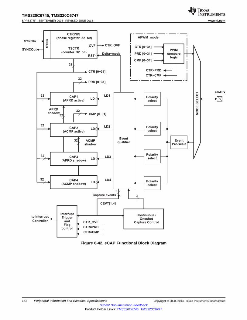
TSCTR(counter−32 bit)
RST
CAP1(APRD active)
LD
CAP2(ACMP active)
LD
CAP3(APRD shadow)
LD
CAP4(ACMP shadow)
LD
Continuous /Oneshot
Capture Control
LD1
LD2
LD3
LD4
32
32
PRD [0−31]
CMP [0−31]
CTR [0−31]
eCAPx
InterruptTrigger
andFlag
control
to Interrupt
Controller
CTR=CMP
32
32
32
32
32
ACMPshadow
EventPre-scale
CTRPHS(phase register−32 bit)
SYNCOut
SYNCIn
Eventqualifier
Polarityselect
Polarityselect
Polarityselect
Polarityselect
CTR=PRD
CTR_OVF
4
PWMcompare
logic
CTR [0−31]
PRD [0−31]
CMP [0−31]
CTR=CMP
CTR=PRD
CTR_OVFOVF
APWM mode
Delta−mode
SY
NC
4Capture events
CEVT[1:4]
APRDshadow
32
32 MO
DE
SE
LE
CT
TMS320C6745, TMS320C6747SPRS377F –SEPTEMBER 2008–REVISED JUNE 2014 www.ti.com
Figure 6-42. eCAP Functional Block Diagram
152 Peripheral Information and Electrical Specifications Copyright © 2008–2014, Texas Instruments IncorporatedSubmit Documentation Feedback
Product Folder Links: TMS320C6745 TMS320C6747

TMS320C6745, TMS320C6747www.ti.com SPRS377F –SEPTEMBER 2008–REVISED JUNE 2014
Table 6-70 is the list of the ECAP registers.
Table 6-70. ECAPx Configuration Registers
ECAP0 ECAP1 ECAP2 ACRONYM REGISTER DESCRIPTIONBYTE ADDRESS BYTE ADDRESS BYTE ADDRESS0x01F0 6000 0x01F0 7000 0x01F0 8000 TSCTR Time-Stamp Counter0x01F0 6004 0x01F0 7004 0x01F0 8004 CTRPHS Counter Phase Offset Value Register0x01F0 6008 0x01F0 7008 0x01F0 8008 CAP1 Capture 1 Register0x01F0 600C 0x01F0 700C 0x01F0 800C CAP2 Capture 2 Register0x01F0 6010 0x01F0 7010 0x01F0 8010 CAP3 Capture 3 Register0x01F0 6014 0x01F0 7014 0x01F0 8014 CAP4 Capture 4 Register0x01F0 6028 0x01F0 7028 0x01F0 8028 ECCTL1 Capture Control Register 10x01F0 602A 0x01F0 702A 0x01F0 802A ECCTL2 Capture Control Register 20x01F0 602C 0x01F0 702C 0x01F0 802C ECEINT Capture Interrupt Enable Register0x01F0 602E 0x01F0 702E 0x01F0 802E ECFLG Capture Interrupt Flag Register0x01F0 6030 0x01F0 7030 0x01F0 8030 ECCLR Capture Interrupt Clear Register0x01F0 6032 0x01F0 7032 0x01F0 8032 ECFRC Capture Interrupt Force Register0x01F0 605C 0x01F0 705C 0x01F0 805C REVID Revision ID
Table 6-71 shows the eCAP timing requirement and Table 6-72 shows the eCAP switching characteristics.
Table 6-71. Enhanced Capture (eCAP) Timing RequirementPARAMETER TEST CONDITIONS MIN MAX UNIT
tw(CAP) Capture input pulse width Asynchronous 2tc(SCO) cyclesSynchronous 2tc(SCO) cycles
Table 6-72. eCAP Switching CharacteristicsPARAMETER TEST CONDITIONS MIN MAX UNIT
tw(APWM) Pulse duration, APWMx output high/low 20 ns
Copyright © 2008–2014, Texas Instruments Incorporated Peripheral Information and Electrical Specifications 153Submit Documentation Feedback
Product Folder Links: TMS320C6745 TMS320C6747

QWDTMR
QWDPRD
16
QWDOGUTIME
QUPRD
QUTMR
32
UTOUT
WDTOUT
Quadraturecapture unit
(QCAP)
QCPRDLAT
QCTMRLAT
16
QFLG
QEPSTS
QEPCTL
Registersused by
multiple units
QCLKQDIR
QI
QS
PHE
PCSOUT
Quadraturedecoder(QDU)
QDECCTL
16
Position counter/control unit
(PCCU)QPOSLAT
QPOSSLAT
16
QPOSILAT
EQEPxAIN
EQEPxBIN
EQEPxIIN
EQEPxIOUT
EQEPxIOE
EQEPxSIN
EQEPxSOUT
EQEPxSOE
GPIOMUX
EQEPxA/XCLK
EQEPxB/XDIR
EQEPxS
EQEPxI
QPOSCMP QEINT
QFRC
32
QCLR
QPOSCTL
1632
QPOSCNT
QPOSMAX
QPOSINIT
EQEPxINT
Enhanced QEP (eQEP) Peripheral
Systemcontrol registers
QCTMR
QCPRD
1616
QCAPCTL
EQEPxENCLK
SYSCLK2
Data
bu
s
To CPU
Inte
rru
pt
Co
ntr
oller
TMS320C6745, TMS320C6747SPRS377F –SEPTEMBER 2008–REVISED JUNE 2014 www.ti.com
6.19 Enhanced Quadrature Encoder (eQEP) PeripheralThe C6745/6747 device contains up to two enhanced quadrature encoder (eQEP) modules. See theTMS320C6745/C6747 DSP Peripherals Overview Reference Guide. (SPRUFK9) for more details.
Figure 6-43. eQEP Functional Block Diagram
Table 6-73 is the list of the EQEP registers.
Table 6-74 shows the eQEP timing requirement and Table 6-75 shows the eQEP switchingcharacteristics.
154 Peripheral Information and Electrical Specifications Copyright © 2008–2014, Texas Instruments IncorporatedSubmit Documentation Feedback
Product Folder Links: TMS320C6745 TMS320C6747

TMS320C6745, TMS320C6747www.ti.com SPRS377F –SEPTEMBER 2008–REVISED JUNE 2014
Table 6-73. EQEP Registers
EQEP0 EQEP1BYTE ADDRESS BYTE ADDRESS ACRONYM REGISTER DESCRIPTION
0x01F0 9000 0x01F0 A000 QPOSCNT eQEP Position Counter0x01F0 9004 0x01F0 A004 QPOSINIT eQEP Initialization Position Count0x01F0 9008 0x01F0 A008 QPOSMAX eQEP Maximum Position Count0x01F0 900C 0x01F0 A00C QPOSCMP eQEP Position-compare0x01F0 9010 0x01F0 A010 QPOSILAT eQEP Index Position Latch0x01F0 9014 0x01F0 A014 QPOSSLAT eQEP Strobe Position Latch0x01F0 9018 0x01F0 A018 QPOSLAT eQEP Position Latch0x01F0 901C 0x01F0 A01C QUTMR eQEP Unit Timer0x01F0 9020 0x01F0 A020 QUPRD eQEP Unit Period Register0x01F0 9024 0x01F0 A024 QWDTMR eQEP Watchdog Timer0x01F0 9026 0x01F0 A026 QWDPRD eQEP Watchdog Period Register0x01F0 9028 0x01F0 A028 QDECCTL eQEP Decoder Control Register0x01F0 902A 0x01F0 A02A QEPCTL eQEP Control Register0x01F0 902C 0x01F0 A02C QCAPCTL eQEP Capture Control Register0x01F0 902E 0x01F0 A02E QPOSCTL eQEP Position-compare Control Register0x01F0 9030 0x01F0 A030 QEINT eQEP Interrupt Enable Register0x01F0 9032 0x01F0 A032 QFLG eQEP Interrupt Flag Register0x01F0 9034 0x01F0 A034 QCLR eQEP Interrupt Clear Register0x01F0 9036 0x01F0 A036 QFRC eQEP Interrupt Force Register0x01F0 9038 0x01F0 A038 QEPSTS eQEP Status Register0x01F0 903A 0x01F0 A03A QCTMR eQEP Capture Timer0x01F0 903C 0x01F0 A03C QCPRD eQEP Capture Period Register0x01F0 903E 0x01F0 A03E QCTMRLAT eQEP Capture Timer Latch0x01F0 9040 0x01F0 A040 QCPRDLAT eQEP Capture Period Latch0x01F0 905C 0x01F0 A05C REVID eQEP Revision ID
Table 6-74. Enhanced Quadrature Encoder Pulse (eQEP) Timing RequirementsPARAMETER TEST CONDITIONS MIN MAX UNIT
tw(QEPP) QEP input period Asynchronous/synchronous 2tc(SCO) cyclestw(INDEXH) QEP Index Input High time Asynchronous/synchronous 2tc(SCO) cyclestw(INDEXL) QEP Index Input Low time Asynchronous/synchronous 2tc(SCO) cyclestw(STROBH) QEP Strobe High time Asynchronous/synchronous 2tc(SCO) cyclestw(STROBL) QEP Strobe Input Low time Asynchronous/synchronous 2tc(SCO) cycles
Table 6-75. eQEP Switching CharacteristicsPARAMETER MIN MAX UNIT
td(CNTR)xin Delay time, external clock to counter increment 4tc(SCO) cyclestd(PCS-OUT)QEP Delay time, QEP input edge to position compare sync output 6tc(SCO) cycles
Copyright © 2008–2014, Texas Instruments Incorporated Peripheral Information and Electrical Specifications 155Submit Documentation Feedback
Product Folder Links: TMS320C6745 TMS320C6747
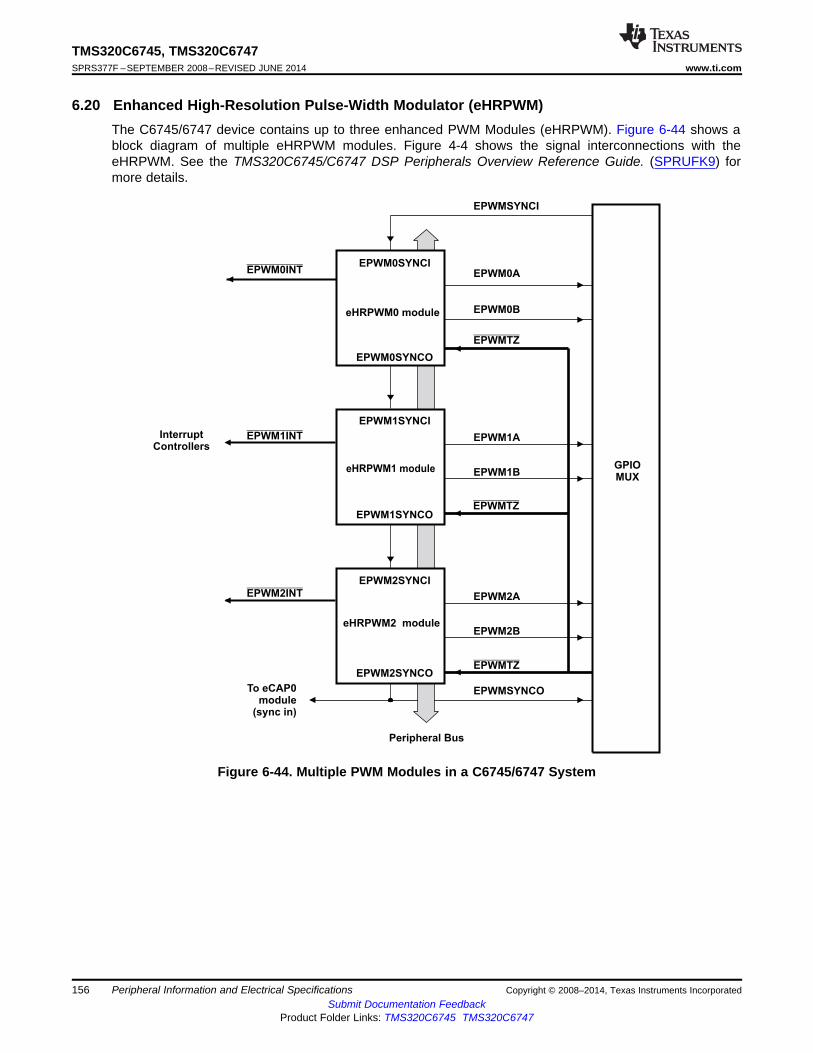
EPWMTZ
Peripheral Bus
eHRPWM0 module
eHRPWM1 module
EPWM0SYNCI
EPWM1SYNCI
EPWM1SYNCO
EPWM2SYNCI
EPWM2SYNCO
GPIOMUX
EPWMSYNCI
EPWM2A
EPWM2B
EPWM1A
EPWM1B
EPWM0A
EPWM0B
EPWM0INT
EPWM1INT
EPWM2INT
EPWMTZ
EPWMTZ
EPWM0SYNCO
InterruptControllers
EPWMSYNCOTo eCAP0module
(sync in)
eHRPWM2 module
TMS320C6745, TMS320C6747SPRS377F –SEPTEMBER 2008–REVISED JUNE 2014 www.ti.com
6.20 Enhanced High-Resolution Pulse-Width Modulator (eHRPWM)The C6745/6747 device contains up to three enhanced PWM Modules (eHRPWM). Figure 6-44 shows ablock diagram of multiple eHRPWM modules. Figure 4-4 shows the signal interconnections with theeHRPWM. See the TMS320C6745/C6747 DSP Peripherals Overview Reference Guide. (SPRUFK9) formore details.
Figure 6-44. Multiple PWM Modules in a C6745/6747 System
156 Peripheral Information and Electrical Specifications Copyright © 2008–2014, Texas Instruments IncorporatedSubmit Documentation Feedback
Product Folder Links: TMS320C6745 TMS320C6747
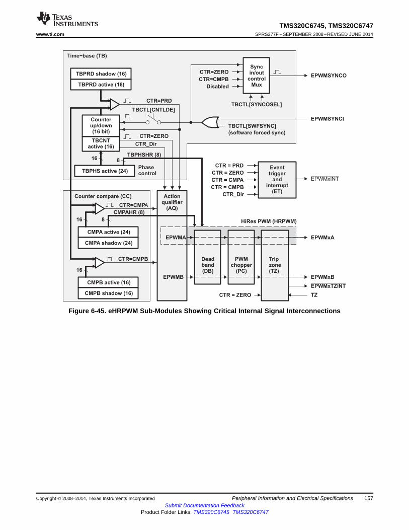
CTR=PRD
TBPRD shadow (16)
TBPRD active (16)
Counterup/down(16 bit)
TBCNTactive (16)
TBCTL[CNTLDE]
TBCTL[SWFSYNC]
(software forced sync)
EPWMSYNCI
CTR=ZERO
CTR_Dir
CTR=CMPB
Disabled
Syncin/out
controlMux
TBCTL[SYNCOSEL]
EPWMSYNCO
TBPHS active (24)
16 8TBPHSHR (8)
Phasecontrol
Time−base (TB)
CTR=CMPA
CMPA active (24)
16
CMPA shadow (24)
Actionqualifier
(AQ)
8
16
Counter compare (CC)
CMPB active (16)
CTR=CMPB
CMPB shadow (16)
CMPAHR (8)
EPWMA
EPWMB
Deadband(DB)
PWMchopper
(PC)
Tripzone(TZ)
CTR = ZERO
EPWMxA
EPWMxB
EPWMxTZINT
TZ
HiRes PWM (HRPWM)
CTR = PRD
CTR = ZERO
CTR = CMPB
CTR = CMPA
CTR_Dir
Eventtrigger
andinterrupt
(ET)
EPWMxINT
CTR=ZERO
TMS320C6745, TMS320C6747www.ti.com SPRS377F –SEPTEMBER 2008–REVISED JUNE 2014
Figure 6-45. eHRPWM Sub-Modules Showing Critical Internal Signal Interconnections
Copyright © 2008–2014, Texas Instruments Incorporated Peripheral Information and Electrical Specifications 157Submit Documentation Feedback
Product Folder Links: TMS320C6745 TMS320C6747
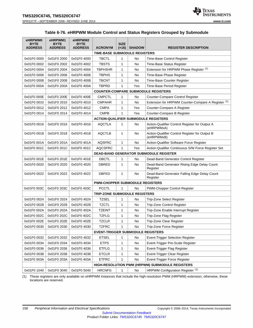
TMS320C6745, TMS320C6747SPRS377F –SEPTEMBER 2008–REVISED JUNE 2014 www.ti.com
Table 6-76. eHRPWM Module Control and Status Registers Grouped by Submodule
eHRPWM0 eHRPWM1 eHRPWM2BYTE BYTE BYTE SIZE
ADDRESS ADDRESS ADDRESS ACRONYM (×16) SHADOW REGISTER DESCRIPTIONTIME-BASE SUBMODULE REGISTERS
0x01F0 0000 0x01F0 2000 0x01F0 4000 TBCTL 1 No Time-Base Control Register0x01F0 0002 0x01F0 2002 0x01F0 4002 TBSTS 1 No Time-Base Status Register0x01F0 0004 0x01F0 2004 0x01F0 4004 TBPHSHR 1 No Extension for HRPWM Phase Register (1)
0x01F0 0006 0x01F0 2006 0x01F0 4006 TBPHS 1 No Time-Base Phase Register0x01F0 0008 0x01F0 2008 0x01F0 4008 TBCNT 1 No Time-Base Counter Register0x01F0 000A 0x01F0 200A 0x01F0 400A TBPRD 1 Yes Time-Base Period Register
COUNTER-COMPARE SUBMODULE REGISTERS0x01F0 000E 0x01F0 200E 0x01F0 400E CMPCTL 1 No Counter-Compare Control Register0x01F0 0010 0x01F0 2010 0x01F0 4010 CMPAHR 1 No Extension for HRPWM Counter-Compare A Register (1)
0x01F0 0012 0x01F0 2012 0x01F0 4012 CMPA 1 Yes Counter-Compare A Register0x01F0 0014 0x01F0 2014 0x01F0 4014 CMPB 1 Yes Counter-Compare B Register
ACTION-QUALIFIER SUBMODULE REGISTERS0x01F0 0016 0x01F0 2016 0x01F0 4016 AQCTLA 1 No Action-Qualifier Control Register for Output A
(eHRPWMxA)0x01F0 0018 0x01F0 2018 0x01F0 4018 AQCTLB 1 No Action-Qualifier Control Register for Output B
(eHRPWMxB)0x01F0 001A 0x01F0 201A 0x01F0 401A AQSFRC 1 No Action-Qualifier Software Force Register0x01F0 001C 0x01F0 201C 0x01F0 401C AQCSFRC 1 Yes Action-Qualifier Continuous S/W Force Register Set
DEAD-BAND GENERATOR SUBMODULE REGISTER0x01F0 001E 0x01F0 201E 0x01F0 401E DBCTL 1 No Dead-Band Generator Control Register0x01F0 0020 0x01F0 2020 0x01F0 4020 DBRED 1 No Dead-Band Generator Rising Edge Delay Count
Register0x01F0 0022 0x01F0 2022 0x01F0 4022 DBFED 1 No Dead-Band Generator Falling Edge Delay Count
RegisterPWM-CHOPPER SUBMODULE REGISTERS
0x01F0 003C 0x01F0 203C 0x01F0 403C PCCTL 1 No PWM-Chopper Control RegisterTRIP-ZONE SUBMODULE REGISTERS
0x01F0 0024 0x01F0 2024 0x01F0 4024 TZSEL 1 No Trip-Zone Select Register0x01F0 0028 0x01F0 2028 0x01F0 4028 TZCTL 1 No Trip-Zone Control Register0x01F0 002A 0x01F0 202A 0x01F0 402A TZEINT 1 No Trip-Zone Enable Interrupt Register0x01F0 002C 0x01F0 202C 0x01F0 402C TZFLG 1 No Trip-Zone Flag Register0x01F0 002E 0x01F0 202E 0x01F0 402E TZCLR 1 No Trip-Zone Clear Register0x01F0 0030 0x01F0 2030 0x01F0 4030 TZFRC 1 No Trip-Zone Force Register
EVENT-TRIGGER SUBMODULE REGISTERS0x01F0 0032 0x01F0 2032 0x01F0 4032 ETSEL 1 No Event-Trigger Selection Register0x01F0 0034 0x01F0 2034 0x01F0 4034 ETPS 1 No Event-Trigger Pre-Scale Register0x01F0 0036 0x01F0 2036 0x01F0 4036 ETFLG 1 No Event-Trigger Flag Register0x01F0 0038 0x01F0 2038 0x01F0 4038 ETCLR 1 No Event-Trigger Clear Register0x01F0 003A 0x01F0 203A 0x01F0 403A ETFRC 1 No Event-Trigger Force Register
HIGH-RESOLUTION PWM (HRPWM) SUBMODULE REGISTERS0x01F0 1040 0x01F0 3040 0x01F0 5040 HRCNFG 1 No HRPWM Configuration Register (1)
(1) These registers are only available on eHRPWM instances that include the high-resolution PWM (HRPWM) extension; otherwise, theselocations are reserved.
158 Peripheral Information and Electrical Specifications Copyright © 2008–2014, Texas Instruments IncorporatedSubmit Documentation Feedback
Product Folder Links: TMS320C6745 TMS320C6747

PWM (A)
TZ
tw(TZ)
td(TZ_PWM)HZ
TMS320C6745, TMS320C6747www.ti.com SPRS377F –SEPTEMBER 2008–REVISED JUNE 2014
6.20.1 Enhanced Pulse Width Modulator (eHRPWM) TimingPWM refers to PWM outputs on eHRPWM1-6. Table 6-77 shows the PWM timing requirements andTable 6-78, switching characteristics.
Table 6-77. eHRPWM Timing RequirementsPARAMETER TEST CONDITIONS MIN MAX UNIT
tw(SYNCIN) Sync input pulse width Asynchronous 2tc(SCO) cyclesSynchronous 2tc(SCO) cycles
Table 6-78. eHRPWM Switching CharacteristicsPARAMETER TEST CONDITIONS MIN MAX UNIT
tw(PWM) Pulse duration, PWMx output high/low 20 nstw(SYNCOUT) Sync output pulse width 8tc(SCO) cyclestd(PWM)TZA Delay time, trip input active to PWM forced high no pin load; 25 ns
Delay time, trip input active to PWM forced low no additionalprogrammable delay
td(TZ-PWM)HZ Delay time, trip input active to PWM Hi-Z no additional 20 nsprogrammable delay
6.20.2 Trip-Zone Input Timing
A. PWM refers to all the PWM pins in the device. The state of the PWM pins after TZ is taken high depends on the PWMrecovery software.
Figure 6-46. PWM Hi-Z Characteristics
Table 6-79. Trip-Zone input Timing Requirements
PARAMETER MIN MAX UNITtw(TZ) Pulse duration, TZx input low Asynchronous 1tc(SCO) cycles
Synchronous 2tc(SCO) cycles
Table 6-80 shows the high-resolution PWM switching characteristics.
Table 6-80. High Resolution PWM Characteristics at SYSCLKOUT = (60 - 100 MHz)
PARAMETER MIN TYP MAX UNITMicro Edge Positioning (MEP) step size (1) 200 ps
(1) MEP step size will increase with low voltage and high temperature and decrease with high voltage and cold temperature.
Copyright © 2008–2014, Texas Instruments Incorporated Peripheral Information and Electrical Specifications 159Submit Documentation Feedback
Product Folder Links: TMS320C6745 TMS320C6747
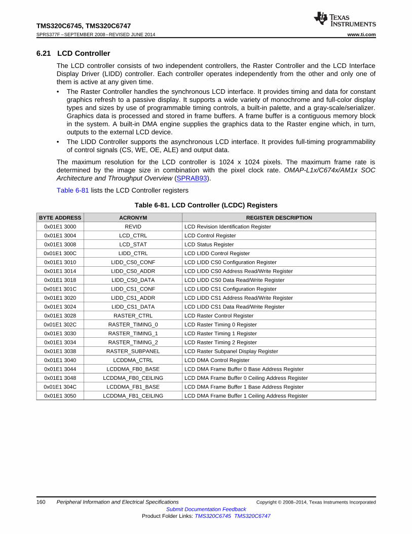
TMS320C6745, TMS320C6747SPRS377F –SEPTEMBER 2008–REVISED JUNE 2014 www.ti.com
6.21 LCD ControllerThe LCD controller consists of two independent controllers, the Raster Controller and the LCD InterfaceDisplay Driver (LIDD) controller. Each controller operates independently from the other and only one ofthem is active at any given time.• The Raster Controller handles the synchronous LCD interface. It provides timing and data for constant
graphics refresh to a passive display. It supports a wide variety of monochrome and full-color displaytypes and sizes by use of programmable timing controls, a built-in palette, and a gray-scale/serializer.Graphics data is processed and stored in frame buffers. A frame buffer is a contiguous memory blockin the system. A built-in DMA engine supplies the graphics data to the Raster engine which, in turn,outputs to the external LCD device.
• The LIDD Controller supports the asynchronous LCD interface. It provides full-timing programmabilityof control signals (CS, WE, OE, ALE) and output data.
The maximum resolution for the LCD controller is 1024 x 1024 pixels. The maximum frame rate isdetermined by the image size in combination with the pixel clock rate. OMAP-L1x/C674x/AM1x SOCArchitecture and Throughput Overview (SPRAB93).
Table 6-81 lists the LCD Controller registers
Table 6-81. LCD Controller (LCDC) Registers
BYTE ADDRESS ACRONYM REGISTER DESCRIPTION0x01E1 3000 REVID LCD Revision Identification Register0x01E1 3004 LCD_CTRL LCD Control Register0x01E1 3008 LCD_STAT LCD Status Register0x01E1 300C LIDD_CTRL LCD LIDD Control Register0x01E1 3010 LIDD_CS0_CONF LCD LIDD CS0 Configuration Register0x01E1 3014 LIDD_CS0_ADDR LCD LIDD CS0 Address Read/Write Register0x01E1 3018 LIDD_CS0_DATA LCD LIDD CS0 Data Read/Write Register0x01E1 301C LIDD_CS1_CONF LCD LIDD CS1 Configuration Register0x01E1 3020 LIDD_CS1_ADDR LCD LIDD CS1 Address Read/Write Register0x01E1 3024 LIDD_CS1_DATA LCD LIDD CS1 Data Read/Write Register0x01E1 3028 RASTER_CTRL LCD Raster Control Register0x01E1 302C RASTER_TIMING_0 LCD Raster Timing 0 Register0x01E1 3030 RASTER_TIMING_1 LCD Raster Timing 1 Register0x01E1 3034 RASTER_TIMING_2 LCD Raster Timing 2 Register0x01E1 3038 RASTER_SUBPANEL LCD Raster Subpanel Display Register0x01E1 3040 LCDDMA_CTRL LCD DMA Control Register0x01E1 3044 LCDDMA_FB0_BASE LCD DMA Frame Buffer 0 Base Address Register0x01E1 3048 LCDDMA_FB0_CEILING LCD DMA Frame Buffer 0 Ceiling Address Register0x01E1 304C LCDDMA_FB1_BASE LCD DMA Frame Buffer 1 Base Address Register0x01E1 3050 LCDDMA_FB1_CEILING LCD DMA Frame Buffer 1 Ceiling Address Register
160 Peripheral Information and Electrical Specifications Copyright © 2008–2014, Texas Instruments IncorporatedSubmit Documentation Feedback
Product Folder Links: TMS320C6745 TMS320C6747
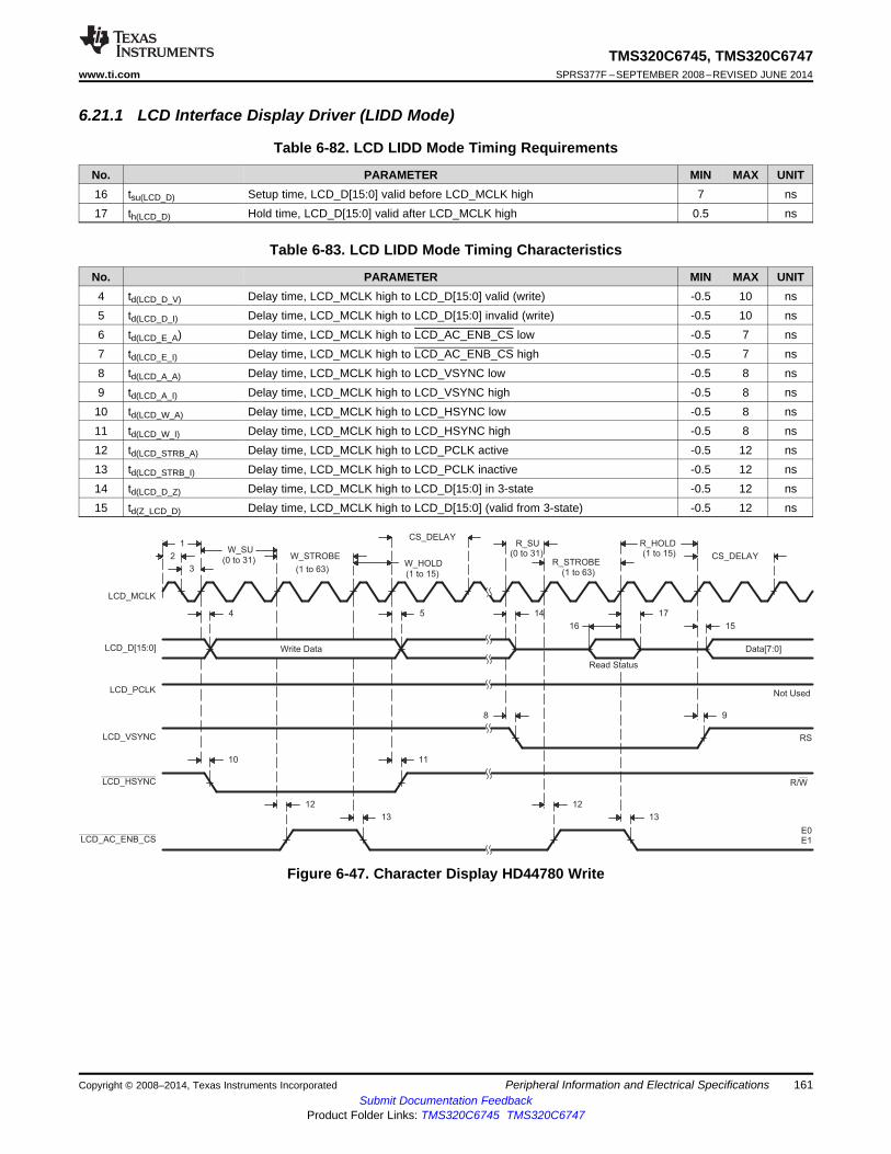
LCD_AC_ENB_CS
LCD_PCLK
2
3
1W_SU
(0 to 31) W_STROBE
(1 to 63)W_HOLD
(1 to 15)
CS_DELAYR_SU
(0 to 31)R_STROBE
(1 to 63)
R_HOLD(1 to 15) CS_DELAY
LCD_MCLK
4
Write Data
5 14
16
17
15
Data[7:0]
Not Used
8 9
10 11
12
13
12
13
RS
R/W
E0E1
LCD_D[15:0]
LCD_VSYNC
LCD_HSYNC
Read Status
TMS320C6745, TMS320C6747www.ti.com SPRS377F –SEPTEMBER 2008–REVISED JUNE 2014
6.21.1 LCD Interface Display Driver (LIDD Mode)
Table 6-82. LCD LIDD Mode Timing Requirements
No. PARAMETER MIN MAX UNIT16 tsu(LCD_D) Setup time, LCD_D[15:0] valid before LCD_MCLK high 7 ns17 th(LCD_D) Hold time, LCD_D[15:0] valid after LCD_MCLK high 0.5 ns
Table 6-83. LCD LIDD Mode Timing Characteristics
No. PARAMETER MIN MAX UNIT4 td(LCD_D_V) Delay time, LCD_MCLK high to LCD_D[15:0] valid (write) -0.5 10 ns5 td(LCD_D_I) Delay time, LCD_MCLK high to LCD_D[15:0] invalid (write) -0.5 10 ns6 td(LCD_E_A) Delay time, LCD_MCLK high to LCD_AC_ENB_CS low -0.5 7 ns7 td(LCD_E_I) Delay time, LCD_MCLK high to LCD_AC_ENB_CS high -0.5 7 ns8 td(LCD_A_A) Delay time, LCD_MCLK high to LCD_VSYNC low -0.5 8 ns9 td(LCD_A_I) Delay time, LCD_MCLK high to LCD_VSYNC high -0.5 8 ns
10 td(LCD_W_A) Delay time, LCD_MCLK high to LCD_HSYNC low -0.5 8 ns11 td(LCD_W_I) Delay time, LCD_MCLK high to LCD_HSYNC high -0.5 8 ns12 td(LCD_STRB_A) Delay time, LCD_MCLK high to LCD_PCLK active -0.5 12 ns13 td(LCD_STRB_I) Delay time, LCD_MCLK high to LCD_PCLK inactive -0.5 12 ns14 td(LCD_D_Z) Delay time, LCD_MCLK high to LCD_D[15:0] in 3-state -0.5 12 ns15 td(Z_LCD_D) Delay time, LCD_MCLK high to LCD_D[15:0] (valid from 3-state) -0.5 12 ns
Figure 6-47. Character Display HD44780 Write
Copyright © 2008–2014, Texas Instruments Incorporated Peripheral Information and Electrical Specifications 161Submit Documentation Feedback
Product Folder Links: TMS320C6745 TMS320C6747
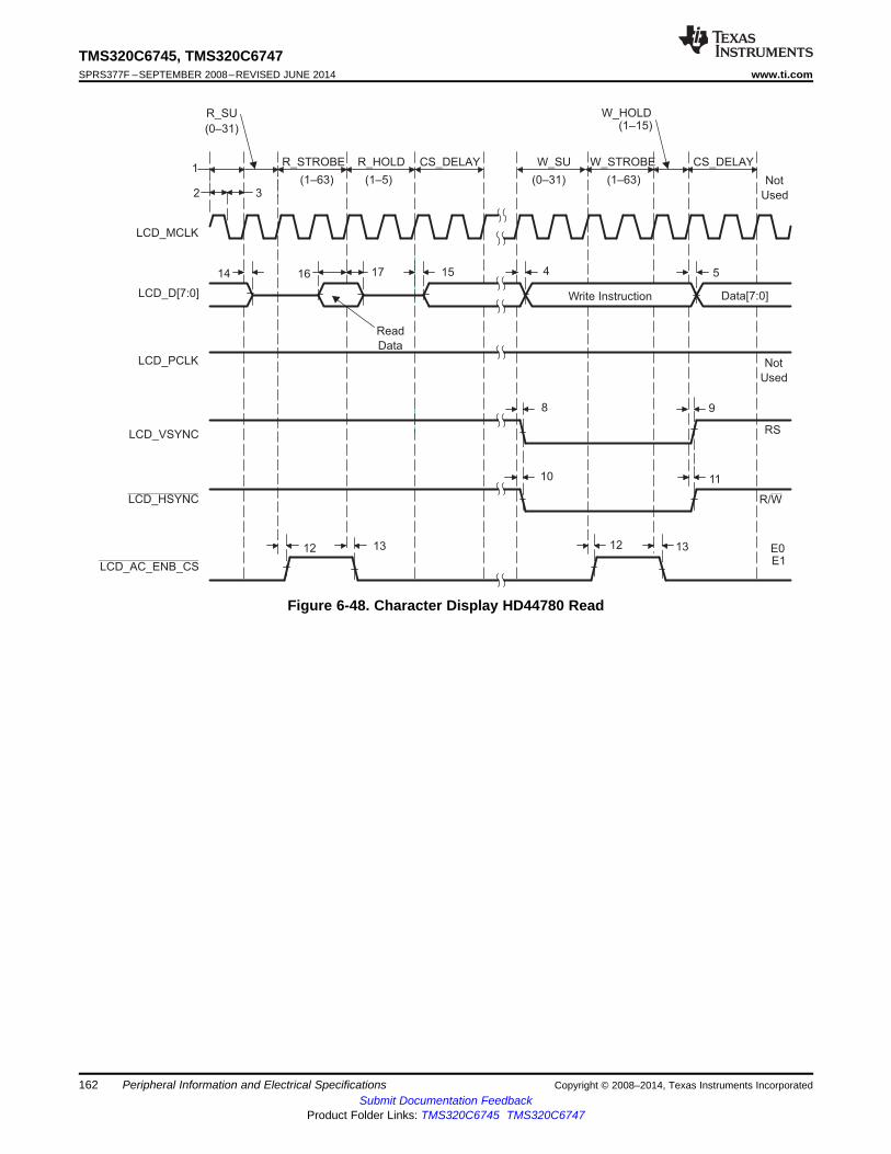
LCD_AC_ENB_CS
LCD_PCLK
LCD_VSYNC
LCD_HSYNC
R_SU
R_STROBE R_HOLD
(0–31)
(1–63) (1–5)
CS_DELAY
Not
Used
RS
R/W
LCD_MCLK
1
2 3
W_SU W_STROBE
W_HOLD
(0–31) (1–63)
(1–15)
CS_DELAY
8 9
12 13
10 11
Not
Used
LCD_D[7:0]
14 1716
Read
Data
15 4 5
E0E1
12 13
Data[7:0]Write Instruction
TMS320C6745, TMS320C6747SPRS377F –SEPTEMBER 2008–REVISED JUNE 2014 www.ti.com
Figure 6-48. Character Display HD44780 Read
162 Peripheral Information and Electrical Specifications Copyright © 2008–2014, Texas Instruments IncorporatedSubmit Documentation Feedback
Product Folder Links: TMS320C6745 TMS320C6747

LCD_D[15:0]
LCD_AC_ENB_CS
(async mode)
LCD_VSYNC
LCD_HSYNC
LCD_MCLK
LCD_PCLK
4
W_SU W_STROBE
W_HOLD
(0−31) (1−63)
(1−15)
CS_DELAY
CS0CS1
A0
R/W
E
Clock
1
2 3
W_SU W_STROBE
W_HOLD
(0−31) (1−63)
(1−15)
CS_DELAY
5 4 5
6 7 6 7
8 9
12 13
Write Address Write Data
12 13
10 11 10 11
Data[15:0]
TMS320C6745, TMS320C6747www.ti.com SPRS377F –SEPTEMBER 2008–REVISED JUNE 2014
Figure 6-49. Micro-Interface Graphic Display 6800 Write
Copyright © 2008–2014, Texas Instruments Incorporated Peripheral Information and Electrical Specifications 163Submit Documentation Feedback
Product Folder Links: TMS320C6745 TMS320C6747

LCD_D[15:0]
LCD_AC_ENB_CS
(async mode)
LCD_VSYNC
LCD_HSYNC
LCD_MCLK
LCD_PCLK
4
W_SU W_STROBE
W_HOLD
(0−31) (1−63)
(1−15)
CS_DELAY
CS0CS1
A0
R/W
E
Clock
1
2 3
R_SU
R_STROBE R_HOLD
(0−31)
(1−63 (1−15)
CS_DELAY
5 14 15
6 7 6 7
8 9
12 13
1716
Write Address
Read
Data
10 11
1213
Data[15:0]
TMS320C6745, TMS320C6747SPRS377F –SEPTEMBER 2008–REVISED JUNE 2014 www.ti.com
Figure 6-50. Micro-Interface Graphic Display 6800 Read
164 Peripheral Information and Electrical Specifications Copyright © 2008–2014, Texas Instruments IncorporatedSubmit Documentation Feedback
Product Folder Links: TMS320C6745 TMS320C6747
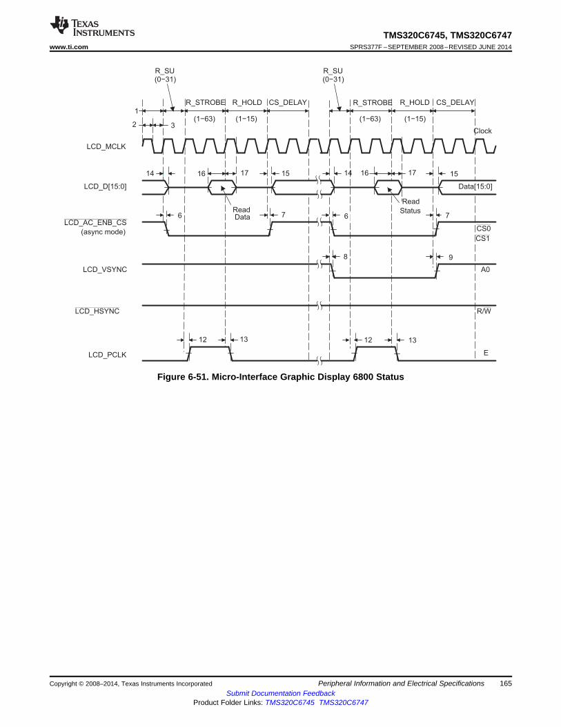
ReadData
LCD_D[15:0]
LCD_AC_ENB_CS
(async mode)
LCD_VSYNC
LCD_HSYNC
LCD_MCLK
LCD_PCLK
R_SU
R_STROBE R_HOLD
(0−31)
(1−63) (1−15)
CS_DELAY
CS0
CS1
A0
R/W
E
Clock
1
2 3
R_STROBE R_HOLD
(1−63) (1−15)
CS_DELAY
14 15
6 7 6 7
8 9
12 13
171614 1716 15
12 13
Data[15:0]
R_SU(0−31)
Read
Status
TMS320C6745, TMS320C6747www.ti.com SPRS377F –SEPTEMBER 2008–REVISED JUNE 2014
Figure 6-51. Micro-Interface Graphic Display 6800 Status
Copyright © 2008–2014, Texas Instruments Incorporated Peripheral Information and Electrical Specifications 165Submit Documentation Feedback
Product Folder Links: TMS320C6745 TMS320C6747
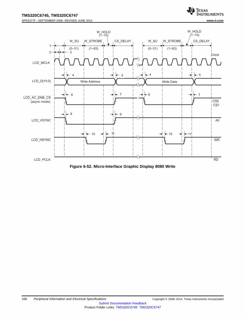
LCD_D[15:0]
LCD_AC_ENB_CS
(async mode)
LCD_VSYNC
LCD_HSYNC
LCD_MCLK
LCD_PCLK
4
W_SU W_STROBE
W_HOLD
(0−31) (1−63)
(1−15)
CS_DELAY
DATA[15:0]
CS0
CS1
A0
WR
RD
Clock
1
2 3
W_SU W_STROBE
W_HOLD
(0−31) (1−63)
(1−15)
CS_DELAY
5 4 5
6 7 6 7
8 9
10 11
Write Address Write Data
10 11
TMS320C6745, TMS320C6747SPRS377F –SEPTEMBER 2008–REVISED JUNE 2014 www.ti.com
Figure 6-52. Micro-Interface Graphic Display 8080 Write
166 Peripheral Information and Electrical Specifications Copyright © 2008–2014, Texas Instruments IncorporatedSubmit Documentation Feedback
Product Folder Links: TMS320C6745 TMS320C6747
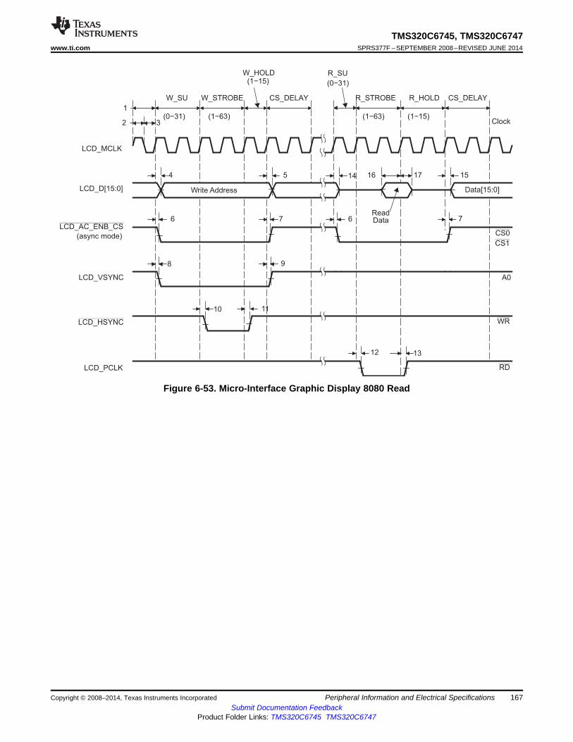
LCD_D[15:0]
LCD_AC_ENB_CS
(async mode)
LCD_VSYNC
LCD_HSYNC
LCD_MCLK
LCD_PCLK
4
W_SU W_STROBE
W_HOLD
(0−31) (1−63)
(1−15)
CS_DELAY
CS0
CS1
A0
WR
RD
Clock
1
2 3
R_SU
R_STROBE R_HOLD
(0−31)
(1−63) (1−15)
CS_DELAY
5 14 15
6 7 6 7
8 9
12 13
1716
ReadData
10 11
Data[15:0]Write Address
TMS320C6745, TMS320C6747www.ti.com SPRS377F –SEPTEMBER 2008–REVISED JUNE 2014
Figure 6-53. Micro-Interface Graphic Display 8080 Read
Copyright © 2008–2014, Texas Instruments Incorporated Peripheral Information and Electrical Specifications 167Submit Documentation Feedback
Product Folder Links: TMS320C6745 TMS320C6747

LCD_D[15:0]
LCD_AC_ENB_CS
LCD_VSYNC
LCD_HSYNC
LCD_MCLK
LCD_PCLK
R_SU
R_STROBE R_HOLD
(0−31)
(1−63) (1−15)
CS_DELAY
CS0
CS1
A0
WR
RD
Clock
1
23
R_STROBE R_HOLD
(1−63) (1−15)
CS_DELAY
14 15
6 7 6
8
12 13
1716
Read Status
14 1716
Read Data
15
12 13
Data[15:0]
7
9
R_SU(0−31)
TMS320C6745, TMS320C6747SPRS377F –SEPTEMBER 2008–REVISED JUNE 2014 www.ti.com
Figure 6-54. Micro-Interface Graphic Display 8080 Status
168 Peripheral Information and Electrical Specifications Copyright © 2008–2014, Texas Instruments IncorporatedSubmit Documentation Feedback
Product Folder Links: TMS320C6745 TMS320C6747
TMS320C6745, TMS320C6747www.ti.com SPRS377F –SEPTEMBER 2008–REVISED JUNE 2014
6.21.2 LCD Raster Mode
Table 6-84. LCD Raster Mode TimingSee Figure 6-55 through Figure 6-59
No. PARAMETER MIN MAX UNIT1 tc(PIXEL_CLK) Cycle time, pixel clock 26.6 ns2 tw(PIXEL_CLK_H) Pulse duration, pixel clock high 10 ns3 tw(PIXEL_CLK_L) Pulse duration, pixel clock low 10 ns4 td(LCD_D_V) Delay time, LCD_PCLK high to LCD_D[15:0] valid (write) -0.5 9 ns5 td(LCD_D_IV) Delay time, LCD_PCLK high to LCD_D[15:0] invalid (write) -0.5 9 ns6 td(LCD_AC_ENB_CS_A) Delay time, LCD_PCLK low to LCD_AC_ENB_CS high S2 - 0.5 (1) S2 + 9 (1) ns7 td(LCD_AC_ENB_CS_I) Delay time, LCD_PCLK low to LCD_AC_ENB_CS low S2 - 0.5 (1) S2 + 9 (1) ns8 td(LCD_VSYNC_A) Delay time, LCD_PCLK low to LCD_VSYNC high (2) -0.5 12 ns9 td(LCD_VSYNC_I) Delay time, LCD_PCLK low to LCD_VSYNC low (2) -0.5 12 ns10 td(LCD_HSYNC_A) Delay time, LCD_PCLK high to LCD_HSYNC high (2) -0.5 12 ns11 td(LCD_HSYNC_I) Delay time, LCD_PCLK high to LCD_HSYNC low (2) -0.5 12 ns
(1) S2 = SYSCLK2 cycle time in ns(2) The activation edge of the control signals LCD_VSYNC and LCD_HSYNC may be programmed to either the rising or falling edge of the
pixel clock through the LCD (RASTER_TIMING_2) register. In Figure 6-56 through Figure 6-59, all signal polarity and activation edgesare based on the default LCD (RASTER_TIMING_2) register settings.
Frame-to-frame timing is derived through the following parameters in the LCD (RASTER_TIMING_1)register:• Vertical front porch (VFP)• Vertical sync pulse width (VSW)• Vertical back porch (VBP)• Lines per panel (LPP)
Line-to-line timing is derived through the following parameters in the LCD (RASTER_TIMING_0) register:• Horizontal front porch (HFP)• Horizontal sync pulse width (HSW)• Horizontal back porch (HBP)• Pixels per panel (PPL)
.LCD_AC_ENB_CS timing is derived through the following parameter in the LCD (RASTER_TIMING_2)register:• AC bias frequency (ACB)
The display format produced in raster mode is shown in Figure 6-55. An entire frame is delivered one lineat a time. The first line delivered starts at data pixel (1, 1) and ends at data pixel (P, 1). The last linedelivered starts at data pixel (1, L) and ends at data pixel (P, L). The beginning of each new frame isdenoted by the activation of I/O signal LCD_VSYNC. The beginning of each new line is denoted by theactivation of I/O signal LCD_HSYNC.
Copyright © 2008–2014, Texas Instruments Incorporated Peripheral Information and Electrical Specifications 169Submit Documentation Feedback
Product Folder Links: TMS320C6745 TMS320C6747

LCD
1, 1 2, 1 3, 1
1, 2 2, 2
1, 3
P, 1P−1,1
P−2,
P, 2P−1,2
P, 3
1, L
1,
L−1
1,L−2
3, L2, L
2,
L−1
P, L
P−1,
L−1
P,
L−1
P−1,L
P,
L−2
P−2,L
Data Pixels (From 1 to P)D
ata
Lin
es (
Fro
m 1
to L
)
1
TMS320C6745, TMS320C6747SPRS377F –SEPTEMBER 2008–REVISED JUNE 2014 www.ti.com
Figure 6-55. LCD Raster-Mode Display Format
170 Peripheral Information and Electrical Specifications Copyright © 2008–2014, Texas Instruments IncorporatedSubmit Documentation Feedback
Product Folder Links: TMS320C6745 TMS320C6747

LCD_HSYNC
Hsync
LCD_VSYNC
(1 to 64)
VSW
(1 to 64)
VSW
(0 to 255)
VFP
(1 to 1024)
Frame Time 70 Hz~
LPP
(0 to 255)
LCD_D[15:0]
1, 1
P, 1
1, 2
P, 2
1, L
P, L
1, L-1
P, L-1
Line
Time
Vsync
Data
Active TFT
LCD_AC_ENB_CS
VBP
CLK
LCD_HSYNC Hsync
10 11
LCD_PCLK
LCD_D[15:0] 1, 1 2, 2 P, 2P, 12, 1 1, 2
PLL
16 × (1 to 1024)
HBP
(1 to 256)
Line 1
(1 to 256)
HFP
(1 to 64)
HSW PLL
16 × (1 to 1024)
Line 2
Data
LCD_AC_ENB_CS Enable
TMS320C6745, TMS320C6747www.ti.com SPRS377F –SEPTEMBER 2008–REVISED JUNE 2014
Figure 6-56. LCD Raster-Mode Active
Copyright © 2008–2014, Texas Instruments Incorporated Peripheral Information and Electrical Specifications 171Submit Documentation Feedback
Product Folder Links: TMS320C6745 TMS320C6747

LCD_HSYNC LP
LCD_VSYNC
VSW = 1
(1 to 1024)
Frame Time ~ 70Hz
LPP
LCD_D[7:0]
1, L−2
P, L−2
1, L−4
P, L−4
Line
Time
LCD_HSYNC LP
10 11
LCD_PCLK
LCD_D[7:0] 1, 5 2, 6 P, 6P, 52, 5 1, 6
PPL
16 (1 to 1024)
HBP
(1 to 256)
Line 5
HFP
(1 to 64)
HSW PPL
16 (1 to 2024)
Line 6
1, 1:P, 1
1, 5:P, 5
1, L−1
P, L−1
1, L
1, L−1
P, L−1
1, L−3
P, L−3
(1 to 64)
VSW = 1(1 to 64)
VFP = 0VBP = 0 VFP = 0
VBP = 0
FP
Data
CP
Data
Passive STN
LCD_AC_ENB_CS M
ACB
(0 to 255)
ACB
(0 to 255)
1, 4:P, 4
1, 3:P, 3
1, 2:P, 2
1, L:P, L
1, 6:P, 6
1, 2P, 2
1, 1P, 1
1, LP, L
(1 to 256)
TMS320C6745, TMS320C6747SPRS377F –SEPTEMBER 2008–REVISED JUNE 2014 www.ti.com
Figure 6-57. LCD Raster-Mode Passive
172 Peripheral Information and Electrical Specifications Copyright © 2008–2014, Texas Instruments IncorporatedSubmit Documentation Feedback
Product Folder Links: TMS320C6745 TMS320C6747

LCD_HSYNC
LCD_PCLK
(active mode)
LCD_D[15:0]
(active mode)1, L P, L2, L
PPL
16 ×(1 to 1024)
HBP
(1 to 256
Line L
(1 to 256)
HFP
(1 to 64)
HSW PPL
16 ×(1 to 1024)
Line 1 (Passive Only)
LCD_VSYNC
LCD_PCLK
(passive mode)
LCD_AC_ENB_CS
LCD_D[7:0]
(passive mode)1, L 2, 1 P, 1P, L2, L 1, 1
10 11
8
6
4
4
5
5
1
2 3
1
2 3
VSW = 1
VFP = 0VBP = 0
TMS320C6745, TMS320C6747www.ti.com SPRS377F –SEPTEMBER 2008–REVISED JUNE 2014
Figure 6-58. LCD Raster-Mode Control Signal Activation
Copyright © 2008–2014, Texas Instruments Incorporated Peripheral Information and Electrical Specifications 173Submit Documentation Feedback
Product Folder Links: TMS320C6745 TMS320C6747
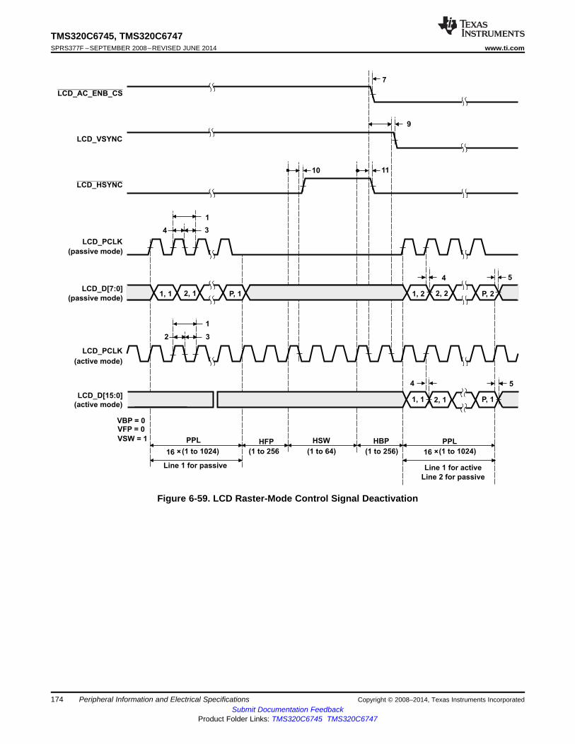
LCD_HSYNC
LCD_PCLK
(active mode)
LCD_D[15:0]
(active mode)
PPL
16 ×(1 to 1024)
HBP
(1 to 256
Line 1 for passive
(1 to 256)
HFP
(1 to 64)
HSW PPL
16 ×(1 to 1024)
Line 1 for active
LCD_VSYNC
LCD_PCLK
(passive mode)
LCD_AC_ENB_CS
LCD_D[7:0]
(passive mode)1, 1 2, 2 P, 2P, 12, 1 1, 2
10 11
9
7
4 5
1
2 3
VSW = 1
VFP = 0VBP = 0
P, 11, 1 2, 1
4 5
1
34
Line 2 for passive
TMS320C6745, TMS320C6747SPRS377F –SEPTEMBER 2008–REVISED JUNE 2014 www.ti.com
Figure 6-59. LCD Raster-Mode Control Signal Deactivation
174 Peripheral Information and Electrical Specifications Copyright © 2008–2014, Texas Instruments IncorporatedSubmit Documentation Feedback
Product Folder Links: TMS320C6745 TMS320C6747
TMS320C6745, TMS320C6747www.ti.com SPRS377F –SEPTEMBER 2008–REVISED JUNE 2014
6.22 TimersThe timers support the following features:• Configurable as single 64-bit timer or two 32-bit timers• Period timeouts generate interrupts, DMA events or external pin events• 8 32-bit compare registers• Compare matches generate interrupt events• Capture capability• 64-bit Watchdog capability (Timer64P1 only)Table 6-85 lists the timer registers.
Table 6-85. Timer Registers
Timer64P 0 Timer64P 1 ACRONYM REGISTER DESCRIPTION0x01C2 0000 0x01C2 1000 REV Revision Register0x01C2 0004 0x01C2 1004 EMUMGT Emulation Management Register0x01C2 0008 0x01C2 1008 GPINTGPEN GPIO Interrupt and GPIO Enable Register0x01C2 000C 0x01C2 100C GPDATGPDIR GPIO Data and GPIO Direction Register0x01C2 0010 0x01C2 1010 TIM12 Timer Counter Register 120x01C2 0014 0x01C2 1014 TIM34 Timer Counter Register 340x01C2 0018 0x01C2 1018 PRD12 Timer Period Register 120x01C2 001C 0x01C2 101C PRD34 Timer Period Register 340x01C2 0020 0x01C2 1020 TCR Timer Control Register0x01C2 0024 0x01C2 1024 TGCR Timer Global Control Register0x01C2 0028 0x01C2 1028 WDTCR Watchdog Timer Control Register0x01C2 0034 0x01C2 1034 REL12 Timer Reload Register 120x01C2 0038 0x01C2 1038 REL34 Timer Reload Register 340x01C2 003C 0x01C2 103C CAP12 Timer Capture Register 120x01C2 0040 0x01C2 1040 CAP34 Timer Capture Register 340x01C2 0044 0x01C2 1044 INTCTLSTAT Timer Interrupt Control and Status Register0x01C2 0060 0x01C2 1060 CMP0 Compare Register 00x01C2 0064 0x01C2 1064 CMP1 Compare Register 10x01C2 0068 0x01C2 1068 CMP2 Compare Register 20x01C2 006C 0x01C2 106C CMP3 Compare Register 30x01C2 0070 0x01C2 1070 CMP4 Compare Register 40x01C2 0074 0x01C2 1074 CMP5 Compare Register 50x01C2 0078 0x01C2 1078 CMP6 Compare Register 60x01C2 007C 0x01C2 107C CMP7 Compare Register 7
Copyright © 2008–2014, Texas Instruments Incorporated Peripheral Information and Electrical Specifications 175Submit Documentation Feedback
Product Folder Links: TMS320C6745 TMS320C6747
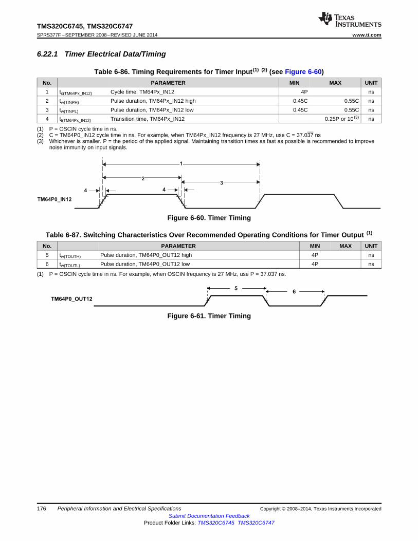
TM64P0_OUT12
56
1
2
44
3
TM64P0_IN12
TMS320C6745, TMS320C6747SPRS377F –SEPTEMBER 2008–REVISED JUNE 2014 www.ti.com
6.22.1 Timer Electrical Data/Timing
Table 6-86. Timing Requirements for Timer Input (1) (2) (see Figure 6-60)No. PARAMETER MIN MAX UNIT1 tc(TM64Px_IN12) Cycle time, TM64Px_IN12 4P ns2 tw(TINPH) Pulse duration, TM64Px_IN12 high 0.45C 0.55C ns3 tw(TINPL) Pulse duration, TM64Px_IN12 low 0.45C 0.55C ns4 tt(TM64Px_IN12) Transition time, TM64Px_IN12 0.25P or 10 (3) ns
(1) P = OSCIN cycle time in ns.(2) C = TM64P0_IN12 cycle time in ns. For example, when TM64Px_IN12 frequency is 27 MHz, use C = 37.037 ns(3) Whichever is smaller. P = the period of the applied signal. Maintaining transition times as fast as possible is recommended to improve
noise immunity on input signals.
Figure 6-60. Timer Timing
Table 6-87. Switching Characteristics Over Recommended Operating Conditions for Timer Output (1)
No. PARAMETER MIN MAX UNIT5 tw(TOUTH) Pulse duration, TM64P0_OUT12 high 4P ns6 tw(TOUTL) Pulse duration, TM64P0_OUT12 low 4P ns
(1) P = OSCIN cycle time in ns. For example, when OSCIN frequency is 27 MHz, use P = 37.037 ns.
Figure 6-61. Timer Timing
176 Peripheral Information and Electrical Specifications Copyright © 2008–2014, Texas Instruments IncorporatedSubmit Documentation Feedback
Product Folder Links: TMS320C6745 TMS320C6747

Peripheral
Configuration
Bus
Noise
Filter
Noise
Filter
Clock Prescaler
I2CPSCxPrescaler
Register
Bit Clock Generator
I2CCLKHxClock Divide
High Register
I2CCLKLxClock Divide
Low Register
Control
I2CCOARxOwn Address
Register
I2CSARxSlave Address
Register
I2CCMDRx Mode Register
I2CEMDRxExtended Mode
Register
I2CCNTxData Count
Register
I2CPID1Peripheral ID
Register 1
I2CPID2Peripheral ID
Register 2
Transmit
I2CXSRxTransmit Shift
Register
I2CDXRx Transmit Buffer
Receive
I2CDRRx Receive Buffer
I2CRSRxReceive Shift
Register
I2Cx_SCL
I2Cx_SDA Interrupt/DMA
I2CIERxInterrupt Enable
Register
I2CSTRxInterrupt Status
Register
I2CSRCxInterrupt Source
Register
Control
I2CPFUNCPin Function
Register
I2CPDIRPin Direction
Register
I2CPDINPin Data In
Register
I2CPDOUTPin Data Out
Register
I2CPDSETPin Data Set
Register
I2CPDCLRPin Data Clear
Register
Interrupt DMA
Requests
TMS320C6745, TMS320C6747www.ti.com SPRS377F –SEPTEMBER 2008–REVISED JUNE 2014
6.23 Inter-Integrated Circuit Serial Ports (I2C0, I2C1)
6.23.1 I2C Device-Specific InformationHaving two I2C modules on the C6745/6747 simplifies system architecture, since one module may beused by the DSP to control local peripherals ICs (DACs, ADCs, etc.) while the other may be used tocommunicate with other controllers in a system or to implement a user interface. Figure 6-62 is blockdiagram of the C6745/6747 I2C Module.
Each I2C port supports:• Compatible with Philips® I2C Specification Revision 2.1 (January 2000)• Fast Mode up to 400 Kbps (no fail-safe I/O buffers)• Noise Filter to Remove Noise 50 ns or less• Seven- and Ten-Bit Device Addressing Modes• Master (Transmit/Receive) and Slave (Transmit/Receive) Functionality• Events: DMA, Interrupt, or Polling• General-Purpose I/O Capability if not used as I2C
Figure 6-62. I2C Module Block Diagram
Copyright © 2008–2014, Texas Instruments Incorporated Peripheral Information and Electrical Specifications 177Submit Documentation Feedback
Product Folder Links: TMS320C6745 TMS320C6747
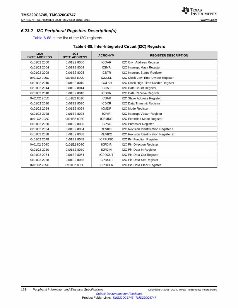
TMS320C6745, TMS320C6747SPRS377F –SEPTEMBER 2008–REVISED JUNE 2014 www.ti.com
6.23.2 I2C Peripheral Registers Description(s)Table 6-88 is the list of the I2C registers.
Table 6-88. Inter-Integrated Circuit (I2C) Registers
I2C0 I2C1 ACRONYM REGISTER DESCRIPTIONBYTE ADDRESS BYTE ADDRESS0x01C2 2000 0x01E2 8000 ICOAR I2C Own Address Register0x01C2 2004 0x01E2 8004 ICIMR I2C Interrupt Mask Register0x01C2 2008 0x01E2 8008 ICSTR I2C Interrupt Status Register0x01C2 200C 0x01E2 800C ICCLKL I2C Clock Low-Time Divider Register0x01C2 2010 0x01E2 8010 ICCLKH I2C Clock High-Time Divider Register0x01C2 2014 0x01E2 8014 ICCNT I2C Data Count Register0x01C2 2018 0x01E2 8018 ICDRR I2C Data Receive Register0x01C2 201C 0x01E2 801C ICSAR I2C Slave Address Register0x01C2 2020 0x01E2 8020 ICDXR I2C Data Transmit Register0x01C2 2024 0x01E2 8024 ICMDR I2C Mode Register0x01C2 2028 0x01E2 8028 ICIVR I2C Interrupt Vector Register0x01C2 202C 0x01E2 802C ICEMDR I2C Extended Mode Register0x01C2 2030 0x01E2 8030 ICPSC I2C Prescaler Register0x01C2 2034 0x01E2 8034 REVID1 I2C Revision Identification Register 10x01C2 2038 0x01E2 8038 REVID2 I2C Revision Identification Register 20x01C2 2048 0x01E2 8048 ICPFUNC I2C Pin Function Register0x01C2 204C 0x01E2 804C ICPDIR I2C Pin Direction Register0x01C2 2050 0x01E2 8050 ICPDIN I2C Pin Data In Register0x01C2 2054 0x01E2 8054 ICPDOUT I2C Pin Data Out Register0x01C2 2058 0x01E2 8058 ICPDSET I2C Pin Data Set Register0x01C2 205C 0x01E2 805C ICPDCLR I2C Pin Data Clear Register
178 Peripheral Information and Electrical Specifications Copyright © 2008–2014, Texas Instruments IncorporatedSubmit Documentation Feedback
Product Folder Links: TMS320C6745 TMS320C6747
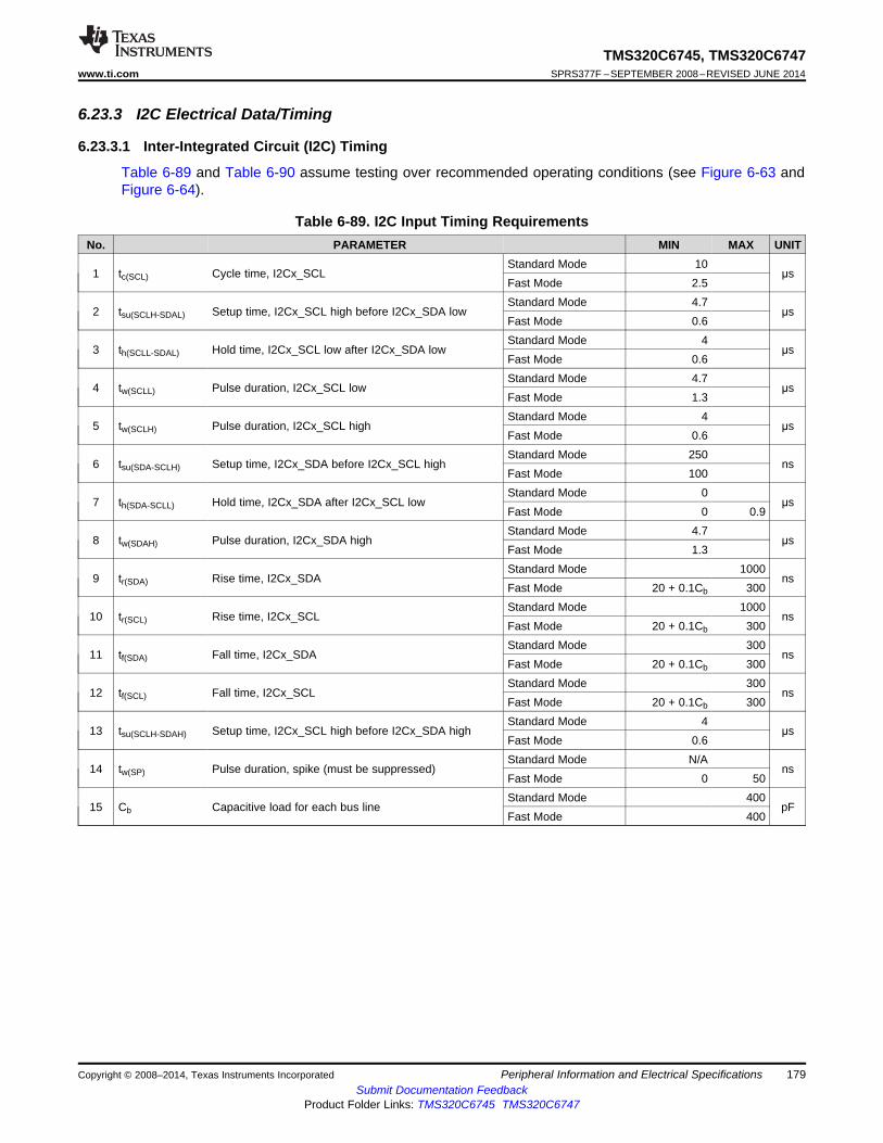
TMS320C6745, TMS320C6747www.ti.com SPRS377F –SEPTEMBER 2008–REVISED JUNE 2014
6.23.3 I2C Electrical Data/Timing
6.23.3.1 Inter-Integrated Circuit (I2C) Timing
Table 6-89 and Table 6-90 assume testing over recommended operating conditions (see Figure 6-63 andFigure 6-64).
Table 6-89. I2C Input Timing RequirementsNo. PARAMETER MIN MAX UNIT
Standard Mode 101 tc(SCL) Cycle time, I2Cx_SCL μs
Fast Mode 2.5Standard Mode 4.7
2 tsu(SCLH-SDAL) Setup time, I2Cx_SCL high before I2Cx_SDA low μsFast Mode 0.6Standard Mode 4
3 th(SCLL-SDAL) Hold time, I2Cx_SCL low after I2Cx_SDA low μsFast Mode 0.6Standard Mode 4.7
4 tw(SCLL) Pulse duration, I2Cx_SCL low μsFast Mode 1.3Standard Mode 4
5 tw(SCLH) Pulse duration, I2Cx_SCL high μsFast Mode 0.6Standard Mode 250
6 tsu(SDA-SCLH) Setup time, I2Cx_SDA before I2Cx_SCL high nsFast Mode 100Standard Mode 0
7 th(SDA-SCLL) Hold time, I2Cx_SDA after I2Cx_SCL low μsFast Mode 0 0.9Standard Mode 4.7
8 tw(SDAH) Pulse duration, I2Cx_SDA high μsFast Mode 1.3Standard Mode 1000
9 tr(SDA) Rise time, I2Cx_SDA nsFast Mode 20 + 0.1Cb 300Standard Mode 1000
10 tr(SCL) Rise time, I2Cx_SCL nsFast Mode 20 + 0.1Cb 300Standard Mode 300
11 tf(SDA) Fall time, I2Cx_SDA nsFast Mode 20 + 0.1Cb 300Standard Mode 300
12 tf(SCL) Fall time, I2Cx_SCL nsFast Mode 20 + 0.1Cb 300Standard Mode 4
13 tsu(SCLH-SDAH) Setup time, I2Cx_SCL high before I2Cx_SDA high μsFast Mode 0.6Standard Mode N/A
14 tw(SP) Pulse duration, spike (must be suppressed) nsFast Mode 0 50Standard Mode 400
15 Cb Capacitive load for each bus line pFFast Mode 400
Copyright © 2008–2014, Texas Instruments Incorporated Peripheral Information and Electrical Specifications 179Submit Documentation Feedback
Product Folder Links: TMS320C6745 TMS320C6747
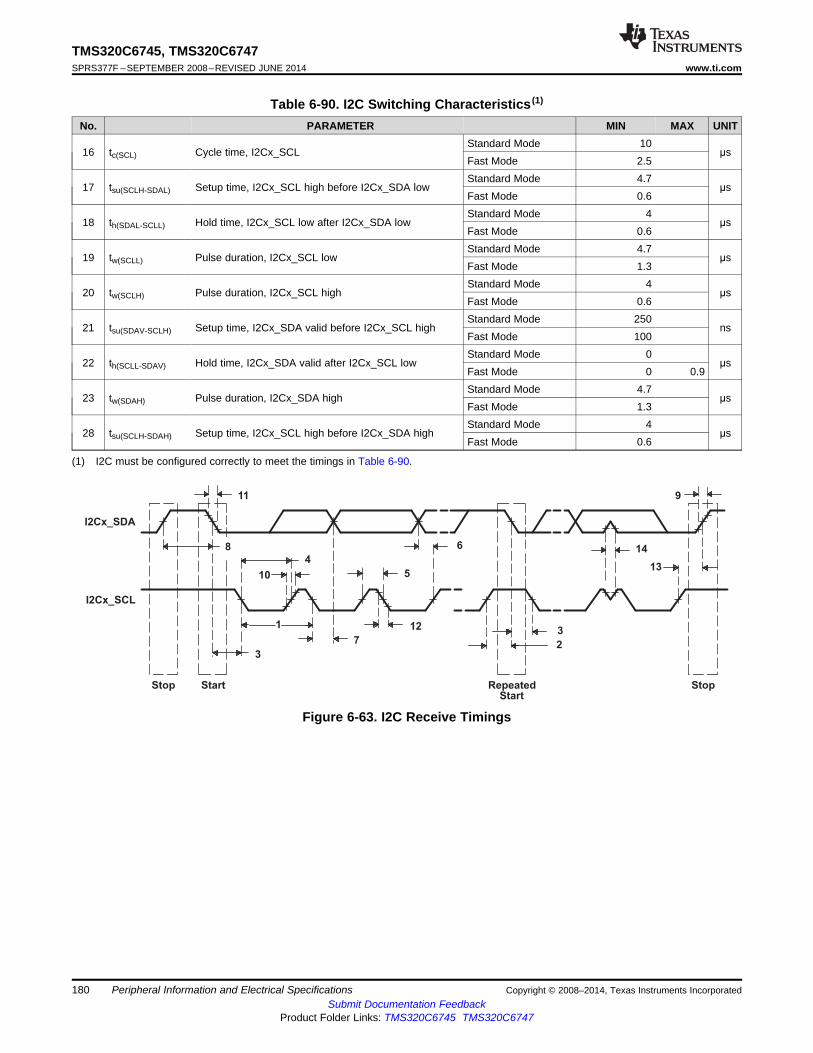
10
8
4
3
7
12
5
6 14
2
3
13
Stop Start RepeatedStart
Stop
I2Cx_SDA
I2Cx_SCL
1
11 9
TMS320C6745, TMS320C6747SPRS377F –SEPTEMBER 2008–REVISED JUNE 2014 www.ti.com
Table 6-90. I2C Switching Characteristics (1)
No. PARAMETER MIN MAX UNITStandard Mode 10
16 tc(SCL) Cycle time, I2Cx_SCL μsFast Mode 2.5Standard Mode 4.7
17 tsu(SCLH-SDAL) Setup time, I2Cx_SCL high before I2Cx_SDA low μsFast Mode 0.6Standard Mode 4
18 th(SDAL-SCLL) Hold time, I2Cx_SCL low after I2Cx_SDA low μsFast Mode 0.6Standard Mode 4.7
19 tw(SCLL) Pulse duration, I2Cx_SCL low μsFast Mode 1.3Standard Mode 4
20 tw(SCLH) Pulse duration, I2Cx_SCL high μsFast Mode 0.6Standard Mode 250
21 tsu(SDAV-SCLH) Setup time, I2Cx_SDA valid before I2Cx_SCL high nsFast Mode 100Standard Mode 0
22 th(SCLL-SDAV) Hold time, I2Cx_SDA valid after I2Cx_SCL low μsFast Mode 0 0.9Standard Mode 4.7
23 tw(SDAH) Pulse duration, I2Cx_SDA high μsFast Mode 1.3Standard Mode 4
28 tsu(SCLH-SDAH) Setup time, I2Cx_SCL high before I2Cx_SDA high μsFast Mode 0.6
(1) I2C must be configured correctly to meet the timings in Table 6-90.
Figure 6-63. I2C Receive Timings
180 Peripheral Information and Electrical Specifications Copyright © 2008–2014, Texas Instruments IncorporatedSubmit Documentation Feedback
Product Folder Links: TMS320C6745 TMS320C6747

25
23
19
18
22
27
20
21
17
18
28
Stop Start RepeatedStart
Stop
I2Cx_SDA
I2Cx_SCL
16
26 24
TMS320C6745, TMS320C6747www.ti.com SPRS377F –SEPTEMBER 2008–REVISED JUNE 2014
Figure 6-64. I2C Transmit Timings
Copyright © 2008–2014, Texas Instruments Incorporated Peripheral Information and Electrical Specifications 181Submit Documentation Feedback
Product Folder Links: TMS320C6745 TMS320C6747
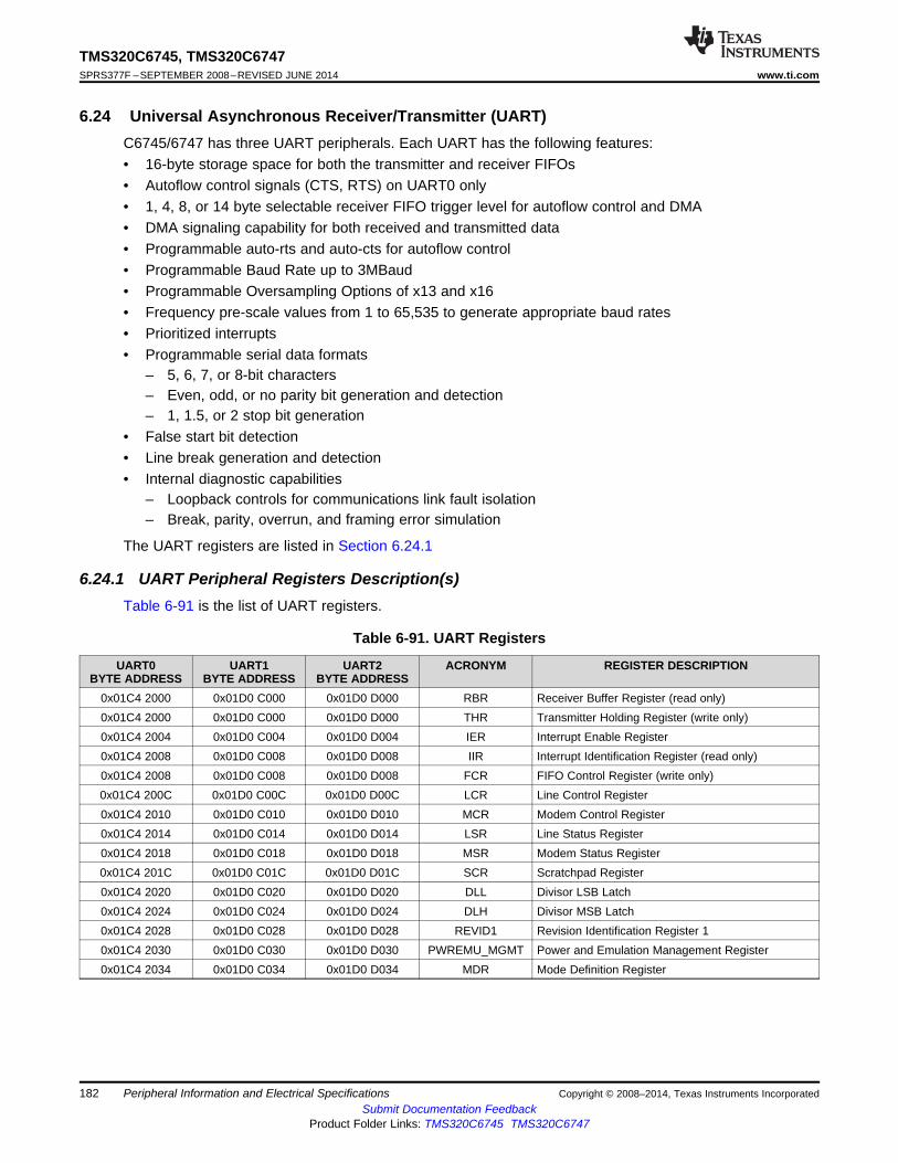
TMS320C6745, TMS320C6747SPRS377F –SEPTEMBER 2008–REVISED JUNE 2014 www.ti.com
6.24 Universal Asynchronous Receiver/Transmitter (UART)C6745/6747 has three UART peripherals. Each UART has the following features:• 16-byte storage space for both the transmitter and receiver FIFOs• Autoflow control signals (CTS, RTS) on UART0 only• 1, 4, 8, or 14 byte selectable receiver FIFO trigger level for autoflow control and DMA• DMA signaling capability for both received and transmitted data• Programmable auto-rts and auto-cts for autoflow control• Programmable Baud Rate up to 3MBaud• Programmable Oversampling Options of x13 and x16• Frequency pre-scale values from 1 to 65,535 to generate appropriate baud rates• Prioritized interrupts• Programmable serial data formats
– 5, 6, 7, or 8-bit characters– Even, odd, or no parity bit generation and detection– 1, 1.5, or 2 stop bit generation
• False start bit detection• Line break generation and detection• Internal diagnostic capabilities
– Loopback controls for communications link fault isolation– Break, parity, overrun, and framing error simulation
The UART registers are listed in Section 6.24.1
6.24.1 UART Peripheral Registers Description(s)Table 6-91 is the list of UART registers.
Table 6-91. UART Registers
UART0 UART1 UART2 ACRONYM REGISTER DESCRIPTIONBYTE ADDRESS BYTE ADDRESS BYTE ADDRESS
0x01C4 2000 0x01D0 C000 0x01D0 D000 RBR Receiver Buffer Register (read only)0x01C4 2000 0x01D0 C000 0x01D0 D000 THR Transmitter Holding Register (write only)0x01C4 2004 0x01D0 C004 0x01D0 D004 IER Interrupt Enable Register0x01C4 2008 0x01D0 C008 0x01D0 D008 IIR Interrupt Identification Register (read only)0x01C4 2008 0x01D0 C008 0x01D0 D008 FCR FIFO Control Register (write only)0x01C4 200C 0x01D0 C00C 0x01D0 D00C LCR Line Control Register0x01C4 2010 0x01D0 C010 0x01D0 D010 MCR Modem Control Register0x01C4 2014 0x01D0 C014 0x01D0 D014 LSR Line Status Register0x01C4 2018 0x01D0 C018 0x01D0 D018 MSR Modem Status Register0x01C4 201C 0x01D0 C01C 0x01D0 D01C SCR Scratchpad Register0x01C4 2020 0x01D0 C020 0x01D0 D020 DLL Divisor LSB Latch0x01C4 2024 0x01D0 C024 0x01D0 D024 DLH Divisor MSB Latch0x01C4 2028 0x01D0 C028 0x01D0 D028 REVID1 Revision Identification Register 10x01C4 2030 0x01D0 C030 0x01D0 D030 PWREMU_MGMT Power and Emulation Management Register0x01C4 2034 0x01D0 C034 0x01D0 D034 MDR Mode Definition Register
182 Peripheral Information and Electrical Specifications Copyright © 2008–2014, Texas Instruments IncorporatedSubmit Documentation Feedback
Product Folder Links: TMS320C6745 TMS320C6747
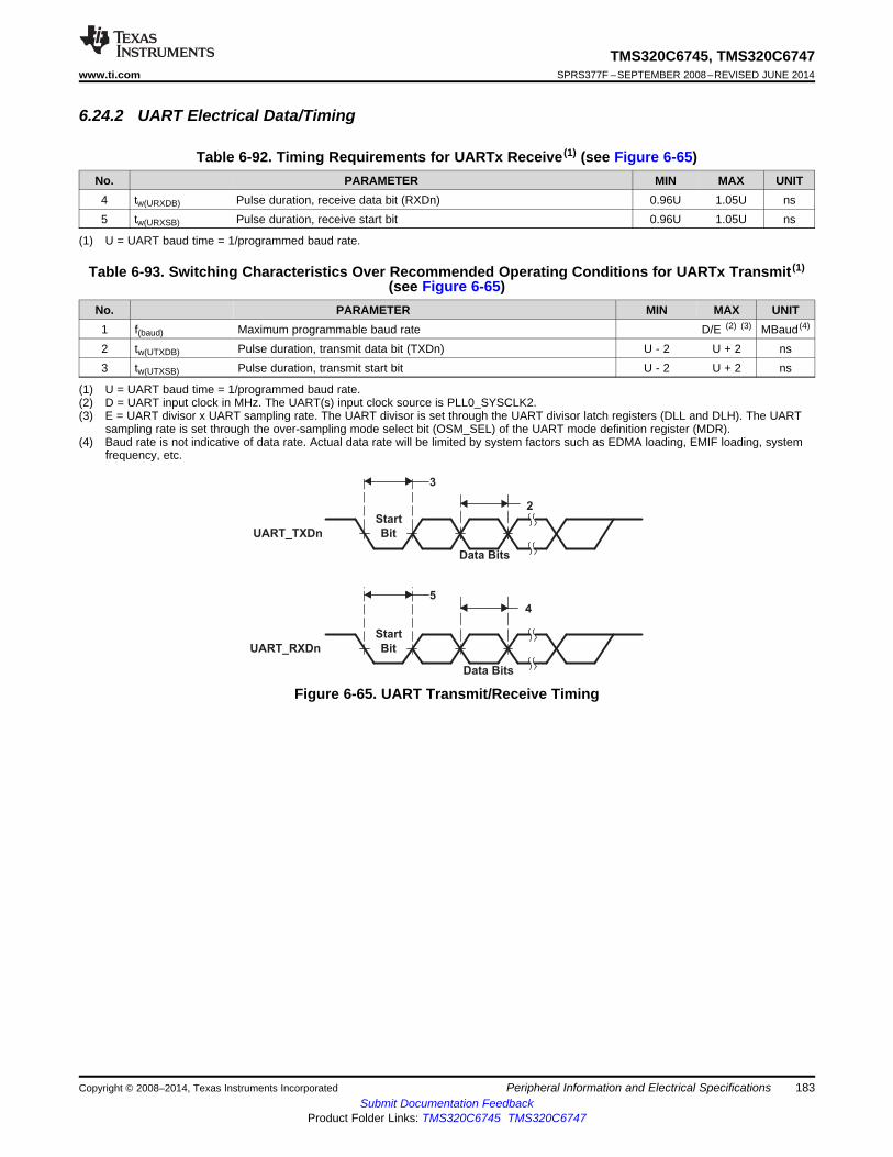
3
2Start
Bit
Data Bits
UART_TXDn
UART_RXDn
5
Data Bits
Bit
Start
4
TMS320C6745, TMS320C6747www.ti.com SPRS377F –SEPTEMBER 2008–REVISED JUNE 2014
6.24.2 UART Electrical Data/Timing
Table 6-92. Timing Requirements for UARTx Receive (1) (see Figure 6-65)No. PARAMETER MIN MAX UNIT4 tw(URXDB) Pulse duration, receive data bit (RXDn) 0.96U 1.05U ns5 tw(URXSB) Pulse duration, receive start bit 0.96U 1.05U ns
(1) U = UART baud time = 1/programmed baud rate.
Table 6-93. Switching Characteristics Over Recommended Operating Conditions for UARTx Transmit (1)
(see Figure 6-65)No. PARAMETER MIN MAX UNIT1 f(baud) Maximum programmable baud rate D/E (2) (3) MBaud (4)
2 tw(UTXDB) Pulse duration, transmit data bit (TXDn) U - 2 U + 2 ns3 tw(UTXSB) Pulse duration, transmit start bit U - 2 U + 2 ns
(1) U = UART baud time = 1/programmed baud rate.(2) D = UART input clock in MHz. The UART(s) input clock source is PLL0_SYSCLK2.(3) E = UART divisor x UART sampling rate. The UART divisor is set through the UART divisor latch registers (DLL and DLH). The UART
sampling rate is set through the over-sampling mode select bit (OSM_SEL) of the UART mode definition register (MDR).(4) Baud rate is not indicative of data rate. Actual data rate will be limited by system factors such as EDMA loading, EMIF loading, system
frequency, etc.
Figure 6-65. UART Transmit/Receive Timing
Copyright © 2008–2014, Texas Instruments Incorporated Peripheral Information and Electrical Specifications 183Submit Documentation Feedback
Product Folder Links: TMS320C6745 TMS320C6747

TMS320C6745, TMS320C6747SPRS377F –SEPTEMBER 2008–REVISED JUNE 2014 www.ti.com
6.25 USB1 Host Controller Registers (USB1.1 OHCI)All the device USB interfaces are compliant with Universal Serial Bus Specification, Revision 1.1.
Table 6-94 is the list of USB Host Controller registers.
Table 6-94. USB1 Host Controller Registers
BYTE ADDRESS ACRONYM REGISTER DESCRIPTION0x01E2 5000 HCREVISION OHCI Revision Number Register0x01E2 5004 HCCONTROL HC Operating Mode Register0x01E2 5008 HCCOMMANDSTATUS HC Command and Status Register0x01E2 500C HCINTERRUPTSTATUS HC Interrupt and Status Register0x01E2 5010 HCINTERRUPTENABLE HC Interrupt Enable Register0x01E2 5014 HCINTERRUPTDISABLE HC Interrupt Disable Register0x01E2 5018 HCHCCA HC HCAA Address Register (1)
0x01E2 501C HCPERIODCURRENTED HC Current Periodic Register (1)
0x01E2 5020 HCCONTROLHEADED HC Head Control Register (1)
0x01E2 5024 HCCONTROLCURRENTED HC Current Control Register (1)
0x01E2 5028 HCBULKHEADED HC Head Bulk Register (1)
0x01E2 502C HCBULKCURRENTED HC Current Bulk Register (1)
0x01E2 5030 HCDONEHEAD HC Head Done Register (1)
0x01E2 5034 HCFMINTERVAL HC Frame Interval Register0x01E2 5038 HCFMREMAINING HC Frame Remaining Register0x01E2 503C HCFMNUMBER HC Frame Number Register0x01E2 5040 HCPERIODICSTART HC Periodic Start Register0x01E2 5044 HCLSTHRESHOLD HC Low-Speed Threshold Register0x01E2 5048 HCRHDESCRIPTORA HC Root Hub A Register0x01E2 504C HCRHDESCRIPTORB HC Root Hub B Register0x01E2 5050 HCRHSTATUS HC Root Hub Status Register0x01E2 5054 HCRHPORTSTATUS1 HC Port 1 Status and Control Register (2)
0x01E2 5058 HCRHPORTSTATUS2 HC Port 2 Status and Control Register (3)
(1) Restrictions apply to the physical addresses used in these registers.(2) Connected to the integrated USB1.1 phy pins (USB1_DM, USB1_DP).(3) Although the controller implements two ports, the second port cannot be used.
Table 6-95. Switching Characteristics Over Recommended Operating Conditions for USB1LOW SPEED FULL SPEED
No. PARAMETER UNITMIN MAX MIN MAX
U1 tr Rise time, USB1_DP and USB1_DM signals (1) 75 (1) 300 (1) 4 (1) 20 (1) nsU2 tf Fall time, USB1_DP and USB1_DM signals (1) 75 (1) 300 (1) 4 (1) 20 (1) nsU3 tRFM Rise/Fall time matching (2) 80 (2) 120 (2) 90 (2) 110 (2) %U4 VCRS Output signal cross-over voltage (1) 1.3 (1) 2 (1) 1.3 (1) 2 (1) VU5 tj Differential propagation jitter (3) -25 (3) 25 (3) -2 (3) 2 (3) nsU6 fop Operating frequency (4) 1.5 12 MHz
(1) Low Speed: CL = 200 pF. High Speed: CL = 50pF(2) tRFM =( tr/tf ) x 100(3) t jr = t px(1) - tpx(0)(4) fop = 1/tper
6.25.1 USB1 Unused Signal ConfigurationIf USB1 is unused, then the USB1 signals should be configured as shown in Section 3.6.23.
184 Peripheral Information and Electrical Specifications Copyright © 2008–2014, Texas Instruments IncorporatedSubmit Documentation Feedback
Product Folder Links: TMS320C6745 TMS320C6747

TMS320C6745, TMS320C6747www.ti.com SPRS377F –SEPTEMBER 2008–REVISED JUNE 2014
6.26 USB0 OTG (USB2.0 OTG)The C6745/6747 USB2.0 peripheral supports the following features:• USB 2.0 peripheral at speeds high speed (HS: 480 Mb/s - C6747 only) and full speed (FS: 12 Mb/s)• USB 2.0 host at speeds HS (C6747 only), FS, and low speed (LS: 1.5 Mb/s)• All transfer modes (control, bulk, interrupt, and isochronous)• 4 Transmit (TX) and 4 Receive (RX) endpoints in addition to endpoint 0• FIFO RAM
– 4K endpoint– Programmable size
• Integrated USB 2.0 High Speed PHY• Connects to a standard Charge Pump for VBUS 5 V generation• RNDIS mode for accelerating RNDIS type protocols using short packet termination over USB
Important Notice: On the original device pinout (marked "A" in the lower right corner of the package),pins USB0_VSSA33 (ZKB package pin H4; PTP package pin 139) and USB0_VSSA (ZKB package pinF3; PTP package pin 136) were connected to ground outside the package. For more robust ESDperformance, the USB0 ground references are now connected inside the package on packages marked"B" and the package pins are unconnected. This change will require that any external filter circuitspreviously referenced to ground at these pins will need to reference the board ground instead.
Important Notice: The USB0 controller module clock (PLL0_SYSCLK2) must be greater than 30 MHz forproper operation of the USB controller. A clock rate of 60 MHz or greater is recommended to avoid datathroughput reduction.
Table 6-96 is the list of USB OTG registers.
Table 6-96. Universal Serial Bus OTG (USB0) Registers
BYTE ADDRESS ACRONYM REGISTER DESCRIPTION0x01E0 0000 REVID Revision Register0x01E0 0004 CTRLR Control Register0x01E0 0008 STATR Status Register0x01E0 000C EMUR Emulation Register0x01E0 0010 MODE Mode Register0x01E0 0014 AUTOREQ Autorequest Register0x01E0 0018 SRPFIXTIME SRP Fix Time Register0x01E0 001C TEARDOWN Teardown Register0x01E0 0020 INTSRCR USB Interrupt Source Register0x01E0 0024 INTSETR USB Interrupt Source Set Register0x01E0 0028 INTCLRR USB Interrupt Source Clear Register0x01E0 002C INTMSKR USB Interrupt Mask Register0x01E0 0030 INTMSKSETR USB Interrupt Mask Set Register0x01E0 0034 INTMSKCLRR USB Interrupt Mask Clear Register0x01E0 0038 INTMASKEDR USB Interrupt Source Masked Register0x01E0 003C EOIR USB End of Interrupt Register0x01E0 0040 - Reserved0x01E0 0050 GENRNDISSZ1 Generic RNDIS Size EP10x01E0 0054 GENRNDISSZ2 Generic RNDIS Size EP20x01E0 0058 GENRNDISSZ3 Generic RNDIS Size EP30x01E0 005C GENRNDISSZ4 Generic RNDIS Size EP40x01E0 0400 FADDR Function Address Register0x01E0 0401 POWER Power Management Register
Copyright © 2008–2014, Texas Instruments Incorporated Peripheral Information and Electrical Specifications 185Submit Documentation Feedback
Product Folder Links: TMS320C6745 TMS320C6747

TMS320C6745, TMS320C6747SPRS377F –SEPTEMBER 2008–REVISED JUNE 2014 www.ti.com
Table 6-96. Universal Serial Bus OTG (USB0) Registers (continued)BYTE ADDRESS ACRONYM REGISTER DESCRIPTION
0x01E0 0402 INTRTX Interrupt Register for Endpoint 0 plus Transmit Endpoints 1 to 40x01E0 0404 INTRRX Interrupt Register for Receive Endpoints 1 to 40x01E0 0406 INTRTXE Interrupt Enable Register for INTRTX0x01E0 0408 INTRRXE Interrupt Enable Register for INTRRX0x01E0 040A INTRUSB Interrupt Register for Common USB Interrupts0x01E0 040B INTRUSBE Interrupt Enable Register for INTRUSB0x01E0 040C FRAME Frame Number Register0x01E0 040E INDEX Index Register for Selecting the Endpoint Status and Control Registers0x01E0 040F TESTMODE Register to Enable the USB 2.0 Test Modes
INDEXED REGISTERSThese registers operate on the endpoint selected by the INDEX register
0x01E0 0410 TXMAXP Maximum Packet Size for Peripheral/Host Transmit Endpoint(Index register set to select Endpoints 1-4 only)
0x01E0 0412 PERI_CSR0 Control Status Register for Endpoint 0 in Peripheral Mode.(Index register set to select Endpoint 0)
HOST_CSR0 Control Status Register for Endpoint 0 in Host Mode.(Index register set to select Endpoint 0)
PERI_TXCSR Control Status Register for Peripheral Transmit Endpoint.(Index register set to select Endpoints 1-4)
HOST_TXCSR Control Status Register for Host Transmit Endpoint.(Index register set to select Endpoints 1-4)
0x01E0 0414 RXMAXP Maximum Packet Size for Peripheral/Host Receive Endpoint(Index register set to select Endpoints 1-4 only)
0x01E0 0416 PERI_RXCSR Control Status Register for Peripheral Receive Endpoint.(Index register set to select Endpoints 1-4)
HOST_RXCSR Control Status Register for Host Receive Endpoint.(Index register set to select Endpoints 1-4)
0x01E0 0418 COUNT0 Number of Received Bytes in Endpoint 0 FIFO.(Index register set to select Endpoint 0)
RXCOUNT Number of Bytes in Host Receive Endpoint FIFO.(Index register set to select Endpoints 1- 4)
0x01E0 041A HOST_TYPE0 Defines the speed of Endpoint 0HOST_TXTYPE Sets the operating speed, transaction protocol and peripheral endpoint
number for the host Transmit endpoint.(Index register set to select Endpoints 1-4 only)
0x01E0 041B HOST_NAKLIMIT0 Sets the NAK response timeout on Endpoint 0.(Index register set to select Endpoint 0)
HOST_TXINTERVAL Sets the polling interval for Interrupt/ISOC transactions or the NAKresponse timeout on Bulk transactions for host Transmit endpoint.(Index register set to select Endpoints 1-4 only)
0x01E0 041C HOST_RXTYPE Sets the operating speed, transaction protocol and peripheral endpointnumber for the host Receive endpoint.(Index register set to select Endpoints 1-4 only)
0x01E0 041D HOST_RXINTERVAL Sets the polling interval for Interrupt/ISOC transactions or the NAKresponse timeout on Bulk transactions for host Receive endpoint.(Index register set to select Endpoints 1-4 only)
0x01E0 041F CONFIGDATA Returns details of core configuration.(Index register set to select Endpoint 0)FIFO
0x01E0 0420 FIFO0 Transmit and Receive FIFO Register for Endpoint 00x01E0 0424 FIFO1 Transmit and Receive FIFO Register for Endpoint 10x01E0 0428 FIFO2 Transmit and Receive FIFO Register for Endpoint 20x01E0 042C FIFO3 Transmit and Receive FIFO Register for Endpoint 30x01E0 0430 FIFO4 Transmit and Receive FIFO Register for Endpoint 4
186 Peripheral Information and Electrical Specifications Copyright © 2008–2014, Texas Instruments IncorporatedSubmit Documentation Feedback
Product Folder Links: TMS320C6745 TMS320C6747
TMS320C6745, TMS320C6747www.ti.com SPRS377F –SEPTEMBER 2008–REVISED JUNE 2014
Table 6-96. Universal Serial Bus OTG (USB0) Registers (continued)BYTE ADDRESS ACRONYM REGISTER DESCRIPTION
OTG DEVICE CONTROL0x01E0 0460 DEVCTL Device Control Register
DYNAMIC FIFO CONTROL0x01E0 0462 TXFIFOSZ Transmit Endpoint FIFO Size
(Index register set to select Endpoints 1-4 only)0x01E0 0463 RXFIFOSZ Receive Endpoint FIFO Size
(Index register set to select Endpoints 1-4 only)0x01E0 0464 TXFIFOADDR Transmit Endpoint FIFO Address
(Index register set to select Endpoints 1-4 only)0x01E0 0466 RXFIFOADDR Receive Endpoint FIFO Address
(Index register set to select Endpoints 1-4 only)0x01E0 046C HWVERS Hardware Version Register
TARGET ENDPOINT 0 CONTROL REGISTERS, VALID ONLY IN HOST MODE0x01E0 0480 TXFUNCADDR Address of the target function that has to be accessed through the
associated Transmit Endpoint.0x01E0 0482 TXHUBADDR Address of the hub that has to be accessed through the associated
Transmit Endpoint. This is used only when full speed or low speeddevice is connected via a USB2.0 high-speed hub.
0x01E0 0483 TXHUBPORT Port of the hub that has to be accessed through the associatedTransmit Endpoint. This is used only when full speed or low speeddevice is connected via a USB2.0 high-speed hub.
0x01E0 0484 RXFUNCADDR Address of the target function that has to be accessed through theassociated Receive Endpoint.
0x01E0 0486 RXHUBADDR Address of the hub that has to be accessed through the associatedReceive Endpoint. This is used only when full speed or low speeddevice is connected via a USB2.0 high-speed hub.
0x01E0 0487 RXHUBPORT Port of the hub that has to be accessed through the associated ReceiveEndpoint. This is used only when full speed or low speed device isconnected via a USB2.0 high-speed hub.
TARGET ENDPOINT 1 CONTROL REGISTERS, VALID ONLY IN HOST MODE0x01E0 0488 TXFUNCADDR Address of the target function that has to be accessed through the
associated Transmit Endpoint.0x01E0 048A TXHUBADDR Address of the hub that has to be accessed through the associated
Transmit Endpoint. This is used only when full speed or low speeddevice is connected via a USB2.0 high-speed hub.
0x01E0 048B TXHUBPORT Port of the hub that has to be accessed through the associatedTransmit Endpoint. This is used only when full speed or low speeddevice is connected via a USB2.0 high-speed hub.
0x01E0 048C RXFUNCADDR Address of the target function that has to be accessed through theassociated Receive Endpoint.
0x01E0 048E RXHUBADDR Address of the hub that has to be accessed through the associatedReceive Endpoint. This is used only when full speed or low speeddevice is connected via a USB2.0 high-speed hub.
0x01E0 048F RXHUBPORT Port of the hub that has to be accessed through the associated ReceiveEndpoint. This is used only when full speed or low speed device isconnected via a USB2.0 high-speed hub.
TARGET ENDPOINT 2 CONTROL REGISTERS, VALID ONLY IN HOST MODE0x01E0 0490 TXFUNCADDR Address of the target function that has to be accessed through the
associated Transmit Endpoint.0x01E0 0492 TXHUBADDR Address of the hub that has to be accessed through the associated
Transmit Endpoint. This is used only when full speed or low speeddevice is connected via a USB2.0 high-speed hub.
0x01E0 0493 TXHUBPORT Port of the hub that has to be accessed through the associatedTransmit Endpoint. This is used only when full speed or low speeddevice is connected via a USB2.0 high-speed hub.
0x01E0 0494 RXFUNCADDR Address of the target function that has to be accessed through theassociated Receive Endpoint.
Copyright © 2008–2014, Texas Instruments Incorporated Peripheral Information and Electrical Specifications 187Submit Documentation Feedback
Product Folder Links: TMS320C6745 TMS320C6747

TMS320C6745, TMS320C6747SPRS377F –SEPTEMBER 2008–REVISED JUNE 2014 www.ti.com
Table 6-96. Universal Serial Bus OTG (USB0) Registers (continued)BYTE ADDRESS ACRONYM REGISTER DESCRIPTION
0x01E0 0496 RXHUBADDR Address of the hub that has to be accessed through the associatedReceive Endpoint. This is used only when full speed or low speeddevice is connected via a USB2.0 high-speed hub.
0x01E0 0497 RXHUBPORT Port of the hub that has to be accessed through the associated ReceiveEndpoint. This is used only when full speed or low speed device isconnected via a USB2.0 high-speed hub.
TARGET ENDPOINT 3 CONTROL REGISTERS, VALID ONLY IN HOST MODE0x01E0 0498 TXFUNCADDR Address of the target function that has to be accessed through the
associated Transmit Endpoint.0x01E0 049A TXHUBADDR Address of the hub that has to be accessed through the associated
Transmit Endpoint. This is used only when full speed or low speeddevice is connected via a USB2.0 high-speed hub.
0x01E0 049B TXHUBPORT Port of the hub that has to be accessed through the associatedTransmit Endpoint. This is used only when full speed or low speeddevice is connected via a USB2.0 high-speed hub.
0x01E0 049C RXFUNCADDR Address of the target function that has to be accessed through theassociated Receive Endpoint.
0x01E0 049E RXHUBADDR Address of the hub that has to be accessed through the associatedReceive Endpoint. This is used only when full speed or low speeddevice is connected via a USB2.0 high-speed hub.
0x01E0 049F RXHUBPORT Port of the hub that has to be accessed through the associated ReceiveEndpoint. This is used only when full speed or low speed device isconnected via a USB2.0 high-speed hub.
TARGET ENDPOINT 4 CONTROL REGISTERS, VALID ONLY IN HOST MODE0x01E0 04A0 TXFUNCADDR Address of the target function that has to be accessed through the
associated Transmit Endpoint.0x01E0 04A2 TXHUBADDR Address of the hub that has to be accessed through the associated
Transmit Endpoint. This is used only when full speed or low speeddevice is connected via a USB2.0 high-speed hub.
0x01E0 04A3 TXHUBPORT Port of the hub that has to be accessed through the associatedTransmit Endpoint. This is used only when full speed or low speeddevice is connected via a USB2.0 high-speed hub.
0x01E0 04A4 RXFUNCADDR Address of the target function that has to be accessed through theassociated Receive Endpoint.
0x01E0 04A6 RXHUBADDR Address of the hub that has to be accessed through the associatedReceive Endpoint. This is used only when full speed or low speeddevice is connected via a USB2.0 high-speed hub.
0x01E0 04A7 RXHUBPORT Port of the hub that has to be accessed through the associated ReceiveEndpoint. This is used only when full speed or low speed device isconnected via a USB2.0 high-speed hub.
CONTROL AND STATUS REGISTER FOR ENDPOINT 00x01E0 0502 PERI_CSR0 Control Status Register for Endpoint 0 in Peripheral Mode
HOST_CSR0 Control Status Register for Endpoint 0 in Host Mode0x01E0 0508 COUNT0 Number of Received Bytes in Endpoint 0 FIFO0x01E0 050A HOST_TYPE0 Defines the Speed of Endpoint 00x01E0 050B HOST_NAKLIMIT0 Sets the NAK Response Timeout on Endpoint 00x01E0 050F CONFIGDATA Returns details of core configuration.
CONTROL AND STATUS REGISTER FOR ENDPOINT 10x01E0 0510 TXMAXP Maximum Packet Size for Peripheral/Host Transmit Endpoint0x01E0 0512 PERI_TXCSR Control Status Register for Peripheral Transmit Endpoint
(peripheral mode)HOST_TXCSR Control Status Register for Host Transmit Endpoint
(host mode)0x01E0 0514 RXMAXP Maximum Packet Size for Peripheral/Host Receive Endpoint
188 Peripheral Information and Electrical Specifications Copyright © 2008–2014, Texas Instruments IncorporatedSubmit Documentation Feedback
Product Folder Links: TMS320C6745 TMS320C6747

TMS320C6745, TMS320C6747www.ti.com SPRS377F –SEPTEMBER 2008–REVISED JUNE 2014
Table 6-96. Universal Serial Bus OTG (USB0) Registers (continued)BYTE ADDRESS ACRONYM REGISTER DESCRIPTION
0x01E0 0516 PERI_RXCSR Control Status Register for Peripheral Receive Endpoint(peripheral mode)
HOST_RXCSR Control Status Register for Host Receive Endpoint(host mode)
0x01E0 0518 RXCOUNT Number of Bytes in Host Receive endpoint FIFO0x01E0 051A HOST_TXTYPE Sets the operating speed, transaction protocol and peripheral endpoint
number for the host Transmit endpoint.0x01E0 051B HOST_TXINTERVAL Sets the polling interval for Interrupt/ISOC transactions or the NAK
response timeout on Bulk transactions for host Transmit endpoint.0x01E0 051C HOST_RXTYPE Sets the operating speed, transaction protocol and peripheral endpoint
number for the host Receive endpoint.0x01E0 051D HOST_RXINTERVAL Sets the polling interval for Interrupt/ISOC transactions or the NAK
response timeout on Bulk transactions for host Receive endpoint.CONTROL AND STATUS REGISTER FOR ENDPOINT 2
0x01E0 0520 TXMAXP Maximum Packet Size for Peripheral/Host Transmit Endpoint0x01E0 0522 PERI_TXCSR Control Status Register for Peripheral Transmit Endpoint
(peripheral mode)HOST_TXCSR Control Status Register for Host Transmit Endpoint
(host mode)0x01E0 0524 RXMAXP Maximum Packet Size for Peripheral/Host Receive Endpoint0x01E0 0526 PERI_RXCSR Control Status Register for Peripheral Receive Endpoint
(peripheral mode)HOST_RXCSR Control Status Register for Host Receive Endpoint
(host mode)0x01E0 0528 RXCOUNT Number of Bytes in Host Receive endpoint FIFO0x01E0 052A HOST_TXTYPE Sets the operating speed, transaction protocol and peripheral endpoint
number for the host Transmit endpoint.0x01E0 052B HOST_TXINTERVAL Sets the polling interval for Interrupt/ISOC transactions or the NAK
response timeout on Bulk transactions for host Transmit endpoint.0x01E0 052C HOST_RXTYPE Sets the operating speed, transaction protocol and peripheral endpoint
number for the host Receive endpoint.0x01E0 052D HOST_RXINTERVAL Sets the polling interval for Interrupt/ISOC transactions or the NAK
response timeout on Bulk transactions for host Receive endpoint.CONTROL AND STATUS REGISTER FOR ENDPOINT 3
0x01E0 0530 TXMAXP Maximum Packet Size for Peripheral/Host Transmit Endpoint0x01E0 0532 PERI_TXCSR Control Status Register for Peripheral Transmit Endpoint
(peripheral mode)HOST_TXCSR Control Status Register for Host Transmit Endpoint
(host mode)0x01E0 0534 RXMAXP Maximum Packet Size for Peripheral/Host Receive Endpoint0x01E0 0536 PERI_RXCSR Control Status Register for Peripheral Receive Endpoint
(peripheral mode)HOST_RXCSR Control Status Register for Host Receive Endpoint
(host mode)0x01E0 0538 RXCOUNT Number of Bytes in Host Receive endpoint FIFO0x01E0 053A HOST_TXTYPE Sets the operating speed, transaction protocol and peripheral endpoint
number for the host Transmit endpoint.0x01E0 053B HOST_TXINTERVAL Sets the polling interval for Interrupt/ISOC transactions or the NAK
response timeout on Bulk transactions for host Transmit endpoint.0x01E0 053C HOST_RXTYPE Sets the operating speed, transaction protocol and peripheral endpoint
number for the host Receive endpoint.0x01E0 053D HOST_RXINTERVAL Sets the polling interval for Interrupt/ISOC transactions or the NAK
response timeout on Bulk transactions for host Receive endpoint.CONTROL AND STATUS REGISTER FOR ENDPOINT 4
Copyright © 2008–2014, Texas Instruments Incorporated Peripheral Information and Electrical Specifications 189Submit Documentation Feedback
Product Folder Links: TMS320C6745 TMS320C6747

TMS320C6745, TMS320C6747SPRS377F –SEPTEMBER 2008–REVISED JUNE 2014 www.ti.com
Table 6-96. Universal Serial Bus OTG (USB0) Registers (continued)BYTE ADDRESS ACRONYM REGISTER DESCRIPTION
0x01E0 0540 TXMAXP Maximum Packet Size for Peripheral/Host Transmit Endpoint0x01E0 0542 PERI_TXCSR Control Status Register for Peripheral Transmit Endpoint
(peripheral mode)HOST_TXCSR Control Status Register for Host Transmit Endpoint
(host mode)0x01E0 0544 RXMAXP Maximum Packet Size for Peripheral/Host Receive Endpoint0x01E0 0546 PERI_RXCSR Control Status Register for Peripheral Receive Endpoint (peripheral
mode)HOST_RXCSR Control Status Register for Host Receive Endpoint
(host mode)0x01E0 0548 RXCOUNT Number of Bytes in Host Receive endpoint FIFO0x01E0 054A HOST_TXTYPE Sets the operating speed, transaction protocol and peripheral endpoint
number for the host Transmit endpoint.0x01E0 054B HOST_TXINTERVAL Sets the polling interval for Interrupt/ISOC transactions or the NAK
response timeout on Bulk transactions for host Transmit endpoint.0x01E0 054C HOST_RXTYPE Sets the operating speed, transaction protocol and peripheral endpoint
number for the host Receive endpoint.0x01E0 054D HOST_RXINTERVAL Sets the polling interval for Interrupt/ISOC transactions or the NAK
response timeout on Bulk transactions for host Receive endpoint.DMA REGISTERS
0x01E0 1000 DMAREVID DMA Revision Register0x01E0 1004 TDFDQ DMA Teardown Free Descriptor Queue Control Register0x01E0 1008 DMAEMU DMA Emulation Control Register0x01E0 1800 TXGCR[0] Transmit Channel 0 Global Configuration Register0x01E0 1808 RXGCR[0] Receive Channel 0 Global Configuration Register0x01E0 180C RXHPCRA[0] Receive Channel 0 Host Packet Configuration Register A0x01E0 1810 RXHPCRB[0] Receive Channel 0 Host Packet Configuration Register B0x01E0 1820 TXGCR[1] Transmit Channel 1 Global Configuration Register0x01E0 1828 RXGCR[1] Receive Channel 1 Global Configuration Register0x01E0 182C RXHPCRA[1] Receive Channel 1 Host Packet Configuration Register A0x01E0 1830 RXHPCRB[1] Receive Channel 1 Host Packet Configuration Register B0x01E0 1840 TXGCR[2] Transmit Channel 2 Global Configuration Register0x01E0 1848 RXGCR[2] Receive Channel 2 Global Configuration Register0x01E0 184C RXHPCRA[2] Receive Channel 2 Host Packet Configuration Register A0x01E0 1850 RXHPCRB[2] Receive Channel 2 Host Packet Configuration Register B0x01E0 1860 TXGCR[3] Transmit Channel 3 Global Configuration Register0x01E0 1868 RXGCR[3] Receive Channel 3 Global Configuration Register0x01E0 186C RXHPCRA[3] Receive Channel 3 Host Packet Configuration Register A0x01E0 1870 RXHPCRB[3] Receive Channel 3 Host Packet Configuration Register B0x01E0 2000 DMA_SCHED_CTRL DMA Scheduler Control Register0x01E0 2800 WORD[0] DMA Scheduler Table Word 00x01E0 2804 WORD[1] DMA Scheduler Table Word 1
. . . . . . . . .0x01E0 28FC WORD[63] DMA Scheduler Table Word 63
QUEUE MANAGER REGISTERS0x01E0 4000 QMGRREVID Queue Manager Revision Register0x01E0 4008 DIVERSION Queue Diversion Register0x01E0 4020 FDBSC0 Free Descriptor/Buffer Starvation Count Register 00x01E0 4024 FDBSC1 Free Descriptor/Buffer Starvation Count Register 10x01E0 4028 FDBSC2 Free Descriptor/Buffer Starvation Count Register 2
190 Peripheral Information and Electrical Specifications Copyright © 2008–2014, Texas Instruments IncorporatedSubmit Documentation Feedback
Product Folder Links: TMS320C6745 TMS320C6747

TMS320C6745, TMS320C6747www.ti.com SPRS377F –SEPTEMBER 2008–REVISED JUNE 2014
Table 6-96. Universal Serial Bus OTG (USB0) Registers (continued)BYTE ADDRESS ACRONYM REGISTER DESCRIPTION
0x01E0 402C FDBSC3 Free Descriptor/Buffer Starvation Count Register 30x01E0 4080 LRAM0BASE Linking RAM Region 0 Base Address Register0x01E0 4084 LRAM0SIZE Linking RAM Region 0 Size Register0x01E0 4088 LRAM1BASE Linking RAM Region 1 Base Address Register0x01E0 4090 PEND0 Queue Pending Register 00x01E0 4094 PEND1 Queue Pending Register 10x01E0 5000 QMEMRBASE[0] Memory Region 0 Base Address Register0x01E0 5004 QMEMRCTRL[0] Memory Region 0 Control Register0x01E0 5010 QMEMRBASE[1] Memory Region 1 Base Address Register0x01E0 5014 QMEMRCTRL[1] Memory Region 1 Control Register
. . . . . . . . .0x01E0 50F0 QMEMRBASE[15] Memory Region 15 Base Address Register0x01E0 50F4 QMEMRCTRL[15] Memory Region 15 Control Register0x01E0 600C CTRLD[0] Queue Manager Queue 0 Control Register D0x01E0 601C CTRLD[1] Queue Manager Queue 1 Control Register D
. . . . . . . . .0x01E0 63FC CTRLD[63] Queue Manager Queue 63 Status Register D0x01E0 6800 QSTATA[0] Queue Manager Queue 0 Status Register A0x01E0 6804 QSTATB[0] Queue Manager Queue 0 Status Register B0x01E0 6808 QSTATC[0] Queue Manager Queue 0 Status Register C0x01E0 6810 QSTATA[1] Queue Manager Queue 1 Status Register A0x01E0 6814 QSTATB[1] Queue Manager Queue 1 Status Register B0x01E0 6818 QSTATC[1] Queue Manager Queue 1 Status Register C
. . . . . . . . .0x01E0 6BF0 QSTATA[63] Queue Manager Queue 63 Status Register A0x01E0 6BF4 QSTATB[63] Queue Manager Queue 63 Status Register B0x01E0 6BF8 QSTATC[63] Queue Manager Queue 63 Status Register C
Copyright © 2008–2014, Texas Instruments Incorporated Peripheral Information and Electrical Specifications 191Submit Documentation Feedback
Product Folder Links: TMS320C6745 TMS320C6747

trtf
VCRS90% VOH
10% VOL
USB0_DM
USB0_DP
t - tper jr
TMS320C6745, TMS320C6747SPRS377F –SEPTEMBER 2008–REVISED JUNE 2014 www.ti.com
6.26.1 USB2.0 Electrical Data/TimingThe USB PHY PLL can support input clock of the following frequencies: 12.0 MHz, 13.0 MHz, 19.2 MHz,20.0 MHz, 24.0 MHz, 26.0 MHz, 38.4 MHz, 40.0 MHz or 48.0 MHz. USB_REFCLKIN jitter tolerance is 50ppm maximum.
C6747 supports low-speed, full-speed and high-speed.
C6745 supports only low-speed and full-speed.
Table 6-97. Switching Characteristics Over Recommended Operating Conditions for USB2.0 (seeFigure 6-66)
LOW SPEED FULL SPEED HIGH SPEED1.5 Mbps 12 Mbps 480 MbpsNo. PARAMETER UNIT
MIN MAX MIN MAX MIN MAX1 tr(D) Rise time, USB0_DP and USB0_DM signals (1) 75 300 4 20 0.5 ns2 tf(D) Fall time, USB0_DP and USB0_DM signals (1) 75 300 4 20 0.5 ns3 trfM Rise/Fall time, matching (2) 80 120 90 111 – – %4 VCRS Output signal cross-over voltage (1) 1.3 2 1.3 2 – – V5 tjr(source)NT Source (Host) Driver jitter, next transition 2 2 (3)ns
tjr(FUNC)NT Function Driver jitter, next transition 25 2 (3) ns6 tjr(source)PT Source (Host) Driver jitter, paired transition (4) 1 1 (3) ns
tjr(FUNC)PT Function Driver jitter, paired transition 10 1 (3) ns7 tw(EOPT) Pulse duration, EOP transmitter (5) 1250 1500 160 175 – – ns8 tw(EOPR) Pulse duration, EOP receiver (5) 670 82 – ns9 t(DRATE) Data Rate 1.5 12 480 Mb/s10 ZDRV Driver Output Resistance – – 40.5 49.5 40.5 49.5 Ω11 ZINP Receiver Input Impedance 100k 100k - - Ω
(1) Low Speed: CL = 200 pF, Full Speed: CL = 50 pF, High Speed: CL = 50 pF(2) tRFM = (tr/tf) x 100. [Excluding the first transaction from the Idle state.](3) For more detailed information, see the Universal Serial Bus Specification Revision 2.0, Chapter 7. Electrical.(4) tjr = tpx(1) - tpx(0)(5) Must accept as valid EOP
Figure 6-66. USB0 Integrated Transceiver Interface Timing
6.26.2 USB0 Unused Signal ConfigurationIf USB0 is unused, then the USB0 signals should be configured as shown in Section 3.6.23.
192 Peripheral Information and Electrical Specifications Copyright © 2008–2014, Texas Instruments IncorporatedSubmit Documentation Feedback
Product Folder Links: TMS320C6745 TMS320C6747

TMS320C6745, TMS320C6747www.ti.com SPRS377F –SEPTEMBER 2008–REVISED JUNE 2014
6.27 Host-Port Interface (UHPI)
6.27.1 HPI Device-Specific InformationThe device includes a user-configurable 16-bit Host-port interface (HPI16). See the TMS320C6745/C6747DSP Peripherals Overview Reference Guide. (SPRUFK9) for more details.
6.27.2 HPI Peripheral Register Description(s)
Table 6-98. HPI Control Registers
BYTE ADDRESS ACRONYM REGISTER DESCRIPTION COMMENTS0x01E1 0000 PID Peripheral Identification Register
The CPU has read/write0x01E1 0004 PWREMU_MGMT HPI power and emulation management register access to the
PWREMU_MGMT register.0x01E1 0008 - Reserved0x01E1 000C GPIO_EN General Purpose IO Enable Register0x01E1 0010 GPIO_DIR1 General Purpose IO Direction Register 10x01E1 0014 GPIO_DAT1 General Purpose IO Data Register 10x01E1 0018 GPIO_DIR2 General Purpose IO Direction Register 20x01E1 001C GPIO_DAT2 General Purpose IO Data Register 20x01E1 0020 GPIO_DIR3 General Purpose IO Direction Register 30x01E1 0024 GPIO_DAT3 General Purpose IO Data Register 301E1 0028 - Reserved01E1 002C - Reserved
The Host and the CPU both01E1 0030 HPIC HPI control register have read/write access to the
HPIC register.HPIA HPI address register The Host has read/write01E1 0034 (HPIAW) (1) (Write) access to the HPIA registers.
The CPU has only readHPIA HPI address register01E1 0038 access to the HPIA registers.(HPIAR) (1) (Read)01E1 000C - 01E1 07FF - Reserved
(1) There are two 32-bit HPIA registers: HPIAR for read operations and HPIAW for write operations. The HPI can be configured such thatHPIAR and HPIAW act as a single 32-bit HPIA (single-HPIA mode) or as two separate 32-bit HPIAs (dual-HPIA mode) from theperspective of the Host. The CPU can access HPIAW and HPIAR independently.
Copyright © 2008–2014, Texas Instruments Incorporated Peripheral Information and Electrical Specifications 193Submit Documentation Feedback
Product Folder Links: TMS320C6745 TMS320C6747
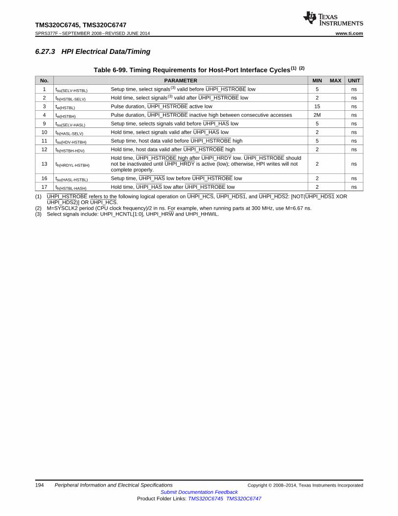
TMS320C6745, TMS320C6747SPRS377F –SEPTEMBER 2008–REVISED JUNE 2014 www.ti.com
6.27.3 HPI Electrical Data/Timing
Table 6-99. Timing Requirements for Host-Port Interface Cycles (1) (2)
No. PARAMETER MIN MAX UNIT1 tsu(SELV-HSTBL) Setup time, select signals (3) valid before UHPI_HSTROBE low 5 ns2 th(HSTBL-SELV) Hold time, select signals (3) valid after UHPI_HSTROBE low 2 ns3 tw(HSTBL) Pulse duration, UHPI_HSTROBE active low 15 ns4 tw(HSTBH) Pulse duration, UHPI_HSTROBE inactive high between consecutive accesses 2M ns9 tsu(SELV-HASL) Setup time, selects signals valid before UHPI_HAS low 5 ns10 th(HASL-SELV) Hold time, select signals valid after UHPI_HAS low 2 ns11 tsu(HDV-HSTBH) Setup time, host data valid before UHPI_HSTROBE high 5 ns12 th(HSTBH-HDV) Hold time, host data valid after UHPI_HSTROBE high 2 ns
Hold time, UHPI_HSTROBE high after UHPI_HRDY low. UHPI_HSTROBE should13 th(HRDYL-HSTBH) not be inactivated until UHPI_HRDY is active (low); otherwise, HPI writes will not 2 ns
complete properly.16 tsu(HASL-HSTBL) Setup time, UHPI_HAS low before UHPI_HSTROBE low 2 ns17 th(HSTBL-HASH) Hold time, UHPI_HAS low after UHPI_HSTROBE low 2 ns
(1) UHPI_HSTROBE refers to the following logical operation on UHPI_HCS, UHPI_HDS1, and UHPI_HDS2: [NOT(UHPI_HDS1 XORUHPI_HDS2)] OR UHPI_HCS.
(2) M=SYSCLK2 period (CPU clock frequency)/2 in ns. For example, when running parts at 300 MHz, use M=6.67 ns.(3) Select signals include: UHPI_HCNTL[1:0], UHPI_HRW and UHPI_HHWIL.
194 Peripheral Information and Electrical Specifications Copyright © 2008–2014, Texas Instruments IncorporatedSubmit Documentation Feedback
Product Folder Links: TMS320C6745 TMS320C6747

TMS320C6745, TMS320C6747www.ti.com SPRS377F –SEPTEMBER 2008–REVISED JUNE 2014
Table 6-100. Switching Characteristics for Host-Port Interface Cycles (1) (2) (3)
No. PARAMETER MIN MAX UNITFor HPI Write, UHPI_HRDY can go high (notready) for these HPI Write conditions;otherwise, UHPI_HRDY stays low (ready):Case 1: Back-to-back HPIA writes (can beeither first or second half-word)Case 2: HPIA write following a PREFETCHcommand (can be either first or second half-word)Case 3: HPID write when FIFO is full orflushing (can be either first or second half-word)Case 4: HPIA write and Write FIFO not empty
For HPI Read, UHPI_HRDY can go high (notDelay time, ready) for these HPI Read conditions:
5 td(HSTBL-HRDYV) UHPI_HSTROBE low to 12 nsCase 1: HPID read (with auto-increment) andUHPI_HRDY valid data not in Read FIFO (can only happen to
first half-word of HPID access)Case 2: First half-word access of HPID Readwithout auto-incrementFor HPI Read, UHPI_HRDY stays low (ready)for these HPI Read conditions:Case 1: HPID read with auto-increment anddata is already in Read FIFO (applies to eitherhalf-word of HPID access)Case 2: HPID read without auto-incrementand data is already in Read FIFO (alwaysapplies to second half-word of HPID access)Case 3: HPIC or HPIA read (applies to eitherhalf-word access)
5a td(HASL-HRDYV) Delay time, UHPI_HAS low to UHPI_HRDY valid 136 ten(HSTBL-HDLZ) Enable time, HD driven from UHPI_HSTROBE low 2 ns7 td(HRDYL-HDV) Delay time, UHPI_HRDY low to HD valid 0 ns8 toh(HSTBH-HDV) Output hold time, HD valid after UHPI_HSTROBE high 1.5 ns14 tdis(HSTBH-HDHZ) Disable time, HD high-impedance from UHPI_ HSTROBE high 12 ns
For HPI Read. Applies to conditions wheredata is already residing in HPID/FIFO:Case 1: HPIC or HPIA read
Delay time, Case 2: First half-word of HPID read with15 td(HSTBL-HDV) 15 nsUHPI_HSTROBE low to HD valid auto-increment and data is already in ReadFIFOCase 3: Second half-word of HPID read withor without auto-incrementFor HPI Write, UHPI_HRDY can go high (notready) for these HPI Write conditions;otherwise, UHPI_HRDY stays low (ready):
Delay time, Case 1: HPID write when Write FIFO is full18 td(HSTBH-HRDYV) UHPI_HSTROBE high to (can happen to either half-word) 12 ns
UHPI_HRDY valid Case 2: HPIA write (can happen to either half-word)Case 3: HPID write without auto-increment(only happens to second half-word)
(1) M=SYSCLK2 period (CPU clock frequency)/2 in ns.(2) UHPI_HSTROBE refers to the following logical operation on UHPI_HCS, UHPI_HDS1, and UHPI_HDS2: [NOT(UHPI_HDS1 XOR
UHPI_HDS2)] OR UHPI_HCS.(3) By design, whenever UHPI_HCS is driven inactive (high), HPI will drive UHPI_HRDY active (low).
Copyright © 2008–2014, Texas Instruments Incorporated Peripheral Information and Electrical Specifications 195Submit Documentation Feedback
Product Folder Links: TMS320C6745 TMS320C6747
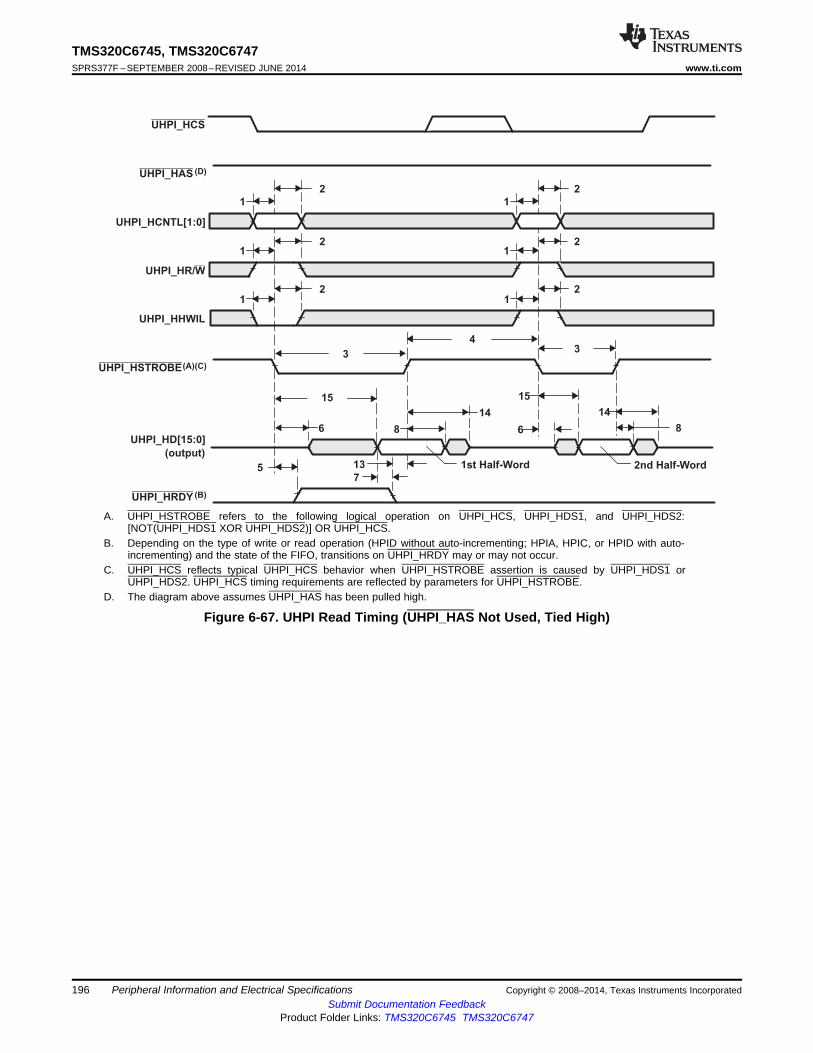
UHPI_HCS
UHPI_HAS (D)
UHPI_HCNTL[1:0]
UHPI_HR/W
UHPI_HHWIL
UHPI_HSTROBE
UHPI_HD[15:0]
(output)
UHPI_HRDY
1
2
12
12
5
6
3
43
1
2
12
12
8
14
15
14
8
7
1st Half-Word 2nd Half-Word
6
13
15
(A)(C)
(B)
TMS320C6745, TMS320C6747SPRS377F –SEPTEMBER 2008–REVISED JUNE 2014 www.ti.com
A. UHPI_HSTROBE refers to the following logical operation on UHPI_HCS, UHPI_HDS1, and UHPI_HDS2:[NOT(UHPI_HDS1 XOR UHPI_HDS2)] OR UHPI_HCS.
B. Depending on the type of write or read operation (HPID without auto-incrementing; HPIA, HPIC, or HPID with auto-incrementing) and the state of the FIFO, transitions on UHPI_HRDY may or may not occur.
C. UHPI_HCS reflects typical UHPI_HCS behavior when UHPI_HSTROBE assertion is caused by UHPI_HDS1 orUHPI_HDS2. UHPI_HCS timing requirements are reflected by parameters for UHPI_HSTROBE.
D. The diagram above assumes UHPI_HAS has been pulled high.
Figure 6-67. UHPI Read Timing (UHPI_HAS Not Used, Tied High)
196 Peripheral Information and Electrical Specifications Copyright © 2008–2014, Texas Instruments IncorporatedSubmit Documentation Feedback
Product Folder Links: TMS320C6745 TMS320C6747

UHPI_HAS(A)
UHPI_HCNTL[1:0]
UHPI_HR/W
UHPI_HHWIL
UHPI_HSTROBE(B)
UHPI_HCS
UHPI_HD[15:0]
(output)
UHPI_HRDY
1st Half-Word 2nd Half-Word75a
14815
1486
43
10
910
9
109
109
10910
917 17
1616
TMS320C6745, TMS320C6747www.ti.com SPRS377F –SEPTEMBER 2008–REVISED JUNE 2014
A. For correct operation, strobe the UHPI_HAS signal only once per UHPI_HSTROBE active cycle.B. UHPI_HSTROBE refers to the following logical operation on UHPI_HCS, UHPI_HDS1, and UHPI_HDS2:
[NOT(UHPI_HDS1 XOR UHPI_HDS2)] OR UHPI_HCS.
Figure 6-68. UHPI Read Timing (UHPI_HAS Used)
Copyright © 2008–2014, Texas Instruments Incorporated Peripheral Information and Electrical Specifications 197Submit Documentation Feedback
Product Folder Links: TMS320C6745 TMS320C6747
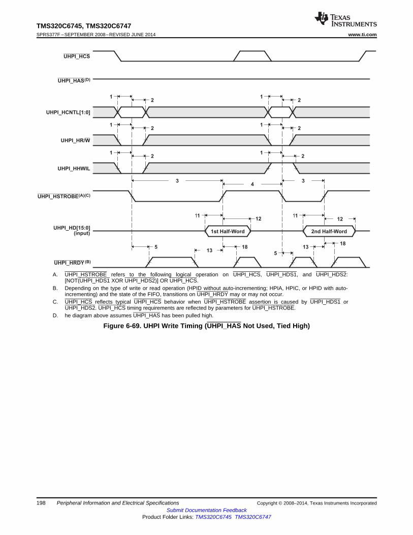
UHPI_HAS(D)
UHPI_HCNTL[1:0]
UHPI_HR/W
UHPI_HHWIL
UHPI_HSTROBE(A)(C)
UHPI_HCS
UHPI_HD[15:0](input)
UHPI_HRDY (B)
21
21
12
21
21
12
34
3
1112
1813
5
185
1112
13
2nd Half-Word1st Half-Word
TMS320C6745, TMS320C6747SPRS377F –SEPTEMBER 2008–REVISED JUNE 2014 www.ti.com
A. UHPI_HSTROBE refers to the following logical operation on UHPI_HCS, UHPI_HDS1, and UHPI_HDS2:[NOT(UHPI_HDS1 XOR UHPI_HDS2)] OR UHPI_HCS.
B. Depending on the type of write or read operation (HPID without auto-incrementing; HPIA, HPIC, or HPID with auto-incrementing) and the state of the FIFO, transitions on UHPI_HRDY may or may not occur.
C. UHPI_HCS reflects typical UHPI_HCS behavior when UHPI_HSTROBE assertion is caused by UHPI_HDS1 orUHPI_HDS2. UHPI_HCS timing requirements are reflected by parameters for UHPI_HSTROBE.
D. he diagram above assumes UHPI_HAS has been pulled high.
Figure 6-69. UHPI Write Timing (UHPI_HAS Not Used, Tied High)
198 Peripheral Information and Electrical Specifications Copyright © 2008–2014, Texas Instruments IncorporatedSubmit Documentation Feedback
Product Folder Links: TMS320C6745 TMS320C6747

1st Half-Word 2nd Half-Word
1211
1211
4
13
3
109
109
109
109
109
109
UHPI_HAS(A)
UHPI_HCNTL[1:0]
UHPI_HR/W
UHPI_HHWIL
UHPI_HSTROBE(B)
UHPI_HCS
UHPI_HD[15:0]
(input)
UHPI_HRDY
1717
16 16
5a
TMS320C6745, TMS320C6747www.ti.com SPRS377F –SEPTEMBER 2008–REVISED JUNE 2014
A. For correct operation, strobe the UHPI_HAS signal only once per UHPI_HSTROBE active cycle.B. UHPI_HSTROBE refers to the following logical operation on UHPI_HCS, UHPI_HDS1, and UHPI_HDS2:
[NOT(UHPI_HDS1 XOR UHPI_HDS2)] OR UHPI_HCS.
Figure 6-70. UHPI Write Timing (UHPI_HAS Used)
Copyright © 2008–2014, Texas Instruments Incorporated Peripheral Information and Electrical Specifications 199Submit Documentation Feedback
Product Folder Links: TMS320C6745 TMS320C6747
TMS320C6745, TMS320C6747SPRS377F –SEPTEMBER 2008–REVISED JUNE 2014 www.ti.com
6.28 Power and Sleep Controller (PSC)The Power and Sleep Controllers (PSC) are responsible for managing transitions of system power on/off,clock on/off, resets (device level and module level). It is used primarily to provide granular power controlfor on chip modules (peripherals and CPU). A PSC module consists of a Global PSC (GPSC) and a set ofLocal PSCs (LPSCs). The GPSC contains memory mapped registers, PSC interrupts, a state machine foreach peripheral/module it controls. An LPSC is associated with every module that is controlled by the PSCand provides clock and reset control.
The PSC includes the following features:• Provides a software interface to:
– Control module clock enable/disable– Control module reset– Control CPU local reset
• Supports ICEpick TAP Router power, clock and reset features. For details on ICEpick features seehttp://tiexpressdsp.com/wiki/index.php?title=ICEPICK.
Table 6-101. Power and Sleep Controller (PSC) Registers
PSC0 PSC1 ACRONYM REGISTER DESCRIPTIONBYTE ADDRESS BYTE ADDRESS
0x01C1 0000 0x01E2 7000 REVID Peripheral Revision and Class Information Register0x01C1 0018 0x01E2 7018 INTEVAL Interrupt Evaluation Register0x01C1 0040 0x01E2 7040 MERRPR0 Module Error Pending Register 0 (module 0-15) (PSC0)
Module Error Pending Register 0 (module 0-31) (PSC1)0x01C1 0050 0x01E2 7050 MERRCR0 Module Error Clear Register 0 (module 0-15) (PSC0)
Module Error Clear Register 0 (module 0-31) (PSC1)0x01C1 0060 0x01E2 7060 PERRPR Power Error Pending Register0x01C1 0068 0x01E2 7068 PERRCR Power Error Clear Register0x01C1 0120 0x01E2 7120 PTCMD Power Domain Transition Command Register0x01C1 0128 0x01E2 7128 PTSTAT Power Domain Transition Status Register0x01C1 0200 0x01E2 7200 PDSTAT0 Power Domain 0 Status Register0x01C1 0204 0x01E2 7204 PDSTAT1 Power Domain 1 Status Register0x01C1 0300 0x01E2 7300 PDCTL0 Power Domain 0 Control Register0x01C1 0304 0x01E2 7304 PDCTL1 Power Domain 1 Control Register0x01C1 0400 0x01E2 7400 PDCFG0 Power Domain 0 Configuration Register0x01C1 0404 0x01E2 7404 PDCFG1 Power Domain 1 Configuration Register
0x01C1 0800 - 0x01E2 7800 - MDSTAT0-MDSTAT15 Module Status n Register (modules 0-15) (PSC0)0x01C1 083C 0x01E2 787C MDSTAT0-MDSTAT31 Module Status n Register (modules 0-31) (PSC1)
0x01C1 0A00 - 0x01E2 7A00 - MDCTL0-MDCTL15 Module Control n Register (modules 0-15) (PSC0)0x01C1 0A3C 0x01E2 7A7C MDCTL0-MDCTL31 Module Control n Register (modules 0-31) (PSC1)
6.28.1 Power Domain and Module TopologyThe device includes two PSC modules.
Each PSC module controls clock states for several of the on chip modules, controllers and interconnectcomponents. Table 6-102 and Table 6-103 lists the set of peripherals/modules that are controlled by thePSC, the power domain they are associated with, the LPSC assignment and the default (power-on reset)module states. The module states and terminology are defined in Section 6.28.1.2.
200 Peripheral Information and Electrical Specifications Copyright © 2008–2014, Texas Instruments IncorporatedSubmit Documentation Feedback
Product Folder Links: TMS320C6745 TMS320C6747
TMS320C6745, TMS320C6747www.ti.com SPRS377F –SEPTEMBER 2008–REVISED JUNE 2014
Table 6-102. PSC0 Default Module Configuration
LPSC Module Name Power Domain Default Module State Auto Sleep/Wake OnlyNumber0 EDMA3 Channel Controller AlwaysON (PD0) SwRstDisable —1 EDMA3 Transfer Controller 0 AlwaysON (PD0) SwRstDisable —2 EDMA3 Transfer Controller 1 AlwaysON (PD0) SwRstDisable —3 EMIFA (BR7) AlwaysON (PD0) SwRstDisable —4 SPI 0 AlwaysON (PD0) SwRstDisable —5 MMC/SD 0 AlwaysON (PD0) SwRstDisable —6-8 Not Used — — —9 UART 0 AlwaysON (PD0) SwRstDisable —10 SCR0 (Br 0, Br 1, Br 2, Br 8) AlwaysON (PD0) Enable Yes11 SCR1 (Br 4) AlwaysON (PD0) Enable Yes12 SCR2 (Br 3, Br 5, Br 6) AlwaysON (PD0) Enable Yes13 PRUSS AlwaysON (PD0) SwRstDisable —14 Not Used — — —15 DSP PD_DSP (PD1) Enable —
Table 6-103. PSC1 Default Module Configuration
LPSC Module Name Power Domain Default Module State Auto Sleep/Wake OnlyNumber0 Not Used — — —1 USB0 (USB2.0) AlwaysON (PD0) SwRstDisable —2 USB1 (USB1.1) AlwaysON (PD0) SwRstDisable —3 GPIO AlwaysON (PD0) SwRstDisable —4 UHPI AlwaysON (PD0) SwRstDisable —5 EMAC AlwaysON (PD0) SwRstDisable —6 EMIFB (Br 20) AlwaysON (PD0) SwRstDisable —7 McASP0 ( + McASP0 FIFO) AlwaysON (PD0) SwRstDisable —8 McASP1 ( + McASP1 FIFO) AlwaysON (PD0) SwRstDisable —9 McASP2( + McASP2 FIFO) AlwaysON (PD0) SwRstDisable —10 SPI 1 AlwaysON (PD0) SwRstDisable —11 I2C 1 AlwaysON (PD0) SwRstDisable —12 UART 1 AlwaysON (PD0) SwRstDisable —13 UART 2 AlwaysON (PD0) SwRstDisable —14-15 Not Used — — —16 LCDC AlwaysON (PD0) SwRstDisable —17 eHRPWM0/1/2 AlwaysON (PD0) SwRstDisable —18-19 Not Used — — —20 ECAP0/1/2 AlwaysON (PD0) SwRstDisable —21 EQEP0/1 AlwaysON (PD0) SwRstDisable —22-23 Not Used — — —24 SCR8 (Br 15) AlwaysON (PD0) Enable Yes25 SCR7 (Br 12) AlwaysON (PD0) Enable Yes26 SCR12 (Br 18) AlwaysON (PD0) Enable Yes27-30 Not Used — — —31 Shared RAM (Br 13) PD_SHRAM Enable Yes
Copyright © 2008–2014, Texas Instruments Incorporated Peripheral Information and Electrical Specifications 201Submit Documentation Feedback
Product Folder Links: TMS320C6745 TMS320C6747

TMS320C6745, TMS320C6747SPRS377F –SEPTEMBER 2008–REVISED JUNE 2014 www.ti.com
6.28.1.1 Power Domain States
A power domain can only be in one of the two states: ON or OFF, defined as follows:• ON: power to the domain is on• OFF: power to the domain is off
In the device, for both PSC0 and PSC1, the Always ON domain, or PD0 power domain, is always in theON state when the chip is powered-on. This domain is not programmable to OFF state.• On PSC0 PD1/PD_DSP Domain: Controls the sleep state for DSP L1 and L2 Memories• On PSC1 PD1/PD_SHRAM Domain: Controls the sleep state for the 128K Shared RAM
6.28.1.2 Module States
The PSC defines several possible states for a module. This states are essentially a combination of themodule reset asserted or de-asserted and module clock on/enabled or off/disabled. The module states aredefined in Table 6-104.
Table 6-104. Module States
Module State Module Reset Module Clock Module State DefinitionEnable De-asserted On A module in the enable state has its module reset de-asserted and it has its
clock on. This is the normal operational state for a given moduleDisable De-asserted Off A module in the disabled state has its module reset de-asserted and it has its
module clock off. This state is typically used for disabling a module clock tosave power. The device is designed in full static CMOS, so when you stop amodule clock, it retains the module’s state. When the clock is restarted, themodule resumes operating from the stopping point.
SyncReset Asserted On A module state in the SyncReset state has its module reset asserted and it hasits clock on. Generally, software is not expected to initiate this state
SwRstDisable Asserted Off A module in the SwResetDisable state has its module reset asserted and it hasits clock disabled. After initial power-on, several modules come up in theSwRstDisable state. Generally, software is not expected to initiate this state
Auto Sleep De-asserted Off A module in the Auto Sleep state also has its module reset de-asserted and itsmodule clock disabled, similar to the Disable state. However this is a specialstate, once a module is configured in this state by software, it can“automatically” transition to “Enable” state whenever there is an internalread/write request made to it, and after servicing the request it will“automatically” transition into the sleep state (with module reset re de-assertedand module clock disabled), without any software intervention. The transitionfrom sleep to enabled and back to sleep state has some cycle latencyassociated with it. It is not envisioned to use this mode when peripherals arefully operational and moving data.
Auto Wake De-asserted Off A module in the Auto Wake state also has its module reset de-asserted and itsmodule clock disabled, similar to the Disable state. However this is a specialstate, once a module is configured in this state by software, it will“automatically” transition to “Enable” state whenever there is an internalread/write request made to it, and will remain in the “Enabled” state from thenon (with module reset re de-asserted and module clock on), without anysoftware intervention. The transition from sleep to enabled state has somecycle latency associated with it. It is not envisioned to use this mode whenperipherals are fully operational and moving data.
202 Peripheral Information and Electrical Specifications Copyright © 2008–2014, Texas Instruments IncorporatedSubmit Documentation Feedback
Product Folder Links: TMS320C6745 TMS320C6747
TMS320C6745, TMS320C6747www.ti.com SPRS377F –SEPTEMBER 2008–REVISED JUNE 2014
6.29 Programmable Real-Time Unit Subsystem (PRUSS)The Programmable Real-Time Unit Subsystem (PRUSS) consists of• Two Programmable Real-Time Units (PRU0 and PRU1) and their associated memories• An Interrupt Controller (INTC) for handling system interrupt events. The INTC also supports posting
events back to the device level host CPU.• A Switched Central Resource (SCR) for connecting the various internal and external masters to the
resources inside the PRUSS.
The two PRUs can operate completely independently or in coordination with each other. The PRUs canalso work in coordination with the device level host CPU. This is determined by the nature of the programwhich is loaded into the PRUs instruction memory. Several different signaling mechanisms are availablebetween the two PRUs and the device level host CPU.
The PRUs are optimized for performing embedded tasks that require manipulation of packed memorymapped data structures, handling of system events that have tight realtime constraints and interfacing withsystems external to the device.
The PRUSS comprises various distinct addressable regions. Externally the subsystem presents a single64Kbyte range of addresses. The internal interconnect bus (also called switched central resource, or SCR)of the PRUSS decodes accesses for each of the individual regions. The PRUSS memory map isdocumented in Table 6-105 and in Table 6-106. Note that these two memory maps are implementedinside the PRUSS and are local to the components of the PRUSS.
Table 6-105. Programmable Real-Time Unit Subsystem (PRUSS) Local Instruction Space Memory Map
BYTE ADDRESS PRU0 PRU10x0000 0000 - 0x0000 0FFF PRU0 Instruction RAM PRU1 Instruction RAM
Table 6-106. Programmable Real-Time Unit Subsystem (PRUSS) Local Data Space Memory Map
BYTE ADDRESS PRU0 PRU10x0000 0000 - 0x0000 01FF Data RAM 0 (1) Data RAM 1 (1)
0x0000 0200 - 0x0000 1FFF Reserved Reserved0x0000 2000 - 0x0000 21FF Data RAM 1 (1) Data RAM 0 (1)
0x0000 2200 - 0x0000 3FFF Reserved Reserved0x0000 4000 - 0x0000 6FFF INTC Registers INTC Registers0x0000 7000 - 0x0000 73FF PRU0 Control Registers PRU0 Control Registers0x0000 7400 - 0x0000 77FF Reserved Reserved0x0000 7800 - 0x0000 7BFF PRU1 Control Registers PRU1 Control Registers0x0000 7C00 - 0xFFFF FFFF Reserved Reserved
(1) Note that PRU0 accesses Data RAM0 at address 0x0000 0000, also PRU1 accesses Data RAM1 at address 0x0000 0000. Data RAM0is intended to be the primary data memory for PRU0 and Data RAM1 is intended to be the primary data memory for PRU1. However forpassing information between PRUs, each PRU can access the data ram of the ‘other’ PRU through address 0x0000 2000.
The global view of the PRUSS internal memories and control ports is documented in Table 6-107. Theoffset addresses of each region are implemented inside the PRUSS but the global device memorymapping places the PRUSS slave port in the address range 0x01C3 0000-0x01C3 FFFF. The PRU0 andPRU1 can use either the local or global addresses to access their internal memories, but using the localaddresses will provide access time several cycles faster than using the global addresses. This is becausewhen accessing via the global address the access needs to be routed through the switch fabric outsidePRUSS and back in through the PRUSS slave port.
Copyright © 2008–2014, Texas Instruments Incorporated Peripheral Information and Electrical Specifications 203Submit Documentation Feedback
Product Folder Links: TMS320C6745 TMS320C6747

TMS320C6745, TMS320C6747SPRS377F –SEPTEMBER 2008–REVISED JUNE 2014 www.ti.com
Table 6-107. Programmable Real-Time Unit Subsystem (PRUSS) Global Memory Map
BYTE ADDRESS REGION0x01C3 0000 - 0x01C3 01FF Data RAM 00x01C3 0200 - 0x01C3 1FFF Reserved0x01C3 2000 - 0x01C3 21FF Data RAM 10x01C3 2200 - 0x01C3 3FFF Reserved0x01C3 4000 - 0x01C3 6FFF INTC Registers0x01C3 7000 - 0x01C3 73FF PRU0 Control Registers0x01C3 7400 - 0x01C3 77FF PRU0 Debug Registers0x01C3 7800 - 0x01C3 7BFF PRU1 Control Registers0x01C3 7C00 - 0x01C3 7FFF PRU1 Debug Registers0x01C3 8000 - 0x01C3 8FFF PRU0 Instruction RAM0x01C3 9000 - 0x01C3 BFFF Reserved0x01C3 C000 - 0x01C3 CFFF PRU1 Instruction RAM0x01C3 D000 - 0x01C3 FFFF Reserved
Each of the PRUs can access the rest of the device memory (including memory mapped peripheral andconfiguration registers) using the global memory space addresses.
6.29.1 PRUSS Register Descriptions
Table 6-108. Programmable Real-Time Unit Subsystem (PRUSS) Control / Status Registers
PRU0 BYTE ADDRESS PRU1 BYTE ADDRESS ACRONYM REGISTER DESCRIPTION0x01C3 7000 0x01C3 7800 CONTROL PRU Control Register0x01C3 7004 0x01C3 7804 STATUS PRU Status Register0x01C3 7008 0x01C3 7808 WAKEUP PRU Wakeup Enable Register0x01C3 700C 0x01C3 780C CYCLCNT PRU Cycle Count0x01C3 7010 0x01C3 7810 STALLCNT PRU Stall Count
PRU Constant Table Block Index0x01C3 7020 0x01C3 7820 CONTABBLKIDX0 Register 0PRU Constant Table Programmable0x01C3 7028 0x01C3 7828 CONTABPROPTR0 Pointer Register 0PRU Constant Table Programmable0x01C3 702C 0x01C3 782C CONTABPROPTR1 Pointer Register 1PRU Internal General Purpose0x01C37400 - 0x01C3747C 0x01C3 7C00 - 0x01C3 7C7C INTGPR0 – INTGPR31 Register 0 (for Debug)PRU Internal General Purpose0x01C37480 - 0x01C374FC 0x01C3 7C80 - 0x01C3 7CFC INTCTER0 – INTCTER31 Register 0 (for Debug)
Table 6-109. Programmable Real-Time Unit Subsystem Interrupt Controller (PRUSS INTC) Registers
BYTE ADDRESS ACRONYM REGISTER DESCRIPTION0x01C3 4000 REVID Revision ID Register0x01C3 4004 CONTROL Control Register0x01C3 4010 GLBLEN Global Enable Register0x01C3 401C GLBLNSTLVL Global Nesting Level Register0x01C3 4020 STATIDXSET System Interrupt Status Indexed Set Register0x01C3 4024 STATIDXCLR System Interrupt Status Indexed Clear Register0x01C3 4028 ENIDXSET System Interrupt Enable Indexed Set Register0x01C3 402C ENIDXCLR System Interrupt Enable Indexed Clear Register0x01C3 4034 HSTINTENIDXSET Host Interrupt Enable Indexed Set Register0x01C3 4038 HSTINTENIDXCLR Host Interrupt Enable Indexed Clear Register
204 Peripheral Information and Electrical Specifications Copyright © 2008–2014, Texas Instruments IncorporatedSubmit Documentation Feedback
Product Folder Links: TMS320C6745 TMS320C6747
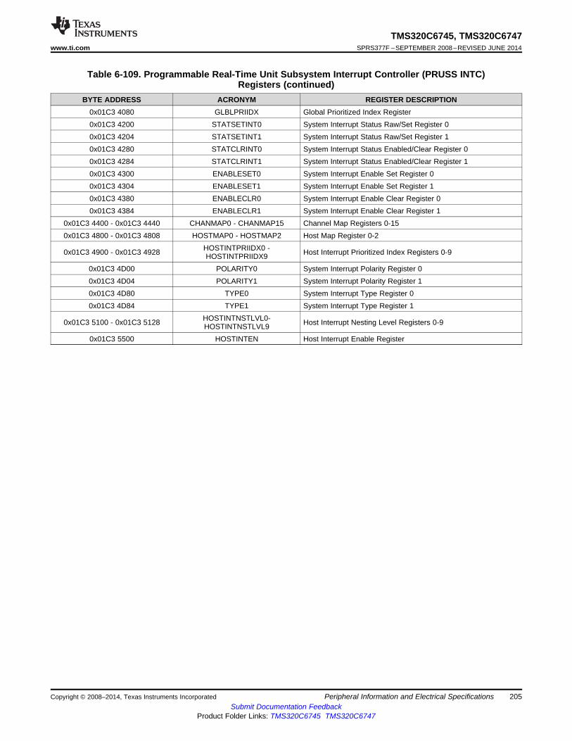
TMS320C6745, TMS320C6747www.ti.com SPRS377F –SEPTEMBER 2008–REVISED JUNE 2014
Table 6-109. Programmable Real-Time Unit Subsystem Interrupt Controller (PRUSS INTC)Registers (continued)
BYTE ADDRESS ACRONYM REGISTER DESCRIPTION0x01C3 4080 GLBLPRIIDX Global Prioritized Index Register0x01C3 4200 STATSETINT0 System Interrupt Status Raw/Set Register 00x01C3 4204 STATSETINT1 System Interrupt Status Raw/Set Register 10x01C3 4280 STATCLRINT0 System Interrupt Status Enabled/Clear Register 00x01C3 4284 STATCLRINT1 System Interrupt Status Enabled/Clear Register 10x01C3 4300 ENABLESET0 System Interrupt Enable Set Register 00x01C3 4304 ENABLESET1 System Interrupt Enable Set Register 10x01C3 4380 ENABLECLR0 System Interrupt Enable Clear Register 00x01C3 4384 ENABLECLR1 System Interrupt Enable Clear Register 1
0x01C3 4400 - 0x01C3 4440 CHANMAP0 - CHANMAP15 Channel Map Registers 0-150x01C3 4800 - 0x01C3 4808 HOSTMAP0 - HOSTMAP2 Host Map Register 0-2
HOSTINTPRIIDX0 -0x01C3 4900 - 0x01C3 4928 Host Interrupt Prioritized Index Registers 0-9HOSTINTPRIIDX90x01C3 4D00 POLARITY0 System Interrupt Polarity Register 00x01C3 4D04 POLARITY1 System Interrupt Polarity Register 10x01C3 4D80 TYPE0 System Interrupt Type Register 00x01C3 4D84 TYPE1 System Interrupt Type Register 1
HOSTINTNSTLVL0-0x01C3 5100 - 0x01C3 5128 Host Interrupt Nesting Level Registers 0-9HOSTINTNSTLVL90x01C3 5500 HOSTINTEN Host Interrupt Enable Register
Copyright © 2008–2014, Texas Instruments Incorporated Peripheral Information and Electrical Specifications 205Submit Documentation Feedback
Product Folder Links: TMS320C6745 TMS320C6747

TMS320C6745, TMS320C6747SPRS377F –SEPTEMBER 2008–REVISED JUNE 2014 www.ti.com
6.30 Emulation LogicThis section describes the steps to use a third party debugger. The debug capabilities and features forDSP are as shown below.
For TI’s latest debug and emulation information see :http://tiexpressdsp.com/wiki/index.php?title=Category:Emulation
DSP:• Basic Debug
– Execution Control– System Visibility
• Real-Time Debug– Interrupts serviced while halted– Low/non-intrusive system visibility while running
• Advanced Debug– Global Start– Global Stop– Specify targeted memory level(s) during memory accesses– HSRTDX (High Speed Real Time Data eXchange)
• Advanced System Control– Subsystem reset via debug– Peripheral notification of debug events– Cache-coherent debug accesses
• Analysis Actions– Stop program execution– Generate debug interrupt– Benchmarking with counters– External trigger generation– Debug state machine state transition– Combinational and Sequential event generation
• Analysis Events– Program event detection– Data event detection– External trigger Detection– System event detection (i.e. cache miss)– Debug state machine state detection
• Analysis Configuration– Application access– Debugger access
206 Peripheral Information and Electrical Specifications Copyright © 2008–2014, Texas Instruments IncorporatedSubmit Documentation Feedback
Product Folder Links: TMS320C6745 TMS320C6747
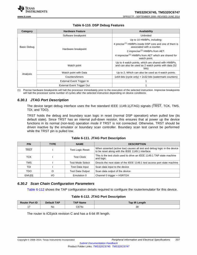
TMS320C6745, TMS320C6747www.ti.com SPRS377F –SEPTEMBER 2008–REVISED JUNE 2014
Table 6-110. DSP Debug Features
Category Hardware Feature AvailabilitySoftware breakpoint Unlimited
Up to 10 HWBPs, including:4 precise (1) HWBPs inside DSP core and one of them is
Basic Debug associated with a counter.Hardware breakpoint
2 imprecise (1) HWBPs from AET.4 imprecise (1) HWBPs from AET which are shared for
watch point.Up to 4 watch points, which are shared with HWBPs,
Watch point and can also be used as 2 watch points with data (32bits)
Watch point with Data Up to 2, Which can also be used as 4 watch points.AnalysisCounters/timers 1x64-bits (cycle only) + 2x32-bits (watermark counters)
External Event Trigger In 1External Event Trigger Out 1
(1) Precise hardware breakpoints will halt the processor immediately prior to the execution of the selected instruction. Imprecise breakpointswill halt the processor some number of cycles after the selected instruction depending on device conditions.
6.30.1 JTAG Port DescriptionThe device target debug interface uses the five standard IEEE 1149.1(JTAG) signals (TRST, TCK, TMS,TDI, and TDO).
TRST holds the debug and boundary scan logic in reset (normal DSP operation) when pulled low (itsdefault state). Since TRST has an internal pull-down resistor, this ensures that at power up the devicefunctions in its normal (non-test) operation mode if TRST is not connected. Otherwise, TRST should bedriven inactive by the emulator or boundary scan controller. Boundary scan test cannot be performedwhile the TRST pin is pulled low.
Table 6-111. JTAG Port Description
PIN TYPE NAME DESCRIPTIONWhen asserted (active low) causes all test and debug logic in the deviceTRST I Test Logic Reset to be reset along with the IEEE 1149.1 interfaceThis is the test clock used to drive an IEEE 1149.1 TAP state machineTCK I Test Clock and logic.
TMS I Test Mode Select Directs the next state of the IEEE 1149.1 test access port state machineTDI I Test Data Input Scan data input to the deviceTDO O Test Data Output Scan data output of the device
EMU[0] I/O Emulation 0 Channel 0 trigger + HSRTDX
6.30.2 Scan Chain Configuration ParametersTable 6-112 shows the TAP configuration details required to configure the router/emulator for this device.
Table 6-112. JTAG Port Description
Router Port ID Default TAP TAP Name Tap IR Length17 No C674x 38
The router is ICEpick revision C and has a 6-bit IR length.
Copyright © 2008–2014, Texas Instruments Incorporated Peripheral Information and Electrical Specifications 207Submit Documentation Feedback
Product Folder Links: TMS320C6745 TMS320C6747

TMS320C6745, TMS320C6747SPRS377F –SEPTEMBER 2008–REVISED JUNE 2014 www.ti.com
6.30.3 JTAG 1149.1 Boundary Scan ConsiderationsTo use boundary scan, the following sequence should be followed:• Execute a valid reset sequence and exit reset• Wait at least 6000 OSCIN clock cycles• Enter boundary scan mode using the JTAG pins
No specific value is required on the EMU[0] pin for boundary scan testing. If TRST is not driven by theboundary scan tool or tester, TRST should be externally pulled high during boundary scan testing.
208 Peripheral Information and Electrical Specifications Copyright © 2008–2014, Texas Instruments IncorporatedSubmit Documentation Feedback
Product Folder Links: TMS320C6745 TMS320C6747
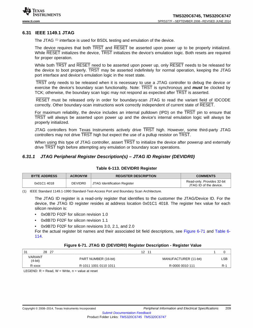
TMS320C6745, TMS320C6747www.ti.com SPRS377F –SEPTEMBER 2008–REVISED JUNE 2014
6.31 IEEE 1149.1 JTAGThe JTAG (1) interface is used for BSDL testing and emulation of the device.
The device requires that both TRST and RESET be asserted upon power up to be properly initialized.While RESET initializes the device, TRST initializes the device's emulation logic. Both resets are requiredfor proper operation.
While both TRST and RESET need to be asserted upon power up, only RESET needs to be released forthe device to boot properly. TRST may be asserted indefinitely for normal operation, keeping the JTAGport interface and device's emulation logic in the reset state.
.TRST only needs to be released when it is necessary to use a JTAG controller to debug the device orexercise the device's boundary scan functionality. Note: TRST is synchronous and must be clocked byTCK; otherwise, the boundary scan logic may not respond as expected after TRST is asserted.
.RESET must be released only in order for boundary-scan JTAG to read the variant field of IDCODEcorrectly. Other boundary-scan instructions work correctly independent of current state of RESET.
For maximum reliability, the device includes an internal pulldown (IPD) on the TRST pin to ensure thatTRST will always be asserted upon power up and the device's internal emulation logic will always beproperly initialized.
JTAG controllers from Texas Instruments actively drive TRST high. However, some third-party JTAGcontrollers may not drive TRST high but expect the use of a pullup resistor on TRST.
When using this type of JTAG controller, assert TRST to initialize the device after powerup and externallydrive TRST high before attempting any emulation or boundary scan operations.
6.31.1 JTAG Peripheral Register Description(s) – JTAG ID Register (DEVIDR0)
Table 6-113. DEVIDR0 Register
BYTE ADDRESS ACRONYM REGISTER DESCRIPTION COMMENTSRead-only. Provides 32-bit0x01C1 4018 DEVIDR0 JTAG Identification Register JTAG ID of the device.
(1) IEEE Standard 1149.1-1990 Standard-Test-Access Port and Boundary Scan Architecture.
The JTAG ID register is a read-only register that identifies to the customer the JTAG/Device ID. For thedevice, the JTAG ID register resides at address location 0x01C1 4018. The register hex value for eachsilicon revision is:• 0x0B7D F02F for silicon revision 1.0• 0x8B7D F02F for silicon revision 1.1• 0x9B7D F02F for silicon revisions 3.0, 2.1, and 2.0For the actual register bit names and their associated bit field descriptions, see Figure 6-71 and Table 6-114.
Figure 6-71. JTAG ID (DEVIDR0) Register Description - Register Value31 28 27 12 11 1 0
VARIANT PART NUMBER (16-bit) MANUFACTURER (11-bit) LSB(4-bit)R-xxxx R-1011 1001 0110 1011 R-0000 0010 111 R-1
LEGEND: R = Read, W = Write, n = value at reset
Copyright © 2008–2014, Texas Instruments Incorporated Peripheral Information and Electrical Specifications 209Submit Documentation Feedback
Product Folder Links: TMS320C6745 TMS320C6747

TCK
TDO
TDI/TMS/TRST
1
6 6
54
3
2
TMS320C6745, TMS320C6747SPRS377F –SEPTEMBER 2008–REVISED JUNE 2014 www.ti.com
Table 6-114. JTAG ID Register Selection Bit Descriptions
BIT NAME DESCRIPTION31:28 VARIANT Variant (4-Bit) value27:12 PART NUMBER Part Number (16-Bit) value11-1 MANUFACTURER Manufacturer (11-Bit) value
0 LSB LSB. This bit is read as a "1".
6.31.2 JTAG Test-Port Electrical Data/Timing
Table 6-115. Timing Requirements for JTAG Test Port (see Figure 6-72)No. PARAMETER MIN MAX UNIT1 tc(TCK) Cycle time, TCK 40 ns2 tw(TCKH) Pulse duration, TCK high 16 ns3 tw(TCKL) Pulse duration, TCK low 16 ns4 tsu(TDIV-TCKH) Setup time, TDI/TMS/TRST valid before TCK high 4 ns5 th(TCLKH-TDIV) Hold time, TDI/TMS/TRST valid after TCK high 4 ns
Table 6-116. Switching Characteristics Over Recommended Operating Conditions for JTAG Test Port(see Figure 6-72)
No. PARAMETER MIN MAX UNIT6 td(TCKL-TDOV) Delay time, TCK low to TDO valid 15 ns
Figure 6-72. JTAG Test-Port Timing
210 Peripheral Information and Electrical Specifications Copyright © 2008–2014, Texas Instruments IncorporatedSubmit Documentation Feedback
Product Folder Links: TMS320C6745 TMS320C6747

Seconds Minutes Hours Days Months Years
Alarm
Timer
AlarmInterrupts
PeriodicInterrupts
Counter32 kHz
OscillatorCompensation
WeekDays
Oscillator
RTC_XI
XTAL
RTC_XO
TMS320C6745, TMS320C6747www.ti.com SPRS377F –SEPTEMBER 2008–REVISED JUNE 2014
6.32 Real Time Clock (RTC)The RTC provides a time reference to an application running on the device. The current date and time istracked in a set of counter registers that update once per second. The time can be represented in 12-houror 24-hour mode. The calendar and time registers are buffered during reads and writes so that updates donot interfere with the accuracy of the time and date.
Alarms are available to interrupt the CPU at a particular time, or at periodic time intervals, such as onceper minute or once per day. In addition, the RTC can interrupt the CPU every time the calendar and timeregisters are updated, or at programmable periodic intervals.
The real-time clock (RTC) provides the following features:• 100-year calendar (xx00 to xx99)• Counts seconds, minutes, hours, day of the week, date, month, and year with leap year compensation• Binary-coded-decimal (BCD) representation of time, calendar, and alarm• 12-hour clock mode (with AM and PM) or 24-hour clock mode• Alarm interrupt• Periodic interrupt• Single interrupt to the CPU• Supports external 32.768-kHz crystal or external clock source of the same frequency• Separate isolated power supply
Figure 6-73 shows a block diagram of the RTC.
Figure 6-73. Real-Time Clock Block Diagram
Copyright © 2008–2014, Texas Instruments Incorporated Peripheral Information and Electrical Specifications 211Submit Documentation Feedback
Product Folder Links: TMS320C6745 TMS320C6747

XTAL32.768
kHz
C2
C1
RTC_XI
RTC_XO
RTC_VSS
32KOSC
RealTimeClock(RTC)
Module
Isolated RTCPower Domain
Real Time ClockRTC_CVDD
RTCPowerSource
TMS320C6745, TMS320C6747SPRS377F –SEPTEMBER 2008–REVISED JUNE 2014 www.ti.com
6.32.1 Clock SourceThe clock reference for the RTC is an external 32.768-kHz crystal or an external clock source of the samefrequency. The RTC also has a separate power supply that is isolated from the rest of the system. Whenthe CPU and other peripherals are without power, the RTC can remain powered to preserve the currenttime and calendar information.
The source for the RTC reference clock may be provided by a crystal or by an external clock source. TheRTC has an internal oscillator buffer to support direct operation with a crystal. The crystal is connectedbetween pins RTC_XI and RTC_XO. RTC_XI is the input to the on-chip oscillator and RTC_XO is theoutput from the oscillator back to the crystal. A crystal with 70k-ohm max ESR is recommended. Typicalload capacitance values are 10-20 pF, where the load capacitance is the series combination of C1 andC2.
An external 32.768-kHz clock source may be used instead of a crystal. In such a case, the clock source isconnected to RTC_XI, and RTC_XO is left unconnected.
If the RTC is not used, the RTC_XI pin should be static held high or low and RTC_XO should be leftunconnected.
Figure 6-74. Clock Source
212 Peripheral Information and Electrical Specifications Copyright © 2008–2014, Texas Instruments IncorporatedSubmit Documentation Feedback
Product Folder Links: TMS320C6745 TMS320C6747
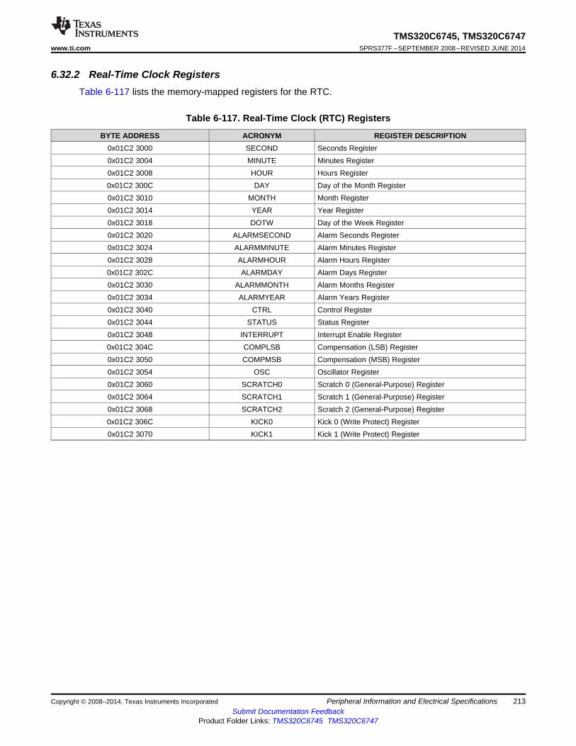
TMS320C6745, TMS320C6747www.ti.com SPRS377F –SEPTEMBER 2008–REVISED JUNE 2014
6.32.2 Real-Time Clock RegistersTable 6-117 lists the memory-mapped registers for the RTC.
Table 6-117. Real-Time Clock (RTC) Registers
BYTE ADDRESS ACRONYM REGISTER DESCRIPTION0x01C2 3000 SECOND Seconds Register0x01C2 3004 MINUTE Minutes Register0x01C2 3008 HOUR Hours Register0x01C2 300C DAY Day of the Month Register0x01C2 3010 MONTH Month Register0x01C2 3014 YEAR Year Register0x01C2 3018 DOTW Day of the Week Register0x01C2 3020 ALARMSECOND Alarm Seconds Register0x01C2 3024 ALARMMINUTE Alarm Minutes Register0x01C2 3028 ALARMHOUR Alarm Hours Register0x01C2 302C ALARMDAY Alarm Days Register0x01C2 3030 ALARMMONTH Alarm Months Register0x01C2 3034 ALARMYEAR Alarm Years Register0x01C2 3040 CTRL Control Register0x01C2 3044 STATUS Status Register0x01C2 3048 INTERRUPT Interrupt Enable Register0x01C2 304C COMPLSB Compensation (LSB) Register0x01C2 3050 COMPMSB Compensation (MSB) Register0x01C2 3054 OSC Oscillator Register0x01C2 3060 SCRATCH0 Scratch 0 (General-Purpose) Register0x01C2 3064 SCRATCH1 Scratch 1 (General-Purpose) Register0x01C2 3068 SCRATCH2 Scratch 2 (General-Purpose) Register0x01C2 306C KICK0 Kick 0 (Write Protect) Register0x01C2 3070 KICK1 Kick 1 (Write Protect) Register
Copyright © 2008–2014, Texas Instruments Incorporated Peripheral Information and Electrical Specifications 213Submit Documentation Feedback
Product Folder Links: TMS320C6745 TMS320C6747

TMS320C6745, TMS320C6747SPRS377F –SEPTEMBER 2008–REVISED JUNE 2014 www.ti.com
7 Device and Documentation Support
7.1 Device Support
7.1.1 Development SupportTI offers an extensive line of development tools for the TMS320C6745/47 platform, including tools toevaluate the performance of the processors, generate code, develop algorithm implementations, and fullyintegrate and debug software and hardware modules. The tool's support documentation is electronicallyavailable within the Code Composer Studio™ Integrated Development Environment (IDE).
The following products support development of TMS320C6745/47 applications:
Software Development Tools:Code Composer Studio™ Integrated Development Environment (IDE): including EditorC/C++/Assembly Code Generation, and Debug plus additional development toolsScalable, Real-Time Foundation Software (DSP/BIOS™), which provides the basic run-time targetsoftware needed to support any application.
Hardware Development Tools:Extended Development System (XDS™) EmulatorFor a complete listing of development-support tools for TMS320C6745/47, visit the Texas Instrumentsweb site on the Worldwide Web at www.ti.com uniform resource locator (URL). For information onpricing and availability, contact the nearest TI field sales office or authorized distributor.
7.1.2 Device and Development-Support Tool NomenclatureTo designate the stages in the product development cycle, TI assigns prefixes to the part numbers of allDSP devices and support tools. Each DSP commercial family member has one of three prefixes: TMX,TMP, or TMS (e.g., TMS320C6745). Texas Instruments recommends two of three possible prefixdesignators for its support tools: TMDX and TMDS. These prefixes represent evolutionary stages ofproduct development from engineering prototypes (TMX/TMDX) through fully qualified productiondevices/tools (TMS/TMDS).
Device development evolutionary flow:
TMX Experimental device that is not necessarily representative of the final device's electricalspecifications.
TMP Final silicon die that conforms to the device's electrical specifications but has not completedquality and reliability verification.
TMS Fully-qualified production device.
Support tool development evolutionary flow:
TMDX Development-support product that has not yet completed Texas Instruments internalqualification testing.
TMDS Fully qualified development-support product.
TMX and TMP devices and TMDX development-support tools are shipped against the followingdisclaimer:
"Developmental product is intended for internal evaluation purposes."
TMS devices and TMDS development-support tools have been characterized fully, and the quality andreliability of the device have been demonstrated fully. TI's standard warranty applies.
214 Device and Documentation Support Copyright © 2008–2014, Texas Instruments IncorporatedSubmit Documentation Feedback
Product Folder Links: TMS320C6745 TMS320C6747
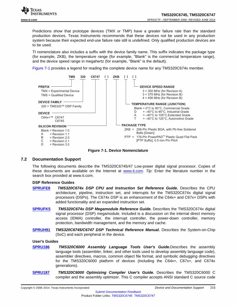
TMS 320 C6747 ( ) ZKB ( ) ( )
PREFIX
TMX = Experimental Device
TMS = Qualified Device
DEVICE FAMILY
320 = TMS320™ DSP Family
DEVICE
C64x+™ C6747C6745
DEVICE SPEED RANGE
3 = 300 MHz (for Revision A)3 = 375 MHz (for Revision B)4 = 456 MHz (for Revision B)
TEMPERATURE RANGE (JUNCTION)
BlankDAT
= 0°C to 90°C, Commercial Grade== –40°C to 105°C,Extended Grade
–40°C to 90°C, Industrial Grade
= –40°C to 125°C, Automotive Grade
PACKAGE TYPE
256-Pin Plastic BGA, with Pb-free SolderedBalls [Green]
ZKB =SILICON REVISION
Blank = Revision 1.0ABCD
PTP = 176-Pin PowerPAD Plastic Quad Flat Pack[PTP Suffix], 0.5 mm Pin Pitch
TM= Revision 1.1= Revision 2.0= Revision 2.1= Revision 3.0
TMS320C6745, TMS320C6747www.ti.com SPRS377F –SEPTEMBER 2008–REVISED JUNE 2014
Predictions show that prototype devices (TMX or TMP) have a greater failure rate than the standardproduction devices. Texas Instruments recommends that these devices not be used in any productionsystem because their expected end-use failure rate still is undefined. Only qualified production devices areto be used.
TI nomenclature also includes a suffix with the device family name. This suffix indicates the package type(for example, ZKB), the temperature range (for example, "Blank" is the commercial temperature range),and the device speed range in megahertz (for example, "Blank" is the default).
Figure 7-1 provides a legend for reading the complete device name for any TMS320C674x member.
Figure 7-1. Device Nomenclature
7.2 Documentation SupportThe following documents describe the TMS320C6745/47 Low-power digital signal processor. Copies ofthese documents are available on the Internet at www.ti.com. Tip: Enter the literature number in thesearch box provided at www.ti.com.
DSP Reference GuidesSPRUFE8 TMS320C674x DSP CPU and Instruction Set Reference Guide. Describes the CPU
architecture, pipeline, instruction set, and interrupts for the TMS320C674x digital signalprocessors (DSPs). The C674x DSP is an enhancement of the C64x+ and C67x+ DSPs withadded functionality and an expanded instruction set.
SPRUFK5 TMS320C674x DSP Megamodule Reference Guide. Describes the TMS320C674x digitalsignal processor (DSP) megamodule. Included is a discussion on the internal direct memoryaccess (IDMA) controller, the interrupt controller, the power-down controller, memoryprotection, bandwidth management, and the memory and cache.
SPRUH91 TMS320C6745/C6747 DSP Technical Reference Manual. Describes the System-on-Chip(SoC) and each peripheral in the device.
User's GuidesSPRU186 TMS320C6000 Assembly Language Tools User's Guide.Describes the assembly
language tools (assembler, linker, and other tools used to develop assembly language code),assembler directives, macros, common object file format, and symbolic debugging directivesfor the TMS320C6000 platform of devices (including the C64x+, C67x+, and C674xgenerations).
SPRU187 TMS320C6000 Optimizing Compiler User's Guide. Describes the TMS320C6000 Ccompiler and the assembly optimizer. This C compiler accepts ANSI standard C source code
Copyright © 2008–2014, Texas Instruments Incorporated Device and Documentation Support 215Submit Documentation Feedback
Product Folder Links: TMS320C6745 TMS320C6747
TMS320C6745, TMS320C6747SPRS377F –SEPTEMBER 2008–REVISED JUNE 2014 www.ti.com
and produces assembly language source code for the TMS320C6000 platform of devices(including the C64x+, C67x+, and C674x generations). The assembly optimizer helps youoptimize your assembly code.
SPRUG82 TMS320C674x DSP Cache User's Guide. Explains the fundamentals of memory cachesand describes how the two-level cache-based internal memory architecture in theTMS320C674x digital signal processor (DSP) can be efficiently used in DSP applications.Shows how to maintain coherence with external memory, how to use DMA to reducememory latencies, and how to optimize your code to improve cache efficiency. The internalmemory architecture in the C674x DSP is organized in a two-level hierarchy consisting of adedicated program cache (L1P) and a dedicated data cache (L1D) on the first level.Accesses by the CPU to the these first level caches can complete without CPU pipelinestalls. If the data requested by the CPU is not contained in cache, it is fetched from the nextlower memory level, L2 or external memory.
7.3 Community ResourcesThe following links connect to TI community resources. Linked contents are provided "AS IS" by therespective contributors. They do not constitute TI specifications and do not necessarily reflect TI's views;see TI's Terms of Use.
TI E2E™ Online Community TI's Engineer-to-Engineer (E2E) Community. Created to fostercollaboration among engineers. At e2e.ti.com, you can ask questions, share knowledge,explore ideas and help solve problems with fellow engineers.
TI Embedded Processors Wiki Texas Instruments Embedded Processors Wiki. Established to helpdevelopers get started with Embedded Processors from Texas Instruments and to fosterinnovation and growth of general knowledge about the hardware and software surroundingthese devices.
7.4 Related LinksThe table below lists quick access links. Categories include technical documents, support and communityresources, tools and software, and quick access to sample or buy.
Table 7-1. Related Links
TECHNICAL TOOLS & SUPPORT &PARTS PRODUCT FOLDER SAMPLE & BUY DOCUMENTS SOFTWARE COMMUNITYTMS320C6745 Click here Click here Click here Click here Click hereTMS320C6747 Click here Click here Click here Click here Click here
7.5 TrademarksDSP/BIOS, PowerPAD, TMS320C6000, C6000, E2E are trademarks of Texas Instruments.All other trademarks are the property of their respective owners.
7.6 Electrostatic Discharge CautionThis integrated circuit can be damaged by ESD. Texas Instruments recommends that all integrated circuits be handled withappropriate precautions. Failure to observe proper handling and installation procedures can cause damage.
ESD damage can range from subtle performance degradation to complete device failure. Precision integrated circuits may be moresusceptible to damage because very small parametric changes could cause the device not to meet its published specifications.
7.7 GlossarySLYZ022 — TI Glossary.
This glossary lists and explains terms, acronyms, and definitions.
216 Device and Documentation Support Copyright © 2008–2014, Texas Instruments IncorporatedSubmit Documentation Feedback
Product Folder Links: TMS320C6745 TMS320C6747

TMS320C6745, TMS320C6747www.ti.com SPRS377F –SEPTEMBER 2008–REVISED JUNE 2014
8 Mechanical Packaging and Orderable Information
This section describes the C6745/6747 orderable part numbers, packaging options, materials, thermal andmechanical parameters.
This section contains mechanical drawings for the ZKB Plastic Ball Grid Array package and the PTPPowerPAD™ plastic quad flat pack package. Additionally, for the PTP package a detailed drawing of theactual thermal pad dimensions as well as a recommended PCB footprint are provided.
8.1 Thermal Data for ZKBThe following table(s) show the thermal resistance characteristics for the PBGA–ZKB mechanicalpackage.
Table 8-1. Thermal Resistance Characteristics (PBGA Package) [ZKB]
No. °C/W (1) °C/W (2) AIR FLOW(m/s) (3)
1 RΘJC Junction-to-case 12.8 13.5 N/A2 RΘJB Junction-to-board 15.1 19.7 N/A3 RΘJA Junction-to-free air 24.5 33.8 0.004 21.9 30 0.505 21.1 28.7 1.00
RΘJMA Junction-to-moving air6 20.4 27.4 2.007 19.6 26 4.008 0.6 0.8 0.009 0.8 1 0.5010 PsiJT Junction-to-package top 0.9 1.2 1.0011 1.1 1.4 2.0012 1.3 1.8 4.0013 14.9 19.1 0.0014 14.4 18.2 0.5015 PsiJB Junction-to-board 14.4 18 1.0016 14.3 17.7 2.0017 14.1 17.4 4.00
(1) These measurements were conducted in a JEDEC defined 2S2P system and will change based on environment as well as application.For more information, see these EIA/JEDEC standards – EIA/JESD51-2, Integrated Circuits Thermal Test Method EnvironmentConditions - Natural Convection (Still Air) and JESD51-7, High Effective Thermal Conductivity Test Board for Leaded Surface MountPackages. Power dissipation of 1W and ambient temp of 70C assumed. PCB with 2oz (70um) top and bottom copper thickness and1.5oz (50um) inner copper thickness
(2) Simulation data, using the same model but with 1oz (35um) top and bottom copper thickness and 0.5oz (18um) inner copper thickness.Power dissipation of 1W and ambient temp of 70C assumed.
(3) m/s = meters per second
Copyright © 2008–2014, Texas Instruments Incorporated Mechanical Packaging and Orderable Information 217Submit Documentation Feedback
Product Folder Links: TMS320C6745 TMS320C6747
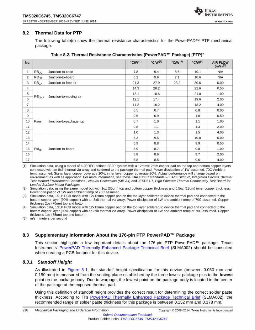
TMS320C6745, TMS320C6747SPRS377F –SEPTEMBER 2008–REVISED JUNE 2014 www.ti.com
8.2 Thermal Data for PTPThe following table(s) show the thermal resistance characteristics for the PowerPAD™ PTP mechanicalpackage.
Table 8-2. Thermal Resistance Characteristics (PowerPAD™ Package) [PTP]"
No. °C/W (1) °C/W (2) °C/W (3) °C/W (4) AIR FLOW(m/s) (5)
1 RΘJC Junction-to-case 7.8 9.4 8.6 10.1 N/A2 RΘJB Junction-to-board 6.2 9.9 7.1 10.6 N/A3 RΘJA Junction-to-free air 21.3 27.9 23.2 30.6 0.004 14.3 20.2 22.6 0.505 13.1 18.6 21.0 1.00
RΘJMA Junction-to-moving air6 12.1 17.4 19.6 2.007 11.2 16.2 18.2 4.008 0.5 0.7 0.8 0.009 0.6 0.9 1.0 0.5010 PsiJT Junction-to-package top 0.7 1.0 1.1 1.0011 0.8 1.1 1.3 2.0012 1.0 1.3 1.5 4.0013 6.3 9.5 10.8 0.0014 5.9 8.8 9.9 0.5015 PsiJB Junction-to-board 5.9 8.7 9.8 1.0016 5.8 8.6 9.7 2.0017 5.8 8.5 9.6 4.00
(1) Simulation data, using a model of a JEDEC defined 2S2P system with a 12mmx12mm copper pad on the top and bottom copper layersconnected with an 8x8 thermal via array and soldered to the package thermal pad. Power dissipation of 1W assumed, 70C Ambienttemp assumed. Signal layer copper coverage 20%, inner layer copper coverage 90%. Actual performance will change based onenvironment as well as application. For more information, see these EIA/JEDEC standards – EIA/JESD51-2, Integrated Circuits ThermalTest Method Environment Conditions - Natural Convection (Still Air) and JESD51-7, High Effective Thermal Conductivity Test Board forLeaded Surface Mount Packages.
(2) Simulation data, using the same model but with 1oz (35um) top and bottom copper thickness and 0.5oz (18um) inner copper thickness.Power dissipation of 1W and ambient temp of 70C assumed.
(3) Simulation data, 1S1P PCB model with 12x12mm copper pad on the top layer soldered to device thermal pad and connected to thebottom copper layer (90% copper) with an 8x8 thermal via array. Power dissipation of 1W and ambient temp of 70C assumed. Copperthickness 2oz (70um) top and bottom.
(4) Simulation data, 1S1P PCB model with 12x12mm copper pad on the top layer soldered to device thermal pad and connected to thebottom copper layer (90% copper) with an 8x8 thermal via array. Power dissipation of 1W and ambient temp of 70C assumed. Copperthickness 1oz (35um) top and bottom.
(5) m/s = meters per second
8.3 Supplementary Information About the 176-pin PTP PowerPAD™ PackageThis section highlights a few important details about the 176-pin PTP PowerPAD™ package. TexasInstruments' PowerPAD Thermally Enhanced Package Technical Brief (SLMA002) should be consultedwhen creating a PCB footprint for this device.
8.3.1 Standoff HeightAs illustrated in Figure 8-1, the standoff height specification for this device (between 0.050 mm and0.150 mm) is measured from the seating plane established by the three lowest package pins to the lowestpoint on the package body. Due to warpage, the lowest point on the package body is located in the centerof the package at the exposed thermal pad.
Using this definition of standoff height provides the correct result for determining the correct solder pastethickness. According to TI's PowerPAD Thermally Enhanced Package Technical Brief (SLMA002), therecommended range of solder paste thickness for this package is between 0.152 mm and 0.178 mm.
218 Mechanical Packaging and Orderable Information Copyright © 2008–2014, Texas Instruments IncorporatedSubmit Documentation Feedback
Product Folder Links: TMS320C6745 TMS320C6747
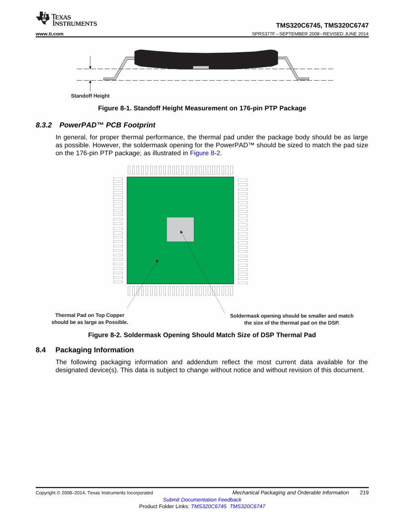
Thermal Pad on Top Coppershould be as large as Possible.
Soldermask opening should be smaller and matchthe size of the thermal pad on the DSP.
Standoff Height
TMS320C6745, TMS320C6747www.ti.com SPRS377F –SEPTEMBER 2008–REVISED JUNE 2014
Figure 8-1. Standoff Height Measurement on 176-pin PTP Package
8.3.2 PowerPAD™ PCB FootprintIn general, for proper thermal performance, the thermal pad under the package body should be as largeas possible. However, the soldermask opening for the PowerPAD™ should be sized to match the pad sizeon the 176-pin PTP package; as illustrated in Figure 8-2.
Figure 8-2. Soldermask Opening Should Match Size of DSP Thermal Pad
8.4 Packaging InformationThe following packaging information and addendum reflect the most current data available for thedesignated device(s). This data is subject to change without notice and without revision of this document.
Copyright © 2008–2014, Texas Instruments Incorporated Mechanical Packaging and Orderable Information 219Submit Documentation Feedback
Product Folder Links: TMS320C6745 TMS320C6747

PACKAGE OPTION ADDENDUM
www.ti.com 15-Apr-2017
Addendum-Page 1
PACKAGING INFORMATION
Orderable Device Status(1)
Package Type PackageDrawing
Pins PackageQty
Eco Plan(2)
Lead/Ball Finish(6)
MSL Peak Temp(3)
Op Temp (°C) Device Marking(4/5)
Samples
TMS320C6745DPTP3 ACTIVE HLQFP PTP 176 40 Green (RoHS& no Sb/Br)
CU NIPDAU Level-4-260C-72 HR TMS320C6745DPTP3
TMS320C6745DPTP4 ACTIVE HLQFP PTP 176 40 Green (RoHS& no Sb/Br)
CU NIPDAU Level-4-260C-72 HR TMS320C6745DPTP4
TMS320C6745DPTPA3 ACTIVE HLQFP PTP 176 40 Green (RoHS& no Sb/Br)
CU NIPDAU Level-4-260C-72 HR TMS320C6745DPTPA3
TMS320C6745DPTPD4 ACTIVE HLQFP PTP 176 40 Green (RoHS& no Sb/Br)
CU NIPDAU Level-4-260C-72 HR TMS320C6745DPTPD4
TMS320C6745DPTPT3 ACTIVE HLQFP PTP 176 40 Green (RoHS& no Sb/Br)
CU NIPDAU Level-4-260C-72 HR TMS320C6745DPTPT3
TMS320C6747DZKB3 ACTIVE BGA ZKB 256 90 Green (RoHS& no Sb/Br)
SNAGCU Level-3-260C-168 HR TMS320C6747DZKB3
TMS320C6747DZKB4 ACTIVE BGA ZKB 256 90 Green (RoHS& no Sb/Br)
SNAGCU Level-3-260C-168 HR TMS320C6747DZKB4
TMS320C6747DZKBA3 ACTIVE BGA ZKB 256 90 Green (RoHS& no Sb/Br)
SNAGCU Level-3-260C-168 HR TMS320C6747DZKBA3
TMS320C6747DZKBD4 ACTIVE BGA ZKB 256 90 Green (RoHS& no Sb/Br)
SNAGCU Level-3-260C-168 HR TMS320C6747DZKBD4
TMS320C6747DZKBT3 ACTIVE BGA ZKB 256 90 Green (RoHS& no Sb/Br)
SNAGCU Level-3-260C-168 HR TMS320C6747DZKBT3
(1) The marketing status values are defined as follows:ACTIVE: Product device recommended for new designs.LIFEBUY: TI has announced that the device will be discontinued, and a lifetime-buy period is in effect.NRND: Not recommended for new designs. Device is in production to support existing customers, but TI does not recommend using this part in a new design.PREVIEW: Device has been announced but is not in production. Samples may or may not be available.OBSOLETE: TI has discontinued the production of the device.
(2) Eco Plan - The planned eco-friendly classification: Pb-Free (RoHS), Pb-Free (RoHS Exempt), or Green (RoHS & no Sb/Br) - please check http://www.ti.com/productcontent for the latest availabilityinformation and additional product content details.TBD: The Pb-Free/Green conversion plan has not been defined.Pb-Free (RoHS): TI's terms "Lead-Free" or "Pb-Free" mean semiconductor products that are compatible with the current RoHS requirements for all 6 substances, including the requirement thatlead not exceed 0.1% by weight in homogeneous materials. Where designed to be soldered at high temperatures, TI Pb-Free products are suitable for use in specified lead-free processes.Pb-Free (RoHS Exempt): This component has a RoHS exemption for either 1) lead-based flip-chip solder bumps used between the die and package, or 2) lead-based die adhesive used betweenthe die and leadframe. The component is otherwise considered Pb-Free (RoHS compatible) as defined above.Green (RoHS & no Sb/Br): TI defines "Green" to mean Pb-Free (RoHS compatible), and free of Bromine (Br) and Antimony (Sb) based flame retardants (Br or Sb do not exceed 0.1% by weightin homogeneous material)
PACKAGE OPTION ADDENDUM
www.ti.com 15-Apr-2017
Addendum-Page 2
(3) MSL, Peak Temp. - The Moisture Sensitivity Level rating according to the JEDEC industry standard classifications, and peak solder temperature.
(4) There may be additional marking, which relates to the logo, the lot trace code information, or the environmental category on the device.
(5) Multiple Device Markings will be inside parentheses. Only one Device Marking contained in parentheses and separated by a "~" will appear on a device. If a line is indented then it is a continuationof the previous line and the two combined represent the entire Device Marking for that device.
(6) Lead/Ball Finish - Orderable Devices may have multiple material finish options. Finish options are separated by a vertical ruled line. Lead/Ball Finish values may wrap to two lines if the finishvalue exceeds the maximum column width.
Important Information and Disclaimer:The information provided on this page represents TI's knowledge and belief as of the date that it is provided. TI bases its knowledge and belief on informationprovided by third parties, and makes no representation or warranty as to the accuracy of such information. Efforts are underway to better integrate information from third parties. TI has taken andcontinues to take reasonable steps to provide representative and accurate information but may not have conducted destructive testing or chemical analysis on incoming materials and chemicals.TI and TI suppliers consider certain information to be proprietary, and thus CAS numbers and other limited information may not be available for release.
In no event shall TI's liability arising out of such information exceed the total purchase price of the TI part(s) at issue in this document sold by TI to Customer on an annual basis.

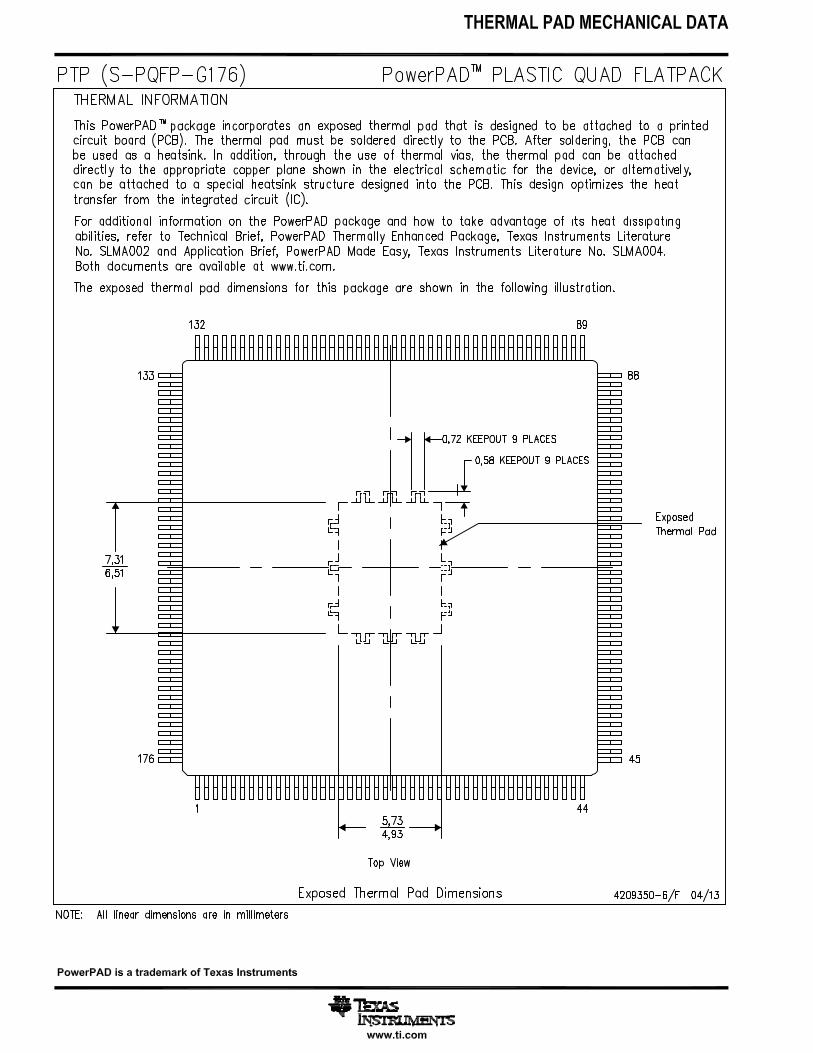


IMPORTANT NOTICE
Texas Instruments Incorporated (TI) reserves the right to make corrections, enhancements, improvements and other changes to itssemiconductor products and services per JESD46, latest issue, and to discontinue any product or service per JESD48, latest issue. Buyersshould obtain the latest relevant information before placing orders and should verify that such information is current and complete.TI’s published terms of sale for semiconductor products (http://www.ti.com/sc/docs/stdterms.htm) apply to the sale of packaged integratedcircuit products that TI has qualified and released to market. Additional terms may apply to the use or sale of other types of TI products andservices.Reproduction of significant portions of TI information in TI data sheets is permissible only if reproduction is without alteration and isaccompanied by all associated warranties, conditions, limitations, and notices. TI is not responsible or liable for such reproduceddocumentation. Information of third parties may be subject to additional restrictions. Resale of TI products or services with statementsdifferent from or beyond the parameters stated by TI for that product or service voids all express and any implied warranties for theassociated TI product or service and is an unfair and deceptive business practice. TI is not responsible or liable for any such statements.Buyers and others who are developing systems that incorporate TI products (collectively, “Designers”) understand and agree that Designersremain responsible for using their independent analysis, evaluation and judgment in designing their applications and that Designers havefull and exclusive responsibility to assure the safety of Designers' applications and compliance of their applications (and of all TI productsused in or for Designers’ applications) with all applicable regulations, laws and other applicable requirements. Designer represents that, withrespect to their applications, Designer has all the necessary expertise to create and implement safeguards that (1) anticipate dangerousconsequences of failures, (2) monitor failures and their consequences, and (3) lessen the likelihood of failures that might cause harm andtake appropriate actions. Designer agrees that prior to using or distributing any applications that include TI products, Designer willthoroughly test such applications and the functionality of such TI products as used in such applications.TI’s provision of technical, application or other design advice, quality characterization, reliability data or other services or information,including, but not limited to, reference designs and materials relating to evaluation modules, (collectively, “TI Resources”) are intended toassist designers who are developing applications that incorporate TI products; by downloading, accessing or using TI Resources in anyway, Designer (individually or, if Designer is acting on behalf of a company, Designer’s company) agrees to use any particular TI Resourcesolely for this purpose and subject to the terms of this Notice.TI’s provision of TI Resources does not expand or otherwise alter TI’s applicable published warranties or warranty disclaimers for TIproducts, and no additional obligations or liabilities arise from TI providing such TI Resources. TI reserves the right to make corrections,enhancements, improvements and other changes to its TI Resources. TI has not conducted any testing other than that specificallydescribed in the published documentation for a particular TI Resource.Designer is authorized to use, copy and modify any individual TI Resource only in connection with the development of applications thatinclude the TI product(s) identified in such TI Resource. NO OTHER LICENSE, EXPRESS OR IMPLIED, BY ESTOPPEL OR OTHERWISETO ANY OTHER TI INTELLECTUAL PROPERTY RIGHT, AND NO LICENSE TO ANY TECHNOLOGY OR INTELLECTUAL PROPERTYRIGHT OF TI OR ANY THIRD PARTY IS GRANTED HEREIN, including but not limited to any patent right, copyright, mask work right, orother intellectual property right relating to any combination, machine, or process in which TI products or services are used. Informationregarding or referencing third-party products or services does not constitute a license to use such products or services, or a warranty orendorsement thereof. Use of TI Resources may require a license from a third party under the patents or other intellectual property of thethird party, or a license from TI under the patents or other intellectual property of TI.TI RESOURCES ARE PROVIDED “AS IS” AND WITH ALL FAULTS. TI DISCLAIMS ALL OTHER WARRANTIES ORREPRESENTATIONS, EXPRESS OR IMPLIED, REGARDING RESOURCES OR USE THEREOF, INCLUDING BUT NOT LIMITED TOACCURACY OR COMPLETENESS, TITLE, ANY EPIDEMIC FAILURE WARRANTY AND ANY IMPLIED WARRANTIES OFMERCHANTABILITY, FITNESS FOR A PARTICULAR PURPOSE, AND NON-INFRINGEMENT OF ANY THIRD PARTY INTELLECTUALPROPERTY RIGHTS. TI SHALL NOT BE LIABLE FOR AND SHALL NOT DEFEND OR INDEMNIFY DESIGNER AGAINST ANY CLAIM,INCLUDING BUT NOT LIMITED TO ANY INFRINGEMENT CLAIM THAT RELATES TO OR IS BASED ON ANY COMBINATION OFPRODUCTS EVEN IF DESCRIBED IN TI RESOURCES OR OTHERWISE. IN NO EVENT SHALL TI BE LIABLE FOR ANY ACTUAL,DIRECT, SPECIAL, COLLATERAL, INDIRECT, PUNITIVE, INCIDENTAL, CONSEQUENTIAL OR EXEMPLARY DAMAGES INCONNECTION WITH OR ARISING OUT OF TI RESOURCES OR USE THEREOF, AND REGARDLESS OF WHETHER TI HAS BEENADVISED OF THE POSSIBILITY OF SUCH DAMAGES.Unless TI has explicitly designated an individual product as meeting the requirements of a particular industry standard (e.g., ISO/TS 16949and ISO 26262), TI is not responsible for any failure to meet such industry standard requirements.Where TI specifically promotes products as facilitating functional safety or as compliant with industry functional safety standards, suchproducts are intended to help enable customers to design and create their own applications that meet applicable functional safety standardsand requirements. Using products in an application does not by itself establish any safety features in the application. Designers mustensure compliance with safety-related requirements and standards applicable to their applications. Designer may not use any TI products inlife-critical medical equipment unless authorized officers of the parties have executed a special contract specifically governing such use.Life-critical medical equipment is medical equipment where failure of such equipment would cause serious bodily injury or death (e.g., lifesupport, pacemakers, defibrillators, heart pumps, neurostimulators, and implantables). Such equipment includes, without limitation, allmedical devices identified by the U.S. Food and Drug Administration as Class III devices and equivalent classifications outside the U.S.TI may expressly designate certain products as completing a particular qualification (e.g., Q100, Military Grade, or Enhanced Product).Designers agree that it has the necessary expertise to select the product with the appropriate qualification designation for their applicationsand that proper product selection is at Designers’ own risk. Designers are solely responsible for compliance with all legal and regulatoryrequirements in connection with such selection.Designer will fully indemnify TI and its representatives against any damages, costs, losses, and/or liabilities arising out of Designer’s non-compliance with the terms and provisions of this Notice.
Mailing Address: Texas Instruments, Post Office Box 655303, Dallas, Texas 75265Copyright © 2017, Texas Instruments Incorporated