tms320dm642 datasheet - ti.com · tms320dm642 sprs200n– july 2002– revised october 2010 the...
TRANSCRIPT
TMS320DM642
www.ti.com SPRS200N–JULY 2002–REVISED OCTOBER 2010
TMS320DM642Video/Imaging Fixed-Point Digital Signal Processor
Check for Samples: TMS320DM642
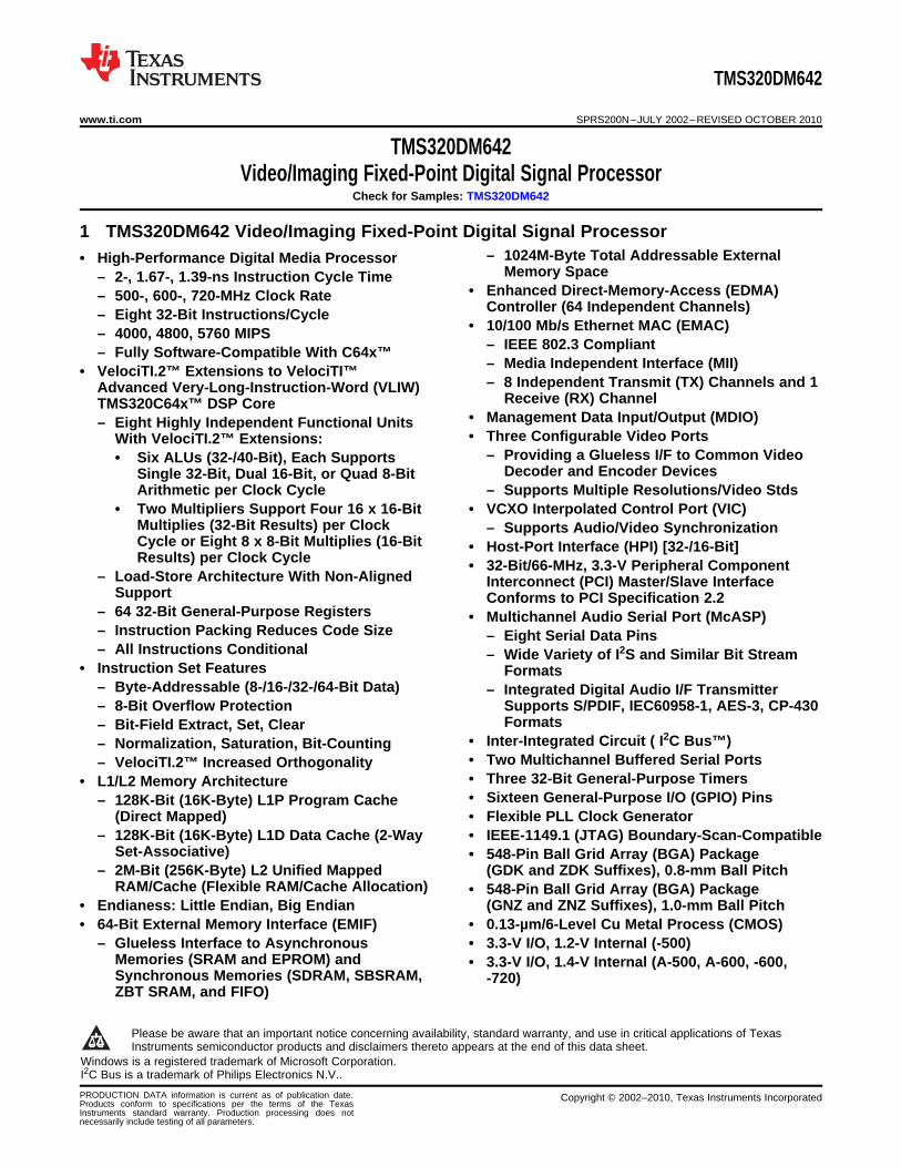
1 TMS320DM642 Video/Imaging Fixed-Point Digital Signal Processor123
– 1024M-Byte Total Addressable External• High-Performance Digital Media ProcessorMemory Space– 2-, 1.67-, 1.39-ns Instruction Cycle Time
• Enhanced Direct-Memory-Access (EDMA)– 500-, 600-, 720-MHz Clock RateController (64 Independent Channels)– Eight 32-Bit Instructions/Cycle
• 10/100 Mb/s Ethernet MAC (EMAC)– 4000, 4800, 5760 MIPS– IEEE 802.3 Compliant– Fully Software-Compatible With C64x™– Media Independent Interface (MII)• VelociTI.2™ Extensions to VelociTI™– 8 Independent Transmit (TX) Channels and 1Advanced Very-Long-Instruction-Word (VLIW)
Receive (RX) ChannelTMS320C64x™ DSP Core• Management Data Input/Output (MDIO)– Eight Highly Independent Functional Units• Three Configurable Video PortsWith VelociTI.2™ Extensions:
– Providing a Glueless I/F to Common Video• Six ALUs (32-/40-Bit), Each SupportsDecoder and Encoder DevicesSingle 32-Bit, Dual 16-Bit, or Quad 8-Bit
Arithmetic per Clock Cycle – Supports Multiple Resolutions/Video Stds• Two Multipliers Support Four 16 x 16-Bit • VCXO Interpolated Control Port (VIC)
Multiplies (32-Bit Results) per Clock – Supports Audio/Video SynchronizationCycle or Eight 8 x 8-Bit Multiplies (16-Bit • Host-Port Interface (HPI) [32-/16-Bit]Results) per Clock Cycle • 32-Bit/66-MHz, 3.3-V Peripheral Component
– Load-Store Architecture With Non-Aligned Interconnect (PCI) Master/Slave InterfaceSupport Conforms to PCI Specification 2.2
– 64 32-Bit General-Purpose Registers • Multichannel Audio Serial Port (McASP)– Instruction Packing Reduces Code Size – Eight Serial Data Pins– All Instructions Conditional – Wide Variety of I2S and Similar Bit Stream
• Instruction Set Features Formats– Byte-Addressable (8-/16-/32-/64-Bit Data) – Integrated Digital Audio I/F Transmitter– 8-Bit Overflow Protection Supports S/PDIF, IEC60958-1, AES-3, CP-430
Formats– Bit-Field Extract, Set, Clear• Inter-Integrated Circuit ( I2C Bus™)– Normalization, Saturation, Bit-Counting• Two Multichannel Buffered Serial Ports– VelociTI.2™ Increased Orthogonality• Three 32-Bit General-Purpose Timers• L1/L2 Memory Architecture• Sixteen General-Purpose I/O (GPIO) Pins– 128K-Bit (16K-Byte) L1P Program Cache
(Direct Mapped) • Flexible PLL Clock Generator– 128K-Bit (16K-Byte) L1D Data Cache (2-Way • IEEE-1149.1 (JTAG) Boundary-Scan-Compatible
Set-Associative) • 548-Pin Ball Grid Array (BGA) Package– 2M-Bit (256K-Byte) L2 Unified Mapped (GDK and ZDK Suffixes), 0.8-mm Ball Pitch
RAM/Cache (Flexible RAM/Cache Allocation) • 548-Pin Ball Grid Array (BGA) Package• Endianess: Little Endian, Big Endian (GNZ and ZNZ Suffixes), 1.0-mm Ball Pitch• 64-Bit External Memory Interface (EMIF) • 0.13-µm/6-Level Cu Metal Process (CMOS)
– Glueless Interface to Asynchronous • 3.3-V I/O, 1.2-V Internal (-500)Memories (SRAM and EPROM) and • 3.3-V I/O, 1.4-V Internal (A-500, A-600, -600,Synchronous Memories (SDRAM, SBSRAM, -720)ZBT SRAM, and FIFO)
1
Please be aware that an important notice concerning availability, standard warranty, and use in critical applications of TexasInstruments semiconductor products and disclaimers thereto appears at the end of this data sheet.
2Windows is a registered trademark of Microsoft Corporation.3I2C Bus is a trademark of Philips Electronics N.V..
PRODUCTION DATA information is current as of publication date. Copyright © 2002–2010, Texas Instruments IncorporatedProducts conform to specifications per the terms of the TexasInstruments standard warranty. Production processing does notnecessarily include testing of all parameters.

TMS320DM642
SPRS200N–JULY 2002–REVISED OCTOBER 2010 www.ti.com
The TMS320C64x™ DSPs (including the TMS320DM642 device) are the highest-performance fixed-pointDSP generation in the TMS320C6000™ DSP platform. The TMS320DM642 (DM642) device is based onthe second-generation high-performance, advanced VelociTI™ very-long-instruction-word (VLIW)architecture (VelociTI.2™) developed by Texas Instruments (TI), making these DSPs an excellent choicefor digital media applications. The C64x™ is a code-compatible member of the C6000™ DSP platform.
With performance of up to 5760 million instructions per second (MIPS) at a clock rate of 720 MHz, theDM642 device offers cost-effective solutions to high-performance DSP programming challenges. TheDM642 DSP possesses the operational flexibility of high-speed controllers and the numerical capability ofarray processors. The C64x™ DSP core processor has 64 general-purpose registers of 32-bit word lengthand eight highly independent functional units—two multipliers for a 32-bit result and six arithmetic logicunits (ALUs)—with VelociTI.2™ extensions. The VelociTI.2™ extensions in the eight functional unitsinclude new instructions to accelerate the performance in video and imaging applications and extend theparallelism of the VelociTI™ architecture. The DM642 can produce four 16-bit multiply-accumulates(MACs) per cycle for a total of 2880 million MACs per second (MMACS), or eight 8-bit MACs per cycle fora total of 5760 MMACS. The DM642 DSP also has application-specific hardware logic, on-chip memory,and additional on-chip peripherals similar to the other C6000™ DSP platform devices.
The DM642 uses a two-level cache-based architecture and has a powerful and diverse set of peripherals.The Level 1 program cache (L1P) is a 128-Kbit direct mapped cache and the Level 1 data cache (L1D) isa 128-Kbit 2-way set-associative cache. The Level 2 memory/cache (L2) consists of an 2-Mbit memoryspace that is shared between program and data space. L2 memory can be configured as mappedmemory, cache, or combinations of the two. The peripheral set includes: three configurable video ports; a10/100 Mb/s Ethernet MAC (EMAC); a management data input/output (MDIO) module; a VCXOinterpolated control port (VIC); one multichannel buffered audio serial port (McASP0); an inter-integratedcircuit (I2C) Bus module; two multichannel buffered serial ports (McBSPs); three 32-bit general-purposetimers; a user-configurable 16-bit or 32-bit host-port interface (HPI16/HPI32); a peripheral componentinterconnect (PCI); a 16-pin general-purpose input/output port (GP0) with programmable interrupt/eventgeneration modes; and a 64-bit glueless external memory interface (EMIFA), which is capable ofinterfacing to synchronous and asynchronous memories and peripherals.
The DM642 device has three configurable video port peripherals (VP0, VP1, and VP2). These video portperipherals provide a glueless interface to common video decoder and encoder devices. The DM642video port peripherals support multiple resolutions and video standards (e.g., CCIR601, ITU-BT.656,BT.1120, SMPTE 125M, 260M, 274M, and 296M).
These three video port peripherals are configurable and can support either video capture and/or videodisplay modes. Each video port consists of two channels — A and B with a 5120-byte capture/displaybuffer that is splittable between the two channels.
For more details on the Video Port peripherals, see the TMS320C64x DSP Video Port/VCXO InterpolatedControl (VIC) Port Reference Guide (literature number SPRU629).
The McASP0 port supports one transmit and one receive clock zone, with eight serial data pins which canbe individually allocated to any of the two zones. The serial port supports time-division multiplexing oneach pin from 2 to 32 time slots. The DM642 has sufficient bandwidth to support all 8 serial data pinstransmitting a 192-kHz stereo signal. Serial data in each zone may be transmitted and received onmultiple serial data pins simultaneously and formatted in a multitude of variations on the Philips Inter-ICSound (I2S) format.
In addition, the McASP0 transmitter may be programmed to output multiple S/PDIF, IEC60958, AES-3,CP-430 encoded data channels simultaneously, with a single RAM containing the full implementation ofuser data and channel status fields.
McASP0 also provides extensive error-checking and recovery features, such as the bad clock detectioncircuit for each high-frequency master clock which verifies that the master clock is within a programmedfrequency range.
2 TMS320DM642 Video/Imaging Fixed-Point Digital Signal Processor Copyright © 2002–2010, Texas Instruments Incorporated
Submit Documentation FeedbackProduct Folder Link(s): TMS320DM642
TMS320DM642
www.ti.com SPRS200N–JULY 2002–REVISED OCTOBER 2010
The VCXO interpolated control (VIC) port provides digital-to-analog conversion with resolution from 9-bitsto up to 16-bits. The output of the VIC is a single bit interpolated D/A output.For more details on the VICport, see the TMS320C64x DSP Video Port/VCXO Interpolated Control (VIC) Port Reference Guide(literature number SPRU629).
The ethernet media access controller (EMAC) provides an efficient interface between the DM642 DSPcore processor and the network. The DM642 EMAC support both 10Base-T and 100Base-TX, or 10Mbits/second (Mbps) and 100 Mbps in either half- or full-duplex, with hardware flow control and quality ofservice (QOS) support. The DM642 EMAC makes use of a custom interface to the DSP core that allowsefficient data transmission and reception. For more details on the EMAC, see the TMS320C6000 DSPEthernet Media Access Controller (EMAC) / Management Data Input/Output (MDIO) Module ReferenceGuide (literature number SPRU628).
The management data input/output (MDIO) module continuously polls all 32 MDIO addresses in order toenumerate all PHY devices in the system. Once a PHY candidate has been selected by the DSP, theMDIO module transparently monitors its link state by reading the PHY status register. Link change eventsare stored in the MDIO module and can optionally interrupt the DSP, allowing the DSP to poll the linkstatus of the device without continuously performing costly MDIO accesses. For more details on theMDIO, see the TMS320C6000 DSP Ethernet Media Access Controller (EMAC) / Management DataInput/Output (MDIO) Module Reference Guide (literature number SPRU628).
The I2C0 port on the TMS320DM642 allows the DSP to easily control peripheral devices andcommunicate with a host processor. In addition, the standard multichannel buffered serial port (McBSP)can be used to communicate with serial peripheral interface (SPI) mode peripheral devices.
The DM642 has a complete set of development tools which includes: a new C compiler, an assemblyoptimizer to simplify programming and scheduling, and a Windows® debugger interface for visibility intosource code execution.
1.1 Device Compatibility
The DM642 device is a code-compatible member of the C6000™ DSP platform.
The C64x™ DSP generation of devices has a diverse and powerful set of peripherals.
For more detailed information on the device compatibility and similarities/differences among the DM642and other C64x™ devices, see the TMS320DM642 Technical Overview (literature number SPRU615).
Copyright © 2002–2010, Texas Instruments Incorporated TMS320DM642 Video/Imaging Fixed-Point Digital Signal Processor 3Submit Documentation Feedback
Product Folder Link(s): TMS320DM642

HPI32
OR
HPI16
PCI-66
Test
C64x DSP Core
Data Path B
B Register File
B31−B16
B15−B0
Instruction Fetch
Instruction Dispatch
Advanced Instruction Packet
Instruction Decode
Data Path A
A Register File
A31−A16
A15−A0
Power-Down
Logic
.L1 .S1 .M1 .D1 .D2 .M2 .S2 .L2
64SDRAM
FIFO
SBSRAM
SRAM
L1P Cache
Direct-Mapped
16K Bytes Total
Control
Registers
Control
Logic
L1D Cache 2-Way Set-Associative
16K Bytes Total
Advanced
In-Circuit
Emulation
Interrupt
Control
TMS320DM642
Enhanced
DMA
Controller
(EDMA)
L2
Cache
Memory
256kBytes
PLL
(x1, x6, x12)
Timer 2
EMIF A
ZBT SRAMTimer 1
Boot Configuration
ROM/FLASH
I/O Devices
Video Port 2(VP2)
VCXOInterpolatedControl Port
(VIC)
8/10-bit VP1
McBSP1(A)
Video Port 1
(VP1)
AND
McASP0Data
OR
OR
AND/OR
EMAC
MDIO
OR
GP0
I2C0
16
2
(B)
8/10-bit VP0
McBSP0(A)
Video Port 0
(VP0)
AND
McASP0Control
OR
OR
Timer 0
TMS320DM642
SPRS200N–JULY 2002–REVISED OCTOBER 2010 www.ti.com
1.2 Functional Block Diagram
Figure 1-1 shows the functional block diagram of the DM642 device.
A. McBSPs: Framing Chips – H.100, MVIP, SCSA, T1, E1; AC97 Devices; SPI Devices; CodecsB. The Video Port 0 (VP0) peripheral is muxed with the McBSP0 peripheral and the McASP0 control pins. The Video
Port 1 (VP1) peripheral is muxed with the McBSP1 peripheral and the McASP0 data pins. The PCI peripheral ismuxed with the HPI(32/16), EMAC, and MDIO peripherals. For more details on the multiplexed pins of theseperipherals, see the Device Configurations section of this data sheet.
Figure 1-1. Functional Block Diagram
4 TMS320DM642 Video/Imaging Fixed-Point Digital Signal Processor Copyright © 2002–2010, Texas Instruments Incorporated
Submit Documentation FeedbackProduct Folder Link(s): TMS320DM642
TMS320DM642
www.ti.com SPRS200N–JULY 2002–REVISED OCTOBER 2010
1 TMS320DM642 Video/Imaging Fixed-Point Digital 5 DM642 Peripheral Information and ElectricalSignal Processor ........................................ 1 Specifications .......................................... 71
5.1 Parameter Information .............................. 711.1 Device Compatibility ................................. 35.2 Recommended Clock and Control Signal Transition
1.2 Functional Block Diagram ............................ 4Behavior ............................................ 72
2 Device Overview ........................................ 65.3 Power Supplies ..................................... 73
2.1 Device Characteristics ............................... 6 5.4 Enhanced Direct Memory Access (EDMA)2.2 CPU (DSP Core) Description ........................ 7 Controller ........................................... 772.3 Memory Map Summary ............................. 13 5.5 Interrupts ............................................ 81
5.6 Reset ............................................... 832.4 Bootmode ........................................... 16
5.7 Clock PLL ........................................... 862.5 Pin Assignments .................................... 16
5.8 External Memory Interface (EMIF) ................. 922.6 Development ........................................ 505.9 Multichannel Audio Serial Port (McASP0) Peripheral3 Device Configurations ................................ 54
..................................................... 1083.1 Configurations at Reset ............................ 545.10 Inter-Integrated Circuit (I2C) ...................... 1163.2 Configurations After Reset ......................... 565.11 Host-Port Interface (HPI) .......................... 122
3.3 Peripheral Configuration Lock ...................... 595.12 Peripheral Component Interconnect (PCI) ........ 128
3.4 Device Status Register Description ................ 61 5.13 Multichannel Buffered Serial Port (McBSP) ....... 1323.5 Multiplexed Pin Configurations ..................... 63 5.14 Video Port ......................................... 141
3.6 Debugging Considerations ......................... 65 5.15 VCXO Interpolated Control (VIC) ................. 149
5.16 Ethernet Media Access Controller (EMAC) ....... 1513.7 Configuration Examples ............................ 655.17 Management Data Input/Output (MDIO) .......... 1574 Device Operating Conditions ....................... 695.18 Timer .............................................. 1594.1 Absolute Maximum Ratings Over Operating Case
Temperature Range 5.19 General-Purpose Input/Output (GPIO) ............ 161(Unless Otherwise Noted) ................................. 69 5.20 JTAG .............................................. 1644.2 Recommended Operating Conditions .............. 69 Revision History ........................................... 1664.3 Electrical Characteristics Over Recommended 6 Mechanical Data ...................................... 167Ranges of Supply Voltage and Operating Case
6.1 Thermal Data ...................................... 167Temperature (Unless Otherwise Noted) ............ 706.2 Packaging Information ............................ 169
Copyright © 2002–2010, Texas Instruments Incorporated Contents 5Submit Documentation Feedback
Product Folder Link(s): TMS320DM642
TMS320DM642
SPRS200N–JULY 2002–REVISED OCTOBER 2010 www.ti.com
2 Device Overview
2.1 Device Characteristics
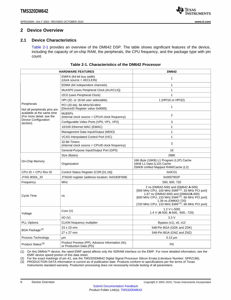
Table 2-1 provides an overview of the DM642 DSP. The table shows significant features of the device,including the capacity of on-chip RAM, the peripherals, the CPU frequency, and the package type with pincount.
Table 2-1. Characteristics of the DM642 Processor
HARDWARE FEATURES DM642
EMIFA (64-bit bus width) 1(clock source = AECLKIN)
EDMA (64 independent channels) 1
McASP0 (uses Peripheral Clock [AUXCLK]) 1
I2C0 (uses Peripheral Clock) 1
HPI (32- or 16-bit user selectable) 1 (HPI16 or HPI32)Peripherals PCI (32-bit), 66-MHz/33-MHz 1[DeviceID Register value 0x9065]Not all peripherals pins areavailable at the same time McBSPs 2(For more detail, see the (internal clock source = CPU/4 clock frequency)Device Configuration
Configurable Video Ports (VP0, VP1, VP2) 3section).10/100 Ethernet MAC (EMAC) 1
Management Data Input/Output (MDIO) 1
VCXO Interpolated Control Port (VIC) 1
32-Bit Timers 3(internal clock source = CPU/8 clock frequency)
General-Purpose Input/Output Port (GP0) 16
Size (Bytes) 288K
16K-Byte (16KB) L1 Program (L1P) CacheOn-Chip MemoryOrganization 16KB L1 Data (L1D) Cache
256KB Unified Mapped RAM/Cache (L2)
CPU ID + CPU Rev ID Control Status Register (CSR.[31:16]) 0x0C01
JTAG BSDL_ID JTAGID register (address location: 0x01B3F008) 0x0007902F
Frequency MHz 500, 600, 720
2 ns (DM642-500) and (DM642 A-500)[500 MHz CPU, 100 MHz EMIF (1), 33 MHz PCI port]
1.67 ns (DM642-600) and (DM642A-600)Cycle Time ns [600 MHz CPU, 133 MHz EMIF (1), 66 MHz PCI port]1.39 ns (DM642-720)
[720 MHz CPU, 133 MHz EMIF (1), 66 MHz PCI port]
1.2 V (–500)Core (V) 1.4 V (A-500, A-600, -600, -720)VoltageI/O (V) 3.3 V
PLL Options CLKIN frequency multiplier Bypass (x1), x6, x12
23 x 23 mm 548-Pin BGA (GDK and ZDK)BGA Package (2)
27 x 27 mm 548-Pin BGA (GNZ and ZNZ)
Process Technology µm 0.13 µm
Product Preview (PP), Advance Information (AI),Product Status (3) PDor Production Data (PD)
(1) On this DM64x™ device, the rated EMIF speed affects only the SDRAM interface on the EMIF. For more detailed information, see theEMIF device speed portion of this data sheet.
(2) For the exact markings of pin A1, see the TMS320DM642 Digital Signal Processor Silicon Errata (Literature Number: SPRZ196).(3) PRODUCTION DATA information is current as of publication date. Products conform to specifications per the terms of Texas
Instruments standard warranty. Production processing does not necessarily include testing of all parameters.
6 Device Overview Copyright © 2002–2010, Texas Instruments Incorporated
Submit Documentation FeedbackProduct Folder Link(s): TMS320DM642
TMS320DM642
www.ti.com SPRS200N–JULY 2002–REVISED OCTOBER 2010
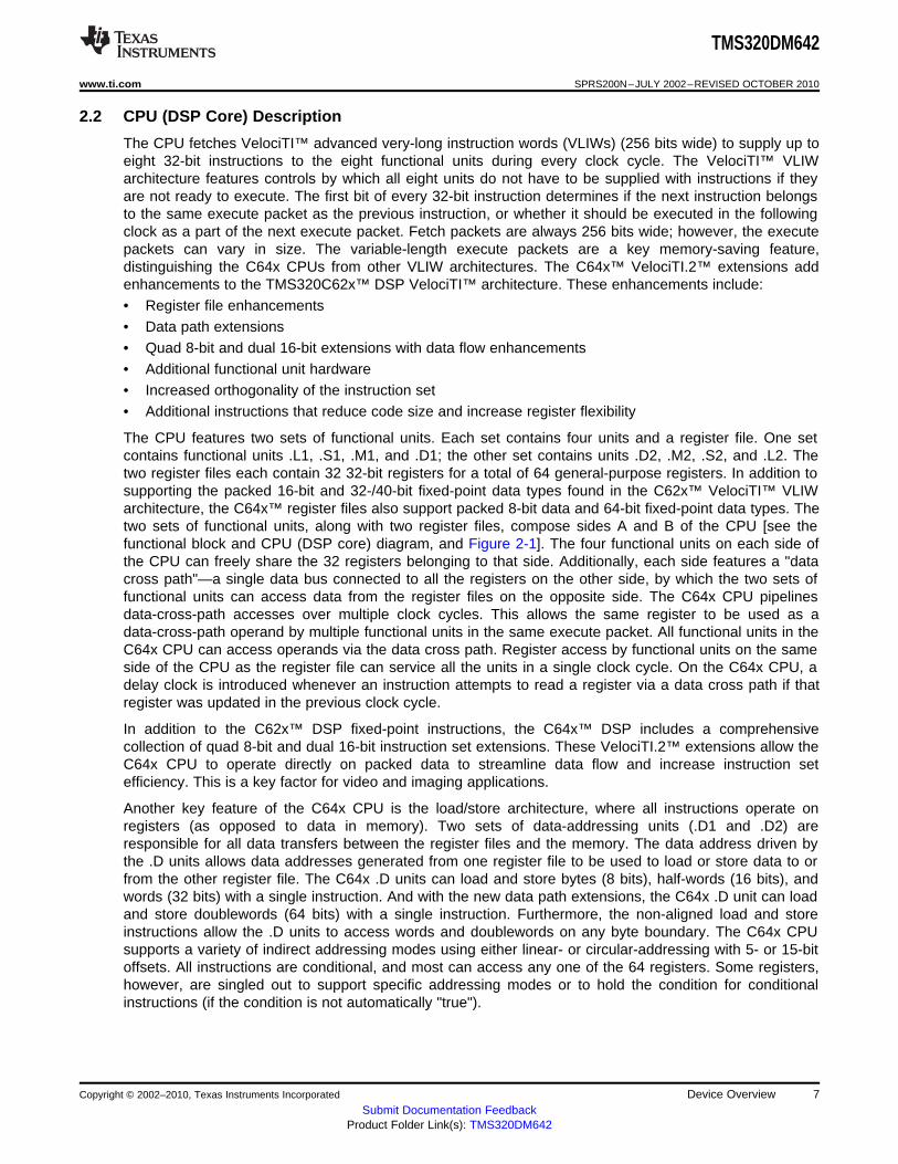
2.2 CPU (DSP Core) Description
The CPU fetches VelociTI™ advanced very-long instruction words (VLIWs) (256 bits wide) to supply up toeight 32-bit instructions to the eight functional units during every clock cycle. The VelociTI™ VLIWarchitecture features controls by which all eight units do not have to be supplied with instructions if theyare not ready to execute. The first bit of every 32-bit instruction determines if the next instruction belongsto the same execute packet as the previous instruction, or whether it should be executed in the followingclock as a part of the next execute packet. Fetch packets are always 256 bits wide; however, the executepackets can vary in size. The variable-length execute packets are a key memory-saving feature,distinguishing the C64x CPUs from other VLIW architectures. The C64x™ VelociTI.2™ extensions addenhancements to the TMS320C62x™ DSP VelociTI™ architecture. These enhancements include:• Register file enhancements• Data path extensions• Quad 8-bit and dual 16-bit extensions with data flow enhancements• Additional functional unit hardware• Increased orthogonality of the instruction set• Additional instructions that reduce code size and increase register flexibility
The CPU features two sets of functional units. Each set contains four units and a register file. One setcontains functional units .L1, .S1, .M1, and .D1; the other set contains units .D2, .M2, .S2, and .L2. Thetwo register files each contain 32 32-bit registers for a total of 64 general-purpose registers. In addition tosupporting the packed 16-bit and 32-/40-bit fixed-point data types found in the C62x™ VelociTI™ VLIWarchitecture, the C64x™ register files also support packed 8-bit data and 64-bit fixed-point data types. Thetwo sets of functional units, along with two register files, compose sides A and B of the CPU [see thefunctional block and CPU (DSP core) diagram, and Figure 2-1]. The four functional units on each side ofthe CPU can freely share the 32 registers belonging to that side. Additionally, each side features a "datacross path"—a single data bus connected to all the registers on the other side, by which the two sets offunctional units can access data from the register files on the opposite side. The C64x CPU pipelinesdata-cross-path accesses over multiple clock cycles. This allows the same register to be used as adata-cross-path operand by multiple functional units in the same execute packet. All functional units in theC64x CPU can access operands via the data cross path. Register access by functional units on the sameside of the CPU as the register file can service all the units in a single clock cycle. On the C64x CPU, adelay clock is introduced whenever an instruction attempts to read a register via a data cross path if thatregister was updated in the previous clock cycle.
In addition to the C62x™ DSP fixed-point instructions, the C64x™ DSP includes a comprehensivecollection of quad 8-bit and dual 16-bit instruction set extensions. These VelociTI.2™ extensions allow theC64x CPU to operate directly on packed data to streamline data flow and increase instruction setefficiency. This is a key factor for video and imaging applications.
Another key feature of the C64x CPU is the load/store architecture, where all instructions operate onregisters (as opposed to data in memory). Two sets of data-addressing units (.D1 and .D2) areresponsible for all data transfers between the register files and the memory. The data address driven bythe .D units allows data addresses generated from one register file to be used to load or store data to orfrom the other register file. The C64x .D units can load and store bytes (8 bits), half-words (16 bits), andwords (32 bits) with a single instruction. And with the new data path extensions, the C64x .D unit can loadand store doublewords (64 bits) with a single instruction. Furthermore, the non-aligned load and storeinstructions allow the .D units to access words and doublewords on any byte boundary. The C64x CPUsupports a variety of indirect addressing modes using either linear- or circular-addressing with 5- or 15-bitoffsets. All instructions are conditional, and most can access any one of the 64 registers. Some registers,however, are singled out to support specific addressing modes or to hold the condition for conditionalinstructions (if the condition is not automatically "true").
Copyright © 2002–2010, Texas Instruments Incorporated Device Overview 7Submit Documentation Feedback
Product Folder Link(s): TMS320DM642

TMS320DM642
SPRS200N–JULY 2002–REVISED OCTOBER 2010 www.ti.com
The two .M functional units perform all multiplication operations. Each of the C64x .M units can performtwo 16 × 16-bit multiplies or four 8 × 8-bit multiplies per clock cycle. The .M unit can also perform 16 ×32-bit multiply operations, dual 16 × 16-bit multiplies with add/subtract operations, and quad 8 × 8-bitmultiplies with add operations. In addition to standard multiplies, the C64x .M units include bit-count,rotate, Galois field multiplies, and bidirectional variable shift hardware.
The two .S and .L functional units perform a general set of arithmetic, logical, and branch functions withresults available every clock cycle. The arithmetic and logical functions on the C64x CPU include single32-bit, dual 16-bit, and quad 8-bit operations.
The processing flow begins when a 256-bit-wide instruction fetch packet is fetched from a programmemory. The 32-bit instructions destined for the individual functional units are "linked" together by "1" bitsin the least significant bit (LSB) position of the instructions. The instructions that are "chained" together forsimultaneous execution (up to eight in total) compose an execute packet. A "0" in the LSB of aninstruction breaks the chain, effectively placing the instructions that follow it in the next execute packet. AC64x™ DSP device enhancement now allows execute packets to cross fetch-packet boundaries. In theTMS320C62x™/TMS320C67x™ DSP devices, if an execute packet crosses the fetch-packet boundary(256 bits wide), the assembler places it in the next fetch packet, while the remainder of the current fetchpacket is padded with NOP instructions. In the C64x™ DSP device, the execute boundary restrictionshave been removed, thereby, eliminating all of the NOPs added to pad the fetch packet, and thus,decreasing the overall code size. The number of execute packets within a fetch packet can vary from oneto eight. Execute packets are dispatched to their respective functional units at the rate of one per clockcycle and the next 256-bit fetch packet is not fetched until all the execute packets from the current fetchpacket have been dispatched. After decoding, the instructions simultaneously drive all active functionalunits for a maximum execution rate of eight instructions every clock cycle. While most results are stored in32-bit registers, they can be subsequently moved to memory as bytes, half-words, or doublewords. Allload and store instructions are byte-, half-word-, word-, or doubleword-addressable.
For more details on the C64x CPU functional units enhancements, see the following documents:• TMS320C6000 CPU and Instruction Set Reference Guide (literature number SPRU189)• TMS320C64x Technical Overview (literature number SPRU395)
8 Device Overview Copyright © 2002–2010, Texas Instruments Incorporated
Submit Documentation FeedbackProduct Folder Link(s): TMS320DM642
.L1
.S1
.M1
.D1
.D2
.M2
.S2
.L2
src1
long dst
88
src2
DA1 (Address)
ST1b (Store Data)
ST2a (Store Data)
RegisterFile A
(A0−A31)
88
88
dst
Data Path A
DA2 (Address)
RegisterFile B
(B0− B31)
LD2a (Load Data)
Data Path B
Control RegisterFile
ST2b (Store Data)
LD1b (Load Data)
88
2X
1X
ST1a (Store Data)
(A)
LD1a (Load Data)
LD2b (Load Data)
32 MSBs32 LSBs
32 MSBs32 LSBs
32 MSBs32 LSBs
32 MSBs32 LSBs
src2
src1
dstlong dstlong src
long srclong dst
dstsrc1
src2
src1
src2
src2
src1dst
src2
src1dst
src2
long dst
src2
src1dst
long dst
long dstlong src
long srclong dst
dst
dst
src2
src1
dst
(A)
(A)
(A)
TMS320DM642
www.ti.com SPRS200N–JULY 2002–REVISED OCTOBER 2010
A. For the .M functional units, the long dst is 32 MSBs and the dst is 32 LSBs.
Figure 2-1. TMS320C64x™ CPU (DSP Core) Data Paths
Copyright © 2002–2010, Texas Instruments Incorporated Device Overview 9Submit Documentation Feedback
Product Folder Link(s): TMS320DM642
TMS320DM642
SPRS200N–JULY 2002–REVISED OCTOBER 2010 www.ti.com
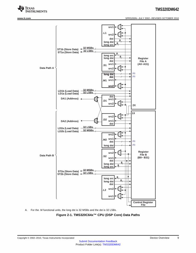
2.2.1 CPU Core Registers
Table 2-2. L2 Cache Registers (C64x)
HEX ADDRESS RANGE ACRONYM REGISTER NAME COMMENTS
0184 0000 CCFG Cache configuration register
0184 0004 – 0184 0FFC – Reserved
0184 1000 EDMAWEIGHT L2 EDMA access control register
0184 1004 – 0184 1FFC – Reserved
0184 2000 L2ALLOC0 L2 allocation register 0
0184 2004 L2ALLOC1 L2 allocation register 1
0184 2008 L2ALLOC2 L2 allocation register 2
0184 200C L2ALLOC3 L2 allocation register 3
0184 2010 – 0184 3FFC – Reserved
0184 4000 L2WBAR L2 writeback base address register
0184 4004 L2WWC L2 writeback word count register
0184 4010 L2WIBAR L2 writeback invalidate base address register
0184 4014 L2WIWC L2 writeback invalidate word count register
0184 4018 L2IBAR L2 invalidate base address register
0184 401C L2IWC L2 invalidate word count register
0184 4020 L1PIBAR L1P invalidate base address register
0184 4024 L1PIWC L1P invalidate word count register
0184 4030 L1DWIBAR L1D writeback invalidate base address register
0184 4034 L1DWIWC L1D writeback invalidate word count register
0184 4038 – 0184 4044 – Reserved
0184 4048 L1DIBAR L1D invalidate base address register
0184 404C L1DIWC L1D invalidate word count register
0184 4050 – 0184 4FFC – Reserved
0184 5000 L2WB L2 writeback all register
0184 5004 L2WBINV L2 writeback invalidate all register
0184 5008 – 0184 7FFC – Reserved
MAR0 to0184 8000 – 0184 81FC ReservedMAR127
0184 8200 MAR128 Controls EMIFA CE0 range 8000 0000 – 80FF FFFF
0184 8204 MAR129 Controls EMIFA CE0 range 8100 0000 – 81FF FFFF
0184 8208 MAR130 Controls EMIFA CE0 range 8200 0000 – 82FF FFFF
0184 820C MAR131 Controls EMIFA CE0 range 8300 0000 – 83FF FFFF
0184 8210 MAR132 Controls EMIFA CE0 range 8400 0000 – 84FF FFFF
0184 8214 MAR133 Controls EMIFA CE0 range 8500 0000 – 85FF FFFF
0184 8218 MAR134 Controls EMIFA CE0 range 8600 0000 – 86FF FFFF
0184 821C MAR135 Controls EMIFA CE0 range 8700 0000 – 87FF FFFF
0184 8220 MAR136 Controls EMIFA CE0 range 8800 0000 – 88FF FFFF
0184 8224 MAR137 Controls EMIFA CE0 range 8900 0000 – 89FF FFFF
0184 8228 MAR138 Controls EMIFA CE0 range 8A00 0000 – 8AFF FFFF
0184 822C MAR139 Controls EMIFA CE0 range 8B00 0000 – 8BFF FFFF
0184 8230 MAR140 Controls EMIFA CE0 range 8C00 0000 – 8CFF FFFF
0184 8234 MAR141 Controls EMIFA CE0 range 8D00 0000 – 8DFF FFFF
0184 8238 MAR142 Controls EMIFA CE0 range 8E00 0000 – 8EFF FFFF
0184 823C MAR143 Controls EMIFA CE0 range 8F00 0000 – 8FFF FFFF
0184 8240 MAR144 Controls EMIFA CE1 range 9000 0000 – 90FF FFFF
0184 8244 MAR145 Controls EMIFA CE1 range 9100 0000 – 91FF FFFF
10 Device Overview Copyright © 2002–2010, Texas Instruments Incorporated
Submit Documentation FeedbackProduct Folder Link(s): TMS320DM642

TMS320DM642
www.ti.com SPRS200N–JULY 2002–REVISED OCTOBER 2010
Table 2-2. L2 Cache Registers (C64x) (continued)
HEX ADDRESS RANGE ACRONYM REGISTER NAME COMMENTS
0184 8248 MAR146 Controls EMIFA CE1 range 9200 0000 – 92FF FFFF
0184 824C MAR147 Controls EMIFA CE1 range 9300 0000 – 93FF FFFF
0184 8250 MAR148 Controls EMIFA CE1 range 9400 0000 – 94FF FFFF
0184 8254 MAR149 Controls EMIFA CE1 range 9500 0000 – 95FF FFFF
0184 8258 MAR150 Controls EMIFA CE1 range 9600 0000 – 96FF FFFF
0184 825C MAR151 Controls EMIFA CE1 range 9700 0000 – 97FF FFFF
0184 8260 MAR152 Controls EMIFA CE1 range 9800 0000 – 98FF FFFF
0184 8264 MAR153 Controls EMIFA CE1 range 9900 0000 – 99FF FFFF
0184 8268 MAR154 Controls EMIFA CE1 range 9A00 0000 – 9AFF FFFF
0184 826C MAR155 Controls EMIFA CE1 range 9B00 0000 – 9BFF FFFF
0184 8270 MAR156 Controls EMIFA CE1 range 9C00 0000 – 9CFF FFFF
0184 8274 MAR157 Controls EMIFA CE1 range 9D00 0000 – 9DFF FFFF
0184 8278 MAR158 Controls EMIFA CE1 range 9E00 0000 – 9EFF FFFF
0184 827C MAR159 Controls EMIFA CE1 range 9F00 0000 – 9FFF FFFF
0184 8280 MAR160 Controls EMIFA CE2 range A000 0000 – A0FF FFFF
0184 8284 MAR161 Controls EMIFA CE2 range A100 0000 – A1FF FFFF
0184 8288 MAR162 Controls EMIFA CE2 range A200 0000 – A2FF FFFF
0184 828C MAR163 Controls EMIFA CE2 range A300 0000 – A3FF FFFF
0184 8290 MAR164 Controls EMIFA CE2 range A400 0000 – A4FF FFFF
0184 8294 MAR165 Controls EMIFA CE2 range A500 0000 – A5FF FFFF
0184 8298 MAR166 Controls EMIFA CE2 range A600 0000 – A6FF FFFF
0184 829C MAR167 Controls EMIFA CE2 range A700 0000 – A7FF FFFF
0184 82A0 MAR168 Controls EMIFA CE2 range A800 0000 – A8FF FFFF
0184 82A4 MAR169 Controls EMIFA CE2 range A900 0000 – A9FF FFFF
0184 82A8 MAR170 Controls EMIFA CE2 range AA00 0000 – AAFF FFFF
0184 82AC MAR171 Controls EMIFA CE2 range AB00 0000 – ABFF FFFF
0184 82B0 MAR172 Controls EMIFA CE2 range AC00 0000 – ACFF FFFF
0184 82B4 MAR173 Controls EMIFA CE2 range AD00 0000 – ADFF FFFF
0184 82B8 MAR174 Controls EMIFA CE2 range AE00 0000 – AEFF FFFF
0184 82BC MAR175 Controls EMIFA CE2 range AF00 0000 – AFFF FFFF
0184 82C0 MAR176 Controls EMIFA CE3 range B000 0000 – B0FF FFFF
0184 82C4 MAR177 Controls EMIFA CE3 range B100 0000 – B1FF FFFF
0184 82C8 MAR178 Controls EMIFA CE3 range B200 0000 – B2FF FFFF
0184 82CC MAR179 Controls EMIFA CE3 range B300 0000 – B3FF FFFF
0184 82D0 MAR180 Controls EMIFA CE3 range B400 0000 – B4FF FFFF
0184 82D4 MAR181 Controls EMIFA CE3 range B500 0000 – B5FF FFFF
0184 82D8 MAR182 Controls EMIFA CE3 range B600 0000 – B6FF FFFF
0184 82DC MAR183 Controls EMIFA CE3 range B700 0000 – B7FF FFFF
0184 82E0 MAR184 Controls EMIFA CE3 range B800 0000 – B8FF FFFF
0184 82E4 MAR185 Controls EMIFA CE3 range B900 0000 – B9FF FFFF
0184 82E8 MAR186 Controls EMIFA CE3 range BA00 0000 – BAFF FFFF
0184 82EC MAR187 Controls EMIFA CE3 range BB00 0000 – BBFF FFFF
0184 82F0 MAR188 Controls EMIFA CE3 range BC00 0000 – BCFF FFFF
0184 82F4 MAR189 Controls EMIFA CE3 range BD00 0000 – BDFF FFFF
0184 82F8 MAR190 Controls EMIFA CE3 range BE00 0000 – BEFF FFFF
0184 82FC MAR191 Controls EMIFA CE3 range BF00 0000 – BFFF FFFF
MAR192 to0184 8300 – 0184 83FC ReservedMAR255
Copyright © 2002–2010, Texas Instruments Incorporated Device Overview 11Submit Documentation Feedback
Product Folder Link(s): TMS320DM642

TMS320DM642
SPRS200N–JULY 2002–REVISED OCTOBER 2010 www.ti.com
Table 2-2. L2 Cache Registers (C64x) (continued)
HEX ADDRESS RANGE ACRONYM REGISTER NAME COMMENTS
0184 8400 – 0187 FFFF – Reserved
12 Device Overview Copyright © 2002–2010, Texas Instruments Incorporated
Submit Documentation FeedbackProduct Folder Link(s): TMS320DM642

TMS320DM642
www.ti.com SPRS200N–JULY 2002–REVISED OCTOBER 2010
2.3 Memory Map Summary
Table 2-3 shows the memory map address ranges of the DM642 device. Internal memory is alwayslocated at address 0 and can be used as both program and data memory. The external memory addressranges in the DM642 device begin at the hex address location 0x8000 0000 for EMIFA.
Table 2-3. TMS320DM642 Memory Map Summary
BLOCK SIZEMEMORY BLOCK DESCRIPTION HEX ADDRESS RANGE(BYTES)
Internal RAM (L2) 256K 0000 0000 – 0003 FFFF
Reserved 768K 0004 0000 – 000F FFFF
Reserved 23M 0010 0000 – 017F FFFF
External Memory Interface A (EMIFA) Registers 256K 0180 0000 – 0183 FFFF
L2 Registers 256K 0184 0000 – 0187 FFFF
HPI Registers 256K 0188 0000 – 018B FFFF
McBSP 0 Registers 256K 018C 0000 – 018F FFFF
McBSP 1 Registers 256K 0190 0000 – 0193 FFFF
Timer 0 Registers 256K 0194 0000 – 0197 FFFF
Timer 1 Registers 256K 0198 0000 – 019B FFFF
Interrupt Selector Registers 256K 019C 0000 – 019F FFFF
EDMA RAM and EDMA Registers 256K 01A0 0000 – 01A3 FFFF
Reserved 512K 01A4 0000 – 01AB FFFF
Timer 2 Registers 256K 01AC 0000 – 01AF FFFF
GP0 Registers 256K – 4K 01B0 0000 – 01B3 EFFF
Device Configuration Registers 4K 01B3 F000 – 01B3 FFFF
I2C0 Data and Control Registers 16K 01B4 0000 – 01B4 3FFF
Reserved 32K 01B4 4000 – 01B4 BFFF
McASP0 Control Registers 16K 01B4 C000 – 01B4 FFFF
Reserved 192K 01B5 0000 – 01B7 FFFF
Reserved 256K 01B8 0000 – 01BB FFFF
Emulation 256K 01BC 0000 – 01BF FFFF
PCI Registers 256K 01C0 0000 – 01C3 FFFF
VP0 Control 16K 01C4 0000 – 01C4 3FFF
VP1 Control 16K 01C4 4000 – 01C4 7FFF
VP2 Control 16K 01C4 8000 – 01C4 BFFF
VIC Control 16K 01C4 C000 – 01C4 FFFF
Reserved 192K 01C5 0000 – 01C7 FFFF
EMAC Control 4K 01C8 0000 – 01C8 0FFF
EMAC Wrapper 8K 01C8 1000 – 01C8 2FFF
EWRAP Registers 2K 01C8 3000 – 01C8 37FF
MDIO Control Registers 2K 01C8 3800 – 01C8 3FFF
Reserved 3.5M 01C8 4000 – 01FF FFFF
QDMA Registers 52 0200 0000 – 0200 0033
Reserved 736M – 52 0200 0034 – 2FFF FFFF
McBSP 0 Data 64M 3000 0000 – 33FF FFFF
McBSP 1 Data 64M 3400 0000 – 37FF FFFF
Reserved 64M 3800 0000 – 3BFF FFFF
McASP0 Data 1M 3C00 0000 – 3C0F FFFF
Reserved 64M – 1M 3C10 0000 – 3FFF FFFF
Reserved 832M 4000 0000 – 73FF FFFF
VP0 Channel A Data 32M 7400 0000 – 75FF FFFF
Copyright © 2002–2010, Texas Instruments Incorporated Device Overview 13Submit Documentation Feedback
Product Folder Link(s): TMS320DM642

TMS320DM642
SPRS200N–JULY 2002–REVISED OCTOBER 2010 www.ti.com
Table 2-3. TMS320DM642 Memory Map Summary (continued)
BLOCK SIZEMEMORY BLOCK DESCRIPTION HEX ADDRESS RANGE(BYTES)
VP0 Channel B Data 32M 7600 0000 – 77FF FFFF
VP1 Channel A Data 32M 7800 0000 – 79FF FFFF
VP1 Channel B Data 32M 7A00 0000 – 7BFF FFFF
VP2 Channel A Data 32M 7C00 0000 – 7DFF FFFF
VP2 Channel B Data 32M 7E00 0000 – 7FFF FFFF
EMIFA CE0 256M 8000 0000 – 8FFF FFFF
EMIFA CE1 256M 9000 0000 – 9FFF FFFF
EMIFA CE2 256M A000 0000 – AFFF FFFF
EMIFA CE3 256M B000 0000 – BFFF FFFF
Reserved 1G C000 0000 – FFFF FFFF
14 Device Overview Copyright © 2002–2010, Texas Instruments Incorporated
Submit Documentation FeedbackProduct Folder Link(s): TMS320DM642

ÎÎÎÎÎÎÎÎÎÎÎÎÎÎÎÎÎÎÎÎÎÎÎÎÎÎÎÎÎÎÎÎÎÎÎÎÎÎÎÎÎÎÎÎÎÎÎÎÎÎÎÎÎÎÎÎÎÎÎÎÎÎÎÎÎÎÎÎÎÎÎÎÎÎÎÎÎÎÎÎÎÎÎÎÎÎÎÎÎÎ0x0000 0000
011010001 111
0x0002 0000
000
L2MODE L2 Memory Block Base Address
0x0003 8000
0x0003 0000
0x0004 0000
32K
Cac
he
(4 W
ay)
64K
Cac
he (
4 W
ay)
128K
Cac
he (
4 W
ay)
256K
Cac
he (
4 W
ay)
[All]
256K
SR
AM
(A
ll)
224K
SR
AM 19
2K S
RA
M
128K
SR
AM
128K-Byte SRAM
64K-Byte RAM
32K-Byte RAM
0x0003 FFFF
32K-Byte RAM
TMS320DM642
www.ti.com SPRS200N–JULY 2002–REVISED OCTOBER 2010
2.3.1 L2 Architecture Expanded
Figure 2-2 shows the detail of the L2 architecture on the TMS320DM642 device. For more information onthe L2MODE bits, see the cache configuration (CCFG) register bit field descriptions in the TMS320C64xTwo-Level Internal Memory Reference Guide (literature number SPRU610).
Figure 2-2. TMS320DM642 L2 Architecture Memory Configuration
Copyright © 2002–2010, Texas Instruments Incorporated Device Overview 15Submit Documentation Feedback
Product Folder Link(s): TMS320DM642

TMS320DM642
SPRS200N–JULY 2002–REVISED OCTOBER 2010 www.ti.com
2.4 Bootmode
The DM642 device resets using the active-low signal RESET. While RESET is low, the device is held inreset and is initialized to the prescribed reset state. Refer to reset timing for reset timing characteristicsand states of device pins during reset. The release of RESET starts the processor running with theprescribed device configuration and boot mode.
The DM642 has three types of boot modes:• Host boot
If host boot is selected, upon release of RESET, the CPU is internally "stalled" while the remainder ofthe device is released. During this period, an external host can initialize the CPU's memory space asnecessary through the host interface, including internal configuration registers, such as those thatcontrol the EMIF or other peripherals. For the DM642 device, the HPI peripheral is used for host boot ifPCI_EN = 0, and the PCI peripheral is used if PCI_EN = 1. Once the host is finished with all necessaryinitialization, it must set the DSPINT bit in the HPIC register to complete the boot process. Thistransition causes the boot configuration logic to bring the CPU out of the "stalled" state. The CPU thenbegins execution from address 0. The DSPINT condition is not latched by the CPU, because it occurswhile the CPU is still internally "stalled". Also, DSPINT brings the CPU out of the "stalled" state only ifthe host boot process is selected. All memory may be written to and read by the host. This allows forthe host to verify what it sends to the DSP if required. After the CPU is out of the "stalled" state, theCPU needs to clear the DSPINT, otherwise, no more DSPINTs can be received.
• EMIF boot (using default ROM timings)Upon the release of RESET, the 1K-Byte ROM code located in the beginning of CE1 is copied toaddress 0 by the EDMA using the default ROM timings, while the CPU is internally "stalled". The datashould be stored in the endian format that the system is using. In this case, the EMIF automaticallyassembles consecutive 8-bit bytes to form the 32-bit instruction words to be copied. The transfer isautomatically done by the EDMA as a single-frame block transfer from the ROM to address 0. Aftercompletion of the block transfer, the CPU is released from the "stalled" state and starts running fromaddress 0.
• No bootWith no boot, the CPU begins direct execution from the memory located at address 0. Note: operationis undefined if invalid code is located at address 0.
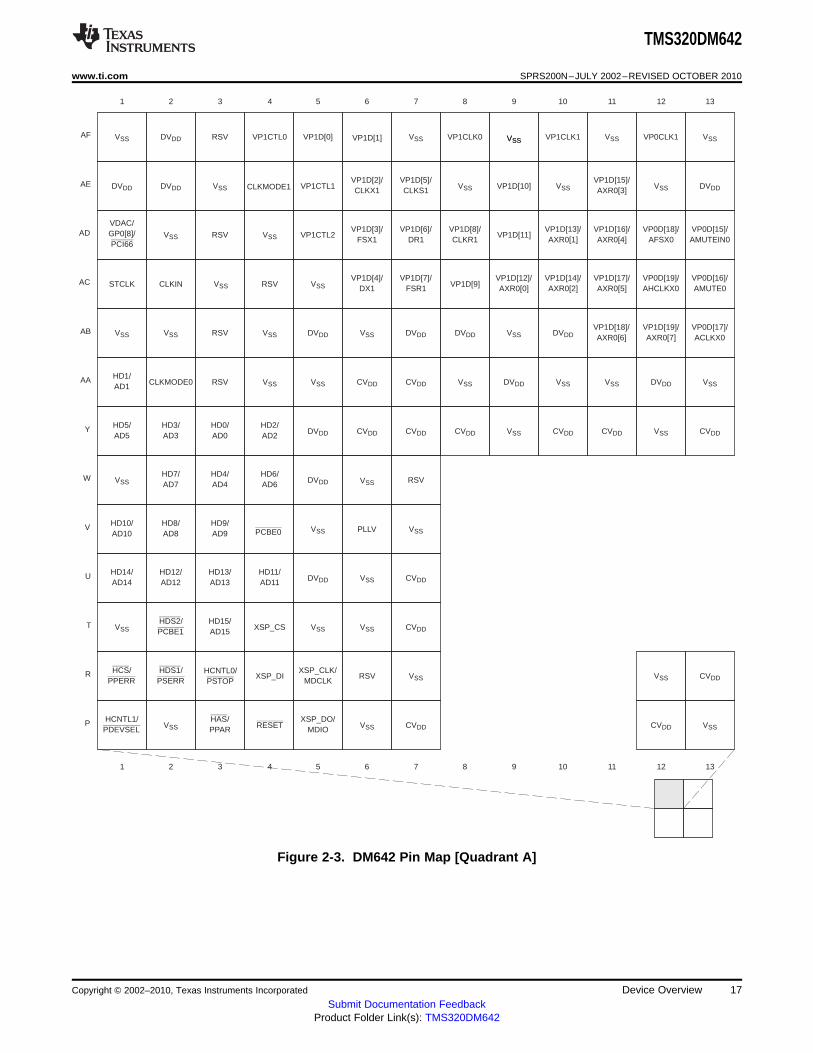
2.5 Pin Assignments
2.5.1 Pin Map
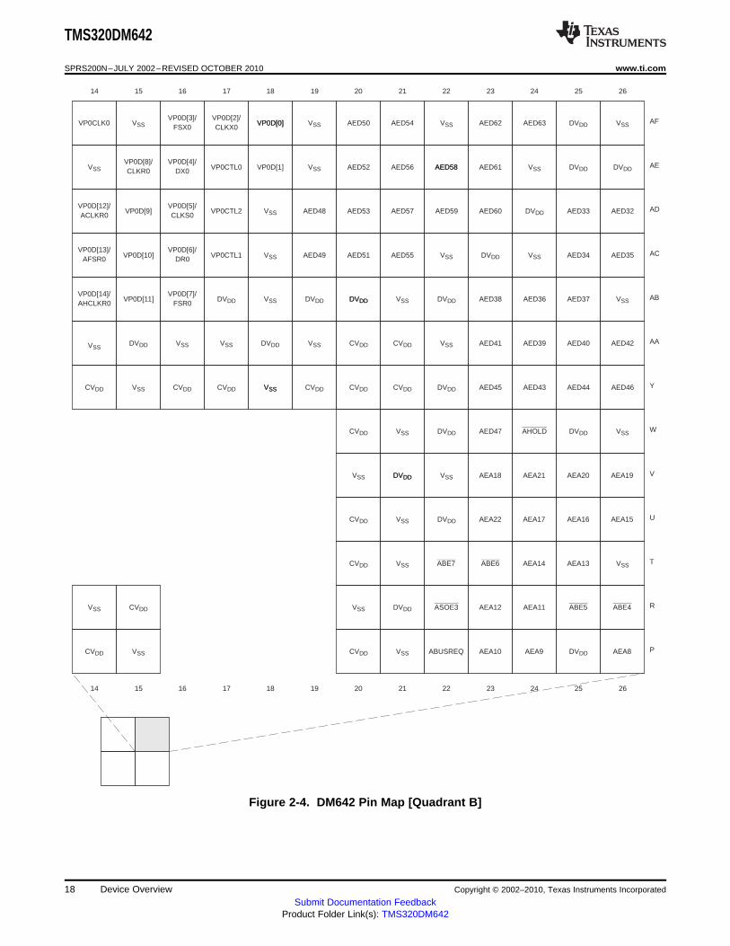
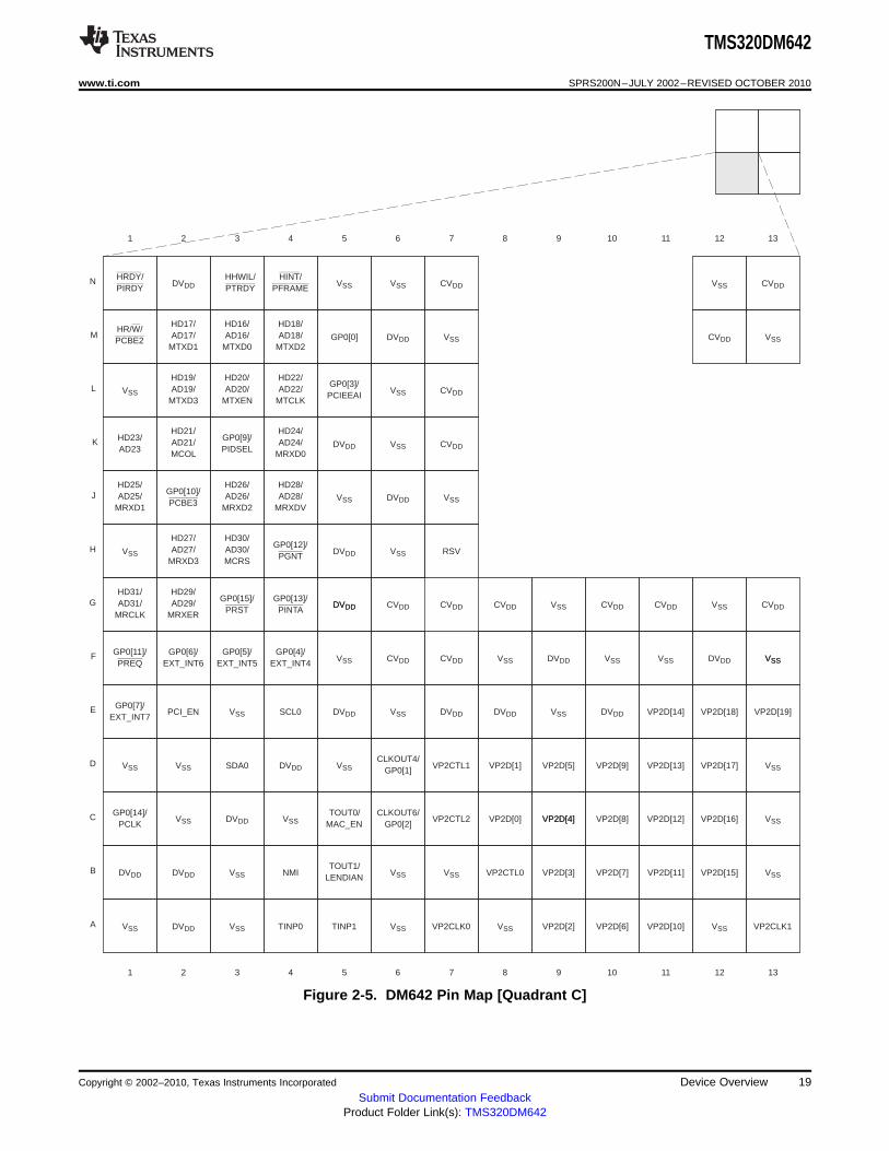
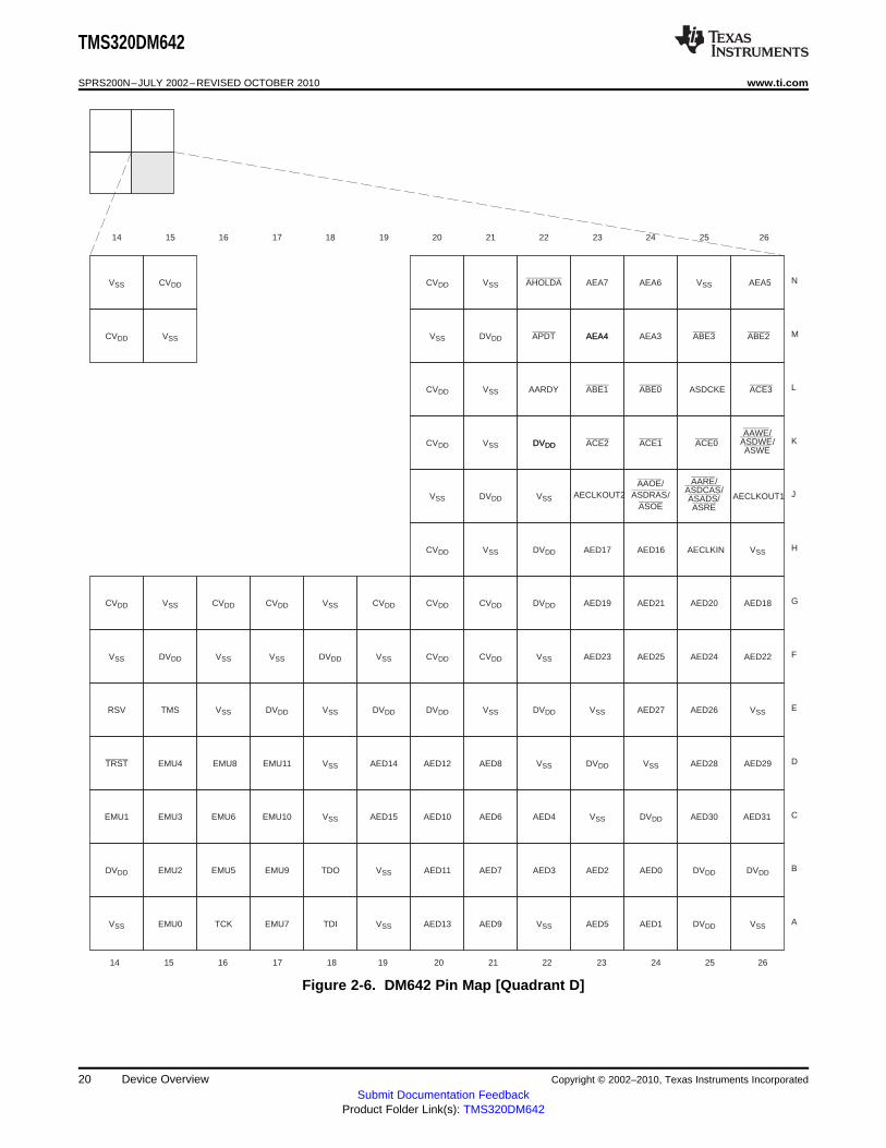
Figure 2-3 through Figure 2-6 show the DM642 pin assignments in four quadrants (A, B, C, and D).
16 Device Overview Copyright © 2002–2010, Texas Instruments Incorporated
Submit Documentation FeedbackProduct Folder Link(s): TMS320DM642
AF
AE
AD
AC
AB
AA
Y
W
V
U
T
R
P
13121110987654321
13121110987654321
CLKMODE1
CLKMODE0
PLLV
RESET
VDAC/GP0[8]/PCI66
HCNTL1/PDEVSEL
HCS/PPERR
HAS/PPAR
HDS1/PSERR
HDS2/PCBE1
HD15/AD15
HD14/AD14
HD13/AD13
HD12/AD12
HD11/AD11
HD10/AD10
HD9/AD9
HD8/AD8
HD7/AD7
HD6/AD6
HD4/AD4
HD3/AD3
HD2/AD2
HD1/AD1
HD0/AD0
PCBE0
XSP_CS
XSP_CLK/MDCLK
XSP_DI
XSP_DO/MDIO
STCLK
VP1D[18]/AXR0[6]
VP1D[19]/AXR0[7]
VP1D[15]/AXR0[3]
VP1D[17]/AXR0[5]
VP0D[19]/AHCLKX0
VP1D[16]/AXR0[4]
VP1D[14]/AXR0[2]
VP1D[13]/AXR0[1]
VP1D[12]/AXR0[0]
VP1D[11]
VP1D[10]
VP1D[9]
VP1D[8]/CLKR1
VP1D[7]/FSR1
VP1D[6]/DR1
VP1D[5]/CLKS1
VP1D[4]/DX1
VP1D[3]/FSX1
VP1D[2]/CLKX1
VP1D[1]VP1D[0] VP1CLK1VP1CLK0
VP1CTL2
VP1CTL1
VP1CTL0
VP0D[17]/ACLKX0
VP0D[16]/AMUTE0
VP0D[15]/AMUTEIN0
VP0CLK1
VP0D[18]/AFSX0
RSV
RSV
RSV
RSV
RSV
RSV
RSV
DVDD DVDD
DVDD
DVDD
DVDD
DVDD
DVDD DVDD
DVDD DVDD DVDD DVDD
DVDD
CVDD CVDD
CVDD
CVDD
CVDD
CVDD CVDD CVDD CVDD CVDD CVDD
CVDD CVDD VSS VSS VSS
VSS VSS VSS VSS VSS
CLKIN VSS
VSS VSS
VSS VSS VSS VSS
VSS VSS
VSS VSS VSS
VSS VSS
VSS VSS VSS
VSS
VSS VSS
VSS VSS
VSS VSS
VSS VSS VSS
VSSVSS VSS VSS
HD5/AD5
HCNTL0/PSTOP
VSS
TMS320DM642
www.ti.com SPRS200N–JULY 2002–REVISED OCTOBER 2010
Figure 2-3. DM642 Pin Map [Quadrant A]
Copyright © 2002–2010, Texas Instruments Incorporated Device Overview 17Submit Documentation Feedback
Product Folder Link(s): TMS320DM642
14 15 16 17 18 19 20 21 22 23 24 25 26
AF
AE
AD
AC
AB
AA
Y
W
V
U
T
R
P
ABE7 ABE6
ABE5 ABE4
ABUSREQ
ASOE3
AEA22
AEA21 AEA20 AEA19AEA18
AEA17 AEA16 AEA15
AEA14 AEA13
AEA12 AEA11
AEA10 AEA9 AEA8
AED63AED62
AED61
AED60AED59
AED58AED58
AED57
AED56
AED55
AED54
AED53
AED52
AED51
AED50
AED49
AED48
AED47
AED46AED45 AED44AED43
AED42AED41 AED40AED39
AED38 AED37AED36
AED35AED34
AED33 AED32
VP0D[14]/AHCLKR0
VP0D[13]/AFSR0
VP0D[12]/ACLKR0
VP0D[11]
VP0D[10]
VP0D[9]
VP0D[8]/CLKR0
VP0D[7]/FSR0
VP0D[6]/DR0
VP0D[5]/CLKS0
VP0D[4]/DX0
VP0D[3]/FSX0
VP0D[2]/CLKX0
VP0D[1]
VP0D[0]VP0D[0]VP0CLK0
VP0CTL2
VP0CTL1
VP0CTL0
DVDD
DVDD
DVDD
DVDDDVDD
AHOLDDVDD DVDD
DVDD
DVDD DVDD
DVDD DVDD DVDDDVDD DVDD
DVDD
DVDD
DVDD DVDD
DVDD
CVDD CVDD
CVDD
CVDD
CVDD
CVDD
CVDD CVDD CVDD CVDD CVDD CVDD
CVDD VSS
VSS VSS
VSS VSS
VSS VSS
VSS
VSS VSS
VSS VSS
VSS VSSVSS
VSSVSS VSS VSS
VSS VSSVSS
VSS VSS VSS
VSS
VSS VSS VSS
VSS VSS VSS VSS
CVDD
14 15 16 17 18 19 20 21 22 23 24 25 26
TMS320DM642
SPRS200N–JULY 2002–REVISED OCTOBER 2010 www.ti.com
Figure 2-4. DM642 Pin Map [Quadrant B]
18 Device Overview Copyright © 2002–2010, Texas Instruments Incorporated
Submit Documentation FeedbackProduct Folder Link(s): TMS320DM642
N
M
L
K
J
H
G
F
E
D
C
B
A
CLKOUT6/GP0[2]
NMI
GP0[7]/EXT_INT7
GP0[6]/EXT_INT6
GP0[5]/EXT_INT5
GP0[4]/EXT_INT4
GP0[15]/PRST
GP0[14]/PCLK
GP0[13]/PINTA
GP0[12]/PGNT
GP0[11]/PREQ
GP0[10]/PCBE3
GP0[9]/PIDSEL
GP0[3]/PCIEEAI
GP0[0]
PCI_EN
HINT/PFRAME
HHWIL/PTRDY
HR/W/PCBE2
HRDY/PIRDY
HD31/AD31/
MRCLK
HD30/AD30/MCRS
HD29/AD29/
MRXER
HD28/AD28/
MRXDV
HD27/AD27/
MRXD3
HD26/AD26/
MRXD2
HD25/AD25/
MRXD1
HD24/AD24/
MRXD0
HD23/AD23
13121110987654321
HD22/AD22/
MTCLK
HD21/AD21/MCOL
HD20/AD20/
MTXEN
HD19/AD19/
MTXD3
HD18/AD18/
MTXD2
HD17/AD17/
MTXD1
HD16/AD16/
MTXD0
VP2D[19]VP2D[18]
VP2D[16]
VP2D[15]
VP2D[14]
VP2D[12]
VP2D[10]
VP2D[8]
VP2D[6]
VP2D[4]VP2D[4]
VP2D[2]
VP2D[0]
VP2CLK0 VP2CLK1
VP2CTL2
TOUT1/LENDIAN
TINP1
TOUT0/MAC_EN
TINP0
SCL0
RSV
DVDD
DVDD DVDD
DVDD
DVDD DVDD DVDD DVDD
DVDD DVDD
DVDDDVDD
DVDD
DVDD
DVDD
DVDD
DVDD
CVDD CVDD
CVDD CVDD
CVDDCVDD CVDD CVDD
CVDD
CVDD
CVDD
CVDD CVDD
VSS VSS VSS VSS VSS
VSS VSS VSS VSS
VSS VSS
VSS
VSS
VSS VSS VSS
VSS VSS VSS
VSS VSS VSS VSS VSSVSS
VSS VSS
VSS VSS
VSS VSS
VSS
VSS VSS
VSS VSS
VSS VSS VSS
SDA0 DVDDCLKOUT4/
GP0[1] VP2CTL1 VP2D[1] VP2D[5] VP2D[9] VP2D[13] VP2D[17]
VP2CTL0 VP2D[3] VP2D[7] VP2D[11]
13121110987654321
TMS320DM642
www.ti.com SPRS200N–JULY 2002–REVISED OCTOBER 2010
Figure 2-5. DM642 Pin Map [Quadrant C]
Copyright © 2002–2010, Texas Instruments Incorporated Device Overview 19Submit Documentation Feedback
Product Folder Link(s): TMS320DM642
N
M
L
K
J
H
G
F
E
D
C
B
A
14 15 16 17 18 19 20 21 22 23 24 25 26
14 15 16 17 18 19 20 21 22 23 24 25 26
TMS
TDO
TDITCK
TRST EMU11
EMU10
EMU9
EMU8
EMU7
EMU6
EMU5
EMU4
EMU3
EMU2
EMU1
EMU0
ACE3
ACE2 ACE1 ACE0
ABE3 ABE2
ABE1 ABE0
APDT
AHOLDA
AECLKIN
AAOE/ASDRAS/
ASOE
AARDY
AECLKOUT1
AARE/ASDCAS/ASADS/ASRE
AAWE/ASDWE/ASWE
ASDCKE
AEA7 AEA6 AEA5
AEA4AEA4 AEA3
AED31AED30
AED29AED28
AED27 AED26
AED25 AED24AED23 AED22
AED21 AED20AED19 AED18
AED17 AED16
AED15
AED14
AED13
AED12
AED11
AED10
AED9
AED8
AED7
AED6 AED4
AED3
AED5
AED2
AED1
AED0
RSV
DVDDVSS
VSS
DVDD DVDD DVDD
DVDD
DVDD VSS
DVDD
DVDD DVDD DVDD
DVDD
DVDD
DVDD
DVDD
DVDD
DVDDDVDD
DVDD
CVDD CVDD
CVDD CVDD CVDD CVDD CVDD
CVDD
CVDD
CVDD
CVDD
CVDD CVDD
VSS VSS VSS
VSS
VSS
VSS VSS VSS
VSS VSS VSS VSS
VSS VSS VSS VSS VSS
VSS VSS
VSSVSS
VSS VSS
VSS
VSS
VSS VSS
VSS VSS VSS
AECLKOUT2
CVDD
TMS320DM642
SPRS200N–JULY 2002–REVISED OCTOBER 2010 www.ti.com
Figure 2-6. DM642 Pin Map [Quadrant D]
20 Device Overview Copyright © 2002–2010, Texas Instruments Incorporated
Submit Documentation FeedbackProduct Folder Link(s): TMS320DM642
TRST
GP0[7]/EXT_INT7 (B)
IEEE Standard1149.1(JTAG)
Emulation
Reserved
Reset andInterrupts
Control/Status
TDITDOTMS
TCK
EMU0EMU1
NMI
GP0[6]/EXT_INT6 (B)
GP0[5]/EXT_INT5 (B)
GP0[4]/EXT_INT4 (B)
RESET
RSV07RSV06
Clock/PLL
CLKIN
CLKMODE1CLKMODE0
PLLV
EMU2EMU3EMU4EMU5
GP0
General-Purpose Input/Output 0 (GP0) Port
GP0[7]/EXT_INT7 (B)
GP0[6]/EXT_INT6 (B)
GP0[5]/EXT_INT5 (B)
GP0[4]/EXT_INT4 (B)
GP0[3]/PCIEEAICLKOUT6/GP0[2] (A)
CLKOUT4/GP0[1] (A)
GP0[0]
CLKOUT6/GP0[2] (A)
CLKOUT4/GP0[1] (A)
EMU6EMU7EMU8EMU9
EMU10
GP0[15]/PRST (C)
GP0[14]/PCLK (C)
GP0[13]/PINTA (C)
GP0[12]/PGNT (C)
GP0[11]/PREQ (C)
GP0[10]/PCBE3 (C)
GP0[9]/PIDSEL (C)
VDAC/GP0[8]/PCI66 (C)
RSV08
EMU11
RSV04RSV03
RSV05
PeripheralControl/Status
PCI_ENTOUT0/MAC_EN
RSV01RSV00
RSV02
TMS320DM642
www.ti.com SPRS200N–JULY 2002–REVISED OCTOBER 2010
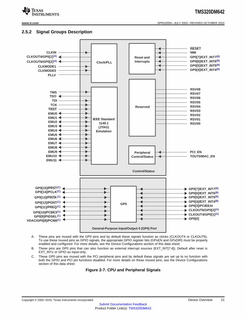
2.5.2 Signal Groups Description
A. These pins are muxed with the GP0 pins and by default these signals function as clocks (CLKOUT4 or CLKOUT6).To use these muxed pins as GPIO signals, the appropriate GPIO register bits (GPxEN and GPxDIR) must be properlyenabled and configured. For more details, see the Device Configurations section of this data sheet.
B. These pins are GP0 pins that can also function as external interrupt sources (EXT_INT[7:4]). Default after reset isEXT_INTx or GPIO as input-only.
C. These GP0 pins are muxed with the PCI peripheral pins and by default these signals are set up to no function withboth the GPIO and PCI pin functions disabled. For more details on these muxed pins, see the Device Configurationssection of this data sheet.
Figure 2-7. CPU and Peripheral Signals
Copyright © 2002–2010, Texas Instruments Incorporated Device Overview 21Submit Documentation Feedback
Product Folder Link(s): TMS320DM642

ACE3AECLKOUT1
AED[63:0]
ACE2
ACE1ACE0
AEA[22:3]
ABE7ABE6
ABE5ABE4
AARDY
Data
Memory Map Space Select
Address
Byte Enables
64
20
ExternalMemory I/F
Control
EMIFA (64-bit)
AECLKIN
AHOLD
AHOLDAABUSREQ
BusArbitration
AARE/ASDCAS/ASADS/ASREASDCKEAECLKOUT2
ASOE3
ABE3ABE2
ABE1ABE0
AAOE/ASDRAS/ASOEAAWE/ASDWE/ASWE
APDT
VDAC/GP0[8]/PCI66
VCXO InterpolatedControl Port (VIC)
Data
TMS320DM642
SPRS200N–JULY 2002–REVISED OCTOBER 2010 www.ti.com
Figure 2-8. EMIFA/VIC Peripheral Signals
22 Device Overview Copyright © 2002–2010, Texas Instruments Incorporated
Submit Documentation FeedbackProduct Folder Link(s): TMS320DM642
HHWIL/PTRDY
HCNTL0/PSTOPHCNTL1/PDEVSEL
Data
Register Select
Half-WordSelect
Control
HPI (A)
(Host-Port Interface)32HD[15:0]/AD[15:0]
HAS/PPARHR/W/PCBE2HCS/PPERRHDS1/PSERRHDS2/PCBE1HRDY/PIRDYHINT/PFRAME(HPI16 ONLY)
HD[15:0]/AD[15:0]
HR/W/PCBE2HDS2/PCBE1
PCBE0
GP0[12]/PGNT
GP0[11]/PREQ
GP0[14]/PCLK
HINT/PFRAMEGP0[13]/PINTA
Data/Address
Arbitration
32Clock
Control
PCI Interface (B)
HAS/PPARGP0[15]/PRSTHRDY/PIRDYHCNTL0/PSTOPHHWIL/PTRDY
GP0[10]/PCBE3
GP0[9]/PIDSELHCNTL1/PDEVSEL
HDS1/PSERRError
CommandByte Enable
SerialEEPROM
XSP_DO/MDIOXSP_CSXSP_CLK/MDCLKXSP_DI
HCS/PPERR
HD[31:16]/AD[31:16] (C)
HD[31:16]/AD[31:16] (C)
TMS320DM642
www.ti.com SPRS200N–JULY 2002–REVISED OCTOBER 2010
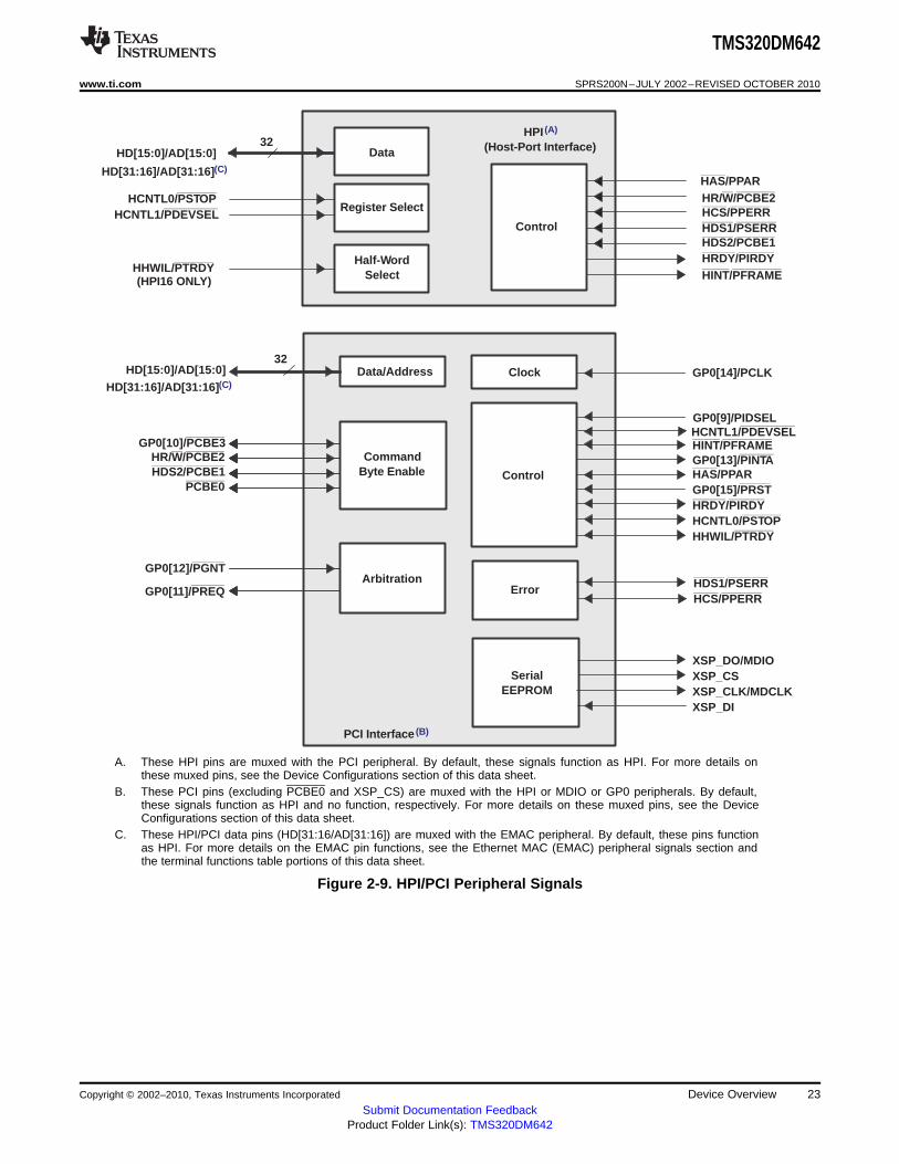
A. These HPI pins are muxed with the PCI peripheral. By default, these signals function as HPI. For more details onthese muxed pins, see the Device Configurations section of this data sheet.
B. These PCI pins (excluding PCBE0 and XSP_CS) are muxed with the HPI or MDIO or GP0 peripherals. By default,these signals function as HPI and no function, respectively. For more details on these muxed pins, see the DeviceConfigurations section of this data sheet.
C. These HPI/PCI data pins (HD[31:16/AD[31:16]) are muxed with the EMAC peripheral. By default, these pins functionas HPI. For more details on the EMAC pin functions, see the Ethernet MAC (EMAC) peripheral signals section andthe terminal functions table portions of this data sheet.
Figure 2-9. HPI/PCI Peripheral Signals
Copyright © 2002–2010, Texas Instruments Incorporated Device Overview 23Submit Documentation Feedback
Product Folder Link(s): TMS320DM642
McBSPs(Multichannel Buffered
Serial Ports)
VP0D[2]/CLKX0(A)
VP0D[3]/FSX0(A)
VP0D[4]/DX0(A)
VP0D[8]/CLKR0(A)
VP0D[7]/FSR0(A)
VP0D[6]/DR0(A)
VP0D[5]/CLKS0(A)
McBSP0
VP1D[2]/CLKX1(A)
VP1D[3]/FSX1(A)
VP1D[4]/DX1(A)
VP1D[8]/CLKR1(A)
VP1D[7]/FSR1(A)
VP1D[6]/DR1(A)
VP1D[5]/CLKS1(A)
McBSP1
TOUT0/MACEN
Timers
TINP0TOUT1/LENDIAN
Timer 1TINP1
Timer 2
Timer 0
SCL0I2C0
I2C0
SDA0
Transmit
Receive
Clock
Transmit
Receive
Clock
TMS320DM642
SPRS200N–JULY 2002–REVISED OCTOBER 2010 www.ti.com
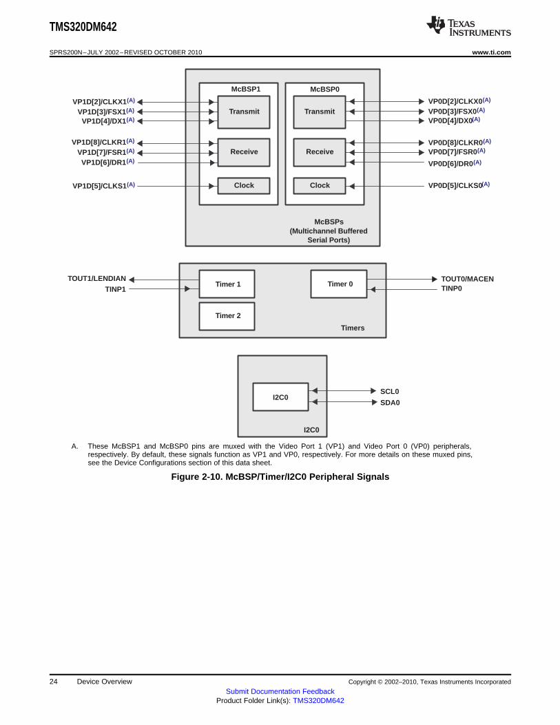
A. These McBSP1 and McBSP0 pins are muxed with the Video Port 1 (VP1) and Video Port 0 (VP0) peripherals,respectively. By default, these signals function as VP1 and VP0, respectively. For more details on these muxed pins,see the Device Configurations section of this data sheet.
Figure 2-10. McBSP/Timer/I2C0 Peripheral Signals
24 Device Overview Copyright © 2002–2010, Texas Instruments Incorporated
Submit Documentation FeedbackProduct Folder Link(s): TMS320DM642

HD21/AD21/MCOL(A)HD28/AD28/MRXDV(A)HD29/AD29/MRXER(A)
HD20/AD20/MTXEN(A)
Ethernet MAC (EMAC)and MDIO
XSP_DO/MDIO(B)
XSP_CLK/MDCLK(B)
MDIO
Clock
HD16/AD16/MTXD0(A)
HD17/AD17/MTXD1(A)
HD18/AD18/MTXD2(A)
HD25/AD25/MRXD1(A)
HD26/AD26/MRXD2(A)
HD27/AD27/MRXD3(A)
EMAC
Transmit
HD24/AD24/MRXD0(A)
HD19/AD19/MTXD3(A)
ClocksHD31/AD31/MRCLK(A)HD22/AD22/MTCLK(A)
HD30/AD30/MCRS(A)
Error Detectand Control
Input/OutputReceive
TMS320DM642
www.ti.com SPRS200N–JULY 2002–REVISED OCTOBER 2010
A. These EMAC pins are muxed with the upper data pins of the HPI or PCI peripherals. By default, these signalsfunction as HPI. For more details on these muxed pins, see the Device Configurations section of this data sheet.
B. These MDIO pins are muxed with the PCI peripherals. By default, these signals function as PCI. For more details onthese muxed pins, see the Device Configurations section of this data sheet.
Figure 2-11. EMAC/MDIO Peripheral Signals
Copyright © 2002–2010, Texas Instruments Incorporated Device Overview 25Submit Documentation Feedback
Product Folder Link(s): TMS320DM642
VP0D[10]VP0D[11]VP0D[12]/ACLKR0VP0D[13]/AFSR0VP0D[14]/AHCLKR0VP0D[15]/AMUTEIN0VP0D[16]/AMUTE0VP0D[17]/ACLKX0
VP0D[0]VP0D[1]
VP0D[2]/CLKX0VP0D[3]/FSX0VP0D[4]/DX0
VP0D[5]/CLKS0VP0D[6]/DR0
VP0D[7]/FSR0VP0D[8]/CLKR0
VP0D[9]VP0D[18]/AFSX0VP0D[19]/AHCLKX0
Capture/DisplayBuffer
(2560 Bytes)
VP0CLK0VP0CLK1VP0CTL0VP0CTL1VP0CTL2
Timing andControl Logic
Video Port 0 (VP0)
Channel B (B)
Channel A (A)
Capture/DisplayBuffer
(2560 Bytes)
Channel B uses onlythe VP0D[19:10] bidirectional pins
STCLK (C)
TMS320DM642
SPRS200N–JULY 2002–REVISED OCTOBER 2010 www.ti.com
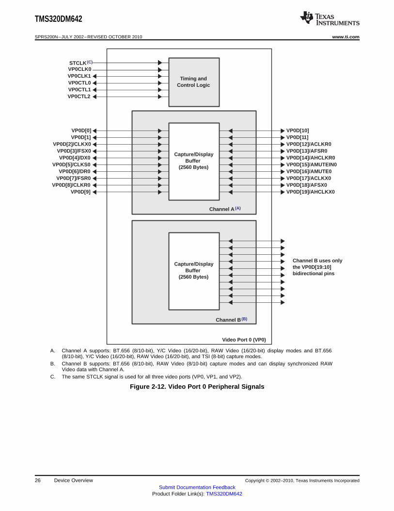
A. Channel A supports: BT.656 (8/10-bit), Y/C Video (16/20-bit), RAW Video (16/20-bit) display modes and BT.656(8/10-bit), Y/C Video (16/20-bit), RAW Video (16/20-bit), and TSI (8-bit) capture modes.
B. Channel B supports: BT.656 (8/10-bit), RAW Video (8/10-bit) capture modes and can display synchronized RAWVideo data with Channel A.
C. The same STCLK signal is used for all three video ports (VP0, VP1, and VP2).
Figure 2-12. Video Port 0 Peripheral Signals
26 Device Overview Copyright © 2002–2010, Texas Instruments Incorporated
Submit Documentation FeedbackProduct Folder Link(s): TMS320DM642

VP1D[10]VP1D[11]VP1D[12]/AXR0[0]VP1D[13]/AXR0[1]VP1D[14]/AXR0[2]VP1D[15]/AXR0[3]VP1D[16]/AXR0[4]VP1D[17]/AXR0[5]
VP1D[0]VP1D[1]
VP1D[2]/CLKX1VP1D[3]/FSX1VP1D[4]/DX1
VP1D[5]/CLKS1VP1D[6]/DR1
VP1D[7]/FSR1VP1D[8]/CLKR1
VP1D[9]VP1D[18]/AXR0[6]VP1D[19]/AXR0[7]
Capture/DisplayBuffer
(2560 Bytes)
VP1CLK0VP1CLK1VP1CTL0VP1CTL1VP1CTL2
Timing andControl Logic
Video Port 1 (VP1)
Channel B (B)
Channel A (A)
Capture/DisplayBuffer
(2560 Bytes)
Channel B uses onlythe VP1D[19:10] bidirectional pins
STCLK (C)
TMS320DM642
www.ti.com SPRS200N–JULY 2002–REVISED OCTOBER 2010
A. Channel A supports: BT.656 (8/10-bit), Y/C Video (16/20-bit), RAW Video (16/20-bit) display modes and BT.656(8/10-bit), Y/C Video (16/20-bit), RAW Video (16/20-bit), and TSI (8-bit) capture modes.
B. Channel B supports: BT.656 (8/10-bit), RAW Video (8/10-bit) capture modes and can display synchronized RAWVideo data with Channel A.
C. The same STCLK signal is used for all three video ports (VP0, VP1, and VP2).
Figure 2-13. Video Port 1 Peripheral Signals
Copyright © 2002–2010, Texas Instruments Incorporated Device Overview 27Submit Documentation Feedback
Product Folder Link(s): TMS320DM642
VP2D[10]VP2D[11]VP2D[12]VP2D[13]VP2D[14]VP2D[15]VP2D[16]VP2D[17]
VP2D[0]VP2D[1]VP2D[2]VP2D[3]VP2D[4]VP2D[5]VP2D[6]VP2D[7]VP2D[8]VP2D[9]
VP2D[18]VP2D[19]
Capture/DisplayBuffer
(2560 Bytes)
VP2CLK0VP2CLK1VP2CTL0VP2CTL1VP2CTL2
Timing andControl Logic
Video Port 2 (VP2)
Channel B (B)
Channel A (A)
Capture/DisplayBuffer
(2560 Bytes)
Channel B uses onlythe VP2D[19:10] bidirectional pins
STCLK (C)
TMS320DM642
SPRS200N–JULY 2002–REVISED OCTOBER 2010 www.ti.com
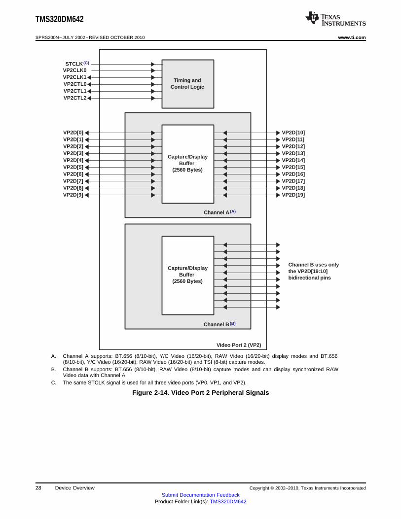
A. Channel A supports: BT.656 (8/10-bit), Y/C Video (16/20-bit), RAW Video (16/20-bit) display modes and BT.656(8/10-bit), Y/C Video (16/20-bit), RAW Video (16/20-bit) and TSI (8-bit) capture modes.
B. Channel B supports: BT.656 (8/10-bit), RAW Video (8/10-bit) capture modes and can display synchronized RAWVideo data with Channel A.
C. The same STCLK signal is used for all three video ports (VP0, VP1, and VP2).
Figure 2-14. Video Port 2 Peripheral Signals
28 Device Overview Copyright © 2002–2010, Texas Instruments Incorporated
Submit Documentation FeedbackProduct Folder Link(s): TMS320DM642
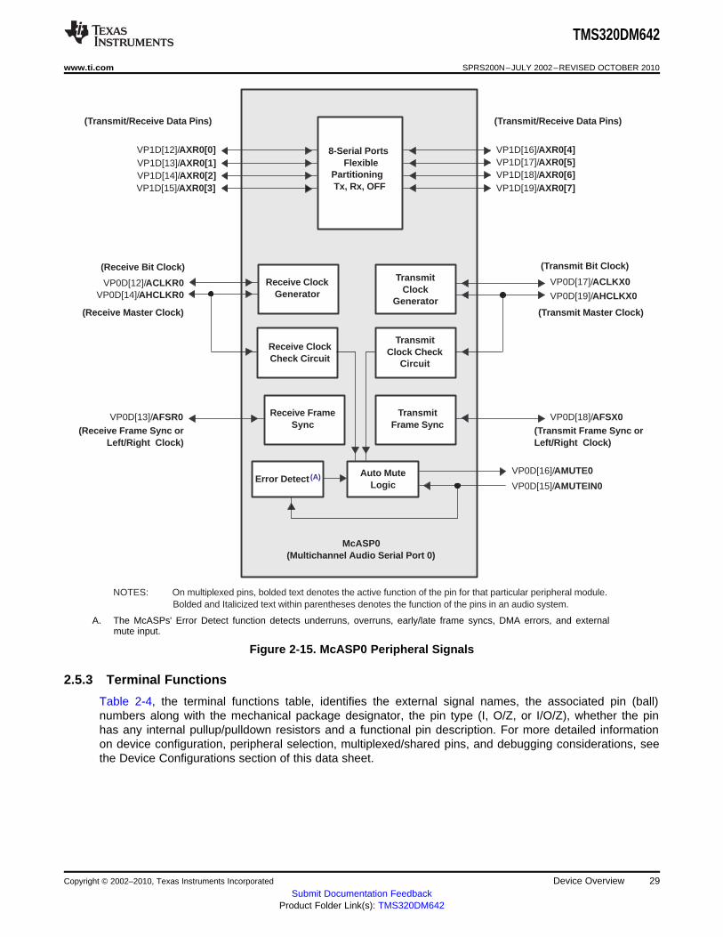
VP1D[19]/AXR0[7]
McASP0(Multichannel Audio Serial Port 0)
VP1D[18]/AXR0[6]
VP0D[17]/ACLKX0
VP0D[19]/AHCLKX0
TransmitClock
Generator
VP0D[15]/AMUTEIN0Auto Mute
Logic
VP0D[16]/AMUTE0
VP0D[18]/AFSX0TransmitFrame Sync
VP0D[13]/AFSR0 Receive FrameSync
VP1D[17]/AXR0[5]VP1D[16]/AXR0[4]
VP0D[12]/ACLKR0VP0D[14]/AHCLKR0
Receive ClockGenerator
VP1D[15]/AXR0[3]VP1D[14]/AXR0[2]VP1D[13]/AXR0[1]VP1D[12]/AXR0[0] 8-Serial Ports
FlexiblePartitioning Tx, Rx, OFF
TransmitClock Check
Circuit
Receive ClockCheck Circuit
Error Detect (A)
(Transmit/Receive Data Pins)(Transmit/Receive Data Pins)
(Receive Bit Clock) (Transmit Bit Clock)
(Receive Master Clock) (Transmit Master Clock)
(Receive Frame Sync orLeft/Right Clock)
(Transmit Frame Sync orLeft/Right Clock)
NOTES: On multiplexed pins, bolded text denotes the active function of the pin for that particular peripheral module.Bolded and Italicized text within parentheses denotes the function of the pins in an audio system.
TMS320DM642
www.ti.com SPRS200N–JULY 2002–REVISED OCTOBER 2010
A. The McASPs' Error Detect function detects underruns, overruns, early/late frame syncs, DMA errors, and externalmute input.
Figure 2-15. McASP0 Peripheral Signals
2.5.3 Terminal Functions
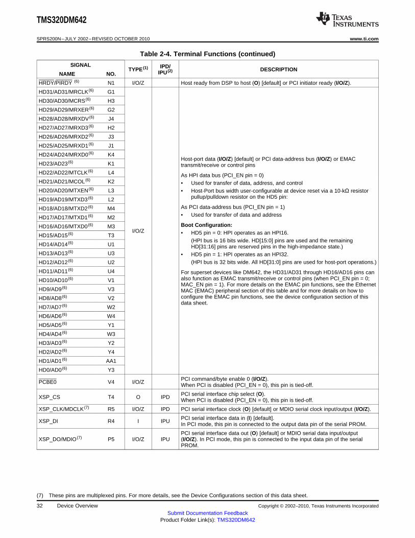
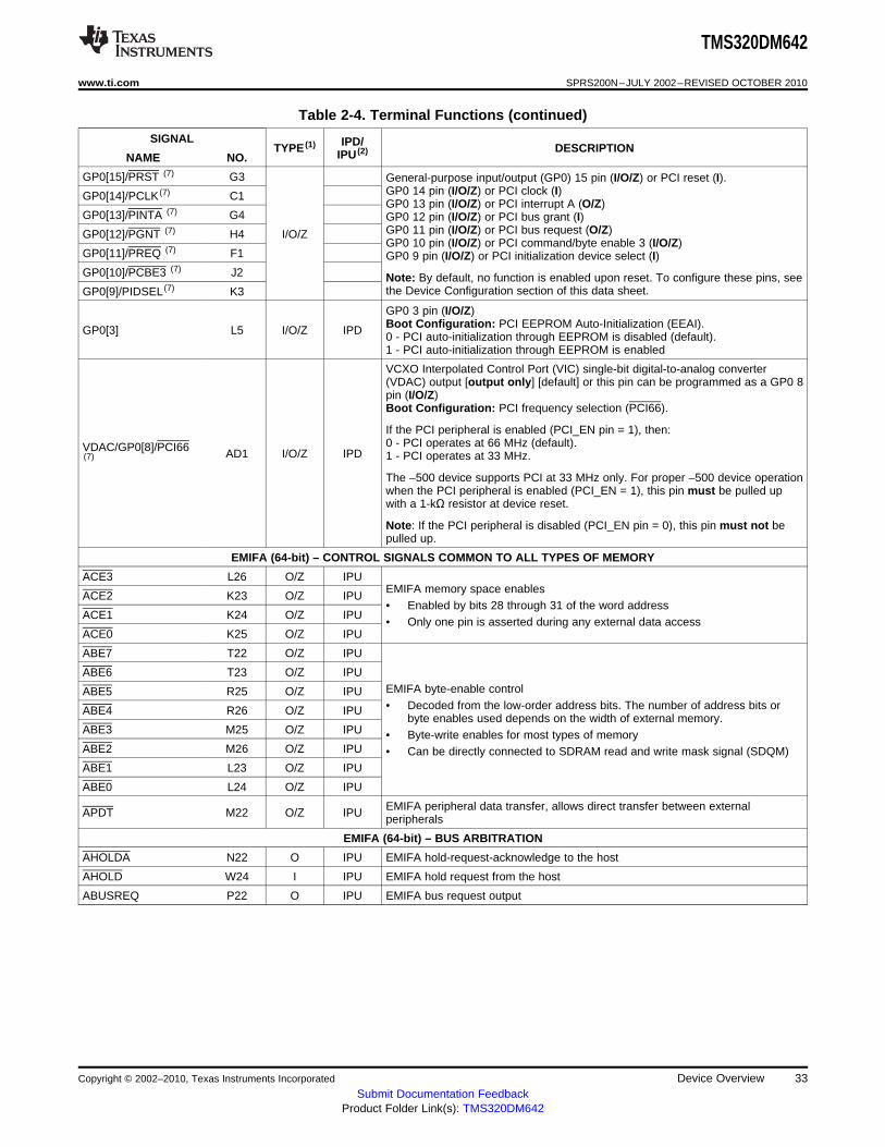
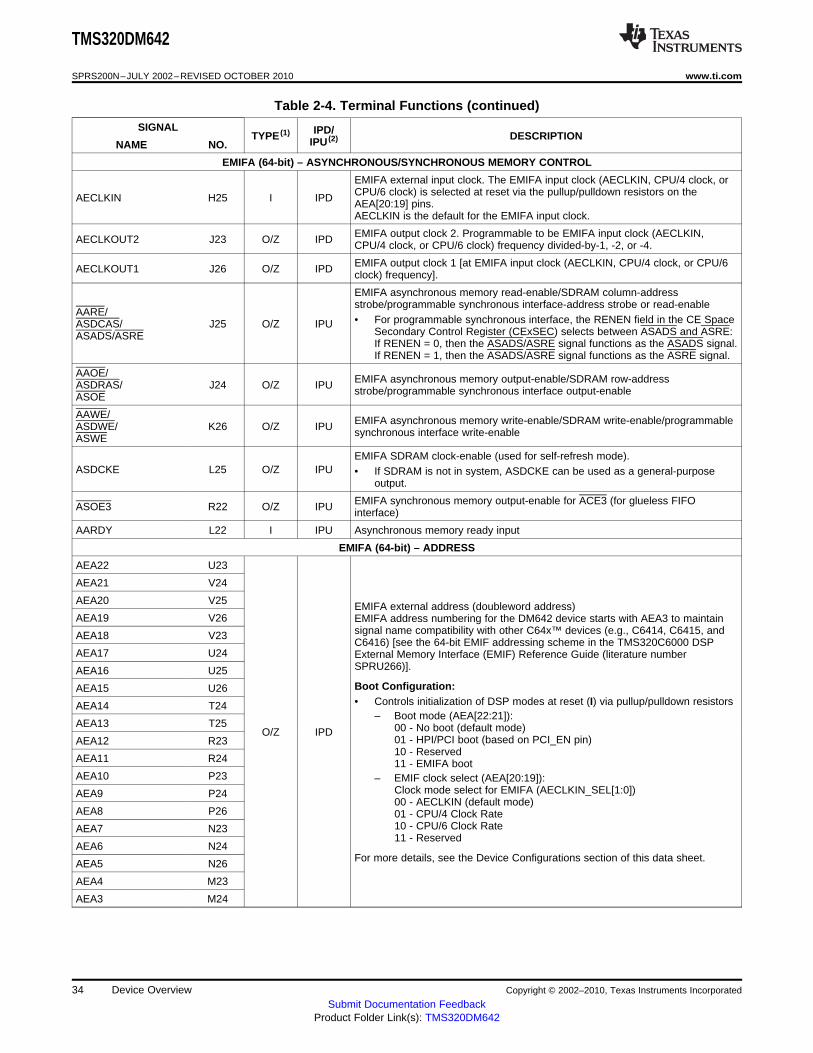
Table 2-4, the terminal functions table, identifies the external signal names, the associated pin (ball)numbers along with the mechanical package designator, the pin type (I, O/Z, or I/O/Z), whether the pinhas any internal pullup/pulldown resistors and a functional pin description. For more detailed informationon device configuration, peripheral selection, multiplexed/shared pins, and debugging considerations, seethe Device Configurations section of this data sheet.
Copyright © 2002–2010, Texas Instruments Incorporated Device Overview 29Submit Documentation Feedback
Product Folder Link(s): TMS320DM642

TMS320DM642
SPRS200N–JULY 2002–REVISED OCTOBER 2010 www.ti.com
Table 2-4. Terminal Functions
SIGNAL IPD/TYPE (1) DESCRIPTIONIPU (2)NAME NO.
CLOCK/PLL CONFIGURATION
CLKIN AC2 I Clock Input. This clock is the input to the on-chip PLL.
Clock output at 1/4 of the device speed (O/Z) [default] or this pin can beCLKOUT4/GP0[1] (3) D6 I/O/Z IPU programmed as a GP0 1 pin (I/O/Z).
Clock output at 1/6 of the device speed (O/Z) [default] or this pin can beCLKOUT6/GP0[2] (3) C6 I/O/Z IPU programmed as a GP0 2 pin (I/O/Z).
CLKMODE1 AE4 I IPD Clock mode select• Selects whether the CPU clock frequency = input clock frequency x1
(Bypass), x6, or x12.CLKMODE0 AA2 I IPD
For more details on the CLKMODE pins and the PLL multiply factors, seethe Clock PLL section of this data sheet.
PLLV (4) V6 A (1) PLL voltage supply
JTAG EMULATION
TMS E15 I IPU JTAG test-port mode select
TDO B18 O/Z IPU JTAG test-port data out
TDI A18 I IPU JTAG test-port data in
TCK A16 I IPU JTAG test-port clock
JTAG test-port reset. For IEEE 1149.1 JTAG compatibility, see the IEEE 1149.1TRST D14 I IPD JTAG compatibility statement portion of this data sheet.
EMU11 D17 I/O/Z IPU Emulation pin 11. Reserved for future use, leave unconnected.
EMU10 C17 I/O/Z IPU Emulation pin 10. Reserved for future use, leave unconnected.
EMU9 B17 I/O/Z IPU Emulation pin 9. Reserved for future use, leave unconnected.
EMU8 D16 I/O/Z IPU Emulation pin 8. Reserved for future use, leave unconnected.
EMU7 A17 I/O/Z IPU Emulation pin 7. Reserved for future use, leave unconnected.
EMU6 C16 I/O/Z IPU Emulation pin 6. Reserved for future use, leave unconnected.
EMU5 B16 I/O/Z IPU Emulation pin 5. Reserved for future use, leave unconnected.
EMU4 D15 I/O/Z IPU Emulation pin 4. Reserved for future use, leave unconnected.
EMU3 C15 I/O/Z IPU Emulation pin 3. Reserved for future use, leave unconnected.
EMU2 B15 I/O/Z IPU Emulation pin 2. Reserved for future use, leave unconnected.
EMU1 C14 I/O/Z IPU Emulation pin 1 (5)
EMU0 A15 I/O/Z IPU Emulation pin 0 (5)
RESETS, INTERRUPTS, AND GENERAL-PURPOSE INPUT/OUTPUTS
RESET P4 I Device reset
Nonmaskable interrupt, edge-driven (rising edge)
Note: Any noise on the NMI pin may trigger an NMI interrupt; therefore, if theNMI B4 I IPDNMI pin is not used, it is recommended that the NMI pin be grounded versusrelying on the IPD.
GP0[7]/EXT_INT7 E1 I/O/Z IPU General-purpose input/output (GPIO) pins (I/O/Z) or external interrupts (inputonly). The default after reset setting is GPIO enabled as input-only.GP0[6]/EXT_INT6 F2 I/O/Z IPU• When these pins function as External Interrupts [by selecting the
GP0[5]/EXT_INT5 F3 I/O/Z IPU corresponding interrupt enable register bit (IER.[7:4])], they are edge-drivenand the polarity can be independently selected via the External Interrupt
GP0[4]/EXT_INT4 F4 I/O/Z IPU Polarity Register bits (EXTPOL.[3:0]).
(1) I = Input, O = Output, Z = High impedance, S = Supply voltage, GND = Ground, A = Analog signal(2) IPD = Internal pulldown, IPU = Internal pullup. (These IPD/IPU signal pins feature a 30-kΩ IPD or IPU resistor. To pull up a signal to the
opposite supply rail, a 1-kΩ resistor should be used.)(3) These pins are multiplexed pins. For more details, see the Device Configurations section of this data sheet.(4) PLLV is not part of external voltage supply. See the Clock PLL section for information on how to connect this pin.(5) The EMU0 and EMU1 pins are internally pulled up with 30-kΩ resistors; therefore, for emulation and normal operation, no external
pullup/pulldown resistors are necessary. However, for boundary scan operation, pull down the EMU1 and EMU0 pins with a dedicated1-kΩ resistor.
30 Device Overview Copyright © 2002–2010, Texas Instruments Incorporated
Submit Documentation FeedbackProduct Folder Link(s): TMS320DM642

TMS320DM642
www.ti.com SPRS200N–JULY 2002–REVISED OCTOBER 2010
Table 2-4. Terminal Functions (continued)
SIGNAL IPD/TYPE (1) DESCRIPTIONIPU (2)NAME NO.
GP0[15]/PRST (3) G3 General-purpose input/output (GP0) 15 pin (I/O/Z) or PCI reset (I).GP0 14 pin (I/O/Z) or PCI clock (I)GP0[14]/PCLK (3) C1GP0 13 pin (I/O/Z) or PCI interrupt A (O/Z)
GP0[13]/PINTA (3) G4 GP0 12 pin (I/O/Z) or PCI bus grant (I)GP0 11 pin (I/O/Z) or PCI bus request (O/Z)GP0[12]/PGNT (3) H4GP0 10 pin (I/O/Z) or PCI command/byte enable 3 (I/O/Z)
GP0[11]/PREQ (3) F1 GP0 9 pin (I/O/Z) or PCI initialization device select (I)I/O/ZGP0[10]/PCBE3 (3) J2 Note: By default, no function is enabled upon reset. To configure these pins, see
the Device Configuration section of this data sheet.GP0[9]/PIDSEL (3) K3
GP0 3 pin (I/O/Z)Boot Configuration: PCI EEPROM Auto-Initialization (EEAI).
GP0[3] L5 IPD0 - PCI auto-initialization through EEPROM is disabled (default).1 - PCI auto-initialization through EEPROM is enabled.
General-purpose 0 pin (GP0[0]) (I/O/Z) [default]This pin can be programmed as GPIO 0 (input only) [default] or as GP0[0](output only) pin or output as a general-purpose interrupt (GP0INT) signalGP0[0] M5 I/O/Z IPD(output only).
Note: This pin must remain low during device reset.
VCXO Interpolated Control Port (VIC) single-bit digital-to-analog converter(VDAC) output [output only] [default] or this pin can be programmed as a GP0 8pin (I/O/Z)Boot Configuration: PCI frequency selection (PCI66).
If the PCI peripheral is enabled (PCI_EN pin = 1), then:0 - PCI operates at 66 MHz (default).VDAC/GP0[8]/PCI66 AD1 I/O/Z IPD 1 - PCI operates at 33 MHz.(3)
The –500 device supports PCI at 33 MHz only. For proper –500 device operationwhen the PCI peripheral is enabled (PCI_EN = 1), this pin must be pulled upwith a 1-kΩ resistor at device reset.
Note: If the PCI peripheral is disabled (PCI_EN pin = 0), this pin be must notpulled up.
Clock output at 1/6 of the device speed (O/Z) [default] or this pin can beCLKOUT6/GP0[2] (6) C6 I/O/Z IPU programmed as a GP0 2 pin (I/O/Z).
Clock output at 1/4 of the device speed (O/Z) [default] or this pin can beCLKOUT4/GP0[1] (6) D6 I/O/Z IPU programmed as a GP0 1 pin (I/O/Z).
HOST-PORT INTERFACE (HPI) or PERIPHERAL COMPONENT INTERCONNECT (PCI) or EMAC
Boot Configuration: PCI enable pin (I)The PCI_EN pin and the MAC_EN pin control the selection (enable/disable) of
PCI_EN E2 I IPD the HPI, EMAC, MDIO, and GP0[15:8], or PCI peripherals. The pins work inconjunction to enable/disable these peripherals (for more details, see the DeviceConfigurations section of this data sheet).
HINT/PFRAME (6) N4 I/O/Z Host interrupt from DSP to host (O) [default] or PCI frame (I/O/Z)
Host control – selects between control, address, or data registers (I) [default] orHCNTL1/PDEVSEL (6) P1 I/O/Z PCI device select (I/O/Z).
Host control – selects between control, address, or data registers (I) [default] orHCNTL0/PSTOP (6) R3 I/O/Z PCI stop (I/O/Z)
Host half-word select – first or second half-word (not necessarily high or lowHHWIL/PTRDY (6) N3 I/O/Z order)
[For HPI16 bus width selection only] (I) [default] or PCI target ready (I/O/Z)
HR/W/PCBE2 (6) M1 I/O/Z Host read or write select (I) [default] or PCI command/byte enable 2 (I/O/Z)
HAS/PPAR (6) P3 I/O/Z Host address strobe (I) [default] or PCI parity (I/O/Z)Host chip select (I) [default] or PCI parity error (I/O/Z)HCS/PPERR (6) R1 I/O/ZHost data strobe 1 (I) [default] or PCI system error (I/O/Z)
HDS1/PSERR (6) R2 I/O/Z Host data strobe 2 (I) [default] or PCI command/byte enable 1 (I/O/Z)
Note: If unused, the following HPI control signals should be externally pulledHDS2/PCBE1 (6) T2 I/O/Zhigh.
(6) These pins are multiplexed pins. For more details, see the Device Configurations section of this data sheet.
Copyright © 2002–2010, Texas Instruments Incorporated Device Overview 31Submit Documentation Feedback
Product Folder Link(s): TMS320DM642
TMS320DM642
SPRS200N–JULY 2002–REVISED OCTOBER 2010 www.ti.com
Table 2-4. Terminal Functions (continued)
SIGNAL IPD/TYPE (1) DESCRIPTIONIPU (2)NAME NO.
HRDY/PIRDY (6) N1 I/O/Z Host ready from DSP to host (O) [default] or PCI initiator ready (I/O/Z).
HD31/AD31/MRCLK (6) G1
HD30/AD30/MCRS (6) H3
HD29/AD29/MRXER (6) G2
HD28/AD28/MRXDV (6) J4
HD27/AD27/MRXD3 (6) H2
HD26/AD26/MRXD2 (6) J3
HD25/AD25/MRXD1 (6) J1
HD24/AD24/MRXD0 (6) K4Host-port data (I/O/Z) [default] or PCI data-address bus (I/O/Z) or EMAC
HD23/AD23 (6) K1 transmit/receive or control pinsHD22/AD22/MTCLK (6) L4 As HPI data bus (PCI_EN pin = 0)HD21/AD21/MCOL (6) K2 • Used for transfer of data, address, and controlHD20/AD20/MTXEN (6) L3 • Host-Port bus width user-configurable at device reset via a 10-kΩ resistor
pullup/pulldown resistor on the HD5 pin:HD19/AD19/MTXD3 (6) L2As PCI data-address bus (PCI_EN pin = 1)HD18/AD18/MTXD2 (6) M4• Used for transfer of data and addressHD17/AD17/MTXD1 (6) M2Boot Configuration:HD16/AD16/MTXD0 (6) M3
I/O/Z • HD5 pin = 0: HPI operates as an HPI16.HD15/AD15 (6) T3(HPI bus is 16 bits wide. HD[15:0] pins are used and the remaining
HD14/AD14 (6) U1 HD[31:16] pins are reserved pins in the high-impedance state.)HD13/AD13 (6) U3 • HD5 pin = 1: HPI operates as an HPI32.
(HPI bus is 32 bits wide. All HD[31:0] pins are used for host-port operations.)HD12/AD12 (6) U2
HD11/AD11 (6) U4 For superset devices like DM642, the HD31/AD31 through HD16/AD16 pins canalso function as EMAC transmit/receive or control pins (when PCI_EN pin = 0;HD10/AD10 (6) V1MAC_EN pin = 1). For more details on the EMAC pin functions, see the Ethernet
HD9/AD9 (6) V3 MAC (EMAC) peripheral section of this table and for more details on how toconfigure the EMAC pin functions, see the device configuration section of thisHD8/AD8 (6) V2data sheet.
HD7/AD7 (6) W2
HD6/AD6 (6) W4
HD5/AD5 (6) Y1
HD4/AD4 (6) W3
HD3/AD3 (6) Y2
HD2/AD2 (6) Y4
HD1/AD1 (6) AA1
HD0/AD0 (6) Y3
PCI command/byte enable 0 (I/O/Z).PCBE0 V4 I/O/Z When PCI is disabled (PCI_EN = 0), this pin is tied-off.
PCI serial interface chip select (O).XSP_CS T4 O IPD When PCI is disabled (PCI_EN = 0), this pin is tied-off.
XSP_CLK/MDCLK (7) R5 I/O/Z IPD PCI serial interface clock (O) [default] or MDIO serial clock input/output (I/O/Z).
PCI serial interface data in (I) [default].XSP_DI R4 I IPU In PCI mode, this pin is connected to the output data pin of the serial PROM.
PCI serial interface data out (O) [default] or MDIO serial data input/outputXSP_DO/MDIO (7) P5 I/O/Z IPU (I/O/Z). In PCI mode, this pin is connected to the input data pin of the serial
PROM.
(7) These pins are multiplexed pins. For more details, see the Device Configurations section of this data sheet.
32 Device Overview Copyright © 2002–2010, Texas Instruments Incorporated
Submit Documentation FeedbackProduct Folder Link(s): TMS320DM642
TMS320DM642
www.ti.com SPRS200N–JULY 2002–REVISED OCTOBER 2010
Table 2-4. Terminal Functions (continued)
SIGNAL IPD/TYPE (1) DESCRIPTIONIPU (2)NAME NO.
GP0[15]/PRST (7) G3 General-purpose input/output (GP0) 15 pin (I/O/Z) or PCI reset (I).GP0 14 pin (I/O/Z) or PCI clock (I)GP0[14]/PCLK (7) C1GP0 13 pin (I/O/Z) or PCI interrupt A (O/Z)
GP0[13]/PINTA (7) G4 GP0 12 pin (I/O/Z) or PCI bus grant (I)GP0 11 pin (I/O/Z) or PCI bus request (O/Z)GP0[12]/PGNT (7) H4 I/O/ZGP0 10 pin (I/O/Z) or PCI command/byte enable 3 (I/O/Z)
GP0[11]/PREQ (7) F1 GP0 9 pin (I/O/Z) or PCI initialization device select (I)GP0[10]/PCBE3 (7) J2 Note: By default, no function is enabled upon reset. To configure these pins, see
the Device Configuration section of this data sheet.GP0[9]/PIDSEL (7) K3
GP0 3 pin (I/O/Z)Boot Configuration: PCI EEPROM Auto-Initialization (EEAI).GP0[3] L5 I/O/Z IPD 0 - PCI auto-initialization through EEPROM is disabled (default).1 - PCI auto-initialization through EEPROM is enabled
VCXO Interpolated Control Port (VIC) single-bit digital-to-analog converter(VDAC) output [output only] [default] or this pin can be programmed as a GP0 8pin (I/O/Z)Boot Configuration: PCI frequency selection (PCI66).
If the PCI peripheral is enabled (PCI_EN pin = 1), then:0 - PCI operates at 66 MHz (default).VDAC/GP0[8]/PCI66 AD1 I/O/Z IPD 1 - PCI operates at 33 MHz.(7)
The –500 device supports PCI at 33 MHz only. For proper –500 device operationwhen the PCI peripheral is enabled (PCI_EN = 1), this pin must be pulled upwith a 1-kΩ resistor at device reset.
Note: If the PCI peripheral is disabled (PCI_EN pin = 0), this pin must not bepulled up.
EMIFA (64-bit) – CONTROL SIGNALS COMMON TO ALL TYPES OF MEMORY
ACE3 L26 O/Z IPUEMIFA memory space enables
ACE2 K23 O/Z IPU• Enabled by bits 28 through 31 of the word address
ACE1 K24 O/Z IPU• Only one pin is asserted during any external data access
ACE0 K25 O/Z IPU
ABE7 T22 O/Z IPU
ABE6 T23 O/Z IPUEMIFA byte-enable controlABE5 R25 O/Z IPU• Decoded from the low-order address bits. The number of address bits orABE4 R26 O/Z IPU
byte enables used depends on the width of external memory.ABE3 M25 O/Z IPU • Byte-write enables for most types of memoryABE2 M26 O/Z IPU • Can be directly connected to SDRAM read and write mask signal (SDQM)ABE1 L23 O/Z IPU
ABE0 L24 O/Z IPU
EMIFA peripheral data transfer, allows direct transfer between externalAPDT M22 O/Z IPU peripherals
EMIFA (64-bit) – BUS ARBITRATION
AHOLDA N22 O IPU EMIFA hold-request-acknowledge to the host
AHOLD W24 I IPU EMIFA hold request from the host
ABUSREQ P22 O IPU EMIFA bus request output
Copyright © 2002–2010, Texas Instruments Incorporated Device Overview 33Submit Documentation Feedback
Product Folder Link(s): TMS320DM642
TMS320DM642
SPRS200N–JULY 2002–REVISED OCTOBER 2010 www.ti.com
Table 2-4. Terminal Functions (continued)
SIGNAL IPD/TYPE (1) DESCRIPTIONIPU (2)NAME NO.
EMIFA (64-bit) – ASYNCHRONOUS/SYNCHRONOUS MEMORY CONTROL
EMIFA external input clock. The EMIFA input clock (AECLKIN, CPU/4 clock, orCPU/6 clock) is selected at reset via the pullup/pulldown resistors on theAECLKIN H25 I IPD AEA[20:19] pins.AECLKIN is the default for the EMIFA input clock.
EMIFA output clock 2. Programmable to be EMIFA input clock (AECLKIN,AECLKOUT2 J23 O/Z IPD CPU/4 clock, or CPU/6 clock) frequency divided-by-1, -2, or -4.
EMIFA output clock 1 [at EMIFA input clock (AECLKIN, CPU/4 clock, or CPU/6AECLKOUT1 J26 O/Z IPD clock) frequency].
EMIFA asynchronous memory read-enable/SDRAM column-addressstrobe/programmable synchronous interface-address strobe or read-enable
AARE/• For programmable synchronous interface, the RENEN field in the CE SpaceASDCAS/ J25 O/Z IPU
Secondary Control Register (CExSEC) selects between ASADS and ASRE:ASADS/ASREIf RENEN = 0, then the ASADS/ASRE signal functions as the ASADS signal.If RENEN = 1, then the ASADS/ASRE signal functions as the ASRE signal.
AAOE/ EMIFA asynchronous memory output-enable/SDRAM row-addressASDRAS/ J24 O/Z IPU strobe/programmable synchronous interface output-enableASOE
AAWE/ EMIFA asynchronous memory write-enable/SDRAM write-enable/programmableASDWE/ K26 O/Z IPU synchronous interface write-enableASWE
EMIFA SDRAM clock-enable (used for self-refresh mode).ASDCKE L25 O/Z IPU • If SDRAM is not in system, ASDCKE can be used as a general-purpose
output.
EMIFA synchronous memory output-enable for ACE3 (for glueless FIFOASOE3 R22 O/Z IPU interface)
AARDY L22 I IPU Asynchronous memory ready input
EMIFA (64-bit) – ADDRESS
AEA22 U23
AEA21 V24
AEA20 V25 EMIFA external address (doubleword address)AEA19 V26 EMIFA address numbering for the DM642 device starts with AEA3 to maintain
signal name compatibility with other C64x™ devices (e.g., C6414, C6415, andAEA18 V23C6416) [see the 64-bit EMIF addressing scheme in the TMS320C6000 DSP
AEA17 U24 External Memory Interface (EMIF) Reference Guide (literature numberSPRU266)].AEA16 U25
Boot Configuration:AEA15 U26• Controls initialization of DSP modes at reset (I) via pullup/pulldown resistorsAEA14 T24
– Boot mode (AEA[22:21]):AEA13 T25 00 - No boot (default mode)O/Z IPD
01 - HPI/PCI boot (based on PCI_EN pin)AEA12 R2310 - Reserved
AEA11 R24 11 - EMIFA bootAEA10 P23 – EMIF clock select (AEA[20:19]):
Clock mode select for EMIFA (AECLKIN_SEL[1:0])AEA9 P2400 - AECLKIN (default mode)
AEA8 P26 01 - CPU/4 Clock Rate10 - CPU/6 Clock RateAEA7 N2311 - Reserved
AEA6 N24For more details, see the Device Configurations section of this data sheet.AEA5 N26
AEA4 M23
AEA3 M24
34 Device Overview Copyright © 2002–2010, Texas Instruments Incorporated
Submit Documentation FeedbackProduct Folder Link(s): TMS320DM642
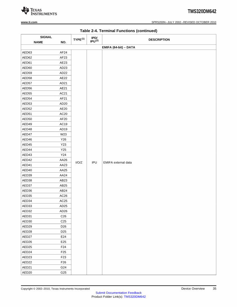
TMS320DM642
www.ti.com SPRS200N–JULY 2002–REVISED OCTOBER 2010
Table 2-4. Terminal Functions (continued)
SIGNAL IPD/TYPE (1) DESCRIPTIONIPU (2)NAME NO.
EMIFA (64-bit) – DATA
AED63 AF24
AED62 AF23
AED61 AE23
AED60 AD23
AED59 AD22
AED58 AE22
AED57 AD21
AED56 AE21
AED55 AC21
AED54 AF21
AED53 AD20
AED52 AE20
AED51 AC20
AED50 AF20
AED49 AC19
AED48 AD19
AED47 W23
AED46 Y26
AED45 Y23
AED44 Y25
AED43 Y24
AED42 AA26I/O/Z IPU EMIFA external data
AED41 AA23
AED40 AA25
AED39 AA24
AED38 AB23
AED37 AB25
AED36 AB24
AED35 AC26
AED34 AC25
AED33 AD25
AED32 AD26
AED31 C26
AED30 C25
AED29 D26
AED28 D25
AED27 E24
AED26 E25
AED25 F24
AED24 F25
AED23 F23
AED22 F26
AED21 G24
AED20 G25
Copyright © 2002–2010, Texas Instruments Incorporated Device Overview 35Submit Documentation Feedback
Product Folder Link(s): TMS320DM642

TMS320DM642
SPRS200N–JULY 2002–REVISED OCTOBER 2010 www.ti.com
Table 2-4. Terminal Functions (continued)
SIGNAL IPD/TYPE (1) DESCRIPTIONIPU (2)NAME NO.
AED19 G23
AED18 G26
AED17 H23
AED16 H24
AED15 C19
AED14 D19
AED13 A20
AED12 D20
AED11 B20
AED10 C20I/O/Z IPU EMIFA external data
AED9 A21
AED8 D21
AED7 B21
AED6 C21
AED5 A23
AED4 C22
AED3 B22
AED2 B23
AED1 A24
AED0 B24
MANAGEMENT DATA INPUT/OUTPUT (MDIO)
XSP_CLK/MDCLK(3) R5 I/O/Z IPD PCI serial interface clock (O) [default] or MDIO serial clock input/output (I/O/Z).
PCI serial interface data out (O) [default] or MDIO serial data input/outputXSP_DO/MDIO(3) P5 I/O/Z IPU (I/O/Z). In PCI mode, this pin is connected to the input data pin of the serial
PROM.
VCXO INTERPOLATED CONTROL PORT (VIC)
VCXO Interpolated Control Port (VIC) single-bit digital-to-analog converter(VDAC) output [output only] [default] or this pin can be programmed as a GP0 8pin (I/O/Z)Boot Configuration: PCI frequency selection (PCI66).If the PCI peripheral is enabled (PCI_EN pin = 1), then:0 - PCI operates at 66 MHz (default).
VDAC/GP0[8]/PCI66 (3) AD1 I/O/Z IPD 1 - PCI operates at 33 MHz.The –500 device supports PCI at 33 MHz only. For proper –500 device operationwhen the PCI peripheral is enabled (PCI_EN = 1), this pin must be pulled upwith a 1-kΩ resistor at device reset.
Note: If the PCI peripheral is disabled (PCI_EN pin = 0), this pin must not bepulled up.
VIDEO PORTS (VP0, VP1, AND VP2)
STCLK AC1 I IPD The STCLK signal drives the hardware counter on the video ports.
36 Device Overview Copyright © 2002–2010, Texas Instruments Incorporated
Submit Documentation FeedbackProduct Folder Link(s): TMS320DM642
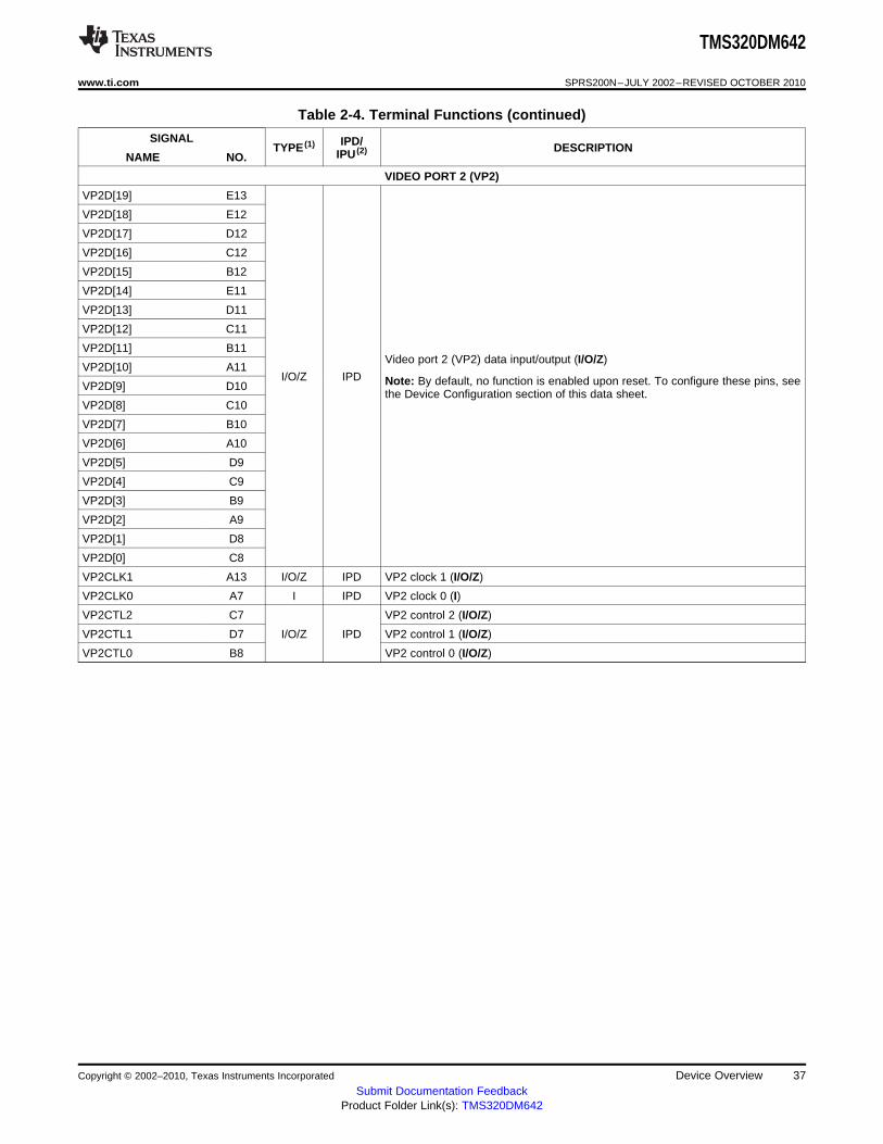
TMS320DM642
www.ti.com SPRS200N–JULY 2002–REVISED OCTOBER 2010
Table 2-4. Terminal Functions (continued)
SIGNAL IPD/TYPE (1) DESCRIPTIONIPU (2)NAME NO.
VIDEO PORT 2 (VP2)
VP2D[19] E13
VP2D[18] E12
VP2D[17] D12
VP2D[16] C12
VP2D[15] B12
VP2D[14] E11
VP2D[13] D11
VP2D[12] C11
VP2D[11] B11Video port 2 (VP2) data input/output (I/O/Z)
VP2D[10] A11I/O/Z IPD Note: By default, no function is enabled upon reset. To configure these pins, seeVP2D[9] D10
the Device Configuration section of this data sheet.VP2D[8] C10
VP2D[7] B10
VP2D[6] A10
VP2D[5] D9
VP2D[4] C9
VP2D[3] B9
VP2D[2] A9
VP2D[1] D8
VP2D[0] C8
VP2CLK1 A13 I/O/Z IPD VP2 clock 1 (I/O/Z)
VP2CLK0 A7 I IPD VP2 clock 0 (I)
VP2CTL2 C7 VP2 control 2 (I/O/Z)
VP2CTL1 D7 I/O/Z IPD VP2 control 1 (I/O/Z)
VP2CTL0 B8 VP2 control 0 (I/O/Z)
Copyright © 2002–2010, Texas Instruments Incorporated Device Overview 37Submit Documentation Feedback
Product Folder Link(s): TMS320DM642
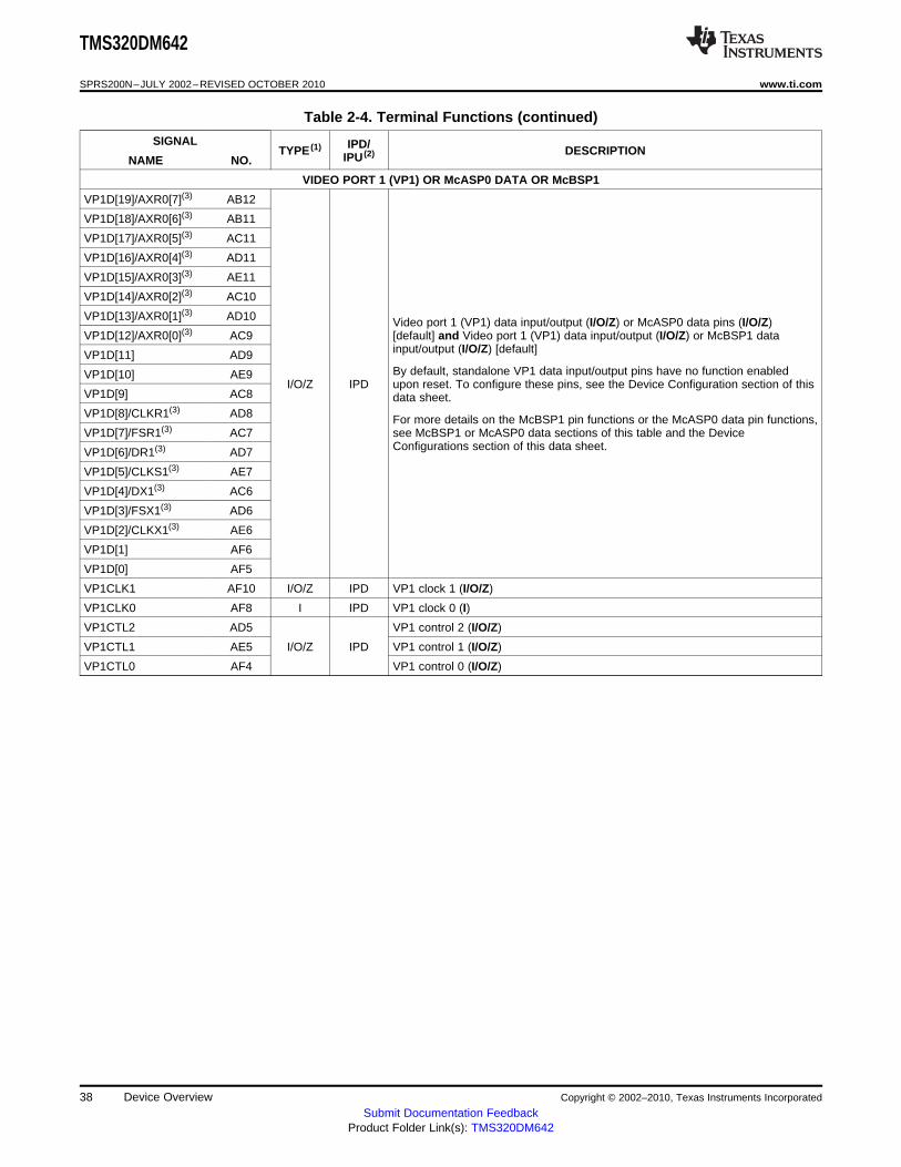
TMS320DM642
SPRS200N–JULY 2002–REVISED OCTOBER 2010 www.ti.com
Table 2-4. Terminal Functions (continued)
SIGNAL IPD/TYPE (1) DESCRIPTIONIPU (2)NAME NO.
VIDEO PORT 1 (VP1) OR McASP0 DATA OR McBSP1
VP1D[19]/AXR0[7](3) AB12
VP1D[18]/AXR0[6](3) AB11
VP1D[17]/AXR0[5](3) AC11
VP1D[16]/AXR0[4](3) AD11
VP1D[15]/AXR0[3](3) AE11
VP1D[14]/AXR0[2](3) AC10
VP1D[13]/AXR0[1](3) AD10 Video port 1 (VP1) data input/output (I/O/Z) or McASP0 data pins (I/O/Z)VP1D[12]/AXR0[0](3) AC9 [default] and Video port 1 (VP1) data input/output (I/O/Z) or McBSP1 data
input/output (I/O/Z) [default]VP1D[11] AD9By default, standalone VP1 data input/output pins have no function enabledVP1D[10] AE9
I/O/Z IPD upon reset. To configure these pins, see the Device Configuration section of thisVP1D[9] AC8 data sheet.VP1D[8]/CLKR1(3) AD8 For more details on the McBSP1 pin functions or the McASP0 data pin functions,VP1D[7]/FSR1(3) AC7 see McBSP1 or McASP0 data sections of this table and the Device
Configurations section of this data sheet.VP1D[6]/DR1(3) AD7
VP1D[5]/CLKS1(3) AE7
VP1D[4]/DX1(3) AC6
VP1D[3]/FSX1(3) AD6
VP1D[2]/CLKX1(3) AE6
VP1D[1] AF6
VP1D[0] AF5
VP1CLK1 AF10 I/O/Z IPD VP1 clock 1 (I/O/Z)
VP1CLK0 AF8 I IPD VP1 clock 0 (I)
VP1CTL2 AD5 VP1 control 2 (I/O/Z)
VP1CTL1 AE5 I/O/Z IPD VP1 control 1 (I/O/Z)
VP1CTL0 AF4 VP1 control 0 (I/O/Z)
38 Device Overview Copyright © 2002–2010, Texas Instruments Incorporated
Submit Documentation FeedbackProduct Folder Link(s): TMS320DM642
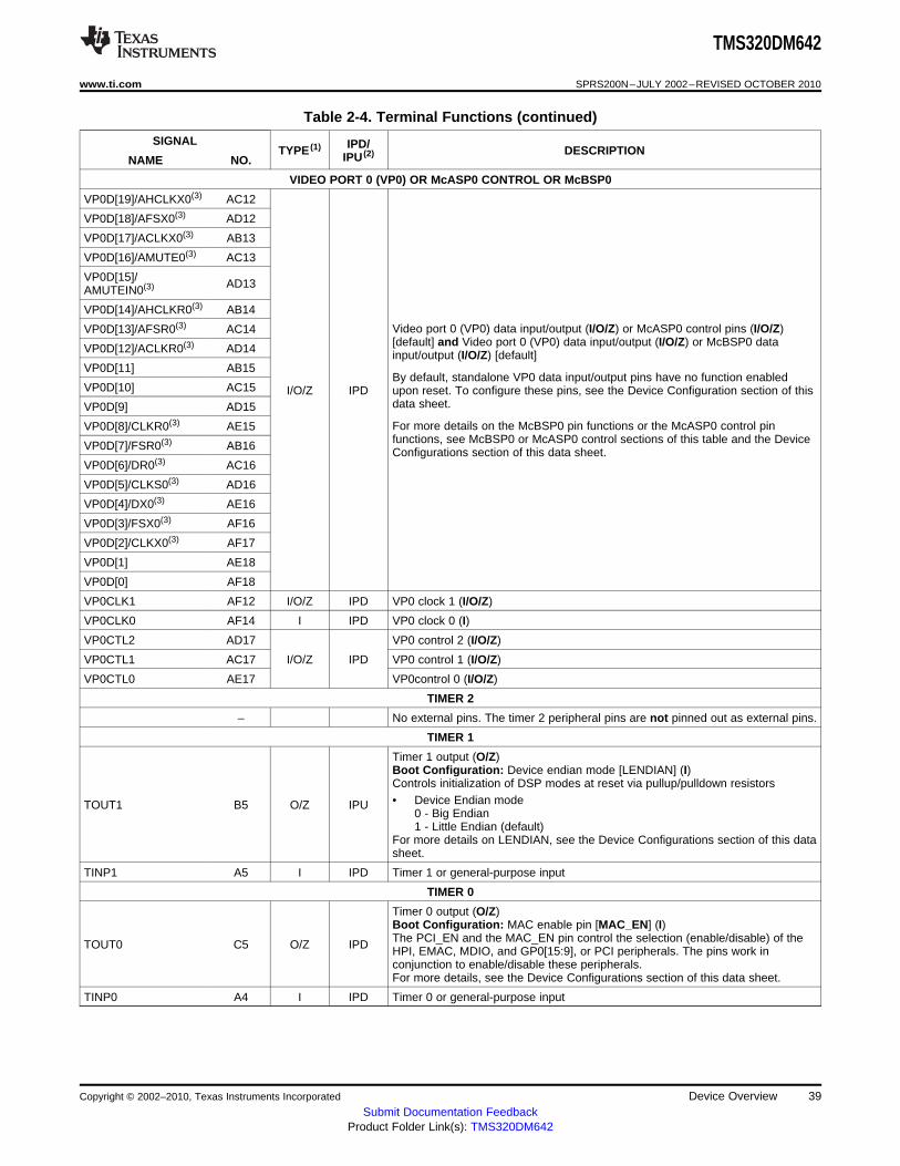
TMS320DM642
www.ti.com SPRS200N–JULY 2002–REVISED OCTOBER 2010
Table 2-4. Terminal Functions (continued)
SIGNAL IPD/TYPE (1) DESCRIPTIONIPU (2)NAME NO.
VIDEO PORT 0 (VP0) OR McASP0 CONTROL OR McBSP0
VP0D[19]/AHCLKX0(3) AC12
VP0D[18]/AFSX0(3) AD12
VP0D[17]/ACLKX0(3) AB13
VP0D[16]/AMUTE0(3) AC13
VP0D[15]/ AD13AMUTEIN0(3)
VP0D[14]/AHCLKR0(3) AB14
Video port 0 (VP0) data input/output (I/O/Z) or McASP0 control pins (I/O/Z)VP0D[13]/AFSR0(3) AC14[default] and Video port 0 (VP0) data input/output (I/O/Z) or McBSP0 dataVP0D[12]/ACLKR0(3) AD14 input/output (I/O/Z) [default]
VP0D[11] AB15By default, standalone VP0 data input/output pins have no function enabled
VP0D[10] AC15 I/O/Z IPD upon reset. To configure these pins, see the Device Configuration section of thisdata sheet.VP0D[9] AD15
For more details on the McBSP0 pin functions or the McASP0 control pinVP0D[8]/CLKR0(3) AE15functions, see McBSP0 or McASP0 control sections of this table and the DeviceVP0D[7]/FSR0(3) AB16 Configurations section of this data sheet.
VP0D[6]/DR0(3) AC16
VP0D[5]/CLKS0(3) AD16
VP0D[4]/DX0(3) AE16
VP0D[3]/FSX0(3) AF16
VP0D[2]/CLKX0(3) AF17
VP0D[1] AE18
VP0D[0] AF18
VP0CLK1 AF12 I/O/Z IPD VP0 clock 1 (I/O/Z)
VP0CLK0 AF14 I IPD VP0 clock 0 (I)
VP0CTL2 AD17 VP0 control 2 (I/O/Z)
VP0CTL1 AC17 I/O/Z IPD VP0 control 1 (I/O/Z)
VP0CTL0 AE17 VP0control 0 (I/O/Z)
TIMER 2
– No external pins. The timer 2 peripheral pins are not pinned out as external pins.
TIMER 1
Timer 1 output (O/Z)Boot Configuration: Device endian mode [LENDIAN] (I)Controls initialization of DSP modes at reset via pullup/pulldown resistors• Device Endian modeTOUT1 B5 O/Z IPU
0 - Big Endian1 - Little Endian (default)
For more details on LENDIAN, see the Device Configurations section of this datasheet.
TINP1 A5 I IPD Timer 1 or general-purpose input
TIMER 0
Timer 0 output (O/Z)Boot Configuration: MAC enable pin [MAC_EN] (I)The PCI_EN and the MAC_EN pin control the selection (enable/disable) of theTOUT0 C5 O/Z IPD HPI, EMAC, MDIO, and GP0[15:9], or PCI peripherals. The pins work inconjunction to enable/disable these peripherals.For more details, see the Device Configurations section of this data sheet.
TINP0 A4 I IPD Timer 0 or general-purpose input
Copyright © 2002–2010, Texas Instruments Incorporated Device Overview 39Submit Documentation Feedback
Product Folder Link(s): TMS320DM642

TMS320DM642
SPRS200N–JULY 2002–REVISED OCTOBER 2010 www.ti.com
Table 2-4. Terminal Functions (continued)
SIGNAL IPD/TYPE (1) DESCRIPTIONIPU (2)NAME NO.
INTER-INTEGRATED CIRCUIT 0 (I2C0)
SCL0 E4 I/O/Z — I2C0 clock.
SDA0 D3 I/O/Z — I2C0 data.
MULTICHANNEL BUFFERED SERIAL PORT 1 (McBSP1)
Video Port 1 (VP1) input/output data 8 pin (I/O/Z) or McBSP1 receive clockVP1D[8]/CLKR1(3) AD8 I/O/Z IPD (I/O/Z) [default]
VP1 input/output data 7 pin (I/O/Z) or McBSP1 receive frame sync (I/O/Z)VP1D[7]/FSR1(3) AC7 I/O/Z IPD [default]
VP1D[6]/DR1(3) AD7 I IPD VP1 input/output data 6 pin (I/O/Z) or McBSP1 receive data (I) [default]
VP1 input/output data 5 pin (I/O/Z) or McBSP1 external clock source (I) (asVP1D[5]/CLKS1(3) AE7 I IPD opposed to internal) [default]
VP1D[4]/DX1(3) AC6 I/O/Z IPD VP1 input/output data 4 pin (I/O/Z) or McBSP1 transmit data (O/Z) [default]
VP1 input/output data 3 pin (I/O/Z) or McBSP1 transmit frame sync (I/O/Z)VP1D[3]/FSX1(3) AD6 I/O/Z IPD [default]
VP1D[2]/CLKX1(3) AE6 I/O/Z IPD VP1 input/output data 2 pin (I/O/Z) or McBSP1 transmit clock (I/O/Z) [default]
MULTICHANNEL BUFFERED SERIAL PORT 0 (McBSP0)
Video Port 0 (VP0) input/output data 8 pin (I/O/Z) or McBSP0 receive clockVP0D[8]/CLKR0(3) AE15 I/O/Z IPD (I/O/Z) [default]
VP0 input/output data 7 pin (I/O/Z) or McBSP0 receive frame sync (I/O/Z)VP0D[7]/FSR0(3) AB16 I/O/Z IPD [default]
VP0D[6]/DR0(3) AC16 I IPD VP0 input/output data 6 pin (I/O/Z) or McBSP0 receive data (I) [default]
VP0 input/output data 5 pin (I/O/Z) or McBSP0 external clock source (I) (asVP0D[5]/CLKS0(3) AD16 I IPD opposed to internal) [default]
VP0D[4]/DX0(3) AE16 O/Z IPD VP0 input/output data 4 pin (I/O/Z) or McBSP0 transmit data (O/Z) [default]
VP0 input/output data 3 pin (I/O/Z) or McBSP0 transmit frame sync (I/O/Z)VP0D[3]/FSX0(3) AF16 I/O/Z IPD [default]
VP0D[2]/CLKX0(3) AF17 I/O/Z IPD VP0 input/output data 2 pin (I/O/Z) or McBSP0 transmit clock (I/O/Z) [default]
40 Device Overview Copyright © 2002–2010, Texas Instruments Incorporated
Submit Documentation FeedbackProduct Folder Link(s): TMS320DM642
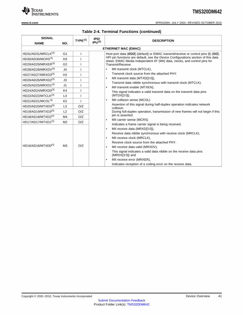
TMS320DM642
www.ti.com SPRS200N–JULY 2002–REVISED OCTOBER 2010
Table 2-4. Terminal Functions (continued)
SIGNAL IPD/TYPE (1) DESCRIPTIONIPU (2)NAME NO.
ETHERNET MAC (EMAC)
HD31/AD31/MRCLK(3) G1 I Host-port data (I/O/Z) [default] or EMAC transmit/receive or control pins (I) (O/Z)HPI pin functions are default, see the Device Configurations section of this dataHD30/AD30/MCRS(3) H3 Isheet. EMAC Media Independent I/F (MII) data, clocks, and control pins for
HD29/AD29/MRXER(3) G2 I Transmit/Receive.• MII transmit clock (MTCLK),HD28/AD28/MRXDV(3) J4 I
Transmit clock source from the attached PHY.HD27/AD27/MRXD3(3) H2 I• MII transmit data (MTXD[3:0]),
HD26/AD26/MRXD2(3) J3 ITransmit data nibble synchronous with transmit clock (MTCLK).
HD25/AD25/MRXD1(3) J1 I• MII transmit enable (MTXEN),
HD24/AD24/MRXD0(3) K4 I This signal indicates a valid transmit data on the transmit data pins(MTDX[3:0]).HD22/AD22/MTCLK(3) L4 I
• MII collision sense (MCOL)HD21/AD21/MCOL(3) K2 IAssertion of this signal during half-duplex operation indicates network
HD20/AD20/MTXEN(3) L3 O/Z collision.HD19/AD19/MTXD3(3) L2 O/Z During full-duplex operation, transmission of new frames will not begin if this
pin is asserted.HD18/AD18/MTXD2(3) M4 O/Z• MII carrier sense (MCRS)
HD17/AD17/MTXD1(3) M2 O/ZIndicates a frame carrier signal is being received.
• MII receive data (MRXD[3:0]),Receive data nibble synchronous with receive clock (MRCLK).
• MII receive clock (MRCLK),Receive clock source from the attached PHY.
HD16/AD16/MTXD0(3) M3 O/Z • MII receive data valid (MRXDV),This signal indicates a valid data nibble on the receive data pins(MRDX[3:0]) and
• MII receive error (MRXER),Indicates reception of a coding error on the receive data.
Copyright © 2002–2010, Texas Instruments Incorporated Device Overview 41Submit Documentation Feedback
Product Folder Link(s): TMS320DM642

TMS320DM642
SPRS200N–JULY 2002–REVISED OCTOBER 2010 www.ti.com
Table 2-4. Terminal Functions (continued)
SIGNAL IPD/TYPE (1) DESCRIPTIONIPU (2)NAME NO.
MULTICHANNEL AUDIO SERIAL PORT 0 (McASP0) CONTROL
VP0 input/output data 19 pin (I/O/Z) or McASP0 transmit high-frequency masterVP0D[19]/AHCLKX0(3) AC12 I/O/Z IPD clock (I/O/Z).
VP0 input/output data 18 pin (I/O/Z) or McASP0 transmit frame sync or left/rightVP0D[18]/AFSX0(3) AD12 I/O/Z IPD clock (LRCLK) (I/O/Z).
VP0D[17]/ACLKX0(3) AB13 I/O/Z IPD VP0 input/output data 17 pin (I/O/Z) or McASP0 transmit bit clock (I/O/Z).
VP0D[16]/AMUTE0(3) AC13 O/Z IPD VP0 input/output data 16 pin (I/O/Z) or McASP0 mute output (O/Z).
VP0D[15]/ AD13 I/O/Z IPD VP0 input/output data 15 pin (I/O/Z) or McASP0 mute input (I/O/Z).AMUTEIN0(3)
VP0 input/output data 14 pin (I/O/Z) or McASP0 receive high-frequency masterVP0D[14]/AHCLKR0(3) AB14 I/O/Z IPD clock (I/O/Z).
VP0 input/output data 13 pin (I/O/Z) or McASP0 receive frame sync or left/rightVP0D[13]/AFSR0(3) AC14 I/O/Z IPD clock (LRCLK) (I/O/Z).
VP0D[12]/ACLKR0(3) AD14 I/O/Z IPD VP0 input/output data 12 pin (I/O/Z) or McASP0 receive bit clock (I/O/Z).
MULTICHANNEL AUDIO SERIAL PORT 0 (McASP0) DATA
VP1D[19]/AXR0[7](3) AB12
VP1D[18]/AXR0[6](3) AB11
VP1D[17]/AXR0[5](3) AC11
VP1D[16]/AXR0[4](3) AD11 VP1 input/output data pins [19:12] (I/O/Z) or McASP0 TX/RX data pins [7:0]I/O/Z IPD (I/O/Z) [default].VP1D[15]/AXR0[3](3) AE11
VP1D[14]/AXR0[2](3) AC10
VP1D[13]/AXR0[1](3) AD10
VP1D[12]/AXR0[0](3) AC9
RESERVED FOR TEST
Reserved. This pin must be connected directly to CVDD for proper deviceRSV07 H7 A — operation.
Reserved. This pin must be connected directly to DVDD for proper deviceRSV08 R6 A — operation.
RSV05 E14 I IPD
RSV06 W7 A —
RSV00 AA3 A — Reserved (leave unconnected, do not connect to power or ground. If the signalRSV01 AB3 I — must be routed out from the device, the internal pull-up/down resistance should
not be relied upon and an external pull-up/down should be used.)RSV02 AC4 O/Z —
RSV03 AD3 O/Z —
RSV04 AF3 O IPU
42 Device Overview Copyright © 2002–2010, Texas Instruments Incorporated
Submit Documentation FeedbackProduct Folder Link(s): TMS320DM642
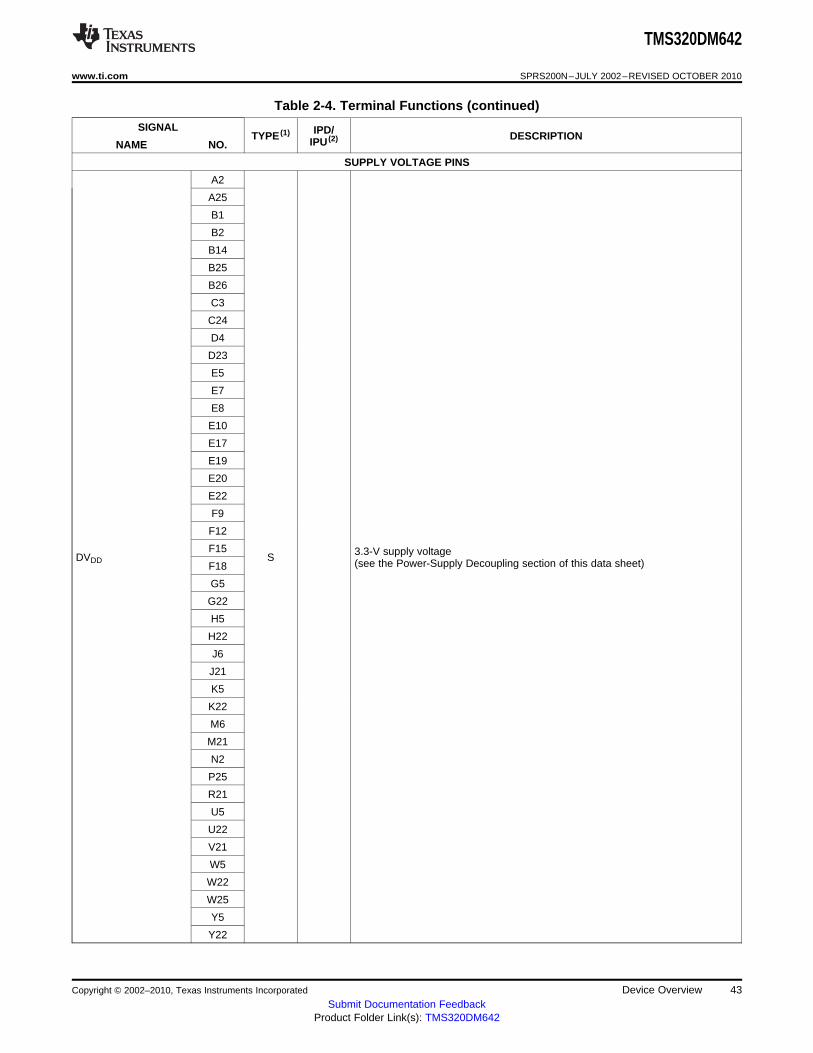
TMS320DM642
www.ti.com SPRS200N–JULY 2002–REVISED OCTOBER 2010
Table 2-4. Terminal Functions (continued)
SIGNAL IPD/TYPE (1) DESCRIPTIONIPU (2)NAME NO.
SUPPLY VOLTAGE PINS
A2
A25
B1
B2
B14
B25
B26
C3
C24
D4
D23
E5
E7
E8
E10
E17
E19
E20
E22
F9
F12
F15 3.3-V supply voltageDVDD S (see the Power-Supply Decoupling section of this data sheet)F18
G5
G22
H5
H22
J6
J21
K5
K22
M6
M21
N2
P25
R21
U5
U22
V21
W5
W22
W25
Y5
Y22
Copyright © 2002–2010, Texas Instruments Incorporated Device Overview 43Submit Documentation Feedback
Product Folder Link(s): TMS320DM642
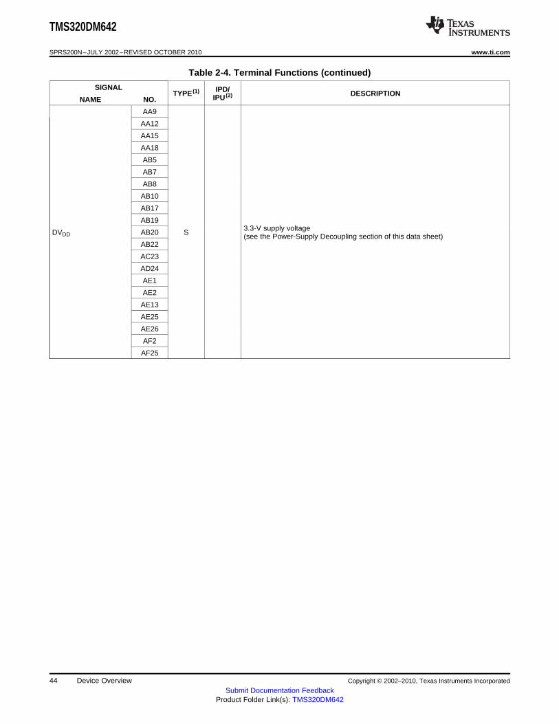
TMS320DM642
SPRS200N–JULY 2002–REVISED OCTOBER 2010 www.ti.com
Table 2-4. Terminal Functions (continued)
SIGNAL IPD/TYPE (1) DESCRIPTIONIPU (2)NAME NO.
AA9
AA12
AA15
AA18
AB5
AB7
AB8
AB10
AB17
AB193.3-V supply voltageDVDD AB20 S (see the Power-Supply Decoupling section of this data sheet)
AB22
AC23
AD24
AE1
AE2
AE13
AE25
AE26
AF2
AF25
44 Device Overview Copyright © 2002–2010, Texas Instruments Incorporated
Submit Documentation FeedbackProduct Folder Link(s): TMS320DM642
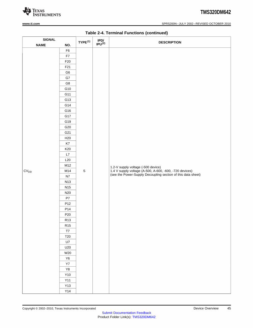
TMS320DM642
www.ti.com SPRS200N–JULY 2002–REVISED OCTOBER 2010
Table 2-4. Terminal Functions (continued)
SIGNAL IPD/TYPE (1) DESCRIPTIONIPU (2)NAME NO.
F6
F7
F20
F21
G6
G7
G8
G10
G11
G13
G14
G16
G17
G19
G20
G21
H20
K7
K20
L7
L20
M12 1.2-V supply voltage (-500 device)CVDD M14 S 1.4 V supply voltage (A-500, A-600, -600, -720 devices)
(see the Power-Supply Decoupling section of this data sheet)N7
N13
N15
N20
P7
P12
P14
P20
R13
R15
T7
T20
U7
U20
W20
Y6
Y7
Y8
Y10
Y11
Y13
Y14
Copyright © 2002–2010, Texas Instruments Incorporated Device Overview 45Submit Documentation Feedback
Product Folder Link(s): TMS320DM642
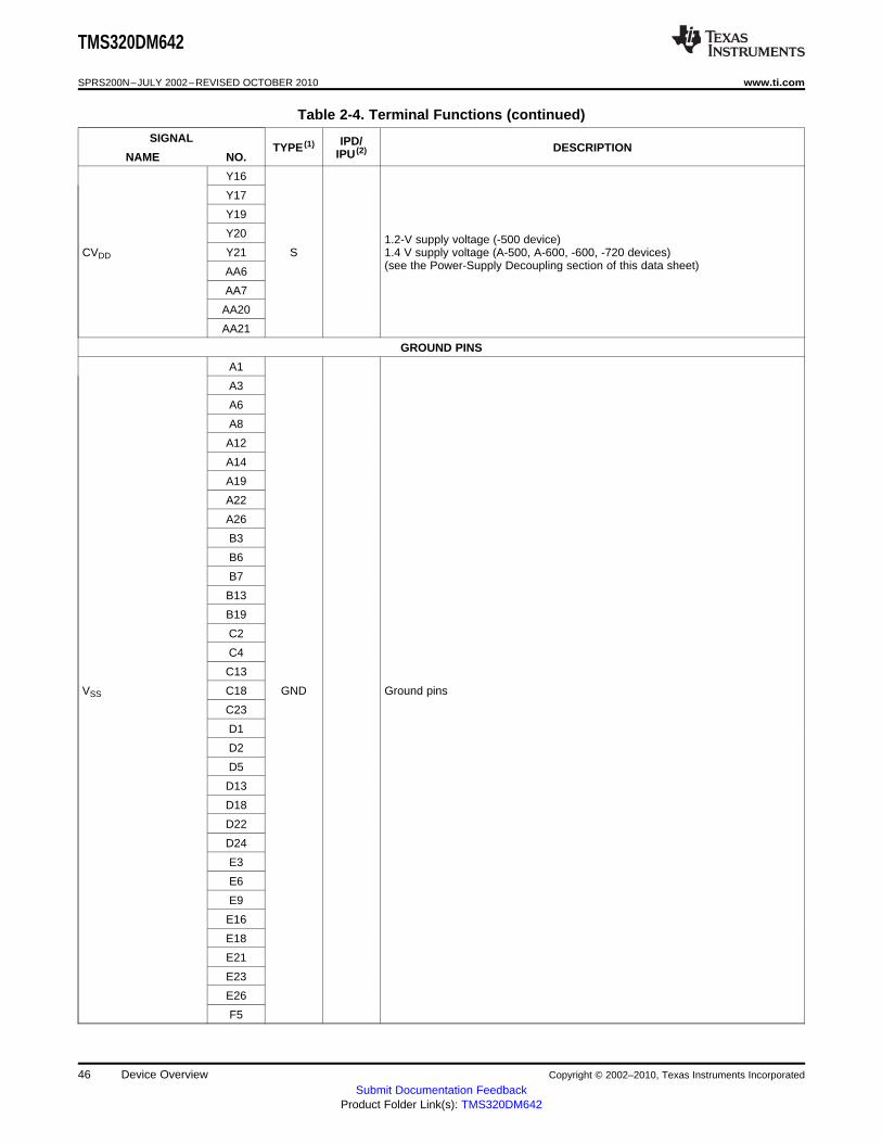
TMS320DM642
SPRS200N–JULY 2002–REVISED OCTOBER 2010 www.ti.com
Table 2-4. Terminal Functions (continued)
SIGNAL IPD/TYPE (1) DESCRIPTIONIPU (2)NAME NO.
Y16
Y17
Y19
Y20 1.2-V supply voltage (-500 device)CVDD Y21 S 1.4 V supply voltage (A-500, A-600, -600, -720 devices)
(see the Power-Supply Decoupling section of this data sheet)AA6
AA7
AA20
AA21
GROUND PINS
A1
A3
A6
A8
A12
A14
A19
A22
A26
B3
B6
B7
B13
B19
C2
C4
C13
VSS C18 GND Ground pins
C23
D1
D2
D5
D13
D18
D22
D24
E3
E6
E9
E16
E18
E21
E23
E26
F5
46 Device Overview Copyright © 2002–2010, Texas Instruments Incorporated
Submit Documentation FeedbackProduct Folder Link(s): TMS320DM642

TMS320DM642
www.ti.com SPRS200N–JULY 2002–REVISED OCTOBER 2010
Table 2-4. Terminal Functions (continued)
SIGNAL IPD/TYPE (1) DESCRIPTIONIPU (2)NAME NO.
F8
F10
F11
F13
F14
F16
F17
F19
F22
G9
G12
G15
G18
H1
H6
H21
H26
J5
J7
J20
J22
K6
VSS K21 GND Ground pins
L1
L6
L21
M7
M13
M15
M20
N5
N6
N12
N14
N21
N25
P2
P6
P13
P15
P21
R7
R12
R14
R20
Copyright © 2002–2010, Texas Instruments Incorporated Device Overview 47Submit Documentation Feedback
Product Folder Link(s): TMS320DM642
TMS320DM642
SPRS200N–JULY 2002–REVISED OCTOBER 2010 www.ti.com
Table 2-4. Terminal Functions (continued)
SIGNAL IPD/TYPE (1) DESCRIPTIONIPU (2)NAME NO.
T1
T5
T6
T21
T26
U6
U21
V5
V7
V20
V22
W1
W6
W21
W26
Y9
Y12
Y15
Y18
AA4
AA5
AA8
VSS AA10 GND Ground pins
AA11
AA13
AA14
AA16
AA17
AA19
AA22
AB1
AB2
AB4
AB6
AB9
AB18
AB21
AB26
AC3
AC5
AC18
AC22
AC24
AD2
AD4
48 Device Overview Copyright © 2002–2010, Texas Instruments Incorporated
Submit Documentation FeedbackProduct Folder Link(s): TMS320DM642
TMS320DM642
www.ti.com SPRS200N–JULY 2002–REVISED OCTOBER 2010
Table 2-4. Terminal Functions (continued)
SIGNAL IPD/TYPE (1) DESCRIPTIONIPU (2)NAME NO.
AD18
AE3
AE8
AE10
AE12
AE14
AE19
AE24
VSS AF1 GND Ground pins
AF7
AF9
AF11
AF13
AF15
AF19
AF22
AF26
Copyright © 2002–2010, Texas Instruments Incorporated Device Overview 49Submit Documentation Feedback
Product Folder Link(s): TMS320DM642

TMS320DM642
SPRS200N–JULY 2002–REVISED OCTOBER 2010 www.ti.com
2.6 Development
2.6.1 Development Support
TI offers an extensive line of development tools for the TMS320C6000™ DSP platform, including tools toevaluate the performance of the processors, generate code, develop algorithm implementations, and fullyintegrate and debug software and hardware modules.
The following products support development of C6000™ DSP-based applications:
Software Development Tools:
Code Composer Studio™ Integrated Development Environment (IDE): including Editor
C/C++/Assembly Code Generation, and Debug plus additional development tools
Scalable, Real-Time Foundation Software (DSP/BIOS™), which provides the basic run-time targetsoftware needed to support any DSP application.
Hardware Development Tools:
Extended Development System (XDS™) Emulator (supports C6000™ DSP multiprocessor system debug)EVM (Evaluation Module)
For a complete listing of development-support tools for the TMS320C6000™ DSP platform, visit the TexasInstruments web site on the Worldwide Web at http://www.ti.com uniform resource locator (URL). Forinformation on pricing and availability, contact the nearest TI field sales office or authorized distributor.
50 Device Overview Copyright © 2002–2010, Texas Instruments Incorporated
Submit Documentation FeedbackProduct Folder Link(s): TMS320DM642
TMS320DM642
www.ti.com SPRS200N–JULY 2002–REVISED OCTOBER 2010
2.6.2 Device Support
2.6.2.1 Device and Development-Support Tool Nomenclature
To designate the stages in the product development cycle, TI assigns prefixes to the part numbers of allDSP devices and support tools. Each DSP commercial family member has one of three prefixes: TMX,TMP, or TMS (e.g., TMS 320DM642AGDKA5). Texas Instruments recommends two of three possibleprefix designators for its support tools: TMDX and TMDS. These prefixes represent evolutionary stages ofproduct development from engineering prototypes (TMX/TMDX) through fully qualified productiondevices/tools (TMS/TMDS).
Device development evolutionary flow:
TMX Experimental device that is not necessarily representative of the final device's electricalspecifications
TMP Final silicon die that conforms to the device's electrical specifications but has not completedquality and reliability verification
TMS Fully qualified production device
Support tool development evolutionary flow:
TMDX Development-support product that has not yet completed Texas Instruments internalqualification testing.
TMDS Fully qualified development-support product
TMX and TMP devices and TMDX development-support tools are shipped against the followingdisclaimer:
"Developmental product is intended for internal evaluation purposes."
TMS devices and TMDS development-support tools have been characterized fully, and the quality andreliability of the device have been demonstrated fully. TI's standard warranty applies.
Predictions show that prototype devices (TMX or TMP) have a greater failure rate than the standardproduction devices. Texas Instruments recommends that these devices not be used in any productionsystem because their expected end-use failure rate still is undefined. Only qualified production devices areto be used.
TI device nomenclature also includes a suffix with the device family name. This suffix indicates thepackage type (for example, GDK), the temperature range (for example, “A” is the extended temperaturerange), and the device speed range in megahertz (for example, 5 is 500 MHz). Figure 2-16 provides alegend for reading the complete device name for any TMS320C6000™ DSP platform member.
The ZDK package, like the GDK package, is a 548-ball plastic BGA only with Pb-free balls. The ZNZ is thePb-free package version of the GNZ package.
For device part numbers and further ordering information for TMS320DM642 in the GDK, GNZ, ZDK, andZNZ package types, see the TI website (http://www.ti.com) or contact your TI sales representative.
Copyright © 2002–2010, Texas Instruments Incorporated Device Overview 51Submit Documentation Feedback
Product Folder Link(s): TMS320DM642
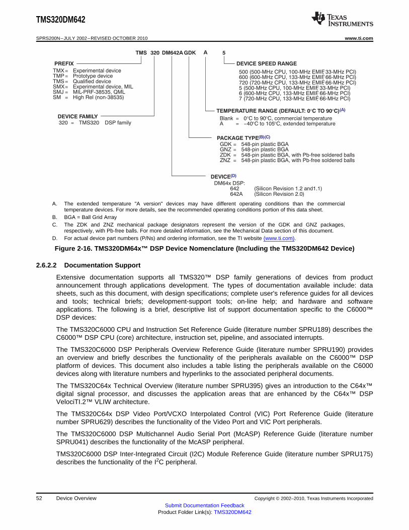
DM64x DSP:642 (Silicon Revision 1.2 and1.1)642A (Silicon Revision 2.0)
PREFIX DEVICE SPEED RANGE
TMS 320 DM642A GDK 5
TMX = Experimental deviceTMP = Prototype deviceTMS = Qualified deviceSMX= Experimental device, MILSMJ = MIL-PRF-38535, QMLSM = High Rel (non-38535)
DEVICE FAMILY320 = TMS320 DSP family
PACKAGE TYPE(B)(C)
GDK = 548-pin plastic BGAGNZ = 548-pin plastic BGAZDK = 548-pin plastic BGA, with Pb-free soldered ballsZNZ = 548-pin plastic BGA, with Pb-free soldered balls
DEVICE(D)
TEMPERATURE RANGE (DEFAULT: 0°C TO 90°C)(A)
A
Blank = 0°C to 90°C, commercial temperatureA = −40°C to 105°C, extended temperature
500 (500-MHz CPU, 100-MHz EMIF, 33-MHz PCI)600 (600-MHz CPU, 133-MHz EMIF, 66-MHz PCI)720 (720-MHz CPU, 133-MHz EMIF, 66-MHz PCI)5 (500-MHz CPU, 100-MHz EMIF, 33-MHz PCI)6 (600-MHz CPU, 133-MHz EMIF, 66-MHz PCI)7 (720-MHz CPU, 133-MHz EMIF, 66-MHz PCI)
TMS320DM642
SPRS200N–JULY 2002–REVISED OCTOBER 2010 www.ti.com
A. The extended temperature "A version" devices may have different operating conditions than the commercialtemperature devices. For more details, see the recommended operating conditions portion of this data sheet.
B. BGA = Ball Grid ArrayC. The ZDK and ZNZ mechanical package designators represent the version of the GDK and GNZ packages,
respectively, with Pb-free balls. For more detailed information, see the Mechanical Data section of this document.D. For actual device part numbers (P/Ns) and ordering information, see the TI website (www.ti.com).
Figure 2-16. TMS320DM64x™ DSP Device Nomenclature (Including the TMS320DM642 Device)
2.6.2.2 Documentation Support
Extensive documentation supports all TMS320™ DSP family generations of devices from productannouncement through applications development. The types of documentation available include: datasheets, such as this document, with design specifications; complete user's reference guides for all devicesand tools; technical briefs; development-support tools; on-line help; and hardware and softwareapplications. The following is a brief, descriptive list of support documentation specific to the C6000™DSP devices:
The TMS320C6000 CPU and Instruction Set Reference Guide (literature number SPRU189) describes theC6000™ DSP CPU (core) architecture, instruction set, pipeline, and associated interrupts.
The TMS320C6000 DSP Peripherals Overview Reference Guide (literature number SPRU190) providesan overview and briefly describes the functionality of the peripherals available on the C6000™ DSPplatform of devices. This document also includes a table listing the peripherals available on the C6000devices along with literature numbers and hyperlinks to the associated peripheral documents.
The TMS320C64x Technical Overview (literature number SPRU395) gives an introduction to the C64x™digital signal processor, and discusses the application areas that are enhanced by the C64x™ DSPVelociTI.2™ VLIW architecture.
The TMS320C64x DSP Video Port/VCXO Interpolated Control (VIC) Port Reference Guide (literaturenumber SPRU629) describes the functionality of the Video Port and VIC Port peripherals.
The TMS320C6000 DSP Multichannel Audio Serial Port (McASP) Reference Guide (literature numberSPRU041) describes the functionality of the McASP peripheral.
TMS320C6000 DSP Inter-Integrated Circuit (I2C) Module Reference Guide (literature number SPRU175)describes the functionality of the I2C peripheral.
52 Device Overview Copyright © 2002–2010, Texas Instruments Incorporated
Submit Documentation FeedbackProduct Folder Link(s): TMS320DM642

TMS320DM642
www.ti.com SPRS200N–JULY 2002–REVISED OCTOBER 2010
TMS320C6000 DSP Ethernet Media Access Controller (EMAC)/ Management Data Input/Output (MDIO)Module Reference Guide (literature number SPRU628) describes the functionality of the EMAC and MDIOperipherals.
TMS320DM642 Technical Overview (literature number SPRU615) describes the TMS320DM642architecture including details of its peripherals. This document also shows several example applicationssuch as using the DM642 device in development of IP phones, video-on-demand set-top boxes, andsurveillance digital video recorders.
The TMS320DM642 Digital Signal Processor Silicon Errata (literature number SPRZ196) describes theknown exceptions to the functional specifications for particular silicon revisions of the TMS320DM642device.
The TMS320DM64x Power Consumption Summary application report (literature number SPRA962)discusses the power consumption for user applications with the TMS320DM642 DSP devices.
The TMS320DM642 Hardware Designer’s Resource Guide (literature number SPRAA51) is organized bydevelopment flow and functional areas to make design efforts as seamless as possible. This documentincludes getting started, board design, system testing, and checklists to aid in initial designs and debugefforts. Each section of this document includes pointers to valuable information including: technicaldocumentation, models, symbols, and reference designs for use in each phase of design. Particularattention is given to peripheral interfacing and system-level design concerns.
The Using IBIS Models for Timing Analysis application report (literature number SPRA839) describes howto properly use IBIS models to attain accurate timing analysis for a given system.
The tools support documentation is electronically available within the Code Composer Studio™ IntegratedDevelopment Environment (IDE). For a complete listing of C6000™ DSP latest documentation, visit theTexas Instruments web site on the Worldwide Web at http://www.ti.com uniform resource locator (URL).
2.6.2.3 Device Silicon Revision
The device silicon revision can be determined by the "Die PG code" marked on the top of the package.For more detailed information on the DM642 silicon revision, package markings, and the knownexceptions to the functional specifications as well as any usage notes, refer to the device-specific siliconerrata: TMS320DM642 Digital Signal Processor Silicon Errata (literature number SPRZ196).
Copyright © 2002–2010, Texas Instruments Incorporated Device Overview 53Submit Documentation Feedback
Product Folder Link(s): TMS320DM642

TMS320DM642
SPRS200N–JULY 2002–REVISED OCTOBER 2010 www.ti.com
3 Device Configurations
On the DM642 device, bootmode and certain device configurations/peripheral selections are determined atdevice reset, while other device configurations/peripheral selections are software-configurable via theperipheral configurations register (PERCFG) [address location 0x01B3F000] after device reset.
3.1 Configurations at Reset
For DM642 proper device operation, GP0[0] (pin M5) must remain low, do not oppose the internalpulldown (IPD).
3.1.1 Peripheral Selection at Device Reset
Some DM642 peripherals share the same pins (internally muxed) and are mutually exclusive (i.e., HPI,general-purpose input/output pins GP0[15:9], PCI and its internal EEPROM, EMAC, and MDIO). OtherDM642 peripherals (i.e., the Timers, I2C0, and the GP0[7:0] pins), are always available.• HPI, GP0[15:9], PCI, EEPROM (internal to PCI), EMAC, and MDIO peripherals
The PCI_EN and MAC_EN pins are latched at reset. They determine specific peripheral selection,summarized in Table 3-1. For further clarification of the HPI vs. EMAC configuration, see Table 3-2.
Table 3-1. PCI_EN, HD5, and MAC_EN Peripheral Selection (HPI, GP0[15:9], PCI, EMAC, and MDIO)
PERIPHERAL SELECTION PERIPHERALS SELECTED
PCI_EN PCI_EEAI HD5 MAC_EN HPI Data HPI Data EEPROM EMAC and32-Bit PCI GP0[15:9]Pin [E2] Pin [L5] Pin [Y1] Pin [C5] Lower Upper (Auto-Init) MDIO
0 0 0 0 √ Hi-Z Disabled N/A Disabled √0 0 0 1 √ Hi-Z Disabled N/A √ √0 0 1 0 √ √ Disabled N/A Disabled √0 0 1 1 Disabled Disabled N/A √ √
Enabled1 1 X X Disabled √ (via External Disabled Disabled
EEPROM)
Disabled1 0 X X Disabled √ Disabled Disabled(default values)
• If the PCI is disabled (PCI_EN = 0), the HPI peripheral is enabled and based on the HD5 andMAC_EN pin configuration at reset, HPI16 mode or EMAC and MDIO can be selected. When the PCIis disabled (PCI_EN = 0), the GP0[15:9] pins can also be programmed as GPIO, provided the GPxENand GPxDIR bits are properly configured.This means all multiplexed HPI/PCI pins function as HPI and all standalone PCI pins (PCBE0 andXSP_CS) are tied-off (Hi-Z). Also, the multiplexed GP0/PCI pins can be used as GPIO with the propersoftware configuration of the GPIO enable and direction registers (for more details, see Table 3-8).
• If the PCI is enabled (PCI_EN = 1), the HPI peripheral is disabled.This means all multiplexed HPI/PCI pins function as PCI. Also, the multiplexed GP0/PCI pins functionas PCI pins (for more details, see Table 3-8).
• The MAC_EN pin, in combination with the PCI_EN and HD5 pins, controls the selection of the EMACand MDIO peripherals (for more details, see Table 3-2).
• The PCI_EN pin (= 1) and the PCI_EEAI pin control the whether the PCI initializes its internal registersvia external EEPROM (PCI_EEAI = 1) or if the internal default values are used instead(PCI_EEAI = 0).
Table 3-2. HPI vs. EMAC Peripheral Pin Selection
CONFIGURATION SELECTION PERIPHERALS SELECTED
GP0[0] (Pin [M5])(1) HD5 (Pin [Y1]) MAC_EN (Pin [C5]) HD[15:0] HD[31:16]
0 0 0 HPI16 Hi-Z
54 Device Configurations Copyright © 2002–2010, Texas Instruments Incorporated
Submit Documentation FeedbackProduct Folder Link(s): TMS320DM642
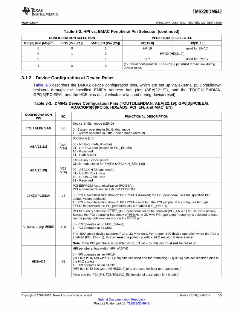
TMS320DM642
www.ti.com SPRS200N–JULY 2002–REVISED OCTOBER 2010
Table 3-2. HPI vs. EMAC Peripheral Pin Selection (continued)
CONFIGURATION SELECTION PERIPHERALS SELECTED
GP0[0] (Pin [M5])(1) HD5 (Pin [Y1]) MAC_EN (Pin [C5]) HD[15:0] HD[31:16]
0 0 1 HPI16 used for EMAC
0 1 0 HPI32 (HD[31:0])
0 1 1 Hi-Z used for EMAC
(1) Invalid configuration. The GP0[0] pin must remain low during1 X X device reset.
3.1.2 Device Configuration at Device Reset
Table 3-3 describes the DM642 device configuration pins, which are set up via external pullup/pulldownresistors through the specified EMIFA address bus pins (AEA[22:19]), and the TOUT1/LENDIAN,GP0[3]/PCIEEAI, and the HD5 pins (all of which are latched during device reset).
Table 3-3. DM642 Device Configuration Pins (TOUT1/LENDIAN, AEA[22:19], GP0[3]/PCIEEAI,VDAC/GP0[8]/PCI66, HD5/AD5, PCI_EN, and MAC_EN)
CONFIGURATION NO. FUNCTIONAL DESCRIPTIONPIN
Device Endian mode (LEND)
TOUT1/LENDIAN B5 0 - System operates in Big Endian mode1 - System operates in Little Endian mode (default)
Bootmode [1:0]
00 - No boot (default mode)[U23,AEA[22:21] 01 - HPI/PCI boot (based on PCI_EN pin)V24]10 - Reserved11 - EMIFA boot
EMIFA input clock selectClock mode select for EMIFA (AECLKIN_SEL[1:0])
[V25, 00 - AECLKIN (default mode)AEA[20:19] V26] 01 - CPU/4 Clock Rate10 - CPU/6 Clock Rate11 - Reserved
PCI EEPROM Auto-Initialization (PCIEEAI)PCI auto-initialization via external EEPROM
0 - PCI auto-initialization through EEPROM is disabled; the PCI peripheral uses the specified PCIGP0[3]/PCIEEAI L5default values (default).1 - PCI auto-initialization through EEPROM is enabled; the PCI peripheral is configured throughEEPROM provided the PCI peripheral pin is enabled (PCI_EN = 1).
PCI frequency selection (PCI66) [PCI peripheral needs be enabled (PCI_EN = 1) to use this function]Selects the PCI operating frequency of 66 MHz or 33 MHz PCI operating frequency is selected at resetvia the pullup/pulldown resistor on the PCI66 pin:
0 - PCI operates at 66 MHz (default).VDAC/GP0[8]/ PCI66 AD1 1 - PCI operates at 33 MHz.
The -500 speed device supports PCI at 33 MHz only. For proper -500 device operation when the PCI isenabled (PCI_EN = 1), this pin must be pulled up with a 1-kΩ resistor at device reset.
Note: If the PCI peripheral is disabled (PCI_EN pin = 0), this pin must not be pulled up.
HPI peripheral bus width (HPI_WIDTH)
0 - HPI operates as an HPI16.(HPI bus is 16 bits wide. HD[15:0] pins are used and the remaining HD[31:16] pins are reserved pins in
HD5/AD5 Y1 the Hi-Z state.)1 - HPI operates as an HPI32.(HPI bus is 32 bits wide. All HD[31:0] pins are used for host-port operations.)
(Also see the PCI_EN; TOUT0/MAC_EN functional description in this table)
Copyright © 2002–2010, Texas Instruments Incorporated Device Configurations 55Submit Documentation Feedback
Product Folder Link(s): TMS320DM642
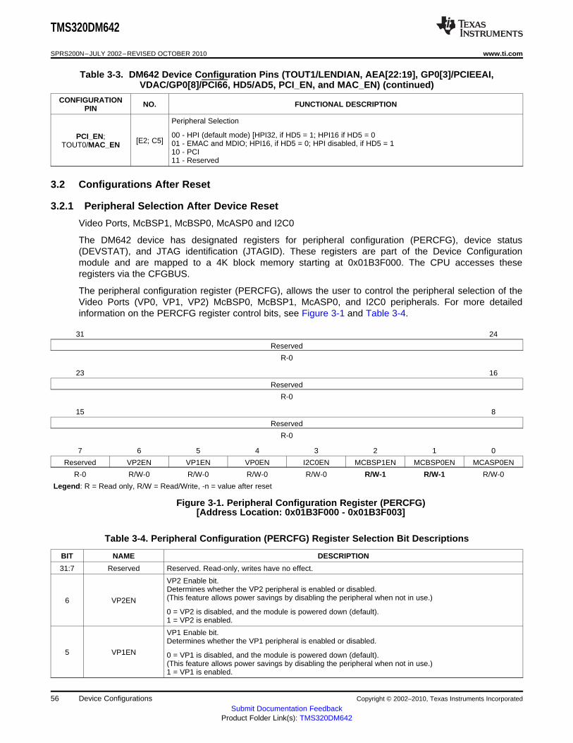
TMS320DM642
SPRS200N–JULY 2002–REVISED OCTOBER 2010 www.ti.com
Table 3-3. DM642 Device Configuration Pins (TOUT1/LENDIAN, AEA[22:19], GP0[3]/PCIEEAI,VDAC/GP0[8]/PCI66, HD5/AD5, PCI_EN, and MAC_EN) (continued)
CONFIGURATION NO. FUNCTIONAL DESCRIPTIONPIN
Peripheral Selection
00 - HPI (default mode) [HPI32, if HD5 = 1; HPI16 if HD5 = 0PCI_EN; [E2; C5] 01 - EMAC and MDIO; HPI16, if HD5 = 0; HPI disabled, if HD5 = 1TOUT0/MAC_EN10 - PCI11 - Reserved
3.2 Configurations After Reset
3.2.1 Peripheral Selection After Device Reset
Video Ports, McBSP1, McBSP0, McASP0 and I2C0
The DM642 device has designated registers for peripheral configuration (PERCFG), device status(DEVSTAT), and JTAG identification (JTAGID). These registers are part of the Device Configurationmodule and are mapped to a 4K block memory starting at 0x01B3F000. The CPU accesses theseregisters via the CFGBUS.
The peripheral configuration register (PERCFG), allows the user to control the peripheral selection of theVideo Ports (VP0, VP1, VP2) McBSP0, McBSP1, McASP0, and I2C0 peripherals. For more detailedinformation on the PERCFG register control bits, see Figure 3-1 and Table 3-4.
31 24
Reserved
R-0
23 16
Reserved
R-0
15 8
Reserved
R-0
7 6 5 4 3 2 1 0
Reserved VP2EN VP1EN VP0EN I2C0EN MCBSP1EN MCBSP0EN MCASP0EN
R-0 R/W-0 R/W-0 R/W-0 R/W-0 R/W-1 R/W-1 R/W-0
Legend: R = Read only, R/W = Read/Write, -n = value after reset
Figure 3-1. Peripheral Configuration Register (PERCFG)[Address Location: 0x01B3F000 - 0x01B3F003]
Table 3-4. Peripheral Configuration (PERCFG) Register Selection Bit Descriptions
BIT NAME DESCRIPTION
31:7 Reserved Reserved. Read-only, writes have no effect.
VP2 Enable bit.Determines whether the VP2 peripheral is enabled or disabled.(This feature allows power savings by disabling the peripheral when not in use.)6 VP2EN
0 = VP2 is disabled, and the module is powered down (default).1 = VP2 is enabled.
VP1 Enable bit.Determines whether the VP1 peripheral is enabled or disabled.
5 VP1EN 0 = VP1 is disabled, and the module is powered down (default).(This feature allows power savings by disabling the peripheral when not in use.)1 = VP1 is enabled.
56 Device Configurations Copyright © 2002–2010, Texas Instruments Incorporated
Submit Documentation FeedbackProduct Folder Link(s): TMS320DM642
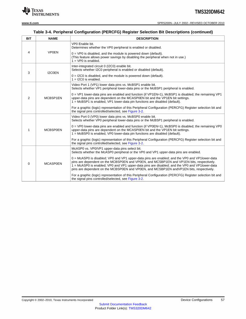
TMS320DM642
www.ti.com SPRS200N–JULY 2002–REVISED OCTOBER 2010
Table 3-4. Peripheral Configuration (PERCFG) Register Selection Bit Descriptions (continued)
BIT NAME DESCRIPTION
VP0 Enable bit.Determines whether the VP0 peripheral is enabled or disabled.
4 VP0EN 0 = VP0 is disabled, and the module is powered down (default).(This feature allows power savings by disabling the peripheral when not in use.)1 = VP0 is enabled.
Inter-integrated circuit 0 (I2C0) enable bit.Selects whether I2C0 peripheral is enabled or disabled (default).
3 I2C0EN0 = I2C0 is disabled, and the module is powered down (default).1 = I2C0 is enabled.
Video Port 1 (VP1) lower data pins vs. McBSP1 enable bit.Selects whether VP1 peripheral lower-data pins or the McBSP1 peripheral is enabled.
0 = VP1 lower-data pins are enabled and function (if VP1EN=1), McBSP1 is disabled; the remaining VP12 MCBSP1EN upper-data pins are dependent on the MCASP0EN bit and the VP1EN bit settings.
1 = McBSP1 is enabled, VP1 lower-data pin functions are disabled (default).
For a graphic (logic) representation of this Peripheral Configuration (PERCFG) Register selection bit andthe signal pins controlled/selected, see Figure 3-2.
Video Port 0 (VP0) lower data pins vs. McBSP0 enable bit.Selects whether VP0 peripheral lower-data pins or the McBSP1 peripheral is enabled.
0 = VP0 lower-data pins are enabled and function (if VP0EN=1), McBSP0 is disabled; the remaining VP01 MCBSP0EN upper-data pins are dependent on the MCASP0EN bit and the VP1EN bit settings.
1 = McBSP0 is enabled, VP0 lower-data pin functions are disabled (default).
For a graphic (logic) representation of this Peripheral Configuration (PERCFG) Register selection bit andthe signal pins controlled/selected, see Figure 3-2.
McASP0 vs. VP0/VP1 upper-data pins select bit.Selects whether the McASP0 peripheral or the VP0 and VP1 upper-data pins are enabled.
0 = McASP0 is disabled; VP0 and VP1 upper-data pins are enabled; and the VP0 and VP1lower-datapins are dependent on the MCBSP0EN and VP0EN, and MCSBP1EN and VP1EN bits, respectively.0 MCASP0EN 1 = McASP0 is enabled; VP0 and VP1 upper-data pins are disabled; and the VP0 and VP1lower-datapins are dependent on the MCBSP0EN and VP0EN, and MCSBP1EN andVP1EN bits, respectively.
For a graphic (logic) representation of this Peripheral Configuration (PERCFG) Register selection bit andthe signal pins controlled/selected, see Figure 3-2.
Copyright © 2002–2010, Texas Instruments Incorporated Device Configurations 57Submit Documentation Feedback
Product Folder Link(s): TMS320DM642
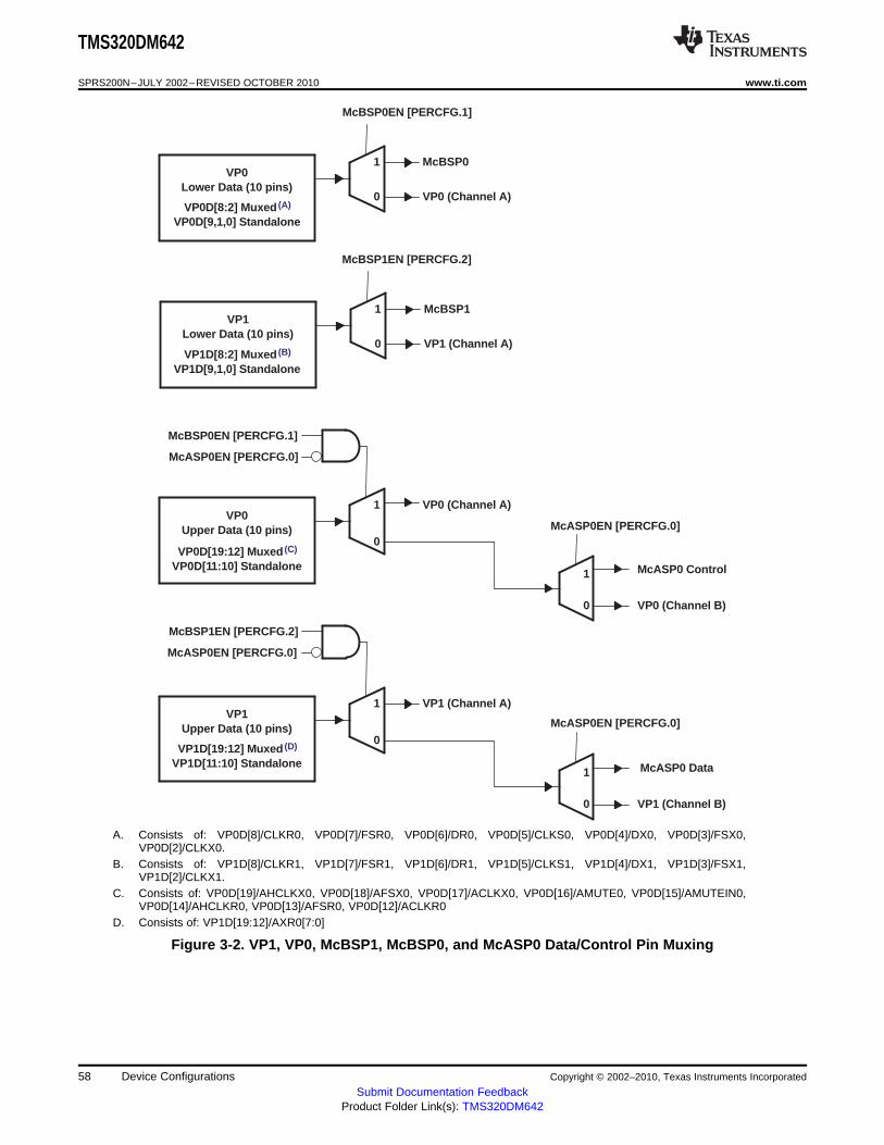
1
0
VP0Lower Data (10 pins)
VP0 (Channel A)
McBSP0
McBSP0EN [PERCFG.1]
1
0
VP1Lower Data (10 pins)
VP1 (Channel A)
McBSP1
McBSP1EN [PERCFG.2]
1
0
VP0Upper Data (10 pins)
VP0 (Channel B)
VP0 (Channel A)
McBSP0EN [PERCFG.1]
1
0
McASP0EN [PERCFG.0]
McASP0 Control
1
0
VP1Upper Data (10 pins)
VP1 (Channel B)
VP1 (Channel A)
1
0
McASP0EN [PERCFG.0]
McASP0 Data
McASP0EN [PERCFG.0]
McBSP1EN [PERCFG.2]
McASP0EN [PERCFG.0]
VP0D[8:2] Muxed (A)
VP0D[9,1,0] Standalone
VP1D[8:2] Muxed (B)
VP1D[9,1,0] Standalone
VP0D[19:12] Muxed (C)
VP0D[11:10] Standalone
VP1D[19:12] Muxed (D)
VP1D[11:10] Standalone
TMS320DM642
SPRS200N–JULY 2002–REVISED OCTOBER 2010 www.ti.com
A. Consists of: VP0D[8]/CLKR0, VP0D[7]/FSR0, VP0D[6]/DR0, VP0D[5]/CLKS0, VP0D[4]/DX0, VP0D[3]/FSX0,VP0D[2]/CLKX0.
B. Consists of: VP1D[8]/CLKR1, VP1D[7]/FSR1, VP1D[6]/DR1, VP1D[5]/CLKS1, VP1D[4]/DX1, VP1D[3]/FSX1,VP1D[2]/CLKX1.
C. Consists of: VP0D[19]/AHCLKX0, VP0D[18]/AFSX0, VP0D[17]/ACLKX0, VP0D[16]/AMUTE0, VP0D[15]/AMUTEIN0,VP0D[14]/AHCLKR0, VP0D[13]/AFSR0, VP0D[12]/ACLKR0
D. Consists of: VP1D[19:12]/AXR0[7:0]
Figure 3-2. VP1, VP0, McBSP1, McBSP0, and McASP0 Data/Control Pin Muxing
58 Device Configurations Copyright © 2002–2010, Texas Instruments Incorporated
Submit Documentation FeedbackProduct Folder Link(s): TMS320DM642
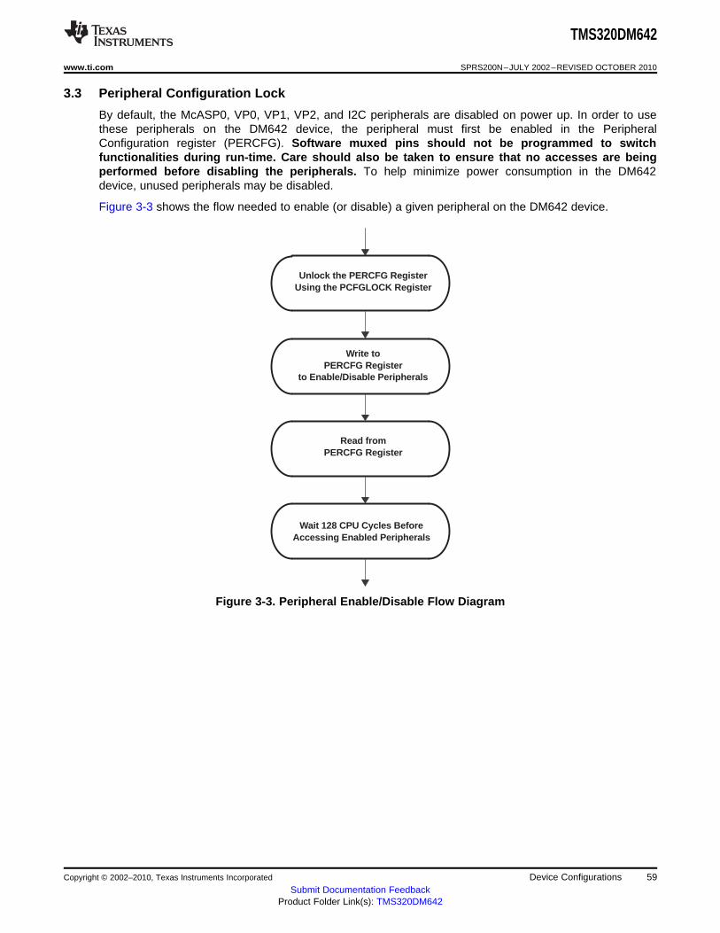
Unlock the PERCFG RegisterUsing the PCFGLOCK Register
Write toPERCFG Register
to Enable/Disable Peripherals
Read fromPERCFG Register
Wait 128 CPU Cycles BeforeAccessing Enabled Peripherals
TMS320DM642
www.ti.com SPRS200N–JULY 2002–REVISED OCTOBER 2010
3.3 Peripheral Configuration Lock
By default, the McASP0, VP0, VP1, VP2, and I2C peripherals are disabled on power up. In order to usethese peripherals on the DM642 device, the peripheral must first be enabled in the PeripheralConfiguration register (PERCFG). Software muxed pins should not be programmed to switchfunctionalities during run-time. Care should also be taken to ensure that no accesses are beingperformed before disabling the peripherals. To help minimize power consumption in the DM642device, unused peripherals may be disabled.
Figure 3-3 shows the flow needed to enable (or disable) a given peripheral on the DM642 device.
Figure 3-3. Peripheral Enable/Disable Flow Diagram
Copyright © 2002–2010, Texas Instruments Incorporated Device Configurations 59Submit Documentation Feedback
Product Folder Link(s): TMS320DM642

TMS320DM642
SPRS200N–JULY 2002–REVISED OCTOBER 2010 www.ti.com
A 32-bit key (value = 0x10C0010C) must be written to the Peripheral Configuration Lock register(PCFGLOCK) in order to unlock access to the PERCFG register. Reading the PCFGLOCK registerdetermines whether the PERCFG register is currently locked (LOCKSTAT bit = 1) or unlocked(LOCKSTAT bit = 0), see Figure 3-4. A peripheral can only be enabled when the PERCFG register is"unlocked" (LOCKSTAT bit = 0).
Read Accesses
31 1 0
Reserved LOCKSTAT
R-0 R-1
Write Accesses
31 0
LOCK
W-0
Legend: R = Read only, R/W = Read/Write, -n = value after reset
Figure 3-4. PCFGLOCK Register Diagram [Address Location: 0x01B3 F018] - Read/Write Accesses
Table 3-5. PCFGLOCK Register Selection Bit Descriptions - Read Accesses
BIT NAME DESCRIPTION
31:1 Reserved Reserved. Read-only, writes have no effect.
Lock status bit.Determines whether the PERCFG register is locked or unlocked.
0 LOCKSTAT 0 = Unlocked, read accesses to the PERCFG register allowed.1 = Locked, write accesses to the PERCFG register do not modify the register state [default].
Reads are unaffected by Lock Status.
Table 3-6. PCFGLOCK Register Selection Bit Descriptions - Write Accesses
BIT NAME DESCRIPTION
Lock bits.31:0 LOCK 0x10C0010C = Unlocks PERCFG register accesses.
Any write to the PERCFG register will automatically relock the register. In order to avoid the unnecessaryoverhead of multiple unlock/enable sequences, all peripherals should be enabled with a single write to thePERCFG register with the necessary enable bits set.
Prior to waiting 128 CPU cycles, the PERCFG register should be read. There is no direct correlationbetween the CPU issuing a write to the PERCFG register and the write actually occurring. Reading thePERCFG register after the write is issued forces the CPU to wait for the write to the PERCFG register tooccur.
Once a peripheral is enabled, the DSP (or other peripherals such as the HPI) must wait a minimum of 128CPU cycles before accessing the enabled peripheral. The user must ensure that no accesses areperformed to a peripheral while it is disabled.
60 Device Configurations Copyright © 2002–2010, Texas Instruments Incorporated
Submit Documentation FeedbackProduct Folder Link(s): TMS320DM642
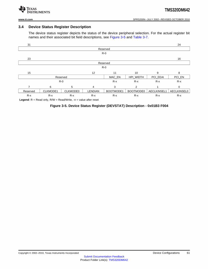
TMS320DM642
www.ti.com SPRS200N–JULY 2002–REVISED OCTOBER 2010
3.4 Device Status Register Description
The device status register depicts the status of the device peripheral selection. For the actual register bitnames and their associated bit field descriptions, see Figure 3-5 and Table 3-7.
31 24
Reserved
R-0
23 16
Reserved
R-0
15 12 11 10 9 8
Reserved MAC_EN HPI_WIDTH PCI_EEAI PCI_EN
R-0 R-x R-x R-x R-x
7 6 5 4 3 2 1 0
Reserved CLKMODE1 CLKMODE0 LENDIAN BOOTMODE1 BOOTMODE0 AECLKINSEL1 AECLKINSEL0
R-x R-x R-x R-x R-x R-x R-x R-x
Legend: R = Read only, R/W = Read/Write, -n = value after reset
Figure 3-5. Device Status Register (DEVSTAT) Description - 0x01B3 F004
Copyright © 2002–2010, Texas Instruments Incorporated Device Configurations 61Submit Documentation Feedback
Product Folder Link(s): TMS320DM642

TMS320DM642
SPRS200N–JULY 2002–REVISED OCTOBER 2010 www.ti.com
Table 3-7. Device Status (DEVSTAT) Register Selection Bit Descriptions
BIT NAME DESCRIPTION
31:12 Reserved Reserved. Read-only, writes have no effect.
EMAC enable bit.Shows the status of whether EMAC peripheral is enabled or disabled (default).
11 MAC_EN 0 = EMAC is disabled, and the module is powered down (default).1 = EMAC is enabled.
This bit has no effect if the PCI peripheral is enabled (PCI_EN = 1).
HPI bus width control bit.Shows the status of whether the HPI bus operates in 32-bit mode or in 16-bit mode (default).
10 HPI_WIDTH0 = HPI operates in 16-bit mode. (default).1 = HPI operates in 32-bit mode.
PCI EEPROM auto-initialization bit (PCI auto-initialization via external EEPROM).Shows the status of whether the PCI module initializes internal registers via external EEPROM or if theinternal PCI default values are used instead (default).
9 PCI_EEAI 0 = PCI auto-initialization through EEPROM is disabled; the PCI peripheral uses the specified PCI defaultvalues (default).1 = PCI auto-initialization through EEPROM is enabled; the PCI peripheral is configured throughEEPROM provided the PCI peripheral pin is enabled (PCI_EN = 1).
PCI enable bit.Shows the status of whether the PCI peripheral is enabled or disabled (default).
8 PCI_EN 0 = PCI disabled. (default).1 = PCI enabled.
Global select for the PCI vs. HPI/EMAC/MDIO/GPIO peripherals.
7 Reserved Reserved. Read-only, writes have no effect.
6 CLKMODE1 Clock mode select bitsShows the status of whether the CPU clock frequency equals the input clock frequency X1 (Bypass), x6,or x12.Clock mode select for CPU clock frequency (CLKMODE[1:0])
00 - Bypass (x1) (default mode)01 - x65 CLKMODE010 - x1211 - Reserved
For more details on the CLKMODE pins and the PLL multiply factors, see the Clock PLL section of thisdata sheet.
Device Endian mode (LEND)Shows the status of whether the system is operating in Big Endian mode or Little Endian mode (default).
4 LENDIAN0 - System is operating in Big Endian mode1 - System is operating in Little Endian mode (default)
3 BOOTMODE1 Bootmode configuration bitsShows the status of what device bootmode configuration is operational.
Bootmode [1:0]00 - No boot (default mode)2 BOOTMODE001 - HPI/PCI boot (based on PCI_EN pin)10 - Reserved11 - EMIFA boot
1 AECLKINSEL1 EMIFA input clock selectShows the status of what clock mode is enabled or disabled for the EMIF.Clock mode select for EMIFA (AECLKIN_SEL[1:0])
00 - AECLKIN (default mode)0 AECLKINSEL001 - CPU/4 Clock Rate10 - CPU/6 Clock Rate11 - Reserved
62 Device Configurations Copyright © 2002–2010, Texas Instruments Incorporated
Submit Documentation FeedbackProduct Folder Link(s): TMS320DM642
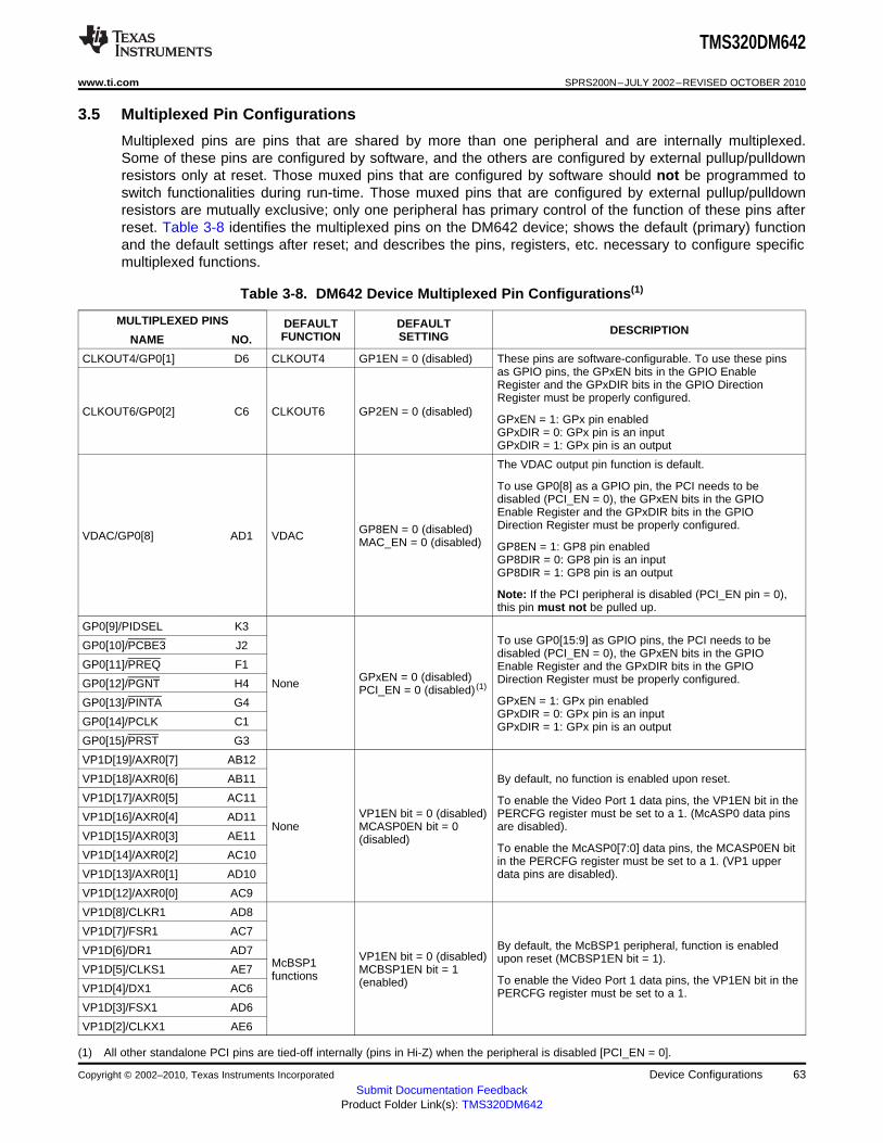
TMS320DM642
www.ti.com SPRS200N–JULY 2002–REVISED OCTOBER 2010
3.5 Multiplexed Pin Configurations
Multiplexed pins are pins that are shared by more than one peripheral and are internally multiplexed.Some of these pins are configured by software, and the others are configured by external pullup/pulldownresistors only at reset. Those muxed pins that are configured by software should not be programmed toswitch functionalities during run-time. Those muxed pins that are configured by external pullup/pulldownresistors are mutually exclusive; only one peripheral has primary control of the function of these pins afterreset. Table 3-8 identifies the multiplexed pins on the DM642 device; shows the default (primary) functionand the default settings after reset; and describes the pins, registers, etc. necessary to configure specificmultiplexed functions.
Table 3-8. DM642 Device Multiplexed Pin Configurations(1)
MULTIPLEXED PINS DEFAULT DEFAULT DESCRIPTIONFUNCTION SETTINGNAME NO.
CLKOUT4/GP0[1] D6 CLKOUT4 GP1EN = 0 (disabled) These pins are software-configurable. To use these pinsas GPIO pins, the GPxEN bits in the GPIO EnableRegister and the GPxDIR bits in the GPIO DirectionRegister must be properly configured.
CLKOUT6/GP0[2] C6 CLKOUT6 GP2EN = 0 (disabled)GPxEN = 1: GPx pin enabledGPxDIR = 0: GPx pin is an inputGPxDIR = 1: GPx pin is an output
The VDAC output pin function is default.
To use GP0[8] as a GPIO pin, the PCI needs to bedisabled (PCI_EN = 0), the GPxEN bits in the GPIOEnable Register and the GPxDIR bits in the GPIODirection Register must be properly configured.GP8EN = 0 (disabled)VDAC/GP0[8] AD1 VDAC MAC_EN = 0 (disabled) GP8EN = 1: GP8 pin enabledGP8DIR = 0: GP8 pin is an inputGP8DIR = 1: GP8 pin is an output
Note: If the PCI peripheral is disabled (PCI_EN pin = 0),this pin must not be pulled up.
GP0[9]/PIDSEL K3To use GP0[15:9] as GPIO pins, the PCI needs to beGP0[10]/PCBE3 J2disabled (PCI_EN = 0), the GPxEN bits in the GPIO
GP0[11]/PREQ F1 Enable Register and the GPxDIR bits in the GPIOGPxEN = 0 (disabled) Direction Register must be properly configured.GP0[12]/PGNT H4 None PCI_EN = 0 (disabled) (1)
GPxEN = 1: GPx pin enabledGP0[13]/PINTA G4GPxDIR = 0: GPx pin is an input
GP0[14]/PCLK C1 GPxDIR = 1: GPx pin is an outputGP0[15]/PRST G3
VP1D[19]/AXR0[7] AB12
VP1D[18]/AXR0[6] AB11 By default, no function is enabled upon reset.
VP1D[17]/AXR0[5] AC11 To enable the Video Port 1 data pins, the VP1EN bit in theVP1EN bit = 0 (disabled) PERCFG register must be set to a 1. (McASP0 data pinsVP1D[16]/AXR0[4] AD11
None MCASP0EN bit = 0 are disabled).VP1D[15]/AXR0[3] AE11 (disabled)
To enable the McASP0[7:0] data pins, the MCASP0EN bitVP1D[14]/AXR0[2] AC10 in the PERCFG register must be set to a 1. (VP1 upperVP1D[13]/AXR0[1] AD10 data pins are disabled).
VP1D[12]/AXR0[0] AC9
VP1D[8]/CLKR1 AD8
VP1D[7]/FSR1 AC7By default, the McBSP1 peripheral, function is enabledVP1D[6]/DR1 AD7 VP1EN bit = 0 (disabled) upon reset (MCBSP1EN bit = 1).McBSP1VP1D[5]/CLKS1 AE7 MCBSP1EN bit = 1functions To enable the Video Port 1 data pins, the VP1EN bit in the(enabled)VP1D[4]/DX1 AC6 PERCFG register must be set to a 1.
VP1D[3]/FSX1 AD6
VP1D[2]/CLKX1 AE6
(1) All other standalone PCI pins are tied-off internally (pins in Hi-Z) when the peripheral is disabled [PCI_EN = 0].
Copyright © 2002–2010, Texas Instruments Incorporated Device Configurations 63Submit Documentation Feedback
Product Folder Link(s): TMS320DM642
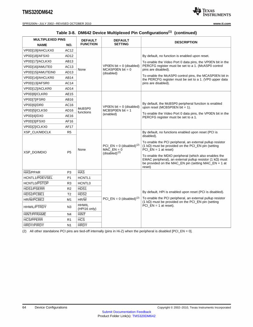
TMS320DM642
SPRS200N–JULY 2002–REVISED OCTOBER 2010 www.ti.com
Table 3-8. DM642 Device Multiplexed Pin Configurations(1) (continued)
MULTIPLEXED PINS DEFAULT DEFAULT DESCRIPTIONFUNCTION SETTINGNAME NO.
VP0D[19]/AHCLKX0 AC12
VP0D[18]/AFSX0 AD12 By default, no function is enabled upon reset.
VP0D[17]/ACLKX0 AB13 To enable the Video Port 0 data pins, the VP0EN bit in theVP0EN bit = 0 (disabled) PERCFG register must be set to a 1. (McASP0 controlVP0D[16]/AMUTE0 AC13
None MCASP0EN bit = 0 pins are disabled).VP0D[15]/AMUTEIN0 AD13 (disabled)
To enable the McASP0 control pins, the MCASP0EN bit inVP0D[14]/AHCLKR0 AB14 the PERCFG register must be set to a 1. (VP0 upper dataVP0D[13]/AFSR0 AC14 pins are disabled).
VP0D[12]/ACLKR0 AD14
VP0D[8]/CLKR0 AE15
VP0D[7]/FSR0 AB16By default, the McBSP0 peripheral function is enabledVP0D[6]/DR0 AC16 VP0EN bit = 0 (disabled) upon reset (MCBSP0EN bit = 1).McBSP0VP0D[5]/CLKS0 AD16 MCBSP0EN bit = 1functions To enable the Video Port 0 data pins, the VP0EN bit in the(enabled)VP0D[4]/DX0 AE16 PERCFG register must be set to a 1.
VP0D[3]/FSX0 AF16
VP0D[2]/CLKX0 AF17
XSP_CLK/MDCLK R5 By default, no functions enabled upon reset (PCI isdisabled).
To enable the PCI peripheral, an external pullup resistorPCI_EN = 0 (disabled) (2) (1 kΩ) must be provided on the PCI_EN pin (setting
None MAC_EN = 0 PCI_EN = 1 at reset)XSP_DO/MDIO P5 (disabled) (2)
To enable the MDIO peripheral (which also enables theEMAC peripheral), an external pullup resistor (1 kΩ) mustbe provided on the MAC_EN pin (setting MAC_EN = 1 atreset)
HAS/PPAR P3 HAS
HCNTL1/PDEVSEL P1 HCNTL1
HCNTL0/PSTOP R3 HCNTL0
HDS1/PSERR R2 HDS1By default, HPI is enabled upon reset (PCI is disabled).
HDS2/PCBE1 T2 HDS2To enable the PCI peripheral, an external pullup resistorPCI_EN = 0 (disabled) (2)
HR/W/PCBE2 M1 HR/W(1 kΩ) must be provided on the PCI_EN pin (setting
HHWIL PCI_EN = 1 at reset).HHWIL/PTRDY N3 (HPI16 only)
HINT/PFRAME N4 HINT
HCS/PPERR R1 HCS
HRDY/PIRDY N1 HRDY
(2) All other standalone PCI pins are tied-off internally (pins in Hi-Z) when the peripheral is disabled [PCI_EN = 0].
64 Device Configurations Copyright © 2002–2010, Texas Instruments Incorporated
Submit Documentation FeedbackProduct Folder Link(s): TMS320DM642
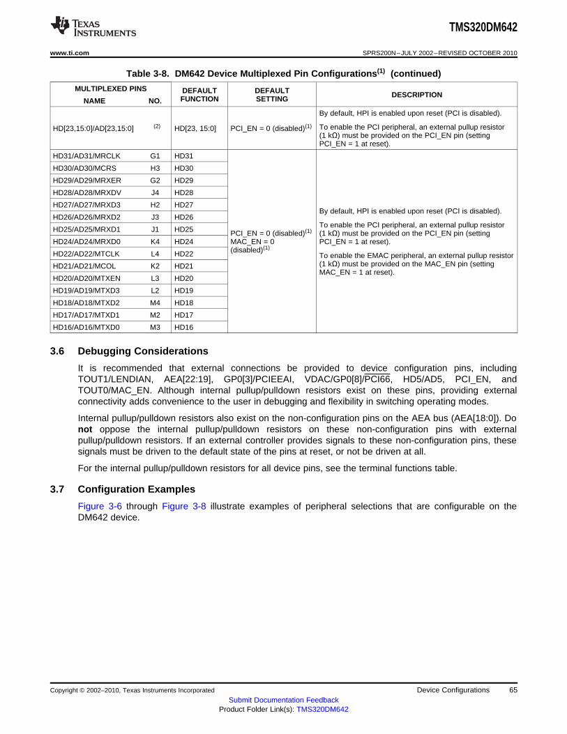
TMS320DM642
www.ti.com SPRS200N–JULY 2002–REVISED OCTOBER 2010
Table 3-8. DM642 Device Multiplexed Pin Configurations(1) (continued)
MULTIPLEXED PINS DEFAULT DEFAULT DESCRIPTIONFUNCTION SETTINGNAME NO.
By default, HPI is enabled upon reset (PCI is disabled).
To enable the PCI peripheral, an external pullup resistorHD[23,15:0]/AD[23,15:0] (2) HD[23, 15:0] PCI_EN = 0 (disabled)(1)
(1 kΩ) must be provided on the PCI_EN pin (settingPCI_EN = 1 at reset).
HD31/AD31/MRCLK G1 HD31
HD30/AD30/MCRS H3 HD30
HD29/AD29/MRXER G2 HD29
HD28/AD28/MRXDV J4 HD28
HD27/AD27/MRXD3 H2 HD27By default, HPI is enabled upon reset (PCI is disabled).
HD26/AD26/MRXD2 J3 HD26To enable the PCI peripheral, an external pullup resistor
HD25/AD25/MRXD1 J1 HD25 PCI_EN = 0 (disabled)(1) (1 kΩ) must be provided on the PCI_EN pin (settingHD24/AD24/MRXD0 K4 HD24 MAC_EN = 0 PCI_EN = 1 at reset).
(disabled)(1)HD22/AD22/MTCLK L4 HD22 To enable the EMAC peripheral, an external pullup resistor
(1 kΩ) must be provided on the MAC_EN pin (settingHD21/AD21/MCOL K2 HD21MAC_EN = 1 at reset).
HD20/AD20/MTXEN L3 HD20
HD19/AD19/MTXD3 L2 HD19
HD18/AD18/MTXD2 M4 HD18
HD17/AD17/MTXD1 M2 HD17
HD16/AD16/MTXD0 M3 HD16
3.6 Debugging Considerations
It is recommended that external connections be provided to device configuration pins, includingTOUT1/LENDIAN, AEA[22:19], GP0[3]/PCIEEAI, VDAC/GP0[8]/PCI66, HD5/AD5, PCI_EN, andTOUT0/MAC_EN. Although internal pullup/pulldown resistors exist on these pins, providing externalconnectivity adds convenience to the user in debugging and flexibility in switching operating modes.
Internal pullup/pulldown resistors also exist on the non-configuration pins on the AEA bus (AEA[18:0]). Donot oppose the internal pullup/pulldown resistors on these non-configuration pins with externalpullup/pulldown resistors. If an external controller provides signals to these non-configuration pins, thesesignals must be driven to the default state of the pins at reset, or not be driven at all.
For the internal pullup/pulldown resistors for all device pins, see the terminal functions table.
3.7 Configuration Examples
Figure 3-6 through Figure 3-8 illustrate examples of peripheral selections that are configurable on theDM642 device.
Copyright © 2002–2010, Texas Instruments Incorporated Device Configurations 65Submit Documentation Feedback
Product Folder Link(s): TMS320DM642

PERCFG Register V alue: 0x0000 0078External Pins: PCI_EN = 0 GP0[3]/PCIEEAI = 0 HD5 = 0 TOUT0/MAC_EN = 1
PCI
HPI(16-Bit)
EMAC
MDIO
VP0(20-Bit)
McBSP0
McASP0 Data
McBSP1
EMIFA
Clockand
System
GP0and
EXT_INT
I2C0
VP2(20-Bit)
VIC
TIMER0
TIMER1
TIMER2
McASP0 Control
16HD[15:0]
MTXD[3:0], MTXEN
MRXD[3:0], MRXER,MRXDV, MCOL, MCRS,
MTCLK, MRCLK
MDIO, MDCLK
VP0CLK0VP0CLK1,
VP0CTL[2:0],VP0D[19:0]
VP1(20-Bit)
VP1CLK0
VP1CLK1,VP1CTL[2:0],
VP1D[19:0]
AED[63:0]64
AECLKIN, AARDY , AHOLD
AEA[22:3], ACE[3:0] , ABE[7:0] ,AECLKOUT1, AECLKOUT2,ASDCKE, ASOE3 , APDT,AHOLDA , ABUSREQ,AARE/ASDCAS/ASADS/ASRE,AAOE/ASDRAS/ASOE,AAWE/ASDWE/ASWE
CLKIN,CLKMODE0, CLKMODE1
CLKOUT4, CLKOUT6, PLL V
SCL0
SDA0
VP2CLK0
VP2CLK1,VP2CTL[2:0],VP2D[19:0]
TINP0
TOUT0/MACEN
TINP1
TOUT1/LENDIAN
STCLK (A)
VDAC/GP0[8]/PCI66
HRDY, HINT
HCNTL0, HCNTL1,HHWIL, HAS, HR/W,
HCS, HDS1, HDS2
GP0[15:9, 3:0]
GP0[7:4]
STCLK (A)
STCLK (A)
Shading denotes a peripheral module not available for this configuration.
A. STCLK supports all three video ports (VP2, VP1, and VP0).
TMS320DM642
SPRS200N–JULY 2002–REVISED OCTOBER 2010 www.ti.com
Figure 3-6. Configuration Example A(3 20-Bit Video Ports + HPI + EMAC + MDIO + I2C0 + EMIF + 3 Timers)
66 Device Configurations Copyright © 2002–2010, Texas Instruments Incorporated
Submit Documentation FeedbackProduct Folder Link(s): TMS320DM642

McASP0 Data
McASP0 Control
PERCFG Register V alue: 0x0000 007EExtenal Pins: PCI_EN = 0 GP0[3]/PCIEEAI = 0 HD5 = 0 TOUT0/MAC_EN = 1
PCI
HPI(16-Bit)
EMAC
MDIO
VP0(10-Bit)
McBSP0
McBSP1
EMIFA
Clockand
System
GP0and
EXT_INT
I2C0
VP2(20-Bit)
VIC
TIMER0
TIMER1
TIMER2
16HD[15:0]
MTXD[3:0], MTXEN
MRXD[3:0], MRXER,MRXDV, MCOL, MCRS,
MTCLK, MRCLK
MDIO, MDCLK
VP0CLK0VP0CLK1,
VP0CTL[2:0],VP0D[19:10]
VP1(10-Bit)
VP1CLK0
VP1CLK1,VP1CTL[2:0],VP1D[19:10]
AED[63:0]64
AECLKIN, AARDY , AHOLD
AEA[22:3], ACE[3:0] , ABE[7:0] ,AECLKOUT1, AECLKOUT2,ASDCKE, ASOE3 , APDT,AHOLDA , ABUSREQ,AARE/ASDCAS/ASADS/ASRE,AAOE/ASDRAS/ASOE,AAWE/ASDWE/ASWE
CLKIN,CLKMODE0, CLKMODE1
CLKOUT4, CLKOUT6, PLL V
SCL0
SDA0
VP2CLK0
VP2CLK1,VP2CTL[2:0],VP2D[19:0]
TINP0
TOUT0/MACEN
TINP1
TOUT1/LENDIAN
STCLK (A)
VDAC/GP0[8]/PCI66
HRDY, HINT
HCNTL0, HCNTL1,HHWIL, HAS, HR/W,
HCS, HDS1, HDS2
GP0[15:9, 3:0]
GP0[7:4]
STCLK (A)
STCLK (A)
CLKR0, FSR0, DR0,CLKS0, DX0, FSX0,
CLKX0
CLKR1, FSR1, DR1,CLKS1, DX1, FSX1,
CLKX1
Shading denotes a peripheral module not available for this configuration.
A. STCLK supports all three video ports (VP2, VP1, and VP0).
TMS320DM642
www.ti.com SPRS200N–JULY 2002–REVISED OCTOBER 2010
Figure 3-7. Configuration Example B(2 10-Bit Video Ports + 2 McBSPs + EMAC + MDIO + I2C0 + EMIF)
[Possible Video IP Phone Application]
Copyright © 2002–2010, Texas Instruments Incorporated Device Configurations 67Submit Documentation Feedback
Product Folder Link(s): TMS320DM642

Shading denotes a peripheral module not available for this configuration.
PCI
HPI(16-Bit)
EMAC
MDIO
VP0(10-Bit)
McBSP0
McASP0 Data
McBSP1
EMIFA
Clockand
System
GP0and
EXT_INT
I2C0
VP2(20-Bit)
VIC
TIMER0
TIMER1
TIMER2
McASP0 Control
16HD[15:0]
MTXD[3:0], MTXEN
MRXD[3:0], MRXER,MRXDV, MCOL, MCRS,
MTCLK, MRCLK
MDIO, MDCLK
VP0CLK0VP0CLK1,
VP0CTL[2:0],VP0D[9:0]
VP1(10-Bit)
VP1CLK0
VP1CLK1,VP1CTL[2:0],
VP1D[9:0]
AED[63:0]64
AECLKIN, AARDY , AHOLD
AEA[22:3], ACE[3:0] , ABE[7:0] ,AECLKOUT1, AECLKOUT2,ASDCKE, ASOE3 , APDT,AHOLDA , ABUSREQ,AARE/ASDCAS/ASADS/ASRE,AAOE/ASDRAS/ASOE,AAWE/ASDWE/ASWE
CLKIN,CLKMODE0, CLKMODE1
CLKOUT4, CLKOUT6, PLL V
SCL0
SDA0
VP2CLK0
VP2CLK1,VP2CTL[2:0],VP2D[19:0]
TINP0
TOUT0/MACEN
TINP1
TOUT1/LENDIAN
STCLK (A)
VDAC/GP0[8]/PCI66
HRDY, HINT
HCNTL0, HCNTL1,HHWIL, HAS, HR/W,
HCS, HDS1, HDS2
GP0[15:9, 3:0]
GP0[7:4]
STCLK (A)
STCLK (A)
AHCLKX0, AFSX0,ACLKX0, AMUTE0,
AMUTEIN0, AHCLKR0,AFSR0, ACLKR0
AXR0[7:0]
PERCFG Register V alue: 0x0000 0079Extenal Pins: PCI_EN = 0 GP0[3]/PCIEEAI = 0 HD5 = 0 TOUT0/MAC_EN = 1
A. STCLK supports all three video ports (VP2, VP1, and VP0).
TMS320DM642
SPRS200N–JULY 2002–REVISED OCTOBER 2010 www.ti.com
Figure 3-8. Configuration Example C(1 20-Bit Video Port, 2 10-Bit Video Ports + 1 McASP0 + VIC + I2C0 + EMIF)
[Possible Set-Top Box Application]
68 Device Configurations Copyright © 2002–2010, Texas Instruments Incorporated
Submit Documentation FeedbackProduct Folder Link(s): TMS320DM642
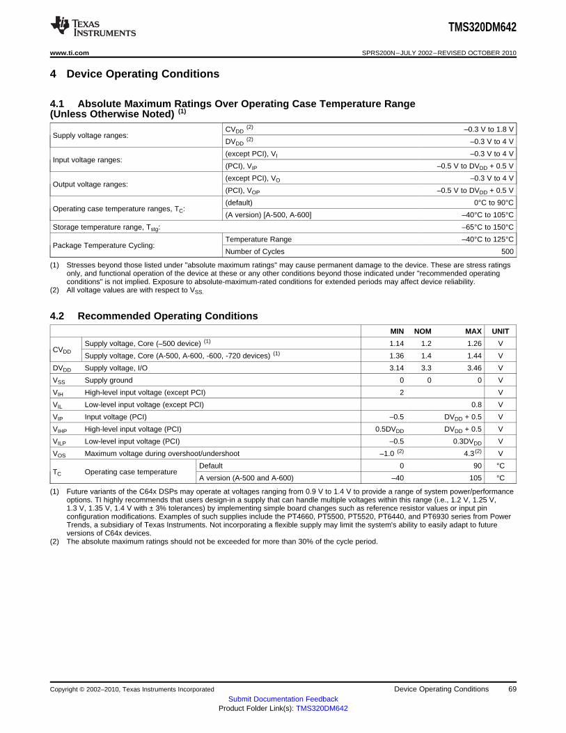
TMS320DM642
www.ti.com SPRS200N–JULY 2002–REVISED OCTOBER 2010
4 Device Operating Conditions
4.1 Absolute Maximum Ratings Over Operating Case Temperature Range(Unless Otherwise Noted) (1)
CVDD(2) –0.3 V to 1.8 V
Supply voltage ranges:DVDD
(2) –0.3 V to 4 V
(except PCI), VI –0.3 V to 4 VInput voltage ranges:
(PCI), VIP –0.5 V to DVDD + 0.5 V
(except PCI), VO –0.3 V to 4 VOutput voltage ranges:
(PCI), VOP –0.5 V to DVDD + 0.5 V
(default) 0°C to 90°COperating case temperature ranges, TC:
(A version) [A-500, A-600] –40°C to 105°C
Storage temperature range, Tstg: –65°C to 150°C
Temperature Range –40°C to 125°CPackage Temperature Cycling:
Number of Cycles 500
(1) Stresses beyond those listed under "absolute maximum ratings" may cause permanent damage to the device. These are stress ratingsonly, and functional operation of the device at these or any other conditions beyond those indicated under "recommended operatingconditions" is not implied. Exposure to absolute-maximum-rated conditions for extended periods may affect device reliability.
(2) All voltage values are with respect to VSS.
4.2 Recommended Operating ConditionsMIN NOM MAX UNIT
Supply voltage, Core (–500 device) (1) 1.14 1.2 1.26 VCVDD
Supply voltage, Core (A-500, A-600, -600, -720 devices) (1) 1.36 1.4 1.44 V
DVDD Supply voltage, I/O 3.14 3.3 3.46 V
VSS Supply ground 0 0 0 V
VIH High-level input voltage (except PCI) 2 V
VIL Low-level input voltage (except PCI) 0.8 V
VIP Input voltage (PCI) –0.5 DVDD + 0.5 V
VIHP High-level input voltage (PCI) 0.5DVDD DVDD + 0.5 V
VILP Low-level input voltage (PCI) –0.5 0.3DVDD V
VOS Maximum voltage during overshoot/undershoot –1.0 (2) 4.3 (2) V
Default 0 90 °CTC Operating case temperature
A version (A-500 and A-600) –40 105 °C
(1) Future variants of the C64x DSPs may operate at voltages ranging from 0.9 V to 1.4 V to provide a range of system power/performanceoptions. TI highly recommends that users design-in a supply that can handle multiple voltages within this range (i.e., 1.2 V, 1.25 V,1.3 V, 1.35 V, 1.4 V with ± 3% tolerances) by implementing simple board changes such as reference resistor values or input pinconfiguration modifications. Examples of such supplies include the PT4660, PT5500, PT5520, PT6440, and PT6930 series from PowerTrends, a subsidiary of Texas Instruments. Not incorporating a flexible supply may limit the system's ability to easily adapt to futureversions of C64x devices.
(2) The absolute maximum ratings should not be exceeded for more than 30% of the cycle period.
Copyright © 2002–2010, Texas Instruments Incorporated Device Operating Conditions 69Submit Documentation Feedback
Product Folder Link(s): TMS320DM642
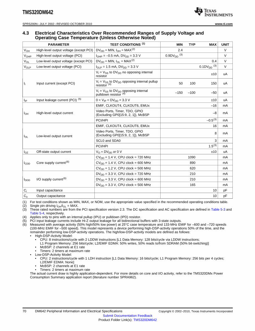
TMS320DM642
SPRS200N–JULY 2002–REVISED OCTOBER 2010 www.ti.com
4.3 Electrical Characteristics Over Recommended Ranges of Supply Voltage andOperating Case Temperature (Unless Otherwise Noted)
PARAMETER TEST CONDITIONS (1) MIN TYP MAX UNIT
VOH High-level output voltage (except PCI) DVDD = MIN, IOH = MAX (2) 2.4 V
VOHP High-level output voltage (PCI) IOHP = –0.5 mA, DVDD = 3.3 V 0.9DVDD(3) V
VOL Low-level output voltage (except PCI) DVDD = MIN, IOL = MAX (2) 0.4 V
VOLP Low-level output voltage (PCI) IOLP = 1.5 mA, DVDD = 3.3 V 0.1DVDD(3) V
VI = VSS to DVDD no opposing internal ±10 uAresistor
VI = VSS to DVDD opposing internal pullupII Input current (except PCI) 50 100 150 uAresistor (4)
VI = VSS to DVDD opposing internal –150 –100 –50 uApulldown resistor (4)
IIP Input leakage current (PCI) (5) 0 < VIP < DVDD = 3.3 V ±10 uA
EMIF, CLKOUT4, CLKOUT6, EMUx –16 mA
Video Ports, Timer, TDO, GPIOIOH High-level output current –8 mA(Excluding GP0[15:9, 2, 1]), McBSP
PCI/HPI –0.5 (3) mA
EMIF, CLKOUT4, CLKOUT6, EMUx 16 mA
Video Ports, Timer, TDO, GPIO 8 mA(Excluding GP0[15:9, 2, 1]), McBSPIOL Low-level output currentSCL0 and SDA0 3 mA
PCI/HPI 1.5 (3) mA
IOZ Off-state output current VO = DVDD or 0 V ±10 uA
CVDD = 1.4 V, CPU clock = 720 MHz 1090 mA
ICDD Core supply current (6) CVDD = 1.4 V, CPU clock = 600 MHz 890 mA
CVDD = 1.2 V, CPU clock = 500 MHz 620 mA
DVDD = 3.3 V, CPU clock = 720 MHz 210 mA
IDDD I/O supply current (6) DVDD = 3.3 V, CPU clock = 600 MHz 210 mA
DVDD = 3.3 V, CPU clock = 500 MHz 165 mA
Ci Input capacitance 10 pF
Co Output capacitance 10 pF
(1) For test conditions shown as MIN, MAX, or NOM, use the appropriate value specified in the recommended operating conditions table.(2) Single pin driving IOH/IOL = MAX.(3) These rated numbers are from the PCI specification version 2.3. The DC specification and AC specification are defined in Table 5-3 and
Table 5-4, respectively.(4) Applies only to pins with an internal pullup (IPU) or pulldown (IPD) resistor.(5) PCI input leakage currents include Hi-Z output leakage for all bidirectional buffers with 3-state outputs.(6) Measured with average activity (50% high/50% low power) at 25°C case temperature and 133-MHz EMIF for –600 and –720 speeds
(100-MHz EMIF for –500 speed). This model represents a device performing high-DSP-activity operations 50% of the time, and theremainder performing low-DSP-activity operations. The high/low-DSP-activity models are defined as follows:• High-DSP-Activity Model:
• CPU: 8 instructions/cycle with 2 LDDW instructions [L1 Data Memory: 128 bits/cycle via LDDW instructions;L1 Program Memory: 256 bits/cycle; L2/EMIF EDMA: 50% writes, 50% reads to/from SDRAM (50% bit-switching)]
• McBSP: 2 channels at E1 rate• Timers: 2 timers at maximum rate
• Low-DSP-Activity Model:• CPU: 2 instructions/cycle with 1 LDH instruction [L1 Data Memory: 16 bits/cycle; L1 Program Memory: 256 bits per 4 cycles;
L2/EMIF EDMA: None]• McBSP: 2 channels at E1 rate• Timers: 2 timers at maximum rate
The actual current draw is highly application-dependent. For more details on core and I/O activity, refer to the TMS320DMx PowerConsumption Summary application report (literature number SPRA962).
70 DM642 Peripheral Information and Electrical Specifications Copyright © 2002–2010, Texas Instruments Incorporated
Submit Documentation FeedbackProduct Folder Link(s): TMS320DM642

Transmission Line
4.0 pF 1.85 pF
Z0 = 50 Ω
(see note)
Tester Pin Electronics Data Sheet Timing Reference Point
OutputUnderTest
42 Ω 3.5 nH
Device Pin(see note)
Vref = 1.5 V
Vref = VIL MAX (or VOL MAX or
Vref = VIH MIN (or VOH MIN or VIHP MIN or VOHP MIN)
VILP MAX or VOLP MAX)
TMS320DM642
www.ti.com SPRS200N–JULY 2002–REVISED OCTOBER 2010
5 DM642 Peripheral Information and Electrical Specifications
5.1 Parameter Information
5.1.1 Parameter Information Device-Specific Information
A. The data sheet provides timing at the device pin. For output timing analysis, the tester pin electronics and itstransmission line effects must be taken into account. A transmission line with a delay of 2 ns or longer can be used toproduce the desired transmission line effect. The transmission line is intended as a load only. It is not necessary toadd or subtract the transmission line delay (2 ns or longer) from the data sheet timings.
B. Input requirements in this data sheet are tested with an input slew rate of < 4 Volts per nanosecond (4 V/ns) at thedevice pin.
Figure 5-1. Test Load Circuit for AC Timing Measurements
The load capacitance value stated is only for characterization and measurement of AC timing signals. Thisload capacitance value does not indicate the maximum load the device is capable of driving.
5.1.1.1 Signal Transition Levels
All input and output timing parameters are referenced to 1.5 V for both "0" and "1" logic levels.
Figure 5-2. Input and Output Voltage Reference Levels for AC Timing Measurements
All rise and fall transition timing parameters are referenced to VIL MAX and VIH MIN for input clocks,VOLMAX and VOH MIN for output clocks, VILP MAX and VIHP MIN for PCI input clocks, and VOLP MAX andVOHP MIN for PCI output clocks.
Figure 5-3. Rise and Fall Transition Time Voltage Reference Levels
5.1.1.2 Signal Transition Rates
All timings are tested with an input edge rate of 4 Volts per nanosecond (4 V/ns).
5.1.1.3 Timing Parameters and Board Routing Analysis
The timing parameter values specified in this data sheet do not include delays by board routings. As agood board design practice, such delays must always be taken into account. Timing values may be
Copyright © 2002–2010, Texas Instruments Incorporated DM642 Peripheral Information and Electrical Specifications 71Submit Documentation Feedback
Product Folder Link(s): TMS320DM642

1
23
45
6
78
1011
ECLKOUTx(Output from DSP)
ECLKOUTx(Input to External Device)
Control Signals (A)
(Output from DSP)
Control Signals(Input to External Device)
Data Signals (B)
(Output from External Device)
Data Signals (B)
(Input to DSP)
9
TMS320DM642
SPRS200N–JULY 2002–REVISED OCTOBER 2010 www.ti.com
adjusted by increasing/decreasing such delays. TI recommends utilizing the available I/O bufferinformation specification (IBIS) models to analyze the timing characteristics correctly. To properly use IBISmodels to attain accurate timing analysis for a given system, see the Using IBIS Models for TimingAnalysis application report (literature number SPRA839). If needed, external logic hardware such asbuffers may be used to compensate any timing differences.
For inputs, timing is most impacted by the round-trip propagation delay from the DSP to the externaldevice and from the external device to the DSP. This round-trip delay tends to negatively impact the inputsetup time margin, but also tends to improve the input hold time margins (see Table 5-1 and Figure 5-4).
Figure 5-4 represents a general transfer between the DSP and an external device. The figure alsorepresents board route delays and how they are perceived by the DSP and the external device.
Table 5-1. Board-Level Timing Example(see Figure 5-4)
NO. DESCRIPTION
1 Clock route delay
2 Minimum DSP hold time
3 Minimum DSP setup time
4 External device hold time requirement
5 External device setup time requirement
6 Control signal route delay
7 External device hold time
8 External device access time
9 DSP hold time requirement
10 DSP setup time requirement
11 Data route delay
A. Control signals include data for Writes.B. Data signals are generated during Reads from an external device.
Figure 5-4. Board-Level Input/Output Timings
5.2 Recommended Clock and Control Signal Transition Behavior
All clocks and control signals must transition between VIH and VIL (or between VIL and VIH) in a monotonicmanner.
72 DM642 Peripheral Information and Electrical Specifications Copyright © 2002–2010, Texas Instruments Incorporated
Submit Documentation FeedbackProduct Folder Link(s): TMS320DM642
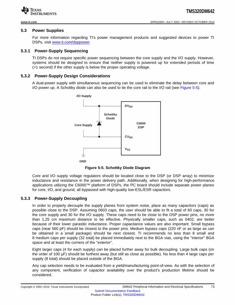
DVDD
CVDD
VSS
C6000DSP
SchottkyDiode
I/O Supply
Core Supply
GND
TMS320DM642
www.ti.com SPRS200N–JULY 2002–REVISED OCTOBER 2010
5.3 Power Supplies
For more information regarding TI's power management products and suggested devices to power TIDSPs, visit www.ti.com/dsppower.
5.3.1 Power-Supply Sequencing
TI DSPs do not require specific power sequencing between the core supply and the I/O supply. However,systems should be designed to ensure that neither supply is powered up for extended periods of time(>1 second) if the other supply is below the proper operating voltage.
5.3.2 Power-Supply Design Considerations
A dual-power supply with simultaneous sequencing can be used to eliminate the delay between core andI/O power up. A Schottky diode can also be used to tie the core rail to the I/O rail (see Figure 5-5).
Figure 5-5. Schottky Diode Diagram
Core and I/O supply voltage regulators should be located close to the DSP (or DSP array) to minimizeinductance and resistance in the power delivery path. Additionally, when designing for high-performanceapplications utilizing the C6000™ platform of DSPs, the PC board should include separate power planesfor core, I/O, and ground, all bypassed with high-quality low-ESL/ESR capacitors.
5.3.3 Power-Supply Decoupling
In order to properly decouple the supply planes from system noise, place as many capacitors (caps) aspossible close to the DSP. Assuming 0603 caps, the user should be able to fit a total of 60 caps, 30 forthe core supply and 30 for the I/O supply. These caps need to be close to the DSP power pins, no morethan 1.25 cm maximum distance to be effective. Physically smaller caps, such as 0402, are betterbecause of their lower parasitic inductance. Proper capacitance values are also important. Small bypasscaps (near 560 pF) should be closest to the power pins. Medium bypass caps (220 nF or as large as canbe obtained in a small package) should be next closest. TI recommends no less than 8 small and8 medium caps per supply (32 total) be placed immediately next to the BGA vias, using the "interior" BGAspace and at least the corners of the "exterior".
Eight larger caps (4 for each supply) can be placed further away for bulk decoupling. Large bulk caps (onthe order of 100 µF) should be furthest away (but still as close as possible). No less than 4 large caps persupply (8 total) should be placed outside of the BGA.
Any cap selection needs to be evaluated from a yield/manufacturing point-of-view. As with the selection ofany component, verification of capacitor availability over the product’s production lifetime should beconsidered.
Copyright © 2002–2010, Texas Instruments Incorporated DM642 Peripheral Information and Electrical Specifications 73Submit Documentation Feedback
Product Folder Link(s): TMS320DM642

PWRD
Internal Clock Tree
CPU
IFR
IER
CSR
PD1
PD2
Power-Down
Logic
Clock
PLL
CLKIN RESET
CLKOUT6
PD3
Internal
Peripherals
CLKOUT4
Clock
and DividersDistribution
TMS320DM642
TMS320DM642
SPRS200N–JULY 2002–REVISED OCTOBER 2010 www.ti.com
5.3.4 Peripheral Power-Down Operation
The DM642 device can be powered down in three ways:• Power-down due to pin configuration• Power-down due to software configuration – relates to the default state of the peripheral configuration
bits in the PERCFG register.• Power-down during run-time via software configuration
On the DM642 device, the HPI, PCI, and EMAC and MDIO peripherals are controlled (selected) at the pinlevel during chip reset (e.g., PCI_EN, HD5, and MAC_EN pins).
The McASP0, McBSP0, McBSP1, VP0, VP1, VP2, and I2C0 peripheral functions are selected via theperipheral configuration (PERCFG) register bits.
For more detailed information on the peripheral configuration pins and the PERCFG register bits, see theDevice Configurations section of this document.
5.3.5 Power-Down Modes Logic
Figure 5-6 shows the power-down mode logic on the DM642
A. External input clocks, with the exception of CLKIN, are not gated by the power-down mode logic.
Figure 5-6. Power-Down Mode Logic
74 DM642 Peripheral Information and Electrical Specifications Copyright © 2002–2010, Texas Instruments Incorporated
Submit Documentation FeedbackProduct Folder Link(s): TMS320DM642
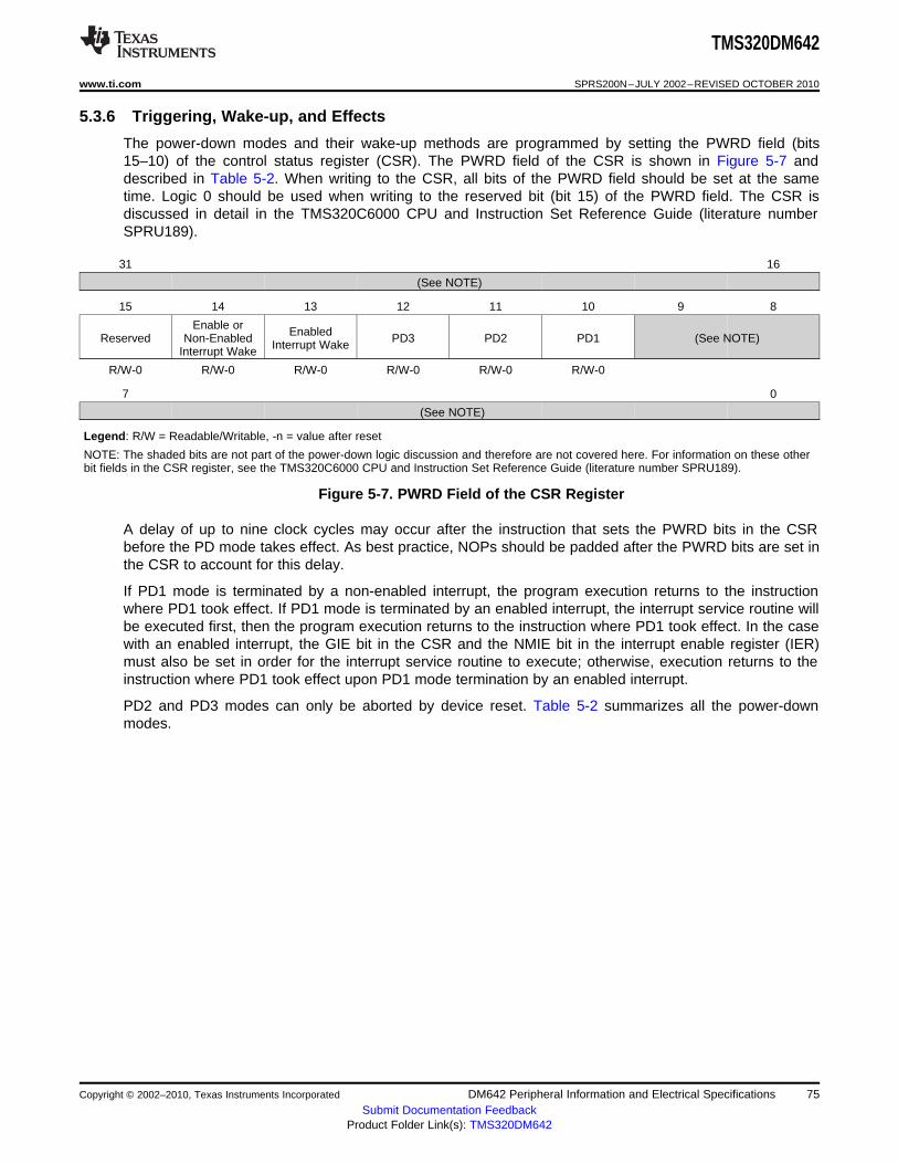
TMS320DM642
www.ti.com SPRS200N–JULY 2002–REVISED OCTOBER 2010
5.3.6 Triggering, Wake-up, and Effects
The power-down modes and their wake-up methods are programmed by setting the PWRD field (bits15–10) of the control status register (CSR). The PWRD field of the CSR is shown in Figure 5-7 anddescribed in Table 5-2. When writing to the CSR, all bits of the PWRD field should be set at the sametime. Logic 0 should be used when writing to the reserved bit (bit 15) of the PWRD field. The CSR isdiscussed in detail in the TMS320C6000 CPU and Instruction Set Reference Guide (literature numberSPRU189).
31 16
(See NOTE)
15 14 13 12 11 10 9 8
Enable or EnabledReserved Non-Enabled PD3 PD2 PD1 (See NOTE)Interrupt WakeInterrupt Wake
R/W-0 R/W-0 R/W-0 R/W-0 R/W-0 R/W-0
7 0
(See NOTE)
Legend: R/W = Readable/Writable, -n = value after reset
NOTE: The shaded bits are not part of the power-down logic discussion and therefore are not covered here. For information on these otherbit fields in the CSR register, see the TMS320C6000 CPU and Instruction Set Reference Guide (literature number SPRU189).
Figure 5-7. PWRD Field of the CSR Register
A delay of up to nine clock cycles may occur after the instruction that sets the PWRD bits in the CSRbefore the PD mode takes effect. As best practice, NOPs should be padded after the PWRD bits are set inthe CSR to account for this delay.
If PD1 mode is terminated by a non-enabled interrupt, the program execution returns to the instructionwhere PD1 took effect. If PD1 mode is terminated by an enabled interrupt, the interrupt service routine willbe executed first, then the program execution returns to the instruction where PD1 took effect. In the casewith an enabled interrupt, the GIE bit in the CSR and the NMIE bit in the interrupt enable register (IER)must also be set in order for the interrupt service routine to execute; otherwise, execution returns to theinstruction where PD1 took effect upon PD1 mode termination by an enabled interrupt.
PD2 and PD3 modes can only be aborted by device reset. Table 5-2 summarizes all the power-downmodes.
Copyright © 2002–2010, Texas Instruments Incorporated DM642 Peripheral Information and Electrical Specifications 75Submit Documentation Feedback
Product Folder Link(s): TMS320DM642
TMS320DM642
SPRS200N–JULY 2002–REVISED OCTOBER 2010 www.ti.com
Table 5-2. Characteristics of the Power-Down Modes
PRWD Field POWER-DOWN WAKE-UP METHOD EFFECT ON CHIP'S OPERATION(BITS 15–10) MODE
000000 No power-down — —
001001 PD1 Wake by an enabled interrupt CPU halted (except for the interrupt logic)Power-down mode blocks the internal clock inputs at theboundary of the CPU, preventing most of the CPU's logic fromWake by an enabled or010001 PD1 switching. During PD1, EDMA transactions can proceednon-enabled interruptbetween peripherals and internal memory.
Output clock from PLL is halted, stopping the internal clockstructure from switching and resulting in the entire chip being
011010 PD2 (1) Wake by a device reset halted. All register and internal RAM contents are preserved. Allfunctional I/O "freeze" in the last state when the PLL clock isturned off.
Input clock to the PLL stops generating clocks. All register andinternal RAM contents are preserved. All functional I/O "freeze"in the last state when the PLL clock is turned off. Followingreset, the PLL needs time to re-lock, just as it does following011100 PD3 (1) Wake by a device reset power-up.Wake-up from PD3 takes longer than wake-up from PD2because the PLL needs to be re-locked, just as it does followingpower-up.
All others Reserved — —
(1) When entering PD2 and PD3, all functional I/O remains in the previous state. However, for peripherals which are asynchronous innature or peripherals with an external clock source, output signals may transition in response to stimulus on the inputs. Under theseconditions, peripherals will not operate according to specifications.
5.3.7 C64x Power-Down Mode with an Emulator
If user power-down modes are programmed, and an emulator is attached, the modes will be masked toallow the emulator access to the system. This condition prevails until the emulator is reset or the cable isremoved from the header. If power measurements are to be performed when in a power-down mode, theemulator cable should be removed.
When the DSP is in power-down mode PD2 or PD3, emulation logic will force any emulation executioncommand (such as Step or Run) to spin in IDLE. For this reason, PC writes (such as loading code) willfail. A DSP reset will be required to get the DSP out of PD2/PD3.
76 DM642 Peripheral Information and Electrical Specifications Copyright © 2002–2010, Texas Instruments Incorporated
Submit Documentation FeedbackProduct Folder Link(s): TMS320DM642

TMS320DM642
www.ti.com SPRS200N–JULY 2002–REVISED OCTOBER 2010
5.4 Enhanced Direct Memory Access (EDMA) Controller
The EDMA controller handles all data transfers between the level-two (L2) cache/memory controller andthe device peripherals on the DM642 DSP. These data transfers include cache servicing, non-cacheablememory accesses, user-programmed data transfers, and host accesses.
5.4.1 EDMA Device-Specific Information
5.4.1.1 EDMA Channel Synchronization Events
The C64x EDMA supports up to 64 EDMA channels which service peripheral devices and externalmemory. Table 5-3 lists the source of C64x EDMA synchronization events associated with each of theprogrammable EDMA channels. For the DM642 device, the association of an event to a channel is fixed;each of the EDMA channels has one specific event associated with it. These specific events are capturedin the EDMA event registers (ERL, ERH) even if the events are disabled by the EDMA event enableregisters (EERL, EERH). The priority of each event can be specified independently in the transferparameters stored in the EDMA parameter RAM. For more detailed information on the EDMA module andhow EDMA events are enabled, captured, processed, linked, chained, and cleared, etc., see theTMS320C6000 DSP Enhanced Direct Memory Access (EDMA) Controller Reference Guide (literaturenumber SPRU234).
Table 5-3. TMS320DM642 EDMA Channel Synchronization Events (1)
EDMA EVENT NAME EVENT DESCRIPTIONCHANNEL
0 DSP_INT HPI/PCI-to-DSP interrupt
1 TINT0 Timer 0 interrupt
2 TINT1 Timer 1 interrupt
3 SD_INTA EMIFA SDRAM timer interrupt
4 GPINT4/EXT_INT4 GP0 event 4/External interrupt pin 4
5 GPINT5/EXT_INT5 GP0 event 5/External interrupt pin 5
6 GPINT6/EXT_INT6 GP0 event 6/External interrupt pin 6
7 GPINT7/EXT_INT7 GP0 event 7/External interrupt pin 7
8 GPINT0 GP0 event 0
9 GPINT1 GP0 event 1
10 GPINT2 GP0 event 2
11 GPINT3 GP0 event 3
12 XEVT0 McBSP0 transmit event
13 REVT0 McBSP0 receive event
14 XEVT1 McBSP1 transmit event
15 REVT1 McBSP1 receive event
16 VP0EVTYA VP0 Channel A Y event DMA request
17 VP0EVTUA VP0 Channel A Cb event DMA request
18 VP0EVTVA VP0 Channel A Cr event DMA request
19 TINT2 Timer 2 interrupt
20–23 – None
24 VP0EVTYB VP0 Channel B Y event DMA request
25 VP0EVTUB VP0 Channel B Cb event DMA request
26 VP0EVTVB VP0 Channel B Cr event DMA request
27–31 – None
32 AXEVTE0 McASP0 transmit even event
(1) In addition to the events shown in this table, each of the 64 channels can also be synchronized with the transfer completion or alternatetransfer completion events. For more detailed information on EDMA event-transfer chaining, see the TMS320C6000 DSP EnhancedDirect Memory Access (EDMA) Controller Reference Guide (literature number SPRU234).
Copyright © 2002–2010, Texas Instruments Incorporated DM642 Peripheral Information and Electrical Specifications 77Submit Documentation Feedback
Product Folder Link(s): TMS320DM642

TMS320DM642
SPRS200N–JULY 2002–REVISED OCTOBER 2010 www.ti.com
Table 5-3. TMS320DM642 EDMA Channel Synchronization Events (continued)
EDMA EVENT NAME EVENT DESCRIPTIONCHANNEL
33 AXEVTO0 McASP0 transmit odd event
34 AXEVT0 McASP0 transmit event
35 AREVTE0 McASP0 receive even event
36 AREVTO0 McASP0 receive odd event
37 AREVT0 McASP0 receive event
38 VP1EVTYB VP1 Channel B Y event DMA request
39 VP1EVTUB VP1 Channel B Cb event DMA request
40 VP1EVTVB VP1 Channel B Cr event DMA request
41 VP2EVTYB VP2 Channel B Y event DMA request
42 VP2EVTUB VP2 Channel B Cb event DMA request
43 VP2EVTVB VP2 Channel B Cr event DMA request
44 ICREVT0 I2C0 receive event
45 ICXEVT0 I2C0 transmit event
46–47 – None
48 GPINT8 GP0 event 8
49 GPINT9 GP0 event 9
50 GPINT10 GP0 event 10
51 GPINT11 GP0 event 11
52 GPINT12 GP0 event 12
53 GPINT13 GP0 event 13
54 GPINT14 GP0 event 14
55 GPINT15 GP0 event 15
56 VP1EVTYA VP1 Channel A Y event DMA request
57 VP1EVTUA VP1 Channel A Cb event DMA request
58 VP1EVTVA VP1 Channel A Cr event DMA request
59 VP2EVTYA VP2 Channel A Y event DMA request
60 VP2EVTUA VP2 Channel A Cb event DMA request
61 VP2EVTVA VP2 Channel A Cr event DMA request
62–63 – None
78 DM642 Peripheral Information and Electrical Specifications Copyright © 2002–2010, Texas Instruments Incorporated
Submit Documentation FeedbackProduct Folder Link(s): TMS320DM642

TMS320DM642
www.ti.com SPRS200N–JULY 2002–REVISED OCTOBER 2010
5.4.2 EDMA Peripheral Register Description(s)
Table 5-4. EDMA Registers (C64x)
HEX ADDRESS RANGE ACRONYM REGISTER NAME
01A0 0800 – 01A0 FF98 – Reserved
01A0 FF9C EPRH Event polarity high register
01A0 FFA4 CIPRH Channel interrupt pending high register
01A0 FFA8 CIERH Channel interrupt enable high register
01A0 FFAC CCERH Channel chain enable high register
01A0 FFB0 ERH Event high register
01A0 FFB4 EERH Event enable high register
01A0 FFB8 ECRH Event clear high register
01A0 FFBC ESRH Event set high register
01A0 FFC0 PQAR0 Priority queue allocation register 0
01A0 FFC4 PQAR1 Priority queue allocation register 1
01A0 FFC8 PQAR2 Priority queue allocation register 2
01A0 FFCC PQAR3 Priority queue allocation register 3
01A0 FFDC EPRL Event polarity low register
01A0 FFE0 PQSR Priority queue status register
01A0 FFE4 CIPRL Channel interrupt pending low register
01A0 FFE8 CIERL Channel interrupt enable low register
01A0 FFEC CCERL Channel chain enable low register
01A0 FFF0 ERL Event low register
01A0 FFF4 EERL Event enable low register
01A0 FFF8 ECRL Event clear low register
01A0 FFFC ESRL Event set low register
01A1 0000 – 01A3 FFFF – Reserved
Table 5-5. Quick DMA (QDMA) and Pseudo Registers
HEX ADDRESS RANGE ACRONYM REGISTER NAME
0200 0000 QOPT QDMA options parameter register
0200 0004 QSRC QDMA source address register
0200 0008 QCNT QDMA frame count register
0200 000C QDST QDMA destination address register
0200 0010 QIDX QDMA index register
0200 0014 – 0200 001C Reserved
0200 0020 QSOPT QDMA pseudo options register
0200 0024 QSSRC QDMA psuedo source address register
0200 0028 QSCNT QDMA psuedo frame count register
0200 002C QSDST QDMA destination address register
0200 0030 QSIDX QDMA psuedo index register
Copyright © 2002–2010, Texas Instruments Incorporated DM642 Peripheral Information and Electrical Specifications 79Submit Documentation Feedback
Product Folder Link(s): TMS320DM642
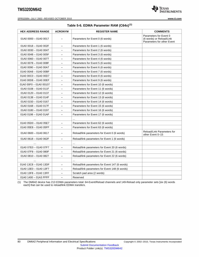
TMS320DM642
SPRS200N–JULY 2002–REVISED OCTOBER 2010 www.ti.com
Table 5-6. EDMA Parameter RAM (C64x) (1)
HEX ADDRESS RANGE ACRONYM REGISTER NAME COMMENTS
Parameters for Event 001A0 0000 – 01A0 0017 – Parameters for Event 0 (6 words) (6 words) or Reload/Link
Parameters for other Event
01A0 0018 – 01A0 002F – Parameters for Event 1 (6 words)
01A0 0030 – 01A0 0047 – Parameters for Event 2 (6 words)
01A0 0048 – 01A0 005F – Parameters for Event 3 (6 words)
01A0 0060 – 01A0 0077 – Parameters for Event 4 (6 words)
01A0 0078 – 01A0 008F – Parameters for Event 5 (6 words)
01A0 0090 – 01A0 00A7 – Parameters for Event 6 (6 words)
01A0 00A8 – 01A0 00BF – Parameters for Event 7 (6 words)
01A0 00C0 – 01A0 00D7 – Parameters for Event 8 (6 words)
01A0 00D8 – 01A0 00EF – Parameters for Event 9 (6 words)
01A0 00F0 – 01A0 00107 – Parameters for Event 10 (6 words)
01A0 0108 – 01A0 011F – Parameters for Event 11 (6 words)
01A0 0120 – 01A0 0137 – Parameters for Event 12 (6 words)
01A0 0138 – 01A0 014F – Parameters for Event 13 (6 words)
01A0 0150 – 01A0 0167 – Parameters for Event 14 (6 words)
01A0 0168 – 01A0 017F – Parameters for Event 15 (6 words)
01A0 0180 – 01A0 0197 – Parameters for Event 16 (6 words)
01A0 0198 – 01A0 01AF – Parameters for Event 17 (6 words)
... ...
01A0 05D0 – 01A0 05E7 – Parameters for Event 62 (6 words)
01A0 05E8 – 01A0 05FF – Parameters for Event 63 (6 words)
Reload/Link Parameters for01A0 0600 – 01A0 0617 – Reload/link parameters for Event 0 (6 words) other Event 0–15
01A0 0618 – 01A0 062F – Reload/link parameters for Event 1 (6 words)
... ...
01A0 07E0 – 01A0 07F7 – Reload/link parameters for Event 20 (6 words)
01A0 07F8 – 01A0 080F – Reload/link parameters for Event 21 (6 words)
01A0 0810 – 01A0 0827 – Reload/link parameters for Event 22 (6 words)
... ...
01A0 13C8 – 01A0 13DF – Reload/link parameters for Event 147 (6 words)
01A0 13E0 – 01A0 13F7 – Reload/link parameters for Event 148 (6 words)
01A0 13F8 – 01A0 13FF – Scratch pad area (2 words)
01A0 1400 – 01A3 FFFF – Reserved
(1) The DM642 device has 213 EDMA parameters total: 64-Event/Reload channels and 149-Reload only parameter sets [six (6) wordseach] that can be used to reload/link EDMA transfers.
80 DM642 Peripheral Information and Electrical Specifications Copyright © 2002–2010, Texas Instruments Incorporated
Submit Documentation FeedbackProduct Folder Link(s): TMS320DM642
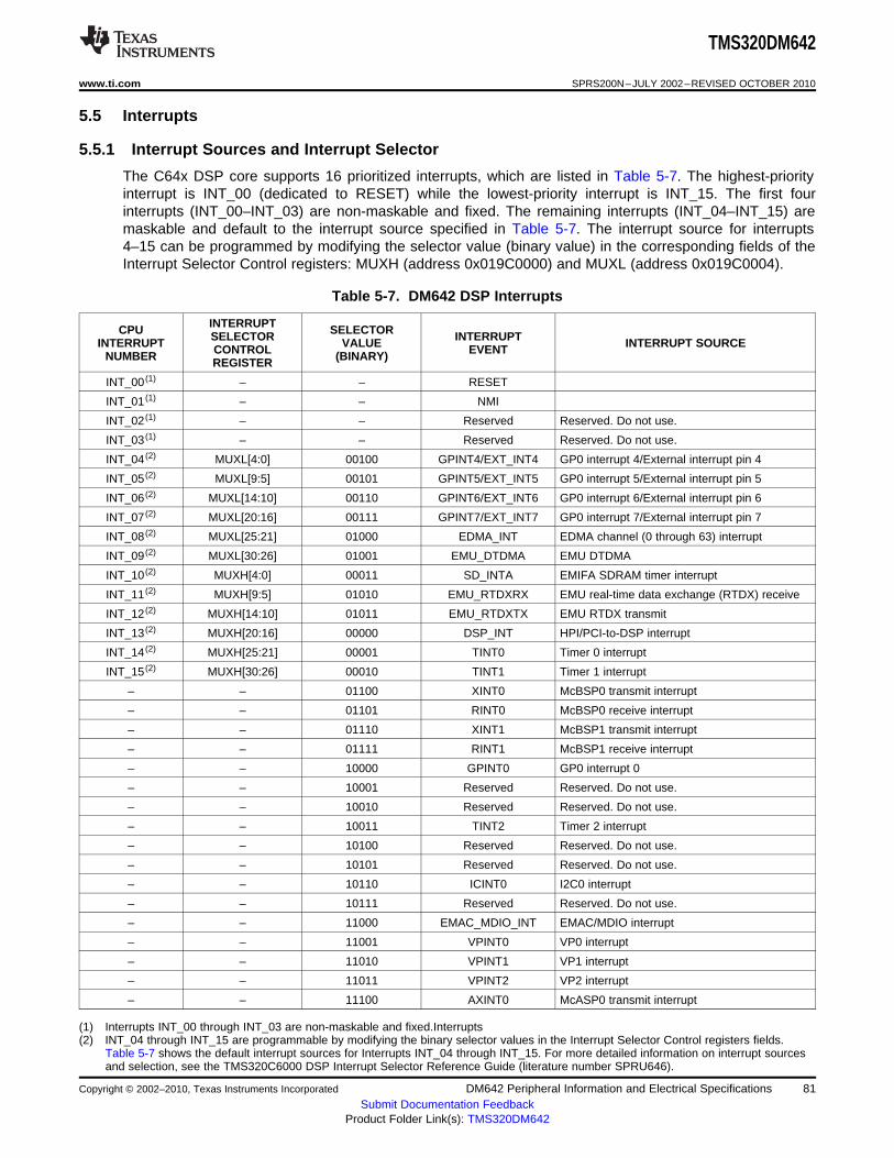
TMS320DM642
www.ti.com SPRS200N–JULY 2002–REVISED OCTOBER 2010
5.5 Interrupts
5.5.1 Interrupt Sources and Interrupt Selector
The C64x DSP core supports 16 prioritized interrupts, which are listed in Table 5-7. The highest-priorityinterrupt is INT_00 (dedicated to RESET) while the lowest-priority interrupt is INT_15. The first fourinterrupts (INT_00–INT_03) are non-maskable and fixed. The remaining interrupts (INT_04–INT_15) aremaskable and default to the interrupt source specified in Table 5-7. The interrupt source for interrupts4–15 can be programmed by modifying the selector value (binary value) in the corresponding fields of theInterrupt Selector Control registers: MUXH (address 0x019C0000) and MUXL (address 0x019C0004).
Table 5-7. DM642 DSP Interrupts
INTERRUPTCPU SELECTORSELECTOR INTERRUPTINTERRUPT VALUE INTERRUPT SOURCECONTROL EVENTNUMBER (BINARY)REGISTER
INT_00 (1) – – RESET
INT_01 (1) – – NMI
INT_02 (1) – – Reserved Reserved. Do not use.
INT_03 (1) – – Reserved Reserved. Do not use.
INT_04 (2) MUXL[4:0] 00100 GPINT4/EXT_INT4 GP0 interrupt 4/External interrupt pin 4
INT_05 (2) MUXL[9:5] 00101 GPINT5/EXT_INT5 GP0 interrupt 5/External interrupt pin 5
INT_06 (2) MUXL[14:10] 00110 GPINT6/EXT_INT6 GP0 interrupt 6/External interrupt pin 6
INT_07 (2) MUXL[20:16] 00111 GPINT7/EXT_INT7 GP0 interrupt 7/External interrupt pin 7
INT_08 (2) MUXL[25:21] 01000 EDMA_INT EDMA channel (0 through 63) interrupt
INT_09 (2) MUXL[30:26] 01001 EMU_DTDMA EMU DTDMA
INT_10 (2) MUXH[4:0] 00011 SD_INTA EMIFA SDRAM timer interrupt
INT_11 (2) MUXH[9:5] 01010 EMU_RTDXRX EMU real-time data exchange (RTDX) receive
INT_12 (2) MUXH[14:10] 01011 EMU_RTDXTX EMU RTDX transmit
INT_13 (2) MUXH[20:16] 00000 DSP_INT HPI/PCI-to-DSP interrupt
INT_14 (2) MUXH[25:21] 00001 TINT0 Timer 0 interrupt
INT_15 (2) MUXH[30:26] 00010 TINT1 Timer 1 interrupt
– – 01100 XINT0 McBSP0 transmit interrupt
– – 01101 RINT0 McBSP0 receive interrupt
– – 01110 XINT1 McBSP1 transmit interrupt
– – 01111 RINT1 McBSP1 receive interrupt
– – 10000 GPINT0 GP0 interrupt 0
– – 10001 Reserved Reserved. Do not use.
– – 10010 Reserved Reserved. Do not use.
– – 10011 TINT2 Timer 2 interrupt
– – 10100 Reserved Reserved. Do not use.
– – 10101 Reserved Reserved. Do not use.
– – 10110 ICINT0 I2C0 interrupt
– – 10111 Reserved Reserved. Do not use.
– – 11000 EMAC_MDIO_INT EMAC/MDIO interrupt
– – 11001 VPINT0 VP0 interrupt
– – 11010 VPINT1 VP1 interrupt
– – 11011 VPINT2 VP2 interrupt
– – 11100 AXINT0 McASP0 transmit interrupt
(1) Interrupts INT_00 through INT_03 are non-maskable and fixed.Interrupts(2) INT_04 through INT_15 are programmable by modifying the binary selector values in the Interrupt Selector Control registers fields.
Table 5-7 shows the default interrupt sources for Interrupts INT_04 through INT_15. For more detailed information on interrupt sourcesand selection, see the TMS320C6000 DSP Interrupt Selector Reference Guide (literature number SPRU646).
Copyright © 2002–2010, Texas Instruments Incorporated DM642 Peripheral Information and Electrical Specifications 81Submit Documentation Feedback
Product Folder Link(s): TMS320DM642
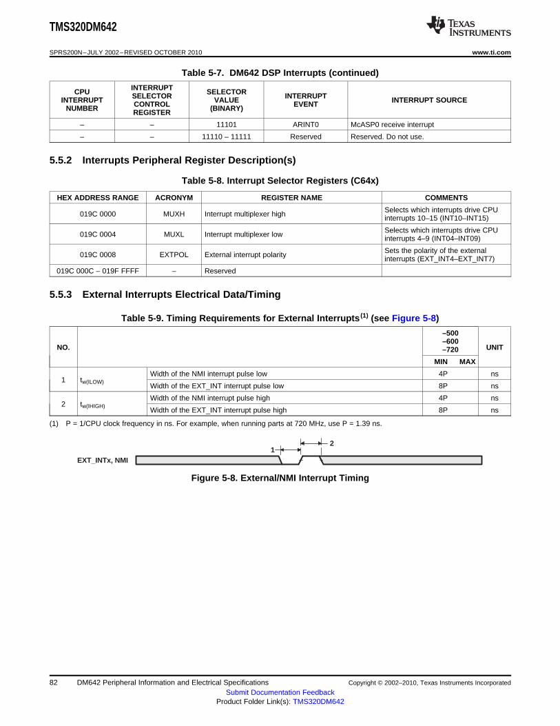
21
EXT_INTx, NMI
TMS320DM642
SPRS200N–JULY 2002–REVISED OCTOBER 2010 www.ti.com
Table 5-7. DM642 DSP Interrupts (continued)
INTERRUPTCPU SELECTORSELECTOR INTERRUPTINTERRUPT VALUE INTERRUPT SOURCECONTROL EVENTNUMBER (BINARY)REGISTER
– – 11101 ARINT0 McASP0 receive interrupt
– – 11110 – 11111 Reserved Reserved. Do not use.
5.5.2 Interrupts Peripheral Register Description(s)
Table 5-8. Interrupt Selector Registers (C64x)
HEX ADDRESS RANGE ACRONYM REGISTER NAME COMMENTS
Selects which interrupts drive CPU019C 0000 MUXH Interrupt multiplexer high interrupts 10–15 (INT10–INT15)
Selects which interrupts drive CPU019C 0004 MUXL Interrupt multiplexer low interrupts 4–9 (INT04–INT09)
Sets the polarity of the external019C 0008 EXTPOL External interrupt polarity interrupts (EXT_INT4–EXT_INT7)
019C 000C – 019F FFFF – Reserved
5.5.3 External Interrupts Electrical Data/Timing
Table 5-9. Timing Requirements for External Interrupts (1) (see Figure 5-8)
–500–600
NO. UNIT–720
MIN MAX
Width of the NMI interrupt pulse low 4P ns1 tw(ILOW)
Width of the EXT_INT interrupt pulse low 8P ns
Width of the NMI interrupt pulse high 4P ns2 tw(IHIGH)
Width of the EXT_INT interrupt pulse high 8P ns
(1) P = 1/CPU clock frequency in ns. For example, when running parts at 720 MHz, use P = 1.39 ns.
Figure 5-8. External/NMI Interrupt Timing
82 DM642 Peripheral Information and Electrical Specifications Copyright © 2002–2010, Texas Instruments Incorporated
Submit Documentation FeedbackProduct Folder Link(s): TMS320DM642
TMS320DM642
www.ti.com SPRS200N–JULY 2002–REVISED OCTOBER 2010
5.6 Reset
A hardware reset (RESET) is required to place the DSP into a known good state out of power-up. TheRESET signal can be asserted (pulled low) prior to ramping the core and I/O voltages or after the coreand I/O voltages have reached their proper operating conditions. As a best practice, reset should be heldlow during power-up. Prior to deasserting RESET (low-to-high transition), the core and I/O voltages shouldbe at their proper operating conditions and CLKIN should also be running at the correct frequency. WhenPCI is enabled, the PCI input clock (PCLK) must be running prior to deasserting RESET as well.
When the PCI peripheral is enabled, a WARMRESET can be performed via the host. A WARMRESETperforms the same functionality as a hardware reset, but does not relatch the boot configuration pins.Whatever boot configuration that was latched on the previous hardware reset will be performed during theWARMRESET.
A hardware reset does not reset the PCI peripheral state machine. The PCI state machine is reset via thePRST signal. The PRST signal does not affect the DSP.
Emulation resets, done using Code Composer Studio™ IDE, have the same affect as a PCIWARMRESET.
For information on peripheral selection at the rising edge of RESET, see the Device Configuration sectionof this data manual.
5.6.1 Reset Electrical Data/Timing
Table 5-10. Timing Requirements for Reset (see Figure 5-9)
–500–600
NO. UNIT–720
MIN MAX
1 tw(RST) Width of the RESET pulse 250 µs
16 tsu(boot) Setup time, boot configuration bits valid before RESET high (1) 4E or 4C (2) ns
17 th(boot) Hold time, boot configuration bits valid after RESET high (1) 4P (3) ns
18 tsu(PCLK-RSTH) Setup time, PCLK active before RESET high (4) 32N ns
(1) AEA[22:19], LENDIAN, PCIEEAI, and HD5/AD5 are the boot configuration pins during device reset.(2) E = 1/AECLKIN clock frequency in ns. C = 1/CLKIN clock frequency in ns.
Select the MIN parameter value, whichever value is larger.(3) P = 1/CPU clock frequency in ns. For example, when running parts at 720 MHz, use P = 1.39 ns.(4) N = the PCI input clock (PCLK) period in ns. When PCI is enabled (PCI_EN = 1), this parameter must be met.
Copyright © 2002–2010, Texas Instruments Incorporated DM642 Peripheral Information and Electrical Specifications 83Submit Documentation Feedback
Product Folder Link(s): TMS320DM642
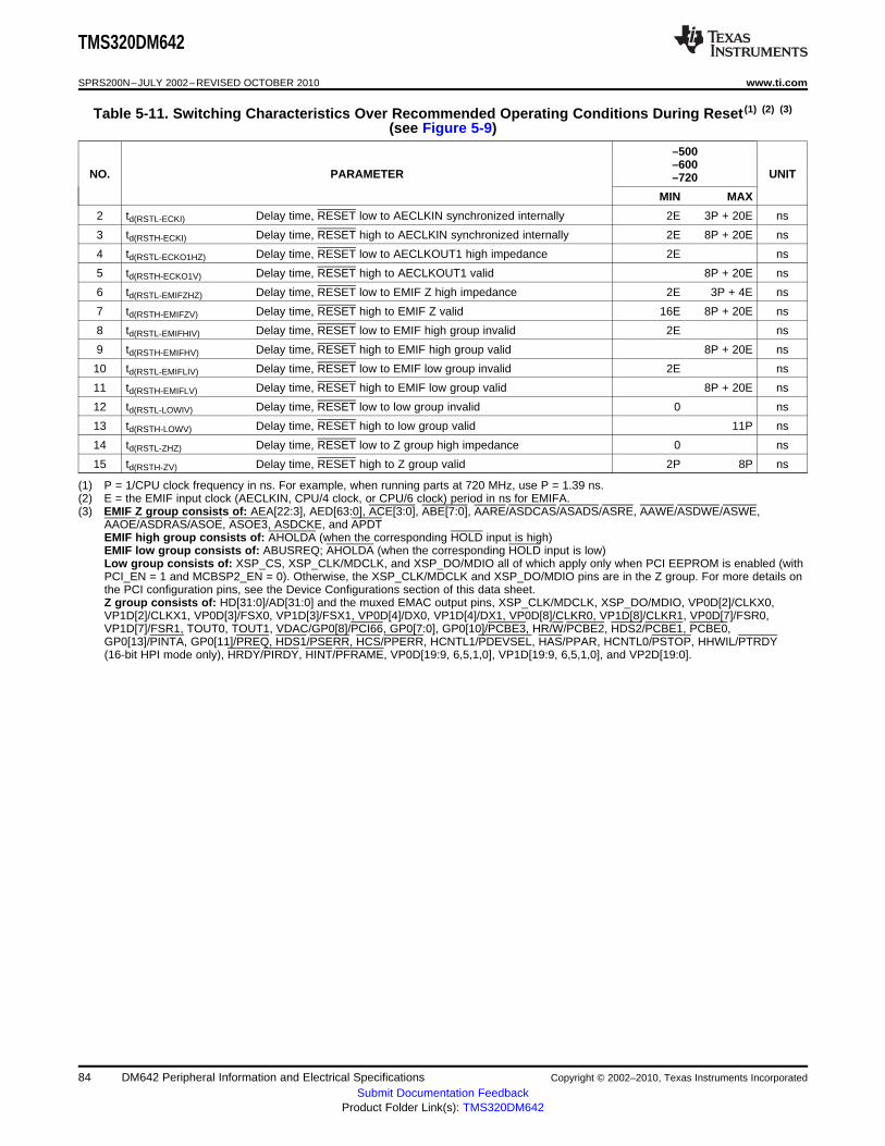
TMS320DM642
SPRS200N–JULY 2002–REVISED OCTOBER 2010 www.ti.com
Table 5-11. Switching Characteristics Over Recommended Operating Conditions During Reset (1) (2) (3)
(see Figure 5-9)
–500–600
NO. PARAMETER UNIT–720
MIN MAX
2 td(RSTL-ECKI) Delay time, RESET low to AECLKIN synchronized internally 2E 3P + 20E ns
3 td(RSTH-ECKI) Delay time, RESET high to AECLKIN synchronized internally 2E 8P + 20E ns
4 td(RSTL-ECKO1HZ) Delay time, RESET low to AECLKOUT1 high impedance 2E ns
5 td(RSTH-ECKO1V) Delay time, RESET high to AECLKOUT1 valid 8P + 20E ns
6 td(RSTL-EMIFZHZ) Delay time, RESET low to EMIF Z high impedance 2E 3P + 4E ns
7 td(RSTH-EMIFZV) Delay time, RESET high to EMIF Z valid 16E 8P + 20E ns
8 td(RSTL-EMIFHIV) Delay time, RESET low to EMIF high group invalid 2E ns
9 td(RSTH-EMIFHV) Delay time, RESET high to EMIF high group valid 8P + 20E ns
10 td(RSTL-EMIFLIV) Delay time, RESET low to EMIF low group invalid 2E ns
11 td(RSTH-EMIFLV) Delay time, RESET high to EMIF low group valid 8P + 20E ns
12 td(RSTL-LOWIV) Delay time, RESET low to low group invalid 0 ns
13 td(RSTH-LOWV) Delay time, RESET high to low group valid 11P ns
14 td(RSTL-ZHZ) Delay time, RESET low to Z group high impedance 0 ns
15 td(RSTH-ZV) Delay time, RESET high to Z group valid 2P 8P ns
(1) P = 1/CPU clock frequency in ns. For example, when running parts at 720 MHz, use P = 1.39 ns.(2) E = the EMIF input clock (AECLKIN, CPU/4 clock, or CPU/6 clock) period in ns for EMIFA.(3) EMIF Z group consists of: AEA[22:3], AED[63:0], ACE[3:0], ABE[7:0], AARE/ASDCAS/ASADS/ASRE, AAWE/ASDWE/ASWE,
AAOE/ASDRAS/ASOE, ASOE3, ASDCKE, and APDTEMIF high group consists of: AHOLDA (when the corresponding HOLD input is high)EMIF low group consists of: ABUSREQ; AHOLDA (when the corresponding HOLD input is low)Low group consists of: XSP_CS, XSP_CLK/MDCLK, and XSP_DO/MDIO all of which apply only when PCI EEPROM is enabled (withPCI_EN = 1 and MCBSP2_EN = 0). Otherwise, the XSP_CLK/MDCLK and XSP_DO/MDIO pins are in the Z group. For more details onthe PCI configuration pins, see the Device Configurations section of this data sheet.Z group consists of: HD[31:0]/AD[31:0] and the muxed EMAC output pins, XSP_CLK/MDCLK, XSP_DO/MDIO, VP0D[2]/CLKX0,VP1D[2]/CLKX1, VP0D[3]/FSX0, VP1D[3]/FSX1, VP0D[4]/DX0, VP1D[4]/DX1, VP0D[8]/CLKR0, VP1D[8]/CLKR1, VP0D[7]/FSR0,VP1D[7]/FSR1, TOUT0, TOUT1, VDAC/GP0[8]/PCI66, GP0[7:0], GP0[10]/PCBE3, HR/W/PCBE2, HDS2/PCBE1, PCBE0,GP0[13]/PINTA, GP0[11]/PREQ, HDS1/PSERR, HCS/PPERR, HCNTL1/PDEVSEL, HAS/PPAR, HCNTL0/PSTOP, HHWIL/PTRDY(16-bit HPI mode only), HRDY/PIRDY, HINT/PFRAME, VP0D[19:9, 6,5,1,0], VP1D[19:9, 6,5,1,0], and VP2D[19:0].
84 DM642 Peripheral Information and Electrical Specifications Copyright © 2002–2010, Texas Instruments Incorporated
Submit Documentation FeedbackProduct Folder Link(s): TMS320DM642

AECLKOUT2
17
14
1
CLKOUT4
CLKOUT6
RESET
AECLKIN
Boot and DeviceConfiguration Inputs (C)
16
15
32
10
8
11
9
76
1312
AECLKOUT1
54
PCLK
18
Low Group (A)
Z Group (A)(B)
EMIF Z Group (A)(B)
EMIF High Group (A)
EMIF Low Group (A)
TMS320DM642
www.ti.com SPRS200N–JULY 2002–REVISED OCTOBER 2010
A. EMIF Z group consists of: AEA[22:3], AED[63:0], ACE[3:0], ABE[7:0], AARE/ASDCAS/ASADS/ASRE,AAWE/ASDWE/ASWE, AAOE/ASDRAS/ASOE, ASOE3, ASDCKE, and APDTEMIF high group consists of: AHOLDA (when the corresponding HOLD input is high)EMIF low group consists of: ABUSREQ; AHOLDA (when the corresponding HOLD input is low)Low group consists of: XSP_CS, XSP_CLK/MDCLK, and XSP_DO/MDIO all of which apply only when PCIEEPROM is enabled (with PCI_EN = 1 and MCBSP2_EN = 0). Otherwise, the XSP_CLK/MDCLK andXSP_DO/MDIO pins are in the Z group. For more details on the PCI configuration pins, see the Device Configurationssection of this data sheet.Z group consists of: HD[31:0]/AD[31:0] and the muxed EMAC output pins, XSP_CLK/MDCLK, XSP_DO/MDIO,VP0D[2]/CLKX0, VP1D[2]/CLKX1, VP0D[3]/FSX0, VP1D[3]/FSX1, VP0D[4]/DX0, VP1D[4]/DX1, VP0D[8]/CLKR0,VP1D[8]/CLKR1, VP0D[7]/FSR0, VP1D[7]/FSR1, TOUT0, TOUT1, VDAC/GP0[8]/PCI66, GP0[7:0], GP0[10]/PCBE3,HR/W/PCBE2, HDS2/PCBE1, PCBE0, GP0[13]/PINTA, GP0[11]/PREQ, HDS1/PSERR, HCS/PPERR,HCNTL1/PDEVSEL, HAS/PPAR, HCNTL0/PSTOP, HHWIL/PTRDY (16-bit HPI mode only), HRDY/PIRDY,HINT/PFRAME, VP0D[19:9, 6,5,1,0], VP1D[19:9, 6,5,1,0], and VP2D[19:0].
B. If AEA[22:19], LENDIAN, PCIEEAI, and HD5/AD5 pins are actively driven, care must be taken to ensure no timingcontention between parameters 6, 7, 14, 15, 16, and 17.
C. Boot and Device Configurations Inputs (during reset) include: AEA[22:19], LENDIAN, PCIEEAI, and HD5/AD5.The PCI_EN pin must be driven valid at all times and the user must not switch values throughout device operation.
Figure 5-9. Reset Timing
Copyright © 2002–2010, Texas Instruments Incorporated DM642 Peripheral Information and Electrical Specifications 85Submit Documentation Feedback
Product Folder Link(s): TMS320DM642
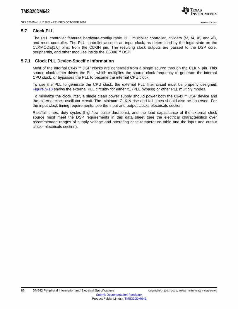
TMS320DM642
SPRS200N–JULY 2002–REVISED OCTOBER 2010 www.ti.com
5.7 Clock PLL
The PLL controller features hardware-configurable PLL multiplier controller, dividers (/2, /4, /6, and /8),and reset controller. The PLL controller accepts an input clock, as determined by the logic state on theCLKMODE[1:0] pins, from the CLKIN pin. The resulting clock outputs are passed to the DSP core,peripherals, and other modules inside the C6000™ DSP.
5.7.1 Clock PLL Device-Specific Information
Most of the internal C64x™ DSP clocks are generated from a single source through the CLKIN pin. Thissource clock either drives the PLL, which multiplies the source clock frequency to generate the internalCPU clock, or bypasses the PLL to become the internal CPU clock.
To use the PLL to generate the CPU clock, the external PLL filter circuit must be properly designed.Figure 5-10 shows the external PLL circuitry for either x1 (PLL bypass) or other PLL multiply modes.
To minimize the clock jitter, a single clean power supply should power both the C64x™ DSP device andthe external clock oscillator circuit. The minimum CLKIN rise and fall times should also be observed. Forthe input clock timing requirements, see the input and output clocks electricals section.
Rise/fall times, duty cycles (high/low pulse durations), and the load capacitance of the external clocksource must meet the DSP requirements in this data sheet (see the electrical characteristics overrecommended ranges of supply voltage and operating case temperature table and the input and outputclocks electricals section).
86 DM642 Peripheral Information and Electrical Specifications Copyright © 2002–2010, Texas Instruments Incorporated
Submit Documentation FeedbackProduct Folder Link(s): TMS320DM642

PLLMULT
1
0
PLLCLK
CLKMODE0
CLKMODE1
CLKIN
C2C1EMIfilter
3.3 V
/2
/8
/4
/6
00 01 10
CPU Clock
Peripheral Bus, EDMA
Clock
Timer Internal Clock
CLKOUT4, Peripheral Clock
(AUXCLK for McASP),
McBSP Internal Clock
CLKOUT6
/2
/4
EMIF 00 01 10 EK2RATE(GBLCTL.[19,18])
ECLKOUT2ECLKOUT1
PLLx6, x12
10 µF 0.1 µF
AEA[20:19]
Internal to DM642
PLLV
ECLKIN
TMS320DM642
www.ti.com SPRS200N–JULY 2002–REVISED OCTOBER 2010
(For the PLL Options, CLKMODE Pins Setup, and PLL Clock Frequency Ranges, see the "TMS320DMA642PLL Multiply Factor Options, Clock Frequency Ranges, and Typical Lock Time" table.)
A. Place all PLL external components (C1, C2, and the EMI Filter as close to the C6000 DSP device as possible. For thebest performance, TI recommends that all the PLL external components be on a single side of the board withoutjumpers, switches, or components other than the ones shown.
B. For reduced PLL jitter, maximize the spacing between switching signals and the PLL external components (C1, C2,and the EMI Filter).
C. The 3.3-V supply for the EMI filter must be from the same 3.3-V power plane supplying the I/O voltage, DVDD.D. EMI filter manufacturer TDK part number ACF451832-333, -233, -153, -103. Panasonic part number EXCCET103U.
Figure 5-10. External PLL Circuitry for Either PLL Multiply Modes or x1 (Bypass) Mode
Copyright © 2002–2010, Texas Instruments Incorporated DM642 Peripheral Information and Electrical Specifications 87Submit Documentation Feedback
Product Folder Link(s): TMS320DM642

TMS320DM642
SPRS200N–JULY 2002–REVISED OCTOBER 2010 www.ti.com
Table 5-12. TMS320DM642 PLL Multiply Factor Options, Clock Frequency Ranges,and Typical Lock Time (1) (2)
GDK and ZDK PACKAGES – 23 x 23 mm BGA,GNZ and ZNZ PACKAGES – 27 x 27 mm BGA
CLKMODE CLKIN CPU CLOCK TYPICALCLKOUT4 CLKOUT6CLKMODE1 CLKMODE0 (PLL MULTIPLY RANGE FREQUENCY LOCK TIMERANGE (MHz) RANGE (MHz)FACTORS) (MHz) RANGE (MHz) (µs) (3)
0 0 Bypass (x1) 30–75 30–75 7.5–18.8 5–12.5 N/A
0 1 x6 30–75 180–450 45–112.5 30–7575
1 0 x12 30–50 360–600 90–150 60–100
1 1 Reserved – – – – –
(1) These clock frequency range values are applicable to a DM642-600 speed device. For –500 and -720 device speed values, see theCLKIN timing requirements table for the specific device speed.
(2) Use external pullup resistors on the CLKMODE pins (CLKMODE1 and CLKMODE0) to set the DM642 device to one of the valid PLLmultiply clock modes (x6 or x12). With internal pulldown resistors on the CLKMODE pins (CLKMODE1, CLKMODE0), the default clockmode is x1 (bypass).
(3) Under some operating conditions, the maximum PLL lock time may vary by as much as 150% from the specified typical value. Forexample, if the typical lock time is specified as 100 µs, the maximum value may be as long as 250 µs.
5.7.2 Clock PLL Electrical Data/Timing (Input and Output Clocks)
Table 5-13. Timing Requirements for CLKIN for –500 Devices (1) (2) (3) (see Figure 5-11)
–500
NO. PLL MODE x12 PLL MODE x6 x1 (Bypass) UNIT
MIN MAX MIN MAX MIN MAX
1 tc(CLKIN) Cycle time, CLKIN 24 33.3 13.3 33.3 13.3 33.3 ns
2 tw(CLKINH) Pulse duration, CLKIN high 0.45C 0.45C 0.45C ns
3 tw(CLKINL) Pulse duration, CLKIN low 0.45C 0.45C 0.45C ns
4 tt(CLKIN) Transition time, CLKIN 5 5 1 ns
5 tJ(CLKIN) Period jitter, CLKIN 0.02C 0.02C 0.02C ns
(1) The reference points for the rise and fall transitions are measured at VIL MAX and VIH MIN.(2) For more details on the PLL multiplier factors (x6, x12), see the Clock PLL section of this data sheet.(3) C = CLKIN cycle time in ns. For example, when CLKIN frequency is 50 MHz, use C = 20 ns.
Table 5-14. Timing Requirements for CLKIN for –600 Devices (1) (2) (3) (see Figure 5-11)
–600
NO. PLL MODE x12 PLL MODE x6 x1 (Bypass) UNIT
MIN MAX MIN MAX MIN MAX
1 tc(CLKIN) Cycle time, CLKIN 20 33.3 13.3 33.3 13.3 33.3 ns
2 tw(CLKINH) Pulse duration, CLKIN high 0.45C 0.45C 0.45C ns
3 tw(CLKINL) Pulse duration, CLKIN low 0.45C 0.45C 0.45C ns
4 tt(CLKIN) Transition time, CLKIN 5 5 1 ns
5 tJ(CLKIN) Period jitter, CLKIN 0.02C 0.02C 0.02C ns
(1) The reference points for the rise and fall transitions are measured at VIL MAX and VIH MIN.(2) For more details on the PLL multiplier factors (x6, x12), see the Clock PLL section of this data sheet.(3) C = CLKIN cycle time in ns. For example, when CLKIN frequency is 50 MHz, use C = 20 ns.
88 DM642 Peripheral Information and Electrical Specifications Copyright © 2002–2010, Texas Instruments Incorporated
Submit Documentation FeedbackProduct Folder Link(s): TMS320DM642
CLKIN
2
3
4
4
5 1
CLKOUT4
1
2
3
3
TMS320DM642
www.ti.com SPRS200N–JULY 2002–REVISED OCTOBER 2010
Table 5-15. Timing Requirements for CLKIN for –720 Devices (1) (2) (3) (see Figure 5-11)
–720
NO. PLL MODE x12 PLL MODE x6 x1 (Bypass) UNIT
MIN MAX MIN MAX MIN MAX
1 tc(CLKIN) Cycle time, CLKIN 16.6 33.3 13.3 33.3 13.3 33.3 ns
2 tw(CLKINH) Pulse duration, CLKIN high 0.45C 0.45C 0.45C ns
3 tw(CLKINL) Pulse duration, CLKIN low 0.45C 0.45C 0.45C ns
4 tt(CLKIN) Transition time, CLKIN 5 5 1 ns
5 tJ(CLKIN) Period jitter, CLKIN 0.02C 0.02C 0.02C ns
(1) The reference points for the rise and fall transitions are measured at VIL MAX and VIH MIN.(2) For more details on the PLL multiplier factors (x6, x12), see the Clock PLL section of this data sheet.(3) C = CLKIN cycle time in ns. For example, when CLKIN frequency is 50 MHz, use C = 20 ns.
Figure 5-11. CLKIN Timing
Table 5-16. Switching Characteristics Over Recommended Operating Conditions for CLKOUT4 (1) (2) (3)
(see Figure 5-12)
–500–600–720NO. PARAMETER UNIT
CLKMODE = x1, x6, x12
MIN MAX
1 tw(CKO4H) Pulse duration, CLKOUT4 high 2P – 0.7 2P + 0.7 ns
2 tw(CKO4L) Pulse duration, CLKOUT4 low 2P – 0.7 2P + 0.7 ns
3 tt(CKO4) Transition time, CLKOUT4 1 ns
(1) The reference points for the rise and fall transitions are measured at VOL MAX and VOH MIN.(2) PH is the high period of CLKIN in ns and PL is the low period of CLKIN in ns.(3) P = 1/CPU clock frequency in nanoseconds (ns)
Figure 5-12. CLKOUT4 Timing
Copyright © 2002–2010, Texas Instruments Incorporated DM642 Peripheral Information and Electrical Specifications 89Submit Documentation Feedback
Product Folder Link(s): TMS320DM642

CLKOUT6
1
2
3
3
AECLKIN
2
3
4
4
5 1
TMS320DM642
SPRS200N–JULY 2002–REVISED OCTOBER 2010 www.ti.com
Table 5-17. Switching Characteristics Over Recommended Operating Conditions for CLKOUT6 (1) (2) (3)
(see Figure 5-13)
–500–600–720NO. PARAMETER UNIT
CLKMODE = x1, x6, x12
MIN MAX
1 tw(CKO6H) Pulse duration, CLKOUT6 high 3P – 0.7 3P + 0.7 ns
2 tw(CKO6L) Pulse duration, CLKOUT6 low 3P – 0.7 3P + 0.7 ns
3 tt(CKO6) Transition time, CLKOUT6 1 ns
(1) The reference points for the rise and fall transitions are measured at VOL MAX and VOH MIN.(2) PH is the high period of CLKIN in ns and PL is the low period of CLKIN in ns.(3) P = 1/CPU clock frequency in nanoseconds (ns)
Figure 5-13. CLKOUT6 Timing
Table 5-18. Timing Requirements for AECLKIN for EMIFA (1) (2) (3) (see Figure 5-14)
–500–600
NO. UNIT–720
MIN MAX
1 tc(EKI) Cycle time, AECLKIN 6 (4) 16P ns
2 tw(EKIH) Pulse duration, AECLKIN high 2.7 ns
3 tw(EKIL) Pulse duration, AECLKIN low 2.7 ns
4 tt(EKI) Transition time, AECLKIN 3 ns
5 tJ(EKI) Period jitter, AECLKIN 0.02E ns
(1) P = 1/CPU clock frequency in ns. For example, when running parts at 720 MHz, use P = 1.39 ns.(2) The reference points for the rise and fall transitions are measured at VIL MAX and VIH MIN.(3) E = the EMIF input clock (AECLKIN, CPU/4 clock, or CPU/6 clock) period in ns for EMIFA.(4) Minimum AECLKIN cycle times must be met, even when AECLKIN is generated by an internal clock source. Minimum AECLKIN times
are based on internal logic speed; the maximum useable speed of the EMIF may be lower due to AC timing requirements. On the 600and 720 devices, 133-MHz operation is achievable if the requirements of the EMIF Device Speed section are met. On the 500 devices,100-MHz operation is achievable if the requirements of the EMIF Device Speed section are met.
Figure 5-14. AECLKIN Timing for EMIFA
90 DM642 Peripheral Information and Electrical Specifications Copyright © 2002–2010, Texas Instruments Incorporated
Submit Documentation FeedbackProduct Folder Link(s): TMS320DM642

45
12
AECLKIN
AECLKOUT1
3 3
45
12
AECLKIN
AECLKOUT2
3 3
TMS320DM642
www.ti.com SPRS200N–JULY 2002–REVISED OCTOBER 2010
Table 5-19. Switching Characteristics Over Recommended Operating Conditions for AECLKOUT1 for theEMIFA Module (1) (2) (3) (see Figure 5-15)
–500–600
NO. PARAMETER UNIT–720
MIN MAX
1 tw(EKO1H) Pulse duration, AECLKOUT1 high EH – 0.7 EH + 0.7 ns
2 tw(EKO1L) Pulse duration, AECLKOUT1 low EL – 0.7 EL + 0.7 ns
3 tt(EKO1) Transition time, AECLKOUT1 1 ns
4 td(EKIH-EKO1H) Delay time, AECLKIN high to AECLKOUT1 high 1 8 ns
5 td(EKIL-EKO1L) Delay time, AECLKIN low to AECLKOUT1 low 1 8 ns
(1) E = the EMIF input clock (AECLKIN, CPU/4 clock, or CPU/6 clock) period in ns for EMIFA.(2) The reference points for the rise and fall transitions are measured at VOL MAX and VOH MIN.(3) EH is the high period of E (EMIF input clock period) in ns and EL is the low period of E (EMIF input clock period) in ns for EMIFA.
Figure 5-15. AECLKOUT1 Timing for the EMIFA Module
Table 5-20. Switching Characteristics Over Recommended Operating Conditions for AECLKOUT2 for theEMIFA Module (1) (2) (see Figure 5-16)
–500–600
NO. PARAMETER UNIT–720
MIN MAX
1 tw(EKO2H) Pulse duration, AECLKOUT2 high 0.5NE – 0.7 0.5NE + 0.7 ns
2 tw(EKO2L) Pulse duration, AECLKOUT2 low 0.5NE – 0.7 0.5NE + 0.7 ns
3 tt(EKO2) Transition time, AECLKOUT2 1 ns
4 td(EKIH-EKO2H) Delay time, AECLKIN high to AECLKOUT2 high 1 8 ns
5 td(EKIL-EKO2L) Delay time, AECLKIN low to AECLKOUT2 low 1 8 ns
(1) The reference points for the rise and fall transitions are measured at VOL MAX and VOH MIN.(2) E = the EMIF input clock (AECLKIN, CPU/4 clock, or CPU/6 clock) period in ns for EMIFA. N = the EMIF input clock divider; N = 1, 2,
or 4.
Figure 5-16. AECLKOUT2 Timing for the EMIFA Module
Copyright © 2002–2010, Texas Instruments Incorporated DM642 Peripheral Information and Electrical Specifications 91Submit Documentation Feedback
Product Folder Link(s): TMS320DM642
TMS320DM642
SPRS200N–JULY 2002–REVISED OCTOBER 2010 www.ti.com
5.8 External Memory Interface (EMIF)
EMIF supports a glueless interface to a variety of external devices, including:• Pipelined synchronous-burst SRAM (SBSRAM)• Synchronous DRAM (SDRAM)• Asynchronous devices, including SRAM, ROM, and FIFOs• An external shared-memory device
5.8.1 EMIF Device-Specific Information
EMIF Device Speed
The rated EMIF speed of these devices only applies to the SDRAM interface when in a system that meetsthe following requirements:• 1 chip-enable (CE) space (maximum of 2 chips) of SDRAM connected to EMIF• up to 1 CE space of buffers connected to EMIF• EMIF trace lengths between 1 and 3 inches• 166-MHz SDRAM for 133-MHz operation• 143-MHz SDRAM for 100-MHz operation
Other configurations may be possible, but timing analysis must be done to verify all AC timings are met.Verification of AC timings is mandatory when using configurations other than those specified above. TIrecommends utilizing I/O buffer information specification (IBIS) to analyze all AC timings.
To properly use IBIS models to attain accurate timing analysis for a given system, see the Using IBISModels for Timing Analysis application report (literature number SPRA839).
To maintain signal integrity, serial termination resistors should be inserted into all EMIF output signal lines(see the Terminal Functions table for the EMIF output signals).
For more detailed information on the DM642 EMIF peripheral, see the TMS320C6000 DSP ExternalMemory Interface (EMIF) Reference Guide (literature number SPRU266).
92 DM642 Peripheral Information and Electrical Specifications Copyright © 2002–2010, Texas Instruments Incorporated
Submit Documentation FeedbackProduct Folder Link(s): TMS320DM642

TMS320DM642
www.ti.com SPRS200N–JULY 2002–REVISED OCTOBER 2010
5.8.2 EMIF Peripheral Register Description(s)
Table 5-21. EMIFA Registers
HEX ADDRESS RANGE ACRONYM REGISTER NAME COMMENTS
0180 0000 GBLCTL EMIFA global control
0180 0004 CECTL1 EMIFA CE1 space control
0180 0008 CECTL0 EMIFA CE0 space control
0180 000C – Reserved
0180 0010 CECTL2 EMIFA CE2 space control
0180 0014 CECTL3 EMIFA CE3 space control
0180 0018 SDCTL EMIFA SDRAM control
0180 001C SDTIM EMIFA SDRAM refresh control
0180 0020 SDEXT EMIFA SDRAM extension
0180 0024 – 0180 003C – Reserved
0180 0040 PDTCTL Peripheral device transfer (PDT) control
0180 0044 CESEC1 EMIFA CE1 space secondary control
0180 0048 CESEC0 EMIFA CE0 space secondary control
0180 004C – Reserved
0180 0050 CESEC2 EMIFA CE2 space secondary control
0180 0054 CESEC3 EMIFA CE3 space secondary control
0180 0058 – 0183 FFFF – Reserved
5.8.3 EMIF Electrical Data/Timing
5.8.3.1 Asynchronous Memory Timing
Table 5-22. Timing Requirements for Asynchronous Memory Cycles for EMIFA Module (1) (2)
(see Figure 5-17 and Figure 5-18)
–500–600
NO. UNIT–720
MIN MAX
3 tsu(EDV-AREH) Setup time, AEDx valid before AARE high 6.5 ns
4 th(AREH-EDV) Hold time, AEDx valid after AARE high 1 ns
6 tsu(ARDY-EKO1H) Setup time, AARDY valid before AECLKOUTx high 3 ns
7 th(EKO1H-ARDY) Hold time, AARDY valid after AECLKOUTx high 2.5 ns
(1) To ensure data setup time, simply program the strobe width wide enough. AARDY is internally synchronized. The AARDY signal is onlyrecognized two cycles before the end of the programmed strobe time and while AARDY is low, the strobe time is extendedcycle-by-cycle. When AARDY is recognized low, the end of the strobe time is two cycles after AARDY is recognized high. To useAARDY as an asynchronous input, the pulse width of the AARDY signal should be wide enough (e.g., pulse width = 2E) to ensure setupand hold time is met.
(2) RS = Read setup, RST = Read strobe, RH = Read hold, WS = Write setup, WST = Write strobe, WH = Write hold. These parametersare programmed via the EMIF CE space control registers.
Copyright © 2002–2010, Texas Instruments Incorporated DM642 Peripheral Information and Electrical Specifications 93Submit Documentation Feedback
Product Folder Link(s): TMS320DM642

77
66
Setup = 2 Strobe = 3 Not Ready Hold = 2
BE
Address
1
1
1
1
5
4
AARDY
5
AECLKOUTx
ACEx
AEA[22:3]
AED[63:0]
AAOE/ASDRAS/ASOE (A)
AARE/ASDCAS/ASADS/ASRE (A)
ABE[7:0]
AAWE/ASDWE/ASWE (A)
2
2
2
2
3
Read Data
TMS320DM642
SPRS200N–JULY 2002–REVISED OCTOBER 2010 www.ti.com
Table 5-23. Switching Characteristics Over Recommended Operating Conditions for AsynchronousMemory Cycles for EMIFA Module (1) (2) (3) (see Figure 5-17 and Figure 5-18)
–500–600
NO. PARAMETER UNIT–720
MIN MAX
1 tosu(SELV-AREL) Output setup time, select signals valid to AARE low RS * E – 1.8 ns
2 toh(AREH-SELIV) Output hold time, AARE high to select signals invalid RH * E – 1.9 ns
5 td(EKO1H-AREV) Delay time, AECLKOUTx high to AARE valid 1 7 ns
8 tosu(SELV-AWEL) Output setup time, select signals valid to AAWE low WS * E – 2.0 ns
9 toh(AWEH-SELIV) Output hold time, AAWE high to select signals invalid WH * E – 2.5 ns
10 td(EKO1H-AWEV) Delay time, AECLKOUTx high to AAWE valid 1.3 7.1 ns
(1) RS = Read setup, RST = Read strobe, RH = Read hold, WS = Write setup, WST = Write strobe, WH = Write hold. These parametersare programmed via the EMIF CE space control registers.
(2) E = AECLKOUT1 period in ns for EMIFA(3) Select signals for EMIFA include: ACEx, ABE[7:0], AEA[22:3], AAOE; and for EMIFA writes, include AED[63:0].
A. AAOE/ASDRAS/ASOE, AARE/ASDCAS/ASADS/ASRE, and AAWE/ASDWE/ASWE operate as AAOE (identifiedunder select signals), AARE, and AAWE, respectively, during asynchronous memory accesses.
Figure 5-17. Asynchronous Memory Read Timing for EMIFA
94 DM642 Peripheral Information and Electrical Specifications Copyright © 2002–2010, Texas Instruments Incorporated
Submit Documentation FeedbackProduct Folder Link(s): TMS320DM642

Setup = 2 Strobe = 3 Not Ready Hold = 2
BE
Address
Write Data
1010
8
8
8
8
7766
AECLKOUTx
ACEx
AEA[22:3]
AED[63:0]
ABE[7:0]
AARDY
AAOE/ASDRAS/ASOE (A)
AARE/ASDCAS/ASADS/ASRE (A)
AAWE/ASDWE/ASWE (A)
9
9
9
9
TMS320DM642
www.ti.com SPRS200N–JULY 2002–REVISED OCTOBER 2010
A. AAOE/ASDRAS/ASOE, AARE/ASDCAS/ASADS/ASRE, and AAWE/ASDWE/ASWE operate as AAOE (identifiedunder select signals), AARE, and AAWE, respectively, during asynchronous memory accesses.
Figure 5-18. Asynchronous Memory Write Timing for EMIFA
Copyright © 2002–2010, Texas Instruments Incorporated DM642 Peripheral Information and Electrical Specifications 95Submit Documentation Feedback
Product Folder Link(s): TMS320DM642
TMS320DM642
SPRS200N–JULY 2002–REVISED OCTOBER 2010 www.ti.com
5.8.3.2 Programmable Synchronous Interface Timing
Table 5-24. Timing Requirements for Programmable Synchronous Interface Cycles for EMIFA Module(see Figure 5-19)
–600–500, A-600 –720NO. UNITMIN MAX MIN MAX
6 tsu(EDV-EKOxH) Setup time, read AEDx valid before AECLKOUTx high 3.1 2 ns
7 th(EKOxH-EDV) Hold time, read AEDx valid after AECLKOUTx high 1.8 1.5 ns
Table 5-25. Switching Characteristics Over Recommended Operating Conditions for ProgrammableSynchronous Interface Cycles for EMIFA Module (1) (see Figure 5-19–Figure 5-21)
–600–500, A-600 –720NO. PARAMETER UNITMIN MAX MIN MAX
1 td(EKOxH-CEV) Delay time, AECLKOUTx high to ACEx valid 1.1 6.4 1.1 4.9 ns
2 td(EKOxH-BEV) Delay time, AECLKOUTx high to ABEx valid 6.4 4.9 ns
3 td(EKOxH-BEIV) Delay time, AECLKOUTx high to ABEx invalid 1.1 1.1 ns
4 td(EKOxH-EAV) Delay time, AECLKOUTx high to AEAx valid 6.4 4.9 ns
5 td(EKOxH-EAIV) Delay time, AECLKOUTx high to AEAx invalid 1.1 1.1 ns
8 td(EKOxH-ADSV) Delay time, AECLKOUTx high to ASADS/ASRE valid 1.1 6.4 1.1 4.9 ns
9 td(EKOxH-OEV) Delay time, AECLKOUTx high to ASOE valid 1.1 6.4 1.1 4.9 ns
10 td(EKOxH-EDV) Delay time, AECLKOUTx high to AEDx valid 6.4 4.9 ns
11 td(EKOxH-EDIV) Delay time, AECLKOUTx high to AEDx invalid 1.1 1.1 ns
12 td(EKOxH-WEV) Delay time, AECLKOUTx high to ASWE valid 1.1 6.4 1.1 4.9 ns
(1) The following parameters are programmable via the EMIF CE Space Secondary Control register (CExSEC):• Read latency (SYNCRL): 0-, 1-, 2-, or 3-cycle read latency• Write latency (SYNCWL): 0-, 1-, 2-, or 3-cycle write latency• ACEx assertion length (CEEXT): For standard SBSRAM or ZBT SRAM interface, ACEx goes inactive after the final command has
been issued (CEEXT = 0). For synchronous FIFO interface with glue, ACEx is active when ASOE is active (CEEXT = 1).• Function of ASADS/ASRE (RENEN): For standard SBSRAM or ZBT SRAM interface, ASADS/ASRE acts as ASADS with deselect
cycles (RENEN = 0). For FIFO interface, ASADS/ASRE acts as ASRE with NO deselect cycles (RENEN = 1).• Synchronization clock (SNCCLK): Synchronized to AECLKOUT1 or AECLKOUT2
96 DM642 Peripheral Information and Electrical Specifications Copyright © 2002–2010, Texas Instruments Incorporated
Submit Documentation FeedbackProduct Folder Link(s): TMS320DM642
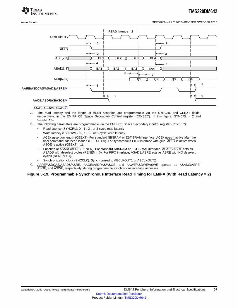
AECLKOUTx
ACEx
ABE[7:0]
AEA[22:3]
AED[63:0]
AARE/ASDCAS/ASADS/ASRE (C)
AAOE/ASDRAS/ASOE (C)
AAWE/ASDWE/ASWE (C)
BE1 BE2 BE3 BE4
Q1 Q2 Q3 Q4
9
1
4 5
8
9
67
3
1
2BE1 BE2 BE3 BE4
EA1 EA2 EA4
8
READ latency = 2
EA3
TMS320DM642
www.ti.com SPRS200N–JULY 2002–REVISED OCTOBER 2010
A. The read latency and the length of ACEx assertion are programmable via the SYNCRL and CEEXT fields,respectively, in the EMIFA CE Space Secondary Control register (CExSEC). In this figure, SYNCRL = 2 andCEEXT = 0.
B. The following parameters are programmable via the EMIF CE Space Secondary Control register (CExSEC):• Read latency (SYNCRL): 0-, 1-, 2-, or 3-cycle read latency• Write latency (SYNCWL): 0-, 1-, 2-, or 3-cycle write latency• ACEx assertion length (CEEXT): For standard SBSRAM or ZBT SRAM interface, ACEx goes inactive after the
final command has been issued (CEEXT = 0). For synchronous FIFO interface with glue, ACEx is active whenASOE is active (CEEXT = 1).
• Function of ASADS/ASRE (RENEN): For standard SBSRAM or ZBT SRAM interface, ASADS/ASRE acts asASADS with deselect cycles (RENEN = 0). For FIFO interface, ASADS/ASRE acts as ASRE with NO deselectcycles (RENEN = 1).
• Synchronization clock (SNCCLK): Synchronized to AECLKOUT1 or AECLKOUT2C. AARE/ASDCAS/ASADS/ASRE, AAOE/ASDRAS/ASOE, and AAWE/ASDWE/ASWE operate as ASADS/ASRE,
ASOE, and ASWE, respectively, during programmable synchronous interface accesses.
Figure 5-19. Programmable Synchronous Interface Read Timing for EMIFA (With Read Latency = 2)
Copyright © 2002–2010, Texas Instruments Incorporated DM642 Peripheral Information and Electrical Specifications 97Submit Documentation Feedback
Product Folder Link(s): TMS320DM642

AECLKOUTx
ACEx
ABE[7:0]
AEA[22:3]
AED[63:0]
AARE/ASDCAS/ASADS/ASRE (C)
AAOE/ASDRAS/ASOE (C)
AAWE/ASDWE/ASWE (C)
BE1 BE2 BE3 BE4
Q1 Q2 Q3 Q4
12
11
3
1
12
10
4
2
1
8
5
8
EA1 EA2 EA3 EA410
TMS320DM642
SPRS200N–JULY 2002–REVISED OCTOBER 2010 www.ti.com
A. The write latency and the length of ACEx assertion are programmable via the SYNCWL and CEEXT fields,respectively, in the EMIFA CE Space Secondary Control register (CExSEC). In this figure, SYNCWL = 0 andCEEXT = 0.
B. The following parameters are programmable via the EMIF CE Space Secondary Control register (CExSEC):• Read latency (SYNCRL): 0-, 1-, 2-, or 3-cycle read latency• Write latency (SYNCWL): 0-, 1-, 2-, or 3-cycle write latency• ACEx assertion length (CEEXT): For standard SBSRAM or ZBT SRAM interface, ACEx goes inactive after the
final command has been issued (CEEXT = 0). For synchronous FIFO interface with glue, ACEx is active whenASOE is active (CEEXT = 1).
• Function of ASADS/ASRE (RENEN): For standard SBSRAM or ZBT SRAM interface, ASADS/ASRE acts asASADS with deselect cycles (RENEN = 0). For FIFO interface, ASADS/ASRE acts as ASRE with NO deselectcycles (RENEN = 1).
• Synchronization clock (SNCCLK): Synchronized to AECLKOUT1 or AECLKOUT2C. AARE/ASDCAS/ASADS/ASRE, AAOE/ASDRAS/ASOE, and AAWE/ASDWE/ASWE operate as ASADS/ASRE,
ASOE, and ASWE, respectively, during programmable synchronous interface accesses.
Figure 5-20. Programmable Synchronous Interface Write Timing for EMIFA (With Write Latency = 0)
98 DM642 Peripheral Information and Electrical Specifications Copyright © 2002–2010, Texas Instruments Incorporated
Submit Documentation FeedbackProduct Folder Link(s): TMS320DM642
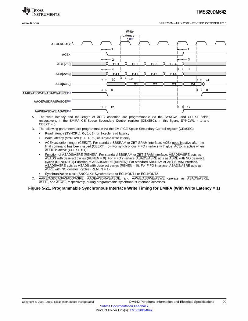
AECLKOUTx
ACEx
ABE[7:0]
AEA[22:3]
AED[63:0]
AARE/ASDCAS/ASADS/ASRE (C)
AAOE/ASDRAS/ASOE (C)
AAWE/ASDWE/ASWE (C)
BE1 BE2 BE3 BE4
Q1 Q2 Q311
3
12
10
4
2
1
8
5
8
EA1 EA2 EA3 EA410
WriteLatency =
1 (B)
1
Q4
12
TMS320DM642
www.ti.com SPRS200N–JULY 2002–REVISED OCTOBER 2010
A. The write latency and the length of ACEx assertion are programmable via the SYNCWL and CEEXT fields,respectively, in the EMIFA CE Space Secondary Control register (CExSEC). In this figure, SYNCWL = 1 andCEEXT = 0.
B. The following parameters are programmable via the EMIF CE Space Secondary Control register (CExSEC):• Read latency (SYNCRL): 0-, 1-, 2-, or 3-cycle read latency• Write latency (SYNCWL): 0-, 1-, 2-, or 3-cycle write latency• ACEx assertion length (CEEXT): For standard SBSRAM or ZBT SRAM interface, ACEx goes inactive after the
final command has been issued (CEEXT = 0). For synchronous FIFO interface with glue, ACEx is active whenASOE is active (CEEXT = 1).
• Function of ASADS/ASRE (RENEN): For standard SBSRAM or ZBT SRAM interface, ASADS/ASRE acts asASADS with deselect cycles (RENEN = 0). For FIFO interface, ASADS/ASRE acts as ASRE with NO deselectcycles (RENEN = 1).Function of ASADS/ASRE (RENEN): For standard SBSRAM or ZBT SRAM interface,ASADS/ASRE acts as ASADS with deselect cycles (RENEN = 0). For FIFO interface, ASADS/ASRE acts asASRE with NO deselect cycles (RENEN = 1).
• Synchronization clock (SNCCLK): Synchronized to ECLKOUT1 or ECLKOUT2C. AARE/ASDCAS/ASADS/ASRE, AAOE/ASDRAS/ASOE, and AAWE/ASDWE/ASWE operate as ASADS/ASRE,
ASOE, and ASWE, respectively, during programmable synchronous interface accesses.
Figure 5-21. Programmable Synchronous Interface Write Timing for EMIFA (With Write Latency = 1)
Copyright © 2002–2010, Texas Instruments Incorporated DM642 Peripheral Information and Electrical Specifications 99Submit Documentation Feedback
Product Folder Link(s): TMS320DM642

TMS320DM642
SPRS200N–JULY 2002–REVISED OCTOBER 2010 www.ti.com
5.8.3.3 Synchronous DRAM Timing
Table 5-26. Timing Requirements for Synchronous DRAM Cycles for EMIFA Module (see Figure 5-22)
–600–500, A-600 –720NO. UNITMIN MAX MIN MAX
6 tsu(EDV-EKO1H) Setup time, read AEDx valid before AECLKOUTx high 2.1 0.6 ns
7 th(EKO1H-EDV) Hold time, read AEDx valid after AECLKOUTx high 2.8 2.1 ns
Table 5-27. Switching Characteristics Over Recommended Operating Conditions for Synchronous DRAMCycles for EMIFA Module (see Figure 5-22–Figure 5-29)
–600–500, A-600 –720NO. PARAMETER UNITMIN MAX MIN MAX
1 td(EKO1H-CEV) Delay time, AECLKOUTx high to ACEx valid 1.3 6.4 1.3 4.9 ns
2 td(EKO1H-BEV) Delay time, AECLKOUTx high to ABEx valid 6.4 4.9 ns
3 td(EKO1H-BEIV) Delay time, AECLKOUTx high to ABEx invalid 1.3 1.3 ns
4 td(EKO1H-EAV) Delay time, AECLKOUTx high to AEAx valid 6.4 4.9 ns
5 td(EKO1H-EAIV) Delay time, AECLKOUTx high to AEAx invalid 1.3 1.3 ns
8 td(EKO1H-CASV) Delay time, AECLKOUTx high to ASDCAS valid 1.3 6.4 1.3 4.9 ns
9 td(EKO1H-EDV) Delay time, AECLKOUTx high to AEDx valid 6.4 4.9 ns
10 td(EKO1H-EDIV) Delay time, AECLKOUTx high to AEDx invalid 1.3 1.3 ns
11 td(EKO1H-WEV) Delay time, AECLKOUTx high to ASDWE valid 1.3 6.4 1.3 4.9 ns
12 td(EKO1H-RAS) Delay time, AECLKOUTx high to ASDRAS valid 1.3 6.4 1.3 4.9 ns
13 td(EKO1H-ACKEV) Delay time, AECLKOUTx high to ASDCKE valid 1.3 6.4 1.3 4.9 ns
14 td(EKO1H-PDTV) Delay time, AECLKOUTx high to APDT valid 1.3 6.4 1.3 4.9 ns
100 DM642 Peripheral Information and Electrical Specifications Copyright © 2002–2010, Texas Instruments Incorporated
Submit Documentation FeedbackProduct Folder Link(s): TMS320DM642

AECLKOUTx
ACEx
ABE[7:0]
AEA[12:3]
AED[63:0]
AEA13
AAOE/ASDRAS/ASOE (A)
AARE/ASDCAS/ASADS/ASRE (A)
AAWE/ASDWE/ASWE (A)
AEA[22:14]
BE1 BE2 BE3 BE4
Bank
Column
D1 D2 D3 D4
8
76
5
5
5
1
32
8
4
4
4
1
READ
APDT (B)1414
TMS320DM642
www.ti.com SPRS200N–JULY 2002–REVISED OCTOBER 2010
A. AARE/ASDCAS/ASADS/ASRE, AAWE/ASDWE/ASWE, and AAOE/ASDRAS/ASOE operate as ASDCAS, ASDWE,and ASDRAS, respectively, during SDRAM accesses.
B. APDT signal is only asserted when the EDMA is in PDT mode (set the PDTS bit to 1 in the EDMA options parameterRAM). For APDT read, data is not latched into EMIF. The PDTRL field in the PDT control register (PDTCTL)configures the latency of the APDT signal with respect to the data phase of a read transaction. The latency of theAPDT signal for a read can be programmed to 0, 1, 2, or 3 by setting PDTRL to 00, 01, 10, or 11, respectively.PDTRL equals 00 (zero latency) in Figure 5-22.
Figure 5-22. SDRAM Read Command (CAS Latency 3) for EMIFA
Copyright © 2002–2010, Texas Instruments Incorporated DM642 Peripheral Information and Electrical Specifications 101Submit Documentation Feedback
Product Folder Link(s): TMS320DM642
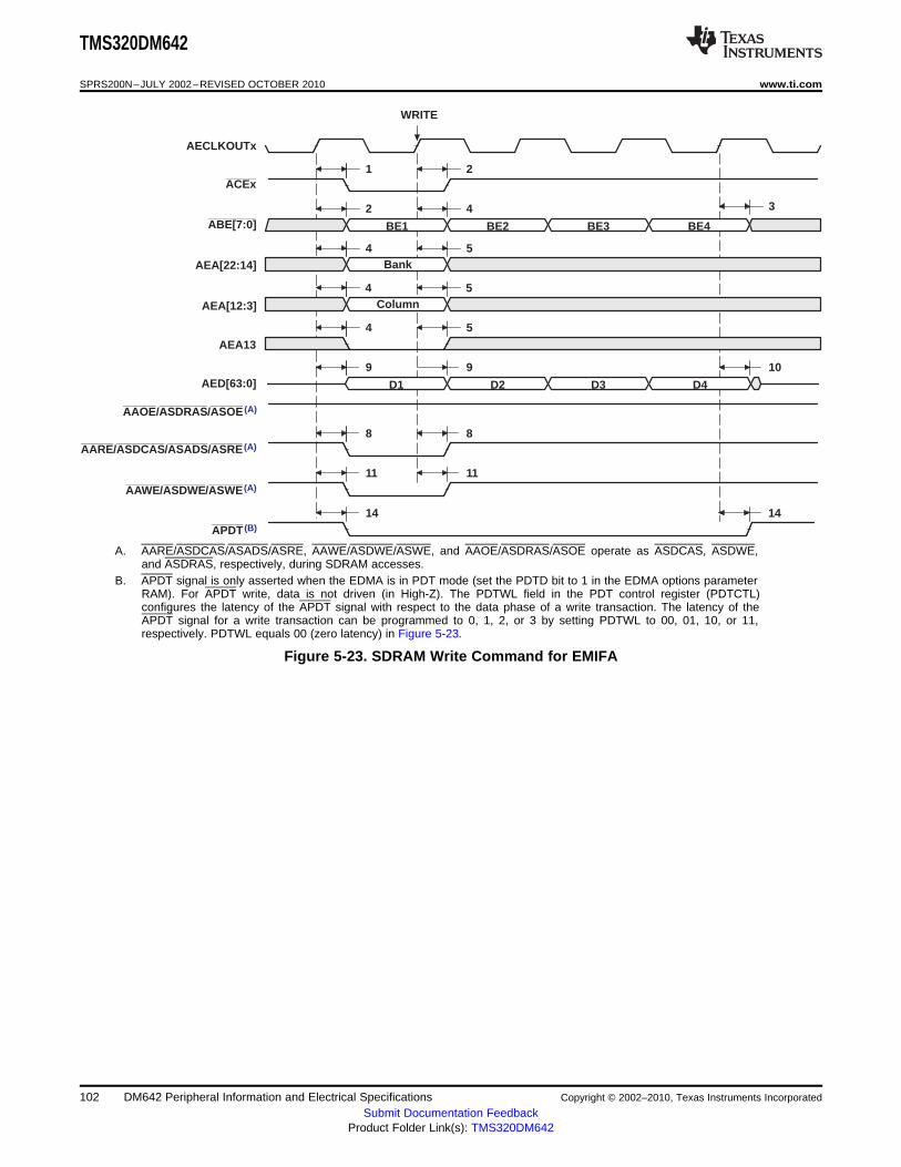
AECLKOUTx
ACEx
ABE[7:0]
AEA[12:3]
AED[63:0]
AAOE/ASDRAS/ASOE (A)
AARE/ASDCAS/ASADS/ASRE (A)
AAWE/ASDWE/ASWE (A)
AEA13
AEA[22:14]
BE1 BE2 BE3 BE4
Bank
Column
D1 D2 D3 D4
11
8
9
5
5
5
4
2
11
8
9
4
4
2
1
10
3
4
WRITE
APDT (B)
1414
TMS320DM642
SPRS200N–JULY 2002–REVISED OCTOBER 2010 www.ti.com
A. AARE/ASDCAS/ASADS/ASRE, AAWE/ASDWE/ASWE, and AAOE/ASDRAS/ASOE operate as ASDCAS, ASDWE,and ASDRAS, respectively, during SDRAM accesses.
B. APDT signal is only asserted when the EDMA is in PDT mode (set the PDTD bit to 1 in the EDMA options parameterRAM). For APDT write, data is not driven (in High-Z). The PDTWL field in the PDT control register (PDTCTL)configures the latency of the APDT signal with respect to the data phase of a write transaction. The latency of theAPDT signal for a write transaction can be programmed to 0, 1, 2, or 3 by setting PDTWL to 00, 01, 10, or 11,respectively. PDTWL equals 00 (zero latency) in Figure 5-23.
Figure 5-23. SDRAM Write Command for EMIFA
102 DM642 Peripheral Information and Electrical Specifications Copyright © 2002–2010, Texas Instruments Incorporated
Submit Documentation FeedbackProduct Folder Link(s): TMS320DM642
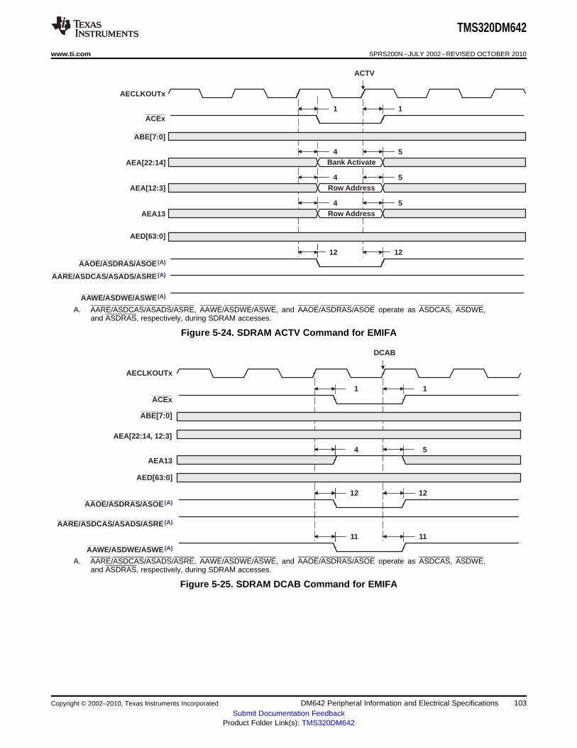
AECLKOUTx
ACEx
ABE[7:0]
AEA[22:14]
AED[63:0]
AEA13
AAOE/ASDRAS/ASOE (A)
AARE/ASDCAS/ASADS/ASRE (A)
AAWE/ASDWE/ASWE (A)
Bank Activate
Row Address
Row Address
12
5
5
5
1
AEA[12:3]
ACTV
12
4
4
4
1
AECLKOUTx
ACEx
ABE[7:0]
AEA[22:14, 12:3]
AED[63:0]
AEA13
AAOE/ASDRAS/ASOE (A)
AARE/ASDCAS/ASADS/ASRE (A)
AAWE/ASDWE/ASWE (A)
11
12
5
1
DCAB
11
12
4
1
TMS320DM642
www.ti.com SPRS200N–JULY 2002–REVISED OCTOBER 2010
A. AARE/ASDCAS/ASADS/ASRE, AAWE/ASDWE/ASWE, and AAOE/ASDRAS/ASOE operate as ASDCAS, ASDWE,and ASDRAS, respectively, during SDRAM accesses.
Figure 5-24. SDRAM ACTV Command for EMIFA
A. AARE/ASDCAS/ASADS/ASRE, AAWE/ASDWE/ASWE, and AAOE/ASDRAS/ASOE operate as ASDCAS, ASDWE,and ASDRAS, respectively, during SDRAM accesses.
Figure 5-25. SDRAM DCAB Command for EMIFA
Copyright © 2002–2010, Texas Instruments Incorporated DM642 Peripheral Information and Electrical Specifications 103Submit Documentation Feedback
Product Folder Link(s): TMS320DM642
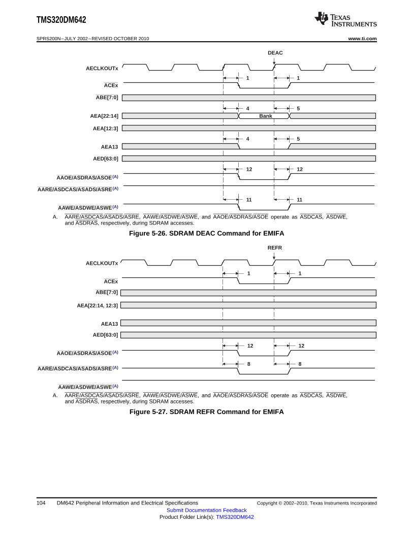
AECLKOUTx
ACEx
ABE[7:0]
AEA[22:14]
AED[63:0]
AEA13
AAOE/ASDRAS/ASOE (A)
AARE/ASDCAS/ASADS/ASRE (A)
AAWE/ASDWE/ASWE (A)
AEA[12:3]
Bank
11
12
5
5
1
DEAC
11
12
4
4
1
AECLKOUTx
ACEx
ABE[7:0]
AEA[22:14, 12:3]
AED[63:0]
AEA13
AAOE/ASDRAS/ASOE (A)
AARE/ASDCAS/ASADS/ASRE (A)
AAWE/ASDWE/ASWE (A)
8
12
1
REFR
8
12
1
TMS320DM642
SPRS200N–JULY 2002–REVISED OCTOBER 2010 www.ti.com
A. AARE/ASDCAS/ASADS/ASRE, AAWE/ASDWE/ASWE, and AAOE/ASDRAS/ASOE operate as ASDCAS, ASDWE,and ASDRAS, respectively, during SDRAM accesses.
Figure 5-26. SDRAM DEAC Command for EMIFA
A. AARE/ASDCAS/ASADS/ASRE, AAWE/ASDWE/ASWE, and AAOE/ASDRAS/ASOE operate as ASDCAS, ASDWE,and ASDRAS, respectively, during SDRAM accesses.
Figure 5-27. SDRAM REFR Command for EMIFA
104 DM642 Peripheral Information and Electrical Specifications Copyright © 2002–2010, Texas Instruments Incorporated
Submit Documentation FeedbackProduct Folder Link(s): TMS320DM642

AECLKOUTx
ACEx
ABE[7:0]
AEA[22:3]
AED[63:0]
AAOE/ASDRAS/ASOE (A)
AARE/ASDCAS/ASADS/ASRE (A)
AAWE/ASDWE/ASWE (A)
MRS value
11
8
12
5
1
MRS
11
8
12
4
1
End Self-RefreshSelf Refresh
1313
AECLKOUTx
ACEx
ABE[7:0]
AEA[22:14, 12:3]
AEA13
AED[63:0]
AAOE/ASDRAS/ASOE (A)
AAWE/ASDWE/ASWE (A)
ASDCKE
≥ TRAS cycles
AARE/ASDCAS/ASADS/ASRE (A)
TMS320DM642
www.ti.com SPRS200N–JULY 2002–REVISED OCTOBER 2010
A. AARE/ASDCAS/ASADS/ASRE, AAWE/ASDWE/ASWE, and AAOE/ASDRAS/ASOE operate as ASDCAS, ASDWE,and ASDRAS, respectively, during SDRAM accesses.
Figure 5-28. SDRAM MRS Command for EMIFA
A. AARE/ASDCAS/ASADS/ASRE, AAWE/ASDWE/ASWE, and AAOE/ASDRAS/ASOE operate as ASDCAS, ASDWE,and ASDRAS, respectively, during SDRAM accesses.
Figure 5-29. SDRAM Self-Refresh Timing for EMIFA
Copyright © 2002–2010, Texas Instruments Incorporated DM642 Peripheral Information and Electrical Specifications 105Submit Documentation Feedback
Product Folder Link(s): TMS320DM642
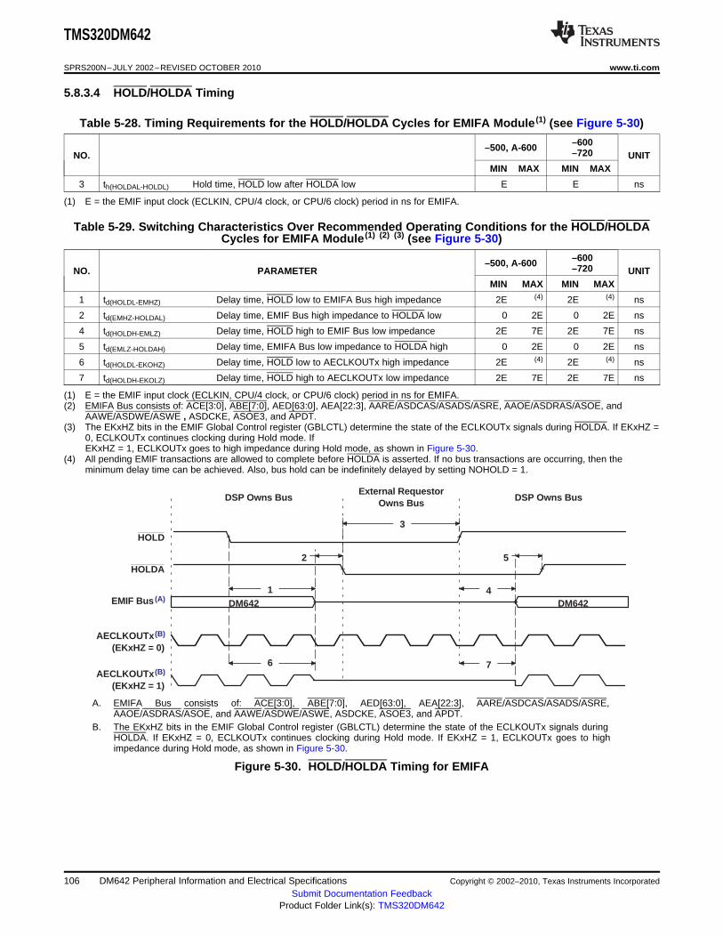
HOLD
HOLDA
EMIF Bus (A)
DSP Owns BusExternal Requestor
Owns BusDSP Owns Bus
DM642 DM6421
3
2 5
4
AECLKOUTx(B)
(EKxHZ = 0)
AECLKOUTx(B)
(EKxHZ = 1)
6 7
TMS320DM642
SPRS200N–JULY 2002–REVISED OCTOBER 2010 www.ti.com
5.8.3.4 HOLD/HOLDA Timing
Table 5-28. Timing Requirements for the HOLD/HOLDA Cycles for EMIFA Module (1) (see Figure 5-30)
–600–500, A-600 –720NO. UNITMIN MAX MIN MAX
3 th(HOLDAL-HOLDL) Hold time, HOLD low after HOLDA low E E ns
(1) E = the EMIF input clock (ECLKIN, CPU/4 clock, or CPU/6 clock) period in ns for EMIFA.
Table 5-29. Switching Characteristics Over Recommended Operating Conditions for the HOLD/HOLDACycles for EMIFA Module (1) (2) (3) (see Figure 5-30)
–600–500, A-600 –720NO. PARAMETER UNITMIN MAX MIN MAX
1 td(HOLDL-EMHZ) Delay time, HOLD low to EMIFA Bus high impedance 2E (4) 2E (4) ns
2 td(EMHZ-HOLDAL) Delay time, EMIF Bus high impedance to HOLDA low 0 2E 0 2E ns
4 td(HOLDH-EMLZ) Delay time, HOLD high to EMIF Bus low impedance 2E 7E 2E 7E ns
5 td(EMLZ-HOLDAH) Delay time, EMIFA Bus low impedance to HOLDA high 0 2E 0 2E ns
6 td(HOLDL-EKOHZ) Delay time, HOLD low to AECLKOUTx high impedance 2E (4) 2E (4) ns
7 td(HOLDH-EKOLZ) Delay time, HOLD high to AECLKOUTx low impedance 2E 7E 2E 7E ns
(1) E = the EMIF input clock (ECLKIN, CPU/4 clock, or CPU/6 clock) period in ns for EMIFA.(2) EMIFA Bus consists of: ACE[3:0], ABE[7:0], AED[63:0], AEA[22:3], AARE/ASDCAS/ASADS/ASRE, AAOE/ASDRAS/ASOE, and
AAWE/ASDWE/ASWE , ASDCKE, ASOE3, and APDT.(3) The EKxHZ bits in the EMIF Global Control register (GBLCTL) determine the state of the ECLKOUTx signals during HOLDA. If EKxHZ =
0, ECLKOUTx continues clocking during Hold mode. IfEKxHZ = 1, ECLKOUTx goes to high impedance during Hold mode, as shown in Figure 5-30.
(4) All pending EMIF transactions are allowed to complete before HOLDA is asserted. If no bus transactions are occurring, then theminimum delay time can be achieved. Also, bus hold can be indefinitely delayed by setting NOHOLD = 1.
A. EMIFA Bus consists of: ACE[3:0], ABE[7:0], AED[63:0], AEA[22:3], AARE/ASDCAS/ASADS/ASRE,AAOE/ASDRAS/ASOE, and AAWE/ASDWE/ASWE, ASDCKE, ASOE3, and APDT.
B. The EKxHZ bits in the EMIF Global Control register (GBLCTL) determine the state of the ECLKOUTx signals duringHOLDA. If EKxHZ = 0, ECLKOUTx continues clocking during Hold mode. If EKxHZ = 1, ECLKOUTx goes to highimpedance during Hold mode, as shown in Figure 5-30.
Figure 5-30. HOLD/HOLDA Timing for EMIFA
106 DM642 Peripheral Information and Electrical Specifications Copyright © 2002–2010, Texas Instruments Incorporated
Submit Documentation FeedbackProduct Folder Link(s): TMS320DM642
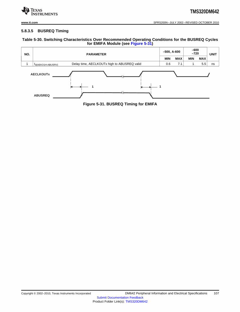
AECLKOUTx
1
ABUSREQ
1
TMS320DM642
www.ti.com SPRS200N–JULY 2002–REVISED OCTOBER 2010
5.8.3.5 BUSREQ Timing
Table 5-30. Switching Characteristics Over Recommended Operating Conditions for the BUSREQ Cyclesfor EMIFA Module (see Figure 5-31)
–600–500, A-600 –720NO. PARAMETER UNITMIN MAX MIN MAX
1 td(AEKO1H-ABUSRV) Delay time, AECLKOUTx high to ABUSREQ valid 0.6 7.1 1 5.5 ns
Figure 5-31. BUSREQ Timing for EMIFA
Copyright © 2002–2010, Texas Instruments Incorporated DM642 Peripheral Information and Electrical Specifications 107Submit Documentation Feedback
Product Folder Link(s): TMS320DM642
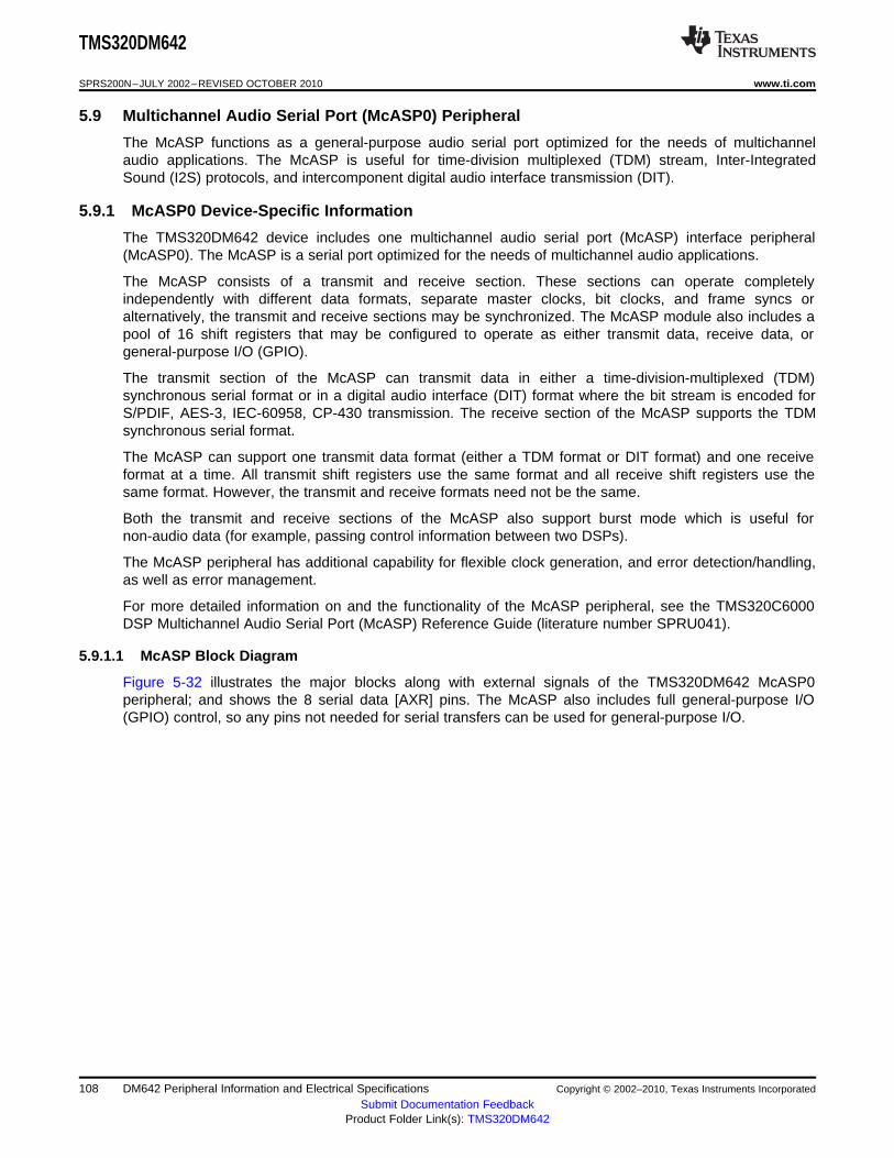
TMS320DM642
SPRS200N–JULY 2002–REVISED OCTOBER 2010 www.ti.com
5.9 Multichannel Audio Serial Port (McASP0) Peripheral
The McASP functions as a general-purpose audio serial port optimized for the needs of multichannelaudio applications. The McASP is useful for time-division multiplexed (TDM) stream, Inter-IntegratedSound (I2S) protocols, and intercomponent digital audio interface transmission (DIT).
5.9.1 McASP0 Device-Specific Information
The TMS320DM642 device includes one multichannel audio serial port (McASP) interface peripheral(McASP0). The McASP is a serial port optimized for the needs of multichannel audio applications.
The McASP consists of a transmit and receive section. These sections can operate completelyindependently with different data formats, separate master clocks, bit clocks, and frame syncs oralternatively, the transmit and receive sections may be synchronized. The McASP module also includes apool of 16 shift registers that may be configured to operate as either transmit data, receive data, orgeneral-purpose I/O (GPIO).
The transmit section of the McASP can transmit data in either a time-division-multiplexed (TDM)synchronous serial format or in a digital audio interface (DIT) format where the bit stream is encoded forS/PDIF, AES-3, IEC-60958, CP-430 transmission. The receive section of the McASP supports the TDMsynchronous serial format.
The McASP can support one transmit data format (either a TDM format or DIT format) and one receiveformat at a time. All transmit shift registers use the same format and all receive shift registers use thesame format. However, the transmit and receive formats need not be the same.
Both the transmit and receive sections of the McASP also support burst mode which is useful fornon-audio data (for example, passing control information between two DSPs).
The McASP peripheral has additional capability for flexible clock generation, and error detection/handling,as well as error management.
For more detailed information on and the functionality of the McASP peripheral, see the TMS320C6000DSP Multichannel Audio Serial Port (McASP) Reference Guide (literature number SPRU041).
5.9.1.1 McASP Block Diagram
Figure 5-32 illustrates the major blocks along with external signals of the TMS320DM642 McASP0peripheral; and shows the 8 serial data [AXR] pins. The McASP also includes full general-purpose I/O(GPIO) control, so any pins not needed for serial transfers can be used for general-purpose I/O.
108 DM642 Peripheral Information and Electrical Specifications Copyright © 2002–2010, Texas Instruments Incorporated
Submit Documentation FeedbackProduct Folder Link(s): TMS320DM642
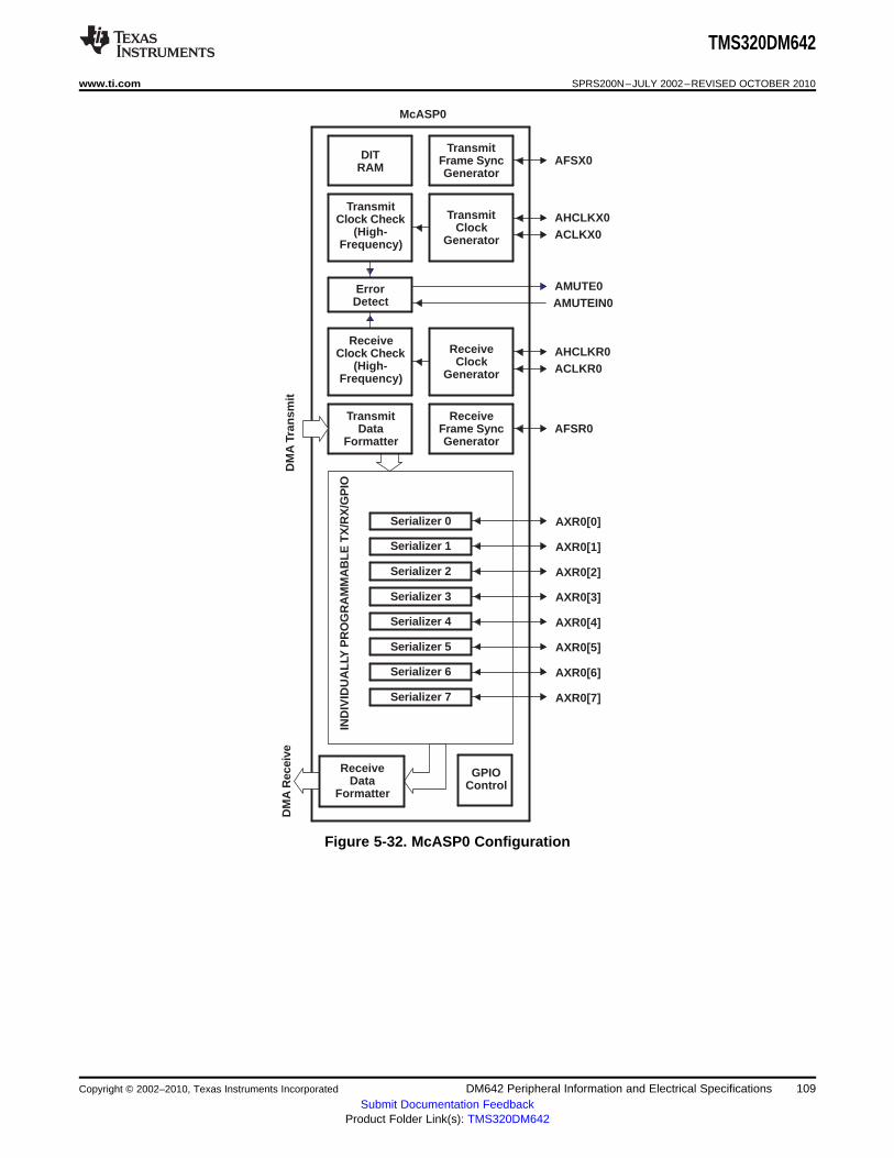
ReceiveClock
Generator
AHCLKR0ACLKR0
Clock CheckTransmit
GeneratorClock
Transmit
ACLKX0AHCLKX0
DITRAM
Transmit
GeneratorFrame Sync AFSX0
DetectError
ReceiveFrame SyncGeneratorFormatter
TransmitData
AMUTE0AMUTEIN0
AFSR0
Serializer 0
Serializer 1
Serializer 3
Serializer 2
Serializer 6
Serializer 7
Serializer 5
Serializer 4
(High-Frequency)
ReceiveClock Check
(High-Frequency)
Receive
FormatterData
McASP0
DM
A T
rans
mit
DM
A R
ecei
ve
IND
IVID
UA
LLY
PR
OG
RA
MM
AB
LE T
X/R
X/G
PIO
ControlGPIO
AXR0[0]
AXR0[1]
AXR0[3]
AXR0[2]
AXR0[6]
AXR0[7]
AXR0[5]
AXR0[4]
TMS320DM642
www.ti.com SPRS200N–JULY 2002–REVISED OCTOBER 2010
Figure 5-32. McASP0 Configuration
Copyright © 2002–2010, Texas Instruments Incorporated DM642 Peripheral Information and Electrical Specifications 109Submit Documentation Feedback
Product Folder Link(s): TMS320DM642

TMS320DM642
SPRS200N–JULY 2002–REVISED OCTOBER 2010 www.ti.com
5.9.2 McASP0 Peripheral Register Description(s)
Table 5-31. McASP0 Control Registers
HEX ADDRESS RANGE ACRONYM REGISTER NAME
01B4 C000 PID Peripheral Identification register [Register value: 0x0010 0101]
01B4 C004 PWRDEMU Power down and emulation management register
01B4 C008 – Reserved
01B4 C00C – Reserved
01B4 C010 PFUNC Pin function register
01B4 C014 PDIR Pin direction register
01B4 C018 PDOUT Pin data out register
01B4 C01C PDIN/PDSET Pin data in / data set registerRead returns: PDINWrites affect: PDSET
01B4 C020 PDCLR Pin data clear register
01B4 C024 – 01B4 C040 – Reserved
01B4 C044 GBLCTL Global control register
01B4 C048 AMUTE Mute control register
01B4 C04C DLBCTL Digital Loop-back control register
01B4 C050 DITCTL DIT mode control register
01B4 C054 – 01B4 C05C – Reserved
Alias of GBLCTL containing only Receiver Reset bits, allows transmit to be reset01B4 C060 RGBLCTL independently from receive.
01B4 C064 RMASK Receiver format UNIT bit mask register
01B4 C068 RFMT Receive bit stream format register
01B4 C06C AFSRCTL Receive frame sync control register
01B4 C070 ACLKRCTL Receive clock control register
01B4 C074 AHCLKRCTL High-frequency receive clock control register
01B4 C078 RTDM Receive TDM slot 0–31 register
01B4 C07C RINTCTL Receiver interrupt control register
01B4 C080 RSTAT Status register – Receiver
01B4 C084 RSLOT Current receive TDM slot register
01B4 C088 RCLKCHK Receiver clock check control register
01B4 C08C – 01B4 C09C – Reserved
Alias of GBLCTL containing only Transmitter Reset bits, allows transmit to be reset01B4 C0A0 XGBLCTL independently from receive.
01B4 C0A4 XMASK Transmit format UNIT bit mask register
01B4 C0A8 XFMT Transmit bit stream format register
01B4 C0AC AFSXCTL Transmit frame sync control register
01B4 C0B0 ACLKXCTL Transmit clock control register
01B4 C0B4 AHCLKXCTL High-frequency Transmit clock control register
01B4 C0B8 XTDM Transmit TDM slot 0–31 register
01B4 C0BC XINTCTL Transmit interrupt control register
01B4 C0C0 XSTAT Status register – Transmitter
01B4 C0C4 XSLOT Current transmit TDM slot
01B4 C0C8 XCLKCHK Transmit clock check control register
110 DM642 Peripheral Information and Electrical Specifications Copyright © 2002–2010, Texas Instruments Incorporated
Submit Documentation FeedbackProduct Folder Link(s): TMS320DM642
TMS320DM642
www.ti.com SPRS200N–JULY 2002–REVISED OCTOBER 2010
Table 5-31. McASP0 Control Registers (continued)
HEX ADDRESS RANGE ACRONYM REGISTER NAME
01B4 C0CC – 01B4 C0FC – Reserved
01B4 C100 DITCSRA0 Left (even TDM slot) channel status register file
01B4 C104 DITCSRA1 Left (even TDM slot) channel status register file
01B4 C108 DITCSRA2 Left (even TDM slot) channel status register file
01B4 C10C DITCSRA3 Left (even TDM slot) channel status register file
01B4 C110 DITCSRA4 Left (even TDM slot) channel status register file
01B4 C114 DITCSRA5 Left (even TDM slot) channel status register file
01B4 C118 DITCSRB0 Right (odd TDM slot) channel status register file
01B4 C11C DITCSRB1 Right (odd TDM slot) channel status register file
01B4 C120 DITCSRB2 Right (odd TDM slot) channel status register file
01B4 C124 DITCSRB3 Right (odd TDM slot) channel status register file
01B4 C128 DITCSRB4 Right (odd TDM slot) channel status register file
01B4 C12C DITCSRB5 Right (odd TDM slot) channel status register file
01B4 C130 DITUDRA0 Left (even TDM slot) user data register file
01B4 C134 DITUDRA1 Left (even TDM slot) user data register file
01B4 C138 DITUDRA2 Left (even TDM slot) user data register file
01B4 C13C DITUDRA3 Left (even TDM slot) user data register file
01B4 C140 DITUDRA4 Left (even TDM slot) user data register file
01B4 C144 DITUDRA5 Left (even TDM slot) user data register file
01B4 C148 DITUDRB0 Right (odd TDM slot) user data register file
01B4 C14C DITUDRB1 Right (odd TDM slot) user data register file
01B4 C150 DITUDRB2 Right (odd TDM slot) user data register file
01B4 C154 DITUDRB3 Right (odd TDM slot) user data register file
01B4 C158 DITUDRB4 Right (odd TDM slot) user data register file
01B4 C15C DITUDRB5 Right (odd TDM slot) user data register file
01B4 C160 – 01B4 C17C – Reserved
01B4 C180 SRCTL0 Serializer 0 control register
01B4 C184 SRCTL1 Serializer 1 control register
01B4 C188 SRCTL2 Serializer 2 control register
01B4 C18C SRCTL3 Serializer 3 control register
01B4 C190 SRCTL4 Serializer 4 control register
01B4 C194 SRCTL5 Serializer 5 control register
01B4 C198 SRCTL6 Serializer 6 control register
01B4 C19C SRCTL7 Serializer 7 control register
01B4 C1A0 – 01B4 C1FC – Reserved
01B4 C200 XBUF0 Transmit Buffer for Serializer 0
01B4 C204 XBUF1 Transmit Buffer for Serializer 1
01B4 C208 XBUF2 Transmit Buffer for Serializer 2
01B4 C20C XBUF3 Transmit Buffer for Serializer 3
01B4 C210 XBUF4 Transmit Buffer for Serializer 4
01B4 C214 XBUF5 Transmit Buffer for Serializer 5
01B4 C218 XBUF6 Transmit Buffer for Serializer 6
01B4 C21C XBUF7 Transmit Buffer for Serializer 7
01B4 C220 – 01B4 C27C – Reserved
01B4 C280 RBUF0 Receive Buffer for Serializer 0
01B4 C284 RBUF1 Receive Buffer for Serializer 1
01B4 C288 RBUF2 Receive Buffer for Serializer 2
Copyright © 2002–2010, Texas Instruments Incorporated DM642 Peripheral Information and Electrical Specifications 111Submit Documentation Feedback
Product Folder Link(s): TMS320DM642
TMS320DM642
SPRS200N–JULY 2002–REVISED OCTOBER 2010 www.ti.com
Table 5-31. McASP0 Control Registers (continued)
HEX ADDRESS RANGE ACRONYM REGISTER NAME
01B4 C28C RBUF3 Receive Buffer for Serializer 3
01B4 C290 RBUF4 Receive Buffer for Serializer 4
01B4 C294 RBUF5 Receive Buffer for Serializer 5
01B4 C298 RBUF6 Receive Buffer for Serializer 6
01B4 C29C RBUF7 Receive Buffer for Serializer 7
01B4 C2A0 – 01B4 FFFF – Reserved
Table 5-32. McASP0 Data Registers
HEX ADDRESS RANGE ACRONYM REGISTER NAME COMMENTS
(Used when RSEL or XSELMcASPx receive buffers or McASPx transmit buffers via bits = 0 [these bits are located3C00 0000 – 3C0F FFFF RBUF/XBUFx the Peripheral Data Bus. in the RFMT or XFMT registers,
respectively].)
5.9.3 McASP0 Electrical Data/Timing
5.9.3.1 Multichannel Audio Serial Port (McASP) Timing
Table 5-33. Timing Requirements for McASP (see Figure 5-33 and Figure 5-34) (1)
–500–600
NO. UNIT–720
MIN MAX
1 tc(AHCKRX) Cycle time, AHCLKR/X 20 ns
2 tw(AHCKRX) Pulse duration, AHCLKR/X high or low 10 ns
3 tc(CKRX) Cycle time, ACLKR/X ACLKR/X ext 33 ns
4 tw(CKRX) Pulse duration, ACLKR/X high or low ACLKR/X ext 16.5 ns
ACLKR/X int 5 ns5 tsu(FRX-CKRX) Setup time, AFSR/X input valid before ACLKR/X latches data
ACLKR/X ext 5 ns
ACLKR/X int 5 ns6 th(CKRX-FRX) Hold time, AFSR/X input valid after ACLKR/X latches data
ACLKR/X ext 5 ns
ACLKR/X int 5 ns7 tsu(AXR-CKRX) Setup time, AXR input valid before ACLKR/X latches data
ACLKR/X ext 5 ns
ACLKR/X int 5 ns8 th(CKRX-AXR) Hold time, AXR input valid after ACLKR/X latches data
ACLKR/X ext 5 ns
(1) ACLKX internal: ACLKXCTL.CLKXM=1, PDIR.ACLKX = 1ACLKX external input: ACLKXCTL.CLKXM=0, PDIR.ACLKX=0ACLKX external output: ACLKXCTL.CLKXM=0, PDIR.ACLKX=1ACLKR internal: ACLKRCTL.CLKRM=1, PDIR.ACLKR = 1ACLKR external input: ACLKRCTL.CLKRM=0, PDIR.ACLKR=0ACLKR external output: ACLKRCTL.CLKRM=0, PDIR.ACLKR=1
112 DM642 Peripheral Information and Electrical Specifications Copyright © 2002–2010, Texas Instruments Incorporated
Submit Documentation FeedbackProduct Folder Link(s): TMS320DM642

TMS320DM642
www.ti.com SPRS200N–JULY 2002–REVISED OCTOBER 2010
Table 5-34. Switching Characteristics Over Recommended Operating Conditions for McASP(see Figure 5-33 and Figure 5-34) (1)
–500–600
NO. PARAMETER UNIT–720
MIN MAX
9 tc(AHCKRX) Cycle time, AHCLKR/X 20 ns
10 tw(AHCKRX) Pulse duration, AHCLKR/X high or low 10 ns
11 tc(CKRX) Cycle time, ACLKR/X ACLKR/X int 33 ns
12 tw(CKRX) Pulse duration, ACLKR/X high or low ACLKR/X int 16.5 ns
ACLKR/X int –1 5 ns13 td(CKRX-FRX) Delay time, ACLKR/X transmit edge to AFSX/R output valid
ACLKR/X ext 0 10 ns
ACLKX int –1 5 ns14 td(CKX-AXRV) Delay time, ACLKX transmit edge to AXR output valid
ACLKX ext 0 10 ns
ACLKR/X int 0 10 nsDisable time, AXR high impedance following last data bit from15 tdis(CKRX-AXRHZ) ACLKR/X transmit edge ACLKR/X ext 0 10 ns
(1) ACLKX internal: ACLKXCTL.CLKXM=1, PDIR.ACLKX = 1ACLKX external input: ACLKXCTL.CLKXM=0, PDIR.ACLKX=0ACLKX external output: ACLKXCTL.CLKXM=0, PDIR.ACLKX=1ACLKR internal: ACLKRCTL.CLKRM=1, PDIR.ACLKR = 1ACLKR external input: ACLKRCTL.CLKRM=0, PDIR.ACLKR=0ACLKR external output: ACLKRCTL.CLKRM=0, PDIR.ACLKR=1
Copyright © 2002–2010, Texas Instruments Incorporated DM642 Peripheral Information and Electrical Specifications 113Submit Documentation Feedback
Product Folder Link(s): TMS320DM642
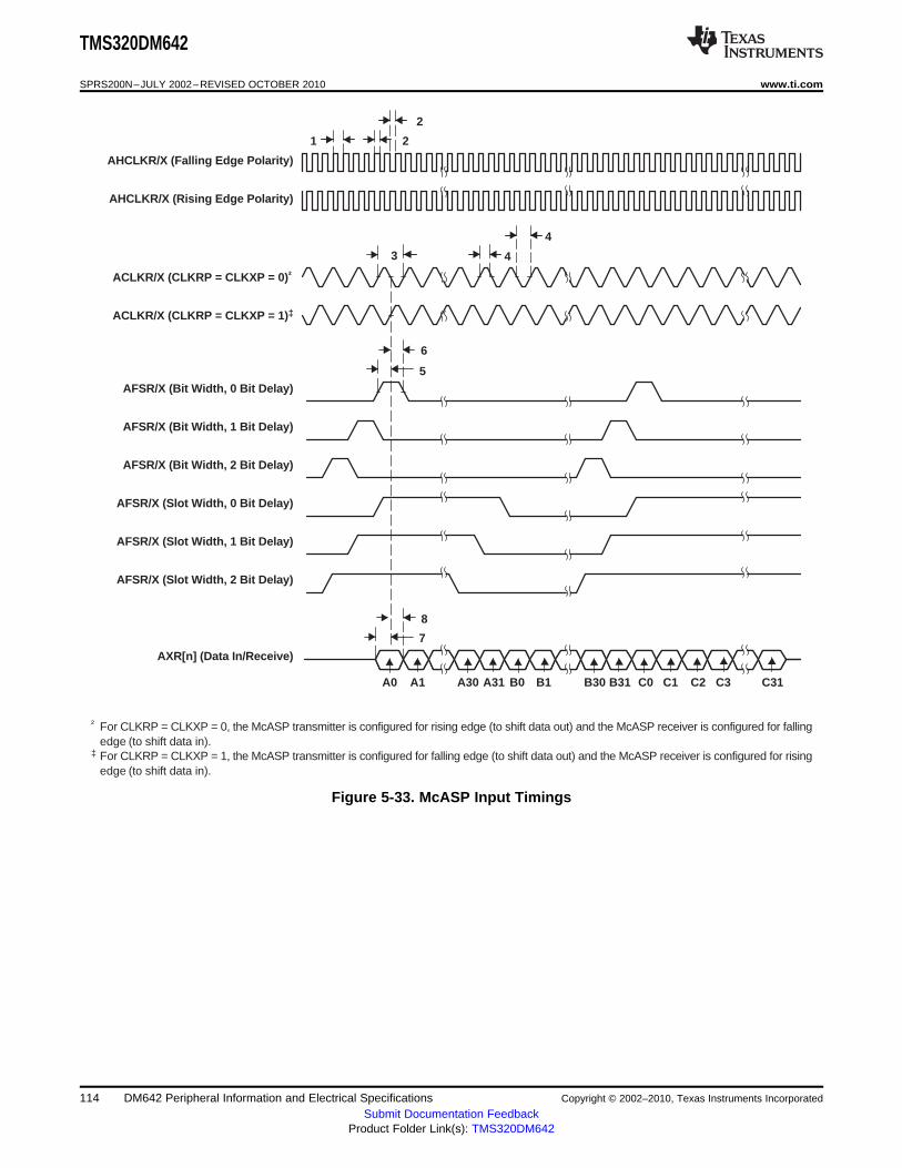
8
7
4
43
2
21
A0 A1 B0 B1A30 A31 B30 B31 C0 C1 C2 C3 C31
AHCLKR/X (Falling Edge Polarity)
AHCLKR/X (Rising Edge Polarity)
AFSR/X (Bit Width, 0 Bit Delay)
AFSR/X (Bit Width, 1 Bit Delay)
AFSR/X (Bit Width, 2 Bit Delay)
AFSR/X (Slot Width, 0 Bit Delay)
AFSR/X (Slot Width, 1 Bit Delay)
AFSR/X (Slot Width, 2 Bit Delay)
AXR[n] (Data In/Receive)
6
5
ACLKR/X (CLKRP = CLKXP = 0)†
ACLKR/X (CLKRP = CLKXP = 1)‡
† For CLKRP = CLKXP = 0, the McASP transmitter is configured for rising edge (to shift data out) and the McASP receiver is configured for fallingedge (to shift data in).
‡ For CLKRP = CLKXP = 1, the McASP transmitter is configured for falling edge (to shift data out) and the McASP receiver is configured for risingedge (to shift data in).
TMS320DM642
SPRS200N–JULY 2002–REVISED OCTOBER 2010 www.ti.com
Figure 5-33. McASP Input Timings
114 DM642 Peripheral Information and Electrical Specifications Copyright © 2002–2010, Texas Instruments Incorporated
Submit Documentation FeedbackProduct Folder Link(s): TMS320DM642
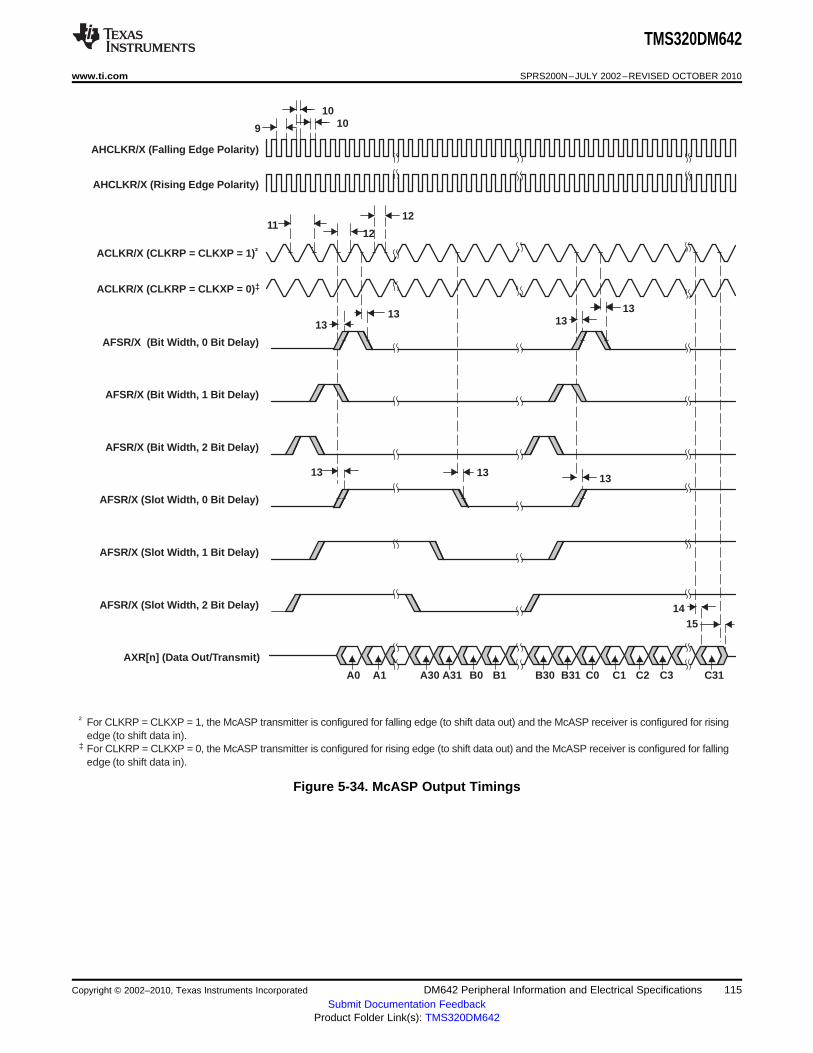
† For CLKRP = CLKXP = 1, the McASP transmitter is configured for falling edge (to shift data out) and the McASP receiver is configured for risingedge (to shift data in).
‡ For CLKRP = CLKXP = 0, the McASP transmitter is configured for rising edge (to shift data out) and the McASP receiver is configured for fallingedge (to shift data in).
1514
131313
1313
1313
12
1211
1010
9
A0 A1 B0 B1A30 A31 B30 B31 C0 C1 C2 C3 C31
AHCLKR/X (Falling Edge Polarity)
AHCLKR/X (Rising Edge Polarity)
AFSR/X (Bit Width, 0 Bit Delay)
AFSR/X (Bit Width, 1 Bit Delay)
AFSR/X (Bit Width, 2 Bit Delay)
AFSR/X (Slot Width, 0 Bit Delay)
AFSR/X (Slot Width, 1 Bit Delay)
AFSR/X (Slot Width, 2 Bit Delay)
AXR[n] (Data Out/Transmit)
ACLKR/X (CLKRP = CLKXP = 0)‡
ACLKR/X (CLKRP = CLKXP = 1)†
TMS320DM642
www.ti.com SPRS200N–JULY 2002–REVISED OCTOBER 2010
Figure 5-34. McASP Output Timings
Copyright © 2002–2010, Texas Instruments Incorporated DM642 Peripheral Information and Electrical Specifications 115Submit Documentation Feedback
Product Folder Link(s): TMS320DM642

TMS320DM642
SPRS200N–JULY 2002–REVISED OCTOBER 2010 www.ti.com
5.10 Inter-Integrated Circuit (I2C)
The inter-integrated circuit (I2C) module provides an interface between a TMS320C6000™ DSP and otherdevices compliant with Philips Semiconductors Inter-IC bus (I2C bus) specification version 2.1 andconnected by way of an I2C-bus. External components attached to this 2-wire serial bus cantransmit/receive up to 8-bit data to/from the DSP through the I2C module.
5.10.1 I2C Device-Specific Information
The I2C module on the TMS320DM642 can be used by the DSP to control local peripherals ICs (DACs,ADCs, etc.) while the other may be used to communicate with other controllers in a system or toimplement a user interface.
The I2C port supports:• Compatible with Philips I2C Specification Revision 2.1 (January 2000)• Fast Mode up to 400 Kbps (no fail-safe I/O buffers)• Noise Filter to Remove Noise 50 ns or less• Seven- and Ten-Bit Device Addressing Modes• Master (Transmit/Receive) and Slave (Transmit/Receive) Functionality• Events: DMA, Interrupt, or Polling• Slew-Rate Limited Open-Drain Output Buffers
Figure 5-35 is a block diagram of the I2C0 module.
116 DM642 Peripheral Information and Electrical Specifications Copyright © 2002–2010, Texas Instruments Incorporated
Submit Documentation FeedbackProduct Folder Link(s): TMS320DM642
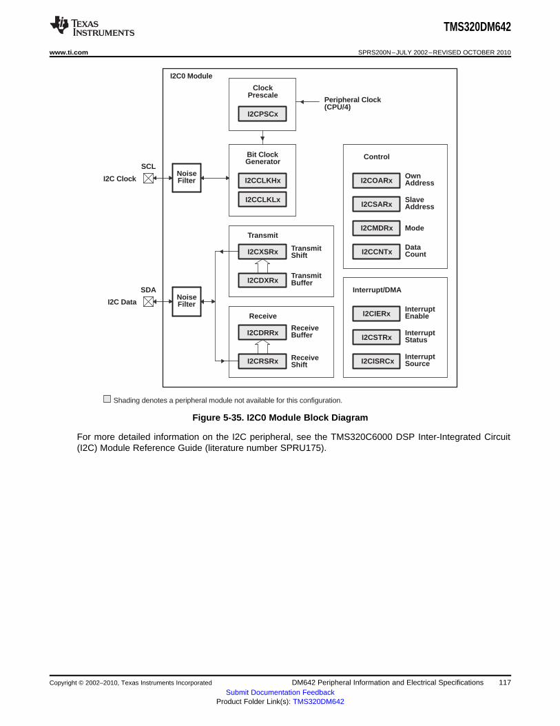
ClockPrescale
I2CPSCx
Peripheral Clock(CPU/4)
I2CCLKHx
GeneratorBit Clock
I2CCLKLx
NoiseFilter
SCL
I2CXSRx
I2CDXRx
Transmit
TransmitShift
TransmitBuffer
I2CDRRx
ShiftI2CRSRx
ReceiveBuffer
Receive
Receive
Filter
SDA
I2C DataNoise
I2COARx
I2CSARxSlaveAddress
Control
AddressOwn
I2CMDRx
I2CCNTx
Mode
DataCount
SourceInterrupt
InterruptStatus
I2CISRCx
I2CSTRx
EnableInterrupt
I2CIERx
Interrupt/DMA
I2C0 Module
I2C Clock
Shading denotes a peripheral module not available for this configuration.
TMS320DM642
www.ti.com SPRS200N–JULY 2002–REVISED OCTOBER 2010
Figure 5-35. I2C0 Module Block Diagram
For more detailed information on the I2C peripheral, see the TMS320C6000 DSP Inter-Integrated Circuit(I2C) Module Reference Guide (literature number SPRU175).
Copyright © 2002–2010, Texas Instruments Incorporated DM642 Peripheral Information and Electrical Specifications 117Submit Documentation Feedback
Product Folder Link(s): TMS320DM642
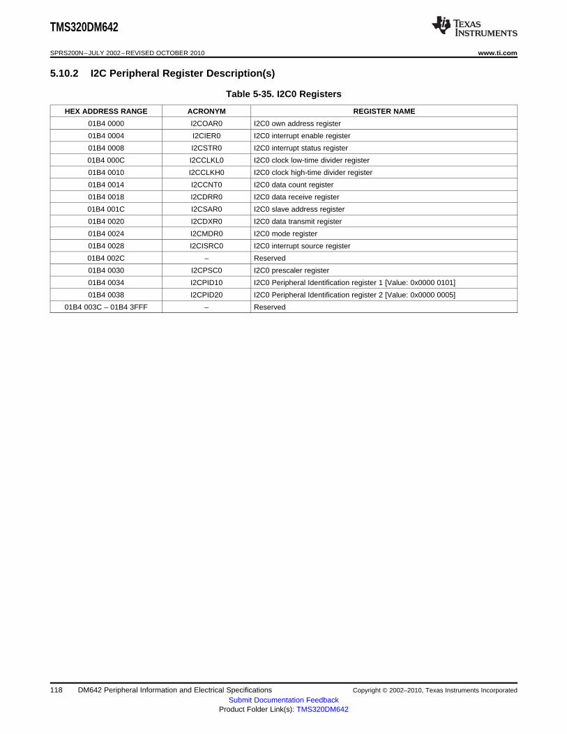
TMS320DM642
SPRS200N–JULY 2002–REVISED OCTOBER 2010 www.ti.com
5.10.2 I2C Peripheral Register Description(s)
Table 5-35. I2C0 Registers
HEX ADDRESS RANGE ACRONYM REGISTER NAME
01B4 0000 I2COAR0 I2C0 own address register
01B4 0004 I2CIER0 I2C0 interrupt enable register
01B4 0008 I2CSTR0 I2C0 interrupt status register
01B4 000C I2CCLKL0 I2C0 clock low-time divider register
01B4 0010 I2CCLKH0 I2C0 clock high-time divider register
01B4 0014 I2CCNT0 I2C0 data count register
01B4 0018 I2CDRR0 I2C0 data receive register
01B4 001C I2CSAR0 I2C0 slave address register
01B4 0020 I2CDXR0 I2C0 data transmit register
01B4 0024 I2CMDR0 I2C0 mode register
01B4 0028 I2CISRC0 I2C0 interrupt source register
01B4 002C – Reserved
01B4 0030 I2CPSC0 I2C0 prescaler register
01B4 0034 I2CPID10 I2C0 Peripheral Identification register 1 [Value: 0x0000 0101]
01B4 0038 I2CPID20 I2C0 Peripheral Identification register 2 [Value: 0x0000 0005]
01B4 003C – 01B4 3FFF – Reserved
118 DM642 Peripheral Information and Electrical Specifications Copyright © 2002–2010, Texas Instruments Incorporated
Submit Documentation FeedbackProduct Folder Link(s): TMS320DM642

TMS320DM642
www.ti.com SPRS200N–JULY 2002–REVISED OCTOBER 2010
5.10.3 I2C Electrical Data/Timing
5.10.3.1 Inter-Integrated Circuits (I2C) Timing
Table 5-36. Timing Requirements for I2C Timings (1) (see Figure 5-36)
–500–600–720
NO. UNITSTANDARD FAST MODEMODE
MIN MAX MIN MAX
1 tc(SCL) Cycle time, SCL 10 2.5 µs
Setup time, SCL high before SDA low (for a repeated START2 tsu(SCLH-SDAL) 4.7 0.6 µscondition)
Hold time, SCL low after SDA low (for a START and a repeated3 th(SCLL-SDAL) 4 0.6 µsSTART condition)
4 tw(SCLL) Pulse duration, SCL low 4.7 1.3 µs
5 tw(SCLH) Pulse duration, SCL high 4 0.6 µs
6 tsu(SDAV-SDLH) Setup time, SDA valid before SCL high 250 100 (2) ns
7 th(SDA-SDLL) Hold time, SDA valid after SCL low (For I2C bus™ devices) 0 (3) 0 (3) 0.9 (4) µs
Pulse duration, SDA high between STOP and START8 tw(SDAH) 4.7 1.3 µsconditions
20 + 0.1Cb9 tr(SDA) Rise time, SDA 1000 300 ns(5)
20 + 0.1Cb10 tr(SCL) Rise time, SCL 1000 300 ns(5)
20 + 0.1Cb11 tf(SDA) Fall time, SDA 300 300 ns(5)
20 + 0.1Cb12 tf(SCL) Fall time, SCL 300 300 ns(5)
13 tsu(SCLH-SDAH) Setup time, SCL high before SDA high (for STOP condition) 4 0.6 µs
14 tw(SP) Pulse duration, spike (must be suppressed) 0 50 ns
15 Cb(5) Capacitive load for each bus line 400 400 pF
(1) The I2C pins SDA and SCL do not feature fail-safe I/O buffers. These pins could potentially draw current when the device is powereddown.
(2) A Fast-mode I2C-bus™ device can be used in a Standard-mode I2C-bus™ system, but the requirement tsu(SDA-SCLH) ≥250 ns must thenbe met. This will automatically be the case if the device does not stretch the LOW period of the SCL signal. If such a device does stretchthe LOW period of the SCL signal, it must output the next data bit to the SDA line tr max + tsu(SDA-SCLH) = 1000 + 250 = 1250 ns(according to the Standard-mode I2C-Bus Specification) before the SCL line is released.
(3) A device must internally provide a hold time of at least 300 ns for the SDA signal (referred to the VIHmin of the SCL signal) to bridge theundefined region of the falling edge of SCL.
(4) The maximum th(SDA-SCLL) has only to be met if the device does not stretch the low period [tw(SCLL)] of the SCL signal.(5) Cb = total capacitance of one bus line in pF. If mixed with HS-mode devices, faster fall-times are allowed.
Copyright © 2002–2010, Texas Instruments Incorporated DM642 Peripheral Information and Electrical Specifications 119Submit Documentation Feedback
Product Folder Link(s): TMS320DM642
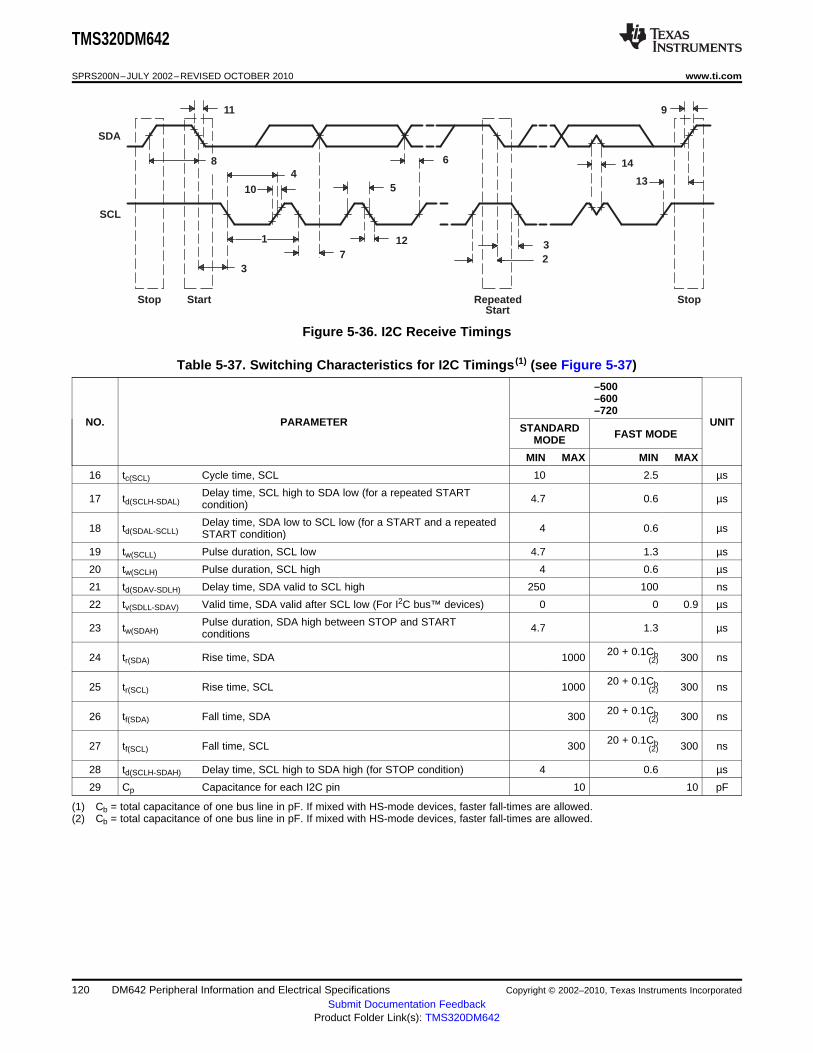
10
84
37
12
5
6 14
23
13
Stop Start RepeatedStart
Stop
SDA
SCL
1
11 9
TMS320DM642
SPRS200N–JULY 2002–REVISED OCTOBER 2010 www.ti.com
Figure 5-36. I2C Receive Timings
Table 5-37. Switching Characteristics for I2C Timings (1) (see Figure 5-37)
–500–600–720
NO. PARAMETER UNITSTANDARD FAST MODEMODE
MIN MAX MIN MAX
16 tc(SCL) Cycle time, SCL 10 2.5 µs
Delay time, SCL high to SDA low (for a repeated START17 td(SCLH-SDAL) 4.7 0.6 µscondition)
Delay time, SDA low to SCL low (for a START and a repeated18 td(SDAL-SCLL) 4 0.6 µsSTART condition)
19 tw(SCLL) Pulse duration, SCL low 4.7 1.3 µs
20 tw(SCLH) Pulse duration, SCL high 4 0.6 µs
21 td(SDAV-SDLH) Delay time, SDA valid to SCL high 250 100 ns
22 tv(SDLL-SDAV) Valid time, SDA valid after SCL low (For I2C bus™ devices) 0 0 0.9 µs
Pulse duration, SDA high between STOP and START23 tw(SDAH) 4.7 1.3 µsconditions
20 + 0.1Cb24 tr(SDA) Rise time, SDA 1000 300 ns(2)
20 + 0.1Cb25 tr(SCL) Rise time, SCL 1000 300 ns(2)
20 + 0.1Cb26 tf(SDA) Fall time, SDA 300 300 ns(2)
20 + 0.1Cb27 tf(SCL) Fall time, SCL 300 300 ns(2)
28 td(SCLH-SDAH) Delay time, SCL high to SDA high (for STOP condition) 4 0.6 µs
29 Cp Capacitance for each I2C pin 10 10 pF
(1) Cb = total capacitance of one bus line in pF. If mixed with HS-mode devices, faster fall-times are allowed.(2) Cb = total capacitance of one bus line in pF. If mixed with HS-mode devices, faster fall-times are allowed.
120 DM642 Peripheral Information and Electrical Specifications Copyright © 2002–2010, Texas Instruments Incorporated
Submit Documentation FeedbackProduct Folder Link(s): TMS320DM642
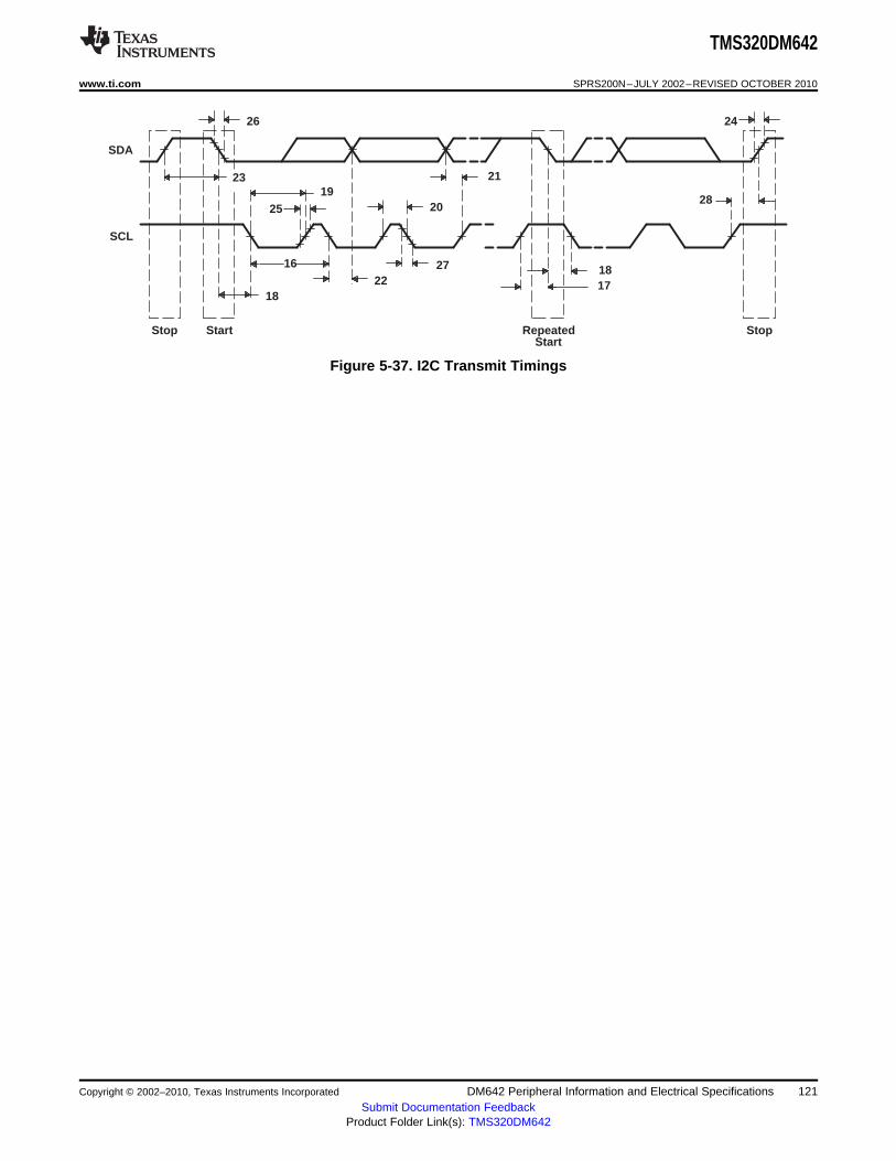
25
2319
1822
27
20
21
1718
28
Stop Start RepeatedStart
Stop
SDA
SCL
16
26 24
TMS320DM642
www.ti.com SPRS200N–JULY 2002–REVISED OCTOBER 2010
Figure 5-37. I2C Transmit Timings
Copyright © 2002–2010, Texas Instruments Incorporated DM642 Peripheral Information and Electrical Specifications 121Submit Documentation Feedback
Product Folder Link(s): TMS320DM642
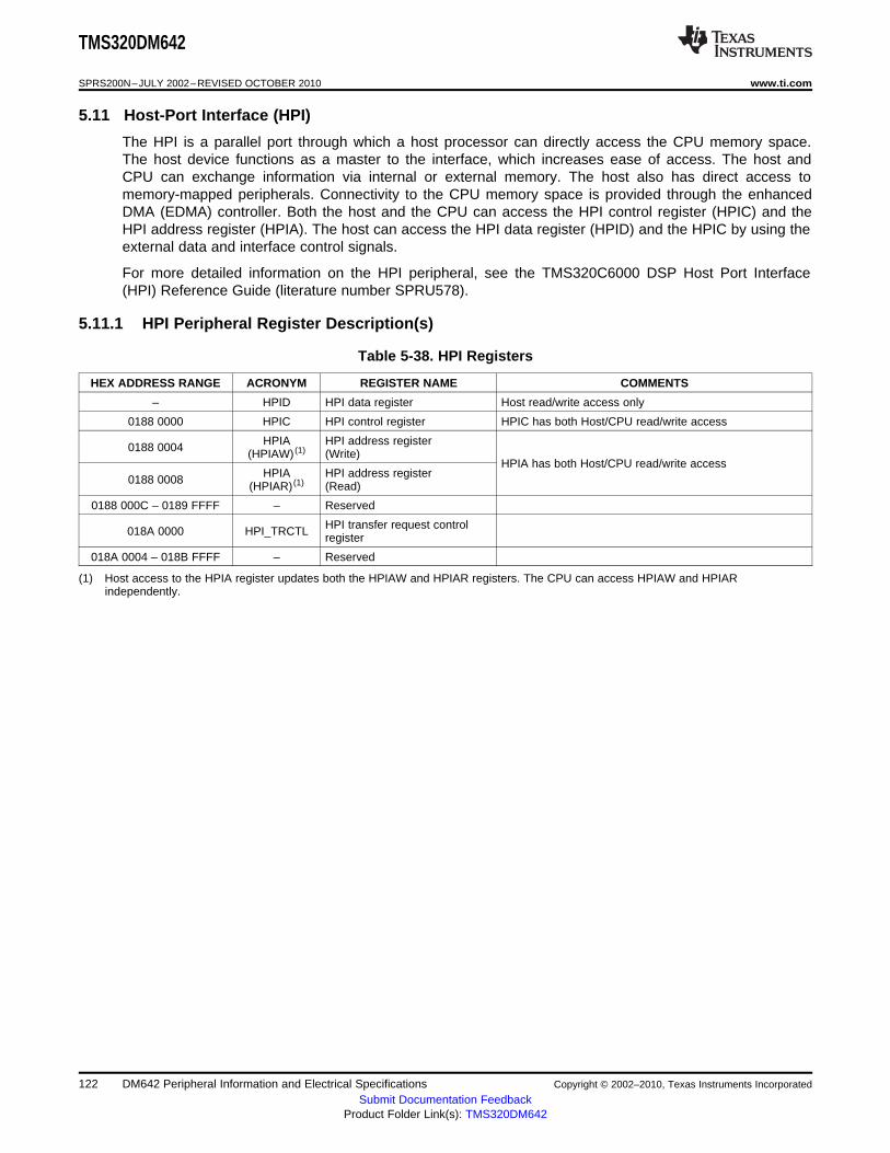
TMS320DM642
SPRS200N–JULY 2002–REVISED OCTOBER 2010 www.ti.com
5.11 Host-Port Interface (HPI)
The HPI is a parallel port through which a host processor can directly access the CPU memory space.The host device functions as a master to the interface, which increases ease of access. The host andCPU can exchange information via internal or external memory. The host also has direct access tomemory-mapped peripherals. Connectivity to the CPU memory space is provided through the enhancedDMA (EDMA) controller. Both the host and the CPU can access the HPI control register (HPIC) and theHPI address register (HPIA). The host can access the HPI data register (HPID) and the HPIC by using theexternal data and interface control signals.
For more detailed information on the HPI peripheral, see the TMS320C6000 DSP Host Port Interface(HPI) Reference Guide (literature number SPRU578).
5.11.1 HPI Peripheral Register Description(s)
Table 5-38. HPI Registers
HEX ADDRESS RANGE ACRONYM REGISTER NAME COMMENTS
– HPID HPI data register Host read/write access only
0188 0000 HPIC HPI control register HPIC has both Host/CPU read/write access
HPIA HPI address register0188 0004 (HPIAW) (1) (Write)HPIA has both Host/CPU read/write access
HPIA HPI address register0188 0008 (HPIAR) (1) (Read)
0188 000C – 0189 FFFF – Reserved
HPI transfer request control018A 0000 HPI_TRCTL register
018A 0004 – 018B FFFF – Reserved
(1) Host access to the HPIA register updates both the HPIAW and HPIAR registers. The CPU can access HPIAW and HPIARindependently.
122 DM642 Peripheral Information and Electrical Specifications Copyright © 2002–2010, Texas Instruments Incorporated
Submit Documentation FeedbackProduct Folder Link(s): TMS320DM642

TMS320DM642
www.ti.com SPRS200N–JULY 2002–REVISED OCTOBER 2010
5.11.2 Host-Port Interface (HPI) Electrical Data/Timing
Table 5-39. Timing Requirements for Host-Port Interface Cycles (1) (2) (see Figure 5-38 throughFigure 5-45)
–500–600
NO. UNIT–720
MIN MAX
1 tsu(SELV-HSTBL) Setup time, select signals (3) valid before HSTROBE low 5 ns
2 th(HSTBL-SELV) Hold time, select signals (3) valid after HSTROBE low 2.4 ns
3 tw(HSTBL) Pulse duration, HSTROBE low 4P (4) ns
4 tw(HSTBH) Pulse duration, HSTROBE high between consecutive accesses 4P ns
10 tsu(SELV-HASL) Setup time, select signals (3) valid before HAS low 5 ns
11 th(HASL-SELV) Hold time, select signals (3) valid after HAS low 2 ns
12 tsu(HDV-HSTBH) Setup time, host data valid before HSTROBE high 5 ns
13 th(HSTBH-HDV) Hold time, host data valid after HSTROBE high 2.8 ns
Hold time, HSTROBE low after HRDY low. HSTROBE should not be inactivated14 th(HRDYL-HSTBL) 2 nsuntil HRDY is active (low); otherwise, HPI writes will not complete properly.
18 tsu(HASL-HSTBL) Setup time, HAS low before HSTROBE low 2 ns
19 th(HSTBL-HASL) Hold time, HAS low after HSTROBE low 2.1 ns
(1) HSTROBE refers to the following logical operation on HCS, HDS1, and HDS2: [NOT(HDS1 XOR HDS2)] OR HCS.(2) P = 1/CPU clock frequency in ns. For example, when running parts at 720 MHz, use P = 1.39 ns.(3) Select signals include: HCNTL[1:0] and HR/W. For HPI16 mode only, select signals also include HHWIL.(4) Select the parameter value of 4P or 12.5 ns, whichever is larger.
Table 5-40. Switching Characteristics Over Recommended Operating Conditions During Host-PortInterface Cycles (1) (2) (see Figure 5-38 through Figure 5-45)
–500–600
NO. PARAMETER UNIT–720
MIN MAX
6 td(HSTBL-HRDYH) Delay time, HSTROBE low to HRDY high (3) 1.3 4P + 8 ns
7 td(HSTBL-HDLZ) Delay time, HSTROBE low to HD low impedance for an HPI read 2 ns
8 td(HDV-HRDYL) Delay time, HD valid to HRDY low -3 ns
9 toh(HSTBH-HDV) Output hold time, HD valid after HSTROBE high 1.5 ns
15 td(HSTBH-HDHZ) Delay time, HSTROBE high to HD high impedance 12 ns
16 td(HSTBL-HDV) Delay time, HSTROBE low to HD valid (HPI16 mode, 2nd half-word only) 4P + 8 ns
(1) HSTROBE refers to the following logical operation on HCS, HDS1, and HDS2: [NOT(HDS1 XOR HDS2)] OR HCS.(2) P = 1/CPU clock frequency in ns. For example, when running parts at 720 MHz, use P = 1.39 ns.(3) This parameter is used during HPID reads and writes. For reads, at the beginning of a word transfer (HPI32) or the first half-word
transfer (HPI16) on the falling edge of HSTROBE, the HPI sends the request to the EDMA internal address generation hardware, andHRDY remains high until the EDMA internal address generation hardware loads the requested data into HPID. For writes, HRDY goeshigh if the internal write buffer is full.
Copyright © 2002–2010, Texas Instruments Incorporated DM642 Peripheral Information and Electrical Specifications 123Submit Documentation Feedback
Product Folder Link(s): TMS320DM642
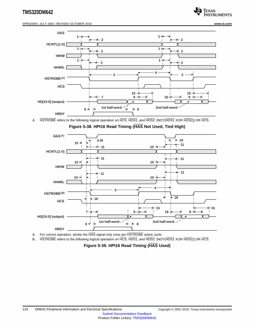
1st half-word 2nd half-word86
15916
1597
43
21
21
21
21
21
21
HAS
HCNTL[1:0]
HR/W
HHWIL
HSTROBE (A)
HCS
HD[15:0] (output)
HRDY
3
HAS (A)
HCNTL[1:0]
HR/W
HHWIL
HSTROBE (B)
HCS
HD[15:0] (output)
HRDY
1st half-word 2nd half-word86
15916
1597
43
11
1011
10
1110
1110
111011
1019 19
1818
TMS320DM642
SPRS200N–JULY 2002–REVISED OCTOBER 2010 www.ti.com
A. HSTROBE refers to the following logical operation on HCS, HDS1, and HDS2: [NOT(HDS1 XOR HDS2)] OR HCS.
Figure 5-38. HPI16 Read Timing (HAS Not Used, Tied High)
A. For correct operation, strobe the HAS signal only once per HSTROBE active cycle.B. HSTROBE refers to the following logical operation on HCS, HDS1, and HDS2: [NOT(HDS1 XOR HDS2)] OR HCS.
Figure 5-39. HPI16 Read Timing (HAS Used)
124 DM642 Peripheral Information and Electrical Specifications Copyright © 2002–2010, Texas Instruments Incorporated
Submit Documentation FeedbackProduct Folder Link(s): TMS320DM642

1st half-word 2nd half-word
1312
1312
4
14
3
21
21
21
21
21
21
HAS
HCNTL[1:0]
HR/W
HHWIL
HSTROBE (A)
HCS
HD[15:0] (input)
HRDY
3
6
1st half-word 2nd half-word
1312
1312
4
14
3
1110
1110
1110
1110
1110
1110
HAS (A)
HCNTL[1:0]
HR/W
HHWIL
HSTROBE (B)
HCS
HD[15:0] (input)
HRDY
1919
18 18
6
TMS320DM642
www.ti.com SPRS200N–JULY 2002–REVISED OCTOBER 2010
A. HSTROBE refers to the following logical operation on HCS, HDS1, and HDS2: [NOT(HDS1 XOR HDS2)] OR HCS.
Figure 5-40. HPI16 Write Timing (HAS Not Used, Tied High)
A. For correct operation, strobe the HAS signal only once per HSTROBE active cycle.B. HSTROBE refers to the following logical operation on HCS, HDS1, and HDS2: [NOT(HDS1 XOR HDS2)] OR HCS.
Figure 5-41. HPI16 Write Timing (HAS Used)
Copyright © 2002–2010, Texas Instruments Incorporated DM642 Peripheral Information and Electrical Specifications 125Submit Documentation Feedback
Product Folder Link(s): TMS320DM642

6
3
HAS
HCNTL[1:0]
HR/W
HSTROBE (A)
HCS
HD[31:0] (output)
HRDY8
97
21
21
15
86
1597
318
1110
1110
19HAS (A)
HCNTL[1:0]
HR/W
HSTROBE (B)
HCS
HD[31:0] (output)
HRDY
TMS320DM642
SPRS200N–JULY 2002–REVISED OCTOBER 2010 www.ti.com
A. HSTROBE refers to the following logical operation on HCS, HDS1, and HDS2: [NOT(HDS1 XOR HDS2)] OR HCS.
Figure 5-42. HPI32 Read Timing (HAS Not Used, Tied High)
A. For correct operation, strobe the HAS signal only once per HSTROBE active cycle.B. HSTROBE refers to the following logical operation on HCS, HDS1, and HDS2: [NOT(HDS1 XOR HDS2)] OR HCS.
Figure 5-43. HPI32 Read Timing (HAS Used)
126 DM642 Peripheral Information and Electrical Specifications Copyright © 2002–2010, Texas Instruments Incorporated
Submit Documentation FeedbackProduct Folder Link(s): TMS320DM642

1312
14
3
21
21
HAS
HCNTL[1:0]
HR/W
HSTROBE (A)
HCS
HD[31:0] (input)
HRDY6
1312
14
318
1110
1110
19
HAS (A)
HCNTL[1:0]
HR/W
HSTROBE (B)
HCS
HD[31:0] (input)
HRDY6
TMS320DM642
www.ti.com SPRS200N–JULY 2002–REVISED OCTOBER 2010
A. HSTROBE refers to the following logical operation on HCS, HDS1, and HDS2: [NOT(HDS1 XOR HDS2)] OR HCS.
Figure 5-44. HPI32 Write Timing (HAS Not Used, Tied High)
A. For correct operation, strobe the HAS signal only once per HSTROBE active cycle.B. HSTROBE refers to the following logical operation on HCS, HDS1, and HDS2: [NOT(HDS1 XOR HDS2)] OR HCS.
Figure 5-45. HPI32 Write Timing (HAS Used)
Copyright © 2002–2010, Texas Instruments Incorporated DM642 Peripheral Information and Electrical Specifications 127Submit Documentation Feedback
Product Folder Link(s): TMS320DM642
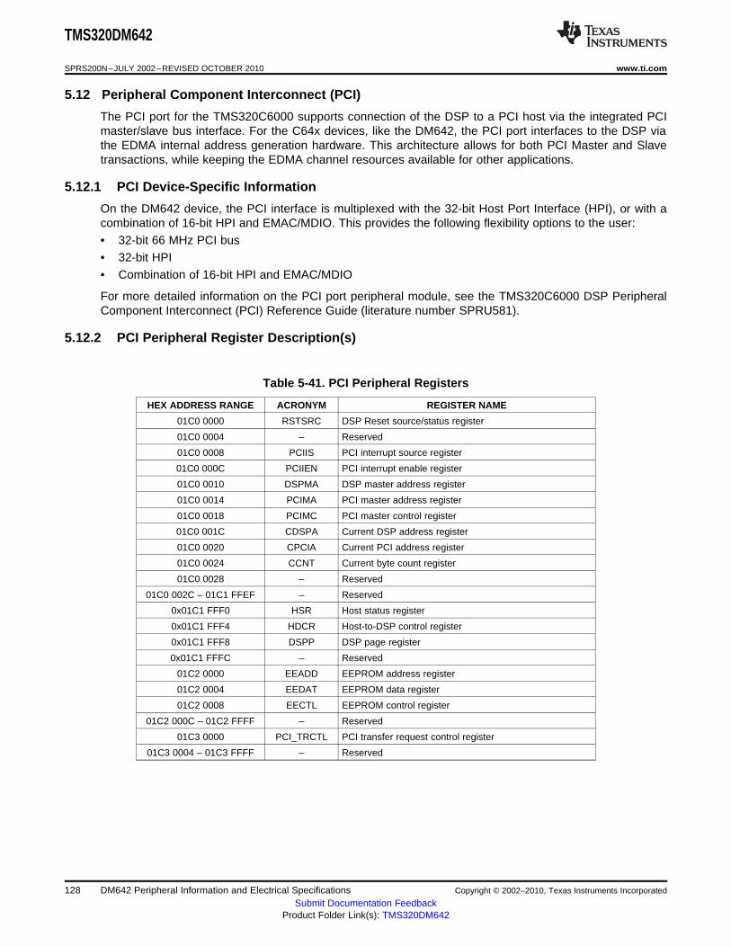
TMS320DM642
SPRS200N–JULY 2002–REVISED OCTOBER 2010 www.ti.com
5.12 Peripheral Component Interconnect (PCI)
The PCI port for the TMS320C6000 supports connection of the DSP to a PCI host via the integrated PCImaster/slave bus interface. For the C64x devices, like the DM642, the PCI port interfaces to the DSP viathe EDMA internal address generation hardware. This architecture allows for both PCI Master and Slavetransactions, while keeping the EDMA channel resources available for other applications.
5.12.1 PCI Device-Specific Information
On the DM642 device, the PCI interface is multiplexed with the 32-bit Host Port Interface (HPI), or with acombination of 16-bit HPI and EMAC/MDIO. This provides the following flexibility options to the user:• 32-bit 66 MHz PCI bus• 32-bit HPI• Combination of 16-bit HPI and EMAC/MDIO
For more detailed information on the PCI port peripheral module, see the TMS320C6000 DSP PeripheralComponent Interconnect (PCI) Reference Guide (literature number SPRU581).
5.12.2 PCI Peripheral Register Description(s)
Table 5-41. PCI Peripheral Registers
HEX ADDRESS RANGE ACRONYM REGISTER NAME
01C0 0000 RSTSRC DSP Reset source/status register
01C0 0004 – Reserved
01C0 0008 PCIIS PCI interrupt source register
01C0 000C PCIIEN PCI interrupt enable register
01C0 0010 DSPMA DSP master address register
01C0 0014 PCIMA PCI master address register
01C0 0018 PCIMC PCI master control register
01C0 001C CDSPA Current DSP address register
01C0 0020 CPCIA Current PCI address register
01C0 0024 CCNT Current byte count register
01C0 0028 – Reserved
01C0 002C – 01C1 FFEF – Reserved
0x01C1 FFF0 HSR Host status register
0x01C1 FFF4 HDCR Host-to-DSP control register
0x01C1 FFF8 DSPP DSP page register
0x01C1 FFFC – Reserved
01C2 0000 EEADD EEPROM address register
01C2 0004 EEDAT EEPROM data register
01C2 0008 EECTL EEPROM control register
01C2 000C – 01C2 FFFF – Reserved
01C3 0000 PCI_TRCTL PCI transfer request control register
01C3 0004 – 01C3 FFFF – Reserved
128 DM642 Peripheral Information and Electrical Specifications Copyright © 2002–2010, Texas Instruments Incorporated
Submit Documentation FeedbackProduct Folder Link(s): TMS320DM642

PCLK
1
2
3
4
4
0.4 DVDD V MINPeak to Peak for3.3V signaling
PRST
PCLK
2
1
TMS320DM642
www.ti.com SPRS200N–JULY 2002–REVISED OCTOBER 2010
5.12.3 PCI Electrical Data/Timing
5.12.3.1 Peripheral Component Interconnect (PCI) Timing
Table 5-42. Timing Requirements for PCLK (1) (2) (see Figure 5-46)
–500, A-600 –600, –720[33 MHz] [66 MHz]NO. UNIT
MIN MAX MIN MAX
1 tc(PCLK) Cycle time, PCLK 30 (or 4P (3)) 15 (or 4P (3)) ns
2 tw(PCLKH) Pulse duration, PCLK high 11 6 ns
3 tw(PCLKL) Pulse duration, PCLK low 11 6 ns
4 tsr(PCLK) Δv/Δt slew rate, PCLK 1 4 1.5 4 V/ns
(1) For 3.3-V operation, the reference points for the rise and fall transitions are measured at VILP MAX and VIHP MIN.(2) P = 1/CPU clock frequency in ns. For example when running parts at 720 MHz, use P = 1.39 ns.(3) Select the parameter value, whichever is larger.
Figure 5-46. PCLK Timing
Table 5-43. Timing Requirements for PCI Reset (see Figure 5-47)
–500–600
NO. UNIT–720
MIN MAX
1 tw(PRST) Pulse duration, PRST 1 ms
2 tsu(PCLKA-PRSTH) Setup time, PCLK active before PRST high 100 µs
Figure 5-47. PCI Reset (PRST) Timing
Table 5-44. Timing Requirements for PCI Inputs (see Figure 5-48)
–600–500, A-600 –720NO. UNIT33 MHz 66 MHz
MIN MAX MIN MAX
4 tsu(IV-PCLKH) Setup time, input valid before PCLK high 7 3 ns
5 th(IV-PCLKH) Hold time, input valid after PCLK high 0 0 ns
Copyright © 2002–2010, Texas Instruments Incorporated DM642 Peripheral Information and Electrical Specifications 129Submit Documentation Feedback
Product Folder Link(s): TMS320DM642

Inputs Valid
PCLK
PCI Input
4
5
1
2
1
3
PCLK
PCI Output
TMS320DM642
SPRS200N–JULY 2002–REVISED OCTOBER 2010 www.ti.com
Figure 5-48. PCI Input Timing (33-/66-MHz)
Table 5-45. Switching Characteristics Over Recommended Operating Conditions for PCI Outputs(see Figure 5-49)
–600–500, A-600 –720NO. parameter UNIT33 MHz 66 MHz
MIN MAX MIN MAX
1 td(PCLKH-OV) Delay time, PCLK high to output valid 2 11 2 6 ns
2 td(PCLKH-OLZ) Delay time, PCLK high to output low impedance 2 2 ns
3 td(PCLKH-OHZ) Delay time, PCLK high to output high impedance 28 14 ns
Figure 5-49. PCI Output Timing (33-/66-MHz)
130 DM642 Peripheral Information and Electrical Specifications Copyright © 2002–2010, Texas Instruments Incorporated
Submit Documentation FeedbackProduct Folder Link(s): TMS320DM642
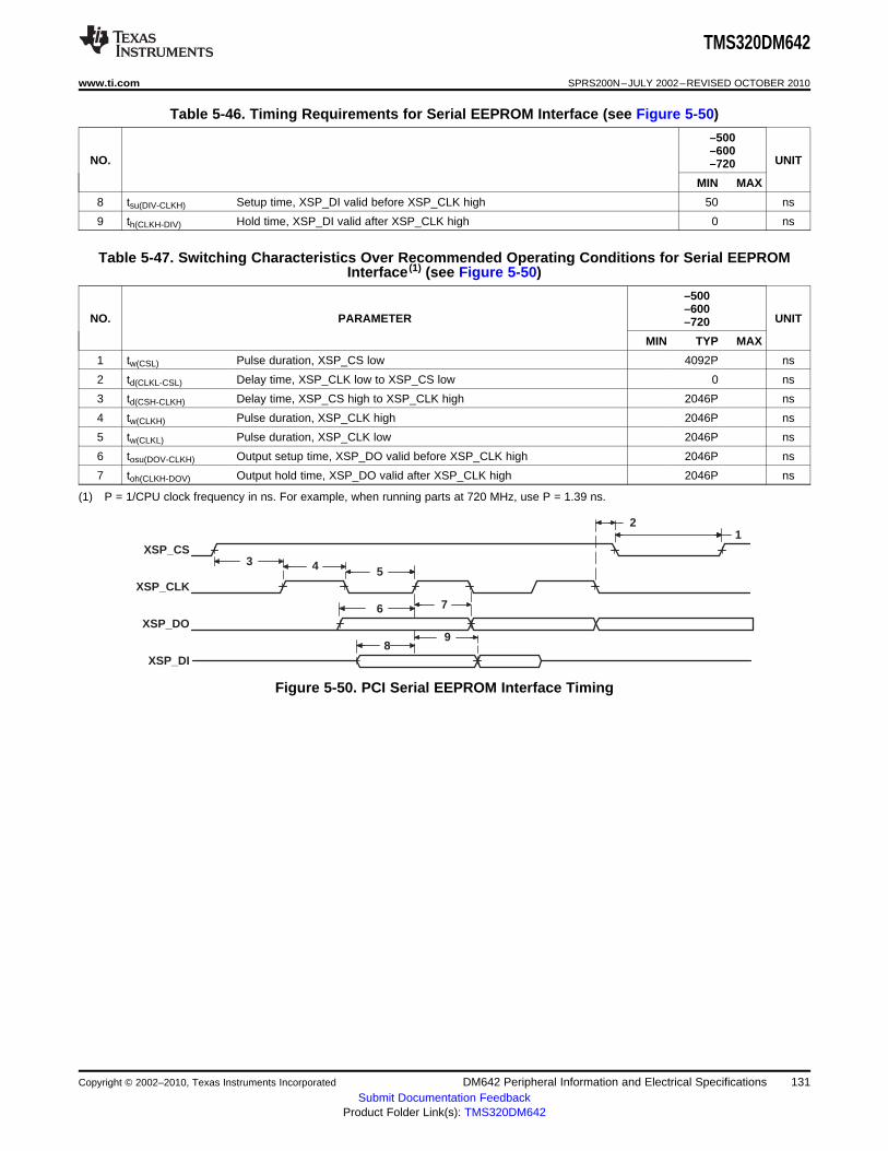
98
76
3
2
54
1XSP_CS
XSP_CLK
XSP_DO
XSP_DI
TMS320DM642
www.ti.com SPRS200N–JULY 2002–REVISED OCTOBER 2010
Table 5-46. Timing Requirements for Serial EEPROM Interface (see Figure 5-50)
–500–600
NO. UNIT–720
MIN MAX
8 tsu(DIV-CLKH) Setup time, XSP_DI valid before XSP_CLK high 50 ns
9 th(CLKH-DIV) Hold time, XSP_DI valid after XSP_CLK high 0 ns
Table 5-47. Switching Characteristics Over Recommended Operating Conditions for Serial EEPROMInterface (1) (see Figure 5-50)
–500–600
NO. PARAMETER UNIT–720
MIN TYP MAX
1 tw(CSL) Pulse duration, XSP_CS low 4092P ns
2 td(CLKL-CSL) Delay time, XSP_CLK low to XSP_CS low 0 ns
3 td(CSH-CLKH) Delay time, XSP_CS high to XSP_CLK high 2046P ns
4 tw(CLKH) Pulse duration, XSP_CLK high 2046P ns
5 tw(CLKL) Pulse duration, XSP_CLK low 2046P ns
6 tosu(DOV-CLKH) Output setup time, XSP_DO valid before XSP_CLK high 2046P ns
7 toh(CLKH-DOV) Output hold time, XSP_DO valid after XSP_CLK high 2046P ns
(1) P = 1/CPU clock frequency in ns. For example, when running parts at 720 MHz, use P = 1.39 ns.
Figure 5-50. PCI Serial EEPROM Interface Timing
Copyright © 2002–2010, Texas Instruments Incorporated DM642 Peripheral Information and Electrical Specifications 131Submit Documentation Feedback
Product Folder Link(s): TMS320DM642

TMS320DM642
SPRS200N–JULY 2002–REVISED OCTOBER 2010 www.ti.com
5.13 Multichannel Buffered Serial Port (McBSP)
The McBSP provides these functions:• Full-duplex communication• Double-buffered data registers, which allow a continuous data stream• Independent framing and clocking for receive and transmit• Direct interface to industry-standard codecs, analog interface chips (AICs), and other serially
connected analog-to-digital (A/D) and digital-to-analog (D/A) devices• External shift clock or an internal, programmable frequency shift clock for data transfer
For more detailed information on the McBSP peripheral, see the TMS320C6000 DSP MultichannelBuffered Serial Port (McBSP) Reference Guide (literature number SPRU580).
5.13.1 McBSP Peripheral Register Description(s)
Table 5-48. McBSP 0 Registers
HEX ADDRESS RANGE ACRONYM REGISTER NAME COMMENTS
The CPU and EDMA controller018C 0000 DRR0 McBSP0 data receive register via Configuration Bus can only read this register; they
cannot write to it.
0x3000 0000 – 0x33FF FFFF DRR0 McBSP0 data receive register via Peripheral Bus
018C 0004 DXR0 McBSP0 data transmit register via Configuration Bus
0x3000 0000 – 0x33FF FFFF DXR0 McBSP0 data transmit register via Peripheral Bus
018C 0008 SPCR0 McBSP0 serial port control register
018C 000C RCR0 McBSP0 receive control register
018C 0010 XCR0 McBSP0 transmit control register
018C 0014 SRGR0 McBSP0 sample rate generator register
018C 0018 MCR0 McBSP0 multichannel control register
018C 001C RCERE00 McBSP0 enhanced receive channel enable register 0
018C 0020 XCERE00 McBSP0 enhanced transmit channel enable register 0
018C 0024 PCR0 McBSP0 pin control register
018C 0028 RCERE10 McBSP0 enhanced receive channel enable register 1
018C 002C XCERE10 McBSP0 enhanced transmit channel enable register 1
018C 0030 RCERE20 McBSP0 enhanced receive channel enable register 2
018C 0034 XCERE20 McBSP0 enhanced transmit channel enable register 2
018C 0038 RCERE30 McBSP0 enhanced receive channel enable register 3
018C 003C XCERE30 McBSP0 enhanced transmit channel enable register 3
018C 0040 – 018F FFFF – Reserved
132 DM642 Peripheral Information and Electrical Specifications Copyright © 2002–2010, Texas Instruments Incorporated
Submit Documentation FeedbackProduct Folder Link(s): TMS320DM642
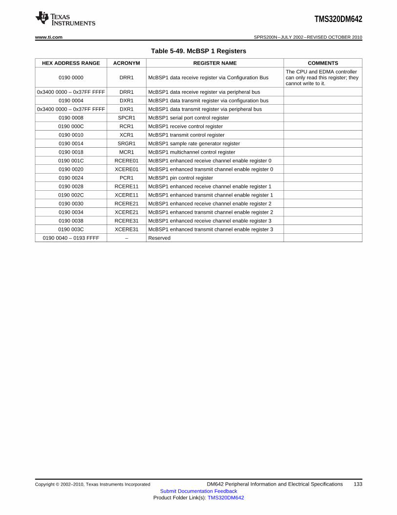
TMS320DM642
www.ti.com SPRS200N–JULY 2002–REVISED OCTOBER 2010
Table 5-49. McBSP 1 Registers
HEX ADDRESS RANGE ACRONYM REGISTER NAME COMMENTS
The CPU and EDMA controller0190 0000 DRR1 McBSP1 data receive register via Configuration Bus can only read this register; they
cannot write to it.
0x3400 0000 – 0x37FF FFFF DRR1 McBSP1 data receive register via peripheral bus
0190 0004 DXR1 McBSP1 data transmit register via configuration bus
0x3400 0000 – 0x37FF FFFF DXR1 McBSP1 data transmit register via peripheral bus
0190 0008 SPCR1 McBSP1 serial port control register
0190 000C RCR1 McBSP1 receive control register
0190 0010 XCR1 McBSP1 transmit control register
0190 0014 SRGR1 McBSP1 sample rate generator register
0190 0018 MCR1 McBSP1 multichannel control register
0190 001C RCERE01 McBSP1 enhanced receive channel enable register 0
0190 0020 XCERE01 McBSP1 enhanced transmit channel enable register 0
0190 0024 PCR1 McBSP1 pin control register
0190 0028 RCERE11 McBSP1 enhanced receive channel enable register 1
0190 002C XCERE11 McBSP1 enhanced transmit channel enable register 1
0190 0030 RCERE21 McBSP1 enhanced receive channel enable register 2
0190 0034 XCERE21 McBSP1 enhanced transmit channel enable register 2
0190 0038 RCERE31 McBSP1 enhanced receive channel enable register 3
0190 003C XCERE31 McBSP1 enhanced transmit channel enable register 3
0190 0040 – 0193 FFFF – Reserved
Copyright © 2002–2010, Texas Instruments Incorporated DM642 Peripheral Information and Electrical Specifications 133Submit Documentation Feedback
Product Folder Link(s): TMS320DM642

TMS320DM642
SPRS200N–JULY 2002–REVISED OCTOBER 2010 www.ti.com
5.13.2 McBSP Electrical Data/Timing
5.13.2.1 Multichannel Buffered Serial Port (McBSP) Timing
Table 5-50. Timing Requirements for McBSP (1) (see Figure 5-51)
–500–600
NO. UNIT–720
MIN MAX
2 tc(CKRX) Cycle time, CLKR/X CLKR/X ext 4P or 6.67 (2) (3) ns
3 tw(CKRX) Pulse duration, CLKR/X high or CLKR/X low CLKR/X ext 0.5tc(CKRX) –1 (4) ns
CLKR int 95 tsu(FRH-CKRL) Setup time, external FSR high before CLKR low ns
CLKR ext 1.3
CLKR int 66 th(CKRL-FRH) Hold time, external FSR high after CLKR low ns
CLKR ext 3
CLKR int 87 tsu(DRV-CKRL) Setup time, DR valid before CLKR low ns
CLKR ext 0.9
CLKR int 38 th(CKRL-DRV) Hold time, DR valid after CLKR low ns
CLKR ext 3.1
CLKX int 910 tsu(FXH-CKXL) Setup time, external FSX high before CLKX low ns
CLKX ext 1.3
CLKX int 611 th(CKXL-FXH) Hold time, external FSX high after CLKX low ns
CLKX ext 3
(1) CLKRP = CLKXP = FSRP = FSXP = 0. If polarity of any of the signals is inverted, then the timing references of that signal are alsoinverted.
(2) P = 1/CPU clock frequency in ns. For example, when running parts at 720 MHz, use P = 1.39 ns.(3) Use whichever value is greater. Minimum CLKR/X cycle times must be met, even when CLKR/X is generated by an internal clock
source. The minimum CLKR/X cycle times are based on internal logic speed; the maximum usable speed may be lower due to EDMAlimitations and AC timing requirements.
(4) This parameter applies to the maximum McBSP frequency. Operate serial clocks (CLKR/X) in the reasonable range of 40/60 duty cycle.
134 DM642 Peripheral Information and Electrical Specifications Copyright © 2002–2010, Texas Instruments Incorporated
Submit Documentation FeedbackProduct Folder Link(s): TMS320DM642
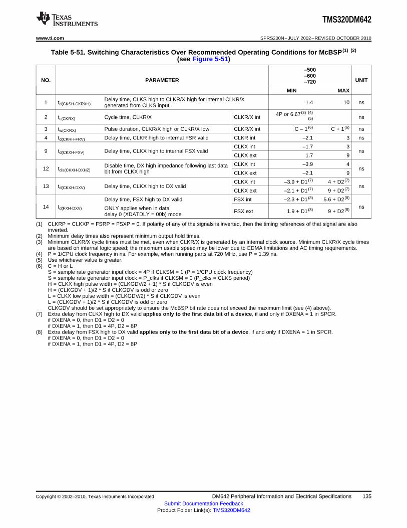
TMS320DM642
www.ti.com SPRS200N–JULY 2002–REVISED OCTOBER 2010
Table 5-51. Switching Characteristics Over Recommended Operating Conditions for McBSP (1) (2)
(see Figure 5-51)
–500–600
NO. PARAMETER UNIT–720
MIN MAX
Delay time, CLKS high to CLKR/X high for internal CLKR/X1 td(CKSH-CKRXH) 1.4 10 nsgenerated from CLKS input
4P or 6.67 (3) (4)2 tc(CKRX) Cycle time, CLKR/X CLKR/X int ns(5)
3 tw(CKRX) Pulse duration, CLKR/X high or CLKR/X low CLKR/X int C – 1 (6) C + 1 (6) ns
4 td(CKRH-FRV) Delay time, CLKR high to internal FSR valid CLKR int –2.1 3 ns
CLKX int –1.7 39 td(CKXH-FXV) Delay time, CLKX high to internal FSX valid ns
CLKX ext 1.7 9
CLKX int –3.9 4Disable time, DX high impedance following last data12 tdis(CKXH-DXHZ) nsbit from CLKX high CLKX ext –2.1 9
CLKX int –3.9 + D1 (7) 4 + D2 (7)
13 td(CKXH-DXV) Delay time, CLKX high to DX valid nsCLKX ext –2.1 + D1 (7) 9 + D2 (7)
Delay time, FSX high to DX valid FSX int –2.3 + D1 (8) 5.6 + D2 (8)
14 td(FXH-DXV) nsONLY applies when in data FSX ext 1.9 + D1 (8) 9 + D2 (8)delay 0 (XDATDLY = 00b) mode
(1) CLKRP = CLKXP = FSRP = FSXP = 0. If polarity of any of the signals is inverted, then the timing references of that signal are alsoinverted.
(2) Minimum delay times also represent minimum output hold times.(3) Minimum CLKR/X cycle times must be met, even when CLKR/X is generated by an internal clock source. Minimum CLKR/X cycle times
are based on internal logic speed; the maximum usable speed may be lower due to EDMA limitations and AC timing requirements.(4) P = 1/CPU clock frequency in ns. For example, when running parts at 720 MHz, use P = 1.39 ns.(5) Use whichever value is greater.(6) C = H or L
S = sample rate generator input clock = 4P if CLKSM = 1 (P = 1/CPU clock frequency)S = sample rate generator input clock = P_clks if CLKSM = 0 (P_clks = CLKS period)H = CLKX high pulse width = (CLKGDV/2 + 1) * S if CLKGDV is evenH = (CLKGDV + 1)/2 * S if CLKGDV is odd or zeroL = CLKX low pulse width = (CLKGDV/2) * S if CLKGDV is evenL = (CLKGDV + 1)/2 * S if CLKGDV is odd or zeroCLKGDV should be set appropriately to ensure the McBSP bit rate does not exceed the maximum limit (see (4) above).
(7) Extra delay from CLKX high to DX valid applies only to the first data bit of a device, if and only if DXENA = 1 in SPCR.if DXENA = 0, then D1 = D2 = 0if DXENA = 1, then D1 = 4P, D2 = 8P
(8) Extra delay from FSX high to DX valid applies only to the first data bit of a device, if and only if DXENA = 1 in SPCR.if DXENA = 0, then D1 = D2 = 0if DXENA = 1, then D1 = 4P, D2 = 8P
Copyright © 2002–2010, Texas Instruments Incorporated DM642 Peripheral Information and Electrical Specifications 135Submit Documentation Feedback
Product Folder Link(s): TMS320DM642

Bit(n-1) (n-2) (n-3)
Bit 0 Bit(n-1) (n-2) (n-3)
1412
1110
9
33
2
87
65
44
3
1
32
CLKS
CLKR
FSR (int)
FSR (ext)
DR
CLKX
FSX (int)
FSX (ext)
FSX (XDATDLY=00b)
DX
13 (A)
13 (A)
21
CLKS
FSR external
CLKR/X (no need to resync)
CLKR/X (needs resync)
TMS320DM642
SPRS200N–JULY 2002–REVISED OCTOBER 2010 www.ti.com
A. Parameter No. 13 applies to the first data bit only when XDATDLY ≠ 0.
Figure 5-51. McBSP Timing
Table 5-52. Timing Requirements for FSR When GSYNC = 1 (see Figure 5-52)
–500–600
NO. UNIT–720
MIN MAX
1 tsu(FRH-CKSH) Setup time, FSR high before CLKS high 4 ns
2 th(CKSH-FRH) Hold time, FSR high after CLKS high 4 ns
Figure 5-52. FSR Timing When GSYNC = 1
136 DM642 Peripheral Information and Electrical Specifications Copyright © 2002–2010, Texas Instruments Incorporated
Submit Documentation FeedbackProduct Folder Link(s): TMS320DM642
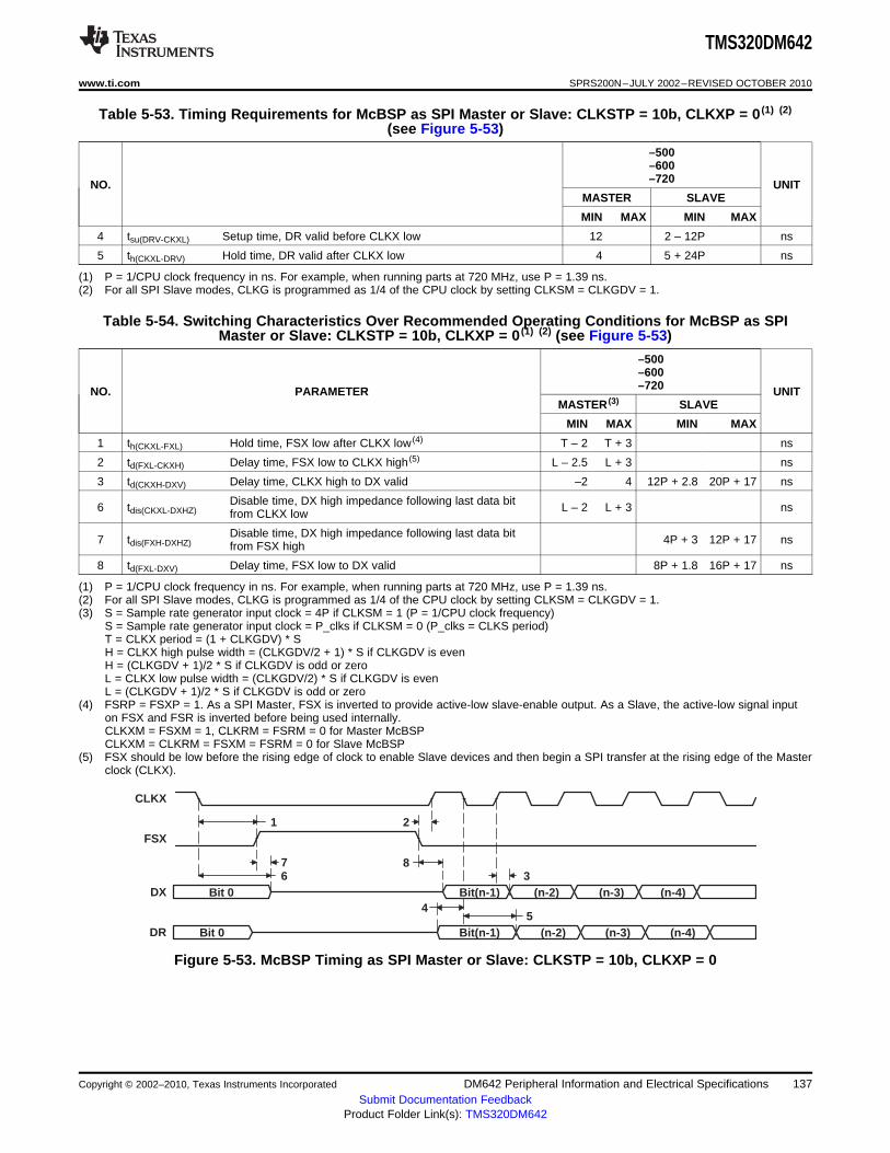
Bit 0 Bit(n-1) (n-2) (n-3) (n-4)
Bit 0 Bit(n-1) (n-2) (n-3) (n-4)5
4
387
6
21
CLKX
FSX
DX
DR
TMS320DM642
www.ti.com SPRS200N–JULY 2002–REVISED OCTOBER 2010
Table 5-53. Timing Requirements for McBSP as SPI Master or Slave: CLKSTP = 10b, CLKXP = 0 (1) (2)
(see Figure 5-53)
–500–600–720NO. UNIT
MASTER SLAVE
MIN MAX MIN MAX
4 tsu(DRV-CKXL) Setup time, DR valid before CLKX low 12 2 – 12P ns
5 th(CKXL-DRV) Hold time, DR valid after CLKX low 4 5 + 24P ns
(1) P = 1/CPU clock frequency in ns. For example, when running parts at 720 MHz, use P = 1.39 ns.(2) For all SPI Slave modes, CLKG is programmed as 1/4 of the CPU clock by setting CLKSM = CLKGDV = 1.
Table 5-54. Switching Characteristics Over Recommended Operating Conditions for McBSP as SPIMaster or Slave: CLKSTP = 10b, CLKXP = 0 (1) (2) (see Figure 5-53)
–500–600–720NO. PARAMETER UNIT
MASTER (3) SLAVE
MIN MAX MIN MAX
1 th(CKXL-FXL) Hold time, FSX low after CLKX low (4) T – 2 T + 3 ns
2 td(FXL-CKXH) Delay time, FSX low to CLKX high (5) L – 2.5 L + 3 ns
3 td(CKXH-DXV) Delay time, CLKX high to DX valid –2 4 12P + 2.8 20P + 17 ns
Disable time, DX high impedance following last data bit6 tdis(CKXL-DXHZ) L – 2 L + 3 nsfrom CLKX low
Disable time, DX high impedance following last data bit7 tdis(FXH-DXHZ) 4P + 3 12P + 17 nsfrom FSX high
8 td(FXL-DXV) Delay time, FSX low to DX valid 8P + 1.8 16P + 17 ns
(1) P = 1/CPU clock frequency in ns. For example, when running parts at 720 MHz, use P = 1.39 ns.(2) For all SPI Slave modes, CLKG is programmed as 1/4 of the CPU clock by setting CLKSM = CLKGDV = 1.(3) S = Sample rate generator input clock = 4P if CLKSM = 1 (P = 1/CPU clock frequency)
S = Sample rate generator input clock = P_clks if CLKSM = 0 (P_clks = CLKS period)T = CLKX period = (1 + CLKGDV) * SH = CLKX high pulse width = (CLKGDV/2 + 1) * S if CLKGDV is evenH = (CLKGDV + 1)/2 * S if CLKGDV is odd or zeroL = CLKX low pulse width = (CLKGDV/2) * S if CLKGDV is evenL = (CLKGDV + 1)/2 * S if CLKGDV is odd or zero
(4) FSRP = FSXP = 1. As a SPI Master, FSX is inverted to provide active-low slave-enable output. As a Slave, the active-low signal inputon FSX and FSR is inverted before being used internally.CLKXM = FSXM = 1, CLKRM = FSRM = 0 for Master McBSPCLKXM = CLKRM = FSXM = FSRM = 0 for Slave McBSP
(5) FSX should be low before the rising edge of clock to enable Slave devices and then begin a SPI transfer at the rising edge of the Masterclock (CLKX).
Figure 5-53. McBSP Timing as SPI Master or Slave: CLKSTP = 10b, CLKXP = 0
Copyright © 2002–2010, Texas Instruments Incorporated DM642 Peripheral Information and Electrical Specifications 137Submit Documentation Feedback
Product Folder Link(s): TMS320DM642
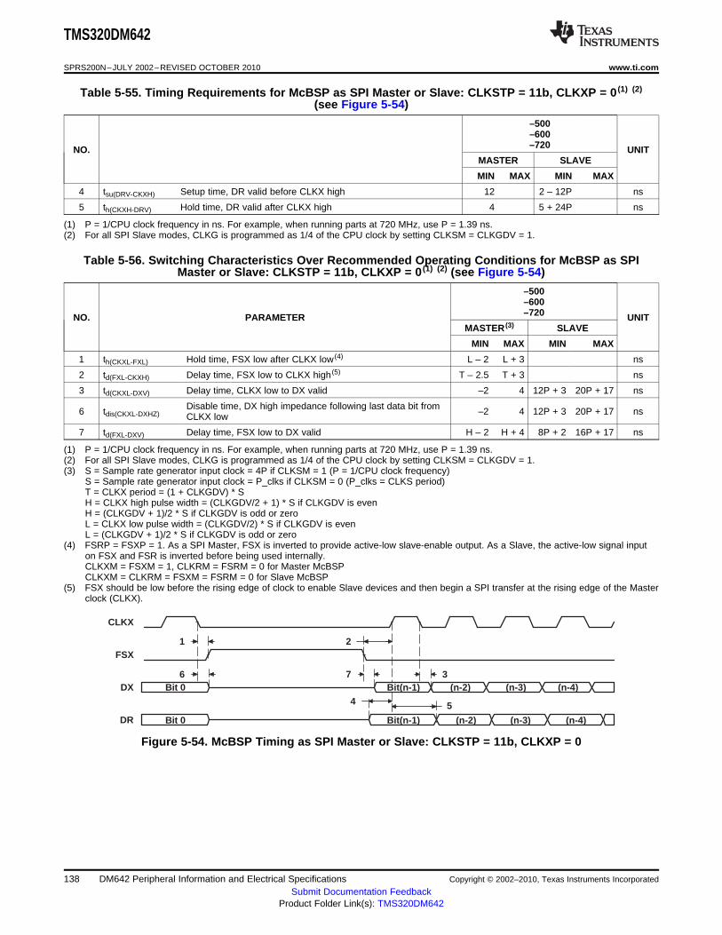
Bit 0 Bit(n-1) (n-2) (n-3) (n-4)
Bit 0 Bit(n-1) (n-2) (n-3) (n-4)
4
376
21
CLKX
FSX
DX
DR
5
TMS320DM642
SPRS200N–JULY 2002–REVISED OCTOBER 2010 www.ti.com
Table 5-55. Timing Requirements for McBSP as SPI Master or Slave: CLKSTP = 11b, CLKXP = 0 (1) (2)
(see Figure 5-54)
–500–600–720NO. UNIT
MASTER SLAVE
MIN MAX MIN MAX
4 tsu(DRV-CKXH) Setup time, DR valid before CLKX high 12 2 – 12P ns
5 th(CKXH-DRV) Hold time, DR valid after CLKX high 4 5 + 24P ns
(1) P = 1/CPU clock frequency in ns. For example, when running parts at 720 MHz, use P = 1.39 ns.(2) For all SPI Slave modes, CLKG is programmed as 1/4 of the CPU clock by setting CLKSM = CLKGDV = 1.
Table 5-56. Switching Characteristics Over Recommended Operating Conditions for McBSP as SPIMaster or Slave: CLKSTP = 11b, CLKXP = 0 (1) (2) (see Figure 5-54)
–500–600–720NO. PARAMETER UNIT
MASTER (3) SLAVE
MIN MAX MIN MAX
1 th(CKXL-FXL) Hold time, FSX low after CLKX low (4) L – 2 L + 3 ns
2 td(FXL-CKXH) Delay time, FSX low to CLKX high (5) T – 2.5 T + 3 ns
3 td(CKXL-DXV) Delay time, CLKX low to DX valid –2 4 12P + 3 20P + 17 ns
Disable time, DX high impedance following last data bit from6 tdis(CKXL-DXHZ) –2 4 12P + 3 20P + 17 nsCLKX low
7 td(FXL-DXV) Delay time, FSX low to DX valid H – 2 H + 4 8P + 2 16P + 17 ns
(1) P = 1/CPU clock frequency in ns. For example, when running parts at 720 MHz, use P = 1.39 ns.(2) For all SPI Slave modes, CLKG is programmed as 1/4 of the CPU clock by setting CLKSM = CLKGDV = 1.(3) S = Sample rate generator input clock = 4P if CLKSM = 1 (P = 1/CPU clock frequency)
S = Sample rate generator input clock = P_clks if CLKSM = 0 (P_clks = CLKS period)T = CLKX period = (1 + CLKGDV) * SH = CLKX high pulse width = (CLKGDV/2 + 1) * S if CLKGDV is evenH = (CLKGDV + 1)/2 * S if CLKGDV is odd or zeroL = CLKX low pulse width = (CLKGDV/2) * S if CLKGDV is evenL = (CLKGDV + 1)/2 * S if CLKGDV is odd or zero
(4) FSRP = FSXP = 1. As a SPI Master, FSX is inverted to provide active-low slave-enable output. As a Slave, the active-low signal inputon FSX and FSR is inverted before being used internally.CLKXM = FSXM = 1, CLKRM = FSRM = 0 for Master McBSPCLKXM = CLKRM = FSXM = FSRM = 0 for Slave McBSP
(5) FSX should be low before the rising edge of clock to enable Slave devices and then begin a SPI transfer at the rising edge of the Masterclock (CLKX).
Figure 5-54. McBSP Timing as SPI Master or Slave: CLKSTP = 11b, CLKXP = 0
138 DM642 Peripheral Information and Electrical Specifications Copyright © 2002–2010, Texas Instruments Incorporated
Submit Documentation FeedbackProduct Folder Link(s): TMS320DM642

Bit 0 Bit(n-1) (n-2) (n-3) (n-4)
Bit 0 Bit(n-1) (n-2) (n-3) (n-4)54
387
6
21
CLKX
FSX
DX
DR
TMS320DM642
www.ti.com SPRS200N–JULY 2002–REVISED OCTOBER 2010
Table 5-57. Timing Requirements for McBSP as SPI Master or Slave: CLKSTP = 10b, CLKXP = 1 (1) (2)
(see Figure 5-55)
–500–600–720NO. UNIT
MASTER SLAVE
MIN MAX MIN MAX
4 tsu(DRV-CKXH) Setup time, DR valid before CLKX high 12 2 – 12P ns
5 th(CKXH-DRV) Hold time, DR valid after CLKX high 4 5 + 24P ns
(1) P = 1/CPU clock frequency in ns. For example, when running parts at 720 MHz, use P = 1.39 ns.(2) For all SPI Slave modes, CLKG is programmed as 1/4 of the CPU clock by setting CLKSM = CLKGDV = 1.
Table 5-58. Switching Characteristics Over Recommended Operating Conditions for McBSP as SPIMaster or Slave: CLKSTP = 10b, CLKXP = 1 (1) (2) (see Figure 5-55)
–500–600–720NO. PARAMETER UNIT
MASTER (3) SLAVE
MIN MAX MIN MAX
1 th(CKXH-FXL) Hold time, FSX low after CLKX high (4) T – 2 T + 3 ns
2 td(FXL-CKXL) Delay time, FSX low to CLKX low (5) H – 2.5 H + 3 ns
3 td(CKXL-DXV) Delay time, CLKX low to DX valid –2 4 12P + 3 20P + 17 ns
Disable time, DX high impedance following last data bit6 tdis(CKXH-DXHZ) H – 2 H + 3 nsfrom CLKX high
Disable time, DX high impedance following last data bit7 tdis(FXH-DXHZ) 4P + 3 12P + 17 nsfrom FSX high
8 td(FXL-DXV) Delay time, FSX low to DX valid 8P + 2 16P + 17 ns
(1) P = 1/CPU clock frequency in ns. For example, when running parts at 720 MHz, use P = 1.39 ns.(2) For all SPI Slave modes, CLKG is programmed as 1/4 of the CPU clock by setting CLKSM = CLKGDV = 1.(3) S = Sample rate generator input clock = 4P if CLKSM = 1 (P = 1/CPU clock frequency)
S = Sample rate generator input clock = P_clks if CLKSM = 0 (P_clks = CLKS period)T = CLKX period = (1 + CLKGDV) * SH = CLKX high pulse width = (CLKGDV/2 + 1) * S if CLKGDV is evenH = (CLKGDV + 1)/2 * S if CLKGDV is odd or zeroL = CLKX low pulse width = (CLKGDV/2) * S if CLKGDV is evenL = (CLKGDV + 1)/2 * S if CLKGDV is odd or zero
(4) FSRP = FSXP = 1. As a SPI Master, FSX is inverted to provide active-low slave-enable output. As a Slave, the active-low signal inputon FSX and FSR is inverted before being used internally.CLKXM = FSXM = 1, CLKRM = FSRM = 0 for Master McBSPCLKXM = CLKRM = FSXM = FSRM = 0 for Slave McBSP
(5) FSX should be low before the rising edge of clock to enable Slave devices and then begin a SPI transfer at the rising edge of the Masterclock (CLKX).
Figure 5-55. McBSP Timing as SPI Master or Slave: CLKSTP = 10b, CLKXP = 1
Copyright © 2002–2010, Texas Instruments Incorporated DM642 Peripheral Information and Electrical Specifications 139Submit Documentation Feedback
Product Folder Link(s): TMS320DM642

Bit 0 Bit(n-1) (n-2) (n-3) (n-4)
Bit 0 Bit(n-1) (n-2) (n-3) (n-4)5
4
376
21
CLKX
FSX
DX
DR
TMS320DM642
SPRS200N–JULY 2002–REVISED OCTOBER 2010 www.ti.com
Table 5-59. Timing Requirements for McBSP as SPI Master or Slave: CLKSTP = 11b, CLKXP = 1 (1) (2)
(see Figure 5-56)
–500–600–720NO. UNIT
MASTER SLAVE
MIN MAX MIN MAX
4 tsu(DRV-CKXH) Setup time, DR valid before CLKX high 12 2 – 12P ns
5 th(CKXH-DRV) Hold time, DR valid after CLKX high 4 5 + 24P ns
(1) P = 1/CPU clock frequency in ns. For example, when running parts at 720 MHz, use P = 1.39 ns.(2) For all SPI Slave modes, CLKG is programmed as 1/4 of the CPU clock by setting CLKSM = CLKGDV = 1.
Table 5-60. Switching Characteristics Over Recommended Operating Conditions for McBSP as SPIMaster or Slave: CLKSTP = 11b, CLKXP = 1 (1) (2) (see Figure 5-56)
–500–600–720NO. PARAMETER UNIT
MASTER (3) SLAVE
MIN MAX MIN MAX
1 th(CKXH-FXL) Hold time, FSX low after CLKX high (4) H – 2 H + 3 ns
2 td(FXL-CKXL) Delay time, FSX low to CLKX low (5) T – 2.5 T + 1.5 ns
3 td(CKXH-DXV) Delay time, CLKX high to DX valid –2 4 12P + 3 20P + 17 ns
Disable time, DX high impedance following last data bit6 tdis(CKXH-DXHZ) –2 4 12P + 3 20P + 17 nsfrom CLKX high
7 td(FXL-DXV) Delay time, FSX low to DX valid L – 2 L + 4 8P + 2 16P + 17 ns
(1) P = 1/CPU clock frequency in ns. For example, when running parts at 720 MHz, use P = 1.39 ns.(2) For all SPI Slave modes, CLKG is programmed as 1/4 of the CPU clock by setting CLKSM = CLKGDV = 1.(3) S = Sample rate generator input clock = 4P if CLKSM = 1 (P = 1/CPU clock frequency)
S = Sample rate generator input clock = P_clks if CLKSM = 0 (P_clks = CLKS period)T = CLKX period = (1 + CLKGDV) * SH = CLKX high pulse width = (CLKGDV/2 + 1) * S if CLKGDV is evenH = (CLKGDV + 1)/2 * S if CLKGDV is odd or zeroL = CLKX low pulse width = (CLKGDV/2) * S if CLKGDV is evenL = (CLKGDV + 1)/2 * S if CLKGDV is odd or zero
(4) FSRP = FSXP = 1. As a SPI Master, FSX is inverted to provide active-low slave-enable output. As a Slave, the active-low signal inputon FSX and FSR is inverted before being used internally.CLKXM = FSXM = 1, CLKRM = FSRM = 0 for Master McBSPCLKXM = CLKRM = FSXM = FSRM = 0 for Slave McBSP
(5) FSX should be low before the rising edge of clock to enable Slave devices and then begin a SPI transfer at the rising edge of the Masterclock (CLKX).
Figure 5-56. McBSP Timing as SPI Master or Slave: CLKSTP = 11b, CLKXP = 1
140 DM642 Peripheral Information and Electrical Specifications Copyright © 2002–2010, Texas Instruments Incorporated
Submit Documentation FeedbackProduct Folder Link(s): TMS320DM642
TMS320DM642
www.ti.com SPRS200N–JULY 2002–REVISED OCTOBER 2010
5.14 Video Port
Each Video Port is capable of sending and receiving digital video data. The Video Ports are also capableof capturing/displaying RAW data. The Video Port peripherals follow video standards such as BT.656 andSMPTE296.
5.14.1 Video Port Device-Specific Information
The TMS320DM642 device has three video port peripherals.
The video port peripheral can operate as a video capture port, video display port, or as a transport streaminterface (TSI) capture port.
The port consists of two channels: A and B. A 5120-byte capture/display buffer is splittable between thetwo channels. The entire port (both channels) is always configured for either video capture or display only.Separate data pipelines control the parsing and formatting of video capture or display data for each of theBT.656, Y/C, raw video, and TSI modes.
For video capture operation, the video port may operate as two 8/10-bit channels of BT.656 or raw videocapture; or as a single channel of 8/10-bit BT.656, 8/10-bit raw video, 16/20-bit Y/C video, 16/20-bit rawvideo, or 8-bit TSI.
For video display operation, the video port may operate as a single channel of 8/10-bit BT.656; or as asingle channel of 8/10-bit BT.656, 8/10-bit raw video, 16/20 bit Y/C video, or 16/20-bit raw video. It mayalso operate in a two channel 8/10-bit raw mode in which the two channels are locked to the same timing.Channel B is not used during single channel operation.
For more detailed information on the DM642 Video Port peripherals, see the TMS320C64x DSP VideoPort/VCXO Interpolated Control (VIC) Port Reference Guide (literature number SPRU629).
5.14.2 Video Port Peripheral Register Description(s)
Table 5-61. Video Port 0, 1, and 2 (VP0, VP1, and VP2) Control Registers
HEX ADDRESS RANGEACRONYM DESCRIPTION
VP0 VP1 VP2
01C4 0000 01C4 4000 01C4 8000 VP_PIDx Video Port Peripheral Identification Register
01C4 0004 01C4 4004 01C4 8004 VP_PCRx Video Port Peripheral Control Register
01C4 0008 01C4 4008 01C4 8008 – Reserved
01C4 000C 01C4 400C 01C4 800C – Reserved
01C4 0020 01C4 4020 01C4 8020 VP_PFUNCx Video Port Pin Function Register
01C4 0024 01C4 4024 01C4 8024 VP_PDIRx Video Port Pin Direction Register
01C4 0028 01C4 4028 01C4 8028 VP_PDINx Video Port Pin Data Input Register
01C4 002C 01C4 402C 01C4 802C VP_PDOUTx Video Port Pin Data Output Register
01C4 0030 01C4 4030 01C4 8030 VP_PDSETx Video Port Pin Data Set Register
01C4 0034 01C4 4034 01C4 8034 VP_PDCLRx Video Port Pin Data Clear Register
01C4 0038 01C4 4038 01C4 8038 VP_PIENx Video Port Pin Interrupt Enable Register
01C4 003C 01C4 403C 01C4 803C VP_PIPOx Video Port Pin Interrupt Polarity Register
01C4 0040 01C4 4040 01C4 8040 VP_PISTATx Video Port Pin Interrupt Status Register
01C4 0044 01C4 4044 01C4 8044 VP_PICLRx Video Port Pin Interrupt Clear Register
01C4 00C0 01C4 40C0 01C4 80C0 VP_CTLx Video Port Control Register
01C4 00C4 01C4 40C4 01C4 80C4 VP_STATx Video Port Status Register
01C4 00C8 01C4 40C8 01C4 80C8 VP_IEx Video Port Interrupt Enable Register
01C4 00CC 01C4 40CC 01C4 80CC VP_ISx Video Port interrupt Status Register
01C4 0100 01C4 4100 01C4 8100 VC_STATx Video Capture Channel A Status Register
01C4 0104 01C4 4104 01C4 8104 VC_CTLx Video Capture Channel A Control Register
Copyright © 2002–2010, Texas Instruments Incorporated DM642 Peripheral Information and Electrical Specifications 141Submit Documentation Feedback
Product Folder Link(s): TMS320DM642

TMS320DM642
SPRS200N–JULY 2002–REVISED OCTOBER 2010 www.ti.com
Table 5-61. Video Port 0, 1, and 2 (VP0, VP1, and VP2) Control Registers (continued)
HEX ADDRESS RANGEACRONYM DESCRIPTION
VP0 VP1 VP2
01C4 0108 01C4 4108 01C4 8108 VC_ASTRTx Video Capture Channel A Field 1 Start Register
01C4 010C 01C4 410C 01C4 810C VC_ASTOPx Video Capture Channel A Field 1 Stop Register
01C4 0110 01C4 4110 01C4 8110 VC_ASTRTx Video Capture Channel A Field 2 Start Register
01C4 0114 01C4 4114 01C4 8114 VC_ASTOPx Video Capture Channel A Field 2 Stop Register
01C4 0118 01C4 4118 01C4 8118 VC_AVINTx Video Capture Channel A Vertical Interrupt Register
01C4 011C 01C4 411C 01C4 811C VC_ATHRLDx Video Capture Channel A Threshold Register
01C4 0120 01C4 4120 01C4 8120 VC_AEVTCTx Video Capture Channel A Event Count Register
01C4 0140 01C4 4140 01C4 8140 VC_BSTATx Video Capture Channel B Status Register
01C4 0144 01C4 4144 01C4 8144 VC_BCTLx Video Capture Channel B Control Register
01C4 0148 01C4 4148 01C4 8148 VC_BSTRTx Video Capture Channel B Field 1 Start Register
01C4 014C 01C4 414C 01C4 814C VC_BSTOPx Video Capture Channel B Field 1 Stop Register
01C4 0150 01C4 4150 01C4 8150 VC_BSTRTx Video Capture Channel B Field 2 Start Register
01C4 0154 01C4 4154 01C4 8154 VC_BSTOPx Video Capture Channel B Field 2 Stop Register
01C4 0158 01C4 4158 01C4 8158 VC_BVINTx Video Capture Channel B Vertical Interrupt Register
01C4 015C 01C4 415C 01C4 815C VC_BTHRLDx Video Capture Channel B Threshold Register
01C4 0160 01C4 4160 01C4 8160 VC_BEVTCTx Video Capture Channel B Event Count Register
01C4 0180 01C4 4180 01C4 8180 TSI_CTLx TCI Capture Control Register
01C4 0184 01C4 4184 01C4 8184 TSI_CLKINITLx TCI Clock Initialization LSB Register
01C4 0188 01C4 4188 01C4 8188 TSI_CLKINITMx TCI Clock Initialization MSB Register
01C4 018C 01C4 418C 01C4 818C TSI_STCLKLx TCI System Time Clock LSB Register
01C4 0190 01C4 4190 01C4 8190 TSI_STCLKMx TCI System Time Clock MSB Register
01C4 0194 01C4 4194 01C4 8194 TSI_STCMPLx TCI System Time Clock Compare LSB Register
01C4 0198 01C4 4198 01C4 8198 TSI_STCMPMx TCI System Time Clock Compare MSB Register
01C4 019C 01C4 419C 01C4 819C TSI_STMSKLx TCI System Time Clock Compare Mask LSB Register
01C4 01A0 01C4 41A0 01C4 81A0 TSI_STMSKMx TCI System Time Clock Compare Mask MSB Register
01C4 01A4 01C4 41A4 01C4 81A4 TSI_TICKSx TCI System Time Clock Ticks Interrupt Register
01C4 0200 01C4 4200 01C4 8200 VD_STATx Video Display Status Register
01C4 0204 01C4 4204 01C4 8204 VD_CTLx Video Display Control Register
01C4 0208 01C4 4208 01C4 8208 VD_FRMSZx Video Display Frame Size Register
01C4 020C 01C4 420C 01C4 820C VD_HBLNKx Video Display Horizontal Blanking Register
01C4 0210 01C4 4210 01C4 8210 VD_VBLKS1x Video Display Field 1 Vertical Blanking Start Register
01C4 0214 01C4 4214 01C4 8214 VD_VBLKE1x Video Display Field 1 Vertical Blanking End Register
01C4 0218 01C4 4218 01C4 8218 VD_VBLKS2x Video Display Field 2 Vertical Blanking Start Register
01C4 021C 01C4 421C 01C4 821C VD_VBLKE2x Video Display Field 2 Vertical Blanking End Register
01C4 0220 01C4 4220 01C4 8220 VD_IMGOFF1x Video Display Field 1 Image Offset Register
01C4 0224 01C4 4224 01C4 8224 VD_IMGSZ1x Video Display Field 1 Image Size Register
01C4 0228 01C4 4228 01C4 8228 VD_IMGOFF2x Video Display Field 2 Image Offset Register
01C4 022C 01C4 422C 01C4 822C VD_IMGSZ2x Video Display Field 2 Image Size Register
01C4 0230 01C4 4230 01C4 8230 VD_FLDT1x Video Display Field 1 Timing Register
01C4 0234 01C4 4234 01C4 8234 VD_FLDT2x Video Display Field 2 Timing Register
01C4 0238 01C4 4238 01C4 8238 VD_THRLDx Video Display Threshold Register
01C4 023C 01C4 423C 01C4 823C VD_HSYNCx Video Display Horizontal Synchronization Register
01C4 0240 01C4 4240 01C4 8240 VD_VSYNS1x Video Display Field 1 Vertical Synchronization Start Register
01C4 0244 01C4 4244 01C4 8244 VD_VSYNE1x Video Display Field 1 Vertical Synchronization End Register
01C4 0248 01C4 4248 01C4 8248 VD_VSYNS2x Video Display Field 2 Vertical Synchronization Start Register
01C4 024C 01C4 424C 01C4 824C VD_VSYNE2x Video Display Field 2 Vertical Synchronization End Register
142 DM642 Peripheral Information and Electrical Specifications Copyright © 2002–2010, Texas Instruments Incorporated
Submit Documentation FeedbackProduct Folder Link(s): TMS320DM642

TMS320DM642
www.ti.com SPRS200N–JULY 2002–REVISED OCTOBER 2010
Table 5-61. Video Port 0, 1, and 2 (VP0, VP1, and VP2) Control Registers (continued)
HEX ADDRESS RANGEACRONYM DESCRIPTION
VP0 VP1 VP2
01C4 0250 01C4 4250 01C4 8250 VD_RELOADx Video Display Counter Reload Register
01C4 0254 01C4 4254 01C4 8254 VD_DISPEVTx Video Display Display Event Register
01C4 0258 01C4 4258 01C4 8258 VD_CLIPx Video Display Clipping Register
01C4 025C 01C4 425C 01C4 825C VD_DEFVALx Video Display Default Display Value Register
01C4 0260 01C4 4260 01C4 8260 VD_VINTx Video Display Vertical Interrupt Register
01C4 0264 01C4 4264 01C4 8264 VD_FBITx Video Display Field Bit Register
01C4 0268 01C4 4268 01C4 8268 VD_VBIT1x Video Display Field 1Vertical Blanking Bit Register
01C4 026C 01C4 426C 01C4 826C VD_VBIT2x Video Display Field 2Vertical Blanking Bit Register
7400 000 7800 0000 7C00 0000 Y_RSCA Y FIFO Source Register A
7400 0008 7800 0008 7C00 0008 CB_SRCA CB FIFO Source Register A
7400 0010 7800 0010 7C00 0010 CR_SRCA CR FIFO Source Register A
7400 0020 7800 0020 7C00 0020 Y_DSTA Y FIFO Destination Register A
7400 0028 7800 0028 7C00 0028 CB_DST CB FIFO Destination Register
7400 0030 7800 0030 7C00 0030 CR_DST CR FIFO Destination Register
7600 0000 7A00 0000 7E00 0000 Y_SRCB Y FIFO Source Register B
7600 0008 7A00 0008 7E00 0008 CB_SRCB CB FIFO Source Register b
7600 0010 7A00 0010 7E00 0010 CR_SRCB CR FIFO Source Register B
7600 0020 7A00 0020 7E00 0020 Y_DSTB Y FIFO Destination Register B
Copyright © 2002–2010, Texas Instruments Incorporated DM642 Peripheral Information and Electrical Specifications 143Submit Documentation Feedback
Product Folder Link(s): TMS320DM642

VPxCLKINx
2 3
1 4
4
TMS320DM642
SPRS200N–JULY 2002–REVISED OCTOBER 2010 www.ti.com
5.14.3 Video Port (VP0, VP1, VP2) Electrical Data/Timing
5.14.3.1 VCLKIN Timing (Video Capture Mode)
Table 5-62. Timing Requirements for Video Capture Mode for VPxCLKINx (1)
(see Figure 5-57)
–500–600
NO. UNIT–720
MIN MAX
1 tc(VKI) Cycle time, VPxCLKINx 12.5 ns
2 tw(VKIH) Pulse duration, VPxCLKINx high 5.4 ns
3 tw(VKIL) Pulse duration, VPxCLKINx low 5.4 ns
4 tt(VKI) Transition time, VPxCLKINx 3 ns
(1) The reference points for the rise and fall transitions are measured at VIL MAX and VIH MIN.
Figure 5-57. Video Port Capture VPxCLKINx TIming
144 DM642 Peripheral Information and Electrical Specifications Copyright © 2002–2010, Texas Instruments Incorporated
Submit Documentation FeedbackProduct Folder Link(s): TMS320DM642
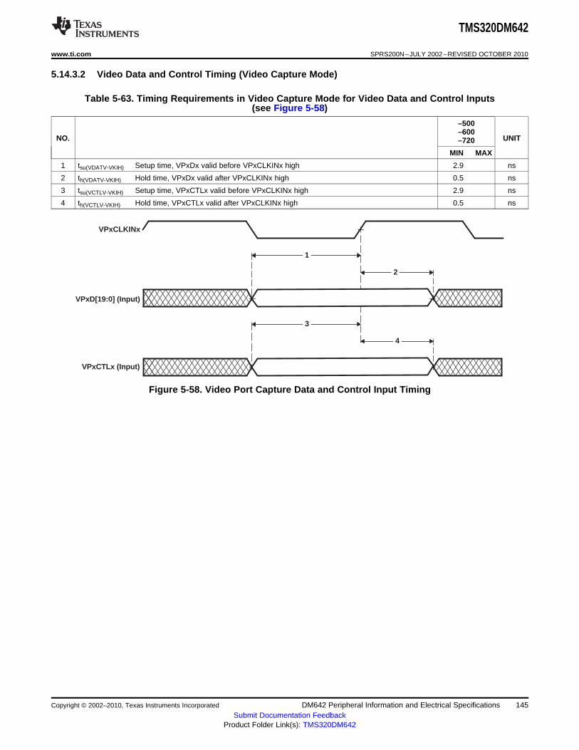
VPxCLKINx
VPxD[19:0] (Input)
VPxCTLx (Input)
1
2
3
4
TMS320DM642
www.ti.com SPRS200N–JULY 2002–REVISED OCTOBER 2010
5.14.3.2 Video Data and Control Timing (Video Capture Mode)
Table 5-63. Timing Requirements in Video Capture Mode for Video Data and Control Inputs(see Figure 5-58)
–500–600
NO. UNIT–720
MIN MAX
1 tsu(VDATV-VKIH) Setup time, VPxDx valid before VPxCLKINx high 2.9 ns
2 th(VDATV-VKIH) Hold time, VPxDx valid after VPxCLKINx high 0.5 ns
3 tsu(VCTLV-VKIH) Setup time, VPxCTLx valid before VPxCLKINx high 2.9 ns
4 th(VCTLV-VKIH) Hold time, VPxCTLx valid after VPxCLKINx high 0.5 ns
Figure 5-58. Video Port Capture Data and Control Input Timing
Copyright © 2002–2010, Texas Instruments Incorporated DM642 Peripheral Information and Electrical Specifications 145Submit Documentation Feedback
Product Folder Link(s): TMS320DM642
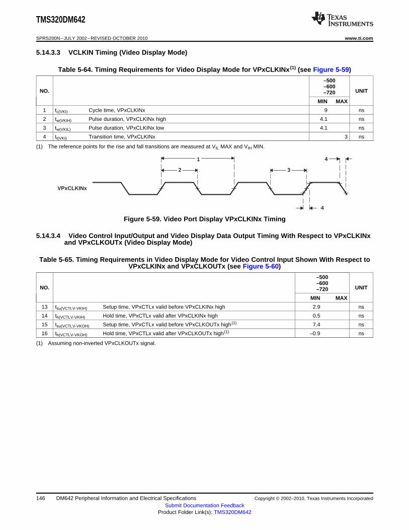
VPxCLKINx
2 3
1 4
4
TMS320DM642
SPRS200N–JULY 2002–REVISED OCTOBER 2010 www.ti.com
5.14.3.3 VCLKIN Timing (Video Display Mode)
Table 5-64. Timing Requirements for Video Display Mode for VPxCLKINx (1) (see Figure 5-59)
–500–600
NO. UNIT–720
MIN MAX
1 tc(VKI) Cycle time, VPxCLKINx 9 ns
2 tw(VKIH) Pulse duration, VPxCLKINx high 4.1 ns
3 tw(VKIL) Pulse duration, VPxCLKINx low 4.1 ns
4 tt(VKI) Transition time, VPxCLKINx 3 ns
(1) The reference points for the rise and fall transitions are measured at VIL MAX and VIH MIN.
Figure 5-59. Video Port Display VPxCLKINx Timing
5.14.3.4 Video Control Input/Output and Video Display Data Output Timing With Respect to VPxCLKINxand VPxCLKOUTx (Video Display Mode)
Table 5-65. Timing Requirements in Video Display Mode for Video Control Input Shown With Respect toVPxCLKINx and VPxCLKOUTx (see Figure 5-60)
–500–600
NO. UNIT–720
MIN MAX
13 tsu(VCTLV-VKIH) Setup time, VPxCTLx valid before VPxCLKINx high 2.9 ns
14 th(VCTLV-VKIH) Hold time, VPxCTLx valid after VPxCLKINx high 0.5 ns
15 tsu(VCTLV-VKOH) Setup time, VPxCTLx valid before VPxCLKOUTx high (1) 7.4 ns
16 th(VCTLV-VKOH) Hold time, VPxCTLx valid after VPxCLKOUTx high (1) –0.9 ns
(1) Assuming non-inverted VPxCLKOUTx signal.
146 DM642 Peripheral Information and Electrical Specifications Copyright © 2002–2010, Texas Instruments Incorporated
Submit Documentation FeedbackProduct Folder Link(s): TMS320DM642
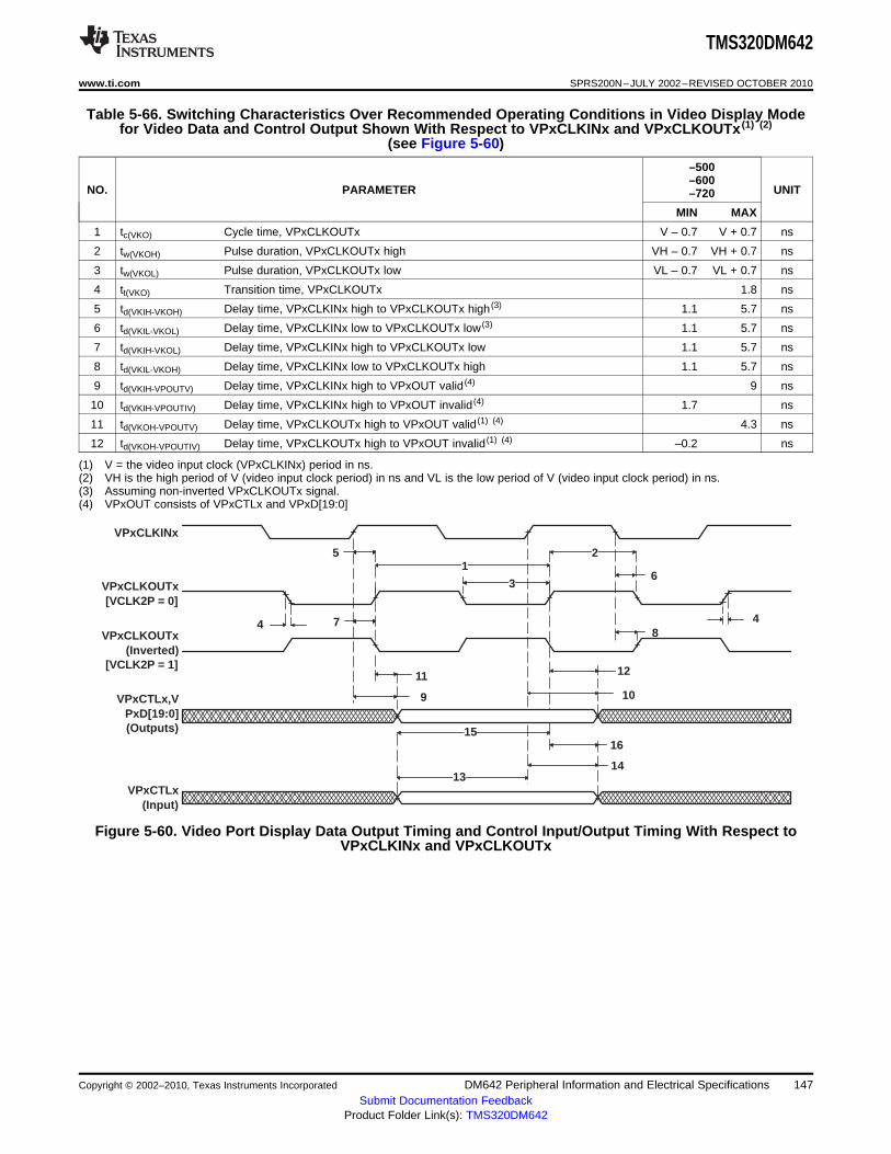
VPxCLKINx
VPxCLKOUTx[VCLK2P = 0]
VPxCLKOUTx(Inverted)
[VCLK2P = 1]
VPxCTLx,VPxD[19:0](Outputs)
VPxCTLx(Input)
5
7
1
3
2
6
8
9
13
10
14
11 12
1516
44
TMS320DM642
www.ti.com SPRS200N–JULY 2002–REVISED OCTOBER 2010
Table 5-66. Switching Characteristics Over Recommended Operating Conditions in Video Display Modefor Video Data and Control Output Shown With Respect to VPxCLKINx and VPxCLKOUTx (1) (2)
(see Figure 5-60)
–500–600
NO. PARAMETER UNIT–720
MIN MAX
1 tc(VKO) Cycle time, VPxCLKOUTx V – 0.7 V + 0.7 ns
2 tw(VKOH) Pulse duration, VPxCLKOUTx high VH – 0.7 VH + 0.7 ns
3 tw(VKOL) Pulse duration, VPxCLKOUTx low VL – 0.7 VL + 0.7 ns
4 tt(VKO) Transition time, VPxCLKOUTx 1.8 ns
5 td(VKIH-VKOH) Delay time, VPxCLKINx high to VPxCLKOUTx high (3) 1.1 5.7 ns
6 td(VKIL-VKOL) Delay time, VPxCLKINx low to VPxCLKOUTx low (3) 1.1 5.7 ns
7 td(VKIH-VKOL) Delay time, VPxCLKINx high to VPxCLKOUTx low 1.1 5.7 ns
8 td(VKIL-VKOH) Delay time, VPxCLKINx low to VPxCLKOUTx high 1.1 5.7 ns
9 td(VKIH-VPOUTV) Delay time, VPxCLKINx high to VPxOUT valid (4) 9 ns
10 td(VKIH-VPOUTIV) Delay time, VPxCLKINx high to VPxOUT invalid (4) 1.7 ns
11 td(VKOH-VPOUTV) Delay time, VPxCLKOUTx high to VPxOUT valid (1) (4) 4.3 ns
12 td(VKOH-VPOUTIV) Delay time, VPxCLKOUTx high to VPxOUT invalid (1) (4) –0.2 ns
(1) V = the video input clock (VPxCLKINx) period in ns.(2) VH is the high period of V (video input clock period) in ns and VL is the low period of V (video input clock period) in ns.(3) Assuming non-inverted VPxCLKOUTx signal.(4) VPxOUT consists of VPxCTLx and VPxD[19:0]
Figure 5-60. Video Port Display Data Output Timing and Control Input/Output Timing With Respect toVPxCLKINx and VPxCLKOUTx
Copyright © 2002–2010, Texas Instruments Incorporated DM642 Peripheral Information and Electrical Specifications 147Submit Documentation Feedback
Product Folder Link(s): TMS320DM642
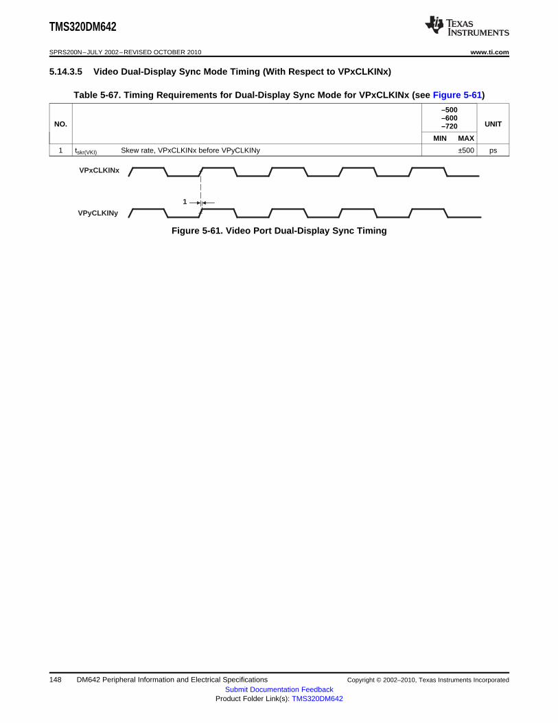
1
VPxCLKINx
VPyCLKINy
TMS320DM642
SPRS200N–JULY 2002–REVISED OCTOBER 2010 www.ti.com
5.14.3.5 Video Dual-Display Sync Mode Timing (With Respect to VPxCLKINx)
Table 5-67. Timing Requirements for Dual-Display Sync Mode for VPxCLKINx (see Figure 5-61)
–500–600
NO. UNIT–720
MIN MAX
1 tskr(VKI) Skew rate, VPxCLKINx before VPyCLKINy ±500 ps
Figure 5-61. Video Port Dual-Display Sync Timing
148 DM642 Peripheral Information and Electrical Specifications Copyright © 2002–2010, Texas Instruments Incorporated
Submit Documentation FeedbackProduct Folder Link(s): TMS320DM642

TMS320DM642
www.ti.com SPRS200N–JULY 2002–REVISED OCTOBER 2010
5.15 VCXO Interpolated Control (VIC)
The VIC can be used in conjunction with the Video Ports (VPs) to maintain synchronization of a videostream. The VIC can also be used to control a VCXO to adjust the pixel clock rate to a video port.
5.15.1 VIC Device-Specific Information
The VCXO interpolated control (VIC) port provides digital-to-analog conversation with resolution from9-bits to up to 16-bits. The output of the VIC is a single bit interpolated D/A output (VDAC pin).
Typical D/A converters provide a discrete output level for every value of the digital word that is beingconverted. This is a problem for digital words that are long. This is avoided in a Sigma Delta type D/Aconverter by choosing a few widely spaced output levels and interpolating values between them. Theinterpolating mechanism causes the output to oscillate rapidly between the levels in such a manner thatthe average output represents the value of input code.
In the VIC, two output levels are chosen (0 and 1), and Sigma Delta interpolation scheme is implementedto interpolate between these levels with a rapidly changing signal. The frequency of interpolation isdependent on the resolution needed.
When the video port is used in transport stream interface (TSI) mode, the VIC port is used to control thesystem clock, VCXO, for MPEG transport stream.
The VIC supports the following features:• Single interpolation for D/A conversion• Programmable precision from 9-to-16 bits• Interface for register accesses
For more detailed information on the DM642 VCXO interpolated control (VIC) peripheral, see theTMS320C64x DSP Video Port/VCXO Interpolated Control (VIC) Port Reference Guide (literature numberSPRU629).
5.15.2 VIC Peripheral Register Description(s)
Table 5-68. VCXO Interpolated Control (VIC) Port Registers
HEX ADDRESS RANGE ACRONYM REGISTER NAME
01C4 C000 VICCTL VIC control register
01C4 C004 VICIN VIC input register
01C4 C008 VPDIV VIC clock divider register
01C4 C00C – 01C4 FFFF – Reserved
Copyright © 2002–2010, Texas Instruments Incorporated DM642 Peripheral Information and Electrical Specifications 149Submit Documentation Feedback
Product Folder Link(s): TMS320DM642

STCLK
2 3
1 4
4
TMS320DM642
SPRS200N–JULY 2002–REVISED OCTOBER 2010 www.ti.com
5.15.3 VIC Electrical Data/Timing
5.15.3.1 STCLK Timing
Table 5-69. Timing Requirments for STCLK (1) (see Figure 5-62)
–500–600
NO. UNIT–720
MIN MAX
1 tc(STCLK) Cycle time, STCLK 33.3 ns
2 tw(STCLKH) Pulse duration, STCLK high 16 ns
3 tw(STCLKL) Pulse duration, STCLK low 16 ns
4 tt(STCLK) Transition time, STCLK 3 ns
(1) The reference points for the rise and fall transitions are measured at VIL MAX and VIH MIN.
Figure 5-62. STCLK Timing
150 DM642 Peripheral Information and Electrical Specifications Copyright © 2002–2010, Texas Instruments Incorporated
Submit Documentation FeedbackProduct Folder Link(s): TMS320DM642
TMS320DM642
www.ti.com SPRS200N–JULY 2002–REVISED OCTOBER 2010
5.16 Ethernet Media Access Controller (EMAC)
The EMAC controls the flow of packet data from the DSP to the PHY.
5.16.1 EMAC Device-Specific Information
The ethernet media access controller (EMAC) provides an efficient interface between the DM642 DSPcore processor and the network. The DM642 EMAC support both 10Base-T and 100Base-TX, or10 Mbits/second (Mbps) and 100 Mbps in either half- or full-duplex, with hardware flow control and qualityof service (QOS) support. The DM642 EMAC makes use of a custom interface to the DSP core thatallows efficient data transmission and reception.
The EMAC controls the flow of packet data from the DSP to the PHY. The MDIO module controls PHYconfiguration and status monitoring.
Both the EMAC and the MDIO modules interface to the DSP through a custom interface that allowsefficient data transmission and reception. This custom interface is referred to as the EMAC controlmodule, and is considered integral to the EMAC/MDIO peripheral. The control module is also used tocontrol device reset, interrupts, and system priority.
The TMS320C6000 DSP Ethernet Media Access Controller (EMAC) / Management Data Input/Output(MDIO) Module Reference Guide (literature number SPRU628) describes the DM642 EMAC peripheral indetail. Some of the features documented in this peripheral reference guide are not supported on theDM642 at this time. The DM642 supports one receive channel and does not support receive quality ofservice (QOS). For a list of supported registers and register fields, see Table 5-70 [Ethernet MAC (EMAC)Control Registers] and Table 5-71 [EMAC Statistics Registers] in this data manual.
5.16.2 EMAC Peripheral Register Description(s)
Table 5-70. Ethernet MAC (EMAC) Control Registers
HEX ADDRESS RANGE ACRONYM REGISTER NAME
01C8 0000 TXIDVER Transmit Identification and Version Register
01C8 0004 TXCONTROL Transmit Control Register
01C8 0008 TXTEARDOWN Transmit Teardown Register
01C8 000C – Reserved
01C8 0010 RXIDVER Receive Identification and Version Register
01C8 0014 RXCONTROL Receive Control Register
Receive Teardown Register01C8 0018 RXTEARDOWN (RXTDNCH field only supports writes of 0.)
01C8 001C – 01C8 00FF – Reserved
Receive Multicast/Broadcast/Promiscuous Channel Enable Register01C8 0100 RXMBPENABLE (The RXQOSEN field is reserved and only supports writes of 0. The PROMCH,
BROADCH, and MUCTCH bit fields only support writes of 0.)
Receive Unicast Set Register01C8 0104 RXUNICASTSET (Bits 7–1 are reserved and only support writes of 0.)
Receive Unicast Clear Register01C8 0108 RXUNICASTCLEAR (Bits 7–1 are reserved and only support writes of 0.)
01C8 010C RXMAXLEN Receive Maximum Length Register
01C8 0110 RXBUFFEROFFSET Receive Buffer Offset Register
01C8 0114 RXFILTERLOWTHRESH Receive Filter Low Priority Packets Threshold Register
01C8 0118 – 01C8 011F – Reserved
01C8 0120 RX0FLOWTHRESH Receive Channel 0 Flow Control Threshold Register
Copyright © 2002–2010, Texas Instruments Incorporated DM642 Peripheral Information and Electrical Specifications 151Submit Documentation Feedback
Product Folder Link(s): TMS320DM642
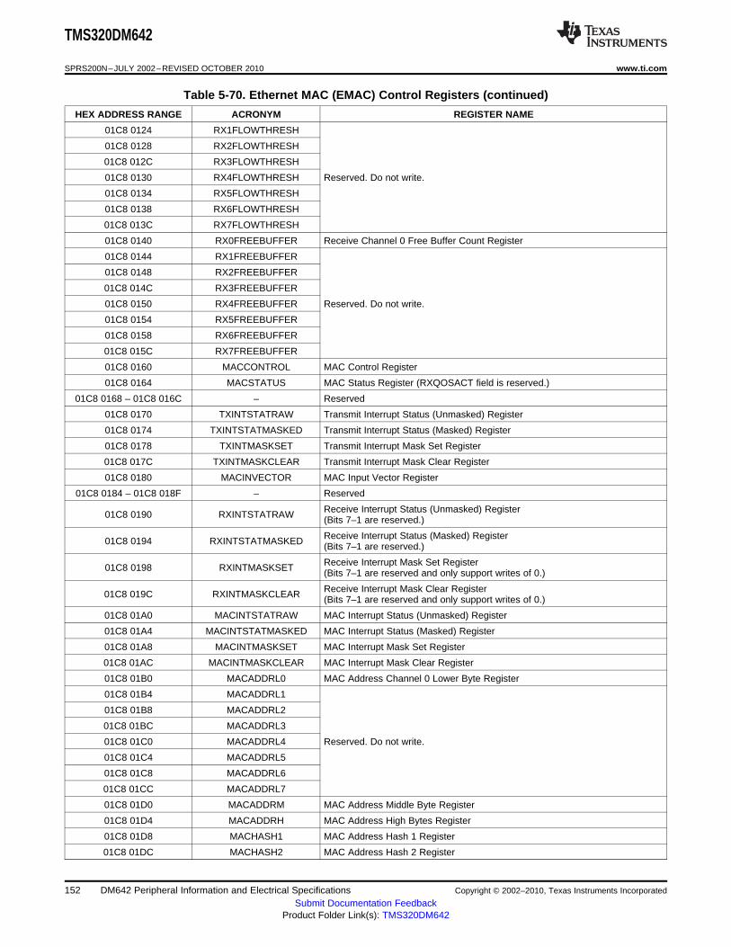
TMS320DM642
SPRS200N–JULY 2002–REVISED OCTOBER 2010 www.ti.com
Table 5-70. Ethernet MAC (EMAC) Control Registers (continued)
HEX ADDRESS RANGE ACRONYM REGISTER NAME
01C8 0124 RX1FLOWTHRESH
01C8 0128 RX2FLOWTHRESH
01C8 012C RX3FLOWTHRESH
01C8 0130 RX4FLOWTHRESH Reserved. Do not write.
01C8 0134 RX5FLOWTHRESH
01C8 0138 RX6FLOWTHRESH
01C8 013C RX7FLOWTHRESH
01C8 0140 RX0FREEBUFFER Receive Channel 0 Free Buffer Count Register
01C8 0144 RX1FREEBUFFER
01C8 0148 RX2FREEBUFFER
01C8 014C RX3FREEBUFFER
01C8 0150 RX4FREEBUFFER Reserved. Do not write.
01C8 0154 RX5FREEBUFFER
01C8 0158 RX6FREEBUFFER
01C8 015C RX7FREEBUFFER
01C8 0160 MACCONTROL MAC Control Register
01C8 0164 MACSTATUS MAC Status Register (RXQOSACT field is reserved.)
01C8 0168 – 01C8 016C – Reserved
01C8 0170 TXINTSTATRAW Transmit Interrupt Status (Unmasked) Register
01C8 0174 TXINTSTATMASKED Transmit Interrupt Status (Masked) Register
01C8 0178 TXINTMASKSET Transmit Interrupt Mask Set Register
01C8 017C TXINTMASKCLEAR Transmit Interrupt Mask Clear Register
01C8 0180 MACINVECTOR MAC Input Vector Register
01C8 0184 – 01C8 018F – Reserved
Receive Interrupt Status (Unmasked) Register01C8 0190 RXINTSTATRAW (Bits 7–1 are reserved.)
Receive Interrupt Status (Masked) Register01C8 0194 RXINTSTATMASKED (Bits 7–1 are reserved.)
Receive Interrupt Mask Set Register01C8 0198 RXINTMASKSET (Bits 7–1 are reserved and only support writes of 0.)
Receive Interrupt Mask Clear Register01C8 019C RXINTMASKCLEAR (Bits 7–1 are reserved and only support writes of 0.)
01C8 01A0 MACINTSTATRAW MAC Interrupt Status (Unmasked) Register
01C8 01A4 MACINTSTATMASKED MAC Interrupt Status (Masked) Register
01C8 01A8 MACINTMASKSET MAC Interrupt Mask Set Register
01C8 01AC MACINTMASKCLEAR MAC Interrupt Mask Clear Register
01C8 01B0 MACADDRL0 MAC Address Channel 0 Lower Byte Register
01C8 01B4 MACADDRL1
01C8 01B8 MACADDRL2
01C8 01BC MACADDRL3
01C8 01C0 MACADDRL4 Reserved. Do not write.
01C8 01C4 MACADDRL5
01C8 01C8 MACADDRL6
01C8 01CC MACADDRL7
01C8 01D0 MACADDRM MAC Address Middle Byte Register
01C8 01D4 MACADDRH MAC Address High Bytes Register
01C8 01D8 MACHASH1 MAC Address Hash 1 Register
01C8 01DC MACHASH2 MAC Address Hash 2 Register
152 DM642 Peripheral Information and Electrical Specifications Copyright © 2002–2010, Texas Instruments Incorporated
Submit Documentation FeedbackProduct Folder Link(s): TMS320DM642

TMS320DM642
www.ti.com SPRS200N–JULY 2002–REVISED OCTOBER 2010
Table 5-70. Ethernet MAC (EMAC) Control Registers (continued)
HEX ADDRESS RANGE ACRONYM REGISTER NAME
01C8 01E0 BOFFTEST Backoff Test Register
01C8 01E4 TPACETEST Transmit Pacing Test Register
01C8 01E8 RXPAUSE Receive Pause Timer Register
01C8 01EC TXPAUSE Transmit Pause Timer Register
01C8 01F0 – 01C8 01FF – Reserved
01C8 0200 – 01C8 05FF (see Table 5-71) EMAC Statistics Registers
01C8 0600 TX0HDP Transmit Channel 0 DMA Head Descriptor Pointer Register
01C8 0604 TX1HDP Transmit Channel 1 DMA Head Descriptor Pointer Register
01C8 0608 TX2HDP Transmit Channel 2 DMA Head Descriptor Pointer Register
01C8 060C TX3HDP Transmit Channel 3 DMA Head Descriptor Pointer Register
01C8 0610 TX4HDP Transmit Channel 4 DMA Head Descriptor Pointer Register
01C8 0614 TX5HDP Transmit Channel 5 DMA Head Descriptor Pointer Register
01C8 0618 TX6HDP Transmit Channel 6 DMA Head Descriptor Pointer Register
01C8 061C TX7HDP Transmit Channel 7 DMA Head Descriptor Pointer Register
01C8 0620 RX0HDP Receive Channel 0 DMA Head Descriptor Pointer Register
01C8 0624 RX1HDP
01C8 0628 RX2HDP
01C8 062C RX3HDP
01C8 0630 RX4HDP Reserved. Do not write.
01C8 0634 RX5HDP
01C8 0638 RX6HDP
01C8 063C RX7HDP
01C8 0640 TX0INTACK Transmit Channel 0 Interrupt Acknowledge Register
01C8 0644 TX1INTACK Transmit Channel 1 Interrupt Acknowledge Register
01C8 0648 TX2INTACK Transmit Channel 2 Interrupt Acknowledge Register
01C8 064C TX3INTACK Transmit Channel 3 Interrupt Acknowledge Register
01C8 0650 TX4INTACK Transmit Channel 4 Interrupt Acknowledge Register
01C8 0654 TX5INTACK Transmit Channel 5 Interrupt Acknowledge Register
01C8 0658 TX6INTACK Transmit Channel 6 Interrupt Acknowledge Register
01C8 065C TX7INTACK Transmit Channel 7 Interrupt Acknowledge Register
01C8 0660 RX0INTACK Receive Channel 0 Interrupt Acknowledge Register
01C8 0664 RX1INTACK
01C8 0668 RX2INTACK
01C8 066C RX3INTACK
01C8 0670 RX4INTACK Reserved. Do not write.
01C8 0674 RX5INTACK
01C8 0678 RX6INTACK
01C8 067C RX7INTACK
01C8 0680 – 01C8 0FFF – Reserved
Copyright © 2002–2010, Texas Instruments Incorporated DM642 Peripheral Information and Electrical Specifications 153Submit Documentation Feedback
Product Folder Link(s): TMS320DM642

TMS320DM642
SPRS200N–JULY 2002–REVISED OCTOBER 2010 www.ti.com
Table 5-71. EMAC Statistics Registers
HEX ADDRESS RANGE ACRONYM REGISTER NAME
01C8 0200 RXGOODFRAMES Good Receive Frames Register
01C8 0204 RXBCASTFRAMES Broadcast Receive Frames Register
01C8 0208 RXMCASTFRAMES Multicast Receive Frames Register
01C8 020C RXPAUSEFRAMES Pause Receive Frames Register
01C8 0210 RXCRCERRORS Receive CRC Errors Register
01C8 0214 RXALIGNCODEERRORS Receive Alignment/Code Errors Register
01C8 0218 RXOVERSIZED Receive Oversized Frames Register
01C8 021C RXJABBER Receive Jabber Frames Register
01C8 0220 RXUNDERSIZED Receive Undersized Frames Register
01C8 0224 RXFRAGMENTS Receive Frame Fragments Register
01C8 0228 RXFILTERED Filtered Receive Frames Register
01C8 022C RXQOSFILTERED Reserved
01C8 0230 RXOCTETS Receive Octet Frames Register
01C8 0234 TXGOODFRAMES Good Transmit Frames Register
01C8 0238 TXBCASTFRAMES Broadcast Transmit Frames Register
01C8 023C TXMCASTFRAMES Multicast Transmit Frames Register
01C8 0240 TXPAUSEFRAMES Pause Transmit Frames Register
01C8 0244 TXDEFERRED Deferred Transmit Frames Register
01C8 0248 TXCOLLISION Collision Register
01C8 024C TXSINGLECOLL Single Collision Transmit Frames Register
01C8 0250 TXMULTICOLL Multiple Collision Transmit Frames Register
01C8 0254 TXEXCESSIVECOLL Excessive Collisions Register
01C8 0258 TXLATECOLL Late Collisions Register
01C8 025C TXUNDERRUN Transmit Underrun Register
01C8 0260 TXCARRIERSLOSS Transmit Carrier Sense Errors Register
01C8 0264 TXOCTETS Transmit Octet Frames Register
01C8 0268 FRAME64 Transmit and Receive 64 Octet Frames Register
01C8 026C FRAME65T127 Transmit and Receive 65 to 127 Octet Frames Register
01C8 0270 FRAME128T255 Transmit and Receive 128 to 255 Octet Frames Register
01C8 0274 FRAME256T511 Transmit and Receive 256 to 511 Octet Frames Register
01C8 0278 FRAME512T1023 Transmit and Receive 512 to 1023 Octet Frames Register
01C8 027C FRAME1024TUP Transmit and Receive 1024 or Above Octet Frames Register
01C8 0280 NETOCTETS Network Octet Frames Register
01C8 0284 RXSOFOVERRUNS Receive Start of Frame Overruns Register
01C8 0288 RXMOFOVERRUNS Receive Middle of Frame Overruns Register
01C8 028C RXDMAOVERRUNS Receive DMA Overruns Register
01C8 0290 – 01C8 05FF – Reserved
Table 5-72. EMAC Wrapper
HEX ADDRESS RANGE ACRONYM REGISTER NAME
01C8 1000 – 01C8 1FFF EMAC Control Module Descriptor Memory
01C8 2000 – 01C8 2FFF – Reserved
Table 5-73. EWRAP Registers
HEX ADDRESS RANGE ACRONYM REGISTER NAME
01C8 3000 EWTRCTRL TR control
01C8 3004 EWCTL Interrupt control register
154 DM642 Peripheral Information and Electrical Specifications Copyright © 2002–2010, Texas Instruments Incorporated
Submit Documentation FeedbackProduct Folder Link(s): TMS320DM642

MRCLK
2 3
1
MTCLK
2 3
1
TMS320DM642
www.ti.com SPRS200N–JULY 2002–REVISED OCTOBER 2010
Table 5-73. EWRAP Registers (continued)
HEX ADDRESS RANGE ACRONYM REGISTER NAME
01C8 3008 EWINTTCNT Interrupt timer count
01C8 300C – 01C8 37FF – Reserved
5.16.3 EMAC Electrical Data/Timing
Table 5-74. Timing Requirements for MRCLK (see Figure 5-63)
–500–600
NO. UNIT–720
MIN MAX
1 tc(MRCLK) Cycle time, MRCLK 40 ns
2 tw(MRCLKH) Pulse duration, MRCLK high 14 ns
3 tw(MRCLKL) Pulse duration, MRCLK low 14 ns
Figure 5-63. MRCLK Timing (EMAC – Receive)
Table 5-75. Timing Requirements for MTCLK (see Figure 5-63)
–500–600
NO. UNIT–720
MIN MAX
1 tc(MTCLK) Cycle time, MTCLK 40 ns
2 tw(MTCLKH) Pulse duration, MTCLK high 14 ns
3 tw(MTCLKL) Pulse duration, MTCLK low 14 ns
Figure 5-64. MTCLK Timing (EMAC – Transmit)
Copyright © 2002–2010, Texas Instruments Incorporated DM642 Peripheral Information and Electrical Specifications 155Submit Documentation Feedback
Product Folder Link(s): TMS320DM642
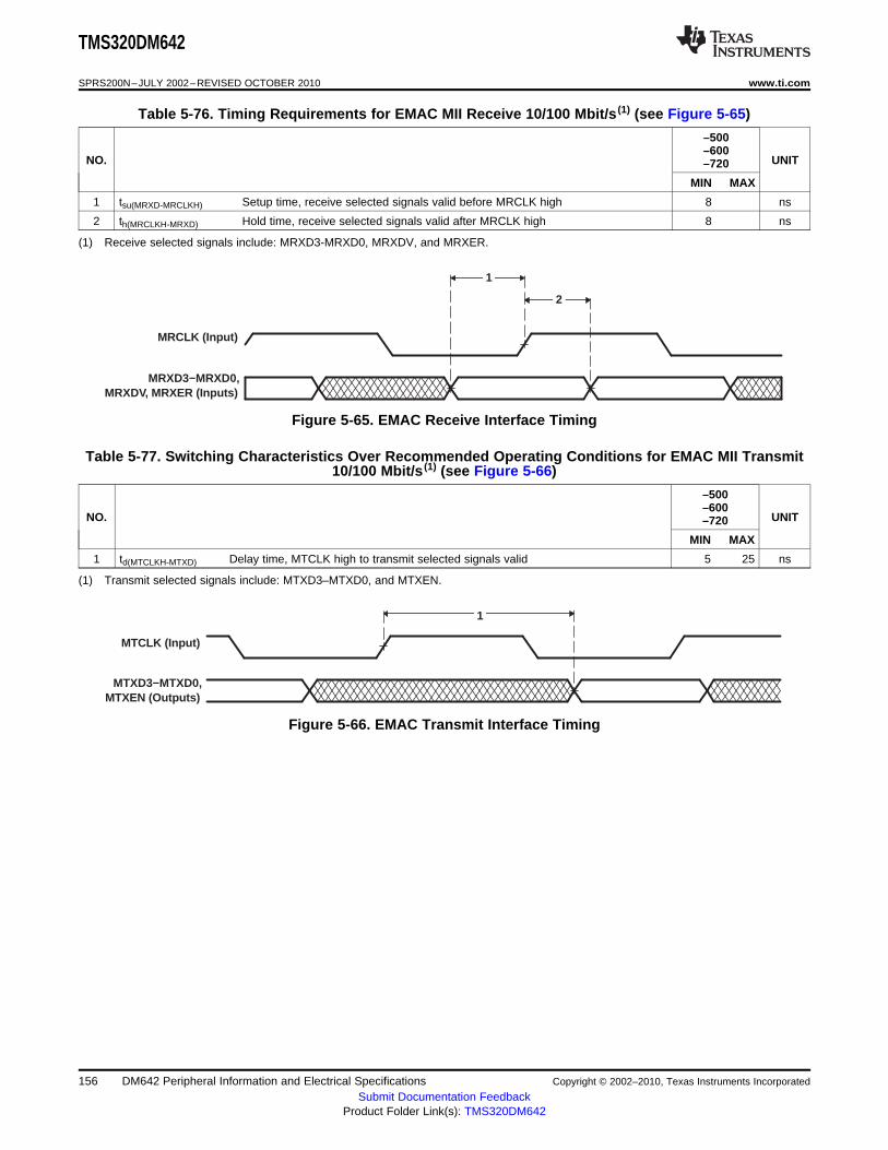
MRCLK (Input)
1
2
MRXD3−MRXD0,MRXDV, MRXER (Inputs)
1
MTCLK (Input)
MTXD3−MTXD0,MTXEN (Outputs)
TMS320DM642
SPRS200N–JULY 2002–REVISED OCTOBER 2010 www.ti.com
Table 5-76. Timing Requirements for EMAC MII Receive 10/100 Mbit/s (1) (see Figure 5-65)
–500–600
NO. UNIT–720
MIN MAX
1 tsu(MRXD-MRCLKH) Setup time, receive selected signals valid before MRCLK high 8 ns
2 th(MRCLKH-MRXD) Hold time, receive selected signals valid after MRCLK high 8 ns
(1) Receive selected signals include: MRXD3-MRXD0, MRXDV, and MRXER.
Figure 5-65. EMAC Receive Interface Timing
Table 5-77. Switching Characteristics Over Recommended Operating Conditions for EMAC MII Transmit10/100 Mbit/s (1) (see Figure 5-66)
–500–600
NO. UNIT–720
MIN MAX
1 td(MTCLKH-MTXD) Delay time, MTCLK high to transmit selected signals valid 5 25 ns
(1) Transmit selected signals include: MTXD3–MTXD0, and MTXEN.
Figure 5-66. EMAC Transmit Interface Timing
156 DM642 Peripheral Information and Electrical Specifications Copyright © 2002–2010, Texas Instruments Incorporated
Submit Documentation FeedbackProduct Folder Link(s): TMS320DM642
TMS320DM642
www.ti.com SPRS200N–JULY 2002–REVISED OCTOBER 2010
5.17 Management Data Input/Output (MDIO)
The MDIO module controls PHY configuration and status monitoring.
5.17.1 Device-Specific Information
The management data input/output (MDIO) module continuously polls all 32 MDIO addresses in order toenumerate all PHY devices in the system.
The management data input/output (MDIO) module implements the 802.3 serial management interface tointerrogate and control Ethernet PHY(s) using a shared two-wire bus. Host software uses the MDIOmodule to configure the auto-negotiation parameters of each PHY attached to the EMAC, retrieve thenegotiation results, and configure required parameters in the EMAC module for correct operation. Themodule is designed to allow almost transparent operation of the MDIO interface, with very littlemaintenance from the core processor.
The TMS320C6000 DSP Ethernet Media Access Controller (EMAC) / Management Data Input/Output(MDIO) Module Reference Guide (literature number SPRU628) describes the DM642 MDIO peripheral indetail. Some of the features documented in this peripheral reference guide are not supported on theDM642 at this time. The DM642 only supports one EMAC module. For a list of supported registers andregister fields, see Table 5-78 [MDIO Registers] in this data manual.
5.17.2 Peripheral Register Description(s)
Table 5-78. MDIO Registers
HEX ADDRESS RANGE ACRONYM REGISTER NAME
01C8 3800 VERSION MDIO Version Register
01C8 3804 CONTROL MDIO Control Register
01C8 3808 ALIVE MDIO PHY Alive Indication Register
01C8 380C LINK MDIO PHY Link Status Register
MDIO Link Status Change Interrupt Register01C8 3810 LINKINTRAW (MAC1 field is reserved and only supports writes of 0.)
MDIO Link Status Change Interrupt (Masked) Register01C8 3814 LINKINTMASKED (MAC1 field is reserved and only supports writes of 0.)
MDIO User Command Complete Interrupt Register01C8 3818 USERINTRAW (MAC1 field is reserved and only supports writes of 0.)
MDIO User Command Complete Interrupt (Masked) Register01C8 381C USERINTMASKED (MAC1 field is reserved and only supports writes of 0.)
MDIO User Command Complete Interrupt Mask Set Register01C8 3820 USERINTMASKSET (MAC1 field is reserved and only supports writes of 0.)
MDIO User Command Complete Interrupt Mask Clear Register01C8 3824 USERINTMASKCLEAR (MAC1 field is reserved and only supports writes of 0.)
01C8 3828 USERACCESS0 MDIO User Access Register 0
01C8 382C USERACCESS1 Reserved. Do not write.
01C8 3830 USERPHYSEL0 MDIO User PHY Select Register 0
01C8 3834 USERPHYSEL1 Reserved. Do not write.
01C8 3838 – 01C8 3FFF – Reserved
Copyright © 2002–2010, Texas Instruments Incorporated DM642 Peripheral Information and Electrical Specifications 157Submit Documentation Feedback
Product Folder Link(s): TMS320DM642
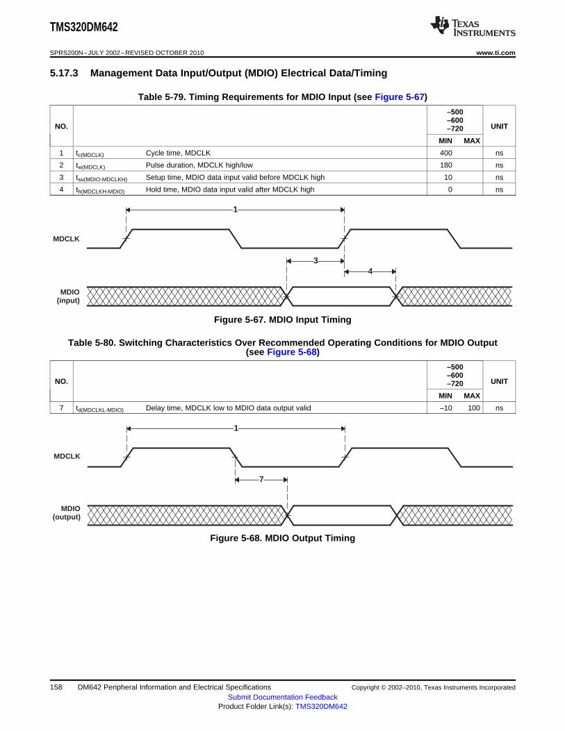
1
34
MDCLK
MDIO(input)
1
7
MDCLK
MDIO(output)
TMS320DM642
SPRS200N–JULY 2002–REVISED OCTOBER 2010 www.ti.com
5.17.3 Management Data Input/Output (MDIO) Electrical Data/Timing
Table 5-79. Timing Requirements for MDIO Input (see Figure 5-67)
–500–600
NO. UNIT–720
MIN MAX
1 tc(MDCLK) Cycle time, MDCLK 400 ns
2 tw(MDCLK) Pulse duration, MDCLK high/low 180 ns
3 tsu(MDIO-MDCLKH) Setup time, MDIO data input valid before MDCLK high 10 ns
4 th(MDCLKH-MDIO) Hold time, MDIO data input valid after MDCLK high 0 ns
Figure 5-67. MDIO Input Timing
Table 5-80. Switching Characteristics Over Recommended Operating Conditions for MDIO Output(see Figure 5-68)
–500–600
NO. UNIT–720
MIN MAX
7 td(MDCLKL-MDIO) Delay time, MDCLK low to MDIO data output valid –10 100 ns
Figure 5-68. MDIO Output Timing
158 DM642 Peripheral Information and Electrical Specifications Copyright © 2002–2010, Texas Instruments Incorporated
Submit Documentation FeedbackProduct Folder Link(s): TMS320DM642

TMS320DM642
www.ti.com SPRS200N–JULY 2002–REVISED OCTOBER 2010
5.18 Timer
The C6000™ DSP device has 32-bit general-purpose timers that can be used to:• Time events• Count events• Generate pulses• Interrupt the CPU• Send synchronization events to the DMA
The timers have two signaling modes and can be clocked by an internal or an external source. The timershave an input pin and an output pin. The input and output pins (TINP and TOUT) can function as timerclock input and clock output. They can also be respectively configured for general-purpose input andoutput.
With an internal clock, for example, the timer can signal an external A/D converter to start a conversion, orit can trigger the DMA controller to begin a data transfer. With an external clock, the timer can countexternal events and interrupt the CPU after a specified number of events.
5.18.1 Timer Device-Specific Information
The DM642 device has a total of three 32-bit general-purpose timers (Timer0, Timer1, and Timer2).Timer2 is not externally pinned out.
For more detailed information, see the TMS320C6000 DSP 32-Bit Timer Reference Guide (literaturenumber SPRU582).
5.18.2 Timer Peripheral Register Description(s)
Table 5-81. Timer 0 Registers
HEX ADDRESS RANGE ACRONYM REGISTER NAME COMMENTS
Determines the operating mode of the timer, monitors the0194 0000 CTL0 Timer 0 control register timer status, and controls the function of the TOUT pin.
Contains the number of timer input clock cycles to count.0194 0004 PRD0 Timer 0 period register This number controls the TSTAT signal frequency.
0194 0008 CNT0 Timer 0 counter register Contains the current value of the incrementing counter.
0194 000C – 0197 FFFF – Reserved
Table 5-82. Timer 1 Registers
HEX ADDRESS RANGE ACRONYM REGISTER NAME COMMENTS
Determines the operating mode of the timer, monitors the0198 0000 CTL1 Timer 1 control register timer status, and controls the function of the TOUT pin.
Contains the number of timer input clock cycles to count.0198 0004 PRD1 Timer 1 period register This number controls the TSTAT signal frequency.
0198 0008 CNT1 Timer 1 counter register Contains the current value of the incrementing counter.
0198 000C – 019B FFFF – Reserved
Table 5-83. Timer 2 Registers
HEX ADDRESS RANGE ACRONYM REGISTER NAME COMMENTS
Determines the operating mode of the timer, monitors the01AC 0000 CTL2 Timer 2 control register timer status.
Contains the number of timer input clock cycles to count.01AC 0004 PRD2 Timer 2 period register This number controls the TSTAT signal frequency.
01AC 0008 CNT2 Timer 2 counter register Contains the current value of the incrementing counter.
01AC 000C – 01AF FFFF – Reserved
Copyright © 2002–2010, Texas Instruments Incorporated DM642 Peripheral Information and Electrical Specifications 159Submit Documentation Feedback
Product Folder Link(s): TMS320DM642

TINPx
TOUTx
4
3
21
TMS320DM642
SPRS200N–JULY 2002–REVISED OCTOBER 2010 www.ti.com
5.18.3 Timer Electrical Data/Timing
Table 5-84. Timing Requirements for Timer Inputs (1) (see Figure 5-69)
–500–600
NO. UNIT–720
MIN MAX
1 tw(TINPH) Pulse duration, TINP high 8P ns
2 tw(TINPL) Pulse duration, TINP low 8P ns
(1) P = 1/CPU clock frequency in ns. For example, when running parts at 720 MHz, use P = 1.39 ns.
Table 5-85. Switching Characteristics Over Recommended Operating Conditions for Timer Outputs (1)
(see Figure 5-69)
–500–600
NO. PARAMETER UNIT–720
MIN MAX
3 tw(TOUTH) Pulse duration, TOUT high 8P – 3 ns
4 tw(TOUTL) Pulse duration, TOUT low 8P – 3 ns
(1) P = 1/CPU clock frequency in ns. For example, when running parts at 720 MHz, use P = 1.39 ns.
Figure 5-69. Timer Timing
160 DM642 Peripheral Information and Electrical Specifications Copyright © 2002–2010, Texas Instruments Incorporated
Submit Documentation FeedbackProduct Folder Link(s): TMS320DM642

TMS320DM642
www.ti.com SPRS200N–JULY 2002–REVISED OCTOBER 2010
5.19 General-Purpose Input/Output (GPIO)
The GPIO peripheral provides dedicated general-purpose pins that can be configured as either inputs oroutputs. When configured as an output, you can write to an internal register to control the state driven onthe output pin. When configured as an input, you can detect the state of the input by reading the state ofan internal register.
In addition, the GPIO peripheral can produce CPU interrupts and EDMA events in different interrupt/eventgeneration modes.
5.19.1 GPIO Device-Specific Information
To use the GP[15:0] software-configurable GPIO pins, the GPxEN bits in the GP Enable (GPEN) Registerand the GPxDIR bits in the GP Direction (GPDIR) Register must be properly configured.
GPxEN = 1 GP[x] pin is enabled
GPxDIR = 0 GP[x] pin is an input
GPxDIR = 1 GP[x] pin is an output
where "x" represents one of the 15 through 0 GPIO pins
Figure 5-70 shows the GPIO enable bits in the GPEN register for the DM642 device. To use any of theGPx pins as general-purpose input/output functions, the corresponding GPxEN bit must be set to "1"(enabled). Default values are device-specific, so refer to Figure 5-70 for the DM642 default configuration.
31 16
Reserved
R-0
15 14 13 12 11 10 9 8 7 6 5 4 3 2 1 0
GP15 GP14 GP13 GP12 GP11 GP10 GP9 GP8 GP7 GP6 GP5 GP4 GP3 GP2 GP1 GP0EN EN EN EN EN EN EN EN EN EN EN EN EN EN EN EN
R/W-0 R/W-0 R/W-0 R/W-0 R/W-0 R/W-0 R/W-0 R/W-0 R/W-1 R/W-1 R/W-1 R/W-1 R/W-1 R/W-0 R/W-0 R/W-1
Legend: R/W = Readable/Writable, -n = value after reset, -x = undefined value after reset
Figure 5-70. GPIO Enable Register (GPEN) [Hex Address: 01B0 0000]
Figure 5-71 shows the GPIO direction bits in the GPDIR register. This register determines if a given GPIOpin is an input or an output providing the corresponding GPxEN bit is enabled (set to "1") in the GPENregister. By default, all the GPIO pins are configured as input pins.
Copyright © 2002–2010, Texas Instruments Incorporated DM642 Peripheral Information and Electrical Specifications 161Submit Documentation Feedback
Product Folder Link(s): TMS320DM642

TMS320DM642
SPRS200N–JULY 2002–REVISED OCTOBER 2010 www.ti.com
31 16
Reserved
R-0
15 14 13 12 11 10 9 8 7 6 5 4 3 2 1 0
GP15 GP14 GP13 GP12 GP11 GP10 GP9 GP8 GP7 GP6 GP5 GP4 GP3 GP2 GP1 GP0DIR DIR DIR DIR DIR DIR DIR DIR DIR DIR DIR DIR DIR DIR DIR DIR
R/W-0 R/W-0 R/W-0 R/W-0 R/W-0 R/W-0 R/W-0 R/W-0 R/W-0 R/W-0 R/W-0 R/W-0 R/W-0 R/W-0 R/W-0 R/W-0
Legend: R/W = Readable/Writable, -n = value after reset, -x = undefined value after reset
Figure 5-71. GPIO Direction Register (GPDIR) [Hex Address: 01B0 0004]
For more detailed information on general-purpose inputs/outputs (GPIOs), see the TMS320C6000 DSPGeneral-Purpose Input/Output (GPIO) Reference Guide (literature number SPRU584).
5.19.2 GPIO Peripheral Register Description(s)
Table 5-86. GP0 Registers
HEX ADDRESS RANGE ACRONYM REGISTER NAME
01B0 0000 GPEN GP0 enable register
01B0 0004 GPDIR GP0 direction register
01B0 0008 GPVAL GP0 value register
01B0 000C – Reserved
01B0 0010 GPDH GP0 delta high register
01B0 0014 GPHM GP0 high mask register
01B0 0018 GPDL GP0 delta low register
01B0 001C GPLM GP0 low mask register
01B0 0020 GPGC GP0 global control register
01B0 0024 GPPOL GP0 interrupt polarity register
01B0 0028 – 01B3 EFFF – Reserved
162 DM642 Peripheral Information and Electrical Specifications Copyright © 2002–2010, Texas Instruments Incorporated
Submit Documentation FeedbackProduct Folder Link(s): TMS320DM642
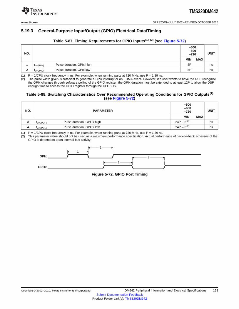
GPIx
GPOx
4
3
21
TMS320DM642
www.ti.com SPRS200N–JULY 2002–REVISED OCTOBER 2010
5.19.3 General-Purpose Input/Output (GPIO) Electrical Data/Timing
Table 5-87. Timing Requirements for GPIO Inputs (1) (2) (see Figure 5-72)
–500–600
NO. UNIT–720
MIN MAX
1 tw(GPIH) Pulse duration, GPIx high 8P ns
2 tw(GPIL) Pulse duration, GPIx low 8P ns
(1) P = 1/CPU clock frequency in ns. For example, when running parts at 720 MHz, use P = 1.39 ns.(2) The pulse width given is sufficient to generate a CPU interrupt or an EDMA event. However, if a user wants to have the DSP recognize
the GPIx changes through software polling of the GPIO register, the GPIx duration must be extended to at least 12P to allow the DSPenough time to access the GPIO register through the CFGBUS.
Table 5-88. Switching Characteristics Over Recommended Operating Conditions for GPIO Outputs (1)
(see Figure 5-72)
–500–600
NO. PARAMETER UNIT–720
MIN MAX
3 tw(GPOH) Pulse duration, GPOx high 24P – 8 (2) ns
4 tw(GPOL) Pulse duration, GPOx low 24P – 8 (2) ns
(1) P = 1/CPU clock frequency in ns. For example, when running parts at 720 MHz, use P = 1.39 ns.(2) This parameter value should not be used as a maximum performance specification. Actual performance of back-to-back accesses of the
GPIO is dependent upon internal bus activity.
Figure 5-72. GPIO Port Timing
Copyright © 2002–2010, Texas Instruments Incorporated DM642 Peripheral Information and Electrical Specifications 163Submit Documentation Feedback
Product Folder Link(s): TMS320DM642
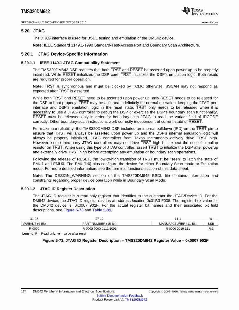
TMS320DM642
SPRS200N–JULY 2002–REVISED OCTOBER 2010 www.ti.com
5.20 JTAG
The JTAG interface is used for BSDL testing and emulation of the DM642 device.
Note: IEEE Standard 1149.1-1990 Standard-Test-Access Port and Boundary Scan Architecture.
5.20.1 JTAG Device-Specific Information
5.20.1.1 IEEE 1149.1 JTAG Compatibility Statement
The TMS320DM642 DSP requires that both TRST and RESET be asserted upon power up to be properlyinitialized. While RESET initializes the DSP core, TRST initializes the DSP's emulation logic. Both resetsare required for proper operation.
Note: TRST is synchronous and must be clocked by TCLK; otherwise, BSCAN may not respond asexpected after TRST is asserted.
While both TRST and RESET need to be asserted upon power up, only RESET needs to be released forthe DSP to boot properly. TRST may be asserted indefinitely for normal operation, keeping the JTAG portinterface and DSP's emulation logic in the reset state. TRST only needs to be released when it isnecessary to use a JTAG controller to debug the DSP or exercise the DSP's boundary scan functionality.RESET must be released only in order for boundary-scan JTAG to read the variant field of IDCODEcorrectly. Other boundary-scan instructions work correctly independent of current state of RESET.
For maximum reliability, the TMS320DM642 DSP includes an internal pulldown (IPD) on the TRST pin toensure that TRST will always be asserted upon power up and the DSP's internal emulation logic willalways be properly initialized. JTAG controllers from Texas Instruments actively drive TRST high.However, some third-party JTAG controllers may not drive TRST high but expect the use of a pullupresistor on TRST. When using this type of JTAG controller, assert TRST to intialize the DSP after powerupand externally drive TRST high before attempting any emulation or boundary scan operations.
Following the release of RESET, the low-to-high transition of TRST must be "seen" to latch the state ofEMU1 and EMU0. The EMU[1:0] pins configure the device for either Boundary Scan mode or Emulationmode. For more detailed information, see the terminal functions section of this data sheet.
Note: The DESIGN_WARNING section of the TMS320DM642 BSDL file contains information andconstraints regarding proper device operation while in Boundary Scan Mode.
5.20.1.2 JTAG ID Register Description
The JTAG ID register is a read-only register that identifies to the customer the JTAG/Device ID. For theDM642 device, the JTAG ID register resides at address location 0x01B3 F008. The register hex value forthe DM642 device is: 0x0007 902F. For the actual register bit names and their associated bit fielddescriptions, see Figure 5-73 and Table 5-89.
31-28 27-12 11-1 0
VARIANT (4-Bit) PART NUMBER (16-Bit) MANUFACTURER (11-Bit) LSB
R-0000 R-0000 0000 0111 1001 R-0000 0010 111 R-1
Legend: R = Read only, -n = value after reset
Figure 5-73. JTAG ID Register Description – TMS320DM642 Register Value – 0x0007 902F
164 DM642 Peripheral Information and Electrical Specifications Copyright © 2002–2010, Texas Instruments Incorporated
Submit Documentation FeedbackProduct Folder Link(s): TMS320DM642
TCK
TDO
TDI/TMS/TRST
1
2
34
2
TMS320DM642
www.ti.com SPRS200N–JULY 2002–REVISED OCTOBER 2010
Table 5-89. JTAG ID Register Selection Bit Descriptions
BIT NAME DESCRIPTION
31:28 VARIANT Variant (4-Bit) value.DM642 value: 0000.
27:12 PART NUMBER Part Number (16-Bit) value. DM642 value: 0000 0000 0111 1001.
11–1 MANUFACTURER Manufacturer (11-Bit) value. DM642 value: 0000 0010 111.
0 LSB LSB. This bit is read as a "1" for DM642.
5.20.2 JTAG Peripheral Register Description(s)
Table 5-90. JTAG ID Register
HEX ADDRESS RANGE ACRONYM REGISTER NAME COMMENTS
Read-only. Provides 32-bit01B3 F008 JTAGID JTAG Identification Register JTAG ID of the device.
5.20.3 JTAG Test-Port Electrical Data/Timing
Table 5-91. Timing Requirements for JTAG Test Port (see Figure 5-74)
–500–600
NO. UNIT–720
MIN MAX
1 tc(TCK) Cycle time, TCK 35 ns
3 tsu(TDIV-TCKH) Setup time, TDI/TMS/TRST valid before TCK high 10 ns
4 th(TCKH-TDIV) Hold time, TDI/TMS/TRST valid after TCK high 9 ns
Table 5-92. Switching Characteristics Over Recommended Operating Conditions for JTAG Test Port(see Figure 5-74)
–500–600
NO. PARAMETER UNIT–720
MIN MAX
2 td(TCKL-TDOV) Delay time, TCK low to TDO valid 0 18 ns
Figure 5-74. JTAG Test-Port Timing
Copyright © 2002–2010, Texas Instruments Incorporated DM642 Peripheral Information and Electrical Specifications 165Submit Documentation Feedback
Product Folder Link(s): TMS320DM642
TMS320DM642
SPRS200N–JULY 2002–REVISED OCTOBER 2010 www.ti.com
Revision HistoryNOTE: Page numbers for previous revisions may differ from page numbers in the current version.
This data sheet revision history highlights the technical changes made to the SPRS200M device-specificdata sheet to make it an SPRS200N revision.
Scope: Reference to Errata added to Packaging Information.
SEE ADDS/CHANGES/DELETES
Section 4.3 Added note regarding VOH and VOL.
166 DM642 Peripheral Information and Electrical Specifications Copyright © 2002–2010, Texas Instruments Incorporated
Submit Documentation FeedbackProduct Folder Link(s): TMS320DM642
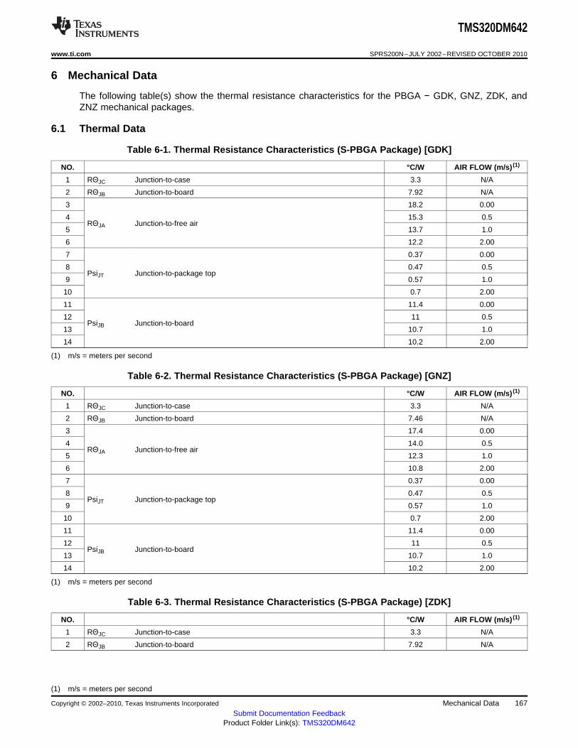
TMS320DM642
www.ti.com SPRS200N–JULY 2002–REVISED OCTOBER 2010
6 Mechanical Data
The following table(s) show the thermal resistance characteristics for the PBGA − GDK, GNZ, ZDK, andZNZ mechanical packages.
6.1 Thermal Data
Table 6-1. Thermal Resistance Characteristics (S-PBGA Package) [GDK]
NO. °C/W AIR FLOW (m/s) (1)
1 RΘJC Junction-to-case 3.3 N/A
2 RΘJB Junction-to-board 7.92 N/A
3 18.2 0.00
4 15.3 0.5RΘJA Junction-to-free air
5 13.7 1.0
6 12.2 2.00
7 0.37 0.00
8 0.47 0.5PsiJT Junction-to-package top
9 0.57 1.0
10 0.7 2.00
11 11.4 0.00
12 11 0.5PsiJB Junction-to-board
13 10.7 1.0
14 10.2 2.00
(1) m/s = meters per second
Table 6-2. Thermal Resistance Characteristics (S-PBGA Package) [GNZ]
NO. °C/W AIR FLOW (m/s) (1)
1 RΘJC Junction-to-case 3.3 N/A
2 RΘJB Junction-to-board 7.46 N/A
3 17.4 0.00
4 14.0 0.5RΘJA Junction-to-free air
5 12.3 1.0
6 10.8 2.00
7 0.37 0.00
8 0.47 0.5PsiJT Junction-to-package top
9 0.57 1.0
10 0.7 2.00
11 11.4 0.00
12 11 0.5PsiJB Junction-to-board
13 10.7 1.0
14 10.2 2.00
(1) m/s = meters per second
Table 6-3. Thermal Resistance Characteristics (S-PBGA Package) [ZDK]
NO. °C/W AIR FLOW (m/s) (1)
1 RΘJC Junction-to-case 3.3 N/A
2 RΘJB Junction-to-board 7.92 N/A
(1) m/s = meters per second
Copyright © 2002–2010, Texas Instruments Incorporated Mechanical Data 167Submit Documentation Feedback
Product Folder Link(s): TMS320DM642

TMS320DM642
SPRS200N–JULY 2002–REVISED OCTOBER 2010 www.ti.com
Table 6-3. Thermal Resistance Characteristics (S-PBGA Package) [ZDK] (continued)
NO. °C/W AIR FLOW (m/s) (1)
3 18.2 0.00
4 15.3 0.5RΘJA Junction-to-free air
5 13.7 1.0
6 12.2 2.00
7 0.37 0.00
8 0.47 0.5PsiJT Junction-to-package top
9 0.57 1.0
10 0.7 2.00
11 11.4 0.00
12 11 0.5PsiJB Junction-to-board
13 10.7 1.0
14 10.2 2.00
Table 6-4. Thermal Resistance Characteristics (S-PBGA Package) [ZNZ]
NO. °C/W AIR FLOW (m/s) (1)
1 RΘJC Junction-to-case 3.3 N/A
2 RΘJB Junction-to-board 7.46 N/A
3 17.4 0.00
4 14.0 0.5RΘJA Junction-to-free air
5 12.3 1.0
6 10.8 2.00
7 0.37 0.00
8 0.47 0.5PsiJT Junction-to-package top
9 0.57 1.0
10 0.7 2.00
11 11.4 0.00
12 11 0.5PsiJB Junction-to-board
13 10.7 1.0
14 10.2 2.00
(1) m/s = meters per second
168 Mechanical Data Copyright © 2002–2010, Texas Instruments Incorporated
Submit Documentation FeedbackProduct Folder Link(s): TMS320DM642

TMS320DM642AGNZ
Dx-YMLLLLS
TMX320DM642GNZ
Dx-YMLLLLS
Lot T race Code
nnn
TMS320DMG42AGNZ
Dx-YMLLLLS
@ 2005 TI@ 2005 TI@ 2003 TI
V VV
Lot T race Code Lot T race Code
Pin A1 Pin A1 Pin A1
DIGITAL MEDIA
PROCESSOR
nn
DIGITAL MEDIA
PROCESSOR
DIGITAL MEDIA
PROCESSOR
TMS320DM642
www.ti.com SPRS200N–JULY 2002–REVISED OCTOBER 2010
6.2 Packaging Information
The following packaging information and addendum reflect the most current released data available for thedesignated device(s). This data is subject to change without notice and without revision of this document.
Figure 6-1 shows some examples of the types of DM642 package symbolization for −500 MHz, −600MHz, and −720 MHz devices. Pin A1 is always located at the top-left corner when you can read thesilkscreening/laser-etching and view the TI logo properly.
Figure 6-1. Example, Lot Trace Codes for TMX320DM642 and TMS320DM642 (GDK and GNZ Packages)
For more details on package markings, see the TMS320DM642 Digital Signal Processor Silicon Errata(Literature Number: SPRZ196).
Copyright © 2002–2010, Texas Instruments Incorporated Mechanical Data 169Submit Documentation Feedback
Product Folder Link(s): TMS320DM642

PACKAGE OPTION ADDENDUM
www.ti.com 15-Apr-2017
Addendum-Page 1
PACKAGING INFORMATION
Orderable Device Status(1)
Package Type PackageDrawing
Pins PackageQty
Eco Plan(2)
Lead/Ball Finish(6)
MSL Peak Temp(3)
Op Temp (°C) Device Marking(4/5)
Samples
TMS320DM642AGDK6 NRND FC/CSP GDK 548 60 TBD SNPB Level-4-220C-72 HR TMS320DM642A@ 2003 TIGDK
TMS320DM642AGDK7 NRND FC/CSP GDK 548 40 TBD SNPB Level-4-220C-72 HR TMS320DM642A@ 2003 TIGDK720
TMS320DM642AGDKA5 NRND FC/CSP GDK 548 60 TBD SNPB Level-4-220C-72 HR TMS320DM642A@ 2003 TIGDKA5
TMS320DM642AGDKA6 NRND FC/CSP GDK 548 60 TBD SNPB Level-4-220C-72 HR TMS320DM642A@ 2003 TIGDKA6
TMS320DM642AGNZ6 NRND FCBGA GNZ 548 40 TBD SNPB Level-4-220C-72 HR TMS320DM642A@ 2003 TIGNZ
TMS320DM642AGNZ7 NRND FCBGA GNZ 548 40 TBD SNPB Level-4-220C-72 HR TMS320DM642A@ 2003 TIGNZ720
TMS320DM642AGNZA5 NRND FCBGA GNZ 548 40 TBD SNPB Level-4-220C-72 HR TMS320DM642A@ 2003 TIGNZA5
TMS320DM642AGNZA6 NRND FCBGA GNZ 548 40 TBD SNPB Level-4-220C-72 HR TMS320DM642A@ 2003 TIGNZA6
TMS320DM642AZDK5 NRND FCBGA ZDK 548 60 Pb-Free (RoHSExempt)
SNAGCU Level-4-260C-72HR TMS320DM642A@ 2003 TIZDK500
TMS320DM642AZDK6 NRND FCBGA ZDK 548 60 Pb-Free (RoHSExempt)
SNAGCU Level-4-260C-72HR TMS320DM642A@ 2003 TIZDK

PACKAGE OPTION ADDENDUM
www.ti.com 15-Apr-2017
Addendum-Page 2
Orderable Device Status(1)
Package Type PackageDrawing
Pins PackageQty
Eco Plan(2)
Lead/Ball Finish(6)
MSL Peak Temp(3)
Op Temp (°C) Device Marking(4/5)
Samples
TMS320DM642AZDK7 NRND FCBGA ZDK 548 60 Pb-Free (RoHSExempt)
SNAGCU Level-4-260C-72HR TMS320DM642A@ 2003 TIZDK720
TMS320DM642AZDK7HK NRND FCBGA ZDK 548 60 Pb-Free (RoHSExempt)
SNAGCU Level-4-260C-72HR TMS320DM642A@ 2003 TIZDK720
TMS320DM642AZDKA5 NRND FCBGA ZDK 548 60 Pb-Free (RoHSExempt)
SNAGCU Level-4-260C-72HR TMS320DM642A@ 2003 TIZDKA5
TMS320DM642AZDKA6 NRND FCBGA ZDK 548 60 Pb-Free (RoHSExempt)
SNAGCU Level-4-260C-72HR TMS320DM642A@ 2003 TIZDKA6
TMS320DM642AZNZ5 NRND FCBGA ZNZ 548 40 Pb-Free (RoHSExempt)
SNAGCU Level-4-260C-72HR TMS320DM642A@ 2003 TIZNZ500
TMS320DM642AZNZ6 NRND FCBGA ZNZ 548 40 Pb-Free (RoHSExempt)
SNAGCU Level-4-260C-72HR TMS320DM642A@ 2003 TIZNZ
TMS320DM642AZNZ7 NRND FCBGA ZNZ 548 40 Pb-Free (RoHSExempt)
SNAGCU Level-4-260C-72HR TMS320DM642A@ 2003 TIZNZ720
TMS320DM642AZNZA5 NRND FCBGA ZNZ 548 40 Pb-Free (RoHSExempt)
SNAGCU Level-4-260C-72HR TMS320DM642A@ 2003 TIZNZA5
TMS320DM642AZNZA6 NRND FCBGA ZNZ 548 40 Pb-Free (RoHSExempt)
SNAGCU Level-4-260C-72HR TMS320DM642A@ 2003 TIZNZA6
TMSDM642AZDK5TAN NRND FCBGA ZDK 548 60 Pb-Free (RoHSExempt)
SNAGCU Level-4-260C-72HR TMS320DM642A@ 2003 TIZDK500
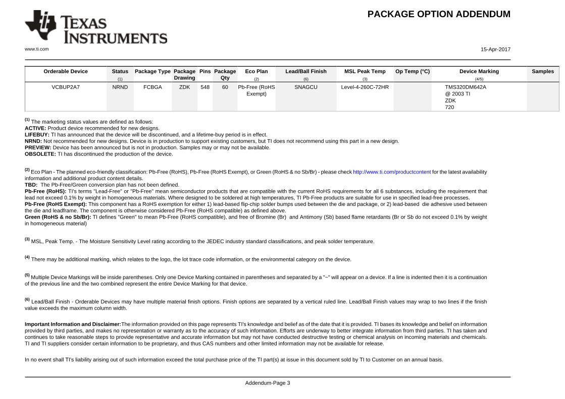
PACKAGE OPTION ADDENDUM
www.ti.com 15-Apr-2017
Addendum-Page 3
Orderable Device Status(1)
Package Type PackageDrawing
Pins PackageQty
Eco Plan(2)
Lead/Ball Finish(6)
MSL Peak Temp(3)
Op Temp (°C) Device Marking(4/5)
Samples
VCBUP2A7 NRND FCBGA ZDK 548 60 Pb-Free (RoHSExempt)
SNAGCU Level-4-260C-72HR TMS320DM642A@ 2003 TIZDK720
(1) The marketing status values are defined as follows:ACTIVE: Product device recommended for new designs.LIFEBUY: TI has announced that the device will be discontinued, and a lifetime-buy period is in effect.NRND: Not recommended for new designs. Device is in production to support existing customers, but TI does not recommend using this part in a new design.PREVIEW: Device has been announced but is not in production. Samples may or may not be available.OBSOLETE: TI has discontinued the production of the device.
(2) Eco Plan - The planned eco-friendly classification: Pb-Free (RoHS), Pb-Free (RoHS Exempt), or Green (RoHS & no Sb/Br) - please check http://www.ti.com/productcontent for the latest availabilityinformation and additional product content details.TBD: The Pb-Free/Green conversion plan has not been defined.Pb-Free (RoHS): TI's terms "Lead-Free" or "Pb-Free" mean semiconductor products that are compatible with the current RoHS requirements for all 6 substances, including the requirement thatlead not exceed 0.1% by weight in homogeneous materials. Where designed to be soldered at high temperatures, TI Pb-Free products are suitable for use in specified lead-free processes.Pb-Free (RoHS Exempt): This component has a RoHS exemption for either 1) lead-based flip-chip solder bumps used between the die and package, or 2) lead-based die adhesive used betweenthe die and leadframe. The component is otherwise considered Pb-Free (RoHS compatible) as defined above.Green (RoHS & no Sb/Br): TI defines "Green" to mean Pb-Free (RoHS compatible), and free of Bromine (Br) and Antimony (Sb) based flame retardants (Br or Sb do not exceed 0.1% by weightin homogeneous material)
(3) MSL, Peak Temp. - The Moisture Sensitivity Level rating according to the JEDEC industry standard classifications, and peak solder temperature.
(4) There may be additional marking, which relates to the logo, the lot trace code information, or the environmental category on the device.
(5) Multiple Device Markings will be inside parentheses. Only one Device Marking contained in parentheses and separated by a "~" will appear on a device. If a line is indented then it is a continuationof the previous line and the two combined represent the entire Device Marking for that device.
(6) Lead/Ball Finish - Orderable Devices may have multiple material finish options. Finish options are separated by a vertical ruled line. Lead/Ball Finish values may wrap to two lines if the finishvalue exceeds the maximum column width.
Important Information and Disclaimer:The information provided on this page represents TI's knowledge and belief as of the date that it is provided. TI bases its knowledge and belief on informationprovided by third parties, and makes no representation or warranty as to the accuracy of such information. Efforts are underway to better integrate information from third parties. TI has taken andcontinues to take reasonable steps to provide representative and accurate information but may not have conducted destructive testing or chemical analysis on incoming materials and chemicals.TI and TI suppliers consider certain information to be proprietary, and thus CAS numbers and other limited information may not be available for release.
In no event shall TI's liability arising out of such information exceed the total purchase price of the TI part(s) at issue in this document sold by TI to Customer on an annual basis.

PACKAGE OPTION ADDENDUM
www.ti.com 15-Apr-2017
Addendum-Page 4
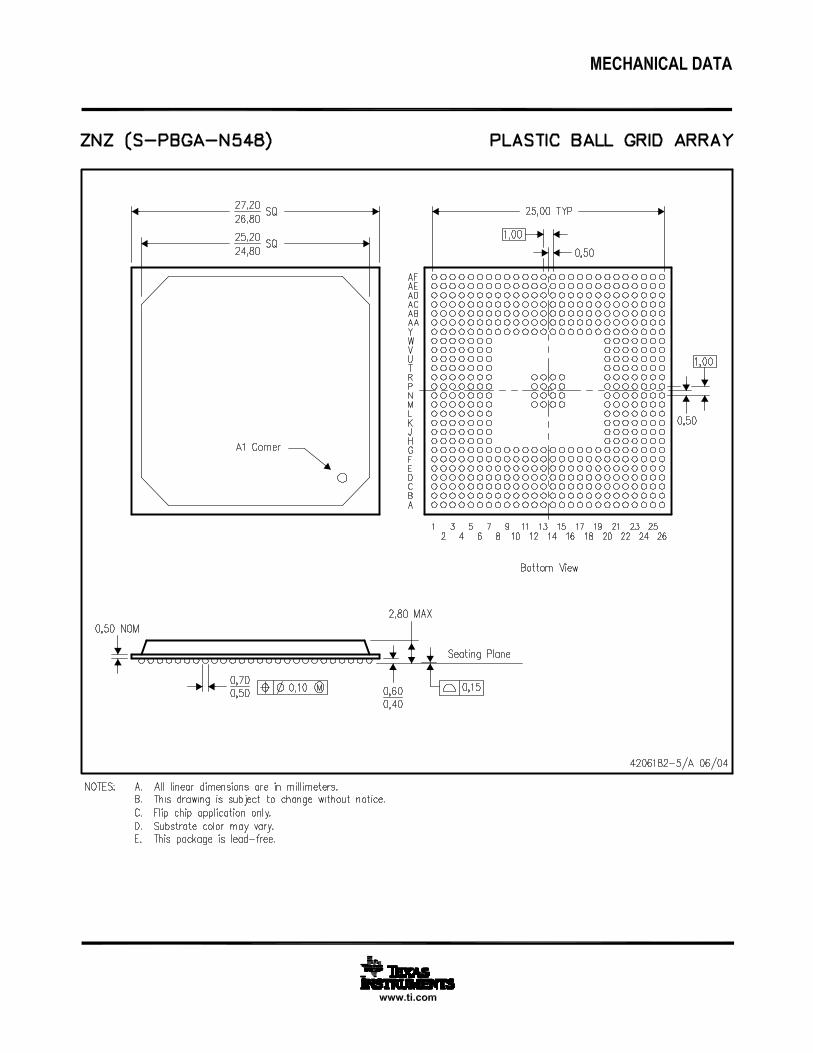

MECHANICAL DATA
MPBG301 – JULY 2002
1POST OFFICE BOX 655303 • DALLAS, TEXAS 75265
GDK (S–PBGA–N548) PLASTIC BALL GRID ARRAY
A1 Corner
Bottom View
0,10 0,12
0,80
0,80SQ20,9021,10
AFAE
ADAC
ABAA
YW
VU
TR
PN
ML
KJ
HG
FE
DC
2625
2423
2221
2019
1817
1615
1413
1211
109
87
65
431
2,80 MAX
B
2
SQ23,1022,90
0,450,35
20,00 TYP
0,40
0,40
A
0,450,55
Seating Plane
0,50 NOM
4203481-3/B 07/02
NOTES: A. All linear dimensions are in millimeters.B. This drawing is subject to change without notice.C. Flip chip application only.
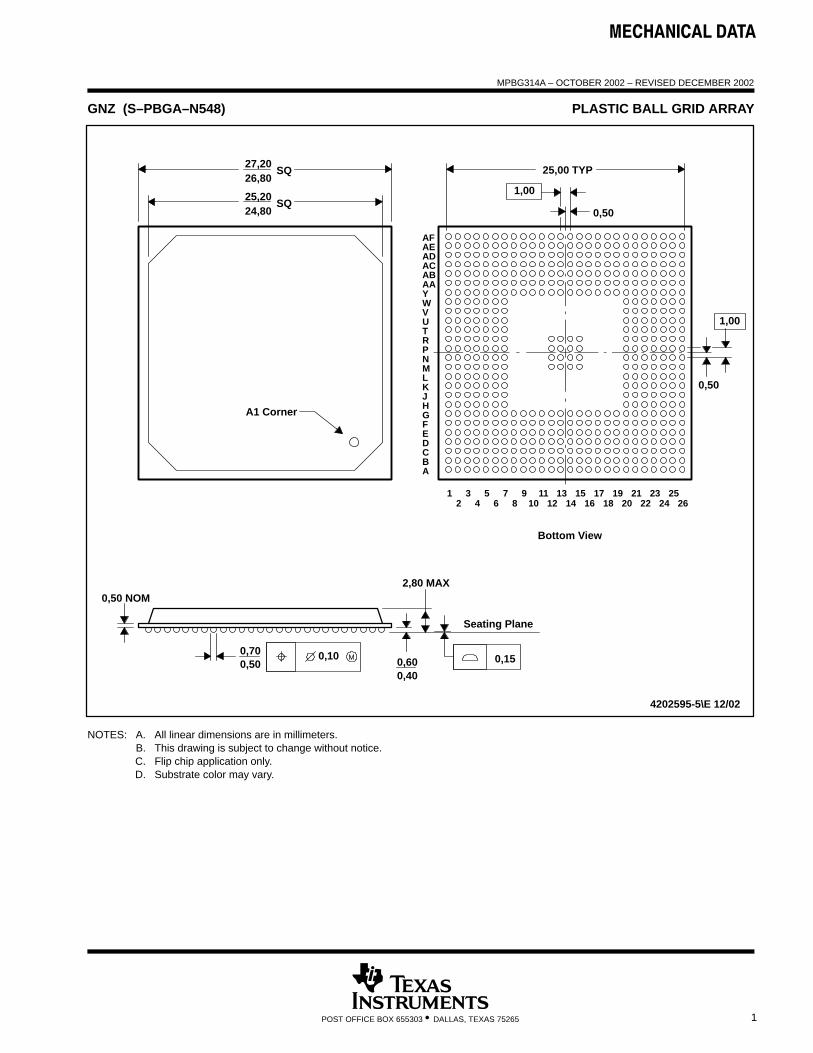
MPBG314A – OCTOBER 2002 – REVISED DECEMBER 2002
1POST OFFICE BOX 655303 • DALLAS, TEXAS 75265
GNZ (S–PBGA–N548) PLASTIC BALL GRID ARRAY
1,00
1,00
0,50
0,50
2321191713 15
AEAF
ACAD
AAAB
W
UV
Y
11975
PR
MN
KL
HJ
3
F
DE
1
ABC
G
T
25,00 TYP
25262420 22161412 18106 842
Seating Plane
0,15
Bottom View
4202595-5\E 12/02
27,20
SQ
26,80
24,8025,20
A1 Corner
SQ
0,400,60
0,700,50
0,10
0,50 NOM2,80 MAX
NOTES: A. All linear dimensions are in millimeters.B. This drawing is subject to change without notice.C. Flip chip application only.D. Substrate color may vary.


IMPORTANT NOTICE
Texas Instruments Incorporated (TI) reserves the right to make corrections, enhancements, improvements and other changes to itssemiconductor products and services per JESD46, latest issue, and to discontinue any product or service per JESD48, latest issue. Buyersshould obtain the latest relevant information before placing orders and should verify that such information is current and complete.TI’s published terms of sale for semiconductor products (http://www.ti.com/sc/docs/stdterms.htm) apply to the sale of packaged integratedcircuit products that TI has qualified and released to market. Additional terms may apply to the use or sale of other types of TI products andservices.Reproduction of significant portions of TI information in TI data sheets is permissible only if reproduction is without alteration and isaccompanied by all associated warranties, conditions, limitations, and notices. TI is not responsible or liable for such reproduceddocumentation. Information of third parties may be subject to additional restrictions. Resale of TI products or services with statementsdifferent from or beyond the parameters stated by TI for that product or service voids all express and any implied warranties for theassociated TI product or service and is an unfair and deceptive business practice. TI is not responsible or liable for any such statements.Buyers and others who are developing systems that incorporate TI products (collectively, “Designers”) understand and agree that Designersremain responsible for using their independent analysis, evaluation and judgment in designing their applications and that Designers havefull and exclusive responsibility to assure the safety of Designers' applications and compliance of their applications (and of all TI productsused in or for Designers’ applications) with all applicable regulations, laws and other applicable requirements. Designer represents that, withrespect to their applications, Designer has all the necessary expertise to create and implement safeguards that (1) anticipate dangerousconsequences of failures, (2) monitor failures and their consequences, and (3) lessen the likelihood of failures that might cause harm andtake appropriate actions. Designer agrees that prior to using or distributing any applications that include TI products, Designer willthoroughly test such applications and the functionality of such TI products as used in such applications.TI’s provision of technical, application or other design advice, quality characterization, reliability data or other services or information,including, but not limited to, reference designs and materials relating to evaluation modules, (collectively, “TI Resources”) are intended toassist designers who are developing applications that incorporate TI products; by downloading, accessing or using TI Resources in anyway, Designer (individually or, if Designer is acting on behalf of a company, Designer’s company) agrees to use any particular TI Resourcesolely for this purpose and subject to the terms of this Notice.TI’s provision of TI Resources does not expand or otherwise alter TI’s applicable published warranties or warranty disclaimers for TIproducts, and no additional obligations or liabilities arise from TI providing such TI Resources. TI reserves the right to make corrections,enhancements, improvements and other changes to its TI Resources. TI has not conducted any testing other than that specificallydescribed in the published documentation for a particular TI Resource.Designer is authorized to use, copy and modify any individual TI Resource only in connection with the development of applications thatinclude the TI product(s) identified in such TI Resource. NO OTHER LICENSE, EXPRESS OR IMPLIED, BY ESTOPPEL OR OTHERWISETO ANY OTHER TI INTELLECTUAL PROPERTY RIGHT, AND NO LICENSE TO ANY TECHNOLOGY OR INTELLECTUAL PROPERTYRIGHT OF TI OR ANY THIRD PARTY IS GRANTED HEREIN, including but not limited to any patent right, copyright, mask work right, orother intellectual property right relating to any combination, machine, or process in which TI products or services are used. Informationregarding or referencing third-party products or services does not constitute a license to use such products or services, or a warranty orendorsement thereof. Use of TI Resources may require a license from a third party under the patents or other intellectual property of thethird party, or a license from TI under the patents or other intellectual property of TI.TI RESOURCES ARE PROVIDED “AS IS” AND WITH ALL FAULTS. TI DISCLAIMS ALL OTHER WARRANTIES ORREPRESENTATIONS, EXPRESS OR IMPLIED, REGARDING RESOURCES OR USE THEREOF, INCLUDING BUT NOT LIMITED TOACCURACY OR COMPLETENESS, TITLE, ANY EPIDEMIC FAILURE WARRANTY AND ANY IMPLIED WARRANTIES OFMERCHANTABILITY, FITNESS FOR A PARTICULAR PURPOSE, AND NON-INFRINGEMENT OF ANY THIRD PARTY INTELLECTUALPROPERTY RIGHTS. TI SHALL NOT BE LIABLE FOR AND SHALL NOT DEFEND OR INDEMNIFY DESIGNER AGAINST ANY CLAIM,INCLUDING BUT NOT LIMITED TO ANY INFRINGEMENT CLAIM THAT RELATES TO OR IS BASED ON ANY COMBINATION OFPRODUCTS EVEN IF DESCRIBED IN TI RESOURCES OR OTHERWISE. IN NO EVENT SHALL TI BE LIABLE FOR ANY ACTUAL,DIRECT, SPECIAL, COLLATERAL, INDIRECT, PUNITIVE, INCIDENTAL, CONSEQUENTIAL OR EXEMPLARY DAMAGES INCONNECTION WITH OR ARISING OUT OF TI RESOURCES OR USE THEREOF, AND REGARDLESS OF WHETHER TI HAS BEENADVISED OF THE POSSIBILITY OF SUCH DAMAGES.Unless TI has explicitly designated an individual product as meeting the requirements of a particular industry standard (e.g., ISO/TS 16949and ISO 26262), TI is not responsible for any failure to meet such industry standard requirements.Where TI specifically promotes products as facilitating functional safety or as compliant with industry functional safety standards, suchproducts are intended to help enable customers to design and create their own applications that meet applicable functional safety standardsand requirements. Using products in an application does not by itself establish any safety features in the application. Designers mustensure compliance with safety-related requirements and standards applicable to their applications. Designer may not use any TI products inlife-critical medical equipment unless authorized officers of the parties have executed a special contract specifically governing such use.Life-critical medical equipment is medical equipment where failure of such equipment would cause serious bodily injury or death (e.g., lifesupport, pacemakers, defibrillators, heart pumps, neurostimulators, and implantables). Such equipment includes, without limitation, allmedical devices identified by the U.S. Food and Drug Administration as Class III devices and equivalent classifications outside the U.S.TI may expressly designate certain products as completing a particular qualification (e.g., Q100, Military Grade, or Enhanced Product).Designers agree that it has the necessary expertise to select the product with the appropriate qualification designation for their applicationsand that proper product selection is at Designers’ own risk. Designers are solely responsible for compliance with all legal and regulatoryrequirements in connection with such selection.Designer will fully indemnify TI and its representatives against any damages, costs, losses, and/or liabilities arising out of Designer’s non-compliance with the terms and provisions of this Notice.
Mailing Address: Texas Instruments, Post Office Box 655303, Dallas, Texas 75265Copyright © 2017, Texas Instruments Incorporated