tn0108 technical note - stmicroelectronics · september 2013 doc id 15874 rev 2 1/26 tn0108...
TRANSCRIPT

September 2013 Doc ID 15874 Rev 2 1/26
TN0108Technical note
Migration differences between SPC560B4x/50 andSPC560C4x/50 512KB Cut 1 to Cut 2
IntroductionSTMicroelectronics have created an e200Z0 core-based Power Architecture family of devices targeted at automotive body applications.
This document details the changes that have been implemented going between Cut 1.1 and Cut 2 of the device.
Reading this document will expedite migration time for customers, who are currently using Cut 1.1 silicon and will require to migrate to the Cut 2 device.
This document is not intended to replace the reference manual or device errata list and differences pointed out in this document should be cross referenced with the relevant sections in the latest reference manual and errata document.
The Table 1 shows the full part numbers and device identification.
For simplicity throughout this document, the MCU will be referred to as the SPC560B. For differences between the B and C variants, please consult the reference manual.
Table 1. Device identification
Device manufacturer
Part numbersMaskset JTAG ID
Package device marking mask
identifier
Cut 1.1 Cut 2 Cut 1.1 Cut 2 Cut 1.1 Cut 2
STMicroelectronics
SPC560B40L3, SPC560B40L5, SPC560B44L3, SPC560B44L5, SPC560B50B2, SPC560B50L3, SPC560B50L5, SPC560C40L3, SPC560C44L3, SPC560C50L3
FB50X11Z FB50X20B 0x1AE40041 0x0AE41041 Z B
www.st.com

Contents TN0108
2/26 Doc ID 15874 Rev 2
Contents
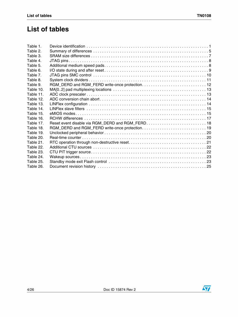
1 Summary of differences . . . . . . . . . . . . . . . . . . . . . . . . . . . . . . . . . . . . . . 5
2 Memory and memory control . . . . . . . . . . . . . . . . . . . . . . . . . . . . . . . . . . 7
2.1 SRAM size . . . . . . . . . . . . . . . . . . . . . . . . . . . . . . . . . . . . . . . . . . . . . . . . . 7
3 Pin configuration . . . . . . . . . . . . . . . . . . . . . . . . . . . . . . . . . . . . . . . . . . . . 8
3.1 Additional GPIO on JTAG pins . . . . . . . . . . . . . . . . . . . . . . . . . . . . . . . . . . 8
3.2 Medium speed pad allocation . . . . . . . . . . . . . . . . . . . . . . . . . . . . . . . . . . . 8
3.3 Input/output state during and after reset . . . . . . . . . . . . . . . . . . . . . . . . . . 9
3.4 GPIO pin configuration in standby mode . . . . . . . . . . . . . . . . . . . . . . . . . . 9
4 Debug . . . . . . . . . . . . . . . . . . . . . . . . . . . . . . . . . . . . . . . . . . . . . . . . . . . . 10
4.1 Debug through LPM . . . . . . . . . . . . . . . . . . . . . . . . . . . . . . . . . . . . . . . . . 10
4.2 JTAG operation in safe mode . . . . . . . . . . . . . . . . . . . . . . . . . . . . . . . . . . 10
4.3 Nexus configuration . . . . . . . . . . . . . . . . . . . . . . . . . . . . . . . . . . . . . . . . . 10
5 Peripherals . . . . . . . . . . . . . . . . . . . . . . . . . . . . . . . . . . . . . . . . . . . . . . . . 11
5.1 Peripheral clock prescalers . . . . . . . . . . . . . . . . . . . . . . . . . . . . . . . . . . . 11
5.2 ADC register map change . . . . . . . . . . . . . . . . . . . . . . . . . . . . . . . . . . . . 12
5.3 ADC additional external result registers . . . . . . . . . . . . . . . . . . . . . . . . . . 12
5.4 ADC multiplex control . . . . . . . . . . . . . . . . . . . . . . . . . . . . . . . . . . . . . . . . 13
5.5 ADC clock prescaler divider . . . . . . . . . . . . . . . . . . . . . . . . . . . . . . . . . . . 13
5.6 ADC abort modification . . . . . . . . . . . . . . . . . . . . . . . . . . . . . . . . . . . . . . 14
5.7 ADC offset calculation . . . . . . . . . . . . . . . . . . . . . . . . . . . . . . . . . . . . . . . 14
5.8 LINFlex slave configuration change . . . . . . . . . . . . . . . . . . . . . . . . . . . . . 14
5.9 LINFlex slave filters . . . . . . . . . . . . . . . . . . . . . . . . . . . . . . . . . . . . . . . . . 15
5.10 eMIOS additional modes and channel types . . . . . . . . . . . . . . . . . . . . . . 15
6 Reset and BAM . . . . . . . . . . . . . . . . . . . . . . . . . . . . . . . . . . . . . . . . . . . . 17
6.1 Reset Configuration Halfword (RCHW) . . . . . . . . . . . . . . . . . . . . . . . . . . 17
6.2 Correct reset event-disable feature . . . . . . . . . . . . . . . . . . . . . . . . . . . . . 17
6.3 Write once protection of reset configuration registers . . . . . . . . . . . . . . . 18

TN0108 Contents
Doc ID 15874 Rev 2 3/26
6.4 Unused BAM space abort . . . . . . . . . . . . . . . . . . . . . . . . . . . . . . . . . . . . 19
7 Clocks (including RTC) . . . . . . . . . . . . . . . . . . . . . . . . . . . . . . . . . . . . . . 20
7.1 Invalid clock selection inhibit . . . . . . . . . . . . . . . . . . . . . . . . . . . . . . . . . . 20
7.2 RTC counter updates . . . . . . . . . . . . . . . . . . . . . . . . . . . . . . . . . . . . . . . . 20
7.3 RTC operation through non-destructive reset . . . . . . . . . . . . . . . . . . . . . 21
7.4 External 32 kHz oscillator . . . . . . . . . . . . . . . . . . . . . . . . . . . . . . . . . . . . . 21
8 CTU (Cross Triggering Unit) . . . . . . . . . . . . . . . . . . . . . . . . . . . . . . . . . . 22
8.1 CTU source update . . . . . . . . . . . . . . . . . . . . . . . . . . . . . . . . . . . . . . . . . 22
8.2 CTU PIT/eMIOS configuration change . . . . . . . . . . . . . . . . . . . . . . . . . . . 22
9 Power, low power, and wakeup . . . . . . . . . . . . . . . . . . . . . . . . . . . . . . . 23
9.1 API/RTC wakeup source . . . . . . . . . . . . . . . . . . . . . . . . . . . . . . . . . . . . . 23
9.2 Halt mode defect fixed . . . . . . . . . . . . . . . . . . . . . . . . . . . . . . . . . . . . . . . 23
9.3 Standby mode exit Flash control . . . . . . . . . . . . . . . . . . . . . . . . . . . . . . . 23
9.4 Voltage regulator power up current clamping . . . . . . . . . . . . . . . . . . . . . . 23
10 Revision history . . . . . . . . . . . . . . . . . . . . . . . . . . . . . . . . . . . . . . . . . . . 25
List of tables TN0108
4/26 Doc ID 15874 Rev 2
List of tables
Table 1. Device identification . . . . . . . . . . . . . . . . . . . . . . . . . . . . . . . . . . . . . . . . . . . . . . . . . . . . . . . 1Table 2. Summary of differences . . . . . . . . . . . . . . . . . . . . . . . . . . . . . . . . . . . . . . . . . . . . . . . . . . . . 5Table 3. SRAM size differences . . . . . . . . . . . . . . . . . . . . . . . . . . . . . . . . . . . . . . . . . . . . . . . . . . . . . 7Table 4. JTAG pins . . . . . . . . . . . . . . . . . . . . . . . . . . . . . . . . . . . . . . . . . . . . . . . . . . . . . . . . . . . . . . . 8Table 5. Additional medium speed pads. . . . . . . . . . . . . . . . . . . . . . . . . . . . . . . . . . . . . . . . . . . . . . . 8Table 6. I/O state during and after reset . . . . . . . . . . . . . . . . . . . . . . . . . . . . . . . . . . . . . . . . . . . . . . . 9Table 7. JTAG pins SMC control . . . . . . . . . . . . . . . . . . . . . . . . . . . . . . . . . . . . . . . . . . . . . . . . . . . 10Table 8. System clock dividers . . . . . . . . . . . . . . . . . . . . . . . . . . . . . . . . . . . . . . . . . . . . . . . . . . . . . 11Table 9. RGM_DERD and RGM_FERD write-once protection. . . . . . . . . . . . . . . . . . . . . . . . . . . . . 12Table 10. MA[0..2] pad multiplexing locations . . . . . . . . . . . . . . . . . . . . . . . . . . . . . . . . . . . . . . . . . . 13Table 11. ADC clock prescaler . . . . . . . . . . . . . . . . . . . . . . . . . . . . . . . . . . . . . . . . . . . . . . . . . . . . . . 13Table 12. ADC conversion chain abort . . . . . . . . . . . . . . . . . . . . . . . . . . . . . . . . . . . . . . . . . . . . . . . . 14Table 13. LINFlex configuration . . . . . . . . . . . . . . . . . . . . . . . . . . . . . . . . . . . . . . . . . . . . . . . . . . . . . 14Table 14. LINFlex slave filters . . . . . . . . . . . . . . . . . . . . . . . . . . . . . . . . . . . . . . . . . . . . . . . . . . . . . . 15Table 15. eMIOS modes. . . . . . . . . . . . . . . . . . . . . . . . . . . . . . . . . . . . . . . . . . . . . . . . . . . . . . . . . . . 15Table 16. RCHW differences . . . . . . . . . . . . . . . . . . . . . . . . . . . . . . . . . . . . . . . . . . . . . . . . . . . . . . . 17Table 17. Reset event disable via RGM_DERD and RGM_FERD. . . . . . . . . . . . . . . . . . . . . . . . . . . 18Table 18. RGM_DERD and RGM_FERD write-once protection. . . . . . . . . . . . . . . . . . . . . . . . . . . . . 19Table 19. Unclocked peripheral behavior . . . . . . . . . . . . . . . . . . . . . . . . . . . . . . . . . . . . . . . . . . . . . . 20Table 20. Real-time counter . . . . . . . . . . . . . . . . . . . . . . . . . . . . . . . . . . . . . . . . . . . . . . . . . . . . . . . . 20Table 21. RTC operation through non-destructive reset. . . . . . . . . . . . . . . . . . . . . . . . . . . . . . . . . . . 21Table 22. Additional CTU sources . . . . . . . . . . . . . . . . . . . . . . . . . . . . . . . . . . . . . . . . . . . . . . . . . . . 22Table 23. CTU PIT trigger source. . . . . . . . . . . . . . . . . . . . . . . . . . . . . . . . . . . . . . . . . . . . . . . . . . . . 22Table 24. Wakeup sources . . . . . . . . . . . . . . . . . . . . . . . . . . . . . . . . . . . . . . . . . . . . . . . . . . . . . . . . . 23Table 25. Standby mode exit Flash control . . . . . . . . . . . . . . . . . . . . . . . . . . . . . . . . . . . . . . . . . . . . 23Table 26. Document revision history . . . . . . . . . . . . . . . . . . . . . . . . . . . . . . . . . . . . . . . . . . . . . . . . . 25

TN0108 Summary of differences
Doc ID 15874 Rev 2 5/26
1 Summary of differences
This section gives a summary of all the differences between the SPC560B 512 KB Flash size silicon revisions Cut 1.1 and Cut 2. These differences are described in more detail in the following sections. For ease of navigation, the section number provides a link to the appropriate section.
Table 2. Summary of differences
Description Cut 1.1 Cut 2 Section
SRAM size increase 32 KB SRAM 48 KB SRAM Section 2.1
Additional GPIO on JTAG pins Dedicated JTAG pinsAdded PH[9] and PH[10] to TMS and TCK
Section 3.1
Medium speed pad allocation 27 additional medium pads Section 3.2
GPIO state during and after resetHigh-Z in reset, then input with weak pull-up
High-Z during and after reset except JTAG and ABS pins
Section 3.3
Debug through LPM Not supported Supported Section 4.1
JTAG operation in safe modeJTAG pins tri-state by default in SAFE mode
SMC modified, so JTAG pins remain active in SAFE mode
Section 4.2
Nexus TAP change Change to TAP command Section 4.3
Peripheral clock prescalers Disabled out of reset Enabled out of reset Section 5.1
ADC register map changeFundamentally different to Cut 2. Code change required.
Section 5.2
ADC additional external result register
Four external results registers for ANX[0..3]
32 external results registers covering full external mux
Section 5.3
ADC multiplex controlAdditional pad-multiplexing options.
Section 5.4
ADC clock prescaler divider Set to sysclk/2Option to use sysclk/2 when in LPM on 16 MHz IRC
Section 5.5
ADC abortSlow abort for chained commands
New “abortchain” control bit added for rapid abort.
Section 5.6
ADC offset calculation ImplementedRemoved. Did not provide any benefit to ADC precision.
Section 5.7
LINFlex configuration changeAll four LINFlex modules support master/slave
LINFlex 0 is master /slave, all others are master only
Section 5.8
LINFlex slave filters Eight ID filters on LINFlex0 16 ID filters on LINFlex0 Section 5.9
eMIOS additional modes and channel types
Eight modes and three channel types
Added two more channel types with four more modes
Section 5.10
RCHW format 0x0000_005A 0x005A_0000 Section 6.1
Correct reset event disableCan disable all reset sources in DERD/FERD
Allow ability to lock all reset config registers
Section 6.2
Protection of reset event disable registers
Write-once protection based on 32-bit resolution
Individual 16-bit protection for DERD/FERD
Section 6.3

Summary of differences TN0108
6/26 Doc ID 15874 Rev 2
Unused BAM space abortNon-BAM code not set to 0x0 so no exception
Non-BAM ROM areas set to 0x0 to force exception
Section 6.4
Invalid clock selection inhibitSystem hang, if access clock gated peripheral
No system hang, if access peripheral with clock disabled
Section 7.1
RTC counter updateRTC has to be stopped before updating compare value
Allow RTC compare value to be changed without halting the counter
Section 7.2
RTC operation through non-destructive reset
RTC stops and is reset during reset period
RTC continues to run through non-destructive and watchdog resets
Section 7.3
External 32 kHz oscillator Not functional Functional Section 7.4
CTU source updateAdd Ch24 and Ch48 as trigger sourced for ADC
Section 8.1
CTU PIT/eMIOS configurationeMIOS ch23 to CTU_23, PIT_3 to CTU_28
eMIOS ch23 not mapped. PIT_3 moved to CTU ch23
Section 8.2
API/RTC Wakeup SourceAPI/RTC shared wakeup source zero
API wakeup source zero and RTC wakeup source one
Section 9.1
Halt mode defect Cannot enter Halt Halt mode working correctly Section 9.2
Standby mode exit Flash control In RGM_STDBY In ME_DRUN_MC register Section 9.3
Vreg power-on current clamp No current clamping Current clamp set to 200 mA Section 9.4
Table 2. Summary of differences (continued)
Description Cut 1.1 Cut 2 Section

TN0108 Memory and memory control
Doc ID 15874 Rev 2 7/26
2 Memory and memory control
2.1 SRAM sizeThe SPC560B Cut 1.1 MCU has 32 Kbytes of SRAM. This has been increased on the Cut 2 MCU to 48 Kbytes. The additional SRAM has been added below the existing 32 Kbyte block to create a contiguous 48 KB block on Cut 2.
Caution: When using the Cut 2 device, you need to ensure that the RAM initialisation routine is modified to include the additional memory space, in order to avoid any ECC errors when reading from the SRAM. Even a 16-bit write could cause an ECC error, as it is implemented as a 32-bit read modify write in order to update the ECC.
Table 3. SRAM size differences
Silicon revisionSRAM memory
Start address End address Size
SPC560B Cut 1.1 0x4000_0000 0x4000_7FFF 32 Kbytes
SPC560B Cut 2 0x4000_0000 0x4000_BFFF 48 Kbytes
Pin configuration TN0108
8/26 Doc ID 15874 Rev 2
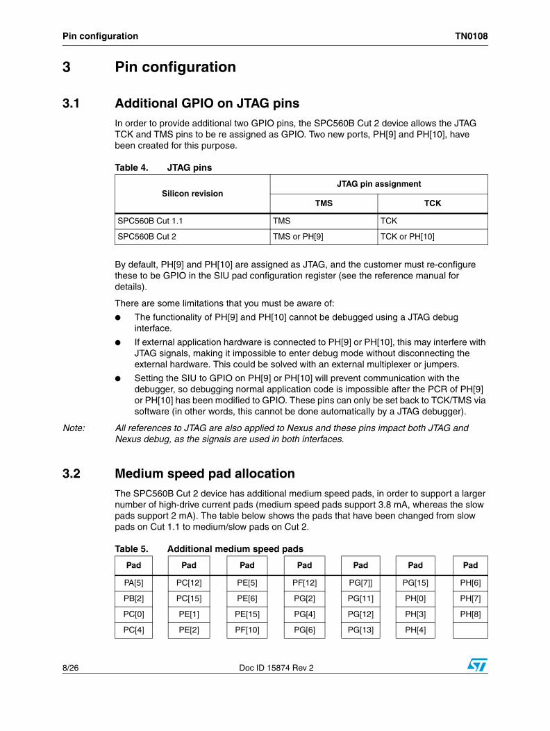
3 Pin configuration
3.1 Additional GPIO on JTAG pinsIn order to provide additional two GPIO pins, the SPC560B Cut 2 device allows the JTAG TCK and TMS pins to be re assigned as GPIO. Two new ports, PH[9] and PH[10], have been created for this purpose.
By default, PH[9] and PH[10] are assigned as JTAG, and the customer must re-configure these to be GPIO in the SIU pad configuration register (see the reference manual for details).
There are some limitations that you must be aware of:
● The functionality of PH[9] and PH[10] cannot be debugged using a JTAG debug interface.
● If external application hardware is connected to PH[9] or PH[10], this may interfere with JTAG signals, making it impossible to enter debug mode without disconnecting the external hardware. This could be solved with an external multiplexer or jumpers.
● Setting the SIU to GPIO on PH[9] or PH[10] will prevent communication with the debugger, so debugging normal application code is impossible after the PCR of PH[9] or PH[10] has been modified to GPIO. These pins can only be set back to TCK/TMS via software (in other words, this cannot be done automatically by a JTAG debugger).
Note: All references to JTAG are also applied to Nexus and these pins impact both JTAG and Nexus debug, as the signals are used in both interfaces.
3.2 Medium speed pad allocationThe SPC560B Cut 2 device has additional medium speed pads, in order to support a larger number of high-drive current pads (medium speed pads support 3.8 mA, whereas the slow pads support 2 mA). The table below shows the pads that have been changed from slow pads on Cut 1.1 to medium/slow pads on Cut 2.
Table 4. JTAG pins
Silicon revisionJTAG pin assignment
TMS TCK
SPC560B Cut 1.1 TMS TCK
SPC560B Cut 2 TMS or PH[9] TCK or PH[10]
Table 5. Additional medium speed pads
Pad Pad Pad Pad Pad Pad Pad
PA[5] PC[12] PE[5] PF[12] PG[7]] PG[15] PH[6]
PB[2] PC[15] PE[6] PG[2] PG[11] PH[0] PH[7]
PC[0] PE[1] PE[15] PG[4] PG[12] PH[3] PH[8]
PC[4] PE[2] PF[10] PG[6] PG[13] PH[4]

TN0108 Pin configuration
Doc ID 15874 Rev 2 9/26
Note that not all of these pads are available in all packages! Consult the device reference manual for details. This gives a total of 40 medium speed pads in the 144 QPF package and 25 medium speed pads in the 100 QFP package.
Customers must be careful of the number of pads that are switched together with the resulting increase in current. The sum of the current on each pad segment must not exceed the maximum current, as defined in the device datasheet.
3.3 Input/output state during and after resetOn Cut 1 devices, the input/output pins are set to high impedance (tri stated) during reset. Once reset has been released, the input/output pins are set to input with weak pull-ups enabled.
On Cut 2 devices, the input/output are set to high impedance during reset and remain in this state, once the reset has been released.
The following pins are critical to boot operation and are not in high impedance state during reset:
● PA[9] (FAB) is pull-down. Without external strong pull-up the device starts fetching from Flash
● PA[8] (ABS) is pull-up
● RESET pad is driven low. This is pull-up only after PHASE2 reset completion
● JTAG pads (TCK, TMS, and TDI) are pull-up, whilst TDO remains tri state
● Nexus output pads (MDO[n], MCKO, EVTO, MSEO) are forced to output
3.4 GPIO pin configuration in standby modeOn Cut 2 devices, if GPIO pull-ups are active on standby entry, the pull-up will remain active on standby exit, until such a point as the pull-up is cleared by software.
Table 6. I/O state during and after reset
Silicon revisionInput/output pins during
resetInput/output pins after reset
SPC560B Cut 1.1 High impedance Input, weak pull-up
SPC560B Cut 2 High impedanceHigh Impedance except JTAG and ABS that are input, weak pull-up

Debug TN0108
10/26 Doc ID 15874 Rev 2
4 Debug
4.1 Debug through LPMIt is desired that there is debug capability right up the point the MCU enters low-power mode, and that debug capability is re-initiated as soon as the MCU starts to wake up.
Debug handshaking has been added to Cut 2 to notify the debugger that a low-power mode entry is about to take place. This allows the debugger to cease communication with the MCU during low-power mode without any errors. Similarly, once the MCU starts to wake up, handshaking is used to inform the debugger of the wakeup. With the debugger attached, transition from low-power mode can only be completed once the debugger has acknowledged the wakeup.
4.2 JTAG operation in safe modeOn Cut 1 devices, the default state of the SMC (Safe Mode Control) bits in the PCR (Pad Configuration Registers) defaults to zero. This means that when the MCU enters SAFE mode, the device pins are tri stated. If a debugger is connected at this point, then the debug session is terminated as soon as the pins tri state.
On Cut 2 devices, the SMC bit for the JTAG pins defaults to one after reset. This keeps the JTAG pins alive in safe mode, thus allowing debug through safe mode by default.
4.3 Nexus configurationThe information in this section is only applicable to customers who are working with the NPC (Nexus Port Controller), for example a JTAG based Flash programming solution. Most development tool vendors have already implemented this change for Cut 2.
On Cut 1.1 devices, the following TAP controller commands are in place:
● ACCESS_AUX_TAP_ONCE 10001 grants the platform ownership of the TAP
● ACCESS_AUX_TAP_NPC 10010 grants the Nexus Port Controller (NPC) ownership of the TAP.
On Cut 2 Devices, these commands are modified to be in-line with previous eSYS devices with:
● ACCESS_AUX_TAP_ONCE 10001 grants the platform ownership of the TAP
● ACCESS_AUX_TAP_NPC 10000 grants the Nexus Port Controller (NPC) ownership of the TAP
Table 7. JTAG pins SMC control
Silicon revision Default PCRx_SMC state Comments
SPC560B Cut 1.1 0 JTAG pins disabled in safe mode
SPC560B Cut 2 1 for JTAG pins JTAG pins active in safe mode

TN0108 Peripherals
Doc ID 15874 Rev 2 11/26
5 Peripherals
5.1 Peripheral clock prescalersOn Cut 1.1 devices, the system clock divider enable bits DE0, DE1, and DE2 within the system clock divider configuration registers are cleared out of reset. This means that any attempt to access an off-platform peripheral without enabling the relevant clock divider will result in a system crash.
On Cut 2 devices, the system clock divider enable bits are set out of reset to enable all the peripheral clock prescalers.
Table 8. System clock dividers
Silicon revisionDE0, DE1, DE2 in GCM_SC_DC[0..2]
Implications
SPC560B Cut 1.1 Cleared out of reset System clock to peripherals is disabled out of reset
SPC560B Cut 2 Set out of reset System clock to peripherals is enabled out of reset

Peripherals TN0108
12/26 Doc ID 15874 Rev 2
5.2 ADC register map changeThe ADC memory map and register description has fundamentally changed between Cut 1.1 and Cut 2 devices. This was to bring the ADC implementation more in-line with the format of other peripherals (for example including a Module Configuration Register).
Migrating ADC code between Cut 1.1 and Cut 2 requires a code re-write to use the new register and bit field names. There is a new header file available to support the new interface on Cut 2.
There are also some functional changes to the ADC going from Cut 1.1 to Cut 2 that are detailed in the next three sections.
5.3 ADC additional external result registersThe ADC has four external channels ANX[0..3]. These can be used with four external 8-bit multiplexers (controlled by the MA[0..2] bits) to provide up to 32 extended ADC channels.
Cut 1.1 devices have a single result register for each of the four external ADC channels.
On Cut 2 devices, there are 32 external results registers, so there is a unique results register for each supported external channel. The results are automatically stored in the appropriate external channel, thus allowing the user to treat an externally multiplexed channel in the same manner as an internal channel.
Table 9. RGM_DERD and RGM_FERD write-once protection
Silicon revision External multiplexed channels Implications
SPC560B Cut 1.1Four results registers, one per ANX[0..3] channel.
Need to read result register before another channel on same external multiplexer is used again.
SPC560B Cut 232 results registers, one for each potential externally multiplexed channel.
External ADC channels can be treated the same as internal channels in software.
TN0108 Peripherals
Doc ID 15874 Rev 2 13/26
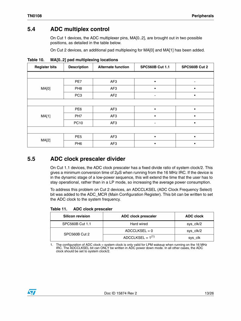
5.4 ADC multiplex controlOn Cut 1 devices, the ADC multiplexer pins, MA[0..2], are brought out in two possible positions, as detailed in the table below.
On Cut 2 devices, an additional pad multiplexing for MA[0] and MA[1] has been added.
5.5 ADC clock prescaler dividerOn Cut 1.1 devices, the ADC clock prescaler has a fixed divide ratio of system clock/2. This gives a minimum conversion time of 2µS when running from the 16 MHz IRC. If the device is in the dynamic stage of a low-power sequence, this will extend the time that the user has to stay operational, rather than in a LP mode, so increasing the average power consumption.
To address this problem on Cut 2 devices, an ADCCLKSEL (ADC Clock Frequency Select) bit was added to the ADC_MCR (Main Configuration Register). This bit can be written to set the ADC clock to the system frequency.
Table 10. MA[0..2] pad multiplexing locations
Register bits Description Alternate function SPC560B Cut 1.1 SPC560B Cut 2
MA[0]
PE7 AF3 • -
PH8 AF3 • •
PC3 AF2 - •
MA[1]
PE6 AF3 • •
PH7 AF3 • •
PC10 AF3 - •
MA[2]PE5 AF3 • •
PH6 AF3 • •
Table 11. ADC clock prescaler
Silicon revision ADC clock prescaler ADC clock
SPC560B Cut 1.1 Hard wired sys_clk/2
SPC560B Cut 2 ADCCLKSEL = 0 sys_clk/2
ADCCLKSEL = 1(1)
1. The configuration of ADC clock = system clock is only valid for LPM wakeup when running on the 16 MHz IRC. The ADCCLKSEL bit can ONLY be written in ADC power down mode. In all other cases, the ADC clock should be set to system clock/2.
sys_clk

Peripherals TN0108
14/26 Doc ID 15874 Rev 2
5.6 ADC abort modificationOn Cut 1.1 devices, if an ADC conversion chain is to be aborted, this does not happen immediately. All conversions of the chain need to be aborted individually, resulting in a delay before a new conversion chain can be issued.
On Cut 2 devices, an “ABORTCHAIN” bit has been added to the ADC_MCR (Main Configuration Register). The exact behavior is dependent on the Mode bit. In summary, setting the ABORTCHAIN bit immediately aborts all conversion chains. As soon as a new conversion is requested, the ABORTCHAIN bit is automatically cleared. Depending on mode, an ECH (end of chain) interrupt is generated and the NSTART and JSTART bits are also cleared. For more details consult the device reference manual.
5.7 ADC offset calculationCut 1.1 devices have an ADC offset calculation mechanism. This was proven not to improve the overall ADC performance, as the intrinsic ADC precision is better than the offset calculation resolution.
The offset calculation mechanism has been removed for Cut 2 devices.
5.8 LINFlex slave configuration changeCut 1.1 devices have LIN slave features on all of the four LINFlex modules (each slave port has eight identifiers filters).
On Cut 2 devices, there is only one LINFlex module (LinFlex 0) that provides slave functionality. The remaining three LINFlex modules have been changed to master only.
Customers must ensure that if they are using the LINFlex in slave mode on Cut 1.1, the application code will need to be changed, if this was not using LINFlex channel zero.
Table 12. ADC conversion chain abort
Silicon revision Chain abort mechanism
SPC560B Cut 1.1 Individual abort for each conversion
SPC560B Cut 2 Immediate via ABORTCHAIN
Table 13. LINFlex configuration
Silicon revisionLINFlex 0 LINFlex 1 LINFlex 2 LINFlex 3
Master Slave Master Slave Master Slave Master Slave
SPC560B Cut 1.1 • • • • • • • •
SPC560B Cut 2 • • • - • - • -

TN0108 Peripherals
Doc ID 15874 Rev 2 15/26
5.9 LINFlex slave filtersCut 1.1 devices had eight identifier (ID) filters on all of the four LINFlex channels (all channels supported slave mode).
On Cut 2 devices, LINFlex channel zero (the only channel supporting slave mode) has had the number of ID filters increased from eight to 16.
5.10 eMIOS additional modes and channel typesThe eMIOS on Cut 1 devices supports eight different operating modes via three different channel types (X, Y, and F).
On Cut 2 devices, two additional channel types (G and H) have been added to support additional four modes, as detailed in the table below.
Table 14. LINFlex slave filters
Silicon revision LINFlex 0 LINFlex 1 LINFlex 2 LINFlex 3
SPC560B Cut 1.1 Eight ID filters Eight ID filters Eight ID filters Eight ID filters
SPC560B Cut 2 16 ID filters N/A (master only) N/A (master only) N/A (master only)
Table 15. eMIOS modes
Mode description Mode name
Existing channels on Cut 1.1 (and Cut 2)
New additional channels on Cut 2
Type X Type Y Type F Type G Type H
General Purpose Input/Output GPIO • • • • •
Single Action Input Capture SAIC • • • • •
Single Action Output Compare SAOC • • • • •
Modulus Counter MC • - - - -
Modulus Counter Buffered (Up/Down) MCB • - - • -
Output Pulse width and Frequency Modulation (Buffered)
OPWFMB • - - • -
Output Pulse Width Modulation (Buffered) OPWMB • • - • •
Output Pulse Width Modulation Trigger OPWMT • • - • •
Additional Modes supported only on Cut 2 via new channels
Input Pulse Width Measurement IPWM - - - • •
Input Period Measurement IPM - - - • •
Double Action Output Compare DAOC - - - • •
Center-aligned Output PWM Buffered with dead-time insertion
OPWMCB - - - • -

Peripherals TN0108
16/26 Doc ID 15874 Rev 2
On Cut 2 devices, the new channel types are implemented as follows:
● eMIOS 0 ch1-7, channel type G
● eMIOS 0 ch9-15, channel type H
● eMIOS 1 ch9-15, channel type H
For more details on the specifics of each mode and channel groupings, consult the device reference manual.

TN0108 Reset and BAM
Doc ID 15874 Rev 2 17/26
6 Reset and BAM
6.1 Reset Configuration Halfword (RCHW)The RCHW (Reset Configuration Half Word) has been changed from being in the lower to the upper 32-bits of the address space, as defined in the table below.
The user must ensure that the Flash RCHW is updated. Otherwise a valid RCHW will not be found and the device will not successfully boot from Flash.
6.2 Correct reset event-disable featureOn Cut 1.1 devices, it was possible to disable all reset events by writing to the RGM_FERD and RGM_DERD bits. This was never intended as a supported mode of operation, since it is not desirable to be able to lock out all reset sources.
On Cut 2, the distribution of reset sources in the DERD and FERD registers has been changed as shown in the table below. In addition, the DERD register has been set to read only, so the reset sources within DERD cannot be disabled.
Table 16. RCHW differences
Silicon revision RCHW format
SPC560B Cut 1.1 0x0000_005A
SPC560B Cut 2 0x005A_0000

Reset and BAM TN0108
18/26 Doc ID 15874 Rev 2
Note that the RGM_FERD and RGM_DERD registers are ‘write-once’. For details on a change that was made to this implementation between Cut 1.1 and Cut 2 devices, see the following section.
For further details on the FERD and DERD registers, consult the device reference manual.
6.3 Write once protection of reset configuration registersOn Cut 1.1 devices, the RGM_DERD and RGM_FERD registers are configured such that write-once protection to these registers is provided as a 32-bit block. Thus, any write to the DERD or FERD register (be it 16-bits or otherwise) will prevent further writes to either register. The only way to correctly configure this is to write to the DERD and FERD registers in a single 32-bit write.
On Cut 2 devices, the mechanism has been changed such that the RGM_DERD and RGM_FERD registers each have their own 16-bit write-once mechanism. This is somewhat irrelevant, since the DERD register has been set to read-only in Cut 2, however it means that any attempt to write to DERD will not impact the write-once mechanism for FERD.
Table 17. Reset event disable via RGM_DERD and RGM_FERD
Register bits Description SPC560B Cut 1.1 SPC560B Cut 2
RGM_FERD (Functional Event Reset Disable Register)
D_EXR Disable External Reset - Read only
D_Flash Disable code or data Flash error reset • •
D_LVD45 Disable 4.5 V LVI detected reset • •
D_CMU0_FHL Disable CMU0 Clock higher/lower than ref • •
D_CMU0_OLR Disable Oscillator freq lower than reference • •
D_PLL/D_FMPLL Disable PLL0 fail reset (Cut 1.1)Disable FMPLL fail reset (Cut 2)
• •
D_CHKSTOP Disable checkstop reset - Read only
D_Soft Disable Software reset - Read only
D_Core Disable Core reset • •
D_JTAG Disable JTAG-initiated reset • •
RGM_DERD (destructive Event Reset Disable Register)
D_LVD27 - Read only
D_SWT • Read only
D_LVD12_PD1 - Read only
D_LVD12_PD0 - Read only

TN0108 Reset and BAM
Doc ID 15874 Rev 2 19/26
6.4 Unused BAM space abortThe SPC560B BAM code is implemented as an 8 KB ROM block at the bottom of the memory map (0xFFFF_C000 to 0xFFFF_FFFF). The BAM code itself is considerably smaller than the 8 KB ROM block. It is desirable to trap any attempt to execute non BAM code within this ROM block. In Power Architecture, an instruction with all bits set to zero is defined as an illegal instruction, which can be trapped.
On Cut 1.1 devices, non BAM locations were left as non-zero, so if the PC was set to a non BAM location within the ROM block, an undefined operation would result.
On Cut 2 devices, unused locations within the ROM block have been set to zero, to any attempt to execute from within this area will result in an exception.
This has no real impact for customer code, but is listed here in the case customers notice the change to the BAM and are concerned that there is a functional change in the BAM code.
Table 18. RGM_DERD and RGM_FERD write-once protection
Silicon revision Write protection mechanism Implications
SPC560B Cut 1.1Any write to DERD or FERD would write-protect
both registers.If configuring both registers, need to do
so with single 32-bit write.
SPC560B Cut 2 Individual 16-bit protection on each register.Write to DERD (read-only) will not block
subsequent write to FERD.

Clocks (including RTC) TN0108
20/26 Doc ID 15874 Rev 2
7 Clocks (including RTC)
7.1 Invalid clock selection inhibitOn Cut 1.1 devices, whenever an attempt was made to access a peripheral that had the peripheral clock disabled, the system hung with no response.
On Cut 2 devices, this has been fixed such that the system no longer hangs. If the RAE bit is set within the SSCM_ERROR register, then the user will be notified of an access problem with an IVOR2 exception. The clock status of each peripheral (enabled or disabled) can be determined by reading the ME_PSx registers.
7.2 RTC counter updatesOn Cut 1.1 devices, the RTC has to be halted (by writing to the CNTEN bit in the RTC Control register) before the RTC compare value (RTCVAL) is changed. This not only stopped the counter, but also had the effect of resetting the counter.
A modification has been made on Cut 2 devices, so that the RTCVAL can be changed without halting the counter.
Note: For customers who have written code to change the counter value in Cut 1.1, you need to be careful of the fact that the counter is reset when CNTEN is cleared. On Cut 2 you may get a timer compare almost immediately after modifying the RTVAL.
Table 19. Unclocked peripheral behavior
Silicon revision Behavior on accessing unclocked peripheral
SPC560B Cut 1.1 Non-recoverable system hang.
SPC560B Cut 2 System does not hang. User notified via IVOR2 exception.
Table 20. Real-time counter
Silicon revision Change RTCVAL Comments
SPC560B Cut 1.1 Halt Counter, then change RTVALCounter is reset when CNTEN is
cleared
SPC560B Cut 2 Change RTVAL when counter is running No need to stop counter

TN0108 Clocks (including RTC)
Doc ID 15874 Rev 2 21/26
7.3 RTC operation through non-destructive resetOn Cut 1.1 devices, when a non-destructive reset (for example a functional reset or watchdog reset) is issued, the RTC (real-time clock) is reset.
On Cut 2 devices, the clocking circuitry has been changed so that the RTC will continue to run and keep time through a non-destructive reset.
7.4 External 32 kHz oscillatorOn Cut 1.1 devices, there was a fault, which prevented the 32 kHz external oscillator from functioning. This has been fixed on Cut 2 devices so an external 32 kHz oscillator can be used. For a list of devices that have been qualified to function correctly, consult the device reference manual and datasheet.
Table 21. RTC operation through non-destructive reset
Silicon revision RTC behavior Implications
SPC560B Cut 1.1 RTC is reset Loss of time keeping
SPC560B Cut 2 RTC continues to run No loss of time keeping

CTU (Cross Triggering Unit) TN0108
22/26 Doc ID 15874 Rev 2
8 CTU (Cross Triggering Unit)
8.1 CTU source updateThe Cross Triggering Unit (CTU) provides a mechanism for an eMIOS or PIT timer event to synchronize an ADC conversion. The CTU provides the ADC a channel number to define which channel triggers the conversion.
On Cut 2 devices, channel 24 of eMIOS_0 and eMIOS_1 has been added as a trigger source for the ADC. These channels, both type X, support OPWMT mode, which can be used in conjunction with the ADC for lighting applications.
For full details of the CTU channels consult the device reference manual, where is a table showing all of the CTU channel sources.
8.2 CTU PIT/eMIOS configuration changeOn Cut 1 devices, the PIT_3 is mapped to CTU channel 28 and eMIOS_0 channel 23 is mapped to CTU channel 23.
On Cut 2 devices, PIT_3 has been moved to CTU channel 23.
For the full CTU trigger source mapping, consult the device reference manual.
Table 22. Additional CTU sources
Silicon revision Additional CTU channels CTU source number
SPC560B Cut 2 eMIOS_0 Channel 24 (Type X) 24
eMIOS_1 Channel 24 (Type X) 48
Table 23. CTU PIT trigger source
Silicon revision CTU channel 23 CTU channel 28
SPC560B Cut 1.1 eMIOS_0 Channel 23 PIT_3
SPC560B Cut 2 PIT_3 Reserved
TN0108 Power, low power, and wakeup
Doc ID 15874 Rev 2 23/26
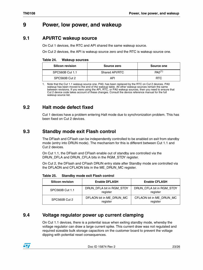
9 Power, low power, and wakeup
9.1 API/RTC wakeup sourceOn Cut 1 devices, the RTC and API shared the same wakeup source.
On Cut 2 devices, the API is wakeup source zero and the RTC is wakeup source one.
9.2 Halt mode defect fixedCut 1 devices have a problem entering Halt mode due to synchronization problem. This has been fixed on Cut 2 devices.
9.3 Standby mode exit Flash controlThe DFlash and CFlash can be independently controlled to be enabled on exit from standby mode (entry into DRUN mode). The mechanism for this is different between Cut 1.1 and Cut 2 devices.
On Cut 1.1, the DFlash and CFlash enable out of standby are controlled via the DRUN_DFLA and DRUN_CFLA bits in the RGM_STDY register.
On Cut 2, the DFlash and CFlash DRUN entry state after Standby mode are controlled via the DFLAON and CFLAON bits in the ME_DRUN_MC register.
9.4 Voltage regulator power up current clampingOn Cut 1.1 devices, there is a potential issue when exiting standby mode, whereby the voltage regulator can draw a large current spike. This current draw was not regulated and required sizeable bulk storage capacitors on the customer board to prevent the voltage dipping with potential reset consequences.
Table 24. Wakeup sources
Silicon revision Source zero Source one
SPC560B Cut 1.1 Shared API/RTC PA0(1)
1. Note that the Cut 1.1 wakeup source one, PA0, has been replaced by the RTC on Cut 2 devices. PA0 wakeup has been moved to the end of the wakeup table. All other wakeup sources remain the same between revisions. If you were using the API, RTC, or PA0 wakeup sources, then you need to ensure that Cut 2 device code takes account of these changes. Consult the device reference manual for the full wakeup source list.
SPC560B Cut 2 API RTC
Table 25. Standby mode exit Flash control
Silicon revision Enable DFLASH Enable CFLASH
SPC560B Cut 1.1DRUN_DFLA bit in RGM_STDY
registerDRUN_CFLA bit in RGM_STDY
register
SPC560B Cut 2DFLAON bit in ME_DRUN_MC
registerCFLAON bit in ME_DRUN_MC
register

Power, low power, and wakeup TN0108
24/26 Doc ID 15874 Rev 2
On Cut 2 devices, the voltage regulator has been current-clamped to 200 mA, so the bulk-storage capacitors on the customer board can be smaller and more optimized.
Note that hardware designed for Cut 1.1 will be fully functional with Cut 2 devices, but if the bulk capacitors have been reduced for Cut 2 hardware, this hardware will not support Cut 1.1.

TN0108 Revision history
Doc ID 15874 Rev 2 25/26
10 Revision history
Table 26. Document revision history
Date Revision Changes
16-Jun-2009 1 Initial release.
18-Sep-2013 2 Updated Disclaimer.

TN0108
26/26 Doc ID 15874 Rev 2
Please Read Carefully:
Information in this document is provided solely in connection with ST products. STMicroelectronics NV and its subsidiaries (“ST”) reserve theright to make changes, corrections, modifications or improvements, to this document, and the products and services described herein at anytime, without notice.
All ST products are sold pursuant to ST’s terms and conditions of sale.
Purchasers are solely responsible for the choice, selection and use of the ST products and services described herein, and ST assumes noliability whatsoever relating to the choice, selection or use of the ST products and services described herein.
No license, express or implied, by estoppel or otherwise, to any intellectual property rights is granted under this document. If any part of thisdocument refers to any third party products or services it shall not be deemed a license grant by ST for the use of such third party productsor services, or any intellectual property contained therein or considered as a warranty covering the use in any manner whatsoever of suchthird party products or services or any intellectual property contained therein.
UNLESS OTHERWISE SET FORTH IN ST’S TERMS AND CONDITIONS OF SALE ST DISCLAIMS ANY EXPRESS OR IMPLIED WARRANTY WITH RESPECT TO THE USE AND/OR SALE OF ST PRODUCTS INCLUDING WITHOUT LIMITATION IMPLIED WARRANTIES OF MERCHANTABILITY, FITNESS FOR A PARTICULAR PURPOSE (AND THEIR EQUIVALENTS UNDER THE LAWS OF ANY JURISDICTION), OR INFRINGEMENT OF ANY PATENT, COPYRIGHT OR OTHER INTELLECTUAL PROPERTY RIGHT.
ST PRODUCTS ARE NOT DESIGNED OR AUTHORIZED FOR USE IN: (A) SAFETY CRITICAL APPLICATIONS SUCH AS LIFE SUPPORTING, ACTIVE IMPLANTED DEVICES OR SYSTEMS WITH PRODUCT FUNCTIONAL SAFETY REQUIREMENTS; (B) AERONAUTIC APPLICATIONS; (C) AUTOMOTIVE APPLICATIONS OR ENVIRONMENTS, AND/OR (D) AEROSPACE APPLICATIONS OR ENVIRONMENTS. WHERE ST PRODUCTS ARE NOT DESIGNED FOR SUCH USE, THE PURCHASER SHALL USE PRODUCTS AT PURCHASER’S SOLE RISK, EVEN IF ST HAS BEEN INFORMED IN WRITING OF SUCH USAGE, UNLESS A PRODUCT IS EXPRESSLY DESIGNATED BY ST AS BEING INTENDED FOR “AUTOMOTIVE, AUTOMOTIVE SAFETY OR MEDICAL” INDUSTRY DOMAINS ACCORDING TO ST PRODUCT DESIGN SPECIFICATIONS. PRODUCTS FORMALLY ESCC, QML OR JAN QUALIFIED ARE DEEMED SUITABLE FOR USE IN AEROSPACE BY THE CORRESPONDING GOVERNMENTAL AGENCY.
Resale of ST products with provisions different from the statements and/or technical features set forth in this document shall immediately voidany warranty granted by ST for the ST product or service described herein and shall not create or extend in any manner whatsoever, anyliability of ST.
ST and the ST logo are trademarks or registered trademarks of ST in various countries.Information in this document supersedes and replaces all information previously supplied.
The ST logo is a registered trademark of STMicroelectronics. All other names are the property of their respective owners.
© 2013 STMicroelectronics - All rights reserved
STMicroelectronics group of companies
Australia - Belgium - Brazil - Canada - China - Czech Republic - Finland - France - Germany - Hong Kong - India - Israel - Italy - Japan - Malaysia - Malta - Morocco - Philippines - Singapore - Spain - Sweden - Switzerland - United Kingdom - United States of America
www.st.com