tnt5002 technical reference manual and specifications
TRANSCRIPT

GPIBTNT5002TM Technical Reference ManualPCI to GPIB High-Performance Non-Controller
TNT5002 Technical Reference Manual
May 2004 EditionPart Number 370595B-01

Support
Worldwide Technical Support and Product Information
ni.com
National Instruments Corporate Headquarters
11500 North Mopac Expressway Austin, Texas 78759-3504 USA Tel: 512 683 0100
Worldwide Offices
Australia 1800 300 800, Austria 43 0 662 45 79 90 0, Belgium 32 0 2 757 00 20, Brazil 55 11 3262 3599, Canada (Calgary) 403 274 9391, Canada (Ottawa) 613 233 5949, Canada (Québec) 450 510 3055, Canada (Toronto) 905 785 0085, Canada (Vancouver) 514 685 7530, China 86 21 6555 7838, Czech Republic 420 224 235 774, Denmark 45 45 76 26 00, Finland 385 0 9 725 725 11, France 33 0 1 48 14 24 24, Germany 49 0 89 741 31 30, Greece 30 2 10 42 96 427, India 91 80 51190000, Israel 972 0 3 6393737, Italy 39 02 413091, Japan 81 3 5472 2970, Korea 82 02 3451 3400, Malaysia 603 9131 0918, Mexico 001 800 010 0793, Netherlands 31 0 348 433 466, New Zealand 0800 553 322, Norway 47 0 66 90 76 60, Poland 48 22 3390150, Portugal 351 210 311 210, Russia 7 095 783 68 51, Singapore 65 6226 5886, Slovenia 386 3 425 4200, South Africa 27 0 11 805 8197, Spain 34 91 640 0085, Sweden 46 0 8 587 895 00, Switzerland 41 56 200 51 51, Taiwan 886 2 2528 7227, Thailand 662 992 7519, United Kingdom 44 0 1635 523545
For further support information, refer to the Technical Support and Professional Services appendix. To comment on the documentation, send email to [email protected].
© 2003–2004 National Instruments Corporation. All rights reserved.

Important Information
WarrantyThe TNT5002 is warranted against defects in materials and workmanship for a period of one year from the date of shipment, as evidenced by receipts or other documentation. National Instruments will, at its option, repair or replace equipment that proves to be defective during the warranty period. This warranty includes parts and labor.
The media on which you receive National Instruments software are warranted not to fail to execute programming instructions, due to defects in materials and workmanship, for a period of 90 days from date of shipment, as evidenced by receipts or other documentation. National Instruments will, at its option, repair or replace software media that do not execute programming instructions if National Instruments receives notice of such defects during the warranty period. National Instruments does not warrant that the operation of the software shall be uninterrupted or error free.
A Return Material Authorization (RMA) number must be obtained from the factory and clearly marked on the outside of the package before any equipment will be accepted for warranty work. National Instruments will pay the shipping costs of returning to the owner parts which are covered by warranty.
National Instruments believes that the information in this document is accurate. The document has been carefully reviewed for technical accuracy. In the event that technical or typographical errors exist, National Instruments reserves the right to make changes to subsequent editions of this document without prior notice to holders of this edition. The reader should consult National Instruments if errors are suspected. In no event shall National Instruments be liable for any damages arising out of or related to this document or the information contained in it.
EXCEPT AS SPECIFIED HEREIN, NATIONAL INSTRUMENTS MAKES NO WARRANTIES, EXPRESS OR IMPLIED, AND SPECIFICALLY DISCLAIMS ANY WARRANTY OF MERCHANTABILITY OR FITNESS FOR A PARTICULAR PURPOSE. CUSTOMER’S RIGHT TO RECOVER DAMAGES CAUSED BY FAULT OR NEGLIGENCE ON THE PART OF NATIONAL INSTRUMENTS SHALL BE LIMITED TO THE AMOUNT THERETOFORE PAID BY THE CUSTOMER. NATIONAL INSTRUMENTS WILL NOT BE LIABLE FOR DAMAGES RESULTING FROM LOSS OF DATA, PROFITS, USE OF PRODUCTS, OR INCIDENTAL OR CONSEQUENTIAL DAMAGES, EVEN IF ADVISED OF THE POSSIBILITY THEREOF. This limitation of the liability of National Instruments will apply regardless of the form of action, whether in contract or tort, including negligence. Any action against National Instruments must be brought within one year after the cause of action accrues. National Instruments shall not be liable for any delay in performance due to causes beyond its reasonable control. The warranty provided herein does not cover damages, defects, malfunctions, or service failures caused by owner’s failure to follow the National Instruments installation, operation, or maintenance instructions; owner’s modification of the product; owner’s abuse, misuse, or negligent acts; and power failure or surges, fire, flood, accident, actions of third parties, or other events outside reasonable control.
CopyrightUnder the copyright laws, this publication may not be reproduced or transmitted in any form, electronic or mechanical, including photocopying, recording, storing in an information retrieval system, or translating, in whole or in part, without the prior written consent of National Instruments Corporation.
TrademarksHS488™, National Instruments™, NI™, ni.com™, NI-488.2™, NI-488DDK™, TNT4882™, TNT488C™, and TNT5002™ are trademarks of National Instruments Corporation.
Product and company names mentioned herein are trademarks or trade names of their respective companies.
PatentsFor patents covering National Instruments products, refer to the appropriate location: Help»Patents in your software, the patents.txt file on your CD, or ni.com/patents.
WARNING REGARDING USE OF NATIONAL INSTRUMENTS PRODUCTS(1) NATIONAL INSTRUMENTS PRODUCTS ARE NOT DESIGNED WITH COMPONENTS AND TESTING FOR A LEVEL OF RELIABILITY SUITABLE FOR USE IN OR IN CONNECTION WITH SURGICAL IMPLANTS OR AS CRITICAL COMPONENTS IN ANY LIFE SUPPORT SYSTEMS WHOSE FAILURE TO PERFORM CAN REASONABLY BE EXPECTED TO CAUSE SIGNIFICANT INJURY TO A HUMAN.
(2) IN ANY APPLICATION, INCLUDING THE ABOVE, RELIABILITY OF OPERATION OF THE SOFTWARE PRODUCTS CAN BE IMPAIRED BY ADVERSE FACTORS, INCLUDING BUT NOT LIMITED TO FLUCTUATIONS IN ELECTRICAL POWER SUPPLY, COMPUTER HARDWARE MALFUNCTIONS, COMPUTER OPERATING SYSTEM SOFTWARE FITNESS, FITNESS OF COMPILERS AND DEVELOPMENT SOFTWARE USED TO DEVELOP AN APPLICATION, INSTALLATION ERRORS, SOFTWARE AND HARDWARE COMPATIBILITY PROBLEMS, MALFUNCTIONS OR FAILURES OF ELECTRONIC MONITORING OR CONTROL DEVICES, TRANSIENT FAILURES OF ELECTRONIC SYSTEMS (HARDWARE AND/OR SOFTWARE), UNANTICIPATED USES OR MISUSES, OR ERRORS ON THE PART OF THE USER OR APPLICATIONS DESIGNER (ADVERSE FACTORS SUCH AS THESE ARE HEREAFTER COLLECTIVELY TERMED “SYSTEM FAILURES”). ANY APPLICATION WHERE A SYSTEM FAILURE WOULD CREATE A RISK OF HARM TO PROPERTY OR PERSONS (INCLUDING THE RISK OF BODILY INJURY AND DEATH) SHOULD NOT BE RELIANT SOLELY UPON ONE FORM OF ELECTRONIC SYSTEM DUE TO THE RISK OF SYSTEM FAILURE. TO AVOID DAMAGE, INJURY, OR DEATH, THE USER OR APPLICATION DESIGNER MUST TAKE REASONABLY PRUDENT STEPS TO PROTECT AGAINST SYSTEM FAILURES, INCLUDING BUT NOT LIMITED TO BACK-UP OR SHUT DOWN MECHANISMS. BECAUSE EACH END-USER SYSTEM IS CUSTOMIZED AND DIFFERS FROM NATIONAL INSTRUMENTS' TESTING PLATFORMS AND BECAUSE A USER OR APPLICATION DESIGNER MAY USE NATIONAL INSTRUMENTS PRODUCTS IN COMBINATION WITH OTHER PRODUCTS IN A MANNER NOT EVALUATED OR CONTEMPLATED BY NATIONAL INSTRUMENTS, THE USER OR APPLICATION DESIGNER IS ULTIMATELY RESPONSIBLE FOR VERIFYING AND VALIDATING THE SUITABILITY OF NATIONAL INSTRUMENTS PRODUCTS WHENEVER NATIONAL INSTRUMENTS PRODUCTS ARE INCORPORATED IN A SYSTEM OR APPLICATION, INCLUDING, WITHOUT LIMITATION, THE APPROPRIATE DESIGN, PROCESS AND SAFETY LEVEL OF SUCH SYSTEM OR APPLICATION.

© National Instruments Corporation v TNT5002 Technical Reference Manual
Contents
About This ManualProduct Features ............................................................................................................xiHow To Use This Manual..............................................................................................xiiConventions ...................................................................................................................xiii
Mnemonic Conventions...................................................................................xivRelated Documentation..................................................................................................xv
Chapter 1Architectural Overview
TNT5002 Block Diagram ..............................................................................................1-1TNT5002 Mode Selection .............................................................................................1-2FIFO Overview ..............................................................................................................1-2DMA Overview .............................................................................................................1-3
Chapter 2Signal Pins
Signal Definitions and Conventions ..............................................................................2-1GPIB Signals..................................................................................................................2-2
GPIB Data Signals...........................................................................................2-2GPIB Interface Management Signals ..............................................................2-2GPIB Handshake Signals ................................................................................2-3
Device Signals ...............................................................................................................2-4Miscellaneous Signals (All Modes).................................................................2-4Miscellaneous Signals (PCI4882 Mode) .........................................................2-5Indicator Signals..............................................................................................2-5
PCI Signals ....................................................................................................................2-6Generic Interface Signals...............................................................................................2-8Power/Ground Pins ........................................................................................................2-9
PCI4882 Power/Ground Pins ..........................................................................2-9GEN4882 Power/Ground Pins ........................................................................2-9
Chapter 3Register Descriptions
Register Groups .............................................................................................................3-1Register Groups in PCI4882 Mode .................................................................3-1Register Groups in GEN4882 Mode ...............................................................3-2
PCI4882 Mode Register Map ........................................................................................3-2
Contents
TNT5002 Technical Reference Manual vi ni.com
GEN4882 Mode Register Map...................................................................................... 3-4TNT5002 Status/Control Register Group...................................................................... 3-5
TNT5002 Status/Control Registers Sorted by Offset ..................................... 3-5TNT5002 Status/Control Registers Sorted by Mnemonic .............................. 3-6TNT5002 Status/Control Register Descriptions ............................................. 3-7
PCI Configuration Registers.......................................................................................... 3-10PCI Configuration Register Map .................................................................... 3-10PCI Configuration Register Descriptions ....................................................... 3-11
DMA Status/Control Registers...................................................................................... 3-26DMA Status/Control Registers Sorted by Offset ............................................ 3-26DMA Status/Control Registers Sorted by Mnemonic..................................... 3-27DMA Status/Control Register Descriptions.................................................... 3-28
4882 Register Set........................................................................................................... 3-454882-Mode Registers Sorted by Offset........................................................... 3-454882-Mode Registers Sorted by Mnemonic ................................................... 3-474882-Mode Register Descriptions .................................................................. 3-49
Serial Number Register ................................................................................................. 3-113
Chapter 4Functional Description—PCI4882 and GEN4882 Modes
Overview ....................................................................................................................... 4-1GPIB Reset Manager..................................................................................................... 4-2
Overview......................................................................................................... 4-2Hardware Resets ............................................................................................. 4-2Register Bit Description.................................................................................. 4-3Operation......................................................................................................... 4-4
Talker/Listener Manager ............................................................................................... 4-6Overview......................................................................................................... 4-6Register Bit Definitions .................................................................................. 4-6Operation......................................................................................................... 4-10
GPIB Transfer Manager ................................................................................................ 4-11Overview......................................................................................................... 4-11Initialization Phase—Register Bit Definitions................................................ 4-12Initialization Phase—Operation...................................................................... 4-21Data Transfer Phase—Register Bit Definitions .............................................. 4-23Data Transfer Phase—Operation .................................................................... 4-25Termination Phase—Register Bit Definitions ................................................ 4-27Termination Phase—Operation....................................................................... 4-29Using 8-bit FIFOs ........................................................................................... 4-29
Device Clear Block........................................................................................................ 4-30Overview......................................................................................................... 4-30Register Bit Definitions .................................................................................. 4-30Operation......................................................................................................... 4-31
Contents
© National Instruments Corporation vii TNT5002 Technical Reference Manual
Device Trigger Block.....................................................................................................4-33Overview .........................................................................................................4-33Register Bit Definitions...................................................................................4-33Operation .........................................................................................................4-35
Serial Poll Response Manager .......................................................................................4-36Overview .........................................................................................................4-36Register Bit Definitions...................................................................................4-36Operation .........................................................................................................4-39
Parallel Poll Response Manager ....................................................................................4-42Overview .........................................................................................................4-42Register Bit Definitions...................................................................................4-42Operation .........................................................................................................4-44
Remote Local Block ......................................................................................................4-46Overview .........................................................................................................4-46Register Bit Definitions...................................................................................4-46Operation .........................................................................................................4-48
HS488 Manager .............................................................................................................4-49Overview .........................................................................................................4-49Register Bit Description ..................................................................................4-49Operation .........................................................................................................4-57
Timer..............................................................................................................................4-59Overview .........................................................................................................4-59Register Bit Definitions...................................................................................4-59Operation .........................................................................................................4-61
Interrupts ........................................................................................................................4-63Overview .........................................................................................................4-63Register Bit Descriptions.................................................................................4-63Operation .........................................................................................................4-65
Debugging Bits ..............................................................................................................4-66Overview .........................................................................................................4-66Register Bit Descriptions.................................................................................4-66
Miscellaneous Bits .........................................................................................................4-76Overview .........................................................................................................4-76Rarely Used GPIB Transfer Bits .....................................................................4-76Rarely Used Controller Bits ............................................................................4-78Rarely Used Interrupt Bits...............................................................................4-79
Rarely Used Addressing Mode Bits...............................................................................4-81Register Bit Definitions...................................................................................4-81Operation—Extended Dual Addressing Mode................................................4-83

Contents
TNT5002 Technical Reference Manual viii ni.com
Chapter 5DMA Manager
DMA Overview............................................................................................................. 5-1Link Chaining Overview ............................................................................................... 5-2DMA Transfers.............................................................................................................. 5-3
Initialization Phase.......................................................................................... 5-3Transfer Phase................................................................................................. 5-4Termination Phase........................................................................................... 5-4Alignment of Data in the DFIFO .................................................................... 5-5
Chapter 6Serial ROM
Overview ....................................................................................................................... 6-1Serial Autoload.............................................................................................................. 6-1Serial ROM Contents .................................................................................................... 6-1
PCI Device ID................................................................................................. 6-2Serial Number ................................................................................................. 6-2Remaining Bytes ............................................................................................. 6-2Accessing the EEPROM ................................................................................. 6-2Register Bit Descriptions ................................................................................ 6-3
Chapter 7Clocks
Clock Domains .............................................................................................................. 7-1PCI4882 Mode............................................................................................................... 7-1GEN4882 Mode............................................................................................................. 7-1
Chapter 8Reset Considerations
Hardware Resets ............................................................................................................ 8-1PCI Reset (PCI4882 Mode Only) ................................................................... 8-1Generic Reset (GEN4882 Mode Only) ........................................................... 8-1
Software Resets ............................................................................................................. 8-2GPIB Software Reset (PCI4882 Mode Only) ................................................. 8-2GPIB Hardware Reset (PCI_4882 Mode)....................................................... 8-2GPIB pon (All Modes) .................................................................................... 8-2GPIB Reset (All Modes) ................................................................................. 8-2DMA Reset (PCI4882 Mode) ......................................................................... 8-3Power-on Considerations ................................................................................ 8-3

Contents
© National Instruments Corporation ix TNT5002 Technical Reference Manual
Appendix AElectrical Specifications and Timing
Appendix BMechanical Information
Appendix CGPIB Remote Messages
Appendix DTechnical Support and Professional Services

© National Instruments Corporation xi TNT5002 Technical Reference Manual
About This Manual
The TNT5002 is high performance GPIB interface that supports the following two modes of usage (refer to Chapter 1, Architectural Overview, for a complete description of different modes):
• PCI4882 mode—In this mode, the TNT5002 is able to run all NI-488.2 based drivers developed for the PCI-GPIB unmodified. This mode is functionally equivalent to One-chip mode in the NI TNT4882 with a PCI interface. This is the default mode for the TNT5002.
• GEN4882 mode—In this mode, the TNT5002 is functionally equivalent to One-chip mode in the NI TNT4882/TNT4882C. Any application written for the TNT4882/TNT4882C in mode will run unmodified on the TNT5002.
The TNT5002 implements IEEE 488.1 Interface Functions SH1, AH1, T5, TE5, L3, LE3, SR1, RL1, PP1, PP2, DC1, and DT1. The TNT5002 also implements HS488 Interface Functions AHE1, SHE1, and CF1.
The TNT5002 implements Controller function C0, allowing no Controller capability in any mode.
A DMA Controller with a 64-byte FIFO may be used in PCI4882 mode. This may be used in addition to the 32-byte GPIB FIFO, effectively making a 96-byte FIFO.
The TNT5002 also implements IEEE 488.1 Electrical Driver/Receiver Capability E2 (three-state drivers).
Product Features• Complies with PCI Local Bus Specification, Revision 2.1 or 2.2
• Complies with IEEE 488.1 Standard Digital Interface for Programmable Instrumentation and IEEE 488.2
• Complete backwards compatibility with software written using NI-488.2, NI-488DDK, or NI-Device
• Complies with HS4881
1 Assuming PCI4882 or GEN4882 modes

About This Manual
TNT5002 Technical Reference Manual xii ni.com
• PCI Bus-master1
• Auto-negotiating handshake, can use HS488 capable instruments and non-HS488 instruments simultaneously1
• Automatic GPIB EOS and/or NL remote message detection
• 144-pin PQFP package or 256 Fine-pitch BGA package
• 3.3V core
• 3.3V or 5V PCI/Generic interface signaling environments
• Integrated IEEE 488.1 compliant three-state GPIB transceivers
• Can use PCI clock or external 40 MHz clock for GPIB circuitry (40 MHz external clock required for maximum transfer rates and all HS488 transfers)
• 32-bit PCI or 16/8-bit generic interface
• 64-byte PCI DMA FIFO1
• 32-byte GPIB FIFO1
• Transfer rates up to 8 Mbytes/s using HS4881
• Transfer rates up to 1.5 Mbytes/s using IEEE 488.1 handshake
• TNT5002 performs the following IEEE 488.1 Interface Functions: SH1, AH1, T5, TE5, L3, LE3, SR1, RL1, PP1, PP2, DC1, DT1, C0
• TNT5002 performs HS488 Functions AHE1, SHE1, and CF11
• NI TNT4882 One-chip compatible register set
• Indicator pins: REM, talk addressed, listen addressed
• Synchronous design
How To Use This ManualThis manual is designed for use in two ways. Chapter 3, Register Descriptions, contains a listing of registers sorted first by group and then alphabetically. Chapter 4, Functional Description—PCI4882 and GEN4882 Modes, contains different sections addressing different GPIB concepts, such as parallel polling and GPIB data transfers.
Users who are very familiar with the register set may find Chapter 3, Register Descriptions, easier to use because specific registers are easy to find. Users who are less familiar may find Chapter 4, Functional Description—PCI4882 and GEN4882 Modes, easier because all of the
1 Assuming PCI4882 mode

About This Manual
© National Instruments Corporation xiii TNT5002 Technical Reference Manual
register bits needed to perform a certain GPIB function are often located in different registers.
ConventionsThe following conventions appear in this manual:
» The » symbol leads you through nested menu items and dialog box options to a final action. The sequence File»Page Setup»Options directs you to pull down the File menu, select the Page Setup item, and select Options from the last dialog box.
# The pound sign indicates a signal is active low. Active low signals are logically asserted when in a low state; such as a pin being grounded or a register bit being 0.
+ The plus symbol is a logical binary OR operator.
& The ampersand symbol is a logical binary AND operator.
~ The tilde is a logical unary negation operator.
* The asterisk is the multiplication operator.
This icon denotes a note, which alerts you to important information.
active-low Active-low means that the signal should be at a logic low state to be asserted. For example, RST# is an active-low signal that resets various internal registers. The registers are reset when RST# is at logic 0 (ground).
byte 8 bits
DMA DMA is an acronym for Direct Memory Access. In the TNT5002, DMA is used to transfer data automatically between system memory and the GPIB FIFO. During DMA transfers, a DMA controller initiates register accesses.
dword 32 bits
IEEE 488.1 and IEEE 488.1 and IEEE 488.2 refer to the ANSI/IEEE Standard 488.1-1987IEEE 488.2 and the ANSI/IEEE Standard 488.2-1992, respectively, which define the
GPIB.
italic Italic text denotes variables, emphasis, a cross reference, or an introduction to a key concept. This font also denotes text that is a placeholder for a word or value that you must supply.

About This Manual
TNT5002 Technical Reference Manual xiv ni.com
monospace Text in this font denotes text or characters that you should enter from the keyboard, sections of code, programming examples, and syntax examples. This font is also used for the proper names of disk drives, paths, directories, programs, subprograms, subroutines, device names, functions, operations, variables, filenames, and extensions.
word 16 bits
Mnemonic ConventionsThere are many mnemonics that appear in this manual. Some mnemonics are spelled identically but may differ in case; some are all capitalized and some are all lower case. The following guidelines describe the naming convention used:
Convention Examples
Register mnemonics are capitalized. CHOR, CFG, PCIDR
Register bit mnemonics are capitalized. ADSR[LPAS], DCR[BERHAND]
Register bit mnemonics are prefixed by the register in which they are accessed, except when they are used in the bit descriptions of the registers in which the bit is accessed.
CHSR[ERROR], CFG[CCEN]
A mnemonic for a register bit may refer to a bit in more than one register. This is clarified by prefixing a bit mnemonic with the register in which the bit is accessed.
CHSR[INT], ISR3[INT]
Similar bits in a given register may be grouped together and indexed with brackets.
PPR[LPPE[3:0]], CHCR[SWAP[1:0]]
One bit of a group of similar bits in a given register may be indexed without brackets.
PPR[LPPE2], CHCR[SWAP0]
Signal pins are capitalized. FRAME#, DAV#, SCL
GPIB local messages as defined in IEEE 488.1 are lower case. rdy, nba
GPIB remote messages as defined in IEEE 488.1 are capitalized. TCT, DCL
All GPIB signal pin names are suffixed with #. DAV#, NRFD#
All AUXCR, AUXMR, and CMDR commands are capitalized. IFC, ~IST

About This Manual
© National Instruments Corporation xv TNT5002 Technical Reference Manual
Related DocumentationThe following documents contain information that you might find helpful as you read this manual:
• ANSI/IEEE Standard 488.1-1987, IEEE Standard Digital Interface for Programmable Instrumentation
• ANSI/IEEE Standard 488.2-1992, IEEE Standard Codes, Formats, Protocols, and Common Commands
All IEEE 488.1 state machine state names are capitalized. SDYS, CIDS
The indexing brackets may be left off a bus name if the entire bus is the subject of the context.
DIO#, AD
Convention Examples

© National Instruments Corporation 1-1 TNT5002 Technical Reference Manual
1Architectural Overview
TNT5002 Block Diagram
PCI
PCI Core
DMA FIFO
ChipStatus Control
Registers
PCI ConfigRegisters
DMAStatus/Control
Registers
GPIB Transceivers
GPIB FIFO
4882 Registers
GPIB Core
1
0
Mode
GPIB
GenericPort
TNT5002

Chapter 1 Architectural Overview
TNT5002 Technical Reference Manual 1-2 ni.com
TNT5002 Mode SelectionThere are two distinct modes of operation in the TNT5002. PCI4882 and GEN4882 modes implement the TNT4882 One-chip register set. This register set can be accessed through a generic IO interface or a PCI interface. PCI4882 mode implements a PCI bus-master interface. GEN4882 mode implements a generic IO interface. The two different modes of operation are outlined in the following table. The interface must be selected by the MODE pin and must not be changed dynamically since the pinout is significantly different between interfaces.
FIFO OverviewIf the TNT5002 is in PCI4882 mode, there are two FIFOs: a 32-byte FIFO connected to the GPIB and a 64-byte FIFO connected to the PCI bus.
The 32-byte GPIB FIFO (GFIFO) is used for both GPIB reads and writes. It can be written to and read from simultaneously by the DMA Controller and Source/Acceptor GPIB state machines.
The 64-byte DMA FIFO (DFIFO) connected to the PCI bus is used for DMA transfers. This FIFO is connected to the PCI bus on one side and the GFIFO on the other side.
During DMA transfers, bytes are automatically transferred between the DFIFO and GFIFO. The GFIFO should never be directly accessed. The TNT5002 always interprets all DMA accesses between the GFIFO and DMA FIFO as 16-bit operations. During programmed IO (PIO) operations, the DMA FIFO is never accessed, just the GFIFO.
If the TNT5002 is in GEN4882 mode, there is one 32-byte FIFO connected to the GPIB. This FIFO can be accessed through either PIO or DMA.
Mode
User Configuration TNT5002 Features
MODEPin Reset Command
GPIB Register
Set Interface
Total FIFO Depth (Bytes)
PCI4882 3.3V CMDR[SOFT_RESET] 4882 PCI 64 + 32
GEN4882 GND CMDR[SOFT_RESET] 4882 Generic 32

Chapter 1 Architectural Overview
© National Instruments Corporation 1-3 TNT5002 Technical Reference Manual
DMA OverviewIf the TNT5002 is in PCI4882 mode, the DMA Controller must be used to maximize transfer rates. The GPIB registers in the TNT5002 are configured in the same manner regardless of whether DMA is used. If DMA is used, the GPIB FIFO should not be directly accessed because the DMA Controller automatically transfers data between the DMA FIFO and GPIB FIFO.
If the TNT5002 is in GEN4882 mode, an external DMA controller can be connected to the TNT5002.

© National Instruments Corporation 2-1 TNT5002 Technical Reference Manual
2Signal Pins
Signal Definitions and Conventions
Type Definition
I Standard input only.
O Standard output only.
TS Tristate bi-directional.
STS Sustained tristate. Active low signal must be pulled high for one cycle when deasserting.
OD Standard open drain.
PU Signal is pulled up internally with a 25 kΩ–100 kΩ resistor. Although these pins are pulled up internally, they should also be connected to either 3.3V or GND.
PD Signal is pulled down internally with a 30 kΩ–90 kΩ resistor. Although these pins are pulled up internally, they should also be connected to either 3.3V or GND.
GT GPIB Transceiver.

Chapter 2 Signal Pins
TNT5002 Technical Reference Manual 2-2 ni.com
GPIB SignalsThe following 16 signals implement the GPIB protocol as described in IEEE 488.1. These signals exist in all modes.
GPIB Data Signals
GPIB Interface Management SignalsThese signals are used for signaling among controllers and devices.
Pin Name Type Description
DIO#[8:1] GT Data Lines—The eight DIO lines carry command and data messages on the GPIB. All commands and most data bytes use the 7-bit ASCII or ISO code set, leaving the eighth bit, DIO8#, unused or used for parity. However, applications may use DIO8# as a normal data signal for 8-bit data.
Pin Name Type Description
IFC# GT Interface Clear—The System Controller asserts IFC# to place all devices into a known quiescent state.
ATN# GT Attention—The Controller-in-Charge asserts ATN# when it sends commands and unasserts ATN# when it sends data messages.
SRQ# GT Service Request—A device asserts SRQ# to request service from a Controller.
REN# GT Remote Enable—The System Controller asserts REN# to enable devices for remote programming.
EOI# GT End or Identify—A Talker asserts EOI# to signal the end of data. EOI# is also asserted by the Controller-in-Charge to signal the execution of a parallel poll.

Chapter 2 Signal Pins
© National Instruments Corporation 2-3 TNT5002 Technical Reference Manual
GPIB Handshake SignalsThese signals are used to handshake data and command bytes using both 3-wire and HS488 transfer protocols.
Pin Name Type Description
DAV# GT Data Valid—DAV# indicates whether DIO# is stable and whether devices can safely accept the signals. When a Controller sends commands, it controls DAV#, and when a Talker sends data it controls DAV#.
NRFD# GT Not Ready for Data—NRFD# indicates whether a Listener is ready to receive a data byte. NRFD# is driven by all active Listeners when a Talker is sending data or by all devices when the Controller is sending commands. NRFD# is also used by the Talker to control HS488 transfers.
NDAC# GT Not Data Accepted—NDAC# indicates whether all devices have accepted the byte for which DAV# was most recently asserted. NDAC# is driven by all active Listeners when a Talker is sending data or by all devices when a Controller is sending commands.

Chapter 2 Signal Pins
TNT5002 Technical Reference Manual 2-4 ni.com
Device Signals
Miscellaneous Signals (All Modes)
Pin Name Type Description
EXT_CLK I GPIB Circuitry Clock—This clock may be used for the GPIB circuitry. It should be driven by an external oscillator at 40MHz. In PCI4882 or PCI9914 modes this pin must remain undriven if USE_PCI_CLK is asserted because the GPIB circuitry will be clocked by PCI_CLK.
TRIGGER O Trigger—The trigger pin is asserted when the DT state machine is in DTAS. DTAS is entered after receiving the Group Execute Trigger (GET) command as an Addressed Listener, or after writing AUXMR[TRIG]. TRIGGER unasserts after either leaving DTAS or three clock cycles after writing AUXMR[TRIG].
SRQ_OE# I, PU SRQ# Output Enable—This debugging pin asynchronously enables the SRQ# transceiver when asserted. The logic state is then determined by SRQ_DATA. This pin must be unasserted for normal operation.
SRQ_DATA I, PU SRQ# Data Input—When SRQ_OE# is asserted this debugging pin determines the drive state of the SRQ# transceiver. Asserting this pin causes the SRQ# transceiver to drive SRQ# actively false. Unasserting this pin causes the SRQ# transceiver to drive SRQ# actively true.
Chapter 2 Signal Pins
© National Instruments Corporation 2-5 TNT5002 Technical Reference Manual
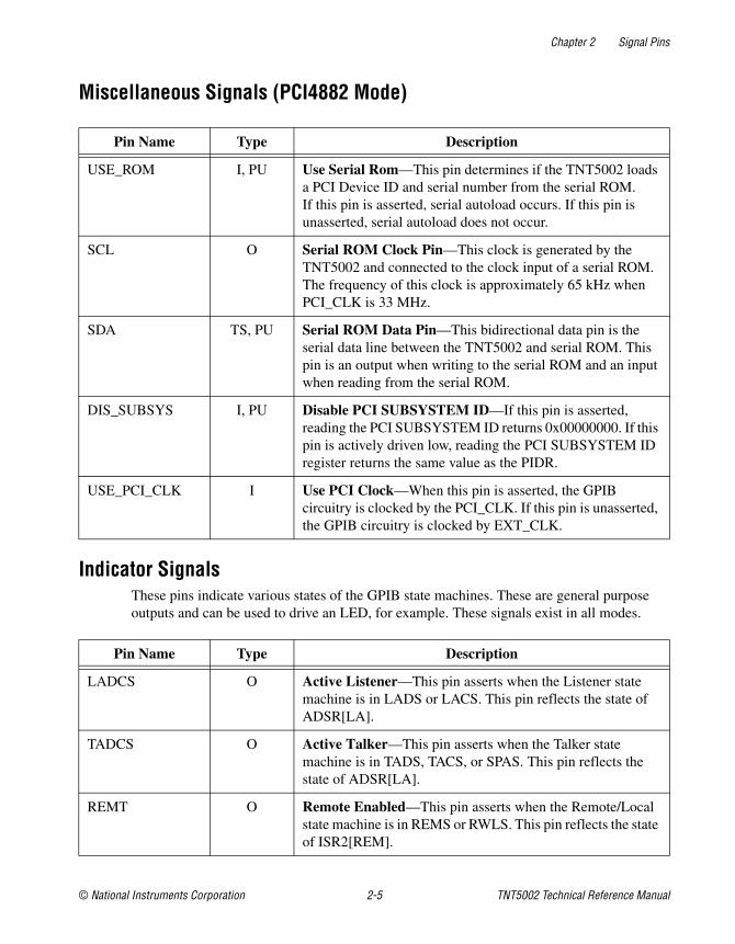
Miscellaneous Signals (PCI4882 Mode)
Indicator SignalsThese pins indicate various states of the GPIB state machines. These are general purpose outputs and can be used to drive an LED, for example. These signals exist in all modes.
Pin Name Type Description
USE_ROM I, PU Use Serial Rom—This pin determines if the TNT5002 loads a PCI Device ID and serial number from the serial ROM. If this pin is asserted, serial autoload occurs. If this pin is unasserted, serial autoload does not occur.
SCL O Serial ROM Clock Pin—This clock is generated by the TNT5002 and connected to the clock input of a serial ROM. The frequency of this clock is approximately 65 kHz when PCI_CLK is 33 MHz.
SDA TS, PU Serial ROM Data Pin—This bidirectional data pin is the serial data line between the TNT5002 and serial ROM. This pin is an output when writing to the serial ROM and an input when reading from the serial ROM.
DIS_SUBSYS I, PU Disable PCI SUBSYSTEM ID—If this pin is asserted, reading the PCI SUBSYSTEM ID returns 0x00000000. If this pin is actively driven low, reading the PCI SUBSYSTEM ID register returns the same value as the PIDR.
USE_PCI_CLK I Use PCI Clock—When this pin is asserted, the GPIB circuitry is clocked by the PCI_CLK. If this pin is unasserted, the GPIB circuitry is clocked by EXT_CLK.
Pin Name Type Description
LADCS O Active Listener—This pin asserts when the Listener state machine is in LADS or LACS. This pin reflects the state of ADSR[LA].
TADCS O Active Talker—This pin asserts when the Talker state machine is in TADS, TACS, or SPAS. This pin reflects the state of ADSR[LA].
REMT O Remote Enabled—This pin asserts when the Remote/Local state machine is in REMS or RWLS. This pin reflects the state of ISR2[REM].

Chapter 2 Signal Pins
TNT5002 Technical Reference Manual 2-6 ni.com
PCI SignalsThese signals implement a PCI interface. These signals only exist in PCI4882 mode. In GEN4882 mode, these pins have different functionality.
Pin Name Type Description
PCI_CLK I PCI Clock—This is the clock input from the PCI bus.
AD[31:0] TS PCI Address/Data—These signals are the multiplexed PCI address and data bus.
C/BE#[3:0] TS Command/Byte Enable—These signals are the multiplexed command and byte enables. During the PCI address phase C/BE# conveys the type of transfer taking place. Following the address phase, C/BE# indicates whether valid data is present on the four byte lanes of the AD bus.
PAR TS Parity—PAR carries the even parity over the AD and C/BE# buses during address and data phases. The device that drives AD and CBE# also drives PAR. PAR is valid one clock cycle after AD and C/BE# are valid.
FRAME# STS Frame—A PCI master asserts FRAME# to indicate the beginning and duration of a transaction. FRAME# assertion indicates the beginning of a PCI transaction. Data transactions can continue while FRAME# is asserted. FRAME# unassertion indicates the final data phase requested by the initiator.
IRDY# STS Initiator Ready—IRDY# is driven by the initiator of a transaction to indicate the initiator’s ability to complete the current data phase. During a write transaction, IRDY# is asserted when valid data is driven onto the AD bus. During a read, IRDY# is asserted when the initiator is able to accept data for the current data phase.
TRDY# STS Target Ready—TRDY# is driven be the target of a transaction to indicate the target’s ability to complete the current data phase. During a write transaction, TRDY# is asserted when the target is able to accept data for the current data phase. During a read, TRDY# is asserted when the target is driving valid data onto the AD bus.

Chapter 2 Signal Pins
© National Instruments Corporation 2-7 TNT5002 Technical Reference Manual
DEVSEL# STS Device Select—DEVSEL# is asserted by the target to indicate that the device is accepting the transaction.
STOP# STS Stop—This signal is driven by the target to request that the initiator stop the current transaction.
IDSEL STS Initialization Device Select—This signal is used as the chip select for Type 0 PCI configuration accesses to PCI configuration space.
PERR# STS Parity Error—PERR# is asserted when a parity error is detected. PERR# can be asserted by the target during a write transaction and by the initiator during a read transaction.
SERR# TS System Error—SERR# is asserted to indicate a serious system problem or a parity error during the address phase of a data transfer.
REQ# TS Bus Request—REQ# is asserted to request access to the bus.
GNT# I Bus Grant—GNT# is asserted to grant access to the bus.
INTA# TS Interrupt—This signal is asynchronously asserted to interrupt the CPU.
PCI_RST# I PCI Reset—This signal is used to initialize the device to a known state. While PCI_RST# is asserted all PCI and GPIB signals are tri-stated. PCI_RST# must be asserted during power-up to ensure that the GPIB signals do not glitch when connected to another device.
Pin Name Type Description

Chapter 2 Signal Pins
TNT5002 Technical Reference Manual 2-8 ni.com
Generic Interface SignalsThese signals implement a generic bus interface. These signals only exist in GEN4882 mode. In PCI4882 mode, these pins have different functionality.
Pin Name Type Description
DACK# I DMA Acknowledge—DACK#, along with IORD# or IOWT#, asserts during DMA accesses.
CS# I Chip Select—CS#, along with IORD# or IOWT#, asserts during IO accesses.
DRQ O DMA Request—DRQ is asserted to request a DMA transfer.
HWORD# I 16-Bit Access—HWORD# is asserted during 16-bit register accesses and unasserted for 8-bit register accesses. HWORD# is ignored during DMA accesses.
INT TS Interrupt—INT asserts when an enabled interrupt condition is true.
IOA[6:0] I Address—IOA selects a register during IO accesses.
IOD[15:0] IO Data—IOD is the 16-bit bi-directional data bus used for DMA and IO accesses. During 8-bit writes data must be on the lower 8 bits. During 8-bit reads the data will be smeared across both byte lanes. Unused signals in 8-bit mode should not be left floating.
IORD# I Read—IORD# is asserted to indicate an IO or DMA read.
IOWT# I Write—IOWT# is asserted to indicate an IO or DMA write.
RESET# I Reset—RESET# resets the chip to its initial power-on state. RESET# also asynchronously tri-states the GPIB transceivers.

Chapter 2 Signal Pins
© National Instruments Corporation 2-9 TNT5002 Technical Reference Manual
Power/Ground PinsThe location of power and ground pins are the same among all modes, although the meaning of the pins changes slightly.
PCI4882 Power/Ground PinsThe following pins supply power to the TNT5002 in PCI4882 mode.
GEN4882 Power/Ground PinsThe following pins supply power to the TNT5002 in GEN4882 mode.
Pin Name Description
3.3V Core/GPIB Transceiver Power—These pins provide power for the digital core and all output signal pins except PCI signals. These pins must be connected to a 3.3V source. If not connected directly to the PCI 3.3V power rail, the 3.3V supply they are connected to cannot vary by more than 170mV. If these pins are connected to the PCI 3.3V rail, that rail may vary according to the PCI Specification.
VIO PCI Transceiver Power—These pins provide power for the PCI Transceivers. These must be connected to 3.3V or 5V as allowed by the PCI Specification.
GND Ground—These pins are ground pins for both power inputs.
VIO_SEL VIO Comparator—This input is used to determine whether VIO is 3.3V or 5V. This signal is compared against 3.3V and must be directly connected to VIO.
Pin Name Description
3.3V Core/GPIB Transceiver Power—These pins provide power for the digital core and all output signal pins except the Generic Interface signals. These pins must be connected to a 3.3V source.
VIO Generic Interface Transceiver Power—These pins provide power for the Generic Interface Transceivers. The generic interface pins can be powered from either 3.3V or 5V. The voltage connected to VIO is used to drive the generic interface pins.
GND Ground—These pins are ground pins for both power inputs.

Chapter 2 Signal Pins
TNT5002 Technical Reference Manual 2-10 ni.com
VIO_SEL VIO Comparator—This input is used to determine whether VIO is 3.3V or 5V. This signal is compared against 3.3V and must be directly connected to VIO.
PWR_GOOD Power Good—This input must be unasserted while 3.3V is out of the specified operating range. For example, this pin must be unasserted while 3.3V is ramping up as well as ramping down.
Pin Name Description

© National Instruments Corporation 3-1 TNT5002 Technical Reference Manual
3Register Descriptions
Register GroupsThe following tables group the registers into functional blocks such that all registers in a given block serve a similar function.
Register Groups in PCI4882 Mode
Offset from PBAR0 Register Group
0x000–0x2FF Chip Status/Control
0x300–0x3FF PCI Configuration
0x400–0x4FF Miscellaneous Status/Control
0x500–0x5FF DMA Status/Control
0x600–0x7FF Reserved
Offset from PBAR1 Register Group
0x0000–0x00FF Reserved
0x0100–0x011F 4882 Register Set
0x0120–0x012F Reserved
0x0130–0x013F Reserved
0x0140–0x014F Reserved
0x0150–0x1FFF Reserved
0x2000–0x3FFF Serial Number

Chapter 3 Register Descriptions
TNT5002 Technical Reference Manual 3-2 ni.com
Register Groups in GEN4882 Mode
PCI4882 Mode Register Map
Offset Register Group
0x00–0x1F 4882 Register Set
0x20–0x2F Reserved
0x30–0x3F Reserved
0x40–0x4F GPIB Test/Status
0x50–0x7F Reserved

Chapter 3 Register Descriptions
© National Instruments Corporation 3-3 TNT5002 Technical Reference Manual
PCI Config Space0×00
0×FF
0×00
PBAR0
PBAR0 + 0×7FF
IODWBSR†
PBAR1
IOWBSR1††
PBAR1 + 0×2000
PBAR1 + 0×3FFF
Status/Control Registers
CHIPStatus/Control
PCI Configuration
MiscellaneousStatus/Control
DMAStatus/Control
Reserved
GPIB Registers
Reserved
4882 Register Set
Reserved
Serial Number
Serial Number(All Offsets)
0×000
0×300
0×400
0×500
0×600
0×7FF
0×0000
0×0100
0×0120
0×0130
0×0140
0×0150
0×1FFF
PCI Memory Space
0×1FFF
0×0000† IODWBSR is a register that defines thelocation of GPIB Registers in PBAR1.
†† IOWBSR1 is a register that defines thelocation of the serial number in PBAR1.
Reserved
Reserved
Reserved

Chapter 3 Register Descriptions
TNT5002 Technical Reference Manual 3-4 ni.com
GEN4882 Mode Register MapThe following register map is valid when interfacing through generic interface. These registers are accessed by asserting CS# or DACK# and IORD# or IOWR#.
GPIB Registers
4882 Register Set
Reserved
0×00
0×20
0×30
0×40
0×50
0×FF
Reserved
Reserved
Reserved

Chapter 3 Register Descriptions
© National Instruments Corporation 3-5 TNT5002 Technical Reference Manual
TNT5002 Status/Control Register GroupThese registers are only available in PCI4882 mode. This register group is used to control and configure the PCI interface.
TNT5002 Status/Control Registers Sorted by OffsetRegisters at offsets not listed are reserved.
Offset from PBAR0 Mnemonic Write Register Read Register
0x14 LCISR2 Reserved Local CPU Interrupt Status 2
0xC0 IODWBSR IO Device Window Base/Size IO Device Window Base/Size
0xC4 IOWBSR1 IO Window 1 Base/Size IO Window 1 Base/Size
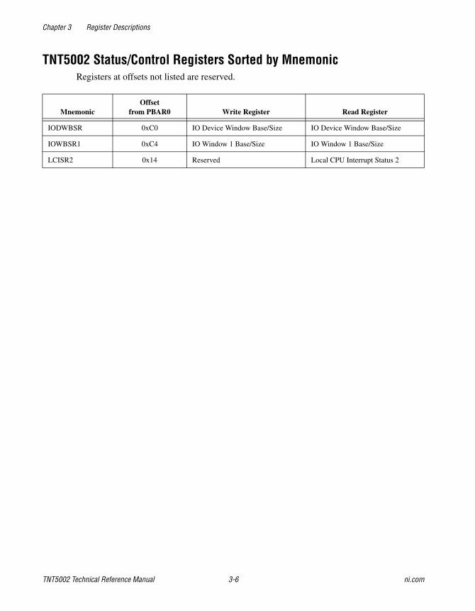
Chapter 3 Register Descriptions
TNT5002 Technical Reference Manual 3-6 ni.com
TNT5002 Status/Control Registers Sorted by MnemonicRegisters at offsets not listed are reserved.
MnemonicOffset
from PBAR0 Write Register Read Register
IODWBSR 0xC0 IO Device Window Base/Size IO Device Window Base/Size
IOWBSR1 0xC4 IO Window 1 Base/Size IO Window 1 Base/Size
LCISR2 0x14 Reserved Local CPU Interrupt Status 2
Chapter 3 Register Descriptions
© National Instruments Corporation 3-7 TNT5002 Technical Reference Manual
TNT5002 Status/Control Register Descriptions
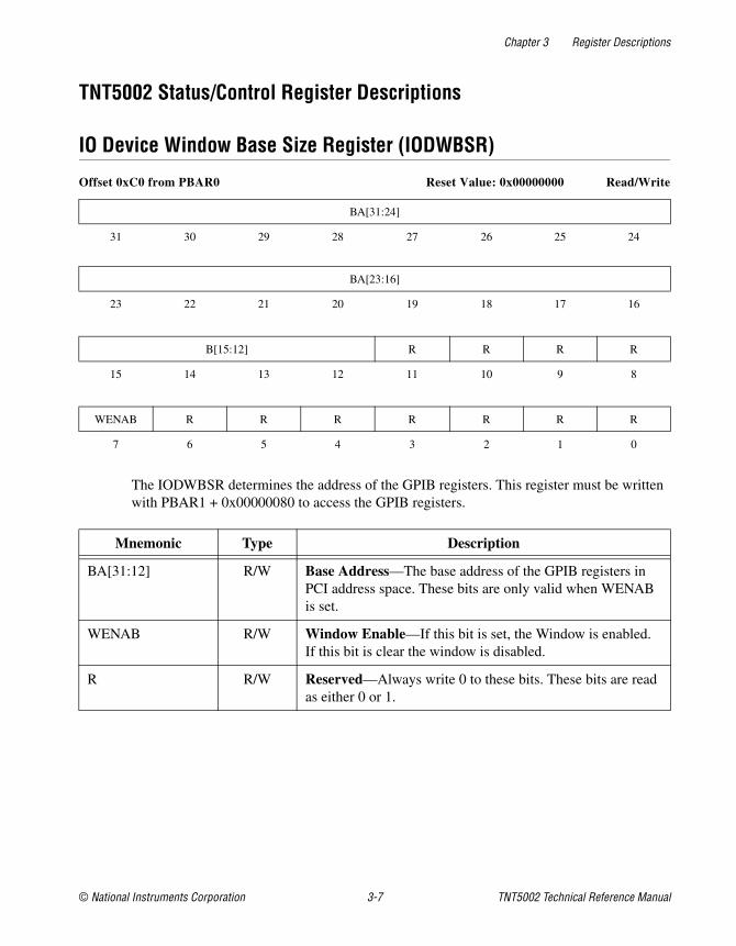
IO Device Window Base Size Register (IODWBSR)
Offset 0xC0 from PBAR0 Reset Value: 0x00000000 Read/Write
The IODWBSR determines the address of the GPIB registers. This register must be written with PBAR1 + 0x00000080 to access the GPIB registers.
BA[31:24]
31 30 29 28 27 26 25 24
BA[23:16]
23 22 21 20 19 18 17 16
B[15:12] R R R R
15 14 13 12 11 10 9 8
WENAB R R R R R R R
7 6 5 4 3 2 1 0
Mnemonic Type Description
BA[31:12] R/W Base Address—The base address of the GPIB registers in PCI address space. These bits are only valid when WENAB is set.
WENAB R/W Window Enable—If this bit is set, the Window is enabled. If this bit is clear the window is disabled.
R R/W Reserved—Always write 0 to these bits. These bits are read as either 0 or 1.

Chapter 3 Register Descriptions
TNT5002 Technical Reference Manual 3-8 ni.com
IO Window Base/Size Register 1 (IOWBSR1)
Offset 0xC4 from PBAR0 Reset Value: 0x00000000 Read/Write
The IODWBSR determines the address of the serial number. This register must be written with PBAR1 + 0x0000208C to access the serial number.
BA[31:24]
31 30 29 28 27 26 25 24
BA[23:16]
23 22 21 20 19 18 17 16
BA[15:8]
15 14 13 12 11 10 9 8
WENAB R R WSIZE[4:0]
7 6 5 4 3 2 1 0
Mnemonic Type Description
BA[31:8] R/W Base Address—The base address in PCI address space. The number of bits compared is determined by the WSIZE[4:0].
WENAB R/W Window Enable—If this bit is set, the Window is enabled. If this bit is clear the window is disabled.
WSIZE[4:0] R/W Window Size—These bits determine the size of the serial number window in PBAR1. The size in bytes is 2(WSIZE + 1). WSIZE should be set to 01100, indicating the size of the window is 8 kB.
R R/W Reserved—Always write 0 to these bits. These bits are read as either 0 or 1.

Chapter 3 Register Descriptions
© National Instruments Corporation 3-9 TNT5002 Technical Reference Manual
Local CPU Interrupt Status 2 (LCISR2)
Offset 0x14 from PBAR0 Reset Value: 0x00000000 Read Only
This register reflects various interrupts. This register should not be accessed for most applications.
PCIINT R R R R R R R
31 30 29 28 27 26 25 24
R R R R R R R R
23 22 21 20 19 18 17 16
R R R R R R R R
15 14 13 12 11 10 9 8
R R R R R R R R
7 6 5 4 3 2 1 0
Mnemonic Type Description
PCIINT R PCI Interrupt—PCIINT is ISR3[INT].
R R Reserved—Always write 0 to these bits. These bits are read as either 0 or 1.

Chapter 3 Register Descriptions
TNT5002 Technical Reference Manual 3-10 ni.com
PCI Configuration RegistersThese registers are only available in PCI4882 mode.
PCI Configuration Register MapAll PCI devices must support a set of configuration registers that control the behavior of the PCI device and provide a consistent location for a PCI device to indicate its status. The PCI specification does support some functionality that is superfluous to the requirements of the TNT5002’s PCI interface. The register space, as implemented in the PCI interface, is shown in the following table.
Mnemonic
Offset in PCI Config
SpaceOffset in
Memory Space
Byte 3 Byte 2 Byte 1 Byte 0
31 24 23 16 15 8 7 0
PIDR 0x00 PBAR0 + 0x300 Device ID Vendor ID
PSCR 0x04 PBAR0 + 0x304 PCI Status PCI Control
PCCRIDR 0x08 PBAR0 + 0x308 Class Code Revision ID
PLIVR 0x0C PBAR0 + 0x30C 0 Latency Timer Cache Line Size
PBAR0 0x10 PBAR0 + 0x310 Base Address Register 0
PBAR1 0x14 PBAR0 + 0x314 Base Address Register 1
Reserved 0x18 PBAR0 + 0x318 Reserved
Reserved 0x1C PBAR0 + 0x31C Reserved
Reserved 0x20 PBAR0 + 0x320 Reserved
Reserved 0x24 PBAR0 + 0x324 Reserved
PCISR 0x28 PBAR0 + 0x328 Reserved/CIS Pointer Register
PSUBR 0x2C PBAR0 + 0x32C Subsystem ID Subsystem Vendor ID
Reserved 0x30 PBAR0 + 0x330 Reserved
Reserved 0x34 PBAR0 + 0x334 Reserved
Reserved 0x38 PBAR0 + 0x338 Reserved
PLRIDR 0x3C PBAR0 + 0x33C Max_Lat Min_Gnt Interrupt Pin Interrupt Line
PBACOR 0x40 PBAR0 + 0x340 Base Address Configuration Register
Reserved 0x44 PBAR0 + 0x344 Reserved
PERCR 0x48 PBAR0 + 0x348 Expansion ROM Configuration Register

Chapter 3 Register Descriptions
© National Instruments Corporation 3-11 TNT5002 Technical Reference Manual
PCI Configuration Register Descriptions
Device ID/Vendor ID Register (PIDR)
Offset 0x00 from PCI Config Space, 0x300 from PBAR0 Reset Value: See Description Read Only
DEVICE_ID[15:8]
31 30 29 28 27 26 25 24
DEVICE_ID[7:0]
23 22 21 20 19 18 17 16
VENDOR_ID[15:8]
15 14 13 12 11 10 9 8
VENDOR_ID[7:0]
7 6 5 4 3 2 1 0
Mnemonic Type Description
DEVICE_ID[15:0] R Device Identification Number—The default DEVICE_ID of the TNT5002 is 0xC850. The default DEVICE_ID is overwritten from a serial ROM if USE_ROM is asserted or not connected.
VENDOR_ID[15:0] R Vendor Identification Number—This sixteen bit value is assigned by the PCI Special Interest Group. National Instruments’ PCI Vendor ID number is 0x1093.

Chapter 3 Register Descriptions
TNT5002 Technical Reference Manual 3-12 ni.com
PCI Status and Control Register (PSCR)
Offset 0x04 from PCI Config Space, 0x304 from PBAR0 Reset Value: 0x02000000 Read/Write
Bits 31–16 are status bits. The PCI interface sets the bits in these registers. In order to clear a bit in the status register, a PCI device must write a one to the bit. This convention is required by the PCI specification. Bits 15–0 are control bits, and these bits are read/write.
PERRDT SERRDT SMABT RTABT STABT SPEEDA SPEEDB PARDT
31 30 29 28 27 26 25 24
FBBC 0 0 0 0 0 0 0
23 22 21 20 19 18 17 16
0 0 0 0 0 0 0 SERREN
15 14 13 12 11 10 9 8
ADSTEP PERREN 0 MWIEN 0 MSTREN MEMEN IOEN
7 6 5 4 3 2 1 0
Mnemonic Type Description
PERRDT R/W Parity Error Detect—This bit is set when the PCI interface detects a parity error even when parity error handling is disabled by clearing PERREN.
SERRDT R/W System Error Detected—The PCI interface sets this bit when it asserts SERR#.
SMABT R/W Signal Master Abort—The PCI interface sets this bit if it terminates a PCI master cycle with a master abort.
RTABT R/W Receive Target Abort—The PCI interface sets this bit to indicate that it received a target abort while performing a PCI master cycle.
STABT R/W Signal Target Abort—The PCI interface sets this bit if it terminates a slave cycle with a target abort.

Chapter 3 Register Descriptions
© National Instruments Corporation 3-13 TNT5002 Technical Reference Manual
SPEEDA SPEEDB
R/W Address Decoding Speed—SPEEDA and SPEEDB are hardwired to 0 and 1, respectively, to indicate that the PCI interface is a medium speed decoder. These bits are set in accordance with the PCI specification requirements. Writes to these bits are ignored.
PARDT R/W Parity Detect—The PCI interface sets this bit if three conditions are met:
• The PCI interface asserted PERR# or detected that PERR# was asserted by another device.
• The PCI interface was performing a master cycle when PERR# was asserted.
• PERREN is set.
FBBC R/W Fast Back-to-Back Capable—This bit is hardwired to 1 indicating that the PCI interface supports fast back-to-back transfers as a PCI slave. Writes to this bit are ignored.
SERREN R/W SERR# Enable—Setting this bit permits the PCI interface to assert SERR# during system error conditions. Clearing this bit prevents the PCI interface from asserting SERR#.
ADSTEP R/W Address Stepping—This bit is hardwired to 0 to indicate that address or data stepping is not performed. Writes to this bit are ignored.
PERREN R/W Parity Error Response Enable—Setting this bit enables the PCI interface to assert PERR# and set PERRDT. If this bit is cleared, the PCI interface must ignore parity errors and continue normal operations.
MWIEN R/W Memory Write/Invalidate Enable—Setting this bit allows the PCI interface to initiate memory write and invalidate and memory read line cycles as a PCI master. Clearing this bit makes the PCI interface initiate standard memory write and read cycles.
Mnemonic Type Description

Chapter 3 Register Descriptions
TNT5002 Technical Reference Manual 3-14 ni.com
MSTREN R/W Master Mode Enable—Setting this bit permits the PCI interface to operate as a PCI master. Clearing this bit disables master mode.
MEMEN R/W Memory Space Response Enable—Setting this bit permits the PCI interface to respond to PCI memory cycles that map to the PCI interface. Clearing this bit makes the PCI interface ignore all PCI memory space transfers.
IOEN R/W IO Space Response Enable—Setting this bit permits the PCI interface to respond to PCI IO space cycles that map to the PCI interface. Clearing this bit makes the PCI interface ignore all PCI IO space transfers.
Mnemonic Type Description
Chapter 3 Register Descriptions
© National Instruments Corporation 3-15 TNT5002 Technical Reference Manual
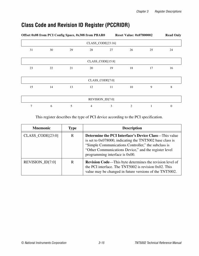
Class Code and Revision ID Register (PCCRIDR)
Offset 0x08 from PCI Config Space, 0x308 from PBAR0 Reset Value: 0x07800002 Read Only
This register describes the type of PCI device according to the PCI specification.
CLASS_CODE[23:16]
31 30 29 28 27 26 25 24
CLASS_CODE[15:8]
23 22 21 20 19 18 17 16
CLASS_CODE[7:0]
15 14 13 12 11 10 9 8
REVISION_ID[7:0]
7 6 5 4 3 2 1 0
Mnemonic Type Description
CLASS_CODE[23:0] R Determine the PCI Interface’s Device Class—This value is set to 0x078000, indicating the TNT5002 base class is “Simple Communications Controller,” the subclass is “Other Communications Device,” and the register level programming interface is 0x00.
REVISION_ID[7:0] R Revision Code—This byte determines the revision level of the PCI interface. The TNT5002 is revision 0x02. This value may be changed in future versions of the TNT5002.
Chapter 3 Register Descriptions
TNT5002 Technical Reference Manual 3-16 ni.com
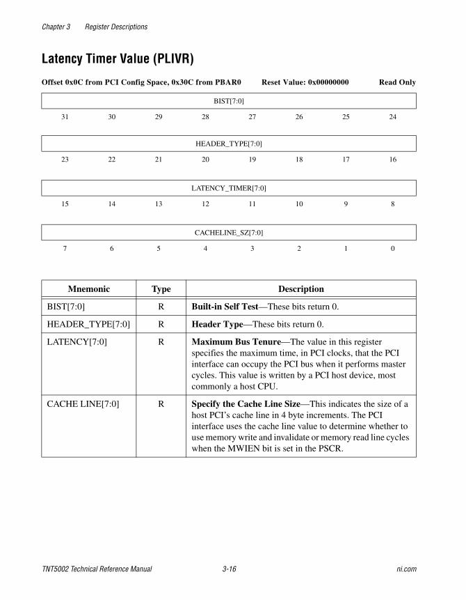
Latency Timer Value (PLIVR)
Offset 0x0C from PCI Config Space, 0x30C from PBAR0 Reset Value: 0x00000000 Read Only
BIST[7:0]
31 30 29 28 27 26 25 24
HEADER_TYPE[7:0]
23 22 21 20 19 18 17 16
LATENCY_TIMER[7:0]
15 14 13 12 11 10 9 8
CACHELINE_SZ[7:0]
7 6 5 4 3 2 1 0
Mnemonic Type Description
BIST[7:0] R Built-in Self Test—These bits return 0.
HEADER_TYPE[7:0] R Header Type—These bits return 0.
LATENCY[7:0] R Maximum Bus Tenure—The value in this register specifies the maximum time, in PCI clocks, that the PCI interface can occupy the PCI bus when it performs master cycles. This value is written by a PCI host device, most commonly a host CPU.
CACHE LINE[7:0] R Specify the Cache Line Size—This indicates the size of a host PCI’s cache line in 4 byte increments. The PCI interface uses the cache line value to determine whether to use memory write and invalidate or memory read line cycles when the MWIEN bit is set in the PSCR.
Chapter 3 Register Descriptions
© National Instruments Corporation 3-17 TNT5002 Technical Reference Manual
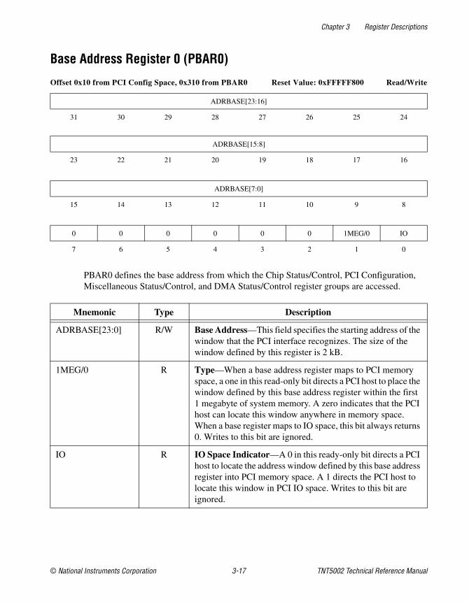
Base Address Register 0 (PBAR0)
Offset 0x10 from PCI Config Space, 0x310 from PBAR0 Reset Value: 0xFFFFF800 Read/Write
PBAR0 defines the base address from which the Chip Status/Control, PCI Configuration, Miscellaneous Status/Control, and DMA Status/Control register groups are accessed.
ADRBASE[23:16]
31 30 29 28 27 26 25 24
ADRBASE[15:8]
23 22 21 20 19 18 17 16
ADRBASE[7:0]
15 14 13 12 11 10 9 8
0 0 0 0 0 0 1MEG/0 IO
7 6 5 4 3 2 1 0
Mnemonic Type Description
ADRBASE[23:0] R/W Base Address—This field specifies the starting address of the window that the PCI interface recognizes. The size of the window defined by this register is 2 kB.
1MEG/0 R Type—When a base address register maps to PCI memory space, a one in this read-only bit directs a PCI host to place the window defined by this base address register within the first 1 megabyte of system memory. A zero indicates that the PCI host can locate this window anywhere in memory space. When a base register maps to IO space, this bit always returns 0. Writes to this bit are ignored.
IO R IO Space Indicator—A 0 in this ready-only bit directs a PCI host to locate the address window defined by this base address register into PCI memory space. A 1 directs the PCI host to locate this window in PCI IO space. Writes to this bit are ignored.

Chapter 3 Register Descriptions
TNT5002 Technical Reference Manual 3-18 ni.com
Base Address Register 1 (PBAR1)
Offset 0x14 from PCI Config Space, 0x314 from PBAR0 Reset Value: 0xFFFFFC00 Read/Write
PBAR1 defines the base address from which the 4882 Register Set, 9914 Register Set, GPIB Test/Status, and Serial Number register groups are accessed.
ADRBASE[23:16]
31 30 29 28 27 26 25 24
ADRBASE[15:8]
23 22 21 20 19 18 17 16
ADRBASE[7:0]
15 14 13 12 11 10 9 8
0 0 0 0 0 0 1MEG/0 IO
7 6 5 4 3 2 1 0
Mnemonic Type Description
ADRBASE[23:0] R/W Base Address—This field specifies the starting address of the window that the PCI interface recognizes. The size of the window defined by this register is 16 kB.
1MEG/0 R/W Type—When a base address register maps to PCI memory space, a one in this read-only bit directs a PCI host to place the window defined by this base address register within the first 1 megabyte of system memory. A zero indicates that the PCI host can locate this window anywhere in memory space. When a base register maps to IO space, this bit always returns 0. Writes to this bit are ignored.
IO R/W IO Space Indicator—A 0 in this ready-only bit directs a PCI host to locate the address window defined by this base address register into PCI memory space. A 1 directs the PCI host to locate this window in PCI IO space. Writes to this bit are ignored.

Chapter 3 Register Descriptions
© National Instruments Corporation 3-19 TNT5002 Technical Reference Manual
CIS Pointer Register Register (PCISR)
Offset 0x28 from PCI Config Space, 0x328 from PBAR0 Reset Value: 0x00000000 Read/Write
This register is the Cardbus Information Structure and is only used for Cardbus applications.
CIS[31:24]
31 30 29 28 27 26 25 24
CIS[23:16]
23 22 21 20 19 18 17 16
CIS[15:8]
15 14 13 12 11 10 9 8
CIS[7:0]
7 6 5 4 3 2 1 0
Mnemonic Type Description
CIS R/W Card Information Structure—Stores the 32 bit memory address of the Card information structure for Cardbus applications. This register is fully readable/writeable when PERCR[CBUSEN] is set. Otherwise, this register always returns 0.

Chapter 3 Register Descriptions
TNT5002 Technical Reference Manual 3-20 ni.com
Subsystem ID Register (PSUBR)
Offset 0x2C from PCI Config Space, 0x32C from PBAR0 Reset Value: See Description Read Only
This register implements the PCI Subsystem ID and Subsystem Vendor ID fields as required by PCI Specification 2.2. The reset value of this register depends on DIS_SUBSYS.
SUBSYSTEM_ID[15:8]
31 30 29 28 27 26 25 24
SUBSYSTEM_ID[7:0]
23 22 21 20 19 18 17 16
SUBVENDOR_ID[15:8]
15 14 13 12 11 10 9 8
SUBVENDOR_ID[7:0]
7 6 5 4 3 2 1 0
Mnemonic Type Description
SUBSYSTEM_ID[15:0] R Subsystem ID—If DIS_SUBSYS is asserted or not connected, these bits return 0x0000. If DIS_SUBSYS is actively unasserted, SUBSYSTEM_ID returns PIDR[DEVICE_ID[15:0]].
SUBVENDOR_ID[15:0] R Subsystem Vendor ID—If DIS_SUBSYS is asserted or not connected, these bits return 0x0000. If DIS_SUBSYS is actively unasserted, SUBVENDOR_ID returns PIDR[VENDOR_ID[15:0]].

Chapter 3 Register Descriptions
© National Instruments Corporation 3-21 TNT5002 Technical Reference Manual
Latency Request Interrupt Definition Register (PLRIDR)
Offset 0x3C from PCI Config Space, 0x33C from PBAR0 Reset Value: 0x00000100 Read/Write
This register implements the various fields required by PCI Specification 2.2.
MAX_LAT[7:0]
31 30 29 28 27 26 25 24
MIN_GNT[7:0]
23 22 21 20 19 18 17 16
INT_PIN[7:0]
15 14 13 12 11 10 9 8
INT_LINE[7:0]
7 6 5 4 3 2 1 0
Mnemonic Type Description
MAX_LAT[7:0] R Maximum Requested Latency—These bits are hard-wired to 0. Writes to these bits are ignored.
MIN_GNT[7:0] R Minimum Bus Grant Time—These bits are hard-wired to 0. Writes to these bits are ignored.
INT_PIN[7:0] R Interrupt Pin—This read-only byte specifies which interrupt pin the PCI interface uses for interrupts. This byte is hardwired to 0x01 since the PCI interface can use only the INTA# signal. Writes to these bits are ignored.
INT_LINE[7:0] R/W Interrupt Line—This read-write byte specifies interrupt line routing information. It has no effect on the PCI interface. The PCI host device writes a value in this byte which an interrupt service routine can use to determine interrupt vector and priority information.

Chapter 3 Register Descriptions
TNT5002 Technical Reference Manual 3-22 ni.com
Base Address Configuration Register (PBAC0R)
Offset 0x40 from PCI Config Space, 0x340 from PBAR0 Reset Value: 0x0000B4A8 Read/Write
This fields in this register are used to configure PBAR0 and PBAR1. Most applications should not access this register.
R R R R R R R R
31 30 29 28 27 26 25 24
R R R R R R R R
23 22 21 20 19 18 17 16
B1_EN B1_S[4:0] B1_1MEG 0
15 14 10 9 8
B0_EN B0_S[4:0] B0_1MEG 0
7 6 2 1 0
Mnemonic Type Description
B0_ENB1_EN
R/W PBAR0/PBAR1 Enable—Setting these bits enable PBAR0 or PBAR1. When PBAR0 or PBAR1 are enabled a PCI host can read and write data from and to it, and the PCI interface uses the contents of this register to decode incoming PCI addresses. If PBAR0 or PBAR1 is disabled, it returns all zeros when it is read as required by the PCI specification.
B0_S[4:0]B1_S[4:0]
R/W PBAR0/PBAR1 Window Size—These bits specify the amount of PCI memory space that the PBAR0 or PBAR1 requires. The amount of address space is 2[Bx_S+1] bytes long. The PCI specification recommends that if the address space being requested lies in PCI memory space, Bx_S should be greater than 12. If the address space being requested lies in PCI IO space, Bx_S should be greater than 8.

Chapter 3 Register Descriptions
© National Instruments Corporation 3-23 TNT5002 Technical Reference Manual
B0_1MEGB1_1MEG
R/W Memory Type—When PBAR0 or PBAR1 maps to PCI memory space, setting this bit directs a PCI host to place the window defined by this base address register within the first megabyte of system memory. A zero indicates that the PCI host can locate this window anywhere in memory space. When a Base Address Register maps to IO space, this bit is ignored. B0_1MEG/ B1_1MEG reflects the state of PBAR0[1MEG/0]/PBAR1[1MEG/0].
R R/W Reserved—Always write 0 to these bits. These bits are read as either 0 or 1.
Mnemonic Type Description

Chapter 3 Register Descriptions
TNT5002 Technical Reference Manual 3-24 ni.com
Expansion ROM Configuration Register (PERCR)
Offset 0x48 from PCI Config Space, 0x348 from PBAR0 Reset Value: 0xC7000000 Read/Write
R BEERREN CBUSEN FASTEN# WRITEEN HWRL2 HWRL1 HWRL0
31 30 29 28 27 26 25 24
R R R R R R R R
23 22 21 20 19 18 17 16
R R R R R R R R
15 14 13 12 11 10 9 8
R R R R R R R R
7 6 5 4 3 2 1 0
Mnemonic Type Description
BEERREN R/W Bus Error on Unsupported BE Codes—Setting this bit enables the PCI interface to terminate a PCI slave transfer with a target abort if the initiating PCI master uses a non-aligned BE# encoding. If this bit is cleared, the PCI interface terminates the transfer with a disconnect allowing the PCI master to assume the transfer completed successfully, but the interface does not actually initiate a cycle.
CBUSEN R/W Card Bus Support Enable—Setting this bit enable the CIS pointer register (PCISR). Clearing this bit makes the PCISR return 0.
FASTEN# R/W Fast Back-to-Back Enable—Clearing this bit sets the PSCR[FBBC] by indicating support for fast back-to-back cycles. Setting this bit clears PSCR[FBBC]. This feature helps deal with finicky BIOS that might not handle fast back-to-back properly.
WRITEEN R/W Write Enable—Setting this bit makes the PLRIDR (MAR_LAT and MIN_GNT) writable. Clearing this bit makes these registers read-only.
Chapter 3 Register Descriptions
© National Instruments Corporation 3-25 TNT5002 Technical Reference Manual
HWRL[2:0] R/W Hardware Retry Limit—These bits specify the number of times the PCI interface retries a PCI cycle before returning a bus error to the port that initiated the transfer. The number of retries is 2HWRL.
R R/W Reserved—Always write 0 to these bits. These bits are read as 1 or 0.
Mnemonic Type Description

Chapter 3 Register Descriptions
TNT5002 Technical Reference Manual 3-26 ni.com
DMA Status/Control RegistersThese registers are only available in PCI4882 mode. This register group is used to control and monitor status of the DMA controller.
DMA Status/Control Registers Sorted by OffsetRegisters at offsets not listed are reserved.
Offset from PBAR0 Mnemonic Write Register Read Register
0x500 CHOR Channel Operation Channel Operation
0x504 CHCR Channel Control Channel Control
0x508 TCR Transfer Count Transfer Count
0x50C MCR Memory Configuration Memory Configuration
0x510 MAR Memory Address Memory Address
0x514 DCR Device Configuration Device Configuration
0x51C LKCR Link Configuration Link Configuration
0x520 LKAR Link Address Link Address
0x528 BAR Base Address Base Address
0x52C BCR Base Count Base Count
0x53C CHSR Reserved Channel Status
0x540 FCR Reserved FIFO Count

Chapter 3 Register Descriptions
© National Instruments Corporation 3-27 TNT5002 Technical Reference Manual
DMA Status/Control Registers Sorted by MnemonicRegisters at offsets not listed are reserved.
MnemonicOffset from
PBAR0 Write Register Read Register
BAR 0x528 Base Address Base Address
BCR 0x52C Base Count Base Count
CHCR 0x504 Channel Control Channel Control
CHOR 0x500 Channel Operation Channel Operation
CHSR 0x53C Reserved Channel Status
DCR 0x514 Device Configuration Device Configuration
FCR 0x540 Reserved FIFO Count
LKAR 0x520 Link Address Link Address
LKCR 0x51C Link Configuration Link Configuration
MAR 0x510 Memory Address Memory Address
MCR 0x50C Memory Configuration Memory Configuration
TCR 0x508 Transfer Count Transfer Count

Chapter 3 Register Descriptions
TNT5002 Technical Reference Manual 3-28 ni.com
DMA Status/Control Register Descriptions
Base Address Register (BAR)
Offset 0x528 from PBAR0 Reset Value: 0x00000000 Read/Write
BAR[31:24]
31 30 29 28 27 26 25 24
BAR[23:16]
23 22 21 20 19 18 17 16
BAR[15:8]
15 14 13 12 11 10 9 8
BAR[7:0]
7 6 5 4 3 2 1 0
Mnemonic Type Description
BAR[31:0] R/W Base Address Register—The BAR is loaded automatically by the DMA Controller with the address from the current link node.

Chapter 3 Register Descriptions
© National Instruments Corporation 3-29 TNT5002 Technical Reference Manual
Base Count Register (BCR)
Offset 0x52C from PBAR0 Reset Value: 0x00000000 Read/Writee
BCR[31:24]
31 30 29 28 27 26 25 24
BCR[23:16]
23 22 21 20 19 18 17 16
BCR[15:8]
15 14 13 12 11 10 9 8
BCR[7:0]
7 6 5 4 3 2 1 0
Mnemonic Type Description
BCR[31:0] R/W Base Count Register—The BCR is loaded automatically by the DMA Controller with the count from the current link node.

Chapter 3 Register Descriptions
TNT5002 Technical Reference Manual 3-30 ni.com
Channel Control Register (CHCR)
Offset 0x504 from PBAR0 Reset Value: 0x55550000 Read/Write
This register is used to configure the DMA controller and should be configured prior to any DMA transfer.
0 1 0 1 0 1 0 1
31 30 29 28 27 26 25 24
0 1 0 1 0 1 0 1
23 22 21 20 19 18 17 16
0 0 0 0 0 0 0 0
15 14 13 12 11 10 9 8
0 0 0 0 DIR RMODE[2:0]
7 6 5 4 3 2 1 0
Mnemonic Type Description
DIR R/W Transfer Direction—DIR indicates the direction of data flow of a DMA transfer.
DIR Direction
0 .....................Memory to GPIB1 .....................GPIB to Memory
RMODE[2:0] R/W Transfer Mode Select—Determines the mode of operation for the DMA Controller Channel.
RMODE[2:0] DMA Type
100 .................... Link Shortother .................. Reserved

Chapter 3 Register Descriptions
© National Instruments Corporation 3-31 TNT5002 Technical Reference Manual
Channel Operation Register (CHOR)
Offset 0x500 from PBAR0 Reset Value: 0x00000512 Read/Write
This register is used to control DMA transfers, including starting and stopping transfers.
DMARESET R R R R R R R
31 30 29 28 27 26 25 24
R R R R R R R R
23 22 21 20 19 18 17 16
R R R R 0 1 0 1
15 14 13 12 11 10 9 8
CLR DONE R R FRESET ABORT STOP 1 START
7 6 5 4 3 2 1 0
Mnemonic Type Description
DMARESET R/W DMA Reset—Setting this bit causes the DMA Controller to be reset. Refer to Chapter 8, Reset Considerations, for more information.
CLR DONE R/W Clear Done Status Bit—Setting this bit clears the DONE status bit. The DONE status bit is also automatically cleared when a new operation is started.
FRESET R/W FIFO Reset—Setting this bit clears the FIFO. The bit is automatically cleared.
ABORT R/W Abort DMA Operation—When this bit is written with a one, the current DMA stops after the completion of any transfer started before the bit was set. All bytes in the FIFO are lost. This bit clears when START is set.
STOP R/W Stop DMA—When this bit is written with a one, the current DMA is stopped after the FIFO has been allowed to empty. This bit clears when START is set.

Chapter 3 Register Descriptions
TNT5002 Technical Reference Manual 3-32 ni.com
START R/W Start DMA Operation—A DMA transfer is started by writing this bit with a one after programming the appropriate address, count, configuration, and control registers.
R R/W Reserved—Always write 0 to these bits. These bits are read as either 0 or 1.
Mnemonic Type Description

Chapter 3 Register Descriptions
© National Instruments Corporation 3-33 TNT5002 Technical Reference Manual
Channel Status Register (CHSR)
Offset 0x53C from PBAR0 Reset Value: 0x00000000 Read Only
This register contains status information about the DMA Controller.
R R R R R R DONE R
31 30 29 28 27 26 25 24
R R R R R R R R
23 22 21 20 19 18 17 16
ERROR SABORT R STOPS OPERR[1:0] RFERR R
15 14 13 12 11 10 9 8
R DRQA R MERR[1:0] DERR[1:0]
7 6 5 4 3 2 1 0
Mnemonic Type Description
DONE R DMA Done—This bit clears when the DMA is started and sets when the transfer is completed normally or by an error.
ERROR R Error Occurred—Indicates the transfer completed due to an error. The other bits indicate the type of error.
SABORT R Software Abort—This bit asserts when CHOR[ABORT] is set.
STOPS R Stopped Status—This bit sets when CHOR[STOP] is set.
Note: STOPS is not status that the DMA Controller has stopped but that the STOP bit was written. To get status that the DMA Controller has STOPPED, enable the DONE IE, then write STOP in the CHOR to get an interrupt that the DMA Controller has actually stopped.

Chapter 3 Register Descriptions
TNT5002 Technical Reference Manual 3-34 ni.com
OPERR[1:0] R Operation Error Code—An illegal FIFO operation such as reading an empty FIFO or writing a full FIFO occurred. OPERR is just a status bit, it does not stop the DMA Controller from finishing a transfer.
OPERR[1:0] Error
00 ......................... FIFO Error01 ......................... Bus Errorothers.................... Reserved
XFERR R Transfer Error—One or more of the transfer processes terminated with an error. Refer to the LERR, MERR, and DERR bit to determine the type.
DRQA R DRQA Status—The state of the DRQ signal from the GPIB circuitry.
MERR[1:0] R Memory Transfer Error—These bits indicate the type of error which stopped the memory transfer process.
MERR[1:0] Error
00 ...................... No Error01 ...................... Bus Error10 ...................... Retry Limit Exceeded11 ...................... Other Error
DERR[1:0] R Device Transfer Error—These bits indicate the type of error which stopped the device transfer process.
DERR[1:0] Error
00 ...................... No Error01 ...................... Bus Error10 ...................... Retry Limit Exceeded11 ...................... Other Error
R R Reserved—Always write 0 to these bits. These bits are read as either 0 or 1.
Mnemonic Type Description

Chapter 3 Register Descriptions
© National Instruments Corporation 3-35 TNT5002 Technical Reference Manual
Device Configuration Register (DCR)
Offset 0x514 from PBAR0 Reset Value: 0x00040241 Read/Write
This register is used to configure how the DMA Controller accesses the GPIB circuitry. This register should not be accessed for most applications.
0 0 0 R R R R R
31 30 29 28 27 26 25 24
RL[2:0] RD[1:0] REQS[2:0]
23 22 21 20 19 18 17 16
R R ASEQ[3:0] PSIZE[1:0]
15 14 13 12 11 10 9 8
R 1 R R R 0 R 1
7 6 5 4 3 2 1 0
Mnemonic Type Description
RL[2:0] R/W Retry Limit—These bits determine the maximum number of times a single transfer may be retried. If the limit is exceeded, a retry error is reported and the operation is stopped. When programmed to zero, the first retry results in an error. The limit selects a power of two number of retries that cause an error 0, 1, 2, 4, 8, …, 64.
RD[1:0] R/W Request Delay Limiter—These bits determine the delay that must elapse between transfers. This limit is always enforced for retry cycles. The limit may be enforced for all cycle when the request mode is internal and limited. This has the following values:
RD[1:0] Clock Cycles
00..................... 0
01..................... 32 10..................... 512 11..................... 8192
Chapter 3 Register Descriptions
TNT5002 Technical Reference Manual 3-36 ni.com
REQS[2:0] R/W Request Source—This selects the type of DMA request for the process.
REQS[2:0] Request Source
000 .............Internal Maximum Rate
001 .............Internal Limited Rate, uses RD[1:0] values
010 .............Disable Process. Programmed I/O to the FIFO
100 .............Hardware Request, DRQ line from the internal IO bus
others ...........Reserved
ASEQ[3:0] R/W Address Sequence Selection—Determines how the Device address is modified for the next transfer. ASEQ[3] is the sign bit while the others select a power of two to multiply by the Port Transfer Size.
ASEQ[2:0] ASEQ[3] = 0 ASEQ[3] = 1(increment address) (decrement address)
000 ...........+ 0.............................. – 0001 ...........+ 1 * SIZE ................. – 1 * SIZE010 ...........+ 2 * SIZE ................. – 2 * SIZE011 ...........+ 4 * SIZE ................. – 4 * SIZE100 ...........+ 8 * SIZE ................. – 8 * SIZE101 ...........+ 16 * SIZE ............... – 16 * SIZE110 ...........+ 32 * SIZE ............... – 32 * SIZE111 ...........+ 64 * SIZE ............... – 64 * SIZE
where size is defined as follows:
PSIZE[1:0] SIZE (bytes)
00 ...................invalid01 ...................110 ...................211 ...................4
Mnemonic Type Description

Chapter 3 Register Descriptions
© National Instruments Corporation 3-37 TNT5002 Technical Reference Manual
PSIZE[1:0] R/W Port Transfer Size—The size of the port for the transfer. The actual transfer size may be smaller when aligning addresses and draining the FIFO.
PSIZE[1:0] Port Transfer Size
00................... Reserved01................... 8-bit10................... 16-bit11................... 32-bit
R R/W Reserved—Always write 0 to these bits. These bits are read as either 0 or 1.
Mnemonic Type Description

Chapter 3 Register Descriptions
TNT5002 Technical Reference Manual 3-38 ni.com
FIFO Count Register (FCR)
Offset 0x540 from PBAR0 Reset Value: 0x00000000 Read Only
This register contains the current number of empty bytes positions in the DFIFO. This register should not be accessed for most applications.
R R R R R R R R
31 30 29 28 27 26 25 24
ECR[7:0]
23 22 21 20 19 18 17 16
R R R R R R R R
15 14 13 12 11 10 9 8
FCR[7:0]
7 6 5 4 3 2 1 0
Mnemonic Type Description
ECR[7:0] R Empty FIFO Locations—ECR indicates the number of empty locations (bytes) in the DFIFO.
FCR[7:0] R FIFO Count—FCR indicates the number of bytes remaining in the DFIFO. A transfer is complete when both the TCR and FCR reach zero.
R R Reserved—These bits are read as either 0 or 1.

Chapter 3 Register Descriptions
© National Instruments Corporation 3-39 TNT5002 Technical Reference Manual
Link Address Register (LKAR)
Offset 0x520 from PBAR0 Reset Value: 0x00000000 Read/Write
LKAR[31:24]
31 30 29 28 27 26 25 24
LKAR[23:16]
23 22 21 20 19 18 17 16
LKAR[15:8]
15 14 13 12 11 10 9 8
LKAR[7:0]
7 6 5 4 3 2 1 0
Mnemonic Type Description
LKAR[31:0] R/W Link Address Register—The LKAR points to the next entry when chaining is used. The address of the first link is manually programmed to the LKAR, and the register is modified as subsequent links are loaded from memory. The LKAR must be aligned to the boundary of the programmed transfer size.

Chapter 3 Register Descriptions
TNT5002 Technical Reference Manual 3-40 ni.com
Link Configuration Register (LKCR)
Offset 0x51C from PBAR0 Reset Value: 0x00000000 Read/Write
This register is used to configure how the DMA Controller fetches links from memory.
R R R R R R R R
31 30 29 28 27 26 25 24
RL[2:0] R R R R
23 22 21 20 19 18 17 16
R R R R ASEQ[1:0] PSIZE[1:0]
15 14 13 12 11 10 9 8
R R R R R R R R
7 6 5 4 3 2 1 0
Mnemonic Type Description
RL[2:0] R/W Retry Limit—These bits determine the maximum number of times a single transfer may be retried. If the limit is exceeded, a retry error is reported and the operation is stopped. When programmed to zero, the first retry results in an error. The limit selects a power of two number of retries that cause an error 0, 1, 2, 4, 8, …, 64.
ASEQ[1:0] R/W Address Sequence Selection—Determines how the address is modified for the next transfer.
ASEQ[1:0] Next Address Selection
00 ...................Don’t Count01 ...................Increment10 ...................Decrement

Chapter 3 Register Descriptions
© National Instruments Corporation 3-41 TNT5002 Technical Reference Manual
PSIZE[1:0] R/W Port Transfer Size—The size of the port for the transfer.
PSIZE[1:0] Port Size
01................... 8-bit10................... 16-bit11................... 32-bit
The link process packs smaller data into the 32 bit dwords required by the link process. Unlike data transfers, the transfers must be aligned on the proper boundary.
R R/W Reserved—Always write 0 to these bits. These bits are read as either 0 or 1.
Mnemonic Type Description

Chapter 3 Register Descriptions
TNT5002 Technical Reference Manual 3-42 ni.com
Memory Address Register (MAR)
Offset 0x510 from PBAR0 Reset Value: 0x00000000 Read/Write
MAR[31:24]
31 30 29 28 27 26 25 24
MAR[23:16]
23 22 21 20 19 18 17 16
MAR[15:8]
15 14 13 12 11 10 9 8
MAR[7:0]
7 6 5 4 3 2 1 0
Mnemonic Type Description
MAR[31:0] R/W Memory Address Register—The MAR is loaded automatically by the DMA Controller with the mem_address from the current link node and incremented according to MCR[ASEQ] as data is read from memory. If the address is not aligned to the programmed size boundary as specified by MCR[PSIZE], the DMA Controller does smaller transfer until alignment occurs.

Chapter 3 Register Descriptions
© National Instruments Corporation 3-43 TNT5002 Technical Reference Manual
Memory Configuration Register (MCR)
Offset 0x50C from PBAR0 Reset Value: 0x00040700 Read/Write
This register is used to configure how the DMA Controller writes and reads data from to and from memory.
R R R R R R R R
31 30 29 28 27 26 25 24
R R R R R 1 0 0
23 22 21 20 19 18 17 16
R R 0 0 0 1 PSIZE[1:0]
15 14 13 12 11 10 9 8
R R R R R R R R
7 6 5 4 3 2 1 0
Mnemonic Type Description
PSIZE[1:0] R/W Port Transfer Size—The size of the port for the transfer. The actual transfer size may be smaller when aligning addresses and draining the FIFO.
PSIZE[1:0] Port Transfer Size
00..................... Reserved01..................... 8-bit10..................... 16-bit11..................... 32-bit
R R/W Reserved—Always write 0 to these bits. These bits are read as either 0 or 1.
Chapter 3 Register Descriptions
TNT5002 Technical Reference Manual 3-44 ni.com
Transfer Count Register (TCR)
Offset 0x508 from PBAR0 Reset Value: 0x00000000 Read/Write
TCR[31:24]
31 30 29 28 27 26 25 24
TCR[23:16]
23 22 21 20 19 18 17 16
TCR[15:8]
15 14 13 12 11 10 9 8
TCR[7:0]
7 6 5 4 3 2 1 0
Mnemonic Type Description
TCR[31:0] R/W Transfer Count Register—The TCR is loaded automatically by the DMA Controller with the count from the current link node. The TCR is automatically decremented as data enters the DFIFO.

Chapter 3 Register Descriptions
© National Instruments Corporation 3-45 TNT5002 Technical Reference Manual
4882
Reg
iste
r Set
The
se r
egis
ters
are
onl
y av
aila
ble
in P
CI4
882
and
GE
N48
82 m
odes
. The
se r
egis
ters
con
trol
the
GPI
B c
ircu
itry
.
4882
-Mod
e Re
gist
ers
Sorte
d by
Offs
etR
egis
ter
Off
set
Typ
eB
it 7
Bit
6B
it 5
Bit
4B
it 3
Bit
2B
it 1
Bit
0
DIR
0x00
RD
IR7
DIR
6D
IR5
DIR
4D
IR3
DIR
2D
IR1
DIR
0
ISR
10x
02R
CPT
APT
DET
END
DEC
ERR
DO
DI
IMR
10x
02W
CPT
IEA
PT IE
DET
IEEN
D IE
DEC
IEER
R IE
DO
IED
I IE
ISR
20x
04R
INT
SRQ
ILO
KR
EMR
LOK
CR
EMC
AD
SC
IMR
20x
04W
0SR
QI I
E0
00
LOK
C IE
REM
C IE
AD
SC IE
SPSR
0x06
RS8
PEN
DS6
S5S4
S3S2
S1
SPM
R0x
06W
S8rs
v/R
QS
S6S5
S4S3
S2S1
AD
SR0x
08R
RAT
NN
SPM
SLP
AS
TPA
SLA
TAM
INO
R
AD
MR
0x08
WTO
NLO
N1
10
0A
DM
1A
DM
0
CN
T20x
09R
/WC
NT2
3C
NT2
2C
NT2
1C
NT2
0C
NT1
9C
NT1
8C
NT1
7C
NT1
6
CPT
R0x
0AR
CPT
7C
PT6
CPT
5C
PT4
CPT
3C
PT2
CPT
1C
PT0
AU
XM
R0x
0AW
AU
X7
AU
X6
AU
X5
AU
X4
AU
X3
AU
X2
AU
X1
AU
X0
AU
XR
A0x
0AW
10
0B
INX
EOS
REO
SH
LDE
HLD
A
AU
XR
B0x
0AW
10
1IS
S0
TRI
SPEO
IC
PT_E
NA
BLE
AU
XR
E0x
0AW
11
00
DH
AD
TD
HA
DC
DH
DT
DH
DC
AU
XR
F0x
0AW
11
01
DH
ATA
DH
ALA
DH
UN
TLD
HA
LL
AU
XR
G0x
0AW
01
00
NTN
LR
PP2
DIS
TCT
CH
ES
AU
XR
I0x
0AW
11
10
UST
DPP
20
SISB
AU
XR
J0x
0AW
11
11
TM3
TM2
TM1
TM0
PPR
0x0A
W0
11
US
P3P2
P1
CN
T30x
0BR
/WC
NT3
1C
NT3
0C
NT2
9C
NT2
8C
NT2
7C
NT2
6C
NT2
5C
NT2
4
AD
R0
0x0C
R/W
0D
T0D
L0PR
IMA
DD
R5
PRIM
AD
DR
4PR
IMA
DD
R3
PRIM
AD
DR
2PR
IMA
DD
R1
AD
R1
0x0C
W1
DT1
DL1
AD
DR
5A
DD
R4
AD
DR
3A
DD
R2
AD
DR
1
HSS
EL0x
0DW
00
GO
TOSI
DS
NO
DM
A0
00
ON
EC
AD
R1
0x0E
REO
ID
T1D
L1A
DD
R5
AD
DR
4A
DD
R3
AD
DR
2A
DD
R1

Chapter 3 Register Descriptions
TNT5002 Technical Reference Manual 3-46 ni.com
EOSR
0x0E
WEO
S7EO
S6EO
S5EO
S4EO
S3EO
S2EO
S1EO
S0
AU
XR
K0x
0FW
00
00
00
TM5
TM4
AU
XR
L0x
0FW
00
01
00
0EN
_IB
STA
STS1
0x10
RD
ON
ESC
IND
RQ
STO
PD
AVH
ALT
GSY
NC
CFG
0x10
W0
TLC
HLT
EIN
A/B
NC
CEN
00
16/8
N
DSR
0x11
RD
IO8
DIO
7D
IO6
DIO
5D
IO4
DIO
3D
IO2
DIO
1
PT1
0x11
W0
0PT
1_EN
PT1_
4PT
1_3
PT1_
2PT
1_1
PT1_
0
NIC
_DEL
AY0x
11W
01
0N
IC_D
ELAY
4N
IC_D
ELAY
3N
IC_D
ELAY
2N
IC_D
ELAY
1N
IC_D
ELAY
0
DAV
_HO
LD0x
11W
10
0D
AV_H
OLD
4D
AV_H
OLD
3D
AV_H
OLD
2D
AV_H
OLD
1D
AV_H
OLD
0
DIO
_SET
UP
0x11
W1
10
DIO
_SET
UP4
DIO
_SET
UP3
DIO
_SET
UP2
DIO
_SET
UP1
DIO
_SET
UP0
IMR
30x
12R
/W0
GF
IFO
_RD
Y I
E0
STO
P IE
NFF
IEN
EF IE
TLC
INT
IED
ON
E IE
HIE
R0x
13W
DG
AD
GB
0N
O_T
SETU
P0
00
PMT_
W_E
OS
CN
T00x
14R
/WC
NT7
CN
T6C
NT5
CN
T4C
NT3
CN
T2C
NT1
CN
T0
MIS
C0x
15W
00
0H
SESL
OW
WR
AP
NO
AS
NO
TS
CN
T10x
16R
/WC
NT1
5C
NT1
4C
NT1
3C
NT1
2C
NT1
1C
NT1
0C
NT9
CN
T8
CSR
0x17
RV
3V
2V
1V
01
R0
0
KEY
REG
0x17
W0
0M
STD
NO
_T1
00
00
GFI
FO0x
18R
/WG
FIFO
7G
FIFO
6G
FIFO
5G
FIFO
4G
FIFO
3G
FIFO
2G
FIFO
1G
FIFO
0
GFI
FO0x
19R
/WG
FIFO
15G
FIFO
14G
FIFO
13G
FIFO
12G
FIFO
11G
FIFO
10G
FIFO
9G
FIFO
8
ISR
30x
1AR
INT
GFI
FO_R
DY
RST
OP
NFF
NEF
TLC
INT
DO
NE
SASR
0x1B
RN
BA
AEH
SA
NH
S1A
NH
S2A
DH
SA
CR
DY
SH1A
SH1B
DC
R0x
1BW
DIO
8D
IO7
DIO
6D
IO5
DIO
4D
IO3
DIO
2D
IO1
STS2
0x1C
R1
16/8
N0
1A
FFN
AEF
NB
FFN
BEF
N
CM
DR
0x1C
WC
MD
7C
MD
6C
MD
5C
MD
4C
MD
3C
MD
2C
MD
1C
MD
0
ISR
00x
1DR
NB
AST
BO
NL
EOS
IFC
IAT
NI
TOSY
NC
IMR
00x
1DW
1ST
BO
IEN
LEN
BTO
IFC
I IE
ATN
I IE
TO IE
SYN
C IE
BSR
0x1F
RAT
ND
AVN
DA
CN
RFD
EOI
SRQ
IFC
REN
BC
R0x
1FW
0D
AVN
DA
CN
RFD
EOI
SRQ
00
Reg
iste
rO
ffse
tT
ype
Bit
7B
it 6
Bit
5B
it 4
Bit
3B
it 2
Bit
1B
it 0

Chapter 3 Register Descriptions
© National Instruments Corporation 3-47 TNT5002 Technical Reference Manual
4882
-Mod
e Re
gist
ers
Sorte
d by
Mne
mon
ic
Reg
iste
rO
ffse
tT
ype
Bit
7B
it 6
Bit
5B
it 4
Bit
3B
it 2
Bit
1B
it 0
AD
MR
0x08
WTO
NLO
N1
10
0A
DM
1A
DM
0
AD
R0
0x0C
R/W
0D
T0D
L0PR
IMA
DD
R5
PRIM
AD
DR
4PR
IMA
DD
R3
PRIM
AD
DR
2PR
IMA
DD
R1
AD
R1
0x0C
W1
DT1
DL1
AD
DR
5A
DD
R4
AD
DR
3A
DD
R2
AD
DR
1
AD
R1
0x0E
REO
ID
T1D
L1A
DD
R5
AD
DR
4A
DD
R3
AD
DR
2A
DD
R1
AD
SR0x
08R
RAT
NN
SPM
SLP
AS
TPA
SLA
TAM
INO
R
AU
XM
R0x
0AW
AU
X7
AU
X6
AU
X5
AU
X4
AU
X3
AU
X2
AU
X1
AU
X0
AU
XR
A0x
0AW
10
0B
INX
EOS
REO
SH
LDE
HLD
A
AU
XR
B0x
0AW
10
1IS
S0
TRI
SPEO
IC
PT_E
NA
BLE
AU
XR
E0x
0AW
11
00
DH
AD
TD
HA
DC
DH
DT
DH
DC
AU
XR
F0x
0AW
11
01
DH
ATA
DH
ALA
DH
UN
TLD
HA
LL
AU
XR
G0x
0AW
01
00
NTN
LR
PP2
DIS
TCT
CH
ES
AU
XR
I0x
0AW
11
10
UST
DPP
20
SISB
AU
XR
J0x
0AW
11
11
TM3
TM2
TM1
TM0
AU
XR
K0x
0FW
00
00
00
TM5
TM4
AU
XR
L0x
0FW
00
01
00
0EN
_IB
STA
BC
R0x
1FW
ATN
DAV
ND
AC
NR
FDEO
ISR
QIF
CR
EN
BSR
0x1F
R0
DAV
ND
AC
NR
FDEO
ISR
Q0
0
CFG
0x10
W0
TLC
HLT
EIN
A/B
NC
CEN
00
016
/8N
CM
DR
0x1C
WC
MD
7C
MD
6C
MD
5C
MD
4C
MD
3C
MD
2C
MD
1C
MD
0
CN
T00x
14R
/WC
NT7
CN
T6C
NT5
CN
T4C
NT3
CN
T2C
NT1
CN
T0
CN
T10x
16R
/WC
NT1
5C
NT1
4C
NT1
3C
NT1
2C
NT1
1C
NT1
0C
NT9
CN
T8
CN
T20x
09R
/WC
NT2
3C
NT2
2C
NT2
1C
NT2
0C
NT1
9C
NT1
8C
NT1
7C
NT1
6
CN
T30x
0BR
/WC
NT3
1C
NT3
0C
NT2
9C
NT2
8C
NT2
7C
NT2
6C
NT2
5C
NT2
4
CPT
R0x
0AR
CPT
7C
PT6
CPT
5C
PT4
CPT
3C
PT2
CPT
1C
PT0
CSR
0x17
RV
3V
2V
1V
01
R0
0
DAV
_HO
LD0x
11W
10
0D
AV_H
OLD
4D
AV_H
OLD
3D
AV_H
OLD
2D
AV_H
OLD
1D
AV_H
OLD
0
DC
R0x
1BW
DIO
8D
IO7
DIO
6D
IO5
DIO
4D
IO3
DIO
2D
IO1

Chapter 3 Register Descriptions
TNT5002 Technical Reference Manual 3-48 ni.com
DIO
_SET
UP
0x11
W1
10
DIO
_SET
UP4
DIO
_SET
UP3
DIO
_SET
UP2
DIO
_SET
UP1
DIO
_SET
UP0
DIR
0x00
RD
IR7
DIR
6D
IR5
DIR
4D
IR3
DIR
2D
IR1
DIR
0
DSR
0x11
RD
IO8
DIO
7D
IO6
DIO
5D
IO4
DIO
3D
IO2
DIO
1
EOSR
0x0E
WEO
S7EO
S6EO
S5EO
S4EO
S3EO
S2EO
S1EO
S0
GFI
FO0x
18R
/WG
FIFO
7G
FIFO
6G
FIFO
5G
FIFO
4G
FIFO
3G
FIFO
2G
FIFO
1G
FIFO
0
GFI
FO0x
19R
/WG
FIFO
15G
FIFO
14G
FIFO
13G
FIFO
12G
FIFO
11G
FIFO
10G
FIFO
9G
FIFO
8
HIE
R0x
13W
DG
AD
GB
0N
O_T
SETU
P0
00
PMT_
W_E
OS
HSS
EL0x
0DW
00
GO
TOSI
DS
NO
DM
A0
00
ON
EC
IMR
00x
1DW
1ST
BO
IEN
LEN
BTO
IFC
I IE
ATN
I IE
TO IE
SYN
C IE
ISR
00x
1DR
NB
AST
BO
NL
EOS
IFC
IAT
NI
TOSY
NC
IMR
10x
02W
CPT
IEA
PT IE
DET
IEEN
D IE
DEC
IEER
R IE
DO
IED
I IE
ISR
10x
02R
CPT
APT
DET
END
DEC
ERR
DO
DI
IMR
20x
04W
0SR
QI I
E0
00
LOK
C IE
REM
C IE
AD
SC IE
ISR
20x
04R
INT
SRQ
ILO
KR
EMR
LOK
CR
EMC
AD
SC
IMR
30x
12R
/W0
GF
IFO
_RD
Y I
E0
STO
P IE
NFF
IEN
EF IE
TLC
INT
IED
ON
E IE
ISR
30x
1AR
INT
GFI
FO_R
DY
RST
OP
NFF
NEF
TLC
INT
DO
NE
KEY
REG
0x17
W0
0M
STD
NO
_T1
00
00
MIS
C0x
15W
00
0H
SESL
OW
WR
AP
NO
AS
NO
TS
NIC
_DEL
AY0x
11W
01
0N
IC_D
ELAY
4N
IC_D
ELAY
3N
IC_D
ELAY
2N
IC_D
ELAY
1N
IC_D
ELAY
0
PPR
0x0A
W0
11
US
P3P
2P1
PT1
0x11
W0
0PT
1_EN
PT1_
4PT
1_3
PT1_
2PT
1_1
PT1_
0
SASR
0x1B
RN
BA
AEH
SA
NH
S1A
NH
S2A
DH
SA
CR
DY
SH1A
SH1B
SPM
R0x
06W
S8rs
v/R
QS
S6S5
S4S3
S2S1
SPSR
0x06
RS8
PEN
DS6
S5S4
S3S2
S1
STS1
0x10
RD
ON
ESC
IND
RQ
STO
PD
AVH
ALT
GSY
NC
STS2
0x1C
R1
16/8
N0
1A
FFN
AEF
NB
FFN
BEF
N
Reg
iste
rO
ffse
tT
ype
Bit
7B
it 6
Bit
5B
it 4
Bit
3B
it 2
Bit
1B
it 0

Chapter 3 Register Descriptions
© National Instruments Corporation 3-49 TNT5002 Technical Reference Manual
4882-Mode Register Descriptions
Address Mode Register (ADMR)
Offset 0x08 in 4882 Register Set Reset Value: 0x30 Write Only
The ADMR is used to select the addressing mode and should be configured before clearing pon.
ADDR_MODE
7 0
Mnemonic Type Description
ADDR_MODE W Address Mode—The ADMR selects the addressing mode of the device. The following lists all address modes. Refer to the following table for more information on each mode.
Addressing Mode ADMR
No Addressing.............................. 0x30Normal Addressing ...................... 0x31Extended Addressing.................... 0x32Normal Dual Addressing.............. 0x31Extended Dual Addressing........... 0x33Normal Multiple Addressing........ 0x30Extended Multiple Addressing..... 0x30Talk Only...................................... 0xB0Listen Only................................... 0x70Talk and Listen ............................. 0xF0
Addressing Mode ADMRNumber of
GPIB Devices ADR0 ADR1
No Addressing 0x30 0 N/A N/A
Normal Addressing 0x31 1 Primary Address Disabled
Extended Addressing 0x32 1 Primary Address Secondary Address
Normal Dual Addressing 0x31 2 Device 1 Primary Address Device 2 Primary Address
Extended Dual Addressing 0x33 2 Device 1 Primary Address Device 2 Primary Address
Normal Multiple Addressing 0x30 3+ Disabled Disabled

Chapter 3 Register Descriptions
TNT5002 Technical Reference Manual 3-50 ni.com
Extended Multiple Addressing 0x30 3+ Disabled Disabled
Talk Only 0xB0 1 Disabled Disabled
Listen Only 0x70 1 Disabled Disabled
Talk and Listen 0xF0 1 Disabled Disabled
Addressing Mode ADMRNumber of
GPIB Devices ADR0 ADR1

Chapter 3 Register Descriptions
© National Instruments Corporation 3-51 TNT5002 Technical Reference Manual
Address Write Register 0 (ADR0)
Offset 0x0C in 4882 Register Set Reset Value: 0x00 Write Only
ADR0 configures how the device is addressed on the GPIB.
0 DT0 DL0 PRIM_ADDR[4:0]
7 6 5 4 0
Mnemonic Type Description
DT0 W Disable Primary Talker—If DT0 is set, the primary Talker is not enabled and PRIM_ADDR is not compared to GPIB Talk commands. If DT0 is cleared, the primary Talker responds to GPIB Talk commands matching PRIM_ADDR.
DL0 W Disable Primary Listener—If DL0 is set, the primary Listener is not enabled and PRIM_ADDR is not compared to GPIB Listen commands. If DL0 is cleared, the primary Listener responds to GPIB Listen commands matching PRIM_ADDR.
PRIM_ADDR[4:0] W Primary Address—The meaning of PRIM_ADDR depends on the Addressing Mode as selected by ADMR.
Addressing Mode PRIM_ADDR
No Addressing............................ DisabledNormal Addressing .................... Primary AddressExtended Addressing.................. Primary AddressNormal Dual Addressing............ Device 1 Primary AddressExtended Dual Addressing......... Device 1 Primary AddressNormal Multiple Addressing...... DisabledExtended Multiple Addressing... DisabledTalk Only.................................... DisabledListen Only................................. Disabled
Chapter 3 Register Descriptions
TNT5002 Technical Reference Manual 3-52 ni.com
Address Read Register 0 (ADR0)
Offset 0x0C in 4882 Register Set Reset Value: 0x00 Read Only
ADR0 reflects the GPIB addressing configuration of the device.
0 DT0 DL0 PRIM_ADDR[4:0]
7 6 5 4 0
Mnemonic Type Description
DT0 R Disable Primary Talker—If DT0 is set, the primary Talker is not enabled and PRIM_ADDR is not compared to GPIB Talk commands. If DT0 is cleared, the primary Talker responds to GPIB Talk commands matching PRIM_ADDR.
DL0 R Disable Primary Listener—If DL0 is set, the primary Listener is not enabled and PRIM_ADDR is not compared to GPIB Listen commands. If DL0 is cleared, the primary Listener responds to GPIB Listen commands matching PRIM_ADDR.
PRIM_ADDR[4:0] R Primary Address—The meaning of PRIM_ADDR depends on the Addressing Mode as selected by ADMR.
Addressing Mode PRIM_ADDR
No Addressing ............................N/ANormal Addressing .....................Primary AddressExtended Addressing ..................Primary AddressNormal Dual Addressing ............Device 1 Primary AddressExtended Dual Addressing .........Device 1 Primary AddressNormal Multiple Addressing ......DisabledExtended Multiple Addressing ...DisabledTalk Only ....................................DisabledListen Only .................................Disabled

Chapter 3 Register Descriptions
© National Instruments Corporation 3-53 TNT5002 Technical Reference Manual
Address Write Register 1 (ADR1)
Offset 0x0C in 4882 Register Set Reset Value: 0x80 Write Only
ADR1 configures how the device is addressed on the GPIB. ADR1 should be configured before clearing pon.
1 DT1 DL1 ADDR[4:0]
7 6 5 4 0
Mnemonic Type Description
DT1 W Disable Talker—If DT1 is set, the secondary Talker is not enabled and ADDR is not compared to GPIB Talk commands. If DT1 is cleared, the secondary Talker responds to GPIB Talk commands matching ADDR.
DL1 W Disable Listener—If DL1 is set, the secondary Listener is not enabled and ADDR is not compared to GPIB Listen commands. If DL1 is cleared, the secondary Listener responds to GPIB Listen commands matching ADDR.
ADDR[4:0] W Other Address—Some of the Addressing Modes selected in the ADMR require an additional address. The following table shows the meaning of ADDR for each Addressing Mode.
Addressing Mode ADR1
No Addressing............................ DisabledNormal Addressing .................... DisabledExtended Addressing.................. Secondary AddressNormal Dual Addressing............ Device 2 Primary AddressExtended Dual Addressing......... Device 2 Primary AddressNormal Multiple Addressing...... DisabledExtended Multiple Addressing... DisabledTalk Only.................................... DisabledListen Only................................. DisabledTalk and Listen ........................... Disabled

Chapter 3 Register Descriptions
TNT5002 Technical Reference Manual 3-54 ni.com
Address Read Register 1 (ADR1)
Offset 0x0E in 4882 Register Set Reset Value: 0x00 Read Only
ADR1 reflects the GPIB addressing configuration of the device.
EOI DT1 DL1 ADDR[4:0]
7 6 5 4 0
Mnemonic Type Description
EOI R EOI Received—This bit indicates the state of the EOI# line when the most recent data byte was accepted. If EOI is set, the EOI# line was asserted.
DT1 R Disable Talker—If DT1 is set, the secondary Talker is not enabled and ADDR is not compared to GPIB Talk commands. If DT1 is cleared, the secondary Talker responds to GPIB Talk commands matching ADDR.
DL1 R Disable Listener—If DL1 is set, the secondary Listener is not enabled and ADDR is not compared to GPIB Listen commands. If DL1 is cleared, the secondary Listener responds to GPIB Listen commands matching ADDR.
ADDR[4:0] R Other Address—Some of the Addressing Modes selected in the ADMR require an additional address. The following table shows the meaning of ADDR for each Addressing Mode.
Addressing Mode ADR1
No Addressing ............................DisabledNormal Addressing .....................DisabledExtended Addressing ..................Secondary AddressNormal Dual Addressing ............Device 2 Primary AddressExtended Dual Addressing .........Device 2 Primary AddressNormal Multiple Addressing ......DisabledExtended Multiple Addressing ...DisabledTalk Only ....................................DisabledListen Only .................................DisabledTalk and Listen............................Disabled

Chapter 3 Register Descriptions
© National Instruments Corporation 3-55 TNT5002 Technical Reference Manual
Address Status Register (ADSR)
Offset 0x08 in 4882 Register Set Reset Value: 0x00 Read Only
The ADSR reflects various states and signals used to determine the address status.
R ATNN SPMS LPAS TPAS LA TA MINOR
7 6 5 4 3 2 1 0
Mnemonic Type Description
ATNN R Attention—ATNN reflects the level of the ATN# pin. If ATNN is cleared, the ATN# signal is asserted.
SPMS R Serial Poll Mode State—SPMS indicates whether the Talker state machine is in SPMS. When SPMS and TA are both set, the Talker can send a serial poll response byte.
SPMS is set by: SPE & ACDS
SPMS is cleared by: (SPD & ACDS) + pon + IFC
LPAS R Listener Primary Address State—LPAS indicates that the Listener has received its primary listen address (MLA). LPAS is cleared after receiving any primary command byte that is not MLA.
LPAS is set by: MLA & ACDS
LPAS is cleared by: (PCG & ~MLA & ACDS) + pon
TPAS R Talker Primary Address State—TPAS indicates that the Talker has received its primary talk address (MTA). TPAS is cleared after receiving any primary command byte that is not MTA.
TPAS is set by: MTA & ACDS
TPAS is cleared by: (PCG & ~MTA & ACDS) + pon
LA R Listen Addressed—When LA is set, the Listener state machine is in LACS or LADS.

Chapter 3 Register Descriptions
TNT5002 Technical Reference Manual 3-56 ni.com
TA R Talk Addressed—When TA is set, the Talker state machine is in TADS, TACS, or SPAS.
MINOR R Major/Minor—In normal dual addressing mode or extended dual addressing mode, MINOR indicates whether the information in the ADSR bits apply to the major or minor Talker and Listener state machines. The major address is the address written to ADR0. The minor address is the address written to ADR1. MINOR sets when the last addressing command received was for the minor address. MINOR clears when the last addressing command received was for the major address. Minor never sets in other modes.
Mnemonic Type Description
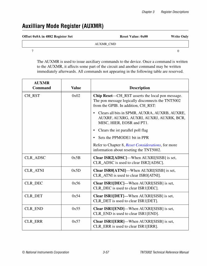
Chapter 3 Register Descriptions
© National Instruments Corporation 3-57 TNT5002 Technical Reference Manual
Auxilliary Mode Register (AUXMR)
Offset 0x0A in 4882 Register Set Reset Value: 0x00 Write Only
The AUXMR is used to issue auxiliary commands to the device. Once a command is written to the AUXMR, it affects some part of the circuit and another command may be written immediately afterwards. All commands not appearing in the following table are reserved.
AUXMR_CMD
7 0
AUXMR Command Value Description
CH_RST 0x02 Chip Reset—CH_RST asserts the local pon message. The pon message logically disconnects the TNT5002 from the GPIB. In addition, CH_RST:
• Clears all bits in SPMR, AUXRA, AUXRB, AUXRE, AUXRF, AUXRG, AUXRI, AUXRJ, AUXRK, BCR, MISC, HIER, EOSR and PT1.
• Clears the ist parallel poll flag
• Sets the PPMODE1 bit in PPR
Refer to Chapter 8, Reset Considerations, for more information about reseting the TNT5002.
CLR_ADSC 0x5B Clear ISR2[ADSC]—When AUXRI[SISB] is set, CLR_ADSC is used to clear ISR2[ADSC].
CLR_ATNI 0x5D Clear ISR0[ATNI]—When AUXRI[SISB] is set, CLR_ATNI is used to clear ISR0[ATNI].
CLR_DEC 0x56 Clear ISR1[DEC]—When AUXRI[SISB] is set, CLR_DEC is used to clear ISR1[DEC].
CLR_DET 0x54 Clear ISR1[DET]—When AUXRI[SISB] is set, CLR_DET is used to clear ISR1[DET].
CLR_END 0x55 Clear ISR1[END]—When AUXRI[SISB] is set, CLR_END is used to clear ISR1[END].
CLR_ERR 0x57 Clear ISR1[ERR]—When AUXRI[SISB] is set, CLR_ERR is used to clear ISR1[ERR].

Chapter 3 Register Descriptions
TNT5002 Technical Reference Manual 3-58 ni.com
CLR_IFCI 0x5C Clear ISR0[IFCI]—When AUXRI[SISB] is set, CLR_IFCI is used to clear ISR0[IFCI].
CLR_SRQI 0x58 Clear ISR2[SRQI]—When AUXRI[SISB] is set, CLR_SRQI is used to clear ISR2[SRQI].
CLR_LOKC 0x59 Clear ISR2[LOKC]—When AUXRI[SISB] is set, CLR_LOKC is used to clear ISR2[LOKC].
CLR_REMC 0x5A Clear ISR2[REMC]—When AUXRI[SISB] is set, CLR_REMC is used to clear ISR2[REMC].
CLR_SYNC/SET_SYNC
0x5E/0x5F Clear/Set ISR0[SYNC]—CLR_SYNC and SET_SYNC are used to set and clear ISR0[SYNC].
HLDI 0x51 Holdoff Immediately—HLDI prevents the Acceptor state machine from transitioning from ANRS to ACRS. NRFD# remains asserted in ANRS causing an RFD holdoff.
INVALID 0x07 Release DAC Holdoff (Invalid)—INVALID releases a DAC holdoff. If ISR1[APT] is set, the command that caused the DAC holdoff is interpreted as an Other Secondary Address (OSA).
IST/~IST 0x09/0x01 Set/Clear Parallel Poll Flag (ist)—IST and ~IST set and clear the Parallel Poll Flag (ist). Refer to the Parallel Poll Response Manager section of Chapter 4, Functional Description—PCI4882 and GEN4882 Modes, for more information.
LTN_CONT 0x1B Listen in Continuous Mode—LTN_CONT asserts the local ltn message and also sets Continuous Holdoff mode, regardless of AUXRA[HOLDOFFMODE]. If Continuous Holdoff mode was set by LTN_CONT, that holdoff mode will remain selected until the device becomes unaddressed to listen or LTN is issued.
LUL 0x0C Unlisten—LUL forces the Listener state machine into LIDS.
LUN 0x1C Local Unlisten—LUN causes the Listener state machine to enter LIDS if the Controller state machine is in CACS.
LUT 0x0B Untalk—LUT forces the Talker state machine into TIDS.
AUXMR Command Value Description

Chapter 3 Register Descriptions
© National Instruments Corporation 3-59 TNT5002 Technical Reference Manual
PAGEIN 0x50 Page-in Registers—This command is implemented only for backwards compatibility reasons.
PON 0x00 Pulse Pon—The PON command sets the local pon message for 1 clock cycle, then clears pon.
PULSE_RTL 0x05 Pulse Return to Local—PULSE_RTL sets the rtl local message for one clock cycle (if rtl is not already set), then clears rtl.
REQT/REQF 0x18/0x19 Request True/Request False—REQT indirectly causes the SRQ# to assert. REQF causes the SRQ# to unassert. These commands are inputs to the IEEE 488.2 Service Request Synchronization circuitry.
RHDF 0x03 Release Holdoff—RHDF clears the RFD holdoff state. The Acceptor state machine enters the RFD holdoff state following the HLDI command or as configured to do so by AUXRA[HOLDOFFMODE].
TRIG 0x04 Trigger—This command forces the TRIG pin to assert for 3 clock cycles. This command has no effect on ISR1[DET] or the DT interface function.
VALID 0x0F Release DAC Holdoff (Valid)—This command clears the DAC holdoff condition. If ISR1[APT] is set, this command causes the GPIB command to be interpreted as MSA.
AUXMR Command Value Description

Chapter 3 Register Descriptions
TNT5002 Technical Reference Manual 3-60 ni.com
Auxiliary Register A (AUXRA)
Offset 0x0A in 4882 Register Set Reset Value: 0x80 Write Only
AUXRA controls the EOS and END GPIB Remote Messages and specifies the RFD Holdoff mode.
1 0 0 BIN XEOS REOS HOLDOFFMODE[1:0]
7 6 5 4 3 2 1 0
Mnemonic Type Description
BIN W Binary EOS—BIN selects whether the EOSR represents an 8-bit binary number or a 7-bit ASCII character. When BIN is set, the EOSR is treated as an 8-bit value. All 8 bits of a data byte must match EOSR to generate the END condition. When BIN is cleared, the EOSR is treated as a 7-bit value. Only the lower 7 bits of a data byte must match the EOSR to generate the END condition.
XEOS W Transmit END with EOS—XEOS permits or prohibits automatic transmission of the GPIB END message at the same time as the EOS message when in TACS. If XEOS is set and the byte being sourced onto the GPIB matches the contents of the EOSR, EOI# is sent true along with the data. Setting CFG[CCEN] is the preferred way of sending EOI# during transfers.
REOS W Enable EOS when Receiving—When REOS is set, each byte received is compared to the EOSR to detect the END condition. When REOS is cleared, data bytes received are not compared to the EOSR to detect the END condition.
HOLDOFFMODE[1:0] W Acceptor Holdoff Mode—When receiving data bytes, HOLDOFFMODE affects how the local rdy message is generated.
HOLDOFFMODE[1:0] Holdoff Mode
00........................ Normal 01........................ RFD Holdoff on All Data10........................ RFD Holdoff on END11........................ Continuous

Chapter 3 Register Descriptions
© National Instruments Corporation 3-61 TNT5002 Technical Reference Manual
Auxiliary Register B (AUXRB)
Offset 0x0A in 4882 Register Set Reset Value: 0xA0 Write Only
AUXRB affects several different circuits. Refer to individual register bit descriptions.
1 0 1 ISS 0 TRI SPEOI CPT_ENABLE
7 6 5 4 3 2 1 0
Mnemonic Type Description
ISS W Individual Status Select—The value of the Parallel Poll Flag is used as the local ist message when AUXRB[ISS] is cleared. The value of SRQS is used as the local ist message when AUXRB[ISS] is set.
TRI W Enable 500ns T1 Delay—TRI affects the duration of the T1 delay.
SPEOI W Send END During Serial Polls—When SPEOI is set, EOI# is asserted with all serial poll responses.
CPT_ENABLE W Command Pass Through Enable—CPT_ENABLE is set to allow the detection of undefined commands and to set ISR1[CPT]. Clearing CPT_ENABLE clears ISR1[CPT] and prevents detecting undefined commands.

Chapter 3 Register Descriptions
TNT5002 Technical Reference Manual 3-62 ni.com
Auxiliary Register E (AUXRE)
Offset 0x0A in 4882 Register Set Reset Value: 0xC0 Write Only
Setting each bit in the AUXRE causes a DAC holdoff whenever a particular command is received.
1 1 0 0 DHADT DHADC DHDT DHDC
7 6 5 4 3 2 1 0
Mnemonic Type Description
DHADT W DAC Holdoff on GET Commands—DHADT causes a DAC holdoff whenever the GET command is received.
DHADC W DAC Holdoff on DCL or SDC Command—DHADC causes a DAC holdoff whenever the DCL or SDC command is received.
DHDT W DAC Holdoff on Device Trigger—DHDT causes a DAC holdoff whenever the Device Trigger command is received (GET when the device is listen addressed).
DHDC W DAC Holdoff on Device Clear—DHDC causes a DAC holdoff whenever the Device Clear command is received (either SDC when the device is listen addressed or DCL).

Chapter 3 Register Descriptions
© National Instruments Corporation 3-63 TNT5002 Technical Reference Manual
Auxiliary Register F (AUXRF)
Offset 0x0A in 4882 Register Set Reset Value: 0xD0 Write Only
Setting each bit in the AUXRF causes a DAC holdoff whenever a particular command is received.
1 1 0 1 DHATA DHALA DHUNTL DHALL
7 6 5 4 3 2 1 0
Mnemonic Type Description
DHATA W DAC Holdoff on All Talk Addresses—DHATA causes a DAC holdoff on all commands in the range 0x40 to 0x5E inclusive. DIO8 is ignored for all command bytes. When performing a DAC holdoff due to DHATA, ISR1[CPT] sets.
DHALA W DAC Holdoff on All Listen Addresses—DHALA causes a DAC holdoff on all commands in the range 0x20 to 0x3E inclusive. DIO8 is ignored for all command bytes. When performing a DAC holdoff due to DHALA, ISR1[CPT] sets.
DHUNTL W DAC Holdoff on UNT and UNL—DHUNTL causes a DAC holdoff on the UNT and UNL commands. DIO8 is ignored on all command bytes. When performing a DAC holdoff due to DHUNTL, ISR1[CPT] sets.
DHALL W DAC Holdoff on All UCG, ACG, and SCG Commands—DHALL causes a DAC holdoff on all commands in the ranges 0x00 to 0x1F inclusive and 0x60 to 0x7F inclusive. DIO8 is ignored on all command bytes. When performing a DAC holdoff due to DHALL, ISR1[CPT] sets.
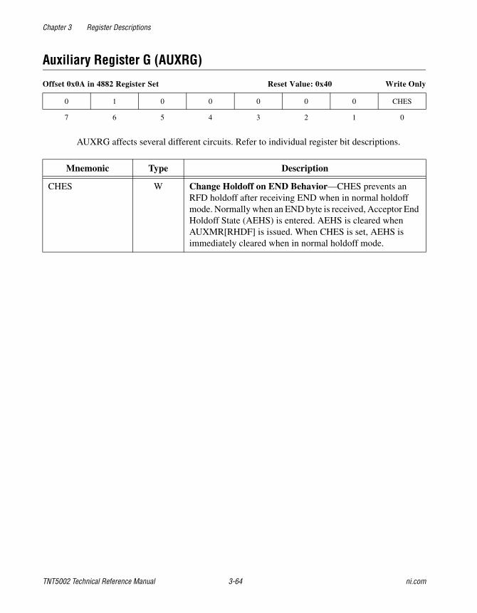
Chapter 3 Register Descriptions
TNT5002 Technical Reference Manual 3-64 ni.com
Auxiliary Register G (AUXRG)
Offset 0x0A in 4882 Register Set Reset Value: 0x40 Write Only
AUXRG affects several different circuits. Refer to individual register bit descriptions.
0 1 0 0 0 0 0 CHES
7 6 5 4 3 2 1 0
Mnemonic Type Description
CHES W Change Holdoff on END Behavior—CHES prevents an RFD holdoff after receiving END when in normal holdoff mode. Normally when an END byte is received, Acceptor End Holdoff State (AEHS) is entered. AEHS is cleared when AUXMR[RHDF] is issued. When CHES is set, AEHS is immediately cleared when in normal holdoff mode.

Chapter 3 Register Descriptions
© National Instruments Corporation 3-65 TNT5002 Technical Reference Manual
Auxiliary Register I (AUXRI)
Offset 0x0A in 4882 Register Set Reset Value: 0xE0 Write Only
AUXRI affects several different circuits. Refer to individual register bit descriptions.
1 1 1 0 USTD PPMODE2 0 SISB
7 6 5 4 3 2 1 0
Mnemonic Type Description
USTD W Enable 1100ns T1 Delay—USTD effects the duration of the T1 delay.
PPMODE2 W Parallel Poll Mode 2—This bit, together with PPR[PPMODE1], determine how the device is configured for parallel polls. Refer to Parallel Poll Response Manager section of Chapter 4, Functional Description—PCI4882 and GEN4882 Modes, for a description of this bit.
SISB W Static Interrupt Bits—SISB controls the conditions that clear the bits in ISR0, ISR1, and ISR2. If SISB is cleared, reading one of these registers clears the bits in that register. If SISB is set, the bits are cleared as described in this manual. SISB should normally be set.

Chapter 3 Register Descriptions
TNT5002 Technical Reference Manual 3-66 ni.com
Auxiliary Register J (AUXRJ)
Offset 0x0A in 4882 Register Set Reset Value: 0xF0 Write Only
AUXRJ and AUXRK implement a general-purpose timer that can cause an interrupt. The timer can also be used in byte timeout mode. In this mode the timer restarts each time a byte is read from or written to the GFIFO.
1 1 1 1 TM[3:0]
7 6 5 4 3 0
Mnemonic Type Description
TM[3:0] W Timer—TM[3:0], together with AUXRK[TM[5:4]] determines the timeout duration of the timer. The timeout duration depends on the input clock frequency. The table in the following section, Auxiliary Register K (AUXRK), shows the timeout duration assuming a 40 MHz clock. For other clock frequencies, the timeout duration can be scaled by the ratio of the frequencies.

Chapter 3 Register Descriptions
© National Instruments Corporation 3-67 TNT5002 Technical Reference Manual
Auxiliary Register K (AUXRK)
Offset 0x0F in 4882 Register Set Reset Value: 0x00 Write Only
AUXRJ and AUXRK implement a general-purpose timer that can cause an interrupt. The timer can also be used in byte timeout mode. In this mode the timer restarts each time a byte is read from or written to the GFIFO.
0 0 0 0 0 0 TM[5:4]
7 6 5 4 3 0
Mnemonic Type Description
TM[5:4] W Timer—TM[5:4], together with AUXRJ[TM[3:0]] determines the timeout duration of the timer as specified in the following table. The timeout duration depends on the input clock frequency. The table shows the timeout duration assuming a 40 MHz clock. For other clock frequencies, the timeout duration can be scaled by the ratio of the frequencies.
TM[5:0]Approximate Timeout Duration
(40MHz Clock)
000000 Disabled
000001 16.0 µs
000010 32.0 µs
000011 128 µs
000100 256 µs
000101 1.02 ms
000110 4.10 ms
000111 16.4 ms
001000 32.8 ms
001001 131 ms
001010 262 ms
001011 1.05 s

Chapter 3 Register Descriptions
TNT5002 Technical Reference Manual 3-68 ni.com
001100 4.19 s
001101 16.8 s
001110 33.6 s
001111 134 s
010001 300 s
100001 1,000 s
TM[5:0]Approximate Timeout Duration
(40MHz Clock)

Chapter 3 Register Descriptions
© National Instruments Corporation 3-69 TNT5002 Technical Reference Manual
Bus Control Register (BCR)
Offset 0x1F in 4882 Register Set Reset Value: 0x00 Write Only
The BCR allows the GPIB Interface Management and Handshake signals to be arbitrarily asserted.
0 DAV NDAC NRFD EOI SRQ 0 0
7 6 5 4 3 2 1 0
Mnemonic Type Description
DAVNDACNRFDEOISRQ
WWWWW
GPIB Control Bits—Writing a bit in the BCR causes the corresponding GPIB signal to assert (unless MISC[WRAP] is set). The TNT5002 can’t assert ATN#, IFC#, or REN#.

Chapter 3 Register Descriptions
TNT5002 Technical Reference Manual 3-70 ni.com
Bus Status Register (BSR)
Offset 0x1F in 4882 Register Set Reset Value: 0x00 Read Only
The BSR is used to read the state of the GPIB Interface Management and Handshake signals.
ATN DAV NDAC NRFD EOI SRQ IFC REN
7 6 5 4 3 2 1 0
Mnemonic Type Description
ATNDAVNDACNRFDEOISRQIFCREN
RRRRRRRR
GPIB Monitor Bits—The BSR indicates the status of the GPIB signals.

Chapter 3 Register Descriptions
© National Instruments Corporation 3-71 TNT5002 Technical Reference Manual
GPIB Transfer Configuration (CFG)
Offset 0x10 in 4882 Register Set Reset Value: 0x00 Write Only
The CFG register is used to configure GPIB transfers.
0 TLCHLTE IN A/BN CCEN 0 0 16/8N
7 6 5 4 3 2 1 0
Mnemonic Type Description
TLCHLTE W Halt on TLC Interrupts—TLCHLTE determines which conditions halt the GPIB Transfer Manager (once it has been started with the CMDR[GO]). When TLCHLTE is set, the GPIB Transfer manager also halts when any enabled interrupt in IMR0, IMR1, or IMR2 asserts.
When TLCHLTE is cleared, the GPIB Transfer manager halts when the CMDR[STOP] is issued or all of the bytes specified in the CNT3–0 registers have been transferred.
In most applications, the GPIB Transfer manager should only be stopped in response to some of the IMR0, IMR1, or IMR2 interrupts. Typically, TLCHLTE is cleared. When an interrupt asserts, software determines whether the interrupt should stop the GPIB Transfer manager. CMDR[STOP] can then be issued to stop the GPIB Transfer manager.
IN W Direction—IN indicates the direction of the GPIB transfer. For sending commands or data, IN should be cleared. IN should be set for receiving data. Command bytes are received regardless of the state of IN.
A/BN W First FIFO—When packing and unpacking data into the FIFO in 16-bit mode, the GPIB Transfer Manager alternates writing (or reading) between the upper and lower bytes. If A/BN is cleared, the GPIB Transfer manager writes (or reads) the first byte to GFIFO[7:0]. If A/BN is set, the GPIB Transfer manager writes (or reads) the first byte to GFIFO[15:8].

Chapter 3 Register Descriptions
TNT5002 Technical Reference Manual 3-72 ni.com
CCEN W Send EOI# With Last Byte—When CCEN is set and the GPIB transfer manager is sending GPIB data, EOI# is asserted with the last byte of the transfer.
16/8N W 16-bit Wide FIFO—When 16/8N is set, the GFIFO is 16-bits wide and may be accessed using byte or word accesses. When 16/8N is cleared, only the low-order byte of each position in the GFIFO is used. 16/8N should always be set unless the host is not capable of supporting 16 bit transfers to the TNT5002.
Mnemonic Type Description
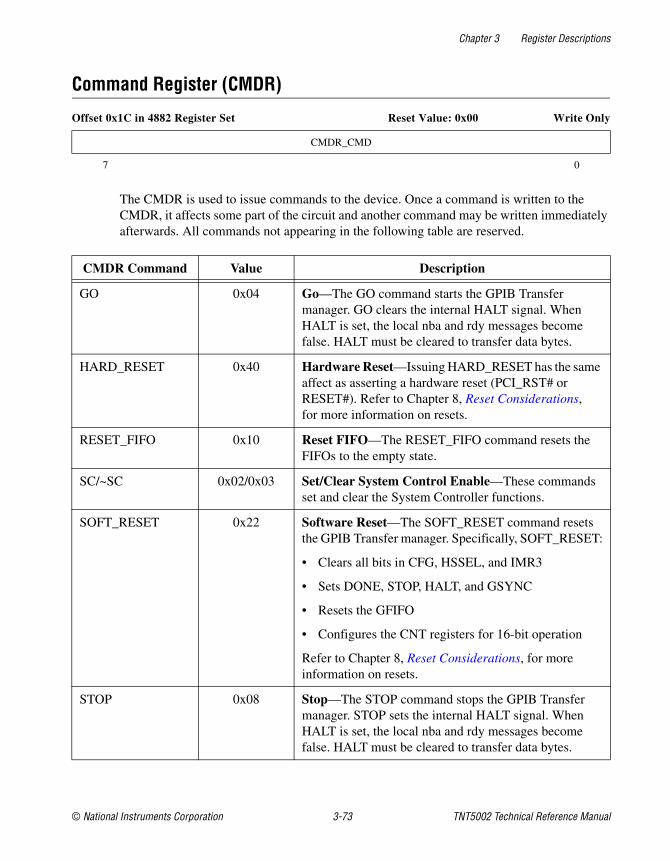
Chapter 3 Register Descriptions
© National Instruments Corporation 3-73 TNT5002 Technical Reference Manual
Command Register (CMDR)
Offset 0x1C in 4882 Register Set Reset Value: 0x00 Write Only
The CMDR is used to issue commands to the device. Once a command is written to the CMDR, it affects some part of the circuit and another command may be written immediately afterwards. All commands not appearing in the following table are reserved.
CMDR_CMD
7 0
CMDR Command Value Description
GO 0x04 Go—The GO command starts the GPIB Transfer manager. GO clears the internal HALT signal. When HALT is set, the local nba and rdy messages become false. HALT must be cleared to transfer data bytes.
HARD_RESET 0x40 Hardware Reset—Issuing HARD_RESET has the same affect as asserting a hardware reset (PCI_RST# or RESET#). Refer to Chapter 8, Reset Considerations, for more information on resets.
RESET_FIFO 0x10 Reset FIFO—The RESET_FIFO command resets the FIFOs to the empty state.
SC/~SC 0x02/0x03 Set/Clear System Control Enable—These commands set and clear the System Controller functions.
SOFT_RESET 0x22 Software Reset—The SOFT_RESET command resets the GPIB Transfer manager. Specifically, SOFT_RESET:
• Clears all bits in CFG, HSSEL, and IMR3
• Sets DONE, STOP, HALT, and GSYNC
• Resets the GFIFO
• Configures the CNT registers for 16-bit operation
Refer to Chapter 8, Reset Considerations, for more information on resets.
STOP 0x08 Stop—The STOP command stops the GPIB Transfer manager. STOP sets the internal HALT signal. When HALT is set, the local nba and rdy messages become false. HALT must be cleared to transfer data bytes.

Chapter 3 Register Descriptions
TNT5002 Technical Reference Manual 3-74 ni.com
Count Registers (CNT0, CNT1, CNT2, CNT3)
CNT0Offset 0x14 in 4882 Register Set Reset Value: 0xFF Read/Write
CNT1Offset 0x16 in 4882 Register Set Reset Value: 0xFF Read/Write
CNT2Offset 0x09 in 4882 Register Set Reset Value: 0xFF Read/Write
CNT3Offset 0x0B in 4882 Register Set Reset Value: 0xFF Read/Write
CNT[7:0]
7 0
CNT[15:8]
7 0
CNT[23:16]
7 0
CNT[31:24]
7 0
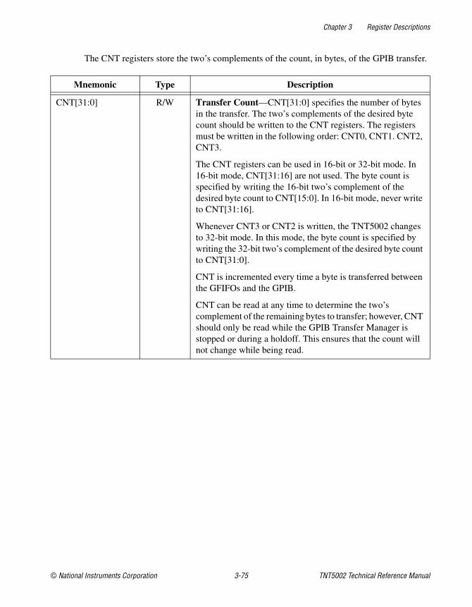
Chapter 3 Register Descriptions
© National Instruments Corporation 3-75 TNT5002 Technical Reference Manual
The CNT registers store the two’s complements of the count, in bytes, of the GPIB transfer.
Mnemonic Type Description
CNT[31:0] R/W Transfer Count—CNT[31:0] specifies the number of bytes in the transfer. The two’s complements of the desired byte count should be written to the CNT registers. The registers must be written in the following order: CNT0, CNT1. CNT2, CNT3.
The CNT registers can be used in 16-bit or 32-bit mode. In 16-bit mode, CNT[31:16] are not used. The byte count is specified by writing the 16-bit two’s complement of the desired byte count to CNT[15:0]. In 16-bit mode, never write to CNT[31:16].
Whenever CNT3 or CNT2 is written, the TNT5002 changes to 32-bit mode. In this mode, the byte count is specified by writing the 32-bit two’s complement of the desired byte count to CNT[31:0].
CNT is incremented every time a byte is transferred between the GFIFOs and the GPIB.
CNT can be read at any time to determine the two’s complement of the remaining bytes to transfer; however, CNT should only be read while the GPIB Transfer Manager is stopped or during a holdoff. This ensures that the count will not change while being read.

Chapter 3 Register Descriptions
TNT5002 Technical Reference Manual 3-76 ni.com
Command Pass Through Register (CPTR)
Offset 0x0A in 4882 Register Set Reset Value: 0x00 Read Only
CPTR[7:0]
7 0
Mnemonic Type Description
CPTR[7:0] R Command Pass Through—The CPTR holds the results of parallel polls. After starting a parallel poll, wait for ISR0[CO] to set before reading the CPTR. CPTR also stores the last command byte received.

Chapter 3 Register Descriptions
© National Instruments Corporation 3-77 TNT5002 Technical Reference Manual
Chip Signature Register (CSR)
Offset 0x17 in 4882 Register Set Reset Value: 0x4C Read Only
The CSR contains a unique identifier to distinguish it from other GPIB ASICs.
VERSION[3:0] 1 R 0 0
7 6 5 4 3 2 1 0
Mnemonic Type Description
VERSION[3:0] R Version—This field indicates the version of the TNT5002. For this TNT5002, VERSION[3:0] reads back 0100. This value may change in future versions.

Chapter 3 Register Descriptions
TNT5002 Technical Reference Manual 3-78 ni.com
DAV Hold Time Register (DAV_HOLD)
Offset 0x11 in 4882 Register Set Reset Value: 0x80 Write Only
1 0 0 DAV_HOLD[4:0]
7 6 5 4 0
Mnemonic Type Description
DAV_HOLD[4:0] W DAV Hold Time—DAV_HOLD determines the minimum time the Source state machine asserts DAV# during HS488 transfers when pmt is false. This is the amount of time the Source state machine remains in STRS. The DAV hold time is determined by the expression:
DAV hold time = 25 ns * (2 + DAV_HOLD[4:0])

Chapter 3 Register Descriptions
© National Instruments Corporation 3-79 TNT5002 Technical Reference Manual
DIO Control Register (DCR)
Offset 0x1B in 4882 Register Set Reset Value: 0x00 Write Only
DIO[8:1]
7 0
Mnemonic Type Description
DIO[8:1] W GPIB DIO Bits—Setting a bit in the DCR register causes the corresponding DIO# signal to assert (unless MISC[WRAP] is set).

Chapter 3 Register Descriptions
TNT5002 Technical Reference Manual 3-80 ni.com
DIO Setup Time Register (DIO_SETUP)
Offset 0x11 in 4882 Register Set Reset Value: 0xC0 Write Only
DIO_SETUP determines the setup time for DIO# during HS488 transfers.
1 1 0 DIO_SETUP[4:0]
7 6 5 4 0
Mnemonic Type Description
DIO_SETUP[4:0] W DIO Setup Time—DIO_SETUP determines the minimum setup time from the GPIB DIO lines being valid to DAV# asserting during HS488 transfers. This is the amount of time required to transition from SGNS to STRS. If HIER[NO_TSETUP] is set, the DIO_SETUP delay is 75 ns periods. If HIER[NO_TSETUP] is cleared, the DIO_SETUP delay is determined by the expression:
DIO setup delay = 25 ns * (4 + DIO_SETUP[4:0])

Chapter 3 Register Descriptions
© National Instruments Corporation 3-81 TNT5002 Technical Reference Manual
Data In Register (DIR)
Offset 0x00 in 4882 Register Set Reset Value: 0x00 Write Only
The DIR is implemented for backwards compatibility reasons. Do not use the DIR.
DIR[7:0]
7 0
Mnemonic Type Description
DIR[7:0] W Data In—DIR contains the last data byte accepted.
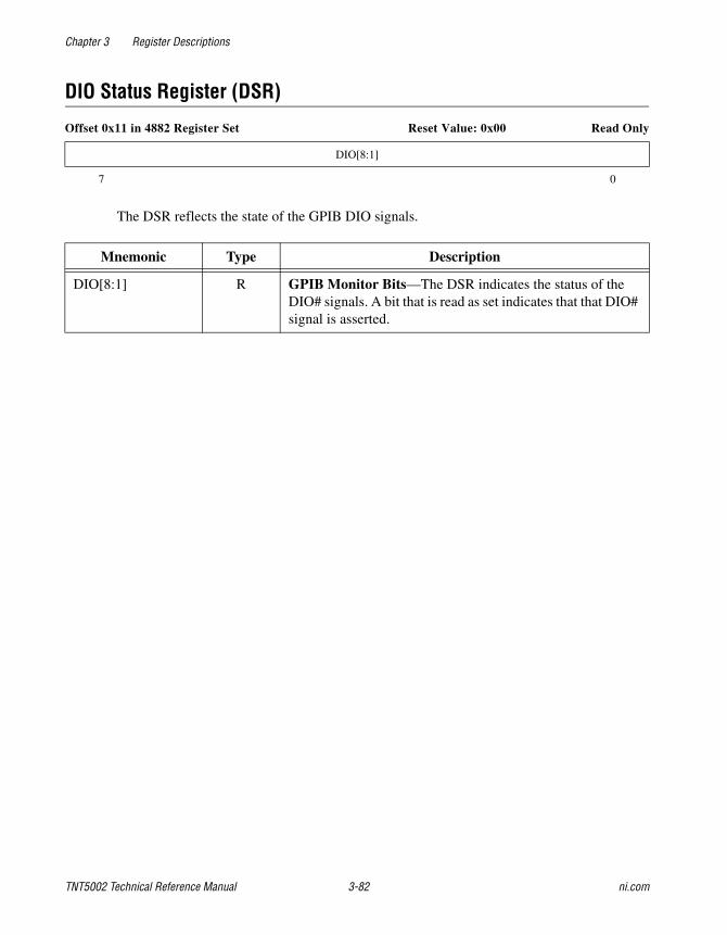
Chapter 3 Register Descriptions
TNT5002 Technical Reference Manual 3-82 ni.com
DIO Status Register (DSR)
Offset 0x11 in 4882 Register Set Reset Value: 0x00 Read Only
The DSR reflects the state of the GPIB DIO signals.
DIO[8:1]
7 0
Mnemonic Type Description
DIO[8:1] R GPIB Monitor Bits—The DSR indicates the status of the DIO# signals. A bit that is read as set indicates that that DIO# signal is asserted.

Chapter 3 Register Descriptions
© National Instruments Corporation 3-83 TNT5002 Technical Reference Manual
End-of-String Register (EOSR)
Offset 0x0E in 4882 Register Set Reset Value: 0x00 Write Only
EOSR[7:0]
7 0
Mnemonic Type Description
EOSR[7:0] W End Of String Character—The EOSR stores the byte used to detect the END condition. The EOSR is compared to each data byte received when AUXRA[REOS] is set. If EOS matches the data byte received, the END condition is true. AUXRA[BIN] determines whether 7 or 8 bits are compared.
When AUXRA[XEOS] is set, each data byte sent is compared to the EOSR. If the data byte being sent matches EOS, EOI# is asserted with that data byte.
If a Listener is configured to detect an EOS character sent by a Talker during an HS488 transfer, the Talker must write that byte to the EOSR and set HIER[PMT_W_EOS].

Chapter 3 Register Descriptions
TNT5002 Technical Reference Manual 3-84 ni.com
GPIB FIFO (GFIFO)
GFIFO[15:8]Offset 0x19 in 4882 Register Set Reset Value: 0x00 Read/Write
GFIFO[7:0]Offset 0x18 in 4882 Register Set Reset Value: 0x00 Read/Write
The FIFO buffers data during GPIB transfers.
GFIFO[15:8]
7 0
GFIFO[7:0]
7 0
Mnemonic Type Description
GFIFO[15:8]GFIFO[7:0]
R/WR/W
GPIB FIFO—The GPIB FIFO buffers data to and from the GPIB during GPIB transfers. Internally, the GFIFO is 16 positions deep and either 1 or 2 bytes wide, as configured by CFG[16/8N]. When reading and writing data from and to the GFIFO, the GPIB Transfer Manager alternates writing or reading bytes to the upper and lower bytes of the GFIFO. The GPIB Transfer manager writes (or reads) the first byte to GFIFO[7:0] when CFG[A/BN] is cleared and to GFIFO[15:8] when CFG[A/BN] is set.

Chapter 3 Register Descriptions
© National Instruments Corporation 3-85 TNT5002 Technical Reference Manual
High-Speed Enable Register (HIER)
Offset 0x3 in 4882 Register Set Reset Value: 0x00 Write Only
AUXRI affects several different circuits. Refer to individual register bit descriptions.
DG[1:0] 0 NO_TSETUP 0 0 0 PMT_W_EOS
7 6 5 4 3 2 1 0
Mnemonic Type Description
DG[1:0] W Deglitch Selector—DAV# is deglitched when receiving command bytes or data bytes. The minimum pulse accepted is the minimum time that DAV# must remain continuously asserted to be detected by the Acceptor state machine. The maximum pulse ignored is the maximum time that DAV# can remain continuously asserted and be ignored by the Acceptor state machine. The following table lists how DAV# is deglitched when using a 40 MHz clock:
DG[1:0] Minimum Pulse Maximum Pulse Accepted (ns) Ignored (ns)
00.......................25 ............................ 1210.......................37 ............................ 2511.......................75 ............................ 50others .................Reserved ................. Reserved
NO_TSETUP W No Extra DIO_SETUP Setup Delay—NO_TSETUP and the DIO_SETUP register determine the setup time from the DIO lines being valid to DAV# asserting during HS488 transfers. If NO_TSETUP is set, the DIO setup time is 75 ns.
PMT_W_EOS W Assert pmt With EOS—Setting this bit causes the Source to keep DAV# asserted for a longer period of time when using an EOS character during HS488 transfers. When PMT_W_EOS is set, the duration of DAV# assertions when the EOS byte is sourced is determined by NIC_DELAY rather than DAV_HOLD. The Talker must write the EOS byte to the EOSR and set PMT_W_EOS when a listener is configured to detect EOS bytes when using HS488.
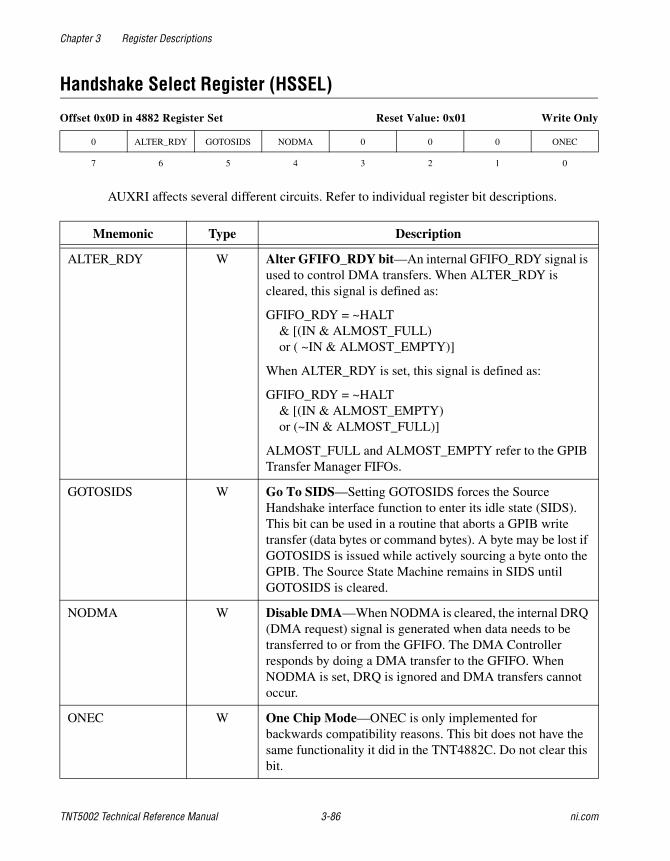
Chapter 3 Register Descriptions
TNT5002 Technical Reference Manual 3-86 ni.com
Handshake Select Register (HSSEL)
Offset 0x0D in 4882 Register Set Reset Value: 0x01 Write Only
AUXRI affects several different circuits. Refer to individual register bit descriptions.
0 ALTER_RDY GOTOSIDS NODMA 0 0 0 ONEC
7 6 5 4 3 2 1 0
Mnemonic Type Description
ALTER_RDY W Alter GFIFO_RDY bit—An internal GFIFO_RDY signal is used to control DMA transfers. When ALTER_RDY is cleared, this signal is defined as:
GFIFO_RDY = ~HALT& [(IN & ALMOST_FULL) or ( ~IN & ALMOST_EMPTY)]
When ALTER_RDY is set, this signal is defined as:
GFIFO_RDY = ~HALT& [(IN & ALMOST_EMPTY) or (~IN & ALMOST_FULL)]
ALMOST_FULL and ALMOST_EMPTY refer to the GPIB Transfer Manager FIFOs.
GOTOSIDS W Go To SIDS—Setting GOTOSIDS forces the Source Handshake interface function to enter its idle state (SIDS). This bit can be used in a routine that aborts a GPIB write transfer (data bytes or command bytes). A byte may be lost if GOTOSIDS is issued while actively sourcing a byte onto the GPIB. The Source State Machine remains in SIDS until GOTOSIDS is cleared.
NODMA W Disable DMA—When NODMA is cleared, the internal DRQ (DMA request) signal is generated when data needs to be transferred to or from the GFIFO. The DMA Controller responds by doing a DMA transfer to the GFIFO. When NODMA is set, DRQ is ignored and DMA transfers cannot occur.
ONEC W One Chip Mode—ONEC is only implemented for backwards compatibility reasons. This bit does not have the same functionality it did in the TNT4882C. Do not clear this bit.

Chapter 3 Register Descriptions
© National Instruments Corporation 3-87 TNT5002 Technical Reference Manual
Interrupt Mask Register 0 (IMR0)
Offset 0x1D in 4882 Register Set Reset Value: 0x80 Write Only
IMR0 contains interrupt enables for ISR0 and internal control bits.
GLINT STBO IE NLEN BTO IFCI IE ATNI IE TO IE SYNC IE
7 6 5 4 3 2 1 0
Mnemonic Type Description
GLINT W Enable Certain Interrupts—GLINT enables IMR0, IMR1, and IMR2 interrupts. GLINT is redundant with IMR3[TLCINT IE], so always set GLINT. Writing AUXMR[SETSWRST] sets GLINT.
STBO IE W Status Byte Out Interrupt Enable—Setting STBO IE enables Serial Poll Mode SP2. Setting STBO IE also generates an interrupt when the GPIB Controller serial polls the device.
NLEN W Newline Enable—When NLEN is set, the 7-bit ASCII newline character (0xA) is treated as an EOS character. When a newline data byte is accepted, the Acceptor behaves as if the EOI# signal was asserted when the byte was accepted. Normally, the EOS character is written to the EOSR. NLEN allows the Acceptor to recognize two different EOS characters: newline and the EOSR character.
BTO W Byte Timeout—When BTO is set, the Timer is reset whenever a data byte is sent or received or whenever a command byte is sent.
IFCI IE W IFC# Interrupt Enable—IFCI IE enables an interrupt when the IFCI condition is true.
ATNI IE W ATN# Interrupt Enable—ATNI IE enables an interrupt when the ATNI condition is true.
TO IE W Timeout Interrupt Enable—TO IE enables an interrupt when the TO condition is true.
SYNC IE W GPIB Synchronized Interrupt Enable—SYNC IE enables an interrupt when the SYNC condition is true.

Chapter 3 Register Descriptions
TNT5002 Technical Reference Manual 3-88 ni.com
Interrupt Mask Register 1 (IMR1)
Offset 0x02 in 4882 Register Set Reset Value: 0x00 Write Only
IMR1 contains interrupt enables for interrupts in ISR1.
CPT IE APT IE DET IE END IE DEC IE ERR IE DO IE DI IE
7 6 5 4 3 2 1 0
Mnemonic Type Description
CPT IE W Command Pass Through Interrupt Enable—CPT IE enables an interrupt when the CPT condition is true.
APT IE W Address Pass Through Interrupt—APT IE enables an interrupt when the APT condition is true.
DET IE W Device Trigger Interrupt Enable—DET IE enables an interrupt when the the DET condition is true.
END IE W END Interrupt Enable—END IE enables an interrupt when the END condition is true.
DEC IE W Device Clear Interrupt Enable—DEC IE enables an interrupt when the the DEC condition is true.
ERR IE W Error Interrupt Enable—ERR IE enables an interrupt when the ERR condition is true.
DO IE W Data Out Interrupt Enable—DO IE enables an interrupt when the DO condition is true.
DI IE W Data In Interrupt Enable—DI IE enables an interrupt when the DI condition is true.

Chapter 3 Register Descriptions
© National Instruments Corporation 3-89 TNT5002 Technical Reference Manual
Interrupt Mask Register 2 (IMR2)
Offset 0x04 in 4882 Register Set Reset Value: 0x00 Write Only
IMR2 contains interrupt enables for interrupts in ISR2.
0 0 0 0 0 LOKC IE REMC IE ADSC IE
7 6 5 4 3 2 1 0
Mnemonic Type Description
LOKC IE W Lockout Change Interrupt Enable—LOKC IE enables an interrupt when the LOKC condition is true.
REMC IE W Remote Change Interrupt Enable—REMC IE enables an interrupt when the REMC condition is true.
ADSC IE W Address Status Change Interrupt Enable—ADSC IE enables an interrupt when the ADSC condition is true.

Chapter 3 Register Descriptions
TNT5002 Technical Reference Manual 3-90 ni.com
Interrupt Mask Register 3 (IMR3)
Offset 0x12 in 4882 Register Set Reset Value: 0x00 Read/Write
IMR3 contains interrupt enables for interrupts in ISR3.
0 GFIFO_RDY IE 0 STOP IE NFF IE NEF IE TLCINT IE DONE IE
7 6 5 4 3 2 1 0
Mnemonic Type Description
GFIFO_RDY IE R/W GFIFO_RDY Interrupt Enable—GFIFO_RDY IE enables an interrupt when the GFIFO_RDY condition is true. Reading GFIFO_RDY IE returns the value of the interrupt enable bit, not the GFIFO_RDY condition.
STOP IE R/W STOP Interrupt Enable—STOP IE enables an interrupt when the STOP condition is true. Reading STOP IE returns the value of the interrupt enable bit, not the STOP condition.
NFF IE R/W FIFO Not Full Interrupt Enable—NFF IE enables an interrupt when the NFF condition is true. Reading NFF IE returns the value of the interrupt enable bit, not the NFF condition.
NEF IE R/W FIFO Not Empty Interrupt Enable—NEF IE enables an interrupt when the NEF condition is true. Reading NEF IE returns the value of the interrupt enable bit, not the NEF condition.
TLCINT IE R/W TLC Interrupt Enable—TLCINT IE enables the TNT5002 to generate an interrupt when TLCINT asserts.
DONE IE R/W DONE Interrupt Enable—DONE IE enables an interrupt when the DONE condition is true. Reading DONE IE returns the value of the interrupt enable bit, not the DONE condition.

Chapter 3 Register Descriptions
© National Instruments Corporation 3-91 TNT5002 Technical Reference Manual
Interrupt Status Register 0 (ISR0)
Offset 0x1D in 4882 Register Set Reset Value: 0x00 Read Only
ISR0 contains various status bits that can cause an interrupt when enabled in IMR0.
NBA STBO NL EOS IFCI ATNI TO SYNC
7 6 5 4 3 2 1 0
Mnemonic Type Description
NBA R New Byte Available—NBA reflects the local nba message, which indicates that the SH interface function has bytes to send. Specifically,
NBA = ~CFGR[IN] & ~(FIFO empty).
STBO R Status Byte Out—STBO sets when the Talker enters SPAS (Serial Poll Active State) during a serial poll. STBO clears after writing to the SPMR or when SPAS becomes false.
NL R Newline Received—NL indicates whether the last data byte received was a newline character (0x0A). NL sets and clears regardless of the value of IMR0[NLEN].
EOS R End-of-String—EOS indicates that the last data byte received satisfies the EOS condition. ISR1[END] should be used instead of EOS to detect the end of a read transfer.
EOS is set by:LACS & EOS & REOS & ACDS
EOS is cleared by:pon + ~REOS + (LACS & ~EOS & ACDS)
IFCI R IFC Interrupt—IFCI is set when the GPIB IFC# signal asserts. Writing AUXMR[CLR_IFCI] clears IFCI. The GPIB state machines detect and appropriately handle IFC# without any intervention. IFC# should not have any other affect on the device, so devices should not monitor or interrupt on IFCI.
ATNI R ATN Interrupt—ATNI is set when the GPIB ATN# signal asserts. Writing AUXMR[CLR_ATNI] clears ATNI. The GPIB state machines detect the ATN# signal and interpret it appropriately without any intervention.
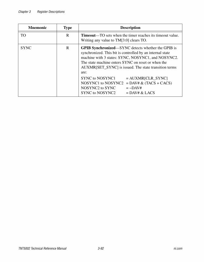
Chapter 3 Register Descriptions
TNT5002 Technical Reference Manual 3-92 ni.com
TO R Timeout—TO sets when the timer reaches its timeout value. Writing any value to TM[3:0] clears TO.
SYNC R GPIB Synchronized—SYNC detects whether the GPIB is synchronized. This bit is controlled by an internal state machine with 3 states: SYNC, NOSYNC1, and NOSYNC2. The state machine enters SYNC on reset or when the AUXMR[SET_SYNC] is issued. The state transition terms are:
SYNC to NOSYNC1 = AUXMR[CLR_SYNC]NOSYNC1 to NOSYNC2 = DAV# & (TACS + CACS)NOSYNC2 to SYNC = ~DAV#SYNC to NOSYNC2 = DAV# & LACS
Mnemonic Type Description

Chapter 3 Register Descriptions
© National Instruments Corporation 3-93 TNT5002 Technical Reference Manual
Interrupt Status Register 1 (ISR1)
Offset 0x02 in 4882 Register Set Reset Value: 0x00 Read Only
ISR1 contains various status bits that can cause an interrupt when enabled in IMR1.
CPT APT DET END DEC ERR DO DI
7 6 5 4 3 2 1 0
Mnemonic Type Description
CPT R Command Pass Through—CPT indicates that a command that must be processed by software was received. In the following description, a primary command is any command in the range (0x0–0x5F) and a secondary command is any command in the range (0x60–0x7F). The most significant bit (DIO8) of the command byte is always ignored.
When AUXRB[CPT_ENABLE] is set, CPT sets when an undefined primary command is received. The following commands are always undefined: 0x10, 0x12, 0x13, 0x16, 0x17, 0x1A–0x1F. If addressed to talk or listen, the following commands are also undefined: 0x0, 0x2, 0x3, 0x6, 0x7, 0xA–0xF
If the last primary command received was undefined, CPT also sets on any secondary command.
When CPT sets, a DAC holdoff occurs. A DAC holdoff prevents the Controller from sending more command bytes. Write AUXMR[VALID] to clear the DAC holdoff.
Reading the CPTR clears CPT. Clearing IMR1[CPT] clears CPT and disables the circuitry that detects undefined commands.
CPT is set by:
[UCG + (ACG & (TADS + LADS))] & undefined &ACDS & AUXRB[CPT_ENABLE]
+ UDPCF & SCG & ACDS &AUXRB[CPT_ENABLE]
+ AUXRE[DHADT] & GET & LADS+ AUXRE[DHADC] & (SDC + DCL) & ACDS+ AUXRF[DHATA] & TAG & ~UNT & ACDS+ AUXRF[DHALA] & LAG & ~UNL & ACDS+ AUXRF[DHUNTL] & (UNT + UNL) & ACDS+ AUXRF[DHALL] & ATN & ACDS
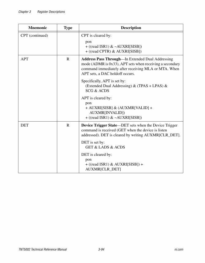
Chapter 3 Register Descriptions
TNT5002 Technical Reference Manual 3-94 ni.com
CPT (continued) CPT is cleared by:
pon+ ((read ISR1) & ~AUXRI[SISB])+ ((read CPTR) & AUXRI[SISB])
APT R Address Pass Through—In Extended Dual Addressing mode (ADMR is 0x33), APT sets when receiving a secondary command immediately after receiving MLA or MTA. When APT sets, a DAC holdoff occurs.
Specifically, APT is set by:(Extended Dual Addressing) & (TPAS + LPAS) &SCG & ACDS
APT is cleared by:pon + AUXRI[SISB] & (AUXMR[VALID] +
AUXMR[INVALID])+ ((read ISR1) & ~AUXRI[SISB])
DET R Device Trigger State—DET sets when the Device Trigger command is received (GET when the device is listen addressed). DET is cleared by writing AUXMR[CLR_DET].
DET is set by:GET & LADS & ACDS
DET is cleared by:pon + ((read ISR1) & AUXRI[SISB]) +AUXMR[CLR_DET]
Mnemonic Type Description

Chapter 3 Register Descriptions
© National Instruments Corporation 3-95 TNT5002 Technical Reference Manual
END R END Received—END sets after receiving a byte satisfying the END condition. A byte satisfies the END condition if the Talker asserts EOI# when it sends the byte or AUXRA[REOS] is set and the byte matches the contents of the EOSR.
END is set by:LACS & (EOI + (EOS & AUXRA[REOS]) + (NL & IMR0[NLEN]))
END is cleared by:pon + ((read ISR1) & ~AUXRI[SISB]) +AUXMR[CLR_END]
DEC R Device Clear State—DEC sets when the Device Clear command is received (either SDC when the device is listen addressed or DCL). DEC is cleared by writing AUXMR[CLR_DEC].
DEC is set by:(DCL + (SDC & LADS))& ACDS
DEC is cleared by:pon + ((read ISR1) & ~AUXRI[SISB]) +AUXMR[CLR_DEC].
ERR R Error—ERR sets when the TNT5002 tries to send a data or command byte but detects no Listeners on the GPIB. ERR is cleared by writing to AUXMR[CLR_ERR].
ERR is set by: SDYS & T1 & ~SHAS & RFD & EXTDAC
ERR is cleared by: pon
+ ((read ISR1) & ~AUXRI[SISB]) +AUXMR[CLR_ERR]
Mnemonic Type Description

Chapter 3 Register Descriptions
TNT5002 Technical Reference Manual 3-96 ni.com
DO R Data Out Interrupt—DO sets whenever the Talker state machine is in TACS and the TNT5002 has no data to send. DO can be used instead of ISR2[ADSC] to determine when to begin a routine that sends data bytes.
DO is set by: TACS & SGNS & ~nba
DO is cleared by: pon
+ ((read ISR1) & ~AUXRI[SISB]) + ~TACS +~SGNS + nba
DI R Data In—DI indicates that the Acceptor has accepted a data byte while in SPMS.
DI is set by: ~Continuous Holdoff Mode & SPMS & LACS & DAV
& ~ATN#
DI is cleared by: pon + ((read ISR1) & ~AUXRI[SISB]) + (AUXMR[RHDF] & Holdoff) + (~SPMS)
Mnemonic Type Description

Chapter 3 Register Descriptions
© National Instruments Corporation 3-97 TNT5002 Technical Reference Manual
Interrupt Status Register 2 (ISR2)
Offset 0x04 in 4882 Register Set Reset Value: 0x00 Read Only
ISR2 contains various status bits that can cause an interrupt when enabled in IMR2.
INT SRQI LOK REM 0 LOKC REMC ADSC
7 6 5 4 3 2 1 0
Mnemonic Type Description
INT R Interrupt—INT is exactly the same as ISR3[TLCINT].
INT = IMR0[GLINT] & + (IMR2[LOKC IE] & ISR2[LOKC])+ (IMR2[REMC IE] & ISR2[REMC])+ (IMR2[ADSC IE] & ISR2[ADSC])+ (IMR1[CPT IE] & ISR1[CPT])+ (IMR1[APT IE] & ISR1[APT])+ (IMR1[DET IE] & ISR1[DET])+ (IMR1[END IE] & ISR1[END])+ (IMR1[DEC IE] & ISR1[DEC])+ (IMR1[ERR IE] & ISR1[ERR])+ (IMR1[DO IE] & ISR1[DO])+ (IMR1[DI IE] & ISR1[DI])+ (IMR0[STBO IE] & ISR0[STBO])+ (IMR0[IFCI IE] & ISR0[IFC])+ (IMR0[ATNI IE] & ISR0[ATNI])+ (IMR0[TO IE] & ISR0[TO])+ (IMR0[SYNC IE] & ISR0[SYNC])
LOK R Lockout State—This bit is set when the Remote/Local state machine is in a lockout state (RWLS or LWLS) and is cleared when in a non-lockout state (REMS or LOCS).
REM R Remote State—This bit is cleared when the Remote/Local state machine is in a local state (LOCS or LWLS) and is set when in a remote state (REMS or RWLS).
LOKC R LOK Change—LOKC sets when value of the ISR2[LOK] changes.
LOKC is cleared by:pon
+ AUXMR[CLR_LOK] + ((read ISR2) &~AUXRI[SISB])

Chapter 3 Register Descriptions
TNT5002 Technical Reference Manual 3-98 ni.com
REMC R REM Change—REMC sets when value of the ISR2[REM] changes.
REMC is cleared by:pon + AUXMR[CLR_REM] + ((read ISR2) &~AUXRI[SISB])
ADSC R Address Status Change—ADSC indicates that the addressing state has changed. ADSC sets after:
• Being addressed or unaddressed to talk
• Being addressed or unaddressed to listen
ADSC is set by:~(lon + ton) & (any change in ADSR[TA, LA, or MINOR])
ADSC is cleared by:pon + (read ISR2) & ~AUXRI[SISB]+ AUXMR[CLR_ADSC] + ADMR[LON] +ADMR[TON]
Mnemonic Type Description

Chapter 3 Register Descriptions
© National Instruments Corporation 3-99 TNT5002 Technical Reference Manual
Interrupt Status Register 3 (ISR3)
Offset 0x1A in 4882 Register Set Reset Value: 0x00 Read Only
ISR3 contains various status bits that can cause an interrupt when enabled in IMR3. PCI_INTA# is the logical OR of ISR3[INT] and LCISR2[DMA].
INT GFIFO_RDY R STOP NFF NEF TLCINT DONE
7 6 5 4 3 2 1 0
Mnemonic Type Description
INT R Interrupt—INT indicates that an enabled IMR3 interrupt is asserting.
INT = (GFIFO_RDY IE & GFIFO_RDY)+ (STOP IE & STOP)+ (NFF IE & NFF)+ (NEF IE & NEF)+ (TLCINT IE & TLCINT)+ (DONE IE & DONE)
The INTA# pin asserts whenever INT is set.
GFIFO_RDY R GFIFO Ready—GFIFO_RDY indicates that the GFIFO is ready for several transfers. During GPIB reads, GFIFO_RDY indicates that the FIFO is at least 75% full and the transfer is not halted. During GPIB writes and sending commands, GFIFO_RDY indicates that the FIFO is at least 75% empty and the transfer is not halted
GFIFO_RDY = ~HALT & ((FIFOs 75% Empty & ~CFGR[IN])+ (FIFOs 75% Full & CFGR[IN]))
STOP R GPIB Transfer Manager Stopped—STOP indicates that the transfer manager has stopped transferring bytes between the GFIFOs and the GPIB. The transfer manager stops when either all of the bytes specified by CNT have been transferred or CMDR[STOP] is issued.
NFF R Not Full FIFO—NFF indicates that the GFIFO is not full. Assuming the GFIFO has been configured as 16-bits wide, NFF sets when at least one word may be written to the GFIFO. NFF clears when there is not room for at least one word in the GFIFO.

Chapter 3 Register Descriptions
TNT5002 Technical Reference Manual 3-100 ni.com
NEF R Not Empty FIFO—NEF indicates that the GFIFO is not empty. Assuming the GFIFO has been configured as 16-bits wide, NEF sets when at least one word may be read from the GFIFO; or, when one byte may be read from the GFIFO and STS1[HALT] is set and STS1[DONE] is not set. NEF clears when there is less than one word in the GFIFO while STS1[HALT] is not set or when STS1[DONE] is set.
TLCINT R TLC Interrupt—TLCINT indicates whether an enabled IMR0, IMR1, or IMR2 interrupt is asserting.
TLCINT = IMR0[GLINT]& + (IMR2[LOKC IE] & ISR2[LOKC])+ (IMR2[REMC IE] & ISR2[REMC])+ (IMR2[ADSC IE] & ISR2[ADSC])+ (IMR1[CPT IE] & ISR1[CPT])+ (IMR1[APT IE] & ISR1[APT])+ (IMR1[DET IE] & ISR1[DET])+ (IMR1[END IE] & ISR1[END])+ (IMR1[DEC IE] & ISR1[DEC])+ (IMR1[ERR IE] & ISR1[ERR])+ (IMR1[DO IE] & ISR1[DO])+ (IMR1[DI IE] & ISR1[DI])+ (IMR0[STBO IE] & ISR0[STBO])+ (IMR0[IFCI IE] & ISR0[IFC])+ (IMR0[ATNI IE] & ISR0[ATNI])+ (IMR0[TO IE] & ISR0[TO])+ (IMR0[SYNC IE] & ISR0[SYNC])
TLCINT IE enables the TNT5002 to generate a PCI interrupt when TLCINT asserts.
DONE R DONE—At the end of a transfer, DONE indicates that all devices on the GPIB have finished the transfer. DONE only sets after STOP sets.
DONE = (GSYNC & ~CFG[IN]) + (GFIFO empty & CFG[IN])
Mnemonic Type Description

Chapter 3 Register Descriptions
© National Instruments Corporation 3-101 TNT5002 Technical Reference Manual
Key Control Register (KEYREG)
Offset 0x17 in 4882 Register Set Reset Value: 0x00 Write Only
KEYREG contains bits that affect the T1 delay.
0 0 MSTD NO_T1 0 0 0 0
7 6 5 4 3 2 1 0
Mnemonic Type Description
MSTD W Enable 350ns T1 Delay—MSTD affects the duration of the T1 delay.
NO_T1 W Enable 50ns T1 Delay—NO_T1 affects the duration of the T1 delay.

Chapter 3 Register Descriptions
TNT5002 Technical Reference Manual 3-102 ni.com
Miscellaneous Register (MISC)
Offset 0x15 in 4882 Register Set Reset Value: 0x00 Write Only
MISC affects several different circuits. Refer to individual register bit descriptions.
0 0 0 HSE SLOW WRAP NOAS NOTS
7 6 5 4 3 2 1 0
Mnemonic Type Description
HSE W HS488 Enable—When HSE is set, HS488 is enabled. When HSE is cleared, the traditional 3-wire transfers are always used. Even when HSE is set, transfers only use the HS488 protocol if both the Talker and Listener are capable of HS488 transfers. The Source state machine detects this condition without intervention and automatically selects between HS488 and 3-wire handshake protocols.
SLOW W Slow Handshake Lines—Setting SLOW enables circuitry that increases the time NRFD# or NDAC# must be unasserted before the Source state machine responds to the unassertion. The sampling of NRFD# and NDAC# is delayed by 40 clock periods when SLOW is set. Setting SLOW may help communication to a few devices that do not meet the IEEE 488.1 standard.
WRAP W Wrap Back—When WRAP is set, the GPIB pins are tristated, but the GPIB signals are fed back into the TNT5002. The external state of each signal is ignored. This bit may be used to allow diagnostics to run without disconnecting GPIB cables from the board.
NOAS W No HALT on ATN# or STBO Interrupts—NOAS prevents HALT from asserting due to ISR0[ATN] or ISR0[STBO] interrupts.
NOTS W No HALT on Timeout or SRQI Interrupts—NOTS prevents HALT from asserting due to ISR0[TIMO] or ISR2[SRQI] interrupts.

Chapter 3 Register Descriptions
© National Instruments Corporation 3-103 TNT5002 Technical Reference Manual
Non-Interlocked Capable Delay Register (NIC_DELAY)
Offset 0x11 in 4882 Register Set Reset Value: 0x40 Write Only
NIC_DELAY determines the length of the NRFD pulse at the beginning of an HS488 transfer.
0 1 0 NIC_DELAY[4:0]
7 6 5 4 0
Mnemonic Type Description
NIC_DELAY[4:0] W NIC Delay—NIC_DELAY determines the minimum time the Source state machine sends NIC at the beginning of an HS488 transfers. NIC_DELAY also determines the minimum time the Source state machine asserts DAV# when pmt is true. The NIC delay is determined by the expression:
NIC delay = 25 ns * (2 + NIC_DELAY[4:0])

Chapter 3 Register Descriptions
TNT5002 Technical Reference Manual 3-104 ni.com
Parallel Poll Register (PPR)
Offset 0x0A in 4882 Register Set Reset Value: 0x70 Write Only
PPR is used to configure Parallel Poll responses.
0 1 1 PPMODE1 SENSE LPPE[2:0]
7 6 5 4 5 2 0
Mnemonic Type Description
PPMODE1 W Parallel Poll Mode 1—This bit, together with AUXRI[PPMODE2], determine how the device is configured for parallel polls. Refer to the Parallel Poll Response Manager section of Chapter 4, Functional Description—PCI4882 and GEN4882 Modes, for more information.
SENSE W Sense—The state of the DIO line selected by LPPE during a parallel poll response is described in the following table:
SENSE ist DIO Line
0 .............. 0.............. asserted0 .............. 1..............unasserted1 .............. 0..............unasserted1 .............. 1.............. asserted
DIO lines are driven with open-collector drivers during parallel polls. DIO lines that are not asserted (driven low) are not actively driven high. This allows different devices to simultaneously drive different DIO signals.
LPPE[2:0] W Local Parallel Poll Configuration—In Local Parallel Poll Configuration, LPPE[2:0] configures how the Parallel Poll Response Manager responds to parallel polls. In Local Parallel Poll Configuration mode, the Parallel Poll Response Manager is configured as if it received a PPE command of 0x6n where n = LPPE[2:0].

Chapter 3 Register Descriptions
© National Instruments Corporation 3-105 TNT5002 Technical Reference Manual
Programmable T1 Register (PT1)
Offset 0x11 in 4882 Register Set Reset Value: 0x00 Write Only
PT1 is used to specify the T1 delay for Source state machine.
0 0 PT1_ENA PT1[4:0]
7 6 5 4 0
Mnemonic Type Description
PT1_ENA W Programmable T1 Enable—When PT1_ENA is set, the Source state machine uses PT1[4:0] to determine the length of the T1 delay for sending the second and subsequent data bytes.
When the TNT5002 sends command bytes or data bytes to GPIB devices using the traditional 3-wire handshake, the Source state machine first drives the data byte or command byte value on the DIO[8:1] pins. After waiting for a certain delay (know as the T1 delay), DAV# is asserted to indicate that the DIO[8:1] signals are valid. IEEE 488.1 has certain requirements for the duration of the T1 delay. The programmable T1 delay does not affect GPIB read operations or sending command bytes.
PT1[4:0] W Programmable T1 Delay—When PT1_ENA is set, the T1 delay for command bytes and the first data byte of a string is 44 clock periods. For other data bytes, the T1 delay when using a clock with period T is:
T1 = T * (2 + PT1[4:0])
For example, if the clock period is 25 ns and PT1[4:0] = 10010. The T1 delay is:
25 ns * (2 + 18) = 25 ns * 20 = 500 ns.
For most applications not using HS488, PT1[4:0] should be configured for 500 ns if PT1_ENA is set.

Chapter 3 Register Descriptions
TNT5002 Technical Reference Manual 3-106 ni.com
Source/Acceptor Status Register (SASR)
Offset 0x1B in 4882 Register Set Reset Value: 0x00 Read Only
The SASR reflects various internal states and signals.
NBA AEHS ANHS1 ANHS2 ADHS ACRDY SH1A SH1B
7 6 5 4 3 2 1 0
Mnemonic Type Description
NBA R New Byte Available—NBA reflects the local nba message, which indicates that the SH interface function has a byte to send. Specifically,
NBA = ~CFGR[IN] & ~(FIFO empty).
AEHS R Acceptor End Holdoff State—AEHS sets after receiving a data byte with EOI# asserted, receiving a data byte matching the EOSR when AUXRA[REOS] is true, or receiving the NL character (0x0A) when IMR0[NLEN] is true. AEHS is cleared by writing AUXMR[RHDF].
ANHS1 R Acceptor Not Ready Holdoff—ANHS1 sets when the Acceptor receives a data byte with EOI# asserted, receives a data byte matching the EOSR when AUXRA[REOS] is true, or receives the NL character (0x0A) when NLEN is true. ANHS1 also sets when a data byte is accepted when the Acceptor is not in Continuous Holdoff mode. ANHS1 is cleared when holdoff is false, AUXMR[RHDF] is issued, or AUXMR[LTN_CONT] is issued.
ANHS2 R Acceptor Not Ready Holdoff Immediately—ANHS2 is set by writing AUXMR[HLDI]. ANHS2 is cleared by writing AUXMR[RHDF].
ADHS R Acceptor Data Holdoff State—ADHS sets when a DAC holdoff is active. ADHS is cleared by AUXMR[VALID] or AUXMR[INVALID].
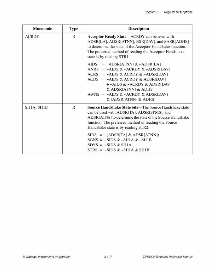
Chapter 3 Register Descriptions
© National Instruments Corporation 3-107 TNT5002 Technical Reference Manual
ACRDY R Acceptor Ready State—ACRDY can be used with ADSR[LA], ADSR[ATNN], BSR[DAV], and SASR[ADHS] to determine the state of the Acceptor Handshake function. The preferred method of reading the Acceptor Handshake state is by reading STR1.
AIDS = ADSR[ATNN] & ~ADSR[LA]ANRS = ~AIDS & ~ACRDY & ~ADSR[DAV]ACRS = ~AIDS & ACRDY & ~ADSR[DAV]ACDS = ~AIDS & ACRDY & ADSR[DAV]
+ ~AIDS & ~ACRDY & ADSR[DAV] & ADSR[ATNN] & ADHS
AWNS = ~AIDS & ~ACRDY & ADSR[DAV] & (ADSR[ATNN] & ADHS)
SH1A, SH1B R Source Handshake State bits—The Source Handshake state can be used with ADSR[TA], ADSR[SPMS], and ADSR[ATN#] to determine the state of the Source Handshake function. The preferred method of reading the Source Handshake state is by reading STR2.
SIDS = ~(ADSR[TA] & ADSR[ATNN])SGNS = ~SIDS & ~SH1A & ~SH1BSDYS = ~SIDS & SH1ASTRS = ~SIDS & ~SH1A & SH1B
Mnemonic Type Description

Chapter 3 Register Descriptions
TNT5002 Technical Reference Manual 3-108 ni.com
Serial Poll Mode Register (SPMR)
Offset 0x06 in 4882 Register Set Reset Value: 0x00 Write Only
The contents of the SPMR are driven onto DIO# when the device is serial polled.
STB[8] RSV_RQS STB[6:1]
7 6 5 0
Mnemonic Type Description
STB[8,6:1] W Status Byte—These bits are used to create the serial poll response to send to the GPIB Controller.
RSV_RQS W Request Service—The meaning of this bit depends on the Serial Poll Mode.
• Mode SP1—Always clear this bit
• Mode SP2—This bit is the RQS bit returned in a serial poll response
• Mode SP3—Setting this bit causes SRQ to assert.
Refer to the Serial Poll Response Manager section of Chapter 4, Functional Description—PCI4882 and GEN4882 Modes, for more information.

Chapter 3 Register Descriptions
© National Instruments Corporation 3-109 TNT5002 Technical Reference Manual
Serial Poll Status Register (SPSR)
Offset 0x06 in 4882 Register Set Reset Value: 0x00 Read Only
The SPSR reflects the status of how the device is configured to respond to Serial Polls.
STB8 PEND STB[6:1]
7 6 5 0
Mnemonic Type Description
STB[8,6:1] R Status Byte—The value of STB[8,6-1] most recently written to the SPMR.
PEND R Pending Service Request—PEND asserts after requesting service (using AUXMR[REQT] in modes SP1 or SP2, or RSV_RQS in mode SP2). PEND clears when the GPIB Controller serial polls the device. This bit can be used to confirm the GPIB Controller serial polled the device. However, in most applications monitoring this bit is not necessary. Refer to the Serial Poll Response Manager section of Chapter 4, Functional Description—PCI4882 and GEN4882 Modes, for the definitions of SP1 and SP2.

Chapter 3 Register Descriptions
TNT5002 Technical Reference Manual 3-110 ni.com
Status 1 Register (STS1)
Offset 0x10 in 4882 Register Set Reset Value: 0x00 Read Only
STS1 reflects various internal signals in the device.
DONE 0 IN DRQ STOP DAV HALT GSYNC
7 6 5 4 3 2 1 0
Mnemonic Type Description
DONE R DONE—At the end of a transfer, DONE indicates that all devices on the GPIB have finished the transfer. DONE only sets after STOP sets. This bit is identical to ISR3[DONE].
DONE = (GSYNC & ~CFG[IN]) + (GFIFO empty & CFG[IN])
IN R GPIB Transfer Direction—IN reflects the GPIB Transfer direction as set by CFG[IN]. IN set indicates the TNT5002 is configured to accepts GPIB data bytes. IN cleared indicates the TNT5002 is configured to send GPIB data bytes or command bytes.
DRQ R Internal DMA Request—The TNT5002 asserts this internal signal to indicate to the DMA controller that data may be transferred between the GFIFO and the DFIFO. DRQ also reflects the state of the DRQ pin in GEN4882 mode.
STOP R GPIB Transfer Stopped—STOP is set by any of the following conditions:
• The last byte (as indicated by the CNT registers) of a command or data transfer is written to the GPIB
• The last byte (as indicated by the CNT registers) of a read transfer is read into the GFIFO
• The CMDR[STOP] command is issued
• The CMDR[SOFT_RESET] command is issued or a hardware reset asserts.
STOP is cleared by CMDR[GO].
DAV R DAV—This bit indicates the status of the GPIB DAV# Handshake line. If DAV is set, the GPIB DAV# signal is asserted.

Chapter 3 Register Descriptions
© National Instruments Corporation 3-111 TNT5002 Technical Reference Manual
HALT R GPIB Transfer Halted—HALT indicates the status of the GPIB transfer state machine. HALT is set if STOP is set. When IMR3[TLCHLTE] is set, HALT also sets when ISR3[TLCINT] asserts. If MISC[NOAS] or MISC[NOTS] are set, certain IMR0, IMR1, and IMR2 interrupts do not cause HALT.
GSYNC R GPIB Synchronized—GSYNC indicates that the GPIB has synchronized. That is, the last byte transferred was accepted by all GPIB Listeners.
GSYNC is set by when the following expression becomes true: HALT & CFGR[IN] & (AIDS + ANRS) + HALT & ~CFGR[IN] & (SIDS + SGNS)
GSYNC is also set by a hardware or software reset.
CMDR[GO] clears GSYNC.
Mnemonic Type Description

Chapter 3 Register Descriptions
TNT5002 Technical Reference Manual 3-112 ni.com
Status Register 2 (STS2)
Offset 0x9A in 4882 Register Set Reset Value: 0x90 Read Only
STS2 reflects various internal signals in the device.
1 16/8N 0 1 AFFN AEFN BFFN BEFN
7 6 5 4 3 2 1 0
Mnemonic Type Description
16/8N R 16-bit or 8-bit FIFO mode—This bit reflects the status of the 16/8N bit in CFG[16/8N].
UGNF R Upper GFIFO Not Full—UGNF is set when at least one byte may be written to GFIFO[15:8].
UGNE R Upper GFIFO Not Empty—UGNE is set when at least one byte may be read from GFIFO[15:8].
LGNF R Lower GFIFO Not Full—LGNF is set when at least one byte may be written to GFIFO[7:0].
LGNE R Lower GFIFO Not Empty—LGNE is set when at least one byte may be read from GFIFO[7:0].

Chapter 3 Register Descriptions
© National Instruments Corporation 3-113 TNT5002 Technical Reference Manual
Serial Number Register
Serial Number (SNUM)
Offsets 0x2000 – 0x3FFF from PBAR0 Reset Value: 0x00000000 Read
SNUM[31:24]
31 30 29 28 27 26 25 24
SNUM[23:16]
23 22 21 20 19 18 17 16
SNUM[15:8]
15 14 13 12 11 10 9 8
SNUM[7:0]
7 6 5 4 3 2 1 0
Mnemonic Type Description
SNUM R Serial Number—When the USE_ROM pin is asserted, this register is automatically loaded with the serial number read from the serial ROM. If USE_ROM is unasserted, this register retains its reset value. This register is aliased across a large address space for backwards-compatibility reasons.

© National Instruments Corporation 4-1 TNT5002 Technical Reference Manual
4Functional Description—PCI4882 and GEN4882 Modes
OverviewThis chapter groups register bit descriptions by functional blocks instead of by register location. That is, all of the bits relevant to a single module of the TNT5002 are described together—even if the bits appear in several different registers.
For example, one of the circuits in the TNT5002 is the Remote Local Block. Two of the bits in the IMR2 register enable interrupts related to this circuit. In the Remote Local Block section, the following table appears:
IMR2 (Write Only)
The table indicates that bits 1 and 2 of IMR2 are relevant to the Remote Local block. The behavior of these two bits is described immediately following the figure. The other bits in the register are not relevant to the Remote Local block and are shaded. However, when software writes to IMR2, it must write all of the bits of IMR2 at the same time. When a 0 or 1 appears in the table, that value must be written to that bit location.
The arrangement of register bits has been chosen for historical backwards-compatibility. All of the bits that pertain to a certain piece of circuitry often do not appear in a single register. Most registers contain bits that pertain to different pieces of circuitry.
0 0 0 0 CO IE LOKC IE REMC IE ADSC IE
7 6 5 4 3 2 1 0

Chapter 4 Functional Description—PCI4882 and GEN4882 Modes
TNT5002 Technical Reference Manual 4-2 ni.com
GPIB Reset Manager
OverviewThe GPIB Reset Manager controls the resetting and initialization of the GPIB circuitry in the TNT5002. Resets which affect the entire chip are discussed in Chapter 8, Reset Considerations.
Hardware ResetsAsserting the reset pin of the TNT5002 causes the TNT5002 to:
• Enter 4882 mode.
• Perform the same actions as writing CMDR[SOFT_RESET].
• Perform the same actions as writing AUXMR[CH_RST].
The reset pin in PCI4882 mode is PCI_RST#. The reset pin in GEN4882 mode is RESET#. Note that asserting PCI_RST# also resets the PCI interface.

Chapter 4 Functional Description—PCI4882 and GEN4882 Modes
© National Instruments Corporation 4-3 TNT5002 Technical Reference Manual
Register Bit Description
CMDR
Offset 0x10 in 4882 Register Set Reset Value: 0x00 Write Only
CMDR_CMD
7 6 5 4 3 2 1 0
CMDRCommand Value Description
SOFT_RESET 0x22 Software Reset—The SOFT_RESET command resets the GPIB Transfer manager. Specifically, SOFT_RESET:
• Clears all bits in CFG, HSSEL, and IMR3
• Sets DONE and STOP
• Resets the GFIFO
• Configures the CNT registers for 16-bit operation
Refer to Chapter 8, Reset Considerations, for more information on resets.
HARD_RESET 0x40 Hardware Reset—Issuing HARD_RESET has the same effect as asserting a hardware reset (PCI_RST# or RESET#). Refer to Chapter 8, Reset Considerations, for more information on resets.

Chapter 4 Functional Description—PCI4882 and GEN4882 Modes
TNT5002 Technical Reference Manual 4-4 ni.com
AUXMR
Offset 0x0A in 4882 Register Set Reset Value: 0x00 Write Only
OperationInitializing the TNT5002 consists of four steps:
1. Reset the GPIB Transfer Manager
2. Assert the local power-on message
3. Configure for GPIB operation
4. Clear the local power-on message.
Reset the GPIB Transfer ManagerWrite CMDR[SOFT_RESET]. This configures the TNT5002 for 4882-mode.
Assert the Local Power-on MessageWrite AUXMR[CH_RST]. This command asserts the local pon message. When pon is true, the TNT5002 is logically disconnected from the GPIB. The local pon message remains true until explicitly cleared.
AUXMR_CMD
7 0
AUXMRCommand Value Description
CH_RST 0x02 Chip Reset—CH_RST asserts the local pon message. The pon message logically disconnects the TNT5002 from the GPIB. In addition, CH_RST:
• Clears all bits in SPMR, AUXRA, AUXRB, AUXRE, AUXRF, AUXRG, AUXRI, AUXRJ, AUXRK, BCR, MISC, HIER, EOSR and PT1.
• Clears the ist parallel poll flag
• Sets PPR[PPMODE1]
Refer to Chapter 8, Reset Considerations, for more information about reseting the TNT5002.
PON 0x00 Pulse Pon—The PON command sets the local pon message for 1 clock cycle, then clears pon.

Chapter 4 Functional Description—PCI4882 and GEN4882 Modes
© National Instruments Corporation 4-5 TNT5002 Technical Reference Manual
Configure the TNT5002 for GPIB OperationThe managers must be configured while pon is asserted:
1. Set the GPIB address in the Talker/Listener Manager
2. Configure the Serial Poll Response Manager
3. Configure the Parallel Poll Response Manager
4. Configure the Device Clear and Device Trigger Manager
5. Set the desired T1 delay
Clear the Local Power-on MessageWrite AUXMR[PON] to clear pon. Once pon is clear, the TNT5002 is logically connected to the GPIB.

Chapter 4 Functional Description—PCI4882 and GEN4882 Modes
TNT5002 Technical Reference Manual 4-6 ni.com
Talker/Listener Manager
OverviewThe Talker/Listener Manager monitors GPIB commands to determine the addressing state of the TNT5002.
Register Bit Definitions
ADMR
Offset 0x08 in 4882 Register Set Reset Value: 0x00 Write Only
ADDR_MODE
7 0
Mnemonic Type Description
ADDR_MODE W Address Mode—The ADMR selects the addressing mode of the device. The following table lists all address modes.
Number of Addressing Mode ADMR GPIB Devices
Normal Addressing ............ 0x31....................1
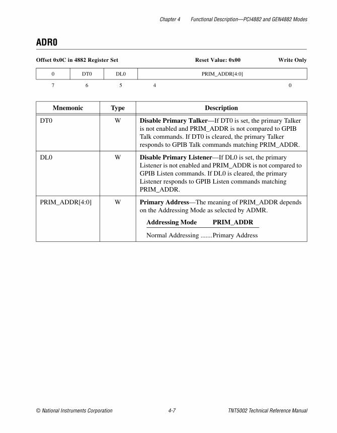
Chapter 4 Functional Description—PCI4882 and GEN4882 Modes
© National Instruments Corporation 4-7 TNT5002 Technical Reference Manual
ADR0
Offset 0x0C in 4882 Register Set Reset Value: 0x00 Write Only
0 DT0 DL0 PRIM_ADDR[4:0]
7 6 5 4 0
Mnemonic Type Description
DT0 W Disable Primary Talker—If DT0 is set, the primary Talker is not enabled and PRIM_ADDR is not compared to GPIB Talk commands. If DT0 is cleared, the primary Talker responds to GPIB Talk commands matching PRIM_ADDR.
DL0 W Disable Primary Listener—If DL0 is set, the primary Listener is not enabled and PRIM_ADDR is not compared to GPIB Listen commands. If DL0 is cleared, the primary Listener responds to GPIB Listen commands matching PRIM_ADDR.
PRIM_ADDR[4:0] W Primary Address—The meaning of PRIM_ADDR depends on the Addressing Mode as selected by ADMR.
Addressing Mode PRIM_ADDR
Normal Addressing .......Primary Address

Chapter 4 Functional Description—PCI4882 and GEN4882 Modes
TNT5002 Technical Reference Manual 4-8 ni.com
ADSR
Offset 0x08 in 4882 Register Set Reset Value: 0x00 Read Only
0 ATNN SPMS LPAS TPAS LA TA MINOR
7 6 5 4 3 2 1 0
Mnemonic Type Description
SPMS R Serial Poll Mode State—SPMS indicates whether the Talker state machine is in SPMS. When SPMS is set and TA is set, the Talker can send a serial poll response byte.
SPMS is set by:SPE & ACDS
SPMS is cleared by:(SPD & ACDS) + pon + IFC
LA R Listen Addressed—When LA is set, the Listener state machine is in LACS or LADS.
TA R Talk Addressed—When TA is set, the Talker state machine is in TADS, TACS, or SPAS.

Chapter 4 Functional Description—PCI4882 and GEN4882 Modes
© National Instruments Corporation 4-9 TNT5002 Technical Reference Manual
IMR2
Offset 0x04 in 4882 Register Set Reset Value: 0x00 Write Only
ISR2
Offset 0x04 in 4882 Register Set Reset Value: 0x00 Read Only
0 0 0 0 0 LOKC IE REMC IE ADSC IE
7 6 5 4 3 2 1 0
INT R LOK REM R LOKC REMC ADSC
7 6 5 4 3 2 1 0
Mnemonic Type Description
ADSCADSC IE
RW
Address Status Change—ADSC indicates that the addressing state has changed. ADSC sets after:
• Being addressed or unaddressed to talk
• Being addressed or unaddressed to listen
ADSC is set by:~(lon + ton) & (any change in ADSR[TA, LA, or MINOR])
ADSC is cleared by:pon + (read ISR2) & ~AUXRI[SISB]+ AUXMR[CLR_ADSC] + ADMR[LON] + ADMR[TON]

Chapter 4 Functional Description—PCI4882 and GEN4882 Modes
TNT5002 Technical Reference Manual 4-10 ni.com
AUXMR
Offset 0x0A in 4882 Register Set Reset Value: 0x00 Write Only
Operation
Setting the GPIB AddressA GPIB device may use single addressing or extended addressing. A single address is an integer between 0 and 30 inclusive. An extended address consists of a primary address between 0 and 30 and a secondary address between 0 and 30.
To configure the TNT5002 to use single addressing:
• Write 0x31 to the ADMR
• Write the address to ADR0
Determining the Addressing StateTo determine the GPIB addressing state of the TNT5002, read the ADSR. The following table decodes the value read from ADSR.
ISR2[ADSC] asserts when ADMR[TA,LA] changes. Interrupt on ISR2[ADSC] to be notified when the addressing state changes.
AUXMR_CMD
7 0
AUXMRCommand Value Description
CLR_ADSC 0x5B Clear ISR2[ADSC]—When AUXRI[SISB] is set, CLR_ADSC is used to clear ISR2[ADSC].
ADSR Bits
Addressing StateSPMS LA TA
0 0 1 Talker—Can send data bytes
0 1 0 Listener—Can receive data bytes
1 0 1 Serial Poll state—Can send a serial poll response

Chapter 4 Functional Description—PCI4882 and GEN4882 Modes
© National Instruments Corporation 4-11 TNT5002 Technical Reference Manual
GPIB Transfer Manager
OverviewThe GPIB Transfer Manager transfers data between the GFIFO and the GPIB. The transfer manager is used to send command and data bytes to devices or receive data bytes from devices.
Programming the transfer manager is very similar between sending commands and transferring data. This chapter divides a GPIB transfer into three phases: Initialization, Data transfer, and Termination
The next several sections describe the register bits used by each phase separately.
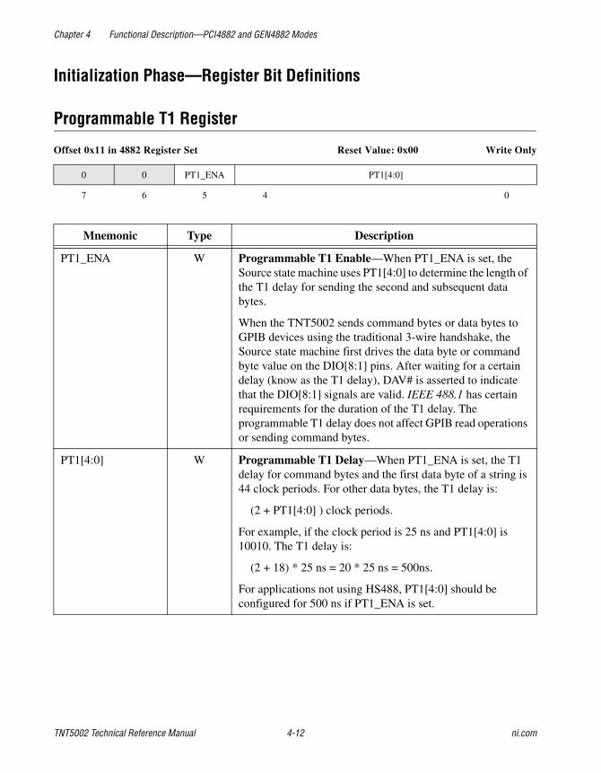
Chapter 4 Functional Description—PCI4882 and GEN4882 Modes
TNT5002 Technical Reference Manual 4-12 ni.com
Initialization Phase—Register Bit Definitions
Programmable T1 Register
Offset 0x11 in 4882 Register Set Reset Value: 0x00 Write Only
0 0 PT1_ENA PT1[4:0]
7 6 5 4 0
Mnemonic Type Description
PT1_ENA W Programmable T1 Enable—When PT1_ENA is set, the Source state machine uses PT1[4:0] to determine the length of the T1 delay for sending the second and subsequent data bytes.
When the TNT5002 sends command bytes or data bytes to GPIB devices using the traditional 3-wire handshake, the Source state machine first drives the data byte or command byte value on the DIO[8:1] pins. After waiting for a certain delay (know as the T1 delay), DAV# is asserted to indicate that the DIO[8:1] signals are valid. IEEE 488.1 has certain requirements for the duration of the T1 delay. The programmable T1 delay does not affect GPIB read operations or sending command bytes.
PT1[4:0] W Programmable T1 Delay—When PT1_ENA is set, the T1 delay for command bytes and the first data byte of a string is 44 clock periods. For other data bytes, the T1 delay is:
(2 + PT1[4:0] ) clock periods.
For example, if the clock period is 25 ns and PT1[4:0] is 10010. The T1 delay is:
(2 + 18) * 25 ns = 20 * 25 ns = 500ns.
For applications not using HS488, PT1[4:0] should be configured for 500 ns if PT1_ENA is set.

Chapter 4 Functional Description—PCI4882 and GEN4882 Modes
© National Instruments Corporation 4-13 TNT5002 Technical Reference Manual
IMR0
Offset 0x1D in 4882 Register Set Reset Value: 0x80 Write Only
ISR0
Offset 0x1D in 4882 Register Set Reset Value: 0x00 Read Only
GLINT STBO IE NLEN BTO IFCI IE ATNI IE TO IE SYNC IE
7 6 5 4 3 0
NBA STBO NL EOS IFCI ATNI TO SYNC
7 6 5 4 0
Mnemonic Type Description
NLENNL
WR
Newline Enable—When NLENis set, the TNT5002 treats the 7-bit ASCII newline character (0xA) as an EOS character. When the TNT5002 accepts a newline data byte, the TNT5002 behaves as if the EOI# signal was also asserted. Normally, the EOS character is written to EOSR. NLEN allows the TNT5002 to recognize two different EOS characters: newline and the character in EOSR.
Newline Received—NL indicates whether the last data byte received by the TNT5002 was a newline character. NL sets and clears regardless of the value of NLEN.

Chapter 4 Functional Description—PCI4882 and GEN4882 Modes
TNT5002 Technical Reference Manual 4-14 ni.com
IMR1
Offset 0x02 in 4882 Register Set Reset Value: 0x00 Write Only
ISR1
Offset 0x02 in 4882 Register Set Reset Value: 0x00 Read Only
CPT IE APT IE DET IE END IE DEC IE ERR IE DO IE DI IE
7 6 5 4 3 2 1 0
CPT APT DET END RX DEC ERR DO DI
7 6 5 4 3 2 1 0
Mnemonic Type Description
DODO IE
RW
Data Out Interrupt—DO sets whenever the Talker state machine is in TACS and the TNT5002 has no data to send. DO can be used instead of ISR2[ADSC] to determine when to begin a routine that sends data bytes.
DO is set by:TACS & SGNS & ~nba
DO is cleared by:pon + ((read ISR1) & ~AUXRI[SISB]) + ~TACS + ~SGNS + nba
DO Interrupt Enable—DO IE enables an interrupt when the DO condition is true.

Chapter 4 Functional Description—PCI4882 and GEN4882 Modes
© National Instruments Corporation 4-15 TNT5002 Technical Reference Manual
IMR1
Offset 0x02 in 4882 Register Set Reset Value: 0x00 Write Only
ISR1
Offset 0x02 in 4882 Register Set Reset Value: 0x00 Read Only
CPT IE APT IE DET IE END IE DEC IE ERR IE DO IE DI IE
7 6 5 4 3 2 1 0
CPT APT DET END DEC ERR DO DI
7 6 5 4 3 2 1 0
Mnemonic Type Description
END END IE
RW
END Received—END sets after receiving a byte from the GPIB satisfying the END condition. A byte satisfies the END condition if the Talker asserts EOI# when it sends the byte or AUXRA[REOS] is set and the byte matches the contents of the EOSR.
END is set by:LADS & (EOI + (EOS & AUXRA[REOS]) + (NL & IMR0[NLEN]))
END is cleared by:pon + (read ISR1) & ~AUXRI[SISB]+ AUXMR[CLR_END]
ERRERR IE
RW
Error—ERR sets when the Source tries to send a data or command byte but detects no Listeners on the GPIB. ERR is cleared by writing to AUXMR[CLR_ERR].
ERR is set by: SDYS & T1 & ~SHAS & RFD & EXTDAC
ERR is cleared by: pon + ((read ISR1) & ~AUXRI[SISB]) + AUXMR[CLR_ERR]

Chapter 4 Functional Description—PCI4882 and GEN4882 Modes
TNT5002 Technical Reference Manual 4-16 ni.com
EOSR
Offset 0x0E in 4882 Register Set Reset Value: 0x00 Write Only
EOSR[7:0]
7 0
Mnemonic Type Description
EOSR[7:0] W End Of String Character—The EOSR stores the byte used to detect the END condition. The EOSR is compared to each data byte received when AUXRA[REOS] is set. If EOS matches the data byte received, the END condition is true. AUXRA[BIN] determines whether 7 or 8 bits are compared.
When AUXRA[XEOS] is set, each data byte sent is compared to the EOSR. If the data byte being sent matches EOS, EOI# is asserted with that data byte.
If a listener is configured to detect an EOS character sent by a Talker during an HS488 transfer, the Talker must write that byte to the EOSR and set HIER[PMT_W_EOS].

Chapter 4 Functional Description—PCI4882 and GEN4882 Modes
© National Instruments Corporation 4-17 TNT5002 Technical Reference Manual
AUXRA
Offset 0x0A in 4882 Register Set Reset Value: 0x00 Write Only
1 0 0 BIN XEOS REOS HOLDOFFMODE[1:0]
7 6 5 4 3 2 1 0
Mnemonic Type Description
BIN W Binary EOS—BIN selects whether the EOSR represents an 8-bit binary number or a 7-bit ASCII character. When BIN is set, the EOSR is treated as an 8-bit value. All 8 bits of a data byte must match EOSR to generate the END condition. When BIN is cleared, the EOSR is treated as a 7-bit value. Only the lower 7 bits of a data byte must match the EOSR to generate the END condition.
REOS W Enable EOS when Receiving—When REOS is set, each byte received is compared to the EOSR to detect the END condition. When REOS is cleared, data bytes received are not compared to the EOSR to detectthe END condition.
HOLDOFFMODE[1:0] W Acceptor Holdoff Mode—When receiving data bytes, HOLDOFFMODE affects how the local rdy message is generated.
HOLDOFFMODE[1:0] Holdoff Mode
00........................Normal mode01........................RFD Holdoff on All Data mode10........................RFD Holdoff on END11........................Continuous

Chapter 4 Functional Description—PCI4882 and GEN4882 Modes
TNT5002 Technical Reference Manual 4-18 ni.com
CFG
Offset 0x10 in 4882 Register Set Reset Value: 0x00 Write Only
0 TLCHLTE IN A/BN CCEN 0 0 16/8N
7 6 5 4 3 2 1 0
Mnemonic Type Description
IN W Direction—In indicates the direction of the GPIB transfer. For sending commands or data, IN should be cleared. IN should be set for receiving data. Command bytes may be received regardless of the state of IN.
CCEN W Send EOI# With Last Byte—When CCEN is set and the GPIB transfer manager is sending GPIB data, EOI# is asserted with the last byte of the transfer. This bit should always be set unless it breaks apart a string into multiple transfers.
16/8N W 16-bit Wide FIFO—When 16/8N is set,the GFIFO is 16-bits wide and may be accessed using byte or word accesses. When 16/8N is cleared, only the low-order byte of each position in the GFIFO is used 16/8N should always be set unless the host is not capable of supporting 16 bit transfers to the TNT5002.

Chapter 4 Functional Description—PCI4882 and GEN4882 Modes
© National Instruments Corporation 4-19 TNT5002 Technical Reference Manual
CNT0
Offset 0x14 in 4882 Register Set Reset Value: 0xFF Read/Write
CNT1
Offset 0x16 in 4882 Register Set Reset Value: 0xFF Read/Write
CNT2
Offset 0x09 in 4882 Register Set Reset Value: 0xFF Read/Write
CNT3
Offset 0x0B in 4882 Register Set Reset Value: 0xFF Read/Write
CNT[7:0]
7 0
CNT[15:8]
7 0
CNT[23:16]
7 0
CNT[31:24]
7 0

Chapter 4 Functional Description—PCI4882 and GEN4882 Modes
TNT5002 Technical Reference Manual 4-20 ni.com
AUXMR
Offset 0x0A in 4882 Register Set Reset Value: 0x00 Write Only
Mnemonic Type Description
CNT[31:0] R/W Transfer Count—CNT[31:0] specifies the number of bytes in transfer. The two’s complements of the desired byte count should be written to the CNT registers. The registers must be written in the following order: CNT0, CNT1. CNT2, CNT3.
The CNT registers can be used in 16-bit or 32-bit mode. In 16-bit mode, CNT[31:16] are not used. The byte count is specified by writing the 16-bit two’s complement of the desired byte count to CNT[15:0]. In 16-bit mode, never write to CNT[31:16].
Whenever CNT3 or CNT2 are written to, the TNT5002 changes to 32-bit mode. In this mode, the byte count is specified by writing the 32-bit two’s complement of the desired byte count to CNT[31:0].
CNT is incremented every time a byte is transferred between the FIFOs and the GPIB.
CNT can be read at any time to determine the two’s complement of the remaining bytes to transfer; however, CNT should only be read while the GPIB Transfer Manager is stopped or during a holdoff. This ensures that the CNT will not change while being read.
AUXMR_CMD
7 0
AUXMRCommand Value Description
RHDF 0x03 Release Holdoff—RHDF clears the RFD holdoff state. The Acceptor enters the RFD holdoff state following the HLDI command or as configured to do so by AUXRA[HOLDOFFMODE].
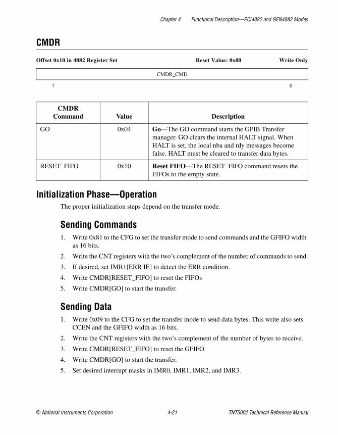
Chapter 4 Functional Description—PCI4882 and GEN4882 Modes
© National Instruments Corporation 4-21 TNT5002 Technical Reference Manual
CMDR
Offset 0x10 in 4882 Register Set Reset Value: 0x00 Write Only
Initialization Phase—OperationThe proper initialization steps depend on the transfer mode.
Sending Commands1. Write 0x81 to the CFG to set the transfer mode to send commands and the GFIFO width
as 16 bits.
2. Write the CNT registers with the two’s complement of the number of commands to send.
3. If desired, set IMR1[ERR IE] to detect the ERR condition.
4. Write CMDR[RESET_FIFO] to reset the FIFOs
5. Write CMDR[GO] to start the transfer.
Sending Data1. Write 0x09 to the CFG to set the transfer mode to send data bytes. This write also sets
CCEN and the GFIFO width as 16 bits.
2. Write the CNT registers with the two’s complement of the number of bytes to receive.
3. Write CMDR[RESET_FIFO] to reset the GFIFO
4. Write CMDR[GO] to start the transfer.
5. Set desired interrupt masks in IMR0, IMR1, IMR2, and IMR3.
CMDR_CMD
7 0
CMDRCommand Value Description
GO 0x04 Go—The GO command starts the GPIB Transfer manager. GO clears the internal HALT signal. When HALT is set, the local nba and rdy messages become false. HALT must be cleared to transfer data bytes.
RESET_FIFO 0x10 Reset FIFO—The RESET_FIFO command resets the FIFOs to the empty state.

Chapter 4 Functional Description—PCI4882 and GEN4882 Modes
TNT5002 Technical Reference Manual 4-22 ni.com
Receiving Data1. Write 0x21 to the CFG to set the transfer mode to receive data bytes and set the GFIFO
width to 16 bits.
2. Write the CNT registers with the two’s complement of the number of bytes to send.
3. If used, write the EOS character to the EOSR.
4. Write 10 to AUXRA[HOLDOFFMODE]. At the same time, set or clear AUXRA[REOS] and AUXRA[BIN] as needed.
5. Write AUXMR[RHDF] to clear RFD holdoffs.
6. Write CMDR[RESET_FIFO] to reset the FIFOs
7. Write CMDR[GO] to start the transfer.
8. Set desired interrupt masks in IMR0, IMR1, IMR2, and IMR3.
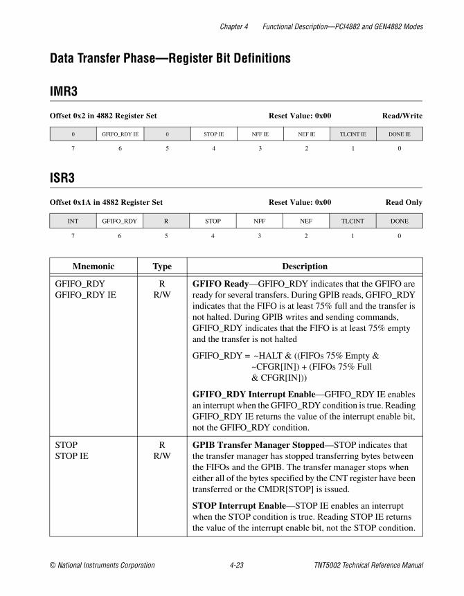
Chapter 4 Functional Description—PCI4882 and GEN4882 Modes
© National Instruments Corporation 4-23 TNT5002 Technical Reference Manual
Data Transfer Phase—Register Bit Definitions
IMR3
Offset 0x2 in 4882 Register Set Reset Value: 0x00 Read/Write
ISR3
Offset 0x1A in 4882 Register Set Reset Value: 0x00 Read Only
0 GFIFO_RDY IE 0 STOP IE NFF IE NEF IE TLCINT IE DONE IE
7 6 5 4 3 2 1 0
INT GFIFO_RDY R STOP NFF NEF TLCINT DONE
7 6 5 4 3 2 1 0
Mnemonic Type Description
GFIFO_RDYGFIFO_RDY IE
RR/W
GFIFO Ready—GFIFO_RDY indicates that the GFIFO are ready for several transfers. During GPIB reads, GFIFO_RDY indicates that the FIFO is at least 75% full and the transfer is not halted. During GPIB writes and sending commands, GFIFO_RDY indicates that the FIFO is at least 75% empty and the transfer is not halted
GFIFO_RDY = ~HALT & ((FIFOs 75% Empty &~CFGR[IN]) + (FIFOs 75% Full & CFGR[IN]))
GFIFO_RDY Interrupt Enable—GFIFO_RDY IE enables an interrupt when the GFIFO_RDY condition is true. Reading GFIFO_RDY IE returns the value of the interrupt enable bit, not the GFIFO_RDY condition.
STOPSTOP IE
RR/W
GPIB Transfer Manager Stopped—STOP indicates that the transfer manager has stopped transferring bytes between the FIFOs and the GPIB. The transfer manager stops when either all of the bytes specified by the CNT register have been transferred or the CMDR[STOP] is issued.
STOP Interrupt Enable—STOP IE enables an interrupt when the STOP condition is true. Reading STOP IE returns the value of the interrupt enable bit, not the STOP condition.

Chapter 4 Functional Description—PCI4882 and GEN4882 Modes
TNT5002 Technical Reference Manual 4-24 ni.com
AUXMR
Offset 0x0A in 4882 Register Set Reset Value: 0x00 Write Only
NFFNFF IE
RR/W
Not Full FIFO—NFF indicates that the GFIFO is not full. Assuming the GFIFO has been configured as 16-bits wide, NFF sets when at least one dword may be written to the GFIFO. NFF clears when there is not room for at least one dword in the GFIFO.
NFF Interrupt Enable—NFF IE enables an interrupt when the NFF condition is true. Reading NFF IE returns the value of the interrupt enable bit, not the NFF condition.
NEFNEF IE
RR/W
Not Empty FIFO—NEF indicates that the GFIFO is not empty. Assuming the GFIFO has been configured as 16-bits wide, NEF sets when at least one dword may be read from the GFIFO; or, when one byte may be read from the GFIFO and STS1[HALT] is set and STS1[DONE] is not set. NEF clears when there is less than one dword in the GFIFO while STS1[HALT] is not set or when STS1[DONE] is set.
NEF Interrupt Enable—NEF IE enables an interrupt when the NEF condition is true. Reading NEF IE returns the value of the interrupt enable bit, not the NEF condition.
AUXMR_CMD
7 0
AUXMRCommand Value Description
HLDI 0x51 Holdoff Immediately—HLDI prevents the Acceptor state machine from transitioning from ANRS to ACRS. NRFD# remains asserted in ANRS causing an RFD holdoff.
Mnemonic Type Description
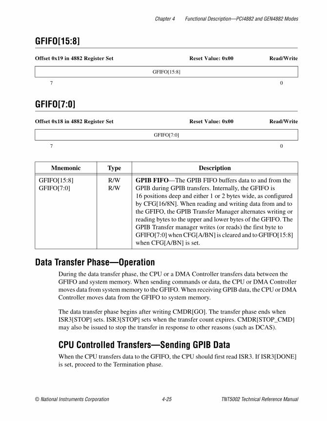
Chapter 4 Functional Description—PCI4882 and GEN4882 Modes
© National Instruments Corporation 4-25 TNT5002 Technical Reference Manual
GFIFO[15:8]
Offset 0x19 in 4882 Register Set Reset Value: 0x00 Read/Write
GFIFO[7:0]
Offset 0x18 in 4882 Register Set Reset Value: 0x00 Read/Write
Data Transfer Phase—OperationDuring the data transfer phase, the CPU or a DMA Controller transfers data between the GFIFO and system memory. When sending commands or data, the CPU or DMA Controller moves data from system memory to the GFIFO. When receiving GPIB data, the CPU or DMA Controller moves data from the GFIFO to system memory.
The data transfer phase begins after writing CMDR[GO]. The transfer phase ends when ISR3[STOP] sets. ISR3[STOP] sets when the transfer count expires. CMDR[STOP_CMD] may also be issued to stop the transfer in response to other reasons (such as DCAS).
CPU Controlled Transfers—Sending GPIB DataWhen the CPU transfers data to the GFIFO, the CPU should first read ISR3. If ISR3[DONE] is set, proceed to the Termination phase.
GFIFO[15:8]
7 0
GFIFO[7:0]
7 0
Mnemonic Type Description
GFIFO[15:8]GFIFO[7:0]
R/WR/W
GPIB FIFO—The GPIB FIFO buffers data to and from the GPIB during GPIB transfers. Internally, the GFIFO is 16 positions deep and either 1 or 2 bytes wide, as configured by CFG[16/8N]. When reading and writing data from and to the GFIFO, the GPIB Transfer Manager alternates writing or reading bytes to the upper and lower bytes of the GFIFO. The GPIB Transfer manager writes (or reads) the first byte to GFIFO[7:0] when CFG[A/BN] is cleared and to GFIFO[15:8] when CFG[A/BN] is set.

Chapter 4 Functional Description—PCI4882 and GEN4882 Modes
TNT5002 Technical Reference Manual 4-26 ni.com
If ISR3[NEF] is cleared, the GFIFO is empty. The CPU can write up to 16 words to the GFIFO.
If ISR3[GFIFO_RDY] is set, the CPU can write up to 12 words to the GFIFO.
If ISR3[NFF] is set, the CPU can write one word into the GFIFO.
The CPU can poll on ISR3 bits or interrupt on them.
Odd Byte TransfersIf the transfer count is odd, the CPU can pad the last byte and write a full word to the FIFOs. Once the transfer count expires, the TNT5002 does not send more bytes. Extra bytes in the FIFOs are ignored.
CPU Controlled Transfers—Receiving GPIB DataWhen the CPU transfers data from the GFIFO, the CPU should first read ISR3.
If ISR3[NFF] is clear, the GFIFO is full. The CPU can read up to 16 words from the GFIFO.
If ISR3[GFIFO_RDY] is set, the CPU can read up to 12 words from the GFIFO.
If ISR3[NEF] is set, the CPU can read 1 word from the FIFOs.
If ISR3[NEF] is clear, the GFIFO is empty. The CPU should examine the value of ISR3[STOP] that was read at the same time as ISR3[NEF]. If ISR3[STOP] is set, the transfer has finished. The CPU can proceed to the Termination phase of the transfer. If ISR3[STOP] is cleared, the transfer is not finished, the CPU can continue polling the FIFO status bits.
The CPU can poll on ISR3 bits or interrupt on them.
ISR3[NEF] normally only sets when the GFIFO has at least one word. When the number of bytes in the transfer is odd, there is not a full word to transfer from the FIFOs at the end of the transfer. So, when ISR3[STOP] is set, ISR3[NEF] sets when the FIFO has exactly one byte (the last byte of the transfer).
If the transfer is terminated with EOS or EOI, the transfer must be stopped by writing CMDR[STOP]. Any remaining bytes in the GFIFO must be manually read.
DMA Controlled Transfers—Sending GPIB DataWhen using the DMA Controller, the DMA transfer should be continued until ISR3[DONE] is set. When ISR3[DONE] sets, proceed to the termination phase.

Chapter 4 Functional Description—PCI4882 and GEN4882 Modes
© National Instruments Corporation 4-27 TNT5002 Technical Reference Manual
DMA Controlled Transfers—Receiving GPIB DataWhen using the DMA Controller to receive data, the DMA transfer should be continued until ISR3[STOP] is set. When ISR3[STOP] sets, the TNT5002 keeps asserting the DRQ signal until the GFIFO is empty. To ensure that all data is read from the GFIFO, after ISR3[STOP] sets, either wait for ISR3[NEF] to clear indicating that the GFIFO is empty or halt the DMA Controller and manually read the remaining bytes out of the GFIFO.
Termination Phase—Register Bit Definitions
CMDR
Offset 0x1C in 4882 Register Set Reset Value: 0x00 Write Only
AUXMR
Offset 0x0A in 4882 Register Set Reset Value: 0x00 Write Only
CMDR_CMD
7 0
CMDRCommand Value Description
STOP 0x08 Stop—The STOP command stops the GPIB Transfer manager. STOP sets the internal HALT signal. When HALT is set, the local nba and rdy messages become false. HALT must be cleared to transfer data bytes.
AUXMR_CMD
7 0
AUXMRCommand Value Description
CLR_END 0x55 Clear ISR1[END]—When AUXRI[SISB] is set, CLR_END is used to clear ISR1[END].
CLR_ERR 0x57 Clear ISR1[ERR]—When AUXRI[SISB] is set, CLR_ERR is used to clear ISR1[ERR].

Chapter 4 Functional Description—PCI4882 and GEN4882 Modes
TNT5002 Technical Reference Manual 4-28 ni.com
HSSEL
Offset 0x0D in 4882 Register Set Reset Value: 0x00 Write Only
IMR3
Offset 0x12 in 4882 Register Set Reset Value: 0x00 Read/Write
ISR3
Offset 0x1A in 4882 Register Set Reset Value: 0x00 Read Only
0 MIKEJ GOTOSIDS NODMA 0 0 0 0
7 6 5 4 3 2 1 0
Mnemonic Type Description
GOTOSIDS W Go To SIDS—Setting GOTOSIDS forces the Source Handshake interface function to enter its idle state. This bit can be used in a routine that aborts GPIB write transfers (data bytes or command bytes).
0 GFIFO_RDY IE 0 STOP IE NFF IE NEF IE TLCINT IE DONE IE
7 6 5 4 3 2 1 0
INT GFIFO_RDY R STOP NFF NEF TLCINT DONE
7 6 5 4 3 2 1 0
Mnemonic Type Description
DONEDONE IE
RR/W
DONE—At the end of a transfer, DONE indicates that all devices on the GPIB have finished the transfer. DONE only sets after STOP sets.
DONE = STS1[GSYNC] & (~CFG[IN] + (FIFOS EMPTY & CFG[IN]))
Done Interrupt Enable—DONE IE enables an interrupt when the DONE condition is true. Reading DONE IE returns the value of the interrupt enable bit, not the DONE condition.

Chapter 4 Functional Description—PCI4882 and GEN4882 Modes
© National Instruments Corporation 4-29 TNT5002 Technical Reference Manual
Termination Phase—OperationThe termination phase begins when ISR3[STOP] sets following a read or when IRS3[DONE] sets following a write. For GPIB reads, ensure that the FIFOs are empty before entering the Termination Phase.
1. Halt the DMA Controller, if it is being used.
2. If the TNT5002 is the GPIB Controller (active or standby), wait for ISR3[DONE] to set. ISR3[DONE] indicates that all devices on the GPIB have completed the transfer. If the TNT5002 is not the GPIB Controller, there is no need to wait for ISR3[DONE].
3. Read the CNT registers. The two’s complement of the CNT registers indicate how many bytes did not get transferred. For example, if the original byte count was 100 and the CNT registers read 20 (after converting the two’s complement) at the end of the transfer, then 100 – 20 = 80 bytes actually were transferred, 20 bytes were not.
4. Handle any interrupting condition that caused CMDR[STOP] to be issued. This may include clearing ISR1[END] or ISR1[ERR] if those interrupts occur.
Using 8-bit FIFOsThe description of the GPIB Transfer Manager assumes that the FIFO is configured as 16 bits wide (CFG[16/8N] is set). If the GFIFO is configured as 8 bits wide (CFG[16/8N] is cleared), the behavior of a few bits change.
In 8-bit FIFO mode, the GFIFO is 8 bits wide and 16 bytes deep. ISR3[NEF], ISR3[NFF], and ISR3[GFIFO_RDY] refer to the state of the GFIFO assuming it is only 16 bytes deep. For example, when reading from the GPIB (with CFG[16/8N] is cleared), ISR3[NEF] indicates that one byte (not one word) is available to be read from the FIFO.

Chapter 4 Functional Description—PCI4882 and GEN4882 Modes
TNT5002 Technical Reference Manual 4-30 ni.com
Device Clear Block
OverviewThe Device Clear Block determines whether the GPIB Controller is issuing a device clear command to the device. This block implements the IEEE 488.1 DC interface function. Refer to IEEE 488.1 and IEEE 488.2 for more information.
Register Bit Definitions
IMR1
Offset 0x02 in 4882 Register Set Reset Value: 0x00 Write Only
ISR1
Offset 0x02 in 4882 Register Set Reset Value: 0x00 Read Only
CPT IE APT IE DET IE END IE DEC IE ERR IE DO IE DI IE
7 6 5 4 3 2 1 0
CPT APT DET END RR DEC ERR DO DI
7 6 5 4 3 2 1 0
Mnemonic Type Description
DECDEC IE
RW
Device Clear State—DEC sets when the GPIB Controller sends a Device Clear command to the device (either SDC when the device is listen addressed or DCL). DEC is cleared writing AUXMR[CLR_DEC].
DEC is set by:DCL + (SDC & LADS)
DEC is cleared by:pon + AUXMR[CLR_DEC].
DEC Interrupt Enable—DEC IE enables an interrupt when the DEC condition.

Chapter 4 Functional Description—PCI4882 and GEN4882 Modes
© National Instruments Corporation 4-31 TNT5002 Technical Reference Manual
AUXRE
Offset 0x0A in 4882 Register Set Reset Value: 0xC0 Write Only
AUXMR
Offset 0x0A in 4882 Register Set Reset Value: 0x00 Write Only
OperationAs IEEE 488.1 requires, the Device Clear state machine enters the Device Clear Active State (DCAS) after receiving the Device Clear (DCL) command or after receiving the Selected Device Clear (SDC) command while addressed to listen.
ISR1[DCAS] sets after entering DCAS. A hardware interrupt occurs if IMR1[DCAS IE] is set. If IMR1[DCAS IE] is set, a DAC holdoff occurs whenever ISR1[DCAS] sets.
If AUXRE[DHDC] is set, a DAC holdoff occurs when DCL or SDC is received, regardless of the addressing state.
1 1 0 0 DHADT DHADC DHDT DHDC
7 6 5 4 3 2 1 0
Mnemonic Type Description
DHDC W DAC Holdoff on Device Clear—DHDC causes a DAC holdoff when the Device Clear command is received (either SDC when the device is listen addressed or DCL).
AUXMR_CMD
7 0
AUXMRCommand Value Description
VALID 0x0F Release DAC Holdoff (Valid)—Clears the DAC holdoff condition. If ISR1[APT] is set, this command causes the command to be interpreted as MSA.
CLR_DEC 0x56 Clear ISR1[DEC]—When AUXRI[SISB] is set, CLR_DEC is used to clear ISR1[DEC].

Chapter 4 Functional Description—PCI4882 and GEN4882 Modes
TNT5002 Technical Reference Manual 4-32 ni.com
IEEE 488.2 lists the required behavior of device software in response to a device clear.
Disabling Device ClearAlmost all non-controllers should monitor Device Clear. Applications that do not use Device Clear can simply ignore the status bits in this block and never set the interrupt enable bits or AUXRE[DHDC]. The Device Clear state machine cannot be explicitly disabled. However, this block does not affect any GPIB signals when AUXRE[DHDC] is cleared.
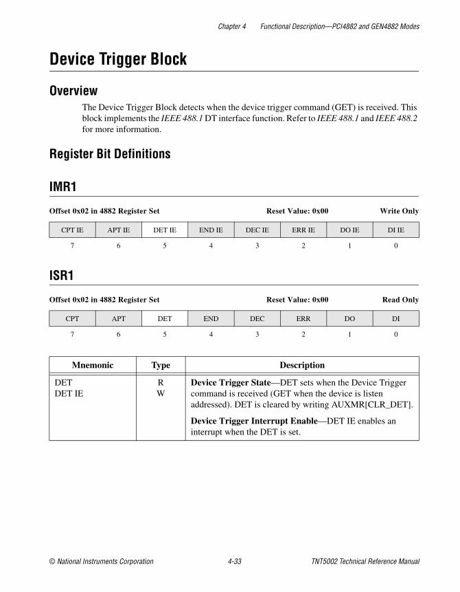
Chapter 4 Functional Description—PCI4882 and GEN4882 Modes
© National Instruments Corporation 4-33 TNT5002 Technical Reference Manual
Device Trigger Block
OverviewThe Device Trigger Block detects when the device trigger command (GET) is received. This block implements the IEEE 488.1 DT interface function. Refer to IEEE 488.1 and IEEE 488.2 for more information.
Register Bit Definitions
IMR1
Offset 0x02 in 4882 Register Set Reset Value: 0x00 Write Only
ISR1
Offset 0x02 in 4882 Register Set Reset Value: 0x00 Read Only
CPT IE APT IE DET IE END IE DEC IE ERR IE DO IE DI IE
7 6 5 4 3 2 1 0
CPT APT DET END DEC ERR DO DI
7 6 5 4 3 2 1 0
Mnemonic Type Description
DETDET IE
RW
Device Trigger State—DET sets when the Device Trigger command is received (GET when the device is listen addressed). DET is cleared by writing AUXMR[CLR_DET].
Device Trigger Interrupt Enable—DET IE enables an interrupt when the DET is set.

Chapter 4 Functional Description—PCI4882 and GEN4882 Modes
TNT5002 Technical Reference Manual 4-34 ni.com
AUXRE
Offset 0x0A in 4882 Register Set Reset Value: 0xC0 Write Only
AUXMR
Offset 0x0A in 4882 Register Set Reset Value: 0x00 Write Only
1 1 0 0 DHADT DHADC DHDT DHDC
7 6 5 4 3 2 1 0
Mnemonic Type Description
DHDT W DAC Holdoff on Device Trigger—DHDT causes a DAC holdoff when the DT state machine enters DTAS.
AUXMR_CMD
7 0
AUXMRCommand Value Description
TRIG 0x04 Trigger—This command forces the TRIG pin to assert for 3 clock cycles. This command has no affect on ISR1[DET] or the DT interface function.
VALID 0x0F Release DAC Holdoff (Valid)—This command clears the DAC holdoff condition. If ISR1[APT] is set, this command causes the GPIB command to be interpreted as MSA.
CLR_DET 0x54 Clear ISR1[DET]—When AUXRI[SISB] is set, CLR_DET is used to clear ISR1[DET].

Chapter 4 Functional Description—PCI4882 and GEN4882 Modes
© National Instruments Corporation 4-35 TNT5002 Technical Reference Manual
OperationThe Device Trigger state machine enters the Device Trigger Active State (DTAS) after receiving the Group Execute Trigger (GET) command while addressed to listen.
ISR1[GET] sets after entering DTAS. ISR1[GET] can cause an interrupt if IMR1[GET IE] is set.
If AUXRE[DHDT] is set, a DAC holdoff occurs after receiving the GET while addressed to listen.
Disabling the TriggerApplications that do not use Device Trigger can simply ignore the status bits in this block and never set the interrupt enable bits or AUXRE bits. The Device Trigger block cannot be explicitly disabled. However, this block does not affect any GPIB signals when AUXRE[DHDT] and AUXRE[DHADT] are clear.

Chapter 4 Functional Description—PCI4882 and GEN4882 Modes
TNT5002 Technical Reference Manual 4-36 ni.com
Serial Poll Response Manager
OverviewThe Serial Poll Response Block responds to the serial polls from the GPIB Controller and generates the GPIB SRQ# (service request) signal. This block implements the IEEE 488.1 SR1 interface function and the IEEE 488.2 set rsv interface function.
IEEE 488.2 thoroughly describes issues concerning Serial Poll responses.
Register Bit Definitions
IMR0
Offset 0x1D in 4882 Register Set Reset Value: 0x80 Write Only
ISR0
Offset 0x1D in 4882 Register Set Reset Value: 0x00 Read Only
GLINT STBO IE NLEN BTO IFCI IE ATNI IE TO IE SYNC IE
7 6 5 4 3 2 1 0
NBA STBO NL EOS IFCI ATNI TO SYNC
7 6 5 4 3 2 1 0
Mnemonic Type Description
STBO IE W Status Byte Out Interrupt Enable—Setting STBO IE enables Serial Poll Mode SP2. Setting STBO IE also generates an interrupt when a GPIB Controller serial polls the device.
STBO R Status Byte Out—STBO sets when the Talker enters SPAS (Serial Poll Active State) during a serial poll. STBO clears after writing to the SPMR or when SPAS becomes false.

Chapter 4 Functional Description—PCI4882 and GEN4882 Modes
© National Instruments Corporation 4-37 TNT5002 Technical Reference Manual
AUXMR
Offset 0x0A in 4882 Register Set Reset Value: 0x00 Write Only
AUXRB
Offset 0x0A in 4882 Register Set Reset Value: 0xA0 Write Only
AUXMR_CMD
7 0
AUXMRCommand Value Description
REQT/REQF 0x18/0x19 Request True/Request False—REQT indirectly causes the SRQ# to assert. REQF causes the SRQ# to unassert. These commands are inputs to the IEEE 488.2 Service Request Synchronization circuitry.
1 0 1 ISS 0 TRI SPEOI CPT_ENABLE
7 6 5 4 3 2 1 0
Mnemonic Type Description
SPEOI W Send END During Serial Polls—When SPEOI is set, EOI# is asserted with all serial poll responses. Most devices should not set this bit.

Chapter 4 Functional Description—PCI4882 and GEN4882 Modes
TNT5002 Technical Reference Manual 4-38 ni.com
SPMR
Offset 0x06 in 4882 Register Set Reset Value: 0x00 Write Only
SPSR
Offset 0x06 in 4882 Register Set Reset Value: 0x00 Read Only
STB[8] RSV_RQS STB[6:1]
7 6 5 0
Mnemonic Type Description
STB[8,6:1] W Status Byte—These bits make up the serial poll response to send to the GPIB Controller during a serial poll.
RSV_RQS W Request Service—The meaning of this bit depends on the Serial Poll Mode.
• Mode SP1—Always clear this bit
• Mode SP2—This bit is the RQS bit returned in a serial poll response
• Mode SP3—Setting this bit causes SRQ to assert.
STB8 PEND STB[6:1]
7 6 5 0
Mnemonic Type Description
STB[8,6:1] R Status Byte—The value of the STB bits most recently written to SPMR.
PEND R Pending Service Request—PEND asserts after requesting service (using AUXMR[REQT] in modes SP1 or SP2, or RSV_RQS in mode SP2). PEND clears when the GPIB Controller serial polls the device. This bit can be used to confirm the GPIB Controller serial polled the device. However, in most applications monitoring this bit is not necessary. Refer to the Serial Poll Response Manager section for the definitions of SP1 and SP2.

Chapter 4 Functional Description—PCI4882 and GEN4882 Modes
© National Instruments Corporation 4-39 TNT5002 Technical Reference Manual
ADSR
Offset 0x08 in 4882 Register Set Reset Value: 0x00 Read Only
OperationThe Serial Poll Response block generates the SRQ# signal and generates responses when a GPIB Controller serially polls the device. The three modes of operation are shown in the table.
Choosing a Serial Poll ModeIn Serial Poll Mode SP1, the SPMR must be written whenever the value of the status byte changes. When a Controller serial polls the device, the Serial Poll Response Manager responds to the serial poll immediately with the current value of SPMR. Most devices use mode SP1. This mode allows the device to respond quickly to serial polls and decreases the number of interrupts generated.
In Serial Poll Mode SP2, the Serial Poll Response Manager generates an interrupt when the Controller serial polls the device. After the interrupt, the Serial Poll Response Manager waits for the SPMR to be written. The device then sends the status byte to the Controller. SP2 mode may be more efficient if the status byte of the device changes more frequently than the GPIB Controller serial polls the device.
R ATNN SPMS LPAS TPAS LA TA MINOR
7 6 5 4 3 2 1 0
Mnemonic Type Description
SPMS R Serial Poll Mode State—SPMS indicates whether Talker state machine is in SPMS. When SPMS is set and TA is set, the Talker can send a serial poll response byte.
Serial Poll Mode SRQ# Generation
Software Intervention Required to Respond
to Serial Polls
SP1 IEEE 488.2-style using reqt and reqf No
SP2 IEEE 488.2-style using reqt and reqf Yes
SP3 IEEE 488.1-style using rsv No

Chapter 4 Functional Description—PCI4882 and GEN4882 Modes
TNT5002 Technical Reference Manual 4-40 ni.com
Serial Poll Mode SP3 is similar to mode SP1 except that SP3 uses IEEE 488.1-style SRQ# generation. IEEE 488.2-style SRQ# generation is preferred, so the use of mode SP3 is discouraged.
Using Serial Poll Mode SP1To use this mode IMR0[STBO IE] must be cleared. To assert SRQ#, write AUXMR[REQT] and then write the current status byte to SPMR with RSV_RQS cleared.
This write to SPMR causes SRQ# to assert. SRQ# remains asserted until a Controller serial polls the device or the service request is stopped.
To stop requesting service, write AUXMR[REQF] and then write the current status byte to SPMR with RSV_RQS is cleared. The write to SPMR causes SRQ# to unassert.
To update the SPMR without affecting SRQ#, simply write the current status byte to SPMR with RSV_RQS cleared.
Using Serial Poll Mode SP2To use this mode IMR0[STBO IE] must be set. To assert SRQ#, write AUXMR[REQT]. This write causes SRQ to assert. SRQ# remains asserted until the GPIB Controller serial polls the device or AUXMR[REQF] is issued.
When the GPIB Controller serial polls the device, ISR0[STBO] sets. In response to this interrupt, write the current status byte to SPMR. For this write to SPMR, SPMR[RSV_RQS] should be set if the device is actively requesting service.
Using Serial Poll Mode SP3To use this mode IMR0[STBO IE] must be cleared. To assert SRQ#, write the current status byte to the SPMR with RSV_RQS set. This causes SRQ# to assert until the GPIB Controller serial polls the device or the RSV_RQS is cleared. To unassert SRQ#, the device writes the current status byte to the SPMR with RSV_RQS cleared.

Chapter 4 Functional Description—PCI4882 and GEN4882 Modes
© National Instruments Corporation 4-41 TNT5002 Technical Reference Manual
Status Byte ValueWhen a Controller serial polls the device, an 8-bit status byte is returned. The 8 bits of the status byte are generated as follows:
RQS indicates whether the device is actively requesting service. In modes SP1 and SP3, RQS is automatically generated. In mode SP2, the current value of SPMR[RSV_RQS] is used as RQS.
STB8 RQS STB[6:1]
7 6 5 0

Chapter 4 Functional Description—PCI4882 and GEN4882 Modes
TNT5002 Technical Reference Manual 4-42 ni.com
Parallel Poll Response Manager
OverviewThe Parallel Response Block responds to the parallel polls from the Controller. This block implements the IEEE 488.1 PP interface function.
Register Bit Definitions
AUXRB
Offset 0x0A in 4882 Register Set Reset Value: 0xA0 Write Only
AUXRI
Offset 0x0A in 4882 Register Set Reset Value: 0xE0 Write Only
1 0 1 ISS 0 TRI SPEOI CPT_ENABLE
7 6 5 4 3 2 1 0
Mnemonic Type Description
ISS W Individual Status Select—The value of the Parallel Poll Flag is used as the local ist message when AUXRB[ISS] is cleared. The value of SRQS is used as the local ist message when AUXRB[ISS] is set.
1 1 1 0 USTD PPMODE2 0 SISB
7 6 5 4 3 2 1 0
Mnemonic Type Description
PPMODE2 W Parallel Poll Mode 2—This bit, together with PPR[PPMODE1], determine how the device is configured for parallel polls.

Chapter 4 Functional Description—PCI4882 and GEN4882 Modes
© National Instruments Corporation 4-43 TNT5002 Technical Reference Manual
AUXMR
Offset 0x0A in 4882 Register Set Reset Value: 0x00 Write Only
PPR
Offset 0x0A in 4882 Register Set Reset Value: 0x70 Write Only
AUXMR_CMD
7 0
AUXMRCommand Value Description
IST/~IST 0x01/0x09 Set/Clear Parallel Poll Flag (ist)—IST and ~IST set and clear the Parallel Poll Flag (ist).
0 1 1 PPMODE1 SENSE LPPE[2:0]
7 6 5 4 3 0
Mnemonic Type Description
PPMODE1 W Parallel Poll Mode 1—This bit, together with AUXRI[PPMODE2], determine how the device is configured for parallel polls. Refer to the Parallel Poll Response Manager section for more information.

Chapter 4 Functional Description—PCI4882 and GEN4882 Modes
TNT5002 Technical Reference Manual 4-44 ni.com
OperationThe GPIB Controller initiates a parallel poll by sending the IDY message to the device. The device responds by sending one of eight messages (PPR1, PPR2, PPR3, …, PPR8) to the Controller. The PPRn message can be sent true or false.
The operation of the Parallel Poll Response Manager depends on the configuration mode: Disabled, Remote, or Local. Select one of these mode by writing to AUXRI[PPMODE2] and PPR[PPMODE1] according to the following table:
Disabled ModeMany devices do not support Parallel Polls. To disable parallel polls, set PPR[PPMODE1].
SENSE W Sense—The state of the DIO line selected by LPPE line during a parallel poll response is described in the following table:
SENSE ist DIO Line
0 .................. 0.............. asserted0 .................. 1..............unasserted1 .................. 0..............unasserted1 .................. 1.............. asserted
DIO lines are driven with open-collector drivers during parallel polls. DIO lines that are not asserted (driven low) are not actively driven high. This allows different devices to simultaneously drive different DIO signals.
LPPE[2:0] W Local Parallel Poll Configuration—In Local Parallel Poll Configuration, LPPE[2:0] configures how the Parallel Poll Response Manager responds to parallel polls. In Local Parallel Poll Configuration mode, the Parallel Poll Response Manager is configured as if it received a PPE command of 0x6n where n = LPPE[2:0].
PPR[PPMODE1] AUXRI[PPMODE2] Parallel Poll Mode
0 0 Remote Configuration
0 1 Local Configuration
1 X Disabled
Mnemonic Type Description
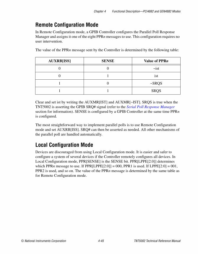
Chapter 4 Functional Description—PCI4882 and GEN4882 Modes
© National Instruments Corporation 4-45 TNT5002 Technical Reference Manual
Remote Configuration ModeIn Remote Configuration mode, a GPIB Controller configures the Parallel Poll Response Manager and assigns it one of the eight PPRn messages to use. This configuration requires no user intervention.
The value of the PPRn message sent by the Controller is determined by the following table:
Clear and set ist by writing the AUXMR[IST] and AUXMR[~IST]. SRQS is true when the TNT5002 is asserting the GPIB SRQ# signal (refer to the Serial Poll Response Manager section for information). SENSE is configured by a GPIB Controller at the same time PPRn is configured.
The most straightforward way to implement parallel polls is to use Remote Configuration mode and set AUXRB[ISS]. SRQ# can then be asserted as needed. All other mechanisms of the parallel poll are handled automatically.
Local Configuration Mode Devices are discouraged from using Local Configuration mode. It is easier and safer to configure a system of several devices if the Controller remotely configures all devices. In Local Configuration mode, PPR[SENSE] is the SENSE bit. PPR[LPPE[2:0]] determines which PPRn message to use. If PPR[LPPE[2:0]] = 000, PPR1 is used. If LPPE[2:0] = 001, PPR2 is used, and so on. The value of the PPRn message is determined by the same table as for Remote Configuration mode.
AUXRB[ISS] SENSE Value of PPRn
0 0 ~ist
0 1 ist
1 0 ~SRQS
1 1 SRQS

Chapter 4 Functional Description—PCI4882 and GEN4882 Modes
TNT5002 Technical Reference Manual 4-46 ni.com
Remote Local Block
OverviewMost GPIB devices have local controls such as knobs, switches, or buttons that affect the state of the device. Devices may allow the GPIB Controller to disable local controls to ensure that remote commands behave as expected. The Remote Local Block determines whether the GPIB Controller intends to disable or enable the local controls of the device. The Remote Local Block does not directly affect any GPIB signals. This Block implements the IEEE 488.1 RL interface function. IEEE 488.2 (Section 5.6) has a more complete description of issues concerning Remote Local behavior.
Register Bit Definitions
IMR2
Offset 0x04 in 4882 Register Set Reset Value: 0x00 Write Only
ISR2
Offset 0x04 in 4882 Register Set Reset Value: 0x00 Read Only
0 SRQ IE 0 0 0 LOKC IE REMC IE ADSC IE
7 6 5 4 3 2 1 0
INT SRQI LOK REM R LOKC REMC ADSC
7 6 5 4 3 2 1 0
Mnemonic Type Description
LOK R Lockout State—This bit is set when the Remote/Local state machine is in a Lockout state (RWLS or LWLS) and is cleared when in non-lockout states (REMS or LOCS).
REM R Remote State—This bit is cleared when the Remote/Local state machine is in a local state (LOCS or LWLS) and is set when in remote states (REMS or RWLS).
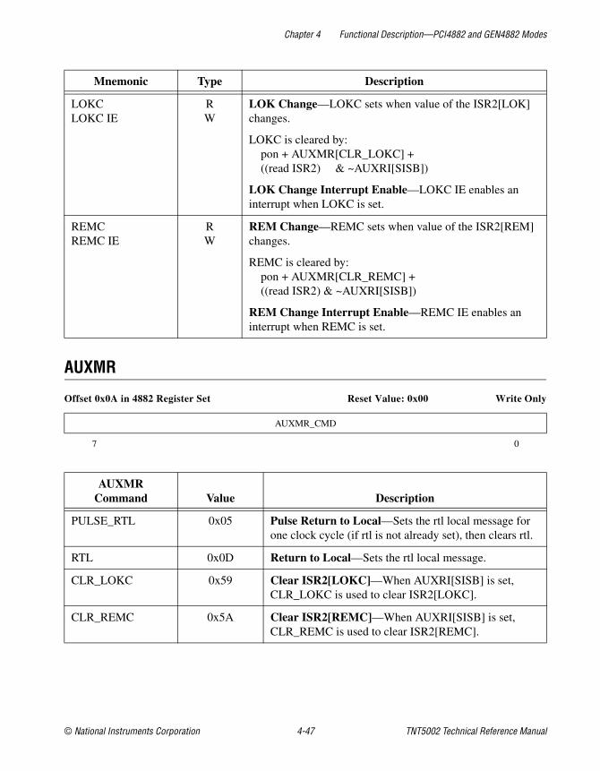
Chapter 4 Functional Description—PCI4882 and GEN4882 Modes
© National Instruments Corporation 4-47 TNT5002 Technical Reference Manual
AUXMR
Offset 0x0A in 4882 Register Set Reset Value: 0x00 Write Only
LOKCLOKC IE
RW
LOK Change—LOKC sets when value of the ISR2[LOK] changes.
LOKC is cleared by:pon + AUXMR[CLR_LOKC] + ((read ISR2) & ~AUXRI[SISB])
LOK Change Interrupt Enable—LOKC IE enables an interrupt when LOKC is set.
REMCREMC IE
RW
REM Change—REMC sets when value of the ISR2[REM] changes.
REMC is cleared by:pon + AUXMR[CLR_REMC] + ((read ISR2) & ~AUXRI[SISB])
REM Change Interrupt Enable—REMC IE enables an interrupt when REMC is set.
AUXMR_CMD
7 0
AUXMRCommand Value Description
PULSE_RTL 0x05 Pulse Return to Local—Sets the rtl local message for one clock cycle (if rtl is not already set), then clears rtl.
RTL 0x0D Return to Local—Sets the rtl local message.
CLR_LOKC 0x59 Clear ISR2[LOKC]—When AUXRI[SISB] is set, CLR_LOKC is used to clear ISR2[LOKC].
CLR_REMC 0x5A Clear ISR2[REMC]—When AUXRI[SISB] is set, CLR_REMC is used to clear ISR2[REMC].
Mnemonic Type Description

Chapter 4 Functional Description—PCI4882 and GEN4882 Modes
TNT5002 Technical Reference Manual 4-48 ni.com
OperationTo use the Remote Local block, set IMR2[REMC IE]. When ISR2[REMC] causes an interrupt, examine ISR2[REM] to determine whether currently in a local or remote state. IEEE 488.2 lists the requirements of a device in the local and remote states.
Most applications that use Remote Local only need to be notified when the Controller changes the device from a remote state to a local state or from a local state to a remote state. ISR2[REMC] detects both of these conditions.
Asserting the rtl local message prevents the Remote Local block from entering a Remote state (unless in a lockout state—refer to IEEE 488.1 for more information).
Disabling Remote LocalApplications that do not use Remote Local can simply ignore the status bits in this block and never set the interrupt enable bits. The Remote Local Block cannot be explicitly disabled. However, this block does not affect any GPIB signals.

Chapter 4 Functional Description—PCI4882 and GEN4882 Modes
© National Instruments Corporation 4-49 TNT5002 Technical Reference Manual
HS488 Manager
OverviewHS488 is an extension of IEEE 488.1 that defines a non-interlocked protocol for transferring data between devices. By using the HS488 protocol, devices can transfer data at faster rates than with the traditional 3-wire interlocked protocol defined by IEEE 488.1.
The HS488 Manager handles the HS488 transfer protocol entirely in hardware. However, configuring HS488 requires software intervention. Once configured, use the GPIB transfer manager to transfer data in the same way for both HS488 and interlocked transfers.
The HS488 protocol uses several delays that are a function of the total length of all GPIB cables in the system. The software must detect when to enable HS488 and configure registers for the proper delays.
Register Bit Description
AUXRB
Offset 0x0A in 4882 Register Set Reset Value: 0xA0 Write Only
1 0 1 ISS 0 TRI SPEOI CPT_ENABLE
7 6 5 4 3 2 1 0
Mnemonic Type Description
CPT_ENABLE W Command Pass Through Enable—CPT_ENABLE is set to allow the detection of undefined commands and to set ISR1[CPT]. Clearing CPT_ENABLE clears ISR1[CPT] and prevents detecting undefined commands.

Chapter 4 Functional Description—PCI4882 and GEN4882 Modes
TNT5002 Technical Reference Manual 4-50 ni.com
AUXRF
Offset 0x0A in 4882 Register Set Reset Value: 0xD0 Write Only
1 1 0 1 DHATA DHALA DHUNTL DHALL
7 6 5 4 3 2 1 0
Mnemonic Type Description
DHATA W DAC Holdoff on All Talk Addresses—DHATA causes a DAC holdoff on all commands in the range 0x40 to 0x5E inclusive. DIO8 is ignored for all command bytes. When performing a DAC holdoff due to DHATA, ISR1[CPT] sets.
DHALA W DAC Holdoff on All Listen Addresses—DHALA causes a DAC holdoff on all commands in the range 0x20 to 0x3E inclusive. DIO8 is ignored for all command bytes. When performing a DAC holdoff due to DHALA, ISR1[CPT] sets.
DHUNTL W DAC Holdoff on UNT and UNL—DHUNTL causes a DAC holdoff on the UNT and UNL commands. DIO8 is ignored on all command bytes. When performing a DAC holdoff due to DHUNTL, ISR1[CPT] sets.
DHALL W DAC Holdoff on All UCG, ACG, and SCG Commands—DHALL causes a DAC holdoff on all commands in the ranges 0x00 to 0x1F inclusive and 0x60 to 0x7F inclusive. DIO8 is ignored on all command bytes. When performing a DAC holdoff due to DHALL, ISR1[CPT] sets.
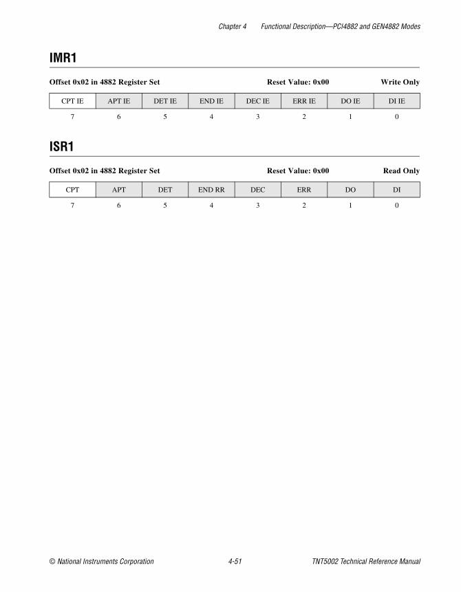
Chapter 4 Functional Description—PCI4882 and GEN4882 Modes
© National Instruments Corporation 4-51 TNT5002 Technical Reference Manual
IMR1
Offset 0x02 in 4882 Register Set Reset Value: 0x00 Write Only
ISR1
Offset 0x02 in 4882 Register Set Reset Value: 0x00 Read Only
CPT IE APT IE DET IE END IE DEC IE ERR IE DO IE DI IE
7 6 5 4 3 2 1 0
CPT APT DET END RR DEC ERR DO DI
7 6 5 4 3 2 1 0

Chapter 4 Functional Description—PCI4882 and GEN4882 Modes
TNT5002 Technical Reference Manual 4-52 ni.com
Mnemonic Type Description
CPT R Command Pass Through—CPT indicates that a command that must be processed by software was received. In the following description, a primary command is any command in the range (0x0–0x5F) and a secondary command is any command in the range (0x60–0x7F). The most significant bit (DIO8) of the command byte is always ignored.
When AUXRB[CPT_ENABLE] is set, CPT sets when an undefined primary command is received. The following commands are always undefined: 0x10, 0x12, 0x13, 0x16, 0x17, 0x1A–0x1F. If addressed to talk or listen, the following commands are also undefined: 0x0, 0x2, 0x3, 0x6, 0x7, 0xA–0xF
If the last primary command received was undefined, CPT also sets on any secondary command.
When CPT sets, a DAC holdoff occurs. A DAC holdoff prevents the Controller from sending more command bytes. Write AUXMR[VALID] to clear the DAC holdoff.
Reading the CPTR clears CPT. Clearing IMR1[CPT] clears CPT and disables the circuitry that detects undefined commands.
CPT is set by:[UCG + (ACG & (TADS + LADS))] & undefined & ACDS
& AUXRB[CPT_ENABLE]+ UDPCF & SCG & ACDS & AUXRB[CPT_ENABLE]+ AUXRE[DHADT] & GET & LADS+ AUXRE[DHADC] & (SDC + DCL) & ACDS+ AUXRF[DHATA] & TAG & ~UNT & ACDS+ AUXRF[DHALA] & LAG & ~UNL & ACDS+ AUXRF[DHUNTL] & (UNT + UNL) & ACDS+ AUXRF[DHALL] & ATN & ACDS
CPT is cleared by:pon+ ((read ISR1) & ~AUXRI[SISB])+ ((read CPTR) & AUXRI[SISB])

Chapter 4 Functional Description—PCI4882 and GEN4882 Modes
© National Instruments Corporation 4-53 TNT5002 Technical Reference Manual
CPTR
Offset 0x0A in 4882 Register Set Reset Value: 0x00 Read Only
AUXMR
Offset 0x0A in 4882 Register Set Reset Value: 0x00 Write Only
CPTR[7:0]
7 0
Mnemonic Type Description
CPTR[7:0] R Command Pass Through—The CPTR stores the last command byte received and also stores the results of parallel polls.
AUXMR_CMD
7 0
AUXMRCommand Value Description
VALID 0x0F Release DAC Holdoff (Valid)—VALID clears the DAC holdoff condition.
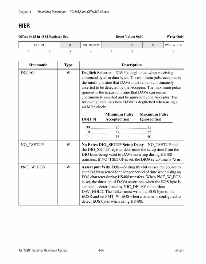
Chapter 4 Functional Description—PCI4882 and GEN4882 Modes
TNT5002 Technical Reference Manual 4-54 ni.com
HIER
Offset 0x13 in 4882 Register Set Reset Value: 0x00 Write Only
DG[1:0] 0 NO_TSETUP 0 0 0 PMT_W_EOS
7 6 5 4 3 2 1 0
Mnemonic Type Description
DG[1:0] W Deglitch Selector—DAV# is deglitched when receiving command bytes or data bytes. The minimum pulse accepted is the minimum time that DAV# must remain continuously asserted to be detected by the Acceptor. The maximum pulse ignored is the maximum time that DAV# can remain continuously asserted and be ignored by the Acceptor. The following table lists how DAV# is deglitched when using a 40 MHz clock:
Minimum Pulse Maximum PulseDG[1:0] Accepted (ns) Ignored (ns)
00 ....................... 25...........................1210 ....................... 37...........................2511 ....................... 75...........................50
NO_TSETUP W No Extra DIO_SETUP Setup Delay—NO_TSETUP and the DIO_SETUP register determine the setup time from the DIO lines being valid to DAV# asserting during HS488 transfers. If NO_TSETUP is set, the DIO# setup time is 75 ns.
PMT_W_EOS W Assert pmt With EOS—Setting this bit causes the Source to keep DAV# asserted for a longer period of time when using an EOS character during HS488 transfers. When PMT_W_EOS is set, the duration of DAV# assertions when the EOS byte is sourced is determined by NIC_DELAY rather than DAV_HOLD. The Talker must write the EOS byte to the EOSR and set PMT_W_EOS when a listener is configured to detect EOS bytes when using HS488.

Chapter 4 Functional Description—PCI4882 and GEN4882 Modes
© National Instruments Corporation 4-55 TNT5002 Technical Reference Manual
DIO_SETUP
Offset 0x11 in 4882 Register Set Reset Value: 0xC0 Write Only
DAV_HOLD
Offset 0x11 in 4882 Register Set Reset Value: 0x80 Write Only
1 1 0 DIO_SETUP[4:0]
7 6 5 4 0
Mnemonic Type Description
DIO_SETUP[4:0] W DIO Setup Time—DIO_SETUP determines the minimum setup time from the GPIB DIO# lines being valid to DAV# asserting during HS488 transfers. This is the amount of time required to transition from SGNS to STRS. If HIER[NO_TSETUP] is set, the DIO_SETUP delay is 3 clock periods. If HIER[NO_TSETUP] is cleared, the DIO_SETUP delay is determined by the expression:
DIO setup delay = 25 ns * (4 + DIO_SETUP[4:0])
1 0 0 DAV_HOLD[4:0]
7 6 5 4 0
Mnemonic Type Description
DAV_HOLD[4:0] W DAV Hold Time—DAV_HOLD determines the minimum time the Source state machine asserts DAV# during HS488 transfers when pmt is false. This is the amount of time the Source state machine remains in STRS. The DAV hold time is determined by the expression:
DAV hold time = 25 ns * (2 + DAV_HOLD[4:0])
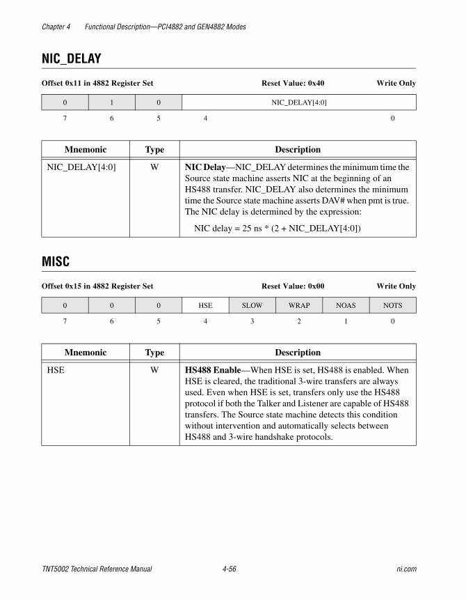
Chapter 4 Functional Description—PCI4882 and GEN4882 Modes
TNT5002 Technical Reference Manual 4-56 ni.com
NIC_DELAY
Offset 0x11 in 4882 Register Set Reset Value: 0x40 Write Only
MISC
Offset 0x15 in 4882 Register Set Reset Value: 0x00 Write Only
0 1 0 NIC_DELAY[4:0]
7 6 5 4 0
Mnemonic Type Description
NIC_DELAY[4:0] W NIC Delay—NIC_DELAY determines the minimum time the Source state machine asserts NIC at the beginning of an HS488 transfer. NIC_DELAY also determines the minimum time the Source state machine asserts DAV# when pmt is true. The NIC delay is determined by the expression:
NIC delay = 25 ns * (2 + NIC_DELAY[4:0])
0 0 0 HSE SLOW WRAP NOAS NOTS
7 6 5 4 3 2 1 0
Mnemonic Type Description
HSE W HS488 Enable—When HSE is set, HS488 is enabled. When HSE is cleared, the traditional 3-wire transfers are always used. Even when HSE is set, transfers only use the HS488 protocol if both the Talker and Listener are capable of HS488 transfers. The Source state machine detects this condition without intervention and automatically selects between HS488 and 3-wire handshake protocols.

Chapter 4 Functional Description—PCI4882 and GEN4882 Modes
© National Instruments Corporation 4-57 TNT5002 Technical Reference Manual
Operation
Configuring the System Cable LengthTo use HS488 transfers, a Controller sends the CFE command followed by a CFGn command.
Responding to System Cable Length ConfigurationHS488 devices (including the Controller) must recognize and respond to the system cable length commands (CFE and CFGn). The software must recognize the CFE and CFGn commands and implement the CF interface function. Unlike other GPIB commands, the TNT5002 does not automatically respond to these commands. The software must assist the hardware.
To implement the CF interface function set AUXRB[CPT_ENABLE] and IMR1[CPT IE] to interrupt on undefined commands
ISR1[CPT] sets when an undefined “primary” command is received. When an undefined primary command is received, CPT also sets on all secondary commands until a defined primary command is received. Each time the ISR1[CPT] sets, execute the following algorithm:
1. Read the command byte from the CPTR
2. If the command is CFE (0x1F) then
a. Disable HS488 as described in the Disabling HS488 section
b. Write 0xDF to AUXRF to holdoff on all commands
3. Otherwise, if the command is a PCG command other than CFE then
a. Write 0xD0 to AUXRF to clear holdoff on all commands
b. clear AUXRB[CPT_ENABLE], then set AUXRB[CPT_ENABLE]
4. Otherwise, if (0x61 ≤ command ≤ 0x6F)
a. Subtract 0x60 from command to calculate cable length
b. Enable HS488 with Cable Length as described in the Enabling HS488 section
5. Write AUXMR[VALID] to release DAC holdoff
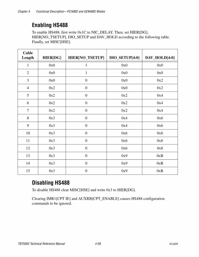
Chapter 4 Functional Description—PCI4882 and GEN4882 Modes
TNT5002 Technical Reference Manual 4-58 ni.com
Enabling HS488To enable HS488, first write 0x1C to NIC_DELAY. Then, set HIER[DG], HIER[NO_TSETUP], DIO_SETUP and DAV_HOLD according to the following table. Finally, set MISC[HSE].
Disabling HS488To disable HS488 clear MISC[HSE] and write 0x3 to HIER[DG].
Clearing IMR1[CPT IE] and AUXRB[CPT_ENABLE] causes HS488 configuration commands to be ignored.
Cable Length HIER[DG] HIER[NO_TSETUP] DIO_SETUP[4:0] DAV_HOLD[4:0]
1 0x0 1 0x0 0x0
2 0x0 1 0x0 0x0
3 0x0 0 0x0 0x2
4 0x2 0 0x0 0x2
5 0x2 0 0x2 0x4
6 0x2 0 0x2 0x4
7 0x2 0 0x2 0x4
8 0x3 0 0x4 0x6
9 0x3 0 0x4 0x6
10 0x3 0 0x6 0x8
11 0x3 0 0x6 0x8
12 0x3 0 0x6 0x8
13 0x3 0 0x9 0xB
14 0x3 0 0x9 0xB
15 0x3 0 0x9 0xB

Chapter 4 Functional Description—PCI4882 and GEN4882 Modes
© National Instruments Corporation 4-59 TNT5002 Technical Reference Manual
Timer
OverviewThe Timer is a general-purpose timer that can generate interrupts or terminate GPIB subroutine calls that may not return. Most devices do not use timeouts.
Register Bit Definitions
AUXRJ
Offset 0x0A in 4882 Register Set Reset Value: 0xF0 Write Only
AUXRK
Offset 0x0F in 4882 Register Set Reset Value: 0x00 Write Only
1 1 1 1 TM[3:0]
7 6 5 4 3 0
0 0 0 0 0 0 TM[5:4]
7 6 5 4 3 2 1 0
Mnemonic Type Description
TM[5:0] W Timer—TM[5:0] determine the timeout duration of the timer as specified in the following table. The timeout duration depends on the clock frequency. The following table shows the timeout duration assuming a 40 MHz clock. For other clock frequencies, the timeout duration can be scaled by the ratio of the frequencies.
TM[5:0] Timeout Duration (for 40 MHz Clock)
000000 Disabled
000001 16.0 µs
000010 32.0 µs

Chapter 4 Functional Description—PCI4882 and GEN4882 Modes
TNT5002 Technical Reference Manual 4-60 ni.com
000011 128 µs
000100 256 µs
000101 1.02 ms
000110 4.10 ms
000111 16.4 ms
001000 32.8 ms
001001 131 ms
001010 262 ms
001011 1.05 s
001100 4.19 s
001101 16.8 s
001110 33.6 s
001111 134 s
010001 300 s
100001 1000 s
TM[5:0] Timeout Duration (for 40 MHz Clock)

Chapter 4 Functional Description—PCI4882 and GEN4882 Modes
© National Instruments Corporation 4-61 TNT5002 Technical Reference Manual
IMR0
Offset 0x1D in 4882 Register Set Reset Value: 0x80 Write Only
ISR0
Offset 0x1D in 4882 Register Set Reset Value: 0x00 Read Only
Operation
Starting the TimerTo start the timer, configure the desired timeout value as follows:
• Write 0000 to TM[3:0]
• Write the desired timeout value to AUXRK[TM[5:4]].
• Write the desired timeout value to AUXRJ[TM[3:0]] to start the timer.
Restarting the TimerTo manually restart the timer, re-execute the configuration steps shown above. If IMR0[BTO] is set, the timer restarts whenever a command or data byte is sent or whenever a data byte is received from the GPIB.
GLINT STBO IE NLEN BTO IFCI IE ATNI IE TO IE SYNC IE
7 6 5 4 3 2 1 0
NBA STBO NL EOS IFCI ATNI TO SYNC
7 6 5 4 3 2 1 0
Mnemonic Type Description
BTO W Byte Timeout—When BTO is set, the Timer is reset whenever a data byte is sent or received or whenever a command byte is sent.
TOTO IE
RW
Timeout—TO sets when the timer reaches its timeout value as specified by AUXRJ and AUXRK. Writing any value to TM[3:0] clears TO.
TO Interrupt Enable—TO IE enables an interrupt when the TO condition is true. Refer to the Interrupts section for more information.

Chapter 4 Functional Description—PCI4882 and GEN4882 Modes
TNT5002 Technical Reference Manual 4-62 ni.com
Stopping the TimerTo stop the timer, write 0000 to [TM[3:0]].
Determining when a Timeout OccursISR0[TO] is set when the timeout condition is satisfied ISR0[TO] can either be polled or enabled to cause an interrupt. The timeout condition is satisfied when the timeout duration elapses.

Chapter 4 Functional Description—PCI4882 and GEN4882 Modes
© National Instruments Corporation 4-63 TNT5002 Technical Reference Manual
Interrupts
OverviewThis section describes bits used to generate hardware interrupts.
Register Bit Descriptions
IMR0
Offset 0x1D in 4882 Register Set Reset Value: 0x80 Write Only
AUXRI
Offset 0x0A in 4882 Register Set Reset Value: 0x00 Write Only
GLINT STBO IE NLEN BTO IFCI IE ATNI IE TO IE SYNC IE
7 6 5 4 3 2 1 0
Mnemonic Type Description
GLINT R Enable Certain Interrupts—GLINT enables IMR0, IMR1, and IMR2 interrupts. GLINT is redundant with IMR3[TLCINT IE], so always set GLINT. Writing AUXMR[SETSWRST] sets GLINT.
1 1 1 0 USTD PPMODE2 0 SISB
7 6 5 4 3 2 1 0
Mnemonic Type Description
SISB W Static Interrupt Bits—SISB controls the conditions that clear the bits in ISR0, ISR1, and ISR2. If SISB is cleared, reading one of these registers clears the bits in that register. If SISB is set, the bits are cleared as described in this manual. Most applications should set SISB.
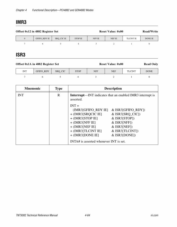
Chapter 4 Functional Description—PCI4882 and GEN4882 Modes
TNT5002 Technical Reference Manual 4-64 ni.com
IMR3
Offset 0x12 in 4882 Register Set Reset Value: 0x00 Read/Write
ISR3
Offset 0x1A in 4882 Register Set Reset Value: 0x00 Read Only
0 GFIFO_RDY IE SRQ_CIC IE STOP IE NFF IE NEF IE TLCINT IE DONE IE
7 6 5 4 3 2 1 0
INT GFIFO_RDY SRQ_CIC STOP NFF NEF TLCINT DONE
7 6 5 4 3 2 1 0
Mnemonic Type Description
INT R Interrupt—INT indicates that an enabled IMR3 interrupt is asserted.
INT = (IMR3[GFIFO_RDY IE] & ISR3[GFIFO_RDY])+ (IMR3[SRQCIC IE] & ISR3[SRQ_CIC])+ (IMR3[STOP IE] & ISR3[STOP])+ (IMR3[NFF IE] & ISR3[NFF])+ (IMR3[NEF IE] & ISR3[NEF])+ (IMR3[TLCINT IE] & ISR3[TLCINT])+ (IMR3[DONE IE] & ISR3[DONE])
INTA# is asserted whenever INT is set.
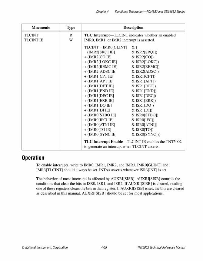
Chapter 4 Functional Description—PCI4882 and GEN4882 Modes
© National Instruments Corporation 4-65 TNT5002 Technical Reference Manual
OperationTo enable interrupts, write to IMR0, IMR1, IMR2, and IMR3. IMR0[GLINT] and IMR3[TLCINT] should always be set. INTA# asserts whenever ISR3[INT] is set.
The behavior of most interrupts is affected by AUXRI[SISB]. AUXRI[SISB] controls the conditions that clear the bits in ISR0, ISR1, and ISR2. If AUXRI[SISB] is cleared, reading one of these registers clears the bits in that register. If AUXRI[SISB] is set, the bits are cleared as described in this manual. AUXRI[SISB] should be set for most applications.
TLCINTTLCINT IE
RW
TLC Interrupt—TLCINT indicates whether an enabled IMR0, IMR1, or IMR2 interrupt is asserted.
TLCINT = IMR0[GLINT] & (IMR2[SRQI IE] & ISR2[SRQI])+ (IMR2[CO IE] & ISR2[CO])+ (IMR2[LOKC IE] & ISR2[LOKC])+ (IMR2[REMC IE] & ISR2[REMC])+ (IMR2[ADSC IE] & ISR2[ADSC])+ (IMR1[CPT IE] & ISR1[CPT])+ (IMR1[APT IE] & ISR1[APT])+ (IMR1[DET IE] & ISR1[DET])+ (IMR1[END IE] & ISR1[END])+ (IMR1[DEC IE] & ISR1[DEC])+ (IMR1[ERR IE] & ISR1[ERR])+ (IMR1[DO IE] & ISR1[DO])+ (IMR1[DI IE] & ISR1[DI])+ (IMR0[STBO IE] & ISR0[STBO])+ (IMR0[IFCI IE] & ISR0[IFC])+ (IMR0[ATNI IE] & ISR0[ATNI])+ (IMR0[TO IE] & ISR0[TO])+ (IMR0[SYNC IE] & ISR0[SYNC])
TLC Interrupt Enable—TLCINT IE enables the TNT5002 to generate an interrupt when TLCINT asserts.
Mnemonic Type Description

Chapter 4 Functional Description—PCI4882 and GEN4882 Modes
TNT5002 Technical Reference Manual 4-66 ni.com
Debugging Bits
OverviewThis section describes bits that can be used for debugging. In most applications, these bits are not used.
Register Bit Descriptions
ADR0
Offset 0x0C in 4882 Register Set Reset Value: 0x00 Read Only
R DT0 DL0 PRIMADDR[4:0]
7 6 5 4 0
Mnemonic Type Description
DT0 R Disable Primary Talker—If DT0 is set, the primary Talker is not enabled and PRIM_ADDR is not compared to GPIB Talk commands. If DT0 is cleared, the primary Talker responds to GPIB Talk commands matching PRIM_ADDR.
DL0 R Disable Primary Listener—If DL0 is set, the primary Listener is not enabled and PRIM_ADDR is not compared to GPIB Listen commands. If DL0 is cleared, the primary Listener responds to GPIB Listen commands matching PRIM_ADDR.
PRIM_ADDR[4:0] R Primary Address—The meaning of PRIM_ADDR depends on the Addressing Mode as selected by ADMR.
Addressing Mode PRIM_ADDR
No Addressing ............................DisabledNormal Addressing .....................Primary AddressExtended Addressing ..................Primary AddressNormal Dual Addressing ............Device 1 Primary AddressExtended Dual Addressing .........Device 1 Primary AddressNormal Multiple Addressing ......DisabledExtended Multiple Addressing ...DisabledTalk Only ....................................DisabledListen Only .................................Disabled

Chapter 4 Functional Description—PCI4882 and GEN4882 Modes
© National Instruments Corporation 4-67 TNT5002 Technical Reference Manual
ADR1
Offset 0x0E in 4882 Register Set Reset Value: 0x00 Read Only
EOI DT1 DL1 ADDR[4:0]
7 6 5 4 0
Mnemonic Type Description
EOI R EOI# Received—This bit indicates the state of the EOI# line when the most recent data byte was accepted. If EOI is set, the EOI# line was asserted.
DT1 R Disable Talker—If DT1 is set, the primary Talker is not enabled and ADDR is not compared to GPIB Talk commands. If DT1 is cleared, the primary Talker responds to GPIB Talk commands matching ADDR.
DL1 R Disable Listener—If DL1 is set, the primary Listener is not enabled and ADDR is not compared to GPIB Listen commands. If DL1 is cleared, the primary Listener responds to GPIB Listen commands matching ADDR.
ADDR[4:0] R Other Address—Some of the Addressing Modes selected in the ADMR require an additional address. The following table shows the meaning of ADDR for each Addressing Mode.
Addressing Mode ADDR
No Addressing..............................DisabledNormal Addressing ......................DisabledExtended Addressing....................Secondary AddressNormal Dual Addressing..............Device 2 Primary AddressExtended Dual Addressing...........Device 2 Primary AddressNormal Multiple Addressing........DisabledExtended Multiple Addressing.....DisabledTalk Only......................................DisabledListen Only...................................DisabledTalk and Listen .............................Disabled

Chapter 4 Functional Description—PCI4882 and GEN4882 Modes
TNT5002 Technical Reference Manual 4-68 ni.com
ADSR
Offset 0x08 in 4882 Register Set Reset Value: 0x00 Read Only
R ATNN SPMS LPAS TPAS LA TA MINOR
7 6 5 4 3 2 1 0
Mnemonic Type Description
LPAS R Listener Primary Address State—LPAS indicates that the Listener has received its primary listen address (MLA). LPAS is cleared after receiving any primary command byte that is not MLA.
LPAS is set by:MLA & ACDS
LPAS is cleared by:(PCG & ~MLA & ACDS) + pon
TPAS R Talker Primary Address State—TPAS indicates that the Talker has received its primary talk address (MTA). TPAS is cleared after receiving any primary command byte that is not MTA.
TPAS is set by:MTA & ACDS
TPAS is cleared by:(PCG & ~MTA & ACDS) + pon

Chapter 4 Functional Description—PCI4882 and GEN4882 Modes
© National Instruments Corporation 4-69 TNT5002 Technical Reference Manual
BSR
Offset 0x1F in 4882 Register Set Reset Value: 0x00 Read Only
DSR
Offset 0x11 in 4882 Register Set Reset Value: 0x00 Read Only
ATN DAV NDAC NRFD EOI SRQ IFC REN
7 6 5 4 3 2 1 0
DIO[8:1]
7 0
Mnemonic Type Description
ATNDAVNDACNRFDEOISRQIFCRENDIO[8:1]
RRRRRRRRR
GPIB Monitor Bits—The BSR and DSR registers indicate the status of the GPIB signals.
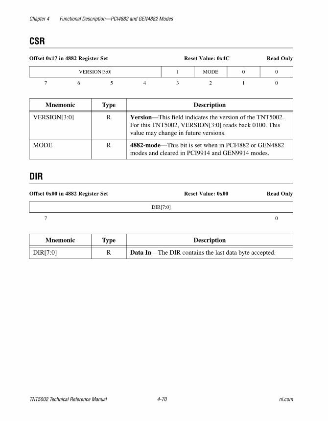
Chapter 4 Functional Description—PCI4882 and GEN4882 Modes
TNT5002 Technical Reference Manual 4-70 ni.com
CSR
Offset 0x17 in 4882 Register Set Reset Value: 0x4C Read Only
DIR
Offset 0x00 in 4882 Register Set Reset Value: 0x00 Read Only
VERSION[3:0] 1 MODE 0 0
7 6 5 4 3 2 1 0
Mnemonic Type Description
VERSION[3:0] R Version—This field indicates the version of the TNT5002. For this TNT5002, VERSION[3:0] reads back 0100. This value may change in future versions.
MODE R 4882-mode—This bit is set when in PCI4882 or GEN4882 modes and cleared in PCI9914 and GEN9914 modes.
DIR[7:0]
7 0
Mnemonic Type Description
DIR[7:0] R Data In—The DIR contains the last data byte accepted.

Chapter 4 Functional Description—PCI4882 and GEN4882 Modes
© National Instruments Corporation 4-71 TNT5002 Technical Reference Manual
ISR0
Offset 0x1D in 4882 Register Set Reset Value: 0x00 Read Only
MISC
Offset 0x15 in 4882 Register Set Reset Value: 0x00 Write Only
NBA STBO NL EOS IFCI ATNI TO SYNC
7 6 5 4 3 2 1 0
Mnemonic Type Description
EOS R End-of-String—EOS indicates that the last data byte received satisfies the END condition. ISR1[END] should be used instead of EOS to detect the end of a read transfer.
EOS is set by:LACS & EOS & REOS & ACDS
EOS is cleared by:pon + ~REOS + (LACS & ~EOS & ACDS)
0 0 0 HSE SLOW WRAP NOAS NOTS
7 6 5 4 3 2 1 0
Mnemonic Type Description
WRAP W Wrap Back—When WRAP is set, the GPIB pins are tristated, but the GPIB signals are fed back into the TNT5002. The external state of each signal is ignored. This bit may be used to allow diagnostics to run without disconnecting GPIB cables from the board.

Chapter 4 Functional Description—PCI4882 and GEN4882 Modes
TNT5002 Technical Reference Manual 4-72 ni.com
SASR
Offset 0x1B in 4882 Register Set Reset Value: 0x00 Read Only
NBA AEHS ANHS1 ANHS2 ADHS ACRDY SH1A SH1B
7 6 5 4 3 2 1 0
Mnemonic Type Description
NBA R New Byte Available—NBA reflects the local nba message, which indicates that the SH interface function has a byte to send. Specifically,
NBA = ~CFGR[IN] & ~(FIFO empty).
AEHS R Acceptor End Holdoff State—AEHS sets after receiving a data byte with EOI# asserted, receiving a data byte matching the EOSR when AUXRA[REOS] is true, or receiving the NL character (0x0A) when IMR0[NLEN] is true.
ANHS1 R Acceptor Not Ready Holdoff—ANHS1 sets when the Acceptor receives a data byte with EOI# asserted, receives a data byte matching the EOSR when AUXRA[REOS] is true, or receives the NL character (0x0A) when NLEN is true. ANHS1 also sets when a data byte is accepted when the Acceptor is not in Continuous Holdoff mode. ANHS1 is cleared when holdoff is false, AUXMR[RHDF] is issued, or AUXMR[LTN_CONT] is issued.
ANHS2 R Acceptor Not Ready Holdoff Immediately bit—ANHS2 is set by writing AUXMR[HLDI]. ANHS2 is cleard by writing AUXMR[RHDF].
ADHS R Acceptor Data Holdoff State bit—ADHS sets when a DAC holdoff is active. ADHS is cleared by writing AUXMR[VALID] or AUXMR[INVALID].

Chapter 4 Functional Description—PCI4882 and GEN4882 Modes
© National Instruments Corporation 4-73 TNT5002 Technical Reference Manual
STS1
Offset 0x10 in 4882 Register Set Reset Value: 0x01 Read Only
ACRDY R Acceptor Ready State bit—ACRDY can be used with ADSR[LA], ADSR[ATNN], BSR[DAV] and ADHS to determine the state of the Acceptor Handshake function. The preferred method of reading the Acceptor Handshake state is by reading STR1.
AIDS = ~ADSR[ATNN] & ~ADSR[LA]ANRS = ~AIDS & ~ACRDY & ~BSR[DAV]ACRS = ~AIDS & ACRDY & ~ BSR[DAV]ACDS = ~AIDS & ACRDY & BSR[DAV] + ~AIDS & ~ACRDY & BSR[DAV]
& ADSR[ATNN] & ADHSAWNS = ~AIDS & ~ACRDY & BSR[DAV]
& ~(ADSR[ATNN] & ADHS)
SH1A, SH1B R Source Handshake State bits—The Source Handshake state can be used with TA, SPMS and ATNN in the ADSR to determine the state of the Source Handshake function. The preferred method of reading the Source Handshake state is by reading STR2.
SIDS = ~(TACS & ~ADSR[ATNN])SGNS = ~SIDS & ~SH1A & ~SH1BSDYS = ~SIDS & SH1ASTRS = ~SIDS & ~SH1A & ~SH1B
DONE R IN DRQ STOP DAV HALT GSYNC
7 6 5 4 3 2 1 0
Mnemonic Type Description
DONE R DONE—At the end of a transfer, DONE indicates that all devices on the GPIB have finished the transfer. DONE only sets after STOP sets. This bit is identical to ISR3[0].
Mnemonic Type Description

Chapter 4 Functional Description—PCI4882 and GEN4882 Modes
TNT5002 Technical Reference Manual 4-74 ni.com
IN R GPIB Transfer Direction—IN reflects the GPIB Transfer direction as set by CFG[5]. IN set indicates the TNT5002 is configured to accepts GPIB data bytes. IN cleared indicates the TNT5002 is configured to send GPIB data bytes or command bytes.
DRQ R Internal DMA Request—The TNT5002 asserts this internal signal to indicate to the PCI interface circuitry that data may be transferred between the GFIFO and the DFIFO. DRQ also reflects the state of the DRQ pin in GEN4882 mode.
STOP R GPIB Transfer Stopped—STOP is set by any of the following conditions:
• The last byte (as indicated by the CNT registers) of a command or data transfer is written to the GPIB
• The last byte (as indicated by the CNT registers) of a read transfer is read into the GFIFO
• The CMDR[STOP] command is issued
• The CMDR[SOFT_RESET] command is issued or a hardware reset asserts.
STOP is cleared by CMDR[GO].
DAV R DAV—This bit indicates the status of the GPIB Handshake line DAV. If DAV is set, the GPIB DAV# signal is asserted.
HALT R GPIB Transfer Halted—HALT indicates the status of the GPIB transfer circuit. HALT is set if the STOP bit is set. When TLCHLTE is set, HALT also sets when any enabled interrupt in IMR0, IMR1, or IMR2 asserts.
If NOAS is set or NOTS is set, certain IMR0, IMR1, and IMR2 interrupts do not cause HALT.
Mnemonic Type Description

Chapter 4 Functional Description—PCI4882 and GEN4882 Modes
© National Instruments Corporation 4-75 TNT5002 Technical Reference Manual
STS2
Offset 0x1C in 4882 Register Set Reset Value: 0x0A Read Only
GSYNC R GPIB Synchronized—GSYNC indicates that the GPIB has synchronized. That is, the last byte transferred was accepted by all GPIB Listeners.
CMDR[GO] clears GSYNC.
GSYNC is set by when the following expression becomes true:
HALT & CFGR[IN] & (AIDS + ANRS) + HALT & ~CFGR[IN] & (SIDS + SGNS).
GSYNC is also set by a hardware or software reset.
1 16/8N 0 1 AFFN AEFN BFFN BEFN
7 6 5 4 3 2 1 0
Mnemonic Type Description
16/8N R 16-bit or 8-bit FIFO mode—This bit reflects the status of the 16/8N bit in CFG[0].
AFFN R FIFO A Not Full Flag—AFFN is set when at least one byte may be written to GFIFO[15:8].
AEFN R FIFO A Not Empty Flag—AEFN is set when at least one byte may be read from GFIFO[15:8].
BFFN R FIFO B Not Full Flag—BFFN is set when at least one byte may be written to GFIFO[7:0].
BEFN R FIFO B Not Empty Flag—BEFN is set when at least one byte may be read from GFIFO[7:0].
Mnemonic Type Description
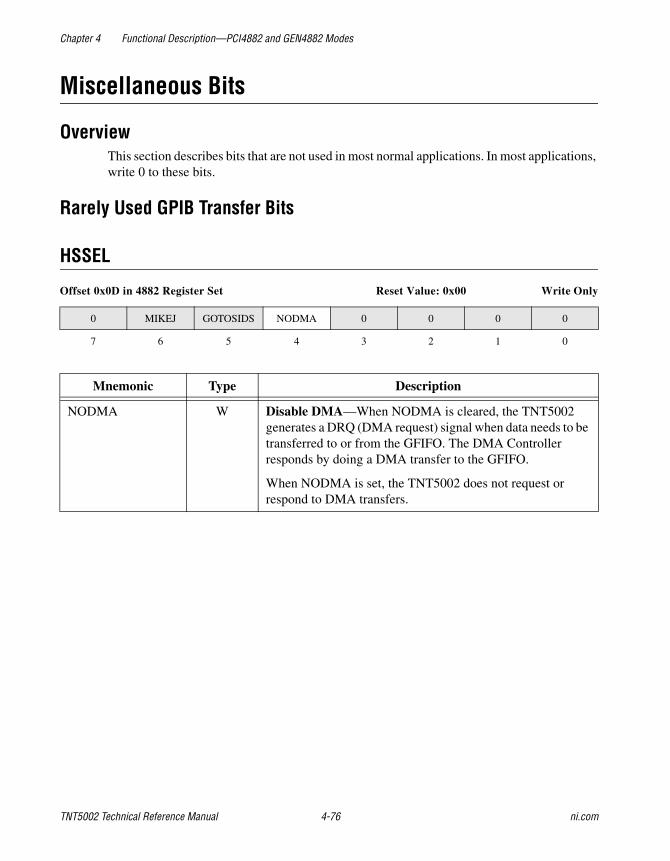
Chapter 4 Functional Description—PCI4882 and GEN4882 Modes
TNT5002 Technical Reference Manual 4-76 ni.com
Miscellaneous Bits
OverviewThis section describes bits that are not used in most normal applications. In most applications, write 0 to these bits.
Rarely Used GPIB Transfer Bits
HSSEL
Offset 0x0D in 4882 Register Set Reset Value: 0x00 Write Only
0 MIKEJ GOTOSIDS NODMA 0 0 0 0
7 6 5 4 3 2 1 0
Mnemonic Type Description
NODMA W Disable DMA—When NODMA is cleared, the TNT5002 generates a DRQ (DMA request) signal when data needs to be transferred to or from the GFIFO. The DMA Controller responds by doing a DMA transfer to the GFIFO.
When NODMA is set, the TNT5002 does not request or respond to DMA transfers.

Chapter 4 Functional Description—PCI4882 and GEN4882 Modes
© National Instruments Corporation 4-77 TNT5002 Technical Reference Manual
CFG
Offset 0x10 in 4882 Register Set Reset Value: 0x00 Write Only
COMMAND TLCHLTE IN A/BN CCEN 0 0 16/8N
7 6 5 4 3 2 1 0
Mnemonic Type Description
TLCHLTE W Halt on TLC interrupts—TLCHLTE determines which conditions halt the GPIB Transfer Manager (once it has been started with CMDR[GO]. When TLCHLTE is cleared, the GPIB Transfer manager halts when the CMDR[STOP] is issued and all of the bytes specified in the CNT3–0 registers have been transferred.
When TLCHLTE is set, the GPIB Transfer manager also halts when any enabled interrupt in IMR0, IMR1, or IMR2 asserts.
In most applications, the GPIB Transfer manager should only be stopped in response to some of the IMR0, IMR1, or IMR2 interrupts. Typically, TLCHLTE is cleared. When an interrupt asserts, software determines whether the interrupt should stop the GPIB Transfer manager. CMDR[STOP] can then be issued to stop the GPIB Transfer manager.
A/BN W Endianess Control for FIFOs—When packing and unpacking data into the FIFO in 16-bit mode, the GPIB Transfer Manager alternates writing (or reading) bytes to FIFO A and FIFO B. If A/BN is cleared, the GPIB Transfer manager writes (or reads) the first byte to FIFO B. If A/BN is set, the GPIB Transfer manager writes (or reads) the first byte to FIFO A.

Chapter 4 Functional Description—PCI4882 and GEN4882 Modes
TNT5002 Technical Reference Manual 4-78 ni.com
Rarely Used Controller Bits
AUXRG
Offset 0x08 in 4882 Register Set Reset Value: 0x40 Write Only
AUXMR
Offset 0x0A in 4882 Register Set Reset Value: 0x00 Write Only
0 1 0 0 0 RPP2 DISTCT CHES
7 6 5 4 3 2 1 0
Mnemonic Type Description
RPP2 W Assert rpp—When RPP2 is set, the local rpp message is true. If Active Controller, rpp causes a parallel poll to be conducted. Normally, AUXMR[RPP1] is used to conduct parallel polls. When using rpp, the duration of the parallel poll is 80 clock cycles. RPP2 allows duration or parallel polls to be controlled.
DISTCT W Disable TCT Recognition—Setting DISTCT causes the GPIB TCT command message to be undefined. If a GPIB Controller tries to pass control to the TNT5002, the TNT5002 does not become the Controller.
AUXMR_CMD
7 0
AUXMRCommand Value Description
LUN 0x1C Local Unlisten—LUN causes the Listener state machine to enter LIDS if the Controller state machine is in CACS.

Chapter 4 Functional Description—PCI4882 and GEN4882 Modes
© National Instruments Corporation 4-79 TNT5002 Technical Reference Manual
Rarely Used Interrupt Bits
IMR0
Offset 0x1D in 4882 Register Set Reset Value: 0x80 Write Only
ISR0
Offset 0x1D in 4882 Register Set Reset Value: 0x00 Read Only
GLINT STBO IE NLEN BTO IFCI IE ATNI IE TO IE SYNC IE
7 6 5 4 3 2 1 0
NBA STBO NL EOS IFCI ATNI TO SYNC
7 6 5 4 3 2 1 0
Mnemonic Type Description
IFCIIFCI IE
RW
IFC Interrupt—IFCI is set when the GPIB IFC# signal asserts. IFC# unasserted or writing AUXMR[CLR_IFCI] clears IFCI. The GPIB state machines detect and appropriately handle IFC# without any intervention. IFC# should not have any other effect on the device, so devices should not monitor or interrupt on IFCI.
IFCI Interrupt Enable—IFCI IE enables an interrupt when the IFCI condition is true.
ATNIATNI IE
R W
ATN Interrupt—ATNI is set when the GPIB ATN# signal asserts. ATN# unasserted or writing AUXMR[CLR_ATNI] clears ATNI. The GPIB state machines detect the ATN# signal and interpret it appropriately without any intervention. ATN# should not have any other effect on the device, so devices should not monitor or interrupt on ATNI.
ATNI Interrupt Enable—ATNI IE enables an interrupt when the ATNI condition is true.
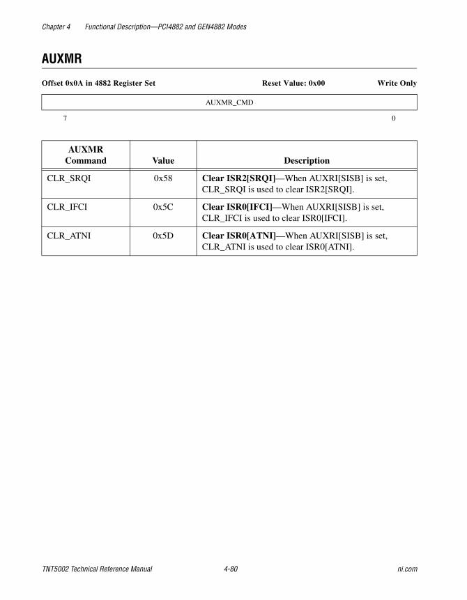
Chapter 4 Functional Description—PCI4882 and GEN4882 Modes
TNT5002 Technical Reference Manual 4-80 ni.com
AUXMR
Offset 0x0A in 4882 Register Set Reset Value: 0x00 Write Only
AUXMR_CMD
7 0
AUXMRCommand Value Description
CLR_SRQI 0x58 Clear ISR2[SRQI]—When AUXRI[SISB] is set, CLR_SRQI is used to clear ISR2[SRQI].
CLR_IFCI 0x5C Clear ISR0[IFCI]—When AUXRI[SISB] is set, CLR_IFCI is used to clear ISR0[IFCI].
CLR_ATNI 0x5D Clear ISR0[ATNI]—When AUXRI[SISB] is set, CLR_ATNI is used to clear ISR0[ATNI].
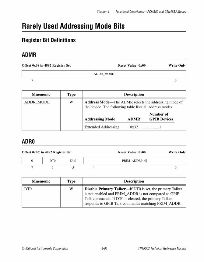
Chapter 4 Functional Description—PCI4882 and GEN4882 Modes
© National Instruments Corporation 4-81 TNT5002 Technical Reference Manual
Rarely Used Addressing Mode Bits
Register Bit Definitions
ADMR
Offset 0x08 in 4882 Register Set Reset Value: 0x00 Write Only
ADR0
Offset 0x0C in 4882 Register Set Reset Value: 0x00 Write Only
ADDR_MODE
7 0
Mnemonic Type Description
ADDR_MODE W Address Mode—The ADMR selects the addressing mode of the device. The following table lists all address modes.
Number of Addressing Mode ADMR GPIB Devices
Extended Addressing.......... 0x32 ....................1
0 DT0 DL0 PRIM_ADDR[4:0]
7 6 5 4 0
Mnemonic Type Description
DT0 W Disable Primary Talker—If DT0 is set, the primary Talker is not enabled and PRIM_ADDR is not compared to GPIB Talk commands. If DT0 is cleared, the primary Talker responds to GPIB Talk commands matching PRIM_ADDR.
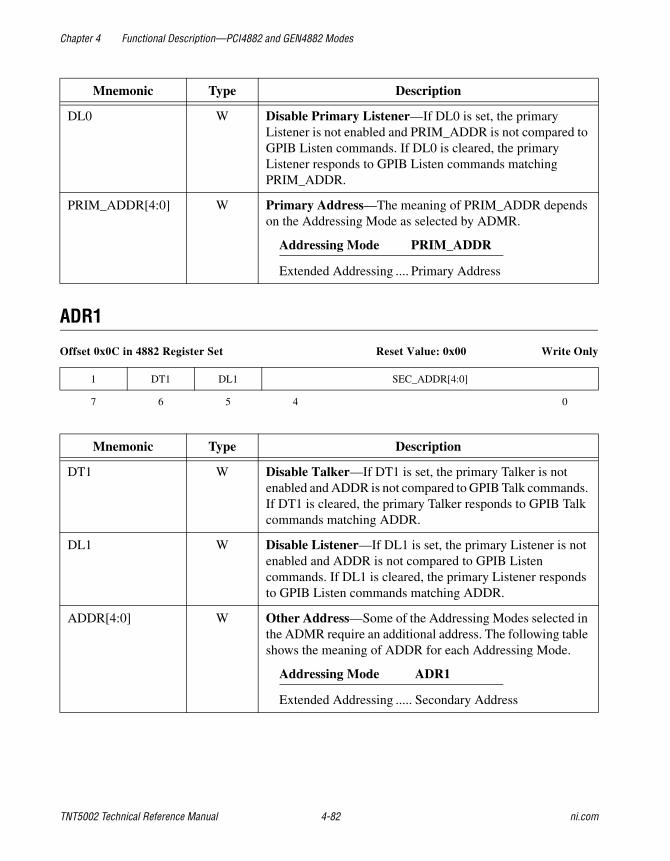
Chapter 4 Functional Description—PCI4882 and GEN4882 Modes
TNT5002 Technical Reference Manual 4-82 ni.com
ADR1
Offset 0x0C in 4882 Register Set Reset Value: 0x00 Write Only
DL0 W Disable Primary Listener—If DL0 is set, the primary Listener is not enabled and PRIM_ADDR is not compared to GPIB Listen commands. If DL0 is cleared, the primary Listener responds to GPIB Listen commands matching PRIM_ADDR.
PRIM_ADDR[4:0] W Primary Address—The meaning of PRIM_ADDR depends on the Addressing Mode as selected by ADMR.
Addressing Mode PRIM_ADDR
Extended Addressing .... Primary Address
1 DT1 DL1 SEC_ADDR[4:0]
7 6 5 4 0
Mnemonic Type Description
DT1 W Disable Talker—If DT1 is set, the primary Talker is not enabled and ADDR is not compared to GPIB Talk commands. If DT1 is cleared, the primary Talker responds to GPIB Talk commands matching ADDR.
DL1 W Disable Listener—If DL1 is set, the primary Listener is not enabled and ADDR is not compared to GPIB Listen commands. If DL1 is cleared, the primary Listener responds to GPIB Listen commands matching ADDR.
ADDR[4:0] W Other Address—Some of the Addressing Modes selected in the ADMR require an additional address. The following table shows the meaning of ADDR for each Addressing Mode.
Addressing Mode ADR1
Extended Addressing ..... Secondary Address
Mnemonic Type Description

Chapter 4 Functional Description—PCI4882 and GEN4882 Modes
© National Instruments Corporation 4-83 TNT5002 Technical Reference Manual
Operation—Extended Dual Addressing ModeTo use Extended Dual Addressing mode, first write the primary address to ADR0. If only one primary address is used, write 0xE0 to ADR1. If two primary addresses are used, write the second primary address to ADR1.
Poll for or interrupt on ISR1[APT]. When ISR1[APT] sets, read ADSR[MINOR] to determine which primary address was received and read the CPTR to see what secondary command is on bus. If the secondary command is one of the addresses implemented by the device, write AUXMR[VALID]. Otherwise, write AUXMR[INVALID].
AUXMR[VALID] causes a transition to enter TADS or LADS.
© National Instruments Corporation 5-1 TNT5002 Technical Reference Manual
5DMA Manager
DMA OverviewThe DMA Manager contains a 64-byte FIFO (DFIFO), separate from the GFIFO, which can be used for DMA transfers. This FIFO, combined with the GFIFO, allow the GPIB Source or Acceptor to continuously transfer data at rates up to 8 MB/s. The DMA Manager may only be used in PCI4882 mode.
If DMA is used, the CPU should never write directly to the GFIFO. Bytes are automatically transferred between the DFIFO and the GFIFO. The GPIB circuitry should be programmed in an identical way regardless of whether DMA is used.
This chapter divides a DMA transfer into three phases: Initialization, Transfer, and Termination. Link Chaining is the recommended transfer mode and the descriptions of the three phases assume Link Chaining mode.

Chapter 5 DMA Manager
TNT5002 Technical Reference Manual 5-2 ni.com
Link Chaining OverviewThe DMA Controller uses a process called Link Chaining to control DMA transfers. In this mode, the LKAR is programmed with the physical address of the first node in a linked list in memory. The nodes in the linked list each have three 32-bit fields. Link Chain nodes have the transfer count of the block of data associated with that node (count), the physical address of the start of the data block (mem_address), and the physical address of the next node in the linked list (next). When the DMA Controller fetches a node from memory, it loads count into the TCR, mem_address into the MAR, and next into the LKAR. When the DMA Controller has transferred all of the data associated with a given node, it loads the next node’s values. The process continues until the DMA Controller reads a node with the count set to 0.
Figure 5-1. Short Link Structure Formats
count
mem_address
next
count
mem_address
next
0
X
X

Chapter 5 DMA Manager
© National Instruments Corporation 5-3 TNT5002 Technical Reference Manual
DMA TransfersDMA Transfers are divided into three phases; Initialization, Transfer, and Termination.
Initialization PhaseMost applications should not set any interrupt enables for the DMA Status/Control registers. Instead, interrupts in the 4882 Register set should be enabled.
DMA Read Operation in Link Chain ModeAssuming the DMA Controller just came out of one of the reset conditions (internal POR, global reset, or DMA Channel reset) one can start the Initialization phase of a transfer. To start a DMA read, perform the following steps:
1. Program the CHCR, MCR, DCR, and LKCR for the ports, size, and other options as needed. Typical values written to these registers are as follows:
CHCR: 0x0000040C
MCR: 0x00e00700
DCR: 0x00e40241
LKCR: 0x00000700
2. Create the link chain in memory.
Note The mem_address must be a word aligned address.
3. Program the LKAR with the physical address of the first link in memory.
4. Set CHOR[START].
DMA Write Operation in Link Chain ModeAssuming the DMA Controller just came out of one of the reset conditions (internal POR, global reset, or DMA Channel reset) one can start the Initialization phase of a transfer. To start a DMA write, perform the following steps:
1. Program the CHCR, MCR, DCR, and LKCR for the ports, size, and other options as needed. Typical values written to these registers are as follows:
CHCR: 0x00002404
MCR: 0x00e00700
DCR: 0x00e40241
LKCR: 0x00000700

Chapter 5 DMA Manager
TNT5002 Technical Reference Manual 5-4 ni.com
2. Create the link chain in memory.
Note The mem_address must be a word aligned address.
3. Program the LKAR with the physical address of the first link in memory.
4. Set CHOR[START].
Transfer PhaseIn Link mode, after CHOR[START] is written, the DMA Controller fetches link information as pointed to by the LKAR. The DMA Controller populates the TCR, MAR, LKAR and possibly DAR with values read from the link node. The Link process continues until it reads in a TCR value of zero. The address of the node for the current transfer is copied to the LLKAR, as the LKAR contains the address of the next link in the chain after the first node is read.
Termination PhaseIf the DMA Controller stops due to normal termination (reading a link node with count set to 0) then no cleanup is needed. Anything that causes the DMA Controller to terminate, either normally or due to an error, sets CHSR[DONE]. There are several ways the DMA Controller terminates. It can be stopped by a successful transfer or by using a software command. The software commands that stop the DMA Controller are CHOR[STOP], CHOR[ABORT], CHOR[SET LPAUSE], and CHOR[DMARESET].
Setting CHOR[DMARESET] has the same effect as a power-on reset (POR). Any cycle or transfer is terminated when CHOR[DMARESET] is set. All DMA Controller registers are reset and the DFIFO is cleared. This method should be avoided if a transfer is in progress.
CHOR[ABORT] and CHOR[STOP] can be used to terminate the transfer at any time. Using CHOR[STOP] allows the DMA Controller to empty the DFIFO before terminating. If CHOR[ABORT] is used, the DMA Controller is not allowed to empty the DFIFO.
CHOR[SET LPAUSE] is used to pause the Link process if the structures in memory need to be modified. Setting CHOR[SET LPAUSE] stops the processing of links until cleared with CHOR[CLR LPAUSE]. The link information is reloaded after CHOR[CLR LPAUSE].
If the DMA Controller is stopped during a transfer the DMA Controller could have been anywhere in memory reading links. The first step to recovery is to set CHCR[XMODE[2:0]] to 000 if the TCR or FCR are not 0, then write CHOR[START] to finish the partial transfer. To restart the link chain first set CHCR[XMODE[2:0]] to 100. Then read the LLKAR to get the last attempted and write this value into the LKAR. Setting CHOR[START] starts the DMA Controller again. The same process works for CHOR[ABORT]. Another way to pause the DMA Controller during Link mode is the use of CHOR[SET LPAUSE]. To recover from

Chapter 5 DMA Manager
© National Instruments Corporation 5-5 TNT5002 Technical Reference Manual
this simply copy the LLKAR or a new node address into the LKAR before writing CHOR[CLR LPAUSE] again.
When CHCR[NETP] is set to anything other than 1 byte, there may be bytes remaining in the DFIFO at the end of a DMA transfer. If CHCR[NETP] is not set to 1 byte, read FCR[7:0] at the end of a DMA transfer to determine the number of bytes remaining in the DFIFO. These bytes must then be manually read from the DFIFO. The DMA controller should be stopped before accessing the DFIFO.
Alignment of Data in the DFIFOThe GFIFO always interprets DMA accesses as 16-bits wide. However, the DMA Controller is capable of 8-bit DMA accesses to the GFIFO. Care must be taken to ensure the DMA Controller does not perform an 8-bit access, except on the last byte of a transfer.
Consider the following case during a DMA write: A link chain with three nodes is created in memory, the first containing a valid odd count and an odd address in memory. The DMA Controller will begin reading data from memory and perform word accesses from the DFIFO to the GFIFO. At the end of the data transfer described by this node there will be just one byte in the DFIFO. The DMAC will attempt to align transfers to dword addresses. The DMA Controller will perform a byte-wide DMA access to the GFIFO; however, the GFIFO interprets all DMA accesses as 16-bits wide. The DMA Controller performs byte-smearing during DMA transfers to unused byte lanes so the result will be that the same byte appears in the GFIFO twice. This can be avoided by ensuring that all transfers start at an even (word aligned) address in memory.
This problem does not occur if the starting address is even and the count is odd. An extra byte can be written to or read from the GFIFO at the end of a GPIB transfer without corrupting the transfer.

© National Instruments Corporation 6-1 TNT5002 Technical Reference Manual
6Serial ROM
OverviewThe PCI4882 and PCI9914 modes of the TNT5002 implement the 2 wire serial interface found on 24Cxx family of EEPROMs. The Serial ROM interface is not accessible in GEN4882 or GEN9914 modes. Some compatible vendors of these parts are Atmel, Catalyst, National Semiconductor, Philips, and Ricor. At a minimum the PCI Device ID and serial number can be loaded from the serial ROM. Additional data can be stored in the serial ROM, but must be manually read through the SRIR.
Serial AutoloadSerial Autoload occurs if USE_ROM is asserted. During Serial Autoload the TNT5002 automatically loads the PCI Device ID and serial number from the EEPROM after PCI Reset or Global Reset. It begins loading at address 0 on the serial interface. Data that is loaded automatically is interpreted as big endian, most significant bit first. The bytes at addresses 0 and 1 must be 0. The TNT5002 uses the Random Read protocol during Serial Autoload.
Serial ROM Contents
PCI Device ID 0x0000
BYTE 3 BYTE 2 BYTE 1 BYTE 0
SERIAL NUMBER
BYTE 7 BYTE 6 BYTE 5 BYTE 4
Chapter 6 Serial ROM
TNT5002 Technical Reference Manual 6-2 ni.com
PCI Device IDFirst, bytes 0 and 1 are read and discarded. Then, 16 bits are loaded from serial addresses 2 and 3 and loaded into PIDR[31:16] (PCI Device ID). This occurs immediately after PCI_RST# is asserted to prevent a BIOS from reading the PIDR before it is loaded. The Device ID is not guaranteed to be loaded before the first BIOS access to the PIDR because of the amount of time required to read the EEPROM. If a system is determined to read the PIDR only after serial autoload completes, then the PCI Device ID can be loaded from the EEPROM. Otherwise, the PCI Device ID in the EEPROM must match the default value of the PIDR if USE_ROM is asserted to prevent the value from changing after it has been read by the BIOS. The serial ROM Autoload is complete after approximately 1.6 ms.
Serial NumberAfter the PIDR is read, a 32 bit value is read from addresses 4 through 7 and loaded into SNUM. This value is intended to be used as the serial number of the device. When USE_ROM is unasserted, SNUM retains its reset value. If more than one PCI device with a PCI Vendor/Device ID of 0xC8011093 exists in the same system, each device must have a unique, non-zero serial number if an NI-488.2 driver is used.
Remaining BytesAll bytes beyond byte 7 can be arbitrarily changed. These bytes can not be read directly from a register but can be read from the serial ROM by use of the SRIR.
Some status information is available in the SRIR to indicate the state of the serial auto load procedure. After serial auto load is complete the SRIR also provides a method to programmatically read and write the serial EEPROM. Refer to the SRIR description.
Accessing the EEPROM
Random Read Protocol During Serial AutoloadDuring Serial Autoload the TNT5002 automatically reads the EEPROM using the Random Read I2C protocol. A random read requires a “dummy” byte write sequence to load in the data dword address. Once the device address and data address are clocked in and acknowledged by the EEPROM, the TNT5002 generates another start condition. The TNT5002 now initiates a current address read by sending a device address with the read/write select bit high. The EEPROM acknowledges the device address and serially clocks out the data. The TNT5002 does not respond with a zero but does generate a stop condition. No user intervention is required for Serial Autoload.

Chapter 6 Serial ROM
© National Instruments Corporation 6-3 TNT5002 Technical Reference Manual
Figure 6-1. SDA line during a Serial Autoload
Accessing the EEPROM ManuallyThe EEPROM can be manually read from and written to using the SRIR. Only the PCI Device ID and serial number are automatically loaded into TNT5002 registers. Refer to the EEPROM datasheet for the I2C protocol.
Register Bit Descriptions
SRIR
Offset 0x480 from PBAR0 Read/Write
SRI BUSY R R R R SRI BYTE[2:0]
31 30 29 28 27 26 25 24
R R R R R R R SDA DSTAT
23 22 21 20 19 18 17 16
R R R R R R R R
15 14 13 12 11 10 9 8
R R R R R R SCL SDA
7 6 5 4 3 2 1 0
Sta
rt
Writ
e
Sta
rtDeviceAddress
WordAddress n
Dummy Write
MS
B
MS
B
MS
B
LSB
LSB
LSB
R/W
AC
K
AC
K
AC
K
No
AC
KData n
Sto
p
Rea
dDeviceAddress
SDA Line

Chapter 6 Serial ROM
TNT5002 Technical Reference Manual 6-4 ni.com
Mnemonic Type Description
SRI_BUSY R Serial ROM Interface Busy—This read only bit indicates the status of serial auto load. If this bit returns 1 serial auto load is in progress. A 0 indicates serial auto load is complete or the device is not connected to a Serial ROM (USE_ROM is unasserted).
SRI_BYTE[2:0] R Serial ROM Byte Status—These read only bits indicate the progress of serial auto load by reporting the current byte being loaded. This field increments from 0 to 7 as progress is made in the serial auto load procedure.
SDA_DSTAT R SDA Drive Status—This read only bit reflects the state of the writable bit at position 0 of this register.
SCL R/W Serial ROM Clock—This writable-readable bit controls the state of the SCL pin after serial auto load is complete. Writing a 1 causes a high logic level on the SCL pin and writing a 0 causes a low logic level. This bit is set by PCI Reset or Global Reset.
SDA R/W Serial ROM Data—Writing this bit controls the drive state of the SDA pin after serial auto load is complete. Since the SDA pin is open-collector, writing a 1 causes a high impedance on the SDA pin and writing a 0 causes a low logic level. Note that this bit must be set 1 when reading data from the serial EEPROM. Reading this bit returns the current value of the SDA pin. The writable version of this bit must be read at position 16 of this register since reading bit 0 always reflects the state of the external pin. This bit is set by PCI Reset or Global Reset.

Chapter 6 Serial ROM
© National Instruments Corporation 6-5 TNT5002 Technical Reference Manual
SNUM
Offset 0x2000 – 0x3FFF from PBAR1 Reset Value: 0x00000000 Read Only
SNUM[31:24]
31 30 29 28 27 26 25 24
SNUM[23:16]
23 22 21 20 19 18 17 16
SNUM[15:8]
15 14 13 12 11 10 9 8
SNUM[7:0]
7 6 5 4 3 2 1 0
Mnemonic Type Description
SNUM R Serial Number—When the USE_ROM pin is asserted, this register is automatically loaded with the serial number read from the serial ROM. If USE_ROM is unasserted, this register retains its reset value. This register is aliased across a large address space for backwards-compatibility. New software should only access SNUM at offset 0x2000.

© National Instruments Corporation 7-1 TNT5002 Technical Reference Manual
7Clocks
Clock DomainsThe TNT5002 has 2 clock domains in PCI4882 mode, the PCI domain and the GPIB domain. In GEN4882 mode there is only one clock domain, the GPIB domain.
PCI4882 ModeAll of the PCI interface circuitry is clocked from the PCI_CLK pin. This circuitry includes all registers in the Local Configuration group, PCI Configuration group, and DMA Controller group. This clock is subject to the constraints of the PCI specification for 33 MHz operation.
The source of the clock for the GPIB circuitry, which includes the 4882 Mode Register Set, can either be the PCI_CLK or an external clock connected to EXT_CLK. When USE_PCI_CLK is unasserted, the GPIB circuitry is clocked by EXT_CLK. If USE_PCI_CLK is asserted the GPIB circuitry is clocked by PCI_CLK and no other clock is needed (EXT_CLK must not be driven). The frequency of EXT_CLK can be any frequency between PCI_CLK and 40 MHz. If a clock with a frequency less than 40 MHz is used, GPIB transfer rates may be reduced because the Source and Acceptor handshake functions, which are clocked by EXT_CLK, require 40 MHz for maximum transfer speed. A 40 MHz clock is required for HS488 transfers.
All timing diagrams are based on a 33 MHz PCI clock and a 40 MHz external clock.
GEN4882 ModeThe frequency of EXT_CLK should be 40 MHz. All registers accessible in these modes are clocked by EXT_CLK.
USE_PCI_CLK Behavior
0 GPIB circuitry clocked by EXT_CLK
1 GPIB circuitry clocked by PCI_CLK
© National Instruments Corporation 8-1 TNT5002 Technical Reference Manual
8Reset Considerations
Hardware Resets
PCI Reset (PCI4882 Mode Only)This reset is asserted by the PCI_RST# pin from the PCI bus. This signal can be asynchronous with respect to PCI_CLK. PCI Reset performs the following functions:
• Asynchronously tri-states the GPIB signals.
• Asserts the local GPIB pon message.
• Sets the mode to PCI4882 mode.
• Resets all GPIB registers to their reset state.
• Resets all Status/Control Registers.
• Causes a serial ROM Autoload to occur.
Generic Reset (GEN4882 Mode Only)This reset is asserted by the RESET# pin. This signal can be asynchronous with respect to CLK. Generic Reset performs the following functions:
• Asynchronously tri-states the GPIB signals.
• Asserts the local GPIB pon message.
• Sets the mode to GEN4882-mode.
• Resets all GPIB registers to their reset state.

Chapter 8 Reset Considerations
TNT5002 Technical Reference Manual 8-2 ni.com
Software ResetsThe following resets can be triggered by writing to registers.
GPIB Software Reset (PCI4882 Mode Only)This reset is asserted by writing CMDR[SOFT_RESET] and has the following effects:
• Resets the following registers: CFG, HSSEL, and IMR3
• Sets the internal DONE and STOP signals
• Resets the GFIFO
• Configures the CNT registers for 16-bit operation
GPIB Hardware Reset (PCI_4882 Mode)This reset is asserted by writing CMDR[HARD_RESET]. This reset has the same function as a hardware reset.
GPIB pon (All Modes)This reset is asserted by writing AUXMR[PON] in PCI4882 and GEN4882 modes. Asserting pon by writing to the AUXMR or AUXCR causes pon to become asserted then unasserted.
Global Reset, GPIB Hardware Reset, Generic Reset, and PCI Reset also cause pon to assert. If pon is asserted by one of these resets it must be manually cleared by writing AUXMR[PON] or AUXCR[SWRST].
Asserting pon causes the GPIB state machines to return to their idle states and also asynchronously unasserts the GPIB signals.
GPIB Reset (All Modes)This reset is asserted by writing AUXMR[CH_RST] in PCI4882 and GEN4882 modes, and has the following effects:
• Resets the following PCI4882 and GEN4882 mode registers: SPMR, AUXRA, AUXRB, AUXRE, AUXRF, AUXRG, AUXRI, AUXRJ, AUXRK, BCR, MISC, HIER, EOSR and PT1
• Clears parallel poll flag (ist)
• Sets PPR[PPMODE1]
• Clears all ISRs and IMRs
• Sets the local pon message (pon must be manually cleared after GPIB Reset)

Chapter 8 Reset Considerations
© National Instruments Corporation 8-3 TNT5002 Technical Reference Manual
DMA Reset (PCI4882 Mode)This reset is asserted by writing CHOR[DMA RESET]. Following an assertion of this reset all registers in the DMA Status/Control group are reset to their initial value.
Power-on ConsiderationsThe TNT5002 can be powered on or off while connected to the GPIB without causing glitches on the GPIB signals. To guarantee that glitches do not occur, a pin must be asserted while the 3.3V power ramps up. The pin in PCI4882 mode is PCI_RST#. The pin in GEN4882 mode is PWR_GOOD.

© National Instruments Corporation A-1 TNT5002 Technical Reference Manual
AElectrical Specifications and Timing
Absolute Maximum Ratings
DC Specifications
General DC Specifications
Symbol Parameter Condition Min Typ Max Units
Vdd Supply voltage — –0.3 — 4.0 V
Vin Input pin voltage — –0.3 — Vdd + 0.3 —
Iin Input pin current 25 °C –10.0 — 10.0 mA
Tstg Storage temperature range — –55 — 150 C
Tlead Lead temperature* — — — 300 C
Ta Ambient temperature — 0 — 70 C
* 10 sec
Symbol Parameter Condition Min Typ Max Units
Vcc Supply voltage — 3.0 3.3 3.6 V
Vio PCI signaling voltage*3.3V Signaling 3.0 3.3 3.6 V
5V Signaling 4.75 5.0 5.25 V
Icc Power supply — — 100.0 150.0 mA
* Must comply with PCI Specification.

Appendix A Electrical Specifications and Timing
TNT5002 Technical Reference Manual A-2 ni.com
Serial ROM Interface SpecificationsThese specifications apply to the SCL and SDA pins.
Indicator Pin SpecificationsThese specifications apply to the REMT, LADCS, TADCS, and TRIG pins.
GPIB Signal Pin SpecificationsThese specifications apply to the 16 GPIB signals.
Symbol Parameter Condition Min Typ Max Units
Vih Input high voltage — 2.0 3.3 — V
Vil Input low voltage — — 0.0 0.8 V
Isda SDA drive current — — — 4 mA
Iscl SCL drive current — — — 2 mA
Symbol Parameter Condition Min Typ Max Units
Voh Output high voltage — 2.4 3.3 — V
Vol Output low voltage — — 0.0 0.4 V
Iol Sink current — — 2 — mA
Ioh Drive current — — –2 — mA
Symbol Parameter Condition Min Typ Max Units
Voh High-level output voltage Iout = –16mA 2.4 3.3 6 V
Vol Low-level output voltage Iout = 48mA — 0 0.5 V
Vih High-level input voltage — 2.0 — — V
Vil Low-level input voltage — — — 0.8 V
Vhyst Hysteresis — 0.4 — — V
Cin Pin capacitance — — — 50 pF
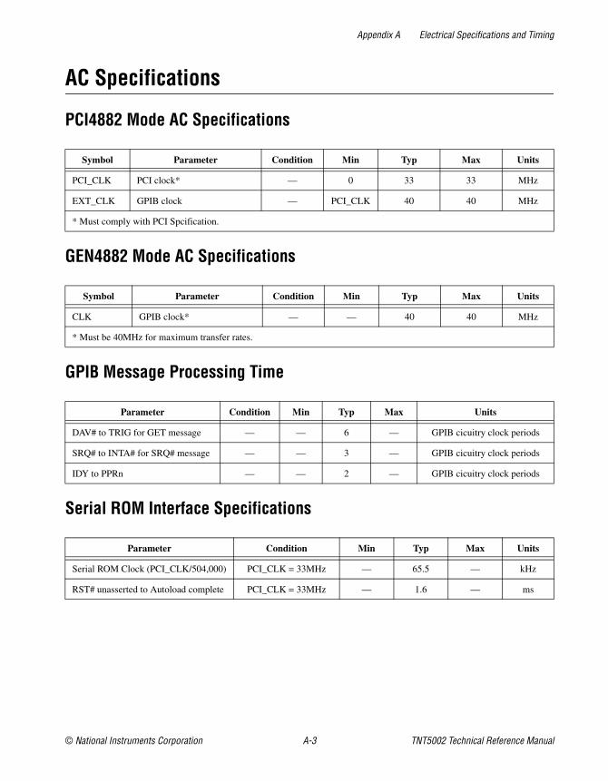
Appendix A Electrical Specifications and Timing
© National Instruments Corporation A-3 TNT5002 Technical Reference Manual
AC Specifications
PCI4882 Mode AC Specifications
GEN4882 Mode AC Specifications
GPIB Message Processing Time
Serial ROM Interface Specifications
Symbol Parameter Condition Min Typ Max Units
PCI_CLK PCI clock* — 0 33 33 MHz
EXT_CLK GPIB clock — PCI_CLK 40 40 MHz
* Must comply with PCI Spcification.
Symbol Parameter Condition Min Typ Max Units
CLK GPIB clock* — — 40 40 MHz
* Must be 40MHz for maximum transfer rates.
Parameter Condition Min Typ Max Units
DAV# to TRIG for GET message — — 6 — GPIB cicuitry clock periods
SRQ# to INTA# for SRQ# message — — 3 — GPIB cicuitry clock periods
IDY to PPRn — — 2 — GPIB cicuitry clock periods
Parameter Condition Min Typ Max Units
Serial ROM Clock (PCI_CLK/504,000) PCI_CLK = 33MHz — 65.5 — kHz
RST# unasserted to Autoload complete PCI_CLK = 33MHz — 1.6 — ms

Appendix A Electrical Specifications and Timing
TNT5002 Technical Reference Manual A-4 ni.com
PCI Timing Specifications (PCI4882 Mode)These specifications apply to REQ#, GNT#, AD, C/BE#, PAR, PERR#, SERR#, FRAME#, IRDY#, TRDY#, DEVSEL#, STOP#, and IDSEL.
Generic Interface Timing Specifications (GEN4882 Mode)These specifications apply to IOA, IOD, IOWR, IORD, INT, HWORD#, DACK#, DRQ, and CS#.
Symbol Parameter Min Typ Max Units
Tval PCI_CLK to Signal Valid (bused signals) 2 — 11 ns
Tval(ptp) PCI_CLK to Signal Valid (point-to-point signals) 2 — 12 ns
Ton Float to active delay 2 — — ns
Toff Active to float delay — — 28 ns
Tsu Input setup time to PCI_CLK (bused signals) 7 — — ns
Tsu Input setup time to PCI_CLK (GNT#) 10 — — ns
Th Input signal hold time from PCI_CLK 0 — — ns
Trst-off Reset active to Output Float — — 40 ns
Symbol Parameter Min Typ Max Units
Tval Clock to Signal Valid 2 — 11 ns
Tsu Input setup time to clock 7 — — ns
Th Input signal hold time from clock 0 — — ns
Ton Float to active delay 2 — — ns
Toff Active to float delay — — 28 ns
Trst-off Reset active to Output Float — — 40 ns

Appendix A Electrical Specifications and Timing
© National Instruments Corporation A-5 TNT5002 Technical Reference Manual
Thermal Specifications
144 QFP
Symbol Parameter Condition Max Units
Tj1 Junction Temperature — 86 °C
Ψjt Thermal Characterizaton Junction to Top of Case — 2.4 °C/W
θja Thermal Resistance from Junction to Ambient 0 m/s 26 °C/W
θjma Thermal Resistance from Junction to Ambient 1 m/s 23 °C/W
θjma Thermal Resistance from Junction to Ambient 2 m/s 21 °C/W
1 Junction temperature, Tj, at rated ambient Ta = 70C.
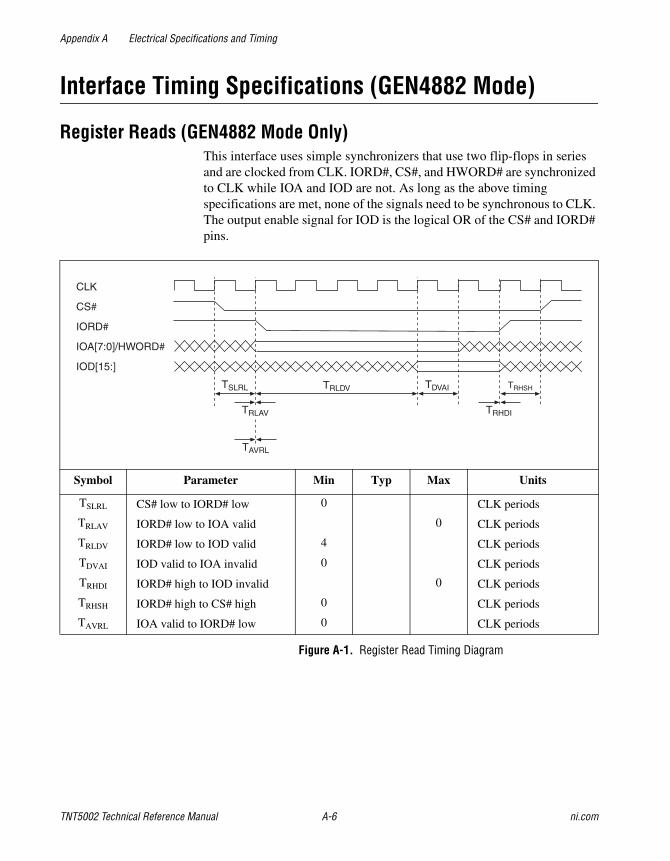
Appendix A Electrical Specifications and Timing
TNT5002 Technical Reference Manual A-6 ni.com
Interface Timing Specifications (GEN4882 Mode)
Register Reads (GEN4882 Mode Only)This interface uses simple synchronizers that use two flip-flops in series and are clocked from CLK. IORD#, CS#, and HWORD# are synchronized to CLK while IOA and IOD are not. As long as the above timing specifications are met, none of the signals need to be synchronous to CLK. The output enable signal for IOD is the logical OR of the CS# and IORD# pins.
Figure A-1. Register Read Timing Diagram
Symbol Parameter Min Typ Max Units
TSLRL CS# low to IORD# low 0 CLK periods
TRLAV IORD# low to IOA valid 0 CLK periods
TRLDV IORD# low to IOD valid 4 CLK periods
TDVAI IOD valid to IOA invalid 0 CLK periods
TRHDI IORD# high to IOD invalid 0 CLK periods
TRHSH IORD# high to CS# high 0 CLK periods
TAVRL IOA valid to IORD# low 0 CLK periods
CLK
CS#
IORD#
IOA[7:0]/HWORD#
IOD[15:]
TSLRL TRLDV TDVAI
TRLAV TRHDI
TRHSH
TAVRL

Appendix A Electrical Specifications and Timing
© National Instruments Corporation A-7 TNT5002 Technical Reference Manual
Register Writes (GEN4882 Mode Only)This interface uses simple synchronizers that use two flip-flops in series and are clocked from CLK. IOWT#, CS#, and HWORD# are synchronized to CLK while IOA and IOD are not. Data is stored on the next rising clock edge after the synchronized IOWT# and CS# signals have been asserted. As long as the above timing specifications are met, none of the signals need be synchronous to CLK.
Figure A-2. Register Write Timing Diagram
Symbol Parameter Min Typ Max Units
TSLWL CS# low to IOWR# low 0 CLK periods
TWLADV IOWR# low to IOA/IOD valid 0 CLK periods
TWLWH IOWR# low to IOWR# high 4 CLK periods
TWHDI IOWR# high to IOD invalid 0 CLK periods
TWHAI IOWR# high to IOA invalid 0 CLK periods
TWHSH IOWR# high to CS# high 0 CLK periods
CLK
CS#
IOWT#
IOA[7:0]/HWORD#
IOD[15:]
TSLWL TWLDI TQLAH
TWLDV TWLDV

Appendix A Electrical Specifications and Timing
TNT5002 Technical Reference Manual A-8 ni.com
DMA Reads (GEN4882 Mode Only)This interface uses simple synchronizers that use two flip-flops in series and are clocked from CLK. IORD# and DACK# are synchronized to CLK while IOA and IOD are not. As long as the above timing specifications are met, none of the signals need be synchronous to CLK.
Figure A-3. DMA Read Timing Diagram
To read multiple words, DACK# may remain asserted during multiple assertions/unassertions of IORD#. IORD# must unassert after each word.
When the last word is read from the GFIFO, DRQ will unassert within four clock cycles of IORD# asserting.
Symbol Parameter Min Typ Max Units
TQHAL DRQ high to DACK# low 0 CLK periods
TALRL DACK# low to IORD# low 0 CLK periods
TRLDV IORD# low to IOD valid 4 CLK periods
TRLQL IORD# low to DRQ low 4 CLK periods
TQLAH DRQ low to DACK# high 0 CLK periods
TRHDI IORD# high to IOD invalid 0 CLK periods
TRHRL IORD# high to IORD# low 2 CLK periods
CLK
DRQ
DACK#
IORD#
IOD[15:]
TQHAL TALRL TRLDV
TRLQL
TQLAH
TRHDI
TRHRL
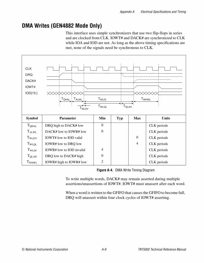
Appendix A Electrical Specifications and Timing
© National Instruments Corporation A-9 TNT5002 Technical Reference Manual
DMA Writes (GEN4882 Mode Only)This interface uses simple synchronizers that use two flip-flops in series and are clocked from CLK. IOWT# and DACK# are synchronized to CLK while IOA and IOD are not. As long as the above timing specifications are met, none of the signals need be synchronous to CLK.
Figure A-4. DMA Write Timing Diagram
To write multiple words, DACK# may remain asserted during multiple assertions/unassertions of IOWT#. IOWT# must unassert after each word.
When a word is written to the GFIFO that causes the GFIFO to become full, DRQ will unassert within four clock cycles of IOWT# asserting.
Symbol Parameter Min Typ Max Units
TQHAL DRQ high to DACK# low 0 CLK periods
TALWL DACK# low to IOWR# low 0 CLK periods
TWLDV IOWT# low to IOD valid 0 CLK periods
TWLQL IOWR# low to DRQ low 4 CLK periods
TWLDI IOWR# low to IOD invalid 4 CLK periods
TQLAH DRQ low to DACK# high 0 CLK periods
TWHWL IOWR# high to IOWR# low 2 CLK periods
CLK
DRQ
DACK#
IOWT#
IOD[15:]
TQHAL TALWL TWLDI
TWLQL TQLAHTWLDV
TWHWL

© National Instruments Corporation B-1 TNT5002 Technical Reference Manual
BMechanical Information
PackagingThe TNT5002 is implemented in a standard 144-pin plastic quad flat pack (PQFP) package and a 256-ball plastic fine-pitch ball grid array (FPBGA).
QFP Package
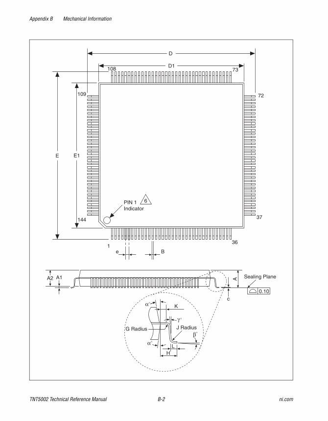
Appendix B Mechanical Information
TNT5002 Technical Reference Manual B-2 ni.com
108
109
E1
144
PIN 1Indicator
6
D
D173
72
37
36
Be1
A2 A1 Sealing PlaneA
c0.10
G Radius J Radius
K
HL
E

Appendix B Mechanical Information
© National Instruments Corporation B-3 TNT5002 Technical Reference Manual
Symbol Dimension Min Nom Max
A Package overall height1 3.5 mm 3.7 mm 4.07 mm
A1 Package standoff height 0.13 mm 0.29 mm 0.43 mm
A2 Package thickness 3.17 mm 3.41 mm 3.67 mm
D Package overall width 31.90 BSC2 mm
D1 Package width 28.00 BSC2 mm
E Package overall length 31.90 BSC2 mm
E1 Package length 28.00 BSC2 mm
L Foot length 0.63 mm 0.84 mm 1.03 mm
e Lead pitch 0.65 BSC2
B Lead width 0.22 mm — 0.38 mm
c Lead thickness 0.10 mm 0.15 mm 0.23 mm
α — 8 degrees — 16 degrees
β — 0 degrees — 7 degrees
γ — 0 degrees — 10 degrees
G Foot radius 0.08 degrees 0.23 degrees —
H Lead length1 1.95 REF mm
J Ankle radius 0.20 degrees 0.30 degrees 0.50 degrees
K Foot length 0.20 mm — —
2H3 — 3.9 mm
1 The value for this measurement is for reference only.2 ANSI Y14.5M-1982, American National Standard Dimensioning and Tolerancing, Section 1.3.2, defines Basic Dimension (BSC) as: A numerical value used to describe the theoretically exact size, profile, orientation, or location of a feature or datum target. It is the basis from which permissible variations are established by tolerances on other dimensions, in notes, or in feature control frames.3 The consistency within each option is the “Footprint” dimension, “2H.” This is the dimension of the feature calculated by subtracting the package body dimension “D1,” from the lead tip-to-tip dimension “D.”

Appendix B Mechanical Information
TNT5002 Technical Reference Manual B-4 ni.com
PinoutsThe pinout on the TNT5002 depends on the mode as selected by MODE pin. When this pin is asserted or not connected, the TNT5002 is in PCI mode. When MODE is deasserted, the TNT5002 is in GEN mode. Refer to Chapter 1, Architectural Overview, for a description of each mode.
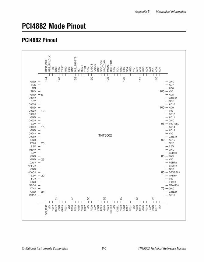
Appendix B Mechanical Information
© National Instruments Corporation B-5 TNT5002 Technical Reference Manual
PCI4882 Mode Pinout
PCI4882 Pinout
GNDTCKTDI
TDOGND
DIO1#3.3V
DIO5#GND
DIO2#DIO6#
GNDDIO3#
3.3VDIO7#
GNDDIO4#DIO8#
GNDEOI#3.3V
REN#3.3VGNDGND
DAV#NRFD#
GNDNDAC#
3.3VIFC#GND
SRQ#ATN#GND
INTA#
GNDAD7AD6VIOAD8C/BE0#GNDAD10AD9VIOAD12AD11GNDVIO_SELAD14AD13VIOC/BE1#AD15GND3.3VGNDSERR#PARVIOPERR#STOP#GNDDEVSEL#TRDY#VIOIRDY#FRAME#GNDC/BE2#AD16
GP
IB_C
LKU
SE
_PC
I_C
LKT
MS
GN
D3.
3VT
RS
TG
ND
3.3V
GN
DD
IS_S
UB
SY
SN
CR
EM
TT
RIG
3.3V
LAD
CS
TAD
CS
GN
DS
RQ
_OE
#S
RQ
_DAT
AM
OD
EU
SE
_RO
M3.
3VS
CL
GN
D3.
3VS
DA
GN
DV
IOA
D1
AD
0G
ND
AD
3A
D2
VIO
AD
5A
D4
PC
I_C
LK VIO
RS
T#
RE
Q#
GN
DG
NT
#A
D31
VIO
AD
30A
D29
GN
DA
D28
AD
27V
IOA
D26
3.3V
GN
DA
D25
GN
DA
D24
C/B
E3#
VIO
IDS
EL
AD
23G
ND
AD
22A
D21
VIO
AD
20A
D19
GN
DA
D18
3.3V
GN
DA
D17
VIO
5
10
15
20
25
30
35
105
100
95
90
85
80
75
40 45 50 55 60 65 70
144
140
135
130
125
120
115
110
TNT5002

Appendix B Mechanical Information
TNT5002 Technical Reference Manual B-6 ni.com
PCI4882 Mode
Name Pin
3.3V 7, 14, 21, 23, 30, 52, 69, 88, 120, 123, 131, 137, 140
AD0 115
AD1 116
AD2 112
AD3 113
AD4 109
AD5 110
AD6 106
AD7 107
AD8 104
AD9 100
AD10 101
AD11 97
AD12 98
AD13 93
AD14 94
AD15 90
AD16 73
AD17 71
AD18 68
AD19 66
AD20 65
AD21 63
AD22 62
AD23 60
AD24 56
AD25 54
AD26 51
AD27 49
AD28 48

Appendix B Mechanical Information
© National Instruments Corporation B-7 TNT5002 Technical Reference Manual
AD29 46
AD30 45
AD31 43
ATN# 34
C/BE#0 103
C/BE#1 91
C/BE#2 74
C/BE#3 57
DAV# 26
DEVSEL# 80
DIO1# 6
DIO2# 10
DIO3# 13
DIO4# 17
DIO5# 8
DIO6# 11
DIO7# 15
DIO8# 18
DIS_SUBSYS 135
EOI# 20
FRAME# 76
GND 1, 5, 9, 12, 16, 19, 24, 25, 28, 32, 35, 41, 47, 53, 55, 61, 67, 70, 75, 81, 87, 89, 96, 102, 108, 114, 118, 121, 128, 136, 138, 141
GNT# 42
EXT_CLK 144
IDSEL 59
IFC# 31
INTA# 36
IRDY# 77
LADCS 130
MODE 125
NDAC# 29
Name Pin

Appendix B Mechanical Information
TNT5002 Technical Reference Manual B-8 ni.com
NRFD# 27
PAR 85
PCI_CLK 37
PERR# 83
REMT 133
REN# 22
REQ# 40
RST# 39
SCL 122
SDA 119
SERR# 86
SRQ# 33
STOP# 82
SRQ_DATA 126
SRQ_OE# 127
TADCS 129
TCK 2
TDI 3
TDO 4
TMS 142
TRDY# 79
TRIG 132
TRST 139
USE_PCI_CLK 143
USE_SER_ROM 124
VIO 38, 44, 50, 58, 64, 72, 78, 84, 92, 99, 105, 111, 117
VIO_SEL 95
* Pins not listed are no-connects.
Name Pin

Appendix B Mechanical Information
© National Instruments Corporation B-9 TNT5002 Technical Reference Manual
GEN4882 Mode Pinout
GEN4882 Pinout
GNDTCKTDI
TDOGND
DIO1#3.3V
DIO5#GND
DIO2#DIO6#
GNDDIO3#
3.3VDIO7#
GNDDIO4#DIO8#
GNDEOI#3.3V
REN#3.3VGNDGND
DAV#NRFD#
GNDNDAC#
3.3VIFC#GND
SRQ#ATN#GND
NC
GNDIOWT#IORD#VIOIOA0VIOGNDIOA2IOA1VIOIOA4IOA3GNDVIO_SELIOA6IOA5VIOVIOIOD0GND3.3VGNDVIOVIOVIOVIOVIOGNDVIOVIOVIOVIOVIOGNDVIOIOD1
CLK
GN
DT
MS
GN
D3.
3VT
RS
TG
ND
3.3V
GN
DN
CN
CR
EM
TT
RIG
3.3V
LAD
CS
TAD
CS
GN
DS
RQ
_OE
#S
RQ
_DAT
AM
OD
EN
C3.
3VN
CG
ND
3.3V
NC
GN
DV
IOH
WO
RD
#D
AC
K#
GN
DR
ES
ET
#C
S#
VIO
DR
QIN
T
VIO
VIO
PW
R_G
OO
DN
CG
ND
VIO
VIO
VIO
IOD
15IO
D14
GN
DIO
D13
IOD
12V
IOIO
D11
3.3V
GN
DIO
D10
GN
DIO
D9
VIO
VIO
GN
DIO
D8
GN
DIO
D7
IOD
6V
IOIO
D5
IOD
4G
ND
IOD
33.
3VG
ND
IOD
2V
IO
5
10
15
20
25
30
35
105
100
95
90
85
80
75
40 45 50 55 60 65 70
144
140
135
130
125
120
115
110
TNT5002

Appendix B Mechanical Information
TNT5002 Technical Reference Manual B-10 ni.com
GEN4882/GEN9914 Mode
Name Pin
3.3V 7, 14, 21, 23, 30, 52, 69, 88, 120, 123, 131, 137, 140, 135
DACK# 115
HWORD# 116
CS# 112
RST# 113
INT 109
DRQ 110
IORD# 106
IOWT# 107
IOA0 104
IOA1 100
IOA2 101
IOA3 97
IOA4 98
IOA5 93
IOA6 94
IOD0 90
IOD1 73
IOD2 71
IOD3 68
IOD4 66
IOD5 65
IOD6 63
IOD7 62
IOD8 60
IOD9 56
IOD10 54
IOD11 51
IOD12 49
IOD13 48

Appendix B Mechanical Information
© National Instruments Corporation B-11 TNT5002 Technical Reference Manual
IOD14 46
IOD15 45
ATN# 34
DAV# 26
DIO1# 6
DIO2# 10
DIO3# 13
DIO4# 17
DIO5# 8
DIO6# 11
DIO7# 15
DIO8# 18
EOI# 20
GND 1, 5, 9, 12, 16, 19, 24, 25, 28, 32, 35, 41, 47, 53, 55, 59, 61, 67, 70, 75, 81, 87, 89, 96, 102, 108, 114, 118, 121, 125, 128, 136, 138, 141, 143
CLK 144
IFC# 31
LADCS 130
NDAC# 29
NRFD# 27
REMT 133
REN# 22
PWR_GOOD 39
SRQ# 33
SRQ_DATA 126
SRQ_OE# 127
TADCS 129
TCK 2
TDI 3
TDO 4
TMS 142
TRIG 132
Name Pin

Appendix B Mechanical Information
TNT5002 Technical Reference Manual B-12 ni.com
TRST 139
VIO 38, 44, 50, 58, 64, 72, 78, 84, 92, 99, 105, 111, 117, 43, 91, 74, 57, 103, 80, 76, 42, 77, 85, 37, 83, 86, 82, 79
VIO_SEL 95
* Pins not listed are no-connects.
Name Pin

© National Instruments Corporation C-1 TNT5002 Technical Reference Manual
CGPIB Remote Messages
Hex Dec ASCII Msg Hex Dec ASCII Msg
00 00 NUL 20 32 SP MLA0
01 01 SOH GTL 21 33 ! MLA1
02 02 STX 22 34 “ MLA2
03 03 ETX 23 35 # MLA3
04 04 EOT SDC 24 36 $ MLA4
05 05 ENQ PPC 25 37 % MLA5
06 06 ACK 26 38 & MLA6
07 07 BEL 27 39 ' MLA7
08 08 BS GET 28 40 ( MLA8
09 09 HT TCT 29 41 ) MLA9
0A 10 LF 2A 42 * MLA10
0B 11 VT 2B 43 + MLA11
0C 12 FF 2C 44 , MLA12
0D 13 CR 2D 45 - MLA13
0E 14 SO 2E 46 . MLA14
0F 15 SI 2F 47 / MLA15
10 16 DLE 30 48 0 MLA16
11 17 DC1 LLO 31 49 1 MLA17
12 18 DC2 32 50 2 MLA18
13 19 DC3 33 51 3 MLA19
14 20 DC4 DCL 34 52 4 MLA20

Appendix C GPIB Remote Messages
TNT5002 Technical Reference Manual C-2 ni.com
15 21 NAK PPU 35 53 5 MLA21
16 22 SYN 36 54 6 MLA22
17 23 ETB 37 55 7 MLA23
18 24 CAN SPE 38 56 8 MLA24
19 25 EM SPD 39 57 9 MLA25
1A 26 SUB 3A 58 : MLA26
1B 27 ESC 3B 59 ; MLA27
1C 28 FS 3C 60 < MLA28
1D 29 GS 3D 61 = MLA29
1E 30 RS 3E 62 > MLA30
1F 31 US 3F 63 ? UNL
40 64 @ MTA0 60 96 ` MSA0, PPE
41 65 A MTA1 61 97 a MSA1, PPE
42 66 B MTA2 62 98 b MSA2, PPE
43 67 C MTA3 63 99 c MSA3, PPE
44 68 D MTA4 64 100 d MSA4, PPE
45 69 E MTA5 65 101 e MSA5, PPE
46 70 F MTA6 66 102 f MSA6, PPE
47 71 G MTA7 67 103 g MSA7, PPE
48 72 H MTA8 68 104 h MSA8, PPE
49 73 I MTA9 69 105 i MSA9, PPE
4A 74 J MTA10 6A 106 j MSA10, PPE
4B 75 K MTA11 6B 107 k MSA11, PPE
4C 76 L MTA12 6C 108 l MSA12, PPE
4D 77 M MTA13 6D 109 m MSA13, PPE
4E 78 N MTA14 6E 110 n MSA14, PPE
Hex Dec ASCII Msg Hex Dec ASCII Msg

Appendix C GPIB Remote Messages
© National Instruments Corporation C-3 TNT5002 Technical Reference Manual
4F 79 O MTA15 6F 111 o MSA15, PPE
50 80 P MTA16 70 112 p MSA16, PPD
51 81 Q MTA17 71 113 q MSA17, PPD
52 82 R MTA18 72 114 r MSA18, PPD
53 83 S MTA19 73 115 s MSA19, PPD
54 84 T MTA20 74 116 t MSA20, PPD
55 85 U MTA21 75 117 u MSA21, PPD
56 86 V MTA22 76 118 v MSA22, PPD
57 87 W MTA23 77 119 w MSA23, PPD
58 88 X MTA24 78 120 x MSA24, PPD
59 89 Y MTA25 79 121 y MSA25, PPD
5A 90 Z MTA26 7A 122 z MSA26, PPD
5B 91 [ MTA27 7B 123 MSA27, PPD
5C 92 \ MTA28 7C 124 | MSA28, PPD
5D 93 ] MTA29 7D 125 MSA29, PPD
5E 94 ^ MTA30 7E 126 ~ MSA30, PPD
5F 95 _ UNT 7F 127 DEL
DCL Device Clear MTA My Talk Address SPD Serial Poll DisableGET Group Execute Trigger PPC Parallel Poll Configure SPE Serial Poll EnableGTL Go To Local PPD Parallel Poll Disable TCT Take ControlLLO Local Lockout PPE Parallel Poll Enable UNL UnlistenMLA My Listen Address PPU Parallel Poll Unconfigure UNT UntalkMSA My Secondary Adddress SDC Selected Device Clear
Hex Dec ASCII Msg Hex Dec ASCII Msg

© National Instruments Corporation D-1 TNT5002 Technical Reference Manual
DTechnical Support and Professional Services
Visit the following sections of the National Instruments Web site at ni.com for technical support and professional services:
• Support—Online technical support resources at ni.com/support include the following:
– Self-Help Resources—For immediate answers and solutions, visit the award-winning National Instruments Web site for software drivers and updates, a searchable KnowledgeBase, product manuals, step-by-step troubleshooting wizards, thousands of example programs, tutorials, application notes, instrument drivers, and so on.
– Free Technical Support—All registered users receive free Basic Service, which includes access to hundreds of Application Engineers worldwide in the NI Developer Exchange at ni.com/exchange. National Instruments Application Engineers make sure every question receives an answer.
• Training and Certification—Visit ni.com/training for self-paced training, eLearning virtual classrooms, interactive CDs, and Certification program information. You also can register for instructor-led, hands-on courses at locations around the world.
• System Integration—If you have time constraints, limited in-house technical resources, or other project challenges, NI Alliance Program members can help. To learn more, call your local NI office or visit ni.com/alliance.
If you searched ni.com and could not find the answers you need, contact your local office or NI corporate headquarters. Phone numbers for our worldwide offices are listed at the front of this manual. You also can visit the Worldwide Offices section of ni.com/niglobal to access the branch office Web sites, which provide up-to-date contact information, support phone numbers, email addresses, and current events.