top-down design of dsp systems - radar remote sensing group
TRANSCRIPT

TOP-DOWN DESIGN OF DSP SYSTEMS: A CASE STUDY
Yann Grégor Tréméac
A dissertation submitted in fulfilment of the
requirements for the degree of Master of Science in
Engineering (Electrical)
University of Cape Town,
1999

DECLARATION
I declare that this dissertation is my own, unaided work. It is being submitted for
the degree of Master of Science in Engineering in the University of Cape Town. It
has not been submitted before for any degree on examination in any other
university.
…………………………
Signature of Author
Cape Town September 1999
ABSTRACT
The primary goal of this thesis is to investigate the use of a formal top-down
methodology for designing digital signal processing systems. As a case study, the
design of a synthetic aperture radar (SAR) digital preprocessor is attempted. The
preprocessor is targeted for the Texas Instruments’ TMS320C80 DSP. In other
work linked to this project, the same preprocessor was implemented by Grant
Carter on a field programmable gate array (FPGA) [2]. Secondary goals of this
thesis are to document the various tools and techniques used to accelerate
prototyping, and to compare the DSP and the FPGA implementation.
The proposed methodology starts with the client specifications to create an initial
abstract decomposition of the application. This model is then refined until the final
design is obtained. The development process is broken down into four steps: the
specification, the functional design (preliminary hardware-independent design),
the implementation definition (detailed hardware-dependent design) and the
implementation steps. A successful implementation is shown to follow from this
process.
The case study experience shows that the top-down approach undoubtedly has its
advantages for designing DSP systems, although it must be accompanied by
bottom-up principles. One of the advantages is that more emphasis is placed at
design level and that the designer is initially forced to think about the solution in a
hardware-independent way. Thus, the designer is more likely to produce reusable
specifications and solutions of general applicability.
The use of C as the programming language definitely increased the programmer
productivity, as opposed to Assembler. The C80 multitasking operating system
also helped in the transition from functional to executive model. However, the use
of both C and the multitasking operating system has an execution time cost that
cannot precisely be evaluated. This constitutes a major drawback: it means that
algorithm complexity (i.e. the number of mathematical operations involved) must
be evaluated at functional design level and that the DSP must be chosen with

speed and memory capabilities largely superior to the algorithm complexity
evaluation. In our case, the ratio between the time based on the algorithm
complexity evaluation and the actual program execution time is approximately
one to three.
Some comparisons have been carried out with the FPGA’s implementation [2].
The specification and functional design steps lead to similar results, but major
differences exist in the hardware-dependent design. Generally speaking, the
implementation of a system in an FPGA implies working at a less abstract level
than the mapping of a functional design onto a DSP.

ACKNOWLEDGMENTS
I wish to express my gratitude to all those who, by their advice, comments and
constructive criticisms, contributed to this thesis project.
I would especially like to thank Professor Mike Inggs for his unfailing assistance
throughout the period of development; Jasper Horrell for his help with the SAR
theory, his comments and ideas; Grant Carter whose experience on FPGAs has
been greatly useful; Amit and Thomas Bennett for their advice and comments.
Sincere thanks to Rolf Lengenfelder whose simulator is a priceless gift for the
radar remote sensing group.

ii
TABLE OF CONTENTS
1. OVERVIEW...........................................................................................................................9
2. DESIGN METHODOLOGY ..............................................................................................12
2.1 THE DESCRIPTION MODEL 13 2.2 THE DEVELOPMENT PROCESS 14
2.2.1 The Specification step 14 2.2.2 The Functional Design step 14 2.2.3 The Implementation Definition step 15 2.2.4 The Implementation step 15
2.3 CONCLUSIONS 16
3. THE TMS320C80 DSP ........................................................................................................18
3.1 DSP ARCHITECTURES: A BRIEF OVERVIEW 18 3.2 THE TMS320C80 ARCHITECTURE 20 3.3 THE PROGRAMMING ENVIRONMENT 22
3.3.1 The Software Development Board 22 3.3.2 The developing tools 23 3.3.3 The multitasking executive 24
3.4 CONCLUSIONS 25
4. THE SPECIFICATION STEP............................................................................................26
4.1 RADAR BACKGROUND 26 4.1.1 SAR concepts 26
4.2 REQUIREMENTS 33 4.3 FROM REQUIREMENTS TO SPECIFICATIONS 34 4.4 CONCLUSION : TOP-LEVEL DESCRIPTION MODEL 35
5. THE FUNCTIONAL DESIGN STEP ................................................................................37
5.1 PROPOSED MODELS 37 5.2 FILTER DESIGN 39
5.2.1 The phase aspect 39 5.2.2 Coefficient calculation 40 5.2.3 Filter designing tools 41 5.2.4 Filter quantisation effects 42
5.3 ANALYSING MODELS ALGORITHM 43 5.3.1 The Presummer/Prefilter frequency response 43 5.3.2 Comparing the model frequency responses of both models 44 5.3.3 Refining the Presummer and Prefilter models 45 5.3.4 Comparing both model algorithm complexity 45
5.4 ALGORITHM VALIDATION: SIMULATING THE PREPROCESSOR 46 5.4.1 The simulation set-up 46 5.4.2 The simulation results 47
5.5 MODEL REFINEMENTS 54 5.5.1 The data width consideration 54 5.5.2 The real-time consideration 55
5.6 CONCLUSION: FUNCTIONAL-LEVEL DESCRIPTION MODEL 55

iii
6. THE IMPLEMENTATION DEFINITION STEP ............................................................58
6.1 THE DIFFERENT DESIGN CHOICES 58 6.1.1 Choosing the C80 58 6.1.2 The appropriate use of the C80’s resources 60 6.1.3 C language and Assembler 60 6.1.4 The multitasking executive 61 6.1.5 Memory organisation 61 6.1.6 Single and Double Transfer Models 62 6.1.7 Means of communication 63 6.1.8 The test bench 64
6.2 REFINING THE MODEL 64 6.2.1 External memory assignments 64 6.2.2 Internal memory assignments 67 6.2.3 Tasks refining 68 6.2.4 Semaphores 69 6.2.5 The PP programs 70
6.3 CONCLUSION: THE EXECUTIVE-LEVEL DESCRIPTION MODEL. 70
7. THE IMPLEMENTATION STEP .....................................................................................79
7.1 THE FOUR IMPLEMENTATIONS 79 7.2 IMPLEMENTATION AND FUNCTIONAL VERIFICATION 80 7.3 SPEED VERIFICATION 81 7.4 CHOSEN DESIGN SPEED ANALYSIS 83 7.5 CONCLUSIONS 86
8. CONCLUSIONS AND RECOMMENDATIONS .............................................................87
APPENDIX A. SAR PARAMETER CALCULATIONS.........................................................90
APPENDIX B. THE FIR FILTERS ..........................................................................................94
APPENDIX C. THE SIMULATION.......................................................................................103
C.1 THE RAW&PRESUM DIRECTORY 103 C.2 THE PREFILT DIRECTORY 104 C.3 THE RAW_52 DIRECTORY 105 C.4 THE MATLAB DIRECTORY 105 C.5 THE TEST BENCH DIRECTORY 106
APPENDIX D. THE C80 PROGRAMS..................................................................................107
D.1 THE PP C COMPILER BENCHMARK DIRECTORY 108 D.1.1 The source sub-directory 108 D.1.2 The include sub-directory 108 D.1.3 The obj sub-directory 109 D.1.4 The exe sub-directory 109
D.2 THE DD, DS, SD AND SS DIRECTORIES 109 D.2.1 The source sub-directory 109 D.2.2 The include sub-directory 110 D.2.3 The obj sub-directory 110 D.2.4 The exe sub-directory 111

iv
LIST OF FIGURES
FIGURE 1: DFD SYMBOLS..........................................................................................................13
FIGURE 2: V-MODEL OF OVERALL DEVELOPMENT CYCLE .............................................16
FIGURE 3: THE C80 BLOCK DIAGRAM....................................................................................20
FIGURE 4: TMS320C80 SDB COMPONENTS ............................................................................22
FIGURE 5: PERFOMANCE OF THE PP C COMPILER..............................................................23
FIGURE 6: SIMPLIFIED SAR GEOMETRY, STRIPMAP MODE..............................................27
FIGURE 7: SAR BLOCK DIAGRAM ...........................................................................................27
FIGURE 8: PHASE AND DOPPLER OF RETURNS FROM ONE POINT TARGET..... ERROR!
BOOKMARK NOT DEFINED.
FIGURE 9: THE AZIMUTH AND RANGE COMPRESSIONS ...................................................32
FIGURE 10: THE CONTEXT DIAGRAM ....................................................................................35
FIGURE 11: SINGLE-STAGE MODEL ........................................................................................38
FIGURE 12: DUAL-STAGE MODEL ...........................................................................................39
FIGURE 13: VISUALISING THE EFFECTS OF QUANTISATION ...........................................42
FIGURE 14: DUAL-STAGE MODEL INTERMEDIATE AND GLOBAL FREQUENCY
RESPONSES ...................................................... ERROR! BOOKMARK NOT DEFINED.
FIGURE 15: THE SINGLE (GREY) AND DUAL-STAGE MODEL FREQUENCY RESPONSES
...............................................................................................................................................44
FIGURE 16: RAW DATA, MAGNITUDE ....................................................................................49
FIGURE 17: TWO SITUATIONS IN RANGE SAMPLING.........................................................49
FIGURE 18: SIMULATION WITH FILTER RICE31 ...................................................................50
FIGURE 19: REFERENCE MATRIX ............................................................................................51
FIGURE 20: FILTERING SIDE EFFECTS WITH A 31-TAP (LEFT) AND A 63-TAP FILTER 52
FIGURE 21: FOCUSED NON FILTERED AND FILTERED (‘RICE31’) RETURNS ................53
FIGURE 22: FILTERED AND AZIMUTH COMPRESSED DATA, COMBO FILTER..............54
FIGURE 23: DATA FLOW DIAGRAM, FUNCTIONAL LEVEL ...............................................56
FIGURE 24: PRESUMMER FLOW CHART ................................................................................57
FIGURE 25: PREFILTER FLOW CHART ....................................................................................57
FIGURE 26: THE DATA BLOCKS FILTERING STEPS (NUMBER 1 TO N) VERSUS TIME.62
FIGURE 27: THE INPUT-PRESUMMER DOUBLE BUFFER. ...................................................65
FIGURE 28: THE PRESUMMER-PREFILTER CIRCULAR BUFFER .......................................66
FIGURE 29: THE INTERNAL PRESUMMER SINGLE BUFFER ..............................................67
FIGURE 30: ONE OF THE FOUR INTERNAL PREFILTER BUFFERS ....................................68
FIGURE 31: DFD, TASK LEVEL..................................................................................................72
FIGURE 32: DFD, MP-PPS LEVEL ..............................................................................................73

v
FIGURE 33: THE TASK TIMING DIAGRAM .............................................................................74
FIGURE 34: THE PRESUMMER TASK FLOW CHART ............................................................75
FIGURE 35: THE INPUT PREFILTER TASK FLOW CHART ...................................................76
FIGURE 36: THE PREFILTER TASK FLOW CHART................................................................77
FIGURE 37: THE OUTPUT PREFILTER TASK FLOW CHART ...............................................78
FIGURE 38: THE PRESUMMER THROUGHPUT, SD IMPLEMENTATION...........................85
FIGURE 39: THE OUTPUT THROUGHPUT, SD IMPLEMENTATION....................................85
FIGURE 40: ‘COMBO’ FILTER IMPULSE RESPONSE.............................................................96
FIGURE 41: ‘COMBO’ FILTER FREQUENCY RESPONSE ......................................................96
FIGURE 42: ‘HAM15’ FILTER IMPULSE RESPONSE ..............................................................97
FIGURE 43: ‘HAM15’ FILTER FREQUENCY RESPONSE .......................................................97
FIGURE 44: ‘HAM31’ FILTER IMPULSE RESPONSE ..............................................................98
FIGURE 45: ‘HAM31’ FILTER FREQUENCY RESPONSE .......................................................98
FIGURE 46: ‘RECT31’ FILTER IMPULSE RESPONSE .............................................................99
FIGURE 47: ‘RECT31’ FILTER FREQUENCY RESPONSE.......................................................99
FIGURE 48: ‘RICE31’ FILTER IMPULSE RESPONSE.............................................................100
FIGURE 49: ‘RICE31’ FILTER FREQUENCY RESPONSE......................................................100
FIGURE 50: ‘RICE63’ FILTER IMPULSE RESPONSE.............................................................101
FIGURE 51: ‘RICE63’ FILTER FREQUENCY RESPONSE......................................................101
FIGURE 52: ‘RICE81’ FILTER IMPULSE RESPONSE.............................................................102
FIGURE 53: ‘RICE81’ FILTER FREQUENCY RESPONSE......................................................102

vi
LIST OF TABLES
TABLE 1: BASIC SASAR 1 CHARACTERITICS........................................................................33
TABLE 2: AUXILLIARY SASAR 1 PARAMETERS...................................................................33
TABLE 3: BOTH MODEL ALGORITHM COMPLEXITIES.......................................................45
TABLE 4: INTEGRATED NOISE VERSUS FILTER...................................................................51
TABLE 5: THE FOUR IMPLEMENTATION THROUGHPUTS .................................................82

vii
LIST OF ACRONYMS
A/D Analogue to Digital
COTS Commercial-off the shelf
D/A Digital to Analogue
DD One of the four TMS320C80 implementations, see 7.1.
DFD Data Flow Diagram
DMA Direct Memory Access
DRAM Dynamic Random Access Memory
DS One of the four TMS320C80 implementations, see 7.1.
DSP Digital Signal Processor
DTM Double Transfer Model, see 6.1.6
FIR Finite Impulse Response
FFT Fast Fourier Transform
FPGA Field Programmable Gate Array
IIR Infinite Impulse Response
IPC Inter-Processor Communication
PP Parallel Processor
PRF Pulse Repetition Frequency
PRI Pulse Repetition Interval
viii
MAC Multiply-ACcumulate
MIPS Mega Instruction Per Second
MOPS Mega Operation Per Second
MP Master Processor
MVP Multimedia Video Processor
RASSP Rapid Prototyping of Application Specific Digital Signal Processor
RISC Reduced Instruction Set Computer
RTOS Real-Time Operating System
SAR Synthetic Aperture Radar
SD One of the four TMS320C80 implementations, see 7.1.
SDB Software Development Board
SS One of the four TMS320C80 implementations, see 7.1.
STD State Transition Diagram
STM Single Transfer Model, see 6.1.6
TC Transfer Controller
TTM Time-To-Market
VC Video Controller
VHF Very High Frequency
VP Virtual Prototyping
VRAM Video Random Access Memory

1. Overview
9
1. Overview
Digital signal processing is concerned with the representation, transformation and
manipulation of digitally represented signals. Today, digital signal processing
algorithms and hardware are prevalent in a wide range of systems, from high-volume
consumer electronics (e.g. facsimile, disk drives and car radios), through industrial
systems (e.g. robots and assembly lines) to highly specialised military applications
(e.g. satellites and rockets). In the next few years, the technology will allow the rise of
applications such as speech or handwriting recognition, video conferencing, adaptive
noise cancellation on automobiles and aircraft, adaptive vehicular suspension, to name
a few.
Along with the rising popularity and complexity of digital signal processing
applications, the system designers are now facing increased pressure to create
products quickly and inexpensively. Time-to-market (TTM) has become the key
factor in the success of these products in the competitive electronics marketplace. In
addition to rapid integration, the designers must bear in mind that, with continually
shifting technology and declining lifetime products, a design description is likely to
‘sit’ in different hardware solutions. In other terms, portability of design specifications
must be ensured, in order to improve detailed documentation, maintainability, and
rapid re-targeting of the implementation.
The use of commercial-off-the-shelf (COTS) products as hardware supports, and
conventional C language, for programming general-purpose digital signal processors
(DSP)1 can be seen as means to achieve reductions in overall development time.
1 The term general-purpose DSP is used here to differentiate the chip family from the FPGA or ASIC families which can also be considered as digital signal processors. However, we are using the abbreviation DSP all along the dissertation because it is both more convenient and generally agreed as the term to name those processors.

1. Overview
10
Equally, formal methodologies may be used to improve readability and
maintainability of quality solutions.
The main goal of this thesis is precisely to investigate the use of a methodology for
specifying, designing, and implementing DSP systems. The proposed formal
methodology, detailed in the next chapter, has been developed by J.P Calvez [1]:
characterised by a top-down and system approach, the development process starts
with the customer’s needs, and successively refines models and requirements to
finally obtain the implemented solution. As a case study, the design of a synthetic
aperture radar (SAR) digital preprocessor is attempted. The preprocessor is targeted
for the Texas Instruments’ TMS320C80 DSP. In other work linked to this project, the
same preprocessor was implemented by Grant Carter on a field programmable gate
array (FPGA) [2]. Along with the methodology, the thesis will investigate the various
tools and methods used to reduce the TTM. Furthermore, it will summarise the
difference and similarities encountered between programming a DSP and
programming a FPGA.
Thesis Outlines
The thesis is organised into eight chapters. A brief overview of each of them follows:
Chapter 2 introduces the framework for the design and implementation of the case
study. The development process is broken down into four steps: the Specification, the
Functional Design (Preliminary Design), the Implementation Definition (Detailed
Design) and the Implementation steps. These steps are detailed in the chapter, together
with the modelling graphs. Particular attention is put on the diverse methods used to
reduce the time spent for implementation.
The third chapter describes some hardware features common to DSPs, pointing out
their performance for signal processing applications. The chapter, among other things,
explains how the architectural diversity of DSPs leads to difficulties when one has to
choose the right processor for a specific job. Then, the chapter focuses on the Texas
Instruments’ TMS320C80 and its programming environment.

1. Overview
11
Chapter 4 details the first step of the development process, the specification step. Prior
to the presentation of the case study is the necessary introduction to some radar
concepts.
Chapter 5 describes the functional design step in the development process. Finite
impulse response (FIR) design techniques are also described. Finally, the resulting
functional model is tested and the client requirements verified.
Chapter 6 discusses the implementation definition of the Preprocessor. The functional
model is refined here into a hardware-dependent model. The chapter is first structured
as a catalogue of the different technical solutions preferred. It finishes with memory
and task refinements.
Chapter 7 focuses on the implementation of the Preprocessor. The program
functionality is verified with the help of the test bench created during the functional
model simulation. Finally, the timing constraints set during the specification step are
validated and discussed.
The last chapter contains the conclusions drawn from the case study development
experience. Here, the advantages and limitations of the methodology and the methods
used during the implementation step, together with the differences between the
TMS320C80 and the FPGA solutions, are discussed.
2. Design Methodology
12
2. Design Methodology
During the past decade, several different designing methodologies have been
developed, mainly because of the increasing TTM pressure and complexity of the
systems. A non-exhaustive list of these design methods follows:
• Object oriented methods: Object Orient Design (OOD [3]), Object Modelling
Techniques (OMT [4]), and Unified Modelling Language (UML [5]). Today, these
techniques are applied in data base and software applications. Most of the time, the
use of these methods is conditional on the possibility of using object-oriented
languages for software implementation.
• Structured methods: Structured Analysis and Structured Design (SA and SD,
[6]-[7]). Hatley-Pirbhai [8] and Ward-Mellor [9] have added real-time concerns to the
structured method. These are among the most popular methods used in the industrial
world (probably because they are the most ancient), especially for control and real-
time applications.
• Software-Hardware Co-Design Methods: This has been the hot design topic of
the past few years. Co-design aims at managing the heterogeneity of the systems to be
designed within an integrated design environment. Some techniques such as Virtual
Prototyping (VP), under the auspices of the Rapid Prototyping of Application Specific
Digital Signal Processor (RASSP) program, have started to show promising results.
However, they are still at development stage (e.g. VP needs the presence of
simulation models for every hardware components used in the prototype: these
models are still scarce in practice [10] and [2]).
The case study development process framework is greatly inspired by J.P. Calvez’s
methodology [1]. This formal methodology is ahead of most of the techniques
described above and facilitates the choice of the most appropriate to be used,

2. Design Methodology
13
satisfying the imposed implementation constraints. Characterised by a top-down and
system approach, the methodology breaks the development into four steps:
specification, functional design, implementation definition and implementation steps.
This methodology was developed for electronic systems in the broadest sense of the
term. In the following sections, we will narrow the methodology scope down to digital
signal processing systems.
2.1 The Description Model
J.P. Calvez starts from the principles that any system can be observed, at any of the
development stages, by three complementary views:
• A spatial view: the spatial view describes the functionality of the system. A Data
Flow Diagram (DFD) is generally agreed upon as the standard diagram to use. The
symbols used in a DFD are presented in Figure 1. (For event-driven applications, one
can add to the DFD a Control Flow Diagram, see Hatley&Pirbhai [8]).
• A temporal view: it describes the behaviour of each function described in the
spatial view. Different models can be used here: software sequential codes can be
described with Flow Charts or description algorithms, hardware control loops with
State Transition Diagram (STD), concurrent tasks with Timing Diagrams, etc …
• An executive view: this is a description of the ‘executive’ support of the system,
in other words the hardware or the software components.
Figure 1: DFD Symbols
Time Discrete Data FlowTime Continuous Data Flow
EventData Store
Terminator (Source or Sink)
Functions

2. Design Methodology
14
Note that these views are quite similar to the functional, dynamic and object views in
the OO modelling technique.
2.2 The Development Process
As said previously the methodology is globally top-down: it starts from the customer's
problem to search for an appropriate implementation by successive approaches. Each
of the steps must produce a view of the system at the specific level. Specification,
functional design, implementation definition and implementation steps are described
below.
2.2.1 The Specification step
The specification step aims at defining a complete but purely external description of
the system to be designed, starting with the customer’s requirements. The
specifications are of functional (e.g. the system must filter the input data),
operational (e.g. the filter must run at 5 and 10 MHz) and technical natures (e.g. the
final product must be less than 10 cm long). The functional and operational
specifications are used in the functional design step, whereas the technological
specifications are only used in the implementation definition and implementation
steps. The description model of the system at specification level consists of a DFD,
called Context Diagram, together with the written functional, operational and
technical specifications.
2.2.2 The Functional Design step
The functional design step, or preliminary design, aims at defining the inner
specifications of the system in a complete but hardware-independent way. The
solution for this step is deduced from an analysis of the functional specifications.
First, a functional decomposition is carried out. The design process then consists of
2. Design Methodology
15
successive refinements of the DFD until it can’t be further refined without hardware
assumptions.
For digital systems, the performance and quality of the selected algorithm, with the
specified data word length, chosen filters, and other design criteria, are tested at this
stage. In order to do so, a simulation of the process is performed.
The description model of the system at functional design level consists of a DFD,
together with Flow Charts or STDs (behavioural view).
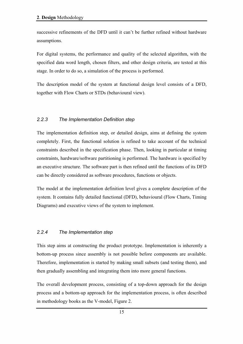
2.2.3 The Implementation Definition step
The implementation definition step, or detailed design, aims at defining the system
completely. First, the functional solution is refined to take account of the technical
constraints described in the specification phase. Then, looking in particular at timing
constraints, hardware/software partitioning is performed. The hardware is specified by
an executive structure. The software part is then refined until the functions of its DFD
can be directly considered as software procedures, functions or objects.
The model at the implementation definition level gives a complete description of the
system. It contains fully detailed functional (DFD), behavioural (Flow Charts, Timing
Diagrams) and executive views of the system to implement.
2.2.4 The Implementation step
This step aims at constructing the product prototype. Implementation is inherently a
bottom-up process since assembly is not possible before components are available.
Therefore, implementation is started by making small subsets (and testing them), and
then gradually assembling and integrating them into more general functions.
The overall development process, consisting of a top-down approach for the design
process and a bottom-up approach for the implementation process, is often described
in methodology books as the V-model, Figure 2.

2. Design Methodology
16
The implementation step is expensive in terms of time and resources. Its development
cost can be reduced by several means:
• The co-designing methods allow the simultaneous development of the hardware
and software implementations.
• The availability and “performance” of developing tools are of importance.
• Existing constituents should be use as often as possible. This strategy is called
reusability. Reusability for hardware has existed for several decades: very complex
components are available on the market for implementation. This point of view is
more recent for software, but it has already significant effects on the application
development cost. It consists of using third-party libraries, real-time executive, and
object-oriented programming methods.
Figure 2: V-model of overall development cycle
2.3 Conclusions
The chapter described the organisational framework that will be used for the
specification, design and implementation of our case study. This case study consists
of prototyping a SAR digital preprocessor on the TMS320C80 DSP. Prior to the case
study presentation is a description of DSPs in general and of the TMS320C80 in
particular.
Implementation Specification
Functional Design
Specification
NEED PRODUCT
Implementation and test
Integration and test
Acceptance and Certification

2. Design Methodology
17

3. The TMS320C80 DSP
18
3. The TMS320C80 DSP
The chapter is divided into three sections. First, common hardware features in DSP
processors are overviewed. This section remains brief, and the reader may refer to
[11] and [12] for more detailed information. The second section focuses on the Texas
Instruments’ TMS320C80 and its features of interest for the development process of
the case study. In the third and last section, the hardware and software environment
accompanying the TMS320C80 is described in detail.
3.1 DSP Architectures: A Brief Overview
DSP processors are designed to support high-performance, repetitive, and numerically
intensive tasks. The two most commonly used signal processing operations are
filtering and computing the Fast Fourier Transform. Reducing their time cost has
greatly motivated the hardware features commonly found in DSP processors. These
features are:
• Multiply-accumulate (MAC) instructions can be performed in a single cycle. In
order to do so, an accumulator and a multiplier are integrated together in the data path.
• Several accesses to memory can be performed in a single instruction cycle. The
separation of data and program memories and busses characterises the so-called
Harvard architecture [11] (the Texas Instruments’ TMS320C10 uses a classic
Harvard architecture).
• Sophisticated address generation units are integrated in DSPs. Modulo-addressing
is used to simplify the use of circular buffers (e.g. the Lucent DSP16xxx) and bit-
reversed addressing, is used to simplify the implementation of certain FFT algorithms
(e.g. the Texas Instruments TMS320C5x family).

3. The TMS320C80 DSP
19
• Hardware loops (e.g. the Analog Devices ADSP-21xx family) allow the
programmer to implement a for-next loop without adding any instruction cycles for
updating and testing the loop counter. This feature is very interesting for highly
repetitive inner-loops.
• The instruction and data caches are generally simpler than the ones used in
general-purpose processors.
• Serial/parallel I/O interfaces and specialised I/O handling mechanisms such as
low-overhead interrupts and direct memory access (e.g. the Motorola DSP563xx
processors provide a six-channel DMA controller).
In addition to these common features, DSPs can add diverse hardware capabilities:
strong support for multiprocessor designs (e.g. the Analog Devices ADSP-2106x
family), A/D and D/A converters (e.g. the Motorola DSP561xx family), or even
microcontroller-like features (e.g. the Motorola’s DSP568xxx family) are available
today. Moreover, new general-purpose processor architectures, such as the Intel’s
Pentium and the Integrated Device Technology’s R4650, are adding some signal
processing capabilities on chip.
Hence, comparing DSPs performance is not an easy task. None of the figures of merit
such as MIPS (mega instructions per second), MOPS (mega operations per second),
or even MMACS (mega multiply-accumulate instructions per second) can, alone,
characterise a DSP. In order to choose the right processor for the job, the system
engineer must also compare application needs and DSP capabilities on other factors
such as I/O data rate, dynamic range, cost, power consumption, and ease of
development, to name a few.

3. The TMS320C80 DSP
20
3.2 The TMS320C80 Architecture
The TMS320C80 Multimedia Video Processor (MVP)1 is capable of doing up to 1.6
billion RISC-like operations per second at 40 MHz. The impressive performance of
the C80, even 4 years after its launch on the market, is due to the fact that the C80 is
actually not one processor, but 5. It contains four parallel processors (PPs) and one
master processor (MP) on one chip. In addition, the C80 has an internal Transfer
Controller (TC), 50Kbytes of SRAM connected to a crossbar switch, and a Video
Controller (VC). Figure 3 shows the architecture of the TMS320C80 [13] (the parts in
grey are the “processing elements”).
Figure 3: The C80 Block Diagram
The MP is a 32-bit RISC processor, with a floating-point unit [14]. The main function
of the MP, besides performing floating-point operations, is to act as a system
manager, controlling the four PPs and managing the interfaces to the outside world.
1 The TMS320C80 will be called the C80 all along the dissertation for the sake of convenience.

3. The TMS320C80 DSP
21
The PPs are 32-bit fixed-point DSPs and give to the C80 most of its computational
performance [15]. The Very Long Instruction Word (VLIW) technology allows the
PPs to perform up to 10 RISC-like operations in each clock cycle. They are generally
used to perform fairly simple operations at high speed. Each PP supports up to three
nested hardware loops.
Each of the five processors has one instruction cache and execute independently of
each other. The processors communicate via shared memory. The C80 contains 50
Kbytes of on-chip memory, divided into 25 blocks of 2 Kbytes. Each of the five
processors has five such blocks associated with it. The PPs have one instruction
cache, a parameter RAM block, and 3 data RAM blocks. The MP has 2 data cache
blocks, two instruction cache blocks and one parameter RAM block.
A crossbar network of switches allows the different processors to access each RAM
during each clock cycle, although only one processor can access any block in one
clock cycle. The MP is capable of up to two accesses per clock cycle (one instruction
fetch and one data/cache read/write), while the PPs are capable of up to three accesses
per clock cycles (one instruction fetch, one local data read/write and one global data
read/write).
The TC provides the interface between the C80 processors and external memory. It is
a very powerful DMA controller, servicing data and cache requests from all five
processors. It has a 64-bit interface to the C80’s crossbar and a 64-bit interface to the
outside world. TC operations involving the data RAMs are usually performed in
response to packet transfer request from the MP or PPs. Packet transfers provide a
number of different formats and options to allow flexibility in the movement of data.
A format of interest for the case study is the dimensioned transfer that allows several
two-dimensional patches to be transferred by a single packet transfer [16].
The VC peripheral is of no interest for our case study development process.

3. The TMS320C80 DSP
22
3.3 The Programming Environment
This section presents the hardware and software environment that is used during the
implementation step. It includes the software development board, and software tools
such as compilers, debuggers and multitasking executive.
3.3.1 The Software Development Board
The software development board (SDB), in Figure 4 extracted from [17], is a PCI
plug-in card. The SDB includes a Windows NT device driver to enable
communications between the host and the C80. It contains a 40MHz TMS320C80,
8Mbytes of DRAM and a PCI host interface. In addition, the SDB includes 2 Mbytes
of video random-access memory (VRAM), the AD1848 audio CODEC and the
Philips chip set video digitizer/decoder.
Figure 4: TMS320C80 SDB Components

3. The TMS320C80 DSP
23
3.3.2 The developing tools
• The code generation tools. The code generation tools package contains shell
utilities to compile, assemble, and link source files to create an executable object file.
The C80 has two compilers - one for the MP, one for the PPs. The former is quite
efficient (which is not surprising, as the MP is a RISC processor), the latter not really.
Indeed, as DSP architectures are fairly specific, it has always been difficult to develop
good C compilers for them.
As a benchmark, a filtering process is implemented on one PP, in both C and
Assembly (see Appendix D). It consists of a convolution between a 31-tap filter (8-bit
width) and a line of 4K values (8-bit width). It takes, with the assembly code, 1.7
microseconds for a PP to sample one value, 6.9 ms for the entire line. The chart in
Figure 5 shows the relative performances of the levels of C optimisation compared to
that of the Assembly code. The compiler package includes an optimization program
that improves the execution speed by simplifying loops, and rearranging statements
and expressions. (Note that the C code should follow certain guidelines if the
optimiser is used [18]).
0 % 2 0 % 4 0 % 6 0 % 8 0 % 1 0 0 %
C o m p iled C
O p tim ise d C -le v e l 0
O p tim ise d C -le v e l 2
A sse m b ly
Figure 5: Perfomance of the PP C Compiler
The chart shows that the use of C, even if optimised, instead of Assembly, means
sometimes losing as much as a third of the C80 performance.
The code generation tools also contain the assemblers, which translate assembly
language source code into machine language object files. There are also two types of
assemblers, one for the MP one for the PPs.

3. The TMS320C80 DSP
24
The linker is the third tool of the code generation package. Its job is to create
executable modules by combining the object files.
• The debuggers: The C and Assembly source debuggers help the programmer to
develop, test, and refine C80 C and Assembly language programs. There are two
types of debuggers: one for the MP and one for the PPs. Both types of debuggers use
the same DOS interface. Debugging a C80 application that runs on the five processors
means running and managing five different DOS windows, a task that can be tricky
and time consuming. The use of the parallel debugger manager (pdm), a command
shell from which the programmer can invoke and control multiple debuggers, eases
debugger management.
• SDBshell: SDBshell is a command-line interface that provides a basic set of
commands to access memory and registers of the SDB. It is possible with SDBshell to
load a C80 executable on the SDB and to read/write from/to the SDB DRAM.
3.3.3 The multitasking executive
The multitasking executive is an operating system running on the C80’s MP. It allows
several tasks to run concurrently on the MP. Basically a task is a program element of a
software project. To each task is allocated a “virtual processor”, i.e. a program
counter, a stack memory area and a stack pointer. As with any modern multitasking
software, this run-time environment takes care of the whole task management. Thus,
the transfer of processor control from one task to the other is transparent to the
application software programmer. The multitasking executive context switching is
constant, regardless of the number of tasks. It is equal to 114 clock cycles, 2.9 µsec
for a 40 MHz device [19]. Note that the multitasking executive is not in strict terms a
real-time operating system (RTOS) because not all the functions have a fixed
execution time for each operation performed, although most of them do. In addition to
the basics of any multitasking software, the multitasking executive provides a
software interface through which tasks on the MP issue commands to the PPs. The PP

3. The TMS320C80 DSP
25
code is not in the least affected by the multitasking. Besides, inter-processor
communication (IPC) is also facilitated.
3.4 Conclusions
In this chapter, the diversity in DSPs hardware features has been exposed to the
reader. Then the C80, the SDB and its software tools have been described. The SDB
will be the hardware support for the case study implementation. The following
chapter, The Specification Step, describes the first step paving the way for the
development of the SAR digital preprocessor.

4. The Specification Step
26
4. The Specification Step
This chapter begins the design of the case study. The specification step aims at
expressing a top-level and purely external view of the system, starting from the client
requirements.
The chapter is structured as follows:
First, basic concepts of Synthetic Aperture Radar (SAR) are introduced. This section
only focuses on the background that will be useful for the understanding of the case
study: the reader may refer to [25] for a more complete introduction to SAR. Then,
the client requirements are described. This is followed by a discussion on the system
functional specifications, together with the external inputs and outputs. Finally, the
Context Diagram, modelling the system at top-level, is presented.
4.1 Radar Background
4.1.1 SAR concepts
SAR techniques have been conceived to form high-resolution images of terrain.
Figure 6 shows the basics of SAR geometry. The platform, usually an aircraft or a
satellite, carries a side-looking radar antenna that illuminates the ground with a series
of electromagnetic coded pulses. The along track direction is called the azimuth
direction, while the distance from the aircraft to a point on the ground is known as the
slant range.
Once transmitted and received, the signal is split into its In_phase and Quadrature
phase components (the circulator in Figure 7 ensures that the signal follows the
correct path during transmission and reception). Following the complex

4. The Specification Step
27
demodulation, the pulse is digitised. The data, a complex representation of the
sampled pulse in range, is finally stored.
Figure 6: Simplified SAR geometry, Stripmap mode
Figure 7: SAR Block Diagram
Q
PULSE GENERATOR
COHerent Oscillator
-90°
A/D
A/D
I
Range Lines
Illuminated Scene
Antenna Circulator
Ground

4. The Specification Step
28
Some important SAR parameters are described below:
• Among the parameters of interest in the range direction are the Pulse Bandwidth,
B, and the sampling rate, fad. For a monochromatic pulse with length τp, the
bandwidth maybe approximated by:
Equation 1 p
Bτ1≈
The Nyquist theorem imposes the sampling rate to be greater than B, or otherwise
aliasing would occur and ghost images would appear.
• Among the parameters of interest in the azimuth direction are the Doppler (or
Azimuth) Bandwidth and the Pulse Repetition Frequency (PRF). The latter, whose
inverse is the interpulse time (or Pulse Repetition Interval, PRI), is usually constant
for SAR applications. To derive an expression for the Doppler Bandwidth, we start
with the expression for the range to target:
Equation 2 2220)( tvRtR +=
where ‘t’ is the time axis in the azimuth direction, t being zero at the closest approach
(i.e. t can be negative here). ‘v’ is the speed of the aircraft, and ‘R0’ the closest
approach range. The phase of the returned pulse at time t is:
Equation 3 λ
πθ )(4)( tRt =
where λ is the transmitted wavelength. The phase has a hyperbolic curvature as the
example in Error! Reference source not found. shows. The Doppler frequency (see
[21], p.68) is linked with the phase derivative by
Equation 4 dtdR
dtdtf D ⋅=⋅=
λθ
π2
21)(

4. The Specification Step
29
By combining Equation 2 and Equation 4 we have:
Equation 5 202
2
)()2()(
⎟⎠⎞
⎜⎝⎛+
××=
vR
t
ttsignvtf D λ
An example of Doppler frequency can be seen in Error! Reference source not
found.. Note that the curve is not linear: in fact if the azimuth beamwidth were
extended, it would converge to the finite values λv2± . The range from the minimum
to the maximum existing Doppler Frequencies is called the Doppler Bandwidth, Bd.
Equation 6 )()( minmaxmin_max_ tftfffB DDDDd −=−=
tmin and tmax are the times where the target enters and leaves the beam. They are given by:
Equation 7 v
Rtand
v
Rt
azaz ⎟⎠⎞
⎜⎝⎛⋅
−=⎟⎠⎞
⎜⎝⎛⋅
= 2tan
2tan 0
min
0
max
θθ
where θaz is the azimuth beamwidth. By combining Equation 5, Equation 6 and
Equation 7, we finally obtain:
Equation 8 λ
θ⎟⎠⎞
⎜⎝⎛⋅
= 2sin4 az
d
vB
To satisfy the Nyquist criteria, the PRF must be bigger than Bd.
In many systems, the image formation is done on a ground station and not in real
time. It consists mainly of compressions in range and azimuth. Different methods
exist: one of them, the Range/Doppler Algorithm, is briefly described here:
• First, the data is range compressed through a classical method: matched filtering.
This consists of correlating the received pulse against the replica of the transmitted
pulse: in practice, the operation is often done in the frequency domain for efficiency.
The range-compressed data is generally filtered with a “window” which has the
property to decrease the sidelobe levels at the expense of spatial resolution. This

4. The Specification Step
30
resolution is given by:
Equation 9 BcKr winr 2_=δ
where c is the speed of light and Kr_win is a factor function of the window. A most
commonly used window is the Hamming window whose Kr_win is 1.3 [23]. If a
resolution of a few meters is to be obtained, a short monochromatic pulse of a few
tens of nanoseconds length, or a chirp pulse of a few microseconds length may be
used (see [20], §2.4, for chirp pulses).
• After range compression, corner turning and range curvature correction must be
performed to prepare the data for azimuth compression. The first operation is a simple
matrix transposition, the second corrects the effects of the so-called range curvature.
In fact, for a strip mapping SAR, the range to the target is function of the position of
the aircraft in azimuth. Its curvature, the range curvature, is hyperbolic and needs to
be flattened before azimuth compression with one- dimensional reference function.
• Finally, the azimuth compression, the operation that truly distinguishes SAR from
other radar, is performed following the range compression principles. Windowing is
also performed. The azimuth resolution, without multi-look processing (see next
section), is given by:
Equation 10 d
winazaz BvK _=δ
Kaz_win being the factor function of the widow chosen to filter the data in azimuth.
Figure 9 shows the return of a point target before compression, after range
compression and after azimuth compression (the parameters for this simulation are in
Table 1, except that, for ‘aesthetic reasons’, the PRF and the azimuth beamwidth have
been set respectively to 52 Hz and 13°). In this example, the range curvature spreads
the signal over a hundred samples. The range sample spacing here is smaller than the
azimuth sample spacing, giving the impression that the target is spread in range.
For more information, Barber in [24] gives an excellent review of the processing
involved in digital imaging for SAR.

4. The Specification Step
31
Figure 8: Phase and Doppler of returns from one point target
-954 -477 0 477 954 1430
-954 -477 0 477 954 1430
Plane Location in Azimuth [meters]

4. The Specification Step
32
Figure 9: The Azimuth and Range Compressions
14116
14178
14147
14209
Ran
ge [m
eter
s]
14116
14178
14147
14209
Ran
ge [m
eter
s]
14116
14178
14147
14209
Ran
ge [m
eter
s]
14240
-954 -477 0 477 954 1430
-954 -477 0 477 954 1430
-954 -477 0 477 954 1430
Azimuth [meters]

4. The Specification Step
33
4.2 Requirements
The processor is to be designed for the South African Synthetic Aperture Radar
SASAR 1. This is an airborne VHF SAR system whose principal characteristics are
noted in Table 1.
Table 1: Basic SASAR 1 Characteritics
Transmitted Pulse Monochromatic, 88 ns length PRF Constant, 625 Hz
Carrier Frequency VHF, 141 MHz Azimuth beamwidth 45º, Sinc shape Elevation beamwidth 60º, Sinc shape
Beam Direction, azimuth 0º Beam Direction (Look angle), elevation -30º
Platform Boeing, 246 m.s-1
The following characteristics are calculated from the ones above (the formulae and
calculations are in Appendix A:SAR Parameter Calculations):
Table 2: Auxilliary SASAR 1 Parameters
Maximum Range Resolution 13.2 m Maximum Doppler Bandwidth 180 Hz Maximum Azimuth Resolution 1.2 m
For SASAR 1, the number of samples per pulse is 2048. The problem is that with
such a rate, data storage becomes a problem. As the sampling in range is now fixed,
the idea is to reduce the sampled data rate in azimuth (effective PRF), with obviously
as little distortion in the data as possible. This is what constitutes the client needs. The
following paragraph links the client requirements to the specifications necessary for
the functional design step to begin.

4. The Specification Step
34
4.3 From Requirements to Specifications
A decrease in the PRF forces the Doppler bandwidth to be artificially lowered in order
to meet the Nyquist Criteria. Hence, the first step is to establish a limit as to how
much the azimuth bandwidth and subsequentally the azimuth resolution can be
reduced. The azimuth resolution does not really need to be larger than the range
resolution, as it is often desirable to have in an image the same resolution in both the
horizontal and vertical directions. Therefore the minimum acceptable azimuth
resolution is 13.2 meters. The minimum azimuth bandwidth can now be calculated.
However, this calculation must take into account the mentioned concept of multi-look
processing.
Multi-look processing is a means to reduce image speckle at the expense of spatial
resolution. It uses azimuth bandwidth segmentation to create different images whose
linear summation will give the desired result (concerning the several issues involved
in the process, the reader is referred to [22] §5.2 and [25] §2-6.4). The number of
independent looks characterises the loss of azimuth resolution in this operation.
There are two independent looks for SASAR 1. The resulting minimum acceptable
azimuth bandwidth is 38 Hz. Thus, according Nyquist Sampling Criteria ([26] p.87),
the effective PRF has to be greater than 38Hz. The easiest way of bringing the PRF
down would be to sub-sample the collected data. Here, the sub-sample factor is
chosen to be 12, so that the effective PRF would be 52 Hz. It is chosen quite above 38
Hz in order to allow filtering and windowing to occur without any risk of aliasing.
More important, a 52 Hz rate satisfies the client requirement of being able to store the
data without overload.
The Preprocessor to be designed is placed after range compression (the range
compression on SASAR 1 is done in hardware), after the A/Ds, and just before data
storage.

4. The Specification Step
35
4.4 Conclusion : Top-Level Description Model
The simplistic Context Diagram and the specifications derived from the client
requirements (of operational, functional and technical nature) are presented in this
section. They completely model the system at top level.
Figure 10: The Context Diagram
The operational specifications are:
• The Preprocessor input data arrives in packets of 2048 complex values at a rate of
625 Hz. The Quadrature and In-phase components of the complex value are each 8-bit
wide (dynamic range of the two A/Ds).
• The Preprocessor output data exits the system by packets of 2048 complex values
at rate of 52 Hz. The Quadrature and In-phase components of the complex value are
each 8-bit wide.
Functional wise, the Preprocessor’s job is to insure that aliasing does not occur while
sub-sampling the input data by twelve in azimuth.
Finally, the technical specifications stipulate to use, if possible, the TMS320C80 SDB
for implementing the Preprocessor.
Some comments on the system to be designed are presented below:
• As reader might have noticed, even if the received data arrives against a single
physical dimension, the time, they are always represented in a two-dimensional space
(see Figure 9). The two axes are the range or fast time axis, and the azimuth, or slow
time axis. The Preprocessor’s job will be to process and sub-sample in the slow time
axis, so one can already see that this will be our major real-time issue during the
implementation.
Output Data Input Data Preprocessor

4. The Specification Step
36
• The Preprocessor latency is not important here. Actually it does not really matter
if there are a few seconds between the moment the data is received by the antenna and
the moment the same data is stored in memory. However, the throughput of the
system is important: the Preprocessor must be able to handle the job at the desired rate
in any situation, or else data loss will occur.
The system top-level specifications have been exposed now. However, no internal
solution has been provided yet. This is going to be the focus of the next chapter,
which will describe, in a hardware-independent way, the internal functional and
behavioural models of the system.

5. The Functional Design Step
37
5. The Functional Design Step
The first decomposition of the design is deduced from the client specification
analysis. In fact, in our case, two rough decompositions are first proposed, then
analysed and finally compared. During this comparison, we will describe why a Finite
Impulse Response filter will be needed, and we will give some FIR design techniques.
Then, after choosing the ‘best’ model of the two, successive refinements will be
carried out. The characterisation of the internal variables and of the events will be part
of the refinements. The functions that are updating these variables are then deduced,
together with the behaviour of each function. Finally, the DFD and the Flow Charts,
modelling the system at functional level, are drawn.
At one point of the design, the algorithm is validated through simulation. The latter is
implemented with C programs running under Linux and with Matlab functions. It will
help us to choose the filter and the created output results will serve as a reference
during the verification of the implementation.
5.1 Proposed Models
Two models are proposed here:
• The single stage model simply combines a low-pass filter and a sub-sample
process. Sub-sampling in azimuth brings the PRF down to a value close to the desired
one. The chosen sub-sampling factor is twelve, so the final PRF is approximately 52
Hz. But as the azimuth (or Doppler) bandwidth of the system (180 Hz) is bigger than
the desired final PRF, sub-sampling only will introduce aliasing effects. A traditional
low-pass filter, reducing the azimuth signal bandwidth to a value less than 52 Hz (but

5. The Functional Design Step
38
greater than 38 Hz), is then combined with the sub-sampling process. In this case,
aliasing effects (i.e. ghosts images) are avoided.
Figure 11: single-stage model
• The dual stage model is a combination of an averaging block (the Presummer)
and a filtering block (the Prefilter). As the maximum azimuth bandwidth of the
signal is 180Hz and the sampling frequency 625 Hz, it is possible to sub-sample
directly the signal in azimuth by three (i.e. take one value out of three), leading to an
effective PRF of 625/3=208.33Hz. Sub-sampling by four would have introduced
aliasing (the effective PRF would be 157Hz). But in fact, instead of simply sub-
sampling, the dual stage method proposes an averaging solution: the latter offers a
signal to noise ratio improvement.
But presumming alone does not fulfil the client requirements. Therefore, in order to
obtain the required effective PRF, a combination “low-pass filter/sub-sampler”, whose
behaviour is similar to the single stage model behaviour, is cascaded after the
Presummer. With a sub-sampling factor of four for the second block of the dual stage
model, the overall dual stage model throughput is the same than the single stage
model one.
Please refer to Appendix A, in the Presummer/Prefilter operations section, for
calculation details.
Output Data Az Bandwidth 50 Hz
PRF 52 Hz
Input Data Az bandwidth 180 Hz PRF 625 Hz
Low-pass Filter &
Sub-Sampler x12

5. The Functional Design Step
39
Figure 12: Dual-stage model
Both models fulfil the client requirements: they must be analysed in more depth and
be compared so that one of them could be chosen for the Implementation step.
However, before proceeding with the analysis, a discussion on FIR filtering is
warranted.
5.2 Filter Design
A study applicable to both models is described below, explaining why linear-phase
FIR filters are the best numerical low-pass filters for our application and describing
how to calculate FIR filter coefficients.
5.2.1 The phase aspect
As the image formation from raw SAR data needs accurate phase measurements, the
ideal filter should have a zero-phase response in the desired frequency band. But zero-
phase filters do not exist, for any “real life” system has to be causal (see [26], p.204).
Therefore, some phase distortions are inevitable: in our situation, a linear-phase
response would be the best, as this results in only a translation of the SAR image,
without degrading the focusing performance. A linear phase response is indeed
Low-pass Filter &
Sub-Sampler x4
Summer &
Sub-Sampler x3
Input Data Az bandwidth 180 Hz PRF 625 Hz
Presummed Data Az Bandwidth 180 Hz
PRF 208.33 Hz
Output DataAz Bandwidth 50 Hz
PRF 52 Hz

5. The Functional Design Step
40
similar to a delay in time domain, and as the system latency is not really a problem,
the delay distortions can be considered as inconsequential.
The whole digital filter family is made up of two subsets: the Infinite Impulse
Response (IIR) filters and the Finite Impulse Response (FIR) filters. Only the latter
can have an ideal linear-phase response. The operation of a FIR filter may be
expressed as:
Equation 11 ∑ −
=−−×=⊗= 1
0)1()()()()( N
nnNhnxnhnxny
where h is the filter to be designed, x the input of the filter, y the output, N the filter
length (or filter number of taps) and n the representation of the sampled time.
The linear phase constraint imposes to the low pass filter to be symmetrical i.e.
)1()( nNhnh −−= (see [26], p.251).
5.2.2 Coefficient calculation
The calculation of the FIR filter coefficients may be done via numerous design
methods. In brief, one can say that the finite number of coefficients in a low-pass FIR
filter introduces two side effects in the frequency domain. First, the cut-off frequency
slope is far from infinite and second, the passband and stopband are not flat. The more
these side effects have to be reduced, the longer the filter required. Similarly, if the
filter length is set, the design of the “best filter” often consists of finding a good
balance between ripples (band flatness) and width of the transition band.
There are two popular approaches for designing FIR filters. The first is the windowing
method: very intuitive, it applies a window on the ideal desired time response in order
to obtain a finite number of coefficient [26] §7.4. Windowing often gives good results
but the method is empirical and does not offer individual control over the
approximation errors in the different bands. The Kaiser window and the Hamming
window are among the most commonly used windows.

5. The Functional Design Step
41
The second approach uses “optimum” techniques. The idea is to minimise the error
between the desired frequency response and the real-value amplitudes in the
frequency domain. Two definitions of the approximation error exist: the weighted
integral square error (or L2) and the weighted Chebyshev error [28].
Algorithmic techniques and today’s computational performances are the reasons why
the “optimum design” is achievable. Among today’s common algorithms are the
linear Parks-McClellan or the Remez exchange algorithm [27].
5.2.3 Filter designing tools
The calculation of filter coefficients is greatly facilitated by today’s designing tools.
Four commercial or academic tools are:
• Rice University Matlab programs: The Rice University Digital Signal Processing
Group has developed a set of Matlab routines for some optimum techniques, one
concerning the Constrained Least Mean Square Method [28]. The programs are
available at http://www-dsp.rice.edu/software.
• The Matlab Signal Processing toolbox contains some FIR Filter design routines,
using both windowing and optimum techniques.
• Qed: developed by Synopsys and part of the COSSAP package. Qed is a complete
software tool, with a friendly user interface. It is, among other things, possible to
visualise the filter step response, zeros and poles, group delay, etc…
• ScopeFIR. This shareware, similar to Qed (although less complete), has been
developed by Iowegian International Corporation and is available at
http://www.iowegian.com.
Four parameters are required by these software tools: The stopband and passband
edge frequencies (some programs would simply require a cut-off frequency), and the
stopband and passband ripples.

5. The Functional Design Step
42
5.2.4 Filter quantisation effects
As the data is 8-bit wide, it is first natural to consider using coefficients with the same
width, since this would permit the use of fixed-point hardware devices and would
facilitate the implementation stage. Unfortunately, all the software tools presented
above return floating-point coefficient filters. A float-to-signed-char quantisation
would then be required and the impact of this on the magnitude response in the
frequency domain must be evaluated. Figure 13 shows the frequency response of a
filter, designed for the dual stage model, before and after quantisation. The difference
in the passband and the transition band is not visible. In the stopband, the magnitude
difference is of a maximum of 3 dB around -40 dB. The 8-bit quantisation can
therefore be considered as acceptable for the application.
Figure 13: Visualising the effects of quantisation
Filter with floating point coefficients
Filter with 8-bit wide coefficients
5. The Functional Design Step
43
5.3 Analysing models algorithm
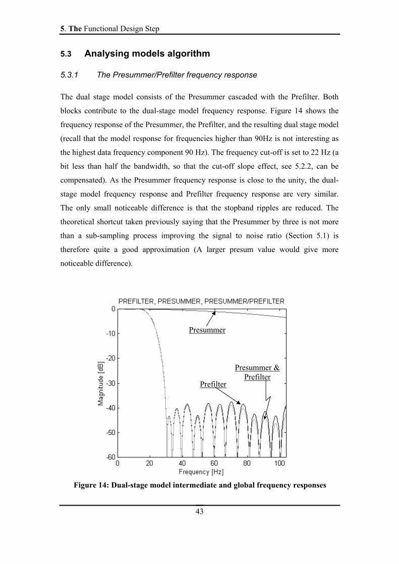
5.3.1 The Presummer/Prefilter frequency response
The dual stage model consists of the Presummer cascaded with the Prefilter. Both
blocks contribute to the dual-stage model frequency response. Figure 14 shows the
frequency response of the Presummer, the Prefilter, and the resulting dual stage model
(recall that the model response for frequencies higher than 90Hz is not interesting as
the highest data frequency component 90 Hz). The frequency cut-off is set to 22 Hz (a
bit less than half the bandwidth, so that the cut-off slope effect, see 5.2.2, can be
compensated). As the Presummer frequency response is close to the unity, the dual-
stage model frequency response and Prefilter frequency response are very similar.
The only small noticeable difference is that the stopband ripples are reduced. The
theoretical shortcut taken previously saying that the Presummer by three is not more
than a sub-sampling process improving the signal to noise ratio (Section 5.1) is
therefore quite a good approximation (A larger presum value would give more
noticeable difference).
Figure 14: Dual-stage model intermediate and global frequency responses
Presummer
Prefilter
Presummer & Prefilter

5. The Functional Design Step
44
5.3.2 Comparing the model frequency responses of both models
In this section, we have chosen a 31-tap low-pass FIR filter fulfilling the dual-stage
model Prefilter requirements (the filter has not been chosen completely arbitrarily: it
is actually ‘RICE31’, whose coefficients are present in Appendix B: The FIR Filters).
In the single stage solution, the filter, in order to have the same characteristics as the
Presummer-Prefilter frequency response, would have to be approximately 81-taps
wide (‘RICE81’, see Appendix B). The comparison between the model frequency
responses for both models is now possible. We can see from Figure 15 that the
difference is minimal: in the passband and transition band, the performance of the two
models is very similar. In the stopband, the peak levels are nearly the same, around -
40 dB; the integrated sidelobe levels (i.e. the integrated sidelobes over the integrated
main lobe) are also similar, around -53 dB. This frequency performance offers no
clear better solution. For implementation, an important parameter is the complexity of
each algorithm. An approximate calculation of the complexity of each model is
examined next.
Figure 15: The Single (Grey) and Dual-Stage Model Frequency Responses

5. The Functional Design Step
45
5.3.3 Refining the Presummer and Prefilter models
The calculation of the algorithm complexities requires that the models be refined.
In the single stage model case, the sub-sampler is logically placed after the low-pass
filter, since no aliasing should occur during the sub-sampling stage. The low-pass
filter would produce one range line at a rate of 625 range lines per second and the sub-
sampler would simply keep one line out of 12. However, it is wasteful to produce 12
range lines when only one is useful (Note that the latter statement is only true because
we are not using an IIR filter, but a system that does not contain any feedback).
Moreover, merging the two blocks is very intuitive and simple. The filter would wait
until twelve new input range lines are available. Then it would produce one range line
and wait for twelve other range lines to come, etc… By proceeding as such, we are
saving a huge amount of processing time while producing exactly the same results as
before.
The dual stage model is refined following the same principles: in the Presummer, the
averaging process and the sub-sampler are merged while in the Prefilter, the low-pass
filter and its associate sub-sampler are also merged in a similar manner to the
refinement of the single stage model.
5.3.4 Comparing both model algorithm complexity
This refinement allows us now to compare the algorithms of both approximated
models. The calculation remains simplistic as the hardware is still unspecified at this
stage: the comparison is only done on the number of mathematical operations used for
producing one value. The filters used for the calculation are the ones used in 5.3.2.
Table 3: Both Model Algorithm Complexities
Number of multiplication Number of additions “One filter” (1st model) 81 80
Presummer/Prefilter 0 + 31 2*4 + 30

5. The Functional Design Step
46
The Presummer-Prefilter (dual stage) solution uses less than half of the mathematical
operators used by the single stage filter solution.
The figures above should be interpreted with care. It is not said here that if both
models were implemented on the same hardware device, the single stage model would
be twice slower than the dual stage model. There are too many unknown parameters
to do a proper relative comparison (e.g. the timing overhead due to internal
communication latencies, which are probably bigger for the dual stage model, cannot
be approximated without a strong understanding of the hardware and eventually the
operating system used). But despite that, the “data processing” nature of the system
and the important difference between the algorithm complexities of both models
motivate our belief that the dual stage model implementation will be the fastest.
The Presummer-Prefilter is then chosen to be the model to implement.
5.4 Algorithm validation: simulating the Preprocessor
5.4.1 The simulation set-up
The chosen model low-pass filter remains to be designed. Choosing the “best” filter
by simply visualising its frequency response is very subjective: no one really knows
when parameters such as transition band width and ripple levels are good or well-
balanced enough. Therefore, in order to have a better knowledge of the quality of the
filter, a simulation was set up. The latter consists of the following steps:
• The input data is created with SARSIM2, a radar simulator written by Rolf
Lengenfelder[29]. The SARSIM2 radar and platform (i.e. the aircraft) parameters
follow the SASAR1 specifications. The target is a point located at a ground range of
10 kms from the platform; the input data is range compressed. The full script file for
SARSIM2 is in Appendix C: The Simulation. The resulting data is a 2048×29765
(Range×Azimuth) matrix of complex values. Each Q and I part of the latter is
represented by an unsigned character.

5. The Functional Design Step
47
• The input data is then presummed and prefiltered. But before this operation, the
data matrix (range line vs. azimuth line) must be transposed, or corner turned, as the
filtering process is done in the azimuth direction. In addition, the Presummer and the
Prefilter must work on signed data, so the 128 offset must be removed prior to any
processing. Here, existing C routines have been used: all of them were written by
Jasper Horrell[30].
• Also required for the evaluation is a Reference matrix whereby the client
requirements are ideally and artificially fulfilled. SARSIM2 is again used for the
purpose. The PRF is brought down to 52 Hz, and the azimuth beam width is narrowed
down to 13 degrees, so that PRF and Doppler bandwidth respect the Nyquist criterion.
The other SARSIM2 parameters remain the same as the ones used for the input data
creation. But some processing remains to be done, as the antenna gain pattern, a sinc
function, leaves us with undesired returns outside the 13 degrees beam width. A
Matlab routine was written to read the SARSIM2 file, corner turn the matrix, and set
these undesired returns down to zero (The number of range lines within the new beam
width has been calculated in Appendix A).
• The Filtered and the Reference magnitude matrices are subtracted. Prior to the
subtraction operation, both matrices are normalised and interpolated in range and
azimuth (the interpolation factor was chosen to be 2 to prevent aliasing when moving
from a complex matrix to its magnitude). The “difference” matrix absolute
integration, called from now on the Integrated Noise, will be our chosen criterion for
the best filter selection. This information extraction is done under Matlab (See
Appendix C).
5.4.2 The simulation results
In the next paragraphs, the results obtained with the simulation are discussed.
• Figure 16 shows the relevant 128 range bins in the raw data matrix after corner
turning. The grey colour scale, ranging from white (lowest value) to black, represents
the magnitude of the signal. The range curvature here is quite severe (approximately

5. The Functional Design Step
48
100 range bins). This affects the preprocessing as the latter has been conceived with
the hypothesis that the pulse returns are sitting in the same range bin. The simulation
should be able to show precisely what the effects of the range curvature on the
preprocessing are.
The overall shape of the graph shows bigger magnitude values when approaching the
middle azimuth sample. On close inspection, the darkest spots do not appear in the
middle, but are actually located in the areas where the returns are migrating from one
range line to the other. The global shape can easily be explained. The varying
parameters on which depends the magnitude of a pulse return are the distance to the
target and the antenna gain pattern. They both contribute to strengthen the closest
approach points. The darkest spots are due to sampling in the range direction. Already
range-compressed, the continuous signal for each range line would be a triangular
function (correlation between two rectangular shapes). Figure 17 shows the sampling
of two slightly displaced triangular functions, the range sampling rate being, as in the
simulation, barely above the Nyquist rate. For the most common case, the left one, the
triangular function is represented by two relatively equivalent samples. In the image
then, two points would appear in the range line. In some cases however, as the right
chart is showing, the pulse would be represented mainly by one sample approaching
the maximum value of the triangular function, the other samples being a lot weaker.
In these cases one very dark spot would appear on the image.

5. The Functional Design Step
49
Figure 16: Raw Data, Magnitude
Figure 17: Two situations in range sampling
• Figure 18 shows the magnitude of the data after preprocessing using the filter
‘RICE31’ (‘RICE31’, filter used in Figure 13, Error! Reference source not found.,
and Figure 15, is described in Appendix B). As expected, low pass filtering consists of
artificially narrowing down the azimuth beam width: this is due to the fact that the
low-frequency components of the spectrum sit on the central region of the graph, i.e.
around the closest approach point.
05
1 01 52 02 53 03 54 04 55 0
R a n g e
Mag
nitu
de
0
1 0
2 0
3 0
4 0
5 0
R a n g e
Mag
nitu
de

5. The Functional Design Step
50
• The Reference matrix, Figure 19, looks pretty similar. The only “visual”
difference is the presence, in the filtered data of Figure 18 outside the narrow beam
width, of small residues. The latter quantification will serve as the criterion for the
choice of our best filter.
• The Integrated Noise is calculated. This process is repeated over for a series of
filters that are described in Appendix B. The best result is obtained for the filter
‘RICE31’, a 31-taps filter designed with a Matlab program developed by Rice
University [28]. The other results, normalised with the ‘RICE31’ filter and converted
into dBs, are presented in Table 4.
Figure 18: Simulation with Filter RICE31

5. The Functional Design Step
51
Figure 19: Reference Matrix
Table 4: Integrated Noise versus Filter
FILTERS COMBO HAM15 HAM31 RECT31 RICE31 RICE63 Integrated Noise (dB) 9.57 1.51 0.51 3.22 0 1.66
The first thing to note is that apart from the ‘COMBO’ and the ‘RECT31’ filter, the
results are pretty similar. The ‘COMBO’ filter is a simple filter whose four
coefficients have unit values. Associating the ‘COMBO’ filter with the Presummer by
three is equivalent of averaging and sub-sampling by twelve. Both the ‘COMBO’ and
the ‘RECT31’ filters (a 31-taps filter designed with a rectangular window) have very
high level sidelobes, which is the reason why the Integrated Noise result is not good.
Among the 31-taps filter, the expected hierarchy is respected: the choice could have
been done just on the look of the frequency responses. The major “surprise” is the 63-
taps filter result: ‘RICE63’, whose frequency response looks the “best”, does give a
poorer result than ‘RICE31’.

5. The Functional Design Step
52
The proposed explanation for this result is described here. Let us imagine a vector of
100 values, containing a rectangular shape of 20 values in its middle. Figure 20 shows
the signal filtered by ‘RICE31’ and ‘RICE63’. After the convolution the rectangular
signal is spread onto N-1 more samples, N being the filter length. This spreading
occurs not just one time in our case study but twice in a hundred of range bins (see
Figure 16). These side effects are all contributing to the increase of the Integrated
Noise. Up to 31 taps, they have been counterbalanced by the filter frequency response
improvement. A 63-tap filter is already too long.
It can be noted that the 15 taps filter does not give such bad results: so if the
application happens to run too slowly, the use of ‘HAM15’ in the dual stage model
could be considered to save processing time. But for the moment, ‘RICE31’ is the
chosen filter.
Figure 20: Filtering Side effects with a 31-tap (left) and a 63-tap filter
The complete validation of the model still requires a comparison between the filtered
result and the ideal one. Figure 21 shows two sets of data that are fully focused, i.e.
the range curvature and azimuth compression processes described in 4.1.1 are applied
(the C routines were written by J.Horrell [30]). In the first graph, the point target
return is not filtered before azimuth compression. In the second graph, the data is
Presummed, Prefiltered (with ‘RICE31’), and azimuth compressed (Note that, in order
to have a better picture, all the points in Figure 21 that had a value less than –60 dB
were set down to –Infinity). Visually, the two results are very similar. When
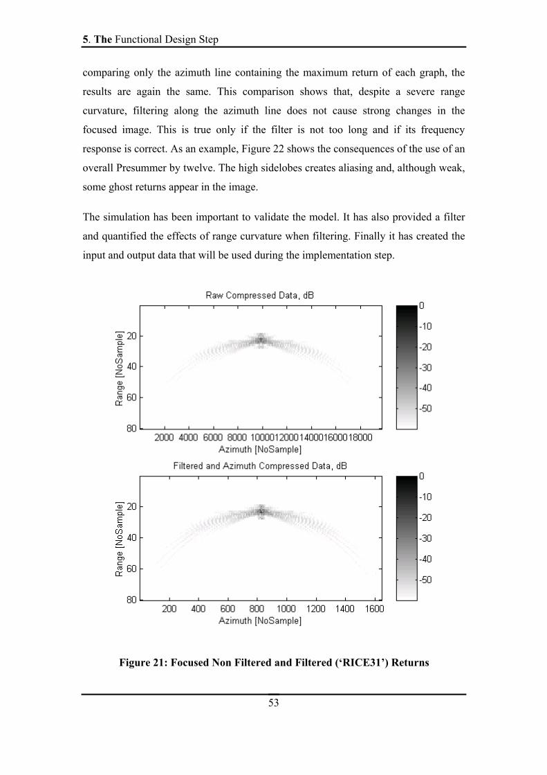
5. The Functional Design Step
53
comparing only the azimuth line containing the maximum return of each graph, the
results are again the same. This comparison shows that, despite a severe range
curvature, filtering along the azimuth line does not cause strong changes in the
focused image. This is true only if the filter is not too long and if its frequency
response is correct. As an example, Figure 22 shows the consequences of the use of an
overall Presummer by twelve. The high sidelobes creates aliasing and, although weak,
some ghost returns appear in the image.
The simulation has been important to validate the model. It has also provided a filter
and quantified the effects of range curvature when filtering. Finally it has created the
input and output data that will be used during the implementation step.
Figure 21: Focused Non Filtered and Filtered (‘RICE31’) Returns

5. The Functional Design Step
54
Figure 22: Filtered and Azimuth Compressed Data, COMBO filter
5.5 Model Refinements
The data width and real time considerations, proposed in this section, are necessary to
the elaboration of the system functional modelling.
5.5.1 The data width consideration
The Presummer is adding three 8-bit data to form the output. Considering that the
input data is using the full 8-bit scale, the number of possible values that the output
can take is 28×3. So, if scaling and precision loss are to be avoided, the output must be
at least 10-bit wide. If the storage capacity cannot handle this memory overhead, a
divider by 3 must be put after the averaging function. It would add some timing
overhead and would introduce a loss in data precision (e.g. if the input is a unit
impulse, the output without the divider would produce three ones, while the output
with the divider, and the 8-bit cast, would produce only zeros). For the Prefilter, the
output range is 28×3×∑=
N
i
ih1
)( , with ∑=
=N
i
ih1
867)( for ‘RICE31’. So, after the
convolution, the data must be at least 20-bit wide. In order to have an 8-bit output
stream (a client requirement) and a maximum achievable dynamic range, the data

5. The Functional Design Step
55
must be divided by 3×867=2601 before truncation. This results in an inevitable
precision loss which consequences have already been taken into account during the
simulation (i.e. in the simulation, the precision loss after Presumming is null, and its
only after the Prefiltering that the data is truncated down to 8-bit values).
5.5.2 The real-time consideration
The main consideration that will be discussed in this section is how to implement the
corner turning into a real time process. The corner turning simply transposes the data
matrix to facilitate the filtering operation. However, in real-time, the data is received
and processed continuously. As an example, the Presummer needs to wait until after
the first 2 range lines and the first value of the third range line arrive before producing
the first output value. Thus, data storage facilities will be needed within the system.
For the Prefilter to work, 31 presummed ranges lines must also be temporary stored.
Note that the dual stage model, already preferred in 5.3.4, is also advantageous when
the amount of data to store is considered.
5.6 Conclusion: Functional-level Description Model
In order to model the system, two types of diagrams are used: DFD and Flow Charts.
The DFD is modelling the functional structure of the system while the Flow Charts
are describing the elementary bubble-functions of the DFD.
The DFD at functional level is in Figure 23. The transfer of the input data to the first
storage facility is performed by a function that we named the Receiver. This Receiver
then signals the Presummer, through Event1, that new data have arrived at
Data_Store1. Similarly, the Presummer is sending its results to Data_Store2 and
signalling the event to the Prefilter through Event2. Event1 and Event2 are the means
of synchronisation between the blocks. Practically, these events could be control
signals in hardware or task messages in software. The final scaling operation is
incorporated in the Prefilter. The self-explanatory Flow Charts in Figure 24 and

5. The Functional Design Step
56
Figure 25 provide the dynamic behavioural modelling for the two Presummer and
Prefilter functions (the Receiver function is trivial at this level).
In this chapter, the system internal model has been decomposed, and the deduced
algorithm has been tested and validated. Finally, the functional modelling has been
exposed. However, the model description is very general, as the hardware is still not
specified. In the next chapter, the physical support for the application will be verified
and the hardware-dependent refinements will be described.
Figure 23: Data Flow Diagram, Functional Level
Event2
Event1
Presummer
Prefilter
Filter ‘RICE31’
Receiver
Input Data
Output Data
Data_Store1 (8-bit)
Data_Store2 (10-bit)
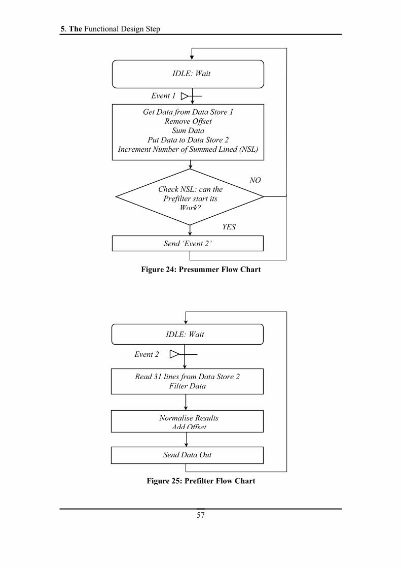
5. The Functional Design Step
57
Figure 24: Presummer Flow Chart
Figure 25: Prefilter Flow Chart
Read 31 lines from Data Store 2 Filter Data
Event 2
IDLE: Wait
Send Data Out
Normalise Results Add Offset
Event 1
IDLE: Wait
Get Data from Data Store 1 Remove Offset
Sum Data Put Data to Data Store 2
Increment Number of Summed Lined (NSL)
Send ‘Event 2’
YES
NOCheck NSL: can the
Prefilter start its Work?
6. The Implementation Definition Step
58
6. The Implementation Definition Step
The aim of the implementation definition step chapter is to define the Preprocessor
completely at “executive” level, starting from the functional model of the previous
chapter. The chapter is structured as follows:
First, the use of the C80 SDB as the hardware support is justified. All the different
technical choices are exposed: the use of C, the multitasking executive, the memory
organisation, the transfer models, the means of communication and the test bench.
Following this, the refinements leading to the software code are described. Finally, the
DFD, the timing diagram and the Flow Charts, modelling the system at task level, are
drawn.
6.1 The different design choices
6.1.1 Choosing the C80
The C80’s SDB capacities are compared against the application specifications on the
following points:
• Data width. The C80 can support the data width requirements: 8-bit and 16-bit
operations are possible. The fixed-point nature of the device will not cause any data
loss if 16-bit data is used during the prefiltering stage.
• Storage capacity. The C80 internal memory capacity, although quite big when
compared to other DSPs, cannot handle the storage of many range lines at a time.
Therefore, at each stage of the process, i.e. before and after the Presummer and the
Prefilter, the data has to transfer from/to external memory to/from internal memory.
The SDB external memory (8 Mbytes of DRAM) can support the application needs.

6. The Implementation Definition Step
59
• Speed Requirements. The best way to prove that the C80 is able to fulfil the
processing speed requirements is to directly write its most time consuming part, i.e.
the two averaging (presumming) and convolution (prefiltering) inner loops. These
inner loops are targeted for the PPs (see next section). The first program to be written,
‘average_c’ (18 lines of code), removes the 128 offset to the unsigned 8-bit data
located in an internal buffer and averages them. The second program, ‘convol_c’ (25
lines of code), convolves the 16-bit data located in an internal buffer with ‘RICE31’,
divides each result by 2601, inserts the 128 offset back and scales the output down to
8-bit. The convol_c program, compiled with an optimisation level 2, takes 4.11
microseconds to process one value, and would therefore take 16.86 milliseconds to
process one presummed range line. This value is close to the client requirements (19.2
milliseconds), but assigning the prefiltering work to two PPs instead of one would
virtually divide the overall time to process one presummed range line by two. The
averaging function performance in terms of speed is strongly under the client
requirements (1.09 versus 4.8 milliseconds).
• Data Transfer. The time spent for transferring data is also estimated. There is at
least, for each line produced, twelve input and 31 presummed range lines to be read,
four presummed and one prefilted range line to be stored. With a transfer rate of two
and three clock cycles for a write and read operation respectively, and with a 64-bit
wide data bus, the minimum time required for transfer is 3 milliseconds. This result,
compared against the 19.2 milliseconds PRI, indicates sufficient performance. Note
that the total amount of time necessary for processing and transferring the data is not
the sum of the two individual times: recall that the C80’s TC, in charge of the transfer,
and the PPs are working independently.
After having compared the different client requirements with the C80 capabilities, it
has been decided to use the DSP and its board as the hardware platform for the case
study.

6. The Implementation Definition Step
60
6.1.2 The appropriate use of the C80’s resources
The TC, the MP, and the PPs are the main “active” C80 resources. They will be used
in a classical way for the application, i.e.:
• The MP will have to supervise the PPs work and formulate the data transfer
requests to the TC.
• The PPs will have to perform the “time consuming” part of the work: the
convolution and the averaging inner loops. In the light of the inner loops timing
results, one PP is assigned for the presumming work, two for the prefiltering.
• The TC will issue the data transfer requests.
The work assigned to the processing elements, in particular the work assigned to the
MP, will be described in more details all along the following sections.
6.1.3 C language and Assembler
The advantages of using the C language instead of native Assembly are the following:
• Increase of programmer productivity
• Maintainability
• Portability of the code
But Assembly remains useful for time-critical performance, as the PP compiler
performance study in 3.3.2 has shown. Thus, even thought the program will be first
written in C, with the use of the optimiser, one must bear in mind that some
computing time could be save by writing inner loops, such as the convolution used for
prefiltering, in Assembly.

6. The Implementation Definition Step
61
6.1.4 The multitasking executive
The use of multitasking executive is quite appropriate for our application: the
Presummer and the Prefilter can be written and verified independently. Moreover,
they can be easily pipelined with the help of the multitasking executive (pipelining
helps to increase the system throughput).
Using the multitasking executive encourages the programmer to write the most of the
code under the MP (Recall that the multitasking executive only runs on the MP). For
example let us consider the transfer requests case. A PP cannot run concurrent tasks,
so if it is issuing a transfer request whose completion is necessary for the continuation
of the sequential code it can do nothing but wait for the data to arrive. On the
contrary, if a task under the MP is waiting for data transfer completion, the
multitasking executive kernel automatically switches to another task, so the MP is
fully used and time is not wasted. Therefore, we will leave only the very few
compute-intensive parts to be done by the PPs, while writing most of the code under
the MP (Presummer and Prefilter synchronisation, data transfer management and PP
supervision).
6.1.5 Memory organisation
Static Allocation. The internal and external memory spaces are shared between the 5
processors, which simplifies the programming model. However, this can lead to
memory contention and data security problems. Therefore, static allocation has been
chosen. In that case, the memory spaces are disjointed (this is the so-called mutual
exclusion concept. For more information, please refer to [31]) and allocated at
compile time i.e. the different data, code and variable storage spaces are defined
statically in the “include files” and at link stage.
Program Memory. The classical approach is to leave the program code in off-chip
memory: this would not lead to excessive timing overhead as the C80’s processors,
i.e. the MP and the four PPs, have each 2Kbytes of instruction cache.

6. The Implementation Definition Step
62
Data Memory. Most of the internal memory should be dedicated to the buffers used
for processing data. For the PPs, the program global and static variables together with
the stack are also allocated in internal memory. For the MP, on the contrary, these
variables are allocated in external memory: the timing loss should not be excessive, as
the MP possesses 2Kbytes of data cache.
6.1.6 Single and Double Transfer Models
Double transfer and single transfer models are two solutions for processing data that
resides in off-chip memory:
• The single transfer model (STM), very common in the DSP world, consists of (i)
transferring a block of data from off-chip memory to an on-chip buffer, (ii) computing
the data, and (iii) sending them back to off-chip memory. The STM is repeated as
many times as necessary.
• The double transfer model (DTM) uses two internal buffers (see [15], §12-23).
While the first one is processed, the C80’s TC “discharges” and “recharges” the other
one. Then, the buffers are swapped, the first one assigned to the TC, the second one to
the PP. Figure 26 shows the repeat of the double buffering process over N times. After
initialisation, while the block number N-1 is processed, the block number N-2 is
transferred out and the block N transferred in.
Time 1 2 3 4 … N+1 Input data block nº 1 2 3 4 … N+1 Compute block nº 1 2 3 … N
Output block nº 1 2 … N-1 The grey parts are non-available space times
Figure 26: The Data Blocks Filtering Steps (number 1 to N) versus Time.

6. The Implementation Definition Step
63
Neither of these two methods is, on first inspection, preferred: on one hand, if the
STM were used, the processing element(s) would do nothing during the transfer stage,
which is a loss of computational time for the C80. On the other hand, it is not certain
that the DTM is efficient when implemented under the MP. Indeed, multitasking and
double buffering force one to split the Presummer or the Prefilter functions into three
small tasks: one for transferring the data in, one for computing the data, and one for
transferring the data out. Therefore, a timing overhead due to inter-task
communication and task context switching is observed.
So the two methods for both the Prefilter and the Presummer are implemented. The
timing results and the proposed explanation for them are in Chapter 7. For clarity
reasons, only one design is presented during this chapter: the Presummer using the
STM and the Prefilter using the DTM.
6.1.7 Means of communication
The inter-task communications are of two sorts:
• Data communications are done via shared memory: in that case, the program
modelling is eased. However, a particular care should be put on avoiding memory
contention: static allocation and mutual exclusion should be applied as often as
possible.
• Inter-task synchronisation is done via semaphores and signals: they are part of the
multitasking executive means of inter-task communication, and are the “low-cost”
alternatives to ports and messages. If the Presummer task wants to signal the Prefilter
task that new data has been presummed, it invokes the
‘TaskSignalSema(Semaphore_name)’ function, with the Presummer task invoking
‘TaskWaitSema(Semaphore_name)’ to ensure that this data is available or to wait
otherwise. The semaphores are also the links task-TC and task-PP.

6. The Implementation Definition Step
64
6.1.8 The test bench
The test bench must be designed together with the case study itself since verification
of the design must be done. The SDB does not offer an adequate peripheral for
implementing the test bench with the help of an external device. Therefore, it has been
decided to implement the test bench with the SDB external memory and the C80
resources. This requires that two tasks be added to the case study: the Input task reads
the input data from a specific external memory bank while the Output task stores the
output data also in external memory. The executive-level Input task replaces the
Receiver, bubble-function declared at functional level (section 5.6).
The Input and Output tasks can be fused, for speed efficiency, respectively with the
Presummer and the Prefilter tasks. For the moment we decide to keep input and output
tasks separate from the others so that the core part of the Preprocessor is not affected
by the decision that our test bench resides on board. Moreover, the program gains in
clarity by doing such.
6.2 Refining the model
6.2.1 External memory assignments
The data must be temporarily stored in external buffers before presumming and
prefiltering. The corresponding structure and size of these buffers is as follows:
• The Presummer input buffer is a double buffer whose structure is based on the
principles described in 6.1.6. It can contain six 8-bit range lines (24 Kbytes) so that
the Presummer can work on three of them while the Input task “charges” the three
other ones. The buffer, whose structure is shown in Figure 27, is called the Input-
Presummer Double Buffer. It corresponds to ‘Data Store 1’, the storage facility drawn
in the Functional level DFD page56.
• The Prefilter input buffer is a circular buffer containing 60 16-bit range lines (480
Kbytes). The Prefilter can work on the last available 31 ranges lines, while the

6. The Implementation Definition Step
65
Presummer task “charges” four new presummed lines. If a 60-line buffer has been
chosen instead of a smaller 35-line buffer, it is because some extra memory was
available off-chip. This buffer, whose structure is in Figure 28, is called the
Presummer-Prefilter Circular Buffer. It corresponds to ‘Data Store 2’, the storage
facility drawn in the Functional level DFD page 56.
• The Prefilter output buffer is a double buffer containing two 8-bit range lines (8
Kbytes) that links the Prefilter and the Output tasks. This buffer, whose structure is
very similar to the Input-Presummer Double Buffer, is called the Prefilter-Output
Double Buffer. This buffer doesn’t appear in the functional model: it results from our
desire to keep test bench and ‘core’ tasks independent.
I_I1-1 I_Q1-1 I_I1-2 … I_I1-2048 I_Q1-2048
I_I2-1 I_Q2-1 I_I2-2 … I_I2-2048 I_Q2-2048
I_I3-1 I_Q3-1 I_I3-2 … I_I3-2048 I_Q3-2048
I_I4-1 I_Q4-1 I_I4-2 … I_I4-2048 I_Q4-2048
I_I5-1 I_Q5-1 I_I5-2 … I_I5-2048 I_Q5-2048
I_I6-1 I_Q6-1 I_I6-2 … I_I6-2048 I_Q6-2048
The prefix “I_” attached to the variable signifies input data; the “I” or “Q” symbols mean In_phase or Quadrature component; the first index is the range line number, the second the range bin number.
Figure 27: The Input-Presummer Double Buffer.
2048 range bins1 Byte
2*3
rang
e lin
es

6. The Implementation Definition Step
66
P_I1-1 P_I2-1 P_I3-1 … P_I59-1 P_I60-1 P_Q1-1 P_Q2-1 P_Q3-1 … P_Q59-1 P_Q60-1 P_I1-2 P_I2-2 P_I3-2 … P_I59-2 P_I60-2 P_Q1-2 P_Q2-2 P_Q3-2 … P_Q59-2 P_Q60-2
…
…
…
…
…
P_Q1-2048 P_Q2-2048 P_Q2-2048 … P_Q59-2048 P_Q60-2048
The prefix “P_” attached to the variable signifies presummed data; the “I” or “Q” symbols mean In_phase or Quadrature component; the first index is the range line number, the second the range bin number.
Figure 28: The Presummer-Prefilter Circular Buffer
The other off-chip banks are the following:
• The Filter Bank. The filter coefficients reside here at start up.
• The Input Bank. The input data resides here at start up.
• The Output Buffer. The output task stores the data here so that verification can be
done (it is possible with the SBD tools to read the off-chip memory after a program
has finished running).
• The Timing Buffer. Information such as speed results is stored here at run-time.
2048
rang
e bi
ns
60 range lines
2 Bytes

6. The Implementation Definition Step
67
6.2.2 Internal memory assignments
The corresponding structure and size of the internal buffers reserved for the
Presumming and Prefiltering tasks is as follows:
• The Internal Presummer Single Buffer contains three eighths of a range line, i.e.
1536 Bytes. The memory organisation is as follows: the three values to be summed
together are in consecutive memory addresses, thus allowing the averaging function to
work faster. Recall that the data is not in this order when arriving from the A/Ds: it is
corner turned. This corner turning is done “on the fly” thanks to the TC capabilities.
The buffer organisation can be seen in Figure 29.
• Four blocks of nearly four kilobytes (3968 Bytes) each are dedicated to the
Prefilter work. Two buffers are used at a time for the filtering and two for the transfer
(Recall that the DTM described in 6.1.6 is applied to the prefiltering work). The
organisation of one of these four buffers, called Internal Prefilter Double Buffers, can
be seen in Figure 30.
I_I1-1 I_I2-1 I_I3-1 I_Q1-1 I_Q2-1 I_Q3-1 I_I1-2 I_I2-2 I_I3-2 I_Q1-2 I_Q2-2 I_Q3-2
… … …
I_Q1-256 I_Q2-256 I_Q3-256
Figure 29: The Internal Presummer Single Buffer

6. The Implementation Definition Step
68
P_I1-1 P_I2-1 P_I3-1 … P_I31-1 P_Q1-1 P_Q2-1 P_Q3-1 … P_Q31-1 P_I1-2 P_I2-2 P_I3-2 … P_I31-2 P_Q1-2 P_Q2-2 P_Q3-2 … P_Q31-2
… … …
…
P_Q1-256 P_Q2-256 P_Q3-256 … P_Q31-256
Figure 30: One of the four Internal Prefilter Buffers
The filter ‘RICE31’ is also copied on-chip. Actually, it is copied twice so that the two
PPs used for Prefiltering can work in complete independence: recall that the crossbar
can answer in one clock cycle to on-chip memory access requests from all the PPs as
long as the memory addresses are in different blocks (see 3.3.2).
6.2.3 Tasks refining
The application is split into seven tasks that are briefly described here:
• The Input task stores the data it receives (in our case it reads it form an off-chip
data bank, the Input Buffer) to the Input-Presummer Double Buffer.
• The Presummer task reads the data from the Input-Presummer Double Buffer,
averages them and stores the results in the Presummer-Prefilter Circular Buffer. In
order to do so, the Presumming task uses PP2 (Parallel Processor number 2) and the
Internal Presummer Single Buffer resources.
• The Input Prefilter transfers data from the Presummer-Prefilter Circular Buffer to
the two Internal Presummer Double Buffers. The Prefilter task is issuing requests for
PP0 and PP1 to filter the data. The Output Prefilter task transfers the data from the
Internal Presummer Double Buffers to the Prefilter-Output Double Buffer. There are
two reasons why the Prefilter function is split into three different tasks. Firstly, the
independence between transfers and computation must be maintained for the double
buffering model to work. Secondly, the data input and output transfers are also

6. The Implementation Definition Step
69
separated into two tasks in order to facilitate the code writing: updating the data
pointers and writing the code for the start up cases is particularly complicated when
input and output data transfers are combined in one task.
• The Output task reads the data from the Prefilter-Output Double Buffer and stores
them to the Output Buffer.
• The Main task is the starting point of the program. It loads up the multitasking
executive, initialises the semaphores (see next) and launches the six tasks declared
above. Once this is done, the Main task does nothing but stay in an endless loop.
6.2.4 Semaphores
Here are the different semaphores used for the application:
• Two semaphores perform the synchronisation between the Input task and the
Presummer task. The first one, ESumFull, is here to ensure the Presummer that three
new lines have arrived (it is preferable for the Input, and not the Presummer, task to
count the number of lines arriving so that the latency resulting from inter-task
communication is minimised). The second semaphore, ESumEmpty, signals that the
Presummer task has finished the processing the set of input lines, so that the Input
task can replace them. ESumFull and ESumEmpty are the detailed ‘Event1’, present
in the functional level DFD, page 56.
• In the same manner ECirNewLine and ECirLineUsed are linking Presummer and
Prefilter tasks. These are the detailed ‘Event2’, present in the functional-level DFD.
• Three semaphores synchronise the three tasks in charge of the presumming.
FiltEndIn signals the Prefilter task that the data has arrived, FiltEndProcess signals
the Output Prefilter task that the data has been processed and FiltEndOut signals the
Input Prefilter task that the processed data has been transferred. No memory
contention should occur with the implementation of these three semaphores.
• EFiltedFull and EFiltedEmpty link the Output Prefilter task with the Output task.

6. The Implementation Definition Step
70
6.2.5 The PP programs
Four sequential functions are dedicated to run on the PPs:
• Presumming functions: The function ppSum is simply an interface between the
MP-resident Presummer task and the average_c inner loop. average_c, the function
described in 6.1.1, is working on the Internal Presummer Single Buffer.
• Prefiltering functions: ppFilt is interfacing the MP-resident Prefilter task with
the other PP function written for the PPs, i.e. convol_c: the convolution inner loop
described in 6.1.1 is working on the Internal Prefilter Double Buffer.
6.3 Conclusion: The Executive-Level Description Model.
The system is modelled with three different diagrams that complement each other: the
DFD (functional view), the Timing Diagram and the Flow Charts (behavioural view).
The executive view is the C80 SDB block diagram, in Figure 4 page 22.
The DFD is separated into two parts for more clarity. The first part, shown in Figure
31, gives a general view of the system at task level. It summarises the implementation
choices discussed in the previous sections. The second part, drawn in Figure 32,
shows the data relationship between the MP Presummer and Prefilter tasks and the PP
corresponding “slave” programmes. When the MP requests the PP to run a program, it
does it via a command buffer (e.g. SumCmdBuf). The MP waits for the PP to signal
that it finishes the job via a semaphore (e.g. PPSumEnd). These means of
communications don’t appear in the PP code, as the choice of whether using the
multitasking executive or not is completely transparent to the PP.
The wait and process states of each task as a function of time are drawn in the Task
Timing Diagram, Figure 33. This diagram offers only a simplified version of the real
case. For example, the Input and the Presummer task execution times are chosen to be
the same so that no time is wasted waiting for the other task to complete its work. The
real case, as we will see in the next chapter, is far more complicated.

6. The Implementation Definition Step
71
The Flow Charts complete the application modelling. They describe the sequential
behaviour of the bubble-tasks present in the DFD. The four Flow Charts representing
only the Presummer and the Prefilter are drawn in pages 75-78. Semaphores linking
the TC and the tasks have been added, as well as the semaphores linking some MP
tasks to PP functions (e.g. the InSumReq and the PPSumEnd semaphores in Figure
34). These diagrams are detailed enough so that the transition to C code is merely a
matter of transcription.
In this chapter, the application has been detailed down to its lowest interesting level,
the task level. The design is complete at this stage: the next step, described in the next
chapter, consists of implementing the Preprocessor, and verifying its performance in
terms of speed.

6. The Implementation Definition Step
72
Figure 31: DFD, Task Level
ESumEmpty
Internal Prefilter Double Buffers
FiltEndOut
Prefilter-Output Double Buffer
EFiltedEmpty
FiltEndProcess
FiltEndIn
ESumFull
Internal PresummerSingle Buffer
Input-Presummer Double Buffer
Presummer-Prefilter Circular Buffer
Presummer
Input Prefilter
Output Prefilter
Prefilter
ECirNewLine ECirLineUsed
EFiltedFull
Input Data
Output data
Output Task
Input Task

6. The Implementation Definition Step
73
Figure 32: DFD, MP-PPs level
SumCmdBuf
Internal PresummerSingle Buffer
Presummer ppSum
PPSumEnd
ppFilt
PPFiltEnd2
FiltCmdBuf1
PPFiltEnd1
FiltCmdBuf2
Internal Prefilter Double Buffer nº2
Internal Prefilter Double Buffer nº1
Prefilter
‘RICE31’ nº2
‘RICE31’ nº1
ppFilt

6. The Implementation Definition Step
74
Figure 33: The Task Timing Diagram
EFiltedFull
FiltEndIn
EFiltedFull
ECirNewLine
ECirLineUsed
ECirNewLine
ESumFull
ESumEmpty
Input Presummer Output
Prefilter Input
Prefilter
Prefilter
Output T
ime
Axe
s
FiltEndOut
FiltEndProcess
FiltEndIn
…
…
…
EFiltedEmpty
…
…
…
32 It
erat
ions

6. The Implementation Definition Step
75
Figure 34: The Presummer Task Flow Chart
ESumFull
Initialisation: Number of Summed Lines NSL = -31
[NSL > -1] AND [NSL multiple of 4]?
IDLE: Wait
Swap the Input-Presummer Double Buffer Update the pointer to the Presummer-Prefilter Circular Buffer Signal ESumEmpty NSL ++
NO
YES
Send ECirNewLine
ECireLineUsed
InSumReq
PPSumEnd
OutSumReq
Number of Blocks=16?
In Transfer Request: Wait
Send SumCmdBuf to 1 PP: Wait
Out Transfer Request: Wait
Number of Blocks = 0
Wait
Increment Number of Blocks Update the pointers to memory
NO
YES

6. The Implementation Definition Step
76
Figure 35: The Input Prefilter Task Flow Chart
ECirNewLine
Initialisation
IDLE: Wait
- Update the pointer to the Presummer-Prefilter Circular Buffer
- Signal ECirLineUsed
FiltEndOut
InFiltReq
Number of Blocks=32?
Wait
In Transfer Request: Wait
Number of Blocks = 0
- Increment Number of Blocks - Update the pointers to memory - Signal FiltEndIn
NO
YES

6. The Implementation Definition Step
77
Figure 36: The Prefilter Task Flow Chart
ECirNewLine
Initialisation
IDLE: Wait
PPFiltEnd
Send FiltCmdBuf to 2 PPs: Wait
Swap the Internal Prefilter Double Buffer-
Signal FiltEndProcess
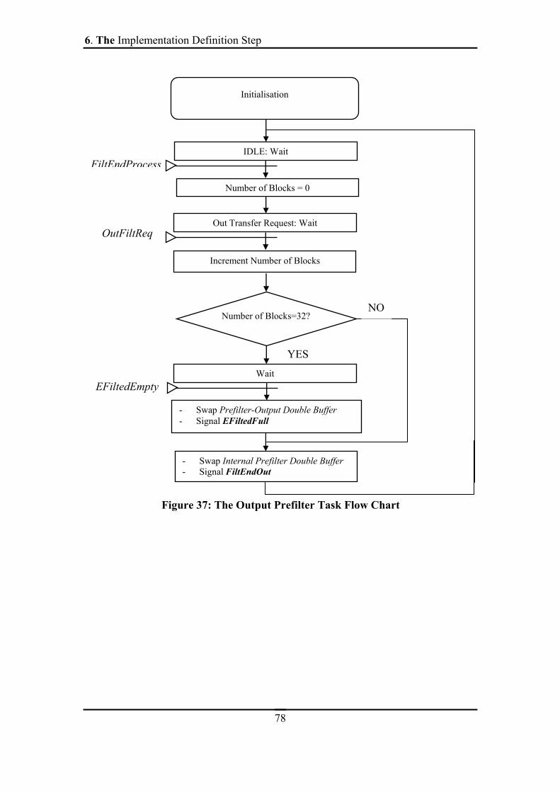
6. The Implementation Definition Step
78
Figure 37: The Output Prefilter Task Flow Chart
FiltEndProcess
Initialisation
IDLE: Wait
- Swap Prefilter-Output Double Buffer - Signal EFiltedFull
OutFiltReq
Number of Blocks=32?
Out Transfer Request: Wait
Number of Blocks = 0
Increment Number of Blocks
NO
YES
Wait EFiltedEmpty
- Swap Internal Prefilter Double Buffer - Signal FiltEndOut

7. The Implementation Step
79
7. The Implementation Step
The implementation step chapter ends the Preprocessor development work: it
describes the means utilised for implementing, debugging and verifying the case
study. Section 7.2 describes the inter-linked implementation and verification process.
Then, the measured results are given in section 7.3 and analysed in section 7.4. This
section concludes on how the code could be further optimised.
Prior to this, the following section explains why four different versions of the
Preprocessor are to be written. The section also describes what are the principal
characteristics of these different codes.
7.1 The Four Implementations
There are design orientations whose costs in terms of speed are difficult to “predict”:
one must then carry on with the code writing and calculate the speed performances a
posteriori. If the speed results are unsatisfying, alternative design choices must be
made and the source code must be re-written. The transfer models described in section
6.1.6 illustrate the above. As the efficiency of these models in terms of speed is not
known, it is decided to write the four codes combining STM and DTM for both the
Presummer and the Prefilter. A brief description of the four implementations follows:
The DD implementation. DTM for both the Presummer (internal RAM size: 2∗0.75
kilobytes) and the Prefilter (internal RAM size: 2∗3.88 kilobytes). There are in total 9
tasks composing the Preprocessor code: the Main, the Input, the Input-Presummer, the
Presummer, the Output-Presummer, the Input-Prefilter, the Prefilter, the Output-
Prefilter, and the Output tasks.

7. The Implementation Step
80
The SS implementation. STM for both the Presummer (internal RAM size: 1∗1.5
kilobytes) and the Prefilter (internal RAM size: 1∗7.76 kilobytes). There are in total 5
tasks composing the Preprocessor code: the Main, the Input, the Presummer, the
Prefilter, and the Output tasks.
The SD implementation. STM for the Presummer (internal RAM size: 1∗1.5
kilobytes) and DTM for the Prefilter (internal RAM size: 2∗3.88 kilobytes). This is
the design described in the previous chapter (seven tasks).
The DS implementation. DTM for the Presummer (internal RAM size: 2∗0.75
kilobytes) and STM for the Prefilter (internal RAM size: 1∗7.76 kilobytes). There are
in total 7 tasks composing the Preprocessor code: the Main, the Input, the Input-
Presummer, the Presummer, the Output-Presummer, the Prefilter, and the Output
tasks.
7.2 Implementation and Functional Verification
First, only one version, the SD, is selected to be entirely written and tested. The work
consists then of writing and debugging one by one the SD tasks. Two comments on
the Main task follow:
• The Main function assigns a ‘priority’ value to each of the task it creates (the
priority value determines the task scheduling, see [32]). For the moment, the same
priority is attributed to each eight tasks so that the MP resource can be shared in a
round-robin fashion.
• All the tasks are written following the same pattern: Wait Semaphore 1-Do Work-
Signal Semaphore 2. This concept leads to robust behaviour since none of the
functions is able to start a new cycle without ‘acknowledgement’. But it raises an
issue: how to start the process if every task waits. The multitasking executive’s
answer to the problem is the possibility to assign an initial count to each semaphore (a
semaphore can be seen as a shared variable that gets incremented when signalled and
decremented when received). For example, as the Input task does not have to wait the

7. The Implementation Step
81
first two times to fill the Input-Presummer Double Buffer, the ESumEmpty
semaphore’s count is initialised at two.
The other tasks can be easily deduced from the DFD and the Flow Charts page 72 to
page 78.
The debugger tool described in 3.3.2 is used during the early stages of the
development, when individual task behaviours or inner loops are to be tested. Here, a
short set of 21 ‘friendly looking’ range lines in loop is used as input data (the
simulated data set contains too many zeros for the inner memory reading at debugging
to be useful).
The verification of the entire application is quite difficult with the debugger. In
addition to the unfriendly character of the graphic interfaces (there is one DOS
window for each processor), the co-ordination between the MP and the PPs is not
perfect when debugging. For example, it is impossible to launch from the MP
debugger a command to the same PP twice.
This is the reason why the overall functionality verification is carried out using the
SDBshell tool. Once this program is launched from the host computer, the following
operations are performed: first, the input data is “manually” stored at a specific
address in external memory (Input Bank). It corresponds to a 1024-lines block of the
data that served in the system simulation, page 46 (this is due to the limited amount of
available space in the SDB DRAM). Following the input storage, the C80 program is
executed. Finally, the Output Buffer is read. The resulting 78 range lines are
compared with the simulation results.
Once the SD is completely checked and verified, the same work is performed for the
DD, SS, and DS implementations.
7.3 Speed Verification
The output throughputs are measured as follows: the Output task code is slightly
modified: now, in addition to the described jobs, the program stores the register
TCOUNT (in the Timing Buffer) each time a range line is produced. TCOUNT is the

7. The Implementation Step
82
current 32-bit value of the timer (decrements by one at each clock cycles). Following
the execution of the design, the Timing Buffer is read using SDBshell. The
Presummer throughputs are measured following the same principles. These two
maximum throughputs measured for each implementation are below.
Table 5: The Four Implementation Throughputs
Presummer Throughput Output Throughput
DD Implementation 3.8 milliseconds 15.2 milliseconds
SS Implementation 5.2 milliseconds 11.7 milliseconds
SD Implementation 2.8 milliseconds 10.1 milliseconds
DS Implementation 5.9 milliseconds 13.5 milliseconds
The four implementations satisfy the client requirements of having their output
throughputs better than 19.2 milliseconds. However, the SS and the DS
implementations do not fulfil the requirements of having the presummed throughput
better than 4.8 milliseconds. On close inspection, the SS (respectively DS)
implementation throughput is most of the time at 2.2 milliseconds (respectively 2.5):
the jumps to 5.2 milliseconds (respectively 5.9) occur one time out of four, when the
Prefilter task(s) start(s) to process new range lines. The excessive jumps show that the
Prefilter work does not “spread” over the four Presummer cycles. The results above
show us that using a DTM for both the Presummer and the Prefilter is not really
efficient either.
Three propositions for the figures in Table 5 follow:
• By increasing the number of tasks, the overhead due to task context switching is
likely to increase.
• The lack of pipelining creates moments when data transfers bottleneck the MP and
the PPs. The Prefilter needs more time to transfer and process its data block than the
Presummer does in any of the proposed implementation. Therefore, a bottleneck on
the Prefilter is likely to create more timing overhead than a bottleneck on the
Presummer.

7. The Implementation Step
83
• The imbalance between the Presummer and the Prefilter number of internal loops
also affect the timing results. This proposition is illustrated through the comparison
between the SD and DS implementations (They both have the same number of tasks,
so proposition one does not apply). In order to produce one output line, the DS
implementation goes trough (16∗4) 64 presumming and 16 prefiltering “transfer on
chip-process-transfer off chip” type loops. As a consequence, the Presummer waits
and signals are more numerous than the Prefilter ones. Therefore, situations whereby
the multitasking core has to test 5 or 6 tasks before founding one available are not
scarce (Recall that a wait causes the core to switch tasks and that the tasks share the
MP in a round-robin fashion). On the contrary, the SD implementation is perfectly
balanced, going trough 32 presumming and 32 prefiltering loops per output line
production. In that case, the multitasking core switches more regularly from
presumming to prefiltering: the timing overhead due to task context switching is then
shortened.
It is very difficult if not impossible to calculate precisely context task switching
timing overheads. For instance, the states of the TC as a function of time can not be
perfectly evaluated (e.g. the TC performs unpredictable tasks such as data instruction
loads), so it is difficult to know for how long a task would wait for data transfer. This
is the reason why these propositions remain rough and do not offer any quantitative
answers.
7.4 Chosen Design Speed Analysis
The SD implementation is preferred to the others because it offers the best timing
results and that its code is simpler than the only other implementation that fulfil the
client requirements, i.e. the DD implementation. The SD implementation has been
fully described in the previous chapter.
The evolution of the Presummer and the Prefilter throughputs over time are plotted in
Figure 38 and Figure 39. These evolutions can be explained as follows:

7. The Implementation Step
84
• The Prefilter does not perform while the first 31 presummed lines are produced.
This causes the first 30 presummed throughput rates to level at 1.85 milliseconds.
• The Prefilter starts a new job every fourth presummed line. This causes the
regularly spaced jumps of approximately 0.2 milliseconds in the presummed
throughput graph.
• The Prefilter sometimes needs to wrap around the Presummer-Prefilter Circular
Buffer to collect the 31 lines to be processed. In that case, the on-chip data transfer
requests double, overloading by such the C80 work. This explains the square aspect of
the output throughput graph and the steps that can be seen every 30 lines in the
presumming throughput graph.
The maximum output throughput overloads the convolution timing complexity by 10
to 16 %, a reasonable result. Another speed result is of interest: the design, with the
average and convolution inner loops deactivated, has a maximum output throughput
of 9.8 milliseconds. Therefore, if the design were to run faster, the rewriting of the PP
codes would not be, alone, satisfying: the MP tasks would have also to be reshaped.
An idea would use Assembly for the inner loops and fuse the Input task with the
Presummer task and the Output task with the Output Prefilter tasks. Unfortunately,
both transformations would cause the code to be less readable.
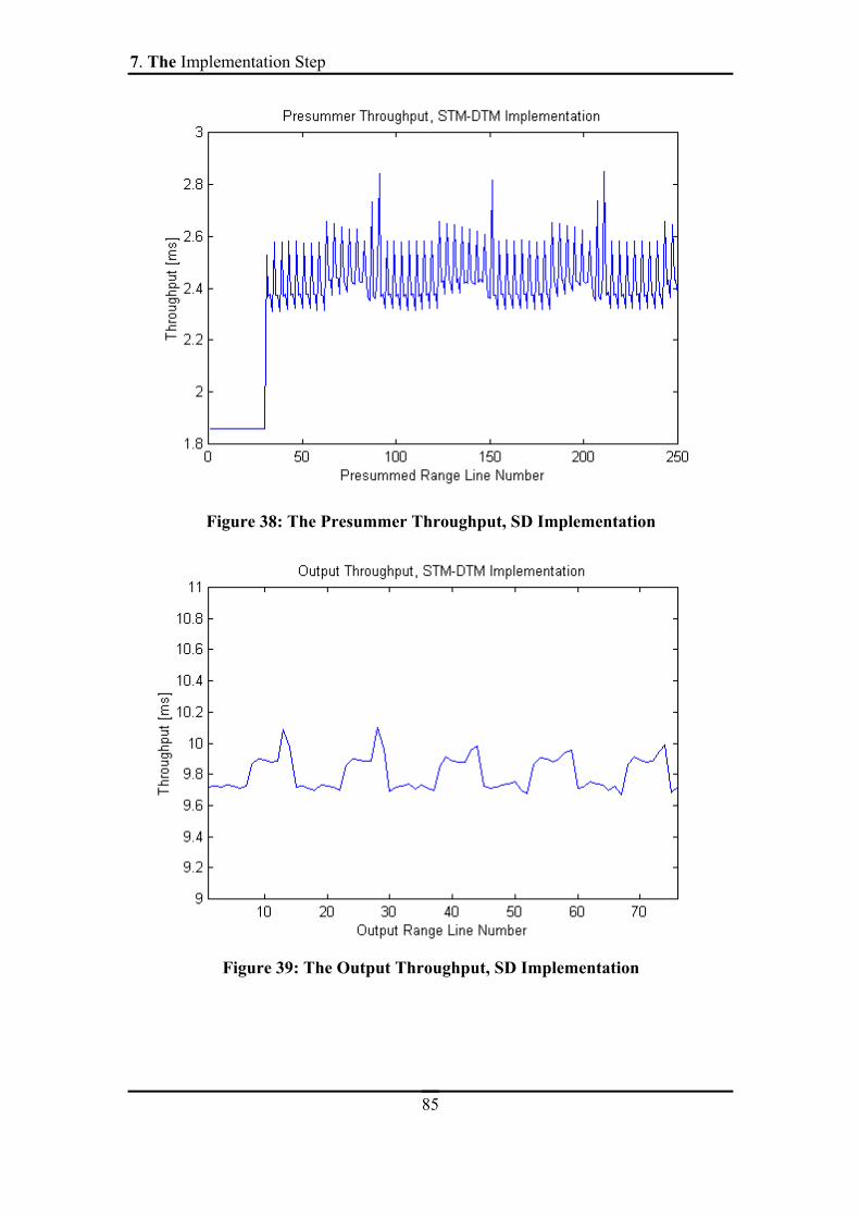
7. The Implementation Step
85
Figure 38: The Presummer Throughput, SD Implementation
Figure 39: The Output Throughput, SD Implementation
7. The Implementation Step
86
7.5 Conclusions
In this chapter, the implementation has been verified and the speed checked against
the client requirements. The SD implementation offers a successful version of the
Preprocessor targeted for the C80 (The C codes are in Appendix D). However, an in-
depth analyse of these timing results has been quite difficult because the ideal tools
for time performance analysis, e.g. a profiler, were not available.
This concludes our work on the development of the Preprocessor. The following
chapter will draw general conclusions on the advantages and limitations of using a
top-down approach to designing.

8. Conclusions and Recommendations
87
8. Conclusions and Recommendations
The following paragraphs summarise the remarks on the methodology and the
methods used during the development of the Preprocessor. In addition, the FPGA
implementation of the preprocessor attempted by Grant Carter [2] and the C80
implementation described above are briefly compared.
Calvez’s methodology was described in Chapter 2 in a rather simplistic way (some
may even say naïve). Indeed, a pure top-down approach for designing is unrealistic.
The example of the inner loops illustrates the matter: they had been implemented at
the early stages of the implementation definition step so that their resulting timing
complexity measurement could ease the mapping of the functional DFD to the SDB.
Equally, using hardware components or software libraries (i.e. using reusability
methods) in order to reduce the implementation cost can cause some changes in the
trade-offs made during the functional design phase. Thus, some FPGA’s FIR Filter
VHDL (Very High Speed Integrated Circuit Hardware Description Language) models
can only have their number of taps equals to powers of two [2]. So, in practise,
bottom-up principles are applied along the development process.
But using a ‘globally’ top-down approach for specifying and designing DSP systems
has undoubtedly its advantages. One of them is that it increases the work at design
level and forces the designer to think about the solution at first in a hardware-
independent way: in that case, the designer is likely to produce more reusable
specifications and general solutions. Increasing the work at design level also means
enforces the algorithm validation step: in our case study, using a rather short filter to
obtain better results was rather a counter-intuitive concept. Hence, if the simulation
results were not at our disposition, the designer would have been tempted to increase
the filter length regarding the timing results, degrading by such the performance of the
system.

8. Conclusions and Recommendations
88
Another advantage is that the methodology facilitates project organisation and
management: development of complex digital signal processing systems can be
assigned to different engineers. This is particularly interesting because different
development steps require different skills. Indeed, coming back to the Preprocessor
example, the specification step was conducted with some SAR background; the
functional design step required digital signal processing skills; knowledge on DSPs,
RTOS and parallelism were needed during the implementation definition step; C
programming and debugging skills were necessary during the implementation step.
Means to reduce the development time cost, especially during implementation, have
been described in Chapter 2. An assessment on their use and their efficiency follows:
• Co-design methods have not been used in the case study: indeed, the entire
hardware support was a COTS product and was part of the technical specifications.
• Reusability has been proved to be useful when the decision was made to
implement four versions of the application, see 7.1. Indeed, whereas the first version
(The SD version) took 11 man-days to implement and verify (the learning curves and
all the previous steps are excluded from the timing count), the second and the third
(DD and SS) took only two man-days. The development time cost has been reduced
mainly thanks to the multitasking executive that helped the modularization of the
software program. The fourth version took less than an hour to implement, as the
work consisted only of assembling already existing tasks. The use of existing software
functions has also greatly speeded up the functional design simulation. But, generally
speaking, the creation of software ‘components’ or libraries must be carefully
managed: highly robust functions must be implemented, and, very important, changes
must be strictly controlled and documented.
• Developing tools: The tools used during the development process of the
Preprocessor are the following: Mathcad (specification step), Matlab (functional
design step), the multitasking executive (implementation definition step), the
compilers, the debuggers, SDBshell, C and Hexadecimal editors (implementation
step). No profiler was available: it would be interesting for future work to get hold of
the TMS320C80 simulator and see if the included profiler would help optimising

8. Conclusions and Recommendations
89
systems speed performance.
Using C as the programming language definitely increased the programmer
productivity. The multitasking executive also helped a great deal in the transition from
functional to executive model. But both of them have a time cost that cannot be
precisely evaluated. This constitutes the main drawback of using a general-purpose
DSP with a high-level language and an operating system. This means that algorithm
complexity must be evaluated at functional design level and that the DSP must be
chosen with speed and memory capabilities largely superior to the algorithm
complexity evaluation. In our case, the ratio between the assembly coded prefiltering
inner loop and the actual program execution time is approximately one to three.
Some comparisons have been carried out with Grant Carter’s implementation of the
same Preprocessor on a FPGA [2]. The specification and functional design steps lead
to similar results, but major differences exist in the hardware-dependent design. One
of them is the use, for the FPGA implementation, of two overall loops, or state
machines, in order to control the sequence of operations in the Prefilter and in the
Presummer. These state machines do not appear in the DSP design: a DSP naturally
delivers a sequential interpretation of the code, while, coupled with a RTOS,
concurrency can be performed as well. Another big difference is that the DSP design
works globally on data blocks (reducing by such TC bottlenecks and task
communication overload) while the FPGA design works on data values (reducing by
such the amount of registers to produce). Generally speaking, the implementation of a
system in an FPGA implies working at a less abstract level than the mapping of a
functional design onto a DSP. As a result, the FPGA is more dedicated to the
application, leading to possible reduction of hardware cost.
Despite these differences, the design community expresses a strong will to
homogenise the development process. The creation of ambitious, third-generation
software package such as COSSAP (developed by Synopsis), or Ptolemy (developed
by the University of California Berkeley, see [33]), illustrates this. These design tools
offer not only the possibility to simulate the drawn system, but they also claim the
possibility of automatically generating appropriate codes for the desired target(s). The
investigation of such packages could be an interesting extension to this thesis.

Appendix A. SAR Parameter Calculations
90
Appendix A. SAR Parameter Calculations
This appendix contains the preliminary MathCAD calculations derived from the basic
SA-SAR characteristics. These results are mostly utilised during the algorithm
simulation in the functional design step. This MathCAD file can also be found on the
enclosed CD-ROM, under the specification directory.
Constant values
c 3 108. m. sec 1.====================================================================SA-SAR characteristics
f 141 MHz. (VHF-System) Client(C): Frequency bandResult(R): Wavelengthλ c
fλ 2.128 m=
v 246 m. sec 1.C: The radar is mounted on a boeing
h boeing 10 km.
θ az 45 deg. C: Azimuth Beamwidth
C: Elevation Beamwidth
C: Look Angle
C: Pulse Repetition Frequency (PRF)
C: Pulse length
θ el 30 deg.
θ look 30 deg.
PRF 625 Hz.
τ 88 10 9. sec.
B d
4 v. sinθ az
2.
λB d 176.983 Hz= !! R:Doppler Bandwidth
δ slant_rangec τ.
2 δ slant_range 13.2 m= !! R: Range Resolution
====================================================================

Appendix A. SAR Parameter Calculations
91
GEOMETRY
R target_ground 10 km. Assumed(A): Ground distance from the radar to the target
R target_slant R target_ground2 h boeing
2 R: Radar-Target Slant Range (Distance)
R target_slant 14.142 km=
t target 2R target_slant
c. R: Radar-Target Slant Range (Time)
t target 9.42809 10 5 sec=
R near_slanth boeing
cos θ lookR: Near Slant Range (Distance)
R near_slant 11.547 km=
t near2 R near_slant.
c
t near 7.69800410 5 sec= R: Near Slant Range (Time)
f s 12.768617MHz. C: Sampling frequency fromSarSim2
Figure: SAR Geometry
δslant_range
Rcover_slant
θlook
Aircraft
.
Rnear_slant
Rfar_slant
Ground

Appendix A. SAR Parameter Calculations
92
N range 2048 C: Number of range bins
R cover_slant N range δ slant_range. R: ground coverage, in range
R cover_slant 27.034 km=
R far_slant km=R far_slantR far_slant R cover_slant R near_slant
T i
2 R target_slant. tanθ az
2.
vT i 47.625 sec= R: Illumination time
N PRF T i. N 2.977 104=
CONCLUSION. The SARSIM2 simulation "bounders" are :
in azimuth -T i2
and T i2
in range R near_slant and R far_slant
Remark. For the linux simulation purposes the data matrix has been cut out:The first sample is the range bin nb 200
t near200f s
9.26434410 5 sec=
===================================================================
PRESUMMER / PREFILTER OPERATIONS
K win 0.89
δ az K winv
B d. δ az 1.237 m= !! R: Azimuth Resolution
(Before Filtering)
Nb Sum 3
PRFNb Sum
208.333 Hz=
Nb filt 31 Skp filt 4
PRF newPRF
Nb Sum Skp filt. R: New PRF after Presumming and PrefilteringPRF new 52.083 Hz=
Calculation of the new azimuth bandwidth / resolution, after filtering and sub-sampling. Let the new azimuth resolution linked to the range resolution
The factor 2 characterises the loss of resolution due to 2 independent looks δ az
δ slant_range2
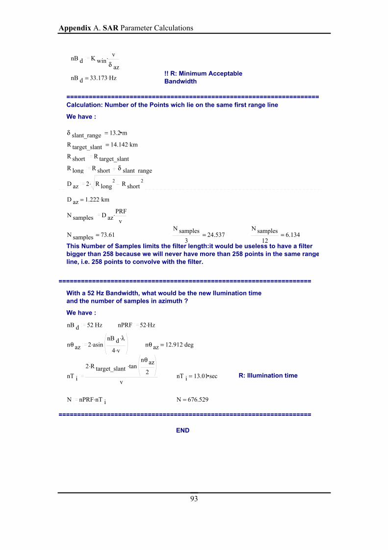
Appendix A. SAR Parameter Calculations
93
2
nB d K winv
δ az.
!! R: Minimum AcceptableBandwidth nB d 33.173 Hz=
====================================================================Calculation: Number of the Points wich lie on the same first range line
We have :
δ slant_range 13.2 m=
R target_slant 14.142 km=
R short R target_slantR long R short δ slant_range
D az 2 R long2 R short
2.
D az 1.222 km=
N samples D azPRF
v.
N samples 73.61=N samples
324.537=
N samples12
6.134=
This Number of Samples limits the filter length:it would be useless to have a filter bigger than 258 because we will never have more than 258 points in the same rangeline, i.e. 258 points to convolve with the filter.
====================================================================
With a 52 Hz Bandwidth, what would be the new Ilumination timeand the number of samples in azimuth ?
We have :
nB d 52 Hz nPRF 52 Hz.
nθ az 2 asinnB d λ.
4 v.. nθ az 12.912 deg=
nT i
2 R target_slant. tannθ az
2.
vnT i 13.01 sec= R: Illumination time
N nPRF nT i. N 676.529=
====================================================================
END

Appendix B. The FIR Filters
94
Appendix B. The FIR Filters
This appendix describes the characteristics of the different FIR filter utilised in the
functional design step chapter. The filters are:
• COMBO: the simplest filter, consisting of three unit coefficients.
• HAM15: this filter has been designed using a Hamming window. The program
used, called ‘fir1’, is part of the signal processing toolbox under Matlab. The
frequency cut-off is set at 22 Hz for a 208.33 sampling frequency. The required
number of coefficients is 15.
• HAM31: this filter has been designed with fir1, a Hamming window, a 22 Hz
frequency cut-off (208.33 sampling frequency), and a required number of taps equal
to 31.
• RECT31: This filter has been designed with fir1, a rectangular window, a 22 Hz
frequency cut-off (208.33 sampling frequency) and a required number of taps equal to
31.
• RICE31: This filter has been designed with cl2lp. Cl2lp is a Matlab program
developed by Rice University (the program can be found at http://www-dsp.rice.edu):
it uses constraint least square optimum techniques (see [28]). The cut-off frequency is
22 Hz; the required stop band and passband ripples are at 1 per cent (or -40 dB); the
number of coefficients is 31.
• RICE63: This filter uses the same program and parameters than above, except
that the number of coefficients is 63.
• RICE81: This filter has been designed for comparing single-stage and dual-stage
models at functional design level. The sampling frequency is 625 Hz, and the number

Appendix B. The FIR Filters
95
of coefficients 81. The other parameters are equivalent to the ones used for creating
RICE31.
The time and frequency responses of each filter are plotted in the next pages. The
filter coefficients can be found on the enclosed CD-ROM, under the simulation/filters
directory.

Appendix B. The FIR Filters
96
Figure 40: ‘COMBO’ Filter Impulse Response
Figure 41: ‘COMBO’ Filter Frequency Response

Appendix B. The FIR Filters
97
Figure 42: ‘HAM15’ Filter Impulse Response
Figure 43: ‘HAM15’ Filter Frequency Response
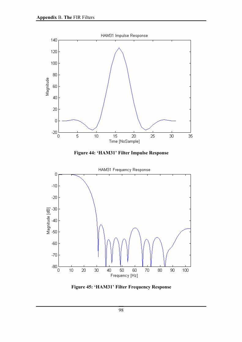
Appendix B. The FIR Filters
98
Figure 44: ‘HAM31’ Filter Impulse Response
Figure 45: ‘HAM31’ Filter Frequency Response

Appendix B. The FIR Filters
99
Figure 46: ‘RECT31’ Filter Impulse Response
Figure 47: ‘RECT31’ Filter Frequency Response
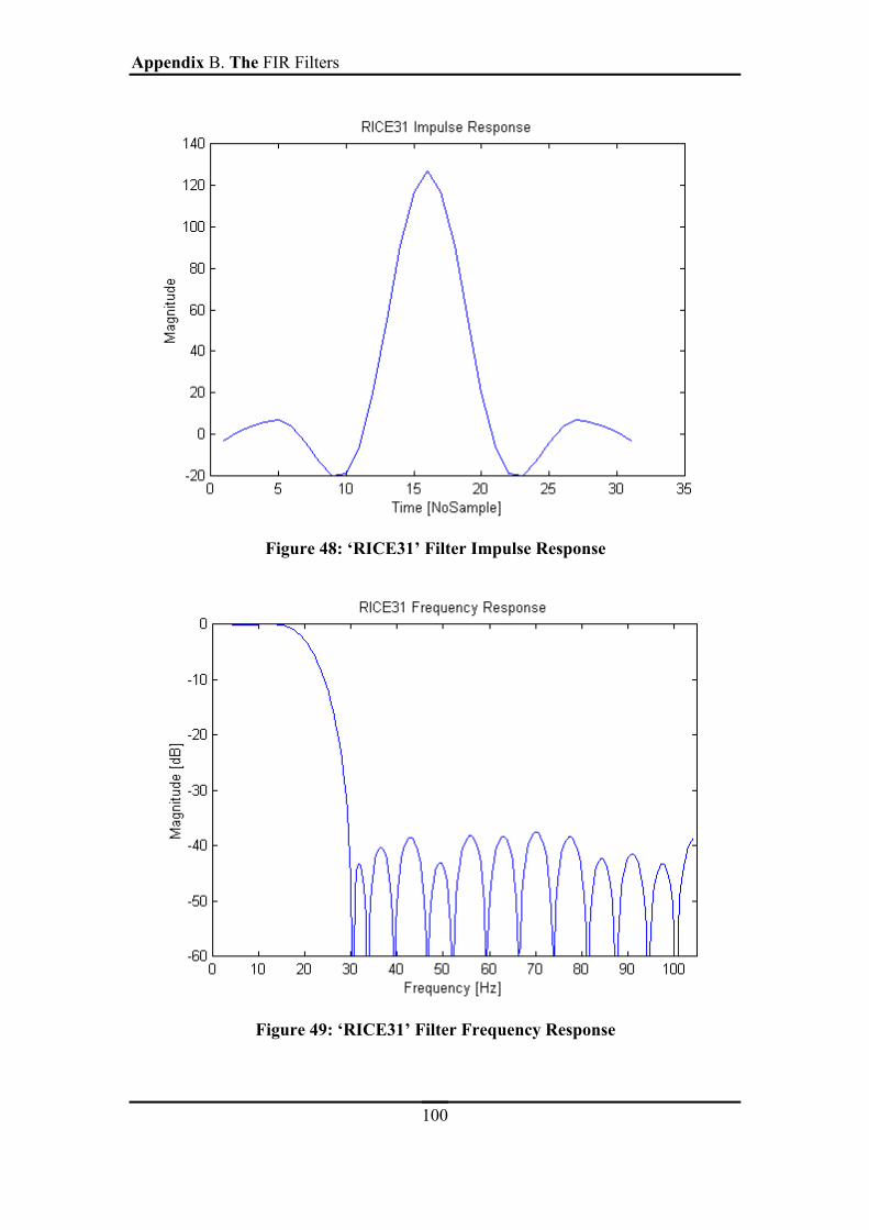
Appendix B. The FIR Filters
100
Figure 48: ‘RICE31’ Filter Impulse Response
Figure 49: ‘RICE31’ Filter Frequency Response

Appendix B. The FIR Filters
101
Figure 50: ‘RICE63’ Filter Impulse Response
Figure 51: ‘RICE63’ Filter Frequency Response

Appendix B. The FIR Filters
102
Figure 52: ‘RICE81’ Filter Impulse Response
Figure 53: ‘RICE81’ Filter Frequency Response

Appendix C. The Simulation
103
Appendix C. The Simulation
The different data files and scripts created during the simulation of the functional
design (see 5.4.1) are on the enclosed CD-ROM, under the simulation directory (Note
that the programs written by Horrell [30] and Lengenfelder [29] and used during the
simulation are not on the CD-ROM). This directory is structured as follows:
C.1 The raw&presum directory
This directory contains the input, the presummed and the azimuth compressed data
files (see 5.4.1). The associate script files are also here.
• sarsim_raw.scr: SARSIM2 script for the creation of the input data matrix.
• raw.bin: Input data matrix. Size: 116 Mbytes (2048 columns, 29765 lines and
unsigned char complex values).
• corner.bin: Corner turned input data. Size: 116 Mbytes (29765 columns, 2048
lines and unsigned char complex values).

Appendix C. The Simulation
104
• bcorner.bin: Block extracted from corner turned matrix. The block extraction
process was not mentioned in 5.4.1. It consists of extracting the relevant 128 range
bins that contains non-zero values. This has been done for saving memory and
processing time. The bcorner.bin file will feed the simulated Presummer, but also the
azimuth compression process. Size: 7.2 Mbytes (29765 columns, 128 lines and
unsigned char complex values).
• presum.scr: Script for the Presummer function.
• summed.flt: Presummed bcorner.bin. Size: 4.8 Mbytes (9922 columns, 128
lines, floating complex values).
• azccorn.scr: Script for the azimuth compression function.
• azccorn.flt: Azimuth compressed bcorner.bin. Size: 29 Mbytes (29765 columns,
128 lines, floating point complex values).
C.2 The prefilt directory
The Prefilter operation is performed for each of the filters described in the previous
appendix. Each of the comb, ham15, ham31, rect31, rice31, rice63 directories
contains the following files:
• filt.txt, fir1.txt, or cl2lp.txt: Filter coefficients file.
• prefilt.scr: Script for the Prefilter function.
• filted.bin: Prefiltered summed.flt. Size: 620 Kbytes (2481 columns, 128 lines,
unsigned char complex values).
• azcfilt.scr: Script for azimuth compression.
• azcfilt.flt: Azimuth compressed filted.bin. Size: 2.4 Mbytes (2481 columns, 128
lines, floating point complex values).

Appendix C. The Simulation
105
C.3 The raw_52 directory
This directory contains the different files involved in the creation of reference matrix,
see 5.4.1.
• sarsim_52.scr: SARSIM2 script for the creation of the new raw data matrix.
• raw_52.bin: Raw data matrix. Size: 9.7 Mbytes (2048 columns, 2481 lines and
unsigned char complex values).
• corner.bin: Corner turned raw matrix. Size: 9.7 Mbytes (2481 columns, 2048 lines
and unsigned char complex values).
• bcorner.bin: Block extracted from corner turned matrix. This is the so-called
Reference matrix. Size: 620 Kbytes (2481 columns, 128 lines and unsigned char
complex values).
C.4 The matlab directory
Each of the filted.bin under the prefilter directory is compared with the Reference
matrix bcorner.bin. This comparison is done with the help of the following Matlab
functions:
• get_reference: this function simply reads the file bcorner.bin and creates the
Reference matrix.
• calculate_INoise reads the filted.bin file, creates the Filtered matrix and subtracts
it to the Reference matrix. Prior to the subtraction operation, both matrices are
normalised and interpolated in range and azimuth. The Matlab routine finally
integrates the newly created “difference” matrix to obtain the so-called Integrated
Noise, our criterion for the best filter selection.
• read_IQ and vec2asc are two annexe programs.

Appendix C. The Simulation
106
C.5 The test bench directory
Contains the test bench used during the verification phase.
• braw.bin. Block extracted from raw.bin (raw&presum directory). Size: 4 Mbytes
(2048 columns, 1024 lines, unsigned char complex values). braw.bin is the file used
as input data during the verification of the implementation(s).
• bcorner.bin Corner turned braw.bin. Size: 4 Mbytes (1024 columns, 2048 lines,
unsigned char complex values).
• bsummed.flt Presummed bcorner.bin. Size: 5.3 Mbytes (341 columns, 2048 lines,
floating point complex values).
• out_sim.bin Prefiltered bsummed.flt (the filter used is ‘RICE31’). Size: 312
Kbytes (78 columns, 2048 lines, unsigned char complex values). This file is to be
compared with the out_C80 file, see Appendix D.

Appendix D. The C80 Programs
107
Appendix D. The C80 Programs
The different C80 programs are on the enclosed CD-ROM, under the C80 programs
directory. This directory is structured as follows:

Appendix D. The C80 Programs
108
D.1 The PP C Compiler Benchmark directory
This directory contains the codes that were used to benchmark the PP C compiler, see
3.3.2.
D.1.1 The source sub-directory
The source directory contains the following C source files:
• main.c: MP file and starting point of the program. main.c creates the FirServer
task that commands PP0 to execute ppFir.c.
• ppFir.c: PP main program that transfers data on-chip, launches the convol inner
loop and transfers data off-chip.
• convol_c.c: convolution inner loop written in C.
• convol_c.s: Assembly file generated by the compiler on the convol_c.c file. It is to
be compared with the following one.
• convol_s.s: convolution inner loop written in Assembly.
• filt.c: filter coefficients file.
• input.c: input data file.
• build.bat: batch file that contains all the compilation and linking commands.
D.1.2 The include sub-directory
The include directory contains the following C include files
• main.h: MP include file.
• ppFir.h: PP include file.

Appendix D. The C80 Programs
109
D.1.3 The obj sub-directory
Contains the object files created by the C80 compiler convol_c.o, convol_s.o, filt.obj,
input.obj, main.obj, and ppfir.o. Five other files are present:
• mypplnk.cmd: PP linker command file.
• ppfir.out: PP intermediate executable
• ppfir.map: file generated by the linker for the PP link.
• mymplnk.cmd MP linker command file.
• xfir.map: file generated by the linker for the final link.
D.1.4 The exe sub-directory
• init.pdm is used for debugging purposes.
• xfir.out is the C80 executable to be downloaded to the SDB.
D.2 The dd, ds, sd and ss directories
These directories respectively contain the codes that represent the dd, ds, sd and ss
implementations, see 7.1.
D.2.1 The source sub-directory
• pp_Sum.c & average_c.c are the PP functions in charge of the presumming, see
6.2.5.
• pp_Filt.c & convol_c.c are the PP functions in charge of the prefiltering, see 6.2.5.

Appendix D. The C80 Programs
110
• coef.c is the filter coefficients file.
• mp_Main.c implements the Main task, see 6.2.3
• mp_Input.c implements the Input task, see 6.2.3
• mp_Output.c implements the Output task, see 6.2.3
• [mp_ISum.c, mp_Sum.c, mp_OSum.c] or [mp_Sum.c]: implements the
Presummer, with either the DTM (dd and ds implementations) or the STM (ss and sd
implementations) model.
• [mp_Filt.c, mp_IFilt.c, mp_OFilt.c] or [mp_Filt.c]: implements the Prefilter,
with either the DTM (dd and sd implementations) or the STM (ss and ds
implementations) model.
• build.bat: batch file that contains all the compilation and linking commands.
D.2.2 The include sub-directory
The include directory contains the following C include files
• mp.h: MP include file
• common.h: include file used by both MP and PP programs
D.2.3 The obj sub-directory
This directory contains each of the compiled C files. Two other files are present:
• mylnk.cmd: linker command file.
• preproc.map: file generated by the linker.

Appendix D. The C80 Programs
111
D.2.4 The exe sub-directory
• preproc.out: C80 executable.
• braw.bin: input data file, see C.5.
• init.pdm and mpdb.bat are used for debugging purposes.
• out_C80.bin is the resulting output data file read from the SDB external memory.
The file is to be compared to out_sim.bin, see C.5.
• out_time.bin is the file containing the values of the register TCOUNT at output
range line production time.
• sum_time.bin is the file containing the values of the register TCOUNT at
presummed range line production time.
In addition, another timing result file exists for the chosen (sd) implementation.
• out_t1.bin contains also timing results at output line production. However, here,
for timing understanding, the inner loops are deactivated (see 7.4).

112
REFERENCES
[1] J.P. Calvez, Embedded Real-Time Systems: a Specification and Design
Methodology, John Wiley Publisher 1993.
[2] G. Carter, System Level Simulation of Digital Designs: A Case Study, MSc
Thesis, University of Cape Town, 1998.
[3] G. Booch, Object-Oriented Analysis and Design with Applications, 2nd
Edition, Benjamin/Cummings, New York, 1994.
[4] J. Rumbaugh et al., Object-Oriented Modelling and Design, Prentice-Hall
Englewood Cliffs NJ, 1991.
[5] G. Booch et al, The Unified Modelling Language User Guide, Addison-
Wesley Longman, 1998.
[6] T. DeMarco, Structured Analysis and System Specification, Prentice-Hall,
1979.
[7] E. Yourdon, Modern Structured Analysis, Prentice-Hall, Englewood Cliffs NJ,
1989.
[8] D.J. Hatley, I.A. Pirbhai, Strategies for Real-Time System Specifications,
Dorset House Publishing Co., 1988
[9] P.T. Ward, and Mellor, Structured Development for Real-Time Systems,
Prentice-Hall, Englewood Cliffs NJ., 1989
[10] RASSP Taxonomy Working Group, RASSP VHDL Modelling Terminology
and Taxonomy, http://www.atl.external.lmco.com/rassp/taxon/rass_taxon.html, June
1998.
[11] Lapsley, Bier, Shoham, Lee, DSP Processor Fundamentals, Chapter 5,
Berkeley Design Technology, 1996

113
[12] V.K. Madisetti, VLSI Digital Signal Processors, Chapter 1, Butterworth-
Heinemann, 1995
[13] Texas Instruments, TMS320C8x System-Level Synopsis, Chapter 2, 1995.
[14] Texas Instruments, TMS320C80 (MVP) Master Processor User’s Guide, 1995.
[15] Texas Instruments, TMS320C80 (MVP) Parallel Processor User’s Guide,
1995.
[16] Texas Instruments, TMS320C80 (MVP) Transfer Controller User’s Guide,
Chapter 4, 1995.
[17] Texas Instruments, TMS320C80 (MVP) Software Development Board
Installation Guide, 1997.
[18] Texas Instruments, TMS320C80 (MVP) Code Generation Tools User’s Guide,
Section 1.3.3, 1995.
[19] MVP Hotline Account, personal communication, [email protected], 1998
[20] C.Oliver, S.Quegan, Understanding Synthetic Aperture Radar Images, Artech
House 1998.
[21] M.L. Skolnik, Introduction to radar systems, McGraw-Hill, 1981.
[22] J.C. Curlander, R.N. McDonough, Synthetic Aperture Radar, Systems and
Signal Processing, Wiley & Sons 1991.
[23] F.J. Harris, “On the use of windows for harmonic analysis with the Discrete
Fourrier Transform”, IEEE Proceedings, vol.66, no. 8, 1 January 1978, pp. 51-83.
[24] B.C. Barber, “Theory of digital imaging from orbital synthetic-aperture radar”,
Int. J. Remote Sensing, Vol. 6, No7, 1985.
[25] F.M. Henderson, A.J. Lewis, Principles & Applications of Imaging Radar,
John Wiley & Sons, §2, 1998.

114
[26] V. Oppenheim and R. W. Schafer, Discrete-time Signal Processing, Prentice-
Hall, 1989.
[27] T.W. Parks and C.S. Burrus, Digital Filter Design, John Wiley and Sons,
1987.
[28] I.W. Selesnick, M. Lang and C. S. Burrus, “Constrained Least Square Design
of FIR Filters without specified transition bands”, IEEE Transactions on Signal
Processing, June 1994.
[29] R. Lengenfelder, The Design and Implementation of a Radar Simulator, MSc
Thesis, University of Cape Town, 1998.
[30] J. Horrell, The Design of a VHF Synthetic Aperture Radar System, PhD
Thesis, University of Cape Town, 1999.
[31] T. Axford, Concurrent Programming: Fundamental Techniques for Real-Time
and Parallel Software Design, p.9-14, John Wiley & Sons, 1989.
[32] Texas Instruments, TMS320C8x (MVP) Multitasking Executive User’s Guide,
Section 2.8.1, 1995
[33] http://www.ptolemy.eecs.berkeley.edu

115
BIBLIOGRAPHY
• W. Baetens, M. Adé‚ R. Lauwereins, “Porting GRAPE to the TMS320C80”, 8th
Int. Conf. on Signal Processing Applications & Technology ICSPAT, San Diego CA
USA, Sept. 14-17, pp. 1589-1593, 1997.
• W. Baetens, M. Adé, R. Lauwereins, “Rapid prototyping of video processing
algorithms on the TMS320C80 MVP”, 2nd European DSP Education and Research
Conference. Paris, France, September 23-24, p314-319, 1998.
• Blue Wave Systems, A Parallel DSP Based Radar System, Application Note,
http://www.bluews.com
• Blue Wave Systems, Solving Medical Imaging Problems with the C80 DSP,
Application Note, http://www.bluews.com
• W.G. Carrara, R.S. Goodman, R.M. Majewski, Spotlight Synthetic Aperture
Radar Signal Processing Algorithms, Artech House, 1995.
• J.E. Cooling, Real-Time Software Systems, an introduction to structured and
object-oriented design, International Thomson Computer Press, 1997.
• E. Cooper, Minimizing Quantization Effects Using the TMS320 Digital Signal
Processor Family, Application Report, Texas Instruments, 1994.
• G. Cutts, Structured Systems Analysis & Design Methodology, Paradigm 1987.
• J.A Debardelaben, V.K. Madisetti, A.J. Gradient, Incorporating Cost Modelling in
Embedded-System Design, IEEE Design & Test of Computers, July-September 1997.
• T. DeMarco, Structured Analysis and System Specification, Prentice-Hall, 1978.
• Downton, D. Crookes, Parallel Architectures for Image Processing, Electronics &
Communication Engineering Journal, 10, (3), 1998.

116
• R. J. Higgins, Digital Signal Processing in VLSI, Prentice Hall, 1990.
• J. Kim, Y. Kim, “Performance Analysis and Tuning for a Single-Chip
Multiprocessor DSP”, IEEE Concurrency Journal, January-March 1997.
• I. Main, Factors to Consider when Choosing The Right DSP For The Job,
Electronic Design, June 8, 1998.
• Pan, Y. S. Oh, Y. S. Sohn, and R.H. Park, “Implementation of a fast hierarchical
motion vector estimation algorithm using mean pyramid on TMS320C80 DSP board”,
in Proc. 1998 International Technical Conference Circuits/Systems, Comput.
Commun., vol. I, pp. 171-174, Sokcho, Korea, July 1998.
• J. H. Park et al., "Implementation of the Navigation Parameter Extraction from the
Aerial Image Sequence on TMS320C80 DSP board," in Proc. 8th Int. Conf. Signal
Processing Applications & Technology, pp. 1562-1566, San Diego, CA, USA, Sep.
1997.
• Y.S. Sohn et al., “Implementation of a two-stage block matching algorithm using
integral projections on the TMS320C80 DSP Board”, in Proc. 8th International
Conference Signal Processing Applications & Technology, pp. 1213-1217, San Diego,
CA, USA, Sep. 1997.
• S.L. Wasson, Top-Down FPGA Design- A 12-Step Program: FPGA design flow
benefits from a structured design approach, Integrated System Design, January 1996.