topic 3d - tem - portland state universityweb.pdx.edu/~pmoeck/phy381/tem.pdf · topic 3d - tem 1.0...
TRANSCRIPT

Topic 3d - TEM1.0 Review• 1.1 Types of Solids• 1.2 Basic of Crystallography Concepts• 1.3 Crystal Structures
2.0 Basic Principles• 2.1 The Microscope Column• 2.2 Beam and Specimen Interaction• 2.3 Sample Prep• 2.4 Sample Holder
3.0 Imaging and Examples• Bright field, Dark field, Phase contrast, e- diffraction,
SAED, EELS, EDS, Mapping, STEM
4.0 Limitations
5.0 Summary

1.1 Types of SolidsCrystalline material: atoms self-organize in a periodic array
Single crystal: atoms are in a repeating or periodic array over the entire extent of the material
Polycrystalline material: comprised of many small crystals or grains
Amorphous: lacks a systematic atomic arrangement
Crystalline Amorphous
SiO2
SiO2

1.1 Unit CellThe unit cell is the smallest structural unit or building block that can describe the crystal structure. Repetition of the unit cell generates the entire crystal.
Example: 2D honeycomb net can be represented by translation of two adjacent atoms that form a unit cell for this 2D crystalline structure

1.1 Crystal structureTo discuss crystalline structures it is useful to consider atoms as being hard spheres with well-defined radii. In this hard-sphere model, the shortest distance between two like atoms is one diameter.
We can also consider crystalline structure as a lattice of points at atom/sphere centers.
• Think of a crystal as being an array of atomic hard spheres• Or a lattice point : a 3D array of points at sphere (atom) centers• Lattice parameters: edge lengths (a,b,c), angles (α,β,γ) of unit cells.
ab
c
α
γ
β

Positions and Directions
x, y, z → u, v, wX
Y
Z
Lattice Positions and Directions:1) Always establish an origin2) Determine the coordinates of the lattice points of interest3) Translate the vector to the origin if required by drawing a
parallel line or move the origin.
4) Subtract the first point from the second: u2-u1,v2-v1,w2-w15) Clear fractions and reduce to lowest terms6) Write direction with square brackets [uvw]7) Negative directions get a bar over them.
1.2 Review of Crystallography Concepts

Miller indices- h,k,l- for naming points in the crystal lattice. The origin has been arbitrarily selected as the bottom left-back corner of the unit cell.
12
3
4
5
1) 2)3)4) 5)
1.2 Positions and Directions

Notation for lattice positions.
Family of directions, <111>, representing all body diagonals for adjacent unit cells in the cubic system.
1.2 Positions and Directions

Miller Indices
Miller indices are a notation for describing directions and labelling planes in lattices and crystals. The basis for determining the index is the unit cell. It is important to be clear about the unit cell being used.
A direction is expressed in terms of its ratio of unit vectorsin the form [uvw] where u, v and w are integers. A family of crystallographically equivalent directions is expressed as <uvw>.
A Miller index for a plane is expressed as (hkl), where h, k and l are integers. A family of crystallographically equivalent planes is expressed as {hkl}.
1.2 Planes

1) Identify the locations where the plane intercepts the x, y, z axes as the fractions of the unit cell edge lengths a, b, c.
2) Infinity if the plane is parallel.3) Take the reciprocal of the intercepts. 4) Clear any fraction but do not reduce to lowest terms. 5) Example: 1/3,1/3,1/3 is (333) not (111)!!!6) Use parentheses to indicate planes (hkl) again with a hat
over the negative indices.7) Families are indicated by {hkl}Remember Terminology:Defined coordinate system: x, y, zRespective unit cell edge lengths: a, b, c Direction: Denoted by [uvw]Family of direction(s): Denoted by: <uvw>Plane: Denoted by: (hkl)Family of Plane(s): Denoted by: {hkl}
1.2 Planes

( ) ?
1) Identify the locations where the plane intercepts the x, y, z axes as the fractions of the unit cell edge lengths a, b, c.
2) Infinity if the plane is parallel.3) Take the reciprocal of the intercepts. 4) Clear any fraction but do not reduce to lowest terms. 5) Example: 1/3,1/3,1/3 is (333) not (111)!!!6) Use parentheses to indicate planes (hkl) again with a hat over the negative indices.7) Families are indicated by {hkl}
1.2 Planes

Representation of a series each of (a) (001), (b) (110), and (c) (111) crystallographic planes.
<110> = [110],[101], [011], [1-10], [10-1],[01-1],[-1-10],[-10-1] [0-1-1],[-110],[-101][0-11]
1.2 Planes

1.2 Indexing of Planes and Directions
ab
c
ab
c
[110]
[uvw]-one direction, [111]
<uvw> - a family of equivalentdirections
<111> - [111], [-111],[1-11][11-1], etc. total: 8
(hkl) - one plane, (110)
{hkl} - a set of equivalentplanes
{110} - (110),(101),(011)(110), etc. 12
[111][111]
_
(110)
(101)
_

• Directions are always perpendicular to their respective planes, i.e. [111]direction is perpendicular to the (111) plane (for cubic systems, not true in all systems) .
• Families of equivalent planes are equal with respect to symmetrical structures, they do not have to be parallel. Equivalent planes must be translated to the correct atomic positions in order to maintain the proper crystal symmetry.
• Families of directions are equivalent in absolute magnitude.
• (222) planes are parallel to the (111) planes but not equal.
• Intercepts for the (222) planes are 1/2,1/2,1/2
• Intercepts for the (333) planes are 1/3,1/3,1/3, remember this is in what we call “reciprocal space”. If you draw out the (333) plane it isparallel to the (111) plane but not equivalent.

1.3 Crystal Structures
Ø Metals are usually (poly)crystalline; although formation of amorphous metals is possible by rapid cooling
Ø The atomic bonding in metals is non-directional ⇒ no restriction on numbers or positions of nearest-neighbor atoms ⇒ large number of nearest neighbors and dense atomic packing
Ø Atom (hard sphere) radius, R, defined by ion core radius -typically 0.1 - 0.2 nm
Ø The most common types of unit cells are the faced-centered cubic (FCC), the body-centered cubic (BCC) and the hexagonal close-packed (HCP).

Face-Centered Cubic (FCC) Crystal Structure (I)
Ø Atoms are located at each of the corners and on the centers of all the faces of cubic unit cell
Ø Cu, Al, Ag, Au have this crystal structure
Two representations of the FCC unit cell
1.3 Crystal Structures

1.3 Crystal StructuresØ The hard spheres or ion cores touch one another across a face diagonal ⇒
the cube edge length, a= 2r√2 (or 4r/ √2)
Ø The coordination number, CN = the number of closest neighbors to which an atom is bonded = number of touching atoms, CN = 12
Ø Number of atoms per unit cell, n = 4. In FCC unit cell we have: 6 face atoms shared by two cells: 6 x 1/2 = 3
8 corner atoms shared by eight cells: 8 x 1/8 = 1
Ø Atomic packing factor, APF = fraction of volume occupied by hard spheres = (Sum of atomic volumes)/(Volume of cell) = 0.74
r
a
FCC (II)

1.3 Crystal Structures FCC (III)
Ø Corner and face atoms in the unit cell are equivalent
Ø FCC crystal has APF of 0.74, the maximum packing for a system equal-sized spheres ⇒ FCC is a close-packed structure
Ø FCC can be represented by a stack of close-packed planes (planes with highest density of atoms)

Body-Centered Cubic (BCC) Crystal Structure (I)
Atom at each corner and at center of cubic unit cell: Cr, α-Fe, Mo
1.3 Crystal Structures

1.3 Crystal Structures BCC (II)
Ø The hard spheres touch one another along cube diagonal ⇒ the cube edge length, a= 4r/√3
Ø The coordination number, CN = 8
Ø Number of atoms per unit cell, n = 2Center atom (1) shared by no other cells: 1 x 1 = 18 corner atoms shared by eight cells: 8 x 1/8 = 1
Ø Atomic packing factor, APF = 0.68
Ø Corner and center atoms are equivalent
a
r

2.0 Basic PrinciplesMicroscopy (TEM)/Scanning TransmissionElectron Microscopy (STEM)
• What is a TEM?
• Example instruments: JEOL and Philips
• How it works-gun, lenses, specimen
• Why use electrons?
• What can a TEM do?(i) Imaging and diffraction(ii) Imaging-diffraction and phase contrast diffraction(iii) Chemical analysis

What is a TEM?
In a typical TEM a static beam of electrons at 100 - 400kV accelerating voltage illuminate a region of an electron transparent specimen which is immersed in the objective lens of the microscope. The transmitted and diffracted electrons are recombined by the objective lens to form a diffraction pattern in the back focal plane of that lens and a magnified image of the sample in its image plane. A number of intermediate lenses are used to project either the image or the diffraction pattern onto a fluorescent screen for observation. The screen is usually lifted and the image formed on photographic film for recording purposes.

Modern TEMs
JEOL 2010F

Basic features of An Analytical TEM
Electron Gun
EDS DetectorCondenser LensSpecimen HolderObjective LensMagnifying LensesHAADF DetectorViewing Chamber
Camera ChamberSTEM Detector orEELS
2.1 The Microscope Column

Electron Optics of a TEM

Electron beam Source

The Lenses in a TEM
Condenser lenses(two)-control how strongly beam is focused (condensed) onto specimen. At low Mag. Spread beam to illuminate a large area, at highMag. strongly condense beam.

The Lenses in a TEM
Objective lens-focus image (imageformation) and contribute most to the magnification of the image.

The Lenses in a TEM
Four lenses form magnificationsystem-determine the magnificationof the microscope. Whenever themagnification is changed, the currentsthrough these lenses change.

Q: Why Electrons?A: Resolution!
In the expression for the resolution(Rayleigh’s Criterion)
r = 0.61λ/nsinαλ-wavelength, λ=[1.5/(V+10-6V2)]1/2 nm
V-accelerating voltage, n-refractive index
α-aperture of objective lens, very small in TEM
→ sinα →α and so r=0.61λ/α α~0.1 radiansGreen Light 200kV Electronsλ~400nm λ~0.0025nmn~1.7 oil immersion n~1 (vacuum)r~150nm (0.15µm) r~0.02nm (0.2Å)
1/10th size of an atom!UNREALISTIC! WHY?
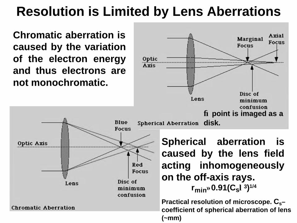
Resolution is Limited by Lens Aberrations
→point is imaged as a disk.
Spherical aberration is caused by the lens field acting inhomogeneously on the off-axis rays.
Chromatic aberration is caused by the variation of the electron energy and thus electrons are not monochromatic.
rmin≈0.91(Csλ3)1/4
Practical resolution of microscope. Cs–coefficient of spherical aberration of lens (~mm)

Scanning Transmission Electron Microscopy In STEM, the
electron beam is rastered (scan coil) across the surface of a sample in a similar manner to SEM, however, the sample is a thin TEM section and the diffraction contrast image is collected on a solid-state (ADF) detector.
JEOL 2000FX Analytical Electron Microscope
STEM detectoror EELS
HAADF Detector
HAADF-high angleannular dark-field
Scanningbeam
specimen
BF ADFADF
BF
DF
(STEM)
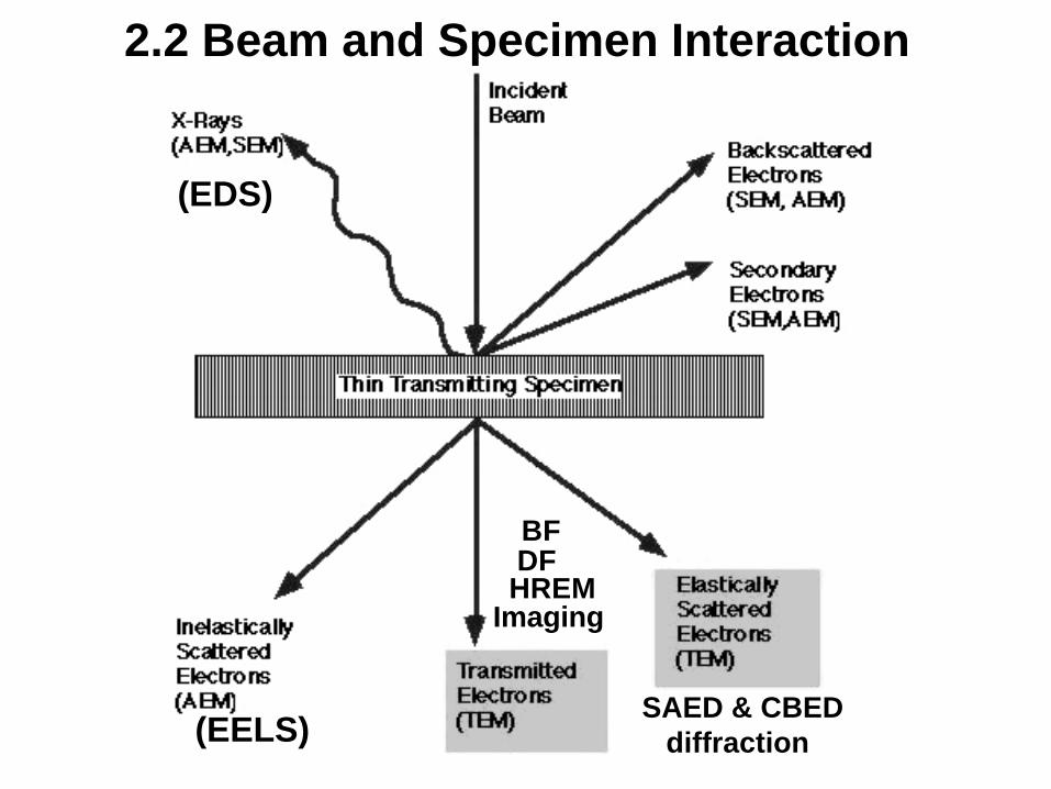
2.2 Beam and Specimen Interaction
(EDS)
(EELS)SAED & CBED
diffraction
BFDFHREM
Imaging

2.3 Conventional Specimen PreparationIon-milling a ceramic
3mm
Ultrasonic cutgrind Dimple center part
of disk to ~5-10µmion-mill until a hole appears in disk
Ar (4-6keV, 1mm A)
Jet-polishing metal
Drill a 3mmcylinder
Cut into disksand grind
A disk is mounted in a jet-polishing machine and is electro-polished until a small hole is made.
a thin stream of acid
+-
Ultramicrotomy-using a (diamond) knife blade Mainly for sectioning biological materials.To avoid ion-milling damage ultramicrotome can also be usedto prepare ceramic TEM specimens.

Specimen Preparation on Grids
Dispersing crystals or powders on a carbon film on a grid
3mm

Making a semiconductor specimen with a Focused Ion Beam (FIB)
1. a failure is located and a strip of Pt is placed as a protectivecover.
2. On one side of the strip a trench is milled out with the FIM.3. The same is done on the other side of the strip (visible
structure).4. The strip is milled on both sides and then the sides connecting
the strip to the wafer are cut through.5. The strip is tilted, cut at the bottom and deposited on a TEM
grid.
1 2 3 4 5

Conventional Specimen PreparationIon-milling a ceramic
3mm
Ultrasonic cutgrind Dimple center part
of disk to ~5-10µmion-mill until a hole appears in disk
Ar (4-6keV, 1mm A)
Jet-polishing metal
Drill a 3mmcylinder
Cut into disksand grind
A disk is mounted in a jet-polishing machine and is electro-polished until a small hole is made.
a thin stream of acid
+-
Ultramicrotomy-using a (diamond) knife blade Mainly for sectioning biological materials.To avoid ion-milling damage ultramicrotome can also be usedto prepare ceramic TEM specimens.

2.4 Specimen Holders
a split pole pieceobjective lens
holder
beam
Heating and strainingTwin specimen holder
Double tilt heating
Rotation, tilting, heating, cooling and straining

3.0 Imaging
Two principal kinds:
• Diffraction contrast imaging - BF and DF imaging Use either an non-diffracted or diffracted beam and remove all other beams from the image by use of an objective aperture
• Phase contrast or high resolution imaging HREMUse all of the diffracted and non diffracted beams (by using a large objective aperture or none at all) and add them back together, phase and intensity to form a phase contrast image.

Bright Field (BF) and Dark Field (DF) ImagingIncident beam
specimen
transmitted beam
diffracted beam
objective aperture
hole in objectiveaperture(10-100µm)
In BF imaging - only the transmitted beam is allowed to pass objective aperture to form images, mass-thickness contrast
BF
DF
DF
DF imaging:Only diffractedbeams are allowed to pass the aperture to form images.
Particles in Al-CuAlloy. Thin platelets ll e Vertical, darkParticles ⊥e.

Phase Contrast Imaging High Resolution Electron Microscopy
(HREM)
Use a large objectiveaperture. Phases and intensities of diffracted and transmitted beams are combined to form a phase contrast image.
TD
Si
Objectiveaperture
Electron diffraction pattern recordedFrom both BN film on Si substrate.
BN

Basic Features of Electron Diffraction
λ = 2dsinθλ =0.037Å (@100kV)θ=0.26o if d=4Å
Reciprocal lattice
λ = 2dθL
L-camera length
r/L=sin2θas θ → 0
r/L = 2θ
r/L = λ /dor
r = λL/d
λL–camera length constant of microscope
1/d-reciprocal of interplanar distance(Å- 1)A reciprocal lattice is another way of view a crystal lattice and is used to understand diffraction patterns. A dimension of 1/d is used in reciprocal lattices.

Applications of TEM
TEM
Conventional TEMMicrostructure, morphology (grain size, orientation), phase distribution and defect analysis (point defects, dislocations and grain boundaries)
In situ TEMIrradiation and deformation experimentsEnvironmental cells (corrosion)Phase transformations(hot- and cold-stage, electric field)
Analytical TEM (Z-contrast imaging)Chemical composition-EDS, EELS, ELNES, EXELFS, Z-contrast imaging
HRTEMLattice imaging, Structure of complex materialsand atomic structure of defects (interfaces)

Diffraction Contrast –BF & DF Imaging
Objective aperture
C-filmamorphous
crystal
D
T
BF image
C-filmcrystal
D
T
C-film
crystal
DF image
Diffraction + mass-thickness Contrast

SAED Patterns of Single Crystal, Polycrystalline and Amorphous Samples
a b c
a. Single crystal Fe (BCC) thin film-[001]b. Polycrystalline thin film of Pd2Sic. Amorphous thin film of Pd2Si. The diffuse
halo is indicative of scattering from anamorphous material.
r1 r2200
020
110

Sub-Nanometric EDS Analysis (JEOL-2010F Field-emission TEM)
MBE-grown InGaAsP/InP Multi-quantum well structure
EDS spectra taken with a 5Å Probe. A) 1nm InGaAsP layerB) ~3nm away from interfaceWithin InP matrix.
•
•
A
B
A
B
InGaAsP
InP
HREM

Electron Energy Loss Spectroscopy (EELS)
EELS is a microanalytical technique that uses the characteristic spectrum of energy losses of transmitted electrons to obtain information about elemental composition, chemical bonding, and electronic structure (oxidation state). Moreover, by selecting electrons with a specific loss energy by a slit so as to image them, element distribution in the specimen can be visualized (Elemental mapping). The spatial resolution is limited by the diameter of the incident illumination focused on the sample.
focused beam~1.3Å
t<500Å
spectrometerEELS
Annulardetector
e-(E, E-∆E)
BF
DF
Z-contrastimage

Elemental Analysis by EELS
Integral peak intensity is proportional to the number of each atom in the measured region. From the intensity and the cross-section of inelasticscattering, the elemental ratio is determined as C:N:Cl:Fe=42.9:3.9:1.1:0.9.This value is corresponding well to the expected molecular composition (43:4:1:1). This result is obtained from the sample weight of 1X10-13 g.EELS spectrum from the region of 1 um diameter
of iron tetraphenylporphyrin monochloride crystal.
ClL2,3
CK
NK
OK
FeL2,3
Counts
Loss of energy (eV)

a.HREM image of carbon nanotube.b.Carbon map at the same region. c.EELS spectrum.d.Intensity profile ofcarbon mapperpendicular to thetube axis. The intensityprofile correspondswell to the calculatednumber distribution ofcarbon atoms (solidline) based on the sizeand the shape of thenanotube.The intensity dip atcenter part iscorresponding to 20carbon atoms.
Quantification of Elemental Mapping
a b
c d
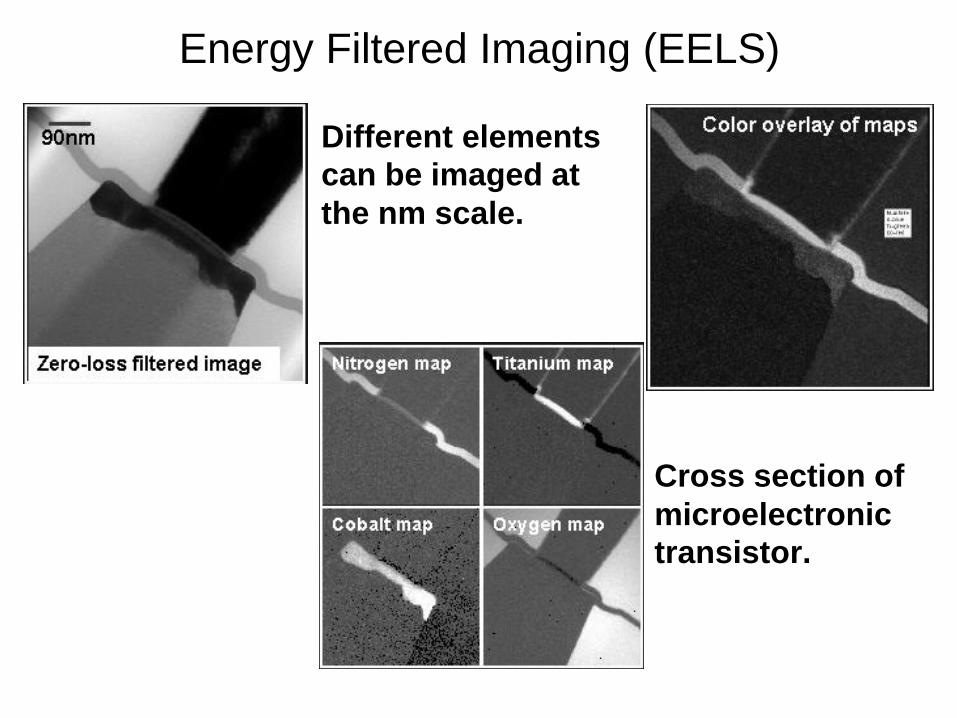
Energy Filtered Imaging (EELS)
Different elements can be imaged at the nm scale.
Cross section ofmicroelectronictransistor.

focused beam~1.3Å
t<500Å
spectrometerEELS
Annulardetector
e-(E, E-∆E)
BF
DF
Z-contrastimage
(STEM)
Z-contrast
High Resolution Z-contrast ImagingAtomic Ordering in Ba(Mg1/3Nb2/3)O3
I α Z2

4.0 Limitations of TEM
• Sampling
• Interpretation of image
• Beam damage
• Specimen preparation

5.0 Summary I
The uniqueness of TEM is the ability to obtain crystallographic, atomic, structural and microanalytical data such as:
• Chemical composition
• Bonding (distance and angle)
• Electronic structure
• Coordination number data from the sample.
• TEM is the most efficient and versatile technique for the characterization of materials.

5.0 Summary II
• UHV instrument
• Operation from 80 kV to 1000kV
• New techniques have made breakthroughs in sampleprep (FIB)
• Image interpretation
• Cost is prohibitive: 2-3.5 million$$
• Facilities and bldg. quality
• Training