topic: fast hierarchical optimization method for high ... · • channel sim. + 2.5d/3d ... pkg...
TRANSCRIPT
Image
Topic:
o Nam elementum commodo mattis. Pellentesque
malesuada blandit euismod.
Topic:
o Nam elementum commodo mattis. Pellentesque
malesuada blandit euismod.
o Nam elementum commodo mattis. Pellentesque
malesuada blandit euismod.
Topic:
o Nam elementum commodo mattis. Pellentesque
malesuada blandit euismod.
TITLE
Fast Hierarchical Optimization Method for High Speed Channel Design Using Channel Operating Margin (COM)
Spearker
Bo Pu, (Samsung Electronics)
Paper Author
Bo Pu (Samsung Electronics),
Rae Woon Yoo (Samsung Electronics)
Jiyoung Park (Samsung Electronics)
Jun So Pak (Samsung Electronics)
Sungwook Moon (Samsung Electronics)
Fast Hierarchical Optimization Method for High Speed Channel Design Using Channel Operating Margin (COM)
Speaker
Bo Pu, (Samsung Electronics)
Paper Author
Bo Pu (Samsung Electronics),
Rae Woon Yoo (Samsung Electronics)
Jiyoung Park (Samsung Electronics)
Jun So Pak (Samsung Electronics)
Sungwook Moon (Samsung Electronics)
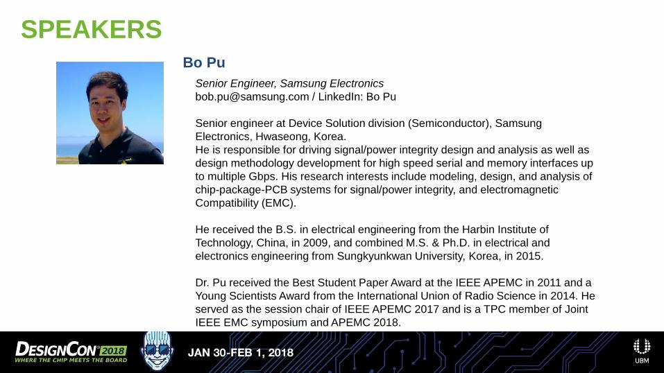
SPEAKERS Bo Pu
Senior Engineer, Samsung Electronics
[email protected] / LinkedIn: Bo Pu
Senior engineer at Device Solution division (Semiconductor), Samsung
Electronics, Hwaseong, Korea.
He is responsible for driving signal/power integrity design and analysis as well as
design methodology development for high speed serial and memory interfaces up
to multiple Gbps. His research interests include modeling, design, and analysis of
chip-package-PCB systems for signal/power integrity, and electromagnetic
Compatibility (EMC).
He received the B.S. in electrical engineering from the Harbin Institute of
Technology, China, in 2009, and combined M.S. & Ph.D. in electrical and
electronics engineering from Sungkyunkwan University, Korea, in 2015.
Dr. Pu received the Best Student Paper Award at the IEEE APEMC in 2011 and a
Young Scientists Award from the International Union of Radio Science in 2014. He
served as the session chair of IEEE APEMC 2017 and is a TPC member of Joint
IEEE EMC symposium and APEMC 2018.
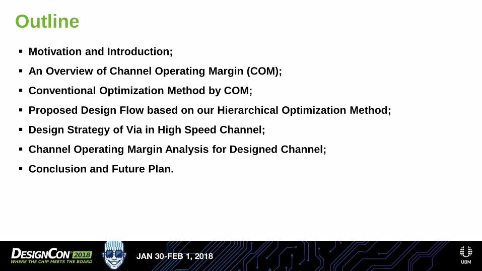
Outline
Motivation and Introduction;
An Overview of Channel Operating Margin (COM);
Conventional Optimization Method by COM;
Proposed Design Flow based on our Hierarchical Optimization Method;
Design Strategy of Via in High Speed Channel;
Channel Operating Margin Analysis for Designed Channel;
Conclusion and Future Plan.
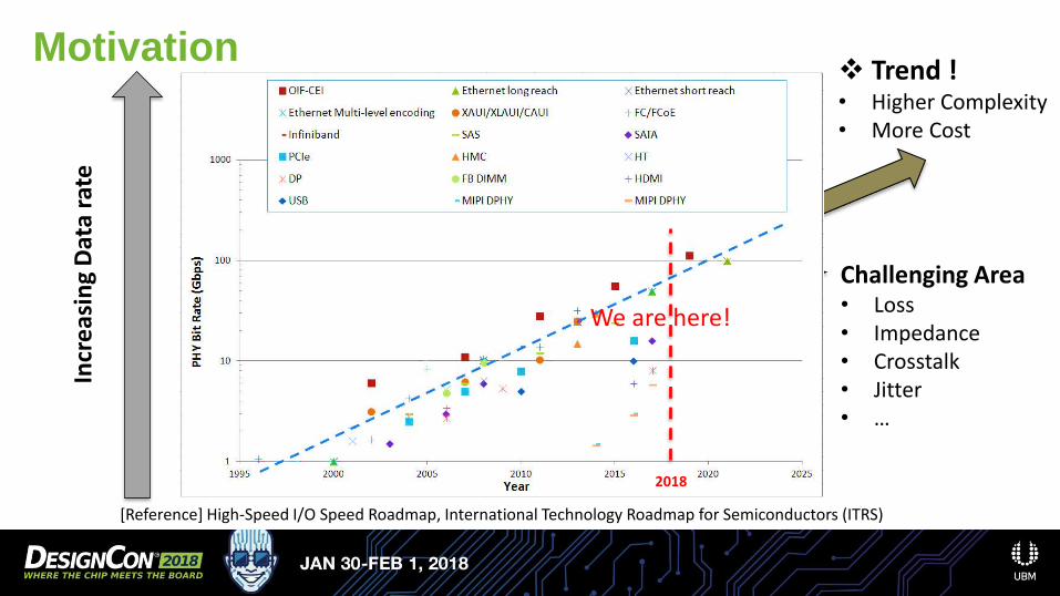
Motivation
[Reference] High-Speed I/O Speed Roadmap, International Technology Roadmap for Semiconductors (ITRS)
Trend ! • Higher Complexity • More Cost
Incr
eas
ing
Dat
a ra
te
Challenging Area • Loss • Impedance • Crosstalk • Jitter • …
We are here!
2018
Motivation
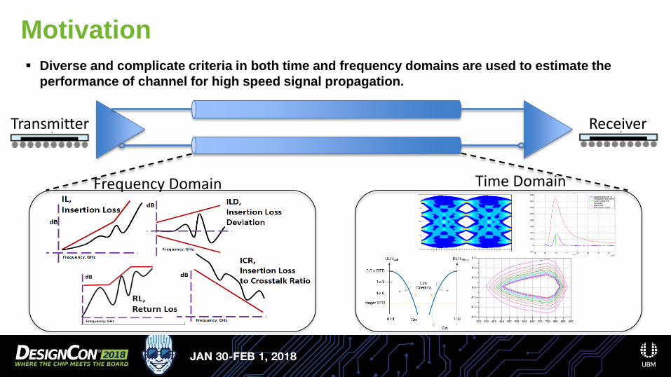
Frequency Domain Time Domain
Transmitter Receiver
Diverse and complicate criteria in both time and frequency domains are used to estimate the
performance of channel for high speed signal propagation.
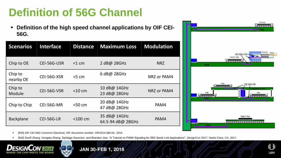
Definition of the high speed channel applications by OIF CEI-
56G.
Definition of 56G Channel
Scenarios Interface Distance Maximum Loss Modulation
Chip to OE CEI-56G-USR <1 cm 2 dB@ 28GHz NRZ
Chip to nearby OE
CEI-56G-XSR <5 cm 6 dB@ 28GHz
NRZ or PAM4
Chip to Module
CEI-56G-VSR <10 cm 10 dB@ 14GHz 23 dB@ 28GHz
NRZ or PAM4
Chip to Chip CEI-56G-MR <50 cm 20 dB@ 14GHz 47 dB@ 28GHz
PAM4
Backplane CEI-56G-LR <100 cm 35 dB@ 14GHz 64.5-94 dB@ 28GHz
PAM4
[Ref] OIF CEI-56G Common Electrical, OIF document number: OIF2014.380.02, 2015.
[Ref] Geoff Zhang, Hongtao Zhang, Santiago Asuncion, and Brandon Jiao, “A Tutorial on PAM4 Signaling for 56G Serial Link Applications”, DesignCon 2017, Santa Clara, CA, 2017.
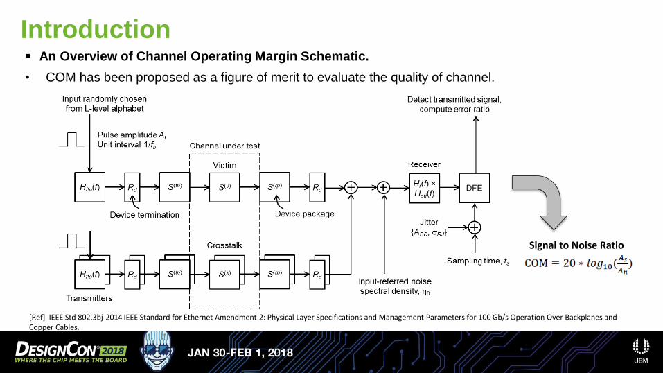
An Overview of Channel Operating Margin Schematic.
• COM has been proposed as a figure of merit to evaluate the quality of channel.
Introduction
[Ref] IEEE Std 802.3bj-2014 IEEE Standard for Ethernet Amendment 2: Physical Layer Specifications and Management Parameters for 100 Gb/s Operation Over Backplanes and Copper Cables.
Signal to Noise Ratio
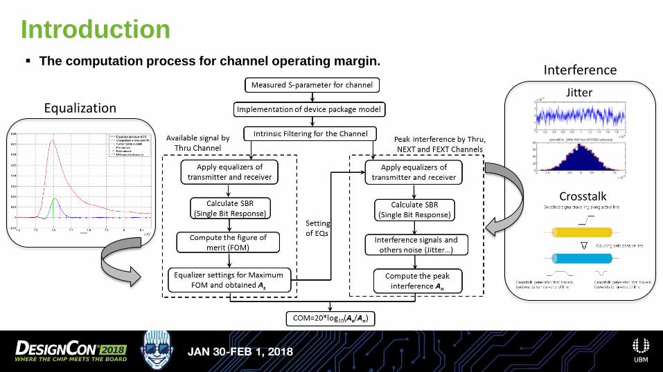
The computation process for channel operating margin.
Introduction
Jitter
Crosstalk
Interference
Equalization
Introduction
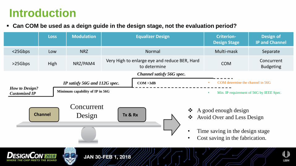
Loss Modulation Equalizer Design Criterion- Design Stage
Design of IP and Channel
<25Gbps Low NRZ Normal Multi-mask Separate
>25Gbps High NRZ/PAM4 Very High to enlarge eye and reduce BER, Hard
to determine COM
Concurrent Budgeting
Can COM be used as a deign guide in the design stage, not the evaluation period?
Minimum capability of IP in 56G How to Design?
Customized IP
COM >3dB IP satisfy 56G and 112G spec.
Channel satisfy 56G spec.
• Min. IP requirement of 56G by IEEE Spec.
• COM determine the channel in 56G
A good enough design
Avoid Over and Less Design
• Time saving in the design stage
• Cost saving in the fabrication.
Channel Tx & Rx
Concurrent
Design
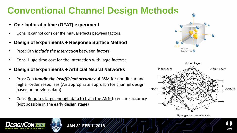
One factor at a time (OFAT) experiment
• Cons: It cannot consider the mutual effects between factors.
Design of Experiments + Response Surface Method
• Pros: Can include the interaction between factors;
• Cons: Huge time cost for the interaction with large factors;
Design of Experiments + Artificial Neural Networks
• Pros: Can handle the insufficient accuracy of RSM for non-linear and higher order responses (An appropriate approach for channel design based on previous data)
• Cons: Requires large enough data to train the ANN to ensure accuracy (Not possible in the early design stage)
Conventional Channel Design Methods
Fig. A typical structure for ANN.
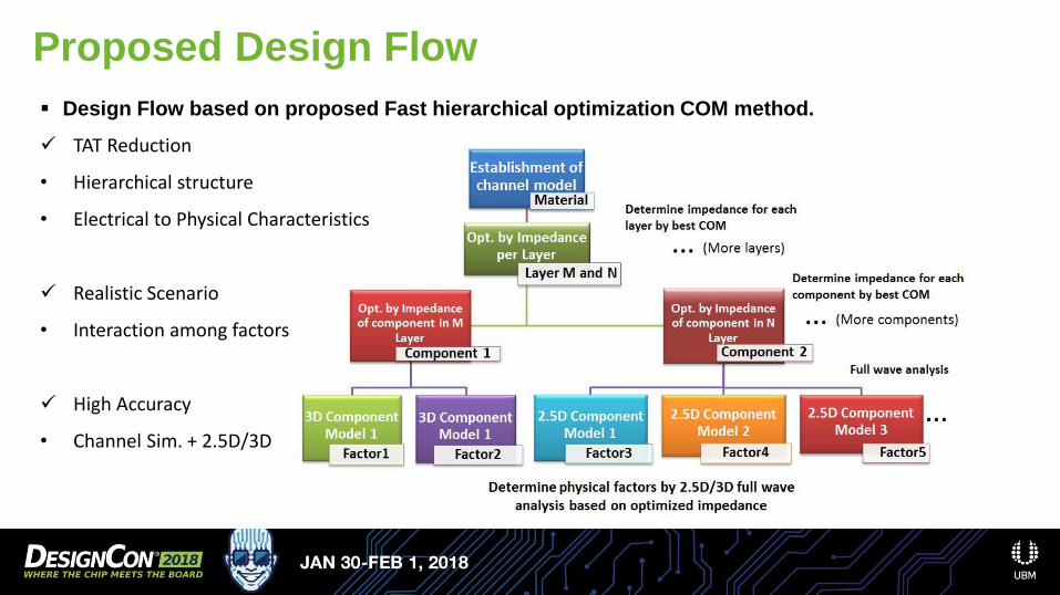
Design Flow based on proposed Fast hierarchical optimization COM method.
TAT Reduction
• Hierarchical structure
• Electrical to Physical Characteristics
Realistic Scenario
• Interaction among factors
High Accuracy
• Channel Sim. + 2.5D/3D
Proposed Design Flow
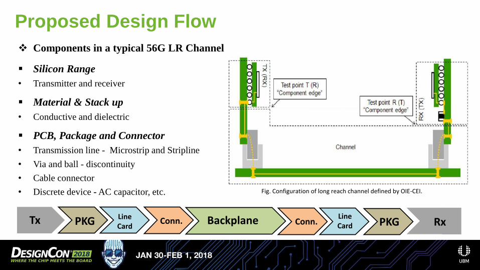
Components in a typical 56G LR Channel
Silicon Range
• Transmitter and receiver
Material & Stack up
• Conductive and dielectric
PCB, Package and Connector
• Transmission line - Microstrip and Stripline
• Via and ball - discontinuity
• Cable connector
• Discrete device - AC capacitor, etc.
Proposed Design Flow
Tx PKG Line Card
Conn. Backplane Conn. Line Card PKG Rx
Fig. Configuration of long reach channel defined by OIE-CEI.
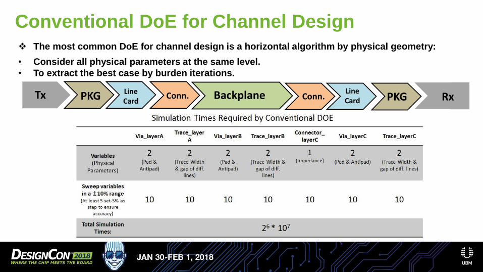
The most common DoE for channel design is a horizontal algorithm by physical geometry:
• Consider all physical parameters at the same level.
• To extract the best case by burden iterations.
Conventional DoE for Channel Design
Tx PKG Line Card
Conn. Backplane Conn. Line Card PKG Rx
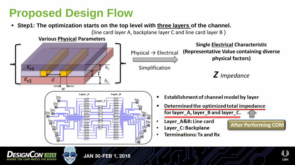
Step1: The optimization starts on the top level with three layers of the channel.
(line card layer A, backplane layer C and line card layer B )
Proposed Design Flow
εr1
εr2
t h1
h2 d
w
Various Physical Parameters Single Electrical Characteristic
(Representative Value containing diverse physical factors)
Z Impedance Simplification
Physical → Electrical
After Performing COM

Step2: Expanded each layer to corresponding components and determine the optimized
impedance for each device by COM computation.
Proposed Design Flow
Single Electrical Characteristic
Z Impedance
Expanded Electrical Characteristics
Impedance Matrix [ Z(Via, Line, Connector, etc.) ]
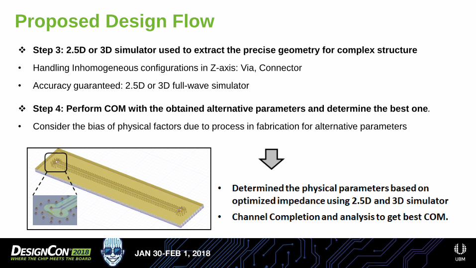
Step 3: 2.5D or 3D simulator used to extract the precise geometry for complex structure
• Handling Inhomogeneous configurations in Z-axis: Via, Connector
• Accuracy guaranteed: 2.5D or 3D full-wave simulator
Step 4: Perform COM with the obtained alternative parameters and determine the best one.
• Consider the bias of physical factors due to process in fabrication for alternative parameters
Proposed Design Flow
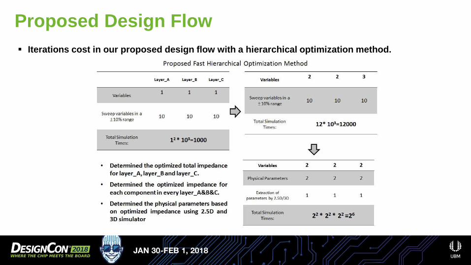
Iterations cost in our proposed design flow with a hierarchical optimization method.
Proposed Design Flow
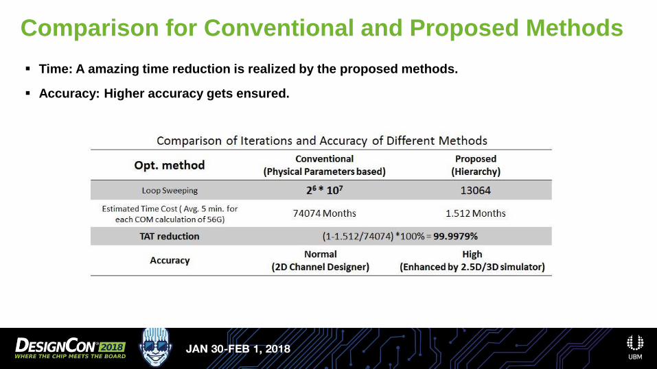
Time: A amazing time reduction is realized by the proposed methods.
Accuracy: Higher accuracy gets ensured.
Comparison for Conventional and Proposed Methods
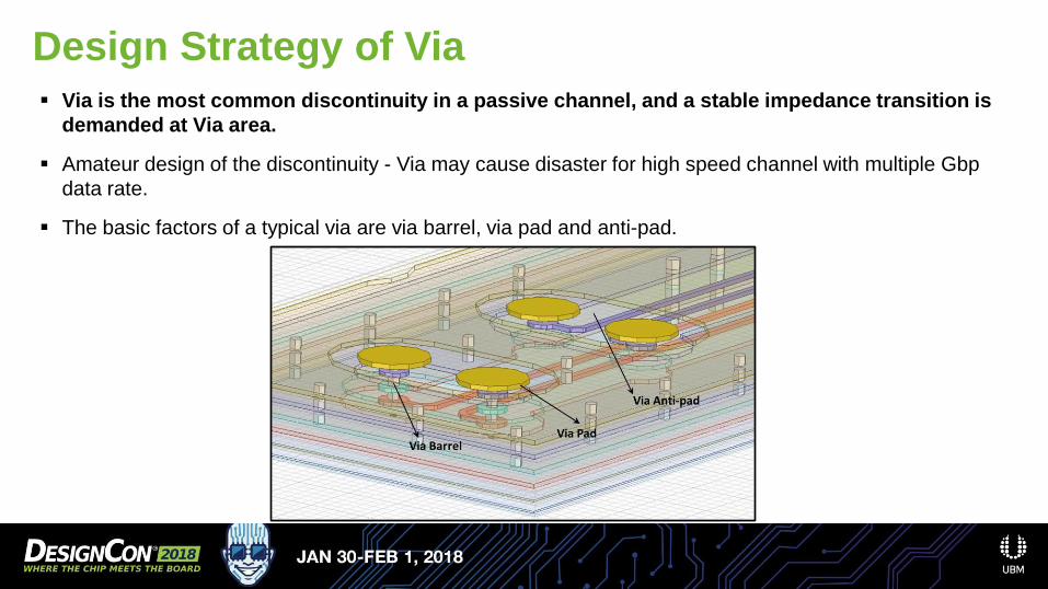
Via is the most common discontinuity in a passive channel, and a stable impedance transition is
demanded at Via area.
Amateur design of the discontinuity - Via may cause disaster for high speed channel with multiple Gbp
data rate.
The basic factors of a typical via are via barrel, via pad and anti-pad.
Design Strategy of Via
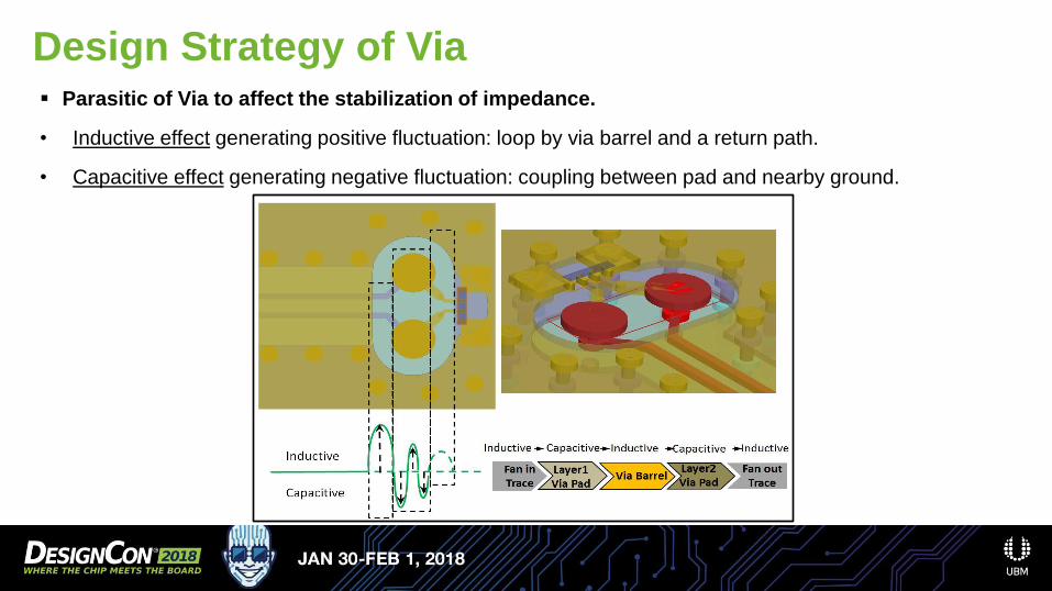
Parasitic of Via to affect the stabilization of impedance.
• Inductive effect generating positive fluctuation: loop by via barrel and a return path.
• Capacitive effect generating negative fluctuation: coupling between pad and nearby ground.
Design Strategy of Via
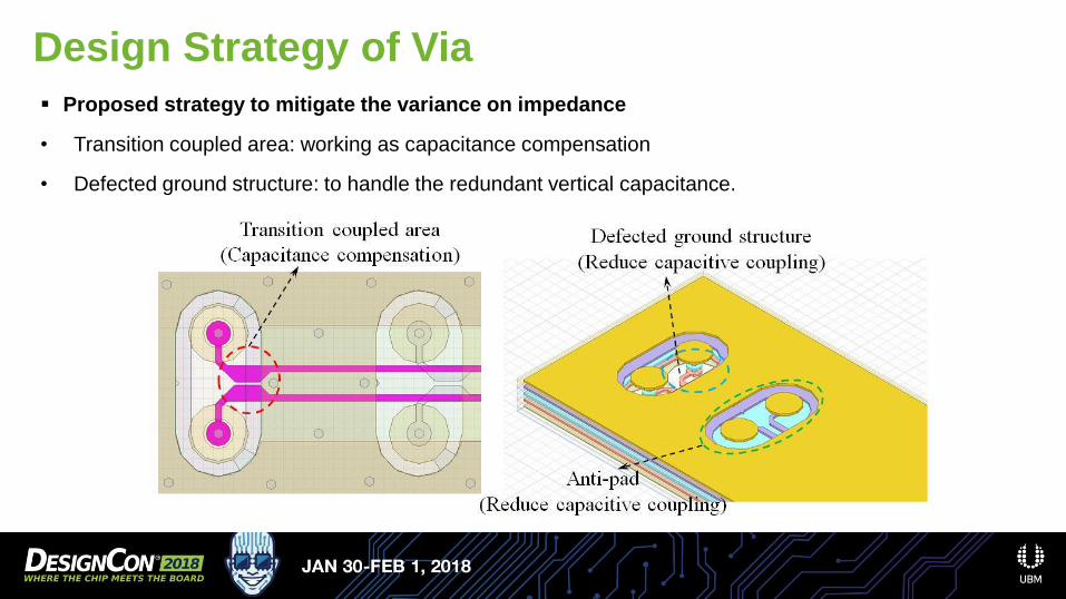
Proposed strategy to mitigate the variance on impedance
• Transition coupled area: working as capacitance compensation
• Defected ground structure: to handle the redundant vertical capacitance.
Design Strategy of Via
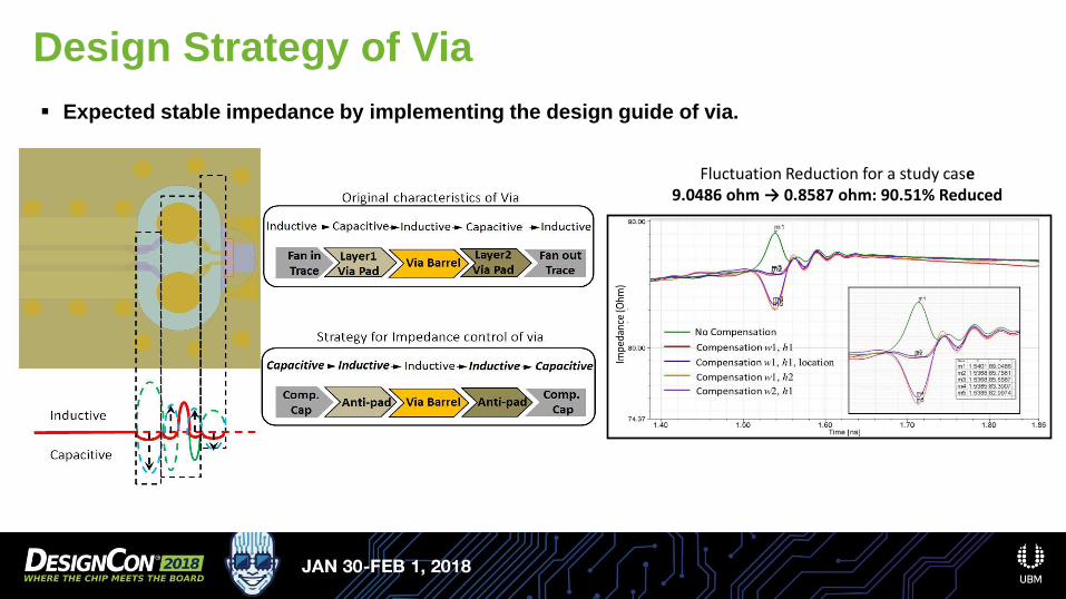
Expected stable impedance by implementing the design guide of via.
Design Strategy of Via
Fluctuation Reduction for a study case 9.0486 ohm → 0.8587 ohm: 90.51% Reduced
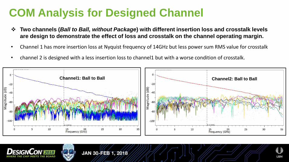
Two channels (Ball to Ball, without Package) with different insertion loss and crosstalk levels
are design to demonstrate the effect of loss and crosstalk on the channel operating margin.
• Channel 1 has more insertion loss at Nyquist frequency of 14GHz but less power sum RMS value for crosstalk
• channel 2 is designed with a less insertion loss to channel1 but with a worse condition of crosstalk.
COM Analysis for Designed Channel
Channel1: Ball to Ball Channel2: Ball to Ball
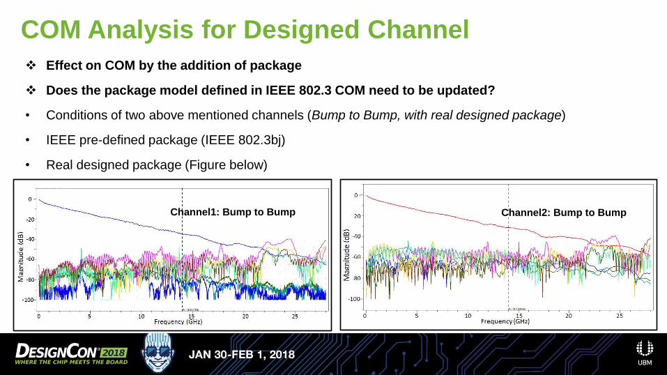
Effect on COM by the addition of package
Does the package model defined in IEEE 802.3 COM need to be updated?
• Conditions of two above mentioned channels (Bump to Bump, with real designed package)
• IEEE pre-defined package (IEEE 802.3bj)
• Real designed package (Figure below)
COM Analysis for Designed Channel
Channel1: Bump to Bump Channel2: Bump to Bump
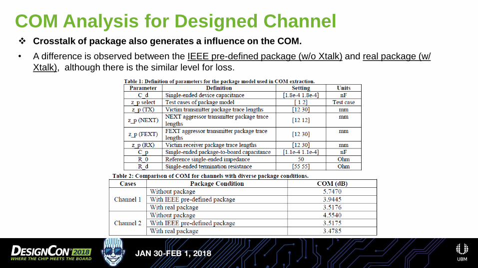
Crosstalk of package also generates a influence on the COM.
• A difference is observed between the IEEE pre-defined package (w/o Xtalk) and real package (w/
Xtalk), although there is the similar level for loss.
COM Analysis for Designed Channel
In this paper, we first propose a design flow for channel design by a fast hierarchical
optimization method based on COM.
Advantages on accuracy and speed for our proposed hierarchical design flow was
demonstrated.
Novel design strategy to mitigate the fluctuation of impedance at via was addressed
Characteristic such as loss and crosstalk of the designed channel is demonstrated。
The effect of package on the COM was discussed by a comparison of diverse
package conditions.
In future works, we will concentrated on the enhancement of the design flow and
contribute to the accurate COM criterion for high speed links.
Conclusion and Future Plan
Reference [1] R. Mellitz, A. Ran, M. P. Li, and V. Ragavassamy, “Channel Operating Margin (COM): Evolution of Channel Specifications
for 25 Gbps and Beyond”, DesignCon 2013, Santa Clara, CA, 2013.
[2] Mike Peng Li, “Design and Verification for High-Speed I/Os at Multiple to 60 Gbps With Jitter, Signal Integrity, and Power
Optimization”, DesignCon 2015, Santa Clara, CA, 2015.
[3] A. Healey and C. Y. Liu, “Channel Operating Margin for 56 Gb/s PAM4 Chip-to-Chip and Backplane Interfaces”,
DesignCon 2016, Santa Clara, CA, 2016.
[4] C. Filip, D. Araujo, P. V. Gurswamy, M. Rowlands. A. Gafarov, and P. Anmula, “Optimization Methods for High-Speed
SerDes Channels using COM Metric” , DesignCon 2017, Santa Clara, CA, 2017.
[5] Geoff Zhang, Hongtao Zhang, Santiago Asuncion, and Brandon Jiao, “A Tutorial on PAM4 Signaling for 56G Serial Link
Applications”, DesignCon 2017, Santa Clara, CA, 2017.
[6] “CEI-56G-LR-PAM4 Long Reach Interface”, OIF document number: OIF2014.380.02, 2015.
[7] IEEE Std 802.3bj-2014 IEEE Standard for Ethernet Amendment 2: Physical Layer Specifications and Management
Parameters for 100 Gb/s Operation Over Backplanes and Copper Cables.