topology optimized mode conversion in a photonic crystal … · topology optimized mode conversion...
TRANSCRIPT

General rights Copyright and moral rights for the publications made accessible in the public portal are retained by the authors and/or other copyright owners and it is a condition of accessing publications that users recognise and abide by the legal requirements associated with these rights.
Users may download and print one copy of any publication from the public portal for the purpose of private study or research.
You may not further distribute the material or use it for any profit-making activity or commercial gain
You may freely distribute the URL identifying the publication in the public portal If you believe that this document breaches copyright please contact us providing details, and we will remove access to the work immediately and investigate your claim.
Downloaded from orbit.dtu.dk on: Feb 04, 2020
Topology optimized mode conversion in a photonic crystal waveguide fabricated insiliconon-insulator material
Frandsen, Lars Hagedorn; Elesin, Yuriy; Frellsen, Louise Floor; Mitrovic, Miranda; Ding, Yunhong;Sigmund, Ole; Yvind, KrestenPublished in:Optics Express
Link to article, DOI:10.1364/OE.22.008525
Publication date:2014
Document VersionPublisher's PDF, also known as Version of record
Link back to DTU Orbit
Citation (APA):Frandsen, L. H., Elesin, Y., Frellsen, L. F., Mitrovic, M., Ding, Y., Sigmund, O., & Yvind, K. (2014). Topologyoptimized mode conversion in a photonic crystal waveguide fabricated in siliconon-insulator material. OpticsExpress, 22(7), 8525-8532. https://doi.org/10.1364/OE.22.008525

Topology optimized mode conversion in a photonic crystal waveguide fabricated in silicon-
on-insulator material
Lars H. Frandsen,1,* Yuriy Elesin,2,3 Louise F. Frellsen,1 Miranda Mitrovic,1 Yunhong Ding,1 Ole Sigmund,2 and Kresten Yvind1
1DTU Fotonik, Department of Photonics Engineering, Technical University of Denmark, 2800 Lyngby, Denmark 2DTU Mekanik, Department of Mechanics Engineering, Technical University of Denmark, 2800 Lyngby, Denmark
3Now at Topsoe Fuel Cell, 2800 Lyngby, Denmark *[email protected]
Abstract: We have designed and for the first time experimentally verified a topology optimized mode converter with a footprint of ~6.3 μm × ~3.6 μm which converts the fundamental even mode to the higher order odd mode of a dispersion engineered photonic crystal waveguide. 2D and 3D topology optimization is utilized and both schemes result in designs theoretically showing an extinction ratio larger than 21 dB. The 3D optimized design has an experimentally estimated insertion loss lower than ~2 dB in an ~43 nm bandwidth. The mode conversion is experimentally confirmed in this wavelength range by recording mode profiles using vertical grating couplers and an infrared camera. The experimentally determined extinction ratio is > 12 dB and is believed to be limited by the spatial resolution of our setup.
©2014 Optical Society of America
OCIS codes: (000.3860) Mathematical methods in physics; (000.4430) Numerical approximation and analysis; (030.4070) Modes; (050.6624) Subwavelength structures; (130.3120) Integrated optics devices; (130.5296) Photonic crystal waveguides.
References and links
1. Y. Huang, G. Xu, and S.-T. Ho, “An ultracompact optical mode order converter,” IEEE Photon. Technol. Lett. 18(21), 2281–2283 (2006).
2. L. Luo, L. H. Gabrielli, and M. Lipson, “On-chip mode-division multiplexer,” in CLEO: 2013, OSA Technical Digest (online) (Optical Society of America, 2013), paper CTh1C.6.
3. Y. Ding, J. Xu, F. Da Ros, B. Huang, H. Ou, and C. Peucheret, “On-chip two-mode division multiplexing using tapered directional coupler-based mode multiplexer and demultiplexer,” Opt. Express 21(8), 10376–10382 (2013).
4. B. T. Lee and S. Y. Shin, “Mode-order converter in a multimode waveguide,” Opt. Lett. 28(18), 1660–1662 (2003).
5. G. Chen and J. U. Kang, “Waveguide mode converter based on two-dimensional photonic crystals,” Opt. Lett. 30(13), 1656–1658 (2005).
6. V. Liu, D. A. B. Miller, and S. Fan, “Ultra-compact photonic crystal waveguide spatial mode converter and its connection to the optical diode effect,” Opt. Express 20(27), 28388–28397 (2012).
7. J. Lu and J. Vučković, “Objective-first design of high-efficiency, small-footprint couplers between arbitrary nanophotonic waveguide modes,” Opt. Express 20(7), 7221–7236 (2012).
8. M. P. Bendsøe and N. Kikuchi, “Generating optimal topologies in structural design using a homogenization method,” Comput. Methods Appl. Mech. Eng. 71(2), 197–224 (1988).
9. P. I. Borel, A. Harpøth, L. H. Frandsen, M. Kristensen, P. Shi, J. S. Jensen, and O. Sigmund, “Topology optimization and fabrication of photonic crystal structures,” Opt. Express 12(9), 1996–2001 (2004).
10. J. S. Jensen and O. Sigmund, “Topology optimization for nano-photonics,” Laser Photon. Rev. 5(2), 308–321 (2011), doi:10.1002/lpor.201000014.
11. S. Johnson and J. Joannopoulos, “Block-iterative frequency-domain methods for Maxwell’s equations in a planewave basis,” Opt. Express 8(3), 173–190 (2001).
12. L. H. Frandsen, A. V. Lavrinenko, J. Fage-Pedersen, and P. I. Borel, “Photonic crystal waveguides with semi-slow light and tailored dispersion properties,” Opt. Express 14(20), 9444–9450 (2006).
13. J. Li, T. P. White, L. O’Faolain, A. Gomez-Iglesias, and T. F. Krauss, “Systematic design of flat band slow light in photonic crystal waveguides,” Opt. Express 16(9), 6227–6232 (2008).
#205831 - $15.00 USD Received 31 Jan 2014; revised 24 Mar 2014; accepted 27 Mar 2014; published 2 Apr 2014(C) 2014 OSA 7 April 2014 | Vol. 22, No. 7 | DOI:10.1364/OE.22.008525 | OPTICS EXPRESS 8525
14. Y. Elesin, B. S. Lazarov, J. S. Jensen, and O. Sigmund, “Design of robust and efficient photonic switches using topology optimization,” Photon. Nanostruct. Fund. Appl. 10(1), 153–165 (2012).
15. Y. Elesin, B. S. Lazarov, J. S. Jensen, and O. Sigmund, “Time domain topology optimization of 3D nanophotonic devices,” Photon. Nanostruct. Fund. Appl. 12(1), 23–33 (2014).
16. M. Pu, L. Liu, H. Ou, K. Yvind, and J. M. Hvam, “Ultra-low-loss inverted taper coupler for silicon-on-insulator ridge waveguide,” Opt. Commun. 283(19), 3678–3682 (2010).
17. Y. Ding, H. Ou, J. Xu, M. Xiong, and C. Peucheret, “On-chip mode multiplexer based on a single grating coupler,” in Proceedings of IEEE Photonics Conference (Institute of Electrical and Electronics Engineers, 2012), pp. 707–708.
18. B. Wohlfeil, S. Burger, C. Stamatiadis, J. Pomplun, F. Schmidt, L. Zimmermann, and K. Petermann, “Numerical simulation of grating couplers for mode multiplexed systems,” Proc. SPIE 8988, 89880K (2014).
1. Introduction
Mode conversions between optical modes of different orders in ultra-compact photonic integrated circuits (PICs) have recently been investigated [1–7] to support the field of on-chip processing of mode-division multiplexed data-signals. Typically, integrated mode order converters (in the remaining referred to as ‘mode converters’) rely on phase matching between different waveguides [1–4] or on scattering effects induced in single waveguides [5–7]. The approach based on phase matching may give a compact and efficient solution for conversion between the fundamental even and the first order odd waveguide modes, but the concept is presumably too intricate to scale to higher order conversions and will require large device footprints [2,4], which makes it a less attractive choice for dense PICs handling several mode orders. On the other hand, mode converters based on scattering effects induced in the waveguide may have footprints of a few square vacuum wavelengths only [6,7], but have narrow spectral bandwidths and are problematic to realize in practice due to the delicacy of the scattering elements and, thus, such designs still remain to be experimentally verified.
Topology optimization (TO) [8] has been experimentally proven to be a strong and robust inverse design tool for designing various compact nanophotonic components with narrow- or broad-band and low-loss performances [9,10]. Here, we present experimental results on low-loss broadband mode conversion between the transverse electric fundamental even (TE0) mode and the first higher order odd mode (TE1) in a photonic crystal waveguide (PhCW) fabricated in silicon-on-insulator (SOI) material. Mode conversion is obtained by applying topology optimization to the PhCW and demonstrates the practical feasibility of using TO in order to realize ultra-compact mode conversion in PICs. Furthermore, TO is used to optimize the coupling efficiency of the TE1 mode from the PhCW to a photonic wire (PhW).
2. Design, optimization, and modelling
2.1 Dispersion engineering the photonic crystal waveguide
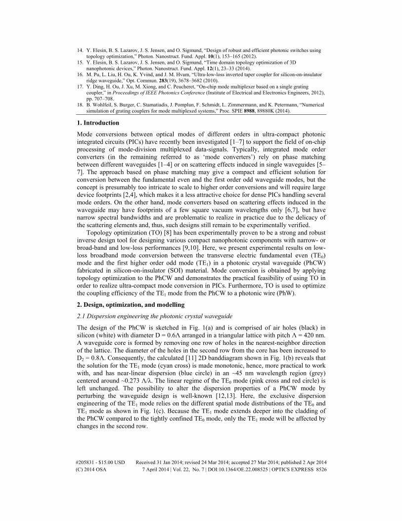
The design of the PhCW is sketched in Fig. 1(a) and is comprised of air holes (black) in silicon (white) with diameter D = 0.6Λ arranged in a triangular lattice with pitch Λ = 420 nm. A waveguide core is formed by removing one row of holes in the nearest-neighbor direction of the lattice. The diameter of the holes in the second row from the core has been increased to D2 = 0.8Λ. Consequently, the calculated [11] 2D banddiagram shown in Fig. 1(b) reveals that the solution for the TE1 mode (cyan cross) is made monotonic, hence, more practical to work with, and has near-linear dispersion (blue circle) in an ~45 nm wavelength region (grey) centered around ~0.273 Λ/λ. The linear regime of the TE0 mode (pink cross and red circle) is left unchanged. The possibility to alter the dispersion properties of a PhCW mode by perturbing the waveguide design is well-known [12,13]. Here, the exclusive dispersion engineering of the TE1 mode relies on the different spatial mode distributions of the TE0 and TE1 mode as shown in Fig. 1(c). Because the TE1 mode extends deeper into the cladding of the PhCW compared to the tightly confined TE0 mode, only the TE1 mode will be affected by changes in the second row.
#205831 - $15.00 USD Received 31 Jan 2014; revised 24 Mar 2014; accepted 27 Mar 2014; published 2 Apr 2014(C) 2014 OSA 7 April 2014 | Vol. 22, No. 7 | DOI:10.1364/OE.22.008525 | OPTICS EXPRESS 8526

Fig. 1. (a) Sketch of the PhCW design. (b) The 2D banddiagram showing that with D2>D, the TE1 mode (cyan cross) can be made monotonic (blue circle) in an ~45 nm bandwidth (grey) while the fundamental TE0 (pink cross and red circle) is left unchanged. For the calculation of the 2D banddiagram we used an equivalent slab waveguide index of 2.983. (c) Mode profiles for the TE0 (red) and TE1 (blue) mode.
2.2 Topology optimization of the mode converter and the output coupling interface
The objective of the TO is to convert the input TE0 mode of the PhCW into the TE1 mode in the ~45 nm wavelength region located in the index-guided regime around 0.273 Λ/λ. Figure 2(a) shows the PhCW used as a basis for the TO which is comprised of a 450 nm wide and single-mode input PhW, a 6.3 μm long dispersion engineered PhCW (c.f. previous discussion), and an 1150 nm wide output PhW supporting more than two modes. In the TO, the width of the output PhW was widened compared to a 750 nm wide PhW supporting only two modes in order to reduce any ravaging reflections back into the PhCW caused by an improper coupling interface between the PhCW and the output PhW. This was done well-knowing that the output coupling interface during optimization was not optimal from a transmission point of view. However, low transmission into the PhW had no impact on the TO as the objectives for the optimization were located inside the PhCW as described in the following and did not depend on the transmission to the PhW.
Topology optimization is performed utilizing repeated finite-difference time-domain (FDTD) calculations and sensitivity analyses using a software package developed in-house [14,15]. In the TO, the distribution of material in a given design area is iteratively modified in order to match the calculated intensity distribution of the photonic crystal mode at position #1 (dashed red) in Fig. 2(a) to that of the TE1 mode. The design domain (green) in Fig. 2(a) is ~2.5 μm × ~2.5 μm and was arbitrarily chosen to be a set of circular and/or elliptical regions around the 3 innermost rows of holes in order to prevent dramatic changes in the design and to avoid appearance of isolated silicon islands that would be incompatible with e.g. a membrane configuration. Although we could have chosen a larger and/or a continuous design domain, numerical experiments showed that relatively small and isolated design areas were enough to yield the targeted mode conversion. Had the conversion efficiency been unsatisfactory, the design areas could have been changed in order to introduce more freedom in the TO. After having obtained efficient mode conversion in the PhCW at position #1, we address the output coupling interface to a 750 nm wide and double-mode PhW by doing a
#205831 - $15.00 USD Received 31 Jan 2014; revised 24 Mar 2014; accepted 27 Mar 2014; published 2 Apr 2014(C) 2014 OSA 7 April 2014 | Vol. 22, No. 7 | DOI:10.1364/OE.22.008525 | OPTICS EXPRESS 8527

separate TO on the design shown in Fig. 2(b). Here, the TE1 mode is excited inside the PhCW and TO is performed using the design domain sketched in green in Fig. 2(b). Here, the objective is to optimize the transmission of the TE1 mode from the PhCW to position #2 (dashed red) in the output PhW. The final mode converter design is obtained by combining the optimized converter and the optimized output coupling designs into one PhCW design.
Fig. 2. (a) PhCW with arbitrarily chosen design domain (green) used in the TO. (b) PhCW with standard butt coupling interfaces and design domain (green) for optimizing the output coupling of the TE1 mode to the PhW. (c, d) PhCW TE0-TE1 mode converter with optimized output couplers obtained utilizing (c) 2D and (d) 3D TO.
We perform 2D and 3D topology optimizations with a 16 nm spatial resolution and perfectly matched absorbing layers as boundary conditions surrounding the structures in Figs. 2(a) and 2(b). In 2D optimizations we use an equivalent slab waveguide index of 2.983 for TE polarization found using Ref [11]. In 3D optimizations, the 340 nm thick silicon slab has a refractive index of nSi = 3.418 and has a silica buffer with index nSiO2 = 1.444 below and air above. The TE0 and TE1 modes are partly located above the silica-line in the ~45 nm wavelength region of interest, thus, both modes may leak into the silica buffer layer. However, due to the short length of the PhCW the out-of-plane leakage-loss for the generic PhCW is expected to be negligible. The design domain extends vertically through the silicon slab but designed structures are constrained to be uniform in the vertical direction to make the optimized designs feasible for fabrication with dry etching techniques. In all optimizations, a ~280 nm spectrally broad (full-width at half-maximum) Gaussian-shaped pulse is used as optical input centered on ~1540 nm. Figures 2(c) and 2(d) show the 2D and 3D topology optimized (TopOpt) designs, respectively. The final designs of the mode converters have been obtained after ~200 TO iteration steps whereas coupling interface designs have reached convergence after only ~25 iteration steps. By comparing the 2D and 3D optimized structures some features are seen to be similar and both optimizations involve intricate tuning of the individual photonic crystal holes. As intuitively expected from the symmetric intensity profile of the TE1 mode, the TopOpt coupling interfaces are (close to being) symmetric around the axis of propagation, even though such symmetry was not enforced explicitly.
2.3 Modelling the topology optimized structures
Figure 3(a) shows the 3D FDTD-calculated transmission spectrum for TE0 light input into the 3D TopOpt (blue circle) mode converter normalized to the transmission spectrum of the TE0
#205831 - $15.00 USD Received 31 Jan 2014; revised 24 Mar 2014; accepted 27 Mar 2014; published 2 Apr 2014(C) 2014 OSA 7 April 2014 | Vol. 22, No. 7 | DOI:10.1364/OE.22.008525 | OPTICS EXPRESS 8528

mode propagating through a PhW. Mode conversion of the TE0 to the TE1 mode is clearly observed as illustrated in Fig. 3(b) showing the propagation of the orthogonal H-field (Hz) at 1545 nm through the 3D TopOpt mode converter from Fig. 2(d). As seen, the mode conversion is obtained by a non-trivial twisting of the TE0 mode, hence, intuitively explaining the asymmetric structure of the converter design. The inset of Fig. 3(a) shows the output power flux recorded at 1545 nm in the PhW as a function of the relative position across the PhW with 0 nm being the PhW center. The flux reveals a TE1/TE0 mode extinction ratio better than 21 dB. The 3D TopOpt mode converter has an ~43 nm operational bandwidth from ~1523 nm to ~1565 nm showing lower than 2 dB insertion loss compared to a PhW and better than ~16 dB TE1/TE0 mode extinction ratio. Figure 3(a) also shows the 3D FDTD-calculated transmission spectrum for the 2D TopOpt (red square) mode converter and clearly shows a lower transmission than the 3D TopOpt. This is in accordance with previous investigations [15] revealing that 3D TO gives better performance compared to 2D TO even though an effective index approximation for the 2D waveguide slab is adopted. Hence, 3D optimization schemes may be needed to obtain best performances for nanophotonic structures. To show the effect of topology optimizing the PhCW/PhW output interface, we plot the normalized transmission spectrum in Fig. 3(a) for the 3D TopOpt mode converter having a standard butt coupling (orange triangle) interface at the output. It is clear that this mode converter shows ~3 dB lower transmission in the operational bandwidth. Above ~1565 nm the TE0 mode is not converted and, naturally, the butt coupling interface gives a higher transmission (of the TE0 mode) than the topology optimized interface. The lowest insertion loss of the mode converter is 0.90 dB at 1545 nm. This loss includes coupling loss for the TE0 mode at the standard input interface and we believe the insertion loss of the component may be decreased ~0.2-0.3 dB by applying topology optimization to the input coupling interface as well.
Fig. 3. (a) 3D FDTD-calculated transmission spectra for the 2D TopOpt (red square) and 3D TopOpt (blue circle) mode converter with TopOpt output coupling interfaces. Also shown is the spectrum for the 3D TopOpt converter having a butt coupling output interface (orange triangle). All spectra are normalized to TE0 transmission in a PhW. The inset shows the power flux recorded in the output PhW for the 3D TopOpt mode converter as a function of the relative position across the PhW with 0 nm being the center. (b) 3D FDTD-calculated propagation of the Hz-field through the 3D TopOpt mode converter from Fig. 2(d) calculated near maximum transmission at 1545 nm.
#205831 - $15.00 USD Received 31 Jan 2014; revised 24 Mar 2014; accepted 27 Mar 2014; published 2 Apr 2014(C) 2014 OSA 7 April 2014 | Vol. 22, No. 7 | DOI:10.1364/OE.22.008525 | OPTICS EXPRESS 8529
3. Experimental results
3.1 Fabrication
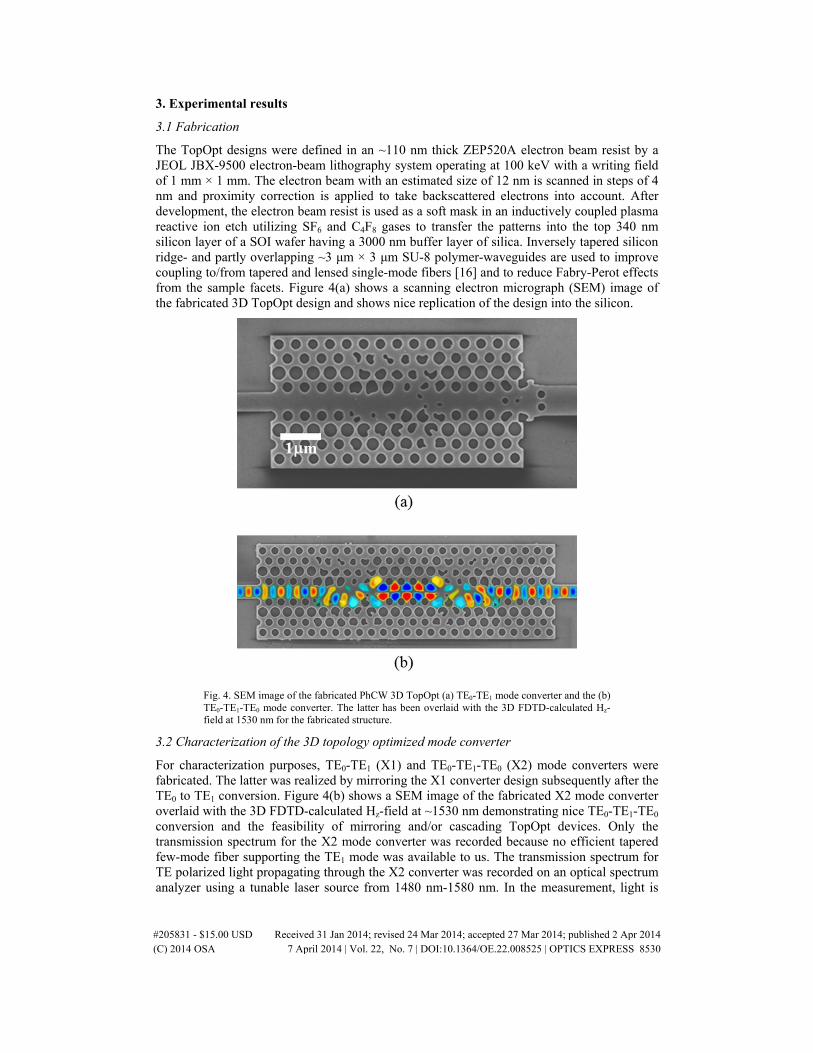
The TopOpt designs were defined in an ~110 nm thick ZEP520A electron beam resist by a JEOL JBX-9500 electron-beam lithography system operating at 100 keV with a writing field of 1 mm × 1 mm. The electron beam with an estimated size of 12 nm is scanned in steps of 4 nm and proximity correction is applied to take backscattered electrons into account. After development, the electron beam resist is used as a soft mask in an inductively coupled plasma reactive ion etch utilizing SF6 and C4F8 gases to transfer the patterns into the top 340 nm silicon layer of a SOI wafer having a 3000 nm buffer layer of silica. Inversely tapered silicon ridge- and partly overlapping ~3 μm × 3 μm SU-8 polymer-waveguides are used to improve coupling to/from tapered and lensed single-mode fibers [16] and to reduce Fabry-Perot effects from the sample facets. Figure 4(a) shows a scanning electron micrograph (SEM) image of the fabricated 3D TopOpt design and shows nice replication of the design into the silicon.
Fig. 4. SEM image of the fabricated PhCW 3D TopOpt (a) TE0-TE1 mode converter and the (b) TE0-TE1-TE0 mode converter. The latter has been overlaid with the 3D FDTD-calculated Hz-field at 1530 nm for the fabricated structure.
3.2 Characterization of the 3D topology optimized mode converter
For characterization purposes, TE0-TE1 (X1) and TE0-TE1-TE0 (X2) mode converters were fabricated. The latter was realized by mirroring the X1 converter design subsequently after the TE0 to TE1 conversion. Figure 4(b) shows a SEM image of the fabricated X2 mode converter overlaid with the 3D FDTD-calculated Hz-field at ~1530 nm demonstrating nice TE0-TE1-TE0 conversion and the feasibility of mirroring and/or cascading TopOpt devices. Only the transmission spectrum for the X2 mode converter was recorded because no efficient tapered few-mode fiber supporting the TE1 mode was available to us. The transmission spectrum for TE polarized light propagating through the X2 converter was recorded on an optical spectrum analyzer using a tunable laser source from 1480 nm-1580 nm. In the measurement, light is
#205831 - $15.00 USD Received 31 Jan 2014; revised 24 Mar 2014; accepted 27 Mar 2014; published 2 Apr 2014(C) 2014 OSA 7 April 2014 | Vol. 22, No. 7 | DOI:10.1364/OE.22.008525 | OPTICS EXPRESS 8530

output from the X2 mode converter through a 350 nm wide and 1.6 mm long single-mode PhW to ensure that only a pure TE0 mode is collected with the single-mode tapered and lensed fibers used.
Fig. 5. Measured transmission spectrum for the 3D TopOpt X2 mode converter (black) normalized to TE0 transmission through a PhW. The corresponding 3D-FDTD calculated spectrum (blue-circle) is also shown.
Figure 5 shows the measured spectrum normalized to a PhW for the 3D TopOpt X2 converter (black). Also shown is the corresponding 3D FDTD-calculated spectrum (blue circle) of the original design that nicely predicts the measurement qualitatively and quantitatively in the operational bandwidth. Discrepancies are mainly explained by the finite grid size used in the 3D FDTD calculations. To experimentally verify mode conversion, we have recorded the mode profiles after the X1 and X2 mode converters with an InGaAs infrared camera (IR-Cam - Xenics XEVA XC130).
Fig. 6. (a) Configuration for measuring mode profiles of the X1 and X2 mode converters. (b) Mode profiles recorded for the 3D TopOpt mode converter at different wavelengths. The top row is for the X1 converter and the bottom row is for the X2 converter. (c) Line scans across the mode profiles for the 3D TopOpt X1 mode converter as a function of the relative position in the grating with 0 μm being the center of the grating.
#205831 - $15.00 USD Received 31 Jan 2014; revised 24 Mar 2014; accepted 27 Mar 2014; published 2 Apr 2014(C) 2014 OSA 7 April 2014 | Vol. 22, No. 7 | DOI:10.1364/OE.22.008525 | OPTICS EXPRESS 8531

As sketched in Fig. 6(a), this was done by using an output few-mode waveguide gently tapered from a width of 750 nm to a width of 12 μm and having a vertical grating coupler [17,18] at the end above which the IR-Cam was placed. Figure 6(b) shows the qualitative mode profiles recorded for the 3D TopOpt mode converter at different wavelengths. The top/bottom row images are taken after the X1/X2 converter, respectively. The mode converter is found to show TE0-TE1 mode conversion in a broad range from ~1480 nm to ~1545 nm and the TE0-TE1-TE0 conversion is confirmed. Figure 6(c) shows intensity line scans across the mode profiles for the X1 mode converter as a function of the relative position in the grating with 0 μm being the center of the grating. The mode profiles have been recorded at 1500 nm (red square), 1530 nm (orange triangle), and 1543 nm (green circle) using an objective with high numerical aperture (0.9) and 2 mm focal length (magnification x100). Experimentally, we find a TE1/TE0 extinction ratio around 12 dB in the bandwidth of operation. However, we see that the node of the TE1 profile (at relative position 0 μm in Fig. 6(c), i.e. at the center of the grating) is only resolved by a single point, thus, the highest possible extinction ratio we can measure is limited by the spatial resolution of the setup being the size of the grating coupler, the magnification of the microscope objective, and the pixel pitch of the detector (30 μm). Therefore, by utilizing a larger grating and/or a detector array with smaller pitch we will be able to resolve the node better and measure a more accurate extinction ratio, which we anticipate to increase. As the designs are reversible and characterized in a linear power regime, we can estimate the insertion loss of the TE0-TE1 converter by halving the measured insertion loss of the TE0-TE1-TE0 converter. The maximum error by doing so estimated from the 12 dB extinction error is < 0.25 dB. From Fig. 5 the 3D TopOpt X1 (X2) mode converter is experimentally estimated to have an insertion loss < ~2 dB (~4 dB) in a bandwidth from ~1500 nm to ~1543 nm corresponding to the linear and monotonic regime in Fig. 1. In the bandwidth from ~1510 nm to ~1540 nm the insertion loss is lower than ~1 dB (~2 dB).
4. Conclusion
We have demonstrated the feasibility of using topology optimization for the design of a compact ~6.3 μm × ~3.6 μm mode converter which converts the fundamental even mode to the first order odd mode in a silicon-on-insulator photonic crystal waveguide. The calculated insertion loss is lower than ~2 dB in an ~43 nm operational bandwidth with extinction ratio larger than 21 dB. In accordance with previous findings, 3D optimization is found to give better performance than 2D optimization even though an effective index approximation is adopted in the 2D optimization. Intuitively, this may especially be true for more complex responses like lambda-splitting, slow-light and mode conversion problems. The 3D topology optimized mode converter is experimentally verified by fabricating the structure in silicon-on-insulator material and shows mode conversion with minimum insertion loss <1 dB and lower than 2 dB in an ~43 nm bandwidth in nice agreement with calculations. In experiments, the mode extinction ratio is measured to be ~12 dB and is currently limited by the spatial resolution of our setup. To our knowledge, our work constitutes the first experimental demonstration of a photonic crystal waveguide mode converter. In the future, we believe that the topology optimization method can be applied to realize low-loss broadband conversions between lower and/or higher order modes with complex mode fields in photonic wires using only footprints of a few square vacuum wavelengths.
Acknowledgments
This work was supported by the VILLUM foundation via the project ‘Optical Nano-engineered Components for High-capacity Integrated silicon Photonics’ (ONCHIP) and ‘Nanophotonics for Terabit Communications’ (NATEC) center of excellence.
#205831 - $15.00 USD Received 31 Jan 2014; revised 24 Mar 2014; accepted 27 Mar 2014; published 2 Apr 2014(C) 2014 OSA 7 April 2014 | Vol. 22, No. 7 | DOI:10.1364/OE.22.008525 | OPTICS EXPRESS 8532