tpd4e002 quad low-capacitance array with +/-15-kv … · tpd4e002 protected ic interface io1 io2...
TRANSCRIPT
TPD4E002
InterfaceProtected IC
IO1
IO2 IO3
IO4
IO1
IO2
IO3
IO4
IO1
IO2
IO3
IO4
GND
Product
Folder
Sample &Buy
Technical
Documents
Tools &
Software
Support &Community
An IMPORTANT NOTICE at the end of this data sheet addresses availability, warranty, changes, use in safety-critical applications,intellectual property matters and other important disclaimers. PRODUCTION DATA.
TPD4E002SLVS615F –JULY 2006–REVISED DECEMBER 2016
TPD4E002 Quad Low-Capacitance Array with ±15-kV ESD Protection
1
1 Features1• IEC 61000-4-2 ESD Protection
– ±15-kV IEC 61000-4-2 Contact Discharge• IEC 61000-4-5 Surge Protection
– 2.5-A Peak Pulse Current (8/20-µs Pulse)• ANSI/ESDA/JEDEC JS-001
– ±15-kV Human Body Model (HBM)• Four Unidirectional Voltage Suppression Diodes
for use in ESD Protection• I/O Breakdown Voltage, VBR = 6.1 V (Minimum)• I/O Capacitance 11 pF (Typical)• Low Leakage Current < 100 nA• Very Small Printed-Circuit Board (PCB) Area
< 2.6 mm2
• High Integration• Suitable for High-Density Boards
2 Applications• Computers• Printers• Communication Systems and Cellular Phones• Video Equipment
3 DescriptionThe TPD4E002 device is a transient voltagesuppressor (TVS) designed to protect up to four linesagainst electrostatic discharge (ESD) transients. Themonolithic circuit design allows superior capacitancematching between the channels and reducedcrosstalk. This device is ideal for applications whereboth reduced line capacitance and board space-saving are required.
Device Information(1)
PART NUMBER PACKAGE BODY SIZE (NOM)TPD4E002 SOT (5) 1.60 mm × 1.20 mm
(1) For all available packages, see the orderable addendum atthe end of the data sheet.
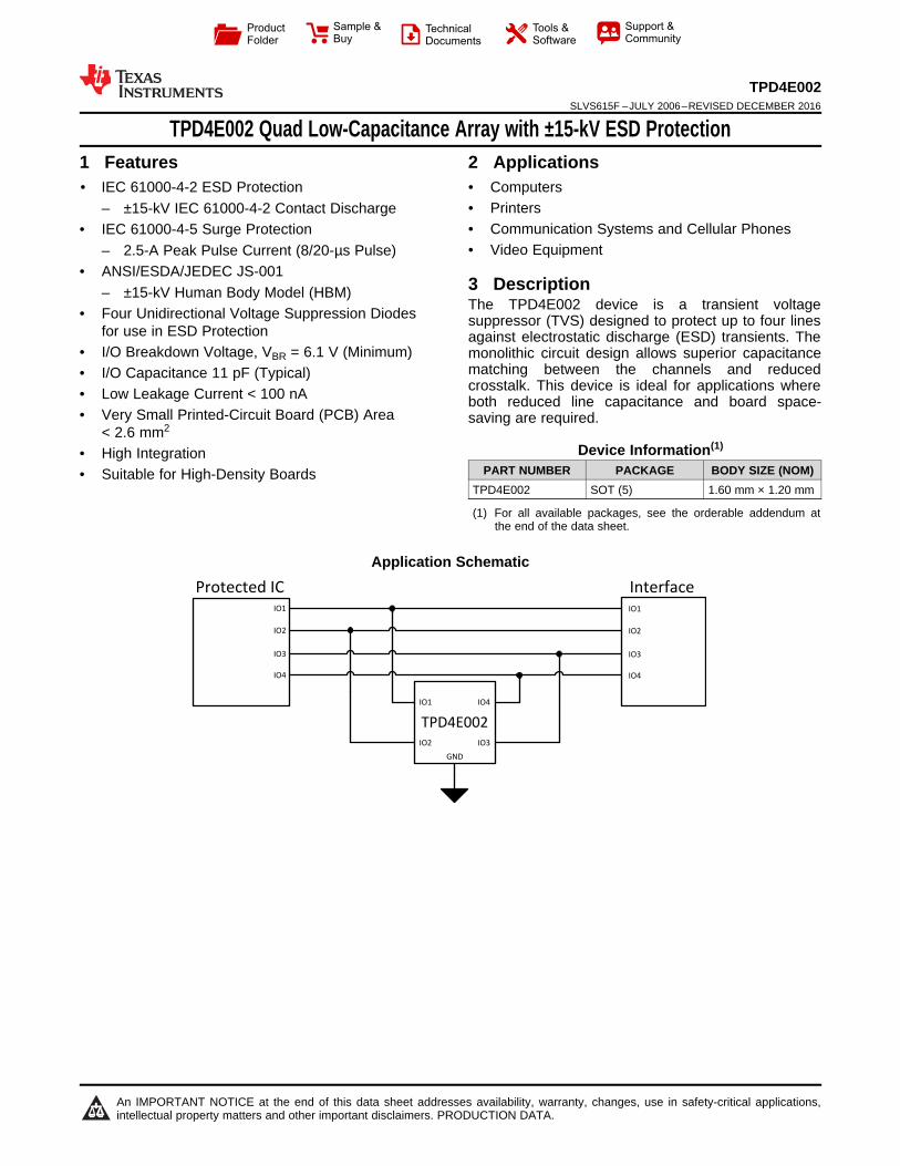
Application Schematic

2
TPD4E002SLVS615F –JULY 2006–REVISED DECEMBER 2016 www.ti.com
Product Folder Links: TPD4E002
Submit Documentation Feedback Copyright © 2006–2016, Texas Instruments Incorporated
Table of Contents1 Features .................................................................. 12 Applications ........................................................... 13 Description ............................................................. 14 Revision History..................................................... 25 Pin Configuration and Functions ......................... 36 Specifications......................................................... 4
6.1 Absolute Maximum Ratings ...................................... 46.2 ESD Ratings—JEDEC Specification......................... 46.3 ESD Ratings—IEC Specification .............................. 46.4 Recommended Operating Conditions....................... 46.5 Thermal Information .................................................. 46.6 Electrical Characteristics........................................... 56.7 Typical Characteristics .............................................. 6
7 Detailed Description .............................................. 77.1 Overview ................................................................... 77.2 Functional Block Diagram ........................................ 77.3 Feature Description................................................... 7
7.4 Device Functional Modes.......................................... 78 Application and Implementation .......................... 8
8.1 Application Information.............................................. 88.2 Typical Application .................................................... 8
9 Power Supply Recommendations ........................ 910 Layout................................................................... 10
10.1 Layout Guidelines ................................................. 1010.2 Layout Example .................................................... 10
11 Device and Documentation Support ................. 1111.1 Documentation Support ........................................ 1111.2 Receiving Notification of Documentation Updates 1111.3 Community Resources.......................................... 1111.4 Trademarks ........................................................... 1111.5 Electrostatic Discharge Caution............................ 1111.6 Glossary ................................................................ 11
12 Mechanical, Packaging, and OrderableInformation ........................................................... 11
4 Revision HistoryNOTE: Page numbers for previous revisions may differ from page numbers in the current version.
Changes from Revision E (February 2016) to Revision F Page
• Updated the Pin Functions table ............................................................................................................................................ 3
Changes from Revision D (July 2010) to Revision E Page
• Added ESD Ratings table, Feature Description section, Device Functional Modes, Application and Implementationsection, Power Supply Recommendations section, Layout section, Device and Documentation Support section, andMechanical, Packaging, and Orderable Information section .................................................................................................. 1
• Deleted Ordering Information table. See POA at the end of the document ........................................................................... 1

1
2
3
5
4
IO1
GND
IO2
IO4
IO3
3
TPD4E002www.ti.com SLVS615F –JULY 2006–REVISED DECEMBER 2016
Product Folder Links: TPD4E002
Submit Documentation FeedbackCopyright © 2006–2016, Texas Instruments Incorporated
5 Pin Configuration and Functions
DRL Package5-Pin SOTTop View
Pin FunctionsPIN
TYPE DESCRIPTIONNO. NAME
1 I/O1 I/O ESD protection channel2 GND — Ground3 I/O2 I/O ESD protection channel4 I/O3 I/O ESD protection channel5 I/O4 I/O ESD protection channel

4
TPD4E002SLVS615F –JULY 2006–REVISED DECEMBER 2016 www.ti.com
Product Folder Links: TPD4E002
Submit Documentation Feedback Copyright © 2006–2016, Texas Instruments Incorporated
(1) Stresses beyond those listed under Absolute Maximum Ratings may cause permanent damage to the device. These are stress ratingsonly, which do not imply functional operation of the device at these or any other conditions beyond those indicated under RecommendedOperating Conditions. Exposure to absolute-maximum-rated conditions for extended periods may affect device reliability.
6 Specifications
6.1 Absolute Maximum Ratingsover operating free-air temperature range (unless otherwise noted) (1)
MIN MAX UNITTJ Junction temperature 125 °CTop Operating temperature –40 125 °CTstg Storage temperature –55 150 °C
(1) JEDEC document JEP155 states that 500-V HBM allows safe manufacturing with a standard ESD control process.(2) JEDEC document JEP157 states that 250-V CDM allows safe manufacturing with a standard ESD control process.
6.2 ESD Ratings—JEDEC SpecificationVALUE UNIT
V(ESD) Electrostatic dischargeIEC 61000-4-2 contact discharge
±15000 VHuman-body model (HBM), per ANSI/ESDA/JEDEC JS-001 (1)
Charged-device model (CDM), per JEDEC specification JESD22-C101 (2)
6.3 ESD Ratings—IEC SpecificationVALUE UNIT
Ipp Peak pulse current IEC 61000-4-5 (tp = 8/20 μs) 2.5 APpp Peak pulse power IEC 61000-4-5 (tp = 8/20 μs) 25 W
6.4 Recommended Operating Conditionsover operating free-air temperature range (unless otherwise noted)
MIN MAX UNITVI/O Operating voltage 0 5 V
Operating temperature –40 125 °C
(1) For more information about traditional and new thermal metrics, see the Semiconductor and IC Package Thermal Metrics applicationreport.
6.5 Thermal Information
THERMAL METRIC (1)TPD4E002
UNITDRL (SOT)5 PINS
RθJA Junction-to-ambient thermal resistance 220 °C/WRθJC(top) Junction-to-case (top) thermal resistance 80.3 °C/WRθJB Junction-to-board thermal resistance 42.9 °C/WψJT Junction-to-top characterization parameter 3.2 °C/WψJB Junction-to-board characterization parameter 42.5 °C/WRθJC(bot) Junction-to-case (bottom) thermal resistance n/a °C/W

5
TPD4E002www.ti.com SLVS615F –JULY 2006–REVISED DECEMBER 2016
Product Folder Links: TPD4E002
Submit Documentation FeedbackCopyright © 2006–2016, Texas Instruments Incorporated
(1) Rd is measured under reverse breakdown condition with inrush current in the range of 1 A using pulse techniques.
6.6 Electrical CharacteristicsTamb = 25°C
PARAMETER TEST CONDITIONS MIN TYP MAX UNITVBR I/O breakdown voltage IR = 1 mA 6.1 7.2 VIRM I/O leakage current VRM = 3 V 0.1 μAαT Voltage temperature coefficient 4.5 mV/°CC I/O capacitance per line 11 pFRd Dynamic resistance (1) 2 Ω

I(m
A)
IN
110.0
–110.0
100.0
–100.0
90.0
–90.0
80.0
–80.0
70.0
–70.0
60.0
–60.0
50.0
–50.0
40.0
–40.0
30.0
–30.0
20.0
–20.0
10.0
–10.0
0.00
8.0 7.5 7.0 6.5 6.0 5.5 5.0 4.5 4.0 3.5 3.0 2.5 2.0 1.5 1.0 500m 0 –500m –1.0 –1.5
V (V)IN
Cap
acit
an
ce (
pF
)
9.0
1 2 3 4 5 6 7 8 9 10
9.5
10.0
10.5
11.0
11.5
12.0
Frequency (Mhz)
Cap
acit
an
ce (
pF
)
8.0
–40 0 25 70 85 125
8.5
9.0
9.5
10.0
10.5
11.0
11.5
12.0
Temperature (ºC)
6
TPD4E002SLVS615F –JULY 2006–REVISED DECEMBER 2016 www.ti.com
Product Folder Links: TPD4E002
Submit Documentation Feedback Copyright © 2006–2016, Texas Instruments Incorporated
6.7 Typical Characteristics
Figure 1. I/O Capacitance vs Temperature Figure 2. I/O Capacitance vs Frequency (Typical Values)
Figure 3. Diode Current Across I/O Voltage (Typical Values)
xxxx
IO1 IO2 IO3 IO4
GND
7
TPD4E002www.ti.com SLVS615F –JULY 2006–REVISED DECEMBER 2016
Product Folder Links: TPD4E002
Submit Documentation FeedbackCopyright © 2006–2016, Texas Instruments Incorporated
7 Detailed Description
7.1 OverviewThe TPD4E002 is a four-channel TVS protection diode array. The TPD4E002 is rated to dissipate contact ESDstrikes of ±15 kV, beyond Level 4 as specified in the IEC 61000-4-2 international standard. This device has an11-pF I/O capacitance per channel, making it ideal for use in data I/O interfaces of up to 100 MHz.
7.2 Functional Block Diagram
7.3 Feature DescriptionThe TPD4E002 is a TVS that provides ESD protection for up to four channels, withstanding up to ±15-kV contactESD per IEC 61000-4-2 and 2.5-A peak pulse current per IEC 61000-4-5. The monolithic technology yieldsexceptionally small variations in capacitance between any I/O pin of the TPD4E002. The small footprint is idealfor applications where space-saving designs are important.
7.4 Device Functional ModesThe TPD4E002 device is a passive integrated circuit that triggers when voltages are above VBR or below thediodes VF of approximately –0.5 V. During ESD events, voltages as high as ±15-kV contact ESD can be directedto ground through the internal diodes. Once the voltages on the protected line fall below the trigger levels ofTPD4E002 (usually within tens of nano seconds) the device reverts to its high-impedance state.

TPD4E002
InterfaceProtected IC
IO1
IO2 IO3
IO4
IO1
IO2
IO3
IO4
IO1
IO2
IO3
IO4
GND
8
TPD4E002SLVS615F –JULY 2006–REVISED DECEMBER 2016 www.ti.com
Product Folder Links: TPD4E002
Submit Documentation Feedback Copyright © 2006–2016, Texas Instruments Incorporated
8 Application and Implementation
NOTEInformation in the following applications sections is not part of the TI componentspecification, and TI does not warrant its accuracy or completeness. TI’s customers areresponsible for determining suitability of components for their purposes. Customers shouldvalidate and test their design implementation to confirm system functionality.
8.1 Application InformationThe TPD4E002 device is a TVS diode array typically used to provide a path to ground for dissipating ESD eventson high-speed signal lines between a human interface connector and a system. As the current from ESD passesthrough the TVS, only a small voltage drop is present across the diode. This is the voltage presented to theprotected integrated circuit (IC). The triggered TVS holds this voltage, VCLAMP, to a safe level for the protected IC.
8.2 Typical ApplicationIn a typical design example, one TPD4E002 device is being used to protect an IC against potential ESD from afour-channel human interface port, as shown in Figure 4.
Figure 4. Typical Application for TPD4E002
8.2.1 Design RequirementsTable 1 lists the parameters for this typical application.
Table 1. Design ParametersDESIGN PARAMETER VALUE
Signal's voltage range on I/O1, I/O2, I/O3, and I/O4 0 V to 5 VOperating frequency < 100 MHz
8.2.2 Detailed Design ProcedureTo begin the design process, some parameters must be decided upon; the designer must know the following:• Voltage range of the signal on all protected lines• Operating frequency on all protected lines
8.2.2.1 Signal Range on I/O1 Through I/O2The TPD4E002 device has 4 identical protection channels for signal lines. The symmetry of the device providesflexibility when selecting which of the four I/O channels will protect which signal lines. Any I/O supports a signalrange of 0 V to 5 V and up to 100 MHz.
Vo
ltag
e (
20
V/d
iv)
Time (50 ns/div)
0.0
0.5
1.0
1.5
2.0
2.5
3.0
0 5 10 15 20 25 30 35 40 45 50
Time ( s)µ
IPP
(A
)
0
5
10
15
20
25
30
PP
P (
W)
Power (W)
Current (A)
9
TPD4E002www.ti.com SLVS615F –JULY 2006–REVISED DECEMBER 2016
Product Folder Links: TPD4E002
Submit Documentation FeedbackCopyright © 2006–2016, Texas Instruments Incorporated
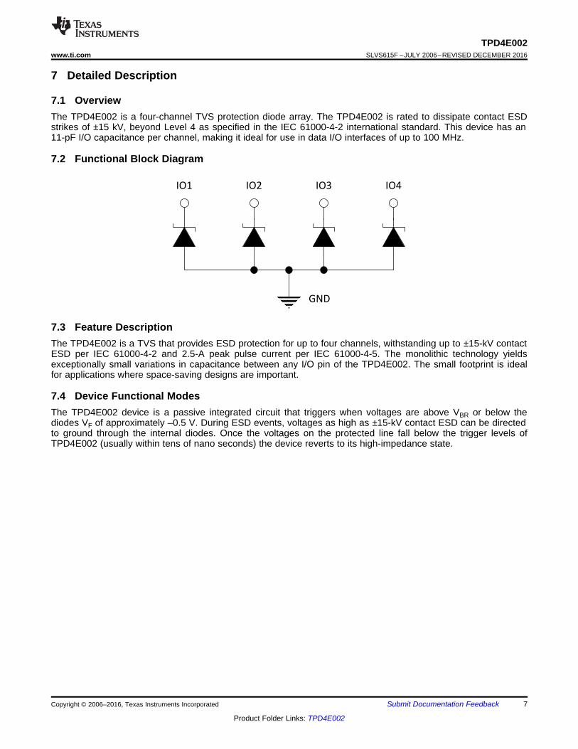
8.2.3 Application Curves
Figure 5. ESD Clamp Voltage at I/O Pins: IEC6100-4-215-kV Contact Discharge
Figure 6. Pulse Waveform (8/20-µs Pulse)
9 Power Supply RecommendationsThe TPD4E002 is a passive ESD protection device and there is no need to power it. Do not violate the maximumvoltage specifications for each pin.
TPD4E002
1D1
D2
Pin to GND
Legend
VIA to Internal GND Plane
Top Layer GND Plane
10
TPD4E002SLVS615F –JULY 2006–REVISED DECEMBER 2016 www.ti.com
Product Folder Links: TPD4E002
Submit Documentation Feedback Copyright © 2006–2016, Texas Instruments Incorporated
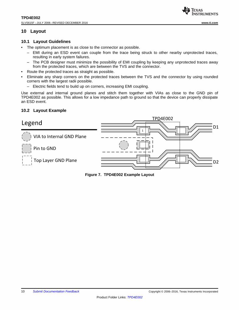
10 Layout
10.1 Layout Guidelines• The optimum placement is as close to the connector as possible.
– EMI during an ESD event can couple from the trace being struck to other nearby unprotected traces,resulting in early system failures.
– The PCB designer must minimize the possibility of EMI coupling by keeping any unprotected traces awayfrom the protected traces, which are between the TVS and the connector.
• Route the protected traces as straight as possible.• Eliminate any sharp corners on the protected traces between the TVS and the connector by using rounded
corners with the largest radii possible.– Electric fields tend to build up on corners, increasing EMI coupling.
Use external and internal ground planes and stitch them together with VIAs as close to the GND pin ofTPD4E002 as possible. This allows for a low impedance path to ground so that the device can properly dissipatean ESD event.
10.2 Layout Example
Figure 7. TPD4E002 Example Layout
11
TPD4E002www.ti.com SLVS615F –JULY 2006–REVISED DECEMBER 2016
Product Folder Links: TPD4E002
Submit Documentation FeedbackCopyright © 2006–2016, Texas Instruments Incorporated
11 Device and Documentation Support
11.1 Documentation Support
11.1.1 Related DocumentationFor related documentation see the following:• Reading and Understanding an ESD Protection Datasheet• ESD Layout Guide
11.2 Receiving Notification of Documentation UpdatesTo receive notification of documentation updates, navigate to the device product folder on ti.com. In the upperright corner, click on Alert me to register and receive a weekly digest of any product information that haschanged. For change details, review the revision history included in any revised document.
11.3 Community ResourcesThe following links connect to TI community resources. Linked contents are provided "AS IS" by the respectivecontributors. They do not constitute TI specifications and do not necessarily reflect TI's views; see TI's Terms ofUse.
TI E2E™ Online Community TI's Engineer-to-Engineer (E2E) Community. Created to foster collaborationamong engineers. At e2e.ti.com, you can ask questions, share knowledge, explore ideas and helpsolve problems with fellow engineers.
Design Support TI's Design Support Quickly find helpful E2E forums along with design support tools andcontact information for technical support.
11.4 TrademarksE2E is a trademark of Texas Instruments.All other trademarks are the property of their respective owners.
11.5 Electrostatic Discharge CautionThese devices have limited built-in ESD protection. The leads should be shorted together or the device placed in conductive foamduring storage or handling to prevent electrostatic damage to the MOS gates.
11.6 GlossarySLYZ022 — TI Glossary.
This glossary lists and explains terms, acronyms, and definitions.
12 Mechanical, Packaging, and Orderable InformationThe following pages include mechanical, packaging, and orderable information. This information is the mostcurrent data available for the designated devices. This data is subject to change without notice and revision ofthis document. For browser-based versions of this data sheet, refer to the left-hand navigation.
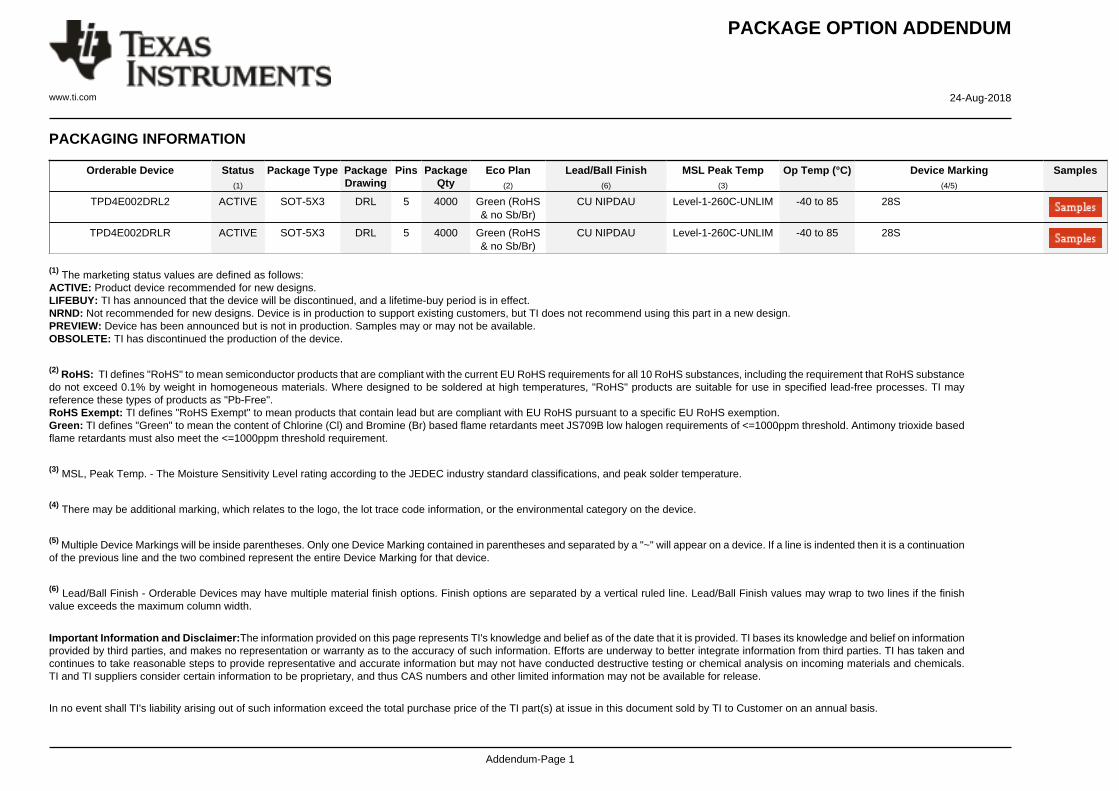
PACKAGE OPTION ADDENDUM
www.ti.com 24-Aug-2018
Addendum-Page 1
PACKAGING INFORMATION
Orderable Device Status(1)
Package Type PackageDrawing
Pins PackageQty
Eco Plan(2)
Lead/Ball Finish(6)
MSL Peak Temp(3)
Op Temp (°C) Device Marking(4/5)
Samples
TPD4E002DRL2 ACTIVE SOT-5X3 DRL 5 4000 Green (RoHS& no Sb/Br)
CU NIPDAU Level-1-260C-UNLIM -40 to 85 28S
TPD4E002DRLR ACTIVE SOT-5X3 DRL 5 4000 Green (RoHS& no Sb/Br)
CU NIPDAU Level-1-260C-UNLIM -40 to 85 28S
(1) The marketing status values are defined as follows:ACTIVE: Product device recommended for new designs.LIFEBUY: TI has announced that the device will be discontinued, and a lifetime-buy period is in effect.NRND: Not recommended for new designs. Device is in production to support existing customers, but TI does not recommend using this part in a new design.PREVIEW: Device has been announced but is not in production. Samples may or may not be available.OBSOLETE: TI has discontinued the production of the device.
(2) RoHS: TI defines "RoHS" to mean semiconductor products that are compliant with the current EU RoHS requirements for all 10 RoHS substances, including the requirement that RoHS substancedo not exceed 0.1% by weight in homogeneous materials. Where designed to be soldered at high temperatures, "RoHS" products are suitable for use in specified lead-free processes. TI mayreference these types of products as "Pb-Free".RoHS Exempt: TI defines "RoHS Exempt" to mean products that contain lead but are compliant with EU RoHS pursuant to a specific EU RoHS exemption.Green: TI defines "Green" to mean the content of Chlorine (Cl) and Bromine (Br) based flame retardants meet JS709B low halogen requirements of <=1000ppm threshold. Antimony trioxide basedflame retardants must also meet the <=1000ppm threshold requirement.
(3) MSL, Peak Temp. - The Moisture Sensitivity Level rating according to the JEDEC industry standard classifications, and peak solder temperature.
(4) There may be additional marking, which relates to the logo, the lot trace code information, or the environmental category on the device.
(5) Multiple Device Markings will be inside parentheses. Only one Device Marking contained in parentheses and separated by a "~" will appear on a device. If a line is indented then it is a continuationof the previous line and the two combined represent the entire Device Marking for that device.
(6) Lead/Ball Finish - Orderable Devices may have multiple material finish options. Finish options are separated by a vertical ruled line. Lead/Ball Finish values may wrap to two lines if the finishvalue exceeds the maximum column width.
Important Information and Disclaimer:The information provided on this page represents TI's knowledge and belief as of the date that it is provided. TI bases its knowledge and belief on informationprovided by third parties, and makes no representation or warranty as to the accuracy of such information. Efforts are underway to better integrate information from third parties. TI has taken andcontinues to take reasonable steps to provide representative and accurate information but may not have conducted destructive testing or chemical analysis on incoming materials and chemicals.TI and TI suppliers consider certain information to be proprietary, and thus CAS numbers and other limited information may not be available for release.
In no event shall TI's liability arising out of such information exceed the total purchase price of the TI part(s) at issue in this document sold by TI to Customer on an annual basis.
PACKAGE OPTION ADDENDUM
www.ti.com 24-Aug-2018
Addendum-Page 2
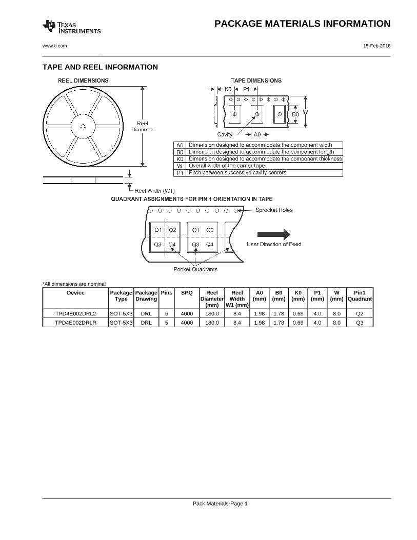
TAPE AND REEL INFORMATION
*All dimensions are nominal
Device PackageType
PackageDrawing
Pins SPQ ReelDiameter
(mm)
ReelWidth
W1 (mm)
A0(mm)
B0(mm)
K0(mm)
P1(mm)
W(mm)
Pin1Quadrant
TPD4E002DRL2 SOT-5X3 DRL 5 4000 180.0 8.4 1.98 1.78 0.69 4.0 8.0 Q2
TPD4E002DRLR SOT-5X3 DRL 5 4000 180.0 8.4 1.98 1.78 0.69 4.0 8.0 Q3
PACKAGE MATERIALS INFORMATION
www.ti.com 15-Feb-2018
Pack Materials-Page 1

*All dimensions are nominal
Device Package Type Package Drawing Pins SPQ Length (mm) Width (mm) Height (mm)
TPD4E002DRL2 SOT-5X3 DRL 5 4000 183.0 183.0 20.0
TPD4E002DRLR SOT-5X3 DRL 5 4000 183.0 183.0 20.0
PACKAGE MATERIALS INFORMATION
www.ti.com 15-Feb-2018
Pack Materials-Page 2


IMPORTANT NOTICE
Texas Instruments Incorporated (TI) reserves the right to make corrections, enhancements, improvements and other changes to itssemiconductor products and services per JESD46, latest issue, and to discontinue any product or service per JESD48, latest issue. Buyersshould obtain the latest relevant information before placing orders and should verify that such information is current and complete.TI’s published terms of sale for semiconductor products (http://www.ti.com/sc/docs/stdterms.htm) apply to the sale of packaged integratedcircuit products that TI has qualified and released to market. Additional terms may apply to the use or sale of other types of TI products andservices.Reproduction of significant portions of TI information in TI data sheets is permissible only if reproduction is without alteration and isaccompanied by all associated warranties, conditions, limitations, and notices. TI is not responsible or liable for such reproduceddocumentation. Information of third parties may be subject to additional restrictions. Resale of TI products or services with statementsdifferent from or beyond the parameters stated by TI for that product or service voids all express and any implied warranties for theassociated TI product or service and is an unfair and deceptive business practice. TI is not responsible or liable for any such statements.Buyers and others who are developing systems that incorporate TI products (collectively, “Designers”) understand and agree that Designersremain responsible for using their independent analysis, evaluation and judgment in designing their applications and that Designers havefull and exclusive responsibility to assure the safety of Designers' applications and compliance of their applications (and of all TI productsused in or for Designers’ applications) with all applicable regulations, laws and other applicable requirements. Designer represents that, withrespect to their applications, Designer has all the necessary expertise to create and implement safeguards that (1) anticipate dangerousconsequences of failures, (2) monitor failures and their consequences, and (3) lessen the likelihood of failures that might cause harm andtake appropriate actions. Designer agrees that prior to using or distributing any applications that include TI products, Designer willthoroughly test such applications and the functionality of such TI products as used in such applications.TI’s provision of technical, application or other design advice, quality characterization, reliability data or other services or information,including, but not limited to, reference designs and materials relating to evaluation modules, (collectively, “TI Resources”) are intended toassist designers who are developing applications that incorporate TI products; by downloading, accessing or using TI Resources in anyway, Designer (individually or, if Designer is acting on behalf of a company, Designer’s company) agrees to use any particular TI Resourcesolely for this purpose and subject to the terms of this Notice.TI’s provision of TI Resources does not expand or otherwise alter TI’s applicable published warranties or warranty disclaimers for TIproducts, and no additional obligations or liabilities arise from TI providing such TI Resources. TI reserves the right to make corrections,enhancements, improvements and other changes to its TI Resources. TI has not conducted any testing other than that specificallydescribed in the published documentation for a particular TI Resource.Designer is authorized to use, copy and modify any individual TI Resource only in connection with the development of applications thatinclude the TI product(s) identified in such TI Resource. NO OTHER LICENSE, EXPRESS OR IMPLIED, BY ESTOPPEL OR OTHERWISETO ANY OTHER TI INTELLECTUAL PROPERTY RIGHT, AND NO LICENSE TO ANY TECHNOLOGY OR INTELLECTUAL PROPERTYRIGHT OF TI OR ANY THIRD PARTY IS GRANTED HEREIN, including but not limited to any patent right, copyright, mask work right, orother intellectual property right relating to any combination, machine, or process in which TI products or services are used. Informationregarding or referencing third-party products or services does not constitute a license to use such products or services, or a warranty orendorsement thereof. Use of TI Resources may require a license from a third party under the patents or other intellectual property of thethird party, or a license from TI under the patents or other intellectual property of TI.TI RESOURCES ARE PROVIDED “AS IS” AND WITH ALL FAULTS. TI DISCLAIMS ALL OTHER WARRANTIES ORREPRESENTATIONS, EXPRESS OR IMPLIED, REGARDING RESOURCES OR USE THEREOF, INCLUDING BUT NOT LIMITED TOACCURACY OR COMPLETENESS, TITLE, ANY EPIDEMIC FAILURE WARRANTY AND ANY IMPLIED WARRANTIES OFMERCHANTABILITY, FITNESS FOR A PARTICULAR PURPOSE, AND NON-INFRINGEMENT OF ANY THIRD PARTY INTELLECTUALPROPERTY RIGHTS. TI SHALL NOT BE LIABLE FOR AND SHALL NOT DEFEND OR INDEMNIFY DESIGNER AGAINST ANY CLAIM,INCLUDING BUT NOT LIMITED TO ANY INFRINGEMENT CLAIM THAT RELATES TO OR IS BASED ON ANY COMBINATION OFPRODUCTS EVEN IF DESCRIBED IN TI RESOURCES OR OTHERWISE. IN NO EVENT SHALL TI BE LIABLE FOR ANY ACTUAL,DIRECT, SPECIAL, COLLATERAL, INDIRECT, PUNITIVE, INCIDENTAL, CONSEQUENTIAL OR EXEMPLARY DAMAGES INCONNECTION WITH OR ARISING OUT OF TI RESOURCES OR USE THEREOF, AND REGARDLESS OF WHETHER TI HAS BEENADVISED OF THE POSSIBILITY OF SUCH DAMAGES.Unless TI has explicitly designated an individual product as meeting the requirements of a particular industry standard (e.g., ISO/TS 16949and ISO 26262), TI is not responsible for any failure to meet such industry standard requirements.Where TI specifically promotes products as facilitating functional safety or as compliant with industry functional safety standards, suchproducts are intended to help enable customers to design and create their own applications that meet applicable functional safety standardsand requirements. Using products in an application does not by itself establish any safety features in the application. Designers mustensure compliance with safety-related requirements and standards applicable to their applications. Designer may not use any TI products inlife-critical medical equipment unless authorized officers of the parties have executed a special contract specifically governing such use.Life-critical medical equipment is medical equipment where failure of such equipment would cause serious bodily injury or death (e.g., lifesupport, pacemakers, defibrillators, heart pumps, neurostimulators, and implantables). Such equipment includes, without limitation, allmedical devices identified by the U.S. Food and Drug Administration as Class III devices and equivalent classifications outside the U.S.TI may expressly designate certain products as completing a particular qualification (e.g., Q100, Military Grade, or Enhanced Product).Designers agree that it has the necessary expertise to select the product with the appropriate qualification designation for their applicationsand that proper product selection is at Designers’ own risk. Designers are solely responsible for compliance with all legal and regulatoryrequirements in connection with such selection.Designer will fully indemnify TI and its representatives against any damages, costs, losses, and/or liabilities arising out of Designer’s non-compliance with the terms and provisions of this Notice.
Mailing Address: Texas Instruments, Post Office Box 655303, Dallas, Texas 75265Copyright © 2018, Texas Instruments Incorporated