tps541620devm-050 user's guide - texas instruments
TRANSCRIPT

User’s GuideTPS541620DEVM-050 User's Guide
ABSTRACT
The TPS541620DEVM-050 evaluation module (EVM) features the TPS541620 a highly integrated non-isolatedDual DC-DC converter that is capable of high frequency operation in a 3 mm x 5 mm package. The device canbe configured as two single 6-A rails or combined to drive a single 12-A current load. Though the TPS541620 ishighly configurable, the TPS541620DEVM-050 is configured for dual output operation only and each of thechannels operate independently on this board. The Channel 1 Vout is configured for 1.0 V and Channel 2 Vout isconfigured for 3.3 V and each channel can deliver up to 6 A of load current. Input and output capacitors areincluded on the board. Monitoring test points are provided on the board as well.
The allowed operating conditions on the TPS541620DEVM-050 is listed in Table 1-1
Table 1-1. EVM Allowed Input and Output RangeOrdering Code Configuration Input Voltage Output Voltage Output Current
TPS541620DEVM-050 Dual Outputs VIN = 9 V to 15 VVOUT1 = 1.0 V 0 to 6 A
VOUT2 = 3.3 V 0 to 6 A
Note
The EVM has jumpers and test points that allow easy evaluation of steady state measurements suchas efficiency, line/load regulation, input/output voltage ripple. Other tests such as frequency response,load transient, startup, and power down can be performed.
Table of Contents1 Description.............................................................................................................................................................................. 2
1.1 Before You Begin............................................................................................................................................................... 21.2 Typical Applications............................................................................................................................................................21.3 Features............................................................................................................................................................................. 2
2 Electrical Performance Specifications................................................................................................................................. 33 Getting Started........................................................................................................................................................................44 Test Setup................................................................................................................................................................................7
4.1 List of Test Points, Jumpers and Connectors.....................................................................................................................75 EVM Assembly Drawing and PCB Layout............................................................................................................................ 86 Bill of Materials..................................................................................................................................................................... 16
List of FiguresFigure 3-1. TPS541620DEVM-050 PCB Board...........................................................................................................................5Figure 3-2. TPS541620DEVM-050 Schematic............................................................................................................................ 6Figure 5-1. Top Layer PCB Drawing............................................................................................................................................ 8Figure 5-2. Top Layer Solder Layout........................................................................................................................................... 9Figure 5-3. Signal Layer 1......................................................................................................................................................... 10Figure 5-4. Signal Layer 2..........................................................................................................................................................11Figure 5-5. Signal Layer 3......................................................................................................................................................... 12Figure 5-6. Signal Layer 4......................................................................................................................................................... 13Figure 5-7. Bottom Layer PCB Layout.......................................................................................................................................14Figure 5-8. Bottom Solder..........................................................................................................................................................15
List of TablesTable 1-1. EVM Allowed Input and Output Range....................................................................................................................... 1
www.ti.com Table of Contents
SNVU626 – NOVEMBER 2020Submit Document Feedback
TPS541620DEVM-050 User's Guide 1
Copyright © 2020 Texas Instruments Incorporated

Table 2-1. TPS541620 Electrical Performance............................................................................................................................3Table 4-1. Test Point Functions....................................................................................................................................................7Table 6-1. BOM for TPS541620DEVM (Dual Output)................................................................................................................16
TrademarksAll trademarks are the property of their respective owners.
1 DescriptionThe TPS541620 is a configurable dual-output buck converter. The TPS541620DEVM-050 uses a nominal 12-Vbus to produce a regulated 1-V and 3.3-V output at up to 6 A of load current each. The TPS541620DEVM-050only demonstrates the dual output capability.
1.1 Before You BeginThe following warnings and cautions are noted for the safety of anyone using or working close to theTPS541620DEVM-050. Observe all safety precautions.
Warning The TPS541620DEVM-050 engineering verification board may become hot duringoperation due to power dissipation. Avoid contact with the board. Follow allapplicable safety procedures applicable to your laboratory.
!Caution Do not leave the EVM board powered when unattended.
WARNING
The circuit board has signal traces, components, and component leads on the bottom of the board.This may result in exposed voltages, hot surfaces or sharp edges. Do not reach under the boardduring operation.
WARNING
The circuit board surface area may be hot under some operating conditions. To avoid injury, usecaution when touching the board during operation.
1.2 Typical Applications• Wired and Wireless Infrastructure Equipment• Ethernet Switches• Router Network• ASIC, SoC, FPGA, DSP I/O Voltage Rails• Industrial Test and Measurement Equipment
1.3 Features• Regulated 1-V and 3.3-V output for TPS541620DEVM-050 up to 6 A each output current• Convenient test points for probing
Trademarks www.ti.com
2 TPS541620DEVM-050 User's Guide SNVU626 – NOVEMBER 2020Submit Document Feedback
Copyright © 2020 Texas Instruments Incorporated

2 Electrical Performance SpecificationsTable 2-1 lists the electrical performance specifications (TPS541620DEVM-050) under room temperature 25°C.
Table 2-1. TPS541620 Electrical PerformancePARAMETER TEST CONDITIONS MIN TYP MAX UNIT
INPUT CHARACTERISTICSVoltage range VIN 9 12 15 V
OUTPUT CHARACTERISTICSOutput voltage, VOUT1 1 V
Output voltage, VOUT2 3.3 V
Output load current, IOUT1 0 6 A
Output load current, IOUT2 0 6 A
SYSTEMS CHARACTERISTICSSwitching frequency, fSW VOUT1 = 1 V/6 A, VOUT2 = 3.3V/6A 1 MHz
www.ti.com Electrical Performance Specifications
SNVU626 – NOVEMBER 2020Submit Document Feedback
TPS541620DEVM-050 User's Guide 3
Copyright © 2020 Texas Instruments Incorporated

3 Getting StartedFigure 3-1 illustrates the TPS541620DEVM-050 EVM. The EVM is provided with input/output connectors andtest points as shown inTable 4-1 . A power supply capable of supplying 4 A or greater must be connected to J1and/or J3 through a pair of wires 20AWG or lower . The Vout1 load must be connected to J2 through a pair ofwires 20 AWG or lower. The Vout2 load must be connected to J4 through a pair of wires 20 AWG or lower. Themaximum load current capability of each output is 6A. Wire lengths should be minimized to reduce losses in thewires. The VIN input voltage can be monitored using TP3 with TP5 as the ground reference or using TP4 withTPS6 as the ground reference. TP1 is used to monitor the output voltage VOUT1 with TP24 as the groundreference. TP2 is used to monitor the output voltage VOUT2 with TP25 as the ground reference.
Make sure jumpers J9 and J10 are set in the ON position which enables both the DC/DC converters on theTPS541620. Jumper J9 enables DC/DC1 and jumper J10 enables DC/DC2 of the TPS541620. Setting thejumpers to the OFF position will disable the DC/DC converter. Apply the input voltage supply of 12V to J1 and/orJ3. Connect your oscilloscope or multi-meter probes to the appropriate test points to observe.
Getting Started www.ti.com
4 TPS541620DEVM-050 User's Guide SNVU626 – NOVEMBER 2020Submit Document Feedback
Copyright © 2020 Texas Instruments Incorporated

Figure 3-1. TPS541620DEVM-050 PCB Board
www.ti.com Getting Started
SNVU626 – NOVEMBER 2020Submit Document Feedback
TPS541620DEVM-050 User's Guide 5
Copyright © 2020 Texas Instruments Incorporated

Figure 3-2. TPS541620DEVM-050 Schematic
Getting Started www.ti.com
6 TPS541620DEVM-050 User's Guide SNVU626 – NOVEMBER 2020Submit Document Feedback
Copyright © 2020 Texas Instruments Incorporated

4 Test SetupThe EVM has jumpers and test points that allow easy evaluation of efficiency, frequency response, loadtransient, output ripple, startup, and power down.
4.1 List of Test Points, Jumpers and ConnectorsTable 4-1 lists the test point, jumpers, and connector functions.
Table 4-1. Test Point FunctionsReferenceDesignator Description
J1 VIN, Input Voltage Supply
J2 VOUT1, 1.0 V up to 6 A
J3 VIN, Input Voltage Supply
J4 VOUT2, 1.8 V up to 6 A
J9 Enable for Vout1, connects EN1 to BP5 or AGND
J10 Enable for Vout2, connects EN2 to BP5 or AGND
J11 Connect Sync to BP5 for Float for using external Sync
TP1, TP24 Vout1 sensing test points
TP2, TP25 Vout2 sensing test points
TP3, TP5,TP4, TP6 VIN sensing test points
TP23 BP5 sensing test point
SYNC External Synchronization Input connection
CHA, CHB Loop measurement test points
EN1 Enable for Vout1
EN2/ISHARE Enable for Vout2
PG1 Power good for Vout1, connected to BP5 through 100kOhm
PG2/CLKO Power good for Vout2, connected to BP5 through 100kOhm
FB2/VSHARE FB2 test point
www.ti.com Test Setup
SNVU626 – NOVEMBER 2020Submit Document Feedback
TPS541620DEVM-050 User's Guide 7
Copyright © 2020 Texas Instruments Incorporated

5 EVM Assembly Drawing and PCB LayoutFigure 5-1 through Figure 5-8 show the design of the EVM printed circuit board.
Figure 5-1. Top Layer PCB Drawing
EVM Assembly Drawing and PCB Layout www.ti.com
8 TPS541620DEVM-050 User's Guide SNVU626 – NOVEMBER 2020Submit Document Feedback
Copyright © 2020 Texas Instruments Incorporated

Figure 5-2. Top Layer Solder Layout
www.ti.com EVM Assembly Drawing and PCB Layout
SNVU626 – NOVEMBER 2020Submit Document Feedback
TPS541620DEVM-050 User's Guide 9
Copyright © 2020 Texas Instruments Incorporated

Figure 5-3. Signal Layer 1
EVM Assembly Drawing and PCB Layout www.ti.com
10 TPS541620DEVM-050 User's Guide SNVU626 – NOVEMBER 2020Submit Document Feedback
Copyright © 2020 Texas Instruments Incorporated

Figure 5-4. Signal Layer 2
www.ti.com EVM Assembly Drawing and PCB Layout
SNVU626 – NOVEMBER 2020Submit Document Feedback
TPS541620DEVM-050 User's Guide 11
Copyright © 2020 Texas Instruments Incorporated

Figure 5-5. Signal Layer 3
EVM Assembly Drawing and PCB Layout www.ti.com
12 TPS541620DEVM-050 User's Guide SNVU626 – NOVEMBER 2020Submit Document Feedback
Copyright © 2020 Texas Instruments Incorporated
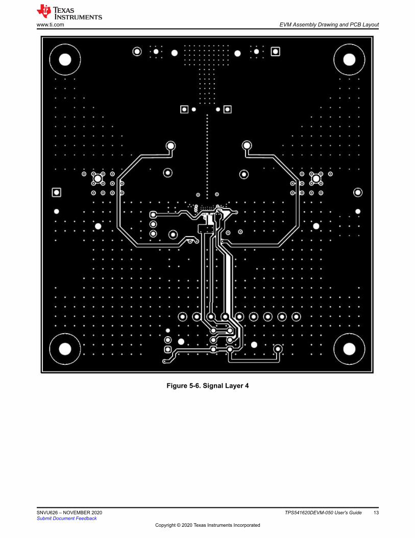
Figure 5-6. Signal Layer 4
www.ti.com EVM Assembly Drawing and PCB Layout
SNVU626 – NOVEMBER 2020Submit Document Feedback
TPS541620DEVM-050 User's Guide 13
Copyright © 2020 Texas Instruments Incorporated

Figure 5-7. Bottom Layer PCB Layout
EVM Assembly Drawing and PCB Layout www.ti.com
14 TPS541620DEVM-050 User's Guide SNVU626 – NOVEMBER 2020Submit Document Feedback
Copyright © 2020 Texas Instruments Incorporated

Figure 5-8. Bottom Solder
www.ti.com EVM Assembly Drawing and PCB Layout
SNVU626 – NOVEMBER 2020Submit Document Feedback
TPS541620DEVM-050 User's Guide 15
Copyright © 2020 Texas Instruments Incorporated

6 Bill of MaterialsTable 6-1 lists the BOM for the ( EVM).
Table 6-1. BOM for TPS541620DEVM (Dual Output)QTY DESIGNATOR DESCRIPTION PARTNUMBER MANUFACTURER
2 C1, C2 CAP, CERM, 0.1 uF, 16 V, +/- 10%, X5R, 0201 MuRata GRM033C71C104KE14D
5 C3, C6, C16,C17, C18
CAP, CERM, 100 uF, 6.3 V, +/- 20%, X5r,0805 MuRata GRM21BR60J107M
2 C7, C12 CAP, CERM, 47 uF, 25 V, +/- 20%, X5R, 1206_190 TDK C3216X5R1E476M160AC
2 C8, C11 CAP, CERM, 22 uF, 25 V, +/- 20%, X5R, 0805 MuRata GRM21BR61E226ME44L
2 C9, C10 CAP, CERM, 0.1 µF, 50 V,+/- 10%, X7R, AEC-Q200Grade 1, 0603
Kemet C0603C104K5RACAUTO 2
1 C13 CAP, CERM, 2.2 µF, 6.3 V,+/- 20%, X5R, 0402 MuRata GRM153R60J225ME95D 1
2 C21, C23 CAP, AL, 100 uF, 25 V, +/- 20%, 0.34 ohm, AEC-Q200 Grade 2, SMD
Panasonic EEE-FK1E101XP
1 C24 CAP, CERM, 0.1 uF, 16 V, +/- 10%, X7R, 0402 AVX 0402YC104KAT2A
2 C28, C29 CAP, CERM, 0.1 uF, 25 V, +/- 10%, X6S, 0201 MuRata GRM033C81E104KE14D
4 J1, J2, J3, J4 Terminal Block, 5.08 mm, 2x1, Brass, TH On-Shore Technology ED120/2DS
2 J7, J8 Header, 100mil, 2x1, Gold, TH Sullins ConnectorSolutions
PBC02SAAN
3 J9, J10, J11 Header, 2.54mm, 3x1, Gold, TH Samtec TSW-103-08-G-S
1 L1 Inductor, Shielded, Composite, 560 nH, 22 A,0.00331 ohm, AEC-Q200,SMD
Coilcraft XAL6030-561MEB 1
1 L2 Inductor, Shielded, Composite, 1.2 µH, 16 A, 0.0075ohm, AEC-Q200 Grade 1, SMD
Coilcraft XAL6030-122MEB
1 R1 RES, 56.2 k, 1%, 0.063 W, 0402 Vishay-Dale CRCW040256K2FKED
4 R2, R3, R4, R13 RES, 10.0 k, 1%, 0.063 W, 0402 Yageo America 'RC0402FR-0710KL
1 R5 RES, 15.4 k, 1%, 0.1 W, 0402 Vishay-Dale CRCW040215K4FKED
1 R6 RES, 17.4 k, 1%, 0.1 W, 0402 Vishay-Dale CRCW040217K4FKED
1 R7, R8 RES, 100 k, 1%, 0.1 W, 0402 Vishay-Dale CRCW0402100KFKED
2 R11, R12 RES, 49.9, 1%, 0.1 W, 0402 Vishay-Dale CRCW040249R9FKED
1 R14 RES, 0, 1%, 0.5 W, 0805 Keystone 5106
3 SH-J1, SH-J2,SH-J3
Shunt, 100mil, Gold plated, Black Samtec SNT-100-BK-G
4 TP1, TP2, TP3,TP4
Test Point, Multipurpose, Red, TH Keystone 5010
6 TP5, TP6, TP19,TP20, TP24,
TP25
Test Point, Multipurpose, Black, TH Keystone 5011
3 TP9, TP14, TP23 Test Point, Miniature, Red, TH Keystone 5000
8 TP10, TP11,TP12, TP13,TP15, TP16,TP17, TP18
Test Point, Miniature, White, TH Keystone 5002
2 TP21, TP22 PC Test Point, SMT TE Connectivity RCU-0C
1 U1 TPS541620RPBR, RPB0025A (VQFN-HR-25) Texas Instruments TPS541620RPBR
Bill of Materials www.ti.com
16 TPS541620DEVM-050 User's Guide SNVU626 – NOVEMBER 2020Submit Document Feedback
Copyright © 2020 Texas Instruments Incorporated

IMPORTANT NOTICE AND DISCLAIMER
TI PROVIDES TECHNICAL AND RELIABILITY DATA (INCLUDING DATASHEETS), DESIGN RESOURCES (INCLUDING REFERENCE DESIGNS), APPLICATION OR OTHER DESIGN ADVICE, WEB TOOLS, SAFETY INFORMATION, AND OTHER RESOURCES “AS IS” AND WITH ALL FAULTS, AND DISCLAIMS ALL WARRANTIES, EXPRESS AND IMPLIED, INCLUDING WITHOUT LIMITATION ANY IMPLIED WARRANTIES OF MERCHANTABILITY, FITNESS FOR A PARTICULAR PURPOSE OR NON-INFRINGEMENT OF THIRD PARTY INTELLECTUAL PROPERTY RIGHTS.These resources are intended for skilled developers designing with TI products. You are solely responsible for (1) selecting the appropriate TI products for your application, (2) designing, validating and testing your application, and (3) ensuring your application meets applicable standards, and any other safety, security, or other requirements. These resources are subject to change without notice. TI grants you permission to use these resources only for development of an application that uses the TI products described in the resource. Other reproduction and display of these resources is prohibited. No license is granted to any other TI intellectual property right or to any third party intellectual property right. TI disclaims responsibility for, and you will fully indemnify TI and its representatives against, any claims, damages, costs, losses, and liabilities arising out of your use of these resources.TI’s products are provided subject to TI’s Terms of Sale (www.ti.com/legal/termsofsale.html) or other applicable terms available either on ti.com or provided in conjunction with such TI products. TI’s provision of these resources does not expand or otherwise alter TI’s applicable warranties or warranty disclaimers for TI products.
Mailing Address: Texas Instruments, Post Office Box 655303, Dallas, Texas 75265Copyright © 2020, Texas Instruments Incorporated