tps54561-q1 4.5-v to 60-v input, 5-a, step-down dc-dc
TRANSCRIPT

SW
VDD
GND
BOOT
FB
COMP
TPS54561-Q1
EN
RT/CLK
VI
VO
SS/TR
PWRGD
Copyright © 2016, Texas Instruments Incorporated
60
65
70
75
80
85
90
95
100
0 1 2 3 4 5
Effic
iency
(%)
IO - Output Current (A) C024
V = 12 V, f = 620 kHzO (SW)= 5 V and 3.3 V, = 400 kHzV fO (SW)
12 V to 5 V
12 V to 3.3 V
36 V to 12 V
Product
Folder
Order
Now
Technical
Documents
Tools &
Software
Support &Community
An IMPORTANT NOTICE at the end of this data sheet addresses availability, warranty, changes, use in safety-critical applications,intellectual property matters and other important disclaimers. PRODUCTION DATA.
TPS54561-Q1SLVSC60A –SEPTEMBER 2014–REVISED JANUARY 2017
TPS54561-Q1 4.5-V to 60-V Input, 5-A, Step-Down DC-DC Converter With Eco-mode™
1
1 Features1• Qualified for Automotive Applications• AEC-Q100 Qualified With the Following Results:
– Device Temperature Grade 1: –40°C to 125°CAmbient Operating Temperature Range
– Device HBM ESD Classification H1C– Device CDM ESD Classification C5
• High Efficiency at Light Loads With Pulse-Skipping Eco-mode™ Control
• 87-mΩ High-Side MOSFET• 152-µA Operating Quiescent Current and
2-µA Shutdown Current• 100-kHz to 2.5-MHz Switching Frequency• Synchronizes to External Clock• Low-Dropout Operation at Light Loads With
Integrated BOOT Recharge FET• Adjustable UVLO Voltage and Hysteresis• Power-Good Output Monitor for Undervoltage and
Overvoltage• Adjustable Soft-Start and Sequencing• 0.8-V 1% Internal Voltage Reference• 10-Pin WSON With Thermal Pad Package• –40°C to 150°C TJ Operating Range• Create a Custom Design using the TPS54561-Q1
with the WEBENCH® Power Designer
2 Applications• Vehicle Accessories: GPS (see SLVA412),
Entertainment• USB Dedicated Charging Ports and Battery
Chargers (see SLVA464)• 12-V and 24-V Automotive Power Systems
3 DescriptionThe TPS54561-Q1 device is a 60-V, 5-A, step-downregulator with an integrated high-side MOSFET. Thedevice survives load dump pulses up to 65 V perISO7637. Current-mode control provides simpleexternal compensation and flexible componentselection. A low-ripple pulse-skip mode and 152-µAsupply current enables high efficiency at light loads.Pulling the enable pin low reduces shutdown supplycurrent to 2 µA .
Undervoltage lockout has an internal 4.3-V setting.Use of an external resistor divider at the EN pin canincrease the setting. The soft-start pin controls theoutput-voltage start-up ramp and also configuressequencing or tracking. An open-drain power-goodsignal indicates the output is within 93% to 106% ofits nominal voltage.
A wide adjustable switching-frequency range allowsoptimization for either efficiency or externalcomponent size. Cycle-by-cycle current limit,frequency foldback, and thermal shutdown protect thedevice during an overload condition.
The TPS54561-Q1 is available in a 10-pin, 4-mm × 4-mm WSON package.
Device Information(1)
PART NUMBER PACKAGE BODY SIZE (NOM)TPS54561-Q1 WSON (10) 4.00 mm × 4.00 mm
(1) For all available packages, see the orderable addendum atthe end of the data sheet.
SpaceSimplified Schematic Efficiency vs Load Current
2
TPS54561-Q1SLVSC60A –SEPTEMBER 2014–REVISED JANUARY 2017 www.ti.com
Product Folder Links: TPS54561-Q1
Submit Documentation Feedback Copyright © 2014–2017, Texas Instruments Incorporated
Table of Contents1 Features .................................................................. 12 Applications ........................................................... 13 Description ............................................................. 14 Revision History..................................................... 25 Pin Configuration and Functions ......................... 36 Specifications......................................................... 4
6.1 Absolute Maximum Ratings ..................................... 46.2 ESD Ratings.............................................................. 46.3 Recommended Operating Conditions....................... 46.4 Thermal Information .................................................. 56.5 Electrical Characteristics.......................................... 56.6 Timing Requirements ................................................ 66.7 Switching Characteristics .......................................... 66.8 Typical Characteristics .............................................. 7
7 Detailed Description ............................................ 117.1 Overview ................................................................. 117.2 Functional Block Diagram ....................................... 127.3 Feature Description................................................. 12
7.4 Device Functional Modes........................................ 278 Application and Implementation ........................ 28
8.1 Application Information............................................ 288.2 Typical Application .................................................. 28
9 Power Supply Recommendations ...................... 4210 Layout................................................................... 43
10.1 Layout Guidelines ................................................. 4310.2 Layout Example .................................................... 43
11 Device and Documentation Support ................. 4411.1 Device Support...................................................... 4411.2 Documentation Support ....................................... 4411.3 Receiving Notification of Documentation Updates 4411.4 Community Resources.......................................... 4411.5 Trademarks ........................................................... 4411.6 Electrostatic Discharge Caution............................ 4511.7 Glossary ................................................................ 45
12 Mechanical, Packaging, and OrderableInformation ........................................................... 45
4 Revision History
Changes from Original (September 2014) to Revision A Page
• Changed package SON To: WSON in the Features and throughout the data sheet ........................................................... 1• Added the WEBENCH information in the Features, Detailed Design Procedure, and Device Support sections .................. 1• Added SW, 5-ns transient to the Absolute Maximum Ratings ............................................................................................... 4• Moved Storage temperature range to the Absolute Maximum Ratings ................................................................................. 4• Changed the Handling Ratings table to the ESD Ratings ..................................................................................................... 4• Changed Equation 10 and Equation 11 .............................................................................................................................. 19• Changed Equation 30 .......................................................................................................................................................... 30• Changed Equation 33 .......................................................................................................................................................... 30• Moved Power Dissipation Estimate to the Detailed Design Procedure section ................................................................... 35• Moved the location of the Safe Operating Area ................................................................................................................... 37• Moved Inverting Power Supply and Split-Rail Power Supply to the Application Information section................................... 41

BOOT
VDD
EN
SS/TR
RT/CLK
PWRGD
SW
GND
COMP
FB
10
9
1
2
3
4
5
8
7
6
Thermal
Pad
3
TPS54561-Q1www.ti.com SLVSC60A –SEPTEMBER 2014–REVISED JANUARY 2017
Product Folder Links: TPS54561-Q1
Submit Documentation FeedbackCopyright © 2014–2017, Texas Instruments Incorporated
5 Pin Configuration and Functions
DPR Package10-Pin WSON
(Top View)
Pin FunctionsPIN
I/O DESCRIPTIONNAME NO.
BOOT 1 OThe device requires a bootstrap capacitor between BOOT and SW. If the voltage on this capacitor is belowthe minimum required voltage to operate the high-side MOSFET, the gate driver switches off until thebootstrap capacitor recharges.
COMP 7 O Error amplifier output, and input to the output switch-current comparator (PWM comparator). Connectfrequency compensation components to this pin.
EN 3 I Enable pin, with internal pullup current source. Pull below 1.2 V to disable. Float to enable. Adjust the inputundervoltage lockout with two resistors. See the Enable and Adjust Undervoltage Lockout section.
FB 6 I Inverting input of the transconductance (gm) error amplifier.GND 8 — Ground
PWRGD 10 O Power-good is an open-drain output that asserts if the output voltage is low because of thermal shutdown,dropout, overvoltage, or EN shutdown.
RT/CLK 5 I
Resistor timing and external clock. An internal amplifier holds this pin at a fixed voltage when using anexternal resistor to ground to set the switching frequency. When pulled above the PLL upper threshold, amode change occurs, and the pin becomes a synchronization input. This change disables the internalamplifier, and the pin is a high-impedance clock input to the internal PLL. Stopping the clocking edges re-enables the internal amplifier, and the operating mode returns to resistor programmed mode.
SS/TR 4 I Soft-start and tracking input pin. An external capacitor connected to this pin sets the output rise time. Avoltage on this pin overrides the internal reference, which allows use of the pin for tracking and sequencing.
SW 9 I The source of the internal high-side power MOSFET, and switching node of the converter.VDD 2 I Input supply pin with 4.5-V to 60-V operating range.
Thermal pad — — To ensure proper operation, electrically connect the GND pin to the copper pad under the IC on the printedcircuit board.
4
TPS54561-Q1SLVSC60A –SEPTEMBER 2014–REVISED JANUARY 2017 www.ti.com
Product Folder Links: TPS54561-Q1
Submit Documentation Feedback Copyright © 2014–2017, Texas Instruments Incorporated
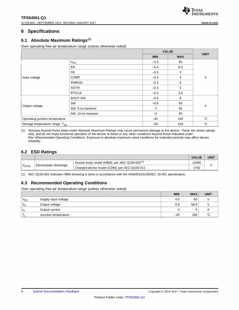
(1) Stresses beyond those listed under Absolute Maximum Ratings may cause permanent damage to the device. These are stress ratingsonly, and do not imply functional operation of the device at these or any other conditions beyond those indicated underRec–65ommended Operating Conditions. Exposure to absolute-maximum-rated conditions for extended periods may affect devicereliability.
6 Specifications
6.1 Absolute Maximum Ratings (1)
Over operating free-air temperature range (unless otherwise noted)VALUE
UNITMIN MAX
Input voltage
VDD –0.3 65
V
EN –0.3 8.4FB –0.3 3COMP –0.3 3PWRGD –0.3 6SS/TR –0.3 3RT/CLK –0.3 3.6
Output voltage
BOOT-SW –0.3 8
VSW –0.6 65SW, 5-ns transient –7 65SW, 10-ns transient –2 65
Operating junction temperature -40 150 °CStorage temperature range, Tstg –65 150 °C
(1) AEC Q100-002 indicates HBM stressing is done in accordance with the ANSI/ESDA/JEDEC JS-001 specification.
6.2 ESD RatingsVALUE UNIT
V(ESD) Electrostatic dischargeHuman-body model (HBM), per AEC Q100-002 (1) ±2000
VCharged-device model (CDM), per AEC-Q100-011 ±750
6.3 Recommended Operating ConditionsOver operating free-air temperature range (unless otherwise noted)
MIN MAX UNITVDD Supply input voltage 4.5 60 VVO Output voltage 0.8 58.8 VIO Output current 0 5 ATJ Junction temperature –40 150 °C

5
TPS54561-Q1www.ti.com SLVSC60A –SEPTEMBER 2014–REVISED JANUARY 2017
Product Folder Links: TPS54561-Q1
Submit Documentation FeedbackCopyright © 2014–2017, Texas Instruments Incorporated
(1) For more information about traditional and new thermal metrics, see the Semiconductor and IC Package Thermal Metrics applicationreport.
(2) Determination of the power rating at a specific ambient temperature must be at the maximum junction temperature of 150°C. This is thepoint where distortion starts to increase substantially. See the power dissipation estimate in the Power Dissipation Estimate section ofthis data sheet for more information.
6.4 Thermal Information
THERMAL METRIC (1) (2)TPS54561-Q1
UNITDPR10 PINS
RθJA Junction-to-ambient thermal resistance (standard board) 35.1 °C/WRθJCtop Junction-to-case (top) thermal resistance 34.1 °C/WRθJB Junction-to-board thermal resistance 12.3 °C/WψJT Junction-to-top characterization parameter 0.3 °C/WψJB Junction-to-board characterization parameter 12.5 °C/WRθJCbot Junction-to-case (bottom) thermal resistance 2.2 °C/W
(1) Measure open-loop current limit directly at the SW pin. The current is independent of the inductor value and slope compensation.
6.5 Electrical CharacteristicsTJ = –40°C to 150°C, VDD = 4.5 to 60 V (unless otherwise noted)
PARAMETER TEST CONDITIONS MIN TYP MAX UNIT
SUPPLY VOLTAGE (VDD PIN)
Operating input voltage 4.5 60 V
Internal undervoltage lockout threshold VDD rising 4.1 4.3 4.48 V
Internal undervoltage lockout thresholdhysteresis 325 mV
Shutdown supply current V(EN) = 0 V, TA = 25°C, 4.5 V ≤ VDD ≤ 60 V 2.25 4.5µA
Operating: nonswitching supply current V(FB) = 0.9 V, TA = 25°C 152 200
ENABLE AND UVLO (EN PIN)
V(EN)th Enable threshold voltage No voltage hysteresis, rising and falling 1.1 1.2 1.3 V
Input currentEnable threshold + 50 mV –4.6
µAEnable threshold – 50 mV –0.58 –1.2 -1.8
I(HYS) Hysteresis current –2.2 –3.4 -4.5 µA
VOLTAGE REFERENCE
Vref Voltage reference 0.792 0.8 0.808 V
HIGH-SIDE MOSFET
On-resistance VDD = 12 V, V(BOOT-SW) = 6 V 87 185 mΩ
ERROR AMPLIFIER
Input current 50 nA
gm(ea) Error-amplifier transconductance –2 µA < I(COMP) < 2 µA, V(COMP) = 1 V 350 µS
Error-amplifier transconductance (gm) duringsoft-start
–2 µA < I(COMP) < 2 µA, V(COMP) = 1 V, V(FB) =0.4 V 78 µS
A(OL) Error-amplifier open-loop dc gain V(FB) = 0.8 V 10 000 V/V
Minnimum unity-gain bandwidth 2500 kHz
Error-amplifier source and sink V(COMP) = 1 V, 100 mV overdrive ±30 µA
gm(ps) COMP to SW current transconductance 17 S
CURRENT LIMIT
Current limit threshold
All VDD and temperatures, open loop (1) 6.3 7.5 8.8
AAll temperatures, VDD = 12 V, open loop (1) 6.3 7.5 8.3
VDD = 12 V, TA = 25°C, open loop (1) 7.1 7.5 7.9
THERMAL SHUTDOWN
Thermal shutdown 176 °C
Thermal shutdown hysteresis 12 °C

6
TPS54561-Q1SLVSC60A –SEPTEMBER 2014–REVISED JANUARY 2017 www.ti.com
Product Folder Links: TPS54561-Q1
Submit Documentation Feedback Copyright © 2014–2017, Texas Instruments Incorporated
Electrical Characteristics (continued)TJ = –40°C to 150°C, VDD = 4.5 to 60 V (unless otherwise noted)
PARAMETER TEST CONDITIONS MIN TYP MAX UNIT
EXTERNAL CLOCK (RT/CLK PIN)
RT/CLK high threshold 1.55 2 V
RT/CLK low threshold 0.5 1.2 V
SOFT-START AND TRACKING (SS/TR PIN)
I(SS) Charge current V(SS/TR) = 0.4 V 1.7 µA
SS/TR-to-FB matching V(SS/TR) = 0.4 V 42 mV
SS/TR-to-reference crossover 98% of nominal FB voltage 1.16 V
SS/TR discharge current (overload) V(FB) = 0 V, V(SS/TR) = 0.4 V 354 µA
SS/TR discharge voltage V(FB) = 0 V 54 mV
POWER GOOD (PWRGD PIN)
FB threshold for PWRGD low FB falling 91%
FB threshold for PWRGD high FB rising 93%
FB threshold for PWRGD low FB rising 108%
FB threshold for PWRGD high FB falling 106%
Hysteresis FB falling 2%
Output-high leakage V(PWRGD) = 5.5 V, TA = 25°C 10 nA
On-resistance I(PWRGD) = 3 mA, V(FB) < 0.79 V 45 Ω
Minimum input voltage for defined outputvoltage V(PWRGD) < 0.5 V, I(PWRGD) = 100 µA 0.9 2 V
6.6 Timing RequirementsMIN TYP MAX UNIT
RT/CLKMinimum CLK input pulse duration 15 ns
6.7 Switching CharacteristicsTJ = –40°C to 150°C, VDD = 4.5 V to 60 V (unless otherwise noted)
PARAMETER TEST CONDITIONS MIN TYP MAX UNITENABLE AND UVLO (EN PIN)
Enable to COMP active VDD = 12 V, TA = 25°C 540 µsCURRENT-LIMITtd(CL) Current limit threshold delay 60 nsSW
t(ON) Minimum controllable on-time VDD = 23.7 V, VO = 5 V, IO = 3.5 A, R(RT)= 39.6 kΩ, TA = 25°C 100 ns
RT/CLKSwitching frequency range using RTmode 100 2500 kHz
f(SW) Switching frequency R(RT) = 200 kΩ 450 500 550 kHzSwitching frequency range using CLKmode 160 2300 kHz
TIMING RESISTOR AND EXTERNAL CLOCK (RT/CLK PIN)RT/CLK falling edge to SW rising edgedelay
Measured at 500 kHz with an RT resistor(R(RT)) in series 55 ns
PLL lock-in time Measured at 500 kHz 78 µs

Junction Temperature (qC)
Sw
itc
hin
g F
req
ue
nc
y (
kH
z)
-50 -25 0 25 50 75 100 125 150
450
460
470
480
490
500
510
520
530
540
550
D025Resistance at RT/CLK (k:)
Sw
itc
hin
g F
req
ue
nc
y (
kH
z)
200 300 400 500 600 700 800 900 1000
100
150
200
250
300
350
400
450
500
D024
Junction Temperature (qC)
Hig
h-S
ide
Sw
itch
Cur
rent
(A
)
-50 -25 0 25 50 75 100 125 1506
6.5
7
7.5
8
8.5
9
D027Input Voltage (V)
Hig
h-S
ide
Sw
itc
h C
urr
en
t (A
)
0 10 20 30 40 50 60
4.5
4.7
4.9
5.1
5.3
5.5
5.7
5.9
6.1
6.3
6.5
D026
-40q
25q
150q
Junction Temperature (qC)
Sta
tic
Dra
in-S
ou
rce
On
-Sta
te R
es
ista
nc
e (:
)
-50 -25 0 25 50 75 100 125 150
0
0.05
0.1
0.15
0.2
0.25
D004
BOOT-SW = 3 V
BOOT-SW = 6 V
Junction Temperature (qC)
Vo
lta
ge
Re
fere
nc
e (
V)
-50 -25 0 25 50 75 100 125 150
0.784
0.789
0.794
0.799
0.804
0.809
0.814
D028
7
TPS54561-Q1www.ti.com SLVSC60A –SEPTEMBER 2014–REVISED JANUARY 2017
Product Folder Links: TPS54561-Q1
Submit Documentation FeedbackCopyright © 2014–2017, Texas Instruments Incorporated
6.8 Typical Characteristics
Figure 1. On-Resistance vs Junction Temperature
VDD = 12 V
Figure 2. Voltage Reference vs Junction Temperature
VDD = 12 V
Figure 3. Switch-Current Limit vs Junction Temperature Figure 4. Switch-Current Limit vs Input Voltage
R(RT) = 200 kΩ VDD = 12 V
Figure 5. Switching Frequency vs Junction Temperature Figure 6. Switching Frequency vs RT/CLK Resistance,Low-Frequency Range

Junction Temperature (qC)
Inp
ut
Cu
rre
nt
at
EN
(P
A)
-50 -25 0 25 50 75 100 125 150
-5.5
-5.3
-5.1
-4.9
-4.7
-4.5
-4.3
-4.1
-3.9
-3.7
-3.5
D019Junction Temperature (qC)
Inp
ut
Cu
rre
nt
at
EN
(P
A)
-50 -25 0 25 50 75 100 125 150
-2.5
-2.3
-2.1
-1.9
-1.7
-1.5
-1.3
-1.1
-0.9
-0.7
-0.5
D018
Junction Temperature (qC)
Tra
nsco
nduc
tanc
e (P
S)
-50 -25 0 25 50 75 100 125 15020
30
40
50
60
70
80
90
100
110
120
D021Junction Temperature (qC)
EN
Th
res
ho
ld (
V)
-50 -25 0 25 50 75 100 125 150
1.15
1.18
1.21
1.24
1.27
1.3
1.33
D020
Junction Temperature (ºC)
Tra
nsco
nduc
tanc
e (P
S)
-50 -25 0 25 50 75 100 125 150200
250
300
350
400
450
500
D022Resistance at RT/CLK (k:)
Sw
itc
hin
g F
req
ue
nc
y (
kH
z)
0 50 100 150 200
0
500
1000
1500
2000
2500
D023
8
TPS54561-Q1SLVSC60A –SEPTEMBER 2014–REVISED JANUARY 2017 www.ti.com
Product Folder Links: TPS54561-Q1
Submit Documentation Feedback Copyright © 2014–2017, Texas Instruments Incorporated
Typical Characteristics (continued)
Figure 7. Switching Frequency vs RT/CLK Resistance,High-Frequency Range
VDD = 12 V
Figure 8. EA Transconductance vs Junction Temperature
VDD = 12 V
Figure 9. EA Transconductance During Soft-Start vsJunction Temperature
VDD = 12 V
Figure 10. EN Pin Threshold Voltage vs JunctionTemperature
VDD = 12 V V(EN) = Threshold + 50 mV
Figure 11. EN Pin Current vs Junction Temperature
VDD = 12 V V(EN) = Threshold – 50 mV
Figure 12. EN Pin Current vs Junction Temperature

Junction Temperature (qC)
Sup
ply
Cur
rent
at V
DD P
in (P
A)
-50 -25 0 25 50 75 100 125 15070
90
110
130
150
170
190
210
D013Input Voltage (V)
Sup
ply
Cur
rent
at V
DD P
in (P
A)
0 10 20 30 40 50 6070
90
110
130
150
170
190
210
D012
Junction Temperature (qC)
Sup
ply
Cur
rent
at V
DD P
in (P
A)
-50 -25 0 25 50 75 100 125 1500
0.5
1
1.5
2
2.5
3
D015Input Voltage (V)
Sup
ply
Cur
rent
at V
DD P
in (P
A)
0 10 20 30 40 50 600
0.5
1
1.5
2
2.5
3
D014
Junction Temperature (qC)
I (E
N)
Hy
ste
res
is (P
A)
-50 -25 0 25 50 75 100 125 150
-4.5
-4.3
-4.1
-3.9
-3.7
-3.5
-3.3
-3.1
-2.9
-2.7
-2.5
D017Voltage at FB (V)
No
min
al
Sw
itc
hin
g F
req
ue
nc
y (
%)
0 0.1 0.2 0.3 0.4 0.5 0.6 0.7 0.8
0
25
50
75
100
D016
V (FB) Falling
V (FB) Rising
9
TPS54561-Q1www.ti.com SLVSC60A –SEPTEMBER 2014–REVISED JANUARY 2017
Product Folder Links: TPS54561-Q1
Submit Documentation FeedbackCopyright © 2014–2017, Texas Instruments Incorporated
Typical Characteristics (continued)
VDD = 12 V
Figure 13. EN Pin Current Hysteresis vs JunctionTemperature
Figure 14. Switching Frequency vs FB
VDD = 12 V
Figure 15. Shutdown Supply Current vs JunctionTemperature
TJ = 25ºC
Figure 16. Shutdown Supply Current vs Input Voltage
VDD = 12 V
Figure 17. I(VDD) Supply Current vs Junction Temperature
TJ = 25ºC
Figure 18. I(VDD) Supply Current vs Input Voltage

FB Pin Voltage (mV)
SS
/TR
-to-
FB
Offs
et (
mV
)
0 100 200 300 400 500 600 700 8000
100
200
300
400
500
600
700
800
900
D007 Junction Temperature (qC)
SS
/TR
-to-
FB
Offs
et (
mV
)
-50 -25 0 25 50 75 100 125 15020
25
30
35
40
45
50
55
60
D006
Junction Temperature (qC)
Pow
er-G
ood
Thr
esho
ld (
%)
-50 -25 0 25 50 75 100 125 15088
90
92
94
96
98
100
102
104
106
108
110
D008
FB RisingFB FallingFB RisingFB Falling
Junction Temperature (qC)
Po
we
r-G
oo
d R
es
ista
nc
e (:
)
-50 -25 0 25 50 75 100 125 150
0
10
20
30
40
50
60
70
80
D009
Junction Temperature (qC)
BO
OT
-SW
UV
LO V
olta
ge (
V)
-50 -25 0 25 50 75 100 125 1501.8
1.9
2
2.1
2.2
2.3
2.4
2.5
2.6
D011
BOOT-SW UVLO FallingBOOT-SW UVLO Rising
Junction Temperature (qC)
VD
D P
in V
olta
ge (
V)
-50 -25 0 25 50 75 100 125 1503.7
3.8
3.9
4
4.1
4.2
4.3
4.4
4.5
D010
UVLO Start SwitchingUVLO Stop Switching
10
TPS54561-Q1SLVSC60A –SEPTEMBER 2014–REVISED JANUARY 2017 www.ti.com
Product Folder Links: TPS54561-Q1
Submit Documentation Feedback Copyright © 2014–2017, Texas Instruments Incorporated
Typical Characteristics (continued)
Figure 19. BOOT-SW UVLO vs Junction Temperature Figure 20. Input Voltage UVLO vs Junction Temperature
VDD = 12 V
Figure 21. PWRGD On-Resistance vs Junction Temperature
VDD = 12 V
Figure 22. PWRGD Threshold vs Junction Temperature
VDD = 12 V TJ = 25ºC
Figure 23. SS/TR to FB Offset vs FB
VDD = 12 V V(FB) = 0.4 V
Figure 24. SS/TR to FB Offset vs Temperature

Output Current (A)
I np
ut
Vo
lta
ge
(V)
0.05 0.1 0.15 0.2 0.25 0.3 0.35 0.4 0.45 0.5
4.6
4.7
4.8
4.9
5
5.1
5.2
5.3
5.4
5.5
5.6
D005
Start
Stop
DropoutVoltage
DropoutVoltage
11
TPS54561-Q1www.ti.com SLVSC60A –SEPTEMBER 2014–REVISED JANUARY 2017
Product Folder Links: TPS54561-Q1
Submit Documentation FeedbackCopyright © 2014–2017, Texas Instruments Incorporated
Typical Characteristics (continued)
Figure 25. 5-V Start and Stop Voltage (see Low-Dropout Operation and Bootstrap Voltage (BOOT))
7 Detailed Description
7.1 OverviewThe TPS54561-Q1 device is a 60-V, 5-A, step-down (buck) regulator with an integrated high-side n-channelMOSFET. The device implements constant-frequency current-mode control, which reduces output capacitanceand simplifies external frequency compensation. The wide switching frequency range of 100 kHz to 2500 kHzallows either efficiency or size optimization when selecting the output filter components. The use of a resistorconnected to ground from the RT/CLK pin adjusts the switching frequency. The device has an internal phase-locked loop (PLL) connected to the RT/CLK pin that synchronizes the power-switch turnon to the falling edge ofan external clock signal.
The TPS54561-Q1 device has a default input start-up voltage of approximately 4.3 V. The EN pin adjusts theinput-voltage undervoltage-lockout (UVLO) threshold with two external resistors. An internal pullup current sourceenables operation when the EN pin is floating. The operating current is 152 µA under no-load conditions whennot switching. With the device disabled, the supply current is 2 µA.
The integrated 87-mΩ high-side MOSFET supports high-efficiency power supply designs capable of delivering5 A of continuous current to a load. A bootstrap capacitor connected from the BOOT pin to the SW pin suppliesthe gate-drive bias voltage for the integrated high-side MOSFET. The TPS54561-Q1 device reduces the externalcomponent count by integrating the bootstrap recharge diode. A BOOT UVLO circuit monitors the BOOT pincapacitor voltage, and turns off the high-side MOSFET when the BOOT to SW voltage falls below a presetthreshold. An automatic BOOT capacitor recharge circuit allows the TPS54561-Q1 to operate at high duty cyclesapproaching 100%. Therefore, the maximum output voltage is near the minimum input supply voltage of theapplication. The minimum output voltage is 0.8 V, which equals the internal feedback reference.
An overvoltage protection (OVP) comparator minimizes output overvoltage transients. On activation of the OVPcomparator, the high-side MOSFET turns off and remains off until the output voltage is less than 106% of thedesired output voltage.
Using the SS/TR (soft-start and tracking) pin minimizes inrush currents or provides power supply sequencingduring power-up. Couple a small-value capacitor from the SS/TR pin to the GND pin to adjust the soft-start time.Couple a resistor divider from SS/TR pin to GND pin for critical power-supply sequencing requirements. Thedevice discharges the SS/TR pin before the output powers up. This discharging ensures a repeatable restartafter an overtemperature fault, UVLO fault, or a disabled condition. When the overload condition goes away, thesoft-start circuit controls the recovery from the fault output level to the nominal regulation voltage. A frequencyfoldback circuit reduces the switching frequency during start-up or overcurrent fault conditions to help maintaincontrol of the inductor current.

Error
Amplifier
BootCharge
Boot
UVLO
UVLO
CurrentSense
OscillatorWith PLL
FrequencyShift
Slope
Compensation
PWM
Comparator
MinimumClampPulseSkip
MaximumClamp
Voltage
Reference
OverloadRecovery
FB
SS/TR
COMP
RT/CLK
SW
BOOT
VDD
GND
Thermal
Shutdown
EN
Enable
Comparator
ShutdownLogic
Shutdown
Enable
Threshold
Logic
Shutdown
PWRGD
Thermal Pad
Shutdown
OV
UV
S
Logic
Copyright © 2016, Texas Instruments Incorporated
12
TPS54561-Q1SLVSC60A –SEPTEMBER 2014–REVISED JANUARY 2017 www.ti.com
Product Folder Links: TPS54561-Q1
Submit Documentation Feedback Copyright © 2014–2017, Texas Instruments Incorporated
7.2 Functional Block Diagram
7.3 Feature Description
7.3.1 Fixed-Frequency PWM ControlThe TPS54561-Q1 device uses fixed-frequency, peak-current-mode control with adjustable switching frequency.An error amplifier compares the output voltage to an internal voltage reference through an external resistordivider connected to the FB pin. An internal oscillator initiates the turnon of the high-side MOSFET. The erroramplifier output at the COMP pin controls the high-side MOSFET current. When the high-side MOSFET switchcurrent reaches the threshold level set by the COMP voltage, the power switch turns off. The COMP pin voltageincreases and decreases as the output current increases and decreases. The device implements current limitingby clamping the COMP pin voltage to a maximum level. Implementation of the pulse-skipping Eco-mode controlscheme is through a minimum voltage clamp on the COMP pin.
7.3.2 Slope Compensation Output CurrentThe TPS54561-Q1 adds a compensating ramp to the MOSFET switch-current sense signal. This slopecompensation prevents sub-harmonic oscillations at duty cycles greater than 50%. The slope compensation doesnot affect the peak current limit of the high-side switch, which remains constant over the full duty cycle range.

O I O DS(on) (d) (d) O (DC)V max Dmax (V min I max r V ) V I max R= ´ - ´ + - + ´
13
TPS54561-Q1www.ti.com SLVSC60A –SEPTEMBER 2014–REVISED JANUARY 2017
Product Folder Links: TPS54561-Q1
Submit Documentation FeedbackCopyright © 2014–2017, Texas Instruments Incorporated
Feature Description (continued)7.3.3 Pulse-Skipping Eco-mode Control SchemeThe TPS54561-Q1 device operates in a pulse-skipping Eco-mode control scheme at light load currents toimprove efficiency by reducing switching and gate-drive losses. If the output voltage is within regulation and thepeak switch current of any switching cycle is below the pulse-skipping current threshold, the device enters pulse-skipping mode. The pulse-skipping current threshold is the peak switch-current level corresponding to a nominalCOMP voltage of 600 mV.
When in pulse-skipping mode, the TPS54561-Q1 device clamps the COMP pin voltage to 600 mV and inhibitsthe high-side MOSFET. Because the device is not switching, the output voltage begins to decay. The voltagecontrol loop responds to the falling output voltage by increasing the COMP pin voltage. The high-side MOSFETenables and switching resumes when the error amplifier lifts COMP above the pulse-skipping threshold. Theoutput voltage recovers to the regulated value, and COMP eventually falls below the pulse-skipping threshold, atwhich time the device again enters pulse-skipping mode. The internal PLL remains operational when in pulse-skipping mode. When operating at light load currents in pulse-skipping mode, the switching transitions occursynchronously with the external clock signal.
During pulse-skipping operation, the TPS54561-Q1 device senses and controls the peak switch current, not theaverage load current. Therefore, the load current at which the device enters pulse-skipping mode depends on theoutput inductor value. The circuit in Figure 46 enters pulse-skipping mode at about 25.3 mA output current. Asthe load current approaches zero, the device enters the pulse-skipping mode. During the time period when thereis no switching the input current falls to the 152-µA quiescent current.
7.3.4 Low-Dropout Operation and Bootstrap Voltage (BOOT)The TPS54561-Q1 device provides an integrated bootstrap voltage regulator. A small capacitor between theBOOT and SW pins provides the gate-drive voltage for the high-side MOSFET. The BOOT capacitor rechargeswhen the high-side MOSFET is off and the external low-side diode conducts. The recommended value of theBOOT capacitor is 0.1 µF. For stable performance over temperature and voltage, TI recommends a ceramiccapacitor with an X7R or X5R grade dielectric with a voltage rating of 10 V or higher.
When operating with a low voltage difference from input to output, the high-side MOSFET of the TPS54561-Q1operates at 100% duty cycle as long as the BOOT-to-SW pin voltage is greater than 2.1 V. When the voltagefrom BOOT to SW drops below 2.1 V, the high-side MOSFET turns off and an integrated low-side MOSFET pullsSW low to recharge the BOOT capacitor. To reduce the losses of the small low-side MOSFET at high outputvoltages, the device disables this small low-side MOSFET at 24-V output and re-enables it when the outputreaches 21.5 V.
Because the gate-drive current sourced from the BOOT capacitor is small, the high-side MOSFET can remain onfor many switching cycles before the MOSFET turns off to refresh the capacitor. Thus the effective duty cycle ofthe switching regulator can be high, approaching 100%. The main influences on the effective duty cycle of theconverter during dropout are the voltage drops across the power MOSFET, the inductor resistance, the low-sidediode voltage, and the printed-circuit-board (PCB) resistance.
Figure 25 shows the start and stop voltages for a typical 5-V output application, and plots the input voltageversus load current. The definition of start voltage is the input voltage required to regulate the output within 1% ofnominal voltage. The definition of stop voltage is the input voltage at which the output drops by 5% or whereswitching stops.
During high-duty-cycle (low dropout) conditions, inductor current ripple increases while the BOOT capacitorrecharges, resulting in an increase in output-voltage ripple. Increased ripple occurs when the off-time required torecharge the BOOT capacitor is longer than the high-side off-time associated with cycle-by-cycle PWM control.
At heavy loads, increase the minimum input voltage to ensure a monotonic start-up. For this condition, useEquation 1 to calculate the maximum output voltage for a given minimum input voltage.
where• Dmax = 0.9• V(d) = Forward drop of the catch diode• R(DC) = DC resistance of output inductor

(EN)th(UVLO2)
(START) (EN)th(1)
(UVLO1)
VR
V VI
R
=
-
+
(START) (STOP)(UVLO1)
(HYS)
V VR
I
æ ö-= ç ÷
ç ÷è ø
O(HS) (LS)
V 0.8 VR R
0.8 V
æ ö-= ´ ç ÷
è ø
14
TPS54561-Q1SLVSC60A –SEPTEMBER 2014–REVISED JANUARY 2017 www.ti.com
Product Folder Links: TPS54561-Q1
Submit Documentation Feedback Copyright © 2014–2017, Texas Instruments Incorporated
Feature Description (continued)• rDS(on) = 1 / (–0.3 × V(BOOT_SW)
2 + 3.577 × V(BOOT_SW) – 4.246)• V(BOOT_SW) = V(BOOT) + V(d)
• V(BOOT) = (1.41 × VImin – 0.554 – V(d) x f(SW) – 1.847 × 10³ × I(BOOT_SW)) / (1.41 + f(SW))• I(BOOT_SW) = 100 × 10-6 A• f(SW) = Operating frequency in MHz (1)
7.3.5 Error AmplifierA transconductance error amplifier controls the TPS54561-Q1 voltage regulation loop. The error amplifiercompares the FB pin voltage to the lower of the internal soft-start voltage or the internal 0.8-V voltage reference.The transconductance (gm(ea)) of the error amplifier is 350 µS during normal operation. During soft-startoperation, the device reduces the transconductance to 78 µS and references the error amplifier to the internalsoft-start voltage.
The frequency compensation components (capacitor, series resistor, and capacitor) connect the error-amplifieroutput COMP pin to the GND pin.
7.3.6 Adjusting the Output VoltageThe internal voltage reference produces a precise 0.8-V ±1% voltage reference over the operating temperatureand voltage range by scaling the output of a bandgap reference circuit. A resistor divider from the output node tothe FB pin sets the output voltage. Divider resistors with a 1% tolerance or better are recommended. Select thelow-side resistor, R(LS), for the desired divider current, and use Equation 2 to calculate R(HS). To improveefficiency at light loads, consider using larger-value resistors. However, if the values are too high, the regulator ismore susceptible to noise and voltage errors because of the FB input current may become noticeable.
(2)
7.3.7 Enable and Adjust Undervoltage LockoutThe VDD pin voltage rising above 4.3 V when the EN pin voltage exceeds the enable threshold of 1.2 V enablesthe TPS54561-Q1 device. The VDD pin voltage falling below 4 V or the EN pin voltage dropping below 1.2 Vdisables the TPS54561-Q1 device. The EN pin has an internal pullup current source, I(1), of 1.2 µA that enablesoperation of the TPS54561-Q1 device when the EN pin floats.
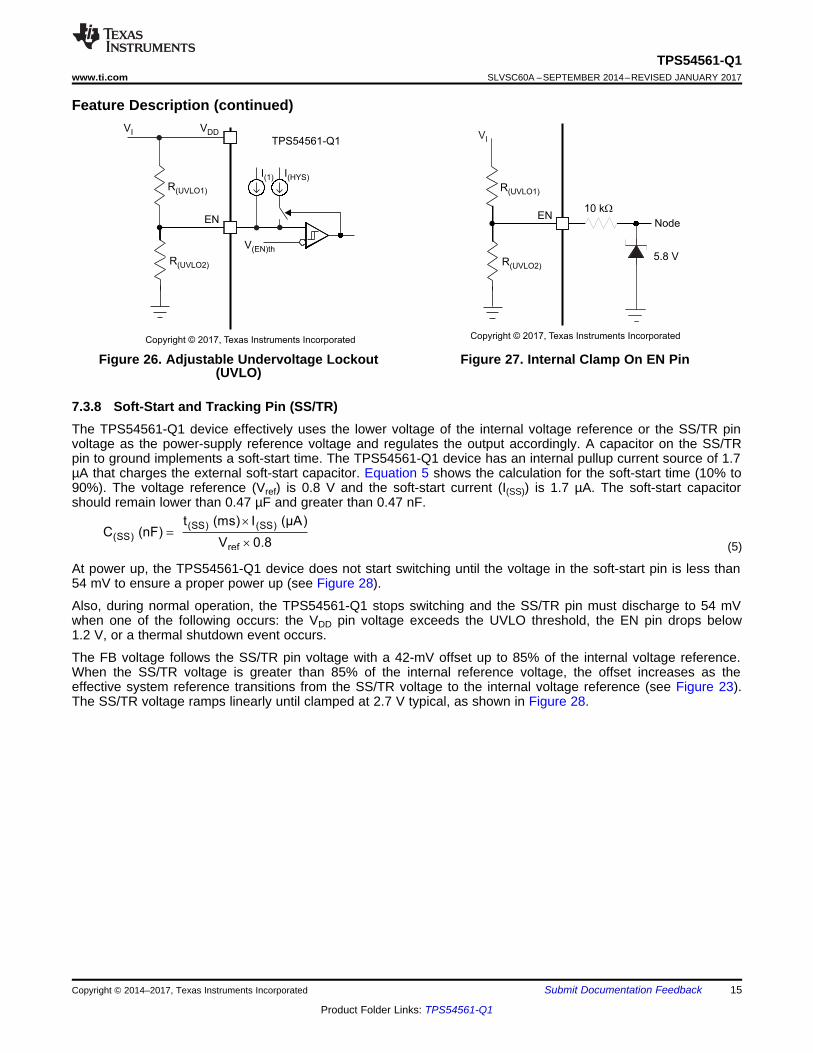
If an application requires a higher undervoltage lockout (UVLO) threshold, use the circuit shown in Figure 26 toadjust the input voltage UVLO with two external resistors. When the EN pin voltage exceeds 1.2 V, the EN pinsources an additional 3.4 µA of hysteresis current, I(HYS). This additional current facilitates adjustable inputvoltage UVLO hysteresis. Pulling the EN pin below 1.2 V removes the 3.4-µA I(HYS) current. Use Equation 3 tocalculate R(UVLO1) for the desired UVLO hysteresis voltage. Use Equation 4 to calculate R(UVLO2) for the desiredVDD start voltage.
In applications designed to start at relatively low input voltages (for example, from 4.5 V to 9 V) and withstandhigh input voltages (for example, from 40 V to 60 V), the EN pin may experience a voltage greater than theabsolute maximum voltage of 8.4 V during the high-input-voltage condition. To avoid exceeding this voltagewhen using the EN resistors, a 5.8-V Zener diode that is capable of sinking up to 150 µA internally clamps theEN pin.
(3)
(4)
(SS) (SS)(SS)
ref
t (ms) I (μA)C (nF)
V 0.8
´
=
´
TPS54561-Q1
I(1)
VDD
R(UVLO1)
R(UVLO2)
EN
V(EN)th
I(HYS)
VI
Copyright © 2017, Texas Instruments Incorporated
ENNode
5.8 V
10 kW
R(UVLO1)
R(UVLO2)
VI
Copyright © 2017, Texas Instruments Incorporated
15
TPS54561-Q1www.ti.com SLVSC60A –SEPTEMBER 2014–REVISED JANUARY 2017
Product Folder Links: TPS54561-Q1
Submit Documentation FeedbackCopyright © 2014–2017, Texas Instruments Incorporated
Feature Description (continued)
Figure 26. Adjustable Undervoltage Lockout(UVLO)
Figure 27. Internal Clamp On EN Pin
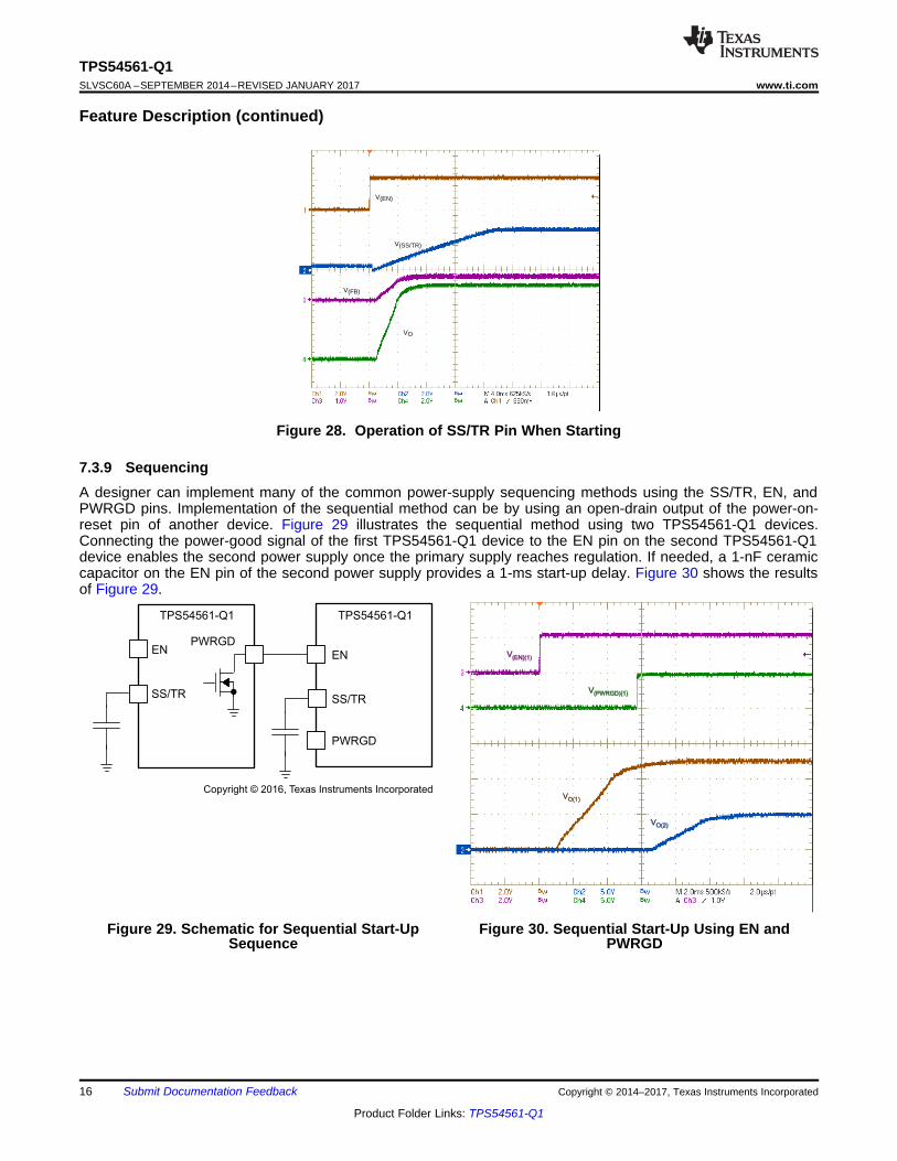
7.3.8 Soft-Start and Tracking Pin (SS/TR)The TPS54561-Q1 device effectively uses the lower voltage of the internal voltage reference or the SS/TR pinvoltage as the power-supply reference voltage and regulates the output accordingly. A capacitor on the SS/TRpin to ground implements a soft-start time. The TPS54561-Q1 device has an internal pullup current source of 1.7µA that charges the external soft-start capacitor. Equation 5 shows the calculation for the soft-start time (10% to90%). The voltage reference (Vref) is 0.8 V and the soft-start current (I(SS)) is 1.7 µA. The soft-start capacitorshould remain lower than 0.47 µF and greater than 0.47 nF.
(5)
At power up, the TPS54561-Q1 device does not start switching until the voltage in the soft-start pin is less than54 mV to ensure a proper power up (see Figure 28).
Also, during normal operation, the TPS54561-Q1 stops switching and the SS/TR pin must discharge to 54 mVwhen one of the following occurs: the VDD pin voltage exceeds the UVLO threshold, the EN pin drops below1.2 V, or a thermal shutdown event occurs.
The FB voltage follows the SS/TR pin voltage with a 42-mV offset up to 85% of the internal voltage reference.When the SS/TR voltage is greater than 85% of the internal reference voltage, the offset increases as theeffective system reference transitions from the SS/TR voltage to the internal voltage reference (see Figure 23).The SS/TR voltage ramps linearly until clamped at 2.7 V typical, as shown in Figure 28.
V(EN)(1)
VO(1)
VO(2)
V(PWRGD)(1)
SS/TR
TPS54561-Q1
EN
PWRGD
ENPWRGD
SS/TR
TPS54561-Q1
Copyright © 2016, Texas Instruments Incorporated
VO
V(FB)
V(SS/TR)
V(EN)
16
TPS54561-Q1SLVSC60A –SEPTEMBER 2014–REVISED JANUARY 2017 www.ti.com
Product Folder Links: TPS54561-Q1
Submit Documentation Feedback Copyright © 2014–2017, Texas Instruments Incorporated
Feature Description (continued)
Figure 28. Operation of SS/TR Pin When Starting
7.3.9 SequencingA designer can implement many of the common power-supply sequencing methods using the SS/TR, EN, andPWRGD pins. Implementation of the sequential method can be by using an open-drain output of the power-on-reset pin of another device. Figure 29 illustrates the sequential method using two TPS54561-Q1 devices.Connecting the power-good signal of the first TPS54561-Q1 device to the EN pin on the second TPS54561-Q1device enables the second power supply once the primary supply reaches regulation. If needed, a 1-nF ceramiccapacitor on the EN pin of the second power supply provides a 1-ms start-up delay. Figure 30 shows the resultsof Figure 29.
Figure 29. Schematic for Sequential Start-UpSequence
Figure 30. Sequential Start-Up Using EN andPWRGD
White space

SS/TR
TPS54561-Q1
EN
BOOT
PWRGD
SS/TR
TPS54561-Q1
EN
PWRGD
VO(1)
VO(2)
R1
R4
R3
R2
SW
BOOT
SW
FB
Copyright © 2016, Texas Instruments Incorporated
EN
TPS54160
3
SS/TR4
PWRGD6
EN
TPS54160
3
SS/TR4
PWRGD6
TPS54561-Q1
TPS54561-Q1
Copyright © 2016, Texas Instruments Incorporated
V(EN)(1), V(EN)(2)
VO(1)
VO(2)
17
TPS54561-Q1www.ti.com SLVSC60A –SEPTEMBER 2014–REVISED JANUARY 2017
Product Folder Links: TPS54561-Q1
Submit Documentation FeedbackCopyright © 2014–2017, Texas Instruments Incorporated
Feature Description (continued)
Figure 31. Schematic for Ratiometric Start-UpSequence
Figure 32. Ratiometric Start-Up Using CoupledSS/TR Pins
Figure 31 shows a method for a ratiometric start-up sequence by connecting the SS/TR pins together. Theregulator outputs ramp up and reach regulation at the same time. When calculating the soft-start capacitor byusing Equation 5, double the pullup current source (I(SS)). Figure 32 shows the results of Figure 31.
Figure 33. Schematic for Ratiometric and Simultaneous Start-Up Sequence
One can implement ratiometric and simultaneous power-supply sequencing by connecting the resistor network ofR1 and R2 shown in Figure 33 to the output of a power supply that must be tracked, or to another voltagereference source. Using Equation 7 and Equation 8, one can calculate values for the tracking resistors to initiateVO(2) slightly before, after, or at the same time as VO(1). Equation 6 is the voltage difference between VO(1) andVO(2) at 95% of nominal output regulation.

V(EN)
VO(1)
VO(2)
V(EN)
VO(1)
VO(2)
O(1)R1 2800 V 180 V> ´ - ´ D
ref
O(2) ref
V R1R2
V V V
´=
+ D -
O(2) (SSoffset)O(1)
ref (SS)
V V VR1 V
V I
+ D= - ´
O(1) O(2)V V VD = -
18
TPS54561-Q1SLVSC60A –SEPTEMBER 2014–REVISED JANUARY 2017 www.ti.com
Product Folder Links: TPS54561-Q1
Submit Documentation Feedback Copyright © 2014–2017, Texas Instruments Incorporated
Feature Description (continued)The ΔV variable is zero volts for simultaneous sequencing. To minimize the effect of the inherent SS/TR-to-FBoffset (V(SSoffset)) in the soft-start circuit and the offset created by the pullup current source (I(SS)) and trackingresistors, the equations include V(SSoffset) and I(SS) as variables.
To design a ratiometric start-up in which the VO(2) voltage is slightly greater than the VO(1) voltage when VO(2)reaches regulation, use a negative number in Equation 6 through Equation 8 for ΔV. Equation 6 results in apositive number for applications in which VO(2) is slightly lower than VO(1) when VO(2) reaches its regulation.
Because of the requirement for pulling the SS/TR pin below 54 mV before starting after an EN, UVLO, or thermalshutdown fault, careful selection of the tracking resistors ensures that the device restarts after a fault. Make surethe calculated R1 value from Equation 7 is greater than the value calculated in Equation 9 to ensure the devicecan recover from a fault.
As the SS/TR voltage becomes more than 85% of the nominal reference voltage, V(SSoffset) becomes larger as thesoft-start circuits gradually hand off the regulation reference to the internal voltage reference. The SS/TR pinvoltage must be greater than 1.5 V for a complete handoff to the internal voltage reference as shown inFigure 23.
(6)
at 95% of nominal output regulation.
(7)
(8)
(9)
Figure 34. Ratiometric Start-Up With Tracking Resistors –VO(2) Before VO(1)
Figure 35. Ratiometric Start-Up With Tracking Resistors –VO(2) After VO(1)

0.991
92417sw (kHz) =
RT (k )W
f
T 1.008
101756R (k ) =
sw (kHz)W
f
V(EN)
VO(1)
VO(2)
19
TPS54561-Q1www.ti.com SLVSC60A –SEPTEMBER 2014–REVISED JANUARY 2017
Product Folder Links: TPS54561-Q1
Submit Documentation FeedbackCopyright © 2014–2017, Texas Instruments Incorporated
Feature Description (continued)
Figure 36. Simultaneous Start-Up With Tracking Resistors
7.3.10 Constant Switching Frequency and Timing Resistor (RT/CLK Pin)The switching frequency of the TPS54561-Q1 device is adjustable over a wide range, from 100 kHz to 2500 kHz,by placing a resistor between the RT/CLK pin and GND pin. The RT/CLK pin voltage is typically 0.5 V and musthave a resistor to ground to set the switching frequency. To determine the timing resistance for a given switchingfrequency, use Equation 10 or Equation 11 or the curves in Figure 6 and Figure 7. To reduce the solution size,one would typically set the switching frequency as high as possible, but consider tradeoffs of the conversionefficiency, maximum input voltage, and minimum controllable on-time. The minimum controllable on-time istypically 100 ns, which limits the maximum operating frequency in applications with high input-to-output step-down ratios. The frequency foldback circuit also limits the maximum switching frequency. The next section talksabout the maximum switching frequency in detail.
(10)
(11)
7.3.11 Accurate Current-Limit Operation and Maximum Switching FrequencyThe TPS54561-Q1 device implements peak-current-mode control, in which the COMP pin voltage controls thepeak current of the high-side MOSFET. A signal proportional to the high-side switch current and the COMP pinvoltage are compared each cycle. When the peak switch current intersects the COMP control voltage, the high-side switch turns off. During overcurrent conditions that pull the output voltage low, the error amplifier increasesswitch current by driving the COMP pin high. The device clamps the error-amplifier output internally at a levelwhich sets the switch-current limit. The TPS54561-Q1 device provides an accurate current-limit threshold with atypical current-limit delay of 60 ns. With smaller inductor values, the delay results in a higher peak inductorcurrent. Figure 37 shows the relationship between the inductor value and the peak inductor current.
O (dc) O (d)(SW_skip)
(ON) I O DS(on) (d)
I R V V1f max
t V I r V
æ ö´ + += ´ ç ÷
ç ÷- ´ +è ø
(CL) (dc) O(SC) (d)(DIV)(SW_ shift)
(ON) I (CL) DS(on) (d)
I R V Vff
t V I r V
æ ö´ + += ´ ç ÷
ç ÷- ´ +è ø
td(CL)
Inducto
r C
urr
ent (A
)
ΔCLpkPeak Inductor Current
Open-Loop Current Limit
ΔCLpk = (V / L ) tI (O) d(CL)´
t(ON)
20
TPS54561-Q1SLVSC60A –SEPTEMBER 2014–REVISED JANUARY 2017 www.ti.com
Product Folder Links: TPS54561-Q1
Submit Documentation Feedback Copyright © 2014–2017, Texas Instruments Incorporated
Feature Description (continued)
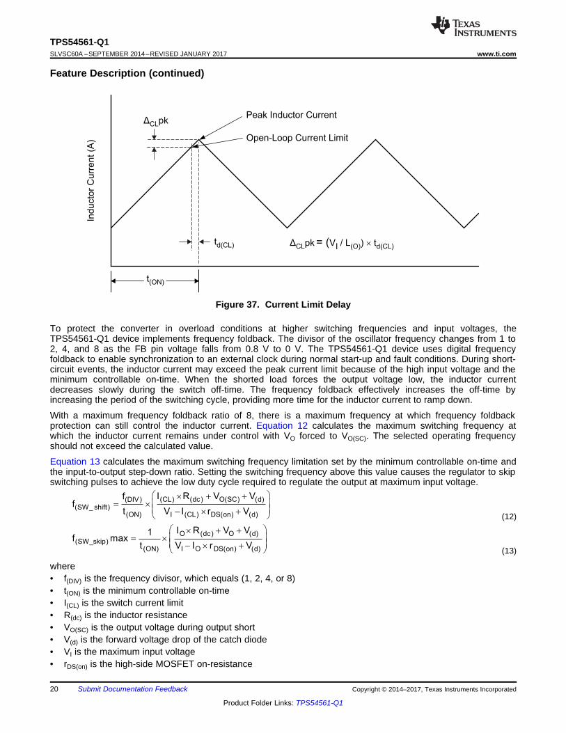
Figure 37. Current Limit Delay
To protect the converter in overload conditions at higher switching frequencies and input voltages, theTPS54561-Q1 device implements frequency foldback. The divisor of the oscillator frequency changes from 1 to2, 4, and 8 as the FB pin voltage falls from 0.8 V to 0 V. The TPS54561-Q1 device uses digital frequencyfoldback to enable synchronization to an external clock during normal start-up and fault conditions. During short-circuit events, the inductor current may exceed the peak current limit because of the high input voltage and theminimum controllable on-time. When the shorted load forces the output voltage low, the inductor currentdecreases slowly during the switch off-time. The frequency foldback effectively increases the off-time byincreasing the period of the switching cycle, providing more time for the inductor current to ramp down.
With a maximum frequency foldback ratio of 8, there is a maximum frequency at which frequency foldbackprotection can still control the inductor current. Equation 12 calculates the maximum switching frequency atwhich the inductor current remains under control with VO forced to VO(SC). The selected operating frequencyshould not exceed the calculated value.
Equation 13 calculates the maximum switching frequency limitation set by the minimum controllable on-time andthe input-to-output step-down ratio. Setting the switching frequency above this value causes the regulator to skipswitching pulses to achieve the low duty cycle required to regulate the output at maximum input voltage.
(12)
(13)
where• f(DIV) is the frequency divisor, which equals (1, 2, 4, or 8)• t(ON) is the minimum controllable on-time• I(CL) is the switch current limit• R(dc) is the inductor resistance• VO(SC) is the output voltage during output short• V(d) is the forward voltage drop of the catch diode• VI is the maximum input voltage• rDS(on) is the high-side MOSFET on-resistance

RT/CLK
TPS54561-Q1
ClockSource
PLLRT
RT/CLK
TPS54561-Q1
Hi-Z
Clock
Source
PLL
RT
Copyright © 2017, Texas Instruments Incorporated
21
TPS54561-Q1www.ti.com SLVSC60A –SEPTEMBER 2014–REVISED JANUARY 2017
Product Folder Links: TPS54561-Q1
Submit Documentation FeedbackCopyright © 2014–2017, Texas Instruments Incorporated
Feature Description (continued)• IO is the output current• VO is the output voltage
7.3.12 Synchronization to RT/CLK PinThe RT/CLK pin can receive a frequency synchronization signal from an external system clock. To implementthis synchronization feature, connect a square wave to the RT/CLK pin through either circuit network shown inFigure 38. The square wave applied to the RT/CLK pin must switch lower than 0.5 V, and higher than 2 V, andhave a pulse duration greater than 15 ns. The synchronization frequency range is 160 kHz to 2300 kHz. Therising edge of SW synchronizes to the falling edge of the RT/CLK pin signal. The design of the externalsynchronization circuit should be such that the default frequency-set resistor connects from the RT/CLK pin toGND pin when the synchronization signal is off. When using a low-impedance signal source, the connection ofthe frequency-set resistor is in parallel with an ac-coupling capacitor to a termination resistor (for example, 300Ω) as shown in Figure 38. The two resistors in series provide the default frequency-setting resistance when thesignal source turns off. The sum of the resistance should set the switching frequency close to the external CLKfrequency. TI recommends ac-coupling the synchronization signal through a 10-pF ceramic capacitor to theRT/CLK pin.
The first time the input pulls the RT/CLK pin above the PLL high threshold, which has a 2-V maximum value, theTPS54561-Q1 switches from the RT resistor free-running frequency mode to the PLL synchronized mode.Removal of the internal 0.5-V voltage source results, and the RT/CLK pin becomes high-impedance as the PLLstarts to lock onto the external signal. The switching frequency can be higher or lower than the frequency set withthe RT/CLK resistor. The device transitions from the resistor-programmed mode to the PLL mode and locks ontothe external clock frequency within 78 µs. During the transition from the PLL mode to the resistor-programmedmode, the switching frequency falls to 150 kHz and then increases or decreases to the resistor-programmedfrequency on re-application of the 0.5-V bias voltage to the RT/CLK resistor.
The switching frequency divisor goes from 8 to 4, 2, and 1 as the FB pin voltage ramps from 0 V to 0.8 V. Thedevice implements a digital-frequency foldback to enable synchronization to an external clock during normalstart-up and fault conditions. Figure 39, Figure 40, and Figure 41 show the device synchronized to an externalsystem clock in continuous-conduction mode (CCM), discontinuous-conduction (DCM) and pulse-skipping mode.
SPACER
Figure 38. Synchronizing to a System Clock

V(SW)
ExternalClock
I(L)
V(SW)
ExternalClock
I(L)
V(SW)
ExternalClock
I(L)
22
TPS54561-Q1SLVSC60A –SEPTEMBER 2014–REVISED JANUARY 2017 www.ti.com
Product Folder Links: TPS54561-Q1
Submit Documentation Feedback Copyright © 2014–2017, Texas Instruments Incorporated
Feature Description (continued)
Figure 39. Plot of Synchronizing in CCMFigure 40. Plot of Synchronizing in DCM
Figure 41. Plot of Synchronizing in Pulse-Skipping Mode
7.3.13 Power Good (PWRGD Pin)The PWRGD pin is an open-drain output. When the FB pin is between 93% and 106% of the internal voltagereference, TPS54561-Q1 device de-asserts the PWRGD pin and this pin floats. TI recommends a pullup resistorof 1 kΩ to a voltage source that is 5.5 V or less. A higher pullup resistance reduces the amount of current drawnfrom the pullup voltage source when the PWRGD pin is low. A lower pullup resistance reduces the switchingnoise seen on the PWRGD signal. PWRGD is in a defined state once the VDD pin voltage is greater than 2 V, butwith reduced current sinking capability. PWRGD achieves full current-sinking capability as the VDD pin voltageapproaches 3 V.
TPS54561-Q1 device pulls the PWRGD pin low when the FB pin voltage is lower than 90% or greater than 108%of the nominal internal reference voltage. Also, the TPS54561-Q1 device pulls the PWRGD pin low after an EN,UVLO, or thermal shutdown fault.

FB
COMP
VO
R(HS)
R(COMP)
C(ZERO)
C(POLE)R(LS)
C(OEA) R(OEA)
gm(ea)
350 µS
0.8 V
Power Stageg 17 Sm(ps)
SW
R(ESR)
C(O)
R(L)
b
a
c
Copyright © 2016, Texas Instruments Incorporated
23
TPS54561-Q1www.ti.com SLVSC60A –SEPTEMBER 2014–REVISED JANUARY 2017
Product Folder Links: TPS54561-Q1
Submit Documentation FeedbackCopyright © 2014–2017, Texas Instruments Incorporated
Feature Description (continued)7.3.14 Overvoltage ProtectionThe TPS54561-Q1 incorporates an output overvoltage-protection (OVP) circuit to minimize voltage overshootwhen recovering from output fault conditions or strong unload transients in designs with low output capacitance.For example, on an overload event of the power-supply output, the error amplifier compares the actual outputvoltage to the internal reference voltage. If the FB pin voltage is lower than the internal reference voltage for aconsiderable time, the output of the error amplifier increases to a maximum voltage corresponding to the peakcurrent-limit threshold. On removal of the overload condition, the regulator output rises and the error amplifieroutput transitions to the normal operating level. In some applications, the power-supply output voltage canincrease faster than the response of the error amplifier output, resulting in an output overshoot.
The OVP feature minimizes output overshoot when using a low-value output capacitor by comparing the FB pinvoltage to the rising OVP threshold, which is nominally 108% of the internal voltage reference. If the FB pinvoltage is greater than the rising OVP threshold, immediately disabling the high-side MOSFET minimizes outputovershoot. When the FB voltage drops below the falling OVP threshold, which is nominally 106% of the internalvoltage reference, the high-side MOSFET resumes normal operation.
7.3.15 Thermal ShutdownThe TPS54561-Q1 provides an internal thermal shutdown to protect the device when the junction temperatureexceeds 176°C. The high-side MOSFET stops switching when the junction temperature exceeds the thermal tripthreshold. Once the silicon temperature falls below 164°C, the device reinitiates the power-up sequencecontrolled by the SS/TR pin.
7.3.16 Small-Signal Model for Loop ResponseFigure 42 shows a simplified model for the TPS54561-Q1 control loop, with which the designer can simulate tocheck the frequency response and dynamic load response. The error amplifier is a transconductance amplifierwith a gm(ea) of 350 µS. A user can model the error amplifier using an ideal voltage controlled current source. Theresistor, R(OEA), and capacitor, C(OEA), model the open-loop gain and frequency response of the amplifier. The1-mV ac voltage source between nodes a and b effectively breaks the control loop for the frequency-responsemeasurements. Plotting c/b provides the small-signal response of the frequency compensation. Plotting a/bprovides the small-signal response of the overall loop. To evaluate the dynamic loop response, replace the loadresistor, R(L), with a current source that has the appropriate load-step amplitude and step rate in a time-domainanalysis. This equivalent model is only valid for continuous-conduction-mode (CCM) operation.
Figure 42. Small-Signal Model for Loop Response
VO
R(ESR)
C(O)
R(L)
V( )c
gm(ea)
f(P)
A(dc)
f(Z)
Copyright © 2017, Texas Instruments Incorporated
24
TPS54561-Q1SLVSC60A –SEPTEMBER 2014–REVISED JANUARY 2017 www.ti.com
Product Folder Links: TPS54561-Q1
Submit Documentation Feedback Copyright © 2014–2017, Texas Instruments Incorporated
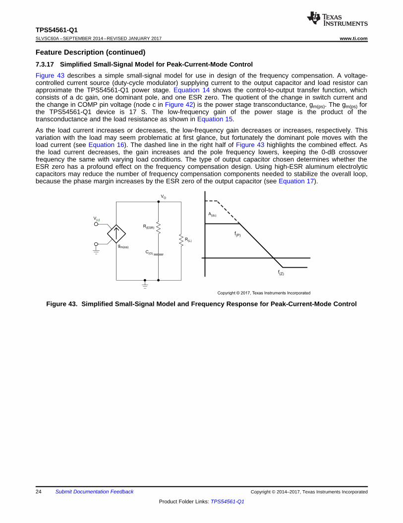
Feature Description (continued)7.3.17 Simplified Small-Signal Model for Peak-Current-Mode ControlFigure 43 describes a simple small-signal model for use in design of the frequency compensation. A voltage-controlled current source (duty-cycle modulator) supplying current to the output capacitor and load resistor canapproximate the TPS54561-Q1 power stage. Equation 14 shows the control-to-output transfer function, whichconsists of a dc gain, one dominant pole, and one ESR zero. The quotient of the change in switch current andthe change in COMP pin voltage (node c in Figure 42) is the power stage transconductance, gm(ps). The gm(ps) forthe TPS54561-Q1 device is 17 S. The low-frequency gain of the power stage is the product of thetransconductance and the load resistance as shown in Equation 15.
As the load current increases or decreases, the low-frequency gain decreases or increases, respectively. Thisvariation with the load may seem problematic at first glance, but fortunately the dominant pole moves with theload current (see Equation 16). The dashed line in the right half of Figure 43 highlights the combined effect. Asthe load current decreases, the gain increases and the pole frequency lowers, keeping the 0-dB crossoverfrequency the same with varying load conditions. The type of output capacitor chosen determines whether theESR zero has a profound effect on the frequency compensation design. Using high-ESR aluminum electrolyticcapacitors may reduce the number of frequency compensation components needed to stabilize the overall loop,because the phase margin increases by the ESR zero of the output capacitor (see Equation 17).
Figure 43. Simplified Small-Signal Model and Frequency Response for Peak-Current-Mode Control

Vref
VO
R(HS)
R(COMP)
C(ZERO)
C(POLE)
R(LS)
C(OEA)
gm(ea) COMP
FBType 2A Type 2B Type 1
R(OEA)
R(COMP)
C(ZERO)
C(POLE)
b
a
c
Copyright © 2016, Texas Instruments Incorporated
(Z)(O) (ESR)
1f
C R 2=
´ ´ p
(P)(O) (L)
1f
C R 2=
´ ´ p
(dc) m(ps) (L)A g R= ´
(Z)O(dc)
(C)
(P)
s1
2 fVA
V s1
2 f
æ ö+ç ÷
ç ÷p ´è ø= ´æ ö
+ç ÷ç ÷p ´è ø
25
TPS54561-Q1www.ti.com SLVSC60A –SEPTEMBER 2014–REVISED JANUARY 2017
Product Folder Links: TPS54561-Q1
Submit Documentation FeedbackCopyright © 2014–2017, Texas Instruments Incorporated
Feature Description (continued)
(14)
(15)
(16)
(17)
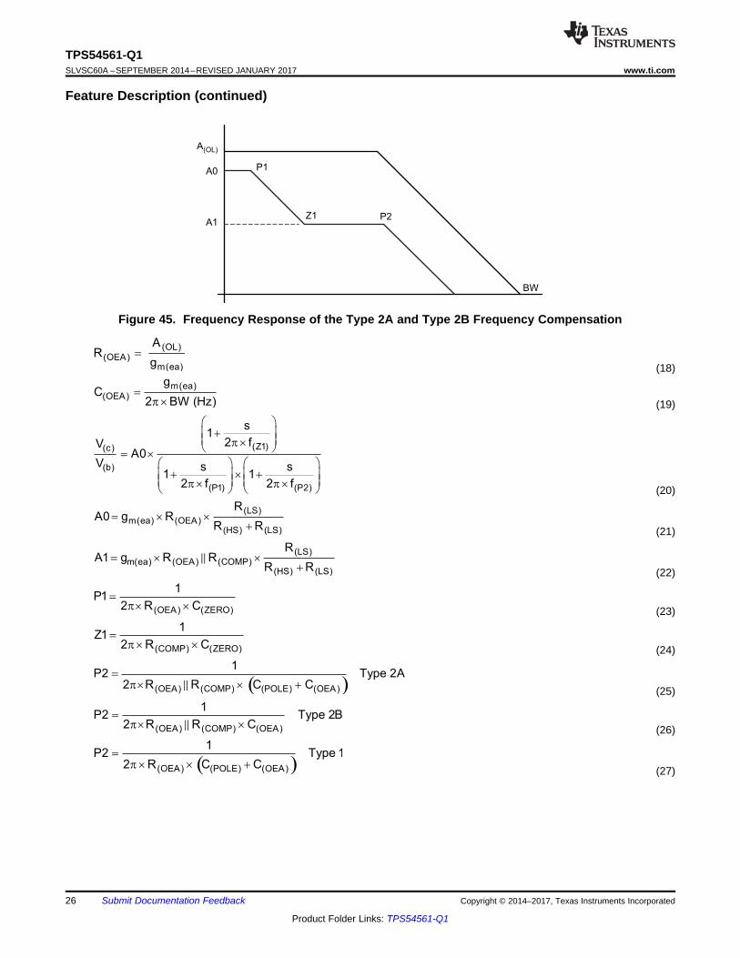
7.3.18 Small-Signal Model for Frequency CompensationThe TPS54561-Q1 uses a transconductance amplifier for the error amplifier and supports three of the commonly-used frequency-compensation circuits. Figure 44 shows compensation circuits of Type 2A, Type 2B, and Type 1.Implementation of Type 2 circuits is typically in high-bandwidth power-supply designs using low-ESR outputcapacitors. The Type 1 circuit is good for the power-supply designs using high-ESR aluminum electrolytic ortantalum capacitors. Equation 18 and Equation 19 relate the frequency response of the amplifier to the small-signal model in Figure 44. Modeling of the open-loop gain and bandwidth uses R(OEA) and C(OEA), as shown inFigure 44. See the application section for a design example using a Type 2A network with a low-ESR outputcapacitor.
This data sheet includes Equation 18 through Equation 27 as a reference. An alternative is to use WEBENCHsoftware tools to create a design based on the power-supply requirements.
Figure 44. Types of Frequency Compensation
( )(OEA) (POLE) (OEA)
1P2 Type 1
2 R C C=
p ´ ´ +
(OEA) (COMP) (OEA)
1P2 Type 2B
2 R R C=
p´ ´P
( )(OEA) (COMP) (POLE) (OEA)
1P2 Type 2A
2 R R C C=
p´ ´ +P
(COMP) (ZERO)
1Z1
2 R C=
p ´ ´
(OEA) (ZERO)
1P1
2 R C=
p´ ´
(LS)m(ea) (OEA) (COMP)
(HS) (LS)
RA1 g R R
R R= ´ ´
+
P
(LS)m(ea) (OEA)
(HS) (LS)
RA0 g R
R R= ´ ´
+
(Z1)(c)
(b)
(P1) (P2)
s1
2 fVA0
V s s1 1
2 f 2 f
æ ö+ç ÷
ç ÷p ´è ø= ´æ ö æ ö
+ ´ +ç ÷ ç ÷ç ÷ ç ÷p ´ p ´è ø è ø
m(ea)(OEA)
gC
2 BW (Hz)=
p ´
(OL)(OEA)
m(ea)
AR
g=
A0
A1
P1
Z1 P2
A(OL)
BW
26
TPS54561-Q1SLVSC60A –SEPTEMBER 2014–REVISED JANUARY 2017 www.ti.com
Product Folder Links: TPS54561-Q1
Submit Documentation Feedback Copyright © 2014–2017, Texas Instruments Incorporated
Feature Description (continued)
Figure 45. Frequency Response of the Type 2A and Type 2B Frequency Compensation
(18)
(19)
(20)
(21)
(22)
(23)
(24)
(25)
(26)
(27)

27
TPS54561-Q1www.ti.com SLVSC60A –SEPTEMBER 2014–REVISED JANUARY 2017
Product Folder Links: TPS54561-Q1
Submit Documentation FeedbackCopyright © 2014–2017, Texas Instruments Incorporated
7.4 Device Functional Modes
7.4.1 Operation With VI = < 4.5 V (Minimum VDD)TI recommends operating the TPS54561-Q1 device with input voltages above 4.5 V. The typical VDD UVLOthreshold is 4.3 V, and the device may operate at input voltages down to the UVLO voltage. At input voltagesbelow the actual UVLO voltage, the device does not switch. If an external resistor divider pulls the EN pin up toVDD or EN pin is floating, when VDD passes the UVLO threshold the device becomes active. Switching begins,and the soft-start sequence initiates. The TPS54561-Q1 device starts at the soft-start time determined by theexternal capacitance on the SS/TR pin.
7.4.2 Operation With EN ControlThe enable threshold voltage is 1.2 V typical. With EN held below that voltage, the device shuts down andswitching stops even if VDD is above its UVLO threshold. The IC quiescent current decreases in this state. Afterincreasing the EN pin voltage above the threshold while VDD is above its UVLO threshold, the device becomesactive. Switching resumes and the soft-start sequence begins. The TPS54561-Q1 device starts at the soft-starttime determined by the external capacitance at the SS/TR pin.

VI
GND
ENGND
7 V to 60 V
2.2µFC1
2.2µFC2
2.2µFC3
GND
GND
GND
90.9kR2
442kR1
GND
TP1
TP2
12
J3
12
J4
GND
2.2µFC10
1
2
J2
21
+C11
DNP
0.01µFC13
PWRGD
TP10
FB
BOOT1
VDD2
EN3
SS/TR4
RT/CLK5
FB6
COMP7
GND8
SW9
PWRGD10
PAD
U1
TPS54561-Q1
243kR3
16.9kR4
47pFC8
4700pFC5
12
J5
SS/TRGND
GND
SS/TR
GND
SS/TR
0.1µF
C4
5 V @ 5 A
VO
GND
47µFC9
47µFC7
47µFC6
GND
GND
49.9R7
53.6kR5
10.2kR6
TP6
TP8
TP4
TP7TP5
TP3
7.2µH
L1
7447798720
1
2
J1
21
+ C12DNP
13
2
D1PDS760-13
FB
PWRGD PULLUP
TP91.00k
R8
Copyright © 2016, Texas Instruments Incorporated
28
TPS54561-Q1SLVSC60A –SEPTEMBER 2014–REVISED JANUARY 2017 www.ti.com
Product Folder Links: TPS54561-Q1
Submit Documentation Feedback Copyright © 2014–2017, Texas Instruments Incorporated
8 Application and Implementation
NOTEInformation in the following applications sections is not part of the TI componentspecification, and TI does not warrant its accuracy or completeness. TI’s customers areresponsible for determining suitability of components for their purposes. Customers shouldvalidate and test their design implementation to confirm system functionality.
8.1 Application InformationThe TPS54561-Q1 device is a 60-V, 5-A, step-down regulator with an integrated high-side MOSFET. This devicetypically converts a higher dc voltage to a lower dc voltage with a maximum available output current of 5 A.Example applications are: 12-V, 24-V and 48-V industrial, automotive and communication power systems. Usethe following design procedure to select component values for the TPS54561-Q1 device. This procedureillustrates the design of a high-frequency switching regulator using ceramic output capacitors. The Excel™spreadsheet (SLVC452) located on the product page can help on all calculations. Alternatively, use theWEBENCH software to generate a complete design. The WEBENCH software uses an iterative designprocedure and accesses a comprehensive database of components when generating a design. This sectionpresents a simplified discussion of the design process.
8.2 Typical Application
Figure 46. 5-V Output TPS54561-Q1 Design Example
8.2.1 Design RequirementsThis guide illustrates the design of a high-frequency switching regulator using ceramic output capacitors. Thedesigner must know a few parameters in order to start the design process. Determination of these requirementsis typically at the system level. This example design uses the following known parameters:

(SW_skip)
1 5 A 11 m 5 V 0.7 Vf max 955 kHz
100 ns 60 V 5 A 87 m 0.7 V
æ ö´ W + += ´ =ç ÷
- ´ W +è ø
29
TPS54561-Q1www.ti.com SLVSC60A –SEPTEMBER 2014–REVISED JANUARY 2017
Product Folder Links: TPS54561-Q1
Submit Documentation FeedbackCopyright © 2014–2017, Texas Instruments Incorporated
Typical Application (continued)DESIGN PARAMETER EXAMPLE VALUE
Output voltage (VO) 5 VTransient response, 1.25-A to 3.75-A load step ΔVO = ±4 %Maximum output current (IO) 5 AInput voltage (VI) 12 V nominal, 7 V to 60 VOutput voltage ripple (VO(RIPPLE)) 0.5% of VO
Start input voltage (rising VI) 6.5 VStop input voltage (falling VI) 5 V
8.2.2 Detailed Design Procedure
8.2.2.1 Custom Design with WEBENCH® ToolsClick here to create a custom design using the TPS54561-Q1 device with the WEBENCH® Power Designer.1. Start by entering your VIN, VOUT, and IOUT requirements.2. Optimize your design for key parameters like efficiency, footprint and cost using the optimizer dial and
compare this design with other possible solutions from Texas Instruments.3. The WEBENCH Power Designer provides you with a customized schematic along with a list of materials with
real time pricing and component availability.4. In most cases, you will also be able to:
– Run electrical simulations to see important waveforms and circuit performance– Run thermal simulations to understand the thermal performance of your board– Export your customized schematic and layout into popular CAD formats– Print PDF reports for the design, and share your design with colleagues
5. Get more information about WEBENCH tools at www.ti.com/WEBENCH.
8.2.2.2 Selecting the Switching FrequencyThe first step is to choose a switching frequency for the regulator. Typically, the designer uses the highestswitching frequency possible because this produces the smallest solution size. High switching frequency allowsfor lower-value inductors and smaller output capacitors compared to a power supply that switches at a lowerfrequency. Several factors including the minimum controllable on-time of the internal power switch, the inputvoltage, the output voltage, and the frequency-foldback protection limit the switching frequency that the designercan select.
Use Equation 12 and Equation 13 to calculate the upper limit of the switching frequency for the regulator.Choose the lower-value result from the two equations. Switching frequencies higher than these values result inpulse-skipping or the lack of overcurrent protection during a short circuit.
The typical minimum controllable on-time, t(ON), is 100 ns for the TPS54561-Q1 device. For this example, theoutput voltage is 5 V and the maximum input voltage is 60 V, which allows for a maximum switch frequency up to955 kHz to avoid pulse skipping from Equation 28. To ensure overcurrent runaway is not a concern during shortcircuits, use Equation 29 to determine the maximum switching frequency for frequency foldback protection. Witha maximum input voltage of 60 V, assuming a diode voltage of 0.7 V, inductor resistance of 11 mΩ, switchresistance of 87 mΩ, a current limit value of 6 A, and short-circuit output voltage of 0.1 V, the maximum switchingfrequency is 1151 kHz.
For this design, choose a lower switching frequency of 400 kHz to operate comfortably below the calculatedmaximums. To determine the timing resistance for a given switching frequency, use Equation 10, or the curve inFigure 6, or the curve in Figure 7. Resistor R3 sets the switching frequency shown in Figure 46. For 400-kHzoperation, the closest standard value resistor is 243 kΩ.
(28)

(RIPPLE)(L) O
I 1.591 AI peak I 5.021 A 5.817 A
2 2= + = + =
( ) ( )( ) ( )
2 22 O I O 2
(L) OI (O) (SW)
V V max V 5 V 60 V 5 V1 1I RMS I 5 A 5.021 A
12 V max L f 12 60 V 7.2 H 400 kHz
æ ö´ - æ ö´ -ç ÷= + ´ = + ´ =ç ÷ç ÷ç ÷´ ´ ´ m ´è øè ø
( ) ( )O I O
(RIPPLE)I (O) (SW)
V V max V 5 V 60 V 5 VI 1.591 A
V max L f 60 V 7.2 H 400 kHz
´ - ´ -= = =
´ ´ ´ m ´
I O O(O)
O (IND) I (SW)
V max V V 60 V 5 V 5 VL min 7.6 H
I K V max f 5 A 0.3 60 V 400 kHz
æ ö æ ö- æ ö æ ö-= ç ÷ ´ ç ÷ = ´ = mç ÷ ç ÷ç ÷ ç ÷´ ´ ´ ´è ø è øè ø è ø
T 1.008
101756R (k ) 242 k
400 (kHz)W = = W
(SW_shift)
8 6 A 11 m 0.1 V 0.7 Vf 1151 kHz
100 ns 60 V 6 A 87 m 0.7 V
æ ö´ W + += ´ =ç ÷
- ´ W +è ø
30
TPS54561-Q1SLVSC60A –SEPTEMBER 2014–REVISED JANUARY 2017 www.ti.com
Product Folder Links: TPS54561-Q1
Submit Documentation Feedback Copyright © 2014–2017, Texas Instruments Incorporated
(29)
(30)
8.2.2.3 Output Inductor Selection (L(O))To calculate the minimum value of the output inductor, use Equation 31.
k(IND) is a ratio that represents the amount of inductor ripple current relative to the maximum output current. Theoutput capacitor filters the inductor ripple current. Therefore, choosing high inductor ripple currents impacts theselection of the output capacitor, because the output capacitor must have a ripple current rating equal to orgreater than the inductor ripple current. In general, the inductor ripple value is at the discretion of the designer.However, the designer may use the following guidelines.
For designs using low-ESR output capacitors such as ceramics, a value as high as k(IND) = 0.3 may be desirable.When using higher-ESR output capacitors, k(IND) = 0.2 yields better results. Because the inductor ripple current ispart of the current-mode PWM control system, the inductor ripple current should always be greater than 150 mAfor stable PWM operation. In a wide-input voltage regulator, choosing a relatively large inductor ripple current isbest to provide sufficient ripple current with the input voltage at the minimum.
For this design example, k(IND) = 0.3 and the calculated inductor value is 7.6 µH. The nearest standard value is7.2 µH. It is important not to exceed both the rms current and saturation-current ratings of the inductor.Equation 33 and Equation 34 calculate the rms and peak inductor current. For this design, the rms inductorcurrent is 5.021 A and the peak inductor current is 5.817 A. The chosen inductor has an rms current rating of 6 Aand a saturation current rating of 7.9 A.
As the equation set demonstrates, lowering ripple currents reduces the output voltage ripple of the regulator butrequires a larger value of inductance. Selecting higher ripple currents increases the output-voltage ripple of theregulator but allows for a lower inductance value.
The current flowing through the inductor is the inductor ripple current plus the output current. During power up,faults, or transient load conditions, the inductor current can increase above the peak inductor current levelcalculated previously. In transient conditions, the inductor current can increase up to the switch-current limit ofthe device. For this reason, the most-conservative design approach is to choose an inductor with a saturationcurrent rating equal to or greater than the switch-current limit of the TPS54561-Q1 device, which is nominally 7.5A.
(31)
spacer
(32)
spacer
(33)
spacer
(34)

( ) ( )
( ) ( )( )( )
2 22 2
OH OL
(O) (O) 2 2 2 2
(P) (int)
I I 3.75 A 1.25 AC L 7.2 H 44.1 F
5.2 V 5 VV V
æ ö-ç ÷ -è ø> ´ = m ´ = mæ ö --ç ÷è ø
O(O)
(SW) O
2 I 2 2.5 AC 62.5 μF
f V 400 kHz 0.2 V
´ D ´> = =
´ D ´
31
TPS54561-Q1www.ti.com SLVSC60A –SEPTEMBER 2014–REVISED JANUARY 2017
Product Folder Links: TPS54561-Q1
Submit Documentation FeedbackCopyright © 2014–2017, Texas Instruments Incorporated
8.2.2.4 Output CapacitorThere are three primary considerations for selecting the value of the output capacitor. The output capacitordetermines the modulator pole, the output voltage ripple, and the regulator response to a large change in loadcurrent. It is necessary to select the output capacitance based on the most-stringent of these three criteria.
The desired response to a large change in the load current is the first criterion. The output capacitor must supplythe increased load current until the regulator responds to the load step. The regulator does not respondimmediately to a large, fast increase in the load current such as transitioning from no load to a full load. Theregulator usually needs two or more clock cycles for the control loop to sense the change in output voltage andadjust the peak switch current in response to the higher load. The output capacitance must be large enough tosupply the difference in current for two clock cycles to maintain the output voltage within the specified range.Equation 35 shows the minimum output capacitance necessary, where ΔIO is the change in output current, f(sw) isthe regulator switching frequency, and ΔVO is the allowable change in the output voltage. For this example, thetransient load response specification is 4% change in VO for a load step from 1.25 A to 3.75 A. Therefore, ΔIO is3.75 A – 1.25 A = 2.5 A, and ΔVO = 4% × 5 V = 0.2 V. Using these numbers gives a minimum capacitance of62.5 µF. This value does not take the ESR of the output capacitor into account in the output voltage change. Forceramic capacitors, the ESR is usually small enough to ignore. Aluminum electrolytic and tantalum capacitorshave higher ESR, and load-step calculations must include the ESR term.
Sizing of the output capacitor must be such as to absorb energy stored in the inductor when transitioning from ahigh to low load current. The catch diode of the regulator cannot sink current, so energy stored in the inductorcan produce an output voltage overshoot when the load current rapidly decreases. Figure 51 shows a typicalload-step response. The excess energy absorbed in the output capacitor increases the voltage on the capacitor.Sizing of the capacitor must be such as to maintain the desired output voltage during these transient periods.Equation 36 calculates the minimum capacitance required to keep the output voltage overshoot to a desiredvalue, where L(O) is the value of the inductor, IOH is the output current under heavy load, IOL is the output underlight load, VP is the peak output voltage, and V(int) is the initial voltage. For this example, the worst-case load stepis from 3.75 A to 1.25 A. The output voltage increases during this load transition, and the stated maximum in ourspecification is 4% of the output voltage. This makes V(P) = 1.04 × 5 V = 5.2 V. V(int) is the initial capacitor voltagewhich is the nominal output voltage of 5 V. Using these numbers in Equation 36 yields a minimum capacitance of44.1 µF.
Equation 37 calculates the minimum output capacitance needed to meet the output-voltage ripple specification,where f(SW) is the switching frequency, VO(RIPPLE) is the maximum allowable output voltage ripple, and IO(RIPPLE) isthe inductor ripple current. Equation 37 yields 19.9 µF.
Equation 38 calculates the maximum ESR an output capacitor can have to meet the output voltage ripplespecification. Equation 38 indicates the ESR should be less than 15.7 mΩ.
The most stringent criterion for the output capacitor is 62.5 µF, required to maintain the output voltage withinregulation tolerance during a load transient.
Capacitance de-ratings for aging, temperature, and dc bias increase this minimum value. For this example, theselection is three 47-µF, 10-V ceramic capacitors with 5 mΩ of ESR. The derated capacitance is 87.4 µF, wellabove the minimum required capacitance of 62.5 µF.
Capacitors generally have a maximum ripple-current rating. Filtering a ripple current equal to or below thatmaximum ripple current does not degrade capacitor reliability. Some capacitor data sheets specify the root-mean-square (rms) value of the maximum ripple current. Use Equation 39 to calculate the rms ripple current thatthe output capacitor must support. For this example, Equation 39 yields 459 mA.
(35)
(36)

( ) ( )
( ) ( )
2
I O O (d) ( j) (SW) I (d)
(D)I
2
V V I V C f V VP
V 2
12 V 5 V 5 A 0.52 V 180 pF 400 kHz 12 V 0.52 V1.65 W
12 V 2
- ´ ´ ´ ´ += + =
- ´ ´ ´ ´ ++ =
( ) ( )O I O
(CO)
I (O) (SW)
V V min V 5 V 60 V 5 VI RMS 459 mA
12 V min L f 12 60 V 7.2 H 400 kHz
´ - ´ -= = =
´ ´ ´ ´ ´ m ´
O(RIPPLE)(ESR)
O(RIPPLE)
V 25 mVR 15.7 m
I 1.591 A< = = W
(O)(SW) O(RIPPLE)
O(RIPPLE)
1 1 1 1C 19.9 F
8 f 8 400 kHz 25 mVV
1.591 AI
> ´ = ´ = m´ ´æ ö æ ö
ç ÷ ç ÷ç ÷ è øè ø
32
TPS54561-Q1SLVSC60A –SEPTEMBER 2014–REVISED JANUARY 2017 www.ti.com
Product Folder Links: TPS54561-Q1
Submit Documentation Feedback Copyright © 2014–2017, Texas Instruments Incorporated
(37)
(38)
(39)
8.2.2.5 Catch DiodeThe TPS54561-Q1 device requires an external catch diode between the SW pin and GND. The selected diodemust have a reverse voltage rating equal to or greater than maximum input voltage. The peak current rating ofthe diode must be greater than the maximum inductor current. Schottky diodes are typically a good choice for thecatch diode because of the low forward voltage of these diodes. The lower the forward voltage of the diode, thehigher the efficiency of the regulator.
Typically, diodes with higher voltage and current ratings have higher forward voltages. A diode with a minimum of60-V reverse voltage is preferable, to allow input voltage transients up to the rated voltage of the TPS54561-Q1device.
For the example design, select the Schottky diode for its lower forward voltage and good thermal characteristicscompared to smaller devices. The typical forward voltage of the diode is 0.52 V at 5 A.
One must select the diode with an appropriate power rating. The diode conducts the output current during theoff-time of the internal power switch. The off-time of the internal switch is a function of the maximum inputvoltage, the output voltage, and the switching frequency. Multiplying the output current during the off-time withthe forward voltage of the diode can calculate the instantaneous conduction losses of the diode. At higherswitching frequencies, take the ac losses of the diode into account. The ac losses of the diode are because ofthe charging and discharging of the junction capacitance, and also of reverse-recovery charge. Use Equation 40to calculate the total power dissipation, including conduction losses and ac losses of the diode.
The selected diode has a junction capacitance of 180 pF. Using Equation 40 with the nominal input voltage of12 V, the total loss in the diode is 1.65 W.
If the power supply spends a significant amount of time at light load currents or in sleep mode, consider using adiode which has a low leakage current and slightly higher forward voltage drop.
(40)
8.2.2.6 Input CapacitorThe TPS54561-Q1 device requires a high-quality ceramic type X5R or X7R input decoupling capacitor with atleast 3 µF of effective capacitance. Some applications benefit from additional bulk capacitance. The effectivecapacitance includes any loss of capacitance because of dc bias effects. The voltage rating of the input capacitormust be greater than the maximum input voltage. The capacitor must also have a ripple-current rating greaterthan the maximum input current ripple of the TPS54561-Q1 device. Use Equation 41 to calculate the input ripplecurrent.
The value of a ceramic capacitor varies significantly with temperature and the dc bias applied to the capacitor.Selecting a dielectric material that is more stable over temperature can minimize the capacitance variationsbecause of temperature. The usual selection for capacitors in a switching regulator is X5R or X7R ceramicdielectric, because they have a high capacitance-to-volume ratio and are fairly stable over temperature. Theinput capacitor selection must also consider the dc bias. The effective value of a capacitor decreases as the dcbias across a capacitor increases.

(SS) (SS)
ref
t (ms) I ( A) 3.5 ms 1.7 AC13 9.3 nF
V (V) 0.8 0.8 V 0.8
´ m ´ m= = =
´ ´
(O) O(SS)
(SS)
C V 0.8t
I
´ ´
>
OI
(I) (SW)
I 0.25 5 A 0.25V 355 mV
C f 8.8 F 400 kHz
´ ´D = = =
´ m ´
I OO(CI) O
I I
V min VV 5 V 7 V 5 VI RMS I 5 A 2.26 A
V min V min 7 V 7 V
æ ö- æ ö-= ´ ´ ç ÷ = ´ ´ =ç ÷ç ÷ è øè ø
33
TPS54561-Q1www.ti.com SLVSC60A –SEPTEMBER 2014–REVISED JANUARY 2017
Product Folder Links: TPS54561-Q1
Submit Documentation FeedbackCopyright © 2014–2017, Texas Instruments Incorporated
This example design requires a ceramic capacitor with at least a 60-V voltage rating to support the maximuminput voltage. Common standard ceramic capacitor voltage ratings include 4 V, 6.3 V, 10 V, 16 V, 25 V, 50 V or100 V. For this example, use four 2.2-µF, 100-V capacitors in parallel.
The input capacitance value determines the input ripple voltage of the regulator. Use Equation 42 to calculate theinput voltage ripple. Using the design example values, IO = 5 A, C(I) = 8.8 µF, f(sw) = 400 kHz, yields an inputvoltage ripple of 355 mV and an rms input ripple current of 2.26 A.
(41)
(42)
8.2.2.7 Soft-Start CapacitorThe soft-start capacitor determines the minimum amount of time for the output voltage to reach its nominalprogrammed value during power up. This is useful if a load requires a controlled voltage slew rate. Adjustablesoft-start is also useful if the output capacitance is large and would require large amounts of current to chargethe capacitor quickly to the output-voltage level. The large currents necessary to charge the output capacitor maymake the TPS54561-Q1 device reach the current limit, or the excessive current draw from the input power supplymay cause the input voltage rail to sag. Limiting the output-voltage slew rate solves both of these problems.
The soft-start time must be long enough to allow the regulator to charge the output capacitor up to the outputvoltage without drawing excessive current. Use Equation 43 to find the minimum soft-start time, t(SS), necessaryto charge the output capacitor, C(O), from 10% to 90% of the output voltage, VO, with an typical soft-start currentof I(SS). In the example, to charge the effective output capacitance of 87.4 µF up to 5 V with an average current of1 A requires a 0.3-ms soft-start time.
After selecting the soft-start time, calculate the soft-start capacitor value by using Equation 5. For the examplecircuit, the soft-start time is not too critical, because the output capacitor value is 3 × 47 µF, which does notrequire much current to charge to 5 V. The example circuit has the soft-start time set to an arbitrary value of3.5 ms, which requires a 9.3-nF soft-start capacitor, as calculated by Equation 44. For this design, use the next-larger standard value of 10 nF.
(43)
(44)
8.2.2.8 Bootstrap Capacitor SelectionThe TPS54561-Q1 device requires a 0.1-µF ceramic capacitor connected between the BOOT and SW pins forproper operation. The recommendation is a ceramic capacitor with X5R or better grade dielectric. The capacitorshould have a 10-V or higher voltage rating.

(SW)(CO2) (P,mod)
f 400 kHzf f 1821Hz 19.1kHz
2 2= ´ = ´ =
(CO1) (P,mod) (Z,mod)f f f 1821Hz 1090 kHz 44.6 kHz= ´ = ´ =
(Z,mod)(ESR) (O)
1 1f 1090 kHz
2 R C 2 1.67 m 87.4 F= = =
p ´ ´ p ´ W ´ m
O(P,mod)
O (O)
I max 5 Af 1821Hz
2 V C 2 5 V 87.4 F= = =
p ´ ´ p ´ ´ m
OV 0.8 V 5 V 0.8 VR5 R6 10.2 k 53.55 k
0.8 V 0.8 V
æ ö æ ö- -= ´ = W ´ = Wç ÷ ç ÷
è ø è ø
(EN) th
(START) (EN) th(1)
(UVLO1)
V 1.2 VR2 90.97 k
V V 6.5 V 1.2 V1.2 AI
442 kR
= = = W- -
+ m+W
(START) (STOP)
(HYS)
V V 6.5 V 5 VR1 441.18 k
I 3.4 A
- -= = = W
m
34
TPS54561-Q1SLVSC60A –SEPTEMBER 2014–REVISED JANUARY 2017 www.ti.com
Product Folder Links: TPS54561-Q1
Submit Documentation Feedback Copyright © 2014–2017, Texas Instruments Incorporated
8.2.2.9 Undervoltage Lockout Set PointUsing an external voltage divider on the EN pin of the TPS54561-Q1 device can adjust the undervoltage lockout(UVLO). The UVLO has two thresholds, one for power up when the input voltage is rising and the other for powerdown when the input voltage is falling. For the example design, the TPS54561-Q1 device should turn on andstart switching once the input voltage increases above 6.5 V (UVLO start). After the regulator starts switching, itshould continue to do so until the input voltage falls below 5 V (UVLO stop).
A resistor divider consisting of R(UVLO1) and R(UVLO2) between VI and ground, and connected to the EN pin, canset programmable UVLO threshold voltage. Equation 3 and Equation 4 calculate the resistance valuesnecessary. For the example application, a 442-kΩ resistor between VI and EN (R1) and a 90.9-kΩ resistorbetween EN and ground (R2) are required to produce the 6.5-V start and 5-V stop voltages.
(45)
(46)
8.2.2.10 Output Voltage and Feedback Resistor SelectionThe voltage divider of R5 and R6 sets the output voltage. For the example design, select 10.2 kΩ for R6. UseEquation 2 to calculate R5 as 53.55 kΩ. The nearest standard 1% resistor is 53.6 kΩ. Because of the inputcurrent of the FB pin, the current flowing through the feedback network should be greater than 1 µA to maintainthe output voltage accuracy. A value for R6 of less than 800 kΩ satisfies this requirement. Choosing higherresistor values decreases quiescent current and improves efficiency at low output currents but may alsointroduce noise immunity problems.
(47)
8.2.2.11 CompensationThere are several methods to design compensation for dc-dc regulators. The method presented here is easy tocalculate and ignores the effects of the slope compensation that is internal to the device. Ignoring the slopecompensation causes the actual crossover frequency to be lower than the crossover frequency used in thecalculations. This method assumes the crossover frequency is between the modulator pole and the ESR zeroand the ESR zero is at least 10 times greater the modulator pole.
To get started, calculate the modulator pole, f(P,mod), and the ESR zero, f(Z,mod) using Equation 48 andEquation 49. For output capacitance C(O), use a derated value of 87.4 µF. Use equations Equation 50 andEquation 51 to estimate a starting point for the crossover frequency, f(CO). For the example design, f(P,mod) is 1821Hz and f(Z,mod) is 1090 kHz. Equation 50 is the geometric mean of the modulator pole and the ESR zero, andEquation 51 is the geometric mean of modulator pole and half of the switching frequency. Equation 50 yields44.6 kHz and Equation 51 gives 19.1 kHz. Use the geometric mean value of Equation 50 and Equation 51 for aninitial crossover frequency which is 29.2 kHz. For this example, the target crossover frequency is 30 kHz for animproved transient response.
Next, calculate the compensation components. Use of a resistor in series with a capacitor creates acompensating zero. A capacitor in parallel with these two components forms the compensating pole.
(48)
(49)
(50)
(51)

(SW)
1 1C8 47.1pF
R4 f 16.9 k 400kHz= = =
p´ ´ p´ W ´
(O) (ESR)C R 87.4 F 1.67 mC8 8.64 pF
R4 16.9 k
´ m ´ W= = =
W
(P,mod)
1 1C5 5172 pF
2 R4 f 2 16.9 k 1821Hz= = =
p ´ ´ p ´ W ´
(CO) (O) O
m(ps) ref m(ea)
2 f C V 2 29.2 kHz 87.4 F 5 VR4 16.84 k
g V g 17 S 0.8 V 350 S
æ öæ öp ´ ´ æ ö æ öp ´ ´ m= ´ ç ÷ = ´ = Wç ÷ ç ÷ ç ÷ç ÷ ç ÷´ ´ mè ø è øè ø è ø
35
TPS54561-Q1www.ti.com SLVSC60A –SEPTEMBER 2014–REVISED JANUARY 2017
Product Folder Links: TPS54561-Q1
Submit Documentation FeedbackCopyright © 2014–2017, Texas Instruments Incorporated
To determine the compensation resistor, R4, use Equation 52. Assume the power stage transconductance,gm(ps), is 17 S. The output voltage VO, reference voltage Vref, and amplifier transconductance gm(ea), are 5 V,0.8 V and 350 µS, respectively. Calculated the value for R4 as 16.84 kΩ, and then select a standard value of16.9 kΩ. Use Equation 53 to set the compensation zero to the modulator pole frequency. Equation 53 yields5172 pF for compensating capacitor C5. The selection for this design is 4700 pF.
(52)
(53)
If desired, implement a compensation pole by adding capacitor C8 in parallel with the series combination of R4and C5. Use the larger value calculated from Equation 54 and Equation 55 for C8 to set the compensation pole.The selected value of C8 is 47 pF for this example design.
(54)
(55)
8.2.2.12 Discontinuous Conduction Mode and Eco-mode BoundaryWith an input voltage of 12 V, the example design enters discontinuous-conduction mode when the outputcurrent is less than 408 mA. The power supply enters Eco-mode when the output current is lower than 25.3 mA.The input current draw is 257 µA with no load.

A J JA (tot)T max T max R Pq
= - ´
J A JA (tot)T T R Pq
= + ´
(tot) (COND) (SW) (G) (Q)P P P P P 0.906 W 0.118 W 0.014 W 0.0018 W 1.040 W= + + + = + + + =
(Q) I QP V I 12 V 152 A 0.0018 W= ´ = ´ m =
(G) I g (SW)P V Q f 12 V 3 nC 400 kHz 0.014 W= ´ ´ = ´ ´ =
(SW) I (SW) O rP V f I t 12 V 400 kHz 5 A 4.9 ns 0.118 W= ´ ´ ´ = ´ ´ ´ =
( )2 2O(COND) O DS(on)
I
V 5 VP I r 5 A 87 m 0.906 W
V 12 V
æ ö æ ö= ´ ´ ç ÷ = ´ W ´ =ç ÷ç ÷ è øè ø
36
TPS54561-Q1SLVSC60A –SEPTEMBER 2014–REVISED JANUARY 2017 www.ti.com
Product Folder Links: TPS54561-Q1
Submit Documentation Feedback Copyright © 2014–2017, Texas Instruments Incorporated
8.2.2.13 Power Dissipation EstimateThe following formulas show how to estimate the TPS54561-Q1 device power dissipation under continuousconduction mode (CCM) operation. These equations are not suitable if the device operates in discontinuousconduction mode (DCM).
The power dissipation of the IC includes conduction loss (P(COND)), switching loss (P(SW)), gate drive loss (P(G))and supply current loss (P(Q)). Example calculations are shown with the 12-V nominal input voltage of theexample design.1. Conduction loss
where• IO is the output current (A)• rDS(on) is the on-resistance of the high-side MOSFET (Ω)• VO is the output voltage (V)• VI is the input voltage (V) (56)
2. Switching loss
where• f(SW) is the switching frequency (Hz)• tr is the SW pin voltage rise time, estimated by tr = VDD (V) × 0.16 (ns/V) + 3 (ns) (57)
3. Gate drive loss
where• Qg is the total gate charge of the internal MOSFET (58)
4. Quiescent current loss
where• IQ is the operating nonswitching supply current (59)
Therefore,
(60)
For given TA,
where• TJ is the junction temperature (°C)• TA is the ambient temperature (°C)• RθJA is the thermal resistance of the package (°C/W)• P(tot) is the total device power dissipation (W) (61)
For given TJmax = 150°C
where• TAmax is maximum ambient temperature (°C)• TJmax is maximum junction temperature (°C) (62)
Additional power losses occur in the regulator circuit because of the inductor ac and dc losses, the catch diodeand PCB trace resistance. All of these losses impact the overall efficiency of the regulator.

Output Current (A)
Am
bien
t Tem
pera
ture
(qC
)
0 0.5 1 1.5 2 2.5 3 3.5 4 4.5 520
30
40
50
60
70
80
90
D049
18 V24 V36 V48 V60 V
Output Current (A)
Am
bien
t Tem
pera
ture
(qC
)
0 0.5 1 1.5 2 2.5 3 3.5 4 4.5 520
30
40
50
60
70
80
90
D050
400 LFM200 LFM100 LFMNat. Conv.
Output Current (A)
Am
bien
t Tem
pera
ture
(qC
)
0 0.5 1 1.5 2 2.5 3 3.5 4 4.5 520
30
40
50
60
70
80
90
D047
8 V12 V24 V36 V48 V60 V
Output Current (A)
Am
bien
t Tem
pera
ture
(q)
0 0.5 1 1.5 2 2.5 3 3.5 4 4.5 520
30
40
50
60
70
80
90
D048
8 V12 V24 V36 V48 V60 V
37
TPS54561-Q1www.ti.com SLVSC60A –SEPTEMBER 2014–REVISED JANUARY 2017
Product Folder Links: TPS54561-Q1
Submit Documentation FeedbackCopyright © 2014–2017, Texas Instruments Incorporated
8.2.3 Safe Operating Area
Figure 47 through Figure 50 show the safe operating area (SOA) of the device for 3.3-V, 5-V, and 12-V outputsand varying amounts of forced air flow applications. The temperature derating curves represent the conditions atwhich the TPS54561-Q1 device, PCB and the output Inductor are at or below the manufacturer’s maximumoperating temperatures. Figure 47, through Figure 50 doesn't consider the impact from the catch diode thermalperformance. For higher reliability, TI uses 125 °C as the temperature limit for TPS54561-Q1 device onFigure 47, through Figure 50. Derating limits apply to devices soldered directly to a double-sided PCB with 2 oz.copper, similar to the board on TPS54561EVM-555 evaluation module.
Pay careful attention to the other components chosen for the design, especially the catch diode. In mostapplications, the catch diode limits the thermal performance. When operating at high duty cycles or at a higherswitching frequency, the thermal performance of the TPS54561-Q1 device can become the limiting factor.
VO = 3.3 V Natural Convectionf(SW) = 400 kHz
Figure 47. 3.3-V Outputs
VO = 5 V Natural Convectionf(SW) = 400 kHz
Figure 48. 5-V Outputs
VO = 12 V Natural Convectionf(SW) = 600 kHz
Figure 49. 12-V Outputs
VI = 48 V Air flow direction: L1 to output terminalVO = 12 V f(SW) = 600 kHz
Figure 50. Air Flow Conditions
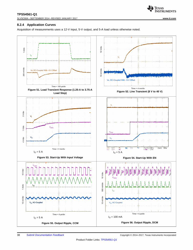
10
mV
/div
10
V/d
iv
V(SW)
V , AC-CoupledO
Time = 4 µs/div
I(L)
1A
/div
10
mV
/div
10
V/d
iv
V(SW)
Time = 4 µs/div
I(L)50
0 m
A/d
iv
V , AC-CoupledO
VI
VO
V(EN)
4 V
/div
5 V
/div
VI
VO
Time = 2 ms/div
V(EN)
1 V
/div
10
mV
/div
10
V/d
iv
VI
Vo, DC-Coupled With –5-V Offset
Time = 4 ms/divTime = 100 µs/div
200 m
V/d
iv1
A/d
iv
IO
Vo, DC-Coupled With –5-V Offset
38
TPS54561-Q1SLVSC60A –SEPTEMBER 2014–REVISED JANUARY 2017 www.ti.com
Product Folder Links: TPS54561-Q1
Submit Documentation Feedback Copyright © 2014–2017, Texas Instruments Incorporated
8.2.4 Application CurvesAcquisition of measurements uses a 12-V input, 5-V output, and 5-A load unless otherwise noted.
Figure 51. Load Transient Response (1.25-A to 3.75-ALoad Step) Figure 52. Line Transient (8 V to 40 V)
IO = 5 A
Figure 53. Start-Up With Input Voltage
IO = 5 A
Figure 54. Start-Up With EN
IO = 5 A
Figure 55. Output Ripple, CCM
IO = 100 mA
Figure 56. Output Ripple, DCM

Time = 40 s/divm
2 V
/div
VI
VO
Time = 40 s/divm
2 V
/div
VI
VO
10
mV
/div
10
V/d
iv
V(SW)
V , AC-CoupledI
Time = 4 µs/div
I(L)
50
0 m
A/d
iv
20 m
V/d
iv2 V
/div
V(SW)
VO
Time = 40 µs/div
I(L)
200 m
A/d
iv
10
mV
/div
10
V/d
iv V(SW)
V , AC-CoupledO
Time = 1 ms/div
I(L)
20
0 m
A/d
iv
20
0 m
V/d
iv1
0 V
/div
V(SW)
V , AC-CoupledI
Time = 4 µs/div
I(L)1 m
\A/d
iv
39
TPS54561-Q1www.ti.com SLVSC60A –SEPTEMBER 2014–REVISED JANUARY 2017
Product Folder Links: TPS54561-Q1
Submit Documentation FeedbackCopyright © 2014–2017, Texas Instruments Incorporated
Acquisition of measurements uses a 12-V input, 5-V output, and 5-A load unless otherwise noted.
No load
Figure 57. Output Ripple, Eco-mode
IO = 5 A
Figure 58. Input Ripple, CCM
IO = 100 mA100 mA
Figure 59. Input Ripple, DCM
VI = 5.5 V No loadVO = 5.0 V EN floating
Figure 60. Low-Dropout Operation, Steady State
IO = 100 mA EN floating
Figure 61. Low-Dropout Operation
IO = 1 A EN floating
Figure 62. Low-Dropout Operation

Frequency (Hz)
Gai
n (d
B)
Pha
se (
Deg
rees
)
10 100 1000 10000 100000-60 -180
-40 -120
-20 -60
0 0
20 60
40 120
60 180
D033
GainPhase
Output Current (A)
Out
put V
olta
ge D
evia
tion
(%)
0 1 2 3 4 5-0.1
-0.08
-0.06
-0.04
-0.02
0
0.02
0.04
0.06
0.08
0.1
D034
Output Current (A)
Effi
cien
cy (
%)
0 1 2 3 4 560
65
70
75
80
85
90
95
100
D031
VDD6 V12 V24 V
36 V48 V60 V
Output Current (A)
Effi
cien
cy (
%)
0.001 0.01 0.1 10
10
20
30
40
50
60
70
80
90
100
D032
VDD6 V12 V24 V36 V48 V60 V
Output Current (A)
Effi
cien
cy (
%)
0 1 2 3 4 560
65
70
75
80
85
90
95
100
D029
VDD7 V12 V24 V36 V48 V60 V
Output Current (A)
Effi
cien
cy (
%)
0.001 0.01 0.1 10
10
20
30
40
50
60
70
80
90
100
D030
VDD7 V12 V24 V36 V48 V60 V
40
TPS54561-Q1SLVSC60A –SEPTEMBER 2014–REVISED JANUARY 2017 www.ti.com
Product Folder Links: TPS54561-Q1
Submit Documentation Feedback Copyright © 2014–2017, Texas Instruments Incorporated
Acquisition of measurements uses a 12-V input, 5-V output, and 5-A load unless otherwise noted.
f(SW) = 400 kHz VO = 5 V
Figure 63. Efficiency vs Load Current
f(SW) = 400 kHz VO = 5 V
Figure 64. Light-Load Efficiency
f(SW) = 400 kHz VO = 3.3 V
Figure 65. Efficiency vs Load Current
f(SW) = 400 kHz VO = 3.3 V
Figure 66. Light-Load Efficiency
f(SW) = 400 kHz VI = 12 V VO = 5 VIO = 5 A
Figure 67. Overall Loop Frequency Response
f(SW) = 400 kHz VI = 12 V VO = 5 V
Figure 68. Regulation vs Load Current

SWVDD
GND
BOOT
FB
COMP
TPS54561-Q1
EN
RT/CLK
C(POLE)
C(ZERO)
R(COMP)
R(RT)
C(O)
L(O)
C(BOOT)C(I)
R(HS)
C(VDD)
C(SS)
VI
VO
+
+
GND
R(LS)
PWRGD
SS/TR
Copyright © 2017, Texas Instruments Incorporated
Input Voltage (V)
Out
put V
olta
ge D
evia
tion
(%)
5 10 15 20 25 30 35 40 45 50 55 60-0.1
-0.08
-0.06
-0.04
-0.02
0
0.02
0.04
0.06
0.08
0.1
D035
41
TPS54561-Q1www.ti.com SLVSC60A –SEPTEMBER 2014–REVISED JANUARY 2017
Product Folder Links: TPS54561-Q1
Submit Documentation FeedbackCopyright © 2014–2017, Texas Instruments Incorporated
Acquisition of measurements uses a 12-V input, 5-V output, and 5-A load unless otherwise noted.
f(SW) = 400 kHz IO = 2.5 A VO = 5 V
Figure 69. Regulation vs Input Voltage
8.2.5 Inverting Power SupplyOne use of the TPS54561-Q1 is to convert a positive input voltage to a negative output voltage. Idealapplications are amplifiers requiring a negative power supply. For a more-detailed example, see Create anInverting Power Supply From a Step-Down Regulator, application report SLVA317.
Figure 70. TPS54561-Q1 Inverting Power Supply Based on Application Report SLVA317

SWVDD
GND
BOOT
FB
COMP
TPS54561-Q1
RT/CLK
GND
VI
VO+
VO–
C(O)–
T(O)
C(O)+
+
++
C(I) C(BOOT)
R(HS)
R(LS)
R(COMP)
C(POLE)
C(VDD)
C(SS)
C(ZERO)R(RT)
EN
PWRGD
SS/TR
Copyright © 2016, Texas Instruments Incorporated
42
TPS54561-Q1SLVSC60A –SEPTEMBER 2014–REVISED JANUARY 2017 www.ti.com
Product Folder Links: TPS54561-Q1
Submit Documentation Feedback Copyright © 2014–2017, Texas Instruments Incorporated
Acquisition of measurements uses a 12-V input, 5-V output, and 5-A load unless otherwise noted.8.2.6 Split-Rail Power SupplyAnother use of the TPS54561-Q1 device is to convert a positive input voltage to a split-rail positive- andnegative-output voltage by using a coupled inductor. Ideal applications are amplifiers requiring a split-railpositive- and negative-voltage power supply. For a more-detailed example, see Creating a Split-Rail PowerSupply With a Wide Input Voltage Buck Regulator, application report SLVA369.
Figure 71. TPS54561-Q1 Split-Rail Power Supply Based on Application Report SLVA369
9 Power Supply Recommendations
The design of the device is for operation from an input voltage supply range between 4.5 V and 60 V. Goodregulation of this input supply is essential. If the input supply is more distant than a few inches from theTPS54561-Q1 converter, the circuit may require additional bulk capacitance besides the ceramic bypasscapacitors. An electrolytic capacitor with a value of 100 µF is a typical choice.

BOOT
VDD
EN
RT/CLK
SW
GND
COMP
FB
Input
Bypass
Capacitor
UVLO
Adjust
Resistors
Frequency
Set Resistor
CompensationNetwork
ResistorDivider
Output
Inductor
Output
Capacitor
VO
VI
Top-SideGround
AreaCatch
Diode
Route boot-capacitortrace on another layer toprovide a wide path forthe top-side ground.
Thermal Via
Signal Via
SS/TR
PWRGD
Soft-Start
Capacitor
43
TPS54561-Q1www.ti.com SLVSC60A –SEPTEMBER 2014–REVISED JANUARY 2017
Product Folder Links: TPS54561-Q1
Submit Documentation FeedbackCopyright © 2014–2017, Texas Instruments Incorporated
10 Layout
10.1 Layout GuidelinesLayout is a critical portion of good power-supply design. There are several signal paths that conduct fast-changing currents or voltages that can interact with stray inductance or parasitic capacitance to generate noiseor degrade performance. See Figure 72 for a PCB layout example.• To reduce parasitic effects, bypass the VDD pin to ground with a low-ESR ceramic bypass capacitor with X5R
or X7R dielectric.• Take care to minimize the loop area formed by the bypass capacitor connections, the VDD pin, and the anode
of the catch diode. Route the SW pin to the cathode of the catch diode and to the output inductor. Becausethe SW connection is the switching node, locate the catch diode and output inductor close to the SW pins,and minimize the area of the PCB conductor to prevent excessive capacitive coupling.
• Tie the GND pin directly to the copper pad under the IC for the exposed thermal pad. Connect this copperpad to internal PCB ground planes using multiple vias directly under the IC.
• For operation at full-rated load, the top-side ground area must provide adequate heat dissipating area.• The RT/CLK pin is sensitive to noise, so locate the RT resistor as close as possible to the IC and route
conductors with minimal lengths of trace.• Figure 72 shows the approximate placement for the additional external components.• It may be possible to obtain acceptable performance with alternate PCB layouts. However, this layout, meant
as a guideline, demonstrably produces good results.
Boxing in the components in the design of Figure 46, the estimated printed-circuit board area is 1.025 in2
(661 mm2). This area does not include test points or connectors. To further reduce the area, use a two-sidedassembly and replace the 0603-sized passives with a smaller-sized equivalent.
10.2 Layout Example
Figure 72. PCB Layout Example
44
TPS54561-Q1SLVSC60A –SEPTEMBER 2014–REVISED JANUARY 2017 www.ti.com
Product Folder Links: TPS54561-Q1
Submit Documentation Feedback Copyright © 2014–2017, Texas Instruments Incorporated
11 Device and Documentation Support
11.1 Device Support
11.1.1 Development SupportFor the TPS54560, TPS54561, and TPS54561-Q1 family Excel design tool, see SLVC452.
11.2 Documentation Support
11.2.1 Related DocumentationFor related documentation, see the following:• Create an Inverting Power Supply From a Step-Down Regulator, SLVA317• Creating a Split-Rail Power Supply With a Wide Input Voltage Buck Regulator, SLVA369• Evaluation Module for the TPS54561 Step-Down Converter, SLVU993• Creating a Universal Car Charger for USB Devices From the TPS54240 and TPS2511, SLVA464
11.2.2 Custom Design with WEBENCH® ToolsClick here to create a custom design using the TPS54561-Q1 device with the WEBENCH® Power Designer.1. Start by entering your VIN, VOUT, and IOUT requirements.2. Optimize your design for key parameters like efficiency, footprint and cost using the optimizer dial and
compare this design with other possible solutions from Texas Instruments.3. The WEBENCH Power Designer provides you with a customized schematic along with a list of materials with
real time pricing and component availability.4. In most cases, you will also be able to:
– Run electrical simulations to see important waveforms and circuit performance– Run thermal simulations to understand the thermal performance of your board– Export your customized schematic and layout into popular CAD formats– Print PDF reports for the design, and share your design with colleagues
5. Get more information about WEBENCH tools at www.ti.com/WEBENCH.
11.3 Receiving Notification of Documentation UpdatesTo receive notification of documentation updates, navigate to the device product folder on ti.com. In the upperright corner, click on Alert me to register and receive a weekly digest of any product information that haschanged. For change details, review the revision history included in any revised document.
11.4 Community ResourcesThe following links connect to TI community resources. Linked contents are provided "AS IS" by the respectivecontributors. They do not constitute TI specifications and do not necessarily reflect TI's views; see TI's Terms ofUse.
TI E2E™ Online Community TI's Engineer-to-Engineer (E2E) Community. Created to foster collaborationamong engineers. At e2e.ti.com, you can ask questions, share knowledge, explore ideas and helpsolve problems with fellow engineers.
Design Support TI's Design Support Quickly find helpful E2E forums along with design support tools andcontact information for technical support.
11.5 TrademarksEco-mode, E2E are trademarks of Texas Instruments.WEBENCH is a registered trademark of Texas Instruments.Excel is a trademark of Microsoft Corporation.

45
TPS54561-Q1www.ti.com SLVSC60A –SEPTEMBER 2014–REVISED JANUARY 2017
Product Folder Links: TPS54561-Q1
Submit Documentation FeedbackCopyright © 2014–2017, Texas Instruments Incorporated
11.6 Electrostatic Discharge CautionThese devices have limited built-in ESD protection. The leads should be shorted together or the device placed in conductive foamduring storage or handling to prevent electrostatic damage to the MOS gates.
11.7 GlossarySLYZ022 — TI Glossary.
This glossary lists and explains terms, acronyms, and definitions.
12 Mechanical, Packaging, and Orderable InformationThe following pages include mechanical, packaging, and orderable information. This information is the most-current data available for the designated devices. This data is subject to change without notice and withoutrevision of this document. For browser-based versions of this data sheet, refer to the left-hand navigation.

PACKAGE OPTION ADDENDUM
www.ti.com 10-Dec-2020
Addendum-Page 1
PACKAGING INFORMATION
Orderable Device Status(1)
Package Type PackageDrawing
Pins PackageQty
Eco Plan(2)
Lead finish/Ball material
(6)
MSL Peak Temp(3)
Op Temp (°C) Device Marking(4/5)
Samples
TPS54561QDPRRQ1 ACTIVE WSON DPR 10 3000 RoHS & Green NIPDAU Level-2-260C-1 YEAR -40 to 125 TPS54561Q
TPS54561QDPRTQ1 ACTIVE WSON DPR 10 250 RoHS & Green NIPDAU Level-2-260C-1 YEAR -40 to 125 TPS54561Q
(1) The marketing status values are defined as follows:ACTIVE: Product device recommended for new designs.LIFEBUY: TI has announced that the device will be discontinued, and a lifetime-buy period is in effect.NRND: Not recommended for new designs. Device is in production to support existing customers, but TI does not recommend using this part in a new design.PREVIEW: Device has been announced but is not in production. Samples may or may not be available.OBSOLETE: TI has discontinued the production of the device.
(2) RoHS: TI defines "RoHS" to mean semiconductor products that are compliant with the current EU RoHS requirements for all 10 RoHS substances, including the requirement that RoHS substancedo not exceed 0.1% by weight in homogeneous materials. Where designed to be soldered at high temperatures, "RoHS" products are suitable for use in specified lead-free processes. TI mayreference these types of products as "Pb-Free".RoHS Exempt: TI defines "RoHS Exempt" to mean products that contain lead but are compliant with EU RoHS pursuant to a specific EU RoHS exemption.Green: TI defines "Green" to mean the content of Chlorine (Cl) and Bromine (Br) based flame retardants meet JS709B low halogen requirements of <=1000ppm threshold. Antimony trioxide basedflame retardants must also meet the <=1000ppm threshold requirement.
(3) MSL, Peak Temp. - The Moisture Sensitivity Level rating according to the JEDEC industry standard classifications, and peak solder temperature.
(4) There may be additional marking, which relates to the logo, the lot trace code information, or the environmental category on the device.
(5) Multiple Device Markings will be inside parentheses. Only one Device Marking contained in parentheses and separated by a "~" will appear on a device. If a line is indented then it is a continuationof the previous line and the two combined represent the entire Device Marking for that device.
(6) Lead finish/Ball material - Orderable Devices may have multiple material finish options. Finish options are separated by a vertical ruled line. Lead finish/Ball material values may wrap to twolines if the finish value exceeds the maximum column width.
Important Information and Disclaimer:The information provided on this page represents TI's knowledge and belief as of the date that it is provided. TI bases its knowledge and belief on informationprovided by third parties, and makes no representation or warranty as to the accuracy of such information. Efforts are underway to better integrate information from third parties. TI has taken andcontinues to take reasonable steps to provide representative and accurate information but may not have conducted destructive testing or chemical analysis on incoming materials and chemicals.TI and TI suppliers consider certain information to be proprietary, and thus CAS numbers and other limited information may not be available for release.
In no event shall TI's liability arising out of such information exceed the total purchase price of the TI part(s) at issue in this document sold by TI to Customer on an annual basis.
PACKAGE OPTION ADDENDUM
www.ti.com 10-Dec-2020
Addendum-Page 2
OTHER QUALIFIED VERSIONS OF TPS54561-Q1 :
• Catalog: TPS54561
NOTE: Qualified Version Definitions:
• Catalog - TI's standard catalog product

TAPE AND REEL INFORMATION
*All dimensions are nominal
Device PackageType
PackageDrawing
Pins SPQ ReelDiameter
(mm)
ReelWidth
W1 (mm)
A0(mm)
B0(mm)
K0(mm)
P1(mm)
W(mm)
Pin1Quadrant
TPS54561QDPRRQ1 WSON DPR 10 3000 330.0 12.4 4.25 4.25 1.15 8.0 12.0 Q2
TPS54561QDPRTQ1 WSON DPR 10 250 180.0 12.4 4.25 4.25 1.15 8.0 12.0 Q2
PACKAGE MATERIALS INFORMATION
www.ti.com 5-Feb-2016
Pack Materials-Page 1

*All dimensions are nominal
Device Package Type Package Drawing Pins SPQ Length (mm) Width (mm) Height (mm)
TPS54561QDPRRQ1 WSON DPR 10 3000 367.0 367.0 35.0
TPS54561QDPRTQ1 WSON DPR 10 250 210.0 185.0 35.0
PACKAGE MATERIALS INFORMATION
www.ti.com 5-Feb-2016
Pack Materials-Page 2

www.ti.com
PACKAGE OUTLINE
C
10X 0.350.25
3 0.1
2.6 0.1
0.80.7
8X 0.8
10X 0.50.3
(0.1) TYP
2X3.2
0.050.00
B 4.13.9
A
4.13.9
(0.2)
WSON - 0.8 mm max heightDPR0010APLASTIC SMALL OUTLINE - NO LEAD
4218856/B 01/2021
PIN 1 INDEX AREA
SEATING PLANE
0.08 C
1
5 6
10
PIN 1 ID0.1 C A B0.05 C
THERMAL PADEXPOSED
SEE ALTERNATIVELEAD DETAIL
11
NOTES: 1. All linear dimensions are in millimeters. Any dimensions in parenthesis are for reference only. Dimensioning and tolerancing per ASME Y14.5M. 2. This drawing is subject to change without notice. 3. The package thermal pad must be soldered to the printed circuit board for thermal and mechanical performance.
SCALE 3.000
20.000
FULL R
ALTERNATIVE LEADDETAIL
BOTTOM VIEW SIDE VIEW

www.ti.com
EXAMPLE BOARD LAYOUT
(R0.05) TYP
8X (0.8)
0.07 MINALL AROUND0.07 MAX
ALL AROUND
(2.6)
(3.8)
10X (0.3)
10X (0.6)
(3)
( 0.2) VIATYP
(1.25)
(1.05)
WSON - 0.8 mm max heightDPR0010APLASTIC SMALL OUTLINE - NO LEAD
4218856/B 01/2021
SYMM
1
56
10
SYMM
LAND PATTERN EXAMPLEEXPOSED METAL SHOWN
SCALE:15X
11
NOTES: (continued) 4. This package is designed to be soldered to a thermal pad on the board. For more information, see Texas Instruments literature number SLUA271 (www.ti.com/lit/slua271).
SOLDER MASKOPENINGSOLDER MASK
METAL UNDER
SOLDER MASKDEFINED
EXPOSEDMETAL
METALEDGE
SOLDER MASKOPENING
SOLDER MASK DETAILS
NON SOLDER MASKDEFINED
(PREFERRED)
EXPOSEDMETAL

www.ti.com
EXAMPLE STENCIL DESIGN
10X (0.3)
10X (0.6)
8X (0.8)
4X(1.31)
4X (1.15)
(0.76)
(3.8)
(R0.05) TYP
(0.68)
WSON - 0.8 mm max heightDPR0010APLASTIC SMALL OUTLINE - NO LEAD
4218856/B 01/2021
NOTES: (continued) 5. Laser cutting apertures with trapezoidal walls and rounded corners may offer better paste release. IPC-7525 may have alternate design recommendations.
SOLDER PASTE EXAMPLEBASED ON 0.125 mm THICK STENCIL
EXPOSED PAD 11:
77% PRINTED SOLDER COVERAGE BY AREASCALE:20X
SYMM
1
5 6
10
SYMM
METALTYP
11

IMPORTANT NOTICE AND DISCLAIMERTI PROVIDES TECHNICAL AND RELIABILITY DATA (INCLUDING DATASHEETS), DESIGN RESOURCES (INCLUDING REFERENCEDESIGNS), APPLICATION OR OTHER DESIGN ADVICE, WEB TOOLS, SAFETY INFORMATION, AND OTHER RESOURCES “AS IS”AND WITH ALL FAULTS, AND DISCLAIMS ALL WARRANTIES, EXPRESS AND IMPLIED, INCLUDING WITHOUT LIMITATION ANYIMPLIED WARRANTIES OF MERCHANTABILITY, FITNESS FOR A PARTICULAR PURPOSE OR NON-INFRINGEMENT OF THIRDPARTY INTELLECTUAL PROPERTY RIGHTS.These resources are intended for skilled developers designing with TI products. You are solely responsible for (1) selecting the appropriateTI products for your application, (2) designing, validating and testing your application, and (3) ensuring your application meets applicablestandards, and any other safety, security, or other requirements. These resources are subject to change without notice. TI grants youpermission to use these resources only for development of an application that uses the TI products described in the resource. Otherreproduction and display of these resources is prohibited. No license is granted to any other TI intellectual property right or to any third partyintellectual property right. TI disclaims responsibility for, and you will fully indemnify TI and its representatives against, any claims, damages,costs, losses, and liabilities arising out of your use of these resources.TI’s products are provided subject to TI’s Terms of Sale (https:www.ti.com/legal/termsofsale.html) or other applicable terms available eitheron ti.com or provided in conjunction with such TI products. TI’s provision of these resources does not expand or otherwise alter TI’sapplicable warranties or warranty disclaimers for TI products.IMPORTANT NOTICE
Mailing Address: Texas Instruments, Post Office Box 655303, Dallas, Texas 75265Copyright © 2021, Texas Instruments Incorporated