tps61086 18.5-v pfm – pwm step-up dc – dc … · tps61086 slvsa05b –august 2009–revised...
TRANSCRIPT

IN
EN
SW
FBMODE
AGND COMP
SS
14
68
3 7
2
5PGND
9
10
SW
Cby
1 F16 V
mCin
10 F16 V
m
V
2.5 V to 6 VIN
L
3.3 Hm
DPMEG2010AEH
V
12 VS
R1
156 kW
R2
18 kW
Cout
2* 10 F25 V
m
Rcomp
68 kW
Ccomp820 pFCss
100 nFTPS61086
Product
Folder
Sample &Buy
Technical
Documents
Tools &
Software
Support &Community
TPS61086SLVSA05B –AUGUST 2009–REVISED AUGUST 2015
TPS61086 18.5-V PFM – PWM Step-Up DC – DC Converter With 2.0-A Switch1
1 Features• 2.3-V to 6.0-V Input Voltage Range 3 Description
The TPS61086 device is a high-frequency, high-• 18.5-V Boost Converter With 2.0-A Switch Currentefficiency DC-to-DC converter with an integrated 2.0-• 1.2-MHz Switching FrequencyA, 0.13-Ω power switch capable of providing an
• Power Save Mode for Improved Efficiency at Low- output voltage up to 18.5 V. The implemented boostOutput Power or Forced PWM converter is based on a fixed frequency of 1.2-MHz,
pulse-width-modulation (PWM) controller that allows• Adjustable Soft-Startthe use of small external inductors and capacitors• Thermal Shutdownand provides fast transient response.
• Undervoltage LockoutAt light-load, the device can operate in Power Save• 10-Pin VSON PackageMode with pulse-frequency-modulation (PFM) toimprove the efficiency while keeping a low-output2 Applications voltage ripple. For very noise-sensitive applications,the device can be forced to PWM Mode operation• Handheld Devicesover the entire load range by pulling the MODE pin• GPS Receivershigh. The external compensation allows optimizing
• Digital Still Cameras the application for specific conditions. A capacitor• Portable Applications connected to the soft-start pin minimizes inrush
current at start-up.• DSL Modems• PCMCIA Cards Device Information(1)
• TFT LCD Bias Supply PART NUMBER PACKAGE BODY SIZE (NOM)TPS61086 VSON (10) 3.00 mm × 3.00 mm
(1) For all available packages, see the orderable addendum atthe end of the data sheet.
Simplified Schematic
1
An IMPORTANT NOTICE at the end of this data sheet addresses availability, warranty, changes, use in safety-critical applications,intellectual property matters and other important disclaimers. PRODUCTION DATA.
TPS61086SLVSA05B –AUGUST 2009–REVISED AUGUST 2015 www.ti.com
Table of Contents7.4 Device Functional Modes.......................................... 91 Features .................................................................. 1
8 Application and Implementation ........................ 102 Applications ........................................................... 18.1 Application Information............................................ 103 Description ............................................................. 18.2 Typical Applications ................................................ 104 Revision History..................................................... 28.3 System Examples ................................................... 185 Pin Configuration and Functions ......................... 3
9 Power Supply Recommendations ...................... 216 Specifications......................................................... 410 Layout................................................................... 216.1 Absolute Maximum Ratings ...................................... 4
10.1 Layout Guidelines ................................................. 216.2 ESD Ratings.............................................................. 410.2 Layout Example .................................................... 216.3 Recommended Operating Conditions....................... 4
11 Device and Documentation Support ................. 226.4 Thermal Information .................................................. 411.1 Community Resources.......................................... 226.5 Electrical Characteristics........................................... 511.2 Trademarks ........................................................... 226.6 Typical Characteristics .............................................. 611.3 Electrostatic Discharge Caution............................ 227 Detailed Description .............................................. 811.4 Glossary ................................................................ 227.1 Overview ................................................................... 8
12 Mechanical, Packaging, and Orderable7.2 Functional Block Diagram ......................................... 8Information ........................................................... 227.3 Feature Description................................................... 8
4 Revision HistoryNOTE: Page numbers for previous revisions may differ from page numbers in the current version.
Changes from Revision A (June 2015) to Revision B Page
• Changed "FREQ" to "MODE" in Absolute Maximum Ratings table ...................................................................................... 4• Changed "mA" to "A" in X-axis label for Figure 4 .................................................................................................................. 6• Changed VS from "12V/50 mA" to "12V/500 mA" in Figure 7. ............................................................................................ 10
Changes from Original (August 2009) to Revision A Page
• Added Pin Configuration and Functions section, ESD Ratings table, Feature Description section, Device FunctionalModes, Application and Implementation section, Power Supply Recommendations section, Layout section, Deviceand Documentation Support section, and Mechanical, Packaging, and Orderable Information section .............................. 1
• Deleted Ordering Information table ....................................................................................................................................... 1
2 Submit Documentation Feedback Copyright © 2009–2015, Texas Instruments Incorporated
Product Folder Links: TPS61086
SW
SS
MODE
IN
SW
AGND
COMP
FB
EN
PGND
Thermal
Pad
TPS61086www.ti.com SLVSA05B –AUGUST 2009–REVISED AUGUST 2015
5 Pin Configuration and Functions
DRC Package10-Pin VSON
Top View
Pin FunctionsPIN
I/O DESCRIPTIONNAME NO.
COMP 1 I/O Compensation pinFB 2 I Feedback pinEN 3 I Shutdown control input. Connect this pin to logic high level to enable the device
4AGND — Analog ground
Thermal PadPGND 5 — Power ground
6SW — Switch pin
7IN 8 — Input supply pin
9 Operating mode selection pin. MODE = 'high' for forced PWM operation. MODE = 'low' for PFMMODE I operationSS 10 — Soft-start control pin. Connect a capacitor to this pin if soft-start needed. Open = no soft-start
Copyright © 2009–2015, Texas Instruments Incorporated Submit Documentation Feedback 3
Product Folder Links: TPS61086

TPS61086SLVSA05B –AUGUST 2009–REVISED AUGUST 2015 www.ti.com
6 Specifications
6.1 Absolute Maximum Ratingsover operating free-air temperature range (unless otherwise noted) (1)
MIN MAX UNITInput voltage IN (2) –0.3 7 VVoltage on pins EN, FB, SS, MODE, COMP –0.3 7 VVoltage on pin SW –0.3 20 VOperating junction temperature –40 150 °CStorage temperature –65 150 °C
(1) Stresses beyond those listed under Absolute Maximum Ratings may cause permanent damage to the device. These are stress ratingsonly, and functional operation of the device at these or any other conditions beyond those indicated under Recommended OperatingConditions is not implied. Exposure to absolute-maximum-rated conditions for extended periods may affect device reliability
(2) All voltage values are with respect to network ground terminal.
6.2 ESD RatingsVALUE UNIT
Human body model (HBM), per ANSI/ESDA/JEDEC JS-001 (1) ±2000V(ESD) Electrostatic discharge Charged-device model (CDM), per JEDEC specification JESD22-C101 (2) ±500 V
Machine Model ±200
(1) JEDEC document JEP155 states that 500-V HBM allows safe manufacturing with a standard ESD control process. Pins listed as ±2000V may actually have higher performance.
(2) JEDEC document JEP157 states that 250-V CDM allows safe manufacturing with a standard ESD control process. Pins listed as ±500 Vmay actually have higher performance.
6.3 Recommended Operating ConditionsMIN MAX UNIT
VIN Input voltage 2.3 6 VVS Boost output voltage VIN + 0.5 18.5 VTA Operating free-air temperature –40 85 °CTJ Operating junction temperature –40 125 °C
6.4 Thermal InformationTPS61086
THERMAL METRIC (1) DRC (VSON) UNIT10 PINS
RθJA Junction-to-ambient thermal resistance 54.7 °C/WRθJC(top) Junction-to-case (top) thermal resistance 67.2 °C/WRθJB Junction-to-board thermal resistance 29.6 °C/WψJT Junction-to-top characterization parameter 2.3 °C/WψJB Junction-to-board characterization parameter 29.8 °C/WRθJC(bot) Junction-to-case (bottom) thermal resistance 15.6 °C/W
(1) For more information about traditional and new thermal metrics, see the Semiconductor and IC Package Thermal Metrics applicationreport, SPRA953.
4 Submit Documentation Feedback Copyright © 2009–2015, Texas Instruments Incorporated
Product Folder Links: TPS61086
TPS61086www.ti.com SLVSA05B –AUGUST 2009–REVISED AUGUST 2015
6.5 Electrical CharacteristicsVIN = 3.3 V, EN = IN, VS = 12 V, TA = –40°C to 85°C, typical values are at TA = 25°C (unless otherwise noted)
PARAMETER TEST CONDITIONS MIN TYP MAX UNITSUPPLYVIN Input voltage range 2.3 6 VIQ Operating quiescent current into IN Device not switching, VFB = 1.3 V 75 100 μAISDVIN Shutdown current into IN EN = GND 1 μAVUVLO Undervoltage lockout threshold VIN falling 2.2 V
VIN rising 2.3 VTSD Thermal shutdown Temperature rising 150 °CTSDHYS Thermal shutdown hysteresis 14 °CLOGIC SIGNALS EN, FREQVIH High level input voltage VIN = 2.3 V to 6 V 2 VVIL Low level input voltage VIN = 2.3 V to 6 V 0.5 VIINLEAK Input leakage current EN = GND 0.1 μABOOST CONVERTERVS Boost output voltage VIN + 0.5 18.5 VVFB Feedback regulation voltage 1.23 1.238 1.246 Vgm Transconductance error amplifier 107 μA/VIFB Feedback input bias current VFB = 1.238 V 0.1 μArDS(on) N-channel MOSFET on-resistance VIN = VGS = 5 V, ISW = current 0.13 0.2
limitΩ
VIN = VGS = 3.3 V, ISW = current 0.16 0.23limit
ISWLEAK SW leakage current EN = GND, VSW = 6 V 10 μAILIM N-channel MOSFET current limit 2 2.6 3.2 AISS Soft-start current VSS = 1.238 V 7 10 13 μAfS Oscillator frequency 0.9 1.2 1.5 MHz
Line regulation VIN = 2.3 V to 6 V, IOUT = 10 mA 0.0002 %/VLoad regulation VIN = 3.3 V, IOUT = 1 mA to 400 0.11 %/AmA
Copyright © 2009–2015, Texas Instruments Incorporated Submit Documentation Feedback 5
Product Folder Links: TPS61086

I-
Ou
tpu
t c
urr
en
t -
AO
1.6
V - Supply voltage - VIN
L = 3.3 µH
1.4
1.2
1.0
0.8
0.4
0.6
0.2
0.03.5 6.0
V = 9 VS
V = 12 VS
V = 18.5 VS
2.5 3.0 4.0 4.5 5.55.0
V = 15 VS
200
400
600
800
1000
1200
1400
1600
0 0.1 0.2 0.3 0.4 0.5 0.6
I - Load current - AO
f -
Fre
qu
en
cy
- k
Hz
MODE = V
Forced PWML = 3.3 µH
IN
VIN = 3.3 V
V = 12 VS
Eff
icie
ncy -
%
100
I - Output Current - mAO
FREQ = GNDV = 3.3 V
L = 3.3 µHIN
90
70
80
60
50
20
40
10
30
00.1 1 100 1000
V = 9 VS
V = 12 VSV = 15 VS
10
Eff
icie
ncy -
%
100
I - Output Current - mAO
FREQ = VINV = 3.3 V
L = 3.3 µHIN
90
70
80
60
50
20
40
10
30
01 10 100 1000
V = 9 VS
V = 12 VSV = 15 VS
TPS61086SLVSA05B –AUGUST 2009–REVISED AUGUST 2015 www.ti.com
6.6 Typical CharacteristicsThe typical characteristics are measured with the inductor CDRH6D12 3.3 µH from Sumida and the rectifier diode SL22.
Table 1. Table of GraphsFIGURE
η Efficiency vs Load current- PFM VIN = 3.3 V, VS = 9 V, 12 V, 15 V Figure 1η Efficiencyvs Load current - Forced PWM VIN = 3.3 V, VS = 9 V, 12 V, 15 V Figure 2Iout(max) Maximum output current Figure 3fS Switching frequency - Forced PWM vs Load current, VIN = 3.3 V, VS = 12 V Figure 4fS Switching frequency - Forced PWM vs Supply voltage, VS = 12 V, Iout = 200 mA Figure 5
Supply current vs Supply voltage,VIN = 3.3 V, VS = 12 V Figure 6
Figure 1. PFM Mode Efficiency vs Output Current Figure 2. Force PWM Mode Efficiency vs Output Current
Figure 4. Frequency vs Load CurrentFigure 3. Output Current vs Supply Voltage
6 Submit Documentation Feedback Copyright © 2009–2015, Texas Instruments Incorporated
Product Folder Links: TPS61086

0
200
400
600
800
1000
1200
1400
2.5 3.0 3.5 4.0 4.5 5.0 5.5 6.0
V - Supply Voltage - VCC
f -
Fre
qu
en
cy -
kH
z
MODE = V
Forced PWML = 3.3 µH
IN
V = 12 V / 200 mAS
I-
Su
pp
ly C
urr
en
t -
mA
CC
2.5
V - Supply Voltage - VCC
2.0
0.5
1.5
1.0
02.0 3.0 5.0 6.0
MODE = GND(PFM)
MODE = V
Forced PWMIN
4.03.52.5 4.5 5.5
VIN = 3.3 V
V = 12 V/50 mAS
TPS61086www.ti.com SLVSA05B –AUGUST 2009–REVISED AUGUST 2015
Figure 6. Supply Current vs Supply VoltageFigure 5. Frequency vs Supply Voltage
Copyright © 2009–2015, Texas Instruments Incorporated Submit Documentation Feedback 7
Product Folder Links: TPS61086
COMP
FB
GM Amplifier
Vref
SW SW
Gate Driver of
Power
Transistor
IN
SS
PWM
Generator
Current limit
and
Soft Start
Toff Generator
Ton
PGND
Bias Vref = 1.24V
UVLO
Thermal Shutdown
AGND
EN MODE
VIN VS
TPS61086SLVSA05B –AUGUST 2009–REVISED AUGUST 2015 www.ti.com
7 Detailed Description
7.1 OverviewThe boost converter is designed for output voltages up to 18.5 V with a switch peak current limit of 2.0 Aminimum. The device, which operates in a current mode scheme with quasi-constant frequency, is externallycompensated for maximum flexibility and stability. The switching frequency is fixed to 1.2 MHz and the minimuminput voltage is 2.3 V. To limit the inrush current at start-up a soft-start pin is available.
TPS61086 boost converter’s novel topology using adaptive OFF-time provides superior load and line transientresponses and operates also over a wider range of applications than conventional converters.
7.2 Functional Block Diagram
7.3 Feature Description
7.3.1 Soft-StartThe boost converter has an adjustable soft-start to prevent high inrush current during start-up. To minimize theinrush current during start-up an external capacitor, connected to the soft-start pin SS and charged with aconstant current, is used to slowly ramp up the internal current limit of the boost converter. When the EN pin ispulled high, the soft-start capacitor CSS is immediately charged to 0.3 V. The capacitor is then charged at aconstant current of 10 μA typically until the output of the boost converter VS has reached its Power Goodthreshold (90% of VS nominal value). During this time, the SS voltage directly controls the peak inductor current,starting with 0 A at VSS = 0.3 V up to the full current limit at VSS ≈ 800 mV. The maximum load current isavailable after the soft-start is completed. The larger the capacitor the slower the ramp of the current limit and thelonger the soft-start time. A 100 nF capacitor is usually sufficient for most of the applications. When the EN pin ispulled low, the soft-start capacitor is discharged to ground.
8 Submit Documentation Feedback Copyright © 2009–2015, Texas Instruments Incorporated
Product Folder Links: TPS61086

TPS61086www.ti.com SLVSA05B –AUGUST 2009–REVISED AUGUST 2015
Feature Description (continued)7.3.2 Undervoltage Lockout (UVLO)To avoid mis-operation of the device at low input voltages an undervoltage lockout is included that disables thedevice, if the input voltage falls below 2.2 V.
7.3.3 Thermal ShutdownA thermal shutdown is implemented to prevent damages due to excessive heat and power dissipation. Typicallythe thermal shutdown happens at a junction temperature of 150°C. When the thermal shutdown is triggered thedevice stops switching until the junction temperature falls below typically 136°C. Then the device starts switchingagain.
7.3.4 Overvoltage PreventionIf overvoltage is detected on the FB pin (typically 3% above the nominal value of 1.238 V) the part stopsswitching immediately until the voltage on this pin drops to its nominal value. This prevents overvoltage on theoutput and secures the circuits connected to the output from excessive overvoltage.
7.4 Device Functional Modes
7.4.1 Power Save ModeConnecting the MODE pin to GND (or any low logic level) enables the Power Save Mode operation. Theconverter operates in quasi fixed frequency PWM (Pulse Width Modulation) mode at moderate to heavy load andin the PFM (Pulse Frequency Modulation) mode during light loads, which maintains high efficiency over a wideload current range.
In PFM mode the converter is skipping switch pulses. However, within a PFM pulse, the switching frequency isstill fixed to 1.2 MHz typically and the duty cycle determined by the input and output voltage. Therefore, theinductor peak current will remain constant for a defined application. With an increasing output load current, thePFM pulses become closer and closer (the PFM mode frequency gets higher) until no pulse is skipped anymore:the device operates then in CCM (Continuous Conduction Mode) with normal PWM mode.
The PFM mode frequency (between each PFM pulse) depends on the load current, the external components likethe inductor or the output capacitor values as well as the output voltage. The device enters Power Save Mode asthe inductor peak current falls below a 0.6A typically and switches until VS is 1% higher than its nominal value.The converter stops switching when VS = VS + 0.5%. The output voltage will thenrefore oscillate between 0.5%and 1% more than its nominal value which will provide excellent transient response to sudden load change, sincethe output voltage drop will be reduced due to this slight positive offset (see Figure 12).
7.4.2 Forced PWM ModePulling the MODE pin high forces the converter to operate in a continuous PWM mode evan at light loadcurrents. The advantage is that the converter operates with a quai constant frequency that allows simple filteringof the swithcing frequency for noise-sensitive applications. In this mode and at light load, the efficiency is lowercompared to the Power Save Mode.
For additional flexibility, it is possible to switch from Power Save Mode to Forced PWM Mode during operation.This allows efficient power management by adjusting the operation of the converter to the specific systemrequirements.
Copyright © 2009–2015, Texas Instruments Incorporated Submit Documentation Feedback 9
Product Folder Links: TPS61086

IN
EN
SW
FBMODE
AGND COMP
SS
14
68
3 7
2
5PGND
9
10
SW
Cby1 µF16 VCin
10 µF16 V
L3.3 µH
DPMEG2010AEH
R1156 kΩ
R218 kΩ
Cout2*10 µF25 V
Rcomp68kΩ
Ccomp1.2 nFCss
100 nFTPS61086
V
3.3 V ± 20%IN
V
12 V/500 mAS
TPS61086SLVSA05B –AUGUST 2009–REVISED AUGUST 2015 www.ti.com
8 Application and Implementation
NOTEInformation in the following applications sections is not part of the TI componentspecification, and TI does not warrant its accuracy or completeness. TI’s customers areresponsible for determining suitability of components for their purposes. Customers shouldvalidate and test their design implementation to confirm system functionality.
8.1 Application InformationThe TPS61086 is designed for output voltages up to 18.5 V with a switch peak current limit of 2.0 A minimum.The device, which operates in a current mode scheme with quasi-constant frequency, is externally compensatedfor maximum flexibility and stability. The switching frequency is fixed to 1.2 MHz and the minimum input voltageis 2.3 V. To limit the inrush current at start-up, a soft-start pin is available.
TPS61086 boost converter's novel topology using adaptive off-time provides superior load and line transientresponses and operates also over a wider range of applications than conventional converters.
8.2 Typical Applications
8.2.1 3.3-V to 12-V Boost Converter With PFM Mode at Light Load
Figure 7. Typical Application, 3.3 V to 12 V (PFM Mode)
8.2.1.1 Design RequirementsFor this example, the design parameters are listed in Table 2.
Table 2. Design ParametersDESIGN PARAMETERS EXAMPLE VALUES
Input Voltage 3.3 V ± 20%Output Voltage 12 VOutput Current 500 mA
Operation Mode at Light Load PFM
10 Submit Documentation Feedback Copyright © 2009–2015, Texas Instruments Incorporated
Product Folder Links: TPS61086
INL
S
V DI
f L
×D =
×
D
III outL
swpeak-
+D
=12
( )(max) (min) 12
L
out LIM
II I D
Dæ ö= - × -ç ÷
è ø
1IN
S
VD
V
h×= -
TPS61086www.ti.com SLVSA05B –AUGUST 2009–REVISED AUGUST 2015
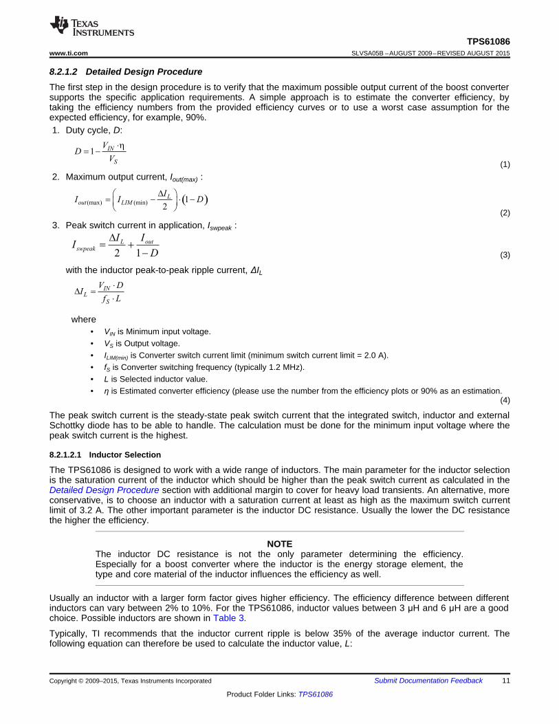
8.2.1.2 Detailed Design ProcedureThe first step in the design procedure is to verify that the maximum possible output current of the boost convertersupports the specific application requirements. A simple approach is to estimate the converter efficiency, bytaking the efficiency numbers from the provided efficiency curves or to use a worst case assumption for theexpected efficiency, for example, 90%.1. Duty cycle, D:
(1)2. Maximum output current, Iout(max) :
(2)3. Peak switch current in application, Iswpeak :
(3)
with the inductor peak-to-peak ripple current, ΔIL
where• VIN is Minimum input voltage.• VS is Output voltage.• ILIM(min) is Converter switch current limit (minimum switch current limit = 2.0 A).• fS is Converter switching frequency (typically 1.2 MHz).• L is Selected inductor value.• η is Estimated converter efficiency (please use the number from the efficiency plots or 90% as an estimation.
(4)
The peak switch current is the steady-state peak switch current that the integrated switch, inductor and externalSchottky diode has to be able to handle. The calculation must be done for the minimum input voltage where thepeak switch current is the highest.
8.2.1.2.1 Inductor Selection
The TPS61086 is designed to work with a wide range of inductors. The main parameter for the inductor selectionis the saturation current of the inductor which should be higher than the peak switch current as calculated in theDetailed Design Procedure section with additional margin to cover for heavy load transients. An alternative, moreconservative, is to choose an inductor with a saturation current at least as high as the maximum switch currentlimit of 3.2 A. The other important parameter is the inductor DC resistance. Usually the lower the DC resistancethe higher the efficiency.
NOTEThe inductor DC resistance is not the only parameter determining the efficiency.Especially for a boost converter where the inductor is the energy storage element, thetype and core material of the inductor influences the efficiency as well.
Usually an inductor with a larger form factor gives higher efficiency. The efficiency difference between differentinductors can vary between 2% to 10%. For the TPS61086, inductor values between 3 μH and 6 μH are a goodchoice. Possible inductors are shown in Table 3.
Typically, TI recommends that the inductor current ripple is below 35% of the average inductor current. Thefollowing equation can therefore be used to calculate the inductor value, L:
Copyright © 2009–2015, Texas Instruments Incorporated Submit Documentation Feedback 11
Product Folder Links: TPS61086

D avg forwardP I V= ×
avg outI I=
2
-
0.35
IN S IN
S out S
V V VL
V I f
hæ öæ ö æ ö= × ×ç ÷ç ÷ ç ÷× è øè ø è ø
TPS61086SLVSA05B –AUGUST 2009–REVISED AUGUST 2015 www.ti.com
where• VIN is Minimum input voltage.• VS is Output voltage.• Iout is Maximum output current in the application.• fS is Converter switching frequency (typically 1.2 MHz).• η is Estimated converter efficiency (please use the number from the efficiency plots or 90% as an estimation.
(5)
Table 3. Inductor SelectionL COMPONENT SIZE DCR TYPSUPPLIER Isat (A)CODE(μH) (L×W×H mm) (mΩ)
3.3 Sumida CDH38D09 4 x 4 x 1 240 1.254.7 Sumida CDPH36D13 5 x 5 x 1.5 155 1.363.3 Sumida CDPH4D19F 5.2 x 5.2 x 2 33 1.53.3 Sumida CDRH6D12 6.7 x 6.7 x 1.5 62 2.24.7 Würth Elektronik 7447785004 5.9 x 6.2 x 3.3 60 2.55 Coilcraft MSS7341 7.3 x 7.3 x 4.1 24 2.9
8.2.1.2.2 Rectifier Diode Selection
To achieve high efficiency a Schottky type should be used for the rectifier diode. The reverse voltage ratingshould be higher than the maximum output voltage of the converter. The averaged rectified forward current Iavg ,the Schottky diode needs to be rated for, is equal to the output current Iout :
(6)
Usually a Schottky diode with 1-A maximum average rectified forward current rating is sufficient for mostapplications. The Schottky rectifier can be selected with lower forward current capability depending on the outputcurrent Iout but has to be able to dissipate the power. The dissipated power, PD , is the average rectified forwardcurrent times the diode forward voltage, Vforward .
(7)
Typically the diode should be able to dissipate around 500 mW depending on the load current and forwardvoltage.
Table 4. Rectifier Diode SelectionCURRENT COMPONENT PACKAGEVr Vforward/Iavg SUPPLIERRATING Iavg CODE TYPE
750 mA 20 V 0.425 V / 1 A Fairchild Semiconductor FYV0704S SOT 231 A 20 V 0.39 V / 1 A NXP PMEG2010AEH SOD 1231 A 20 V 0.5 V / 1 A Vishay Semiconductor SS12 SMA1 A 20 V 0.44 V / 1 A Vishay Semiconductor MSS1P2L µ -SMP2 A 20 V 0.44 V / 2 A Vishay Semiconductor SL22 SMB
12 Submit Documentation Feedback Copyright © 2009–2015, Texas Instruments Incorporated
Product Folder Links: TPS61086

110IN S out
COMP
out
V V CR
L I
× ××
=
× 7.5
s out
COMP
out COMP
V CC
I R
×
=
× ×
2 1870
1.238
m= » W
=
FB
FB
VR k
A
V V
1 2 1S
FB
VR R
V
æ ö= × -ç ÷
è øV
FB
R1
R2
VS
TPS61086www.ti.com SLVSA05B –AUGUST 2009–REVISED AUGUST 2015
8.2.1.2.3 Setting the Output Voltage
The output voltage is set by an external resistor divider. Typically, a minimum current of 50 μA flowing throughthe feedback divider gives good accuracy and noise covering. A standard low side resistor of 18 kΩ is typicallyselected. The resistors are then calculated as:
(8)
8.2.1.2.4 Compensation (COMP)
The regulator loop can be compensated by adjusting the external components connected to the COMP pin. TheCOMP pin is the output of the internal transconductance error amplifier.
Standard values of RCOMP = 16 kΩ and CCOMP = 2.7 nF will work for the majority of the applications.
Please refer to Table 5 for dedicated compensation networks giving an improved load transient response. Thefollowing equations can be used to calculate RCOMP and CCOMP :
where• VIN is Minimum input voltage.• VS is Output voltage.• Cout is Output capacitance.• L is Inductor value, for example, 3.3 μH or 4.7 μH.• Iout is Maximum output current in the application. (9)
Make sure that RCOMP < 120 kΩ and CCOMP> 820 pF, independent of the results of the above formulas.
Table 5. Recommended Compensation Network Values at High/Low FrequencyL VS VIN ± 20% RCOMP CCOMP
5 V 100 kΩ 820 pF15 V
3.3 V 91 kΩ 1.2 nF5 V 68 kΩ 820 pF
3.3 μH 12 V3.3 V 68 kΩ 1.2 nF5 V 39 kΩ 820 pF
9 V3.3 V 39 kΩ 1.2 nF
Table 5 gives conservative RCOMP and CCOMP values for certain inductors, input and output voltages providing avery stable system. For a faster response time, a higher RCOMP value can be used to enlarge the bandwidth, aswell as a slightly lower value of CCOMP to keep enough phase margin. These adjustments should be performed inparallel with the load transient response monitoring of TPS61086.
8.2.1.2.5 Input Capacitor Selection
For good input voltage filtering low-ESR ceramic capacitors are recommended. TPS61086 has an analog inputIN. Therefore, a 1-μF bypass is highly recommended as close as possible to the IC from IN to GND.
One 10-μF ceramic input capacitors are sufficient for most of the applications. For better input voltage filteringthis value can be increased. Refer to Table 6 and typical applications for input capacitor recommendation
Copyright © 2009–2015, Texas Instruments Incorporated Submit Documentation Feedback 13
Product Folder Links: TPS61086

V
5 V/divSW
V
50 mV/divS_AC
I
0.5 A/divl
10 µs/div
V = 3.3 V, V = 12 V/50 mAIN S
V
5 V/divSW
V
50 mV/divS_AC
I
0.5 A/divl
10 µs/div
V = 3.3 V, V = 12 V/50 mAIN S
-D = ×
×
S IN outC
S S out
V V IV
V f C_ ( ) _D = ×C ESR L peak C ESRV I R
TPS61086SLVSA05B –AUGUST 2009–REVISED AUGUST 2015 www.ti.com
8.2.1.2.6 Output Capacitor Selection
For best output voltage filtering a low-ESR output capacitor like ceramic capcaitor is recommended. Two to four10-μF ceramic output capacitors (or two 22 μF) work for most of the applications. Higher capacitor values can beused to improve the load transient response. Refer to Table 6 for the selection of the output capacitor.
Table 6. Rectifier Input and Output Capacitor SelectionCAPACITOR/SI VOLTAGE RATING SUPPLIER COMPONENT CODE
ZECIN 22 μF/1206 16 V Taiyo Yuden EMK316 BJ 226ML
IN bypass 1 μF/0603 16 V Taiyo Yuden EMK107 BJ 105KACOUT 10 μF/1206 25 V Taiyo Yuden TMK316 BJ 106KL
To calculate the output voltage ripple, the following equation can be used:
where• ΔVC is Output voltage ripple dependent on output capacitance,output current and switching frequency.• VS is Output voltage.• VIN is Minimum input voltage of boost converter.• fS is Converter switching frequency (typically 1.2 MHz).• Iout is Output capacitance.• ΔVC_ESR is Output voltage ripple due to output capacitors ESR (equivalent series resistance).• ISWPEAK is Inductor peak switch current in the application.• RC_ESR is Output capacitors equivalent series resistance (ESR). (10)
ΔVC_ESR can be neglected in many cases since ceramic capacitors provide very low ESR.
8.2.1.3 Application Curves
Figure 8. PFM Mode Switching Pulse Figure 9. PFM Mode Switching Pulses
14 Submit Documentation Feedback Copyright © 2009–2015, Texas Instruments Incorporated
Product Folder Links: TPS61086
EN
5 V/div
V
5 V/div
S
I
1 A/div
L
V = 3.3 V
V = 12 V / 300 mA
IN
S
C = 100 nFSS
2 ms/div
V
50 mV/divS_AC
I
50 mA/divOUT
400 µs/div
V = 3.3 V
V = 12 V/50 mA - 150 mAIN
S
C = 40 µF
L = 3.3 µHOUT
R = 16 kΩ
C = 2.7 nFcomp
comp
V
200 mV/divS_AC
V
2 V/divIN
400 µs/div
V = 2.3 V - 6.0V
V = 12 V/0 mAIN
S
C = 40 µF
L = 3.3 µHOUT
R = 16 kΩ
C = 2.7 nFcomp
comp
V
10 V/divSW
V
50 mV/divS_AC
I
0.5 A/divl
100 µs/div
V = 3.3 V, V = 12 V/4 mAIN S
V
10 V/divSW
V
50 mV/divS_AC
I
1 A/divl
400 ns/div
V = 3.3 V
V = 12 V/300 mAIN
S
TPS61086www.ti.com SLVSA05B –AUGUST 2009–REVISED AUGUST 2015
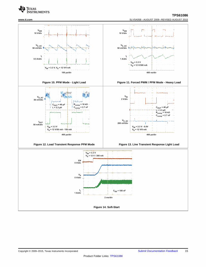
Figure 10. PFM Mode - Light Load Figure 11. Forced PWM / PFM Mode - Heavy Load
Figure 12. Load Transient Response PFM Mode Figure 13. Line Transient Response Light Load
Figure 14. Soft-Start
Copyright © 2009–2015, Texas Instruments Incorporated Submit Documentation Feedback 15
Product Folder Links: TPS61086
IN
EN
SW
FBMODE
AGND COMP
SS
14
68
3 7
2
5PGND
9
10
SW
Cby1 µF16 VCin
10 µF16 V
L3.3 µH
DPMEG2010AEH
R1156 kΩ
R218 kΩ
Cout10 µF25 V
Rcomp68kΩ
Ccomp1.2 nFCss
100 nFTPS61086
V
3.3 V ± 20%IN
V
12 V/500 mA max.S
TPS61086SLVSA05B –AUGUST 2009–REVISED AUGUST 2015 www.ti.com
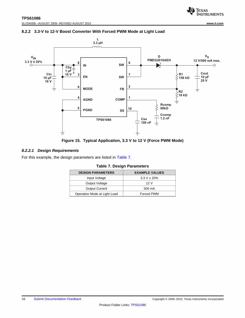
8.2.2 3.3-V to 12-V Boost Converter With Forced PWM Mode at Light Load
Figure 15. Typical Application, 3.3 V to 12 V (Force PWM Mode)
8.2.2.1 Design RequirementsFor this example, the design parameters are listed in Table 7.
Table 7. Design ParametersDESIGN PARAMETERS EXAMPLE VALUES
Input Voltage 3.3 V ± 20%Output Voltage 12 VOutput Current 500 mA
Operation Mode at Light Load Forced PWM
16 Submit Documentation Feedback Copyright © 2009–2015, Texas Instruments Incorporated
Product Folder Links: TPS61086
V
100 mV/divS_AC
I
50 mA/divOUT
400 µs/div
V = 3.3 V
V = 12 V/50 mA - 150 mAIN
S
C = 40 µF
L = 3.3 µHOUT
R = 16 kΩ
C = 2.7 nFcomp
comp
V
200 mV/divS_AC
V
2 V/divIN
400 µs/div
V = 2.3 V - 6.0V
V = 12 V/150 mAIN
S
C = 40 µF
L = 3.3 µHOUT
R = 16 kΩ
C = 2.7 nFcomp
comp
V
10 V/divSW
V
50 mV/divS_AC
I
0.5 A/divl
100 µs/div
V = 3.3 V, V = 12 V/4 mAIN S
V
10 V/divSW
V
50 mV/divS_AC
I
1 A/divl
400 ns/div
V = 3.3 V
V = 12 V/300 mAIN
S
TPS61086www.ti.com SLVSA05B –AUGUST 2009–REVISED AUGUST 2015
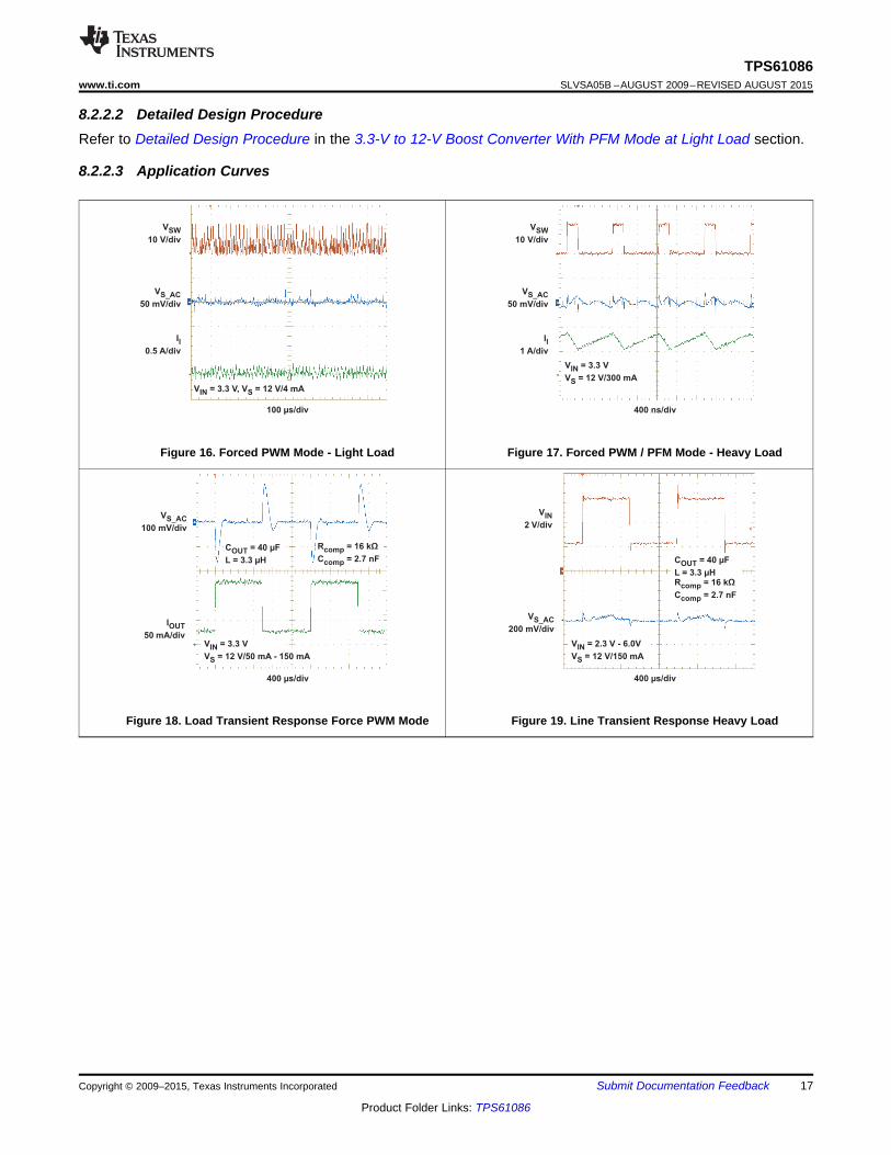
8.2.2.2 Detailed Design ProcedureRefer to Detailed Design Procedure in the 3.3-V to 12-V Boost Converter With PFM Mode at Light Load section.
8.2.2.3 Application Curves
Figure 16. Forced PWM Mode - Light Load Figure 17. Forced PWM / PFM Mode - Heavy Load
Figure 18. Load Transient Response Force PWM Mode Figure 19. Line Transient Response Heavy Load
Copyright © 2009–2015, Texas Instruments Incorporated Submit Documentation Feedback 17
Product Folder Links: TPS61086
V
5 V ± 20%IN
IN
EN
SW
D
FBMODE
AGND COMP
PMEG2010AEH
SS
14
68
3 7
2
5PGND
9
10
SW
TPS61086
Cin2* 10 µF/
16 V
Cby
1 µF/16 V
L3.3 µH
Riso
10 kW
BC857C
Ciso1 µF/ 25 V
Rcomp100 kΩ
Ccomp820 pFCss
100 nF
R1200 kΩ
R218 kΩ
Cout4*10 µF/25 V
V
15 V/50 mAS
Enable
C19470 nF/
50 V
C18470 nF/
50 V
T2BC850B
Vgh26.5 V / 20 mA
IN
EN
SW
FB
Cout
MODE
AGND COMP
4*10µF/
25V
SS
14
68
3 7
2
5PGND
9
10
SW
V
-7 V/20 mAGL
C201 µF/35 V
T1BC857B
R86.8 kΩ
D8BZX84C7V5
C14470 nF/
25 V
-Vs
D4BAV99
C15470 nF/50 V
C16470 nF/
50 V
C17470 nF/
50 V
D3BAV99
D2BAV99
3·Vs
2·Vs
R1013 kΩ
D9BZX84C27V
L3.3 µH
V
5 V ± 20%IN
Cby1 µF/16 V
DSL22 V
15 V/500 mAS
R1200 kΩ
R218 kΩ
Rcomp100 kΩ
Ccomp820 pF
Css100 nF
Cin2*10 µF/
16 V
TPS61086
C131 µF/35 V
TPS61086SLVSA05B –AUGUST 2009–REVISED AUGUST 2015 www.ti.com
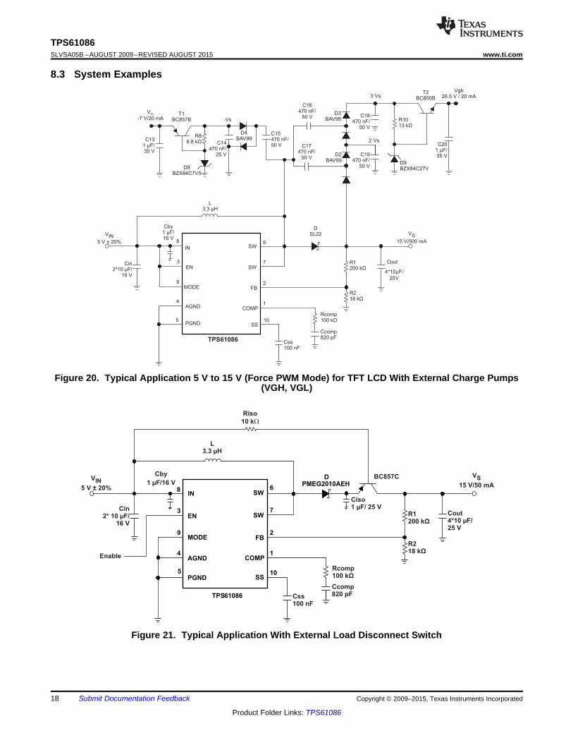
8.3 System Examples
Figure 20. Typical Application 5 V to 15 V (Force PWM Mode) for TFT LCD With External Charge Pumps(VGH, VGL)
Figure 21. Typical Application With External Load Disconnect Switch
18 Submit Documentation Feedback Copyright © 2009–2015, Texas Instruments Incorporated
Product Folder Links: TPS61086

IN
EN
SW
D
FBMODE
AGND COMP
SS
14
68
3 7
2
5PGND
9
10
SW
TPS61086
V
3.3 V ± 20%IN
Cin10 µF/
16 V
Cby1 µF/ 16 V
L3.3 µH
Css100 nF
Rcomp68 kΩ
Ccomp1.2 nF
Rsense15 Ω
Cout2* 10 µF/25 V
V
300 mAS3S3P wLED
LW E67CDz
BZX84C18 V
Rlimit110 Ω
optional
PMEG2010AEH
IN
EN
SW
FBMODE
AGND COMP
SS
14
68
3 7
2
5PGND
9
10
SW
Cby1 µF16 VCin
10 µF16 V
PMEG2010AEH
R1200 kΩ
R218 kΩ
Cout10 µF25 V
Css100 nF
TPS61086
V
3.3 V ± 20%IN
L3.3 µH
V
15 V/30 mAS
Rcomp91 kΩ
Ccomp1.2 nF
Rlimit110 Ω
DzBZX84C 18V
OvervoltageProtection
D
TPS61086www.ti.com SLVSA05B –AUGUST 2009–REVISED AUGUST 2015
System Examples (continued)
Figure 22. Typical Application, 3.3 V to 15 V (PFM Mode) With Overvoltage Protection
Figure 23. Simple Application (3.3-V Input Voltage - Forced PWM Mode) for wLED Supply (3S3P) (WithOptional Clamping Zener Diode)
Copyright © 2009–2015, Texas Instruments Incorporated Submit Documentation Feedback 19
Product Folder Links: TPS61086

IN
EN
SW
D
FBMODE
AGND COMP
SS
14
68
3 7
2
5PGND
9
10
SW
TPS61086
Cby1 µF/ 16 V
L3.3 µH
Css100 nF
Rsense15 Ω
3S3P wLEDLW E67C
RlimitR1
180 kΩ
Analog Brightness Control
PWM Signal
3.3 V ~ wLED off0 V ~ l = 30 mA (each string)
Can be used swinging from 0 V to 3.3 V
LED
110 Ω
optional
V
3.3 V ± 20%IN
Cin10 µF/
16 V
Rcomp68 kΩ
Ccomp1.2 nF
Cout2* 10 µF/25 V
V
300 mAS
PMEG2010AEHDz
BZX84C
18 V
R2127 kΩ
IN
EN
SW
D
FBMODE
AGND COMP
SS
14
68
3 7
2
5PGND
9
10
SW
TPS61086
Cby1 µF/ 16 V
L3.3 µH
Css100 nF
Rsense15 Ω
3S3P wLEDLW E67C
Rlimit110 Ω
PWM100 Hz to 500 Hz
optional
V
3.3 V ± 20%IN
Cin10 µF/
16 V
Rcomp68 kΩ
Ccomp1.2 nF
Cout2* 10 µF/25 V
V
300 mAS
PMEG2010AEH DzBZX84C
18 V
TPS61086SLVSA05B –AUGUST 2009–REVISED AUGUST 2015 www.ti.com
System Examples (continued)
Figure 24. Simple Application (3.3-V Input Voltage - Forced PWM Mode) for wLED Supply (3S3P) WithAdjustable Brightness Control Using a PWM Signal on the Enable Pin (With Optional Clamping Zener
Diode)
Figure 25. Simple Application (3.3-V Input Voltage - Forced PWM Mode) for wLED Supply (3S3P) WithAdjustable Brightness Control Using an Analog Signal on the Feedback Pin (With Optional Clamping
Zener Diode)
20 Submit Documentation Feedback Copyright © 2009–2015, Texas Instruments Incorporated
Product Folder Links: TPS61086
SS
MO
DE
IN SW
1 2 3 4
578
PG
ND
VINVOUT
GND
569
SW
10
TPS61086
AG
ND
EN
FB
CO
MP
TPS61086www.ti.com SLVSA05B –AUGUST 2009–REVISED AUGUST 2015
9 Power Supply RecommendationsThe TPS61086 is designed to operate from an input voltage supply range between 2.3 V and 6.0 V. The powersupply to the TPS61086 needs to have a current rating according to the supply voltage, output voltage, andoutput current of the TPS61086.
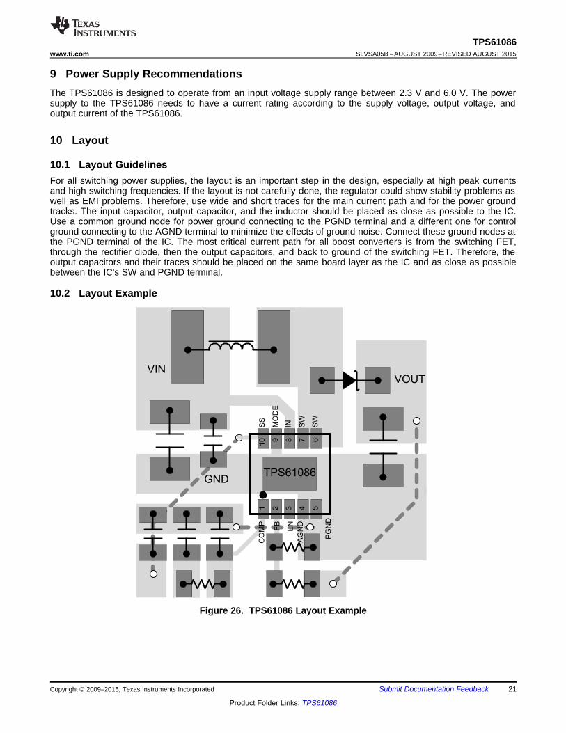
10 Layout
10.1 Layout GuidelinesFor all switching power supplies, the layout is an important step in the design, especially at high peak currentsand high switching frequencies. If the layout is not carefully done, the regulator could show stability problems aswell as EMI problems. Therefore, use wide and short traces for the main current path and for the power groundtracks. The input capacitor, output capacitor, and the inductor should be placed as close as possible to the IC.Use a common ground node for power ground connecting to the PGND terminal and a different one for controlground connecting to the AGND terminal to minimize the effects of ground noise. Connect these ground nodes atthe PGND terminal of the IC. The most critical current path for all boost converters is from the switching FET,through the rectifier diode, then the output capacitors, and back to ground of the switching FET. Therefore, theoutput capacitors and their traces should be placed on the same board layer as the IC and as close as possiblebetween the IC's SW and PGND terminal.
10.2 Layout Example
Figure 26. TPS61086 Layout Example
Copyright © 2009–2015, Texas Instruments Incorporated Submit Documentation Feedback 21
Product Folder Links: TPS61086

TPS61086SLVSA05B –AUGUST 2009–REVISED AUGUST 2015 www.ti.com
11 Device and Documentation Support
11.1 Community ResourcesThe following links connect to TI community resources. Linked contents are provided "AS IS" by the respectivecontributors. They do not constitute TI specifications and do not necessarily reflect TI's views; see TI's Terms ofUse.
TI E2E™ Online Community TI's Engineer-to-Engineer (E2E) Community. Created to foster collaborationamong engineers. At e2e.ti.com, you can ask questions, share knowledge, explore ideas and helpsolve problems with fellow engineers.
Design Support TI's Design Support Quickly find helpful E2E forums along with design support tools andcontact information for technical support.
11.2 TrademarksE2E is a trademark of Texas Instruments.All other trademarks are the property of their respective owners.
11.3 Electrostatic Discharge CautionThese devices have limited built-in ESD protection. The leads should be shorted together or the device placed in conductive foamduring storage or handling to prevent electrostatic damage to the MOS gates.
11.4 GlossarySLYZ022 — TI Glossary.
This glossary lists and explains terms, acronyms, and definitions.
12 Mechanical, Packaging, and Orderable InformationThe following pages include mechanical, packaging, and orderable information. This information is the mostcurrent data available for the designated devices. This data is subject to change without notice and revision ofthis document. For browser-based versions of this data sheet, refer to the left-hand navigation.
22 Submit Documentation Feedback Copyright © 2009–2015, Texas Instruments Incorporated
Product Folder Links: TPS61086
PACKAGE OPTION ADDENDUM
www.ti.com 16-Jul-2015
Addendum-Page 1
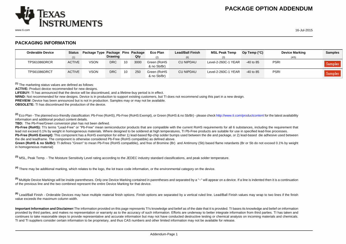
PACKAGING INFORMATION
Orderable Device Status(1)
Package Type PackageDrawing
Pins PackageQty
Eco Plan(2)
Lead/Ball Finish(6)
MSL Peak Temp(3)
Op Temp (°C) Device Marking(4/5)
Samples
TPS61086DRCR ACTIVE VSON DRC 10 3000 Green (RoHS& no Sb/Br)
CU NIPDAU Level-2-260C-1 YEAR -40 to 85 PSRI
TPS61086DRCT ACTIVE VSON DRC 10 250 Green (RoHS& no Sb/Br)
CU NIPDAU Level-2-260C-1 YEAR -40 to 85 PSRI
(1) The marketing status values are defined as follows:ACTIVE: Product device recommended for new designs.LIFEBUY: TI has announced that the device will be discontinued, and a lifetime-buy period is in effect.NRND: Not recommended for new designs. Device is in production to support existing customers, but TI does not recommend using this part in a new design.PREVIEW: Device has been announced but is not in production. Samples may or may not be available.OBSOLETE: TI has discontinued the production of the device.
(2) Eco Plan - The planned eco-friendly classification: Pb-Free (RoHS), Pb-Free (RoHS Exempt), or Green (RoHS & no Sb/Br) - please check http://www.ti.com/productcontent for the latest availabilityinformation and additional product content details.TBD: The Pb-Free/Green conversion plan has not been defined.Pb-Free (RoHS): TI's terms "Lead-Free" or "Pb-Free" mean semiconductor products that are compatible with the current RoHS requirements for all 6 substances, including the requirement thatlead not exceed 0.1% by weight in homogeneous materials. Where designed to be soldered at high temperatures, TI Pb-Free products are suitable for use in specified lead-free processes.Pb-Free (RoHS Exempt): This component has a RoHS exemption for either 1) lead-based flip-chip solder bumps used between the die and package, or 2) lead-based die adhesive used betweenthe die and leadframe. The component is otherwise considered Pb-Free (RoHS compatible) as defined above.Green (RoHS & no Sb/Br): TI defines "Green" to mean Pb-Free (RoHS compatible), and free of Bromine (Br) and Antimony (Sb) based flame retardants (Br or Sb do not exceed 0.1% by weightin homogeneous material)
(3) MSL, Peak Temp. - The Moisture Sensitivity Level rating according to the JEDEC industry standard classifications, and peak solder temperature.
(4) There may be additional marking, which relates to the logo, the lot trace code information, or the environmental category on the device.
(5) Multiple Device Markings will be inside parentheses. Only one Device Marking contained in parentheses and separated by a "~" will appear on a device. If a line is indented then it is a continuationof the previous line and the two combined represent the entire Device Marking for that device.
(6) Lead/Ball Finish - Orderable Devices may have multiple material finish options. Finish options are separated by a vertical ruled line. Lead/Ball Finish values may wrap to two lines if the finishvalue exceeds the maximum column width.
Important Information and Disclaimer:The information provided on this page represents TI's knowledge and belief as of the date that it is provided. TI bases its knowledge and belief on informationprovided by third parties, and makes no representation or warranty as to the accuracy of such information. Efforts are underway to better integrate information from third parties. TI has taken andcontinues to take reasonable steps to provide representative and accurate information but may not have conducted destructive testing or chemical analysis on incoming materials and chemicals.TI and TI suppliers consider certain information to be proprietary, and thus CAS numbers and other limited information may not be available for release.

PACKAGE OPTION ADDENDUM
www.ti.com 16-Jul-2015
Addendum-Page 2
In no event shall TI's liability arising out of such information exceed the total purchase price of the TI part(s) at issue in this document sold by TI to Customer on an annual basis.
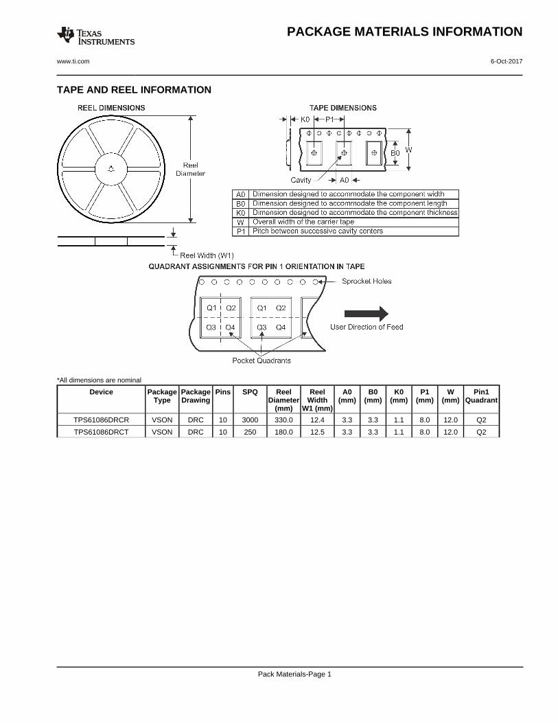
TAPE AND REEL INFORMATION
*All dimensions are nominal
Device PackageType
PackageDrawing
Pins SPQ ReelDiameter
(mm)
ReelWidth
W1 (mm)
A0(mm)
B0(mm)
K0(mm)
P1(mm)
W(mm)
Pin1Quadrant
TPS61086DRCR VSON DRC 10 3000 330.0 12.4 3.3 3.3 1.1 8.0 12.0 Q2
TPS61086DRCT VSON DRC 10 250 180.0 12.5 3.3 3.3 1.1 8.0 12.0 Q2
PACKAGE MATERIALS INFORMATION
www.ti.com 6-Oct-2017
Pack Materials-Page 1
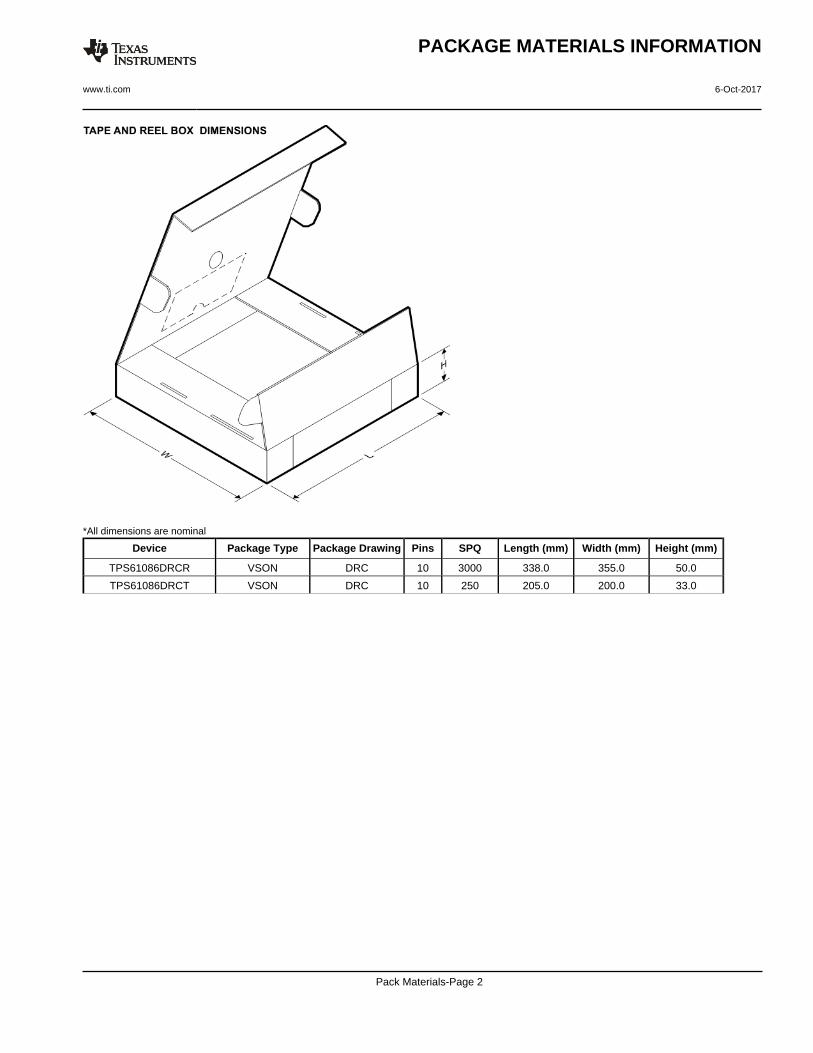
*All dimensions are nominal
Device Package Type Package Drawing Pins SPQ Length (mm) Width (mm) Height (mm)
TPS61086DRCR VSON DRC 10 3000 338.0 355.0 50.0
TPS61086DRCT VSON DRC 10 250 205.0 200.0 33.0
PACKAGE MATERIALS INFORMATION
www.ti.com 6-Oct-2017
Pack Materials-Page 2
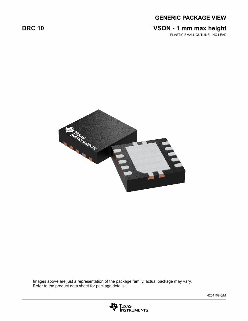
GENERIC PACKAGE VIEW
Images above are just a representation of the package family, actual package may vary.Refer to the product data sheet for package details.
DRC 10 VSON - 1 mm max heightPLASTIC SMALL OUTLINE - NO LEAD
4204102-3/M
www.ti.com
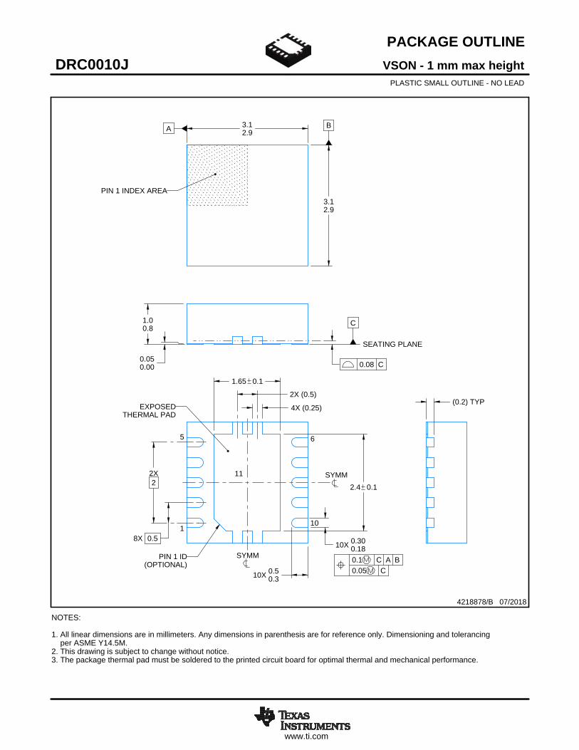
PACKAGE OUTLINE
C
10X 0.300.18
2.4 0.1
2X2
1.65 0.1
8X 0.5
1.00.8
10X 0.50.3
0.050.00
A 3.12.9
B
3.12.9
(0.2) TYP4X (0.25)
2X (0.5)
VSON - 1 mm max heightDRC0010JPLASTIC SMALL OUTLINE - NO LEAD
4218878/B 07/2018
PIN 1 INDEX AREA
SEATING PLANE
0.08 C
1
5 6
10
(OPTIONAL)PIN 1 ID 0.1 C A B
0.05 C
THERMAL PADEXPOSED
SYMM
SYMM11
NOTES: 1. All linear dimensions are in millimeters. Any dimensions in parenthesis are for reference only. Dimensioning and tolerancing per ASME Y14.5M. 2. This drawing is subject to change without notice. 3. The package thermal pad must be soldered to the printed circuit board for optimal thermal and mechanical performance.
SCALE 4.000

www.ti.com
EXAMPLE BOARD LAYOUT
0.07 MINALL AROUND0.07 MAX
ALL AROUND
10X (0.24)
(2.4)
(2.8)
8X (0.5)
(1.65)
( 0.2) VIATYP
(0.575)
(0.95)
10X (0.6)
(R0.05) TYP
(3.4)
(0.25)
(0.5)
VSON - 1 mm max heightDRC0010JPLASTIC SMALL OUTLINE - NO LEAD
4218878/B 07/2018
SYMM
1
5 6
10
LAND PATTERN EXAMPLEEXPOSED METAL SHOWN
SCALE:20X
11SYMM
NOTES: (continued) 4. This package is designed to be soldered to a thermal pad on the board. For more information, see Texas Instruments literature number SLUA271 (www.ti.com/lit/slua271).5. Vias are optional depending on application, refer to device data sheet. If any vias are implemented, refer to their locations shown on this view. It is recommended that vias under paste be filled, plugged or tented.
SOLDER MASKOPENINGSOLDER MASK
METAL UNDER
SOLDER MASKDEFINED
EXPOSED METAL
METALSOLDER MASKOPENING
SOLDER MASK DETAILS
NON SOLDER MASKDEFINED
(PREFERRED)
EXPOSED METAL
www.ti.com
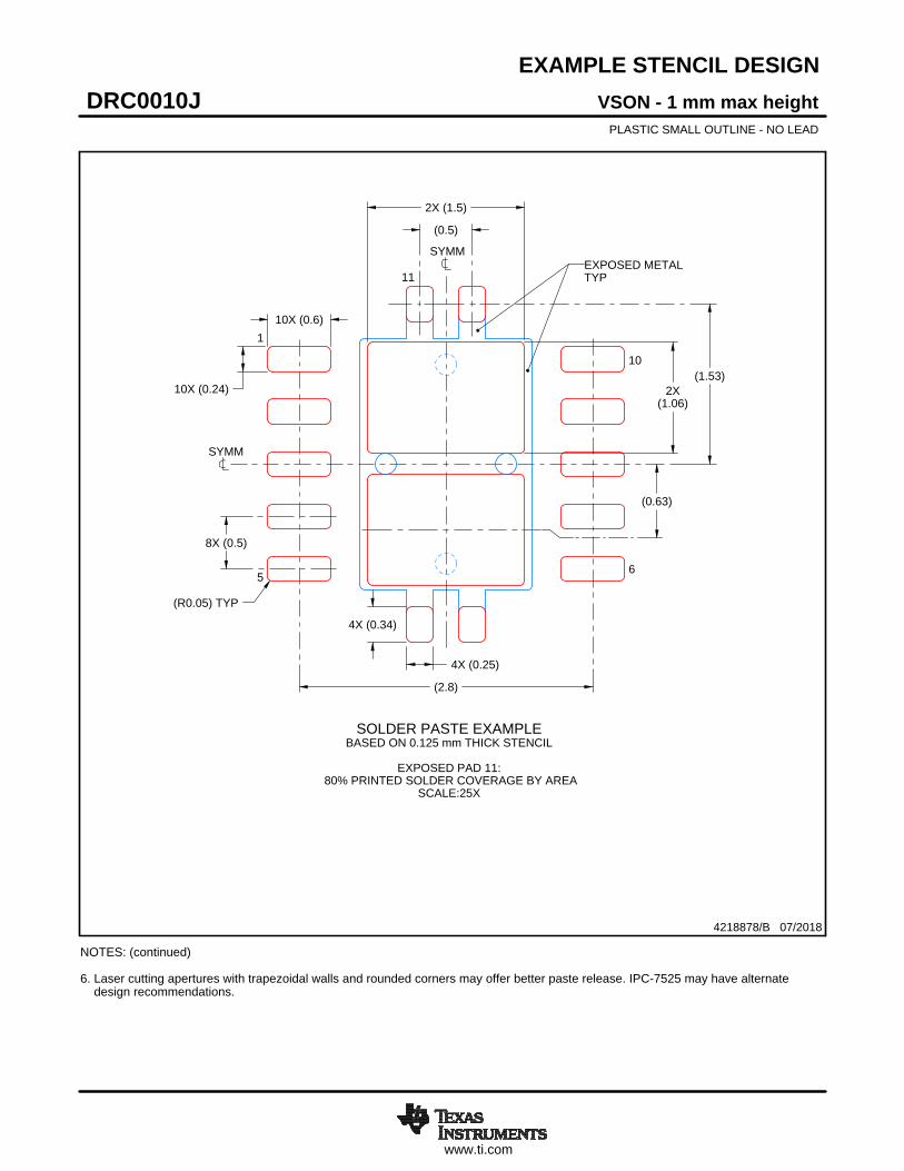
EXAMPLE STENCIL DESIGN
(R0.05) TYP
10X (0.24)
10X (0.6)
2X (1.5)
2X(1.06)
(2.8)
(0.63)
8X (0.5)
(0.5)
4X (0.34)
4X (0.25)
(1.53)
VSON - 1 mm max heightDRC0010JPLASTIC SMALL OUTLINE - NO LEAD
4218878/B 07/2018
NOTES: (continued) 6. Laser cutting apertures with trapezoidal walls and rounded corners may offer better paste release. IPC-7525 may have alternate design recommendations.
SOLDER PASTE EXAMPLEBASED ON 0.125 mm THICK STENCIL
EXPOSED PAD 11:
80% PRINTED SOLDER COVERAGE BY AREASCALE:25X
SYMM
1
56
10
EXPOSED METALTYP11
SYMM
IMPORTANT NOTICE
Texas Instruments Incorporated (TI) reserves the right to make corrections, enhancements, improvements and other changes to itssemiconductor products and services per JESD46, latest issue, and to discontinue any product or service per JESD48, latest issue. Buyersshould obtain the latest relevant information before placing orders and should verify that such information is current and complete.TI’s published terms of sale for semiconductor products (http://www.ti.com/sc/docs/stdterms.htm) apply to the sale of packaged integratedcircuit products that TI has qualified and released to market. Additional terms may apply to the use or sale of other types of TI products andservices.Reproduction of significant portions of TI information in TI data sheets is permissible only if reproduction is without alteration and isaccompanied by all associated warranties, conditions, limitations, and notices. TI is not responsible or liable for such reproduceddocumentation. Information of third parties may be subject to additional restrictions. Resale of TI products or services with statementsdifferent from or beyond the parameters stated by TI for that product or service voids all express and any implied warranties for theassociated TI product or service and is an unfair and deceptive business practice. TI is not responsible or liable for any such statements.Buyers and others who are developing systems that incorporate TI products (collectively, “Designers”) understand and agree that Designersremain responsible for using their independent analysis, evaluation and judgment in designing their applications and that Designers havefull and exclusive responsibility to assure the safety of Designers' applications and compliance of their applications (and of all TI productsused in or for Designers’ applications) with all applicable regulations, laws and other applicable requirements. Designer represents that, withrespect to their applications, Designer has all the necessary expertise to create and implement safeguards that (1) anticipate dangerousconsequences of failures, (2) monitor failures and their consequences, and (3) lessen the likelihood of failures that might cause harm andtake appropriate actions. Designer agrees that prior to using or distributing any applications that include TI products, Designer willthoroughly test such applications and the functionality of such TI products as used in such applications.TI’s provision of technical, application or other design advice, quality characterization, reliability data or other services or information,including, but not limited to, reference designs and materials relating to evaluation modules, (collectively, “TI Resources”) are intended toassist designers who are developing applications that incorporate TI products; by downloading, accessing or using TI Resources in anyway, Designer (individually or, if Designer is acting on behalf of a company, Designer’s company) agrees to use any particular TI Resourcesolely for this purpose and subject to the terms of this Notice.TI’s provision of TI Resources does not expand or otherwise alter TI’s applicable published warranties or warranty disclaimers for TIproducts, and no additional obligations or liabilities arise from TI providing such TI Resources. TI reserves the right to make corrections,enhancements, improvements and other changes to its TI Resources. TI has not conducted any testing other than that specificallydescribed in the published documentation for a particular TI Resource.Designer is authorized to use, copy and modify any individual TI Resource only in connection with the development of applications thatinclude the TI product(s) identified in such TI Resource. NO OTHER LICENSE, EXPRESS OR IMPLIED, BY ESTOPPEL OR OTHERWISETO ANY OTHER TI INTELLECTUAL PROPERTY RIGHT, AND NO LICENSE TO ANY TECHNOLOGY OR INTELLECTUAL PROPERTYRIGHT OF TI OR ANY THIRD PARTY IS GRANTED HEREIN, including but not limited to any patent right, copyright, mask work right, orother intellectual property right relating to any combination, machine, or process in which TI products or services are used. Informationregarding or referencing third-party products or services does not constitute a license to use such products or services, or a warranty orendorsement thereof. Use of TI Resources may require a license from a third party under the patents or other intellectual property of thethird party, or a license from TI under the patents or other intellectual property of TI.TI RESOURCES ARE PROVIDED “AS IS” AND WITH ALL FAULTS. TI DISCLAIMS ALL OTHER WARRANTIES ORREPRESENTATIONS, EXPRESS OR IMPLIED, REGARDING RESOURCES OR USE THEREOF, INCLUDING BUT NOT LIMITED TOACCURACY OR COMPLETENESS, TITLE, ANY EPIDEMIC FAILURE WARRANTY AND ANY IMPLIED WARRANTIES OFMERCHANTABILITY, FITNESS FOR A PARTICULAR PURPOSE, AND NON-INFRINGEMENT OF ANY THIRD PARTY INTELLECTUALPROPERTY RIGHTS. TI SHALL NOT BE LIABLE FOR AND SHALL NOT DEFEND OR INDEMNIFY DESIGNER AGAINST ANY CLAIM,INCLUDING BUT NOT LIMITED TO ANY INFRINGEMENT CLAIM THAT RELATES TO OR IS BASED ON ANY COMBINATION OFPRODUCTS EVEN IF DESCRIBED IN TI RESOURCES OR OTHERWISE. IN NO EVENT SHALL TI BE LIABLE FOR ANY ACTUAL,DIRECT, SPECIAL, COLLATERAL, INDIRECT, PUNITIVE, INCIDENTAL, CONSEQUENTIAL OR EXEMPLARY DAMAGES INCONNECTION WITH OR ARISING OUT OF TI RESOURCES OR USE THEREOF, AND REGARDLESS OF WHETHER TI HAS BEENADVISED OF THE POSSIBILITY OF SUCH DAMAGES.Unless TI has explicitly designated an individual product as meeting the requirements of a particular industry standard (e.g., ISO/TS 16949and ISO 26262), TI is not responsible for any failure to meet such industry standard requirements.Where TI specifically promotes products as facilitating functional safety or as compliant with industry functional safety standards, suchproducts are intended to help enable customers to design and create their own applications that meet applicable functional safety standardsand requirements. Using products in an application does not by itself establish any safety features in the application. Designers mustensure compliance with safety-related requirements and standards applicable to their applications. Designer may not use any TI products inlife-critical medical equipment unless authorized officers of the parties have executed a special contract specifically governing such use.Life-critical medical equipment is medical equipment where failure of such equipment would cause serious bodily injury or death (e.g., lifesupport, pacemakers, defibrillators, heart pumps, neurostimulators, and implantables). Such equipment includes, without limitation, allmedical devices identified by the U.S. Food and Drug Administration as Class III devices and equivalent classifications outside the U.S.TI may expressly designate certain products as completing a particular qualification (e.g., Q100, Military Grade, or Enhanced Product).Designers agree that it has the necessary expertise to select the product with the appropriate qualification designation for their applicationsand that proper product selection is at Designers’ own risk. Designers are solely responsible for compliance with all legal and regulatoryrequirements in connection with such selection.Designer will fully indemnify TI and its representatives against any damages, costs, losses, and/or liabilities arising out of Designer’s non-compliance with the terms and provisions of this Notice.
Mailing Address: Texas Instruments, Post Office Box 655303, Dallas, Texas 75265Copyright © 2018, Texas Instruments Incorporated