tps793 low-noise, high psrr, rf, 200-ma ldo linear ... sheets/texas...advanced, proprietary bicmos...
TRANSCRIPT

10 100 1 k 10 k
20
60
100
100 k 1 M 10 M
Rip
ple
Reje
cti
on
(d
B)
Frequency (Hz)
VIN = 3.8 V
COUT = 2.2 Fm
CNR = 0.1 Fm
IOUT = 10 mA
IOUT = 200 mA
40
70
90
30
50
80
10
0
VIN
VIN
VOUT
VOUTIN
EN GND NR
OUT
TPS79328
0.1 Fm 10 Fm
0.01 Fm
Product
Folder
Sample &Buy
Technical
Documents
Tools &
Software
Support &Community
An IMPORTANT NOTICE at the end of this data sheet addresses availability, warranty, changes, use in safety-critical applications,intellectual property matters and other important disclaimers. PRODUCTION DATA.
TPS793SLVS348L –JULY 2001–REVISED MAY 2015
TPS793 Low-Noise, High PSRR, RF, 200-mA Low-Dropout Linear Regulators inNanoStar™ Wafer Chip Scale and SOT-23
1
1 Features1• 200-mA RF Low-Dropout Regulator
With Enable• Available in Fixed-Voltage Versions from 1.8 V to
4.75 V and Adjustable (1.22 V to 5.5 V)• High PSRR (70 dB at 10 kHz)• Low Noise (32 μVRMS, TPS79328)• Fast Start-Up Time (50 μs)• Stable With a 2.2-μF Ceramic Capacitor• Excellent Load and Line Transient Response• Very Low Dropout Voltage (112 mV at 200 mA,
TPS79330)• 5- and 6-Pin SOT23 (DBV) and NanoStar Wafer
Chip Scale (YZQ) Packages
2 Applications• RF: VCOs, Receivers, ADCs• Audio• Cellular and Cordless Telephones• Bluetooth®, Wireless LAN• Handheld Organizers, PDAs
3 DescriptionThe TPS793 family of low-dropout (LDO) low-powerlinear voltage regulators features high power-supplyrejection ratio (PSRR), ultralow-noise, fast start-up,and excellent line and load transient responses inNanoStar™ wafer chip scale and SOT23 packages.NanoStar packaging gives an ultrasmall footprint aswell as an ultralow profile and package weight,making these devices ideal for portable applicationssuch as handsets and PDAs. Each device in thefamily is stable, with a small, 2.2-μF ceramiccapacitor on the output. The TPS793 family uses anadvanced, proprietary BiCMOS fabrication process toyield extremely low dropout voltages (for example,112 mV at 200 mA, TPS79330). Each deviceachieves fast start-up times (approximately 50 μs witha 0.001-μF bypass capacitor) while consuming verylow quiescent current (170 μA typical). Moreover,when the device is placed in standby mode, thesupply current is reduced to less than 1 μA. TheTPS79328 exhibits approximately 32 μVRMS of outputvoltage noise at 2.8-V output with a 0.1-μF bypasscapacitor. Applications with analog components thatare noise-sensitive, such as portable RF electronics,benefit from the high PSRR and low-noise featuresas well as the fast response time.
Device Information(1)
PART NUMBER PACKAGE BODY SIZE (NOM)
TPS793SOT-23 (6) 2.90 mm × 1.60 mmSOT-23 (5) 2.90 mm × 1.60 mmDSBGA (5) 1.35 mm × 1.00 mm
(1) For all available packages, see the orderable addendum atthe end of the data sheet.
Typical Application Circuit Ripple Rejection vs Frequency

2
TPS793SLVS348L –JULY 2001–REVISED MAY 2015 www.ti.com
Product Folder Links: TPS793
Submit Documentation Feedback Copyright © 2001–2015, Texas Instruments Incorporated
Table of Contents1 Features .................................................................. 12 Applications ........................................................... 13 Description ............................................................. 14 Revision History..................................................... 25 Pin Configuration and Functions ......................... 36 Specifications......................................................... 4
6.1 Absolute Maximum Ratings ...................................... 46.2 ESD Ratings ............................................................ 46.3 Recommended Operating Conditions....................... 46.4 Thermal Information .................................................. 56.5 Electrical Characteristics .......................................... 66.6 Typical Characteristics .............................................. 7
7 Detailed Description ............................................ 117.1 Overview ................................................................. 117.2 Functional Block Diagrams ..................................... 117.3 Feature Description................................................. 127.4 Device Functional Modes........................................ 13
8 Application and Implementation ........................ 148.1 Application Information............................................ 148.2 Typical Application .................................................. 158.3 Do's and Don'ts....................................................... 17
9 Power Supply Recommendations ...................... 1710 Layout................................................................... 18
10.1 Layout Guidelines ................................................. 1810.2 Layout Example .................................................... 1810.3 Power Dissipation ................................................. 18
11 Device and Documentation Support ................. 2011.1 Device Support...................................................... 2011.2 Documentation Support ........................................ 2011.3 Community Resource............................................ 2011.4 Trademarks ........................................................... 2111.5 Electrostatic Discharge Caution............................ 2111.6 Glossary ................................................................ 21
12 Mechanical, Packaging, and OrderableInformation ........................................................... 21
4 Revision History
Changes from Revision K (October 2007) to Revision L Page
• Changed title of data sheet ................................................................................................................................................... 1• Deleted references to YEQ package throughout document (package is obsolete) .............................................................. 1• Changed fourth bullet of Features list to low noise ................................................................................................................ 1• Changed front-page figure ..................................................................................................................................................... 1• Changed Absolute Maximum Ratings condition statement ................................................................................................... 4• Added Pin Configurations and Functions section, ESD Ratings table, Feature Description section, Device Functional
Modes, Application and Implementation section, Power Supply Recommendations section, Layout section, Deviceand Documentation Support section, and Mechanical, Packaging, and Orderable Information section .............................. 4
• Deleted Dissipation Ratings table; added Thermal Information table ................................................................................... 5• Deleted TJ = 25°C test condition from PSRR specification measurements because of redundancy .................................... 6• Added condition statement to Typical Characteristics ........................................................................................................... 7• Changed Figure 23; changed capacitor notation to CFF in figure and related table ............................................................ 14• Changed Figure 24; changed capacitor notation to CFF in figure, changed 2.2µF capacitor value to 10µF, and
changed device name .......................................................................................................................................................... 15
A3 A1
C3 C1
B2
IN OUT
GND
NR
EN
3
2
4
5
61
GND
OUT
NR
FB
EN
IN
3
2
4
51
GND
OUT
NREN
IN
3
TPS793www.ti.com SLVS348L –JULY 2001–REVISED MAY 2015
Product Folder Links: TPS793
Submit Documentation FeedbackCopyright © 2001–2015, Texas Instruments Incorporated
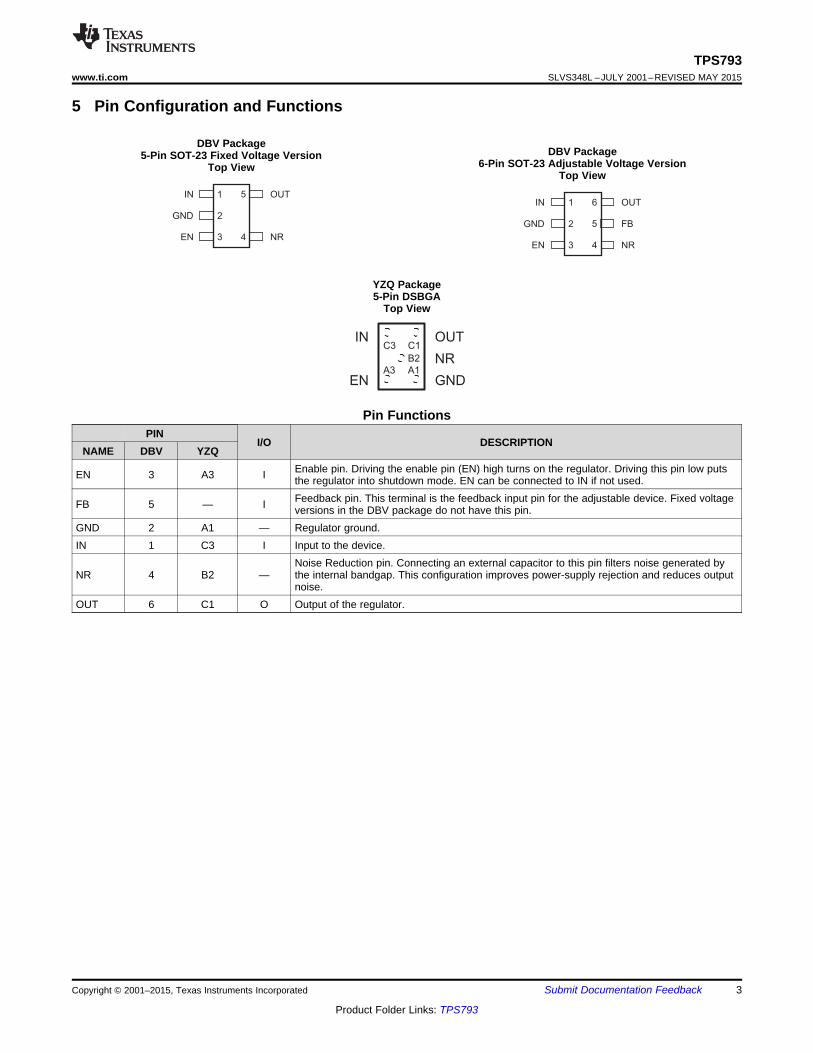
5 Pin Configuration and Functions
DBV Package5-Pin SOT-23 Fixed Voltage Version
Top ViewDBV Package
6-Pin SOT-23 Adjustable Voltage VersionTop View
YZQ Package5-Pin DSBGA
Top View
Pin FunctionsPIN
I/O DESCRIPTIONNAME DBV YZQ
EN 3 A3 I Enable pin. Driving the enable pin (EN) high turns on the regulator. Driving this pin low putsthe regulator into shutdown mode. EN can be connected to IN if not used.
FB 5 — I Feedback pin. This terminal is the feedback input pin for the adjustable device. Fixed voltageversions in the DBV package do not have this pin.
GND 2 A1 — Regulator ground.IN 1 C3 I Input to the device.
NR 4 B2 —Noise Reduction pin. Connecting an external capacitor to this pin filters noise generated bythe internal bandgap. This configuration improves power-supply rejection and reduces outputnoise.
OUT 6 C1 O Output of the regulator.

4
TPS793SLVS348L –JULY 2001–REVISED MAY 2015 www.ti.com
Product Folder Links: TPS793
Submit Documentation Feedback Copyright © 2001–2015, Texas Instruments Incorporated
(1) Stresses beyond those listed under Absolute Maximum Ratings may cause permanent damage to the device. These are stress ratingsonly, which do not imply functional operation of the device at these or any other conditions beyond those indicated under RecommendedOperating Conditions. Exposure to absolute-maximum-rated conditions for extended periods may affect device reliability.
6 Specifications
6.1 Absolute Maximum Ratingsover operating junction temperature range (unless otherwise noted). All voltages are with respect to GND. (1)
MIN MAX UNIT
VoltageInput, VIN –0.3 6 VEnable, VEN –0.3 6 VOutput, VOUT –0.3 6 V
Current Peak output, IOUT(max) Internally limited AOutput short-circuit duration IndefiniteTotal power dissipation Continuous, PD(tot) See Thermal Information
TemperatureJunction, TJ
DBV package –40 150 °CYZQ package –40 125 °C
Storage, Tstg –65 150 °C
(1) JEDEC document JEP155 states that 500-V HBM allows safe manufacturing with a standard ESD control process.(2) JEDEC document JEP157 states that 250-V CDM allows safe manufacturing with a standard ESD control process.
6.2 ESD RatingsVALUE UNIT
V(ESD) Electrostatic dischargeHuman body model (HBM), per ANSI/ESDA/JEDEC JS-001, all pins (1) ±2000
VCharged device model (CDM), per JEDEC specification JESD22-C101,all pins (2) ±500
(1) If CFF is not used or VOUT(nom) < 1.8 V, the minimum recommended COUT = 4.7 µF.
6.3 Recommended Operating Conditionsover operating junction temperature range (unless otherwise noted).
MIN NOM MAX UNITVIN Input supply voltage range 2.7 5.5 VVEN Enable supply voltage range 0 VIN VVOUT Output voltage range VFB 5 VIOUT Output current 0 200 mATJ Operating junction temperature –40 125 °CCIN Input capacitor 0.1 1 µFCOUT Output capacitor 2.2 (1) 10 µFCNR Noise reduction capacitor 0 10 nFCFF Feed-forward capacitor 15 pFR2 Lower feedback resistor 30.1 kΩ

5
TPS793www.ti.com SLVS348L –JULY 2001–REVISED MAY 2015
Product Folder Links: TPS793
Submit Documentation FeedbackCopyright © 2001–2015, Texas Instruments Incorporated
(1) For more information about traditional and new thermal metrics, see the Semiconductor and IC Package Thermal Metrics applicationreport, SPRA953.
6.4 Thermal Information
THERMAL METRIC (1)TPS79301
UNITDBV (SOT-23) YZQ (DSBGA)6 PINS 5 PINS
RθJA Junction-to-ambient thermal resistance 225.1 178.5 °C/WRθJC(top) Junction-to-case (top) thermal resistance 78.4 1.4 °C/WRθJB Junction-to-board thermal resistance 54.7 62.1 °C/WψJT Junction-to-top characterization parameter 3.3 0.9 °C/WψJB Junction-to-board characterization parameter 53.8 62.1 °C/W

6
TPS793SLVS348L –JULY 2001–REVISED MAY 2015 www.ti.com
Product Folder Links: TPS793
Submit Documentation Feedback Copyright © 2001–2015, Texas Instruments Incorporated
(1) Minimum VIN is 2.7 V or VOUT + VDO, whichever is greater.(2) Dropout is not measured for the TPS79318 and TPS79325 because minimum VIN = 2.7 V.(3) For adjustable versions, this parameter applies only after VIN is applied; then VEN transitions high to low.
6.5 Electrical CharacteristicsOver recommended operating temperature range TJ = –40°C to 125°C, VEN = VIN, VIN = VOUT(nom) + 1 V (1), IOUT = 1 mA, COUT =10 μF, CNR = 0.01 μF (unless otherwise noted). Typical values are at TJ = 25°C.
PARAMETER TEST CONDITIONS MIN TYP MAX UNITVIN Input voltage range (1) 2.7 5.5 VIOUT Continuous output current 0 200 mAVFB Internal reference (TPS79301) 1.201 1.225 1.250 V
VOUTOutput voltagerange
TPS79301 VFB 5.5 – VDO
V
TPS79318 0 µA < IOUT < 200 mA, 2.8 V < VIN < 5.5 V 1.764 1.8 1.836TPS79325 0 µA < IOUT < 200 mA, 3.5 V < VIN < 5.5 V 2.45 2.5 2.55TPS79328 0 µA < IOUT < 200 mA, 3.8 V < VIN < 5.5 V 2.744 2.8 2.856TPS793285 0 µA < IOUT < 200 mA, 3.85 V < VIN < 5.5 V 2.793 2.85 2.907TPS79330 0 µA < IOUT < 200 mA, 4 V < VIN < 5.5 V 2.94 3 3.06TPS79333 0 µA < IOUT < 200 mA, 4.3 V < VIN < 5.5 V 3.234 3.3 3.366TPS793475 0 µA < IOUT < 200 mA, 5.25 V < VIN < 5.5 V 4.655 4.75 4.845
ΔVOUT(ΔVIN) Line regulation VOUT + 1 V < VIN ≤ 5.5 V 0.05 0.12 %/VΔVOUT(ΔIOUT) Load regulation 0 µA < IOUT < 200 mA, TJ = 25°C 5 mV
VDO
Dropoutvoltage (2)
(VIN = VOUT(nom) –0.1 V)
TPS79328 IOUT = 200 mA 120 200
mVTPS793285 IOUT = 200 mA 120 200TPS79330 IOUT = 200 mA 112 200TPS79333 IOUT = 200 mA 12 180TPS793475 IOUT = 200 mA 77 125
ICL Output current limit VOUT = 0 V 285 600 mAIGND Ground pin current 0 µA < IOUT < 200 mA 170 220 µAISHUTDOWN Shutdown current (3) VEN = 0 V, 2.7 V < VIN < 5.5 V 0.07 1 µAIFB FB pin current VFB = 1.8 V 1 µA
PSRR Power-supplyrejection ratio TPS79328
f = 100 Hz, IOUT = 10 mA 70
dBf = 100 Hz, IOUT = 200 mA 68f = 10 kHz, IOUT = 200 mA 70f = 100 kHz, IOUT = 200 mA 43
VnOutput noisevoltage TPS79328
BW = 200 Hz to100 kHz,IOUT = 200 mA
CNR = 0.001 μF 55
µVRMSCNR = 0.0047 μF 36CNR = 0.01 μF 33CNR = 0.1 μF 32
tSTR Startup time TPS79328 RL = 14 Ω,COUT = 1 µF
CNR = 0.001 μF 50µsCNR = 0.0047 μF 70
CNR = 0.01 μF 100VEN(high) High-level enable input voltage 2.7 V < VIN < 5.5 V 1.7 VIN VVEN(low) Low-level enable input voltage 2.7 V < VIN < 5.5 V 0 0.7 VIEN EN pin current VEN = 0 V –1 1 µA
UVLOThreshold, VCC rising 2.25 2.65 VHysteresis 100 mV

0
0.05
0.10
0.15
0.20
0.25
0.30
100 1 k 10 k 100 k
Frequency (Hz)
IOUT = 1 mA
IOUT = 200 mA
VIN = 3.8 V
COUT = 10 Fm
CNR = 0.1 Fm
Ou
tpu
t S
pectr
al
No
ise
Den
sit
y (
mV
/H
z√
)
0
0.2
0.4
0.6
0.8
1.0
1.2
1.4
1.6
100 1 k 10 k 100 k
Frequency (Hz)
VIN = 3.8 V
IOUT = 200 mA
COUT = 10 Fm
CNR = 0.1 Fm
CNR = 0.001 Fm
CNR = 0.0047 Fm
CNR = 0.01 Fm
Ou
tpu
t S
pectr
al
No
ise
Den
sit
y (
mV
/H
z√
)
0
50
100
150
200
250
−40 −25−10 5 20 35 50 65 80 95 110 125
TJ (°C)
IOUT = 1 mA
VIN = 3.8 V
COUT = 10 Fm
IOUT = 200 mA
I GN
D(m
A)
0
0.05
0.10
0.15
0.20
0.25
0.30
100 1 k 10 k 100 k
Frequency (Hz)
IOUT = 1 mA
VIN = 3.8 V
COUT = 2.2 Fm
CNR = 0.1 Fm
IOUT = 200 mA
Ou
tpu
t S
pectr
al
No
ise
Den
sit
y (
mV
/H
z√
)
2.795
2.796
2.797
2.798
2.799
2.800
2.801
2.802
2.803
2.804
2.805
0 50 100 150 200
IOUT (mA)
VIN = 3.8 V
COUT = 10 Fm
TJ = 25 C°
VO
UT
(V)
2.775
2.780
2.785
2.790
2.795
2.800
2.805
−40 −25 −10 5 20 35 50 65 80 95 110 125
TJ (°C)
IOUT = 200 mA
IOUT = 1 mA
VIN = 3.8 V
COUT = 10 Fm
VO
UT
(V)
7
TPS793www.ti.com SLVS348L –JULY 2001–REVISED MAY 2015
Product Folder Links: TPS793
Submit Documentation FeedbackCopyright © 2001–2015, Texas Instruments Incorporated
6.6 Typical CharacteristicsOver recommended operating temperature range TJ = –40°C to 125°C, VEN = VIN, VIN = VOUT(nom) + 1 V, IOUT = 1 mA, COUT =10 μF, CNR = 0.01 μF, VOUT(nom) = 2.8 V (unless otherwise noted). Typical values are at TJ = 25°C.
Figure 1. TPS79328 Output Voltage vs Output Current Figure 2. TPS79328 Output Voltage vs JunctionTemperature
Figure 3. TPS79328 Ground Current vs JunctionTemperature
Figure 4. TPS79328 Output Spectral Noise Density vsFrequency
Figure 5. TPS79328 Output Spectral Noise Density vsFrequency
Figure 6. TPS79328 Output Spectral Noise Density vsFrequency

10 100 1 k 10 k
20
60
100
100 k 1 M 10 M
Rip
ple
Reje
cti
on
(d
B)
Frequency (Hz)
VIN = 3.8 V
COUT = 2.2 Fm
CNR = 0.01 Fm
IOUT = 10 mA
IOUT = 200 mA
40
70
90
30
50
80
10
0
10 100 1 k 10 k
20
60
100
100 k 1 M 10 M
Rip
ple
Reje
cti
on
(d
B)
Frequency (Hz)
VIN = 3.8 V
COUT = 2.2 Fm
CNR = 0.1 Fm
IOUT = 10 mA
IOUT = 200 mA
40
70
90
30
50
80
10
0
0
20
40
60
80
100
120
140
160
180
−40 −25−10 5 20 35 50 65 80 95 110 125
IOUT = 200 mA
IOUT = 10 mA
VIN = 2.7 V
COUT = 10 Fm
TJ (°C)
VD
O(m
V)
10 100 1 k 10 k
10
40
80
100 k 1 M 10 M
Rip
ple
Reje
cti
on
(d
B)
Frequency (Hz)
IOUT = 10 mA
50
0
VIN = 3.8 V
COUT = 10 Fm
CNR = 0.01 Fm
IOUT = 200 mA
20
30
60
70
90
100
0.001 0.01 0.1
CNR (mF)
0
10
20
30
40
50
60
VOUT = 2.8 V
IOUT = 200 mA
COUT = 10 Fm
BW = 100 Hz to 100 kHz
RM
S, O
utp
ut
No
ise (
VR
MS
)
100 1 M10 1 k
Frequency (Hz)
10 k 100 k
IOUT = 1 mA
0
0.5
1.0
1.5
2.0
2.5
0
IOUT = 100 mA
10 M
VIN = 3.8 V
COUT = 10 Fm
TJ = 25°C
ZO
(W
)
8
TPS793SLVS348L –JULY 2001–REVISED MAY 2015 www.ti.com
Product Folder Links: TPS793
Submit Documentation Feedback Copyright © 2001–2015, Texas Instruments Incorporated
Typical Characteristics (continued)Over recommended operating temperature range TJ = –40°C to 125°C, VEN = VIN, VIN = VOUT(nom) + 1 V, IOUT = 1 mA, COUT =10 μF, CNR = 0.01 μF, VOUT(nom) = 2.8 V (unless otherwise noted). Typical values are at TJ = 25°C.
Figure 7. Root Mean Square Output Noise vs CNR Figure 8. Output Impedance vs Frequency
Figure 9. TPS79328 Dropout Voltage vs JunctionTemperature
Figure 10. TPS79328 Ripple Rejection vs Frequency
Figure 11. TPS79328 Ripple Rejection vs Frequency Figure 12. TPS79328 Ripple Rejection vs Frequency

0
50
100
150
200
2.5 3.0 3.5 4.0 4.5 5.0
VIN (V)
IOUT = 200 mA
TJ = 25 C°
TJ = −40 C°
TJ = 125 C°
VD
O(m
V)
100
50
0 20 40 60 80 100 120
150
200
250
140 160 180 200
0
IOUT (mA)
TJ = 125 C°
TJ = 25 C°
TJ = −55 C°
VD
O(m
V)
Time (ms)
0
0 15010050 200 250 350300 400 450
20
0
−20
100
500
VIN = 3.8 V
COUT = 10 Fm
−40
200
300 di
dt
0.02A
ms
1mA
I OU
T(m
A)
DV
OU
T(m
V)
=
500
mV
/div
1s/div
VINVOUT
VOUT = 3 V
RL = 15 W
3
Time (ms)
0 604020 80 100 140120 160 180 200
VIN = 3.8 V
VOUT = 2.8 V
IOUT = 200 mA
COUT = 2.2 Fm
TJ = 25 C°
1
2
0
0
2
CNR = 0.0047 Fm
CNR = 0.01 Fm
4
CNR = 0.001 Fm
VE
N(V
)V
OU
T(V
)
Time (ms)
0 302010 40 50 7060 80 90 100
IOUT = 200 mA
COUT = 2.2 Fm
CNR = 0.01 Fm
0
-20
3.8
dv
dt
0.4 V
ms20
4.8
VIN
(mV
)V
OU
T(m
V)
=
9
TPS793www.ti.com SLVS348L –JULY 2001–REVISED MAY 2015
Product Folder Links: TPS793
Submit Documentation FeedbackCopyright © 2001–2015, Texas Instruments Incorporated
Typical Characteristics (continued)Over recommended operating temperature range TJ = –40°C to 125°C, VEN = VIN, VIN = VOUT(nom) + 1 V, IOUT = 1 mA, COUT =10 μF, CNR = 0.01 μF, VOUT(nom) = 2.8 V (unless otherwise noted). Typical values are at TJ = 25°C.
Figure 13. TPS79328 Output Voltage, Enable Voltage vsTime (Start-Up)
Figure 14. TPS79328 Line Transient Response
Figure 15. TPS79328 Load Transient Response Figure 16. Power-Up and Power-Down
Figure 17. Dropout Voltage vs Output Current Figure 18. TPS79301 Dropout Voltage vs Input Voltage

0.01
0.1
10
100
0 0.02 0.04 0.06 0.08 0.20
IOUT (A)
1
Region of Instability
Region of Stability
COUT = 2.2 Fm
VIN = 5.5 V, VOUT ≥ 1.5 V
TJ = −40°C to 125 C°
ES
R,
Eq
uiv
ale
nt
Seri
es
Resis
tan
ce
()
W
0.01
0.1
10
100
0 0.02 0.04 0.06 0.08 0.20
IOUT (A)
1
Region of Instability
Region of Stability
COUT = 10 Fm
VIN = 5.5 V
TJ = −40°C to 125 C°
ES
R,
Eq
uiv
ale
nt
Seri
es
Resis
tan
ce
()
W
10
TPS793SLVS348L –JULY 2001–REVISED MAY 2015 www.ti.com
Product Folder Links: TPS793
Submit Documentation Feedback Copyright © 2001–2015, Texas Instruments Incorporated
Typical Characteristics (continued)Over recommended operating temperature range TJ = –40°C to 125°C, VEN = VIN, VIN = VOUT(nom) + 1 V, IOUT = 1 mA, COUT =10 μF, CNR = 0.01 μF, VOUT(nom) = 2.8 V (unless otherwise noted). Typical values are at TJ = 25°C.
Figure 19. Typical Regions of Stability Equivalent SeriesResistance (ESR) vs Output Current
Figure 20. Typical Regions of Stability Equivalent SeriesResistance (ESR) vs Output Current

_ +
Thermal
Shutdown
Current
Sense
R1
R2
GND
EN
SHUTDOWN
Vref
UVLO
ILIM
250 kW
NR
QuickStart
Bandgap
Reference
1.22 V
UVLO
2.45 V
R2 = 40 kW
IN
IN OUT
_ +
Thermal
Shutdown
Bandgap
Reference
1.22 V
Current
Sense
R2
GND
EN
SHUTDOWN
Vref
UVLO
ILIM
External to
the Device
R1
UVLO
2.45 V
250 kW
NR
FB
59 k
QuickStart
OUTIN
IN
11
TPS793www.ti.com SLVS348L –JULY 2001–REVISED MAY 2015
Product Folder Links: TPS793
Submit Documentation FeedbackCopyright © 2001–2015, Texas Instruments Incorporated
7 Detailed Description
7.1 OverviewThe TPS793 family of LDO regulators has been optimized for use in noise-sensitive battery-operated equipment.The device features extremely low dropout voltages, high PSRR, ultralow output noise, low quiescent current(170 μA typically), and enable-input to reduce supply currents to less than 1 μA when the regulator is turned off.
7.2 Functional Block Diagrams
Figure 21. TPS79301 Block Diagram (Adjustable Version)
Figure 22. TPS793 Block Diagram (Fixed Version)

12
TPS793SLVS348L –JULY 2001–REVISED MAY 2015 www.ti.com
Product Folder Links: TPS793
Submit Documentation Feedback Copyright © 2001–2015, Texas Instruments Incorporated
7.3 Feature Description
7.3.1 Undervoltage Lockout (UVLO)The TPS793 uses an undervoltage lockout (UVLO) circuit that disables the output until the input voltage isgreater than the rising UVLO voltage. This circuit ensures that the device does not exhibit any unpredictablebehavior when the supply voltage is lower than the operational range of the internal circuitry, VIN(min).
7.3.2 ShutdownThe enable pin (EN) is active high. Enable the device by forcing the EN pin to exceed VEN(high) (1.7 V, minimum).Turn off the device by forcing the EN pin to drop below 0.7 V. If shutdown capability is not required, connect ENto IN.
7.3.3 Foldback Current LimitThe TPS793 features internal current limiting and thermal protection. During normal operation, the TPS793 limitsoutput current to approximately 400 mA. When current limiting engages, the output voltage scales back linearlyuntil the overcurrent condition ends. While current limiting is designed to prevent gross device failure, careshould be taken not to exceed the power dissipation ratings of the package or the absolute maximum voltageratings of the device.
7.3.4 Thermal ProtectionThermal protection disables the output when the junction temperature rises to approximately 165°C, allowing thedevice to cool. When the junction temperature cools to approximately 140°C, the output circuitry is againenabled. Depending on power dissipation, thermal resistance, and ambient temperature, the thermal protectioncircuit may cycle on and off. This cycling limits regulator dissipation, protecting the device from damage as aresult of overheating.
Any tendency to activate the thermal protection circuit indicates excessive power dissipation or an inadequateheatsink. For reliable operation, junction temperature must be limited to 125°C maximum. To estimate the marginof safety in a complete design (including heatsink), increase the ambient temperature until the thermal protectionis triggered; use worst-case loads and signal conditions.
The TPS793 internal protection circuitry is designed to protect against overload conditions. This circuitry is notintended to replace proper heatsinking. Continuously running the TPS793 into thermal shutdown degradesdevice reliability.
7.3.5 Reverse Current OperationThe TPS793 PMOS-pass transistor has a built-in back diode that conducts reverse current when the inputvoltage drops below the output voltage (for example, during power down). Current is conducted from the outputto the input and is not internally limited. If extended reverse voltage operation is anticipated, external limiting to5% of the rated output current is recommended.
13
TPS793www.ti.com SLVS348L –JULY 2001–REVISED MAY 2015
Product Folder Links: TPS793
Submit Documentation FeedbackCopyright © 2001–2015, Texas Instruments Incorporated
(1) Approximate value for thermal shutdown.
7.4 Device Functional Modes
7.4.1 Normal OperationThe device regulates to the nominal output voltage under the following conditions:• The input voltage is at least as high as VIN(min).• The input voltage is greater than the nominal output voltage added to the dropout voltage.• The enable voltage is greater than VEN(min).• The output current is less than the current limit.• The device junction temperature is less than the maximum specified junction temperature.
7.4.2 Dropout OperationIf the input voltage is lower than the nominal output voltage plus the specified dropout voltage, but all otherconditions are met for normal operation, the device operates in dropout mode. In this mode of operation, theoutput voltage is the same as the input voltage minus the dropout voltage. The transient performance of thedevice is significantly degraded because the pass device is in the linear region and no longer controls the currentthrough the LDO. Line or load transients in dropout can result in large output voltage deviations.
7.4.3 DisabledThe device is disabled under the following conditions:• The enable voltage is less than the enable falling threshold voltage or has not yet exceeded the enable rising
threshold.• The device junction temperature is greater than the thermal shutdown temperature.• The input voltage is less than UVLOfalling.
Table 1 shows the conditions that lead to the different modes of operation.
Table 1. Device Functional Mode Comparison
OPERATING MODEPARAMETER
VIN VEN IOUT TJ
Normal mode VIN > VOUT(nom) + VDO andVIN > VIN(min)
VEN > VEN(high) IOUT < ILIM TJ < 125°C
Dropout mode VIN(min) < VIN < VOUT(nom) + VDO VEN > VEN(high) — TJ < 125°CDisabled mode(any true condition disables thedevice)
VIN < UVLOfalling VEN < VEN(low) — TJ > 165°C (1)

GNDNR FB
IN OUT
EN
VIN VOUT
R1 CFF
R2
1 Fm2.2 Fm
0.01 Fm
TPS79301
OUTPUT VOLTAGE
PROGRAMMING GUIDE
R1
R2
CFF
2.5V
3.3V
3.6V
1.22V
OUTPUT
VOLTAGE
31.6kW
short
51kW
59kW
open
30.1kW
30.1kW
30.1kW
0pF
22pF
15pF
15pF
C =FF
(3 10 ) (R + R )
(R R )
-7
1 2
1 2
´ ´
´
OUT1 2
REF
VR 1 R
V
æ ö= - ´ç ÷
è ø
1OUT REF
2
RV V 1
R
æ ö= ´ +ç ÷
è ø
14
TPS793SLVS348L –JULY 2001–REVISED MAY 2015 www.ti.com
Product Folder Links: TPS793
Submit Documentation Feedback Copyright © 2001–2015, Texas Instruments Incorporated
8 Application and Implementation
NOTEInformation in the following applications sections is not part of the TI componentspecification, and TI does not warrant its accuracy or completeness. TI’s customers areresponsible for determining suitability of components for their purposes. Customers shouldvalidate and test their design implementation to confirm system functionality.
8.1 Application InformationThe TPS793 family of LDO regulators has been optimized for use in noise-sensitive battery-operated equipment.The device features extremely low dropout voltages, high PSRR, ultralow output noise, low quiescent current(170 μA typically), and enable-input to reduce supply currents to less than 1 μA when the regulator is turned off.
8.1.1 Adjustable OperationThe output voltage of the TPS79301 adjustable regulator is programmed using an external resistor divider asshown in Figure 23. The output voltage is calculated using Equation 1:
where:• VREF = 1.2246 V typ (the internal reference voltage) (1)
Resistors R1 and R2 should be chosen for approximately 50-μA divider current. Lower value resistors can beused for improved noise performance, but the solution consumes more power. Higher resistors values can causeaccuracy issues and other problems. The recommended design procedure is to choose R2 = 30.1 kΩ to set thedivider current at 50 μA, CFF = 15 pF for stability, and then calculate R1 using Equation 2:
(2)
To improve the stability of the adjustable version, it is suggested that a small compensation capacitor be placedbetween OUT and FB. For output voltages less than 1.8 V, the value of this capacitor should be 100 pF. Foroutput voltages greater than 1.8 V, the approximate value of this capacitor can be calculated as shown inEquation 3:
(3)
The suggested value of this capacitor for several resistor ratios is shown in the table in Figure 23. If thiscapacitor is not used (such as in a unity-gain configuration) or if an output voltage less than 1.8 V is chosen, thenthe minimum recommended output capacitor is 4.7 μF instead of 2.2 μF.
Figure 23. TPS79301 Adjustable LDO Regulator Programming

VIN
VIN
VOUT
VOUTIN
EN GND NR
OUT
TPS79328
0.1 Fm 10 Fm
0.01 Fm
15
TPS793www.ti.com SLVS348L –JULY 2001–REVISED MAY 2015
Product Folder Links: TPS793
Submit Documentation FeedbackCopyright © 2001–2015, Texas Instruments Incorporated
8.2 Typical ApplicationA typical application circuit is shown in Figure 24.
Figure 24. Typical Application Circuit
8.2.1 Design RequirementsTable 2 lists the design requirements.
Table 2. Design ParametersPARAMETER DESIGN REQUIREMENT
Input voltage 4.2 V to 3 V (Lithium Ion battery)Output voltage 1.8 V, ±1%DC output current 10 mAPeak output current 75 mAMaximum ambient temperature 65°C
8.2.2 Detailed Design ProcedurePick the desired output voltage option. An input capacitor of 0.1 µF is used as the battery is connected to theinput through a via and a short 10-mil (0.01-in) trace. An output capacitor of 10 µF is used to provide optimalresponse time for the load transient. Verify that the maximum junction temperature is not exceed by referring toFigure 30.
8.2.2.1 Capacitor RecommendationsLow equivalent series resistance (ESR) capacitors should be used for the input, output, noise reduction, andbypass capacitors. Ceramic capacitors with X7R and X5R dielectrics are preferred. These dielectrics offer morestable characteristics. Ceramic X7R capacitors offer improved over-temperature performance, while ceramic X5Rcapacitors are more cost-effective and are available in higher values.
8.2.2.2 Input and Output Capacitor RequirementsA 0.1-μF or larger ceramic input bypass capacitor, connected between IN and GND and located close to theTPS793, is required for stability and improves transient response, noise rejection, and ripple rejection. A higher-value input capacitor may be necessary if large, fast-rise-time load transients are anticipated or the device islocated several inches from the power source.
Like most low-dropout regulators, the TPS793 requires an output capacitor connected between OUT and GND tostabilize the internal control loop. The minimum recommended capacitance is 2.2 μF. Any 2.2-μF or largerceramic capacitor is suitable, provided the capacitance does not vary significantly over temperature. If loadcurrent is not expected to exceed 100 mA, a 1.0-μF ceramic capacitor can be used. If a feed-forward capacitor isnot used (such as in a unity-gain configuration) or if an output voltage less than 1.8 V is chosen, then theminimum recommended output capacitor is 4.7 μF instead of 2.2 μF. Table 3 lists the recommended outputcapacitor sizes for several common configurations.

3
Time (ms)
0 604020 80 100 140120 160 180 200
VIN = 3.8 V
VOUT = 2.8 V
IOUT = 200 mA
COUT = 2.2 Fm
TJ = 25 C°
1
2
0
0
2
CNR = 0.0047 Fm
CNR = 0.01 Fm
4
CNR = 0.001 Fm
VE
N(V
)V
OU
T(V
)
Time (ms)
0 302010 40 50 7060 80 90 100
IOUT = 200 mA
COUT = 2.2 Fm
CNR = 0.01 Fm
0
-20
3.8
dv
dt
0.4 V
ms20
4.8
VIN
(mV
)V
OU
T(m
V)
=
16
TPS793SLVS348L –JULY 2001–REVISED MAY 2015 www.ti.com
Product Folder Links: TPS793
Submit Documentation Feedback Copyright © 2001–2015, Texas Instruments Incorporated
Table 3. Output Capacitor SizingCondition COUT (µF)
VOUT < 1.8 V or CFF = 0 nF 4.7VOUT > 1.8 V, IOUT > 100 mA 2.2VOUT > 1.8 V, IOUT < 100 mA 1
8.2.2.3 Noise Reduction and Feed-Forward Capacitor RequirementsThe internal voltage reference is a key source of noise in an LDO regulator. The TPS793 has an NR pin which isconnected to the voltage reference through a 250-kΩ internal resistor. The 250-kΩ internal resistor, inconjunction with an external bypass capacitor connected to the NR pin, creates a low-pass filter to reduce thevoltage reference noise and, therefore, the noise at the regulator output. In order for the regulator to operateproperly, the current flow out of the NR pin must be at a minimum, because any leakage current creates an IRdrop across the internal resistor, thus creating an output error. Therefore, the bypass capacitor must haveminimal leakage current. The bypass capacitor should be no more than 0.1 μF to ensure that it is fully chargedduring the quickstart time provided by the internal switch shown in the Functional Block Diagrams.
As an example, the TPS79328 exhibits only 32 μVRMS of output voltage noise using a 0.1-μF ceramic bypasscapacitor and a 2.2-μF ceramic output capacitor. Note that the output starts up slower as the bypass capacitanceincreases due to the RC time constant at the NR pin that is created by the internal 250-kΩ resistor and externalcapacitor. This RC time constant is affected by the quick-start circuit, especially for values near or below 10 nF.See Figure 13 for a comparisons of CNR capacitors and startup times.
A feed-forward capacitor is recommended to improve the stability of the device. If R2 = 30.1 kΩ, set C1 to 15 pFfor optimal performance. For voltages less than 1.8 V, the value of this capacitor should be 100 pF. For voltagesgreater than 1.8 V, the approximate value of this capacitor can be calculated as shown in Equation 3.
8.2.3 Application Curves
Figure 25. TPS79328 Output Voltage, Enable Voltage vsTime (Start-Up)
Figure 26. TPS79328 Line Transient Response

0.01
0.1
10
100
0 0.02 0.04 0.06 0.08 0.20
IOUT (A)
1
Region of Instability
Region of Stability
COUT = 10 Fm
VIN = 5.5 V
TJ = −40°C to 125 C°
ES
R,
Eq
uiv
ale
nt
Seri
es
Resis
tan
ce
()
W
Time (ms)
0
0 15010050 200 250 350300 400 450
20
0
−20
100
500
VIN = 3.8 V
COUT = 10 Fm
−40
200
300 di
dt
0.02A
ms
1mA
I OU
T(m
A)
DV
OU
T(m
V)
=
17
TPS793www.ti.com SLVS348L –JULY 2001–REVISED MAY 2015
Product Folder Links: TPS793
Submit Documentation FeedbackCopyright © 2001–2015, Texas Instruments Incorporated
Figure 27. TPS79328 Load Transient Response Figure 28. Typical Regions of Stability Equivalent SeriesResistance (ESR) vs Output Current
8.3 Do's and Don'tsDo place at least one, low ESR, 2.2-μF capacitor as close as possible between the OUT pin of the regulator andthe GND pin.
Do place at least one, low ESR, 0.1-μF capacitor as close as possible between the IN pin of the regulator andthe GND pin.
Do provide adequate thermal paths away from the device.
Do not place the input or output capacitor more than 10 mm away from the regulator.
Do not exceed the absolute maximum ratings.
Do not float the Enable (EN) pin.
Do not resistively or inductively load the NR pin.
Do not let the output voltage get more than 0.3 V above the input voltage.
9 Power Supply RecommendationsThese devices are designed to operate from an input voltage supply range from 2.7 V to 5.5 V. The input voltagerange must provide adequate headroom in order for the device to have a regulated output. This input supplymust be well-regulated and stable. A 0.1-µF input capacitor is required for stability; if the input supply is noisy,additional input capacitors with low ESR can help improve the output noise performance.

D IN OUT OUT3 9 ± 9 , u
IN
GND
EN
OUT
FB
NR
Input Plane
Input Ground
Output Ground
Output Plane
NR and FB Ground
Denotes via
18
TPS793SLVS348L –JULY 2001–REVISED MAY 2015 www.ti.com
Product Folder Links: TPS793
Submit Documentation Feedback Copyright © 2001–2015, Texas Instruments Incorporated
10 Layout
10.1 Layout GuidelinesLayout is a critical part of good power-supply design. There are several signal paths that conduct fast-changingcurrents or voltages that can interact with stray inductance or parasitic capacitance to generate noise or degradethe power-supply performance. To help eliminate these problems, the IN pin should be bypassed to ground witha low ESR ceramic bypass capacitor with an X5R or X7R dielectric.
Equivalent series inductance (ESL) and equivalent series resistance (ESR) must be minimized to maximizeperformance and ensure stability. Every capacitor (CIN, COUT, CNR/SS, CFF) must be placed as close as possible tothe device and on the same side of the PCB as the regulator itself.
Do not place any of the capacitors on the opposite side of the PCB from where the regulator is installed. The useof vias and long traces is strongly discouraged because these circuits may impact system performancenegatively, and even cause instability.
10.1.1 Board Layout Recommendations to Improve PSRR and Noise PerformanceTo improve ac measurements like PSRR, output noise, and transient response, it is recommended that the boardbe designed with separate ground planes for VIN and VOUT, with each ground plane connected only at the GNDpin of the device. In addition, the ground connection for the bypass capacitor should connect directly to the GNDpin of the device.
10.2 Layout Example
Figure 29. Layout Example (DBV Package)
10.3 Power DissipationThe ability to remove heat from the die is different for each package type, presenting different considerations inthe printed circuit board (PCB) layout. The PCB area around the device that is free of other components movesthe heat from the device to the ambient air. Performance data for JEDEC low- and high-K boards are given inThermal Information. Using heavier copper increases the effectiveness in removing heat from the device. Theaddition of plated through-holes to heat-dissipating layers also improves the heatsink effectiveness.
Power dissipation depends on input voltage and load conditions. Power dissipation (PD) can be approximated bythe product of the output current times the voltage drop across the output pass element (VIN to VOUT), as shownin Equation 4.
(4)
Y YJT J T JT D
: T = T + P·
Y YJB J B JB D
: T = T + P·
Power Dissapation (W)
Max
imum
Am
bien
t Tem
pera
ture
(qC
)
0 0.1 0.2 0.3 0.4 0.550
75
100
125DBV PackageYZQ Package
19
TPS793www.ti.com SLVS348L –JULY 2001–REVISED MAY 2015
Product Folder Links: TPS793
Submit Documentation FeedbackCopyright © 2001–2015, Texas Instruments Incorporated
Power Dissipation (continued)Power dissipation resulting from quiescent current is negligible. Excessive power dissipation triggers the thermalprotection circuit.
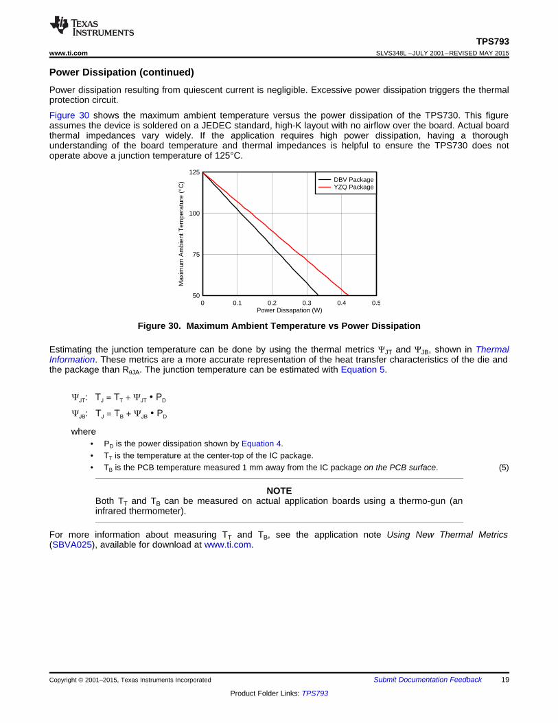
Figure 30 shows the maximum ambient temperature versus the power dissipation of the TPS730. This figureassumes the device is soldered on a JEDEC standard, high-K layout with no airflow over the board. Actual boardthermal impedances vary widely. If the application requires high power dissipation, having a thoroughunderstanding of the board temperature and thermal impedances is helpful to ensure the TPS730 does notoperate above a junction temperature of 125°C.
Figure 30. Maximum Ambient Temperature vs Power Dissipation
Estimating the junction temperature can be done by using the thermal metrics ΨJT and ΨJB, shown in ThermalInformation. These metrics are a more accurate representation of the heat transfer characteristics of the die andthe package than RθJA. The junction temperature can be estimated with Equation 5.
where• PD is the power dissipation shown by Equation 4.• TT is the temperature at the center-top of the IC package.• TB is the PCB temperature measured 1 mm away from the IC package on the PCB surface. (5)
NOTEBoth TT and TB can be measured on actual application boards using a thermo-gun (aninfrared thermometer).
For more information about measuring TT and TB, see the application note Using New Thermal Metrics(SBVA025), available for download at www.ti.com.

20
TPS793SLVS348L –JULY 2001–REVISED MAY 2015 www.ti.com
Product Folder Links: TPS793
Submit Documentation Feedback Copyright © 2001–2015, Texas Instruments Incorporated
(1) For the most current package and ordering information see the Package Option Addendum at the end of this document, or visit thedevice product folder on www.ti.com.
(2) Output voltages from 1.2 V to 4.8 V in 50-mV increments are available. Contact the factory for details and availability.
11 Device and Documentation Support
11.1 Device Support
11.1.1 Development Support
11.1.1.1 Evaluation ModulesSeven evaluation modules (EVMs) are available to assist in the initial circuit performance evaluation using theTPS793:• TPS79301EVM• TPS79318YEQEVM• TPS79325YEQEVM• TPS793285YEQEVM• TPS79328EVM• TPS79328YEQEVM• TPS79330YEQEVM
These EVMs can be requested at the Texas Instruments website through the device product folders orpurchased directly from the TI eStore.
11.1.1.2 Spice ModelsComputer simulation of circuit performance using SPICE is often useful when analyzing the performance ofanalog circuits and systems. A SPICE model for the TPS793 is available through the product folders under Tools& Software.
11.1.2 Device Nomenclature
Table 4. Ordering Information (1) (2)
PRODUCT VOUT
TPS793xxyyyzXX(X) is the nominal output voltage (for example, 28 = 2.8 V; 285 = 2.85 V; 01 = adjustable version).YYY is the package designator.Z is the package quantity. R is for reel (3000 pieces), T is for tape (250 pieces).
11.2 Documentation Support
11.2.1 Related Documentation• Application note, Using New Thermal Metrics, SBVA025.• Application note, Pros and Cons of Using a Feedforward Capacitor with a Low-Dropout Regulator, SBVA042.• TPS793xxYEQEVM User's Guide, SBVU001.• TPS79301EVM, TPS79328EVM LDO Linear Regulator Evaluation Module User's Guide, SLVU060A.
11.3 Community ResourceThe following links connect to TI community resources. Linked contents are provided "AS IS" by the respectivecontributors. They do not constitute TI specifications and do not necessarily reflect TI's views; see TI's Terms ofUse.
TI E2E™ Online Community TI's Engineer-to-Engineer (E2E) Community. Created to foster collaborationamong engineers. At e2e.ti.com, you can ask questions, share knowledge, explore ideas and helpsolve problems with fellow engineers.
Design Support TI's Design Support Quickly find helpful E2E forums along with design support tools andcontact information for technical support.

21
TPS793www.ti.com SLVS348L –JULY 2001–REVISED MAY 2015
Product Folder Links: TPS793
Submit Documentation FeedbackCopyright © 2001–2015, Texas Instruments Incorporated
11.4 TrademarksNanoStar, E2E are trademarks of Texas Instruments.Bluetooth is a registered trademark of Bluetooth SIG, Inc.All other trademarks are the property of their respective owners.
11.5 Electrostatic Discharge CautionThese devices have limited built-in ESD protection. The leads should be shorted together or the device placed in conductive foamduring storage or handling to prevent electrostatic damage to the MOS gates.
11.6 GlossarySLYZ022 — TI Glossary.
This glossary lists and explains terms, acronyms, and definitions.
12 Mechanical, Packaging, and Orderable InformationThe following pages include mechanical, packaging, and orderable information. This information is the mostcurrent data available for the designated devices. This data is subject to change without notice and revision ofthis document. For browser-based versions of this data sheet, refer to the left-hand navigation.

PACKAGE OPTION ADDENDUM
www.ti.com 15-Apr-2017
Addendum-Page 1
PACKAGING INFORMATION
Orderable Device Status(1)
Package Type PackageDrawing
Pins PackageQty
Eco Plan(2)
Lead/Ball Finish(6)
MSL Peak Temp(3)
Op Temp (°C) Device Marking(4/5)
Samples
HPA01085DBVR ACTIVE SOT-23 DBV 5 3000 Green (RoHS& no Sb/Br)
CU NIPDAU Level-1-260C-UNLIM -40 to 125 PHJI
HPA01085DVBR ACTIVE SOT-23 DBV 5 3000 Green (RoHS& no Sb/Br)
CU NIPDAU Level-1-260C-UNLIM -40 to 125 PHJI
TPS79301DBVR ACTIVE SOT-23 DBV 6 3000 Green (RoHS& no Sb/Br)
CU NIPDAU Level-1-260C-UNLIM -40 to 125 PGVI
TPS79301DBVRG4 ACTIVE SOT-23 DBV 6 3000 Green (RoHS& no Sb/Br)
CU NIPDAU Level-1-260C-UNLIM -40 to 125 PGVI
TPS79318DBVR ACTIVE SOT-23 DBV 5 3000 Green (RoHS& no Sb/Br)
CU NIPDAU Level-1-260C-UNLIM -40 to 125 PHHI
TPS79318DBVRG4 ACTIVE SOT-23 DBV 5 3000 Green (RoHS& no Sb/Br)
CU NIPDAU Level-1-260C-UNLIM -40 to 125 PHHI
TPS79318DBVT ACTIVE SOT-23 DBV 5 250 Green (RoHS& no Sb/Br)
CU NIPDAU Level-1-260C-UNLIM -40 to 125 PHHI
TPS79318DBVTG4 ACTIVE SOT-23 DBV 5 250 Green (RoHS& no Sb/Br)
CU NIPDAU Level-1-260C-UNLIM -40 to 125 PHHI
TPS79318YZQR ACTIVE DSBGA YZQ 5 3000 Green (RoHS& no Sb/Br)
SNAGCU Level-1-260C-UNLIM -40 to 125 E3
TPS79318YZQT ACTIVE DSBGA YZQ 5 250 Green (RoHS& no Sb/Br)
SNAGCU Level-1-260C-UNLIM -40 to 125 E3
TPS79325DBVR ACTIVE SOT-23 DBV 5 3000 Green (RoHS& no Sb/Br)
CU NIPDAU Level-1-260C-UNLIM -40 to 125 PGWI
TPS79325DBVRG4 ACTIVE SOT-23 DBV 5 3000 Green (RoHS& no Sb/Br)
CU NIPDAU Level-1-260C-UNLIM -40 to 125 PGWI
TPS79325YZQR ACTIVE DSBGA YZQ 5 3000 Green (RoHS& no Sb/Br)
SNAGCU Level-1-260C-UNLIM -40 to 125 E4
TPS793285DBVR ACTIVE SOT-23 DBV 5 3000 Green (RoHS& no Sb/Br)
CU NIPDAU Level-1-260C-UNLIM -40 to 125 PHII
TPS793285DBVRG4 ACTIVE SOT-23 DBV 5 3000 Green (RoHS& no Sb/Br)
CU NIPDAU Level-1-260C-UNLIM -40 to 125 PHII
TPS793285DBVT ACTIVE SOT-23 DBV 5 250 Green (RoHS& no Sb/Br)
CU NIPDAU Level-1-260C-UNLIM -40 to 125 PHII
TPS793285DBVTG4 ACTIVE SOT-23 DBV 5 250 Green (RoHS& no Sb/Br)
CU NIPDAU Level-1-260C-UNLIM -40 to 125 PHII
PACKAGE OPTION ADDENDUM
www.ti.com 15-Apr-2017
Addendum-Page 2
Orderable Device Status(1)
Package Type PackageDrawing
Pins PackageQty
Eco Plan(2)
Lead/Ball Finish(6)
MSL Peak Temp(3)
Op Temp (°C) Device Marking(4/5)
Samples
TPS793285YZQR ACTIVE DSBGA YZQ 5 3000 Green (RoHS& no Sb/Br)
SNAGCU Level-1-260C-UNLIM -40 to 125 E5
TPS79328DBVR ACTIVE SOT-23 DBV 5 3000 Green (RoHS& no Sb/Br)
CU NIPDAU Level-1-260C-UNLIM -40 to 125 PGXI
TPS79328DBVRG4 ACTIVE SOT-23 DBV 5 3000 Green (RoHS& no Sb/Br)
CU NIPDAU Level-1-260C-UNLIM -40 to 125 PGXI
TPS79328YZQR ACTIVE DSBGA YZQ 5 3000 Green (RoHS& no Sb/Br)
SNAGCU Level-1-260C-UNLIM -40 to 125 E2
TPS79328YZQT ACTIVE DSBGA YZQ 5 250 Green (RoHS& no Sb/Br)
SNAGCU Level-1-260C-UNLIM -40 to 125 E2
TPS79330DBVR ACTIVE SOT-23 DBV 5 3000 Green (RoHS& no Sb/Br)
CU NIPDAU Level-1-260C-UNLIM -40 to 125 PGYI
TPS79330DBVRG4 ACTIVE SOT-23 DBV 5 3000 Green (RoHS& no Sb/Br)
CU NIPDAU Level-1-260C-UNLIM -40 to 125 PGYI
TPS79330YZQR ACTIVE DSBGA YZQ 5 3000 Green (RoHS& no Sb/Br)
SNAGCU Level-1-260C-UNLIM -40 to 125 E6
TPS79330YZQT ACTIVE DSBGA YZQ 5 250 Green (RoHS& no Sb/Br)
SNAGCU Level-1-260C-UNLIM -40 to 125 E6
TPS79333DBVR ACTIVE SOT-23 DBV 5 3000 Green (RoHS& no Sb/Br)
CU NIPDAU Level-1-260C-UNLIM -40 to 125 PHUI
TPS79333DBVRG4 ACTIVE SOT-23 DBV 5 3000 Green (RoHS& no Sb/Br)
CU NIPDAU Level-1-260C-UNLIM -40 to 125 PHUI
TPS793475DBVR ACTIVE SOT-23 DBV 5 3000 Green (RoHS& no Sb/Br)
CU NIPDAU Level-1-260C-UNLIM -40 to 125 PHJI
TPS793475DBVRG4 ACTIVE SOT-23 DBV 5 3000 Green (RoHS& no Sb/Br)
CU NIPDAU Level-1-260C-UNLIM -40 to 125 PHJI
(1) The marketing status values are defined as follows:ACTIVE: Product device recommended for new designs.LIFEBUY: TI has announced that the device will be discontinued, and a lifetime-buy period is in effect.NRND: Not recommended for new designs. Device is in production to support existing customers, but TI does not recommend using this part in a new design.PREVIEW: Device has been announced but is not in production. Samples may or may not be available.OBSOLETE: TI has discontinued the production of the device.
(2) Eco Plan - The planned eco-friendly classification: Pb-Free (RoHS), Pb-Free (RoHS Exempt), or Green (RoHS & no Sb/Br) - please check http://www.ti.com/productcontent for the latest availabilityinformation and additional product content details.TBD: The Pb-Free/Green conversion plan has not been defined.

PACKAGE OPTION ADDENDUM
www.ti.com 15-Apr-2017
Addendum-Page 3
Pb-Free (RoHS): TI's terms "Lead-Free" or "Pb-Free" mean semiconductor products that are compatible with the current RoHS requirements for all 6 substances, including the requirement thatlead not exceed 0.1% by weight in homogeneous materials. Where designed to be soldered at high temperatures, TI Pb-Free products are suitable for use in specified lead-free processes.Pb-Free (RoHS Exempt): This component has a RoHS exemption for either 1) lead-based flip-chip solder bumps used between the die and package, or 2) lead-based die adhesive used betweenthe die and leadframe. The component is otherwise considered Pb-Free (RoHS compatible) as defined above.Green (RoHS & no Sb/Br): TI defines "Green" to mean Pb-Free (RoHS compatible), and free of Bromine (Br) and Antimony (Sb) based flame retardants (Br or Sb do not exceed 0.1% by weightin homogeneous material)
(3) MSL, Peak Temp. - The Moisture Sensitivity Level rating according to the JEDEC industry standard classifications, and peak solder temperature.
(4) There may be additional marking, which relates to the logo, the lot trace code information, or the environmental category on the device.
(5) Multiple Device Markings will be inside parentheses. Only one Device Marking contained in parentheses and separated by a "~" will appear on a device. If a line is indented then it is a continuationof the previous line and the two combined represent the entire Device Marking for that device.
(6) Lead/Ball Finish - Orderable Devices may have multiple material finish options. Finish options are separated by a vertical ruled line. Lead/Ball Finish values may wrap to two lines if the finishvalue exceeds the maximum column width.
Important Information and Disclaimer:The information provided on this page represents TI's knowledge and belief as of the date that it is provided. TI bases its knowledge and belief on informationprovided by third parties, and makes no representation or warranty as to the accuracy of such information. Efforts are underway to better integrate information from third parties. TI has taken andcontinues to take reasonable steps to provide representative and accurate information but may not have conducted destructive testing or chemical analysis on incoming materials and chemicals.TI and TI suppliers consider certain information to be proprietary, and thus CAS numbers and other limited information may not be available for release.
In no event shall TI's liability arising out of such information exceed the total purchase price of the TI part(s) at issue in this document sold by TI to Customer on an annual basis.
OTHER QUALIFIED VERSIONS OF TPS793 :
• Automotive: TPS793-Q1
NOTE: Qualified Version Definitions:
• Automotive - Q100 devices qualified for high-reliability automotive applications targeting zero defects

TAPE AND REEL INFORMATION
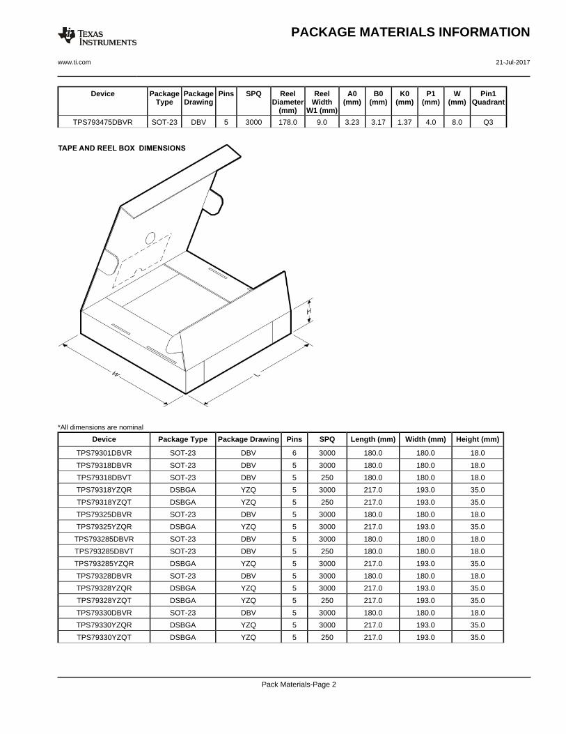
*All dimensions are nominal
Device PackageType
PackageDrawing
Pins SPQ ReelDiameter
(mm)
ReelWidth
W1 (mm)
A0(mm)
B0(mm)
K0(mm)
P1(mm)
W(mm)
Pin1Quadrant
TPS79301DBVR SOT-23 DBV 6 3000 178.0 9.0 3.23 3.17 1.37 4.0 8.0 Q3
TPS79318DBVR SOT-23 DBV 5 3000 178.0 9.0 3.23 3.17 1.37 4.0 8.0 Q3
TPS79318DBVT SOT-23 DBV 5 250 178.0 9.0 3.23 3.17 1.37 4.0 8.0 Q3
TPS79318YZQR DSBGA YZQ 5 3000 178.0 8.4 0.98 1.46 0.69 4.0 8.0 Q1
TPS79318YZQT DSBGA YZQ 5 250 178.0 8.4 0.98 1.46 0.69 4.0 8.0 Q1
TPS79325DBVR SOT-23 DBV 5 3000 178.0 9.0 3.23 3.17 1.37 4.0 8.0 Q3
TPS79325YZQR DSBGA YZQ 5 3000 178.0 8.4 0.98 1.46 0.69 4.0 8.0 Q1
TPS793285DBVR SOT-23 DBV 5 3000 178.0 9.0 3.23 3.17 1.37 4.0 8.0 Q3
TPS793285DBVT SOT-23 DBV 5 250 178.0 9.0 3.23 3.17 1.37 4.0 8.0 Q3
TPS793285YZQR DSBGA YZQ 5 3000 178.0 8.4 0.98 1.46 0.69 4.0 8.0 Q1
TPS79328DBVR SOT-23 DBV 5 3000 178.0 9.0 3.23 3.17 1.37 4.0 8.0 Q3
TPS79328YZQR DSBGA YZQ 5 3000 178.0 8.4 0.98 1.46 0.69 4.0 8.0 Q1
TPS79328YZQT DSBGA YZQ 5 250 178.0 8.4 0.98 1.46 0.69 4.0 8.0 Q1
TPS79330DBVR SOT-23 DBV 5 3000 178.0 9.0 3.23 3.17 1.37 4.0 8.0 Q3
TPS79330YZQR DSBGA YZQ 5 3000 178.0 8.4 0.98 1.46 0.69 4.0 8.0 Q1
TPS79330YZQT DSBGA YZQ 5 250 178.0 8.4 0.98 1.46 0.69 4.0 8.0 Q1
TPS79333DBVR SOT-23 DBV 5 3000 178.0 9.0 3.23 3.17 1.37 4.0 8.0 Q3
TPS79333DBVR SOT-23 DBV 5 3000 180.0 8.4 3.2 3.2 1.4 4.0 8.0 Q3
PACKAGE MATERIALS INFORMATION
www.ti.com 21-Jul-2017
Pack Materials-Page 1
Device PackageType
PackageDrawing
Pins SPQ ReelDiameter
(mm)
ReelWidth
W1 (mm)
A0(mm)
B0(mm)
K0(mm)
P1(mm)
W(mm)
Pin1Quadrant
TPS793475DBVR SOT-23 DBV 5 3000 178.0 9.0 3.23 3.17 1.37 4.0 8.0 Q3
*All dimensions are nominal
Device Package Type Package Drawing Pins SPQ Length (mm) Width (mm) Height (mm)
TPS79301DBVR SOT-23 DBV 6 3000 180.0 180.0 18.0
TPS79318DBVR SOT-23 DBV 5 3000 180.0 180.0 18.0
TPS79318DBVT SOT-23 DBV 5 250 180.0 180.0 18.0
TPS79318YZQR DSBGA YZQ 5 3000 217.0 193.0 35.0
TPS79318YZQT DSBGA YZQ 5 250 217.0 193.0 35.0
TPS79325DBVR SOT-23 DBV 5 3000 180.0 180.0 18.0
TPS79325YZQR DSBGA YZQ 5 3000 217.0 193.0 35.0
TPS793285DBVR SOT-23 DBV 5 3000 180.0 180.0 18.0
TPS793285DBVT SOT-23 DBV 5 250 180.0 180.0 18.0
TPS793285YZQR DSBGA YZQ 5 3000 217.0 193.0 35.0
TPS79328DBVR SOT-23 DBV 5 3000 180.0 180.0 18.0
TPS79328YZQR DSBGA YZQ 5 3000 217.0 193.0 35.0
TPS79328YZQT DSBGA YZQ 5 250 217.0 193.0 35.0
TPS79330DBVR SOT-23 DBV 5 3000 180.0 180.0 18.0
TPS79330YZQR DSBGA YZQ 5 3000 217.0 193.0 35.0
TPS79330YZQT DSBGA YZQ 5 250 217.0 193.0 35.0
PACKAGE MATERIALS INFORMATION
www.ti.com 21-Jul-2017
Pack Materials-Page 2
Device Package Type Package Drawing Pins SPQ Length (mm) Width (mm) Height (mm)
TPS79333DBVR SOT-23 DBV 5 3000 180.0 180.0 18.0
TPS79333DBVR SOT-23 DBV 5 3000 210.0 185.0 35.0
TPS793475DBVR SOT-23 DBV 5 3000 180.0 180.0 18.0
PACKAGE MATERIALS INFORMATION
www.ti.com 21-Jul-2017
Pack Materials-Page 3


IMPORTANT NOTICE
Texas Instruments Incorporated (TI) reserves the right to make corrections, enhancements, improvements and other changes to itssemiconductor products and services per JESD46, latest issue, and to discontinue any product or service per JESD48, latest issue. Buyersshould obtain the latest relevant information before placing orders and should verify that such information is current and complete.TI’s published terms of sale for semiconductor products (http://www.ti.com/sc/docs/stdterms.htm) apply to the sale of packaged integratedcircuit products that TI has qualified and released to market. Additional terms may apply to the use or sale of other types of TI products andservices.Reproduction of significant portions of TI information in TI data sheets is permissible only if reproduction is without alteration and isaccompanied by all associated warranties, conditions, limitations, and notices. TI is not responsible or liable for such reproduceddocumentation. Information of third parties may be subject to additional restrictions. Resale of TI products or services with statementsdifferent from or beyond the parameters stated by TI for that product or service voids all express and any implied warranties for theassociated TI product or service and is an unfair and deceptive business practice. TI is not responsible or liable for any such statements.Buyers and others who are developing systems that incorporate TI products (collectively, “Designers”) understand and agree that Designersremain responsible for using their independent analysis, evaluation and judgment in designing their applications and that Designers havefull and exclusive responsibility to assure the safety of Designers' applications and compliance of their applications (and of all TI productsused in or for Designers’ applications) with all applicable regulations, laws and other applicable requirements. Designer represents that, withrespect to their applications, Designer has all the necessary expertise to create and implement safeguards that (1) anticipate dangerousconsequences of failures, (2) monitor failures and their consequences, and (3) lessen the likelihood of failures that might cause harm andtake appropriate actions. Designer agrees that prior to using or distributing any applications that include TI products, Designer willthoroughly test such applications and the functionality of such TI products as used in such applications.TI’s provision of technical, application or other design advice, quality characterization, reliability data or other services or information,including, but not limited to, reference designs and materials relating to evaluation modules, (collectively, “TI Resources”) are intended toassist designers who are developing applications that incorporate TI products; by downloading, accessing or using TI Resources in anyway, Designer (individually or, if Designer is acting on behalf of a company, Designer’s company) agrees to use any particular TI Resourcesolely for this purpose and subject to the terms of this Notice.TI’s provision of TI Resources does not expand or otherwise alter TI’s applicable published warranties or warranty disclaimers for TIproducts, and no additional obligations or liabilities arise from TI providing such TI Resources. TI reserves the right to make corrections,enhancements, improvements and other changes to its TI Resources. TI has not conducted any testing other than that specificallydescribed in the published documentation for a particular TI Resource.Designer is authorized to use, copy and modify any individual TI Resource only in connection with the development of applications thatinclude the TI product(s) identified in such TI Resource. NO OTHER LICENSE, EXPRESS OR IMPLIED, BY ESTOPPEL OR OTHERWISETO ANY OTHER TI INTELLECTUAL PROPERTY RIGHT, AND NO LICENSE TO ANY TECHNOLOGY OR INTELLECTUAL PROPERTYRIGHT OF TI OR ANY THIRD PARTY IS GRANTED HEREIN, including but not limited to any patent right, copyright, mask work right, orother intellectual property right relating to any combination, machine, or process in which TI products or services are used. Informationregarding or referencing third-party products or services does not constitute a license to use such products or services, or a warranty orendorsement thereof. Use of TI Resources may require a license from a third party under the patents or other intellectual property of thethird party, or a license from TI under the patents or other intellectual property of TI.TI RESOURCES ARE PROVIDED “AS IS” AND WITH ALL FAULTS. TI DISCLAIMS ALL OTHER WARRANTIES ORREPRESENTATIONS, EXPRESS OR IMPLIED, REGARDING RESOURCES OR USE THEREOF, INCLUDING BUT NOT LIMITED TOACCURACY OR COMPLETENESS, TITLE, ANY EPIDEMIC FAILURE WARRANTY AND ANY IMPLIED WARRANTIES OFMERCHANTABILITY, FITNESS FOR A PARTICULAR PURPOSE, AND NON-INFRINGEMENT OF ANY THIRD PARTY INTELLECTUALPROPERTY RIGHTS. TI SHALL NOT BE LIABLE FOR AND SHALL NOT DEFEND OR INDEMNIFY DESIGNER AGAINST ANY CLAIM,INCLUDING BUT NOT LIMITED TO ANY INFRINGEMENT CLAIM THAT RELATES TO OR IS BASED ON ANY COMBINATION OFPRODUCTS EVEN IF DESCRIBED IN TI RESOURCES OR OTHERWISE. IN NO EVENT SHALL TI BE LIABLE FOR ANY ACTUAL,DIRECT, SPECIAL, COLLATERAL, INDIRECT, PUNITIVE, INCIDENTAL, CONSEQUENTIAL OR EXEMPLARY DAMAGES INCONNECTION WITH OR ARISING OUT OF TI RESOURCES OR USE THEREOF, AND REGARDLESS OF WHETHER TI HAS BEENADVISED OF THE POSSIBILITY OF SUCH DAMAGES.Unless TI has explicitly designated an individual product as meeting the requirements of a particular industry standard (e.g., ISO/TS 16949and ISO 26262), TI is not responsible for any failure to meet such industry standard requirements.Where TI specifically promotes products as facilitating functional safety or as compliant with industry functional safety standards, suchproducts are intended to help enable customers to design and create their own applications that meet applicable functional safety standardsand requirements. Using products in an application does not by itself establish any safety features in the application. Designers mustensure compliance with safety-related requirements and standards applicable to their applications. Designer may not use any TI products inlife-critical medical equipment unless authorized officers of the parties have executed a special contract specifically governing such use.Life-critical medical equipment is medical equipment where failure of such equipment would cause serious bodily injury or death (e.g., lifesupport, pacemakers, defibrillators, heart pumps, neurostimulators, and implantables). Such equipment includes, without limitation, allmedical devices identified by the U.S. Food and Drug Administration as Class III devices and equivalent classifications outside the U.S.TI may expressly designate certain products as completing a particular qualification (e.g., Q100, Military Grade, or Enhanced Product).Designers agree that it has the necessary expertise to select the product with the appropriate qualification designation for their applicationsand that proper product selection is at Designers’ own risk. Designers are solely responsible for compliance with all legal and regulatoryrequirements in connection with such selection.Designer will fully indemnify TI and its representatives against any damages, costs, losses, and/or liabilities arising out of Designer’s non-compliance with the terms and provisions of this Notice.
Mailing Address: Texas Instruments, Post Office Box 655303, Dallas, Texas 75265Copyright © 2017, Texas Instruments Incorporated