tps92830-q1 3-channel high-current linear led … fog light, reverse light • front light –...
TRANSCRIPT

CP1P
CP1N
GND
CP2N
CP2P
CPOUT
IN
DIAGEN
DERATE
PWM1
ISP
ISN1
G1
SENSE1
ISN2
G2
SENSE2
ISN3
G3
SENSE3
PWMOUT
FAULT
PWMCHG
IREF
PWM2
PWM3
FD
ICTRL
Battery
Full Duty Cycle
TPS92830-Q1
FAULT Bus
Copyright © 2017, Texas Instruments Incorporated
Product
Folder
Order
Now
Technical
Documents
Tools &
Software
Support &Community
ReferenceDesign
An IMPORTANT NOTICE at the end of this data sheet addresses availability, warranty, changes, use in safety-critical applications,intellectual property matters and other important disclaimers. PRODUCTION DATA.
TPS92830-Q1SLIS178B –OCTOBER 2017–REVISED JANUARY 2018
TPS92830-Q1 3-Channel High-Current Linear LED Controller
1
1 Features1• AEC-Q100 Qualified
– Device Temperature Grade 1: –40°C to 125°CAmbient Operating Temperature Range
– Device HBM ESD Classification Level H2– Device CDM ESD Classification Level C4B
• Wide Voltage Input Range From 4.5 V to 40 V• 3-Channel High-Side Current Driving and Sensing
– Channel-Independent Current Setting– Channel-Independent PWM Inputs– PWM Dimming via Both PWM Inputs and
Power Supply– Optimized Slew Rate for EMC
• High-Precision LED Driving– Precision Current Regulation With External N-
Channel MOSFET (2.5% Tolerance)– 20:1 Analog Dimming Profile With Off-Board
Bin Resistor Support– Precision PWM Generator With Full Duty-
Cycle Mask (2% Tolerance)– Open-Drain PWM Output for Synchronization
• Protection and Diagnostics– Adjustable Output Current Derating for
External MOSFET Thermal Protection– Diagnostics for LED-String Open Circuit or
Short Circuit With Auto Recovery– Diagnostic-Enable With Adjustable Threshold
for Low-Voltage Operation– Fault Bus up to 15 Devices, Configurable As
Either One-Fails–All-Fail or Only-Failed-Channel-Off
– Low Quiescent Current in Fault Mode (<0.75mA per Device)
• Operating Junction Temperature Range: –40°C to150°C
• TSSOP 28 Package (PW)
2 Applications• Rear Light – Tail and Stop Light, Rear Turn
Indicator, Fog Light, Reverse Light• Front Light – Position Light, Daytime Running
Light, Front Turn Indicator, Low Beam
3 DescriptionWith the trend of better lighting homogeneity, high-current LEDs are often used in automotive front andrear lamps with lighting diffusers and light-guides.Meanwhile, in order to meet strict EMC and reliabilityrequirements, linear LED drivers are popular inautomotive applications. However, it is a challenge todeliver high current for linear LED drivers withintegrated power transistors. The TPS92830-Q1device is an advanced automotive-grade high-sideconstant-current linear LED controller for deliveringhigh current using external N-channel MOSFETs. Thedevice has a full set of features for automotiveapplications and is compatible with a wide selectionof N-channel MOSFETs.
Each channel of the TPS92830-Q1 device sets thechannel current independently by the sense-resistorvalue. An internal precision constant-currentregulation loop senses the channel current by thevoltage across the sense resistor and controls thegate voltage of the N-channel MOSFET accordingly.The device also integrates a two-stage charge pumpfor low-dropout operation. The charge-pump voltageis high enough to support a wide selection of N-channel iMOSFETs. iPWM idimming iallows imultiple
Device Information(1)
PART NUMBER PACKAGE BODY SIZE (NOM)TPS92830-Q1 TSSOP (28) 9.70 mm × 4.40 mm
(1) For all available packages, see the orderable addendum atthe end of the data sheet.
Simplified Schematic

2
TPS92830-Q1SLIS178B –OCTOBER 2017–REVISED JANUARY 2018 www.ti.com
Product Folder Links: TPS92830-Q1
Submit Documentation Feedback Copyright © 2017–2018, Texas Instruments Incorporated
Table of Contents1 Features .................................................................. 12 Applications ........................................................... 13 Description ............................................................. 14 Revision History..................................................... 25 Description (Continued) ........................................ 46 Pin Configuration and Functions ......................... 47 Specifications......................................................... 6
7.1 Absolute Maximum Ratings ...................................... 67.2 ESD Ratings ............................................................ 67.3 Recommended Operating Conditions....................... 67.4 Thermal Information .................................................. 77.5 Electrical Characteristics........................................... 77.6 Timing Requirements ................................................ 97.7 Typical Characteristics ............................................ 11
8 Detailed Description ............................................ 148.1 Overview ................................................................. 14
8.2 Functional Block Diagram ....................................... 148.3 Feature Description................................................. 158.4 Device Functional Modes........................................ 29
9 Application and Implementation ........................ 309.1 Application Information............................................ 309.2 Typical Applications ................................................ 30
10 Layout................................................................... 3610.1 Layout Guidelines ................................................. 3610.2 Layout Example .................................................... 36
11 Device and Documentation Support ................. 3711.1 Receiving Notification of Documentation Updates 3711.2 Community Resources.......................................... 3711.3 Trademarks ........................................................... 3711.4 Electrostatic Discharge Caution............................ 3711.5 Glossary ................................................................ 37
12 Mechanical, Packaging, and OrderableInformation ........................................................... 37
4 Revision HistoryNOTE: Page numbers for previous revisions may differ from page numbers in the current version.
Changes from Revision A (October 2017) to Revision B Page
• Changed timing specification for PWM duty cycle ................................................................................................................. 9
Changes from Original (July 2017) to Revision A Page
• Changed tolerances for current regulation and PWM generator in the Features section ..................................................... 1• Changed values for several parameters throughout the Electrical Characteristics table....................................................... 7• Changed parameter definitions for I(DRV_source) and I(DRV_sink) in the Electrical Chaaracteristics table ..................................... 7• Changed parameter symbols for analog dimming accuracy in the Electrical Characteristics table....................................... 8• Changed parameter descriptions for V(OPEN_th_rising), V(OPEN_th_falling), ....................................................................................... 8• Changed parameter descriptions for t(SG_retry_OFF) and t(OPEN_retry_OFF) in the Timing Requirements table............................... 9• Added a condition for Typical Characteristic Figure 6 ......................................................................................................... 11• Deleted a condition from Typical Characteristic Figure 8 .................................................................................................... 12• Deleted a Fast Power Down and Slow Power Up typical characteristic graph .................................................................... 12• Added a Fast Power Down and Slow Power Up typical characteristic graph ...................................................................... 13• Added a condition for Typical Characteristic Figure 17 ....................................................................................................... 13• Added a condition for Typical Characteristic Figure 18........................................................................................................ 13• Changed heat dissipation to current distribution in Parallel MOSFET Driving ..................................................................... 17• Deleted a sentence from the PWM Dimming by Input section............................................................................................. 18• Added resistor and capacitor reference designators............................................................................................................ 19• Deleted percentage values for V(ICTRL_LIN_BOT) and V(ICTRL_LIN_TOP) in the Analog Dimming Topology section ...................... 21• Changed V(SG_th_rising) and V(SG_th_falling) with each other in the LED Short-to-GND Detection section .................................. 25• Changed symbol of short-to-ground retry current to I(Retry_short) ............................................................................................ 26• Changed symbol of LED-open retry current to I(Retry_open) in the LED Open-Circuit Auto Retry section............................... 26• Changed some FAULT TYPE names in Table 4.................................................................................................................. 29• Updated application schematic. ........................................................................................................................................... 30• Changed the value of R8 from 75 kΩ to 76 kΩ for the PWM threshold setting ................................................................... 31

3
TPS92830-Q1www.ti.com SLIS178B –OCTOBER 2017–REVISED JANUARY 2018
Product Folder Links: TPS92830-Q1
Submit Documentation FeedbackCopyright © 2017–2018, Texas Instruments Incorporated
• Changed the equation for calculating K(RES_DiagEn)................................................................................................................ 31• Changed the values of R13 and R6 for ............................................................................................................................... 31• Changed the equation for calculating K(RES_DERATE) .............................................................................................................. 31• Changed component values inthe PWM equations of the Detailed Design Procedure ....................................................... 33• Added an application curve .................................................................................................................................................. 34• Added text in the Layout Guidelines for keeping LED ground separate from device ground .............................................. 36
1CP1P 28 ISP
2CP1N 27 ISN1
3GND 26 G1
4CP2N 25 SENSE1
5CP2P 24 ISN2
6CPOUT 23 G2
7IN 22 SENSE2
8DIAGEN 21 ISN3
9DERATE 20 G3
10PWM1 19 SENSE3
11PWM2 18 PWMOUT
12PWM3 17 FAULT
13FD 16 PWMCHG
14ICTRL 15 IREF
Not to scale
4
TPS92830-Q1SLIS178B –OCTOBER 2017–REVISED JANUARY 2018 www.ti.com
Product Folder Links: TPS92830-Q1
Submit Documentation Feedback Copyright © 2017–2018, Texas Instruments Incorporated
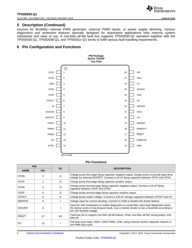
5 Description (Continued)sources for flexibility—internal PWM generator, external PWM inputs, or power supply dimming. Variousdiagnostics and protection features specially designed for automotive applications help improve systemrobustness and ease of use. A one-fails–all-fail fault bus supports TPS92830-Q1 operation together with theTPS92630-Q1, TPS92638-Q1, and TPS9261x-Q1 family to fulfill various fault-handling requirements.
6 Pin Configuration and Functions
PW Package28-Pin TSSOP
Top View
Pin FunctionsPIN
I/O DESCRIPTIONNAME NO.
CP1N 2 O Charge pump first-stage flying capacitor negative output, charge pump to provide gate-drivevoltage for external MOSFET. Connect a 10-nF flying capacitor between CP1P and CP1N.
CP1P 1 O Charge pump first-stage flying capacitor positive output
CP2N 4 O Charge pump second-stage flying capacitor negative output. Connect a 10-nF flyingcapacitor between CP2P and CP2N.
CP2P 5 O Charge pump second-stage flying capacitor positive outputCPOUT 6 O Charge-pump output voltage. Connect a 150-nF storage capacitor between CPOUT and IN.DERATE 9 I Voltage input for current derating. Connect to GND to disable the derate feature.
DIAGEN 8 IInput pin with comparator to enable diagnostics to avoid false open-fault diagnostics whenthe device works in low-dropout mode. Use a resistor divider to set a threshold according tothe LED forward voltage.
FAULT 17 I/O Fault bus pin to support one-fails–all-fail feature. Float: one-fails–all-fail; strong pullup: only-fails-off
FD 13 I Full duty-cycle input, HIGH: 100% PWM; LOW: using external resistor-capacitor network toset PWM duty cycle

5
TPS92830-Q1www.ti.com SLIS178B –OCTOBER 2017–REVISED JANUARY 2018
Product Folder Links: TPS92830-Q1
Submit Documentation FeedbackCopyright © 2017–2018, Texas Instruments Incorporated
Pin Functions (continued)PIN
I/O DESCRIPTIONNAME NO.
G1 26 O Channel 1 gate driver output, connect to CH 1 N-channel MOSFET gateG2 23 O Channel 2 gate driver output, connect to CH 2 N-channel MOSFET gateG3 20 O Channel 3 gate driver output, connect to CH 3 N-channel MOSFET gateGND 3 — GND
ICTRL 14 IAnalog dimming input, modulates the regulation voltage across the current-sense resistor.Apply a voltage source or connect a resistor between ICTRL and GND to set the analogdimming ratio.
IN 7 I Power supply for the device. LED current only flows from the external MOSFET to the LED.
ISN1 27 I Channel 1 current-sense negative input. Connect a current-sense resistor between ISP andISN1 to set the CH 1 current.
ISN2 24 I Channel 2 current-sense negative input. Connect a current-sense resistor between ISP andISN2 to set the CH 2 current.
ISN3 21 I Channel 3 current-sense negative input. Connect a current-sense resistor between ISP andISN3 to set the CH 3 current.
IREF 15 O Internal current reference. Connect an 8-kΩ resistor between IREF and GND,ISP 28 I Channel current-sense positive input. Kelvin-sense to LED sense-resistor positive node.PWM1 10 I Channel 1 PWM inputPWM2 11 I Channel 2 PWM inputPWM3 12 I Channel 3 PWM input
PWMCHG 16 I/O On-chip PWM generator pin for external R-C. Connect a resistor and a capacitor betweenPWMCHG and GND to set the PWM duty cycle and frequency.
PWMOUT 18 O High-voltage PWM open-drain output. Connect a 10-kΩ resistor between IN and PWMOUTSENSE1 25 I/O Channel 1 diagnostics pin. Connect to the CH 1 MOSFET source terminalSENSE2 22 I/O Channel 2 diagnostics pin. Connect to the CH 2 MOSFET source terminalSENSE3 19 I/O Channel 3 diagnostics pin. Connect to the CH 3 MOSFET source terminal

6
TPS92830-Q1SLIS178B –OCTOBER 2017–REVISED JANUARY 2018 www.ti.com
Product Folder Links: TPS92830-Q1
Submit Documentation Feedback Copyright © 2017–2018, Texas Instruments Incorporated
(1) Stresses beyond those listed under Absolute Maximum Ratings may cause permanent damage to the device. These are stress ratingsonly, which do not imply functional operation of the device at these or any other conditions beyond those indicated under RecommendedOperating Conditions. Exposure to absolute-maximum-rated conditions for extended periods may affect device reliability.
(2) All voltages are with respect to GND.(3) Absolute maximum voltage 45 V for 200 ms.
7 Specifications
7.1 Absolute Maximum Ratingsover operating junction temperature range TJ= –40°C to 150°C (unless otherwise noted) (1)
MIN MAX UNITSupply voltage IN (2) –0.3 45 (3) V
Input voltageDERATE, DIAGEN, FD, ICTRL, ISN1, ISN2,ISN3, ISP, PWM1, PWM2, PWM3, PWMOUT,SENSE1, SENSE2, SENSE3 (2)
–0.3 V(IN) + 0.3 V
Output voltage CP1P, CP2P, CPOUT, G1, G2, G3 (2) –0.3 V(IN) + 10 VCurrent-sense voltage V(ISP) – V(ISNx) –0.3 1 VGate-source voltage V(Gx) – V(SENSEx) –1 12 V
I/OFAULT (2) –0.3 22 VCP1N, CP2N, IREF, PWMCHG (2) –0.3 6 V
Storage temperature, Tstg –65 150 °CJunction temperature, TJ -40 150 °C
(1) AEC Q100-002 indicates that HBM stressing shall be in accordance with the ANSI/ESDA/JEDEC JS-001 specification.
7.2 ESD RatingsVALUE UNIT
V(ESD) Electrostatic discharge
Human-body model (HBM), per AEC Q100-002 (1) ±2000
VCharged-device model (CDM), per AECQ100-011
Corner pins (CP1P,ICTRL, IREF, ISP) ±750
Other pins ±500
7.3 Recommended Operating Conditionsover operating junction temperature range TJ= –40°C to 150°C (unless otherwise noted)
MIN MAX UNITDevice supply voltage IN 4.5 40 VSense voltage ISP 0 V(IN) VPWM inputs PWMx 0 V(IN) VDiagnostics enable pin DIAGEN 0 V(IN) VCurrent-sense voltage V(ISP) – V(ISNx) 0 1 VFault bus FAULT 0 20 VPWM open-drain output PWMOUT 0 V(IN) VAnalog dimming input ICTRL 0 V(IN) VCurrent derating input DERATE 0 V(IN) VFull duty-cycle input FD 0 V(IN) V

CS _REG _ x
CS _Device _ CHx
VV 1 ,x 1,2,3
0.295'
CS _REG _ x
CS _ Channel _ CHx
CS _REG _1 CS _REG _ 2 CS _REG _ 3
3 VV 1 ,x 1,2,3
V V V
u'
7
TPS92830-Q1www.ti.com SLIS178B –OCTOBER 2017–REVISED JANUARY 2018
Product Folder Links: TPS92830-Q1
Submit Documentation FeedbackCopyright © 2017–2018, Texas Instruments Incorporated
(1) For more information about traditional and new thermal metrics, see Semiconductor and IC Package Thermal Metrics.
7.4 Thermal Information
THERMAL METRIC (1)TPS92830-Q1
UNITPW (TSSOP)28 PINS
RθJA Junction-to-ambient thermal resistance 79.4 °C/WRθJC(top) Junction-to-case (top) thermal resistance 20.1 °C/WRθJB Junction-to-board thermal resistance 37.4 °C/WψJT Junction-to-top characterization parameter 0.5 °C/WψJB Junction-to-board characterization parameter 36.9 °C/WRθJC(bot) Junction-to-case (bottom) thermal resistance N/A °C/W
(1) External N-channel MOSFET Ciss = 200 pF, Coss = 70 pF, at VDS = 25 Vdc, VGS = 0 Vdc, f = 1 MHz, Vth= 4 V, compensation capacitorCgs = 4 nF
(2)
(3)
7.5 Electrical CharacteristicsVIN = 5 V to 40 V, VICTRL = 3 V, VDERATE = 0 V, TJ= –40°C to 150°C, (1) (unless otherwise noted)
PARAMETER TEST CONDITIONS MIN TYP MAX UNITBIAS
V(POR_rising)Supply voltage POR, risingthreshold 4.5 V
I(Quiescent) Device standby current PWMx = HIGH, FD = HIGH 3.5 mAI(FAULT) Device current in fault mode PWMx = HIGH, FAULT = LOW 0.5 0.75 mAI(IREF) Reference current R(IREF) = 8 kΩ 99 µAC(IREF) IREF loading capacitance R(IREF) = 8 kΩ 0 4.3 nFCHARGE PUMPV(cp_drv) Charge-pump operating voltage 6.1 8.5 10 V
f(cp_sw)Charge-pump switchingfrequency 2.65 MHz
C(cp_flying) Charge-pump flying capacitor 10 nFC(cp_storage) Charge-pump storage capacitor 150 nFHIGH-PRECISION LOGIC INPUTS (DIAGEN, PWMx, FD)VIL(DIAGEN) Input logic-low voltage, DIAGEN 1.105 1.145 1.185 V
VIH(DIAGEN)Input logic-high voltage,DIAGEN 1.193 1.224 1.255 V
VIL(PWMx) Input logic-low voltage, PWMx 1.094 1.128 1.161 VVIH(PWMx) Input logic-high voltage, PWMx 1.176 1.212 1.248 VVIL(FD) Input logic-low voltage, FD 1.105 1.133 1.161 VVIH(FD) Input logic-high voltage, FD 1.186 1.216 1.246 VCONSTANT-CURRENT EXTERNAL N-CHANNEL MOSFET DRIVER
V(CS_REG_FULL)Current-sense-resistorregulation voltage V(ICTRL) = 3 V, V(DERATE) = 0 V 295 mV
∆V(CS)(2) (3) Current-sense-resistor
regulation-voltage accuracy
V(ICTRL) = 3 V, V(DERATE) = 0 V,channel accuracy –1.5% 1.5%
V(ICTRL) = 3 V, V(DERATE) = 0 V,device accuracy –2.5% 2.5%
I(DRV_source)Gate-driver current-sourcecapability at Gx 190 230 270 µA

8
TPS92830-Q1SLIS178B –OCTOBER 2017–REVISED JANUARY 2018 www.ti.com
Product Folder Links: TPS92830-Q1
Submit Documentation Feedback Copyright © 2017–2018, Texas Instruments Incorporated
Electrical Characteristics (continued)VIN = 5 V to 40 V, VICTRL = 3 V, VDERATE = 0 V, TJ= –40°C to 150°C,(1) (unless otherwise noted)
PARAMETER TEST CONDITIONS MIN TYP MAX UNIT
I(DRV_sink)Gate-driver current-sinkcapability at Gx 190 230 270 µA
V(GS_clamp_neg)Gate-source negative clampvoltage –0.9 –0.7 –0.5 V
V(GS_clamp_pos)Gate-source positive clampvoltage 9.8 10.4 11.3 V
I(ISNx_leakage)Leakage current sink on ISNxpins 1.3 2.3 µA
INTERNAL PWM DIMMING
V(PWMCHG_th_rising)Internal PWM generator, risingthreshold 1.45 1.48 1.51 V
V(PWMCHG_th_falling)Internal PWM generator, fallingthreshold 0.78 0.8 0.82 V
V(PWMCHG_th_hys)Internal PWM generatorhysteresis 0.68 V
I(PWMCHG) PWM generator pullup current V(PWMCHG) = 0 V, FD = LOW 194 200 206 µA
VOL(PWMOUT)Open-drain PWMOUT pulldownvoltage
V(PWMCHG) = 3 V, I(PWMOUT) pullupcurrent = 4 mA 0.4 V
rDS(on)(PWMOUT)Open-drain PWMOUT pulldownMOSFET rDS(on)
40 55 90 Ω
ANALOG DIMMINGV(ICTRL_FULL) Full-range ICTRL voltage 1.65 V
V(ICTRL_LIN_TOP)Upper boundary for linearICTRL dimming 1.425 V
V(ICTRL_LIN_BOT)Lower boundary for linearICTRL dimming 75 mV
∆V(CS_ ICTRL_H) Analog dimming accuracyV(ICTRL) = 1.35 V, V(DERATE) = 0 V,accuracy: 1 – (V(CS_REG_x) / 0.27), x =1, 2, 3
–2.5% 2%
∆V(CS_ ICTRL_M) Analog dimming accuracyV(ICTRL) = 0.75 V, V(DERATE) = 0 V,accuracy: 1 – (V(CS_REG_x) / 0.15), x =1, 2, 3
–4% 4%
∆V(CS_ ICTRL_L) Analog dimming accuracyV(ICTRL) = 0.15 V, V(DERATE) = 0 V,accuracy: 1 –V(CS_REG_x) / 0.03, x =1, 2, 3
–18% 18%
I(ICTRL_pullup) ICTRL internal pullup current 0.95 0.985 1.02 mACURRENT DERATINGV(DERATE_FULL) Full-range DERATE voltage 1.83 VV(DERATE_HALF) Half-range DERATE voltage 2.38 V
K(DERATE) Derate dimming ratioV(DERATE) = 1.966 V 81% 87% 95%V(DERATE) = 2.316 V 51% 58% 65%
DIAGNOSTICS
V(OPEN_th_rising)
LED open rising threshold,device triggers open-circuitdiagnostics V(SG_th_rising), andV(SG_th_falling) in the ElectricalCharacteristics table
V(ISNx) – V(SENSEx), x = 1, 2, 3 100 145 190 mV
V(OPEN_th_falling)
LED open falling threshold,device releases from open-circuit diagnostics
V(ISNx) – V(SENSEx), x = 1, 2, 3 240 280 320 mV
V(OPEN_th_hyst) 135 mVI(Retry_open) LED-open retry current 8 10 12 mA

9
TPS92830-Q1www.ti.com SLIS178B –OCTOBER 2017–REVISED JANUARY 2018
Product Folder Links: TPS92830-Q1
Submit Documentation FeedbackCopyright © 2017–2018, Texas Instruments Incorporated
Electrical Characteristics (continued)VIN = 5 V to 40 V, VICTRL = 3 V, VDERATE = 0 V, TJ= –40°C to 150°C,(1) (unless otherwise noted)
PARAMETER TEST CONDITIONS MIN TYP MAX UNIT
V(SG_th_rising)
Channel output VSENSEx short-to-ground rising threshold,device triggers short-to-grounddiagnostics
0.885 0.92 0.95 V
V(SG_th_falling)
Channel output VSENSEx short-to-ground falling threshold,device releases from short-to-ground diagnostics
1.17 1.215 1.26 V
V(SG_th_hyst)Channel output VSENSEx short-to-ground hysteresis 295 mV
I(Retry_short)Channel output VSENSEx short-to-ground retry current 0.75 1 1.25 mA
FAULTVIL(FAULT) Logic-input low threshold 0.7 VVIH(FAULT) Logic-input high threshold 2 VVOL(FAULT) Logic-output low threshold With 500-µA external pullup 0.4 VVOH(FAULT) Logic-output high threshold With 1-µA external pulldown 2.7 3.4 V
I(FAULT_pulldown)FAULT internal pulldowncurrent 650 750 800 µA
I(FAULT_pullup) FAULT internal pullup current 6.5 7.6 9.5 µATHERMAL PROTECTIONT(TSD) Thermal shutdown threshold 176 ºCT(TSD_HYS) Thermal shutdown hysteresis 15 ºC
7.6 Timing RequirementsMIN NOM MAX UNIT
t(OPEN_deg)LED open-circuit deglitch time, described in LED open-circuitdiagnostics section 100 125 150 µs
t(SG_deg)LED short-to-GND detection deglitch time, described in the LED short-to-GND diagnostics section 100 125 150 µs
t(SG_retry_ON)Channel output SENSEx short-to-ground retry on-time, described in theLED short-to-GND auto retry section 100 125 150 µs
t(SG_retry_OFF)Channel output SENSEx short-to-ground retry off-time, described inLED short-to-GND auto retry section 10.8 ms
tOPEN_retry_ON) Channel output SENSEx open-circuit retry on-time 100 125 150 µst(OPEN_retry_OFF)
Channel output SENSEx open-circuit retry off-time 10.8 ms
D(PWM_10)
PWM duty cycle generated internally, nominal 10% duty cycle, asmeasured on output channel; see Figure 1, T(J) = 25ºC 9.8% 10% 10.2%
PWM duty cycle generated internally, nominal 10% duty cycle, asmeasured on output channel; see Figure 1, T(J) = -40ºC to 150ºC 9.75% 10% 10.25%
td(DERATE)Derate current-response delay time when DERATE steps from 1.8 V to2.4 V 25 µs
t(CP_STARTUP)V(IN) = 14 V, Cs = 150 nF, CPOUT voltage reaches 18 V as shown inDevice Start-Up Delay diagram 25 µs
f(DRV_PWM) Recommended PWM driving-frequency range 2000 Hz

PWMx
Channel Current
IOUTx10%
90%90%
10%
t1 t2 t3 t4 t5 t6
Input On-Time
Output On-Time
Copyright © 2017, Texas Instruments Incorporated
10
TPS92830-Q1SLIS178B –OCTOBER 2017–REVISED JANUARY 2018 www.ti.com
Product Folder Links: TPS92830-Q1
Submit Documentation Feedback Copyright © 2017–2018, Texas Instruments Incorporated
Figure 1. Channel-Current Output Timing Diagram

Input Duty Cycle
Out
put C
urre
nt D
uty
Cyc
le
1% 2% 3% 5% 7% 10% 20% 30% 50% 100%0.2%0.3%
0.5%
1%
2%3%
5%
10%
20%30%
50%
100%
D002 Derate Voltage (V(DERATE))
Out
put C
utrr
ent R
atio
1.7 1.8 1.9 2 2.1 2.2 2.3 2.4 2.548%
54%
60%
66%
72%
78%
84%
90%
96%
102%
D003
V(ICTRL) (V)
V(C
S_R
EG
) (V
)
0 0.2 0.4 0.6 0.8 1 1.2 1.4 1.6 1.80
0.05
0.1
0.15
0.2
0.25
0.3
0.35
D001
40qC25qC125qC
Supply Voltage (V)
Cur
rent
(m
A)
4 10 16 22 28 34 400.4
1
55
D003
40qC, I(FAULT)25qC, I(FAULT)125qC, I(FAULT)40qC, I(Quiescent)25qC, I(Quiescent)125qC, I(Quiescent)
Temperature (qC)
V(C
S_R
EG
_FU
LL) (
mV
)
-40 -25 -10 5 20 35 50 65 80 95 110 125290
292
294
296
298
300
D001Supply Voltage (V)
V(C
S_R
EG
_FU
LL) (
mV
)
4 10 16 22 28 34 40290
292
294
296
298
300
D002
40qC25qC125qC
11
TPS92830-Q1www.ti.com SLIS178B –OCTOBER 2017–REVISED JANUARY 2018
Product Folder Links: TPS92830-Q1
Submit Documentation FeedbackCopyright © 2017–2018, Texas Instruments Incorporated
7.7 Typical CharacteristicsTA = 25 ºC unless otherwise noted
V(IN) = 14 V V(ICTRL) = 1.8 V
Figure 2. Full-Range Current-Sense Voltage vs AmbientTemperature
V(ICTRL) = 1.8 V
Figure 3. Full-Range Current-Sense Voltage vs SupplyVoltage
V(IN) = 14 V
Figure 4. Current-Sense Voltage vs ICTRL Input Voltage Figure 5. Device Current vs Supply Voltage
V(IN) = 14 V f(PWM)= 200 Hz V(ICTRL) = 1.8 V
Figure 6. Duty Cycle of PWM Dimming-Current Output vsPWM Input Duty Cycle
V(IN) = 14 V
Figure 7. Current-Derating Profile; Output-Current Ratio vsDERATE Voltage

12
TPS92830-Q1SLIS178B –OCTOBER 2017–REVISED JANUARY 2018 www.ti.com
Product Folder Links: TPS92830-Q1
Submit Documentation Feedback Copyright © 2017–2018, Texas Instruments Incorporated
Typical Characteristics (continued)TA = 25 ºC unless otherwise noted
Ch. 1 = PWM1 Ch. 2 = G1 Ch. 3 = SENSE1Ch. 4 = I(OUT1) V(IN) = 14 V
Figure 8. PWM Dimming
Ch. 1 = PWMCHG Ch. 2 = PWMOUT Ch. 4 = I(OUT1)V(IN) = 14 V
Figure 9. PWM Generator
Ch. 1 = V(IN) Ch. 2 = G1 Ch. 3 = SENSE1Ch. 4 = I(OUT1)
Figure 10. Undervoltage
Ch. 1 = V(IN) Ch. 2 = G1 Ch. 3 = SENSE1Ch. 4 = I(OUT1)
Figure 11. Transient Overvoltage
Ch. 1 = V(IN) Ch. 2 = G1 Ch. 3 = SENSE1Ch. 4 = I(OUT1)
Figure 12. Jump Start
Ch. 1 = V(IN) Ch. 2 = G1 Ch. 3 = SENSE1Ch. 4 = I(OUT1) ƒ = 15 Hz
Figure 13. Superimposed Alternating Voltage

13
TPS92830-Q1www.ti.com SLIS178B –OCTOBER 2017–REVISED JANUARY 2018
Product Folder Links: TPS92830-Q1
Submit Documentation FeedbackCopyright © 2017–2018, Texas Instruments Incorporated
Typical Characteristics (continued)TA = 25 ºC unless otherwise noted
Ch. 1 = V(IN) Ch. 2 = G1 Ch. 3 = SENSE1Ch. 4 = I(OUT1)
Figure 14. Fast Power Down and Slow Power Up
Ch. 1 = V(IN) Ch. 2 = G1 Ch. 3 = SENSE1Ch. 4 = I(OUT1)
Figure 15. Slow Decrease, Quick Increase of Supply Voltage
Ch. 1 = V(IN) Ch. 2 = G1 Ch. 3 = SENSE1Ch. 4 = I(OUT1)
Figure 16. Slow Decrease and Slow Increase of SupplyVoltage
Ch. 1 = FAULT Ch. 2 = SENSE1 Ch. 3 = SENSE2Ch. 4 = SENSE3 LED open-circuit on SENSE1
Figure 17. LED Open-Circuit Protection and One-Fails–All-Fail
Ch. 1 = FAULT Ch. 2 = SENSE1 Ch. 3 = G1Ch. 4 = I(OUT1) LED short-to-ground on SENSE1
Figure 18. LED Hard Short Protection and One-Fails–All-Fail
Ch. 1 = V(IN) Ch. 2 = CP1N Ch. 3 = CPOUT
Figure 19. Device Start-Up Delay

Charge Pump
SUPPLY
Analog
Dimming
PWM
Generator
FAULT Bus
Input / Output
Control
Logic
Temperature
Sensor
Current Sense
Gate Driver
Diagnostics
CURRENT REGULATION
DRIVER X3
TPS92830-Q1
CPOUTCP2PCP2NCP1PCP1N
IN
ICTRL
DERATE
DIAGEN
PWM1
PWM2
PWM3
IREF
PWMCHG
FD
PWMOUT
FAULT
GND
SENSEx
Gx
ISNx
ISP
RSNSx
MNx
Clamp
Copyright © 2017, Texas Instruments Incorporated
14
TPS92830-Q1SLIS178B –OCTOBER 2017–REVISED JANUARY 2018 www.ti.com
Product Folder Links: TPS92830-Q1
Submit Documentation Feedback Copyright © 2017–2018, Texas Instruments Incorporated
8 Detailed Description
8.1 OverviewThe TPS92830-Q1 device is an advanced automotive-grade high-side constant-current linear LED controller fordelivering high current using external N-channel MOSFETs. The device has a full set of features for automotiveapplications. Each channel of the TPS92830-Q1 device sets the channel current independently by the sense-resistor value. An internal precision constant-current regulation loop senses the channel current by the voltageacross the sense resistor and controls the gate voltage of the N-channel MOSFET accordingly. The device alsointegrates a two-stage charge pump for low-dropout operation. The charge-pump voltage is high enough tosupport a wide selection of N-channel MOSFETs. PWM dimming allows multiple sources for flexibility—internalPWM generator, external PWM inputs, or power-supply dimming. Various diagnostics and protection featuresspecially designed for automotive applications help improve system robustness and ease of use. A one-fails–all-fail fault bus supports TPS92830-Q1 operation together with the TPS92630-Q1, TPS92638-Q1, and TPS9261x-Q1 family to fulfill various fault-handling requirements.
8.2 Functional Block Diagram

15
TPS92830-Q1www.ti.com SLIS178B –OCTOBER 2017–REVISED JANUARY 2018
Product Folder Links: TPS92830-Q1
Submit Documentation FeedbackCopyright © 2017–2018, Texas Instruments Incorporated
8.3 Feature DescriptionThe TPS92830-Q1 device uses IN voltage to generate device bias. A two-stage charge pump provides gatedriving voltage above the IN voltage for the high-side N-channel MOSFET. Each channel current isindependently set by sense resistors. The analog-dimming ICTRL input supports off-board resistors as bin-setting resistors as well as direct voltage input. An integrated precision PWM generator could be used for PWMdimming locally.
8.3.1 Device BiasThe TPS92830-Q1 device has internal bias-generation and power-on-reset circuits for internal bias.
8.3.1.1 Power-On-Reset (POR)The TPS92830-Q1 device has an internal power-on-reset (POR) function. When power is applied to IN, theinternal POR holds the device in the reset condition until VIN reaches V(POR_rising).
When the supply rises above POR threshold V(POR_rising), the charge pump starts working. The maximum gate-drive voltage is determined by the charge-pump voltage between CPOUT and IN.
8.3.1.2 Current Reference (IREF)The TPS92830-Q1 device has a constant reference-voltage output on the IREF pin and uses current I(IREF) asthe internal current reference. The analog-dimming internal-pullup current on ICTRL, and the PWM-generatorinternal charge current on PWMCHG, use I(IREF) as a reference current. The recommended value of referenceresistor R(IREF) for IREF is 8 kΩ.
8.3.1.3 Low-Current Fault ModeThe TPS92830-Q1 device consumes minimal quiescent current when it is in fault mode. If the FAULT voltage ispulled low either by internal diagnostics or externally, the device performs as follows:• The charge pump is shut down.• All drivers are turned off with their gates internally pulled down.• The PWM generator and PWMOUT are turned off.• IREF current is turned off.• ICTRL current is turned off.
8.3.2 Charge Pump
8.3.2.1 Charge Pump ArchitectureThe TPS92830-Q1 device uses a two-stage charge pump to generate the high-side gate-drive voltage. Thecharge pump is a voltage tripler using external flying and storage capacitors.
CP1 is the first-stage flying capacitor, connected between CP1P and CP1N, which are the positive and negativenodes, respectively. CP2 is the second-stage flying capacitor, connected between CP2P and CP2N, which arethe positive and negative nodes, respectively. CS is the storage capacitor, connected between CPOUT and IN.CS stores charge for the high-side gate driver.
The charge pump switches at frequency f(cp_sw) to optimize EMI performance.
Negative nodes CP1N and CP2N are driven by a 5-V driver, thus the maximum voltage on charge-pump outputnode CPOUT is approximately V(IN) + V(CP_drv). The charge pump voltage across storage capacitor CS is notdependent on V(IN).

(CS _REG _FULL) (ICTRL _DIM) (DERATE _DIM)(CHx)
SNSx
V k kI
R
´ ´
=
Charge Pump
TPS92830-Q1
VIN
IN
CsCP1 CP2
CPOUTCP2PCP2NCP1PCP1N
Copyright © 2017, Texas Instruments Incorporated
16
TPS92830-Q1SLIS178B –OCTOBER 2017–REVISED JANUARY 2018 www.ti.com
Product Folder Links: TPS92830-Q1
Submit Documentation Feedback Copyright © 2017–2018, Texas Instruments Incorporated
Feature Description (continued)
Figure 20. Charge Pump
8.3.3 Constant-Current DrivingThe TPS92830-Q1 device has three independent constant-current driving channels. Each channel sets channelcurrent with an external high-side current-sense resistor, RSNSx. Channel current is set as V(CS_REG) / RSNSx.
Considering that both ICTRL and DERATE voltages reduce current-sense voltage V(CS_REG) independently,channel current can be calculated using the following equation. Each of the dimming ratios is describedseparately in following sections.
(1)
8.3.3.1 High-Side Current SenseThe sense voltage across external current-sense resistor RSNSx feeds back current information to the controller.An internal feedback control loop within the TPS92830-Q1 device regulates the external gate-overdrive voltage ofthe N-channel MOS transistor to keep the sense voltage at the desired level. By setting the external current-sense resistance value, the output current can be set individually on each channel.
8.3.3.2 High-Side Current DrivingTo regulate the output current, the gate-source voltage of the external MOSFET must be regulated accordingly.The constant-current source is used to charge and discharge the N-channel MOSFET gate. During the current-slewing period, constant-current sourcing and sinking ensures the smooth slewing of the output current. Thecontrol loop requires sufficient MOSFET gate capacitance to ensure loop stability. In case the MOSFET gatecapacitance is insufficient, a capacitor CGS must be added across Gx and SENSEx. TI also recommends alwaysputting a CSENSE of 10 nF from each of the SENSEx pins to GND, and close to the device for EMC.
When a channel is switched on, current source I(DRV_source) charges the gate of the external N-channel MOSFET.When a channel is switched off, current sink I(DRV_sink) discharges the gate of the external MOSFET transistordown to ground.

(TH_MISMATCH)(Ballast)
(CH_MISMATCH)
VR
I=
TPS92830-Q1
IN
SUPPLY
FD
IREF
PWMCHG
ISP
STOP
PWMOUT
ISN1
RSNS1
MN1
G1
SENSE1
CPOUT
CP2P
CP2N
CP1P
CP1N CGS
CSENSE
Copyright © 2017, Texas Instruments Incorporated
17
TPS92830-Q1www.ti.com SLIS178B –OCTOBER 2017–REVISED JANUARY 2018
Product Folder Links: TPS92830-Q1
Submit Documentation FeedbackCopyright © 2017–2018, Texas Instruments Incorporated
Feature Description (continued)
Figure 21. MOSFET Gate Capacitance Compensation
8.3.3.3 Gate Overdrive Voltage ProtectionA bidirectional clamp is used to protect the gate-source path of the external N-channel MOSFETs fromoverstress conditions. Gate-source voltage V(GS) is clamped between V(GS_clamp_neg) and V(GS_clamp_pos) forMOSFET protection.
8.3.3.4 High-Precision Current RegulationThe TPS92830-Q1 device has a high-precision current-regulation loop. Its precision is at the maximum when thevoltage across the current-sense resistor is set to maximum. The analog-dimming or current-derating functionreduces the current-sense voltage, thus decreasing current-regulation accuracy.
8.3.3.5 Parallel MOSFET DrivingThe TPS92830-Q1 device is designed to support parallel N-channel MOSFETs driving within the same channel.To balance heat dissipation, multiple MOSFETs could be paralleled together. A ballast resistor for each MOSFETis recommended to balance current distribution among parallel MOSFETs.
Larger variation on threshold mismatches requires larger ballast resistors. V(TH_MISMATCH) is the threshold formismatches within the same batch of MOSFETs. I(CH_MISMATCH) is the allowed mismatch current between theparallel channels. Typically, I(CH_MISMATCH) can be set to 10% of full-range current. The ballast resistor value is setas calculated in the following equation.
(2)
The ballast resistor typically ranges from hundreds of milliohms to several ohms depending on the channelcurrent and MOSFET threshold-voltage variations.

TPS92830-Q1
SUPPLY
IN
FAULT
GND
ISP
ISNx
Gx
SENSEx
MN1 MN2 MN3
RSNSx
Copyright © 2017, Texas Instruments Incorporated
18
TPS92830-Q1SLIS178B –OCTOBER 2017–REVISED JANUARY 2018 www.ti.com
Product Folder Links: TPS92830-Q1
Submit Documentation Feedback Copyright © 2017–2018, Texas Instruments Incorporated
Feature Description (continued)
Figure 22. Parallel MOSFET Driving
8.3.4 PWM DimmingThe TPS92830-Q1 device supports a variety of PWM dimming methods, including PWM supply dimming,external PWM dimming by inputs, and internal PWM dimming by the internal PWM generator. Each PWM cycleshould allow enough positive cycle time for gate charging and enough negative cycle time for gate discharging inorder to achieve an accurate PWM dimming duty cycle.
8.3.4.1 Supply DimmingIn the case of supply dimming, the supply of the whole LED driver module is PWM dimmed, for example bybody-control-module (BCM) high-side switches. The TPS92830-Q1 device supports supply dimming with a shortpower-on delay. Device supply VIN should be always equal to V(ISP) to ensure that the charge pump voltage ishigh enough to turn on the MOSFET.
When supply dimming is used, it is recommended to be used together with PWM input, so that the channel isonly turned on when the input voltage is above the device UVLO threshold. By keeping enough delay timebetween device power up and channel turnon, output current spikes can be avoided to ease EMC design.
8.3.4.2 PWM Dimming by InputEach channel has individual PWM dimming by inputs.
The internal thresholds for PWM1–PWM3 are designed with high precision. With external resistor dividers, eachchannel threshold can be set flexibly and independently.
8.3.4.3 Internal Precision PWM GeneratorThe TPS92830-Q1 device has an integrated precision PWM generator for on-chip PWM dimming as shown in .The device supports open-drain PWMOUT for synchronization between devices. Each device can be connectedas a master, generating PWM, or as a slave, relying on external PWM sources. An external RC circuit preciselysets the duty cycle of the PWM generator across a wide duty-cycle range. Variation of the capacitor value affectsthe output frequency but not the duty cycle.
The PWM generator uses reference current 2 × I(IREF) as the internal charge current, I(PWMCHG).

PWMCHG _ th _ falling PWMCHG PWMEXT
PWMCHG _ th _ rising PWMCHG PWMEXT
PWMEXTPWMCHG _ th _ falling PWMCHG PWMEXT PWMCHG _ th _ rising
PWMCHG _ th _ rising PWMCHG PWMEXT PWMCHG _ th _ falling
V I Rln
V I RD
V I R Vln ln
V I R V
§ · u¨ ¸¨ u ¸© ¹
§ · u¨ ¸ ¨ u ¸© ¹
§ ·¨ ¸¨ ¸© ¹
PWMEXTPWMCHG _ th _ falling PWMCHG PWMEXT PWMCHG _ th _ rising
PWMEXT PWMEXTPWMCHG _ th _ rising PWMCHG PWMEXT PWMCHG _ th _ falling
1f
V I R VR C ln ln
V I R V
ª º§ · § · u« »¨ ¸ ¨ ¸u u « »¨ u ¸ ¨ ¸
© ¹ © ¹¬ ¼
PWMCHG _ th _ risingPWM_ OFF PWMEXT PWMEXT
PWMCHG _ th _ falling
Vt R C ln
V
§ ·¨ ¸ u u¨ ¸© ¹
PWMCHG _ th _ falling PWMCHG PWMEXTPWM_ ON PWMEXT PWMEXT
PWMCHG _ th _ rising PWMCHG PWMEXT
V I Rt R C ln
V I R
§ · u¨ ¸ u u¨ ¸ u© ¹
TPS92830-Q1
IN
GND
TAIL
FD
IREF
PWMCHG
ISP
STOP
PWMOUT
ISN1
RSNS1
MN1
G1
SENSE1
CPOUT
CP2P
CP2N
CP1P
CP1N
Copyright © 2017, Texas Instruments Incorporated
19
TPS92830-Q1www.ti.com SLIS178B –OCTOBER 2017–REVISED JANUARY 2018
Product Folder Links: TPS92830-Q1
Submit Documentation FeedbackCopyright © 2017–2018, Texas Instruments Incorporated
Feature Description (continued)When V(PWMCHG) increases above rising threshold V(PWMCHG_th_rising), the constant-current source is turned off andV(PWMCHG) decays through the external resistor-capacitor circuit. The PWM output is set LOW. The PWMCHGthreshold is set to V(PWMCHG_th_falling). When V(PWMCHG) decreases below falling threshold V(PWMCHG_th_falling), theconstant-current source is turned on again to charge up the external capacitor. The PWM output is HIGH and thethreshold is set to V(PWMCHG_th_rising).
Figure 23. PWM Generator Dual-Brightness Configuration
An external resistor R(PWMEXT) and capacitor C(PWMEXT) are used to set the PWM cycle time.
(3)
(4)
(5)
(6)

ChannelxPWM
PWM
Generator
PWMCHG
PWMx
FD FD
PWM1
PWMOUT
Copyright © 2017, Texas Instruments Incorporated
PWMx
t
V(th_PWM_falling)
V(th_PWM_rising)
ON-time
t(PWM_ON)
OFF-time
t(PWM_OFF)
PWM OFF
PWM ON
20
TPS92830-Q1SLIS178B –OCTOBER 2017–REVISED JANUARY 2018 www.ti.com
Product Folder Links: TPS92830-Q1
Submit Documentation Feedback Copyright © 2017–2018, Texas Instruments Incorporated
Feature Description (continued)
Figure 24. PWM Dimming Profile
8.3.4.4 Full Duty-Cycle SwitchThe TPS92830-Q1 device can flexibly switch between the internal PWM modulation mode and the 100% duty-cycle mode by using the FD input. Once V(FD) is higher than threshold VIH(FD), the internal PWM generator isbypassed and output is merely controlled by the PWM inputs.
If FD is HIGH, the PWMCHG current source is turned off and V(PWMCHG) decays to GND through the externalresistor-capacitor circuit. When FD falls below the threshold, V(PWMCHG) increases from GND due to the internalcharge current.
If FD is HIGH, PWM generator oscillation stops, and PWMOUT is controlled by PWM1 only.
External PWM inputs and internal PWM inputs are combined together for channel PWM dimming, or externalPWM inputs can be used as channel enable inputs.
Figure 25. PWM Dimming Internal Block Diagram

ICTRL
ICTRL _DIM
Vk 100%
1.475 V u
21
TPS92830-Q1www.ti.com SLIS178B –OCTOBER 2017–REVISED JANUARY 2018
Product Folder Links: TPS92830-Q1
Submit Documentation FeedbackCopyright © 2017–2018, Texas Instruments Incorporated
Feature Description (continued)Table 1. Truth Table When Driving With PWM
PWMx FD PWMCHG CHANNELx PWMLOW X X LOWHIGH HIGH X HIGHHIGH LOW R-C PWM generated with RC
Table 2. Truth Table When Driving With PWMOUTPWM1 FD PWMCHG PWMOUT
LOW X X LOWHIGH HIGH X HIGHHIGH LOW R-C PWM generated with RC
8.3.5 Analog DimmingThe TPS92830-Q1 device has a linear analog input pin, ICTRL, for output-current dimming. Voltage across thesense resistors is linearly reduced if the ICTRL input voltage V(ICTRL) decreases. Analog dimming can be used forbrightness control, LED bin brightness correction, and thermal protection with a thermistor. ICTRL also supportsoff-board connection for LED binning and thermistor connection.
8.3.5.1 Analog Dimming TopologyVoltage at the ICTRL pin, V(ICTRL), is used for analog dimming control. To set V(ICTRL), either a reference inputvoltage can be applied or a resistor between ICTRL and GND can be used.
When V(ICTRL) is greater than V(ICTRL_FULL), analog dimming is not enabled; thus the analog dimming ratio is at100%.
When V(ICTRL) is between V(ICTRL_LIN_BOT) and V(ICTRL_LIN_TOP), the analog dimming ratio is directly proportional toV(ICTRL). The analog dimming ratio can be calculated using the following equation. V(ICTRL_LIN_BOT) andV(ICTRL_LIN_TOP) represent the ICTRL voltage boundaries of the linear region.
(7)
When VICTRL is between V(ICTRL_LIN_TOP) and V(ICTRL_FULL) or between V(ICTRL_LIN_BOT) and 0, analog dimming is ina transition region, and linearity is not assured. Thus it is not recommended to use ICTRL in these regions.

Analog
Dimming
I(ICTRL_pullup)
ICTRL
TPS92830-Q1
Copyright © 2017, Texas Instruments Incorporated
100%
0%
V(ICTRL)V(ICTRL_FULL)0.075V 1.25V
Linear Region Full Range Region
V(ICTRL_MAX)
Copyright © 2017, Texas Instruments Incorporated
1.475V
k(DERATE_Dim)
22
TPS92830-Q1SLIS178B –OCTOBER 2017–REVISED JANUARY 2018 www.ti.com
Product Folder Links: TPS92830-Q1
Submit Documentation Feedback Copyright © 2017–2018, Texas Instruments Incorporated
Figure 26. Analog Dimming Ratio
8.3.5.2 Internal High-Precision Pullup Current SourceAn internal precision pullup current I(ICTRL_pullup) is provided within the device to minimize external componentcount. I(ICTRL_pullup) uses current reference I(IREF) as reference. With the internal pullup current source, only anexternal resistor between the ICTRL pin and GND is needed to set the ICTRL voltage and the analog dimmingratio.
If a voltage source or resistor divider is used, the internal pullup current must be taken into account to set theanalog dimming ratio accurately.
The pullup current source pulls the ICTRL pin voltage up to input voltage V(IN) if the ICTRL pin is unconnected.When ICTRL is not used, it is recommended to leave the ICTRL pin floating.
Figure 27. Internal High-Precision Pullup Current Source

DERATE DERATE _FULLDERATE _Dim
DERATE _ STEP
V V 50%k 100%
V 32
§ ·¨ ¸ u¨ ¸© ¹
DERATE _HALF DERATE _FULL
DERATE _ STEP
V VV
32
23
TPS92830-Q1www.ti.com SLIS178B –OCTOBER 2017–REVISED JANUARY 2018
Product Folder Links: TPS92830-Q1
Submit Documentation FeedbackCopyright © 2017–2018, Texas Instruments Incorporated
8.3.6 Output Current DeratingThe TPS92830-Q1 device has an integrated output-current derating function. Voltage across the sensingresistors is reduced if DERATE input voltage VDERATE increases. The output current derating function can beused for supply overvoltage protection and thermal protection with a thermistor. The DERATE current curves aredivided into 32 steps between 100% and 50% with hysteresis.
In the case where DERATE is used for battery voltage sensing, the resistor-divider ratio can be set in a typicalapplication as follows.• In the normal supply-voltage range, for example, (9 V–16 V), the output-current-derating function is disabled.• In the overvoltage range, for example, (18 V–24 V), the output current starts to derate and reaches 50%
when VIN is at 24 V.• When the voltage is even higher, for example, (24 V–26 V), the output current is saturated at 50%.
8.3.6.1 Output-Current Derating TopologyVoltage at the DERATE pin, V(DERATE), is used for output-current-derating control. To set the V(DERATE) voltage, aresistor divider on supply voltage VIN is typically used for supply overvoltage protection.• When VDERATE is lower than V(DERATE_FULL), output current derating is not enabled; thus, output-current
derating ratio k(DERATE_Dim) is at 100%.• When VDERATE is higher than V(DERATE_HALF), output current derating is limited to 50%; thus, output-current
derating ratio k(DERATE_Dim) is at 50%.• When V(DERATE) is between V(DERATE_FULL) and V(DERATE_HALF), the output-current-derating ratio is negatively
proportional to V(DERATE) with 32 steps. Current derating is rounded to the next-lower step. The output-current-derating ratio can be calculated using the following equations.
(8)
(9)

Output Current Derating Ratio
100%
50%
0%
V(DERATE)V(DERATE_FULL) V(DERATE_HALF)
32 steps
Copyright © 2017, Texas Instruments Incorporated
24
TPS92830-Q1SLIS178B –OCTOBER 2017–REVISED JANUARY 2018 www.ti.com
Product Folder Links: TPS92830-Q1
Submit Documentation Feedback Copyright © 2017–2018, Texas Instruments Incorporated
Figure 28. Output-Current Derating Profile
8.3.7 Diagnostics and FaultThe TPS92830-Q1 device provides advanced diagnostics and fault protection methods for automotive exteriorlighting systems. The device is able to detect and protect from LED output short-to-GND as well as from LEDoutput open-circuit scenarios. The device also supports a one-fails–all-fail fault bus that could flexibly fit differentlegislative requirements.

SUPPLY
FAULT
TPS92830-Q1
GND
SENSEx
RSNSx
ISP
ISNx
GxMNx
Copyright © 2017, Texas Instruments Incorporated
SUPPLY
FAULT
TPS92830-Q1
GND
SENSEx
RsnsxISP
ISNx
GxMNx
Copyright © 2017, Texas Instruments Incorporated
25
TPS92830-Q1www.ti.com SLIS178B –OCTOBER 2017–REVISED JANUARY 2018
Product Folder Links: TPS92830-Q1
Submit Documentation FeedbackCopyright © 2017–2018, Texas Instruments Incorporated
Figure 29. LED Open and Short Scenarios
8.3.7.1 LED Short-to-GND DetectionThe TPS92830-Q1 device has channel-independent LED short-to-GND detection. Short-to-GND detection is onlyenabled during channel on-time. Once an LED short-to-GND failure is detected, the device turns off the faultychannel and retries automatically. If the auto-retry mechanism detects that the LED short-to-GND fault has beenremoved, the device resumes normal operation. section
The device monitors voltage V(SENSEx) and compares it with the internal reference voltage to detect short-to-GNDfailures. If the period during which V(SENSEx) falls below V(SG_th_rising) is longer than the deglitch time of t(SG_deg), thedevice asserts a short-to-GND fault on this channel. During the deglitch time period, if VSENSEx rises aboveV(SG_th_falling), the timer is reset.
If a fault is detected, a constant-current source pulls the fault bus down. If FAULT is low, all devices connected tothe fault bus are off in the fault mode.

26
TPS92830-Q1SLIS178B –OCTOBER 2017–REVISED JANUARY 2018 www.ti.com
Product Folder Links: TPS92830-Q1
Submit Documentation Feedback Copyright © 2017–2018, Texas Instruments Incorporated
8.3.7.2 LED Short-to-GND Auto RetryOnce the channel has asserted a short-to-GND fault, it automatically retries periodically. In PWM mode, thedevice sources I(Retry_short) through the SENSEx pin to pull up the LED loads with a pulse duration of t(SG_retry_ON).The device waits for t(SG_retry_OFF) until the next retry pulse. Once auto retry detects that the short-to-GND fault isremoved, the device resumes normal operation. During auto retry mode, the device ignores PWM inputs.
8.3.7.3 LED Open-Circuit DetectionThe TPS92830-Q1 device has channel-independent LED open-circuit detection. Once an LED open-circuit failureis detected, the device turns off the faulty channel and retries automatically. If the retry mechanism detects thatthe LED open-circuit fault is removed, the device resumes normal operation.
The device monitors MOSFET dropout voltage differences between the ISNx and SENSEx pins. Voltagedifference V(ISNx) – V(SENSEx) is compared with internal reference voltage V(OPEN_th_rising) to detect an LED open-circuit failure. If V(ISNx) – V(SENSEx) falls below the V(OPEN_th_rising) voltage and it stays there longer than the deglitchtime of t(OPEN_deg), the device asserts an open-load fault on this channel. During the deglitching time period, ifV(ISNx) – V(SENSEx) rises above V(OPEN_th_falling), the deglitch timer is reset.
In normal operation, the N-channel MOSFET operates in the saturation region with a gate-source voltage closeto its threshold voltage. In this case, the drain-source voltage of the N-channel MOSFET is typically much higherthan open-circuit threshold V(OPEN_th_rising). In the LED open-circuit condition, the N-channel MOSFET operates inthe linear region with a gate-source voltage much higher than its threshold voltage. The N-channel MOSFET isfully on.
If a fault is detected, a constant-current source pulls the fault bus down. If the FAULT pin is low, all devicesconnected to the fault bus are off in the fault mode.
8.3.7.4 LED Open-Circuit Auto RetryOnce the channel has asserted an open-circuit fault, it automatically retries periodically. The device sourcesI(Retry_open) through the SENSEx pin to pull up the LED loads with a pulse duration of t(OPEN_retry_ON). In PWMmode, the device waits for t(OPEN_retry_OFF) until the next retry pulse. Once auto retry detects that the open-circuitfault has been removed, the device resumes normal operation. During auto retry mode, the device ignores PWMinputs. In the open-circuit scenario, the retry current cannot find a path to ground; thus, total current consumptiondoes not increase.
8.3.7.5 Dropout-Mode DiagnosticsWhen the input voltage is not high enough to keep the external N-channel MOSFET in the constant-currentsaturation region, the TPS92830-Q1 device tries to regulate current by driving the external N-channel MOSFETin the linear region. This state is called the dropout mode, because voltage across the sense resistor is not ableto reach the regulation threshold.
In dropout mode, LED open-circuit detection must be disabled via the DIAGEN input. Otherwise, the dropoutmode would be treated as an LED open-circuit fault. The DIAGEN pin is used to avoid false diagnostics on anoutput channel due to low supply voltage.
When the DIAGEN voltage is low, the LED open-circuit detection is ignored. When the DIAGEN voltage is high,LED open-circuit detection resumes normal operation.
In dropout mode, the MOSFET is driven at maximum gate-source voltage to regulate current to the desiredvalue. When the supply voltage increases, the MOSFET gate voltage is pulled down internally by a control loop.If the supply-voltage slew rate is fast, a high-current pulse can be observed on the LED for a short period of time.At the same time, the current-sense voltage may exceed the normal operating range and damage internalcircuitry. A parallel diode or a current-limiting resistor less than 1 kΩ is recommended to clamp the voltageacross the sensing resistor in the case of a large pulse current.

SUPPLY
FAULT
TPS92830-Q1
GND
SENSEx
RSNSxISP
ISNx
Gx
Copyright ©2017, Texas Instruments Incorporated
27
TPS92830-Q1www.ti.com SLIS178B –OCTOBER 2017–REVISED JANUARY 2018
Product Folder Links: TPS92830-Q1
Submit Documentation FeedbackCopyright © 2017–2018, Texas Instruments Incorporated
Figure 30. Resistor and Diode for Sense-Resistor Protection
8.3.7.6 Overtemperature ProtectionThe TPS92830-Q1 device monitors device junction temperature. When the junction temperature reaches thethermal shutdown threshold T(TSD), all outputs shut down and the charge pump also stops working. Once thejunction temperature falls below T(TSD) – T(TSD_HYS), the device resumes normal operation. Duringovertemperature protection, the FAULT bus is pulled low.
8.3.7.7 FAULT Bus Output With One-Fails–All-FailThe TPS92830-Q1 device has a FAULT bus for diagnostics output. It also supports a one-fails–all-fail functionwith other TPS92830-Q1, TPS9261x-Q1, TPS92630-Q1, or TPS92638-Q1 devices.
In normal operation, FAULT is weakly pulled up by internal pullup current source I(FAULT_pullup) to a voltage higherthan VOH(FAULT). If any fault scenario occurs, the FAULT bus is strongly pulled low by internal pulldown currentsource I(FAULT_pulldown). Once V(FAULT) falls below VIL(FAULT) , all outputs are shut down for protection. The faultychannel keeps retrying until the fault condition is removed. The charge pump is shut down, and currentconsumption is also reduced to I(FAULT) to save quiescent current.
If FAULT is externally pulled up with a current higher than I(FAULT_pulldown), the one-fails–all-fail function is disabledand only the faulty channel is turned off. The charge pump remains operating normally, and the device is innormal operation mode. The FAULT bus is able to support up to 15 pieces of TPS92830-Q1, TPS92630-Q1,TPS92638-Q1, or TPS9261x-Q1 devices.

28
TPS92830-Q1SLIS178B –OCTOBER 2017–REVISED JANUARY 2018 www.ti.com
Product Folder Links: TPS92830-Q1
Submit Documentation Feedback Copyright © 2017–2018, Texas Instruments Incorporated
8.3.7.8 Fault Table
Table 3. Fault Table With DIAGEN = HIGH
FAULT TYPE DETECTIONMECHANISM
CHANNELSTATE DEGLITCH TIME FAULT BUS
FAULTHANDLINGROUTINE
FAULTRECOVERY
FAULT FLOATING
LED open-circuit VISNx – VSENSEx <V(OPEN_th_rising)
On t(OPEN_deg)
Constant-currentpulldown
All channelsturned off. Pulsedpullup retry offaulty channel.
Auto recover
LED short-to-GND VSENSEx < V(SG_th_rising) On t(SG_deg)
All channelsturned off. Pulsedpullup retry offaulty channel.
LED short-to-battery
VISNx – VSENSEx <V(OPEN_th_rising)
On or off t(OPEN_deg)
All channelsturned off. Faultychannel pulsedpullup retry offaulty channel.
Overtemperature TJ > T(TSD) On or off All channelsturned off.
FAULT EXTERNALLY PULLED UP
LED open-circuit VISNx – V SENSEx <V(OPEN_th_rising)
On t(OPEN_deg)
Externally pulledup with internalconstant-currentpulldown
Only faultychannel turnedoff. Pulsed pullupretry of faultychannel.
Auto recover
LED short-to-GND V SENSEx < V(SG_th_rising) On t(SG_deg)
Only faultychannel turnedoff. Pulsed pullupretry of faultychannel.
LED short-to-battery
V ISNx – V(SENSEx) <V(OPEN_th_rising)
On or off t(OPEN_deg)
Only faultychannel turnedoff. Pulsed pullupretry of faultychannel.
Overtemperature TJ > T(TSD) On or off All channelsturned off.
FAULT EXTERNALLY PULLED DOWNAll outputs disabled

29
TPS92830-Q1www.ti.com SLIS178B –OCTOBER 2017–REVISED JANUARY 2018
Product Folder Links: TPS92830-Q1
Submit Documentation FeedbackCopyright © 2017–2018, Texas Instruments Incorporated
Table 4. Fault Table With DIAGEN = LOW
FAULT TYPE DETECTIONMECHANISM
CHANNELSTATE DEGLITCH TIME FAULT BUS
FAULTHANDLINGROUTINE
FAULTRECOVERY
FAULT FLOATINGLED open-circuit Ignored Ignored Ignored Ignored Ignored Ignored
LED short-to-GND V(SENSEx) < V(SG_th_rising) On t(SG_deg)
Constant currentpull down
All channelsturned off. Pulsedpullup retry offaulty channel.
Auto recover
LED short-to-battery Ignored Ignored Ignored Ignored Ignored Ignored
Overtemperature TJ > T(TSD) On or off Constant currentpull down
All channelsturned off. Auto recover
FAULT EXTERNALLY PULLED UPLED open-circuit Ignored Ignored Ignored Ignored Ignored Ignored
LED short-to-GND V(SENSEx) < V(SG_th_rising) On t(SG_deg)
Externally pulledup with internalconstant currentpulled down
Only faultychannel turnedoff. Pulsed pullupretry of faultychannel.
Auto recover
LED short-to-battery Ignored Ignored Ignored Ignored Ignored Ignored
Overtemperature TJ > T(TSD) On or off
Externally pulledup with internalconstant currentpulled down
All channelsturned off. Auto recover
FAULT EXTERNALLY PULLED LOWAll outputsdisabled All outputs disabled All outputs
disabledAll outputsdisabled
All outputsdisabled
All outputsdisabled
All outputsdisabled
8.4 Device Functional Modes
8.4.1 Undervoltage Lockout, V(IN) < V(UVLO)
When the device is in undervoltage lockout mode, the TPS92830-Q1 device disables all functions until the supplyrises above the UVLO-rising threshold. The device pulls down the Gx outputs. Other outputs are in the high-impedance state.
8.4.2 Normal Operation (V(IN) ≥ 4.5 V, V(IN) > V(LED) + 0.5 V)The device drives an LED string in normal operation. A 0.5-V minimal dropout voltage is typically more thanenough to maintain LED current regulation.
8.4.3 Low-Voltage DropoutWhen the device drives an LED string in low-dropout mode, even with the MOSFETs fully turned on the outputcurrent may not reach target value. The device reports an LED open-circuit failure if DIAGEN is HIGH.
8.4.4 Fault Mode (Fault Is Detected)When the device detects an open or shorted LED, the device tries to pull down the FAULT pin with a constantcurrent. If the fault bus is pulled down, the device switches to fault mode and consumes a fault current of I(FAULT).

30
TPS92830-Q1SLIS178B –OCTOBER 2017–REVISED JANUARY 2018 www.ti.com
Product Folder Links: TPS92830-Q1
Submit Documentation Feedback Copyright © 2017–2018, Texas Instruments Incorporated
9 Application and Implementation
NOTEInformation in the following applications sections is not part of the TI componentspecification, and TI does not warrant its accuracy or completeness. TI’s customers areresponsible for determining suitability of components for their purposes. Customers shouldvalidate and test their design implementation to confirm system functionality.
9.1 Application InformationIn automotive applications, linear LED drivers are preferable for various applications, especially exterior lighting,for their simplicity and electromagnetic compatibility. This section provides a few examples to show the designprocess for different features.
9.2 Typical Applications
9.2.1 Typical Application for Automotive Exterior Lighting With One-Fails–All-FailVarious functions of exterior lighting may use the following circuit. Here is a typical application circuit for a turnindicator. A TPS92830-Q1 drives a total of nine LEDs with 3s3p configuration at 300 mA each.
Figure 31. TPS92830-Q1 Typical Application Circuit For Automotive Exterior Lighting
9.2.1.1 Design RequirementsWith the wide range of battery voltages in modern automotive systems, it is a common requirement among carOEMs to turn LEDs off when the battery voltage is below the minimal voltage threshold, for example, 6 V.
When the battery voltage is between 6 V and 9 V, LEDs may not achieve full brightness due to low input voltage.Although a linear LED driver may drive in low-dropout mode, it is required not to treat the low-dropout mode asan open-circuit fault and to report a false error.

MOSFET LED IN F Diode F LED,min CS _REGP I V V V V 300mA (16 0.7 6 0.295) 2.702W u u
31
TPS92830-Q1www.ti.com SLIS178B –OCTOBER 2017–REVISED JANUARY 2018
Product Folder Links: TPS92830-Q1
Submit Documentation FeedbackCopyright © 2017–2018, Texas Instruments Incorporated
Typical Applications (continued)When battery voltage ranges between 9 V and 16 V, the LED driver works in normal mode with the one-fails–all-fail feature. If any LED strings fail with an open circuit or short circuit, the TPS92830-Q1 device pulls down thefault bus. All devices connected to the same fault bus turn off their outputs.
When the battery voltage is above 18 V, the TPS92830-Q1 device is able to detect the overvoltage and deratethe output current to reduce the power dissipation of the MOSFETs and prevent thermal damage.
9.2.1.2 Detailed Design ProcedureFixed Parameters• Charge pump flying capacitor C6 = 10 nF• Charge pump flying capacitor C8 = 10 nF• R(IREF) = 8 kΩ• Charge pump storage capacitor C10 = 150 nF
Current Setting• I(LED) = 300 mA• R(SNS)= V(CS_REG) / I(LED) = 0.983 Ω
PWM Threshold Setting• PWM enables when V(IN) > 6 V• K(RES_PWM) = VIH(PWMx, max) / 6 V• K(RES_PWM) = R15 / (R15 + R8)• Set R15 = 20 kΩ, R8 = 76 kΩ
DiagEN Setting (Enables LED-Open Detection When V(IN) > 9 V• K(RES_DiagEN) = VIH(DIAGEN, max) / 9 V• K(RES_DiagEn) = R13 / (R6 + R13)• Set R13 = 10 kΩ, R6 = 62 kΩDiagEN setting
DERATE Setting (Reduces Current Output When V(IN) > 18 V• K(RES_DERATE) = V(DERATE_FULL, min) / 18 V• K(RES_DERATE) = R7 / (R7+ R14)• Set R7 = 10 kΩ, R14 = 95 kΩ
To deliver 300 mA with a single MOSFET package, the designer must consider the maximum thermal-dissipationcondition. The power dissipation of a MOSFET is usually at its peak when input voltage is at 16 V in a full-brightness condition. Assume the minimal LED forward voltage at 300 mA is 6 V.
(10)
MOSFET package and layout design must be considered to dissipate 2.702 W at maximum ambienttemperature, usually 85°C.
The TPS92830 device can support a variety of N-channel MOSFETs in the markets. Adding a capacitor betweenthe gate and source increases the loop phase margin. The recommended total capacitance at Gx is greater than4 nF.

32
TPS92830-Q1SLIS178B –OCTOBER 2017–REVISED JANUARY 2018 www.ti.com
Product Folder Links: TPS92830-Q1
Submit Documentation Feedback Copyright © 2017–2018, Texas Instruments Incorporated
Typical Applications (continued)9.2.1.3 Application Curves
Ch. 1 = V(IN) Ch .2 = V(FAULT) Ch. 3 = V(SENSE2)Ch. 4 = I(OUT2) IN HIGH = 14 V, LOW = 0 V, with reverse
blocking diodePulse duration = 300 µs, period = 2 ms
Figure 32. BCM PWM Dimming Curve
9.2.2 High-Precision Dual-Brightness PWM Generation
9.2.2.1 Dual-Brightness ApplicationAutomotive lighting often reuses the same LEDs for different functions with different brightness, for example,daytime running lights (DRL) and position lights, or stop and tail lights. Analog dimming by changing the constantcurrent may affect LED color temperature. PWM dimming could easily achieve the dimming ratio with the samecolor temperature.
The TPS92830-Q1 device provides a precision PWM generator with a synchronization PWMOUT output. Itsintegrated high-precision PWM generator ensures homogeneity across different devices.

TPS92830-Q1
IN
SUPPLY
FD
IREF
PWMCHG
ISP
ISN1
RSNS1
MN1
G1
SENSE1
CPOUT
CP2P
CP2N
CP1P
CP1N
PWMOUT
FAULT
FD
TPS92830-Q1
IN
FD
IREF
PWMCHG
ISP
ISN1
RSNS1
MN1
G1
SENSE1
CPOUT
CP2P
CP2N
CP1P
CP1N
PWMx
FAULT
Copyright © 2017, Texas Instruments Incorporated
PWM1PWM
CPWMRPWM
33
TPS92830-Q1www.ti.com SLIS178B –OCTOBER 2017–REVISED JANUARY 2018
Product Folder Links: TPS92830-Q1
Submit Documentation FeedbackCopyright © 2017–2018, Texas Instruments Incorporated
Typical Applications (continued)
Figure 33. PWM Generator Master-Slave Configuration
9.2.2.2 Design RequirementsWhen full duty-cycle (FD) is HIGH, the output is at 100% duty cycle.
When full duty-cycle (FD) is LOW, the output is at 10% duty cycle and 250 Hz.
9.2.2.3 Detailed Design ProcedurePWM Equations• RPU = 10 kΩ• CPWM = 105.5 nF• RPWM = 55.5 kΩ

34
TPS92830-Q1SLIS178B –OCTOBER 2017–REVISED JANUARY 2018 www.ti.com
Product Folder Links: TPS92830-Q1
Submit Documentation Feedback Copyright © 2017–2018, Texas Instruments Incorporated
Typical Applications (continued)9.2.2.4 Application Curve
Ch. 1 = V(PWMCHG) Ch. 2 = V(PWMOUT) Ch. 3 = I(OUT1_1)Ch. 4 = I(OUT2_1)
Figure 34. Dual Brightness With Integrated High-PrecisionPWM Generator at Full Duty-cycle
Ch. 1 = V(PWMCHG) Ch. 2 = V(PWMOUT) Ch. 3 = I(OUT1_1)Ch. 4 = I(OUT2_1)
Figure 35. Dual Brightness With Integrated High-PrecisionPWM Generator at 10% Duty-cycle
9.2.3 Driving High-Current LEDs With Parallel MOSFETsThermal performance is one key consideration in automotive exterior driving, especially for a linear LED driver.Due to large variations of automotive battery voltage, a linear LED driver must accommodate thermal dissipationwith a worst-case scenario, which is high ambient temperature and high battery voltage.
LED driver thermal dissipation performance merely depends on the package and PCB thermal dissipation area.However, if the thermal dissipation performance of a single MOSFET is not able to support the required LEDstring current, multiple MOSFETs in parallel are able to dissipate heat for high-current applications.
When a MOSFET is in the saturation region as a current-control device, its current output strongly depends on itsthreshold. MOSFET threshold Vth can vary from one device to another. When MOSFETs are in parallel, even asmall threshold mismatch could lead to imbalance of current distribution.
With an integrated charge pump, the TPS92830-Q1 device provides sufficient headroom even when the supplyvoltage is as low as 5 V. Thus adding ballast resistors between the N-channel MOSFET source and the LEDstring introduces negative feedback for each parallel MOSFET path to balance the current flows.
Table 5. Thermal Measurement of Parallel MOSFETsWITHOUT CURRENT BALLAST
Resistor WITH 1-Ω BALLAST RESISTOR WITH 3-Ω BALLAST RESISTOR
MOSFET1Temperature (ºC) 105.7 85.3 85.9
MOSFET2Temperature (ºC) 76.1 82.8 84.2
MOSFET3Temperature (ºC) 84.8 87.6 85.3

Without Ballast Resistors With 1- Ballast ResistorsW With 3- Ballast ResistorsW
TPS92830-Q1
SUPPLY
IN
FAULT
GND
ISP
ISNx
Gx
SENSEx
MN1 MN2 MN3
RSNSx
Copyright © 2017, Texas Instruments Incorporated
35
TPS92830-Q1www.ti.com SLIS178B –OCTOBER 2017–REVISED JANUARY 2018
Product Folder Links: TPS92830-Q1
Submit Documentation FeedbackCopyright © 2017–2018, Texas Instruments Incorporated
V(IN)= 16 V, I(Total) = 964 mA, TA= 25 ºC.
Figure 36. Parallel MOSFET Driving
9.2.3.1 Application Curves
Figure 37. Thermal Images of Parallel MOSFETs With Various Ballast Resistors

4
3
2
1
13
14
5
8
10
9
11
12
7
6
27
15
20
19
17
18
16
24
23
21
22
25
26
28
GND
PWM2
PWM3
FD
CPOUT
SENSE2
CP2N
GND
TPS92830-Q1
PWM3
FD
DIAGEN
CP2P
ISN1
G1
SENSE1
G3
ISN2
SENSE3
ISPCP1P
PWM1
ISN3
IREF
G2
CP1N
ICTRL
PWMOUTPWM2
DERATE
IN
FAULT
PWMCHG
IN
Copyright © 2017, Texas Instruments Incorporated
PWM1
DERATE
DIAGEN
36
TPS92830-Q1SLIS178B –OCTOBER 2017–REVISED JANUARY 2018 www.ti.com
Product Folder Links: TPS92830-Q1
Submit Documentation Feedback Copyright © 2017–2018, Texas Instruments Incorporated
10 Layout
10.1 Layout GuidelinesThe TPS92830-Q1 device relies on external MOSFETs to dissipate heat for high-current applications. Toeffectively dissipate heat on MOSFETs and LEDs, TI recommends to use 0.071-mm-thick (2-oz.) copper PCBsor metal-based boards. Make the thermal dissipation area with copper as large as possible. Place thermal viason the thermal dissipation area to further improve the thermal dissipation capability. The current path starts fromIN through the sense-resistors, MOSFETs, and LEDs to GND. Wide traces are helpful to reduce parasiticresistance along the current path as shown in the layout example below.
Place capacitors, especially charge pump capacitors, close to the device to make the current path as short aspossible. TI suggests keeping the LED high-current ground path separate from device ground. TI alsorecommends kelvin-connection to the connector. The following layout example shows the recommendedguidelines.
10.2 Layout Example
Figure 38. TPS92830-Q1 Example Layout Diagram

37
TPS92830-Q1www.ti.com SLIS178B –OCTOBER 2017–REVISED JANUARY 2018
Product Folder Links: TPS92830-Q1
Submit Documentation FeedbackCopyright © 2017–2018, Texas Instruments Incorporated
11 Device and Documentation Support
11.1 Receiving Notification of Documentation UpdatesTo receive notification of documentation updates, navigate to the device product folder on ti.com. In the upperright corner, click on Alert me to register and receive a weekly digest of any product information that haschanged. For change details, review the revision history included in any revised document.
11.2 Community ResourcesThe following links connect to TI community resources. Linked contents are provided "AS IS" by the respectivecontributors. They do not constitute TI specifications and do not necessarily reflect TI's views; see TI's Terms ofUse.
TI E2E™ Online Community TI's Engineer-to-Engineer (E2E) Community. Created to foster collaborationamong engineers. At e2e.ti.com, you can ask questions, share knowledge, explore ideas and helpsolve problems with fellow engineers.
Design Support TI's Design Support Quickly find helpful E2E forums along with design support tools andcontact information for technical support.
11.3 TrademarksE2E is a trademark of Texas Instruments.
11.4 Electrostatic Discharge CautionThese devices have limited built-in ESD protection. The leads should be shorted together or the device placed in conductive foamduring storage or handling to prevent electrostatic damage to the MOS gates.
11.5 GlossarySLYZ022 — TI Glossary.
This glossary lists and explains terms, acronyms, and definitions.
12 Mechanical, Packaging, and Orderable InformationThe following pages include mechanical, packaging, and orderable information. This information is the most-current data available for the designated device. This data is subject to change without notice and withoutrevision of this document. For browser-based versions of this data sheet, see the left-hand navigation pane.

PACKAGE OPTION ADDENDUM
www.ti.com 10-Jan-2018
Addendum-Page 1
PACKAGING INFORMATION
Orderable Device Status(1)
Package Type PackageDrawing
Pins PackageQty
Eco Plan(2)
Lead/Ball Finish(6)
MSL Peak Temp(3)
Op Temp (°C) Device Marking(4/5)
Samples
TPS92830QPWRQ1 ACTIVE TSSOP PW 28 2000 Green (RoHS& no Sb/Br)
CU NIPDAU Level-3-260C-168 HR -40 to 125 TPS92830
(1) The marketing status values are defined as follows:ACTIVE: Product device recommended for new designs.LIFEBUY: TI has announced that the device will be discontinued, and a lifetime-buy period is in effect.NRND: Not recommended for new designs. Device is in production to support existing customers, but TI does not recommend using this part in a new design.PREVIEW: Device has been announced but is not in production. Samples may or may not be available.OBSOLETE: TI has discontinued the production of the device.
(2) RoHS: TI defines "RoHS" to mean semiconductor products that are compliant with the current EU RoHS requirements for all 10 RoHS substances, including the requirement that RoHS substancedo not exceed 0.1% by weight in homogeneous materials. Where designed to be soldered at high temperatures, "RoHS" products are suitable for use in specified lead-free processes. TI mayreference these types of products as "Pb-Free".RoHS Exempt: TI defines "RoHS Exempt" to mean products that contain lead but are compliant with EU RoHS pursuant to a specific EU RoHS exemption.Green: TI defines "Green" to mean the content of Chlorine (Cl) and Bromine (Br) based flame retardants meet JS709B low halogen requirements of <=1000ppm threshold. Antimony trioxide basedflame retardants must also meet the <=1000ppm threshold requirement.
(3) MSL, Peak Temp. - The Moisture Sensitivity Level rating according to the JEDEC industry standard classifications, and peak solder temperature.
(4) There may be additional marking, which relates to the logo, the lot trace code information, or the environmental category on the device.
(5) Multiple Device Markings will be inside parentheses. Only one Device Marking contained in parentheses and separated by a "~" will appear on a device. If a line is indented then it is a continuationof the previous line and the two combined represent the entire Device Marking for that device.
(6) Lead/Ball Finish - Orderable Devices may have multiple material finish options. Finish options are separated by a vertical ruled line. Lead/Ball Finish values may wrap to two lines if the finishvalue exceeds the maximum column width.
Important Information and Disclaimer:The information provided on this page represents TI's knowledge and belief as of the date that it is provided. TI bases its knowledge and belief on informationprovided by third parties, and makes no representation or warranty as to the accuracy of such information. Efforts are underway to better integrate information from third parties. TI has taken andcontinues to take reasonable steps to provide representative and accurate information but may not have conducted destructive testing or chemical analysis on incoming materials and chemicals.TI and TI suppliers consider certain information to be proprietary, and thus CAS numbers and other limited information may not be available for release.
In no event shall TI's liability arising out of such information exceed the total purchase price of the TI part(s) at issue in this document sold by TI to Customer on an annual basis.
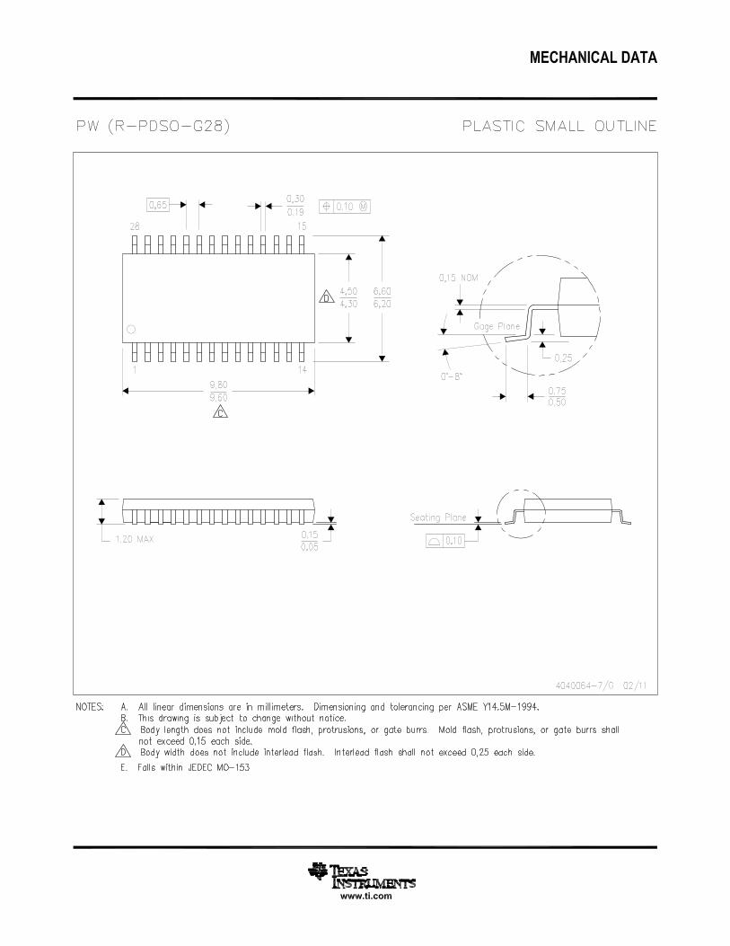


IMPORTANT NOTICE
Texas Instruments Incorporated (TI) reserves the right to make corrections, enhancements, improvements and other changes to itssemiconductor products and services per JESD46, latest issue, and to discontinue any product or service per JESD48, latest issue. Buyersshould obtain the latest relevant information before placing orders and should verify that such information is current and complete.TI’s published terms of sale for semiconductor products (http://www.ti.com/sc/docs/stdterms.htm) apply to the sale of packaged integratedcircuit products that TI has qualified and released to market. Additional terms may apply to the use or sale of other types of TI products andservices.Reproduction of significant portions of TI information in TI data sheets is permissible only if reproduction is without alteration and isaccompanied by all associated warranties, conditions, limitations, and notices. TI is not responsible or liable for such reproduceddocumentation. Information of third parties may be subject to additional restrictions. Resale of TI products or services with statementsdifferent from or beyond the parameters stated by TI for that product or service voids all express and any implied warranties for theassociated TI product or service and is an unfair and deceptive business practice. TI is not responsible or liable for any such statements.Buyers and others who are developing systems that incorporate TI products (collectively, “Designers”) understand and agree that Designersremain responsible for using their independent analysis, evaluation and judgment in designing their applications and that Designers havefull and exclusive responsibility to assure the safety of Designers' applications and compliance of their applications (and of all TI productsused in or for Designers’ applications) with all applicable regulations, laws and other applicable requirements. Designer represents that, withrespect to their applications, Designer has all the necessary expertise to create and implement safeguards that (1) anticipate dangerousconsequences of failures, (2) monitor failures and their consequences, and (3) lessen the likelihood of failures that might cause harm andtake appropriate actions. Designer agrees that prior to using or distributing any applications that include TI products, Designer willthoroughly test such applications and the functionality of such TI products as used in such applications.TI’s provision of technical, application or other design advice, quality characterization, reliability data or other services or information,including, but not limited to, reference designs and materials relating to evaluation modules, (collectively, “TI Resources”) are intended toassist designers who are developing applications that incorporate TI products; by downloading, accessing or using TI Resources in anyway, Designer (individually or, if Designer is acting on behalf of a company, Designer’s company) agrees to use any particular TI Resourcesolely for this purpose and subject to the terms of this Notice.TI’s provision of TI Resources does not expand or otherwise alter TI’s applicable published warranties or warranty disclaimers for TIproducts, and no additional obligations or liabilities arise from TI providing such TI Resources. TI reserves the right to make corrections,enhancements, improvements and other changes to its TI Resources. TI has not conducted any testing other than that specificallydescribed in the published documentation for a particular TI Resource.Designer is authorized to use, copy and modify any individual TI Resource only in connection with the development of applications thatinclude the TI product(s) identified in such TI Resource. NO OTHER LICENSE, EXPRESS OR IMPLIED, BY ESTOPPEL OR OTHERWISETO ANY OTHER TI INTELLECTUAL PROPERTY RIGHT, AND NO LICENSE TO ANY TECHNOLOGY OR INTELLECTUAL PROPERTYRIGHT OF TI OR ANY THIRD PARTY IS GRANTED HEREIN, including but not limited to any patent right, copyright, mask work right, orother intellectual property right relating to any combination, machine, or process in which TI products or services are used. Informationregarding or referencing third-party products or services does not constitute a license to use such products or services, or a warranty orendorsement thereof. Use of TI Resources may require a license from a third party under the patents or other intellectual property of thethird party, or a license from TI under the patents or other intellectual property of TI.TI RESOURCES ARE PROVIDED “AS IS” AND WITH ALL FAULTS. TI DISCLAIMS ALL OTHER WARRANTIES ORREPRESENTATIONS, EXPRESS OR IMPLIED, REGARDING RESOURCES OR USE THEREOF, INCLUDING BUT NOT LIMITED TOACCURACY OR COMPLETENESS, TITLE, ANY EPIDEMIC FAILURE WARRANTY AND ANY IMPLIED WARRANTIES OFMERCHANTABILITY, FITNESS FOR A PARTICULAR PURPOSE, AND NON-INFRINGEMENT OF ANY THIRD PARTY INTELLECTUALPROPERTY RIGHTS. TI SHALL NOT BE LIABLE FOR AND SHALL NOT DEFEND OR INDEMNIFY DESIGNER AGAINST ANY CLAIM,INCLUDING BUT NOT LIMITED TO ANY INFRINGEMENT CLAIM THAT RELATES TO OR IS BASED ON ANY COMBINATION OFPRODUCTS EVEN IF DESCRIBED IN TI RESOURCES OR OTHERWISE. IN NO EVENT SHALL TI BE LIABLE FOR ANY ACTUAL,DIRECT, SPECIAL, COLLATERAL, INDIRECT, PUNITIVE, INCIDENTAL, CONSEQUENTIAL OR EXEMPLARY DAMAGES INCONNECTION WITH OR ARISING OUT OF TI RESOURCES OR USE THEREOF, AND REGARDLESS OF WHETHER TI HAS BEENADVISED OF THE POSSIBILITY OF SUCH DAMAGES.Unless TI has explicitly designated an individual product as meeting the requirements of a particular industry standard (e.g., ISO/TS 16949and ISO 26262), TI is not responsible for any failure to meet such industry standard requirements.Where TI specifically promotes products as facilitating functional safety or as compliant with industry functional safety standards, suchproducts are intended to help enable customers to design and create their own applications that meet applicable functional safety standardsand requirements. Using products in an application does not by itself establish any safety features in the application. Designers mustensure compliance with safety-related requirements and standards applicable to their applications. Designer may not use any TI products inlife-critical medical equipment unless authorized officers of the parties have executed a special contract specifically governing such use.Life-critical medical equipment is medical equipment where failure of such equipment would cause serious bodily injury or death (e.g., lifesupport, pacemakers, defibrillators, heart pumps, neurostimulators, and implantables). Such equipment includes, without limitation, allmedical devices identified by the U.S. Food and Drug Administration as Class III devices and equivalent classifications outside the U.S.TI may expressly designate certain products as completing a particular qualification (e.g., Q100, Military Grade, or Enhanced Product).Designers agree that it has the necessary expertise to select the product with the appropriate qualification designation for their applicationsand that proper product selection is at Designers’ own risk. Designers are solely responsible for compliance with all legal and regulatoryrequirements in connection with such selection.Designer will fully indemnify TI and its representatives against any damages, costs, losses, and/or liabilities arising out of Designer’s non-compliance with the terms and provisions of this Notice.
Mailing Address: Texas Instruments, Post Office Box 655303, Dallas, Texas 75265Copyright © 2018, Texas Instruments Incorporated