traditionally when creating dsp systems, designers...
TRANSCRIPT
HARDWARE / SOFTWARE
PARTITIONING
HW
SW

Instructor: Dr. Yu Hen Hu
Submitted By:
Devang Sachdev
Lizheng Zhang

ABSTRACTTraditionally when creating DSP systems, designers partition the hardware and software early in the process. Hardware and software engineers design their respective components in isolation, and communication between the two groups is minimal. There are several drawbacks to this approach. As a result, hardware-software codesign (HSC) has gained considerable momentum in industry and academia in the last decade. HSC integrates the principles of hardware and software design and provides structured methods and tools that focus on extensive modeling and simulation-based verification. Hardware software partitioning is one the important phases of codesign. In this project we evaluate effect of various partitioning planes on HW-SW co-design architecture, consisting of single SW processor, a HW coprocessor (FPGA), shared memory for HW-SW communication and SW local memory, by mapping very basic DSP algorithms. We implement an example application on the co-design platform with varying partition between the SW and HW functions.

TABLE OF CONTENTS
1 Introduction.....................................................................52 Basics of Hardware/Software Partitioning......................63 Hardware / Software Architecture..................................94 Test Application – DCT Algorithm..................................115 Implementation..............................................................13
5.1 Design Issues..........................................................................135.1.1 Fixed Point Arithmetic......................................................135.1.2 Optimization for DCT operation for JPEG files.................15
5.2 Algorithm Partitioning............................................................185.2.1 All Software Implementation............................................185.2.2 Hardware Serial Multiply – Accumulate Implementation 195.2.3 Hardware Parallel MAC Implementation.........................205.2.4 All Hardware Implementation..........................................21
6 Results...........................................................................237 Conclusion.....................................................................25Acknowledgments...............................................................25References...........................................................................26Appendix.............................................................................27
LIST OF FIGURES

Figure 1: Fundamental Phases of Hardware-Software Codesign.........7Figure 2: HW/SW Architecture..............................................................9Figure 3: 2D DCT using 1D DCT.........................................................12Figure 4: Length of Cosine Coefficients..............................................16Figure 5: Datapath Width....................................................................17Figure 6: DCT Algorithm Partitioning.................................................18Figure 7: MAC Unit.............................................................................19Figure 8: Interface DSP and 1-Serial MAC Unit..................................20Figure 9: Parallel MAC Unit................................................................21Figure 10: Comparison of H/S Partitions............................................23
LIST OF TABLES
Table 1: Partitioning results...............................................................................................23
1 IntroductionEmbedded systems for reactive (real-time) applications are implemented as mixed software-hardware systems, utilizing microprocessors, microcontrollers, Digital Signal Processors, ASICs and/or FPGAs. Generally,

software is used for features and flexibility, while hardware is used to achieve the required performance or for power saving reasons. Re-configurable macros and architectures are introduced for embedded systems to increase flexibility on a higher performance level compared to general-purpose processors. Typically the HW/SW partitioning task is simply seen as mapping the defined functionality from e.g. an executable specification onto given resources. However, when designing an embedded system for a heterogeneous implementation (i.e. hardware and software on embedded processors), more complex activities have to be undertaken as given in the following list: System behavioral description – giving the executable specification of
what the system is suppose to do Hardware/software partitioning – deciding which parts of the system
behavior should be realized by what parts of the hardware architecture. Task scheduling – controlling how the different computational resources
of the hardware architecture are shared between the tasks of the behavioral description
Hardware architecture selection – describing what hardware components should be used and how they are connected.
The main purpose of the present project is to describe the hardware/software partitioning of the investigated test design – DCT algorithm. There are several techniques to do this partitioning. One of them is based on actual profiling information of the design, i.e. figures about the computational complexity of the design. The partitioning of the design will be done for each functional entity or “(group of) block(s)”. Therefore the computational expense of each of the components must be available.
These basics of HW/SW Codesign and Partitioning are provided in section 2 of this report. . In this part general issues about the partitioning process will be introduced. Term definitions are done and basic principles, approaches, and techniques will be presented. Section 3 contains the description of actual hardware/software partitioning target architecture platform. In section 4 discusses the test application. The next section deals with the

design issues related to implementation and actual partitioning of the investigated application. First partitioning approach is restricted to pure SW solution. Gradually portions of application are moved into hardware to achieve an efficient partition. In section 6 the results for the conducted experiments on the test architecture are presented.
2 Basics of Hardware/Software PartitioningTraditionally when creating DSP systems, designers partition the hardware and software early in the process. Hardware and software engineers design their respective components in isolation, and communication between the two groups is minimal. The drawbacks of this approach are several: (1) Less than the best possible implementation of a system,(2) Problems in hardware and software component integration, (3) Uncertainty in the system’s functionality,(4) High costs and long development cycles.
As a result, hardware-software codesign (HSC) has gained considerable momentum in industry and academia in the last decade. HSC integrates the principles of hardware and software design and provides structured methods and tools that focus on extensive modeling and simulation-based verification. Unlike traditional frameworks, HSC also fosters the design of hardware and software systems in parallel. HSC promises significant benefits including shorter development cycles, less expense, maximized processing power and component reuse.In reality, no single HSC methodology can successfully aid in the design of all the various applications. For example, the hardware and software requirements of an elevator control unit are very different from those of a local area network (LAN) system. Accordingly, a family of HSC techniques is germinating. Also, HSC is sometimes an overused term. It covers three distinct areas of codesign, co-development and co-verification. Co-development is the detailed implementation of hardware and software components; co-verification is the verification of these components using co-simulation (executing hardware and software in parallel) technology. In our

case, HSC refers to codesign in which we model and simulate a system at various levels of abstraction, partition (and repartition) it into hardware and software components, and analyze the tradeoffs. Codesign is also sometimes called design space exploration.
Figure 1: Fundamental Phases of Hardware-Software Codesign
The fundamental phases of hardware-software codesign are shown in Fig. 1. It should be noted that the design phases need not be distinct and are often merged. However, it is beneficial to separate them for simplicity so that the main tasks and goals of each phase can be concretely defined. Refer to the references for a more detailed discussion. In the initial phase, designers create a formal text-based specification of the system to be designed. The specification documents the system’s requirements and constraints, its functionality and behavior, and its interface. The interface defines the mechanism through which the system communicates with its external environment. Any other criteria (such as power consumption, size, etc.) deemed important by designers are also taken into account.

The partitioning is a way of deciding for each part – task – of the behavioral description, which part – microprocessor or FPGA – of the hardware architecture should be used to implement it. Therefore partitioning can be thought of as a mapping, whose domain is the set of tasks in the behavioral description, and whose range is the set of components with processing capabilities in the hardware architecture (platform figure). Similarly, all variables in the behavioral description have to be mapped to elements in the architecture with storage capacity, i.e. memories. The problem of constructing this mapping has an exponential complexity; if there are k components and m tasks, there are O(km) different ways to partition. But fortunately, the problem lends itself well to a solution using a branch and bound algorithm, which only needs to evaluate a small fraction of all combinations in order to find the optimum.
The goal function that we try to optimize is the performance by applying various partition planes. There are other criteria besides performance e.g. resources availability and changes to be implemented in real time, which play an important part in partitioning.
3 Hardware / Software ArchitectureThe HW/SW architecture consists of a TMS320C31 Floating point DSP and a Xilinx XCS40 Spartan FPGA. The DSP communicates with the FPGA by writing into its registers from where the FPGA can read, perform tasks and write back to the registers. Address and Data bus of the DSP are connected to the I/O pins of the FPGA. Other than these, signals like Reset, Strobe and R/W are also interfaced with the FPGA. The clocks to both the DSP and the FPGA are separate operating at 50 MHz frequency.

The DSP also interfaces with PC via a parallel port which is used to download programs and data into the DSP memory. The DSP also has access to external RAM. DSP is programmed in C language using Code Composer Studio [11], C complier supplied by TI. The interface with the PC is done using DSK tools and source code written by Prof M. Morrow [7]. Data can be written into the DSP memory by specifying location, length of data and source of data. Similarly the data can also be read from the DSP memory.
Figure 2: HW/SW Architecture
The FPGA is configured using Xilinx Foundation Software [12]. Design is constructed by a mix of schematic and HDL entry. Foundation software is also used to carry out simulations and timing analysis. More over the area occupied by the design can be determined by the synthesis report generated by Foundation software. Once the design is successfully verified, it is synthesized and output bit stream file is programmed on an EEPROM. The EEPROM interfaces with the FPGA and at power up it programs the FPGA.
Due to multiplicity of tools the HW/SW Codesign process gets a lot difficult. Moreover due to lack of co simulation and verification tools the design is highly prone to bugs. Systems like Polis and Ptolemy, and languages like System C, Spec C and Handle C which have been developed for HW/SW Codesign are still in rudimentary phases.
Processor
FPGA
LocalMemory
SharedMemory
GlobalMemory
4 Test Application – DCT AlgorithmThe DCT is a loss-less and reversible mathematical transformation that converts a spatial amplitude representation of data into a spatial frequency representation. One of the advantages of the DCT is its energy compaction

property, that is, the signal energy is concentrated on a few components while most other components are zero or are negligibly small. The DCT was first introduced in 1974 and since then it has been used in many applications such as filtering, transmultiplexers, speech coding, image coding (still frame, video and image storage), pattern recognition, image enhancement, and SAR/IR image coding. The DCT is widely used in image compression applications, especially in lossy image compression. For example, the 2D DCT is used for JPEG still image compression, MPEG moving image compression, and the H.261 and H.263 video-telephony coding schemes. The
energy compaction property of the DCT is well suited for image compression since, as in most images, the energy is concentrated in the low to middle frequencies, and the human eye is more sensitive to the middle frequencies. The DCT is not easy to implement because it is data dependent but it provides a very good compression ratio.
Figure 3: 2D DCT using 1D DCT

Since the 2D DCT can be computed by applying 1D transforms separately to the rows and columns, we say that the 2D DCT is separable in the two dimensions. As in the 1D case, each element F(u,v) of the transform is the inner product of the input and a basis function, but in this case, the basis functions are M x N matrices. Each 2D basis matrix is the outer product of two of the 1D basis vectors.
5 ImplementationAs per the partitioning methodology introduced earlier we implemented the DCT algorithm in MATLAB for function verification. Using MATLAB we also evaluated various design issues discussed in the following sections. After the functionality of the algorithm developed was established, it was implemented on the HW/SW architecture. Following the software oriented approach we first implement a C version of the 64 point DCT on TMS320C31 DSP. Gradually the functions were migrated to FPGA for hardware implementation. We did comparative study of the performance improvement, memory utilization and hardware resource consumption for various partitions.
5.1 Design IssuesDesign issues like effect on accuracy due to length of datapath, width of cosine coefficients and fixed point arithmetic were understood and resolved using MATLAB simulations.
5.1.1 Fixed Point Arithmetic
Floating-point numbers allow us to deal with an extremely wide range of numbers: from the very small to the very large. They do this by storing the number as some digits and the position of the decimal point. For example, 19,000,000 could be stored as (19, 6) and 0.00019 as (19,-5). This sort of arithmetic can be slow and difficult to implement. If we're prepared to lose the wide range of numbers that floating-point gives, we can speed things up

by fixing the position of the decimal point and implement them using integer arithmetic operations.
A fixed point value contains three fields separated by periods. The first field is optional and present only if the MSB (most significant bit) of the value is used as the sign bit. The second field is digits of integer part in the value. The last field is digits of fractional part. The normal reason for using fixed point numbers is to be able to use fractional digits while calculating with integer math. In fact, normal integer math is a special case of fixed point math with no fractional digits defined.
A quick review of fixed point math techniques will show the importance of keeping track of the radix point. In order to add two values, their radix points must be aligned. When two fixed point numbers are multiplied, the number of digits to the right of the radix point in the product is equal to the sum of the digits to the right of the radix point of multiplier and multiplicand. Division of two fixed point numbers requires that you subtract the number of digits to the right of the radix point in the divisor from those of the dividend to get the position of the radix point in the quotient. As the complexity of the calculations increases, so does the need to keep track of the radix point.
The most straightforward representation of fixed point number is the binary fixed point number. If instead of concentrating on the decimal equivalent of the integers and placing a decimal point between decimal digits, we concentrate on the underlying binary integer and place a binary point between binary digits, interesting things happen. The operations used for aligning the radix point change from multiplication and division by powers of 10 to powers of 2 which can be accomplished with shifts. Instead of considering the number of digits to the right of the radix point, the amount of resolution is now important.
One disadvantage of binary fixed point values is that they are often approximations of the decimal values they represent. This approximation, if

present, appears only in the fractional part of the values of course, because an integer times a power of 2 is an integer. The amount of resolution mentioned before is nothing more than the value of the binary fixed point number with only the LSB (least significant bit) being set. This is 1 divided by some power of 2. With 8 bits used for fraction part, for example, we are using 2 raised to the 8th power or 256. 1 divided by 256 equals 0.00390625. With proper rounding, the binary fixed point value used to represent a number will be accurate to within 1/2 of this value or 0.001953125
Binary fixed point values inherit all of the attributes of normal integers. Performing math with normal integers is directly supported by the CPU (with the possible exception of multiplication and division). In order to change the position of the binary point of a value, it must be multiplied or divided by powers of 2. This method puts a small load on the CPU, if shifts are used instead, in return for a little harder to envision implementation of fixed point math.
5.1.2 Optimization for DCT operation for JPEG filesThe key to apply the fixed point arithmetic is to decide the number of bit need to represent the integer and fractional part of the values. This is a trade-off between precision and simplification.
5.1.2.1 Cosine coefficientFor DCT operation in JPEG files, the input data points are unsigned 8-bit integers whose values are from 0 to 255. The fractional part of the DCT algorithm comes from the cosine coefficient used for DCT which, including the normalization factors, will range from -0.5 to 0.5. Usually, these coefficients are pre-calculated and stored in the memory. To decide the necessary number of bit to represent the cosine coefficients, a simple experiment is done for a sample figure. The following figure shows the results where the numbers are fractional part for the cosine coefficients. It is clear that 5 bits for fractional part is enough. Include the sign bit we need 6 bit to represent the cosine coefficients.

Figure 4: Length of Cosine Coefficients
5.1.2.2 Datapath bit widthBecause the absolute value of the cosine coefficients is represented by 5 bits and only multiplication and addition is involved in DCT, the intermediate values of DCT operation will have maximum of 5 bits as the fractional part. For an 8*8 block size for DCT, the intermediate value will vary from -4096 to 4095. So 12 bits are needed to represent the integer part of the intermediate values. Including the sign bit of the MSB, totally 18 bits are need for full precision, full range of DCT calculation.
To find out the optimal number of bits for the intermediate values, another experiment is done on the same example figure as above. The following figure shows the results where values are number of digits used (including the sign bit).
It is clear that totally 12 bits are enough for the intermediate value representation. This means there will be no fractional part in the intermediate values and the true value will be 2*(represented value) which
means the LSB is assumed to be always 0.
2 43
5 6 7 8
1

Figure 5: Datapath Width
1113 1214
79 810

5.2 Algorithm PartitioningThe basic 2D DCT comprises of 2 – 1D DCT loops. MAC operation is at the root of these 1D DCT loops. The various partitions based on this obseration are discussed in this section.
Figure 6: DCT Algorithm Partitioning
5.2.1 All Software ImplementationUsing Code Composer Studio, we implemented the algorithm in C on the DSP. The host PC first dumps the code into the DSP boot memory. The DSP program then waits for the host PC to write the input file (64 points) into the DSP’s on chip memory. The DSP uses these values and computes the DCT output (64 points) and stores in its memory. Once this is done it sends an
for v=1:8 for u=1:8 sum2(u,v)=0; for n=1:8 sum1(n,u) = 0;
for m=1:8
x1 = f(m,n)*dctcos(m,u); sum1(n,u)= sum1(n,u)+ x1;
end y1 = sum1(n,u)*dctcos(n,v);
sum2(u,v)= sum2(u,v)+y1; end endend
All Software implementation
Hardware Serial MAC implementation
All Hardware implementation
Hardware Parallel MAC implementation

interrupt to the PC which reads the computed values and stores in a text file. After this the next block of input data is written into the DSP. C++ routines developed by Prof. Micheal Morrow[7] are used to communicate between the DSP and the PC (reference morrow). Various optimizations for saving memory and improving efficiency of the code were done e.g. use of malloc functions to store cosine coefficient tables. The complier optimizations were not utilized to reach a more realistic comparison of different partitioning levels. The time taken by each section of the code is determined by inbuilt timers. We performed timing analysis for single multiply accumulate (MAC) operation, complete inner loop (1D DCT) execution (i.e. 8 MAC operations) and for both the inner and the outer loops execution (i.e. 64 MAC operations). TMS320C31 offers a MAC unit performing operation in a single cycle.
5.2.2 Hardware Serial Multiply – Accumulate Implementation
MAC is the fundamental operation of a DCT algorithm. In DCT 2 matrices are multiplied. For matrix multiplication each row element of the multiplicand is multiplied with corresponding column element of the multiplier and then all are adder together to form one element of the result. The same can be done by multiplying one row element with one column element at a time and then accumulating the result. As the first partition shown in figure 6, we implement a MAC unit [Figure 7] on the FPGA using HDL.
Figure 7: MAC Unit
The MAC unit is interfaced with the register file in the FPGA [Figure 8]. The DSP writes into these memory mapped register file in the FPGA. The MAC
x+
DCT_In[11:0]
Coeff[5:0]
Acc_In[11:0]Acc_Out[11:0]
Mul_Res[17:6]

unit accesses these registers and outputs the value to Output Register from where the DSP reads the value. So instead of performing the MAC operation the DSP performs 3 Stores and 1 Load operation. The store operations usually take up to 1 cycle and load operation takes 2 cycles in DSP.
Figure 8: Interface DSP and 1-Serial MAC Unit
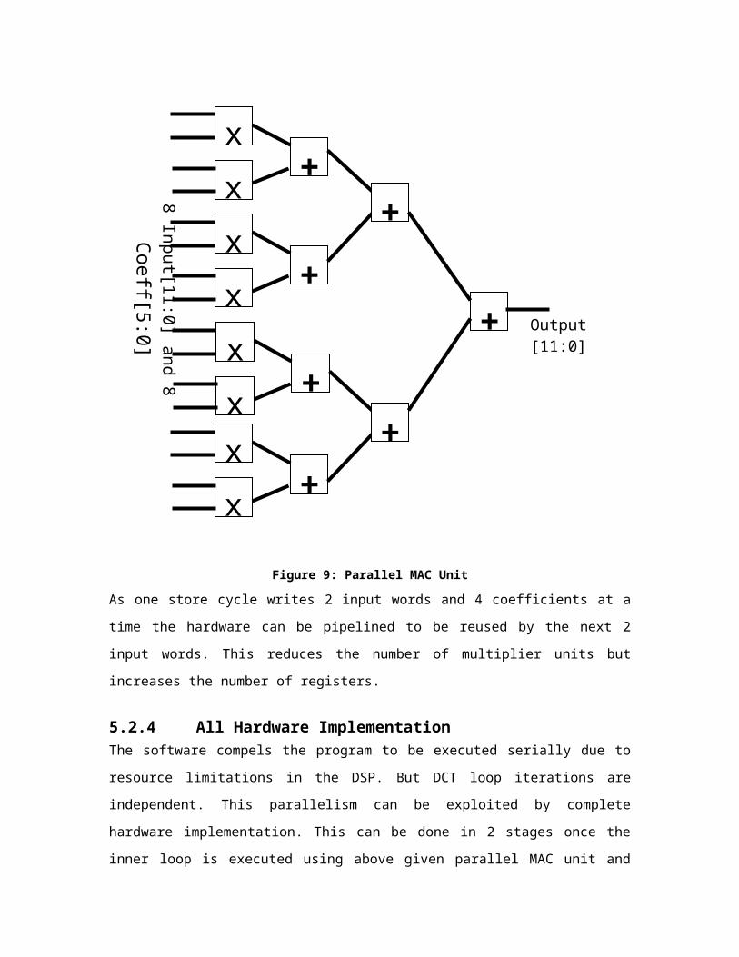
5.2.3 Hardware Parallel MAC ImplementationAs the DSP is capable enough of single cycle MAC operation the Serial MAC
implementation does not improve performance in fact it reduces performance due to load
store operation carried out by the DSP to communicate with the FPGA. Hence the
partition is expanded to include one complete loop of the DCT which consists of 8 MAC
operations. As the input data length is 12 bits and the DSP datapath length is 32 bits, 2
input words are loaded into the FPGA registers in one Store cycle. More over 4 cosine
coefficients are stored in memory tables as a single word. Hence the DSP takes 4 stores
for loading input values and 2 stores to load coefficients (total 6 stores). The hardware
takes just one cycle to compute the output for the complete inner loop. The structure of
the hardware is shown in figure 9.
DSP
FPGA
Input[11:0]
Coeff[5:0]Acc[11:0]
Out[11:0]
MAC
x+x
x+x
x+x
x+x
+
+
+
8 Input[11:0] and 8 C
oeff[5:0]
Output [11:0]

Figure 9: Parallel MAC Unit
As one store cycle writes 2 input words and 4 coefficients at a time the hardware can be pipelined to be reused by the next 2 input words. This reduces the number of multiplier units but increases the number of registers.
5.2.4 All Hardware ImplementationThe software compels the program to be executed serially due to resource limitations in the DSP. But DCT loop iterations are independent. This parallelism can be exploited by complete hardware implementation. This can be done in 2 stages once the inner loop is executed using above given parallel MAC unit and accumulating the result for 8 times to get a single DCT output. The control can be implemented via software. The other approach is to implement the DCT using systolic arrays. For this case at least 64 processing units would be required to attain a considerable performance enhancement. Moreover the hardware could be further optimized by hard coding the coefficients in the FPGA and using custom multipliers, hence reducing hardware cost. Due to the size of FPGA and limited time we could not implement the complete hardware implementation.

6 ResultsWe performed timing analysis of the code but initializing at various points in the code and reading after the task was completed. Also timing for hardware components was done using the Xilinx Foundation tools. Results for area utilization on the FPGA were also gathered. The operating frequency of the DSP and the FPGA is 50 MHz.
Table 1: Partitioning resultsPartition Stores Mac Load Cycles Estimated
Time (us)Actual time Measured
FPGA area
(us)All Software 0 1 2 2560 84 112 0%
1-Serial Hardware MAC 3 0 1 2560 84 156 27%8-Parallel Hardware
MAC 6 0 1 512 16 32 84%
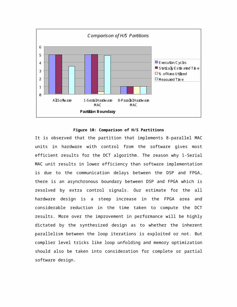
Figure 10 shows the comparison of cycles taken for execution, time taken for execution and the FPGA area utilized for a given partition boundary.
Comparison of H/S Partitions
0
1
2
3
4
5
6
All Software 1-Serial HardwareMAC
8-Parallel HardwareMAC
Partition Boundary
Execution CyclesStatically Estimated Time% of Area UtilizedMeasured Time
Figure 10: Comparison of H/S Partitions
It is observed that the partition that implements 8-parallel MAC units in hardware with control from the software gives most efficient results for the DCT algorithm. The reason why 1-Serial MAC unit results in lower efficiency than software implementation is due to the communication delays between the DSP and FPGA, there is an asynchronous boundary between DSP and FPGA which is resolved by extra control signals. Our estimate for the all hardware design is a steep increase in the FPGA area and considerable reduction in the time taken to compute the DCT results. More over the improvement in performance will be highly dictated by the synthesized design as to whether the inherent parallelism between the loop iterations is exploited or not. But complier level tricks like loop unfolding and memory

optimization should also be taken into consideration for complete or partial software design.
7 ConclusionKey concepts of HW/SW partitioning were presented in this study. The experiments were carried out by implementing test application – DCT on HW/SW architecture consisting for DSP and FPGA. It was observed that by migrated computation intensive tasks on the hardware considerable amount of performance improvement is achieved. Criteria to keep in mind is that if the regions across the boundary are too small, they then to degrade performance due to communication and control delays existing between the HW and the SW. Also frequency of memory accesses in the program affects the performance with partitioning. The memory access problem can be

relaxed by choosing proper architecture or by choosing proper programming language e.g. object oriented languages. Traffic between FPGA and CPU and CPU and main memory should be reduced in order to gain maximum advantage. We have only exploited locality of control structures in loops, an object oriented would allow us to exploit data locality.
AcknowledgmentsThe authors would like to thank Dr. Hu for advising and extended support offered by the way of ECE 734 course. The authors would also like to thank Dr. Venkataramanan at WEMPEC for permitting the use of HW/SW platform and Prof M. Morrow for his advice offered to resolve DSP and PC communications problems.
References1. ‘A Decade of Hardware / Software Codesign’ – Wolf, W;2. ‘Hardware – Software Partitioning and Pipelined Scheduling of
Transformative Applications ‘– Chatha, Karam; Vemuri, Ranga;3. ‘Graph Based Communication Analysis for Hardware/Software
Codesign’ – Knudsen, Peter Voigt; Madsen, Jan;4. ‘Hardware/software partitioning of real-time systems’ – Alexsson, J;5. ‘A hardware/software partitioning algorithm for processor cores of
digital signal processing’ - Togawa, N.; Sakurai, T.; Yanagisawa, M.; Ohtsuki, T.;
6. ‘A case study on hardware/software partitioning’ - Jantsch, A.; Ellervee, P.; Oberg, J.; Hemani, A.;
7. WINDSK – TMS320C3x DSK tools,
http://eceserv0.ece.wisc.edu/~morrow/software
8. TMS320C3x User Guide9. TMS320C3x Assembly Language Tools10.TMS320C3x C Complier Guide11.TI Code Composer Studio12.Xilinx Foundation 4.1i
Appendix
A. MATLAB CodeB. C CodeC. HDL Code
MYBDCT.M
function sum2 = mybdct(f,dctcos,M)
N=8;% % A= 2^(M-1)-1;% B=-2^(M-1);
for v=1:N for u=1:N sum2(u,v)=0; for n=1:N sum1(n,u) = 0; for m=1:N x1 = f(m,n)*dctcos(m,u); %x2 = sat(x1,M); x3 = sum1(n,u)+ x1; sum1(n,u)= x3;%sat(x3,M); end y1 = sum1(n,u)*dctcos(n,v); %y2 = sat(y1,M); y3 = sum2(u,v)+y1; sum2(u,v)= y3;%sat(y3,A,B); end endend

JPEG.Mclear;
imname = input('input the input imagine name:\n','s');%CM = input('input the cosine bits:\n');CM = 6;DM = input('input the data bits:\n');
X = double(imread(imname));
%Y = bdct(X);
Y = fdct(X,CM,DM);
%Y = fix(Y);
Z = uint8(ibdct(Y));
omname = input('input the output imagine name:\n','s');
imwrite(Z,omname);
FDCT.M
% clear;function out = fdct(fig,CM,DM)
N=8;
[a,b] = size(fig);
a = a/N;b= b/N;
coef = dctcos(N,CM);
for i=1:a for j=1:b for k=1:N for h=1:N in(k,h) = fig(8*(i-1)+k,8*(j-1)+h); end end temp = mybdct(in,coef,DM); for k=1:N for h=1:N
out(8*(i-1)+k,8*(j-1)+h)=temp(k,h); end end endend
SAT.Mfunction out = sat(in,N)k = 2^(N-13);a = in*k;b= fix(a);out = b/k;% s% if (out>A) out = A;% end% if(out<B) out=B;% end
DCTCOS.C
#include <stdio.h>#include <math.h>#include <stdlib.h>
#define PI 3.14159265
#define N 8
#define coeff_bits 6#define dct_bits 11#define max_dct 2047#define min_dct -2048#define coeff_value 64
main(){
int u,v,m,n;double cu;//coeff_value;double coeff[N][N],sum1[N][N];
//double max_dct, min_dct;

int f[N][N],sum2[N][N];
char FileName[81];
//makefile();
FILE *input, *output;
if ((input = fopen("data.txt","r"))==NULL){
printf("Unable to open file %s\n",FileName);exit(-1);
}
output = fopen("data2.txt","w");
//setup coefficent array
for (u=0;u<N;u++){
for (m=0;m<N;m++){if(u==0) cu = 1.0/sqrt(2.0);else cu = 1.0;
coeff[m][u]=sqrt(2.0/N)*cu*cos((2.0*m+1.0)*u*PI/(2.0*N));}
}
//read input filewhile(1){
for (m=0;m<N;m++){for (n=0;n<N;n++){
fscanf(input,"%d",&f[m][n]);//printf("%d, ",f[m][n]);
}//getchar();
}if (feof(input))break;
//calculate dct
for (v=0;v<N;v++){for (u=0;u<N;u++){
sum2[u][v] = 0;for (n=0;n<N;n++){
sum1[n][u] = 0.0;for (m=0;m<N;m++)sum1[n][u]= sum1[n][u]+(f[m][n]*coeff[m][u]);sum2[u][v]= sum2[u][v]+sum1[n][u]*coeff[n][v];
}}

}
//output to filefor(m=0; m<N; m++){
for (n=0; n<N; n++)fprintf(output,"%d ",sum2[m][n]);
fprintf(output,"\n");}
}
fclose(input);fclose(output);
}
MAC.V
module mac (out, in, acc, coeff);input [11:0] in, acc;input [5:0] coeff;output [11:0] out;wire [17:0] mid;
assign mid = in * acc;assign out = mid[17:6];endmodule
PARMAC.V
Module parmac(out, in12, in34, in56, in78, coeff1234, coeff5678);input [31:0] in12, in34, in56, in78, coeff1234, coeff5678;output [11:0];
wire [17:0] level1_12, level1_34, level1_56, level1_78;wire [12:0] level2_1234, level2_5678;wire [12:0] level3;
assign level1_12=(in12[11:0]*coeff[5:0])+(in12[27:16]*coeff[11:6]);assign level1_12=(in34[11:0]*coeff[17:12])+(in34[27:16]*coeff[23:18]);assign level1_12=(in56[11:0]*coeff[5:0])+(in56[27:16]*coeff[11:6]);assign level1_12=(in78[11:0]*coeff[17:12])+(in78[27:16]*coeff[23:18]);
assign level2_1234 = level1_12[17:6] + level1_34[17:6];assign level2_5678 = level1_56[17:6] + level1_78[17:6];
assign level3 = level2_1234[12:1] + level2_5678[12:1];

assign out = level3[12:1];
endmodule