transient radiation effects · reic report no. 26 april 19,1 transient radiation effects electronic...
TRANSCRIPT

REIC Report No. 26April 19,1
TRANSIENT RADIATION EFFECTSS)ON ELECTRONIC COMPONENTS AND
SEMICONDUCTOR DEVICES
TDSIA I
RADIATION EFFECTS INFORMATION CENTER
Battelle Memorial Institute
Columbus 1, Ohio

The Radiation Effects Information Center has beenestablished at Battelle Memorial Institute by the UnitedStates Air Force to provide a means of placing radiation-effects data in the hands of designers and those involvedin research and development. Access to the Center andto its reports is obtained through the Air Force. Thisreport has repared ursuant to the provisions of$I " P e r"!tat A 3 -08 T skftp 738103,d rojs .~f, 73'81 and 7634.

WT( po r 26
S4Aprg 9o 063
Report on
(g)TRANSIENT RADIATION EFFECTS ON ELECTRONIC
COMPONENTS AND SEMICONDUCTOR DEVICES
O by
ivq D. C. Jones, F. J. Reid, W. E. Chapin,D. J. Hamman, and E. N. Wyler
AERONAUTICAL SYSTEMS DIVISION
AIR FORCE SYSTEMS COMMAND
'006
RADIATION EFFECTS INFORMATION CENTERBattelle Memorial Institute
Columbus 1, Ohio

ABSTRACT
This report summarizes the information that was availablebefore 1962 concerning the effects of nuclear-weapon-burst andsimulated-burst radiation on electronic components and semicon-ductor devices. This work reports only the effects observedin components that are due to gamma rays and/or neutrons of atransient radiation environment.

TABLE OF CONTENTS
Page
SUMMARY P ND CONCLUSIONS........................................................I
INTRODUCTION......................................................................3
INTERACTIONS OF RADIATION WITH MATTER........................................3
Effects on Solids..............................................................Semiconductors and Semiconductor Junctions................................5
CaseI...............................................................6CaseII..............................................................6Cas. III.............................................................6
Insulators.................................................................7
EFFECTS OF PULSED RADIATION ON ELECTRONIC COMPONENTS....................8
Semiconductor Devices..........................................................8Transistors. ............................................................. 10Diodes....... ....................................................... 16
Electronic Devices..............................................................19Coaxial Cables............................................................19Electron Tubes............................................................33Resistors.................................................................39Capacitors................................................................53Quartz Crystals...........................................................68Magnetic Devices.........................................................73
Pulse Tests.........................................................74Write Disturb Zero Test.............................................78Disturb Tests........................................................78
£ ~~~One-Zero" Test....................................................83Static Test..........................................................85Conclhsions..........................................................e
~~t. ~Printed-Circuit Boards.....................................................8Subsystems....................................................................92
Multivibrators............................................................96Oscillators...............................................................96Power Supplies...........................................................96Amplifiers...............................................................101Conclusions..............................................................101
REFERENCES.......................................................................102
LIST OF FIGURES
Figure 1. Test Circuits for Transient Effects in Transistors...........................1
Figure 2. IC0 Versus Time During a Godiva Burst for an IBM Type 51 Transistor 12
Figure 3. Pulse Height Versus X-Radiation Exposure Rate (Voltage Applied) . 15 . i
Figure 4. Diode Test Circuit.......................................................16
Figure 5. Test Circuit for Open Cables.............................................25
Figure 6. End Configuration for Coaxial-Cable Tests.......................25
Figure 7. Plot of Ecgx Versus Gamma Exposure Rate for 2DZ1 Thyratron Tubes 44
*Figure S. Plot of Ecgx Versus Gamma Exposure Rate for 5643 Thyratron Tubes 44
Figure 9. Transient Radiation Effects on 2-Watt Potted Resistors.....................46
Figure 10. K Versus Applied Voltage for Tantalum Capacitors.........................55

TABLE OF CONTENTS
Page
SUMMARY P ND CONCLUSIONS . 1
INTRODUCTION ......................... 3
INTERACTIONS OF RADIATION WITH MATTER........................................3
Effects on Solids................................................................3Semiconductors and Semiconductor Junctions.................................
CaseI...............................................................6Case11..............................................................6Came Ill.............................................................6
Insulators.................................................................7
EFFECTS OF PULSED RADIATION ON ELECTRONIC COMPONENTS.....................
Semiconductor Devices...........................................................Transistors. ............................................................. 10Diodes...................................................................16
Electronic Devices..............................................................19Coaxial Cables............................................................19Electron Tube@...........................................................33Resistors.................................................................39Capacitors...............................................................53Quartz Crystals...........................................................68Magnetic Devices................................ ........................ 73
Pulse Tests.........................................................74Write Disturb Zero Test.............................................78
£ ~Disturb Tests................... ................................... 78"One-Zero" Test...................................................83Static Test..........................................................85Conclusions........................................................88
S Pbsy tem.............ds........................................................9Prinyted-Circuit. oad.....................................................2Multivibrators............................................................96Oscillators...............................................................96Power Supplies...........................................................96Amplifiers...............................................................101Conclusions..............................................................101
REFERENCES.......................................................................102
LIST OF FIGURES
Figure 1. Test Circuits for Transient Effects in Transistors..........................11
Figure 2. ICC0 Versus Time During a Godiva Burst for an IBM Type 51 Transistor 12
Figure 3. Pulse Height Versus X-Radiation Exposure Rate (Voltage Applied) .. 15
Figure 4. Diode Test Circuit.......................................................16
Figure 5. Test Circuit for Open Cables.............................................25
Figure 6. End Configuration for Coaxial-Cable Tests.................................25
Figure 7. Plot of Ecgx Versus Gamma Exposure Rate for ZD21 Thyratron Tubes 44
Figure 8. Plot of Ecgx Versus Gamma Exposure Rate for S643 Thyratron Tubes 44
Figure 9. Transient Radiation Effects on 2-Watt Potted Resistors.....................46
Figure 10. K Versus Applied Voltage for Tantalum Capacitors.........................55

LIST OF FIGURES(Continued)
Page
Figure 11. K Versus Applied Voltage for Paper Capacitors .... .......... 56
Figure 12. Conductivity Versus Radiation Rate for Sprague Vitamin Q ImpregnatedPaper Capacitors .................. .................... . 8
Figure 13. Conductivity Versus Radiation Rate for Mylar Capacitors ......... 58
Figure 14. Conductivity Versus Radiation Rate for Oil-Impregnated
Paper Capacitors ................. .................... 58
Figure 15. Capacitor Transient Effects Test Circuit Used by IBM ... ........ 67
Figure 16. D-C Lquipment and Circuitry Used by Boeing to Test Capacitors . . .. 67
Figure 17. Typical Rectangular Hysteresis Loop ......... .............. 76
Figure 18. Typical Rectangular Hysteresis Loop for Disturb Tests .. ....... 83
Figure 19. Flux Patterns in Two-Aperture Memory Cores@ ..... .......... 84
Figure 20. Effects of Transient Radiation on Printed-Circuit Boards ......... 93
Figure 21. Effects of Transient Radiation on Printed-Circuit Boards ......... 94
LIST OF TABLES
Table I. Transient [co Measurements ............. ................ 14 0
Table 2. Initial Amplitude of Diode Current Pulse ....... ............ 18
Table 3. Summary of IN277 Diodes Radiation-Induced Current Changes at12 Volts Reverse ................. .................... 18
Table 4. Summary of Transient Radiation Effects to Coaxial Cables ...... z1
Table 5. Transient Radiation Effects on RG-59 /U Coaxial Cables as a Function
of D-C Potential and Gamma Exposure Rate ....... ... ........... 26
Table 6. Transient Radiation Effects on RG-59/U Coaxial Cables of VariousMakes and Manufacture as a Function of D-C Potential and GammaExposure Rate .............. ...... ..................... 28
Table 7. Transient Radiation Effects on RG-59A/U Coaxial Cables as a Functionof Peak Gamma Exposure Rate .......... ..... ................ 29
Table 8. Transient Radiation Effects on Coiled RG-59/U Coaxial Cables as aFunction of Applied Potential ............. ................ 31
Table 9. Transient Radiation Effects on Open-Transmission and Twisted-WireLines as a Function of Physical Configurations ..... .......... 32
Table 10. Summary of Transient Radiation Effects on Electron Tubes .. ...... 34
Table 11. Summary of Transient Radiation Effects on 2DZ1 Thyratron Tubes. . . . 40
fable 12. Summary of Transient Radiation Effects on 5643 Thyratron Tubes .... 43
Table 13. Summary of Transient Radiation Effects on Carbon CompositionResistors .................... ....................... 47

LIST OF TABLES(Continued)
page
Table 14. Summary of Transient Radiation Effects on Metal FilmResistors .. ...... ......... ...................... 50
Table 15. Summary of Transient Radiation Effects on Miscellaneous Resistors . 52
Table 16. Summary of D-C Conductivity Data ........... .............. 59
Table 17. Summary of Transient Radiation Effects on Tantalum Capacitors .. 60
Table 18. Summary of Transient Radiation Effects on Paper Capacitors ...... 62
Table 19. Summary of Transient Radiation Effects on Glass Capacitors 64..... 4
Table 20, Summary of Transient Radiation Effects on Ceramic Capacitors .. 65
Table 21 Summary of Transient Radiation Effects on Miscellaneous Capacitors 66
Table 22. Changes in Frequency and Impedance Parameters of Crystal UnitsDue to Transient Radiation ............... ................. 70
Table 23. Transient Radiation Effects on Various Magnetic Cores and TapesWhen Subjected to Pulse Test (Current) Conditions ..... ......... 75
Table 24. Transient Effects on Various Magnetic Cores When Subjected toPulse Test (Current) Conditions ............. ............... 77
Table 25. Transient and Posttest Radiation Effects on Switching Time of l-,ASecMemory Cores for Various Drive Conditions ....... ........... 79
Table 26. Transient Radiation Effects on Various Magnetic Cores and TapesWhen Subjected to wVz Test Conditions ("Write Disturb Zero"Output Voltage) ............................... so
Table 27. Transient and Poettest Radiation Effects on Memory Cores When Subjectedto wVz ("Write Disturb Zero" Output Voltage) Test Conditions ..... 81
Table 28. Transient Radiation Effects on Memory Cores as Indicated by DisturbTest Voltage Observations ............... ................. 82
Table 29. Transient Radiation Effects on "One" and "Zero" Flux States of Ferrite(Mg-Mn) Two-Aperture Cores ............ ................ 86
Table 30. Transient Radiation Effects on Ferrite (Mg-Mn) Two-Aperture Cores of a(4 x 4) Memory Plane in a Nonpulsed Current State ..... ......... 87
Table 31. Summary of In-Pile Measurements of Critical Parameters ofPrinted-Circuit Boards ................. .................. 90
Table 32. Radiation Exposure-Rate-Affected Changes of Electrical Parameters forVarious Printed-Circuit Boards With Various Insulative Coatings .... 91
Table 33. Summary of Transient Radiation Effects on the Operation ofVarious Electronic Circuits .............. ................. 97

Report on
TRANSIENT RADIATION EFFECTS ON ELECTRONICCOMPONENTS AND SEMICONDUCTOR DEVICES
SUMMARY AND CONCLUSIONS
This report summarizes the information that was available before 1962 concerningthe effects of nuclear-weapon-burbt and simulated-burst radiation on electronic compon-ents and semiconductor devices. Most of the data in this report were obtained fromsimulation facilities.
The effects observed in electronic components exposed to a transient radiationenvironment are primarily due to the gamma-ray exposure rate or integrated neutronflux. The effect caused by the gamma exposure rate can be considered as transient,though some component parameter changes may take hours for recovery. Permanentdamage that is observed in semiconductor devices is attributed to the integrated neutronflux and is not considered in this report.
The results of studies on semiconductor devices have shown that the production ofexcess electrons and holes in semiconductor materials is particularly important be-cause the p-n junction can separate the pairs, thus allowing an excess current to flow.Hence in a reverse-biased diode, a larger-than-normal current will be produced when itis exposed to ionizing radiation. In fact, a leakage current will be observed in a passivediode upon bombardment with ionizing radiation. Similarly, a transistor, which normallyexhibits a small collector current (Ico) when the collector junction is reverse biased andthe emitter is open circuited, can experience large ICo values when exposed to ionizingradiation.
The description and prediction of the radiation-generated currents in semiconduc-tors induced by ionizing radiation are essentially the same for all types of junction de-vices regardless of whether they are audio, high-frequency, power, or switchingtransistors; audio, microwave, Esaki, or switching diodes; rectifiers; infrared detectors;or solar, photovoltaic, or photoconductive cells. The degree to which these excess cur-rents affect the operation of the junction device will depend on the fui-iction of the device.
The differences reported concerning the transient radiation effects on cables haveindicated that much more study and research are needed before cable effects can beadequately predicted. Because of the lack of understanding of cable effects, data gen-erated on components, sucb as resistors, are somewhat masked since the effects in themeasuring cable cannot be separated from the total effect to obtain the component effect.
The transient radiation effect on electron tubes is of a transient nature. Theseriousness of the effect depends on the type of tube and its application. The observedeffect of transient radiation in many types of electron tubes could be considered insigni-ficant when compared to the tolerances of the circuit and the magnitude of the radiationeffects on other components in the same circuit. Because of the small sample size (inmost cases) and inaccurate data, there is little evidence to support any hypothesis re-garding transient radiation effects on electron tubes. However, it seems reasonable toassume that the effects commonly induced in vacuum tubes by transient radiation arethose arising from (1) induced grid charge,(2) gas evolution from elements and walls,(3) decrease in conductivity of insulators, and/or (4) ionization of residual gases.

2
Two types of thyratron tubes are exceptions to the general case for electron tubes
in that there is a considerable amount of transient- radiation-effects data of relativelyrecent origin (1960, 1961). These transient-radiation-effect data on thyratron tubes sup-port the hypothesis that the gamma exposure rate necessary to fire a thyratron is afunction of the negative excess bias, Ecgx. This negative excess bias is simply
Ecgx = Ecc - Ecg J
where Ecc is the applied grid bias and Ecg is the critical grid bias for the plate voltageused when the screen grid is tied to the cathode. For ZDZl thyratron the Ecgx isapproximately equal to (1. 55 x 10-9) (gamma exposure rate in ergs g-l(C)).
The transient radiation effects on resistors are still not fully understood, partiallybecause of the inability to separate the cable and resistor effects. However, the avail-able data give some insight into the transient radiation effects on resistors.
The cause of the effect observed when a resistor is exposed to a pulse of radiationis generally explained in two ways:
(I) A shunt leakage path is produced by the radiation-induced ionization,and/or
(2) An ejection current that is caused by electrons flowing from groundto replace the electrons ejected by radiation (Compton scatteringeffect).
Neither of the two hypotheses dictate that the observed change results in an actual resis-tance change.
Most of the research on capacitors has been concerned with the transient currentflow through a capacitor when exposed to a pulse of radiation. Generally, the currentpulse is considered to result from a decreased leakage resistance which is believed toresult from an increase in dielectric conductivity. This increase in the dielectric con-ductivity is the transient radiation effect of greatest consequence observed in capacitors.
In order to present the effects of transient radiation on capacitors in a form suit-able for analysis, two methods have been developed. IBM has assumed that the radia-tion effect can be considered as a current generator such that this current is propor-tional, for a given capacitor and applied voltage, to the radiation exposure. The BoeingCompany assumes that the radiation effect can be considered as a change in shuntresistance.
Quartz crystals, when exposed to the various gamma-radiation burst levels, do notchange systematically, and the manufacturing processes and crystal cuts influence theresults. The data show that the crystals of the type studied are susceptible to radiationdamage since approximately 20 per cent were rendered inoperable.
Magnetic devices appear not to be significantly affected when exposed to a nuclearenvironment that is equivalent to that produced by the Sandia Pulsed Reactor.
Data on other components and subsystems exposed to transient radiation areextremely limited and should be considered questionable.

3
INTRODUCTION
An attempt has been made to present the information contained in this report in aconcise fashion that lends itself to maximum use by the design engineer. Data concern-
ing exposure rates and total exposure have been converted to common units for ease ofcomparison. Neutron fields and exposure rates are described as nvo for thermal neu-
trons and n cm" 2 sec"1 for fast neutrons. The corresponding time-integrated exposuresare described by (nvo)t and n cm"2. Where information is available, an additional state-ment defining the energy or energy distribution of the flux is presented. All gamma ex-posures are reported in terms of the field, with units being ergs per gram referenced tocarbon [ergs g-l(C)]. Factors used in converting reported gamma exposures to ergs
g 1 l(C) are as follows:
To Convert To Multiply By
SEv g-l ergs g-l(C) 1. 6 x 10¹²-
Rdloentgen ergs g" (C) 87.7
ERep ergo g" (C) 84.6
*Rd (tissue) ergs g l(C) 90.9
• Rad (water) ergo g'lc 90.0
*Mev cm"2 erg. g-l(C) 4.5 x 10⁸
* Photons cm"Z ergs g 4'(C) 4.5 x 10⁸*Auumed average energy of 1 Mev.
INTERACTIONS OF RADIATION WITH MATTER
Effects on Solids
Transient radiation effects on solids will, in this discussion on solids and thefollowing discussions on electronic components, be considered as phenomena associatedwith the excitation and de-excitation of electrons in solids. Transient effects, therefore,will not include displacement radiation effects, in which atoms are displaced from theirnormal lattice sites in crystals or their normal position in molecules,
Particle radiation, such as by neutrons, protons, and electrons, which producesdisplacement effects is a serious source of damage in semiconductors and in othermaterials having electrical properties which depend critically on atomic structure.Displacement effects are also important in the structural damage produced in metals.Ionizing radiation, such as by gamma rays, protons, and electrons, can deposit energythrough a large volume of a solid, producing changes in the chemical bonding of thematerial, and thus leading to changes in the physical properties of materials. This typeof damage is most common in organic materials such as those used in dielectrics and

4
chemical binders for various electronic components. On the other hand, when ionizingradiation is present in high intensities, free electrons resulting from the ionization cantemporarily produce substantial changes in the electrical properties of solids, ortransient radiation effects. Therefore, in general, the study of transient radiationeffects is taken to be a study of ionization phenomena or, in the language of solid-statephysics, carrier generation.
For charged-particle irradiations, most of the energy loss appears as ionizationin the target material. Nuclear-physics research has shown that the number of electronsionized is a function of the total amount of energy deposited. In gases, ionizationefficiencies of Z5 to 45 ev per electron-ion pair have been measured. In semiconductorsthis efficiency appears to be between 3 and 4 ev per electron-hole pair. On the basis ofthe relative ionization potentials, the energy lost per electron ionized in any materialcan be approximated as 2 to 4 times the ionization potential of the material. In applyingthis rule of thumb to a solid-state material, the ionization potential is interpreted to bethe forbidden energy gap. M*
For gamma irradiations almost all of the energy of the incident gamma rays isconverted into electrons by photoelectric, Compton, or pair-production events. Hence,the gamma-ray energy is dissipated via ionization and results in electron-ion productionsimilar to that produced by electrons having energies somewhat less than the gamma-ray energy.
Fast neutrons, on the other hand, interact with matter primarily via elastic scat-tering from nuclei in the short-range nuclear force field. On the average, a neutronimparts to a target atom an energy equal to I/A times the neutron energy, where A isthe atomic-mass number of the atom. For medium- or heavy-mass elements and typicalreactor fast neutrons, the resulting atom moves at a velocity which is considerably lessthan that of the outermost orbital electrons. Hence, the atom is not expected to beionized and should lose energy primarily via elastic collisions with other atoms in thesolid. As a result, only a small fraction of a neutron's energy eventually appears asionization, and a neutron is therefore relatively inefficient in producing transient radia-tion effects. (1) This conclusion is invalid in case the target material contains hydrogen,since a large fraction of the neutron's energy is imparted to the hydrogen atoms and theydissipate it via ionization.
A calculation has been performed(1 ) on the relative energy deposition by neutronsand gamma rays in a typical mixed field from a nuclear reactor or a nuclear burst. Oneexample of this calculation is the biological dose which represents the relative energydeposition for a hydrogen containing tissue-equivalent material. Typical neutron-to-gamma dose ratios in biological material of 0. 1 to 10 are encountered in practice. Inthis case the relative ionization effectiveness is approximately proportional to the tissuedose. On the other hand, in material not containing an appreciable amount of hydrogen,it has been shown that the total energy deposition by neutrons is usually less than thatby gamma rays, and hence the ionization production by neutrons is almost always negli-gible compared with that produced by the gamma-ray component of a mixed field.Exccptions to this rule are some unusual materials, such as B1 0 and Li6 , in whichinelastic neutron reactions occur, (n,a) in these cases, which result in a large amountof ionization energy deposition.
*References appear on page 102.

Semiconductors and Semiconductor Junctions
In a metal the electrons, which are produced as a result of ionization, temporarilyoccupy high-energy states in the conduction band at the expense of some of the lowerenergy states. Since the excess energy carn be distributed quickly among a large numberof conduction electrons in a metal, relaxation times are extremely short as comparedwith those of semiconductors. Hence, the conductivity and other bulk electrical proper-ties of a metal are not expected to be affected appreciably by available ionizationintensities. (1)
In the case of a semiconductor, electrons may be excited from filled states in thevalence band into originally empty states in the conduction band, leaving behind a hole.Hence, the process is described as the generation of electron-hole pairs, producing anonequilibrium state which is eliminated when the excess electrons and holes recombine.Most excess carriers, or electron-hole pairs, recombine at defects in the crystallinelattice. These defects are referred to as recombination centers and are associated withvarious energy levels within the forbidden energy band gap. The time required for theexcess carriers to come to equilibrium by recombining is the excess carrier lifetimewhich is primarily dependent on the density and recombination cross section of theserecombination centers.
In many semiconductor devices which require long minority-carrier lifetimes forefficient operation, ultrapure materials are used which have relatively few recombinationcenters. Recombination times in excess of I microsecond are common, and times aslong as 1 millisecond have been observed. Hence, relatively long relaxation timesassociated with transient radiation phenomena are observed. By purposely adding im-purities to semiconductors or by producing displacement defects by prolonged irradia-I tion, lifetimes much-4horter than these can be obtained. In certain cases, shorterlifetimes are desired for the particular device application. In other cases, particularlywhen a high-lifetime device is irradiated for a long-enough period to decrease the life-time, the operating parameters of the device are affected.
As in a gas, the excess electrons and holes temporarily created in a semiconductorby exposure to ionizing radiation enhance the conductivity of the media. However, amore sensitive manifestation of the radiation effects is observed in semiconductorjunctions. The reverse current of a semiconductor junction is primarily dependent uponthe minority-carrier density near the junction. The conductivity, on the other hand, isa function of the majority carriers. An ionization density capable of increasing themajority-carrier concentration, and hence the conductivity, by a negligibly small amountmay increase the minority-carrier density by orders of magnitude. For example, if thebase region of a junction device contains ultrapure silicon, having a majority-carrierconcentration of 2 x 10 1 3 /cm 3 , there are about I x 107 minority carriers/cm 3 at roomtemperature. If this material is exposed to ionizing radiation which produces a 0. 1 ofI per cent increase in the majority-carrier concentration, the minority-carrier concen-tration is increased to 2 x 10 1 0 /cm 3 , or by a factor of 2000. In this case, the reversecurrent of the junction would be greatly increased and the normal operation of a semi-conductor device incorporating this junction would be affected adversely.
Easley and Blair(Z) and Brown and Easley( 3 ) have presented formulations regardingthe ionization current produced in a semiconductor junction exposed to ionizing radiation.These formulations and the authors' discussions are given in the following paragraphs.

6
In semiconductor devices the generation of hole-electron pairs produces excessjunction currents, since the junction separates those pairs which are generated in itsvicinity. In addition to this current in the volume of the device, there may be an addi-tional current component from surface conduction, or conduction to some other elementof an encapsulating or supporting structure.
If the latter current component is assumed to be negligible, the current fromradiation-generated hole-electron pairs separated by the junction is given by
I(t) = qgA(xI + x 2 ) = qR•t) (xI + x 2 ) , (1)e
where q is the electronic change, g is the generation rate of hole-electron pairs per unittime and volume, A is the area of the junction, and x, and xZ are the widths of the re-gions on each side of the junction in which, on the average, generated hole-electronpairs will be separated at the junction. In the second form, R is the exposure rate inergs g- 1 sec-l', p is the density of the semiconductor, and e is the average energy,expressed in ergs, required to produce a hole-electron pair. The value of e is approxi-mately 3.0 ev or 4.8 x 10⁻¹² ergs in germanium, and 3.5 ev or 5.6 x 10⁻¹ -ergs insilicon. The values of xl and x2 are determined by the characteristics of any given de-vice and the time history of its exposure. Three cases will be considered. The firsttwo require a radiation pulse of sufficient duration so that a steady-state equilibriumexists in the processes of generation, annihilation, and junction collection of hole-electron pairs. The third applies to situations in which the pulse duration is shortcompared to the time for the establishment of steady-state equilibrium.
Case I. If the width, perpendicular to the plane of the junction of semiconductormaterial on both sides of the junction, is greater than a minority-carrier diffusionlength, and if the radiation intensity does not change appreciably during a minority-carrier lifetime, then x = L and the instantaneous value of current is given by
I(t) = qgA(LI + L2 ) = qR(t)pA (LI + L2 ) (2)
Generally, one of the two diffusion lengths can be neglected.
Case II. If a contact surface or other junction is within a distance B of the junction,and if B is less than the diffusion length, then the corresponding x is equal to B/n, whereI<n<Z, depending on the nature of the adjacent interface. In the latter case the conditionof steady-state equilibrium requires that the radiation intensity must not changeappreciably during a time t,(B/n)2 /D, where D is the diffusion constant for minoritycarriers in the region of width W.
Case III. If the radiation-pulse duration is sufficiently short, steady-state equili-brium will not exist. If we consider a rectangular pulse of amplitude R and width t,so that

7
B(3t' <ti < (f) /D<L 2 /D (3)
where t' is the time for carriers to be swept out of the junction space charge region(Wee = width of space charge region) (t'=l0" 1 0 second), then for t1 > t,
S+ + JV-,) , (4)
where DI and D? are the diffusion constants for minority carriers on eigher side of thejunction. The value of Equation (4) when tI = t yields the maximum current amplitude,since when tI < t the current decays at a rate determined primarily by the diffusionconstant.
For the Godiva exposures, in which the radiation pulse width is approximately 80microseconds, the pulse width is long compared with the minority-carrier lifetimesgenerally encountered in semiconductor devices (of the order of I microsecond or less).Consequently, Equations (1) and (2) are applicable.
Account must also be taken of another effect which will be encountered for manysemiconductors devices when samples are exposed to simultaneous fast neutron andgamma-ray fluxes. This occurs at Godiva and also for any fission source when samplesare positioned near enough to the source so that the difference in velocities of the neu-trons and gamma rays does not result in a time separation of the two flux components.This simultaneous exposure can produce a difference in the observed effect form thereduction in difference in the observed effect from the reduction in diffusion length bythe fast-neutron bombardment reduction of carrier lifetime during the irradiation pulse.In the Godiva exposure case, the diffusion length is not a constant during the exposure fordevices with initial carrier lifetimes greater than the order of I microsecond forgermanium and 0. 1 microsecond for silicon, these being the approximate minimumvalues of lifetime produced by the neutrons in a single Godiva burst.
In a device in which the junctions are located at a distance from an interfacegreater than the initial diffusion length, Brown and Easley( 3 ) have shown that theobserved current at any time during a Godiva pulse is somewhat less than would beobserved for equal ionizing-radiation intensity in the absence of the fast-neutron compon-ent. Also, the current peak occurs earlier than the peak intensity of irradiation. This isprimarily caused by the fast-neutron reduction in carrier lifetime, and therefore diffu-sion lengths, during the pulse of radiation.
Insulators
An insulator exposed to ionizing radiation behaves in a manner similar to the be-havior of a semiconductor, in that electrons are excited from bound states in thevalence band, across the forbidden energy gap, into conducting states in the normally
Sempty conduction band. The rate of excitation of these electrons is proportional to theionization dose rate. The resulting conducting charge carriers then recombine, usuallywith the assistance of impurity states in the forbidden gap. However, unlike the case

for semiconductors, impurity states in the forbidden energy gap of insulators frequentlyact not as recombination centers, but as trapping centers. In this role a center readilycaptures one type of charge carrier but does not annihilate it by allowing the other typeof carrier to be captured. For typical insulators the recombination time is extremelyshort, probably of the order of 10-10 seconds. (4) However, electronic perturbations inan insulator can frequently last much longer than the extremely short carrier recombina-tion times because of the occurrence of trapping. Electronic changes lasting minutes orhours are frequently encountered. (1) One difficulty in the study of insulator materials isthat they are not available as controlled pure specimens, such as are provided bymodern semiconductor technology. Hence, the concentration and nature of the impuritiesare frequently unknown, and it is much more difficult to deduce a consistent descriptionof the recombination processes.
Observations of radiation-induced electrical conductivity in insulators have, for themost part, been made by investigating the irradiation behavior of electronic piece partswhich contain dielectric materials as a major part of their structure. Such electronicparts include capacitors, wiring and cables, switches, and transformers. In addition towhat may be ascribed to bulk conductivity changes during irradiation, the emission orinsertion of secondary electrons appears to be important.
Since ionizing radiation interacts primarily with atomic electrons, it can impartsufficient energy to these electrons to eject them from the material. This is primarilya surface effect, although the range of the more energetic secondary electrons may beenough to eject them from distances of the order of millimeters inside a solid sample. (1)In metals and semiconductors the net space charge left behind by the emitted electrons iseasily compensated by an opposite charge flowing through an attached circuit. In an in-sulator the phenomena may be more complicated because the conductivity of the insulatormaterial itself may be so low that a compensating charge cannot arrive promptly. Inactual observations, electrons may be emitted by the material under study or they maybe inserted into it after emission from nearby materials.
Gamma rays produce high-energy secondary electrons directly by the photoelectric,Compton, or pair production processes. In the case of typical reactor or nuclear-detonation gamma rays, the Compton process is predominant. In this case, thesecondary electrons are almost uniformly distributed in energy between a low value anda value almost equal to the energy of the gamma ray.
Contrasting the two radiation-induced effects(l), for low-value capacitors, theemission of secondary electrons is probably the predominant effect. In high-valuecapacitors, the conductivity induced in the insulating material becomes important.Similarly, it is suggested that the predominant radiation effect on the insulating materialsin cables operated at low voltages is the insertion or emission of secondary electrons.
EFFECTS OF PULSED RADIATION ON ELECTRONIC COMPONENTS
Semiconductor Devices
The production of excess electrons and holes in semiconductor materials isparticularly important in the case of semiconductor devices because the p-n junction can

9
separate the pairs, thus allowing an excess current to flow. Hence in a reverse-biaseddiode, a larger-than-normal current will be produced when it is exposed to ionizingradiation. In fact, a leakage current will be observed in a passive diode upon bombard-ment with ionizing radiation. Similarly, a transistor, which normally exhibits a smallcollector current Ico when the collector junction is reverse biased and the emitter isopen circuited, can experience large Ico values when exposed to ionizing radiation.
As indicated inEquation(l), the excess current generated in the volume of a junctiondevice may be expressed as
I(t) = qR.(t)pAx (5)e
where R is expressed in ergs g1 I(C) sec"1 and x assumes various forms depending on acombination of conditions including minority-carrier lifetime, the rate of change of theionizing radiation, and the width of the region of high-lifetime material. Hence themagnitude of the radiation-generated current is directly proportional to the exposurerate 1k and depends on the geometry of the device. The dependence on exposure rate hasbeen demonstrated by van Lint(5) and others who showed that the radiation-induced leak-age current in a reverse-biased semiconductor junction increases linearly with increas-ing gamma-radiation rates. With respect to the geometry of the device, the radiation-generated current is directly proportional to the area A of the junction regardless of theform of x.
In discussing the form of x, it will be assumed that the current contribution fromthe region on only one side of the junction need be considered. This is nearly always ajustifiable simplification for practical junction devices. If the width B (perpendicular tothe plane of the junction) of this region is greater than a minority-carrier diffusion lengthL and if the radiation intensity does not change appreciably during a minority-carrierlifetime (T = LZ/D), then x may be replaced by L in Equation (5). Charge carriers areswept out of the junction space charge region (of width Wsc) in times in the range 10-9to 10-10 sec. The current, arising from the diffusion of hole-electron pairs to the junc-tion from distances the order of a diffusion length away, rises and saturates in times theorder of the lifetime (generally on the order of 10-6 to 10-5 sec).
If B < L and if theradiation intensity does not change appreciably during a timet = (B/n)2 /D, then B/n may be substituted for x in Equation (5), where I < n < 2, depend-ing on the nature of the adjacent interface. For example, considering a p-type regionof germanium with a diffusion constant D of 100 cm 2 /sec and a lifetime of 10-6 sec, thediffusion length would be equal to 0.01 cm. Therefore, if the distance B to the nearestcontact or other junction is less than 0. 01 cm or 4 mils, B/n should be used in Equa-tion (5). Similarly, with n-type silicon having D = 12 cm 2 /sec and T = 10-6 sec, Lwould be 0. 0035 cm or 1. 4 mils
For a moment, consider irradiation pulse durations appreciably longer than eitherT = L 2 /D or t = (B/n)2 /D. The radiation-generated current can be minimized by adjust-ing various parameters, as follows:

10
(1) In all cases, minimize the area of the junction.
(Z) For a given B, and small enough values of T so that L < B, minimize T.
(3) For B < L, minimize B.
If the radiation pulse duration is sufficiently short, steady-state equilibrium willnot exist. The maximum current induced by a rectangular irradiation pulse of amplitudeiR and width tI will be
S=~ o (Ws )
Equation (6) implies that tI is short compared to (B/n)2 /D and L 2 /D, but is long com-pared to the time required for a carrier to transit across the space charge region.
The description and prediction of the radiation-generated currents induced byionizing radiation are essentially the same for all types of junction devices regardless ofwhether they are audio, high-frequency, power, or switching transistors; audio, micro-wave, Esaki, or switching diodes; rectifiers; infrared detectors; or solar, photovoltaic,or photoconductive cells. The degree to which these excess currents affect the operationof the junction device will depend on the function of the device. It is reassuring that anestimate of the magnitude of the radiation-generated current can be obtained for a junc-tion device by knowing the geometry of the device and the electrical characteristics of thehigh-lifetime region. Various workers have reported data on transient leakage currentsin transistors and diodes, but the effective junction volumes [ i. e. , AL, AB/n, orA(Wsc + rD-t) as the case may be] were not known. Where this information was available,as in the case of Easley and Blair's work( 2 ), the peak transient currents in a junctiondevice exposed to a Godiva burst were observed to be approximately proportional to theeffective volume.
Transistors
In-pile measurements on transistors exposed to pulsed radiation have consisted ofmonitoring the transistor collector-to-base leakage current (Ico) and the gain of thetransistor. Figure 1 shows typical test circuits for the measurement of transient leak-age current and gain. (6) The circuit in Figure la is for measuring the transient leak-age current by monitoring the voltage across a 75-ohm resistor connected in series witha 3- or 6 -volt battery and the collector and base leads. The emitter is open circuited.The circuit in Figure lb permits a gain test during the irradiation pulse. For an Icotest using this circuit, there is no voltage applied to the 75-ohm emitter resistor and thebase current is monitored.
There is a transient increase in the Ico of both germanium and silicon transistorsduring a radiation pulse. Figure Z shows a typical Ico transient, in this case an IBMType 51 NPN germanium transistor. (6-8) In general, all types of transistors testedshow this behavior in which the transient leakage current follows approximately theradiation pulse. Sauer' 9 ) indicates that three distinct effects are observed in the Icoresponse, as follows: (1) an "instantaneous" response faithfully following the dose-ratecurve (presumably due to hole-electron pairs produced by the gamma flux), (Z) a

* 11
3 to 6 v
To oscilloscope
a. 'co Test
0 to 10-v square wave
75916 v dc for silicon3v dc for germanium
To oscilloscope
b. Gain and Ico Test
FIGURE 1. TEST CIRCUITS FOR TRANSIENT EFFECTSIN TRANSISTORS

12
Time, 100 jssec/div
FIGURE Z. Ic VERSUS TIME DURING A GODIVA BURSTFOR AN IBM TYPE 51 TRANSISTOR

13
"Permanent" damage level, proportional to the integrated dose (presumably due to theproduction of defects by fast neutrons), and (3) relatively small, rapidly decaying contri-bution (may be due to recombination of close vacancy-interstitial pairs, electron-holerecombination, short-lived radioactive species, surface-or ionization effects, or severalof these).
Table I shows values of Ico for a variety of transistors exposed to transientradiation. Most of the information comes from Godiva exposures (designated as G) inwhich the time rate of change of the gamma exposure rate is such that Equation (5) withx replaced by either L or B/n is applicable to predict the transient Ico value. The sameis true for TRIGA exposures (designated as T).
Some experiments have been performed using a linear accelerator as a radiationsource (designated as L), in which the bremsstrahlung produced from stopping electronsin a target material provides the ionizing radiation. (12) The 6-Mev linear acceleratorprovided either single or multiple pulses of radiation of variable duration up to 1. 8 x10" sec. In this case, one may be required to use Equation (6) to describe the peaktransient Ico values. For recording changes in Ico, a single pulse or radiation was emit-ted by the accelerator, and the change in reverse current of the transistor was almostcompletely transient in nature. Figure 3 shows the variation in the magnitude of thesetransient pulses as a function of the exposure rate for the transistors tested. The out-put voltage (measured across a 75-ohm resistor) is a linear function of the exposurerate for each sample, as predicted from Equation (5), where I is proportional to RAx.The rate of change with exposure rate varies from one sample to another, the differentslopes presumably resulting from different values of Ax. The transient Ico values of thetransistors exposed to ionizing radiation was of the same order of magnitude with andwithout an applied potential, suggesting that photocurrents were created during the pulse.
A column is provided in Table I to show values of effective junction volume Axcalculated from Equation (5). One would expect some variation in the Ax values, for agiven transistor type, due simply to manufacturing variations. Also, if i. is appropriateto use L in place of x, variations will occur due to differences in the material propertyT. However, somewhat larger variations may be evident in Table I because of uncertain-ties in measured values of It and the peak transient values of Ico. For example, resultsof Godiva exposures for 6 samples of transistor Type 2N123 give a spread in Ax of 2 to10 x 10-5 cm 3 , and for 2 samples of Type 2N389 an order of magnitude spread isobserved. More consistent results were obtained for 6 samples of transistor Type IBM51 for which the Ax values were in the range 6 to 12 x 10-5 cm 3 .
For the transistor types shown in Table 1, the transient Ico values are, in general,smaller for silicon devices than for germanium devices. For devices of the twomaterials having the same initial characteristics (particularly with respect to Ax),theory predicts that the transient I values for germanium should be about a factor of2. 5 larger than those for silicon. liowever, without a great deal of information about thedevices shown in Table 1, one would suspect that the major differences between Icovalues for devices of the two materials are reflections of differences in fabricationtechniques affecting the device geometry and the properties of the base materials.
There should be a difference in the transient current traversing the base-collectorjunction of a transistor for an open emitter (as used in all the tests reported) and for agrounded emitter. That is, the base-to-collector current can include the effects oftransistor action if the external connections are appropriate, as would be the case for a

14
a. 0 0 .0 .0'0N N' N 0 mm *M '0m
000000 0 a 00.Q 000 00 000 0 000000 000000
!*Zo ata 4 02 -M0 ON ,a,ý
k 0 b. -4 -i6c iC i e .- ;,ON 0
U0
z~ c a0 o 0 0000 00 00
S~ S0 0N -0 00 000 00.--- -- 2 22 . . 0 N4 0NI0
0
0. 0
00 i;fl 4 L; 0 40ul
00
z 00 0-- ~ 0 0N 0 0 0 0 0 0 0 0 0 0 0 0 0

15
50 71-Note: Number at each experimental
point tells on which pulse
the data were token
5 12+
40 " 21
2+I
30
5+0 -TI 2N335 No. 40+-GE 2N335 No. 14
X-GE 2N335 No. 33
2020 - +26
• • )•'•/O-T! 2N35"8N•
Gamma Exposure Rate, arbitrary units
FIGURE 3. PULSE HEIGHT VERSUS X-RADIATION EXPOSURE RATE(VOLTAGE APPLIED)

16
grounded emitter. Hence, it is extremely important to indicate the test configurationwhen reporting excess leakage currents produced in devices exposed to ionizing radia-tion. In addition, to evaluate properly the electrical behavior of any given transistor
subjected to a radiation pulse, it will be necessary to obtain more accurate informationon the individual junction volumes.
One additional word should be said about the effect of short-duration pulses com-pared with those obtained by testing at Godiva facilities. For example, if the values ofthe important parameters for a silicon transistor, include T = 1 x 10⁻⁶ sec, L = 5. 5x l0,3 cm, A = 2 x 10⁻³ cm 2 , B = 10-7 cm, and Wsc = 10-5 cm, then a peak transientIco value of about 100 pa would be predicted for a Godiva-type burst having a peakradiation exposure rate of 1.4 x 10⁹ ergs g'l(C) sec- 1 . However, for the same peakgamma exposure rate but for a nearly rectangular pulse 10-8 sec wide, the predictedpeak transient Ico value would be about 10 Ma. It is quite clear that the value of currentper unit exposure rate (I/R) for any given device may be quite different for short-duration pulses from that which is observed at Uodiva or TRIGA facilities.
Diodes
In general, the transient leakage currents induced in diodes by radiation aresmaller than those induced in transistors. This is reasonable, since the leakage currentwithout radiation is also generally much smaller, which implies a smaller initial Axproduct for diodes than for transistors. Oscilloscope traces of the leakage current in-duced in diodes are similar in shape to that shown in Figure 2 for a transistor.
Steele( 13 ) of Boeing exposed diodes to a Godiva pulse of about 3 x 10⁵ r sec-I peakgamma exposure rate and observed a transient leakage current of about 7 microamperes.The circuit used is shown in Figure 4. No pulse was obtained when the cable was opencircuited, and the pulse was the same magnitude with or without the applied voltage.Thus, it was concluded that the transient leakage current observed was a photocurrent.
FIGURE 4. DIODE TEST CIRCUIT
Junction diodes of various areas were exposed to a Godiva pulse, and the transientleakage current was measured. To get the larger areas, power diodes and the diodesection of transistors were used. The results showed that the transient leakage currentis approximately proportional to the area of the junction of the diodes. (13)
The reverse leakage current of silicon diodes was measured across a 75-ohmload with a 6-volt supply during a Godiva pulse. (11) Transient leakage currents of about33, 420, and 320 microamperes were observed at a peak gamma exposure rate of

17
7 x 10⁹ ergs g 1 (C) sec- 1 for Diodes 1N251 - Transitron, IN643 - Pacific Setniconductor,and IN658 - Radio Receptor, respectively. The remarks made previously on the Ico ofthe collector-to-base diode of a transistor as a function of flux also apply to the reversecurrents of the diodes tested. In particular, the units with smaller diffusion volumes(Ax product) (e. g. , the 1N251) experienced less transient reverse current than thosewith larger diffusion volumes (e.g., the IN643).
A number of diodes have been exposed to gamma-radiation bursts obtained whenhigh-energy electrons produced by a linear accelerator strike a heavy metal target. (14)
The gamma-radiation pulse was about 2 x 10⁸ ergs g'1 (C) sec-I for a time of 10 micro-seconds. Table 2 shows the initial amplitude of the transient diode current pulse.Measurements on two dummy diodes consisting only of the glass diode body with the leadssealed in each end, in the radiation field, and on two silicon diodes outside of the radia-tion field gave currents during the radiation pulse of 2 microamperes and 1 microampere,respectively. These are negligible in comparison with other signals and gave assurancethat electrical pickup and air ionization within the diode envelope were not significantat the exposure rates used. Reverse diode currents ranging between 10 and 100 micro-amperes were observed during the radiation pulse. These currents decayed to zero-within a few microseconds following the radiation pulse. No permanent change in diodecharacteristics was observed as a result of irradiation. It is noteworthy that the singleHD6008 diode selected for short recovery time had a pulse amplitude similar to that forthe 1N629 fast-recovery diode.
Two diode types shown in Table 2 were also tested in the Godiva facility. (15) Thepeak transient reverse currents were 16 and 38 microamperes for a HD6008 diode, withapplied voltages of 0 and 100 volts, respectively. A 1N76A diode with an applied voltageof 50 volts had a peak reverse current of 38 microamperes during the pulse.
ransient reverse currents from 2500 to 4000 microamperes were obtained in thelarge-area silicon power diode Type 1N1128 exposed to a Godiva pulse. (16) These cur-rent pulses are two orders of magnitude larger than the pulses observed with low-levelsilicon diodes. This observation supports the findings of Steele( 13 ) that the transientleakage current is proportional to the area of the junction of the diode.
Radiation-induced reverse currents were monitored for a number of germaniumgold-bonded diodes exposed to a KUKLA source. (17) In Table 3 the change in diodereverse current at 12 volts for KUKLA Bursts 5 and 9 are tabulated together with thecable and dummy-diode leakage information from Burst 4. The diode currents A1d arealso given after some correction from cable and diode-dummy leakage normalized tothe peak gamma rates for Bursts 5 and 9. The rather large differences between thecurrents of the individual diodes irradiated on the same bursts, and the failure to scalefrom one burst to the other were taken to be caused by differences in some diode param-eter which controls the current. (17) Actually, if one calculates the effective junctionvolumes, Ax that these diodes would have according to Equation (5), the volumes of thesix devices are in the rather narrow range of 5 to 10 x 10-6 cm 3 . (18)
The ability of a Zener diode to maintain a constant voltage during a Godiva pulsehas been measured. ( 1) Output voltages were recorded in only three cases. In fourother cases, no change was observed because of the lack of sensitivity of the oscillo-scope. Peak transient changes in Zener diode voltage of 108 and 29 millivolts (TransitronDiode SV-6) and of 14 millivolts (U.S. Semiconductor Diode Z3.9) were observed forgamma exposure rates of 3 x 10⁹ , 7 x 10⁸, and 7 x 10⁹ ergs g-1 (C) sec-1, respectively.

18
TABLE Z. INITIAL AMPLITUDE OF DIODE CURRENT PULSE
Radiation pulse =2 x 10⁸ ergs g-I (C) sec-1
Current, •a, at Indicated Applied VoltageDiode Diode Forward ReverseType No. Recovery Time I v 0 v 15 v 30 v 50 v 100 v 150 v
HD6008 (Si) Z30 Not measured .. .. .. .. .. 38 --
HD6008 (Si) 229 Not measured .. .. .. .. .. 75 --
HD6008 (Si) 214 Not measured .. .. .. .. .. 64 --
HD6008 (Si) 166 Long .. .. .. .. .. 75 -
HD6008 (Si) 182 Short .. .. .. .. .. 14 --
1N629 (Si) 18 Short 1 11 .. . 15 18 z0
IN629 (Si) 22 Short 1 10 .. .. 17 20 --
IN629 (Si) 23 Short 1 4 .. .. 11 13 --
1N76A (Ge) 62 .-- -- 38 48 50 --..
IN76A (Ge) 39 .... .. 50 52 62 .. ..
IN76A (Ge) 52 .... .. 40 44 50 .. ..
TABLE 3. SUMMARY OF INZ77 DIODE RADIATION-INDUCED CURRENTCHANGES AT 12 VOLTS REVERSE
Case - Alt Aidd AId Diode
9-3-4 6.11 14.9* 0.3 14.9 * 0.3 -- Dummy10-1-5 7.Z8 100 * 10 17.8* 0.4 82 * 10 H1210-2-5 7.28 114.0* 1.0 17.8* 0.4 96.2* 1.1 H1410-4-5 7.28 132 * 8 17.8 * 0.4 114 * 8 H1911-1-9 2.35 21 4* 0.3 5.8 * 0.1 15.6 * 0.3 T611-2-9 2.35 26.3 * 0.3 5.8 * 0.1 20.5 * 0.3 H911-3-9 2.35 30.0* 0.3 5.8* 0.1 24.2* 0.3 T7
Note%
Case - Setup No. - Channel No. - Burst No.
R - 10.6 x peak gamma rate during a burst, in r/mc ( *10%.AIt - peak increase in current through the terminating resistor, in microamperes.A ldd - the contribution to Air from leakage in microamperes, as measured with the diode dummy.
Aid *Air -AIdd, in microamperes.
DWde = diode identifying number.

S. 19
In a later test, the complete reverse characteristics of Zener diodes weredetermined during the Godiva pulse. (14) In order to observe the knee of a Zener break-
down during a radiation test, it was necessary to plot several current-voltage curves
during the Godiva pulse. Two Zener diodes were tested, a Hoffman 1N1313A and a
Texas Instrument 651C4. Both diodes exhibited no change in the knee of the reverse
characteristics during the Godiva pulse of about 10 9 ergs g'l(C) sec"1. However, it
was observed that the minimum diode voltage did not return to zero and varied as the
shape of the burst. This rise was attributed to a cable effect.
Esaki diodes of germanium (IBM 1-ma diode) and GaAs (TI 1N652 5-ma diode)
have been exposed to nominal Godiva pulses. (14) An oscilloscope trace was taken which
plots several I-V characteristics of the diodes during the burst. This was accomplished
by impressing a 400-millivolt, 25-kilocycle, linear sawtooth voltage across the diode
and observing on the oscilloscope a time plot of diode current. Both diodes exhibited no
transient or permanent change in the peak or valley currents. These observations andtheoretical considerations indicate that Esaki diodes of germanium or GaAs will not be
affected in the Godiva environment. Effective junction volumes for these devices will be
on the order of 10-9 to 10-8 cm 3 ; hence, radiation-induced currents are predicted to beless than I ia at gamma exposure rates on the order of 109 ergs g- 1 (C) sec- 1 .
Electronic Devices
Coaxial Cables
Many of the present-day concepts concerning the effects of transient nuclear
radiation on cable insulations were derived from early studies performed with the variouscomponent parts subjected to steady-state conditions of the radiation environment. In
these research programs, three main effects were observed to occur when the organicinsulations were exposed to nuclear radiation: (1) crosslinking, (2) chain cleavage, and
(3) ionization. Crosslinking and chain cleavage usually occur together, and the combined
effect is dependent upon the relative rates of the two processes. In general, plastic and
elastomeric materials tend to become more brittle under the influence of radiation, andthe tensile strength increases. Ionization effects which are transient in nature are
responsible for the increase in electrical conductivity which correspondingly increases
the surface leakage current during irradiation of the insulation material. Results frommany studies on cables have led to conclusions that all insulation materials are e.xtrernely
sensitive to gamma exposure rate. The substantial changes in leakage current ;nd
insulation resistance are primarily attributed to ionization effects. Thus, ionization
effects can be expected to be an important factor in the selection of coaxial and other
types of cables for application in an environment involving transient radiation conditions.
Studies have indicated that polystyrene and polyethylene, both dielectric materialsthat are used in the manufacture of coaxial cables, are the most radiation resistant of
the organic insulations. Polystyrene has been found to be the most radiation resistant
of the two dielectric materials; however, its use for coaxial cables is limited to bead-type construction because it lacks flexibility. Therefore, polyethylene, because it is
more flexible than polystyrene and nearly as radiation resistant, is frequently used where
the nuclear-radiation environment is encountered.

20
A limited amount of information which would describe the magnitude of transientradiation effects to coaxial cables has been gleaned from research experiments whichrequire the use of cables for instrumentation purposes. The results of these experi-ments have pointed out that a large number of factors must be considered by the designerand component engineer in the application and selection of coaxial cables which mightbe subjected to transient-type radiation. Some of these factors are (1) construction(solid or partial dielectrics), (2) cable length and thickness, (3) termination configura-tion, (4) potential between center conductor and shield, and (5) circuit and lineimpedances.
Radiation-effects researchers have concluded that the solid dielectric is lessaffected( 15 ) than the partial-dielectric-type coaxial cable. This conclusion was derivedby empirical means from experiments conducted with the RG-59/U (solid dielectric) andthe RG-62/U (partial dielectric) in which it was found that a voltage pulse, ten timesgreater for the partial-dielectric than for the solid-dielectric cable, was observed at theGodiva II critical assembly. The explanation offered for the pulse occurrence was thatit might be caused by the differences between Compton charge scattering into and out ofthe dielectric region. This appears to have a strong dependence on the dielectricgeometry of the cables. Although these effects are relatively small, they may be of ma-jor importance in small-signal and high-impedance circuits. In solid-dielectric cables,when no potential is applied between conductors, the net effect leaves the cable with apositive charge on the center conductor with a net scattering of electrons outward. In apartial-air-dielectric such as that of the RG-62/U cable, the net effect is the opposite;that is, a negative charge on the center conductor results in a greater negative voltagepulse at the instant of peak radiation during the nuclear pulse.
Unfortunately, a major portion of the knowledge gained thus far concerning tran-sient radiation effects on coaxial cables is related only to instrumentation requirementsfound necessary in determining radiation effects on various electronic parts connectedto the cable ends. Information that would be useful to applications where long coaxiallines are of prime consideration is not available. The question may often arise as towhether a high-intensity radiation burst occurring at a midway point of a coaxial trans-mission line would affect its function and whether the effects might cause malfunctioningof electronic equipment at either end of the line. It has been hypothesized that threephysical factors might be considered as contributing to the magnitude of induced currentsand voltages caused by ionization effects of both neutron fluxes and gamma radiation.These physical factors are (1) length of entire line, (2) Lhickness of dielectric, and(3) length of exposed portion of line. It has been found that the dielectric thickness fora short line (approximately 75 feet) is independent of an induced voltage pulse forstudies( 1 5 ) made with RG-59/U (1/4 inch in diameter) and the "Microdot" (1/8 inch indiameter) cables. However, when considering longer lines and the possibility that alarge portion may be exposed, the dielectric thickness might become a more dependentfactor and should not be discounted.
A large portion of the transient radiation effects measured for coaxial cables hasbeen attributed to a state of intense air ionization that exists at the cable termination orradiation source during the instant of peak neutron flux build-up. To counteract theseundesirable influences, most experimenters have used acrylic insulating sprays, andothers have potted the terminal ends with paraffin. Some of the advantages gainedthrough paraffin applications to terminations are shown in Table 4. Prohibitive values ofinduced voltages were measured when coaxial connectors were used to terminate the line

zL
.1 . .I..
i 1 W'1 : 0 0ICZ +4= ! = = I
obr,
-4j to L t o o t t o t
140
- 0 C-0 . - V)
0%
044 N~ N043N 0404 C O
Z4 4 "I-4 "1. -4 4 -41 -4. 4
4 Ja f 0 0 0 0D 0
C 4 ..4 3mD mD I DI D I D I D Io~~t +- 0 - 0 - 0- 0 - 0 - 0
4. g
A,(, 00 0z 0 0 0 4
0 a
A4 0 4 0 4 0 0 ~ 4 0

2z
; I
o o rw~
to 0to § ~ 04 ~ U0
D 0- 0 C> U14 1.40
N 04 04 04 4 ol * . Q
oa 0 0 0 a
044 04 A404ox 0 0 0 0 6 I 6
b4 N4 .4 -4 -
% 0 .
00 04i
CD £0 # O 0h~ ' 0

23
in an experiment at the Godiva II critical assembly( 2 0 ). Thus, it would appear that theeffects of air ionization caused by the sudden intense flux build-up on oble terminationscan be greatly reduced by proper treatment in the form of potting and Z• avoiding the useof coaxial cable connectors wherever possible. When it becomes imperative thatcoaxial cable connectors be used, some steps should be taken to coat the metal outer::T;:mnatat whben coneorsweee potetalwsapiedbetWeen ith entrconductopr andv thetsurface.
It has been mentioned that coaxial cables tend to exhibit charge scattering and in-creased internal leakage when they are subjected to neutron and gamma pulses. It hast been found that when no potential was applied between the center conductor and the
shield, the end result was in the form of negative current or voltage pulses(2 0 ) whichclosely resembled the general shape of the time ve sus radiation flux curve. It wastheorized that the negative pulse observed was caused by free electrons produced in thedielectric by both the neutron and gamma pulse, directly from primary interactions,and by secondary reactions on the hydrogenous plastic. These reactions are thought tooccur quickly, charging the insulation of the cable positive, and the conductor negative.Some values of these negative pulses are shown in Table 4 for various studies at theGodiva II critical assembly.
Experiments have shown that the application of a negative voltage to the outershield of a cable during a radiation pulse caused further increases in the observedeffects. In contrast, a positive potential applied to the outer shield decreased the effect.Of further interest may be the finding that the first pulse to which the cable was exposedcaused the greatest effect. Subsequent exposure to transient radiation pulses displayedtendencies for lesser effects. This has been explained from the standpoint that theinsulation becomes positively charged during the pulse, and as such the charge revertsto a residual state. Thus, under further irradiations, electrons leaving the plasticdielectric require greater energies. Therefore, after each irradiation fewer electronsare ejected into the conductors. A second explanation of the decrease in the effect withsubsequent irradiation might be that the radiation causes an increase in the resistivityof the organic dielectric. This change in resistivity is considered as a damage mechan-ism because it has been known for some time that the dielectric properties of someplastic insulators undergo permanent changes at relatively low doses. One of thesechanges, the increase in resistivity, has been frequently observed. This second expla-nation should not be construed to indicate that transient radiation exposures tend toimprove insulation qualities of the dielectric in comparison with the nonirradiated item.
Radiation-effects researchers who have studied transient effects on coaxial cableshave seldom agreed on the exact nature and magnitude of the effects. General -gi -e-ment has been reached over the possibility that most of the results obtained from pastradiation-effects experiments on various component parts may truly have been biasedby cable effects. With this consideration in mind, comprehensive studies and experi-ments were initiated recently to determine dependency of (1) potential between conductorand outer shield, (2) polarity of applied potential, (3) manufacturing processes, (4) peakgamma exposure rate, (5) coil configurations, and (6) spacing between conductors on themagnitude and pulse current shape of radiation-induced currents. These studies wereconducted at the Sandia Pulse Reactor facility(ZZ).
The above-mentioned research experiments to determine dependency of voltage andvoltage polarity were conducted by exposing 40 Type RG-59/U coaxial cables to singlebursts of gamma radiation. The cable end configuration consisted of a termination oftwo wires approximately I inch long and spaced 1/4 inch apart. A typical ar 'angement

24
and test circuit are shown in Figures 5 and 6. The magnitude of applied potentials andtheir polarity with respect to the center conductor and shield for the experiment arelisted in Table 5. A positive voltage value indicates that the shield is positive withrespect to the center conductor. Table 5 also includes information concerning the peakgamma rate, the observed radiation-induced current, and an approximate shape of thecurrent pulse for each cable tested. Contrary to some previous theories expounded onthe effects of voltages and polarity, the magnitude of the induced currents appears toincrease with voltage, and the dependency of polarity on these current values is notclearly indicated. It is believed that the inconsistencies or disagreement between resultsfrom this experiment and previous studies could be attributed to possible differences incable impedance, positioning of cable ends with respect to the radiation source, and theparaffin coating of the open ends of the cable. Since there are some differences in thepeak gamma rate for the various cables, some indication exists in the data that mightexplain dissimilarities between the measured current pulses. For example, Cable 13(with +140. 55 volts) can be compared with Cable 36 (with - 140. 63 volts) where it can beseen that the peak gamma rates are reasonably close in value with correspondingly simi-lar induced-current pulses. In a numbex of instances where cables are subjected tosuccessively higher voltages, a decrease in induced peak current occurred. In a major-ity of instances, the general trend is established where greater effects were measuredfor each successive increase in voltage. In this latter instance, it would appear that thedielectric has become more conductive, and with higher voltages more leakage currentflows through the dielectric. The approximate shapes of the pulse current during theradiation pulse are given also in Table 5 for the purpose of showing their general trends.Distinct oscillations were observed for voltages up to 50 volts. These oscillations con-tained both positive and negative segments. At the higher voltages, some of the oscil-loscope traces showing the voltage pulse contained fluctuations and others exhibitedplateaus. Over the entire voltage range, there were traces that were approximatelyproportional to the radiation pulse. For a few negative voltage conditions, the polarityof the trace was in question, and these are indicated by the + sign shown on the trace.
Differences in manufacturing techniques for the same cable types have been con-sidered as a possibility for some disagreement among various researchers, inobserved effects caused by transitory radiation. To resolve this question, a study(2 2 )was made with RG-59/U coaxial cables of three manufacturers. The cables were pre-pared in the manner shown in Figure 6. The results from the experimental work for thethree manufacturers' cables are shown in Table 6. It can be seen that the RG-59/Ucoaxial cables of Manufacturers A and B did not differ appreciably. The coaxial cablefrom Manufacturer C exhibited fewer effects than those from Manufacturers A and B.The other cables shown in Table 3, listed as twinax and triax cables (AmphenolRG-108A/U and RG-59A/U, respectively) were irradiated for comparison purposes. Itcan be seen that the triax cable appears to be less affected than the twinax cable. Thetriax cable in this experiment is identical to the Type RG-59A/U cable with the excep-tion of the added outer shield. The twinax cable is essentially a twisted pair of insulatedwires with an outer shield, and its poor performance might be attributed to the proximityof the positive and negative wires in the encasment.
The question often arises as to whether a coaxial cable used for experimentationcan be re-used in subsequent studies. An exploratory study for the solution of thisproblem was made by exposing a Type RG-59A/U coaxial cable to ten successiveradiation pulses(Z2) at the Sandia Pulsed Reactor facility. The results of this study arepresented in Table 7. In examining the results, two observations can be made. The

25
c • Paroff in
Scope R59/U.
Rt
75 n
FIGURE 5. TEST CIRCUIT FOR OPEN CABLES
'I
Solder connection to shield
Vinyl sheath Polyethylene
FIGURE 6. END CONFIGURATION FOR COAXIAL-CABLE TESTS

26
TABLE 5. TRANSIENT RADIATION EFFECTS ON RG-59/UCOAXIAL CABLES AS A FUNCTION OF D-CPOTENTIAL AND GAMMA EXPOSURE RATE
Peak ObservedGamma Rate, Peak Current Approximate
Cable Potential 109 Pulse Value, Shape ofNumber Applied ergo g-l(C) sec- 1 10-4 amp Pulse
1 0 3.327 0.0723
2 3.098 3.33 --
3 9.366 3.202 0.1079
4 17.11 3.654 0.2194
5 23.487 3.77 0.1394
6 27.87 2.970 0.2160
7 34.07 2.722 0.1370
8 47.007 2.996 -- /IV
9 58.54 2.685 0.2710
10 81.94 2.816 0.3100
11 94.18 4.09r 0.4780 ,ft
12 117.15 3.920 0.3470
13 140.55 3.189 0.3685 A14 164.96 2.820 0.3270 A
15 187.60 2.893 0. 3550 A
16 236.48 4.770 0.7190
17 282.84 3.747 0.550
18 331.90 3.560 0.9450
19 375.13 2.665 0.7980
20 426.75 2.771 0.8440

27
TABLE 5. (Continued)
Peak ObservedGamma Rate, Peak Current Approximate
Cable Potential 109 Pulse Value, Shape ofNumber Applied erg. g-l(C) sec-l 10-4 amp Pulse
21 490.00 2.762 0.8650
22 598.0 2.782 0.8190
23 628.0 2.6460 2.2050
24 690.0 2.646 0.8140 AL
25 786.9 3.551 0.8670
26 915.0 2.594 0.9640
27 0 5.121 0.1097
28 -3.0763 2.802 0.0621
29 -6.30 5.896 0.1177
30 -9.04 3.088 0.0954
31 -17.13 3.576 --
32 -23.371 3.910 0.1440 A33 -23.371 3.057 0.2090 A
34 -46.80 2.735 0.3370
35 -94.33 3.635 0. 0953 .d1
36 -140.63 3. 309 0. 3070 A
37 -235.74 4.887 0.9100
38 -426.37 2.782 2.610
39 -643.0 2.646 0.8140
40 -920.0 2.547 2.950

28
TABLE 6. TRANSIENT RADIATION EFFECTS ON RG-59/U COAXIAL CABLESOF VARIOUS MAKES AND MANUFACTURE AS A FUNCTION OFD-C POTENTIAL AND GAMMA EXPOSURE RATE
Peak Observed Approximate
Manufacturer Gamma Rate, Peak Current Shape ofor Potential 109 Pulse Value, Current
Make Applied ergs g-l(C) sec-I 10-4 amp Pulse
Mfr. A RG-59/U 376.19 3.4 1.16
Mfr. A RG-59/U 376.17 2.77 1.094
Mfr. B RG-59/U 369.1 3.33 1.186
Mfr. E RG-59/U 376.2 4.84 1.389
Mfr. C RG-59/U 370.03 2.91 0. 64ZZ
Mfr. C RG-59/U 370.20 4.66 0.7622 A
Twinax 46.65 2.954 1.13
RG- 108A/U 6.3 4.494 --
RG-108A/U 280.98 3.298 81.0
Triax 46. 808 3. 037 0. 195
RG-59A/U 6.25 4.339 --
RG-59A/U 281.0 3.77 1.370 A

29
t| TABLE 7. TRANSIENT RADIATION EFFECTS ON RG-59A/UCOAXIAL CABLES AS A FUNCTION OF PEAKGAMMA EXPOSURE RATE
Peak Observed ApproximateGamma Rate, Peak Current Shape of
Shot Potential 109 Pulse Value, CurrentNumber Applied ergs g-l(C) sec-l 104 amp Pulse
1 376.0 6.067 1.159
2 116.8 6.570 0.160
I 3 360.0 3.59 --
4 370.0 5.596 --
5 369.78 5.32 0.586
6 369.7 2.747 0.863
8 375.2 3.863 1.014
9 375.0 3.63 0.480
10 375.33 1.076 0.48 .1.

30
first is that there is a tendency for the peak current pulse to decrease during the seriesof pulses by radiation exposure. The second is concerned with the influence of expoburerate shown between radiation pulse Number I and Number 10. It would appear that theearlier theory in which it was mentioned that the plastic dielectric tends to become lessconductive with prolonged radiation exposure might be valid.
It was hypothesized that the charges produced within the dielectric of the coaxialcable are collected by the conductors, suggesting that the radiation-induced current isdependent on the length of cable exposed to radiation. To test this hypothesis, an ex-periment was performed in which cables were coiled around the reactor safety screenwith 1, 2, and 4 turns. Three different voltage conditions - 0, 9, and 280 volts - wereapplied. The results of this study are shown in Table 8. The effects of the radiationpulses are shown in both negative and positive values of pulse current to aid in evalua-tion of the approximate wave shapes given in the tabulations. It can be seen that whenno voltage is applied to the cables, the net effects for the 4-turn arrangement are greaterthan for the 1-turn and 2-turn configurations. When the applied voltage is increased toapproximately 9 and 280 volts, the dependency of the number of turns diminishes.These results tend to negate the assumption of a simple relationship between magnitudeof induced current and the length of cable irradiated; however, they also indicate thatthe applied voltage must be considered as a cause for the inconsistency.
The exploration study conducted to determine the dependency( 22 ) of distance be-tween conductors of an open transmission line to the radiation-induced current was per-formed by exposing two transmission lines to radiation pulses. The first open transmis-sion line consisted of Number 14 wires spaced 4 inches apart. The second transmissionline consisted of Number 18 wires spaced 1 inch apart. Although the second transmissionline was subjected to a less intense radiation pulse, the effects (shown in Table 9) weremuch greater. It was concluded that the increased separation between the conductorsshould and did result in lower leakage current. However, the current in each case washigh in comparison with results shown for the various coaxial cables, which would indi-cate that the coaxial cables are superior to the open transmission lines. In directcomparisons between coaxial lines and open transmission lines it was postulated, on thebasis of the studies, that an open transmission line would require a spacing of approx-imately 8 inches between conductors before they can compare favorably. The study oftransient radiation effects for twisted wires (see Table 9) indicated that the radiationeffects were extremely high and approximately 20 times the effects measured for theRG-59/U cable.
In conclusion, the insight gained through research by various organizations servesto point to vital areas of concern. Much more study and research are needed to cor-rectly identify conditions of cable configurations, termination treatment, construction,impedance, and potential conditions which will tend to minimize the effects of transientradiation. The information made available to this point has emphasized that:
(1) The first radiation pulse can be expected to produce the greatest effect.
(2) The use of solid dielectrics such as polyethylene and polystyrene seemsto reduce the undesirable effects.
(3) Partial-air-dielectric coaxial cables and open or twisted transmissionlines can be expected to exhibit appreciable transitory effects.

31
TABLE 8. TRANSIENT RADIATION EFFECTS ON COILED RG-59/U COAXIALCABLES AS A FUNCTION OF APPLIED POTENTIAL
Number Peak Approximateof Gamma Rate, Peak-Current Values, Shape of
Turns in Potential 10910-6 amp CurrentCoil Applied ergs gl-(C) sec-I Positive Negative Pulse
1 0 2.81 5.25 7.88
1 9.288 2.647 12.93 3.88
1 278.9 2.06 100.40 -
2 0 2.445 8.41 14.23
2 9.34 2.019 12.28 7.76
2 279.02 1.638 56.67 --
4 0 3.389 11.64 35.60 /•
4 9.289 1.930 6.40 7.76
4 279.0 2.121 63.5 --

32
TABLE 9. TRANSIENT RADIATION EFFECTS ON OPEN-TRANSMISSIONAND TWISTED-WIRE LINES AS A FUNCTION OF PHYSICAL
CONFIGURATIONS
ObservedPotential Peak Gamma Rate, Peak-CurrentApplied, 109 Pulse, Value,
Type of Line v ergs g-l(C) sec"I milliamp
Open transmission 472.8 2.20 0. 213 * 0.05line, No. 14 wire,spaced 4 inchesapart
Open transmission 468.7 0.89 1. 20 * 0. 27line, No. 18 wire,spaced 1 inchapart
Twisted pair, No. 22 3.08 4.08 0. 105 * 0. 02wires, vinyl-thermoplastic wire
Ditto 6.00 2.60 0. 125 * 0. 025

33
(4) Some treatment of coaxial-cable terminations such as paraffin coatingsor acrylic sprays reduces air ionization effects.
(5) The use of coaxial connectors should be avoided.
(6) The magnitude of induced pulse current is dependent under certain con-ditions on the length of the line.
(7) The d-c potential between the center conductor and shield, and itspolarity can add to or detract from the over-all effects under certainphysical conditions.
Electron Tubes
The transient radiation effect on electron tubes is of a transient nature. Theseriousness of the effect depends on the type of tube and its application. The observedeffect of transient radiation in many types of electron tubes could be considered insigni-ficant when compared to the tolerances of the circuit and the magnitude of the radiationeffects of other components. in the same circuit.
In most cases the sample size for radiation-effects studies on a special type ofelectron tube has been small. In early transient radiation experiments, 1957-1958, thedosimetry and instrumentation techniques were relatively poor, and hence the accuracyof the data generated during this time must be considered questionable. As can be seenfrom Table 10, a considerable amount of the electron-tube data was obtained during this"early" period. Because of the small sample size (in most cases) and inaccurate data,there is little evidence to support any hypothesis. However, it seems reasonable toassume the effects commonly induced in vacuum tubes by transient radiation are thosearising from (1) induced grid charge (2) gas evolution from elements and walls,(3) decrease in conductivity of insulators, and/or (4) ionization of residual gases.
Image orthicon tubes (television pickup tubes) were exposed at two differenttransient radiation facilities. No effects were observable in the video response of aZ-5358 image orthicon tube during a gamma exposure of 4.4 x 10⁶ ergs g- 1 (C) sec- 1
in a 1-Mev Cockroft-Walton electron accelerator. (33) One Z-5358 and three GL-7629image orthicon tubes were exposed to a pulse of radiation from a Mark F reactor. Notransient measurements were made. However, all tubes performed satisfactorilyfollowing the exposure. Browning of the glass envelopes was detectable for tubes re-ceiving over two exposures of transient radiation. (33)
In another test a vidicon camera head with preamplifier, and an image orthiconcamera head were subjected to several pulses of radiation from a Triga Mark F pulsereactor. (36) As a result of the vidicon camera head being subjected to a pulse of radia-tion, there was a loss of video information at the monitor screen for approximately1/10 second. Most of the resistors above 600 kilohms in the vidicon subsystem werefound to be outside their per cent tolerance limits but within 11 per cent of the nominalvalue after being exposed to the transient radiation environment. The permanent changeobserved in the image orthicon subsystem was caused by faceplate browning and/orelectrical characteristic change (i. e. , beam and photocathode current).

34
C0 *ob ON CO*l 0
t/o4I7
w ~ ~ . i. 0% Sl Cib $
4Ih
La w A0L
C- C* -H 41~
ao,0
3o 4,07, 19,
0#~~0, C4 C4
to> >

I. 351* 104 .4 co
A) a 2 (' o - 2
vr(a eoj
Ott'.g
-44
"I~1§ C4AA~K
cINd zC R U u UU

36
00
CD CD CD C CCD
o 0
00 C4 C
co to

3?
IOU~~ I~m* , 0 - - - -
t~W W3..
4.4
9 00 9 Ci40M0
0 T- 00 T00
0~ own on o-4 -

38
Ix
00'r
.ii o*.ý
go II~i
iliI l

39
The dark current of a photomultiplier tube, as might be expected, was significantlyincreased even at very low gamma exposure rates, as can be seen in Table 10. Therelationship between the change in dark current and gamma exposure rate is not knownbecause of the limited data. (29)
A large sample of electron tubes was exposed to the radiation environment of anuclear burst. Pre- and postirradiation measurements indicated that the electron tubesexperienced no permanent damage due to radiation. No transient measurements weremade. (34)
All the transient-radiation-effects data on electron tubes, with the exception ofthyratron tubes, are presented in Table 10. The data for thyratron tubes are presentedin Tables 11 and 12. Two types of thyratron tubes are exceptions to the general casefor electron tubes in that there is a considerable amount of transient-radiation-effectsdata of relatively recent origin (1960, 1961). These transient-radiation-effects data onthyratron tubes support the hypothesis that the gamma exposure rate necessary to firea thyratron is a function of the negative excell bias, Ecgx. This negative excell bias issimply
Ecgx = Ecc - Ecg
where Ecc is the applied grid bias nd Ecg is the critical grid bias for the plate voltageused when the screen grid is tied to the cathode. (22) Figure 7 is a plot of the Ecgx
versus gamma exposure rate for Type ZD21 thyratron tubes. The demarcation betweenthe fired and not fired tubes, though not absolute, gives an indication of what one couldexpect from a 2D21 thyratron tube exposed to a pulse of radiation. The equation of theline implying the demarcation between the fired and not fired 2D21 thyratron tubes inFigure 7 is Ecgx = 1. 55 x 10-9 times the gamma exposure rate in ergs g-1 (C) sec-. (2Z2)This line of demarcation should be considered to have a questionable firing region of 10per cent on either side.
The data available on the 5643 thyratron tubes are insufficient to state that therelationship between the gamma exposure rate and the excess critical grid voltage islinear. However, it does not preclude this as a possibility. The data for Type 5643thyratron tubes are presented in Figure 8. (21) Since most of the data on thyratron tubeswere generated by the same experimenter and in the same simulation facility, somefactors concerning radiation effects may not have become apparent.
Resistors
The transient radiation effects on resistors are still not fully understood. Be-cause of the variety of resistor types investigated, it is difficult to obtain a statisticallysignificant sample size for any given type. Obtaining accurate measurements of thetransient radiation environment is also a problem. However, the available data givesome insight to the transient radiation effects on resistors.
The cause of the effect observed when a resistor is exposed to a pulse of radiationis generally explained in two ways:

40
.4 44 "4" . 4 41 14141 . q1014 4I
ea.
03 ao vC
co W * **
3!E3.3,3333333
ITTz
- - - - - - - -3 -
z -4 Ca co o t V c ;o t - N 0 C
g .1 2 a a. at
z
V30
1- 1-o
C11 C1 4 41

41
4 a
co%
00
gg00
Ca 0 ca aoU0 0t
-1CL I ttC; C; c;C ;C ; ;9 ;

4Z
I- ý .44-.4 4 4.4 .4 4.4.4 4 "1.4 .4.4 .4 4 4.4 "4.4 .44
~~~~-~t CW4-~W D D O
04 C' - L
t-1 4-k
,.4
el l 1 l
tZ !
00 0

43
Ril ............. ............ - ---------
0.40 C
4id
A 0
14 -00a 00 0000000 .;.44000a00000 00 0 0
z
*0

44
At 84v
4 Tube fired /1> Tube not fired /
t>C D. I 1/4 •
SNot fired 4> A4 4
4.0
414
Fired0.1 o
I07 I08 10 1010
Gamma Exposure Rate,ergs j (C) se' o-27r176
FIGURE 7. Ecgx VERSUS GAMMA EXPOSURE RATEFOR ZD2 I THYRATRON TUBES(ZZ)
4 FiredC> Not fired
I.0
4
44 444 4
0.1
107 i08 iog i0o0
Gamma Exposure Rate,ergs 4t(C) secd' -27i?7
FIGURE 8. Ecgx VERSUS GAMMA EXPOSURE RATEFOR 5643 THYRATRON TUBES(Z2 )

45
(1) A shunt leakage path that is produced by the radiation-inducedionization, and/or
(2) An ejection current that is caused by electrons flowing fromground to replace the electrons ejected by radiation (Comptonscattering effect). (Z3)
INeither of the two hypotheses dictate that the observed change results in an actual
resistance change.
The leakage current observed can be represented by an equivalent circuit in whichthere is a shunt resistor in parallel with the sample resistor. The value of this shuntresistance for an unpotted resistor is a combination of the resistance of the ionized airand other ionized material between the leads. When these materials are ionized byradiation, the value of the shunt resistance dropa and a change in current flow results.This effect can be reduced by potting the resistor to reduce the air ionization with asubsequent increase in the shunt resistance.
When no voltage is applied across an irradiated resistor, a current flow is stillobserved through the resistor. This current flow cannot be explained as a resistancechange resulting from ionization shunting, so another mechanism must be involved.Experiments have indicated that an ejection current caused by electrons flowing fromground to replace'the electrons ejected by radiation is apparently the explanation.
The radiation effects of circuit cables must be disassociated from the test sampleto obtain the actual radiation effects of the test sample. In earlier experiments(1957, 1958), cable effects were generally not considered. In later experiments,attempts have been made to correct for the cable effects to study the mechanism ofdamage to the resistors. However, because of the lack of understanding of cable effects,it seems unreasonable to assume that a technique for complete correction has beenachieved.
The magnitude of the effects observed in resistors is generally considered to bea function of the gamma exposure rate. Data for 2-watt, potted resistors are presentedin Figure 9. From this figure, one could hypothesize that for a given gamma exposurerate the value of the per cent change of apparent resistance increases with the nominalvalue of the resistor. Because of the small sample size, it is undesirable to rate thetypes of resistors with respect to their ability to resist being affected when exposed toa transient radiation environment.
Tables 13, 14, and 15 are a compilation of the data available on the effects oftransient radiation on resistors. Results that were not expressed in per cent change of
apparent resistance ( R) were converted to this common measure when it was possible.
When no voltage was applied to the test circuit, no means could be found to convert theresults to the common measure using the reported data. Data that were not expressiblein apparent resistance change are not presented in Tables 13, 14, 15.

46
0 105 ohms resistanceA 10 ohms resistance
O 100 0 IO7 ohms resistance
O o0 0-1 kso A i -
so
0 LO0 4 6 a610 12
Gamma Exposure Rate, ergs ge (C) sed' x 106
FIGURE 9. TRANSIENT RADIATION EFFECTS ON2-WATT POTTED RESISTORS
It was not always obvious from the reported data whether the apparent resistancechange was an increase or a decrease. For this reason no indication is given in Tables13 through 15 of the direction of apparent resistance change. However, the uncertaintyin direction of change exists only at the lower values of apparent resistance change(under 5 per cent). The higher values of apparent resistance change were an apparentdecrease in resistance.
The classification of the resistors is according to type and initial resistance.When the initial resistance was not reported, the nominal value was used. The nominal
values for resistors are shown as powers of ten only, while the initial resistance isgiven by the measured value and a power of ten. Further classification is according topower rating and potting compound.
The entries in Tables 13, 14, and 15 are intended to be for one resistor; however,it is suspected that some of the entries are averages of two or more resistors.
The transient-radiation-effects data on resistors are not of sufficient quantity tomake quantitative conclusions. However, many hypotheses have been generated on thebasis of data presently available. These hypotheses should aid the engineer in designinga system which will function in a transient-radiation environment. For this reason, thefollowing hypotheses are presented:
(1) The apparent change in resistance of a resistor exposed to transientradiation is mainly a transient change. The permanent damage thathas been observed has been under 2. 5 per cent and may have beencaused by aging through circuit use as well as through exposure. (I , 24, 25)

47
030
"2222 Ag 22 2Ih2 dZI28 -22
011 RME m 91MEZEMMMRMm
.2 1 9
04 '4.4,~mm
z
010
O~tlca
,"tVUt% Z Z0 Z404 4 40. 0. 9
C4 01 N 4 N C4N C4N 0!C 4 4C 0 4C ~ c e q 4C 0 10
4.b
C, e c ce c cect-~ N N N

48
C-4c .a q -- cO4 - 4 .4~
14 r~mmmmemmmmmm
'9' - C4 0
~T T
.9 j AD0 C , 0C z"
Q -0 . 0% Q% 0 ~ Sq -s to. -o 00 at-
Ab.v 4 f. ~ ----
0 O O * L W O 0a 00000 a OLa w ww w m
0 Cc~e4C4Cqc4~4eq~qe4Ct C.C4Oe Ce4 leet

49
AA
ca (0 0t
4"
Q 4444
04,
0 0 0 0 c
-t LeS-m GO 0

50
- E~U
-4a~ m 4 C.0M W M OU3t
1ý 1~O-4. -t-V 4 0 0 0 " g! 0to
44 w~' o C- toC m- 0 M m v
04.o 4 ~ 440~44 44
-04 40 4 0 4 00O~C4
100, 0g aeeae.eo a a
40'04 4 0)4 44

51
""i"
IZ

5Z .
Jdb4 "4
A 4 A-n n n
00%
CIO C. h c
11 0 1 C 9 C
'j".0
-0~ to~ to C4S 3LD c

53
(2) The apparent resistance change is generally believed to result fromionization and/or an ejection current. The ionization may be of theair or potting compound surrounding the resistor, or of the resistor
materials. (11, 14,24,25,26) The ejection current is caused by electronsflowing from ground to replace the electrons ejected by radiation(Compton scattering effect). (23,p27)
(3) The use of a potting compound will reduce the effect of transientradiation on resistors by reducing the influence of ionized air. (26, 14, 27)
(4) The higher the resistance value of the sample, the greater will bethe apparent per cent change of the resistance when exposed to apulse of radiation of sufficient magnitude to cause a change. Resistorsof 10 kilohms or less show less than 5 per cent change.
(5) For a given resistor, the greater the intensity of the radiation pulse,the greater will be the apparent resistance change. (24)
Capacitors
Research on capacitors has been conducted to study the transient and permanenttransient radiation effects on the conductivity, capacitance, and dissipation factor ofcapacitors. The data obtained from the experiments suffers qualitatively because ofinaccurate radiation- environment measurements and difficulties encountered in measur-ing some parameters of capacitors. However, the information is valuable for provid-ing a better understanding of the effects of transient radiation on capacitors.
Most of the information available on capacitors is concerned with the transientcurrent flow through a capacitor when exposed to a pulse of radiation. This pulse couldarise from either a decreased leakage resistance through or around the capacitor or anincrease in the capacitance. Generally, the current pulse is considered to result froma decreased leakage resistance, since experiments have given no positive indications ofcapacitance change during a radiation pulse. The reduction of leakage resistance isbelieved to result from an increase in dielectric conductivity since effort has been takento minimize the effects of ionization of matter external to the capacitors. This increasein the dielectric conductivity is the transient radiation effect of greatest consequenceobserved in capacitors. The magnitude of the effects observed in capacitors is generallyconsidered to be a function of the gamma exposure rate.
The time it takes for a capacitor to regain its preirradiated characteristics is afunction of the time constant of the measuring circuit. The leakage current forsmaller values of capacitance changes approximately as the intensity of the radiationpulse. For higher values of capacitance, the leakage current does not recover duringthe radiation pulse but decreases almost exponentially with time. (26)
There has been no positive indication of transient or permanent capacitancechange. The capacitance changes measured have either been within the experimentalerror or of the same magnitude as the control sample. There appears to be no measur-able permanent change of the dissipation factor.
In order to present the effects of transient radiation on capacitors in a form suit-able for analysis, two methods have been developed. IBM has assumed that the radiation

54
effect can be considered as a current generator such that this current is proportional,
for a given capacitor and applied voltage, to the radiation exposure. (14, 21,22, 26,29)
Using this assumption, IBM has developed an equation which depends on a value "K".
The value "K"I needs to be determined only once for any capacitor type, and then theequation can be solved uniquely for any given pulse shape or magnitude, provided that
the pulse does not differ so greatly from a Godiva pulse that different mechanisms are
involved. Using this IBM current generator model, the current flow (i) in the circuit atany time (t) can be estimated by solving the following differential equation:
di i Kd7 + -. - F(t) = 0
dt T T
where
T = time constant of circuit
F(t) = function of the radiation exposure rate; F(t) = eat/(l + eat)Z
a = radiation pulse shape parameter
K = measure of the current producing efficiency of the radiation
(see Figures 10 and 11)
K = imax/F(ti max)
imax = maximum current during radiation pulse
ti = time of maximum current.
Though there are data that support this model, IBM is conducting experiments tofurther determine the validity of the current-generator model.
The Boeing Company assumes that the radiation effect can be considered as achange in shunt resistance. (30,31,32) Consideration was given to the observed radiationeffect being due to a change in shunt capacitance or emf generation. However, nocapacitance change has been observed, and Boeing assumed negligible emf generation.The Boeing shunt-resistance equation is shown below as calculated from the equationfor parallel plate approximation:
6 co
where
RS = radiation-induced shunt resistance
C = dielectric constant of capacitor dielectric
eo = electrical permittivity in vacuum
= CF, + a2 = radiation-induced electrical conductivity in capacitor
dielectric

55
Ic
T0
Ea-l14
Tantalum capacitorsA 0.01 'f* 0.1l•f
# I/ f
0 10 20 30
Voltage, P
FIGURE 10. K VERSUS APPLIED VOLTAGE FOR TANTALUM CAPACITORS

56
SS
A
,/
-163 I
100 200 300 400 500 600
Voltage, v
FIGURE 11I. K VERSUS APPLIED VOLTAGE FOR PAPER CAPACITORS

57
a = K *6 early history component
c2 = K2-yt - a2 dt for tantalum oxide capacitors and zero for otheroT capacitors
K, = rate-dependent generation constant with units of (roentgen/sec)" I(ohm- centimeter) I
A = rate-dependent generation constant
KZ= exposure-dependent generation constant with units of (ohm-centimeter- roentgen)- I
T2 = decay constant, seconds
t = time measured from beginning of radiation pulse
y = gamma exposure rate
yt = the total exposure up to time C.
Values for K, and A are obtained from experimental data similar to those plotted inFigures 1Z, 13, and 14. Table 16 lists some estimated values of K, and A as determinedby the Boeing Company using data generated by Boeing and IBM along with some valuesfore . These values for A and K1 differ in some instances from those determined byDiamond Ordnance Fuze Laboratory.
Tables 17 through ZI are a compilation of the data available on the transientradiation effects on the conductivity of capacitors. Data that were too meager to be use-ful are not presented in the tables. Using the reported data, no means could be foundto convert the measured effect to a common term, so the data are presented as reported.To aid in the evaluation of the data, the test circuits are presented in Figures 15 and 16.
The transient-radiation-effects data on capacitors are not of sufficient quantity andquality to make firm conclusions. The hypotheses that have been generated should aid theengineer in designing a system to operate in a radiation environment. For this reason,the following hypotheses are presented:
(1) The transient radiation effect on capacitors is of a transient nature,there being no positive indications of permanent damage.
(Z) The major effect of transient radiation on capacitors is the temporaryreduction in leakage resistance due to the increase in the dielectricconductivity.
(3) The ionization and increased conduction in the dielectric materialapparently cause no large decrease in electric strength for thematerials tested. (31)

58
ccO- Ic2 _ _ICi 00
o =-0 21.0
1.0
U 0
O t L IIIII I Jll LL . L J% 0.1 I III0.01 0.10 1.0 10 0.1 1.0 10
Gamma Exposure Rote, 0 a ers g's(C) sed Gamma Exposure Rote, 0e ergs g' (C) sec'
FIGURE 12. CONDUCTIVITY VERSUS FIGURE 13. CONDUCTIVITY VERSUSRADIATION RATE FOR RADIATION RATE FORSPRAGUE VITAMIN Q MYLAR CAPACITORS( 3 1 )
IMPREGNATED PAPERCAPACITORS(
3 1)
100 -N
II 00.:
0.01 0.1 I 10
Gamma Expoeuie Rote, I0' erge gs (C) sece
FIGURE 14. CONDUCTIVITY VERSUS RADIATION RATE FOROIL-IMPREGNATED PAPER CAPACITORS( 3 1)

59I
TABLE 16. SUMMARY OF D,-C CONDUCTIVITY DATA( 3 0 )
KI1,sec
Dielectric C 1 cm r A
Mylar 3 4.Z x 10- 7 0.9
Vitamin Q impregnated 11 5. z x 10-15 0.7paper
Tantalum oxide(a) 25 9.5 x 10 18 1.0
Aluminum oxide 7 3. 3 x 10- 18 1.0
Glass -6.5 2. 0 x 10- 17 1. 0 (estimated)
Oil-impregnated paper -7 7.4 x 10- 17 -1.0
Teflon 2 4. Z x 10- is 8 1.0
Silastic + DC-Z00 -- -5. 1 x 10- 15 -1.0
Mica 6.8 -1. 0 x 10" 17 1.0 (esaimated)
Ceramic -20 -4. 0 x 10- 17 1.0
(a) Other values for tantalum oxide: K2 - 2.3 x 10"14r2 .2"18 x104

60
33MM MMA A m m o a
r4mC 4C C qNNNNc
4 0
oOp i x 0
OZ to a00
00 0 cofa t c C4 0 0
0*0, N 4.1 0'
to 0 ~ 0 b
odV 0**** 06 (b 0*040 000000 CC-3C4 0 000000000a c

I 61N N N N CIC04
%I g s8338 m i o0
*0 -
OR MO OS
tt
3w ts o 0 o 0 0004 N A 0v
a) t- t- 00m00 -, 03 U244
.4N' S!2c' Sc 4
C4
00.
04U 0
.4~~~ 0=4 4 0.
014-
0*4 A 0 To0

62
N M 04 C4 10V)0 N~
~~~i mom 15 Am~ ~ z ii z
770.>
4a =mlC V3 t -
oz U)2z toC30e ;t
co U3 V2 : Oa - -
U0 to-, 0
m% C004 $88m E
Cl) 0 0
N~ C*
"o L0. a. A.0A.
A. I .0.0.0
'GbQV <>0 0 0 00 0 0 00Q000D 0 Q , 0C,0C

63
NO JRN NN" 'B
~10,
A. A
4C 00
C',l
4 ý: '-: 4eýE
w3
~ 0 9 iL
4 N CA V N N
Laa
A au
Aj "A
%~ Q:' - C*CC0 ,10 04C COC104n~

64
U
5 &.~a
a.ll
o 4o
I- a.-,.(.
. 0,?,041404 4 v rý
0,, l Iz T T
X~ 1%'a'
ac*~ r-.0.c t
0G0 00oo m4.m

65
14 14 . s14@4C4 L @% 4
gas 3 8 8
-'-3 A-3
4 _ _ _ _ _
AA.
4~ W3-110 1 SCa. a3; o

66
"vw. m11 4 1 .4 1-140~0 @4C4m t mo
10
In Is
ii8 88PL
0 I t0
In 44
z4 cc C44 @
C-3 C -1 c
CO 04 c0 .4 to w04 A ES 4*:
Ld .44. C.? a0 .4 06 a.4
IL.4
00U
-C04 4 84-
1 4 r4 N0 o CI1
40~
C4e
Ca C!

I67
selector Cswitch
A-8 I
A 0' R G 59 / 1.I
Scope R Sampledifferential capacitorpreamplifier 75n"
FIGURE 15. CAPACITOR TRANSIENT EFFECTS TEST CIRCUIT USED BY IBM
I • ,'v125_ RG-II/1. .0 "I ÷ I. • .~I [__/I t • ) J10:1 high-impedance
, Tektronix 551A a lnd camera
"-600 v
FIGURE 16. D-C EQUIPMENT AND CIRCUITRY USED BY BOEINGTO TEST CAPACITORS

68
(4) The time it takes for a capacitor to regain its prepulse characteristicsis a function of the time constant of the measuring circuit. (Z6 ,31)
(5) The conductivity of capacitor materials is a function of the gammaexposure rate.
(6) For gas capacitors, the general trend of data shows that the leakagecurrent is an increasing function of the gamma exposure rate and theratio of the electrical-field strength to the gas pressure. (26)
Quartz Crystals
The most popular piezoelectric crystal material used in practical application is
quartz, since it is suitable for precise control of frequency in transmitting, monitoring,and receiving circuits, and in other highly selective circuits. One of the most commonapplications for crystals possessing piezoelectric characteristics is in transducers and
accelerometers. Secondary in application are the electro-optical and piezo-opticaleffects caused, respectively, by the change in dielectric constant resulting from anapplied electrical or mechanical stress. Due to the need for precision in control andoperation of electronic circuitry controlled by crystals, their operation in a nuclearenvironment is an item of concern. The special methods used to maintain accuratetemperature conditions and efforts in developing special techniques for cutting accuratecrystal sections, in addition to precise mountings, can be fruitless if the critical func-tions are impaired during irradiation in a nuclear environment.
Several decades ago, the state-of-the-art knowledge that certain types of radiationreduce the elastic constants of quartz crystals was used as a convenient means for mak-ing precise adjustment to their frequency characteristics. It was believed that irradia-tions reduced the characteristic frequency because electrons are expelled from orbitsaround silicon atoms, causing lower energy binding between molecules. Such changeswere of a semipermanent nature, as later evidenced by the restoration of the crystalunits to their original characteristic frequency after baking. Thus, it would appearthat for all practical purposes some degree of permancency with regard to radiationeffects is well established. The question therefore arises as to whether radiation ex-posures of high intensity for short durations, such as would be experienced in criticalassemblies which produce a pulse of neutrons, or nuclear-bomb detonations, causeserious temporary effects and possible permanent damage to the crystals.
The selection of a particular quartz crystal for application in an electronic circuitwhich might be exposed to transient radiation involves a wide variety of considerations.From the circuit designer's standpoint, such electrical parameters as (1) series resonantfrequency, (2) parallel resonant frequency, (3) equivalent parallel impedance, (4) equiva-lent series impedance, and (5) electrostatic shunt capacitance are some of the factorswhich must be considered when weighing the effects of damaging radiation pulses. Someknowledge as to the magnitude of changes in the various parameter values can serve topoint out areas of concern with respect to how much change can be •olerated under antici-pated environmental conditions. From the component engineer's standpoint, such factorsas (1) type of crystal by section, (2) mounting hardware, (3) manufacturer or source,(4) crystal make-up (synthetic or natural), and (5) manufacturing processes becomeimportant since each has some bearing as to the capabilities of the selected crystal unitto withstand damaging effects of nuclear-radiation pulses. Unfortunately, no complete

69
investigation encompassing the effects to various crystal parameters, singularly orcollectively, has been conducted. Also, no conclusive study has been made as to howmuch influence the various physical factors contribute to measurable degradations notedduring transient radiation experiments. The research reported to date is of a fragmen-tary nature, with results indicating that the various parameters show effects of transientradiation and that factors of a physical nature can contribute to differences in perform-ance when crystals are exposed to nuclear detonations and transient radiation.
The two areas of concern associated with the effects of transient radiation onquartz crystals are related to permanent degradation and changes in electrical character-istics that are short-lived. In a sense, studies conducted to evaluate the permanenteffects of transient radiations tend to simulate conditions that might be encountered understorage circumstances. Also, the evaluations tend to forewarn a possible user of theextent that such exposures may have on the prime function of the quartz crystal. Althoughin some instances where no permanent effects to electrical characteristics that areappreciable are indicated by postirradiation observations, no assurance is gained thatthe unit will function properly in a circuit at the instant of maximum levels of transientradiation. This latter effect is of major concern since quartz crystals perform a functionrequiring extreme precision in control of frequency and regulation in many critical cir-cuits. To expand the knowledge in this area, a number of studies have been conductedand are in progress for the purpose of determining whether the crystal will perform itsfunction in an operating circuit closely resembling its actual application. This type ofapproach is used primarily because of the insurmountable problems the researcherencounters in attempting to measure quartz-crystal electrical parameters when the unitsare exposed to radiation pulses that occur at extremely short intervals.
It has been mentioned that the component engineer is faced with many weighingfactors prior to making a decision as to which crystal unit will be least susceptible totransient radiation effects. Knowledge of postirradiation effects can be an initial step inderiving some physical concepts as to the type of crystal cut, crystal make-up, anddesignation nomenclature related to the least- radiation- affected crystal unit. Towardthis objective, some information has been compiled from pertinent experiments, and ispresented in Table 22. To provide the data summary, results from three experimentswere blended. The first experiment( 3 7 ) involves nuclear-blast effects on the impedanceand resonant frequency of various crystal units frequently used in military equipment.The second experiment(38) involves studies conducted at the Godiva II facility with crys-tals that were known for their physical make-up and crystal-cut type. Thc third experi-ment is associated with the crystal's capability for operation during a high-intensitypulse of nuclear energy.
For purposes of comparison, most of the crystal units listed in Table 22 were ex-pected to conform with military specifications requiring frequency tolerances varyingbetween 50 and 100 parts per million. Using these requirements as failure criteria, theType CR-23/U crystals with the AT cut may have been the only crystal units that sur-vived the burst of nuclear radiation. The highest radiation-burst exposure (8 x 10⁶ ergs9-1(C) seems to have caused the most damage in a majority of cases and, as indicatedby maximum changes pertaining to nonfailed units, showed the greatest measurableeffects. There was a central tendency for the least severe radiation exposure (4. 1 x10⁶ ergs g1 l(C)) to show the least effects of the burst, as would be expected. In general,the operation "Teapot" experiment(37 ) showed that quartz crystals, when exposed to thevarious gamma-radiation burst levels, do not change systematically, and the manufactur-ing processes and crystal cuts influence the results. The data show that the crystals ofthe type studied are susceptible to radiation damage since approximately 20 per cent

70
7'9Uts~.I~ *1 ~to
~~id
I" "d t g t- c- t- tO C. 5 - C1 .co co c oIoC3
0: 0 0 0 0 0 O
-u N Ci -40 0 -4CD.
4~~~c 9o 0 9 0 0co t 0
co t- 4 m4 co to C o N
4A 4' C?999~-
to 7o N N N to N o t O t
to ~ 0 t .4 00to % to 0
l 00 0 0 0t0
Iac
wG to t co to a N .N 0
3 4 14 -qI 4 1-

71
101
a .la m
1~ 1R 4
0 0! 0 ~ 0! 0
4- to to 0 0
0~ 0 mt
co m04

72
were rendered inoperable. Of interest were appreciable changes in resonant impedancefor the AT cut crystals. The increases in resonant impedance were attributed to theplastic bonding cement used in mounting the crystal which led to the recommendation
that a more-radiation-resistant bonding material such as indium be used.
The crystals exposed to the transient radiation at the Godiva II facility were usedto determine such influences as crystal cut and crystal make-up on frequency andresonant impedance characteristics after the radiation exposure. It can be seen (inTable 22) that differences between natural and synthetic quartz crystals are not broughtout at the neutron-flux level (1. 8 x 10¹² n cm" 2 ) to which they were exposed. Thisshould not be construed as indicating that the make-up does not influence the degree ofradiation damage, but that more research is needed under more severe radiation environ-ments than has been used in past tests. Slight differences between various crystal-cutconfigurations can be detected, with indications that the ET and DT crystal cuts aremore prone to permanent radiation damage than the other configurations. A point ofinterest brought out by researchers associated with experiments conducted at the GodivaII facility emphasizes that some caution should be exercised -n drawing conclusions con-cerning aging characteristics of quartz crystals on the basis of results obtained at thepulsed reactor. The accumulated effects shown for each crystal unit cannot be attributedto transient radiation effects alone, but include the effects from normal aging andtemperature conditions. This behavior appears logical for quartz crystals that havebeen processed by the manufacturer through use of X-ray exposure for frequencyadjustment. It has been mentioned that a convenient process for establishing the resonantfrequency is to prepare the crystal seed for a frequency that is slightly higher than de-sired. This step in production is followed by exposure of the crystal to X-rays whichtend to decrease the resonant frequency up to a saturation point. Thus, the manufactur-ing process may influence the extent of frequency change that might occur due to sub-sequent transient irradiation, depending upon the extent to which the characteristicfrequency has been adjusted by X-ray treatment.
Information as to how the various electrical parameters of quartz crystals areaffected at the instant of peak radiation exposure is extremnely limited. Since it isdesirable to ascertain the extent of malfunction that may be caused by transient radiation,most experimenters have attempted to study the effects on quartz crystals by operatingthem in an oscillator circuit and exposing only the crystal. In one instance(M-4) a Bulova300 GAX crystal was exposed to a radiation pulse at an exposure rate of approximately109 ergs g-l(C) sec- 1 . By monitoring the output of the oscillator it was possible toobserve a 50 per cent decrease in amplitude with no measureable change in frequency.The change in amplitude was explained as having been caused by a shunt-leakage pathacross the crystal terminals during the radiation pulse. Similar experiments, whichproduced conflicting results, were performed with quartz crystals at the Godiva II criticalassembly(1 5 ) where the units were tested to determine transient radiation effects on theamplitude and frequency of resonant oscillations. For this experiment, no change ofamplitude was detected during the pulse and only a slight change in frequency wasobserved. Other experimental efforts have resulted in further conflict of results by re-porting loss of oscillator output amplitude, momentary interruption of oscillations,changes in frequency, and frequency shifts. In view of the many conflicting results,there is no question but that some major differences other than the general classificationof the component may be biasing the experimental results. These differences betweenthe quartz crystals may be those discussed, namely, crystal make-up, type of crystalcut, methods of mounting, and final processing by the manufacturers.

I73
It is recognized that certain handicaps face the designer and component engineerin their selection of a radiation-resistant quartz crystal. However, with the limited
3 amount of information that has been made available from steady- state and transient-radiation-effects studies, a certain amount of precaution in crystal selection is indicated.It must be realized that no one manufacturer produces crystal assemblies which areradiation resistant throughout their frequency range. Certain crystal cuts are moresensitive to radiation than others, perhaps because of certain orientation factors be-tween the plate dimensions and the crystallographic planes. The fact that higher fre-quency crystals are prone to change drastically when subjected to transient radiationmust be considered. Changes in impedance, which have attributed to the bonding cementfrequently used, should be studied from a material standpoint. In studying these andother factors, a composite picture of a radiation-resistant quartz-crystal assembly willeventually materialize.
Magnetic Devices
Because magnetic devices have undergone considerable development during thepast decade, magnetic materials are being utilized more frequently in electronic andelectrical systems. The performance of magnetic devices depends upon the propertiesof the magnetic core; therefore, the core materials and their stability in a nuclearenvironment are of considerable concern. For optimum performance( 3 9 ), the corematerial should have the following magnetic properties: (I) minimum hysteresis andeddy-current losses (high resistivity, low coercive force, and ability to be made in thinlaminations or tapes), (2) high saturation-flux density, (3) magnetization curve shapedas closely as possible to a rectangular hysteresis loop, and (4) stable magnetic charac-teristics under changing temperature, mechanical strain, and shock conditions.
Of the various types of commercially available core materials that may be used
for magnetic devices, nickel-iron alloys, particularly the grain-oriented rectangular-hysteresis-loop materials (Permenorm 5000 Z alloy, Orthonal, Deltames, etc.) havethe most suitable properties. Cores of cold-rolled silicon steel tape may also be suit-able in many cases, especially for higher power outputs. The saturation-flux-densityvalues of the high-permeability materials (Permalloy C, Mumetal, 1040 alloy, etc.) asused in low-level input circuits are much lower than those of the rectangular-hysteresis-loop materials, which have proved most suitable for output-stage amplifier circuits.
The magnetic properties of core materials have been measured in many steady-state nuclear-radiation experiments to determine their reaction to prolonged exposures.These studies indicated that high-nickel-iron alloys should be avoided because thechanges in permeability, coercive force, remanence, and loop rectangularity were pro-hibitive. On the other hand, silicon- and aluminum-iron alloys were considered highlyresistant to changes in the mentioned magnetic properties. Unfortunately, none of theearly research yielded information as to whether dose rate was an important factor.
The knowledge gained through steady-state radiation experiments may have beenresponsible, with some exceptions, for the exclusion of high-nickel-iron alloy in variousapplications as well as transient-radiation-effects studies. For this reason most currenttransient studies involve core materials containing no nickel ingredient in the alloy, orthose containing a small per cent of nickel. This was indicated by one of the early studieswhere six Mn-Mg ferrite cores( 1l) with 50 turns of wire were subjected to Godiva pulseat a rate of 1017 n cm"2 sec-I. The magnetic cores were in a nondriven or static state

74
when they were exposed to the radiation pulse with the objective of determining whethervoltages would be induced in the coils at the instant of peak radiation level. It was alsoof interest to determine to what extent permanent damage to the magnetic propertiesoccurred. The findings from this study indicated that no measurable output pulses weredetected, and that no significant changes in the magnetic properties resulted.
Until recently, very scant information that could be useful to the designer andcomponent engineer concerning transient radiation effects has been made available. In-formation of this nature is very important to the designer because of his concern as towhether the dynamic characteristics are changed sufficiently to cause an electronicsystem to malfunction during operation. Knowledge of pre- and postirradiation effectsgained from steady-state irradiation experiments fails as a means for predicting systembehavior during transient-type radiation. Of great value to the designer is knowledgeconcerning the instantaneous changes in threshold, remnant (Br) or saturation fluxdensity (B 8 ), or in the Br/B 5 ratio as would be indicated by changes in the amplitude orwave shape of the core output voltage during a burst of nuclear radiation. In addition tothis knowledge, the extent to which transitory radiation affects an excited or drivenmagnetic core commonly encountered in various applications would provide considerableinsight for determining which type of magnetic core material is most desirable for usein a transient nuclear environment. Research experiments which include (1) pulse tests,(2) write disturb - "zero" (wVz) output tests, (3) disturb tests, (4) "1-0" tests, and(5) static tests have been designed and conducted to provide information for applicationpurposes. Some results of these experiments, which were conducted at the Sandia PulsedReactor(4 2) and the Godiva UI critical assembly( 4 0), have been included in this sectionbecause they represent the most recent and comprehensive coverage of the subject.
Pulse Tests. The magnetic core and tape materials used in the pulse test at theSandia Pulsed Reactor (SPR) were Mg-Mn, Mn-Zn, and Cr-Mn-Ni-Zn ferrites, and4-79 Mo-Permalloy tapes. (40) The general applications of the test items were forswitching, memory, and logic circuits. Three of each material type were used underdifferent conditions of "read" and "write" drive. For purpose of clarification, the driveconditions are referred to in Figure 17 as points "al, "b", "c", and"d" on a typical rec-tangular hysteresis loop. In the laboratory arrnagement, each magnetic core was in theshape of a toroid with three coils. The first coil in each of the cores was connected inseries and energized with current pulses sufficient to drive the write current winding ofthe first core to point "a", the second core to point "b" and the third core to point "c0.The second coil on each core was used to switch the core to negative saturation, or point"d" of the hysteresis loop. The third coil on each core was used to monitor the outputvoltage produced by the read and write current pulses in addition to any transient-radiation-induced voltages that might occur during the radiation burst. The monitoredoutput voltage was also useful for determining whether the cores were affected perma-nently. With this arrangement, a major portion of the magnetic properties can be eval-uated for transient radiation effects. Changes in threshold, remnant (Br), or saturationflux density (Bs) would be indicated by changes in the amplitude or wave shape of the coreoutput voltage during the burst.
The results of the SPR experiment( 4 3) are presented in Table 23 which lists thedetails of pulse current drive, output voltages, and radiation environment for each coretested. A review of the results shown in Table 23 indicated to the researchers that themagnetic materials tested did not exhibit any major degradations. No permanentchanges were anticipated at the integrated flux (Z x 1012 n cm" 2 ) to which the ferriteswere exposed.

75
1;
a* T
+ +
* . U~ ao ac , or-. a D,~ +a~ W .4* O ~ a+ +~I00 ,
1-44z6
*Irv

76
C
d a Threshold
FIGURE 17. TYPICAL RECTANGULAR HYSTERESIS LOOP
Of primary interest was whether the output voltages of each core would be dis-turbed during the pulse. In most cases no changes in the output-voltage pulses weredetected. In cases where the pulse voltages exhibited changes, some inconsistencieswere noted. Two of the Mn-Zn cores exhibited sporadic changes in output voltage dur-ing both read and write pulses. The inconsistency arises in that the core with a writedrive at the threshold (point "a") shows no change in output pulse, whereas the coreexcited by current pulses to saturation (point "c") does exhibit the output voltage fluctua-tions. It is conceivable that the core which was excited to point "b" on the hysteresisloop could be in a critical state in which an induced current could be reflected in pro-nounced output voltages. Regardless of the inconsistencies, it is possible to envisionthat in the cases where output voltages were disturbed by the nuclear pulse, the writecurrent pulses may have driven the first core to negative saturation (below point "all)and thus were not reflected in the output voltage measured at the instant of the radiationpulse. From an earlier reference(39), it was mentioned that the high-nickel alloyswere susceptible to radiation damage. The 4-70 Mo-Permalloy tapes used in this studyfall in the class of those magnetic materials with high-nickel content. The differencebetween the two core types was in the thickness, width, and the number of wraps. Thecores with the smallest dimensions and the lesser number of wraps exhibited the great-est changes in output-voltage pulses for both transient and posttest observations. Again,the second core with write drive current conditions (point "b") and the third core withdrive current conditions (point "c") at saturation showed the greatest effects. No explana-tion for differences between the performance of large and small 4-79 Mo-Permalloytapes can be given at this time.
The research experiment that was conducted at the Godiva II critical assembly( 4 1 )concerned Mg-Mn and Cu-Mn ferrites. The instrumentation and experimental designused were identical to those used in the SPR series. One difference in the experimentwas the use of two air coils to gain assurance that any indication of voltage outputobserved during the radiation pulse could be attributed to transient radiation effects onthe magnetic core. The results of the Godiva II series are presented in Table 24. Thefindings observed from the experiment were somewhat similar to those noted for theSPR series in that the cores that were driven ot point "b" (see Figure 17) on the

77
TABLE 24. TRANSIENT EFECTS ON VARIOUS MAGNETIC CORES WHEN SUBJECTED TO PULSE TEST (CURRENT) CONDITIONS
Read Output Voltages, Write Output
; mv Voltages. mv
9, 'Mg-Mn ferrite Memory 140 300 +11.5 - -0 -3.0 -- --
(2 moose)
Ditto Ditto 210 300 427.0 +27.0 -23.0 -5 -22.0
280 300 +10.0 410.0 410.0 -2.0 -2.0 -2.0
Mg-Mn ferrite Memory 200 500 11.0 411.0 411.0 -1.5 -1.0 -1.5
(1• sec)!Ditto Ditto 300 500 429.0 429.0 +29.0 -5.5 -5.5 -5.5
-400 500 +56.0 +56.0 +55.0 -27.0 -28.0 -28.0
Cu-Mn ferrite memory 280 600 415.5 +15.0 +16.0 -2.5 -2.0 -2.0
Ditto Ditto 420 600 437.0 0~3.0 433.0 -10.0 -9.0 -9.0
560 600 453.0 +53.0 463.0 -45.0 -45.0 -45.0
None 210 300 +2.0 -- +2.0 40.3 -- +0.3
None 210 300 +2.0 +2.0 +2.0 +0.5 +0.5 +0.5
Note: Radiation environment at Godiva 11 critical assembly; gamma radiation maximum rate, 1.04 x 10³ ergs g-1 (C) seac',total exposure, 2.73 x 10⁵ ergs g-1 (C), neutron radiation; 12.2 x 10¹¹ n cm" 2 En >2.5 mev and 8.52 x 10¹² n cm'2
En 0. 75 mev.

78
hysteresis loop exhibited some tendency to change at the instant of peak radiation expos-ure level. The greatest change, both transient and permanent, was indicated for the Cu-Mn ferrite. It would be expected that some c6wnlge could be expected since the cores most
affected were those that were excited to a critical point on the hysteresis loop. TheMg-Mn ferrite (2 A-sec) was only slightly affected, which might indicate that the Cu-Mnferrite core material may be susceptible to transient radiation damage. The switchingtime for the ferrites was measured. The results of these measurements, taken underdifferent write drive current conditions, are shown in Table 25. It was concluded thatno problems would be encountered with respect to changes in switching time because ofthe exposures to transient radiation.
Write Disturb Zero Test, The "write disturb zero" or wVz test was cuncieved forthe purpose of dynamically checking transient radiation effects on a write disturb zerosignal. This signal was the output voltage generated by a full read current pulse afterfour half-select write current pulses were applied to the memory cores that were initiallyin the zero saturation state (see Figure 17). Changes in remnant and saturation fluxratio (Br/Bs) or a change in the core threshold would be indicated by chauges in theamplitude or wave shape of the wVx signal. In this phase of the experiment, the writecurrent was adjusted to excite the core to point "all (half-select write) and the read cur-rent was set to drive the core to point "d" (full-select read) on the hysteresis loop. Thesignal voltage values measured prior to the radiation pulse, during the pulse, and againafter the pulse are shown in Table 26. In general, the observations noted during theSPR series indicated that the radiation pulses at the specified rate and exposure leveldid not affect the Br/Bs ratio of the memory cores, nor were there any indications ofchanges in threshold. In some instances, the data were lost due to instrumentation orother difficulties; however, it was concluded that sufficient informatiou was obtained toindicate that the core magnetic states were not affected. The experimental resultsfrom the Godiva II series-41) which involved Mg-Mn and Cu-Mn ferrites under similarinstrument and circuit conditions are shown in Table 27. These results confirm the factthat the radiation pulse in the exposure rate and level listed cannot be expected to alterthe core magnetic properties.
Disturb Tests. Disturb tests are designed to check the disturb "one" (rVl) and"zero" (wVz) voltages of the memory cores. This is accomplished by applying half-select read and write current pulses to the memory cores, some of which are in the "one"state and others in the "zero" saturation states. The current-pulse arrangement in-cluded a 20-p sec write current (Iw) which was used to assure full write with a half-select pulse occurring at some period during the write pulse. The write current wasconnected to switch half of the test samples to the "one" state and the remaining coresto the "zero" state. The half-select current (lhs) was connected to "read-disturb" thecores in the "one" state by driving the cores to point "b" and "write-disturb" the corescontaining "zeros" by driving them to point "a" (Figure 18). The read current (Ir)switched all cores to point "c". The current-pulse program(42 ) consisted of a writepulse occurring at between 1. 5 and 2 Asec before the SPR pulse, continuous half-selectpulses before, during, and after the pulse, and a read pulse approximately 60 11sec afterthe pulse. The results from the SPR series disturb test are given in Table 28,

79
I
TABLE 25. TRANSIENT AND POSTTEST RADIATION EFFECTS ON SWITCHING TIMEOF 1-pSEC MEMORY CORES FOR VARIOUS DRIVE CONDITIONS
PosttestDrive Conditions, Voltage Amplitudes, g Switching
Magnetic Core ma-turns During Time,Material Write(NIw) Read(NIr) Pretest Pulse Posttest Asec
Mg-Mnferrite 510 1000 53.5 53.5 53.5 1.3Ditto 680 1000 83.5 86.0 86.0 0.76
"850 1000 -- 108.5 110.0 0.49Cu-Mn ferrite 570 1000 30.8 30.8 30.8 1.76
Ditto 760 1000 69.5 69.5 71.0 0.615"950 1000 103.5 103.5 103.5 0.43
Note: Radiation environment at Godiva II critical assembly; gamma radiation maximum rate, 1.496 x 10³ ergs g-1 (C)sec" 1,total dose, 2.51 x 10⁵ ergs g-l(C). neutron radiation. 1.79 x 10¹² n cm" 2 En>2.5 mev, and 8.35 x 10¹² n cm-2En>0.75 mev.

80
aO O
" "N to co t- L-w 0roy C 4 o; C 4 4 4 li 14 ' ~4 ~4
iC4 C4 4 4 4 4 a a J t
q ý4
t440 . .a .0 A Q7j SiC ! h l
~ "s* I I
0 __ ____ ____ ____ ____ ___
C:oýV
C C 3
C: I
It g O -M
2. 4
+ + +
.0 8 .
00

81
0 5
0- tv- ti 0
- j 44 4 4 11
0- U) 0 4 0
t4 -~ La * c0a
'-4 .4 c-
0 + + + *
400
U)I N C40
C48
-4 e

82
TABLE 28. TRANSIENT RADIATION UPECTS ON MEMORY CORES AS INDICATED BY DISTURB TEST
VOLTAGE OBSERVATIONS
Output TestVoltages. mv
__16
Mg-Ma ferrite 650 390 660 32 70 5.66 4.36 2.132
(wide temp rane) 60 420 60 8 2 (b) 86 82 5.44 4.42 1.688
Ditto 660 390 660 77 32.5 69 5.66 4.35 2.132
660 420 660 78 80 '8 .44 4.42 1.688
660 390 680 76 31 68 5.66 4.36 2.132660 420 660 78 80 18 5.44 4.42 1.688
660 390 660 20.6 81.5 30 5.66 4.35 2.132
660 420 650 20.6 20 20 5.44 4.42 1.688
660 390 660 17.6 75 26 5.66 4.36 2.132650 420 660 18 18 18 5.44 4.42 1.688
660 390 660 140 150 150 6.66 4.35 2.132660 420 660 88 88 86.5 .44 4.42 1.688
Mg-Mn ferrlte 260 168 260 41 43 43 5.96 4.24 2.227(2 ju )
Ditto 260 168 260 41.5 43 43 5.96 4.24 2.227
"260 168 260 13 11.5 11.5 5.96 4.24 2.227
"260 168 260 12 10.6 11.0 5.96 4.24 2.227
"260 168 260 45 47 46.5 5.96 4.24 2.227
Mg-Mn ferrite 400 246 400 87 32.5 10 5.88 3.96 2.217(211 s)
Ditto 400 245 400 82 34 13.5 6.88 3.96 2.217
"400 245 400 17 64 94 5.88 3.96 2.217
"400 246 400 14 58 88 5.88 3.96 2.217
"400 245 400 61.5 68 60 6.88 3.96 2.217
Cu-Mn ferrite 478 287 478 65 72 69 2.82 2.92 0.159(2 ,u s)
Ditto 478 287 478 68 77 75 2.82 2.92 0.159
"478 287 478 20 18 18 2.82 2.92 0.159
"478 287 478 20 19.5 20 2.82 2.92 0.159
"478 287 1 478 101 108 109 2.82 2.92 0.169
(a) Shot one.(b) Shot two.

83
b
Ng
C "0" Th.'ehold
FIGURE 18. TYPICAL RECTANGULAR HYSTERESIS LOOPFOR DISTURB TESTS
The results and conclusions from the disturb test studies indicated that the memorycores consisting of Mg-Mn ferrites (2 lisec) and the Cu-Mn ferrites (I jpsec) were notaffected so far as their magnetic properties and dynamic states were concerned. TheMg-Mn ferrite cores (wide-temperature-range cores) appeared to show some effects inthat the "one" and "zero" flux states were approximately half-switched. A secondradiation pulse on the same memory cores (results also shown in Table 28) under anincreased half-select drive current (Ihs) and no radiation-induced effects was observed.It was suspected that the difference in results between the two shots could not beattributed to the radiation environment entirely, but that some change in circuit condi-tions or even perhaps the minor increase in half-select drive current may be responsible.The Mg-Mn ferrite cores (1 psec) were also found approximately half-switched, and itwas concluded that these cores were operated at a very critical point and could be ex-pected to change to the extent observed. The effects as shown by posttest output voltagescould not be explained by subsequent investigations, and it was concluded that more test-ing would be needed to arrive at some explanation for the effects listed. The resultsfrom the Godiva II investigations( 4 1) on the disturb conditions of the ferrites confirmedmost of the results obtained from the SPR experiments, and the main agreement betweenthe two series was that the disturb test samples indicated variations of 10 to 15 per centin output signal voltages.
"One-Zero" Test. The "one-zero"l test was included in the SPR series fortransient radiation effects on memory cores. This test was specifically designed todetermine whether there would be any changes in the "one" and "zero" flux states oftwo-aperture Mg-Mu ferrite memory cores when subjected to a transient radiation en-vironment. This phase of the experimental work serves adequately to point out thecomplexities encountered in two-aperture memory cores because of the different fluxpatterns that can be established. A better understanding of these complexities can begained through discussion of drive currents and flux patterns displayed in a typical mem-ory core application shown in the diagrams of Figure 19. In Figure 19 and the
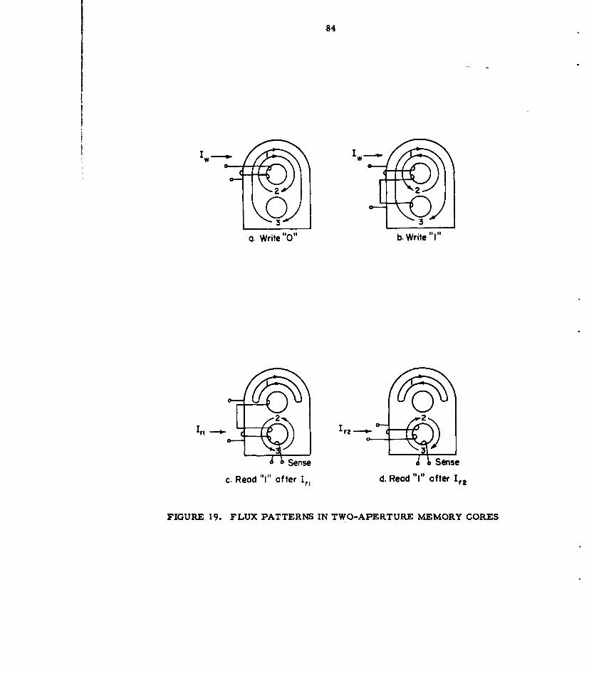
84
Iw
2 2
9 3a. Write 1"04" b. Write "I"
3Sense Sense
c. Read "I" after In d. Read "I" after Irg
FIGURE 19. FLUX PATTERNS IN TWO-APERTURE MEMORY CORES

85
experimental setup, the drive current was connected to switch the first core to the "one"state and the second core to a "zero" state. The drive current (1w) applied to the upperhole through two turns of wire, switches the flux in legs 1, 2, and 3 to a clockwisedirection or "zero" state. The write "one" drive, shown as Figure 19b, consists of twoturns in the upper hole which cause the flux to move counterclockwise, and the one turnin the lower hole causes the flux in Leg 3 to remain in the clockwise direction. Inessence, the drive current switches the flux in Leg 2, and one-half the flux in Leg 1,counterclockwise. The flux in Leg 3, and one-half the flux in Leg 1, remain in theclockwise direction. Interrogation of the memory core is accomplished by means of apair of read pulses. The first read pulse (Irl) is connected to switch the flux in Leg 3in a counterclockwise direction. In order that the flux in Leg 3 can switch, an equalamount of flux in Leg 2 must switch when the core is in the "one" flux state. Also, anequal amount of flux in Leg I must switch when the core is in the "zero" state. Theampere-turns required to switch flux in a magnetic core is proportional to the pathlength about which the flux is switched. Consequently, the relative hysteresis loopswhich are related to the "one" and "zero" flux patterns are similar to those shown inFigure 18 for the lower aperature where the read ampere-turns (NIr) were adjusted topoint "a". The drive ampere-turns switched flux in Legs 2 and 3 of a "one" flux statecore, Figure 19c, but were below the threshold for switching flux in a "zero" flux statecore. The one-turn winding through the upper hole acts as a bias to prevent the fluxfrom switching in Leg 1. The flux pattern for a core in the "zero" state, after Irl, re-mains in the "zero" state, as shown in Figure 19a. The read drive pulse (Ird) wasconnected to drive the flux in Legs 2 and 3 in the clockwise direction. The read drivepulse (Ir2) switches a "one" flux state core from the flux pattern shown in Figure 19c tothe pattern shown in Figure 19d. In this arrangement, no flux is switched in a "zero"flux state core. Because the read cycle and the write operation are independent, anynumber of read pulse pairs can be applied between write pulses. In this respect, it isa form of nondestructive read.
The results from the "one" and "zero" test experiment are shown in Table 29.Some output peak voltages are not shown because of instrumentation and photographicdifficulties; however, sufficient wave-form data were available to indicate that none ofthe radiation pulses affected the "one" and "zero" signals at the sensing terminals.
Static Test. The knowledge that steady-state radiation and transient radiationcause a certain amount of change in the various magnetic properties of memory coresdoes not definitely indicate to the designer and component engineer that the device willmalfunction. To gain assurance that the device can withstand nuclear bombardment,flux conditions must be prearranged to coincide closely to the application. The statictest was designed to determine whether the memory cores could retain preset flux pat-terns after exposure to a radiation pulse. To accomplish this investigation(4 2), a mem-ory plane was constructed which consisted of 16 two-aperture Mg-Mn ferrite memorycores arranged in a 4 x 4 configuration. A random pattern of "ones" and "zeros, waswritten into the memory plane. This was followed by exposing the memory plane to tenradiation pulses at the Sandia Pulsed Reactor. No read or write drive currents wereapplied during irradiations. Each core was nondestructively read after the exposure,and the results are given in Table 30. It was concluded from this investigation thatvariation between pretest and poattest results was within 2 millivolts for all cores withthe exception of one unit. This memory core exhibited a change of 2. 5 millivolts. Ingeneral, it was believed that the changes listed for this test were not excessive and that

86
C4I -ca
-9-,
.0 C
NN
410)
00 G
-3 -
- -- -V3

87
I
TABLE 30. TRANSIENT RADIATION EFFECTS(a) ON FERRITE(Mg-Mn)TWO-APERTURE CORES OF A (4 x 4) MEMORY PLANE INA NONPULSED CURRENT STATE
Core Location Read Voltages (Irl), a• Read Voltages (Ir2), u
X-Plane Y-Plane Pretest Posttest Pretest Posttest
1 1 +19 +21 -19 -21
1 Z +20 +22 -20 -22
1 3 -19 -21 +19 +20
1 4 -1.5 -2 +1.5 +3
2 1 -1.5 -2.0 +2.0 +1.0
2 2 -1.5 -2.0 +5.0 +6.0
2 3 +20 +21 -20 -21
2 4 +3.5 +4.5 -5.0 -5.5
3 1 -19 -20 +19 +20
3 2 -2 -3 +6 +8.5
3 3 +2 +3 -2.5 -3.5
3 4 +20 +21 -20 -22
4 1 +4 +4.5 -7 -9
4 2 +20 +22 -20 -21
4 3 -20 -22 +20 +21
4 4 -1.5 -2.5 +2 +2.5
(a) Neutron and gamma exposures dose for 10 sbots. 1.719 x 10¹³ n cm"2 and 3.68 x 10⁶ ergs g1"(C).

88
for all practical purposes the irradiation had no effect on the flux states of the inactivetwo-aperture ferrite memory cores.
Conclusions. The tests conducted have pointed out certain areas where no concernneed be shown for specific applications and to a limited extent where some caution mustbe exercised. It can be stated that no transient radiation effects can be expected for
"memory cores under application conditions described in (I) "write disturb - zero" (wVz)output, (2) "one" - "zero", and (3) static tests. The changes observed in the pulse anddisturb investigations indicate that some effect from the pulse radiation may be ex-pected; however, they also indicate that additional research is necessary before thesechanges can be explained thoroughly. Because no measurable permanent damage to anyof the memory cores exposed to radiation pulses at both Godiva II and the Sandia reactorfacilities was observed, some possibilities exist for which some of the effects observedduring the radiation pulse were contributed by air ionizations and cable effects. Thiscontribution of effects cannot be considered large since elaborate preparations, suchas the potting of test ur;its and cable termination in paraffin, were made. Also, in somephases of the studies, various control checks were made to determine whether cableinfluences were present.
Printed-Circuit Boards
The use of copper-foil-clad laminates for printed-circuit boards in electronicequipment has made it possible to reduce production costs as well as physical sizes ofcomplex electronic assemblies. However, the effects of various environmental condi-tions, not considered important for the open-wire-type circuitry, may tend to offsetsome of the advantages gained. Uncoated printed-circuit boards exposed to nuclearradiation are affected in a number of ways. Of major interest seems to be degradationof insulation properties as indicated by various studies based on changes in dissipationfactor, insulation resistance, and capacitance caused by nuclear radiation. Degradationsin the form of metal oxides deposited on the surface of the copper-foil strips as well asdiscontinuities in the foil are other ways in which nuclear radiation has been found toaffect printed-circuit boards. In some instances materials such as fluorocarbons havebeen found to melt completely.
Some difficulties encountered in the past in evaluating steady-state radiation effectson printed-circuit boards involve secondary effects caused by in-pile temperature con-ditions and ionization currents. An exposure to ambient temperatures of 150 C alone,without the added effects of nuclear radiation, has been known to cause certain types oflaminates to crack and become distorted. Foil-clad laminates under such temperatureconditions have been known to form blisters and on rare occasions have burst. Ioniza-tion currents caused by intense nuclear-radiation fields present difficulties by cornusingmeasurements of leakage currents as well as other parameters.
Most of the basic knowledge associated with transient radiation effects on printed-circuit-board materials was derived from many of the various steady-state nuclear-radiation-effects studies. Although major differences exist between types of nurlearradiation encountered in material-test and pulsed-type reactors with respect to type ofneutron radiation and energy levels, much has been achieved in providing informationuseful for prediction of performance in a transient radiation environment. One of the

89
early radiation-effects studies( 4 4 ) involved experiments using the CP-5 materials test
reactor, with results indicating that drastic changes in critical parameters occurred atthe instant peak radiation levels were reached. In essence, this introduced the under-standing that materials used for printed-circuit boards were extremely sensitive toexposure rate. Some of these results are given in Table 31 for the various materialsthat withstood prolonged radiation exposure and were in a physical state that would per-mit measurements of evaluating parameters. The conclusion from this study empha-sized the existence of manufacturing-process differences and the fact that this influencewas so great that the results could not be used for determining which printed- circuit-board material was most resistant to nuclear-radiation damage. It also pointed out thatprinted-circuit boards coated with Krylon appeared more radiation resistant than un-coated boards: however, the extent of improvement was not of a magnitude where its usecould be recommended. The main point of interest from the study was that insulativecoatings influenced the electrical properties of printed-circuit boards where exposureto radiation fields became a certainty.
Since it has been established that printed-circuit boards require coatings to mini-mize conditions of transient-radiation-induced ionization currents, a problem thenexists in determining the type of coating that will reduce transient effects of nuclearradiation. Among various studies conducted to determine which coating was mostappropriate, an experiment( 4 5 ) was designed to explore the difference in exposure-ratesensitivity between coated and uncoated copper-clad Fiberglas-melamine boards. Inthis experiment, five printed-circuit boards, one uncoated and four with different insula-tive coatings, were evaluated. The coatings were silicone varnish, epoxy-polyamid,nitrocellulose lacquer, and polyester coatings. The leakage current between copper-foilconductors and the interelectrode capacitance was measured while the specimens wereout of the radiation field and again while they were exposed to a gamma exposure rate ofapproximately 7 x 10³ ergs g- I(C) sec 1 . Some of the results are given in Table 32where it can be seen that the insulative coatings caused a decrease in the ionizationeffects. All of the coated printed-circuit boards exhibited improvement in the variouselectrical characteristics as compared with the uncoated boards. The polyster coatingappears to be superior to the other coatings; however, all coatings used seemed sensi-tive to radiation exposure rate and temperature.
Most studies conducted with radiation exposures to dielectric materials haveproduced results indicating that the major problems confronting the electronic designerare those involving ionization effects. Since ionization currents are to a great extentinvolved and designated as highly contributory to exposure-rate sensitivity, the1 c, n j,classified as equivalent power sources in a circuit configuration. In this re~pt, . itwould then be logical that circuit potentials and currents would be in : ome way be affectedby radiation-induced currents and voltages. To explore the nature of these added dif-ficulties that may influence design considerations, experiments were conducted to pro-vide some insight to the transient-radiation problem to determine how circuit impedance,protective coatings, and applied potential would change the characteristic appearance ofthe radiation-induced current pulses. In the experiment(2 7 ), the printed-circuit boardstested were phenolic and epoxy, 1/16 inch thick, with a printed-circuit grid consistingof two comblike configurations intermeshed, but not making Luntact. The space be-tween the adjacent conductors was 3/64 inch, and each comb consisted of 5 teeth, 1-1/4inches long. The radiation pulse used in this study was produced by a traveling-wavelinear accelerator which generated a pulsed narrow beam of high-energy electrons for aperiod of approximately 10 microseconds. The radiation pulses averaged 2. '-" x 108 ergsg9l(G) sec- 1 .

90
TABLE 31. SUMMARY OF IN-PILE MEASUREMENTS OF CRITICALPARAMETERS OF PRINTED-CIRCUIT BOARDS(a)
Average ofPreirradiation Range or Change
Evaluation Measurements, of Parameters MeasuredParameters Measured range of values Upon Exposure
Glass-Epoxy
Insulation Resistance, ohms 340 x 3,100 x 109 0.01 to 1,160 x 109 ohmsCapacitance, Ajf 11.4 to 15.5 24 to 180 %Dissipation Factor 0. 03 to 0. 08 0.45 to 0.98
Glass-Melamine
Insulation Resistance, ohms 2.9 to 2800 E 109 0.10to 1116 x 109 ohmsCapacitance, Wf 13 to 33.5 0 to 60 %Dissipation Factor 0. 0 to 0.74 0. 06 to 0. 65
Paper- Phenolic
Insulation Resistance, ohms 580 to 1370 x 109 0. 10 to 4233 x 109 ohmsCapacitance, qd 10.9 to 13.9 3.0 to 30 %Dissipation Factor 0. 01 to 0. 06 0. 22 to 0. 37
Steatite
Insulation Resistance, ohms 14.7 x 10⁹ 1. 0 to 10,000 x 109 ohmsCapacitance, Wd 14.5 Z. 0 to 3.3 %Dissipation Factor 0. 038 0. 12 to 0. 17
Nylon- Phenolic
Insulation Resistance, ohms 625 to 1600 x 109 0. 17 to 4600 x 109Capacitance, Wdf 10.7 to 14. 1 5 to 21.0 %Dissipation Factor 0. 02 to 0. 06 0. 062 to 0. 30
(a) Typical nuclear environment for prlnted-clrcult boards In-pile: Neutron fluxes 2. 1 x 10¹² (Nv0 ) and 3.6 x 10⁹ n cm 2
(epicadmium); and gamma exposure rate a 5.3 x 10⁴ ergs g-1 (C) sec 1".

( 91ITABLE 32. RADIATION EXPOSURE-RATE-AFFECTED CHANGES OF
ELECTRICAL PARAMETERS FOR VARIOUS PRINTED-CIRCUIT BOARDS WITH VARIOUS INSULATIVE COATINGS
EvaluationParameter Preirradiation In-Pile ParameterMeasured Measurement Measurement
Nitrocellulose Lacquer
Leakage Current, amp >012 9. 2 x 10⁻⁸Capacitance, IL/f 17. 1 10.2Breakdown Voltage, kv 4. 2 2.6
Silicone Varnish
Leakage Current, amp >10-12 5.6x 10⁻¹⁰
Capacitance, JiLf 15.0 8.5Breakdown Voltage, kv 3.7 3. 2
Epoxy-Polyamid
Leakage Current, amp >10"12 9. 1 x 10⁻⁹Capacitance, U4Lt 16.4 10. 1Breakdown Voltage, kv 4. 3 3.7
Polyester
Leakage Current, amp >10-12 8.3 x 10⁻¹⁰
Capacitance, Apf 21.3 11.0Breakdown Voltage, kv 3.9 3.3
Uncoated Circuit Board
Leakage Current, amp >10-12 1. 09 x 10-7
Capacitance, A'If 14.2 10.3Breakdown Voltage, kv 2.7 2.8
Note: Typical radiation dose rate n 7 x I03 ergs gl(c) aec 1 .
SA T T E L. L E M E M O R I A L I N S 7 1 T U T E

92
The circuit mentioned above consisted of one comb that was connected to a regulated power supply of a variable d-c voltage up to 500 volts. The other cnmb was con-nected to ground through a series resistor located out of the radiation field. The pulsesdeveloped across this resistor by currents flowing during radiation were detected througha cathode follower whose output was connected to an oscilloscope. Two samples of eachboard were used (phenolic and epoxy); one sprayed with acrylic resin and the otheruncoated.
Wave forms were observed on the oscilloscope for various applied voltages from0 to 500 volts. The shape and magnitude of these pulses under conditions of voltageapplication and coating are shown in Figures 20 and 21. It was noted that the differencesbetween effects on phenolic and epoxy circuit boards were insignificant. In examiningthe various pulses shown in Figures 20 and 21, the presence of the large negative pulsefor zero applied voltage on the coated board was surprising because the uncoated boarddisplayed a slight positive pulse. It was also noted that the large negative pulses tendto build up for a time after the radiation pulse. It was hypothesized that the thin coatingof acrylic resin is a source of negative charge that continues to build up with each suc-cessive pulse due to a very high insulation resistance to ground. The opposite reactionfor the uncoated boards was explained as being caused by a positive charge resultingfrom electron ejection and a decrease in leakage resistance through the air and acrossthe surface of the board from one conductor to the other.
It cannot be concluded that an insulating coating is a positive solution to the reduc-tion of radiation-induced ionization in circuit-board materials, but it does indicate thatsome degree of control can be achieved. Other types of coating, probably of the siliconeor polyester varieties, might produce more satisfactory protection from transientradiation.
Subsystems
Past research related to transient radiation effects on electronic component partsand materials has been conducted with the objective of determining which type of compon-ent part is least susceptible to high-intensity radiation pulses and again for the purposeof predicting the functional performance of these parts in electronic circuits. For thegreater part, these studies have indicated that certain component parts should not be usedin radiation environments. The important outcome of the research is the insight gainedwith respect to additional parameters that must be considered when electronic circuitsare designed for use in radiation environments. These additional parameters have beenrecently designated as radiation-induced parameters which consist of (I) radiation-induced currents and voltage pulses, (2) increases in surface and bulk leakage currentsattributed to charge injection and scattering phenomena, and (3) permanent changes in thebasic structural materials.
Two methods, both predicated by results of many theoretical and experimentalprograms, are currently being considered and employed in approaching the problem ofhardening the circuit against radiation. The first method utilizes an approach wherebyknown radiation effects on electronic parts are employed in programming circuit-analysis problems on an anolog computer. Li essence, the first approach is of a theo-retical nature since it consists of calculating or simulating the circuit or system response

93
II500 v
Ib•%,Legend.
•i200v 1O-megohm series resistorP %I --- Unsproyed
-- ----- Sprayed
S\v
-0.5 k 0 6"ov
-0.?5 -Al
Time, ,lec
FIGURE 20. EFFECTS OF TRANSIENT RADIATIONON PRINTED-CIRCUIT BOARDS( 4 0)

94
0.15500 v
010-
0.05
E\0~
- 0 10 - N ..0 v-
."
Legend
/ 100K.n. series resistor•N%/- Uinsproyed
UnSprayed2 - Sprye
0 5 10 iS 20 25 30 35 40
Time, ýLsec
FIGURE Z1. EFFECTS OF TRANSIENT RADIATION
ON PRINTED-CIRCUIT BOARDS( 4 0)

95
with respect to radiation-induced disturbances. The disturbances which are introducedinto the calculation are based on experimental data for component parts and materialswhich have been investigated in various radiation-effects research programs. Thesecond method consists of actual circuit or system testing in a pulsed-radiation-facilityenvironment.
Recently reported studies( 5 4 ) indicate that the theoretical approach for determiningcircuit responses to disturbances produced by radiation pulses is feasible for vacuum-tube and transistor amplifiers, multivibrators, and semiconductor detector circuits.The determination of responses was accomplished by using an analytical process foreach of the circuits. This process included preparation of circuit nodal equations for
t both the normal circuit and the irradiated circuit. Leakage and charge-injection para-
j meters, made available from literature surveys, were used to reconstruct the equiva-lent circuit. Since in some cases it is necessary to separate the leakage parameters
V from the charge parameters, their values were kept independent in an analog loop. Thecircuit nodal equations are used by the programmer to prepare a preliminary blockdiagram which shows the number of operations requiredfor a solution to circuit responses.The conclusions from these studies were that an analog-computer technique can be usedquite successfully for the theoretical investigation of radiation effects on electronic cir-cuits. Results obtained from the study of the amplifier circuits were fruitful in deter-mining nonlinear circuit response caused by radiation. Other observations noted fromthe data indicated that:
(1) High-impedance circuits are particularly sensitive to leakage effects.
(2) High-gain circuits are sensitive to charge-distribution phenomenasuch as injected currents and leakage.
(3) Transistor circuits are sensitive to leakage effects between controland output points and to injected currents that contribute toincreases in base currents.
(4) The diode detector effects stem from leakage across the output.
(5) The multivibrators are affected by both leakage and chargeinjection in the input portion of the circuit with the change ofconduction state occurring only for the large current injectionand/or charge distribution.
The direct approach for determining whether a circuit will function properly duringa pulse of nuclear radiation is associated with the second method involving aspects ofactual testing. The principal advantages of this second approach lie in the fact that theenvironment provided is ideal rather than simulated and the circuit package usually isthe item of concern. The main disadvantage of the second method is that the informationobtained applies only to the circuit assembly used and cannot be treated under generaldefinitions of the circuit type. Because circuit designs vary considerably from applica-tion to application, differences in component parts and their arrangements in circuitsmake it impossible to derive a precise pattern for transient radiation effects. Regard-less of this, some insight can be gained by examining results obtained from reports onthe subject. In this respect, Table 33 summarizes the results from research experi-ments conducted for such circuits as (1) multivibrators, (2) oscillators, (3) powersupplies, and (4) amplifiers.

96
Multivibrators
The main factors affecting operation of a mult-vibrator in a radiation environmentinvolve effects such as change in conducting state, triggering, and pulse amplitude.Most of the multivibrator circuits listed in Table 33 use transistors as the main func-tional component. With few exceptions, most of these circuits triggered or changedtheir state during the radiation pulse. In the few cases listed for vacuum-tube-type cir-cuits, some exhibited no effects, whereas others were found to have changed their state.In one instance( 5 0 ) where six transistorized units were subjected to test at the Godiva IIfacility, three units were classed as complete failures with the remaining three unitsexhibiting a decrease in output of between 70 and 80 per cent. In other cases(6 ), themagnitude of the amplitude was not greatly affected. However, the pulse shape changedconsiderably, with some ringing occurring at high repetition rate for a short time afterthe pulse had reached its peak flux intensity. What may prove to be interesting wereresults from the experiment with the transistorized Eccles-Jordan bistable flip-flopcircuit. In this study, no triggering failure or erratic triggering occurred during theexposure and only a 5 per cent increase in voltage amplitude was observed during thepulse.
Oscillators
The main interest surrounding operation of an oscillator in a transient radiationenvironment involves effects such as frequency and amplitudy shifts as well as whetherthe oscillator exhibits indications of complete failure. Of the 13 oscillators subjectedto transient radiation in recent studies (results shown in Table 33), 4 of the 6 of oneparticular type(50 ) of transistorized oscillator failed cumpletely. None of the electron-tube-type oscillators failed completely during the radiation pulse, and none exhibitedpermanent damage. The majority of electron-tube oscillators exhibited transient effectsconsisting of loss of amplitude by as much as 90 per cent: however, recovery was notedas the flux intensity subsided. Frequency shifts were not excessive, as indicated by thevoltage-controlled oscillator exhibiting a maximum(51) of 3. 1 per cent for full bandwidth. In this instance it was concluded that the oscillator unit should have deviated lessthan 1. 5 per cent of center frequency and would hdve been less than 1. 0 per cent afterproper design of the filament compensation circuit.
It would then appear that transient radiation effects on operating oscillator circuitsof major concern should be associated with changes in output amplitude at the instant ofpeak radiation intensity and that lesser concern need be shown for aftereffects.
Power Supplies
Failures or erratic operation of power supplies subjected to transient radiationconditions is of major concern because of the importance associated with their functionin systems. The failure of a power supply obviously subjects all circuits associatedwith it to various degrees of malfunctioning. In some critical applications, the momen-tary fluctuation of output voltage or an excess of ripple voltage can drastically affect theoperation of other radiation-hardened circuits.

97
t Ct+ + ev
I Ot-4 c
Nl Nl N
0~~~ NN 4
t-~c ca c4aa -
740 VID v*
.I*,
4 c4p N N

98
Aoo0
4?j'
C-1 -4 - -4'4 -+ .
x x x x
N In
o8 0 x x x
m m~
coJ cc
N4 m4 N4 N4 c- c4
-10 .0
-to 1.
o' c w c4 ~ c'] (D o
oa N

99
Isa
z V
IN I I
8%% %,.4 r.1
.4 .4.I 4 .4
000
"M.4 'I- l I
.1 1 10 1 1~In U.
100
~1
IaII I §I
+ +I
aC4 C
CD
'Iv
F44
'o Z4
00
4bO

101
Power supplies can be affected in several ways depending on whether their mainfunctional components are transistors or electron tubes. Most concern is indicated formalfunctions such as increased ripple voltage, poor voltage regulation, increase ordecrease in voltages during the pulse of radiation, and subsequent permanent damage.The most common effects are the increases in ripple voltage which have been mea-sured( 4 7 ) and found to exceed 1 volt. These conditions are often accompanied with indi-catiuns of poor regulation for irradiated power supplies that have been tested in the3 postradiation state throughout their load range. In some instances the irradiated power1supply tends to display considerable ripple, with reduction in line voltage within theunit's specified limits. Increases in line voltage to these irradiated units seem to cor-rect the condition of excessive ripple, and for this reason it is believed that the regula-tion portion of the circuit may be susceptible to radiation damage. In regard to circuit
component parts, Table 33 summarizes transistorized power supplies only becauseresults for electron-tube-type power supplies are not available.
Amplifiers
Of major interest in transient radiation effects on amplifiers is whether radiation-
induced currents or voltages at the amplifier input will cause an amplified effect at theoutput portion of the circuit. To investigate this mechanism of damage, researchershave exposed single-stage amplifiers(Z?7 to radiation pulses from a linear acceleratorwhile observing the cffects on the output portion of the circuit. In this particular pro-gram, the effects of coatings were explored to determine whether such applicationswould effect appreciable improvement in operation of the amplifiers in a radiationenvironment. The single-stage amplifiers employing electron tubes showed some im-
* provement (shown in Table 33), whereas the transistorized amplifier seemed to increasein amplified signals for the sprayed unit. Posttest measurements indicate that radiationpulses in intensities encountered at the Godiva II critical assembly caused some transis-torized amplifiers to decrease in gain. It was believed that the main cause for thisoccurrence is degradation of the transistors.
Conclusions
Both theoretical and experimental studies of radiation effects on circuits haveindicated that the designer must consider two types of transient radiation effects whendesigning circuits that will be required to function in a pulse radiation environment. Thefirst type can be designated as a noise transient which may appear as a voltage or currentpulse induced in the circuit by ionization and/or displacements. This effect tends toaffect operating characteristics by changing leakage conditions of insulating materialsand ultimately changing circuit impedances. The second effect is related to changes incomponent-part characteristics which cause a transient distortion of the normal circuitsignals. The initial approach to selecting and designing a circuit for application in anuclear environment must include the study of component-part radiation-damage sus-ceptibility. This is necessary because, in the mathematical analysis of a circuit,transient radiation effects are introduced as radiation-induced parameters into networkequations in accordance with the mechanisms involved.
Changes in properties of circuit components influence time-dependency character-istics in the circuit parameters. External leakages associated with ionization effects

10Z
become parallel components in the equivalent-circuit configuration during the circuitanalysis. Charge injection and scattering have been treated as current and voltagegenerators, thus influencing the circuit-analysis equations as though the effects wereadditional driving-iorce terms. Obviously, these transient effects are important onlyduring the finite time interval covering a period slightly longer than the radiation burst.
Some general concepts and insight have evolved from theoretical analysis andexperimental results. For example, circuits involving high impedances are generallymore susceptible to transient effects than low-impedance circuits. This has been sub-stantiated in experiments where circuits identical in all respects with the exception ofimpedance were tested and it was found that the low-impedance circuits were leastaffected. The use of high-gain circuits in preference to multiple low-gain circuits, fre-quently considered for miniaturization reasons, should be avoided where possible. Thisis suggested because high-gain circuits and high impedance go hand-in-hand. Cornditionsconducive to ionization should be recognized and attempts made to either avoid the condi-tion or reduce it by application of coatings.
REFERENCES
(1) van Lint, V.A.J. , "Mechanisms of Transient Radiation Effects State of the Art",General Atomic Report GA-2886, January, 196Z.
(2) Easley, J. W. , and Blair, R. R. , "Transient Phenomena in SemiconductorDevices", Appendix E to Nuclear Electronic Effects Program, Third TriannualTechnical Note, WADC TN 60-160, March 15, 1960.
(3) Brown, W. L. , and Easley, J. W. , "The Transient Ionization Pulse in a Semi-conductor Junction", paper presented at the Conference on Pulse Radiation Testing,Kirtland Air Force Base, New Mexico, September, 1960.
(4) van Lint, V.A. J. , "Transient Radiation Effercts-Physics and Tests", GeneralAtomic Report GA- 1827, November 1960.
(5) van Lint, V.A.J. , "Transient Radiation Effects in Semiconductors", Proceedingsof the Second AGET Conference on Nuclear Radiation Effects on Semiconductors,September, 1959.
(6) IBM Radiation Research Group, "Some Effects of Pulsed Neutron Radiation onElectrical Components-I", October 9, 1958.
(7) IBM Radiation Research Group, "Burst Radiation Effects on Semiconductor Com-ponents", March 12, 1958.
(8) Bohan, W. A. , Maxey, J. D. , and Pecoraro, R. P. , "Semiconductor Device Oper-ation in a Pulsed Nuclear Environment", presented at the National TelemeteringConference, May, 1959.
(9) Sauer, S., "A Study of Radiation Effects on Electronic Devices", Edgerton,Germeshausen, 9 Grier, Boston, Massachusetts (December 14, 1959), SecondInterim Report, Part I September 1, 1959, to November 30, 1959.

103
(10) Denny, J. M., "Pulsed Neutron Irradiation of Electronic Components", HughesAircraft Company Technical Memorandum No. 522, July 16, 1958.
(11) "Some Effects of Pulsed Neutron Radiation on Electronic Components. 2. Result
of August 1958 Godiva Test Series", International Business Machines Corporation,Military Products Division, Owego, New York (no date given).
(12) Bohan, W. A., "Effects of Pulsed X-ray Radiation on Semiconductor Devices",IBM Radiation Research Group (no date given).
(13) Steele, H. L. , "Effects of Continuous Gamma Ray or Pulsed Neutron Radiation onSemiconductor Diodes", Boeing Airplane Company Document No. D2-2123,December 2, 1958.
(14) IBM Radiation Research Group, "Pulsed Effects on Electronic Components",Second Triannual Report under Contract AF 33(600)-4046Z, October 31, 1960.
(15) Perkins, C. W. , Denny, J. M., and Downing, R. G. , "Second Experiment onPulsed Neutron Radiation Effects", Hughes Aircraft Company Technical Memoran-
f dum No. 622, September, 1959.
(16) Perkins, C. W., Denny, J.. M., and Downing, R. G., "Third Experiment onPulsed Neutron Radiation Effects", Hughes Aircraft Company Technical Memoran-dum No. 623, October, 1959.
(17) Berger, A. G. , "Transient Radiation Effects on Electronics-Part I", BoeingReport D2-7899, January, 1961.
(18) Caldwell, R. S. , "Transient Radiation Effects to Electronic Parts and Materials"Vol. 2, Sec. 3, Boeing Report D2-6594, February, 1961.
(19) Degenhart, H. J., and Long, A. L. , "Transient Effects of Pulse Radiation onElectronic Parts", U.S. Army Signal Research and Development Laboratory, FortMonmouth, New Jersey, October 6, 1958.
(20) Long, A. L. , "Nuclear Radiation Induced Voltages in Coaxial Cables", U.S. ArmySignal Research and Development Laboratory, Fort Monmouth, New Jersey,Technical Memorandum, August 12, 1960.
(21) "Pulsed Radiation Effects on Electronic Components", Third Triannual Reportunder Contract AF 33(600)-40462, International Business Machines Corporation,Federal Systems Division, Space Guidance Center, Owego, New York,February 28, 1961.
(22) "Pulsed Radiation Effect. on Electronic Components", Fourth Triannual Reportunder Contract AF 33(600)-40462, International Business Machines Corporation,Federal Systems Division, Space Guidance Center, Owego, New York,31 October, 1961.
(23) Conrad, E. , Personal Communication, Diamond Ordnance Fuze Laboratory,Washington, D. C.
(24) "Some Effects of Pulsed Radiation on Electronic Components III, Results ofJanuary, 1959, Godiva Test Series", International Business Machines CorporationFederal Systems Division, Owego, New York.

I
104
(25) Schlosser, W. , "Report on Radiation Effects Studies, Godiva Exposure IV, 27 andZ8 August 1959, U.S. Army Signal Research and Development Laboratory, FortMonmouth, New Jersey, October 27, 1959.
(26) "Some Effects of Pulsed Neutron Radiation on Electronic Components", FinalReport, International Business Machines Corporation, Federal Systems Division,Owego, New York, January, 1960.
(27) Perkins, C. W. , et al. , "First Experiments on the Effects of Radiation Pulses onElectronic Circuits and Components", Hughes Aircraft Company, ResearchLaboratories, February 3, 1958.
(Z8) Markow, D. , Degenhart, H. 3. , and Murphy, H. M. , Jr. , "Effects of MixedNeutron-Gamma Pulses on Electronic Components", U. S. Army Signal Researchand Development Laboratory, Fort Monmouth, New Jersey, September 30, 1959.
(29) "Pulsed Radiation Effects on Electronic Components, First Triannual Report",International Business Machines Corporation, Federal System Division, Owego,New York, July Z0, 1960.
(30) Wicklein, H. W., and Dickhaut, R. H. , "Transient Radiation Effects in Capacitorsand Dielectric Materials", The Boeing Company, Seattle, Washington.
(31) Wicklein, H. W. , Spencer, W. E. , Sandifer, C. W. , "Transient Radiation Effectson Electronics, Part 1", Kukla Transient Radiation Test, Appendix Ill, The BoeingCompany, Seattle, Washington, January, 1961.
(32) Wicklein, H. W., Personal Communication, The Boeing Company, Seattle,Washington.
(33) Schaefer, D. L., "The Effects of Nuclear Radiation on the Performance of theImage Orthicon Television Camera Tube", General Electric Company, January 29,1961.
(34) Chandler, H. G. , "Effects of Pulsed Nuclear Radiation on Nonoperating Tubes andTransistors", Diamond Ordnance Fuze Laboratories, Department of the Army,Washington, D. C., November 20, 1959.
(35) Saelens, R. G., "Radiation Effects on Ceramic Electron Tube Types at Godiva IIFacility", U.S. Army Signal Remearch and Development Laboratory, FortMonmouth, New Jersey, March 17, 1959.
(36) Kothstein, T. F. , "Nuclear Pulse Testing of Viokoi and Image Orthicon CameraHeads", Frankford Arsenal, U.S. Army Ordnance, Philadelphia 37, Pernsylvania,October, 1961.
(37) Hammond, D. L. , "Effects of Radiation on Quartz Crystal Units", Signal CorpsEngineering Laboratories, Fort Monmouth, New Jersey, Technical Memorandum
No. M-1785, June 25, 1956.
(38) Stanley, J. M., "Effects of Nuclear Radiation on Quartz Crystals", U.S. ArmySignal Research and Development Laboratory, Fort Monmouth, New Jersey,Memorandum Report No. FCD-M-33-58, November 17, 1958.

105
(39) Reid, F. J. , and Moody, J. W., "The Effect of Nuclear Radiation on MagneticMaterials", Battellc Memorial Institute, Columbus, Ohio, REIC Technical Memo-randum No. 12, December 31, 1958.
(40) "Study of Effect of High-Intensity Pulsed Nuclear Radiation on Electronic Parts andMaterials (SCORRE)", Report No. 1, Signal Corps Contract Number AD-3b-039-SC-85395, Department of the Army Project No. DA-3G-93-01-001-01, First QuarterlyReport, I July 1960 to 30 September 1960, for the U.S. Army Signal Researchand Development Laboratory, Fort Monmouth, New Jersey, International BusinessMachines Corporation, Federal Systems Division, Owego, New York.
(41) "Study of Effect of High-Intensity Pulsed Nuclear Radiation on Electronic Partsand Materials (SCORRE)", Report No. Z, Signal Corps Contract NumberAD-36-039-SC-85395, Department of the Army Project No. DA-3G-93-01-001-01,Second Quarterly Report, I January 1961 to 31 March 1961, for the U.S. ArmySignal Researchi and Developnment Ldboratory, Fort Monmouth, New Jersey,International Business Machines Corporation, Federal Systems Division, Owego,New York.
(42) "Study of Effect of High-Intensity Pulsed Nuclear Radiation on Electronic Parts andMaterials (SCORRE)", Report No. 3, Signal Corps Contract NumberAD-36-039-SC-85395, Department of the Army Project No. DA-3G-93-01-001-01,Third Quarterly Report, 1 January 1961 to 31 March 1961, for the U.S. ArmySignal Research and Development Laboratory, Fort Monmouth, New Jersey,International Business Machines Corporation, Federal Systems Division, Owego,New York.
(43) "Study of Effect of High-Intensity Pulsed Nuclear Radiation on Electronic Parts and
Materials (SCORRE)", Report No. 4, Signal Corps Contract NumberAD-36-039-SC-85395, Department of the Army Project No. DA-3G-93-01-001-01,Fourth Quarterly Progress Report, 1 April 1961 to 30 June 1961, for the U.S.Army Signal Research and Development Laboratory, Fort Monmouth, New Jersey,International Business Machines Corporation, Federal Systems Division, Owego,New York.
(44) Pfaff, E. R. , and Shelton, R. D. , "Effects of Nuclear Radiation on ElectronicComponents", Admiral Corporation, WADC TR-57-361, Part 2, AF 33(616)-3091,ASTIA, AD 155790, August, 1958.
(45) Hansen, J. F. , and Cary, H., "Final Report on the Effects of Gamma-Induced
Ionization on the Electrical Properties of Printed Circuits and Connectors", toChance Vought Aircraft from Battelle Memorial Institute, March 5, 1959.
(46) Almond, H. B. , and Spencer, W. E. , "Nuclear Radiation Tests of MinutemanFlip-Flop Circuit at the Godiva II Facility", Los Alamos, New Me-rico, TechnicalMemorandum No. 5-7870-7839 (BRC 11770) 9 September 1959.
(47) Almond, H. B. , and Spencer, W. E., "Preliminary Data from Nuclear RadiationTests of the PS-210 Power Supply", Technical Memorandum No. 5-7870-7739(BRC 11769), 30 July 1959.
(48) Almond, H. B., and Perkins, L. C., "Radiation Damage Tests on P.S. 223Transistorized 250 Volt Regulated Power Supply", Technical Memorandum No.PAS-APS-5/0146(BRC 11771), 23 January 1959.
106
(49) Perkins, C. W. , "Effect of Radiation on Ordnance Missile Components", forDiamond Fuze Ordnance Laboratories, Hughes Aircraft Company (BRC 13497),December 1960.
(50) Behrens, R. G., "Effects of Fast Neutrons on Circuitry Employing Semiconduc-tor Devices", for Boeing Airplane Company, Seattle, Washington, Document No.D5-2245 (BRC 11892), 5 November 1957.
(51) Oertel, M. F., and Ashwood, C. R., "Performance of EMR Voltage-ControlledOscillator Units in a Nuclear Environment", Technical Report No. 849, DiamondOrdnance Fuse Laboratories (BRC 12668) , 29 July 1960.
(52) Vassilakos, D., "Radiation Test on the PS 210 Transistorized 150 Volt RegulatedPower Supply", Document No. D5-5851, Boeing Airplane Company, Seattle,Washington, Contract No. AF 33(600)-35030 (BRC 11746), 14 October 1959.
(53) Stralser, B. J. , "First Experiment on Transient Effects of Nuclear Radiation ofElectronic Parts and Circuits", U.S. Navy Electronics Laboratory, San Diego,California, Technical Memorandum No. TM-301 (BRC 12851), 9 September 1958.
(54) Bell, J. E., and Walker, K. R., "Theoretical Study of Burst Introduced TransientRadiation Effects in Basic Electronic Circuits", for the Air Force Special WeaponsCenter, Air Research and Devclopment Command, Kirkland Air Force Base, NewMexico, Final Report, Hughes Aircraft Company (BRC 14963), 15 May 1961.
DCJ/FJR/WEC/DJH/ENW:mjd

LIST OF AVAILABLE REIC PUBLICATIONS
Radiation Effects Information CenterBattelle Memorial Institute
Columbus 1. Ohio
Requests for unclassified information or uncluasified REIC Requests for classified REIC published reports and memo-published reports and memoranda should be sent: randa should be sent. via your contracting officer for
endorsement, to the following address:Radiation Effects Information CenterBattelle Memorial Institute ASD (ASTEVC. Mr. Robert G. Merkle)505 King Avenue Wright-Patterson AFB. OhioColumbus 1. OhioAttention E. N. Wyler
Unclassified ReportsReport Number Title
1 The Effect of Nuclear Radiation on Semiconductor Materials (December 20, 1957). AD 147399
1 (First Addendum) The Effect of Nuclear Radiation on Semiconductor Materials (March 31. 1959), AD 210758
• 6 A Survey of Current Research and Developments in the Field of Dosimetry (May 31. 1958). AD 157172
6 (First Addendum) A Survey of Current Research and Developments in the Field of Dosimetry (March 31. 1959). AD 210766
10 The Effect of Nuclear Radiation on Semiconductor Devices (April 30. 1960). AD 240433(Supersedes Memos Not. 4. 5. 6)
10 (First Addendum The Effect of Nuclear Radiation on Semiconductor Devices (July 15. 1961). AD 262081
16 Survey of Irradiation Facilities (February 28, 1961). AD 256953
17 The Effect of Nuclear Radiation on Structural Adhesives (March 1, 1961). AD 256954(Supersedes Reports Not. 7 and 11)
18 The Effect of Nuclear Radiation on Electronic Components (June 1. 1961). AD 260303 (SupersedesReports Not. 2, 8. 12. 14, and 15 and Memos Nos. 2. 7. 12. 14. and 20)
19 The Effect of Nuclear Radiation on Lubricants and Hydraulic Fluids (May 31. 1961), AD ?61178(Supersedes Report No. 4)
20 The Effect of Nuclear Radiaticn on Structural Metals (September 15. 1961). AD 265839(Supersedes Report No. 5)
21 The Effect of Nuclear Radiation on Elastomeric and Plastic Components and Materials (September 1. 1961)AD 267890 (Supersedes Reports Nos. 3. 9. and 13 and Memos Not. 1. 3. 8. 13, and 17)
23 Proton and Electron Damage to Solar Cells (April 1, 1962)
24 Radiation Effects State of the Art 1961-1962 (June 30. 1962). NASA N62- 16454
*Out of Print in REICs Available only from ASTIA. Armed Services Technical Information Agency. Document Service Center.Arlington Hall Station, Arlington, Virginia.

Classified Reports
Report Number Title
1-C The Effect of Nuclear Radiation on Hydraulic, Pneumatic. and Mechanical Systems for Subsonic,Transonic. and Low-Supemonic Speed Aircraft (Tide Unclassified) (Secret, Restricted Data)(May 31. 1958)
1-C (First Addendum) The Effect of Nuclear Radiation on Hydraulc. Pneumatic. and Mechanical Systems for Subsonic,Transonic. and Low-Supersonic Speed Aircraft (Title Unclasilf:'d) (Secret. Restricted Data)
(March 31. 1959)
1-- (Second The Effect of Nuclear Radiation on Hydraulic, Pneumatic. and Mochanical Systems (Title Unclassified)Addendum) (Secret. Restricted Data) (September 15. i960)
2-C The Effect of Nuclear Radiation on Ceramic Mate "ials (Title Unclassified) (Secret) (June 30. 1959).AD 157173
2-C (First Addendum) The Effect of Nuclear Radiation on Ceramic Materials (Title Unclamified) (Secret. Restricted Data)(June 15. 1961)
4-C The Effect of Nuclear Radiation on Electrical and Electronic Systems (Title Unclassified) (Secret.Restricted Data) (March 15. 1960).
6-C The Effects of Nuclear Weapon Bursts and Simulated Bunts on Electronic Components (Title Unclassified)
(Secret. Restricted Data) (May 31. 1961)
Unclassified Memoranda
Memorandum Number Titic."*9 The Effect of Nuclear Radiation on Glass (November 30. 1968). AD 207701
10 Format for Reporting Radiation Effects Data (May 15. 1959). AD 218251
*ol The Effect of Nuclear Radiation on Hydrocarbon Fuels (November 30. 1958). AD 207702
015 The Effect of Nuclear Radiation on Hoses and Couplings (March 31. 1959). AD 225504
$16 The Effect of Nuclear Radiation on Refrigerants (June 30. 1959). AD 219510
"*18 The Effect of Nuclear Radiation on the Performance of a Hydraulic Flight Control System (June 15. 1959),AD 219512
21 Space Radiation and Its Effects on Materials (June 30, 1961)
23 Radiation Dosimetry: An Annotated Bibliography (September 15. 1961). AD 265523
Classified Memoranda
Memorandum Number Title
1-C The Effects of Nuclear Radiation on Fluorolubes and Other Gyroscope Fluids (Title Unclassified) (Secret)(September 5. 1958). AD 302126
2-C The Effect of Nuclear Radiation on Explosives and Solid Propellants (Title Unclassified) (Secret.Restricted Data) (June 15. 1959)
"*Out of Print in REIC; Available only from ASTIA. Armed Services Technical Information Agency. Document Service Center.Arlington Hall Station. Arlington, Virginia.

Memorandum Numbe Title
" 3-C Does-Rate Effects on Mate i Os. Components, and Systerm (Title Unclassified) (Secrtt, I•estricted Data)
(July 31. 1959)
10-C Nuclear Radiation Effects IOr•Jects (Title Unclassified) (Confidetitial) (March 31, 1962)