transistor digital circuits - utcluj.ro logic family supplied at +5v nm l 1.5v 0.5v 1v nm h 4.5v...
TRANSCRIPT

Transistor Digital Circuits

active semiconductor devices (with three terminals)
Operating principle: using a voltage between two terminals (command) to control the current through the third terminal.
Transistors: voltage-controlled current sources
TRANSISTORS
• transistors: essential components of every electronic circuit
• Pentium 4 microprocessors : ~ 43,5 million field effect transistors
• Intel 4004, 1971, 10µ, 14mm2, 2300 transistors
• IBM z13, (6-to-8 core), 2015, 22nm, 678mm2, 3,990,000,000 transistors
Discrete transistors

Transistor types
Metal-Oxide-Semiconductor Field-Effect Transistors
Bipolar Junction Transistors

Symbols of the transistors
G - gate or grid D - drainS - source
n - type p - type
n-channel enhancement-type MOSFET
p-channel enhancement-type MOSFET
B – baseC – collector E – emitter
npn BJT pnp BJT

vI = VIH ; T- (on) ; iO > 0 ; vO 0
vI = VIL ; T- (off) ; iO = 0 ; vO > 0
The controlled switches are complementary
Switching Transistor - Controlled switch model
n-channel enhancement-type MOSFET
p-channel enhancement-type MOSFET
npn BJT pnp BJT
Tn
vI
vO
iOTp
vO
iOvI
vI = VIH ; T- (off) ; iO = 0 ; vO >0
vI = VIL ; T- (on) ; iO > 0 ; vO 0

Logic inverter
0V logic 0
VPS logic 1
vA Tn vy
VIL = 0 (off) VPS
VIH = VPS (on) 0

logic 0 - 0V
logic 1 - VPS
Tn and R Tp and R
Logic inverter

Critical analysis of the inverter
with Tn and R
Disadvantage elimination:
R as small as possible, ideal R→0;

Critical analysis of the inverter
withTn and R
Solution: replacement of R with a controlled switch
Disadvantage elimination:
R as small as possible, ideal R→0; R as large as possible, ideal R→∞
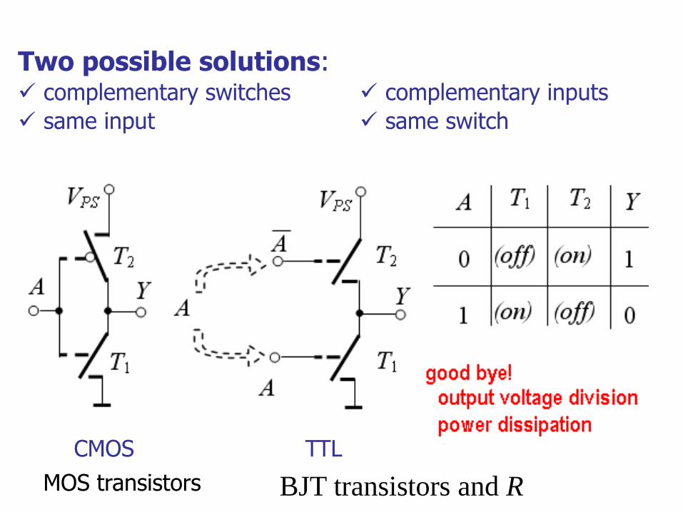
Two possible solutions: complementary switches
same input
TTLCMOS
complementary inputs
same switch
MOS transistors BJT transistors and R
MOSFET DIGITAL CIRCUITS
Ideal controlled switch model
Implementation with MOSFET

CMOS Logic Inverter

Logic function NAND, NOR
How can we
eliminate the
disadvantages
due to the
presence of R ?

CMOS NAND

CMOS NOR CMOS AND

Transfer characteristicof the CMOS inverter
Ideal (input) Real

Noise margins
Logic circuit 1
Logic circuit 2
out in

Noise margins - cont.
maxmax
minmin
OLILL
IHOHH
VVNM
VVNM
Voltage levels and
noise margins for
CMOS logic family
supplied at +5V
V1V5.0V5.1 LNM
V1V5.3V5.4 HNM

Bipolar Digital Circuits• Inverter
RTL Technology
RB is always necessary to limit the base current,
due to the presence of the base-emitter pn junction (0.7V voltage drop when Tn is on)

Bipolar Digital Circuits
• Inverter RTL Technology
• NOR

TTL: Transistor-Transistor Logic
• Logic Inverter
• from technological reasons in TTL integrated circuits the use of only npn type transistors is preferred
• identical transistors but complementary control
vI1, vI2 ?

Standard TTL gate

Voltage levels and noise margins for TTL family
Supply only with 5V