transistors - university of rochester
TRANSCRIPT

TransistorsArthur Chan
Brad ChristensenAndrew Galkiewicz
Sarah GollubAdi RobinsonTyle Stelzig
HAPPY 60th BIRTHDAY!

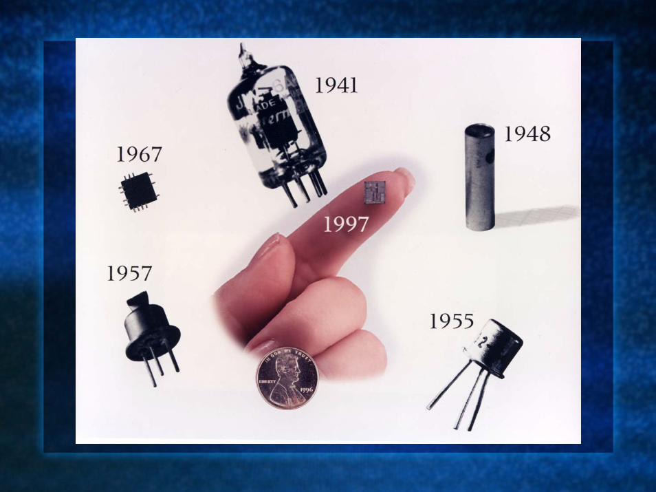
HistoryFirst conceived and patented in 1928 by Julius LilienfeldDuring WWII, research into semiconductors like geranium and silicon intensifiedFirst transistor was made by John Bardeen, Walter Brattain in 1947
http://www.ieee.org/portal/cms_docs_sscs/sscs/07Spring/HR-1stTransistor.jpg

More History
William Shockley led the effort in the creation of the junction transistor in the early 1950s
http://th.physik.uni-frankfurt.de/~jr/gif/phys/bsb.jpg

Bipolar Junction Transistors
NPN (most common) – uses electrons as carrier of current.PNP – uses the lack of electrons (“holes”).
How Transistors Work

The Physics of ItAn insulating effect occurs where the P-type and N-type are in contact. This interface is called a ‘depletion zone’.This insulating effect decreases when a voltage of the correct polarity is appliedApply a voltage across the collector and emitter.There’s a depletion zone between collector and base.Electrons which wander across the base are forced across the upper depletion zone by the applied voltage. The base depletion zone thus controls the collector battery current. This base depletion zone is controlled by the base voltage.

Diagram________ Light
/ \ Bulb| ________/\/\/\________| | || | \________/ |v | |
| || ______|______| | |
Collector | | COLLECTOR N | Thick depletionBattery | + |_____________| layer with electrons
| _____________ <-- passing through____|____ | |___________________ | BASE P | |
_________ |=============| | + _____ 9V | | ____|____
_________ | EMITTER N | _____ Base_____ |_____________| _________ Battery
_________ | _____ .7V_____ | | -| - |_____________________||______________________|
------>
Source of diagram: http://amasci.com/amateur/transis2.html

Transistors as Amplifiers
The base/input voltage controls how much of the current suppliedby the supply voltage (labeled ‘Vcc’) flows through the transistor itself, and how much acts as Vout.Small changes in the base voltage will produce large changes in Vout.You can think of a transistor like a valve: the base/input voltage controls how much of the supply voltage is allowed through.The ratio between the current through the collector and the current through the base is defined as hFE.Unless the transistor is saturated, the current gain equals hFE.Typically hFE is 100.“Darlington pair” is when multiple transistors are connected, thus hFE = hFE1 x hFE2.

Transistors as SwitchesOnce the base voltage reaches a certain level, no additional current will flow
This level is referred to as ‘saturation’The input voltage can therefore be chosen so that the output is in one of only two possible states (ON or OFF)This allows transistors to be used as switches
Diagram: http://en.wikipedia.org/wiki/How_a_Transistor_Works

Field Effect Transistors
Only has two layers of semiconductor material.Electricity flows from one layer called the channel to the other layer called the gate. The voltage across the gate interferes with the current, thus controlling its strength.

Logic GatesWhen high voltage is applied to the base, the transistor behaves like a switch allowing current to flow from the collector to the emitter.If the collector is connected to the resistor, and a high voltage is applied to the base, current flows through the transistor causing a voltage drop across the resistor. In this case Vout is low. So if Vin has high voltage, Vout has low voltage.If Vin has low voltage, current does not flow through the resistor. Thus there is no voltage drop across the resistor and high voltage accumulates at Vout.So if Vin is low, Vout is high.This arrangement of transistors acts as a NOT-gate.Other arrangements can act as other logical gates.Using such gates in series allows for the construction of computers.

Main technologies for Transistor DesignSilicon-Germanium (SiGe)
Usually refers to bipolar devices in SiGetechnology, although SiGe FETs are also viable
MOS Metal Oxide Semiconductor
Bipolar Bipolar is a term used to describe a junction based transistor as distinct from a field effect transistor
BiCMOS Bipolar Complementary Metal Oxide Semiconductor

Distinct Characteristics of the Modern Applications
2 improvements made on the BJTs and FETsUsed more in digital circuits than analog circuits. e.g. RAM, Transistors tend to be integrated into integrated circuits –digital output

Examplestemperature censors (analog output)
Ic rises exponentially with base-emitter voltage (0.6-0.7V for Si)Usable when containing >1 transistor, or in an ideal deviceNot useful alone, as Icdepends on voltage as well as outdoor temperature
calculators of log and other functions
Transistors store binary numbers by switching electric currents on and off Logic gates; compares 2 currents

Future DesignTwisted Ballistic TransistorElectrons follow a ballistic trajectory into and out of junction (bumper)How it worksgate structure crossroads design electric field at center of y-shaped non-conductive intersectioninertia; electric field around the block; ballistic trajectoryElectrons apply varying voltage differentialan indium gallium arsenide-indium aluminum arsenide substrate increases electron flow and produces conductioncurrent need not be present due to magnetsBinary 1s and 0s semiconductor sheet 2D electron gas

Moore’s Law
The conjecture that the most cost-effective number of transistors per unit area on an integrated circuit will double every 12-24 months is known as Moore’s Law. This has proven true!The development of transistors has allowed for this phenomenal increase in density, and thus SPEED.