transistortester with avr microcontroller and a little ... · transistortester with avr...
TRANSCRIPT

TransistorTester with AVR microcontrollerand a little moreVersion 1.05k
Karl-Heinz Kubbelerkh [email protected]
January 19, 2013
Contents
1 Features 4
2 Hardware 72.1 Circuit of the TransistorTester . . . . . . . . . . . . . . . . . . . . . . . . . . . . . . . 72.2 Hints for building the TransistorTester . . . . . . . . . . . . . . . . . . . . . . . . . . 92.3 Programming of the microcontroller . . . . . . . . . . . . . . . . . . . . . . . . . . . . 92.4 Troubleshooting . . . . . . . . . . . . . . . . . . . . . . . . . . . . . . . . . . . . . . . 10
3 Instructions for use 123.1 The measurement operation . . . . . . . . . . . . . . . . . . . . . . . . . . . . . . . . 123.2 Selftest and Calibration . . . . . . . . . . . . . . . . . . . . . . . . . . . . . . . . . . 133.3 special using hints . . . . . . . . . . . . . . . . . . . . . . . . . . . . . . . . . . . . . . 133.4 Compoments with problems . . . . . . . . . . . . . . . . . . . . . . . . . . . . . . . . 143.5 Measurement of PNP and NPN transistors . . . . . . . . . . . . . . . . . . . . . . . . 143.6 Measurement of JFET and D-MOS transistors . . . . . . . . . . . . . . . . . . . . . . 15
4 Configuring the TransistorTester 16
5 Description of the measurement procedures 215.1 Measurement of Semiconductors . . . . . . . . . . . . . . . . . . . . . . . . . . . . . . 23
5.1.1 Measurement of PNP Transistor or P-Channel-MOSFET . . . . . . . . . . . . 235.1.2 Measurement of NPN Transistor or N-Channel-MOSFET . . . . . . . . . . . . 255.1.3 Measurement of Diodes . . . . . . . . . . . . . . . . . . . . . . . . . . . . . . . 275.1.4 Results of different measurements . . . . . . . . . . . . . . . . . . . . . . . . . 27
5.2 Resistor Measurement . . . . . . . . . . . . . . . . . . . . . . . . . . . . . . . . . . . 305.2.1 Resistor Measurement with 680 Ohm Resistors . . . . . . . . . . . . . . . . . . 305.2.2 Resistor Measurement with 470 kOhm resistors . . . . . . . . . . . . . . . . . 325.2.3 Results of the resistor measurements . . . . . . . . . . . . . . . . . . . . . . . 33
5.3 Measurement of Capacitors . . . . . . . . . . . . . . . . . . . . . . . . . . . . . . . . 385.3.1 Discharging of Capacitors . . . . . . . . . . . . . . . . . . . . . . . . . . . . . 385.3.2 Measurement of big Capacitors . . . . . . . . . . . . . . . . . . . . . . . . . . 385.3.3 Measurement of small Capacitors . . . . . . . . . . . . . . . . . . . . . . . . . 405.3.4 Measurement of the Equivalent Series Resistance ESR . . . . . . . . . . . . . . 425.3.5 Results of Capacitor measurement . . . . . . . . . . . . . . . . . . . . . . . . . 455.3.6 Automatic calibration of the capacitor measurement . . . . . . . . . . . . . . . 49
5.4 Measurement of inductance . . . . . . . . . . . . . . . . . . . . . . . . . . . . . . . . 535.4.1 Results of the inductance measurements . . . . . . . . . . . . . . . . . . . . . 54
5.5 Selftest Function . . . . . . . . . . . . . . . . . . . . . . . . . . . . . . . . . . . . . . 555.5.1 Some Results of the Selftest Function . . . . . . . . . . . . . . . . . . . . . . . 58
6 Known errors and unsolved problems 62
1
7 Special Software Parts 63
8 To Do List and new ideas 64
2
Preface
Basically Motive
Every hobbyist knows the following problem: You disassemle a Transistor out of a printed board oryou get one out of a collection box. If you find out the identification number and you already havea data sheet or you can get the documents about this part, everything is well. But if you don’t findany documents, you have no idea, what kind of part this can be. With conventional approach ofmeasurement it is difficult and time-consuming to find out the type of the part and parameters. Itcould be a NPN, PNP, N- or P-Channel-Mosfet etc. It was the idea of Markus F. to hand over thework to a AVR microcontroller.
As my work has started
My work with the software of the TransistorTester of Markus F. [1] has started, because I had prob-lems with my programmer. I had bought a printed board and components, but I could not programthe EEprom of the ATmega8 with the Windows driver without error messages. Therefore I tookthe software of Markus F. and changed all the accesses from the EEprom memory to flash memoryaccesses. By analysing the software in order to save memory at other places of program, I had theidea, to change the result of the ReadADC function from ADC units to millivolt (mV) units. ThemV resolution is needed for any output of voltage values. If ReadADC returns directly the mVresolution, I can save the conversion for each output value. This mV resolution can be get, if youfirst accumulate the results of 22 ADC readings. The sum must be multiplied with two and dividedby nine. Then we have a maximum value of 1023·22·2
9= 5001, which matches perfect to the wanted
mV resolution of measured voltage values. So I additionally had the hope, that the enhancement ofADC resolution by oversampling could help to improve the voltage reading of the ADC, as describedin AVR121 [5]. The original version ReadADC has accumulated the result of 20 ADC measurementsand divides afterwards by 20, so the result is equal to original ADC resolution. By this way never aenhancement of ADC resolution can take place. So I had to do little work to change the ReadADC,but this forced analysing the whole program and change of all “if-statements” in the program, wherevoltage values are queried. But this was only the beginning of my work!
More and more ideas to make measurement faster and more accurate has been implemented.Additionally the range of resistor and capacity measurements are extended. The output format forLCD-Display was changed, so symbols are taken for diodes, resistors and capacitors instead of text.For further details take a look to the actual feature list chapter 1. Planned work and new ideas areaccumulated in the To Do List in chapter 8. By the way, now I can program the EEprom of theATmega with Linux operating system without errors.
At this place I would like to thank the originator and software author Markus Frejek, who hasenabled the continuation with his initial work. In addition I would like to say thanks to the authorsof numerous input to the discussion forum, which have assist me, to find new tasks, weak pointsand errors. Next I would like to thank Markus Reschke, who give me the permission, to publish hischeerful software versions at the SVN server. Furthermore some ideas and software part of MarkusR. was integrated in my own software version, again thank you very much. I have to thank also AscoB., who has developed a new printed board, to enable the reproductions for other hobbyists. Anotherthank I would like to send to Dirk W. , who has handled the omnibus order for this printed board.Never I had time anough to handle these things concurrently with my software developement, at notime the state of further developement of software would have the same level. Thanks for the manysuggestions to improve the tester to the members of the local chapter of the ”Deutscher AmateurRadio Club (DARC)” in Lennestadt.
3

Chapter 1
Features
1. Operates with ATmega8, ATmega168 or ATmega328 microcontrollers.
2. Displaying the results to a 2x16 character LCD-Display.
3. One key operation with automatic power shutdown.
4. Battery operation is possible since shutdown current is only about 20nA.
5. Low cost version is feasible without crystal and auto power off. With software version 1.05kthe sleep modus of the Atmega168 or ATmega328 is used to reduce current if no measurementis required.
6. Automatic detection of NPN and PNP bipolar transistors, N- and P-Channel MOSFETs,JFETs, diodes, double diodes, Thyristors and Triacs.
7. Automatic detection of pin layout of the detected part.
8. Measuring of current amplification factor and Base-Emitter threshold voltage of bipolar tran-sistors.
9. Darlington transistors can be identified by the threshold voltage and high current amplificationfactor.
10. Detection of the protection diode of bipolar transistors and MOSFETs.
11. Measuring of the Gate threshold voltage and Gate capacity value of MOSFETs.
12. Up to two Resistors are measured and shown with symbols and values with up to fourdecimal digits in the right dimension. All symbols are surrounded by the probe numbers of theTester (1-3). So Potentiometer can also be measured. If the Potentiometer is adjusted to oneof its ends, the Tester cannot differ the middle pin and the end pin.
13. Resolution of resistor measurement is now 0.1Ω, values up to 50MΩ are detected.
14. One capacitor can be detected and measured. It is shown with symbol and value with upto four decimal digits in the right dimension. The value can be from 25pF (8MHz clock, 50pF@1MHz clock) to 100mF. The resolution can be up to 1 pF (@8MHz clock].
15. For capacitors with a capacity value above 2µF the Equivalent Serial Resistance (ESR) ismeasured with a resolution of 0.01Ω and shown with two significant decimal digits. This featureis only avaiable for ATmega with at least 16K flash memory (ATmega168 or ATmega328).
4

16. Up to two diodes are shown with symbol or symbol in correct order. Additionallythe flux voltages are shown.
17. LED is detected as diode, the flux voltage is much higher than normal. Two-in-one LEDs arealso detected as two diodes.
18. Zener-Diodes can be detected, if reverse break down Voltage is below 4.5V. These are shown astwo diodes, you can identify this part only by the voltages. The outer probe numbers, whichsurround the diode symbols, are identical in this case. You can identify the real Anode of thediode only by the one with break down (threshold) Voltage nearby 700mV!
19. If more than 3 diode type parts are detected, the number of founded diodes is shown additionallyto the fail message. This can only happen, if Diodes are attached to all three probes and atleast one is a Z-Diode. In this case you should only connect two probes and start measurementagain, one after the other.
20. Measurement of the capacity value of a single diode in reverse direction. Bipolar Transistorscan also be analysed, if you connect the Base and only one of Collector or Emitter.
21. Only one measurement is needed to find out the connections of a bridge rectifier.
22. Capacitors with value below 25pF are usually not detectet, but can be measured together witha parallel diode or a parallel capacitor with at least 25pF. In this case you must subtract thecapacity value of the parallel connected part.
23. For resistors below 2100Ω also the measurement of inductance will be done, if your ATmegahas at least 16K flash memory. The range will be from about 0.01mH to more than 20H,but the accuracy is not good. The measurement result is only shown with a single componentconnected.
24. Testing time is about two seconds, only capacity or inductance measurement can cause longerperiod.
25. Software can be configured to enable series of measurements before power will be shut down.
26. Build in selftest function with optional 50Hz Frequency generator to check the accuracy ofclock frequency and wait calls (ATmega168 and ATmega328 only).
27. Selectable facility to calibrate the internal port resistance of port output and the zero offsetof capacity measurement with the selftest (ATmega168 and ATmega328 only). A externalcapacitor with a value between 100nF and 20µF connected to pin 1 and pin 3 is necessary tocompensate the offset voltage of the analog comparator. This can reduce measurement errorsof capacitors of up to 40µF . With the same capacitor a correction voltage to the internalreference voltage is found to adjust the gain for ADC measuring with the internal reference.
Thyristors and Triacs can only be detected, if the test current is above the holding current. SomeThyristors and Triacs need as higher gate trigger current, than this Tester can deliver. The availabletesting current is only about 6mA! Notice that all features can only be used with microcontrollerwith more program memory such as ATmega168.
Attention: Allways be shure to discharge capacitors before connecting them to theTester! The Tester may be damaged before you have switched it on. There is only a little protectionat the ATmega ports.
5

Extra causion is required if you try to test components mounted in a circuit. In either case theequipment should be disconnected from power source and you should be shure, that no residualvoltage remains in the equipment.
6
Chapter 2
Hardware
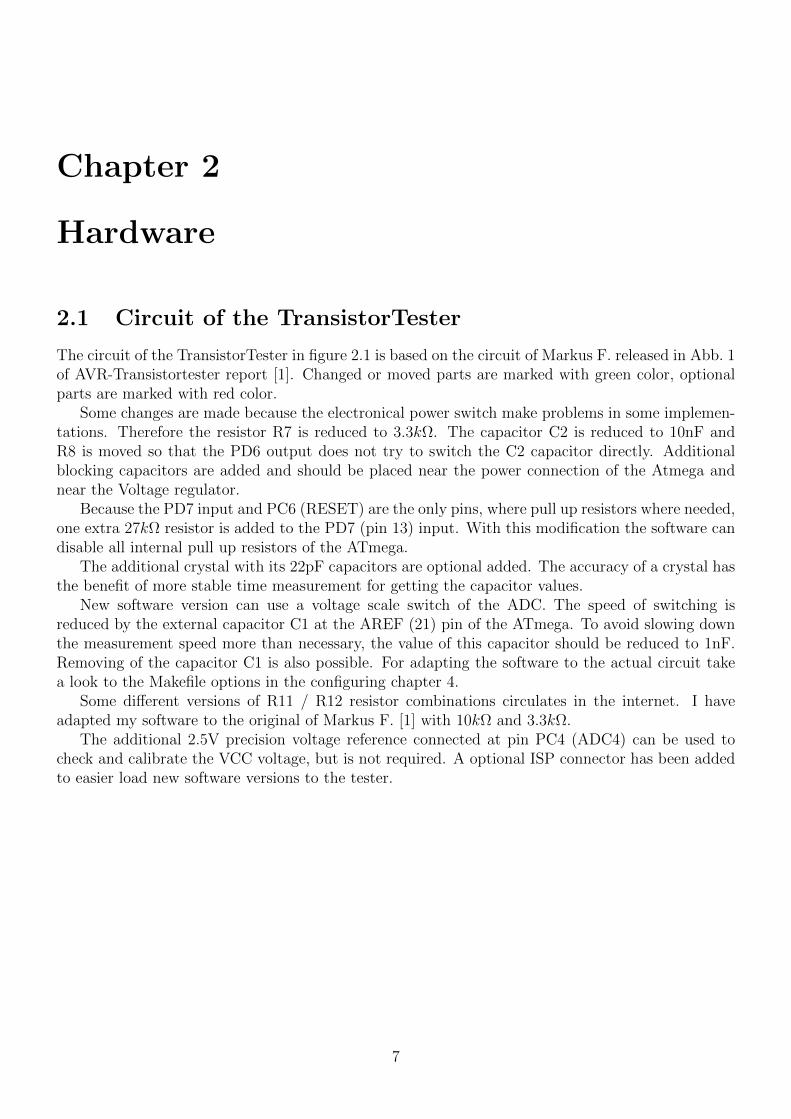
2.1 Circuit of the TransistorTester
The circuit of the TransistorTester in figure 2.1 is based on the circuit of Markus F. released in Abb. 1of AVR-Transistortester report [1]. Changed or moved parts are marked with green color, optionalparts are marked with red color.
Some changes are made because the electronical power switch make problems in some implemen-tations. Therefore the resistor R7 is reduced to 3.3kΩ. The capacitor C2 is reduced to 10nF andR8 is moved so that the PD6 output does not try to switch the C2 capacitor directly. Additionalblocking capacitors are added and should be placed near the power connection of the Atmega andnear the Voltage regulator.
Because the PD7 input and PC6 (RESET) are the only pins, where pull up resistors where needed,one extra 27kΩ resistor is added to the PD7 (pin 13) input. With this modification the software candisable all internal pull up resistors of the ATmega.
The additional crystal with its 22pF capacitors are optional added. The accuracy of a crystal hasthe benefit of more stable time measurement for getting the capacitor values.
New software version can use a voltage scale switch of the ADC. The speed of switching isreduced by the external capacitor C1 at the AREF (21) pin of the ATmega. To avoid slowing downthe measurement speed more than necessary, the value of this capacitor should be reduced to 1nF.Removing of the capacitor C1 is also possible. For adapting the software to the actual circuit takea look to the Makefile options in the configuring chapter 4.
Some different versions of R11 / R12 resistor combinations circulates in the internet. I haveadapted my software to the original of Markus F. [1] with 10kΩ and 3.3kΩ.
The additional 2.5V precision voltage reference connected at pin PC4 (ADC4) can be used tocheck and calibrate the VCC voltage, but is not required. A optional ISP connector has been addedto easier load new software versions to the tester.
7

IN OUT
GND
IC2
PB7(XTAL2/TOSC2)
PC6(RESET)
PD7(AIN1)
PD6(AIN0)
PD5(T1)
PD4(XCK/T0)
PD3(INT1)
PD2(INT0)
PD1(TXD)
PD0(RXD)
PB4(MISO)
PB5(SCK)
PB3(MOSI/OC2)
PB2(OC1B)
PB1(OC1A)
PB0(ICP)
PC0(ADC0)
PC1(ADC1)
PC2(ADC2)
PC3(ADC3)
PC4(ADC4/SDA)
PC5(ADC5/SCL)
AREF
PB6(XTAL1/TOSC1)
ATmega8/168/328
23
24
25
26
27
28
14
15
16
17
18
19
4
3
2
5
6
11
12
13
1
10
21
9
GND8
VCC7
AVCC
AGND
20
22
27k
33k
9V
22p
8MHz
100n
100n100n
Ubat
9
LC
D 2
x1
6
1
2
16
15D7
D6
D5
3
14
4
5
13
12
6
7
11
10
8
D4
D3
D2
D1
D0
E
R/W
RS
VEE
GND
+5V
Ubat
2k
2
33−270
BC547
10k
TP2
TP3
TP1
Test
10k
LED1
R10
T3
BC557C
C1
T2
BC547
R1
68
0
R3
68
0
R5
68
0
R2
47
0k
R4
47
0k
R6
47
0k
C2
10n
T1
R7
3k
3
R1
1
R1
3
10k
3
5
1MISO
SCK
RESET
2
4
6
VCC
MOSI
GND
ISP
Reset
Reset
22p
1n
R9
100k
100n
10
k
27k
R8
D1
R14
C4
C6
R14
2.5V
LT1004
R12
3k3
R1
5
C5
10u
C9
C3
C10 10u serial
VCC
VCC
VCC
VCC
VCC
VCC
VCC
Figure 2.1: New circuit of TransistorTester
The software can follow to another pin assignment of port D for a simpler connection of the LCDdisplay. The following table 2.1 shows the modified assignments.
Signal circuit diagram strip grid board versionpushbutton input PD7 PD0
LCD-RS PD4 PD7LCD-E PD5 PD5
LCD-D4 PD0 PD4LCD-D5 PD1 PD3LCD-D6 PD2 PD2LCD-D7 PD3 PD1
Table 2.1: Changes for strip grid board
For better protection of the ATmega inputs the additional circuit 2.2 can be integrated. Thede-energized contacts of the relay protect the ATmega without power. The contacts will be openedby software only for measurement.
TP2
TP3
TP1
4k7
BC547
PC0(ADC0)
PC1(ADC1)
PC2(ADC2)
PC4(ADC4/SDA)
or Ubat
depending of relay type
VCC
Figure 2.2: Additional protection of the ATmega inputs
8
2.2 Hints for building the TransistorTester
Every LCD-display with at least 2x16 character and a HD44780 compatible controller can be usedwith the TransistorTester. You should respect the current needed for illumination, some LCD needlower current than others. I had tried OLED type displays, but this type cause interference withmeasurements of the ATmega and are not recommended. Also loading of special characters fordisplaying the resistor symbol has caused problems with the OLED.
The resistors R1 to R6 are critical for measurements and this 680Ω and 470kΩ resistors should bemeasurement type resistors (tolerance of 0.1%) to get the full accuracy. You should use a precisionsocket for the ATmega microcontroller to enable the replacement of the microcontroller. The micro-controller ATmega8, ATmega168 and ATmega328 can be used. Recommended is a ATmega168 orATmega328, if you wish to use all features.
Anyway you should assemble all parts to printed board without the microcontroller. A up-to-datelow voltage drop regulator like MCP1702-5002 is recommended as IC2, because it need only 2µA ofstandby current and can still deliver 5V, if your input voltage is only 5.4V. But this part is not pincompatible to well known 78L05 with TO92 body!
After checking, that all needed parts are at the correct place, you should first connect the batteryor power supply to the printed board without LCD-display and microcontroller. You should checkthe voltage at the power pins of the microcontroller and LCD-display terminal during the Test key ispressed. The voltage should disappear, if you release the Test key. If the voltage had correct polarityand value, you should disconnect the power and assemble the microcontroller with correct alignment.Be careful and make shure, that all pins of the microcontroller are in the socket holes. Now you canalso connect the LCD. Check if power pins of the LCD has the right connection to GND and VCCof your board.
If you are shure that everything is all right, reconnect the power. If you have already programmedthe ATmega, you can press the Test button. By pressing the Test key, the background light of theLCD should switch on. If you release the Test button, the LED should illuminate weak. Notice, thatthe software for the microcontroller must be compiled for the correct processor type. A program forthe ATmega8 does not run on a ATmega168!
2.3 Programming of the microcontroller
I release the software for the microcontroller with source code. The developement is done with Linuxoperationg system (Ubuntu) and is controlled with a Makefile. The Makefile makes shure, that yoursoftware will be compiled with the prior selected Makefile options. Some constellations are precom-piled with the source. Please take a look to the ReadMe.txt file in the directory Sourcecode/defaultand to the chapter 4. The result of compilation have the extensions .hex and .eep . Usually thenames will be TransistorTester.hex and TransistorTester.eep . The .hex file contains the data for theprogram memory (flash) of the ATmega processor. The .eep file contains the data for the EEprommemory of the ATmega. Both data files must be loaded to the correct memory.
Additionally the operating state of the ATmega processor must be programmed with the “fuses”.If you can use my Makefile and additionally the program avrdude [12], you need no exact knowledgeof the details about the fuses. You have only to type “make fuses” if you have no crystal or “makefuses-crystal” if you have installed the 8MHz crystal to your printed board. With the ATmega168series of the microcontroller you can also use “make fuses-crystal-lp” to use a crytal with the lowpower mode. Never choose the crystal mode of clock generation, if you don’t have installed the 8MHzcrystal. If you are not shure with the fuses, leave them as default set by manufactor and first bringthe the tester to operation in this mode. Maybe your program runs too slow, if you use program datacompiled for 8MHz operation, but you can correct this later! But a wrong set of fuses may inhibitlater ISP-programming. If you use the Windows operating system, the easiest way to get a correct
9
programmed ATmega is to use the WinAVR package [16],[17]. With my patch [18] you can also setthe fuses by using the Makefile. Of course the avrdude program must support your programmer andthe configuration in the Makefile must match to your environment.
2.4 Troubleshooting
In most cases of problems you will miss the text output to the LCD-display. At first you shouldcheck, if the LED was illuminated weak, if you release the Test button.
Power does not switch on. If the LED is without light and the VCC power has correct 5V voltageduring holding the Test button, the microcontroller does not switch the power correctly. Themicrocontroller should hold the power by switching the PD6 output to 5V, which is usuallydone as one of the first actions. If you hold the Test key pressed, the power is switched onanyway. So you can check the value of VCC power and additionally the voltage value of thePD6 output, if you hold the key pressed. If VCC voltage has correct value (5V), but PD6voltage is below 4V, your microcontroller does not start the program. In this case you shouldcheck if the microcontroller flash has been loaded with proper data for your installed type andif ATmega is correctly configured with the fuses. If your ATmega put the PD6 output to 5Vand the power does not stay if you release the Test key, it is more difficult to find the reason.First you can shorten the LED and try again. If your Tester now starts, your LED may befaulty or mounted with wrong polarity. If this is not the reason, the current amplification factorof your T3 transistor (BC557C) is insufficient. The current to the base of T3 is lower in themicrocontroller state as in the “key pressed” state.
Nothing is readable on the LCD display Check the voltage at the contrast pin at the LCDdisplay (pin 3). Adjust to correct value specified in the data sheet of your display and optimizeby viewing. If you have a high temperature display type, you must provide a negative contrastvoltage for operation. In this case you can use the ICL 7660 device for generating a negativevoltage from positive 5V.
If there is no output readable on the LCD and the background light is on, you should disconnectthe power and check all four data plus the two control signal connections. If all connection arewell, the only reason I see is a uncorrect timing of control signals. This can be caused by aslower LCD controller than expected by the software or the ATmega software runs at wrongclock speed. Please check for which clock speed your programming data was compiled and ifthe fuses of the ATmega are correct set to that speed. You find the clock parameter in thecorresponding Makefile. If the tester is build without the switch off electronic, you can testwith a LED connected to the test pins, if the program operates normally. If the LED flickers,the program operates well. The missing text on the LCD must be caused by wrong connectionor timing.
Something but not all is readable on the LCD display Check if the .eep data are loaded tothe EEprom memory of ATmega. If all data are loaded correctly, you should check the clockspeed of your programming data (Makefile) and ATmega processor settings (fuses).
Measurement is slow and Capacitors are measured about 8 times too small You run soft-ware compiled for 8MHz clock at real clock speed of 1MHz. Please set the fuses of the ATmegacorrectly.
Measurement has strangely values Check if your programmer is still connected to the ISP-plug.The ISP interface should be disconnected for measuring. Very often the reason of wrongmeasurements is the use of software compiled with the AUTOSCALE ADC option and with
10

the option NO REF CAP, but the capacitor at the AREF pin has still a value of 100nF. Wrongassembly of components or remaining soft solder flux can disturb the measurements too. Pleasecheck with the selftest function of your TransistorTester software if possible. For the detailssee Chapter 5.5.
Otherwise inspect your board visually and check the resistor values with a ohmmeter. Youcan use the pins of the ATmega for this check, for example to check the R1 you can measurebetween pin 23 and pin 14. Take a look at the circuit diagram 2.1 for details. There is no needto remove the microcontroller, only battery or power supply should be removed before.
11

Chapter 3
Instructions for use
3.1 The measurement operation
Using of the Transistor-Tester is simple. Anyway some hints are required. In most cases are wireswith alligator clips connected to the test ports with plugs. Also sockets for transistors can beconnected. In either case you can connect parts with three pins to the three test ports in any order.If your part has only two pins, you can connect this pins to any two of the tree test ports. Normallythe polarity of part is irrelevant, you can also connect pins of electrolytical capacitors in any order.The measurement of capacity is normally done in a way, that the minus pole is at the test portwith the lower number. But, because the measurment voltage is only between 0.3 V and at most1.3 V, the polarity doesnt matter. When the part is connected, you should not touch it duringthe measurement. You should put it down to a nonconducting pad if it is not placed in a socket.You should also not touch to the isolation of wires connected with the test ports, the measurementresults can be affected. Then you should press the start button. After displaying a start message,the measurement result should appear after two seconds. If capacitors are measured, the time toresult can be longer corresponding to the capacity.
How the transistor-tester continues, depends on the configuration of the software.
Single measurement mode If the tester is configured for single measurement mode, the testershut off automatical after displaying the result for 10 seconds for a longer lifetime of battery.During the display time a next measurement can be started by pressing the start button. Afterthe shut off a next measurement can be started too of course. The next measurement can bedone with the same or another part.
Endless measurement mode A special case is the configuration without automatical shut off.This configuration is normally only used without the transistors for the shut off function. Aexternal off switch is necessary for this case. The tester will repeat measurements until poweris switched off.
Multi measurement mode In this mode the tester will shut down not after the first measurementbut after a configurable series of measurements. In the standard case the tester will shut downafter five measurements without found part. If any part is identified by test, the tester is shutdown after double of five (ten) measurements. A single measurement with unknown part aftera series of measurement of known parts will reset the counter of known measuerements to zero.Also a single measurement of known part will reset the counter of unknown measurements tozero. This behavior can result in a nearly endless series of measurements without pressing thestart button, if parts are disconnected and connected in periodical manner.
In this mode there is a special feature for the display period. If the start button is pressed onlyshort for switching on the tester, the result of measurement ist only shown for 5 seconds. Buf if
12
you press and hold the start button until the first message is shown, the further measurementresults are shown for 14 seconds. The next measurement can started earlier by pressing thestart button during the displaying of result.
3.2 Selftest and Calibration
If the software is configured with the selftest function, the selftest can be started by connecting allthree test ports together and pushing of the start button. In this case all of the documented tests inthe Selftest chapter 5.5 will be done. The repetition of the tests can be avoided, if the start buttonis hold pressed. So you can skip uninteresting tests fast and you can watch interresting tests byreleasing the start button.
If the function AUTO CAL is selected in the Makefile, there will be calibrated the internalresistance of the port output and the zero offset for the capacity measurement. It is important forthe calibration task, that the connection between the three test ports is relased during test number4. You should not touch to any of the test ports or connected cables when calibration (after test 6)is done. But the equipment should be the same used for further measurements. Otherwise the zerooffset for capacity measurement is not detected correctly.
A capacitor with any capacity between 100nF and 20µF connected to pin 1 and pin 3 is requiredfor the last task of calibration. To indicate that, a capacitor symbol is shown between the pin number1 and 3, followed by the text ” ¿100nF”. You should connect the capacitor not before this text isshown. With this capacitor the offset voltage of the analog comparator will be compensated for bettermeasurement of capacity values. Additionally the gain for ADC measurements using the internalreference voltage will be adjusted too with the same capacitor for better resistor measurement resultswith the AUTOSCALE ADC option.
The zero offset for the ESR measurement will be preset with the option ESR ZERO in theMakefile. This zero offset, which is set too high in normal case, will be preset in EEprom by thesoftware. With every selftest the ESR zero offset will be reset to this initial value. After every ESRmeasurement the result will be checked for negative value (output of ”ESR=0?”). In this case thezero offset will be reduced to get a zero result for next ESR measurement. With this methode thezero offset can be adjusted with a electrolytical capacitor with high capacity value and low ESRvalue. This learned ESR zero offset remains active after power off, but the adjust procedure to getthe zero offset of ESR measurement must be done after every selftest and in this case you shouldalways repeat the measurement some times.
3.3 special using hints
Normally the Tester shows the battery voltage with every start. If the voltage fall below a limit,a warning is shown behind the battery voltage. If you use a rechargeable 9V battery, you shouldreplace the battery as soon as possible or you should recharge. If you use a tester with attached 2.5Vprecision reference, the measured supply voltage will be shown in display row two for 1 second with”VCC=x.xxV”.
It can not repeat often enough, that capacitors should be discharged before measuring. Otherwisethe Tester can be damaged before the start button is pressed. If you try to measure components inassembled condition, the equipment should be allways disconnected from power source. Furthermoreyou should be shure, that no residual voltage reside in the equipment. Every electronical equipmenthas capacitors inside!
If you ty to measure little resistor values, you should keep the resistance of plug connectors andcables in mind. The quality and condition of plug connectors are important, also the resistance of
13

cables used for measurement. The same is in force for the ESR measurement of capacitors. Withpoor connection cable a ESR value of 0.02Ω can grow to 0.61Ω.
You should not expect very good accuracy of measurement results, especially the ESR measure-ment and the results of inductance measurement are not very exact. You can find the results of mytest series in chapter 5.
3.4 Compoments with problems
You should keep in mind by interpreting the measurement results, that the circuit of the Transis-torTester is designed for small signal semiconductors. In normal measurement condition the mea-surement current can only reach about 6 mA. Power semiconductors often make trouble by reason ofresidual current with the identification an the measurement of junction capacity value. The Testeroften can not deliver enough ignition current or holding current for power Thyristors or Triacs. So aThyristor can be detected as NPN transistor or diode. Also it is possible, that a Thyristor or Triacis detected as unknown.
Another problem is the identification of semiconductors with integrated resistors. So the base -emitter diode of a BU508D transistor can not be detected by reason of the parallel connected internal42Ω resistor. Therefore the transistor function can not be tested also. Problem with detection is alsogiven with power Darlington transistors. We can find often internal base - emitter resistors, whichmake it difficult to identify the component with the undersized measurement current.
3.5 Measurement of PNP and NPN transistors
For normal measurement the three pins of the transistor will be connectet in any order to themeasurement inputs of the TransistorTester. After pushing the start button, the Tester shows in row1 the type (NPN or PNP), a possible integrated protecting diode of the Collector - Emitter path andthe sequence of pins. The diode symbol is shown with correct polarity. Row 2 shows the currentamplification factor (B=...) and the Base - Emitter threshold voltage. You shouls know, that theTester can measure the amplification factor with two different circuits, the common Emitter and thecommon Collector circuit (Emitter follower).
With the common Emitter circuit the tester has only two alternative to select the base current:
1. The 680Ω resistor results to a base current of about 6.1mA. This is too high for low leveltransistors with high amplification factor, because the base is saturated. Because the collectorcurrent is also measured with a 680Ω resistor, the collector current can not reach the with theamplification factor higher value. The software version of Markus F. has measured the Base -Emitter threshold voltage in this ciruit (Uf=...).
2. The 470kΩ resistor results to a base current of only 9.2µA . This is very low for a power tran-sistor with low current amplification factor. The software version of Markus F. has identifiedthe current amplification factor with this circuit (hFE=...).
The software of the Tester figure out the current amplification factor additionally with the com-mon Collector circuit. The higher value of both measurement methodes is reported. The commoncollector circuit has the advantage, that the base current is reduced by negative current feedbackcorresponding to the amplification factor. In most cases a better measurement current can be reachedwith this methode for power transistors with the 680Ω resistor and for Darlington Transistors with470kΩ resistor. The reported Base - Emitter threshold voltage Uf is now measured with the same
14

current used for determination of the current amplification factor. However, if you want to know theBase - Emitter threshold voltage with a measurement current of about 6mA, you have to disconnectthe Collector and to start a new measurement. With this connection, the Base - Emitter thresholdvoltage at 6 mA is reported. The capacity value in reverse direction of the diode is also reported. Ofcourse you can also analyse the base - collector diode.
3.6 Measurement of JFET and D-MOS transistors
Because the structure of JFET type is symmetrical, the Source and Drain of this transistores cannot be differed. Normally one of the parameter of this transistor is the current of the transistorwith the Gate at the same level as Source. This current is often higher than the current, which canbe reached with the measurement circuit of the TransistorTester with the 680Ω resistor. For thisreason the 680Ω resistor is connected to the Source. Thus the Gate get with the growing of current anegative bias voltage. The Tester reports the Source current of this circuit and additionally the biasvoltage of the Gate. So various models can be differed. The D-MOS transistors (depletion type) aremeasured with the same methode.
You should know for enhancement MOS transistors (P-E-MOS or N-E-MOS), that the measure-ment of the gate threshold voltage (Vth) is more difficult with little gate capacity values. You canget a better voltage value, if you connect a capacitor with a value of some nF parallel to the gate/source. The gate threshold voltage will be find out with a drain current of about 3.5mA for aP-E-MOS and about 4mA for a N-E-MOS.
15
Chapter 4
Configuring the TransistorTester
The complete software for the TransistorTester is available in source code. The compilation ofmodules is controlled with a Makefile. The developement was done at the Ubuntu Linux operatingsystem with the GNU toolchain (gcc version 4.5.3). It should be possible to use other Linux operatingsystems without problems. To load the compiled data to the flash memory or the EEprom memory,the tool avrdude (version 5.11svn) was taken by the Makefile, if you call “make upload”. The programavrdude [12] is available for Linux and Windows operating system. The gnu C-compiler gcc is alsotaken by the AVR studio software and by the WinAVR [16],[17] software at the Windows operatingsystem. You can load the program data (.hex and .eep) also with other tools to the ATmega, butonly my Makefile version takes care to load the correct data to the choosed processor. Avrdudeloads only data to the ATmega if the Signature Bytes of the connected ATmega is identical to thechoosed one. If you alter the Makefile, all the software will be compiled new, if you call a “make”or “make upload” command. The software compiled for a ATmega8 does not run on a ATmega168.The software compiled for a ATmega328 does not run on the ATmega168! A exeption fron this rule isthe software compiled for ATmega168, this data can also be used for a ATmega328 without changes.Be careful, if you don’t use my Makefile.
With the correct options set, my software runs on the unchanged hardware of Markus F. (PARTNO=M8,NO option NO AREF CAP and NO PULLUP DISABLE option). The clock rate can also be set to8 MHz with fuses, no crystal is required!
The following options in the Makefile are avaiable to configure the software for your Tester.
PARTNO describes the target processor:m8 = ATmega8m168 or m168p = ATmega168m328 or m328p = ATmega328example: PARTNO = m168
UI LANGUAGE specifies the favored LanguageLANG ENGLISH, LANG GERMAN, LANG POLISH, LANG CZECH, LANG SLOVAK, LANG SLOVENEand LANG DUTCH is currently avaiableexample: UI LANGUAGE = LANG ENGLISH
LCD CYRILLIC is only needed for a LCD-display with cyrillic character set. The µ and Ω char-acter is not avaiable with the cyrillic character set. If you specify this option, both charactersare loaded to the LCD with software.example: CFLAGS += -DLCD CYRILLIC
STRIP GRID BOARD This option adapts the software to a changed port D connection for stripgrid printed boards. You can find the details in the chapter hardware 2.1.
16
WITH SELFTEST If you specify this Option, software will include a selftest function. Selftestwill be started, if you connect all three probes together and start measurement.example: CFLAGS += -DWITH SELFTEST
AUTO CAL The zero offset for capacity measurement and the port output resistor values will bewritten additionally to the EEprom with the selftest routine. Additionally the offset voltageof the analog comparator (REF C KORR) and the voltage offset of the internal referencevoltage (REF R KORR) will be measured automatically, if you connect a capacitor with acapacity value between 100nF and 20µF to pin 1 and pin 3 after measurement of capacity zerooffset. All found values will be written to EEprom and will be used for further measurementsautomatically.example: CFLAGS += -DAUTO CAL
FREQUENCY 50HZ At the end of selftest a 50 Hz Signal will be generated on Port 2 and Port 3for up to one minute.example: CFLAGS += -DFREQUENCY 50HZ
CAP EMPTY LEVEL This option defines the voltage level for discharged capacitor (mV units).You can set the level to higher value as 3mV, if the tester does not finish discharging ofcapacitors. In this case the tester ends after longer time with the message “Cell!”.example: CFLAGS += -DCAP EMPTY LEVEL=3
WITH AUTO REF specifies, that reference voltage is read to get the actual factor for capacitymeasuring of low capacity values (below 40µF ).example: CFLAGS += -DWITH AUTO REF
REF C KORR specifies a offset for readed reference voltage in mV units. This can be used toadjust the capacity measurement of little capacitors. A correction value of 10 results to about1 percent lower measurement results. If the option AUTO CAL is selected together withthe WITH SELFTEST option, the REF C KORR will be a offset to the measured voltagedifference of the test capacitor and the internal reference voltage.example: CFLAGS += -DREF C KORR=14
C H KORR specifies a correction value for the measurement of big capacitor values. A value of10 results to 1 percent lower measurement results.example: CFLAGS += -DC H KORR=10
AUTOSCALE ADC enables the automatic scale switchover of the ADC to either VCC or internalreference. Internal reference gives a 2.56V scale for ATmega8 and a 1.1V scale for otherprocessors.example: CFLAGS += -DAUTOSCALE ADC
ESR ZERO defines a zero offset for ESR measurements. This zero offset will be subtracted from allESR measurements. If the ESR measurement results to a negative value, the text ”ESR=0?”is displayed and the zero offset in the EEprom memory will be corrected. This corrected zerooffset will be used for further measurements until it is resetted to initial value by selftest. Ifyour measured ESR values always too high, you should select a higher ESR ZERO value.Example: CFLAGS += -DESR ZERO=29
NO AREF CAP tells your Software, that you have no capacitor (100nF ) installed at pin AREF(pin 21). This enables a shorter wait-time for the AUTOSCALE ADC scale switching of theADC. A 1nF capacitor was tested in this mode without detected errors. Figure 4.1a and 4.1bshow the switching time with a 1nF capacitor. As you can see the switching from 5V to 1.1V
17
is much slower than switching back to 5V. If you have still installed the 100nF , switching timewill be about factor 100 longer!example: CFLAGS += -DNO AREF CAP
REF R KORR specifies a offset for the internal ADC-reference voltage in mV units. With thisoffset a difference by switching from VCC based ADC reference to internal ADC referencefor resistor measurement can be adjusted. If you select the AUTO CAL option of the selftestsection, this value is only a additionally offset to the found voltage difference in the AUTO CALfunction.example: CFLAGS += -DREF R KORR=10
OP MHZ tells your software at which Clock Frequency in MHz your Tester will operate. Thesoftware is tested only for 1 MHz, 8MHz and additionally 16MHz. The 8MHz operation isrecommended for better resolution of capacity and inductance measurement.example: OP MHZ = 8
RESTART DELAY TICS must be set to 6, if the ATmega168 or ATmega328 is used with theinternal RC-oszillator instead of the crystal oszillator. If this value is not preset, the softwarerespects the 16384 clock tics delay for restart from sleep mode with the crystal operation.example: CFLAGS += -DRESTART DELAY TICS=6
USE EEPROM specifies if you wish to locate fix text and tables in EEprom Memory. Otherwisethe flash memory is used. Recommended is to use the EEprom (option set).example: CFLAGS += -DUSE EEPROM
EBC STYLE specifies, that the output of transistor pin layout is done with format “EBC=...” or“GDS=...”. This way of output save program memory for the ATmega. Without this optionthe layout is shown with the format “123=...”, where every point represent a E (Emitter),B (Base) or C (Collector). For FET transistors every point can be a G (Gate), D (Drain) orS (Source).Example: CFLAGS += EBC STYLE
PULLUP DISABLE specifies, that you don’t need the internal pull-up resistors. You must haveinstalled a external pull-up resistor at pin 13 (PD7) to VCC, if you use this option. This optionprevents a possible influence of pull-up resistors at the measuring ports (Port B and Port C).example: CFLAGS += -DPULLUP DISABLE
ANZ MESS this option specifies, how often an ADC value is read and accumulated. You canselect any value between 5 and 200 for building mean value of one ADC measurement. Highervalues result to better accuracy, but longer measurement time. One ADC measurement with44 values takes about 5ms.example: CFLAGS += -DANZ MESS=25
POWER OFF This option enables the automatic power off function. If you don’t specify thisoption, measurements are done in a loop infinitely until power is disconnected with a ON/OFFswitch. If you have the tester without the power off transistors, you can deselect the optionPOWER OFF.
If you have NOT selected the POWER OFF option with the transistors installed, you can alsoshut down the tester. During displaying the measurement result you should hold the start keypressed for several seconds until the ”Timeout” message is displayed. If you then release thekey, the tester will be shut off.
18

You can also specify, after how many measurements without a founded part the tester willshut down. The tester will also shut down the power after twice as much measurements aredone in sequence without a single failed part search. If you have forgotten to unconnect a testpart, total discharging of battery is avoided. Specify the option with a form like CFLAGS+= -DPOWER OFF=5 for a shut off after 5 consecutive measurements without part found.Also 10 measurements with any founded part one after another will shut down. Only if anysequence is interrupted by the other type, measurement continues. The result of measurementstay on the display for 14 seconds for the single measurement, for the multiple measurementversion display time is reduced to 5 seconds (set in config.h). If the start key is pressed a longertime on power on time, the display time is also 14 seconds for the multiple measurement. Themaximum value is 255 (CFLAGS += -DPOWER OFF=255).example 1: CFLAGS += -DPOWER OFF=5example 2: CFLAGS += -DPOWER OFF
BAT CHECK enables the Battery Voltage Check. If you don’t select this option, the versionnumber of software is output to the LCD instead. This option is usefull for battery poweredtester version to remember for the battery change.example: CFLAGS += -DBAT CHECK
BAT OUT enables Battery Voltage Output on LCD (if BAT CHECK is selected). If your 9Vsupply has a diode installed, use the BAT OUT=600 form to specify the threshold voltage (mV)of your diode to adjust the output value. Also the voltage loss of transistor T3 can be respectedwith this option. threshold level does not affect the voltage checking levels (BAT POOR).example 1: CFLAGS += -DBAT OUT=300example 2: CFLAGS += -DBAT OUT
BAT POOR sets the poor level of battery voltage to the specified 100mV (1/10 Volt) value. Thewarning level of battery voltage is 0.8V higher than the specified poor level, if the poor level ismore than 5.3V. If the poor level is 5.3V or less, the warning level is 0.4V higher. If the poorlevel is below 3.0V, the warning level is only 0.2V higher than the selected poor level. Settingthe poor level to low values such as 5.4V is not recommended for rechargeable 9V batteries,because this increase the risk of battery damage by the reason of the deep discharge! If youuse a rechargeable 9V Battery, it is recommended to use a Ready To Use type, because of thelower self-discharge.example for low drop regulator (5.4V): CFLAGS += -DBAT POOR=54example for 7805 type regulator (6.4V): CFLAGS += -DBAT POOR=64
PROGRAMMER select your programmer type for avrdude interface program. The correct se-lection of this option is needed, if you use the “make upload” or “make fuses” call of thisMakefile. For further information please look to the manual pages of avrdude and online doc-umentation [12].example: PROGRAMMER=avrisp2
PORT select the port where avrdude can reach your microcontroller (atmega). For further infor-mation please look to the manual pages of avrdude.example: PORT=usb
19
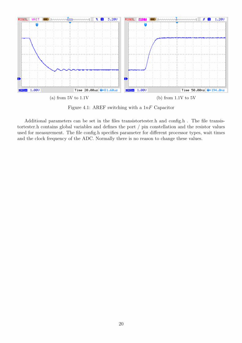
(a) from 5V to 1.1V (b) from 1.1V to 5V
Figure 4.1: AREF switching with a 1nF Capacitor
Additional parameters can be set in the files transistortester.h and config.h . The file transis-tortester.h contains global variables and defines the port / pin constellation and the resistor valuesused for measurement. The file config.h specifies parameter for different processor types, wait timesand the clock frequency of the ADC. Normally there is no reason to change these values.
20

Chapter 5
Description of the measurementprocedures
The simplified schematic of a Input/Output-Port pin of the ATmega is shown in figure 5.1. The PUDswitch isolates all “pull up” resistors of the ATmega. The output of a pin can be switched off withthe DD switch. The Input can operate regardless to the state of the switch DD. The PORT switchusually defined the output level, but also switches the pull up resistor. Because the Switches PORTand DD can not be changed at the same time but only one after another, the pull up resistors candisturb the measurement. Therefore I prefere to disable the pull up resistors with the PUD switch.Of course all the switches are electronic type and the resistors 19Ω and 22Ω are approximated values.
Pull up
to ADC Mux, Port C only22
19
PUD
DD
PORT PIN
Port Pin
VCC
Figure 5.1: simplified diagram of each ATmega port pin
Every of the three terminal probes of your Transistor Tester is build with three ATmega portpins, which is shown as simplified diagram for the terminal probe TP2 (middle of three pins) infigure 5.2.
PC1 PB2
ADCMUX
19
22
19
22
19
22
470k
680
GND
PB3
TP2
R3
R4
VCC
Figure 5.2: simplified circuit of each measurement terminal probe TP
21

Every test pin (measurement port) can be used as digital or analog input. This measurementcapability is independent of using the port as output. Every test pin can be switched to output andin this mode it can be directly connected to GND (0V) or VCC (5V), or it can be connected via a680Ω resistor or a 470kΩ resistor to either GND or VCC. Table 5.1 shows all possible combinationof measurements. Notice, that the positive state can be switched directly to VCC (Port C) or it canbe connected with the 680Ω resistor to VCC (Port B). The same possibility has the negative state ofterminal probe to the GND side. The test state means, that probe can be open (Input), connectedwith the 470kΩ resistor to VCC or GND, or that the probe can be connected with the 680Ω resistorto VCC or GND.
state pin 1 state pin 2 state pin 31. positive negative test2. positive test negative3. test negative positive4. test positive negative5. negative test positive6. negative positive test
Table 5.1: all combinations of measurement
If the capacitor measuring is configured for the tester, the tester will try to discharge the capacitorsconnected at all test pins. If discharge will fail, that means the remaining voltage is to high, thedischarging will be aborted after about 12 seconds with the meassage ”Cell!”. This can also behappen, if no capacitor is connected to any test pin. The cause for this can be, that the cut-offvoltage is choosed to low for this ATmega. You can choose a higher voltage with the Makefile optionCAP EMPTY LEVEL.
22
5.1 Measurement of Semiconductors
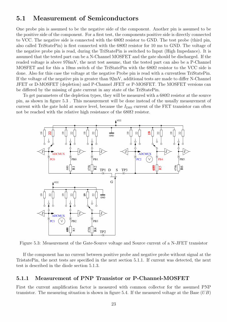
One probe pin is assumed to be the negative side of the component. Another pin is assumed to bethe positive side of the component. For a first test, the components positive side is directly connectedto VCC. The negative side is connected with the 680Ω resistor to GND. The test probe (third pin,also called TriStatePin) is first connected with the 680Ω resistor for 10 ms to GND. The voltage ofthe negative probe pin is read, during the TriStatePin is switched to Input (High Impedance). It isassumed that the tested part can be a N-Channel MOSFET and the gate should be discharged. If thereaded voltage is above 976mV, the next test assume, that the tested part can also be a P-ChannelMOSFET and for this a 10ms switch of the TriStatePin with the 680Ω resistor to the VCC side isdone. Also for this case the voltage at the negative Probe pin is read with a currentless TriStatePin.If the voltage of the negative pin is greater than 92mV, additional tests are made to differ N-ChannelJFET or D-MOSFET (depletion) and P-Channel JFET or P-MOSFET. The MOSFET versions canbe differed by the missing of gate current in any state of the TriStatePin.
To get parameters of the depletion types, they will be measured with a 680Ω resistor at the sourcepin, as shown in figure 5.3 . This measurement will be done instead of the usually measurement ofcurrent with the gate hold at source level, because the IDSS current of the FET transistor can oftennot be reached with the relative high resistance of the 680Ω resistor.
PC2
ADCMUX
PB5PB4
19
22
19
22
TP3 680
470k
PB2
ADCMUX
22
22
19
22
680
470k
GND
19
19
PC0 PB0
ADCMUX
PB1
19
22
19
22
680
470k
TP1
GND
TP2
PB3PC1
R1
R2
R5
R6
R3
R4
19
22
22
19
SD
G
VCC
VCC
Figure 5.3: Measurement of the Gate-Source voltage and Source current of a N-JFET transistor
If the component has no current between positive probe and negative probe without signal at theTristatePin, the next tests are specified in the next section 5.1.1. If current was detected, the nexttest is described in the diode section 5.1.3.
5.1.1 Measurement of PNP Transistor or P-Channel-MOSFET
First the current amplification factor is measured with common collector for the assumed PNPtransistor. The measuring situation is shown in figure 5.4. If the measured voltage at the Base (UB)
23

is above 9mV with the 680Ω resistor, the hFE is build as hFE = UE−UBUB
. The voltage UE is thedifference of the Emitter-voltage to VCC. The difference between the 22Ω and 19Ω resistors are notrespected. If the UB voltage is below 10mV, the measurement is done with the 470kΩ resistor atthe base. In this case the current amplification factor is build as hFE = UE·470000
UB·(680+22).
PC2
ADCMUX
PB5PB4
19
22
19
22
19
22
TP3 680
47
0k
PB2
ADCMUX
22
22
19
22
680
47
0k
GND
19
19
PC0 PB0
ADCMUX
PB1
19
22
19
22
19
22
68
0
47
0k
TP1
GND
TP2
PB3PC1
The green switch state is used
if Voltage at PC1 is < 10mV !
R1
R2
R5
R6
R3
R4
VCC
VCC
Figure 5.4: hFE measurement of PNP transistor with common collector circuit
Next the tests with common emitter are done for the assumed PNP transistor. The positiveside of component is now direct connected to VCC, the negative side 680Ω resistor is connected toGND as shown in Figure 5.5. If the negative side of component has a voltage of above 3.4V, whenthe base side 680Ω resistor was connected to GND, it must be a PNP transistor or a P-ChannelFET. This can be easy find out by analysing the base voltage. If the base voltage is greater 0.97V,it must be a PNP. For measuring the current amplification factor, the 470kΩ resistor is taken asBase resistor instead of the 680Ω. The current amplification factor is build by hFE = UC·470000
UB·(680+19)
. The higher current amplification factor is assumed to be the right one, this one or the one foundwith the common collector circuit. The values found for the PNP are only valid, if a second set ofmeasurements is done. In order to prevent detecting the PNP in the inverse mode (collector andemitter are swapped), the measurement with the higher current amplification is taken as the rightone. If base voltage is lower than 0.97V, it must be a P-E-MOS. In this case the gate thresholdvoltage is measured by switching the gate slowly with the 470kΩ resistor up and down, waiting fora digital input signal change of the Drain side and then read the voltage of the gate pin.
24
PC2
ADCMUX
PB5PB4
19
19
19
22
TP3 47
0k
PB2
ADCMUX
22
22
19
22
680
47
0k
GND
19
19
PC0 PB0
ADCMUX
PB1
22
22
19
22
680
47
0k
TP1
GND
TP2
PB3PC1
22
22
68
0
19
19
The black state of switches is used for test!
amplification factor hFE.
The green state is used for current
R6
R3
R1
R2
R5
R4
VCC
VCC
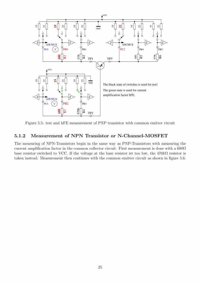
Figure 5.5: test and hFE measurement of PNP transistor with common emitter circuit
5.1.2 Measurement of NPN Transistor or N-Channel-MOSFET
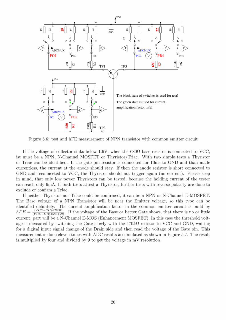
The measuring of NPN-Transistors begin in the same way as PNP-Transistors with measuring thecurrent amplification factor in the common collector circuit. First measurement is done with a 680Ωbase resistor switched to VCC. If the voltage at the base resistor ist too low, the 470kΩ resistor istaken instead. Measurement then continues with the common emitter circuit as shown in figure 5.6.
25
PC2
ADCMUX
PB5PB4
19
19
19
22
TP3 47
0k
PB2
ADCMUX
22
22
19
22
680
47
0k
GND
19
19
PC0 PB0 PB1
22
22
19
22
47
0k
TP1
GND
TP2
PB3PC1
19
19
The black state of switches is used for test!
amplification factor hFE.
The green state is used for current
22
22
680
68
0
ADCMUX
R1
R3
R2
R5
R6
R4
VCC
VCC
Figure 5.6: test and hFE measurement of NPN transistor with common emitter circuit
If the voltage of collector sinks below 1.6V, when the 680Ω base resistor is connected to VCC,ist must be a NPN, N-Channel MOSFET or Thyristor/Triac. With two simple tests a Thyristoror Triac can be identified. If the gate pin resistor is connected for 10ms to GND and than madecurrentless, the current at the anode should stay. If then the anode resistor is short connected toGND and reconnected to VCC, the Thyristor should not trigger again (no current). Please keepin mind, that only low power Thyristors can be tested, because the holding current of the testercan reach only 6mA. If both tests attest a Thyristor, further tests with reverse polarity are done toexclude or confirm a Triac.
If neither Thyristor nor Triac could be confirmed, it can be a NPN or N-Channel E-MOSFET.The Base voltage of a NPN Transistor will be near the Emitter voltage, so this type can beidentified definitely. The current amplification factor in the common emitter circuit is build byhFE = (V CC−UC)·470000
(V CC−UB)·(680+22). If the voltage of the Base or better Gate shows, that there is no or little
current, part will be a N-Channel E-MOS (Enhancement MOSFET). In this case the threshold volt-age is measured by switching the Gate slowly with the 470kΩ resistor to VCC and GND, waitingfor a digital input signal change of the Drain side and then read the voltage of the Gate pin. Thismeasurement is done eleven times with ADC results accumulated as shown in Figure 5.7. The resultis multiplied by four and divided by 9 to get the voltage in mV resolution.
26

Figure 5.7: measuring of threshold voltage of N-Channel-MOSFET
5.1.3 Measurement of Diodes
If current is detected with the pre-tests, the behavior of the part will be checked to be a diode. Theflow voltage with the 680Ω resistor must be between 0.15V and 4.64V. The flux voltage with the680Ω must be greater than 1.125 times the flux voltage with the 470kΩ resistor and eight times theflux voltage with the 470kΩ must be greater than the flux voltage with the 680Ω resistor. I hope,that this behavior is always a diode.
5.1.4 Results of different measurements
The following three tables shows results of different test probes with one ATmega8 processor andtwo different software versions of a ATmega168 processor. The measurement of the inverse capacityvalue for the double diode MBR4045PT is only possible with cooling. This will be caused by highresidual current of this 40A diode. Also the capacity value of the inverse base emitter diode of thegermanium transistor AC128 can only be measured with cooling.
27
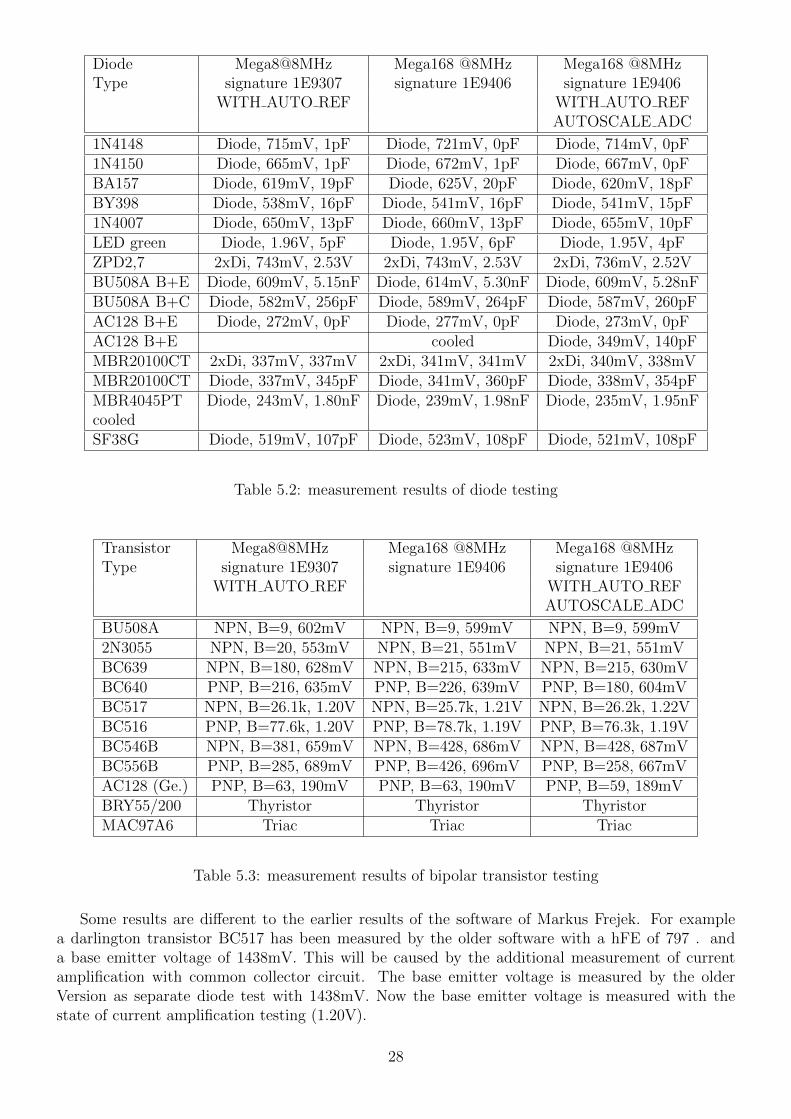
Diode Mega8@8MHz Mega168 @8MHz Mega168 @8MHzType signature 1E9307 signature 1E9406 signature 1E9406
WITH AUTO REF WITH AUTO REFAUTOSCALE ADC
1N4148 Diode, 715mV, 1pF Diode, 721mV, 0pF Diode, 714mV, 0pF1N4150 Diode, 665mV, 1pF Diode, 672mV, 1pF Diode, 667mV, 0pFBA157 Diode, 619mV, 19pF Diode, 625V, 20pF Diode, 620mV, 18pFBY398 Diode, 538mV, 16pF Diode, 541mV, 16pF Diode, 541mV, 15pF1N4007 Diode, 650mV, 13pF Diode, 660mV, 13pF Diode, 655mV, 10pFLED green Diode, 1.96V, 5pF Diode, 1.95V, 6pF Diode, 1.95V, 4pFZPD2,7 2xDi, 743mV, 2.53V 2xDi, 743mV, 2.53V 2xDi, 736mV, 2.52VBU508A B+E Diode, 609mV, 5.15nF Diode, 614mV, 5.30nF Diode, 609mV, 5.28nFBU508A B+C Diode, 582mV, 256pF Diode, 589mV, 264pF Diode, 587mV, 260pFAC128 B+E Diode, 272mV, 0pF Diode, 277mV, 0pF Diode, 273mV, 0pFAC128 B+E cooled Diode, 349mV, 140pFMBR20100CT 2xDi, 337mV, 337mV 2xDi, 341mV, 341mV 2xDi, 340mV, 338mVMBR20100CT Diode, 337mV, 345pF Diode, 341mV, 360pF Diode, 338mV, 354pFMBR4045PT Diode, 243mV, 1.80nF Diode, 239mV, 1.98nF Diode, 235mV, 1.95nFcooledSF38G Diode, 519mV, 107pF Diode, 523mV, 108pF Diode, 521mV, 108pF
Table 5.2: measurement results of diode testing
Transistor Mega8@8MHz Mega168 @8MHz Mega168 @8MHzType signature 1E9307 signature 1E9406 signature 1E9406
WITH AUTO REF WITH AUTO REFAUTOSCALE ADC
BU508A NPN, B=9, 602mV NPN, B=9, 599mV NPN, B=9, 599mV2N3055 NPN, B=20, 553mV NPN, B=21, 551mV NPN, B=21, 551mVBC639 NPN, B=180, 628mV NPN, B=215, 633mV NPN, B=215, 630mVBC640 PNP, B=216, 635mV PNP, B=226, 639mV PNP, B=180, 604mVBC517 NPN, B=26.1k, 1.20V NPN, B=25.7k, 1.21V NPN, B=26.2k, 1.22VBC516 PNP, B=77.6k, 1.20V PNP, B=78.7k, 1.19V PNP, B=76.3k, 1.19VBC546B NPN, B=381, 659mV NPN, B=428, 686mV NPN, B=428, 687mVBC556B PNP, B=285, 689mV PNP, B=426, 696mV PNP, B=258, 667mVAC128 (Ge.) PNP, B=63, 190mV PNP, B=63, 190mV PNP, B=59, 189mVBRY55/200 Thyristor Thyristor ThyristorMAC97A6 Triac Triac Triac
Table 5.3: measurement results of bipolar transistor testing
Some results are different to the earlier results of the software of Markus Frejek. For examplea darlington transistor BC517 has been measured by the older software with a hFE of 797 . anda base emitter voltage of 1438mV. This will be caused by the additional measurement of currentamplification with common collector circuit. The base emitter voltage is measured by the olderVersion as separate diode test with 1438mV. Now the base emitter voltage is measured with thestate of current amplification testing (1.20V).
28

FET Mega8@8MHz Mega168 @8MHz Mega168 @8MHzType signature 1E9307 signature 1E9406 signature 1E9406
WITH AUTO REF WITH AUTO REFAUTOSCALE ADC
ZVNL120A N-E-MOS,D, 1.5V N-E-MOS,D, 1.5V N-E-MOS,D, 1.5V142pF 146pF 141pF
IRF530N N-E-MOS,D, 3.6V N-E-MOS,D, 3.6V N-E-MOS,D, 3.6V1.55nF 1.56nF 1.55nF
BS170 N-E-MOS,D, 2.6V N-E-MOS,D, 2.6V N-E-MOS,D, 2.6V71pF 73pF 70pF
IRL3803 N-E-MOS,D, 2.3V N-E-MOS,D, 2.3V N-E-MOS,D, 2.3V9.82nF 9.82nF 9.79nF
IRFU120N N-E-MOS,D, 4.2V N-E-MOS,D, 4.2V N-E-MOS,D, 4.2V918pF 924pF 918pF
BUZ71A N-E-MOS,D, 3.2V N-E-MOS,D, 3.2V N-E-MOS,D, 3.2V710pF 718pF 712pF
ZVP2106A P-E-MOS,D, 3.2V P-E-MOS,D, 3.2V P-E-MOS,D, 3.2V117pF 121pF 116pF
IRF5305 P-E-MOS,D, 3.6V P-E-MOS,D, 3.6V P-E-MOS,D, 3.6V2.23nF 2.25nF 2.24nF
BS250 P-E-MOS,D, 2.6V P-E-MOS,D, 2.6V P-E-MOS,D, 2.6V46pF 48pF 46pF
IRFU9024 P-E-MOS,D, 3.5V P-E-MOS,D, 3.6V P-E-MOS,D, 3.5V954pF 954pF 951pF
J310 N-JFET N-JFET N-JFETIdss=24-60mA I=3.1mA Vgs=2.2V I=3.1mA Vgs=2.2V I=3.1mA Vgs=2.2VBF256C N-JFET N-JFET N-JFETIdss=11-18mA I=3.3mA Vgs=2.3V I=3.4mA Vgs=2.3V I=3.3mA Vgs=2.3VBF245A N-JFET N-JFET N-JFETIdss=2-6mA I=1.1mA Vgs=.75V I=1.1mA Vgs=0.74V I=1.1mA Vgs=0.75VBF245B N-JFET N-JFET N-JFETIdss=6-15mA I=2.4mA Vgs=1.7V I=2.5mA Vgs=1.7V I=2.4mA Vgs=1.7VBF245C N-JFET N-JFET N-JFETIdss=12-25mA I=3.8mA Vgs=2.7V I=3.9mA Vgs=2.7V I=3.8mA Vgs=2.7V
Table 5.4: measurement results of MOS transistor testing
29
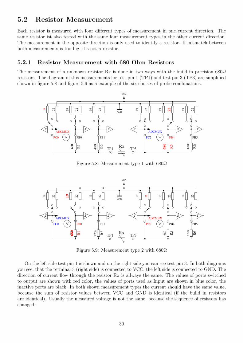
5.2 Resistor Measurement
Each resistor is measured with four different types of measurement in one current direction. Thesame resistor ist also tested with the same four measurement types in the other current direction.The measurement in the opposite direction is only used to identify a resistor. If mismatch betweenboth measurements is too big, it’s not a resistor.
5.2.1 Resistor Measurement with 680 Ohm Resistors
The measurement of a unknown resistor Rx is done in two ways with the build in precision 680Ωresistors. The diagram of this measurements for test pin 1 (TP1) and test pin 3 (TP3) are simplifiedshown in figure 5.8 and figure 5.9 as a example of the six choises of probe combinations.
PC0 PB0
ADCMUX
PC2
ADCMUX
PB5PB4PB1
19
22
19
22
19
22
19
22
19
22
19
22
680
470k
TP1 TP3Rx
680
470k
GND
R1
R2
R6
R5
VCC
Figure 5.8: Measurement type 1 with 680Ω
PC0 PB0
ADCMUX
PC2 PB5
ADCMUX
PB1 PB4
GND
19
22
19
22
19
22
19
22
19
22
19
22
680
470k
680
470k
TP1 TP3RxR
1
R6
R5
R2
VCC
Figure 5.9: Measurement type 2 with 680Ω
On the left side test pin 1 is shown and on the right side you can see test pin 3. In both diagramsyou see, that the terminal 3 (right side) is connected to VCC, the left side is connected to GND. Thedirection of current flow through the resistor Rx is allways the same. The values of ports switchedto output are shown with red color, the values of ports used as Input are shown in blue color, theinactive ports are black. In both shown measurement types the current should have the same value,because the sum of resistor values between VCC and GND is identical (if the build in resistorsare identical). Usually the measured voltage is not the same, because the sequence of resistors haschanged.
30

The V symbol within the circle marks the ports used for voltage measurement. In both configu-rations the value of resistor Rx can be computed with the known resistor values and the measuredvoltages, if the relation of resistor Rx and the 680Ω is not too high. The theoretical voltage gradientis shown in figure 5.10, where resistor values are shown in logarithmic scale.
0
1000
2000
3000
4000
5000
100m 1 10 100 1k 10k 100k
volt
age
/m
V
resistor Rx / Ohm
PC2, type 1PC0, type 2
Figure 5.10: Voltages of type 1 and type 2 measurements with 680Ω
The graph of measurement type 1 is shown in figure 5.11a with zoomed scale for the lower resistorrange. You can see, that you need a better ADC resolution than the standard 4.9mV resolution atthe 5V ADC reference, to get the right resistor value from measured voltage below 2Ω. There are onlythree ADC steps from 0Ω to 2Ω. The range switching with the AUTOSCALE ADC option can helpin this case. The same zoomed range of measurement type 2 shows the figure 5.11b. Unfortunatelywe can not use the higher ADC resolution for measurement type 2 in this range, because the voltageis too high and our ATmega have no differential ADC input. Measurements with the 680Ω resistorsare taken for building the result of measurements up to 20kΩ (Voltage of measurement type 2 willbe below 169mV).
For higher resistor values the measurements with the 470kΩ resistors are used. The mean valueof both measurements is taken as displayed resistor value, if all tests attests, that it is no othertype of part. If the AUTOSCALE ADC function is selected and one of the voltages of the bothmeasurement types is below 0.98V, a weighted average is build with factor four for this value. Theother value is weighted with factor one. This is done to respect the factor four better resolutionof this measurement. Factor four is only taken for ATmega168 and ATmega328 processors, for theATmega8 two is taken as weighting factor if voltage is below 0.98V, because the reference voltagefor the ADC is here 2.54V instead of 1.1V . If the ATmega has more than 8KByte flash memory, thevoltage measurement at the resistors will be delayed until no more changes are detected or the timelimit is reached. With this method big capacitors are no more detected as resistors by mistake andthe DC resistance of big inductors will be measured correctly.
31

130135140145150155160165170175180185190195200
0 1 2 3 4 5 6 7 8 9 10
volt
age
/m
V
resistor Rx / Ohm
PC2, type 1
(a) Type 1 measurement
478047854790479548004805481048154820482548304835484048454850
0 1 2 3 4 5 6 7 8 9 10
volt
age
/m
V
resistor Rx / Ohm
PC0, type 2
(b) Type 2 measurement
Figure 5.11: Cut-out of theoretical Voltage from 0Ω to 10Ω
5.2.2 Resistor Measurement with 470 kOhm resistors
The next figures 5.12 and 5.13 shows the same measurement procedure for the measurement withthe precision 470kΩ resistors. Because the 470kΩ is very big in relation to the port resistor values22Ω and 19Ω, the port resistor values are ignored for the computing of the resistor value Rx.
For both measurement types with the 470kΩ resistors only one Voltage is measured, because thecurrent is so low, that no voltage difference at the internal port resistors of the ATmega can bemeasured (as expected). The theoretical voltage gradient is shown in figure 5.14 where the resistorvalues are again shown in logarithmic scale. The theoretical gradient in this diagram ends at 100MΩ,but the resulting value of the Tester is limited to 60MΩ, otherwise the Tester assumes that no resistoris connected. The weighted average of both measurement types is taken as result with the same rulesdescribed for the measurements with the 680Ω resistors. For all ATmega processors I had found,that the measured results with the 470kΩ resistors are more exactly, if a constant offset of 350Ω willbe added. This offset can be adjusted with the RH OFFSET define in the config.h file.
PC0 PB0 PB1
ADCMUX
PC2 PB4
ADCMUX
PB5
19
22
19
22
19
22
GND
19
22
19
22
19
22
470k
680
TP3TP1470k
680
RxR1
R2
R5
R6
VCC
Figure 5.12: Measurement type 3 with 470kΩ
32

PC0 PB0 PB1
ADCMUX
PC2 PB4 PB5
ADCMUX
19
22
19
22
19
22
GND
19
22
19
22
19
22
470k
680
470k
680
TP1 TP3RxR
1
R2
R5
R6
VCC
Figure 5.13: Measurement type 4 with 470kΩ
0
1000
2000
3000
4000
5000
10k 100k 1M 10M 100M
volt
age
/m
V
resistor Rx / Ohm
PC2 type 3PC0, type 4
Figure 5.14: Voltages of type 3 and type 4 measurements with 470kΩ
5.2.3 Results of the resistor measurements
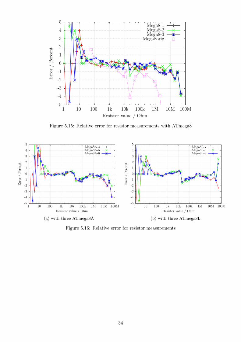
Figure 5.15 shows the relative errors of the resistor measurements with three ATmega8 microcon-trollers. Additionally some results with the original software of Markus F. with one ATmega8 areshown as ”Mega8orig” in this figure. More measurements results with ATmega8A and ATmega8Lare shown in figure 5.16a and 5.16b. Figure 5.17 shows the same measurements with a ATmega168microcontroller. Mega168 are the results without the AUTOSCALE ADC option, Mega168as arethe same measurements with the AUTOSCALE ADC option. With the ATmega168 microcontrollerit seems to be possible, that measurements of resistors in the range from 20Ω to 20MΩ can be mea-sured with a tolerance of ±1%. For Measurements below 100Ω you should keep in mind, that anymeasurement probe with wire have a resistance too. It is better to connect the resistor directly tothe terminal pins. If this is not possible, subtract the resistance value of the shortened probe. Forexample, if your Resistor have a printed value of 30Ω, your tester shows a value of 30.6Ω and thetwo probes shortened have a value of 0.5Ω, then your resistor has been measured with 30.1Ω. Belowa resistance value of 10Ω one resolution step results to a error of more than 1%!
33
-5
-4
-3
-2
-1
0
1
2
3
4
5
1 10 100 1k 10k 100k 1M 10M 100M
Err
or/
Per
cent
Resistor value / Ohm
Mega8-1Mega8-2Mega8-3
Mega8orig
Figure 5.15: Relative error for resistor measurements with ATmega8
-5
-4
-3
-2
-1
0
1
2
3
4
5
1 10 100 1k 10k 100k 1M 10M 100M
Err
or/
Per
cent
Resistor value / Ohm
Mega8A-4Mega8A-5Mega8A-6
(a) with three ATmega8A
-5
-4
-3
-2
-1
0
1
2
3
4
5
1 10 100 1k 10k 100k 1M 10M 100M
Err
or/
Per
cent
Resistor value / Ohm
Mega8L-7Mega8L-8Mega8L-9
(b) with three ATmega8L
Figure 5.16: Relative error for resistor measurements
34
-5
-4
-3
-2
-1
0
1
2
3
4
5
1 10 100 1k 10k 100k 1M 10M 100M
Err
or/
Per
cent
Resistor value / Ohm
Mega168Mega168as
Figure 5.17: Relative error for resistor measurements with ATmega168
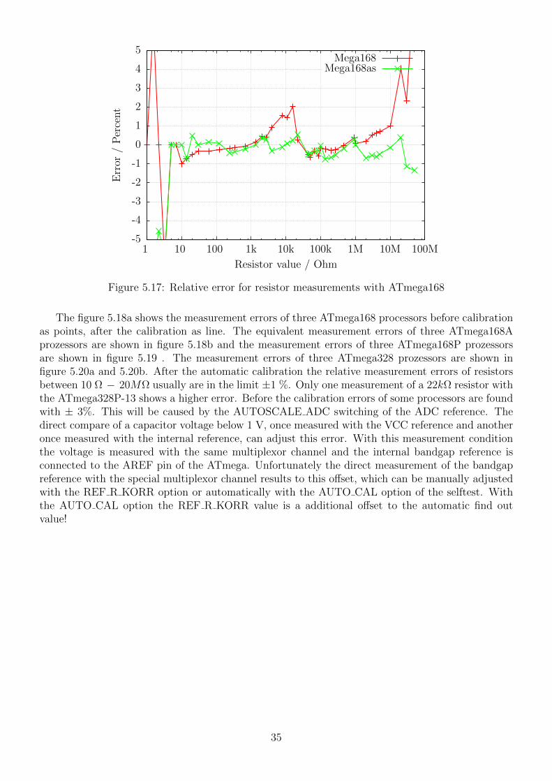
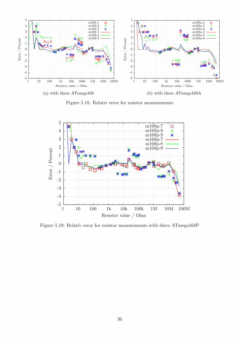
The figure 5.18a shows the measurement errors of three ATmega168 processors before calibrationas points, after the calibration as line. The equivalent measurement errors of three ATmega168Aprozessors are shown in figure 5.18b and the measurement errors of three ATmega168P prozessorsare shown in figure 5.19 . The measurement errors of three ATmega328 prozessors are shown infigure 5.20a and 5.20b. After the automatic calibration the relative measurement errors of resistorsbetween 10 Ω − 20MΩ usually are in the limit ±1 %. Only one measurement of a 22kΩ resistor withthe ATmega328P-13 shows a higher error. Before the calibration errors of some processors are foundwith ± 3%. This will be caused by the AUTOSCALE ADC switching of the ADC reference. Thedirect compare of a capacitor voltage below 1 V, once measured with the VCC reference and anotheronce measured with the internal reference, can adjust this error. With this measurement conditionthe voltage is measured with the same multiplexor channel and the internal bandgap reference isconnected to the AREF pin of the ATmega. Unfortunately the direct measurement of the bandgapreference with the special multiplexor channel results to this offset, which can be manually adjustedwith the REF R KORR option or automatically with the AUTO CAL option of the selftest. Withthe AUTO CAL option the REF R KORR value is a additional offset to the automatic find outvalue!
35
-5
-4
-3
-2
-1
0
1
2
3
4
5
1 10 100 1k 10k 100k 1M 10M 100M
Err
or/
Per
cent
Resistor value / Ohm
m168-1m168-2m168-3m168-1m168-2m168-3
(a) with three ATmega168
-5
-4
-3
-2
-1
0
1
2
3
4
5
1 10 100 1k 10k 100k 1M 10M 100M
Err
or/
Per
cent
Resistor value / Ohm
m168a-4m168a-5m168a-6m168a-4m168a-5m168a-6
(b) with three ATmega168A
Figure 5.18: Relativ error for resistor measurements
-5
-4
-3
-2
-1
0
1
2
3
4
5
1 10 100 1k 10k 100k 1M 10M 100M
Err
or/
Per
cent
Resistor value / Ohm
m168p-7m168p-8m168p-9m168p-7m168p-8m168p-9
Figure 5.19: Relativ error for resistor measurements with three ATmega168P
36

-5
-4
-3
-2
-1
0
1
2
3
4
5
1 10 100 1k 10k 100k 1M 10M 100M
Err
or/
Per
cent
Resistor value / Ohm
m328-10m328-11m328-12m328-10m328-11m328-12
(a) with three ATmega328
-5
-4
-3
-2
-1
0
1
2
3
4
5
1 10 100 1k 10k 100k 1M 10M 100M
Err
or/
Per
cent
Resistor value / Ohm
m328p-13m328p-14m328p-15m328p-13m328p-14m328p-15
(b) with three ATmega328P
Figure 5.20: Relativ error for resistor measurements
37
5.3 Measurement of Capacitors
The measurement of capacitor values are done as separate task by measurement of load time after allother measurements. The original software of Markus F. did this with a program loop, which readsthe corresponding digital input pin until a switch occured and count the loop cycles. This has thehandicap, that the resolution of time measurement is limited by the time consumption of one loopcycle. This usually was done in all six combinations for all three probe pins. The actual softwareuses two different ways to get the load time in only three combinations for the three probe pins. Thepositive side is now always the higher probe number. Only if capacity is measured parallel with adiode, the polarity can be in the other order.
5.3.1 Discharging of Capacitors
You should always discharge the capacitor before connecting it to the tester. The tester additionallydischarge the capacitor before any measurement. If the voltage is below 1300mV, the capacitor isshortened by the output pins of the connected ADC port (Port C). I believe that this is legal becauseevery output port has a built in resistance of about 20Ω. The data sheet Figure 149 (page 258)[2] shows voltage drop of output pins up to 2V. Of course I can not guaranty, that no damage canoccur. I have tested the function with big capacitors of more than 15mF many times and I havenever noticed any problem. The current should be below the specified limit of 40mA and is reducedfast by discharging. Off course damage can occur if you do not discharge a (high voltage) capacitorbefore connecting it to your tester.
5.3.2 Measurement of big Capacitors
One side of the capacitor is connected to GND. The other side of the capacitor is connected withthe 680Ω resistor to VCC for a period of 10ms. Afterwards this probe pin is switched to Input (HighImpedance). After this 10 ms current pulse the voltage of the capacitor is measured without anycurrent. If the voltage has not reached a minimal value of 300mV, the load pulse is repeated up to499 times. If after 127 pulses a minimum voltage of 75mV is not reached (about 2s), further loadis stopped, because never the 300mV can be reached with the remaining load pulses. Figure 5.21shows the three phases of measuring the capacity value of a capacitor. The value of the capacity isthen computed with the count of load pulses and the reached load voltage from a table. The tablecontains the factors to get the capacity in nF units from load time and the reached voltage with aspacing of 25mV. Interim value of voltage will be interpolated.
38

PC0 PB0
ADCMUX
PC2
ADCMUX
PB5PB4PB1
19
22
19
22
19
22
19
22
19
22
19
22
68
0
47
0k
TP1 TP3 680
47
0k
GND
Cx
PC0 PB0
ADCMUX
PC2
ADCMUX
PB5PB4PB1
19
22
22
19
22
19
22
19
22
19
22
680
47
0k
TP1 TP3 680
47
0k
GND
Cx
PC0 PB0
ADCMUX
PC2
ADCMUX
PB5PB4PB1
22
19
22
19
22
19
22
19
22
19
22
68
0
47
0k
TP1 TP3 68
0
47
0k
GND
Cx
10ms Charge Phase of capacitor
Quick Discharge of capacitor
19
Voltage Measurement Phase of capacitor
<1.3V
R1
R2
R5
R6
R1
R2
R5
R6
R1
R2
R5
R6
19
VCC
VCC
VCC
Figure 5.21: discharge a capacitor and load with 10ms load pulses until voltage reach a value of300mV
As a result of the low load voltage, the measurement is much faster than the initial softwareversion, because this advantage works also on discharging. So bigger capacitors can be measured.Furthermore a diode, which is parallel connected to the capacitor dont disturb the measurement inmost cases, because the flux voltage of most diodes is not reached. Figure 5.22a shows the charge anddischarge for a 229µF capacitor. The flat top of diagram from load end to discharge begin is causedby the measuring and computing time of the ATmega. Figure 5.22b shows the same measurementfor a 5mF capacitor, notice how the time for measurement is grown to about 1.5 seconds inclusivethe discharge. The last example shows the capacity measuring of a 15mF capacitor in Figure 5.23
39

(a) 229µF Capacitor (b) 5mF Capacitor
Figure 5.22: Charge and discharge of big Capacitors for measuring
Figure 5.23: Charge and discharge of a 15mF Capacitor for measuring
After this capacity measurement the self-discharge of the capacitor will be checked by waiting aproportional period the loading has taken and reading the load voltage again. The measured capacityvalue is corrected due to this voltage drop. A test with a parallel connection of a 68µF capacitorand a 2.2kΩ resistor shows the effectivity of this method. The measured capacity value withoutthe resistor is 66.5µF , with the parallel 2.2kΩ resistor results to a capacity value of 66.3µF . Forcomparison here are the results measured with a Peaktech 3315 multimeter: Without the resistor acapacity value of 68.2µF is measured, with the parallel 2.2kΩ resistor a value of 192µF is measuredwith the multimeter.
5.3.3 Measurement of small Capacitors
If the first 10 ms load pulse has overloaded the capacitor, another technique of measurement is used.The ATmega processor has a build in 16-Bit counter, which can operate at the full clock rate (1MHz
40
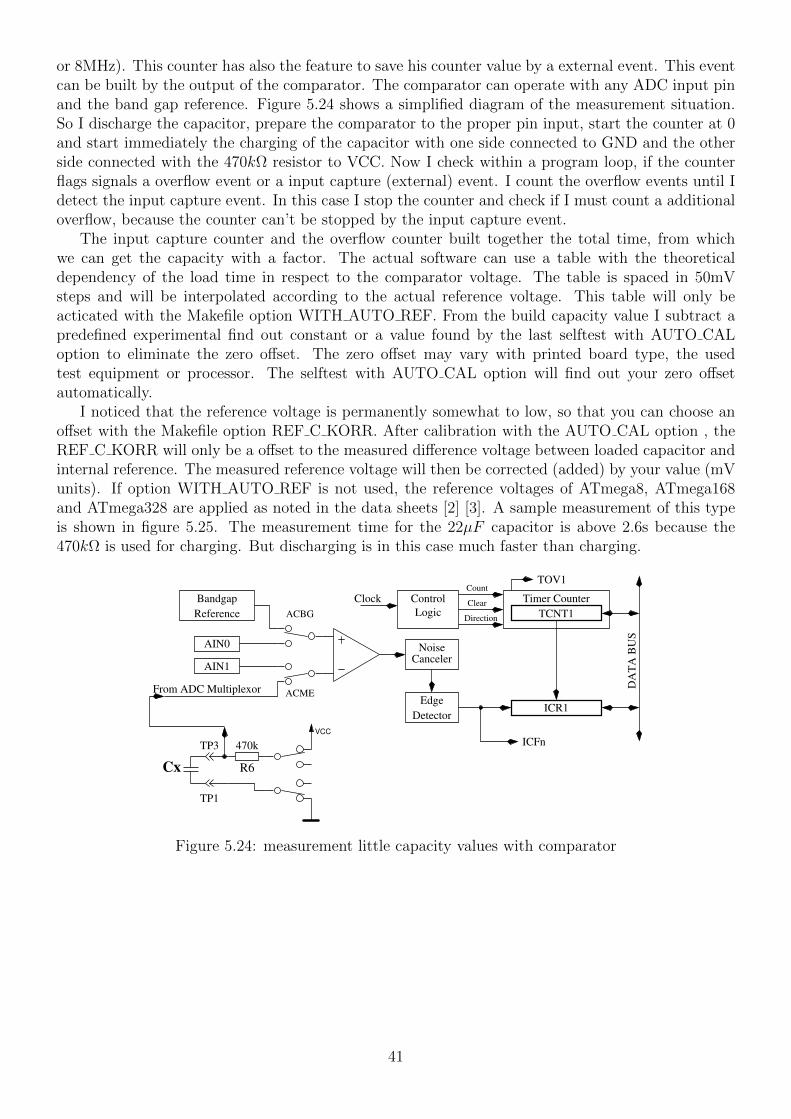
or 8MHz). This counter has also the feature to save his counter value by a external event. This eventcan be built by the output of the comparator. The comparator can operate with any ADC input pinand the band gap reference. Figure 5.24 shows a simplified diagram of the measurement situation.So I discharge the capacitor, prepare the comparator to the proper pin input, start the counter at 0and start immediately the charging of the capacitor with one side connected to GND and the otherside connected with the 470kΩ resistor to VCC. Now I check within a program loop, if the counterflags signals a overflow event or a input capture (external) event. I count the overflow events until Idetect the input capture event. In this case I stop the counter and check if I must count a additionaloverflow, because the counter can’t be stopped by the input capture event.
The input capture counter and the overflow counter built together the total time, from whichwe can get the capacity with a factor. The actual software can use a table with the theoreticaldependency of the load time in respect to the comparator voltage. The table is spaced in 50mVsteps and will be interpolated according to the actual reference voltage. This table will only beacticated with the Makefile option WITH AUTO REF. From the build capacity value I subtract apredefined experimental find out constant or a value found by the last selftest with AUTO CALoption to eliminate the zero offset. The zero offset may vary with printed board type, the usedtest equipment or processor. The selftest with AUTO CAL option will find out your zero offsetautomatically.
I noticed that the reference voltage is permanently somewhat to low, so that you can choose anoffset with the Makefile option REF C KORR. After calibration with the AUTO CAL option , theREF C KORR will only be a offset to the measured difference voltage between loaded capacitor andinternal reference. The measured reference voltage will then be corrected (added) by your value (mVunits). If option WITH AUTO REF is not used, the reference voltages of ATmega8, ATmega168and ATmega328 are applied as noted in the data sheets [2] [3]. A sample measurement of this typeis shown in figure 5.25. The measurement time for the 22µF capacitor is above 2.6s because the470kΩ is used for charging. But discharging is in this case much faster than charging.
Detector
Edge
Bandgap
Reference
AIN0
AIN1
From ADC Multiplexor
ACBG
ACME
NoiseCanceler
Count
Clear
Direction
Control
Logic
Clock
ICFn
DA
TA
BU
S
TOV1
Timer Counter
TCNT1
ICR1
TP3
TP1
Cx
470k
R6
VCC
Figure 5.24: measurement little capacity values with comparator
41
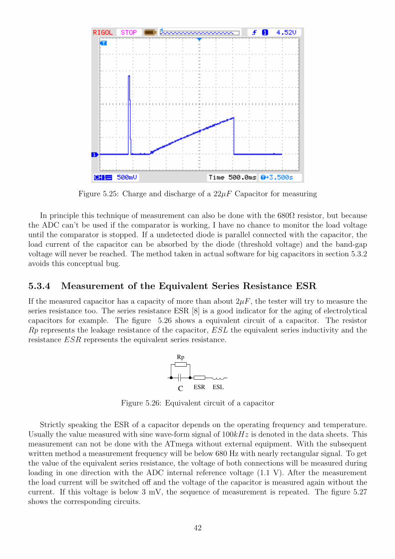
Figure 5.25: Charge and discharge of a 22µF Capacitor for measuring
In principle this technique of measurement can also be done with the 680Ω resistor, but becausethe ADC can’t be used if the comparator is working, I have no chance to monitor the load voltageuntil the comparator is stopped. If a undetected diode is parallel connected with the capacitor, theload current of the capacitor can be absorbed by the diode (threshold voltage) and the band-gapvoltage will never be reached. The method taken in actual software for big capacitors in section 5.3.2avoids this conceptual bug.
5.3.4 Measurement of the Equivalent Series Resistance ESR
If the measured capacitor has a capacity of more than about 2µF , the tester will try to measure theseries resistance too. The series resistance ESR [8] is a good indicator for the aging of electrolyticalcapacitors for example. The figure 5.26 shows a equivalent circuit of a capacitor. The resistorRp represents the leakage resistance of the capacitor, ESL the equivalent series inductivity and theresistance ESR represents the equivalent series resistance.
Rp
C ESR ESL
Figure 5.26: Equivalent circuit of a capacitor
Strictly speaking the ESR of a capacitor depends on the operating frequency and temperature.Usually the value measured with sine wave-form signal of 100kHz is denoted in the data sheets. Thismeasurement can not be done with the ATmega without external equipment. With the subsequentwritten method a measurement frequency will be below 680 Hz with nearly rectangular signal. To getthe value of the equivalent series resistance, the voltage of both connections will be measured duringloading in one direction with the ADC internal reference voltage (1.1 V). After the measurementthe load current will be switched off and the voltage of the capacitor is measured again without thecurrent. If this voltage is below 3 mV, the sequence of measurement is repeated. The figure 5.27shows the corresponding circuits.
42
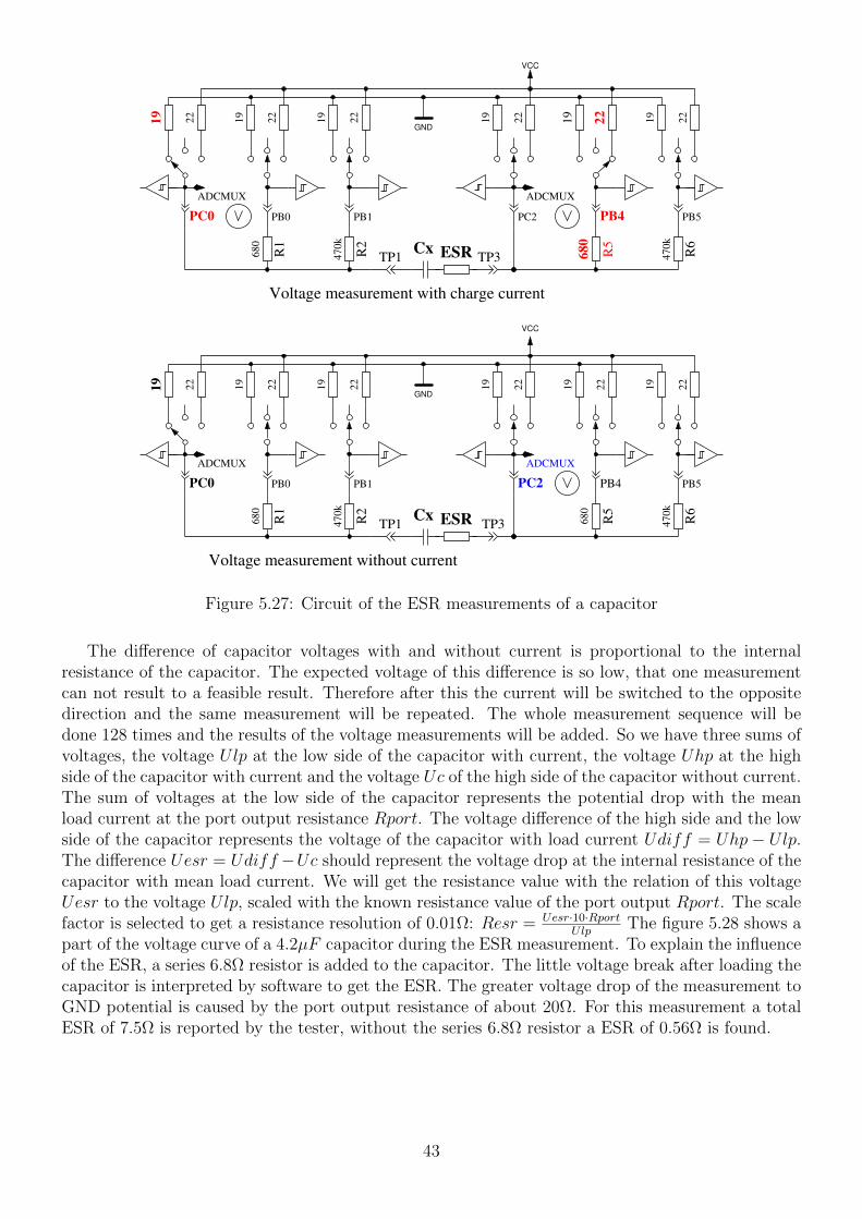
PC0 PB0
ADCMUX
PC2
ADCMUX
PB5PB4PB1
19
22
19
22
19
22
19
22
19
22
19
22
68
0
47
0k
TP1 680
47
0k
GND
Cx
PC0 PB0
ADCMUX
PC2
ADCMUX
PB5PB4PB1
22
19
22
19
22
19
22
19
22
19
22
68
0
47
0k
TP1 68
0
47
0k
GND
Cx
19
Voltage measurement without current
R1
R2
R5
R6
R1
R2
R5
R6
TP3
TP3
ESR
ESR
Voltage measurement with charge current
VCC
VCC
Figure 5.27: Circuit of the ESR measurements of a capacitor
The difference of capacitor voltages with and without current is proportional to the internalresistance of the capacitor. The expected voltage of this difference is so low, that one measurementcan not result to a feasible result. Therefore after this the current will be switched to the oppositedirection and the same measurement will be repeated. The whole measurement sequence will bedone 128 times and the results of the voltage measurements will be added. So we have three sums ofvoltages, the voltage Ulp at the low side of the capacitor with current, the voltage Uhp at the highside of the capacitor with current and the voltage Uc of the high side of the capacitor without current.The sum of voltages at the low side of the capacitor represents the potential drop with the meanload current at the port output resistance Rport. The voltage difference of the high side and the lowside of the capacitor represents the voltage of the capacitor with load current Udiff = Uhp− Ulp.The difference Uesr = Udiff−Uc should represent the voltage drop at the internal resistance of thecapacitor with mean load current. We will get the resistance value with the relation of this voltageUesr to the voltage Ulp, scaled with the known resistance value of the port output Rport. The scalefactor is selected to get a resistance resolution of 0.01Ω: Resr = Uesr·10·Rport
UlpThe figure 5.28 shows a
part of the voltage curve of a 4.2µF capacitor during the ESR measurement. To explain the influenceof the ESR, a series 6.8Ω resistor is added to the capacitor. The little voltage break after loading thecapacitor is interpreted by software to get the ESR. The greater voltage drop of the measurement toGND potential is caused by the port output resistance of about 20Ω. For this measurement a totalESR of 7.5Ω is reported by the tester, without the series 6.8Ω resistor a ESR of 0.56Ω is found.
43

(a) One pin to GND (b) Pin to Pin
Figure 5.28: Voltage curve of a 4.2µF capacitor during the ESR measurement
The accuracy of the ESR measurement is not very high by different reasons:
1. The voltage measurement at both pins of the capacitor can not be done at the same time, theonly way is to do it in sequence. In the interim time between both measurements the loadcurrent has changed due to the charge of capacitor. The program tries to compensate this factwith a capacity dependent correction of the low side voltage.
2. The ADC takes the measurement voltage after 1.5 clock ticks after the start of conversion. Theconversion beginns with the rising edge of the ADC-clock, if the start bit is set. If the chargecurrent will be switched off to early, the ADC takes the wrong voltage for the measurementwith current. If the charge current will be switched off to late, the capacitor will take moreelectric charge, than that of the corresponding measurement with load current. This will causea too high voltage of the measurement without current. But it is difficult to switch off thecurrent at the right time by software.
3. The port output resistance is used as a reference value by this measurement method, but thisresistance value is not exacly known too.
4. The resolution of the ADC is not sufficient to get a resolution of resistance of 0.01Ω. To get thebest avaiable resolution of ADC, the internal reference (1.1 V) is used for all measurements.The resolution deficit will be attenuated by accumulating a big number of single measurementstoo.
5. The switching of ports can not be exactly synchronized to the ADC clock with polling ofconversion done.
Anyway the results seems to be practical, as shown with the following figure 5.29. The ESRvalues of the same part measured with the Transistortester vary more than the values measured withthe LCR meter. All ESR results from the LCR meter are measured with a frequency of 1 kHz. Youmust respect the quality of all connection parts. The used cable connections can cause a highermeasured resistance value. The plug connectors can also result a higher resistance value. The LCRmeter has the advantage of the used Kelvin terminals.
44
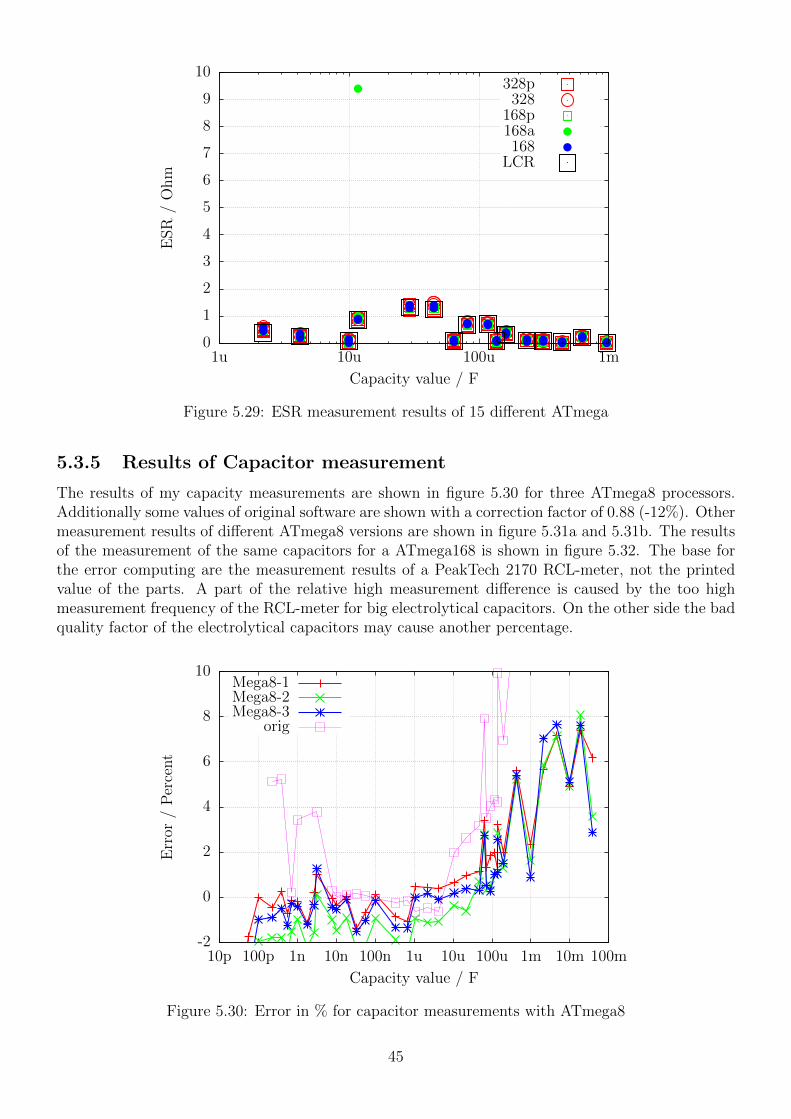
0
1
2
3
4
5
6
7
8
9
10
1u 10u 100u 1m
ESR
/O
hm
Capacity value / F
328p328
168p168a168
LCR
Figure 5.29: ESR measurement results of 15 different ATmega
5.3.5 Results of Capacitor measurement
The results of my capacity measurements are shown in figure 5.30 for three ATmega8 processors.Additionally some values of original software are shown with a correction factor of 0.88 (-12%). Othermeasurement results of different ATmega8 versions are shown in figure 5.31a and 5.31b. The resultsof the measurement of the same capacitors for a ATmega168 is shown in figure 5.32. The base forthe error computing are the measurement results of a PeakTech 2170 RCL-meter, not the printedvalue of the parts. A part of the relative high measurement difference is caused by the too highmeasurement frequency of the RCL-meter for big electrolytical capacitors. On the other side the badquality factor of the electrolytical capacitors may cause another percentage.
-2
0
2
4
6
8
10
10p 100p 1n 10n 100n 1u 10u 100u 1m 10m 100m
Err
or/
Per
cent
Capacity value / F
Mega8-1Mega8-2Mega8-3
orig
Figure 5.30: Error in % for capacitor measurements with ATmega8
45
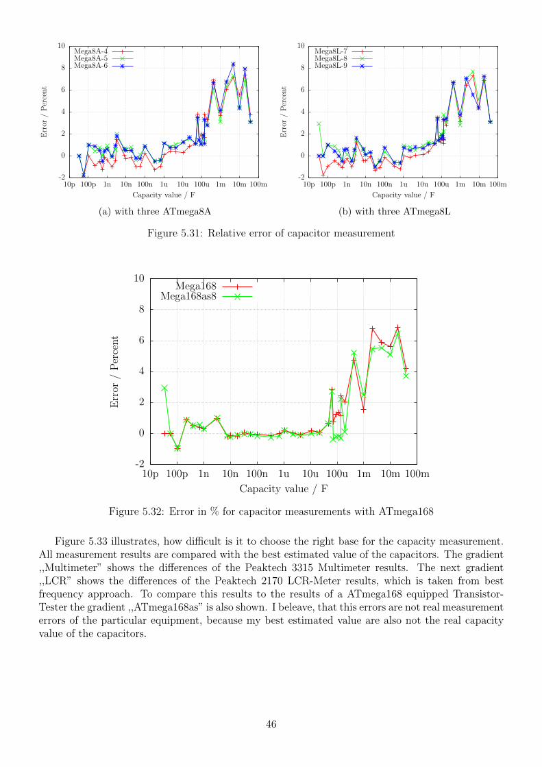
-2
0
2
4
6
8
10
10p 100p 1n 10n 100n 1u 10u 100u 1m 10m 100m
Err
or/
Per
cent
Capacity value / F
Mega8A-4Mega8A-5Mega8A-6
(a) with three ATmega8A
-2
0
2
4
6
8
10
10p 100p 1n 10n 100n 1u 10u 100u 1m 10m 100m
Err
or/
Per
cent
Capacity value / F
Mega8L-7Mega8L-8Mega8L-9
(b) with three ATmega8L
Figure 5.31: Relative error of capacitor measurement
-2
0
2
4
6
8
10
10p 100p 1n 10n 100n 1u 10u 100u 1m 10m 100m
Err
or/
Per
cent
Capacity value / F
Mega168Mega168as8
Figure 5.32: Error in % for capacitor measurements with ATmega168
Figure 5.33 illustrates, how difficult is it to choose the right base for the capacity measurement.All measurement results are compared with the best estimated value of the capacitors. The gradient,,Multimeter” shows the differences of the Peaktech 3315 Multimeter results. The next gradient,,LCR” shows the differences of the Peaktech 2170 LCR-Meter results, which is taken from bestfrequency approach. To compare this results to the results of a ATmega168 equipped Transistor-Tester the gradient ,,ATmega168as” is also shown. I beleave, that this errors are not real measurementerrors of the particular equipment, because my best estimated value are also not the real capacityvalue of the capacitors.
46

-4
-3
-2
-1
0
1
2
3
4
5
6
7
10p 100p 1n 10n 100n 1u 10u 100u 1m 10m 100m
Err
or/
Per
cent
Capacity value / F
MultimeterLCR
Mega168as
Figure 5.33: Comparison of capacity measurement results of Multimeter, LCR-meter and ATmega168
The differences of measurements of three different ATmega168 processors are shown in figure 5.34a. In this case the results of the LCR meter is taken as base of comparison. The same results ofthree different ATmega168A processors are shown in figure 5.34b and three different ATmega168PAprocessors are shown in figure 5.35. The results of three ATmega328 are additianally shown infigure 5.36a and the results from three ATmega328P are shown in figure 5.36b. At this only the zerovalue of the capacity measurement of 39pF is respected, all other facility to correct the results arenot used. This zero value includes the 2-3pF, which are caused by the 12 cm long cable with theclips. The board layout can cause a different zero value, I have fixed this zero value with the board”DG2BRS V 5.2.1”.
-5
0
5
10
15
20
25
10p 100p 1n 10n 100n 1u 10u 100u 1m 10m
Err
or/
Per
cent
Capacity value / F
168-1168-2168-3
(a) three ATmega168
-2
-1
0
1
2
3
4
5
6
10p 100p 1n 10n 100n 1u 10u 100u 1m 10m
Err
or/
Per
cent
Capacity value / F
168A-4168A-5168A-6
(b) three ATmega168A
Figure 5.34: capacity measurement error, not calibrated
47
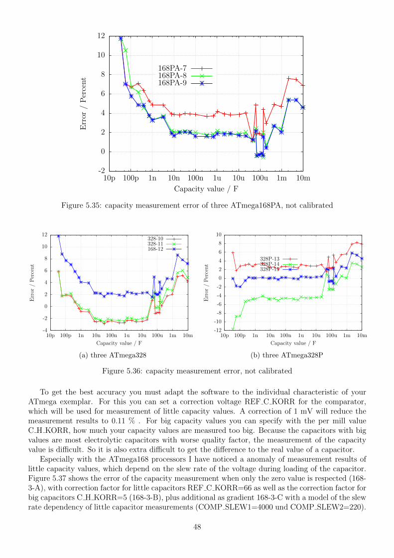
-2
0
2
4
6
8
10
12
10p 100p 1n 10n 100n 1u 10u 100u 1m 10m
Err
or/
Per
cent
Capacity value / F
168PA-7168PA-8168PA-9
Figure 5.35: capacity measurement error of three ATmega168PA, not calibrated
-4
-2
0
2
4
6
8
10
12
10p 100p 1n 10n 100n 1u 10u 100u 1m 10m
Err
or/
Per
cent
Capacity value / F
328-10328-11168-12
(a) three ATmega328
-12
-10
-8
-6
-4
-2
0
2
4
6
8
10
10p 100p 1n 10n 100n 1u 10u 100u 1m 10m
Err
or/
Per
cent
Capacity value / F
328P-13328P-14328P-15
(b) three ATmega328P
Figure 5.36: capacity measurement error, not calibrated
To get the best accuracy you must adapt the software to the individual characteristic of yourATmega exemplar. For this you can set a correction voltage REF C KORR for the comparator,which will be used for measurement of little capacity values. A correction of 1 mV will reduce themeasurement results to 0.11 % . For big capacity values you can specify with the per mill valueC H KORR, how much your capacity values are measured too big. Because the capacitors with bigvalues are most electrolytic capacitors with worse quality factor, the measurement of the capacityvalue is difficult. So it is also extra difficult to get the difference to the real value of a capacitor.
Especially with the ATmega168 processors I have noticed a anomaly of measurement results oflittle capacity values, which depend on the slew rate of the voltage during loading of the capacitor.Figure 5.37 shows the error of the capacity measurement when only the zero value is respected (168-3-A), with correction factor for little capacitors REF C KORR=66 as well as the correction factor forbig capacitors C H KORR=5 (168-3-B), plus additional as gradient 168-3-C with a model of the slewrate dependency of little capacitor measurements (COMP SLEW1=4000 und COMP SLEW2=220).
48

Also the self-discharge of big capacitors is respected with gradient 168-3-C. The component withthe slew rate dependent value is computed with COMP SLEW1
cval+COMP SLEW2− COMP SLEW1
COMP SLEW2, where cval is the
measured capacity value with pF units.
-5
0
5
10
15
20
25
10p 100p 1n 10n 100n 1u 10u 100u 1m 10m
Err
or/
Per
cent
Capacity value / F
168-3-A168-3-B168-3-C
Figure 5.37: Improvement of the capacitor measurement of one ATmega168
5.3.6 Automatic calibration of the capacitor measurement
The automatic calibration is build in two parts. The first part find out the zero offset of the capacitymeasurement. For that the mean value of the capacity measured without connected capacitor isbuild. A mean value for all 6 measurement combinations is build with 8 repetitions. After successfulldetermination the zero offsets are written to the EEprom and will be used for further measurements.More difficult was the clearance of the variance of the different ATmega processors for little capacitors(<40µF ), which is shown in Figure 5.34a, 5.34b and 5.35. As a significant reason for this is foundthe different characteristic (Offset voltage) of the analog comparator.
The date of measurement of nine different processors is shown in figure 5.38 . The ”diff2ref” pointsshow the difference of the voltage of a loaded capacitor of 660nF to the individual internal referencevoltages (band gap). Ideally this difference Voltage should be zero, if the analog comparator hasstopped the loading by the signal to the processor. The short handling time of the processor shouldnot result to a measurably rising of the capacitor voltage of this relative big capacitor. The ”CapErr”points show the estimated measurement errors of each processor out of figure 5.34a, 5.34b and 5.35with per mill units. It is noticeable, how the ”CapErr” points will follow the ”diff2ref” points.Therefore the ”diff” points show the difference between the particular ”CapErr” and ”diff2ref”points. With a mean value of the ”diff” points we can get a good estimation for the correctionof the capacitor measurements together with the difference voltage of the loaded capacitor and theinternal reference.
For the second part of adjustment you must connect a capacitor to pin 1 and pin 3. This capacitorshould have a good quality factor and should have a capacity between 100nF and 20µF . It shouldbe a film capacitor, as far as possible not a ceramic capacitor und in no case a electrolytic capacitor.You don’t need to know the exact value of this capacitor.
49

-20
-10
0
10
20
30
40
50
60
70
0 2 4 6 8 10
Err
or/
per
mill
Diff
eren
ceto
refe
rence
/m
V
Number of ATmega168
diff2refCapErr
diff
Figure 5.38: Date of nine ATmega168 processors
The figures 5.39a, 5.39b, 5.40, 5.41a and 5.41b shows the measurement results of the differentprocessors with a standard software after the auto calibration. The flash of the processors was loadedwith the same software, only for the ATmega168PA the Makefile must be adapted with ”PARTNO= m168p”. After loading the data the selftest was started for each ATmega and a capacitor with330nF was connected during test No. 10 to pin 1 and pin 3.
-4
-3
-2
-1
0
1
2
3
4
5
6
7
10p 100p 1n 10n 100n 1u 10u 100u 1m 10m
Err
or/
Per
cent
Capacity value / F
168-1168-2168-3
(a) three ATmega168
-4
-3
-2
-1
0
1
2
3
4
5
6
10p 100p 1n 10n 100n 1u 10u 100u 1m 10m
Err
or/
Per
cent
Capacity value / F
168A-4168A-5168A-6
(b) three ATmega168A
Figure 5.39: capacity measurement error, calibrated
50
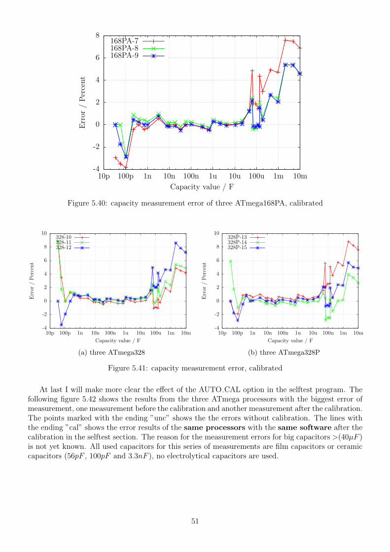
-4
-2
0
2
4
6
8
10p 100p 1n 10n 100n 1u 10u 100u 1m 10m
Err
or/
Per
cent
Capacity value / F
168PA-7168PA-8168PA-9
Figure 5.40: capacity measurement error of three ATmega168PA, calibrated
-4
-2
0
2
4
6
8
10
10p 100p 1n 10n 100n 1u 10u 100u 1m 10m
Err
or/
Per
cent
Capacity value / F
328-10328-11328-12
(a) three ATmega328
-4
-2
0
2
4
6
8
10
10p 100p 1n 10n 100n 1u 10u 100u 1m 10m
Err
or/
Per
cent
Capacity value / F
328P-13328P-14328P-15
(b) three ATmega328P
Figure 5.41: capacity measurement error, calibrated
At last I will make more clear the effect of the AUTO CAL option in the selftest program. Thefollowing figure 5.42 shows the results from the three ATmega processors with the biggest error ofmeasurement, one measurement before the calibration and another measurement after the calibration.The points marked with the ending ”unc” shows the the errors without calibration. The lines withthe ending ”cal” shows the error results of the same processors with the same software after thecalibration in the selftest section. The reason for the measurement errors for big capacitors >(40µF )is not yet known. All used capacitors for this series of measurements are film capacitors or ceramiccapacitors (56pF , 100pF and 3.3nF ), no electrolytical capacitors are used.
51
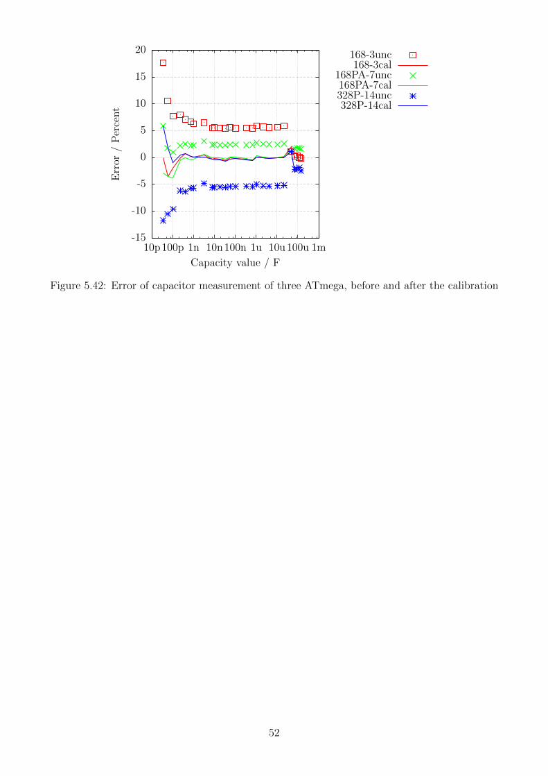
-15
-10
-5
0
5
10
15
20
10p100p 1n 10n100n 1u 10u100u 1m
Err
or/
Per
cent
Capacity value / F
168-3unc168-3cal
168PA-7unc168PA-7cal328P-14unc328P-14cal
Figure 5.42: Error of capacitor measurement of three ATmega, before and after the calibration
52
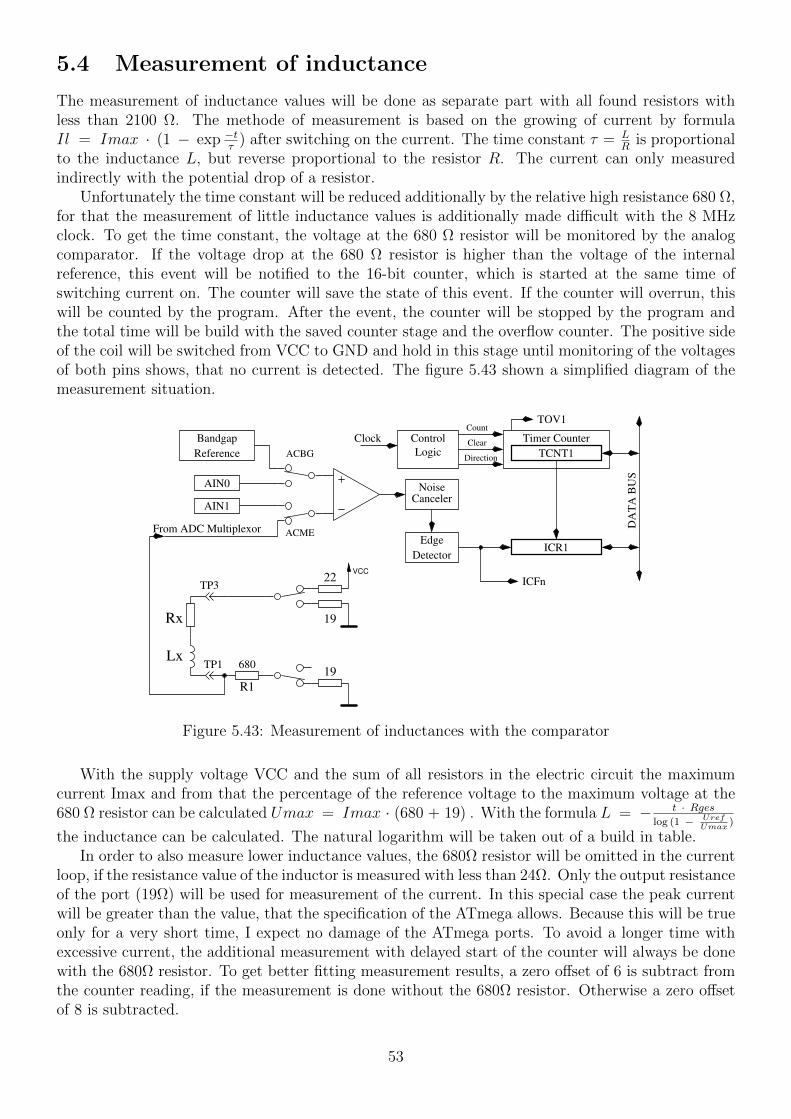
5.4 Measurement of inductance
The measurement of inductance values will be done as separate part with all found resistors withless than 2100 Ω. The methode of measurement is based on the growing of current by formulaIl = Imax · (1 − exp −t
τ) after switching on the current. The time constant τ = L
Ris proportional
to the inductance L, but reverse proportional to the resistor R. The current can only measuredindirectly with the potential drop of a resistor.
Unfortunately the time constant will be reduced additionally by the relative high resistance 680 Ω,for that the measurement of little inductance values is additionally made difficult with the 8 MHzclock. To get the time constant, the voltage at the 680 Ω resistor will be monitored by the analogcomparator. If the voltage drop at the 680 Ω resistor is higher than the voltage of the internalreference, this event will be notified to the 16-bit counter, which is started at the same time ofswitching current on. The counter will save the state of this event. If the counter will overrun, thiswill be counted by the program. After the event, the counter will be stopped by the program andthe total time will be build with the saved counter stage and the overflow counter. The positive sideof the coil will be switched from VCC to GND and hold in this stage until monitoring of the voltagesof both pins shows, that no current is detected. The figure 5.43 shown a simplified diagram of themeasurement situation.
Detector
Edge
Bandgap
Reference
AIN0
AIN1
From ADC Multiplexor
ACBG
ACME
NoiseCanceler
Count
Clear
Direction
Control
Logic
Clock
ICFn
DA
TA
BU
S
TOV1
Timer Counter
TCNT1
ICR1
TP3
680
R1
Rx
LxTP1
19
22
19
VCC
Figure 5.43: Measurement of inductances with the comparator
With the supply voltage VCC and the sum of all resistors in the electric circuit the maximumcurrent Imax and from that the percentage of the reference voltage to the maximum voltage at the680 Ω resistor can be calculated Umax = Imax · (680 + 19) . With the formula L = − t · Rges
log (1 − UrefUmax
)
the inductance can be calculated. The natural logarithm will be taken out of a build in table.In order to also measure lower inductance values, the 680Ω resistor will be omitted in the current
loop, if the resistance value of the inductor is measured with less than 24Ω. Only the output resistanceof the port (19Ω) will be used for measurement of the current. In this special case the peak currentwill be greater than the value, that the specification of the ATmega allows. Because this will be trueonly for a very short time, I expect no damage of the ATmega ports. To avoid a longer time withexcessive current, the additional measurement with delayed start of the counter will always be donewith the 680Ω resistor. To get better fitting measurement results, a zero offset of 6 is subtract fromthe counter reading, if the measurement is done without the 680Ω resistor. Otherwise a zero offsetof 8 is subtracted.
53
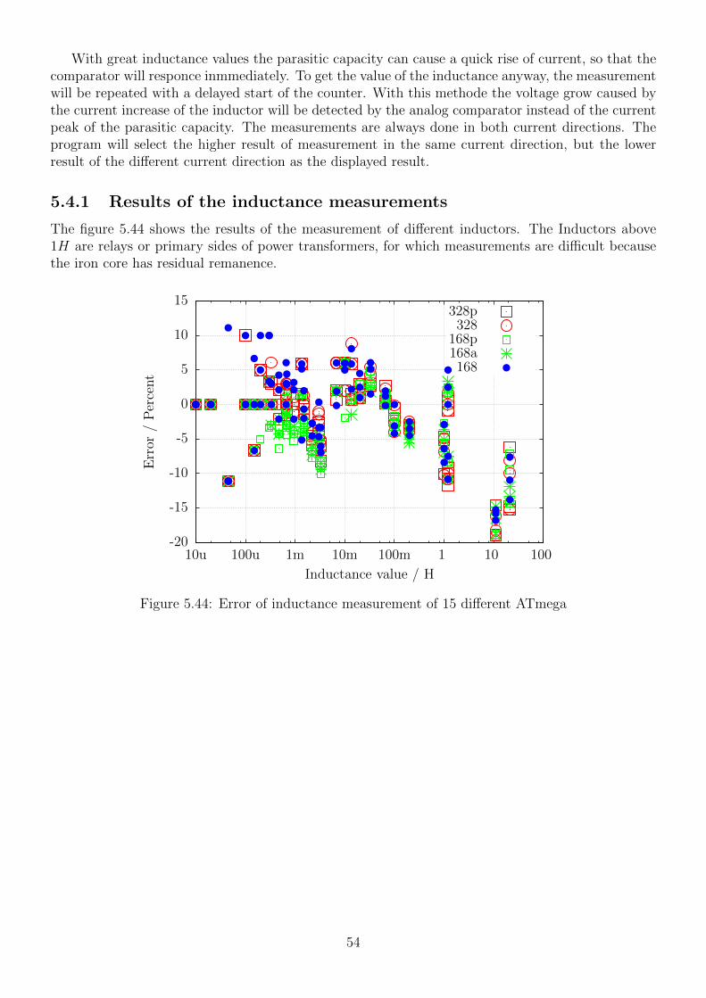
With great inductance values the parasitic capacity can cause a quick rise of current, so that thecomparator will responce inmmediately. To get the value of the inductance anyway, the measurementwill be repeated with a delayed start of the counter. With this methode the voltage grow caused bythe current increase of the inductor will be detected by the analog comparator instead of the currentpeak of the parasitic capacity. The measurements are always done in both current directions. Theprogram will select the higher result of measurement in the same current direction, but the lowerresult of the different current direction as the displayed result.
5.4.1 Results of the inductance measurements
The figure 5.44 shows the results of the measurement of different inductors. The Inductors above1H are relays or primary sides of power transformers, for which measurements are difficult becausethe iron core has residual remanence.
-20
-15
-10
-5
0
5
10
15
10u 100u 1m 10m 100m 1 10 100
Err
or/
Per
cent
Inductance value / H
328p328
168p168a168
Figure 5.44: Error of inductance measurement of 15 different ATmega
54

5.5 Selftest Function
Beginning with release 0.9k I have implemented a self test function. Usage is very simple. If youhave installed test terminal with clamps, put all clamps together to a piece of uninsulated wire andpress the start button. The program notice the shorten probes and start the self test function. Afterfinishing the self test the transistor tester will continue with normal measurement. If no equipmentis connected, the program will end with “part unknown or damaged”. You can configure self testonly for a ATmega168 or ATmega328. The separate steps of the self test function 1 to 7 is displayedon row 1 of the LCD display with the letter T followed by the step number. Every step is repeated4 times, before the program continues with the next step. But if you hold the start key pressed,when the test cycle is finished, this test is not repeated any more. If you leave the key pressed thetotal time, every test is executed only once.
Without the AUTO CAL option only measurement results are displayed in every step, no erroranalysis are done, you must interpret the results yourself. At this place I will give you an additionalimportant hint. Never do a measurement with connected ISP plug! The ISP interface influences themeasurement. Here is the list of currently implemented tests:
1. Measurement of the 1.3V (or 1.1V) reference Voltage (band gap Reference). In row1 the text “Ref=” and the measured Voltage in mV is displayed. For the ATmega8 the voltageshould be near to 1.3V. For the other processors the voltage should be near to 1.1V. The secondrow shows the resulting factor for the capacity measurement with the 470kΩ resistor.
2. Comparing of the 680Ω resistors. In row 1 the cryptic text “+RL- 12 13 23” is shown.Meaning of this is as follows: The RL is the short form of Resistor Low meaning the 680Ωresistors. The 12 stand for: resistor at pin 1 is connected to VCC (+) and resistor at pin 2is connected to GND (-). The result of this measurement is displayed in row 2 at the firstplace as difference to the theoretical value. In row 1 follows now a “13” which means, that thefirst connection of measurement 1 is still connected with 680Ω to VCC but that the resistor ofpin 3 is connected to GND. The result is displayed in the middle place of row 2 as differenceto the theoretical value. The last measurement of this test “23.” means that now the resistorat pin 2 is connected to VCC (+) and the resistor of pin 3 is connected to GND. The result ofmeasurement is displayed at the last place of LCR row 2 as difference to the theoretical value.Please remember, that the resolution of the ADC is about 4.88mV! The measurement situationis also shown in figure 5.45. The theoretical value with respect to the internal resistance of thepins should be: 5001·(19+680)
(19+680+680+22)= 2493 .
22
PB0
680
19
22
TP1 TP2
GND
ADCMUX
19
PC0
19
22
ADCMUX
TP1 TP3
GND
ADCMUX
TP2
GND
TP3
first measurement second measurement third measurement
PC0 TP3 TP2 TP1PB0
680
22
19
PC2
19
22
PB4
680
22
19
PC1
19
22
PC2
19
22
PB4
680
19
22
680
PB2
19
22
680
PB2
19
22
PC1
19
22
R3
R5
R5R
3
R1
R1
VCC VCCVCC
Figure 5.45: Comparison of 680Ω resistors
55

3. Comparing of the 470kΩ resistors. Now the display shows in row 1 “+RH- 12 13 23”.The same procedure as done in step 2 is repeated with the 470kΩ resistors (symbols RH).All results are shown as difference to the theoretical value. The theoretical value is this time
5001·(19+470000](19+470000+470000+22)
= 2500 for all combinations.
4. In this step nothing is measured, but the order is displayed isolate Probe!, which meansthat it is time to separate the probes (release from wire).
5. This step tests the capability of GND (-) connected 470kΩ resistors (H) to pull thetest pins to GND. Row 1 shows the text “RH-”. Row 2 should display zero for all three pins.
6. This step tests the capability of VCC (+) connected 470kΩ resistors (H) to pull thetest pins to VCC (+). Row 1 shows the text “RH+”. The results are shown als differenceto VCC and should be near zero. Great differences from the best value for test 5 and 6 areerrors such as isolation problem, flux material or damaged port.
7. This Step tests the voltages of the 470kΩ/680Ω resistor divider. The voltage differenceto the expected voltage of the 470kΩ / 680Ω resistor dividers is shown in row 2 of the LCDfor all three terminals. Differences of more than some mV can be caused by the assembly ofwrong resistor values.
8. Measuring of internal resistance of pin output switched to the GND signal. Thistest and the follwing tests will only be done, if the option AUTO CAL is selected. The internalresistance of the port C outputs switched to GND (-) are measured with the current of toVCC (+) switched 680Ω resistors, see Figure 5.46. Only the three pins of the ADC port aremeasured, the resistor port B (PB0,PB2 and PB4) can not be measured without hardwaremodification. Is is assumed that the port resistance of the different ports are nearly identical.The resistor value will be shown in the next test.
first measurement second measurement third measurement
19
PB0
680
19
22
TP1
GND
ADCMUX
PC0
22
19
680
19
22
GND
ADCMUX
22
19
680
19
22
GND
ADCMUX
22
PC1 PB2 PC2 PB4
TP3TP2
R1
R3
R5
VCC VCC VCC
Figure 5.46: Measurement of internal resistance of Port C switched to GND
9. Measuring of internal resistance of port outputs switched to the VCC (+)signal.The needed current is generated with to GND connected 680Ω resistors . It are the samemeasurements as those in test 8 to the other side as you can see in Figure 5.47. With thefollowing steps the resistance is computed: To get the current, the following is computed:(V CC−(resultoftest8)−(resultoftest9))/680. To get both resistor values, the voltage (resultof test 8 or 9) is divided by this current. The result for this test will then be notified in row 1with the text ”RI Hi=”, the resistance value (Ω) to the GND side is displayed in row 2 withthe text ”RI Lo=”. Both results will be written to the EEprom memory and will be used forfurther measurement.
56

first measurement second measurement third measurement
PB0
68
0
TP1
GND
ADCMUX
PC0
68
0
GND
ADCMUX
68
0
GND
ADCMUX
PC1 PB2 PC2 PB4
TP3TP2
22
19
22
22
19
19
19
22
19
19
22
22
R1
R3
R5
VCC VCC VCC
Figure 5.47: Measurement of internal resistance of Port C switched to VCC
10. Measurement of the zero offset of the capacitor measurement. The zero offset for thecapacity measurement with pin combinations 1:3, 2:3 and 1:2 is shown in that order in displayrow 1 following the “C0 ”. Alls three values are shown in pF units. For this measurements nopredefined zero offset is respected. The zero offsets of pin combinations in opposite order is alsomeasured. The results will be written to the EEprom, if all values are less than 70pF . Thiswill be notified by the output of “OK” in row 2. The found zero offsets are used for furthercapacity measurements with respect to the pin combination. Please notice, that changes of thetest equipment can cause a new adjustment of the zero offset. If you use wire with clips, thezero offset may be 3 pF greater compared to a empty socket.
11. Wait for the connection of a capacitor to pin 1 and pin 3. The message “1-C-3 >100nF”is shown in row 1 of LCD. To prepare the measurement of the comparator offset voltage, youmust connect a sufficient big capacitor to pin 1 and pin 3. It should be a capacitor with a highquality factor and a capacity between 100nF and 20µF . You should never use electrolyticalcapacitors, use film capacitors instead.
12. Measurement of the comparator offset for capacitor measurement adjustment. Toget the offset of the analog comparator, a capacitor must already be connected to pin 1 andpin 3. The capacitor is needed for buffering the load voltage of a capacitor, in order to get thevoltage difference of load voltage to the internal reference voltage (band gap). If measurementis successfull, the correction value is short shown with the text “REF C=” in row 1 of the LCDand written to the EEprom. You can give a additional offset to the automatic measured valuewith the REF C KORR option.
If you have selected the AUTOSCALE ADC option, the gain of the ADC readings with theinternal reference will be adjusted by comparing a capacitor voltage below 1 V once readedwith VCC reference and once readed with the internal reference. The measurement result isshown in row 2 with the text “REF R=”. Your REF R KORR value is a additional offset tothis automatic find out difference value.
At the end of test function the text “Test End” is shown in row 1 and the version number ofsoftware is shown in row 2. If the Makefile option FREQUENCY 50HZ is set, a 50Hz rectanglesignal is generated on pin 2 and the same signal in opposite direction on pin 3. Pin 1 is switched toGND . The current is limited with 680Ω resistors. This will be notified by the Output of “50Hz” atthe end of row 1 of the LCD display. The 50Hz signal will be generated 30 times for 2 seconds each.You can check the time of the wait calls, if you have an oscilloscope or frequency counter. Figure5.48 shows the oscillograph curves of both 50 Hz output pins with crystal operation.
57
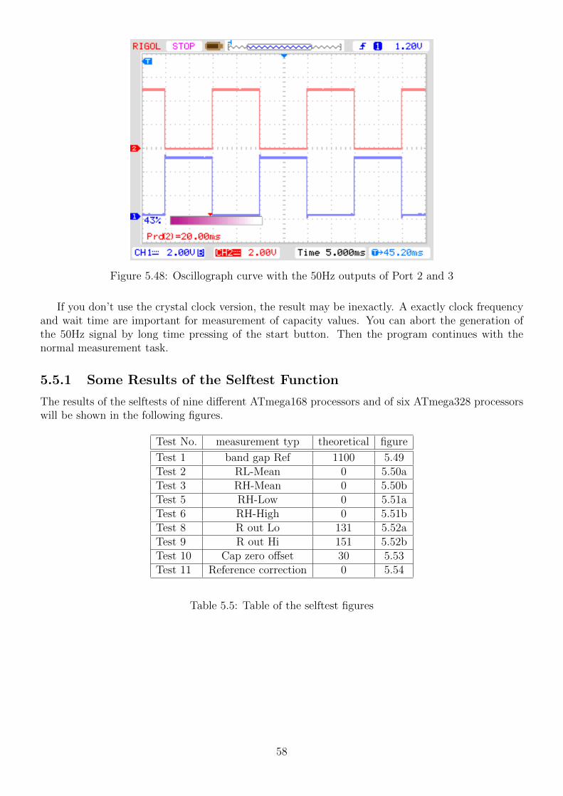
Figure 5.48: Oscillograph curve with the 50Hz outputs of Port 2 and 3
If you don’t use the crystal clock version, the result may be inexactly. A exactly clock frequencyand wait time are important for measurement of capacity values. You can abort the generation ofthe 50Hz signal by long time pressing of the start button. Then the program continues with thenormal measurement task.
5.5.1 Some Results of the Selftest Function
The results of the selftests of nine different ATmega168 processors and of six ATmega328 processorswill be shown in the following figures.
Test No. measurement typ theoretical figure
Test 1 band gap Ref 1100 5.49Test 2 RL-Mean 0 5.50aTest 3 RH-Mean 0 5.50bTest 5 RH-Low 0 5.51aTest 6 RH-High 0 5.51bTest 8 R out Lo 131 5.52aTest 9 R out Hi 151 5.52bTest 10 Cap zero offset 30 5.53Test 11 Reference correction 0 5.54
Table 5.5: Table of the selftest figures
58

1050
1060
1070
1080
1090
1100
1110
0 1 2 3 4 5 6 7 8 9 10 11 12 13 14 15 16
refe
rence
volt
age
/m
V
Processor number
Reference
Figure 5.49: Selftest: Reference-Voltages
-20
-15
-10
-5
0
5
0 1 2 3 4 5 6 7 8 9 10 11 12 13 14 15 16
volt
age
/m
V
Processor number
RLmiddle12RLmiddle13RLmiddle23
(a) with 680Ω
-20
-15
-10
-5
0
5
0 1 2 3 4 5 6 7 8 9 10 11 12 13 14 15 16
volt
age
/m
V
Processor number
RHmiddle12RHmiddle13RHmiddle23
(b) with 470kΩ
Figure 5.50: Selftest: difference to ideal mean voltage
59
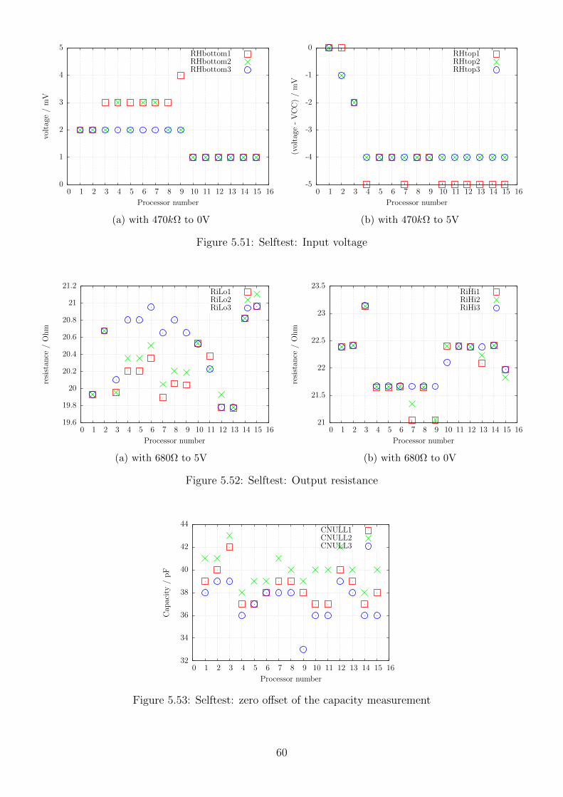
0
1
2
3
4
5
0 1 2 3 4 5 6 7 8 9 10 11 12 13 14 15 16
volt
age
/m
V
Processor number
RHbottom1RHbottom2RHbottom3
(a) with 470kΩ to 0V
-5
-4
-3
-2
-1
0
0 1 2 3 4 5 6 7 8 9 10 11 12 13 14 15 16
(vol
tage
-V
CC
)/
mV
Processor number
RHtop1RHtop2RHtop3
(b) with 470kΩ to 5V
Figure 5.51: Selftest: Input voltage
19.6
19.8
20
20.2
20.4
20.6
20.8
21
21.2
0 1 2 3 4 5 6 7 8 9 10 11 12 13 14 15 16
resi
stan
ce/
Oh
m
Processor number
RiLo1RiLo2RiLo3
(a) with 680Ω to 5V
21
21.5
22
22.5
23
23.5
0 1 2 3 4 5 6 7 8 9 10 11 12 13 14 15 16
resi
stan
ce/
Oh
m
Processor number
RiHi1RiHi2RiHi3
(b) with 680Ω to 0V
Figure 5.52: Selftest: Output resistance
32
34
36
38
40
42
44
0 1 2 3 4 5 6 7 8 9 10 11 12 13 14 15 16
Cap
acit
y/
pF
Processor number
CNULL1CNULL2CNULL3
Figure 5.53: Selftest: zero offset of the capacity measurement
60

-60
-40
-20
0
20
40
60
80
0 1 2 3 4 5 6 7 8 9 10 11 12 13 14 15 16
Vol
tage
corr
ecti
on/
mV
Processor number
REF C KORRREF R KORR
Figure 5.54: Selftest: correction values after automatic calibration
At last I would like to show you the difference voltages of the external at the AREF pin witha multimeter measured voltages and the internal with the ADC measured voltages of the referencevoltages of 15 different ATmega precessors and the found correction voltages (REF R KORR) afterthe automatic calibration in figure 5.55. You can see, that the automatic calibration values nearlyfollow the external measured values.
-40
-30
-20
-10
0
10
20
30
40
0 1 2 3 4 5 6 7 8 9 10 11 12 13 14 15 16
Vol
tage
diff
eren
ce/
mV
Processor number
AREF - REFREF R KORR
Figure 5.55: Selftest: Voltage difference of the internal reference
61

Chapter 6
Known errors and unsolved problems
Software Version 1.05k
1. Germanium Diodes (AC128) are not detected in all cases.
2. Capacity value in reverse direction for Power Schottky Diodes such as MBR3045PT can notbe measured, if only one diode is connected. The reason is a too big residual current of thisdiode. Sometimes the measurement is possible by cooling down the device (with cooling sprayfor example).
3. Here and there a wrong detection of the 2.5V precision referenz is reported, when the PC4 pin(27) is unconnected. You can avoid this behaviour with a additional pull up resistor connectedto VCC.
4. The diode function of a triac gate can not be examined.
5. Sometimes a problem with the Brown Out level of 4.3V is reported for ATmega168 or AT-mega328 processors. This will cause a reset during capacity measurement. A reason is notknown. The Resets will disappear, if the Brown Out level is set to 2.7V.
62

Chapter 7
Special Software Parts
Several modifications are done to save flash memory. The LCD-Output of probe-pin numberswas done in the form “lcd data(’1’+pin)”. To save the add operation for every call, the entry“lcd testpin(uint8 t pin)” was added to the lcd routines.c.
The pseudo calls in the form “ delay ms(200)” are not implemented as library calls, but waitloops are implemented for every call. This will consume much memory, if you have many calls atdifferent location in your program. All of this pseudo calls are replaced with calls to my specialassembly written library, which uses only 74 bytes of flash memory (@8MHz), but enables calls fromwait1us() to wait5s() in steps of 1,2,3,4,5,10,20. . . . The routines include the Watch Dog Reset forall calls above 50ms. Every wait call usually only need one instruction (2 Byte). Wait calls withinterim value such as 8ms need two calls (5ms and 3ms or two times a 4ms call). I don’t know anyimplementation, which is more economical if you use many wait calls in your program. The callsuses no registers, only the Stack Pointers for the return adresses in the RAM (at most 28 Byte stackspace in current release) is used. The total list of functions is:wait1us(), wait2us(), wait3us(), wait4us(), wait5us(), wait10us(),wait20us(), wait30us(), wait30us(), wait40us(), wait50us(), wait100us(),wait200us(), wait300us(), wait400us(), wait500us(), wait1ms(),wait2ms(), wait3ms(), wait4ms(), wait5ms(), wait10ms(),wait20ms(), wait30ms(), wait40ms(), wait50ms(), wait100ms(),wait200ms(),wait300ms(), wait400ms, wait500ms(), wait1s(),wait2s(), wait3s(), wait4s() and wait5s();That are 36 functions with only 37 instructions inclusive Watch Dog Reset! There is really no way toshorten this library. Last not least matches the wait calls the exactly delay time, if the lowest waitcall does. Only the wait calls above 50ms are one cycle per 100ms to long because of the additionallyintegrated watch dog reset.
Additionally the often used calling sequence “wait5ms(); ReadADC. . . ();” is replaced by the call“W5msReadADC(. . . );”. The same is done for the sequence “wait20ms(); ReadADC(. . . );” whichis replaced by one “W20msReadADC(. . . );” call. The function ReadADC is additionally written inassembly language, so that this add-on could be implemented very effective. The functional identicalC-version of the ReadADC function is also avaiable as source.
63
Chapter 8
To Do List and new ideas
1. Add more and better documentation.
2. Check if transistor tester could get better interpolated ADC values if additional noise is added tothe signal or to the ADC reference (see ATMEL document AVR121: Enhancing ADC resolutionby oversampling). If all items are identical, there can’t be any enhancement of resolution byoversampling. Can enough noise be generated with the ATmega counter? How additional noiseaffects the upper and lower limit values? Of course this method can not eliminate all of theADC errors.
3. This method can be tested by building a ramp input signal and monitoring this signal. Theramp signal can be build by slowly charging a big capacitor with the 470k resistor. The growingof the voltage can then be monitored with the LCD display in a special part of self test.
4. Think about how we can get the real internal resistance of port B output (resistor switchingport) instead of assuming, that ports are equal.
5. Can discharging of capacitors be made more quickly, if the minus pin is additionally raisedwith the 680Ω resistor to VCC (+)?
6. Check if the tester can use floating-point representation of values. The risk of overflow is lower.There is no need to use multiplication and division together to build a multiplication with anon integer factor. But I don’t know how much flash memory must be spend for the library.
7. Write User’s guide for configuring the tester with the Makefile options and description of thebuild chain.
8. If the holding current of a thyristor can not be reached with the 680Ω resistor, is it harmless toswitch the cathode directly to GND and the anode directly to VCC for a very short time? Thecurrent could reach more than 100mA. Will the port be damaged? What is with the powersupply (voltage regulator)?
9. Check the Port afterwards with self test function!
10. Can voltage regulators be checked? (Input, Output, GND)
11. Can optoelectronic couplers be checked?
12. Warning message, if the found reference voltage is not plausible in relation to ATmega modeland VCC.
64

13. What is about a second generation tester with a bigger ATmega which includes differentialADC-port, more flash memory . ? There is no ATxmega which have supply voltage of 5V,only the ATmega line is possible.
14. Idea for a New Projekt: USB version without LCD-Display, Power from USB, Communicationto PC over a USB-Serial bridge.
65
Bibliography
[1] Markus Frejek AVR-Transistortester,. Embedded Projects Journal, 11. Ausgabe, 2011
[2] Atmel Corporation 8-bit AVR with 8KBytes In-System Programmable Flash - ATmega8(L),.Manual, 2486Z-AVR-02/11, 2011
[3] Atmel Corporation 8-bit AVR with 4/8/16/32KBytes In-System Programmable Flash - AT-mega48 - ATmega328,. Manual, 8271D-AVR-05/11, 2011
[4] Atmel Corporation Atmel AVR126: ADC of megaAVR in Single Ended Mode,. ApplicationNote, 8444A-AVR-10/11, 2011
[5] Atmel Corporation Atmel AVR121: Enhancing ADC resolution by oversampling,. ApplicationNote, 8003A-AVR-09/05, 2005
[6] http://en.wikibooks.org/wiki/LaTeX LaTeX documentation,. Guide to the LaTeX markuplanguage, 2012
[7] http://en.wikibooks.org/wiki/Gnuplot Gnuplot documentation,. Documentation for theplotting tool gnuplot, 2012
[8] Wikipedia http://de.wikipedia.org/wiki/Equivalent_Series_Resistance Explanationfor ESR in german language. Standardization and equivalent circuit of a capacitor, 2012
[9] http://www.xfig.org/userman Xfig documentation,. Documentation of the interactive drawingtool xfig, 2009
[10] http://docs.gimp.org/2.6/de gimp documentation. Documentation of the GNU Image Ma-nipolation Program, 2010
[11] http://www.mikrocontroller.net/articles/AVR-Transistortester Online documentationof the Transistortester, Online Article, 2009-2011
[12] http://www.mikrocontroller.net/articles/AVRDUDE Online documentation of avrdude pro-grammer interface, Online Article, 2004-2011
[13] http://www.mikrocontroller.net/topic/131804 Thread from Markus, Forum thread, 2009
[14] http://www.mikrocontroller.net/articles/AVR_Transistortester Short description ofnew features of the TransistorTester von Karl-Heinz K., Online Article, 2012
[15] http://www.mikrocontroller.net/topic/248078 Thread from Karl-Heinz, Thread and newsoftware versions, 2012
[16] http://www.mikrocontroller.net/articles/WinAVR Information about WinAVR in germanlanguage, Online Article, 2012
66

[17] http://winavr.sorceforge.net Source for WinAVR package, Download source, 2012
[18] http://www.mikrocontroller.net/topic/248078?page=5#2922341 Patch for WinAVR, Set-ting of Fuses with avrdude, Download Quelle, 2012
67