tsmc: advanced design for low power at 65nm and below · tsmc: advanced design for low-power at...
TRANSCRIPT

TSMC: Advanced Design for Low Power at 65nm and Below

Sec7:2
TSMC: Advanced Design for Low Power at 65nm and Below
By L.C. Lu, Deputy Director of the Design Methodology Program at TSMC, and David Lan, Senior Manager in design methodology at TSMC North America.Several drivers create the need for low power today. These include advanced processes at 65nm and below, which, although they enable SoC designs with much more complexity, consume more power. Mobile devices also require low-power chips to extend the battery life in order to compete in the market place and also to reduce overall system cost, which includes packaging costs To achieve low-power, design for power has to be a goal from the start. Today, low-power design demands the best efforts of the design and manufacturing ecosystem, including:
Process optimization•Low-power design techniques•CPFstandardsupportthroughouttoolsflow•Libraries and IP•Referencedesignflow(RDF)asexemplifiedintheTSMC9.0RDF•
To meet customers’ demands in low power, TSMC optimizes its process technology for low-power designs. Nevertheless, at today’s extremely small feature sizes, dynamic and leakage power issues remain. This means techniques for mitigating power consumption must come from the design side. For foundry customers’ power-sensitive 65nm or 45nm designs, it is critical to fully leverageTSMCprocesseswith compatible,power-savingEDA toolflows.TSMCalready brings to bear low-power methodologies and IP aimed at reducing dynamic, active,andstandbypowerleakage.Alloftheselow-powermethodologiesrequirefullyautomatedEDAsupport,asshownbelow.
Figure 142. TSMC integrated low-power solution
Adaptive VoltageScaling (AVS)
Dynamic VoltageFreq. Scaling (DVFS)
Voltage Island
Clock Gating
Source + Back Bias
Longer Channelin Non-Critical Paths
Voltage Scaling
Back Bias
Muti-Vt Device
Active Leakage
Low-Power Methodologies
Low-Power Automation – Power Format
Low-Power Process
Low-PowerLib
Low-PowerSRAM
Coarse-Grain PowerGating with Lower Vdd
Coarse-GrainData Retention
Coarse-GrainPower Gating
Power Shutdown
Fine-GrainPower Gating
Standby LeakageDynamic Power
Dual Power SRAM
Sec7:2

TSMC: Advanced Design for Low-Power at 65nm and Below
Sec7:3
TSMC 65nm Low-Power ProcessToday, the 65nm TSMC process includes:
Multi-• Vt cellsNew gate oxide material•Low K interconnect, including ELK, ULK•Strained engineering•
However, the low-power challenge requires more than just process support.
Low-Power Design TechniquesTSMC customers utilize the full gamut of power reduction techniques, and TSMC has expanded support for these approaches, culminating in the new Reference DesignFlow9.0(RDF9.0):
For dynamic power: clock gating, multiple-voltage domains, dynamic voltage •andfrequencyscaling,hierarchicalvoltagewithdualpowerSRAM,andadaptivevoltage scalingFor active leakage power: multi-• Vt, back-biasing, voltage scaling, and source-and back-biasingForstandbyleakagepower:fine-andcoarse-grainpowergating,powershut-off,•and data retention
CPF: The Low-Power StandardTSMCandCadencehavecollaboratedonlow-powersinceearly2004.In2006,TSMCwas a founding member of the Si2 Low Power Coalition and the Power Forward Initiative, recognizing that another key requirement is that design tools in the methodology communicate low-power design intent in a single, standard format. TheSi2CommonPowerFormat(CPF),thefirstlow-powerEDAformatembracedby TSMC for 65nm low-power design, enables this capability.
The Need for CPFWhat are the challenges of design-based solutions? Who are the stakeholders? Management,thedesignteam,theverificationteam,andtheimplementationteamalldependonlow-powerdesignefficienciesforproductivityandsuccess.For management:
Increases schedule risk•Increases risk of failure•Increases silicon cost•
For the design team:Greatlyincreasescomplexityofquality-of-silicon(QoS)tradeoffstoexplore•Isolation and retention add complexity to design•Introduces architecture modeling challenges•

TSMC: Advanced Design for Low-Power at 65nm and Below
Sec7:4
Fortheverificationteam:More functionality to verify•Howisthefunctionalityspecified?•How will changes be communicated?•Now need to verify power structure implementation•
For the implementation team:Addscomplexitytofloorplanning,powerplanning,placement,clocktreesynthesis,•and routingIncreasesdifficultyoftimingclosure•Increasesdesign-for-testdifficulty•
Figure 143. Design-based solutions affect everyone
Management
DesignTeam
VerificationTeam
ImplementationTeam
Figure 144. CPF enables low-power automation
Common Power Format (CPF) is an ASCII File that captures:
Power design intentPower domain
Power modesDefinitionsTransition expressionsModal analysis
Level shifter cells
Isolation cells
State-retention cells
Switch cells
Always-on cells
Logical: hierarchical modulesas domain members
Physical: power/ground netsand connectivity
Analysis view: timing librarysets for power domains
Level shifter logicIsolation logicState-retention logicSwitch logic & Control signals
Power logic
Technology information
CPF CapabilitiesTheCommonPowerFormat (CPF) is a single specificationofpower intentusedthroughoutdesign,verification,andimplementation.

TSMC: Advanced Design for Low-Power at 65nm and Below
Sec7:5
TSMC has taken a leadership role in ensuring that the rich variety of power reduction techniques automated by CPF result in verifiable improvements to 65nm designs. The following section describes an early program to validate the Common Power Format for use with TSMC technology.
The TSMC Proof-Point ProjectThe proof-point project objectives included: [33]
Enhancing communications between logic design and physical design teams •AchievingsynergybetweenTSMClow-powerIPandEDAtoolsforimplementing•power gating and power shut-off ValidatingadvanceddesigntechniquesinsiliconusingaCPF-basedEDAtoolflow•Verifying functionality and timing results for advanced techniques•Improvingverificationtechnologies•Looking for opportunities for further automation •
Inanydesignproject, if thedesign intent isclearlyspecified, itunifies thedesignteam.CPFprovidesasinglefilewithstandarddefinitionsofpowerintent,allowingdesignersanddesigntoolstoutilizeacommondatasetthroughoutthedesignflow.To help drive CPF-awareness into a low-power methodology, TSMC undertook a verificationprojectanddefinedthetechniqueswhichwouldbeused,asshowninFigure 145.
Figure 145. TSMC’s low-power test run

TSMC: Advanced Design for Low-Power at 65nm and Below
Sec7:6
The baseline for the project was a comparison to previous design techniques, without CPFsupport.Simpler,earlier,power-reductiondesigntechniques(areaoptimizationandclockgating)had little functionalityandtiming impact,butalsocontributedlittle reduction in power. More advanced techniques now being applied, such as powergating,wereexpectedtoimpactfunctionalandtimingverification,aswellas dramatically reducing power, so this project was developed to measure power reduction, gauge the complexity impact of advanced power gating, and work to minimize that impact.
TSMC Proof-Point DesignTSMCusedalargesystem-on-chipdesignblock,withmorethan100,000instances, 50(RAM)blocks,andmorethan100,000nets.[33]In the design flow, TSMC used CPF-enabled EDA tools and focused on powergatingasthekeypowerreductiondesigntechniquetobestevaluatethefullbenefitof the technique. Power gating involves switching off the power to blocks of the circuit when those portions are idle, and signal isolation, so that powered-down blocks do not pose unintended loads on other active portions. When used together, power switching and signal isolation can impact SoC timing, and even functionality if blocks are switched on or off improperly. The proof-point project comprised:
500Kgateblock•52RAMblocks•Powergatingimplementationandverification•Autoswitchandisolationcellinsertion•Automaticpowergridconnection•Simulationverificationforpowergating•Formalverification•
IP Usage in the TSMC Proof-Point ProjectThe project used a TSMC 65LP library, including special low-power IP, which is a requirement for power-gated low-power design. This IP included specialized power-gating cells to allow both column-style power gating and ring-type power gating. The specialized power switches automatically eliminate power-up glitches and electromigration, through dual control and a dual-switch structure. AnimportantpartoftheprojectwastovalidatethattheCPF-enabledEDAflowtookproper advantage of these IP elements. With Cadence CPF-enabled technologies, TSMC captured the proof-point design and proceeded through the design and implementationflowshowninFigure 146.

TSMC: Advanced Design for Low-Power at 65nm and Below
Sec7:7
WiththispowerfulCPF-basedflow,thedesignwasautomaticallyaugmentedwithpower switches and isolation cells to accomplish power gating. RTL synthesis used power-gatingauto-switchinginsertedasacheckerboardorsurroundingfloorplan(Figure 147).RTLsimulationverifiedpowergatingandretentionflip-flopbehavior.Then, gate-level simulation of power shutdown was done under power-mode transition and unknown propagation. Unknown signal generation and propagation was done automatically in the CPF environment without Verilog model changes in the library.
Figure 146. Flow of automation from RTL to GDS [33]

TSMC: Advanced Design for Low-Power at 65nm and Below
Sec7:8
Cadence Encounter Conformal Equivalence Checker and Conformal Low Power were used to formally verify the auto-control signal setting for the switches and isolation cells, as well as the actual power/ground connection to the network. Before CPF, designers would have needed to manually check the connections and generate largeamountsofverificationtestbenchestocheckforfunctionalcorrectness.Theseareallerror-proneactivities.Theuseofautomatedformalverificationfromdesignintent,throughRTLandfinalimplementation,isoneofthevisiblebenefitsofCPFasusedthroughoutthisflow.
Figure 147. Power-gating inserted surrounding the floorplan [Ref. 33]

TSMC: Advanced Design for Low-Power at 65nm and Below
Sec7:9
Results of the Proof-Point ProjectWhen comparing a baseline project, utilizing low-power design techniques—which didnotuseCPF—with aCPF-basedEDA toolflow, clear benefitswere realized.Notablebenefitsincluded:
The design was completed faster•The design required fewer iterations•Designintentwasconsistentthroughouttheflow,sotheintegrityofthepower•gating structure was preserved throughout the designAutomatedpowergatingachieved40xleakagepowerreduction•
CPF-based automation was successful, created no functional nor timing failures, andleadtonoareainefficiencies.The pilot project also revealed a variety of additional opportunities to enhance low-power design techniques through the use of a CPF-based format. This work is already under way in ongoing projects between TSMC and Cadence. Enjoyingsuccessinthisfirstproof-pointproject,thetwocompaniessettoworktorefineandintegrateIPdesignusingtheCommonPowerFormat.Inaddition,TSMCwasabletovalidateCPFsupportforTSMCReferenceFlow9.0.
CPF-Based TSMC Reference Flow 9.0TheTSMCReferenceFlow9.0wasannouncedinJune2007.ThisflowsupportsCPFtools for 65nm and 45nm process technologies.
Figure 148. TSMC Reference Flow 9.0: complete CPF integration [Ref. 34]

TSMC: Advanced Design for Low-Power at 65nm and Below
Sec7:10
This9.0flowsolves criticalproblems since it isbasedonCPF.Thedetailsof theCadencetechnologiesinvolvedinthisflowareasfollows:
Sample Design Information from CPFThismulti-supplyvoltage(MSV)design(seeFigure 150)containsaDMAblockandaDMAbridge,withtwoMACsthatarebasedonidenticalRTLbuthavedifferentpower behavior.Threepowerdomainsandfourpowermodesarespecified,asshowninthefigurebelow. The power modes, the state behavior, the isolation cells, and state retention allconspiretoposeasignificantchallenge!
Figure 149. CPF flow: Supported tool functionality
Pervasive CPFCPF Quality Check
Encounter Conformal Low Power
Functional SimulationIncisive Design Team Simulator Incisive Design Team Manager
Logic Synthesis and DFTEncounter RTL Compiler
LEC + Power ChecksEncounter Conformal Low Power
Logic SimulationIncisive Design Team Simulator
Physical ImplementationSoC Encounter System
LEC + Power ChecksEncounter Conformal Low Power
ATPGEncounter Test
Timing & SI SignoffEncounter Timing System
IR Drop and Power SignoffVoltageStorm Dynamic Gate Option
Power domain/mode aware IR drop analysis (static and dynamic). Power-up analysis of power switches and impact on neighbors.
Verification of virtual LP logic: Linting, consistency, functional, structural checks
Functional validation of virtual LP behavior and PSO: State loss, isolation, SRPGAuto generation of PSO mode coverage.
Power domain, multi mode, DVFS aware synthesis and power analysis. Autoinsertion, mapping and optimization of iso, LS, SRPG. Power domain aware testsynthesis, insertion of iso/LS on DFT nets.
Power domain/mode aware delay calculation, including DVFS, MMMC support.
Automatic mapping of power-modes (from CPF) into test-modesFault model/coverage of low power structures, SRPG (excluding power switches).
Gate2Gate logic equivalence checks. Structural, property, and functional checksFor LP logic.
Power domain/mode aware P&R, w/o dont_touchPower switch insertion and optimization. LS and clamp optimization. DVFS andMMMC support.
Functional validation of LP logic behavior and PSO: state loss, isolation, SRPG
RTL2Gate logic equivalence checks (incl. LP cells).Structural, property, and functional checks for LP logic.

TSMC: Advanced Design for Low-Power at 65nm and Below
Sec7:11
Functional and Logic SimulationAd-hocpowermanagementverificationisveryrisky,impactingproductivitybecausemanual intervention is required to model power management, and there are many filesandchangestomaintain.Qualityisatrisk,becausethereisnoguaranteethatwhatisverifiediswhatisactuallyimplemented.Schedulepredictabilityalsosuffers,because power-related errors may be discovered late.
Figure 150. MSV design example
VDDM (0.84V) VDD (1V)
Phys II
Retention registers
Enabled level shifters (level shifter w/isolation)
Requires functional verification!
Switch
Switch
MAC I(0.84V)
MAC II(0.84V)
DMAAHMB
VDDlu
VDDau
DM
A B
ridge
RTL Design
Define power domains
Define state retention
Define power controlsDefine isolation logicPower modes:
DMA and DMA BridgeTwo MACs w/ identical RTL
PDCorePDMac1
MAC1 optimized
Technology dataLibrary cellsOperating conditions
MAC2 stores all regs
Mode # Mac 1 Mac 2
OFF
OFFOFF
OFF
ON
ONON4
3
2
1
ON
PDMac2
PCM
Phys I
Figure 151. Ad-hoc verification steps
Modify RTL to instantiatelow-power models
Create custom PLI to modellow-power operation
Create custom libraries to supportlow-power models
Modify testbench to simulatepower shut-off

TSMC: Advanced Design for Low-Power at 65nm and Below
Sec7:12
ButwiththeCPF-enabledflow,verificationbenefitsarerealized,includingimprovedproductivity,withnoimpacttoexistingverificationmethodology,nogoldendesignfilechanges,nocustomlibrarydevelopment,andnoPLIdevelopment.Italsoresultsin enhanced quality, because what designers verify is what they actually design. Better schedule predictability is achieved, because power issues are detected early.Thebottomlineis:reducedrisk!
RealcustomerdesignissuesuncoveredwiththeCPF-enabledverificationflowhaveincluded:
Cache memory in power down domain, where the processor running from cache •would lose program and hang. Simulations were used to determine cache and power sequencingPower-down caused a hang on the system bus due to isolation values. One •customer commented,“We were worried something like that would happen…”Therestorefrompower-downwasnotclean;non-stateretentionflopsneededa•reset or initialization signalPower-up and isolation disable was happening at the same time, there was not •enough time for power to stabilize before enabling outputsIncorrect design of the power control module created oscillations on control •signals in one mode
CPFautomationidentifiedtheseissuesearlytoensuredesignintegrity.
Figure 152. Incisive power management verification approach
The ONLY power-awareverification flow
RTL
Design Verification
CPF
FormalAnalysis
Simulation
Accelerationand Emulation
Lint and StructuralAnalysisV
erification Coverage
Testbench A
utomation

TSMC: Advanced Design for Low-Power at 65nm and Below
Sec7:13
Logic Synthesis and DFTThe contributions of CPF in the logic synthesis and DFP stages of design included:
Multi-objective synthesis structures logic for timing, power, and area •simultaneously. This is the only way to close on multiple orthogonal objectives. Also, better logic structure delivers superior quality of silicon through physicalimplementationTop-down multi-power domain synthesis optimizes across power domains, •including isolation and level shifter latency. Supports fast what-if exploration of MSV and PSO scenarios, power mode-aware power exploration, and is key to achieving optimal power/timing balance
Logic Equivalence Checking (LEC) and Power ChecksCPF quality checking helps eliminate errors in the CPF. Three critical areas for checking include:
Logic equivalence checking (LEC) ensures that low-power optimizations do not•introduce logical errors; enables true EC leveraging CPF; checks state retention mapping from RTL to gate; checks corresponding presence of isolation and level shifter during implementation; and checks power domain boundariesFunctional and structural checks ensure proper insertion of low-power cells and •proper connectivity of low-power cells, and formally validate isolation and state retention functions. This runs at RTL design, both logical and physical netlist leveraging CPF as the golden specificationTransistor-level checks check domain boundaries for un-buffered inputs (sneak paths)•
Figure 153. Encounter RTL Compiler: Multi-objective, multi-voltage RTL synthesis
Clock Period
Leakage Power
Top
Lib10.8V
Lib21.0V Lib3
1.2VRTL
ChipCPF
ChipSDC
A
BC
PSO
Die Size
Encounter RTLCompiler = 5% faster
RTL Compiler = 12% smaller
RTL Compiler = 45% cooler
Too slow? Too hot?
Isolation

TSMC: Advanced Design for Low-Power at 65nm and Below
Sec7:14
Automatic Test Pattern Generation (ATPG)Automatictestpatterngeneration(ATPG)ischallengingfordesignswithadvancedpowermanagementtechniques.WiththeTSMCRDF9.0:
Domain-awarescantestingrecognizespowerdomainsandenablesafullscan•test even when a module is shut downATPGtestcoverageforlow-powerstructures•Power-awareATPGminimizespowerduringtestmodebyintelligentfilloftest•patterns
Figure 154. Encounter Conformal Low Power: Independent low-power implementation verification
Figure 155. Encounter Test: Unique power-aware test solution
Excessive powerconsumption during
scan testing
Low-power scanvectors manage power
during scan test
ModeClock(MHz)
% Switching Switch power(mW)
2.9610~20
46
6
500Normal operation
Scan test
Low-powerscan test
50
50
11.86
1.66
Nano CPU, 35K instances, 9K registers

TSMC: Advanced Design for Low-Power at 65nm and Below
Sec7:15
Physical ImplementationPhysical implementation with CPF supports multi-supply voltage designs, with automated insertion of low-power elements and concurrent optimization of multiple power domains.
Timing and SI SignoffIn the TSMC RDF 9.0, timing and signal integrity (SI) signoff with CPF featurecomplete signoff static timing analysis, built from production-proven products such as Cadence CTE, CeltIC®Signal IntegrityAnalysis,andSignalStorm® Nanometer DelayCalculator (NDC),plus siliconvalidationandsupport from foundryandIP/library vendors.Advanced timing debug speeds analysis, increasing productivity, and supportsstandardinterfaces.Theflowcanbetcl-orGUI-driven,andsupportstimingdebug,interactivequeries,tclAPI,andhistograms.
Figure 156. SoC Encounter RTL-to-GDSII System: Automation for multiple power domains
Single pass top-down MSV, multi-mode synthesis
Clock tree synthesis
Physical synthesis
1.0V1.2V 0.9V
module (top):
module (A):
Level shiftersincluded
1.2V
1.2V
1.2V
0.9V
0.9V
0.9V
ONEblock
ONE tree
MSVphysical synthesis
Concurrentoptimization of 0.9Vand 1.2V domains
Leve
l shi
fters
pla
ced
conc
urre
ntly
durin
g ph
ysic
al s
ynth
esis
module (B):

TSMC: Advanced Design for Low-Power at 65nm and Below
Sec7:16
IR Drop and Power SignoffIntheTSMCCadenceRDF9.0flow,IRdropandpowersignoffcapabilitiesincludestaticanddynamicpowerrailverification,basedonpatentedpowerconsumptionalgorithms,andpowerrailverificationforIRdropandelectromigration.CadenceVoltageStorm® Power Verification supports both vectorless and vector-drivenanalysis modes. It provides comprehensive low-power support for MSMV, power switches, and power-up. IR drop and power signoff is integrated with Cadence Encounter platform techonologies for automatic de-coupling capacitance optimization;withCeltICNDCtodeterminetheimpactofIRdropontimingandnoise;andwithCadenceAllegro®PackageDesignertoeasilydeterminetheimpactof package loading on IR drop.
Figure 157. Encounter Timing System
.lib SDC Netlist CPF
SPEF/SDF/WLM
DRVsPathsSDF
Optional
cdB
ECSM DEFEncounter TimingSystem

TSMC: Advanced Design for Low-Power at 65nm and Below
Sec7:17
Figure 158. VoltageStorm dynamic power analysis
DEFGDSII
OA
Encounterplatform
RC extraction engine
PowerMeterpower calculation
Static and dynamicrail analysis
AllegroPackageDesigner
EncounterTimingSystem
Power gridview library
VoltageStorm DG
Figure 159. SoC Encounter System: VoltageStorm flow
SoC Encounter SystemPlaced and Routed DesignDatabase
Static and DynamicIR-Drop Analysis
Power-SwitchECO
DecapECO
Timing and CriticalPath Analysis
(EncounterTiming System)
Edit Power-PadLocation
PowerLibraries
CPF ModeSpecification
Plots
Waveforms and IR Drop Files
Report Power(Common Power Engine)

TSMC: Advanced Design for Low-Power at 65nm and Below
Sec7:18
The following diagram describes how power-up modes and sequencing are analysed, starting with creation of the circuit netlist, simulation, creation of dynamic power grid views, and analysis and viewing capabilities.
The following diagram shows the power switch insertion and optimization flow,with power, current, and IR drop reporting.
Figure 161. Power–up flow
PowerMeter
Logic CircuitNetlist
1. Create circuit netlist 2. Simulate with Virtuoso UltraSim Full-Chip Simulator
CircuitNetlist
UltraSim
VDD
3. Create dynamic power grid views 4. Analyze in VoltageStorm DG
CircuitNetlist
UltraSim VoltageStorm DGVDD
Load full-chip power RC networkwith PGVs and analyze
Capture dynamiccurrent in PGV
Control
Inputsclamped
Outputscorrectlyloaded
VoltageStorm(Power Meter)
UltraSim
Top LevelCircuit File
RC Grid
Netlist
SpiceWaveformsand Results
Power-TransistorDynamic
Currents (ptl)
TemplateStimulus
VoltageSources
Sleep ctrlRC Network
SignalLoading
Figure 160. Power switch optimization flow
ram2ram1
PD1PD1PLL
VoltageStorm
SoC EncounterSystem
DEFSOC
TWF, VCD
Power SwitchCurrent and
IR-DropReport
Power GridView Library
addPowerSwitch
runVSDG
optPowerSwitchPower Calculation
Rail Analysis
RC Extraction Engine

TSMC: Advanced Design for Low-Power at 65nm and Below
Sec7:19
The de-coupling capacitor, or decap, insertion and optimization can ensure power grid integrity while preventing excess power dissipation. Intelligent insertion of decaps is increasingly critical for small geometry processes due to leakage concerns. ThefollowingflowshowstheprocessofdecapinsertionintheCadenceTSMCReferenceDesignFlow9.0.
Figure 162. Decap optimization flow
Rule-Based De-Cap and Filter Cells Insertion
Dynamic IR Drop Analysis
Placement-Aware De-Cap Analysis
ECO File for SoC Encounter
ECO
Voltage Storm
DEF
Run ECO in SoC Encounter System
* Decaps are Placed where Most Effective
Area Based Decap Opt FlowDecap Added Anywhere
in the Region
Featibility Serve Decap Opt Flow
Filter Cell Swapped with Decap
Cell with no IR Drop
Congested Design with High IR DropComponents are Missed to Make
Roam for Filters (Decaps)
Cell with High IR Drop Decap Cell

TSMC: Advanced Design for Low-Power at 65nm and Below
Sec7:20
TSMC Low-Power Library: CPF CompliantTSMC has developed low-power libraries that support all of the low-power managementtechniquesenabledbytheCPFflow.Theseinclude:
DualpowerSRAM(45nm)•Voltage island support elements•
Level shifters �Enabled level shifters for shutdown domain �Differentvoltagelibrary �Back bias library �
Power-gating power switches•Footer, header support �Isolationcells(ISO-0,ISO-1,ISO-retention) �Always-onswitchesforfeed-through �Retentionflip-flops �
So,insummary,aswehaveseen,theTSMCRDF9.0flowsupportsallthekeypowermanagement techniques in an automated fashion through CPF.
Figure 163. CPF-based tool flow for TSMC 9.0
RTLCPF CPF quality check
RTL simulation
Logic simulation
Physical implementation
LEC and power checks
ATPG
Timing and SI signoff
IR drop and power signoff
Logic synthesis and DFTMSMV, SRPG, PSO,MMMC, DVFS, always-
on buffers
MSMV, MMMC, DVFS,power switch, always-on
buffers
Isolation,SRPG,
state loss
MSMV,MM,
DVFS,SRPG
Isolation,SRPG,
state loss
Auto mapof powermodes to
test modes
LEC and power checks
Gate netlist
Physicalnetlist

TSMC: Advanced Design for Low-Power at 65nm and Below
Sec7:21
In addition, TSMC and Cadence have embarked upon numerous CPF-based low-power follow-on projects. These projects focus on complex low-power design techniques such as hierarchical voltage islands, adaptive-voltage scaling, and power gating with data retention, as well as support for TSMC’s new 45nm processes.
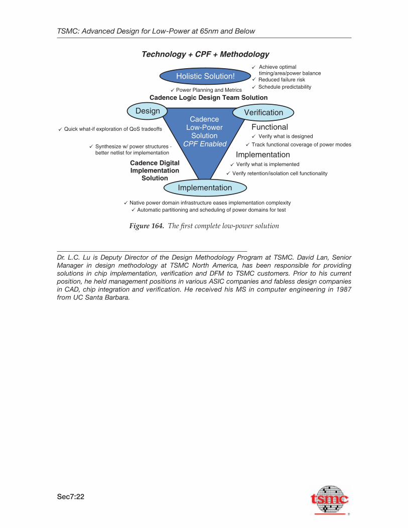
SummarySince2004,TSMCandCadencehaveenjoyedahistoryoflow-powercollaboration,andhavemadesignificanteffortsindevelopingtheCPFstandard.CommonPowerFormatflowautomationdeliversupto2xproductivityimprovementoverpreviousmethods.CPFfacilitatespowerreductionbenefitsfromawidevarietyof power management techniques:
For dynamic power: clock gating, multiple-voltage domains, dynamic voltage •andfrequencyscaling,hierarchicalvoltagewithdualpowerSRAM,andadaptivevoltage scalingFor active leakage power: multi-• Vt, back-biasing, voltage scaling, and source- and back-biasingForstandbyleakagepower:fine-andcoarse-grainpowergating,powershut-•off, and data retention
TSMC and Cadence continue to work together to deliver advanced low-power design capabilities to joint customers in two key ways:
Customers are supported through the TSMC Reference Flow •TSMC libraries enable advanced low-power design techniques used in the •CPF-basedflow
Together,TSMCandCadenceofferthefirstcompletelow-powersolution:technology,combined with methodology, enabled by CPF.
TSMC: Advanced Design for Low-Power at 65nm and Below
Sec7:22
Dr. L.C. Lu is Deputy Director of the Design Methodology Program at TSMC. David Lan, Senior Manager in design methodology at TSMC North America, has been responsible for providing solutions in chip implementation, verification and DFM to TSMC customers. Prior to his current position, he held management positions in various ASIC companies and fabless design companies in CAD, chip integration and verification. He received his MS in computer engineering in 1987 from UC Santa Barbara.
Figure 164. The first complete low-power solution
Holistic Solution!
Design Verification
Implementation
CadenceLow-Power
SolutionCPF Enabled
Achieve optimaltiming/area/power balanceReduced failure riskSchedule predictability
Verify what is designedQuick what-if exploration of QoS tradeoffs
Track functional coverage of power modes
Verify what is implemented
Verify retention/isolation cell functionality
Implementation
Functional
Power Planning and Metrics
¸
¸
¸¸
¸
¸¸
Synthesize w/ power structures -better netlist for implementation
Native power domain infrastructure eases implementation complexityAutomatic partitioning and scheduling of power domains for test
¸
¸
¸
¸
¸
Cadence Logic Design Team Solution
Cadence DigitalImplementation
Solution
Technology + CPF + Methodology