tunnel diode
TRANSCRIPT

Presentation
On Tunnel diode
Submitted To :
Farzana Rahman Mishu
Sr. Lecturer
Department of CSE
University of Development Alternative
Date of Submission: 29/08/2015
Md. Sohel Sarker
UODA
Presented By
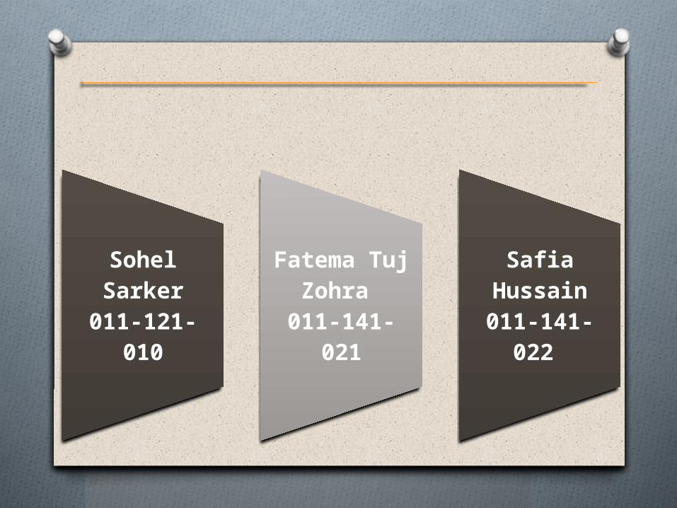
Sohel Sarker
011-121-010
Fatema Tuj Zohra
011-141-021
Safia Hussain 011-141-
022
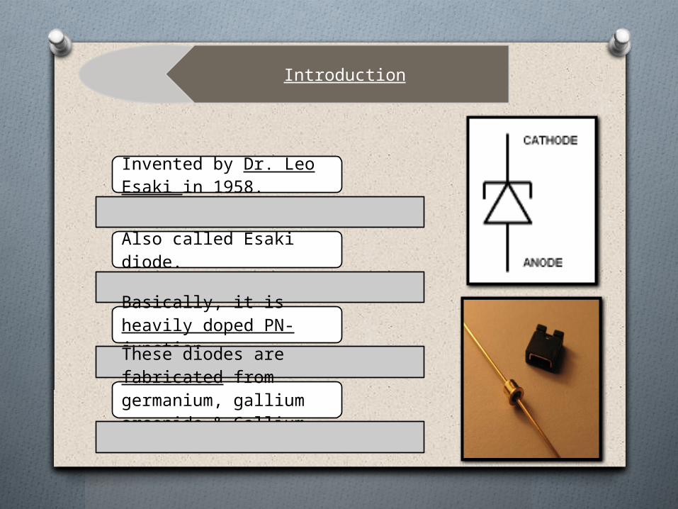
Introduction
Invented by Dr. Leo Esaki in 1958.
Also called Esaki diode.
Basically, it is heavily doped PN- junction.These diodes are fabricated from germanium, gallium arsenide & Gallium Antimonide.

Description
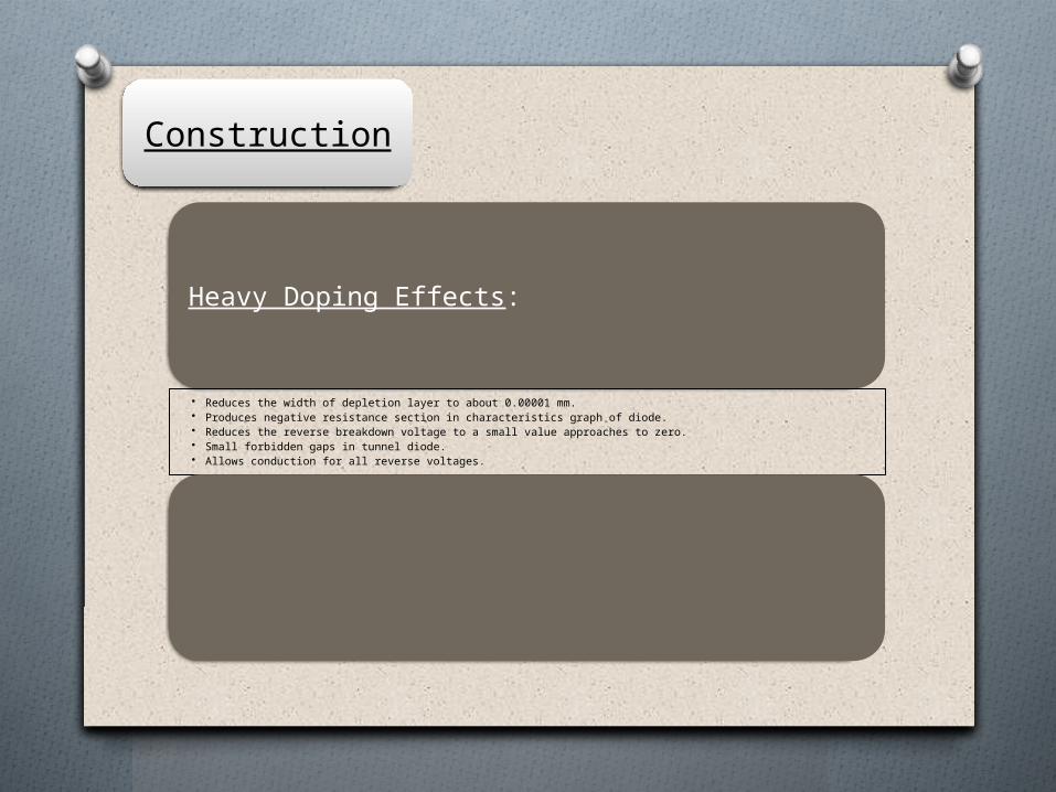
Construction
Heavy Doping Effects:
• Reduces the width of depletion layer to about 0.00001 mm.• Produces negative resistance section in characteristics graph of diode.• Reduces the reverse breakdown voltage to a small value approaches to zero.• Small forbidden gaps in tunnel diode.• Allows conduction for all reverse voltages.
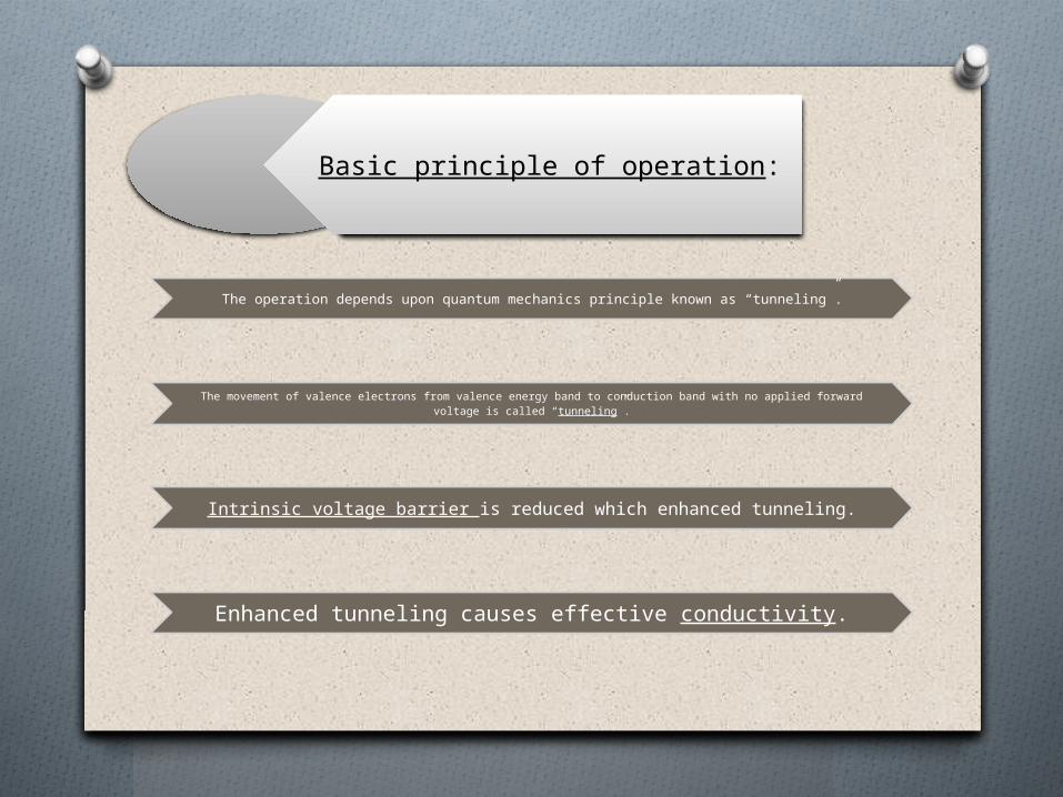
Basic principle of operation:
The operation depends upon quantum mechanics principle known as “tunneling”.
The movement of valence electrons from valence energy band to conduction band with no applied forward voltage is called “tunneling”.
Intrinsic voltage barrier is reduced which enhanced tunneling.
Enhanced tunneling causes effective conductivity.
Working
At first voltage begin to increase, Electrons tunnel through pn junction.Electron and holes states become aligned.
Voltage increases further:States become misaligned. Current drops.Shows negative resistance (V increase, I decrease).
As voltage increase yet further:The diode behave as normal diode.The electrons no longer tunnel through barrier.
Forward Bias operation:
Working(contd.)
The electrons in valence band of p-side tunnel directly towards the
empty states present in the conduction band of n-side.

I/V Characteristics
As forward bias is applied, significant I is produced.
After continuous increase of V, the
current achieves its minimum value called as Valley Current. After
further increase in V, current start increasing as
ordinary diode.
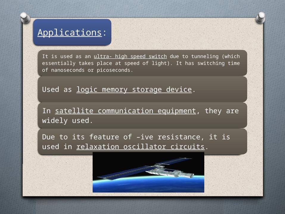
Applications:It is used as an ultra- high speed switch due to tunneling (which essentially takes place at speed of light). It has switching time of nanoseconds or picoseconds.
Used as logic memory storage device.
In satellite communication equipment, they are widely used.
Due to its feature of –ive resistance, it is used in relaxation oscillator circuits.
Applications(contd.):
Tunnel diodes are resistant to the effects of magnetic fields, high temperature and radioactivity. That’s why these can be used in modern military equipments - NMR machines.
Due to low power requirement, they are used in FM receivers.
Thank You