tutorial 2 automatic placement & routinghuihua.huang/index_files/encounter_tutorial_f2012.pdfin...
TRANSCRIPT
Tutorial 2 Automatic Placement & Routing
Please follow the instructions found under Setup on the CADTA main page before starting this tutorial.
1.1. Start Encounter
Log on to NX client using your EE departmental username and password. Go to your Encounter directory by typing:
cd ~/cad/se
Copy your mapping verilog file without header and output LEF file from previous tutorial and via fix pearl code:
cp ~/cad/cadence/your_own.lef .
cp /home/cad/startup/EE6325/aux/addvias.pl .
Source the following link:
. /home/eng/h/hxh025000/public_html/index_files/profile.ic-5_enc
Start the Encounter design environment by typing the following in your Encounter directory: encounter
(MAKE SURE YOU DO NOT RUN THIS IN BACKGROUND!!!)
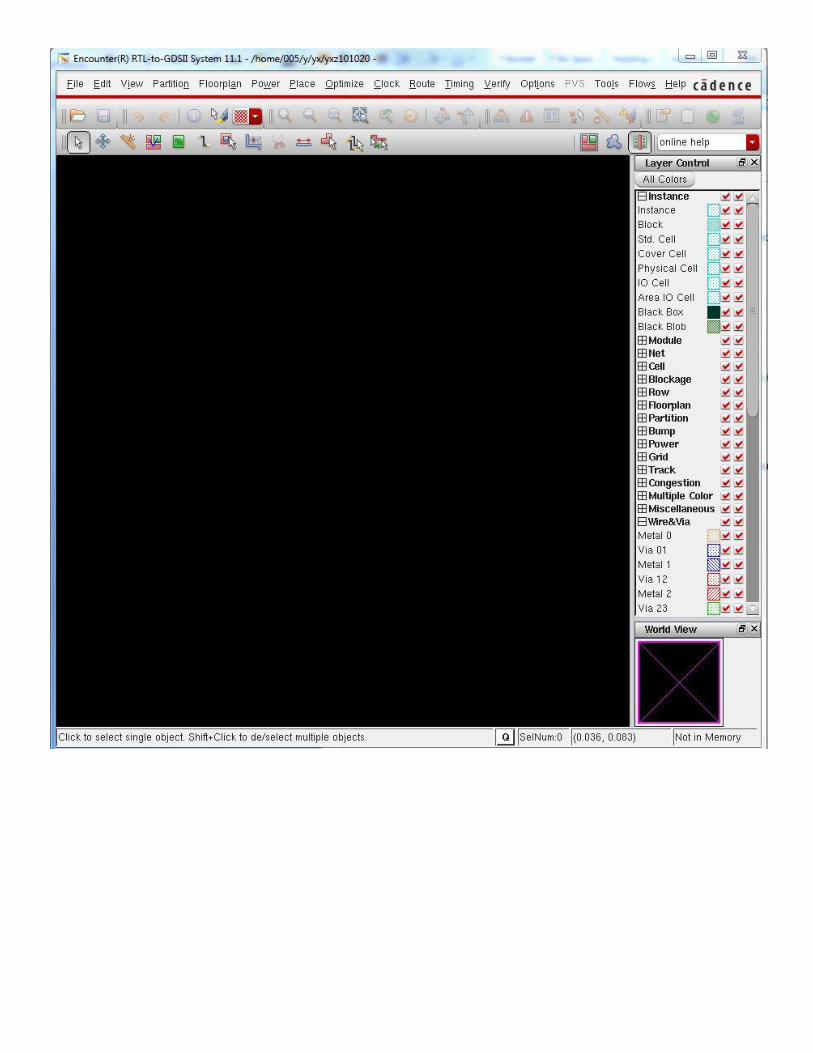

1.2. Import files
Now you can import both your Cadence LEF file (which contains information that Encounter needs regarding your cell library) and your synthesized Verilog netlist (which contains an electrical description of the circuit) into the Silicon Ensemble environment.
In the Encounter GUI, Click File -> Import Design, the Design Import window will pop up.
In the Netlist part, check Verilog option, select your verilog file for, and check Auto Assign option for Top Cell.
In the Technology/Physical Libraries part, check LEF Files option, select your ABSOuput.lef file.
In the Power part, put vdd! and gnd! for Power/Ground Nets and then Click OK
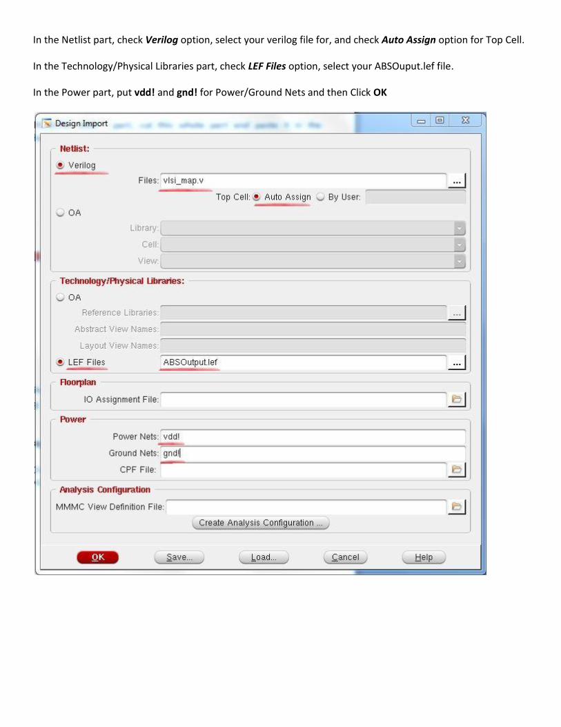
1.3. Floorplanning
Floorplanning is the stage of the design where the area of the design is defined. Two regions exist within the design: the core, which contains the cells arranged in rows, and the I/O area, which contains power and ground rings and I/O pins.
Select Floorplan -> Specify Floorplan to open the floorplanning window. In the Basic tab. Make sure Core Size is set to Aspect Ratio and Aspect Ratio is set to 1.0 (this controls the ratio between height and width of the design). Set the Core to IO Boundary Distance to 20 microns all directions. (If the design has room after routing, you may want to go back and re-run floorplanning with a smaller distance, as this will reduce the area of your design substantially. This will mean however that you will need to re-run all steps after floorplanning as well).
Do NOT click OK now.
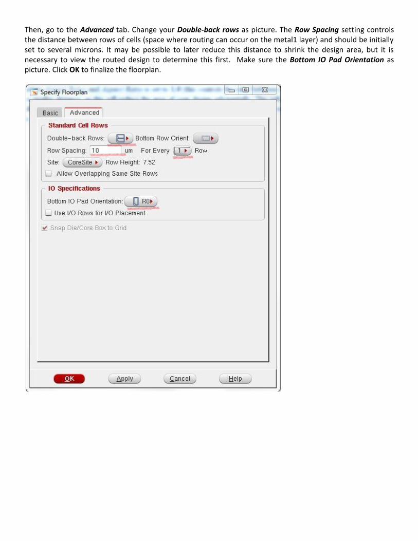
Then, go to the Advanced tab. Change your Double-back rows as picture. The Row Spacing setting controls the distance between rows of cells (space where routing can occur on the metal1 layer) and should be initially set to several microns. It may be possible to later reduce this distance to shrink the design area, but it is necessary to view the routed design to determine this first. Make sure the Bottom IO Pad Orientation as picture. Click OK to finalize the floorplan.
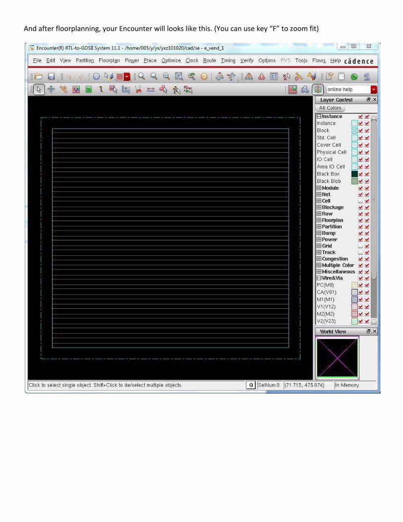
And after floorplanning, your Encounter will looks like this. (You can use key “F” to zoom fit)
1.4. Placement
1.4.1. Place Standard Cells
Once the floorplanning is complete, IO ports and cells need to be placed in the alotted rows.
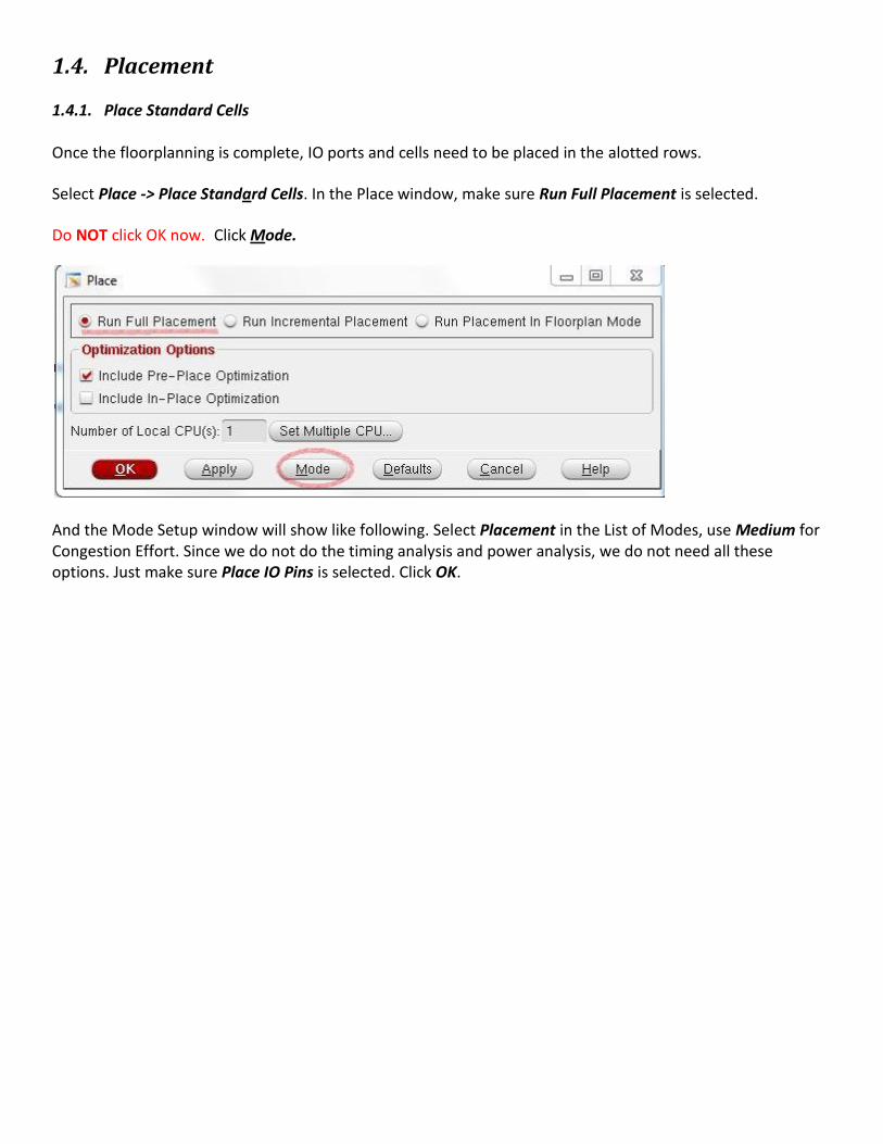
Select Place -> Place Standard Cells. In the Place window, make sure Run Full Placement is selected.
Do NOT click OK now. Click Mode.
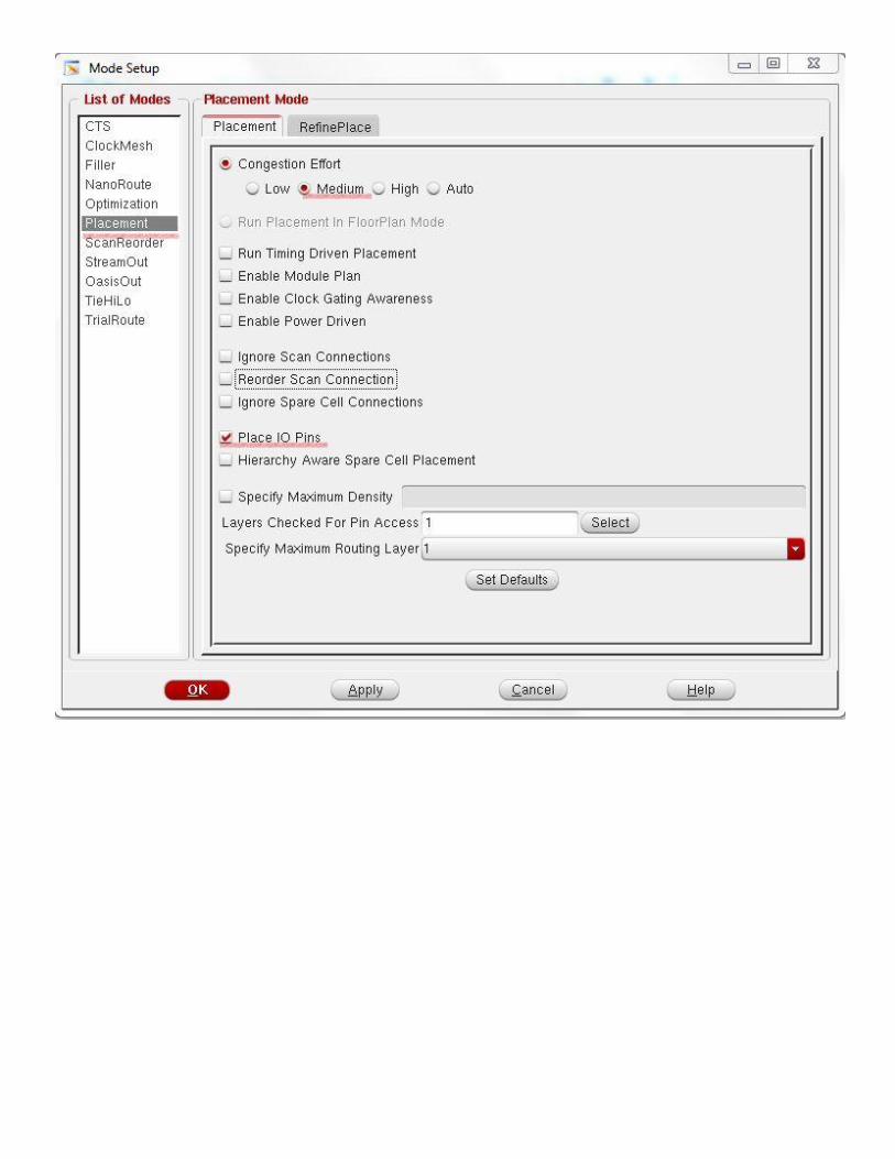
And the Mode Setup window will show like following. Select Placement in the List of Modes, use Medium for Congestion Effort. Since we do not do the timing analysis and power analysis, we do not need all these options. Just make sure Place IO Pins is selected. Click OK.
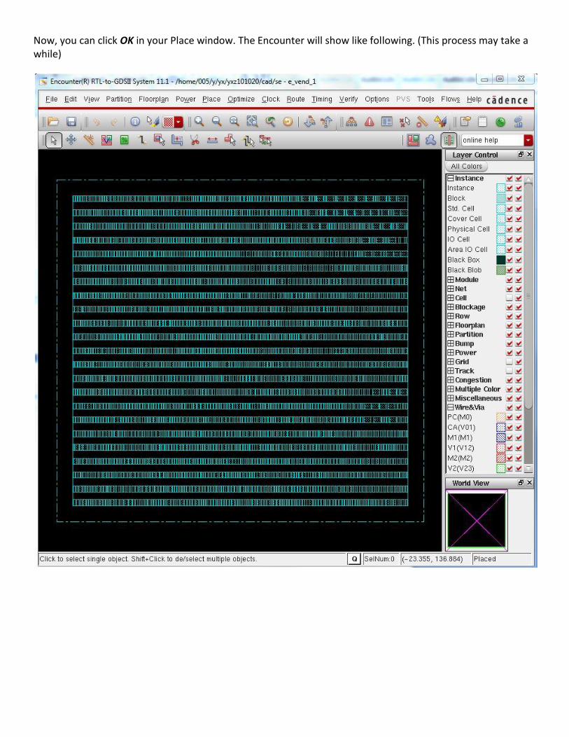
Now, you can click OK in your Place window. The Encounter will show like following. (This process may take a while)
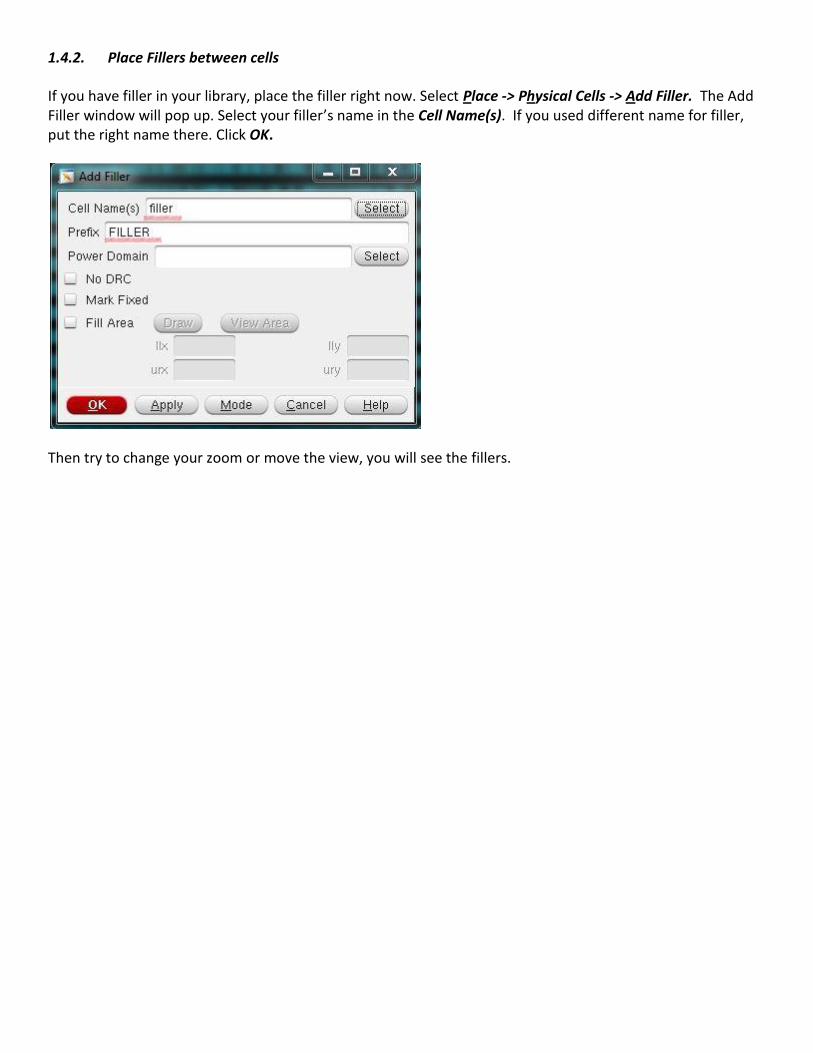
1.4.2. Place Fillers between cells
If you have filler in your library, place the filler right now. Select Place -> Physical Cells -> Add Filler. The Add Filler window will pop up. Select your filler’s name in the Cell Name(s). If you used different name for filler, put the right name there. Click OK.
Then try to change your zoom or move the view, you will see the fillers.
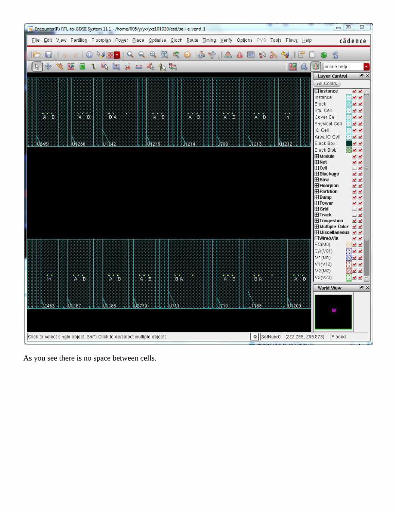
As you see there is no space between cells.
1.5. Power/Ground
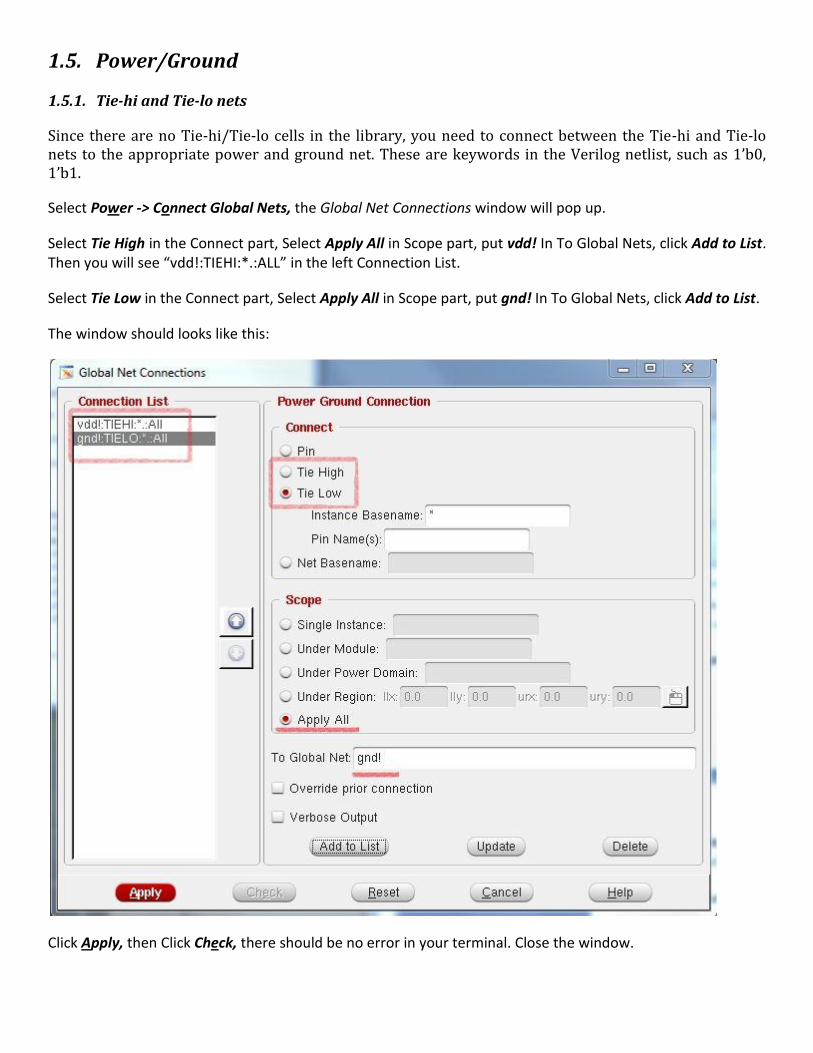
1.5.1. Tie-hi and Tie-lo nets
Since there are no Tie-hi/Tie-lo cells in the library, you need to connect between the Tie-hi and Tie-lo nets to the appropriate power and ground net. These are keywords in the Verilog netlist, such as 1’b0, 1’b1.
Select Power -> Connect Global Nets, the Global Net Connections window will pop up.
Select Tie High in the Connect part, Select Apply All in Scope part, put vdd! In To Global Nets, click Add to List. Then you will see “vdd!:TIEHI:*.:ALL” in the left Connection List.
Select Tie Low in the Connect part, Select Apply All in Scope part, put gnd! In To Global Nets, click Add to List.
The window should looks like this:
Click Apply, then Click Check, there should be no error in your terminal. Close the window.
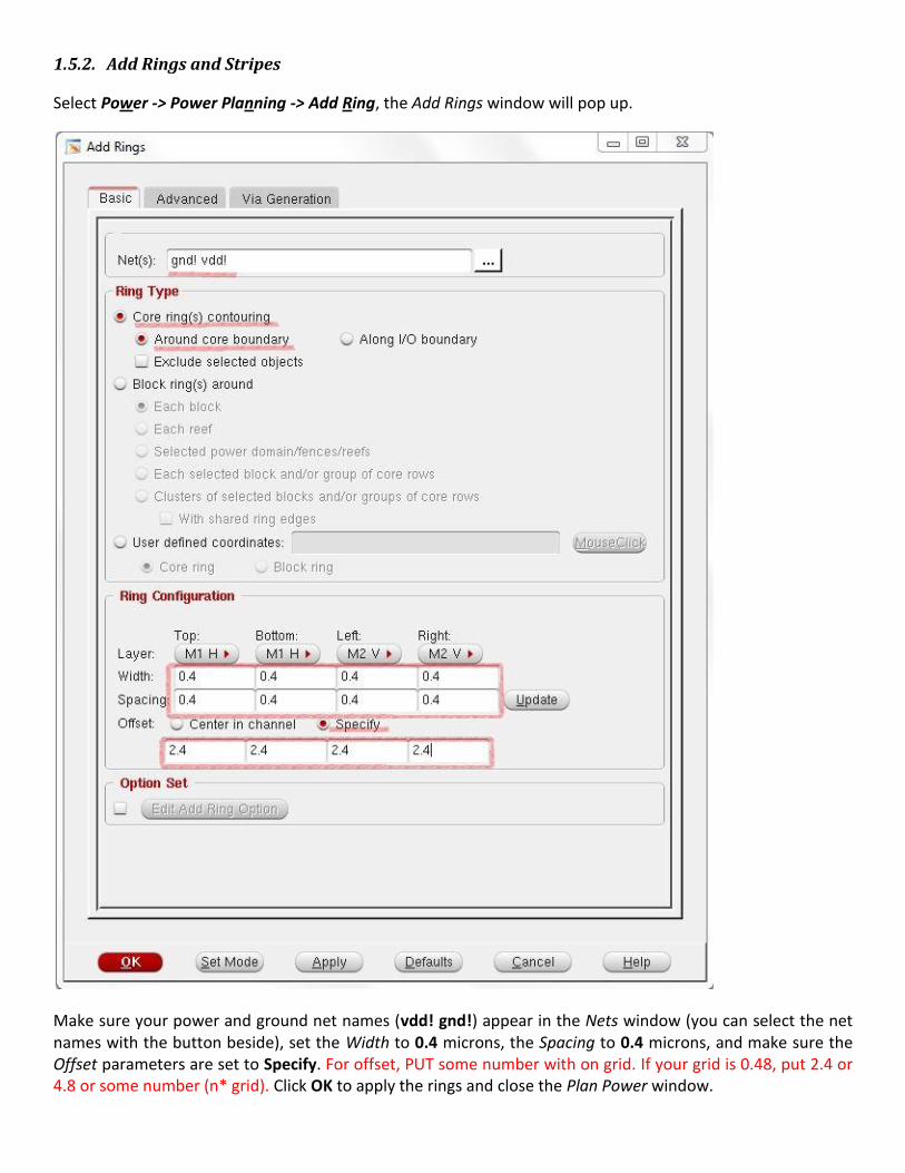
1.5.2. Add Rings and Stripes
Select Power -> Power Planning -> Add Ring, the Add Rings window will pop up.
Make sure your power and ground net names (vdd! gnd!) appear in the Nets window (you can select the net names with the button beside), set the Width to 0.4 microns, the Spacing to 0.4 microns, and make sure the Offset parameters are set to Specify. For offset, PUT some number with on grid. If your grid is 0.48, put 2.4 or 4.8 or some number (n* grid). Click OK to apply the rings and close the Plan Power window.
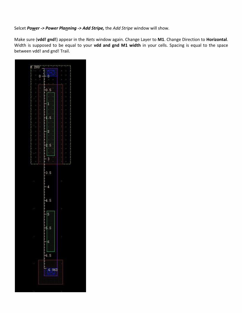
Selcet Power -> Power Planning -> Add Stripe, the Add Stripe window will show.
Make sure (vdd! gnd!) appear in the Nets window again. Change Layer to M1. Change Direction to Horizontal. Width is supposed to be equal to your vdd and gnd M1 width in your cells. Spacing is equal to the space between vdd! and gnd! Trail.
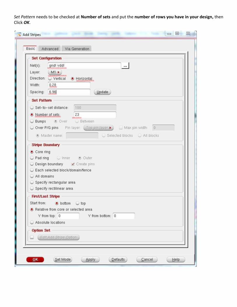
Set Pattern needs to be checked at Number of sets and put the number of rows you have in your design, then Click OK.
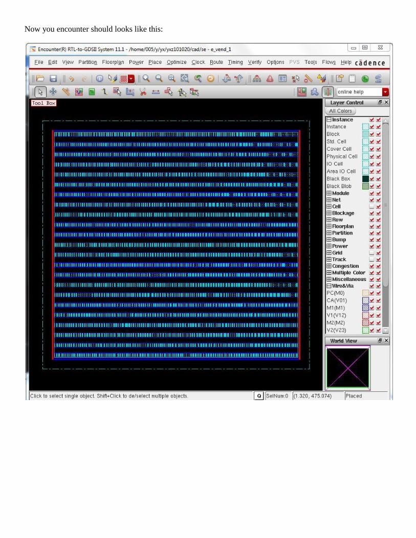
Now you encounter should looks like this:
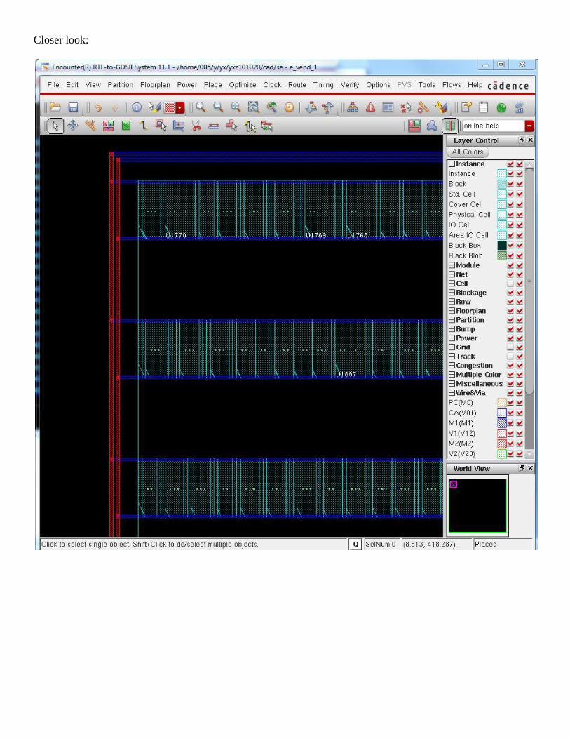
Closer look:
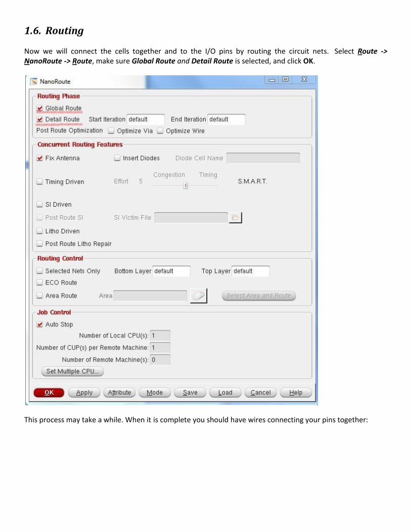
1.6. Routing
Now we will connect the cells together and to the I/O pins by routing the circuit nets. Select Route -> NanoRoute -> Route, make sure Global Route and Detail Route is selected, and click OK.
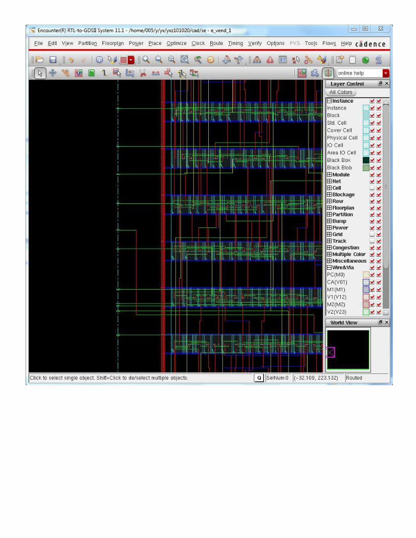
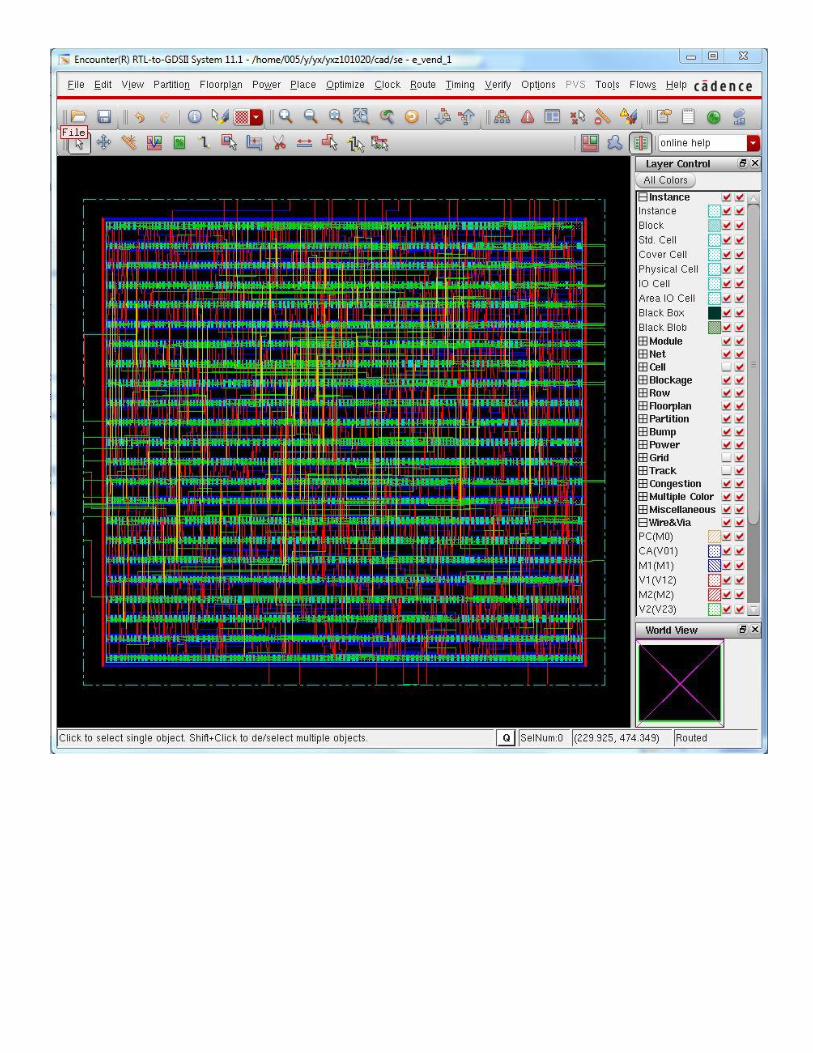
This process may take a while. When it is complete you should have wires connecting your pins together:
1.7. Export files
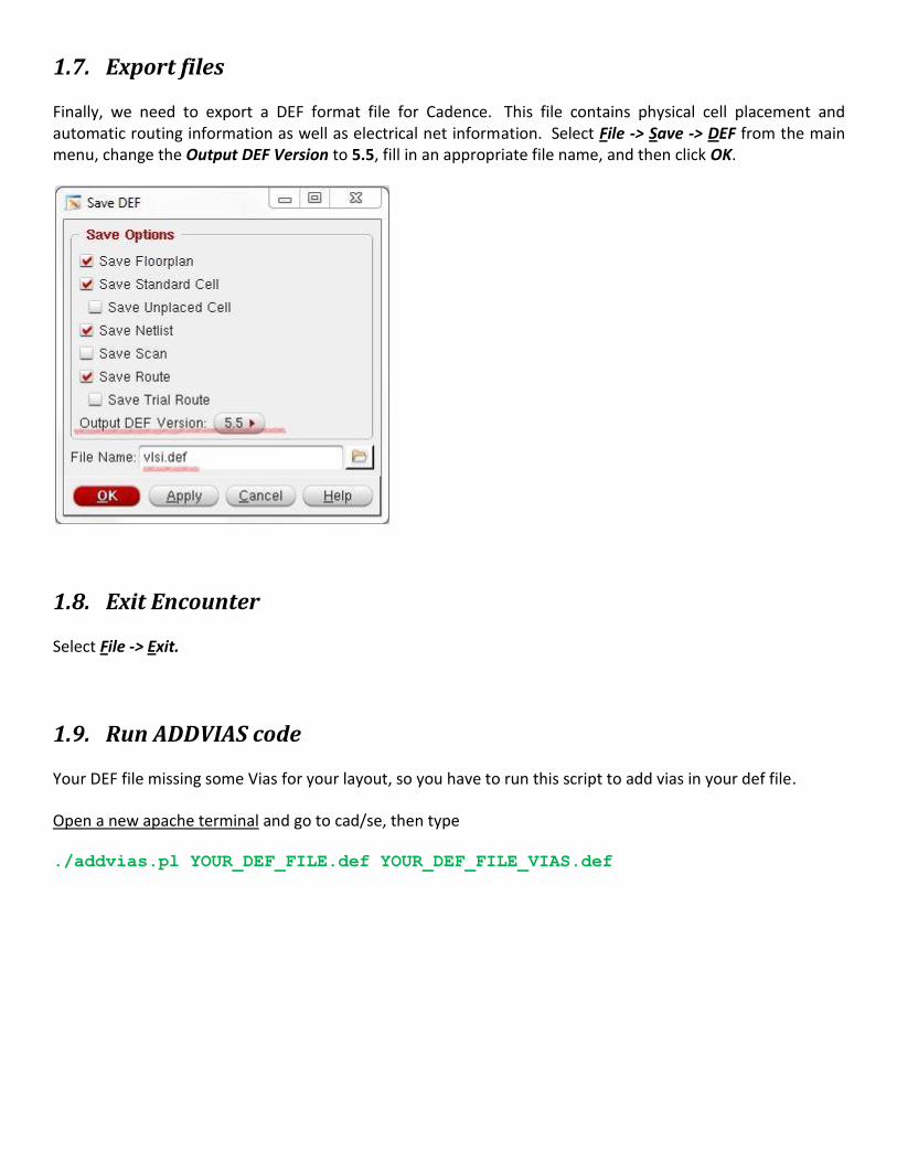
Finally, we need to export a DEF format file for Cadence. This file contains physical cell placement and automatic routing information as well as electrical net information. Select File -> Save -> DEF from the main menu, change the Output DEF Version to 5.5, fill in an appropriate file name, and then click OK.
1.8. Exit Encounter
Select File -> Exit.
1.9. Run ADDVIAS code
Your DEF file missing some Vias for your layout, so you have to run this script to add vias in your def file.
Open a new apache terminal and go to cad/se, then type
./addvias.pl YOUR_DEF_FILE.def YOUR_DEF_FILE_VIAS.def