tutorial 5 creating your own components
TRANSCRIPT
8/6/2019 Tutorial 5 Creating Your Own Components
http://slidepdf.com/reader/full/tutorial-5-creating-your-own-components 1/5
TutorialsCreating your own components
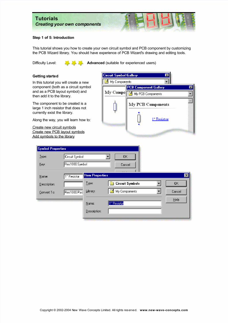
This tutorial shows you how to create your own circuit symbol and PCB component by customizing
the PCB Wizard library. You should have experience of PCB Wizard's drawing and editing tools.
Difficulty Level: Advanced (suitable for experienced users)
Getting started
In this tutorial you will create a new
component (both as a circuit symbol
and as a PCB layout symbol) and
then add it to the library.
The component to be created is a
large 1 inch resistor that does not
currently exist the library.
Along the way, you will learn how to:
Create new circuit symbols
Create new PCB layout symbols
Add symbols to the library
Step 1 of 5: Introduction
Copyright © 2002-2004 New Wave Concepts Limited. All rights reserved. www.new-wave-concepts.com

8/6/2019 Tutorial 5 Creating Your Own Components
http://slidepdf.com/reader/full/tutorial-5-creating-your-own-components 2/5
TutorialsCreating your own components
Step 2 of 5: Creating the circuit symbol
The first step is to create the circuit symbol for the new component.
Using the drawing tools in the Insert | Picture menu, draw a
resistor shape using a rectangle and two vertical lines.
Next, select all three of these objects and then choose Circuit
Diagram from the Edit | Layer menu. This will place each
object on the layer used for circuit diagram drawing.
With the shape drawn, you need to specify exactly where the
connection points are on the symbol. This is done by placing
pins on the symbol.
Choose Insert Pin from the Edit | Symbol menu and then
click on the top of the upper-most vertical line. A window will
appear allowing you to specify the pin number. Enter a pinnumber of 1 and then click on the OK button.
Add a second pin at the bottom of the bottom-most vertical line
with the number 2. It should now look as shown opposite.
Type determines what category of symbol is created. Ensure
that Circuit Symbol is selected.
Key is a unique identifier that will be used by the software toaccess the symbol. The Key field is normally based on the
name of the symbol being created. In this example the value
Res1000.Symbol is used (since it is a 1 inch, or 1000 mil,
resistor circuit symbol).
Name and Description are used to describe the symbol being
created. Enter the name 1" Resistor .
Convert To specifies which PCB layout symbol should be
used when this circuit symbol is converting into a PCB layout.
This is done by entering the same value here as in the Key
field of the appropriate PCB symbol. As this symbol is to be
linked to an equivalent PCB symbol, you should enter a valueof Res1000.Package.
Finally click OK to create the circuit symbol.
Step 1: Drawing the circuit
symbol shape.
Step 2: Adding
the pins.
Step 3: Making
the symbol.
The symbol is now ready to be created. Select all of the symbol objects (including the pins) and
choose Make Symbol from the Edit | Symbol menu.
A window will appear in
which you can specify a
range of properties for the
symbol. Complete the fields
as shown on the left.
Tip! You need to
remember which Key
values you have used
when creating your own
circuit and PCB layoutsymbols.
Copyright © 2002-2004 New Wave Concepts Limited. All rights reserved. www.new-wave-concepts.com
1
2

8/6/2019 Tutorial 5 Creating Your Own Components
http://slidepdf.com/reader/full/tutorial-5-creating-your-own-components 3/5
TutorialsCreating your own components
Step 3 of 5: Creating the PCB layout symbol
With the circuit symbol created, you can now create the associated PCB layout symbol. This
process follows much the same approach as for creating circuit symbols.
Draw two pads and then a rectangle (the rectangle tool can be
found in the Insert | Picture menu) to represent the body of
the resistor. The pads should be 1 inch apart (using a grid
spacing of 0.1 inch will help with this).
Next, select the rectangle and choose Silk Screen from the
Edit | Layer menu. This will place the package outline on the
component-side silk screen layer.
Note: If you want to include a real-world view of the component
you should do it at this point. Using the drawing tools draw how
the component would look (remembering to ensure that these
drawn objects are placed on the Real Components layer).
With the shape drawn, you need to specify exactly where the
connection points are on the symbol. This is done by placing
pins on the symbol.
Choose Insert Pin from the Edit | Symbol menu and then
click in the centre of the top-most pad. A window will appear
allowing you to specify the pin number. Enter a pin number of 1
and then click on the OK button.
Add a second pin on top of the bottom-most pad with the
number 2. It should now look as shown opposite.
Step 1: Drawing
the PCB layout
symbol shape.
Step 2: Adding the pins.
The PCB layout symbol is now ready to be created. Select all of the symbol objects (including thepins) and choose Make Symbol from the Edit | Symbol menu.
A window will appear in
which you can specify a
range of properties for the
symbol. Complete the fields
as shown on the left.
Step 3: Making
the symbol.
Type determines what category of symbol is created. Ensure
that PCB Component is selected.
Key is a unique identifier that will be used by the software to
access the symbol. The Key field should match the value
entered into the Convert To field on the circuit symbol. For
this symbol enter a value of Res1000.Package.
Name and Description are used to describe the symbol being
created. Enter the name 1" Resistor .The Convert To option only applies to circuit symbols and is
therefore disabled. You can ignore this field.
Finally click OK to create the PCB layout symbol.
Copyright © 2002-2004 New Wave Concepts Limited. All rights reserved. www.new-wave-concepts.com
1
2

8/6/2019 Tutorial 5 Creating Your Own Components
http://slidepdf.com/reader/full/tutorial-5-creating-your-own-components 4/5
TutorialsCreating your own components
Step 4 of 5: Adding the symbols to the library
Now that both symbols have been created, you need to add them to the library.
Starting with the circuit symbol,a new library needs to be
created. Choose New Library
from the Tools | Library menu.
In the window that appears
enter My Components as the
name, select Circuit Symbols
as the Type and then click on
the OK button.Next select the circuit symbol
created earlier and choose
Add to Library from the Tools
| Library menu.
Another window will appear.
Ensure that the new My
Components library has been
selected and then click on the
OK button.
Once done you will see the
symbol appear in the gallery.
A second library needs to be
created for the PCB layout
symbol. Choose New Library
from the Tools | Library menu.
In the window that appears
enter My PCB Components as
the name, select PCB
Componentsas the Type and
then click on the OK button.Next select the PCB layout
symbol created earlier and
choose Add to Library from
the Tools | Library menu.
Another window will appear.
Ensure that the new My PCB
Components library has been
selected and then click on the
OK button.
Once done you will see the
symbol appear in the gallery.
This process is then repeated for the PCB layout symbol.
Copyright © 2002-2004 New Wave Concepts Limited. All rights reserved. www.new-wave-concepts.com
8/6/2019 Tutorial 5 Creating Your Own Components
http://slidepdf.com/reader/full/tutorial-5-creating-your-own-components 5/5
TutorialsCreating your own components
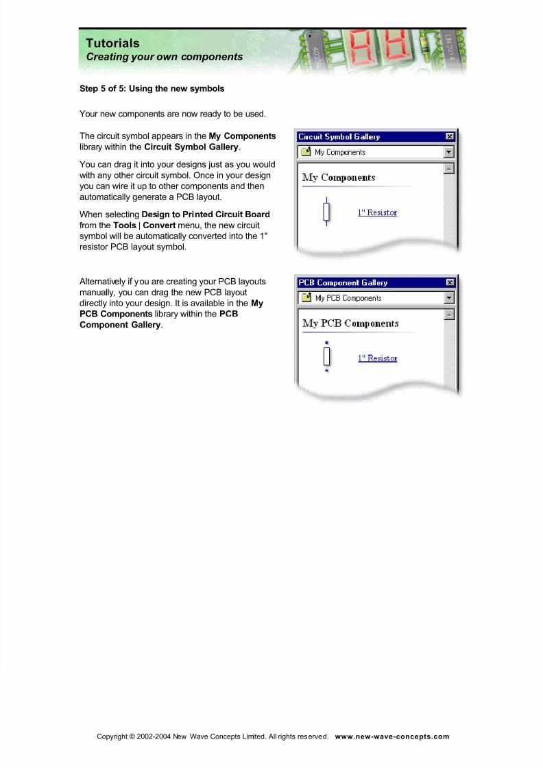
Step 5 of 5: Using the new symbols
Your new components are now ready to be used.
The circuit symbol appears in the My Components library within the Circuit Symbol Gallery.
You can drag it into your designs just as you would
with any other circuit symbol. Once in your design
you can wire it up to other components and then
automatically generate a PCB layout.
When selecting Design to Printed Circuit Board
from the Tools | Convert menu, the new circuit
symbol will be automatically converted into the 1"
resistor PCB layout symbol.
Alternatively if you are creating your PCB layouts
manually, you can drag the new PCB layout
directly into your design. It is available in the My
PCB Components library within the PCB
Component Gallery.
Copyright © 2002-2004 New Wave Concepts Limited. All rights reserved. www.new-wave-concepts.com