txb0108 8-bit bidirectional voltage-level translator …€¢ desktop pc bga microstar 2.50 mm x...
TRANSCRIPT
Product
Folder
Sample &Buy
Technical
Documents
Tools &
Software
Support &Community
TXB0108SCES643F –NOVEMBER 2006–REVISED NOVEMBER 2014
TXB0108 8-Bit Bidirectional Voltage-Level Translator with Auto-Direction Sensing and±15-kV ESD Protection
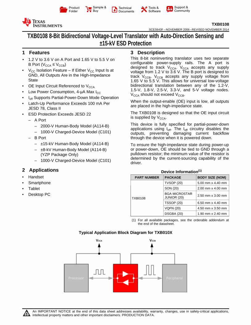
1 Features 3 DescriptionThis 8-bit noninverting translator uses two separate
1• 1.2 V to 3.6 V on A Port and 1.65 V to 5.5 V onconfigurable power-supply rails. The A port isB Port (VCCA ≤ VCCB)designed to track VCCA. VCCA accepts any supply
• VCC Isolation Feature – If Either VCC Input Is at voltage from 1.2 V to 3.6 V. The B port is designed toGND, All Outputs Are in the High-Impedance track VCCB. VCCB accepts any supply voltage fromState 1.65 V to 5.5 V. This allows for universal low-voltage
bidirectional translation between any of the 1.2-V,• OE Input Circuit Referenced to VCCA1.5-V, 1.8-V, 2.5-V, 3.3-V, and 5-V voltage nodes.• Low Power Consumption, 4-μA Max ICC VCCA should not exceed VCCB.
• Ioff Supports Partial-Power-Down Mode OperationWhen the output-enable (OE) input is low, all outputs• Latch-Up Performance Exceeds 100 mA Per are placed in the high-impedance state.JESD 78, Class IIThe TXB0108 is designed so that the OE input circuit• ESD Protection Exceeds JESD 22is supplied by VCCA.
– A PortThis device is fully specified for partial-power-down– 2000-V Human-Body Model (A114-B)applications using Ioff. The Ioff circuitry disables the
– 1000-V Charged-Device Model (C101) outputs, preventing damaging current backflowthrough the device when it is powered down.– B Port
– ±15-kV Human-Body Model (A114-B) To ensure the high-impedance state during power-upor power-down, OE should be tied to GND through a– ±8-kV Human-Body Model (A114-B)pulldown resistor; the minimum value of the resistor is(YZP Package Only)determined by the current-sourcing capability of the– 1000-V Charged-Device Model (C101) driver.
2 Applications Device Information(1)
• Handset PART NUMBER PACKAGE BODY SIZE (NOM)TVSOP (20) 5.00 mm x 4.40 mm• SmartphoneSON (20) 2.00 mm x 4.00 mm• TabletBGA MICROSTAR• Desktop PC 2.50 mm x 3.00 mmJUNIOR (20)TXB0108TSSOP (20) 6.50 mm x 4.40 mmVQFN (20) 4.50 mm x 3.50 mmDSGBA (20) 1.90 mm x 2.40 mm
(1) For all available packages, see the orderable addendum atthe end of the datasheet.
Typical Application Block Diagram for TXB010X
1
An IMPORTANT NOTICE at the end of this data sheet addresses availability, warranty, changes, use in safety-critical applications,intellectual property matters and other important disclaimers. PRODUCTION DATA.
TXB0108SCES643F –NOVEMBER 2006–REVISED NOVEMBER 2014 www.ti.com
Table of Contents6.16 Operating Characteristics........................................ 91 Features .................................................................. 16.17 Typical Characteristics .......................................... 102 Applications ........................................................... 1
7 Parameter Measurement Information ................ 113 Description ............................................................. 18 Detailed Description ............................................ 124 Revision History..................................................... 2
8.1 Overview ................................................................. 125 Pin Configuration and Functions ......................... 38.2 Functional Block Diagram ....................................... 126 Specifications......................................................... 58.3 Feature Description................................................. 136.1 Absolute Maximum Ratings ..................................... 58.4 Device Functional Modes........................................ 146.2 Handling Ratings....................................................... 5
9 Application and Implementation ........................ 156.3 Recommended Operating Conditions ...................... 59.1 Application Information............................................ 156.4 Thermal Information .................................................. 69.2 Typical Application ................................................. 156.5 Electrical Characteristics .......................................... 6
10 Power Supply Recommendations ..................... 176.6 Timing Requirements: VCCA = 1.2 V ......................... 711 Layout................................................................... 176.7 Timing Requirements: VCCA = 1.5 V ± 0.1 V ............ 7
11.1 Layout Guidelines ................................................. 176.8 Timing Requirements: VCCA = 1.8 V ± 0.15 V .......... 711.2 Layout Example .................................................... 176.9 Timing Requirements: VCCA = 2.5 V ± 0.2 V ............ 7
6.10 Timing Requirements: VCCA = 3.3 V ± 0.3 V .......... 7 12 Device and Documentation Support ................. 186.11 Switching Characteristics: VCCA = 1.2 V ................. 7 12.1 Trademarks ........................................................... 186.12 Switching Characteristics: VCCA = 1.5 V ± 0.1 V .... 8 12.2 Electrostatic Discharge Caution............................ 186.13 Switching Characteristics: VCCA = 1.8 V ± 0.15 V .. 8 12.3 Glossary ................................................................ 186.14 Switching Characteristics: VCCA = 2.5 V ± 0.2 V .... 8 13 Mechanical, Packaging, and Orderable
Information ........................................................... 186.15 Switching Characteristics: VCCA = 3.3 V ± 0.3 V .... 9
4 Revision HistoryNOTE: Page numbers for previous revisions may differ from page numbers in the current version.
Changes from Revision E (April 2012) to Revision F Page
• Added Pin Configuration and Functions section, Handling Rating table, Feature Description section, DeviceFunctional Modes, Application and Implementation section, Power Supply Recommendations section, Layoutsection, Device and Documentation Support section, and Mechanical, Packaging, and Orderable Informationsection ................................................................................................................................................................................... 1
• Changed VOLA value 0.9 to 0.3 .............................................................................................................................................. 6
Changes from Revision D (September 2011) to Revision E Page
• Added notes to pin out graphics............................................................................................................................................. 3
Changes from Revision C (August 2011) to Revision D Page
• Added ±8-kV Human-Body Model (A114-B) (YZP Package Only) to Features ..................................................................... 1
2 Submit Documentation Feedback Copyright © 2006–2014, Texas Instruments Incorporated
Product Folder Links: TXB0108

GXY OR ZXY PACKAGE(BOTTOM VIEW)
A
B
C
D
21 3 4 5
20
19
16
15
14
13
1
2
5
6
7
8
PW PACKAGE(TOP VIEW)
18
17
12
11
3
4
9
10
RGY PACKAGE(TOP VIEW)
YZP PACKAGE(BALL SIDE VIEW)
1 20
10 11
2
3
4
5
6
7
8
9
19
18
17
16
15
14
13
12
VCCB
B2
B3
B4
B5
B6
B7
B8
VCCA
A2
A3
A4
A5
A6
A7
A8
GN
DB
1
A1
OE
VCCB
B2
B3
B4
B5
B6
B7
B8
GND
VCCA
A1
A2
A3
A4
A5
A6
A7
A8
OE
B1B1
B2
B3
B4
A2
A3
A4
1
2
3
4
20
19
18
17
VCCB
GND
B5
B6
OE
A5
A6
5
6
7
8
16
15
14
13
B7
B8
A7
A8
9
10
12
11
A1
VCCA
DQS PACKAGE(TOP VIEW)
B6 B8 A8 A6
GND B7 A7 OE
VCCB
B5 A5 VCCA
B4 B3 A3 A4
B2 B1 A1 A2
1 2 3 4
E
D
C
B
A
TXB0108www.ti.com SCES643F –NOVEMBER 2006–REVISED NOVEMBER 2014
5 Pin Configuration and Functions
Note: For the RGY package, the exposed center thermal pad must be connected to ground.A. Pullup resistors are not required on both sides for Logic I/O.B. If pullup or pulldown resistors are needed, the resistor value must be over 50 kΩ.C. 50 kΩ is a safe recommended value, if the customer can accept higher VOL or lower VOH, smaller pullup or pulldown
resistor is allowed, the draft estimation is VOL = VCCOUT × 4.5 k/(4.5 k + RPU) and VOH = VCCOUT × RDW/(4.5 k + RDW).D. If pullup resistors are needed, please refer to the TXS0108 or contact TI.E. For detailed information, please refer to application note SCEA043.
Pin FunctionsPIN
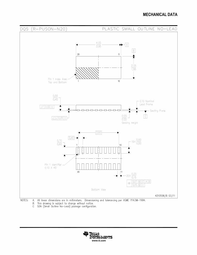
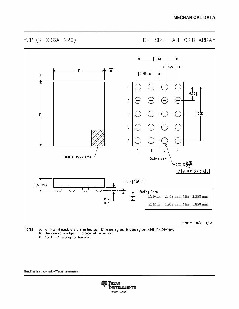
I/O (1) FUNCTIONNAME PW, RGY NO. DQS NO. YZP NO.
A1 1 1 A3 I/O Input/output 1. Referenced to VCCA.
VCCA 2 5 C4 S A-port supply voltage. 1.1 V ≤ VCCA ≤ 3.6 V, VCCA ≤ VCCB.
A2 3 2 A4 I/O Input/output 2. Referenced to VCCA.
A3 4 3 B3 I/O Input/output 3. Referenced to VCCA.
A4 5 4 B4 I/O Input/output 4. Referenced to VCCA.
A5 6 7 C3 I/O Input/output 5. Referenced to VCCA.
A6 7 8 E4 I/O Input/output 6. Referenced to VCCA.
A7 8 9 D3 I/O Input/output 7. Referenced to VCCA.
A8 9 10 E3 I/O Input/output 8. Referenced to VCCA.
OE 10 6 D4 I Output enable. Pull OE low to place all outputs in 3-state mode. Referenced to VCCA.
GND 11 15 D1 S Ground
B8 12 11 E2 I/O Input/output 8. Referenced to VCCB.
B7 13 12 D2 I/O Input/output 7. Referenced to VCCB.
B6 14 13 E1 I/O Input/output 6. Referenced to VCCB.
B5 15 14 C2 I/O Input/output 5. Referenced to VCCB.
(1) I = input, O = output, I/O = input and output, S = power supply
Copyright © 2006–2014, Texas Instruments Incorporated Submit Documentation Feedback 3
Product Folder Links: TXB0108
TXB0108SCES643F –NOVEMBER 2006–REVISED NOVEMBER 2014 www.ti.com
Pin Functions (continued)PIN
I/O (1) FUNCTIONNAME PW, RGY NO. DQS NO. YZP NO.
B4 16 17 B1 I/O Input/output 4. Referenced to VCCB.
B3 17 18 B2 I/O Input/output 3. Referenced to VCCB.
B2 18 19 A1 I/O Input/output 2. Referenced to VCCB.
VCCB 19 16 C1 S B-port supply voltage. 1.65 V ≤ VCCB ≤ 5.5 V.
B1 20 20 A2 I/O Input/output 1. Referenced to VCCB.
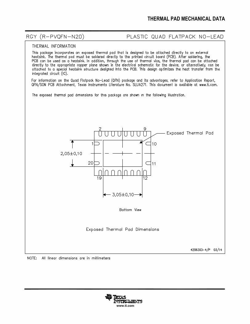
Thermal — — For the RGY package, the exposed center thermal pad must be connected to ground.Pad
Pin Assignments (20-Ball GXY/ZXY Package)1 2 3 4 5
D VCCB B2 B4 B6 B8C B1 B3 B5 B7 GNDB A1 A3 A5 A7 OEA VCCA A2 A4 A6 A8
4 Submit Documentation Feedback Copyright © 2006–2014, Texas Instruments Incorporated
Product Folder Links: TXB0108
TXB0108www.ti.com SCES643F –NOVEMBER 2006–REVISED NOVEMBER 2014
6 Specifications
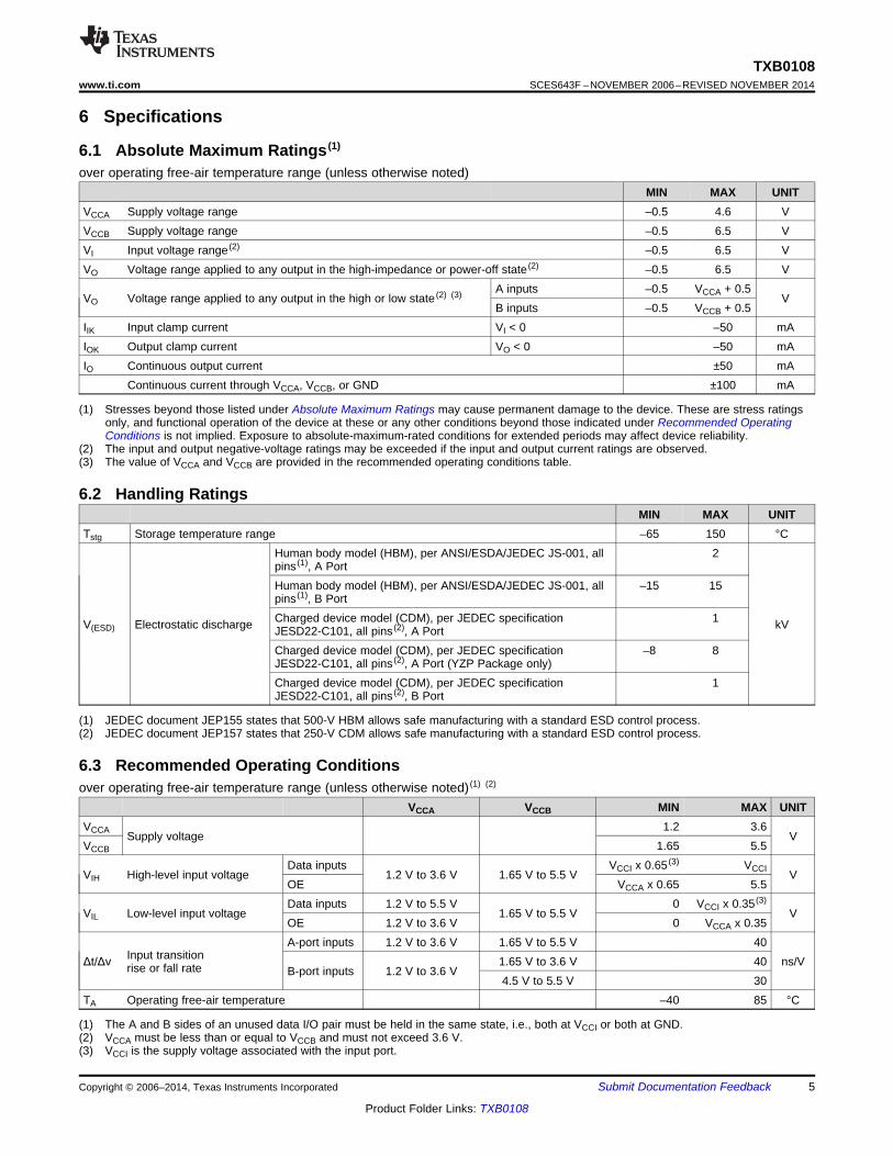
6.1 Absolute Maximum Ratings (1)
over operating free-air temperature range (unless otherwise noted)MIN MAX UNIT
VCCA Supply voltage range –0.5 4.6 VVCCB Supply voltage range –0.5 6.5 VVI Input voltage range (2) –0.5 6.5 VVO Voltage range applied to any output in the high-impedance or power-off state (2) –0.5 6.5 V
A inputs –0.5 VCCA + 0.5VO Voltage range applied to any output in the high or low state (2) (3) V
B inputs –0.5 VCCB + 0.5IIK Input clamp current VI < 0 –50 mAIOK Output clamp current VO < 0 –50 mAIO Continuous output current ±50 mA
Continuous current through VCCA, VCCB, or GND ±100 mA
(1) Stresses beyond those listed under Absolute Maximum Ratings may cause permanent damage to the device. These are stress ratingsonly, and functional operation of the device at these or any other conditions beyond those indicated under Recommended OperatingConditions is not implied. Exposure to absolute-maximum-rated conditions for extended periods may affect device reliability.
(2) The input and output negative-voltage ratings may be exceeded if the input and output current ratings are observed.(3) The value of VCCA and VCCB are provided in the recommended operating conditions table.
6.2 Handling RatingsMIN MAX UNIT
Tstg Storage temperature range –65 150 °CHuman body model (HBM), per ANSI/ESDA/JEDEC JS-001, all 2pins (1), A PortHuman body model (HBM), per ANSI/ESDA/JEDEC JS-001, all –15 15pins (1), B PortCharged device model (CDM), per JEDEC specification 1V(ESD) Electrostatic discharge kVJESD22-C101, all pins (2), A PortCharged device model (CDM), per JEDEC specification –8 8JESD22-C101, all pins (2), A Port (YZP Package only)Charged device model (CDM), per JEDEC specification 1JESD22-C101, all pins (2), B Port
(1) JEDEC document JEP155 states that 500-V HBM allows safe manufacturing with a standard ESD control process.(2) JEDEC document JEP157 states that 250-V CDM allows safe manufacturing with a standard ESD control process.
6.3 Recommended Operating Conditionsover operating free-air temperature range (unless otherwise noted) (1) (2)
VCCA VCCB MIN MAX UNITVCCA 1.2 3.6
Supply voltage VVCCB 1.65 5.5
Data inputs VCCI x 0.65 (3) VCCIVIH High-level input voltage 1.2 V to 3.6 V 1.65 V to 5.5 V VOE VCCA x 0.65 5.5Data inputs 1.2 V to 5.5 V 0 VCCI x 0.35 (3)
VIL Low-level input voltage 1.65 V to 5.5 V VOE 1.2 V to 3.6 V 0 VCCA x 0.35A-port inputs 1.2 V to 3.6 V 1.65 V to 5.5 V 40
Input transitionΔt/Δv 1.65 V to 3.6 V 40 ns/Vrise or fall rate B-port inputs 1.2 V to 3.6 V4.5 V to 5.5 V 30
TA Operating free-air temperature –40 85 °C
(1) The A and B sides of an unused data I/O pair must be held in the same state, i.e., both at VCCI or both at GND.(2) VCCA must be less than or equal to VCCB and must not exceed 3.6 V.(3) VCCI is the supply voltage associated with the input port.
Copyright © 2006–2014, Texas Instruments Incorporated Submit Documentation Feedback 5
Product Folder Links: TXB0108
TXB0108SCES643F –NOVEMBER 2006–REVISED NOVEMBER 2014 www.ti.com
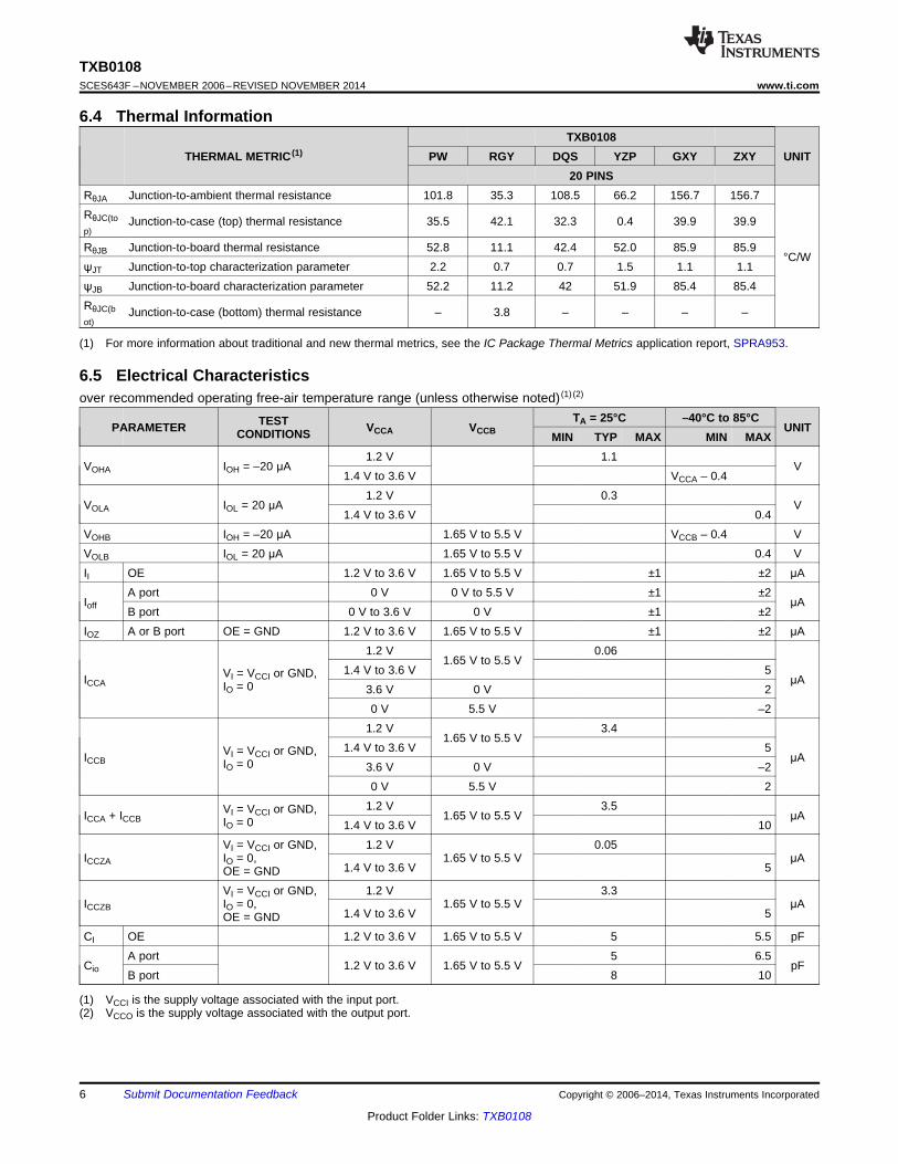
6.4 Thermal InformationTXB0108
THERMAL METRIC (1) PW RGY DQS YZP GXY ZXY UNIT20 PINS
RθJA Junction-to-ambient thermal resistance 101.8 35.3 108.5 66.2 156.7 156.7RθJC(to Junction-to-case (top) thermal resistance 35.5 42.1 32.3 0.4 39.9 39.9p)
RθJB Junction-to-board thermal resistance 52.8 11.1 42.4 52.0 85.9 85.9°C/W
ψJT Junction-to-top characterization parameter 2.2 0.7 0.7 1.5 1.1 1.1ψJB Junction-to-board characterization parameter 52.2 11.2 42 51.9 85.4 85.4RθJC(b Junction-to-case (bottom) thermal resistance – 3.8 – – – –ot)
(1) For more information about traditional and new thermal metrics, see the IC Package Thermal Metrics application report, SPRA953.
6.5 Electrical Characteristicsover recommended operating free-air temperature range (unless otherwise noted) (1) (2)
TA = 25°C –40°C to 85°CTESTPARAMETER VCCA VCCB UNITCONDITIONS MIN TYP MAX MIN MAX1.2 V 1.1
VOHA IOH = –20 μA V1.4 V to 3.6 V VCCA – 0.4
1.2 V 0.3VOLA IOL = 20 μA V
1.4 V to 3.6 V 0.4VOHB IOH = –20 μA 1.65 V to 5.5 V VCCB – 0.4 VVOLB IOL = 20 μA 1.65 V to 5.5 V 0.4 VII OE 1.2 V to 3.6 V 1.65 V to 5.5 V ±1 ±2 μA
A port 0 V 0 V to 5.5 V ±1 ±2Ioff μA
B port 0 V to 3.6 V 0 V ±1 ±2IOZ A or B port OE = GND 1.2 V to 3.6 V 1.65 V to 5.5 V ±1 ±2 μA
1.2 V 0.061.65 V to 5.5 V
1.4 V to 3.6 V 5VI = VCCI or GND,ICCA μAIO = 0 3.6 V 0 V 20 V 5.5 V –2
1.2 V 3.41.65 V to 5.5 V
1.4 V to 3.6 V 5VI = VCCI or GND,ICCB μAIO = 0 3.6 V 0 V –20 V 5.5 V 2
1.2 V 3.5VI = VCCI or GND,ICCA + ICCB 1.65 V to 5.5 V μAIO = 0 1.4 V to 3.6 V 10VI = VCCI or GND, 1.2 V 0.05
ICCZA IO = 0, 1.65 V to 5.5 V μA1.4 V to 3.6 V 5OE = GND
VI = VCCI or GND, 1.2 V 3.3ICCZB IO = 0, 1.65 V to 5.5 V μA
1.4 V to 3.6 V 5OE = GNDCI OE 1.2 V to 3.6 V 1.65 V to 5.5 V 5 5.5 pF
A port 5 6.5Cio 1.2 V to 3.6 V 1.65 V to 5.5 V pF
B port 8 10
(1) VCCI is the supply voltage associated with the input port.(2) VCCO is the supply voltage associated with the output port.
6 Submit Documentation Feedback Copyright © 2006–2014, Texas Instruments Incorporated
Product Folder Links: TXB0108
TXB0108www.ti.com SCES643F –NOVEMBER 2006–REVISED NOVEMBER 2014
6.6 Timing Requirements: VCCA = 1.2 VTA = 25°C, VCCA = 1.2 V
VCCB = 1.8 V VCCB = 2.5 V VCCB = 3.3 V VCCB = 5 VUNIT
TYP TYP TYP TYPData rate 20 20 20 20 Mbps
tw Pulse duration Data inputs 50 50 50 50 ns
6.7 Timing Requirements: VCCA = 1.5 V ± 0.1 Vover recommended operating free-air temperature range, VCCA = 1.5 V ± 0.1 V (unless otherwise noted)
VCCB = 1.8 V VCCB = 2.5 V VCCB = 3.3 V VCCB = 5 V± 0.15 V ± 0.2 V ± 0.3 V ± 0.5 V UNIT
MIN MAX MIN MAX MIN MAX MIN MAXData rate 50 50 50 50 Mbps
tw Pulse duration Data inputs 20 20 20 20 ns
6.8 Timing Requirements: VCCA = 1.8 V ± 0.15 Vover recommended operating free-air temperature range, VCCA = 1.8 V ± 0.15 V (unless otherwise noted)
VCCB = 1.8 V VCCB = 2.5 V VCCB = 3.3 V VCCB = 5 V± 0.15 V ± 0.2 V ± 0.3 V ± 0.5 V UNIT
MIN MAX MIN MAX MIN MAX MIN MAXData rate 52 60 60 60 Mbps
tw Pulse duration Data inputs 19 17 17 17 ns
6.9 Timing Requirements: VCCA = 2.5 V ± 0.2 Vover recommended operating free-air temperature range, VCCA = 2.5 V ± 0.2 V (unless otherwise noted)
VCCB = 2.5 V VCCB = 3.3 V VCCB = 5 V± 0.2 V ± 0.3 V ± 0.5 V UNIT
MIN MAX MIN MAX MIN MAXData rate 70 100 100 Mbps
tw Pulse duration Data inputs 14 10 10 ns
6.10 Timing Requirements: VCCA = 3.3 V ± 0.3 Vover recommended operating free-air temperature range, VCCA = 3.3 V ± 0.3 V (unless otherwise noted)
VCCB = 3.3 V VCCB = 5 V± 0.3 V ± 0.5 V UNIT
MIN MAX MIN MAXData rate 100 100 Mbps
tw Pulse duration Data inputs 10 10 ns
6.11 Switching Characteristics: VCCA = 1.2 VTA = 25°C, VCCA = 1.2 V
VCCB = 1.8 V VCCB = 2.5 V VCCB = 3.3 V VCCB = 5 VFROM TOPARAMETER UNIT(INPUT) (OUTPUT) TYP TYP TYP TYPA B 9.5 7.9 7.6 8.5
tpd nsB A 9.2 8.8 8.4 8
A 1 1 1 1ten OE μs
B 1 1 1 1A 20 17 17 18
tdis OE nsB 20 16 15 15
trA, tfA A-port rise and fall times 4.1 4.4 4.1 3.9 ns
Copyright © 2006–2014, Texas Instruments Incorporated Submit Documentation Feedback 7
Product Folder Links: TXB0108
TXB0108SCES643F –NOVEMBER 2006–REVISED NOVEMBER 2014 www.ti.com
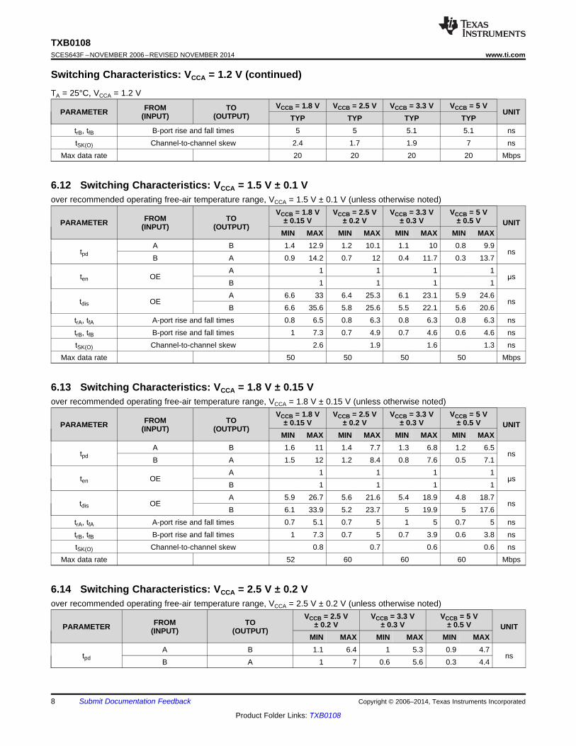
Switching Characteristics: VCCA = 1.2 V (continued)TA = 25°C, VCCA = 1.2 V
VCCB = 1.8 V VCCB = 2.5 V VCCB = 3.3 V VCCB = 5 VFROM TOPARAMETER UNIT(INPUT) (OUTPUT) TYP TYP TYP TYPtrB, tfB B-port rise and fall times 5 5 5.1 5.1 nstSK(O) Channel-to-channel skew 2.4 1.7 1.9 7 ns
Max data rate 20 20 20 20 Mbps
6.12 Switching Characteristics: VCCA = 1.5 V ± 0.1 Vover recommended operating free-air temperature range, VCCA = 1.5 V ± 0.1 V (unless otherwise noted)
VCCB = 1.8 V VCCB = 2.5 V VCCB = 3.3 V VCCB = 5 VFROM TO ± 0.15 V ± 0.2 V ± 0.3 V ± 0.5 VPARAMETER UNIT(INPUT) (OUTPUT)
MIN MAX MIN MAX MIN MAX MIN MAXA B 1.4 12.9 1.2 10.1 1.1 10 0.8 9.9
tpd nsB A 0.9 14.2 0.7 12 0.4 11.7 0.3 13.7
A 1 1 1 1ten OE μs
B 1 1 1 1A 6.6 33 6.4 25.3 6.1 23.1 5.9 24.6
tdis OE nsB 6.6 35.6 5.8 25.6 5.5 22.1 5.6 20.6
trA, tfA A-port rise and fall times 0.8 6.5 0.8 6.3 0.8 6.3 0.8 6.3 nstrB, tfB B-port rise and fall times 1 7.3 0.7 4.9 0.7 4.6 0.6 4.6 nstSK(O) Channel-to-channel skew 2.6 1.9 1.6 1.3 ns
Max data rate 50 50 50 50 Mbps
6.13 Switching Characteristics: VCCA = 1.8 V ± 0.15 Vover recommended operating free-air temperature range, VCCA = 1.8 V ± 0.15 V (unless otherwise noted)
VCCB = 1.8 V VCCB = 2.5 V VCCB = 3.3 V VCCB = 5 VFROM TO ± 0.15 V ± 0.2 V ± 0.3 V ± 0.5 VPARAMETER UNIT(INPUT) (OUTPUT)
MIN MAX MIN MAX MIN MAX MIN MAXA B 1.6 11 1.4 7.7 1.3 6.8 1.2 6.5
tpd nsB A 1.5 12 1.2 8.4 0.8 7.6 0.5 7.1
A 1 1 1 1ten OE μs
B 1 1 1 1A 5.9 26.7 5.6 21.6 5.4 18.9 4.8 18.7
tdis OE nsB 6.1 33.9 5.2 23.7 5 19.9 5 17.6
trA, tfA A-port rise and fall times 0.7 5.1 0.7 5 1 5 0.7 5 nstrB, tfB B-port rise and fall times 1 7.3 0.7 5 0.7 3.9 0.6 3.8 nstSK(O) Channel-to-channel skew 0.8 0.7 0.6 0.6 ns
Max data rate 52 60 60 60 Mbps
6.14 Switching Characteristics: VCCA = 2.5 V ± 0.2 Vover recommended operating free-air temperature range, VCCA = 2.5 V ± 0.2 V (unless otherwise noted)
VCCB = 2.5 V VCCB = 3.3 V VCCB = 5 VFROM TO ± 0.2 V ± 0.3 V ± 0.5 VPARAMETER UNIT(INPUT) (OUTPUT)
MIN MAX MIN MAX MIN MAXA B 1.1 6.4 1 5.3 0.9 4.7
tpd nsB A 1 7 0.6 5.6 0.3 4.4
8 Submit Documentation Feedback Copyright © 2006–2014, Texas Instruments Incorporated
Product Folder Links: TXB0108

TXB0108www.ti.com SCES643F –NOVEMBER 2006–REVISED NOVEMBER 2014
Switching Characteristics: VCCA = 2.5 V ± 0.2 V (continued)over recommended operating free-air temperature range, VCCA = 2.5 V ± 0.2 V (unless otherwise noted)
VCCB = 2.5 V VCCB = 3.3 V VCCB = 5 VFROM TO ± 0.2 V ± 0.3 V ± 0.5 VPARAMETER UNIT(INPUT) (OUTPUT)
MIN MAX MIN MAX MIN MAXA 1 1 1
ten OE μsB 1 1 1A 5 16.9 4.9 15 4.5 13.8
tdis OE nsB 4.8 21.8 4.5 17.9 4.4 15.2
trA, tfA A-port rise and fall times 0.8 3.6 0.6 3.6 0.5 3.5 nstrB, tfB B-port rise and fall times 0.6 4.9 0.7 3.9 0.6 3.2 nstSK(O) Channel-to-channel skew 0.4 0.3 0.3 ns
Max data rate 70 100 100 Mbps
6.15 Switching Characteristics: VCCA = 3.3 V ± 0.3 Vover recommended operating free-air temperature range, VCCA = 3.3 V ± 0.3 V (unless otherwise noted)
VCCB = 3.3 V VCCB = 5 VFROM TO ± 0.3 V ± 0.5 VPARAMETER UNIT(INPUT) (OUTPUT)
MIN MAX MIN MAXA B 0.9 4.9 0.8 4
tpd nsB A 0.5 5.4 0.2 4
A 1 1ten OE μs
B 1 1A 4.5 13.9 4.1 12.4
tdis OE nsB 4.1 17.3 4 14.4
trA, tfA A-port rise and fall times 0.5 3 0.5 3 nstrB, tfB B-port rise and fall times 0.7 3.9 0.6 3.2 nstSK(O) Channel-to-channel skew 0.4 0.3 ns
Max data rate 100 100 Mbps
6.16 Operating CharacteristicsTA = 25°C
VCCA
1.2 V 1.2 V 1.5 V 1.8 V 2.5 V 2.5 V 3.3 VVCCB
PARAMETER TEST CONDITIONS UNIT3.3 V5 V 1.8 V 1.8 V 1.8 V 2.5 V 5 V to
5 VTYP TYP TYP TYP TYP TYP TYP
A-port input, B-port output 9 8 7 7 7 7 8CL = 0, f = 10 MHz,CpdA B-port input, A-port output 12 11 11 11 11 11 11tr = tf = 1 ns, pFOE = VCCAA-port input, B-port output 35 26 27 27 27 27 28
CpdB (outputs enabled)B-port input, A-port output 26 19 18 18 18 20 21A-port input, B-port output 0.01 0.01 0.01 0.01 0.01 0.01 0.01
CL = 0, f = 10 MHz,CpdA B-port input, A-port output 0.01 0.01 0.01 0.01 0.01 0.01 0.01tr = tf = 1 ns, pFOE = GNDA-port input, B-port output 0.01 0.01 0.01 0.01 0.01 0.01 0.03CpdB (outputs disabled)
B-port input, A-port output 0.01 0.01 0.01 0.01 0.01 0.01 0.03
Copyright © 2006–2014, Texas Instruments Incorporated Submit Documentation Feedback 9
Product Folder Links: TXB0108
TXB0108SCES643F –NOVEMBER 2006–REVISED NOVEMBER 2014 www.ti.com
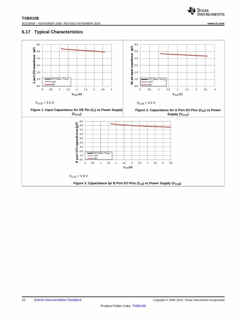
6.17 Typical Characteristics
VCCB = 3.3 V VCCB = 3.3 V
Figure 1. Input Capacitance for OE Pin (CI) vs Power Supply Figure 2. Capacitance for A Port I/O Pins (CIO) vs Power(VCCA) Supply (VCCA)
VCCA = 1.8 V
Figure 3. Capacitance fpr B Port I/O Pins (CIO) vs Power Supply (VCCB)
10 Submit Documentation Feedback Copyright © 2006–2014, Texas Instruments Incorporated
Product Folder Links: TXB0108
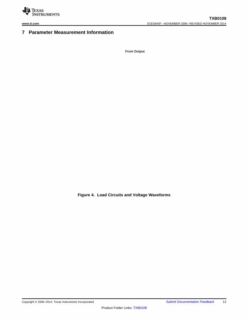
From Output Under Test
LOAD CIRCUIT FORENABLE/DISABLE
TIME MEASUREMENT
S1
2 × VCCO
Open
50 k
VCCI
0 V
VCCI/2 VCCI/2
tw
VOLTAGE WAVEFORMSPROPAGATION DELAY TIMES
VOLTAGE WAVEFORMSPULSE DURATION
Input
tPZL/tPLZtPHZ/tPZH
2 × VCCOOpen
TEST S1
A. CL includes probe and jig capacitance.B. All input pulses are supplied by generators having the following characteristics: PRR10 MHz, ZO = 50 Ω, dv/dt ≥ 1 V/ns.C. The outputs are measured one at a time, with one transition per measurement.D. tPLH and tPHL are the same as tpd.E. VCCI is the VCC associated with the input port.F. VCCO is the VCC associated with the output port.G. All parameters and waveforms are not applicable to all devices.
50 kFrom Output
Under Test
1 M15 pF 15 pF
LOAD CIRCUIT FOR MAX DATA RATE,PULSE DURATION PROPAGATION
DELAY OUTPUT RISE AND FALL TIMEMEASUREMENT
tPLH tPHL
0 V
VCCO/2
VCCI/2 VCCI/2
0.9 VCCOVCCO/2
tr
0.1 VCCO
tf
VCCIInput
OutputVOH
VOL
TXB0108www.ti.com SCES643F –NOVEMBER 2006–REVISED NOVEMBER 2014
7 Parameter Measurement Information
Figure 4. Load Circuits and Voltage Waveforms
Copyright © 2006–2014, Texas Instruments Incorporated Submit Documentation Feedback 11
Product Folder Links: TXB0108
TXB0108SCES643F –NOVEMBER 2006–REVISED NOVEMBER 2014 www.ti.com
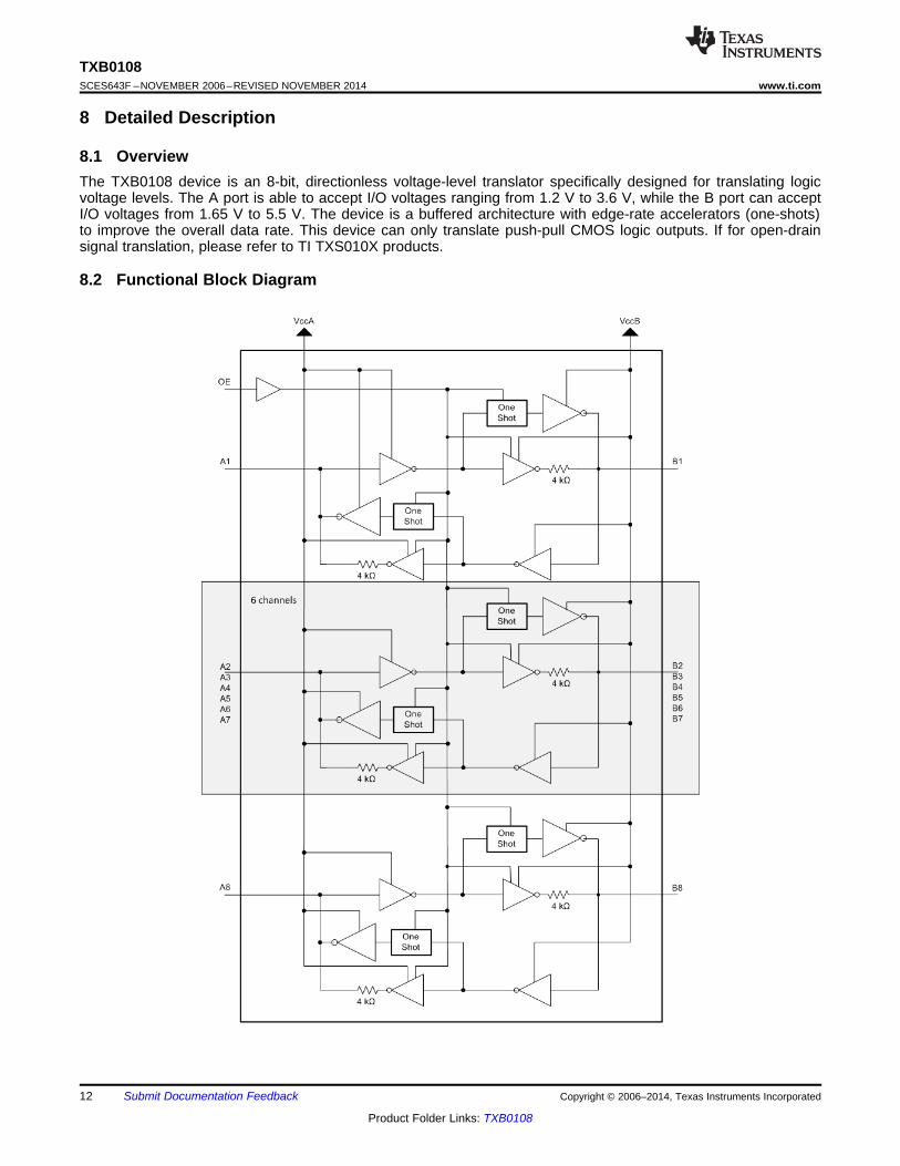
8 Detailed Description
8.1 OverviewThe TXB0108 device is an 8-bit, directionless voltage-level translator specifically designed for translating logicvoltage levels. The A port is able to accept I/O voltages ranging from 1.2 V to 3.6 V, while the B port can acceptI/O voltages from 1.65 V to 5.5 V. The device is a buffered architecture with edge-rate accelerators (one-shots)to improve the overall data rate. This device can only translate push-pull CMOS logic outputs. If for open-drainsignal translation, please refer to TI TXS010X products.
8.2 Functional Block Diagram
12 Submit Documentation Feedback Copyright © 2006–2014, Texas Instruments Incorporated
Product Folder Links: TXB0108
IIN
VIN
VT/4 k
–(VD – VT)/4 k
A. VT is the input threshold voltage of the TXB0108 (typically VCCI/2).B. VD is the supply voltage of the external driver.
4k
4k
A B
VCCA VCCB
OneShot
OneShot
OneShot
OneShot
T1
T2
T3
T4
TXB0108www.ti.com SCES643F –NOVEMBER 2006–REVISED NOVEMBER 2014
8.3 Feature Description
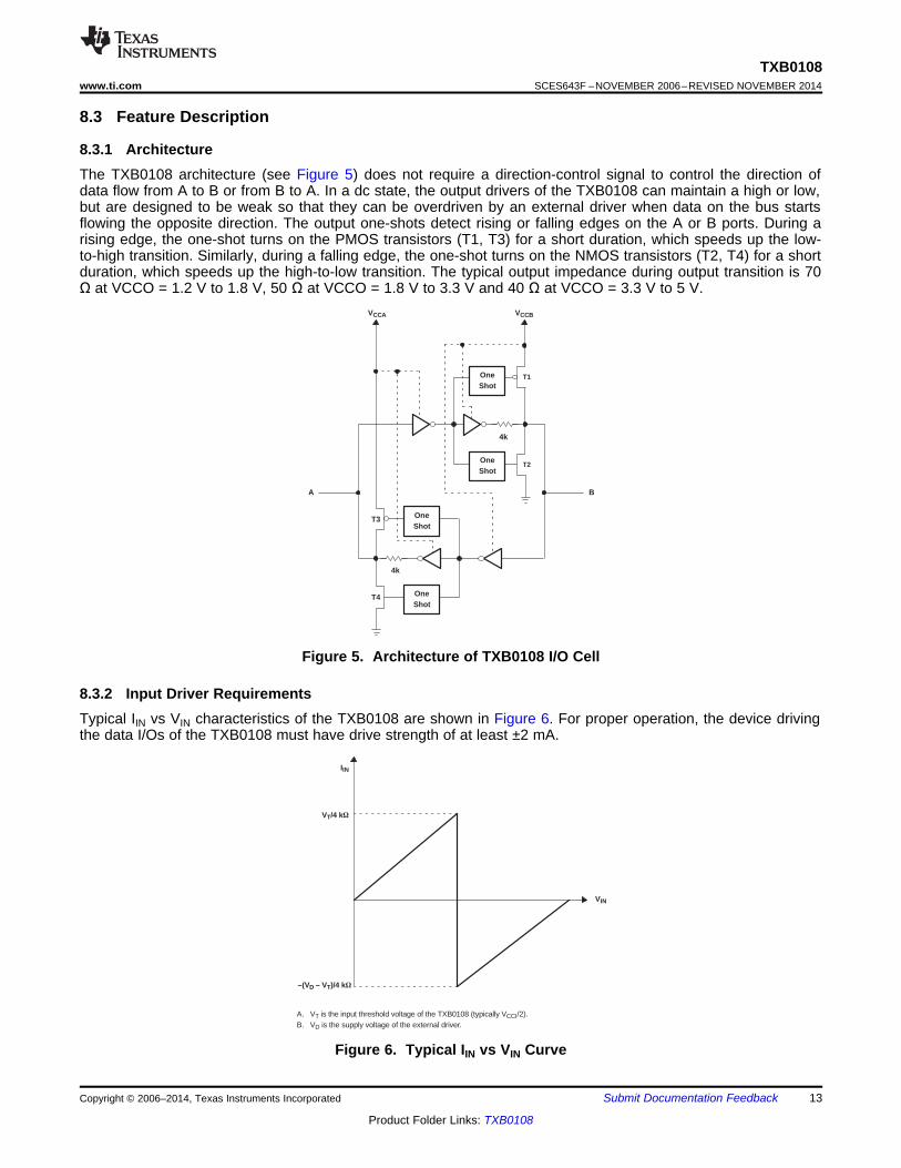
8.3.1 ArchitectureThe TXB0108 architecture (see Figure 5) does not require a direction-control signal to control the direction ofdata flow from A to B or from B to A. In a dc state, the output drivers of the TXB0108 can maintain a high or low,but are designed to be weak so that they can be overdriven by an external driver when data on the bus startsflowing the opposite direction. The output one-shots detect rising or falling edges on the A or B ports. During arising edge, the one-shot turns on the PMOS transistors (T1, T3) for a short duration, which speeds up the low-to-high transition. Similarly, during a falling edge, the one-shot turns on the NMOS transistors (T2, T4) for a shortduration, which speeds up the high-to-low transition. The typical output impedance during output transition is 70Ω at VCCO = 1.2 V to 1.8 V, 50 Ω at VCCO = 1.8 V to 3.3 V and 40 Ω at VCCO = 3.3 V to 5 V.
Figure 5. Architecture of TXB0108 I/O Cell
8.3.2 Input Driver RequirementsTypical IIN vs VIN characteristics of the TXB0108 are shown in Figure 6. For proper operation, the device drivingthe data I/Os of the TXB0108 must have drive strength of at least ±2 mA.
Figure 6. Typical IIN vs VIN Curve
Copyright © 2006–2014, Texas Instruments Incorporated Submit Documentation Feedback 13
Product Folder Links: TXB0108

TXB0108SCES643F –NOVEMBER 2006–REVISED NOVEMBER 2014 www.ti.com
Feature Description (continued)8.3.3 Output Load ConsiderationsTI recommends careful PCB layout practices with short PCB trace lengths to avoid excessive capacitive loadingand to ensure that proper O.S. triggering takes place. PCB signal trace-lengths should be kept short enoughsuch that the round-trip delay of any reflection is less than the one-shot duration. This improves signal integrityby ensuring that any reflection sees a low impedance at the driver. The O.S. circuits have been designed to stayon for approximately 10 ns. The maximum capacitance of the lumped load that can be driven also dependsdirectly on the one-shot duration. With very heavy capacitive loads, the one-shot can time-out before the signal isdriven fully to the positive rail. The O.S. duration has been set to best optimize trade-offs between dynamic ICC,load driving capability, and maximum bit-rate considerations. Both PCB trace length and connectors add to thecapacitance that the TXB0108 output sees, so it is recommended that this lumped-load capacitance beconsidered to avoid O.S. re-triggering, bus contention, output signal oscillations, or other adverse system-levelaffects.
8.3.4 Enable and DisableThe TXB0108 has an OE input that is used to disable the device by setting OE = low, which places all I/Os in thehigh-impedance (Hi-Z) state. The disable time (tdis) indicates the delay between when OE goes low and whenthe outputs actually get disabled (Hi-Z). The enable time (ten) indicates the amount of time the user must allowfor the one-shot circuitry to become operational after the OE is high.
8.3.5 Pullup or Pulldown Resistors on I/O LinesThe TXB0108 is designed to drive capacitive loads of up to 70 pF. The output drivers of the TXB0108 have lowdc drive strength. If pullup or pulldown resistors are connected externally to the data I/Os, their values must bekept higher than 50 kΩ to ensure that they do not contend with the output drivers of the TXB0108. For the samereason, the TXB0108 should not be used in applications such as I2C or 1-Wire where an open-drain driver isconnected on the bidirectional data I/O. For these applications, use a device from the TI TXS01xx series of leveltranslators.
8.4 Device Functional ModesThe TXB0108 device has two functional modes, enabled and disabled. To disable the device, set the OE inputlow, which places all I/Os in a high impedance state. Setting the OE input high will enable the device.
14 Submit Documentation Feedback Copyright © 2006–2014, Texas Instruments Incorporated
Product Folder Links: TXB0108
TXB0108www.ti.com SCES643F –NOVEMBER 2006–REVISED NOVEMBER 2014
9 Application and Implementation
NOTEInformation in the following applications sections is not part of the TI componentspecification, and TI does not warrant its accuracy or completeness. TI’s customers areresponsible for determining suitability of components for their purposes. Customers shouldvalidate and test their design implementation to confirm system functionality.
9.1 Application InformationThe TXB0108 can be used in level-translation applications for interfacing devices or systems operating atdifferent interface voltages with one another. It can only translate push-pull CMOS logic outputs. If for open-drainsignal translation, please refer to TI TXS010X products. Any external pulldown or pullup resistors arerecommended to be larger than 50kΩ.
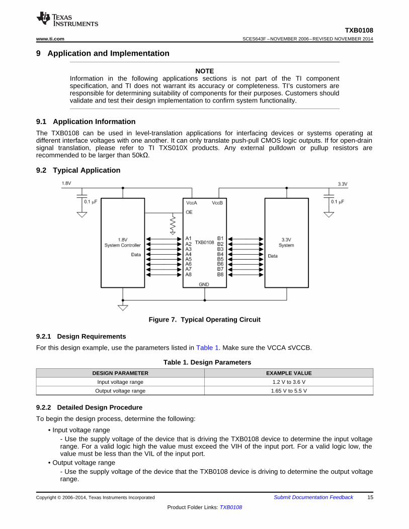
9.2 Typical Application
Figure 7. Typical Operating Circuit
9.2.1 Design RequirementsFor this design example, use the parameters listed in Table 1. Make sure the VCCA ≤VCCB.
Table 1. Design ParametersDESIGN PARAMETER EXAMPLE VALUE
Input voltage range 1.2 V to 3.6 VOutput voltage range 1.65 V to 5.5 V
9.2.2 Detailed Design ProcedureTo begin the design process, determine the following:
• Input voltage range- Use the supply voltage of the device that is driving the TXB0108 device to determine the input voltagerange. For a valid logic high the value must exceed the VIH of the input port. For a valid logic low, thevalue must be less than the VIL of the input port.
• Output voltage range- Use the supply voltage of the device that the TXB0108 device is driving to determine the output voltagerange.
Copyright © 2006–2014, Texas Instruments Incorporated Submit Documentation Feedback 15
Product Folder Links: TXB0108
TXB0108SCES643F –NOVEMBER 2006–REVISED NOVEMBER 2014 www.ti.com
- Do not recommend having the external pullup or pulldown resistors. If mandatory, it is recommendedthe value should be larger than 50 kΩ.
• An external pulldown or pullup resistor decreases the output VOH and VOL. Use the below equations to draftestimate the VOH and VOL as a result of an external pulldown and pullup resistor.
VOH = VCCx × RPD / (RPD + 4.5 kΩ)VOL = VCCx × 4.5kΩ / (RPU + 4.5 kΩ)Where:
• VCCx is the output port supply voltage on either VCCA or VCCB• RPD is the value of the external pull down resistor• RPU is the value of the external pull up resistor• 4.5 kΩ is the counting the variation of the serial resistor 4 kΩ in the I/O line.
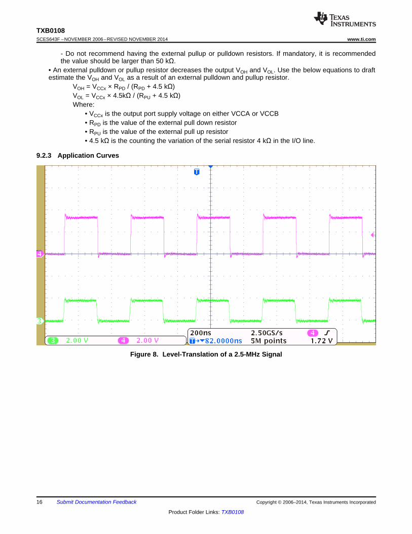
9.2.3 Application Curves
Figure 8. Level-Translation of a 2.5-MHz Signal
16 Submit Documentation Feedback Copyright © 2006–2014, Texas Instruments Incorporated
Product Folder Links: TXB0108
TXB0108www.ti.com SCES643F –NOVEMBER 2006–REVISED NOVEMBER 2014
10 Power Supply RecommendationsDuring operation, ensure that VCCA ≤ VCCB at all times. During power-up sequencing, VCCA ≥ VCCB does notdamage the device, so any power supply can be ramped up first. The TXB0108 has circuitry that disables alloutput ports when either VCC is switched off (VCCA/B = 0 V).
The output-enable (OE) input circuit is designed so that it is supplied by VCCA and when the (OE) input is low, alloutputs are placed in the high-impedance state. To ensure the high-impedance state of the outputs duringpower-up or power-down, the OE input pin must be tied to GND through a pulldown resistor and must not beenabled until VCCA and VCCB are fully ramped and stable. The minimum value of the pulldown resistor to groundis determined by the current-sourcing capability of the driver.
11 Layout
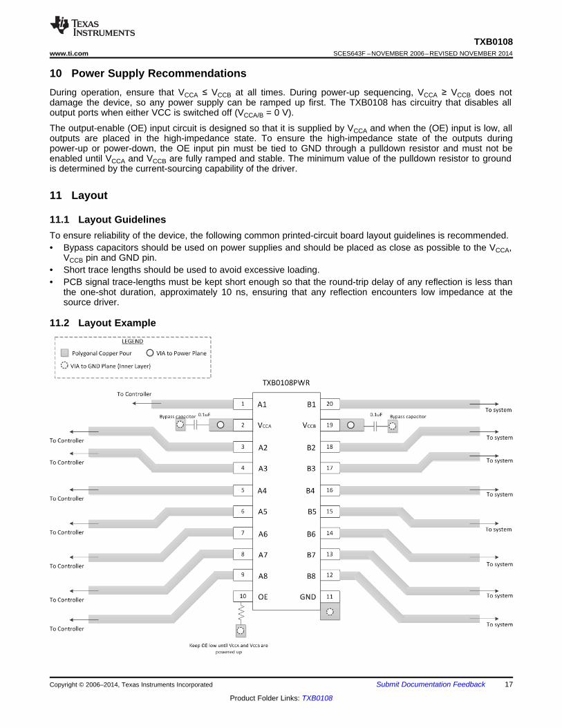
11.1 Layout GuidelinesTo ensure reliability of the device, the following common printed-circuit board layout guidelines is recommended.• Bypass capacitors should be used on power supplies and should be placed as close as possible to the VCCA,
VCCB pin and GND pin.• Short trace lengths should be used to avoid excessive loading.• PCB signal trace-lengths must be kept short enough so that the round-trip delay of any reflection is less than
the one-shot duration, approximately 10 ns, ensuring that any reflection encounters low impedance at thesource driver.
11.2 Layout Example
Copyright © 2006–2014, Texas Instruments Incorporated Submit Documentation Feedback 17
Product Folder Links: TXB0108
TXB0108SCES643F –NOVEMBER 2006–REVISED NOVEMBER 2014 www.ti.com
12 Device and Documentation Support
12.1 TrademarksAll trademarks are the property of their respective owners.
12.2 Electrostatic Discharge CautionThese devices have limited built-in ESD protection. The leads should be shorted together or the device placed in conductive foamduring storage or handling to prevent electrostatic damage to the MOS gates.
12.3 GlossarySLYZ022 — TI Glossary.
This glossary lists and explains terms, acronyms, and definitions.
13 Mechanical, Packaging, and Orderable InformationThe following pages include mechanical, packaging, and orderable information. This information is the mostcurrent data available for the designated devices. This data is subject to change without notice and revision ofthis document. For browser-based versions of this data sheet, refer to the left-hand navigation.
18 Submit Documentation Feedback Copyright © 2006–2014, Texas Instruments Incorporated
Product Folder Links: TXB0108
PACKAGE OPTION ADDENDUM
www.ti.com 22-Jun-2016
Addendum-Page 1
PACKAGING INFORMATION
Orderable Device Status(1)
Package Type PackageDrawing
Pins PackageQty
Eco Plan(2)
Lead/Ball Finish(6)
MSL Peak Temp(3)
Op Temp (°C) Device Marking(4/5)
Samples
TXB0108DQSR ACTIVE USON DQS 20 3000 Green (RoHS& no Sb/Br)
CU NIPDAUAG Level-1-260C-UNLIM -40 to 85 5MR5MH
TXB0108PWR ACTIVE TSSOP PW 20 2000 Green (RoHS& no Sb/Br)
CU NIPDAU Level-1-260C-UNLIM -40 to 85 YE08
TXB0108PWRG4 ACTIVE TSSOP PW 20 2000 Green (RoHS& no Sb/Br)
CU NIPDAU Level-1-260C-UNLIM -40 to 85 YE08
TXB0108RGYR ACTIVE VQFN RGY 20 3000 Green (RoHS& no Sb/Br)
CU NIPDAU Level-2-260C-1 YEAR -40 to 85 YE08
TXB0108RGYRG4 ACTIVE VQFN RGY 20 3000 Green (RoHS& no Sb/Br)
CU NIPDAU Level-2-260C-1 YEAR -40 to 85 YE08
TXB0108YZPR ACTIVE DSBGA YZP 20 3000 Green (RoHS& no Sb/Br)
SNAGCU Level-1-260C-UNLIM -40 to 85 5M
TXB0108ZXYR ACTIVE BGAMICROSTAR
JUNIOR
ZXY 20 2500 Green (RoHS& no Sb/Br)
SNAGCU Level-1-260C-UNLIM -40 to 85 YE08
(1) The marketing status values are defined as follows:ACTIVE: Product device recommended for new designs.LIFEBUY: TI has announced that the device will be discontinued, and a lifetime-buy period is in effect.NRND: Not recommended for new designs. Device is in production to support existing customers, but TI does not recommend using this part in a new design.PREVIEW: Device has been announced but is not in production. Samples may or may not be available.OBSOLETE: TI has discontinued the production of the device.
(2) Eco Plan - The planned eco-friendly classification: Pb-Free (RoHS), Pb-Free (RoHS Exempt), or Green (RoHS & no Sb/Br) - please check http://www.ti.com/productcontent for the latest availabilityinformation and additional product content details.TBD: The Pb-Free/Green conversion plan has not been defined.Pb-Free (RoHS): TI's terms "Lead-Free" or "Pb-Free" mean semiconductor products that are compatible with the current RoHS requirements for all 6 substances, including the requirement thatlead not exceed 0.1% by weight in homogeneous materials. Where designed to be soldered at high temperatures, TI Pb-Free products are suitable for use in specified lead-free processes.Pb-Free (RoHS Exempt): This component has a RoHS exemption for either 1) lead-based flip-chip solder bumps used between the die and package, or 2) lead-based die adhesive used betweenthe die and leadframe. The component is otherwise considered Pb-Free (RoHS compatible) as defined above.Green (RoHS & no Sb/Br): TI defines "Green" to mean Pb-Free (RoHS compatible), and free of Bromine (Br) and Antimony (Sb) based flame retardants (Br or Sb do not exceed 0.1% by weightin homogeneous material)
(3) MSL, Peak Temp. - The Moisture Sensitivity Level rating according to the JEDEC industry standard classifications, and peak solder temperature.
(4) There may be additional marking, which relates to the logo, the lot trace code information, or the environmental category on the device.
PACKAGE OPTION ADDENDUM
www.ti.com 22-Jun-2016
Addendum-Page 2
(5) Multiple Device Markings will be inside parentheses. Only one Device Marking contained in parentheses and separated by a "~" will appear on a device. If a line is indented then it is a continuationof the previous line and the two combined represent the entire Device Marking for that device.
(6) Lead/Ball Finish - Orderable Devices may have multiple material finish options. Finish options are separated by a vertical ruled line. Lead/Ball Finish values may wrap to two lines if the finishvalue exceeds the maximum column width.
Important Information and Disclaimer:The information provided on this page represents TI's knowledge and belief as of the date that it is provided. TI bases its knowledge and belief on informationprovided by third parties, and makes no representation or warranty as to the accuracy of such information. Efforts are underway to better integrate information from third parties. TI has taken andcontinues to take reasonable steps to provide representative and accurate information but may not have conducted destructive testing or chemical analysis on incoming materials and chemicals.TI and TI suppliers consider certain information to be proprietary, and thus CAS numbers and other limited information may not be available for release.
In no event shall TI's liability arising out of such information exceed the total purchase price of the TI part(s) at issue in this document sold by TI to Customer on an annual basis.
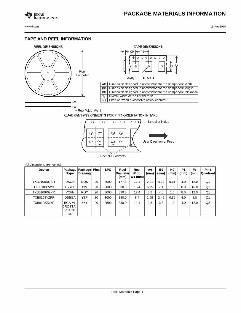
TAPE AND REEL INFORMATION
*All dimensions are nominal
Device PackageType
PackageDrawing
Pins SPQ ReelDiameter
(mm)
ReelWidth
W1 (mm)
A0(mm)
B0(mm)
K0(mm)
P1(mm)
W(mm)
Pin1Quadrant
TXB0108DQSR USON DQS 20 3000 177.8 12.4 2.21 4.22 0.81 4.0 12.0 Q1
TXB0108PWR TSSOP PW 20 2000 330.0 16.4 6.95 7.1 1.6 8.0 16.0 Q1
TXB0108RGYR VQFN RGY 20 3000 330.0 12.4 3.8 4.8 1.6 8.0 12.0 Q1
TXB0108YZPR DSBGA YZP 20 3000 180.0 8.4 1.99 2.49 0.56 4.0 8.0 Q1
TXB0108ZXYR BGA MI CROSTA
R JUNI OR
ZXY 20 2500 330.0 12.4 2.8 3.3 1.0 4.0 12.0 Q2
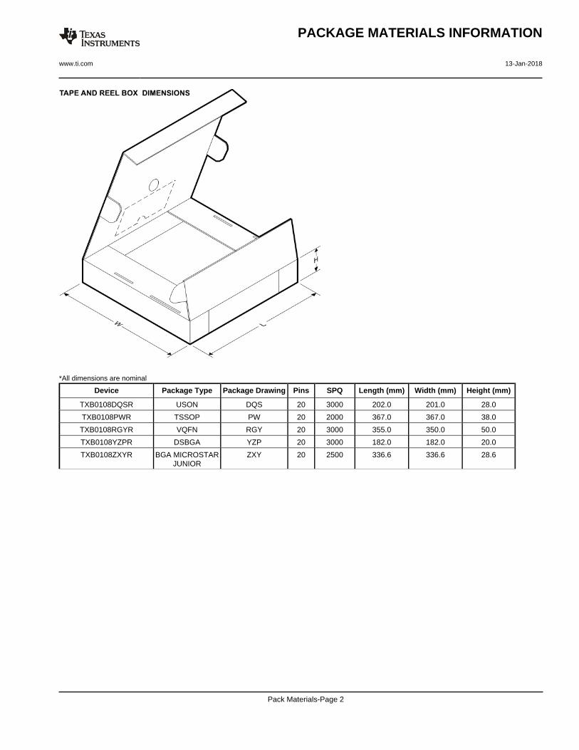
PACKAGE MATERIALS INFORMATION
www.ti.com 13-Jan-2018
Pack Materials-Page 1
*All dimensions are nominal
Device Package Type Package Drawing Pins SPQ Length (mm) Width (mm) Height (mm)
TXB0108DQSR USON DQS 20 3000 202.0 201.0 28.0
TXB0108PWR TSSOP PW 20 2000 367.0 367.0 38.0
TXB0108RGYR VQFN RGY 20 3000 355.0 350.0 50.0
TXB0108YZPR DSBGA YZP 20 3000 182.0 182.0 20.0
TXB0108ZXYR BGA MICROSTARJUNIOR
ZXY 20 2500 336.6 336.6 28.6
PACKAGE MATERIALS INFORMATION
www.ti.com 13-Jan-2018
Pack Materials-Page 2
www.ti.com
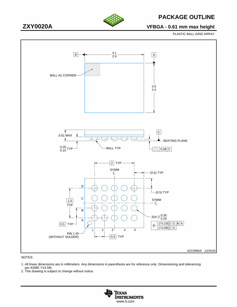
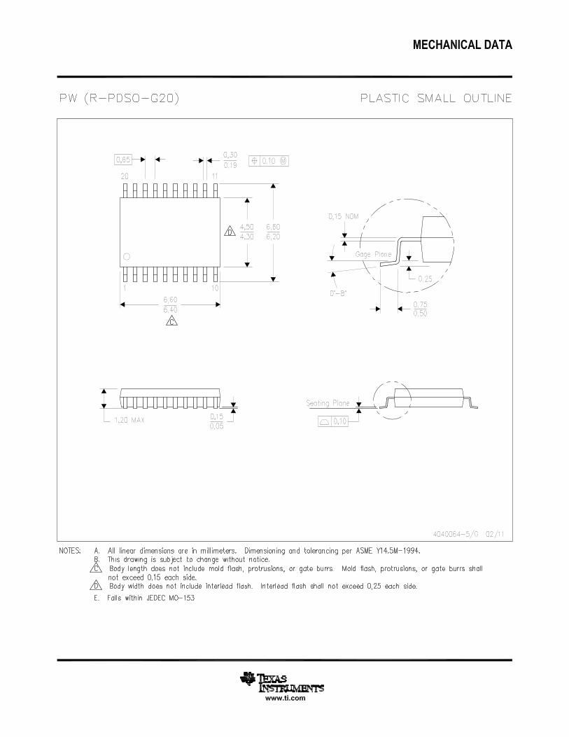
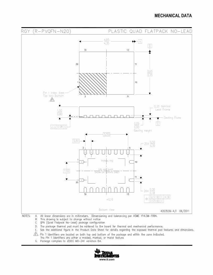
PACKAGE OUTLINE
C0.61 MAX
TYP0.250.15
1.5TYP
2 TYP
0.5 TYP
0.5 TYP
20X 0.350.25
B 3.12.9 A
2.62.4
(0.5) TYP
(0.5) TYP
VFBGA - 0.61 mm max heightZXY0020APLASTIC BALL GRID ARRAY
4222996/A 12/2016
NOTES: 1. All linear dimensions are in millimeters. Any dimensions in parenthesis are for reference only. Dimensioning and tolerancing per ASME Y14.5M. 2. This drawing is subject to change without notice.
BALL A1 CORNER
SEATING PLANE
BALL TYP 0.08 C
0.15 C B A0.05 C
SYMM
SYMM
(WITHOUT SOLDER)PIN 1 ID
B
1 2 3 4 5
A
C
D
SCALE 4.800

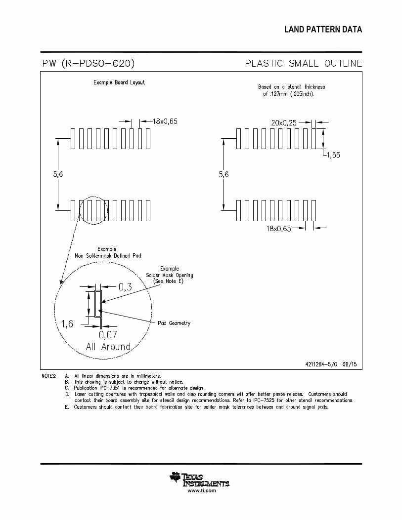
www.ti.com
EXAMPLE BOARD LAYOUT
20X ( 0.25) (0.5) TYP
(0.5) TYP
( 0.25)METAL
0.05 MAX
SOLDER MASKOPENING
METAL UNDERSOLDER MASK
( 0.25)SOLDER MASKOPENING
0.05 MIN
VFBGA - 0.61 mm max heightZXY0020APLASTIC BALL GRID ARRAY
4222996/A 12/2016
NOTES: (continued) 3. Final dimensions may vary due to manufacturing tolerance considerations and also routing constraints. For information, see Texas Instruments literature number SPRAA99 (www.ti.com/lit/spraa99).
SYMM
SYMM
LAND PATTERN EXAMPLEEXPOSED METAL SHOWN
SCALE:25X
1 2 3 4 5
A
B
C
D
NON-SOLDER MASKDEFINED
(PREFERRED)
SOLDER MASK DETAILSNOT TO SCALE
EXPOSED METAL
SOLDER MASKDEFINED
EXPOSED METAL
www.ti.com
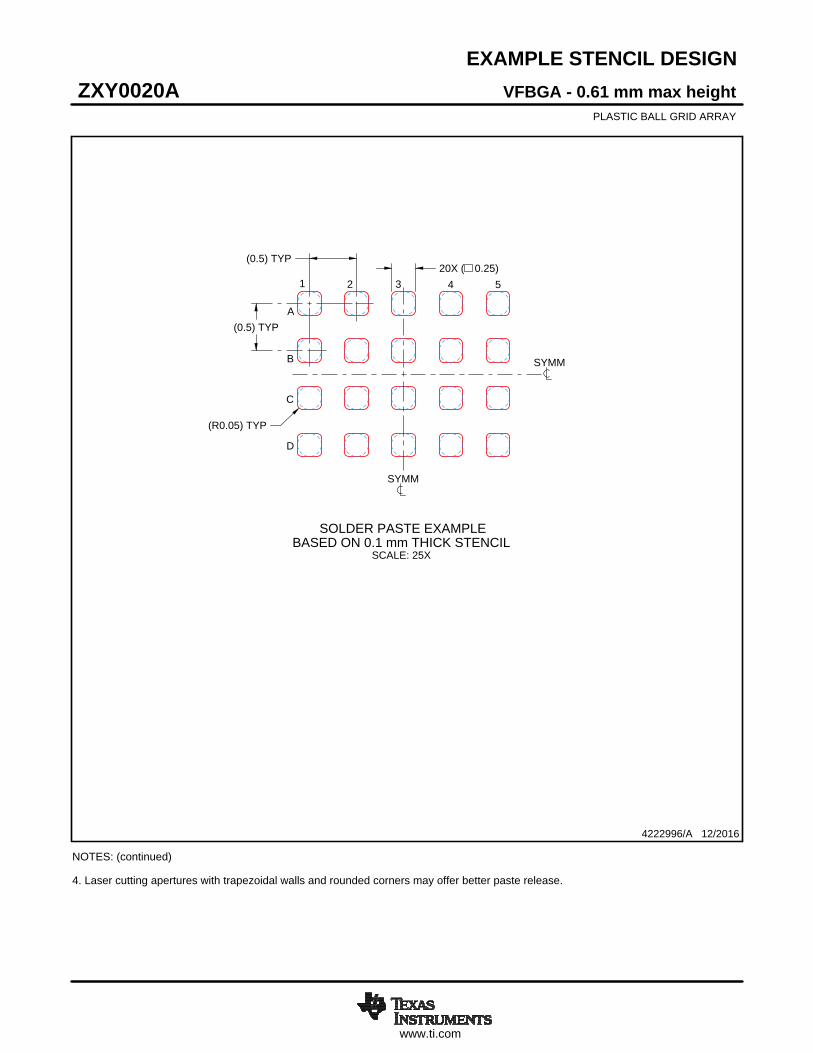
EXAMPLE STENCIL DESIGN
(R0.05) TYP
(0.5) TYP
(0.5) TYP
20X ( 0.25)
VFBGA - 0.61 mm max heightZXY0020APLASTIC BALL GRID ARRAY
4222996/A 12/2016
NOTES: (continued) 4. Laser cutting apertures with trapezoidal walls and rounded corners may offer better paste release.
SYMM
SYMM
1 2 3 4 5
A
SOLDER PASTE EXAMPLEBASED ON 0.1 mm THICK STENCIL
SCALE: 25X
B
C
D

D: Max =
E: Max =
2.418 mm, Min =
1.918 mm, Min =
2.358 mm
1.858 mm
IMPORTANT NOTICE
Texas Instruments Incorporated (TI) reserves the right to make corrections, enhancements, improvements and other changes to itssemiconductor products and services per JESD46, latest issue, and to discontinue any product or service per JESD48, latest issue. Buyersshould obtain the latest relevant information before placing orders and should verify that such information is current and complete.TI’s published terms of sale for semiconductor products (http://www.ti.com/sc/docs/stdterms.htm) apply to the sale of packaged integratedcircuit products that TI has qualified and released to market. Additional terms may apply to the use or sale of other types of TI products andservices.Reproduction of significant portions of TI information in TI data sheets is permissible only if reproduction is without alteration and isaccompanied by all associated warranties, conditions, limitations, and notices. TI is not responsible or liable for such reproduceddocumentation. Information of third parties may be subject to additional restrictions. Resale of TI products or services with statementsdifferent from or beyond the parameters stated by TI for that product or service voids all express and any implied warranties for theassociated TI product or service and is an unfair and deceptive business practice. TI is not responsible or liable for any such statements.Buyers and others who are developing systems that incorporate TI products (collectively, “Designers”) understand and agree that Designersremain responsible for using their independent analysis, evaluation and judgment in designing their applications and that Designers havefull and exclusive responsibility to assure the safety of Designers' applications and compliance of their applications (and of all TI productsused in or for Designers’ applications) with all applicable regulations, laws and other applicable requirements. Designer represents that, withrespect to their applications, Designer has all the necessary expertise to create and implement safeguards that (1) anticipate dangerousconsequences of failures, (2) monitor failures and their consequences, and (3) lessen the likelihood of failures that might cause harm andtake appropriate actions. Designer agrees that prior to using or distributing any applications that include TI products, Designer willthoroughly test such applications and the functionality of such TI products as used in such applications.TI’s provision of technical, application or other design advice, quality characterization, reliability data or other services or information,including, but not limited to, reference designs and materials relating to evaluation modules, (collectively, “TI Resources”) are intended toassist designers who are developing applications that incorporate TI products; by downloading, accessing or using TI Resources in anyway, Designer (individually or, if Designer is acting on behalf of a company, Designer’s company) agrees to use any particular TI Resourcesolely for this purpose and subject to the terms of this Notice.TI’s provision of TI Resources does not expand or otherwise alter TI’s applicable published warranties or warranty disclaimers for TIproducts, and no additional obligations or liabilities arise from TI providing such TI Resources. TI reserves the right to make corrections,enhancements, improvements and other changes to its TI Resources. TI has not conducted any testing other than that specificallydescribed in the published documentation for a particular TI Resource.Designer is authorized to use, copy and modify any individual TI Resource only in connection with the development of applications thatinclude the TI product(s) identified in such TI Resource. NO OTHER LICENSE, EXPRESS OR IMPLIED, BY ESTOPPEL OR OTHERWISETO ANY OTHER TI INTELLECTUAL PROPERTY RIGHT, AND NO LICENSE TO ANY TECHNOLOGY OR INTELLECTUAL PROPERTYRIGHT OF TI OR ANY THIRD PARTY IS GRANTED HEREIN, including but not limited to any patent right, copyright, mask work right, orother intellectual property right relating to any combination, machine, or process in which TI products or services are used. Informationregarding or referencing third-party products or services does not constitute a license to use such products or services, or a warranty orendorsement thereof. Use of TI Resources may require a license from a third party under the patents or other intellectual property of thethird party, or a license from TI under the patents or other intellectual property of TI.TI RESOURCES ARE PROVIDED “AS IS” AND WITH ALL FAULTS. TI DISCLAIMS ALL OTHER WARRANTIES ORREPRESENTATIONS, EXPRESS OR IMPLIED, REGARDING RESOURCES OR USE THEREOF, INCLUDING BUT NOT LIMITED TOACCURACY OR COMPLETENESS, TITLE, ANY EPIDEMIC FAILURE WARRANTY AND ANY IMPLIED WARRANTIES OFMERCHANTABILITY, FITNESS FOR A PARTICULAR PURPOSE, AND NON-INFRINGEMENT OF ANY THIRD PARTY INTELLECTUALPROPERTY RIGHTS. TI SHALL NOT BE LIABLE FOR AND SHALL NOT DEFEND OR INDEMNIFY DESIGNER AGAINST ANY CLAIM,INCLUDING BUT NOT LIMITED TO ANY INFRINGEMENT CLAIM THAT RELATES TO OR IS BASED ON ANY COMBINATION OFPRODUCTS EVEN IF DESCRIBED IN TI RESOURCES OR OTHERWISE. IN NO EVENT SHALL TI BE LIABLE FOR ANY ACTUAL,DIRECT, SPECIAL, COLLATERAL, INDIRECT, PUNITIVE, INCIDENTAL, CONSEQUENTIAL OR EXEMPLARY DAMAGES INCONNECTION WITH OR ARISING OUT OF TI RESOURCES OR USE THEREOF, AND REGARDLESS OF WHETHER TI HAS BEENADVISED OF THE POSSIBILITY OF SUCH DAMAGES.Unless TI has explicitly designated an individual product as meeting the requirements of a particular industry standard (e.g., ISO/TS 16949and ISO 26262), TI is not responsible for any failure to meet such industry standard requirements.Where TI specifically promotes products as facilitating functional safety or as compliant with industry functional safety standards, suchproducts are intended to help enable customers to design and create their own applications that meet applicable functional safety standardsand requirements. Using products in an application does not by itself establish any safety features in the application. Designers mustensure compliance with safety-related requirements and standards applicable to their applications. Designer may not use any TI products inlife-critical medical equipment unless authorized officers of the parties have executed a special contract specifically governing such use.Life-critical medical equipment is medical equipment where failure of such equipment would cause serious bodily injury or death (e.g., lifesupport, pacemakers, defibrillators, heart pumps, neurostimulators, and implantables). Such equipment includes, without limitation, allmedical devices identified by the U.S. Food and Drug Administration as Class III devices and equivalent classifications outside the U.S.TI may expressly designate certain products as completing a particular qualification (e.g., Q100, Military Grade, or Enhanced Product).Designers agree that it has the necessary expertise to select the product with the appropriate qualification designation for their applicationsand that proper product selection is at Designers’ own risk. Designers are solely responsible for compliance with all legal and regulatoryrequirements in connection with such selection.Designer will fully indemnify TI and its representatives against any damages, costs, losses, and/or liabilities arising out of Designer’s non-compliance with the terms and provisions of this Notice.
Mailing Address: Texas Instruments, Post Office Box 655303, Dallas, Texas 75265Copyright © 2018, Texas Instruments Incorporated