typical mechanisms in advanced soi mosfets and … · dielectric isolation: vertical and lateral...
TRANSCRIPT

Sorin Cristoloveanu
- Almost no introduction- Operation of SOI transistors- Gate tunneling and floating-body effects- Fringing fields and short-channel effects - Narrow-channel effects- Extremely thin film effects- Self-heating- Double-gate operation- Multiple-gate MOSFETs- Next speaker
Typical Mechanisms in Advanced SOI MOSFETsand Challenging Issues for Compact Modeling

SOI Technology - Definition & Questions
� Is SOI really young ?Yes, 30-35 years onlyNo, twice as old as the lifetime left on ITRS
� Is SOI for the future ?(Yes)2 ! Bulk cannot make it. There is nothing left, but SOI !
� Is the future what it used to be ?No, because SOI allows expanding the frontiers !
Sorin 20-05
Definition: SOI is a young technologyfor the future of the microelectronics

Why SOI ?
Sorin 20-05
Dielectric isolation: vertical and lateral (no latch-up)Vertical junctions: reduced leakage and capacitanceExcellent tolerance of transient radiation effectsSimpler processing & high flexibility: no wells or trenchesIdeal structure for sensors, MEMS, high-temperature devices
Attenuated short-channel effects: enhanced scalingLow-voltage & low-power operation:
sharp subthreshold swing, reduced leakage, low VT

Floating-Body Effects in PD SOI MOSFETs
Sorin 20-05
Kink effect
Latch &related noise
Models available!
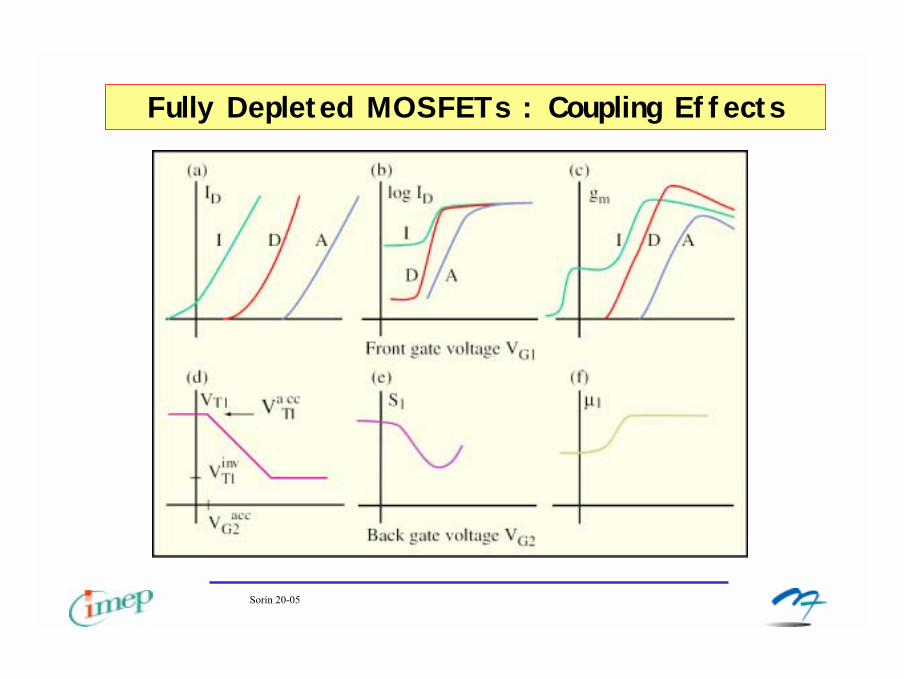
Fully Depleted MOSFETs : Coupling Effects
Sorin 20-05

Sorin 20-05

Sorin 20-05
Notes:� The front channel is sensitive to
back-gate bias and qualityof BOX and back interface
� Conventional models account for2-interface coupling
� MOSFETs with thin BOX require3-interface models andsubstrate depletion effects

Self-Heating in SOI MOSFETs
Sorin 20-05

Si
Si
Gate
oxideSource
Si
α
Drain
WireWireWire
BOX
Thermal Conductance: Analytical Model
� Thermal equivalent circuit� BOX contribution prevails
Change the BOX material !!
Al2O3 BOX
SiO2 BOX
Gate + S/D
Sorin 20-05

Solution: Thin Buried Alumina
0
50
100
150
200
0 50 100 150 200BOX (nm )
Latti
ce T
empe
ratu
re (C
)
(a)
(b)
o
SiO2 BOX
Al2O3 BOX
∆T=40°C
! Thinner BOX reduces the channel lattice temperature.! The advantage of Al2O3 BOX is maintained for thin BOX.
Sorin 20-05

0E+00
1E-05
2E-05
3E-05
4E-05
5E-05
6E-05
7E-05
8E-05
9E-05
1E-04
0.2 0.4 0.6 0.8 1 1.2 1.4
Gate Voltage [V]
Tran
scon
duct
ance
[S]
W = 10 µmL = 10 µmVD = 0.1 VHold time 30 s
200 ms
Step time 2 s20 ms
Gate-Induced Floating-Body Effects (GIFBE)
Sorin 20-05
A new scaling-related effect:FBE induced by gate tunneling
� second peak in transconductance� time & frequency dependent� decreases in shorter or narrowerchannels [Pretet et al�02]
⇐
0E+00
1E-06
2E-06
3E-06
4E-06
5E-06
6E-06
7E-06
8E-06
9E-06
1E-05
0 0.5 1 1.5
Gate Voltage [V]
Nor
mal
ized
tran
scon
duct
ance
[S.µ
m -1
]
W =10, 0.4, 0.32, 0.28, 0.24, 0.2, 0.18 µm
L = 10 µmVD = 0.2 V
0E+00
1E-04
2E-04
3E-04
4E-04
5E-04
6E-04
7E-04
0 0.5 1 1.5
Gate voltage (V)
Nor
mal
ized
tran
scon
duct
ance
[S.µ
m]
L = 10, 1, 2, 0.6, 0.16 µm
W = 10 µmVD = 0.2 V

GIFBE : Analysis
Sorin 20-05
� The body potential is defined by thebalance between gate-to-bodycurrent and recombination current
� Suppression of current transients(overshoot & undershoot)
� Impact on history effects in ICs
⇐
Gate
Substrate
S D
BOX
Body
1.00
1.02
1.04
1.06
1.08
1.10
0 5 10 15 20 25 30
Time [s]
Nor
mal
ized
Dra
in C
urre
nt
W = L = 10 µmVD = 0.1 V
VG1 : 0 -> 1.1 V
VG1 : 0 -> 0.9 V
VG1 : 0 -> 1.2 V
-0.7-0.6-0.5-0.4-0.3-0.2-0.1
00.10.20.30.40.5
-1.2 -0.8 -0.4 0 0.4 0.8 1.2Vgs (V)
Vbs
(V)
1E-12
1E-11
1E-10
1E-09
1E-08
Log
(|Ib|
(A))
L=20µm/W=20µmL=5µm/W=3µm
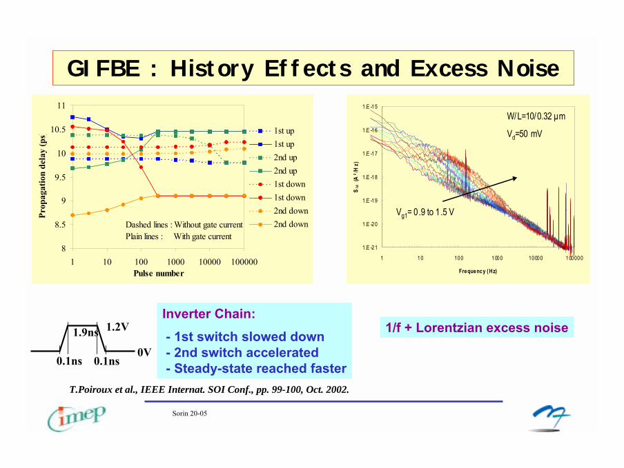
GIFBE : History Effects and Excess Noise
8
8.5
9
9.5
10
10.5
11
1 10 100 1000 10000 100000Pulse number
Prop
agat
ion
dela
y (p
s) 1st up1st up2nd up2nd up1st down1st down2nd down2nd downDashed lines : Without gate current
Plain lines : With gate current
1.9ns
0.1ns 0.1ns
1.2V
0V
Inverter Chain:
- 1st switch slowed down- 2nd switch accelerated- Steady-state reached faster
T.Poiroux et al., IEEE Internat. SOI Conf., pp. 99-100, Oct. 2002.
1.E -21
1.E -20
1.E -19
1.E -18
1.E -17
1.E -16
1.E -15
1 10 100 1000 10000 100000
Frequency ( Hz)
SId
(A²/H
z)
W/L=10/0.32 µm
Vd=50 mV
Vg1= 0.9 to 1.5 V
1/f + Lorentzian excess noise
Sorin 20-05

Surprising GIFBE in Fully Depleted MOSFETs
Sorin 20-05
� Second peak even for VG2 = 0� More accumulated back interface → higher peak
� Model :
0.0 0.2 0.4 0.6 0.8 1.0 1.2 1.40
2
4
6
8
10
12
14
16
18
20
W=5µmL=10µm
Vg2=0 to -10V
g m1 (
µS)
Vg1 (V)
∆VT1 ≈ - ∆Ψs1 ≈ -Csi/(Csi + Cox1) ∆Ψs2 coupling
ID ~ (VG1 – VT1)
∆Ψ+
+×=G1
2
ox1si
si0∆V
.CC
C1 smm gg
Peak for ∆Ψs2 / ∆VG1 ≈ 1
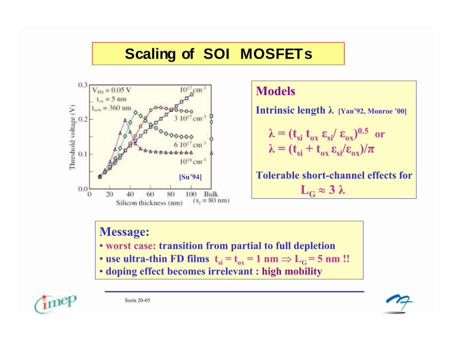
Scaling of SOI MOSFETs
Sorin 20-05
ModelsIntrinsic length λ [Yan�92, Monroe �00]
λ = (tsi tox εsi/ εox)0.5 orλ = (tsi + tox εsi/εox)/π
Tolerable short-channel effects forLG ≈ 3 λ
Message:� worst case: transition from partial to full depletion� use ultra-thin FD films tsi = tox = 1 nm ⇒ LG = 5 nm !!� doping effect becomes irrelevant : high mobility
[Su�94]

No doping effect below 15 nm !
Fringing Fields in SOI
0
50
100
150
200
250
50 100 150 200 250 300 350
S ilico n thickness (Å)
DIB
L (m
V/V
) N o dop ing effect
D op ing effect
Gro u n dPlan e
Stan d ardN A=101 8cm-3
N A=101 5cm-3
Sorin 20-05
Medication :� Thin Si film� Thin BOX (not too thin!!)� Low-K BOX (SON?)� Ground-plane (genetics!!)
0
50
100
150
200
250
0 50 100 150 200 250 300 350
Film thickness (Å)
DIB
L (m
V/V
)
StandardtBOX=380nm
Low ktBOX=380nm
Ground plane + tBOX= 50 nm
tsi=160 Å
tsi=280 Å
Simulations
ModelExperiment
0
50
100
150
200
250
0 50 100 150 200 250 300 350
Film thickness (Å)
DIB
L (m
V/V
)
StandardtBOX=380nm
Low ktBOX=380nm
Ground plane + tBOX= 50 nm
tsi=160 Å
tsi=280 Å
Simulations
ModelExperiment
No doping effect below 15 nm ! Ground plane enables thicker films!Ernst et al�99

Sorin 20-05
Distribution of Fringing Fields in SOI MOSFETs
Analytical model based on conformal mappingErnst et al�99

Narrow-Channel Effects in SOI MOSFETs
Sorin 20-05
Special SOI Effects : FBE� Subthreshold swing increases
in narrow & thick (PD) channels� Attenuated floating-body effects� No models
Classical effects : VT, gm vs. W� Coupling between width, length and thickness� LOCOS : sidewall overdoping
less efficient in ultra-thin films� STI : corner effects� Models available
[Pretet�01]
0
0.1
0.2
0.3
0.4
0.5
0.6
0.7
0.8
0 2 4 6 8 10
Channel width (µm)
Fron
t gat
e th
resh
old
volta
ge (V
)
VD = 50 mVLOCOS L = 10 µmSTI L = 10 µm
tsi = 15 nmtsi = 37 nm
tsi = 100 nm
STI tsi = 130
30
40
50
60
70
0 2 4 6 8 10Channel width (µm)
Sub
thre
shol
d sw
ing
(mV
/dec
)
tsi = 37 nm
tsi = 15 nm
VD = 2 VL = 10 µm
tsi = 100 nm
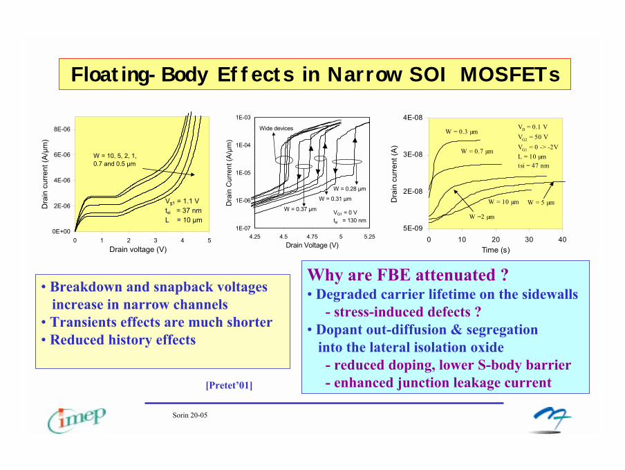
Floating-Body Effects in Narrow SOI MOSFETs
Sorin 20-05
Why are FBE attenuated ?� Degraded carrier lifetime on the sidewalls
- stress-induced defects ?� Dopant out-diffusion & segregation
into the lateral isolation oxide- reduced doping, lower S-body barrier- enhanced junction leakage current
� Breakdown and snapback voltagesincrease in narrow channels
� Transients effects are much shorter� Reduced history effects
[Pretet�01]
1E-07
1E-06
1E-05
1E-04
1E-03
4.25 4.5 4.75 5 5.25Drain Voltage (V)
Dra
in C
urre
nt (A
/µm
)
W = 0.37 µm
W = 0.31 µm
W = 0.28 µm
VG1 = 0 Vtsi = 130 nm
Wide devices
0E+00
2E-06
4E-06
6E-06
8E-06
0 1 2 3 4 5Drain voltage (V)
Dra
in c
urre
nt (A
/µm
)
Vg1 = 1.1 Vtsi = 37 nmL = 10 µm
W = 10, 5, 2, 1, 0.7 and 0.5 µm
5E-09
2E-08
3E-08
4E-08
0 10 20 30 40Time (s)
Dra
in c
urre
nt (A
)
VD = 0.1 VVG2 = 50 VVG1 = 0 -> -2VL = 10 µmtsi = 47 nm
W = 10 µm W = 5 µm
W = 0.7 µm
W = 0.3 µm
W =2 µm

Chopping the SOI MOSFET’s
S D +
Length ⇒ 10 nm
+ = Volume ?10�18 - 10�19 cm3 !
Thickness ⇒ 1 nm Width ⇒ 10 nm
� What is the meaning of 1017 cm-3 doping level ??
� Is the impurity location important ?
� A few thousands Si atoms, only. Call them by name!
� Modeling and simulation tools
� Statistical fluctuations
-40.00
0.05
0.10
0.15
0.20
0.25
-2 0 2 4Front gate voltage VG1 (V)
Dra
in c
urre
nt I D
(µA
)
6 8 10
VG2 = -5 to 5, step = 1 V
tsi = 1 nm
1 nm - MOSFET
Sorin 20-05

Ultra Thin Film Effects in SOI MOSFETs
Sorin 20-05
Sorin et al�03
1E-11
1E-09
1E-07
1E-05
1E-03
-3 -2 -1 0Gate Voltage [V]
Dra
in c
urre
nt [A
]
VG2 = 10, 12, 14, 16, 18, 25, 30 V
W = 10 µmL = 0.1 µmVD = 0.05 V
-0.7
-0.5
-0.3
-0.1
0.1
0.3
0.5
0.7
-50 0 50VG2, T2 [V]
VT1
,G1 [
V] W = 10 µmL = 10 µmVD = 0.1 Vtsi = 47 nm
B
C
D
A
VG1(VT2)VT1(VG2) -3
-2.5-2
-1.5-1
-0.50
0.51
1.52
-70 -50 -30 -10 10 30 50VG2, (T2) [V]
V T1,
(G1)
[V]
W = 10 µmL = 0.1 µmVD = 0.05 V
VG1(VT2)VT1(VG2)
Coupling curves VT1(VG2) and VT2(VG1)Thick film: the two curves interceptUltra-thin film: the curves are superposed
47 nm 8 nm
2G2ox
1ox1T V
ttV ∆−≅∆
111
22 G
oxSi
Si
ox
oxT V
CCC
ttV ∆
+−≅∆
11
22 G
ox
oxT V
ttV ∆−≅∆

Pseudo-Double-Gate Operation
Similar front and back inversion charges:
( )2T2G2ox
1ox1T1G VV
ttVV −=−
What is the correct value of VT1 and VT2 ?
� Thick film: intercept point� Thin film: any value on the common curve !� Wrong biasing: irrealistic mobility value
This relation does not apply to weak inversion :World record : swing 7 mV/dec !!
0.0E+005.0E-101.0E-091.5E-092.0E-092.5E-093.0E-093.5E-094.0E-094.5E-095.0E-09
0 0.2 0.4 0.6
Gate voltage [V]
Tran
scon
duct
ance
[S] W = 10 µm
L = 10 µmVD = 0.1 V
BC
D
A
tsi = 47 nm(a)
1E-13
1E-12
1E-11
1E-10
1E-09
1E-08
1E-07
1E-06
1E-05
1E-04
0.3 0.4 0.5 0.6 0.7 0.8
Gate voltage [V]
Dra
in c
urre
nt [A
]
VD = 0.1 Vtox2/tox1 = 10
PseudoDouble-Gate

Ultimately Thin Double-Gate MOSFETs
Sorin 20-05
� 3-nm-thick DG-MOSFET� simultaneous biasing of front and back gates: VG2 = 1.2 VG1
� outstanding transconductance gain: up to 400%� mobility effect rather than charge effect
Impact of volume inversion
Cristoloveanu et al�99

Impact of Volume Inversion on Mobility
Sorin 20-05
� Dimensional confinement: tsi < 10 nm� VT increases below 10 nm� Quantum charge distribution totally different
from classical profile (Poisson)� Enhanced volume inversion [Sangiorgi et al �98]
� SG: more carriers flow near interfaces� DG: most carriers flow far from interfaces
- lower vertical field- less roughness-induced scattering- empirical model showing mobility gain
[Cristoloveanu et al�99]

Carrier Mobility in Ultra Thin SOI MOSFETs
� Monte-Carlo simulations indicate [Gamiz�01] :(including phonon + Coulomb + surface roughness scattering)
- enhanced mobility in sub-10-nm thickness range- higher mobility in DG-MOSFETs
� Experiments in MOS-Hall devices demonstrate [Mastrapasqua�01] :- impoved mobility in recent SOI materials- good mobility in sub-10-nm thick MOSFETs- higher mobility in DG-MOSFETs
Compact models ??

Ultimate Scaling of DG-MOSFETs
� Acceptable short-channel effects if LG ≥ 3 λ
λ = [(k/2) tsi tox ]0.5 or λ = (tsi + 2ktox )/π with k = εsi/εox
� Ultra thin SOI films will be necessary for 10-nm-long DG-MOSFETs
Intrinsic length λ
Franck �01 L = 8 nm, Likharev�00

Transport Properties in FinFETs
G
FilmhFin
tFin
BOXN-channel P-channel
Lateral mobility
196 cm2/Vs Lateral interface 96 cm2/Vs
Front mobility
677 cm2/Vs Front interface 163 cm2/Vs
Back mobility
682 cm2/Vs Back interface 150 cm2/Vs
4 channels2 gatesCornersCouplingModels ??
Sorin 20-05

VD=1V
Field-Effect Junctions: Series Resistance Lowering
50-100 Centered
50-100 Drain 50-100 Source
Accumulation layers:
⇒ Low RS⇒ Low RD
Accumulationlayer:
⇒ Low RS
⇒ Improved gm
Accumulationlayer:⇒ Low RD
N N
N N N NPP
P
Allibert et al�01
Sorin 20-05

VBACKGATE
VPG
P+P+
VJG
Cross-section view
N -BODY
POLYTOX
The 4-Gate Transistor : G4-MOSFET� Maximum number of gates !� G4-MOSFET = MOSFET + JFET
2 lateral junction gates ⇒ JFET modeFront and back gates ⇒ MOSFET mode
� Standard partially-depleted SOI technology� Depletion/accumulation device� Drawn MOSFET length defines width� MOSFET width defines channel length
Sorin 20-05
Cristoloveanu et al�02
n+ D
p+
JG2
p+
JG1
G2 substrate
PolyG1
BOX
n+ S n-channel
n-channel
G4-FET
0.0 100
10 10-6
20 10-6
30 10-6
40 10-6
50 10-6
60 10-6
0 2 4 6 8 10
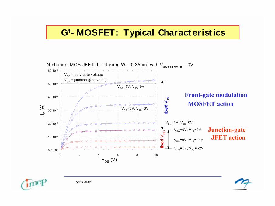
N-channel MOS-JFET (L = 1.5um, W = 0.35um) with VSUBSTRATE = 0V
I D (A
)
VDS (V)
VPG=3V, VJG=0V
VPG=0V, VJG=0V
VPG=0V, VJG= -2V
VPG=0V, VJG= -1V
VPG=1V, VJG=0V
VPG=2V, VJG=0V
fixed
VJG
fixed
VP
G
VPG = poly-gate voltageVJG = junction-gate voltage
Sorin 20-05
G4-MOSFET: Typical Characteristics
Front-gate modulationMOSFET action
Junction-gateJFET action

G4-MOSFET: Typical Characteristics
Sorin 20-05
10-10
10-9
10-8
10-7
10-6
10-5
-4 -3 -2 -1 0 1
Semilog Scale
I D (A
)
VJG (V)
VSUBSTRATE = 0VVDS = 100mV
VPG = -2V-1V0V
VPG = +1V
10-13
10-12
10-11
10-10
10-9
10-8
10-7
10-6
10-5
-2 -1.5 -1 -0.5 0 0.5 1
Semilog ScaleI D
(A)
VPG (V)
VJG = -4V
VJG = -3V
VJG = -2V-1V
VJG = 0V
10-13
10-12
10-11
10-10
10-9
10-8
10-7
10-6
10-5
-4 -3 -2 -1 0 1
Semilog Scale
I D (A
)
VJG (V)
VPG = -2V
-1V
VPG = 0V
VPG = +1V
VSUBSTRATE = -20VVDS = 100mV
� Current control by either front gate or junction gates� Back-gate depletion makes easier device cut-off (full depletion)� Top and back gate accumulation enables large currents� Applications: mixed signals, low-power modulation, RF mixers� New logic families: quaternary logic

Sorin 20-05
G4-FET: Modeling
Con
cent
ratio
n
Con
cent
ratio
n
−+=
D
DD
LWxth1
2N)x(n
α
How can a partially depleted body become fully depleted ?� The doping seen by one gate is lowered by the other gates� Concept of effective doping� The depletion region is expanded: the G4-FET can be turned off

Context:
Advanced SOI MOS scaling:• ultra-thin gate oxides =>=> new Gate Induced FBEs• the transistor body will be the thinnest layer• ultra-thin silicon films => new coupling effects• thin BOX or other types of BOX => relax self-heating• double gate transistors: new quantum and transport effects
Other modeling issues: series resistance, thickness fluctuations, quantum effects, mobility behavior, coupling and corner effects, transient and history effects, etc, etc
Join the SOI Club !!!
- SOI is no longer a promising technology- SOI is the necessary technology
Do we need a conclusion ??