u-95 application note versatile uc1834 optimizes linear
TRANSCRIPT

APPLICATION NOTE
VERSATILE UC1834 OPTIMIZESLINEAR REGULATOR EFFICIENCY
Linear voltage regulators have long been an important resource to power supplydesigners. Three terminal, fixed-voltage linear regulators find extensive use as “spot”regulators and as post-regulation stages fed by switched-mode supplies. However,while inexpensive and simple to use, these devices have several performance limitations.
First, three terminal regulators are inefficient power converters. Power dissipation in alinear regulator is given by the relation:
Most monolithic regulators now available require an input-to-output voltage differen-tial of at least 2 to 3V. This requirement can result in substantial inefficiency, particu-larly in low voltage supplies. As switched-mode power technology matures, powerlosses incurred in linear post-regulation stages are becoming more significant in termsof overall system efficiency.
Second, fixed-voltage regulators, with fixed maximum output currents, lack versatility.The use of these devices requires that OEMs maintain large, diverse inventories in orderto support a broad range of power supply requirements.
Third, fixed three-terminal devices lack thetherefore can exhibit poor load regulation.
capability of remote voltage sensing, and
Finally, the most common failure mechanism for linear regulators is a shorted passtransistor. All critical loads, therefore, require over-voltage protection not provided bythree-terminal regulators.
IMPROVED PERFORMANCE WITH UC1834
The UC 1834 is a programmable linear regulator control IC which, with an external passtransistor, forms a complete linear power supply. This IC provides solutions to all theabove-mentioned drawbacks of three-terminal devices.
Figure 1 shows the basic elements of positive and negative regulators implemented withthe UC1834. An error amplifier monitors the output voltage and provides appropriatebias to the pass transistor (Q1) through a driver stage. This high-gain error amplifier(E/A) allows good dynamic regulation while allowing Q1 to operate near saturation inthe common-emitter mode. The circuits can achieve high efficiency by maintainingoutput regulation with an input-to-output voltage differential as low as 0.5V (at 5A).
U - 9 5
3-21

APPLICATION NOTE U-95
The UC1834 has both positive and negative reference voltage outputs, as well as asink-or-source driver stage, as shown in Figure 1. These features allow implementationof either positive or negative regulators with this single IC, as shown. Output voltagesfrom 1.5V to nearly 40V can be programmed by appropriate choice of remote sensingdivider elements. Remote sensing also allows improved DC and dynamic loadregulation.
Figure 1. Basic Elements of (a.) Positive and (b.) Negative Regulatorsimplemented with a UC1834
3-22

APPLICATlON NOTE U-95
The UC1834 is intended to provide a complete linear regulation system. Therefore,many auxiliary features are included on this IC which eliminate the need for additionalcircuit elements. Figure 2 shows a more complete block diagram including on-chipprovisions for current sensing, fault monitoring, remote voltage sensing, and thermalprotection.
Figure 2. UC1834 Block Diagram
DRIVING THE PASS TRANSISTOR
Figure 3 shows suggested pass transistor configurations for implementing either posi-tive or negative regulators with the UC1834. For those low current (5200mA) applica-tions in which efficiency is not extremely critical, the UC1834 output transistor canserve as the pass element, resulting in the simple configurations of Figure 3a. Anexternal pass transistor is needed for output currents greater than 200mA. With thecircuits of Figure 3c, the UC1834 can maintain regulation while operating the passtransistor near saturation. Operation at very high output currents (to ~ 30A) is possiblewith the Darlington pass elements of Figure 3d.
Q3-23
Q
.

APPLICATION NOTE U-95
Positive Output Negative Output
Figure 3. Pass Transistor Configurations
3-24

APPLICATION NOTE U-95
Current in the UC 1834 output transistor is self-limiting, for improved reliability. Thislimiting is achieved by Q3 and R1 in Figure 4a. The resulting maximum output currentis a function of temperature as shown in Figure 4b.
A resistor (RE) is shown in series with the drive transistor in Figures 3c, d. This resistorshares base-drive power with the transistor, allowing cooler, more reliable operation ofthe IC. RE should be as large as possible while still supporting adequate pass transistorbase current under worst-case conditions of low input voltage and maximum outputcurrent:
VRE(min) = VIN(min) - VBE(max)(Q2) - VCE(sat)(max)(Ql)
IB(maxMQ2) = IO(max)/ &min)(Q2)RE(opt) = VRE(min)/ IB(max)(QZ)
where: VRE (min) is minimum voltage available to REIB(max) (~2) is maximum required base drive to Q2RE(opt) is optimum value of RE.
RE also enhances stability by allowing operation of Q1 as an emitter-follower, therebyeliminating fl~l from the loop transfer function:
ICCQl) = IE(Q1) q (VE/Aout - VBE(Q~) - VBE(QB))/ RE (P independent).
-55 25 125T (°C)
a. b.
Figure 4 a. Driver Current Limiting Circuitb. Resulting Maximum Current vs Temperature
3-25

APPLICATION NOTE
CURRENT SENSING
U-95
In order to protect the pass transistor from damage due to overheating, one must senseits emitter current (1~) and then decrease the base drive if 1~ is excessive. The UC 1834current sense amplifier (CS/A) accomplishes these tasks.
The UC1834 CS/A has a common mode range which includes both input supply“rails”. This extended range is made possible by introducing matched voltage offsets inthe differential input paths, as shown in Figure 5. Internal current sources bias the offsetdiodes in their appropriate direction. Which bias source (+ or -) is active is determinedby whether the CS/A positive (+) input is greater or less than VIN/~. Therefore, it isadvisable to configure the sensing circuit such that the voltage at CS/A(+) will not crossVIN/~ during operation. This precludes sensing in series with the load for mostapplications.
RSENSE
Figure 5. Two Diode-Drop Offset Allows Current Sensing at Supply Rail
The CS/A has a programmable current limit threshold which can be set between 0mVand 150mV. Programming is achieved by setting the voltage at the “Threshold Adjust”terminal (pin 4) to 10 • VTH(desired ) . The factor of 10 provides good noise immunity atpin 4 while allowing low power dissipation in the current sensing resistor. Figure 6shows the guaranteed relationship between Vp1~4 and the actual resulting thresholdacross the CS/A inputs. Note that the threshold is clamped at 150mV if pin 4 is open orif Vp1~4 > 1.5V. The “Threshold Adjust” input is high impedance (bias current is lessthan lOpA), allowing simple programming through a voltage divider from the 1.5Vreference output. However, loading the 1.5V reference will affect the regulation of the-2.0V reference. Figure 7 shows how to compensate for this loading with a singleresistor when the -2.0V reference is needed.
3-26

APPLICATION NOTE U-95
VOLTAGE AT THRESHOLD ADJUST PIN (PIN 4) - V
Figure 6. Guaranteed Tolerances on C/S Threshold Adjustment
Figure 7. Setting the Current Threshold andCompensating the -2.0V Reference
The CS/A functions by pulling the E/A output low, turning off the output driver(Figure 8). As current approaches the threshold value, the E/A attempts to correct forthe CS/A output, resulting in an E/A input offset voltage. The supply output voltagecan decrease a proportional amount. When the CS/A input voltage differential reachesthe current sense threshold, then the pass transistor is totally controlled by the CS/A.The combined CS/A and E/A gains and output configurations result in the currentlimit knee characteristic of Figure 9.
3-27
73’3

offset voltage at error amp inputs referenced to inv inputs
APPLICATION NOTE
SENSE-
SENSE+
THRESHOLDADJUST
Figure 8. Current Sense Tied to E/A Output
-10 -7.5 -5.0 -2.5 CURRENT SENSETHRESHOLD
DIFFERENTIAL VOLTAGE AT CURRENT SENSE INPUTS - mV(REFERENCED TO SENSE - INPUT)
Figure 9. Current Limiting Knee Characteristic
FOLD BACK CURRENT LIMITING
It is desirable to put an upper limit on pass transistor power dissipation in order toprotect that device. Ideally, for a constant power limit:
or:where K is a constant(ignoring the sense resistor voltage drop).
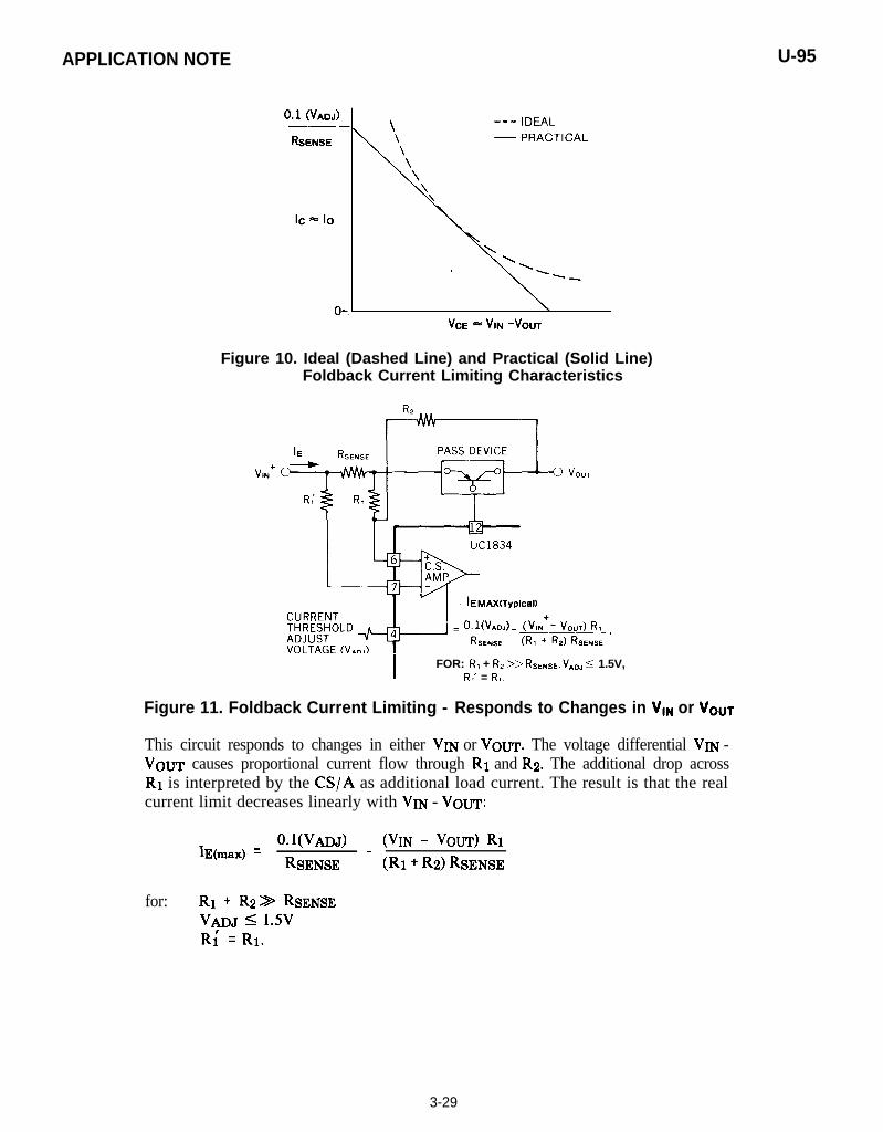
As the input-to-out voltage differential increases, it is necessary to “fold back” themaximum allowable current. This ideal foldback characteristic is shown in Figure 10,along with a practical characteristic achievable with the circuit of Figure 11.
3-28
U-95
ideal practical
APPLICATION NOTE U-95
Figure 10. Ideal (Dashed Line) and Practical (Solid Line)Foldback Current Limiting Characteristics
FOR: RI + R2 >> RsENsE, VADJ I 1.5V,R,’ = R,.
Figure 11. Foldback Current Limiting - Responds to Changes in VIN or Vou~
This circuit responds to changes in either VIN or VOUT. The voltage differential VIN -VOUT causes proportional current flow through RI and R2. The additional drop acrossR1 is interpreted by the CS/A as additional load current. The result is that the realcurrent limit decreases linearly with VIN - Vow:
IE(xnax) =OWADJ) (VIN - VOUT) R1
RSENSE - (Rl+R2)RmNSE
for: RI + R2B RSENSEVApJ 5 1.5v
Ri = RI.
Q3-29

APPLICATION NOTE
This technique can be susceptible to “latch-off”. If a momentary short at the supplyoutput causes 1~ to drop to zero (pass transistor cut off), then VOUT cannot recoverwhen the short is subsequentially removed. To prevent this undesirable operation, onemust ensure that IE( max) > 0 when VOUT = 0 and VIN is at its minimum:
Figure 12 shows an alternative foldback current limiting scheme which responds todecreased VOUT only. This circuit gives the output characteristics of Figure 13, definedby the following relation:
This technique is immune to “latch-off” because the minimum current limit is alwaysnon-zero.
Figure 12. Foldback Current Limiting – Responds to Changes in VouT Only
U-95
3-30

APPLICATION NOTE U-95
VOUTVOUT (Designed)
Figure 13. Foldback Current Limiting Characteristic
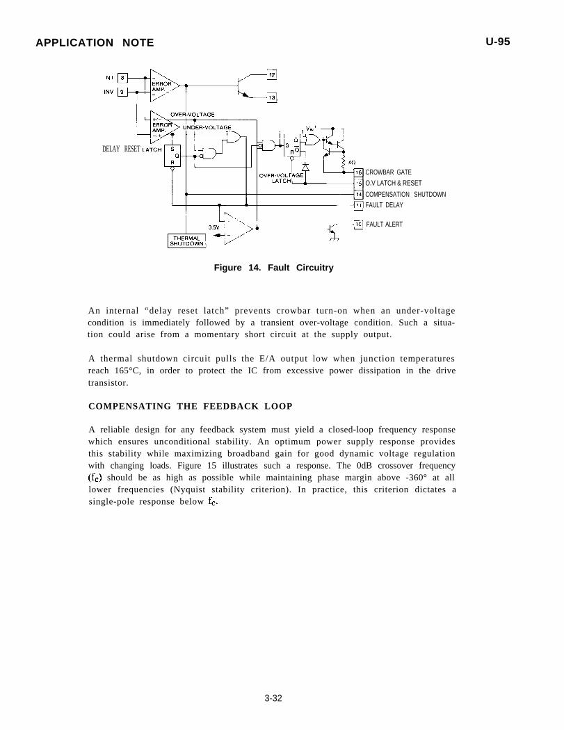
F A U L T C I R C U I T R Y A N D S Y S T E M I N T E R F A C I N G
In order to minimize the need for additional components, the UC 1834 has on-chipprovisions for fault detection and logic interfacing. These features are particularlyuseful when the linear regulator is part of a larger power supply system.
As shown in Figure 14, an internal comparator monitors the UC1834 E/ A inputs. Thiscomparator has two thresholds, for over- and under-voltage detection. Comparatorthresholds are fixed at 1 VN.J. - VINV. 1 = 150mV. The resulting output voltage windowsfor non-fault operation are:
± 10% for positive (+) supplies
= ± 7.5% for negative (-) supplies.
A fault delay circuit prevents transient over- or under-voltage conditions (due to arapidly changing load) being defined as faults. The delay time is programmable. Anexternal capacitor at pin 11 is charged from an internal 75pA source. The delay periodends when the capacitor voltage reaches ~3.5V. The delay time is therefore ~47ms/ pF.The fault alert output (pin 10) becomes an active low if an out-of-tolerance conditionpersists after the delay period. When no fault exists, this output is an open collector.
An over-voltage fault activates a 100mA crowbar gate drive output (pin 16) which canbe used to switch on a shunt SCR. Such a fault also sets an over-voltage latch if the resetvoltage (pin 15) is above the latch reset threshold (typically 0.4V). When the latch is setits Q output will pull pin 15 low through a series diode. As long as a nominal pull-upload exists, the series diode prevents 0 from pulling pin 15 below the reset threshold.However, pin 15 is pulled low enough to disable the driver outputs if pins 15 and 14 aretied together. With pin 15 and 14 common, the regulator will latch off in response to anover-voltage fault. If the fault condition is cleared and pins 14 and 15 are momentarilypulled below the latch reset threshold, the driver outputs are re-enabled.
3-31
APPLICATION NOTE
DELAY RESET
CROWBAR GATE
O.V LATCH & RESET
COMPENSATION SHUTDOWN
FAULT DELAY
FAULT ALERT
Figure 14. Fault Circuitry
An internal “delay reset latch” prevents crowbar turn-on when an under-voltagecondition is immediately followed by a transient over-voltage condition. Such a situa-tion could arise from a momentary short circuit at the supply output.
A thermal shutdown circuit pulls the E/A output low when junction temperaturesreach 165°C, in order to protect the IC from excessive power dissipation in the drivetransistor.
COMPENSATING THE FEEDBACK LOOP
A reliable design for any feedback system must yield a closed-loop frequency responsewhich ensures unconditional stability. An optimum power supply response providesthis stability while maximizing broadband gain for good dynamic voltage regulationwith changing loads. Figure 15 illustrates such a response. The 0dB crossover frequency(fc) should be as high as possible while maintaining phase margin above -360° at alllower frequencies (Nyquist stability criterion). In practice, this criterion dictates asingle-pole response below fc.
U-95
3-32

APPLICATION NOTE U-95
Figure 15. Desired Closed-Loop Response
Linear supplies using the UC 1834 will usually have a current limiting loop in addition tothe voltage control loop, as illustrated for two basic configurations* in Figure 16. Bothloops must be stabilized for reliable operation. This is accomplished by appropriatelycompensating the E/A and CS/A at their common output (pin 14). Design of thecompensation networks will often require an iterative procedure, since the compensa-tion for one loop will affect the response of the other. A straightforward approach isoutlined below:
1). Determine the frequency response of all voltage loopE/A. Appendix I offers guidelines for this step.
e l e m e n t s e x c l u d i n g t h e
2). Design E/A compensation giving a frequency response which, when added tothe response calculated in step 1, will yield a total loop characteristicconsistent with the objectives outlined above. (Appendix II.)
3). Calculate the current loop response and determine whether it satisfies theNyquist stability criterion. (Appendix III.) If not, add additionalcompensation and then recalculate the voltage loop response.
4). Iterate if necessary.
*All other configurations of Figure 3 are variants of these two. and can be treated in essentially the same ways.
3-33

APPLICATION NOTE U-95
CONFIGURATION I CONFIGURATION II
RE
C. d.
Figure 16. Voltage and Current Loops for Two Basic Configurations
EXAMPLE
Figure 17 shows a 5V, 5A (positive output) supply of the class shown in Figures 16a, c.This circuit tends toward instability when it is lightly loaded because of the high gain(p q 200) of the pass transistor at low currents. Output capacitor C2 is needed tointroduce a pole which rolls off the gain of the voltage loop to 0dB at 100kHz, avoidinginstability due to the additional phase shift of a transistor pole at:
Assuming a minimum load of 1A (RL q 5R), the low frequency voltage loop gain,excluding the E/A, is (from Appendix I):
3-34

APPLICATION NOTE U-95
Figure 17. 0.5V Input-Output Differential 5A Positive Regulator
A pole at 5kHz is required in order to roll off from 26dB to 0dB at 100kHz. The requiredvalue of C2 is therefore given by:
The dashed curves of Figure 18a show the resulting voltage loop response, excluded thecompensated E/A. Notice that the 5kHz pole (just added) itself introduces undesirablephase lag. This can be corrected by positioning the compensation zero (see Appendix II)at the same frequency. With (providing ~ 0dBE/A gain above 5kHz), then:
The gain and phase of the compensated E/A (dotted lines) and complete voltage loop(solid lines) are also shown in Figure 18a.
The resulting current loop response (Figure 18b) is seen to meet the stability criterion.Gain above 5kHz is given by (from Appendix III):
3-35

APPLICATION NOTE U-95
a. b.
Figure 18. Loop Responses for Circuit of Figure 17a. Voltage Loopb. Current Loop
Reasonable phase margin (~40°) is maintained as the transistor and CS/A poles rolloff this small gain to 0dB.
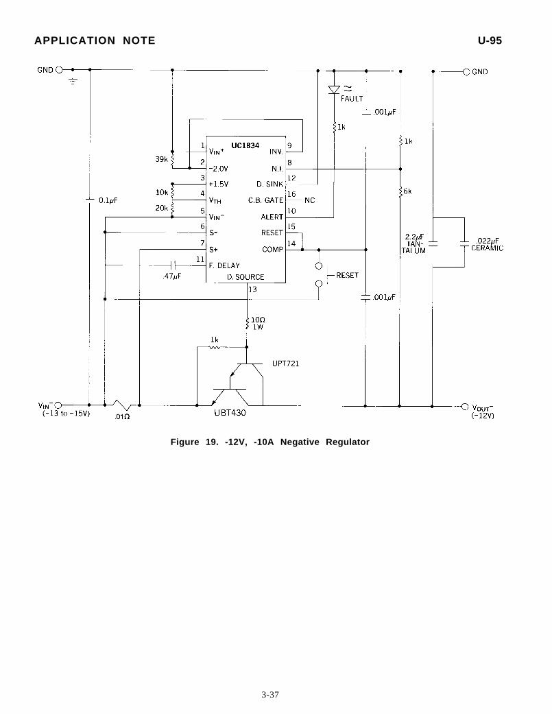
Figure 19 shows the UC1834 used to implement a negative output supply. A Darlingtonpass element provides adequate gain for operation at output current levels up to 10A.
CONCLUSION
Ever-increasing requirements for improved power supply economy and efficiency haveproduced a need for a versatile control IC capable of minimizing power losses in linearregulators. The UC1834 meets this need while also supporting all the auxilliary func-tions required of such supplies. This control circuit provides for optimized performancein a broad range of linear regulators, and in fact extends the range of applications forwhich such regulators are appropriate.
3-36
APPLICATION NOTE U-95
Figure 19. -12V, -10A Negative Regulator
3-37

APPLICATION NOTE U-95
APPENDIX I - FREQUENCY RESPONSE OF VOLTAGE LOOP ELEMENTS
A. The configuration of Figure 16a has, in addition to the compensated E/A, thefollowing loop elements:
l Drive Transistor - RE allows operation of the driver as an emitter follower.Together these elements have an effective small signal AC conductance of 1/RE.
l Pass Transistor - Low frequency gain (p) and unity-gain frequency (f7) are usuallyspecified. The pass transistor adds a pole to the loop transfer function at f P=fr/P.Therefore, in order to maintain phase margin at low frequencies, the best choice fora pass device is often a high frequency, low gain switching transistor. Furtherimprovement can be obtained by adding a base-emitter resistor ( RBE in Figure 16a)which increases the pole frequency to:
fp =
where:
l Load Impedance - Load characteristics vary greatly with application and operatingconditions. The most commonly used models and their respective (s domain)transfer functions are given in Table 1. Note that there are no poles in the transferfunctions of those loads which lack shunt capacitance. This can result in a looptransfer function which cannot be rolled off to 0dB at a suitably low frequency usingsimple E/A compensation networks. For this reason a shunt output capacitor isoften added to supplies which must drive loads having low or indeterminantcapacitance.
l Voltage Divider - The output sensing network introduces a gain of Rz/(Rl + R2).
l Total Loop Gain, excluding the E/A, is therefore given by:
B. The circuit of Figure 16b has a more straightforward response, since the only element(other than the E/A) which introduces any gain is the voltage divider:
3-38

APPLICATION NOTE U-95
Table 1. Load Models and their Transfer Functions
3-39

APPLICATION NOTE U-95
APPENDIX II - ERROR AMPLIFIER RESPONSE
Figure 20 shows the open-loop gain and phase response of the UC1834 E/A whenlightly loaded. The gain curve represents an upper limit on the gain available from thecompensated amplifier. Note that a second-order pole occurs near 800kHz. Stablecircuits will require a 0dB crossover well below this frequency (fc :‘, 500kHz).
The E/A can be compensated with or without the use of local feedback. When operatedwithout such feedback (Figure 21a) the transconductance properties of the E/Abecome evident; i.e. the voltage gain in given by:
where:
10 100 1K 10K 1OOK 1MFREQUENCY - HERTZ
Figure 20. Error Amplifier Gain and Phase Frequency Response
When the E/A has local feedback (Figure 21b), its gain is. to a first approximation,independent of transconductance:
a. b.
I Figure 21. E/A Compensation (a.) Without and (b.) With Local Feedback
3-40

APPLICATION NOTE U-95
However , the use of local feedback creates an addi t ional loop which must beindependently stable. The UC1834 has no internal compensation to ensure thisstability, so additional external compensation is usually required. An 820pF capacitorfrom the E/A output to ground will stabilize this inner voltage loop while alsoenhancing current loop stability.
An additional drawback to the use of local feedback is that ZF places a DC load on theE/A output. With a transconductance amplifier this results in additional input offsetvoltage:
This offset results in degradation of DC regulation. The problem can be averted bytaking local feedback from the emitter of the drive transistor if the driver is configuredas an emitter-follower.
Whatever the compensation scheme, the UC1834 E/A output can sink or source amaximum of 100pA.
Table 2 shows two typical compensation schemes and the resulting E/A transferfunctions. The first of these circuits is most widely used.
Table 2. E/A Compensation Circuits and Gain Response
3-41

APPLICATION NOTE U-95
APPENDIX III - FREQUENCY RESPONSE OF THE CURRENT LOOP
CS/A - Figure 22 shows the open-loop gain and phase response of the UC 1834CS/A. This is also a transconductance amplifier, having gM = l/ 7Ofl= 14mS. Thevoltage gain is analogous to that of the E/A. The E/A compensation impedance (Zcor ZF(E/A)) is also seen by the CS/A output. For purposes of small signal ACanalysis, the CS/A will always see this impedance as being returned to VE (asshown in Figures 16c, d) when the E/A is compensated by either of the methodsshown in Table 2.
Figure 22. Current Sense Amplifier Gain and Phase Frequency Response
Pass Transistor - Introduces current gain p to the loop transfer of both basicconfigurations (Figures 16c, d). Considerations outlined in Appendix I also applyhere.
Sense Resistor - Resistance value RSENSE appears in transfer function for bothconfigurations.
Drive Transistor - In the circuit of Figure 16c, RE allows operation of the driver asan emitter-follower. Effective conductance is l/ RE.
Closed-loop responses are given by the following:
for circuit of Figure 16c:
for circuit of Figure 16d:
UNITRODE CORPORATION7 CONTINENTAL BLVD. l MERRIMACK. NH 03054TEL (603) 424-2410 l FAX (603) 424-3460
3-42
f < 500kHz, f <

IMPORTANT NOTICE
Texas Instruments and its subsidiaries (TI) reserve the right to make changes to their products or to discontinueany product or service without notice, and advise customers to obtain the latest version of relevant informationto verify, before placing orders, that information being relied on is current and complete. All products are soldsubject to the terms and conditions of sale supplied at the time of order acknowledgement, including thosepertaining to warranty, patent infringement, and limitation of liability.
TI warrants performance of its semiconductor products to the specifications applicable at the time of sale inaccordance with TI’s standard warranty. Testing and other quality control techniques are utilized to the extentTI deems necessary to support this warranty. Specific testing of all parameters of each device is not necessarilyperformed, except those mandated by government requirements.
CERTAIN APPLICATIONS USING SEMICONDUCTOR PRODUCTS MAY INVOLVE POTENTIAL RISKS OFDEATH, PERSONAL INJURY, OR SEVERE PROPERTY OR ENVIRONMENTAL DAMAGE (“CRITICALAPPLICATIONS”). TI SEMICONDUCTOR PRODUCTS ARE NOT DESIGNED, AUTHORIZED, ORWARRANTED TO BE SUITABLE FOR USE IN LIFE-SUPPORT DEVICES OR SYSTEMS OR OTHERCRITICAL APPLICATIONS. INCLUSION OF TI PRODUCTS IN SUCH APPLICATIONS IS UNDERSTOOD TOBE FULLY AT THE CUSTOMER’S RISK.
In order to minimize risks associated with the customer’s applications, adequate design and operatingsafeguards must be provided by the customer to minimize inherent or procedural hazards.
TI assumes no liability for applications assistance or customer product design. TI does not warrant or representthat any license, either express or implied, is granted under any patent right, copyright, mask work right, or otherintellectual property right of TI covering or relating to any combination, machine, or process in which suchsemiconductor products or services might be or are used. TI’s publication of information regarding any thirdparty’s products or services does not constitute TI’s approval, warranty or endorsement thereof.
Copyright 1999, Texas Instruments Incorporated