uart to wi-fi® bridge with 24-v ac power (rev. a)
TRANSCRIPT
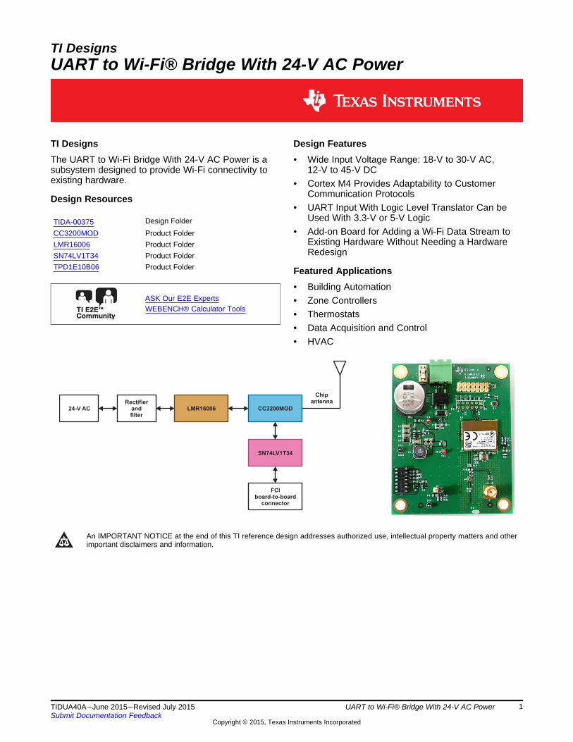
24-V ACRectifier
andfilter
LMR16006 CC3200MOD
SN74LV1T34
FCIboard-to-board
connector
Chipantenna
TI DesignsUART to Wi-Fi® Bridge With 24-V AC Power
TI Designs Design FeaturesThe UART to Wi-Fi Bridge With 24-V AC Power is a • Wide Input Voltage Range: 18-V to 30-V AC,subsystem designed to provide Wi-Fi connectivity to 12-V to 45-V DCexisting hardware. • Cortex M4 Provides Adaptability to Customer
Communication ProtocolsDesign Resources• UART Input With Logic Level Translator Can be
Used With 3.3-V or 5-V LogicDesign FolderTIDA-00375• Add-on Board for Adding a Wi-Fi Data Stream toCC3200MOD Product Folder
Existing Hardware Without Needing a HardwareLMR16006 Product FolderRedesignSN74LV1T34 Product Folder
TPD1E10B06 Product Folder Featured Applications• Building Automation
ASK Our E2E Experts • Zone ControllersWEBENCH® Calculator Tools • Thermostats
• Data Acquisition and Control• HVAC
An IMPORTANT NOTICE at the end of this TI reference design addresses authorized use, intellectual property matters and otherimportant disclaimers and information.
1TIDUA40A–June 2015–Revised July 2015 UART to Wi-Fi® Bridge With 24-V AC PowerSubmit Documentation Feedback
Copyright © 2015, Texas Instruments Incorporated

Key System Specifications www.ti.com
1 Key System Specifications
Table 1. Key System Specifications
PARAMETER SPECIFICATION DETAILS24 V nominal, AC or DC
Input voltage 8-V to 45-V DC See Section 4.1, Section 4.224-V AC + 25%
Power connector Phoenix contact 1757242 See Section 4.1Interface UART TX and RX signals See Section 4.4
Interface connector FCI 55510-114TRLF See Section 4.4
2 UART to Wi-Fi® Bridge With 24-V AC Power TIDUA40A–June 2015–Revised July 2015Submit Documentation Feedback
Copyright © 2015, Texas Instruments Incorporated

www.ti.com System Description
2 System DescriptionThe TIDA-00375 reference design is a UART to Wi-Fi Bridge that is powered by 24-V AC nominally. Theinput voltage can range from 8-V to 45-V DC or 18-VRMS to 30-VRMS AC. It is intended for use withindustrial and building automation systems that need to add Wi-Fi capability to an existing product. TheUART to Wi-Fi Bridge can be used as a cable replacement or to add wireless functions to an existinginstallation. This reference design has a bridge rectifier, input voltage filter, and a 3.3-V output step-downregulator to supply the primary system voltage.
Figure 1. UART to Wi-Fi Bridge With 24-V AC Power
3TIDUA40A–June 2015–Revised July 2015 UART to Wi-Fi® Bridge With 24-V AC PowerSubmit Documentation Feedback
Copyright © 2015, Texas Instruments Incorporated

24-V ACRectifier
andfilter
LMR16006 CC3200MOD
SN74LV1T34
FCIboard-to-board
connector
Chipantenna
Block Diagram www.ti.com
3 Block Diagram
Figure 2. TIDA-00375 Block Diagram
4 UART to Wi-Fi® Bridge With 24-V AC Power TIDUA40A–June 2015–Revised July 2015Submit Documentation Feedback
Copyright © 2015, Texas Instruments Incorporated

CC3200MOD
VCC
GPIO &PeripheralInterfaces
RF Filter
Serial Flash8Mbit
Pull-upresistors
CC3200R1M2RGC
PowerInductors
Caps
32-KHzCrystal
40-MHzCrystal
www.ti.com Block Diagram
3.1 Highlighted Products
3.1.1 CC3200MOD SimpleLink Wi-Fi and Internet-of-Things Module Solution, a Single-Chip WirelessMCU
This device is the industry’s first programmable FCC, IC, CE, and Wi-Fi Certified Wireless microcontroller(MCU) module with built-in Wi-Fi connectivity. Created for the Internet of Things (IoT), the SimpleLinkCC3200MOD is a wireless MCU module that integrates an ARM® Cortex®-M4 MCU, allowing customersto develop an entire application with a single device. With on-chip Wi-Fi, Internet, and robust securityprotocols, no prior Wi-Fi experience is required for faster development. The CC3200MOD integrates allrequired system-level hardware components including clocks, SPI flash, RF switch, and passives into anLGA package for easy assembly and low-cost PCB design. The CC3200MOD is provided as a completeplatform solution including software, sample applications, tools, user and programming guides, referencedesigns, and the TI E2E support community.
The applications MCU subsystem contains an industry-standard ARM Cortex-M4 core running at 80 MHz.
The device includes a wide variety of peripherals, including a fast parallel camera interface, I2S, SD/MMC,UART, SPI, I2C, and four-channel ADC. The CC3200 family includes flexible embedded RAM for code anddata; ROM with external serial flash bootloader and peripheral drivers; and SPI flash for Wi-Fi networkprocessor service packs, Wi-Fi certificates, and credentials.
The Wi-Fi network processor subsystem features a Wi-Fi Internet-on-a-chip™ and contains an additionaldedicated ARM MCU that completely off-loads the applications MCU. This subsystem includes an802.11 b/g/n radio, baseband, and MAC with a powerful crypto engine for fast, secure Internetconnections with 256-bit encryption. The CC3200MOD supports station, access point, and Wi-Fi Direct™modes. The device also supports WPA2 personal and enterprise security and WPS 2.0. The Wi-FiInternet-on-a-chip includes embedded TCP/IP and TLS/SSL stacks, HTTP server, and multiple Internetprotocols. The power-management subsystem includes integrated DC-DC converters supporting a widerange of supply voltages. This subsystem enables low-power consumption modes, such as the hibernatewith RTC mode requiring less than 7 μA of current.
Figure 3. CC3200MOD Module Functional Block Diagram Figure 4. CC3200 Hardware Overview
5TIDUA40A–June 2015–Revised July 2015 UART to Wi-Fi® Bridge With 24-V AC PowerSubmit Documentation Feedback
Copyright © 2015, Texas Instruments Incorporated

GND
SW
CB
VIN
FB
SHDN
HS
Driver
EA
0.765 V
Bootstrap
Regulator
Frequency
Shift
Bandgap
Ref
Main OSC
Logic &
PWM Latch
PW
M
Com
para
tor
+±
Leading Edge
Blanking
™
Slope
Compensation
COMPSS
++±
CB Refresh
Wimp FET
Current Sense
Block Diagram www.ti.com
3.1.2 LMR16006 SIMPLE SWITCHER® 60-V Buck Regulator With High Efficiency ECO ModeThe LMR16006 is a PWM DC/DC buck (step-down) regulator. With a wide input range of 4 to 60 V, it issuitable for a wide range of application from industrial to automotive for power conditioning from anunregulated source. The regulator’s standby current is 28 μA in ECO mode, which is suitable for batteryoperating systems. An ultra-low 1-μA shutdown current can further prolong battery life. Operatingfrequency is fixed at 0.7 MHz (X version) and 2.1 MHz (Y version) allowing the use of small externalcomponents while still being able to have low output ripple voltage. Soft-start and compensation circuitsare implemented internally, which allows the device to be used with minimized external components. TheLMR16006 is optimized for up to 600 mA load currents. It has a 0.765-V typical feedback voltage. Thedevice has built-in protection features such as pulse-by-pulse current limit, thermal sensing, and shutdowndue to excessive power dissipation. The LMR16006 is available in a low profile SOT-6L package.
Figure 5. LMR16006 Functional Block Diagram
6 UART to Wi-Fi® Bridge With 24-V AC Power TIDUA40A–June 2015–Revised July 2015Submit Documentation Feedback
Copyright © 2015, Texas Instruments Incorporated

1 2
2 4
A Y
www.ti.com Block Diagram
3.1.3 SN74LV1T34 Single Power Supply Buffer GATE CMOS Logic Level ShifterThe SN74LV1T34 is a low-voltage CMOS gate logic that operates at a wider voltage range for industrial,portable, telecom, and automotive applications. The output level is referenced to the supply voltage and isable to support 1.8, 2.5, 3.3, and 5-V CMOS levels.
The input is designed with a lower threshold circuit to match 1.8-V input logic at VCC = 3.3 V and can beused in 1.8 to 3.3-V level up translation. In addition, the 5-V tolerant input pins enable down translation(for example, 3.3-V to 2.5-V output at VCC = 2.5 V). The wide VCC range of 1.8 to 5.5 V allows generationof desired output levels to connect to controllers or processors.
The SN74LV1T34 is designed with current-drive capability of 8 mA to reduce line reflections, overshoot,and undershoot caused by high-drive outputs.
Figure 6. SN74LV1T34 Logic Diagram
3.1.4 TPD1E10B06 Single Channel ESD in 0402 Package With 10-pF Capacitance and 6-V BreakdownThe TPD1E10B06 device is a single-channel electrostatic discharge (ESD) transient voltage suppression(TVS) diode in a small 0402 package. This TVS protection product offers ±30-kV contact ESD, ±30-kVIEC air-gap protection, and has an ESD clamp circuit with a back-to-back TVS diode for bipolar orbidirectional signal support. The 12-pF line capacitance of this ESD protection diode is suitable for a widerange of applications supporting data rates up to 400 Mbps. The 0402 package is an industry standardand is convenient for component placement in space-saving applications.
Typical applications of this ESD protection product are circuit protection for audio lines (microphone,earphone, and speaker phone), SD interfacing, keypad or other buttons, VBUS pin and ID pin of USBports, and general-purpose I/O ports. This ESD clamp is good for the protection of the end equipment likeebooks, tablets, remote controllers, wearables, set-top boxes, and electronic point of sale equipment.
Figure 7. TPD1E10B06 Device Configuration
7TIDUA40A–June 2015–Revised July 2015 UART to Wi-Fi® Bridge With 24-V AC PowerSubmit Documentation Feedback
Copyright © 2015, Texas Instruments Incorporated
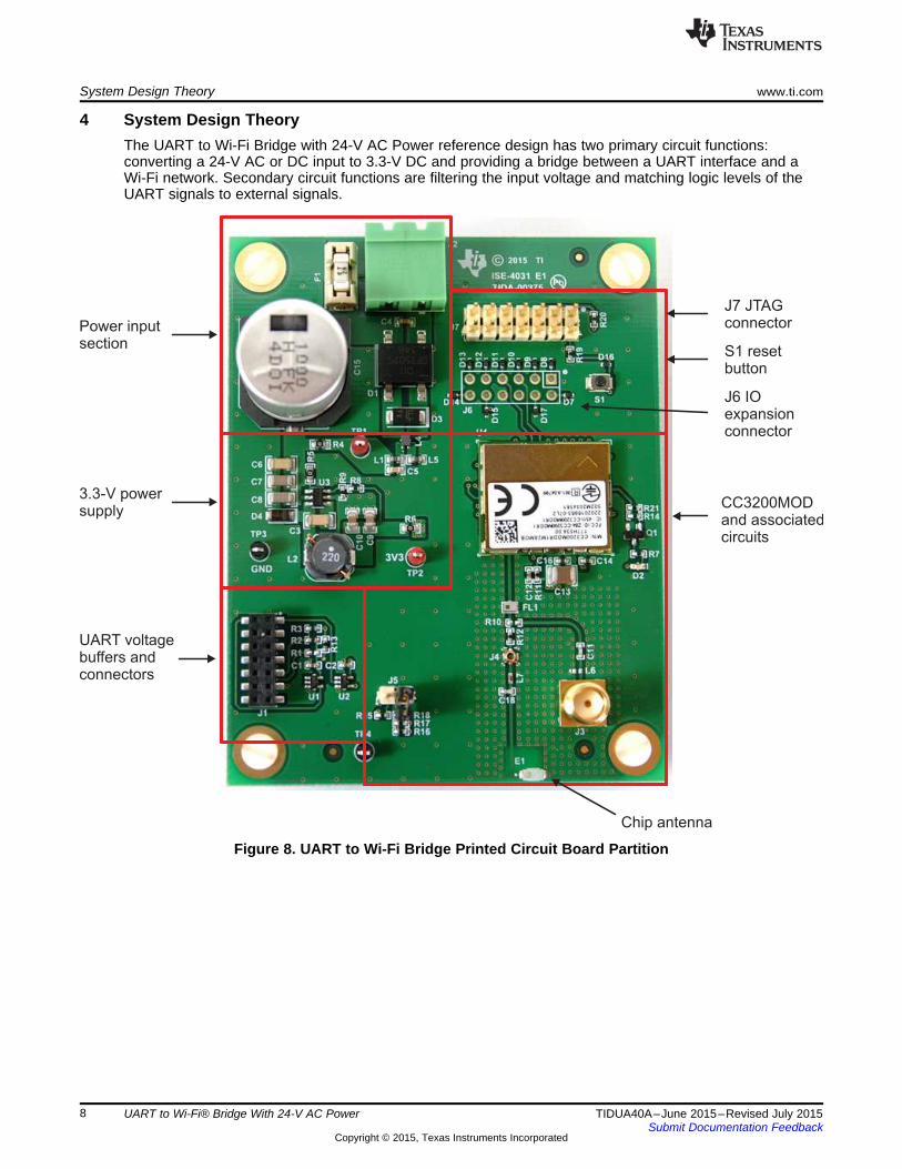
Power inputsection
3.3-V powersupply
UART voltagebuffers andconnectors
J7 JTAGconnector
S1 resetbutton
J6 IOexpansionconnector
CC3200MODand associatedcircuits
Chip antenna
System Design Theory www.ti.com
4 System Design TheoryThe UART to Wi-Fi Bridge with 24-V AC Power reference design has two primary circuit functions:converting a 24-V AC or DC input to 3.3-V DC and providing a bridge between a UART interface and aWi-Fi network. Secondary circuit functions are filtering the input voltage and matching logic levels of theUART signals to external signals.
Figure 8. UART to Wi-Fi Bridge Printed Circuit Board Partition
8 UART to Wi-Fi® Bridge With 24-V AC Power TIDUA40A–June 2015–Revised July 2015Submit Documentation Feedback
Copyright © 2015, Texas Instruments Incorporated

0.1µF
100V
C6
10µF
6.3V
C9
1
2
J2
1757242
GND
CB1
VIN5
GND2
SHDN4
FB3
SW6
U3
LMR16006XDDC
D4MBR1H100SFT3G
1µF100V
C7
0.1µF
100V
C3
TDK
22µH
L2
CLF7045T-220M
SW
VDC_IN
10µF
6.3V
C10
3V3
0
R63V3_OUT
1µF100V
C8
0
R5
VOUT = 0.765 V (1+(Rtop/Rbottom))Rtop = Rbottom ((VOUT/0.765 V)-1)
75.0kR9
249kR8
VFB
0
R4
GND
123 4
Bourns
L4SRF2012-300Y
330 ohm
MuRata
L1
BLM18SG331TN1D
330 ohm
MuRata
L5
BLM18SG331TN1D
0.01µF
100V
C5
1000pF
100V
C4
45V
D3SMAJ45CA
TP1
TP3
GND
TP4
TP2
1000µF50V
C15
~3
+1
~4
-2
D1
DF1502S-T
IN1IN2
IN2_FF1
0154002.DRT
www.ti.com System Design Theory
4.1 Power InputD1 is a bridge rectifier to convert the AC input to DC for use by the step-down regulator. D3 is a transientabsorber with a 45-V break-down voltage, which limits the input voltage range to 45 V. C4, L1, L4, L5, andC5 form an input filter to reduce conducted RF both into and out of the system. L1 and L5 are ferrites toreduce differential mode RF, and L4 is a common-mode filter. The capacitors are included to furtherreduce high frequency signal content. C15 is a 1000-μF, 50-V aluminum electrolytic capacitor provided tomaintain the DC voltage between the AC voltage peaks. This is somewhat higher than normally applied tosimilar circuits.
This design is not suitable for systems where the 24-V AC source has one connection grounded.Grounding the board to this common ground would burn up D1.
Figure 9. Power Input and 3.3-V Power Supply Schematic
4.2 3.3-V Power SupplyThe 3.3-V power supply is provided by the LMR16006 circuit. The LMR16006 was chosen for this designfor several reasons. The LMR16006 is an easy-to-use and inexpensive SIMPLE SWITCHER part with aninput voltage range that extends from 4 to 60 V. The 600-mA capacity of the LMR16006 is more thanadequate for this design. The CC3200MOD has its maximum current load of 450 mA when the inputvoltage is 3.3 V. This occurs during radio calibration at power on. The maximum load during datatransmission is less than 300 mA.
The design procedure for the LMR16006 circuit follows the procedure in the LMR16006 datasheet. Thetarget conditions for the LMR16006 design are very similar to the example conditions on the datasheet.There are some exceptions: the output voltage is 3.3 V and the voltage ripple target is 0.5% or 16.5 mV.The inductor used is a TDK CLF7045T-220M. This 22-μH inductor has a current rating of 1.9 A, which isslightly higher than the recommended 1.6 A rating suggested in the LMR16006 design procedure. The20-μF total output capacitance provided by C9 and C10 ensures that the voltage ripple is low under allload conditions. The input capacitance provided by ceramic capacitors C7 and C8 totals 2 μF. C15 iseffectively part of this input capacitance. The input capacitors have a voltage rating of 100 V to insure thecapacitance remains above 1 μF when the input voltage approaches 40 V. C3 is the bootstrap capacitorand is the required 0.1 μF. It is rated for 100 V because the SW node will reach nearly 45 V when theboard is operated at 30-VRMS AC. D4 is a Schottky diode that is rated for 100 V and 1 A and serves as thefreewheeling diode for the circuit.
R4 and R6 are provided to allow current measurements.
9TIDUA40A–June 2015–Revised July 2015 UART to Wi-Fi® Bridge With 24-V AC PowerSubmit Documentation Feedback
Copyright © 2015, Texas Instruments Incorporated

GND1
GND2
GPIO103
GPIO114
GPIO145
GPIO156
GPIO167
GPIO178
GPIO129
GPIO1310
GPIO2211
JTAG_TDI12
NC13
NC14
NC15
GND16
NC17
JTAG_TDO18
GPIO2819
NC20
JTAG_TCK21
JTAG_TMS22
SOP223
SOP124
ANTSEL125
ANTSEL226
GND27
GND28
NC29
GND30
RF_BG31
GND32
NC33
SOP034
RESET35
VBAT_DCDC_ANA36
VBAT_DCDC_PA37
GND38
NC39
VBAT_DCDC_DIG_IO40
NC41
GPIO3042
GND43
GPIO044
NC45
GPIO146
GPIO247
GPIO348
GPIO449
GPIO550
GPIO651
GPIO752
GPIO853
GPIO954
GND55
GND56
GND57
GND58
GND59
GND60
GND61
GND62
GND63
U4
CC3200MODR1M2AMOBR
GND
GND
3V3
4.7µFC14
GND
0.1µF
10V
C12
100kR11
3V3
GND
RXTX
RX
TX
100kR13
3V3
100kR16
100kR17
2.67kR18
SOP0SOP1
SOP2
270R15
3V3
1
2
J5
PBC02SAAN
SOP2
SH-J5
nRST
GPIO9
GPIO13GPIO14GPIO15
1 2
3 4
5 6
7 8
9 10
11 12
J6
PEC06DAAN
DNPGPIO17GPIO16
GND
GPIO11
GPIO17GPIO16CC_RF_OUT
nRST
TDITDOTCKTMS
100µF
6.3V
C13
GND
3V3
GPIO12GPIO11GPIO10GPIO9GPIO8
GPIO8GPIO10GPIO12GPIO13GPIO14GPIO15
GPIO5
Green
12
D2
3V3
301R7
2.67kR21
10.0k
R14
GNDGND
1
23
Q1BSS138
GPIO5
4.7µFC16
GND
System Design Theory www.ti.com
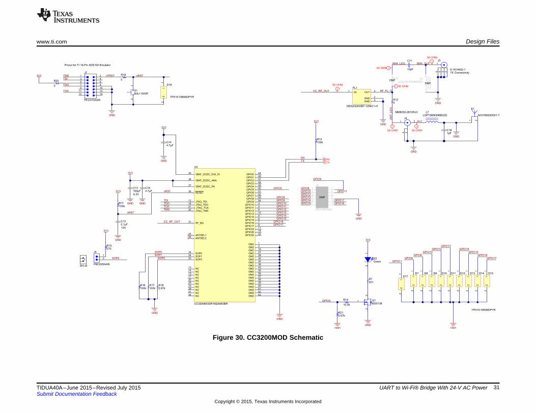
4.3 CC3200MODThe CC3200MOD is an easy-to-use module that contains the serial memory and crystals required for aCC3200-based system. External components are the necessary bypass capacitors and pulldown resistors.The UART interface is used for both system programming and communication.
There are several connectors provided for test and expansion. J5 is provided for FLASH programming. J5is shorted for programming operations and is left open during normal operation. J6 is an expansionconnector that allows adding extra peripheral circuits to the CC3200MOD GPIOs. J7 is a JTAG connectorfor system debugging. It follows the TI 14-pin JTAG format. The RESET button S1 provides a manualreset capability. Diodes D7 through D17 provide ESD protection for the GPIOs and reset.
The RF antenna output section has two antenna options. The PCB is populated with the parts for theonboard chip antenna E1. Connector J4 is an RF test connector. J3 is an SMA connector for use with anexternal antenna. Capacitor C11 is installed, but L6 and R10 in the SMA path are not installed. To use theSMA connector, R12 should be removed and R10 installed. L6 can be installed if it is needed.
Figure 10. CC3200MOD Schematic
10 UART to Wi-Fi® Bridge With 24-V AC Power TIDUA40A–June 2015–Revised July 2015Submit Documentation Feedback
Copyright © 2015, Texas Instruments Incorporated

1 2
E1
AH316M245001-T
IN1
GND2
OUT3
GND4
FL1
DEA202450BT-1294C1-H
1 2
34
J4
MM8030-2610RJ3
0R10
DNP
0R12
GND
L7LQP15MN3N6B02D
GND
1pFC18
10pF
C11
GND
L6LQG15HS3N6S02D
DNP
1
2345 TE Connectivity
J3
5-1814832-1
CC_RF_OUT RF_FL_O
AN
T_L
EG
SMA_LEG SMA_OUT
J4-2
i
50 OHMi 50 OHM
i
50 OHM
i50 OHM
i
50 OHM
i
50 OHM
GND
1 2
3 4
5 6
7 8
9 10
11 12
13 14
J7
PEC07DAAN
GND
TMS
TDI
TDO
TCK
nTRST
0
R19 nRST3V3
11
22
D16
TPD1E10B06DPYR
0
R20
21
S1
B3U-1000P
www.ti.com System Design Theory
Figure 11. JTAG Connector Schematic
Figure 12. Antenna Section Schematic
11TIDUA40A–June 2015–Revised July 2015 UART to Wi-Fi® Bridge With 24-V AC PowerSubmit Documentation Feedback
Copyright © 2015, Texas Instruments Incorporated

1
3
56
4
2
7
910
8
12 11
14 13
J1
55510-114TRLF
RX TX
GND
3V3
0
R3
2 4
NC1
GND3
VCC5
U1
SN74LV1T34DCKR
2 4
NC1
GND3
VCC5
U2
SN74LV1T34DCKR
GNDGND
3V3
0.1µF
10V
C20.1µF
10V
C1
VEXT
VEXT
RX_EXT TX_EXT
5V_EXT
0R2
5V_EXT
0R1
DNPDNP
System Design Theory www.ti.com
4.4 UART Voltage Buffers and Other CircuitsThe UART connection to the CC3200MOD is made through J1, an FCI 55510-114TRLF 14-pin board-to-board socket with 2-mm pin spacing. U1 and U2 are buffers that provide IO voltage matching between theCC3200MOD and an external system. U1 can be powered from a voltage used for the external system’sIO or from the onboard 3.3-V power supply. R1 is not populated by default but can be used if an externalIO voltage is connected to J1 pin 10. R2 is used to connect an external IO voltage at J1 pin 9. R1 and R2should not be populated at the same time. R3 connects J1 pin 9 to the internal 3.3-V supply. If R2 and R3are both installed, U1 is powered by the TIDA-00375 PCB’s 3.3-V supply.
Figure 13. UART Interface Connector Schematic
12 UART to Wi-Fi® Bridge With 24-V AC Power TIDUA40A–June 2015–Revised July 2015Submit Documentation Feedback
Copyright © 2015, Texas Instruments Incorporated

www.ti.com Getting Started: Firmware
5 Getting Started: FirmwareIn order for the TIDA-00375 reference design to work, CC3200MOD software must be able to receive datafrom the UART port and transmit that data using a socket to another end node connected in the samenetwork. The software must also be able to receive data from socket and write the data to the UART port.For this application, the serial-Wi-Fi application from CC3200 SDK was reused. Note that this is from SDKversion 1.1.0 for CC3200 silicon revision R1.
5.1 Application OverviewThe serial-Wi-Fi application showcases the capability of the CC3200MOD to provide easy, self-containedterminal access behavior over a UART interface. The application provides a driver-less solution and allowsoperation based on ASCII character set interpretation. This application runs over the UART interface andbehaves as a command line interpreter. Leveraging the complete network stack integration of theCC3200, it allows secure, robust end-to-end communication.
5.2 Application FeaturesThe following features are provided in the application:• Support to connect to an Enterprise or Personal network using OPEN, WEP, or WPA authentication.• Automatic network discovery of an available peer using mDNS.• Once a network is configured, the CC3200MOD can auto connect to the AP on every boot.• Ability to use optional secure sockets.
5.3 Operating ModesThe application operates in three modes:1. Terminal/Interpreter mode
Interpreter mode behaves as pure point-to-point cable replacement. This is the most common use inwhich a serial cable formerly used to carry information is replaced by SimpleLink devices on both endsof the line. This mode can also be used to extend an existing line farther without additional serialcommunication cable being installed.
2. Local control modeThis allows issuing commands to the locally connected device. These commands encompass a closeset of options to control the SimpleLink device. The mode is entered using a predefined escapesequence (//<).
3. Remote control modeThis allows issuing commands to the remotely connected device. These commands encompass thesame set of options to control the remote SimpleLink as the local device. The mode is entered using apredefined escape sequence (//>).
13TIDUA40A–June 2015–Revised July 2015 UART to Wi-Fi® Bridge With 24-V AC PowerSubmit Documentation Feedback
Copyright © 2015, Texas Instruments Incorporated

J2 powerconnector withPhoenix 1757019mating connector
J5 connector
USB-to-UARTconverter
J1 mated withFCI 98414-F06-14ULF
Getting Started www.ti.com
6 Getting StartedThe following assumes that the user has installed the CC3200 SDK, Code Composer Studio™ (CCS), andUniFlash™ to program the FLASH device on the UART to Wi-Fi Bridge PCB. It is recommended that theuser be familiar with CC3200 Project 0 from the CC3200 wiki site. This will insure that CCS is set upcorrectly, the CCS UniFlash utility is installed, and the drivers (simplelink, ti_rtos_config, driverlib, oslib)have been built. The drivers must be built before the procedure in Section 6.2 can be run. If applicationdebugging capability is needed, a TI TMDSEMU100V2U-14T JTAG Emulator can be connected to J7 onthe PCB.
6.1 Hardware SetupIn order to test the UART to Wi-Fi Bridge reference design, either two UART to Wi-Fi Bridge PCBs mustbe used, or one UART to Wi-Fi Bridge can be used for one node and a CC3200MOD LaunchPad can beused for the other. Each board must have a terminal program such as Tera Term running on a hostcomputer. If available, use two host computers with the terminal program running, one for each UART-to-Wi-Fi node. However, a single host running two terminal windows can be used.
To power the board, connect a power supply to the power connector J2. A suitable mating connector forJ2 is the Phoenix 1757019. The power supply can be any AC or DC supply between 6 and 48 V. Choosea power supply with a 1-A capacity for voltages from 6 to 12 V or a 0.5-A capacity above 12 V.
To monitor the UART traffic, an interface board or a cable with an FCI 98414-F06-14ULF connector isrequired to connect the UART signals to the UART to Wi-Fi Bridge PCB. To connect the UART to the hostcomputer, a UART-to-USB connector must be used to connect the UART signals into the host. The UARTconnection is also the programming connection for the UART to Wi-Fi Bridge PCB. Make sure that thejumper is installed on J5 before applying power to the PCB.
Figure 14. Board With Power and FCI Connector Plus USB-to-UART Converter
14 UART to Wi-Fi® Bridge With 24-V AC Power TIDUA40A–June 2015–Revised July 2015Submit Documentation Feedback
Copyright © 2015, Texas Instruments Incorporated

www.ti.com Getting Started
6.2 Software SetupFor testing purposes, the serial-Wi-Fi application will be used. For simplicity, the application will use non-secure sockets for the communication. The following steps describe the procedure to configure theapplication for non-secure sockets, build the binary, flash onto the TIDA-00375 PCB, configure, and test.
For more information about the serial-Wi-Fi application and the use of secure sockets for communication,see the CC32xx Serial Wi-Fi documentation that is provided in the CC3200 SDK.
6.2.1 Configure the Application
1. Open CCS and import serial_wifi example application from CC3200 SDK.2. Configure the application for non-secure sockets:
(a) Open serial_wifi.h.(b) On line 95 (line 87 in SDK 1.1.0), comment out "#define SECURE_SOCKETS".(c) Open serial_wifi.c.(d) In function StartTcpServer, comment out #ifdef SECURE_SOCKETS (line 1585 (line 1605 in SDK
1.1.0)) and #endif (line 1587 (line 1607 in SDK 1.1.0)) to initialize variable lRetVal.3. Build project:
(a) Go to Project → Build Project.(b) If using default settings, this should generate the file, serial_wifi.bin.
4. Flash binary:(a) Enable programming mode (pulling SOP2 high) by placing jumper on J5.(b) Connect the USB-to-UART converter and adapter cable from the TIDA-00375 PCB to the laptop.(c) Power on TIDA-00375 PCB.(d) Look in Device Manager and note the TIDA-00375 PCB’s COM port.(e) Open CCS UniFlash program.(f) Click File → New Configuration:
• Connection: CC3x Serial (UART) Interface.• Board or Device: SimpleLink Wi-Fi CC3100/CC3200.
(g) Change COM Port to match the COM port found from Device Manager.(h) If first time booting the hardware, perform a Service Pack Update:
(i) Click on Service Pack Update.(ii) Find the CC3200 Service Pack binary.
(i) Flash the serial-Wi-Fi application.(i) Click on "/sys/mcuimg.bin".(ii) Change URL to point to serial_wifi.bin file generated from Step 3: Build project.(iii) Make sure only the Update box is checked.(iv) Go to Operation → Program.
(j) Power off the TIDA-00375 PCB.(k) Change back to run mode (pulling SOP2 low) by removing jumper from J5.
5. Repeat Steps 1 through 4 on the second TIDA-00375 PCB or a CC3200 LaunchPad. The LaunchPadwill require a USB cable instead of the USB adapter board and cable.
15TIDUA40A–June 2015–Revised July 2015 UART to Wi-Fi® Bridge With 24-V AC PowerSubmit Documentation Feedback
Copyright © 2015, Texas Instruments Incorporated

Getting Started www.ti.com
6.2.2 Run the Application
1. Open a terminal with the following settings:• Port: COM port from Device Manager• Baud Rate: 115200• Data: 8 bit• Parity: None• Stop: 1 bit• Flow control: None
Figure 15. Tera Term Port Setup
2. Start the serial-Wi-Fi application:(a) Power on the TIDA-00375 PCB.(b) The terminal should show "CC3200 SERIAL WiFi Application".(c) If not, go back to Step 4: Flash binary from Section 6.2.1 and try flashing the application again.
16 UART to Wi-Fi® Bridge With 24-V AC Power TIDUA40A–June 2015–Revised July 2015Submit Documentation Feedback
Copyright © 2015, Texas Instruments Incorporated

www.ti.com Getting Started
3. Connect to Access Point (AP):(a) Upon reset, the device will connect to the stored AP using the AUTO connect policy. If the device
connects to AP, go to Step 4: Configure mDNS. If the device does not connect to an AP in sixseconds, the application will prompt the user to connect to a known AP using the local controlmode.
Figure 16. Terminal Information With No AP
(b) Enter local control mode (\\<).(c) Use the following command to connect to an AP:
Format: wlan_connect [SSID] [Type] [Sec] [User] [Key]SSID: Name of APType: 0-Personal, 1-ENTSec: 0-OPEN, 1-WEP, 2-WPAUser: Username, only needed if using ENTKey: Password for WEP and WPAExample:"TI_AP" SSID with no securitywlan_connect TI_AP 0 0a"TI_AP" SSID with WPA security and password "TI_password"wlan_connect TI_AP 0 2 TI_password
17TIDUA40A–June 2015–Revised July 2015 UART to Wi-Fi® Bridge With 24-V AC PowerSubmit Documentation Feedback
Copyright © 2015, Texas Instruments Incorporated

Getting Started www.ti.com
Figure 17. Setting Up the Access Point SSID
(d) Once completed, the application will show that it was able to connect to the AP and an IP addresshas been acquired.
18 UART to Wi-Fi® Bridge With 24-V AC Power TIDUA40A–June 2015–Revised July 2015Submit Documentation Feedback
Copyright © 2015, Texas Instruments Incorporated

www.ti.com Getting Started
Figure 18. Terminal Window Screenshot Showing UART to Wi-Fi End Node Console
4. Configure mDNS:(a) This step only needs to be done the first time after performing a serial erase.(b) One node must be configured as mDNS server. Use local control mode to program.(c) Enter local control mode (\\<).(d) Configure for client or server:
mDNS 0 <0-server, 1-client>5. Repeat Steps 1 through 5 for the second TIDA-00375 PCB or LaunchPad.
19TIDUA40A–June 2015–Revised July 2015 UART to Wi-Fi® Bridge With 24-V AC PowerSubmit Documentation Feedback
Copyright © 2015, Texas Instruments Incorporated

Getting Started www.ti.com
Figure 19. Setting DNS as Server
Devices should now be in interpreter mode. If the device is still in control mode, type "exit" to resumeinterpreter mode.
20 UART to Wi-Fi® Bridge With 24-V AC Power TIDUA40A–June 2015–Revised July 2015Submit Documentation Feedback
Copyright © 2015, Texas Instruments Incorporated

www.ti.com Getting Started
6.3 Communication Test
1. Reset both nodes.2. Both nodes should connect to the same AP and acquire an IP address.3. Verify that "TCP connection established" appears on both nodes.4. Type on the server terminal and press <Enter> to see the same characters on the client.5. Type on the client terminal and press <Enter> to see the same characters on the server.
Figure 20. Terminal Window Screenshots Showing Both Consoles
21TIDUA40A–June 2015–Revised July 2015 UART to Wi-Fi® Bridge With 24-V AC PowerSubmit Documentation Feedback
Copyright © 2015, Texas Instruments Incorporated

Input powerEfficiency 100%
Output power
æ ö= ´ç ÷
è ø
Testing www.ti.com
7 Testing
7.1 Power Supply DC TestingIn order to test the power supply efficiency, DC input voltage was used to simplify the measurements.Efficiency is calculated by taking the ratio of the output power to the input power of the power supply.
(1)
The power is calculated from voltage and current measurements. For the efficiency test, the input power isapplied at J2 and the input voltage is measured at TP1. Input current is measured by inserting a digitalmultimeter (DMM) between the input power source and J2. To measure the output current, R6 is removedand the output currents are measured by connecting a DMM across the two pads of the resistor. Inputvoltage was measured at TP1. Output voltage was measured across the output capacitors C9 and C10.The input voltage was adjusted to different voltages in the operating range by setting the voltagemeasured at TP1. The power was measured under two conditions: with the UART communication idle andwhile transmitting continuous UART data by Wi-Fi. In both cases, the calculated data shows the powersupply efficiency decreases as the input voltage increases.
22 UART to Wi-Fi® Bridge With 24-V AC Power TIDUA40A–June 2015–Revised July 2015Submit Documentation Feedback
Copyright © 2015, Texas Instruments Incorporated

Input Voltage (V)
Eff
icie
ncy
5 10 15 20 25 30 35 40 4560%
65%
70%
75%
80%
85%
90%
95%
www.ti.com Testing
Table 2. Power Supply Efficiency, UART Idle
INPUT INPUT INPUT POWER OUTPUT OUTPUT OUTPUT EFFICIENCYVOLTAGE (V) CURRENT (mA) (mW) VOLTAGE (V) CURRENT (mA) POWER (mW)5.00 23.50 117.5 3.336 31.9 106.4184 90.57%7.50 17.10 128.25 3.336 32.2 107.4192 83.76%
10.00 13.20 132 3.336 32.1 107.0856 81.13%12.00 10.90 130.8 3.336 30.8 102.7488 78.55%15.01 9.00 135.09 3.339 30.3 101.1717 74.89%18.00 7.60 136.8 3.344 31.1 103.9984 76.02%18.00 7.63 137.34 3.344 30.6 102.3264 74.51%20.00 6.88 137.6 3.344 30.0 100.3200 72.91%24.00 6.02 144.48 3.344 30.5 101.9920 70.59%30.01 4.99 149.7499 3.342 30.3 101.2626 67.62%35.00 4.44 155.4 3.341 30.5 101.9005 65.57%40.01 4.04 161.6404 3.341 30.4 101.5664 62.83%42.50 3.90 165.75 3.342 30.6 102.2652 61.70%
Figure 21. Power Supply Efficiency for UART Idle
23TIDUA40A–June 2015–Revised July 2015 UART to Wi-Fi® Bridge With 24-V AC PowerSubmit Documentation Feedback
Copyright © 2015, Texas Instruments Incorporated

Input Voltage (V)
Eff
icie
ncy
5 10 15 20 25 30 35 40 4565%
70%
75%
80%
85%
90%
95%
Testing www.ti.com
Table 3. Power Supply Efficiency UART Continuous Data
INPUT INPUT INPUT POWER OUTPUT OUTPUT OUTPUT EFFICIENCYVOLTAGE (V) CURRENT (mA) (mW) VOLTAGE (V) CURRENT (mA) POWER (mW)5.05 56.6 285.83 3.336 78.9 263.2104 92.09%7.55 39.7 299.735 3.336 78.4 261.5424 87.26%
10.03 30.7 307.921 3.336 78.5 261.876 85.05%12.03 25.7 309.171 3.336 78.5 261.876 84.70%15.02 21.5 322.93 3.336 78.4 261.5424 80.99%18.04 18.2 328.328 3.336 78.2 260.8752 79.46%20.04 16.71 334.8684 3.336 78.2 260.8752 77.90%24.09 14.3 344.487 3.336 78.3 261.2088 75.83%30.02 11.9 357.238 3.336 78.2 260.8752 73.03%35.03 10.54 369.2057 3.336 78.2 260.8752 70.66%40.04 9.55 382.382 3.336 78.3 261.2088 68.31%42.49 9.18 390.0582 3.336 78.3 261.2088 66.97%
Figure 22. Power Supply Efficiency for UART Sending Data Continuously
The current measurements shown are average current measurements over time. They are low comparedto the maximum current expected for the CC3200MOD. The instantaneous current is much higher duringWi-Fi transmissions.
24 UART to Wi-Fi® Bridge With 24-V AC Power TIDUA40A–June 2015–Revised July 2015Submit Documentation Feedback
Copyright © 2015, Texas Instruments Incorporated
www.ti.com Testing
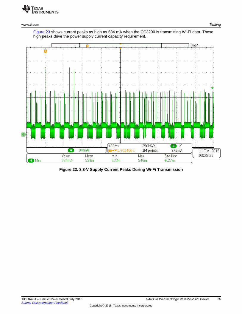
Figure 23 shows current peaks as high as 534 mA when the CC3200 is transmitting Wi-Fi data. Thesehigh peaks drive the power supply current capacity requirement.
Figure 23. 3.3-V Supply Current Peaks During Wi-Fi Transmission
25TIDUA40A–June 2015–Revised July 2015 UART to Wi-Fi® Bridge With 24-V AC PowerSubmit Documentation Feedback
Copyright © 2015, Texas Instruments Incorporated

Testing www.ti.com
7.2 Power Supply AC TestingThe UART to Wi-Fi Bridge was tested with a Kikusui PCR500M AC Power Supply. The minimum ACvoltage that the system worked at was 4-V AC, 60 Hz. The rectified and filtered input voltage at TP2 wasabout 4-V DC with the 4-V AC input. Lowering the voltage to 4-V AC leads to the processor resetting dueto the 3.3-V power supply loosing regulation. The system would not start up again unless the input voltagewas 4.4-V AC.
The voltage on the filter capacitor C15 was measured with an oscilloscope to see the performance of theinput filter. The ripple voltage for an input voltage of 18-V AC on C15 is shown in Figure 24.
Figure 24. Ripple Voltage at C15 for an 18-V AC, 60-Hz Input
For the measurement in Figure 24, the system was transmitting constantly as it was for the efficiencymeasurement, ensuring a maximum ripple. The peak-to-peak voltage ripple is only 440 mV in this case.
26 UART to Wi-Fi® Bridge With 24-V AC Power TIDUA40A–June 2015–Revised July 2015Submit Documentation Feedback
Copyright © 2015, Texas Instruments Incorporated

www.ti.com Testing
For an 18-V AC at 50-Hz input, the voltage ripple on C15 is 280 mV (see Figure 25).
Figure 25. Ripple Voltage at C15 for an 18-V AC, 50-Hz Input
27TIDUA40A–June 2015–Revised July 2015 UART to Wi-Fi® Bridge With 24-V AC PowerSubmit Documentation Feedback
Copyright © 2015, Texas Instruments Incorporated

Path Loss
Th
rou
gh
pu
t (M
Bp
s)
Access Point
65 70 75 80 85 90 95 100 105 110 1150
2
4
6
8
10
12
14UDP TxUDP RxTCP TxTCP Rx
Path Loss
Th
rou
gh
pu
t (M
Bp
s)
Station
65 70 75 80 85 90 95 100 105 110 1150
2
4
6
8
10
12
14UDP TxUDP RxTCP TxTCP Rx
Testing www.ti.com
7.3 CC3200 Performance
7.3.1 Data ThroughputThe data in this section was provided by the CC3100 and CC3200 design team. It is included to show theWi-Fi performance.
The following two graphs show data throughput measurements with the hardware set up as both an APand a Station. The data was not taken on the hardware described in this document. It was taken with aCC3100-based system that includes the CC3100 BoosterPack. The CC3100 and CC3200 have the samenetwork processor subsystems, so their performance will be the same. The antenna on the PCB for theUART to Wi-Fi Bridge is the same antenna used in the CC3100 BoosterPack, and great care has beentaken to ensure the UART to Wi-Fi Bridge RF output circuit matches the CC3100 BoosterPack, includingthe trace width, the thickness of the PCB dielectric between the RF output traces and the ground plane,and the overall board thickness.
The CC3100 system was tested in a chamber using a Cisco AP 1252 router and a Cisco-Linksys AE1000router. The test measures throughput versus path loss (range) where the AP or Station is placed in achamber. Range is simulated by using an attenuator to reduce the module output power.
Figure 26. Data Throughput versus Path Loss Figure 27. Data Throughput versus Path Loss(CC3100 AP) (CC3100 Station)
The UART to Wi-Fi Bridge is limited in its throughput by the CC3200 UART module. The UART modulehas a maximum bit rate of 3 Mbits per second.
7.3.2 In-Office Range TestFor these tests, the UART in the UART to Wi-Fi Bridge was tested at 115,200 bits per second.
In order to see how the UART to Wi-Fi Bridge can perform in an office environment, tests were run withthe hardware set up as described in Section 6.2. Using a TP-Link model TL-WR740N router at the AP,one of the systems was moved away from the router and communication was re-checked. In one test,communication was still possible with one system at a distance of 83.3 meters from the AP. There wereno obstructions between the system and the AP, though the RF line of sight was down a narrow corridorwith walls and cubicles lining the corridor. Another test had the system 25.4 meters form the AP, but theRF signal had to penetrate four walls and several rows of cubicles to get from the AP to the system.
This test is not meant to be a performance test. Actual user performance depends upon many factors,such as the model of the AP used, the amount of RF interference in the environment in which thehardware is installed, the location of the hardware in relation to walls or metal objects, and other factorsunique to each installation.
28 UART to Wi-Fi® Bridge With 24-V AC Power TIDUA40A–June 2015–Revised July 2015Submit Documentation Feedback
Copyright © 2015, Texas Instruments Incorporated
Access Point
TIDA-00375UART to Wi-Fi® Bridge
System UART
Cloud
www.ti.com Other Applications
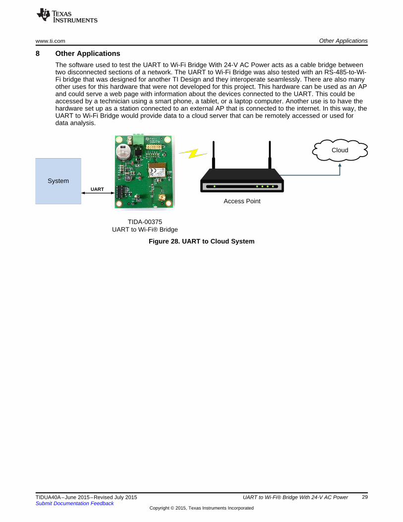
8 Other ApplicationsThe software used to test the UART to Wi-Fi Bridge With 24-V AC Power acts as a cable bridge betweentwo disconnected sections of a network. The UART to Wi-Fi Bridge was also tested with an RS-485-to-Wi-Fi bridge that was designed for another TI Design and they interoperate seamlessly. There are also manyother uses for this hardware that were not developed for this project. This hardware can be used as an APand could serve a web page with information about the devices connected to the UART. This could beaccessed by a technician using a smart phone, a tablet, or a laptop computer. Another use is to have thehardware set up as a station connected to an external AP that is connected to the internet. In this way, theUART to Wi-Fi Bridge would provide data to a cloud server that can be remotely accessed or used fordata analysis.
Figure 28. UART to Cloud System
29TIDUA40A–June 2015–Revised July 2015 UART to Wi-Fi® Bridge With 24-V AC PowerSubmit Documentation Feedback
Copyright © 2015, Texas Instruments Incorporated

0.1µF
100V
C6
10µF
6.3V
C9
1
2
J2
1757242
1
3
56
4
2
7
910
8
12 11
14 13
J1
55510-114TRLF
Pin 55 = CCTX, Host RX; 57 = CCRX
RX TX
GND
3V3
0
R3
GND
CB1
VIN5
GND2
SHDN4
FB3
SW6
U3
LMR16006XDDC
2 4
NC1
GND3
VCC5
U1
SN74LV1T34DCKR
2 4
NC1
GND3
VCC5
U2
SN74LV1T34DCKR
GNDGND
3V3
0.1µF
10V
C20.1µF
10V
C1
VEXT
VEXT
RX_EXT TX_EXT
5V_EXT
0R2
5V_EXT
0R1
DNPDNP
D4MBR1H100SFT3G
1µF100V
C7
0.1µF
100V
C3
TDK
22µH
L2
CLF7045T-220M
SW
VDC_IN
10µF
6.3V
C10
3V3
0
R63V3_OUT
1µF100V
C8
0
R5
VOUT = 0.765 V (1+(Rtop/Rbottom))Rtop = Rbottom ((VOUT/0.765 V)-1)
75.0kR9
249kR8
VFB
0
R4
GND
123 4
Bourns
L4SRF2012-300Y
330 ohm
MuRata
L1
BLM18SG331TN1D
330 ohm
MuRata
L5
BLM18SG331TN1D
0.01µF
100V
C5
1000pF
100V
C4
45V
D3SMAJ45CA
TP1
TP3
GND
TP4
TP2
1000µF50V
C15
~3
+1
~4
-2
D1
DF1502S-T
IN1IN2
IN2_FF1
0154002.DRT
Design Files www.ti.com
9 Design Files
9.1 SchematicsTo download the schematics, see the design files at TIDA-00375.
Figure 29. Power and Interface Schematic
30 UART to Wi-Fi® Bridge With 24-V AC Power TIDUA40A–June 2015–Revised July 2015Submit Documentation Feedback
Copyright © 2015, Texas Instruments Incorporated
GND1
GND2
GPIO103
GPIO114
GPIO145
GPIO156
GPIO167
GPIO178
GPIO129
GPIO1310
GPIO2211
JTAG_TDI12
NC13
NC14
NC15
GND16
NC17
JTAG_TDO18
GPIO2819
NC20
JTAG_TCK21
JTAG_TMS22
SOP223
SOP124
ANTSEL125
ANTSEL226
GND27
GND28
NC29
GND30
RF_BG31
GND32
NC33
SOP034
RESET35
VBAT_DCDC_ANA36
VBAT_DCDC_PA37
GND38
NC39
VBAT_DCDC_DIG_IO40
NC41
GPIO3042
GND43
GPIO044
NC45
GPIO146
GPIO247
GPIO348
GPIO449
GPIO550
GPIO651
GPIO752
GPIO853
GPIO954
GND55
GND56
GND57
GND58
GND59
GND60
GND61
GND62
GND63
U4
CC3200MODR1M2AMOBR
GND
GND
3V3
4.7µFC14
GND
1 2
E1
AH316M245001-T
IN1
GND2
OUT3
GND4
FL1
DEA202450BT-1294C1-H
1 2
34
J4
MM8030-2610RJ3
0R10
DNP
0R12
GND
L7LQP15MN3N6B02D
GND
1pFC18
0.1µF
10V
C12
100kR11
3V3
GND
10pF
C11
GND
L6LQG15HS3N6S02D
DNP
RXTX
RX
TX
100kR13
3V3
1
2345 TE Connectivity
J3
5-1814832-1
100kR16
100kR17
2.67kR18
SOP0SOP1
SOP2
270R15
3V3
1
2
J5
PBC02SAAN
SOP2
SH-J5
CC_RF_OUT RF_FL_O
AN
T_L
EG
SMA_LEG SMA_OUT
J4-2
i
50 OHMi 50 OHM
i
50 OHM
i50 OHM
i
50 OHM
i
50 OHM
1 2
3 4
5 6
7 8
9 10
11 12
13 14
J7
PEC07DAAN
GND
TMSTDI
TDO
TCK
nTRST
0
R19
nRST
nRST3V3
Pinout for TI 14-Pin XDS100 Emulator
11
22
D16
TPD1E10B06DPYR
0
R20
21
S1B3U-1000P
GND
GPIO9
GPIO13GPIO14GPIO15
1 2
3 4
5 6
7 8
9 10
11 12
J6
PEC06DAAN
DNPGPIO17GPIO16
GND
GPIO11
GPIO17GPIO16
11
22
D10
11
22
D11
11
22
D12
11
22
D13
11
22
D14
11
22
D9
11
22
D8
11
22
D7
11
22
D15
TPD1E10B06DPYR
GND
GPIO17GPIO16
GPIO15GPIO14
GPIO13GPIO12
GPIO10GPIO8
GPIO9
11
22
D17
GPIO11
CC_RF_OUT
nRST
TDITDOTCKTMS
100µF
6.3V
C13
GND
3V3
GPIO12GPIO11GPIO10GPIO9GPIO8
GPIO8GPIO10GPIO12GPIO13GPIO14GPIO15
GPIO5
Green
12
D2
3V3
301R7
2.67kR21
10.0k
R14
GNDGND
1
23
Q1BSS138
GPIO5
4.7µFC16
GND
www.ti.com Design Files
Figure 30. CC3200MOD Schematic
31TIDUA40A–June 2015–Revised July 2015 UART to Wi-Fi® Bridge With 24-V AC PowerSubmit Documentation Feedback
Copyright © 2015, Texas Instruments Incorporated

Design Files www.ti.com
9.2 Bill of MaterialsTo download the bill of materials (BOM), see the design files at TIDA-00375.
9.3 PCB Layout RecommendationsThe layout of this PCB was done by carefully following the recommended guidelines for the LMR16006,the CC3200MOD, and the Taiyo Yuden AH316M245001-T chip antenna. The power nets from J2 throughto the 3V3 net are made as wide as practical. For the CC3200MOD, follow the Hardware Design ReviewProcess and PCB Layout Design Guidelines found on the SimpleLink™ Wi-Fi® CC31xx/CC32xx MainPage for best results.
9.3.1 Layer PlotsTo download the layer plots, see the design files at TIDA-00375.
9.4 Altium ProjectTo download the Altium project files, see the design files at TIDA-00375.
9.5 Gerber FilesTo download the Gerber files, see the design files at TIDA-00375.
9.6 Assembly DrawingsTo download the Gerber files, see the design files at TIDA-00375.
32 UART to Wi-Fi® Bridge With 24-V AC Power TIDUA40A–June 2015–Revised July 2015Submit Documentation Feedback
Copyright © 2015, Texas Instruments Incorporated
www.ti.com Software Files
10 Software FilesTo download the software files, see the design files at TIDA-00375.
11 References
1. Texas Instruments, CC3200MOD SimpleLink™ Wi-Fi® and Internet-of-Things Module Solution, aSingle-Chip Wireless MCU, CC3200MOD Datasheet (SWRS166)
2. Texas Instruments, SimpleLink™ Wi-Fi® CC31xx/CC32xx Main Page (link)3. Texas Instruments, SimpleLink Wi-Fi CC3100 BoosterPack (http://www.ti.com/tool/cc3100boost)4. Texas Instruments, LMR16006 SIMPLE SWITCHER® 60 V 0.6 A Buck Regulators With High
Efficiency ECO Mode, LMR16006 Datasheet (SNVSA24)5. Texas Instruments, SN74LV1T34 Single Power Supply Buffer GATE CMOS Logic Level Shifter,
SN74LV1T34 Datasheet (SCLS743)
12 AcknowledgmentsThe authors would like to thank Ben Gilboa, Moshe Leibo, and all of the members of the CC3100/CC3200SimpleLink team for their support for this project and especially for the throughput data.
13 About the AuthorsMARK KNAPP is a Systems Architect at Texas Instruments Incorporated where he is responsible fordeveloping reference design solutions for the Building Automation segment. He has an extensivebackground in video camera systems and infrared imaging systems for Military, Automotive and Industrialapplications. Mark earned his BSEE at the University of Michigan-Dearborn and his MSEE at theUniversity of Texas at Dallas.
CHRISTINA S. LAM is a Systems Architect at Texas Instruments where she is responsible for developingfirmware for reference design solutions in the industrial segment. Christina has broad experience withapplications processors, microcontrollers, and digital-signal processors with specialties in embeddedfirmware. Christina earned her BS in electrical and computer engineering from the University of Texas atAustin.
33TIDUA40A–June 2015–Revised July 2015 UART to Wi-Fi® Bridge With 24-V AC PowerSubmit Documentation Feedback
Copyright © 2015, Texas Instruments Incorporated

Revision History www.ti.com
Revision History
Changes from Original (June 2015) to A Revision ......................................................................................................... Page
• Changed from preview page............................................................................................................. 1
NOTE: Page numbers for previous revisions may differ from page numbers in the current version.
34 Revision History TIDUA40A–June 2015–Revised July 2015Submit Documentation Feedback
Copyright © 2015, Texas Instruments Incorporated

IMPORTANT NOTICE FOR TI REFERENCE DESIGNS
Texas Instruments Incorporated ("TI") reference designs are solely intended to assist designers (“Buyers”) who are developing systems thatincorporate TI semiconductor products (also referred to herein as “components”). Buyer understands and agrees that Buyer remainsresponsible for using its independent analysis, evaluation and judgment in designing Buyer’s systems and products.TI reference designs have been created using standard laboratory conditions and engineering practices. TI has not conducted anytesting other than that specifically described in the published documentation for a particular reference design. TI may makecorrections, enhancements, improvements and other changes to its reference designs.Buyers are authorized to use TI reference designs with the TI component(s) identified in each particular reference design and to modify thereference design in the development of their end products. HOWEVER, NO OTHER LICENSE, EXPRESS OR IMPLIED, BY ESTOPPELOR OTHERWISE TO ANY OTHER TI INTELLECTUAL PROPERTY RIGHT, AND NO LICENSE TO ANY THIRD PARTY TECHNOLOGYOR INTELLECTUAL PROPERTY RIGHT, IS GRANTED HEREIN, including but not limited to any patent right, copyright, mask work right,or other intellectual property right relating to any combination, machine, or process in which TI components or services are used.Information published by TI regarding third-party products or services does not constitute a license to use such products or services, or awarranty or endorsement thereof. Use of such information may require a license from a third party under the patents or other intellectualproperty of the third party, or a license from TI under the patents or other intellectual property of TI.TI REFERENCE DESIGNS ARE PROVIDED "AS IS". TI MAKES NO WARRANTIES OR REPRESENTATIONS WITH REGARD TO THEREFERENCE DESIGNS OR USE OF THE REFERENCE DESIGNS, EXPRESS, IMPLIED OR STATUTORY, INCLUDING ACCURACY ORCOMPLETENESS. TI DISCLAIMS ANY WARRANTY OF TITLE AND ANY IMPLIED WARRANTIES OF MERCHANTABILITY, FITNESSFOR A PARTICULAR PURPOSE, QUIET ENJOYMENT, QUIET POSSESSION, AND NON-INFRINGEMENT OF ANY THIRD PARTYINTELLECTUAL PROPERTY RIGHTS WITH REGARD TO TI REFERENCE DESIGNS OR USE THEREOF. TI SHALL NOT BE LIABLEFOR AND SHALL NOT DEFEND OR INDEMNIFY BUYERS AGAINST ANY THIRD PARTY INFRINGEMENT CLAIM THAT RELATES TOOR IS BASED ON A COMBINATION OF COMPONENTS PROVIDED IN A TI REFERENCE DESIGN. IN NO EVENT SHALL TI BELIABLE FOR ANY ACTUAL, SPECIAL, INCIDENTAL, CONSEQUENTIAL OR INDIRECT DAMAGES, HOWEVER CAUSED, ON ANYTHEORY OF LIABILITY AND WHETHER OR NOT TI HAS BEEN ADVISED OF THE POSSIBILITY OF SUCH DAMAGES, ARISING INANY WAY OUT OF TI REFERENCE DESIGNS OR BUYER’S USE OF TI REFERENCE DESIGNS.TI reserves the right to make corrections, enhancements, improvements and other changes to its semiconductor products and services perJESD46, latest issue, and to discontinue any product or service per JESD48, latest issue. Buyers should obtain the latest relevantinformation before placing orders and should verify that such information is current and complete. All semiconductor products are soldsubject to TI’s terms and conditions of sale supplied at the time of order acknowledgment.TI warrants performance of its components to the specifications applicable at the time of sale, in accordance with the warranty in TI’s termsand conditions of sale of semiconductor products. Testing and other quality control techniques for TI components are used to the extent TIdeems necessary to support this warranty. Except where mandated by applicable law, testing of all parameters of each component is notnecessarily performed.TI assumes no liability for applications assistance or the design of Buyers’ products. Buyers are responsible for their products andapplications using TI components. To minimize the risks associated with Buyers’ products and applications, Buyers should provideadequate design and operating safeguards.Reproduction of significant portions of TI information in TI data books, data sheets or reference designs is permissible only if reproduction iswithout alteration and is accompanied by all associated warranties, conditions, limitations, and notices. TI is not responsible or liable forsuch altered documentation. Information of third parties may be subject to additional restrictions.Buyer acknowledges and agrees that it is solely responsible for compliance with all legal, regulatory and safety-related requirementsconcerning its products, and any use of TI components in its applications, notwithstanding any applications-related information or supportthat may be provided by TI. Buyer represents and agrees that it has all the necessary expertise to create and implement safeguards thatanticipate dangerous failures, monitor failures and their consequences, lessen the likelihood of dangerous failures and take appropriateremedial actions. Buyer will fully indemnify TI and its representatives against any damages arising out of the use of any TI components inBuyer’s safety-critical applications.In some cases, TI components may be promoted specifically to facilitate safety-related applications. With such components, TI’s goal is tohelp enable customers to design and create their own end-product solutions that meet applicable functional safety standards andrequirements. Nonetheless, such components are subject to these terms.No TI components are authorized for use in FDA Class III (or similar life-critical medical equipment) unless authorized officers of the partieshave executed an agreement specifically governing such use.Only those TI components that TI has specifically designated as military grade or “enhanced plastic” are designed and intended for use inmilitary/aerospace applications or environments. Buyer acknowledges and agrees that any military or aerospace use of TI components thathave not been so designated is solely at Buyer's risk, and Buyer is solely responsible for compliance with all legal and regulatoryrequirements in connection with such use.TI has specifically designated certain components as meeting ISO/TS16949 requirements, mainly for automotive use. In any case of use ofnon-designated products, TI will not be responsible for any failure to meet ISO/TS16949.IMPORTANT NOTICE
Mailing Address: Texas Instruments, Post Office Box 655303, Dallas, Texas 75265Copyright © 2015, Texas Instruments Incorporated