uc1610 uc3610 dual schottky diode bridge - … · uc1610 uc3610 slus339b − june 1993 − revised...
TRANSCRIPT
UC1610UC3610
SLUS339B − JUNE 1993 − REVISED DECEMBER 2004
DUAL SCHOTTKY DIODE BRIDGE
1www.ti.com
FEATURES� Monolithic Eight-Diode Array
� Exceptional Efficiency
� Low Forward Voltage
� Fast Recovery Time
� High Peak Current
� Small Size
DESCRIPTION
This eight-diode array is designed forhigh-current, low duty-cycle applications typical offlyback voltage clamping for inductive loads. Thedual bridge connection makes this deviceparticularly applicable to bipolar driven steppermotors.
The use of Schottky diode technology featureshigh efficiency through lowered forward voltagedrop and decreased reverse recovery time.
This single monolithic chip is fabricated in bothhermetic CERDIP and copper-leaded plasticpackages. The UC1610 in ceramic is designed for−55°C to 125°C environments but with reducedpeak current capability. The UC2610 in plastic andceramic is designed for −25°C to 125°Cenvironments also with reduced peak currentcapability; while the UC3610 in plastic has highercurrent rating over a 0°C to 70°C temperaturerange.
AVAILABLE OPTIONS
T TPackaged Devices
TA = TJ SOIC Wide (DW) DIL (J) DIL (N)
−55°C to 125°C UC1610DW UC1610J UC1610N
−25°C to 125°C UC2610DW UC2610J UC2610N
0°C to 70°C UC3610DW UC3610J UC3610N
THERMAL INFORMATION
PACKAGE θja θjc
SOIC (DW) 16 pin 50 − 100(1) 27
DIP (J) 8 pin 125 − 160 20(2)
DIP (N) 8 pin 103(1) 50
NOTES: 1. Specified θja (junction-to-ambient) is for devices mounted to 5-in2 FR4 PC board with one ounce copper where noted. Whenresistance range is given, lower values are for 5-in2 aluminum PC board. Test PWB was 0.062 in thick and typically used 0.635-mmtrace widths for power packages and 1.3-mm trace widths for non-power packages with a 100-mil x 100-mil probe land area at theend of each trace.
2. θjc data values stated were derived from MIL−STD−1835B. MIL−STD−1835B states that the baseline values shown are worst case(mean + 2s) for a 60-mil x 60-mil microcircuit device silicon die and applicable for devices with die sizes up to 14400 square mils.For device die sizes greater than 14400 square mils use the following values; dual-in-line, 11°C/W; flat pack, 10°C/W; pin grid array,10°C/W.
PRODUCTION DATA information is current as of publication date.Products conform to specifications per the terms of Texas Instrumentsstandard warranty. Production processing does not necessarily includetesting of all parameters.
Copyright © 2001, Texas Instruments Incorporated

UC1610UC3610
SLUS339B − JUNE 1993 − REVISED DECEMBER 2004
2 www.ti.com
N OR J PACKAGETOP VIEW
DW PACKAGETOP VIEW
absolute maximum ratings over operating free-air temperature (unless otherwise noted)†�
Peak inverse voltage (per diode) 50 V. . . . . . . . . . . . . . . . . . . . . . . . . . . . . . . . . . . . . . . . . . . . . . . . . . . . . . . . . . . . . Peak forward current UC1611 1 A. . . . . . . . . . . . . . . . . . . . . . . . . . . . . . . . . . . . . . . . . . . . . . . . . . . . . . . . . . . . . . . . . . . . . . . . . . . . . . . . . UC2610 1 A. . . . . . . . . . . . . . . . . . . . . . . . . . . . . . . . . . . . . . . . . . . . . . . . . . . . . . . . . . . . . . . . . . . . . . . . . . . . . . . . . UC3611 3 A. . . . . . . . . . . . . . . . . . . . . . . . . . . . . . . . . . . . . . . . . . . . . . . . . . . . . . . . . . . . . . . . . . . . . . . . . . . . . . . . . Power dissipation at TA = 70°C 1 W. . . . . . . . . . . . . . . . . . . . . . . . . . . . . . . . . . . . . . . . . . . . . . . . . . . . . . . . . . . . . . . Storage temperature range, Tstg −65°C to 150°C. . . . . . . . . . . . . . . . . . . . . . . . . . . . . . . . . . . . . . . . . . . . . . . . . . . . Lead temperature (soldering, 10 seconds) 300°C. . . . . . . . . . . . . . . . . . . . . . . . . . . . . . . . . . . . . . . . . . . . . . . . . . .
† Stresses beyond those listed under “absolute maximum ratings” may cause permanent damage to the device. These are stress ratings only, andfunctional operation of the device at these or any other conditions beyond those indicated under “recommended operating conditions” is notimplied. Exposure to absolute-maximum-rated conditions for extended periods may affect device reliability.
‡ Consult packaging section of databook for thermal limitations and considerations of package.
electrical characteristics, all specifications apply to each individual diode, TJ = 25°C, TA = TJ,(except as noted)
PARAMETER TEST CONDITIONS MIN TYP MAX UNITS
Forward voltage dropIF = 100 mA 0.35 0.5 0.7 V
Forward voltage dropIF = 1 A 0.8 1.0 1.3 V
Leakage currentVR = 40 V 0.01 0.1 mA
Leakage currentVR = 40 V, TJ = 100°C 0.1 1.0 mA
Reverse recovery 0.5 A forward to 0.5 A reverse 15 ns
Forward recovery 1 A forward to 1.1 V recovery 30 ns
Junction capacitance VR = 5 V 70 pF
NOTE: At forward currents of greater than 1.0 A, a parasitic current of approximately 10 mA may be collected by adjacent diodes.
PRODUCT PREVIEW information concerns products in the formative ordesign phase of development. Characteristic data and otherspecifications are design goals. Texas Instruments reserves the right tochange or discontinue these products without notice.

UC1610UC3610
SLUS339B − JUNE 1993 − REVISED DECEMBER 2004
3www.ti.com
APPLICATION INFORMATION
Figure 1
0 10 20 30 40 50
1
23
5
10
2030
50
100
200300
500
1000
Reverse Voltage − V
T J = 125
T J = 25T J = 75
REVERSE CURRENTvs
VOLTAGE
Lea
kag
e C
urr
ent
− μA
°C
°C
°C
Figure 2
0 0.4 0.8 1.2 1.6 2.0
0.001
0.0020.003
0.005
0.01
0.020.030.05
0.1
0.20.3
0.5
1.0
Forward Voltage − V
0.2 0.6 1.0 1.4 1.8
2.03.0
5.0
T J = −55
T J = 25
T J = 125
FORWARD CURRENTvs
VOLTAGE
Fo
rwar
d C
urr
ent
− A
°C
°C
°C
Figure 3
Time, 2 ns/DIV
TRR(4.6 ns)
IR = 0.5 A
I = 0.5 A TA = 25
0 A
Dio
de
Cu
rren
t 20
0 m
A D
IV
REVERSE RECOVERY CHARACTERISTICS
F°C
Figure 4
Time, 2 ns/DIV
TFR(6 ns)
IF = 1 A
1.1 VTA = 25
Diode Voltage
0 A
Diode Current
0 A
Dio
de
Volt
age
1.0
V/D
IV
Dio
de
Cu
rren
t 50
0 m
A D
IV
FORWARD RECOVERY CHARACTERISTICS
°C

PACKAGE OPTION ADDENDUM
www.ti.com 13-Apr-2018
Addendum-Page 1
PACKAGING INFORMATION
Orderable Device Status(1)
Package Type PackageDrawing
Pins PackageQty
Eco Plan(2)
Lead/Ball Finish(6)
MSL Peak Temp(3)
Op Temp (°C) Device Marking(4/5)
Samples
UC2610N ACTIVE PDIP P 8 50 Green (RoHS& no Sb/Br)
CU NIPDAU | Call TI N / A for Pkg Type -40 to 85 UC2610N
UC2610NG4 ACTIVE PDIP P 8 50 Green (RoHS& no Sb/Br)
Call TI N / A for Pkg Type -40 to 85 UC2610N
UC3610DW ACTIVE SOIC DW 16 40 Green (RoHS& no Sb/Br)
CU NIPDAU Level-2-260C-1 YEAR 0 to 70 UC3610DW
UC3610DWG4 ACTIVE SOIC DW 16 40 Green (RoHS& no Sb/Br)
CU NIPDAU Level-2-260C-1 YEAR 0 to 70 UC3610DW
UC3610DWTR ACTIVE SOIC DW 16 2000 Green (RoHS& no Sb/Br)
CU NIPDAU Level-2-260C-1 YEAR 0 to 70 UC3610DW
UC3610DWTRG4 ACTIVE SOIC DW 16 2000 Green (RoHS& no Sb/Br)
CU NIPDAU Level-2-260C-1 YEAR 0 to 70 UC3610DW
UC3610N ACTIVE PDIP P 8 50 Green (RoHS& no Sb/Br)
CU NIPDAU | Call TI N / A for Pkg Type 0 to 70 UC3610N
UC3610NG4 ACTIVE PDIP P 8 50 Green (RoHS& no Sb/Br)
Call TI N / A for Pkg Type 0 to 70 UC3610N
(1) The marketing status values are defined as follows:ACTIVE: Product device recommended for new designs.LIFEBUY: TI has announced that the device will be discontinued, and a lifetime-buy period is in effect.NRND: Not recommended for new designs. Device is in production to support existing customers, but TI does not recommend using this part in a new design.PREVIEW: Device has been announced but is not in production. Samples may or may not be available.OBSOLETE: TI has discontinued the production of the device.
(2) RoHS: TI defines "RoHS" to mean semiconductor products that are compliant with the current EU RoHS requirements for all 10 RoHS substances, including the requirement that RoHS substancedo not exceed 0.1% by weight in homogeneous materials. Where designed to be soldered at high temperatures, "RoHS" products are suitable for use in specified lead-free processes. TI mayreference these types of products as "Pb-Free".RoHS Exempt: TI defines "RoHS Exempt" to mean products that contain lead but are compliant with EU RoHS pursuant to a specific EU RoHS exemption.Green: TI defines "Green" to mean the content of Chlorine (Cl) and Bromine (Br) based flame retardants meet JS709B low halogen requirements of <=1000ppm threshold. Antimony trioxide basedflame retardants must also meet the <=1000ppm threshold requirement.
(3) MSL, Peak Temp. - The Moisture Sensitivity Level rating according to the JEDEC industry standard classifications, and peak solder temperature.
(4) There may be additional marking, which relates to the logo, the lot trace code information, or the environmental category on the device.

PACKAGE OPTION ADDENDUM
www.ti.com 13-Apr-2018
Addendum-Page 2
(5) Multiple Device Markings will be inside parentheses. Only one Device Marking contained in parentheses and separated by a "~" will appear on a device. If a line is indented then it is a continuationof the previous line and the two combined represent the entire Device Marking for that device.
(6) Lead/Ball Finish - Orderable Devices may have multiple material finish options. Finish options are separated by a vertical ruled line. Lead/Ball Finish values may wrap to two lines if the finishvalue exceeds the maximum column width.
Important Information and Disclaimer:The information provided on this page represents TI's knowledge and belief as of the date that it is provided. TI bases its knowledge and belief on informationprovided by third parties, and makes no representation or warranty as to the accuracy of such information. Efforts are underway to better integrate information from third parties. TI has taken andcontinues to take reasonable steps to provide representative and accurate information but may not have conducted destructive testing or chemical analysis on incoming materials and chemicals.TI and TI suppliers consider certain information to be proprietary, and thus CAS numbers and other limited information may not be available for release.
In no event shall TI's liability arising out of such information exceed the total purchase price of the TI part(s) at issue in this document sold by TI to Customer on an annual basis.

TAPE AND REEL INFORMATION
*All dimensions are nominal
Device PackageType
PackageDrawing
Pins SPQ ReelDiameter
(mm)
ReelWidth
W1 (mm)
A0(mm)
B0(mm)
K0(mm)
P1(mm)
W(mm)
Pin1Quadrant
UC3610DWTR SOIC DW 16 2000 330.0 16.4 10.75 10.7 2.7 12.0 16.0 Q1
PACKAGE MATERIALS INFORMATION
www.ti.com 14-Jul-2012
Pack Materials-Page 1

*All dimensions are nominal
Device Package Type Package Drawing Pins SPQ Length (mm) Width (mm) Height (mm)
UC3610DWTR SOIC DW 16 2000 367.0 367.0 38.0
PACKAGE MATERIALS INFORMATION
www.ti.com 14-Jul-2012
Pack Materials-Page 2

GENERIC PACKAGE VIEW
Images above are just a representation of the package family, actual package may vary.Refer to the product data sheet for package details.
DW 16 SOIC - 2.65 mm max heightSMALL OUTLINE INTEGRATED CIRCUIT
4040000-2/H
www.ti.com
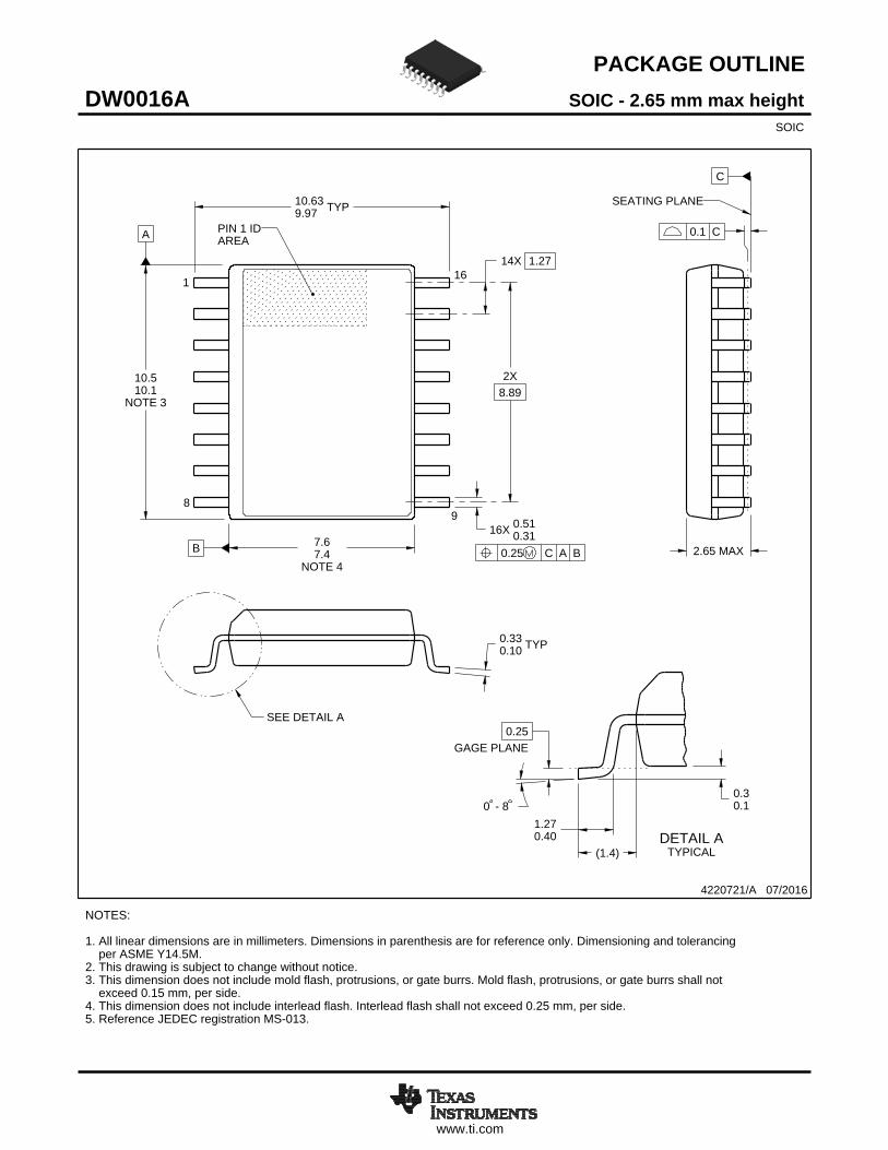
PACKAGE OUTLINE
C
TYP10.639.97
2.65 MAX
14X 1.27
16X 0.510.31
2X8.89
TYP0.330.10
0 - 80.30.1
(1.4)
0.25GAGE PLANE
1.270.40
A
NOTE 3
10.510.1
BNOTE 4
7.67.4
4220721/A 07/2016
SOIC - 2.65 mm max heightDW0016ASOIC
NOTES: 1. All linear dimensions are in millimeters. Dimensions in parenthesis are for reference only. Dimensioning and tolerancing per ASME Y14.5M. 2. This drawing is subject to change without notice. 3. This dimension does not include mold flash, protrusions, or gate burrs. Mold flash, protrusions, or gate burrs shall not exceed 0.15 mm, per side. 4. This dimension does not include interlead flash. Interlead flash shall not exceed 0.25 mm, per side.5. Reference JEDEC registration MS-013.
1 16
0.25 C A B
98
PIN 1 IDAREA
SEATING PLANE
0.1 C
SEE DETAIL A
DETAIL ATYPICAL
SCALE 1.500
www.ti.com
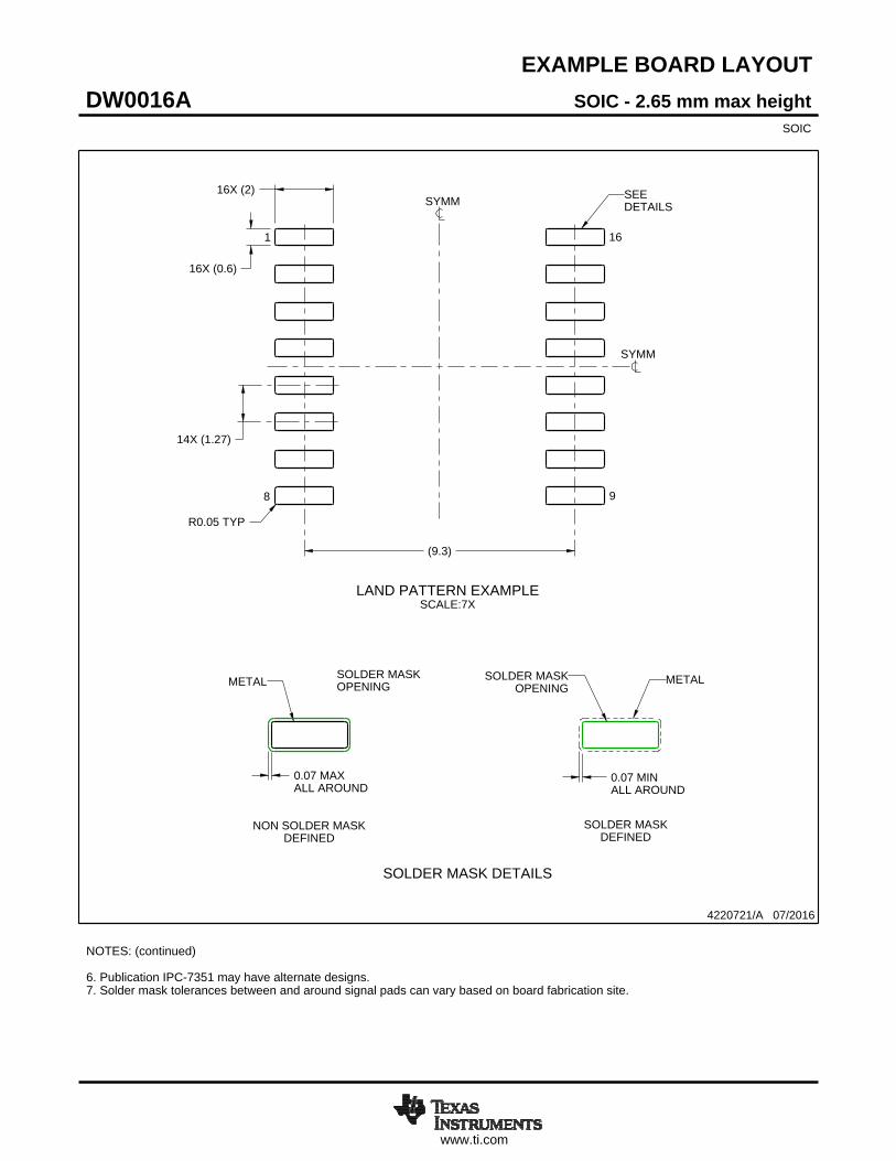
EXAMPLE BOARD LAYOUT
0.07 MAXALL AROUND
0.07 MINALL AROUND
(9.3)
14X (1.27)
R0.05 TYP
16X (2)
16X (0.6)
4220721/A 07/2016
SOIC - 2.65 mm max heightDW0016ASOIC
NOTES: (continued) 6. Publication IPC-7351 may have alternate designs. 7. Solder mask tolerances between and around signal pads can vary based on board fabrication site.
METAL SOLDER MASKOPENING
NON SOLDER MASKDEFINED
SOLDER MASK DETAILS
OPENINGSOLDER MASK METAL
SOLDER MASKDEFINED
LAND PATTERN EXAMPLESCALE:7X
SYMM
1
8 9
16
SEEDETAILS
SYMM

www.ti.com
EXAMPLE STENCIL DESIGN
R0.05 TYP
16X (2)
16X (0.6)
14X (1.27)
(9.3)
4220721/A 07/2016
SOIC - 2.65 mm max heightDW0016ASOIC
NOTES: (continued) 8. Laser cutting apertures with trapezoidal walls and rounded corners may offer better paste release. IPC-7525 may have alternate design recommendations. 9. Board assembly site may have different recommendations for stencil design.
SOLDER PASTE EXAMPLEBASED ON 0.125 mm THICK STENCIL
SCALE:7X
SYMM
SYMM
1
8 9
16

IMPORTANT NOTICE
Texas Instruments Incorporated (TI) reserves the right to make corrections, enhancements, improvements and other changes to itssemiconductor products and services per JESD46, latest issue, and to discontinue any product or service per JESD48, latest issue. Buyersshould obtain the latest relevant information before placing orders and should verify that such information is current and complete.TI’s published terms of sale for semiconductor products (http://www.ti.com/sc/docs/stdterms.htm) apply to the sale of packaged integratedcircuit products that TI has qualified and released to market. Additional terms may apply to the use or sale of other types of TI products andservices.Reproduction of significant portions of TI information in TI data sheets is permissible only if reproduction is without alteration and isaccompanied by all associated warranties, conditions, limitations, and notices. TI is not responsible or liable for such reproduceddocumentation. Information of third parties may be subject to additional restrictions. Resale of TI products or services with statementsdifferent from or beyond the parameters stated by TI for that product or service voids all express and any implied warranties for theassociated TI product or service and is an unfair and deceptive business practice. TI is not responsible or liable for any such statements.Buyers and others who are developing systems that incorporate TI products (collectively, “Designers”) understand and agree that Designersremain responsible for using their independent analysis, evaluation and judgment in designing their applications and that Designers havefull and exclusive responsibility to assure the safety of Designers' applications and compliance of their applications (and of all TI productsused in or for Designers’ applications) with all applicable regulations, laws and other applicable requirements. Designer represents that, withrespect to their applications, Designer has all the necessary expertise to create and implement safeguards that (1) anticipate dangerousconsequences of failures, (2) monitor failures and their consequences, and (3) lessen the likelihood of failures that might cause harm andtake appropriate actions. Designer agrees that prior to using or distributing any applications that include TI products, Designer willthoroughly test such applications and the functionality of such TI products as used in such applications.TI’s provision of technical, application or other design advice, quality characterization, reliability data or other services or information,including, but not limited to, reference designs and materials relating to evaluation modules, (collectively, “TI Resources”) are intended toassist designers who are developing applications that incorporate TI products; by downloading, accessing or using TI Resources in anyway, Designer (individually or, if Designer is acting on behalf of a company, Designer’s company) agrees to use any particular TI Resourcesolely for this purpose and subject to the terms of this Notice.TI’s provision of TI Resources does not expand or otherwise alter TI’s applicable published warranties or warranty disclaimers for TIproducts, and no additional obligations or liabilities arise from TI providing such TI Resources. TI reserves the right to make corrections,enhancements, improvements and other changes to its TI Resources. TI has not conducted any testing other than that specificallydescribed in the published documentation for a particular TI Resource.Designer is authorized to use, copy and modify any individual TI Resource only in connection with the development of applications thatinclude the TI product(s) identified in such TI Resource. NO OTHER LICENSE, EXPRESS OR IMPLIED, BY ESTOPPEL OR OTHERWISETO ANY OTHER TI INTELLECTUAL PROPERTY RIGHT, AND NO LICENSE TO ANY TECHNOLOGY OR INTELLECTUAL PROPERTYRIGHT OF TI OR ANY THIRD PARTY IS GRANTED HEREIN, including but not limited to any patent right, copyright, mask work right, orother intellectual property right relating to any combination, machine, or process in which TI products or services are used. Informationregarding or referencing third-party products or services does not constitute a license to use such products or services, or a warranty orendorsement thereof. Use of TI Resources may require a license from a third party under the patents or other intellectual property of thethird party, or a license from TI under the patents or other intellectual property of TI.TI RESOURCES ARE PROVIDED “AS IS” AND WITH ALL FAULTS. TI DISCLAIMS ALL OTHER WARRANTIES ORREPRESENTATIONS, EXPRESS OR IMPLIED, REGARDING RESOURCES OR USE THEREOF, INCLUDING BUT NOT LIMITED TOACCURACY OR COMPLETENESS, TITLE, ANY EPIDEMIC FAILURE WARRANTY AND ANY IMPLIED WARRANTIES OFMERCHANTABILITY, FITNESS FOR A PARTICULAR PURPOSE, AND NON-INFRINGEMENT OF ANY THIRD PARTY INTELLECTUALPROPERTY RIGHTS. TI SHALL NOT BE LIABLE FOR AND SHALL NOT DEFEND OR INDEMNIFY DESIGNER AGAINST ANY CLAIM,INCLUDING BUT NOT LIMITED TO ANY INFRINGEMENT CLAIM THAT RELATES TO OR IS BASED ON ANY COMBINATION OFPRODUCTS EVEN IF DESCRIBED IN TI RESOURCES OR OTHERWISE. IN NO EVENT SHALL TI BE LIABLE FOR ANY ACTUAL,DIRECT, SPECIAL, COLLATERAL, INDIRECT, PUNITIVE, INCIDENTAL, CONSEQUENTIAL OR EXEMPLARY DAMAGES INCONNECTION WITH OR ARISING OUT OF TI RESOURCES OR USE THEREOF, AND REGARDLESS OF WHETHER TI HAS BEENADVISED OF THE POSSIBILITY OF SUCH DAMAGES.Unless TI has explicitly designated an individual product as meeting the requirements of a particular industry standard (e.g., ISO/TS 16949and ISO 26262), TI is not responsible for any failure to meet such industry standard requirements.Where TI specifically promotes products as facilitating functional safety or as compliant with industry functional safety standards, suchproducts are intended to help enable customers to design and create their own applications that meet applicable functional safety standardsand requirements. Using products in an application does not by itself establish any safety features in the application. Designers mustensure compliance with safety-related requirements and standards applicable to their applications. Designer may not use any TI products inlife-critical medical equipment unless authorized officers of the parties have executed a special contract specifically governing such use.Life-critical medical equipment is medical equipment where failure of such equipment would cause serious bodily injury or death (e.g., lifesupport, pacemakers, defibrillators, heart pumps, neurostimulators, and implantables). Such equipment includes, without limitation, allmedical devices identified by the U.S. Food and Drug Administration as Class III devices and equivalent classifications outside the U.S.TI may expressly designate certain products as completing a particular qualification (e.g., Q100, Military Grade, or Enhanced Product).Designers agree that it has the necessary expertise to select the product with the appropriate qualification designation for their applicationsand that proper product selection is at Designers’ own risk. Designers are solely responsible for compliance with all legal and regulatoryrequirements in connection with such selection.Designer will fully indemnify TI and its representatives against any damages, costs, losses, and/or liabilities arising out of Designer’s non-compliance with the terms and provisions of this Notice.
Mailing Address: Texas Instruments, Post Office Box 655303, Dallas, Texas 75265Copyright © 2018, Texas Instruments Incorporated