ultra-broadband infrared absorption by tapered hyperbolic ...web.mst.edu/~gaojie/publications/55. oe...
TRANSCRIPT
Ultra-broadband infrared absorption by tapered hyperbolic multilayer waveguides HUIXU DENG,1 CHERIAN J. MATHAI,2 SHUBHRA GANGOPADHYAY,2 JIE GAO,1,3 AND XIAODONG YANG1,* 1Department of Mechanical and Aerospace Engineering, Missouri University of Science and Technology, Rolla, MO 65409, USA 2Department of Electrical and Computer Engineering, University of Missouri, Columbia, Missouri 65211, USA [email protected] *[email protected]
Abstract: Ultra-broadband strong absorption over 92% covering the infrared wavelength range of 1 ~ 6μm is demonstrated by using the tapered hyperbolic Au-SiO2 multilayer waveguides on glass substrates. Such broadband absorption is formed by the stop-light modes at various wavelengths located at different waveguide widths. A planar hyperbolic waveguide model is built to determine the stop-light modes by considering both forward and backward guided modes. The stop-light modes located inside the Au-SiO2 multilayer waveguide are simulated at the absorption peaks by reducing the Au loss. Tapered multilayer waveguides with varying top widths are further simulated, fabricated and measured, indicating the almost linear relation between the waveguide width and the stop-light wavelength. Moreover, the broadband absorption of tapered waveguide is proved to be angle-insensitive and polarization-independent, and the heat generation and temperature increase are also discussed. © 2018 Optical Society of America under the terms of the OSA Open Access Publishing Agreement OCIS codes: (300.1030) Absorption; (260.2160) Energy transfer; (160.3198) Metamaterials; (130.3060) Infrared.
References and links 1. Y. Cui, Y. He, Y. Jin, F. Ding, L. Yang, Y. Ye, S. Zhong, Y. Lin, and S. He, “Plasmonic and metamaterial
structures as electromagnetic absorbers,” Laser Photonics Rev. 8(4), 495–520 (2014). 2. C. M. Watts, X. Liu, and W. J. Padilla, “Metamaterial Electromagnetic Wave Absorbers,” Adv. Mater. 24(23),
OP98 (2012). 3. N. P. Sergeant, O. Pincon, M. Agrawal, and P. Peumans, “Design of wide-angle solar-selective absorbers using
aperiodic metal-dielectric stacks,” Opt. Express 17(25), 22800–22812 (2009). 4. H. Wang and L. Wang, “Perfect selective metamaterial solar absorbers,” Opt. Express 21(S6 Suppl 6), A1078–
A1093 (2013). 5. H. Deng, T. Wang, J. Gao, and X. Yang, “Metamaterial thermal emitters based on nanowire cavities for high-
efficiency thermophotovoltaics,” J. Opt. 16(3), 035102 (2014). 6. X. Liu, T. Tyler, T. Starr, A. F. Starr, N. M. Jokerst, and W. J. Padilla, “Taming the Blackbody with Infrared
Metamaterials as Selective Thermal Emitters,” Phys. Rev. Lett. 107(4), 045901 (2011). 7. N. I. Landy, C. M. Bingham, T. Tyler, N. Jokerst, D. R. Smith, and W. J. Padilla, “Design, theory, and
measurement of a polarization-insensitive absorber for terahertz imaging,” Phys. Rev. B 79(12), 125104 (2009). 8. K. Aydin, V. E. Ferry, R. M. Briggs, and H. A. Atwater, “Broadband polarization-independent resonant light
absorption using ultrathin plasmonic super absorbers,” Nat. Commun. 2, 517 (2011). 9. H. Deng, L. Stan, D. A. Czaplewski, J. Gao, and X. Yang, “Broadband infrared absorbers with stacked double
chromium ring resonators,” Opt. Express 25(23), 28295–28304 (2017). 10. W. Wang, Y. Cui, Y. He, Y. Hao, Y. Lin, X. Tian, T. Ji, and S. He, “Efficient multiband absorber based on one-
dimensional periodic metal-dielectric photonic crystal with a reflective substrate,” Opt. Lett. 39(2), 331–334 (2014).
11. J. W. Dong, G. Q. Liang, Y. H. Chen, and H. Z. Wang, “Robust absorption broadband in one-dimensional metallic-dielectric quasi-periodic structure,” Opt. Express 14(5), 2014–2020 (2006).
12. N. Mattiucci, M. J. Bloemer, N. Aközbek, and G. D’Aguanno, “Impedance matched thin metamaterials make metals absorbing,” Sci. Rep. 3(1), 3203 (2013).
13. H. Deng, Z. Li, L. Stan, D. Rosenmann, D. Czaplewski, J. Gao, and X. Yang, “Broadband perfect absorber based on one ultrathin layer of refractory metal,” Opt. Lett. 40(11), 2592–2595 (2015).
14. Y. Cui, K. H. Fung, J. Xu, H. Ma, Y. Jin, S. He, and N. X. Fang, “Ultrabroadband Light Absorption by a Sawtooth Anisotropic Metamaterial Slab,” Nano Lett. 12(3), 1443–1447 (2012).
Vol. 26, No. 5 | 5 Mar 2018 | OPTICS EXPRESS 6360
#319376 https://doi.org/10.1364/OE.26.006360 Journal © 2018 Received 10 Jan 2018; revised 22 Feb 2018; accepted 27 Feb 2018; published 1 Mar 2018
15. F. Ding, Y. Jin, B. Li, H. Cheng, L. Mo, and S. He, “Ultrabroadband strong light absorption based on thin multilayered metamaterials,” Laser Photonics Rev. 8(6), 946–953 (2014).
16. D. Ji, H. Song, X. Zeng, H. Hu, K. Liu, N. Zhang, and Q. Gan, “Broadband absorption engineering of hyperbolic metafilm patterns,” Sci. Rep. 4(1), 4498 (2014).
17. H. Hu, D. Ji, X. Zeng, K. Liu, and Q. Gan, “Rainbow Trapping in Hyperbolic Metamaterial Waveguide,” Sci. Rep. 3(1), 1249 (2013).
18. J. Zhou, A. F. Kaplan, L. Chen, and L. J. Guo, “Experiment and Theory of the Broadband Absorption by a Tapered Hyperbolic Metamaterial Array,” ACS Photonics 1(7), 618–624 (2014).
19. O. Kidwai, S. V. Zhukovsky, and J. E. Sipe, “Dipole radiation near hyperbolic metamaterials: applicability of effective-medium approximation,” Opt. Lett. 36(13), 2530–2532 (2011).
20. C. Guclu, S. Campione, and F. Capolino, “Hyperbolic metamaterial as super absorber for scattered fields generated at its surface,” Phys. Rev. B 86(20), 205130 (2012).
21. G. Xu, T. Pan, T. Zang, and J. Sun, “Characteristics of guided waves in indefinite-medium waveguides,” Opt. Commun. 281(10), 2819–2825 (2008).
1. Introduction Broadband infrared absorption has been studied widely [1,2] for advancing many applications in solar cells [3,4], thermophotovoltaics [5], thermal radiators [6] and infrared imaging [7]. Several different mechanisms have been used to obtain broadband absorption such asthe combination of multiple resonances in one metasurface [4,8,9], the excitation of interferences in metal-dielectric stacks [10,11], the design of impedance match for multilayers [12,13], and the stop-light effects in tapered hyperbolic waveguides [14–18].
Cui et al. [14] demonstrated the ultra-broadband absorption to be higher than 95% in 3 ~ 5.5μmλ = in theory and simulation. Ding et al. [15] achieved broadband absorption over
90% in 0.4 ~ 3.6μmλ = by utilizing the high loss metal of Chromium (Cr) in experiment. Zhou et al. [18] also fabricated a 9-stack Au-Al2O3 tapered structure resulting in absorption in
1.5 ~ 3μmλ = and an 11-stack Au-Ge tapered structure giving absorption in 2.5 ~ 6μmλ = . All these works proved that stop light in tapered hyperbolic waveguide is a robust way to get ultra-broadband absorption. In the previous works with tapered hyperbolic waveguides [14–18], the stop-light effects are not fully utilized yet and ultra-broadband strong absorption is not realized by using metal with relatively low loss. In this paper, ultra-broadband absorption covering the wavelength range from 1 μm to 6 μm with absorption over 92% is realized by the designed tapered hyperbolic metal-dielectric multilayer waveguide made of 13-pair Au-SiO2 multilayer on a glass substrate. It is revealed that the ultra-broadband absorption response of the tapered hyperbolic waveguide is due to the combination of the stop-light modes at different wavelengths located at different waveguide widths, which is confirmed with a planar hyperbolic waveguide model by considering both forward and backward guided modes. The stop-light modes at different wavelengths supported inside the Au-SiO2 multilayer waveguide are visualized by simulation at the corresponding absorption peaks by reducing the Au loss. Six tapered multilayer waveguides with different top widths are further studied and characterized. The relation between the waveguide width and the stop-light wavelength turns out to be almost linear from all the results in theory, simulation and experiment. Finally, in order to show the demonstrated tapered hyperbolic waveguide absorbers are practical in the applications of solar and thermal energy harvesting, the angle-insensitive and polarization-independent absorption properties, as well as the heat generation and temperature increase in the tapered multilayer waveguide are simulated.
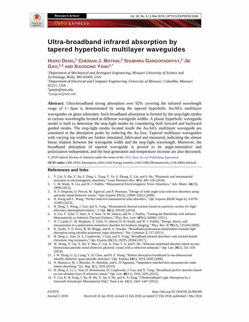
2. Tapered waveguide design and stop-light mode analysis The schematic of the tapered multilayer waveguide consisting of 13-pair Au and SiO2 layers on a glass substrate is shown in Fig. 1(a). The Au layer thickness is 20nmmt = and the SiO2 layer thickness is 80ndt = m. The unit cell period is 1500nmP = , the top width of the tapered waveguide is 250nmtW = and the bottom width is the same as the period P . The
Vol. 26, No. 5 | 5 Mar 2018 | OPTICS EXPRESS 6361
permittivity of SiO2 is a constant 2.1dε = , while the permittivity of Au is from the Drude model ( )21 /m p iε ω ω ω γ= − + where ω is the frequency, 161.37 10 /p rad sω = × is the
plasma frequency and 1312.24 10 /rad sγ = × is the bulk collision frequency which is three times of the original value 0γ [5].
The 13-pair Au-SiO2 multilayer is deposited with the magnetron sputtering system (AJA International). Au is deposited at 4 m Torr with 20 sccm of Ar gas flow at 30 W DC power, while SiO2 is deposited at 4 mTorr with 20 sccm of Ar gas flow as well as 5 sccm of O2 gas at 250 W RF power. The tapered multilayer waveguide is fabricated using Focused Ion Beam (FIB) system (Helios Nanolab 600) by controlling the dwell time of the ion beam milling at different milling depth along the tapered side wall. From the SEM image shown in Fig. 1(b), the Au-SiO2 layer pairs in the fabricated tapered waveguide can be clearly seen, while there is fabrication defect such as the coatings on both sides of the waveguide which are due to the Ga pollution during the long time ion beam milling. Different from most of other light absorber designs where a thick metal mirror is included as a ground plane to eliminate transmission, the current tapered multilayer waveguide absorber stands on a glass substrate so that slight transmission is allowed. Thus, the spectra of both transmission T (in cyan) and reflection R (in red) are measured using Fourier transform infrared spectroscopy (FTIR), and the absorption can be calculated as 1A T R= − − (in blue),which are shown in Fig. 1(c). Since the transmission is close to zero due to the strong absorption of stop-light modes, the absorption is more than 92% in the wavelength range of 1 ~ 6μmλ = . The simulated spectra (dashed curves) calculated by COMSOL Multiphysics are also shown in Fig. 1(c) and in good agreement with the measured results (solid curves)under normal incidence.
Fig. 1. (a) Schematic of the tapered multilayer waveguide consisting of 13 pairs of Au-SiO2 layers. (b) SEM image of the fabricated tapered waveguide with 1500 nmP = and
250 nmtW = . (c) Measured (solid curves) and simulated (dashed curves) spectra of
absorption A (in blue), reflection R (in red) and transmission T (in cyan)under normal incidence.
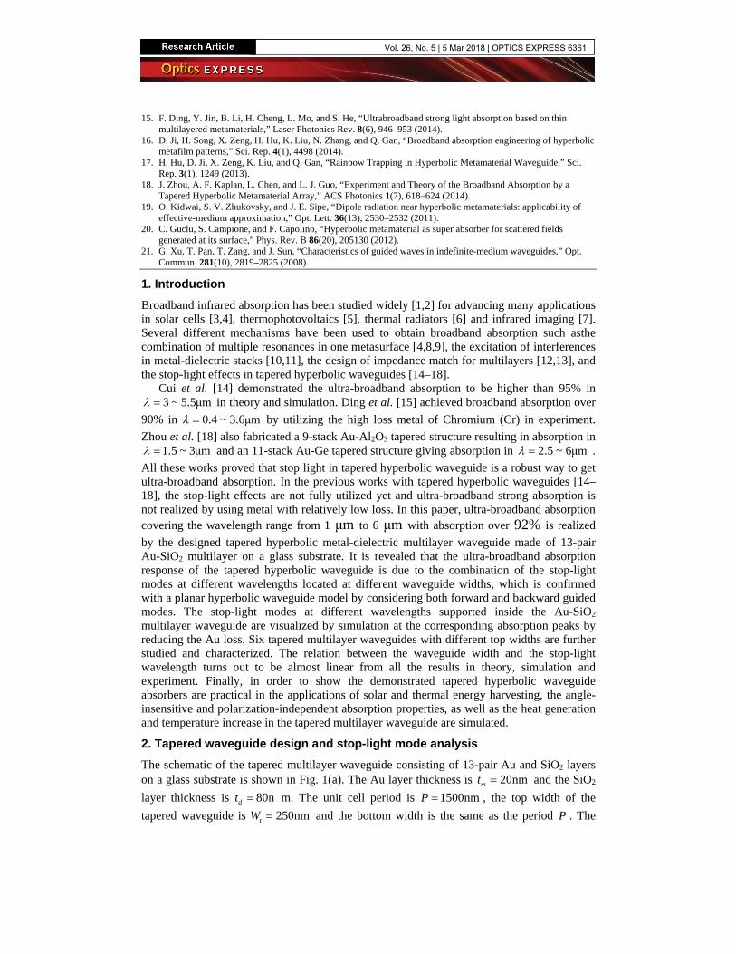
A cladding/core/cladding planar waveguide model is built in order to explain the ultra-broadband absorption achieved in the tapered multilayer waveguide. Due to the symmetry in x and y directions, the tapered Au-SiO2 multilayer waveguide can be regarded as a 2D tapered waveguide with varying width along the z direction and infinite long in y direction. As light propagates in the waveguide along z direction, the change of waveguide width will lead to the variation of waveguide mode. Thus, the whole tapered waveguide can be treated as the combination of infinite slices of waveguides with different widths stacked along z direction, and each slice of waveguide with width W is illustrated in Fig. 2(a). The core represents the hyperbolic waveguide with permittivity tensor of x y zε ε ε ε= + +
, and the claddings on the two sides are air with permittivity of 1 1ε = . The core permittivity can be evaluated via the
Vol. 26, No. 5 | 5 Mar 2018 | OPTICS EXPRESS 6362
effective medium theory [19,20] for the Au-SiO2 multilayer as ( ) ( )( )1 , 1/ / 1 /x m m m d z m m m df f f fε ε ε ε ε ε= + − = + −
in which mf is the volume filling ratio
of metal. Since the Au-SiO2 multilayer is symmetric in x and y directions, xε is equal to yε .
It can be seen from Fig. 2(b) that the waveguide is hyperbolic since xε is negative and zε is positive.
Fig. 2. (a) Schematic of the 2D waveguide model where the core represents the hyperbolic waveguide based on the Au-SiO2 multilayer and the claddings represent the air. (b) Effective permittivity of the Au-SiO2 multilayer in x direction xε (in blue) and z direction zε (in red).
In order to illustrate the formation of stop-light modes, the forward and backward guided modes inside the hyperbolic waveguide are solved by considering the continuous boundary condition at / 2x W= ± (Eq. (1)) and the dispersion relation (Eq. (2)) [21]:
1
11 tan
2z
WW Wε ακ αε
± = ±
(1)
( ) ( ) ( )2 2 2 21 0 1
xx
z
W W Wε
κ α κ ε εε
+ = − (2)
where 0 2 /κ π λ= is the wave vector of the incident light in vacuum, 2 2 21 0 1κ β κ ε= − and
( )2 20
zx
x
εα β κ ε
ε= − . is the wave vector in z direction and should be equal in both the
waveguide core and the air claddings. However, the wave vector in x direction would be different: 1κ in the air claddings and α in the waveguide core. After solving these two equations, the wave vectors can be got and thus the effective index of the waveguide can be calculated by ' ''
0/eff eff effn n in β κ= + = . Since there are two roots found during solving the equations, it indicates that the hyperbolic waveguide can support two guided modes at the same time: the forward guided mode where the phase velocity direction is the same as the group velocity direction and the backward guided mode where these two velocity directions are opposite. As shown in Figs. 3(a) and 3(b), the real and imaginary parts of the effective index are plotted as a function of the waveguide width W at different wavelengths of
1,3 and 5μmλ = . The blue curves indicate that the effective indices of forward guided modes get higher as the waveguide width becomes larger. On the other hand, the effective
Vol. 26, No. 5 | 5 Mar 2018 | OPTICS EXPRESS 6363
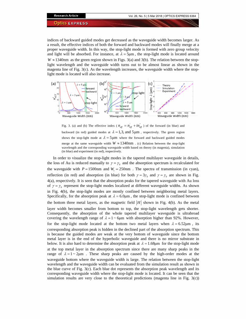
indices of backward guided modes get decreased as the waveguide width becomes larger. As a result, the effective indices of both the forward and backward modes will finally merge at a proper waveguide width. In this way, the stop-light mode is formed with zero group velocity and light will be absorbed. For instance, at 5μmλ = , the stop-light mode is located around
1340nmW ≈ as the green region shown in Figs. 3(a) and 3(b). The relation between the stop-light wavelength and the waveguide width turns out to be almost linear as shown in the magenta line of Fig. 3(c). As the wavelength increases, the waveguide width where the stop-light mode is located will also increase.
Fig. 3. (a) and (b) The effective index ( ' ''eff eff effn n in= + ) of the forward (in blue) and
backward (in red) guided modes at 1, 3, and 5 μmλ = , respectively. The green region
shows the stop-light mode at 5 μmλ = where the forward and backward guided modes
merge at the same waveguide width 1340nmW ≈ . (c) Relation between the stop-light wavelength and the corresponding waveguide width based on theory (in magenta), simulation (in blue) and experiment (in red), respectively.
In order to visualize the stop-light modes in the tapered multilayer waveguide in details, the loss of Au is reduced manually to 0γ γ= and the absorption spectrum is recalculated for the waveguide with 1500nmP = and 250nmtW = . The spectra of transmission (in cyan), reflection (in red) and absorption (in blue) for both 03γ γ= and 0γ γ= are shown in Fig. 4(a), respectively. It is seen that the absorption peaks for the tapered waveguide with Au loss of 0γ γ= represent the stop-light modes localized at different waveguide widths. As shown in Fig. 4(b), the stop-light modes are mostly confined between neighboring metal layers. Specifically, for the absorption peak at 6.0μmλ = , the stop-light mode is confined between the bottom three metal layers, as the magnetic field H shown in Fig. 4(b). As the metal layer width becomes smaller from bottom to top, the stop-light wavelength gets shorter. Consequently, the absorption of the whole tapered multilayer waveguide is ultrabroad covering the wavelength range of 1 ~ 6μmλ = with absorption higher than 92%. However, for the stop-light mode located at the bottom two metal layers when 6.52μmλ = , its corresponding absorption peak is hidden in the declined part of the absorption spectrum. This is because the guided modes are weak at the very bottom of waveguide since the bottom metal layer is in the end of the hyperbolic waveguide and there is no mirror substrate in below. It is also hard to determine the absorption peak at 1.68μmλ = for the stop-light mode at the top metal layer in the absorption spectrum since there are many sharp peaks in the range of 1 ~ 2μmλ = . These sharp peaks are caused by the high-order modes at the waveguide bottom where the waveguide width is large. The relation between the stop-light wavelength and the waveguide width can be evaluated from the simulation result as shown in the blue curve of Fig. 3(c). Each blue dot represents the absorption peak wavelength and its corresponding waveguide width where the stop-light mode is located. It can be seen that the simulation results are very close to the theoretical predictions (magenta line in Fig. 3(c))
Vol. 26, No. 5 | 5 Mar 2018 | OPTICS EXPRESS 6364
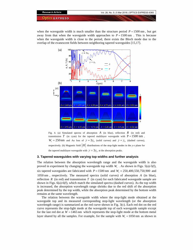
when the waveguide width is much smaller than the structure period 1500 nmP = , but get away from that when the waveguide width approaches to 1500 nmP = . This is because when the waveguide width is close to the period, there exists the Bloch mode due to the overlap of the evanescent fields between neighboring tapered waveguides [15,17].
Fig. 4. (a) Simulated spectra of absorption A (in blue), reflection R (in red) and transmission T (in cyan) for the tapered multilayer waveguide with P 1500 nm= ,
250 nmtW = and Au loss of 03γ γ= (solid curves) and 0γ γ= (dashed curves),
respectively. (b) Magnetic field H distributions of the stop-light modes in the y-z plane for
the tapered multilayer waveguide with 03γ γ= at the absorption peaks.
3. Tapered waveguides with varying top widths and further analysis The relation between the absorption wavelength range and the waveguide width is also proved in experiment by changing the waveguide top width tW . As shown in Figs. 5(a)-5(f), six tapered waveguides are fabricated with 1500 nmP = and 250, 400, 550, 750, 900tW = and 1050 nm , respectively. The measured spectra (solid curves) of absorption A (in blue), reflection R (in red) and transmission T (in cyan) for each fabricated waveguide sample are shown in Figs. 6(a)-6(f), which match the simulated spectra (dashed curves). As the top width is increased, the absorption wavelength range shrinks due to the red shift of the absorption peak determined by the top width, while the absorption peak determined by the bottom width remains at the same wavelength.
The relation between the waveguide width where the stop-light mode obtained at the waveguide top and its measured corresponding stop-light wavelength (or the absorption wavelength range) is summarized as the red curve shown in Fig. 3(c). Each red dot on the red curve represents the stop-light mode at the waveguide top of each waveguide sample except for the last red dot at 1465 nmW = which represents the stop-light mode at the bottom metal layer shared by all the samples. For example, for the sample with 1050 nmtW = as shown in
Vol. 26, No. 5 | 5 Mar 2018 | OPTICS EXPRESS 6365
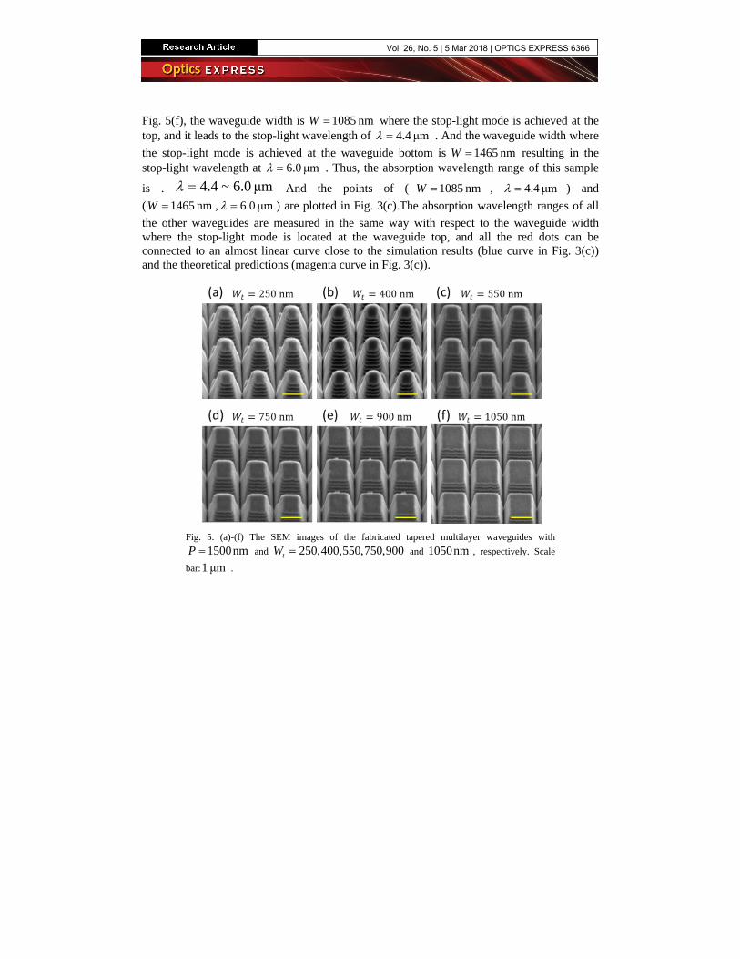
Fig. 5(f), the waveguide width is 1085 nmW = where the stop-light mode is achieved at the top, and it leads to the stop-light wavelength of 4.4 μmλ = . And the waveguide width where the stop-light mode is achieved at the waveguide bottom is 1465 nmW = resulting in the stop-light wavelength at 6.0 μmλ = . Thus, the absorption wavelength range of this sample
is . 4.4 ~ 6.0 μmλ = And the points of ( 1085 nmW = , 4.4 μmλ = ) and ( 1465 nmW = , 6.0 μmλ = ) are plotted in Fig. 3(c).The absorption wavelength ranges of all the other waveguides are measured in the same way with respect to the waveguide width where the stop-light mode is located at the waveguide top, and all the red dots can be connected to an almost linear curve close to the simulation results (blue curve in Fig. 3(c)) and the theoretical predictions (magenta curve in Fig. 3(c)).
Fig. 5. (a)-(f) The SEM images of the fabricated tapered multilayer waveguides with 1500 nmP = and 250, 400, 550, 750, 900tW = and 1050 nm , respectively. Scale
bar:1 μm .
Vol. 26, No. 5 | 5 Mar 2018 | OPTICS EXPRESS 6366
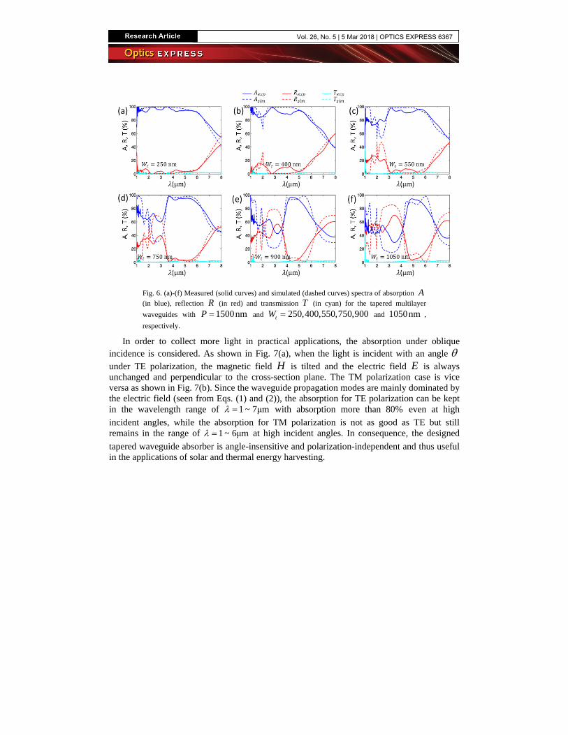
Fig. 6. (a)-(f) Measured (solid curves) and simulated (dashed curves) spectra of absorption A (in blue), reflection R (in red) and transmission T (in cyan) for the tapered multilayer waveguides with 1500 nmP = and 250, 400, 550, 750, 900tW = and 1050 nm , respectively.
In order to collect more light in practical applications, the absorption under oblique incidence is considered. As shown in Fig. 7(a), when the light is incident with an angle θ under TE polarization, the magnetic field H is tilted and the electric field E is always unchanged and perpendicular to the cross-section plane. The TM polarization case is vice versa as shown in Fig. 7(b). Since the waveguide propagation modes are mainly dominated by the electric field (seen from Eqs. (1) and (2)), the absorption for TE polarization can be kept in the wavelength range of 1 ~ 7μmλ = with absorption more than 80% even at high incident angles, while the absorption for TM polarization is not as good as TE but still remains in the range of 1 ~ 6μmλ = at high incident angles. In consequence, the designed tapered waveguide absorber is angle-insensitive and polarization-independent and thus useful in the applications of solar and thermal energy harvesting.
Vol. 26, No. 5 | 5 Mar 2018 | OPTICS EXPRESS 6367
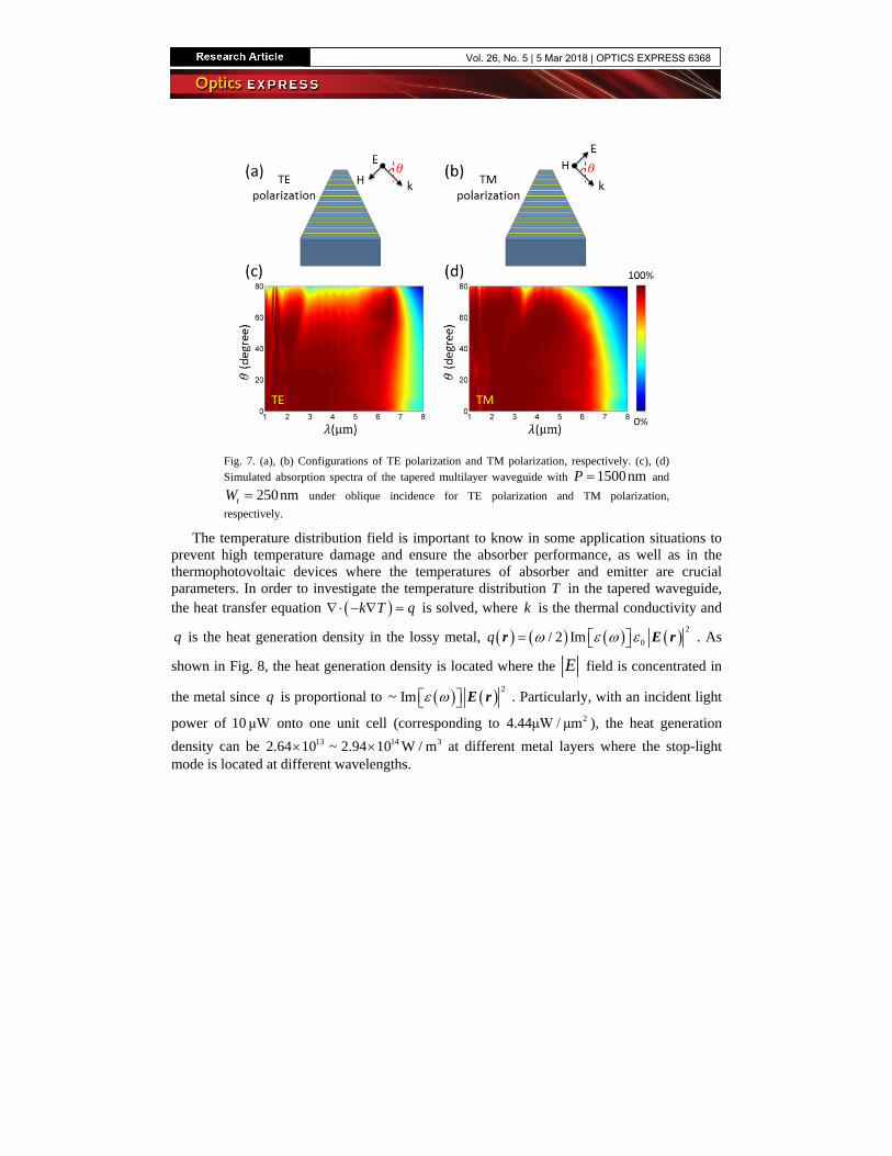
Fig. 7. (a), (b) Configurations of TE polarization and TM polarization, respectively. (c), (d) Simulated absorption spectra of the tapered multilayer waveguide with 1500 nmP = and
250 nmtW = under oblique incidence for TE polarization and TM polarization, respectively.
The temperature distribution field is important to know in some application situations to prevent high temperature damage and ensure the absorber performance, as well as in the thermophotovoltaic devices where the temperatures of absorber and emitter are crucial parameters. In order to investigate the temperature distribution T in the tapered waveguide, the heat transfer equation ( )k T q∇ ⋅ − ∇ = is solved, where k is the thermal conductivity and
q is the heat generation density in the lossy metal, ( ) ( ) ( ) ( ) 20/ 2 Imq ω ε ω ε= r E r . As
shown in Fig. 8, the heat generation density is located where the E field is concentrated in
the metal since q is proportional to ( ) ( ) 2~ Im ε ω E r . Particularly, with an incident light
power of 10 μW onto one unit cell (corresponding to 24.44μW / μm ), the heat generation density can be 13 14 32.64 10 ~ 2.94 10 W / m× × at different metal layers where the stop-light mode is located at different wavelengths.
Vol. 26, No. 5 | 5 Mar 2018 | OPTICS EXPRESS 6368
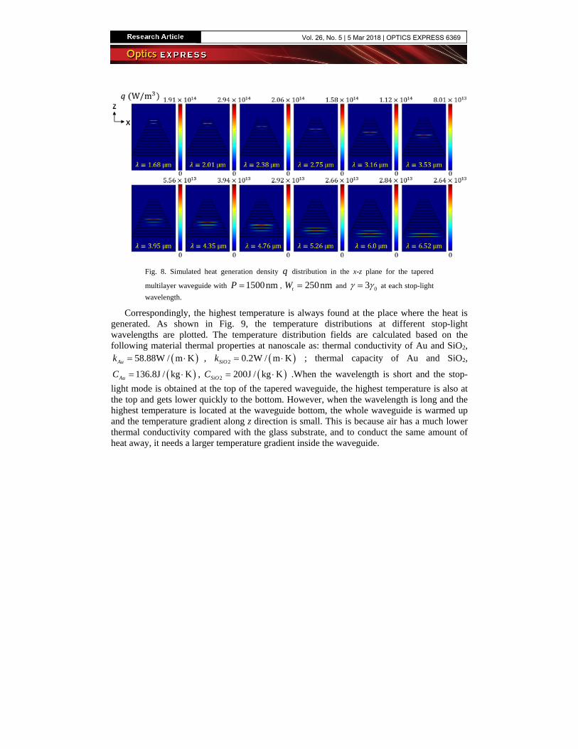
Fig. 8. Simulated heat generation density q distribution in the x-z plane for the tapered
multilayer waveguide with 1500 nmP = , 250 nmtW = and 03γ γ= at each stop-light wavelength.
Correspondingly, the highest temperature is always found at the place where the heat is generated. As shown in Fig. 9, the temperature distributions at different stop-light wavelengths are plotted. The temperature distribution fields are calculated based on the following material thermal properties at nanoscale as: thermal conductivity of Au and SiO2,
( )58.88W / m KAuk = ⋅ , ( )2 0.2W / m KSiOk = ⋅ ; thermal capacity of Au and SiO2,
( )136.8J / kg KAuC = ⋅ , ( )2 200J / kg KSiOC = ⋅ .When the wavelength is short and the stop-light mode is obtained at the top of the tapered waveguide, the highest temperature is also at the top and gets lower quickly to the bottom. However, when the wavelength is long and the highest temperature is located at the waveguide bottom, the whole waveguide is warmed up and the temperature gradient along z direction is small. This is because air has a much lower thermal conductivity compared with the glass substrate, and to conduct the same amount of heat away, it needs a larger temperature gradient inside the waveguide.
Vol. 26, No. 5 | 5 Mar 2018 | OPTICS EXPRESS 6369
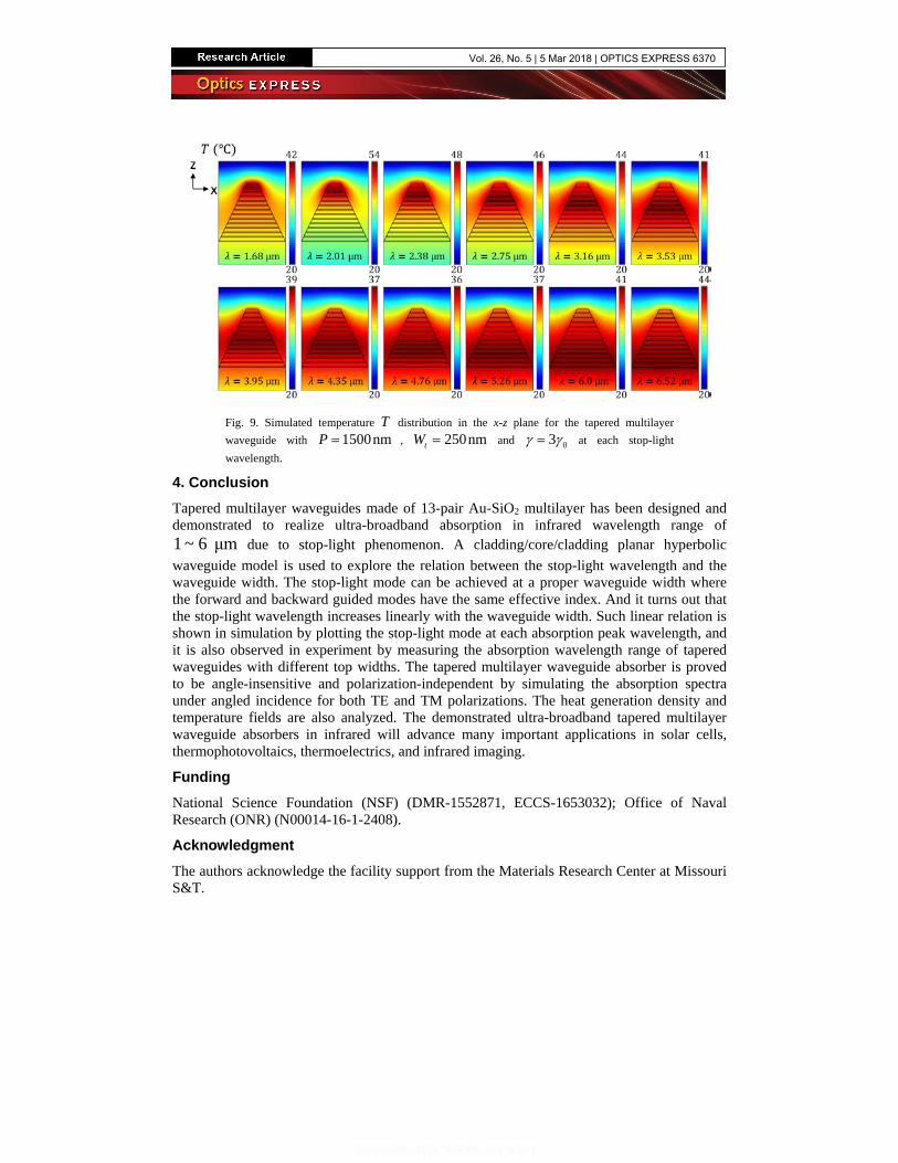
Fig. 9. Simulated temperature T distribution in the x-z plane for the tapered multilayer waveguide with 1500 nmP = , 250 nmtW = and 03γ γ= at each stop-light wavelength.
4. Conclusion Tapered multilayer waveguides made of 13-pair Au-SiO2 multilayer has been designed and demonstrated to realize ultra-broadband absorption in infrared wavelength range of 1 ~ 6 μm due to stop-light phenomenon. A cladding/core/cladding planar hyperbolic waveguide model is used to explore the relation between the stop-light wavelength and the waveguide width. The stop-light mode can be achieved at a proper waveguide width where the forward and backward guided modes have the same effective index. And it turns out that the stop-light wavelength increases linearly with the waveguide width. Such linear relation is shown in simulation by plotting the stop-light mode at each absorption peak wavelength, and it is also observed in experiment by measuring the absorption wavelength range of tapered waveguides with different top widths. The tapered multilayer waveguide absorber is proved to be angle-insensitive and polarization-independent by simulating the absorption spectra under angled incidence for both TE and TM polarizations. The heat generation density and temperature fields are also analyzed. The demonstrated ultra-broadband tapered multilayer waveguide absorbers in infrared will advance many important applications in solar cells, thermophotovoltaics, thermoelectrics, and infrared imaging.
Funding National Science Foundation (NSF) (DMR-1552871, ECCS-1653032); Office of Naval Research (ONR) (N00014-16-1-2408).
Acknowledgment The authors acknowledge the facility support from the Materials Research Center at Missouri S&T.
Vol. 26, No. 5 | 5 Mar 2018 | OPTICS EXPRESS 6370