ultra low-power, integrated ism band sub-ghz...
TRANSCRIPT
2010-2017 Microchip Technology Inc. DS70000622D
MRF89XAData Sheet
Ultra Low-Power, Integrated ISM BandSub-GHz Transceiver

DS70000622D-page 2 Preliminary 2010-2017 Microchip Technology Inc.
Information contained in this publication regarding deviceapplications and the like is provided only for your convenienceand may be superseded by updates. It is your responsibility toensure that your application meets with your specifications.MICROCHIP MAKES NO REPRESENTATIONS ORWARRANTIES OF ANY KIND WHETHER EXPRESS ORIMPLIED, WRITTEN OR ORAL, STATUTORY OROTHERWISE, RELATED TO THE INFORMATION,INCLUDING BUT NOT LIMITED TO ITS CONDITION,QUALITY, PERFORMANCE, MERCHANTABILITY ORFITNESS FOR PURPOSE. Microchip disclaims all liabilityarising from this information and its use. Use of Microchipdevices in life support and/or safety applications is entirely atthe buyer’s risk, and the buyer agrees to defend, indemnify andhold harmless Microchip from any and all damages, claims,suits, or expenses resulting from such use. No licenses areconveyed, implicitly or otherwise, under any Microchipintellectual property rights unless otherwise stated.
Note the following details of the code protection feature on Microchip devices:
• Microchip products meet the specification contained in their particular Microchip Data Sheet.
• Microchip believes that its family of products is one of the most secure families of its kind on the market today, when used in the intended manner and under normal conditions.
• There are dishonest and possibly illegal methods used to breach the code protection feature. All of these methods, to our knowledge, require using the Microchip products in a manner outside the operating specifications contained in Microchip’s Data Sheets. Most likely, the person doing so is engaged in theft of intellectual property.
• Microchip is willing to work with the customer who is concerned about the integrity of their code.
• Neither Microchip nor any other semiconductor manufacturer can guarantee the security of their code. Code protection does not mean that we are guaranteeing the product as “unbreakable.”
Code protection is constantly evolving. We at Microchip are committed to continuously improving the code protection features of ourproducts. Attempts to break Microchip’s code protection feature may be a violation of the Digital Millennium Copyright Act. If such actsallow unauthorized access to your software or other copyrighted work, you may have a right to sue for relief under that Act.
Microchip received ISO/TS-16949:2009 certification for its worldwide headquarters, design and wafer fabrication facilities in Chandler and Tempe, Arizona; Gresham, Oregon and design centers in California and India. The Company’s quality system processes and procedures are for its PIC® MCUs and dsPIC® DSCs, KEELOQ® code hopping devices, Serial EEPROMs, microperipherals, nonvolatile memory and analog products. In addition, Microchip’s quality system for the design and manufacture of development systems is ISO 9001:2000 certified.
QUALITYMANAGEMENTSYSTEMCERTIFIEDBYDNV
== ISO/TS16949==
Trademarks
The Microchip name and logo, the Microchip logo, AnyRate, AVR, AVR logo, AVR Freaks, BeaconThings, BitCloud, CryptoMemory, CryptoRF, dsPIC, FlashFlex, flexPWR, Heldo, JukeBlox, KEELOQ, KEELOQ logo, Kleer, LANCheck, LINK MD, maXStylus, maXTouch, MediaLB, megaAVR, MOST, MOST logo, MPLAB, OptoLyzer, PIC, picoPower, PICSTART, PIC32 logo, Prochip Designer, QTouch, RightTouch, SAM-BA, SpyNIC, SST, SST Logo, SuperFlash, tinyAVR, UNI/O, and XMEGA are registered trademarks of Microchip Technology Incorporated in the U.S.A. and other countries.
ClockWorks, The Embedded Control Solutions Company, EtherSynch, Hyper Speed Control, HyperLight Load, IntelliMOS, mTouch, Precision Edge, and Quiet-Wire are registered trademarks of Microchip Technology Incorporated in the U.S.A.
Adjacent Key Suppression, AKS, Analog-for-the-Digital Age, Any Capacitor, AnyIn, AnyOut, BodyCom, chipKIT, chipKIT logo, CodeGuard, CryptoAuthentication, CryptoCompanion, CryptoController, dsPICDEM, dsPICDEM.net, Dynamic Average Matching, DAM, ECAN, EtherGREEN, In-Circuit Serial Programming, ICSP, Inter-Chip Connectivity, JitterBlocker, KleerNet, KleerNet logo, Mindi, MiWi, motorBench, MPASM, MPF, MPLAB Certified logo, MPLIB, MPLINK, MultiTRAK, NetDetach, Omniscient Code Generation, PICDEM, PICDEM.net, PICkit, PICtail, PureSilicon, QMatrix, RightTouch logo, REAL ICE, Ripple Blocker, SAM-ICE, Serial Quad I/O, SMART-I.S., SQI, SuperSwitcher, SuperSwitcher II, Total Endurance, TSHARC, USBCheck, VariSense, ViewSpan, WiperLock, Wireless DNA, and ZENA are trademarks of Microchip Technology Incorporated in the U.S.A. and other countries.
SQTP is a service mark of Microchip Technology Incorporated in the U.S.A.
Silicon Storage Technology is a registered trademark of Microchip Technology Inc. in other countries.
GestIC is a registered trademark of Microchip Technology Germany II GmbH & Co. KG, a subsidiary of Microchip Technology Inc., in other countries.
All other trademarks mentioned herein are property of their respective companies.
© 2010-2017, Microchip Technology Incorporated, All Rights Reserved.
ISBN: 978-1-5224-2296-9

MRF89XAUltra Low-Power, Integrated ISM Band
Sub-GHz Transceiver
Features
• Fully integrated ultra low-power, sub-GHz transceiver• Wide-band half-duplex transceiver
• Supports proprietary sub-GHz wireless protocols
• Simple 4-wire SPI-compatible interface
• CMOS/TTL-compatible I/Os
• On-chip oscillator circuit
• Dedicated clock output
• Supports power-saving modes
• Operating voltage: 2.1-3.6V
• Low-current consumption, typically:
- 3 mA in RX mode- 25 mA at +10 dBm in TX mode- 0.1 μA (Typical) and 2 μA (Maximum) in
Sleep mode• Supports Industrial temperature range (-40ºC to
+85ºC)
• Complies with ETSI EN 300-220 and FCC part 15
• Small, 32-pin TQFN package
RF/Analog Features
• Supports ISM band sub-GHz frequency ranges:863–870, 902–928 and 950–960 MHz
• Modulation technique: Supports FSK and OOK
• Supports high data rates: Up to 200 kbps, NRZcoding
• Reception sensitivity: Down to -107 dBm at25 kbps in FSK, -113 dBm at 2 kbps in OOK
• RF output power: +12.5 dBm programmable ineight steps
• Wide Received Signal Strength Indicator (RSSI),dynamic range: 70 dB from RX noise floor
• Signal-ended RF input/output
• On-chip frequency synthesizer
• Supports PLL loop filter with lock detect
• Integrated Power Amplifier (PA) and Low NoiseAmplifiers (LNA)
• Channel filters
• On-chip IF gain and mixers
• Integrated low-phase noise VCO
Baseband Features
• Packet handling feature with data whitening andautomatic CRC generation
• Incoming Sync Word (pattern) recognition
• Built-in bit synchronizer for incoming data, andclock synchronization and recovery
• 64-byte transmit/receive FIFO with preload inStandby mode
• Supports Manchester encoding/decoding techniques
Typical Applications
• Home/industrial/building automation
• Remote wireless control
• Wireless PC peripherals
• Remote keyless entry
• Wireless sensor networks
• Vehicle sensor monitoring
• Telemetry
• Data logging systems
• Wireless alarm
• Remote automatic meter reading
• Security systems for home/industrial environments
• Automobile immobilizers
• Sports and performance monitoring
• Wireless toy controls
• Medical applications
General Description
The MRF89XA is a single chip, multi-channel FSK/OOKtransceiver capable of operating in the 863-870 MHzand 902-928 MHz license-free ISM frequency bands, aswell as the 950-960 MHz frequency band. The low-costMRF89XA is optimized for very low-powerconsumption. It incorporates a baseband modem withdata rates up to 200 kbps. Data handling featuresinclude a 64-byte FIFO, packet handling, automaticCRC generation and data whitening. Its highlyintegrated architecture allows for minimum externalcomponent count while still maintaining designflexibility.
2010-2017 Microchip Technology Inc. Preliminary DS70000622D-page 3
MRF89XA
All critical RF and baseband functions are integrated inthe MRF89XA, which minimizes the externalcomponent count and reduces the design time. The RFcommunication parameters are made programmableand most of them may be dynamically set. Amicrocontroller, RF SAW filter, 12.8 MHz crystal, and afew passive components are required to create acomplete, reliable radio function. The MRF89XA usesseveral low-power mechanisms to reduce overallcurrent consumption and extend battery life. Its smallsize and low-power consumption makes the MRF89XAideal for a wide variety of short-range radioapplications. The MRF89XA complies with European(ETSI EN 300-220) and United States (FCC Part15.247 and 15.249) regulatory standards.
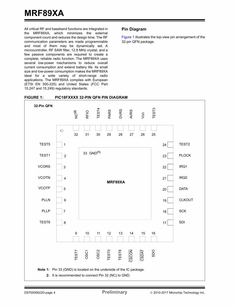
Pin Diagram
Figure 1 illustrates the top-view pin arrangement of the32-pin QFN package.
FIGURE 1: PIC18FXXXX 32-PIN QFN PIN DIAGRAM
32-Pin QFN
Note 1: Pin 33 (GND) is located on the underside of the IC package.
2: It is recommended to connect Pin 32 (NC) to GND.
1
2
3
4
5
6
7
8 17
18
23
24
21
22
19
20
9 10 11 12 13 14 15 16
32 31 30 29 28 27 26 25
TEST5
TEST1
VCORS
PLLN
PLLP
TEST6
TEST2
PLOCK
IRQ1
IRQ0
DATA
CLKOUT
SCK
SDI
NC
(2)
RF
IO
TE
ST
4
PA
RS
DV
RS
VD
D
TE
ST
3
TE
ST
7
OS
C1
OS
C2
TE
ST
0
TE
ST
8
CS
CO
N
SD
O33 GND(1)
VCOTN
VCOTP
CS
DA
T
AV
RS
MRF89XA
DS70000622D-page 4 Preliminary 2010-2017 Microchip Technology Inc.
MRF89XA
Table of ContentsOverview ............................................................................................................................................................................................... 7Hardware Description ......................................................................................................................................................................... 11Functional Description ........................................................................................................................................................................ 55Application Details .............................................................................................................................................................................. 93Electrical Characteristics................................................................................................................................................................... 103Packaging Information ...................................................................................................................................................................... 129Appendix A: FSK and OOK RX Filters vs. Bit rates .......................................................................................................................... 131Appendix B: CRC Computation in C ................................................................................................................................................. 132Appendix C: Revision History ........................................................................................................................................................... 133The Microchip Web Site.................................................................................................................................................................... 135Customer Change Notification Service ............................................................................................................................................. 135Customer Support ............................................................................................................................................................................. 135Product Identification System ........................................................................................................................................................... 139
TO OUR VALUED CUSTOMERS
It is our intention to provide our valued customers with the best documentation possible to ensure successful use of your Microchipproducts. To this end, we will continue to improve our publications to better suit your needs. Our publications will be refined andenhanced as new volumes and updates are introduced.
If you have any questions or comments regarding this publication, please contact the Marketing Communications Department viaE-mail at [email protected] or fax the Reader Response Form in the back of this data sheet to (480) 792-4150. Wewelcome your feedback.
Most Current Data Sheet
To obtain the most up-to-date version of this data sheet, please register at our Worldwide Web site at:
http://www.microchip.com
You can determine the version of a data sheet by examining its literature number found on the bottom outside corner of any page.The last character of the literature number is the version number, (e.g., DS30000A is version A of document DS30000).
Errata
An errata sheet, describing minor operational differences from the data sheet and recommended workarounds, may exist for currentdevices. As device/documentation issues become known to us, we will publish an errata sheet. The errata will specify the revisionof silicon and revision of document to which it applies.
To determine if an errata sheet exists for a particular device, please check with one of the following:
• Microchip’s Worldwide Web site; http://www.microchip.com• Your local Microchip sales office (see last page)When contacting a sales office, please specify which device, revision of silicon and data sheet (include literature number) you areusing.
Customer Notification System
Register on our web site at www.microchip.com to receive the most current information on all of our products.
2010-2017 Microchip Technology Inc. Preliminary DS70000622D-page 5

MRF89XA
NOTES:
DS70000622D-page 6 Preliminary 2010-2017 Microchip Technology Inc.
MRF89XA
1.0 OVERVIEW
Microchip's MRF89XA is a fully integrated, half-duplex,sub-GHz transceiver. This low-power, single-chip FSKand OOK baseband transceiver supports:
• Superheterodyne architecture• Multi-channel, multi-band synthesizer with Phase
Locked Loop (PLL) for easy RF design• Power Amplifier (PA)• Low Noise Amplifier (LNA)• I/Q two stage down converter mixers• I/Q demodulator, FSK/OOK• Baseband filters and amplifiers
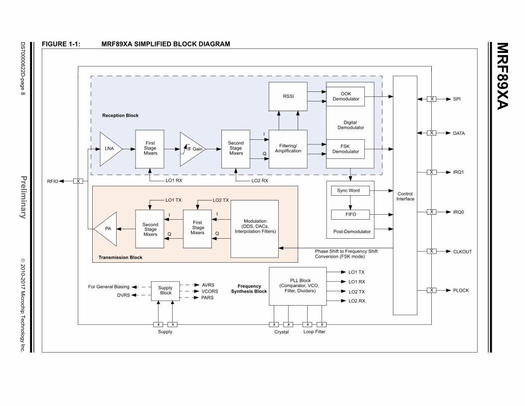
The simplified block diagram of the MRF89XA isillustrated in Figure 1-1.
The MRF89XA is a good option for low-cost, high-volume, low data rate (200 kbps), and two-way short-range wireless applications. This device is a single-chipFSK and OOK transceiver capable of operating in the 863-870 MHz and 902-928 MHz license-free ISMfrequency bands, and the 950-960 MHz frequencyband.
The low-cost MRF89XA is optimized for very low-powerconsumption (3 mA in Receive mode). It incorporates abaseband modem with data rates up to 200 kbps in FSKand 32 kbps in OOK. Data handling features include a64-byte FIFO, packet handling, automatic CRCgeneration, and data whitening. The device alsosupports Manchester coding techniques. Its highlyintegrated architecture allows for minimum externalcomponent count while maintaining design flexibility. Allmajor RF communication parameters areprogrammable and most of them may be dynamicallyset.
The MRF89XA supports a stable sensitivity andlinearity characteristics for a wide supply range and isinternally regulated. The frequency synthesizer of theMRF89XA is a fully integrated integer-N type PLL. Theoscillator circuit provided on the MRF89XA deviceprovides the reference clock for the PLL. Thefrequency synthesizer requires only five externalcomponents, which include the PLL loop filter and theVCO tank circuit. Low-phase noise provides forexcellent adjacent channel rejection capability, Bit ErrorRate (BER), and longer communication range.
The high-resolution PLL allows:
• Usage of multiple channels in any of the bands
• Rapid settling time, which allows for fasterfrequency hopping
A communication link in most applications can becreated using a low-cost 12.8 MHz crystal, a SAW filter,and a low-cost microcontroller. The MRF89XAprovides a clock signal for the microcontroller. Thetransceiver can be interfaced with many popularMicrochip PIC® microcontrollers through a 4-wireSerial Peripheral Interface (SPI), interrupts (IRQ0 andIRQ1), PLL lock, and clock out. The interface betweenthe microcontroller and MRF89XA (a typical MRF89XARF node) is illustrated in Figure 1-2.
The MRF89XA supports the following digital dataprocessing features:
• Received Signal Strength Indicator (RSSI)
• Sync Word recognition
• Packet handling
• Interrupt and flags
• Different operating modes (Continuous, Buffered,and Packet)
• Data filtering/whitening/encoding
• Baseband power amplifier
• 64-byte TX/RX FIFO
The role of the digital processing unit is to interface thedata to/from the modulator/demodulator and themicrocontroller access points (SPI, IRQ and DATA pins).It also controls all of the Configuration registers. Thereceiver's Baseband Bandwidth (BBBW) can beprogrammed to accommodate various deviations anddata rates requirements.
An optional Bit Synchronizer (BitSync) is provided, tosupply a synchronous clock and data stream to acompanion microcontroller in Continuous mode, or tofill the FIFO with glitch-free data in Buffered mode. Thetransceiver is integrated with different power-savingmodes and a software wake-up time through the hostmicrocontroller to keep track of the activities, whichreduce the overall current consumption and extendsthe battery life. The small size and low-powerconsumption of the MRF89XA makes it ideal forvarious short-range radio applications.
The MRF89XA complies with European (ETSI EN 300-220) and United States (FCC Part 15.247 and 15.249)regulatory standards.
2010-2017 Microchip Technology Inc. Preliminary DS70000622D-page 7
MR
F89X
A
DS
70000622D
-page 8
Prelim
ina
ry
2010-2017 Microchip T
echnology Inc.
tor
ControlInterface
ulator
X
X
X
X
TX
RX
TX
RX
SPI
DATA
CLKOUT
PLOCK
ncy Shift e)
X
X IRQ1
IRQ0
FIGURE 1-1: MRF89XA SIMPLIFIED BLOCK DIAGRAM
X
Second StageMixers
StageMixers
Modulation(DDS, DACs,
Interpolation Filters)
First StageMixers
Second StageMixers
RSSI
Digital Demodula
PLL Block(Comparator, VCO,
Filter, Dividers)
LNA IF Gain
PA
Filtering/Amplification
OOK Demodulator
FSK Demodulator
Post-Demod
Sync Word
FIFO
Supply Block
xx
LO1
LO1 TX
LO1
LO2
LO2
LO1 RX
LO2 TX
LO2 RX
xx xx
RFIO
Transmission Block
Reception Block
Frequency
I
Q
I
Q
I
Q
Phase Shift to Freque
Supply Crystal Loop Filter
First
Conversion (FSK mod
PARSVCORSAVRS
DVRS
For General BiasingSynthesis Block
2010
-2017 Microchip T
echnology Inc.
Prelim
ina
ryD
S700
00622D-page 9
MR
F89X
A
FIG
PIC® MCU
I/O
I/O
SDO
SDI
SCK
INT0
INT1
I/O
I/O
OSC1
ation, refer to Section 3.8, Data
URE 1-2: MRF89XA TO MICROCONTROLLER INTERFACE (NODE) BLOCK DIAGRAM
Antenna
Saw
Filter
MatchingCircuitry
Block
PARS
RFIO
LoopFilterBlock
RF Block
RF
BasebandAmplifier/
Filter/Limiter
PowerManagement
Memory
Crystal Frequency = 12.8 MHz
ProcessingUnit
MRF89XA
ControlInterface
Data
TankCircuitBlock
CSDAT
CSCON
SDI
SDO
SCK
IRQ0
IRQ1
DATA
PLOCK
CLKOUT
Note: The interface between the MRF89XA and the MCU depends on the Data mode of operation. For more informProcessing.
Circuits
MRF89XA
NOTES:
DS70000622D-page 10 Preliminary 2010-2017 Microchip Technology Inc.
MRF89XA
2.0 HARDWARE DESCRIPTION
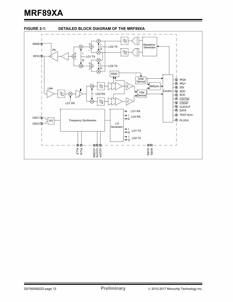
The MRF89XA is an integrated, single-chip, low-powerISM band sub-GHz transceiver. A detailed blockdiagram of the MRF89XA is illustrated in Figure 2-1.The frequency synthesizer is clocked by an external12.8 MHz crystal, and frequency ranges from 863-870MHz, 902-928 MHz, and 950-960 MHz are possible.
The MRF89XA receiver employs a superheterodynearchitecture. The first IF is one-ninth of the RFfrequency (approximately 100 MHz). The seconddown-conversion, down converts the I and Q signals tobaseband in the case of the FSK receiver (zero-IF) andto a low-IF (IF2) for the OOK receiver. After the seconddown-conversion stage, the received signal is channelselect filtered and amplified to a level adequate fordemodulation. Both FSK and OOK demodulation areavailable. Image rejection is achieved using a SAWfilter.
The baseband I and Q signals at the transmitter side aredigitally generated by a Direct Digital Synthesis (DDS),whose Digital-to-Analog Converters (DAC) are followedby two anti-aliasing, low-pass filters that transform thedigital signal into analog In-Phase (I) and Quadrature(Q) components with frequency as the selectedFrequency Deviation (fdev). The transmitter supportsboth FSK and OOK modes of operation. The transmitterhas a typical output power of +12.5 dBm. An internaltransmit/receive switch combines the transmitter andreceiver circuits into a single-ended RFIO pin (pin 31).The RFIO pin is connected through the impedancematching circuitry to an external antenna. The deviceoperates in the low-voltage range of 2.1-3.6V, and inSleep mode, it operates at a very low-current state,typically 0.1 µA.
The frequency synthesizer is based on an integer-NPLL having PLL bandwidth of 15 kHz. Twoprogrammable frequency dividers in the feedback loopof the PLL and one programmable divider on thereference oscillator allow the LO frequency to beadjusted. The reference frequency is generated by acrystal oscillator running at 12.8 MHz.
The MRF89XA is controlled by a digital block thatincludes registers to store the configuration settings ofthe radio. These registers are accessed by a hostmicrocontroller through a Serial Peripheral Interface(SPI). The quality of the data is validated using theRSSI and bit synchronizer blocks built into thetransceiver. Data is buffered in a 64-byte transmitter orreceiver FIFO. The transceiver is controlled through a4-wire SPI, interrupts (IRQ0 and IRQ1), PLOCK, DATA,and Chip Select pins for SPI, which are illustrated inFigure 2-1. On-chip regulators provide stable supplyvoltages to sensitive blocks and allow the MRF89XA tobe used with supply voltages from 2.1-3.6V. Mostblocks are supplied with a voltage below 1.4V.
The MRF89XA supports the following feature blocks:
• Data filtering and whitening
• Bit synchronization
• 64-byte transmit/receive FIFO buffer
• General configuration registers
These features reduce the processing load, whichallow the use of simple, low-cost, 8-bit microcontrollersfor data processing.
2010-2017 Microchip Technology Inc. Preliminary DS70000622D-page 11
MRF89XA
FIGURE 2-1: DETAILED BLOCK DIAGRAM OF THE MRF89XA
Waveform Generator
FSK Demod
BitSync
OOKDemod
Control
XO
RSSI
LO1 RX
LO2 RXI
IQ
Q
LO1 TX
IQ
LO2 TX
LO1 RX
LO2 RX
LO1 TX
LO2 TX
LO2 TX
RFIO
OSC1
OSC2
VC
OR
S
PARS
IRQ0
IRQ1
SDI
SDO SCK
CSCON
CLKOUTDATA
CSDAT
TEST<8:0>
VC
OT
P
VC
OT
N
PL
LP
PL
LN
DV
RS
PLOCK
PA
LNA
I
Q
Q
I
I
Q
LO Generator
Frequency Synthesizer
AV
RS
DS70000622D-page 12 Preliminary 2010-2017 Microchip Technology Inc.
MRF89XA
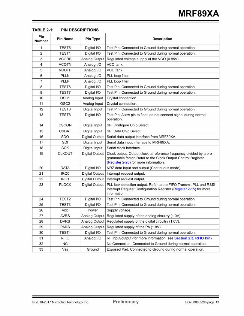
TABLE 2-1: PIN DESCRIPTIONS
Pin Number
Pin Name Pin Type Description
1 TEST5 Digital I/O Test Pin. Connected to Ground during normal operation.
2 TEST1 Digital I/O Test Pin. Connected to Ground during normal operation.
3 VCORS Analog Output Regulated voltage supply of the VCO (0.85V).
4 VCOTN Analog I/O VCO tank.
5 VCOTP Analog I/O VCO tank.
6 PLLN Analog I/O PLL loop filter.
7 PLLP Analog I/O PLL loop filter.
8 TEST6 Digital I/O Test Pin. Connected to Ground during normal operation.
9 TEST7 Digital I/O Test Pin. Connected to Ground during normal operation.
10 OSC1 Analog Input Crystal connection.
11 OSC2 Analog Input Crystal connection.
12 TEST0 Digital Input Test Pin. Connected to Ground during normal operation.
13 TEST8 Digital I/O Test Pin. Allow pin to float; do not connect signal during normal operation.
14 CSCON Digital Input SPI Configure Chip Select.
15 CSDAT Digital Input SPI Data Chip Select.
16 SDO Digital Output Serial data output interface from MRF89XA.
17 SDI Digital Input Serial data input interface to MRF89XA.
18 SCK Digital Input Serial clock interface.
19 CLKOUT Digital Output Clock output. Output clock at reference frequency divided by a pro-grammable factor. Refer to the Clock Output Control Register (Register 2-28) for more information.
20 DATA Digital I/O NRZ data input and output (Continuous mode).
21 IRQ0 Digital Output Interrupt request output.
22 IRQ1 Digital Output Interrupt request output.
23 PLOCK Digital Output PLL lock detection output. Refer to the FIFO Transmit PLL and RSSI Interrupt Request Configuration Register (Register 2-15) for more information.
24 TEST2 Digital I/O Test Pin. Connected to Ground during normal operation.
25 TEST3 Digital I/O Test Pin. Connected to Ground during normal operation.
26 VDD Power Supply voltage.
27 AVRS Analog Output Regulated supply of the analog circuitry (1.0V).
28 DVRS Analog Output Regulated supply of the digital circuitry (1.0V).
29 PARS Analog Output Regulated supply of the PA (1.8V).
30 TEST4 Digital I/O Test Pin. Connected to Ground during normal operation.
31 RFIO Analog I/O RF input/output (for more information, see Section 2.3, RFIO Pin).
32 NC — No Connection. Connected to Ground during normal operation.
33 Vss Ground Exposed Pad. Connected to Ground during normal operation.
2010-2017 Microchip Technology Inc. Preliminary DS70000622D-page 13

MRF89XA
2.1 Power Supply and Ground BlockPins
To provide stable sensitivity and linearitycharacteristics over a wide supply range, theMRF89XA is internally voltage regulated. This internalregulated power supply block structure is illustrated inFigure 2-2.
The power supply bypassing is essential for betterhandling of signal surges and noise in the power line.To ensure correct operation of the regulator circuit, thedecoupling capacitor connection (shown in Figure 2-2)is recommended. These decoupling components arerecommended for any design. The power supply blockgenerates four regulated supplies for the analog,digital, VCO, and the PLL blocks to reduce the voltagesfor their specific requirements. However, Power-onReset (POR), Configuration registers, and the SPI usethe VDD supply given to the MRF89XA.
The large value decoupling capacitors should beplaced at the PCB power input. The smaller valuedecoupling capacitors should be placed at every powerpoint of the device and at bias points for the RF port.Poor bypassing can lead to conducted interference,which can cause noise and spurious signals to coupleinto the RF sections, thereby significantly reducing theperformance.
It is recommended that the VDD pin have two bypasscapacitors to ensure sufficient bypass and decoupling.However, based on the selected carrier frequency, thebypass capacitor values vary. The trace length (VDD pinto bypass capacitors) should be made as short aspossible.
FIGURE 2-2: POWER SUPPLY BLOCK DIAGRAM
TABLE 2-2: POWER SUPPLY PIN DETAILS
Blocks Biasing Through Associated PinsRegulated Voltage
(in Volts)
POR, SPI and Configuration Registers VDD VDD 2.1–3.6
Regulated Supply (VINTS) VDD VDD 1.4
Analog VINTS AVRS 1.0
Digital VINTS DVRS 1.0
VCO VINTS VCORS 0.85
PA VDD PARS 1.8
VDD – Pin 26 2.1 – 3.6V
External Supply
Internal Regulator 1.4 V
Digital Regulator 1.0 V
VCO Regulator 0.85 V
PA Regulator 1.80 V
VCORS Pin 3
PARS Pin 29
Biasing: - PA Driver - Ext. PA Choke
Biasing: - VCO Circuit - Ext. VCO Tank
Biasing Digital Blocks
DVRS Pin 28
Biasing Analog Blocks
AVRS Pin 27
Analog Regulator 1.0 V
Biasing: - SPI - Config. Registers - POR
1 µFY5V
1 µF Y5V
0.22 µFX7R
0.1 µFX7R
0.047 µF X7R
VBAT
VINTS
DS70000622D-page 14 Preliminary 2010-2017 Microchip Technology Inc.
MRF89XA
2.2 Reset Pin
The device enters the Reset mode if any of thefollowing events takes place:
• Power-on Reset (POR)
• Manual Reset
The POR happens when the MRF89XA is switched onusing VDD. The POR cycle takes at least 10 ms toexecute any communication operations on the SPI bus.
An external hardware or manual Reset of theMRF89XA can be performed by asserting the TEST8pin (pin 13) to high for 100 µs and then releasing thepin. After releasing the pin, it takes more than 5 ms forthe transceiver to be ready for any operations. Thereset pin is driven with an open-drain output; therefore,is pulled high while the device is in POR. The devicedoes not accept commands during the Reset period.For more information, refer to Section 3.1.2, ManualReset.
2.3 RFIO Pin
The receiver and the transmitter share the same RFIOpin (pin 31). Figure 2-3 illustrates the configuration ofthe common RF front-end.
• In Transmit mode, the PA and the PA regulatorare ON with voltage on the PARS pin (pin 29)equal to the nominal voltage of the regulator(about 1.8V). The external RF choke inductanceis used to bias the PA.
• In Receive mode, the PA and PA regulator are OFF and PARS is tied to the ground. The external RF choke inductor is used for biasing and match-ing the LNA (this is implemented as a common gate amplifier).
FIGURE 2-3: COMMON RF INPUT AND OUTPUT PIN DIAGRAM
The PA and the LNA front-ends in the MRF89XA, whichshare the same Input/Output pin, are internallymatched to approximately 50.
2.4 Filters and Amplifiers Block
2.4.1 INTERPOLATION FILTER
After the digital-to-analog conversion during transmis-sion, both I and Q signals are smoothened by interpo-lation filters. These interpolation filters perform lowpass filtering of the digitally generated signal and pre-vent the alias signals from entering the modulators.
2.4.2 POWER AMPLIFIER
The Power Amplifier (PA) integrated in the MRF89XAoperates under a regulated voltage supply of 1.8V. Theexternal RF choke inductor is biased by an internalregulator output made available on the PARS pin (pin29). Therefore, the PA output power is consistent overthe power supply range. The consistency in operationis important for applications which allows bothpredictable RF performance and battery life.
An open collector output requires biasing using aninductor as an RF choke. For the recommended PAbias and matching circuit details see Section 4.5.2,Suggested PA Biasing And Matching.
The matching of the SAW filter depends on the SAWfilter selected. Many modern SAW filters have 50input and output, which simplifies matching for theMRF89XA. This is demonstrated in the applicationcircuit. If the choice of SAW filter is different than 50,the required impedance match on the input and outputof the SAW filter is needed.
2.4.3 LOW NOISE AMPLIFIER (WITHFIRST MIXER)
In Receive mode, the RFIO pin (pin 31) is connected toa fixed-gain, common-gate, Low Noise Amplifier (LNA).The performance of this amplifier is such that the NoiseFigure (NF) of the receiver is estimated to beapproximately 7 dB.
The LNA has approximately 50 impedance, whichfunctions well with the proposed antenna (PCB/Monopole) during signal transmission. The LNA is fol-lowed by an internal RF band-pass filter.
RFIO
PARS
PA
PA Regulator
RX ON
LNA
To Antenna
(1.8V)
Note: Image rejection is achieved using a SAWfilter on the RF input.
2010-2017 Microchip Technology Inc. Preliminary DS70000622D-page 15
MRF89XA
2.4.4 IF GAIN AND SECOND I/Q MIXER
Following the LNA and first down-conversion, there isan IF amplifier whose gain can be programmed from13.5-0 dB in 4.5 dB steps, through the registerDMODREG. For more information, refer toSection 2.14.2, Data And Modulation ConfigurationRegister Details. The default setting corresponds to0 dB gain, but lower values can be used to increase theRSSI dynamic range.
2.4.5 CHANNEL FILTERS
The second mixer stages are followed by the channelselect filters. The channel select filters have a stronginfluence on the noise bandwidth and selectivity of thereceiver, and therefore, its sensitivity. Each channelselect filter features a passive second-order RC filter,with a programmable bandwidth, and the “fine” channelselection is performed by an active, third-order,Butterworth filter, which acts as a low-pass filter for thezero-IF configuration (FSK), or a complex polyphasefilter for the low-IF (OOK) configuration. For moreinformation on configuring passive and active filterssee Section 3.4.4, Channel Filters.
2.5 Frequency Synthesizer Block
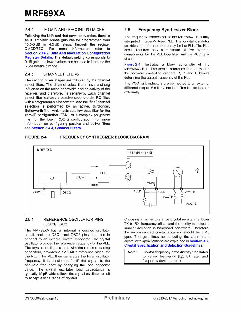
The frequency synthesizer of the MRF89XA is a fullyintegrated integer-N type PLL. The crystal oscillatorprovides the reference frequency for the PLL. The PLLcircuit requires only a minimum of five externalcomponents for the PLL loop filter and the VCO tankcircuit.
Figure 2-4 illustrates a block schematic of theMRF89XA PLL. The crystal reference frequency andthe software controlled dividers R, P, and S blocksdetermine the output frequency of the PLL.
The VCO tank inductors are connected to an externaldifferential input. Similarly, the loop filter is also locatedexternally.
FIGURE 2-4: FREQUENCY SYNTHESIZER BLOCK DIAGRAM
2.5.1 REFERENCE OSCILLATOR PINS (OSC1/OSC2)
The MRF89XA has an internal, integrated oscillatorcircuit, and the OSC1 and OSC2 pins are used toconnect to an external crystal resonator. The crystaloscillator provides the reference frequency for the PLL.The crystal oscillator circuit, with the required loadingcapacitors, provides a 12.8-MHz reference signal forthe PLL. The PLL then generates the local oscillatorfrequency. It is possible to “pull” the crystal to theaccurate frequency by changing the load capacitorvalue. The crystal oscillator load capacitance istypically 15 pF, which allows the crystal oscillator circuitto accept a wide range of crystals.
Choosing a higher tolerance crystal results in a lowerTX to RX frequency offset and the ability to select asmaller deviation in baseband bandwidth. Therefore,the recommended crystal accuracy should be 40ppm. The guidelines for selecting the appropriatecrystal with specifications are explained in Section 4.7,Crystal Specification and Selection Guidelines.
PFD
XO (Ri + 1)
VCORS
OSC1 OSC2 PLLP PLLN
VCOTN
VCOTP
LO
VtuneFCOMP
75 * (Pi + 1) + SiMRF89XA
Note: Crystal frequency error directly translatesto carrier frequency (frf), bit rate, andfrequency deviation error.
DS70000622D-page 16 Preliminary 2010-2017 Microchip Technology Inc.

MRF89XA
2.5.2 CLKOUT OUTPUT PIN (CLKOUT)
The transceiver can provide a clock signal through theCLKOUT pin (pin 19) to the microcontroller for accuratetiming, thereby eliminating the need for a secondcrystal. This results in reducing the component count.The CLKOUT is a sub-multiple of the referencefrequency and is programmable.
The two main functions of the CLKOUT output are:
• To provide a clock output for a hostmicrocontroller, thus saving the cost of anadditional oscillator.
• To provide an oscillator reference output.Measurement of the CLKOUT signal enablessimple software trimming of the initial crystaltolerance.
CLKOUT can be made available in any operationmode, except Sleep mode, and is automaticallyenabled at power-up.
2.5.3 PHASE-LOCKED LOOP ARCHITECTURE
The Integer-N Phase-Locked Loop (PLL) circuitrydetermines the operating frequency of the device. ThePLL maintains accuracy using the crystal-controlledreference oscillator and provides maximum flexibility inperformance to the designers.
The high resolution of the PLL allows the use ofmultiple channels in any of the bands. The on-chip PLLis capable of performing manual and automaticcalibration to compensate for the changes intemperature or operating voltage.
2.5.3.1 PLL Lock Pin (PLOCK)
The MRF89XA features a PLL lock (PLOCK) detectindicator. This is useful for optimizing power consump-tion by adjusting the synthesizer wake-up time. Thelock status can also be read on the LSTSPLL bit fromthe FTPRIREG register (Register 2-15), and must becleared by writing a ‘1’ to this same register. The lockstatus is available on the PLOCK pin (pin 23) by settingthe LENPLL bit in the FTPRIREG register.
2.5.4 VOLTAGE CONTROLLED OSCILLATOR
The integrated Voltage Controlled Oscillator (VCO)requires two external tank circuit inductors. As the inputis differential, the two inductors must have the samenominal value. The performance of these componentsis essential for both the phase noise and the powerconsumption of the PLL. It is recommended that a pairof high Q inductors is selected. These should bemounted orthogonally to other inductors in the circuit(in particular the PA choke) to reduce spurious couplingbetween the PA and the VCO. For best performance,wire wound high-Q inductors with tight tolerance shouldbe used as described in Section 4.0, ApplicationDetails. In addition, such measures may reduce radi-ated pulling effects and undesirable transient behavior,thus minimizing spectral occupancy.
The output signal of the VCO is used as the input to thelocal oscillator (LO) generator stage, as illustrated inFigure 2-5.The VCO frequency is subdivided and usedin a series of up or down conversions for transmissionor reception.
FIGURE 2-5: LO VCO OUTPUT GENERATOR
Note: To minimize the current consumption ofthe MRF89XA, ensure that the CLKOUTsignal is disabled when unused.
Note: Ensuring a symmetrical layout of VCOinductors further improves the PLL spec-tral purity.
LO VCO Output
Receiver LOs
Transmitter LOs
LO1 RX
LO2 RX 8
I
Q
LO1 TX
90º
I
Q
LO2 TX 8
90º
I
Q
90º
2010-2017 Microchip Technology Inc. Preliminary DS70000622D-page 17
MRF89XA
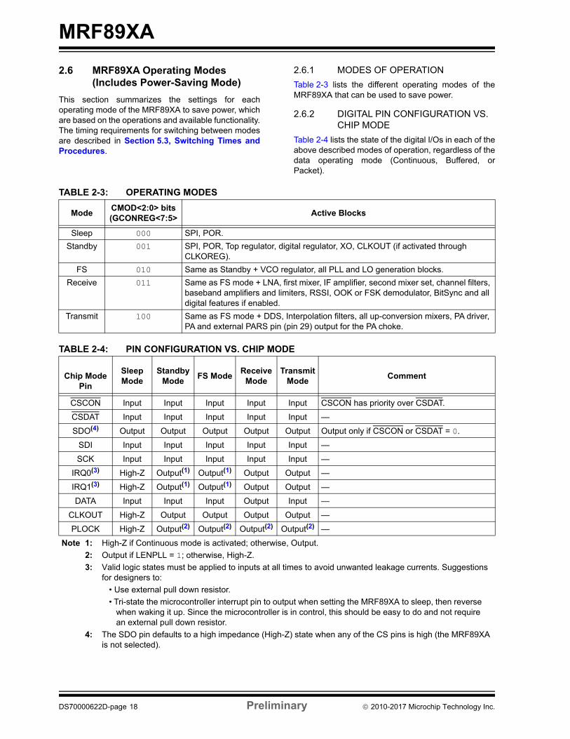
2.6 MRF89XA Operating Modes (Includes Power-Saving Mode)
This section summarizes the settings for eachoperating mode of the MRF89XA to save power, whichare based on the operations and available functionality.The timing requirements for switching between modesare described in Section 5.3, Switching Times andProcedures.
2.6.1 MODES OF OPERATION
Table 2-3 lists the different operating modes of theMRF89XA that can be used to save power.
2.6.2 DIGITAL PIN CONFIGURATION VS. CHIP MODE
Table 2-4 lists the state of the digital I/Os in each of theabove described modes of operation, regardless of thedata operating mode (Continuous, Buffered, orPacket).
TABLE 2-3: OPERATING MODES
TABLE 2-4: PIN CONFIGURATION VS. CHIP MODE
ModeCMOD<2:0> bits (GCONREG<7:5>
Active Blocks
Sleep 000 SPI, POR.
Standby 001 SPI, POR, Top regulator, digital regulator, XO, CLKOUT (if activated through CLKOREG).
FS 010 Same as Standby + VCO regulator, all PLL and LO generation blocks.
Receive 011 Same as FS mode + LNA, first mixer, IF amplifier, second mixer set, channel filters, baseband amplifiers and limiters, RSSI, OOK or FSK demodulator, BitSync and all digital features if enabled.
Transmit 100 Same as FS mode + DDS, Interpolation filters, all up-conversion mixers, PA driver, PA and external PARS pin (pin 29) output for the PA choke.
Chip.Mode
Pin
Sleep Mode
Standby Mode
FS ModeReceive
ModeTransmit
ModeComment
CSCON Input Input Input Input Input CSCON has priority over CSDAT.
CSDAT Input Input Input Input Input —
SDO(4) Output Output Output Output Output Output only if CSCON or CSDAT = 0.
SDI Input Input Input Input Input —
SCK Input Input Input Input Input —
IRQ0(3) High-Z Output(1) Output(1) Output Output —
IRQ1(3) High-Z Output(1) Output(1) Output Output —
DATA Input Input Input Output Input —
CLKOUT High-Z Output Output Output Output —
PLOCK High-Z Output(2) Output(2) Output(2) Output(2) —
Note 1: High-Z if Continuous mode is activated; otherwise, Output.
2: Output if LENPLL = 1; otherwise, High-Z.
3: Valid logic states must be applied to inputs at all times to avoid unwanted leakage currents. Suggestions for designers to:
• Use external pull down resistor.
• Tri-state the microcontroller interrupt pin to output when setting the MRF89XA to sleep, then reverse when waking it up. Since the microcontroller is in control, this should be easy to do and not require an external pull down resistor.
4: The SDO pin defaults to a high impedance (High-Z) state when any of the CS pins is high (the MRF89XA is not selected).
DS70000622D-page 18 Preliminary 2010-2017 Microchip Technology Inc.
MRF89XA
2.7 Interrupt (IRQ0 and IRQ1) Pins
The Interrupt Requests (IRQ0 and IRQ1) pins 21 and22 provide an interrupt signal to the hostmicrocontroller from the MRF89XA. Interrupt requestsare generated for the host microcontroller by pulling theIRQ0 (pin 21) or IRQ1 (pin 22) pin low or high based onthe events and configuration settings of theseinterrupts. Interrupts must be enabled and unmaskedbefore the IRQ pins are active. For detailed functionaldescription of interrupts, see Section 3.8, DataProcessing.
2.8 DATA Pin
After OOK or FSK demodulation, the baseband signalis available to the user on the DATA pin (pin 20), whenContinuous mode is selected. Therefore, in Continuousmode, the host microcontroller directly accesses theNRZ data to or from the modulator or demodulator,respectively, on the bidirectional DATA pin. The SPIData, FIFO, and packet handler are therefore inactive.In Buffered and Packet modes, the data is retrievedfrom the FIFO through the SPI.
During transmission, the DATA pin is configured asDATA (Data Out) and with the internal Transmit modedisabled; this manually modulates the data from theexternal host microcontroller. If the Transmit mode isenabled, this pin can be tied “high” or can be leftunconnected.
During reception, the DATA pin is configured as DATA(Data In); this pin receives the data in conjunction withDCLK. The DATA pin (unused in packed mode) shouldbe pulled up to VDD through a 100 kΩ resistor.
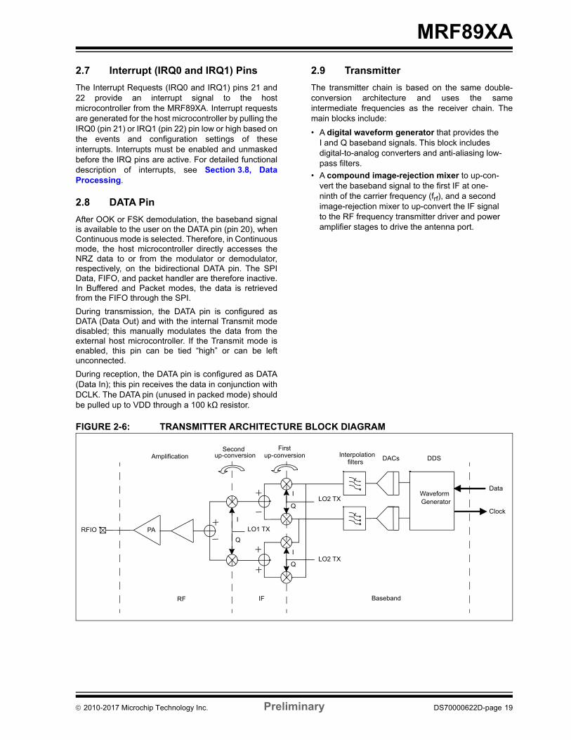
2.9 Transmitter
The transmitter chain is based on the same double-conversion architecture and uses the sameintermediate frequencies as the receiver chain. Themain blocks include:
• A digital waveform generator that provides the I and Q baseband signals. This block includes digital-to-analog converters and anti-aliasing low-pass filters.
• A compound image-rejection mixer to up-con-vert the baseband signal to the first IF at one-ninth of the carrier frequency (frf), and a second image-rejection mixer to up-convert the IF signal to the RF frequency transmitter driver and power amplifier stages to drive the antenna port.
FIGURE 2-6: TRANSMITTER ARCHITECTURE BLOCK DIAGRAM
Waveform Generator
LO1 TX
LO2 TX
LO2 TX
RFIO PA
I
Q
Q
I
I
Q
DDS DACs Interpolation
filters
Baseband IF RF
Data
Clock
FirstSecond up-conversionAmplification
up-conversion
2010-2017 Microchip Technology Inc. Preliminary DS70000622D-page 19
MRF89XA
2.9.1 TRANSMITTER ARCHITECTURE
Figure 2-6 illustrates the transmitter architecture blockdiagram. The baseband I and Q signals are digitallygenerated by a DDS whose Digital-to-AnalogConverters (DAC) followed by two anti-aliasing low-pass filters transform the digital signal into analog in-phase (I) and quadrature (Q) components whosefrequency is the selected frequency deviation, and isset using the FDVAL<7:0> bits from FDEVREG<7:0>.
In FSK mode, the input data switches the relativephase of I and Q between -90° and +90° with continu-ous phase. The modulation is therefore performed atthis initial stage, because the information contained inthe phase difference is converted into a frequency shiftwhen the I and Q signals are up-converted in the firstmixer stage. This first up-conversion stage is dupli-cated to enhance image rejection. The FSK conventionis such that:
DATA = 1 frf + fdev
DATA = 0 frf – fdev
In OOK mode, the phase difference between the I andQ channels is kept constant (independent of thetransmitted data). Thus, the first stage of up-conversioncreates a fixed frequency signal at the low IF = fdev (thisexplains why the transmitted OOK spectrum is offset byfdev). OOK Modulation is accomplished by switching thePA and PA regulator stages ON and OFF. Byconvention:
DATA = 1 PAon
DATA = 0 PAoff
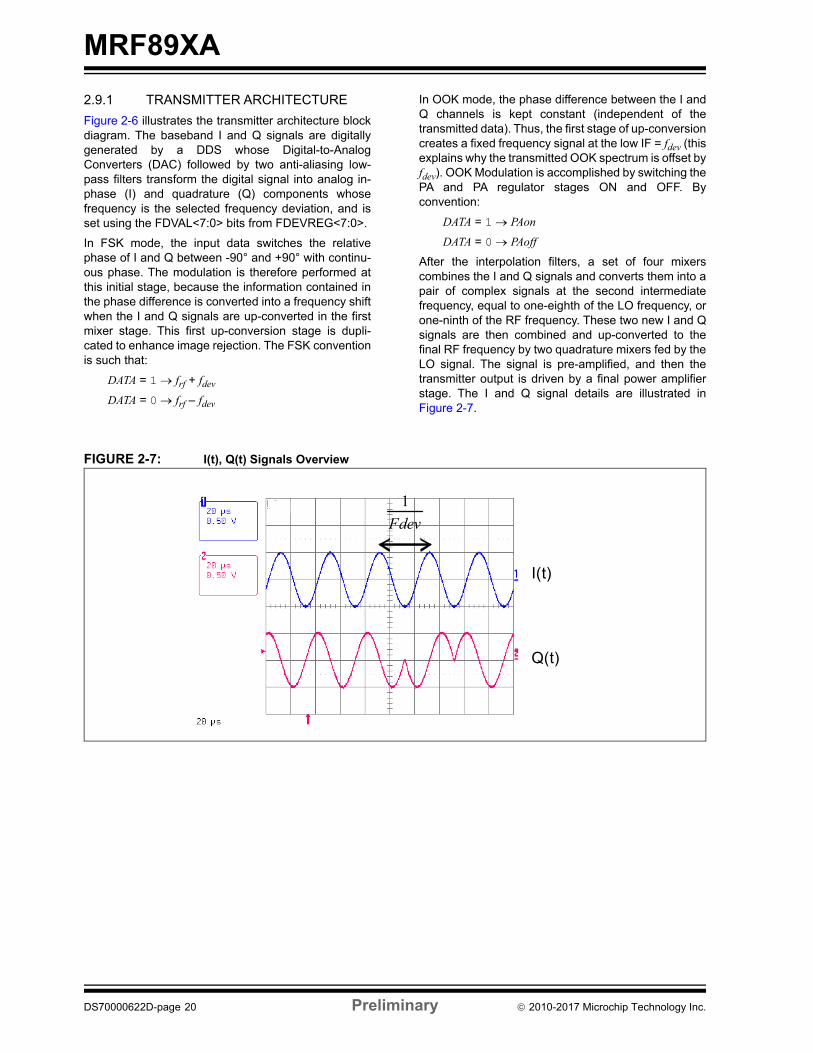
After the interpolation filters, a set of four mixerscombines the I and Q signals and converts them into apair of complex signals at the second intermediatefrequency, equal to one-eighth of the LO frequency, orone-ninth of the RF frequency. These two new I and Qsignals are then combined and up-converted to thefinal RF frequency by two quadrature mixers fed by theLO signal. The signal is pre-amplified, and then thetransmitter output is driven by a final power amplifierstage. The I and Q signal details are illustrated inFigure 2-7.
FIGURE 2-7: I(t), Q(t) Signals Overview
I(t)
Q(t)
Fdev
1
DS70000622D-page 20 Preliminary 2010-2017 Microchip Technology Inc.
MRF89XA
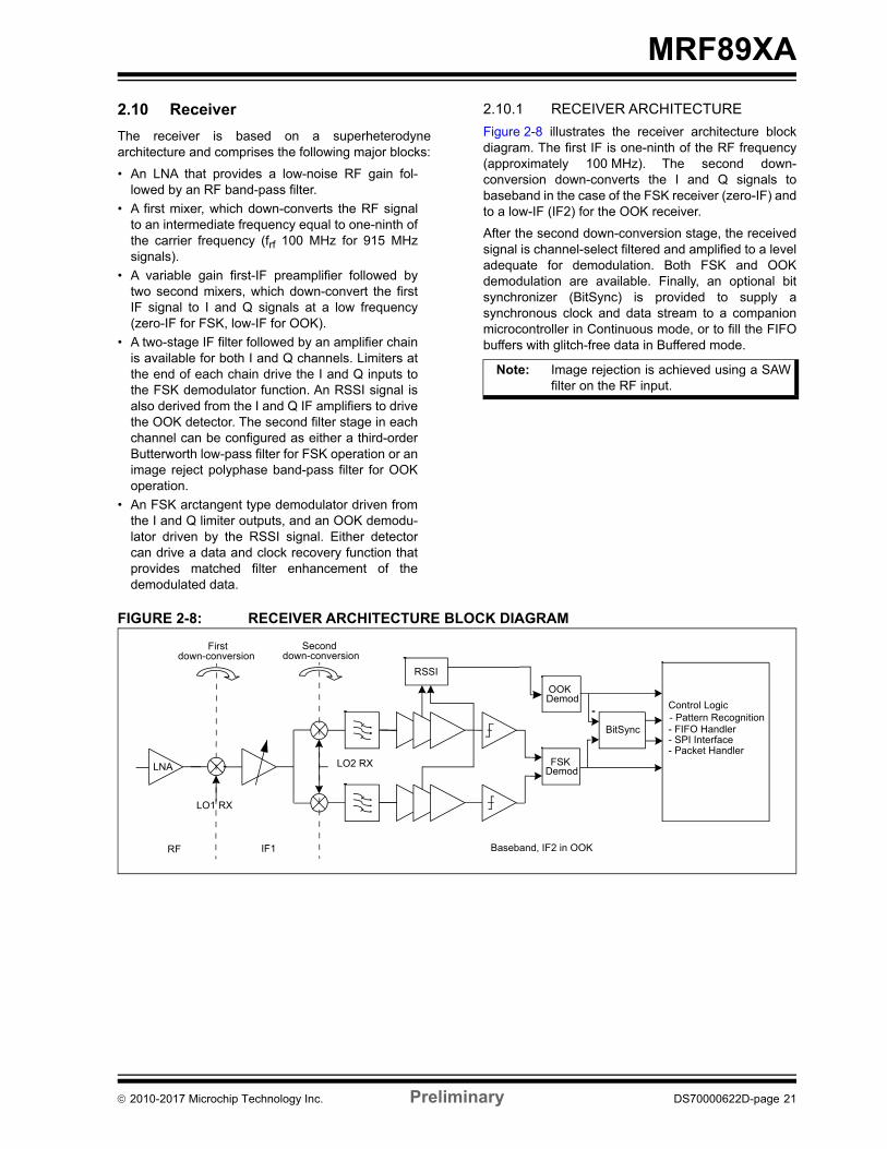
2.10 Receiver
The receiver is based on a superheterodynearchitecture and comprises the following major blocks:
• An LNA that provides a low-noise RF gain fol-lowed by an RF band-pass filter.
• A first mixer, which down-converts the RF signalto an intermediate frequency equal to one-ninth ofthe carrier frequency (frf 100 MHz for 915 MHzsignals).
• A variable gain first-IF preamplifier followed bytwo second mixers, which down-convert the firstIF signal to I and Q signals at a low frequency(zero-IF for FSK, low-IF for OOK).
• A two-stage IF filter followed by an amplifier chainis available for both I and Q channels. Limiters atthe end of each chain drive the I and Q inputs tothe FSK demodulator function. An RSSI signal isalso derived from the I and Q IF amplifiers to drivethe OOK detector. The second filter stage in eachchannel can be configured as either a third-orderButterworth low-pass filter for FSK operation or animage reject polyphase band-pass filter for OOKoperation.
• An FSK arctangent type demodulator driven fromthe I and Q limiter outputs, and an OOK demodu-lator driven by the RSSI signal. Either detectorcan drive a data and clock recovery function thatprovides matched filter enhancement of thedemodulated data.
2.10.1 RECEIVER ARCHITECTURE
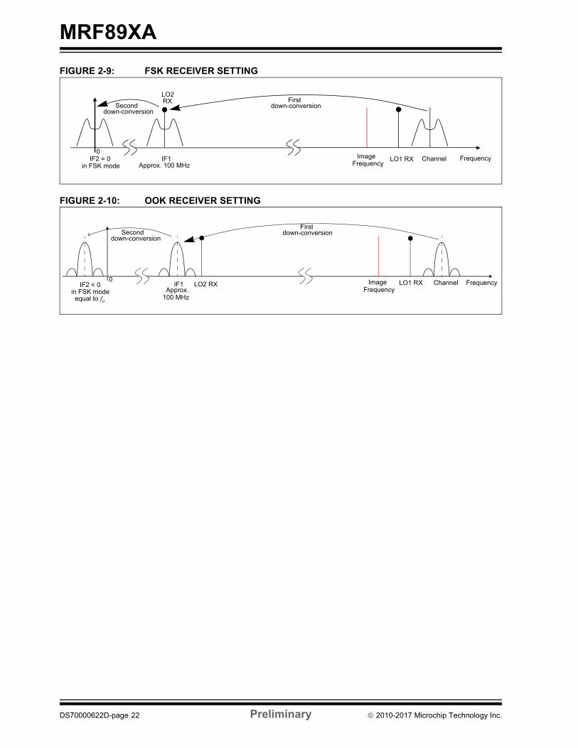
Figure 2-8 illustrates the receiver architecture blockdiagram. The first IF is one-ninth of the RF frequency(approximately 100 MHz). The second down-conversion down-converts the I and Q signals tobaseband in the case of the FSK receiver (zero-IF) andto a low-IF (IF2) for the OOK receiver.
After the second down-conversion stage, the receivedsignal is channel-select filtered and amplified to a leveladequate for demodulation. Both FSK and OOKdemodulation are available. Finally, an optional bitsynchronizer (BitSync) is provided to supply asynchronous clock and data stream to a companionmicrocontroller in Continuous mode, or to fill the FIFObuffers with glitch-free data in Buffered mode.
FIGURE 2-8: RECEIVER ARCHITECTURE BLOCK DIAGRAM
Note: Image rejection is achieved using a SAWfilter on the RF input.
FSKDemod
BitSync
OOKDemod
Control Logic - Pattern Recognition - FIFO Handler - SPI Interface - Packet Handler
RSSI
LO1 RX
LO2 RXLNA
Baseband, IF2 in OOK IF1 RF
Firstdown-conversion
Seconddown-conversion
2010-2017 Microchip Technology Inc. Preliminary DS70000622D-page 21
MRF89XA
FIGURE 2-9: FSK RECEIVER SETTING
FIGURE 2-10: OOK RECEIVER SETTING
Channel LO1 RX Image Frequency
IF1 Approx. 100 MHz
First down-conversionSecond
down-conversion
0 IF2 = 0
in FSK mode Frequency
LO2 RX
Channel LO1 RX
First down-conversionSecond
down-conversion
0 IF2 < 0
in FSK mode
Image Frequency
LO2 RX Frequency IF1 Approx.
equal to fo 100 MHz
DS70000622D-page 22 Preliminary 2010-2017 Microchip Technology Inc.
MRF89XA
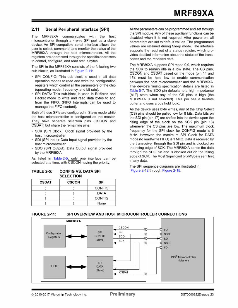
2.11 Serial Peripheral Interface (SPI)
The MRF89XA communicates with the hostmicrocontroller through a 4-wire SPI port as a slavedevice. An SPI-compatible serial interface allows theuser to select, command, and monitor the status of theMRF89XA through the host microcontroller. All theregisters are addressed through the specific addressesto control, configure, and read status bytes.
The SPI in the MRF89XA consists of the following twosub-blocks, as illustrated in Figure 2-11:
• SPI CONFIG: This sub-block is used in all dataoperation modes to read and write the configurationregisters which control all the parameters of the chip(operating mode, frequency, and bit rate).
• SPI DATA: This sub-block is used in Buffered andPacket mode to write and read data bytes to andfrom the FIFO. (FIFO Interrupts can be used tomanage the FIFO content).
Both of these SPIs are configured in Slave mode whilethe host microcontroller is configured as the master.They have separate selection pins (CSCON andCSDAT) but share the remaining pins:
• SCK (SPI Clock): Clock signal provided by thehost microcontroller
• SDI (SPI Input): Data Input signal provided by thehost microcontroller
• SDO (SPI Output): Data Output signal providedby the MRF89XA
As listed in Table 2-5, only one interface can beselected at a time, with CSCON having the priority:
TABLE 2-5: CONFIG VS. DATA SPI SELECTION
All the parameters can be programmed and set throughthe SPI module. Any of these auxiliary functions can bedisabled when it is not required. After power-on, allparameters are set to default values. The programmedvalues are retained during Sleep mode. The interfacesupports the read out of a status register, which pro-vides detailed information about the status of the trans-ceiver and the received data.
The MRF89XA supports SPI mode 0,0, which requiresthe SCK to remain idle in a low state. The CS pins,CSCON and CSDAT based on the mode (pin 14 and15), must be held low to enable communicationbetween the host microcontroller and the MRF89XA.The device’s timing specification details are listed inTable 5-7. The SDO pin defaults to a high impedance(hi-Z) state when any of the CS pins is high (theMRF89XA is not selected). This pin has a tri-statebuffer and uses a bus hold logic.
As the device uses byte writes, any of the Chip Select(CS) pins should be pulled low for 8 bits. Data bits onthe SDI pin (pin 17) are shifted into the device upon therising edge of the clock on the SCK pin (pin 18)whenever the CS pins are low. The maximum clockfrequency for the SPI clock for CONFIG mode is 6MHz. However, the maximum SPI Clock for DATAmode (to read/write FIFO) is 1 MHz. Data is received bythe transceiver through the SDI pin and is clocked onthe rising edge of SCK. The MRF89XA sends the datathrough the SDO pin and is clocked out on the fallingedge of SCK. The Most Significant bit (MSb) is sent firstin any data.
The SPI sequence diagrams are illustrated in Figure 2-12 through Figure 2-15.
FIGURE 2-11: SPI OVERVIEW AND HOST MICROCONTROLLER CONNECTIONS
CSDAT CSCON SPI
0 0 CONFIG
0 1 DATA
1 0 CONFIG
1 1 None
SPIDATA
(Slave)
SDI
SDO
SCK
SPICONFIG
(Slave)
Config. Registers
MRF89XA
CSDAT
PIC® Microcontroller(Master)
CSCONI/O
SDO
SDI
SCK
I/O
Configuration Registers
FIFO
2010-2017 Microchip Technology Inc. Preliminary DS70000622D-page 23
MRF89XA
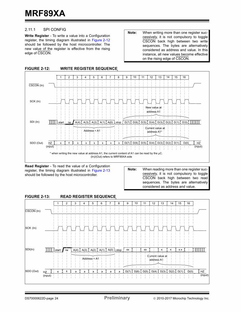
2.11.1 SPI CONFIG
Write Register - To write a value into a Configurationregister, the timing diagram illustrated in Figure 2-12should be followed by the host microcontroller. Thenew value of the register is effective from the risingedge of CSCON.
FIGURE 2-12: WRITE REGISTER SEQUENCE
Read Register - To read the value of a Configurationregister, the timing diagram illustrated in Figure 2-13should be followed by the host microcontroller.
FIGURE 2-13: READ REGISTER SEQUENCE
Note: When writing more than one register suc-cessively, it is not compulsory to toggleCSCON back high between two writesequences. The bytes are alternativelyconsidered as address and value. In thisinstance, all new values become effectiveon the rising edge of CSCON.
A(4) A(3) A(2) A(1) D(7) D(6) D(5) D(4) D(3) D(2) D(1) D(0)
x x x x x x x D(6) D(5) D(4) D(3) D(2) D(1)
SCK (In)
SDI (In)
SDO (Out)
CSCON (In)
A(0)
* when writing the new value at address A1, the current content of A1 can be read by the µC. (In)/(Out) refers to MRF89XA side
x HZ (input)
D(0)
stop
1 5 4 3 2 6 987 10 11 12 13 15 16
HZ (input)
Address = A1Current value at
address A1*
D(7)
New value at
address A1
start rw
14
Note: When reading more than one register suc-cessively, it is not compulsory to toggleCSCON back high between two readsequences. The bytes are alternativelyconsidered as address and value.
SCK (In)
SDI(In)
SDO (Out)
CSCON (In)
Current value at address A1
HZ (input)
1 5 4 3 2 6 987 10 11 12 13 14 15 16
xx xx x x x x
HZ (input)
A(0)A(1) stopA(2)A(3) A(4)
Address = A1
rwstart
x x x x x x x x D(7) D(6) D(5) D(4) D(3) D(2) D(1) D(0)
DS70000622D-page 24 Preliminary 2010-2017 Microchip Technology Inc.
MRF89XA
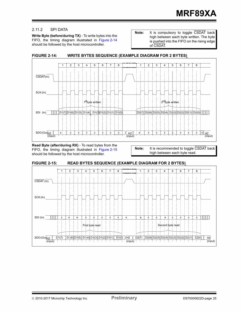
2.11.2 SPI DATA
Write Byte (before/during TX) - To write bytes into theFIFO, the timing diagram illustrated in Figure 2-14should be followed by the host microcontroller.
FIGURE 2-14: WRITE BYTES SEQUENCE (EXAMPLE DIAGRAM FOR 2 BYTES)
Read Byte (after/during RX) - To read bytes from theFIFO, the timing diagram illustrated in Figure 2-15should be followed by the host microcontroller.
FIGURE 2-15: READ BYTES SEQUENCE (EXAMPLE DIAGRAM FOR 2 BYTES)
Note: It is compulsory to toggle CSDAT backhigh between each byte written. The byteis pushed into the FIFO on the rising edgeof CSDAT.
SCK (In)
SDI (In)
SDO (Out) x
D1(6) D1(5) D1(4) D1(3) D1(2) D1(1) D2(7) D2(6) D2(5) D2(4) D2(3) D2(2) D2(1) D2(0)D1(0)D1(7)
HZ (input)
HZ (input)
HZ (input)
CSDAT(In)
x
x x x x x x x x x x x x x x x x
1 5 4 3 2 6 87 1 5 432 6 8 7
1st byte written 2nd byte written
Note: It is recommended to toggle CSDAT backhigh between each byte read.
SCK (In)
SDO (Out) D1(6) D1(5) D1(4) D1(3) D1(2) D1(1) D2(7) D2(6) D2(5) D2(4) D2(3) D2(2) D2(1) D2(0)D1(0)
D1(7) HZ (input)
HZ (input)
SDI (In) x x x x x x x x x x x x x x x x
HZ (input)
CSDAT (In)
1 5 4 3 2 6 87 1 5 432 6 87
Second byte read
x
First byte read
2010-2017 Microchip Technology Inc. Preliminary DS70000622D-page 25
MRF89XA
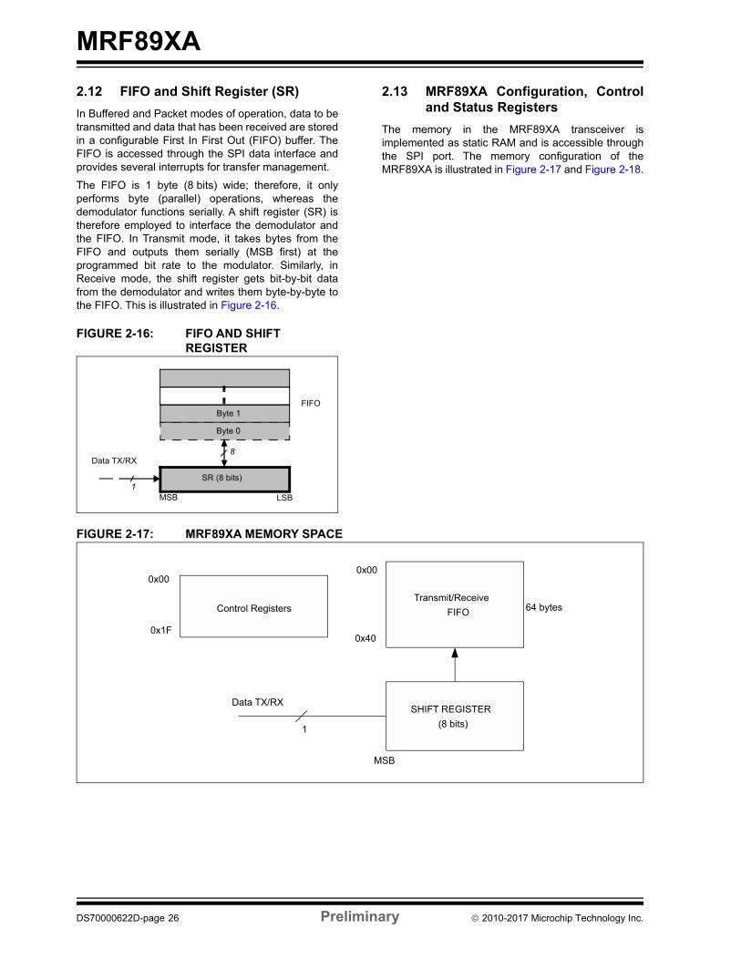
2.12 FIFO and Shift Register (SR)
In Buffered and Packet modes of operation, data to betransmitted and data that has been received are storedin a configurable First In First Out (FIFO) buffer. TheFIFO is accessed through the SPI data interface andprovides several interrupts for transfer management.
The FIFO is 1 byte (8 bits) wide; therefore, it onlyperforms byte (parallel) operations, whereas thedemodulator functions serially. A shift register (SR) istherefore employed to interface the demodulator andthe FIFO. In Transmit mode, it takes bytes from theFIFO and outputs them serially (MSB first) at theprogrammed bit rate to the modulator. Similarly, inReceive mode, the shift register gets bit-by-bit datafrom the demodulator and writes them byte-by-byte tothe FIFO. This is illustrated in Figure 2-16.
FIGURE 2-16: FIFO AND SHIFT REGISTER
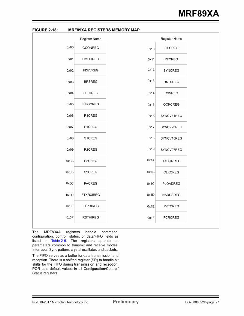
2.13 MRF89XA Configuration, Controland Status Registers
The memory in the MRF89XA transceiver isimplemented as static RAM and is accessible throughthe SPI port. The memory configuration of theMRF89XA is illustrated in Figure 2-17 and Figure 2-18.
FIGURE 2-17: MRF89XA MEMORY SPACE
Data TX/RX8
1 SR (8 bits)
Byte 0
Byte 1FIFO
MSB LSB
Control RegistersTransmit/Receive
FIFO
0x00 0x00
0x1F
64 bytes
0x40
SHIFT REGISTER
(8 bits)1
Data TX/RX
MSB
DS70000622D-page 26 Preliminary 2010-2017 Microchip Technology Inc.
MRF89XA
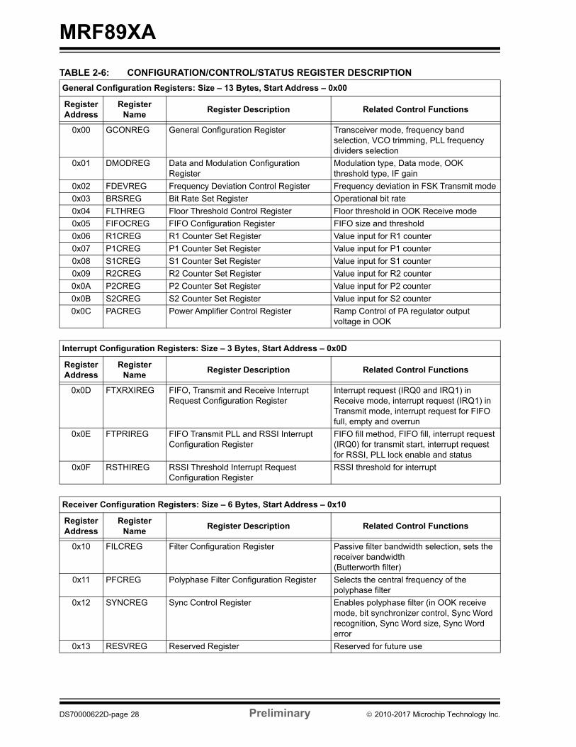
FIGURE 2-18: MRF89XA REGISTERS MEMORY MAP
The MRF89XA registers handle command,configuration, control, status, or data/FIFO fields aslisted in Table 2-6. The registers operate onparameters common to transmit and receive modes,Interrupts, Sync pattern, crystal oscillator, and packets.
The FIFO serves as a buffer for data transmission andreception. There is a shifted register (SR) to handle bitshifts for the FIFO during transmission and reception.POR sets default values in all Configuration/Control/Status registers.
0x05
0x06
FIFOCREG
R1CREG
S1CREG
P1CREG
FTPRIREG
FTXRXIREG
PACREG
S2CREG
R2CREG
P2CREG
GCONREG
DMODREG
FDEVREG
BRSREG
FLTHREG
RSTHIREG
0x00
0x01
0x04
0x03
0x02
0x0A
0x09
0x08
0x0E
0x0D
0x0C
0x0B
0x0F
0x1A
0x1B
0x1C
0x1D
0x1E
0x17
0x18
0x19
0x14
0x15
0x16
0x12
0x13
0x11
0x07
PLOADREG
CLKOREG
TXCONREG
SYNCV07REG
SYNCV15REG
SYNCV23REG
SYNCV31REG
OOKCREG
RSVREG
RSTSREG
PKTCREG
NADDSREG
PFCREG
SYNCREG
FCRCREG 0x1F
Register Name Register Name
FILCREG 0x10
2010-2017 Microchip Technology Inc. Preliminary DS70000622D-page 27
MRF89XA
TABLE 2-6: CONFIGURATION/CONTROL/STATUS REGISTER DESCRIPTION
General Configuration Registers: Size – 13 Bytes, Start Address – 0x00
Register Address
Register Name
Register Description Related Control Functions
0x00 GCONREG General Configuration Register Transceiver mode, frequency band selection, VCO trimming, PLL frequency dividers selection
0x01 DMODREG Data and Modulation Configuration Register
Modulation type, Data mode, OOK threshold type, IF gain
0x02 FDEVREG Frequency Deviation Control Register Frequency deviation in FSK Transmit mode
0x03 BRSREG Bit Rate Set Register Operational bit rate
0x04 FLTHREG Floor Threshold Control Register Floor threshold in OOK Receive mode
0x05 FIFOCREG FIFO Configuration Register FIFO size and threshold
0x06 R1CREG R1 Counter Set Register Value input for R1 counter
0x07 P1CREG P1 Counter Set Register Value input for P1 counter
0x08 S1CREG S1 Counter Set Register Value input for S1 counter
0x09 R2CREG R2 Counter Set Register Value input for R2 counter
0x0A P2CREG P2 Counter Set Register Value input for P2 counter
0x0B S2CREG S2 Counter Set Register Value input for S2 counter
0x0C PACREG Power Amplifier Control Register Ramp Control of PA regulator output voltage in OOK
Interrupt Configuration Registers: Size – 3 Bytes, Start Address – 0x0D
Register Address
Register Name
Register Description Related Control Functions
0x0D FTXRXIREG FIFO, Transmit and Receive Interrupt Request Configuration Register
Interrupt request (IRQ0 and IRQ1) in Receive mode, interrupt request (IRQ1) in Transmit mode, interrupt request for FIFO full, empty and overrun
0x0E FTPRIREG FIFO Transmit PLL and RSSI Interrupt Configuration Register
FIFO fill method, FIFO fill, interrupt request (IRQ0) for transmit start, interrupt request for RSSI, PLL lock enable and status
0x0F RSTHIREG RSSI Threshold Interrupt Request Configuration Register
RSSI threshold for interrupt
Receiver Configuration Registers: Size – 6 Bytes, Start Address – 0x10
Register Address
Register Name
Register Description Related Control Functions
0x10 FILCREG Filter Configuration Register Passive filter bandwidth selection, sets the receiver bandwidth (Butterworth filter)
0x11 PFCREG Polyphase Filter Configuration Register Selects the central frequency of the polyphase filter
0x12 SYNCREG Sync Control Register Enables polyphase filter (in OOK receive mode, bit synchronizer control, Sync Word recognition, Sync Word size, Sync Word error
0x13 RESVREG Reserved Register Reserved for future use
DS70000622D-page 28 Preliminary 2010-2017 Microchip Technology Inc.
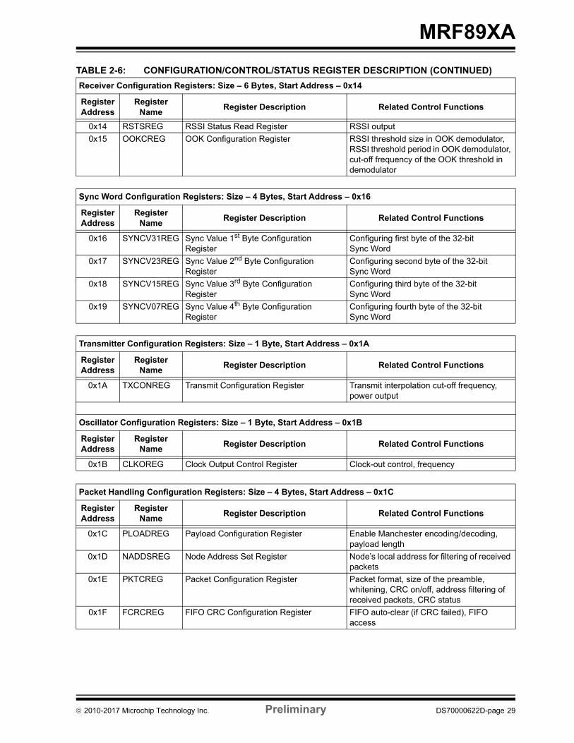
MRF89XA
Receiver Configuration Registers: Size – 6 Bytes, Start Address – 0x14
Register Address
Register Name
Register Description Related Control Functions
0x14 RSTSREG RSSI Status Read Register RSSI output
0x15 OOKCREG OOK Configuration Register RSSI threshold size in OOK demodulator, RSSI threshold period in OOK demodulator, cut-off frequency of the OOK threshold in demodulator
Sync Word Configuration Registers: Size – 4 Bytes, Start Address – 0x16
Register Address
Register Name
Register Description Related Control Functions
0x16 SYNCV31REG Sync Value 1st Byte Configuration Register
Configuring first byte of the 32-bit Sync Word
0x17 SYNCV23REG Sync Value 2nd Byte Configuration Register
Configuring second byte of the 32-bit Sync Word
0x18 SYNCV15REG Sync Value 3rd Byte Configuration Register
Configuring third byte of the 32-bit Sync Word
0x19 SYNCV07REG Sync Value 4th Byte Configuration Register
Configuring fourth byte of the 32-bit Sync Word
Transmitter Configuration Registers: Size – 1 Byte, Start Address – 0x1A
Register Address
Register Name
Register Description Related Control Functions
0x1A TXCONREG Transmit Configuration Register Transmit interpolation cut-off frequency, power output
Oscillator Configuration Registers: Size – 1 Byte, Start Address – 0x1B
Register Address
Register Name
Register Description Related Control Functions
0x1B CLKOREG Clock Output Control Register Clock-out control, frequency
Packet Handling Configuration Registers: Size – 4 Bytes, Start Address – 0x1C
Register Address
Register Name
Register Description Related Control Functions
0x1C PLOADREG Payload Configuration Register Enable Manchester encoding/decoding, payload length
0x1D NADDSREG Node Address Set Register Node’s local address for filtering of received packets
0x1E PKTCREG Packet Configuration Register Packet format, size of the preamble, whitening, CRC on/off, address filtering of received packets, CRC status
0x1F FCRCREG FIFO CRC Configuration Register FIFO auto-clear (if CRC failed), FIFO access
TABLE 2-6: CONFIGURATION/CONTROL/STATUS REGISTER DESCRIPTION (CONTINUED)
2010-2017 Microchip Technology Inc. Preliminary DS70000622D-page 29

MRF89XA
2.14 General Configuration Registers
2.14.1 GENERAL CONFIGURATION REGISTER DETAILS
REGISTER 2-1: GCONREG: GENERAL CONFIGURATION REGISTER (ADDRESS:0X00) (POR:0X28)
R/W-0 R/W-0 R/W-1 R/W-0 R/W-1 R/W-0 R/W-0 R/W-0
CMOD<2:0> FBS<1:0> VCOT<1:0> RPS
bit 7 bit 0
R = Readable bit W = Writable bit U = Unimplemented bit, read as ‘0’
-n = Value at POR ‘1’ = Bit is set ‘0’ = Bit is cleared x = Bit is unknown
r = Reserved
bit 7-5 CMOD<2:0>: Chip Mode bits
These bits select the mode of operation of the transceiver.111 = Reserved; do not use110 = Reserved; do not use101 = Reserved; do not use100 = Transmit mode 011 = Receive mode 010 = Frequency Synthesizer mode 001 = Standby mode (default)000 = Sleep mode
bit 4-3 FBS<1:0>: Frequency Band Select bits
These bits set the frequency band to be used in Sub-GHz range.11 = Reserved10 = 950-960 MHz or 863-870 MHz (application circuit dependent)01 = 915-928 MHz (default)00 = 902-915 MHz
bit 2-1 VCOT<1:0>: TX bits
For each AFC cycle run, these bits toggle between logic ‘1’ and logic ‘0’.11 = Vtune + 180 mV typ10 = Vtune + 120 mV typ01 = Vtune + 60 mV typ00 = Vtune determined by tank inductors values (default)
bit 0 RPS: RPS Select bit
This bit selects between the two sets of frequency dividers of the PLL, Ri/Pi/Si. For more information, see Section 3.2.7, Frequency Calculation.
1 = Enable R2/P2/S2 set0 = Enable R1/P1/S1 set (default)
DS70000622D-page 30 Preliminary 2010-2017 Microchip Technology Inc.
MRF89XA
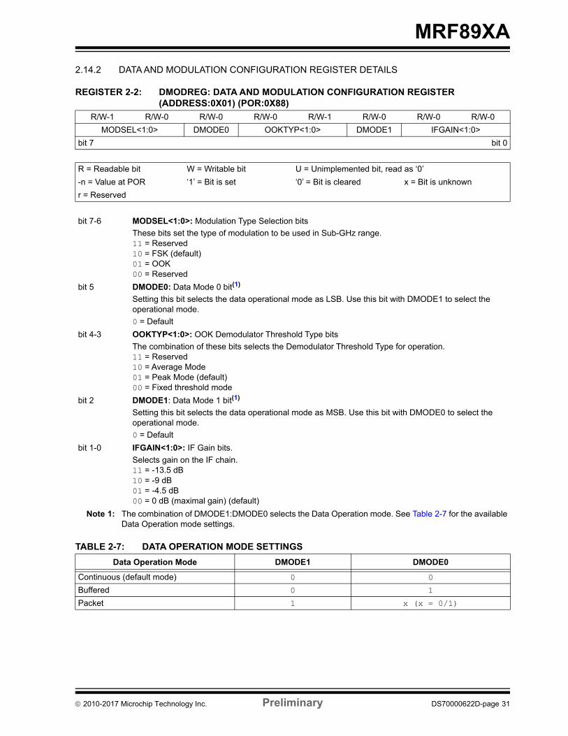
2.14.2 DATA AND MODULATION CONFIGURATION REGISTER DETAILS
REGISTER 2-2: DMODREG: DATA AND MODULATION CONFIGURATION REGISTER (ADDRESS:0X01) (POR:0X88)
TABLE 2-7: DATA OPERATION MODE SETTINGS
R/W-1 R/W-0 R/W-0 R/W-0 R/W-1 R/W-0 R/W-0 R/W-0
MODSEL<1:0> DMODE0 OOKTYP<1:0> DMODE1 IFGAIN<1:0>
bit 7 bit 0
R = Readable bit W = Writable bit U = Unimplemented bit, read as ‘0’
-n = Value at POR ‘1’ = Bit is set ‘0’ = Bit is cleared x = Bit is unknown
r = Reserved
bit 7-6 MODSEL<1:0>: Modulation Type Selection bits
These bits set the type of modulation to be used in Sub-GHz range.11 = Reserved10 = FSK (default)01 = OOK 00 = Reserved
bit 5 DMODE0: Data Mode 0 bit(1)
Setting this bit selects the data operational mode as LSB. Use this bit with DMODE1 to select the operational mode.
0 = Default
bit 4-3 OOKTYP<1:0>: OOK Demodulator Threshold Type bits
The combination of these bits selects the Demodulator Threshold Type for operation.11 = Reserved 10 = Average Mode01 = Peak Mode (default)00 = Fixed threshold mode
bit 2 DMODE1: Data Mode 1 bit(1)
Setting this bit selects the data operational mode as MSB. Use this bit with DMODE0 to select the operational mode.
0 = Default
bit 1-0 IFGAIN<1:0>: IF Gain bits.
Selects gain on the IF chain. 11 = -13.5 dB 10 = -9 dB01 = -4.5 dB00 = 0 dB (maximal gain) (default)
Note 1: The combination of DMODE1:DMODE0 selects the Data Operation mode. See Table 2-7 for the availableData Operation mode settings.
Data Operation Mode DMODE1 DMODE0
Continuous (default mode) 0 0Buffered 0 1Packet 1 x (x = 0/1)
2010-2017 Microchip Technology Inc. Preliminary DS70000622D-page 31
MRF89XA
2.14.3 FREQUENCY DEVIATION CONTROL REGISTER DETAILS
REGISTER 2-3: FDEVREG: FREQUENCY DEVIATION CONTROL REGISTER (ADDRESS:0X02) (POR:0X03)
2.14.4 BIT RATE SET REGISTER DETAILS
REGISTER 2-4: BRSREG: BIT RATE SET REGISTER (ADDRESS:0x03) (POR:0x07)
R/W-0 R/W-0 R/W-0 R/W-0 R/W-0 R/W-0 R/W-1 R/W-1
FDVAL<7:0>
bit 7 bit 0
R = Readable bit W = Writable bit U = Unimplemented bit, read as ‘0’
-n = Value at POR ‘1’ = Bit is set ‘0’ = Bit is cleared x = Bit is unknown
r = Reserved
bit 7-0 FDVAL<7:0>: Frequency Deviation Value bits
The bits indicate single side frequency deviation (in bit value) in FSK Transmit mode.FDVAL = 00000011 fdev = 100 kHz (default)
Note 1: fdev is used throughout the data sheet to understand the term frequency deviation and is calculated usingFDVAL<7:0> from FDEVREG.
fdevfxtal
32 FDVAL 1+ ---------------------------------------------------=
Where, FDVAL is the value in the register and has the range from 0 ≤ FDVAL ≤ 255. Refer to Section 3.3.3, fdev Setting in FSK Mode and Section 3.3.4, fdev Setting in OOK Mode for more information on the fdev setting for FSK and OOK modes.
r R/W-0 R/W-0 R/W-0 R/W-0 R/W-1 R/W-1 R/W-1
— BRVAL<6:0>
bit 7 bit 0
R = Readable bit W = Writable bit U = Unimplemented bit, read as ‘0’
-n = Value at POR ‘1’ = Bit is set ‘0’ = Bit is cleared x = Bit is unknown
r = Reserved
bit 7 Reserved: Reserved bit; do not use
0 = Reserved (default)
bit 6-0 BRVAL<6:0>: Bit Rate Value bits
These bits set the bit rate (in bit value) of:
Note 1: The Bit Rates are good for crystal frequency of 12.8 MHz which is taken as a reference throughout the data sheet.
BitRatefxtal
64 BRVAL 1+ --------------------------------------------=
BRVAL<6:0> = 0000111 Bit Rate = 25 kbps NRZ (default)
Where, BRVAL is the value in the register and has the range from 0 ≤ BRVAL ≤ 127.
DS70000622D-page 32 Preliminary 2010-2017 Microchip Technology Inc.
MRF89XA
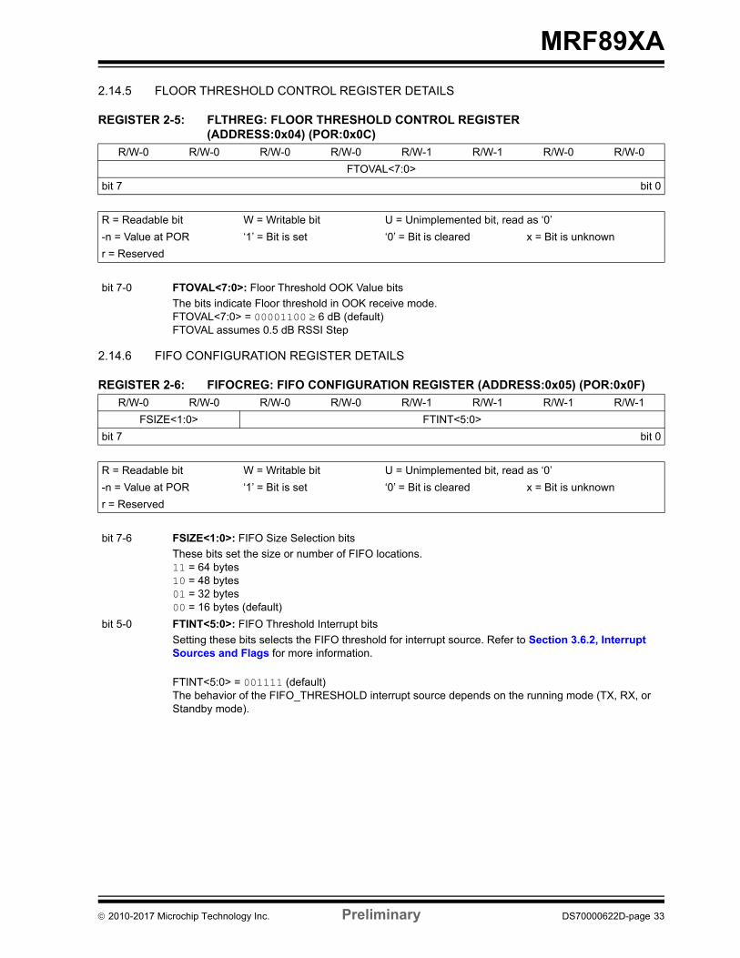
2.14.5 FLOOR THRESHOLD CONTROL REGISTER DETAILS
REGISTER 2-5: FLTHREG: FLOOR THRESHOLD CONTROL REGISTER (ADDRESS:0x04) (POR:0x0C)
2.14.6 FIFO CONFIGURATION REGISTER DETAILS
REGISTER 2-6: FIFOCREG: FIFO CONFIGURATION REGISTER (ADDRESS:0x05) (POR:0x0F)
R/W-0 R/W-0 R/W-0 R/W-0 R/W-1 R/W-1 R/W-0 R/W-0
FTOVAL<7:0>
bit 7 bit 0
R = Readable bit W = Writable bit U = Unimplemented bit, read as ‘0’
-n = Value at POR ‘1’ = Bit is set ‘0’ = Bit is cleared x = Bit is unknown
r = Reserved
bit 7-0 FTOVAL<7:0>: Floor Threshold OOK Value bits
The bits indicate Floor threshold in OOK receive mode.FTOVAL<7:0> = 00001100 6 dB (default)FTOVAL assumes 0.5 dB RSSI Step
R/W-0 R/W-0 R/W-0 R/W-0 R/W-1 R/W-1 R/W-1 R/W-1
FSIZE<1:0> FTINT<5:0>
bit 7 bit 0
R = Readable bit W = Writable bit U = Unimplemented bit, read as ‘0’
-n = Value at POR ‘1’ = Bit is set ‘0’ = Bit is cleared x = Bit is unknown
r = Reserved
bit 7-6 FSIZE<1:0>: FIFO Size Selection bits
These bits set the size or number of FIFO locations.11 = 64 bytes 10 = 48 bytes 01 = 32 bytes 00 = 16 bytes (default)
bit 5-0 FTINT<5:0>: FIFO Threshold Interrupt bits
Setting these bits selects the FIFO threshold for interrupt source. Refer to Section 3.6.2, Interrupt Sources and Flags for more information.
FTINT<5:0> = 001111 (default)The behavior of the FIFO_THRESHOLD interrupt source depends on the running mode (TX, RX, or Standby mode).
2010-2017 Microchip Technology Inc. Preliminary DS70000622D-page 33
MRF89XA
2.14.7 R1 COUNTER SET REGISTER DETAILS
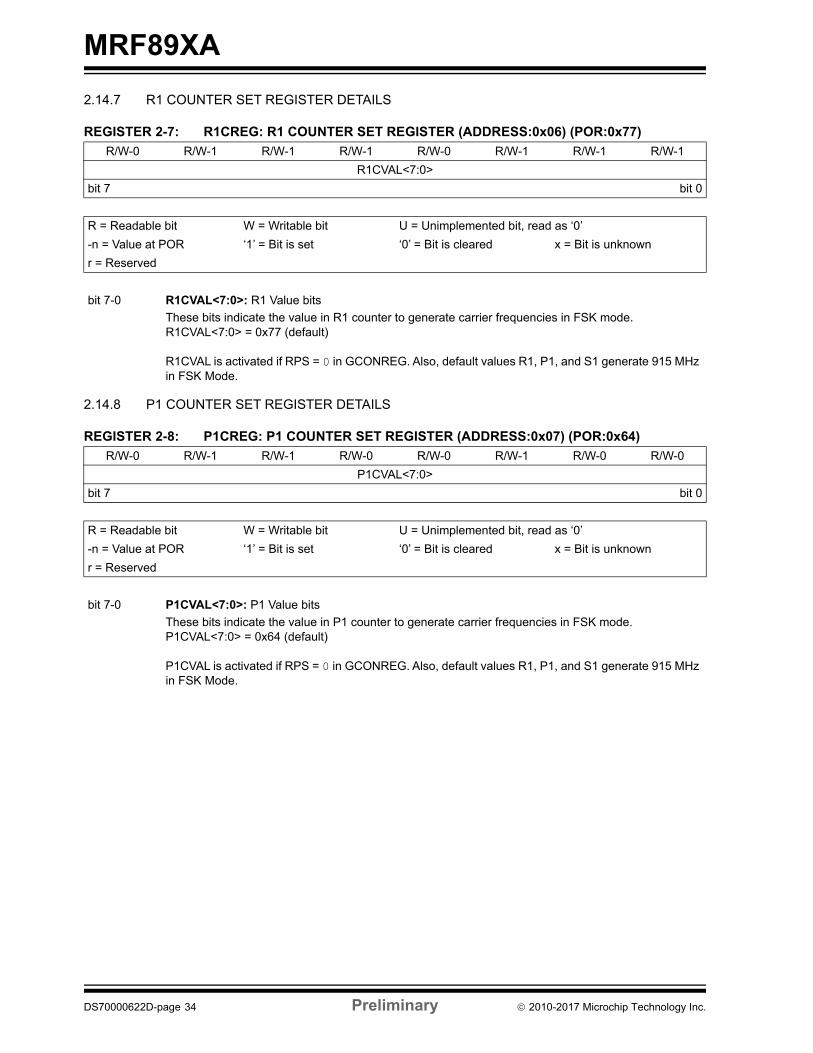
REGISTER 2-7: R1CREG: R1 COUNTER SET REGISTER (ADDRESS:0x06) (POR:0x77)
2.14.8 P1 COUNTER SET REGISTER DETAILS
REGISTER 2-8: P1CREG: P1 COUNTER SET REGISTER (ADDRESS:0x07) (POR:0x64)
R/W-0 R/W-1 R/W-1 R/W-1 R/W-0 R/W-1 R/W-1 R/W-1
R1CVAL<7:0>
bit 7 bit 0
R = Readable bit W = Writable bit U = Unimplemented bit, read as ‘0’
-n = Value at POR ‘1’ = Bit is set ‘0’ = Bit is cleared x = Bit is unknown
r = Reserved
bit 7-0 R1CVAL<7:0>: R1 Value bits
These bits indicate the value in R1 counter to generate carrier frequencies in FSK mode.R1CVAL<7:0> = 0x77 (default)
R1CVAL is activated if RPS = 0 in GCONREG. Also, default values R1, P1, and S1 generate 915 MHz in FSK Mode.
R/W-0 R/W-1 R/W-1 R/W-0 R/W-0 R/W-1 R/W-0 R/W-0
P1CVAL<7:0>
bit 7 bit 0
R = Readable bit W = Writable bit U = Unimplemented bit, read as ‘0’
-n = Value at POR ‘1’ = Bit is set ‘0’ = Bit is cleared x = Bit is unknown
r = Reserved
bit 7-0 P1CVAL<7:0>: P1 Value bits
These bits indicate the value in P1 counter to generate carrier frequencies in FSK mode.P1CVAL<7:0> = 0x64 (default)
P1CVAL is activated if RPS = 0 in GCONREG. Also, default values R1, P1, and S1 generate 915 MHz in FSK Mode.
DS70000622D-page 34 Preliminary 2010-2017 Microchip Technology Inc.
MRF89XA
2.14.9 S1 COUNTER SET REGISTER DETAILS
REGISTER 2-9: S1CREG: S1 COUNTER SET REGISTER (ADDRESS:0x08) (POR:0x32)
2.14.10 R2 COUNTER SET REGISTER DETAILS
REGISTER 2-10: R2CREG: R2 COUNTER SET REGISTER (ADDRESS:0x09) (POR:0x74)
R/W-0 R/W-0 R/W-1 R/W-1 R/W-0 R/W-0 R/W-1 R/W-0
S1CVAL<7:0>
bit 7 bit 0
R = Readable bit W = Writable bit U = Unimplemented bit, read as ‘0’
-n = Value at POR ‘1’ = Bit is set ‘0’ = Bit is cleared x = Bit is unknown
r = Reserved
bit 7-0 S1CVAL<7:0>: S1 Value bits
These bits indicate the value in S1 counter to generate carrier frequencies in FSK mode.S1CVAL<7:0> = 0x32 (default)
S1CVAL is activated if RPS = 0 in GCONREG. Also, default values R1, P1, and S1 generate 915 MHz in FSK Mode.
R/W-0 R/W-1 R/W-1 R/W-1 R/W-0 R/W-1 R/W-0 R/W-0
R2CVAL<7:0>
bit 7 bit 0
R = Readable bit W = Writable bit U = Unimplemented bit, read as ‘0’
-n = Value at POR ‘1’ = Bit is set ‘0’ = Bit is cleared x = Bit is unknown
r = Reserved
bit 7-0 R2CVAL<7:0>: R2 Value bits
These bits indicate the value in R2 counter to generate carrier frequencies in FSK mode.R2CVAL<7:0> = 0x74 (default)
R2CVAL is activated if RPS = 1 in GCONREG. Also, default values R2, P2, and S2 generate 920 MHz in FSK Mode.
2010-2017 Microchip Technology Inc. Preliminary DS70000622D-page 35
MRF89XA
2.14.11 P2 COUNTER SET REGISTER DETAILS
REGISTER 2-11: P2CREG: P2 COUNTER SET REGISTER (ADDRESS:0x0A) (POR:0x62)
2.14.12 S2 COUNTER SET REGISTER DETAILS
REGISTER 2-12: S2CREG: S2 COUNTER SET REGISTER (ADDRESS:0x0B) (POR:0x32)
R/W-0 R/W-1 R/W-1 R/W-0 R/W-0 R/W-0 R/W-1 R/W-0
P2CVAL<7:0>
bit 7 bit 0
R = Readable bit W = Writable bit U = Unimplemented bit, read as ‘0’
-n = Value at POR ‘1’ = Bit is set ‘0’ = Bit is cleared x = Bit is unknown
r = Reserved
bit 7-0 P2CVAL<7:0>: P2 Value bits
These bits indicate the value in P2 counter to generate carrier frequencies in FSK mode.P2CVAL<7:0> = 0x62 (default)
P2CVAL is activated if RPS = 1 in GCONREG. Also, default values R2, P2, and S2 generate 920 MHz in FSK Mode.
R/W-0 R/W-0 R/W-1 R/W-1 R/W-0 R/W-0 R/W-1 R/W-1
S2CVAL<7:0>
bit 7 bit 0
R = Readable bit W = Writable bit U = Unimplemented bit, read as ‘0’
-n = Value at POR ‘1’ = Bit is set ‘0’ = Bit is cleared x = Bit is unknown
r = Reserved
bit 7-0 S2CVAL<7:0>: S2 Value bits
These bits indicate the value in S2 counter to generate carrier frequencies in FSK mode.S2CVAL<7:0> = 0x32 (default).
S2CVAL is activated if RPS = 1 in GCONREG. Also, default values R2, P2, and S2 generate 920 MHz in FSK Mode.
DS70000622D-page 36 Preliminary 2010-2017 Microchip Technology Inc.
MRF89XA
2.14.13 POWER AMPLIFIER CONTROL REGISTER DETAILS
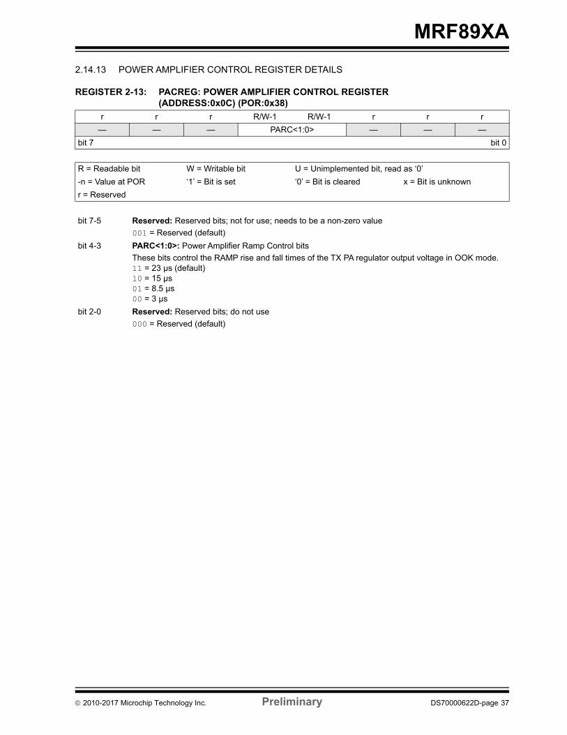
REGISTER 2-13: PACREG: POWER AMPLIFIER CONTROL REGISTER (ADDRESS:0x0C) (POR:0x38)
r r r R/W-1 R/W-1 r r r
— — — PARC<1:0> — — —
bit 7 bit 0
R = Readable bit W = Writable bit U = Unimplemented bit, read as ‘0’
-n = Value at POR ‘1’ = Bit is set ‘0’ = Bit is cleared x = Bit is unknown
r = Reserved
bit 7-5 Reserved: Reserved bits; not for use; needs to be a non-zero value
001 = Reserved (default)
bit 4-3 PARC<1:0>: Power Amplifier Ramp Control bits
These bits control the RAMP rise and fall times of the TX PA regulator output voltage in OOK mode. 11 = 23 µs (default)10 = 15 µs 01 = 8.5 µs 00 = 3 µs
bit 2-0 Reserved: Reserved bits; do not use
000 = Reserved (default)
2010-2017 Microchip Technology Inc. Preliminary DS70000622D-page 37

MRF89XA
2.15 Interrupt Configuration Registers
2.15.1 FIFO TRANSMIT AND RECEIVE INTERRUPT REQUEST CONFIGURATION REGISTER DETAILS
REGISTER 2-14: FTXRXIREG: FIFO TRANSMIT AND RECEIVE INTERRUPT REQUEST CONFIGURATION REGISTER (ADDRESS:0x0D) (POR:0x00)
R/W-0 R/W-0 R/W-0 R/W-0 R/W-0 R/W-0 R/W-0 R/W-0
IRQ0RXS<1:0> IRQ1RXS<1:0> IRQ1TX FIFOFULL FIFOEMPTY FOVRRUN
bit 7 bit 0
R = Readable bit W = Writable bit U = Unimplemented bit, read as ‘0’
-n = Value at POR ‘1’ = Bit is set ‘0’ = Bit is cleared x = Bit is unknown
r = Reserved
bit 7-6 IRQ0RXS<1:0>: IRQ0 Receive Standby bits
These bits control the IRQ0 source in Receive and Standby modes:
If DMODE1:DMODE0 = 00 Continuous Mode (default)11 = SYNC10 = SYNC 01 = RSSI00 = Sync (default)
If DMODE1:DMODE0 = 01 Buffered Mode 11 = SYNC10 = FIFOEMPTY(1)
01 = WRITEBYTE00 = - (default)
If DMODE1:DMODE0 = 1x Packet Mode 11 = SYNC or ARDSMATCH(3) (if address filtering is enabled)10 = FIFOEMPTY(1)
01 = WRITEBYTE00 = PLREADY(2) (default)
bit 5-4 IRQ1RXS<1:0>: IRQ1 Receive Standby bits
These bits control the IRQ1 source in Receive and Standby modes: If DMODE1:DMODE0 = 00 Continuous Mode (default)xx = DCLK
If DMODE1:DMODE0 = 01 Buffered Mode 11 = FIFO_THRESHOLD(1)
10 = RSSI01 = FIFOFULL(1)
00 = - (default)
If DMODE1:DMODE0 = 1x Packet Mode 11 = FIFO_THRESHOLD(1)
10 = RSSI01 = FIFOFULL(1)
00 = CRCOK (default)
Note 1: This mode is also available in Standby mode.
2: PLREADY = Payload ready
3: ADRSMATCH = Address Match
DS70000622D-page 38 Preliminary 2010-2017 Microchip Technology Inc.

MRF89XA
bit 3 IRQ1TX: Transmit IRQ1 bit
This bit selects IRQ1 as source in Transmit mode.
If DMODE1:DMODE0 = 00 Continuous Mode (default):x = DCLK
If DMODE1:DMODE0 = 01 Buffered Mode or 1x Packet Mode:1 = TXDONE 0 = FIFOFULL (default)
bit 2 FIFOFULL: FIFO Full bit
This bit indicates FIFO Full through the IRQ source.1 = FIFO full 0 = FIFO not full
bit 1 FIFOEMPTY: FIFO Empty bit
This bit indicates FIFO empty through the IRQ source.1 = FIFO not Empty 0 = FIFO Empty
bit 0 FOVRRUN: FIFO Overrun Clear bit
This bit indicates if FIFO overrun occurred.1 = FIFO Overrun occurred 0 = No FIFO Overrun occurredWriting a ‘1’ for this bit clears the flag and the FIFO.
REGISTER 2-14: FTXRXIREG: FIFO TRANSMIT AND RECEIVE INTERRUPT REQUEST CONFIGURATION REGISTER (ADDRESS:0x0D) (POR:0x00) (CONTINUED)
Note 1: This mode is also available in Standby mode.
2: PLREADY = Payload ready
3: ADRSMATCH = Address Match
2010-2017 Microchip Technology Inc. Preliminary DS70000622D-page 39
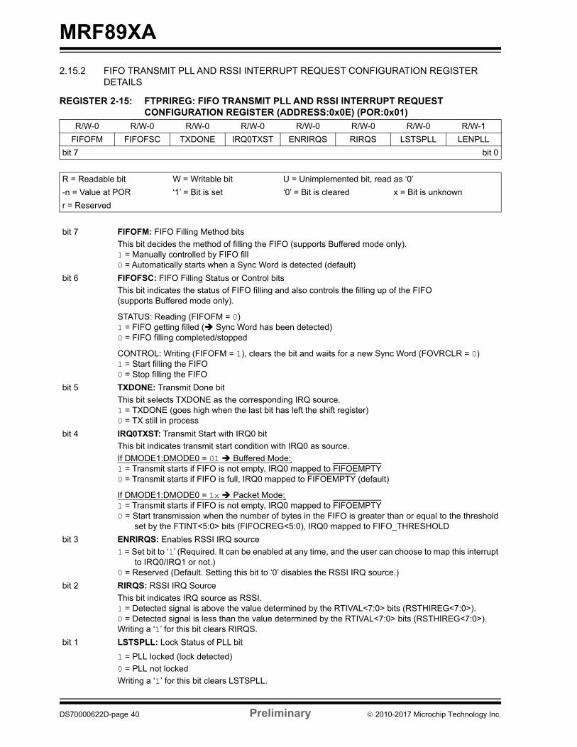
MRF89XA
2.15.2 FIFO TRANSMIT PLL AND RSSI INTERRUPT REQUEST CONFIGURATION REGISTER DETAILS
REGISTER 2-15: FTPRIREG: FIFO TRANSMIT PLL AND RSSI INTERRUPT REQUEST CONFIGURATION REGISTER (ADDRESS:0x0E) (POR:0x01)
R/W-0 R/W-0 R/W-0 R/W-0 R/W-0 R/W-0 R/W-0 R/W-1
FIFOFM FIFOFSC TXDONE IRQ0TXST ENRIRQS RIRQS LSTSPLL LENPLL
bit 7 bit 0
R = Readable bit W = Writable bit U = Unimplemented bit, read as ‘0’
-n = Value at POR ‘1’ = Bit is set ‘0’ = Bit is cleared x = Bit is unknown
r = Reserved
bit 7 FIFOFM: FIFO Filling Method bits
This bit decides the method of filling the FIFO (supports Buffered mode only).1 = Manually controlled by FIFO fill 0 = Automatically starts when a Sync Word is detected (default)
bit 6 FIFOFSC: FIFO Filling Status or Control bits
This bit indicates the status of FIFO filling and also controls the filling up of the FIFO (supports Buffered mode only).
STATUS: Reading (FIFOFM = 0)1 = FIFO getting filled ( Sync Word has been detected)0 = FIFO filling completed/stopped
CONTROL: Writing (FIFOFM = 1), clears the bit and waits for a new Sync Word (FOVRCLR = 0)1 = Start filling the FIFO0 = Stop filling the FIFO
bit 5 TXDONE: Transmit Done bit
This bit selects TXDONE as the corresponding IRQ source.1 = TXDONE (goes high when the last bit has left the shift register)0 = TX still in process
bit 4 IRQ0TXST: Transmit Start with IRQ0 bit
This bit indicates transmit start condition with IRQ0 as source.
If DMODE1:DMODE0 = 01 Buffered Mode:1 = Transmit starts if FIFO is not empty, IRQ0 mapped to FIFOEMPTY0 = Transmit starts if FIFO is full, IRQ0 mapped to FIFOEMPTY (default)
If DMODE1:DMODE0 = 1x Packet Mode:1 = Transmit starts if FIFO is not empty, IRQ0 mapped to FIFOEMPTY0 = Start transmission when the number of bytes in the FIFO is greater than or equal to the threshold
set by the FTINT<5:0> bits (FIFOCREG<5:0), IRQ0 mapped to FIFO_THRESHOLD
bit 3 ENRIRQS: Enables RSSI IRQ source
1 = Set bit to ‘1’ (Required. It can be enabled at any time, and the user can choose to map this interruptto IRQ0/IRQ1 or not.)
0 = Reserved (Default. Setting this bit to ‘0’ disables the RSSI IRQ source.)
bit 2 RIRQS: RSSI IRQ Source
This bit indicates IRQ source as RSSI.1 = Detected signal is above the value determined by the RTIVAL<7:0> bits (RSTHIREG<7:0>).0 = Detected signal is less than the value determined by the RTIVAL<7:0> bits (RSTHIREG<7:0>).Writing a ‘1’ for this bit clears RIRQS.
bit 1 LSTSPLL: Lock Status of PLL bit
1 = PLL locked (lock detected)
0 = PLL not locked
Writing a ‘1’ for this bit clears LSTSPLL.
DS70000622D-page 40 Preliminary 2010-2017 Microchip Technology Inc.
MRF89XA
2.15.3 RSSI THRESHOLD INTERRUPT REQUEST REGISTER DETAILS
REGISTER 2-16: RSTHIREG: RSSI THRESHOLD INTERRUPT REQUEST CONFIGURATION REGISTER (ADDRESS:0x0F) (POR:0x00)
bit 0 LENPLL: Lock Enable of PLL bit
1 = PLL lock detect enabled (default) 0 = PLL lock detect disabled The PLL lock detect flag is mapped to the PLOCK pin (pin 23), and pin 23 is a High-Z pin.
R/W-0 R/W-0 R/W-0 R/W-0 R/W-0 R/W-0 R/W-0 R/W-0
RTIVAL<7:0>
bit 7 bit 0
R = Readable bit W = Writable bit U = Unimplemented bit, read as ‘0’
-n = Value at POR ‘1’ = Bit is set ‘0’ = Bit is cleared x = Bit is unknown
r = Reserved
bit 7-0 RTIVAL<7:0>: RSSI Threshold for Interrupt Value bits
These bits indicate the RSSI threshold value for interrupt request.RTIVAL<7:0> = 00000000 (default)
REGISTER 2-15: FTPRIREG: FIFO TRANSMIT PLL AND RSSI INTERRUPT REQUEST CONFIGURATION REGISTER (ADDRESS:0x0E) (POR:0x01) (CONTINUED)
2010-2017 Microchip Technology Inc. Preliminary DS70000622D-page 41
MRF89XA
2.16 Receiver Configuration Registers
2.16.1 FILTER CONFIGURATION REGISTER DETAILS
REGISTER 2-17: FILCREG: FILTER CONFIGURATION REGISTER (ADDRESS:0x10) (POR:0xA3)
R/W-1 R/W-0 R/W-1 R/W-0 R/W-0 R/W-0 R/W-1 R/W-1
PASFILV<3:0> BUTFILV<3:0>
bit 7 bit 0
R = Readable bit W = Writable bit U = Unimplemented bit, read as ‘0’
-n = Value at POR ‘1’ = Bit is set ‘0’ = Bit is cleared x = Bit is unknown
r = Reserved
bit 7-4 PASFILV<3:0>: Passive Filter Value bits
These bits indicate the typical single sideband bandwidth of the passive low-pass filter. 1111 = 987 kHz1110 = 676 kHz1101 = 514 kHz1100 = 458 kHz1011 = 414 kHz1010 = 378 kHz (default)1001 = 321 kHz1000 = 262 kHz0111 = 234 kHz0110 = 211 kHz0101 = 184 kHz0100 = 157 kHz0011 = 137 kHz0010 = 109 kHz0001 = 82 kHz 0000 = 65 kHz
bit 3-0 BUTFILV<3:0>: Butterworth Filter Value bits
These bits set the receiver bandwidth both in FSK and OOK mode.BUTFILV<3:0> = 0011 fc – fo = 100 kHz (default)
Where,BUTFILV <3:0> is the value in the register fc is the cut-off frequencyfo is the local oscillator frequency (center frequency)fxtal is the crystal oscillator frequency
Note: fc – fo = 100 kHz only when fxtal = 12.8 MHz.
fc fo= 200 kHzfxtalMHz
12.8MHz-----------------------
1 val BUTFILV +8
------------------------------------------------ +
DS70000622D-page 42 Preliminary 2010-2017 Microchip Technology Inc.
MRF89XA
2.16.2 POLYPHASE FILTER CONFIGURATION REGISTER DETAILS
REGISTER 2-18: PFCREG: POLYPHASE FILTER CONFIGURATION REGISTER (ADDRESS:0x11) (POR:0x38)
R/W-0 R/W-0 R/W-1 R/W-1 r r r r
POLCFV<3:0> — — — —
bit 7 bit 0
R = Readable bit W = Writable bit U = Unimplemented bit, read as ‘0’
-n = Value at POR ‘1’ = Bit is set ‘0’ = Bit is cleared x = Bit is unknown
r = Reserved
bit 7-4 POLCFV<3:0>: Polyphase Center Frequency Value bits
These bits indicate the center frequency of the polyphase filter (typically recommended to 100 kHz). POLCFV<3:0> = 0011 fo = 100 kHz (default)
Where, POLCFV <3:0> is the value in the register.fc is the cut-off frequency.fo is the local oscillator frequency (center frequency).fxtal is the crystal oscillator frequency.
bit 3-0 Reserved<3:0>: Reserved bits; do not use; needs to be a non-zero value
1000 = Reserved (default)
fo 200 kHzfxtalMHz
12.8MHz-----------------------
1 val POLCFV +8
----------------------------------------------- =
2010-2017 Microchip Technology Inc. Preliminary DS70000622D-page 43
MRF89XA
2.16.3 SYNC CONTROL REGISTER DETAILS
REGISTER 2-19: SYNCREG: SYNC CONTROL REGISTER (ADDRESS:0x12) (POR:0x18)
R/W-0 R/W-0 R/W-0 R/W-1 R/W-1 R/W-0 R/W-0 r
POLFILEN BSYNCEN SYNCREN SYNCWSZ<1:0> SYNCTEN<1:0> —
bit 7 bit 0
R = Readable bit W = Writable bit U = Unimplemented bit, read as ‘0’
-n = Value at POR ‘1’ = Bit is set ‘0’ = Bit is cleared x = Bit is unknown
r = Reserved
bit 7 POLFILEN: Polyphase Filter Enable bit
This bit enables the polyphase filter in OOK Receive mode.1 = Polyphase filter enabled 0 = Polyphase filter disabled (default)
bit 6 BSYNCEN: Bit Synchronizer Enable bit
This bit controls the enabling and disabling of the bit synchronizer in Continuous receive mode.1 = Bit Synchronizer disabled 0 = Bit Synchronizer enabled (default)
bit 5 SYNCREN: SYNC Word Recognition Enable bit
1 = ON0 = OFF (default)
bit 4-3 SYNCWSZ<1:0>: SYNC Word Size bit
11 = 32 bits (default)10 = 24 bits01 = 16 bits00 = 8 bits
bit 2-1 SYNCTEN<1:0>: SYNC Word Tolerated Error Numbers
These bits indicate the number of errors tolerated in the SYNC Word recognition.11 = 3 Errors 10 = 2 Errors01 = 1 Errors00 = 0 Errors (default)
bit 0 Reserved: Reserved bit; do not use
0 = Reserved (default)
DS70000622D-page 44 Preliminary 2010-2017 Microchip Technology Inc.
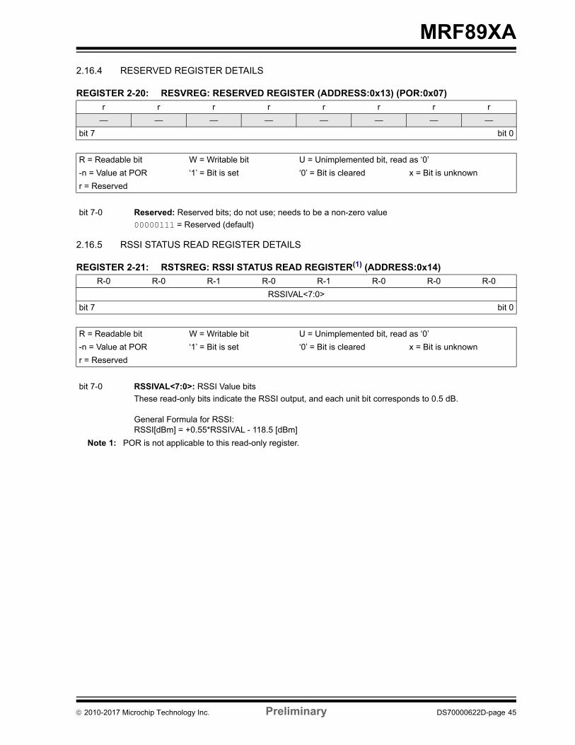
MRF89XA
2.16.4 RESERVED REGISTER DETAILS
REGISTER 2-20: RESVREG: RESERVED REGISTER (ADDRESS:0x13) (POR:0x07)
2.16.5 RSSI STATUS READ REGISTER DETAILS
REGISTER 2-21: RSTSREG: RSSI STATUS READ REGISTER(1) (ADDRESS:0x14)
r r r r r r r r
— — — — — — — —
bit 7 bit 0
R = Readable bit W = Writable bit U = Unimplemented bit, read as ‘0’
-n = Value at POR ‘1’ = Bit is set ‘0’ = Bit is cleared x = Bit is unknown
r = Reserved
bit 7-0 Reserved: Reserved bits; do not use; needs to be a non-zero value
00000111 = Reserved (default)
R-0 R-0 R-1 R-0 R-1 R-0 R-0 R-0
RSSIVAL<7:0>
bit 7 bit 0
R = Readable bit W = Writable bit U = Unimplemented bit, read as ‘0’
-n = Value at POR ‘1’ = Bit is set ‘0’ = Bit is cleared x = Bit is unknown
r = Reserved
bit 7-0 RSSIVAL<7:0>: RSSI Value bits
These read-only bits indicate the RSSI output, and each unit bit corresponds to 0.5 dB.
General Formula for RSSI:RSSI[dBm] = +0.55*RSSIVAL - 118.5 [dBm]
Note 1: POR is not applicable to this read-only register.
2010-2017 Microchip Technology Inc. Preliminary DS70000622D-page 45
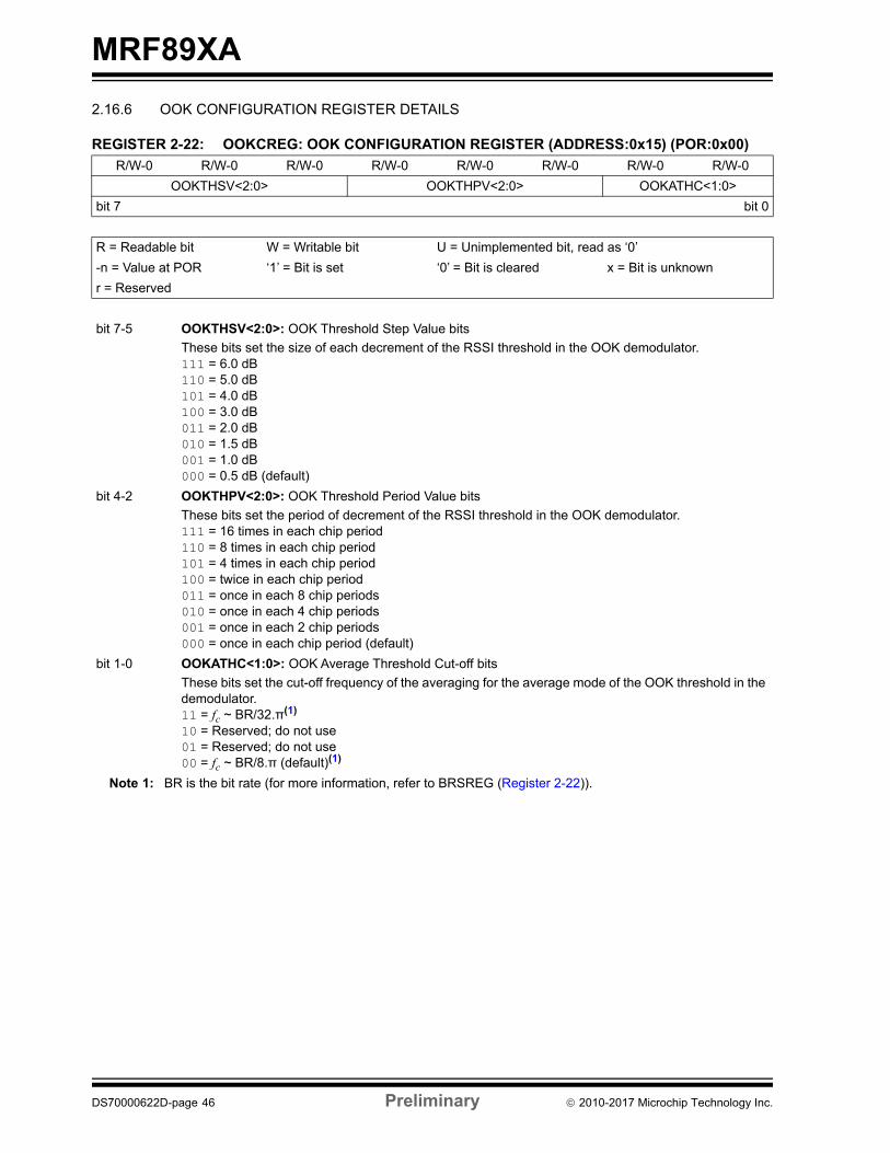
MRF89XA
2.16.6 OOK CONFIGURATION REGISTER DETAILS
REGISTER 2-22: OOKCREG: OOK CONFIGURATION REGISTER (ADDRESS:0x15) (POR:0x00)
R/W-0 R/W-0 R/W-0 R/W-0 R/W-0 R/W-0 R/W-0 R/W-0
OOKTHSV<2:0> OOKTHPV<2:0> OOKATHC<1:0>
bit 7 bit 0
R = Readable bit W = Writable bit U = Unimplemented bit, read as ‘0’
-n = Value at POR ‘1’ = Bit is set ‘0’ = Bit is cleared x = Bit is unknown
r = Reserved
bit 7-5 OOKTHSV<2:0>: OOK Threshold Step Value bits
These bits set the size of each decrement of the RSSI threshold in the OOK demodulator. 111 = 6.0 dB110 = 5.0 dB101 = 4.0 dB100 = 3.0 dB 011 = 2.0 dB010 = 1.5 dB001 = 1.0 dB 000 = 0.5 dB (default)
bit 4-2 OOKTHPV<2:0>: OOK Threshold Period Value bits
These bits set the period of decrement of the RSSI threshold in the OOK demodulator. 111 = 16 times in each chip period110 = 8 times in each chip period101 = 4 times in each chip period100 = twice in each chip period 011 = once in each 8 chip periods010 = once in each 4 chip periods001 = once in each 2 chip periods 000 = once in each chip period (default)
bit 1-0 OOKATHC<1:0>: OOK Average Threshold Cut-off bits
These bits set the cut-off frequency of the averaging for the average mode of the OOK threshold in the demodulator.11 = fc ~ BR/32.π(1)
10 = Reserved; do not use01 = Reserved; do not use00 = fc ~ BR/8.π (default)(1)
Note 1: BR is the bit rate (for more information, refer to BRSREG (Register 2-22)).
DS70000622D-page 46 Preliminary 2010-2017 Microchip Technology Inc.
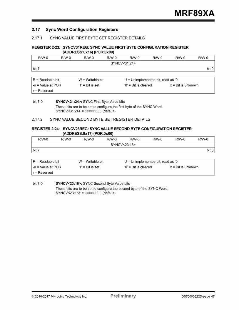
MRF89XA
2.17 Sync Word Configuration Registers
2.17.1 SYNC VALUE FIRST BYTE SET REGISTER DETAILS
REGISTER 2-23: SYNCV31REG: SYNC VALUE FIRST BYTE CONFIGURATION REGISTER (ADDRESS:0x16) (POR:0x00)
2.17.2 SYNC VALUE SECOND BYTE SET REGISTER DETAILS
REGISTER 2-24: SYNCV23REG: SYNC VALUE SECOND BYTE CONFIGURATION REGISTER (ADDRESS:0x17) (POR:0x00)
R/W-0 R/W-0 R/W-0 R/W-0 R/W-0 R/W-0 R/W-0 R/W-0
SYNCV<31:24>
bit 7 bit 0
R = Readable bit W = Writable bit U = Unimplemented bit, read as ‘0’
-n = Value at POR ‘1’ = Bit is set ‘0’ = Bit is cleared x = Bit is unknown
r = Reserved
bit 7-0 SYNCV<31:24>: SYNC First Byte Value bits
These bits are to be set to configure the first byte of the SYNC Word.SYNCV<31:24> = 00000000 (default)
R/W-0 R/W-0 R/W-0 R/W-0 R/W-0 R/W-0 R/W-0 R/W-0
SYNCV<23:16>
bit 7 bit 0
R = Readable bit W = Writable bit U = Unimplemented bit, read as ‘0’
-n = Value at POR ‘1’ = Bit is set ‘0’ = Bit is cleared x = Bit is unknown
r = Reserved
bit 7-0 SYNCV<23:16>: SYNC Second Byte Value bits
These bits are to be set to configure the second byte of the SYNC Word.SYNCV<23:16> = 00000000 (default)
2010-2017 Microchip Technology Inc. Preliminary DS70000622D-page 47
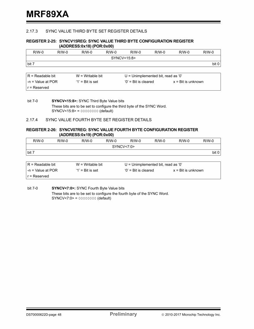
MRF89XA
2.17.3 SYNC VALUE THIRD BYTE SET REGISTER DETAILS
REGISTER 2-25: SYNCV15REG: SYNC VALUE THIRD BYTE CONFIGURATION REGISTER (ADDRESS:0x18) (POR:0x00)
2.17.4 SYNC VALUE FOURTH BYTE SET REGISTER DETAILS
REGISTER 2-26: SYNCV07REG: SYNC VALUE FOURTH BYTE CONFIGURATION REGISTER (ADDRESS:0x19) (POR:0x00)
R/W-0 R/W-0 R/W-0 R/W-0 R/W-0 R/W-0 R/W-0 R/W-0
SYNCV<15:8>
bit 7 bit 0
R = Readable bit W = Writable bit U = Unimplemented bit, read as ‘0’
-n = Value at POR ‘1’ = Bit is set ‘0’ = Bit is cleared x = Bit is unknown
r = Reserved
bit 7-0 SYNCV<15:8>: SYNC Third Byte Value bits
These bits are to be set to configure the third byte of the SYNC Word.SYNCV<15:8> = 00000000 (default)
R/W-0 R/W-0 R/W-0 R/W-0 R/W-0 R/W-0 R/W-0 R/W-0
SYNCV<7:0>
bit 7 bit 0
R = Readable bit W = Writable bit U = Unimplemented bit, read as ‘0’
-n = Value at POR ‘1’ = Bit is set ‘0’ = Bit is cleared x = Bit is unknown
r = Reserved
bit 7-0 SYNCV<7:0>: SYNC Fourth Byte Value bits
These bits are to be set to configure the fourth byte of the SYNC Word.SYNCV<7:0> = 00000000 (default)
DS70000622D-page 48 Preliminary 2010-2017 Microchip Technology Inc.
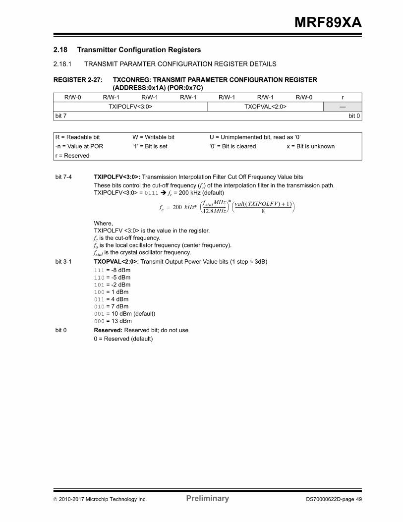
MRF89XA
2.18 Transmitter Configuration Registers
2.18.1 TRANSMIT PARAMTER CONFIGURATION REGISTER DETAILS
REGISTER 2-27: TXCONREG: TRANSMIT PARAMETER CONFIGURATION REGISTER (ADDRESS:0x1A) (POR:0x7C)
R/W-0 R/W-1 R/W-1 R/W-1 R/W-1 R/W-1 R/W-0 r
TXIPOLFV<3:0> TXOPVAL<2:0> —
bit 7 bit 0
R = Readable bit W = Writable bit U = Unimplemented bit, read as ‘0’
-n = Value at POR ‘1’ = Bit is set ‘0’ = Bit is cleared x = Bit is unknown
r = Reserved
bit 7-4 TXIPOLFV<3:0>: Transmission Interpolation Filter Cut Off Frequency Value bits
These bits control the cut-off frequency (fc) of the interpolation filter in the transmission path. TXIPOLFV<3:0> = 0111 fc = 200 kHz (default)
Where, TXIPOLFV <3:0> is the value in the register.fc is the cut-off frequency.fo is the local oscillator frequency (center frequency).fxtal is the crystal oscillator frequency.
bit 3-1 TXOPVAL<2:0>: Transmit Output Power Value bits (1 step ≈ 3dB)
111 = -8 dBm 110 = -5 dBm 101 = -2 dBm 100 = 1 dBm 011 = 4 dBm 010 = 7 dBm 001 = 10 dBm (default)000 = 13 dBm
bit 0 Reserved: Reserved bit; do not use
0 = Reserved (default)
fc 200 kHzfxtalMHz
12.8MHz-----------------------
val TXIPOLFV 1+ 8
--------------------------------------------------------- =
2010-2017 Microchip Technology Inc. Preliminary DS70000622D-page 49
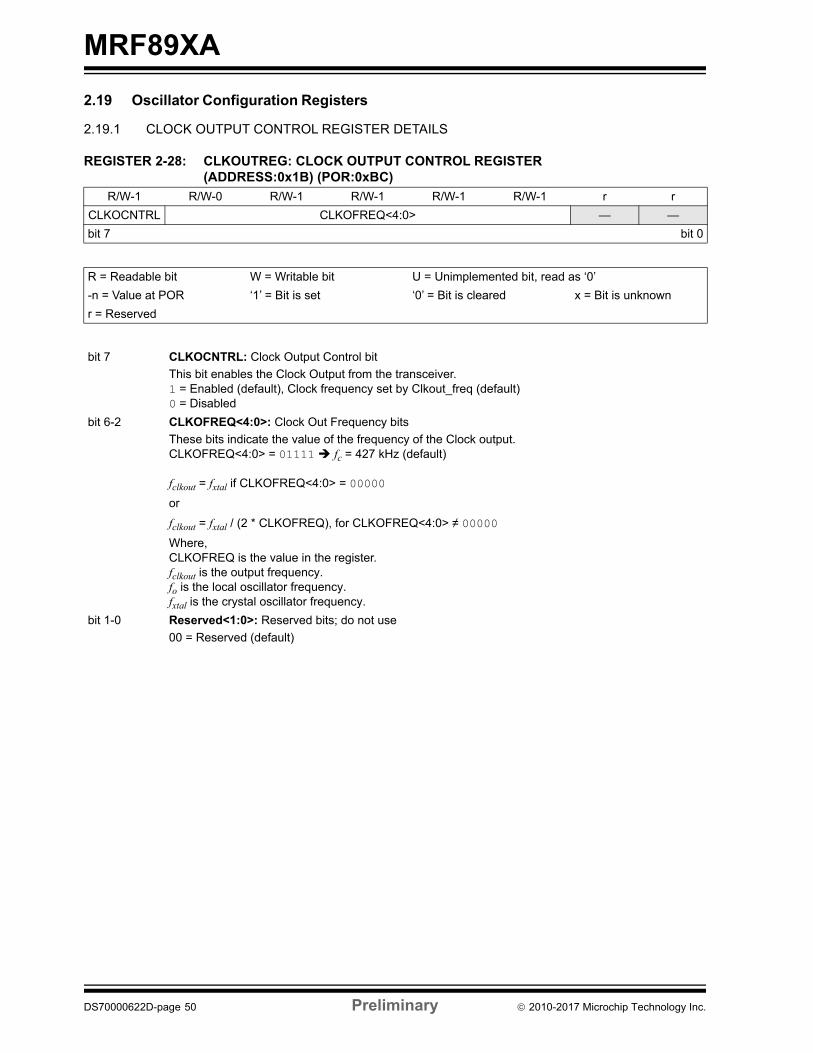
MRF89XA
2.19 Oscillator Configuration Registers
2.19.1 CLOCK OUTPUT CONTROL REGISTER DETAILS
REGISTER 2-28: CLKOUTREG: CLOCK OUTPUT CONTROL REGISTER (ADDRESS:0x1B) (POR:0xBC)
R/W-1 R/W-0 R/W-1 R/W-1 R/W-1 R/W-1 r r
CLKOCNTRL CLKOFREQ<4:0> — —
bit 7 bit 0
R = Readable bit W = Writable bit U = Unimplemented bit, read as ‘0’
-n = Value at POR ‘1’ = Bit is set ‘0’ = Bit is cleared x = Bit is unknown
r = Reserved
bit 7 CLKOCNTRL: Clock Output Control bit
This bit enables the Clock Output from the transceiver.1 = Enabled (default), Clock frequency set by Clkout_freq (default)0 = Disabled
bit 6-2 CLKOFREQ<4:0>: Clock Out Frequency bits
These bits indicate the value of the frequency of the Clock output.CLKOFREQ<4:0> = 01111 fc = 427 kHz (default)
fclkout = fxtal if CLKOFREQ<4:0> = 00000
or
fclkout = fxtal / (2 * CLKOFREQ), for CLKOFREQ<4:0> ≠ 00000Where, CLKOFREQ is the value in the register.fclkout is the output frequency.fo is the local oscillator frequency.fxtal is the crystal oscillator frequency.
bit 1-0 Reserved<1:0>: Reserved bits; do not use
00 = Reserved (default)
DS70000622D-page 50 Preliminary 2010-2017 Microchip Technology Inc.
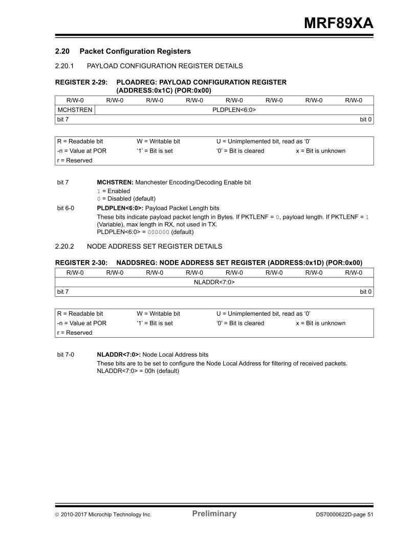
MRF89XA
2.20 Packet Configuration Registers
2.20.1 PAYLOAD CONFIGURATION REGISTER DETAILS
REGISTER 2-29: PLOADREG: PAYLOAD CONFIGURATION REGISTER (ADDRESS:0x1C) (POR:0x00)
2.20.2 NODE ADDRESS SET REGISTER DETAILS
REGISTER 2-30: NADDSREG: NODE ADDRESS SET REGISTER (ADDRESS:0x1D) (POR:0x00)
R/W-0 R/W-0 R/W-0 R/W-0 R/W-0 R/W-0 R/W-0 R/W-0
MCHSTREN PLDPLEN<6:0>
bit 7 bit 0
R = Readable bit W = Writable bit U = Unimplemented bit, read as ‘0’
-n = Value at POR ‘1’ = Bit is set ‘0’ = Bit is cleared x = Bit is unknown
r = Reserved
bit 7 MCHSTREN: Manchester Encoding/Decoding Enable bit
1 = Enabled 0 = Disabled (default)
bit 6-0 PLDPLEN<6:0>: Payload Packet Length bits
These bits indicate payload packet length in Bytes. If PKTLENF = 0, payload length. If PKTLENF = 1 (Variable), max length in RX, not used in TX.PLDPLEN<6:0> = 000000 (default)
R/W-0 R/W-0 R/W-0 R/W-0 R/W-0 R/W-0 R/W-0 R/W-0
NLADDR<7:0>
bit 7 bit 0
R = Readable bit W = Writable bit U = Unimplemented bit, read as ‘0’
-n = Value at POR ‘1’ = Bit is set ‘0’ = Bit is cleared x = Bit is unknown
r = Reserved
bit 7-0 NLADDR<7:0>: Node Local Address bits
These bits are to be set to configure the Node Local Address for filtering of received packets.NLADDR<7:0> = 00h (default)
2010-2017 Microchip Technology Inc. Preliminary DS70000622D-page 51
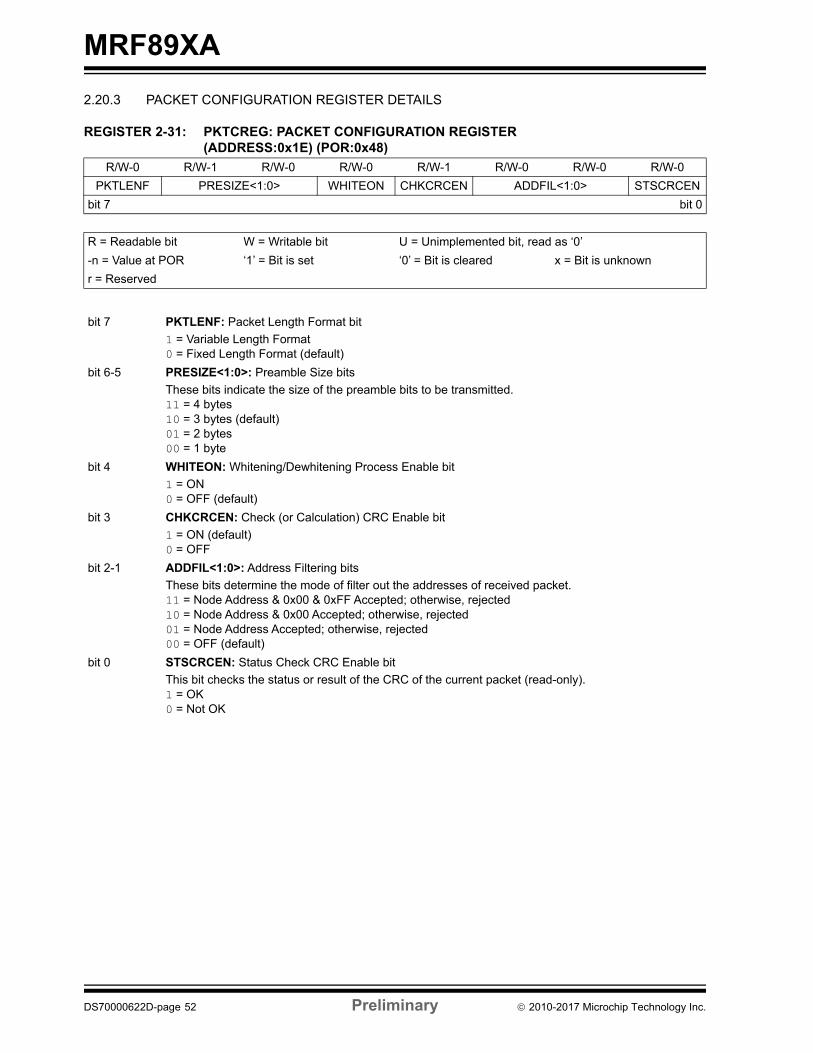
MRF89XA
2.20.3 PACKET CONFIGURATION REGISTER DETAILS
REGISTER 2-31: PKTCREG: PACKET CONFIGURATION REGISTER (ADDRESS:0x1E) (POR:0x48)
R/W-0 R/W-1 R/W-0 R/W-0 R/W-1 R/W-0 R/W-0 R/W-0
PKTLENF PRESIZE<1:0> WHITEON CHKCRCEN ADDFIL<1:0> STSCRCEN
bit 7 bit 0
R = Readable bit W = Writable bit U = Unimplemented bit, read as ‘0’
-n = Value at POR ‘1’ = Bit is set ‘0’ = Bit is cleared x = Bit is unknown
r = Reserved
bit 7 PKTLENF: Packet Length Format bit
1 = Variable Length Format 0 = Fixed Length Format (default)
bit 6-5 PRESIZE<1:0>: Preamble Size bits
These bits indicate the size of the preamble bits to be transmitted.11 = 4 bytes10 = 3 bytes (default)01 = 2 bytes 00 = 1 byte
bit 4 WHITEON: Whitening/Dewhitening Process Enable bit
1 = ON0 = OFF (default)
bit 3 CHKCRCEN: Check (or Calculation) CRC Enable bit
1 = ON (default)0 = OFF
bit 2-1 ADDFIL<1:0>: Address Filtering bits
These bits determine the mode of filter out the addresses of received packet.11 = Node Address & 0x00 & 0xFF Accepted; otherwise, rejected10 = Node Address & 0x00 Accepted; otherwise, rejected01 = Node Address Accepted; otherwise, rejected00 = OFF (default)
bit 0 STSCRCEN: Status Check CRC Enable bit
This bit checks the status or result of the CRC of the current packet (read-only).1 = OK0 = Not OK
DS70000622D-page 52 Preliminary 2010-2017 Microchip Technology Inc.
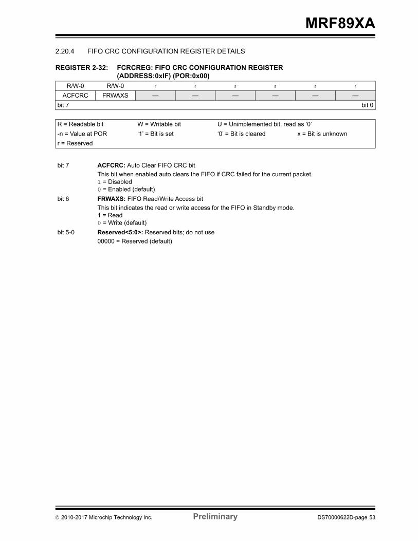
MRF89XA
2.20.4 FIFO CRC CONFIGURATION REGISTER DETAILS
REGISTER 2-32: FCRCREG: FIFO CRC CONFIGURATION REGISTER (ADDRESS:0xIF) (POR:0x00)
R/W-0 R/W-0 r r r r r r
ACFCRC FRWAXS — — — — — —
bit 7 bit 0
R = Readable bit W = Writable bit U = Unimplemented bit, read as ‘0’
-n = Value at POR ‘1’ = Bit is set ‘0’ = Bit is cleared x = Bit is unknown
r = Reserved
bit 7 ACFCRC: Auto Clear FIFO CRC bit
This bit when enabled auto clears the FIFO if CRC failed for the current packet.1 = Disabled 0 = Enabled (default)
bit 6 FRWAXS: FIFO Read/Write Access bit
This bit indicates the read or write access for the FIFO in Standby mode.1 = Read 0 = Write (default)
bit 5-0 Reserved<5:0>: Reserved bits; do not use
00000 = Reserved (default)
2010-2017 Microchip Technology Inc. Preliminary DS70000622D-page 53

MR
F89X
A
DS
70000622D
-page 54
Prelim
ina
ry
2010-2017 Microchip T
echnology Inc.
2 Bit 1 Bit 0Value on
POR
VCOT<1:0> RPS 0x28
E1 IFGAIN<1:0> 0x88
0x03
0x07
0x0C
0x0F
0x77
0x64
0x32
0x74
0x62
0x32
ved Reserved Reserved 0x38
ULL FIFOEMPTY FOVRRUN 0x00
S LSTSPLL LENPLL 0x01
0x00
UTFILV<3:0> 0xA3
ved Reserved Reserved 0x38
YNCTEN<1:0> Reserved 0x18
ved Reserved Reserved 0x07
Read-only
OOKATHC<1:0> 0x00
0x00
0x00
0x00
0x00
<2:0> Reserved 0x7C
Reserved Reserved 0xBC
0x00
0x00
DDFIL<1:0> STSCRCEN 0x48
ved Reserved Reserved 0x00
TABLE 2-8: CONFIGURATION/CONTROL/STATUS REGISTER MAP
Register Function/Parameter
Type
Register Address
Register Name Bit 7 Bit 6 Bit 5 Bit 4 Bit 3 Bit
General 0x00 GCONREG CMOD<2:0> FBS<1:0>
0x01 DMODREG MODSEL<1:0> DMODE0 OOKTYP<1:0> DMOD
0x02 FDEVREG FDVAL<7:0>
0x03 BRSREG Reserved BRVAL<6:0>
0x04 FLTHREG FTOVAL<7:0>
0x05 FIFOCREG FSIZE<1:0> FTINT<5:0>
0x06 R1CREG R1CVAL<7:0>
0x07 P1CREG P1CVAL<7:0>
0x08 S1CREG S1CVAL<7:0>
0x09 R2CREG R2CVAL<7:0>
0x0A P2CREG P2CVAL<7:0>
0x0B S2CREG S2CVAL<7:0>
0x0C PACREG Reserved Reserved Reserved PARC<1:0> Reser
0x0D FTXRXIREG IRQ0RXS<1:0> IRQ1RXS<1:0> IRQ1TX FIFOF
Interrupt 0x0E FTPRIREG FIFOFM FIFOFSC TXDONE IRQ0TXST ENRIRQS RIRQ
0x0F RSTHIREG RTIVAL<7:0>
0x10 FILCREG PASFILV<3:0> B
Receiver 0x11 PFCREG POLCFV<3:0> Reserved Reser
0x12 SYNCREG POLFILEN BSYNCEN SYNCREN SYNCWSZ<1:0> S
0x13 RESVREG Reserved Reserved Reserved Reserved Reserved Reser
0x14 RSTSREG RSSIVAL<7:0>
0x15 OOKCREG OOKTHSV<2:0> OOKTHPV<2:0>
SYNC Word 0x16 SYNCV31REG SYNCV<31:24>
0x17 SYNCV23REG SYNCV<23:16>
0x18 SYNCV15REG SYNCV<15:8>
0x19 SYNCV07REG SYNCV<7:0>
Transmitter 0x1A TXCONREG TXIPOLFV<3:0> TXOPVAL
Clock-out 0x1B CLKOUTREG CLKOCNTRL CLKOFREQ<4:0>
Packet 0x1C PLOADREG MCHSTREN PLDPLEN<6:0>
0x1D NADDSREG NLADDR<7:0>
0x1E PKTCREG PKTLENF PRESIZE<1:0> WHITEON CHKCRCEN A
0x1F FCRCREG ACFCRC FRWAXS Reserved Reserved Reserved Reser
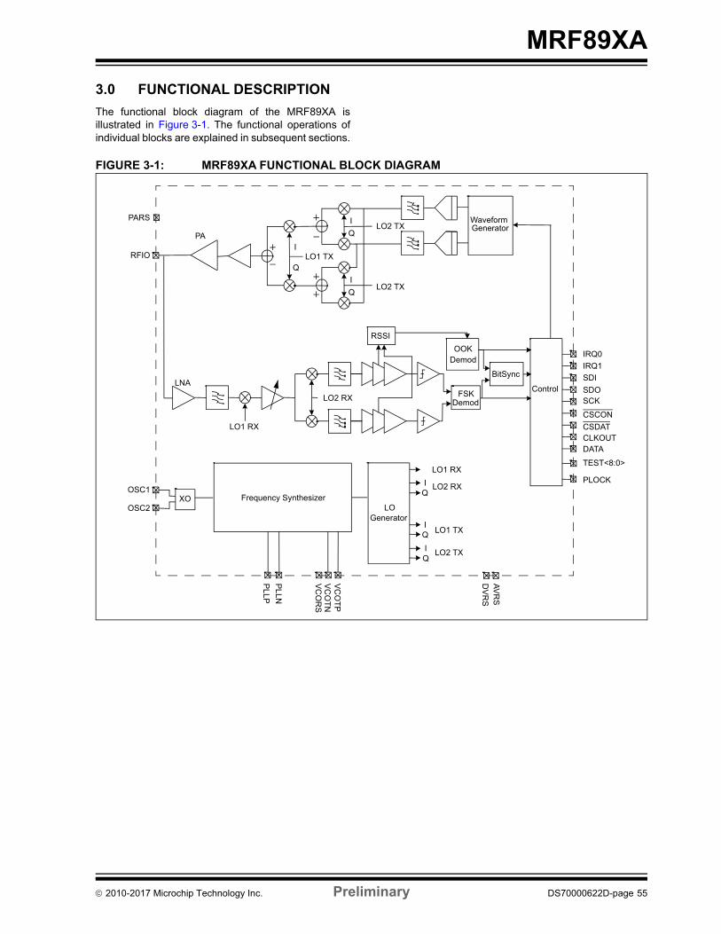
MRF89XA
3.0 FUNCTIONAL DESCRIPTION
The functional block diagram of the MRF89XA isillustrated in Figure 3-1. The functional operations ofindividual blocks are explained in subsequent sections.
FIGURE 3-1: MRF89XA FUNCTIONAL BLOCK DIAGRAM
Waveform Generator
FSK Demod
BitSync
OOKDemod
Control
XO
RSSI
LO1 RX
LO2 RXI
IQ
Q
LO1 TX
IQ
LO2 TX
LO1 RX
LO2 RX
LO1 TX
LO2 TX
LO2 TX
RFIO
OSC1
OSC2
VC
OR
S
PARS
IRQ0
IRQ1
SDI
SDO SCK
CSCON
CLKOUTDATA
CSDAT
TEST<8:0>
VC
OT
P
VC
OT
N
PL
LP
PL
LN
DV
RS
PLOCK
PA
LNA
I
Q
Q
I
I
Q
LO Generator
Frequency Synthesizer
AV
RS
2010-2017 Microchip Technology Inc. Preliminary DS70000622D-page 55
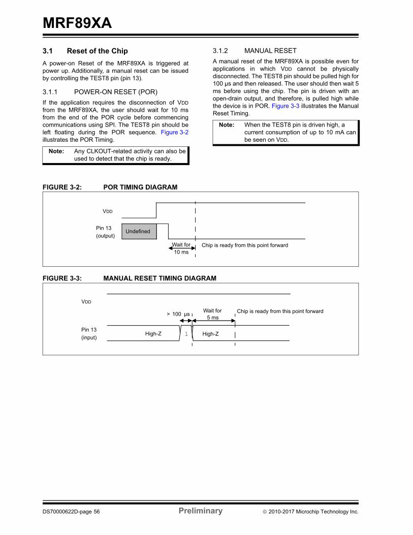
MRF89XA
3.1 Reset of the Chip
A power-on Reset of the MRF89XA is triggered atpower up. Additionally, a manual reset can be issuedby controlling the TEST8 pin (pin 13).
3.1.1 POWER-ON RESET (POR)
If the application requires the disconnection of VDD
from the MRF89XA, the user should wait for 10 msfrom the end of the POR cycle before commencingcommunications using SPI. The TEST8 pin should beleft floating during the POR sequence. Figure 3-2illustrates the POR Timing.
3.1.2 MANUAL RESET
A manual reset of the MRF89XA is possible even forapplications in which VDD cannot be physicallydisconnected. The TEST8 pin should be pulled high for100 µs and then released. The user should then wait 5ms before using the chip. The pin is driven with anopen-drain output, and therefore, is pulled high whilethe device is in POR. Figure 3-3 illustrates the ManualReset Timing.
FIGURE 3-2: POR TIMING DIAGRAM
FIGURE 3-3: MANUAL RESET TIMING DIAGRAM
Note: Any CLKOUT-related activity can also beused to detect that the chip is ready.
Note: When the TEST8 pin is driven high, a current consumption of up to 10 mA canbe seen on VDD.
Wait for 10 ms
VDD
Pin 13
(output)
Chip is ready from this point forward
Undefined
VDD
> 100 µs Chip is ready from this point forward
Pin 13
(input) High-Z High-Z1
Wait for 5 ms
DS70000622D-page 56 Preliminary 2010-2017 Microchip Technology Inc.

MRF89XA
3.2 Frequency Synthesis Description
3.2.1 REFERENCE OSCILLATOR
The crystal oscillator (XTAL) forms the referenceoscillator of an Integer-N PLL. The crystal referencefrequency and the software controlled dividers R, P,and S determine the output frequency of the PLL. Theguidelines for selecting the appropriate crystal withspecifications are explained in Section 4.7, CrystalSpecification and Selection Guidelines.
3.2.2 BUFFERED CLOCK OUTPUT
The buffered clock output is a signal derived from fxtal.It can be used as a reference clock (or a sub-multipleof it) for the host microcontroller and is an output on theCLKOUT pin (pin 19). The pin is activated using theCLKOCNTRL bit (CLKOUTREG<7>). The outputfrequency (CLKOUT) division ratio is programmedthrough the Clock Out Frequency bits (CLKOFREQ5-CLK0FREQ1) in the Clock Output Control Register(CLKOUTREG<6:2>). The two uses of the CLKOUToutput are:
• To provide a clock output for a host microcontroller,thus saving the cost of an additional oscillator.CLKOUT can be made available in any operationmode, except Sleep mode, and is automaticallyenabled at power-up.
• To provide an oscillator reference output.Measurement of the CLKOUT signal enablessimple software trimming of the initial crystaltolerance.
3.2.3 CLOCK REGISTERS
The registers associated with the Clock and its controlare:
• GCONREG (Register 2-1)
• CLKOUTREG (Register 2-28)
3.2.4 PHASE-LOCKED LOOP (PLL)
The frequency synthesizer of the MRF89XA is a fullyintegrated integer-N type PLL. The PLL circuit requiresonly five external components for the PLL loop filterand the VCO tank circuit.
3.2.4.1 PLL Requirements
With integer-N PLL architecture, the followingconditions must be met to ensure correct operation:
• The comparison frequency, FCOMP, of the PhaseFrequency Detector (PFD) input must remainhigher than six times the PLL bandwidth (PLLBW)to guarantee loop stability and to reject harmonicsof the comparison frequency FCOMP. This isexpressed in the inequality:
FCOMP ≥ 6 * PLLBW
• However, the PLLBW must be sufficiently high toallow adequate PLL lock times.
• Because the divider ratio R determines FCOMP, itshould be set close to 119, leading toFCOMP ≈ 100 kHz, which will ensure suitable PLLstability and speed.
The following criteria govern the R, P, and S values forthe PLL block:
• 64 ≤ R ≤ 169
• P+1 > S
• PLLBW = 15 kHz nominal
• Start-up times and reference frequency drives asspecified
3.2.4.2 PLL Lock Detection Indicator
The MRF89XA features a PLL lock detect indicator.This is useful for optimizing power consumption, byadjusting the frequency synthesizer wake-up time(TSFS). For more information on TSFS, refer toTable 5-4. The lock status is available by reading theLock Status of PLL bit (LSTSPLL) in the FIFOTransmit PLL and RSSI Interrupt RequestConfiguration register (FTPRIREG<1>), and must becleared by writing a ‘1’ to this same register. Thelock status can also be seen on the PLOCK pin (pin23) of the device by setting the LENPLL bit(FTPRIREG<0>).
3.2.5 PLL REGISTERS
The registers associated with the PLL are:
• GCONREG (Register 2-1)
• FTPRIREG (Register 2-15)
3.2.6 SW SETTINGS OF THE VCO
To guarantee the optimum operation of the VCO overthe MRF89XA’s frequency and temperature ranges,the settings listed in Table 3-1 should be programmedinto the MRF89XA.
Note: Use the recommended values provided inthe Bill Of Materials (BOM) in Section 4.8,Bill of Materials for any PLL prototypedesign.
Note: CLKOUT is disabled when the MRF89XAis in Sleep mode. If Sleep mode is used,the host microcontroller must have provi-sions to run from its own clock source. Note: The LSTSPLL bit latches high each time
the PLL locks and must be reset by writinga ‘1’ to LSTSPLL from FTPRIREG.
2010-2017 Microchip Technology Inc. Preliminary DS70000622D-page 57
MRF89XA
TABLE 3-1: FREQUENCY BAND SETTING
3.2.6.1 Trimming the VCO Tank byHardware and Software
To ensure that the frequency band of operation isaccurately addressed by the R, P, and S dividers of thesynthesizer, it is necessary to ensure that the VCO iscorrectly centered. The MRF89XA built-in VCOtrimming feature makes it easy and is controlled by theSPI interface. This tuning does not require any RF testequipment, and can be achieved by measuring Vtune,which is the voltage between the PLLN and PLLP pins(6 and 7 pins).
The VCO is centered if the voltage is within the rangeof 50 Vtune(mV) 150.
This measurement should be conducted when inTransmit mode at the center frequency (fo) of thedesired band (for example, approximately 867 MHz inthe 863-870 MHz band), with the appropriate frequencyband setting using the (FBS<1:0> bits(GCONREG<4:3>).
If this inequality is not satisfied, adjust the VCOT<1:0>bits (GCONREG<2:0>) from ‘00’ by monitoring Vtune.This allows the VCO voltage to be trimmed in +60 mVincrements. If the desired voltage range isinaccessible, the voltage may be adjusted further bychanging the tank circuit inductance value.
An increase in inductance results in an increasedVtune. In addition, for mass production, the VCOcapacitance is piece-to-piece dependent. As such, theoptimization proposed above should be verified onseveral prototypes, to ensure that the population iscentered with 100 mV.
The register associated with VCO is GCONREG(Register 2-1).
3.2.7 FREQUENCY CALCULATIONAs illustrated in Figure 2-5, the PLL structure com-prises three different dividers, R, P, and S, which setthe output frequency through the LO. A second set ofdividers is also available to allow rapid switchingbetween a pair of frequencies: R1/P1/S1 and R2/P2/S2. These six dividers are programmed by six indepen-dent registers (see Register 2-7 through Register 2-12), which are selected by GCONREG.
3.2.8 FSK MODE
The formula provided in Equation 3-1 gives therelationship between the local oscillator and R, P, andS values when using FSK modulation.
EQUATION 3-1:
3.2.9 FSK MODE REGISTERS
The registers associated with FSK mode are:
• GCONREG (Register 2-1)
• DMODREG (Register 2-2)
3.2.10 OOK MODE
Due to the manner in which the baseband OOKsymbols are generated, the signal is always offset bythe FSK frequency deviation (FDVAL<7:0> asprogrammed in FDEVREG<7:0>). Therefore, thecenter of the transmitted OOK signal is represented byEquation 3-2.
EQUATION 3-2:
Consequently, in Receive mode, due to the lowintermediate frequency (Low-IF) architecture of theMRF89XA, the frequency should be configured so as toensure the correct low-IF receiver baseband centerfrequency, IF2, as shown in Equation 3-3.
EQUATION 3-3:
As described in Section 3.4.4, Channel Filters, it isrecommended that IF2 be set to 100 kHz.
3.2.11 OOK MODE REGISTERS
The registers associated with OOK mode are:
• GCONREG (Register 2-1)• DMODREG (Register 2-2)• FLTHREG (Register 2-5)• OOKCREG (Register 2-22)
Target Channel (MHz)
FBS1 FBS0
863-870 1 0
902-915 0 0
915-928 0 1
950-960 1 0 frf fsk98---flo=
frf fsk98---
fxtaLR 1+------------- 75 P 1+ S+ =
frf ook tx 98---
fxtaLR 1+------------- 75 P 1+ S+ fdev–=
frf ook tx 98--- flo fdev–=
frf ook rx 98--- flo IF2–=
frf ook rx 98---
fxtaLR 1+------------- 75 P 1+ S+ IF2–=
DS70000622D-page 58 Preliminary 2010-2017 Microchip Technology Inc.
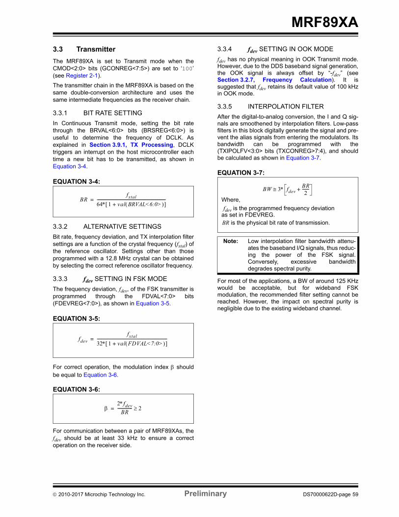
MRF89XA
3.3 Transmitter
The MRF89XA is set to Transmit mode when theCMOD<2:0> bits (GCONREG<7:5>) are set to ‘100’(see Register 2-1).
The transmitter chain in the MRF89XA is based on thesame double-conversion architecture and uses thesame intermediate frequencies as the receiver chain.
3.3.1 BIT RATE SETTING
In Continuous Transmit mode, setting the bit ratethrough the BRVAL<6:0> bits (BRSREG<6:0>) isuseful to determine the frequency of DCLK. Asexplained in Section 3.9.1, TX Processing, DCLKtriggers an interrupt on the host microcontroller eachtime a new bit has to be transmitted, as shown inEquation 3-4.
EQUATION 3-4:
3.3.2 ALTERNATIVE SETTINGS
Bit rate, frequency deviation, and TX interpolation filtersettings are a function of the crystal frequency (fxtal) ofthe reference oscillator. Settings other than thoseprogrammed with a 12.8 MHz crystal can be obtainedby selecting the correct reference oscillator frequency.
3.3.3 fdev SETTING IN FSK MODE
The frequency deviation, fdev, of the FSK transmitter isprogrammed through the FDVAL<7:0> bits(FDEVREG<7:0>), as shown in Equation 3-5.
EQUATION 3-5:
For correct operation, the modulation index shouldbe equal to Equation 3-6.
EQUATION 3-6:
For communication between a pair of MRF89XAs, thefdev should be at least 33 kHz to ensure a correctoperation on the receiver side.
3.3.4 fdev SETTING IN OOK MODE
fdev has no physical meaning in OOK Transmit mode.However, due to the DDS baseband signal generation,the OOK signal is always offset by “-fdev” (seeSection 3.2.7, Frequency Calculation). It issuggested that fdev retains its default value of 100 kHzin OOK mode.
3.3.5 INTERPOLATION FILTER
After the digital-to-analog conversion, the I and Q sig-nals are smoothened by interpolation filters. Low-passfilters in this block digitally generate the signal and pre-vent the alias signals from entering the modulators. Itsbandwidth can be programmed with the(TXIPOLFV<3:0> bits (TXCONREG>7:4), and shouldbe calculated as shown in Equation 3-7.
EQUATION 3-7:
For most of the applications, a BW of around 125 KHzwould be acceptable, but for wideband FSKmodulation, the recommended filter setting cannot bereached. However, the impact on spectral purity isnegligible due to the existing wideband channel.
BRfxtal
64 1 val BRVAL<6:0> + ----------------------------------------------------------------------=
fdevfxtal
32 1 val FDVAL<7:0> + ------------------------------------------------------------------------=
2fdevBR
--------------- 2=
Note: Low interpolation filter bandwidth attenu-ates the baseband I/Q signals, thus reduc-ing the power of the FSK signal.Conversely, excessive bandwidthdegrades spectral purity.
Where,
fdev is the programmed frequency deviation as set in FDEVREG.BR is the physical bit rate of transmission.
BW 3 fdevBR2
-------+
2010-2017 Microchip Technology Inc. Preliminary DS70000622D-page 59
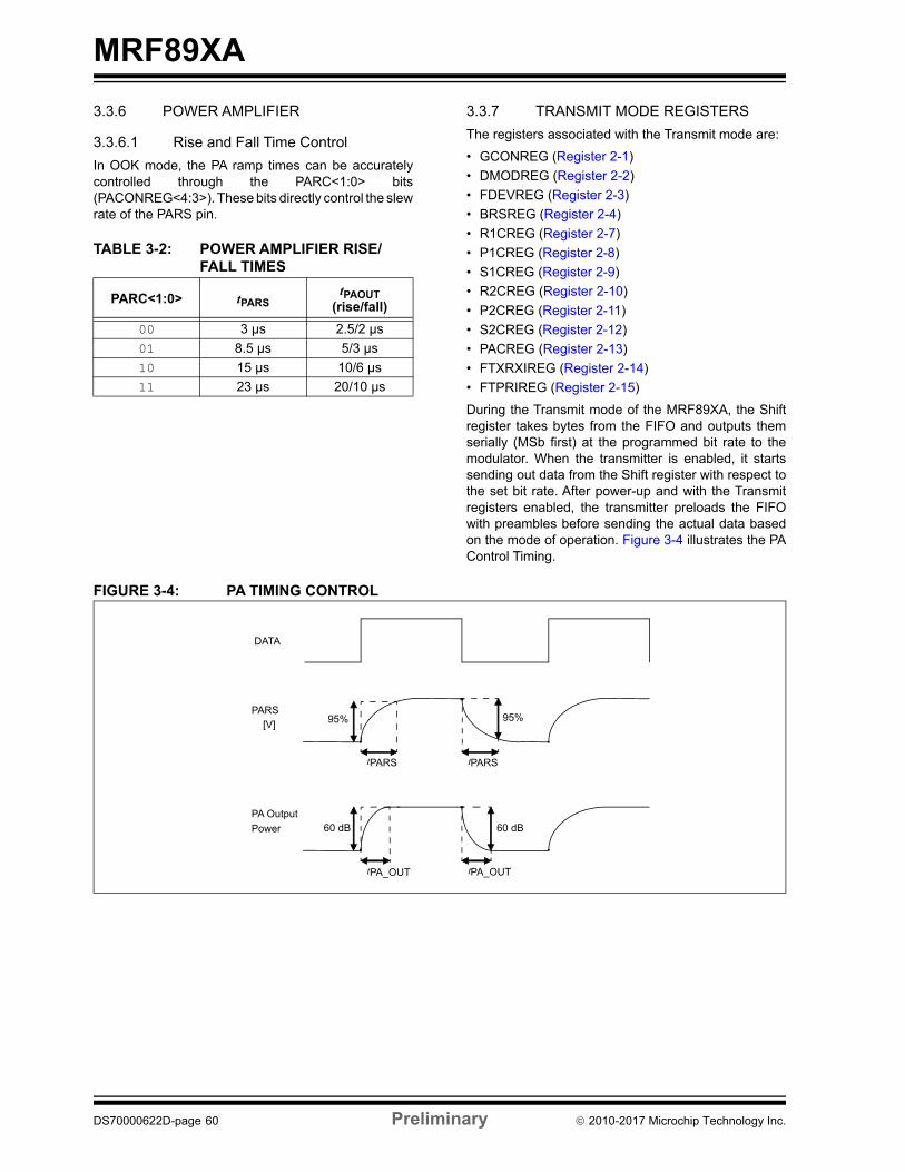
MRF89XA
3.3.6 POWER AMPLIFIER
3.3.6.1 Rise and Fall Time Control
In OOK mode, the PA ramp times can be accuratelycontrolled through the PARC<1:0> bits(PACONREG<4:3>). These bits directly control the slewrate of the PARS pin.
TABLE 3-2: POWER AMPLIFIER RISE/FALL TIMES
3.3.7 TRANSMIT MODE REGISTERS
The registers associated with the Transmit mode are:
• GCONREG (Register 2-1)
• DMODREG (Register 2-2)
• FDEVREG (Register 2-3)
• BRSREG (Register 2-4)
• R1CREG (Register 2-7)
• P1CREG (Register 2-8)
• S1CREG (Register 2-9)
• R2CREG (Register 2-10)
• P2CREG (Register 2-11)
• S2CREG (Register 2-12)
• PACREG (Register 2-13)
• FTXRXIREG (Register 2-14)
• FTPRIREG (Register 2-15)
During the Transmit mode of the MRF89XA, the Shiftregister takes bytes from the FIFO and outputs themserially (MSb first) at the programmed bit rate to themodulator. When the transmitter is enabled, it startssending out data from the Shift register with respect tothe set bit rate. After power-up and with the Transmitregisters enabled, the transmitter preloads the FIFOwith preambles before sending the actual data basedon the mode of operation. Figure 3-4 illustrates the PAControl Timing.
FIGURE 3-4: PA TIMING CONTROL
PARC<1:0> tPARS tPAOUT
(rise/fall)
00 3 µs 2.5/2 µs
01 8.5 µs 5/3 µs
10 15 µs 10/6 µs
11 23 µs 20/10 µs
DATA
PARS
[V] 95%
tPARS tPARS
95%
60 dB 60 dB PA Output
Power
tPA_OUT tPA_OUT
DS70000622D-page 60 Preliminary 2010-2017 Microchip Technology Inc.
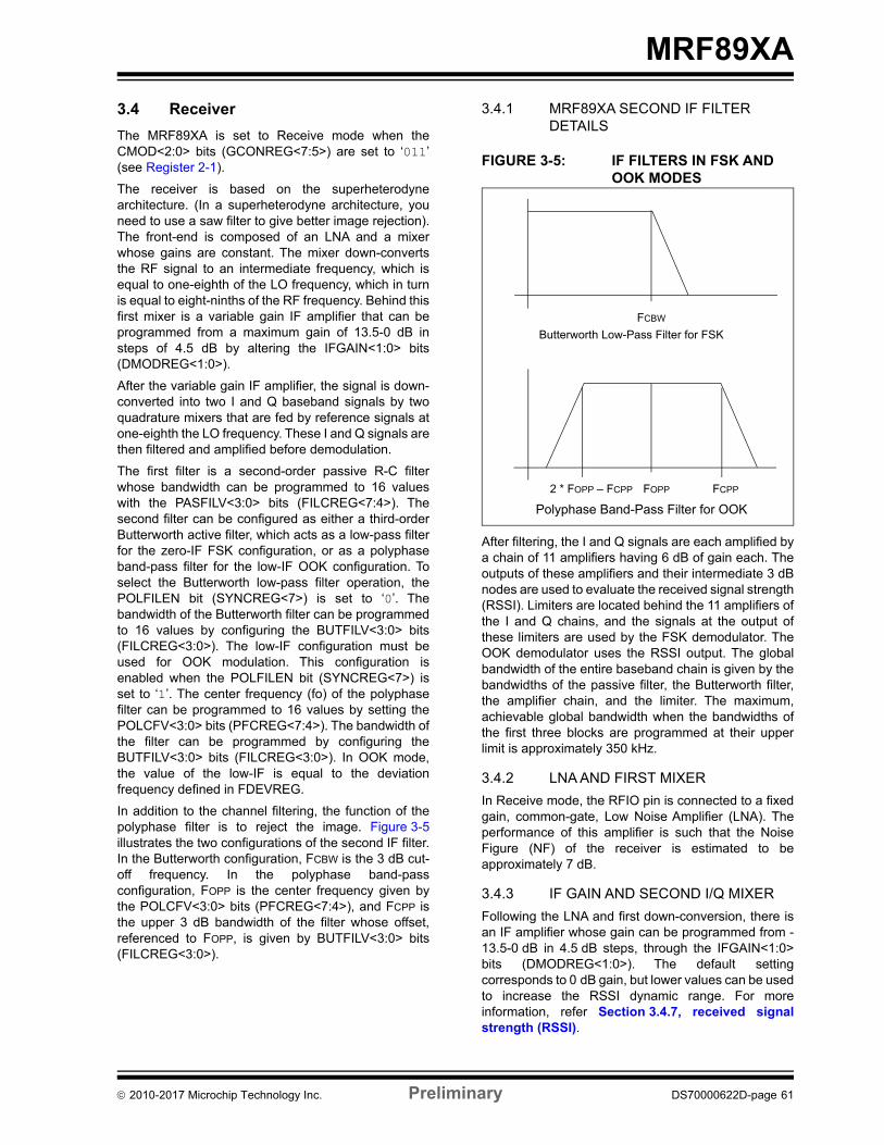
MRF89XA
3.4 Receiver
The MRF89XA is set to Receive mode when theCMOD<2:0> bits (GCONREG<7:5>) are set to ‘011’(see Register 2-1).
The receiver is based on the superheterodynearchitecture. (In a superheterodyne architecture, youneed to use a saw filter to give better image rejection).The front-end is composed of an LNA and a mixerwhose gains are constant. The mixer down-convertsthe RF signal to an intermediate frequency, which isequal to one-eighth of the LO frequency, which in turnis equal to eight-ninths of the RF frequency. Behind thisfirst mixer is a variable gain IF amplifier that can beprogrammed from a maximum gain of 13.5-0 dB insteps of 4.5 dB by altering the IFGAIN<1:0> bits(DMODREG<1:0>).
After the variable gain IF amplifier, the signal is down-converted into two I and Q baseband signals by twoquadrature mixers that are fed by reference signals atone-eighth the LO frequency. These I and Q signals arethen filtered and amplified before demodulation.
The first filter is a second-order passive R-C filterwhose bandwidth can be programmed to 16 valueswith the PASFILV<3:0> bits (FILCREG<7:4>). Thesecond filter can be configured as either a third-orderButterworth active filter, which acts as a low-pass filterfor the zero-IF FSK configuration, or as a polyphaseband-pass filter for the low-IF OOK configuration. Toselect the Butterworth low-pass filter operation, thePOLFILEN bit (SYNCREG<7>) is set to ‘0’. Thebandwidth of the Butterworth filter can be programmedto 16 values by configuring the BUTFILV<3:0> bits(FILCREG<3:0>). The low-IF configuration must beused for OOK modulation. This configuration isenabled when the POLFILEN bit (SYNCREG<7>) isset to ‘1’. The center frequency (fo) of the polyphasefilter can be programmed to 16 values by setting thePOLCFV<3:0> bits (PFCREG<7:4>). The bandwidth ofthe filter can be programmed by configuring theBUTFILV<3:0> bits (FILCREG<3:0>). In OOK mode,the value of the low-IF is equal to the deviationfrequency defined in FDEVREG.
In addition to the channel filtering, the function of thepolyphase filter is to reject the image. Figure 3-5illustrates the two configurations of the second IF filter.In the Butterworth configuration, FCBW is the 3 dB cut-off frequency. In the polyphase band-passconfiguration, FOPP is the center frequency given bythe POLCFV<3:0> bits (PFCREG<7:4>), and FCPP isthe upper 3 dB bandwidth of the filter whose offset,referenced to FOPP, is given by BUTFILV<3:0> bits(FILCREG<3:0>).
3.4.1 MRF89XA SECOND IF FILTER DETAILS
FIGURE 3-5: IF FILTERS IN FSK AND OOK MODES
After filtering, the I and Q signals are each amplified bya chain of 11 amplifiers having 6 dB of gain each. Theoutputs of these amplifiers and their intermediate 3 dBnodes are used to evaluate the received signal strength(RSSI). Limiters are located behind the 11 amplifiers ofthe I and Q chains, and the signals at the output ofthese limiters are used by the FSK demodulator. TheOOK demodulator uses the RSSI output. The globalbandwidth of the entire baseband chain is given by thebandwidths of the passive filter, the Butterworth filter,the amplifier chain, and the limiter. The maximum,achievable global bandwidth when the bandwidths ofthe first three blocks are programmed at their upperlimit is approximately 350 kHz.
3.4.2 LNA AND FIRST MIXER
In Receive mode, the RFIO pin is connected to a fixedgain, common-gate, Low Noise Amplifier (LNA). Theperformance of this amplifier is such that the NoiseFigure (NF) of the receiver is estimated to beapproximately 7 dB.
3.4.3 IF GAIN AND SECOND I/Q MIXER
Following the LNA and first down-conversion, there isan IF amplifier whose gain can be programmed from -13.5-0 dB in 4.5 dB steps, through the IFGAIN<1:0>bits (DMODREG<1:0>). The default settingcorresponds to 0 dB gain, but lower values can be usedto increase the RSSI dynamic range. For moreinformation, refer Section 3.4.7, received signalstrength (RSSI).
Butterworth Low-Pass Filter for FSK
Polyphase Band-Pass Filter for OOK
FCBW
FCPPFOPP2 * FOPP – FCPP
2010-2017 Microchip Technology Inc. Preliminary DS70000622D-page 61
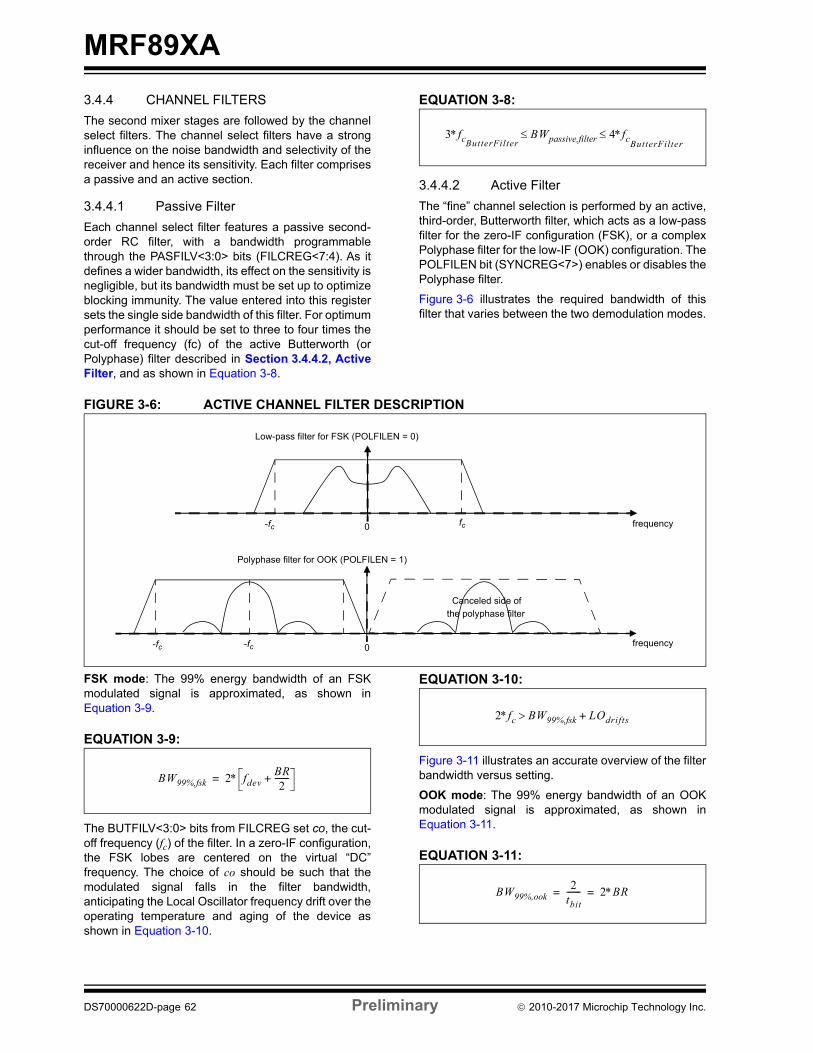
MRF89XA
3.4.4 CHANNEL FILTERS
The second mixer stages are followed by the channelselect filters. The channel select filters have a stronginfluence on the noise bandwidth and selectivity of thereceiver and hence its sensitivity. Each filter comprisesa passive and an active section.
3.4.4.1 Passive Filter
Each channel select filter features a passive second-order RC filter, with a bandwidth programmablethrough the PASFILV<3:0> bits (FILCREG<7:4). As itdefines a wider bandwidth, its effect on the sensitivity isnegligible, but its bandwidth must be set up to optimizeblocking immunity. The value entered into this registersets the single side bandwidth of this filter. For optimumperformance it should be set to three to four times thecut-off frequency (fc) of the active Butterworth (orPolyphase) filter described in Section 3.4.4.2, ActiveFilter, and as shown in Equation 3-8.
EQUATION 3-8:
3.4.4.2 Active Filter
The “fine” channel selection is performed by an active,third-order, Butterworth filter, which acts as a low-passfilter for the zero-IF configuration (FSK), or a complexPolyphase filter for the low-IF (OOK) configuration. ThePOLFILEN bit (SYNCREG<7>) enables or disables thePolyphase filter.
Figure 3-6 illustrates the required bandwidth of thisfilter that varies between the two demodulation modes.
FIGURE 3-6: ACTIVE CHANNEL FILTER DESCRIPTION
FSK mode: The 99% energy bandwidth of an FSKmodulated signal is approximated, as shown inEquation 3-9.
EQUATION 3-9:
The BUTFILV<3:0> bits from FILCREG set co, the cut-off frequency (fc) of the filter. In a zero-IF configuration,the FSK lobes are centered on the virtual “DC”frequency. The choice of co should be such that themodulated signal falls in the filter bandwidth,anticipating the Local Oscillator frequency drift over theoperating temperature and aging of the device asshown in Equation 3-10.
EQUATION 3-10:
Figure 3-11 illustrates an accurate overview of the filterbandwidth versus setting.
OOK mode: The 99% energy bandwidth of an OOKmodulated signal is approximated, as shown inEquation 3-11.
EQUATION 3-11:
3fcButterFilterBWpassive,filter 4fc
ButterFilter
Low-pass filter for FSK (POLFILEN = 0)
Polyphase filter for OOK (POLFILEN = 1)
-fc 0 frequency
frequency0
Canceled side of
the polyphase filter
fc
-fc-fc
BW99%,fsk 2 fdevBR2
-------+=
2fc BW99%,fsk LOdrifts+
BW99%,ook2tbit------- 2BR= =
DS70000622D-page 62 Preliminary 2010-2017 Microchip Technology Inc.

MRF89XA
The POLCFV<3:0> bits (PFCREG<7:4>) set fo, whichis the center frequency of the polyphase filter whenactivated. The fo should always be chosen to be equalto the low Intermediate Frequency of the receiver (IF2).Because low IF frequency of the OOK receiver denotedby IF2 can always be replaced by fo for any calculationsor monitoring purposes.
The following setting is recommended:
fo = 100 kHz
POLCFV<3:0> = 0011.
The value stored as BUTFILV<3:0> bits(FILCREG<3:0>) determines fc, the filter cut-offfrequency. Therefore, fc should be set according toEquation 3-12.
EQUATION 3-12:
Again, fc, as a function of the BUTFILV<3:0> bits, isdescribed in Section 3.4.6, Channel Filters Setting inOOK Mode.
3.4.5 CHANNEL FILTERS SETTING IN FSK MODE
The fc, the 3 dB cut-off frequency of the Butterworth fil-ter used in FSK reception, is programmed through theBUTFILV<3:0> bits (FILCREG<3:0>). However, theentire receiver chain influences this cut-off frequency.The channel select and resultant filter bandwidths areillustrated in Figure 3-7.
Table 4-2 suggests filter settings in FSK mode alongwith the corresponding passive filter bandwidth and theaccepted tolerance on the crystal reference.
FIGURE 3-7: ACTUAL BW OF BUTTERWORTH FILTER
2 fc fo– BW99%,ook LOdrifts+
Where,
fc is the cut-off frequency fo is the center frequency
Butterworth Filter BW, FSK
0
50
100
150
200
250
300
350
400
450
0 6 8 10 12 14
Val BUTFILV<3:0> [d]
FC
(3d
B C
ut-
off
) [k
Hz]
16
ActualBW
TheoreticalBW
2 4
2010-2017 Microchip Technology Inc. Preliminary DS70000622D-page 63
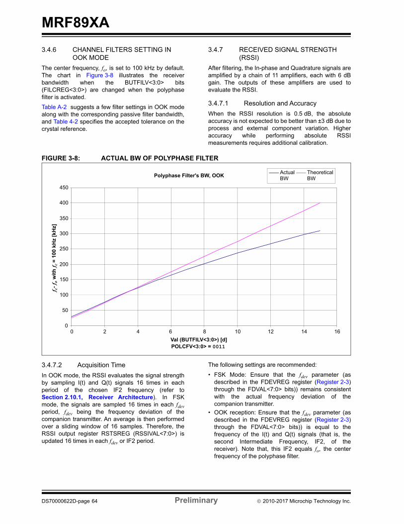
MRF89XA
3.4.6 CHANNEL FILTERS SETTING IN OOK MODE
The center frequency, fo, is set to 100 kHz by default.The chart in Figure 3-8 illustrates the receiverbandwidth when the BUTFILV<3:0> bits(FILCREG<3:0>) are changed when the polyphasefilter is activated.
Table A-2 suggests a few filter settings in OOK modealong with the corresponding passive filter bandwidth,and Table 4-2 specifies the accepted tolerance on thecrystal reference.
3.4.7 RECEIVED SIGNAL STRENGTH (RSSI)
After filtering, the In-phase and Quadrature signals areamplified by a chain of 11 amplifiers, each with 6 dBgain. The outputs of these amplifiers are used toevaluate the RSSI.
3.4.7.1 Resolution and Accuracy
When the RSSI resolution is 0.5 dB, the absoluteaccuracy is not expected to be better than ±3 dB due toprocess and external component variation. Higheraccuracy while performing absolute RSSImeasurements requires additional calibration.
FIGURE 3-8: ACTUAL BW OF POLYPHASE FILTER
3.4.7.2 Acquisition Time
In OOK mode, the RSSI evaluates the signal strengthby sampling I(t) and Q(t) signals 16 times in eachperiod of the chosen IF2 frequency (refer toSection 2.10.1, Receiver Architecture). In FSKmode, the signals are sampled 16 times in each fdevperiod, fdev being the frequency deviation of thecompanion transmitter. An average is then performedover a sliding window of 16 samples. Therefore, theRSSI output register RSTSREG (RSSIVAL<7:0>) isupdated 16 times in each fdev or IF2 period.
The following settings are recommended:
• FSK Mode: Ensure that the fdev parameter (asdescribed in the FDEVREG register (Register 2-3)through the FDVAL<7:0> bits)) remains consistentwith the actual frequency deviation of thecompanion transmitter.
• OOK reception: Ensure that the fdev parameter (asdescribed in the FDEVREG register (Register 2-3)through the FDVAL<7:0> bits)) is equal to thefrequency of the I(t) and Q(t) signals (that is, thesecond Intermediate Frequency, IF2, of thereceiver). Note that, this IF2 equals fo, the centerfrequency of the polyphase filter.
Polyphase Filter's BW, OOK
0
50
100
150
200
250
300
350
400
450
0 4 8 10 12 14
Val (BUTFILV<3:0>) [d]POLCFV<3:0> = 0011
f c-
f o w
ith
fc
= 1
00 k
Hz
[kH
z]
16
ActualBW
TheoreticalBW
2 6
DS70000622D-page 64 Preliminary 2010-2017 Microchip Technology Inc.
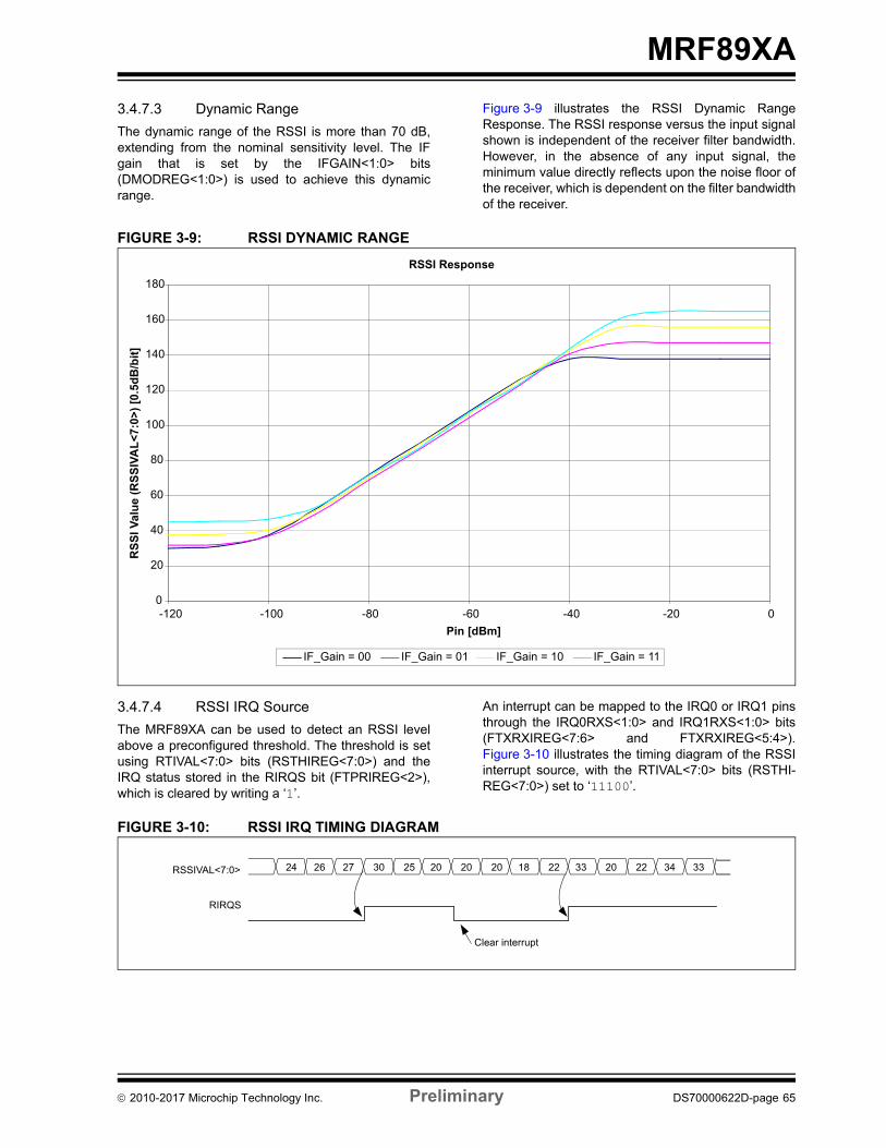
MRF89XA
3.4.7.3 Dynamic Range
The dynamic range of the RSSI is more than 70 dB,extending from the nominal sensitivity level. The IFgain that is set by the IFGAIN<1:0> bits(DMODREG<1:0>) is used to achieve this dynamicrange.
Figure 3-9 illustrates the RSSI Dynamic RangeResponse. The RSSI response versus the input signalshown is independent of the receiver filter bandwidth.However, in the absence of any input signal, theminimum value directly reflects upon the noise floor ofthe receiver, which is dependent on the filter bandwidthof the receiver.
FIGURE 3-9: RSSI DYNAMIC RANGE
3.4.7.4 RSSI IRQ Source
The MRF89XA can be used to detect an RSSI levelabove a preconfigured threshold. The threshold is setusing RTIVAL<7:0> bits (RSTHIREG<7:0>) and theIRQ status stored in the RIRQS bit (FTPRIREG<2>),which is cleared by writing a ‘1’.
An interrupt can be mapped to the IRQ0 or IRQ1 pinsthrough the IRQ0RXS<1:0> and IRQ1RXS<1:0> bits(FTXRXIREG<7:6> and FTXRXIREG<5:4>).Figure 3-10 illustrates the timing diagram of the RSSIinterrupt source, with the RTIVAL<7:0> bits (RSTHI-REG<7:0>) set to ‘11100’.
FIGURE 3-10: RSSI IRQ TIMING DIAGRAM
RSSI Response
0
20
40
60
80
100
120
140
160
180
-120 -100 -80 -60 -40 -20 0
Pin [dBm]
RS
SI
Val
ue
(RS
SIV
AL
<7:
0>)
[0.5
dB
/bit
]
IF_Gain = 00 IF_Gain = 01 IF_Gain = 10 IF_Gain = 11
RIRQS
Clear interrupt
24 26 27 30 25 20 20 20 18 22 20 22 34 33 33 RSSIVAL<7:0>
2010-2017 Microchip Technology Inc. Preliminary DS70000622D-page 65
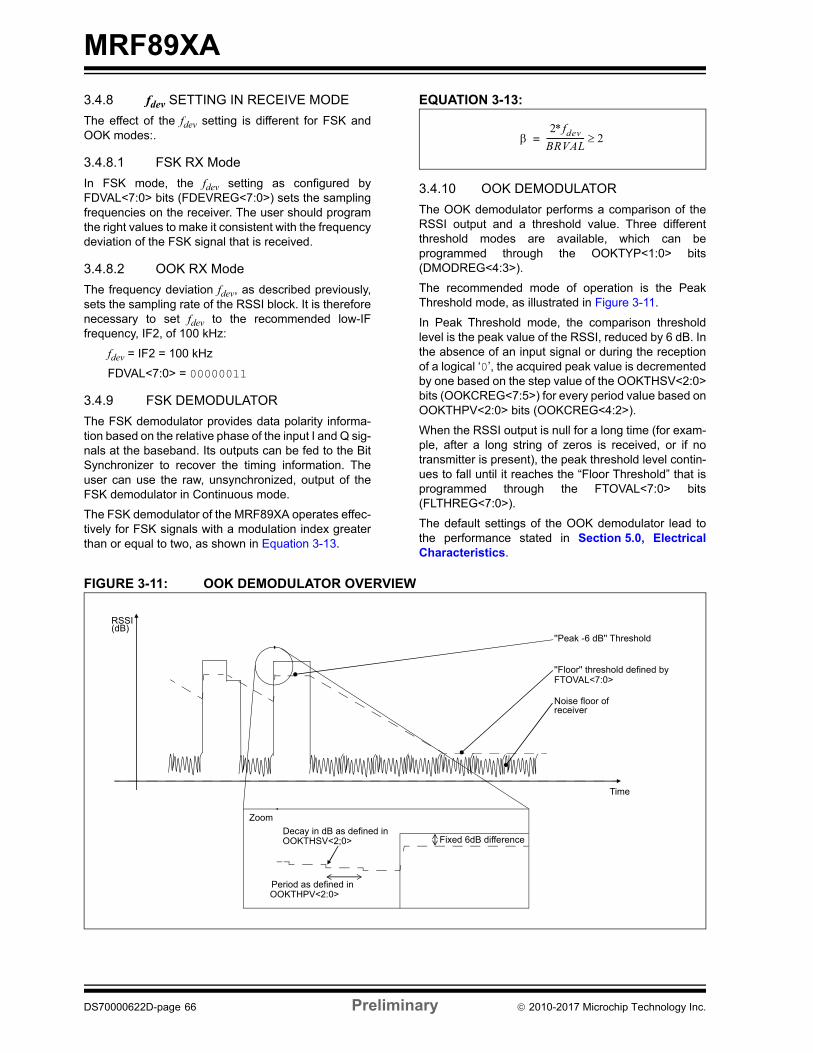
MRF89XA
3.4.8 fdev SETTING IN RECEIVE MODE
The effect of the fdev setting is different for FSK andOOK modes:.
3.4.8.1 FSK RX Mode
In FSK mode, the fdev setting as configured byFDVAL<7:0> bits (FDEVREG<7:0>) sets the samplingfrequencies on the receiver. The user should programthe right values to make it consistent with the frequencydeviation of the FSK signal that is received.
3.4.8.2 OOK RX Mode
The frequency deviation fdev, as described previously,sets the sampling rate of the RSSI block. It is thereforenecessary to set fdev to the recommended low-IFfrequency, IF2, of 100 kHz:
fdev = IF2 = 100 kHz
FDVAL<7:0> = 00000011
3.4.9 FSK DEMODULATOR
The FSK demodulator provides data polarity informa-tion based on the relative phase of the input I and Q sig-nals at the baseband. Its outputs can be fed to the BitSynchronizer to recover the timing information. Theuser can use the raw, unsynchronized, output of theFSK demodulator in Continuous mode.
The FSK demodulator of the MRF89XA operates effec-tively for FSK signals with a modulation index greaterthan or equal to two, as shown in Equation 3-13.
EQUATION 3-13:
3.4.10 OOK DEMODULATOR
The OOK demodulator performs a comparison of theRSSI output and a threshold value. Three differentthreshold modes are available, which can beprogrammed through the OOKTYP<1:0> bits(DMODREG<4:3>).
The recommended mode of operation is the PeakThreshold mode, as illustrated in Figure 3-11.
In Peak Threshold mode, the comparison thresholdlevel is the peak value of the RSSI, reduced by 6 dB. Inthe absence of an input signal or during the receptionof a logical ‘0’, the acquired peak value is decrementedby one based on the step value of the OOKTHSV<2:0>bits (OOKCREG<7:5>) for every period value based onOOKTHPV<2:0> bits (OOKCREG<4:2>).
When the RSSI output is null for a long time (for exam-ple, after a long string of zeros is received, or if notransmitter is present), the peak threshold level contin-ues to fall until it reaches the “Floor Threshold” that isprogrammed through the FTOVAL<7:0> bits(FLTHREG<7:0>).
The default settings of the OOK demodulator lead tothe performance stated in Section 5.0, ElectricalCharacteristics.
FIGURE 3-11: OOK DEMODULATOR OVERVIEW
2fdevBRVAL------------------- 2=
Period as defined in OOKTHPV<2:0>
Decay in dB as defined in OOKTHSV<2;0> Fixed 6dB difference
RSSI (dB)
Noise floor of receiver
''Floor'' threshold defined by FTOVAL<7:0>
Time
''Peak -6 dB'' Threshold
Zoom
DS70000622D-page 66 Preliminary 2010-2017 Microchip Technology Inc.
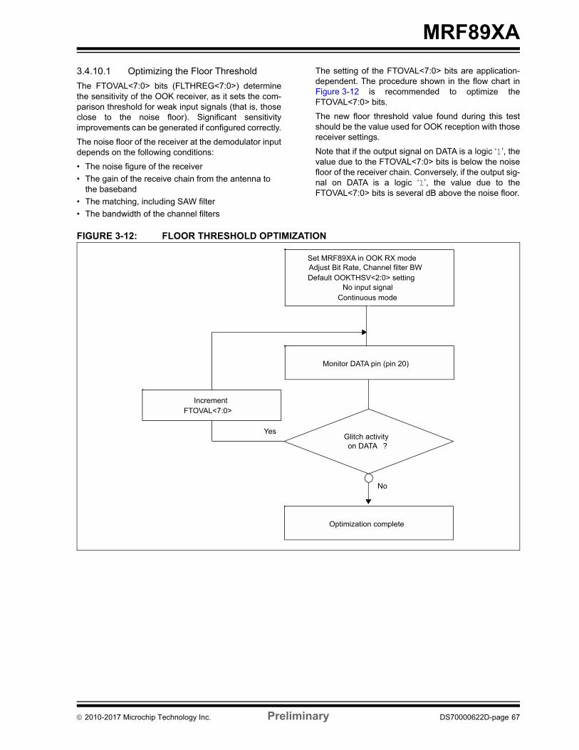
MRF89XA
3.4.10.1 Optimizing the Floor Threshold
The FTOVAL<7:0> bits (FLTHREG<7:0>) determinethe sensitivity of the OOK receiver, as it sets the com-parison threshold for weak input signals (that is, thoseclose to the noise floor). Significant sensitivityimprovements can be generated if configured correctly.
The noise floor of the receiver at the demodulator inputdepends on the following conditions:
• The noise figure of the receiver
• The gain of the receive chain from the antenna to the baseband
• The matching, including SAW filter
• The bandwidth of the channel filters
The setting of the FTOVAL<7:0> bits are application-dependent. The procedure shown in the flow chart inFigure 3-12 is recommended to optimize theFTOVAL<7:0> bits.
The new floor threshold value found during this testshould be the value used for OOK reception with thosereceiver settings.
Note that if the output signal on DATA is a logic ‘1’, thevalue due to the FTOVAL<7:0> bits is below the noisefloor of the receiver chain. Conversely, if the output sig-nal on DATA is a logic ‘1’, the value due to theFTOVAL<7:0> bits is several dB above the noise floor.
FIGURE 3-12: FLOOR THRESHOLD OPTIMIZATION
Set MRF89XA in OOK RX mode Adjust Bit Rate, Channel filter BW Default OOKTHSV<2:0> setting
No input signal Continuous mode
Optimization complete
Glitch activity on DATA ?
Monitor DATA pin (pin 20)
Increment FTOVAL<7:0>
Yes
No
2010-2017 Microchip Technology Inc. Preliminary DS70000622D-page 67
MRF89XA
3.4.10.2 Optimizing OOK Demodulator Response for Fast Fading Signals
A sudden drop in signal strength can cause the bit errorrate to increase. For applications where the expectedsignal drop can be estimated, the OOK demodulatorparameters set by the OOKTHSV<2:0> and OOK-THPV<2:0> bits (OOKCREG<7:5> and OOK-CREG<4:2>) can be optimized.
For a given number of threshold decrements per bit,specified by OOKTHPV<2:0>:
• 000 once in each chip period (default)
• 001 once in 2 chip periods
• 010 once in 4 chip periods
• 011 once in 8 chip periods
• 100 twice in each chip period
• 101 4 times in each chip period
• 110 8 times in each chip period
• 111 16 times in each chip period
For each decrement of value from OOKTHSV<2:0>bits:
• 000 0.5 dB (default)
• 001 1.0 dB
• 010 1.5 dB
• 011 2.0 dB
• 100 3.0 dB
• 101 4.0 dB
• 110 5.0 dB
• 111 6.0 dB
3.4.10.3 Alternative OOK Demodulator Threshold Modes
In addition to the Peak OOK threshold mode, the usercan alternatively select two other threshold detectors:
• Fixed threshold: The value is selected through the OOKCREG register (for more information, refer to Section 3.4.10.1, Optimizing the Floor Thresh-old).
• Average threshold: Data supplied by the RSSI block is averaged with the cut-off frequency.
In Equation 3-14, the higher cut-off frequency enablesa sequence of up to eight consecutive ‘0’s or ‘1’s to besupported, while the lower cut-off frequency presentedin Equation 3-15 allows for the correct reception of upto 32 consecutive ‘0’s or ‘1’s.
EQUATION 3-14:
EQUATION 3-15:
OOKATHC<1:0> 00 fcutoffBRVAL<6:0>
8----------------------------------==
OOKATHC<1:0> 11 fcutoffBRVAL<6:0>
32----------------------------------==
DS70000622D-page 68 Preliminary 2010-2017 Microchip Technology Inc.
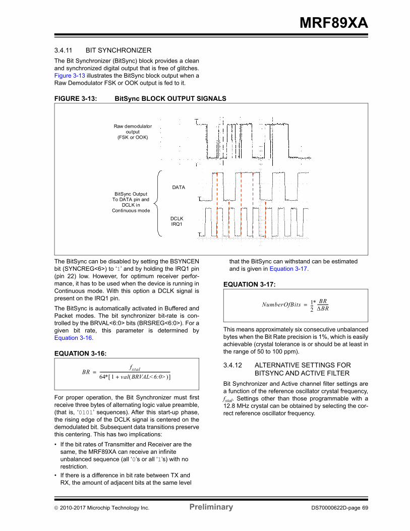
MRF89XA
3.4.11 BIT SYNCHRONIZER
The Bit Synchronizer (BitSync) block provides a cleanand synchronized digital output that is free of glitches.Figure 3-13 illustrates the BitSync block output when aRaw Demodulator FSK or OOK output is fed to it.
FIGURE 3-13: BitSync BLOCK OUTPUT SIGNALS
The BitSync can be disabled by setting the BSYNCENbit (SYNCREG<6>) to ‘1’ and by holding the IRQ1 pin(pin 22) low. However, for optimum receiver perfor-mance, it has to be used when the device is running inContinuous mode. With this option a DCLK signal ispresent on the IRQ1 pin.
The BitSync is automatically activated in Buffered andPacket modes. The bit synchronizer bit-rate is con-trolled by the BRVAL<6:0> bits (BRSREG<6:0>). For agiven bit rate, this parameter is determined byEquation 3-16.
EQUATION 3-16:
For proper operation, the Bit Synchronizer must firstreceive three bytes of alternating logic value preamble,(that is, ‘0101’ sequences). After this start-up phase,the rising edge of the DCLK signal is centered on thedemodulated bit. Subsequent data transitions preservethis centering. This has two implications:
• If the bit rates of Transmitter and Receiver are the same, the MRF89XA can receive an infinite unbalanced sequence (all ‘0’s or all ‘1’s) with no restriction.
• If there is a difference in bit rate between TX and RX, the amount of adjacent bits at the same level
that the BitSync can withstand can be estimated and is given in Equation 3-17.
EQUATION 3-17:
This means approximately six consecutive unbalancedbytes when the Bit Rate precision is 1%, which is easilyachievable (crystal tolerance is or should be at least inthe range of 50 to 100 ppm).
3.4.12 ALTERNATIVE SETTINGS FOR BITSYNC AND ACTIVE FILTER
Bit Synchronizer and Active channel filter settings area function of the reference oscillator crystal frequency,fxtal. Settings other than those programmable with a12.8 MHz crystal can be obtained by selecting the cor-rect reference oscillator frequency.
Raw demodulator
output (FSK or OOK)
DCLK IRQ1
DATA BitSync Output
To DATA pin and DCLK in
Continuous mode
BRfxtal
64 1 val BRVAL<6:0> + ----------------------------------------------------------------------=
NumberOfBits 12--- BRBR-----------=
2010-2017 Microchip Technology Inc. Preliminary DS70000622D-page 69
MRF89XA
3.4.13 DATA OUTPUT
After OOK or FSK demodulation, the baseband signalis made available to the user on the DATA pin (pin 20),when Continuous mode is selected. In Buffered andPacket modes, the data is retrieved from the FIFOthrough the SPI.
During Receive mode, the received data is filled intothe Shift register and then transferred onto the FIFOstack. The FIFO is configured to generate an interruptafter receiving a defined number of bits.
When the internal FIFO is enabled, the FIFO interrupt,which is configured through the IRQ0 and IRQ1 pins(pin 21 and 22), acts as a FIFOFULL interrupt,indicating that the FIFO has been filled to itspreprogrammed limit. The receiver starts filling theFIFO with data when it identifies the synchronouspattern through the synchronous pattern recognitioncircuit. It is recommended to set the threshold to atleast half the length of the register (8 bits) to ensure thatthe external host microcontroller has time to set up.The synchronous pattern recognition circuit preventsthe FIFO from being filled up with noise, and thereforeavoids overloading the external host microcontroller.
3.4.14 RECEIVE MODE REGISTERS
The registers associated with Receive mode are:
• GCONREG (Register 2-1)
• DMODREG (Register 2-2)
• FDEVREG (Register 2-3)
• BRSREG (Register 2-4)
• FLTHREG (Register 2-5)
• FIFOCREG (Register 2-6)
• FTXRXIREG (Register 2-14)
• FTPRIREG (Register 2-15)
• RSTHIREG (Register 2-16)
• FILCREG (Register 2-17)
• PFCREG (Register 2-18)
• SYNCREG (Register 2-19)
• RSTSREG (Register 2-21)
• OOKCREG (Register 2-22)
• SYNCV31REG (Register 2-23)
• SYNCV23REG (Register 2-24)
• SYNCV15REG (Register 2-25)
• SYNCV07REG (Register 2-26)
3.5 Control Block Description
3.5.1 SPI INTERFACE
For more information on standard SPI between theMRF89XA and a microcontroller, refer to Section 2.11,Serial Peripheral Interface (SPI).
3.5.2 SPI REGISTERS
The registers associated with SPI communication are:
• GCONREG (Register 2-1)
• DMODREG (Register 2-2)
• FDEVREG (Register 2-3)
• BRSREG (Register 2-4)
3.6 FIFO Handling
The hardware description of the FIFO is described inSection 2.12, FIFO and Shift Register (SR). TheFIFO is handled by selecting the size of the FIFO, FIFOinterrupts, and clearing the FIFO.
3.6.1 SIZE SELECTION
The FIFO width is programmable to 16, 32, 48, or 64bytes using the FSIZE<1:0> bits (FIFOCREG<7:6>).
3.6.2 INTERRUPT SOURCES AND FLAGS
The MRF89XA generates an interrupt request for thehost microcontroller by pulling the IRQ0 or IRQ1 pinslow or high based on the events and configuration set-tings of these interrupts. All interrupt sources and flagsare configured through the Interrupt Configuration reg-isters, based on the occurrence of the following events:
• Interrupt Requests (IRQ0 and IRQ1) during differ-ent receive standby data modes (such as Contin-uous, Buffered, and Packet) for the following event occurrences: SYNC, RSSI, PLREADY, ARDSMATCH, and FIFOEMPTY.
For example, Write Byte. The WRITEBYTE inter-rupt source goes high for one bit period each timea new byte is transferred from the shift register tothe FIFO (that is, each time a new byte isreceived).
• Interrupt Requests (IRQ0 and IRQ1) during trans-mit modes (such as Continuous, Buffered, and Packet) for the following event occurrences: Data Clock, FIFOFULL, Transmit Done, Transmit Start with IRQ0 and IRQ1.
For example, TX Done. The TXDONE interruptsource goes high when the FIFO is empty and theShift register’s last bit has been sent to the modu-lator (that is, the last bit of the packet has beensent). One bit period delay is required after the ris-ing edge of TXDONE to ensure correct RF trans-mission of the last bit. In practice, this may notrequire special care in the MCU software due toIRQ processing time.
DS70000622D-page 70 Preliminary 2010-2017 Microchip Technology Inc.
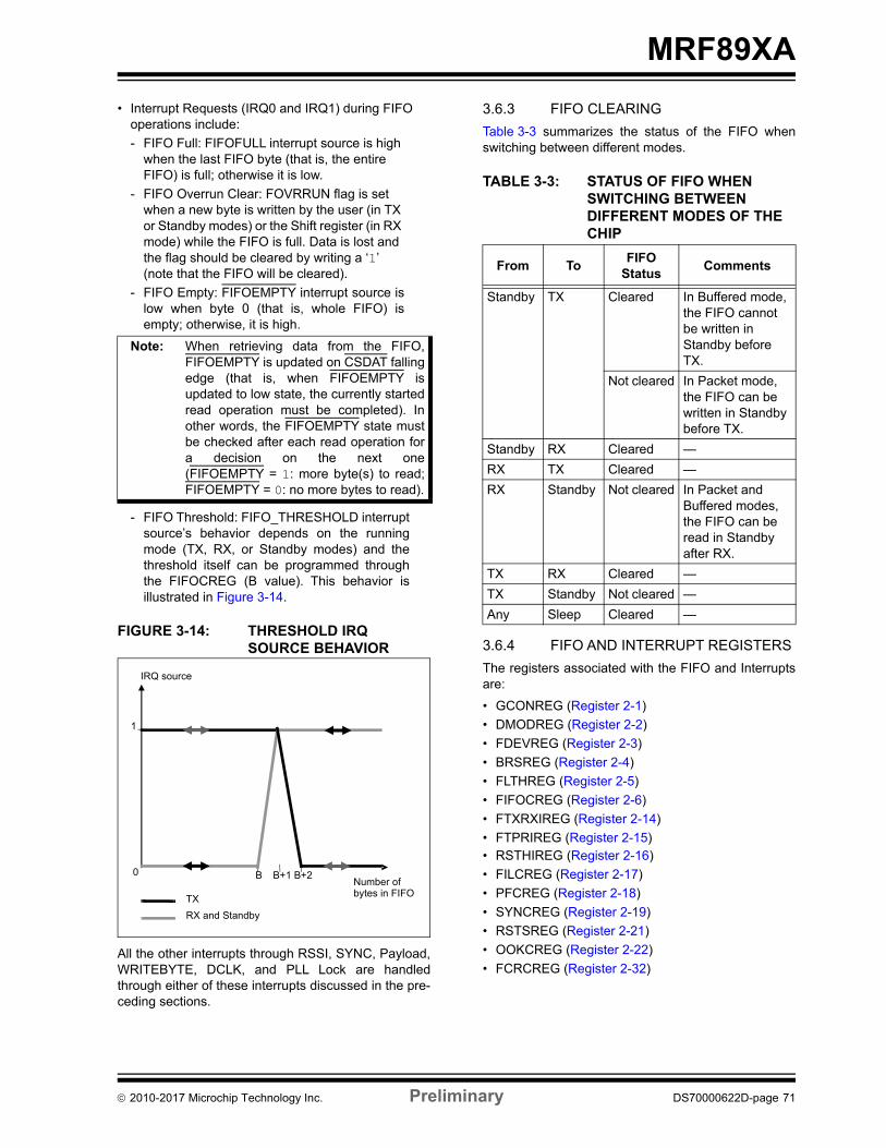
MRF89XA
• Interrupt Requests (IRQ0 and IRQ1) during FIFO operations include:
- FIFO Full: FIFOFULL interrupt source is high when the last FIFO byte (that is, the entire FIFO) is full; otherwise it is low.
- FIFO Overrun Clear: FOVRRUN flag is set when a new byte is written by the user (in TX or Standby modes) or the Shift register (in RX mode) while the FIFO is full. Data is lost and the flag should be cleared by writing a ‘1’ (note that the FIFO will be cleared).
- FIFO Empty: FIFOEMPTY interrupt source islow when byte 0 (that is, whole FIFO) isempty; otherwise, it is high.
- FIFO Threshold: FIFO_THRESHOLD interruptsource’s behavior depends on the runningmode (TX, RX, or Standby modes) and thethreshold itself can be programmed throughthe FIFOCREG (B value). This behavior isillustrated in Figure 3-14.
FIGURE 3-14: THRESHOLD IRQ SOURCE BEHAVIOR
All the other interrupts through RSSI, SYNC, Payload,WRITEBYTE, DCLK, and PLL Lock are handledthrough either of these interrupts discussed in the pre-ceding sections.
3.6.3 FIFO CLEARING
Table 3-3 summarizes the status of the FIFO whenswitching between different modes.
TABLE 3-3: STATUS OF FIFO WHEN SWITCHING BETWEEN DIFFERENT MODES OF THE CHIP
3.6.4 FIFO AND INTERRUPT REGISTERS
The registers associated with the FIFO and Interruptsare:
• GCONREG (Register 2-1)
• DMODREG (Register 2-2)
• FDEVREG (Register 2-3)
• BRSREG (Register 2-4)
• FLTHREG (Register 2-5)
• FIFOCREG (Register 2-6)
• FTXRXIREG (Register 2-14)
• FTPRIREG (Register 2-15)• RSTHIREG (Register 2-16)
• FILCREG (Register 2-17)
• PFCREG (Register 2-18)
• SYNCREG (Register 2-19)
• RSTSREG (Register 2-21)
• OOKCREG (Register 2-22)
• FCRCREG (Register 2-32)
Note: When retrieving data from the FIFO,FIFOEMPTY is updated on CSDAT fallingedge (that is, when FIFOEMPTY isupdated to low state, the currently startedread operation must be completed). Inother words, the FIFOEMPTY state mustbe checked after each read operation fora decision on the next one(FIFOEMPTY = 1: more byte(s) to read;FIFOEMPTY = 0: no more bytes to read).
Number of
IRQ source
0
1
B B+1 B+2
TX
RX and Standby
bytes in FIFO
From ToFIFO
StatusComments
Standby TX Cleared In Buffered mode, the FIFO cannot be written in Standby before TX.
Not cleared In Packet mode, the FIFO can be written in Standby before TX.
Standby RX Cleared —
RX TX Cleared —
RX Standby Not cleared In Packet and Buffered modes, the FIFO can be read in Standby after RX.
TX RX Cleared —
TX Standby Not cleared —
Any Sleep Cleared —
2010-2017 Microchip Technology Inc. Preliminary DS70000622D-page 71
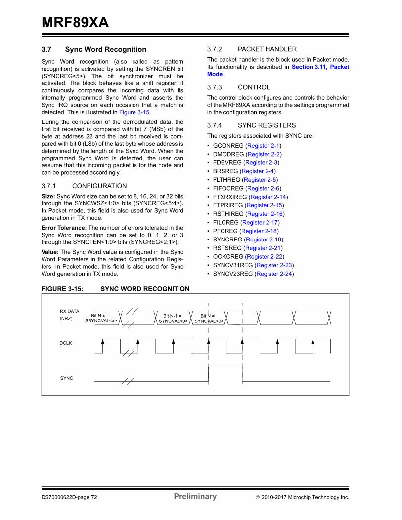
MRF89XA
3.7 Sync Word Recognition
Sync Word recognition (also called as patternrecognition) is activated by setting the SYNCREN bit(SYNCREG<5>). The bit synchronizer must beactivated. The block behaves like a shift register; itcontinuously compares the incoming data with itsinternally programmed Sync Word and asserts theSync IRQ source on each occasion that a match isdetected. This is illustrated in Figure 3-15.
During the comparison of the demodulated data, thefirst bit received is compared with bit 7 (MSb) of thebyte at address 22 and the last bit received is com-pared with bit 0 (LSb) of the last byte whose address isdetermined by the length of the Sync Word. When theprogrammed Sync Word is detected, the user canassume that this incoming packet is for the node andcan be processed accordingly.
3.7.1 CONFIGURATION
Size: Sync Word size can be set to 8, 16, 24, or 32 bitsthrough the SYNCWSZ<1:0> bits (SYNCREG<5:4>).In Packet mode, this field is also used for Sync Wordgeneration in TX mode.
Error Tolerance: The number of errors tolerated in theSync Word recognition can be set to 0, 1, 2, or 3through the SYNCTEN<1:0> bits (SYNCREG<2:1>).
Value: The Sync Word value is configured in the SyncWord Parameters in the related Configuration Regis-ters. In Packet mode, this field is also used for SyncWord generation in TX mode.
3.7.2 PACKET HANDLER
The packet handler is the block used in Packet mode.Its functionality is described in Section 3.11, PacketMode.
3.7.3 CONTROL
The control block configures and controls the behaviorof the MRF89XA according to the settings programmedin the configuration registers.
3.7.4 SYNC REGISTERS
The registers associated with SYNC are:
• GCONREG (Register 2-1)
• DMODREG (Register 2-2)
• FDEVREG (Register 2-3)
• BRSREG (Register 2-4)
• FLTHREG (Register 2-5)
• FIFOCREG (Register 2-6)
• FTXRXIREG (Register 2-14)
• FTPRIREG (Register 2-15)
• RSTHIREG (Register 2-16)
• FILCREG (Register 2-17)
• PFCREG (Register 2-18)
• SYNCREG (Register 2-19)
• RSTSREG (Register 2-21)
• OOKCREG (Register 2-22)
• SYNCV31REG (Register 2-23)
• SYNCV23REG (Register 2-24)
FIGURE 3-15: SYNC WORD RECOGNITION
RX DATA
(NRZ)
DCLK
Bit N-x = SSYNCVAL<x>
Bit N-1 =SYNCVAL<0>
SYNC
SYNCVAL<0>Bit N =
DS70000622D-page 72 Preliminary 2010-2017 Microchip Technology Inc.
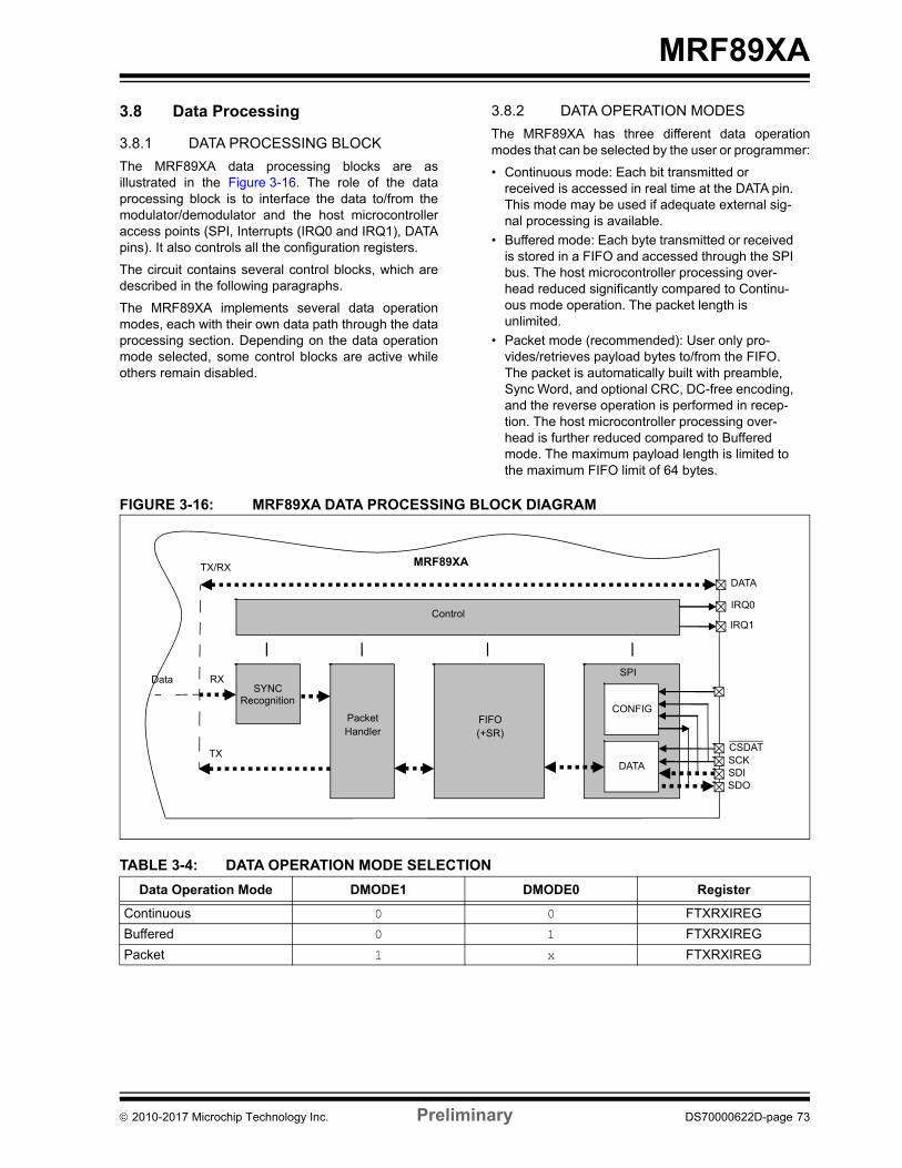
MRF89XA
3.8 Data Processing
3.8.1 DATA PROCESSING BLOCK
The MRF89XA data processing blocks are asillustrated in the Figure 3-16. The role of the dataprocessing block is to interface the data to/from themodulator/demodulator and the host microcontrolleraccess points (SPI, Interrupts (IRQ0 and IRQ1), DATApins). It also controls all the configuration registers.
The circuit contains several control blocks, which aredescribed in the following paragraphs.
The MRF89XA implements several data operationmodes, each with their own data path through the dataprocessing section. Depending on the data operationmode selected, some control blocks are active whileothers remain disabled.
3.8.2 DATA OPERATION MODES
The MRF89XA has three different data operationmodes that can be selected by the user or programmer:
• Continuous mode: Each bit transmitted or received is accessed in real time at the DATA pin. This mode may be used if adequate external sig-nal processing is available.
• Buffered mode: Each byte transmitted or received is stored in a FIFO and accessed through the SPI bus. The host microcontroller processing over-head reduced significantly compared to Continu-ous mode operation. The packet length is unlimited.
• Packet mode (recommended): User only pro-vides/retrieves payload bytes to/from the FIFO. The packet is automatically built with preamble, Sync Word, and optional CRC, DC-free encoding, and the reverse operation is performed in recep-tion. The host microcontroller processing over-head is further reduced compared to Buffered mode. The maximum payload length is limited to the maximum FIFO limit of 64 bytes.
FIGURE 3-16: MRF89XA DATA PROCESSING BLOCK DIAGRAM
TABLE 3-4: DATA OPERATION MODE SELECTION
Data Operation Mode DMODE1 DMODE0 Register
Continuous 0 0 FTXRXIREG
Buffered 0 1 FTXRXIREG
Packet 1 x FTXRXIREG
Control
DATA
CONFIG
SPI
Packet Handler
SYNC Recognition
DATA
IRQ0
IRQ1
SDO SDI SCK CSDAT
RX
TX
TX/RX
Data
MRF89XA
FIFO (+SR)
2010-2017 Microchip Technology Inc. Preliminary DS70000622D-page 73
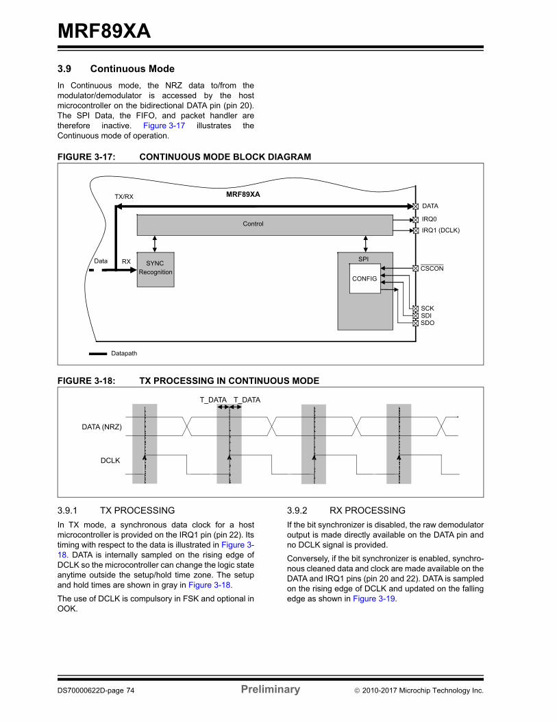
MRF89XA
3.9 Continuous Mode
In Continuous mode, the NRZ data to/from themodulator/demodulator is accessed by the hostmicrocontroller on the bidirectional DATA pin (pin 20).The SPI Data, the FIFO, and packet handler aretherefore inactive. Figure 3-17 illustrates theContinuous mode of operation.
FIGURE 3-17: CONTINUOUS MODE BLOCK DIAGRAM
FIGURE 3-18: TX PROCESSING IN CONTINUOUS MODE
3.9.1 TX PROCESSING
In TX mode, a synchronous data clock for a hostmicrocontroller is provided on the IRQ1 pin (pin 22). Itstiming with respect to the data is illustrated in Figure 3-18. DATA is internally sampled on the rising edge ofDCLK so the microcontroller can change the logic stateanytime outside the setup/hold time zone. The setupand hold times are shown in gray in Figure 3-18.
The use of DCLK is compulsory in FSK and optional inOOK.
3.9.2 RX PROCESSING
If the bit synchronizer is disabled, the raw demodulatoroutput is made directly available on the DATA pin andno DCLK signal is provided.
Conversely, if the bit synchronizer is enabled, synchro-nous cleaned data and clock are made available on theDATA and IRQ1 pins (pin 20 and 22). DATA is sampledon the rising edge of DCLK and updated on the fallingedge as shown in Figure 3-19.
Control
CONFIG
SPI SYNC
Recognition
DATA
IRQ1 (DCLK)
SDO SDI SCK
CSCON RX
TX/RX
IRQ0
Datapath
MRF89XA
Data
DATA (NRZ)
DCLK
T_DATAT_DATA
DS70000622D-page 74 Preliminary 2010-2017 Microchip Technology Inc.
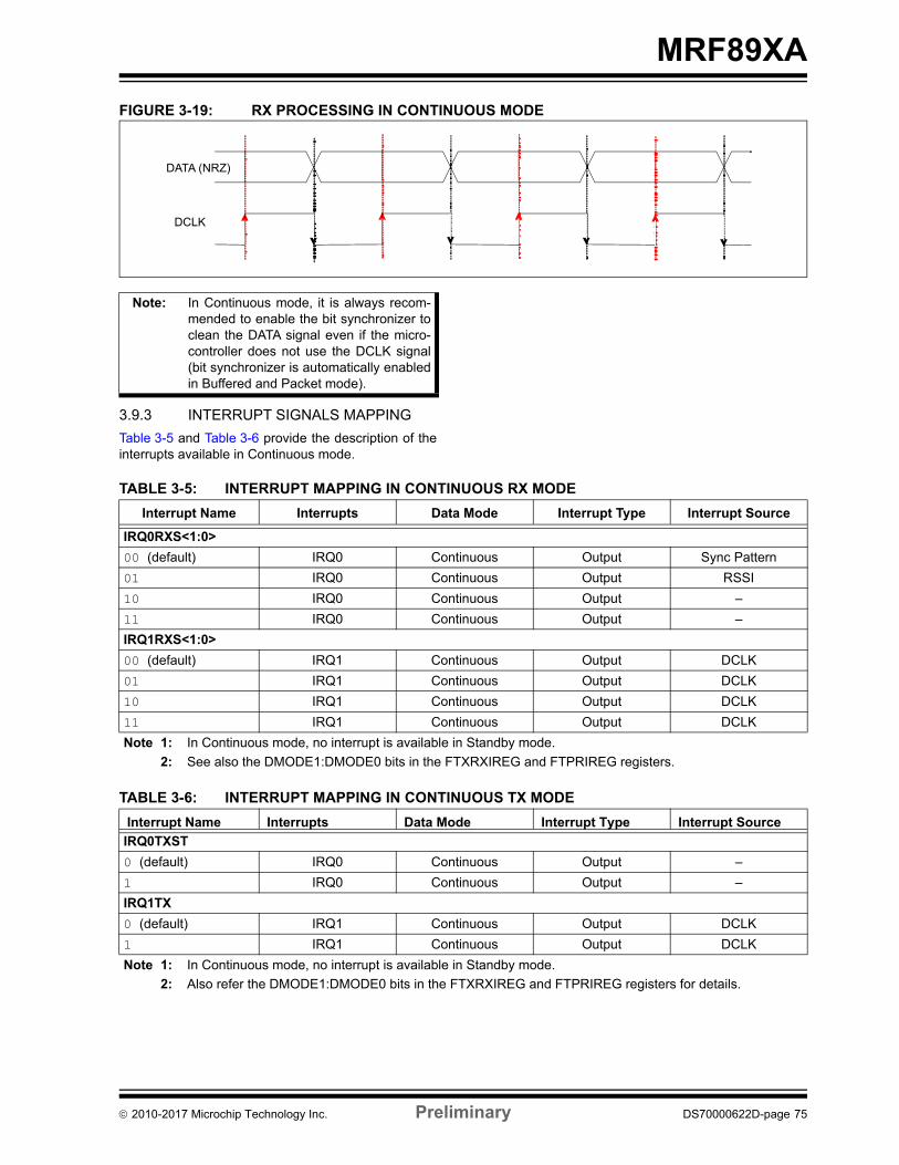
MRF89XA
FIGURE 3-19: RX PROCESSING IN CONTINUOUS MODE
3.9.3 INTERRUPT SIGNALS MAPPING
Table 3-5 and Table 3-6 provide the description of theinterrupts available in Continuous mode.
TABLE 3-5: INTERRUPT MAPPING IN CONTINUOUS RX MODE
TABLE 3-6: INTERRUPT MAPPING IN CONTINUOUS TX MODE
DATA (NRZ)
DCLK
Note: In Continuous mode, it is always recom-mended to enable the bit synchronizer toclean the DATA signal even if the micro-controller does not use the DCLK signal(bit synchronizer is automatically enabledin Buffered and Packet mode).
Interrupt Name Interrupts Data Mode Interrupt Type Interrupt Source
IRQ0RXS<1:0>
00 (default) IRQ0 Continuous Output Sync Pattern
01 IRQ0 Continuous Output RSSI
10 IRQ0 Continuous Output –
11 IRQ0 Continuous Output –
IRQ1RXS<1:0>
00 (default) IRQ1 Continuous Output DCLK
01 IRQ1 Continuous Output DCLK
10 IRQ1 Continuous Output DCLK
11 IRQ1 Continuous Output DCLK
Note 1: In Continuous mode, no interrupt is available in Standby mode.
2: See also the DMODE1:DMODE0 bits in the FTXRXIREG and FTPRIREG registers.
Interrupt Name Interrupts Data Mode Interrupt Type Interrupt Source
IRQ0TXST
0 (default) IRQ0 Continuous Output –
1 IRQ0 Continuous Output –
IRQ1TX
0 (default) IRQ1 Continuous Output DCLK
1 IRQ1 Continuous Output DCLK
Note 1: In Continuous mode, no interrupt is available in Standby mode.
2: Also refer the DMODE1:DMODE0 bits in the FTXRXIREG and FTPRIREG registers for details.
2010-2017 Microchip Technology Inc. Preliminary DS70000622D-page 75
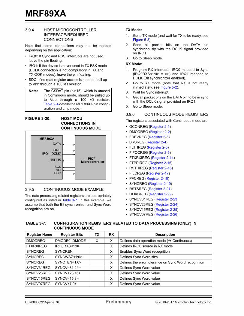
MRF89XA
3.9.4 HOST MICROCONTROLLER INTERFACE/REQUIRED CONNECTIONS
Note that some connections may not be neededdepending on the application:
• IRQ0: If Sync and RSSI interrupts are not used, leave the pin floating.
• IRQ1: If the device is never used in TX FSK mode (DCLK connection is not compulsory in RX and TX OOK modes), leave the pin floating.
• SDO: If no read register access is needed, pull up to VDD through a 100 kΩ resistor.
FIGURE 3-20: HOST MCU CONNECTIONS IN CONTINUOUS MODE
3.9.5 CONTINUOUS MODE EXAMPLE
The data processing related registers are appropriatelyconfigured as listed in Table 3-7. In this example, weassume that both the Bit synchronizer and Sync Wordrecognition are on.
TX Mode:
1. Go to TX mode (and wait for TX to be ready, seeFigure 5-3).
2. Send all packet bits on the DATA pinsynchronously with the DCLK signal providedon IRQ1.
3. Go to Sleep mode.
RX Mode:
1. Program RX interrupts: IRQ0 mapped to Sync(IRQ0RXS<1:0> = 00) and IRQ1 mapped toDCLK (Bit synchronizer enabled).
2. Go to RX mode (note that RX is not readyimmediately, see Figure 5-2).
3. Wait for Sync interrupt.4. Get all packet bits on the DATA pin to be in sync
with the DCLK signal provided on IRQ1.5. Go to Sleep mode.
3.9.6 CONTINUOUS MODE REGISTERS
The registers associated with Continuous mode are:
• GCONREG (Register 2-1)
• DMODREG (Register 2-2)
• FDEVREG (Register 2-3)
• BRSREG (Register 2-4)
• FLTHREG (Register 2-5)
• FIFOCREG (Register 2-6)
• FTXRXIREG (Register 2-14)
• FTPRIREG (Register 2-15)
• RSTHIREG (Register 2-16)
• FILCREG (Register 2-17)
• PFCREG (Register 2-18)
• SYNCREG (Register 2-19)
• RSTSREG (Register 2-21)
• OOKCREG (Register 2-22)
• SYNCV31REG (Register 2-23)
• SYNCV23REG (Register 2-24)
• SYNCV15REG (Register 2-25)• SYNCV07REG (Register 2-26)
TABLE 3-7: CONFIGURATION REGISTERS RELATED TO DATA PROCESSING (ONLY) IN CONTINUOUS MODE
Note: The CSDAT pin (pin15), which is unusedin Continuous mode, should be pulled upto VDD through a 100 kΩ resistor.Table 2-4 details the MRF89XA pin config-uration and chip mode.
PIC®
MRF89XA
IRQ0 IRQ1 (DCLK)
DATA
CSCON
SCKSDI
SDO
Microcontroller
Register Name Register Bits TX RX Description
DMODREG DMODE0, DMODE1 X X Defines data operation mode ( Continuous)
FTXRXIREG IRQ0RXS<1:0> X Defines IRQ0 source in RX mode
SYNCREG SYNCREN X Enables Sync Word recognition
SYNCREG SYNCWSZ<1:0> X Defines Sync Word size
SYNCREG SYNCTEN<1:0> X Defines the error tolerance on Sync Word recognition
SYNCV31REG SYNCV<31:24> X Defines Sync Word value
SYNCV23REG SYNCV<23:16> X Defines Sync Word value
SYNCV15REG SYNCV<15:8> X Defines Sync Word value
SYNCV07REG SYNCV<7:0> X Defines Sync Word value
DS70000622D-page 76 Preliminary 2010-2017 Microchip Technology Inc.
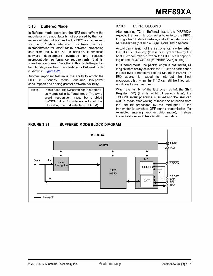
MRF89XA
3.10 Buffered Mode
In Buffered mode operation, the NRZ data to/from themodulator or demodulator is not accessed by the hostmicrocontroller but is stored in the FIFO and accessedvia the SPI data interface. This frees the hostmicrocontroller for other tasks between processingdata from the MRF89XA. In addition, it simplifiessoftware development overhead and reducesmicrocontroller performance requirements (that is,speed and response). Note that in this mode the packethandler stays inactive. The interface for Buffered modeis shown in Figure 3-21.
Another important feature is the ability to empty theFIFO in Standby mode, ensuring low-powerconsumption and adding greater software flexibility.
3.10.1 TX PROCESSING
After entering TX in Buffered mode, the MRF89XAexpects the host microcontroller to write to the FIFO,through the SPI data interface, and all the data bytes tobe transmitted (preamble, Sync Word, and payload).
Actual transmission of the first byte starts either whenthe FIFO is not empty (that is, first byte written by thehost microcontroller) or when the FIFO is full depend-ing on the IRQ0TXST bit (FTPRIREG<4>) setting.
In Buffered mode, the packet length is not limited, aslong as there are bytes inside the FIFO to be sent. Whenthe last byte is transferred to the SR, the FIFOEMPTYIRQ source is issued to interrupt the hostmicrocontroller, when the FIFO can still be filled withadditional bytes if required.
When the last bit of the last byte has left the ShiftRegister (SR) (that is, eight bit periods later), theTXDONE interrupt source is issued and the user canexit TX mode after waiting at least one bit period fromthe last bit processed by the modulator. If thetransmitter is switched OFF during transmission (forexample, entering another chip mode), it stopsimmediately, even if there is still unsent data.
FIGURE 3-21: BUFFERED MODE BLOCK DIAGRAM
Note: In this case, Bit Synchronizer is automati-cally enabled in Buffered mode. The SyncWord recognition must be enabled(SYNCREN = 1) independently of theFIFO filling method selected (FIFOFM).
Control
FIFO (+SR)
DATA
CONFIG
SPISYNC
Recognition
IRQ0
IRQ1
SDO SDI SCK CSDAT
CSCON RX
TX
Datapath
MRF89XA
Data
2010-2017 Microchip Technology Inc. Preliminary DS70000622D-page 77
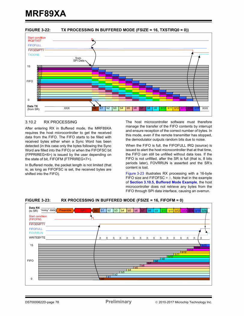
MRF89XA
FIGURE 3-22: TX PROCESSING IN BUFFERED MODE (FSIZE = 16, TXSTIRQ0 = 0))
3.10.2 RX PROCESSING
After entering RX in Buffered mode, the MRF89XArequires the host microcontroller to get the receiveddata from the FIFO. The FIFO starts to be filled withreceived bytes either when a Sync Word has beendetected (in this case only the bytes following the SyncWord are filled into the FIFO) or when the FIFOFSC bit(FPPRIREG<6>) is issued by the user depending onthe state of bit, FIFOFM (FTPRIREG<7>).
In Buffered mode, the packet length is not limited (thatis, as long as FIFOFSC is set, the received bytes areshifted into the FIFO).
The host microcontroller software must thereforemanage the transfer of the FIFO contents by interruptand ensure reception of the correct number of bytes. Inthis mode, even if the remote transmitter has stopped,the demodulator outputs random bits due to noise.
When the FIFO is full, the FIFOFULL IRQ (source) isissued to alert the host microcontroller that at that time,the FIFO can still be unfilled without data loss. If theFIFO is not unfilled, after the SR is full (that is, 8 bitsperiods later), FOVRRUN is asserted and the SR’scontent is lost.
Figure 3-23 illustrates RX processing with a 16-byteFIFO size and FIFOFSC = 0. Note that in the exampleof Section 3.10.5, Buffered Mode Example, the hostmicrocontroller does not retrieve any bytes from theFIFO through SPI data interface, causing an overrun.
FIGURE 3-23: RX PROCESSING IN BUFFERED MODE (FSIZE = 16, FIFOFM = 0)
b0 b1 b2 b3 b4 b5 b6 b7 b8 b9 b10 b11 b14 b15b12 b13
b0 b1
FIFO
0
15
Data TX (from SR)
Start condition IRQ0TXST
FIFOEMPTY
FIFOFULL
TXDONE
b5
b2 b3 b4
b6 b7 b8 b9 b10 b11 b12 b13 b14 b15
XXX XXX
from SPI Data
b0 b1 b2 b3 b4 b5 b6 b7 b8 b9 b10 b11 b14 b15b12 b13 b16Sync Preamble “noisy” data
b0b1
b5
b2b3
b4
b6b7
b8b9
b10 b11
b12 b13
b14b15
0
15
Data RX (to SR)
Start condition (FIFOFM)
FIFOEMPTY
FIFOFULL
FOVRRUN
WRITEBYTE
FIFO
DS70000622D-page 78 Preliminary 2010-2017 Microchip Technology Inc.

MRF89XA
3.10.3 INTERRUPT SIGNALS MAPPING
Table 3-8 and Table 3-9 describe the interruptsavailable in Buffered mode.
TABLE 3-8: INTERRUPT MAPPING IN BUFFERED RX AND STANDBY MODE
TABLE 3-9: INTERRUPT MAPPING IN BUFFERED TX MODE
3.10.4 HOST MICROCONTROLLER CONNECTIONS IN BUFFERED MODE
Depending on the application, some hostmicrocontroller connections may not be required:
• IRQ0: If none of the relevant IRQ sources are used, leave the pin floating.
• IRQ1: If none of the relevant IRQ sources are used, leave the pin floating.
• SDO: If no read register access is needed and the device is used in TX mode only, in this case, pull up to VDD through a 100 kΩ resistor.
FIGURE 3-24: HOST MCU CONNECTIONS IN BUFFERED MODE
3.10.5 BUFFERED MODE EXAMPLE
The data processing related registers are appropriatelyconfigured as listed in Table 3-10. In this example, weassume that Sync Word recognition is on and FIFOFM= 0.
Interrupt Name Interrupts Data Mode Interrupt TypeRX Interrupt
Source Standby Interrupt
Source
IRQ0RXS<1:0>
00 (default) IRQ0 Buffered Output — —
01 IRQ0 Buffered Output WRITEBYTE —
10 IRQ0 Buffered Output FIFOEMPTY FIFOEMPTY
11 IRQ0 Buffered Output Sync Pattern —
IRQ1RXS<1:0>
00 (default) IRQ1 Buffered Output — —
01 IRQ1 Buffered Output FIFOFULL FIFOFULL
10 IRQ1 Buffered Output RSSI —
11 IRQ1 Buffered Output FIFO_THRESHOLD FIFO_THRESHOLD
Note: Also refer the DMODE1 and DMODE0 bits in the FTXRXIREG and FTPRIREG registers for details.
Interrupt Name Interrupts Data Mode Interrupt Type Interrupt Source
IRQ0TXST
0 (default) IRQ0 Buffered Output FIFOEMPTY
1 IRQ0 Buffered Output FIFOEMPTY
IRQ1TX
0 (default) IRQ1 Buffered Output FIFOFULL
1 IRQ1 Buffered Output TXDONE
Note: Also refer the DMODE1 and DMODE0 bits in the FTXRXIREG and FTPRIREG registers for details.
Note: The DATA pin (pin 20), which is unused inBuffered mode, should be pulled up toVDD through a 100 kΩ resistor. Table 2-4provides details about the MRF89XA pinconfiguration and chip mode.
PIC®
MRF89XA
IRQ0
IRQ1
CSCON
SCKSDI
SDO
CSDAT
MIcrocontroller
2010-2017 Microchip Technology Inc. Preliminary DS70000622D-page 79
MRF89XA
TABLE 3-10: CONFIGURATION REGISTERS RELATED TO DATA PROCESSING IN BUFFERED MODE
TX Mode:
1. Program TX start condition and IRQs: Start TXwhen FIFO is not empty (IRQ0TXST = 1) andIRQ1 mapped to TXDONE (IRQ1TX = 1).
2. Go to TX mode (and wait for TX to be ready, seeFigure 5-3).
3. Write packet bytes into FIFO. TX starts when thefirst byte is written (IRQ0TXST = 1).Assumption: The FIFO is being filled through theSPI Data faster than being unfilled by SR.
4. Wait for TXDONE interrupt (+ 1 bit period).
5. Go to Sleep mode.
RX Mode:
1. Program RX/Standby interrupts: IRQ0 mappedto FIFOEMPTY (IRQ0RXS<1:0> = 10) andIRQ1 mapped to the FIFO threshold(IRQ1RXS<1:0> = 11). Configure the FIFOthreshold to an appropriate value (for example,to detect packet end, if its length is known).
2. Go to RX mode (note that RX is not ready imme-diately; see Section 5.3.1, Optimized ReceiveCycle for more information).
3. Wait for the FIFO threshold interrupt (that is,Sync Word has been detected and the FIFO hasfilled up to the defined threshold).
4. If it is packet end, go to Standby (SR’s content islost).
5. Read packet byte from the FIFO untilFIFOEMPTY goes low (or correct number ofbytes is read).
6. Go to Sleep mode.
Register Name Register Bits TX RX Description
DMODREG DMODE0, DMODE1 X X Defines data operation mode (Buffered)
FIFOCREG FSIZE<1:0> X X Defines FIFO size
FIFOCREG FTINT<5:0> X X Defines FIFO threshold
FTXRXIREG IRQ0RXS<1:0> — X Defines IRQ0 source in RX mode
FTXRXIREG IRQ1RXS<1:0> — X Defines IRQ1 source in RX mode
FTXRXIREG IRQ1TX X — Defines IRQ1 source in TX mode
FTPRIREG IRQ0TXST X — Defines IRQ0 source in TX mode
FTPRIREG FIFOFM — X Defines FIFO filling method
FTPRIREG FIFOFSC — X Controls FIFO filling status
SYNCREG SYNCREN — X Enables Sync Word recognition
SYNCREG SYNCWSZ<1:0> — X Defines Sync Word size
SYNCREG SYNCTEN<1:0> — X Defines the error tolerance on Sync Word recognition
SYNCV31REG SYNCV<31:24> — X Defines Sync Word value
SYNCV23REG SYNCV<23:16> — X Defines Sync Word value
SYNCV15REG SYNCV<15:8> — X Defines Sync Word value
SYNCV07REG SYNCV<7:0> — X Defines Sync Word value
DS70000622D-page 80 Preliminary 2010-2017 Microchip Technology Inc.
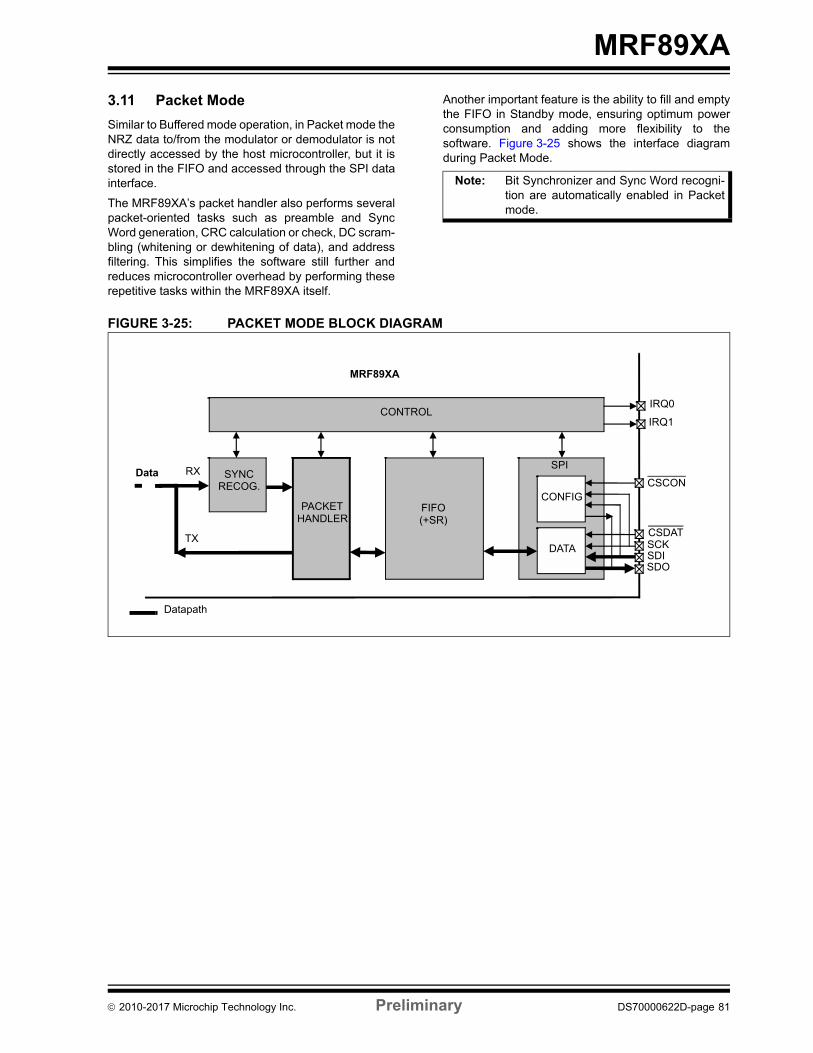
MRF89XA
3.11 Packet Mode
Similar to Buffered mode operation, in Packet mode theNRZ data to/from the modulator or demodulator is notdirectly accessed by the host microcontroller, but it isstored in the FIFO and accessed through the SPI datainterface.
The MRF89XA’s packet handler also performs severalpacket-oriented tasks such as preamble and SyncWord generation, CRC calculation or check, DC scram-bling (whitening or dewhitening of data), and addressfiltering. This simplifies the software still further andreduces microcontroller overhead by performing theserepetitive tasks within the MRF89XA itself.
Another important feature is the ability to fill and emptythe FIFO in Standby mode, ensuring optimum powerconsumption and adding more flexibility to thesoftware. Figure 3-25 shows the interface diagramduring Packet Mode.
FIGURE 3-25: PACKET MODE BLOCK DIAGRAM
Note: Bit Synchronizer and Sync Word recogni-tion are automatically enabled in Packetmode.
CONTROL
DATA
CONFIG
SPI
PACKET HANDLER
SYNC RECOG.
IRQ0
IRQ1
SDO SDI SCK CSDAT
RX
TX
Datapath
MRF89XA
Data
FIFO (+SR)
CSCON
2010-2017 Microchip Technology Inc. Preliminary DS70000622D-page 81
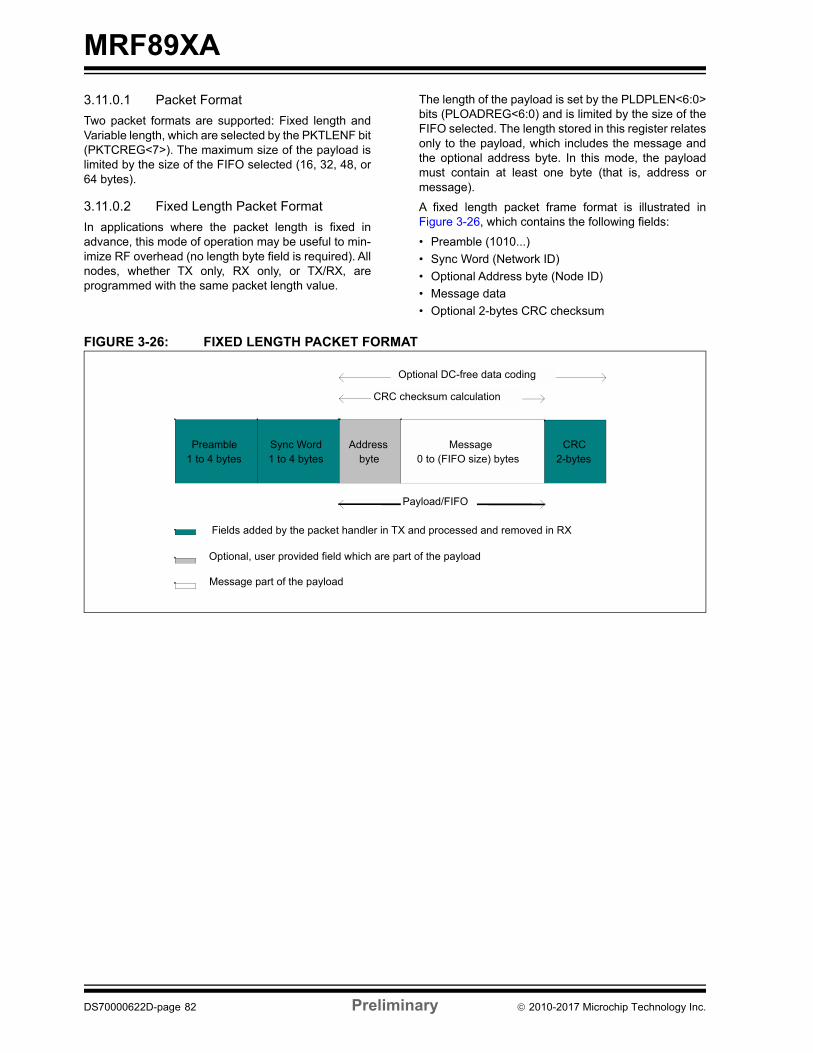
MRF89XA
3.11.0.1 Packet Format
Two packet formats are supported: Fixed length andVariable length, which are selected by the PKTLENF bit(PKTCREG<7>). The maximum size of the payload islimited by the size of the FIFO selected (16, 32, 48, or64 bytes).
3.11.0.2 Fixed Length Packet Format
In applications where the packet length is fixed inadvance, this mode of operation may be useful to min-imize RF overhead (no length byte field is required). Allnodes, whether TX only, RX only, or TX/RX, areprogrammed with the same packet length value.
The length of the payload is set by the PLDPLEN<6:0>bits (PLOADREG<6:0) and is limited by the size of theFIFO selected. The length stored in this register relatesonly to the payload, which includes the message andthe optional address byte. In this mode, the payloadmust contain at least one byte (that is, address ormessage).
A fixed length packet frame format is illustrated inFigure 3-26, which contains the following fields:
• Preamble (1010...)
• Sync Word (Network ID)
• Optional Address byte (Node ID)
• Message data
• Optional 2-bytes CRC checksum
FIGURE 3-26: FIXED LENGTH PACKET FORMAT
Message0 to (FIFO size) bytes
Addressbyte
CRC2-bytes
Sync Word1 to 4 bytes
Preamble 1 to 4 bytes
Payload/FIFO
CRC checksum calculation
Fields added by the packet handler in TX and processed and removed in RX
Optional, user provided field which are part of the payload
Message part of the payload
Optional DC-free data coding
DS70000622D-page 82 Preliminary 2010-2017 Microchip Technology Inc.
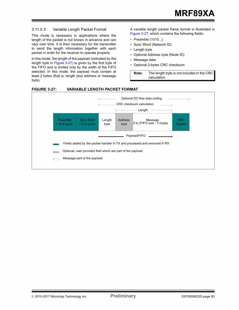
MRF89XA
3.11.0.3 Variable Length Packet Format
This mode is necessary in applications where thelength of the packet is not known in advance and canvary over time. It is then necessary for the transmitterto send the length information together with eachpacket in order for the receiver to operate properly.
In this mode, the length of the payload (indicated by thelength byte in Figure 3-27) is given by the first byte ofthe FIFO and is limited only by the width of the FIFOselected. In this mode, the payload must contain atleast 2 bytes (that is, length plus address or messagebyte).
A variable length packet frame format is illustrated inFigure 3-27, which contains the following fields:
• Preamble (1010...)
• Sync Word (Network ID)
• Length byte
• Optional Address byte (Node ID)
• Message data
• Optional 2-bytes CRC checksum
FIGURE 3-27: VARIABLE LENGTH PACKET FORMAT
Note: The length byte is not included in the CRCcalculation.
Message0 to (FIFO size - 1) bytes
Addressbyte
Lengthbyte
CRC 2-bytes
Sync Word1 to 4 bytes
Preamble 1 to 4 bytes
Payload/FIFO
CRC checksum calculation
Fields added by the packet handler in TX and processed and removed in RX
Optional, user provided field which are part of the payload
Message part of the payload
Optional DC-free data coding
Length
2010-2017 Microchip Technology Inc. Preliminary DS70000622D-page 83
MRF89XA
3.11.1 TX PROCESSING
In TX mode, the packet handler dynamically builds thepacket by performing the following operations on thepayload available in the FIFO:
• Adding a programmable number of preamble bytes
• Adding a programmable Sync Word
• Optionally calculating CRC over complete pay-load field (optional length byte plus optional address byte plus message) and appending the 2 bytes checksum
• Optional support for DC-free encoding of the data (Manchester or Whitening)
Only the payload (including optional address andlength fields) should be provided by the user in theFIFO.
Assuming that the device is in TX mode, and thendepending on the setting of the IRQ0TXST bit (FTPRI-REG<4>), packet transmission (starting with pro-grammed preamble) starts either after the first byte iswritten into the FIFO (IRQ0TXST = 1) or after the num-ber of bytes written reaches the user-defined threshold(IRQ0TXST = 0). The FIFO can be fully or partially filledin Standby mode through the FRWAXS bit(FCRCREG<6>). In this case, the start condition is onlychecked when entering TX mode.
At the end of the transmission (TXDONE = 1), the usermust exit TX mode if required (for example, back toStandby mode).
While in TX mode, before and after packet transmis-sion (not enough bytes or TXDONE), additional pream-ble bytes are sent to the modulator. When the startcondition is met, the current additional preamble byte iscompletely sent before the transmission of the nextpacket (that is, programmed preamble) is started.
3.11.2 RX PROCESSING
In RX mode the packet handler extracts the userpayload to the FIFO by performing the followingoperations:
• Receiving the preamble and stripping off the preamble
• Detecting the Sync Word and stripping off the Sync Word
• Optional DC-free decoding of data
• Optionally checking the address byte
• Optionally checking CRC and reflecting the result on the STSCRCEN bit (PKTREG<0>) and CRCOK from IRQ source (for more information, refer to Register 2-14).
Only the payload (including optional address andlength fields) is made available in the FIFO.
PLREADY and CRCOK interrupts (the latter only ifCRC is enabled) can be generated to indicate the endof the packet reception (for more information, refer toRegister 2-14).
By default, if the CRC check is enabled and fails for thecurrent packet, the FIFO is automatically cleared andneither of the two interrupts is generated and a newpacket reception is started. This autoclear function canbe disabled via the ACFCRC bit (FCRCREG<7>) and,in this case, even if CRC fails, the FIFO is not clearedand only the PLREADY IRQ source is issued.
Once fully received, the payload can also be fully orpartially retrieved in Standby mode from the FRWAXSbit. At the end of the reception, although the FIFO auto-matically stops being filled, it still depends on the userto explicitly exit RX mode if required (for example, go toStandby mode to get payload). The FIFO must beempty for a new packet reception to start.
3.11.3 PACKET FILTERING
The MRF89XA packet handler offers several mecha-nisms for packet filtering ensuring that only usefulpackets are made available to the host microcontroller,significantly reducing system power consumption andsoftware complexity.
3.11.3.1 Sync Word-Based
Sync Word filtering or recognition is enabled in Packetmode. It is used for identifying the start of the payloadand also for network identification. As described earlier,the Sync Word recognition block is configured (withsize, error tolerance, value) from the SYNCREN, SYN-CWSZ, SYNCTEN, SYNCV31-0 bits in the SYNCREG,SYNCV31REG, SYNCV23REG, SYNCV15REG, andSYNCV07REG Configuration registers. This informa-tion is used for appending Sync Word in TX and filteringpackets in RX.
Every received packet that does not start with thislocally configured Sync Word is automatically dis-carded, and no interrupt is generated.
When the Sync Word is detected, payload receptionautomatically starts and the Sync IRQ source is issued.
3.11.3.2 Length-Based
In variable length Packet mode, the PLDPLEN<6:0>bits (PLOADREG<6:0>) must be programmed with themaximum length permitted. If the received length byteis smaller than this maximum, the packet is acceptedand processed; otherwise, it is discarded.
To disable this function, the user should set the value ofthe PLDPLEN<6:0> bits to the value of the FIFO sizeselected.
Note: The received length byte, as part of thepayload, is not stripped off the packet andis made available in the FIFO.
DS70000622D-page 84 Preliminary 2010-2017 Microchip Technology Inc.
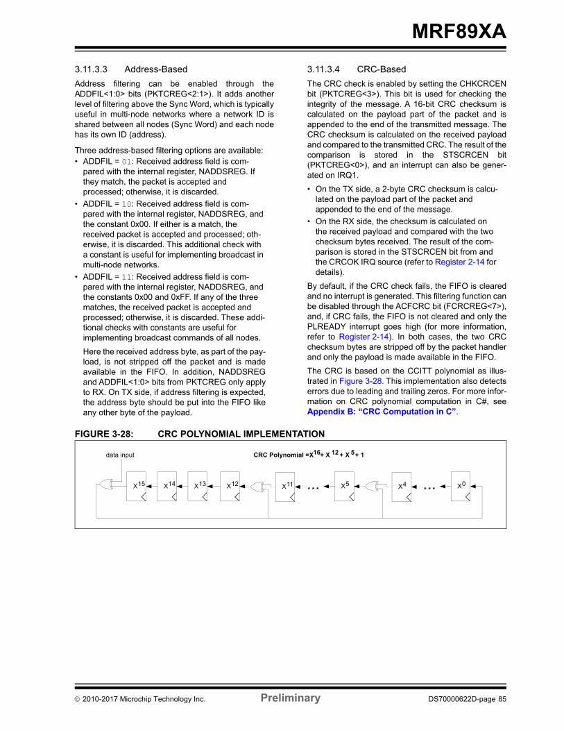
MRF89XA
3.11.3.3 Address-Based
Address filtering can be enabled through theADDFIL<1:0> bits (PKTCREG<2:1>). It adds anotherlevel of filtering above the Sync Word, which is typicallyuseful in multi-node networks where a network ID isshared between all nodes (Sync Word) and each nodehas its own ID (address).
Three address-based filtering options are available:• ADDFIL = 01: Received address field is com-
pared with the internal register, NADDSREG. If they match, the packet is accepted and processed; otherwise, it is discarded.
• ADDFIL = 10: Received address field is com-pared with the internal register, NADDSREG, and the constant 0x00. If either is a match, the received packet is accepted and processed; oth-erwise, it is discarded. This additional check with a constant is useful for implementing broadcast in multi-node networks.
• ADDFIL = 11: Received address field is com-pared with the internal register, NADDSREG, and the constants 0x00 and 0xFF. If any of the three matches, the received packet is accepted and processed; otherwise, it is discarded. These addi-tional checks with constants are useful for implementing broadcast commands of all nodes.
Here the received address byte, as part of the pay-load, is not stripped off the packet and is madeavailable in the FIFO. In addition, NADDSREGand ADDFIL<1:0> bits from PKTCREG only applyto RX. On TX side, if address filtering is expected,the address byte should be put into the FIFO likeany other byte of the payload.
3.11.3.4 CRC-Based
The CRC check is enabled by setting the CHKCRCENbit (PKTCREG<3>). This bit is used for checking theintegrity of the message. A 16-bit CRC checksum iscalculated on the payload part of the packet and isappended to the end of the transmitted message. TheCRC checksum is calculated on the received payloadand compared to the transmitted CRC. The result of thecomparison is stored in the STSCRCEN bit(PKTCREG<0>), and an interrupt can also be gener-ated on IRQ1.
• On the TX side, a 2-byte CRC checksum is calcu-lated on the payload part of the packet and appended to the end of the message.
• On the RX side, the checksum is calculated on the received payload and compared with the two checksum bytes received. The result of the com-parison is stored in the STSCRCEN bit from and the CRCOK IRQ source (refer to Register 2-14 for details).
By default, if the CRC check fails, the FIFO is clearedand no interrupt is generated. This filtering function canbe disabled through the ACFCRC bit (FCRCREG<7>),and, if CRC fails, the FIFO is not cleared and only thePLREADY interrupt goes high (for more information,refer to Register 2-14). In both cases, the two CRCchecksum bytes are stripped off by the packet handlerand only the payload is made available in the FIFO.
The CRC is based on the CCITT polynomial as illus-trated in Figure 3-28. This implementation also detectserrors due to leading and trailing zeros. For more infor-mation on CRC polynomial computation in C#, seeAppendix B: “CRC Computation in C”.
FIGURE 3-28: CRC POLYNOMIAL IMPLEMENTATION
X14 X13 X12 X11 X5 X0 X15
CRC Polynomial =X16 + X 12 + X 5 + 1
* * * X4* * *
data input
2010-2017 Microchip Technology Inc. Preliminary DS70000622D-page 85
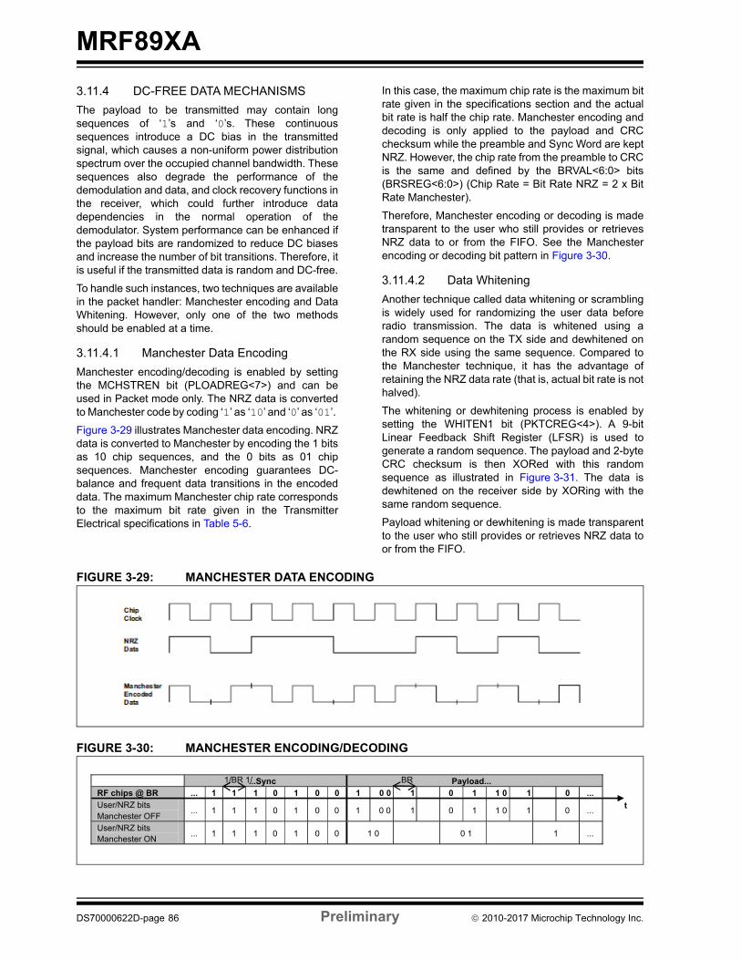
MRF89XA
3.11.4 DC-FREE DATA MECHANISMS
The payload to be transmitted may contain longsequences of ‘1’s and ‘0’s. These continuoussequences introduce a DC bias in the transmittedsignal, which causes a non-uniform power distributionspectrum over the occupied channel bandwidth. Thesesequences also degrade the performance of thedemodulation and data, and clock recovery functions inthe receiver, which could further introduce datadependencies in the normal operation of thedemodulator. System performance can be enhanced ifthe payload bits are randomized to reduce DC biasesand increase the number of bit transitions. Therefore, itis useful if the transmitted data is random and DC-free.
To handle such instances, two techniques are availablein the packet handler: Manchester encoding and DataWhitening. However, only one of the two methodsshould be enabled at a time.
3.11.4.1 Manchester Data Encoding
Manchester encoding/decoding is enabled by settingthe MCHSTREN bit (PLOADREG<7>) and can beused in Packet mode only. The NRZ data is convertedto Manchester code by coding ‘1’ as ‘10’ and ‘0’ as ‘01’.
Figure 3-29 illustrates Manchester data encoding. NRZdata is converted to Manchester by encoding the 1 bitsas 10 chip sequences, and the 0 bits as 01 chipsequences. Manchester encoding guarantees DC-balance and frequent data transitions in the encodeddata. The maximum Manchester chip rate correspondsto the maximum bit rate given in the TransmitterElectrical specifications in Table 5-6.
In this case, the maximum chip rate is the maximum bitrate given in the specifications section and the actualbit rate is half the chip rate. Manchester encoding anddecoding is only applied to the payload and CRCchecksum while the preamble and Sync Word are keptNRZ. However, the chip rate from the preamble to CRCis the same and defined by the BRVAL<6:0> bits(BRSREG<6:0>) (Chip Rate = Bit Rate NRZ = 2 x BitRate Manchester).
Therefore, Manchester encoding or decoding is madetransparent to the user who still provides or retrievesNRZ data to or from the FIFO. See the Manchesterencoding or decoding bit pattern in Figure 3-30.
3.11.4.2 Data Whitening
Another technique called data whitening or scramblingis widely used for randomizing the user data beforeradio transmission. The data is whitened using arandom sequence on the TX side and dewhitened onthe RX side using the same sequence. Compared tothe Manchester technique, it has the advantage ofretaining the NRZ data rate (that is, actual bit rate is nothalved).
The whitening or dewhitening process is enabled bysetting the WHITEN1 bit (PKTCREG<4>). A 9-bitLinear Feedback Shift Register (LFSR) is used togenerate a random sequence. The payload and 2-byteCRC checksum is then XORed with this randomsequence as illustrated in Figure 3-31. The data isdewhitened on the receiver side by XORing with thesame random sequence.
Payload whitening or dewhitening is made transparentto the user who still provides or retrieves NRZ data toor from the FIFO.
FIGURE 3-29: MANCHESTER DATA ENCODING
FIGURE 3-30: MANCHESTER ENCODING/DECODING
...Sync Payload...
RF chips @ BR ... 1 1 1 0 1 0 0 1 0 0 1 0 1 1 0 1 0 ...
User/NRZ bits Manchester OFF
... 1 1 1 0 1 0 0 1 0 0 1 0 1 1 0 1 0 ...
User/NRZ bits Manchester ON
... 1 1 1 0 1 0 0 1 0 0 1 1 ...
t
1/BR 1/ BR
DS70000622D-page 86 Preliminary 2010-2017 Microchip Technology Inc.
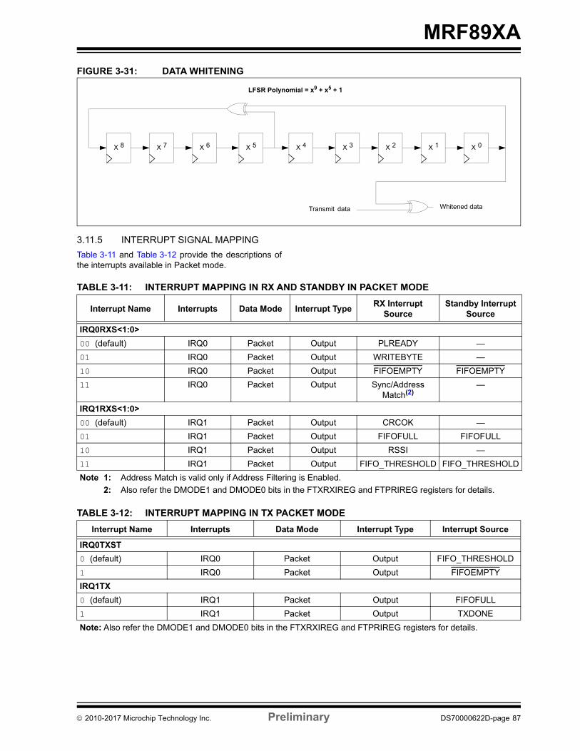
MRF89XA
FIGURE 3-31: DATA WHITENING
3.11.5 INTERRUPT SIGNAL MAPPING
Table 3-11 and Table 3-12 provide the descriptions ofthe interrupts available in Packet mode.
TABLE 3-11: INTERRUPT MAPPING IN RX AND STANDBY IN PACKET MODE
TABLE 3-12: INTERRUPT MAPPING IN TX PACKET MODE
X 7 X 6 X 5 X 4 X 3 X 2 X 1 X 0 X 8
LFSR Polynomial = x9 + x5 + 1
Transmit data Whitened data
Interrupt Name Interrupts Data Mode Interrupt TypeRX Interrupt
Source Standby Interrupt
Source
IRQ0RXS<1:0>
00 (default) IRQ0 Packet Output PLREADY —
01 IRQ0 Packet Output WRITEBYTE —
10 IRQ0 Packet Output FIFOEMPTY FIFOEMPTY
11 IRQ0 Packet Output Sync/Address Match(2)
—
IRQ1RXS<1:0>
00 (default) IRQ1 Packet Output CRCOK —
01 IRQ1 Packet Output FIFOFULL FIFOFULL
10 IRQ1 Packet Output RSSI —
11 IRQ1 Packet Output FIFO_THRESHOLD FIFO_THRESHOLD
Note 1: Address Match is valid only if Address Filtering is Enabled.
2: Also refer the DMODE1 and DMODE0 bits in the FTXRXIREG and FTPRIREG registers for details.
Interrupt Name Interrupts Data Mode Interrupt Type Interrupt Source
IRQ0TXST
0 (default) IRQ0 Packet Output FIFO_THRESHOLD
1 IRQ0 Packet Output FIFOEMPTY
IRQ1TX
0 (default) IRQ1 Packet Output FIFOFULL
1 IRQ1 Packet Output TXDONE
Note: Also refer the DMODE1 and DMODE0 bits in the FTXRXIREG and FTPRIREG registers for details.
2010-2017 Microchip Technology Inc. Preliminary DS70000622D-page 87
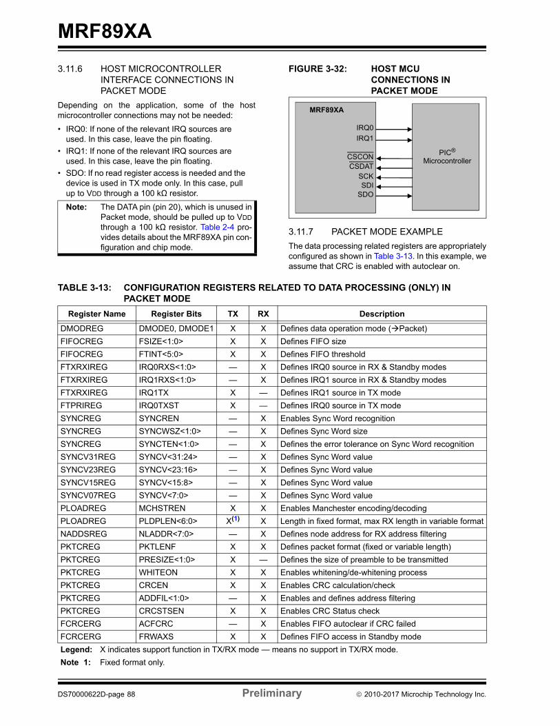
MRF89XA
3.11.6 HOST MICROCONTROLLER INTERFACE CONNECTIONS IN PACKET MODE
Depending on the application, some of the hostmicrocontroller connections may not be needed:
• IRQ0: If none of the relevant IRQ sources are used. In this case, leave the pin floating.
• IRQ1: If none of the relevant IRQ sources are used. In this case, leave the pin floating.
• SDO: If no read register access is needed and the device is used in TX mode only. In this case, pull up to VDD through a 100 kΩ resistor.
FIGURE 3-32: HOST MCU CONNECTIONS IN PACKET MODE
3.11.7 PACKET MODE EXAMPLE
The data processing related registers are appropriatelyconfigured as shown in Table 3-13. In this example, weassume that CRC is enabled with autoclear on.
TABLE 3-13: CONFIGURATION REGISTERS RELATED TO DATA PROCESSING (ONLY) IN PACKET MODE
Note: The DATA pin (pin 20), which is unused inPacket mode, should be pulled up to VDD
through a 100 kΩ resistor. Table 2-4 pro-vides details about the MRF89XA pin con-figuration and chip mode.
PIC®
MRF89XA
IRQ0
IRQ1
CSCON
SCKSDI
SDO
CSDATMicrocontroller
Register Name Register Bits TX RX Description
DMODREG DMODE0, DMODE1 X X Defines data operation mode (Packet)
FIFOCREG FSIZE<1:0> X X Defines FIFO size
FIFOCREG FTINT<5:0> X X Defines FIFO threshold
FTXRXIREG IRQ0RXS<1:0> — X Defines IRQ0 source in RX & Standby modes
FTXRXIREG IRQ1RXS<1:0> — X Defines IRQ1 source in RX & Standby modes
FTXRXIREG IRQ1TX X — Defines IRQ1 source in TX mode
FTPRIREG IRQ0TXST X — Defines IRQ0 source in TX mode
SYNCREG SYNCREN — X Enables Sync Word recognition
SYNCREG SYNCWSZ<1:0> — X Defines Sync Word size
SYNCREG SYNCTEN<1:0> — X Defines the error tolerance on Sync Word recognition
SYNCV31REG SYNCV<31:24> — X Defines Sync Word value
SYNCV23REG SYNCV<23:16> — X Defines Sync Word value
SYNCV15REG SYNCV<15:8> — X Defines Sync Word value
SYNCV07REG SYNCV<7:0> — X Defines Sync Word value
PLOADREG MCHSTREN X X Enables Manchester encoding/decoding
PLOADREG PLDPLEN<6:0> X(1) X Length in fixed format, max RX length in variable format
NADDSREG NLADDR<7:0> — X Defines node address for RX address filtering
PKTCREG PKTLENF X X Defines packet format (fixed or variable length)
PKTCREG PRESIZE<1:0> X — Defines the size of preamble to be transmitted
PKTCREG WHITEON X X Enables whitening/de-whitening process
PKTCREG CRCEN X X Enables CRC calculation/check
PKTCREG ADDFIL<1:0> — X Enables and defines address filtering
PKTCREG CRCSTSEN X X Enables CRC Status check
FCRCERG ACFCRC — X Enables FIFO autoclear if CRC failed
FCRCERG FRWAXS X X Defines FIFO access in Standby mode
Legend: X indicates support function in TX/RX mode — means no support in TX/RX mode.
Note 1: Fixed format only.
DS70000622D-page 88 Preliminary 2010-2017 Microchip Technology Inc.

MRF89XA
TX Mode:
1. Program TX start condition and IRQs: Start TXwhen the FIFO is not empty (IRQ0TXST = 1)and IRQ1 mapped to TXDONE (IRQ1TX = 1).
2. Set CMOD = Standby mode and enable theFIFO access in Standby mode.
3. Write all payload bytes into the FIFO (FRWAXS= 0, Standby interrupts can be used if needed).
4. Go to TX mode. When TX is ready (automati-cally handled), TX starts (IRQ0TXST = 1).
5. Wait for TXDONE interrupt (plus one bit period).
6. Go to Sleep mode.
RX Mode:
1. Program RX/Standby interrupts: IRQ0 mappedto FIFOEMPTY (IRQ0RXS = 10) and IRQ1mapped to FIFO Threshold (IRQ1RXS = 11).Configure FIFO Threshold to an appropriatevalue (for example, to detect packet end, if itslength is known).
2. Go to RX mode by setting the CMOD register.FIFO threshold interrupt occurs when the FIFOis full with received contents. So enabling ofIRQ1 to “CRCOK” interrupt is required.
3. Wait for CRCOK interrupt.
4. Go to Standby mode.
5. Read payload byte from the FIFO untilFIFOEMPTY goes low, (FRWAXS = 1).
6. Go to Sleep mode.
3.11.8 ADDITIONAL INFORMATION TO HANDLE PACKET MODE
If the number of bytes filled for transmission is greaterthan the actual length of the packet to be transmittedand IRQ0TXST = 1, the FIFO is cleared after thepacket has been transmitted. Therefore, the extrabytes in the FIFO are lost. Otherwise, if IRQ0TXST = 0,the extra bytes are kept in the FIFO. This opens up thepossibility of transmitting more than one packet by fill-ing the FIFO with multiple packet messages.
It is not possible to receive multiple packets. After apacket has been received and filled in the FIFO, all itscontents must be read (that is, the FIFO must be emptyfor a new packet reception to be initiated).
The PLREADY interrupt goes high when the last pay-load byte is available in the FIFO and remains high untilall its data are read. Similar behavior is applicable toARDSMATCH and CRCOK interrupts.
The CRC result is available in the STSCRCEN bitimmediately as the CRCOK and PLREADY interruptsources are triggered. In RX mode, the STSCRCEN bitis cleared when the complete payload has been readfrom the FIFO. If the payload is read in Standby mode,the STSCRCEN bit is cleared when the user goes backto RX mode and a new Sync Word is detected.
The FIFOFM and FIFOFSC bits have no meaning inPacket mode and should be set to their default valuesonly.
3.11.9 PACKET MODE REGISTERS
The registers associated with Packet mode are:
• GCONREG (Register 2-1)• DMODREG (Register 2-2)• FDEVREG (Register 2-3)• BRSREG (Register 2-4)• FLTHREG (Register 2-5)• FIFOCREG (Register 2-6)• FTXRXIREG (Register 2-14)• FTPRIREG (Register 2-15)• RSTHIREG (Register 2-16)• FILCREG (Register 2-17)• PFCREG (Register 2-18)• SYNCREG (Register 2-19)• RSTSREG (Register 2-21)• OOKCREG (Register 2-22)• SYNCV31REG (Register 2-23)• SYNCV23REG (Register 2-24)• SYNCV15REG (Register 2-25)• SYNCV07REG (Register 2-26)• PLOADREG (Register 2-29)• NADDSREG (Register 2-30)• PKTCREG (Register 2-31)• FCRCREG (Register 2-32)
2010-2017 Microchip Technology Inc. Preliminary DS70000622D-page 89
MRF89XA
3.12 Initialization
Certain control register values must be initialized forbasic operations of the MRF89XA. These values differfrom the POR values and provide improved operationalparameters. These settings are normally made onceafter a Reset. After initialization, the other features ofthe MRF89XA device can be configured based on theapplication. Accessing a register is implied as a com-mand to the MRF89XA device through the SPI port.
The steps to initialize the MRF89XA using the controlregisters are as follows:
1. In the GCONREG register:
a) Set the Chip Mode (CMOD<2:0>), Fre-quency Band (FBS<1:0>), and VCO Trim(VCOT<1:0>) bits.
b) Program the Frequency band.
c) Set the Trim bits to appropriately tune in theVCO.
2. In the DMODREG register:
a) Select the Modulation Type using the MOD-SEL<1:0> bits.
b) Enable DATA mode for Transmission usingthe DMODE0 and DMODE1 bits.
c) Select the gain for IF chain using theIFGAIN<1:0> bits.
d) In the FDEVREG register, program the Fre-quency Deviation bits (FDVAL<7:0>).
3. In the BRSREG register, program the Bit Rateusing the BRVAL<6:0> bits.
4. In the FLTHREG register, set the Floor Thresh-old for OOK using the FTOVAL<7:0> bits.
5. In the FIFOCREG register, configure the FIFOSize and FIFO Threshold using the FSIZE<1:0>and FTINT<5:0> bits.
6. In the PACREG register, configure the PowerAmplifier Ramp Control using the PARC<1:0>bits.
7. In the FTXRXIREG register:
a) Configure the RX interrupts for IRQ0 andIRQ1 using the IRQ0RXS<1:0> andIRQ1RXS<1:0> bits.
b) Configure the TX interrupts for IRQ1 usingthe IRQ1TX bit.
8. In the FTPRIREG register:
a) Configure the TX interrupts for IRQ0 usingthe IRQ0TXST bit.
b) Enable PLL Lock for interrupt on IRQ1using the LENPLL bit.
9. In the RSTHIREG, program the RSSI Thresholdvalue for interrupt request using theRTIVAL<7:0> bits.
10. In the FILCREG register, enable the PassiveFilter using the PASFILV<3:0> bits.
11. Configure RX parameters:
a) Enable Passive Filter with the value as setin step 10.
b) Set fc and fo.
c) Enable SYNC and Set SYNC Word, Size,Length, and Tolerance.
d) Set configuration bytes for OOK Thresholdfrom OOKCREG.
12. In the SYNCREG register, setSYNCWSZ<1:0> = 11 for 32-bit SYNC Word.
13. Configure TX parameters:
a) Change or Reset fc.
b) In the TXCONREG register, enable TX andits transmit power using theTXIPOLFV<3:0> and TXOPVAL<2:0> bits.
14. In the CLKOUTREG register, configure theClock Settings using the CLKOCNTRL andCLKOFREQ<4:0> bits.
15. Configure the Packet Frame parameters in thePLOADREG, NADDSREG, PKTCREG, andFCRCREG registers:
a) Enable Manchester Encoding.
b) Set the packet format and the length of thepacket.
c) Set the Node local address.
d) Program preamble variables.
e) Configure CRC parameters.
f) Enable Address Filtering.
16. In the FCRCREG register, enable FIFO writeaccess using the FRWAXS bit.
Note 1: Program registers 0x00 - 0x1F withappropriate settings. (General Configura-tion Parameters, IRQ Parameters, andPacket Parameters).
2: Clear the PLL Lock flag by setting theLSTSPLL bit (FTPRIREG 0x0E<1>) to‘1’.
3: Program CMOD bits (GCONREG 0x00<7:5>) to ‘0b010 Frequency Synthe-sizer mode.
4: Verify the PLL lock flag through theLSTSPLL bit (FTPRIREG 0x0E<1>). IfLSTSPLL = 1, it implies that theMRF89XA is ready to operate at the fre-quency indicated by the Ri/Pi/Si registerset.
5: Program the CMOD bits (GCONREG0x00 <7:5>) to ‘0b001 Standby mode.
DS70000622D-page 90 Preliminary 2010-2017 Microchip Technology Inc.
MRF89XA
3.13 Battery Power Management Configuration Values
Battery life can be greatly extended in MRF89XA appli-cations where transmissions from field nodes are infre-quent, or network communications can beconcentrated in periodic time slots. For example, fieldnodes in many wireless alarm systems report opera-tional status a few times a day, and can otherwise sleepunless an alarm condition occurs. Sensor networks thatmonitor parameters that change relatively slowly, suchas air and soil temperature in agricultural settings andswitching lights ON/OFF, only need to transmitupdates a few times per hour.
At room temperature, the MRF89XA draws a maximumof 1 μA in Sleep mode, with a typical value of 100 nA.To achieve minimum Sleep mode current, the SDI pin(pin 17) and SCK pin (pin 18) must be held logic low,while CSCON pin (pin 14), CSDAT pin (pin 15) andSDO pin (pin 16) must be held logic high.
The MRF89XA can go from Sleep mode throughStandby mode and Synthesizer mode to Transmit (orReceive) mode in less than 6 ms. For configuring anddriving the device different operating modes refer toTable 2-3. At a data rate of 33.33 kbps, a 32-bytepacket with a 4-byte preamble and a 4-byte start pat-tern takes about 10 ms to transmit. Assume that theMRF89XA then switches to Receive mode for one sec-ond to listen for a response and returns to Sleep mode.On the basis of reporting every six hours, the ON toSleep duty cycle is about 1:21,259, greatly extendingbattery life over continuous transmit-receive or evenstandby operation.
The required timing accuracy for the microcontrollers ina sleep-cycled application depends on several factors:
• The required “timestamp” accuracy of data reported by sleeping field nodes. R-C Sleep mode timers built into many microcontrollers have a tol-erance of ±20% or more. For applications that require more accurate timestamping, many micro-controllers can run on a watch crystal during Sleep mode and achieve timestamp accuracies better than one second per 24 hours.
• If the base station and any routing nodes present in a network must sleep cycle in addition to the field nodes. Watch crystal control is usually needed to keep all nodes accurately synchronized to the active time slots.
• If the base station and any routing nodes present in a network can operate continuously (AC pow-ered, solar charged batteries), and a loose time stamp accuracy is OK, the microcontrollers in sleeping field nodes can usually operate from internal low-accuracy R-C timers.
Therefore, as previously mentioned, Sleep mode is thelowest power consumption mode in which the clockand all functional blocks of the device are disabled. Incase of an interrupt, the device wakes up, switches toActive mode and an interrupt signal generated on theIRQ pin indicates the change in state to the host micro-controller. The source of the interrupt can bedetermined by reading the status word of the device.
To reduce current consumption, the MRF89XAshould be placed in the low-power consuming Sleepmode. In Sleep mode, the 12.8 MHz main oscillatoris turned OFF, disabling the RF and baseband cir-cuitry. Data is retained in the control and FIFO regis-ters and the transceiver is accessible through theSPI port. The MRF89XA does not enter Sleep modeif any interrupt remains active, regardless of thestate of the CLKOCNTRL bit (CLKOUTREG<7>).This way, the microcontroller can always have aclock signal to process the interrupt. To prevent high-current consumption, which results in shorter batterylife, it is highly recommended to process and clearinterrupts before entering Sleep mode. Unnecessaryfunctions should be turned off to avoid unwantedinterrupts. To minimize current consumption, theMRF89XA supports different power-saving modes,along with an integrated wake-up timer.
When switching from Sleep mode to Standby mode,the crystal oscillator is active for no more than 5 ms.Switching from Standby mode to Synthesizer mode,the PLL locks in less than 0.5 ms. PLL lock can be mon-itored on the PLOCK pin (pin 23) of the MRF89XA. Theradio can then be switched to either Transmit orReceive mode. When switching from any other modeback to Sleep mode, the device drops to its Sleep modecurrent in less than 1 ms.
Note: Many host microcontrollers cannot beoperated from the MRF89XA bufferedclock output if sleep cycling is planned. InSleep mode, the MRF89XA buffered clockoutput is disabled, which disables themicrocontroller unless it is capable ofautomatically switching to an internalclock source when external clocking islost.
2010-2017 Microchip Technology Inc. Preliminary DS70000622D-page 91
MRF89XA
To make the MRF89XA device enter into Sleep mode,certain control register values must be initialized. Thesequence to program the control registers for enteringinto Sleep mode and Wake-up modes are as follows:
For Sleep mode:
1. Check the IRQ bit status.
2. Handle Interrupts.
3. Configure the GCONREG register.
4. Set or reset CLKOUT in the CLKOUTREGregister.
EXAMPLE 3-1: TO PUT THE MRF89XA INTO SLEEP MODE
The MRF89XA device can wake up from any interruptactivity.
For Wake-up mode, perform any of the following tasks:
• Enter in TX/RX mode.
• Enable CLKOUT.
• Set the INT pin.
EXAMPLE 3-2: TO WAKE THE MRF89XA FROM SLEEP MODE
3.13.1 POWER-SAVING MODE REGISTERS
The registers associated with power-saving modesare:
• GCONREG (Register 2-1)
• DMODREG (Register 2-2)
• FDEVREG (Register 2-3)
• BRSREG (Register 2-4)
• FTXRXIREG (Register 2-14)
• FTPRIREG (Register 2-15)
• CLKOUTREG (Register 2-28)
Set CMOD<2:0> (GCONREG<2:0>) = 0
Set CMOD<2:0> (GCONREG<2:0>) = 1
DS70000622D-page 92 Preliminary 2010-2017 Microchip Technology Inc.
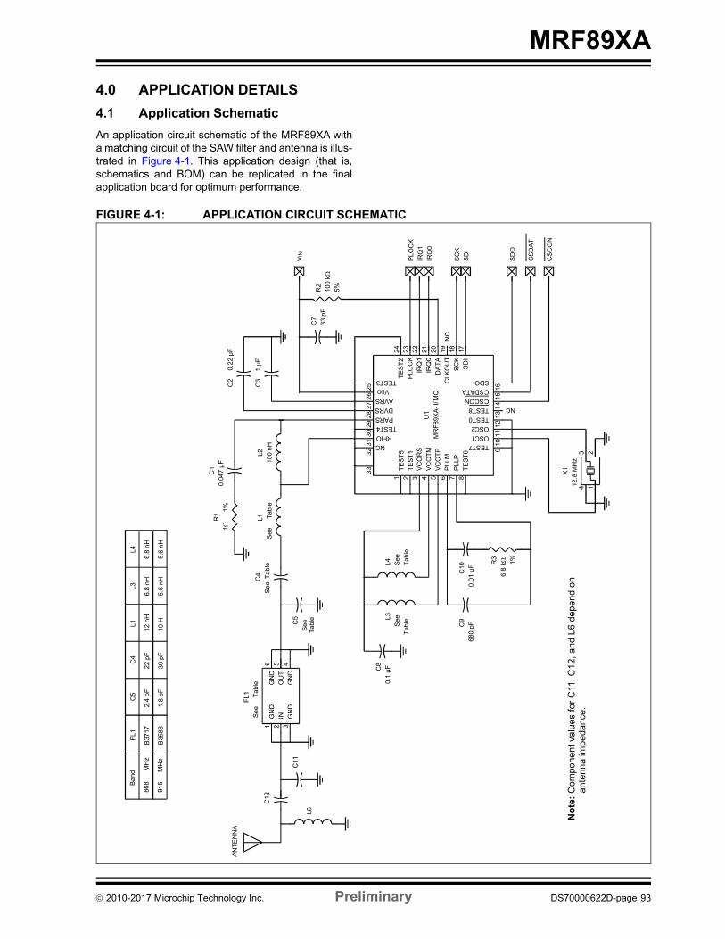
MRF89XA
4.0 APPLICATION DETAILS
4.1 Application Schematic
An application circuit schematic of the MRF89XA witha matching circuit of the SAW filter and antenna is illus-trated in Figure 4-1. This application design (that is,schematics and BOM) can be replicated in the finalapplication board for optimum performance.
FIGURE 4-1: APPLICATION CIRCUIT SCHEMATICC
1
0.0
47 µ
F
C2
0.2
2 µ
F
C3
1 µ
FC
4
See T
able
C5
See
C7
33 p
F
C8
0.1
µF
C9
680 p
F
C10
0.0
1 µ
F
C11
See
Tabl
e
FL1
IN GN
D
GN
D
GN
D
OU
T
GN
D2 3
45
16
C12
L1
See
Tabl
e
L2
100
nH
L3
See
L4 See
L6
PLO
CK
CS
CO
N
IRQ
0
SD
I
SC
K
SD
O
CS
DA
T
IRQ
1
VIN
R1
1
1%
R2
100 k
5%
R3
6.8
k 1%
U1
MR
F89X
A-I
/MQ
TE
ST
5
TE
ST
1V
CO
RS
VC
OT
M
VC
OT
P
PLLM
PLLP
TE
ST
6
TEST7
OSC1
OSC2
TEST0
TEST8
CSCON
CSDATA
SDO
SD
I
SC
K
CLK
OU
T
DA
TA
IRQ
0
IRQ
1
PLO
CK
TE
ST
2
TEST3
VDD
AVRS
DVRS
PARS
TEST4
RFIO
NC
1 2 3 4 5 6 7 8
910
11
12
13
14
15
16
17
18
19
20
21
22
23
24
25
26
27
28
29
30
31
32
33
X1
12.8
MH
z
143 2
NC
NC
AN
TE
NN
A
L3
L4
6.8 n
H6.
8 n
H
5.6 n
H5.
6 n
H
B3717
B3588
Table
Tabl
e
Table
FL1
C5
C4
L1
12 n
H
10 H
22 p
F
30 p
F
2.4
pF
1.8
pF
No
te:
Com
pone
nt v
alue
s fo
r C
11, C
12, a
nd L
6 de
pen
d on
868
MH
z
Band
915
MH
z
ant
enna
impe
danc
e.
2010-2017 Microchip Technology Inc. Preliminary DS70000622D-page 93
MRF89XA
4.2 RF Transmitter Matching
The optimum load for the RF port at a given frequencyband is listed in Table 4-1. These load values in thetable are expected by the RF port pins to have as anantenna load for maximum power transfer. For allantenna applications, an RF choke inductor (L2) mustbe included during transmission because the RF out-puts are of open-collector type.
4.3 Antenna Components
The MRF89XA is single-ended and has an unbalancedinput and output impedance close to 30-j25. Therefore,it only requires a matching circuit to the SAW filter andantenna. The C11, C12, and L6 are part of the match-ing network these components make for the antennacircuit. L1, C4, and C5 are tuned to provide thatimpedance (30+j25) to the RFIO pin. In this case, thetransceiver can transfer all power toward the antenna.This impedance is called Optimum Load Impedance.L2 is an RF choke inductor. L3 and L4 are VCO induc-tors. The details are shown in Figure 4-1.
TABLE 4-1: ANTENNA LOAD VALUES FOR 868 MHz AND 915 MHz FREQUENCY BANDS
4.4 SAW FILTER
FL1 is a SAW filter. While in Transmitting mode, theSAW filter is used to suppress the harmonics. While inReceiving mode, the SAW filter is used to reject theimage frequencies and out-of-band interfering signals.
4.4.1 SAW FILTER PLOT
Figure 4-2 and Figure 4-3 illustrate the plots of theSAW filter used in the application circuit. The plotsshown are representative. For exact specifications,refer to the SAW Filter manufacturer data sheet.
Band FL1 C5 C4 L1
868 MHz TA0801A 1.8 pF 22 pF 8.2 nH
915 MHz TA0281A 1.8 pF 30 pF 10 nH
Note 1: The SAW filter can be of EPCOS (B3717and B3588) or Taisaw (TA0801A andTA0281A) for 868 MHz and 915 MHzrespectively with matching componentsremaining the same as shown in Figure 4-1and Table 4-1.
DS70000622D-page 94 Preliminary 2010-2017 Microchip Technology Inc.
MRF89XA
FIGURE 4-2: 868 MHz SAW FILTER PLOT
FIGURE 4-3: 915 MHz SAW FILTER PLOT
-80
-70
-60
-50
-40
-30
-20
-10
0
400 600 800 1000 1200 1400 1600 1800 2000
Frequency [MHz]
Att
enu
ati
on
[d
B]
-80
-70
-60
-50
-40
-30
-20
-10
0
400 600 800 1000 1200 1400 1600 1800 2000
Frequency [MHz]
Att
enu
atio
n [
dB
]
2010-2017 Microchip Technology Inc. Preliminary DS70000622D-page 95
MRF89XA
4.5 POWER AMPLIFIER
The Power Amplifier (PA) integrated in the MRF89XAoperates under a regulated voltage supply of 1.8V. Theexternal RF choke inductor is biased using an internalregulator output made available on the PARS pin (pin29). These features help PA output power to be consis-tent over the power supply range. This is important forapplications that allow predictable RF performance andbattery life.
4.5.1 OPTIMUM LOAD IMPEDANCE
As the PA and the LNA front-ends in the MRF89XAshare the same input or output pin, they are internallymatched to approximately 50Ω. Figure 4-4 illustratesthe optimum load impedance of RFIO through animpedance chart.
FIGURE 4-4: OPTIMAL LOAD IMPEDANCE CHART
Pmax-1dB circle
Max PowerZopt = 30 + j25
Note: Refer to Section 4.8, Bill of Materials foran optimized PA load setting.
DS70000622D-page 96 Preliminary 2010-2017 Microchip Technology Inc.
MRF89XA
4.5.2 SUGGESTED PA BIASING AND MATCHING
The recommended PA bias and matching circuit isillustrated in Figure 4-5.
FIGURE 4-5: RECOMMENDED PA BIASING AND OUTPUT MATCHING
Refer to Section 4.8, Bill of Materials for the opti-mized matching arrangement for each frequency band.
4.5.3 COMMON INPUT AND OUTPUT FRONT-END
The Receiver and Transmitter share the same RFIOpin (pin 31). Figure 4-6 illustrates the configuration ofthe common RF front-end.
In Transmit mode, the PA and the PA regulator areactive, with the voltage on the PARS pin equal to thenominal voltage of the regulator (1.8V). The externalinductance is used to bias the PA.
In Receive mode, both the PA and the PA regulator areOFF and PARS is tied to the ground. The RF chokeinductor is then used to bias the LNA.
FIGURE 4-6: FRONT-END DESCRIPTION
PARS
RFIO
100 nH
0.047 µF
SAW
Low-pass and DC block
PA
Antenna port
DC block
1W 1%
RFIO
PARS
PA
PA
RX ON
LNA
To Antenna
Regulator(1.8V)
2010-2017 Microchip Technology Inc. Preliminary DS70000622D-page 97
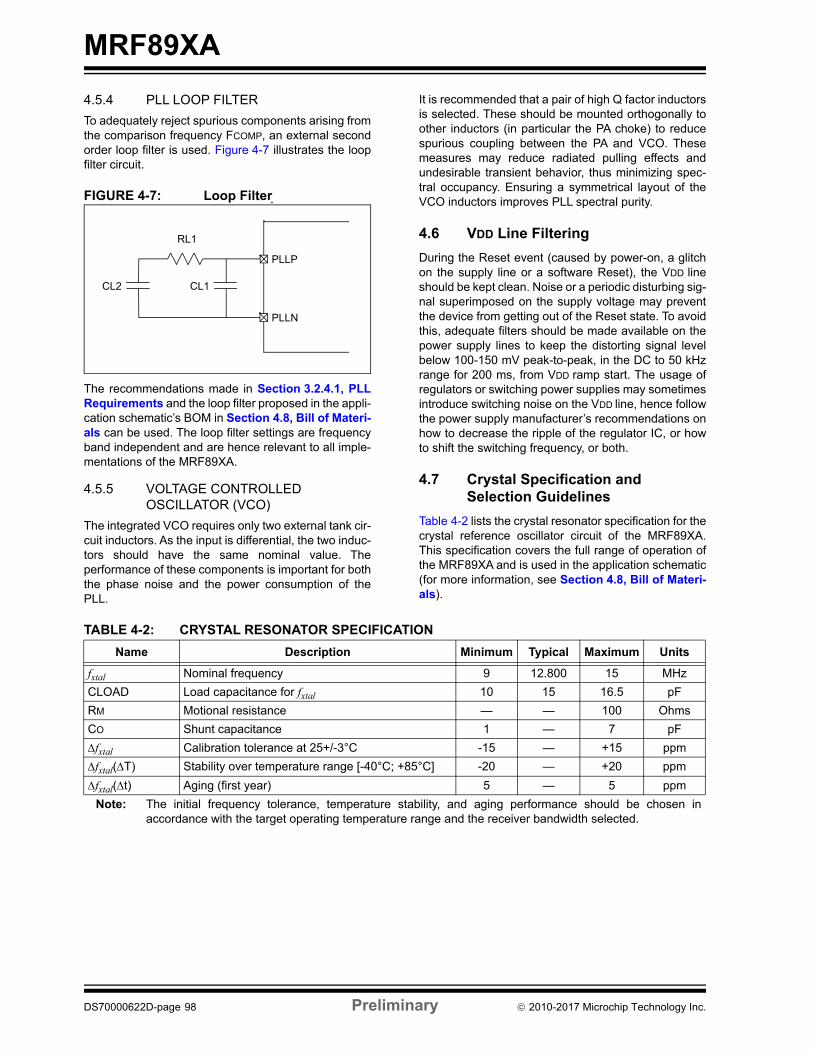
MRF89XA
4.5.4 PLL LOOP FILTER
To adequately reject spurious components arising fromthe comparison frequency FCOMP, an external secondorder loop filter is used. Figure 4-7 illustrates the loopfilter circuit.
FIGURE 4-7: Loop Filter
The recommendations made in Section 3.2.4.1, PLLRequirements and the loop filter proposed in the appli-cation schematic’s BOM in Section 4.8, Bill of Materi-als can be used. The loop filter settings are frequencyband independent and are hence relevant to all imple-mentations of the MRF89XA.
4.5.5 VOLTAGE CONTROLLED OSCILLATOR (VCO)
The integrated VCO requires only two external tank cir-cuit inductors. As the input is differential, the two induc-tors should have the same nominal value. Theperformance of these components is important for boththe phase noise and the power consumption of thePLL.
It is recommended that a pair of high Q factor inductorsis selected. These should be mounted orthogonally toother inductors (in particular the PA choke) to reducespurious coupling between the PA and VCO. Thesemeasures may reduce radiated pulling effects andundesirable transient behavior, thus minimizing spec-tral occupancy. Ensuring a symmetrical layout of theVCO inductors improves PLL spectral purity.
4.6 VDD Line Filtering
During the Reset event (caused by power-on, a glitchon the supply line or a software Reset), the VDD lineshould be kept clean. Noise or a periodic disturbing sig-nal superimposed on the supply voltage may preventthe device from getting out of the Reset state. To avoidthis, adequate filters should be made available on thepower supply lines to keep the distorting signal levelbelow 100-150 mV peak-to-peak, in the DC to 50 kHzrange for 200 ms, from VDD ramp start. The usage ofregulators or switching power supplies may sometimesintroduce switching noise on the VDD line, hence followthe power supply manufacturer’s recommendations onhow to decrease the ripple of the regulator IC, or howto shift the switching frequency, or both.
4.7 Crystal Specification and Selection Guidelines
Table 4-2 lists the crystal resonator specification for thecrystal reference oscillator circuit of the MRF89XA.This specification covers the full range of operation ofthe MRF89XA and is used in the application schematic(for more information, see Section 4.8, Bill of Materi-als).
TABLE 4-2: CRYSTAL RESONATOR SPECIFICATION
PLLP
CL1 CL2
PLLN
RL1
Name Description Minimum Typical Maximum Units
fxtal Nominal frequency 9 12.800 15 MHz
CLOAD Load capacitance for fxtal 10 15 16.5 pF
RM Motional resistance — — 100 Ohms
CO Shunt capacitance 1 — 7 pF
fxtal Calibration tolerance at 25+/-3°C -15 — +15 ppm
fxtal(T) Stability over temperature range [-40°C; +85°C] -20 — +20 ppm
fxtal(t) Aging (first year) 5 — 5 ppm
Note: The initial frequency tolerance, temperature stability, and aging performance should be chosen inaccordance with the target operating temperature range and the receiver bandwidth selected.
DS70000622D-page 98 Preliminary 2010-2017 Microchip Technology Inc.

MRF89XA
4.8 Bill of Materials
TABLE 4-3: MRF89XA APPLICATION SCHEMATIC BILL OF MATERIALS FOR 868 MHz
Designator Value Description Manufacturer
C1 0.047 μF Capacitor, Ceramic, 10V, +/-10%, X7R, SMT 0402 Murata Electronics North America
C2 0.22 μF Capacitor, Ceramic, 16V, +/-10%, X7R, SMT 0402 Murata Electronics North America
C3 1 μF Capacitor, Ceramic, 6.3V, +/-10%, X5R, SMT 0603 Murata Electronics North America
C4 22 pF Capacitor, Ceramic, 50V, +/-5%, UHI-Q NP0, SMT 0402
Johanson Technology
C5 1.8 pF Capacitor, Ceramic, 50V, +/-0.1 pF, UHI-Q NP0, SMT 0402
Johanson Technology
C7 33 pF Capacitor, Ceramic, 50V, +/-5%, C0G, SMT 0402 Murata Electronics North America
C8 0.1 μF Capacitor, Ceramic, 16V, +/-10%, C0G, SMT 0402 Murata Electronics North America
C9 680 pF Capacitor, Ceramic, 50V, +/-5%, C0G, SMT 0402 Murata Electronics North America
C10 0.01 μF Capacitor, Ceramic, 16V, +/-10%, X7R, SMT 0402 Murata Electronics North America
C11 4.3 pF Capacitor, Ceramic, 50V, +/-0.1 pF, UHI-Q NP0, SMT 0402
Johanson Technology
C12 1.5 pF Capacitor, Ceramic, 50V, +/-0.1 pF, UHI-Q NP0, SMT 0402
Johanson Technology
FL1 TA0801A SAW Filter Taisaw
L1 8.2 nH Inductor, Ceramic, +/-5%, SMT 0402 Johanson Technology
L2 100 nH Inductor, Ceramic, +/-5%, SMT 0402 Johanson Technology
L3 6.8 nH Inductor, Wirewound, +/-5%, SMT 0402 Johanson Technology
L4 6.8 nH Inductor, Wirewound, +/-5%, SMT 0402 Johanson Technology
L6 10 nH Inductor, Ceramic, +/-5%, SMT 0402 Johanson Technology
R1 1 ohm Resistor, 1%, +/-100 ppm/C, SMT 0402 Vishay/Dale
R2 100K ohm Resistor, 5%, +/-100 ppm/C, SMT 0402 Yageo
R3 6.8K ohm Resistor, 1%, +/-100 ppm/C, SMT 0402 Yageo
R4 0 ohm Resistor, SMT 0402 Yageo
R5 — Not Populated —
U1 MRF89XA Transceiver Microchip Technology Inc.
X1 12.800 MHz
Crystal, +/-10 ppm, 15 pF, ESR 100 ohms, SMT 5x3.2mm
—
Note: For battery powered applications, a highvalue capacitance should be implementedin parallel with C1 (typically 10 μF) to offera low impedance voltage source duringstartup sequences.
2010-2017 Microchip Technology Inc. Preliminary DS70000622D-page 99
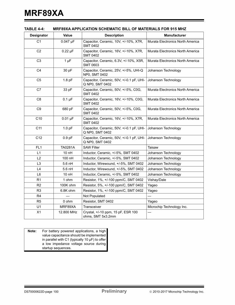
MRF89XA
TABLE 4-4: MRF89XA APPLICATION SCHEMATIC BILL OF MATERIALS FOR 915 MHZ
Designator Value Description Manufacturer
C1 0.047 μF Capacitor, Ceramic, 10V, +/-10%, X7R, SMT 0402
Murata Electronics North America
C2 0.22 μF Capacitor, Ceramic, 16V, +/-10%, X7R, SMT 0402
Murata Electronics North America
C3 1 μF Capacitor, Ceramic, 6.3V, +/-10%, X5R, SMT 0603
Murata Electronics North America
C4 30 pF Capacitor, Ceramic, 25V, +/-5%, UHI-Q NP0, SMT 0402
Johanson Technology
C5 1.8 pF Capacitor, Ceramic, 50V, +/-0.1 pF, UHI-Q NP0, SMT 0402
Johanson Technology
C7 33 pF Capacitor, Ceramic, 50V, +/-5%, C0G, SMT 0402
Murata Electronics North America
C8 0.1 μF Capacitor, Ceramic, 16V, +/-10%, C0G, SMT 0402
Murata Electronics North America
C9 680 pF Capacitor, Ceramic, 50V, +/-5%, C0G, SMT 0402
Murata Electronics North America
C10 0.01 μF Capacitor, Ceramic, 16V, +/-10%, X7R, SMT 0402
Murata Electronics North America
C11 1.0 pF Capacitor, Ceramic, 50V, +/-0.1 pF, UHI-Q NP0, SMT 0402
Johanson Technology
C12 0.9 pF Capacitor, Ceramic, 50V, +/-0.1 pF, UHI-Q NP0, SMT 0402
Johanson Technology
FL1 TA0281A SAW Filter Taisaw
L1 10 nH Inductor, Ceramic, +/-5%, SMT 0402 Johanson Technology
L2 100 nH Inductor, Ceramic, +/-5%, SMT 0402 Johanson Technology
L3 5.6 nH Inductor, Wirewound, +/-5%, SMT 0402 Johanson Technology
L4 5.6 nH Inductor, Wirewound, +/-5%, SMT 0402 Johanson Technology
L6 10 nH Inductor, Ceramic, +/-5%, SMT 0402 Johanson Technology
R1 1 ohm Resistor, 1%, +/-100 ppm/C, SMT 0402 Vishay/Dale
R2 100K ohm Resistor, 5%, +/-100 ppm/C, SMT 0402 Yageo
R3 6.8K ohm Resistor, 1%, +/-100 ppm/C, SMT 0402 Yageo
R4 — Not Populated —
R5 0 ohm Resistor, SMT 0402 Yageo
U1 MRF89XA Transceiver Microchip Technology Inc.
X1 12.800 MHz Crystal, +/-10 ppm, 15 pF, ESR 100 ohms, SMT 5x3.2mm
—
Note: For battery powered applications, a highvalue capacitance should be implementedin parallel with C1 (typically 10 μF) to offera low impedance voltage source duringstartup sequences.
DS70000622D-page 100 Preliminary 2010-2017 Microchip Technology Inc.
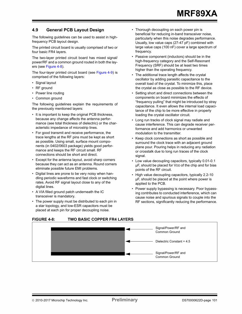
MRF89XA
4.9 General PCB Layout Design
The following guidelines can be used to assist in high-frequency PCB layout design.
The printed circuit board is usually comprised of two orfour basic FR4 layers.
The two-layer printed circuit board has mixed signal/power/RF and a common ground routed in both the lay-ers (see Figure 4-8).
The four-layer printed circuit board (see Figure 4-9) iscomprised of the following layers:
• Signal layout
• RF ground
• Power line routing
• Common ground
The following guidelines explain the requirements ofthe previously mentioned layers:
• It is important to keep the original PCB thickness, because any change affects the antenna perfor-mance (see total thickness of dielectric) or the char-acteristic impedance of microstrip lines.
• For good transmit and receive performance, the trace lengths at the RF pins must be kept as short as possible. Using small, surface mount compo-nents (in 0402/0603 package) yields good perfor-mance and keeps the RF circuit small. RF connections should be short and direct.
• Except for the antenna layout, avoid sharp corners because they can act as an antenna. Round corners eliminate possible future EMI problems.
• Digital lines are prone to be very noisy when han-dling periodic waveforms and fast clock or switching rates. Avoid RF signal layout close to any of the digital lines.
• A VIA filled ground patch underneath the IC transceiver is mandatory.
• The power supply must be distributed to each pin in a star topology, and low-ESR capacitors must be placed at each pin for proper decoupling noise.
• Thorough decoupling on each power pin is beneficial for reducing in-band transceiver noise, particularly when this noise degrades performance. Usually, low value caps (27-47 pF) combined with large value caps (100 nF) cover a large spectrum of frequency.
• Passive component (inductors) should be in the high-frequency category and the Self-Resonant Frequency (SRF) should be at least two times higher than the operating frequency.
• The additional trace length affects the crystal oscillator by adding parasitic capacitance to the overall load of the crystal. To minimize this, place the crystal as close as possible to the RF device.
• Setting short and direct connections between the components on board minimizes the effects of “frequency pulling” that might be introduced by stray capacitance. It even allows the internal load capaci-tance of the chip to be more effective in properly loading the crystal oscillator circuit.
• Long run tracks of clock signal may radiate and cause interference. This can degrade receiver per-formance and add harmonics or unwanted modulation to the transmitter.
• Keep clock connections as short as possible and surround the clock trace with an adjacent ground plane pour. Pouring helps in reducing any radiation or crosstalk due to long run traces of the clock signal.
• Low value decoupling capacitors, typically 0.01-0.1 µF, should be placed for VDD of the chip and for bias points of the RF circuit.
• High value decoupling capacitors, typically 2.2-10 µF, should be placed at the point where power is applied to the PCB.
• Power supply bypassing is necessary. Poor bypass-ing contributes to conducted interference, which can cause noise and spurious signals to couple into the RF sections, significantly reducing the performance.
FIGURE 4-8: TWO BASIC COPPER FR4 LAYERS
Signal/Power/RF andCommon Ground
Dielectric Constant = 4.5
Signal/Power/RF andCommon Ground
2010-2017 Microchip Technology Inc. Preliminary DS70000622D-page 101
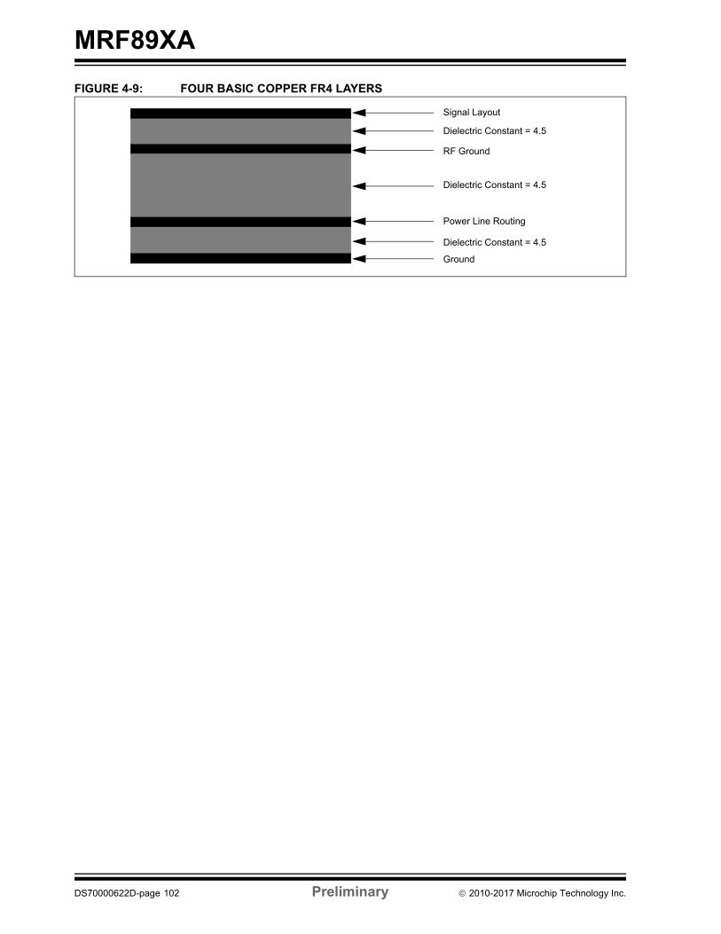
MRF89XA
FIGURE 4-9: FOUR BASIC COPPER FR4 LAYERS
Signal Layout
Dielectric Constant = 4.5
RF Ground
Dielectric Constant = 4.5
Power Line Routing
Dielectric Constant = 4.5
Ground
DS70000622D-page 102 Preliminary 2010-2017 Microchip Technology Inc.
MRF89XA
5.0 ELECTRICAL CHARACTERISTICS
Absolute Maximum Ratings
Ambient temperature under bias.............................................................................................................. -40°C to +85°C
Storage temperature .............................................................................................................................. -55°C to +125°C
Lead temperature (soldering, max 10s) ............................................................................................................... +260°C
Voltage on VDD with respect to VSS ............................................................................................................... -0.3V to 6V
Voltage on any combined digital and analog pin with respect to VSS (except RFIO and VDD) ....... -0.3V to (VDD + 0.3V)
Voltage on open-collector outputs (RFIO)(1) ............................................................................................... -0.3V to 3.7V
Input current into pin (except VDD and VSS).......................................................................................... -25 mA to 25 mA
Electrostatic discharge with human body model .................................................................................................... 1000V
Note 1: At maximum, voltage on RFIO cannot be higher than 6V.
Note: Stresses above those listed under “Absolute Maximum Ratings” may cause permanent damage to thedevice. This is a stress rating only and functional operation of the device at those or any other conditionsabove those indicated in the operation listings of this specification is not implied. Exposure to maximumrating conditions for extended periods may affect device reliability.
2010-2017 Microchip Technology Inc. Preliminary DS70000622D-page 103

MRF89XA
5.1 ESD Notice
The MRF89XA is a high-performance radio frequencydevice. It satisfies:
• Class II of the JEDEC standard JESD22-A114-B (Human Body Model) of 2 KV, except on all of the RF pins where it satisfies Class 1A.
• Class III of the JEDEC standard JESD22-C101C (Charged Device Model) on all pins.
It should thus be handled with all the necessary ESDprecautions to avoid any permanent damage.
TABLE 5-1: RECOMMENDED OPERATING CONDITIONS
TABLE 5-2: CURRENT CONSUMPTION(3)
Parameter Min Typ Max Unit Condition
Ambient Operating Temperature -40 — +85 °C —
Supply Voltage for RF, Analog and Digital Circuits 2.1 — 3.6 V —
Supply Voltage for Digital I/O 2.1 — 3.6 V —
Input High Voltage (VIH) 0.5 * VDD — VDD + 0.3 V —
Input Low Voltage (VIL) -0.3V — 0.2 * VDD V —
DC Voltage on Open Collector Outputs (RFIO)(1, 2) VDD – 1.5 — VDD + 1.5 V —
AC Peak Voltage on Open Collector Outputs (IO)(1) VDD – 1.5 — VDD + 1.5 V —
Note 1: At minimum, VDD – 1.5V should not be lower than 1.8V.
2: At maximum, VDD + 1.5V should not be higher than 3.7V.
Symbol Chip Mode Min Typ Max Unit Condition
IDDSL Sleep — 0.1 2 µA Sleep clock disabled, all blocks disabled
IDDST Idle — 65 80 µA Oscillator and baseband enabled(2)
IDDFS Frequency Synthesizer — 1.3 1.7 mA Frequency synthesizer running
IDDTX TX ——
2516
3021
mAmA
Output power = +10 dBmOutput power = +1 dBm(1)
IDDRX RX — 3.0 3.5 mA —
Note 1: Guaranteed by design and characterization.
2: Crystal CLOAD = 10 pF, C0 = 2.5 pF, RM = 15.
3: Measurement Conditions: Temp = 25°C, VDD = 3.3V, crystal frequency = 12.8 MHz, carrier frequency = 868 or 915 MHz, modulation FSK, data rate = 25 kbps, fdev = 50 kHz, fc = 100 kHz, unless otherwise specified.
DS70000622D-page 104 Preliminary 2010-2017 Microchip Technology Inc.
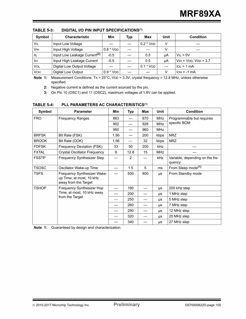
MRF89XA
TABLE 5-3: DIGITAL I/O PIN INPUT SPECIFICATIONS(1)
TABLE 5-4: PLL PARAMETERS AC CHARACTERISTICS(1)
Symbol Characteristic Min Typ Max Unit Condition
VIL Input Low Voltage — — 0.2 * VDD V —
VIH Input High Voltage 0.8 * VDD — — V —
IIL Input Low Leakage Current(2) -0.5 — 0.5 µA VIL = 0V
IIH Input High Leakage Current -0.5 — 0.5 µA VIH = VDD, VDD = 3.7
VOL Digital Low Output Voltage — — 0.1 * VDD — IOL = 1 mA
VOH Digital Low Output 0.9 * VDD — — V IOH = -1 mA
Note 1: Measurement Conditions: TA = 25°C, VDD = 3.3V, crystal frequency = 12.8 MHz, unless otherwise specified.
2: Negative current is defined as the current sourced by the pin.
3: On Pin 10 (OSC1) and 11 (OSC2), maximum voltages of 1.8V can be applied.
Symbol Parameter Min Typ Max Unit Condition
FRO Frequency Ranges 863 — 870 MHz Programmable but requires specific BOM902 — 928 MHz
950 — 960 MHz
BRFSK Bit Rate (FSK) 1.56 — 200 kbps NRZ
BROOK Bit Rate (OOK) 1.56 — 32 kbps NRZ
FDFSK Frequency Deviation (FSK) 33 50 200 kHz —
FXTAL Crystal Oscillator Frequency 9 12.8 15 MHz —
FSSTP Frequency Synthesizer Step — 2 — kHz Variable, depending on the fre-quency
TSOSC Oscillator Wake-up Time — 1.5 5 ms From Sleep mode(1)
TSFS Frequency Synthesizer Wake-up Time; at most, 10 kHz away from the Target
— 500 800 µs From Standby mode
TSHOP Frequency Synthesizer Hop Time; at most, 10 kHz away from the Target
— 180 — µs 200 kHz step
— 200 — µs 1 MHz step
— 250 — µs 5 MHz step
— 260 — µs 7 MHz step
— 290 — µs 12 MHz step
— 320 — µs 20 MHz step
— 340 — µs 27 MHz step
Note 1: Guaranteed by design and characterization.
2010-2017 Microchip Technology Inc. Preliminary DS70000622D-page 105
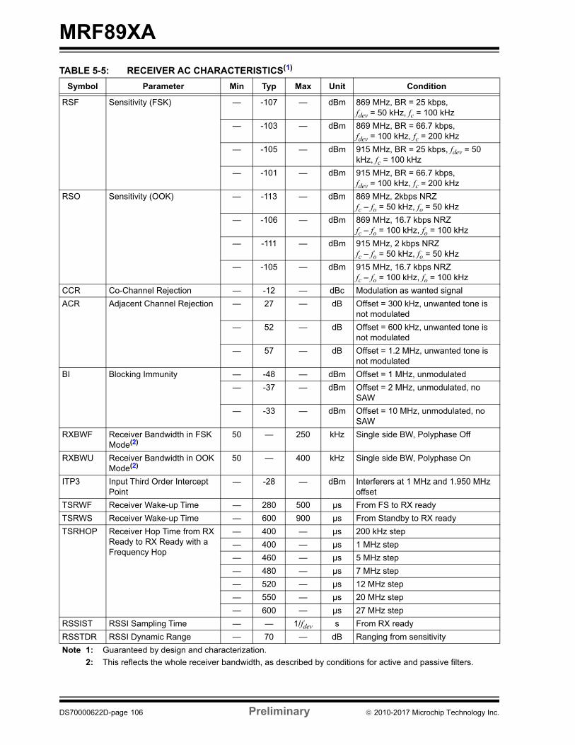
MRF89XA
TABLE 5-5: RECEIVER AC CHARACTERISTICS(1)
Symbol Parameter Min Typ Max Unit Condition
RSF Sensitivity (FSK) — -107 — dBm 869 MHz, BR = 25 kbps, fdev = 50 kHz, fc = 100 kHz
— -103 — dBm 869 MHz, BR = 66.7 kbps, fdev = 100 kHz, fc = 200 kHz
— -105 — dBm 915 MHz, BR = 25 kbps, fdev = 50 kHz, fc = 100 kHz
— -101 — dBm 915 MHz, BR = 66.7 kbps, fdev = 100 kHz, fc = 200 kHz
RSO Sensitivity (OOK) — -113 — dBm 869 MHz, 2kbps NRZfc – fo = 50 kHz, fo = 50 kHz
— -106 — dBm 869 MHz, 16.7 kbps NRZfc – fo = 100 kHz, fo = 100 kHz
— -111 — dBm 915 MHz, 2 kbps NRZfc – fo = 50 kHz, fo = 50 kHz
— -105 — dBm 915 MHz, 16.7 kbps NRZfc – fo = 100 kHz, fo = 100 kHz
CCR Co-Channel Rejection — -12 — dBc Modulation as wanted signal
ACR Adjacent Channel Rejection — 27 — dB Offset = 300 kHz, unwanted tone is not modulated
— 52 — dB Offset = 600 kHz, unwanted tone is not modulated
— 57 — dB Offset = 1.2 MHz, unwanted tone is not modulated
BI Blocking Immunity — -48 — dBm Offset = 1 MHz, unmodulated
— -37 — dBm Offset = 2 MHz, unmodulated, no SAW
— -33 — dBm Offset = 10 MHz, unmodulated, no SAW
RXBWF Receiver Bandwidth in FSK Mode(2)
50 — 250 kHz Single side BW, Polyphase Off
RXBWU Receiver Bandwidth in OOK Mode(2)
50 — 400 kHz Single side BW, Polyphase On
ITP3 Input Third Order Intercept Point
— -28 — dBm Interferers at 1 MHz and 1.950 MHz offset
TSRWF Receiver Wake-up Time — 280 500 µs From FS to RX ready
TSRWS Receiver Wake-up Time — 600 900 µs From Standby to RX ready
TSRHOP Receiver Hop Time from RX Ready to RX Ready with a Frequency Hop
— 400 — µs 200 kHz step
— 400 — µs 1 MHz step
— 460 — µs 5 MHz step
— 480 — µs 7 MHz step
— 520 — µs 12 MHz step
— 550 — µs 20 MHz step
— 600 — µs 27 MHz step
RSSIST RSSI Sampling Time — — 1/fdev s From RX ready
RSSTDR RSSI Dynamic Range — 70 — dB Ranging from sensitivity
Note 1: Guaranteed by design and characterization.
2: This reflects the whole receiver bandwidth, as described by conditions for active and passive filters.
DS70000622D-page 106 Preliminary 2010-2017 Microchip Technology Inc.
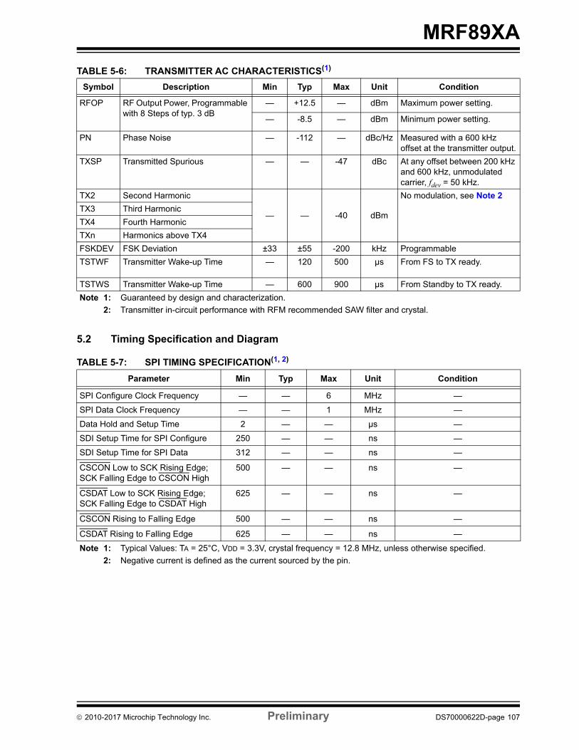
MRF89XA
TABLE 5-6: TRANSMITTER AC CHARACTERISTICS(1)
5.2 Timing Specification and Diagram
TABLE 5-7: SPI TIMING SPECIFICATION(1, 2)
Symbol Description Min Typ Max Unit Condition
RFOP RF Output Power, Programmable with 8 Steps of typ. 3 dB
— +12.5 — dBm Maximum power setting.
— -8.5 — dBm Minimum power setting.
PN Phase Noise — -112 — dBc/Hz Measured with a 600 kHz offset at the transmitter output.
TXSP Transmitted Spurious — — -47 dBc At any offset between 200 kHz and 600 kHz, unmodulated carrier, fdev = 50 kHz.
TX2 Second Harmonic
— — -40 dBm
No modulation, see Note 2
TX3 Third Harmonic
TX4 Fourth Harmonic
TXn Harmonics above TX4
FSKDEV FSK Deviation ±33 ±55 -200 kHz Programmable
TSTWF Transmitter Wake-up Time — 120 500 µs From FS to TX ready.
TSTWS Transmitter Wake-up Time — 600 900 µs From Standby to TX ready.
Note 1: Guaranteed by design and characterization.
2: Transmitter in-circuit performance with RFM recommended SAW filter and crystal.
Parameter Min Typ Max Unit Condition
SPI Configure Clock Frequency — — 6 MHz —
SPI Data Clock Frequency — — 1 MHz —
Data Hold and Setup Time 2 — — µs —
SDI Setup Time for SPI Configure 250 — — ns —
SDI Setup Time for SPI Data 312 — — ns —
CSCON Low to SCK Rising Edge;SCK Falling Edge to CSCON High
500 — — ns —
CSDAT Low to SCK Rising Edge;SCK Falling Edge to CSDAT High
625 — — ns —
CSCON Rising to Falling Edge 500 — — ns —
CSDAT Rising to Falling Edge 625 — — ns —
Note 1: Typical Values: TA = 25°C, VDD = 3.3V, crystal frequency = 12.8 MHz, unless otherwise specified.
2: Negative current is defined as the current sourced by the pin.
2010-2017 Microchip Technology Inc. Preliminary DS70000622D-page 107
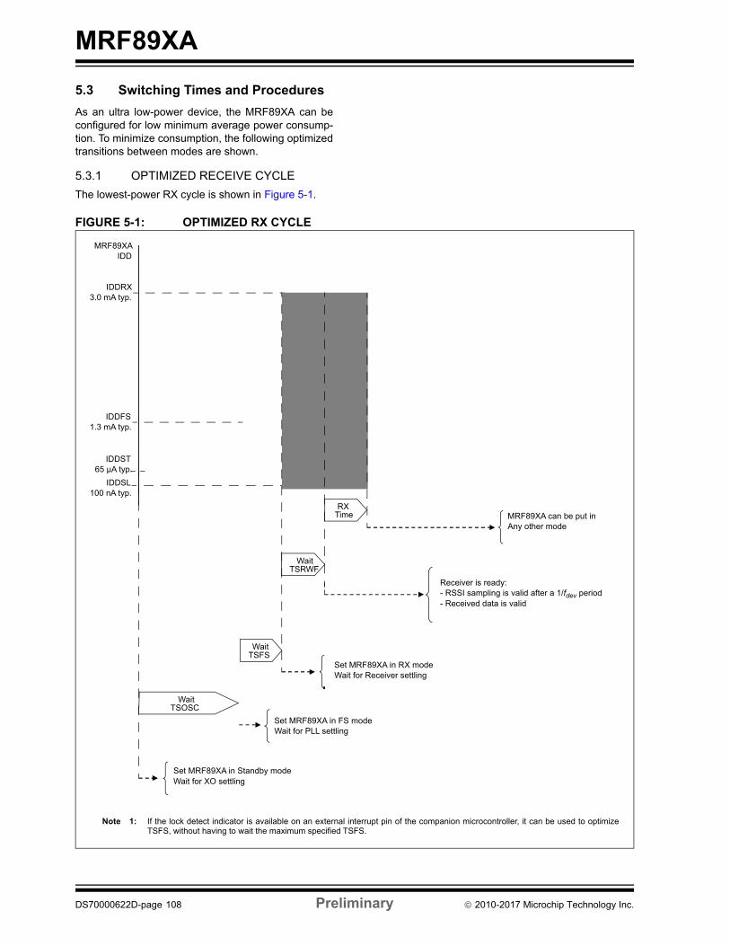
MRF89XA
5.3 Switching Times and Procedures
As an ultra low-power device, the MRF89XA can beconfigured for low minimum average power consump-tion. To minimize consumption, the following optimizedtransitions between modes are shown.
5.3.1 OPTIMIZED RECEIVE CYCLE
The lowest-power RX cycle is shown in Figure 5-1.
FIGURE 5-1: OPTIMIZED RX CYCLE
MRF89XA IDD
Set MRF89XA in Standby modeWait for XO settling
Set MRF89XA in FS mode Wait for PLL settling
Set MRF89XA in RX mode Wait for Receiver settling
IDDRX 3.0 mA typ.
IDDFS 1.3 mA typ.
IDDST 65 µA typ.
IDDSL 100 nA typ.
Wait TSOSC
Wait TSFS
Wait TSRWF
Receiver is ready: - RSSI sampling is valid after a 1/fdev period - Received data is valid
MRF89XA can be put in Any other mode
RX Time
Note 1: If the lock detect indicator is available on an external interrupt pin of the companion microcontroller, it can be used to optimizeTSFS, without having to wait the maximum specified TSFS.
DS70000622D-page 108 Preliminary 2010-2017 Microchip Technology Inc.
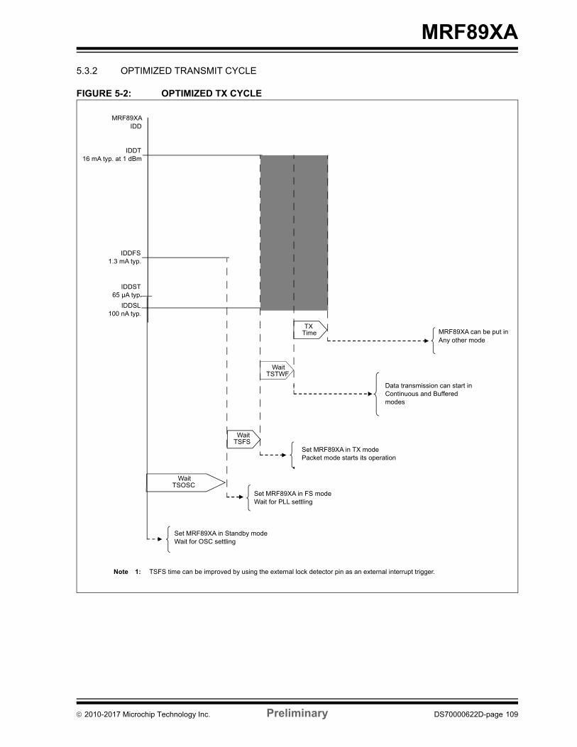
MRF89XA
5.3.2 OPTIMIZED TRANSMIT CYCLE
FIGURE 5-2: OPTIMIZED TX CYCLE
MRF89XA IDD
Set MRF89XA in Standby modeWait for OSC settling
Set MRF89XA in FS mode Wait for PLL settling
Set MRF89XA in TX mode Packet mode starts its operation
IDDT 16 mA typ. at 1 dBm
IDDFS 1.3 mA typ.
IDDST 65 µA typ.
IDDSL 100 nA typ.
Wait TSOSC
Wait TSFS
Wait TSTWF
Data transmission can start in Continuous and Buffered modes
MRF89XA can be put in Any other mode
TX Time
Note 1: TSFS time can be improved by using the external lock detector pin as an external interrupt trigger.
2010-2017 Microchip Technology Inc. Preliminary DS70000622D-page 109
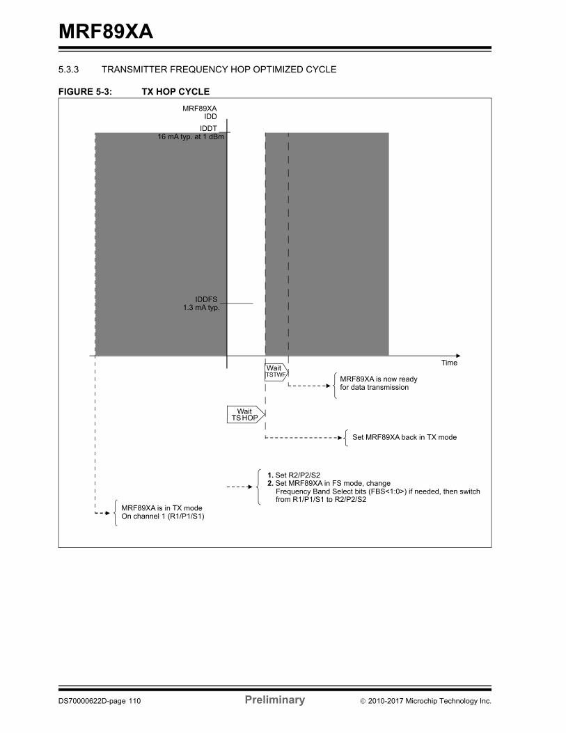
MRF89XA
5.3.3 TRANSMITTER FREQUENCY HOP OPTIMIZED CYCLE
FIGURE 5-3: TX HOP CYCLE
MRF89XAIDD
Time
MRF89XA is in TX mode On channel 1 (R1/P1/S1)
MRF89XA is now ready for data transmission
IDDT16 mA typ. at 1 dBm
IDDFS1.3 mA typ.
Wait TSHOP
Wait TSTWF
Set MRF89XA back in TX mode
1. Set R2/P2/S2 2. Set MRF89XA in FS mode, change
Frequency Band Select bits (FBS<1:0>) if needed, then switch from R1/P1/S1 to R2/P2/S2
DS70000622D-page 110 Preliminary 2010-2017 Microchip Technology Inc.
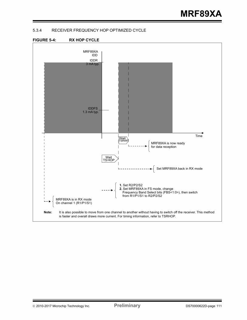
MRF89XA
5.3.4 RECEIVER FREQUENCY HOP OPTIMIZED CYCLE
FIGURE 5-4: RX HOP CYCLE
MRF89XAIDD
Time
MRF89XA is in RX mode On channel 1 (R1/P1/S1)
MRF89XA is now ready for data reception
IDDR3 mA typ.
IDDFS1.3 mA typ.
Wait TSHOP
Wait TSRWF
Set MRF89XA back in RX mode
1. Set R2/P2/S2 2. Set MRF89XA in FS mode, change
Frequency Band Select bits (FBS<1:0>), then switch from R1/P1/S1 to R2/P2/S2
Note: It is also possible to move from one channel to another without having to switch off the receiver. This methodis faster and overall draws more current. For timing information, refer to TSRHOP.
2010-2017 Microchip Technology Inc. Preliminary DS70000622D-page 111

MRF89XA
5.3.5 RX TX AND TX RX JUMP CYCLES
FIGURE 5-5: RX TX RX CYCLE
MRF89XA IDD
Time
MRF89XA is in RX mode
Set MRF89XA in TX mode
MRF89XA is now ready for data transmission
IDDR 3.0 mA typ.
Wait TSTWF
IDDT 16 mA typ. at 1 dBm
Set MRF89XA in RX mode
Wait TSRWF
MRF89XA is ready to receive data
DS70000622D-page 112 Preliminary 2010-2017 Microchip Technology Inc.
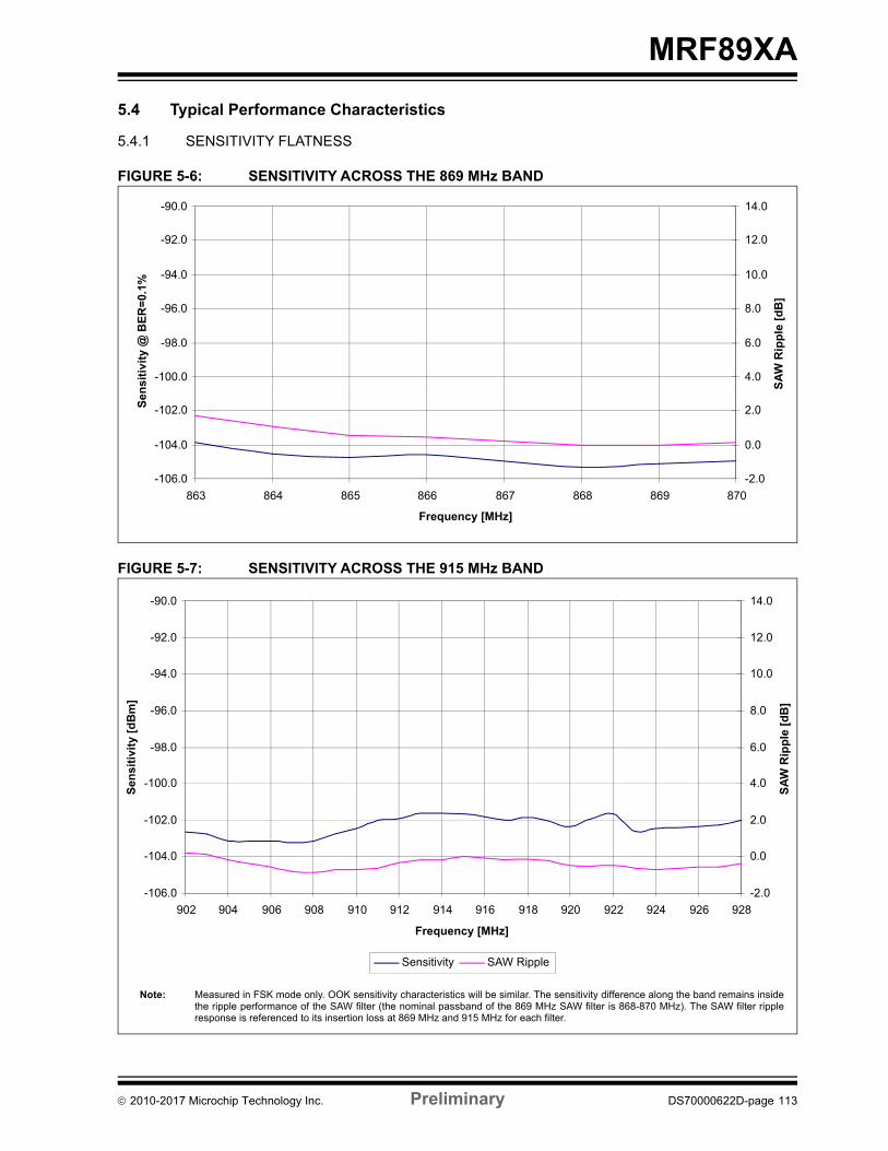
MRF89XA
5.4 Typical Performance Characteristics
5.4.1 SENSITIVITY FLATNESS
FIGURE 5-6: SENSITIVITY ACROSS THE 869 MHz BAND
FIGURE 5-7: SENSITIVITY ACROSS THE 915 MHz BAND
-106.0
-104.0
-102.0
-100.0
-98.0
-96.0
-94.0
-92.0
-90.0
863 864 865 866 867 868 869 870
Frequency [MHz]
Sen
siti
vity
@ B
ER
=0.
1%
-2.0
0.0
2.0
4.0
6.0
8.0
10.0
12.0
14.0
SA
W R
ipp
le [
dB
]
-106.0
-104.0
-102.0
-100.0
-98.0
-96.0
-94.0
-92.0
-90.0
902 904 906 908 910 912 914 916 918 920 922 924 926 928
Frequency [MHz]
Sen
siti
vity
[d
Bm
]
-2.0
0.0
2.0
4.0
6.0
8.0
10.0
12.0
14.0
SA
W R
ipp
le [
dB
]
Sensitivity SAW Ripple
Note: Measured in FSK mode only. OOK sensitivity characteristics will be similar. The sensitivity difference along the band remains insidethe ripple performance of the SAW filter (the nominal passband of the 869 MHz SAW filter is 868-870 MHz). The SAW filter rippleresponse is referenced to its insertion loss at 869 MHz and 915 MHz for each filter.
2010-2017 Microchip Technology Inc. Preliminary DS70000622D-page 113
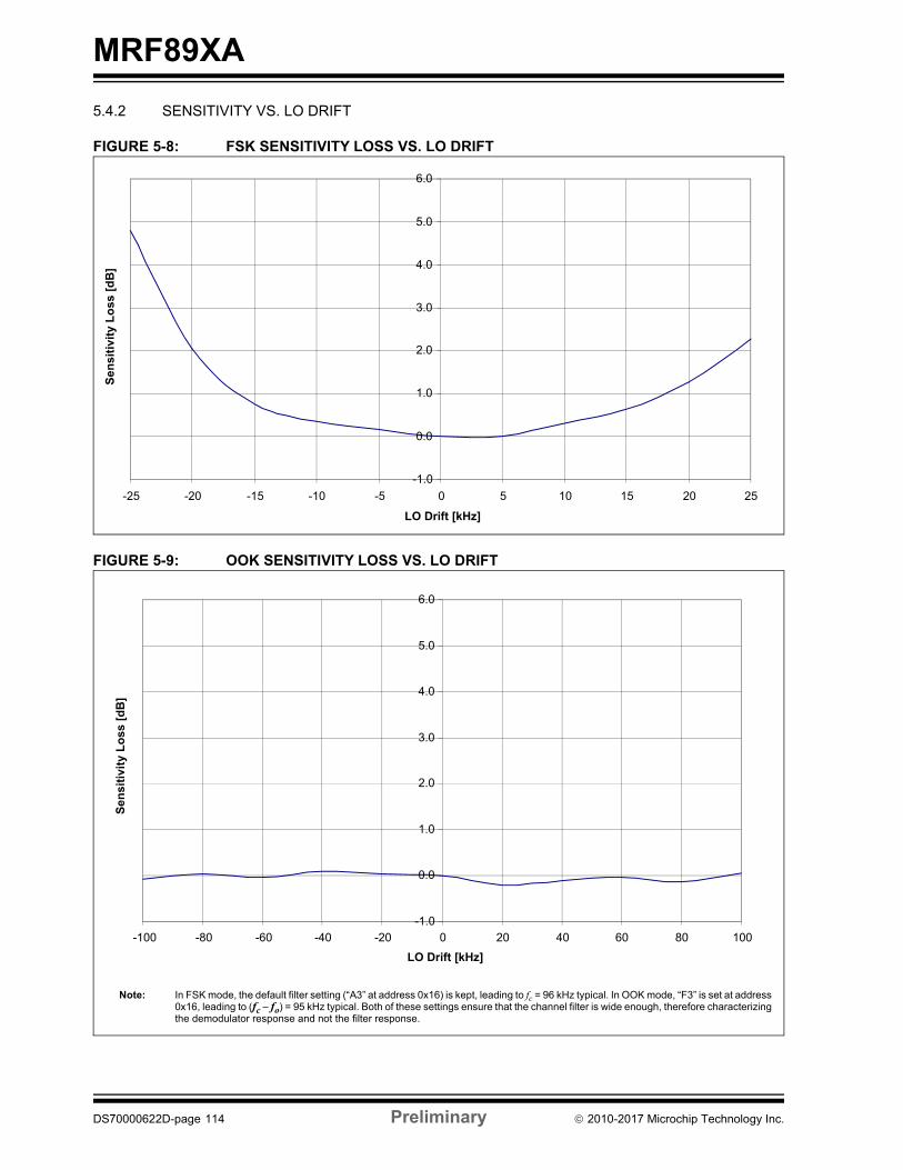
MRF89XA
5.4.2 SENSITIVITY VS. LO DRIFT
FIGURE 5-8: FSK SENSITIVITY LOSS VS. LO DRIFT
FIGURE 5-9: OOK SENSITIVITY LOSS VS. LO DRIFT
-1.0
0.0
1.0
2.0
3.0
4.0
5.0
6.0
-25 -20 -15 -10 -5 0 5 10 15 20 25
LO Drift [kHz]
Sen
siti
vity
Lo
ss [
dB
]
-1.0
0.0
1.0
2.0
3.0
4.0
5.0
6.0
-100 -80 -60 -40 -20 0 20 40 60 80 100
LO Drift [kHz]
Sen
siti
vity
Lo
ss [
dB
]
Note: In FSK mode, the default filter setting (“A3” at address 0x16) is kept, leading to fc = 96 kHz typical. In OOK mode, “F3” is set at address0x16, leading to (fc – fo) = 95 kHz typical. Both of these settings ensure that the channel filter is wide enough, therefore characterizingthe demodulator response and not the filter response.
DS70000622D-page 114 Preliminary 2010-2017 Microchip Technology Inc.

MRF89XA
5.4.3 SENSITIVITY VS. RECEIVER BW
FIGURE 5-10: FSK SENSITIVITY VS. RX BW
FIGURE 5-11: OOK SENSITIVITY CHANGE VS. RX BW
-6.0
-5.0
-4.0
-3.0
-2.0
-1.0
0.0
1.0
50 100 150 200 250 300
fc of Active Filter [kHz]
Sen
siti
vity
Imp
rove
men
t [d
B]
=>
-6.0
-5.0
-4.0
-3.0
-2.0
-1.0
0.0
1.0
0 50 100 150 200 250 300 350
fc-fo [kHz]
Sen
sit
ivit
y Im
pro
vem
ent
[dB
] =
>
2010-2017 Microchip Technology Inc. Preliminary DS70000622D-page 115
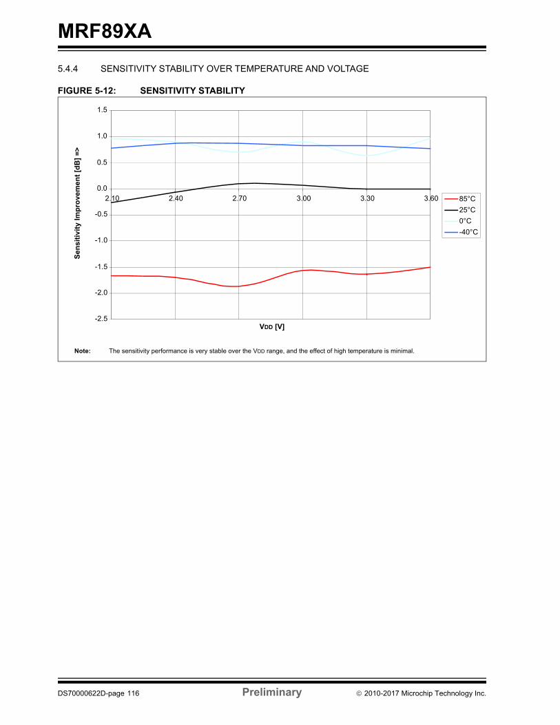
MRF89XA
5.4.4 SENSITIVITY STABILITY OVER TEMPERATURE AND VOLTAGE
FIGURE 5-12: SENSITIVITY STABILITY
-2.5
-2.0
-1.5
-1.0
-0.5
0.0
0.5
1.0
1.5
2.10 2.40 2.70 3.00 3.30 3.60
VDD [V]
Sen
siti
vity
Imp
rove
men
t [d
B]
=>
85°C
25°C
0°C
-40°C
Note: The sensitivity performance is very stable over the VDD range, and the effect of high temperature is minimal.
DS70000622D-page 116 Preliminary 2010-2017 Microchip Technology Inc.
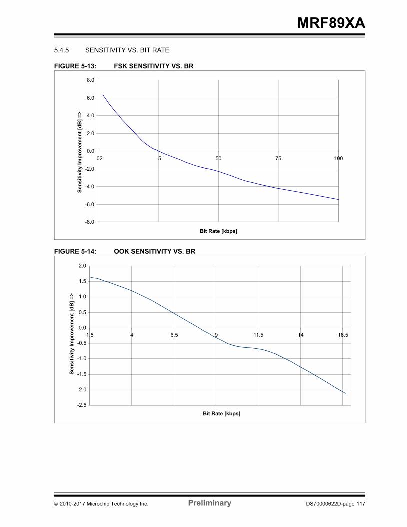
MRF89XA
5.4.5 SENSITIVITY VS. BIT RATE
FIGURE 5-13: FSK SENSITIVITY VS. BR
FIGURE 5-14: OOK SENSITIVITY VS. BR
-8.0
-6.0
-4.0
-2.0
0.0
2.0
4.0
6.0
8.0
02 5 50 75
Bit Rate [kbps]
Se
nsi
tivi
ty Im
pro
vem
ent
[dB
] =
>
100
-2.5
-2.0
-1.5
-1.0
-0.5
0.0
0.5
1.0
1.5
2.0
1.5 4 6.5 9 11.5 14 16.5
Bit Rate [kbps]
Sen
siti
vity
Im
pro
vem
ent
[dB
] =
>
2010-2017 Microchip Technology Inc. Preliminary DS70000622D-page 117

MRF89XA
5.4.6 ADJACENT CHANNEL REJECTION
FIGURE 5-15: ACR IN FSK MODE
FIGURE 5-16: ACR IN OOK MODE
0
10
20
30
40
50
60
70
-1000 -800 -600 -400 -200 0 200 400 600 800 1000
Offset [kHz]
AC
R [
dB
]
-20
-10
0
10
20
30
40
50
60
-300 -200 -100 0 100 200 300
Offset [kHz]
AC
R [d
B]
Note: In FSK mode, the unwanted signal is unmodulated (as described in the EN 300-220). Co-channel rejection (CCR, offset = 0 kHz) ispositive due to the DC cancellation process of the zero-IF architecture. In OOK mode, the polyphase filter efficiency is limited, thuslimiting the adjacent channel rejection at 2xFo distance.
DS70000622D-page 118 Preliminary 2010-2017 Microchip Technology Inc.

MRF89XA
5.4.7 OUTPUT POWER FLATNESS
FIGURE 5-17: POUT FOR 869 MHz BAND OPERATION
FIGURE 5-18: POUT FOR 915 MHz BAND OPERATION
0.0
2.0
4.0
6.0
8.0
10.0
12.0
863 864 865 866 867 868 869 870
Frequency [MHz]
PO
UT [
dB
m]
-8.0
-6.0
-4.0
-2.0
0.0
2.0
4.0
SA
W R
ipp
le [
dB
]
POUT SAW Ripple
0.00
2.00
4.00
6.00
8.00
10.00
12.00
902 904 906 908 910 912 914 916 918 920 922 924 926 928
Frequency [MHz]
PO
UT [
dB
m]
-8.0
-6.0
-4.0
-2.0
0.0
2.0
4.0
SA
W R
ipp
le [
dB
]
POUT SAW Ripple
Note: As noted inSection 4.4.1 “SAW Filter Plot”, the 869 MHz SAW filter does not cover the entire European 863-870 MHz frequency bandwhen used in a 50 environment. Therefore, the output power degradation happens at the lowest frequencies. For applications in the863-860 MHz band, it is recommended that an appropriate SAW filter be implemented or that the SAW response is tuned by externalmatching. The SAW filter ripple references are the insertion loss of each SAW at 869 MHz and 915 MHz.
2010-2017 Microchip Technology Inc. Preliminary DS70000622D-page 119
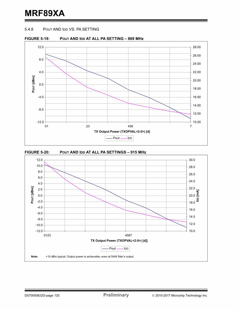
MRF89XA
5.4.8 POUT AND IDD VS. PA SETTING
FIGURE 5-19: POUT AND IDD AT ALL PA SETTING – 869 MHz
FIGURE 5-20: POUT AND IDD AT ALL PA SETTINGS – 915 MHz
-12.0
-8.0
-4.0
0.0
4.0
8.0
12.0
01 23 456 7
TX Output Power (TXOPVAL<2:0>) [d]
PO
UT [
dB
m]
10.00
12.00
14.00
16.00
18.00
20.00
22.00
24.00
26.00
28.00
Pout IDD
-12.0
-10.0
-8.0
-6.0
-4.0
-2.0
0.0
2.0
4.0
6.0
8.0
10.0
12.0
0123 4567
TX Output Power (TXOPVAL<2:0>) [d]]
PO
UT [
dB
m]
10.0
12.0
14.0
16.0
18.0
20.0
22.0
24.0
26.0
28.0
30.0
IDD
[m
A]
Pout IDD
Note: +10 dBm typical. Output power is achievable, even at SAW filter’s output.
DS70000622D-page 120 Preliminary 2010-2017 Microchip Technology Inc.

MRF89XA
5.4.9 POUT STABILITY OVER TEMPERATURE AND VOLTAGE
FIGURE 5-21: POUT STABILITY
The output power is not sensitive to the supply voltage,and it decreases slightly when temperature rises.
-2.0
-1.5
-1.0
-0.5
0.0
0.5
1.0
2.1 2.4 2.7 3.0 3.3 3.6
VDD [V]
PO
UT Im
pro
vem
ent
[dB
] =
>
85ºC
25ºC
-40ºC
0ºC
2010-2017 Microchip Technology Inc. Preliminary DS70000622D-page 121
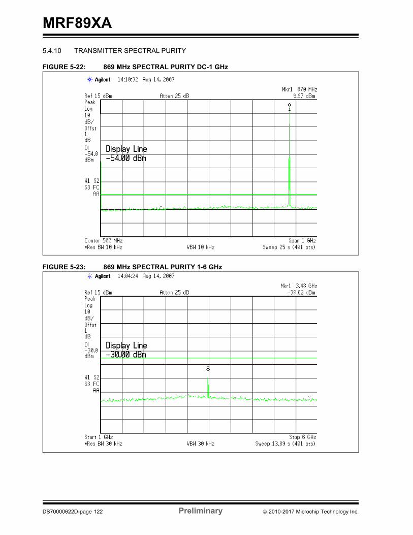
MRF89XA
5.4.10 TRANSMITTER SPECTRAL PURITY
FIGURE 5-22: 869 MHz SPECTRAL PURITY DC-1 GHz
FIGURE 5-23: 869 MHz SPECTRAL PURITY 1-6 GHz
DS70000622D-page 122 Preliminary 2010-2017 Microchip Technology Inc.

MRF89XA
5.4.11 OOK CHANNEL BANDWIDTH
The OOK bit rate ranges form 1.56 to 16.7 kbps. Forthe lowest bit rates, a channel spacing around 200 kHzis achievable.
FIGURE 5-24: OOK SPECTRUM – 2 kbps
FIGURE 5-25: OOK SPECTRUM – 8 kbps
2010-2017 Microchip Technology Inc. Preliminary DS70000622D-page 123
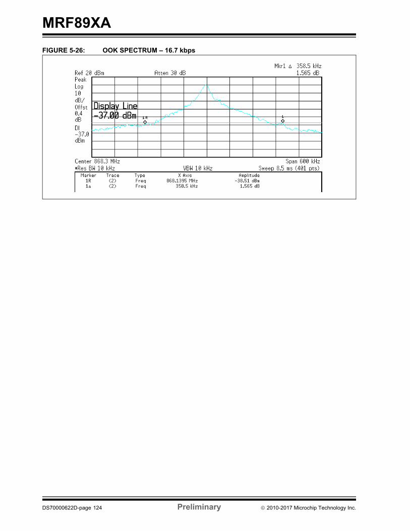
MRF89XA
FIGURE 5-26: OOK SPECTRUM – 16.7 kbps
DS70000622D-page 124 Preliminary 2010-2017 Microchip Technology Inc.
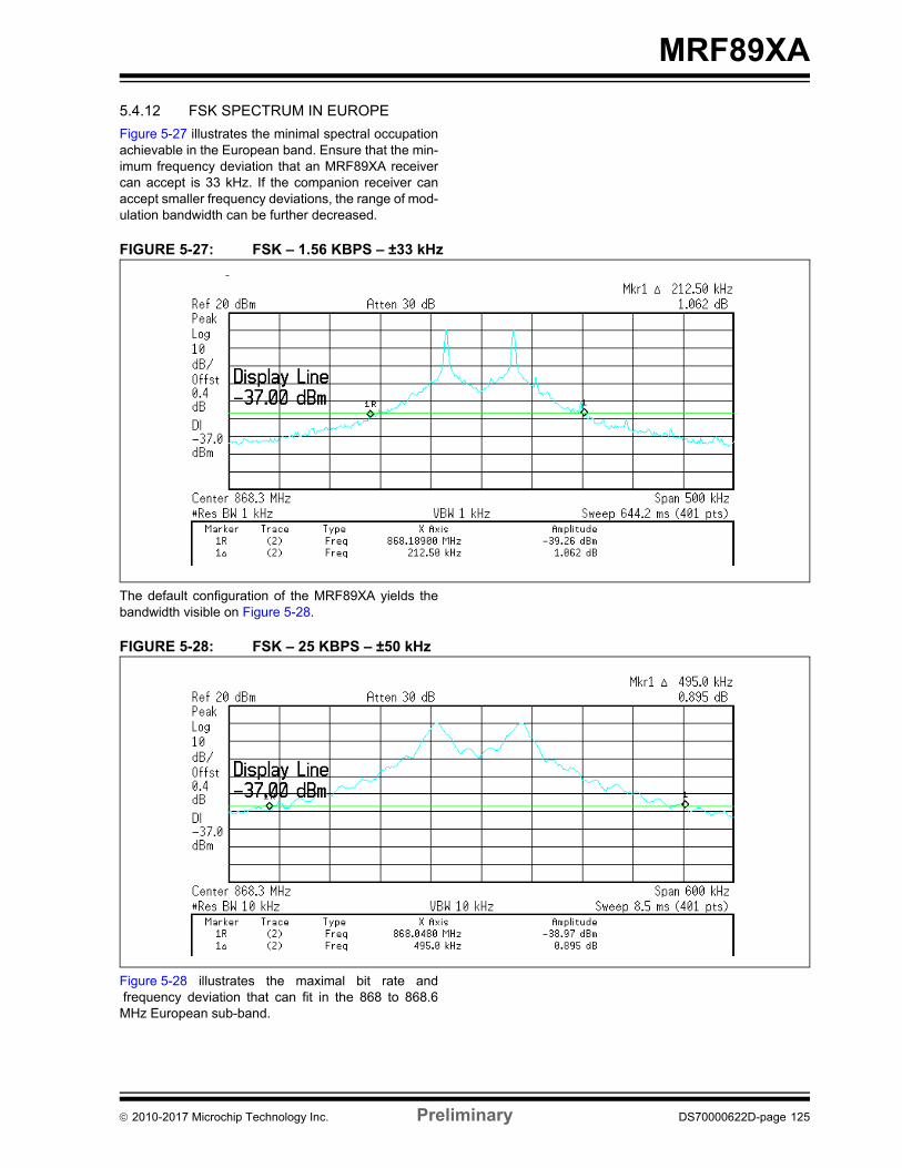
MRF89XA
5.4.12 FSK SPECTRUM IN EUROPE
Figure 5-27 illustrates the minimal spectral occupationachievable in the European band. Ensure that the min-imum frequency deviation that an MRF89XA receivercan accept is 33 kHz. If the companion receiver canaccept smaller frequency deviations, the range of mod-ulation bandwidth can be further decreased.
FIGURE 5-27: FSK – 1.56 KBPS – ±33 kHz
The default configuration of the MRF89XA yields thebandwidth visible on Figure 5-28.
FIGURE 5-28: FSK – 25 KBPS – ±50 kHz
Figure 5-28 illustrates the maximal bit rate andfrequency deviation that can fit in the 868 to 868.6MHz European sub-band.
2010-2017 Microchip Technology Inc. Preliminary DS70000622D-page 125
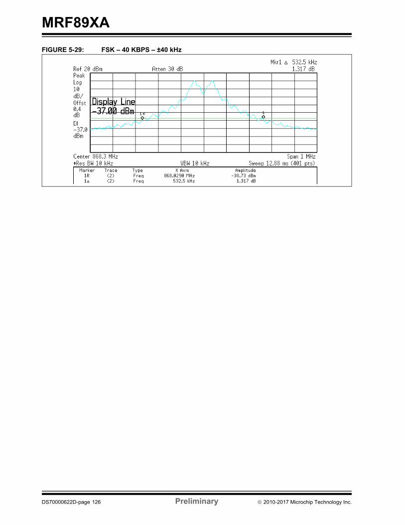
MRF89XA
FIGURE 5-29: FSK – 40 KBPS – ±40 kHz
DS70000622D-page 126 Preliminary 2010-2017 Microchip Technology Inc.
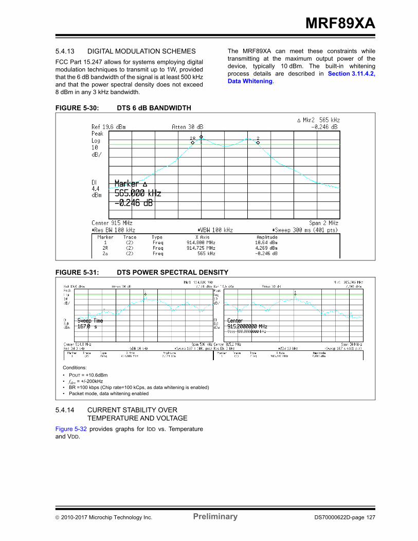
MRF89XA
5.4.13 DIGITAL MODULATION SCHEMES
FCC Part 15.247 allows for systems employing digitalmodulation techniques to transmit up to 1W, providedthat the 6 dB bandwidth of the signal is at least 500 kHzand that the power spectral density does not exceed8 dBm in any 3 kHz bandwidth.
The MRF89XA can meet these constraints whiletransmitting at the maximum output power of thedevice, typically 10 dBm. The built-in whiteningprocess details are described in Section 3.11.4.2,Data Whitening.
FIGURE 5-30: DTS 6 dB BANDWIDTH
FIGURE 5-31: DTS POWER SPECTRAL DENSITY
5.4.14 CURRENT STABILITY OVER TEMPERATURE AND VOLTAGE
Figure 5-32 provides graphs for IDD vs. Temperatureand VDD.
Conditions:
• POUT = +10.6dBm• fdev = +/-200kHz• BR =100 kbps (Chip rate=100 kCps, as data whitening is enabled)• Packet mode, data whitening enabled
2010-2017 Microchip Technology Inc. Preliminary DS70000622D-page 127

MR
F89X
A
DS
70000622D
-page 128
Prelim
ina
ry
2010-2017 Microchip T
echnology Inc.
Standby Mode Current
2.7 3 3.3 3.6VDD [V]
85ºC25ºC
0ºC-40ºC
RX Mode Current
2.7 3 3.3 3.6VDD [V]
Legend:
FIGURE 5-32: IDD vs. Temperature and VDD
TX Mode Current(Max Output Power)
0.0
5.0
10.0
15.0
20.0
25.0
30.0
2.1 2.4 2.7 3.0 3.3 3.6VDD [V]
Itx
[mA
]T
XLV
L=
000
Sleep Mode Current
0
200
400
600
800
1000
1200
2.1 2.4 2.7 3 3.3 3.6VDD [V]
Isle
ep [
nA
]
0
10
20
30
40
50
60
70
80
90
100
2.1 2.4
Istb
y [
µA
]
FS Mode Current
0.00
0.20
0.40
0.60
0.80
1.00
1.20
1.40
1.60
1.80
2.00
2.1 2.4 2.7 3 3.3 3.6VDD [V]
Ifs
[mA
]
0.00
0.50
1.00
1.50
2.00
2.50
3.00
3.50
4.00
2.1 2.4
Irx
[m
A]
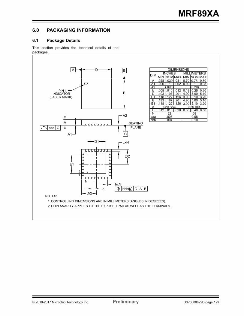
MRF89XA
6.0 PACKAGING INFORMATION
6.1 Package Details
This section provides the technical details of thepackages.
2010-2017 Microchip Technology Inc. Preliminary DS70000622D-page 129

MRF89XA
NOTES:
DS70000622D-page 130 Preliminary 2010-2017 Microchip Technology Inc.

MRF89XA
APPENDIX A: FSK AND OOK RX FILTERS VS. BIT RATES
TABLE A-1: FSK RX FILTERS VS. BIT RATE
TABLE A-2: OOK RX FILTERS VS. BIT RATE
Bit RateFdev (from FDEVREG)
Filter Setting (from
FILCREG)
Fdev + BR/2 (from
FDEVREG and BRSREG)
RX 3dB BWMaximum
DriftProgrammed Actual
kbps ± kHz Hex kHz kHz kHz ± ppm
100 200 FF 250 400 306 62
66.67 133 E9 166.7 250 214 53
50 100 D6 125 175 158 37
40 80 B5 100 150 137 41
33.33 67 A4 83.3 125 116 36
28.57 57 A3 71.4 100 96 27
25 50 A3 62.5 100 96 37
22.22 44 72 55.6 75 69 15
20 40 72 50 75 69 21
18.18 36 72 45.5 75 69 26
16.67 33 72 41.7 75 69 30
15.38 33 41 41 50 47 7
14.29 33 41 40.5 50 47 7
12.5 33 41 39.6 50 47 8
10 33 41 38.3 50 47 10
5 33 41 35.8 50 47 12
2 33 41 34.3 50 47 14
Bit RateFo + BR (from PFCREG and
BRSREG)
Filter Setting (from FILCREG)
RX 3 dB BWMaximum Drift
Programmed Actual
kbps kHz Hex kHz kHz ± ppm
16.67 117 C1 150 154 41
12.5 113 C1 150 154 46
9.52 110 A0 125 129 22
8 108 A0 125 129 23
4.76 105 A0 125 129 27
2.41 102 A0 125 129 30
1.56 102 A0 125 129 30
Note 1: To comply with any regulatory body like FCC for example with Part 15 of the FCC Rules. Operation is sub-ject to the following two conditions: (1) this device may not cause harmful interference, and (2) this devicemust accept any interference received, including interference that may cause undesired operation. Forregulated FSK and OOK settings, see the MRF89XA device module data sheet from Microchip Website.
2010-2017 Microchip Technology Inc. Preliminary DS70000622D-page 131
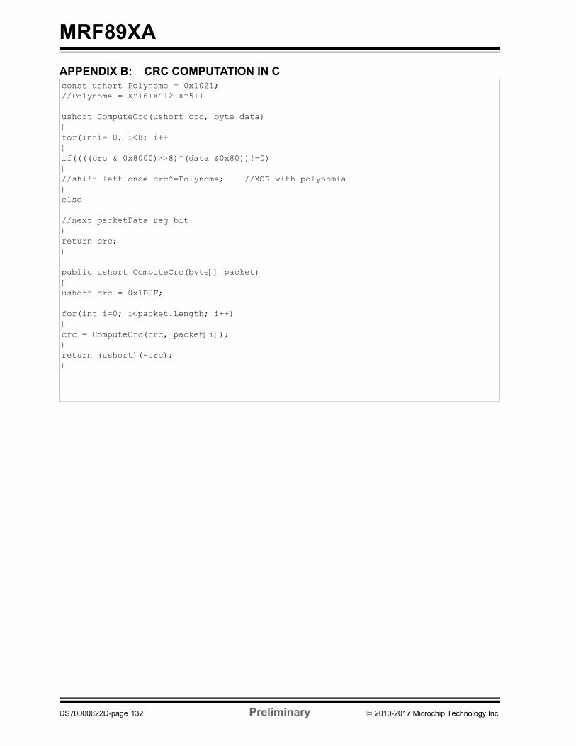
MRF89XA
APPENDIX B: CRC COMPUTATION IN Cconst ushort Polynome = 0x1021; //Polynome = X^16+X^12+X^5+1
ushort ComputeCrc(ushort crc, byte data)for(inti= 0; i<8; i++if((((crc & 0x8000)>>8)^(data &0x80))!=0)//shift left once crc^=Polynome; //XOR with polynomialelse
//next packetData reg bitreturn crc;
public ushort ComputeCrc(byte[] packet) ushort crc = 0x1D0F;
for(int i=0; i<packet.Length; i++)crc = ComputeCrc(crc, packet[i]);return (ushort)(~crc);
DS70000622D-page 132 Preliminary 2010-2017 Microchip Technology Inc.
MRF89XA
APPENDIX C: REVISION HISTORY
Revision A (January 2010)
This is the initial version of this document.
Revision B (June 2010)
Updates have been incorporated throughout thedocument, which required extensive revisions to allchapters.
This version also includes minor typographical andformatting changes throughout the data sheet text.
Revision C (November 2011)
Updates have been incorporated throughout thedocument, which required extensive revisions to allchapters.
Added Appendix B: “CRC Computation in C”.
Revision D (October 2017)
Updates have been incorporated throughout thedocument.
This version also includes minor typographical andformatting changes throughout the data sheet text.
2010-2017 Microchip Technology Inc. Preliminary DS70000622D-page 133

MRF89XA
NOTES:
DS70000622D-page 134 Preliminary 2010-2017 Microchip Technology Inc.
MRF89XA
THE MICROCHIP WEB SITE
Microchip provides online support via our WWW site atwww.microchip.com. This web site is used as a meansto make files and information easily available tocustomers. Accessible by using your favorite Internetbrowser, the web site contains the followinginformation:
• Product Support – Data sheets and errata, application notes and sample programs, design resources, user’s guides and hardware support documents, latest software releases and archived software
• General Technical Support – Frequently Asked Questions (FAQ), technical support requests, online discussion groups, Microchip consultant program member listing
• Business of Microchip – Product selector and ordering guides, latest Microchip press releases, listing of seminars and events, listings of Microchip sales offices, distributors and factory representatives
CUSTOMER CHANGE NOTIFICATION SERVICE
Microchip’s customer notification service helps keepcustomers current on Microchip products. Subscriberswill receive e-mail notification whenever there arechanges, updates, revisions or errata related to aspecified product family or development tool of interest.
To register, access the Microchip web site atwww.microchip.com. Under “Support”, click on“Customer Change Notification” and follow theregistration instructions.
CUSTOMER SUPPORT
Users of Microchip products can receive assistancethrough several channels:
• Distributor or Representative
• Local Sales Office
• Field Application Engineer (FAE)
• Technical Support
Customers should contact their distributor,representative or Field Application Engineer (FAE) forsupport. Local sales offices are also available to helpcustomers. A listing of sales offices and locations isincluded in the back of this document.
Technical support is available through the web siteat: http://microchip.com/support
2010-2017 Microchip Technology Inc. DS70000622D-page 135
MRF89XA
NOTES:
DS70000622D-page 136 2010-2017 Microchip Technology Inc.

MRF89XA
INDEX
AAbsolute Maximum Ratings ................................. 103Architecture Description ....................................... 20
BBit Synchronizer ................................................. 7Block Diagrams
Detailed..................................................... 2MRF89XA Simplified Functional ......................... 8Power Supply ............................................. 14
CChannel Filters.................................................. 16CLKOUT Output (CLKOUT Pin) .............................. 16Configuration Control/Status Register Map ................. 54Configuration/Control/Status Register Description ......... 28Customer Change Notification Service .................... 135Customer Notification Service .............................. 135Customer Support ............................................ 135
DDATA Pin........................................................ 19Digital Pin Configuration vs. Chip Mode ..................... 18
EElectrical Characteristics .................................... 103
Current Consumption .................................. 104Digital I/O Pin Input Specifications ................... 105PLL Parameters AC Characteristics ................. 105Receiver AC Characteristics .......................... 106SPI Timing Specification............................... 107Switching Times and Procedures..................... 108Transmitter AC Characteristics ....................... 107
Errata ............................................................. 5FFeatures
Digital Data Processing................................... 7Frequency Synthesizer Block ................................. 16Frequency Synthesizer Description .......................... 16FSK Receiver Setting .......................................... 22
GGeneral Configuration Register Details ...................... 30
HHardware Description .......................................... 93
II(t), Q(t) Overview .............................................. 20Internet Address .............................................. 135Interpolation Filter .............................................................. 15IRQ Pins and Interrupts........................................ 19
LLO Generator ................................................... 17Low Noise Amplifier (with First Mixer) 15
MMemory Map .................................................... 26Microchip Internet Web Site................................. 135
OOOK Receiver Setting ......................................... 22
PPackaging
Details ................................................... 129Packaging Information ....................................... 129Phase-Locked Loop Architecture............................. 17Pin Descriptions ................................................ 13Pins
CLKOUT................................................... 17CSCON .................................................... 23CSDAT .................................................... 23DATA ...................................................... 19OSC1 ...................................................... 16OSC2 ...................................................... 16PLOCK .................................................... 17Reset ...................................................... 15RFIO .................................................. 11, 15
PLL Lock Pin.................................................... 17POUT and IDD vs. PA Setting ................................ 120Power Amplifier................................................. 15Power Supply Pin Details...................................... 14Power-Saving Modes .......................................... 17
RRead Bytes Sequence ......................................... 25Read Register Sequence...................................... 24Receiver Architecture .......................................... 21Recommended PA Biasing and Output Matching .......... 97Reference Oscillator Pins (OSC1/OSC2).................... 16Register Map.................................................... 54Registers
Bit Rate Set Register (BRSREG)....................... 32Clock Output Control Register (CLKOUTREG) ....... 50Data and Modulation Configuration Register
(DMODREG)........................................ 31FIFO Configuration Register (FIFOCREG) ............ 33FIFO CRC Configuration Register (FCRCREG) ...... 53FIFO Transmit and Receive Interrupt Request
Configuration Register (FTXRXIREG............... ) 38FIFO Transmit PLL and RSSI Interrupt Request
Configuration Register (FTPRIREG) ............. 40Filter Configuration Register (FILCREG) .............. 42Floor Threshold Control Register (FLTHREG)........ 33Frequency Deviation Control Register (FDEVREG).. 32General Configuration Register (GCONREG) ........ 30Node Address Set Register (NADDSREG) ........... 51OOK Configuration Register (OOKCREG) ............ 46P1 Counter Set Register (P1CREG) ................... 34P2 Counter Set Register (P2CREG) ................... 36Packet Configuration Register (PKTCREG)........... 52Payload Configuration Register (PLOADREG) ....... 51Polyphase Filter Configuration Register
(PFCONREG)....................................... 43Power Amplifier Control Register (PACREG) ......... 37R1 Counter Set Register (R1CREG)................... 34R2 Counter Set Register (R2CREG)................... 35Reserved Register (RESVREG) ........................ 45RSSI Status Read Register (RSTSREG).............. 45RSSI Threshold Interrupt Request Configuration
Register (RSTHIREG) ............................. 41S1 Counter Set Register (S1CREG) ................... 35S2 Counter Set Register (S2CREG) ................... 36SYNC Control Register (SYNCREG) .................. 44
2010–2017 Microchip Technology Inc. Preliminary DS70000622D-page 137
MRF89XA
SYNC Value First Byte Configuration Register (SYNCV32REG)......... 47
SYNC Value Fourth Byte Configuration Register (SYNCV07REG)......... 48
SYNC Value Second Byte Configuration Register (SYNCV23REG)......... 47
SYNC Value Third Byte Configuration Register (SYNCV15REG)......... 48
Transmit Parameter Configuration Register TXCONREG) ....................................... 49
Revision History .............................................. 133
SSerial Peripheral Interface (SPI) ........................................ 23SPI Config....................................................... 24SPI Data............................................................................. 25SPI Interface Overview and Host Microcontroller
Connections............................................... 23Suggested PA Biasing and Matching ........................ 15Super-Heterodyne Architecture............................... 11Supported Feature Blocks
64-Byte Transmit and Receive FIFO Buffer ........... 11Bit Synchronization....................................... 11Data Filtering and Whitening ............................ 11General Configuration Registers ....................... 11
Supported frequency bands.................................... 7Switching Times and Procedures
Optimized Receive Cycle.............................. 108Optimized Transmit Cycle ............................. 109Receiver Frequency Hop Optimized Cycle .......... 111RX TX and TX RX Jump Cycles ............... 112Transmitter Frequency Hop Optimized Cycle ....... 110
TTransmitter Architecture ....................................... 19Transmitter Description ........................................ 19Typical Performance Characteristics
Adjacent Channel Rejection........................... 118Current Stability Over Temperature and Voltage ... 127Digital Modulation Schemes .......................... 127FSK Spectrum in Europe .............................. 125OOK Channel Bandwidth.............................. 123Output Power Flatness ................................ 119POUT Stability over Temperature and Voltage ...... 121Sensitivity Flatness..................................... 113Sensitivity Stability over Temperature and Voltage 116Sensitivity vs. Bit Rate ................................. 117Sensitivity vs. LO Drift ................................. 114Sensitivity vs. Receiver BW ........................... 115Transmitter Spectral Purity ............................ 122
VVoltage Controlled Oscillator.............................................. 17
WWrite Bytes Sequence ......................................... 25Write Register Sequence ...................................... 24WWW Address ............................................... 135WWW, On-Line Support ........................................ 5
DS70000622D-page 138 Preliminary 2010–2017 Microchip Technology Inc.

2010-2017 Microchip Technology Inc. Preliminary DS70000622D-page 139
MRF89XA
PRODUCT IDENTIFICATION SYSTEM
To order or obtain information, for example, on pricing or delivery, refer to the factory or the listed sales office.
PART NO. X /XX XXX
PatternPackageTemperatureRange
Device
Device MRF89XA: Ultra Low-Power, Integrated ISM Band Sub-GHz Transceiver
Temperature Range
I = -40ºC to +85ºC (Industrial)
Package MQ = QFN (Quad Flat, No Lead)T = Tape and Reel
Example:
a) MRF89XA-I/MQ: Industrial temperature, QFN package.
b) MRF89XAT-I/MQ: Industrial temperature, QFN package, tape and reel.

DS70000622D-page 140 2010-2017 Microchip Technology Inc.
AMERICASCorporate Office2355 West Chandler Blvd.Chandler, AZ 85224-6199Tel: 480-792-7200 Fax: 480-792-7277Technical Support: http://www.microchip.com/supportWeb Address: www.microchip.com
AtlantaDuluth, GA Tel: 678-957-9614 Fax: 678-957-1455
Austin, TXTel: 512-257-3370
BostonWestborough, MA Tel: 774-760-0087 Fax: 774-760-0088
ChicagoItasca, IL Tel: 630-285-0071 Fax: 630-285-0075
DallasAddison, TX Tel: 972-818-7423 Fax: 972-818-2924
DetroitNovi, MI Tel: 248-848-4000
Houston, TX Tel: 281-894-5983
IndianapolisNoblesville, IN Tel: 317-773-8323Fax: 317-773-5453Tel: 317-536-2380
Los AngelesMission Viejo, CA Tel: 949-462-9523Fax: 949-462-9608Tel: 951-273-7800
Raleigh, NC Tel: 919-844-7510
New York, NY Tel: 631-435-6000
San Jose, CA Tel: 408-735-9110Tel: 408-436-4270
Canada - TorontoTel: 905-695-1980 Fax: 905-695-2078
ASIA/PACIFICAsia Pacific OfficeSuites 3707-14, 37th FloorTower 6, The GatewayHarbour City, Kowloon
Hong KongTel: 852-2943-5100Fax: 852-2401-3431
Australia - SydneyTel: 61-2-9868-6733Fax: 61-2-9868-6755
China - BeijingTel: 86-10-8569-7000 Fax: 86-10-8528-2104
China - ChengduTel: 86-28-8665-5511Fax: 86-28-8665-7889
China - ChongqingTel: 86-23-8980-9588Fax: 86-23-8980-9500
China - DongguanTel: 86-769-8702-9880
China - GuangzhouTel: 86-20-8755-8029
China - HangzhouTel: 86-571-8792-8115 Fax: 86-571-8792-8116
China - Hong Kong SARTel: 852-2943-5100 Fax: 852-2401-3431
China - NanjingTel: 86-25-8473-2460Fax: 86-25-8473-2470
China - QingdaoTel: 86-532-8502-7355Fax: 86-532-8502-7205
China - ShanghaiTel: 86-21-3326-8000 Fax: 86-21-3326-8021
China - ShenyangTel: 86-24-2334-2829Fax: 86-24-2334-2393
China - ShenzhenTel: 86-755-8864-2200 Fax: 86-755-8203-1760
China - WuhanTel: 86-27-5980-5300Fax: 86-27-5980-5118
China - XianTel: 86-29-8833-7252Fax: 86-29-8833-7256
ASIA/PACIFICChina - XiamenTel: 86-592-2388138 Fax: 86-592-2388130
China - ZhuhaiTel: 86-756-3210040 Fax: 86-756-3210049
India - BangaloreTel: 91-80-3090-4444 Fax: 91-80-3090-4123
India - New DelhiTel: 91-11-4160-8631Fax: 91-11-4160-8632
India - PuneTel: 91-20-3019-1500
Japan - OsakaTel: 81-6-6152-7160 Fax: 81-6-6152-9310
Japan - TokyoTel: 81-3-6880- 3770 Fax: 81-3-6880-3771
Korea - DaeguTel: 82-53-744-4301Fax: 82-53-744-4302
Korea - SeoulTel: 82-2-554-7200Fax: 82-2-558-5932 or 82-2-558-5934
Malaysia - Kuala LumpurTel: 60-3-6201-9857Fax: 60-3-6201-9859
Malaysia - PenangTel: 60-4-227-8870Fax: 60-4-227-4068
Philippines - ManilaTel: 63-2-634-9065Fax: 63-2-634-9069
SingaporeTel: 65-6334-8870Fax: 65-6334-8850
Taiwan - Hsin ChuTel: 886-3-5778-366Fax: 886-3-5770-955
Taiwan - KaohsiungTel: 886-7-213-7830
Taiwan - TaipeiTel: 886-2-2508-8600 Fax: 886-2-2508-0102
Thailand - BangkokTel: 66-2-694-1351Fax: 66-2-694-1350
EUROPEAustria - WelsTel: 43-7242-2244-39Fax: 43-7242-2244-393
Denmark - CopenhagenTel: 45-4450-2828 Fax: 45-4485-2829
Finland - EspooTel: 358-9-4520-820
France - ParisTel: 33-1-69-53-63-20 Fax: 33-1-69-30-90-79
Germany - GarchingTel: 49-8931-9700Germany - HaanTel: 49-2129-3766400
Germany - HeilbronnTel: 49-7131-67-3636
Germany - KarlsruheTel: 49-721-625370
Germany - MunichTel: 49-89-627-144-0 Fax: 49-89-627-144-44
Germany - RosenheimTel: 49-8031-354-560
Israel - Ra’anana Tel: 972-9-744-7705
Italy - Milan Tel: 39-0331-742611 Fax: 39-0331-466781
Italy - PadovaTel: 39-049-7625286
Netherlands - DrunenTel: 31-416-690399 Fax: 31-416-690340
Norway - TrondheimTel: 47-7289-7561
Poland - WarsawTel: 48-22-3325737
Romania - BucharestTel: 40-21-407-87-50
Spain - MadridTel: 34-91-708-08-90Fax: 34-91-708-08-91
Sweden - GothenbergTel: 46-31-704-60-40
Sweden - StockholmTel: 46-8-5090-4654
UK - WokinghamTel: 44-118-921-5800Fax: 44-118-921-5820
Worldwide Sales and Service
10/10/17