ultrascale architecture libraries guide (ug974) · chapter2 xilinxparameterizedmacros...
TRANSCRIPT

UltraScale ArchitectureLibraries Guide
UG974 (v2018.2) June 6, 2018
Chapter 1
Introduction
OverviewThis HDL guide is part of the Vivado® Design Suite documentation collection.
This guide contains the following:
• Introduction
• Descriptions of each available macro
• A list of design elements supported in this architecture, organized by functional categories
• Descriptions of each available primitive
About Design ElementsThis version of the Libraries Guide describes the valid design elements for UltraScale™architecture-based devices including the UltraScale and UltraScale+ families, and includesexamples of instantiation code for each element. Instantiation templates are also suppliedin a separate ZIP file, which you can find on www.xilinx.com linked to this file or within theLanguage Templates in the Vivado Design Suite.
Design elements are divided into the following main categories:
• Macros : These elements are in the Xilinx Parameterized Macro library in the tool, and areused to instantiate elements that are complex to instantiate by just using the primitives.The synthesis tools will automatically expand the macros to their underlying primitives.
IMPORTANT: Unimacros from previous generation Xilinx FPGA Architectures are notsupported in the Ultrascale architecture and have been replaced by Xilinx ParameterizedMacros.
• Primitives: Xilinx components that are native to the architecture you are targeting.
UG974 (v2018.2) June 6, 2018 www.xilinx.comUltraScale Architecture Libraries Guide 2
Send Feedback
Chapter 1: Introduction
Design Entry MethodsFor each design element in this guide, Xilinx evaluates four options for using the designelement, and recommends what we believe is the best solution for you. The four options are:
• Instantiation: This component can be instantiated directly into the design. This method isuseful if you want to control the exact use, implementation, or placement of the individualblocks.
• Inference: This component can be inferred by most supported synthesis tools. You shoulduse this method if you want to have complete flexibility and portability of the code tomultiple architectures. Inference also gives the tools the ability to optimize for performance,area, or power, as specified by the user to the synthesis tool.
• IP and IP Integrator Catalog: This component can be instantiated from the IP Catalog.The IP Catalog maintains a library of IP Cores assembled from multiple primitives to formmore complex functions, as well as interfaces to help in instantiation of the more complexprimitives. References here to the IP Catalog generally refer to the latter, where you use theIP catalog to assist in the use and integration of certain primitives into your design.
UG974 (v2018.2) June 6, 2018 www.xilinx.comUltraScale Architecture Libraries Guide 3
Send Feedback
Chapter 2
Xilinx Parameterized Macros
About Xilinx Parameterized MacrosThis section describes Xilinx Parameterized Macros that can be used with UltraScale™architecture-based devices. The macros are organized alphabetically.
IMPORTANT: Unimacros from previous generation Xilinx FPGA Architectures are not supportedin the Ultrascale architecture and have been replaced by Xilinx Parameterized Macros.
The following information is provided for each macro, where applicable:
• Name, description, macro group, macro subgroup, and family
• Schematic symbol
• Introduction
• Logic diagram (if any)
• Port descriptions
• Design Entry Method
• Available attributes
• Example instantiation templates
• Links to additional information
Enabling Xilinx Parameterized MacrosThe following instructions describe how to prepare Vivado to use the XPM libraries.
1. Ensure Vivado can identify the XPMs.
• When using the IDE and/or the project flow, the tools will parse the files added to theproject and setup Vivado to recognize the XPMs.
• When using the non-project flow, you must issue the auto_detect_xpm command.
2. Select the XPM template that you wish to use from below.
3. Copy the contents of the template and paste into your own source file.
4. Set parameters/generics, and wire ports according to the documentation provided ascode comments.
NOTE: Be sure to read and comply with all code comments to properly use the XPMs.
UG974 (v2018.2) June 6, 2018 www.xilinx.comUltraScale Architecture Libraries Guide 4
Send Feedback
Chapter 2: Xilinx Parameterized Macros
TestbenchA testbench for XPM CDC macros is available in the XPM CDC Testbench File.
A testbench for XPM FIFO macros is available in the XPM FIFO Testbench File.
Instantiation TemplatesInstantiation templates for Xilinx Parameterized Macros are also available in Vivado, as well as ina downloadable ZIP file. Because PDF includes headers and footers if you copy text that spanspages, you should copy templates from Vivado or the downloaded ZIP file whenever possible.
Instantiation templates can be found on the Web in the Instantiation Templates for XilinxParameterizable Macros file.
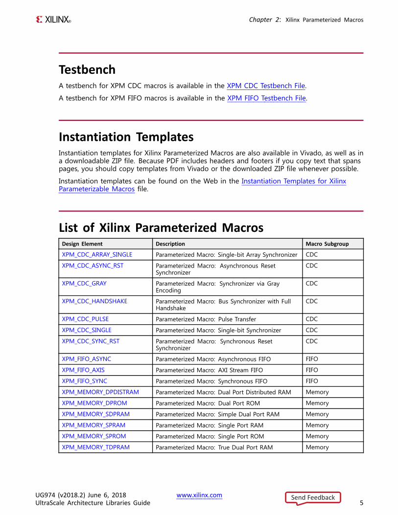
List of Xilinx Parameterized MacrosDesign Element Description Macro Subgroup
XPM_CDC_ARRAY_SINGLE Parameterized Macro: Single-bit Array Synchronizer CDC
XPM_CDC_ASYNC_RST Parameterized Macro: Asynchronous ResetSynchronizer
CDC
XPM_CDC_GRAY Parameterized Macro: Synchronizer via GrayEncoding
CDC
XPM_CDC_HANDSHAKE Parameterized Macro: Bus Synchronizer with FullHandshake
CDC
XPM_CDC_PULSE Parameterized Macro: Pulse Transfer CDC
XPM_CDC_SINGLE Parameterized Macro: Single-bit Synchronizer CDC
XPM_CDC_SYNC_RST Parameterized Macro: Synchronous ResetSynchronizer
CDC
XPM_FIFO_ASYNC Parameterized Macro: Asynchronous FIFO FIFO
XPM_FIFO_AXIS Parameterized Macro: AXI Stream FIFO FIFO
XPM_FIFO_SYNC Parameterized Macro: Synchronous FIFO FIFO
XPM_MEMORY_DPDISTRAM Parameterized Macro: Dual Port Distributed RAM Memory
XPM_MEMORY_DPROM Parameterized Macro: Dual Port ROM Memory
XPM_MEMORY_SDPRAM Parameterized Macro: Simple Dual Port RAM Memory
XPM_MEMORY_SPRAM Parameterized Macro: Single Port RAM Memory
XPM_MEMORY_SPROM Parameterized Macro: Single Port ROM Memory
XPM_MEMORY_TDPRAM Parameterized Macro: True Dual Port RAM Memory
UG974 (v2018.2) June 6, 2018 www.xilinx.comUltraScale Architecture Libraries Guide 5
Send Feedback
Chapter 2: Xilinx Parameterized Macros
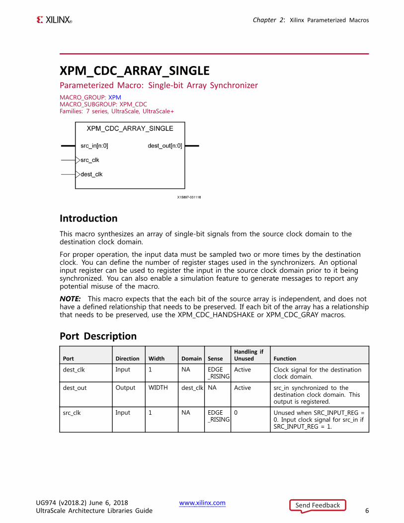
XPM_CDC_ARRAY_SINGLEParameterized Macro: Single-bit Array SynchronizerMACRO_GROUP: XPMMACRO_SUBGROUP: XPM_CDCFamilies: 7 series, UltraScale, UltraScale+
IntroductionThis macro synthesizes an array of single-bit signals from the source clock domain to thedestination clock domain.
For proper operation, the input data must be sampled two or more times by the destinationclock. You can define the number of register stages used in the synchronizers. An optionalinput register can be used to register the input in the source clock domain prior to it beingsynchronized. You can also enable a simulation feature to generate messages to report anypotential misuse of the macro.
NOTE: This macro expects that the each bit of the source array is independent, and does nothave a defined relationship that needs to be preserved. If each bit of the array has a relationshipthat needs to be preserved, use the XPM_CDC_HANDSHAKE or XPM_CDC_GRAY macros.
Port Description
Port Direction Width Domain SenseHandling ifUnused Function
dest_clk Input 1 NA EDGE_RISING
Active Clock signal for the destinationclock domain.
dest_out Output WIDTH dest_clk NA Active src_in synchronized to thedestination clock domain. Thisoutput is registered.
src_clk Input 1 NA EDGE_RISING
0 Unused when SRC_INPUT_REG =0. Input clock signal for src_in ifSRC_INPUT_REG = 1.
UG974 (v2018.2) June 6, 2018 www.xilinx.comUltraScale Architecture Libraries Guide 6
Send Feedback
Chapter 2: Xilinx Parameterized Macros
Port Direction Width Domain SenseHandling ifUnused Function
src_in Input WIDTH src_clk NA Active Input single-bit array to besynchronized to destinationclock domain. It is assumed thateach bit of the array is unrelatedto the others. This is reflectedin the constraints applied to thismacro.
To transfer a binary valuelosslessly across the twoclock domains, use theXPM_CDC_GRAY macro instead.
Design Entry MethodInstantiation Yes
Inference No
IP and IP Integrator Catalog No
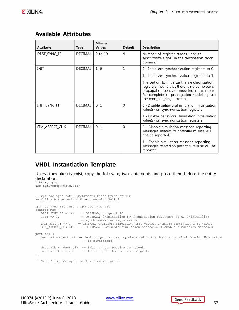
Available Attributes
Attribute TypeAllowedValues Default Description
DEST_SYNC_FF DECIMAL 2 to 10 4 Number of register stages used tosynchronize signal in the destination clockdomain.
INIT_SYNC_FF DECIMAL 0, 1 0 0 - Disable behavioral simulation initializationvalue(s) on synchronization registers.
1 - Enable behavioral simulation initializationvalue(s) on synchronization registers.
SIM_ASSERT_CHK DECIMAL 0, 1 0 0 - Disable simulation message reporting.Messages related to potential misuse willnot be reported.
1 - Enable simulation message reporting.Messages related to potential misuse will bereported.
SRC_INPUT_REG DECIMAL 1, 0 1 0 - Do not register input (src_in)
1 - Register input (src_in) once using src_clk
WIDTH DECIMAL 1 to 1024 2 Width of single - bit array (src_in) that will besynchronized to destination clock domain.
UG974 (v2018.2) June 6, 2018 www.xilinx.comUltraScale Architecture Libraries Guide 7
Send Feedback
Chapter 2: Xilinx Parameterized Macros
VHDL Instantiation TemplateUnless they already exist, copy the following two statements and paste them before the entitydeclaration.Library xpm;use xpm.vcomponents.all;
-- xpm_cdc_array_single: Single-bit Array Synchronizer-- Xilinx Parameterized Macro, version 2018.2
xpm_cdc_array_single_inst : xpm_cdc_array_singlegeneric map (
DEST_SYNC_FF => 4, -- DECIMAL; range: 2-10INIT_SYNC_FF => 0, -- DECIMAL; 0=disable simulation init values, 1=enable simulation init valuesSIM_ASSERT_CHK => 0, -- DECIMAL; 0=disable simulation messages, 1=enable simulation messagesSRC_INPUT_REG => 1, -- DECIMAL; 0=do not register input, 1=register inputWIDTH => 2 -- DECIMAL; range: 1-1024
)port map (
dest_out => dest_out, -- WIDTH-bit output: src_in synchronized to the destination clock domain. This-- output is registered.
dest_clk => dest_clk, -- 1-bit input: Clock signal for the destination clock domain.src_clk => src_clk, -- 1-bit input: optional; required when SRC_INPUT_REG = 1src_in => src_in -- WIDTH-bit input: Input single-bit array to be synchronized to destination clock
-- domain. It is assumed that each bit of the array is unrelated to the others.-- This is reflected in the constraints applied to this macro. To transfer a binary-- value losslessly across the two clock domains, use the XPM_CDC_GRAY macro-- instead.
);
-- End of xpm_cdc_array_single_inst instantiation
Verilog Instantiation Template
// xpm_cdc_array_single: Single-bit Array Synchronizer// Xilinx Parameterized Macro, version 2018.2
xpm_cdc_array_single #(.DEST_SYNC_FF(4), // DECIMAL; range: 2-10.INIT_SYNC_FF(0), // DECIMAL; 0=disable simulation init values, 1=enable simulation init values.SIM_ASSERT_CHK(0), // DECIMAL; 0=disable simulation messages, 1=enable simulation messages.SRC_INPUT_REG(1), // DECIMAL; 0=do not register input, 1=register input.WIDTH(2) // DECIMAL; range: 1-1024
)xpm_cdc_array_single_inst (
.dest_out(dest_out), // WIDTH-bit output: src_in synchronized to the destination clock domain. This// output is registered.
.dest_clk(dest_clk), // 1-bit input: Clock signal for the destination clock domain.
.src_clk(src_clk), // 1-bit input: optional; required when SRC_INPUT_REG = 1
.src_in(src_in) // WIDTH-bit input: Input single-bit array to be synchronized to destination clock// domain. It is assumed that each bit of the array is unrelated to the others. This// is reflected in the constraints applied to this macro. To transfer a binary value// losslessly across the two clock domains, use the XPM_CDC_GRAY macro instead.
);
// End of xpm_cdc_array_single_inst instantiation
UG974 (v2018.2) June 6, 2018 www.xilinx.comUltraScale Architecture Libraries Guide 8
Send Feedback

Chapter 2: Xilinx Parameterized Macros
For More Information• XPM CDC Testbench File
• See the UltraScale Programmable Devices Documentation.
UG974 (v2018.2) June 6, 2018 www.xilinx.comUltraScale Architecture Libraries Guide 9
Send Feedback
Chapter 2: Xilinx Parameterized Macros
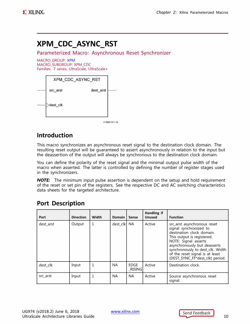
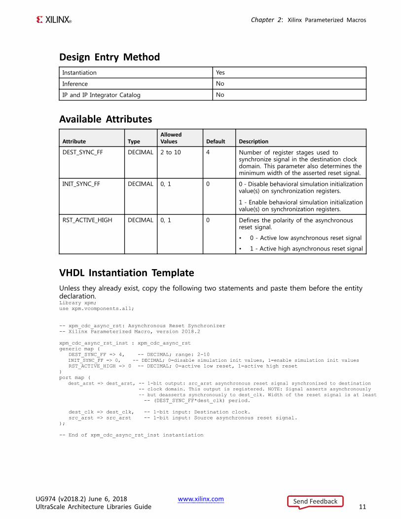
XPM_CDC_ASYNC_RSTParameterized Macro: Asynchronous Reset SynchronizerMACRO_GROUP: XPMMACRO_SUBGROUP: XPM_CDCFamilies: 7 series, UltraScale, UltraScale+
IntroductionThis macro synchronizes an asynchronous reset signal to the destination clock domain. Theresulting reset output will be guaranteed to assert asynchronously in relation to the input butthe deassertion of the output will always be synchronous to the destination clock domain.
You can define the polarity of the reset signal and the minimal output pulse width of themacro when asserted. The latter is controlled by defining the number of register stages usedin the synchronizers.
NOTE: The minimum input pulse assertion is dependent on the setup and hold requirementof the reset or set pin of the registers. See the respective DC and AC switching characteristicsdata sheets for the targeted architecture.
Port Description
Port Direction Width Domain SenseHandling ifUnused Function
dest_arst Output 1 dest_clk NA Active src_arst asynchronous resetsignal synchronized todestination clock domain.This output is registered.NOTE: Signal assertsasynchronously but deassertssynchronously to dest_clk. Widthof the reset signal is at least(DEST_SYNC_FF*dest_clk) period.
dest_clk Input 1 NA EDGE_RISING
Active Destination clock.
src_arst Input 1 NA NA Active Source asynchronous resetsignal.
UG974 (v2018.2) June 6, 2018 www.xilinx.comUltraScale Architecture Libraries Guide 10
Send Feedback
Chapter 2: Xilinx Parameterized Macros
Design Entry MethodInstantiation Yes
Inference No
IP and IP Integrator Catalog No
Available Attributes
Attribute TypeAllowedValues Default Description
DEST_SYNC_FF DECIMAL 2 to 10 4 Number of register stages used tosynchronize signal in the destination clockdomain. This parameter also determines theminimum width of the asserted reset signal.
INIT_SYNC_FF DECIMAL 0, 1 0 0 - Disable behavioral simulation initializationvalue(s) on synchronization registers.
1 - Enable behavioral simulation initializationvalue(s) on synchronization registers.
RST_ACTIVE_HIGH DECIMAL 0, 1 0 Defines the polarity of the asynchronousreset signal.
• 0 - Active low asynchronous reset signal
• 1 - Active high asynchronous reset signal
VHDL Instantiation TemplateUnless they already exist, copy the following two statements and paste them before the entitydeclaration.Library xpm;use xpm.vcomponents.all;
-- xpm_cdc_async_rst: Asynchronous Reset Synchronizer-- Xilinx Parameterized Macro, version 2018.2
xpm_cdc_async_rst_inst : xpm_cdc_async_rstgeneric map (
DEST_SYNC_FF => 4, -- DECIMAL; range: 2-10INIT_SYNC_FF => 0, -- DECIMAL; 0=disable simulation init values, 1=enable simulation init valuesRST_ACTIVE_HIGH => 0 -- DECIMAL; 0=active low reset, 1=active high reset
)port map (
dest_arst => dest_arst, -- 1-bit output: src_arst asynchronous reset signal synchronized to destination-- clock domain. This output is registered. NOTE: Signal asserts asynchronously-- but deasserts synchronously to dest_clk. Width of the reset signal is at least-- (DEST_SYNC_FF*dest_clk) period.
dest_clk => dest_clk, -- 1-bit input: Destination clock.src_arst => src_arst -- 1-bit input: Source asynchronous reset signal.
);
-- End of xpm_cdc_async_rst_inst instantiation
UG974 (v2018.2) June 6, 2018 www.xilinx.comUltraScale Architecture Libraries Guide 11
Send Feedback
Chapter 2: Xilinx Parameterized Macros
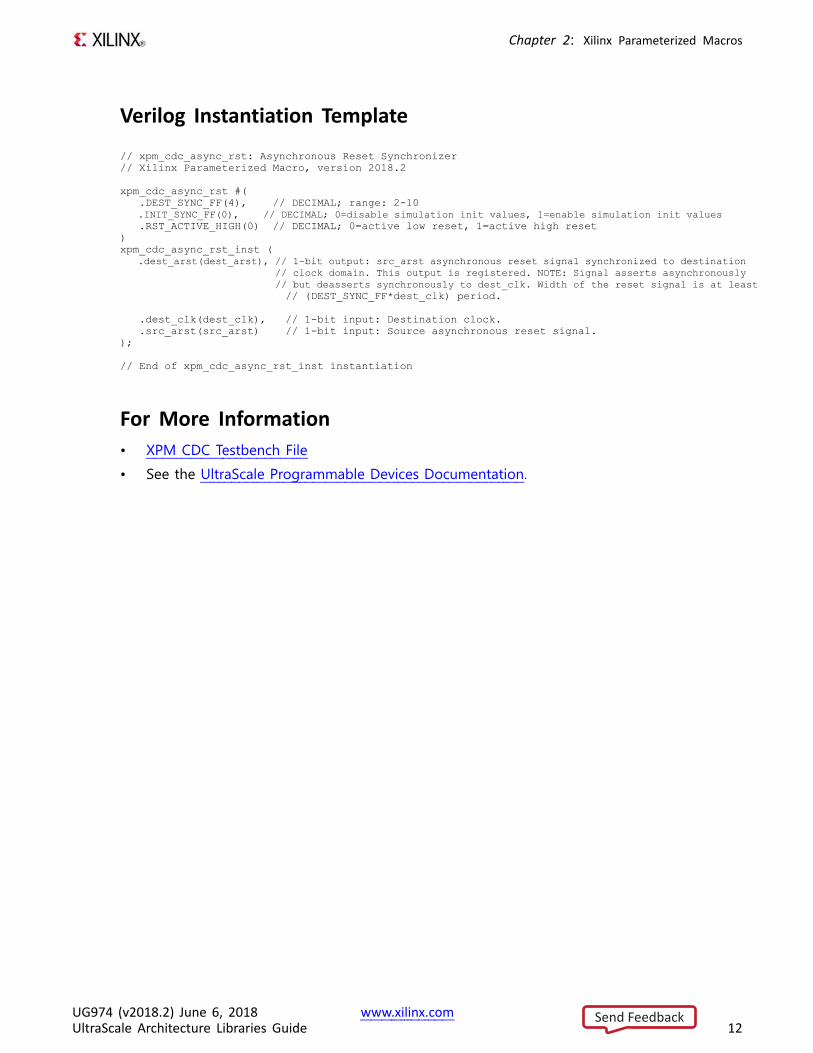
Verilog Instantiation Template
// xpm_cdc_async_rst: Asynchronous Reset Synchronizer// Xilinx Parameterized Macro, version 2018.2
xpm_cdc_async_rst #(.DEST_SYNC_FF(4), // DECIMAL; range: 2-10.INIT_SYNC_FF(0), // DECIMAL; 0=disable simulation init values, 1=enable simulation init values.RST_ACTIVE_HIGH(0) // DECIMAL; 0=active low reset, 1=active high reset
)xpm_cdc_async_rst_inst (
.dest_arst(dest_arst), // 1-bit output: src_arst asynchronous reset signal synchronized to destination// clock domain. This output is registered. NOTE: Signal asserts asynchronously// but deasserts synchronously to dest_clk. Width of the reset signal is at least// (DEST_SYNC_FF*dest_clk) period.
.dest_clk(dest_clk), // 1-bit input: Destination clock.
.src_arst(src_arst) // 1-bit input: Source asynchronous reset signal.);
// End of xpm_cdc_async_rst_inst instantiation
For More Information• XPM CDC Testbench File
• See the UltraScale Programmable Devices Documentation.
UG974 (v2018.2) June 6, 2018 www.xilinx.comUltraScale Architecture Libraries Guide 12
Send Feedback
Chapter 2: Xilinx Parameterized Macros
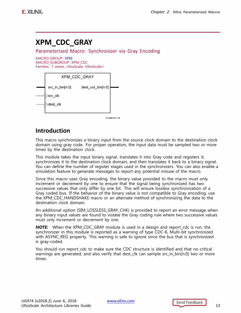
XPM_CDC_GRAYParameterized Macro: Synchronizer via Gray EncodingMACRO_GROUP: XPMMACRO_SUBGROUP: XPM_CDCFamilies: 7 series, UltraScale, UltraScale+
IntroductionThis macro synchronizes a binary input from the source clock domain to the destination clockdomain using gray code. For proper operation, the input data must be sampled two or moretimes by the destination clock.
This module takes the input binary signal, translates it into Gray code and registers it,synchronizes it to the destination clock domain, and then translates it back to a binary signal.You can define the number of register stages used in the synchronizers. You can also enable asimulation feature to generate messages to report any potential misuse of the macro.
Since this macro uses Gray encoding, the binary value provided to the macro must onlyincrement or decrement by one to ensure that the signal being synchronized has twosuccessive values that only differ by one bit. This will ensure lossless synchronization of aGray coded bus. If the behavior of the binary value is not compatible to Gray encoding, usethe XPM_CDC_HANDSHAKE macro or an alternate method of synchronizing the data to thedestination clock domain.
An additional option (SIM_LOSSLESS_GRAY_CHK) is provided to report an error message whenany binary input values are found to violate the Gray coding rule where two successive valuesmust only increment or decrement by one.
NOTE: When the XPM_CDC_GRAY module is used in a design and report_cdc is run, thesynchronizer in this module is reported as a warning of type CDC-6, Multi-bit synchronizedwith ASYNC_REG property. This warning is safe to ignore since the bus that is synchronizedis gray-coded.
You should run report_cdc to make sure the CDC structure is identified and that no criticalwarnings are generated, and also verify that dest_clk can sample src_in_bin[n:0] two or moretimes.
UG974 (v2018.2) June 6, 2018 www.xilinx.comUltraScale Architecture Libraries Guide 13
Send Feedback
Chapter 2: Xilinx Parameterized Macros
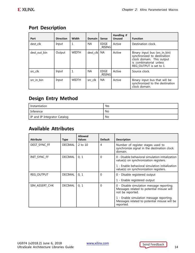
Port Description
Port Direction Width Domain SenseHandling ifUnused Function
dest_clk Input 1 NA EDGE_RISING
Active Destination clock.
dest_out_bin Output WIDTH dest_clk NA Active Binary input bus (src_in_bin)synchronized to destinationclock domain. This outputis combinatorial unlessREG_OUTPUT is set to 1.
src_clk Input 1 NA EDGE_RISING
Active Source clock.
src_in_bin Input WIDTH src_clk NA Active Binary input bus that will besynchronized to the destinationclock domain.
Design Entry MethodInstantiation Yes
Inference No
IP and IP Integrator Catalog No
Available Attributes
Attribute TypeAllowedValues Default Description
DEST_SYNC_FF DECIMAL 2 to 10 4 Number of register stages used tosynchronize signal in the destination clockdomain.
INIT_SYNC_FF DECIMAL 0, 1 0 0 - Disable behavioral simulation initializationvalue(s) on synchronization registers.
1 - Enable behavioral simulation initializationvalue(s) on synchronization registers.
REG_OUTPUT DECIMAL 0, 1 0 0 - Disable registered output
1 - Enable registered output
SIM_ASSERT_CHK DECIMAL 0, 1 0 0 - Disable simulation message reporting.Messages related to potential misuse willnot be reported.
1 - Enable simulation message reporting.Messages related to potential misuse will bereported.
UG974 (v2018.2) June 6, 2018 www.xilinx.comUltraScale Architecture Libraries Guide 14
Send Feedback
Chapter 2: Xilinx Parameterized Macros
Attribute TypeAllowedValues Default Description
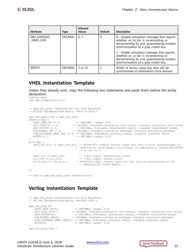
SIM_LOSSLESS_GRAY_CHK
DECIMAL 0, 1 0 0 - Disable simulation message that reportswhether src_in_bin is incrementing ordecrementing by one, guaranteeing losslesssynchronization of a gray coded bus.
1 - Enable simulation message that reportswhether src_in_bin is incrementing ordecrementing by one, guaranteeing losslesssynchronization of a gray coded bus.
WIDTH DECIMAL 2 to 32 2 Width of binary input bus that will besynchronized to destination clock domain.
VHDL Instantiation TemplateUnless they already exist, copy the following two statements and paste them before the entitydeclaration.Library xpm;use xpm.vcomponents.all;
-- xpm_cdc_gray: Synchronizer via Gray Encoding-- Xilinx Parameterized Macro, version 2018.2
xpm_cdc_gray_inst : xpm_cdc_graygeneric map (
DEST_SYNC_FF => 4, -- DECIMAL; range: 2-10INIT_SYNC_FF => 0, -- DECIMAL; 0=disable simulation init values, 1=enable simulation init valuesREG_OUTPUT => 0, -- DECIMAL; 0=disable registered output, 1=enable registered outputSIM_ASSERT_CHK => 0, -- DECIMAL; 0=disable simulation messages, 1=enable simulation messagesSIM_LOSSLESS_GRAY_CHK => 0, -- DECIMAL; 0=disable lossless check, 1=enable lossless checkWIDTH => 2 -- DECIMAL; range: 2-32
)port map (
dest_out_bin => dest_out_bin, -- WIDTH-bit output: Binary input bus (src_in_bin) synchronized to-- destination clock domain. This output is combinatorial unless REG_OUTPUT
-- is set to 1.
dest_clk => dest_clk, -- 1-bit input: Destination clock.src_clk => src_clk, -- 1-bit input: Source clock.src_in_bin => src_in_bin -- WIDTH-bit input: Binary input bus that will be synchronized to the
-- destination clock domain.
);
-- End of xpm_cdc_gray_inst instantiation
Verilog Instantiation Template
// xpm_cdc_gray: Synchronizer via Gray Encoding// Xilinx Parameterized Macro, version 2018.2
xpm_cdc_gray #(.DEST_SYNC_FF(4), // DECIMAL; range: 2-10.INIT_SYNC_FF(0), // DECIMAL; 0=disable simulation init values, 1=enable simulation init values.REG_OUTPUT(0), // DECIMAL; 0=disable registered output, 1=enable registered output.SIM_ASSERT_CHK(0), // DECIMAL; 0=disable simulation messages, 1=enable simulation messages.SIM_LOSSLESS_GRAY_CHK(0), // DECIMAL; 0=disable lossless check, 1=enable lossless check.WIDTH(2) // DECIMAL; range: 2-32
)xpm_cdc_gray_inst (
UG974 (v2018.2) June 6, 2018 www.xilinx.comUltraScale Architecture Libraries Guide 15
Send Feedback
Chapter 2: Xilinx Parameterized Macros
.dest_out_bin(dest_out_bin), // WIDTH-bit output: Binary input bus (src_in_bin) synchronized to// destination clock domain. This output is combinatorial unless REG_OUTPUT// is set to 1.
.dest_clk(dest_clk), // 1-bit input: Destination clock.
.src_clk(src_clk), // 1-bit input: Source clock.
.src_in_bin(src_in_bin) // WIDTH-bit input: Binary input bus that will be synchronized to the// destination clock domain.
);
// End of xpm_cdc_gray_inst instantiation
For More Information• XPM CDC Testbench File
• See the UltraScale Programmable Devices Documentation.
UG974 (v2018.2) June 6, 2018 www.xilinx.comUltraScale Architecture Libraries Guide 16
Send Feedback
Chapter 2: Xilinx Parameterized Macros
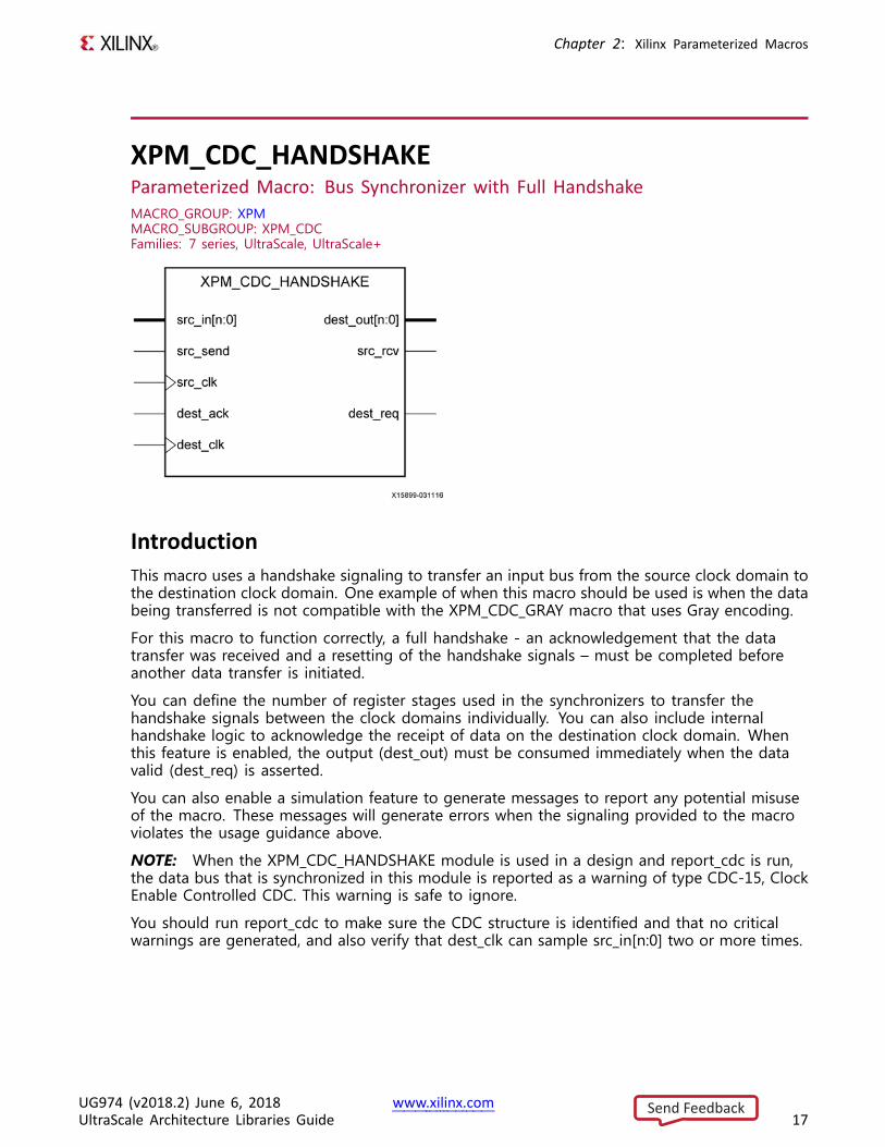
XPM_CDC_HANDSHAKEParameterized Macro: Bus Synchronizer with Full HandshakeMACRO_GROUP: XPMMACRO_SUBGROUP: XPM_CDCFamilies: 7 series, UltraScale, UltraScale+
IntroductionThis macro uses a handshake signaling to transfer an input bus from the source clock domain tothe destination clock domain. One example of when this macro should be used is when the databeing transferred is not compatible with the XPM_CDC_GRAY macro that uses Gray encoding.
For this macro to function correctly, a full handshake - an acknowledgement that the datatransfer was received and a resetting of the handshake signals – must be completed beforeanother data transfer is initiated.
You can define the number of register stages used in the synchronizers to transfer thehandshake signals between the clock domains individually. You can also include internalhandshake logic to acknowledge the receipt of data on the destination clock domain. Whenthis feature is enabled, the output (dest_out) must be consumed immediately when the datavalid (dest_req) is asserted.
You can also enable a simulation feature to generate messages to report any potential misuseof the macro. These messages will generate errors when the signaling provided to the macroviolates the usage guidance above.
NOTE: When the XPM_CDC_HANDSHAKE module is used in a design and report_cdc is run,the data bus that is synchronized in this module is reported as a warning of type CDC-15, ClockEnable Controlled CDC. This warning is safe to ignore.
You should run report_cdc to make sure the CDC structure is identified and that no criticalwarnings are generated, and also verify that dest_clk can sample src_in[n:0] two or more times.
UG974 (v2018.2) June 6, 2018 www.xilinx.comUltraScale Architecture Libraries Guide 17
Send Feedback
Chapter 2: Xilinx Parameterized Macros
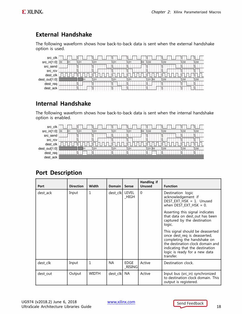
External HandshakeThe following waveform shows how back-to-back data is sent when the external handshakeoption is used.
Internal HandshakeThe following waveform shows how back-to-back data is sent when the internal handshakeoption is enabled.
Port Description
Port Direction Width Domain SenseHandling ifUnused Function
dest_ack Input 1 dest_clk LEVEL_HIGH
0 Destination logicacknowledgement ifDEST_EXT_HSK = 1. Unusedwhen DEST_EXT_HSK = 0.
Asserting this signal indicatesthat data on dest_out has beencaptured by the destinationlogic.
This signal should be deassertedonce dest_req is deasserted,completing the handshake onthe destination clock domain andindicating that the destinationlogic is ready for a new datatransfer.
dest_clk Input 1 NA EDGE_RISING
Active Destination clock.
dest_out Output WIDTH dest_clk NA Active Input bus (src_in) synchronizedto destination clock domain. Thisoutput is registered.
UG974 (v2018.2) June 6, 2018 www.xilinx.comUltraScale Architecture Libraries Guide 18
Send Feedback
Chapter 2: Xilinx Parameterized Macros
Port Direction Width Domain SenseHandling ifUnused Function
dest_req Output 1 dest_clk LEVEL_HIGH
Active Assertion of this signal indicatesthat new dest_out data has beenreceived and is ready to be usedor captured by the destinationlogic.
• When DEST_EXT_HSK =1, this signal will deassertonce the source handshakeacknowledges that thedestination clock domain hasreceived the transferred data.
• When DEST_EXT_HSK = 0,this signal asserts for oneclock period when dest_outbus is valid.
This output is registered.
src_clk Input 1 NA EDGE_RISING
Active Source clock.
src_in Input WIDTH src_clk NA Active Input bus that will besynchronized to the destinationclock domain.
src_rcv Output 1 src_clk LEVEL_HIGH
Active Acknowledgement fromdestination logic that src_inhas been received.
This signal will be deassertedonce destination handshake hasfully completed, thus completinga full data transfer. This outputis registered.
src_send Input 1 src_clk LEVEL_HIGH
Active Assertion of this signal allows thesrc_in bus to be synchronized tothe destination clock domain.
• This signal should only beasserted when src_rcv isdeasserted, indicating thatthe previous data transfer iscomplete.
• This signal should only bedeasserted once src_rcv isasserted, acknowledging thatthe src_in has been receivedby the destination logic.
Design Entry MethodInstantiation Yes
Inference No
IP and IP Integrator Catalog No
UG974 (v2018.2) June 6, 2018 www.xilinx.comUltraScale Architecture Libraries Guide 19
Send Feedback
Chapter 2: Xilinx Parameterized Macros
Available Attributes
Attribute TypeAllowedValues Default Description
DEST_EXT_HSK DECIMAL 1, 0 1 0 - An internal handshake will beimplemented in the macro to acknowledgereceipt of data on the destination clockdomain. When using this option, thevalid dest_out output must be consumedimmediately to avoid any data loss.
1 - External handshake logic must beimplemented by the user to acknowledgereceipt of data on the destination clockdomain.
DEST_SYNC_FF DECIMAL 2 to 10 4 Number of register stages used tosynchronize signal in the destination clockdomain.
INIT_SYNC_FF DECIMAL 0, 1 0 0 - Disable behavioral simulation initializationvalue(s) on synchronization registers.
1 - Enable behavioral simulation initializationvalue(s) on synchronization registers.
SIM_ASSERT_CHK DECIMAL 0, 1 0 0 - Disable simulation message reporting.Messages related to potential misuse willnot be reported.
1 - Enable simulation message reporting.Messages related to potential misuse will bereported.
SRC_SYNC_FF DECIMAL 2 to 10 4 Number of register stages used tosynchronize signal in the source clockdomain.
WIDTH DECIMAL 1 to 1024 1 Width of bus that will be synchronized todestination clock domain.
VHDL Instantiation TemplateUnless they already exist, copy the following two statements and paste them before the entitydeclaration.Library xpm;use xpm.vcomponents.all;
-- xpm_cdc_handshake: Bus Synchronizer with Full Handshake-- Xilinx Parameterized Macro, version 2018.2
xpm_cdc_handshake_inst : xpm_cdc_handshakegeneric map (
DEST_EXT_HSK => 1, -- DECIMAL; 0=internal handshake, 1=external handshakeDEST_SYNC_FF => 4, -- DECIMAL; range: 2-10INIT_SYNC_FF => 0, -- DECIMAL; 0=disable simulation init values, 1=enable simulation init valuesSIM_ASSERT_CHK => 0, -- DECIMAL; 0=disable simulation messages, 1=enable simulation messagesSRC_SYNC_FF => 4, -- DECIMAL; range: 2-10WIDTH => 1 -- DECIMAL; range: 1-1024
)port map (
dest_out => dest_out, -- WIDTH-bit output: Input bus (src_in) synchronized to destination clock domain.-- This output is registered.
UG974 (v2018.2) June 6, 2018 www.xilinx.comUltraScale Architecture Libraries Guide 20
Send Feedback
Chapter 2: Xilinx Parameterized Macros
dest_req => dest_req, -- 1-bit output: Assertion of this signal indicates that new dest_out data has been-- received and is ready to be used or captured by the destination logic. When-- DEST_EXT_HSK = 1, this signal will deassert once the source handshake
-- acknowledges that the destination clock domain has received the transferred-- data. When DEST_EXT_HSK = 0, this signal asserts for one clock period when-- dest_out bus is valid. This output is registered.
src_rcv => src_rcv, -- 1-bit output: Acknowledgement from destination logic that src_in has been-- received. This signal will be deasserted once destination handshake has fully-- completed, thus completing a full data transfer. This output is registered.
dest_ack => dest_ack, -- 1-bit input: optional; required when DEST_EXT_HSK = 1dest_clk => dest_clk, -- 1-bit input: Destination clock.src_clk => src_clk, -- 1-bit input: Source clock.src_in => src_in, -- WIDTH-bit input: Input bus that will be synchronized to the destination clock
-- domain.
src_send => src_send -- 1-bit input: Assertion of this signal allows the src_in bus to be synchronized-- to the destination clock domain. This signal should only be asserted when-- src_rcv is deasserted, indicating that the previous data transfer is complete.-- This signal should only be deasserted once src_rcv is asserted, acknowledging-- that the src_in has been received by the destination logic. .
);
-- End of xpm_cdc_handshake_inst instantiation
Verilog Instantiation Template
// xpm_cdc_handshake: Bus Synchronizer with Full Handshake// Xilinx Parameterized Macro, version 2018.2
xpm_cdc_handshake #(.DEST_EXT_HSK(1), // DECIMAL; 0=internal handshake, 1=external handshake.DEST_SYNC_FF(4), // DECIMAL; range: 2-10.INIT_SYNC_FF(0), // DECIMAL; 0=disable simulation init values, 1=enable simulation init values.SIM_ASSERT_CHK(0), // DECIMAL; 0=disable simulation messages, 1=enable simulation messages.SRC_SYNC_FF(4), // DECIMAL; range: 2-10.WIDTH(1) // DECIMAL; range: 1-1024
)xpm_cdc_handshake_inst (
.dest_out(dest_out), // WIDTH-bit output: Input bus (src_in) synchronized to destination clock domain.// This output is registered.
.dest_req(dest_req), // 1-bit output: Assertion of this signal indicates that new dest_out data has been// received and is ready to be used or captured by the destination logic. When// DEST_EXT_HSK = 1, this signal will deassert once the source handshake
// acknowledges that the destination clock domain has received the transferred data.// When DEST_EXT_HSK = 0, this signal asserts for one clock period when dest_out bus// is valid. This output is registered.
.src_rcv(src_rcv), // 1-bit output: Acknowledgement from destination logic that src_in has been// received. This signal will be deasserted once destination handshake has fully// completed, thus completing a full data transfer. This output is registered.
.dest_ack(dest_ack), // 1-bit input: optional; required when DEST_EXT_HSK = 1
.dest_clk(dest_clk), // 1-bit input: Destination clock.
.src_clk(src_clk), // 1-bit input: Source clock.
.src_in(src_in), // WIDTH-bit input: Input bus that will be synchronized to the destination clock// domain.
.src_send(src_send) // 1-bit input: Assertion of this signal allows the src_in bus to be synchronized to// the destination clock domain. This signal should only be asserted when src_rcv is// deasserted, indicating that the previous data transfer is complete. This signal// should only be deasserted once src_rcv is asserted, acknowledging that the src_in// has been received by the destination logic. .
UG974 (v2018.2) June 6, 2018 www.xilinx.comUltraScale Architecture Libraries Guide 21
Send Feedback

Chapter 2: Xilinx Parameterized Macros
);
// End of xpm_cdc_handshake_inst instantiation
For More Information• XPM CDC Testbench File
• See the UltraScale Programmable Devices Documentation.
UG974 (v2018.2) June 6, 2018 www.xilinx.comUltraScale Architecture Libraries Guide 22
Send Feedback
Chapter 2: Xilinx Parameterized Macros
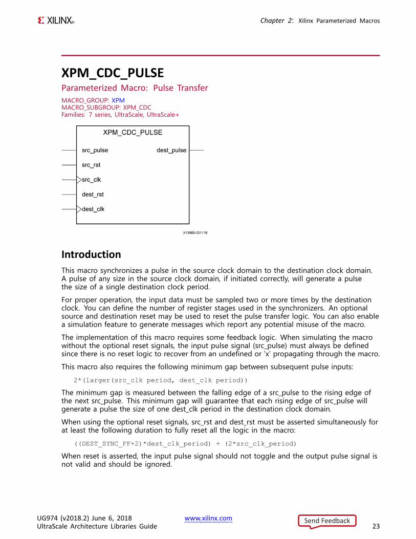
XPM_CDC_PULSEParameterized Macro: Pulse TransferMACRO_GROUP: XPMMACRO_SUBGROUP: XPM_CDCFamilies: 7 series, UltraScale, UltraScale+
IntroductionThis macro synchronizes a pulse in the source clock domain to the destination clock domain.A pulse of any size in the source clock domain, if initiated correctly, will generate a pulsethe size of a single destination clock period.
For proper operation, the input data must be sampled two or more times by the destinationclock. You can define the number of register stages used in the synchronizers. An optionalsource and destination reset may be used to reset the pulse transfer logic. You can also enablea simulation feature to generate messages which report any potential misuse of the macro.
The implementation of this macro requires some feedback logic. When simulating the macrowithout the optional reset signals, the input pulse signal (src_pulse) must always be definedsince there is no reset logic to recover from an undefined or ‘x’ propagating through the macro.
This macro also requires the following minimum gap between subsequent pulse inputs:
2*(larger(src_clk period, dest_clk period))
The minimum gap is measured between the falling edge of a src_pulse to the rising edge ofthe next src_pulse. This minimum gap will guarantee that each rising edge of src_pulse willgenerate a pulse the size of one dest_clk period in the destination clock domain.
When using the optional reset signals, src_rst and dest_rst must be asserted simultaneously forat least the following duration to fully reset all the logic in the macro:
((DEST_SYNC_FF+2)*dest_clk_period) + (2*src_clk_period)
When reset is asserted, the input pulse signal should not toggle and the output pulse signal isnot valid and should be ignored.
UG974 (v2018.2) June 6, 2018 www.xilinx.comUltraScale Architecture Libraries Guide 23
Send Feedback
Chapter 2: Xilinx Parameterized Macros
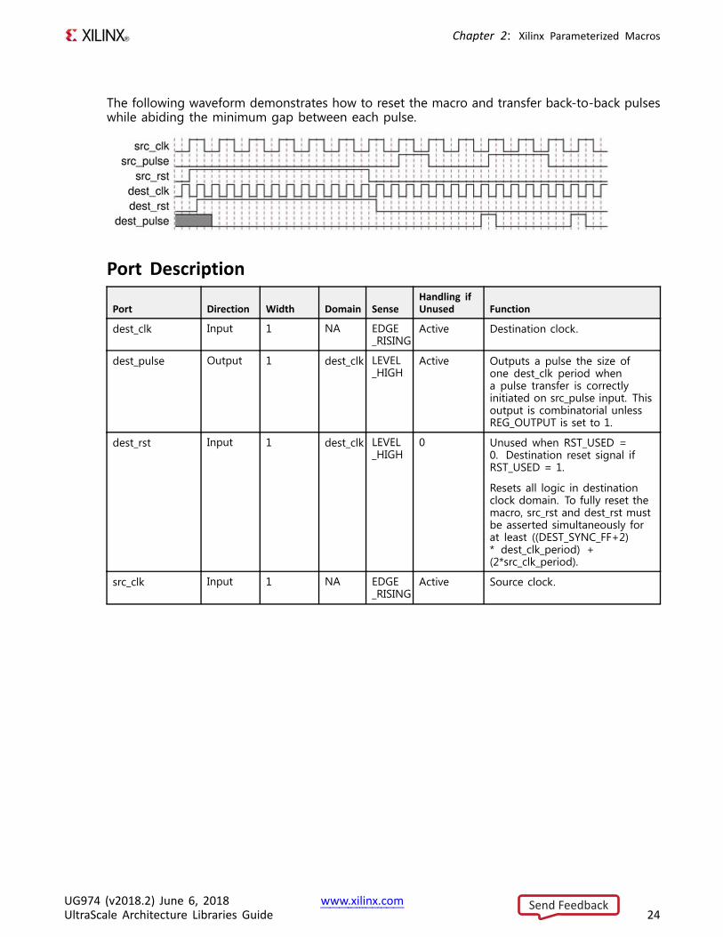
The following waveform demonstrates how to reset the macro and transfer back-to-back pulseswhile abiding the minimum gap between each pulse.
Port Description
Port Direction Width Domain SenseHandling ifUnused Function
dest_clk Input 1 NA EDGE_RISING
Active Destination clock.
dest_pulse Output 1 dest_clk LEVEL_HIGH
Active Outputs a pulse the size ofone dest_clk period whena pulse transfer is correctlyinitiated on src_pulse input. Thisoutput is combinatorial unlessREG_OUTPUT is set to 1.
dest_rst Input 1 dest_clk LEVEL_HIGH
0 Unused when RST_USED =0. Destination reset signal ifRST_USED = 1.
Resets all logic in destinationclock domain. To fully reset themacro, src_rst and dest_rst mustbe asserted simultaneously forat least ((DEST_SYNC_FF+2)* dest_clk_period) +(2*src_clk_period).
src_clk Input 1 NA EDGE_RISING
Active Source clock.
UG974 (v2018.2) June 6, 2018 www.xilinx.comUltraScale Architecture Libraries Guide 24
Send Feedback
Chapter 2: Xilinx Parameterized Macros
Port Direction Width Domain SenseHandling ifUnused Function
src_pulse Input 1 src_clk EDGE_RISING
Active Rising edge of this signalinitiates a pulse transfer to thedestination clock domain.
The minimum gap betweeneach pulse transfer must be atthe minimum 2*(larger(src_clkperiod, dest_clk period)). This ismeasured between the fallingedge of a src_pulse to the risingedge of the next src_pulse. Thisminimum gap will guarantee thateach rising edge of src_pulse willgenerate a pulse the size of onedest_clk period in the destinationclock domain.
When RST_USED = 1, pulsetransfers will not be guaranteedwhile src_rst and/or dest_rst areasserted.
src_rst Input 1 src_clk LEVEL_HIGH
0 Unused when RST_USED = 0.Source reset signal if RST_USED= 1.
Resets all logic in source clockdomain.
To fully reset the macro,src_rst and dest_rst must beasserted simultaneously forat least ((DEST_SYNC_FF+2)* dest_clk_period) +(2*src_clk_period).
Design Entry MethodInstantiation Yes
Inference No
IP and IP Integrator Catalog No
Available Attributes
Attribute TypeAllowedValues Default Description
DEST_SYNC_FF DECIMAL 2 to 10 4 Number of register stages used tosynchronize signal in the destination clockdomain.
INIT_SYNC_FF DECIMAL 0, 1 0 0 - Disable behavioral simulation initializationvalue(s) on synchronization registers.
1 - Enable behavioral simulation initializationvalue(s) on synchronization registers.
UG974 (v2018.2) June 6, 2018 www.xilinx.comUltraScale Architecture Libraries Guide 25
Send Feedback
Chapter 2: Xilinx Parameterized Macros
Attribute TypeAllowedValues Default Description
REG_OUTPUT DECIMAL 0, 1 0 0 - Disable registered output
1 - Enable registered output
RST_USED DECIMAL 1, 0 1 0 - No resets implemented.
1 - Resets implemented.
When RST_USED = 0, src_pulse input mustalways be defined during simulation sincethere is no reset logic to recover from an x -propagating through the macro.
SIM_ASSERT_CHK DECIMAL 0, 1 0 0 - Disable simulation message reporting.Messages related to potential misuse willnot be reported.
1 - Enable simulation message reporting.Messages related to potential misuse will bereported.
VHDL Instantiation TemplateUnless they already exist, copy the following two statements and paste them before the entitydeclaration.Library xpm;use xpm.vcomponents.all;
-- xpm_cdc_pulse: Pulse Transfer-- Xilinx Parameterized Macro, version 2018.2
xpm_cdc_pulse_inst : xpm_cdc_pulsegeneric map (
DEST_SYNC_FF => 4, -- DECIMAL; range: 2-10INIT_SYNC_FF => 0, -- DECIMAL; 0=disable simulation init values, 1=enable simulation init valuesREG_OUTPUT => 0, -- DECIMAL; 0=disable registered output, 1=enable registered outputRST_USED => 1, -- DECIMAL; 0=no reset, 1=implement resetSIM_ASSERT_CHK => 0 -- DECIMAL; 0=disable simulation messages, 1=enable simulation messages
)port map (
dest_pulse => dest_pulse, -- 1-bit output: Outputs a pulse the size of one dest_clk period when a pulse-- transfer is correctly initiated on src_pulse input. This output is-- combinatorial unless REG_OUTPUT is set to 1.
dest_clk => dest_clk, -- 1-bit input: Destination clock.dest_rst => dest_rst, -- 1-bit input: optional; required when RST_USED = 1src_clk => src_clk, -- 1-bit input: Source clock.src_pulse => src_pulse, -- 1-bit input: Rising edge of this signal initiates a pulse transfer to the
-- destination clock domain. The minimum gap between each pulse transfer must-- be at the minimum 2*(larger(src_clk period, dest_clk period)). This is-- measured between the falling edge of a src_pulse to the rising edge of the-- next src_pulse. This minimum gap will guarantee that each rising edge of-- src_pulse will generate a pulse the size of one dest_clk period in the-- destination clock domain. When RST_USED = 1, pulse transfers will not be-- guaranteed while src_rst and/or dest_rst are asserted.
src_rst => src_rst -- 1-bit input: optional; required when RST_USED = 1);
-- End of xpm_cdc_pulse_inst instantiation
UG974 (v2018.2) June 6, 2018 www.xilinx.comUltraScale Architecture Libraries Guide 26
Send Feedback
Chapter 2: Xilinx Parameterized Macros
Verilog Instantiation Template
// xpm_cdc_pulse: Pulse Transfer// Xilinx Parameterized Macro, version 2018.2
xpm_cdc_pulse #(.DEST_SYNC_FF(4), // DECIMAL; range: 2-10.INIT_SYNC_FF(0), // DECIMAL; 0=disable simulation init values, 1=enable simulation init values.REG_OUTPUT(0), // DECIMAL; 0=disable registered output, 1=enable registered output.RST_USED(1), // DECIMAL; 0=no reset, 1=implement reset.SIM_ASSERT_CHK(0) // DECIMAL; 0=disable simulation messages, 1=enable simulation messages
)xpm_cdc_pulse_inst (
.dest_pulse(dest_pulse), // 1-bit output: Outputs a pulse the size of one dest_clk period when a pulse// transfer is correctly initiated on src_pulse input. This output is// combinatorial unless REG_OUTPUT is set to 1.
.dest_clk(dest_clk), // 1-bit input: Destination clock.
.dest_rst(dest_rst), // 1-bit input: optional; required when RST_USED = 1
.src_clk(src_clk), // 1-bit input: Source clock.
.src_pulse(src_pulse), // 1-bit input: Rising edge of this signal initiates a pulse transfer to the// destination clock domain. The minimum gap between each pulse transfer must be// at the minimum 2*(larger(src_clk period, dest_clk period)). This is measured// between the falling edge of a src_pulse to the rising edge of the next// src_pulse. This minimum gap will guarantee that each rising edge of src_pulse// will generate a pulse the size of one dest_clk period in the destination// clock domain. When RST_USED = 1, pulse transfers will not be guaranteed while// src_rst and/or dest_rst are asserted.
.src_rst(src_rst) // 1-bit input: optional; required when RST_USED = 1);
// End of xpm_cdc_pulse_inst instantiation
For More Information• XPM CDC Testbench File
• See the UltraScale Programmable Devices Documentation.
UG974 (v2018.2) June 6, 2018 www.xilinx.comUltraScale Architecture Libraries Guide 27
Send Feedback
Chapter 2: Xilinx Parameterized Macros
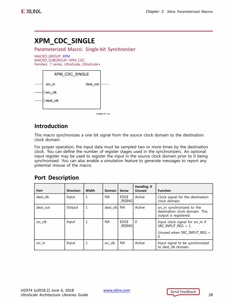
XPM_CDC_SINGLEParameterized Macro: Single-bit SynchronizerMACRO_GROUP: XPMMACRO_SUBGROUP: XPM_CDCFamilies: 7 series, UltraScale, UltraScale+
IntroductionThis macro synchronizes a one bit signal from the source clock domain to the destinationclock domain.
For proper operation, the input data must be sampled two or more times by the destinationclock. You can define the number of register stages used in the synchronizers. An optionalinput register may be used to register the input in the source clock domain prior to it beingsynchronized. You can also enable a simulation feature to generate messages to report anypotential misuse of the macro.
Port Description
Port Direction Width Domain SenseHandling ifUnused Function
dest_clk Input 1 NA EDGE_RISING
Active Clock signal for the destinationclock domain.
dest_out Output 1 dest_clk NA Active src_in synchronized to thedestination clock domain. Thisoutput is registered.
src_clk Input 1 NA EDGE_RISING
0 Input clock signal for src_in ifSRC_INPUT_REG = 1.
Unused when SRC_INPUT_REG =0.
src_in Input 1 src_clk NA Active Input signal to be synchronizedto dest_clk domain.
UG974 (v2018.2) June 6, 2018 www.xilinx.comUltraScale Architecture Libraries Guide 28
Send Feedback
Chapter 2: Xilinx Parameterized Macros
Design Entry MethodInstantiation Yes
Inference No
IP and IP Integrator Catalog No
Available Attributes
Attribute TypeAllowedValues Default Description
DEST_SYNC_FF DECIMAL 2 to 10 4 Number of register stages used tosynchronize signal in the destination clockdomain.
INIT_SYNC_FF DECIMAL 0, 1 0 0 - Disable behavioral simulation initializationvalue(s) on synchronization registers.
1 - Enable behavioral simulation initializationvalue(s) on synchronization registers.
SIM_ASSERT_CHK DECIMAL 0, 1 0 0 - Disable simulation message reporting.Messages related to potential misuse willnot be reported.
1 - Enable simulation message reporting.Messages related to potential misuse will bereported.
SRC_INPUT_REG DECIMAL 1, 0 1 0 - Do not register input (src_in)
1 - Register input (src_in) once using src_clk
VHDL Instantiation TemplateUnless they already exist, copy the following two statements and paste them before the entitydeclaration.Library xpm;use xpm.vcomponents.all;
-- xpm_cdc_single: Single-bit Synchronizer-- Xilinx Parameterized Macro, version 2018.2
xpm_cdc_single_inst : xpm_cdc_singlegeneric map (
DEST_SYNC_FF => 4, -- DECIMAL; range: 2-10INIT_SYNC_FF => 0, -- DECIMAL; 0=disable simulation init values, 1=enable simulation init valuesSIM_ASSERT_CHK => 0, -- DECIMAL; 0=disable simulation messages, 1=enable simulation messagesSRC_INPUT_REG => 1 -- DECIMAL; 0=do not register input, 1=register input
)port map (
dest_out => dest_out, -- 1-bit output: src_in synchronized to the destination clock domain. This output-- is registered.
dest_clk => dest_clk, -- 1-bit input: Clock signal for the destination clock domain.src_clk => src_clk, -- 1-bit input: optional; required when SRC_INPUT_REG = 1src_in => src_in -- 1-bit input: Input signal to be synchronized to dest_clk domain.
);
-- End of xpm_cdc_single_inst instantiation
UG974 (v2018.2) June 6, 2018 www.xilinx.comUltraScale Architecture Libraries Guide 29
Send Feedback
Chapter 2: Xilinx Parameterized Macros
Verilog Instantiation Template
// xpm_cdc_single: Single-bit Synchronizer// Xilinx Parameterized Macro, version 2018.2
xpm_cdc_single #(.DEST_SYNC_FF(4), // DECIMAL; range: 2-10.INIT_SYNC_FF(0), // DECIMAL; 0=disable simulation init values, 1=enable simulation init values.SIM_ASSERT_CHK(0), // DECIMAL; 0=disable simulation messages, 1=enable simulation messages.SRC_INPUT_REG(1) // DECIMAL; 0=do not register input, 1=register input
)xpm_cdc_single_inst (
.dest_out(dest_out), // 1-bit output: src_in synchronized to the destination clock domain. This output is// registered.
.dest_clk(dest_clk), // 1-bit input: Clock signal for the destination clock domain.
.src_clk(src_clk), // 1-bit input: optional; required when SRC_INPUT_REG = 1
.src_in(src_in) // 1-bit input: Input signal to be synchronized to dest_clk domain.);
// End of xpm_cdc_single_inst instantiation
For More Information• XPM CDC Testbench File
• See the UltraScale Programmable Devices Documentation.
UG974 (v2018.2) June 6, 2018 www.xilinx.comUltraScale Architecture Libraries Guide 30
Send Feedback
Chapter 2: Xilinx Parameterized Macros
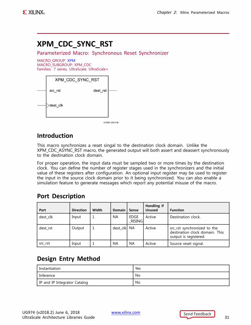
XPM_CDC_SYNC_RSTParameterized Macro: Synchronous Reset SynchronizerMACRO_GROUP: XPMMACRO_SUBGROUP: XPM_CDCFamilies: 7 series, UltraScale, UltraScale+
IntroductionThis macro synchronizes a reset singal to the destination clock domain. Unlike theXPM_CDC_ASYNC_RST macro, the generated output will both assert and deassert synchronouslyto the destination clock domain.
For proper operation, the input data must be sampled two or more times by the destinationclock. You can define the number of register stages used in the synchronizers and the initialvalue of these registers after configuration. An optional input register may be used to registerthe input in the source clock domain prior to it being synchronized. You can also enable asimulation feature to generate messages which report any potential misuse of the macro.
Port Description
Port Direction Width Domain SenseHandling ifUnused Function
dest_clk Input 1 NA EDGE_RISING
Active Destination clock.
dest_rst Output 1 dest_clk NA Active src_rst synchronized to thedestination clock domain. Thisoutput is registered.
src_rst Input 1 NA NA Active Source reset signal.
Design Entry MethodInstantiation Yes
Inference No
IP and IP Integrator Catalog No
UG974 (v2018.2) June 6, 2018 www.xilinx.comUltraScale Architecture Libraries Guide 31
Send Feedback
Chapter 2: Xilinx Parameterized Macros
Available Attributes
Attribute TypeAllowedValues Default Description
DEST_SYNC_FF DECIMAL 2 to 10 4 Number of register stages used tosynchronize signal in the destination clockdomain.
INIT DECIMAL 1, 0 1 0 - Initializes synchronization registers to 0
1 - Initializes synchronization registers to 1
The option to initialize the synchronizationregisters means that there is no complete x -propagation behavior modeled in this macro.For complete x - propagation modelling, usethe xpm_cdc_single macro.
INIT_SYNC_FF DECIMAL 0, 1 0 0 - Disable behavioral simulation initializationvalue(s) on synchronization registers.
1 - Enable behavioral simulation initializationvalue(s) on synchronization registers.
SIM_ASSERT_CHK DECIMAL 0, 1 0 0 - Disable simulation message reporting.Messages related to potential misuse willnot be reported.
1 - Enable simulation message reporting.Messages related to potential misuse will bereported.
VHDL Instantiation TemplateUnless they already exist, copy the following two statements and paste them before the entitydeclaration.Library xpm;use xpm.vcomponents.all;
-- xpm_cdc_sync_rst: Synchronous Reset Synchronizer-- Xilinx Parameterized Macro, version 2018.2
xpm_cdc_sync_rst_inst : xpm_cdc_sync_rstgeneric map (
DEST_SYNC_FF => 4, -- DECIMAL; range: 2-10INIT => 1, -- DECIMAL; 0=initialize synchronization registers to 0, 1=initialize
-- synchronization registers to 1INIT_SYNC_FF => 0, -- DECIMAL; 0=disable simulation init values, 1=enable simulation init valuesSIM_ASSERT_CHK => 0 -- DECIMAL; 0=disable simulation messages, 1=enable simulation messages
)port map (
dest_rst => dest_rst, -- 1-bit output: src_rst synchronized to the destination clock domain. This output-- is registered.
dest_clk => dest_clk, -- 1-bit input: Destination clock.src_rst => src_rst -- 1-bit input: Source reset signal.
);
-- End of xpm_cdc_sync_rst_inst instantiation
UG974 (v2018.2) June 6, 2018 www.xilinx.comUltraScale Architecture Libraries Guide 32
Send Feedback
Chapter 2: Xilinx Parameterized Macros
Verilog Instantiation Template
// xpm_cdc_sync_rst: Synchronous Reset Synchronizer// Xilinx Parameterized Macro, version 2018.2
xpm_cdc_sync_rst #(.DEST_SYNC_FF(4), // DECIMAL; range: 2-10.INIT(1), // DECIMAL; 0=initialize synchronization registers to 0, 1=initialize synchronization
// registers to 1.INIT_SYNC_FF(0), // DECIMAL; 0=disable simulation init values, 1=enable simulation init values.SIM_ASSERT_CHK(0) // DECIMAL; 0=disable simulation messages, 1=enable simulation messages
)xpm_cdc_sync_rst_inst (
.dest_rst(dest_rst), // 1-bit output: src_rst synchronized to the destination clock domain. This output// is registered.
.dest_clk(dest_clk), // 1-bit input: Destination clock.
.src_rst(src_rst) // 1-bit input: Source reset signal.);
// End of xpm_cdc_sync_rst_inst instantiation
For More Information• XPM CDC Testbench File
• See the UltraScale Programmable Devices Documentation.
UG974 (v2018.2) June 6, 2018 www.xilinx.comUltraScale Architecture Libraries Guide 33
Send Feedback
Chapter 2: Xilinx Parameterized Macros
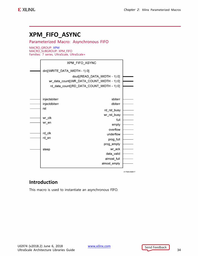
XPM_FIFO_ASYNCParameterized Macro: Asynchronous FIFOMACRO_GROUP: XPMMACRO_SUBGROUP: XPM_FIFOFamilies: 7 series, UltraScale, UltraScale+
IntroductionThis macro is used to instantiate an asynchronous FIFO.
UG974 (v2018.2) June 6, 2018 www.xilinx.comUltraScale Architecture Libraries Guide 34
Send Feedback
Chapter 2: Xilinx Parameterized Macros
The following describes the basic write and read operation of an XPM_FIFO instance. It doesnot distinguish between FIFO types, clock domain or read mode.
• After a user issues a reset, the user should wait until the busy signals go low before issuinganother reset.
• All synchronous signals are sensitive to the rising edge of wr_clk/rd_clk, which is assumedto be a buffered and toggling clock signal behaving according to target device andFIFO/memory primitive requirements.
• A write operation is performed when the FIFO is not full and wr_en is asserted on eachwr_clk cycle.
• A read operation is performed when the FIFO is not empty and rd_en is asserted on eachrd_clk cycle.
• The number of clock cycles required for XPM FIFO to react to dout, full and empty changesdepends on the CLOCK_DOMAIN, READ_MODE, and FIFO_READ_LATENCY settings.
– It may take more than one rd_clk cycle to deassert empty due to write operation(wr_en = 1).
– It may take more than one rd_clk cycle to present the read data on dout port uponassertion of rd_en.
– It may take more than one wr_clk cycle to deassert full due to read operation (rd_en= 1).
• All write operations are gated by the value of wr_en and full on the initiating wr_clk cycle.
• All read operations are gated by the value of rd_en and empty on the initiating rd_clk cycle.
• The wr_en input has no effect when full is asserted on the coincident wr_clk cycle.
• The rd_en input has no effect when empty is asserted on the coincident rd_clk cycle.
• Undriven or unknown values provided on module inputs will produce undefined outputport behavior.
• wr_en/rd_en should not be toggled when reset (rst) or wr_rst_busy or rd_rst_busy is asserted.
• Assertion/deassertion of prog_full happens only when full is deasserted.
• Assertion/deassertion of prog_empty happens only when empty is deasserted.
NOTE: If the RELATED_CLOCKS attribute is set in an asynchronous FIFO, then both the wr_clkand rd_clk should be generated from the same source, violating this will result in timingwarnings and can cause the design to fail in hardware.
UG974 (v2018.2) June 6, 2018 www.xilinx.comUltraScale Architecture Libraries Guide 35
Send Feedback
Chapter 2: Xilinx Parameterized Macros
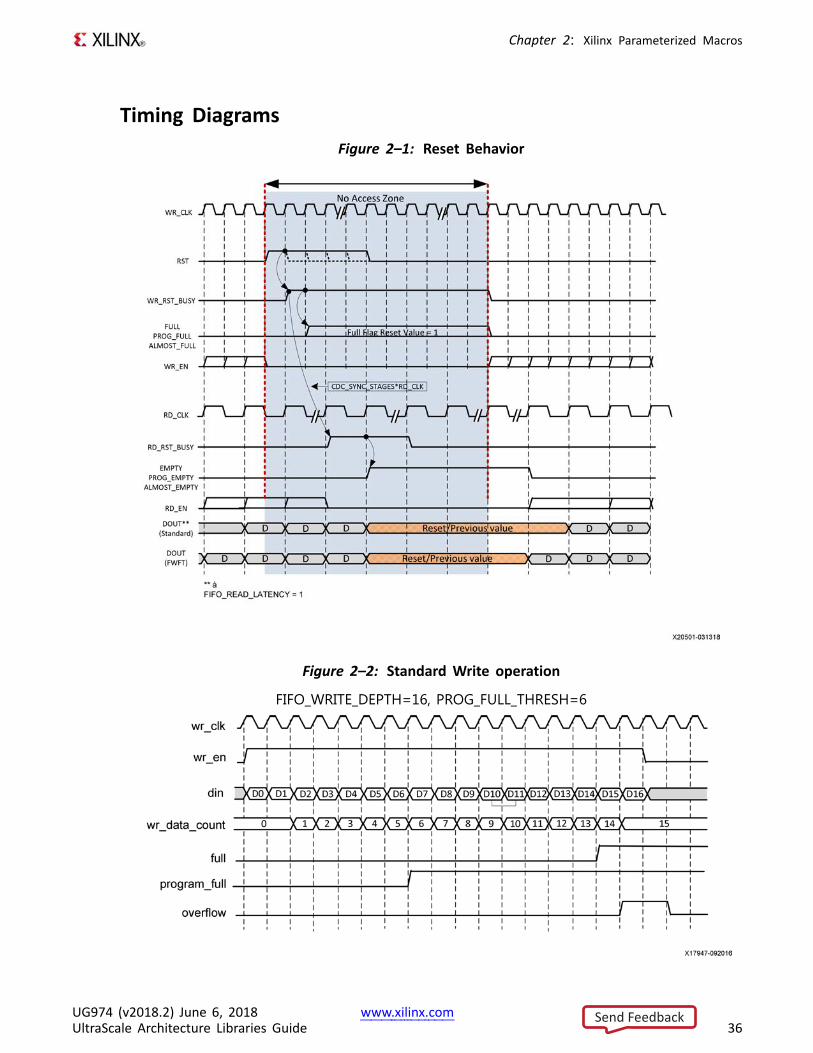
Timing DiagramsFigure 2–1: Reset Behavior
Figure 2–2: Standard Write operation
FIFO_WRITE_DEPTH=16, PROG_FULL_THRESH=6
UG974 (v2018.2) June 6, 2018 www.xilinx.comUltraScale Architecture Libraries Guide 36
Send Feedback
Chapter 2: Xilinx Parameterized Macros
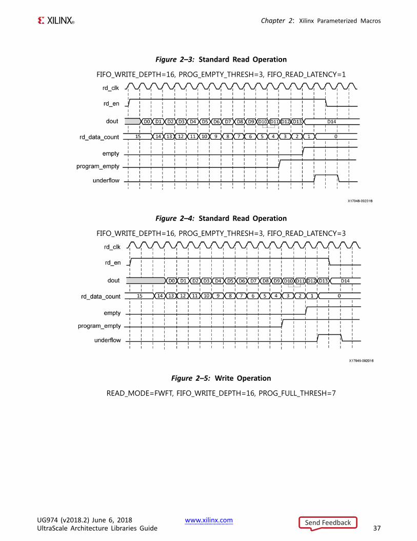
Figure 2–3: Standard Read Operation
FIFO_WRITE_DEPTH=16, PROG_EMPTY_THRESH=3, FIFO_READ_LATENCY=1
Figure 2–4: Standard Read Operation
FIFO_WRITE_DEPTH=16, PROG_EMPTY_THRESH=3, FIFO_READ_LATENCY=3
Figure 2–5: Write Operation
READ_MODE=FWFT, FIFO_WRITE_DEPTH=16, PROG_FULL_THRESH=7
UG974 (v2018.2) June 6, 2018 www.xilinx.comUltraScale Architecture Libraries Guide 37
Send Feedback
Chapter 2: Xilinx Parameterized Macros
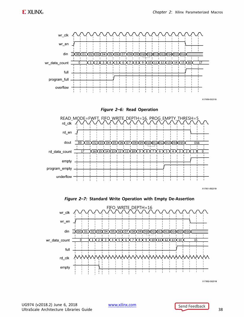
Figure 2–6: Read Operation
READ_MODE=FWFT, FIFO_WRITE_DEPTH=16, PROG_EMPTY_THRESH=5
Figure 2–7: Standard Write Operation with Empty De-Assertion
FIFO_WRITE_DEPTH=16
UG974 (v2018.2) June 6, 2018 www.xilinx.comUltraScale Architecture Libraries Guide 38
Send Feedback
Chapter 2: Xilinx Parameterized Macros
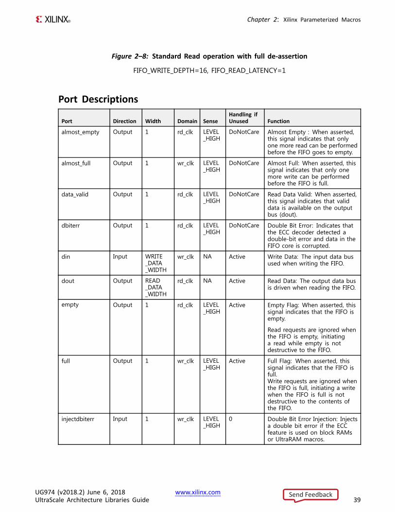
Figure 2–8: Standard Read operation with full de-assertion
FIFO_WRITE_DEPTH=16, FIFO_READ_LATENCY=1
Port Descriptions
Port Direction Width Domain SenseHandling ifUnused Function
almost_empty Output 1 rd_clk LEVEL_HIGH
DoNotCare Almost Empty : When asserted,this signal indicates that onlyone more read can be performedbefore the FIFO goes to empty.
almost_full Output 1 wr_clk LEVEL_HIGH
DoNotCare Almost Full: When asserted, thissignal indicates that only onemore write can be performedbefore the FIFO is full.
data_valid Output 1 rd_clk LEVEL_HIGH
DoNotCare Read Data Valid: When asserted,this signal indicates that validdata is available on the outputbus (dout).
dbiterr Output 1 rd_clk LEVEL_HIGH
DoNotCare Double Bit Error: Indicates thatthe ECC decoder detected adouble-bit error and data in theFIFO core is corrupted.
din Input WRITE_DATA_WIDTH
wr_clk NA Active Write Data: The input data busused when writing the FIFO.
dout Output READ_DATA_WIDTH
rd_clk NA Active Read Data: The output data busis driven when reading the FIFO.
empty Output 1 rd_clk LEVEL_HIGH
Active Empty Flag: When asserted, thissignal indicates that the FIFO isempty.
Read requests are ignored whenthe FIFO is empty, initiatinga read while empty is notdestructive to the FIFO.
full Output 1 wr_clk LEVEL_HIGH
Active Full Flag: When asserted, thissignal indicates that the FIFO isfull.Write requests are ignored whenthe FIFO is full, initiating a writewhen the FIFO is full is notdestructive to the contents ofthe FIFO.
injectdbiterr Input 1 wr_clk LEVEL_HIGH
0 Double Bit Error Injection: Injectsa double bit error if the ECCfeature is used on block RAMsor UltraRAM macros.
UG974 (v2018.2) June 6, 2018 www.xilinx.comUltraScale Architecture Libraries Guide 39
Send Feedback
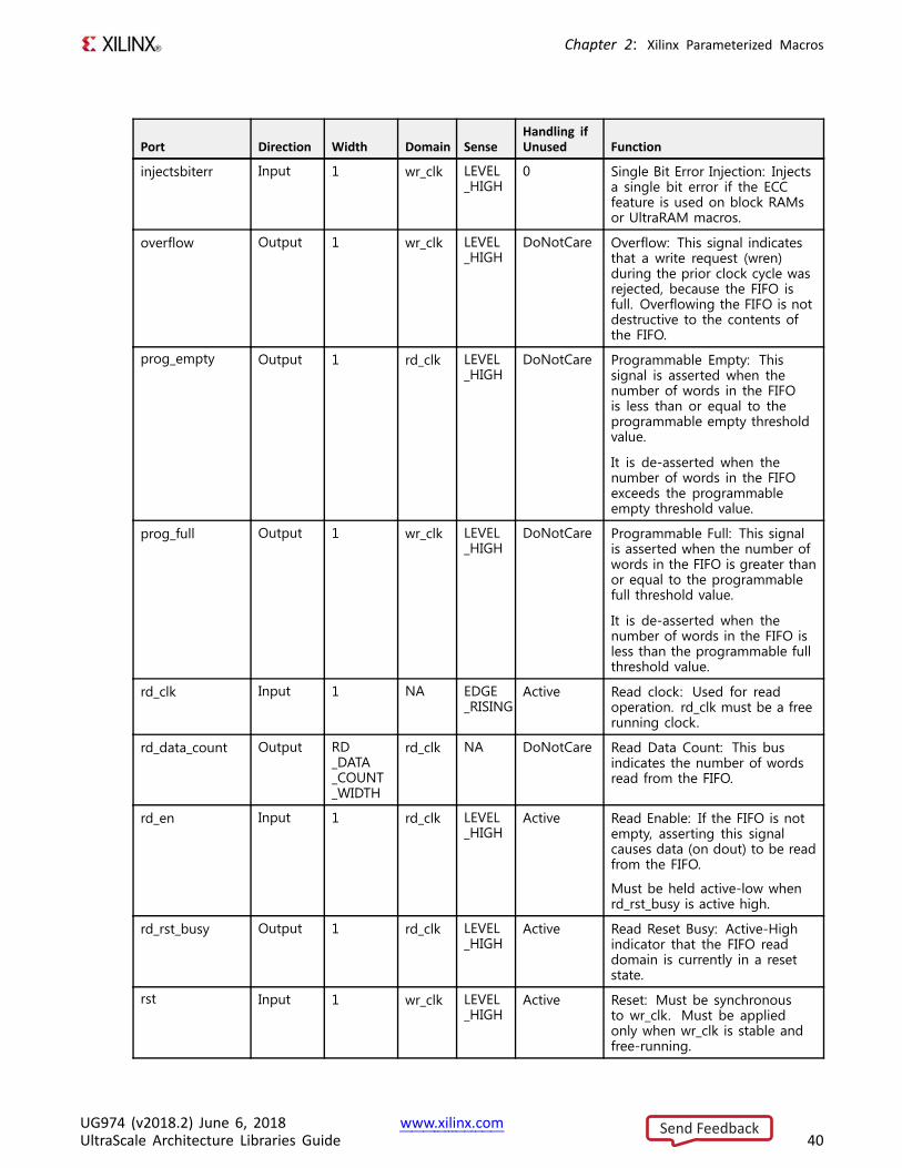
Chapter 2: Xilinx Parameterized Macros
Port Direction Width Domain SenseHandling ifUnused Function
injectsbiterr Input 1 wr_clk LEVEL_HIGH
0 Single Bit Error Injection: Injectsa single bit error if the ECCfeature is used on block RAMsor UltraRAM macros.
overflow Output 1 wr_clk LEVEL_HIGH
DoNotCare Overflow: This signal indicatesthat a write request (wren)during the prior clock cycle wasrejected, because the FIFO isfull. Overflowing the FIFO is notdestructive to the contents ofthe FIFO.
prog_empty Output 1 rd_clk LEVEL_HIGH
DoNotCare Programmable Empty: Thissignal is asserted when thenumber of words in the FIFOis less than or equal to theprogrammable empty thresholdvalue.
It is de-asserted when thenumber of words in the FIFOexceeds the programmableempty threshold value.
prog_full Output 1 wr_clk LEVEL_HIGH
DoNotCare Programmable Full: This signalis asserted when the number ofwords in the FIFO is greater thanor equal to the programmablefull threshold value.
It is de-asserted when thenumber of words in the FIFO isless than the programmable fullthreshold value.
rd_clk Input 1 NA EDGE_RISING
Active Read clock: Used for readoperation. rd_clk must be a freerunning clock.
rd_data_count Output RD_DATA_COUNT_WIDTH
rd_clk NA DoNotCare Read Data Count: This busindicates the number of wordsread from the FIFO.
rd_en Input 1 rd_clk LEVEL_HIGH
Active Read Enable: If the FIFO is notempty, asserting this signalcauses data (on dout) to be readfrom the FIFO.
Must be held active-low whenrd_rst_busy is active high.
rd_rst_busy Output 1 rd_clk LEVEL_HIGH
Active Read Reset Busy: Active-Highindicator that the FIFO readdomain is currently in a resetstate.
rst Input 1 wr_clk LEVEL_HIGH
Active Reset: Must be synchronousto wr_clk. Must be appliedonly when wr_clk is stable andfree-running.
UG974 (v2018.2) June 6, 2018 www.xilinx.comUltraScale Architecture Libraries Guide 40
Send Feedback
Chapter 2: Xilinx Parameterized Macros
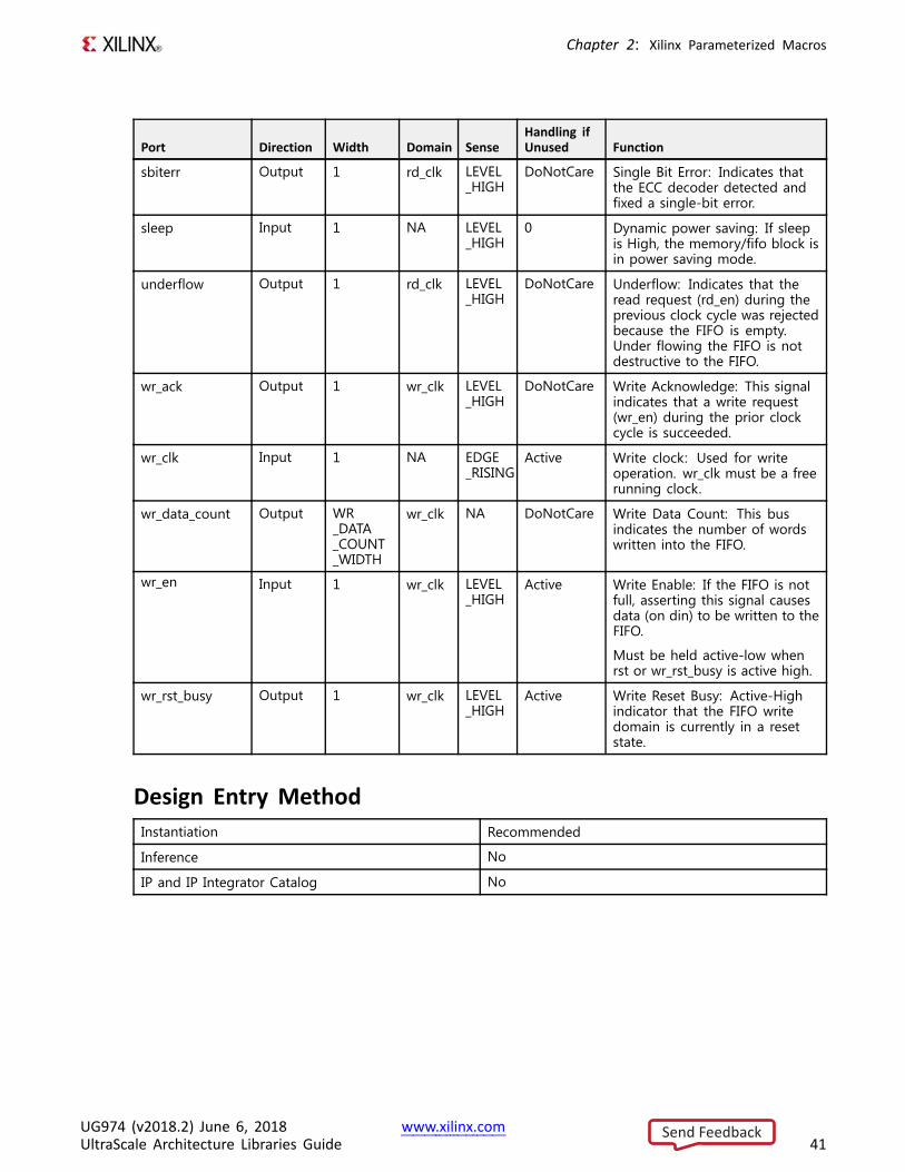
Port Direction Width Domain SenseHandling ifUnused Function
sbiterr Output 1 rd_clk LEVEL_HIGH
DoNotCare Single Bit Error: Indicates thatthe ECC decoder detected andfixed a single-bit error.
sleep Input 1 NA LEVEL_HIGH
0 Dynamic power saving: If sleepis High, the memory/fifo block isin power saving mode.
underflow Output 1 rd_clk LEVEL_HIGH
DoNotCare Underflow: Indicates that theread request (rd_en) during theprevious clock cycle was rejectedbecause the FIFO is empty.Under flowing the FIFO is notdestructive to the FIFO.
wr_ack Output 1 wr_clk LEVEL_HIGH
DoNotCare Write Acknowledge: This signalindicates that a write request(wr_en) during the prior clockcycle is succeeded.
wr_clk Input 1 NA EDGE_RISING
Active Write clock: Used for writeoperation. wr_clk must be a freerunning clock.
wr_data_count Output WR_DATA_COUNT_WIDTH
wr_clk NA DoNotCare Write Data Count: This busindicates the number of wordswritten into the FIFO.
wr_en Input 1 wr_clk LEVEL_HIGH
Active Write Enable: If the FIFO is notfull, asserting this signal causesdata (on din) to be written to theFIFO.
Must be held active-low whenrst or wr_rst_busy is active high.
wr_rst_busy Output 1 wr_clk LEVEL_HIGH
Active Write Reset Busy: Active-Highindicator that the FIFO writedomain is currently in a resetstate.
Design Entry MethodInstantiation Recommended
Inference No
IP and IP Integrator Catalog No
UG974 (v2018.2) June 6, 2018 www.xilinx.comUltraScale Architecture Libraries Guide 41
Send Feedback
Chapter 2: Xilinx Parameterized Macros
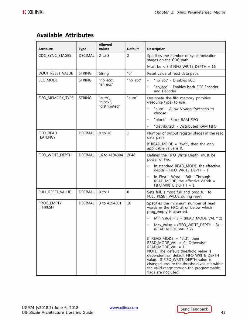
Available Attributes
Attribute TypeAllowedValues Default Description
CDC_SYNC_STAGES DECIMAL 2 to 8 2 Specifies the number of synchronizationstages on the CDC path
Must be < 5 if FIFO_WRITE_DEPTH = 16
DOUT_RESET_VALUE STRING String "0" Reset value of read data path.
ECC_MODE STRING "no_ecc","en_ecc"
"no_ecc" • "no_ecc" - Disables ECC
• "en_ecc" - Enables both ECC Encoderand Decoder
FIFO_MEMORY_TYPE STRING "auto","block","distributed"
"auto" Designate the fifo memory primitive(resource type) to use.
• "auto" - Allow Vivado Synthesis tochoose
• "block" - Block RAM FIFO
• "distributed" - Distributed RAM FIFO
FIFO_READ_LATENCY
DECIMAL 0 to 10 1 Number of output register stages in the readdata path.
If READ_MODE = "fwft", then the onlyapplicable value is 0.
FIFO_WRITE_DEPTH DECIMAL 16 to 4194304 2048 Defines the FIFO Write Depth, must bepower of two.
• In standard READ_MODE, the effectivedepth = FIFO_WRITE_DEPTH - 1
• In First - Word - Fall - ThroughREAD_MODE, the effective depth =FIFO_WRITE_DEPTH + 1
FULL_RESET_VALUE DECIMAL 0 to 1 0 Sets full, almost_full and prog_full toFULL_RESET_VALUE during reset
PROG_EMPTY_THRESH
DECIMAL 3 to 4194301 10 Specifies the minimum number of readwords in the FIFO at or below whichprog_empty is asserted.
• Min_Value = 3 + (READ_MODE_VAL * 2)
• Max_Value = (FIFO_WRITE_DEPTH - 3) -(READ_MODE_VAL * 2)
If READ_MODE = "std", thenREAD_MODE_VAL = 0; OtherwiseREAD_MODE_VAL = 1.NOTE: The default threshold value isdependent on default FIFO_WRITE_DEPTHvalue. If FIFO_WRITE_DEPTH value ischanged, ensure the threshold value is withinthe valid range though the programmableflags are not used.
UG974 (v2018.2) June 6, 2018 www.xilinx.comUltraScale Architecture Libraries Guide 42
Send Feedback
Chapter 2: Xilinx Parameterized Macros
Attribute TypeAllowedValues Default Description
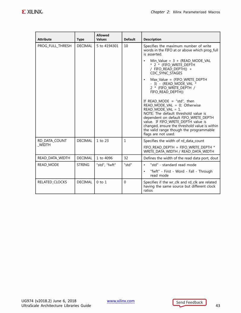
PROG_FULL_THRESH DECIMAL 5 to 4194301 10 Specifies the maximum number of writewords in the FIFO at or above which prog_fullis asserted.
• Min_Value = 3 + (READ_MODE_VAL* 2 * (FIFO_WRITE_DEPTH/ FIFO_READ_DEPTH)) +CDC_SYNC_STAGES
• Max_Value = (FIFO_WRITE_DEPTH- 3) - (READ_MODE_VAL *2 * (FIFO_WRITE_DEPTH /FIFO_READ_DEPTH))
If READ_MODE = "std", thenREAD_MODE_VAL = 0; OtherwiseREAD_MODE_VAL = 1.NOTE: The default threshold value isdependent on default FIFO_WRITE_DEPTHvalue. If FIFO_WRITE_DEPTH value ischanged, ensure the threshold value is withinthe valid range though the programmableflags are not used.
RD_DATA_COUNT_WIDTH
DECIMAL 1 to 23 1 Specifies the width of rd_data_count
FIFO_READ_DEPTH = FIFO_WRITE_DEPTH *WRITE_DATA_WIDTH / READ_DATA_WIDTH
READ_DATA_WIDTH DECIMAL 1 to 4096 32 Defines the width of the read data port, dout
READ_MODE STRING "std", "fwft" "std" • "std" - standard read mode
• "fwft" - First - Word - Fall - Throughread mode
RELATED_CLOCKS DECIMAL 0 to 1 0 Specifies if the wr_clk and rd_clk are relatedhaving the same source but different clockratios
UG974 (v2018.2) June 6, 2018 www.xilinx.comUltraScale Architecture Libraries Guide 43
Send Feedback
Chapter 2: Xilinx Parameterized Macros
Attribute TypeAllowedValues Default Description
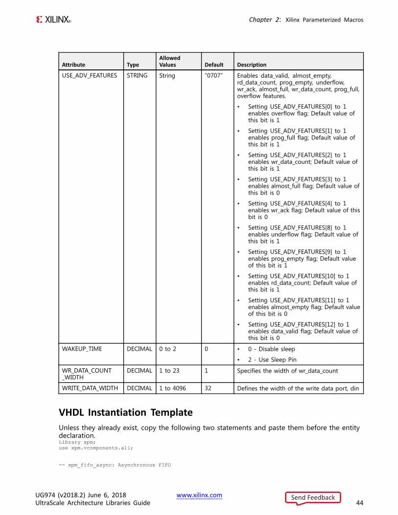
USE_ADV_FEATURES STRING String "0707" Enables data_valid, almost_empty,rd_data_count, prog_empty, underflow,wr_ack, almost_full, wr_data_count, prog_full,overflow features.
• Setting USE_ADV_FEATURES[0] to 1enables overflow flag; Default value ofthis bit is 1
• Setting USE_ADV_FEATURES[1] to 1enables prog_full flag; Default value ofthis bit is 1
• Setting USE_ADV_FEATURES[2] to 1enables wr_data_count; Default value ofthis bit is 1
• Setting USE_ADV_FEATURES[3] to 1enables almost_full flag; Default value ofthis bit is 0
• Setting USE_ADV_FEATURES[4] to 1enables wr_ack flag; Default value of thisbit is 0
• Setting USE_ADV_FEATURES[8] to 1enables underflow flag; Default value ofthis bit is 1
• Setting USE_ADV_FEATURES[9] to 1enables prog_empty flag; Default valueof this bit is 1
• Setting USE_ADV_FEATURES[10] to 1enables rd_data_count; Default value ofthis bit is 1
• Setting USE_ADV_FEATURES[11] to 1enables almost_empty flag; Default valueof this bit is 0
• Setting USE_ADV_FEATURES[12] to 1enables data_valid flag; Default value ofthis bit is 0
WAKEUP_TIME DECIMAL 0 to 2 0 • 0 - Disable sleep
• 2 - Use Sleep Pin
WR_DATA_COUNT_WIDTH
DECIMAL 1 to 23 1 Specifies the width of wr_data_count
WRITE_DATA_WIDTH DECIMAL 1 to 4096 32 Defines the width of the write data port, din
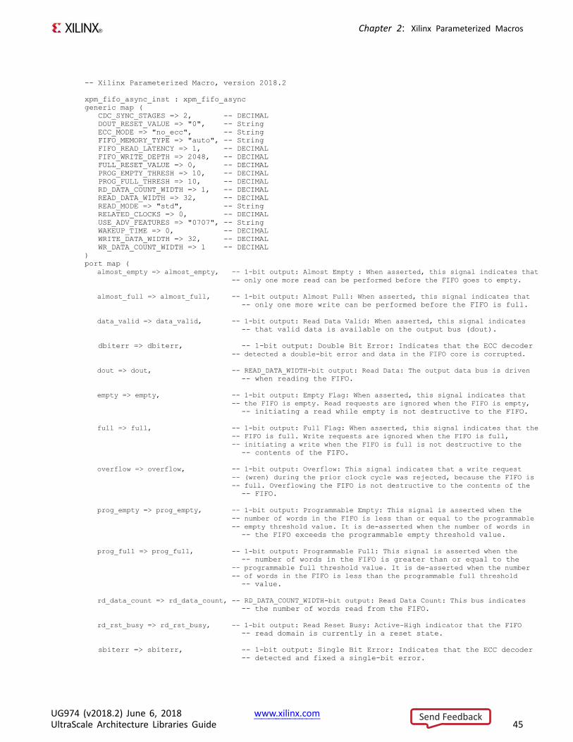
VHDL Instantiation TemplateUnless they already exist, copy the following two statements and paste them before the entitydeclaration.Library xpm;use xpm.vcomponents.all;
-- xpm_fifo_async: Asynchronous FIFO
UG974 (v2018.2) June 6, 2018 www.xilinx.comUltraScale Architecture Libraries Guide 44
Send Feedback
Chapter 2: Xilinx Parameterized Macros
-- Xilinx Parameterized Macro, version 2018.2
xpm_fifo_async_inst : xpm_fifo_asyncgeneric map (
CDC_SYNC_STAGES => 2, -- DECIMALDOUT_RESET_VALUE => "0", -- StringECC_MODE => "no_ecc", -- StringFIFO_MEMORY_TYPE => "auto", -- StringFIFO_READ_LATENCY => 1, -- DECIMALFIFO_WRITE_DEPTH => 2048, -- DECIMALFULL_RESET_VALUE => 0, -- DECIMALPROG_EMPTY_THRESH => 10, -- DECIMALPROG_FULL_THRESH => 10, -- DECIMALRD_DATA_COUNT_WIDTH => 1, -- DECIMALREAD_DATA_WIDTH => 32, -- DECIMALREAD_MODE => "std", -- StringRELATED_CLOCKS => 0, -- DECIMALUSE_ADV_FEATURES => "0707", -- StringWAKEUP_TIME => 0, -- DECIMALWRITE_DATA_WIDTH => 32, -- DECIMALWR_DATA_COUNT_WIDTH => 1 -- DECIMAL
)port map (
almost_empty => almost_empty, -- 1-bit output: Almost Empty : When asserted, this signal indicates that-- only one more read can be performed before the FIFO goes to empty.
almost_full => almost_full, -- 1-bit output: Almost Full: When asserted, this signal indicates that-- only one more write can be performed before the FIFO is full.
data_valid => data_valid, -- 1-bit output: Read Data Valid: When asserted, this signal indicates-- that valid data is available on the output bus (dout).
dbiterr => dbiterr, -- 1-bit output: Double Bit Error: Indicates that the ECC decoder-- detected a double-bit error and data in the FIFO core is corrupted.
dout => dout, -- READ_DATA_WIDTH-bit output: Read Data: The output data bus is driven-- when reading the FIFO.
empty => empty, -- 1-bit output: Empty Flag: When asserted, this signal indicates that-- the FIFO is empty. Read requests are ignored when the FIFO is empty,
-- initiating a read while empty is not destructive to the FIFO.
full => full, -- 1-bit output: Full Flag: When asserted, this signal indicates that the-- FIFO is full. Write requests are ignored when the FIFO is full,-- initiating a write when the FIFO is full is not destructive to the
-- contents of the FIFO.
overflow => overflow, -- 1-bit output: Overflow: This signal indicates that a write request-- (wren) during the prior clock cycle was rejected, because the FIFO is-- full. Overflowing the FIFO is not destructive to the contents of the
-- FIFO.
prog_empty => prog_empty, -- 1-bit output: Programmable Empty: This signal is asserted when the-- number of words in the FIFO is less than or equal to the programmable-- empty threshold value. It is de-asserted when the number of words in
-- the FIFO exceeds the programmable empty threshold value.
prog_full => prog_full, -- 1-bit output: Programmable Full: This signal is asserted when the-- number of words in the FIFO is greater than or equal to the
-- programmable full threshold value. It is de-asserted when the number-- of words in the FIFO is less than the programmable full threshold
-- value.
rd_data_count => rd_data_count, -- RD_DATA_COUNT_WIDTH-bit output: Read Data Count: This bus indicates-- the number of words read from the FIFO.
rd_rst_busy => rd_rst_busy, -- 1-bit output: Read Reset Busy: Active-High indicator that the FIFO-- read domain is currently in a reset state.
sbiterr => sbiterr, -- 1-bit output: Single Bit Error: Indicates that the ECC decoder-- detected and fixed a single-bit error.
UG974 (v2018.2) June 6, 2018 www.xilinx.comUltraScale Architecture Libraries Guide 45
Send Feedback
Chapter 2: Xilinx Parameterized Macros
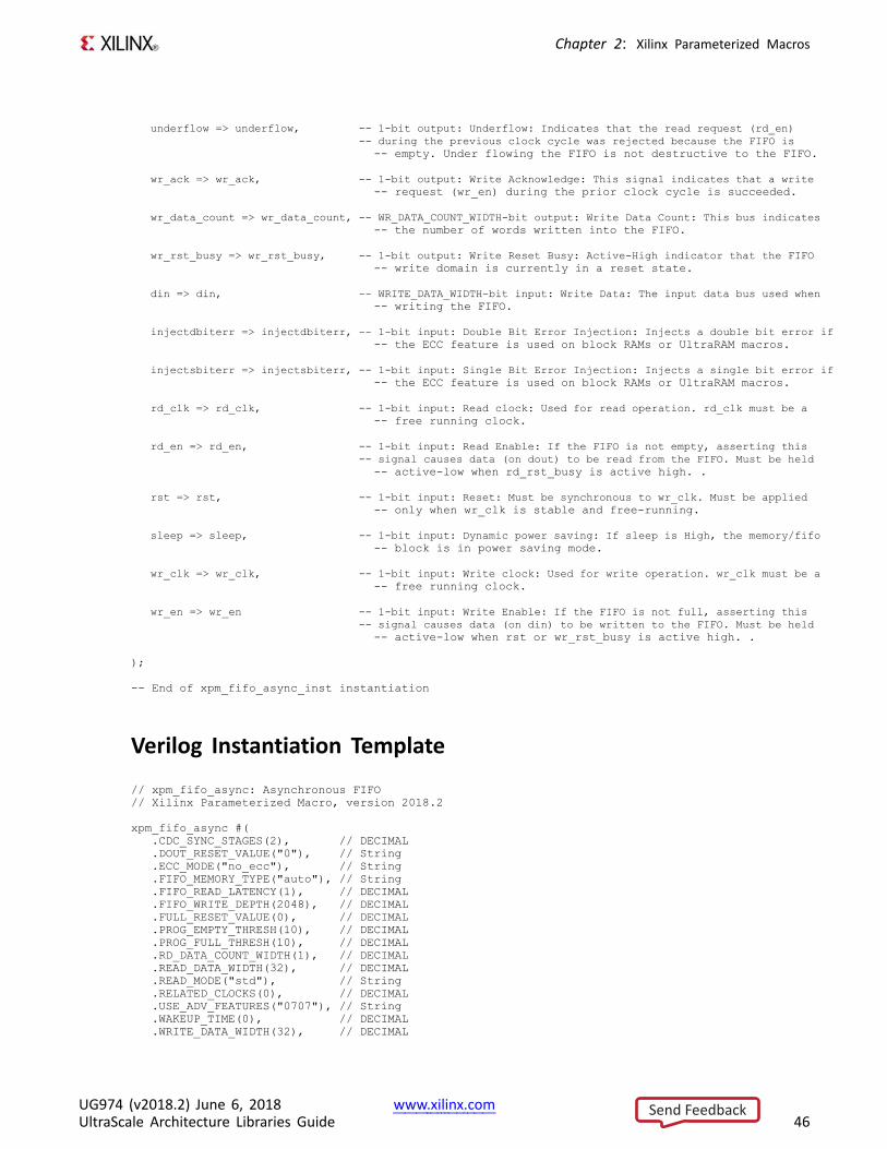
underflow => underflow, -- 1-bit output: Underflow: Indicates that the read request (rd_en)-- during the previous clock cycle was rejected because the FIFO is
-- empty. Under flowing the FIFO is not destructive to the FIFO.
wr_ack => wr_ack, -- 1-bit output: Write Acknowledge: This signal indicates that a write-- request (wr_en) during the prior clock cycle is succeeded.
wr_data_count => wr_data_count, -- WR_DATA_COUNT_WIDTH-bit output: Write Data Count: This bus indicates-- the number of words written into the FIFO.
wr_rst_busy => wr_rst_busy, -- 1-bit output: Write Reset Busy: Active-High indicator that the FIFO-- write domain is currently in a reset state.
din => din, -- WRITE_DATA_WIDTH-bit input: Write Data: The input data bus used when-- writing the FIFO.
injectdbiterr => injectdbiterr, -- 1-bit input: Double Bit Error Injection: Injects a double bit error if-- the ECC feature is used on block RAMs or UltraRAM macros.
injectsbiterr => injectsbiterr, -- 1-bit input: Single Bit Error Injection: Injects a single bit error if-- the ECC feature is used on block RAMs or UltraRAM macros.
rd_clk => rd_clk, -- 1-bit input: Read clock: Used for read operation. rd_clk must be a-- free running clock.
rd_en => rd_en, -- 1-bit input: Read Enable: If the FIFO is not empty, asserting this-- signal causes data (on dout) to be read from the FIFO. Must be held
-- active-low when rd_rst_busy is active high. .
rst => rst, -- 1-bit input: Reset: Must be synchronous to wr_clk. Must be applied-- only when wr_clk is stable and free-running.
sleep => sleep, -- 1-bit input: Dynamic power saving: If sleep is High, the memory/fifo-- block is in power saving mode.
wr_clk => wr_clk, -- 1-bit input: Write clock: Used for write operation. wr_clk must be a-- free running clock.
wr_en => wr_en -- 1-bit input: Write Enable: If the FIFO is not full, asserting this-- signal causes data (on din) to be written to the FIFO. Must be held
-- active-low when rst or wr_rst_busy is active high. .
);
-- End of xpm_fifo_async_inst instantiation
Verilog Instantiation Template
// xpm_fifo_async: Asynchronous FIFO// Xilinx Parameterized Macro, version 2018.2
xpm_fifo_async #(.CDC_SYNC_STAGES(2), // DECIMAL.DOUT_RESET_VALUE("0"), // String.ECC_MODE("no_ecc"), // String.FIFO_MEMORY_TYPE("auto"), // String.FIFO_READ_LATENCY(1), // DECIMAL.FIFO_WRITE_DEPTH(2048), // DECIMAL.FULL_RESET_VALUE(0), // DECIMAL.PROG_EMPTY_THRESH(10), // DECIMAL.PROG_FULL_THRESH(10), // DECIMAL.RD_DATA_COUNT_WIDTH(1), // DECIMAL.READ_DATA_WIDTH(32), // DECIMAL.READ_MODE("std"), // String.RELATED_CLOCKS(0), // DECIMAL.USE_ADV_FEATURES("0707"), // String.WAKEUP_TIME(0), // DECIMAL.WRITE_DATA_WIDTH(32), // DECIMAL
UG974 (v2018.2) June 6, 2018 www.xilinx.comUltraScale Architecture Libraries Guide 46
Send Feedback
Chapter 2: Xilinx Parameterized Macros
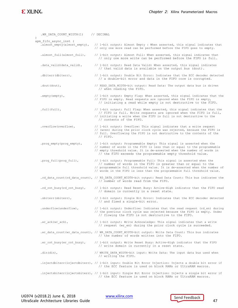
.WR_DATA_COUNT_WIDTH(1) // DECIMAL)xpm_fifo_async_inst (
.almost_empty(almost_empty), // 1-bit output: Almost Empty : When asserted, this signal indicates that// only one more read can be performed before the FIFO goes to empty.
.almost_full(almost_full), // 1-bit output: Almost Full: When asserted, this signal indicates that// only one more write can be performed before the FIFO is full.
.data_valid(data_valid), // 1-bit output: Read Data Valid: When asserted, this signal indicates// that valid data is available on the output bus (dout).
.dbiterr(dbiterr), // 1-bit output: Double Bit Error: Indicates that the ECC decoder detected// a double-bit error and data in the FIFO core is corrupted.
.dout(dout), // READ_DATA_WIDTH-bit output: Read Data: The output data bus is driven// when reading the FIFO.
.empty(empty), // 1-bit output: Empty Flag: When asserted, this signal indicates that the// FIFO is empty. Read requests are ignored when the FIFO is empty,
// initiating a read while empty is not destructive to the FIFO.
.full(full), // 1-bit output: Full Flag: When asserted, this signal indicates that the// FIFO is full. Write requests are ignored when the FIFO is full,
// initiating a write when the FIFO is full is not destructive to the// contents of the FIFO.
.overflow(overflow), // 1-bit output: Overflow: This signal indicates that a write request// (wren) during the prior clock cycle was rejected, because the FIFO is// full. Overflowing the FIFO is not destructive to the contents of the
// FIFO.
.prog_empty(prog_empty), // 1-bit output: Programmable Empty: This signal is asserted when the// number of words in the FIFO is less than or equal to the programmable// empty threshold value. It is de-asserted when the number of words in
// the FIFO exceeds the programmable empty threshold value.
.prog_full(prog_full), // 1-bit output: Programmable Full: This signal is asserted when the// number of words in the FIFO is greater than or equal to the
// programmable full threshold value. It is de-asserted when the number of// words in the FIFO is less than the programmable full threshold value.
.rd_data_count(rd_data_count), // RD_DATA_COUNT_WIDTH-bit output: Read Data Count: This bus indicates the// number of words read from the FIFO.
.rd_rst_busy(rd_rst_busy), // 1-bit output: Read Reset Busy: Active-High indicator that the FIFO read// domain is currently in a reset state.
.sbiterr(sbiterr), // 1-bit output: Single Bit Error: Indicates that the ECC decoder detected// and fixed a single-bit error.
.underflow(underflow), // 1-bit output: Underflow: Indicates that the read request (rd_en) during// the previous clock cycle was rejected because the FIFO is empty. Under
// flowing the FIFO is not destructive to the FIFO.
.wr_ack(wr_ack), // 1-bit output: Write Acknowledge: This signal indicates that a write// request (wr_en) during the prior clock cycle is succeeded.
.wr_data_count(wr_data_count), // WR_DATA_COUNT_WIDTH-bit output: Write Data Count: This bus indicates// the number of words written into the FIFO.
.wr_rst_busy(wr_rst_busy), // 1-bit output: Write Reset Busy: Active-High indicator that the FIFO// write domain is currently in a reset state.
.din(din), // WRITE_DATA_WIDTH-bit input: Write Data: The input data bus used when// writing the FIFO.
.injectdbiterr(injectdbiterr), // 1-bit input: Double Bit Error Injection: Injects a double bit error if// the ECC feature is used on block RAMs or UltraRAM macros.
.injectsbiterr(injectsbiterr), // 1-bit input: Single Bit Error Injection: Injects a single bit error if// the ECC feature is used on block RAMs or UltraRAM macros.
UG974 (v2018.2) June 6, 2018 www.xilinx.comUltraScale Architecture Libraries Guide 47
Send Feedback
Chapter 2: Xilinx Parameterized Macros
.rd_clk(rd_clk), // 1-bit input: Read clock: Used for read operation. rd_clk must be a free// running clock.
.rd_en(rd_en), // 1-bit input: Read Enable: If the FIFO is not empty, asserting this// signal causes data (on dout) to be read from the FIFO. Must be held
// active-low when rd_rst_busy is active high. .
.rst(rst), // 1-bit input: Reset: Must be synchronous to wr_clk. Must be applied only// when wr_clk is stable and free-running.
.sleep(sleep), // 1-bit input: Dynamic power saving: If sleep is High, the memory/fifo// block is in power saving mode.
.wr_clk(wr_clk), // 1-bit input: Write clock: Used for write operation. wr_clk must be a// free running clock.
.wr_en(wr_en) // 1-bit input: Write Enable: If the FIFO is not full, asserting this// signal causes data (on din) to be written to the FIFO. Must be held
// active-low when rst or wr_rst_busy is active high. .
);
// End of xpm_fifo_async_inst instantiation
For More InformationSee the UltraScale Programmable Devices User Guides.
UG974 (v2018.2) June 6, 2018 www.xilinx.comUltraScale Architecture Libraries Guide 48
Send Feedback
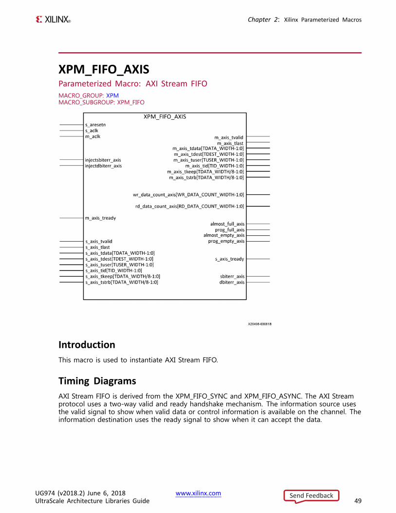
Chapter 2: Xilinx Parameterized Macros
XPM_FIFO_AXISParameterized Macro: AXI Stream FIFOMACRO_GROUP: XPMMACRO_SUBGROUP: XPM_FIFO
IntroductionThis macro is used to instantiate AXI Stream FIFO.
Timing DiagramsAXI Stream FIFO is derived from the XPM_FIFO_SYNC and XPM_FIFO_ASYNC. The AXI Streamprotocol uses a two-way valid and ready handshake mechanism. The information source usesthe valid signal to show when valid data or control information is available on the channel. Theinformation destination uses the ready signal to show when it can accept the data.
UG974 (v2018.2) June 6, 2018 www.xilinx.comUltraScale Architecture Libraries Guide 49
Send Feedback
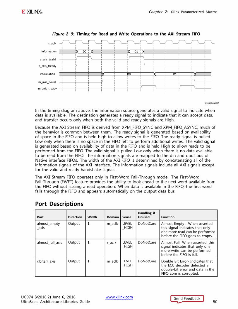
Chapter 2: Xilinx Parameterized Macros
Figure 2–9: Timing for Read and Write Operations to the AXI Stream FIFO
In the timing diagram above, the information source generates a valid signal to indicate whendata is available. The destination generates a ready signal to indicate that it can accept data,and transfer occurs only when both the valid and ready signals are High.
Because the AXI Stream FIFO is derived from XPM_FIFO_SYNC and XPM_FIFO_ASYNC, much ofthe behavior is common between them. The ready signal is generated based on availabilityof space in the FIFO and is held high to allow writes to the FIFO. The ready signal is pulledLow only when there is no space in the FIFO left to perform additional writes. The valid signalis generated based on availability of data in the FIFO and is held High to allow reads to beperformed from the FIFO. The valid signal is pulled Low only when there is no data availableto be read from the FIFO. The information signals are mapped to the din and dout bus ofNative interface FIFOs. The width of the AXI FIFO is determined by concatenating all of theinformation signals of the AXI interface. The information signals include all AXI signals exceptfor the valid and ready handshake signals.
The AXI Stream FIFO operates only in First-Word Fall-Through mode. The First-WordFall-Through (FWFT) feature provides the ability to look ahead to the next word available fromthe FIFO without issuing a read operation. When data is available in the FIFO, the first wordfalls through the FIFO and appears automatically on the output data bus.
Port Descriptions
Port Direction Width Domain SenseHandling ifUnused Function
almost_empty_axis
Output 1 m_aclk LEVEL_HIGH
DoNotCare Almost Empty : When asserted,this signal indicates that onlyone more read can be performedbefore the FIFO goes to empty.
almost_full_axis Output 1 s_aclk LEVEL_HIGH
DoNotCare Almost Full: When asserted, thissignal indicates that only onemore write can be performedbefore the FIFO is full.
dbiterr_axis Output 1 m_aclk LEVEL_HIGH
DoNotCare Double Bit Error- Indicates thatthe ECC decoder detected adouble-bit error and data in theFIFO core is corrupted.
UG974 (v2018.2) June 6, 2018 www.xilinx.comUltraScale Architecture Libraries Guide 50
Send Feedback
Chapter 2: Xilinx Parameterized Macros
Port Direction Width Domain SenseHandling ifUnused Function
injectdbiterr_axis
Input 1 s_aclk LEVEL_HIGH
0 Double Bit Error Injection- Injectsa double bit error if the ECCfeature is used.
injectsbiterr_axis
Input 1 s_aclk LEVEL_HIGH
0 Single Bit Error Injection- Injectsa single bit error if the ECCfeature is used.
m_aclk Input 1 NA EDGE_RISING
Active Master Interface Clock: Allsignals on master interface aresampled on the rising edge ofthis clock.
m_axis_tdata Output TDATA_WIDTH
m_aclk NA Active TDATA: The primary payload thatis used to provide the data thatis passing across the interface.The width of the data payload isan integer number of bytes.
m_axis_tdest Output TDEST_WIDTH
m_aclk NA Active TDEST: Provides routinginformation for the data stream.
m_axis_tid Output TID_WIDTH
m_aclk NA Active TID: The data stream identifierthat indicates different streamsof data.
m_axis_tkeep Output TDATA_WIDTH
m_aclk NA Active TKEEP: The byte qualifier thatindicates whether the content ofthe associated byte of TDATA isprocessed as part of the datastream. Associated bytes thathave the TKEEP byte qualifierdeasserted are null bytes andcan be removed from the datastream. For a 64-bit DATA,bit 0 corresponds to the leastsignificant byte on DATA, andbit 7 corresponds to the mostsignificant byte. For example:
• KEEP[0] = 1b, DATA[7:0] isnot a NULL byte
• KEEP[7] = 0b, DATA[63:56] isa NULL byte
m_axis_tlast Output 1 m_aclk LEVEL_HIGH
Active TLAST: Indicates the boundary ofa packet.
m_axis_tready Input 1 m_aclk LEVEL_HIGH
Active TREADY: Indicates that the slavecan accept a transfer in thecurrent cycle.
UG974 (v2018.2) June 6, 2018 www.xilinx.comUltraScale Architecture Libraries Guide 51
Send Feedback
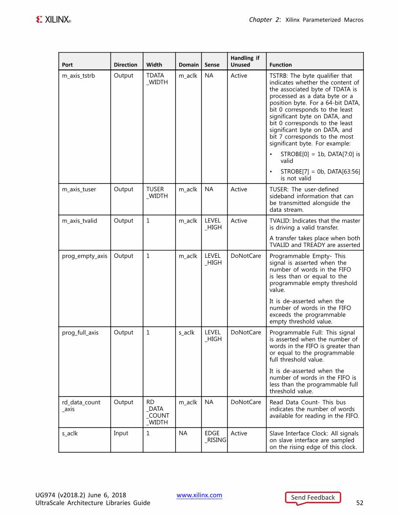
Chapter 2: Xilinx Parameterized Macros
Port Direction Width Domain SenseHandling ifUnused Function
m_axis_tstrb Output TDATA_WIDTH
m_aclk NA Active TSTRB: The byte qualifier thatindicates whether the content ofthe associated byte of TDATA isprocessed as a data byte or aposition byte. For a 64-bit DATA,bit 0 corresponds to the leastsignificant byte on DATA, andbit 0 corresponds to the leastsignificant byte on DATA, andbit 7 corresponds to the mostsignificant byte. For example:
• STROBE[0] = 1b, DATA[7:0] isvalid
• STROBE[7] = 0b, DATA[63:56]is not valid
m_axis_tuser Output TUSER_WIDTH
m_aclk NA Active TUSER: The user-definedsideband information that canbe transmitted alongside thedata stream.
m_axis_tvalid Output 1 m_aclk LEVEL_HIGH
Active TVALID: Indicates that the masteris driving a valid transfer.
A transfer takes place when bothTVALID and TREADY are asserted
prog_empty_axis Output 1 m_aclk LEVEL_HIGH
DoNotCare Programmable Empty- Thissignal is asserted when thenumber of words in the FIFOis less than or equal to theprogrammable empty thresholdvalue.
It is de-asserted when thenumber of words in the FIFOexceeds the programmableempty threshold value.
prog_full_axis Output 1 s_aclk LEVEL_HIGH
DoNotCare Programmable Full: This signalis asserted when the number ofwords in the FIFO is greater thanor equal to the programmablefull threshold value.
It is de-asserted when thenumber of words in the FIFO isless than the programmable fullthreshold value.
rd_data_count_axis
Output RD_DATA_COUNT_WIDTH
m_aclk NA DoNotCare Read Data Count- This busindicates the number of wordsavailable for reading in the FIFO.
s_aclk Input 1 NA EDGE_RISING
Active Slave Interface Clock: All signalson slave interface are sampledon the rising edge of this clock.
UG974 (v2018.2) June 6, 2018 www.xilinx.comUltraScale Architecture Libraries Guide 52
Send Feedback
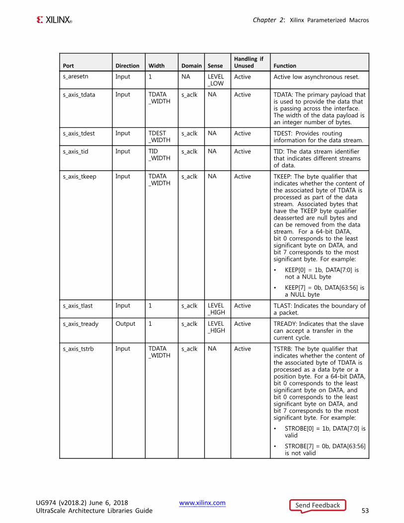
Chapter 2: Xilinx Parameterized Macros
Port Direction Width Domain SenseHandling ifUnused Function
s_aresetn Input 1 NA LEVEL_LOW
Active Active low asynchronous reset.
s_axis_tdata Input TDATA_WIDTH
s_aclk NA Active TDATA: The primary payload thatis used to provide the data thatis passing across the interface.The width of the data payload isan integer number of bytes.
s_axis_tdest Input TDEST_WIDTH
s_aclk NA Active TDEST: Provides routinginformation for the data stream.
s_axis_tid Input TID_WIDTH
s_aclk NA Active TID: The data stream identifierthat indicates different streamsof data.
s_axis_tkeep Input TDATA_WIDTH
s_aclk NA Active TKEEP: The byte qualifier thatindicates whether the content ofthe associated byte of TDATA isprocessed as part of the datastream. Associated bytes thathave the TKEEP byte qualifierdeasserted are null bytes andcan be removed from the datastream. For a 64-bit DATA,bit 0 corresponds to the leastsignificant byte on DATA, andbit 7 corresponds to the mostsignificant byte. For example:
• KEEP[0] = 1b, DATA[7:0] isnot a NULL byte
• KEEP[7] = 0b, DATA[63:56] isa NULL byte
s_axis_tlast Input 1 s_aclk LEVEL_HIGH
Active TLAST: Indicates the boundary ofa packet.
s_axis_tready Output 1 s_aclk LEVEL_HIGH
Active TREADY: Indicates that the slavecan accept a transfer in thecurrent cycle.
s_axis_tstrb Input TDATA_WIDTH
s_aclk NA Active TSTRB: The byte qualifier thatindicates whether the content ofthe associated byte of TDATA isprocessed as a data byte or aposition byte. For a 64-bit DATA,bit 0 corresponds to the leastsignificant byte on DATA, andbit 0 corresponds to the leastsignificant byte on DATA, andbit 7 corresponds to the mostsignificant byte. For example:
• STROBE[0] = 1b, DATA[7:0] isvalid
• STROBE[7] = 0b, DATA[63:56]is not valid
UG974 (v2018.2) June 6, 2018 www.xilinx.comUltraScale Architecture Libraries Guide 53
Send Feedback
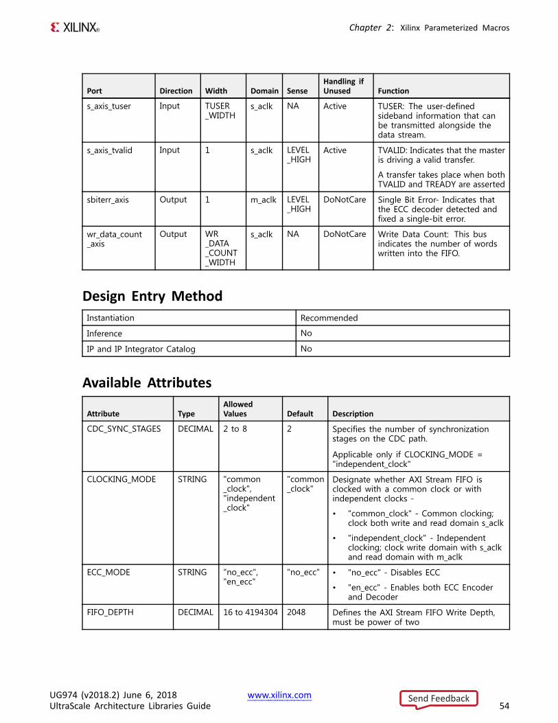
Chapter 2: Xilinx Parameterized Macros
Port Direction Width Domain SenseHandling ifUnused Function
s_axis_tuser Input TUSER_WIDTH
s_aclk NA Active TUSER: The user-definedsideband information that canbe transmitted alongside thedata stream.
s_axis_tvalid Input 1 s_aclk LEVEL_HIGH
Active TVALID: Indicates that the masteris driving a valid transfer.
A transfer takes place when bothTVALID and TREADY are asserted
sbiterr_axis Output 1 m_aclk LEVEL_HIGH
DoNotCare Single Bit Error- Indicates thatthe ECC decoder detected andfixed a single-bit error.
wr_data_count_axis
Output WR_DATA_COUNT_WIDTH
s_aclk NA DoNotCare Write Data Count: This busindicates the number of wordswritten into the FIFO.
Design Entry MethodInstantiation Recommended
Inference No
IP and IP Integrator Catalog No
Available Attributes
Attribute TypeAllowedValues Default Description
CDC_SYNC_STAGES DECIMAL 2 to 8 2 Specifies the number of synchronizationstages on the CDC path.
Applicable only if CLOCKING_MODE ="independent_clock"
CLOCKING_MODE STRING "common_clock","independent_clock"
"common_clock"
Designate whether AXI Stream FIFO isclocked with a common clock or withindependent clocks -
• "common_clock" - Common clocking;clock both write and read domain s_aclk
• "independent_clock" - Independentclocking; clock write domain with s_aclkand read domain with m_aclk
ECC_MODE STRING "no_ecc","en_ecc"
"no_ecc" • "no_ecc" - Disables ECC
• "en_ecc" - Enables both ECC Encoderand Decoder
FIFO_DEPTH DECIMAL 16 to 4194304 2048 Defines the AXI Stream FIFO Write Depth,must be power of two
UG974 (v2018.2) June 6, 2018 www.xilinx.comUltraScale Architecture Libraries Guide 54
Send Feedback
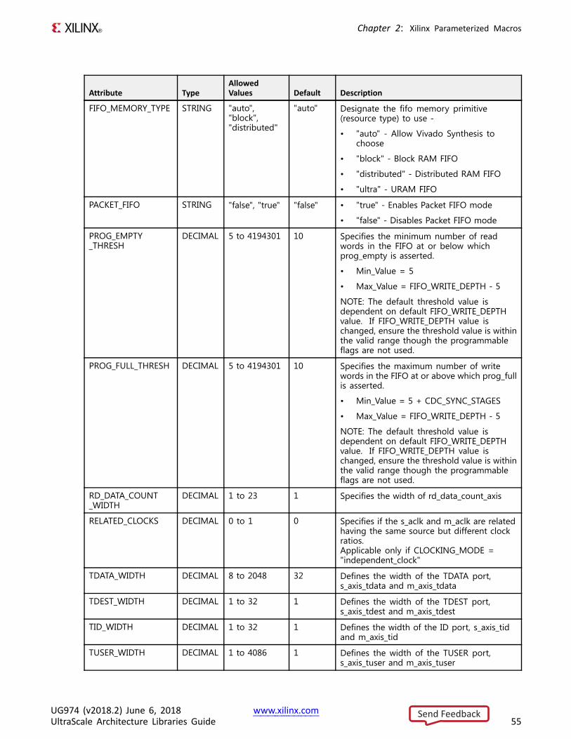
Chapter 2: Xilinx Parameterized Macros
Attribute TypeAllowedValues Default Description
FIFO_MEMORY_TYPE STRING "auto","block","distributed"
"auto" Designate the fifo memory primitive(resource type) to use -
• "auto" - Allow Vivado Synthesis tochoose
• "block" - Block RAM FIFO
• "distributed" - Distributed RAM FIFO
• "ultra" - URAM FIFO
PACKET_FIFO STRING "false", "true" "false" • "true" - Enables Packet FIFO mode
• "false" - Disables Packet FIFO mode
PROG_EMPTY_THRESH
DECIMAL 5 to 4194301 10 Specifies the minimum number of readwords in the FIFO at or below whichprog_empty is asserted.
• Min_Value = 5
• Max_Value = FIFO_WRITE_DEPTH - 5
NOTE: The default threshold value isdependent on default FIFO_WRITE_DEPTHvalue. If FIFO_WRITE_DEPTH value ischanged, ensure the threshold value is withinthe valid range though the programmableflags are not used.
PROG_FULL_THRESH DECIMAL 5 to 4194301 10 Specifies the maximum number of writewords in the FIFO at or above which prog_fullis asserted.
• Min_Value = 5 + CDC_SYNC_STAGES
• Max_Value = FIFO_WRITE_DEPTH - 5
NOTE: The default threshold value isdependent on default FIFO_WRITE_DEPTHvalue. If FIFO_WRITE_DEPTH value ischanged, ensure the threshold value is withinthe valid range though the programmableflags are not used.
RD_DATA_COUNT_WIDTH
DECIMAL 1 to 23 1 Specifies the width of rd_data_count_axis
RELATED_CLOCKS DECIMAL 0 to 1 0 Specifies if the s_aclk and m_aclk are relatedhaving the same source but different clockratios.Applicable only if CLOCKING_MODE ="independent_clock"
TDATA_WIDTH DECIMAL 8 to 2048 32 Defines the width of the TDATA port,s_axis_tdata and m_axis_tdata
TDEST_WIDTH DECIMAL 1 to 32 1 Defines the width of the TDEST port,s_axis_tdest and m_axis_tdest
TID_WIDTH DECIMAL 1 to 32 1 Defines the width of the ID port, s_axis_tidand m_axis_tid
TUSER_WIDTH DECIMAL 1 to 4086 1 Defines the width of the TUSER port,s_axis_tuser and m_axis_tuser
UG974 (v2018.2) June 6, 2018 www.xilinx.comUltraScale Architecture Libraries Guide 55
Send Feedback
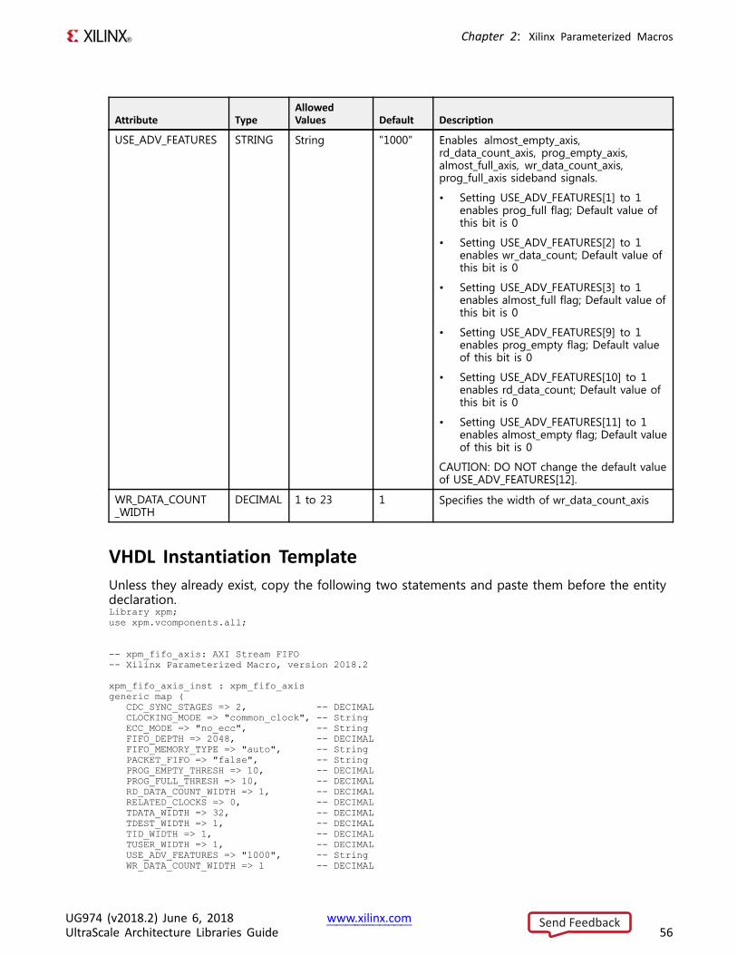
Chapter 2: Xilinx Parameterized Macros
Attribute TypeAllowedValues Default Description
USE_ADV_FEATURES STRING String "1000" Enables almost_empty_axis,rd_data_count_axis, prog_empty_axis,almost_full_axis, wr_data_count_axis,prog_full_axis sideband signals.
• Setting USE_ADV_FEATURES[1] to 1enables prog_full flag; Default value ofthis bit is 0
• Setting USE_ADV_FEATURES[2] to 1enables wr_data_count; Default value ofthis bit is 0
• Setting USE_ADV_FEATURES[3] to 1enables almost_full flag; Default value ofthis bit is 0
• Setting USE_ADV_FEATURES[9] to 1enables prog_empty flag; Default valueof this bit is 0
• Setting USE_ADV_FEATURES[10] to 1enables rd_data_count; Default value ofthis bit is 0
• Setting USE_ADV_FEATURES[11] to 1enables almost_empty flag; Default valueof this bit is 0
CAUTION: DO NOT change the default valueof USE_ADV_FEATURES[12].
WR_DATA_COUNT_WIDTH
DECIMAL 1 to 23 1 Specifies the width of wr_data_count_axis
VHDL Instantiation TemplateUnless they already exist, copy the following two statements and paste them before the entitydeclaration.Library xpm;use xpm.vcomponents.all;
-- xpm_fifo_axis: AXI Stream FIFO-- Xilinx Parameterized Macro, version 2018.2
xpm_fifo_axis_inst : xpm_fifo_axisgeneric map (
CDC_SYNC_STAGES => 2, -- DECIMALCLOCKING_MODE => "common_clock", -- StringECC_MODE => "no_ecc", -- StringFIFO_DEPTH => 2048, -- DECIMALFIFO_MEMORY_TYPE => "auto", -- StringPACKET_FIFO => "false", -- StringPROG_EMPTY_THRESH => 10, -- DECIMALPROG_FULL_THRESH => 10, -- DECIMALRD_DATA_COUNT_WIDTH => 1, -- DECIMALRELATED_CLOCKS => 0, -- DECIMALTDATA_WIDTH => 32, -- DECIMALTDEST_WIDTH => 1, -- DECIMALTID_WIDTH => 1, -- DECIMALTUSER_WIDTH => 1, -- DECIMALUSE_ADV_FEATURES => "1000", -- StringWR_DATA_COUNT_WIDTH => 1 -- DECIMAL
UG974 (v2018.2) June 6, 2018 www.xilinx.comUltraScale Architecture Libraries Guide 56
Send Feedback
Chapter 2: Xilinx Parameterized Macros
)port map (
almost_empty_axis => almost_empty_axis, -- 1-bit output: Almost Empty : When asserted, this signal-- indicates that only one more read can be performed before
-- the FIFO goes to empty.
almost_full_axis => almost_full_axis, -- 1-bit output: Almost Full: When asserted, this signal-- indicates that only one more write can be performed before
-- the FIFO is full.
dbiterr_axis => dbiterr_axis, -- 1-bit output: Double Bit Error- Indicates that the ECC-- decoder detected a double-bit error and data in the FIFO
-- core is corrupted.
m_axis_tdata => m_axis_tdata, -- TDATA_WIDTH-bit output: TDATA: The primary payload that is-- used to provide the data that is passing across the
-- interface. The width of the data payload is an integer-- number of bytes.
m_axis_tdest => m_axis_tdest, -- TDEST_WIDTH-bit output: TDEST: Provides routing information-- for the data stream.
m_axis_tid => m_axis_tid, -- TID_WIDTH-bit output: TID: The data stream identifier that-- indicates different streams of data.
m_axis_tkeep => m_axis_tkeep, -- TDATA_WIDTH-bit output: TKEEP: The byte qualifier that-- indicates whether the content of the associated byte of-- TDATA is processed as part of the data stream. Associated-- bytes that have the TKEEP byte qualifier deasserted are null-- bytes and can be removed from the data stream. For a 64-bit-- DATA, bit 0 corresponds to the least significant byte on-- DATA, and bit 7 corresponds to the most significant byte.-- For example: KEEP[0] = 1b, DATA[7:0] is not a NULL byte
-- KEEP[7] = 0b, DATA[63:56] is a NULL byte .
m_axis_tlast => m_axis_tlast, -- 1-bit output: TLAST: Indicates the boundary of a packet.m_axis_tstrb => m_axis_tstrb, -- TDATA_WIDTH-bit output: TSTRB: The byte qualifier that
-- indicates whether the content of the associated byte of-- TDATA is processed as a data byte or a position byte. For a-- 64-bit DATA, bit 0 corresponds to the least significant byte-- on DATA, and bit 0 corresponds to the least significant byte-- on DATA, and bit 7 corresponds to the most significant byte.-- For example: STROBE[0] = 1b, DATA[7:0] is valid STROBE[7] =
-- 0b, DATA[63:56] is not valid .
m_axis_tuser => m_axis_tuser, -- TUSER_WIDTH-bit output: TUSER: The user-defined sideband-- information that can be transmitted alongside the data
-- stream.
m_axis_tvalid => m_axis_tvalid, -- 1-bit output: TVALID: Indicates that the master is driving a-- valid transfer. A transfer takes place when both TVALID and
-- TREADY are asserted .
prog_empty_axis => prog_empty_axis, -- 1-bit output: Programmable Empty- This signal is asserted-- when the number of words in the FIFO is less than or equal-- to the programmable empty threshold value. It is de-asserted
-- when the number of words in the FIFO exceeds the-- programmable empty threshold value.
prog_full_axis => prog_full_axis, -- 1-bit output: Programmable Full: This signal is asserted-- when the number of words in the FIFO is greater than or-- equal to the programmable full threshold value. It is-- de-asserted when the number of words in the FIFO is less
-- than the programmable full threshold value.
rd_data_count_axis => rd_data_count_axis, -- RD_DATA_COUNT_WIDTH-bit output: Read Data Count- This bus-- indicates the number of words available for reading in the
-- FIFO.
s_axis_tready => s_axis_tready, -- 1-bit output: TREADY: Indicates that the slave can accept a-- transfer in the current cycle.
UG974 (v2018.2) June 6, 2018 www.xilinx.comUltraScale Architecture Libraries Guide 57
Send Feedback
Chapter 2: Xilinx Parameterized Macros
sbiterr_axis => sbiterr_axis, -- 1-bit output: Single Bit Error- Indicates that the ECC-- decoder detected and fixed a single-bit error.
wr_data_count_axis => wr_data_count_axis, -- WR_DATA_COUNT_WIDTH-bit output: Write Data Count: This bus-- indicates the number of words written into the FIFO.
injectdbiterr_axis => injectdbiterr_axis, -- 1-bit input: Double Bit Error Injection- Injects a double-- bit error if the ECC feature is used.
injectsbiterr_axis => injectsbiterr_axis, -- 1-bit input: Single Bit Error Injection- Injects a single-- bit error if the ECC feature is used.
m_aclk => m_aclk, -- 1-bit input: Master Interface Clock: All signals on master-- interface are sampled on the rising edge of this clock.
m_axis_tready => m_axis_tready, -- 1-bit input: TREADY: Indicates that the slave can accept a-- transfer in the current cycle.
s_aclk => s_aclk, -- 1-bit input: Slave Interface Clock: All signals on slave-- interface are sampled on the rising edge of this clock.
s_aresetn => s_aresetn, -- 1-bit input: Active low asynchronous reset.s_axis_tdata => s_axis_tdata, -- TDATA_WIDTH-bit input: TDATA: The primary payload that is
-- used to provide the data that is passing across the-- interface. The width of the data payload is an integer
-- number of bytes.
s_axis_tdest => s_axis_tdest, -- TDEST_WIDTH-bit input: TDEST: Provides routing information-- for the data stream.
s_axis_tid => s_axis_tid, -- TID_WIDTH-bit input: TID: The data stream identifier that-- indicates different streams of data.
s_axis_tkeep => s_axis_tkeep, -- TDATA_WIDTH-bit input: TKEEP: The byte qualifier that-- indicates whether the content of the associated byte of-- TDATA is processed as part of the data stream. Associated-- bytes that have the TKEEP byte qualifier deasserted are null-- bytes and can be removed from the data stream. For a 64-bit-- DATA, bit 0 corresponds to the least significant byte on-- DATA, and bit 7 corresponds to the most significant byte.-- For example: KEEP[0] = 1b, DATA[7:0] is not a NULL byte
-- KEEP[7] = 0b, DATA[63:56] is a NULL byte .
s_axis_tlast => s_axis_tlast, -- 1-bit input: TLAST: Indicates the boundary of a packet.s_axis_tstrb => s_axis_tstrb, -- TDATA_WIDTH-bit input: TSTRB: The byte qualifier that
-- indicates whether the content of the associated byte of-- TDATA is processed as a data byte or a position byte. For a-- 64-bit DATA, bit 0 corresponds to the least significant byte-- on DATA, and bit 0 corresponds to the least significant byte-- on DATA, and bit 7 corresponds to the most significant byte.-- For example: STROBE[0] = 1b, DATA[7:0] is valid STROBE[7] =
-- 0b, DATA[63:56] is not valid .
s_axis_tuser => s_axis_tuser, -- TUSER_WIDTH-bit input: TUSER: The user-defined sideband-- information that can be transmitted alongside the data
-- stream.
s_axis_tvalid => s_axis_tvalid -- 1-bit input: TVALID: Indicates that the master is driving a-- valid transfer. A transfer takes place when both TVALID and
-- TREADY are asserted .
);
-- End of xpm_fifo_axis_inst instantiation
Verilog Instantiation Template
// xpm_fifo_axis: AXI Stream FIFO
UG974 (v2018.2) June 6, 2018 www.xilinx.comUltraScale Architecture Libraries Guide 58
Send Feedback
Chapter 2: Xilinx Parameterized Macros
// Xilinx Parameterized Macro, version 2018.2
xpm_fifo_axis #(.CDC_SYNC_STAGES(2), // DECIMAL.CLOCKING_MODE("common_clock"), // String.ECC_MODE("no_ecc"), // String.FIFO_DEPTH(2048), // DECIMAL.FIFO_MEMORY_TYPE("auto"), // String.PACKET_FIFO("false"), // String.PROG_EMPTY_THRESH(10), // DECIMAL.PROG_FULL_THRESH(10), // DECIMAL.RD_DATA_COUNT_WIDTH(1), // DECIMAL.RELATED_CLOCKS(0), // DECIMAL.TDATA_WIDTH(32), // DECIMAL.TDEST_WIDTH(1), // DECIMAL.TID_WIDTH(1), // DECIMAL.TUSER_WIDTH(1), // DECIMAL.USE_ADV_FEATURES("1000"), // String.WR_DATA_COUNT_WIDTH(1) // DECIMAL
)xpm_fifo_axis_inst (
.almost_empty_axis(almost_empty_axis), // 1-bit output: Almost Empty : When asserted, this signal// indicates that only one more read can be performed before the
// FIFO goes to empty.
.almost_full_axis(almost_full_axis), // 1-bit output: Almost Full: When asserted, this signal// indicates that only one more write can be performed before
// the FIFO is full.
.dbiterr_axis(dbiterr_axis), // 1-bit output: Double Bit Error- Indicates that the ECC// decoder detected a double-bit error and data in the FIFO core
// is corrupted.
.m_axis_tdata(m_axis_tdata), // TDATA_WIDTH-bit output: TDATA: The primary payload that is// used to provide the data that is passing across the
// interface. The width of the data payload is an integer number// of bytes.
.m_axis_tdest(m_axis_tdest), // TDEST_WIDTH-bit output: TDEST: Provides routing information// for the data stream.
.m_axis_tid(m_axis_tid), // TID_WIDTH-bit output: TID: The data stream identifier that// indicates different streams of data.
.m_axis_tkeep(m_axis_tkeep), // TDATA_WIDTH-bit output: TKEEP: The byte qualifier that// indicates whether the content of the associated byte of TDATA// is processed as part of the data stream. Associated bytes// that have the TKEEP byte qualifier deasserted are null bytes// and can be removed from the data stream. For a 64-bit DATA,// bit 0 corresponds to the least significant byte on DATA, and// bit 7 corresponds to the most significant byte. For example:// KEEP[0] = 1b, DATA[7:0] is not a NULL byte KEEP[7] = 0b,
// DATA[63:56] is a NULL byte .
.m_axis_tlast(m_axis_tlast), // 1-bit output: TLAST: Indicates the boundary of a packet.
.m_axis_tstrb(m_axis_tstrb), // TDATA_WIDTH-bit output: TSTRB: The byte qualifier that// indicates whether the content of the associated byte of TDATA// is processed as a data byte or a position byte. For a 64-bit// DATA, bit 0 corresponds to the least significant byte on// DATA, and bit 0 corresponds to the least significant byte on// DATA, and bit 7 corresponds to the most significant byte. For// example: STROBE[0] = 1b, DATA[7:0] is valid STROBE[7] = 0b,
// DATA[63:56] is not valid .
.m_axis_tuser(m_axis_tuser), // TUSER_WIDTH-bit output: TUSER: The user-defined sideband// information that can be transmitted alongside the data
// stream.
.m_axis_tvalid(m_axis_tvalid), // 1-bit output: TVALID: Indicates that the master is driving a// valid transfer. A transfer takes place when both TVALID and
// TREADY are asserted .
UG974 (v2018.2) June 6, 2018 www.xilinx.comUltraScale Architecture Libraries Guide 59
Send Feedback
Chapter 2: Xilinx Parameterized Macros
.prog_empty_axis(prog_empty_axis), // 1-bit output: Programmable Empty- This signal is asserted// when the number of words in the FIFO is less than or equal to// the programmable empty threshold value. It is de-asserted// when the number of words in the FIFO exceeds the programmable
// empty threshold value.
.prog_full_axis(prog_full_axis), // 1-bit output: Programmable Full: This signal is asserted when// the number of words in the FIFO is greater than or equal to// the programmable full threshold value. It is de-asserted when// the number of words in the FIFO is less than the programmable
// full threshold value.
.rd_data_count_axis(rd_data_count_axis), // RD_DATA_COUNT_WIDTH-bit output: Read Data Count- This bus// indicates the number of words available for reading in the
// FIFO.
.s_axis_tready(s_axis_tready), // 1-bit output: TREADY: Indicates that the slave can accept a// transfer in the current cycle.
.sbiterr_axis(sbiterr_axis), // 1-bit output: Single Bit Error- Indicates that the ECC// decoder detected and fixed a single-bit error.
.wr_data_count_axis(wr_data_count_axis), // WR_DATA_COUNT_WIDTH-bit output: Write Data Count: This bus// indicates the number of words written into the FIFO.
.injectdbiterr_axis(injectdbiterr_axis), // 1-bit input: Double Bit Error Injection- Injects a double bit// error if the ECC feature is used.
.injectsbiterr_axis(injectsbiterr_axis), // 1-bit input: Single Bit Error Injection- Injects a single bit// error if the ECC feature is used.
.m_aclk(m_aclk), // 1-bit input: Master Interface Clock: All signals on master// interface are sampled on the rising edge of this clock.
.m_axis_tready(m_axis_tready), // 1-bit input: TREADY: Indicates that the slave can accept a// transfer in the current cycle.
.s_aclk(s_aclk), // 1-bit input: Slave Interface Clock: All signals on slave// interface are sampled on the rising edge of this clock.
.s_aresetn(s_aresetn), // 1-bit input: Active low asynchronous reset.
.s_axis_tdata(s_axis_tdata), // TDATA_WIDTH-bit input: TDATA: The primary payload that is// used to provide the data that is passing across the
// interface. The width of the data payload is an integer number// of bytes.
.s_axis_tdest(s_axis_tdest), // TDEST_WIDTH-bit input: TDEST: Provides routing information// for the data stream.
.s_axis_tid(s_axis_tid), // TID_WIDTH-bit input: TID: The data stream identifier that// indicates different streams of data.
.s_axis_tkeep(s_axis_tkeep), // TDATA_WIDTH-bit input: TKEEP: The byte qualifier that// indicates whether the content of the associated byte of TDATA// is processed as part of the data stream. Associated bytes// that have the TKEEP byte qualifier deasserted are null bytes// and can be removed from the data stream. For a 64-bit DATA,// bit 0 corresponds to the least significant byte on DATA, and// bit 7 corresponds to the most significant byte. For example:// KEEP[0] = 1b, DATA[7:0] is not a NULL byte KEEP[7] = 0b,
// DATA[63:56] is a NULL byte .
.s_axis_tlast(s_axis_tlast), // 1-bit input: TLAST: Indicates the boundary of a packet.
.s_axis_tstrb(s_axis_tstrb), // TDATA_WIDTH-bit input: TSTRB: The byte qualifier that// indicates whether the content of the associated byte of TDATA// is processed as a data byte or a position byte. For a 64-bit// DATA, bit 0 corresponds to the least significant byte on// DATA, and bit 0 corresponds to the least significant byte on// DATA, and bit 7 corresponds to the most significant byte. For// example: STROBE[0] = 1b, DATA[7:0] is valid STROBE[7] = 0b,
// DATA[63:56] is not valid .
UG974 (v2018.2) June 6, 2018 www.xilinx.comUltraScale Architecture Libraries Guide 60
Send Feedback
Chapter 2: Xilinx Parameterized Macros
.s_axis_tuser(s_axis_tuser), // TUSER_WIDTH-bit input: TUSER: The user-defined sideband// information that can be transmitted alongside the data
// stream.
.s_axis_tvalid(s_axis_tvalid) // 1-bit input: TVALID: Indicates that the master is driving a// valid transfer. A transfer takes place when both TVALID and
// TREADY are asserted .
);
// End of xpm_fifo_axis_inst instantiation
For More InformationSee the UltraScale Programmable Devices User Guides.
UG974 (v2018.2) June 6, 2018 www.xilinx.comUltraScale Architecture Libraries Guide 61
Send Feedback
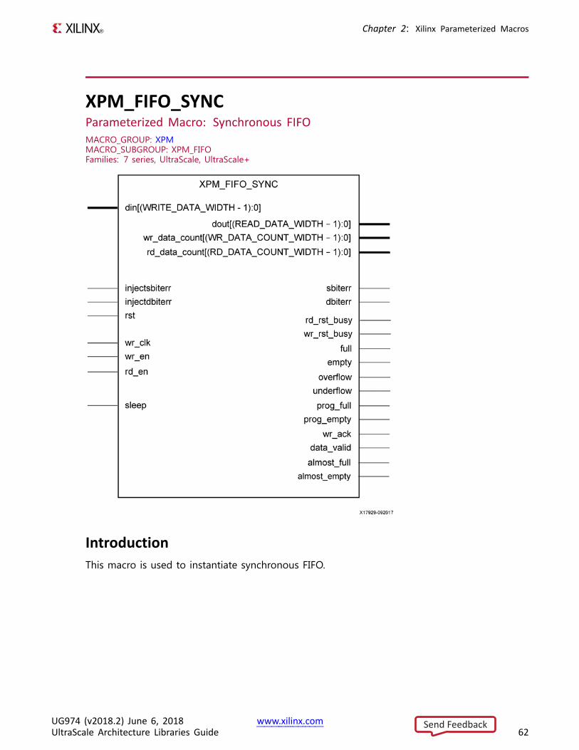
Chapter 2: Xilinx Parameterized Macros
XPM_FIFO_SYNCParameterized Macro: Synchronous FIFOMACRO_GROUP: XPMMACRO_SUBGROUP: XPM_FIFOFamilies: 7 series, UltraScale, UltraScale+
IntroductionThis macro is used to instantiate synchronous FIFO.
UG974 (v2018.2) June 6, 2018 www.xilinx.comUltraScale Architecture Libraries Guide 62
Send Feedback
Chapter 2: Xilinx Parameterized Macros
The following describes the basic write and read operation of an XPM_FIFO instance.
• All synchronous signals are sensitive to the rising edge of wr_clk, which is assumed to be abuffered and toggling clock signal behaving according to target device and FIFO/memoryprimitive requirements.
• A write operation is performed when the FIFO is not full and wr_en is asserted on eachwr_clk cycle.
• A read operation is performed when the FIFO is not empty and rd_en is asserted on eachwr_clk cycle.
• The number of clock cycles required for XPM FIFO to react to dout, full and empty changesdepends on the CLOCK_DOMAIN, READ_MODE, and FIFO_READ_LATENCY settings.
– It may take more than one wr_clk cycle to deassert empty due to write operation(wr_en = 1).
– It may take more than one wr_clk cycle to present the read data on dout port uponassertion of rd_en.
– It may take more than one wr_clk cycle to deassert full due to read operation (rd_en= 1).
• All write operations are gated by the value of wr_en and full on the initiating wr_clk cycle.
• All read operations are gated by the value of rd_en and empty on the initiating wr_clk cycle.
• The wr_en input has no effect when full is asserted on the coincident wr_clk cycle.
• The rd_en input has no effect when empty is asserted on the coincident wr_clk cycle.
• Undriven or unknown values provided on module inputs will produce undefined outputport behavior.
• wr_en/rd_en should not be toggled when reset (rst) or wr_rst_busy or rd_rst_busy is asserted.
• Assertion/deassertion of prog_full happens only when full is deasserted.
• Assertion/deassertion of prog_empty happens only when empty is deasserted.
UG974 (v2018.2) June 6, 2018 www.xilinx.comUltraScale Architecture Libraries Guide 63
Send Feedback
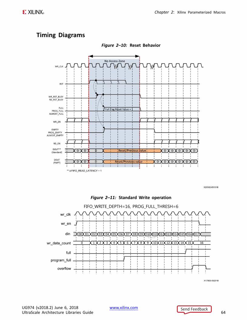
Chapter 2: Xilinx Parameterized Macros
Timing DiagramsFigure 2–10: Reset Behavior
Figure 2–11: Standard Write operation
FIFO_WRITE_DEPTH=16, PROG_FULL_THRESH=6
UG974 (v2018.2) June 6, 2018 www.xilinx.comUltraScale Architecture Libraries Guide 64
Send Feedback
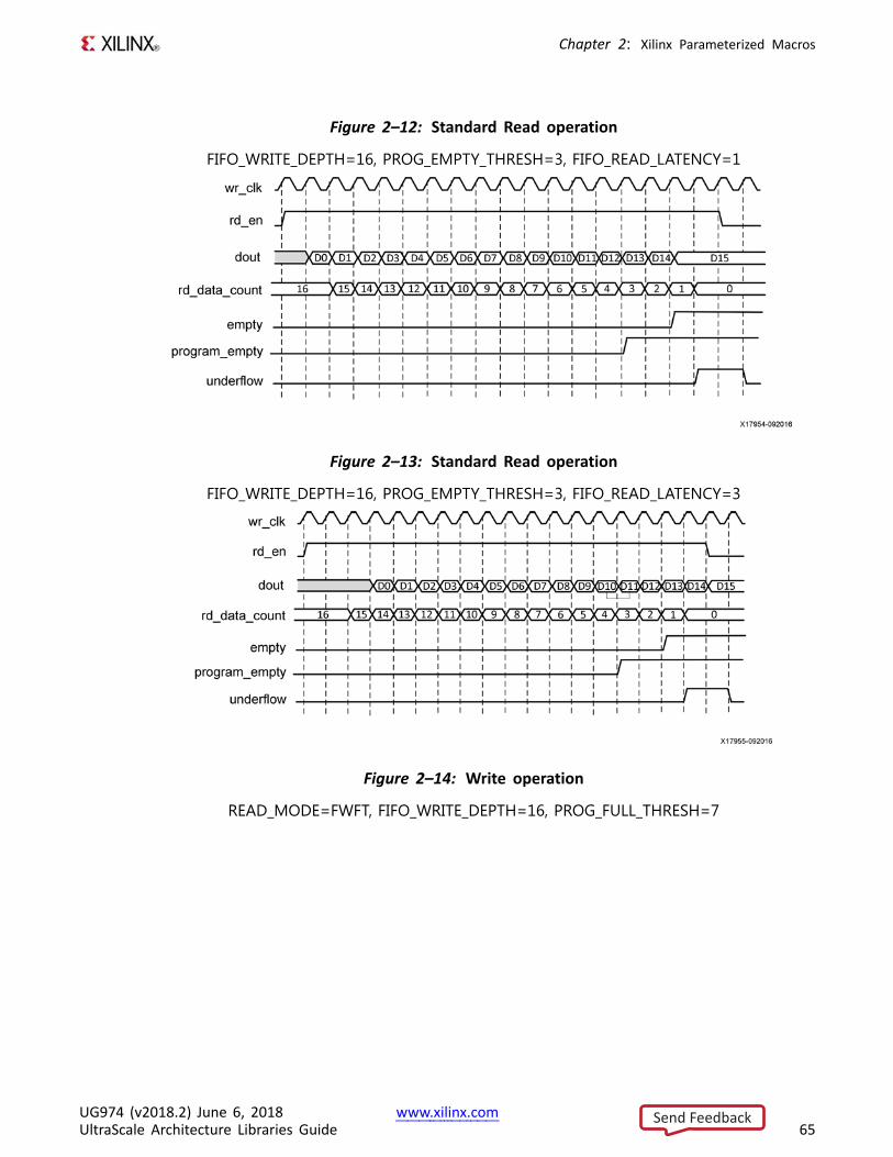
Chapter 2: Xilinx Parameterized Macros
Figure 2–12: Standard Read operation
FIFO_WRITE_DEPTH=16, PROG_EMPTY_THRESH=3, FIFO_READ_LATENCY=1
Figure 2–13: Standard Read operation
FIFO_WRITE_DEPTH=16, PROG_EMPTY_THRESH=3, FIFO_READ_LATENCY=3
Figure 2–14: Write operation
READ_MODE=FWFT, FIFO_WRITE_DEPTH=16, PROG_FULL_THRESH=7
UG974 (v2018.2) June 6, 2018 www.xilinx.comUltraScale Architecture Libraries Guide 65
Send Feedback
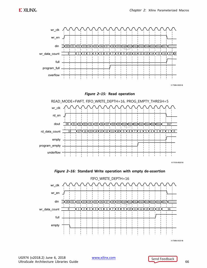
Chapter 2: Xilinx Parameterized Macros
Figure 2–15: Read operation
READ_MODE=FWFT, FIFO_WRITE_DEPTH=16, PROG_EMPTY_THRESH=5
Figure 2–16: Standard Write operation with empty de-assertion
FIFO_WRITE_DEPTH=16
UG974 (v2018.2) June 6, 2018 www.xilinx.comUltraScale Architecture Libraries Guide 66
Send Feedback
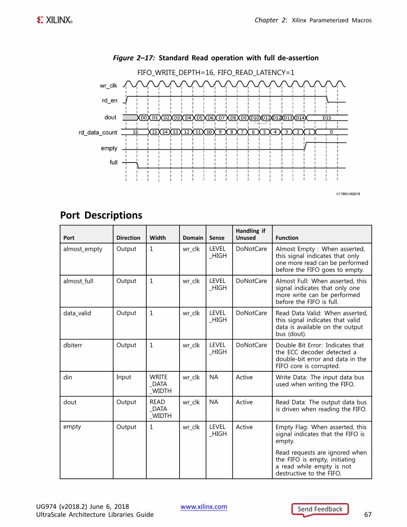
Chapter 2: Xilinx Parameterized Macros
Figure 2–17: Standard Read operation with full de-assertion
FIFO_WRITE_DEPTH=16, FIFO_READ_LATENCY=1
Port Descriptions
Port Direction Width Domain SenseHandling ifUnused Function
almost_empty Output 1 wr_clk LEVEL_HIGH
DoNotCare Almost Empty : When asserted,this signal indicates that onlyone more read can be performedbefore the FIFO goes to empty.
almost_full Output 1 wr_clk LEVEL_HIGH
DoNotCare Almost Full: When asserted, thissignal indicates that only onemore write can be performedbefore the FIFO is full.
data_valid Output 1 wr_clk LEVEL_HIGH
DoNotCare Read Data Valid: When asserted,this signal indicates that validdata is available on the outputbus (dout).
dbiterr Output 1 wr_clk LEVEL_HIGH
DoNotCare Double Bit Error: Indicates thatthe ECC decoder detected adouble-bit error and data in theFIFO core is corrupted.
din Input WRITE_DATA_WIDTH
wr_clk NA Active Write Data: The input data busused when writing the FIFO.
dout Output READ_DATA_WIDTH
wr_clk NA Active Read Data: The output data busis driven when reading the FIFO.
empty Output 1 wr_clk LEVEL_HIGH
Active Empty Flag: When asserted, thissignal indicates that the FIFO isempty.
Read requests are ignored whenthe FIFO is empty, initiatinga read while empty is notdestructive to the FIFO.
UG974 (v2018.2) June 6, 2018 www.xilinx.comUltraScale Architecture Libraries Guide 67
Send Feedback
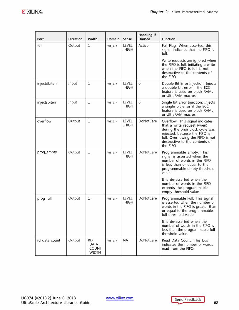
Chapter 2: Xilinx Parameterized Macros
Port Direction Width Domain SenseHandling ifUnused Function
full Output 1 wr_clk LEVEL_HIGH
Active Full Flag: When asserted, thissignal indicates that the FIFO isfull.
Write requests are ignored whenthe FIFO is full, initiating a writewhen the FIFO is full is notdestructive to the contents ofthe FIFO.
injectdbiterr Input 1 wr_clk LEVEL_HIGH
0 Double Bit Error Injection: Injectsa double bit error if the ECCfeature is used on block RAMsor UltraRAM macros.
injectsbiterr Input 1 wr_clk LEVEL_HIGH
0 Single Bit Error Injection: Injectsa single bit error if the ECCfeature is used on block RAMsor UltraRAM macros.
overflow Output 1 wr_clk LEVEL_HIGH
DoNotCare Overflow: This signal indicatesthat a write request (wren)during the prior clock cycle wasrejected, because the FIFO isfull. Overflowing the FIFO is notdestructive to the contents ofthe FIFO.
prog_empty Output 1 wr_clk LEVEL_HIGH
DoNotCare Programmable Empty: Thissignal is asserted when thenumber of words in the FIFOis less than or equal to theprogrammable empty thresholdvalue.
It is de-asserted when thenumber of words in the FIFOexceeds the programmableempty threshold value.
prog_full Output 1 wr_clk LEVEL_HIGH
DoNotCare Programmable Full: This signalis asserted when the number ofwords in the FIFO is greater thanor equal to the programmablefull threshold value.
It is de-asserted when thenumber of words in the FIFO isless than the programmable fullthreshold value.
rd_data_count Output RD_DATA_COUNT_WIDTH
wr_clk NA DoNotCare Read Data Count: This busindicates the number of wordsread from the FIFO.
UG974 (v2018.2) June 6, 2018 www.xilinx.comUltraScale Architecture Libraries Guide 68
Send Feedback
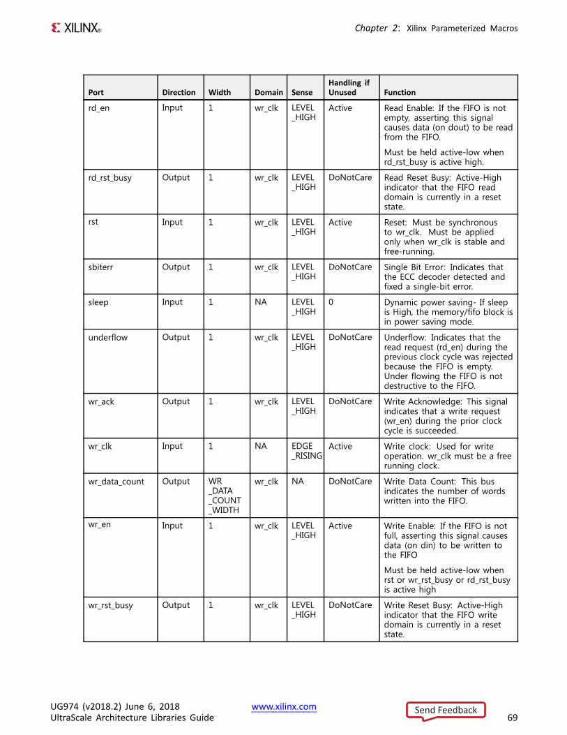
Chapter 2: Xilinx Parameterized Macros
Port Direction Width Domain SenseHandling ifUnused Function
rd_en Input 1 wr_clk LEVEL_HIGH
Active Read Enable: If the FIFO is notempty, asserting this signalcauses data (on dout) to be readfrom the FIFO.
Must be held active-low whenrd_rst_busy is active high.
rd_rst_busy Output 1 wr_clk LEVEL_HIGH
DoNotCare Read Reset Busy: Active-Highindicator that the FIFO readdomain is currently in a resetstate.
rst Input 1 wr_clk LEVEL_HIGH
Active Reset: Must be synchronousto wr_clk. Must be appliedonly when wr_clk is stable andfree-running.
sbiterr Output 1 wr_clk LEVEL_HIGH
DoNotCare Single Bit Error: Indicates thatthe ECC decoder detected andfixed a single-bit error.
sleep Input 1 NA LEVEL_HIGH
0 Dynamic power saving- If sleepis High, the memory/fifo block isin power saving mode.
underflow Output 1 wr_clk LEVEL_HIGH
DoNotCare Underflow: Indicates that theread request (rd_en) during theprevious clock cycle was rejectedbecause the FIFO is empty.Under flowing the FIFO is notdestructive to the FIFO.
wr_ack Output 1 wr_clk LEVEL_HIGH
DoNotCare Write Acknowledge: This signalindicates that a write request(wr_en) during the prior clockcycle is succeeded.
wr_clk Input 1 NA EDGE_RISING
Active Write clock: Used for writeoperation. wr_clk must be a freerunning clock.
wr_data_count Output WR_DATA_COUNT_WIDTH
wr_clk NA DoNotCare Write Data Count: This busindicates the number of wordswritten into the FIFO.
wr_en Input 1 wr_clk LEVEL_HIGH
Active Write Enable: If the FIFO is notfull, asserting this signal causesdata (on din) to be written tothe FIFO
Must be held active-low whenrst or wr_rst_busy or rd_rst_busyis active high
wr_rst_busy Output 1 wr_clk LEVEL_HIGH
DoNotCare Write Reset Busy: Active-Highindicator that the FIFO writedomain is currently in a resetstate.
UG974 (v2018.2) June 6, 2018 www.xilinx.comUltraScale Architecture Libraries Guide 69
Send Feedback
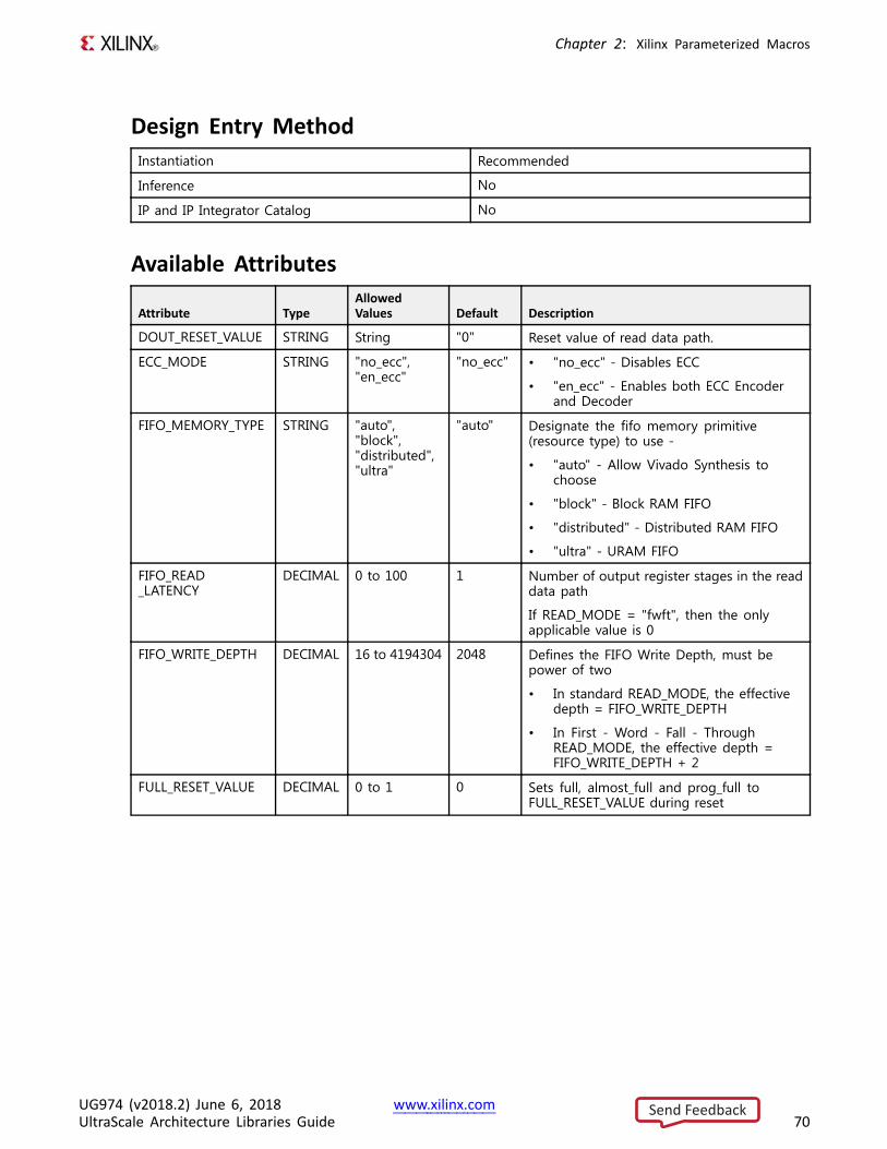
Chapter 2: Xilinx Parameterized Macros
Design Entry MethodInstantiation Recommended
Inference No
IP and IP Integrator Catalog No
Available Attributes
Attribute TypeAllowedValues Default Description
DOUT_RESET_VALUE STRING String "0" Reset value of read data path.
ECC_MODE STRING "no_ecc","en_ecc"
"no_ecc" • "no_ecc" - Disables ECC
• "en_ecc" - Enables both ECC Encoderand Decoder
FIFO_MEMORY_TYPE STRING "auto","block","distributed","ultra"
"auto" Designate the fifo memory primitive(resource type) to use -
• "auto" - Allow Vivado Synthesis tochoose
• "block" - Block RAM FIFO
• "distributed" - Distributed RAM FIFO
• "ultra" - URAM FIFO
FIFO_READ_LATENCY
DECIMAL 0 to 100 1 Number of output register stages in the readdata path
If READ_MODE = "fwft", then the onlyapplicable value is 0
FIFO_WRITE_DEPTH DECIMAL 16 to 4194304 2048 Defines the FIFO Write Depth, must bepower of two
• In standard READ_MODE, the effectivedepth = FIFO_WRITE_DEPTH
• In First - Word - Fall - ThroughREAD_MODE, the effective depth =FIFO_WRITE_DEPTH + 2
FULL_RESET_VALUE DECIMAL 0 to 1 0 Sets full, almost_full and prog_full toFULL_RESET_VALUE during reset
UG974 (v2018.2) June 6, 2018 www.xilinx.comUltraScale Architecture Libraries Guide 70
Send Feedback
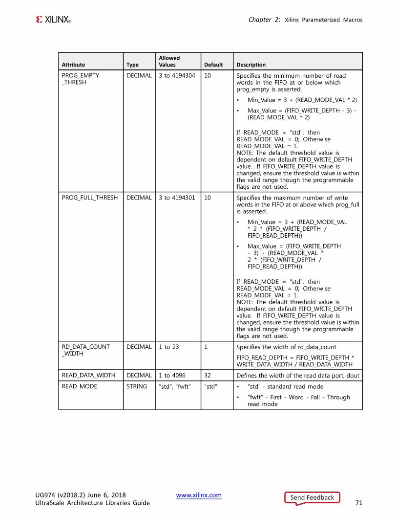
Chapter 2: Xilinx Parameterized Macros
Attribute TypeAllowedValues Default Description
PROG_EMPTY_THRESH
DECIMAL 3 to 4194304 10 Specifies the minimum number of readwords in the FIFO at or below whichprog_empty is asserted.
• Min_Value = 3 + (READ_MODE_VAL * 2)
• Max_Value = (FIFO_WRITE_DEPTH - 3) -(READ_MODE_VAL * 2)
If READ_MODE = "std", thenREAD_MODE_VAL = 0; OtherwiseREAD_MODE_VAL = 1.NOTE: The default threshold value isdependent on default FIFO_WRITE_DEPTHvalue. If FIFO_WRITE_DEPTH value ischanged, ensure the threshold value is withinthe valid range though the programmableflags are not used.
PROG_FULL_THRESH DECIMAL 3 to 4194301 10 Specifies the maximum number of writewords in the FIFO at or above which prog_fullis asserted.
• Min_Value = 3 + (READ_MODE_VAL* 2 * (FIFO_WRITE_DEPTH /FIFO_READ_DEPTH))
• Max_Value = (FIFO_WRITE_DEPTH- 3) - (READ_MODE_VAL *2 * (FIFO_WRITE_DEPTH /FIFO_READ_DEPTH))
If READ_MODE = "std", thenREAD_MODE_VAL = 0; OtherwiseREAD_MODE_VAL = 1.NOTE: The default threshold value isdependent on default FIFO_WRITE_DEPTHvalue. If FIFO_WRITE_DEPTH value ischanged, ensure the threshold value is withinthe valid range though the programmableflags are not used.
RD_DATA_COUNT_WIDTH
DECIMAL 1 to 23 1 Specifies the width of rd_data_count
FIFO_READ_DEPTH = FIFO_WRITE_DEPTH *WRITE_DATA_WIDTH / READ_DATA_WIDTH
READ_DATA_WIDTH DECIMAL 1 to 4096 32 Defines the width of the read data port, dout
READ_MODE STRING "std", "fwft" "std" • "std" - standard read mode
• "fwft" - First - Word - Fall - Throughread mode
UG974 (v2018.2) June 6, 2018 www.xilinx.comUltraScale Architecture Libraries Guide 71
Send Feedback

Chapter 2: Xilinx Parameterized Macros
Attribute TypeAllowedValues Default Description
USE_ADV_FEATURES STRING String "0707" Enables data_valid, almost_empty,rd_data_count, prog_empty, underflow,wr_ack, almost_full, wr_data_count, prog_full,overflow features.
• Setting USE_ADV_FEATURES[0] to 1enables overflow flag; Default value ofthis bit is 1
• Setting USE_ADV_FEATURES[1] to 1enables prog_full flag; Default value ofthis bit is 1
• Setting USE_ADV_FEATURES[2] to 1enables wr_data_count; Default value ofthis bit is 1
• Setting USE_ADV_FEATURES[3] to 1enables almost_full flag; Default value ofthis bit is 0
• Setting USE_ADV_FEATURES[4] to 1enables wr_ack flag; Default value of thisbit is 0
• Setting USE_ADV_FEATURES[8] to 1enables underflow flag; Default value ofthis bit is 1
• Setting USE_ADV_FEATURES[9] to 1enables prog_empty flag; Default valueof this bit is 1
• Setting USE_ADV_FEATURES[10] to 1enables rd_data_count; Default value ofthis bit is 1
• Setting USE_ADV_FEATURES[11] to 1enables almost_empty flag; Default valueof this bit is 0
• Setting USE_ADV_FEATURES[12] to 1enables data_valid flag; Default value ofthis bit is 0
WAKEUP_TIME DECIMAL 0 to 2 0 • 0 - Disable sleep
• 2 - Use Sleep Pin
WR_DATA_COUNT_WIDTH
DECIMAL 1 to 23 1 Specifies the width of wr_data_count
WRITE_DATA_WIDTH DECIMAL 1 to 4096 32 Defines the width of the write data port, din
VHDL Instantiation TemplateUnless they already exist, copy the following two statements and paste them before the entitydeclaration.Library xpm;use xpm.vcomponents.all;
-- xpm_fifo_sync: Synchronous FIFO
UG974 (v2018.2) June 6, 2018 www.xilinx.comUltraScale Architecture Libraries Guide 72
Send Feedback
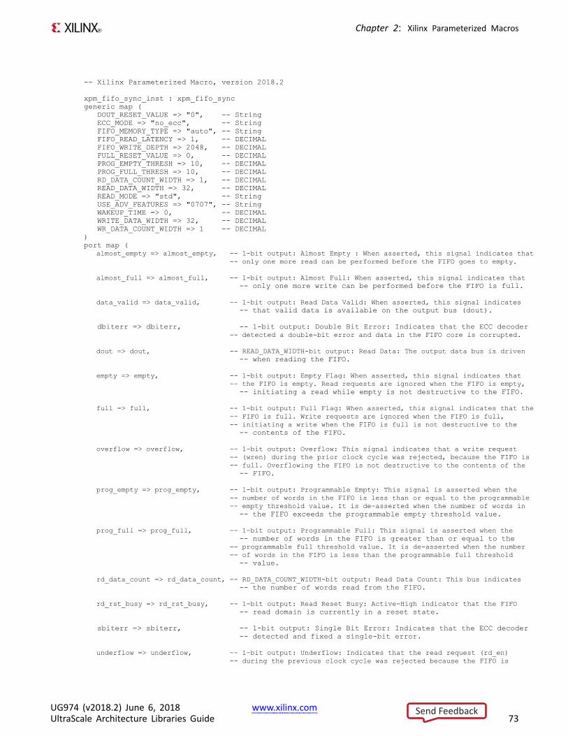
Chapter 2: Xilinx Parameterized Macros
-- Xilinx Parameterized Macro, version 2018.2
xpm_fifo_sync_inst : xpm_fifo_syncgeneric map (
DOUT_RESET_VALUE => "0", -- StringECC_MODE => "no_ecc", -- StringFIFO_MEMORY_TYPE => "auto", -- StringFIFO_READ_LATENCY => 1, -- DECIMALFIFO_WRITE_DEPTH => 2048, -- DECIMALFULL_RESET_VALUE => 0, -- DECIMALPROG_EMPTY_THRESH => 10, -- DECIMALPROG_FULL_THRESH => 10, -- DECIMALRD_DATA_COUNT_WIDTH => 1, -- DECIMALREAD_DATA_WIDTH => 32, -- DECIMALREAD_MODE => "std", -- StringUSE_ADV_FEATURES => "0707", -- StringWAKEUP_TIME => 0, -- DECIMALWRITE_DATA_WIDTH => 32, -- DECIMALWR_DATA_COUNT_WIDTH => 1 -- DECIMAL
)port map (
almost_empty => almost_empty, -- 1-bit output: Almost Empty : When asserted, this signal indicates that-- only one more read can be performed before the FIFO goes to empty.
almost_full => almost_full, -- 1-bit output: Almost Full: When asserted, this signal indicates that-- only one more write can be performed before the FIFO is full.
data_valid => data_valid, -- 1-bit output: Read Data Valid: When asserted, this signal indicates-- that valid data is available on the output bus (dout).
dbiterr => dbiterr, -- 1-bit output: Double Bit Error: Indicates that the ECC decoder-- detected a double-bit error and data in the FIFO core is corrupted.
dout => dout, -- READ_DATA_WIDTH-bit output: Read Data: The output data bus is driven-- when reading the FIFO.
empty => empty, -- 1-bit output: Empty Flag: When asserted, this signal indicates that-- the FIFO is empty. Read requests are ignored when the FIFO is empty,
-- initiating a read while empty is not destructive to the FIFO.
full => full, -- 1-bit output: Full Flag: When asserted, this signal indicates that the-- FIFO is full. Write requests are ignored when the FIFO is full,-- initiating a write when the FIFO is full is not destructive to the
-- contents of the FIFO.
overflow => overflow, -- 1-bit output: Overflow: This signal indicates that a write request-- (wren) during the prior clock cycle was rejected, because the FIFO is-- full. Overflowing the FIFO is not destructive to the contents of the
-- FIFO.
prog_empty => prog_empty, -- 1-bit output: Programmable Empty: This signal is asserted when the-- number of words in the FIFO is less than or equal to the programmable-- empty threshold value. It is de-asserted when the number of words in
-- the FIFO exceeds the programmable empty threshold value.
prog_full => prog_full, -- 1-bit output: Programmable Full: This signal is asserted when the-- number of words in the FIFO is greater than or equal to the
-- programmable full threshold value. It is de-asserted when the number-- of words in the FIFO is less than the programmable full threshold
-- value.
rd_data_count => rd_data_count, -- RD_DATA_COUNT_WIDTH-bit output: Read Data Count: This bus indicates-- the number of words read from the FIFO.
rd_rst_busy => rd_rst_busy, -- 1-bit output: Read Reset Busy: Active-High indicator that the FIFO-- read domain is currently in a reset state.
sbiterr => sbiterr, -- 1-bit output: Single Bit Error: Indicates that the ECC decoder-- detected and fixed a single-bit error.
underflow => underflow, -- 1-bit output: Underflow: Indicates that the read request (rd_en)-- during the previous clock cycle was rejected because the FIFO is
UG974 (v2018.2) June 6, 2018 www.xilinx.comUltraScale Architecture Libraries Guide 73
Send Feedback
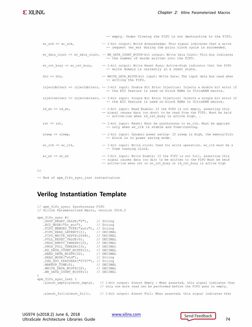
Chapter 2: Xilinx Parameterized Macros
-- empty. Under flowing the FIFO is not destructive to the FIFO.
wr_ack => wr_ack, -- 1-bit output: Write Acknowledge: This signal indicates that a write-- request (wr_en) during the prior clock cycle is succeeded.
wr_data_count => wr_data_count, -- WR_DATA_COUNT_WIDTH-bit output: Write Data Count: This bus indicates-- the number of words written into the FIFO.
wr_rst_busy => wr_rst_busy, -- 1-bit output: Write Reset Busy: Active-High indicator that the FIFO-- write domain is currently in a reset state.
din => din, -- WRITE_DATA_WIDTH-bit input: Write Data: The input data bus used when-- writing the FIFO.
injectdbiterr => injectdbiterr, -- 1-bit input: Double Bit Error Injection: Injects a double bit error if-- the ECC feature is used on block RAMs or UltraRAM macros.
injectsbiterr => injectsbiterr, -- 1-bit input: Single Bit Error Injection: Injects a single bit error if-- the ECC feature is used on block RAMs or UltraRAM macros.
rd_en => rd_en, -- 1-bit input: Read Enable: If the FIFO is not empty, asserting this-- signal causes data (on dout) to be read from the FIFO. Must be held
-- active-low when rd_rst_busy is active high. .
rst => rst, -- 1-bit input: Reset: Must be synchronous to wr_clk. Must be applied-- only when wr_clk is stable and free-running.
sleep => sleep, -- 1-bit input: Dynamic power saving- If sleep is High, the memory/fifo-- block is in power saving mode.
wr_clk => wr_clk, -- 1-bit input: Write clock: Used for write operation. wr_clk must be a-- free running clock.
wr_en => wr_en -- 1-bit input: Write Enable: If the FIFO is not full, asserting this-- signal causes data (on din) to be written to the FIFO Must be held-- active-low when rst or wr_rst_busy or rd_rst_busy is active high
);
-- End of xpm_fifo_sync_inst instantiation
Verilog Instantiation Template
// xpm_fifo_sync: Synchronous FIFO// Xilinx Parameterized Macro, version 2018.2
xpm_fifo_sync #(.DOUT_RESET_VALUE("0"), // String.ECC_MODE("no_ecc"), // String.FIFO_MEMORY_TYPE("auto"), // String.FIFO_READ_LATENCY(1), // DECIMAL.FIFO_WRITE_DEPTH(2048), // DECIMAL.FULL_RESET_VALUE(0), // DECIMAL.PROG_EMPTY_THRESH(10), // DECIMAL.PROG_FULL_THRESH(10), // DECIMAL.RD_DATA_COUNT_WIDTH(1), // DECIMAL.READ_DATA_WIDTH(32), // DECIMAL.READ_MODE("std"), // String.USE_ADV_FEATURES("0707"), // String.WAKEUP_TIME(0), // DECIMAL.WRITE_DATA_WIDTH(32), // DECIMAL.WR_DATA_COUNT_WIDTH(1) // DECIMAL
)xpm_fifo_sync_inst (
.almost_empty(almost_empty), // 1-bit output: Almost Empty : When asserted, this signal indicates that// only one more read can be performed before the FIFO goes to empty.
.almost_full(almost_full), // 1-bit output: Almost Full: When asserted, this signal indicates that
UG974 (v2018.2) June 6, 2018 www.xilinx.comUltraScale Architecture Libraries Guide 74
Send Feedback
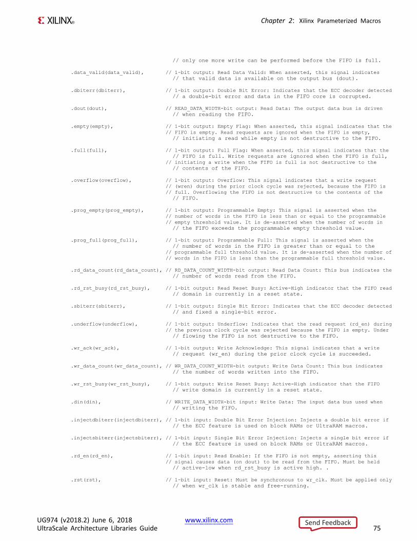
Chapter 2: Xilinx Parameterized Macros
// only one more write can be performed before the FIFO is full.
.data_valid(data_valid), // 1-bit output: Read Data Valid: When asserted, this signal indicates// that valid data is available on the output bus (dout).
.dbiterr(dbiterr), // 1-bit output: Double Bit Error: Indicates that the ECC decoder detected// a double-bit error and data in the FIFO core is corrupted.
.dout(dout), // READ_DATA_WIDTH-bit output: Read Data: The output data bus is driven// when reading the FIFO.
.empty(empty), // 1-bit output: Empty Flag: When asserted, this signal indicates that the// FIFO is empty. Read requests are ignored when the FIFO is empty,
// initiating a read while empty is not destructive to the FIFO.
.full(full), // 1-bit output: Full Flag: When asserted, this signal indicates that the// FIFO is full. Write requests are ignored when the FIFO is full,
// initiating a write when the FIFO is full is not destructive to the// contents of the FIFO.
.overflow(overflow), // 1-bit output: Overflow: This signal indicates that a write request// (wren) during the prior clock cycle was rejected, because the FIFO is// full. Overflowing the FIFO is not destructive to the contents of the
// FIFO.
.prog_empty(prog_empty), // 1-bit output: Programmable Empty: This signal is asserted when the// number of words in the FIFO is less than or equal to the programmable// empty threshold value. It is de-asserted when the number of words in
// the FIFO exceeds the programmable empty threshold value.
.prog_full(prog_full), // 1-bit output: Programmable Full: This signal is asserted when the// number of words in the FIFO is greater than or equal to the
// programmable full threshold value. It is de-asserted when the number of// words in the FIFO is less than the programmable full threshold value.
.rd_data_count(rd_data_count), // RD_DATA_COUNT_WIDTH-bit output: Read Data Count: This bus indicates the// number of words read from the FIFO.
.rd_rst_busy(rd_rst_busy), // 1-bit output: Read Reset Busy: Active-High indicator that the FIFO read// domain is currently in a reset state.
.sbiterr(sbiterr), // 1-bit output: Single Bit Error: Indicates that the ECC decoder detected// and fixed a single-bit error.
.underflow(underflow), // 1-bit output: Underflow: Indicates that the read request (rd_en) during// the previous clock cycle was rejected because the FIFO is empty. Under
// flowing the FIFO is not destructive to the FIFO.
.wr_ack(wr_ack), // 1-bit output: Write Acknowledge: This signal indicates that a write// request (wr_en) during the prior clock cycle is succeeded.
.wr_data_count(wr_data_count), // WR_DATA_COUNT_WIDTH-bit output: Write Data Count: This bus indicates// the number of words written into the FIFO.
.wr_rst_busy(wr_rst_busy), // 1-bit output: Write Reset Busy: Active-High indicator that the FIFO// write domain is currently in a reset state.
.din(din), // WRITE_DATA_WIDTH-bit input: Write Data: The input data bus used when// writing the FIFO.
.injectdbiterr(injectdbiterr), // 1-bit input: Double Bit Error Injection: Injects a double bit error if// the ECC feature is used on block RAMs or UltraRAM macros.
.injectsbiterr(injectsbiterr), // 1-bit input: Single Bit Error Injection: Injects a single bit error if// the ECC feature is used on block RAMs or UltraRAM macros.
.rd_en(rd_en), // 1-bit input: Read Enable: If the FIFO is not empty, asserting this// signal causes data (on dout) to be read from the FIFO. Must be held
// active-low when rd_rst_busy is active high. .
.rst(rst), // 1-bit input: Reset: Must be synchronous to wr_clk. Must be applied only// when wr_clk is stable and free-running.
UG974 (v2018.2) June 6, 2018 www.xilinx.comUltraScale Architecture Libraries Guide 75
Send Feedback
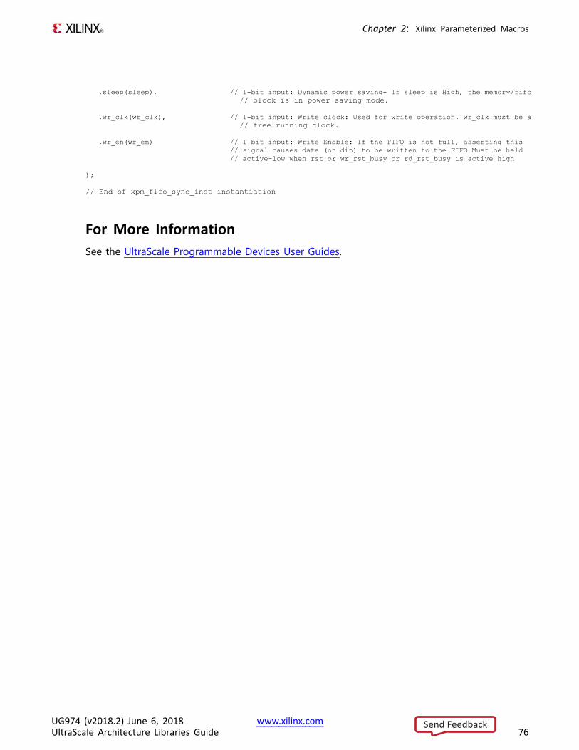
Chapter 2: Xilinx Parameterized Macros
.sleep(sleep), // 1-bit input: Dynamic power saving- If sleep is High, the memory/fifo// block is in power saving mode.
.wr_clk(wr_clk), // 1-bit input: Write clock: Used for write operation. wr_clk must be a// free running clock.
.wr_en(wr_en) // 1-bit input: Write Enable: If the FIFO is not full, asserting this// signal causes data (on din) to be written to the FIFO Must be held// active-low when rst or wr_rst_busy or rd_rst_busy is active high
);
// End of xpm_fifo_sync_inst instantiation
For More InformationSee the UltraScale Programmable Devices User Guides.
UG974 (v2018.2) June 6, 2018 www.xilinx.comUltraScale Architecture Libraries Guide 76
Send Feedback
Chapter 2: Xilinx Parameterized Macros
XPM_MEMORY_DPDISTRAMParameterized Macro: Dual Port Distributed RAMMACRO_GROUP: XPMMACRO_SUBGROUP: XPM_MEMORYFamilies: 7 series, UltraScale, UltraScale+
IntroductionThis macro is used to instantiate Dual Port Distributed RAM. Port-A can be used to performboth read and write operations and simultaneously port B can be used to perform readoperations from the memory. Write operations are not allowed through port B.
UG974 (v2018.2) June 6, 2018 www.xilinx.comUltraScale Architecture Libraries Guide 77
Send Feedback
Chapter 2: Xilinx Parameterized Macros
The following describes the basic read and write port usage of an XPM_MEMORY instance. Itdoes not distinguish between ports A and B.
• All synchronous signals are sensitive to the rising edge of clk[a|b], which is assumed tobe a buffered and toggling clock signal behaving according to target device and memoryprimitive requirements.
• A read operation is implicitly performed to address addr[a|b] combinatorially. The dataoutput is registered each clk[a|b] cycle that en[a|b] is asserted.
• Read data appears on the dout[a|b] port READ_LATENCY_[A|B] clk[a|b] cycles after theassociated read operation.
• A write operation is explicitly performed, writing dina to address addra, when both enaand wea are asserted on each clka cycle.
• All read and write operations are gated by the value of en[a|b] on the initiating clk[a|b]cycle, regardless of input or output latencies. The addra and wea inputs have no effectwhen ena is de-asserted on the coincident clka cycle.
• For each clk[a|b] cycle that rst[a|b] is asserted, the final output register is immediately butsynchronously reset to READ_RESET_VALUE_[A|B], irrespective of READ_LATENCY_[A|B].
• For each clk[a|b] cycle that regce[a|b] is asserted and rst[a|b] is de-asserted, the final outputregister captures and outputs the value from the previous pipeline register.
• Undriven or unknown values provided on module inputs will produce undefined memoryarray and output port behavior.
NOTE:• When the attribute “CLOCKING_MODE” is set to “common_clock”, all read/write operations
to memory through port A and port B are performed on clka. If this attribute is set to“independent_clock”, then read/write operations through port A are performed based onclka, and read/write operations through port B are performed based on clkb.
• Writing to an out-of-range address location may overwrite a valid address location wheneffective address bits match to a physical memory address location.
• set_false_path constraint is needed for the independent clock distributed RAM basedmemory if the design takes care of avoiding address collision (write address != read addressat any given point of time). Set USE_EMBEDDED_CONSTRAINT = 1 if XPM_MEMORY needsto take care of necessary constraints. If USE_EMBEDDED_CONSTRAINT = 0, Vivado maytrigger Timing-6 or Timing-7 or both. Alternatively, you can also add the constraint whenUSE_EMBEDDED_CONSTRAINT = 0. An example of adding this constraint is provided below.If Port-B also has write permissions for an Independent clock configuration, then a similarconstraint needs to be added for clkb as well.
set_false_path -from [filter [all_fanout -from [get_ports clka]-flat -endpoints_only] {IS_LEAF}] -through [get_pins -of_objects[get_cells -hier * -filter {PRIMITIVE_SUBGROUP==LUTRAM ||PRIMITIVE_SUBGROUP==dram || PRIMITIVE_SUBGROUP==drom}]-filter {DIRECTION==OUT}]
• If "CLOCKING_MODE" is set to "independent_clock", Vivado may trigger a false positiveCDC-1 warning and can be ignored.
UG974 (v2018.2) June 6, 2018 www.xilinx.comUltraScale Architecture Libraries Guide 78
Send Feedback
Chapter 2: Xilinx Parameterized Macros
Port Description
Port Direction Width Domain SenseHandling ifUnused Function
addra Input ADDR_WIDTH_A
clka NA Active Address for port A write andread operations.
addrb Input ADDR_WIDTH_B
clkb NA Active Address for port B write andread operations.
clka Input 1 NA EDGE_RISING
Active Clock signal for port A.Also clocks port B whenparameter CLOCKING_MODE is"common_clock".
clkb Input 1 NA EDGE_RISING
Active Clock signal for port B whenparameter CLOCKING_MODEis "independent_clock".Unused when parameterCLOCKING_MODE is"common_clock".
dina Input WRITE_DATA_WIDTH_A
clka NA Active Data input for port A writeoperations.
douta Output READ_DATA_WIDTH_A
clka NA Active Data output for port A readoperations.
doutb Output READ_DATA_WIDTH_B
clkb NA Active Data output for port B readoperations.
ena Input 1 clka LEVEL_HIGH
Active Memory enable signal for port A.
Must be high on clock cycleswhen read or write operationsare initiated. Pipelined internally.
enb Input 1 clkb LEVEL_HIGH
Active Memory enable signal for port B.
Must be high on clock cycleswhen read or write operationsare initiated. Pipelined internally.
regcea Input 1 clka LEVEL_HIGH
1 Clock Enable for the last registerstage on the output data path.
regceb Input 1 clkb LEVEL_HIGH
Active Do not change from the providedvalue.
rsta Input 1 clka LEVEL_HIGH
Active Reset signal for the final port Aoutput register stage.
Synchronously resets outputport douta to the valuespecified by parameterREAD_RESET_VALUE_A.
UG974 (v2018.2) June 6, 2018 www.xilinx.comUltraScale Architecture Libraries Guide 79
Send Feedback
Chapter 2: Xilinx Parameterized Macros
Port Direction Width Domain SenseHandling ifUnused Function
rstb Input 1 clkb LEVEL_HIGH
Active Reset signal for the finalport B output registerstage. Synchronously resetsoutput port doutb to thevalue specified by parameterREAD_RESET_VALUE_B.
wea Input WRITE_DATA_WIDTH_A
clka LEVEL_HIGH
Active Write enable vector for port Ainput data port dina. 1 bit widewhen word-wide writes are used.
In byte-wide write configurations,each bit controls the writing onebyte of dina to address addra.For example, to synchronouslywrite only bits [15-8] of dinawhen WRITE_DATA_WIDTH_A is32, wea would be 4'b0010.
Design Entry MethodInstantiation Yes
Inference No
IP and IP Integrator Catalog No
Available Attributes
Attribute TypeAllowedValues Default Description
ADDR_WIDTH_A DECIMAL 1 to 20 6 Specify the width of the port A address portaddra, in bits.
Must be large enough to accessthe entire memory from port A,i.e. >= $clog2(MEMORY_SIZE /[WRITE|READ]_DATA_WIDTH_A).
ADDR_WIDTH_B DECIMAL 1 to 20 6 Specify the width of the port B address portaddrb, in bits.
Must be large enough to accessthe entire memory from port B,i.e. >= $clog2(MEMORY_SIZE /[WRITE|READ]_DATA_WIDTH_B).
UG974 (v2018.2) June 6, 2018 www.xilinx.comUltraScale Architecture Libraries Guide 80
Send Feedback
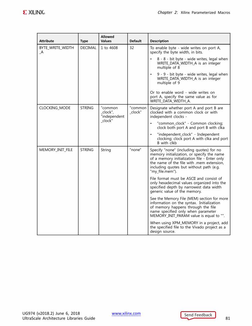
Chapter 2: Xilinx Parameterized Macros
Attribute TypeAllowedValues Default Description
BYTE_WRITE_WIDTH_A
DECIMAL 1 to 4608 32 To enable byte - wide writes on port A,specify the byte width, in bits.
• 8 - 8 - bit byte - wide writes, legal whenWRITE_DATA_WIDTH_A is an integermultiple of 8
• 9 - 9 - bit byte - wide writes, legal whenWRITE_DATA_WIDTH_A is an integermultiple of 9
Or to enable word - wide writes onport A, specify the same value as forWRITE_DATA_WIDTH_A.
CLOCKING_MODE STRING "common_clock","independent_clock"
"common_clock"
Designate whether port A and port B areclocked with a common clock or withindependent clocks -
• "common_clock" - Common clocking;clock both port A and port B with clka
• "independent_clock" - Independentclocking; clock port A with clka and portB with clkb
MEMORY_INIT_FILE STRING String "none" Specify "none" (including quotes) for nomemory initialization, or specify the nameof a memory initialization file - Enter onlythe name of the file with .mem extension,including quotes but without path (e.g."my_file.mem").
File format must be ASCII and consist ofonly hexadecimal values organized into thespecified depth by narrowest data widthgeneric value of the memory.
See the Memory File (MEM) section for moreinformation on the syntax. Initializationof memory happens through the filename specified only when parameterMEMORY_INIT_PARAM value is equal to "".
When using XPM_MEMORY in a project, addthe specified file to the Vivado project as adesign source.
UG974 (v2018.2) June 6, 2018 www.xilinx.comUltraScale Architecture Libraries Guide 81
Send Feedback
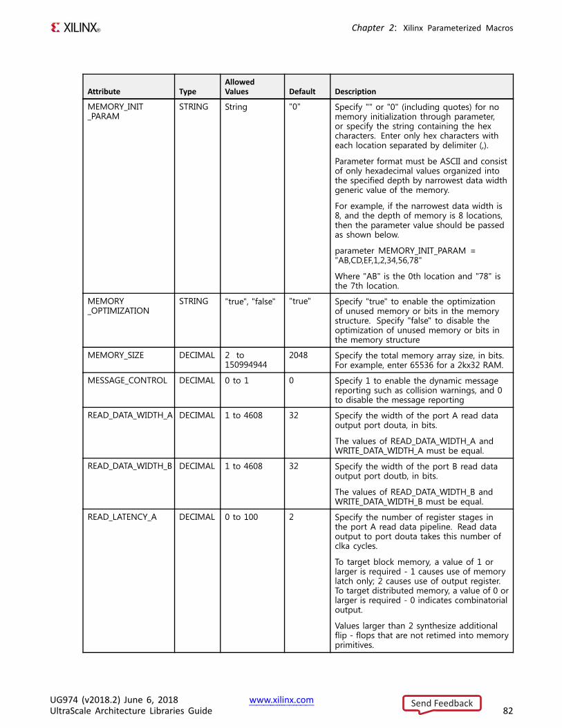
Chapter 2: Xilinx Parameterized Macros
Attribute TypeAllowedValues Default Description
MEMORY_INIT_PARAM
STRING String "0" Specify "" or "0" (including quotes) for nomemory initialization through parameter,or specify the string containing the hexcharacters. Enter only hex characters witheach location separated by delimiter (,).
Parameter format must be ASCII and consistof only hexadecimal values organized intothe specified depth by narrowest data widthgeneric value of the memory.
For example, if the narrowest data width is8, and the depth of memory is 8 locations,then the parameter value should be passedas shown below.
parameter MEMORY_INIT_PARAM ="AB,CD,EF,1,2,34,56,78"
Where "AB" is the 0th location and "78" isthe 7th location.
MEMORY_OPTIMIZATION
STRING "true", "false" "true" Specify "true" to enable the optimizationof unused memory or bits in the memorystructure. Specify "false" to disable theoptimization of unused memory or bits inthe memory structure
MEMORY_SIZE DECIMAL 2 to150994944
2048 Specify the total memory array size, in bits.For example, enter 65536 for a 2kx32 RAM.
MESSAGE_CONTROL DECIMAL 0 to 1 0 Specify 1 to enable the dynamic messagereporting such as collision warnings, and 0to disable the message reporting
READ_DATA_WIDTH_A DECIMAL 1 to 4608 32 Specify the width of the port A read dataoutput port douta, in bits.
The values of READ_DATA_WIDTH_A andWRITE_DATA_WIDTH_A must be equal.
READ_DATA_WIDTH_B DECIMAL 1 to 4608 32 Specify the width of the port B read dataoutput port doutb, in bits.
The values of READ_DATA_WIDTH_B andWRITE_DATA_WIDTH_B must be equal.
READ_LATENCY_A DECIMAL 0 to 100 2 Specify the number of register stages inthe port A read data pipeline. Read dataoutput to port douta takes this number ofclka cycles.
To target block memory, a value of 1 orlarger is required - 1 causes use of memorylatch only; 2 causes use of output register.To target distributed memory, a value of 0 orlarger is required - 0 indicates combinatorialoutput.
Values larger than 2 synthesize additionalflip - flops that are not retimed into memoryprimitives.
UG974 (v2018.2) June 6, 2018 www.xilinx.comUltraScale Architecture Libraries Guide 82
Send Feedback
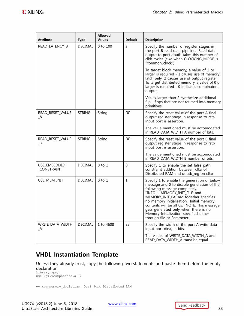
Chapter 2: Xilinx Parameterized Macros
Attribute TypeAllowedValues Default Description
READ_LATENCY_B DECIMAL 0 to 100 2 Specify the number of register stages inthe port B read data pipeline. Read dataoutput to port doutb takes this number ofclkb cycles (clka when CLOCKING_MODE is"common_clock").
To target block memory, a value of 1 orlarger is required - 1 causes use of memorylatch only; 2 causes use of output register.To target distributed memory, a value of 0 orlarger is required - 0 indicates combinatorialoutput.
Values larger than 2 synthesize additionalflip - flops that are not retimed into memoryprimitives.
READ_RESET_VALUE_A
STRING String "0" Specify the reset value of the port A finaloutput register stage in response to rstainput port is assertion.
The value mentioned must be accomodatedin READ_DATA_WIDTH_A number of bits.
READ_RESET_VALUE_B
STRING String "0" Specify the reset value of the port B finaloutput register stage in response to rstbinput port is assertion.
The value mentioned must be accomodatedin READ_DATA_WIDTH_B number of bits.
USE_EMBEDDED_CONSTRAINT
DECIMAL 0 to 1 0 Specify 1 to enable the set_false_pathconstraint addition between clka ofDistributed RAM and doutb_reg on clkb
USE_MEM_INIT DECIMAL 0 to 1 1 Specify 1 to enable the generation of belowmessage and 0 to disable generation of thefollowing message completely."INFO - MEMORY_INIT_FILE andMEMORY_INIT_PARAM together specifiesno memory initialization. Initial memorycontents will be all 0s." NOTE: This messagegets generated only when there is noMemory Initialization specified eitherthrough file or Parameter.
WRITE_DATA_WIDTH_A
DECIMAL 1 to 4608 32 Specify the width of the port A write datainput port dina, in bits.
The values of WRITE_DATA_WIDTH_A andREAD_DATA_WIDTH_A must be equal.
VHDL Instantiation TemplateUnless they already exist, copy the following two statements and paste them before the entitydeclaration.Library xpm;use xpm.vcomponents.all;
-- xpm_memory_dpdistram: Dual Port Distributed RAM
UG974 (v2018.2) June 6, 2018 www.xilinx.comUltraScale Architecture Libraries Guide 83
Send Feedback
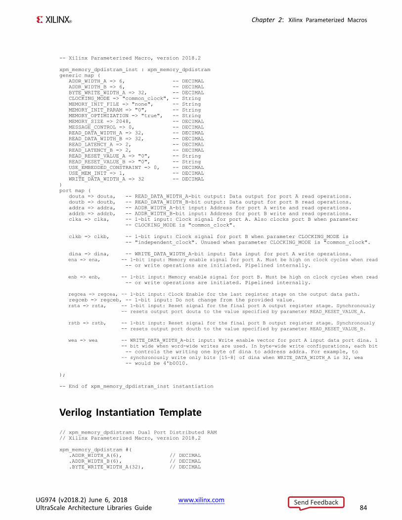
Chapter 2: Xilinx Parameterized Macros
-- Xilinx Parameterized Macro, version 2018.2
xpm_memory_dpdistram_inst : xpm_memory_dpdistramgeneric map (
ADDR_WIDTH_A => 6, -- DECIMALADDR_WIDTH_B => 6, -- DECIMALBYTE_WRITE_WIDTH_A => 32, -- DECIMALCLOCKING_MODE => "common_clock", -- StringMEMORY_INIT_FILE => "none", -- StringMEMORY_INIT_PARAM => "0", -- StringMEMORY_OPTIMIZATION => "true", -- StringMEMORY_SIZE => 2048, -- DECIMALMESSAGE_CONTROL => 0, -- DECIMALREAD_DATA_WIDTH_A => 32, -- DECIMALREAD_DATA_WIDTH_B => 32, -- DECIMALREAD_LATENCY_A => 2, -- DECIMALREAD_LATENCY_B => 2, -- DECIMALREAD_RESET_VALUE_A => "0", -- StringREAD_RESET_VALUE_B => "0", -- StringUSE_EMBEDDED_CONSTRAINT => 0, -- DECIMALUSE_MEM_INIT => 1, -- DECIMALWRITE_DATA_WIDTH_A => 32 -- DECIMAL
)port map (
douta => douta, -- READ_DATA_WIDTH_A-bit output: Data output for port A read operations.doutb => doutb, -- READ_DATA_WIDTH_B-bit output: Data output for port B read operations.addra => addra, -- ADDR_WIDTH_A-bit input: Address for port A write and read operations.addrb => addrb, -- ADDR_WIDTH_B-bit input: Address for port B write and read operations.clka => clka, -- 1-bit input: Clock signal for port A. Also clocks port B when parameter
-- CLOCKING_MODE is "common_clock".
clkb => clkb, -- 1-bit input: Clock signal for port B when parameter CLOCKING_MODE is-- "independent_clock". Unused when parameter CLOCKING_MODE is "common_clock".
dina => dina, -- WRITE_DATA_WIDTH_A-bit input: Data input for port A write operations.ena => ena, -- 1-bit input: Memory enable signal for port A. Must be high on clock cycles when read
-- or write operations are initiated. Pipelined internally.
enb => enb, -- 1-bit input: Memory enable signal for port B. Must be high on clock cycles when read-- or write operations are initiated. Pipelined internally.
regcea => regcea, -- 1-bit input: Clock Enable for the last register stage on the output data path.regceb => regceb, -- 1-bit input: Do not change from the provided value.rsta => rsta, -- 1-bit input: Reset signal for the final port A output register stage. Synchronously
-- resets output port douta to the value specified by parameter READ_RESET_VALUE_A.
rstb => rstb, -- 1-bit input: Reset signal for the final port B output register stage. Synchronously-- resets output port doutb to the value specified by parameter READ_RESET_VALUE_B.
wea => wea -- WRITE_DATA_WIDTH_A-bit input: Write enable vector for port A input data port dina. 1-- bit wide when word-wide writes are used. In byte-wide write configurations, each bit-- controls the writing one byte of dina to address addra. For example, to
-- synchronously write only bits [15-8] of dina when WRITE_DATA_WIDTH_A is 32, wea-- would be 4'b0010.
);
-- End of xpm_memory_dpdistram_inst instantiation
Verilog Instantiation Template
// xpm_memory_dpdistram: Dual Port Distributed RAM// Xilinx Parameterized Macro, version 2018.2
xpm_memory_dpdistram #(.ADDR_WIDTH_A(6), // DECIMAL.ADDR_WIDTH_B(6), // DECIMAL.BYTE_WRITE_WIDTH_A(32), // DECIMAL
UG974 (v2018.2) June 6, 2018 www.xilinx.comUltraScale Architecture Libraries Guide 84
Send Feedback
Chapter 2: Xilinx Parameterized Macros
.CLOCKING_MODE("common_clock"), // String
.MEMORY_INIT_FILE("none"), // String
.MEMORY_INIT_PARAM("0"), // String
.MEMORY_OPTIMIZATION("true"), // String
.MEMORY_SIZE(2048), // DECIMAL
.MESSAGE_CONTROL(0), // DECIMAL
.READ_DATA_WIDTH_A(32), // DECIMAL
.READ_DATA_WIDTH_B(32), // DECIMAL
.READ_LATENCY_A(2), // DECIMAL
.READ_LATENCY_B(2), // DECIMAL
.READ_RESET_VALUE_A("0"), // String
.READ_RESET_VALUE_B("0"), // String
.USE_EMBEDDED_CONSTRAINT(0), // DECIMAL
.USE_MEM_INIT(1), // DECIMAL
.WRITE_DATA_WIDTH_A(32) // DECIMAL)xpm_memory_dpdistram_inst (
.douta(douta), // READ_DATA_WIDTH_A-bit output: Data output for port A read operations.
.doutb(doutb), // READ_DATA_WIDTH_B-bit output: Data output for port B read operations.
.addra(addra), // ADDR_WIDTH_A-bit input: Address for port A write and read operations.
.addrb(addrb), // ADDR_WIDTH_B-bit input: Address for port B write and read operations.
.clka(clka), // 1-bit input: Clock signal for port A. Also clocks port B when parameter CLOCKING_MODE// is "common_clock".
.clkb(clkb), // 1-bit input: Clock signal for port B when parameter CLOCKING_MODE is// "independent_clock". Unused when parameter CLOCKING_MODE is "common_clock".
.dina(dina), // WRITE_DATA_WIDTH_A-bit input: Data input for port A write operations.
.ena(ena), // 1-bit input: Memory enable signal for port A. Must be high on clock cycles when read// or write operations are initiated. Pipelined internally.
.enb(enb), // 1-bit input: Memory enable signal for port B. Must be high on clock cycles when read// or write operations are initiated. Pipelined internally.
.regcea(regcea), // 1-bit input: Clock Enable for the last register stage on the output data path.
.regceb(regceb), // 1-bit input: Do not change from the provided value.
.rsta(rsta), // 1-bit input: Reset signal for the final port A output register stage. Synchronously// resets output port douta to the value specified by parameter READ_RESET_VALUE_A.
.rstb(rstb), // 1-bit input: Reset signal for the final port B output register stage. Synchronously// resets output port doutb to the value specified by parameter READ_RESET_VALUE_B.
.wea(wea) // WRITE_DATA_WIDTH_A-bit input: Write enable vector for port A input data port dina. 1// bit wide when word-wide writes are used. In byte-wide write configurations, each bit// controls the writing one byte of dina to address addra. For example, to synchronously// write only bits [15-8] of dina when WRITE_DATA_WIDTH_A is 32, wea would be 4'b0010.
);
// End of xpm_memory_dpdistram_inst instantiation
For More Information• See the UltraScale Programmable Devices Documentation.
• See the UltraScale Architecture Memory Resources User Guide (UG573).
UG974 (v2018.2) June 6, 2018 www.xilinx.comUltraScale Architecture Libraries Guide 85
Send Feedback
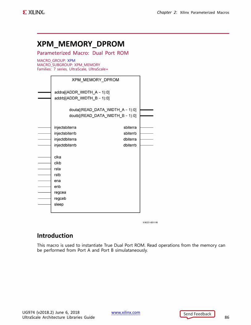
Chapter 2: Xilinx Parameterized Macros
XPM_MEMORY_DPROMParameterized Macro: Dual Port ROMMACRO_GROUP: XPMMACRO_SUBGROUP: XPM_MEMORYFamilies: 7 series, UltraScale, UltraScale+
IntroductionThis macro is used to instantiate True Dual Port ROM. Read operations from the memory canbe performed from Port A and Port B simulataneously.
UG974 (v2018.2) June 6, 2018 www.xilinx.comUltraScale Architecture Libraries Guide 86
Send Feedback
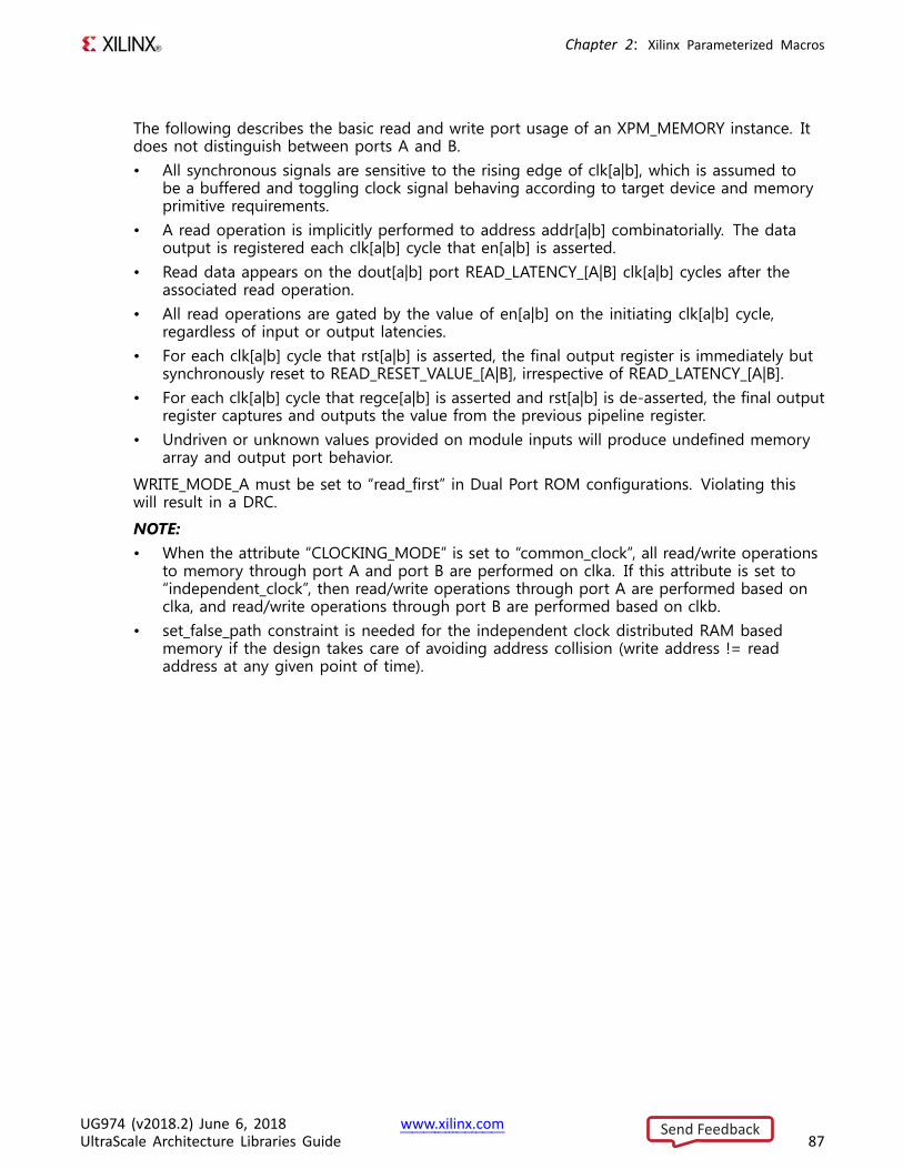
Chapter 2: Xilinx Parameterized Macros
The following describes the basic read and write port usage of an XPM_MEMORY instance. Itdoes not distinguish between ports A and B.• All synchronous signals are sensitive to the rising edge of clk[a|b], which is assumed to
be a buffered and toggling clock signal behaving according to target device and memoryprimitive requirements.
• A read operation is implicitly performed to address addr[a|b] combinatorially. The dataoutput is registered each clk[a|b] cycle that en[a|b] is asserted.
• Read data appears on the dout[a|b] port READ_LATENCY_[A|B] clk[a|b] cycles after theassociated read operation.
• All read operations are gated by the value of en[a|b] on the initiating clk[a|b] cycle,regardless of input or output latencies.
• For each clk[a|b] cycle that rst[a|b] is asserted, the final output register is immediately butsynchronously reset to READ_RESET_VALUE_[A|B], irrespective of READ_LATENCY_[A|B].
• For each clk[a|b] cycle that regce[a|b] is asserted and rst[a|b] is de-asserted, the final outputregister captures and outputs the value from the previous pipeline register.
• Undriven or unknown values provided on module inputs will produce undefined memoryarray and output port behavior.
WRITE_MODE_A must be set to “read_first” in Dual Port ROM configurations. Violating thiswill result in a DRC.
NOTE:• When the attribute “CLOCKING_MODE” is set to “common_clock”, all read/write operations
to memory through port A and port B are performed on clka. If this attribute is set to“independent_clock”, then read/write operations through port A are performed based onclka, and read/write operations through port B are performed based on clkb.
• set_false_path constraint is needed for the independent clock distributed RAM basedmemory if the design takes care of avoiding address collision (write address != readaddress at any given point of time).
UG974 (v2018.2) June 6, 2018 www.xilinx.comUltraScale Architecture Libraries Guide 87
Send Feedback
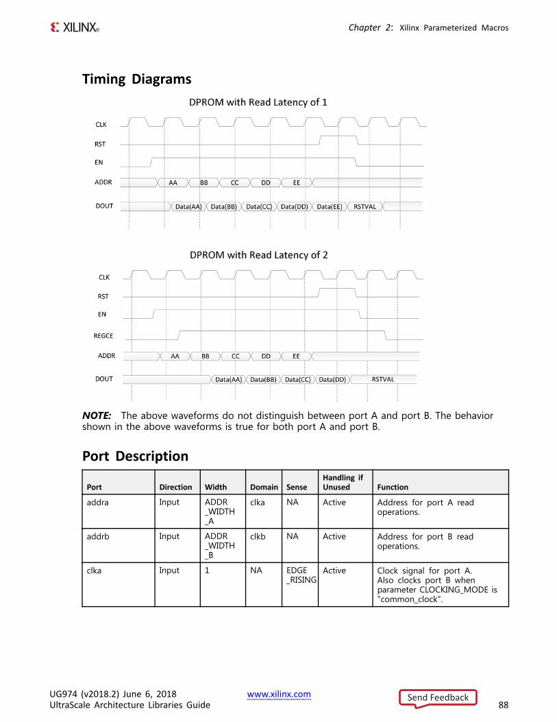
Chapter 2: Xilinx Parameterized Macros
Timing Diagrams
NOTE: The above waveforms do not distinguish between port A and port B. The behaviorshown in the above waveforms is true for both port A and port B.
Port Description
Port Direction Width Domain SenseHandling ifUnused Function
addra Input ADDR_WIDTH_A
clka NA Active Address for port A readoperations.
addrb Input ADDR_WIDTH_B
clkb NA Active Address for port B readoperations.
clka Input 1 NA EDGE_RISING
Active Clock signal for port A.Also clocks port B whenparameter CLOCKING_MODE is"common_clock".
UG974 (v2018.2) June 6, 2018 www.xilinx.comUltraScale Architecture Libraries Guide 88
Send Feedback
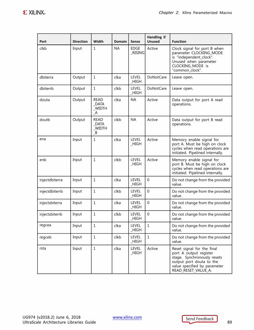
Chapter 2: Xilinx Parameterized Macros
Port Direction Width Domain SenseHandling ifUnused Function
clkb Input 1 NA EDGE_RISING
Active Clock signal for port B whenparameter CLOCKING_MODEis "independent_clock".Unused when parameterCLOCKING_MODE is"common_clock".
dbiterra Output 1 clka LEVEL_HIGH
DoNotCare Leave open.
dbiterrb Output 1 clkb LEVEL_HIGH
DoNotCare Leave open.
douta Output READ_DATA_WIDTH_A
clka NA Active Data output for port A readoperations.
doutb Output READ_DATA_WIDTH_B
clkb NA Active Data output for port B readoperations.
ena Input 1 clka LEVEL_HIGH
Active Memory enable signal forport A. Must be high on clockcycles when read operations areinitiated. Pipelined internally.
enb Input 1 clkb LEVEL_HIGH
Active Memory enable signal forport B. Must be high on clockcycles when read operations areinitiated. Pipelined internally.
injectdbiterra Input 1 clka LEVEL_HIGH
0 Do not change from the providedvalue.
injectdbiterrb Input 1 clkb LEVEL_HIGH
0 Do not change from the providedvalue.
injectsbiterra Input 1 clka LEVEL_HIGH
0 Do not change from the providedvalue.
injectsbiterrb Input 1 clkb LEVEL_HIGH
0 Do not change from the providedvalue.
regcea Input 1 clka LEVEL_HIGH
1 Do not change from the providedvalue.
regceb Input 1 clkb LEVEL_HIGH
1 Do not change from the providedvalue.
rsta Input 1 clka LEVEL_HIGH
Active Reset signal for the finalport A output registerstage. Synchronously resetsoutput port douta to thevalue specified by parameterREAD_RESET_VALUE_A.
UG974 (v2018.2) June 6, 2018 www.xilinx.comUltraScale Architecture Libraries Guide 89
Send Feedback
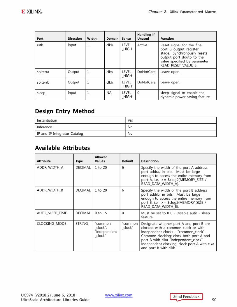
Chapter 2: Xilinx Parameterized Macros
Port Direction Width Domain SenseHandling ifUnused Function
rstb Input 1 clkb LEVEL_HIGH
Active Reset signal for the finalport B output registerstage. Synchronously resetsoutput port doutb to thevalue specified by parameterREAD_RESET_VALUE_B.
sbiterra Output 1 clka LEVEL_HIGH
DoNotCare Leave open.
sbiterrb Output 1 clkb LEVEL_HIGH
DoNotCare Leave open.
sleep Input 1 NA LEVEL_HIGH
0 sleep signal to enable thedynamic power saving feature.
Design Entry MethodInstantiation Yes
Inference No
IP and IP Integrator Catalog No
Available Attributes
Attribute TypeAllowedValues Default Description
ADDR_WIDTH_A DECIMAL 1 to 20 6 Specify the width of the port A addressport addra, in bits. Must be largeenough to access the entire memory fromport A, i.e. >= $clog2(MEMORY_SIZE /READ_DATA_WIDTH_A).
ADDR_WIDTH_B DECIMAL 1 to 20 6 Specify the width of the port B addressport addrb, in bits. Must be largeenough to access the entire memory fromport B, i.e. >= $clog2(MEMORY_SIZE /READ_DATA_WIDTH_B).
AUTO_SLEEP_TIME DECIMAL 0 to 15 0 Must be set to 0 0 - Disable auto - sleepfeature
CLOCKING_MODE STRING "common_clock","independent_clock"
"common_clock"
Designate whether port A and port B areclocked with a common clock or withindependent clocks - "common_clock" -Common clocking; clock both port A andport B with clka "independent_clock" -Independent clocking; clock port A with clkaand port B with clkb
UG974 (v2018.2) June 6, 2018 www.xilinx.comUltraScale Architecture Libraries Guide 90
Send Feedback
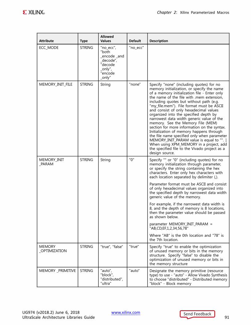
Chapter 2: Xilinx Parameterized Macros
Attribute TypeAllowedValues Default Description
ECC_MODE STRING "no_ecc","both_encode _and_decode","decode_only","encode_only"
"no_ecc"
MEMORY_INIT_FILE STRING String "none" Specify "none" (including quotes) for nomemory initialization, or specify the nameof a memory initialization file - Enter onlythe name of the file with .mem extension,including quotes but without path (e.g."my_file.mem"). File format must be ASCIIand consist of only hexadecimal valuesorganized into the specified depth bynarrowest data width generic value of thememory. See the Memory File (MEM)section for more information on the syntax.Initialization of memory happens throughthe file name specified only when parameterMEMORY_INIT_PARAM value is equal to "". |When using XPM_MEMORY in a project, addthe specified file to the Vivado project as adesign source.
MEMORY_INIT_PARAM
STRING String "0" Specify "" or "0" (including quotes) for nomemory initialization through parameter,or specify the string containing the hexcharacters. Enter only hex characters witheach location separated by delimiter (,).
Parameter format must be ASCII and consistof only hexadecimal values organized intothe specified depth by narrowest data widthgeneric value of the memory.
For example, if the narrowest data width is8, and the depth of memory is 8 locations,then the parameter value should be passedas shown below.
parameter MEMORY_INIT_PARAM ="AB,CD,EF,1,2,34,56,78"
Where "AB" is the 0th location and "78" isthe 7th location.
MEMORY_OPTIMIZATION
STRING "true", "false" "true" Specify "true" to enable the optimizationof unused memory or bits in the memorystructure. Specify "false" to disable theoptimization of unused memory or bits inthe memory structure
MEMORY _PRIMITIVE STRING "auto","block","distributed","ultra"
"auto" Designate the memory primitive (resourcetype) to use - "auto" - Allow Vivado Synthesisto choose "distributed" - Distributed memory"block" - Block memory
UG974 (v2018.2) June 6, 2018 www.xilinx.comUltraScale Architecture Libraries Guide 91
Send Feedback
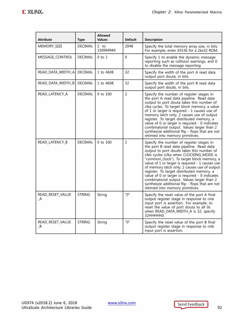
Chapter 2: Xilinx Parameterized Macros
Attribute TypeAllowedValues Default Description
MEMORY_SIZE DECIMAL 2 to150994944
2048 Specify the total memory array size, in bits.For example, enter 65536 for a 2kx32 ROM.
MESSAGE_CONTROL DECIMAL 0 to 1 0 Specify 1 to enable the dynamic messagereporting such as collision warnings, and 0to disable the message reporting
READ_DATA_WIDTH_A DECIMAL 1 to 4608 32 Specify the width of the port A read dataoutput port douta, in bits.
READ_DATA_WIDTH_B DECIMAL 1 to 4608 32 Specify the width of the port B read dataoutput port doutb, in bits.
READ_LATENCY_A DECIMAL 0 to 100 2 Specify the number of register stages inthe port A read data pipeline. Read dataoutput to port douta takes this number ofclka cycles. To target block memory, a valueof 1 or larger is required - 1 causes use ofmemory latch only; 2 causes use of outputregister. To target distributed memory, avalue of 0 or larger is required - 0 indicatescombinatorial output. Values larger than 2synthesize additional flip - flops that are notretimed into memory primitives.
READ_LATENCY_B DECIMAL 0 to 100 2 Specify the number of register stages inthe port B read data pipeline. Read dataoutput to port doutb takes this number ofclkb cycles (clka when CLOCKING_MODE is"common_clock"). To target block memory, avalue of 1 or larger is required - 1 causes useof memory latch only; 2 causes use of outputregister. To target distributed memory, avalue of 0 or larger is required - 0 indicatescombinatorial output. Values larger than 2synthesize additional flip - flops that are notretimed into memory primitives.
READ_RESET_VALUE_A
STRING String "0" Specify the reset value of the port A finaloutput register stage in response to rstainput port is assertion. For example, toreset the value of port douta to all 0swhen READ_DATA_WIDTH_A is 32, specify32HHHHh0.
READ_RESET_VALUE_B
STRING String "0" Specify the reset value of the port B finaloutput register stage in response to rstbinput port is assertion.
UG974 (v2018.2) June 6, 2018 www.xilinx.comUltraScale Architecture Libraries Guide 92
Send Feedback
Chapter 2: Xilinx Parameterized Macros
Attribute TypeAllowedValues Default Description
USE_MEM_INIT DECIMAL 0 to 1 1 Specify 1 to enable the generation of belowmessage and 0 to disable generation of thefollowing message completely."INFO - MEMORY_INIT_FILE andMEMORY_INIT_PARAM together specifiesno memory initialization. Initial memorycontents will be all 0s." NOTE: This messagegets generated only when there is noMemory Initialization specified eitherthrough file or Parameter.
WAKEUP_TIME STRING "disable_sleep", "use_sleep _pin"
"disable_sleep"
Specify "disable_sleep" to disable dynamicpower saving option, and specify"use_sleep_pin" to enable the dynamic powersaving option
VHDL Instantiation TemplateUnless they already exist, copy the following two statements and paste them before the entitydeclaration.Library xpm;use xpm.vcomponents.all;
-- xpm_memory_dprom: Dual Port ROM-- Xilinx Parameterized Macro, version 2018.2
xpm_memory_dprom_inst : xpm_memory_dpromgeneric map (
ADDR_WIDTH_A => 6, -- DECIMALADDR_WIDTH_B => 6, -- DECIMALAUTO_SLEEP_TIME => 0, -- DECIMALCLOCKING_MODE => "common_clock", -- StringECC_MODE => "no_ecc", -- StringMEMORY_INIT_FILE => "none", -- StringMEMORY_INIT_PARAM => "0", -- StringMEMORY_OPTIMIZATION => "true", -- StringMEMORY_PRIMITIVE => "auto", -- StringMEMORY_SIZE => 2048, -- DECIMALMESSAGE_CONTROL => 0, -- DECIMALREAD_DATA_WIDTH_A => 32, -- DECIMALREAD_DATA_WIDTH_B => 32, -- DECIMALREAD_LATENCY_A => 2, -- DECIMALREAD_LATENCY_B => 2, -- DECIMALREAD_RESET_VALUE_A => "0", -- StringREAD_RESET_VALUE_B => "0", -- StringUSE_MEM_INIT => 1, -- DECIMALWAKEUP_TIME => "disable_sleep" -- String
)port map (
dbiterra => dbiterra, -- 1-bit output: Leave open.dbiterrb => dbiterrb, -- 1-bit output: Leave open.douta => douta, -- READ_DATA_WIDTH_A-bit output: Data output for port A read operations.doutb => doutb, -- READ_DATA_WIDTH_B-bit output: Data output for port B read operations.sbiterra => sbiterra, -- 1-bit output: Leave open.sbiterrb => sbiterrb, -- 1-bit output: Leave open.addra => addra, -- ADDR_WIDTH_A-bit input: Address for port A read operations.addrb => addrb, -- ADDR_WIDTH_B-bit input: Address for port B read operations.clka => clka, -- 1-bit input: Clock signal for port A. Also clocks port B when
-- parameter CLOCKING_MODE is "common_clock".
clkb => clkb, -- 1-bit input: Clock signal for port B when parameter CLOCKING_MODE is-- "independent_clock". Unused when parameter CLOCKING_MODE is-- "common_clock".
UG974 (v2018.2) June 6, 2018 www.xilinx.comUltraScale Architecture Libraries Guide 93
Send Feedback
Chapter 2: Xilinx Parameterized Macros
ena => ena, -- 1-bit input: Memory enable signal for port A. Must be high on clock-- cycles when read operations are initiated. Pipelined internally.
enb => enb, -- 1-bit input: Memory enable signal for port B. Must be high on clock-- cycles when read operations are initiated. Pipelined internally.
injectdbiterra => injectdbiterra, -- 1-bit input: Do not change from the provided value.injectdbiterrb => injectdbiterrb, -- 1-bit input: Do not change from the provided value.injectsbiterra => injectsbiterra, -- 1-bit input: Do not change from the provided value.injectsbiterrb => injectsbiterrb, -- 1-bit input: Do not change from the provided value.regcea => regcea, -- 1-bit input: Do not change from the provided value.regceb => regceb, -- 1-bit input: Do not change from the provided value.rsta => rsta, -- 1-bit input: Reset signal for the final port A output register
-- stage. Synchronously resets output port douta to the value specified-- by parameter READ_RESET_VALUE_A.
rstb => rstb, -- 1-bit input: Reset signal for the final port B output register-- stage. Synchronously resets output port doutb to the value specified
-- by parameter READ_RESET_VALUE_B.
sleep => sleep -- 1-bit input: sleep signal to enable the dynamic power saving feature.);
-- End of xpm_memory_dprom_inst instantiation
Verilog Instantiation Template
// xpm_memory_dprom: Dual Port ROM// Xilinx Parameterized Macro, version 2018.2
xpm_memory_dprom #(.ADDR_WIDTH_A(6), // DECIMAL.ADDR_WIDTH_B(6), // DECIMAL.AUTO_SLEEP_TIME(0), // DECIMAL.CLOCKING_MODE("common_clock"), // String.ECC_MODE("no_ecc"), // String.MEMORY_INIT_FILE("none"), // String.MEMORY_INIT_PARAM("0"), // String.MEMORY_OPTIMIZATION("true"), // String.MEMORY_PRIMITIVE("auto"), // String.MEMORY_SIZE(2048), // DECIMAL.MESSAGE_CONTROL(0), // DECIMAL.READ_DATA_WIDTH_A(32), // DECIMAL.READ_DATA_WIDTH_B(32), // DECIMAL.READ_LATENCY_A(2), // DECIMAL.READ_LATENCY_B(2), // DECIMAL.READ_RESET_VALUE_A("0"), // String.READ_RESET_VALUE_B("0"), // String.USE_MEM_INIT(1), // DECIMAL.WAKEUP_TIME("disable_sleep") // String
)xpm_memory_dprom_inst (
.dbiterra(dbiterra), // 1-bit output: Leave open.
.dbiterrb(dbiterrb), // 1-bit output: Leave open.
.douta(douta), // READ_DATA_WIDTH_A-bit output: Data output for port A read operations.
.doutb(doutb), // READ_DATA_WIDTH_B-bit output: Data output for port B read operations.
.sbiterra(sbiterra), // 1-bit output: Leave open.
.sbiterrb(sbiterrb), // 1-bit output: Leave open.
.addra(addra), // ADDR_WIDTH_A-bit input: Address for port A read operations.
.addrb(addrb), // ADDR_WIDTH_B-bit input: Address for port B read operations.
.clka(clka), // 1-bit input: Clock signal for port A. Also clocks port B when// parameter CLOCKING_MODE is "common_clock".
.clkb(clkb), // 1-bit input: Clock signal for port B when parameter CLOCKING_MODE is// "independent_clock". Unused when parameter CLOCKING_MODE is// "common_clock".
UG974 (v2018.2) June 6, 2018 www.xilinx.comUltraScale Architecture Libraries Guide 94
Send Feedback
Chapter 2: Xilinx Parameterized Macros
.ena(ena), // 1-bit input: Memory enable signal for port A. Must be high on clock// cycles when read operations are initiated. Pipelined internally.
.enb(enb), // 1-bit input: Memory enable signal for port B. Must be high on clock// cycles when read operations are initiated. Pipelined internally.
.injectdbiterra(injectdbiterra), // 1-bit input: Do not change from the provided value.
.injectdbiterrb(injectdbiterrb), // 1-bit input: Do not change from the provided value.
.injectsbiterra(injectsbiterra), // 1-bit input: Do not change from the provided value.
.injectsbiterrb(injectsbiterrb), // 1-bit input: Do not change from the provided value.
.regcea(regcea), // 1-bit input: Do not change from the provided value.
.regceb(regceb), // 1-bit input: Do not change from the provided value.
.rsta(rsta), // 1-bit input: Reset signal for the final port A output register stage.// Synchronously resets output port douta to the value specified by
// parameter READ_RESET_VALUE_A.
.rstb(rstb), // 1-bit input: Reset signal for the final port B output register stage.// Synchronously resets output port doutb to the value specified by
// parameter READ_RESET_VALUE_B.
.sleep(sleep) // 1-bit input: sleep signal to enable the dynamic power saving feature.);
// End of xpm_memory_dprom_inst instantiation
For More Information• See the UltraScale Programmable Devices Documentation.
• See the UltraScale Architecture Memory Resources User Guide (UG573).
UG974 (v2018.2) June 6, 2018 www.xilinx.comUltraScale Architecture Libraries Guide 95
Send Feedback
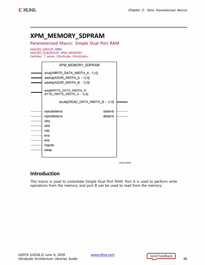
Chapter 2: Xilinx Parameterized Macros
XPM_MEMORY_SDPRAMParameterized Macro: Simple Dual Port RAMMACRO_GROUP: XPMMACRO_SUBGROUP: XPM_MEMORYFamilies: 7 series, UltraScale, UltraScale+
IntroductionThis macro is used to instantiate Simple Dual Port RAM. Port A is used to perform writeoperations from the memory and port B can be used to read from the memory.
UG974 (v2018.2) June 6, 2018 www.xilinx.comUltraScale Architecture Libraries Guide 96
Send Feedback
Chapter 2: Xilinx Parameterized Macros
The following describes the basic read and write port usage of an XPM_MEMORY instance. Itdoes not distinguish between port A and port B.
• All synchronous signals are sensitive to the rising edge of clk[a|b], which is assumed tobe a buffered and toggling clock signal behaving according to target device and memoryprimitive requirements.
• A read operation is implicitly performed to address addrb combinatorially. The data outputis registered each clkb cycle that enb is asserted.
• Read data appears on the doutb port READ_LATENCY_B clkb cycles after the associatedread operation.
• A write operation is explicitly performed, writing dina to address addra, when both enaand wea are asserted on each clka cycle.
• All read and write operations are gated by the value of en[a|b] on the initiating clk[a|b]cycle, regardless of input or output latencies. The addra and wea inputs have no effectwhen ena is de-asserted on the coincident clk[a|b] cycle.
• For each clkb cycle that rstb is asserted, the final output register is immediately butsynchronously reset to READ_RESET_VALUE_B, irrespective of READ_LATENCY_B.
• For each clkb cycle that regceb is asserted and rstb is de-asserted, the final output registercaptures and outputs the value from the previous pipeline register.
• Undriven or unknown values provided on module inputs will produce undefined memoryarray and output port behavior.
UG974 (v2018.2) June 6, 2018 www.xilinx.comUltraScale Architecture Libraries Guide 97
Send Feedback
Chapter 2: Xilinx Parameterized Macros
In Simple Dual Port RAM configuration, only WRITE_MODE_B is considered (though port A hasthe write permissions, WRITE_MODE_B is used because the output data will be connected toport B, and the same mode value is applied to WRITE_MODE_A internally when passing to theprimitive). The following restrictions apply on WRITE_MODE_B parameter in single port RAMconfigurations. Violating this will result in a DRC.
• When the MEMORY_PRIMITIVE attribute is set to “distributed”, WRITE_MODE_B must be setto “read_first”.
• When the MEMORY_PRIMITIVE attribute is set to “block”, WRITE_MODE_B can be set to“read_first”, or “no_change”.
• When the MEMORY_PRIMITIVE attribute is set to “ultra”, WRITE_MODE_B can be set to“write_first” or “read_first”.
• When used as SDP memory, all write modes are supported (READ_FIRST, WRITE_FIRST,NO_CHANGE
NOTE:• When the attribute “CLOCKING_MODE” is set to “common_clock”, all read/write operations
to memory through port A and port B are performed on clka. If this attribute is set to“independent_clock”, then read/write operations through port A are performed based onclka, and read/write operations through port B are performed based on clkb.
• Writing to an out-of-range address location may overwrite a valid address location wheneffective address bits match to a physical memory address location.
• set_false_path constraint is needed for the independent clock distributed RAM basedmemory if the design takes care of avoiding address collision (write address != read addressat any given point of time). Set USE_EMBEDDED_CONSTRAINT = 1 if XPM_MEMORY needsto take care of necessary constraints. If USE_EMBEDDED_CONSTRAINT = 0, Vivado maytrigger Timing-6 or Timing-7 or both. Alternatively, you can also add the constraint whenUSE_EMBEDDED_CONSTRAINT = 0. An example of adding this constraint is provided below.If Port-B also has write permissions for an Independent clock configuration, then a similarconstraint needs to be added for clkb as well.
set_false_path -from [filter [all_fanout -from [get_ports clka]-flat -endpoints_only] {IS_LEAF}] -through [get_pins -of_objects[get_cells -hier * -filter {PRIMITIVE_SUBGROUP==LUTRAM ||PRIMITIVE_SUBGROUP==dram || PRIMITIVE_SUBGROUP==drom}]-filter {DIRECTION==OUT}]
• If"CLOCKING_MODE" is set to "independent_clock", Vivado may trigger a false positiveCDC-1 warning and can be ignored.
• The use of UltraRAM’s dedicated input and output registers are controlled by synthesisbased on the READ_LATENCY_B value. For example, if 4 UltraRAMs are in cascade and theREAD_LATENCY_B is >= 4, then synthesis will absorb as much registers inside UltraRAMprimitive as possible.
UG974 (v2018.2) June 6, 2018 www.xilinx.comUltraScale Architecture Libraries Guide 98
Send Feedback
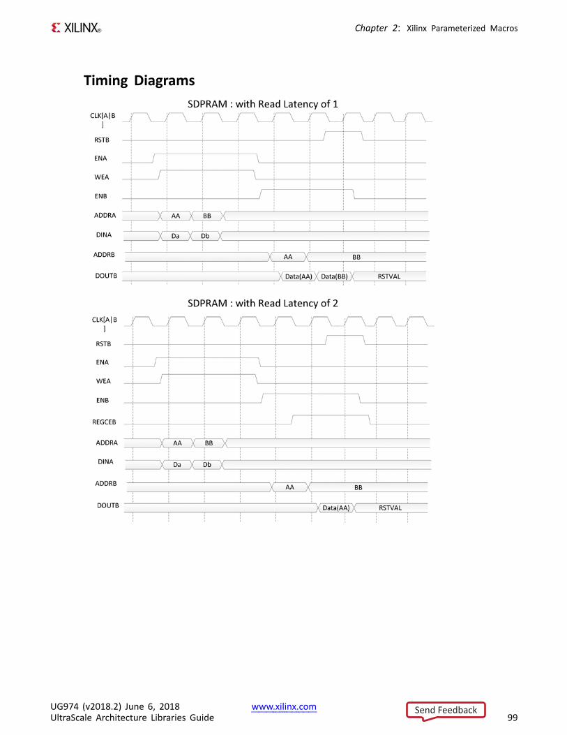
Chapter 2: Xilinx Parameterized Macros
Timing Diagrams
UG974 (v2018.2) June 6, 2018 www.xilinx.comUltraScale Architecture Libraries Guide 99
Send Feedback
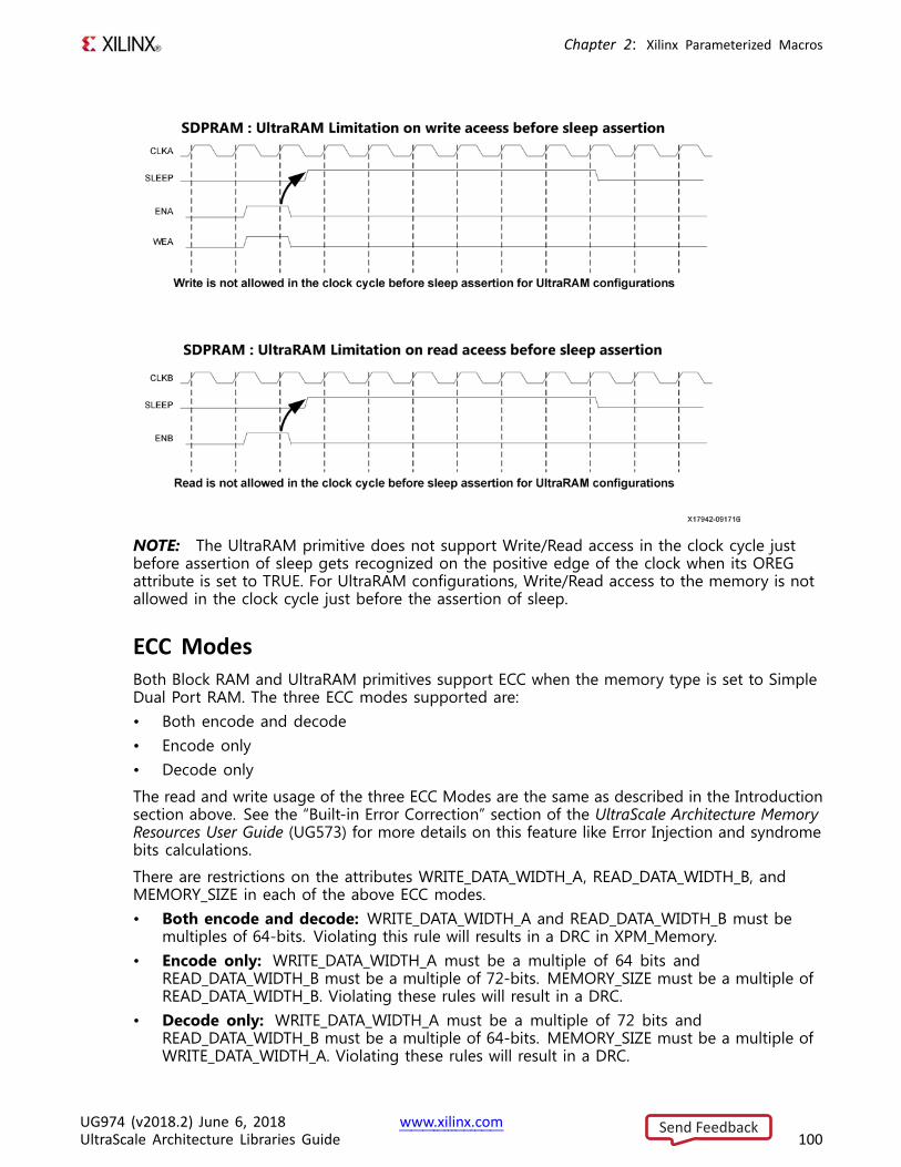
Chapter 2: Xilinx Parameterized Macros
NOTE: The UltraRAM primitive does not support Write/Read access in the clock cycle justbefore assertion of sleep gets recognized on the positive edge of the clock when its OREGattribute is set to TRUE. For UltraRAM configurations, Write/Read access to the memory is notallowed in the clock cycle just before the assertion of sleep.
ECC ModesBoth Block RAM and UltraRAM primitives support ECC when the memory type is set to SimpleDual Port RAM. The three ECC modes supported are:• Both encode and decode• Encode only• Decode only
The read and write usage of the three ECC Modes are the same as described in the Introductionsection above. See the “Built-in Error Correction” section of the UltraScale Architecture MemoryResources User Guide (UG573) for more details on this feature like Error Injection and syndromebits calculations.
There are restrictions on the attributes WRITE_DATA_WIDTH_A, READ_DATA_WIDTH_B, andMEMORY_SIZE in each of the above ECC modes.• Both encode and decode: WRITE_DATA_WIDTH_A and READ_DATA_WIDTH_B must be
multiples of 64-bits. Violating this rule will results in a DRC in XPM_Memory.• Encode only: WRITE_DATA_WIDTH_A must be a multiple of 64 bits and
READ_DATA_WIDTH_B must be a multiple of 72-bits. MEMORY_SIZE must be a multiple ofREAD_DATA_WIDTH_B. Violating these rules will result in a DRC.
• Decode only: WRITE_DATA_WIDTH_A must be a multiple of 72 bits andREAD_DATA_WIDTH_B must be a multiple of 64-bits. MEMORY_SIZE must be a multiple ofWRITE_DATA_WIDTH_A. Violating these rules will result in a DRC.
UG974 (v2018.2) June 6, 2018 www.xilinx.comUltraScale Architecture Libraries Guide 100
Send Feedback

Chapter 2: Xilinx Parameterized Macros
When ECC is enabled the following are not supported:
• Assymetry
• Initialization
• Reset (neither non-zero reset value nor reset assertion)
NOTE: ECC uses a hard-ECC block available in the BRAM/URAM macro and the data widthshould be multiples of 64/72. Use ECC IP for other data width combinations.
Auto Sleep Mode• This feature is applicable only when MEMORY_PRIMITIVE is URAM and is controlled
internally in the UltraRAM to check if it can be put in sleep mode and when it needsto wake up. Thus power savings are obtained automatically without having to explicitlycontrol the SLEEP Pin.
• When AUTO_SLEEP_TIME is 0, the feature is disabled. When AUTO_SLEEP_TIME is nonzero,XPM_MEMORY constructs the pipeline registers equal to AUTO_SLEEP_TIME value on allinput signals except rst[a|b].
• If AUTO_SLEEP_TIME is too low, then UltraRAM goes into sleep and wakeup too often,which can cause more power to be consumed.
• The number of sleep cycles achieved is calculated by following formula:
– If number of consecutive inactive cycles is < AUTO_SLEEP_TIME, then number of sleepcycles = 0
– If number of consecutive inactive cycles is >= AUTO_SLEEP_TIME, Then number ofconsecutive sleep cycles = Number of consecutive inactive cycles – 3
– Inactive cycle is defined as a cycle where there is no Read/Write operation from eitherport
• The latency between the read operation and the data arrival at dout[a|b] isAUTO_SLEEP_TIME + READ_LATENCY_[A|B] clock cycles (Assuming that REGCE is high whenthe output data pipe line exists).
• When the READ_LATENCY_[A|B] is set to 1 or 2, XPM_Memory behaviorally models theAUTO SLEEP feature and forces ‘x’ on DOUT[A|B] when the RAM is in Auto Sleep Mode.For READ_LATENCY_[A|B] greater than 2, the propagation of ‘x’ cannot happen to theDOUT[A|B] as the output registers gets the clock enable (delayed read enable) afterUltraRAM comes out of sleep mode.
• The Auto Sleep mode is most effective for larger Memory sizes or any Memory with verylittle activity.
UG974 (v2018.2) June 6, 2018 www.xilinx.comUltraScale Architecture Libraries Guide 101
Send Feedback

Chapter 2: Xilinx Parameterized Macros
Timing diagrams for Auto Sleep Mode at various read latencies are shown below.
NOTE: EN_DLY[A|B],ADDR_DLY[A|B], and REGCE_DLY[A|B] are the delayed versions of EN[A|B],ADDR[A|B] and REGCE[A|B] by AUTO_SLEEP_TIME number of clock cycles respectively.
UG974 (v2018.2) June 6, 2018 www.xilinx.comUltraScale Architecture Libraries Guide 102
Send Feedback
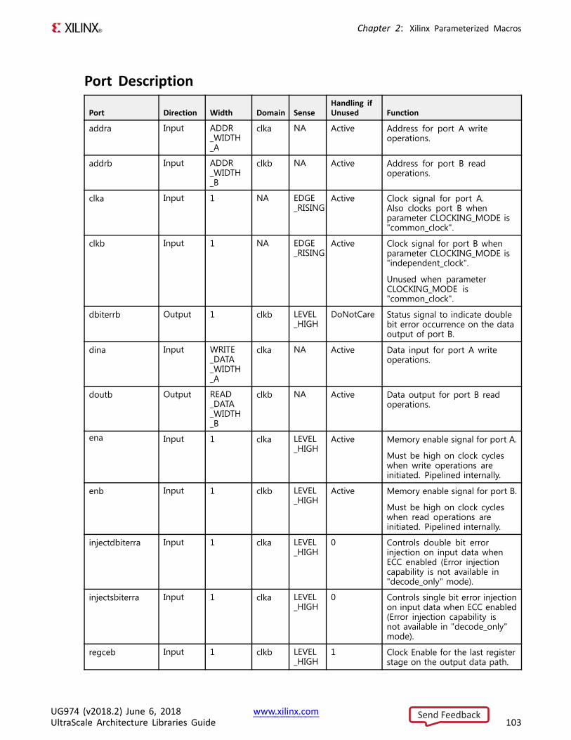
Chapter 2: Xilinx Parameterized Macros
Port Description
Port Direction Width Domain SenseHandling ifUnused Function
addra Input ADDR_WIDTH_A
clka NA Active Address for port A writeoperations.
addrb Input ADDR_WIDTH_B
clkb NA Active Address for port B readoperations.
clka Input 1 NA EDGE_RISING
Active Clock signal for port A.Also clocks port B whenparameter CLOCKING_MODE is"common_clock".
clkb Input 1 NA EDGE_RISING
Active Clock signal for port B whenparameter CLOCKING_MODE is"independent_clock".
Unused when parameterCLOCKING_MODE is"common_clock".
dbiterrb Output 1 clkb LEVEL_HIGH
DoNotCare Status signal to indicate doublebit error occurrence on the dataoutput of port B.
dina Input WRITE_DATA_WIDTH_A
clka NA Active Data input for port A writeoperations.
doutb Output READ_DATA_WIDTH_B
clkb NA Active Data output for port B readoperations.
ena Input 1 clka LEVEL_HIGH
Active Memory enable signal for port A.
Must be high on clock cycleswhen write operations areinitiated. Pipelined internally.
enb Input 1 clkb LEVEL_HIGH
Active Memory enable signal for port B.
Must be high on clock cycleswhen read operations areinitiated. Pipelined internally.
injectdbiterra Input 1 clka LEVEL_HIGH
0 Controls double bit errorinjection on input data whenECC enabled (Error injectioncapability is not available in"decode_only" mode).
injectsbiterra Input 1 clka LEVEL_HIGH
0 Controls single bit error injectionon input data when ECC enabled(Error injection capability isnot available in "decode_only"mode).
regceb Input 1 clkb LEVEL_HIGH
1 Clock Enable for the last registerstage on the output data path.
UG974 (v2018.2) June 6, 2018 www.xilinx.comUltraScale Architecture Libraries Guide 103
Send Feedback
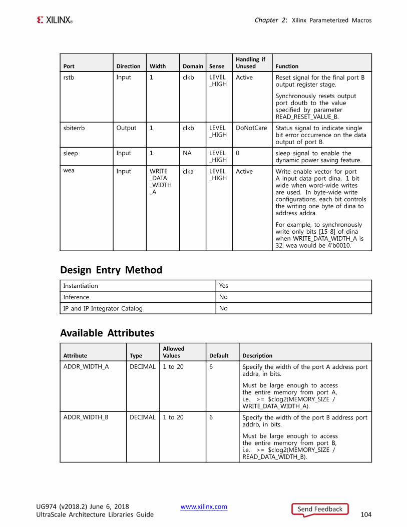
Chapter 2: Xilinx Parameterized Macros
Port Direction Width Domain SenseHandling ifUnused Function
rstb Input 1 clkb LEVEL_HIGH
Active Reset signal for the final port Boutput register stage.
Synchronously resets outputport doutb to the valuespecified by parameterREAD_RESET_VALUE_B.
sbiterrb Output 1 clkb LEVEL_HIGH
DoNotCare Status signal to indicate singlebit error occurrence on the dataoutput of port B.
sleep Input 1 NA LEVEL_HIGH
0 sleep signal to enable thedynamic power saving feature.
wea Input WRITE_DATA_WIDTH_A
clka LEVEL_HIGH
Active Write enable vector for portA input data port dina. 1 bitwide when word-wide writesare used. In byte-wide writeconfigurations, each bit controlsthe writing one byte of dina toaddress addra.
For example, to synchronouslywrite only bits [15-8] of dinawhen WRITE_DATA_WIDTH_A is32, wea would be 4'b0010.
Design Entry MethodInstantiation Yes
Inference No
IP and IP Integrator Catalog No
Available Attributes
Attribute TypeAllowedValues Default Description
ADDR_WIDTH_A DECIMAL 1 to 20 6 Specify the width of the port A address portaddra, in bits.
Must be large enough to accessthe entire memory from port A,i.e. >= $clog2(MEMORY_SIZE /WRITE_DATA_WIDTH_A).
ADDR_WIDTH_B DECIMAL 1 to 20 6 Specify the width of the port B address portaddrb, in bits.
Must be large enough to accessthe entire memory from port B,i.e. >= $clog2(MEMORY_SIZE /READ_DATA_WIDTH_B).
UG974 (v2018.2) June 6, 2018 www.xilinx.comUltraScale Architecture Libraries Guide 104
Send Feedback
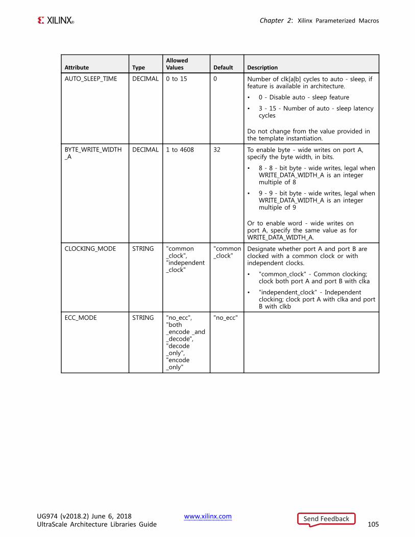
Chapter 2: Xilinx Parameterized Macros
Attribute TypeAllowedValues Default Description
AUTO_SLEEP_TIME DECIMAL 0 to 15 0 Number of clk[a|b] cycles to auto - sleep, iffeature is available in architecture.
• 0 - Disable auto - sleep feature
• 3 - 15 - Number of auto - sleep latencycycles
Do not change from the value provided inthe template instantiation.
BYTE_WRITE_WIDTH_A
DECIMAL 1 to 4608 32 To enable byte - wide writes on port A,specify the byte width, in bits.
• 8 - 8 - bit byte - wide writes, legal whenWRITE_DATA_WIDTH_A is an integermultiple of 8
• 9 - 9 - bit byte - wide writes, legal whenWRITE_DATA_WIDTH_A is an integermultiple of 9
Or to enable word - wide writes onport A, specify the same value as forWRITE_DATA_WIDTH_A.
CLOCKING_MODE STRING "common_clock","independent_clock"
"common_clock"
Designate whether port A and port B areclocked with a common clock or withindependent clocks.
• "common_clock" - Common clocking;clock both port A and port B with clka
• "independent_clock" - Independentclocking; clock port A with clka and portB with clkb
ECC_MODE STRING "no_ecc","both_encode _and_decode","decode_only","encode_only"
"no_ecc"
UG974 (v2018.2) June 6, 2018 www.xilinx.comUltraScale Architecture Libraries Guide 105
Send Feedback
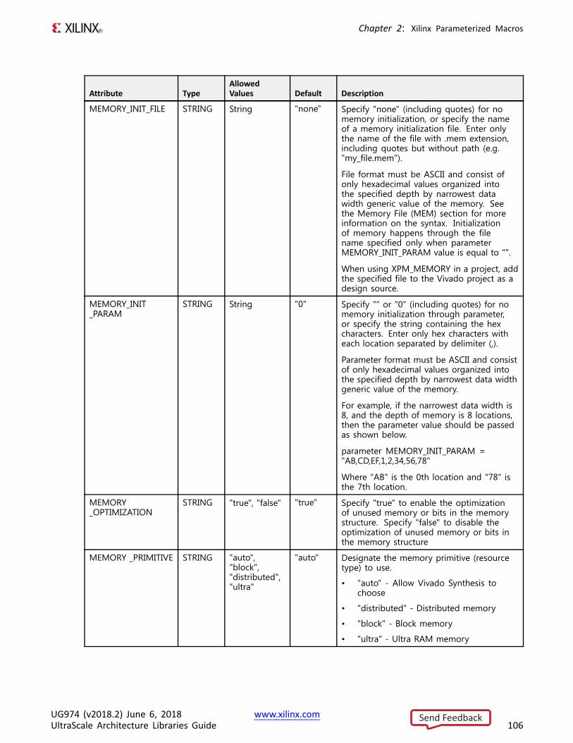
Chapter 2: Xilinx Parameterized Macros
Attribute TypeAllowedValues Default Description
MEMORY_INIT_FILE STRING String "none" Specify "none" (including quotes) for nomemory initialization, or specify the nameof a memory initialization file. Enter onlythe name of the file with .mem extension,including quotes but without path (e.g."my_file.mem").
File format must be ASCII and consist ofonly hexadecimal values organized intothe specified depth by narrowest datawidth generic value of the memory. Seethe Memory File (MEM) section for moreinformation on the syntax. Initializationof memory happens through the filename specified only when parameterMEMORY_INIT_PARAM value is equal to "".
When using XPM_MEMORY in a project, addthe specified file to the Vivado project as adesign source.
MEMORY_INIT_PARAM
STRING String "0" Specify "" or "0" (including quotes) for nomemory initialization through parameter,or specify the string containing the hexcharacters. Enter only hex characters witheach location separated by delimiter (,).
Parameter format must be ASCII and consistof only hexadecimal values organized intothe specified depth by narrowest data widthgeneric value of the memory.
For example, if the narrowest data width is8, and the depth of memory is 8 locations,then the parameter value should be passedas shown below.
parameter MEMORY_INIT_PARAM ="AB,CD,EF,1,2,34,56,78"
Where "AB" is the 0th location and "78" isthe 7th location.
MEMORY_OPTIMIZATION
STRING "true", "false" "true" Specify "true" to enable the optimizationof unused memory or bits in the memorystructure. Specify "false" to disable theoptimization of unused memory or bits inthe memory structure
MEMORY _PRIMITIVE STRING "auto","block","distributed","ultra"
"auto" Designate the memory primitive (resourcetype) to use.
• "auto" - Allow Vivado Synthesis tochoose
• "distributed" - Distributed memory
• "block" - Block memory
• "ultra" - Ultra RAM memory
UG974 (v2018.2) June 6, 2018 www.xilinx.comUltraScale Architecture Libraries Guide 106
Send Feedback
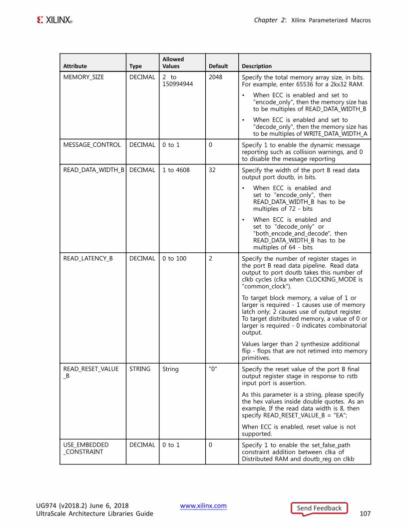
Chapter 2: Xilinx Parameterized Macros
Attribute TypeAllowedValues Default Description
MEMORY_SIZE DECIMAL 2 to150994944
2048 Specify the total memory array size, in bits.For example, enter 65536 for a 2kx32 RAM.
• When ECC is enabled and set to"encode_only", then the memory size hasto be multiples of READ_DATA_WIDTH_B
• When ECC is enabled and set to"decode_only", then the memory size hasto be multiples of WRITE_DATA_WIDTH_A
MESSAGE_CONTROL DECIMAL 0 to 1 0 Specify 1 to enable the dynamic messagereporting such as collision warnings, and 0to disable the message reporting
READ_DATA_WIDTH_B DECIMAL 1 to 4608 32 Specify the width of the port B read dataoutput port doutb, in bits.
• When ECC is enabled andset to "encode_only", thenREAD_DATA_WIDTH_B has to bemultiples of 72 - bits
• When ECC is enabled andset to "decode_only" or"both_encode_and_decode", thenREAD_DATA_WIDTH_B has to bemultiples of 64 - bits
READ_LATENCY_B DECIMAL 0 to 100 2 Specify the number of register stages inthe port B read data pipeline. Read dataoutput to port doutb takes this number ofclkb cycles (clka when CLOCKING_MODE is"common_clock").
To target block memory, a value of 1 orlarger is required - 1 causes use of memorylatch only; 2 causes use of output register.To target distributed memory, a value of 0 orlarger is required - 0 indicates combinatorialoutput.
Values larger than 2 synthesize additionalflip - flops that are not retimed into memoryprimitives.
READ_RESET_VALUE_B
STRING String "0" Specify the reset value of the port B finaloutput register stage in response to rstbinput port is assertion.
As this parameter is a string, please specifythe hex values inside double quotes. As anexample, If the read data width is 8, thenspecify READ_RESET_VALUE_B = "EA";
When ECC is enabled, reset value is notsupported.
USE_EMBEDDED_CONSTRAINT
DECIMAL 0 to 1 0 Specify 1 to enable the set_false_pathconstraint addition between clka ofDistributed RAM and doutb_reg on clkb
UG974 (v2018.2) June 6, 2018 www.xilinx.comUltraScale Architecture Libraries Guide 107
Send Feedback
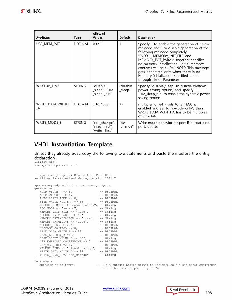
Chapter 2: Xilinx Parameterized Macros
Attribute TypeAllowedValues Default Description
USE_MEM_INIT DECIMAL 0 to 1 1 Specify 1 to enable the generation of belowmessage and 0 to disable generation of thefollowing message completely."INFO - MEMORY_INIT_FILE andMEMORY_INIT_PARAM together specifiesno memory initialization. Initial memorycontents will be all 0s." NOTE: This messagegets generated only when there is noMemory Initialization specified eitherthrough file or Parameter.
WAKEUP_TIME STRING "disable_sleep", "use_sleep _pin"
"disable_sleep"
Specify "disable_sleep" to disable dynamicpower saving option, and specify"use_sleep_pin" to enable the dynamic powersaving option
WRITE_DATA_WIDTH_A
DECIMAL 1 to 4608 32 multiples of 64 - bits When ECC isenabled and set to "decode_only", thenWRITE_DATA_WIDTH_A has to be multiplesof 72 - bits
WRITE_MODE_B STRING "no _change","read _first","write _first"
"no_change"
Write mode behavior for port B output dataport, doutb.
VHDL Instantiation TemplateUnless they already exist, copy the following two statements and paste them before the entitydeclaration.Library xpm;use xpm.vcomponents.all;
-- xpm_memory_sdpram: Simple Dual Port RAM-- Xilinx Parameterized Macro, version 2018.2
xpm_memory_sdpram_inst : xpm_memory_sdpramgeneric map (
ADDR_WIDTH_A => 6, -- DECIMALADDR_WIDTH_B => 6, -- DECIMALAUTO_SLEEP_TIME => 0, -- DECIMALBYTE_WRITE_WIDTH_A => 32, -- DECIMALCLOCKING_MODE => "common_clock", -- StringECC_MODE => "no_ecc", -- StringMEMORY_INIT_FILE => "none", -- StringMEMORY_INIT_PARAM => "0", -- StringMEMORY_OPTIMIZATION => "true", -- StringMEMORY_PRIMITIVE => "auto", -- StringMEMORY_SIZE => 2048, -- DECIMALMESSAGE_CONTROL => 0, -- DECIMALREAD_DATA_WIDTH_B => 32, -- DECIMALREAD_LATENCY_B => 2, -- DECIMALREAD_RESET_VALUE_B => "0", -- StringUSE_EMBEDDED_CONSTRAINT => 0, -- DECIMALUSE_MEM_INIT => 1, -- DECIMALWAKEUP_TIME => "disable_sleep", -- StringWRITE_DATA_WIDTH_A => 32, -- DECIMALWRITE_MODE_B => "no_change" -- String
)port map (
dbiterrb => dbiterrb, -- 1-bit output: Status signal to indicate double bit error occurrence-- on the data output of port B.
UG974 (v2018.2) June 6, 2018 www.xilinx.comUltraScale Architecture Libraries Guide 108
Send Feedback
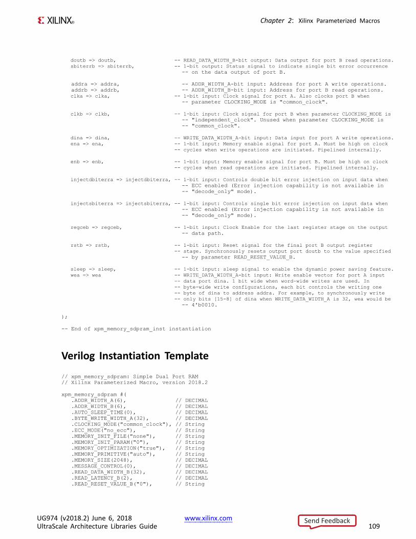
Chapter 2: Xilinx Parameterized Macros
doutb => doutb, -- READ_DATA_WIDTH_B-bit output: Data output for port B read operations.sbiterrb => sbiterrb, -- 1-bit output: Status signal to indicate single bit error occurrence
-- on the data output of port B.
addra => addra, -- ADDR_WIDTH_A-bit input: Address for port A write operations.addrb => addrb, -- ADDR_WIDTH_B-bit input: Address for port B read operations.clka => clka, -- 1-bit input: Clock signal for port A. Also clocks port B when
-- parameter CLOCKING_MODE is "common_clock".
clkb => clkb, -- 1-bit input: Clock signal for port B when parameter CLOCKING_MODE is-- "independent_clock". Unused when parameter CLOCKING_MODE is-- "common_clock".
dina => dina, -- WRITE_DATA_WIDTH_A-bit input: Data input for port A write operations.ena => ena, -- 1-bit input: Memory enable signal for port A. Must be high on clock
-- cycles when write operations are initiated. Pipelined internally.
enb => enb, -- 1-bit input: Memory enable signal for port B. Must be high on clock-- cycles when read operations are initiated. Pipelined internally.
injectdbiterra => injectdbiterra, -- 1-bit input: Controls double bit error injection on input data when-- ECC enabled (Error injection capability is not available in-- "decode_only" mode).
injectsbiterra => injectsbiterra, -- 1-bit input: Controls single bit error injection on input data when-- ECC enabled (Error injection capability is not available in-- "decode_only" mode).
regceb => regceb, -- 1-bit input: Clock Enable for the last register stage on the output-- data path.
rstb => rstb, -- 1-bit input: Reset signal for the final port B output register-- stage. Synchronously resets output port doutb to the value specified
-- by parameter READ_RESET_VALUE_B.
sleep => sleep, -- 1-bit input: sleep signal to enable the dynamic power saving feature.wea => wea -- WRITE_DATA_WIDTH_A-bit input: Write enable vector for port A input
-- data port dina. 1 bit wide when word-wide writes are used. In-- byte-wide write configurations, each bit controls the writing one-- byte of dina to address addra. For example, to synchronously write-- only bits [15-8] of dina when WRITE_DATA_WIDTH_A is 32, wea would be
-- 4'b0010.
);
-- End of xpm_memory_sdpram_inst instantiation
Verilog Instantiation Template
// xpm_memory_sdpram: Simple Dual Port RAM// Xilinx Parameterized Macro, version 2018.2
xpm_memory_sdpram #(.ADDR_WIDTH_A(6), // DECIMAL.ADDR_WIDTH_B(6), // DECIMAL.AUTO_SLEEP_TIME(0), // DECIMAL.BYTE_WRITE_WIDTH_A(32), // DECIMAL.CLOCKING_MODE("common_clock"), // String.ECC_MODE("no_ecc"), // String.MEMORY_INIT_FILE("none"), // String.MEMORY_INIT_PARAM("0"), // String.MEMORY_OPTIMIZATION("true"), // String.MEMORY_PRIMITIVE("auto"), // String.MEMORY_SIZE(2048), // DECIMAL.MESSAGE_CONTROL(0), // DECIMAL.READ_DATA_WIDTH_B(32), // DECIMAL.READ_LATENCY_B(2), // DECIMAL.READ_RESET_VALUE_B("0"), // String
UG974 (v2018.2) June 6, 2018 www.xilinx.comUltraScale Architecture Libraries Guide 109
Send Feedback
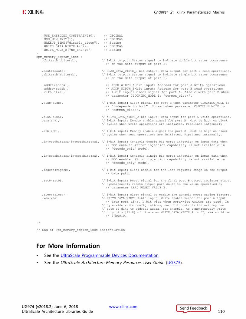
Chapter 2: Xilinx Parameterized Macros
.USE_EMBEDDED_CONSTRAINT(0), // DECIMAL
.USE_MEM_INIT(1), // DECIMAL
.WAKEUP_TIME("disable_sleep"), // String
.WRITE_DATA_WIDTH_A(32), // DECIMAL
.WRITE_MODE_B("no_change") // String)xpm_memory_sdpram_inst (
.dbiterrb(dbiterrb), // 1-bit output: Status signal to indicate double bit error occurrence// on the data output of port B.
.doutb(doutb), // READ_DATA_WIDTH_B-bit output: Data output for port B read operations.
.sbiterrb(sbiterrb), // 1-bit output: Status signal to indicate single bit error occurrence// on the data output of port B.
.addra(addra), // ADDR_WIDTH_A-bit input: Address for port A write operations.
.addrb(addrb), // ADDR_WIDTH_B-bit input: Address for port B read operations.
.clka(clka), // 1-bit input: Clock signal for port A. Also clocks port B when// parameter CLOCKING_MODE is "common_clock".
.clkb(clkb), // 1-bit input: Clock signal for port B when parameter CLOCKING_MODE is// "independent_clock". Unused when parameter CLOCKING_MODE is// "common_clock".
.dina(dina), // WRITE_DATA_WIDTH_A-bit input: Data input for port A write operations.
.ena(ena), // 1-bit input: Memory enable signal for port A. Must be high on clock// cycles when write operations are initiated. Pipelined internally.
.enb(enb), // 1-bit input: Memory enable signal for port B. Must be high on clock// cycles when read operations are initiated. Pipelined internally.
.injectdbiterra(injectdbiterra), // 1-bit input: Controls double bit error injection on input data when// ECC enabled (Error injection capability is not available in// "decode_only" mode).
.injectsbiterra(injectsbiterra), // 1-bit input: Controls single bit error injection on input data when// ECC enabled (Error injection capability is not available in// "decode_only" mode).
.regceb(regceb), // 1-bit input: Clock Enable for the last register stage on the output// data path.
.rstb(rstb), // 1-bit input: Reset signal for the final port B output register stage.// Synchronously resets output port doutb to the value specified by
// parameter READ_RESET_VALUE_B.
.sleep(sleep), // 1-bit input: sleep signal to enable the dynamic power saving feature.
.wea(wea) // WRITE_DATA_WIDTH_A-bit input: Write enable vector for port A input// data port dina. 1 bit wide when word-wide writes are used. In
// byte-wide write configurations, each bit controls the writing one// byte of dina to address addra. For example, to synchronously write// only bits [15-8] of dina when WRITE_DATA_WIDTH_A is 32, wea would be
// 4'b0010.
);
// End of xpm_memory_sdpram_inst instantiation
For More Information• See the UltraScale Programmable Devices Documentation.
• See the UltraScale Architecture Memory Resources User Guide (UG573).
UG974 (v2018.2) June 6, 2018 www.xilinx.comUltraScale Architecture Libraries Guide 110
Send Feedback
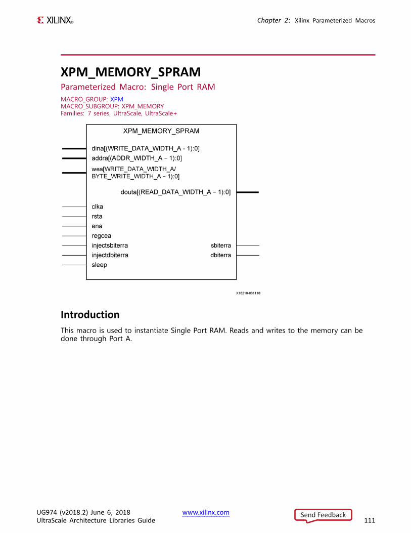
Chapter 2: Xilinx Parameterized Macros
XPM_MEMORY_SPRAMParameterized Macro: Single Port RAMMACRO_GROUP: XPMMACRO_SUBGROUP: XPM_MEMORYFamilies: 7 series, UltraScale, UltraScale+
IntroductionThis macro is used to instantiate Single Port RAM. Reads and writes to the memory can bedone through Port A.
UG974 (v2018.2) June 6, 2018 www.xilinx.comUltraScale Architecture Libraries Guide 111
Send Feedback
Chapter 2: Xilinx Parameterized Macros
The following describes the basic read and write port usage of an XPM_MEMORY instance.
• All synchronous signals are sensitive to the rising edge of clka, which is assumed to bea buffered and toggling clock signal behaving according to target device and memoryprimitive requirements.
• A read operation is implicitly performed to address addra combinatorially. The data outputis registered each clka cycle that ena is asserted.
• Read data appears on the douta port READ_LATENCY_A clka cycles after the associatedread operation.
• A write operation is explicitly performed, writing dina to address addra, when both enaand wea are asserted on each clka cycle.
• All read and write operations are gated by the value of ena on the initiating clka cycle,regardless of input or output latencies. The addra and wea inputs have no effect when enais de-asserted on the coincident clka cycle.
• The behavior of douta with respect to the combination of dina and addra is a functionof WRITE_MODE_A.
• For each clka cycle that rsta is asserted, the final output register is immediately butsynchronously reset to READ_RESET_VALUE_A, irrespective of READ_LATENCY_A.
• For each clka cycle that regcea is asserted and rsta is de-asserted, the final output registercaptures and outputs the value from the previous pipeline register.
• Undriven or unknown values provided on module inputs will produce undefined memoryarray and output port behavior.
The following restrictions apply on the WRITE_MODE_A attribute in Single Port RAMconfigurations. Violating this will result in a DRC.
• When the MEMORY_PRIMITIVE attribute is set to “distributed”, WRITE_MODE_A must be setto “read_first”.
• When the MEMORY_PRIMITIVE attribute is set to “block” or “ultra”, WRITE_MODE_A can beset to “read_first”, “write_first” or “no_change”.
NOTE:1. When byte wide writes are enabled on port A and the write mode is set to “no_change”,
the maximum WRITE_DATA_WIDTH_A supported is
• 32/36 when the MEMORY_PRIMITIVE attribute is set to “block”
• 64/72 when the MEMORY_PRIMTIVE attribute is set to “ultra”
2. Writing to an out-of-range address location may overwrite a valid address location wheneffective address bits match to a physical memory address location.
The use of UltraRAM’s dedicated input and output registers are controlled by synthesisbased on the READ_LATENCY_B value. For example, if 4 UltraRAMs are in cascade and theREAD_LATENCY_B is >= 4, then synthesis will absorb as much registers inside UltraRAMprimitive as possible.
UG974 (v2018.2) June 6, 2018 www.xilinx.comUltraScale Architecture Libraries Guide 112
Send Feedback
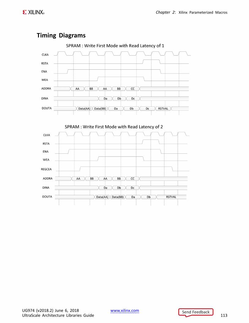
Chapter 2: Xilinx Parameterized Macros
Timing Diagrams
UG974 (v2018.2) June 6, 2018 www.xilinx.comUltraScale Architecture Libraries Guide 113
Send Feedback
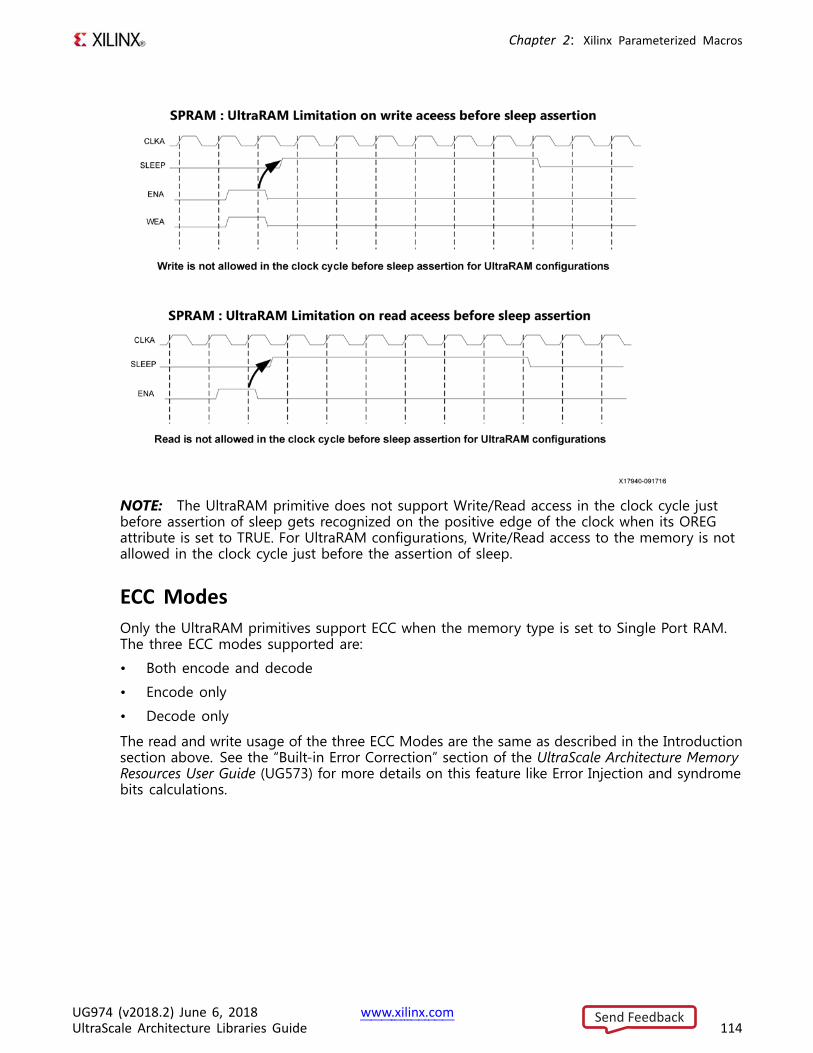
Chapter 2: Xilinx Parameterized Macros
NOTE: The UltraRAM primitive does not support Write/Read access in the clock cycle justbefore assertion of sleep gets recognized on the positive edge of the clock when its OREGattribute is set to TRUE. For UltraRAM configurations, Write/Read access to the memory is notallowed in the clock cycle just before the assertion of sleep.
ECC ModesOnly the UltraRAM primitives support ECC when the memory type is set to Single Port RAM.The three ECC modes supported are:
• Both encode and decode
• Encode only
• Decode only
The read and write usage of the three ECC Modes are the same as described in the Introductionsection above. See the “Built-in Error Correction” section of the UltraScale Architecture MemoryResources User Guide (UG573) for more details on this feature like Error Injection and syndromebits calculations.
UG974 (v2018.2) June 6, 2018 www.xilinx.comUltraScale Architecture Libraries Guide 114
Send Feedback
Chapter 2: Xilinx Parameterized Macros
There are restrictions on the attributes WRITE_DATA_WIDTH_A, READ_DATA_WIDTH_A, andMEMORY_SIZE in each of the above ECC modes.• Both encode and decode: WRITE_DATA_WIDTH_A and READ_DATA_WIDTH_A must be
multiples of 64-bits. Violating this rule will results in a DRC in XPM_Memory.• Encode only: WRITE_DATA_WIDTH_A must be a multiple of 64 bits and
READ_DATA_WIDTH_A must be a multiple of 72-bits. MEMORY_SIZE must be a multiple ofREAD_DATA_WIDTH_A. Violating these rules will result in a DRC.
• Decode only: WRITE_DATA_WIDTH_A must be a multiple of 72 bits andREAD_DATA_WIDTH_A must be a multiple of 64-bits. MEMORY_SIZE must be a multiple ofWRITE_DATA_WIDTH_A. Violating these rules will result in a DRC.
When ECC is enabled the following are not supported:• Assymetry• Initialization• Reset (neither non-zero reset value nor reset assertion)
NOTE: ECC uses a hard-ECC block available in the BRAM/URAM macro and the data widthshould be multiples of 64/72. Use ECC IP for other data width combinations.
Auto Sleep Mode• This feature is applicable only when MEMORY_PRIMITIVE is URAM and is controlled
internally in the UltraRAM to check if it can be put in sleep mode and when it needsto wake up. Thus power savings are obtained automatically without having to explicitlycontrol the SLEEP Pin.
• When AUTO_SLEEP_TIME is 0, the feature is disabled. When AUTO_SLEEP_TIME is nonzero,XPM_MEMORY constructs the pipeline registers equal to AUTO_SLEEP_TIME value on allinput signals except rst[a|b].
• If AUTO_SLEEP_TIME is too low, then UltraRAM goes into sleep and wakeup too often,which can cause more power to be consumed.
• The number of sleep cycles achieved is calculated by following formula:– If number of consecutive inactive cycles is < AUTO_SLEEP_TIME, then number of sleep
cycles = 0– If number of consecutive inactive cycles is >= AUTO_SLEEP_TIME, Then number of
consecutive sleep cycles = Number of consecutive inactive cycles – 3– Inactive cycle is defined as a cycle where there is no Read/Write operation from either
port• The latency between the read operation and the data arrival at dout[a|b] is
AUTO_SLEEP_TIME + READ_LATENCY_[A|B] clock cycles (Assuming that REGCE is high whenthe output data pipe line exists).
• When the READ_LATENCY_[A|B] is set to 1 or 2, XPM_Memory behaviorally models theAUTO SLEEP feature and forces ‘x’ on DOUT[A|B] when the RAM is in Auto Sleep Mode.For READ_LATENCY_[A|B] greater than 2, the propagation of ‘x’ cannot happen to theDOUT[A|B] as the output registers gets the clock enable (delayed read enable) afterUltraRAM comes out of sleep mode.
• The Auto Sleep mode is most effective for larger Memory sizes or any Memory with verylittle activity.
UG974 (v2018.2) June 6, 2018 www.xilinx.comUltraScale Architecture Libraries Guide 115
Send Feedback

Chapter 2: Xilinx Parameterized Macros
Timing diagrams for Auto Sleep Mode at various read latencies are shown below.
NOTE: EN_DLY[A|B],ADDR_DLY[A|B], and REGCE_DLY[A|B] are the delayed versions of EN[A|B],ADDR[A|B] and REGCE[A|B] by AUTO_SLEEP_TIME number of clock cycles respectively.
UG974 (v2018.2) June 6, 2018 www.xilinx.comUltraScale Architecture Libraries Guide 116
Send Feedback
Chapter 2: Xilinx Parameterized Macros
Port Description
Port Direction Width Domain SenseHandling ifUnused Function
addra Input ADDR_WIDTH_A
clka NA Active Address for port A write andread operations.
clka Input 1 NA EDGE_RISING
Active Clock signal for port A.
dbiterra Output 1 clka LEVEL_HIGH
DoNotCare Status signal to indicate doublebit error occurrence on the dataoutput of port A.
dina Input WRITE_DATA_WIDTH_A
clka NA Active Data input for port A writeoperations.
douta Output READ_DATA_WIDTH_A
clka NA Active Data output for port A readoperations.
ena Input 1 clka LEVEL_HIGH
Active Memory enable signal for port A.
Must be high on clock cycleswhen read or write operationsare initiated. Pipelined internally.
injectdbiterra Input 1 clka LEVEL_HIGH
0 Controls double bit errorinjection on input data whenECC enabled (Error injectioncapability is not available in"decode_only" mode).
injectsbiterra Input 1 clka LEVEL_HIGH
0 Controls single bit error injectionon input data when ECC enabled(Error injection capability isnot available in "decode_only"mode).
regcea Input 1 clka LEVEL_HIGH
1 Clock Enable for the last registerstage on the output data path.
rsta Input 1 clka LEVEL_HIGH
Active Reset signal for the finalport A output registerstage. Synchronously resetsoutput port douta to thevalue specified by parameterREAD_RESET_VALUE_A.
sbiterra Output 1 clka LEVEL_HIGH
DoNotCare Status signal to indicate singlebit error occurrence on the dataoutput of port A.
UG974 (v2018.2) June 6, 2018 www.xilinx.comUltraScale Architecture Libraries Guide 117
Send Feedback
Chapter 2: Xilinx Parameterized Macros
Port Direction Width Domain SenseHandling ifUnused Function
sleep Input 1 NA LEVEL_HIGH
0 sleep signal to enable thedynamic power saving feature.
wea Input WRITE_DATA_WIDTH_A
clka LEVEL_HIGH
Active Write enable vector for port Ainput data port dina. 1 bit widewhen word-wide writes are used.
In byte-wide write configurations,each bit controls the writing onebyte of dina to address addra.For example, to synchronouslywrite only bits [15-8] of dinawhen WRITE_DATA_WIDTH_A is32, wea would be 4'b0010.
Design Entry MethodInstantiation Yes
Inference No
IP and IP Integrator Catalog No
Available Attributes
Attribute TypeAllowedValues Default Description
ADDR_WIDTH_A DECIMAL 1 to 20 6 Specify the width of the port A address portaddra, in bits.
Must be large enough to accessthe entire memory from port A,i.e. >= $clog2(MEMORY_SIZE /[WRITE|READ]_DATA_WIDTH_A).
AUTO_SLEEP_TIME DECIMAL 0 to 15 0 Specify the number of clka cycles to auto -sleep, if feature is available in architecture.
• 0 - Disable auto - sleep feature
• 3 - 15 - Number of auto - sleep latencycycles
Do not change from the value provided inthe template instantiation.
UG974 (v2018.2) June 6, 2018 www.xilinx.comUltraScale Architecture Libraries Guide 118
Send Feedback
Chapter 2: Xilinx Parameterized Macros
Attribute TypeAllowedValues Default Description
BYTE_WRITE_WIDTH_A
DECIMAL 1 to 4608 32 To enable byte - wide writes on port A,specify the byte width, in bits.
• 8 - 8 - bit byte - wide writes, legal whenWRITE_DATA_WIDTH_A is an integermultiple of 8
• 9 - 9 - bit byte - wide writes, legal whenWRITE_DATA_WIDTH_A is an integermultiple of 9
Or to enable word - wide writes onport A, specify the same value as forWRITE_DATA_WIDTH_A.
ECC_MODE STRING "no_ecc","both_encode _and_decode","decode_only","encode_only"
"no_ecc"
MEMORY_INIT_FILE STRING String "none" Specify "none" (including quotes) for nomemory initialization, or specify the nameof a memory initialization file - Enter onlythe name of the file with .mem extension,including quotes but without path (e.g."my_file.mem").
File format must be ASCII and consist ofonly hexadecimal values organized intothe specified depth by narrowest datawidth generic value of the memory. Seethe Memory File (MEM) section for moreinformation on the syntax. Initializationof memory happens through the filename specified only when parameterMEMORY_INIT_PARAM value is equal to "".
When using XPM_MEMORY in a project, addthe specified file to the Vivado project as adesign source.
UG974 (v2018.2) June 6, 2018 www.xilinx.comUltraScale Architecture Libraries Guide 119
Send Feedback
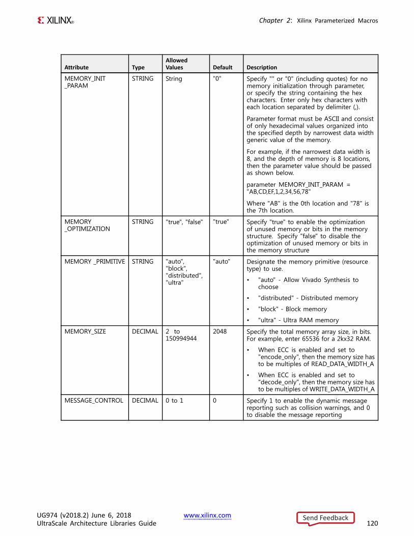
Chapter 2: Xilinx Parameterized Macros
Attribute TypeAllowedValues Default Description
MEMORY_INIT_PARAM
STRING String "0" Specify "" or "0" (including quotes) for nomemory initialization through parameter,or specify the string containing the hexcharacters. Enter only hex characters witheach location separated by delimiter (,).
Parameter format must be ASCII and consistof only hexadecimal values organized intothe specified depth by narrowest data widthgeneric value of the memory.
For example, if the narrowest data width is8, and the depth of memory is 8 locations,then the parameter value should be passedas shown below.
parameter MEMORY_INIT_PARAM ="AB,CD,EF,1,2,34,56,78"
Where "AB" is the 0th location and "78" isthe 7th location.
MEMORY_OPTIMIZATION
STRING "true", "false" "true" Specify "true" to enable the optimizationof unused memory or bits in the memorystructure. Specify "false" to disable theoptimization of unused memory or bits inthe memory structure
MEMORY _PRIMITIVE STRING "auto","block","distributed","ultra"
"auto" Designate the memory primitive (resourcetype) to use.
• "auto" - Allow Vivado Synthesis tochoose
• "distributed" - Distributed memory
• "block" - Block memory
• "ultra" - Ultra RAM memory
MEMORY_SIZE DECIMAL 2 to150994944
2048 Specify the total memory array size, in bits.For example, enter 65536 for a 2kx32 RAM.
• When ECC is enabled and set to"encode_only", then the memory size hasto be multiples of READ_DATA_WIDTH_A
• When ECC is enabled and set to"decode_only", then the memory size hasto be multiples of WRITE_DATA_WIDTH_A
MESSAGE_CONTROL DECIMAL 0 to 1 0 Specify 1 to enable the dynamic messagereporting such as collision warnings, and 0to disable the message reporting
UG974 (v2018.2) June 6, 2018 www.xilinx.comUltraScale Architecture Libraries Guide 120
Send Feedback
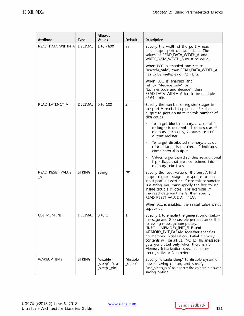
Chapter 2: Xilinx Parameterized Macros
Attribute TypeAllowedValues Default Description
READ_DATA_WIDTH_A DECIMAL 1 to 4608 32 Specify the width of the port A readdata output port douta, in bits. Thevalues of READ_DATA_WIDTH_A andWRITE_DATA_WIDTH_A must be equal.
When ECC is enabled and set to"encode_only", then READ_DATA_WIDTH_Ahas to be multiples of 72 - bits.
When ECC is enabled andset to "decode_only" or"both_encode_and_decode", thenREAD_DATA_WIDTH_A has to be multiplesof 64 - bits.
READ_LATENCY_A DECIMAL 0 to 100 2 Specify the number of register stages inthe port A read data pipeline. Read dataoutput to port douta takes this number ofclka cycles.
• To target block memory, a value of 1or larger is required - 1 causes use ofmemory latch only; 2 causes use ofoutput register.
• To target distributed memory, a valueof 0 or larger is required - 0 indicatescombinatorial output.
• Values larger than 2 synthesize additionalflip - flops that are not retimed intomemory primitives.
READ_RESET_VALUE_A
STRING String "0" Specify the reset value of the port A finaloutput register stage in response to rstainput port is assertion. Since this parameteris a string, you must specify the hex valuesinside double quotes. For example, Ifthe read data width is 8, then specifyREAD_RESET_VALUE_A = "EA";
When ECC is enabled, then reset value is notsupported.
USE_MEM_INIT DECIMAL 0 to 1 1 Specify 1 to enable the generation of belowmessage and 0 to disable generation of thefollowing message completely."INFO - MEMORY_INIT_FILE andMEMORY_INIT_PARAM together specifiesno memory initialization. Initial memorycontents will be all 0s." NOTE: This messagegets generated only when there is noMemory Initialization specified eitherthrough file or Parameter.
WAKEUP_TIME STRING "disable_sleep", "use_sleep _pin"
"disable_sleep"
Specify "disable_sleep" to disable dynamicpower saving option, and specify"use_sleep_pin" to enable the dynamic powersaving option
UG974 (v2018.2) June 6, 2018 www.xilinx.comUltraScale Architecture Libraries Guide 121
Send Feedback
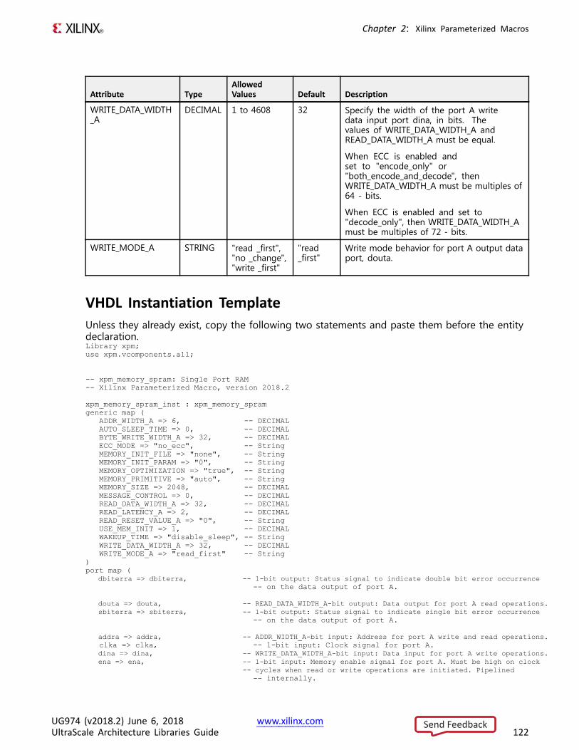
Chapter 2: Xilinx Parameterized Macros
Attribute TypeAllowedValues Default Description
WRITE_DATA_WIDTH_A
DECIMAL 1 to 4608 32 Specify the width of the port A writedata input port dina, in bits. Thevalues of WRITE_DATA_WIDTH_A andREAD_DATA_WIDTH_A must be equal.
When ECC is enabled andset to "encode_only" or"both_encode_and_decode", thenWRITE_DATA_WIDTH_A must be multiples of64 - bits.
When ECC is enabled and set to"decode_only", then WRITE_DATA_WIDTH_Amust be multiples of 72 - bits.
WRITE_MODE_A STRING "read _first","no _change","write _first"
"read_first"
Write mode behavior for port A output dataport, douta.
VHDL Instantiation TemplateUnless they already exist, copy the following two statements and paste them before the entitydeclaration.Library xpm;use xpm.vcomponents.all;
-- xpm_memory_spram: Single Port RAM-- Xilinx Parameterized Macro, version 2018.2
xpm_memory_spram_inst : xpm_memory_spramgeneric map (
ADDR_WIDTH_A => 6, -- DECIMALAUTO_SLEEP_TIME => 0, -- DECIMALBYTE_WRITE_WIDTH_A => 32, -- DECIMALECC_MODE => "no_ecc", -- StringMEMORY_INIT_FILE => "none", -- StringMEMORY_INIT_PARAM => "0", -- StringMEMORY_OPTIMIZATION => "true", -- StringMEMORY_PRIMITIVE => "auto", -- StringMEMORY_SIZE => 2048, -- DECIMALMESSAGE_CONTROL => 0, -- DECIMALREAD_DATA_WIDTH_A => 32, -- DECIMALREAD_LATENCY_A => 2, -- DECIMALREAD_RESET_VALUE_A => "0", -- StringUSE_MEM_INIT => 1, -- DECIMALWAKEUP_TIME => "disable_sleep", -- StringWRITE_DATA_WIDTH_A => 32, -- DECIMALWRITE_MODE_A => "read_first" -- String
)port map (
dbiterra => dbiterra, -- 1-bit output: Status signal to indicate double bit error occurrence-- on the data output of port A.
douta => douta, -- READ_DATA_WIDTH_A-bit output: Data output for port A read operations.sbiterra => sbiterra, -- 1-bit output: Status signal to indicate single bit error occurrence
-- on the data output of port A.
addra => addra, -- ADDR_WIDTH_A-bit input: Address for port A write and read operations.clka => clka, -- 1-bit input: Clock signal for port A.dina => dina, -- WRITE_DATA_WIDTH_A-bit input: Data input for port A write operations.ena => ena, -- 1-bit input: Memory enable signal for port A. Must be high on clock
-- cycles when read or write operations are initiated. Pipelined-- internally.
UG974 (v2018.2) June 6, 2018 www.xilinx.comUltraScale Architecture Libraries Guide 122
Send Feedback
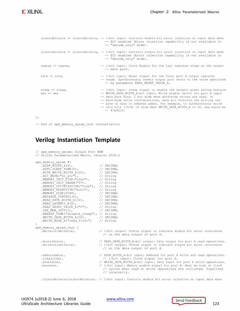
Chapter 2: Xilinx Parameterized Macros
injectdbiterra => injectdbiterra, -- 1-bit input: Controls double bit error injection on input data when-- ECC enabled (Error injection capability is not available in-- "decode_only" mode).
injectsbiterra => injectsbiterra, -- 1-bit input: Controls single bit error injection on input data when-- ECC enabled (Error injection capability is not available in-- "decode_only" mode).
regcea => regcea, -- 1-bit input: Clock Enable for the last register stage on the output-- data path.
rsta => rsta, -- 1-bit input: Reset signal for the final port A output register-- stage. Synchronously resets output port douta to the value specified
-- by parameter READ_RESET_VALUE_A.
sleep => sleep, -- 1-bit input: sleep signal to enable the dynamic power saving feature.wea => wea -- WRITE_DATA_WIDTH_A-bit input: Write enable vector for port A input
-- data port dina. 1 bit wide when word-wide writes are used. In-- byte-wide write configurations, each bit controls the writing one-- byte of dina to address addra. For example, to synchronously write-- only bits [15-8] of dina when WRITE_DATA_WIDTH_A is 32, wea would be
-- 4'b0010.
);
-- End of xpm_memory_spram_inst instantiation
Verilog Instantiation Template
// xpm_memory_spram: Single Port RAM// Xilinx Parameterized Macro, version 2018.2
xpm_memory_spram #(.ADDR_WIDTH_A(6), // DECIMAL.AUTO_SLEEP_TIME(0), // DECIMAL.BYTE_WRITE_WIDTH_A(32), // DECIMAL.ECC_MODE("no_ecc"), // String.MEMORY_INIT_FILE("none"), // String.MEMORY_INIT_PARAM("0"), // String.MEMORY_OPTIMIZATION("true"), // String.MEMORY_PRIMITIVE("auto"), // String.MEMORY_SIZE(2048), // DECIMAL.MESSAGE_CONTROL(0), // DECIMAL.READ_DATA_WIDTH_A(32), // DECIMAL.READ_LATENCY_A(2), // DECIMAL.READ_RESET_VALUE_A("0"), // String.USE_MEM_INIT(1), // DECIMAL.WAKEUP_TIME("disable_sleep"), // String.WRITE_DATA_WIDTH_A(32), // DECIMAL.WRITE_MODE_A("read_first") // String
)xpm_memory_spram_inst (
.dbiterra(dbiterra), // 1-bit output: Status signal to indicate double bit error occurrence// on the data output of port A.
.douta(douta), // READ_DATA_WIDTH_A-bit output: Data output for port A read operations.
.sbiterra(sbiterra), // 1-bit output: Status signal to indicate single bit error occurrence// on the data output of port A.
.addra(addra), // ADDR_WIDTH_A-bit input: Address for port A write and read operations.
.clka(clka), // 1-bit input: Clock signal for port A.
.dina(dina), // WRITE_DATA_WIDTH_A-bit input: Data input for port A write operations.
.ena(ena), // 1-bit input: Memory enable signal for port A. Must be high on clock// cycles when read or write operations are initiated. Pipelined// internally.
.injectdbiterra(injectdbiterra), // 1-bit input: Controls double bit error injection on input data when
UG974 (v2018.2) June 6, 2018 www.xilinx.comUltraScale Architecture Libraries Guide 123
Send Feedback
Chapter 2: Xilinx Parameterized Macros
// ECC enabled (Error injection capability is not available in// "decode_only" mode).
.injectsbiterra(injectsbiterra), // 1-bit input: Controls single bit error injection on input data when// ECC enabled (Error injection capability is not available in// "decode_only" mode).
.regcea(regcea), // 1-bit input: Clock Enable for the last register stage on the output// data path.
.rsta(rsta), // 1-bit input: Reset signal for the final port A output register stage.// Synchronously resets output port douta to the value specified by
// parameter READ_RESET_VALUE_A.
.sleep(sleep), // 1-bit input: sleep signal to enable the dynamic power saving feature.
.wea(wea) // WRITE_DATA_WIDTH_A-bit input: Write enable vector for port A input// data port dina. 1 bit wide when word-wide writes are used. In
// byte-wide write configurations, each bit controls the writing one// byte of dina to address addra. For example, to synchronously write// only bits [15-8] of dina when WRITE_DATA_WIDTH_A is 32, wea would be
// 4'b0010.
);
// End of xpm_memory_spram_inst instantiation
For More Information• See the UltraScale Programmable Devices Documentation.
• See the UltraScale Architecture Memory Resources User Guide (UG573).
UG974 (v2018.2) June 6, 2018 www.xilinx.comUltraScale Architecture Libraries Guide 124
Send Feedback
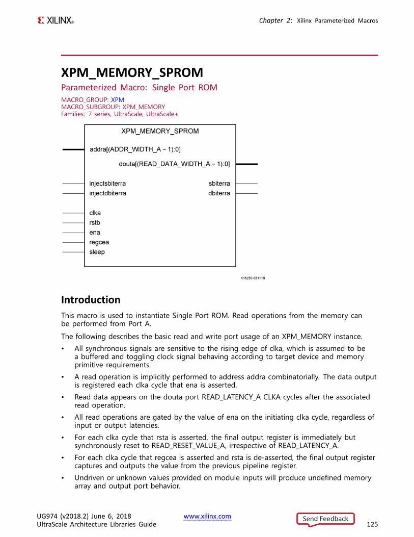
Chapter 2: Xilinx Parameterized Macros
XPM_MEMORY_SPROMParameterized Macro: Single Port ROMMACRO_GROUP: XPMMACRO_SUBGROUP: XPM_MEMORYFamilies: 7 series, UltraScale, UltraScale+
IntroductionThis macro is used to instantiate Single Port ROM. Read operations from the memory canbe performed from Port A.
The following describes the basic read and write port usage of an XPM_MEMORY instance.• All synchronous signals are sensitive to the rising edge of clka, which is assumed to be
a buffered and toggling clock signal behaving according to target device and memoryprimitive requirements.
• A read operation is implicitly performed to address addra combinatorially. The data outputis registered each clka cycle that ena is asserted.
• Read data appears on the douta port READ_LATENCY_A CLKA cycles after the associatedread operation.
• All read operations are gated by the value of ena on the initiating clka cycle, regardless ofinput or output latencies.
• For each clka cycle that rsta is asserted, the final output register is immediately butsynchronously reset to READ_RESET_VALUE_A, irrespective of READ_LATENCY_A.
• For each clka cycle that regcea is asserted and rsta is de-asserted, the final output registercaptures and outputs the value from the previous pipeline register.
• Undriven or unknown values provided on module inputs will produce undefined memoryarray and output port behavior.
UG974 (v2018.2) June 6, 2018 www.xilinx.comUltraScale Architecture Libraries Guide 125
Send Feedback
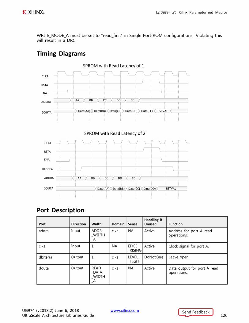
Chapter 2: Xilinx Parameterized Macros
WRITE_MODE_A must be set to “read_first” in Single Port ROM configurations. Violating thiswill result in a DRC.
Timing Diagrams
Port Description
Port Direction Width Domain SenseHandling ifUnused Function
addra Input ADDR_WIDTH_A
clka NA Active Address for port A readoperations.
clka Input 1 NA EDGE_RISING
Active Clock signal for port A.
dbiterra Output 1 clka LEVEL_HIGH
DoNotCare Leave open.
douta Output READ_DATA_WIDTH_A
clka NA Active Data output for port A readoperations.
UG974 (v2018.2) June 6, 2018 www.xilinx.comUltraScale Architecture Libraries Guide 126
Send Feedback
Chapter 2: Xilinx Parameterized Macros
Port Direction Width Domain SenseHandling ifUnused Function
ena Input 1 clka LEVEL_HIGH
Active Memory enable signal forport A. Must be high on clockcycles when read operations areinitiated. Pipelined internally.
injectdbiterra Input 1 clka LEVEL_HIGH
0 Do not change from the providedvalue.
injectsbiterra Input 1 clka LEVEL_HIGH
0 Do not change from the providedvalue.
regcea Input 1 clka LEVEL_HIGH
1 Do not change from the providedvalue.
rsta Input 1 clka LEVEL_HIGH
Active Reset signal for the finalport A output registerstage. Synchronously resetsoutput port douta to thevalue specified by parameterREAD_RESET_VALUE_A.
sbiterra Output 1 clka LEVEL_HIGH
DoNotCare Leave open.
sleep Input 1 NA LEVEL_HIGH
0 sleep signal to enable thedynamic power saving feature.
Design Entry MethodInstantiation Yes
Inference No
IP and IP Integrator Catalog No
Available Attributes
Attribute TypeAllowedValues Default Description
ADDR_WIDTH_A DECIMAL 1 to 20 6 Specify the width of the port A addressport addra, in bits. Must be largeenough to access the entire memory fromport A, i.e. >= $clog2(MEMORY_SIZE /READ_DATA_WIDTH_A).
AUTO_SLEEP_TIME DECIMAL 0 to 15 0 Must be set to 0 0 - Disable auto - sleepfeature
ECC_MODE STRING "no_ecc","both_encode _and_decode","decode_only","encode_only"
"no_ecc" Must be "no_ecc". ECC with Initialization iscurrently not supported.
UG974 (v2018.2) June 6, 2018 www.xilinx.comUltraScale Architecture Libraries Guide 127
Send Feedback
Chapter 2: Xilinx Parameterized Macros
Attribute TypeAllowedValues Default Description
MEMORY_INIT_FILE STRING String "none" Specify "none" (including quotes) for nomemory initialization, or specify the nameof a memory initialization file - Enter onlythe name of the file with .mem extension,including quotes but without path (e.g."my_file.mem"). File format must be ASCIIand consist of only hexadecimal valuesorganized into the specified depth bynarrowest data width generic value of thememory. See the Memory File (MEM)section for more information on the syntax.Initialization of memory happens throughthe file name specified only when parameterMEMORY_INIT_PARAM value is equal to "".When using XPM_MEMORY in a project, addthe specified file to the Vivado project as adesign source.
MEMORY_INIT_PARAM
STRING String "0" Specify "" or "0" (including quotes) for nomemory initialization through parameter,or specify the string containing the hexcharacters. Enter only hex characters witheach location separated by delimiter (,).
Parameter format must be ASCII and consistof only hexadecimal values organized intothe specified depth by narrowest data widthgeneric value of the memory.
For example, if the narrowest data width is8, and the depth of memory is 8 locations,then the parameter value should be passedas shown below.
parameter MEMORY_INIT_PARAM ="AB,CD,EF,1,2,34,56,78"
Where "AB" is the 0th location and "78" isthe 7th location.
MEMORY_OPTIMIZATION
STRING "true", "false" "true" Specify "true" to enable the optimizationof unused memory or bits in the memorystructure. Specify "false" to disable theoptimization of unused memory or bits inthe memory structure
MEMORY _PRIMITIVE STRING "auto","block","distributed","ultra"
"auto" Designate the memory primitive (resourcetype) to use - "auto" - Allow Vivado Synthesisto choose "distributed" - Distributed memory"block" - Block memory
MEMORY_SIZE DECIMAL 2 to150994944
2048 Specify the total memory array size, in bits.For example, enter 65536 for a 2kx32 ROM.
MESSAGE_CONTROL DECIMAL 0 to 1 0 Specify 1 to enable the dynamic messagereporting such as collision warnings, and 0to disable the message reporting
READ_DATA_WIDTH_A DECIMAL 1 to 4608 32 Specify the width of the port A read dataoutput port douta, in bits.
UG974 (v2018.2) June 6, 2018 www.xilinx.comUltraScale Architecture Libraries Guide 128
Send Feedback
Chapter 2: Xilinx Parameterized Macros
Attribute TypeAllowedValues Default Description
READ_LATENCY_A DECIMAL 0 to 100 2 Specify the number of register stages inthe port A read data pipeline. Read dataoutput to port douta takes this number ofclka cycles. To target block memory, a valueof 1 or larger is required - 1 causes use ofmemory latch only; 2 causes use of outputregister. To target distributed memory, avalue of 0 or larger is required - 0 indicatescombinatorial output. Values larger than 2synthesize additional flip - flops that are notretimed into memory primitives.
READ_RESET_VALUE_A
STRING String "0" Specify the reset value of the port A finaloutput register stage in response to rstainput port is assertion. For example, toreset the value of port douta to all 0swhen READ_DATA_WIDTH_A is 32, specify32HHHHh0.
USE_MEM_INIT DECIMAL 0 to 1 1 Specify 1 to enable the generation of belowmessage and 0 to disable generation of thefollowing message completely."INFO - MEMORY_INIT_FILE andMEMORY_INIT_PARAM together specifiesno memory initialization. Initial memorycontents will be all 0s." NOTE: This messagegets generated only when there is noMemory Initialization specified eitherthrough file or Parameter.
WAKEUP_TIME STRING "disable_sleep", "use_sleep _pin"
"disable_sleep"
Specify "disable_sleep" to disable dynamicpower saving option, and specify"use_sleep_pin" to enable the dynamic powersaving option
VHDL Instantiation TemplateUnless they already exist, copy the following two statements and paste them before the entitydeclaration.Library xpm;use xpm.vcomponents.all;
-- xpm_memory_sprom: Single Port ROM-- Xilinx Parameterized Macro, version 2018.2
xpm_memory_sprom_inst : xpm_memory_spromgeneric map (
ADDR_WIDTH_A => 6, -- DECIMALAUTO_SLEEP_TIME => 0, -- DECIMALECC_MODE => "no_ecc", -- StringMEMORY_INIT_FILE => "none", -- StringMEMORY_INIT_PARAM => "0", -- StringMEMORY_OPTIMIZATION => "true", -- StringMEMORY_PRIMITIVE => "auto", -- StringMEMORY_SIZE => 2048, -- DECIMALMESSAGE_CONTROL => 0, -- DECIMALREAD_DATA_WIDTH_A => 32, -- DECIMALREAD_LATENCY_A => 2, -- DECIMALREAD_RESET_VALUE_A => "0", -- StringUSE_MEM_INIT => 1, -- DECIMAL
UG974 (v2018.2) June 6, 2018 www.xilinx.comUltraScale Architecture Libraries Guide 129
Send Feedback
Chapter 2: Xilinx Parameterized Macros
WAKEUP_TIME => "disable_sleep" -- String)port map (
dbiterra => dbiterra, -- 1-bit output: Leave open.douta => douta, -- READ_DATA_WIDTH_A-bit output: Data output for port A read operations.sbiterra => sbiterra, -- 1-bit output: Leave open.addra => addra, -- ADDR_WIDTH_A-bit input: Address for port A read operations.clka => clka, -- 1-bit input: Clock signal for port A.ena => ena, -- 1-bit input: Memory enable signal for port A. Must be high on clock
-- cycles when read operations are initiated. Pipelined internally.
injectdbiterra => injectdbiterra, -- 1-bit input: Do not change from the provided value.injectsbiterra => injectsbiterra, -- 1-bit input: Do not change from the provided value.regcea => regcea, -- 1-bit input: Do not change from the provided value.rsta => rsta, -- 1-bit input: Reset signal for the final port A output register
-- stage. Synchronously resets output port douta to the value specified-- by parameter READ_RESET_VALUE_A.
sleep => sleep -- 1-bit input: sleep signal to enable the dynamic power saving feature.);
-- End of xpm_memory_sprom_inst instantiation
Verilog Instantiation Template
// xpm_memory_sprom: Single Port ROM// Xilinx Parameterized Macro, version 2018.2
xpm_memory_sprom #(.ADDR_WIDTH_A(6), // DECIMAL.AUTO_SLEEP_TIME(0), // DECIMAL.ECC_MODE("no_ecc"), // String.MEMORY_INIT_FILE("none"), // String.MEMORY_INIT_PARAM("0"), // String.MEMORY_OPTIMIZATION("true"), // String.MEMORY_PRIMITIVE("auto"), // String.MEMORY_SIZE(2048), // DECIMAL.MESSAGE_CONTROL(0), // DECIMAL.READ_DATA_WIDTH_A(32), // DECIMAL.READ_LATENCY_A(2), // DECIMAL.READ_RESET_VALUE_A("0"), // String.USE_MEM_INIT(1), // DECIMAL.WAKEUP_TIME("disable_sleep") // String
)xpm_memory_sprom_inst (
.dbiterra(dbiterra), // 1-bit output: Leave open.
.douta(douta), // READ_DATA_WIDTH_A-bit output: Data output for port A read operations.
.sbiterra(sbiterra), // 1-bit output: Leave open.
.addra(addra), // ADDR_WIDTH_A-bit input: Address for port A read operations.
.clka(clka), // 1-bit input: Clock signal for port A.
.ena(ena), // 1-bit input: Memory enable signal for port A. Must be high on clock// cycles when read operations are initiated. Pipelined internally.
.injectdbiterra(injectdbiterra), // 1-bit input: Do not change from the provided value.
.injectsbiterra(injectsbiterra), // 1-bit input: Do not change from the provided value.
.regcea(regcea), // 1-bit input: Do not change from the provided value.
.rsta(rsta), // 1-bit input: Reset signal for the final port A output register stage.// Synchronously resets output port douta to the value specified by
// parameter READ_RESET_VALUE_A.
.sleep(sleep) // 1-bit input: sleep signal to enable the dynamic power saving feature.);
// End of xpm_memory_sprom_inst instantiation
UG974 (v2018.2) June 6, 2018 www.xilinx.comUltraScale Architecture Libraries Guide 130
Send Feedback

Chapter 2: Xilinx Parameterized Macros
For More Information• See the UltraScale Programmable Devices Documentation.
• See the UltraScale Architecture Memory Resources User Guide (UG573).
UG974 (v2018.2) June 6, 2018 www.xilinx.comUltraScale Architecture Libraries Guide 131
Send Feedback
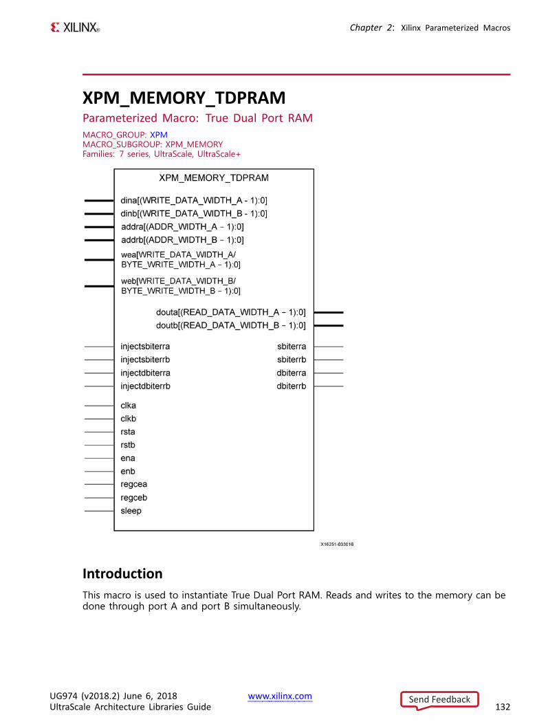
Chapter 2: Xilinx Parameterized Macros
XPM_MEMORY_TDPRAMParameterized Macro: True Dual Port RAMMACRO_GROUP: XPMMACRO_SUBGROUP: XPM_MEMORYFamilies: 7 series, UltraScale, UltraScale+
IntroductionThis macro is used to instantiate True Dual Port RAM. Reads and writes to the memory can bedone through port A and port B simultaneously.
UG974 (v2018.2) June 6, 2018 www.xilinx.comUltraScale Architecture Libraries Guide 132
Send Feedback
Chapter 2: Xilinx Parameterized Macros
The following describes the basic read and write port usage of an XPM_MEMORY instance. Itdoes not distinguish between port A and port B.
• All synchronous signals are sensitive to the rising edge of clk[a|b], which is assumed tobe a buffered and toggling clock signal behaving according to target device and memoryprimitive requirements.
• A read operation is implicitly performed to address addr[a|b] combinatorially. The dataoutput is registered each clk[a|b] cycle that en[a|b] is asserted.
• Read data appears on the dout[a|b] port READ_LATENCY_[A|B] clk[a|b] cycles after theassociated read operation.
• A write operation is explicitly performed, writing din[a|b] to address addr[a|b], when bothen[a|b] and we[a|b] are asserted on each clk[a|b] cycle.
• All read and write operations are gated by the value of en[a|b] on the initiating clk[a|b]cycle, regardless of input or output latencies. The addr[a|b] and we[a|b] inputs have noeffect when en[a|b] is de-asserted on the coincident clk[a|b] cycle.
• The behavior of dout[a|b] with respect to the combination of din[a|b] and addr[a|b] is afunction of WRITE_MODE_[A|B].
• For each clk[a|b] cycle that rst[a|b] is asserted, the final output register is immediately butsynchronously reset to READ_RESET_VALUE_[A|B], irrespective of READ_LATENCY_[A|B].
• For each clk[a|b] cycle that regce[a|b] is asserted and rst[a|b] is de-asserted, the final outputregister captures and outputs the value from the previous pipeline register.
• Undriven or unknown values provided on module inputs will produce undefined memoryarray and output port behavior.
The following restrictions apply on the WRITE_MODE_[A|B] attribute in True Dual Port RAMconfigurations. Violating this will result in a DRC.
• When the MEMORY_PRIMITIVE attribute is set to “distributed”, WRITE_MODE_[A|B] mustbe set to “read_first”.
• When the MEMORY_PRIMITIVE attribute is set to “block”, WRITE_MODE_[A|B] can be setto “read_first”, “write_first” or “no_change”.
• When the MEMORY_PRIMITIVE attribute is set to “ultra”, WRITE_MODE_[A|B] must be setto “no_change”.
NOTE: When byte wide writes are enabled on port [A|B] and the write mode is set to“no_change”, the maximum WRITE_DATA_WIDTH_[A|B] supported is
• 32/36 when the MEMORY_PRIMITIVE attribute is set to “block”
• 64/72 when the MEMORY_PRIMTIVE attribute is set to “ultra”
UG974 (v2018.2) June 6, 2018 www.xilinx.comUltraScale Architecture Libraries Guide 133
Send Feedback
Chapter 2: Xilinx Parameterized Macros
NOTE:• When the attribute “CLOCKING_MODE” is set to “common_clock”, all read/write operations
to memory through port A and port B are performed on clka. If this attribute is set to“independent_clock”, then read/write operations through port A are performed based onclka, and read/write operations through port B are performed based on clkb.
• Writing to an out-of-range address location may overwrite a valid address location wheneffective address bits match to a physical memory address location.
• set_false_path constraint is needed for the independent clock distributed RAM basedmemory if the design takes care of avoiding address collision (write address != read addressat any given point of time). Set USE_EMBEDDED_CONSTRAINT = 1 if XPM_MEMORY needsto take care of necessary constraints. If USE_EMBEDDED_CONSTRAINT = 0, Vivado maytrigger Timing-6 or Timing-7 or both. Alternatively, you can also add the constraint whenUSE_EMBEDDED_CONSTRAINT = 0. An example of adding this constraint is provided below.If Port-B also has write permissions for an Independent clock configuration, then a similarconstraint needs to be added for clkb as well.
set_false_path -from [filter [all_fanout -from [get_ports clka]-flat -endpoints_only] {IS_LEAF}] -through [get_pins -of_objects[get_cells -hier * -filter {PRIMITIVE_SUBGROUP==LUTRAM ||PRIMITIVE_SUBGROUP==dram || PRIMITIVE_SUBGROUP==drom}]-filter {DIRECTION==OUT}]
• If "CLOCKING_MODE" is set to "independent_clock", Vivado may trigger a false positiveCDC-1 warning and can be ignored.
• The use of UltraRAM’s dedicated input and output registers are controlled by synthesisbased on the READ_LATENCY_B value. For example, if 4 UltraRAMs are in cascade and theREAD_LATENCY_B is >= 4, then synthesis will absorb as much registers inside UltraRAMprimitive as possible.
UG974 (v2018.2) June 6, 2018 www.xilinx.comUltraScale Architecture Libraries Guide 134
Send Feedback
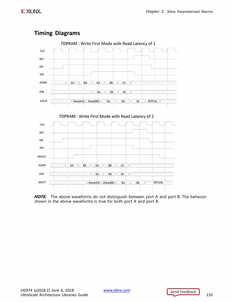
Chapter 2: Xilinx Parameterized Macros
Timing Diagrams
NOTE: The above waveforms do not distinguish between port A and port B. The behaviorshown in the above waveforms is true for both port A and port B.
UG974 (v2018.2) June 6, 2018 www.xilinx.comUltraScale Architecture Libraries Guide 135
Send Feedback
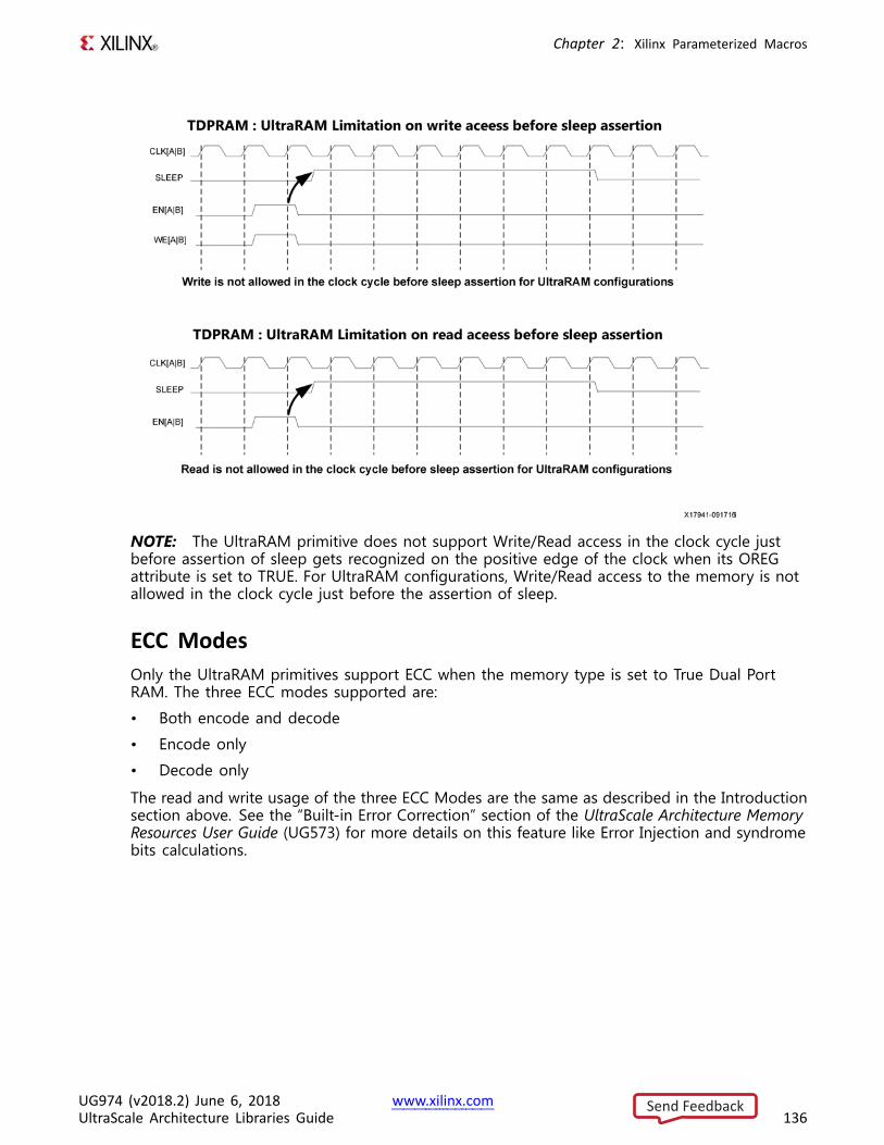
Chapter 2: Xilinx Parameterized Macros
NOTE: The UltraRAM primitive does not support Write/Read access in the clock cycle justbefore assertion of sleep gets recognized on the positive edge of the clock when its OREGattribute is set to TRUE. For UltraRAM configurations, Write/Read access to the memory is notallowed in the clock cycle just before the assertion of sleep.
ECC ModesOnly the UltraRAM primitives support ECC when the memory type is set to True Dual PortRAM. The three ECC modes supported are:
• Both encode and decode
• Encode only
• Decode only
The read and write usage of the three ECC Modes are the same as described in the Introductionsection above. See the “Built-in Error Correction” section of the UltraScale Architecture MemoryResources User Guide (UG573) for more details on this feature like Error Injection and syndromebits calculations.
UG974 (v2018.2) June 6, 2018 www.xilinx.comUltraScale Architecture Libraries Guide 136
Send Feedback
Chapter 2: Xilinx Parameterized Macros
There are restrictions on the attributes WRITE_DATA_WIDTH_[A|B], READ_DATA_WIDTH_[A|B],and MEMORY_SIZE in each of the above ECC modes.• Both encode and decode: WRITE_DATA_WIDTH_[A|B] and READ_DATA_WIDTH_[A|B] must
be multiples of 64-bits. Violating this rule will results in a DRC in XPM_Memory.• Encode only: WRITE_DATA_WIDTH_[A|B] must be a multiple of 64 bits and
READ_DATA_WIDTH_[A|B] must be a multiple of 72-bits. MEMORY_SIZE must be a multipleof READ_DATA_WIDTH_[A|B]. Violating these rules will result in a DRC.
• Decode only: WRITE_DATA_WIDTH_[A|B] must be a multiple of 72 bits andREAD_DATA_WIDTH_[A|B] must be a multiple of 64-bits. MEMORY_SIZE must be a multipleof WRITE_DATA_WIDTH_[A|B]. Violating these rules will result in a DRC.
When ECC is enabled the following are not supported:• Asymmetry• Initialization• Reset (neither non-zero reset value nor reset assertion)
NOTE: ECC uses a hard-ECC block available in the BRAM/URAM macro and the data widthshould be multiples of 64/72. Use ECC IP for other data width combinations.
Auto Sleep Mode• This feature is applicable only when MEMORY_PRIMITIVE is URAM and is controlled
internally in the UltraRAM to check if it can be put in sleep mode and when it needsto wake up. Thus power savings are obtained automatically without having to explicitlycontrol the SLEEP Pin.
• When AUTO_SLEEP_TIME is 0, the feature is disabled. When AUTO_SLEEP_TIME is nonzero,XPM_MEMORY constructs the pipeline registers equal to AUTO_SLEEP_TIME value on allinput signals except rst[a|b].
• If AUTO_SLEEP_TIME is too low, then UltraRAM goes into sleep and wakeup too often,which can cause more power to be consumed.
• The number of sleep cycles achieved is calculated by following formula:– If number of consecutive inactive cycles is < AUTO_SLEEP_TIME, then number of sleep
cycles = 0– If number of consecutive inactive cycles is >= AUTO_SLEEP_TIME, Then number of
consecutive sleep cycles = Number of consecutive inactive cycles – 3– Inactive cycle is defined as a cycle where there is no Read/Write operation from either
port• The latency between the read operation and the data arrival at dout[a|b] is
AUTO_SLEEP_TIME + READ_LATENCY_[A|B] clock cycles (Assuming that REGCE is high whenthe output data pipe line exists).
• When the READ_LATENCY_[A|B] is set to 1 or 2, XPM_Memory behaviorally models theAUTO SLEEP feature and forces ‘x’ on DOUT[A|B] when the RAM is in Auto Sleep Mode.For READ_LATENCY_[A|B] greater than 2, the propagation of ‘x’ cannot happen to theDOUT[A|B] as the output registers gets the clock enable (delayed read enable) afterUltraRAM comes out of sleep mode.
• The Auto Sleep mode is most effective for larger Memory sizes or any Memory with verylittle activity.
UG974 (v2018.2) June 6, 2018 www.xilinx.comUltraScale Architecture Libraries Guide 137
Send Feedback
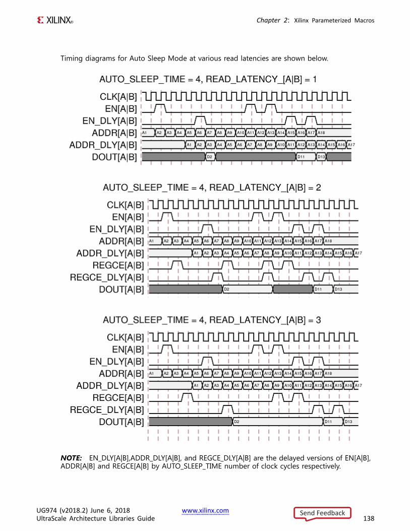
Chapter 2: Xilinx Parameterized Macros
Timing diagrams for Auto Sleep Mode at various read latencies are shown below.
NOTE: EN_DLY[A|B],ADDR_DLY[A|B], and REGCE_DLY[A|B] are the delayed versions of EN[A|B],ADDR[A|B] and REGCE[A|B] by AUTO_SLEEP_TIME number of clock cycles respectively.
UG974 (v2018.2) June 6, 2018 www.xilinx.comUltraScale Architecture Libraries Guide 138
Send Feedback
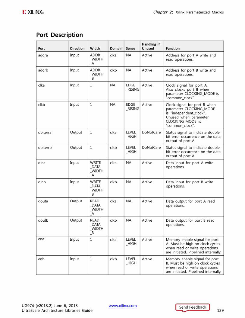
Chapter 2: Xilinx Parameterized Macros
Port Description
Port Direction Width Domain SenseHandling ifUnused Function
addra Input ADDR_WIDTH_A
clka NA Active Address for port A write andread operations.
addrb Input ADDR_WIDTH_B
clkb NA Active Address for port B write andread operations.
clka Input 1 NA EDGE_RISING
Active Clock signal for port A.Also clocks port B whenparameter CLOCKING_MODE is"common_clock".
clkb Input 1 NA EDGE_RISING
Active Clock signal for port B whenparameter CLOCKING_MODEis "independent_clock".Unused when parameterCLOCKING_MODE is"common_clock".
dbiterra Output 1 clka LEVEL_HIGH
DoNotCare Status signal to indicate doublebit error occurrence on the dataoutput of port A.
dbiterrb Output 1 clkb LEVEL_HIGH
DoNotCare Status signal to indicate doublebit error occurrence on the dataoutput of port A.
dina Input WRITE_DATA_WIDTH_A
clka NA Active Data input for port A writeoperations.
dinb Input WRITE_DATA_WIDTH_B
clkb NA Active Data input for port B writeoperations.
douta Output READ_DATA_WIDTH_A
clka NA Active Data output for port A readoperations.
doutb Output READ_DATA_WIDTH_B
clkb NA Active Data output for port B readoperations.
ena Input 1 clka LEVEL_HIGH
Active Memory enable signal for portA. Must be high on clock cycleswhen read or write operationsare initiated. Pipelined internally.
enb Input 1 clkb LEVEL_HIGH
Active Memory enable signal for portB. Must be high on clock cycleswhen read or write operationsare initiated. Pipelined internally.
UG974 (v2018.2) June 6, 2018 www.xilinx.comUltraScale Architecture Libraries Guide 139
Send Feedback
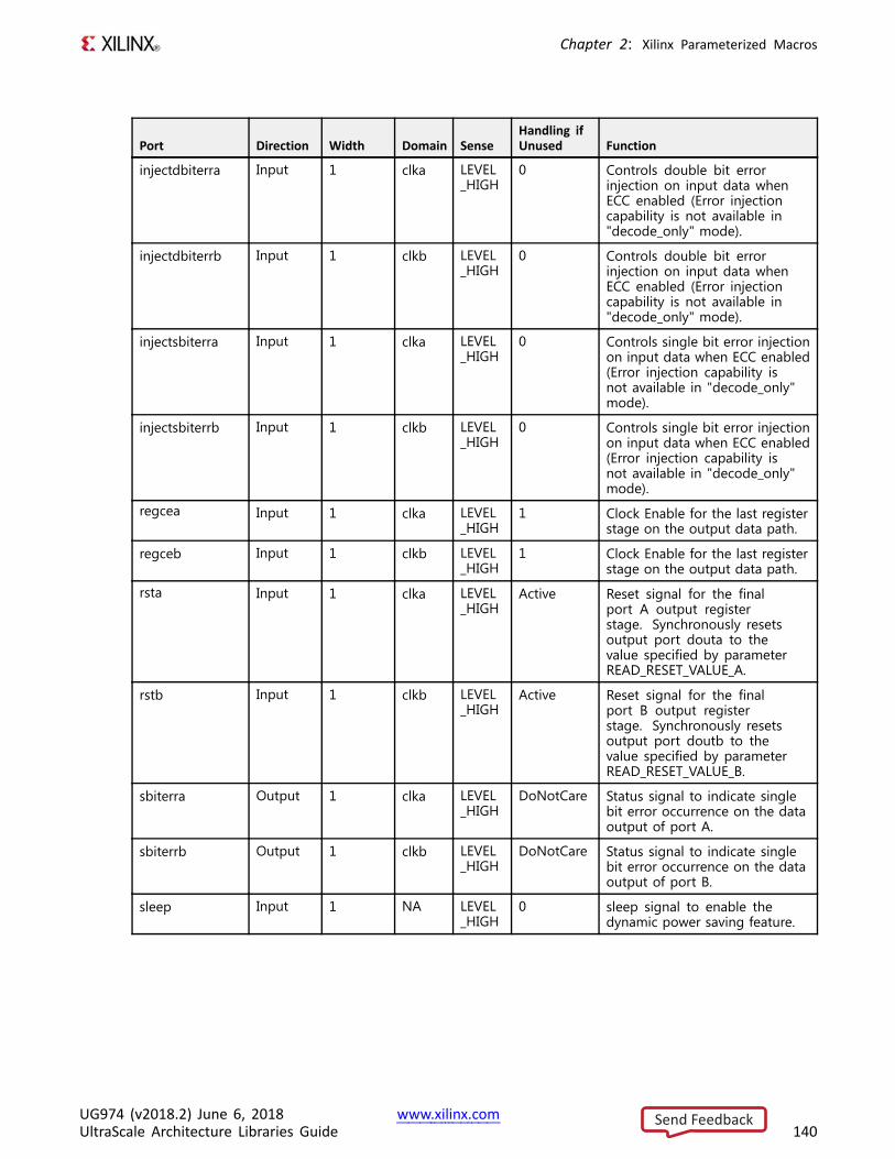
Chapter 2: Xilinx Parameterized Macros
Port Direction Width Domain SenseHandling ifUnused Function
injectdbiterra Input 1 clka LEVEL_HIGH
0 Controls double bit errorinjection on input data whenECC enabled (Error injectioncapability is not available in"decode_only" mode).
injectdbiterrb Input 1 clkb LEVEL_HIGH
0 Controls double bit errorinjection on input data whenECC enabled (Error injectioncapability is not available in"decode_only" mode).
injectsbiterra Input 1 clka LEVEL_HIGH
0 Controls single bit error injectionon input data when ECC enabled(Error injection capability isnot available in "decode_only"mode).
injectsbiterrb Input 1 clkb LEVEL_HIGH
0 Controls single bit error injectionon input data when ECC enabled(Error injection capability isnot available in "decode_only"mode).
regcea Input 1 clka LEVEL_HIGH
1 Clock Enable for the last registerstage on the output data path.
regceb Input 1 clkb LEVEL_HIGH
1 Clock Enable for the last registerstage on the output data path.
rsta Input 1 clka LEVEL_HIGH
Active Reset signal for the finalport A output registerstage. Synchronously resetsoutput port douta to thevalue specified by parameterREAD_RESET_VALUE_A.
rstb Input 1 clkb LEVEL_HIGH
Active Reset signal for the finalport B output registerstage. Synchronously resetsoutput port doutb to thevalue specified by parameterREAD_RESET_VALUE_B.
sbiterra Output 1 clka LEVEL_HIGH
DoNotCare Status signal to indicate singlebit error occurrence on the dataoutput of port A.
sbiterrb Output 1 clkb LEVEL_HIGH
DoNotCare Status signal to indicate singlebit error occurrence on the dataoutput of port B.
sleep Input 1 NA LEVEL_HIGH
0 sleep signal to enable thedynamic power saving feature.
UG974 (v2018.2) June 6, 2018 www.xilinx.comUltraScale Architecture Libraries Guide 140
Send Feedback
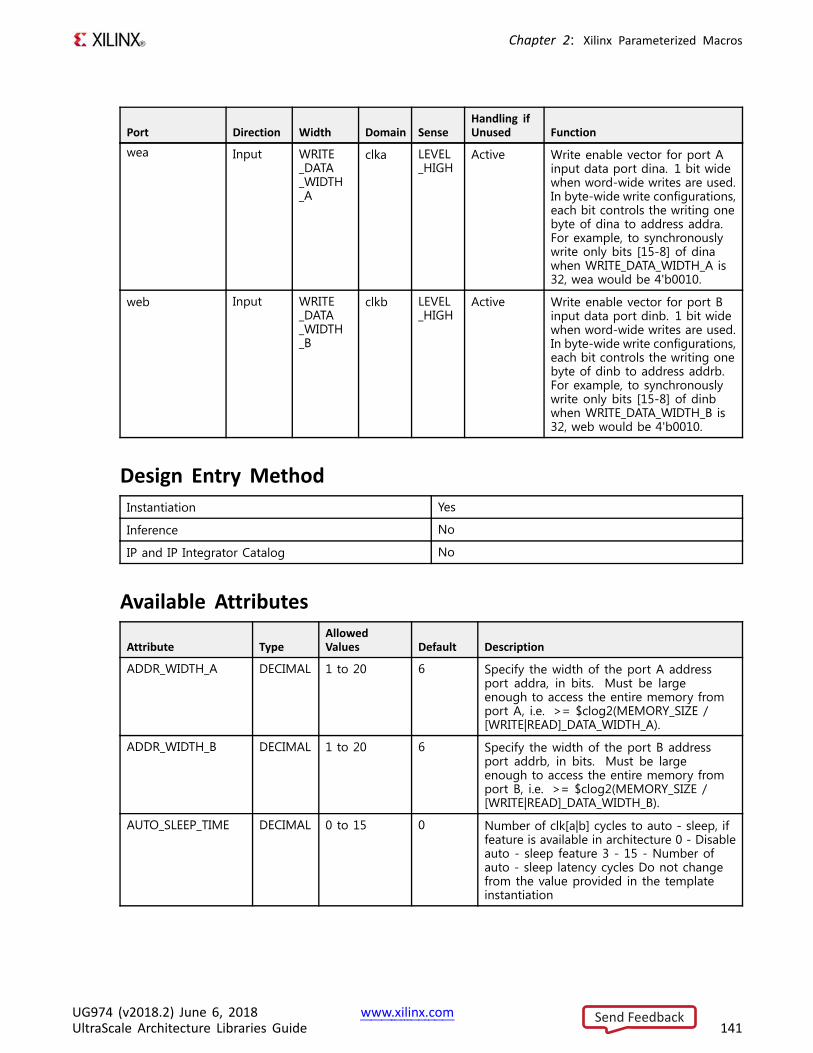
Chapter 2: Xilinx Parameterized Macros
Port Direction Width Domain SenseHandling ifUnused Function
wea Input WRITE_DATA_WIDTH_A
clka LEVEL_HIGH
Active Write enable vector for port Ainput data port dina. 1 bit widewhen word-wide writes are used.In byte-wide write configurations,each bit controls the writing onebyte of dina to address addra.For example, to synchronouslywrite only bits [15-8] of dinawhen WRITE_DATA_WIDTH_A is32, wea would be 4'b0010.
web Input WRITE_DATA_WIDTH_B
clkb LEVEL_HIGH
Active Write enable vector for port Binput data port dinb. 1 bit widewhen word-wide writes are used.In byte-wide write configurations,each bit controls the writing onebyte of dinb to address addrb.For example, to synchronouslywrite only bits [15-8] of dinbwhen WRITE_DATA_WIDTH_B is32, web would be 4'b0010.
Design Entry MethodInstantiation Yes
Inference No
IP and IP Integrator Catalog No
Available Attributes
Attribute TypeAllowedValues Default Description
ADDR_WIDTH_A DECIMAL 1 to 20 6 Specify the width of the port A addressport addra, in bits. Must be largeenough to access the entire memory fromport A, i.e. >= $clog2(MEMORY_SIZE /[WRITE|READ]_DATA_WIDTH_A).
ADDR_WIDTH_B DECIMAL 1 to 20 6 Specify the width of the port B addressport addrb, in bits. Must be largeenough to access the entire memory fromport B, i.e. >= $clog2(MEMORY_SIZE /[WRITE|READ]_DATA_WIDTH_B).
AUTO_SLEEP_TIME DECIMAL 0 to 15 0 Number of clk[a|b] cycles to auto - sleep, iffeature is available in architecture 0 - Disableauto - sleep feature 3 - 15 - Number ofauto - sleep latency cycles Do not changefrom the value provided in the templateinstantiation
UG974 (v2018.2) June 6, 2018 www.xilinx.comUltraScale Architecture Libraries Guide 141
Send Feedback
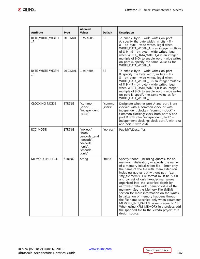
Chapter 2: Xilinx Parameterized Macros
Attribute TypeAllowedValues Default Description
BYTE_WRITE_WIDTH_A
DECIMAL 1 to 4608 32 To enable byte - wide writes on portA, specify the byte width, in bits - 8 -8 - bit byte - wide writes, legal whenWRITE_DATA_WIDTH_A is an integer multipleof 8 9 - 9 - bit byte - wide writes, legalwhen WRITE_DATA_WIDTH_A is an integermultiple of 9 Or to enable word - wide writeson port A, specify the same value as forWRITE_DATA_WIDTH_A.
BYTE_WRITE_WIDTH_B
DECIMAL 1 to 4608 32 To enable byte - wide writes on portB, specify the byte width, in bits - 8 -8 - bit byte - wide writes, legal whenWRITE_DATA_WIDTH_B is an integer multipleof 8 9 - 9 - bit byte - wide writes, legalwhen WRITE_DATA_WIDTH_B is an integermultiple of 9 Or to enable word - wide writeson port B, specify the same value as forWRITE_DATA_WIDTH_B.
CLOCKING_MODE STRING "common_clock","independent_clock"
"common_clock"
Designate whether port A and port B areclocked with a common clock or withindependent clocks - "common_clock" -Common clocking; clock both port A andport B with clka "independent_clock" -Independent clocking; clock port A with clkaand port B with clkb
ECC_MODE STRING "no_ecc","both_encode _and_decode","decode_only","encode_only"
"no_ecc" PublishToDocs: Yes
MEMORY_INIT_FILE STRING String "none" Specify "none" (including quotes) for nomemory initialization, or specify the nameof a memory initialization file - Enter onlythe name of the file with .mem extension,including quotes but without path (e.g."my_file.mem"). File format must be ASCIIand consist of only hexadecimal valuesorganized into the specified depth bynarrowest data width generic value of thememory. See the Memory File (MEM)section for more information on the syntax.Initialization of memory happens throughthe file name specified only when parameterMEMORY_INIT_PARAM value is equal to "". |When using XPM_MEMORY in a project, addthe specified file to the Vivado project as adesign source.
UG974 (v2018.2) June 6, 2018 www.xilinx.comUltraScale Architecture Libraries Guide 142
Send Feedback
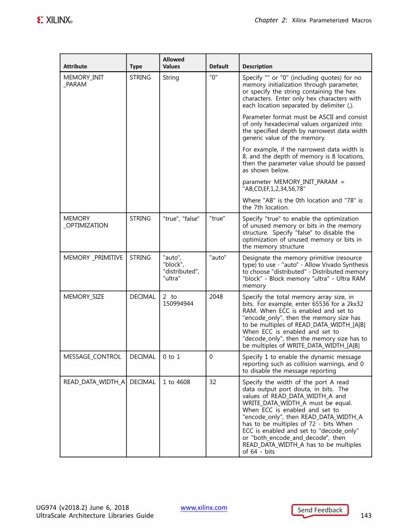
Chapter 2: Xilinx Parameterized Macros
Attribute TypeAllowedValues Default Description
MEMORY_INIT_PARAM
STRING String "0" Specify "" or "0" (including quotes) for nomemory initialization through parameter,or specify the string containing the hexcharacters. Enter only hex characters witheach location separated by delimiter (,).
Parameter format must be ASCII and consistof only hexadecimal values organized intothe specified depth by narrowest data widthgeneric value of the memory.
For example, if the narrowest data width is8, and the depth of memory is 8 locations,then the parameter value should be passedas shown below.
parameter MEMORY_INIT_PARAM ="AB,CD,EF,1,2,34,56,78"
Where "AB" is the 0th location and "78" isthe 7th location.
MEMORY_OPTIMIZATION
STRING "true", "false" "true" Specify "true" to enable the optimizationof unused memory or bits in the memorystructure. Specify "false" to disable theoptimization of unused memory or bits inthe memory structure
MEMORY _PRIMITIVE STRING "auto","block","distributed","ultra"
"auto" Designate the memory primitive (resourcetype) to use - "auto" - Allow Vivado Synthesisto choose "distributed" - Distributed memory"block" - Block memory "ultra" - Ultra RAMmemory
MEMORY_SIZE DECIMAL 2 to150994944
2048 Specify the total memory array size, inbits. For example, enter 65536 for a 2kx32RAM. When ECC is enabled and set to"encode_only", then the memory size hasto be multiples of READ_DATA_WIDTH_[A|B]When ECC is enabled and set to"decode_only", then the memory size has tobe multiples of WRITE_DATA_WIDTH_[A|B]
MESSAGE_CONTROL DECIMAL 0 to 1 0 Specify 1 to enable the dynamic messagereporting such as collision warnings, and 0to disable the message reporting
READ_DATA_WIDTH_A DECIMAL 1 to 4608 32 Specify the width of the port A readdata output port douta, in bits. Thevalues of READ_DATA_WIDTH_A andWRITE_DATA_WIDTH_A must be equal.When ECC is enabled and set to"encode_only", then READ_DATA_WIDTH_Ahas to be multiples of 72 - bits WhenECC is enabled and set to "decode_only"or "both_encode_and_decode", thenREAD_DATA_WIDTH_A has to be multiplesof 64 - bits
UG974 (v2018.2) June 6, 2018 www.xilinx.comUltraScale Architecture Libraries Guide 143
Send Feedback
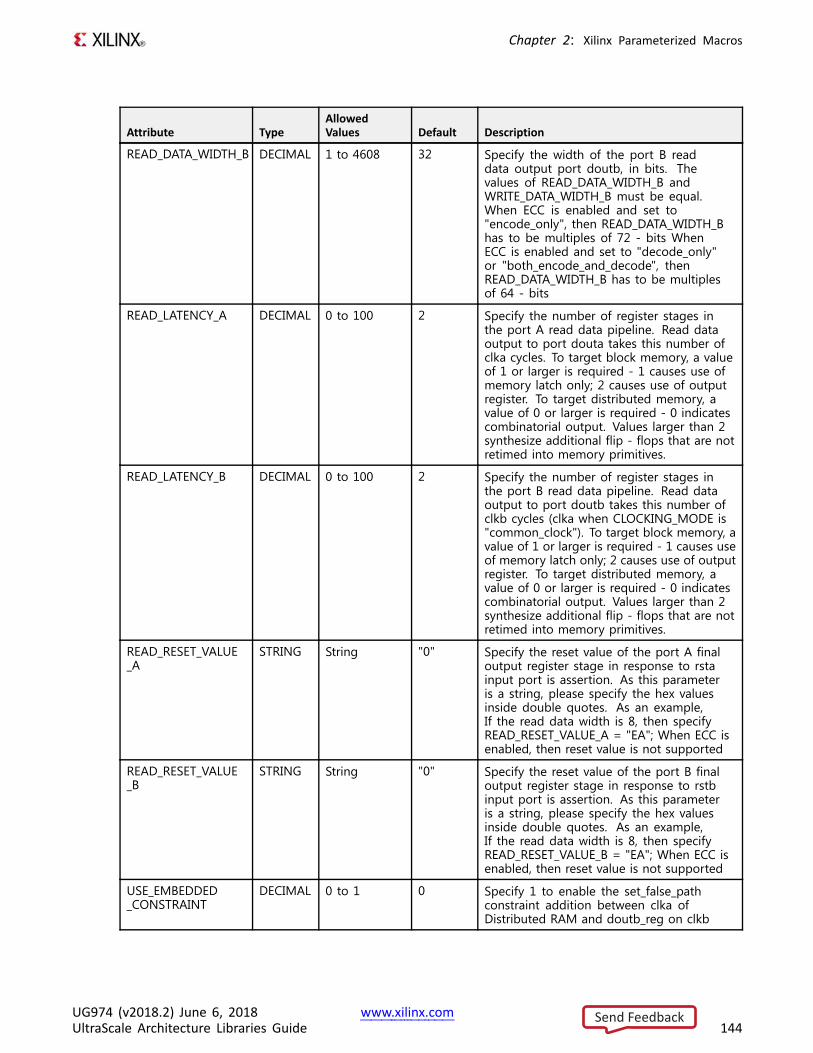
Chapter 2: Xilinx Parameterized Macros
Attribute TypeAllowedValues Default Description
READ_DATA_WIDTH_B DECIMAL 1 to 4608 32 Specify the width of the port B readdata output port doutb, in bits. Thevalues of READ_DATA_WIDTH_B andWRITE_DATA_WIDTH_B must be equal.When ECC is enabled and set to"encode_only", then READ_DATA_WIDTH_Bhas to be multiples of 72 - bits WhenECC is enabled and set to "decode_only"or "both_encode_and_decode", thenREAD_DATA_WIDTH_B has to be multiplesof 64 - bits
READ_LATENCY_A DECIMAL 0 to 100 2 Specify the number of register stages inthe port A read data pipeline. Read dataoutput to port douta takes this number ofclka cycles. To target block memory, a valueof 1 or larger is required - 1 causes use ofmemory latch only; 2 causes use of outputregister. To target distributed memory, avalue of 0 or larger is required - 0 indicatescombinatorial output. Values larger than 2synthesize additional flip - flops that are notretimed into memory primitives.
READ_LATENCY_B DECIMAL 0 to 100 2 Specify the number of register stages inthe port B read data pipeline. Read dataoutput to port doutb takes this number ofclkb cycles (clka when CLOCKING_MODE is"common_clock"). To target block memory, avalue of 1 or larger is required - 1 causes useof memory latch only; 2 causes use of outputregister. To target distributed memory, avalue of 0 or larger is required - 0 indicatescombinatorial output. Values larger than 2synthesize additional flip - flops that are notretimed into memory primitives.
READ_RESET_VALUE_A
STRING String "0" Specify the reset value of the port A finaloutput register stage in response to rstainput port is assertion. As this parameteris a string, please specify the hex valuesinside double quotes. As an example,If the read data width is 8, then specifyREAD_RESET_VALUE_A = "EA"; When ECC isenabled, then reset value is not supported
READ_RESET_VALUE_B
STRING String "0" Specify the reset value of the port B finaloutput register stage in response to rstbinput port is assertion. As this parameteris a string, please specify the hex valuesinside double quotes. As an example,If the read data width is 8, then specifyREAD_RESET_VALUE_B = "EA"; When ECC isenabled, then reset value is not supported
USE_EMBEDDED_CONSTRAINT
DECIMAL 0 to 1 0 Specify 1 to enable the set_false_pathconstraint addition between clka ofDistributed RAM and doutb_reg on clkb
UG974 (v2018.2) June 6, 2018 www.xilinx.comUltraScale Architecture Libraries Guide 144
Send Feedback
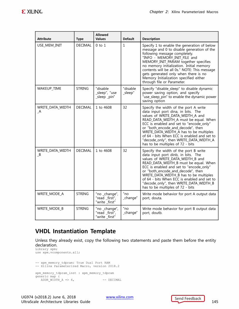
Chapter 2: Xilinx Parameterized Macros
Attribute TypeAllowedValues Default Description
USE_MEM_INIT DECIMAL 0 to 1 1 Specify 1 to enable the generation of belowmessage and 0 to disable generation of thefollowing message completely."INFO - MEMORY_INIT_FILE andMEMORY_INIT_PARAM together specifiesno memory initialization. Initial memorycontents will be all 0s." NOTE: This messagegets generated only when there is noMemory Initialization specified eitherthrough file or Parameter.
WAKEUP_TIME STRING "disable_sleep", "use_sleep _pin"
"disable_sleep"
Specify "disable_sleep" to disable dynamicpower saving option, and specify"use_sleep_pin" to enable the dynamic powersaving option
WRITE_DATA_WIDTH_A
DECIMAL 1 to 4608 32 Specify the width of the port A writedata input port dina, in bits. Thevalues of WRITE_DATA_WIDTH_A andREAD_DATA_WIDTH_A must be equal. WhenECC is enabled and set to "encode_only"or "both_encode_and_decode", thenWRITE_DATA_WIDTH_A has to be multiplesof 64 - bits When ECC is enabled and set to"decode_only", then WRITE_DATA_WIDTH_Ahas to be multiples of 72 - bits
WRITE_DATA_WIDTH_B
DECIMAL 1 to 4608 32 Specify the width of the port B writedata input port dinb, in bits. Thevalues of WRITE_DATA_WIDTH_B andREAD_DATA_WIDTH_B must be equal. WhenECC is enabled and set to "encode_only"or "both_encode_and_decode", thenWRITE_DATA_WIDTH_B has to be multiplesof 64 - bits When ECC is enabled and set to"decode_only", then WRITE_DATA_WIDTH_Bhas to be multiples of 72 - bits
WRITE_MODE_A STRING "no _change","read _first","write _first"
"no_change"
Write mode behavior for port A output dataport, douta.
WRITE_MODE_B STRING "no _change","read _first","write _first"
"no_change"
Write mode behavior for port B output dataport, doutb.
VHDL Instantiation TemplateUnless they already exist, copy the following two statements and paste them before the entitydeclaration.Library xpm;use xpm.vcomponents.all;
-- xpm_memory_tdpram: True Dual Port RAM-- Xilinx Parameterized Macro, version 2018.2
xpm_memory_tdpram_inst : xpm_memory_tdpramgeneric map (
ADDR_WIDTH_A => 6, -- DECIMAL
UG974 (v2018.2) June 6, 2018 www.xilinx.comUltraScale Architecture Libraries Guide 145
Send Feedback
Chapter 2: Xilinx Parameterized Macros
ADDR_WIDTH_B => 6, -- DECIMALAUTO_SLEEP_TIME => 0, -- DECIMALBYTE_WRITE_WIDTH_A => 32, -- DECIMALBYTE_WRITE_WIDTH_B => 32, -- DECIMALCLOCKING_MODE => "common_clock", -- StringECC_MODE => "no_ecc", -- StringMEMORY_INIT_FILE => "none", -- StringMEMORY_INIT_PARAM => "0", -- StringMEMORY_OPTIMIZATION => "true", -- StringMEMORY_PRIMITIVE => "auto", -- StringMEMORY_SIZE => 2048, -- DECIMALMESSAGE_CONTROL => 0, -- DECIMALREAD_DATA_WIDTH_A => 32, -- DECIMALREAD_DATA_WIDTH_B => 32, -- DECIMALREAD_LATENCY_A => 2, -- DECIMALREAD_LATENCY_B => 2, -- DECIMALREAD_RESET_VALUE_A => "0", -- StringREAD_RESET_VALUE_B => "0", -- StringUSE_EMBEDDED_CONSTRAINT => 0, -- DECIMALUSE_MEM_INIT => 1, -- DECIMALWAKEUP_TIME => "disable_sleep", -- StringWRITE_DATA_WIDTH_A => 32, -- DECIMALWRITE_DATA_WIDTH_B => 32, -- DECIMALWRITE_MODE_A => "no_change", -- StringWRITE_MODE_B => "no_change" -- String
)port map (
dbiterra => dbiterra, -- 1-bit output: Status signal to indicate double bit error occurrence-- on the data output of port A.
dbiterrb => dbiterrb, -- 1-bit output: Status signal to indicate double bit error occurrence-- on the data output of port A.
douta => douta, -- READ_DATA_WIDTH_A-bit output: Data output for port A read operations.doutb => doutb, -- READ_DATA_WIDTH_B-bit output: Data output for port B read operations.sbiterra => sbiterra, -- 1-bit output: Status signal to indicate single bit error occurrence
-- on the data output of port A.
sbiterrb => sbiterrb, -- 1-bit output: Status signal to indicate single bit error occurrence-- on the data output of port B.
addra => addra, -- ADDR_WIDTH_A-bit input: Address for port A write and read operations.addrb => addrb, -- ADDR_WIDTH_B-bit input: Address for port B write and read operations.clka => clka, -- 1-bit input: Clock signal for port A. Also clocks port B when
-- parameter CLOCKING_MODE is "common_clock".
clkb => clkb, -- 1-bit input: Clock signal for port B when parameter CLOCKING_MODE is-- "independent_clock". Unused when parameter CLOCKING_MODE is-- "common_clock".
dina => dina, -- WRITE_DATA_WIDTH_A-bit input: Data input for port A write operations.dinb => dinb, -- WRITE_DATA_WIDTH_B-bit input: Data input for port B write operations.ena => ena, -- 1-bit input: Memory enable signal for port A. Must be high on clock
-- cycles when read or write operations are initiated. Pipelined-- internally.
enb => enb, -- 1-bit input: Memory enable signal for port B. Must be high on clock-- cycles when read or write operations are initiated. Pipelined
-- internally.
injectdbiterra => injectdbiterra, -- 1-bit input: Controls double bit error injection on input data when-- ECC enabled (Error injection capability is not available in-- "decode_only" mode).
injectdbiterrb => injectdbiterrb, -- 1-bit input: Controls double bit error injection on input data when-- ECC enabled (Error injection capability is not available in-- "decode_only" mode).
injectsbiterra => injectsbiterra, -- 1-bit input: Controls single bit error injection on input data when-- ECC enabled (Error injection capability is not available in-- "decode_only" mode).
UG974 (v2018.2) June 6, 2018 www.xilinx.comUltraScale Architecture Libraries Guide 146
Send Feedback
Chapter 2: Xilinx Parameterized Macros
injectsbiterrb => injectsbiterrb, -- 1-bit input: Controls single bit error injection on input data when-- ECC enabled (Error injection capability is not available in-- "decode_only" mode).
regcea => regcea, -- 1-bit input: Clock Enable for the last register stage on the output-- data path.
regceb => regceb, -- 1-bit input: Clock Enable for the last register stage on the output-- data path.
rsta => rsta, -- 1-bit input: Reset signal for the final port A output register-- stage. Synchronously resets output port douta to the value specified
-- by parameter READ_RESET_VALUE_A.
rstb => rstb, -- 1-bit input: Reset signal for the final port B output register-- stage. Synchronously resets output port doutb to the value specified
-- by parameter READ_RESET_VALUE_B.
sleep => sleep, -- 1-bit input: sleep signal to enable the dynamic power saving feature.wea => wea, -- WRITE_DATA_WIDTH_A-bit input: Write enable vector for port A input
-- data port dina. 1 bit wide when word-wide writes are used. In-- byte-wide write configurations, each bit controls the writing one-- byte of dina to address addra. For example, to synchronously write-- only bits [15-8] of dina when WRITE_DATA_WIDTH_A is 32, wea would be
-- 4'b0010.
web => web -- WRITE_DATA_WIDTH_B-bit input: Write enable vector for port B input-- data port dinb. 1 bit wide when word-wide writes are used. In-- byte-wide write configurations, each bit controls the writing one-- byte of dinb to address addrb. For example, to synchronously write-- only bits [15-8] of dinb when WRITE_DATA_WIDTH_B is 32, web would be
-- 4'b0010.
);
-- End of xpm_memory_tdpram_inst instantiation
Verilog Instantiation Template
// xpm_memory_tdpram: True Dual Port RAM// Xilinx Parameterized Macro, version 2018.2
xpm_memory_tdpram #(.ADDR_WIDTH_A(6), // DECIMAL.ADDR_WIDTH_B(6), // DECIMAL.AUTO_SLEEP_TIME(0), // DECIMAL.BYTE_WRITE_WIDTH_A(32), // DECIMAL.BYTE_WRITE_WIDTH_B(32), // DECIMAL.CLOCKING_MODE("common_clock"), // String.ECC_MODE("no_ecc"), // String.MEMORY_INIT_FILE("none"), // String.MEMORY_INIT_PARAM("0"), // String.MEMORY_OPTIMIZATION("true"), // String.MEMORY_PRIMITIVE("auto"), // String.MEMORY_SIZE(2048), // DECIMAL.MESSAGE_CONTROL(0), // DECIMAL.READ_DATA_WIDTH_A(32), // DECIMAL.READ_DATA_WIDTH_B(32), // DECIMAL.READ_LATENCY_A(2), // DECIMAL.READ_LATENCY_B(2), // DECIMAL.READ_RESET_VALUE_A("0"), // String.READ_RESET_VALUE_B("0"), // String.USE_EMBEDDED_CONSTRAINT(0), // DECIMAL.USE_MEM_INIT(1), // DECIMAL.WAKEUP_TIME("disable_sleep"), // String.WRITE_DATA_WIDTH_A(32), // DECIMAL.WRITE_DATA_WIDTH_B(32), // DECIMAL.WRITE_MODE_A("no_change"), // String
UG974 (v2018.2) June 6, 2018 www.xilinx.comUltraScale Architecture Libraries Guide 147
Send Feedback
Chapter 2: Xilinx Parameterized Macros
.WRITE_MODE_B("no_change") // String)xpm_memory_tdpram_inst (
.dbiterra(dbiterra), // 1-bit output: Status signal to indicate double bit error occurrence// on the data output of port A.
.dbiterrb(dbiterrb), // 1-bit output: Status signal to indicate double bit error occurrence// on the data output of port A.
.douta(douta), // READ_DATA_WIDTH_A-bit output: Data output for port A read operations.
.doutb(doutb), // READ_DATA_WIDTH_B-bit output: Data output for port B read operations.
.sbiterra(sbiterra), // 1-bit output: Status signal to indicate single bit error occurrence// on the data output of port A.
.sbiterrb(sbiterrb), // 1-bit output: Status signal to indicate single bit error occurrence// on the data output of port B.
.addra(addra), // ADDR_WIDTH_A-bit input: Address for port A write and read operations.
.addrb(addrb), // ADDR_WIDTH_B-bit input: Address for port B write and read operations.
.clka(clka), // 1-bit input: Clock signal for port A. Also clocks port B when// parameter CLOCKING_MODE is "common_clock".
.clkb(clkb), // 1-bit input: Clock signal for port B when parameter CLOCKING_MODE is// "independent_clock". Unused when parameter CLOCKING_MODE is// "common_clock".
.dina(dina), // WRITE_DATA_WIDTH_A-bit input: Data input for port A write operations.
.dinb(dinb), // WRITE_DATA_WIDTH_B-bit input: Data input for port B write operations.
.ena(ena), // 1-bit input: Memory enable signal for port A. Must be high on clock// cycles when read or write operations are initiated. Pipelined// internally.
.enb(enb), // 1-bit input: Memory enable signal for port B. Must be high on clock// cycles when read or write operations are initiated. Pipelined// internally.
.injectdbiterra(injectdbiterra), // 1-bit input: Controls double bit error injection on input data when// ECC enabled (Error injection capability is not available in// "decode_only" mode).
.injectdbiterrb(injectdbiterrb), // 1-bit input: Controls double bit error injection on input data when// ECC enabled (Error injection capability is not available in// "decode_only" mode).
.injectsbiterra(injectsbiterra), // 1-bit input: Controls single bit error injection on input data when// ECC enabled (Error injection capability is not available in// "decode_only" mode).
.injectsbiterrb(injectsbiterrb), // 1-bit input: Controls single bit error injection on input data when// ECC enabled (Error injection capability is not available in// "decode_only" mode).
.regcea(regcea), // 1-bit input: Clock Enable for the last register stage on the output// data path.
.regceb(regceb), // 1-bit input: Clock Enable for the last register stage on the output// data path.
.rsta(rsta), // 1-bit input: Reset signal for the final port A output register stage.// Synchronously resets output port douta to the value specified by
// parameter READ_RESET_VALUE_A.
.rstb(rstb), // 1-bit input: Reset signal for the final port B output register stage.// Synchronously resets output port doutb to the value specified by
// parameter READ_RESET_VALUE_B.
.sleep(sleep), // 1-bit input: sleep signal to enable the dynamic power saving feature.
.wea(wea), // WRITE_DATA_WIDTH_A-bit input: Write enable vector for port A input// data port dina. 1 bit wide when word-wide writes are used. In
// byte-wide write configurations, each bit controls the writing one// byte of dina to address addra. For example, to synchronously write// only bits [15-8] of dina when WRITE_DATA_WIDTH_A is 32, wea would be
UG974 (v2018.2) June 6, 2018 www.xilinx.comUltraScale Architecture Libraries Guide 148
Send Feedback
Chapter 2: Xilinx Parameterized Macros
// 4'b0010.
.web(web) // WRITE_DATA_WIDTH_B-bit input: Write enable vector for port B input// data port dinb. 1 bit wide when word-wide writes are used. In
// byte-wide write configurations, each bit controls the writing one// byte of dinb to address addrb. For example, to synchronously write// only bits [15-8] of dinb when WRITE_DATA_WIDTH_B is 32, web would be
// 4'b0010.
);
// End of xpm_memory_tdpram_inst instantiation
For More Information• See the UltraScale Programmable Devices Documentation.
• See the UltraScale Architecture Memory Resources User Guide (UG573).
UG974 (v2018.2) June 6, 2018 www.xilinx.comUltraScale Architecture Libraries Guide 149
Send Feedback
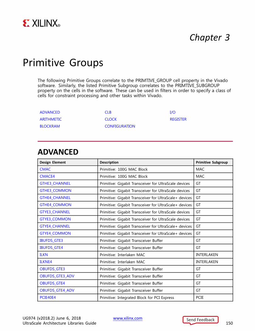
Chapter 3
Primitive GroupsThe following Primitive Groups correlate to the PRIMTIVE_GROUP cell property in the Vivadosoftware. Similarly, the listed Primitive Subgroup correlates to the PRIMTIVE_SUBGROUPproperty on the cells in the software. These can be used in filters in order to specify a class ofcells for constraint processing and other tasks within Vivado.
ADVANCED CLB I/O
ARITHMETIC CLOCK REGISTER
BLOCKRAM CONFIGURATION
ADVANCEDDesign Element Description Primitive Subgroup
CMAC Primitive: 100G MAC Block MAC
CMACE4 Primitive: 100G MAC Block MAC
GTHE3_CHANNEL Primitive: Gigabit Transceiver for UltraScale devices GT
GTHE3_COMMON Primitive: Gigabit Transceiver for UltraScale devices GT
GTHE4_CHANNEL Primitive: Gigabit Transceiver for UltraScale+ devices GT
GTHE4_COMMON Primitive: Gigabit Transceiver for UltraScale+ devices GT
GTYE3_CHANNEL Primitive: Gigabit Transceiver for UltraScale devices GT
GTYE3_COMMON Primitive: Gigabit Transceiver for UltraScale devices GT
GTYE4_CHANNEL Primitive: Gigabit Transceiver for UltraScale+ devices GT
GTYE4_COMMON Primitive: Gigabit Transceiver for UltraScale+ devices GT
IBUFDS_GTE3 Primitive: Gigabit Transceiver Buffer GT
IBUFDS_GTE4 Primitive: Gigabit Transceiver Buffer GT
ILKN Primitive: Interlaken MAC INTERLAKEN
ILKNE4 Primitive: Interlaken MAC INTERLAKEN
OBUFDS_GTE3 Primitive: Gigabit Transceiver Buffer GT
OBUFDS_GTE3_ADV Primitive: Gigabit Transceiver Buffer GT
OBUFDS_GTE4 Primitive: Gigabit Transceiver Buffer GT
OBUFDS_GTE4_ADV Primitive: Gigabit Transceiver Buffer GT
PCIE40E4 Primitive: Integrated Block for PCI Express PCIE
UG974 (v2018.2) June 6, 2018 www.xilinx.comUltraScale Architecture Libraries Guide 150
Send Feedback
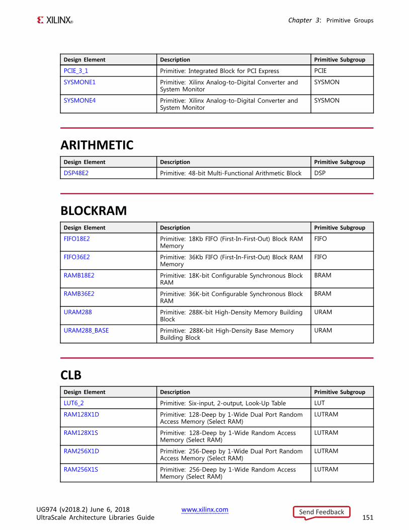
Chapter 3: Primitive Groups
Design Element Description Primitive Subgroup
PCIE_3_1 Primitive: Integrated Block for PCI Express PCIE
SYSMONE1 Primitive: Xilinx Analog-to-Digital Converter andSystem Monitor
SYSMON
SYSMONE4 Primitive: Xilinx Analog-to-Digital Converter andSystem Monitor
SYSMON
ARITHMETICDesign Element Description Primitive Subgroup
DSP48E2 Primitive: 48-bit Multi-Functional Arithmetic Block DSP
BLOCKRAMDesign Element Description Primitive Subgroup
FIFO18E2 Primitive: 18Kb FIFO (First-In-First-Out) Block RAMMemory
FIFO
FIFO36E2 Primitive: 36Kb FIFO (First-In-First-Out) Block RAMMemory
FIFO
RAMB18E2 Primitive: 18K-bit Configurable Synchronous BlockRAM
BRAM
RAMB36E2 Primitive: 36K-bit Configurable Synchronous BlockRAM
BRAM
URAM288 Primitive: 288K-bit High-Density Memory BuildingBlock
URAM
URAM288_BASE Primitive: 288K-bit High-Density Base MemoryBuilding Block
URAM
CLBDesign Element Description Primitive Subgroup
LUT6_2 Primitive: Six-input, 2-output, Look-Up Table LUT
RAM128X1D Primitive: 128-Deep by 1-Wide Dual Port RandomAccess Memory (Select RAM)
LUTRAM
RAM128X1S Primitive: 128-Deep by 1-Wide Random AccessMemory (Select RAM)
LUTRAM
RAM256X1D Primitive: 256-Deep by 1-Wide Dual Port RandomAccess Memory (Select RAM)
LUTRAM
RAM256X1S Primitive: 256-Deep by 1-Wide Random AccessMemory (Select RAM)
LUTRAM
UG974 (v2018.2) June 6, 2018 www.xilinx.comUltraScale Architecture Libraries Guide 151
Send Feedback
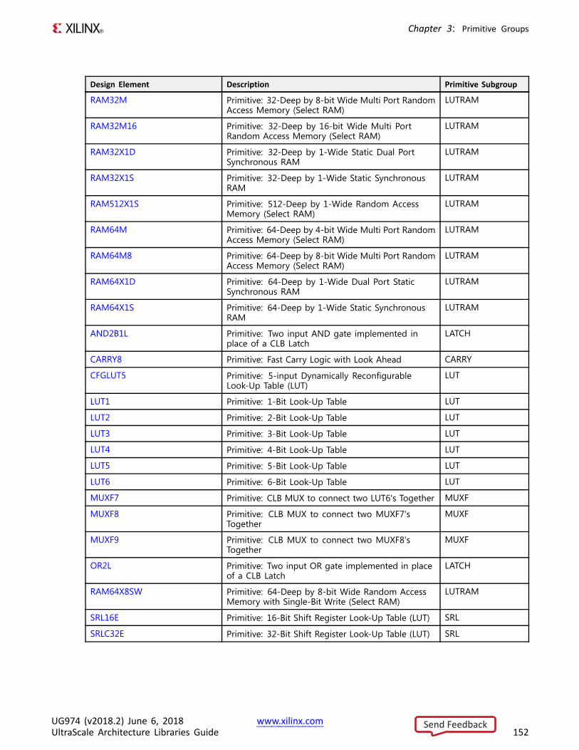
Chapter 3: Primitive Groups
Design Element Description Primitive Subgroup
RAM32M Primitive: 32-Deep by 8-bit Wide Multi Port RandomAccess Memory (Select RAM)
LUTRAM
RAM32M16 Primitive: 32-Deep by 16-bit Wide Multi PortRandom Access Memory (Select RAM)
LUTRAM
RAM32X1D Primitive: 32-Deep by 1-Wide Static Dual PortSynchronous RAM
LUTRAM
RAM32X1S Primitive: 32-Deep by 1-Wide Static SynchronousRAM
LUTRAM
RAM512X1S Primitive: 512-Deep by 1-Wide Random AccessMemory (Select RAM)
LUTRAM
RAM64M Primitive: 64-Deep by 4-bit Wide Multi Port RandomAccess Memory (Select RAM)
LUTRAM
RAM64M8 Primitive: 64-Deep by 8-bit Wide Multi Port RandomAccess Memory (Select RAM)
LUTRAM
RAM64X1D Primitive: 64-Deep by 1-Wide Dual Port StaticSynchronous RAM
LUTRAM
RAM64X1S Primitive: 64-Deep by 1-Wide Static SynchronousRAM
LUTRAM
AND2B1L Primitive: Two input AND gate implemented inplace of a CLB Latch
LATCH
CARRY8 Primitive: Fast Carry Logic with Look Ahead CARRY
CFGLUT5 Primitive: 5-input Dynamically ReconfigurableLook-Up Table (LUT)
LUT
LUT1 Primitive: 1-Bit Look-Up Table LUT
LUT2 Primitive: 2-Bit Look-Up Table LUT
LUT3 Primitive: 3-Bit Look-Up Table LUT
LUT4 Primitive: 4-Bit Look-Up Table LUT
LUT5 Primitive: 5-Bit Look-Up Table LUT
LUT6 Primitive: 6-Bit Look-Up Table LUT
MUXF7 Primitive: CLB MUX to connect two LUT6's Together MUXF
MUXF8 Primitive: CLB MUX to connect two MUXF7'sTogether
MUXF
MUXF9 Primitive: CLB MUX to connect two MUXF8'sTogether
MUXF
OR2L Primitive: Two input OR gate implemented in placeof a CLB Latch
LATCH
RAM64X8SW Primitive: 64-Deep by 8-bit Wide Random AccessMemory with Single-Bit Write (Select RAM)
LUTRAM
SRL16E Primitive: 16-Bit Shift Register Look-Up Table (LUT) SRL
SRLC32E Primitive: 32-Bit Shift Register Look-Up Table (LUT) SRL
UG974 (v2018.2) June 6, 2018 www.xilinx.comUltraScale Architecture Libraries Guide 152
Send Feedback
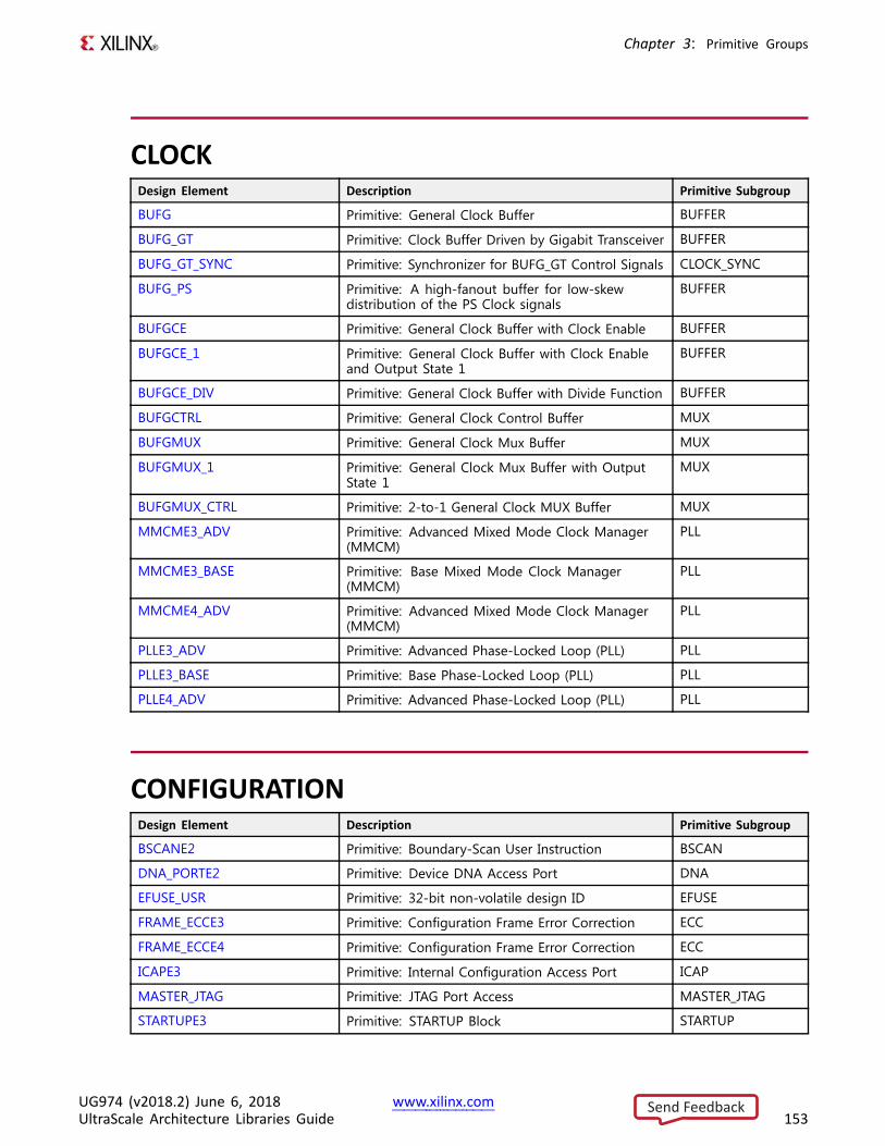
Chapter 3: Primitive Groups
CLOCKDesign Element Description Primitive Subgroup
BUFG Primitive: General Clock Buffer BUFFER
BUFG_GT Primitive: Clock Buffer Driven by Gigabit Transceiver BUFFER
BUFG_GT_SYNC Primitive: Synchronizer for BUFG_GT Control Signals CLOCK_SYNC
BUFG_PS Primitive: A high-fanout buffer for low-skewdistribution of the PS Clock signals
BUFFER
BUFGCE Primitive: General Clock Buffer with Clock Enable BUFFER
BUFGCE_1 Primitive: General Clock Buffer with Clock Enableand Output State 1
BUFFER
BUFGCE_DIV Primitive: General Clock Buffer with Divide Function BUFFER
BUFGCTRL Primitive: General Clock Control Buffer MUX
BUFGMUX Primitive: General Clock Mux Buffer MUX
BUFGMUX_1 Primitive: General Clock Mux Buffer with OutputState 1
MUX
BUFGMUX_CTRL Primitive: 2-to-1 General Clock MUX Buffer MUX
MMCME3_ADV Primitive: Advanced Mixed Mode Clock Manager(MMCM)
PLL
MMCME3_BASE Primitive: Base Mixed Mode Clock Manager(MMCM)
PLL
MMCME4_ADV Primitive: Advanced Mixed Mode Clock Manager(MMCM)
PLL
PLLE3_ADV Primitive: Advanced Phase-Locked Loop (PLL) PLL
PLLE3_BASE Primitive: Base Phase-Locked Loop (PLL) PLL
PLLE4_ADV Primitive: Advanced Phase-Locked Loop (PLL) PLL
CONFIGURATIONDesign Element Description Primitive Subgroup
BSCANE2 Primitive: Boundary-Scan User Instruction BSCAN
DNA_PORTE2 Primitive: Device DNA Access Port DNA
EFUSE_USR Primitive: 32-bit non-volatile design ID EFUSE
FRAME_ECCE3 Primitive: Configuration Frame Error Correction ECC
FRAME_ECCE4 Primitive: Configuration Frame Error Correction ECC
ICAPE3 Primitive: Internal Configuration Access Port ICAP
MASTER_JTAG Primitive: JTAG Port Access MASTER_JTAG
STARTUPE3 Primitive: STARTUP Block STARTUP
UG974 (v2018.2) June 6, 2018 www.xilinx.comUltraScale Architecture Libraries Guide 153
Send Feedback
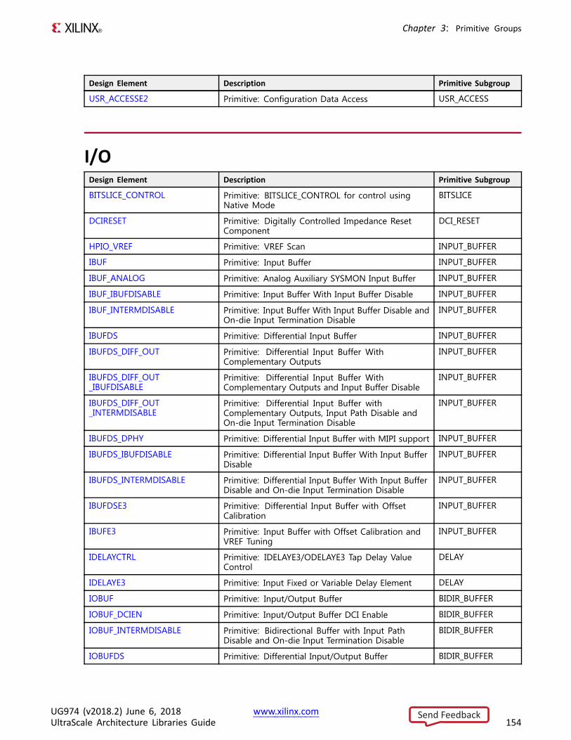
Chapter 3: Primitive Groups
Design Element Description Primitive Subgroup
USR_ACCESSE2 Primitive: Configuration Data Access USR_ACCESS
I/ODesign Element Description Primitive Subgroup
BITSLICE_CONTROL Primitive: BITSLICE_CONTROL for control usingNative Mode
BITSLICE
DCIRESET Primitive: Digitally Controlled Impedance ResetComponent
DCI_RESET
HPIO_VREF Primitive: VREF Scan INPUT_BUFFER
IBUF Primitive: Input Buffer INPUT_BUFFER
IBUF_ANALOG Primitive: Analog Auxiliary SYSMON Input Buffer INPUT_BUFFER
IBUF_IBUFDISABLE Primitive: Input Buffer With Input Buffer Disable INPUT_BUFFER
IBUF_INTERMDISABLE Primitive: Input Buffer With Input Buffer Disable andOn-die Input Termination Disable
INPUT_BUFFER
IBUFDS Primitive: Differential Input Buffer INPUT_BUFFER
IBUFDS_DIFF_OUT Primitive: Differential Input Buffer WithComplementary Outputs
INPUT_BUFFER
IBUFDS_DIFF_OUT_IBUFDISABLE
Primitive: Differential Input Buffer WithComplementary Outputs and Input Buffer Disable
INPUT_BUFFER
IBUFDS_DIFF_OUT_INTERMDISABLE
Primitive: Differential Input Buffer withComplementary Outputs, Input Path Disable andOn-die Input Termination Disable
INPUT_BUFFER
IBUFDS_DPHY Primitive: Differential Input Buffer with MIPI support INPUT_BUFFER
IBUFDS_IBUFDISABLE Primitive: Differential Input Buffer With Input BufferDisable
INPUT_BUFFER
IBUFDS_INTERMDISABLE Primitive: Differential Input Buffer With Input BufferDisable and On-die Input Termination Disable
INPUT_BUFFER
IBUFDSE3 Primitive: Differential Input Buffer with OffsetCalibration
INPUT_BUFFER
IBUFE3 Primitive: Input Buffer with Offset Calibration andVREF Tuning
INPUT_BUFFER
IDELAYCTRL Primitive: IDELAYE3/ODELAYE3 Tap Delay ValueControl
DELAY
IDELAYE3 Primitive: Input Fixed or Variable Delay Element DELAY
IOBUF Primitive: Input/Output Buffer BIDIR_BUFFER
IOBUF_DCIEN Primitive: Input/Output Buffer DCI Enable BIDIR_BUFFER
IOBUF_INTERMDISABLE Primitive: Bidirectional Buffer with Input PathDisable and On-die Input Termination Disable
BIDIR_BUFFER
IOBUFDS Primitive: Differential Input/Output Buffer BIDIR_BUFFER
UG974 (v2018.2) June 6, 2018 www.xilinx.comUltraScale Architecture Libraries Guide 154
Send Feedback
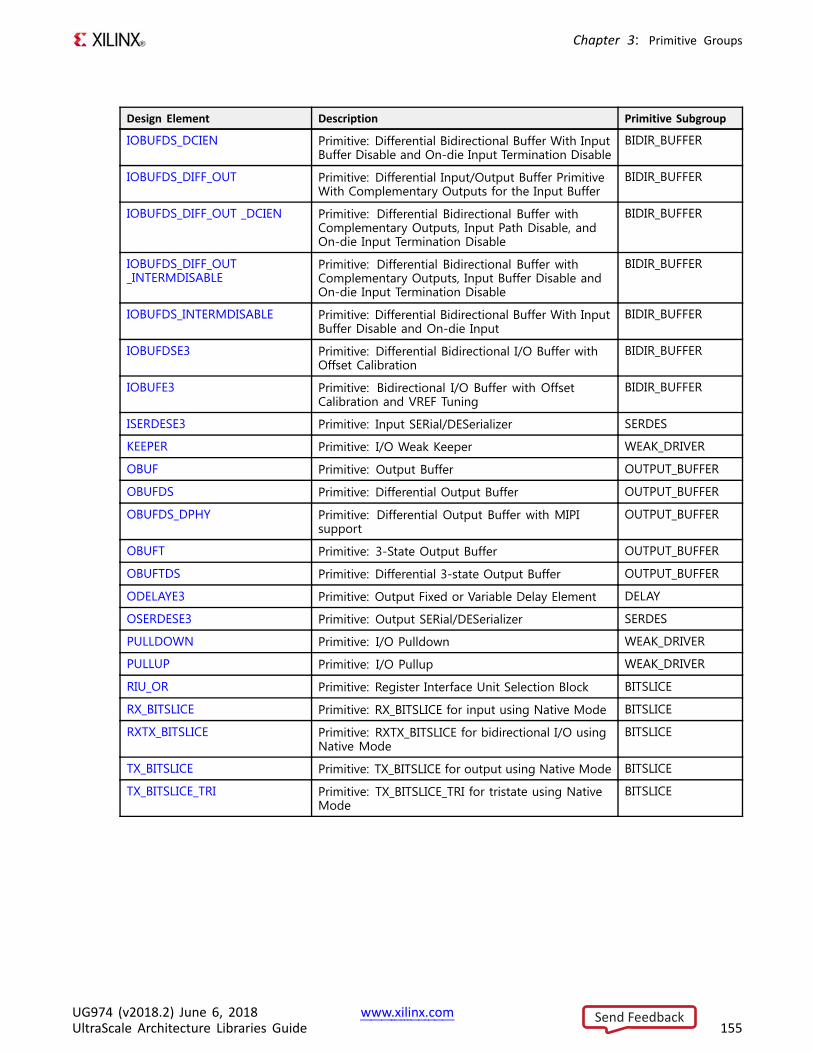
Chapter 3: Primitive Groups
Design Element Description Primitive Subgroup
IOBUFDS_DCIEN Primitive: Differential Bidirectional Buffer With InputBuffer Disable and On-die Input Termination Disable
BIDIR_BUFFER
IOBUFDS_DIFF_OUT Primitive: Differential Input/Output Buffer PrimitiveWith Complementary Outputs for the Input Buffer
BIDIR_BUFFER
IOBUFDS_DIFF_OUT _DCIEN Primitive: Differential Bidirectional Buffer withComplementary Outputs, Input Path Disable, andOn-die Input Termination Disable
BIDIR_BUFFER
IOBUFDS_DIFF_OUT_INTERMDISABLE
Primitive: Differential Bidirectional Buffer withComplementary Outputs, Input Buffer Disable andOn-die Input Termination Disable
BIDIR_BUFFER
IOBUFDS_INTERMDISABLE Primitive: Differential Bidirectional Buffer With InputBuffer Disable and On-die Input
BIDIR_BUFFER
IOBUFDSE3 Primitive: Differential Bidirectional I/O Buffer withOffset Calibration
BIDIR_BUFFER
IOBUFE3 Primitive: Bidirectional I/O Buffer with OffsetCalibration and VREF Tuning
BIDIR_BUFFER
ISERDESE3 Primitive: Input SERial/DESerializer SERDES
KEEPER Primitive: I/O Weak Keeper WEAK_DRIVER
OBUF Primitive: Output Buffer OUTPUT_BUFFER
OBUFDS Primitive: Differential Output Buffer OUTPUT_BUFFER
OBUFDS_DPHY Primitive: Differential Output Buffer with MIPIsupport
OUTPUT_BUFFER
OBUFT Primitive: 3-State Output Buffer OUTPUT_BUFFER
OBUFTDS Primitive: Differential 3-state Output Buffer OUTPUT_BUFFER
ODELAYE3 Primitive: Output Fixed or Variable Delay Element DELAY
OSERDESE3 Primitive: Output SERial/DESerializer SERDES
PULLDOWN Primitive: I/O Pulldown WEAK_DRIVER
PULLUP Primitive: I/O Pullup WEAK_DRIVER
RIU_OR Primitive: Register Interface Unit Selection Block BITSLICE
RX_BITSLICE Primitive: RX_BITSLICE for input using Native Mode BITSLICE
RXTX_BITSLICE Primitive: RXTX_BITSLICE for bidirectional I/O usingNative Mode
BITSLICE
TX_BITSLICE Primitive: TX_BITSLICE for output using Native Mode BITSLICE
TX_BITSLICE_TRI Primitive: TX_BITSLICE_TRI for tristate using NativeMode
BITSLICE
UG974 (v2018.2) June 6, 2018 www.xilinx.comUltraScale Architecture Libraries Guide 155
Send Feedback
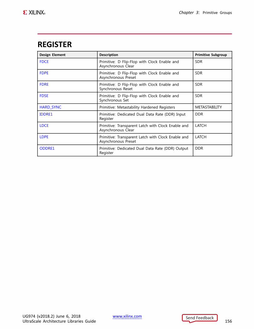
Chapter 3: Primitive Groups
REGISTERDesign Element Description Primitive Subgroup
FDCE Primitive: D Flip-Flop with Clock Enable andAsynchronous Clear
SDR
FDPE Primitive: D Flip-Flop with Clock Enable andAsynchronous Preset
SDR
FDRE Primitive: D Flip-Flop with Clock Enable andSynchronous Reset
SDR
FDSE Primitive: D Flip-Flop with Clock Enable andSynchronous Set
SDR
HARD_SYNC Primitive: Metastability Hardened Registers METASTABILITY
IDDRE1 Primitive: Dedicated Dual Data Rate (DDR) InputRegister
DDR
LDCE Primitive: Transparent Latch with Clock Enable andAsynchronous Clear
LATCH
LDPE Primitive: Transparent Latch with Clock Enable andAsynchronous Preset
LATCH
ODDRE1 Primitive: Dedicated Dual Data Rate (DDR) OutputRegister
DDR
UG974 (v2018.2) June 6, 2018 www.xilinx.comUltraScale Architecture Libraries Guide 156
Send Feedback
Chapter 4
Design Elements
About Design ElementsThis section describes the design elements that can be used with UltraScale™ architecture-baseddevices. The design elements are organized alphabetically.
The following information is provided for each design element, where applicable:
• Name of element
• Brief description
• Schematic symbol (if any)
• Logic table (if any)
• Port descriptions
• Design Entry Method
• Available attributes (if any)
• Example instantiation templates
• For more information
Instantiation TemplatesInstantiation templates for library elements are also available in Vivado, as well as in adownloadable ZIP file. Because PDF includes headers and footers if you copy text that spanspages, you should copy templates from Vivado or the downloaded ZIP file whenever possible.
Instantiation templates can be found on the Web in the Instantiation Templates for UltraScaleDevices file.
UG974 (v2018.2) June 6, 2018 www.xilinx.comUltraScale Architecture Libraries Guide 157
Send Feedback
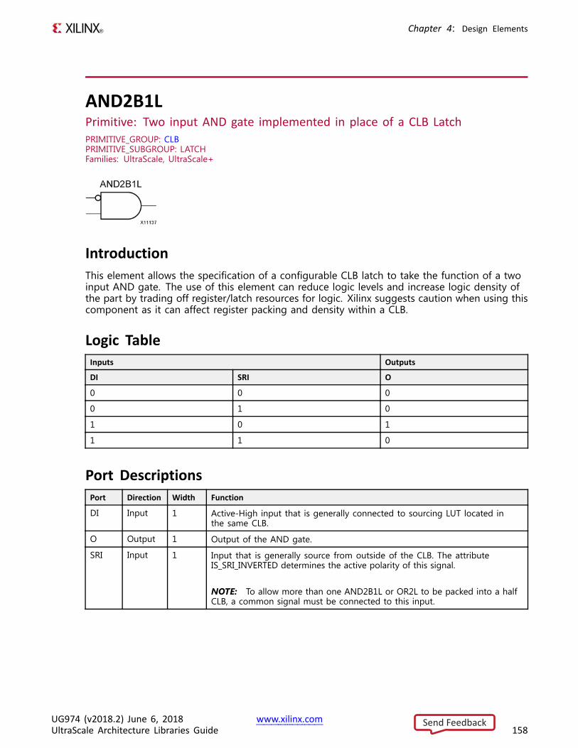
Chapter 4: Design Elements
AND2B1LPrimitive: Two input AND gate implemented in place of a CLB LatchPRIMITIVE_GROUP: CLBPRIMITIVE_SUBGROUP: LATCHFamilies: UltraScale, UltraScale+
IntroductionThis element allows the specification of a configurable CLB latch to take the function of a twoinput AND gate. The use of this element can reduce logic levels and increase logic density ofthe part by trading off register/latch resources for logic. Xilinx suggests caution when using thiscomponent as it can affect register packing and density within a CLB.
Logic TableInputs Outputs
DI SRI O
0 0 0
0 1 0
1 0 1
1 1 0
Port DescriptionsPort Direction Width Function
DI Input 1 Active-High input that is generally connected to sourcing LUT located inthe same CLB.
O Output 1 Output of the AND gate.
SRI Input 1 Input that is generally source from outside of the CLB. The attributeIS_SRI_INVERTED determines the active polarity of this signal.
NOTE: To allow more than one AND2B1L or OR2L to be packed into a halfCLB, a common signal must be connected to this input.
UG974 (v2018.2) June 6, 2018 www.xilinx.comUltraScale Architecture Libraries Guide 158
Send Feedback
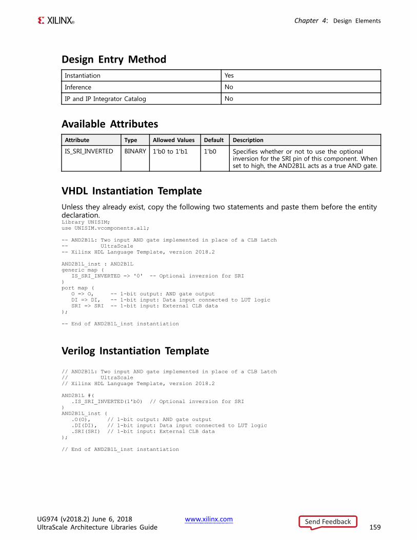
Chapter 4: Design Elements
Design Entry MethodInstantiation Yes
Inference No
IP and IP Integrator Catalog No
Available AttributesAttribute Type Allowed Values Default Description
IS_SRI_INVERTED BINARY 1'b0 to 1'b1 1'b0 Specifies whether or not to use the optionalinversion for the SRI pin of this component. Whenset to high, the AND2B1L acts as a true AND gate.
VHDL Instantiation TemplateUnless they already exist, copy the following two statements and paste them before the entitydeclaration.Library UNISIM;use UNISIM.vcomponents.all;
-- AND2B1L: Two input AND gate implemented in place of a CLB Latch-- UltraScale-- Xilinx HDL Language Template, version 2018.2
AND2B1L_inst : AND2B1Lgeneric map (
IS_SRI_INVERTED => '0' -- Optional inversion for SRI)port map (
O => O, -- 1-bit output: AND gate outputDI => DI, -- 1-bit input: Data input connected to LUT logicSRI => SRI -- 1-bit input: External CLB data
);
-- End of AND2B1L_inst instantiation
Verilog Instantiation Template
// AND2B1L: Two input AND gate implemented in place of a CLB Latch// UltraScale// Xilinx HDL Language Template, version 2018.2
AND2B1L #(.IS_SRI_INVERTED(1'b0) // Optional inversion for SRI
)AND2B1L_inst (
.O(O), // 1-bit output: AND gate output
.DI(DI), // 1-bit input: Data input connected to LUT logic
.SRI(SRI) // 1-bit input: External CLB data);
// End of AND2B1L_inst instantiation
UG974 (v2018.2) June 6, 2018 www.xilinx.comUltraScale Architecture Libraries Guide 159
Send Feedback

Chapter 4: Design Elements
For More Information• See the UltraScale Architecture Configurable Logic Block User Guide (UG574).
• See the UltraScale Programmable Devices Documentation.
UG974 (v2018.2) June 6, 2018 www.xilinx.comUltraScale Architecture Libraries Guide 160
Send Feedback
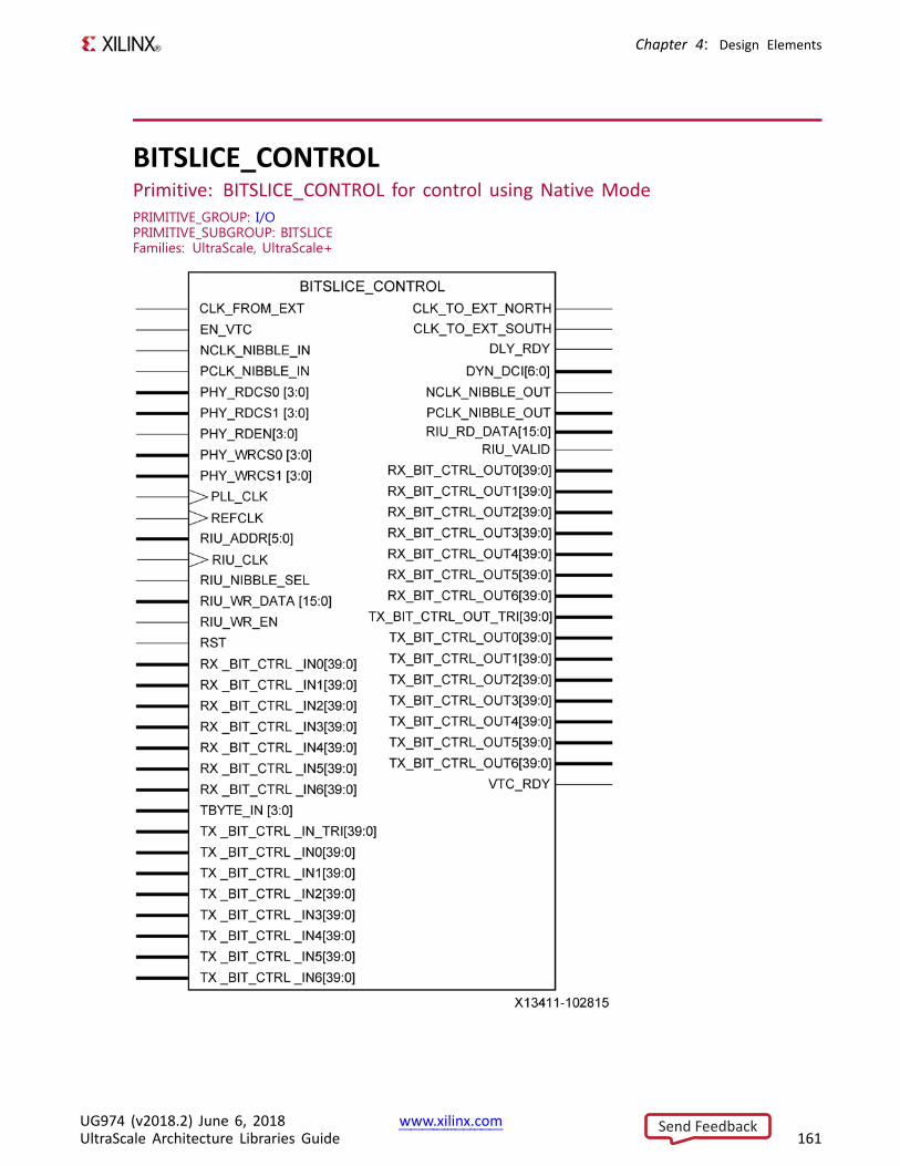
Chapter 4: Design Elements
BITSLICE_CONTROLPrimitive: BITSLICE_CONTROL for control using Native ModePRIMITIVE_GROUP: I/OPRIMITIVE_SUBGROUP: BITSLICEFamilies: UltraScale, UltraScale+
UG974 (v2018.2) June 6, 2018 www.xilinx.comUltraScale Architecture Libraries Guide 161
Send Feedback
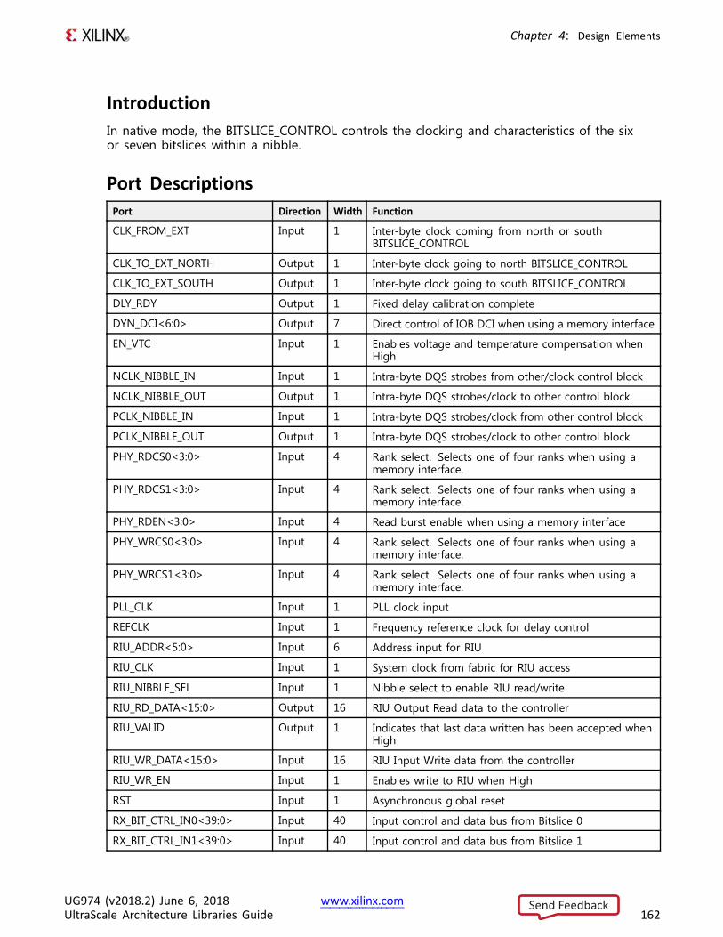
Chapter 4: Design Elements
IntroductionIn native mode, the BITSLICE_CONTROL controls the clocking and characteristics of the sixor seven bitslices within a nibble.
Port DescriptionsPort Direction Width Function
CLK_FROM_EXT Input 1 Inter-byte clock coming from north or southBITSLICE_CONTROL
CLK_TO_EXT_NORTH Output 1 Inter-byte clock going to north BITSLICE_CONTROL
CLK_TO_EXT_SOUTH Output 1 Inter-byte clock going to south BITSLICE_CONTROL
DLY_RDY Output 1 Fixed delay calibration complete
DYN_DCI<6:0> Output 7 Direct control of IOB DCI when using a memory interface
EN_VTC Input 1 Enables voltage and temperature compensation whenHigh
NCLK_NIBBLE_IN Input 1 Intra-byte DQS strobes from other/clock control block
NCLK_NIBBLE_OUT Output 1 Intra-byte DQS strobes/clock to other control block
PCLK_NIBBLE_IN Input 1 Intra-byte DQS strobes/clock from other control block
PCLK_NIBBLE_OUT Output 1 Intra-byte DQS strobes/clock to other control block
PHY_RDCS0<3:0> Input 4 Rank select. Selects one of four ranks when using amemory interface.
PHY_RDCS1<3:0> Input 4 Rank select. Selects one of four ranks when using amemory interface.
PHY_RDEN<3:0> Input 4 Read burst enable when using a memory interface
PHY_WRCS0<3:0> Input 4 Rank select. Selects one of four ranks when using amemory interface.
PHY_WRCS1<3:0> Input 4 Rank select. Selects one of four ranks when using amemory interface.
PLL_CLK Input 1 PLL clock input
REFCLK Input 1 Frequency reference clock for delay control
RIU_ADDR<5:0> Input 6 Address input for RIU
RIU_CLK Input 1 System clock from fabric for RIU access
RIU_NIBBLE_SEL Input 1 Nibble select to enable RIU read/write
RIU_RD_DATA<15:0> Output 16 RIU Output Read data to the controller
RIU_VALID Output 1 Indicates that last data written has been accepted whenHigh
RIU_WR_DATA<15:0> Input 16 RIU Input Write data from the controller
RIU_WR_EN Input 1 Enables write to RIU when High
RST Input 1 Asynchronous global reset
RX_BIT_CTRL_IN0<39:0> Input 40 Input control and data bus from Bitslice 0
RX_BIT_CTRL_IN1<39:0> Input 40 Input control and data bus from Bitslice 1
UG974 (v2018.2) June 6, 2018 www.xilinx.comUltraScale Architecture Libraries Guide 162
Send Feedback
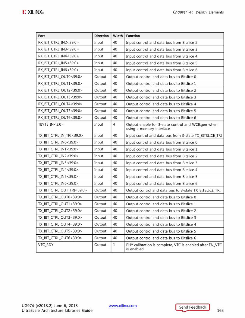
Chapter 4: Design Elements
Port Direction Width Function
RX_BIT_CTRL_IN2<39:0> Input 40 Input control and data bus from Bitslice 2
RX_BIT_CTRL_IN3<39:0> Input 40 Input control and data bus from Bitslice 3
RX_BIT_CTRL_IN4<39:0> Input 40 Input control and data bus from Bitslice 4
RX_BIT_CTRL_IN5<39:0> Input 40 Input control and data bus from Bitslice 5
RX_BIT_CTRL_IN6<39:0> Input 40 Input control and data bus from Bitslice 6
RX_BIT_CTRL_OUT0<39:0> Output 40 Output control and data bus to Bitslice 0
RX_BIT_CTRL_OUT1<39:0> Output 40 Output control and data bus to Bitslice 1
RX_BIT_CTRL_OUT2<39:0> Output 40 Output control and data bus to Bitslice 2
RX_BIT_CTRL_OUT3<39:0> Output 40 Output control and data bus to Bitslice 3
RX_BIT_CTRL_OUT4<39:0> Output 40 Output control and data bus to Bitslice 4
RX_BIT_CTRL_OUT5<39:0> Output 40 Output control and data bus to Bitslice 5
RX_BIT_CTRL_OUT6<39:0> Output 40 Output control and data bus to Bitslice 6
TBYTE_IN<3:0> Input 4 Output enable for 3-state control and WClkgen whenusing a memory interface
TX_BIT_CTRL_IN_TRI<39:0> Input 40 Input control and data bus from 3-state TX_BITSLICE_TRI
TX_BIT_CTRL_IN0<39:0> Input 40 Input control and data bus from Bitslice 0
TX_BIT_CTRL_IN1<39:0> Input 40 Input control and data bus from Bitslice 1
TX_BIT_CTRL_IN2<39:0> Input 40 Input control and data bus from Bitslice 2
TX_BIT_CTRL_IN3<39:0> Input 40 Input control and data bus from Bitslice 3
TX_BIT_CTRL_IN4<39:0> Input 40 Input control and data bus from Bitslice 4
TX_BIT_CTRL_IN5<39:0> Input 40 Input control and data bus from Bitslice 5
TX_BIT_CTRL_IN6<39:0> Input 40 Input control and data bus from Bitslice 6
TX_BIT_CTRL_OUT_TRI<39:0> Output 40 Output control and data bus to 3-state TX_BITSLICE_TRI
TX_BIT_CTRL_OUT0<39:0> Output 40 Output control and data bus to Bitslice 0
TX_BIT_CTRL_OUT1<39:0> Output 40 Output control and data bus to Bitslice 1
TX_BIT_CTRL_OUT2<39:0> Output 40 Output control and data bus to Bitslice 2
TX_BIT_CTRL_OUT3<39:0> Output 40 Output control and data bus to Bitslice 3
TX_BIT_CTRL_OUT4<39:0> Output 40 Output control and data bus to Bitslice 4
TX_BIT_CTRL_OUT5<39:0> Output 40 Output control and data bus to Bitslice 5
TX_BIT_CTRL_OUT6<39:0> Output 40 Output control and data bus to Bitslice 6
VTC_RDY Output 1 PHY calibration is complete, VTC is enabled after EN_VTCis enabled
UG974 (v2018.2) June 6, 2018 www.xilinx.comUltraScale Architecture Libraries Guide 163
Send Feedback
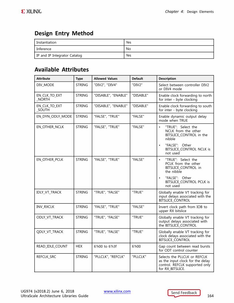
Chapter 4: Design Elements
Design Entry MethodInstantiation Yes
Inference No
IP and IP Integrator Catalog Yes
Available AttributesAttribute Type Allowed Values Default Description
DIV_MODE STRING "DIV2", "DIV4" "DIV2" Select between controller DIV2or DIV4 mode
EN_CLK_TO_EXT_NORTH
STRING "DISABLE", "ENABLE" "DISABLE" Enable clock forwarding to northfor inter - byte clocking
EN_CLK_TO_EXT_SOUTH
STRING "DISABLE", "ENABLE" "DISABLE" Enable clock forwarding to southfor inter - byte clocking
EN_DYN_ODLY_MODE STRING "FALSE", "TRUE" "FALSE" Enable dynamic output delaymode when TRUE
EN_OTHER_NCLK STRING "FALSE", "TRUE" "FALSE" • "TRUE": Select theNCLK from the otherBITSLICE_CONTROL in thenibble
• "FALSE": OtherBITSLICE_CONTROL NCLK isnot used
EN_OTHER_PCLK STRING "FALSE", "TRUE" "FALSE" • "TRUE": Select thePCLK from the otherBITSLICE_CONTROL inthe nibble
• "FALSE": OtherBITSLICE_CONTROL PCLK isnot used
IDLY_VT_TRACK STRING "TRUE", "FALSE" "TRUE" Globally enable VT tracking forinput delays associated with theBITSLICE_CONTROL
INV_RXCLK STRING "FALSE", "TRUE" "FALSE" Invert clock path from IOB toupper RX bitslice
ODLY_VT_TRACK STRING "TRUE", "FALSE" "TRUE" Globally enable VT tracking foroutput delays associated withthe BITSLICE_CONTROL
QDLY_VT_TRACK STRING "TRUE", "FALSE" "TRUE" Globally enable VT tracking forclock delays associated with theBITSLICE_CONTROL
READ_IDLE_COUNT HEX 6'h00 to 6'h3f 6'h00 Gap count between read burstsfor ODT control counter
REFCLK_SRC STRING "PLLCLK", "REFCLK" "PLLCLK" Selects the PLLCLK or REFCLKas the input clock for the delaycontrol. REFCLK supported onlyfor RX_BITSLICE.
UG974 (v2018.2) June 6, 2018 www.xilinx.comUltraScale Architecture Libraries Guide 164
Send Feedback
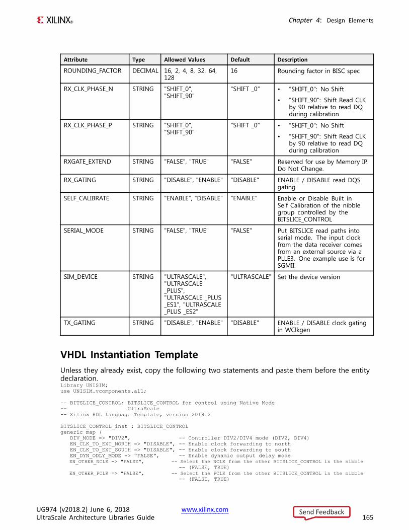
Chapter 4: Design Elements
Attribute Type Allowed Values Default Description
ROUNDING_FACTOR DECIMAL 16, 2, 4, 8, 32, 64,128
16 Rounding factor in BISC spec
RX_CLK_PHASE_N STRING "SHIFT_0","SHIFT_90"
"SHIFT _0" • "SHIFT_0": No Shift
• "SHIFT_90": Shift Read CLKby 90 relative to read DQduring calibration
RX_CLK_PHASE_P STRING "SHIFT_0","SHIFT_90"
"SHIFT _0" • "SHIFT_0": No Shift
• "SHIFT_90": Shift Read CLKby 90 relative to read DQduring calibration
RXGATE_EXTEND STRING "FALSE", "TRUE" "FALSE" Reserved for use by Memory IP.Do Not Change.
RX_GATING STRING "DISABLE", "ENABLE" "DISABLE" ENABLE / DISABLE read DQSgating
SELF_CALIBRATE STRING "ENABLE", "DISABLE" "ENABLE" Enable or Disable Built inSelf Calibration of the nibblegroup controlled by theBITSLICE_CONTROL
SERIAL_MODE STRING "FALSE", "TRUE" "FALSE" Put BITSLICE read paths intoserial mode. The input clockfrom the data receiver comesfrom an external source via aPLLE3. One example use is forSGMII.
SIM_DEVICE STRING "ULTRASCALE","ULTRASCALE_PLUS","ULTRASCALE _PLUS_ES1", "ULTRASCALE_PLUS _ES2"
"ULTRASCALE" Set the device version
TX_GATING STRING "DISABLE", "ENABLE" "DISABLE" ENABLE / DISABLE clock gatingin WClkgen
VHDL Instantiation TemplateUnless they already exist, copy the following two statements and paste them before the entitydeclaration.Library UNISIM;use UNISIM.vcomponents.all;
-- BITSLICE_CONTROL: BITSLICE_CONTROL for control using Native Mode-- UltraScale-- Xilinx HDL Language Template, version 2018.2
BITSLICE_CONTROL_inst : BITSLICE_CONTROLgeneric map (
DIV_MODE => "DIV2", -- Controller DIV2/DIV4 mode (DIV2, DIV4)EN_CLK_TO_EXT_NORTH => "DISABLE", -- Enable clock forwarding to northEN_CLK_TO_EXT_SOUTH => "DISABLE", -- Enable clock forwarding to southEN_DYN_ODLY_MODE => "FALSE", -- Enable dynamic output delay modeEN_OTHER_NCLK => "FALSE", -- Select the NCLK from the other BITSLICE_CONTROL in the nibble
-- (FALSE, TRUE)EN_OTHER_PCLK => "FALSE", -- Select the PCLK from the other BITSLICE_CONTROL in the nibble
-- (FALSE, TRUE)
UG974 (v2018.2) June 6, 2018 www.xilinx.comUltraScale Architecture Libraries Guide 165
Send Feedback
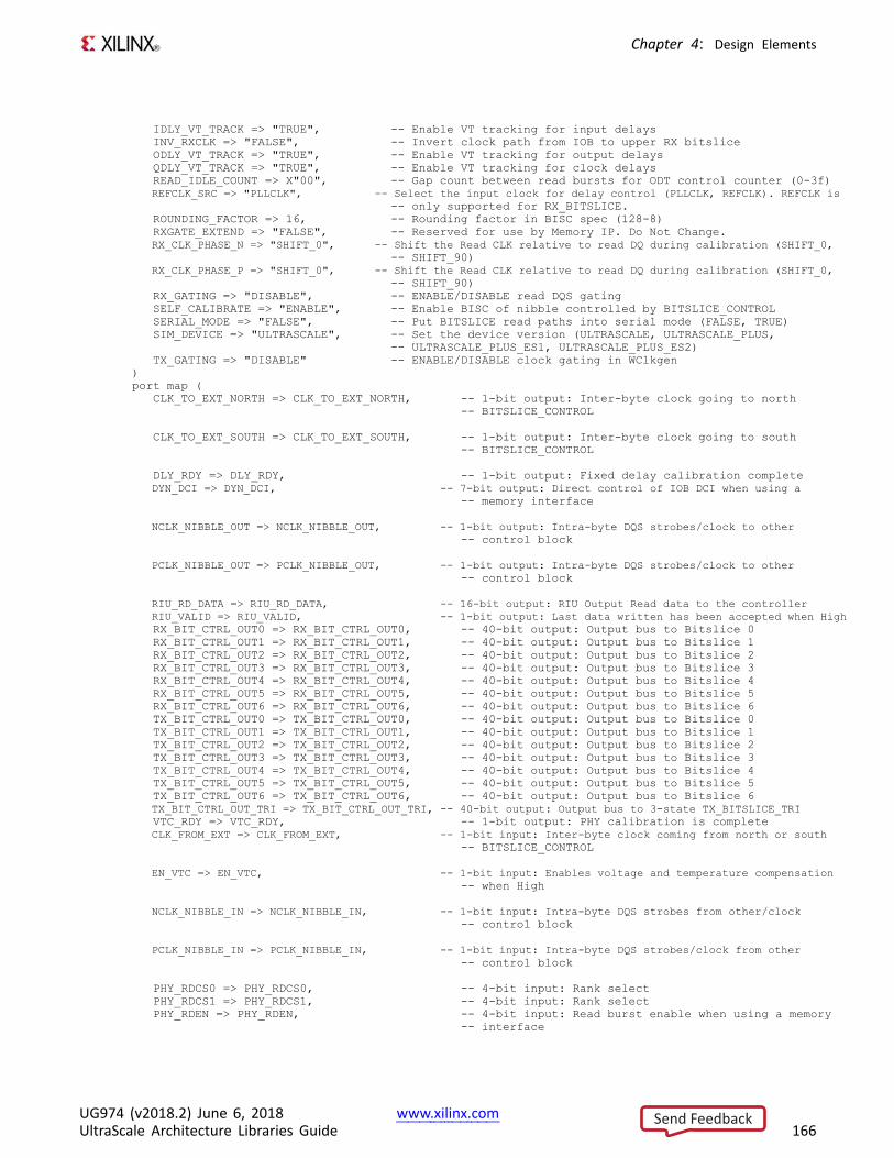
Chapter 4: Design Elements
IDLY_VT_TRACK => "TRUE", -- Enable VT tracking for input delaysINV_RXCLK => "FALSE", -- Invert clock path from IOB to upper RX bitsliceODLY_VT_TRACK => "TRUE", -- Enable VT tracking for output delaysQDLY_VT_TRACK => "TRUE", -- Enable VT tracking for clock delaysREAD_IDLE_COUNT => X"00", -- Gap count between read bursts for ODT control counter (0-3f)REFCLK_SRC => "PLLCLK", -- Select the input clock for delay control (PLLCLK, REFCLK). REFCLK is
-- only supported for RX_BITSLICE.ROUNDING_FACTOR => 16, -- Rounding factor in BISC spec (128-8)RXGATE_EXTEND => "FALSE", -- Reserved for use by Memory IP. Do Not Change.RX_CLK_PHASE_N => "SHIFT_0", -- Shift the Read CLK relative to read DQ during calibration (SHIFT_0,
-- SHIFT_90)RX_CLK_PHASE_P => "SHIFT_0", -- Shift the Read CLK relative to read DQ during calibration (SHIFT_0,
-- SHIFT_90)RX_GATING => "DISABLE", -- ENABLE/DISABLE read DQS gatingSELF_CALIBRATE => "ENABLE", -- Enable BISC of nibble controlled by BITSLICE_CONTROLSERIAL_MODE => "FALSE", -- Put BITSLICE read paths into serial mode (FALSE, TRUE)SIM_DEVICE => "ULTRASCALE", -- Set the device version (ULTRASCALE, ULTRASCALE_PLUS,
-- ULTRASCALE_PLUS_ES1, ULTRASCALE_PLUS_ES2)TX_GATING => "DISABLE" -- ENABLE/DISABLE clock gating in WClkgen
)port map (
CLK_TO_EXT_NORTH => CLK_TO_EXT_NORTH, -- 1-bit output: Inter-byte clock going to north-- BITSLICE_CONTROL
CLK_TO_EXT_SOUTH => CLK_TO_EXT_SOUTH, -- 1-bit output: Inter-byte clock going to south-- BITSLICE_CONTROL
DLY_RDY => DLY_RDY, -- 1-bit output: Fixed delay calibration completeDYN_DCI => DYN_DCI, -- 7-bit output: Direct control of IOB DCI when using a
-- memory interface
NCLK_NIBBLE_OUT => NCLK_NIBBLE_OUT, -- 1-bit output: Intra-byte DQS strobes/clock to other-- control block
PCLK_NIBBLE_OUT => PCLK_NIBBLE_OUT, -- 1-bit output: Intra-byte DQS strobes/clock to other-- control block
RIU_RD_DATA => RIU_RD_DATA, -- 16-bit output: RIU Output Read data to the controllerRIU_VALID => RIU_VALID, -- 1-bit output: Last data written has been accepted when HighRX_BIT_CTRL_OUT0 => RX_BIT_CTRL_OUT0, -- 40-bit output: Output bus to Bitslice 0RX_BIT_CTRL_OUT1 => RX_BIT_CTRL_OUT1, -- 40-bit output: Output bus to Bitslice 1RX_BIT_CTRL_OUT2 => RX_BIT_CTRL_OUT2, -- 40-bit output: Output bus to Bitslice 2RX_BIT_CTRL_OUT3 => RX_BIT_CTRL_OUT3, -- 40-bit output: Output bus to Bitslice 3RX_BIT_CTRL_OUT4 => RX_BIT_CTRL_OUT4, -- 40-bit output: Output bus to Bitslice 4RX_BIT_CTRL_OUT5 => RX_BIT_CTRL_OUT5, -- 40-bit output: Output bus to Bitslice 5RX_BIT_CTRL_OUT6 => RX_BIT_CTRL_OUT6, -- 40-bit output: Output bus to Bitslice 6TX_BIT_CTRL_OUT0 => TX_BIT_CTRL_OUT0, -- 40-bit output: Output bus to Bitslice 0TX_BIT_CTRL_OUT1 => TX_BIT_CTRL_OUT1, -- 40-bit output: Output bus to Bitslice 1TX_BIT_CTRL_OUT2 => TX_BIT_CTRL_OUT2, -- 40-bit output: Output bus to Bitslice 2TX_BIT_CTRL_OUT3 => TX_BIT_CTRL_OUT3, -- 40-bit output: Output bus to Bitslice 3TX_BIT_CTRL_OUT4 => TX_BIT_CTRL_OUT4, -- 40-bit output: Output bus to Bitslice 4TX_BIT_CTRL_OUT5 => TX_BIT_CTRL_OUT5, -- 40-bit output: Output bus to Bitslice 5TX_BIT_CTRL_OUT6 => TX_BIT_CTRL_OUT6, -- 40-bit output: Output bus to Bitslice 6TX_BIT_CTRL_OUT_TRI => TX_BIT_CTRL_OUT_TRI, -- 40-bit output: Output bus to 3-state TX_BITSLICE_TRIVTC_RDY => VTC_RDY, -- 1-bit output: PHY calibration is completeCLK_FROM_EXT => CLK_FROM_EXT, -- 1-bit input: Inter-byte clock coming from north or south
-- BITSLICE_CONTROL
EN_VTC => EN_VTC, -- 1-bit input: Enables voltage and temperature compensation-- when High
NCLK_NIBBLE_IN => NCLK_NIBBLE_IN, -- 1-bit input: Intra-byte DQS strobes from other/clock-- control block
PCLK_NIBBLE_IN => PCLK_NIBBLE_IN, -- 1-bit input: Intra-byte DQS strobes/clock from other-- control block
PHY_RDCS0 => PHY_RDCS0, -- 4-bit input: Rank selectPHY_RDCS1 => PHY_RDCS1, -- 4-bit input: Rank selectPHY_RDEN => PHY_RDEN, -- 4-bit input: Read burst enable when using a memory
-- interface
UG974 (v2018.2) June 6, 2018 www.xilinx.comUltraScale Architecture Libraries Guide 166
Send Feedback
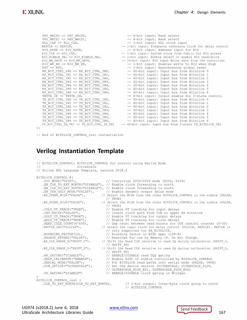
Chapter 4: Design Elements
PHY_WRCS0 => PHY_WRCS0, -- 4-bit input: Rank selectPHY_WRCS1 => PHY_WRCS1, -- 4-bit input: Rank selectPLL_CLK => PLL_CLK, -- 1-bit input: PLL clock inputREFCLK => REFCLK, -- 1-bit input: Frequency reference clock for delay controlRIU_ADDR => RIU_ADDR, -- 6-bit input: Address input for RIURIU_CLK => RIU_CLK, -- 1-bit input: System clock from fabric for RIU accessRIU_NIBBLE_SEL => RIU_NIBBLE_SEL, -- 1-bit input: Nibble select to enable RIU read/writeRIU_WR_DATA => RIU_WR_DATA, -- 16-bit input: RIU Input Write data from the controllerRIU_WR_EN => RIU_WR_EN, -- 1-bit input: Enables write to RIU when HighRST => RST, -- 1-bit input: Asynchronous global resetRX_BIT_CTRL_IN0 => RX_BIT_CTRL_IN0, -- 40-bit input: Input bus from Bitslice 0RX_BIT_CTRL_IN1 => RX_BIT_CTRL_IN1, -- 40-bit input: Input bus from Bitslice 1RX_BIT_CTRL_IN2 => RX_BIT_CTRL_IN2, -- 40-bit input: Input bus from Bitslice 2RX_BIT_CTRL_IN3 => RX_BIT_CTRL_IN3, -- 40-bit input: Input bus from Bitslice 3RX_BIT_CTRL_IN4 => RX_BIT_CTRL_IN4, -- 40-bit input: Input bus from Bitslice 4RX_BIT_CTRL_IN5 => RX_BIT_CTRL_IN5, -- 40-bit input: Input bus from Bitslice 5RX_BIT_CTRL_IN6 => RX_BIT_CTRL_IN6, -- 40-bit input: Input bus from Bitslice 6TBYTE_IN => TBYTE_IN, -- 4-bit input: Output enable for 3-state controlTX_BIT_CTRL_IN0 => TX_BIT_CTRL_IN0, -- 40-bit input: Input bus from Bitslice 0TX_BIT_CTRL_IN1 => TX_BIT_CTRL_IN1, -- 40-bit input: Input bus from Bitslice 1TX_BIT_CTRL_IN2 => TX_BIT_CTRL_IN2, -- 40-bit input: Input bus from Bitslice 2TX_BIT_CTRL_IN3 => TX_BIT_CTRL_IN3, -- 40-bit input: Input bus from Bitslice 3TX_BIT_CTRL_IN4 => TX_BIT_CTRL_IN4, -- 40-bit input: Input bus from Bitslice 4TX_BIT_CTRL_IN5 => TX_BIT_CTRL_IN5, -- 40-bit input: Input bus from Bitslice 5TX_BIT_CTRL_IN6 => TX_BIT_CTRL_IN6, -- 40-bit input: Input bus from Bitslice 6TX_BIT_CTRL_IN_TRI => TX_BIT_CTRL_IN_TRI -- 40-bit input: Input bus from 3-state TX_BITSLICE_TRI
);
-- End of BITSLICE_CONTROL_inst instantiation
Verilog Instantiation Template
// BITSLICE_CONTROL: BITSLICE_CONTROL for control using Native Mode// UltraScale// Xilinx HDL Language Template, version 2018.2
BITSLICE_CONTROL #(.DIV_MODE("DIV2"), // Controller DIV2/DIV4 mode (DIV2, DIV4).EN_CLK_TO_EXT_NORTH("DISABLE"), // Enable clock forwarding to north.EN_CLK_TO_EXT_SOUTH("DISABLE"), // Enable clock forwarding to south.EN_DYN_ODLY_MODE("FALSE"), // Enable dynamic output delay mode.EN_OTHER_NCLK("FALSE"), // Select the NCLK from the other BITSLICE_CONTROL in the nibble (FALSE,
// TRUE).EN_OTHER_PCLK("FALSE"), // Select the PCLK from the other BITSLICE_CONTROL in the nibble (FALSE,
// TRUE).IDLY_VT_TRACK("TRUE"), // Enable VT tracking for input delays.INV_RXCLK("FALSE"), // Invert clock path from IOB to upper RX bitslice.ODLY_VT_TRACK("TRUE"), // Enable VT tracking for output delays.QDLY_VT_TRACK("TRUE"), // Enable VT tracking for clock delays.READ_IDLE_COUNT(6'h00), // Gap count between read bursts for ODT control counter (0-3f).REFCLK_SRC("PLLCLK"), // Select the input clock for delay control (PLLCLK, REFCLK). REFCLK is
// only supported for RX_BITSLICE..ROUNDING_FACTOR(16), // Rounding factor in BISC spec (128-8).RXGATE_EXTEND("FALSE"), // Reserved for use by Memory IP. Do Not Change..RX_CLK_PHASE_N("SHIFT_0"), // Shift the Read CLK relative to read DQ during calibration (SHIFT_0,
// SHIFT_90).RX_CLK_PHASE_P("SHIFT_0"), // Shift the Read CLK relative to read DQ during calibration (SHIFT_0,
// SHIFT_90).RX_GATING("DISABLE"), // ENABLE/DISABLE read DQS gating.SELF_CALIBRATE("ENABLE"), // Enable BISC of nibble controlled by BITSLICE_CONTROL.SERIAL_MODE("FALSE"), // Put BITSLICE read paths into serial mode (FALSE, TRUE).SIM_DEVICE("ULTRASCALE"), // Set the device version (ULTRASCALE, ULTRASCALE_PLUS,
// ULTRASCALE_PLUS_ES1, ULTRASCALE_PLUS_ES2).TX_GATING("DISABLE") // ENABLE/DISABLE clock gating in WClkgen
)BITSLICE_CONTROL_inst (
.CLK_TO_EXT_NORTH(CLK_TO_EXT_NORTH), // 1-bit output: Inter-byte clock going to north// BITSLICE_CONTROL
UG974 (v2018.2) June 6, 2018 www.xilinx.comUltraScale Architecture Libraries Guide 167
Send Feedback
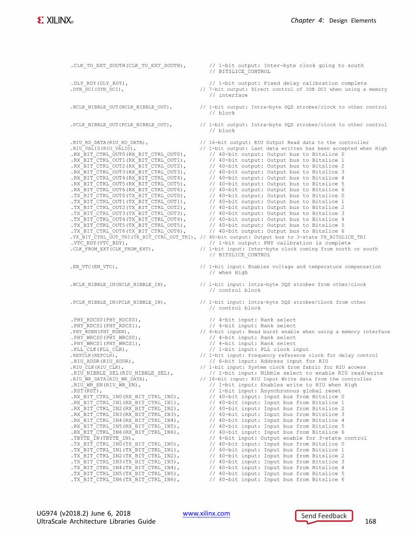
Chapter 4: Design Elements
.CLK_TO_EXT_SOUTH(CLK_TO_EXT_SOUTH), // 1-bit output: Inter-byte clock going to south// BITSLICE_CONTROL
.DLY_RDY(DLY_RDY), // 1-bit output: Fixed delay calibration complete
.DYN_DCI(DYN_DCI), // 7-bit output: Direct control of IOB DCI when using a memory// interface
.NCLK_NIBBLE_OUT(NCLK_NIBBLE_OUT), // 1-bit output: Intra-byte DQS strobes/clock to other control// block
.PCLK_NIBBLE_OUT(PCLK_NIBBLE_OUT), // 1-bit output: Intra-byte DQS strobes/clock to other control// block
.RIU_RD_DATA(RIU_RD_DATA), // 16-bit output: RIU Output Read data to the controller
.RIU_VALID(RIU_VALID), // 1-bit output: Last data written has been accepted when High
.RX_BIT_CTRL_OUT0(RX_BIT_CTRL_OUT0), // 40-bit output: Output bus to Bitslice 0
.RX_BIT_CTRL_OUT1(RX_BIT_CTRL_OUT1), // 40-bit output: Output bus to Bitslice 1
.RX_BIT_CTRL_OUT2(RX_BIT_CTRL_OUT2), // 40-bit output: Output bus to Bitslice 2
.RX_BIT_CTRL_OUT3(RX_BIT_CTRL_OUT3), // 40-bit output: Output bus to Bitslice 3
.RX_BIT_CTRL_OUT4(RX_BIT_CTRL_OUT4), // 40-bit output: Output bus to Bitslice 4
.RX_BIT_CTRL_OUT5(RX_BIT_CTRL_OUT5), // 40-bit output: Output bus to Bitslice 5
.RX_BIT_CTRL_OUT6(RX_BIT_CTRL_OUT6), // 40-bit output: Output bus to Bitslice 6
.TX_BIT_CTRL_OUT0(TX_BIT_CTRL_OUT0), // 40-bit output: Output bus to Bitslice 0
.TX_BIT_CTRL_OUT1(TX_BIT_CTRL_OUT1), // 40-bit output: Output bus to Bitslice 1
.TX_BIT_CTRL_OUT2(TX_BIT_CTRL_OUT2), // 40-bit output: Output bus to Bitslice 2
.TX_BIT_CTRL_OUT3(TX_BIT_CTRL_OUT3), // 40-bit output: Output bus to Bitslice 3
.TX_BIT_CTRL_OUT4(TX_BIT_CTRL_OUT4), // 40-bit output: Output bus to Bitslice 4
.TX_BIT_CTRL_OUT5(TX_BIT_CTRL_OUT5), // 40-bit output: Output bus to Bitslice 5
.TX_BIT_CTRL_OUT6(TX_BIT_CTRL_OUT6), // 40-bit output: Output bus to Bitslice 6
.TX_BIT_CTRL_OUT_TRI(TX_BIT_CTRL_OUT_TRI), // 40-bit output: Output bus to 3-state TX_BITSLICE_TRI
.VTC_RDY(VTC_RDY), // 1-bit output: PHY calibration is complete
.CLK_FROM_EXT(CLK_FROM_EXT), // 1-bit input: Inter-byte clock coming from north or south// BITSLICE_CONTROL
.EN_VTC(EN_VTC), // 1-bit input: Enables voltage and temperature compensation// when High
.NCLK_NIBBLE_IN(NCLK_NIBBLE_IN), // 1-bit input: Intra-byte DQS strobes from other/clock// control block
.PCLK_NIBBLE_IN(PCLK_NIBBLE_IN), // 1-bit input: Intra-byte DQS strobes/clock from other// control block
.PHY_RDCS0(PHY_RDCS0), // 4-bit input: Rank select
.PHY_RDCS1(PHY_RDCS1), // 4-bit input: Rank select
.PHY_RDEN(PHY_RDEN), // 4-bit input: Read burst enable when using a memory interface
.PHY_WRCS0(PHY_WRCS0), // 4-bit input: Rank select
.PHY_WRCS1(PHY_WRCS1), // 4-bit input: Rank select
.PLL_CLK(PLL_CLK), // 1-bit input: PLL clock input
.REFCLK(REFCLK), // 1-bit input: Frequency reference clock for delay control
.RIU_ADDR(RIU_ADDR), // 6-bit input: Address input for RIU
.RIU_CLK(RIU_CLK), // 1-bit input: System clock from fabric for RIU access
.RIU_NIBBLE_SEL(RIU_NIBBLE_SEL), // 1-bit input: Nibble select to enable RIU read/write
.RIU_WR_DATA(RIU_WR_DATA), // 16-bit input: RIU Input Write data from the controller
.RIU_WR_EN(RIU_WR_EN), // 1-bit input: Enables write to RIU when High
.RST(RST), // 1-bit input: Asynchronous global reset
.RX_BIT_CTRL_IN0(RX_BIT_CTRL_IN0), // 40-bit input: Input bus from Bitslice 0
.RX_BIT_CTRL_IN1(RX_BIT_CTRL_IN1), // 40-bit input: Input bus from Bitslice 1
.RX_BIT_CTRL_IN2(RX_BIT_CTRL_IN2), // 40-bit input: Input bus from Bitslice 2
.RX_BIT_CTRL_IN3(RX_BIT_CTRL_IN3), // 40-bit input: Input bus from Bitslice 3
.RX_BIT_CTRL_IN4(RX_BIT_CTRL_IN4), // 40-bit input: Input bus from Bitslice 4
.RX_BIT_CTRL_IN5(RX_BIT_CTRL_IN5), // 40-bit input: Input bus from Bitslice 5
.RX_BIT_CTRL_IN6(RX_BIT_CTRL_IN6), // 40-bit input: Input bus from Bitslice 6
.TBYTE_IN(TBYTE_IN), // 4-bit input: Output enable for 3-state control
.TX_BIT_CTRL_IN0(TX_BIT_CTRL_IN0), // 40-bit input: Input bus from Bitslice 0
.TX_BIT_CTRL_IN1(TX_BIT_CTRL_IN1), // 40-bit input: Input bus from Bitslice 1
.TX_BIT_CTRL_IN2(TX_BIT_CTRL_IN2), // 40-bit input: Input bus from Bitslice 2
.TX_BIT_CTRL_IN3(TX_BIT_CTRL_IN3), // 40-bit input: Input bus from Bitslice 3
.TX_BIT_CTRL_IN4(TX_BIT_CTRL_IN4), // 40-bit input: Input bus from Bitslice 4
.TX_BIT_CTRL_IN5(TX_BIT_CTRL_IN5), // 40-bit input: Input bus from Bitslice 5
.TX_BIT_CTRL_IN6(TX_BIT_CTRL_IN6), // 40-bit input: Input bus from Bitslice 6
UG974 (v2018.2) June 6, 2018 www.xilinx.comUltraScale Architecture Libraries Guide 168
Send Feedback
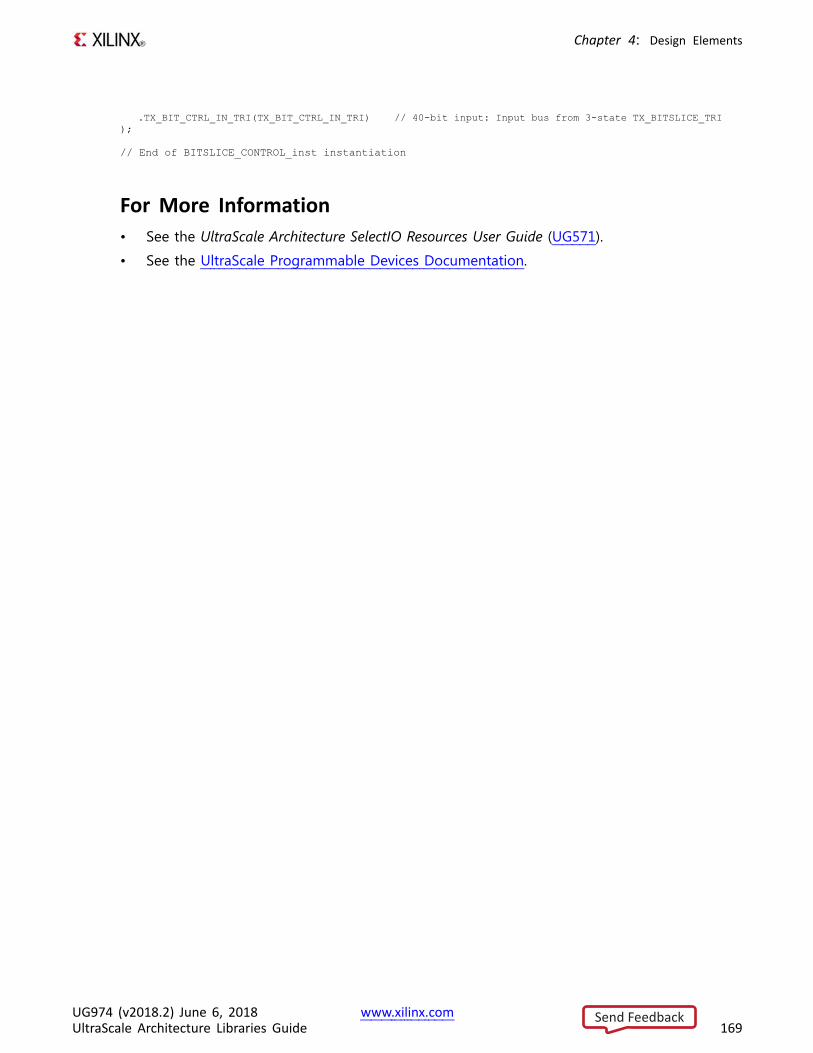
Chapter 4: Design Elements
.TX_BIT_CTRL_IN_TRI(TX_BIT_CTRL_IN_TRI) // 40-bit input: Input bus from 3-state TX_BITSLICE_TRI);
// End of BITSLICE_CONTROL_inst instantiation
For More Information• See the UltraScale Architecture SelectIO Resources User Guide (UG571).
• See the UltraScale Programmable Devices Documentation.
UG974 (v2018.2) June 6, 2018 www.xilinx.comUltraScale Architecture Libraries Guide 169
Send Feedback
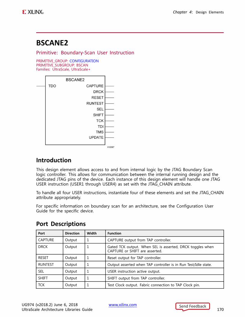
Chapter 4: Design Elements
BSCANE2Primitive: Boundary-Scan User InstructionPRIMITIVE_GROUP: CONFIGURATIONPRIMITIVE_SUBGROUP: BSCANFamilies: UltraScale, UltraScale+
IntroductionThis design element allows access to and from internal logic by the JTAG Boundary Scanlogic controller. This allows for communication between the internal running design and thededicated JTAG pins of the device. Each instance of this design element will handle one JTAGUSER instruction (USER1 through USER4) as set with the JTAG_CHAIN attribute.
To handle all four USER instructions, instantiate four of these elements and set the JTAG_CHAINattribute appropriately.
For specific information on boundary scan for an architecture, see the Configuration UserGuide for the specific device.
Port DescriptionsPort Direction Width Function
CAPTURE Output 1 CAPTURE output from TAP controller.
DRCK Output 1 Gated TCK output. When SEL is asserted, DRCK toggles whenCAPTURE or SHIFT are asserted.
RESET Output 1 Reset output for TAP controller.
RUNTEST Output 1 Output asserted when TAP controller is in Run Test/Idle state.
SEL Output 1 USER instruction active output.
SHIFT Output 1 SHIFT output from TAP controller.
TCK Output 1 Test Clock output. Fabric connection to TAP Clock pin.
UG974 (v2018.2) June 6, 2018 www.xilinx.comUltraScale Architecture Libraries Guide 170
Send Feedback
Chapter 4: Design Elements
Port Direction Width Function
TDI Output 1 Test Data Input (TDI) output from TAP controller.
TDO Input 1 Test Data Output (TDO) input for USER function.
TMS Output 1 Test Mode Select output. Fabric connection to TAP.
UPDATE Output 1 UPDATE output from TAP controller
Design Entry MethodInstantiation Recommended
Inference No
IP and IP Integrator Catalog No
Available AttributesAttribute Type Allowed Values Default Description
JTAG_CHAIN DECIMAL 1, 2, 3, 4 1 Value for USER command
VHDL Instantiation TemplateUnless they already exist, copy the following two statements and paste them before the entitydeclaration.Library UNISIM;use UNISIM.vcomponents.all;
-- BSCANE2: Boundary-Scan User Instruction-- UltraScale-- Xilinx HDL Language Template, version 2018.2
BSCANE2_inst : BSCANE2generic map (
JTAG_CHAIN => 1 -- Value for USER command)port map (
CAPTURE => CAPTURE, -- 1-bit output: CAPTURE output from TAP controller.DRCK => DRCK, -- 1-bit output: Gated TCK output. When SEL is asserted, DRCK toggles when CAPTURE or
-- SHIFT are asserted.
RESET => RESET, -- 1-bit output: Reset output for TAP controller.RUNTEST => RUNTEST, -- 1-bit output: Output asserted when TAP controller is in Run Test/Idle state.SEL => SEL, -- 1-bit output: USER instruction active output.SHIFT => SHIFT, -- 1-bit output: SHIFT output from TAP controller.TCK => TCK, -- 1-bit output: Test Clock output. Fabric connection to TAP Clock pin.TDI => TDI, -- 1-bit output: Test Data Input (TDI) output from TAP controller.TMS => TMS, -- 1-bit output: Test Mode Select output. Fabric connection to TAP.UPDATE => UPDATE, -- 1-bit output: UPDATE output from TAP controllerTDO => TDO -- 1-bit input: Test Data Output (TDO) input for USER function.
);
-- End of BSCANE2_inst instantiation
Verilog Instantiation Template
// BSCANE2: Boundary-Scan User Instruction
UG974 (v2018.2) June 6, 2018 www.xilinx.comUltraScale Architecture Libraries Guide 171
Send Feedback
Chapter 4: Design Elements
// UltraScale// Xilinx HDL Language Template, version 2018.2
BSCANE2 #(.JTAG_CHAIN(1) // Value for USER command
)BSCANE2_inst (
.CAPTURE(CAPTURE), // 1-bit output: CAPTURE output from TAP controller.
.DRCK(DRCK), // 1-bit output: Gated TCK output. When SEL is asserted, DRCK toggles when CAPTURE or// SHIFT are asserted.
.RESET(RESET), // 1-bit output: Reset output for TAP controller.
.RUNTEST(RUNTEST), // 1-bit output: Output asserted when TAP controller is in Run Test/Idle state.
.SEL(SEL), // 1-bit output: USER instruction active output.
.SHIFT(SHIFT), // 1-bit output: SHIFT output from TAP controller.
.TCK(TCK), // 1-bit output: Test Clock output. Fabric connection to TAP Clock pin.
.TDI(TDI), // 1-bit output: Test Data Input (TDI) output from TAP controller.
.TMS(TMS), // 1-bit output: Test Mode Select output. Fabric connection to TAP.
.UPDATE(UPDATE), // 1-bit output: UPDATE output from TAP controller
.TDO(TDO) // 1-bit input: Test Data Output (TDO) input for USER function.);
// End of BSCANE2_inst instantiation
For More Information• See the UltraScale Architecture Configuration User Guide (UG570).
• See the UltraScale Programmable Devices Documentation.
UG974 (v2018.2) June 6, 2018 www.xilinx.comUltraScale Architecture Libraries Guide 172
Send Feedback
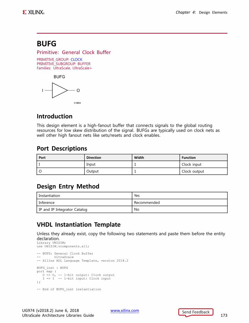
Chapter 4: Design Elements
BUFGPrimitive: General Clock BufferPRIMITIVE_GROUP: CLOCKPRIMITIVE_SUBGROUP: BUFFERFamilies: UltraScale, UltraScale+
IntroductionThis design element is a high-fanout buffer that connects signals to the global routingresources for low skew distribution of the signal. BUFGs are typically used on clock nets aswell other high fanout nets like sets/resets and clock enables.
Port DescriptionsPort Direction Width Function
I Input 1 Clock input
O Output 1 Clock output
Design Entry MethodInstantiation Yes
Inference Recommended
IP and IP Integrator Catalog No
VHDL Instantiation TemplateUnless they already exist, copy the following two statements and paste them before the entitydeclaration.Library UNISIM;use UNISIM.vcomponents.all;
-- BUFG: General Clock Buffer-- UltraScale-- Xilinx HDL Language Template, version 2018.2
BUFG_inst : BUFGport map (
O => O, -- 1-bit output: Clock outputI => I -- 1-bit input: Clock input
);
-- End of BUFG_inst instantiation
UG974 (v2018.2) June 6, 2018 www.xilinx.comUltraScale Architecture Libraries Guide 173
Send Feedback
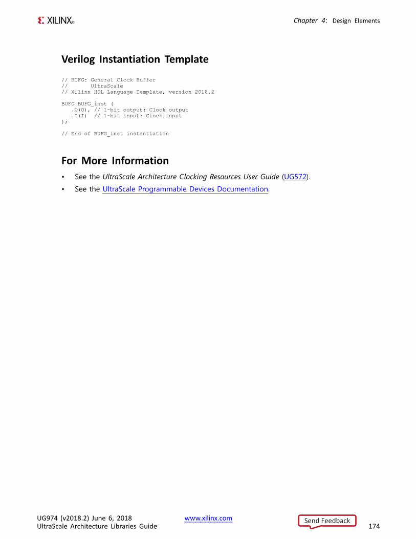
Chapter 4: Design Elements
Verilog Instantiation Template
// BUFG: General Clock Buffer// UltraScale// Xilinx HDL Language Template, version 2018.2
BUFG BUFG_inst (.O(O), // 1-bit output: Clock output.I(I) // 1-bit input: Clock input
);
// End of BUFG_inst instantiation
For More Information• See the UltraScale Architecture Clocking Resources User Guide (UG572).
• See the UltraScale Programmable Devices Documentation.
UG974 (v2018.2) June 6, 2018 www.xilinx.comUltraScale Architecture Libraries Guide 174
Send Feedback
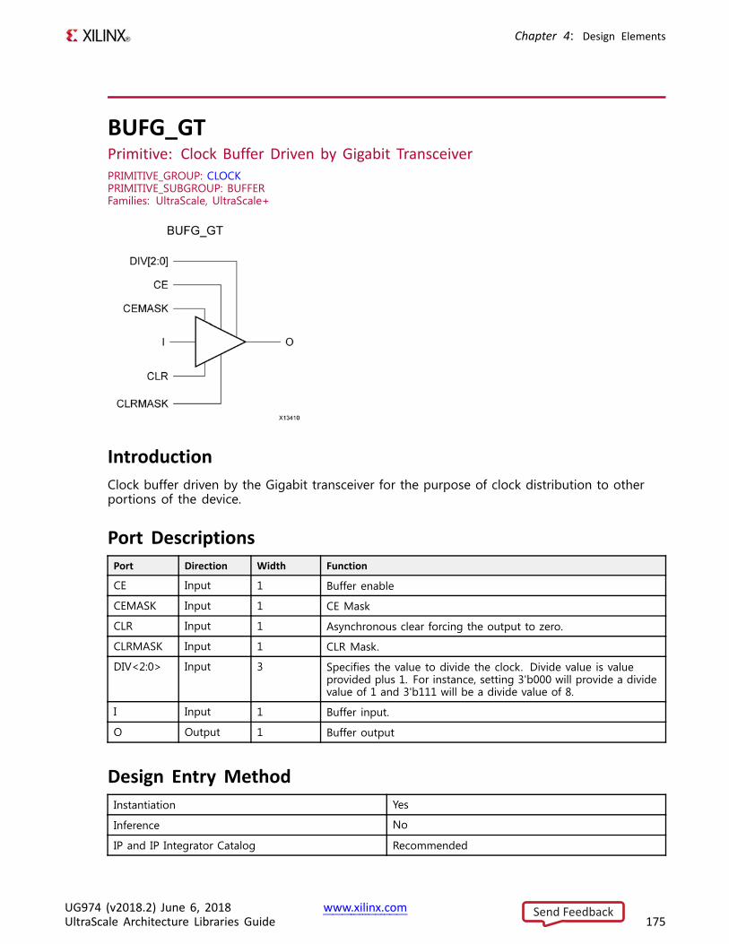
Chapter 4: Design Elements
BUFG_GTPrimitive: Clock Buffer Driven by Gigabit TransceiverPRIMITIVE_GROUP: CLOCKPRIMITIVE_SUBGROUP: BUFFERFamilies: UltraScale, UltraScale+
IntroductionClock buffer driven by the Gigabit transceiver for the purpose of clock distribution to otherportions of the device.
Port DescriptionsPort Direction Width Function
CE Input 1 Buffer enable
CEMASK Input 1 CE Mask
CLR Input 1 Asynchronous clear forcing the output to zero.
CLRMASK Input 1 CLR Mask.
DIV<2:0> Input 3 Specifies the value to divide the clock. Divide value is valueprovided plus 1. For instance, setting 3'b000 will provide a dividevalue of 1 and 3'b111 will be a divide value of 8.
I Input 1 Buffer input.
O Output 1 Buffer output
Design Entry MethodInstantiation Yes
Inference No
IP and IP Integrator Catalog Recommended
UG974 (v2018.2) June 6, 2018 www.xilinx.comUltraScale Architecture Libraries Guide 175
Send Feedback
Chapter 4: Design Elements
VHDL Instantiation TemplateUnless they already exist, copy the following two statements and paste them before the entitydeclaration.Library UNISIM;use UNISIM.vcomponents.all;
-- BUFG_GT: Clock Buffer Driven by Gigabit Transceiver-- UltraScale-- Xilinx HDL Language Template, version 2018.2
BUFG_GT_inst : BUFG_GTport map (
O => O, -- 1-bit output: BufferCE => CE, -- 1-bit input: Buffer enableCEMASK => CEMASK, -- 1-bit input: CE MaskCLR => CLR, -- 1-bit input: Asynchronous clearCLRMASK => CLRMASK, -- 1-bit input: CLR MaskDIV => DIV, -- 3-bit input: Dynamic divide ValueI => I -- 1-bit input: Buffer
);
-- End of BUFG_GT_inst instantiation
Verilog Instantiation Template
// BUFG_GT: Clock Buffer Driven by Gigabit Transceiver// UltraScale// Xilinx HDL Language Template, version 2018.2
BUFG_GT BUFG_GT_inst (.O(O), // 1-bit output: Buffer.CE(CE), // 1-bit input: Buffer enable.CEMASK(CEMASK), // 1-bit input: CE Mask.CLR(CLR), // 1-bit input: Asynchronous clear.CLRMASK(CLRMASK), // 1-bit input: CLR Mask.DIV(DIV), // 3-bit input: Dynamic divide Value.I(I) // 1-bit input: Buffer
);
// End of BUFG_GT_inst instantiation
For More Information• See the UltraScale Architecture Clocking Resources User Guide (UG572).
• See the UltraScale Programmable Devices Documentation.
UG974 (v2018.2) June 6, 2018 www.xilinx.comUltraScale Architecture Libraries Guide 176
Send Feedback
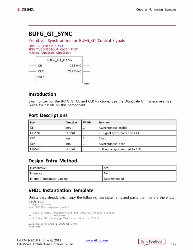
Chapter 4: Design Elements
BUFG_GT_SYNCPrimitive: Synchronizer for BUFG_GT Control SignalsPRIMITIVE_GROUP: CLOCKPRIMITIVE_SUBGROUP: CLOCK_SYNCFamilies: UltraScale, UltraScale+
IntroductionSynchronizer for the BUFG_GT CE and CLR functions. See the UltraScale GT Transceivers UserGuide for details on this component.
Port DescriptionsPort Direction Width Function
CE Input 1 Asynchronous enable
CESYNC Output 1 CE signal synchronized to CLK
CLK Input 1 Clock
CLR Input 1 Asynchronous clear
CLRSYNC Output 1 CLR signal synchronized to CLK
Design Entry MethodInstantiation Yes
Inference No
IP and IP Integrator Catalog Recommended
VHDL Instantiation TemplateUnless they already exist, copy the following two statements and paste them before the entitydeclaration.Library UNISIM;use UNISIM.vcomponents.all;
-- BUFG_GT_SYNC: Synchronizer for BUFG_GT Control Signals-- UltraScale-- Xilinx HDL Language Template, version 2018.2
BUFG_GT_SYNC_inst : BUFG_GT_SYNCport map (
UG974 (v2018.2) June 6, 2018 www.xilinx.comUltraScale Architecture Libraries Guide 177
Send Feedback
Chapter 4: Design Elements
CESYNC => CESYNC, -- 1-bit output: Synchronized CECLRSYNC => CLRSYNC, -- 1-bit output: Synchronized CLRCE => CE, -- 1-bit input: Asynchronous enableCLK => CLK, -- 1-bit input: ClockCLR => CLR -- 1-bit input: Asynchronous clear
);
-- End of BUFG_GT_SYNC_inst instantiation
Verilog Instantiation Template
// BUFG_GT_SYNC: Synchronizer for BUFG_GT Control Signals// UltraScale// Xilinx HDL Language Template, version 2018.2
BUFG_GT_SYNC BUFG_GT_SYNC_inst (.CESYNC(CESYNC), // 1-bit output: Synchronized CE.CLRSYNC(CLRSYNC), // 1-bit output: Synchronized CLR.CE(CE), // 1-bit input: Asynchronous enable.CLK(CLK), // 1-bit input: Clock.CLR(CLR) // 1-bit input: Asynchronous clear
);
// End of BUFG_GT_SYNC_inst instantiation
For More Information• See the UltraScale Architecture Clocking Resources User Guide (UG572).
• See the UltraScale Programmable Devices Documentation.
UG974 (v2018.2) June 6, 2018 www.xilinx.comUltraScale Architecture Libraries Guide 178
Send Feedback
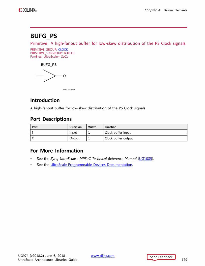
Chapter 4: Design Elements
BUFG_PSPrimitive: A high-fanout buffer for low-skew distribution of the PS Clock signalsPRIMITIVE_GROUP: CLOCKPRIMITIVE_SUBGROUP: BUFFERFamilies: UltraScale+ SoCs
IntroductionA high-fanout buffer for low-skew distribution of the PS Clock signals
Port DescriptionsPort Direction Width Function
I Input 1 Clock buffer input
O Output 1 Clock buffer output
For More Information• See the Zynq UltraScale+ MPSoC Technical Reference Manual (UG1085).
• See the UltraScale Programmable Devices Documentation.
UG974 (v2018.2) June 6, 2018 www.xilinx.comUltraScale Architecture Libraries Guide 179
Send Feedback
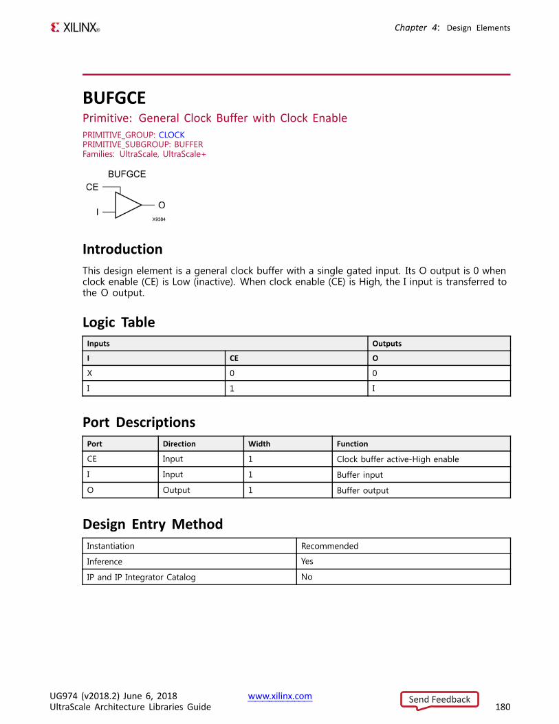
Chapter 4: Design Elements
BUFGCEPrimitive: General Clock Buffer with Clock EnablePRIMITIVE_GROUP: CLOCKPRIMITIVE_SUBGROUP: BUFFERFamilies: UltraScale, UltraScale+
IntroductionThis design element is a general clock buffer with a single gated input. Its O output is 0 whenclock enable (CE) is Low (inactive). When clock enable (CE) is High, the I input is transferred tothe O output.
Logic TableInputs Outputs
I CE O
X 0 0
I 1 I
Port DescriptionsPort Direction Width Function
CE Input 1 Clock buffer active-High enable
I Input 1 Buffer input
O Output 1 Buffer output
Design Entry MethodInstantiation Recommended
Inference Yes
IP and IP Integrator Catalog No
UG974 (v2018.2) June 6, 2018 www.xilinx.comUltraScale Architecture Libraries Guide 180
Send Feedback
Chapter 4: Design Elements
Available AttributesAttribute Type Allowed Values Default Description
CE_TYPE STRING "SYNC","ASYNC"
"SYNC" Specifies whether the enable should be synchronous(glitch - free) or asynchronous (no input clockswitching necessary).
IS_CE_INVERTED BINARY 1'b0 to 1'b1 1'b0 Specifies use of the programmable inversion onthe CE pin.
IS_I_INVERTED BINARY 1'b0 to 1'b1 1'b0 Specifies use of the programmable inversion on theI pin.
VHDL Instantiation TemplateUnless they already exist, copy the following two statements and paste them before the entitydeclaration.Library UNISIM;use UNISIM.vcomponents.all;
-- BUFGCE: General Clock Buffer with Clock Enable-- UltraScale-- Xilinx HDL Language Template, version 2018.2
BUFGCE_inst : BUFGCEgeneric map (
CE_TYPE => "SYNC", -- ASYNC, SYNCIS_CE_INVERTED => '0', -- Programmable inversion on CEIS_I_INVERTED => '0' -- Programmable inversion on I
)port map (
O => O, -- 1-bit output: BufferCE => CE, -- 1-bit input: Buffer enableI => I -- 1-bit input: Buffer
);
-- End of BUFGCE_inst instantiation
Verilog Instantiation Template
// BUFGCE: General Clock Buffer with Clock Enable// UltraScale// Xilinx HDL Language Template, version 2018.2
BUFGCE #(.CE_TYPE("SYNC"), // ASYNC, SYNC.IS_CE_INVERTED(1'b0), // Programmable inversion on CE.IS_I_INVERTED(1'b0) // Programmable inversion on I
)BUFGCE_inst (
.O(O), // 1-bit output: Buffer
.CE(CE), // 1-bit input: Buffer enable
.I(I) // 1-bit input: Buffer);
// End of BUFGCE_inst instantiation
UG974 (v2018.2) June 6, 2018 www.xilinx.comUltraScale Architecture Libraries Guide 181
Send Feedback

Chapter 4: Design Elements
For More Information• See the UltraScale Architecture Clocking Resources User Guide (UG572).
• See the UltraScale Programmable Devices Documentation.
UG974 (v2018.2) June 6, 2018 www.xilinx.comUltraScale Architecture Libraries Guide 182
Send Feedback
Chapter 4: Design Elements
BUFGCE_1Primitive: General Clock Buffer with Clock Enable and Output State 1PRIMITIVE_GROUP: CLOCKPRIMITIVE_SUBGROUP: BUFFERFamilies: UltraScale, UltraScale+
IntroductionThis design element is a general clock buffer with a single gated input. Its O output is 1 whenclock enable (CE) is Low (inactive). When clock enable (CE) is High, the I input is transferred tothe O output.
Logic TableInputs Outputs
I CE O
X 0 1
I 1 I
Port DescriptionsPort Direction Width Function
CE Input 1 Clock buffer active-High enable
I Input 1 Clock input
O Output 1 Clock output
Design Entry MethodInstantiation Yes
Inference No
IP and IP Integrator Catalog No
VHDL Instantiation TemplateUnless they already exist, copy the following two statements and paste them before the entitydeclaration.Library UNISIM;use UNISIM.vcomponents.all;
UG974 (v2018.2) June 6, 2018 www.xilinx.comUltraScale Architecture Libraries Guide 183
Send Feedback
Chapter 4: Design Elements
-- BUFGCE_1: General Clock Buffer with Clock Enable and Output State 1-- UltraScale-- Xilinx HDL Language Template, version 2018.2
BUFGCE_1_inst : BUFGCE_1port map (
O => O, -- 1-bit output: Clock outputCE => CE, -- 1-bit input: Clock buffer active-High enableI => I -- 1-bit input: Clock input
);
-- End of BUFGCE_1_inst instantiation
Verilog Instantiation Template
// BUFGCE_1: General Clock Buffer with Clock Enable and Output State 1// UltraScale// Xilinx HDL Language Template, version 2018.2
BUFGCE_1 BUFGCE_1_inst (.O(O), // 1-bit output: Clock output.CE(CE), // 1-bit input: Clock buffer active-High enable.I(I) // 1-bit input: Clock input
);
// End of BUFGCE_1_inst instantiation
For More Information• See the UltraScale Architecture Clocking Resources User Guide (UG572).
• See the UltraScale Programmable Devices Documentation.
UG974 (v2018.2) June 6, 2018 www.xilinx.comUltraScale Architecture Libraries Guide 184
Send Feedback
Chapter 4: Design Elements
BUFGCE_DIVPrimitive: General Clock Buffer with Divide FunctionPRIMITIVE_GROUP: CLOCKPRIMITIVE_SUBGROUP: BUFFERFamilies: UltraScale, UltraScale+
IntroductionBUFGCE_DIV is a general clock buffer with an enable and divide function.
Port DescriptionsPort Direction Width Function
CE Input 1 Buffer enable input.
CLR Input 1 Asynchronous clear function forcing the output value to zero.
I Input 1 Buffer input
O Output 1 Buffer output
Design Entry MethodInstantiation Yes
Inference No
IP and IP Integrator Catalog No
Available AttributesAttribute Type Allowed Values Default Description
BUFGCE_DIVIDE DECIMAL 1, 2, 3, 4, 5, 6,7, 8
1 Divide value.
Programmable Inversion Attributes: Specifies whether or not to use the optional inversions are to beused on specific pins for this component to change the active polarity of the pin function. When set to 1,it changes the function to behave active-Low rather than active-High. If an external inverter is specifiedon one of these associated pins, the Vivado Design Suite will automatically set this attribute during theopt_design stage so that additional logic is not necessary for changing the input polarity.
UG974 (v2018.2) June 6, 2018 www.xilinx.comUltraScale Architecture Libraries Guide 185
Send Feedback
Chapter 4: Design Elements
Attribute Type Allowed Values Default Description
IS_CE_INVERTED BINARY 1'b0 to 1'b1 1'b0 Specifies whether or not to use the optionalinversion on the CE pin of this component.
IS_CLR_INVERTED BINARY 1'b0 to 1'b1 1'b0 Specifies whether or not to use the optionalinversion on the CLR pin of this component.
IS_I_INVERTED BINARY 1'b0 to 1'b1 1'b0 Specifies whether or not to use the optionalinversion on the I pin of this component.
VHDL Instantiation TemplateUnless they already exist, copy the following two statements and paste them before the entitydeclaration.Library UNISIM;use UNISIM.vcomponents.all;
-- BUFGCE_DIV: General Clock Buffer with Divide Function-- UltraScale-- Xilinx HDL Language Template, version 2018.2
BUFGCE_DIV_inst : BUFGCE_DIVgeneric map (
BUFGCE_DIVIDE => 1, -- 1-8-- Programmable Inversion Attributes: Specifies built-in programmable inversion on specific pinsIS_CE_INVERTED => '0', -- Optional inversion for CEIS_CLR_INVERTED => '0', -- Optional inversion for CLRIS_I_INVERTED => '0' -- Optional inversion for I
)port map (
O => O, -- 1-bit output: BufferCE => CE, -- 1-bit input: Buffer enableCLR => CLR, -- 1-bit input: Asynchronous clearI => I -- 1-bit input: Buffer
);
-- End of BUFGCE_DIV_inst instantiation
Verilog Instantiation Template
// BUFGCE_DIV: General Clock Buffer with Divide Function// UltraScale// Xilinx HDL Language Template, version 2018.2
BUFGCE_DIV #(.BUFGCE_DIVIDE(1), // 1-8// Programmable Inversion Attributes: Specifies built-in programmable inversion on specific pins.IS_CE_INVERTED(1'b0), // Optional inversion for CE.IS_CLR_INVERTED(1'b0), // Optional inversion for CLR.IS_I_INVERTED(1'b0) // Optional inversion for I
)BUFGCE_DIV_inst (
.O(O), // 1-bit output: Buffer
.CE(CE), // 1-bit input: Buffer enable
.CLR(CLR), // 1-bit input: Asynchronous clear
.I(I) // 1-bit input: Buffer);
// End of BUFGCE_DIV_inst instantiation
UG974 (v2018.2) June 6, 2018 www.xilinx.comUltraScale Architecture Libraries Guide 186
Send Feedback

Chapter 4: Design Elements
For More Information• See the UltraScale Architecture Clocking Resources User Guide (UG572).
• See the UltraScale Programmable Devices Documentation.
UG974 (v2018.2) June 6, 2018 www.xilinx.comUltraScale Architecture Libraries Guide 187
Send Feedback
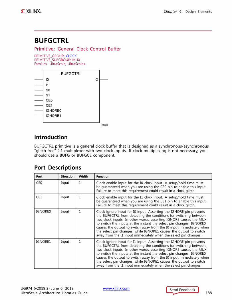
Chapter 4: Design Elements
BUFGCTRLPrimitive: General Clock Control BufferPRIMITIVE_GROUP: CLOCKPRIMITIVE_SUBGROUP: MUXFamilies: UltraScale, UltraScale+
IntroductionBUFGCTRL primitive is a general clock buffer that is designed as a synchronous/asynchronous"glitch free" 2:1 multiplexer with two clock inputs. If clock multiplexing is not necessary, youshould use a BUFG or BUFGCE component.
Port DescriptionsPort Direction Width Function
CE0 Input 1 Clock enable input for the I0 clock input. A setup/hold time mustbe guaranteed when you are using the CE0 pin to enable this input.Failure to meet this requirement could result in a clock glitch.
CE1 Input 1 Clock enable input for the I1 clock input. A setup/hold time mustbe guaranteed when you are using the CE1 pin to enable this input.Failure to meet this requirement could result in a clock glitch.
IGNORE0 Input 1 Clock ignore input for I0 input. Asserting the IGNORE pin preventsthe BUFGCTRL from detecting the conditions for switching betweentwo clock inputs. In other words, asserting IGNORE causes the MUXto switch the inputs at the instant the select pin changes. IGNORE0causes the output to switch away from the I0 input immediately whenthe select pin changes, while IGNORE1 causes the output to switchaway from the I1 input immediately when the select pin changes.
IGNORE1 Input 1 Clock ignore input for I1 input. Asserting the IGNORE pin preventsthe BUFGCTRL from detecting the conditions for switching betweentwo clock inputs. In other words, asserting IGNORE causes the MUXto switch the inputs at the instant the select pin changes. IGNORE0causes the output to switch away from the I0 input immediately whenthe select pin changes, while IGNORE1 causes the output to switchaway from the I1 input immediately when the select pin changes.
UG974 (v2018.2) June 6, 2018 www.xilinx.comUltraScale Architecture Libraries Guide 188
Send Feedback
Chapter 4: Design Elements
Port Direction Width Function
I0 Input 1 Primary clock input into the BUFGCTRL enabled by the CE0 input andselected by the S0 input.
I1 Input 1 Secondary clock input into the BUFGCTRL enabled by the CE1 inputand selected by the S1 input.
O Output 1 Clock output
S0 Input 1 Clock select input for I0. The S pins represent the clock select pinfor each clock input. When using the S pin as input select, there isa setup/hold time requirement. Unlike CE pins, failure to meet thisrequirement will not result in a clock glitch. However, it can cause theoutput clock to appear one clock cycle later.
S1 Input 1 Clock select input for I1. The S pins represent the clock select pinfor each clock input. When using the S pin as input select, there isa setup/hold time requirement. Unlike CE pins, failure to meet thisrequirement will not result in a clock glitch. However, it can cause theoutput clock to appear one clock cycle later.
Design Entry MethodInstantiation Yes
Inference No
IP and IP Integrator Catalog No
Available AttributesAttribute Type Allowed Values Default Description
INIT_OUT DECIMAL 0, 1 0 Initializes the BUFGCTRL output to thespecified value after configuration.
PRESELECT_I0 BOOLEAN FALSE, TRUE FALSE If TRUE, BUFGCTRL output uses I0 input afterconfiguration.
PRESELECT_I1 BOOLEAN FALSE, TRUE FALSE If TRUE, BUFGCTRL output uses I1 input afterconfiguration.
Programmable Inversion Attributes: Specifies whether or not to use the optional inversion on specificpins for this component to change the active polarity of the pin function. When set to 1, it changes thefunction to behave active-Low rather than active-High. If an external inverter is specified on one of theseassociated pins, the Vivado Design Suite will automatically set this attribute during the opt_design stage sothat additional logic is not necessary for changing the input polarity.
IS_CE0_INVERTED BINARY 1'b0 to 1'b1 1'b0 Specifies whether or not to use the optionalinversion on the CE0 pin of this component.
IS_CE1_INVERTED BINARY 1'b0 to 1'b1 1'b0 Specifies whether or not to use the optionalinversion on the CE1 pin of this component.
IS_IGNORE0_INVERTED
BINARY 1'b0 to 1'b1 1'b0 Specifies whether or not to use the optionalinversion on the IGNORE0 pin of thiscomponent.
IS_IGNORE1_INVERTED
BINARY 1'b0 to 1'b1 1'b0 Specifies whether or not to use the optionalinversion on the IGNORE1 pin of thiscomponent.
UG974 (v2018.2) June 6, 2018 www.xilinx.comUltraScale Architecture Libraries Guide 189
Send Feedback
Chapter 4: Design Elements
Attribute Type Allowed Values Default Description
IS_I0_INVERTED BINARY 1'b0 to 1'b1 1'b0 Specifies whether or not to use the optionalinversion on the I0 pin of this component.
IS_I1_INVERTED BINARY 1'b0 to 1'b1 1'b0 Specifies whether or not to use the optionalinversion on the I1 pin of this component.
IS_S0_INVERTED BINARY 1'b0 to 1'b1 1'b0 Specifies whether or not to use the optionalinversion on the S0 pin of this component.
IS_S1_INVERTED BINARY 1'b0 to 1'b1 1'b0 Specifies whether or not to use the optionalinversion on the S1 pin of this component.
NOTE: Both PRESELECT attributes might not be TRUE at the same time.
VHDL Instantiation TemplateUnless they already exist, copy the following two statements and paste them before the entitydeclaration.Library UNISIM;use UNISIM.vcomponents.all;
-- BUFGCTRL: General Clock Control Buffer-- UltraScale-- Xilinx HDL Language Template, version 2018.2
BUFGCTRL_inst : BUFGCTRLgeneric map (
INIT_OUT => 0, -- Initial value of BUFGCTRL output, 0-1PRESELECT_I0 => FALSE, -- BUFGCTRL output uses I0 input, FALSE, TRUEPRESELECT_I1 => FALSE, -- BUFGCTRL output uses I1 input, FALSE, TRUE-- Programmable Inversion Attributes: Specifies built-in programmable inversion on specific pinsIS_CE0_INVERTED => '0', -- Optional inversion for CE0IS_CE1_INVERTED => '0', -- Optional inversion for CE1IS_I0_INVERTED => '0', -- Optional inversion for I0IS_I1_INVERTED => '0', -- Optional inversion for I1IS_IGNORE0_INVERTED => '0', -- Optional inversion for IGNORE0IS_IGNORE1_INVERTED => '0', -- Optional inversion for IGNORE1IS_S0_INVERTED => '0', -- Optional inversion for S0IS_S1_INVERTED => '0' -- Optional inversion for S1
)port map (
O => O, -- 1-bit output: Clock outputCE0 => CE0, -- 1-bit input: Clock enable input for I0CE1 => CE1, -- 1-bit input: Clock enable input for I1I0 => I0, -- 1-bit input: Primary clockI1 => I1, -- 1-bit input: Secondary clockIGNORE0 => IGNORE0, -- 1-bit input: Clock ignore input for I0IGNORE1 => IGNORE1, -- 1-bit input: Clock ignore input for I1S0 => S0, -- 1-bit input: Clock select for I0S1 => S1 -- 1-bit input: Clock select for I1
);
-- End of BUFGCTRL_inst instantiation
Verilog Instantiation Template// BUFGCTRL: General Clock Control Buffer// UltraScale// Xilinx HDL Language Template, version 2018.2
BUFGCTRL #(.INIT_OUT(0), // Initial value of BUFGCTRL output, 0-1.PRESELECT_I0("FALSE"), // BUFGCTRL output uses I0 input, FALSE, TRUE
UG974 (v2018.2) June 6, 2018 www.xilinx.comUltraScale Architecture Libraries Guide 190
Send Feedback
Chapter 4: Design Elements
.PRESELECT_I1("FALSE"), // BUFGCTRL output uses I1 input, FALSE, TRUE// Programmable Inversion Attributes: Specifies built-in programmable inversion on specific pins.IS_CE0_INVERTED(1'b0), // Optional inversion for CE0.IS_CE1_INVERTED(1'b0), // Optional inversion for CE1.IS_I0_INVERTED(1'b0), // Optional inversion for I0.IS_I1_INVERTED(1'b0), // Optional inversion for I1.IS_IGNORE0_INVERTED(1'b0), // Optional inversion for IGNORE0.IS_IGNORE1_INVERTED(1'b0), // Optional inversion for IGNORE1.IS_S0_INVERTED(1'b0), // Optional inversion for S0.IS_S1_INVERTED(1'b0) // Optional inversion for S1
)BUFGCTRL_inst (
.O(O), // 1-bit output: Clock output
.CE0(CE0), // 1-bit input: Clock enable input for I0
.CE1(CE1), // 1-bit input: Clock enable input for I1
.I0(I0), // 1-bit input: Primary clock
.I1(I1), // 1-bit input: Secondary clock
.IGNORE0(IGNORE0), // 1-bit input: Clock ignore input for I0
.IGNORE1(IGNORE1), // 1-bit input: Clock ignore input for I1
.S0(S0), // 1-bit input: Clock select for I0
.S1(S1) // 1-bit input: Clock select for I1);
// End of BUFGCTRL_inst instantiation
For More Information• See the UltraScale Architecture Clocking Resources User Guide (UG572).
• See the UltraScale Programmable Devices Documentation.
UG974 (v2018.2) June 6, 2018 www.xilinx.comUltraScale Architecture Libraries Guide 191
Send Feedback
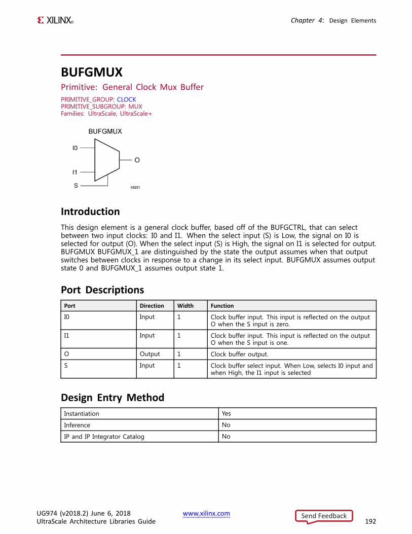
Chapter 4: Design Elements
BUFGMUXPrimitive: General Clock Mux BufferPRIMITIVE_GROUP: CLOCKPRIMITIVE_SUBGROUP: MUXFamilies: UltraScale, UltraScale+
IntroductionThis design element is a general clock buffer, based off of the BUFGCTRL, that can selectbetween two input clocks: I0 and I1. When the select input (S) is Low, the signal on I0 isselected for output (O). When the select input (S) is High, the signal on I1 is selected for output.BUFGMUX BUFGMUX_1 are distinguished by the state the output assumes when that outputswitches between clocks in response to a change in its select input. BUFGMUX assumes outputstate 0 and BUFGMUX_1 assumes output state 1.
Port DescriptionsPort Direction Width Function
I0 Input 1 Clock buffer input. This input is reflected on the outputO when the S input is zero.
I1 Input 1 Clock buffer input. This input is reflected on the outputO when the S input is one.
O Output 1 Clock buffer output.
S Input 1 Clock buffer select input. When Low, selects I0 input andwhen High, the I1 input is selected
Design Entry MethodInstantiation Yes
Inference No
IP and IP Integrator Catalog No
UG974 (v2018.2) June 6, 2018 www.xilinx.comUltraScale Architecture Libraries Guide 192
Send Feedback
Chapter 4: Design Elements
Available AttributesAttribute Type Allowed Values Default Description
CLK_SEL_TYPE STRING "SYNC", "ASYNC" "SYNC" Specifies synchronous (glitch- free) or asynchronous clockswitching.
VHDL Instantiation TemplateUnless they already exist, copy the following two statements and paste them before the entitydeclaration.Library UNISIM;use UNISIM.vcomponents.all;
-- BUFGMUX: General Clock Mux Buffer-- UltraScale-- Xilinx HDL Language Template, version 2018.2
BUFGMUX_inst : BUFGMUXgeneric map (
CLK_SEL_TYPE => "SYNC" -- ASYNC, SYNC)port map (
O => O, -- 1-bit output: Clock outputI0 => I0, -- 1-bit input: Clock input (S=0)I1 => I1, -- 1-bit input: Clock input (S=1)S => S -- 1-bit input: Clock select
);
-- End of BUFGMUX_inst instantiation
Verilog Instantiation Template
// BUFGMUX: General Clock Mux Buffer// UltraScale// Xilinx HDL Language Template, version 2018.2
BUFGMUX #(.CLK_SEL_TYPE("SYNC") // ASYNC, SYNC
)BUFGMUX_inst (
.O(O), // 1-bit output: Clock output
.I0(I0), // 1-bit input: Clock input (S=0)
.I1(I1), // 1-bit input: Clock input (S=1)
.S(S) // 1-bit input: Clock select);
// End of BUFGMUX_inst instantiation
For More Information• See the UltraScale Architecture Clocking Resources User Guide (UG572).
• See the UltraScale Programmable Devices Documentation.
UG974 (v2018.2) June 6, 2018 www.xilinx.comUltraScale Architecture Libraries Guide 193
Send Feedback
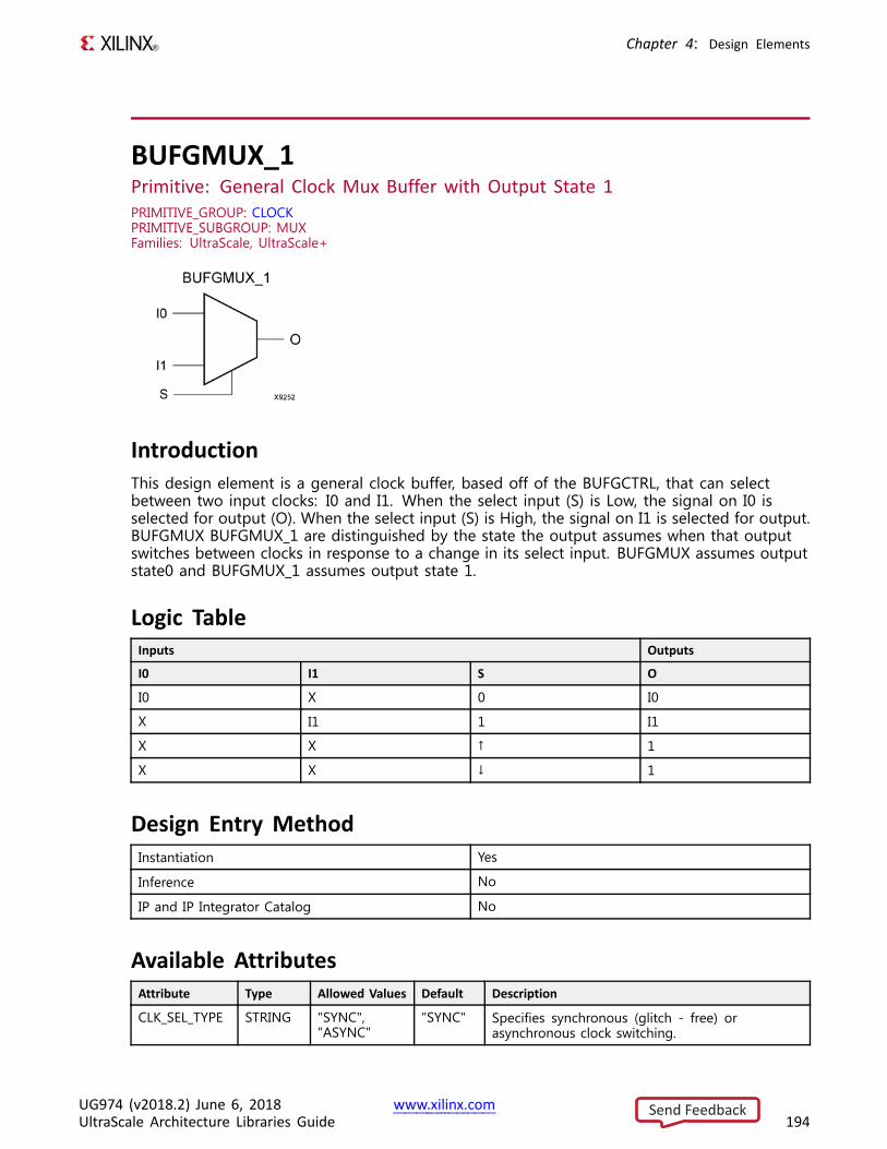
Chapter 4: Design Elements
BUFGMUX_1Primitive: General Clock Mux Buffer with Output State 1PRIMITIVE_GROUP: CLOCKPRIMITIVE_SUBGROUP: MUXFamilies: UltraScale, UltraScale+
IntroductionThis design element is a general clock buffer, based off of the BUFGCTRL, that can selectbetween two input clocks: I0 and I1. When the select input (S) is Low, the signal on I0 isselected for output (O). When the select input (S) is High, the signal on I1 is selected for output.BUFGMUX BUFGMUX_1 are distinguished by the state the output assumes when that outputswitches between clocks in response to a change in its select input. BUFGMUX assumes outputstate0 and BUFGMUX_1 assumes output state 1.
Logic TableInputs Outputs
I0 I1 S O
I0 X 0 I0
X I1 1 I1
X X ↑ 1
X X ↓ 1
Design Entry MethodInstantiation Yes
Inference No
IP and IP Integrator Catalog No
Available AttributesAttribute Type Allowed Values Default Description
CLK_SEL_TYPE STRING "SYNC","ASYNC"
"SYNC" Specifies synchronous (glitch - free) orasynchronous clock switching.
UG974 (v2018.2) June 6, 2018 www.xilinx.comUltraScale Architecture Libraries Guide 194
Send Feedback
Chapter 4: Design Elements
VHDL Instantiation TemplateUnless they already exist, copy the following two statements and paste them before the entitydeclaration.Library UNISIM;use UNISIM.vcomponents.all;
-- BUFGMUX_1: General Clock Mux Buffer with Output State 1-- UltraScale-- Xilinx HDL Language Template, version 2018.2
BUFGMUX_1_inst : BUFGMUX_1generic map (
CLK_SEL_TYPE => "SYNC" -- ASYNC, SYNC)port map (
O => O, -- 1-bit output: Clock outputI0 => I0, -- 1-bit input: Clock input (S=0)I1 => I1, -- 1-bit input: Clock input (S=1)S => S -- 1-bit input: Clock select
);
-- End of BUFGMUX_1_inst instantiation
Verilog Instantiation Template
// BUFGMUX_1: General Clock Mux Buffer with Output State 1// UltraScale// Xilinx HDL Language Template, version 2018.2
BUFGMUX_1 #(.CLK_SEL_TYPE("SYNC") // ASYNC, SYNC
)BUFGMUX_1_inst (
.O(O), // 1-bit output: Clock output
.I0(I0), // 1-bit input: Clock input (S=0)
.I1(I1), // 1-bit input: Clock input (S=1)
.S(S) // 1-bit input: Clock select);
// End of BUFGMUX_1_inst instantiation
For More Information• See the UltraScale Architecture Clocking Resources User Guide (UG572).
• See the UltraScale Programmable Devices Documentation.
UG974 (v2018.2) June 6, 2018 www.xilinx.comUltraScale Architecture Libraries Guide 195
Send Feedback
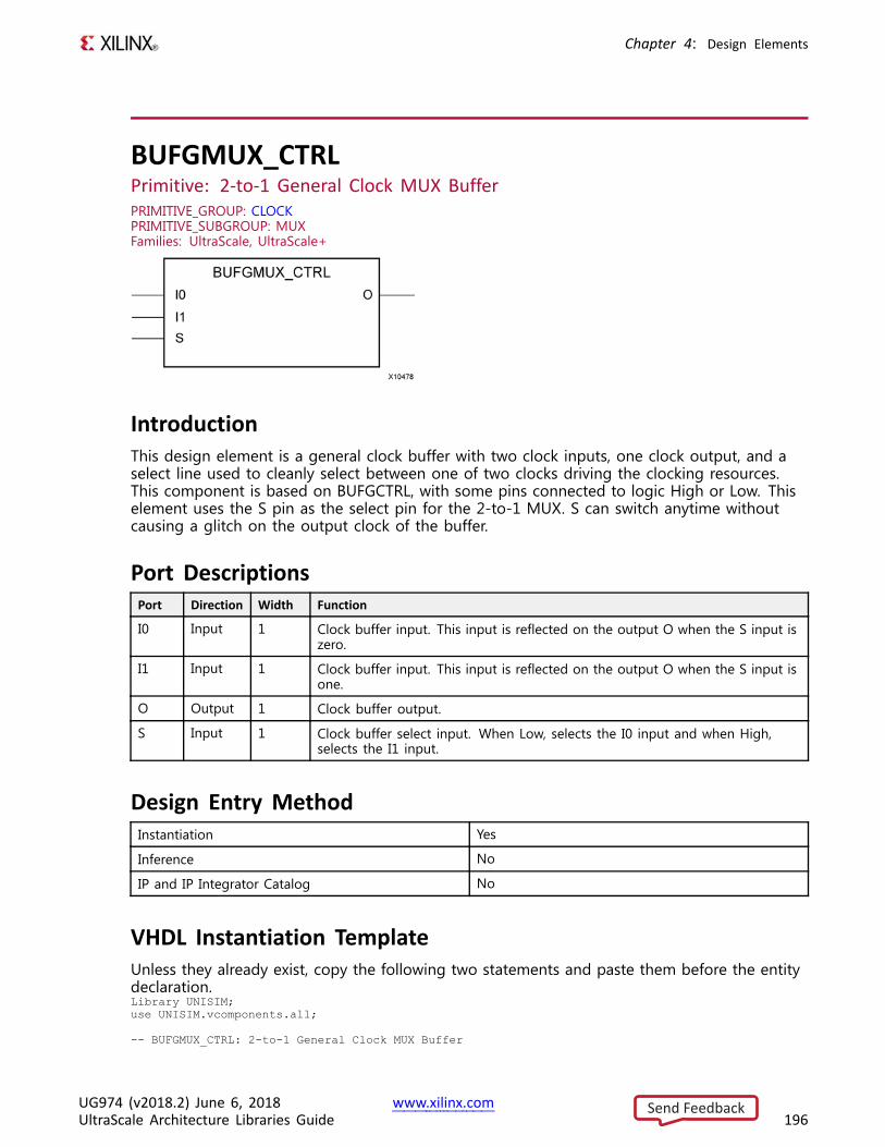
Chapter 4: Design Elements
BUFGMUX_CTRLPrimitive: 2-to-1 General Clock MUX BufferPRIMITIVE_GROUP: CLOCKPRIMITIVE_SUBGROUP: MUXFamilies: UltraScale, UltraScale+
IntroductionThis design element is a general clock buffer with two clock inputs, one clock output, and aselect line used to cleanly select between one of two clocks driving the clocking resources.This component is based on BUFGCTRL, with some pins connected to logic High or Low. Thiselement uses the S pin as the select pin for the 2-to-1 MUX. S can switch anytime withoutcausing a glitch on the output clock of the buffer.
Port DescriptionsPort Direction Width Function
I0 Input 1 Clock buffer input. This input is reflected on the output O when the S input iszero.
I1 Input 1 Clock buffer input. This input is reflected on the output O when the S input isone.
O Output 1 Clock buffer output.
S Input 1 Clock buffer select input. When Low, selects the I0 input and when High,selects the I1 input.
Design Entry MethodInstantiation Yes
Inference No
IP and IP Integrator Catalog No
VHDL Instantiation TemplateUnless they already exist, copy the following two statements and paste them before the entitydeclaration.Library UNISIM;use UNISIM.vcomponents.all;
-- BUFGMUX_CTRL: 2-to-1 General Clock MUX Buffer
UG974 (v2018.2) June 6, 2018 www.xilinx.comUltraScale Architecture Libraries Guide 196
Send Feedback
Chapter 4: Design Elements
-- UltraScale-- Xilinx HDL Language Template, version 2018.2
BUFGMUX_CTRL_inst : BUFGMUX_CTRLport map (
O => O, -- 1-bit output: Clock outputI0 => I0, -- 1-bit input: Clock input (S=0)I1 => I1, -- 1-bit input: Clock input (S=1)S => S -- 1-bit input: Clock select
);
-- End of BUFGMUX_CTRL_inst instantiation
Verilog Instantiation Template
// BUFGMUX_CTRL: 2-to-1 General Clock MUX Buffer// UltraScale// Xilinx HDL Language Template, version 2018.2
BUFGMUX_CTRL BUFGMUX_CTRL_inst (.O(O), // 1-bit output: Clock output.I0(I0), // 1-bit input: Clock input (S=0).I1(I1), // 1-bit input: Clock input (S=1).S(S) // 1-bit input: Clock select
);
// End of BUFGMUX_CTRL_inst instantiation
For More Information• See the UltraScale Architecture Clocking Resources User Guide (UG572).
• See the UltraScale Programmable Devices Documentation.
UG974 (v2018.2) June 6, 2018 www.xilinx.comUltraScale Architecture Libraries Guide 197
Send Feedback
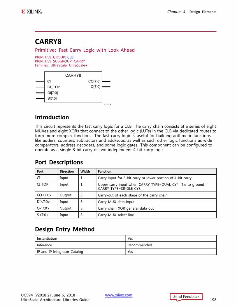
Chapter 4: Design Elements
CARRY8Primitive: Fast Carry Logic with Look AheadPRIMITIVE_GROUP: CLBPRIMITIVE_SUBGROUP: CARRYFamilies: UltraScale, UltraScale+
IntroductionThis circuit represents the fast carry logic for a CLB. The carry chain consists of a series of eightMUXes and eight XORs that connect to the other logic (LUTs) in the CLB via dedicated routes toform more complex functions. The fast carry logic is useful for building arithmetic functionslike adders, counters, subtractors and add/subs, as well as such other logic functions as widecomparators, address decoders, and some logic gates. This component can be configured tooperate as a single 8-bit carry or two independent 4-bit carry logic.
Port DescriptionsPort Direction Width Function
CI Input 1 Carry input for 8-bit carry or lower portion of 4-bit carry.
CI_TOP Input 1 Upper carry input when CARRY_TYPE=DUAL_CY4. Tie to ground ifCARRY_TYPE=SINGLE_CY8.
CO<7:0> Output 8 Carry-out of each stage of the carry chain
DI<7:0> Input 8 Carry-MUX data input
O<7:0> Output 8 Carry chain XOR general data out
S<7:0> Input 8 Carry-MUX select line
Design Entry MethodInstantiation Yes
Inference Recommended
IP and IP Integrator Catalog Yes
UG974 (v2018.2) June 6, 2018 www.xilinx.comUltraScale Architecture Libraries Guide 198
Send Feedback
Chapter 4: Design Elements
Available AttributesAttribute Type Allowed Values Default Description
CARRY_TYPE STRING "SINGLE _CY8","DUAL_CY4"
"SINGLE _CY8" Specifies whether the CLB carry logic isto function as a single 8 - bit carry -chain or two independent 4 - bit carrychains.
VHDL Instantiation TemplateUnless they already exist, copy the following two statements and paste them before the entitydeclaration.Library UNISIM;use UNISIM.vcomponents.all;
-- CARRY8: Fast Carry Logic with Look Ahead-- UltraScale-- Xilinx HDL Language Template, version 2018.2
CARRY8_inst : CARRY8generic map (
CARRY_TYPE => "SINGLE_CY8" -- 8-bit or dual 4-bit carry (DUAL_CY4, SINGLE_CY8))port map (
CO => CO, -- 8-bit output: Carry-outO => O, -- 8-bit output: Carry chain XOR data outCI => CI, -- 1-bit input: Lower Carry-InCI_TOP => CI_TOP, -- 1-bit input: Upper Carry-InDI => DI, -- 8-bit input: Carry-MUX data inS => S -- 8-bit input: Carry-mux select
);
-- End of CARRY8_inst instantiation
Verilog Instantiation Template
// CARRY8: Fast Carry Logic with Look Ahead// UltraScale// Xilinx HDL Language Template, version 2018.2
CARRY8 #(.CARRY_TYPE("SINGLE_CY8") // 8-bit or dual 4-bit carry (DUAL_CY4, SINGLE_CY8)
)CARRY8_inst (
.CO(CO), // 8-bit output: Carry-out
.O(O), // 8-bit output: Carry chain XOR data out
.CI(CI), // 1-bit input: Lower Carry-In
.CI_TOP(CI_TOP), // 1-bit input: Upper Carry-In
.DI(DI), // 8-bit input: Carry-MUX data in
.S(S) // 8-bit input: Carry-mux select);
// End of CARRY8_inst instantiation
For More Information• See the UltraScale Architecture Configurable Logic Block User Guide (UG574).
• See the UltraScale Programmable Devices Documentation.
UG974 (v2018.2) June 6, 2018 www.xilinx.comUltraScale Architecture Libraries Guide 199
Send Feedback
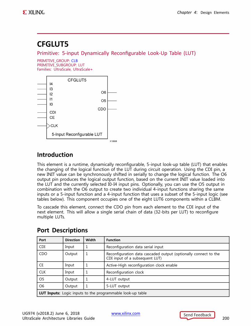
Chapter 4: Design Elements
CFGLUT5Primitive: 5-input Dynamically Reconfigurable Look-Up Table (LUT)PRIMITIVE_GROUP: CLBPRIMITIVE_SUBGROUP: LUTFamilies: UltraScale, UltraScale+
IntroductionThis element is a runtime, dynamically reconfigurable, 5-input look-up table (LUT) that enablesthe changing of the logical function of the LUT during circuit operation. Using the CDI pin, anew INIT value can be synchronously shifted in serially to change the logical function. The O6output pin produces the logical output function, based on the current INIT value loaded intothe LUT and the currently selected I0-I4 input pins. Optionally, you can use the O5 output incombination with the O6 output to create two individual 4-input functions sharing the sameinputs or a 5-input function and a 4-input function that uses a subset of the 5-input logic (seetables below). This component occupies one of the eight LUT6 components within a CLBM.
To cascade this element, connect the CDO pin from each element to the CDI input of thenext element. This will allow a single serial chain of data (32-bits per LUT) to reconfiguremultiple LUTs.
Port DescriptionsPort Direction Width Function
CDI Input 1 Reconfiguration data serial input
CDO Output 1 Reconfiguration data cascaded output (optionally connect to theCDI input of a subsequent LUT)
CE Input 1 Active-High reconfiguration clock enable
CLK Input 1 Reconfiguration clock
O5 Output 1 4-LUT output
O6 Output 1 5-LUT output
LUT Inputs: Logic inputs to the programmable look-up table
UG974 (v2018.2) June 6, 2018 www.xilinx.comUltraScale Architecture Libraries Guide 200
Send Feedback
Chapter 4: Design Elements
Port Direction Width Function
I0 Input 1 Logic inputs to the programmable look-up table
I1 Input 1 Logic inputs to the programmable look-up table
I2 Input 1 Logic inputs to the programmable look-up table
I3 Input 1 Logic inputs to the programmable look-up table
I4 Input 1 Logic inputs to the programmable look-up table
Design Entry MethodInstantiation Yes
Inference No
IP and IP Integrator Catalog No
Available AttributesAttribute Type Allowed Values Default Description
INIT HEX Any 32-bit HEXvalue
All zeroes Specifies the initial logical expression ofthis element
IS_CLK_INVERTED BINARY 1'b0 to 1'b1 1'b0 Indicates whether the CLK is active - highor active - low
VHDL Instantiation TemplateUnless they already exist, copy the following two statements and paste them before the entitydeclaration.Library UNISIM;use UNISIM.vcomponents.all;
-- CFGLUT5: 5-input Dynamically Reconfigurable Look-Up Table (LUT)-- UltraScale-- Xilinx HDL Language Template, version 2018.2
CFGLUT5_inst : CFGLUT5generic map (
INIT => X"00000000", -- Initial logic functionIS_CLK_INVERTED => '0' -- Optional inversion for CLK
)port map (
CDO => CDO, -- 1-bit output: Reconfiguration cascadeO5 => O5, -- 1-bit output: 4-LUTO6 => O6, -- 1-bit output: 5-LUTCDI => CDI, -- 1-bit input: Reconfiguration dataCE => CE, -- 1-bit input: Reconfiguration enableCLK => CLK, -- 1-bit input: Clock-- LUT Inputs inputs: Logic inputsI0 => I0,I1 => I1,I2 => I2,I3 => I3,I4 => I4
);
-- End of CFGLUT5_inst instantiation
UG974 (v2018.2) June 6, 2018 www.xilinx.comUltraScale Architecture Libraries Guide 201
Send Feedback
Chapter 4: Design Elements
Verilog Instantiation Template
// CFGLUT5: 5-input Dynamically Reconfigurable Look-Up Table (LUT)// UltraScale// Xilinx HDL Language Template, version 2018.2
CFGLUT5 #(.INIT(32'h00000000), // Initial logic function.IS_CLK_INVERTED(1'b0) // Optional inversion for CLK
)CFGLUT5_inst (
.CDO(CDO), // 1-bit output: Reconfiguration cascade
.O5(O5), // 1-bit output: 4-LUT
.O6(O6), // 1-bit output: 5-LUT
.CDI(CDI), // 1-bit input: Reconfiguration data
.CE(CE), // 1-bit input: Reconfiguration enable
.CLK(CLK), // 1-bit input: Clock// LUT Inputs inputs: Logic inputs.I0(I0),.I1(I1),.I2(I2),.I3(I3),.I4(I4)
);
// End of CFGLUT5_inst instantiation
For More Information• See the UltraScale Architecture Migration: Methodology Guide (UG1026).
• See the UltraScale Programmable Devices Documentation.
UG974 (v2018.2) June 6, 2018 www.xilinx.comUltraScale Architecture Libraries Guide 202
Send Feedback
Chapter 4: Design Elements
CMACPrimitive: 100G MAC BlockPRIMITIVE_GROUP: ADVANCEDPRIMITIVE_SUBGROUP: MACFamilies: UltraScale
IntroductionThe 100G MAC Block provides a high-performance, low latency 100G Ethernet port that allowsfor a wide range of user customization and statistics gathering. It supports 1588 time stampingfor one step and two step. This element is not intended to be instantiated, used, or modifiedoutside of Xilinx generated IP. The block is designed to be integrated with GTs and deviceclocking resources using fabric interconnect. See the UltraScale Architecture Integrated Blockfor 100G Ethernet Product Guide for further details on this component.
Design Entry MethodInstantiation No
Inference No
IP and IP Integrator Catalog Recommended
For More Information• See the UltraScale Architecture Integrated Block for 100G Ethernet v1.7 Product Guide
(PG165).
• See the UltraScale Programmable Devices Documentation.
UG974 (v2018.2) June 6, 2018 www.xilinx.comUltraScale Architecture Libraries Guide 203
Send Feedback
Chapter 4: Design Elements
CMACE4Primitive: 100G MAC BlockPRIMITIVE_GROUP: ADVANCEDPRIMITIVE_SUBGROUP: MACFamilies: UltraScale+
IntroductionThe 100G MAC Block provides a high-performance, low latency 100G Ethernet port that allowsfor a wide range of user customization and statistics gathering. It supports 1588 time stampingfor one step and two step. This element is not intended to be instantiated, used, or modifiedoutside of Xilinx generated IP. The block is designed to be integrated with GTs and deviceclocking resources using fabric interconnect. See the UltraScale+ Architecture Integrated Blockfor 100G Ethernet Product Guide for further details on this component.
Design Entry MethodInstantiation No
Inference No
IP and IP Integrator Catalog Recommended
For More Information• See the UltraScale Architecture Integrated Block for 100G Ethernet v1.7 Product Guide
(PG165).
• See the UltraScale Programmable Devices Documentation.
UG974 (v2018.2) June 6, 2018 www.xilinx.comUltraScale Architecture Libraries Guide 204
Send Feedback
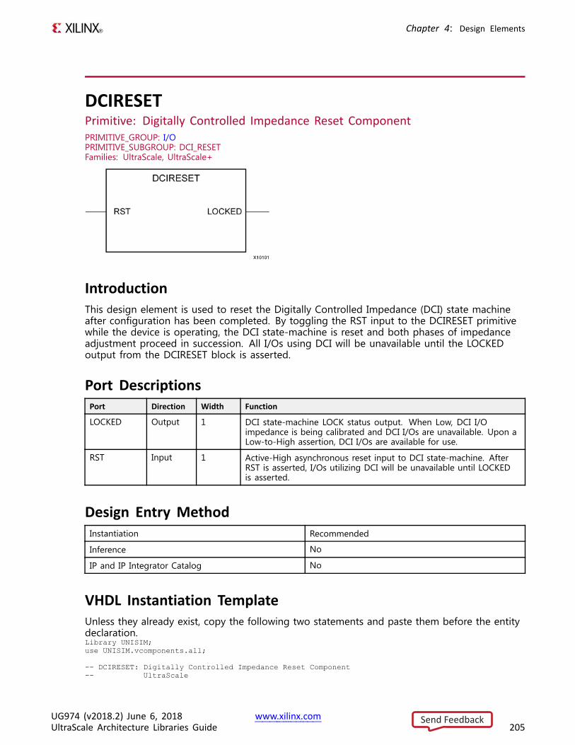
Chapter 4: Design Elements
DCIRESETPrimitive: Digitally Controlled Impedance Reset ComponentPRIMITIVE_GROUP: I/OPRIMITIVE_SUBGROUP: DCI_RESETFamilies: UltraScale, UltraScale+
IntroductionThis design element is used to reset the Digitally Controlled Impedance (DCI) state machineafter configuration has been completed. By toggling the RST input to the DCIRESET primitivewhile the device is operating, the DCI state-machine is reset and both phases of impedanceadjustment proceed in succession. All I/Os using DCI will be unavailable until the LOCKEDoutput from the DCIRESET block is asserted.
Port DescriptionsPort Direction Width Function
LOCKED Output 1 DCI state-machine LOCK status output. When Low, DCI I/Oimpedance is being calibrated and DCI I/Os are unavailable. Upon aLow-to-High assertion, DCI I/Os are available for use.
RST Input 1 Active-High asynchronous reset input to DCI state-machine. AfterRST is asserted, I/Os utilizing DCI will be unavailable until LOCKEDis asserted.
Design Entry MethodInstantiation Recommended
Inference No
IP and IP Integrator Catalog No
VHDL Instantiation TemplateUnless they already exist, copy the following two statements and paste them before the entitydeclaration.Library UNISIM;use UNISIM.vcomponents.all;
-- DCIRESET: Digitally Controlled Impedance Reset Component-- UltraScale
UG974 (v2018.2) June 6, 2018 www.xilinx.comUltraScale Architecture Libraries Guide 205
Send Feedback
Chapter 4: Design Elements
-- Xilinx HDL Language Template, version 2018.2
DCIRESET_inst : DCIRESETport map (
LOCKED => LOCKED, -- 1-bit output: LOCK status outputRST => RST -- 1-bit input: Active-High asynchronous reset input
);
-- End of DCIRESET_inst instantiation
Verilog Instantiation Template
// DCIRESET: Digitally Controlled Impedance Reset Component// UltraScale// Xilinx HDL Language Template, version 2018.2
DCIRESET DCIRESET_inst (.LOCKED(LOCKED), // 1-bit output: LOCK status output.RST(RST) // 1-bit input: Active-High asynchronous reset input
);
// End of DCIRESET_inst instantiation
For More Information• See the UltraScale Architecture SelectIO Resources User Guide (UG571).
• See the UltraScale Programmable Devices Documentation.
UG974 (v2018.2) June 6, 2018 www.xilinx.comUltraScale Architecture Libraries Guide 206
Send Feedback
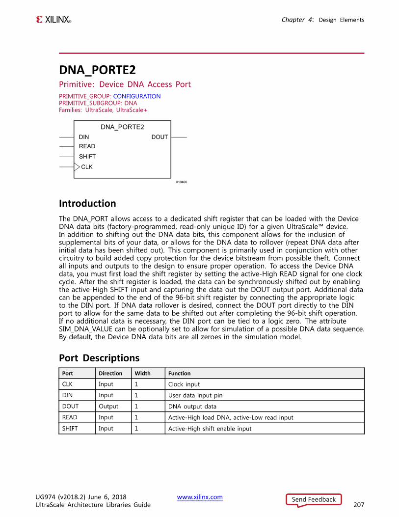
Chapter 4: Design Elements
DNA_PORTE2Primitive: Device DNA Access PortPRIMITIVE_GROUP: CONFIGURATIONPRIMITIVE_SUBGROUP: DNAFamilies: UltraScale, UltraScale+
IntroductionThe DNA_PORT allows access to a dedicated shift register that can be loaded with the DeviceDNA data bits (factory-programmed, read-only unique ID) for a given UltraScale™ device.In addition to shifting out the DNA data bits, this component allows for the inclusion ofsupplemental bits of your data, or allows for the DNA data to rollover (repeat DNA data afterinitial data has been shifted out). This component is primarily used in conjunction with othercircuitry to build added copy protection for the device bitstream from possible theft. Connectall inputs and outputs to the design to ensure proper operation. To access the Device DNAdata, you must first load the shift register by setting the active-High READ signal for one clockcycle. After the shift register is loaded, the data can be synchronously shifted out by enablingthe active-High SHIFT input and capturing the data out the DOUT output port. Additional datacan be appended to the end of the 96-bit shift register by connecting the appropriate logicto the DIN port. If DNA data rollover is desired, connect the DOUT port directly to the DINport to allow for the same data to be shifted out after completing the 96-bit shift operation.If no additional data is necessary, the DIN port can be tied to a logic zero. The attributeSIM_DNA_VALUE can be optionally set to allow for simulation of a possible DNA data sequence.By default, the Device DNA data bits are all zeroes in the simulation model.
Port DescriptionsPort Direction Width Function
CLK Input 1 Clock input
DIN Input 1 User data input pin
DOUT Output 1 DNA output data
READ Input 1 Active-High load DNA, active-Low read input
SHIFT Input 1 Active-High shift enable input
UG974 (v2018.2) June 6, 2018 www.xilinx.comUltraScale Architecture Libraries Guide 207
Send Feedback
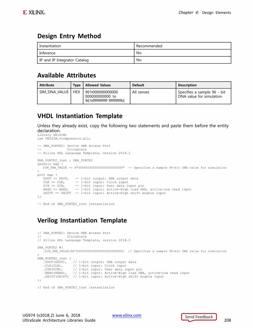
Chapter 4: Design Elements
Design Entry MethodInstantiation Recommended
Inference No
IP and IP Integrator Catalog No
Available AttributesAttribute Type Allowed Values Default Description
SIM_DNA_VALUE HEX 96'h000000000000000000000000 to96'hffffffffffff fffffffffffd
All zeroes Specifies a sample 96 - bitDNA value for simulation
VHDL Instantiation TemplateUnless they already exist, copy the following two statements and paste them before the entitydeclaration.Library UNISIM;use UNISIM.vcomponents.all;
-- DNA_PORTE2: Device DNA Access Port-- UltraScale-- Xilinx HDL Language Template, version 2018.2
DNA_PORTE2_inst : DNA_PORTE2generic map (
SIM_DNA_VALUE => X"000000000000000000000000" -- Specifies a sample 96-bit DNA value for simulation)port map (
DOUT => DOUT, -- 1-bit output: DNA output dataCLK => CLK, -- 1-bit input: Clock inputDIN => DIN, -- 1-bit input: User data input pinREAD => READ, -- 1-bit input: Active-High load DNA, active-Low read inputSHIFT => SHIFT -- 1-bit input: Active-High shift enable input
);
-- End of DNA_PORTE2_inst instantiation
Verilog Instantiation Template
// DNA_PORTE2: Device DNA Access Port// UltraScale// Xilinx HDL Language Template, version 2018.2
DNA_PORTE2 #(.SIM_DNA_VALUE(96'h000000000000000000000000) // Specifies a sample 96-bit DNA value for simulation
)DNA_PORTE2_inst (
.DOUT(DOUT), // 1-bit output: DNA output data
.CLK(CLK), // 1-bit input: Clock input
.DIN(DIN), // 1-bit input: User data input pin
.READ(READ), // 1-bit input: Active-High load DNA, active-Low read input
.SHIFT(SHIFT) // 1-bit input: Active-High shift enable input);
// End of DNA_PORTE2_inst instantiation
UG974 (v2018.2) June 6, 2018 www.xilinx.comUltraScale Architecture Libraries Guide 208
Send Feedback

Chapter 4: Design Elements
For More Information• See the UltraScale Architecture Configuration User Guide (UG570).
• See the UltraScale Programmable Devices Documentation.
UG974 (v2018.2) June 6, 2018 www.xilinx.comUltraScale Architecture Libraries Guide 209
Send Feedback
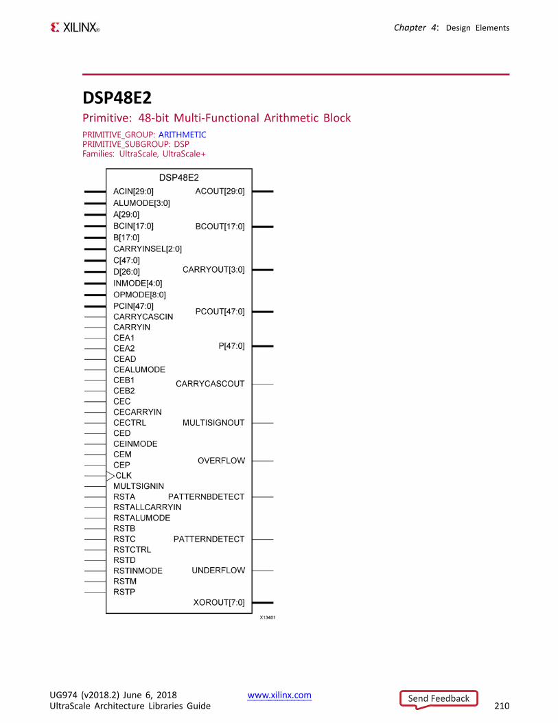
Chapter 4: Design Elements
DSP48E2Primitive: 48-bit Multi-Functional Arithmetic BlockPRIMITIVE_GROUP: ARITHMETICPRIMITIVE_SUBGROUP: DSPFamilies: UltraScale, UltraScale+
UG974 (v2018.2) June 6, 2018 www.xilinx.comUltraScale Architecture Libraries Guide 210
Send Feedback
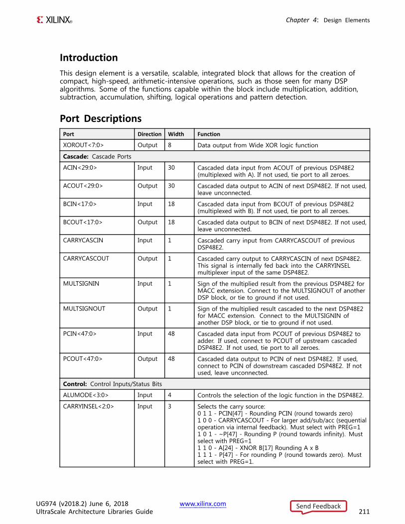
Chapter 4: Design Elements
IntroductionThis design element is a versatile, scalable, integrated block that allows for the creation ofcompact, high-speed, arithmetic-intensive operations, such as those seen for many DSPalgorithms. Some of the functions capable within the block include multiplication, addition,subtraction, accumulation, shifting, logical operations and pattern detection.
Port DescriptionsPort Direction Width Function
XOROUT<7:0> Output 8 Data output from Wide XOR logic function
Cascade: Cascade Ports
ACIN<29:0> Input 30 Cascaded data input from ACOUT of previous DSP48E2(multiplexed with A). If not used, tie port to all zeroes.
ACOUT<29:0> Output 30 Cascaded data output to ACIN of next DSP48E2. If not used,leave unconnected.
BCIN<17:0> Input 18 Cascaded data input from BCOUT of previous DSP48E2(multiplexed with B). If not used, tie port to all zeroes.
BCOUT<17:0> Output 18 Cascaded data output to BCIN of next DSP48E2. If not used,leave unconnected.
CARRYCASCIN Input 1 Cascaded carry input from CARRYCASCOUT of previousDSP48E2.
CARRYCASCOUT Output 1 Cascaded carry output to CARRYCASCIN of next DSP48E2.This signal is internally fed back into the CARRYINSELmultiplexer input of the same DSP48E2.
MULTSIGNIN Input 1 Sign of the multiplied result from the previous DSP48E2 forMACC extension. Connect to the MULTSIGNOUT of anotherDSP block, or tie to ground if not used.
MULTSIGNOUT Output 1 Sign of the multiplied result cascaded to the next DSP48E2for MACC extension. Connect to the MULTSIGNIN ofanother DSP block, or tie to ground if not used.
PCIN<47:0> Input 48 Cascaded data input from PCOUT of previous DSP48E2 toadder. If used, connect to PCOUT of upstream cascadedDSP48E2. If not used, tie port to all zeroes.
PCOUT<47:0> Output 48 Cascaded data output to PCIN of next DSP48E2. If used,connect to PCIN of downstream cascaded DSP48E2. If notused, leave unconnected.
Control: Control Inputs/Status Bits
ALUMODE<3:0> Input 4 Controls the selection of the logic function in the DSP48E2.
CARRYINSEL<2:0> Input 3 Selects the carry source:0 1 1 - PCIN[47] - Rounding PCIN (round towards zero)1 0 0 - CARRYCASCOUT - For larger add/sub/acc (sequentialoperation via internal feedback). Must select with PREG=11 0 1 - ~P[47] - Rounding P (round towards infinity). Mustselect with PREG=11 1 0 - A[24] - XNOR B[17] Rounding A x B1 1 1 - P[47] - For rounding P (round towards zero). Mustselect with PREG=1.
UG974 (v2018.2) June 6, 2018 www.xilinx.comUltraScale Architecture Libraries Guide 211
Send Feedback
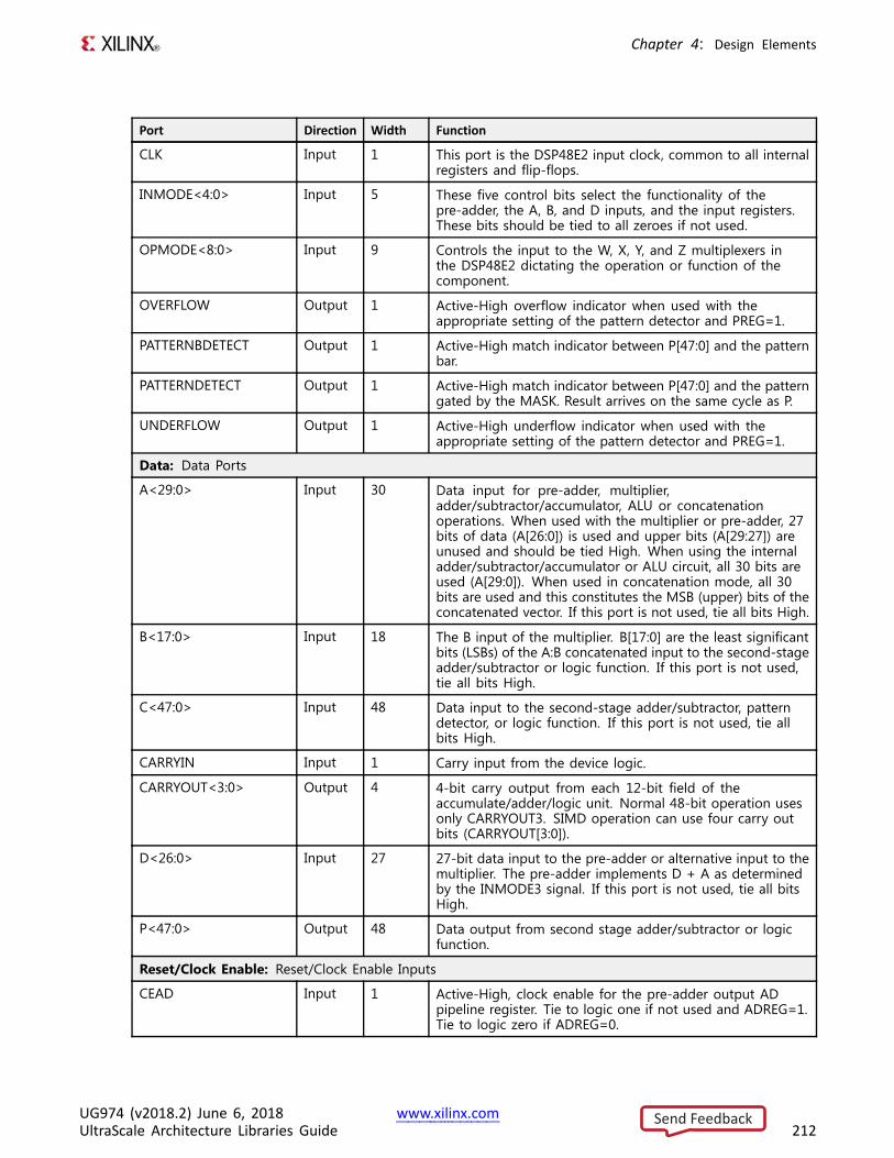
Chapter 4: Design Elements
Port Direction Width Function
CLK Input 1 This port is the DSP48E2 input clock, common to all internalregisters and flip-flops.
INMODE<4:0> Input 5 These five control bits select the functionality of thepre-adder, the A, B, and D inputs, and the input registers.These bits should be tied to all zeroes if not used.
OPMODE<8:0> Input 9 Controls the input to the W, X, Y, and Z multiplexers inthe DSP48E2 dictating the operation or function of thecomponent.
OVERFLOW Output 1 Active-High overflow indicator when used with theappropriate setting of the pattern detector and PREG=1.
PATTERNBDETECT Output 1 Active-High match indicator between P[47:0] and the patternbar.
PATTERNDETECT Output 1 Active-High match indicator between P[47:0] and the patterngated by the MASK. Result arrives on the same cycle as P.
UNDERFLOW Output 1 Active-High underflow indicator when used with theappropriate setting of the pattern detector and PREG=1.
Data: Data Ports
A<29:0> Input 30 Data input for pre-adder, multiplier,adder/subtractor/accumulator, ALU or concatenationoperations. When used with the multiplier or pre-adder, 27bits of data (A[26:0]) is used and upper bits (A[29:27]) areunused and should be tied High. When using the internaladder/subtractor/accumulator or ALU circuit, all 30 bits areused (A[29:0]). When used in concatenation mode, all 30bits are used and this constitutes the MSB (upper) bits of theconcatenated vector. If this port is not used, tie all bits High.
B<17:0> Input 18 The B input of the multiplier. B[17:0] are the least significantbits (LSBs) of the A:B concatenated input to the second-stageadder/subtractor or logic function. If this port is not used,tie all bits High.
C<47:0> Input 48 Data input to the second-stage adder/subtractor, patterndetector, or logic function. If this port is not used, tie allbits High.
CARRYIN Input 1 Carry input from the device logic.
CARRYOUT<3:0> Output 4 4-bit carry output from each 12-bit field of theaccumulate/adder/logic unit. Normal 48-bit operation usesonly CARRYOUT3. SIMD operation can use four carry outbits (CARRYOUT[3:0]).
D<26:0> Input 27 27-bit data input to the pre-adder or alternative input to themultiplier. The pre-adder implements D + A as determinedby the INMODE3 signal. If this port is not used, tie all bitsHigh.
P<47:0> Output 48 Data output from second stage adder/subtractor or logicfunction.
Reset/Clock Enable: Reset/Clock Enable Inputs
CEAD Input 1 Active-High, clock enable for the pre-adder output ADpipeline register. Tie to logic one if not used and ADREG=1.Tie to logic zero if ADREG=0.
UG974 (v2018.2) June 6, 2018 www.xilinx.comUltraScale Architecture Libraries Guide 212
Send Feedback
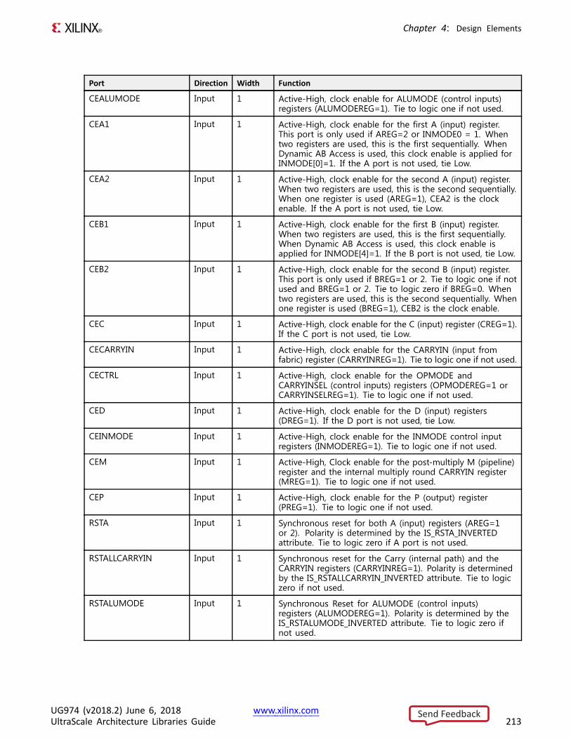
Chapter 4: Design Elements
Port Direction Width Function
CEALUMODE Input 1 Active-High, clock enable for ALUMODE (control inputs)registers (ALUMODEREG=1). Tie to logic one if not used.
CEA1 Input 1 Active-High, clock enable for the first A (input) register.This port is only used if AREG=2 or INMODE0 = 1. Whentwo registers are used, this is the first sequentially. WhenDynamic AB Access is used, this clock enable is applied forINMODE[0]=1. If the A port is not used, tie Low.
CEA2 Input 1 Active-High, clock enable for the second A (input) register.When two registers are used, this is the second sequentially.When one register is used (AREG=1), CEA2 is the clockenable. If the A port is not used, tie Low.
CEB1 Input 1 Active-High, clock enable for the first B (input) register.When two registers are used, this is the first sequentially.When Dynamic AB Access is used, this clock enable isapplied for INMODE[4]=1. If the B port is not used, tie Low.
CEB2 Input 1 Active-High, clock enable for the second B (input) register.This port is only used if BREG=1 or 2. Tie to logic one if notused and BREG=1 or 2. Tie to logic zero if BREG=0. Whentwo registers are used, this is the second sequentially. Whenone register is used (BREG=1), CEB2 is the clock enable.
CEC Input 1 Active-High, clock enable for the C (input) register (CREG=1).If the C port is not used, tie Low.
CECARRYIN Input 1 Active-High, clock enable for the CARRYIN (input fromfabric) register (CARRYINREG=1). Tie to logic one if not used.
CECTRL Input 1 Active-High, clock enable for the OPMODE andCARRYINSEL (control inputs) registers (OPMODEREG=1 orCARRYINSELREG=1). Tie to logic one if not used.
CED Input 1 Active-High, clock enable for the D (input) registers(DREG=1). If the D port is not used, tie Low.
CEINMODE Input 1 Active-High, clock enable for the INMODE control inputregisters (INMODEREG=1). Tie to logic one if not used.
CEM Input 1 Active-High, Clock enable for the post-multiply M (pipeline)register and the internal multiply round CARRYIN register(MREG=1). Tie to logic one if not used.
CEP Input 1 Active-High, clock enable for the P (output) register(PREG=1). Tie to logic one if not used.
RSTA Input 1 Synchronous reset for both A (input) registers (AREG=1or 2). Polarity is determined by the IS_RSTA_INVERTEDattribute. Tie to logic zero if A port is not used.
RSTALLCARRYIN Input 1 Synchronous reset for the Carry (internal path) and theCARRYIN registers (CARRYINREG=1). Polarity is determinedby the IS_RSTALLCARRYIN_INVERTED attribute. Tie to logiczero if not used.
RSTALUMODE Input 1 Synchronous Reset for ALUMODE (control inputs)registers (ALUMODEREG=1). Polarity is determined by theIS_RSTALUMODE_INVERTED attribute. Tie to logic zero ifnot used.
UG974 (v2018.2) June 6, 2018 www.xilinx.comUltraScale Architecture Libraries Guide 213
Send Feedback
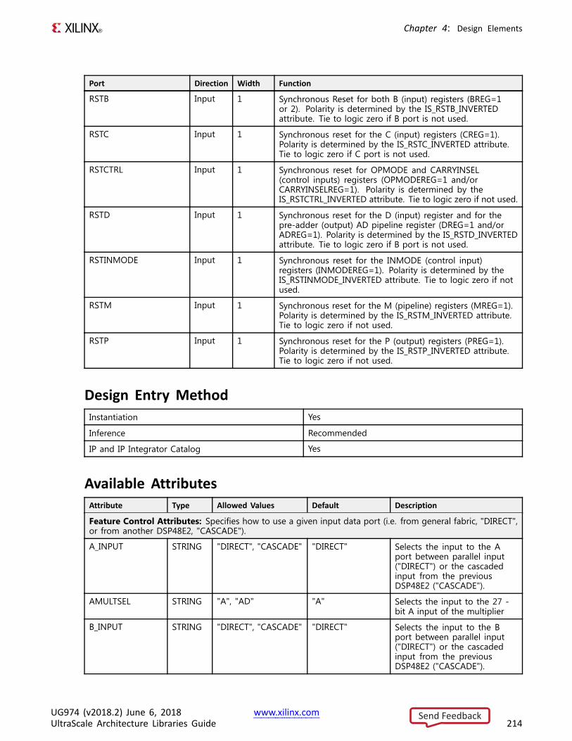
Chapter 4: Design Elements
Port Direction Width Function
RSTB Input 1 Synchronous Reset for both B (input) registers (BREG=1or 2). Polarity is determined by the IS_RSTB_INVERTEDattribute. Tie to logic zero if B port is not used.
RSTC Input 1 Synchronous reset for the C (input) registers (CREG=1).Polarity is determined by the IS_RSTC_INVERTED attribute.Tie to logic zero if C port is not used.
RSTCTRL Input 1 Synchronous reset for OPMODE and CARRYINSEL(control inputs) registers (OPMODEREG=1 and/orCARRYINSELREG=1). Polarity is determined by theIS_RSTCTRL_INVERTED attribute. Tie to logic zero if not used.
RSTD Input 1 Synchronous reset for the D (input) register and for thepre-adder (output) AD pipeline register (DREG=1 and/orADREG=1). Polarity is determined by the IS_RSTD_INVERTEDattribute. Tie to logic zero if B port is not used.
RSTINMODE Input 1 Synchronous reset for the INMODE (control input)registers (INMODEREG=1). Polarity is determined by theIS_RSTINMODE_INVERTED attribute. Tie to logic zero if notused.
RSTM Input 1 Synchronous reset for the M (pipeline) registers (MREG=1).Polarity is determined by the IS_RSTM_INVERTED attribute.Tie to logic zero if not used.
RSTP Input 1 Synchronous reset for the P (output) registers (PREG=1).Polarity is determined by the IS_RSTP_INVERTED attribute.Tie to logic zero if not used.
Design Entry MethodInstantiation Yes
Inference Recommended
IP and IP Integrator Catalog Yes
Available AttributesAttribute Type Allowed Values Default Description
Feature Control Attributes: Specifies how to use a given input data port (i.e. from general fabric, "DIRECT",or from another DSP48E2, "CASCADE").
A_INPUT STRING "DIRECT", "CASCADE" "DIRECT" Selects the input to the Aport between parallel input("DIRECT") or the cascadedinput from the previousDSP48E2 ("CASCADE").
AMULTSEL STRING "A", "AD" "A" Selects the input to the 27 -bit A input of the multiplier
B_INPUT STRING "DIRECT", "CASCADE" "DIRECT" Selects the input to the Bport between parallel input("DIRECT") or the cascadedinput from the previousDSP48E2 ("CASCADE").
UG974 (v2018.2) June 6, 2018 www.xilinx.comUltraScale Architecture Libraries Guide 214
Send Feedback
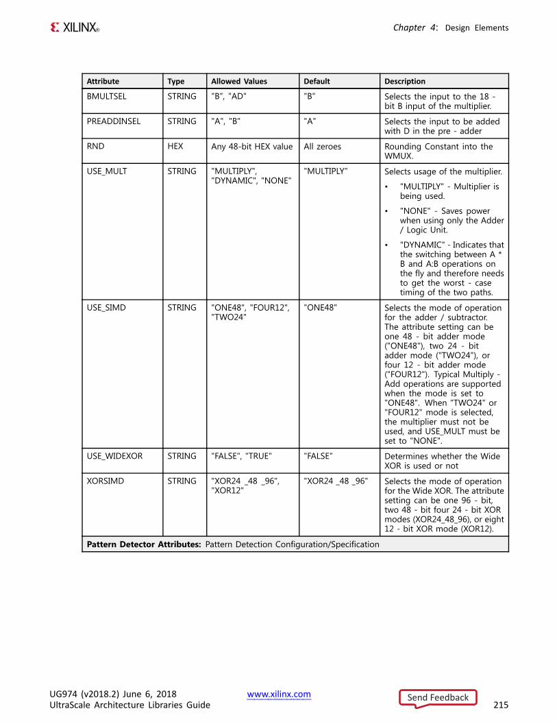
Chapter 4: Design Elements
Attribute Type Allowed Values Default Description
BMULTSEL STRING "B", "AD" "B" Selects the input to the 18 -bit B input of the multiplier.
PREADDINSEL STRING "A", "B" "A" Selects the input to be addedwith D in the pre - adder
RND HEX Any 48-bit HEX value All zeroes Rounding Constant into theWMUX.
USE_MULT STRING "MULTIPLY","DYNAMIC", "NONE"
"MULTIPLY" Selects usage of the multiplier.
• "MULTIPLY" - Multiplier isbeing used.
• "NONE" - Saves powerwhen using only the Adder/ Logic Unit.
• "DYNAMIC" - Indicates thatthe switching between A *B and A:B operations onthe fly and therefore needsto get the worst - casetiming of the two paths.
USE_SIMD STRING "ONE48", "FOUR12","TWO24"
"ONE48" Selects the mode of operationfor the adder / subtractor.The attribute setting can beone 48 - bit adder mode("ONE48"), two 24 - bitadder mode ("TWO24"), orfour 12 - bit adder mode("FOUR12"). Typical Multiply -Add operations are supportedwhen the mode is set to"ONE48". When "TWO24" or"FOUR12" mode is selected,the multiplier must not beused, and USE_MULT must beset to "NONE".
USE_WIDEXOR STRING "FALSE", "TRUE" "FALSE" Determines whether the WideXOR is used or not
XORSIMD STRING "XOR24 _48 _96","XOR12"
"XOR24 _48 _96" Selects the mode of operationfor the Wide XOR. The attributesetting can be one 96 - bit,two 48 - bit four 24 - bit XORmodes (XOR24_48_96), or eight12 - bit XOR mode (XOR12).
Pattern Detector Attributes: Pattern Detection Configuration/Specification
UG974 (v2018.2) June 6, 2018 www.xilinx.comUltraScale Architecture Libraries Guide 215
Send Feedback
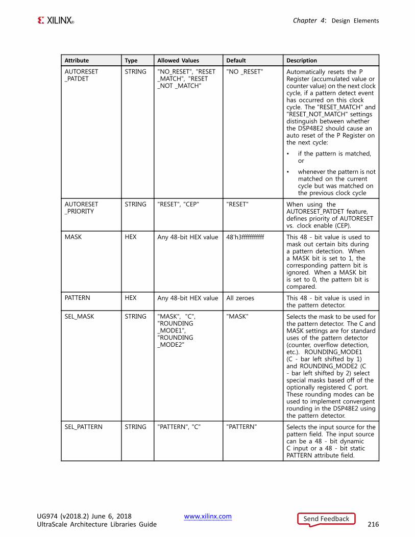
Chapter 4: Design Elements
Attribute Type Allowed Values Default Description
AUTORESET_PATDET
STRING "NO_RESET", "RESET_MATCH", "RESET_NOT _MATCH"
"NO _RESET" Automatically resets the PRegister (accumulated value orcounter value) on the next clockcycle, if a pattern detect eventhas occurred on this clockcycle. The "RESET_MATCH" and"RESET_NOT_MATCH" settingsdistinguish between whetherthe DSP48E2 should cause anauto reset of the P Register onthe next cycle:
• if the pattern is matched,or
• whenever the pattern is notmatched on the currentcycle but was matched onthe previous clock cycle
AUTORESET_PRIORITY
STRING "RESET", "CEP" "RESET" When using theAUTORESET_PATDET feature,defines priority of AUTORESETvs. clock enable (CEP).
MASK HEX Any 48-bit HEX value 48'h3fffffffffff This 48 - bit value is used tomask out certain bits duringa pattern detection. Whena MASK bit is set to 1, thecorresponding pattern bit isignored. When a MASK bitis set to 0, the pattern bit iscompared.
PATTERN HEX Any 48-bit HEX value All zeroes This 48 - bit value is used inthe pattern detector.
SEL_MASK STRING "MASK", "C","ROUNDING_MODE1","ROUNDING_MODE2"
"MASK" Selects the mask to be used forthe pattern detector. The C andMASK settings are for standarduses of the pattern detector(counter, overflow detection,etc.). ROUNDING_MODE1(C - bar left shifted by 1)and ROUNDING_MODE2 (C- bar left shifted by 2) selectspecial masks based off of theoptionally registered C port.These rounding modes can beused to implement convergentrounding in the DSP48E2 usingthe pattern detector.
SEL_PATTERN STRING "PATTERN", "C" "PATTERN" Selects the input source for thepattern field. The input sourcecan be a 48 - bit dynamicC input or a 48 - bit staticPATTERN attribute field.
UG974 (v2018.2) June 6, 2018 www.xilinx.comUltraScale Architecture Libraries Guide 216
Send Feedback
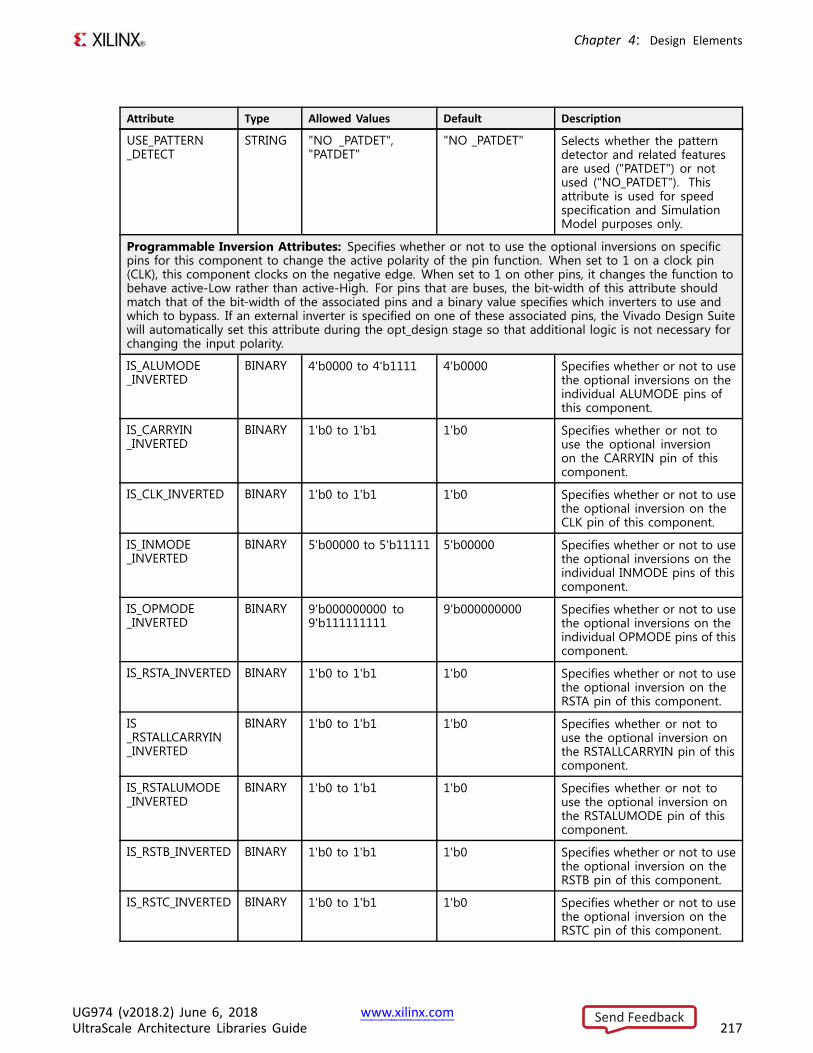
Chapter 4: Design Elements
Attribute Type Allowed Values Default Description
USE_PATTERN_DETECT
STRING "NO _PATDET","PATDET"
"NO _PATDET" Selects whether the patterndetector and related featuresare used ("PATDET") or notused ("NO_PATDET"). Thisattribute is used for speedspecification and SimulationModel purposes only.
Programmable Inversion Attributes: Specifies whether or not to use the optional inversions on specificpins for this component to change the active polarity of the pin function. When set to 1 on a clock pin(CLK), this component clocks on the negative edge. When set to 1 on other pins, it changes the function tobehave active-Low rather than active-High. For pins that are buses, the bit-width of this attribute shouldmatch that of the bit-width of the associated pins and a binary value specifies which inverters to use andwhich to bypass. If an external inverter is specified on one of these associated pins, the Vivado Design Suitewill automatically set this attribute during the opt_design stage so that additional logic is not necessary forchanging the input polarity.
IS_ALUMODE_INVERTED
BINARY 4'b0000 to 4'b1111 4'b0000 Specifies whether or not to usethe optional inversions on theindividual ALUMODE pins ofthis component.
IS_CARRYIN_INVERTED
BINARY 1'b0 to 1'b1 1'b0 Specifies whether or not touse the optional inversionon the CARRYIN pin of thiscomponent.
IS_CLK_INVERTED BINARY 1'b0 to 1'b1 1'b0 Specifies whether or not to usethe optional inversion on theCLK pin of this component.
IS_INMODE_INVERTED
BINARY 5'b00000 to 5'b11111 5'b00000 Specifies whether or not to usethe optional inversions on theindividual INMODE pins of thiscomponent.
IS_OPMODE_INVERTED
BINARY 9'b000000000 to9'b111111111
9'b000000000 Specifies whether or not to usethe optional inversions on theindividual OPMODE pins of thiscomponent.
IS_RSTA_INVERTED BINARY 1'b0 to 1'b1 1'b0 Specifies whether or not to usethe optional inversion on theRSTA pin of this component.
IS_RSTALLCARRYIN_INVERTED
BINARY 1'b0 to 1'b1 1'b0 Specifies whether or not touse the optional inversion onthe RSTALLCARRYIN pin of thiscomponent.
IS_RSTALUMODE_INVERTED
BINARY 1'b0 to 1'b1 1'b0 Specifies whether or not touse the optional inversion onthe RSTALUMODE pin of thiscomponent.
IS_RSTB_INVERTED BINARY 1'b0 to 1'b1 1'b0 Specifies whether or not to usethe optional inversion on theRSTB pin of this component.
IS_RSTC_INVERTED BINARY 1'b0 to 1'b1 1'b0 Specifies whether or not to usethe optional inversion on theRSTC pin of this component.
UG974 (v2018.2) June 6, 2018 www.xilinx.comUltraScale Architecture Libraries Guide 217
Send Feedback
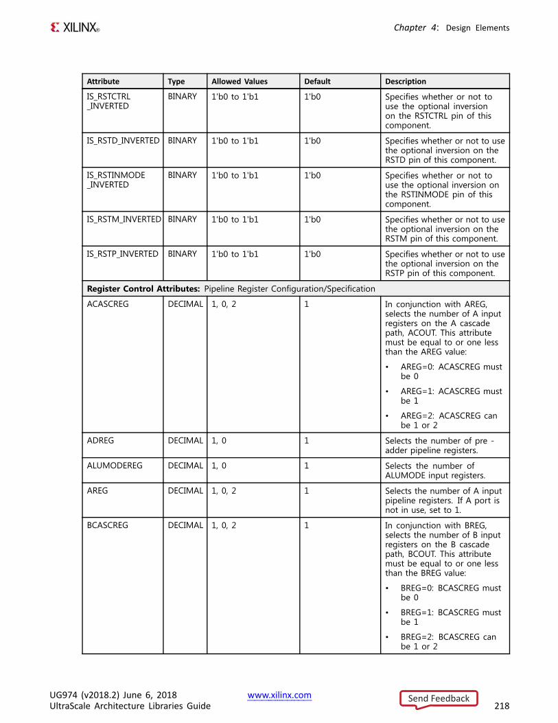
Chapter 4: Design Elements
Attribute Type Allowed Values Default Description
IS_RSTCTRL_INVERTED
BINARY 1'b0 to 1'b1 1'b0 Specifies whether or not touse the optional inversionon the RSTCTRL pin of thiscomponent.
IS_RSTD_INVERTED BINARY 1'b0 to 1'b1 1'b0 Specifies whether or not to usethe optional inversion on theRSTD pin of this component.
IS_RSTINMODE_INVERTED
BINARY 1'b0 to 1'b1 1'b0 Specifies whether or not touse the optional inversion onthe RSTINMODE pin of thiscomponent.
IS_RSTM_INVERTED BINARY 1'b0 to 1'b1 1'b0 Specifies whether or not to usethe optional inversion on theRSTM pin of this component.
IS_RSTP_INVERTED BINARY 1'b0 to 1'b1 1'b0 Specifies whether or not to usethe optional inversion on theRSTP pin of this component.
Register Control Attributes: Pipeline Register Configuration/Specification
ACASCREG DECIMAL 1, 0, 2 1 In conjunction with AREG,selects the number of A inputregisters on the A cascadepath, ACOUT. This attributemust be equal to or one lessthan the AREG value:
• AREG=0: ACASCREG mustbe 0
• AREG=1: ACASCREG mustbe 1
• AREG=2: ACASCREG canbe 1 or 2
ADREG DECIMAL 1, 0 1 Selects the number of pre -adder pipeline registers.
ALUMODEREG DECIMAL 1, 0 1 Selects the number ofALUMODE input registers.
AREG DECIMAL 1, 0, 2 1 Selects the number of A inputpipeline registers. If A port isnot in use, set to 1.
BCASCREG DECIMAL 1, 0, 2 1 In conjunction with BREG,selects the number of B inputregisters on the B cascadepath, BCOUT. This attributemust be equal to or one lessthan the BREG value:
• BREG=0: BCASCREG mustbe 0
• BREG=1: BCASCREG mustbe 1
• BREG=2: BCASCREG canbe 1 or 2
UG974 (v2018.2) June 6, 2018 www.xilinx.comUltraScale Architecture Libraries Guide 218
Send Feedback
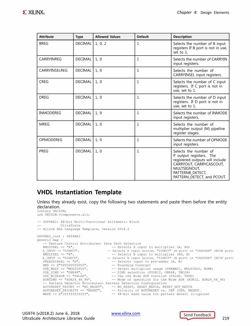
Chapter 4: Design Elements
Attribute Type Allowed Values Default Description
BREG DECIMAL 1, 0, 2 1 Selects the number of B inputregisters If B port is not in use,set to 1.
CARRYINREG DECIMAL 1, 0 1 Selects the number of CARRYINinput registers.
CARRYINSELREG DECIMAL 1, 0 1 Selects the number ofCARRYINSEL input registers.
CREG DECIMAL 1, 0 1 Selects the number of C inputregisters. If C port is not inuse, set to 1.
DREG DECIMAL 1, 0 1 Selects the number of D inputregisters. If D port is not inuse, set to 1.
INMODEREG DECIMAL 1, 0 1 Selects the number of INMODEinput registers.
MREG DECIMAL 1, 0 1 Selects the number ofmultiplier output (M) pipelineregister stages.
OPMODEREG DECIMAL 1, 0 1 Selects the number of OPMODEinput registers.
PREG DECIMAL 1, 0 1 Selects the number ofP output registers. Theregistered outputs will includeCARRYOUT, CARRYCASCOUT,MULTSIGNOUT,PATTERNB_DETECT,PATTERN_DETECT, and PCOUT.
VHDL Instantiation TemplateUnless they already exist, copy the following two statements and paste them before the entitydeclaration.Library UNISIM;use UNISIM.vcomponents.all;
-- DSP48E2: 48-bit Multi-Functional Arithmetic Block-- UltraScale-- Xilinx HDL Language Template, version 2018.2
DSP48E2_inst : DSP48E2generic map (
-- Feature Control Attributes: Data Path SelectionAMULTSEL => "A", -- Selects A input to multiplier (A, AD)A_INPUT => "DIRECT", -- Selects A input source, "DIRECT" (A port) or "CASCADE" (ACIN port)BMULTSEL => "B", -- Selects B input to multiplier (AD, B)B_INPUT => "DIRECT", -- Selects B input source, "DIRECT" (B port) or "CASCADE" (BCIN port)PREADDINSEL => "A", -- Selects input to pre-adder (A, B)RND => X"000000000000", -- Rounding ConstantUSE_MULT => "MULTIPLY", -- Select multiplier usage (DYNAMIC, MULTIPLY, NONE)USE_SIMD => "ONE48", -- SIMD selection (FOUR12, ONE48, TWO24)USE_WIDEXOR => "FALSE", -- Use the Wide XOR function (FALSE, TRUE)XORSIMD => "XOR24_48_96", -- Mode of operation for the Wide XOR (XOR12, XOR24_48_96)-- Pattern Detector Attributes: Pattern Detection ConfigurationAUTORESET_PATDET => "NO_RESET", -- NO_RESET, RESET_MATCH, RESET_NOT_MATCHAUTORESET_PRIORITY => "RESET", -- Priority of AUTORESET vs. CEP (CEP, RESET).MASK => X"3fffffffffff", -- 48-bit mask value for pattern detect (1=ignore)
UG974 (v2018.2) June 6, 2018 www.xilinx.comUltraScale Architecture Libraries Guide 219
Send Feedback
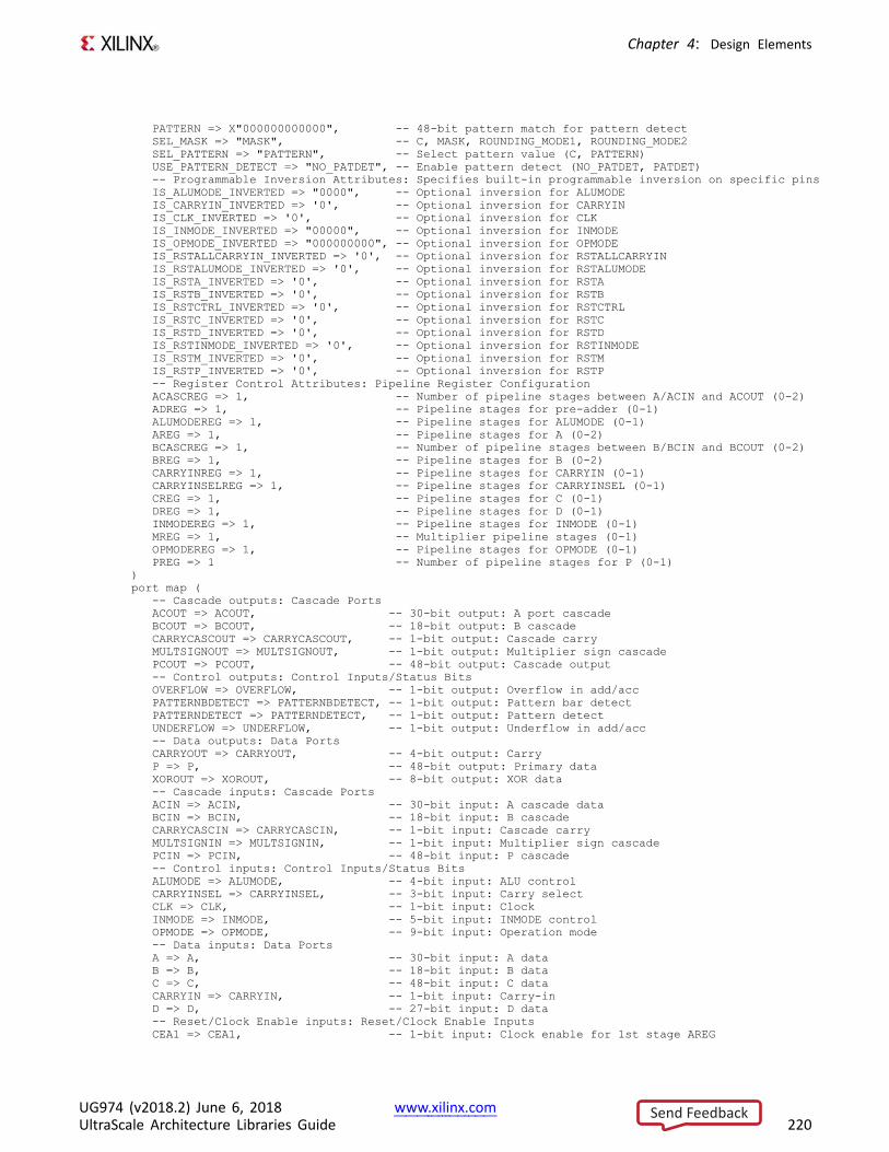
Chapter 4: Design Elements
PATTERN => X"000000000000", -- 48-bit pattern match for pattern detectSEL_MASK => "MASK", -- C, MASK, ROUNDING_MODE1, ROUNDING_MODE2SEL_PATTERN => "PATTERN", -- Select pattern value (C, PATTERN)USE_PATTERN_DETECT => "NO_PATDET", -- Enable pattern detect (NO_PATDET, PATDET)-- Programmable Inversion Attributes: Specifies built-in programmable inversion on specific pinsIS_ALUMODE_INVERTED => "0000", -- Optional inversion for ALUMODEIS_CARRYIN_INVERTED => '0', -- Optional inversion for CARRYINIS_CLK_INVERTED => '0', -- Optional inversion for CLKIS_INMODE_INVERTED => "00000", -- Optional inversion for INMODEIS_OPMODE_INVERTED => "000000000", -- Optional inversion for OPMODEIS_RSTALLCARRYIN_INVERTED => '0', -- Optional inversion for RSTALLCARRYINIS_RSTALUMODE_INVERTED => '0', -- Optional inversion for RSTALUMODEIS_RSTA_INVERTED => '0', -- Optional inversion for RSTAIS_RSTB_INVERTED => '0', -- Optional inversion for RSTBIS_RSTCTRL_INVERTED => '0', -- Optional inversion for RSTCTRLIS_RSTC_INVERTED => '0', -- Optional inversion for RSTCIS_RSTD_INVERTED => '0', -- Optional inversion for RSTDIS_RSTINMODE_INVERTED => '0', -- Optional inversion for RSTINMODEIS_RSTM_INVERTED => '0', -- Optional inversion for RSTMIS_RSTP_INVERTED => '0', -- Optional inversion for RSTP-- Register Control Attributes: Pipeline Register ConfigurationACASCREG => 1, -- Number of pipeline stages between A/ACIN and ACOUT (0-2)ADREG => 1, -- Pipeline stages for pre-adder (0-1)ALUMODEREG => 1, -- Pipeline stages for ALUMODE (0-1)AREG => 1, -- Pipeline stages for A (0-2)BCASCREG => 1, -- Number of pipeline stages between B/BCIN and BCOUT (0-2)BREG => 1, -- Pipeline stages for B (0-2)CARRYINREG => 1, -- Pipeline stages for CARRYIN (0-1)CARRYINSELREG => 1, -- Pipeline stages for CARRYINSEL (0-1)CREG => 1, -- Pipeline stages for C (0-1)DREG => 1, -- Pipeline stages for D (0-1)INMODEREG => 1, -- Pipeline stages for INMODE (0-1)MREG => 1, -- Multiplier pipeline stages (0-1)OPMODEREG => 1, -- Pipeline stages for OPMODE (0-1)PREG => 1 -- Number of pipeline stages for P (0-1)
)port map (
-- Cascade outputs: Cascade PortsACOUT => ACOUT, -- 30-bit output: A port cascadeBCOUT => BCOUT, -- 18-bit output: B cascadeCARRYCASCOUT => CARRYCASCOUT, -- 1-bit output: Cascade carryMULTSIGNOUT => MULTSIGNOUT, -- 1-bit output: Multiplier sign cascadePCOUT => PCOUT, -- 48-bit output: Cascade output-- Control outputs: Control Inputs/Status BitsOVERFLOW => OVERFLOW, -- 1-bit output: Overflow in add/accPATTERNBDETECT => PATTERNBDETECT, -- 1-bit output: Pattern bar detectPATTERNDETECT => PATTERNDETECT, -- 1-bit output: Pattern detectUNDERFLOW => UNDERFLOW, -- 1-bit output: Underflow in add/acc-- Data outputs: Data PortsCARRYOUT => CARRYOUT, -- 4-bit output: CarryP => P, -- 48-bit output: Primary dataXOROUT => XOROUT, -- 8-bit output: XOR data-- Cascade inputs: Cascade PortsACIN => ACIN, -- 30-bit input: A cascade dataBCIN => BCIN, -- 18-bit input: B cascadeCARRYCASCIN => CARRYCASCIN, -- 1-bit input: Cascade carryMULTSIGNIN => MULTSIGNIN, -- 1-bit input: Multiplier sign cascadePCIN => PCIN, -- 48-bit input: P cascade-- Control inputs: Control Inputs/Status BitsALUMODE => ALUMODE, -- 4-bit input: ALU controlCARRYINSEL => CARRYINSEL, -- 3-bit input: Carry selectCLK => CLK, -- 1-bit input: ClockINMODE => INMODE, -- 5-bit input: INMODE controlOPMODE => OPMODE, -- 9-bit input: Operation mode-- Data inputs: Data PortsA => A, -- 30-bit input: A dataB => B, -- 18-bit input: B dataC => C, -- 48-bit input: C dataCARRYIN => CARRYIN, -- 1-bit input: Carry-inD => D, -- 27-bit input: D data-- Reset/Clock Enable inputs: Reset/Clock Enable InputsCEA1 => CEA1, -- 1-bit input: Clock enable for 1st stage AREG
UG974 (v2018.2) June 6, 2018 www.xilinx.comUltraScale Architecture Libraries Guide 220
Send Feedback
Chapter 4: Design Elements
CEA2 => CEA2, -- 1-bit input: Clock enable for 2nd stage AREGCEAD => CEAD, -- 1-bit input: Clock enable for ADREGCEALUMODE => CEALUMODE, -- 1-bit input: Clock enable for ALUMODECEB1 => CEB1, -- 1-bit input: Clock enable for 1st stage BREGCEB2 => CEB2, -- 1-bit input: Clock enable for 2nd stage BREGCEC => CEC, -- 1-bit input: Clock enable for CREGCECARRYIN => CECARRYIN, -- 1-bit input: Clock enable for CARRYINREGCECTRL => CECTRL, -- 1-bit input: Clock enable for OPMODEREG and CARRYINSELREGCED => CED, -- 1-bit input: Clock enable for DREGCEINMODE => CEINMODE, -- 1-bit input: Clock enable for INMODEREGCEM => CEM, -- 1-bit input: Clock enable for MREGCEP => CEP, -- 1-bit input: Clock enable for PREGRSTA => RSTA, -- 1-bit input: Reset for AREGRSTALLCARRYIN => RSTALLCARRYIN, -- 1-bit input: Reset for CARRYINREGRSTALUMODE => RSTALUMODE, -- 1-bit input: Reset for ALUMODEREGRSTB => RSTB, -- 1-bit input: Reset for BREGRSTC => RSTC, -- 1-bit input: Reset for CREGRSTCTRL => RSTCTRL, -- 1-bit input: Reset for OPMODEREG and CARRYINSELREGRSTD => RSTD, -- 1-bit input: Reset for DREG and ADREGRSTINMODE => RSTINMODE, -- 1-bit input: Reset for INMODEREGRSTM => RSTM, -- 1-bit input: Reset for MREGRSTP => RSTP -- 1-bit input: Reset for PREG
);
-- End of DSP48E2_inst instantiation
Verilog Instantiation Template
// DSP48E2: 48-bit Multi-Functional Arithmetic Block// UltraScale// Xilinx HDL Language Template, version 2018.2
DSP48E2 #(// Feature Control Attributes: Data Path Selection.AMULTSEL("A"), // Selects A input to multiplier (A, AD).A_INPUT("DIRECT"), // Selects A input source, "DIRECT" (A port) or "CASCADE" (ACIN port).BMULTSEL("B"), // Selects B input to multiplier (AD, B).B_INPUT("DIRECT"), // Selects B input source, "DIRECT" (B port) or "CASCADE" (BCIN port).PREADDINSEL("A"), // Selects input to pre-adder (A, B).RND(48'h000000000000), // Rounding Constant.USE_MULT("MULTIPLY"), // Select multiplier usage (DYNAMIC, MULTIPLY, NONE).USE_SIMD("ONE48"), // SIMD selection (FOUR12, ONE48, TWO24).USE_WIDEXOR("FALSE"), // Use the Wide XOR function (FALSE, TRUE).XORSIMD("XOR24_48_96"), // Mode of operation for the Wide XOR (XOR12, XOR24_48_96)// Pattern Detector Attributes: Pattern Detection Configuration.AUTORESET_PATDET("NO_RESET"), // NO_RESET, RESET_MATCH, RESET_NOT_MATCH.AUTORESET_PRIORITY("RESET"), // Priority of AUTORESET vs. CEP (CEP, RESET)..MASK(48'h3fffffffffff), // 48-bit mask value for pattern detect (1=ignore).PATTERN(48'h000000000000), // 48-bit pattern match for pattern detect.SEL_MASK("MASK"), // C, MASK, ROUNDING_MODE1, ROUNDING_MODE2.SEL_PATTERN("PATTERN"), // Select pattern value (C, PATTERN).USE_PATTERN_DETECT("NO_PATDET"), // Enable pattern detect (NO_PATDET, PATDET)// Programmable Inversion Attributes: Specifies built-in programmable inversion on specific pins.IS_ALUMODE_INVERTED(4'b0000), // Optional inversion for ALUMODE.IS_CARRYIN_INVERTED(1'b0), // Optional inversion for CARRYIN.IS_CLK_INVERTED(1'b0), // Optional inversion for CLK.IS_INMODE_INVERTED(5'b00000), // Optional inversion for INMODE.IS_OPMODE_INVERTED(9'b000000000), // Optional inversion for OPMODE.IS_RSTALLCARRYIN_INVERTED(1'b0), // Optional inversion for RSTALLCARRYIN.IS_RSTALUMODE_INVERTED(1'b0), // Optional inversion for RSTALUMODE.IS_RSTA_INVERTED(1'b0), // Optional inversion for RSTA.IS_RSTB_INVERTED(1'b0), // Optional inversion for RSTB.IS_RSTCTRL_INVERTED(1'b0), // Optional inversion for RSTCTRL.IS_RSTC_INVERTED(1'b0), // Optional inversion for RSTC.IS_RSTD_INVERTED(1'b0), // Optional inversion for RSTD.IS_RSTINMODE_INVERTED(1'b0), // Optional inversion for RSTINMODE.IS_RSTM_INVERTED(1'b0), // Optional inversion for RSTM.IS_RSTP_INVERTED(1'b0), // Optional inversion for RSTP
UG974 (v2018.2) June 6, 2018 www.xilinx.comUltraScale Architecture Libraries Guide 221
Send Feedback
Chapter 4: Design Elements
// Register Control Attributes: Pipeline Register Configuration.ACASCREG(1), // Number of pipeline stages between A/ACIN and ACOUT (0-2).ADREG(1), // Pipeline stages for pre-adder (0-1).ALUMODEREG(1), // Pipeline stages for ALUMODE (0-1).AREG(1), // Pipeline stages for A (0-2).BCASCREG(1), // Number of pipeline stages between B/BCIN and BCOUT (0-2).BREG(1), // Pipeline stages for B (0-2).CARRYINREG(1), // Pipeline stages for CARRYIN (0-1).CARRYINSELREG(1), // Pipeline stages for CARRYINSEL (0-1).CREG(1), // Pipeline stages for C (0-1).DREG(1), // Pipeline stages for D (0-1).INMODEREG(1), // Pipeline stages for INMODE (0-1).MREG(1), // Multiplier pipeline stages (0-1).OPMODEREG(1), // Pipeline stages for OPMODE (0-1).PREG(1) // Number of pipeline stages for P (0-1)
)DSP48E2_inst (
// Cascade outputs: Cascade Ports.ACOUT(ACOUT), // 30-bit output: A port cascade.BCOUT(BCOUT), // 18-bit output: B cascade.CARRYCASCOUT(CARRYCASCOUT), // 1-bit output: Cascade carry.MULTSIGNOUT(MULTSIGNOUT), // 1-bit output: Multiplier sign cascade.PCOUT(PCOUT), // 48-bit output: Cascade output// Control outputs: Control Inputs/Status Bits.OVERFLOW(OVERFLOW), // 1-bit output: Overflow in add/acc.PATTERNBDETECT(PATTERNBDETECT), // 1-bit output: Pattern bar detect.PATTERNDETECT(PATTERNDETECT), // 1-bit output: Pattern detect.UNDERFLOW(UNDERFLOW), // 1-bit output: Underflow in add/acc// Data outputs: Data Ports.CARRYOUT(CARRYOUT), // 4-bit output: Carry.P(P), // 48-bit output: Primary data.XOROUT(XOROUT), // 8-bit output: XOR data// Cascade inputs: Cascade Ports.ACIN(ACIN), // 30-bit input: A cascade data.BCIN(BCIN), // 18-bit input: B cascade.CARRYCASCIN(CARRYCASCIN), // 1-bit input: Cascade carry.MULTSIGNIN(MULTSIGNIN), // 1-bit input: Multiplier sign cascade.PCIN(PCIN), // 48-bit input: P cascade// Control inputs: Control Inputs/Status Bits.ALUMODE(ALUMODE), // 4-bit input: ALU control.CARRYINSEL(CARRYINSEL), // 3-bit input: Carry select.CLK(CLK), // 1-bit input: Clock.INMODE(INMODE), // 5-bit input: INMODE control.OPMODE(OPMODE), // 9-bit input: Operation mode// Data inputs: Data Ports.A(A), // 30-bit input: A data.B(B), // 18-bit input: B data.C(C), // 48-bit input: C data.CARRYIN(CARRYIN), // 1-bit input: Carry-in.D(D), // 27-bit input: D data// Reset/Clock Enable inputs: Reset/Clock Enable Inputs.CEA1(CEA1), // 1-bit input: Clock enable for 1st stage AREG.CEA2(CEA2), // 1-bit input: Clock enable for 2nd stage AREG.CEAD(CEAD), // 1-bit input: Clock enable for ADREG.CEALUMODE(CEALUMODE), // 1-bit input: Clock enable for ALUMODE.CEB1(CEB1), // 1-bit input: Clock enable for 1st stage BREG.CEB2(CEB2), // 1-bit input: Clock enable for 2nd stage BREG.CEC(CEC), // 1-bit input: Clock enable for CREG.CECARRYIN(CECARRYIN), // 1-bit input: Clock enable for CARRYINREG.CECTRL(CECTRL), // 1-bit input: Clock enable for OPMODEREG and CARRYINSELREG.CED(CED), // 1-bit input: Clock enable for DREG.CEINMODE(CEINMODE), // 1-bit input: Clock enable for INMODEREG.CEM(CEM), // 1-bit input: Clock enable for MREG.CEP(CEP), // 1-bit input: Clock enable for PREG.RSTA(RSTA), // 1-bit input: Reset for AREG.RSTALLCARRYIN(RSTALLCARRYIN), // 1-bit input: Reset for CARRYINREG.RSTALUMODE(RSTALUMODE), // 1-bit input: Reset for ALUMODEREG.RSTB(RSTB), // 1-bit input: Reset for BREG.RSTC(RSTC), // 1-bit input: Reset for CREG.RSTCTRL(RSTCTRL), // 1-bit input: Reset for OPMODEREG and CARRYINSELREG.RSTD(RSTD), // 1-bit input: Reset for DREG and ADREG.RSTINMODE(RSTINMODE), // 1-bit input: Reset for INMODEREG
UG974 (v2018.2) June 6, 2018 www.xilinx.comUltraScale Architecture Libraries Guide 222
Send Feedback
Chapter 4: Design Elements
.RSTM(RSTM), // 1-bit input: Reset for MREG
.RSTP(RSTP) // 1-bit input: Reset for PREG);
// End of DSP48E2_inst instantiation
For More Information• See the UltraScale Architecture DSP Slice User Guide (UG579).
• See the UltraScale Programmable Devices Documentation.
UG974 (v2018.2) June 6, 2018 www.xilinx.comUltraScale Architecture Libraries Guide 223
Send Feedback
Chapter 4: Design Elements
EFUSE_USRPrimitive: 32-bit non-volatile design IDPRIMITIVE_GROUP: CONFIGURATIONPRIMITIVE_SUBGROUP: EFUSEFamilies: UltraScale FPGAs, UltraScale+ FPGAs
IntroductionProvides internal access to the 32 non-volatile, user-programmable eFUSE bits
Port DescriptionsPort Direction Width Function
EFUSEUSR<31:0> Output 32 User eFUSE register value output
Design Entry MethodInstantiation Recommended
Inference No
IP and IP Integrator Catalog No
Available AttributesAttribute Type Allowed Values Default Description
SIM_EFUSE_VALUE HEX Any 32-bit HEXvalue
All zeroes Value of the 32 - bit non - volatilevalue used in simulation
VHDL Instantiation TemplateUnless they already exist, copy the following two statements and paste them before the entitydeclaration.Library UNISIM;use UNISIM.vcomponents.all;
-- EFUSE_USR: 32-bit non-volatile design ID-- UltraScale-- Xilinx HDL Language Template, version 2018.2
EFUSE_USR_inst : EFUSE_USRgeneric map (
SIM_EFUSE_VALUE => X"00000000" -- Value of the 32-bit non-volatile value used in simulation
UG974 (v2018.2) June 6, 2018 www.xilinx.comUltraScale Architecture Libraries Guide 224
Send Feedback
Chapter 4: Design Elements
)port map (
EFUSEUSR => EFUSEUSR -- 32-bit output: User eFUSE register value output);
-- End of EFUSE_USR_inst instantiation
Verilog Instantiation Template
// EFUSE_USR: 32-bit non-volatile design ID// UltraScale// Xilinx HDL Language Template, version 2018.2
EFUSE_USR #(.SIM_EFUSE_VALUE(32'h00000000) // Value of the 32-bit non-volatile value used in simulation
)EFUSE_USR_inst (
.EFUSEUSR(EFUSEUSR) // 32-bit output: User eFUSE register value output);
// End of EFUSE_USR_inst instantiation
For More Information• See the UltraScale Architecture Configuration User Guide (UG570).
• See the UltraScale Programmable Devices Documentation.
UG974 (v2018.2) June 6, 2018 www.xilinx.comUltraScale Architecture Libraries Guide 225
Send Feedback
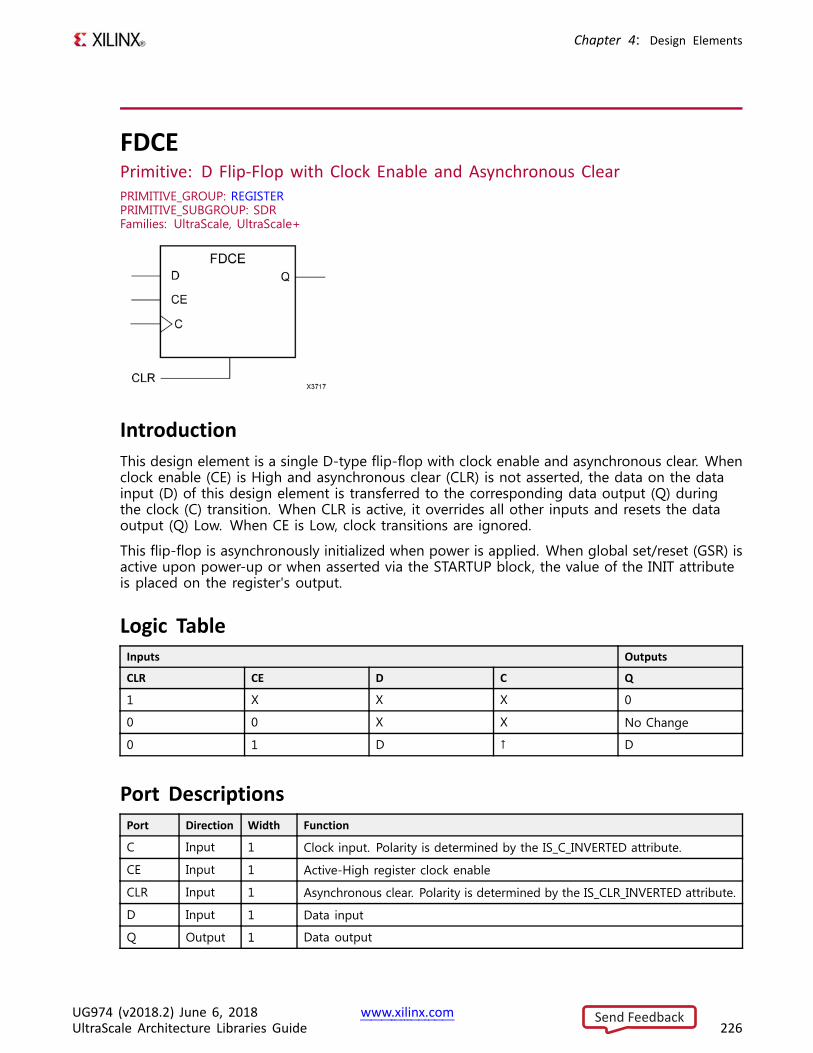
Chapter 4: Design Elements
FDCEPrimitive: D Flip-Flop with Clock Enable and Asynchronous ClearPRIMITIVE_GROUP: REGISTERPRIMITIVE_SUBGROUP: SDRFamilies: UltraScale, UltraScale+
IntroductionThis design element is a single D-type flip-flop with clock enable and asynchronous clear. Whenclock enable (CE) is High and asynchronous clear (CLR) is not asserted, the data on the datainput (D) of this design element is transferred to the corresponding data output (Q) duringthe clock (C) transition. When CLR is active, it overrides all other inputs and resets the dataoutput (Q) Low. When CE is Low, clock transitions are ignored.
This flip-flop is asynchronously initialized when power is applied. When global set/reset (GSR) isactive upon power-up or when asserted via the STARTUP block, the value of the INIT attributeis placed on the register's output.
Logic TableInputs Outputs
CLR CE D C Q
1 X X X 0
0 0 X X No Change
0 1 D ↑ D
Port DescriptionsPort Direction Width Function
C Input 1 Clock input. Polarity is determined by the IS_C_INVERTED attribute.
CE Input 1 Active-High register clock enable
CLR Input 1 Asynchronous clear. Polarity is determined by the IS_CLR_INVERTED attribute.
D Input 1 Data input
Q Output 1 Data output
UG974 (v2018.2) June 6, 2018 www.xilinx.comUltraScale Architecture Libraries Guide 226
Send Feedback
Chapter 4: Design Elements
Design Entry MethodInstantiation Yes
Inference Recommended
IP and IP Integrator Catalog No
Available AttributesAttribute Type Allowed Values Default Description
INIT BINARY 1'b0, 1'b1 1'b0 Sets the initial value of Q output afterconfiguration or when GSR is asserted via theSTARTUP block
Programmable Inversion Attributes: Specifies whether or not to use the optional inversion on specificpins for this component to change the active polarity of the pin function. When set to 1 on a clock pin(C), it creates a negative edge register. When set to 1 on other pins, it changes the function to behaveactive-Low rather than active-High. If an external inverter is specified on one of these associated pins, theVivado Design Suite will automatically set this attribute during the opt_design stage so that additional logicis not necessary for changing the input polarity.
IS_C_INVERTED BINARY 1'b0 to 1'b1 1'b0 Specifies whether or not to use the optionalinversion for the C pin of this component.
IS_CLR_INVERTED BINARY 1'b0 to 1'b1 1'b0 Specifies whether or not to use the optionalinversion for the CLR pin of this component.
IS_D_INVERTED BINARY 1'b0 to 1'b1 1'b0 Specifies whether or not to use the optionalinversion for the D pin of this component. Mustbe set to 0 unless used as an I / O register.
VHDL Instantiation TemplateUnless they already exist, copy the following two statements and paste them before the entitydeclaration.Library UNISIM;use UNISIM.vcomponents.all;
-- FDCE: D Flip-Flop with Clock Enable and Asynchronous Clear-- UltraScale-- Xilinx HDL Language Template, version 2018.2
FDCE_inst : FDCEgeneric map (
INIT => '0', -- Initial value of register, '0', '1'-- Programmable Inversion Attributes: Specifies the use of the built-in programmable inversionIS_CLR_INVERTED => '0', -- Optional inversion for CLRIS_C_INVERTED => '0', -- Optional inversion for CIS_D_INVERTED => '0' -- Optional inversion for D
)port map (
Q => Q, -- 1-bit output: DataC => C, -- 1-bit input: ClockCE => CE, -- 1-bit input: Clock enableCLR => CLR, -- 1-bit input: Asynchronous clearD => D -- 1-bit input: Data
);
-- End of FDCE_inst instantiation
UG974 (v2018.2) June 6, 2018 www.xilinx.comUltraScale Architecture Libraries Guide 227
Send Feedback

Chapter 4: Design Elements
Verilog Instantiation Template
// FDCE: D Flip-Flop with Clock Enable and Asynchronous Clear// UltraScale// Xilinx HDL Language Template, version 2018.2
FDCE #(.INIT(1'b0), // Initial value of register, 1'b0, 1'b1// Programmable Inversion Attributes: Specifies the use of the built-in programmable inversion.IS_CLR_INVERTED(1'b0), // Optional inversion for CLR.IS_C_INVERTED(1'b0), // Optional inversion for C.IS_D_INVERTED(1'b0) // Optional inversion for D
)FDCE_inst (
.Q(Q), // 1-bit output: Data
.C(C), // 1-bit input: Clock
.CE(CE), // 1-bit input: Clock enable
.CLR(CLR), // 1-bit input: Asynchronous clear
.D(D) // 1-bit input: Data);
// End of FDCE_inst instantiation
For More Information• See the UltraScale Architecture Configurable Logic Block User Guide (UG574).
• See the UltraScale Programmable Devices Documentation.
UG974 (v2018.2) June 6, 2018 www.xilinx.comUltraScale Architecture Libraries Guide 228
Send Feedback
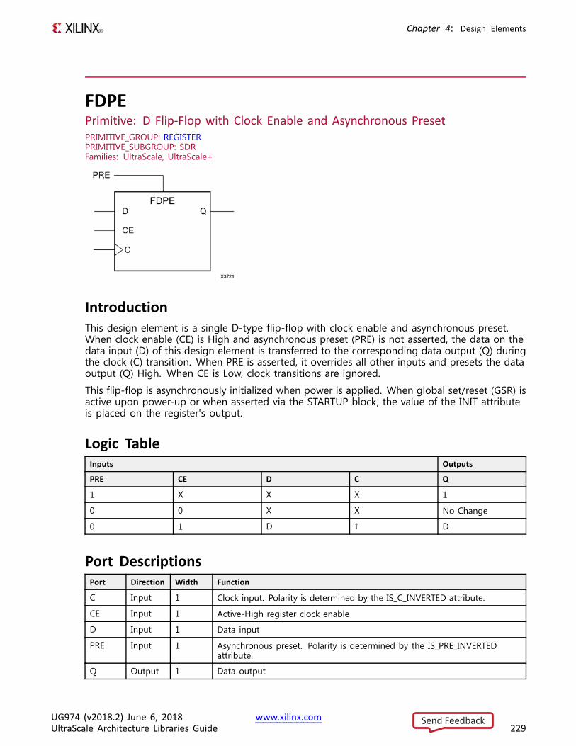
Chapter 4: Design Elements
FDPEPrimitive: D Flip-Flop with Clock Enable and Asynchronous PresetPRIMITIVE_GROUP: REGISTERPRIMITIVE_SUBGROUP: SDRFamilies: UltraScale, UltraScale+
IntroductionThis design element is a single D-type flip-flop with clock enable and asynchronous preset.When clock enable (CE) is High and asynchronous preset (PRE) is not asserted, the data on thedata input (D) of this design element is transferred to the corresponding data output (Q) duringthe clock (C) transition. When PRE is asserted, it overrides all other inputs and presets the dataoutput (Q) High. When CE is Low, clock transitions are ignored.
This flip-flop is asynchronously initialized when power is applied. When global set/reset (GSR) isactive upon power-up or when asserted via the STARTUP block, the value of the INIT attributeis placed on the register's output.
Logic TableInputs Outputs
PRE CE D C Q
1 X X X 1
0 0 X X No Change
0 1 D ↑ D
Port DescriptionsPort Direction Width Function
C Input 1 Clock input. Polarity is determined by the IS_C_INVERTED attribute.
CE Input 1 Active-High register clock enable
D Input 1 Data input
PRE Input 1 Asynchronous preset. Polarity is determined by the IS_PRE_INVERTEDattribute.
Q Output 1 Data output
UG974 (v2018.2) June 6, 2018 www.xilinx.comUltraScale Architecture Libraries Guide 229
Send Feedback
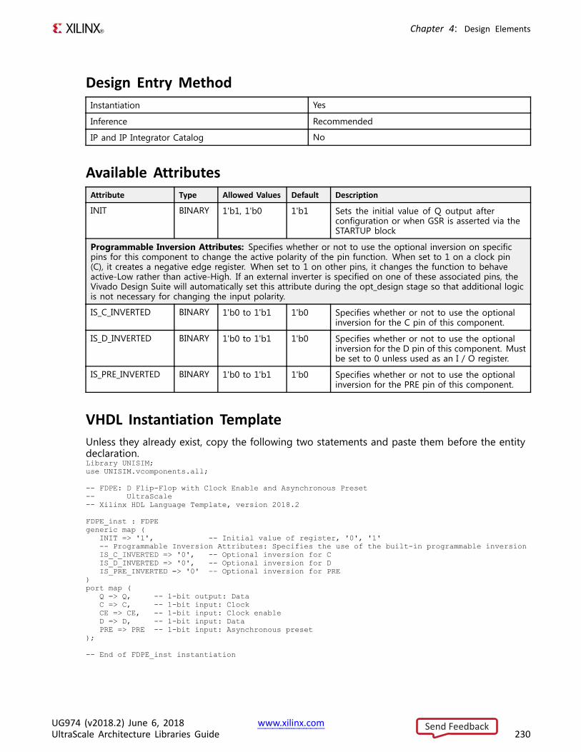
Chapter 4: Design Elements
Design Entry MethodInstantiation Yes
Inference Recommended
IP and IP Integrator Catalog No
Available AttributesAttribute Type Allowed Values Default Description
INIT BINARY 1'b1, 1'b0 1'b1 Sets the initial value of Q output afterconfiguration or when GSR is asserted via theSTARTUP block
Programmable Inversion Attributes: Specifies whether or not to use the optional inversion on specificpins for this component to change the active polarity of the pin function. When set to 1 on a clock pin(C), it creates a negative edge register. When set to 1 on other pins, it changes the function to behaveactive-Low rather than active-High. If an external inverter is specified on one of these associated pins, theVivado Design Suite will automatically set this attribute during the opt_design stage so that additional logicis not necessary for changing the input polarity.
IS_C_INVERTED BINARY 1'b0 to 1'b1 1'b0 Specifies whether or not to use the optionalinversion for the C pin of this component.
IS_D_INVERTED BINARY 1'b0 to 1'b1 1'b0 Specifies whether or not to use the optionalinversion for the D pin of this component. Mustbe set to 0 unless used as an I / O register.
IS_PRE_INVERTED BINARY 1'b0 to 1'b1 1'b0 Specifies whether or not to use the optionalinversion for the PRE pin of this component.
VHDL Instantiation TemplateUnless they already exist, copy the following two statements and paste them before the entitydeclaration.Library UNISIM;use UNISIM.vcomponents.all;
-- FDPE: D Flip-Flop with Clock Enable and Asynchronous Preset-- UltraScale-- Xilinx HDL Language Template, version 2018.2
FDPE_inst : FDPEgeneric map (
INIT => '1', -- Initial value of register, '0', '1'-- Programmable Inversion Attributes: Specifies the use of the built-in programmable inversionIS_C_INVERTED => '0', -- Optional inversion for CIS_D_INVERTED => '0', -- Optional inversion for DIS_PRE_INVERTED => '0' -- Optional inversion for PRE
)port map (
Q => Q, -- 1-bit output: DataC => C, -- 1-bit input: ClockCE => CE, -- 1-bit input: Clock enableD => D, -- 1-bit input: DataPRE => PRE -- 1-bit input: Asynchronous preset
);
-- End of FDPE_inst instantiation
UG974 (v2018.2) June 6, 2018 www.xilinx.comUltraScale Architecture Libraries Guide 230
Send Feedback

Chapter 4: Design Elements
Verilog Instantiation Template
// FDPE: D Flip-Flop with Clock Enable and Asynchronous Preset// UltraScale// Xilinx HDL Language Template, version 2018.2
FDPE #(.INIT(1'b1), // Initial value of register, 1'b0, 1'b1// Programmable Inversion Attributes: Specifies the use of the built-in programmable inversion.IS_C_INVERTED(1'b0), // Optional inversion for C.IS_D_INVERTED(1'b0), // Optional inversion for D.IS_PRE_INVERTED(1'b0) // Optional inversion for PRE
)FDPE_inst (
.Q(Q), // 1-bit output: Data
.C(C), // 1-bit input: Clock
.CE(CE), // 1-bit input: Clock enable
.D(D), // 1-bit input: Data
.PRE(PRE) // 1-bit input: Asynchronous preset);
// End of FDPE_inst instantiation
For More Information• See the UltraScale Architecture Configurable Logic Block User Guide (UG574).
• See the UltraScale Programmable Devices Documentation.
UG974 (v2018.2) June 6, 2018 www.xilinx.comUltraScale Architecture Libraries Guide 231
Send Feedback
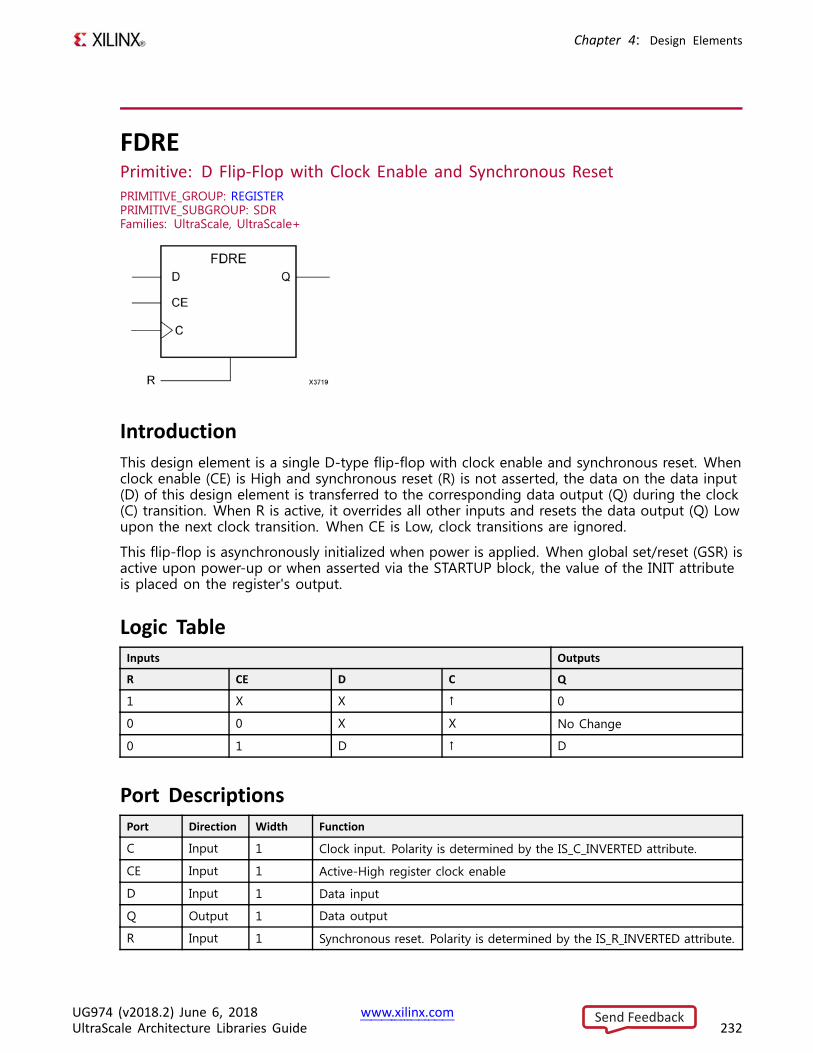
Chapter 4: Design Elements
FDREPrimitive: D Flip-Flop with Clock Enable and Synchronous ResetPRIMITIVE_GROUP: REGISTERPRIMITIVE_SUBGROUP: SDRFamilies: UltraScale, UltraScale+
IntroductionThis design element is a single D-type flip-flop with clock enable and synchronous reset. Whenclock enable (CE) is High and synchronous reset (R) is not asserted, the data on the data input(D) of this design element is transferred to the corresponding data output (Q) during the clock(C) transition. When R is active, it overrides all other inputs and resets the data output (Q) Lowupon the next clock transition. When CE is Low, clock transitions are ignored.
This flip-flop is asynchronously initialized when power is applied. When global set/reset (GSR) isactive upon power-up or when asserted via the STARTUP block, the value of the INIT attributeis placed on the register's output.
Logic TableInputs Outputs
R CE D C Q
1 X X ↑ 0
0 0 X X No Change
0 1 D ↑ D
Port DescriptionsPort Direction Width Function
C Input 1 Clock input. Polarity is determined by the IS_C_INVERTED attribute.
CE Input 1 Active-High register clock enable
D Input 1 Data input
Q Output 1 Data output
R Input 1 Synchronous reset. Polarity is determined by the IS_R_INVERTED attribute.
UG974 (v2018.2) June 6, 2018 www.xilinx.comUltraScale Architecture Libraries Guide 232
Send Feedback

Chapter 4: Design Elements
Design Entry MethodInstantiation Yes
Inference Recommended
IP and IP Integrator Catalog No
Available AttributesAttribute Type Allowed Values Default Description
INIT BINARY 1'b0, 1'b1 1'b0 Sets the initial value of Q output afterconfiguration or when GSR is asserted via theSTARTUP block.
Programmable Inversion Attributes: Specifies whether or not to use the optional inversion on specificpins for this component to change the active polarity of the pin function. When set to 1 on a clock pin(C), it creates a negative edge register. When set to 1 on other pins, it changes the function to behaveactive-Low rather than active-High. If an external inverter is specified on one of these associated pins, theVivado Design Suite will automatically set this attribute during the opt_design stage so that additional logicis not necessary for changing the input polarity.
IS_C_INVERTED BINARY 1'b0 to 1'b1 1'b0 Specifies whether or not to use the optionalinversion for the C pin of this component.
IS_D_INVERTED BINARY 1'b0 to 1'b1 1'b0 Specifies whether or not to use the optionalinversion for the D pin of this component. Mustbe set to 0 unless used as an I / O register.
IS_R_INVERTED BINARY 1'b0 to 1'b1 1'b0 Specifies whether or not to use the optionalinversion for the R pin of this component
VHDL Instantiation TemplateUnless they already exist, copy the following two statements and paste them before the entitydeclaration.Library UNISIM;use UNISIM.vcomponents.all;
-- FDRE: D Flip-Flop with Clock Enable and Synchronous Reset-- UltraScale-- Xilinx HDL Language Template, version 2018.2
FDRE_inst : FDREgeneric map (
INIT => '0', -- Initial value of register, '0', '1'-- Programmable Inversion Attributes: Specifies the use of the built-in programmable inversionIS_C_INVERTED => '0', -- Optional inversion for CIS_D_INVERTED => '0', -- Optional inversion for DIS_R_INVERTED => '0' -- Optional inversion for R
)port map (
Q => Q, -- 1-bit output: DataC => C, -- 1-bit input: ClockCE => CE, -- 1-bit input: Clock enableD => D, -- 1-bit input: DataR => R -- 1-bit input: Synchronous reset
);
-- End of FDRE_inst instantiation
UG974 (v2018.2) June 6, 2018 www.xilinx.comUltraScale Architecture Libraries Guide 233
Send Feedback
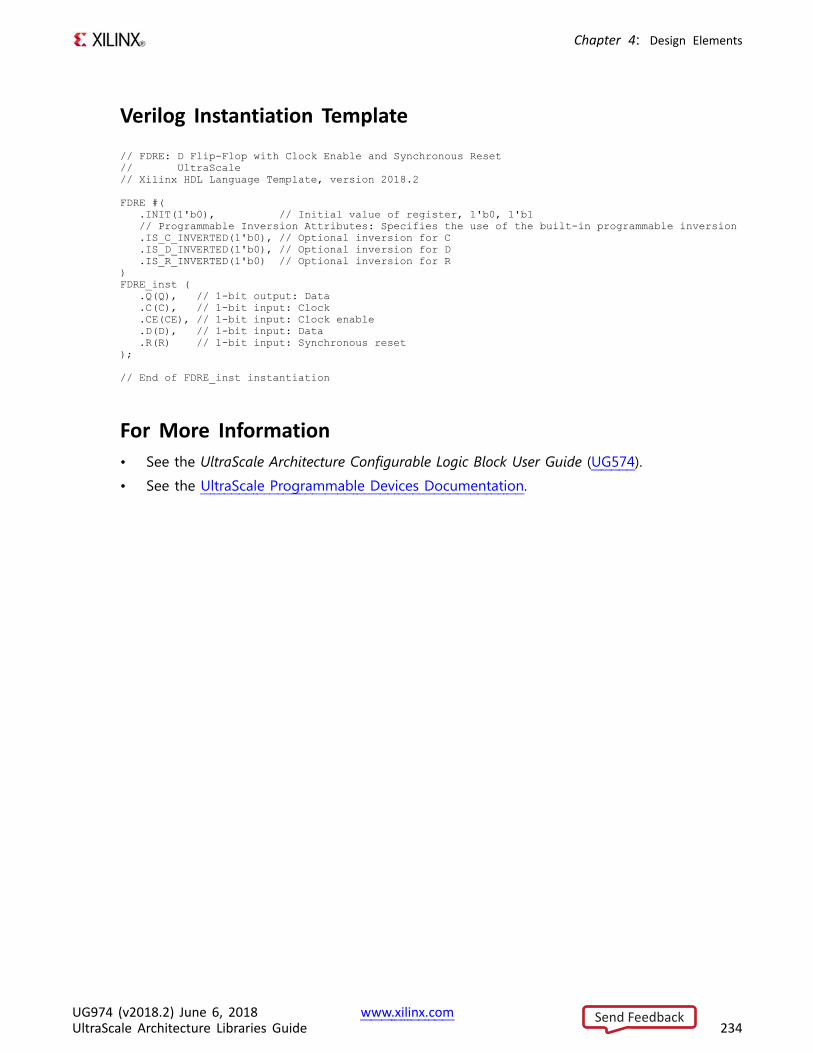
Chapter 4: Design Elements
Verilog Instantiation Template
// FDRE: D Flip-Flop with Clock Enable and Synchronous Reset// UltraScale// Xilinx HDL Language Template, version 2018.2
FDRE #(.INIT(1'b0), // Initial value of register, 1'b0, 1'b1// Programmable Inversion Attributes: Specifies the use of the built-in programmable inversion.IS_C_INVERTED(1'b0), // Optional inversion for C.IS_D_INVERTED(1'b0), // Optional inversion for D.IS_R_INVERTED(1'b0) // Optional inversion for R
)FDRE_inst (
.Q(Q), // 1-bit output: Data
.C(C), // 1-bit input: Clock
.CE(CE), // 1-bit input: Clock enable
.D(D), // 1-bit input: Data
.R(R) // 1-bit input: Synchronous reset);
// End of FDRE_inst instantiation
For More Information• See the UltraScale Architecture Configurable Logic Block User Guide (UG574).
• See the UltraScale Programmable Devices Documentation.
UG974 (v2018.2) June 6, 2018 www.xilinx.comUltraScale Architecture Libraries Guide 234
Send Feedback
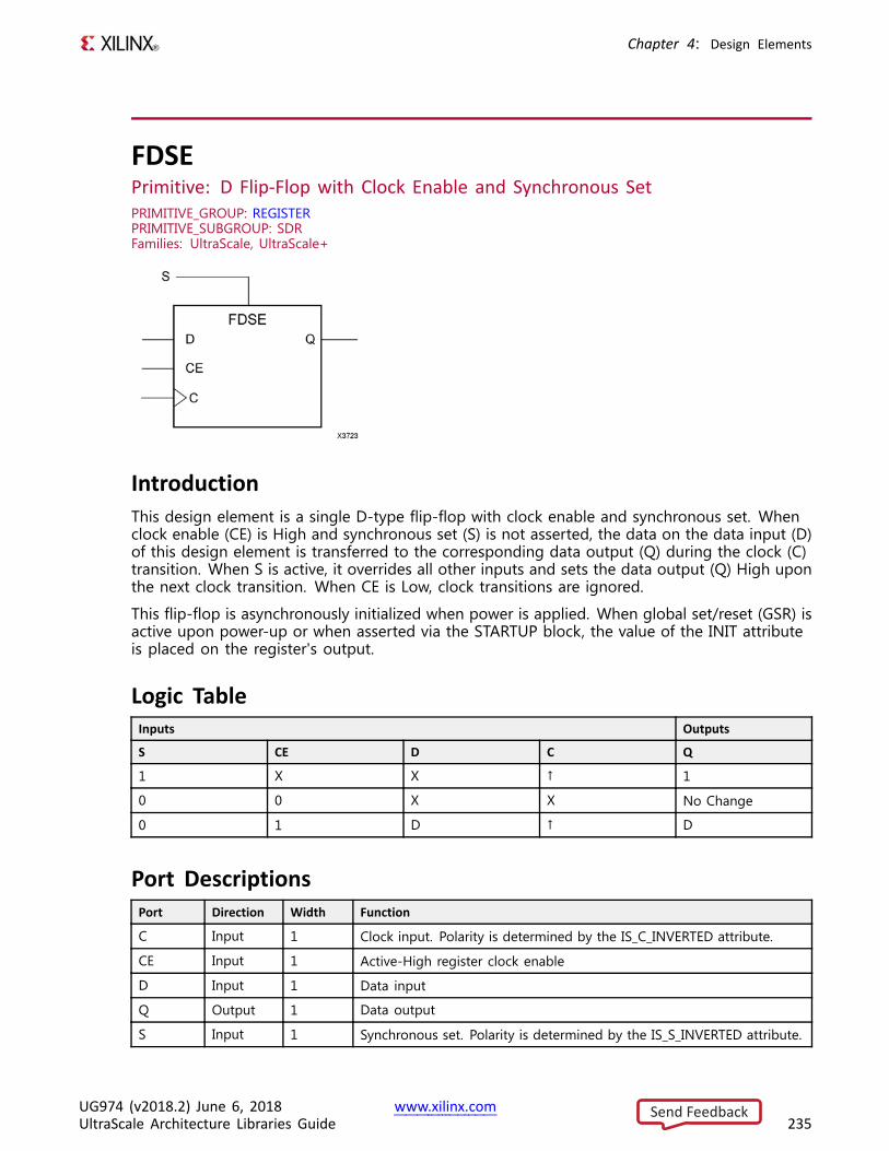
Chapter 4: Design Elements
FDSEPrimitive: D Flip-Flop with Clock Enable and Synchronous SetPRIMITIVE_GROUP: REGISTERPRIMITIVE_SUBGROUP: SDRFamilies: UltraScale, UltraScale+
IntroductionThis design element is a single D-type flip-flop with clock enable and synchronous set. Whenclock enable (CE) is High and synchronous set (S) is not asserted, the data on the data input (D)of this design element is transferred to the corresponding data output (Q) during the clock (C)transition. When S is active, it overrides all other inputs and sets the data output (Q) High uponthe next clock transition. When CE is Low, clock transitions are ignored.
This flip-flop is asynchronously initialized when power is applied. When global set/reset (GSR) isactive upon power-up or when asserted via the STARTUP block, the value of the INIT attributeis placed on the register's output.
Logic TableInputs Outputs
S CE D C Q
1 X X ↑ 1
0 0 X X No Change
0 1 D ↑ D
Port DescriptionsPort Direction Width Function
C Input 1 Clock input. Polarity is determined by the IS_C_INVERTED attribute.
CE Input 1 Active-High register clock enable
D Input 1 Data input
Q Output 1 Data output
S Input 1 Synchronous set. Polarity is determined by the IS_S_INVERTED attribute.
UG974 (v2018.2) June 6, 2018 www.xilinx.comUltraScale Architecture Libraries Guide 235
Send Feedback

Chapter 4: Design Elements
Design Entry MethodInstantiation Yes
Inference Recommended
IP and IP Integrator Catalog No
Available AttributesAttribute Type Allowed Values Default Description
INIT BINARY 1'b1, 1'b0 1'b1 Sets the initial value of Q output afterconfiguration or when GSR is asserted via theSTARTUP block.
Programmable Inversion Attributes: Specifies whether or not to use the optional inversion on specificpins for this component to change the active polarity of the pin function. When set to 1 on a clock pin(C), it creates a negative edge register. When set to 1 on other pins, it changes the function to behaveactive-Low rather than active-High. If an external inverter is specified on one of these associated pins, theVivado Design Suite will automatically set this attribute during the opt_design stage so that additional logicis not necessary for changing the input polarity.
IS_C_INVERTED BINARY 1'b0 to 1'b1 1'b0 Specifies whether or not to use the optionalinversion for the C pin of this component.
IS_D_INVERTED BINARY 1'b0 to 1'b1 1'b0 Specifies whether or not to use the optionalinversion for the D pin of this component. Mustbe set to 0 unless used as an I / O register.
IS_S_INVERTED BINARY 1'b0 to 1'b1 1'b0 Specifies whether or not to use the optionalinversion for the S pin of this component
VHDL Instantiation TemplateUnless they already exist, copy the following two statements and paste them before the entitydeclaration.Library UNISIM;use UNISIM.vcomponents.all;
-- FDSE: D Flip-Flop with Clock Enable and Synchronous Set-- UltraScale-- Xilinx HDL Language Template, version 2018.2
FDSE_inst : FDSEgeneric map (
INIT => '1', -- Initial value of register, '0', '1'-- Programmable Inversion Attributes: Specifies the use of the built-in programmable inversionIS_C_INVERTED => '0', -- Optional inversion for CIS_D_INVERTED => '0', -- Optional inversion for DIS_S_INVERTED => '0' -- Optional inversion for S
)port map (
Q => Q, -- 1-bit output: DataC => C, -- 1-bit input: ClockCE => CE, -- 1-bit input: Clock enableD => D, -- 1-bit input: DataS => S -- 1-bit input: Synchronous set
);
-- End of FDSE_inst instantiation
UG974 (v2018.2) June 6, 2018 www.xilinx.comUltraScale Architecture Libraries Guide 236
Send Feedback

Chapter 4: Design Elements
Verilog Instantiation Template
// FDSE: D Flip-Flop with Clock Enable and Synchronous Set// UltraScale// Xilinx HDL Language Template, version 2018.2
FDSE #(.INIT(1'b1), // Initial value of register, 1'b0, 1'b1// Programmable Inversion Attributes: Specifies the use of the built-in programmable inversion.IS_C_INVERTED(1'b0), // Optional inversion for C.IS_D_INVERTED(1'b0), // Optional inversion for D.IS_S_INVERTED(1'b0) // Optional inversion for S
)FDSE_inst (
.Q(Q), // 1-bit output: Data
.C(C), // 1-bit input: Clock
.CE(CE), // 1-bit input: Clock enable
.D(D), // 1-bit input: Data
.S(S) // 1-bit input: Synchronous set);
// End of FDSE_inst instantiation
For More Information• See the UltraScale Architecture Configurable Logic Block User Guide (UG574).
• See the UltraScale Programmable Devices Documentation.
UG974 (v2018.2) June 6, 2018 www.xilinx.comUltraScale Architecture Libraries Guide 237
Send Feedback
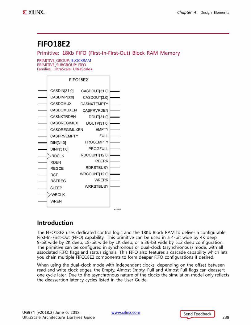
Chapter 4: Design Elements
FIFO18E2Primitive: 18Kb FIFO (First-In-First-Out) Block RAM MemoryPRIMITIVE_GROUP: BLOCKRAMPRIMITIVE_SUBGROUP: FIFOFamilies: UltraScale, UltraScale+
IntroductionThe FIFO18E2 uses dedicated control logic and the 18Kb Block RAM to deliver a configurableFirst-In-First-Out (FIFO) capability. This primitive can be used in a 4-bit wide by 4K deep,9-bit wide by 2K deep, 18-bit wide by 1K deep, or a 36-bit wide by 512 deep configuration.The primitive can be configured in synchronous or dual-clock (asynchronous) mode, with allassociated FIFO flags and status signals. This FIFO also features a cascade capability which letsyou chain multiple FIFO18E2 components to form deeper FIFO configurations if desired.
When using the dual-clock mode with independent clocks, depending on the offset betweenread and write clock edges, the Empty, Almost Empty, Full and Almost Full flags can deassertone cycle later. Due to the asynchronous nature of the clocks the simulation model only reflectsthe deassertion latency cycles listed in the User Guide.
UG974 (v2018.2) June 6, 2018 www.xilinx.comUltraScale Architecture Libraries Guide 238
Send Feedback
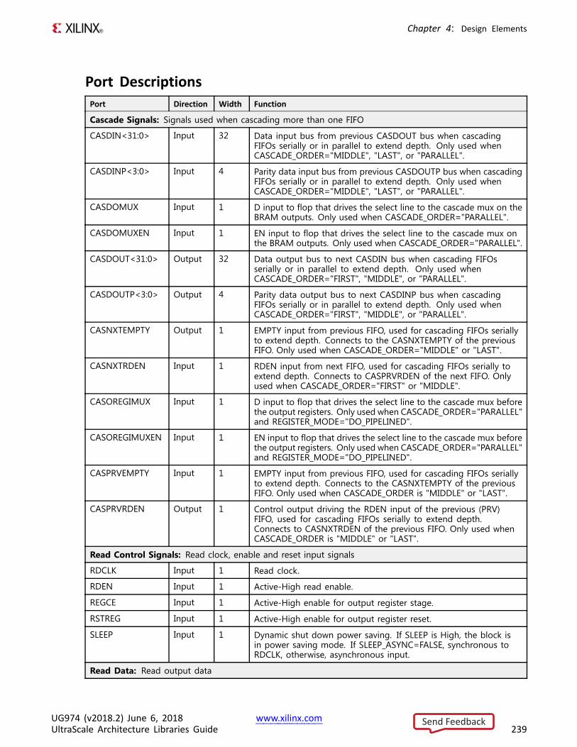
Chapter 4: Design Elements
Port DescriptionsPort Direction Width Function
Cascade Signals: Signals used when cascading more than one FIFO
CASDIN<31:0> Input 32 Data input bus from previous CASDOUT bus when cascadingFIFOs serially or in parallel to extend depth. Only used whenCASCADE_ORDER="MIDDLE", "LAST", or "PARALLEL".
CASDINP<3:0> Input 4 Parity data input bus from previous CASDOUTP bus when cascadingFIFOs serially or in parallel to extend depth. Only used whenCASCADE_ORDER="MIDDLE", "LAST", or "PARALLEL".
CASDOMUX Input 1 D input to flop that drives the select line to the cascade mux on theBRAM outputs. Only used when CASCADE_ORDER="PARALLEL".
CASDOMUXEN Input 1 EN input to flop that drives the select line to the cascade mux onthe BRAM outputs. Only used when CASCADE_ORDER="PARALLEL".
CASDOUT<31:0> Output 32 Data output bus to next CASDIN bus when cascading FIFOsserially or in parallel to extend depth. Only used whenCASCADE_ORDER="FIRST", "MIDDLE", or "PARALLEL".
CASDOUTP<3:0> Output 4 Parity data output bus to next CASDINP bus when cascadingFIFOs serially or in parallel to extend depth. Only used whenCASCADE_ORDER="FIRST", "MIDDLE", or "PARALLEL".
CASNXTEMPTY Output 1 EMPTY input from previous FIFO, used for cascading FIFOs seriallyto extend depth. Connects to the CASNXTEMPTY of the previousFIFO. Only used when CASCADE_ORDER="MIDDLE" or "LAST".
CASNXTRDEN Input 1 RDEN input from next FIFO, used for cascading FIFOs serially toextend depth. Connects to CASPRVRDEN of the next FIFO. Onlyused when CASCADE_ORDER="FIRST" or "MIDDLE".
CASOREGIMUX Input 1 D input to flop that drives the select line to the cascade mux beforethe output registers. Only used when CASCADE_ORDER="PARALLEL"and REGISTER_MODE="DO_PIPELINED".
CASOREGIMUXEN Input 1 EN input to flop that drives the select line to the cascade mux beforethe output registers. Only used when CASCADE_ORDER="PARALLEL"and REGISTER_MODE="DO_PIPELINED".
CASPRVEMPTY Input 1 EMPTY input from previous FIFO, used for cascading FIFOs seriallyto extend depth. Connects to the CASNXTEMPTY of the previousFIFO. Only used when CASCADE_ORDER is "MIDDLE" or "LAST".
CASPRVRDEN Output 1 Control output driving the RDEN input of the previous (PRV)FIFO, used for cascading FIFOs serially to extend depth.Connects to CASNXTRDEN of the previous FIFO. Only used whenCASCADE_ORDER is "MIDDLE" or "LAST".
Read Control Signals: Read clock, enable and reset input signals
RDCLK Input 1 Read clock.
RDEN Input 1 Active-High read enable.
REGCE Input 1 Active-High enable for output register stage.
RSTREG Input 1 Active-High enable for output register reset.
SLEEP Input 1 Dynamic shut down power saving. If SLEEP is High, the block isin power saving mode. If SLEEP_ASYNC=FALSE, synchronous toRDCLK, otherwise, asynchronous input.
Read Data: Read output data
UG974 (v2018.2) June 6, 2018 www.xilinx.comUltraScale Architecture Libraries Guide 239
Send Feedback
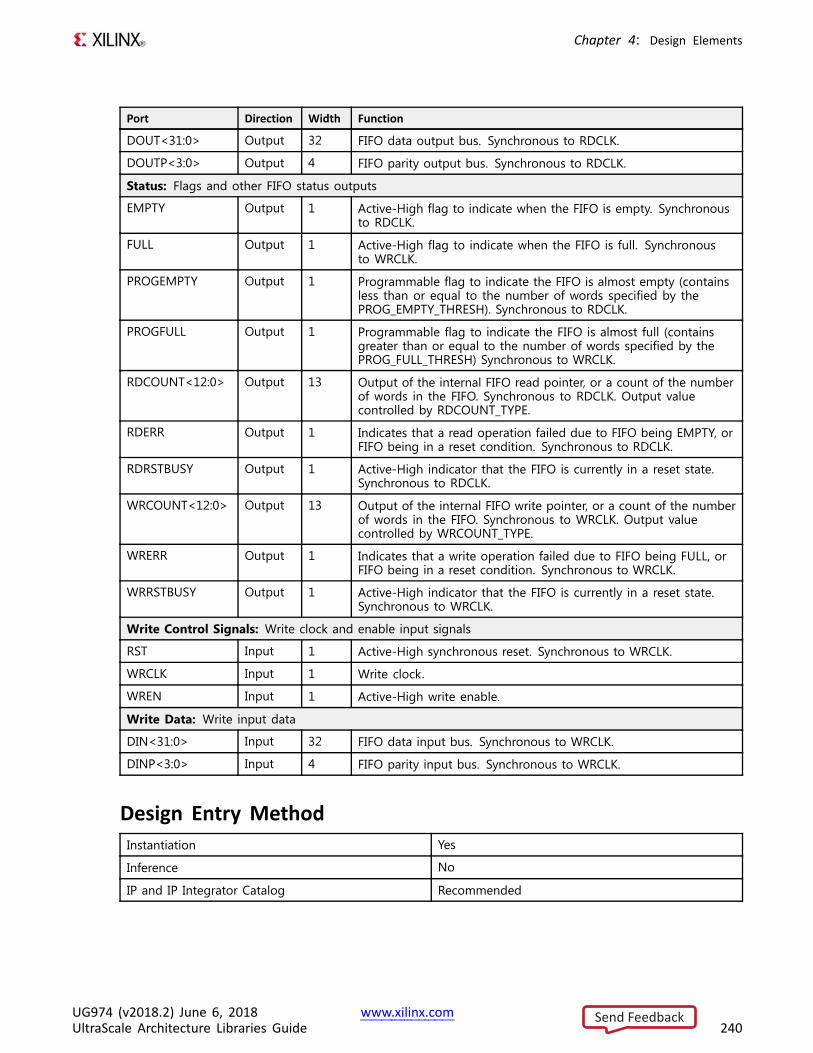
Chapter 4: Design Elements
Port Direction Width Function
DOUT<31:0> Output 32 FIFO data output bus. Synchronous to RDCLK.
DOUTP<3:0> Output 4 FIFO parity output bus. Synchronous to RDCLK.
Status: Flags and other FIFO status outputs
EMPTY Output 1 Active-High flag to indicate when the FIFO is empty. Synchronousto RDCLK.
FULL Output 1 Active-High flag to indicate when the FIFO is full. Synchronousto WRCLK.
PROGEMPTY Output 1 Programmable flag to indicate the FIFO is almost empty (containsless than or equal to the number of words specified by thePROG_EMPTY_THRESH). Synchronous to RDCLK.
PROGFULL Output 1 Programmable flag to indicate the FIFO is almost full (containsgreater than or equal to the number of words specified by thePROG_FULL_THRESH) Synchronous to WRCLK.
RDCOUNT<12:0> Output 13 Output of the internal FIFO read pointer, or a count of the numberof words in the FIFO. Synchronous to RDCLK. Output valuecontrolled by RDCOUNT_TYPE.
RDERR Output 1 Indicates that a read operation failed due to FIFO being EMPTY, orFIFO being in a reset condition. Synchronous to RDCLK.
RDRSTBUSY Output 1 Active-High indicator that the FIFO is currently in a reset state.Synchronous to RDCLK.
WRCOUNT<12:0> Output 13 Output of the internal FIFO write pointer, or a count of the numberof words in the FIFO. Synchronous to WRCLK. Output valuecontrolled by WRCOUNT_TYPE.
WRERR Output 1 Indicates that a write operation failed due to FIFO being FULL, orFIFO being in a reset condition. Synchronous to WRCLK.
WRRSTBUSY Output 1 Active-High indicator that the FIFO is currently in a reset state.Synchronous to WRCLK.
Write Control Signals: Write clock and enable input signals
RST Input 1 Active-High synchronous reset. Synchronous to WRCLK.
WRCLK Input 1 Write clock.
WREN Input 1 Active-High write enable.
Write Data: Write input data
DIN<31:0> Input 32 FIFO data input bus. Synchronous to WRCLK.
DINP<3:0> Input 4 FIFO parity input bus. Synchronous to WRCLK.
Design Entry MethodInstantiation Yes
Inference No
IP and IP Integrator Catalog Recommended
UG974 (v2018.2) June 6, 2018 www.xilinx.comUltraScale Architecture Libraries Guide 240
Send Feedback
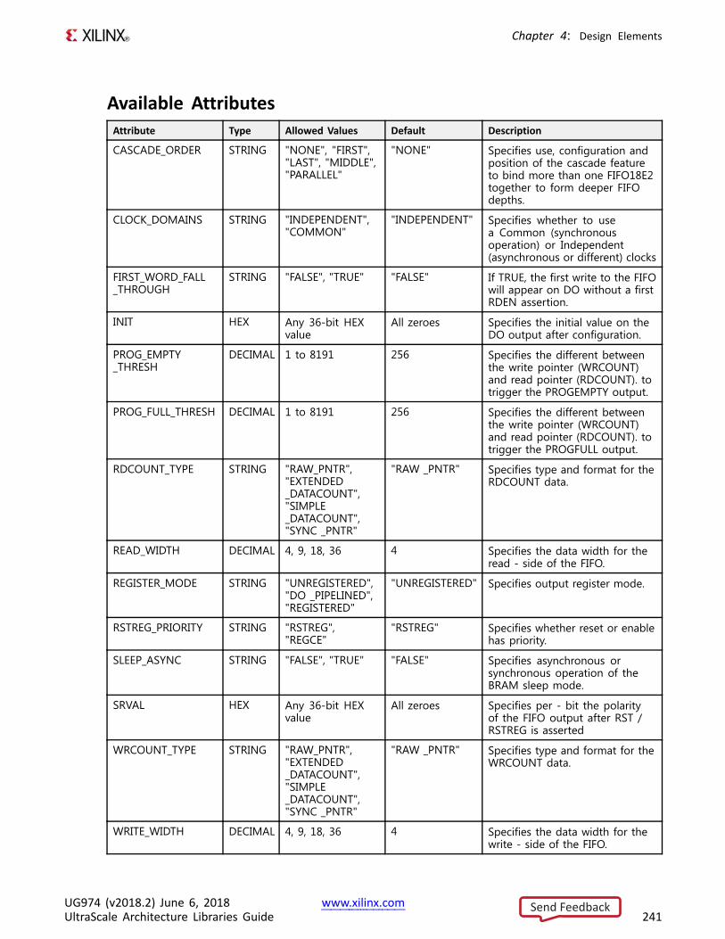
Chapter 4: Design Elements
Available AttributesAttribute Type Allowed Values Default Description
CASCADE_ORDER STRING "NONE", "FIRST","LAST", "MIDDLE","PARALLEL"
"NONE" Specifies use, configuration andposition of the cascade featureto bind more than one FIFO18E2together to form deeper FIFOdepths.
CLOCK_DOMAINS STRING "INDEPENDENT","COMMON"
"INDEPENDENT" Specifies whether to usea Common (synchronousoperation) or Independent(asynchronous or different) clocks
FIRST_WORD_FALL_THROUGH
STRING "FALSE", "TRUE" "FALSE" If TRUE, the first write to the FIFOwill appear on DO without a firstRDEN assertion.
INIT HEX Any 36-bit HEXvalue
All zeroes Specifies the initial value on theDO output after configuration.
PROG_EMPTY_THRESH
DECIMAL 1 to 8191 256 Specifies the different betweenthe write pointer (WRCOUNT)and read pointer (RDCOUNT). totrigger the PROGEMPTY output.
PROG_FULL_THRESH DECIMAL 1 to 8191 256 Specifies the different betweenthe write pointer (WRCOUNT)and read pointer (RDCOUNT). totrigger the PROGFULL output.
RDCOUNT_TYPE STRING "RAW_PNTR","EXTENDED_DATACOUNT","SIMPLE_DATACOUNT","SYNC _PNTR"
"RAW _PNTR" Specifies type and format for theRDCOUNT data.
READ_WIDTH DECIMAL 4, 9, 18, 36 4 Specifies the data width for theread - side of the FIFO.
REGISTER_MODE STRING "UNREGISTERED","DO _PIPELINED","REGISTERED"
"UNREGISTERED" Specifies output register mode.
RSTREG_PRIORITY STRING "RSTREG","REGCE"
"RSTREG" Specifies whether reset or enablehas priority.
SLEEP_ASYNC STRING "FALSE", "TRUE" "FALSE" Specifies asynchronous orsynchronous operation of theBRAM sleep mode.
SRVAL HEX Any 36-bit HEXvalue
All zeroes Specifies per - bit the polarityof the FIFO output after RST /RSTREG is asserted
WRCOUNT_TYPE STRING "RAW_PNTR","EXTENDED_DATACOUNT","SIMPLE_DATACOUNT","SYNC _PNTR"
"RAW _PNTR" Specifies type and format for theWRCOUNT data.
WRITE_WIDTH DECIMAL 4, 9, 18, 36 4 Specifies the data width for thewrite - side of the FIFO.
UG974 (v2018.2) June 6, 2018 www.xilinx.comUltraScale Architecture Libraries Guide 241
Send Feedback
Chapter 4: Design Elements
Attribute Type Allowed Values Default Description
Programmable Inversion Attributes: Specifies whether or not to use the optional inversions on specificpins of this component to change the active polarity of the pin function. When set to 1 on a clock pin(WRCLK or RDCLK), this components clocks on the negative edge. When set to 1 on other pins, it changesthe function to behave active-Low rather than active-High.For pins that are buses, the bit-width of this attribute should match that of the bit-width of the associatedpins and a binary value indicates which inverters to use and which to bypass.If an external inverter is specified on one of these associated pins, the Vivado Design Suite will automaticallyset this attribute during the opt_design stage so that additional logic is not necessary for changing theinput polarity.
IS_RDCLK _INVERTED BINARY 1'b0 to 1'b1 1'b0 Specifies whether or not to usethe optional inversion on theRDCLK pin.
IS_RDEN_INVERTED BINARY 1'b0 to 1'b1 1'b0 Specifies whether or not to usethe optional inversion on theRDEN pin.
IS_RST_INVERTED BINARY 1'b0 to 1'b1 1'b0 Specifies whether or not to usethe optional inversion on the RSTpin.
IS_RSTREG_INVERTED
BINARY 1'b0 to 1'b1 1'b0 Specifies whether or not to usethe optional inversion on theRSTREG pin.
IS_WRCLK_INVERTED
BINARY 1'b0 to 1'b1 1'b0 Specifies whether or not to usethe optional inversion on theWRCLK pin.
IS_WREN_INVERTED BINARY 1'b0 to 1'b1 1'b0 Specifies whether or not to usethe optional inversion on theWREN pin.
VHDL Instantiation TemplateUnless they already exist, copy the following two statements and paste them before the entitydeclaration.Library UNISIM;use UNISIM.vcomponents.all;
-- FIFO18E2: 18Kb FIFO (First-In-First-Out) Block RAM Memory-- UltraScale-- Xilinx HDL Language Template, version 2018.2
FIFO18E2_inst : FIFO18E2generic map (
CASCADE_ORDER => "NONE", -- FIRST, LAST, MIDDLE, NONE, PARALLELCLOCK_DOMAINS => "INDEPENDENT", -- COMMON, INDEPENDENTFIRST_WORD_FALL_THROUGH => "FALSE", -- FALSE, TRUEINIT => X"000000000", -- Initial values on output portPROG_EMPTY_THRESH => 256, -- Programmable Empty ThresholdPROG_FULL_THRESH => 256, -- Programmable Full Threshold-- Programmable Inversion Attributes: Specifies the use of the built-in programmable inversionIS_RDCLK_INVERTED => '0', -- Optional inversion for RDCLKIS_RDEN_INVERTED => '0', -- Optional inversion for RDENIS_RSTREG_INVERTED => '0', -- Optional inversion for RSTREGIS_RST_INVERTED => '0', -- Optional inversion for RSTIS_WRCLK_INVERTED => '0', -- Optional inversion for WRCLKIS_WREN_INVERTED => '0', -- Optional inversion for WRENRDCOUNT_TYPE => "RAW_PNTR", -- EXTENDED_DATACOUNT, RAW_PNTR, SIMPLE_DATACOUNT, SYNC_PNTRREAD_WIDTH => 4, -- 18-9REGISTER_MODE => "UNREGISTERED", -- DO_PIPELINED, REGISTERED, UNREGISTEREDRSTREG_PRIORITY => "RSTREG", -- REGCE, RSTREG
UG974 (v2018.2) June 6, 2018 www.xilinx.comUltraScale Architecture Libraries Guide 242
Send Feedback
Chapter 4: Design Elements
SLEEP_ASYNC => "FALSE", -- FALSE, TRUESRVAL => X"000000000", -- SET/reset value of the FIFO outputsWRCOUNT_TYPE => "RAW_PNTR", -- EXTENDED_DATACOUNT, RAW_PNTR, SIMPLE_DATACOUNT, SYNC_PNTRWRITE_WIDTH => 4 -- 18-9
)port map (
-- Cascade Signals outputs: Multi-FIFO cascade signalsCASDOUT => CASDOUT, -- 32-bit output: Data cascade output busCASDOUTP => CASDOUTP, -- 4-bit output: Parity data cascade output busCASNXTEMPTY => CASNXTEMPTY, -- 1-bit output: Cascade next emptyCASPRVRDEN => CASPRVRDEN, -- 1-bit output: Cascade previous read enable-- Read Data outputs: Read output dataDOUT => DOUT, -- 32-bit output: FIFO data output busDOUTP => DOUTP, -- 4-bit output: FIFO parity output bus.-- Status outputs: Flags and other FIFO status outputsEMPTY => EMPTY, -- 1-bit output: EmptyFULL => FULL, -- 1-bit output: FullPROGEMPTY => PROGEMPTY, -- 1-bit output: Programmable emptyPROGFULL => PROGFULL, -- 1-bit output: Programmable fullRDCOUNT => RDCOUNT, -- 13-bit output: Read countRDERR => RDERR, -- 1-bit output: Read errorRDRSTBUSY => RDRSTBUSY, -- 1-bit output: Reset busy (sync to RDCLK)WRCOUNT => WRCOUNT, -- 13-bit output: Write countWRERR => WRERR, -- 1-bit output: Write ErrorWRRSTBUSY => WRRSTBUSY, -- 1-bit output: Reset busy (sync to WRCLK)-- Cascade Signals inputs: Multi-FIFO cascade signalsCASDIN => CASDIN, -- 32-bit input: Data cascade input busCASDINP => CASDINP, -- 4-bit input: Parity data cascade input busCASDOMUX => CASDOMUX, -- 1-bit input: Cascade MUX selectCASDOMUXEN => CASDOMUXEN, -- 1-bit input: Enable for cascade MUX selectCASNXTRDEN => CASNXTRDEN, -- 1-bit input: Cascade next read enableCASOREGIMUX => CASOREGIMUX, -- 1-bit input: Cascade output MUX selectCASOREGIMUXEN => CASOREGIMUXEN, -- 1-bit input: Cascade output MUX select enableCASPRVEMPTY => CASPRVEMPTY, -- 1-bit input: Cascade previous empty-- Read Control Signals inputs: Read clock, enable and reset input signalsRDCLK => RDCLK, -- 1-bit input: Read clockRDEN => RDEN, -- 1-bit input: Read enableREGCE => REGCE, -- 1-bit input: Output register clock enableRSTREG => RSTREG, -- 1-bit input: Output register resetSLEEP => SLEEP, -- 1-bit input: Sleep Mode-- Write Control Signals inputs: Write clock and enable input signalsRST => RST, -- 1-bit input: ResetWRCLK => WRCLK, -- 1-bit input: Write clockWREN => WREN, -- 1-bit input: Write enable-- Write Data inputs: Write input dataDIN => DIN, -- 32-bit input: FIFO data input busDINP => DINP -- 4-bit input: FIFO parity input bus
);
-- End of FIFO18E2_inst instantiation
Verilog Instantiation Template
// FIFO18E2: 18Kb FIFO (First-In-First-Out) Block RAM Memory// UltraScale// Xilinx HDL Language Template, version 2018.2
FIFO18E2 #(.CASCADE_ORDER("NONE"), // FIRST, LAST, MIDDLE, NONE, PARALLEL.CLOCK_DOMAINS("INDEPENDENT"), // COMMON, INDEPENDENT.FIRST_WORD_FALL_THROUGH("FALSE"), // FALSE, TRUE.INIT(36'h000000000), // Initial values on output port.PROG_EMPTY_THRESH(256), // Programmable Empty Threshold.PROG_FULL_THRESH(256), // Programmable Full Threshold// Programmable Inversion Attributes: Specifies the use of the built-in programmable inversion.IS_RDCLK_INVERTED(1'b0), // Optional inversion for RDCLK.IS_RDEN_INVERTED(1'b0), // Optional inversion for RDEN.IS_RSTREG_INVERTED(1'b0), // Optional inversion for RSTREG
UG974 (v2018.2) June 6, 2018 www.xilinx.comUltraScale Architecture Libraries Guide 243
Send Feedback
Chapter 4: Design Elements
.IS_RST_INVERTED(1'b0), // Optional inversion for RST
.IS_WRCLK_INVERTED(1'b0), // Optional inversion for WRCLK
.IS_WREN_INVERTED(1'b0), // Optional inversion for WREN
.RDCOUNT_TYPE("RAW_PNTR"), // EXTENDED_DATACOUNT, RAW_PNTR, SIMPLE_DATACOUNT, SYNC_PNTR
.READ_WIDTH(4), // 18-9
.REGISTER_MODE("UNREGISTERED"), // DO_PIPELINED, REGISTERED, UNREGISTERED
.RSTREG_PRIORITY("RSTREG"), // REGCE, RSTREG
.SLEEP_ASYNC("FALSE"), // FALSE, TRUE
.SRVAL(36'h000000000), // SET/reset value of the FIFO outputs
.WRCOUNT_TYPE("RAW_PNTR"), // EXTENDED_DATACOUNT, RAW_PNTR, SIMPLE_DATACOUNT, SYNC_PNTR
.WRITE_WIDTH(4) // 18-9)FIFO18E2_inst (
// Cascade Signals outputs: Multi-FIFO cascade signals.CASDOUT(CASDOUT), // 32-bit output: Data cascade output bus.CASDOUTP(CASDOUTP), // 4-bit output: Parity data cascade output bus.CASNXTEMPTY(CASNXTEMPTY), // 1-bit output: Cascade next empty.CASPRVRDEN(CASPRVRDEN), // 1-bit output: Cascade previous read enable// Read Data outputs: Read output data.DOUT(DOUT), // 32-bit output: FIFO data output bus.DOUTP(DOUTP), // 4-bit output: FIFO parity output bus.// Status outputs: Flags and other FIFO status outputs.EMPTY(EMPTY), // 1-bit output: Empty.FULL(FULL), // 1-bit output: Full.PROGEMPTY(PROGEMPTY), // 1-bit output: Programmable empty.PROGFULL(PROGFULL), // 1-bit output: Programmable full.RDCOUNT(RDCOUNT), // 13-bit output: Read count.RDERR(RDERR), // 1-bit output: Read error.RDRSTBUSY(RDRSTBUSY), // 1-bit output: Reset busy (sync to RDCLK).WRCOUNT(WRCOUNT), // 13-bit output: Write count.WRERR(WRERR), // 1-bit output: Write Error.WRRSTBUSY(WRRSTBUSY), // 1-bit output: Reset busy (sync to WRCLK)// Cascade Signals inputs: Multi-FIFO cascade signals.CASDIN(CASDIN), // 32-bit input: Data cascade input bus.CASDINP(CASDINP), // 4-bit input: Parity data cascade input bus.CASDOMUX(CASDOMUX), // 1-bit input: Cascade MUX select.CASDOMUXEN(CASDOMUXEN), // 1-bit input: Enable for cascade MUX select.CASNXTRDEN(CASNXTRDEN), // 1-bit input: Cascade next read enable.CASOREGIMUX(CASOREGIMUX), // 1-bit input: Cascade output MUX select.CASOREGIMUXEN(CASOREGIMUXEN), // 1-bit input: Cascade output MUX select enable.CASPRVEMPTY(CASPRVEMPTY), // 1-bit input: Cascade previous empty// Read Control Signals inputs: Read clock, enable and reset input signals.RDCLK(RDCLK), // 1-bit input: Read clock.RDEN(RDEN), // 1-bit input: Read enable.REGCE(REGCE), // 1-bit input: Output register clock enable.RSTREG(RSTREG), // 1-bit input: Output register reset.SLEEP(SLEEP), // 1-bit input: Sleep Mode// Write Control Signals inputs: Write clock and enable input signals.RST(RST), // 1-bit input: Reset.WRCLK(WRCLK), // 1-bit input: Write clock.WREN(WREN), // 1-bit input: Write enable// Write Data inputs: Write input data.DIN(DIN), // 32-bit input: FIFO data input bus.DINP(DINP) // 4-bit input: FIFO parity input bus
);
// End of FIFO18E2_inst instantiation
For More Information• See the UltraScale Architecture Memory Resources User Guide (UG573).
• See the UltraScale Programmable Devices Documentation.
UG974 (v2018.2) June 6, 2018 www.xilinx.comUltraScale Architecture Libraries Guide 244
Send Feedback
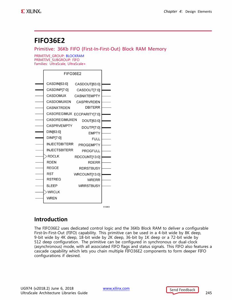
Chapter 4: Design Elements
FIFO36E2Primitive: 36Kb FIFO (First-In-First-Out) Block RAM MemoryPRIMITIVE_GROUP: BLOCKRAMPRIMITIVE_SUBGROUP: FIFOFamilies: UltraScale, UltraScale+
IntroductionThe FIFO36E2 uses dedicated control logic and the 36Kb Block RAM to deliver a configurableFirst-In-First-Out (FIFO) capability. This primitive can be used in a 4-bit wide by 8K deep,9-bit wide by 4K deep, 18-bit wide by 2K deep, 36-bit by 1K deep or a 72-bit wide by512 deep configuration. The primitive can be configured in synchronous or dual-clock(asynchronous) mode, with all associated FIFO flags and status signals. This FIFO also features acascade capability which lets you chain multiple FIFO36E2 components to form deeper FIFOconfigurations if desired.
UG974 (v2018.2) June 6, 2018 www.xilinx.comUltraScale Architecture Libraries Guide 245
Send Feedback
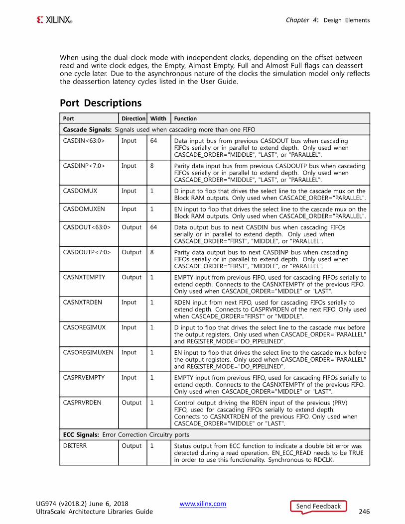
Chapter 4: Design Elements
When using the dual-clock mode with independent clocks, depending on the offset betweenread and write clock edges, the Empty, Almost Empty, Full and Almost Full flags can deassertone cycle later. Due to the asynchronous nature of the clocks the simulation model only reflectsthe deassertion latency cycles listed in the User Guide.
Port DescriptionsPort Direction Width Function
Cascade Signals: Signals used when cascading more than one FIFO
CASDIN<63:0> Input 64 Data input bus from previous CASDOUT bus when cascadingFIFOs serially or in parallel to extend depth. Only used whenCASCADE_ORDER="MIDDLE", "LAST", or "PARALLEL".
CASDINP<7:0> Input 8 Parity data input bus from previous CASDOUTP bus when cascadingFIFOs serially or in parallel to extend depth. Only used whenCASCADE_ORDER="MIDDLE", "LAST", or "PARALLEL".
CASDOMUX Input 1 D input to flop that drives the select line to the cascade mux on theBlock RAM outputs. Only used when CASCADE_ORDER="PARALLEL".
CASDOMUXEN Input 1 EN input to flop that drives the select line to the cascade mux on theBlock RAM outputs. Only used when CASCADE_ORDER="PARALLEL".
CASDOUT<63:0> Output 64 Data output bus to next CASDIN bus when cascading FIFOsserially or in parallel to extend depth. Only used whenCASCADE_ORDER="FIRST", "MIDDLE", or "PARALLEL".
CASDOUTP<7:0> Output 8 Parity data output bus to next CASDINP bus when cascadingFIFOs serially or in parallel to extend depth. Only used whenCASCADE_ORDER="FIRST", "MIDDLE", or "PARALLEL".
CASNXTEMPTY Output 1 EMPTY input from previous FIFO, used for cascading FIFOs serially toextend depth. Connects to the CASNXTEMPTY of the previous FIFO.Only used when CASCADE_ORDER="MIDDLE" or "LAST".
CASNXTRDEN Input 1 RDEN input from next FIFO, used for cascading FIFOs serially toextend depth. Connects to CASPRVRDEN of the next FIFO. Only usedwhen CASCADE_ORDER="FIRST" or "MIDDLE".
CASOREGIMUX Input 1 D input to flop that drives the select line to the cascade mux beforethe output registers. Only used when CASCADE_ORDER="PARALLEL"and REGISTER_MODE="DO_PIPELINED".
CASOREGIMUXEN Input 1 EN input to flop that drives the select line to the cascade mux beforethe output registers. Only used when CASCADE_ORDER="PARALLEL"and REGISTER_MODE="DO_PIPELINED".
CASPRVEMPTY Input 1 EMPTY input from previous FIFO, used for cascading FIFOs serially toextend depth. Connects to the CASNXTEMPTY of the previous FIFO.Only used when CASCADE_ORDER="MIDDLE" or "LAST".
CASPRVRDEN Output 1 Control output driving the RDEN input of the previous (PRV)FIFO, used for cascading FIFOs serially to extend depth.Connects to CASNXTRDEN of the previous FIFO. Only used whenCASCADE_ORDER="MIDDLE" or "LAST".
ECC Signals: Error Correction Circuitry ports
DBITERR Output 1 Status output from ECC function to indicate a double bit error wasdetected during a read operation. EN_ECC_READ needs to be TRUEin order to use this functionality. Synchronous to RDCLK.
UG974 (v2018.2) June 6, 2018 www.xilinx.comUltraScale Architecture Libraries Guide 246
Send Feedback
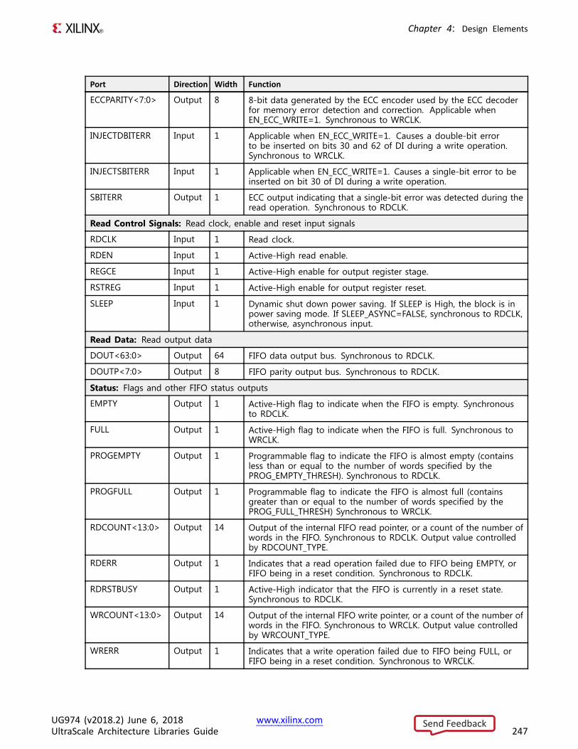
Chapter 4: Design Elements
Port Direction Width Function
ECCPARITY<7:0> Output 8 8-bit data generated by the ECC encoder used by the ECC decoderfor memory error detection and correction. Applicable whenEN_ECC_WRITE=1. Synchronous to WRCLK.
INJECTDBITERR Input 1 Applicable when EN_ECC_WRITE=1. Causes a double-bit errorto be inserted on bits 30 and 62 of DI during a write operation.Synchronous to WRCLK.
INJECTSBITERR Input 1 Applicable when EN_ECC_WRITE=1. Causes a single-bit error to beinserted on bit 30 of DI during a write operation.
SBITERR Output 1 ECC output indicating that a single-bit error was detected during theread operation. Synchronous to RDCLK.
Read Control Signals: Read clock, enable and reset input signals
RDCLK Input 1 Read clock.
RDEN Input 1 Active-High read enable.
REGCE Input 1 Active-High enable for output register stage.
RSTREG Input 1 Active-High enable for output register reset.
SLEEP Input 1 Dynamic shut down power saving. If SLEEP is High, the block is inpower saving mode. If SLEEP_ASYNC=FALSE, synchronous to RDCLK,otherwise, asynchronous input.
Read Data: Read output data
DOUT<63:0> Output 64 FIFO data output bus. Synchronous to RDCLK.
DOUTP<7:0> Output 8 FIFO parity output bus. Synchronous to RDCLK.
Status: Flags and other FIFO status outputs
EMPTY Output 1 Active-High flag to indicate when the FIFO is empty. Synchronousto RDCLK.
FULL Output 1 Active-High flag to indicate when the FIFO is full. Synchronous toWRCLK.
PROGEMPTY Output 1 Programmable flag to indicate the FIFO is almost empty (containsless than or equal to the number of words specified by thePROG_EMPTY_THRESH). Synchronous to RDCLK.
PROGFULL Output 1 Programmable flag to indicate the FIFO is almost full (containsgreater than or equal to the number of words specified by thePROG_FULL_THRESH) Synchronous to WRCLK.
RDCOUNT<13:0> Output 14 Output of the internal FIFO read pointer, or a count of the number ofwords in the FIFO. Synchronous to RDCLK. Output value controlledby RDCOUNT_TYPE.
RDERR Output 1 Indicates that a read operation failed due to FIFO being EMPTY, orFIFO being in a reset condition. Synchronous to RDCLK.
RDRSTBUSY Output 1 Active-High indicator that the FIFO is currently in a reset state.Synchronous to RDCLK.
WRCOUNT<13:0> Output 14 Output of the internal FIFO write pointer, or a count of the number ofwords in the FIFO. Synchronous to WRCLK. Output value controlledby WRCOUNT_TYPE.
WRERR Output 1 Indicates that a write operation failed due to FIFO being FULL, orFIFO being in a reset condition. Synchronous to WRCLK.
UG974 (v2018.2) June 6, 2018 www.xilinx.comUltraScale Architecture Libraries Guide 247
Send Feedback
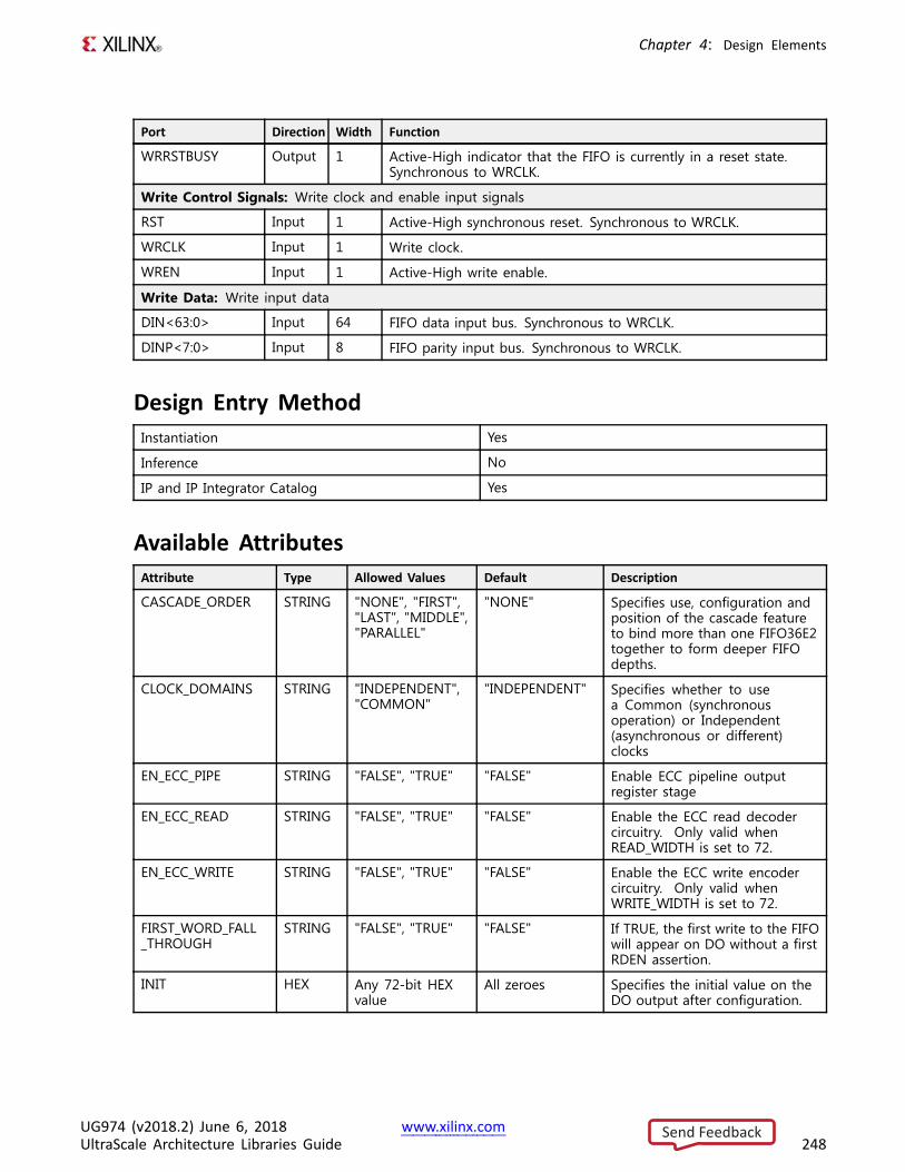
Chapter 4: Design Elements
Port Direction Width Function
WRRSTBUSY Output 1 Active-High indicator that the FIFO is currently in a reset state.Synchronous to WRCLK.
Write Control Signals: Write clock and enable input signals
RST Input 1 Active-High synchronous reset. Synchronous to WRCLK.
WRCLK Input 1 Write clock.
WREN Input 1 Active-High write enable.
Write Data: Write input data
DIN<63:0> Input 64 FIFO data input bus. Synchronous to WRCLK.
DINP<7:0> Input 8 FIFO parity input bus. Synchronous to WRCLK.
Design Entry MethodInstantiation Yes
Inference No
IP and IP Integrator Catalog Yes
Available AttributesAttribute Type Allowed Values Default Description
CASCADE_ORDER STRING "NONE", "FIRST","LAST", "MIDDLE","PARALLEL"
"NONE" Specifies use, configuration andposition of the cascade featureto bind more than one FIFO36E2together to form deeper FIFOdepths.
CLOCK_DOMAINS STRING "INDEPENDENT","COMMON"
"INDEPENDENT" Specifies whether to usea Common (synchronousoperation) or Independent(asynchronous or different)clocks
EN_ECC_PIPE STRING "FALSE", "TRUE" "FALSE" Enable ECC pipeline outputregister stage
EN_ECC_READ STRING "FALSE", "TRUE" "FALSE" Enable the ECC read decodercircuitry. Only valid whenREAD_WIDTH is set to 72.
EN_ECC_WRITE STRING "FALSE", "TRUE" "FALSE" Enable the ECC write encodercircuitry. Only valid whenWRITE_WIDTH is set to 72.
FIRST_WORD_FALL_THROUGH
STRING "FALSE", "TRUE" "FALSE" If TRUE, the first write to the FIFOwill appear on DO without a firstRDEN assertion.
INIT HEX Any 72-bit HEXvalue
All zeroes Specifies the initial value on theDO output after configuration.
UG974 (v2018.2) June 6, 2018 www.xilinx.comUltraScale Architecture Libraries Guide 248
Send Feedback
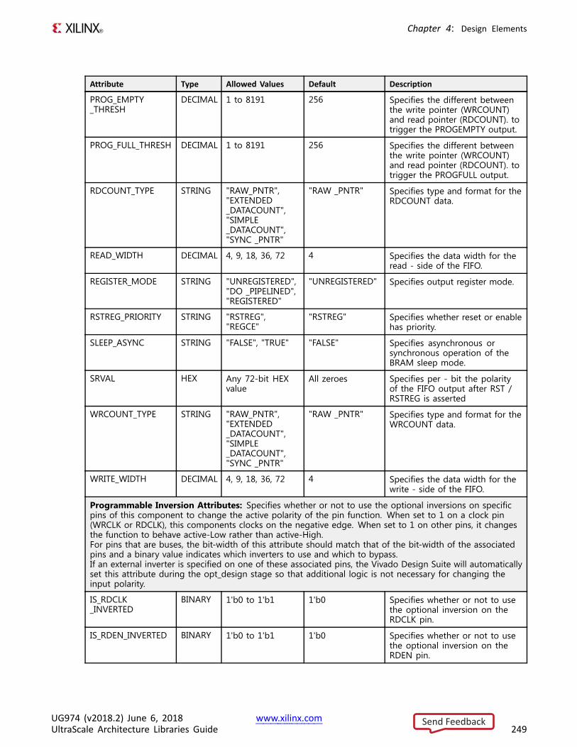
Chapter 4: Design Elements
Attribute Type Allowed Values Default Description
PROG_EMPTY_THRESH
DECIMAL 1 to 8191 256 Specifies the different betweenthe write pointer (WRCOUNT)and read pointer (RDCOUNT). totrigger the PROGEMPTY output.
PROG_FULL_THRESH DECIMAL 1 to 8191 256 Specifies the different betweenthe write pointer (WRCOUNT)and read pointer (RDCOUNT). totrigger the PROGFULL output.
RDCOUNT_TYPE STRING "RAW_PNTR","EXTENDED_DATACOUNT","SIMPLE_DATACOUNT","SYNC _PNTR"
"RAW _PNTR" Specifies type and format for theRDCOUNT data.
READ_WIDTH DECIMAL 4, 9, 18, 36, 72 4 Specifies the data width for theread - side of the FIFO.
REGISTER_MODE STRING "UNREGISTERED","DO _PIPELINED","REGISTERED"
"UNREGISTERED" Specifies output register mode.
RSTREG_PRIORITY STRING "RSTREG","REGCE"
"RSTREG" Specifies whether reset or enablehas priority.
SLEEP_ASYNC STRING "FALSE", "TRUE" "FALSE" Specifies asynchronous orsynchronous operation of theBRAM sleep mode.
SRVAL HEX Any 72-bit HEXvalue
All zeroes Specifies per - bit the polarityof the FIFO output after RST /RSTREG is asserted
WRCOUNT_TYPE STRING "RAW_PNTR","EXTENDED_DATACOUNT","SIMPLE_DATACOUNT","SYNC _PNTR"
"RAW _PNTR" Specifies type and format for theWRCOUNT data.
WRITE_WIDTH DECIMAL 4, 9, 18, 36, 72 4 Specifies the data width for thewrite - side of the FIFO.
Programmable Inversion Attributes: Specifies whether or not to use the optional inversions on specificpins of this component to change the active polarity of the pin function. When set to 1 on a clock pin(WRCLK or RDCLK), this components clocks on the negative edge. When set to 1 on other pins, it changesthe function to behave active-Low rather than active-High.For pins that are buses, the bit-width of this attribute should match that of the bit-width of the associatedpins and a binary value indicates which inverters to use and which to bypass.If an external inverter is specified on one of these associated pins, the Vivado Design Suite will automaticallyset this attribute during the opt_design stage so that additional logic is not necessary for changing theinput polarity.
IS_RDCLK_INVERTED
BINARY 1'b0 to 1'b1 1'b0 Specifies whether or not to usethe optional inversion on theRDCLK pin.
IS_RDEN_INVERTED BINARY 1'b0 to 1'b1 1'b0 Specifies whether or not to usethe optional inversion on theRDEN pin.
UG974 (v2018.2) June 6, 2018 www.xilinx.comUltraScale Architecture Libraries Guide 249
Send Feedback
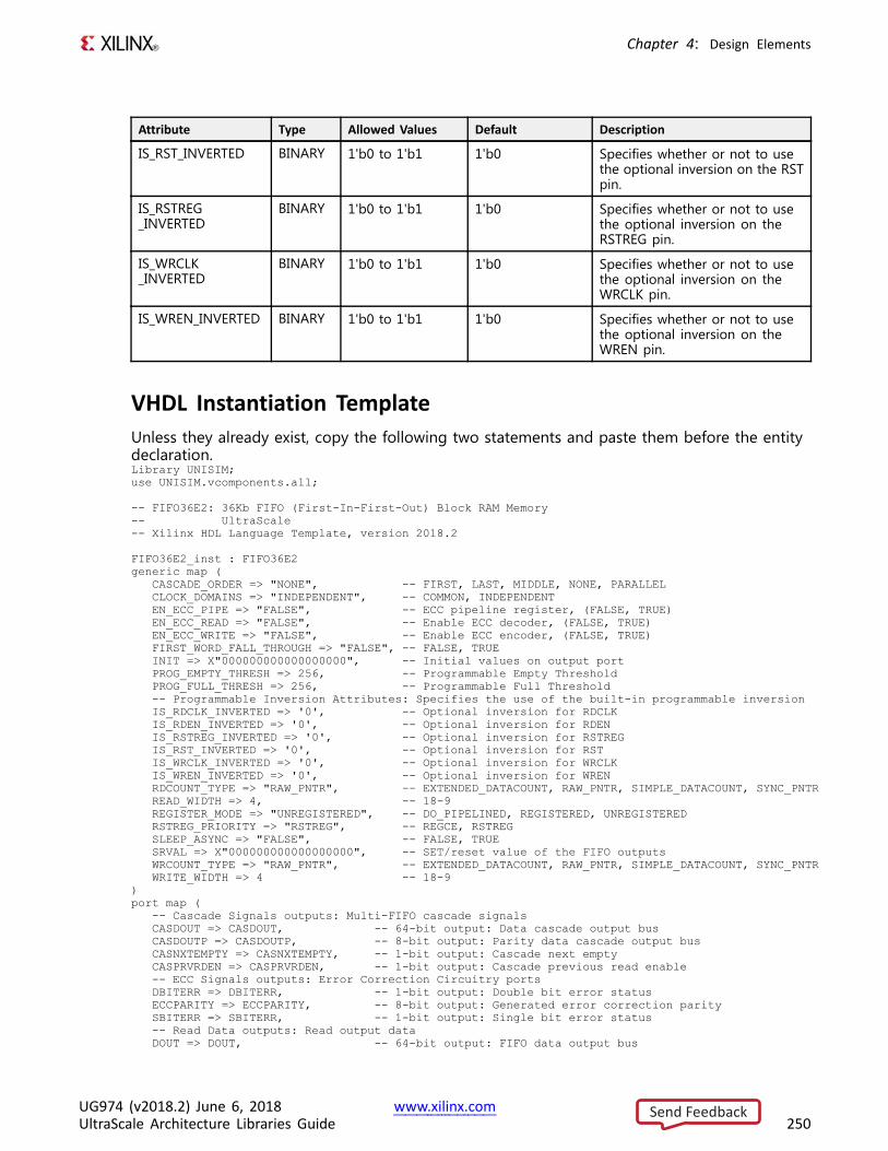
Chapter 4: Design Elements
Attribute Type Allowed Values Default Description
IS_RST_INVERTED BINARY 1'b0 to 1'b1 1'b0 Specifies whether or not to usethe optional inversion on the RSTpin.
IS_RSTREG_INVERTED
BINARY 1'b0 to 1'b1 1'b0 Specifies whether or not to usethe optional inversion on theRSTREG pin.
IS_WRCLK_INVERTED
BINARY 1'b0 to 1'b1 1'b0 Specifies whether or not to usethe optional inversion on theWRCLK pin.
IS_WREN_INVERTED BINARY 1'b0 to 1'b1 1'b0 Specifies whether or not to usethe optional inversion on theWREN pin.
VHDL Instantiation TemplateUnless they already exist, copy the following two statements and paste them before the entitydeclaration.Library UNISIM;use UNISIM.vcomponents.all;
-- FIFO36E2: 36Kb FIFO (First-In-First-Out) Block RAM Memory-- UltraScale-- Xilinx HDL Language Template, version 2018.2
FIFO36E2_inst : FIFO36E2generic map (
CASCADE_ORDER => "NONE", -- FIRST, LAST, MIDDLE, NONE, PARALLELCLOCK_DOMAINS => "INDEPENDENT", -- COMMON, INDEPENDENTEN_ECC_PIPE => "FALSE", -- ECC pipeline register, (FALSE, TRUE)EN_ECC_READ => "FALSE", -- Enable ECC decoder, (FALSE, TRUE)EN_ECC_WRITE => "FALSE", -- Enable ECC encoder, (FALSE, TRUE)FIRST_WORD_FALL_THROUGH => "FALSE", -- FALSE, TRUEINIT => X"000000000000000000", -- Initial values on output portPROG_EMPTY_THRESH => 256, -- Programmable Empty ThresholdPROG_FULL_THRESH => 256, -- Programmable Full Threshold-- Programmable Inversion Attributes: Specifies the use of the built-in programmable inversionIS_RDCLK_INVERTED => '0', -- Optional inversion for RDCLKIS_RDEN_INVERTED => '0', -- Optional inversion for RDENIS_RSTREG_INVERTED => '0', -- Optional inversion for RSTREGIS_RST_INVERTED => '0', -- Optional inversion for RSTIS_WRCLK_INVERTED => '0', -- Optional inversion for WRCLKIS_WREN_INVERTED => '0', -- Optional inversion for WRENRDCOUNT_TYPE => "RAW_PNTR", -- EXTENDED_DATACOUNT, RAW_PNTR, SIMPLE_DATACOUNT, SYNC_PNTRREAD_WIDTH => 4, -- 18-9REGISTER_MODE => "UNREGISTERED", -- DO_PIPELINED, REGISTERED, UNREGISTEREDRSTREG_PRIORITY => "RSTREG", -- REGCE, RSTREGSLEEP_ASYNC => "FALSE", -- FALSE, TRUESRVAL => X"000000000000000000", -- SET/reset value of the FIFO outputsWRCOUNT_TYPE => "RAW_PNTR", -- EXTENDED_DATACOUNT, RAW_PNTR, SIMPLE_DATACOUNT, SYNC_PNTRWRITE_WIDTH => 4 -- 18-9
)port map (
-- Cascade Signals outputs: Multi-FIFO cascade signalsCASDOUT => CASDOUT, -- 64-bit output: Data cascade output busCASDOUTP => CASDOUTP, -- 8-bit output: Parity data cascade output busCASNXTEMPTY => CASNXTEMPTY, -- 1-bit output: Cascade next emptyCASPRVRDEN => CASPRVRDEN, -- 1-bit output: Cascade previous read enable-- ECC Signals outputs: Error Correction Circuitry portsDBITERR => DBITERR, -- 1-bit output: Double bit error statusECCPARITY => ECCPARITY, -- 8-bit output: Generated error correction paritySBITERR => SBITERR, -- 1-bit output: Single bit error status-- Read Data outputs: Read output dataDOUT => DOUT, -- 64-bit output: FIFO data output bus
UG974 (v2018.2) June 6, 2018 www.xilinx.comUltraScale Architecture Libraries Guide 250
Send Feedback
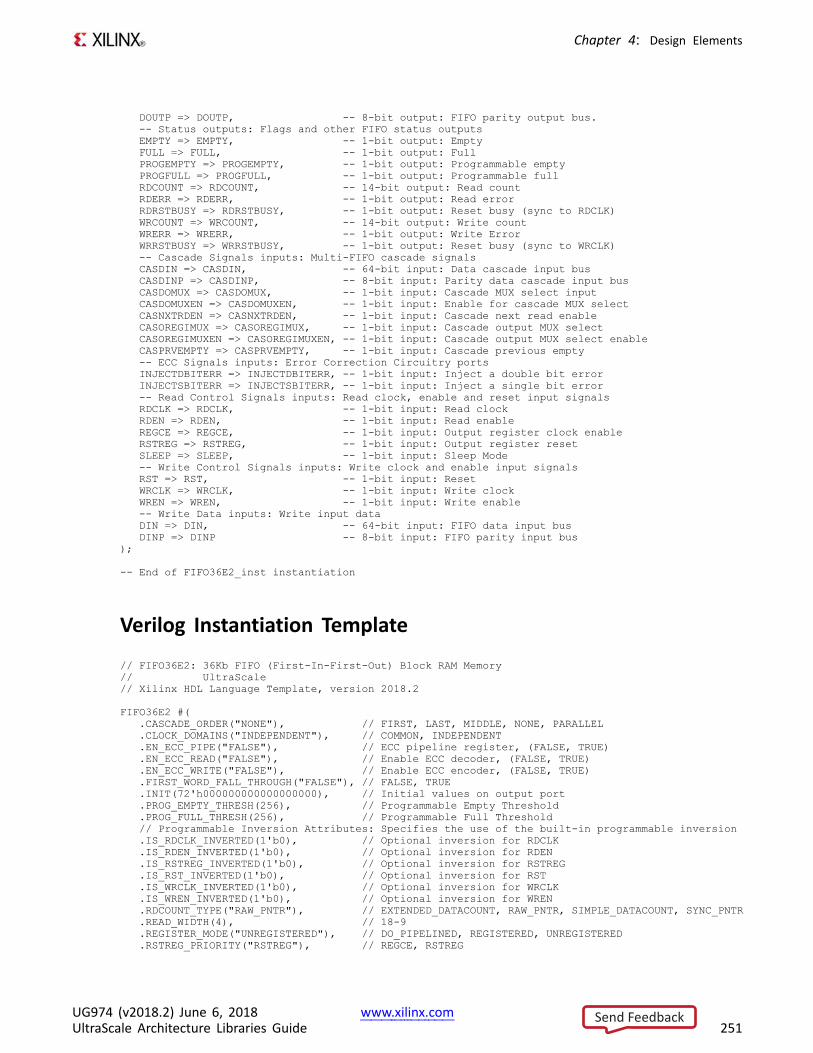
Chapter 4: Design Elements
DOUTP => DOUTP, -- 8-bit output: FIFO parity output bus.-- Status outputs: Flags and other FIFO status outputsEMPTY => EMPTY, -- 1-bit output: EmptyFULL => FULL, -- 1-bit output: FullPROGEMPTY => PROGEMPTY, -- 1-bit output: Programmable emptyPROGFULL => PROGFULL, -- 1-bit output: Programmable fullRDCOUNT => RDCOUNT, -- 14-bit output: Read countRDERR => RDERR, -- 1-bit output: Read errorRDRSTBUSY => RDRSTBUSY, -- 1-bit output: Reset busy (sync to RDCLK)WRCOUNT => WRCOUNT, -- 14-bit output: Write countWRERR => WRERR, -- 1-bit output: Write ErrorWRRSTBUSY => WRRSTBUSY, -- 1-bit output: Reset busy (sync to WRCLK)-- Cascade Signals inputs: Multi-FIFO cascade signalsCASDIN => CASDIN, -- 64-bit input: Data cascade input busCASDINP => CASDINP, -- 8-bit input: Parity data cascade input busCASDOMUX => CASDOMUX, -- 1-bit input: Cascade MUX select inputCASDOMUXEN => CASDOMUXEN, -- 1-bit input: Enable for cascade MUX selectCASNXTRDEN => CASNXTRDEN, -- 1-bit input: Cascade next read enableCASOREGIMUX => CASOREGIMUX, -- 1-bit input: Cascade output MUX selectCASOREGIMUXEN => CASOREGIMUXEN, -- 1-bit input: Cascade output MUX select enableCASPRVEMPTY => CASPRVEMPTY, -- 1-bit input: Cascade previous empty-- ECC Signals inputs: Error Correction Circuitry portsINJECTDBITERR => INJECTDBITERR, -- 1-bit input: Inject a double bit errorINJECTSBITERR => INJECTSBITERR, -- 1-bit input: Inject a single bit error-- Read Control Signals inputs: Read clock, enable and reset input signalsRDCLK => RDCLK, -- 1-bit input: Read clockRDEN => RDEN, -- 1-bit input: Read enableREGCE => REGCE, -- 1-bit input: Output register clock enableRSTREG => RSTREG, -- 1-bit input: Output register resetSLEEP => SLEEP, -- 1-bit input: Sleep Mode-- Write Control Signals inputs: Write clock and enable input signalsRST => RST, -- 1-bit input: ResetWRCLK => WRCLK, -- 1-bit input: Write clockWREN => WREN, -- 1-bit input: Write enable-- Write Data inputs: Write input dataDIN => DIN, -- 64-bit input: FIFO data input busDINP => DINP -- 8-bit input: FIFO parity input bus
);
-- End of FIFO36E2_inst instantiation
Verilog Instantiation Template
// FIFO36E2: 36Kb FIFO (First-In-First-Out) Block RAM Memory// UltraScale// Xilinx HDL Language Template, version 2018.2
FIFO36E2 #(.CASCADE_ORDER("NONE"), // FIRST, LAST, MIDDLE, NONE, PARALLEL.CLOCK_DOMAINS("INDEPENDENT"), // COMMON, INDEPENDENT.EN_ECC_PIPE("FALSE"), // ECC pipeline register, (FALSE, TRUE).EN_ECC_READ("FALSE"), // Enable ECC decoder, (FALSE, TRUE).EN_ECC_WRITE("FALSE"), // Enable ECC encoder, (FALSE, TRUE).FIRST_WORD_FALL_THROUGH("FALSE"), // FALSE, TRUE.INIT(72'h000000000000000000), // Initial values on output port.PROG_EMPTY_THRESH(256), // Programmable Empty Threshold.PROG_FULL_THRESH(256), // Programmable Full Threshold// Programmable Inversion Attributes: Specifies the use of the built-in programmable inversion.IS_RDCLK_INVERTED(1'b0), // Optional inversion for RDCLK.IS_RDEN_INVERTED(1'b0), // Optional inversion for RDEN.IS_RSTREG_INVERTED(1'b0), // Optional inversion for RSTREG.IS_RST_INVERTED(1'b0), // Optional inversion for RST.IS_WRCLK_INVERTED(1'b0), // Optional inversion for WRCLK.IS_WREN_INVERTED(1'b0), // Optional inversion for WREN.RDCOUNT_TYPE("RAW_PNTR"), // EXTENDED_DATACOUNT, RAW_PNTR, SIMPLE_DATACOUNT, SYNC_PNTR.READ_WIDTH(4), // 18-9.REGISTER_MODE("UNREGISTERED"), // DO_PIPELINED, REGISTERED, UNREGISTERED.RSTREG_PRIORITY("RSTREG"), // REGCE, RSTREG
UG974 (v2018.2) June 6, 2018 www.xilinx.comUltraScale Architecture Libraries Guide 251
Send Feedback
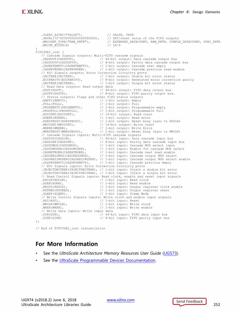
Chapter 4: Design Elements
.SLEEP_ASYNC("FALSE"), // FALSE, TRUE
.SRVAL(72'h000000000000000000), // SET/reset value of the FIFO outputs
.WRCOUNT_TYPE("RAW_PNTR"), // EXTENDED_DATACOUNT, RAW_PNTR, SIMPLE_DATACOUNT, SYNC_PNTR
.WRITE_WIDTH(4) // 18-9)FIFO36E2_inst (
// Cascade Signals outputs: Multi-FIFO cascade signals.CASDOUT(CASDOUT), // 64-bit output: Data cascade output bus.CASDOUTP(CASDOUTP), // 8-bit output: Parity data cascade output bus.CASNXTEMPTY(CASNXTEMPTY), // 1-bit output: Cascade next empty.CASPRVRDEN(CASPRVRDEN), // 1-bit output: Cascade previous read enable// ECC Signals outputs: Error Correction Circuitry ports.DBITERR(DBITERR), // 1-bit output: Double bit error status.ECCPARITY(ECCPARITY), // 8-bit output: Generated error correction parity.SBITERR(SBITERR), // 1-bit output: Single bit error status// Read Data outputs: Read output data.DOUT(DOUT), // 64-bit output: FIFO data output bus.DOUTP(DOUTP), // 8-bit output: FIFO parity output bus.// Status outputs: Flags and other FIFO status outputs.EMPTY(EMPTY), // 1-bit output: Empty.FULL(FULL), // 1-bit output: Full.PROGEMPTY(PROGEMPTY), // 1-bit output: Programmable empty.PROGFULL(PROGFULL), // 1-bit output: Programmable full.RDCOUNT(RDCOUNT), // 14-bit output: Read count.RDERR(RDERR), // 1-bit output: Read error.RDRSTBUSY(RDRSTBUSY), // 1-bit output: Reset busy (sync to RDCLK).WRCOUNT(WRCOUNT), // 14-bit output: Write count.WRERR(WRERR), // 1-bit output: Write Error.WRRSTBUSY(WRRSTBUSY), // 1-bit output: Reset busy (sync to WRCLK)// Cascade Signals inputs: Multi-FIFO cascade signals.CASDIN(CASDIN), // 64-bit input: Data cascade input bus.CASDINP(CASDINP), // 8-bit input: Parity data cascade input bus.CASDOMUX(CASDOMUX), // 1-bit input: Cascade MUX select input.CASDOMUXEN(CASDOMUXEN), // 1-bit input: Enable for cascade MUX select.CASNXTRDEN(CASNXTRDEN), // 1-bit input: Cascade next read enable.CASOREGIMUX(CASOREGIMUX), // 1-bit input: Cascade output MUX select.CASOREGIMUXEN(CASOREGIMUXEN), // 1-bit input: Cascade output MUX select enable.CASPRVEMPTY(CASPRVEMPTY), // 1-bit input: Cascade previous empty// ECC Signals inputs: Error Correction Circuitry ports.INJECTDBITERR(INJECTDBITERR), // 1-bit input: Inject a double bit error.INJECTSBITERR(INJECTSBITERR), // 1-bit input: Inject a single bit error// Read Control Signals inputs: Read clock, enable and reset input signals.RDCLK(RDCLK), // 1-bit input: Read clock.RDEN(RDEN), // 1-bit input: Read enable.REGCE(REGCE), // 1-bit input: Output register clock enable.RSTREG(RSTREG), // 1-bit input: Output register reset.SLEEP(SLEEP), // 1-bit input: Sleep Mode// Write Control Signals inputs: Write clock and enable input signals.RST(RST), // 1-bit input: Reset.WRCLK(WRCLK), // 1-bit input: Write clock.WREN(WREN), // 1-bit input: Write enable// Write Data inputs: Write input data.DIN(DIN), // 64-bit input: FIFO data input bus.DINP(DINP) // 8-bit input: FIFO parity input bus
);
// End of FIFO36E2_inst instantiation
For More Information• See the UltraScale Architecture Memory Resources User Guide (UG573).
• See the UltraScale Programmable Devices Documentation.
UG974 (v2018.2) June 6, 2018 www.xilinx.comUltraScale Architecture Libraries Guide 252
Send Feedback
Chapter 4: Design Elements
FRAME_ECCE3Primitive: Configuration Frame Error CorrectionPRIMITIVE_GROUP: CONFIGURATIONPRIMITIVE_SUBGROUP: ECCFamilies: UltraScale
IntroductionThis design element enables the dedicated, built-in Error Correction Code (ECC) for theconfiguration memory of the device. This element contains outputs that allow monitoring ofthe status of the ECC circuitry and the status of the readback CRC circuitry. This element is notintended to be instantiated, used, or modified outside of the Xilinx generated SEM IP
Design Entry MethodInstantiation No
Inference No
IP and IP Integrator Catalog Recommended
For More Information• See the UltraScale Architecture Soft Error Mitigation Controller v3.0 Product Guide (PG187).
• See the UltraScale Programmable Devices Documentation.
UG974 (v2018.2) June 6, 2018 www.xilinx.comUltraScale Architecture Libraries Guide 253
Send Feedback

Chapter 4: Design Elements
FRAME_ECCE4Primitive: Configuration Frame Error CorrectionPRIMITIVE_GROUP: CONFIGURATIONPRIMITIVE_SUBGROUP: ECCFamilies: UltraScale+
IntroductionThis design element enables the dedicated, built-in Error Correction Code (ECC) for theconfiguration memory of the device. This element contains outputs that allow monitoring ofthe status of the ECC circuitry and the status of the readback CRC circuitry. This element is notintended to be instantiated, used, or modified outside of the Xilinx generated SEM IP
Design Entry MethodInstantiation No
Inference No
IP and IP Integrator Catalog Recommended
For More Information• See the UltraScale Architecture Soft Error Mitigation Controller v3.0 Product Guide (PG187).
• See the UltraScale Programmable Devices Documentation.
UG974 (v2018.2) June 6, 2018 www.xilinx.comUltraScale Architecture Libraries Guide 254
Send Feedback

Chapter 4: Design Elements
GTHE3_CHANNELPrimitive: Gigabit Transceiver for UltraScale devicesPRIMITIVE_GROUP: ADVANCEDPRIMITIVE_SUBGROUP: GTFamilies: UltraScale
IntroductionGTHE3 is a gigabit transceiver component for UltraScale devices. This element is not intendedto be instantiated, used, or modified outside of Xilinx generated IP. See the Transceivers UserGuide for details on this component.
Design Entry MethodInstantiation No
Inference No
IP and IP Integrator Catalog Recommended
For More Information• See the UltraScale Architecture GTH Transceivers User Guide (UG576)
• See the UltraScale FPGAs Transceivers Wizard v1.6 Product Guide (PG182).
• See the UltraScale Programmable Devices Documentation.
UG974 (v2018.2) June 6, 2018 www.xilinx.comUltraScale Architecture Libraries Guide 255
Send Feedback

Chapter 4: Design Elements
GTHE3_COMMONPrimitive: Gigabit Transceiver for UltraScale devicesPRIMITIVE_GROUP: ADVANCEDPRIMITIVE_SUBGROUP: GTFamilies: UltraScale
IntroductionGTHE3 is a gigabit transceiver component for UltraScale devices. This element is not intendedto be instantiated, used, or modified outside of Xilinx generated IP. See the Transceivers UserGuide for details on this component.
Design Entry MethodInstantiation No
Inference No
IP and IP Integrator Catalog Recommended
For More Information• See the UltraScale Architecture GTH Transceivers User Guide (UG576)
• See the UltraScale FPGAs Transceivers Wizard v1.6 Product Guide (PG182).
• See the UltraScale Programmable Devices Documentation.
UG974 (v2018.2) June 6, 2018 www.xilinx.comUltraScale Architecture Libraries Guide 256
Send Feedback

Chapter 4: Design Elements
GTHE4_CHANNELPrimitive: Gigabit Transceiver for UltraScale+ devicesPRIMITIVE_GROUP: ADVANCEDPRIMITIVE_SUBGROUP: GTFamilies: UltraScale+
IntroductionGTHE4 is a gigabit transceiver component for UltraScale+ devices. This element is not intendedto be instantiated, used, or modified outside of Xilinx generated IP. See the Transceivers UserGuide for details on this component.
Design Entry MethodInstantiation No
Inference No
IP and IP Integrator Catalog Recommended
For More Information• See the UltraScale Architecture GTH Transceivers User Guide (UG576)
• See the UltraScale FPGAs Transceivers Wizard v1.6 Product Guide (PG182).
• See the UltraScale Programmable Devices Documentation.
UG974 (v2018.2) June 6, 2018 www.xilinx.comUltraScale Architecture Libraries Guide 257
Send Feedback
Chapter 4: Design Elements
GTHE4_COMMONPrimitive: Gigabit Transceiver for UltraScale+ devicesPRIMITIVE_GROUP: ADVANCEDPRIMITIVE_SUBGROUP: GTFamilies: UltraScale+
IntroductionGTHE4 is a gigabit transceiver component for UltraScale+ devices. This element is not intendedto be instantiated, used, or modified outside of Xilinx generated IP. See the Transceivers UserGuide for details on this component.
Design Entry MethodInstantiation No
Inference No
IP and IP Integrator Catalog Recommended
For More Information• See the UltraScale Architecture GTH Transceivers User Guide (UG576)
• See the UltraScale FPGAs Transceivers Wizard v1.6 Product Guide (PG182).
• See the UltraScale Programmable Devices Documentation.
UG974 (v2018.2) June 6, 2018 www.xilinx.comUltraScale Architecture Libraries Guide 258
Send Feedback
Chapter 4: Design Elements
GTYE3_CHANNELPrimitive: Gigabit Transceiver for UltraScale devicesPRIMITIVE_GROUP: ADVANCEDPRIMITIVE_SUBGROUP: GTFamilies: UltraScale
IntroductionGTYE3 is a gigabit transceiver component for UltraScale devices. This element is not intendedto be instantiated, used, or modified outside of Xilinx generated IP. See the Transceivers UserGuide for details on this component.
Design Entry MethodInstantiation No
Inference No
IP and IP Integrator Catalog Recommended
For More Information• See the UltraScale Architecture GTY Transceivers Advance Specification User Guide (UG578)
• See the UltraScale FPGAs Transceivers Wizard v1.6 Product Guide (PG182).
• See the UltraScale Programmable Devices Documentation.
UG974 (v2018.2) June 6, 2018 www.xilinx.comUltraScale Architecture Libraries Guide 259
Send Feedback

Chapter 4: Design Elements
GTYE3_COMMONPrimitive: Gigabit Transceiver for UltraScale devicesPRIMITIVE_GROUP: ADVANCEDPRIMITIVE_SUBGROUP: GTFamilies: UltraScale
IntroductionGTYE3 is a gigabit transceiver component for UltraScale devices. This element is not intendedto be instantiated, used, or modified outside of Xilinx generated IP. See the Transceivers UserGuide for details on this component.
Design Entry MethodInstantiation No
Inference No
IP and IP Integrator Catalog Recommended
For More Information• See the UltraScale Architecture GTY Transceivers Advance Specification User Guide (UG578)
• See the UltraScale FPGAs Transceivers Wizard v1.6 Product Guide (PG182).
• See the UltraScale Programmable Devices Documentation.
UG974 (v2018.2) June 6, 2018 www.xilinx.comUltraScale Architecture Libraries Guide 260
Send Feedback
Chapter 4: Design Elements
GTYE4_CHANNELPrimitive: Gigabit Transceiver for UltraScale+ devicesPRIMITIVE_GROUP: ADVANCEDPRIMITIVE_SUBGROUP: GTFamilies: UltraScale+
IntroductionGTYE4 is a gigabit transceiver component for UltraScale+ devices. This element is not intendedto be instantiated, used, or modified outside of Xilinx generated IP. See the Transceivers UserGuide for details on this component.
Design Entry MethodInstantiation No
Inference No
IP and IP Integrator Catalog Recommended
For More Information• See the UltraScale Architecture GTY Transceivers Advance Specification User Guide (UG578)
• See the UltraScale FPGAs Transceivers Wizard v1.6 Product Guide (PG182).
• See the UltraScale Programmable Devices Documentation.
UG974 (v2018.2) June 6, 2018 www.xilinx.comUltraScale Architecture Libraries Guide 261
Send Feedback

Chapter 4: Design Elements
GTYE4_COMMONPrimitive: Gigabit Transceiver for UltraScale+ devicesPRIMITIVE_GROUP: ADVANCEDPRIMITIVE_SUBGROUP: GTFamilies: UltraScale+
IntroductionGTYE4 is a gigabit transceiver component for UltraScale+ devices. This element is not intendedto be instantiated, used, or modified outside of Xilinx generated IP. See the Transceivers UserGuide for details on this component.
Design Entry MethodInstantiation No
Inference No
IP and IP Integrator Catalog Recommended
For More Information• See the UltraScale Architecture GTY Transceivers Advance Specification User Guide (UG578)
• See the UltraScale FPGAs Transceivers Wizard v1.6 Product Guide (PG182).
• See the UltraScale Programmable Devices Documentation.
UG974 (v2018.2) June 6, 2018 www.xilinx.comUltraScale Architecture Libraries Guide 262
Send Feedback
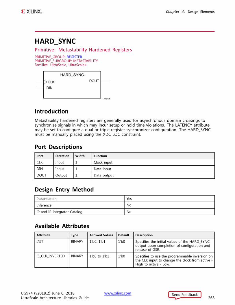
Chapter 4: Design Elements
HARD_SYNCPrimitive: Metastability Hardened RegistersPRIMITIVE_GROUP: REGISTERPRIMITIVE_SUBGROUP: METASTABILITYFamilies: UltraScale, UltraScale+
IntroductionMetastability hardened registers are generally used for asynchronous domain crossings tosynchronize signals in which may incur setup or hold time violations. The LATENCY attributemay be set to configure a dual or triple register synchronizer configuration. The HARD_SYNCmust be manually placed using the XDC LOC constraint.
Port DescriptionsPort Direction Width Function
CLK Input 1 Clock input
DIN Input 1 Data input
DOUT Output 1 Data output
Design Entry MethodInstantiation Yes
Inference No
IP and IP Integrator Catalog No
Available AttributesAttribute Type Allowed Values Default Description
INIT BINARY 1'b0, 1'b1 1'b0 Specifies the initial values of the HARD_SYNCoutput upon completion of configuration andrelease of GSR.
IS_CLK_INVERTED BINARY 1'b0 to 1'b1 1'b0 Specifies to use the programmable inversion onthe CLK input to change the clock from active -High to active - Low.
UG974 (v2018.2) June 6, 2018 www.xilinx.comUltraScale Architecture Libraries Guide 263
Send Feedback
Chapter 4: Design Elements
Attribute Type Allowed Values Default Description
LATENCY DECIMAL 2, 3 2 Specifies whether to use a two stage or threestage synchronizer. Three stage will exhibitbetter MTBF characteristics however have anadditional clock cycle of latency.
VHDL Instantiation TemplateUnless they already exist, copy the following two statements and paste them before the entitydeclaration.Library UNISIM;use UNISIM.vcomponents.all;
-- HARD_SYNC: Metastability Hardened Registers-- UltraScale-- Xilinx HDL Language Template, version 2018.2
HARD_SYNC_inst : HARD_SYNCgeneric map (
INIT => '0', -- Initial values, '0', '1'IS_CLK_INVERTED => '0', -- Programmable inversion on CLK inputLATENCY => 2 -- 2-3
)port map (
DOUT => DOUT, -- 1-bit output: DataCLK => CLK, -- 1-bit input: ClockDIN => DIN -- 1-bit input: Data
);
-- End of HARD_SYNC_inst instantiation
Verilog Instantiation Template
// HARD_SYNC: Metastability Hardened Registers// UltraScale// Xilinx HDL Language Template, version 2018.2
HARD_SYNC #(.INIT(1'b0), // Initial values, 1'b0, 1'b1.IS_CLK_INVERTED(1'b0), // Programmable inversion on CLK input.LATENCY(2) // 2-3
)HARD_SYNC_inst (
.DOUT(DOUT), // 1-bit output: Data
.CLK(CLK), // 1-bit input: Clock
.DIN(DIN) // 1-bit input: Data);
// End of HARD_SYNC_inst instantiation
For More Information• See the UltraScale Architecture Configurable Logic Block User Guide (UG574).
• See the UltraScale Programmable Devices Documentation.
UG974 (v2018.2) June 6, 2018 www.xilinx.comUltraScale Architecture Libraries Guide 264
Send Feedback
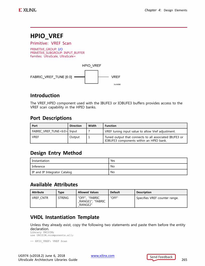
Chapter 4: Design Elements
HPIO_VREFPrimitive: VREF ScanPRIMITIVE_GROUP: I/OPRIMITIVE_SUBGROUP: INPUT_BUFFERFamilies: UltraScale, UltraScale+
IntroductionThe VREF_HPIO component used with the IBUFE3 or IOBUFE3 buffers provides access to theVREF scan capability in the HPIO banks.
Port DescriptionsPort Direction Width Function
FABRIC_VREF_TUNE<6:0> Input 7 VREF tuning input value to allow Vref adjustment.
VREF Output 1 Tuned output that connects to all associated IBUFE3 orIOBUFE3 components within an HPIO bank.
Design Entry MethodInstantiation Yes
Inference No
IP and IP Integrator Catalog No
Available AttributesAttribute Type Allowed Values Default Description
VREF_CNTR STRING "OFF", "FABRIC_RANGE1", "FABRIC_RANGE2"
"OFF" Specifies VREF counter range.
VHDL Instantiation TemplateUnless they already exist, copy the following two statements and paste them before the entitydeclaration.Library UNISIM;use UNISIM.vcomponents.all;
-- HPIO_VREF: VREF Scan
UG974 (v2018.2) June 6, 2018 www.xilinx.comUltraScale Architecture Libraries Guide 265
Send Feedback
Chapter 4: Design Elements
-- UltraScale-- Xilinx HDL Language Template, version 2018.2
HPIO_VREF_inst : HPIO_VREFgeneric map (
VREF_CNTR => "OFF" -- FABRIC_RANGE1, FABRIC_RANGE2, OFF)port map (
VREF => VREF, -- 1-bit output: Tuned output (connect to associated IBUFE3-- component)
FABRIC_VREF_TUNE => FABRIC_VREF_TUNE -- 7-bit input: VREF tuning value);
-- End of HPIO_VREF_inst instantiation
Verilog Instantiation Template
// HPIO_VREF: VREF Scan// UltraScale// Xilinx HDL Language Template, version 2018.2
HPIO_VREF #(.VREF_CNTR("OFF") // FABRIC_RANGE1, FABRIC_RANGE2, OFF
)HPIO_VREF_inst (
.VREF(VREF), // 1-bit output: Tuned output (connect to associated IBUFE3// component)
.FABRIC_VREF_TUNE(FABRIC_VREF_TUNE) // 7-bit input: VREF tuning value);
// End of HPIO_VREF_inst instantiation
For More Information• See the UltraScale Architecture SelectIO Resources User Guide (UG571).
• See the UltraScale Programmable Devices Documentation.
UG974 (v2018.2) June 6, 2018 www.xilinx.comUltraScale Architecture Libraries Guide 266
Send Feedback
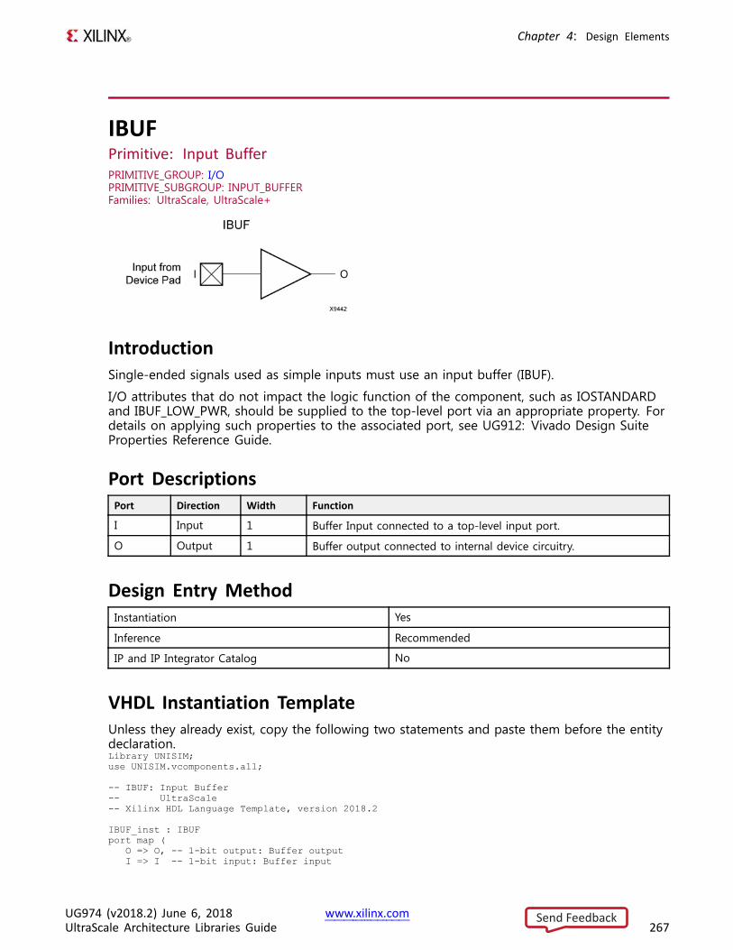
Chapter 4: Design Elements
IBUFPrimitive: Input BufferPRIMITIVE_GROUP: I/OPRIMITIVE_SUBGROUP: INPUT_BUFFERFamilies: UltraScale, UltraScale+
IntroductionSingle-ended signals used as simple inputs must use an input buffer (IBUF).
I/O attributes that do not impact the logic function of the component, such as IOSTANDARDand IBUF_LOW_PWR, should be supplied to the top-level port via an appropriate property. Fordetails on applying such properties to the associated port, see UG912: Vivado Design SuiteProperties Reference Guide.
Port DescriptionsPort Direction Width Function
I Input 1 Buffer Input connected to a top-level input port.
O Output 1 Buffer output connected to internal device circuitry.
Design Entry MethodInstantiation Yes
Inference Recommended
IP and IP Integrator Catalog No
VHDL Instantiation TemplateUnless they already exist, copy the following two statements and paste them before the entitydeclaration.Library UNISIM;use UNISIM.vcomponents.all;
-- IBUF: Input Buffer-- UltraScale-- Xilinx HDL Language Template, version 2018.2
IBUF_inst : IBUFport map (
O => O, -- 1-bit output: Buffer outputI => I -- 1-bit input: Buffer input
UG974 (v2018.2) June 6, 2018 www.xilinx.comUltraScale Architecture Libraries Guide 267
Send Feedback

Chapter 4: Design Elements
);
-- End of IBUF_inst instantiation
Verilog Instantiation Template
// IBUF: Input Buffer// UltraScale// Xilinx HDL Language Template, version 2018.2
IBUF IBUF_inst (.O(O), // 1-bit output: Buffer output.I(I) // 1-bit input: Buffer input
);
// End of IBUF_inst instantiation
For More Information• See the UltraScale Architecture SelectIO Resources User Guide (UG571).
• See the UltraScale Programmable Devices Documentation.
UG974 (v2018.2) June 6, 2018 www.xilinx.comUltraScale Architecture Libraries Guide 268
Send Feedback
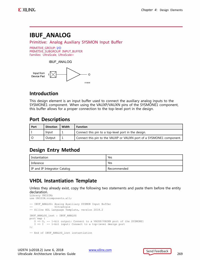
Chapter 4: Design Elements
IBUF_ANALOGPrimitive: Analog Auxiliary SYSMON Input BufferPRIMITIVE_GROUP: I/OPRIMITIVE_SUBGROUP: INPUT_BUFFERFamilies: UltraScale, UltraScale+
IntroductionThis design element is an input buffer used to connect the auxiliary analog inputs to theSYSMONE1 component. When using the VAUXP/VAUXN pins of the SYSMONE1 component,this buffer allows for a proper connection to the top-level port in the design.
Port DescriptionsPort Direction Width Function
I Input 1 Connect this pin to a top-level port in the design.
O Output 1 Connect this pin to the VAUXP or VAUXN port of a SYSMONE1 component.
Design Entry MethodInstantiation Yes
Inference Yes
IP and IP Integrator Catalog Recommended
VHDL Instantiation TemplateUnless they already exist, copy the following two statements and paste them before the entitydeclaration.Library UNISIM;use UNISIM.vcomponents.all;
-- IBUF_ANALOG: Analog Auxiliary SYSMON Input Buffer-- UltraScale-- Xilinx HDL Language Template, version 2018.2
IBUF_ANALOG_inst : IBUF_ANALOGport map (
O => O, -- 1-bit output: Connect to a VAUXP/VAUXN port of the SYSMONE1I => I -- 1-bit input: Connect to a top-level design port
);
-- End of IBUF_ANALOG_inst instantiation
UG974 (v2018.2) June 6, 2018 www.xilinx.comUltraScale Architecture Libraries Guide 269
Send Feedback
Chapter 4: Design Elements
Verilog Instantiation Template
// IBUF_ANALOG: Analog Auxiliary SYSMON Input Buffer// UltraScale// Xilinx HDL Language Template, version 2018.2
IBUF_ANALOG IBUF_ANALOG_inst (.O(O), // 1-bit output: Connect to a VAUXP/VAUXN port of the SYSMONE1.I(I) // 1-bit input: Connect to a top-level design port
);
// End of IBUF_ANALOG_inst instantiation
For More Information• See the UltraScale Architecture System Monitor User Guide (UG580).
• See the UltraScale Programmable Devices Documentation.
UG974 (v2018.2) June 6, 2018 www.xilinx.comUltraScale Architecture Libraries Guide 270
Send Feedback
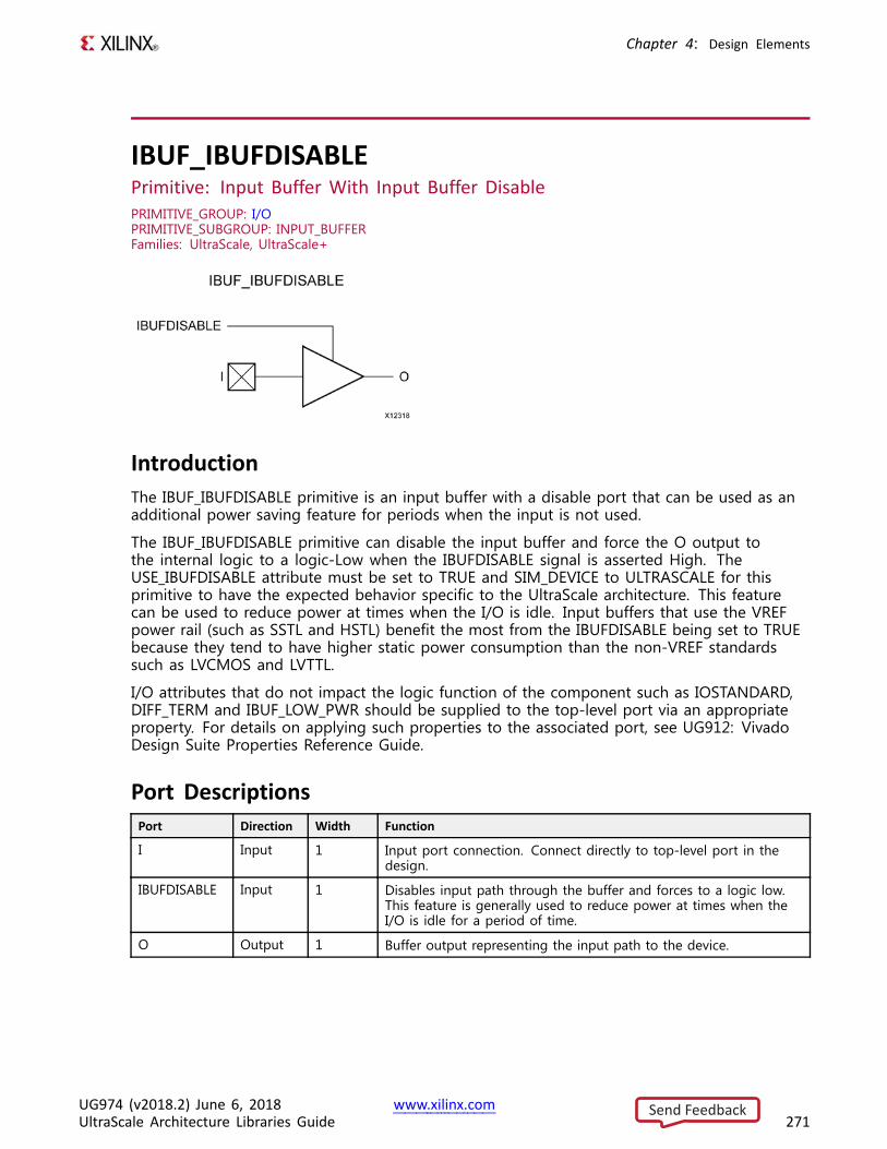
Chapter 4: Design Elements
IBUF_IBUFDISABLEPrimitive: Input Buffer With Input Buffer DisablePRIMITIVE_GROUP: I/OPRIMITIVE_SUBGROUP: INPUT_BUFFERFamilies: UltraScale, UltraScale+
IntroductionThe IBUF_IBUFDISABLE primitive is an input buffer with a disable port that can be used as anadditional power saving feature for periods when the input is not used.
The IBUF_IBUFDISABLE primitive can disable the input buffer and force the O output tothe internal logic to a logic-Low when the IBUFDISABLE signal is asserted High. TheUSE_IBUFDISABLE attribute must be set to TRUE and SIM_DEVICE to ULTRASCALE for thisprimitive to have the expected behavior specific to the UltraScale architecture. This featurecan be used to reduce power at times when the I/O is idle. Input buffers that use the VREFpower rail (such as SSTL and HSTL) benefit the most from the IBUFDISABLE being set to TRUEbecause they tend to have higher static power consumption than the non-VREF standardssuch as LVCMOS and LVTTL.
I/O attributes that do not impact the logic function of the component such as IOSTANDARD,DIFF_TERM and IBUF_LOW_PWR should be supplied to the top-level port via an appropriateproperty. For details on applying such properties to the associated port, see UG912: VivadoDesign Suite Properties Reference Guide.
Port DescriptionsPort Direction Width Function
I Input 1 Input port connection. Connect directly to top-level port in thedesign.
IBUFDISABLE Input 1 Disables input path through the buffer and forces to a logic low.This feature is generally used to reduce power at times when theI/O is idle for a period of time.
O Output 1 Buffer output representing the input path to the device.
UG974 (v2018.2) June 6, 2018 www.xilinx.comUltraScale Architecture Libraries Guide 271
Send Feedback
Chapter 4: Design Elements
Design Entry MethodInstantiation Yes
Inference No
IP and IP Integrator Catalog No
Available AttributesAttribute Type Allowed Values Default Description
SIM_DEVICE STRING "ULTRASCALE","7SERIES"
"7SERIES" This attribute must be set to"ULTRASCALE" in order to exhibitthe proper simulation behavior.
USE_IBUFDISABLE STRING "TRUE", "FALSE" "TRUE" This attribute must be unspecifiedor set to "TRUE" if specified.
VHDL Instantiation TemplateUnless they already exist, copy the following two statements and paste them before the entitydeclaration.Library UNISIM;use UNISIM.vcomponents.all;
-- IBUF_IBUFDISABLE: Input Buffer With Input Buffer Disable-- UltraScale-- Xilinx HDL Language Template, version 2018.2
IBUF_IBUFDISABLE_inst : IBUF_IBUFDISABLEgeneric map (
SIM_DEVICE => "ULTRASCALE" -- Must be set to "ULTRASCALE")port map (
O => O, -- 1-bit output: Buffer outputI => I, -- 1-bit input: Buffer input (connect directly to top-level port)IBUFDISABLE => IBUFDISABLE -- 1-bit input: Buffer disable input, high=disable
);
-- End of IBUF_IBUFDISABLE_inst instantiation
Verilog Instantiation Template
// IBUF_IBUFDISABLE: Input Buffer With Input Buffer Disable// UltraScale// Xilinx HDL Language Template, version 2018.2
IBUF_IBUFDISABLE #(.SIM_DEVICE("ULTRASCALE") // Must be set to "ULTRASCALE"
)IBUF_IBUFDISABLE_inst (
.O(O), // 1-bit output: Buffer output
.I(I), // 1-bit input: Buffer input (connect directly to top-level port)
.IBUFDISABLE(IBUFDISABLE) // 1-bit input: Buffer disable input, high=disable);
// End of IBUF_IBUFDISABLE_inst instantiation
UG974 (v2018.2) June 6, 2018 www.xilinx.comUltraScale Architecture Libraries Guide 272
Send Feedback

Chapter 4: Design Elements
For More Information• See the UltraScale Architecture SelectIO Resources User Guide (UG571).
• See the UltraScale Programmable Devices Documentation.
UG974 (v2018.2) June 6, 2018 www.xilinx.comUltraScale Architecture Libraries Guide 273
Send Feedback
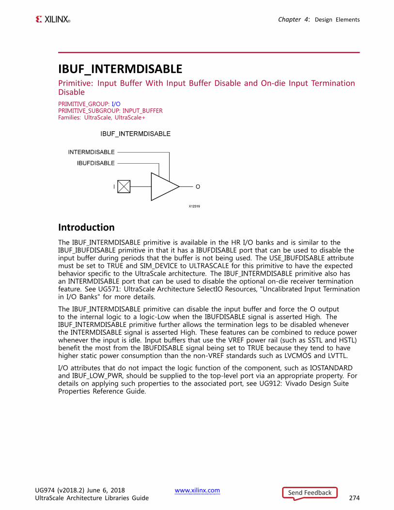
Chapter 4: Design Elements
IBUF_INTERMDISABLEPrimitive: Input Buffer With Input Buffer Disable and On-die Input TerminationDisablePRIMITIVE_GROUP: I/OPRIMITIVE_SUBGROUP: INPUT_BUFFERFamilies: UltraScale, UltraScale+
IntroductionThe IBUF_INTERMDISABLE primitive is available in the HR I/O banks and is similar to theIBUF_IBUFDISABLE primitive in that it has a IBUFDISABLE port that can be used to disable theinput buffer during periods that the buffer is not being used. The USE_IBUFDISABLE attributemust be set to TRUE and SIM_DEVICE to ULTRASCALE for this primitive to have the expectedbehavior specific to the UltraScale architecture. The IBUF_INTERMDISABLE primitive also hasan INTERMDISABLE port that can be used to disable the optional on-die receiver terminationfeature. See UG571: UltraScale Architecture SelectIO Resources, "Uncalibrated Input Terminationin I/O Banks" for more details.
The IBUF_INTERMDISABLE primitive can disable the input buffer and force the O outputto the internal logic to a logic-Low when the IBUFDISABLE signal is asserted High. TheIBUF_INTERMDISABLE primitive further allows the termination legs to be disabled wheneverthe INTERMDISABLE signal is asserted High. These features can be combined to reduce powerwhenever the input is idle. Input buffers that use the VREF power rail (such as SSTL and HSTL)benefit the most from the IBUFDISABLE signal being set to TRUE because they tend to havehigher static power consumption than the non-VREF standards such as LVCMOS and LVTTL.
I/O attributes that do not impact the logic function of the component, such as IOSTANDARDand IBUF_LOW_PWR, should be supplied to the top-level port via an appropriate property. Fordetails on applying such properties to the associated port, see UG912: Vivado Design SuiteProperties Reference Guide.
UG974 (v2018.2) June 6, 2018 www.xilinx.comUltraScale Architecture Libraries Guide 274
Send Feedback
Chapter 4: Design Elements
Port DescriptionsPort Direction Width Function
I Input 1 Input port connection. Connect directly to top-level port in thedesign.
IBUFDISABLE Input 1 Disables input path through the buffer and forces to a logic low.This feature is generally used to reduce power at times when theI/O is idle for a period of time.
INTERMDISABLE Input 1 Control to enable/disable of on-chip input termination. This isgenerally used to reduce power in long periods of an idle state.
O Output 1 Buffer output representing the input path to the device.
Design Entry MethodInstantiation Yes
Inference No
IP and IP Integrator Catalog No
Available AttributesAttribute Type Allowed Values Default Description
SIM_DEVICE STRING "ULTRASCALE","7SERIES"
"7SERIES" This attribute must be set to"ULTRASCALE" in order to exhibitthe proper simulation behavior.
USE_IBUFDISABLE STRING "TRUE", "FALSE" "TRUE" This attribute must be unspecified or setto "TRUE" if specified.
VHDL Instantiation TemplateUnless they already exist, copy the following two statements and paste them before the entitydeclaration.Library UNISIM;use UNISIM.vcomponents.all;
-- IBUF_INTERMDISABLE: Input Buffer With Input Buffer Disable and On-die Input Termination Disable-- UltraScale-- Xilinx HDL Language Template, version 2018.2
IBUF_INTERMDISABLE_inst : IBUF_INTERMDISABLEgeneric map (
SIM_DEVICE => "ULTRASCALE" -- Must be set to "ULTRASCALE")port map (
O => O, -- 1-bit output: Buffer outputI => I, -- 1-bit input: Buffer input (connect directly to top-level port)IBUFDISABLE => IBUFDISABLE, -- 1-bit input: Buffer disable input, high=disableINTERMDISABLE => INTERMDISABLE -- 1-bit input: Input Termination Disable
);
-- End of IBUF_INTERMDISABLE_inst instantiation
UG974 (v2018.2) June 6, 2018 www.xilinx.comUltraScale Architecture Libraries Guide 275
Send Feedback
Chapter 4: Design Elements
Verilog Instantiation Template
// IBUF_INTERMDISABLE: Input Buffer With Input Buffer Disable and On-die Input Termination Disable// UltraScale// Xilinx HDL Language Template, version 2018.2
IBUF_INTERMDISABLE #(.SIM_DEVICE("ULTRASCALE") // Must be set to "ULTRASCALE"
)IBUF_INTERMDISABLE_inst (
.O(O), // 1-bit output: Buffer output
.I(I), // 1-bit input: Buffer input (connect directly to top-level port)
.IBUFDISABLE(IBUFDISABLE), // 1-bit input: Buffer disable input, high=disable
.INTERMDISABLE(INTERMDISABLE) // 1-bit input: Input Termination Disable);
// End of IBUF_INTERMDISABLE_inst instantiation
For More Information• See the UltraScale Architecture SelectIO Resources User Guide (UG571).
• See the UltraScale Programmable Devices Documentation.
UG974 (v2018.2) June 6, 2018 www.xilinx.comUltraScale Architecture Libraries Guide 276
Send Feedback
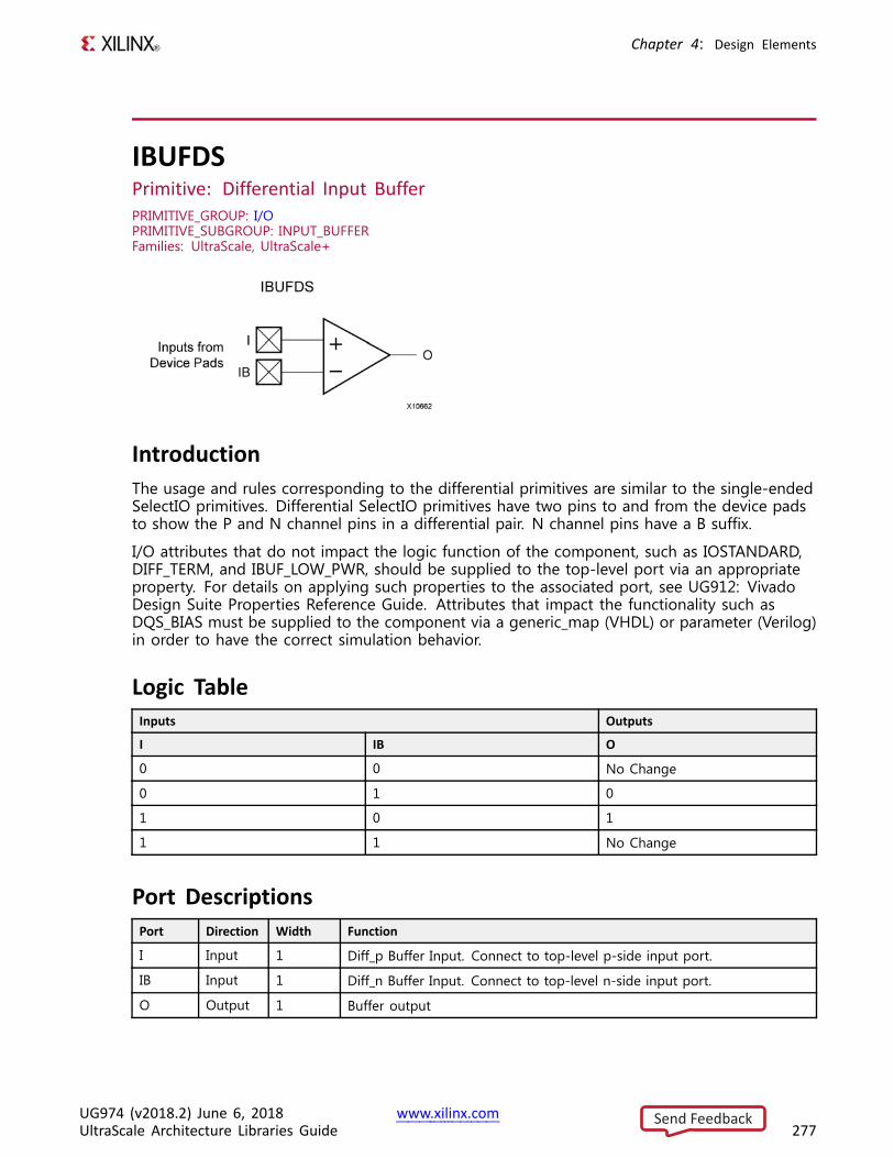
Chapter 4: Design Elements
IBUFDSPrimitive: Differential Input BufferPRIMITIVE_GROUP: I/OPRIMITIVE_SUBGROUP: INPUT_BUFFERFamilies: UltraScale, UltraScale+
IntroductionThe usage and rules corresponding to the differential primitives are similar to the single-endedSelectIO primitives. Differential SelectIO primitives have two pins to and from the device padsto show the P and N channel pins in a differential pair. N channel pins have a B suffix.
I/O attributes that do not impact the logic function of the component, such as IOSTANDARD,DIFF_TERM, and IBUF_LOW_PWR, should be supplied to the top-level port via an appropriateproperty. For details on applying such properties to the associated port, see UG912: VivadoDesign Suite Properties Reference Guide. Attributes that impact the functionality such asDQS_BIAS must be supplied to the component via a generic_map (VHDL) or parameter (Verilog)in order to have the correct simulation behavior.
Logic TableInputs Outputs
I IB O
0 0 No Change
0 1 0
1 0 1
1 1 No Change
Port DescriptionsPort Direction Width Function
I Input 1 Diff_p Buffer Input. Connect to top-level p-side input port.
IB Input 1 Diff_n Buffer Input. Connect to top-level n-side input port.
O Output 1 Buffer output
UG974 (v2018.2) June 6, 2018 www.xilinx.comUltraScale Architecture Libraries Guide 277
Send Feedback
Chapter 4: Design Elements
Design Entry MethodInstantiation Recommended
Inference No
IP and IP Integrator Catalog No
Available AttributesAttribute Type Allowed Values Default Description
DQS_BIAS STRING "FALSE", "TRUE" "FALSE" Provides pull - up / pull - down feature required forsome DQS memory interface pins or provides DCbias for certain LVDS applications.
VHDL Instantiation TemplateUnless they already exist, copy the following two statements and paste them before the entitydeclaration.Library UNISIM;use UNISIM.vcomponents.all;
-- IBUFDS: Differential Input Buffer-- UltraScale-- Xilinx HDL Language Template, version 2018.2
IBUFDS_inst : IBUFDSgeneric map (
DQS_BIAS => "FALSE" -- (FALSE, TRUE))port map (
O => O, -- 1-bit output: Buffer outputI => I, -- 1-bit input: Diff_p buffer input (connect directly to top-level port)IB => IB -- 1-bit input: Diff_n buffer input (connect directly to top-level port)
);
-- End of IBUFDS_inst instantiation
Verilog Instantiation Template
// IBUFDS: Differential Input Buffer// UltraScale// Xilinx HDL Language Template, version 2018.2
IBUFDS #(.DQS_BIAS("FALSE") // (FALSE, TRUE)
)IBUFDS_inst (
.O(O), // 1-bit output: Buffer output
.I(I), // 1-bit input: Diff_p buffer input (connect directly to top-level port)
.IB(IB) // 1-bit input: Diff_n buffer input (connect directly to top-level port));
// End of IBUFDS_inst instantiation
UG974 (v2018.2) June 6, 2018 www.xilinx.comUltraScale Architecture Libraries Guide 278
Send Feedback

Chapter 4: Design Elements
For More Information• See the UltraScale Architecture SelectIO Resources User Guide (UG571).
• See the UltraScale Programmable Devices Documentation.
UG974 (v2018.2) June 6, 2018 www.xilinx.comUltraScale Architecture Libraries Guide 279
Send Feedback
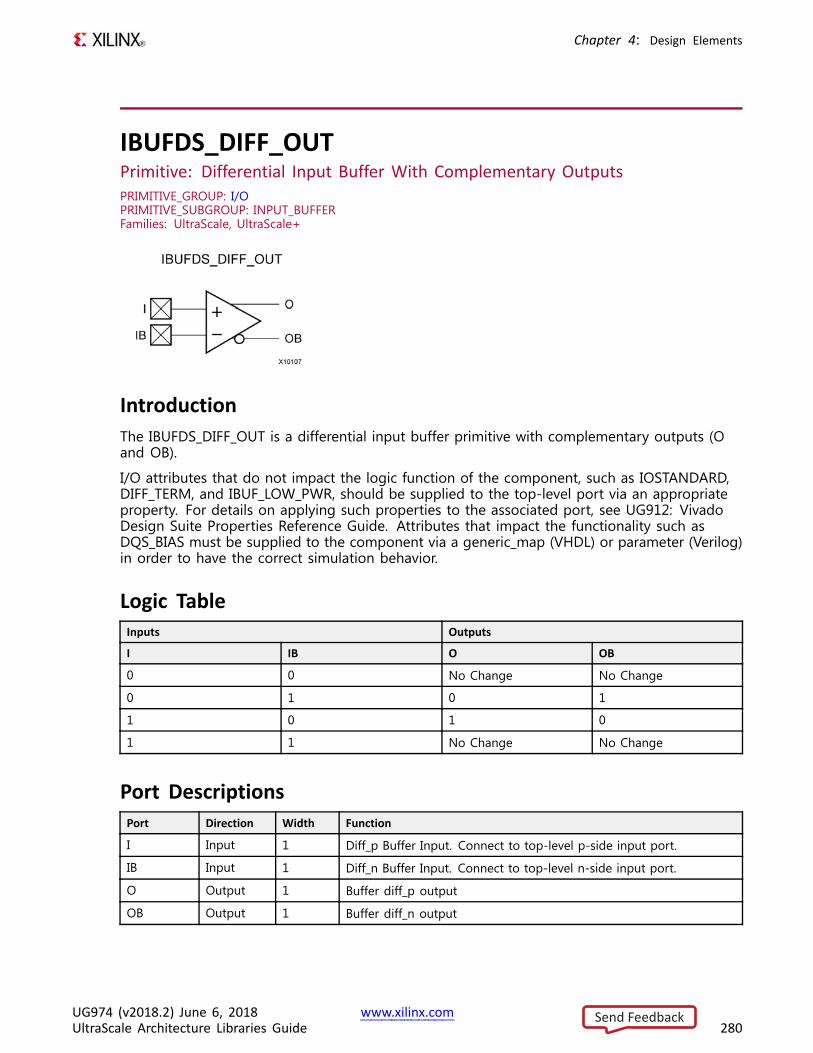
Chapter 4: Design Elements
IBUFDS_DIFF_OUTPrimitive: Differential Input Buffer With Complementary OutputsPRIMITIVE_GROUP: I/OPRIMITIVE_SUBGROUP: INPUT_BUFFERFamilies: UltraScale, UltraScale+
IntroductionThe IBUFDS_DIFF_OUT is a differential input buffer primitive with complementary outputs (Oand OB).
I/O attributes that do not impact the logic function of the component, such as IOSTANDARD,DIFF_TERM, and IBUF_LOW_PWR, should be supplied to the top-level port via an appropriateproperty. For details on applying such properties to the associated port, see UG912: VivadoDesign Suite Properties Reference Guide. Attributes that impact the functionality such asDQS_BIAS must be supplied to the component via a generic_map (VHDL) or parameter (Verilog)in order to have the correct simulation behavior.
Logic TableInputs Outputs
I IB O OB
0 0 No Change No Change
0 1 0 1
1 0 1 0
1 1 No Change No Change
Port DescriptionsPort Direction Width Function
I Input 1 Diff_p Buffer Input. Connect to top-level p-side input port.
IB Input 1 Diff_n Buffer Input. Connect to top-level n-side input port.
O Output 1 Buffer diff_p output
OB Output 1 Buffer diff_n output
UG974 (v2018.2) June 6, 2018 www.xilinx.comUltraScale Architecture Libraries Guide 280
Send Feedback

Chapter 4: Design Elements
Design Entry MethodInstantiation Yes
Inference No
IP and IP Integrator Catalog No
Available AttributesAttribute Type Allowed Values Default Description
DQS_BIAS STRING "FALSE", "TRUE" "FALSE" Provides pull - up / pull - down feature requiredfor some DQS memory interface pins or providesDC bias for certain LVDS applications.
VHDL Instantiation TemplateUnless they already exist, copy the following two statements and paste them before the entitydeclaration.Library UNISIM;use UNISIM.vcomponents.all;
-- IBUFDS_DIFF_OUT: Differential Input Buffer With Complementary Outputs-- UltraScale-- Xilinx HDL Language Template, version 2018.2
IBUFDS_DIFF_OUT_inst : IBUFDS_DIFF_OUTgeneric map (
DQS_BIAS => "FALSE" -- (FALSE, TRUE))port map (
O => O, -- 1-bit output: Buffer diff_p outputOB => OB, -- 1-bit output: Buffer diff_n outputI => I, -- 1-bit input: Diff_p buffer input (connect directly to top-level port)IB => IB -- 1-bit input: Diff_n buffer input (connect directly to top-level port)
);
-- End of IBUFDS_DIFF_OUT_inst instantiation
Verilog Instantiation Template
// IBUFDS_DIFF_OUT: Differential Input Buffer With Complementary Outputs// UltraScale// Xilinx HDL Language Template, version 2018.2
IBUFDS_DIFF_OUT #(.DQS_BIAS("FALSE") // (FALSE, TRUE)
)IBUFDS_DIFF_OUT_inst (
.O(O), // 1-bit output: Buffer diff_p output
.OB(OB), // 1-bit output: Buffer diff_n output
.I(I), // 1-bit input: Diff_p buffer input (connect directly to top-level port)
.IB(IB) // 1-bit input: Diff_n buffer input (connect directly to top-level port));
// End of IBUFDS_DIFF_OUT_inst instantiation
UG974 (v2018.2) June 6, 2018 www.xilinx.comUltraScale Architecture Libraries Guide 281
Send Feedback

Chapter 4: Design Elements
For More Information• See the UltraScale Architecture SelectIO Resources User Guide (UG571).
• See the UltraScale Programmable Devices Documentation.
UG974 (v2018.2) June 6, 2018 www.xilinx.comUltraScale Architecture Libraries Guide 282
Send Feedback
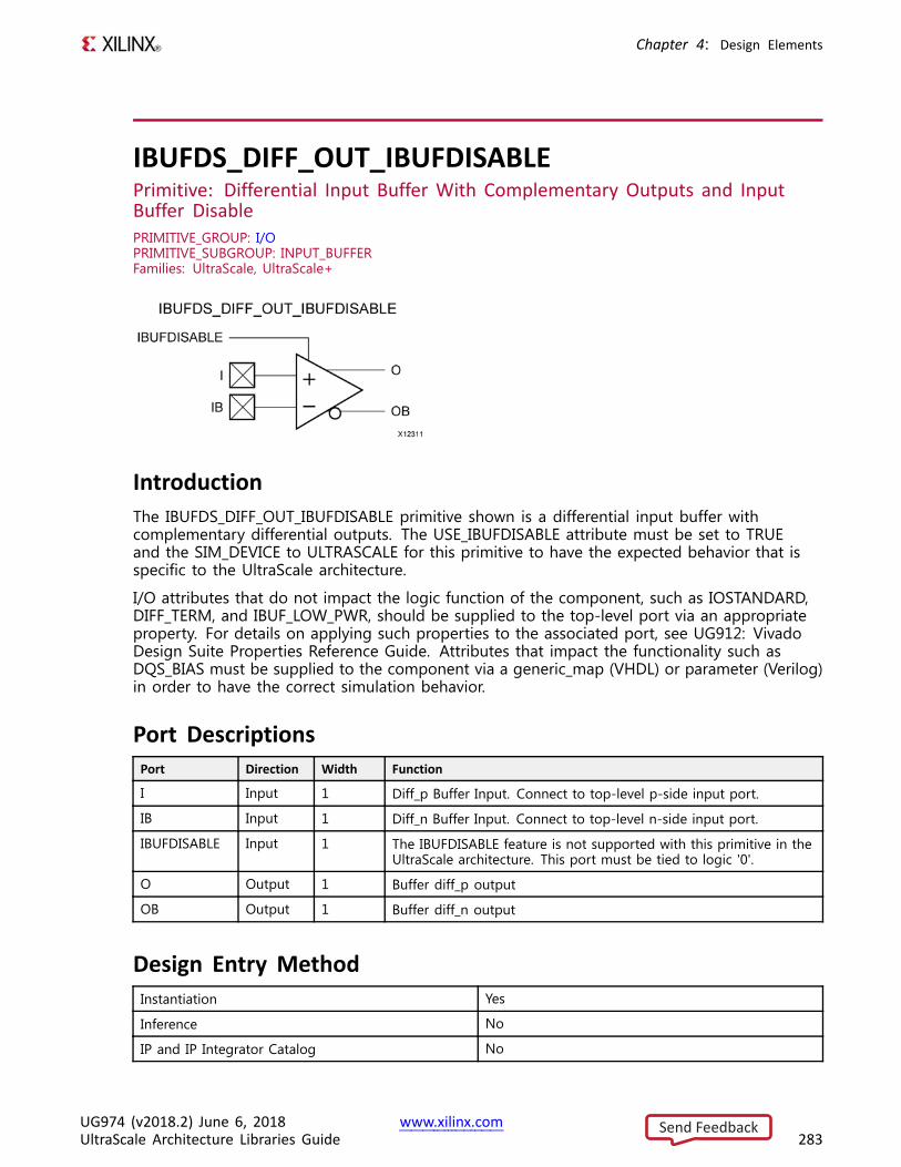
Chapter 4: Design Elements
IBUFDS_DIFF_OUT_IBUFDISABLEPrimitive: Differential Input Buffer With Complementary Outputs and InputBuffer DisablePRIMITIVE_GROUP: I/OPRIMITIVE_SUBGROUP: INPUT_BUFFERFamilies: UltraScale, UltraScale+
IntroductionThe IBUFDS_DIFF_OUT_IBUFDISABLE primitive shown is a differential input buffer withcomplementary differential outputs. The USE_IBUFDISABLE attribute must be set to TRUEand the SIM_DEVICE to ULTRASCALE for this primitive to have the expected behavior that isspecific to the UltraScale architecture.
I/O attributes that do not impact the logic function of the component, such as IOSTANDARD,DIFF_TERM, and IBUF_LOW_PWR, should be supplied to the top-level port via an appropriateproperty. For details on applying such properties to the associated port, see UG912: VivadoDesign Suite Properties Reference Guide. Attributes that impact the functionality such asDQS_BIAS must be supplied to the component via a generic_map (VHDL) or parameter (Verilog)in order to have the correct simulation behavior.
Port DescriptionsPort Direction Width Function
I Input 1 Diff_p Buffer Input. Connect to top-level p-side input port.
IB Input 1 Diff_n Buffer Input. Connect to top-level n-side input port.
IBUFDISABLE Input 1 The IBUFDISABLE feature is not supported with this primitive in theUltraScale architecture. This port must be tied to logic '0'.
O Output 1 Buffer diff_p output
OB Output 1 Buffer diff_n output
Design Entry MethodInstantiation Yes
Inference No
IP and IP Integrator Catalog No
UG974 (v2018.2) June 6, 2018 www.xilinx.comUltraScale Architecture Libraries Guide 283
Send Feedback
Chapter 4: Design Elements
Available AttributesAttribute Type Allowed Values Default Description
DQS_BIAS STRING "FALSE","TRUE"
"FALSE" Provides pull - up / pull - down feature requiredfor some DQS memory interface pins orprovides DC bias for certain LVDS applications.
SIM_DEVICE STRING "ULTRASCALE","7SERIES"
"7SERIES" This attribute must be set to "ULTRASCALE" inorder to exhibit the proper simulation behavior.
USE_IBUFDISABLE STRING "TRUE","FALSE"
"TRUE" This attribute must be unspecified or set to"TRUE" if specified.
VHDL Instantiation TemplateUnless they already exist, copy the following two statements and paste them before the entitydeclaration.Library UNISIM;use UNISIM.vcomponents.all;
-- IBUFDS_DIFF_OUT_IBUFDISABLE: Differential Input Buffer With Complementary Outputs and Input Buffer Disable-- UltraScale-- Xilinx HDL Language Template, version 2018.2
IBUFDS_DIFF_OUT_IBUFDISABLE_inst : IBUFDS_DIFF_OUT_IBUFDISABLEgeneric map (
DQS_BIAS => "FALSE", -- (FALSE, TRUE)SIM_DEVICE => "ULTRASCALE" -- Must be set to "ULTRASCALE"
)port map (
O => O, -- 1-bit output: Buffer diff_p outputOB => OB, -- 1-bit output: Buffer diff_n outputI => I, -- 1-bit input: Diff_p buffer input (connect directly to top-level port)IB => IB, -- 1-bit input: Diff_n buffer input (connect directly to top-level port)IBUFDISABLE => IBUFDISABLE -- 1-bit input: Must be tied to a logic '0'
);
-- End of IBUFDS_DIFF_OUT_IBUFDISABLE_inst instantiation
Verilog Instantiation Template
// IBUFDS_DIFF_OUT_IBUFDISABLE: Differential Input Buffer With Complementary Outputs and Input Buffer Disable// UltraScale// Xilinx HDL Language Template, version 2018.2
IBUFDS_DIFF_OUT_IBUFDISABLE #(.DQS_BIAS("FALSE"), // (FALSE, TRUE).SIM_DEVICE("ULTRASCALE") // Must be set to "ULTRASCALE"
)IBUFDS_DIFF_OUT_IBUFDISABLE_inst (
.O(O), // 1-bit output: Buffer diff_p output
.OB(OB), // 1-bit output: Buffer diff_n output
.I(I), // 1-bit input: Diff_p buffer input (connect directly to top-level port)
.IB(IB), // 1-bit input: Diff_n buffer input (connect directly to top-level port)
.IBUFDISABLE(IBUFDISABLE) // 1-bit input: Must be tied to a logic '0');
// End of IBUFDS_DIFF_OUT_IBUFDISABLE_inst instantiation
UG974 (v2018.2) June 6, 2018 www.xilinx.comUltraScale Architecture Libraries Guide 284
Send Feedback

Chapter 4: Design Elements
For More Information• See the UltraScale Architecture SelectIO Resources User Guide (UG571).
• See the UltraScale Programmable Devices Documentation.
UG974 (v2018.2) June 6, 2018 www.xilinx.comUltraScale Architecture Libraries Guide 285
Send Feedback
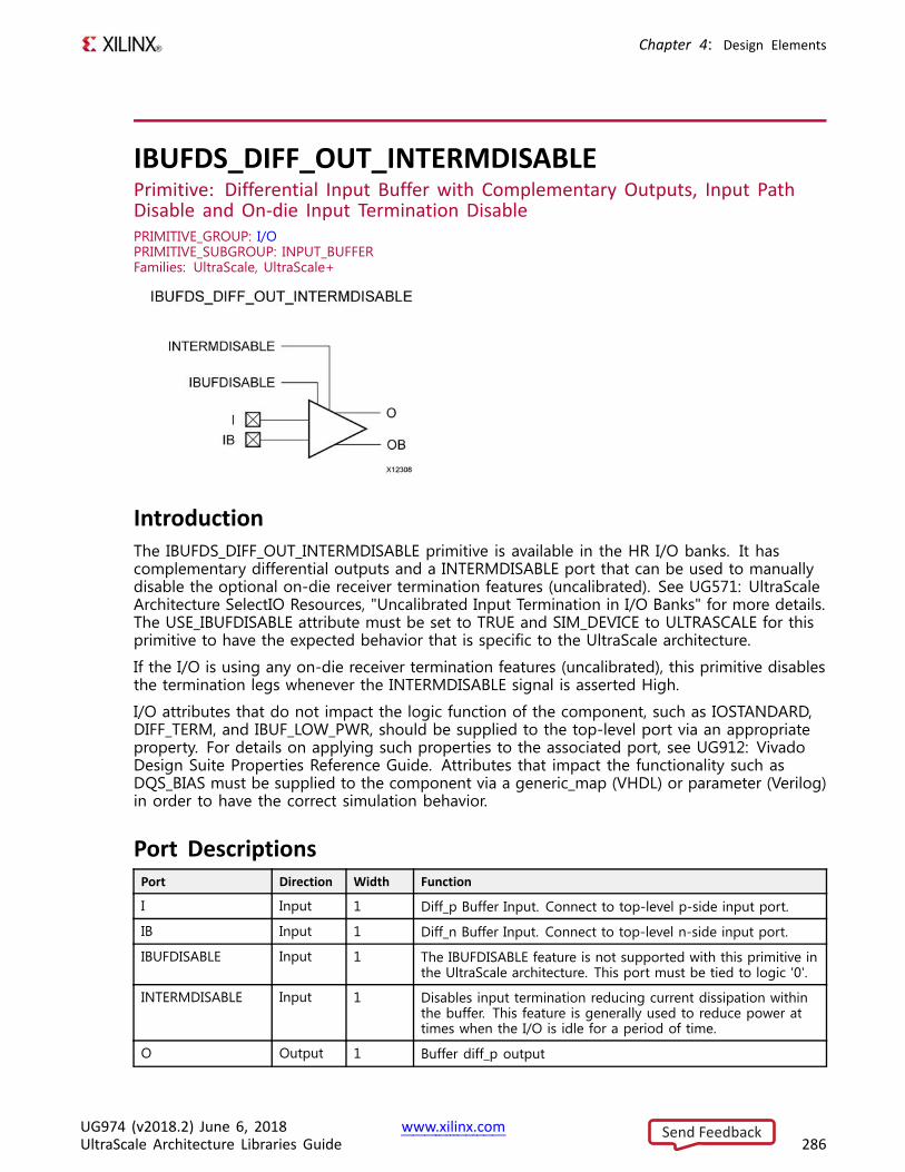
Chapter 4: Design Elements
IBUFDS_DIFF_OUT_INTERMDISABLEPrimitive: Differential Input Buffer with Complementary Outputs, Input PathDisable and On-die Input Termination DisablePRIMITIVE_GROUP: I/OPRIMITIVE_SUBGROUP: INPUT_BUFFERFamilies: UltraScale, UltraScale+
IntroductionThe IBUFDS_DIFF_OUT_INTERMDISABLE primitive is available in the HR I/O banks. It hascomplementary differential outputs and a INTERMDISABLE port that can be used to manuallydisable the optional on-die receiver termination features (uncalibrated). See UG571: UltraScaleArchitecture SelectIO Resources, "Uncalibrated Input Termination in I/O Banks" for more details.The USE_IBUFDISABLE attribute must be set to TRUE and SIM_DEVICE to ULTRASCALE for thisprimitive to have the expected behavior that is specific to the UltraScale architecture.
If the I/O is using any on-die receiver termination features (uncalibrated), this primitive disablesthe termination legs whenever the INTERMDISABLE signal is asserted High.
I/O attributes that do not impact the logic function of the component, such as IOSTANDARD,DIFF_TERM, and IBUF_LOW_PWR, should be supplied to the top-level port via an appropriateproperty. For details on applying such properties to the associated port, see UG912: VivadoDesign Suite Properties Reference Guide. Attributes that impact the functionality such asDQS_BIAS must be supplied to the component via a generic_map (VHDL) or parameter (Verilog)in order to have the correct simulation behavior.
Port DescriptionsPort Direction Width Function
I Input 1 Diff_p Buffer Input. Connect to top-level p-side input port.
IB Input 1 Diff_n Buffer Input. Connect to top-level n-side input port.
IBUFDISABLE Input 1 The IBUFDISABLE feature is not supported with this primitive inthe UltraScale architecture. This port must be tied to logic '0'.
INTERMDISABLE Input 1 Disables input termination reducing current dissipation withinthe buffer. This feature is generally used to reduce power attimes when the I/O is idle for a period of time.
O Output 1 Buffer diff_p output
UG974 (v2018.2) June 6, 2018 www.xilinx.comUltraScale Architecture Libraries Guide 286
Send Feedback
Chapter 4: Design Elements
Port Direction Width Function
OB Output 1 Buffer diff_n output
Design Entry MethodInstantiation Yes
Inference No
IP and IP Integrator Catalog No
Available AttributesAttribute Type Allowed Values Default Description
DQS_BIAS STRING "FALSE", "TRUE" "FALSE" Provides pull - up / pull - down featurerequired for some DQS memory interfacepins or provides DC bias for certain LVDSapplications.
SIM_DEVICE STRING "ULTRASCALE","7SERIES"
"7SERIES" This attribute must be set to "ULTRASCALE"in order to exhibit the proper simulationbehavior.
USE_IBUFDISABLE STRING "TRUE", "FALSE" "TRUE" This attribute must be unspecified or set to"TRUE" if specified.
VHDL Instantiation TemplateUnless they already exist, copy the following two statements and paste them before the entitydeclaration.Library UNISIM;use UNISIM.vcomponents.all;
-- IBUFDS_DIFF_OUT_INTERMDISABLE: Differential Input Buffer with Complementary Outputs, Input Path Disable and On-die Input Termination Disable
-- UltraScale-- Xilinx HDL Language Template, version 2018.2
IBUFDS_DIFF_OUT_INTERMDISABLE_inst : IBUFDS_DIFF_OUT_INTERMDISABLEgeneric map (
DQS_BIAS => "FALSE", -- (FALSE, TRUE)SIM_DEVICE => "ULTRASCALE" -- Must be set to "ULTRASCALE"
)port map (
O => O, -- 1-bit output: Buffer diff_p outputOB => OB, -- 1-bit output: Buffer diff_n outputI => I, -- 1-bit input: Diff_p buffer input (connect directly to top-level port)IB => IB, -- 1-bit input: Diff_n buffer input (connect directly to top-level port)IBUFDISABLE => IBUFDISABLE, -- 1-bit input: Must be tied to a logic '0'INTERMDISABLE => INTERMDISABLE -- 1-bit input: Buffer termination disable, high=disable
);
-- End of IBUFDS_DIFF_OUT_INTERMDISABLE_inst instantiation
Verilog Instantiation Template
// IBUFDS_DIFF_OUT_INTERMDISABLE: Differential Input Buffer with Complementary Outputs, Input Path Disable and On-die Input Termination Disable
// UltraScale
UG974 (v2018.2) June 6, 2018 www.xilinx.comUltraScale Architecture Libraries Guide 287
Send Feedback
Chapter 4: Design Elements
// Xilinx HDL Language Template, version 2018.2
IBUFDS_DIFF_OUT_INTERMDISABLE #(.DQS_BIAS("FALSE"), // (FALSE, TRUE).SIM_DEVICE("ULTRASCALE") // Must be set to "ULTRASCALE"
)IBUFDS_DIFF_OUT_INTERMDISABLE_inst (
.O(O), // 1-bit output: Buffer diff_p output
.OB(OB), // 1-bit output: Buffer diff_n output
.I(I), // 1-bit input: Diff_p buffer input (connect directly to top-level port)
.IB(IB), // 1-bit input: Diff_n buffer input (connect directly to top-level port)
.IBUFDISABLE(IBUFDISABLE), // 1-bit input: Must be tied to a logic '0'
.INTERMDISABLE(INTERMDISABLE) // 1-bit input: Buffer termination disable, high=disable);
// End of IBUFDS_DIFF_OUT_INTERMDISABLE_inst instantiation
For More Information• See the UltraScale Architecture SelectIO Resources User Guide (UG571).
• See the UltraScale Programmable Devices Documentation.
UG974 (v2018.2) June 6, 2018 www.xilinx.comUltraScale Architecture Libraries Guide 288
Send Feedback
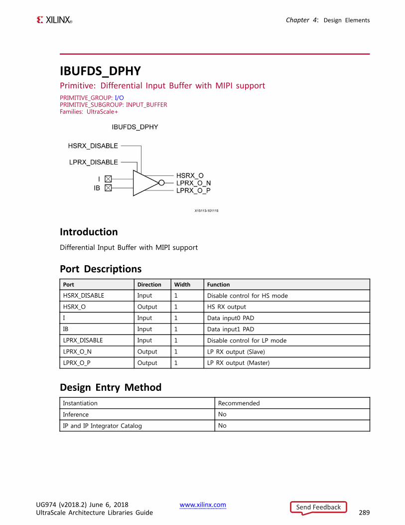
Chapter 4: Design Elements
IBUFDS_DPHYPrimitive: Differential Input Buffer with MIPI supportPRIMITIVE_GROUP: I/OPRIMITIVE_SUBGROUP: INPUT_BUFFERFamilies: UltraScale+
IntroductionDifferential Input Buffer with MIPI support
Port DescriptionsPort Direction Width Function
HSRX_DISABLE Input 1 Disable control for HS mode
HSRX_O Output 1 HS RX output
I Input 1 Data input0 PAD
IB Input 1 Data input1 PAD
LPRX_DISABLE Input 1 Disable control for LP mode
LPRX_O_N Output 1 LP RX output (Slave)
LPRX_O_P Output 1 LP RX output (Master)
Design Entry MethodInstantiation Recommended
Inference No
IP and IP Integrator Catalog No
UG974 (v2018.2) June 6, 2018 www.xilinx.comUltraScale Architecture Libraries Guide 289
Send Feedback
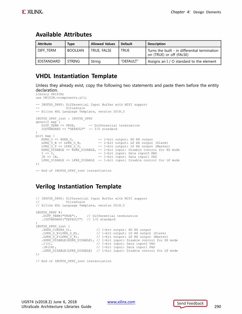
Chapter 4: Design Elements
Available AttributesAttribute Type Allowed Values Default Description
DIFF_TERM BOOLEAN TRUE, FALSE TRUE Turns the built - in differential terminationon (TRUE) or off (FALSE)
IOSTANDARD STRING String "DEFAULT" Assigns an I / O standard to the element
VHDL Instantiation TemplateUnless they already exist, copy the following two statements and paste them before the entitydeclaration.Library UNISIM;use UNISIM.vcomponents.all;
-- IBUFDS_DPHY: Differential Input Buffer with MIPI support-- UltraScale-- Xilinx HDL Language Template, version 2018.2
IBUFDS_DPHY_inst : IBUFDS_DPHYgeneric map (
DIFF_TERM => TRUE, -- Differential terminationIOSTANDARD => "DEFAULT" -- I/O standard
)port map (
HSRX_O => HSRX_O, -- 1-bit output: HS RX outputLPRX_O_N => LPRX_O_N, -- 1-bit output: LP RX output (Slave)LPRX_O_P => LPRX_O_P, -- 1-bit output: LP RX output (Master)HSRX_DISABLE => HSRX_DISABLE, -- 1-bit input: Disable control for HS modeI => I, -- 1-bit input: Data input0 PADIB => IB, -- 1-bit input: Data input1 PADLPRX_DISABLE => LPRX_DISABLE -- 1-bit input: Disable control for LP mode
);
-- End of IBUFDS_DPHY_inst instantiation
Verilog Instantiation Template
// IBUFDS_DPHY: Differential Input Buffer with MIPI support// UltraScale// Xilinx HDL Language Template, version 2018.2
IBUFDS_DPHY #(.DIFF_TERM("TRUE"), // Differential termination.IOSTANDARD("DEFAULT") // I/O standard
)IBUFDS_DPHY_inst (
.HSRX_O(HSRX_O), // 1-bit output: HS RX output
.LPRX_O_N(LPRX_O_N), // 1-bit output: LP RX output (Slave)
.LPRX_O_P(LPRX_O_P), // 1-bit output: LP RX output (Master)
.HSRX_DISABLE(HSRX_DISABLE), // 1-bit input: Disable control for HS mode
.I(I), // 1-bit input: Data input0 PAD
.IB(IB), // 1-bit input: Data input1 PAD
.LPRX_DISABLE(LPRX_DISABLE) // 1-bit input: Disable control for LP mode);
// End of IBUFDS_DPHY_inst instantiation
UG974 (v2018.2) June 6, 2018 www.xilinx.comUltraScale Architecture Libraries Guide 290
Send Feedback

Chapter 4: Design Elements
For More Information• See the UltraScale Architecture SelectIO Resources User Guide (UG571).
• See the UltraScale Programmable Devices Documentation.
UG974 (v2018.2) June 6, 2018 www.xilinx.comUltraScale Architecture Libraries Guide 291
Send Feedback
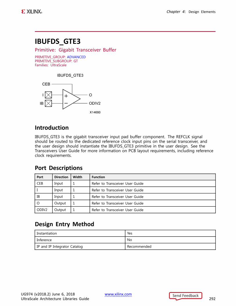
Chapter 4: Design Elements
IBUFDS_GTE3Primitive: Gigabit Transceiver BufferPRIMITIVE_GROUP: ADVANCEDPRIMITIVE_SUBGROUP: GTFamilies: UltraScale
IntroductionIBUFDS_GTE3 is the gigabit transceiver input pad buffer component. The REFCLK signalshould be routed to the dedicated reference clock input pins on the serial transceiver, andthe user design should instantiate the IBUFDS_GTE3 primitive in the user design. See theTransceivers User Guide for more information on PCB layout requirements, including referenceclock requirements.
Port DescriptionsPort Direction Width Function
CEB Input 1 Refer to Transceiver User Guide
I Input 1 Refer to Transceiver User Guide
IB Input 1 Refer to Transceiver User Guide
O Output 1 Refer to Transceiver User Guide
ODIV2 Output 1 Refer to Transceiver User Guide
Design Entry MethodInstantiation Yes
Inference No
IP and IP Integrator Catalog Recommended
UG974 (v2018.2) June 6, 2018 www.xilinx.comUltraScale Architecture Libraries Guide 292
Send Feedback
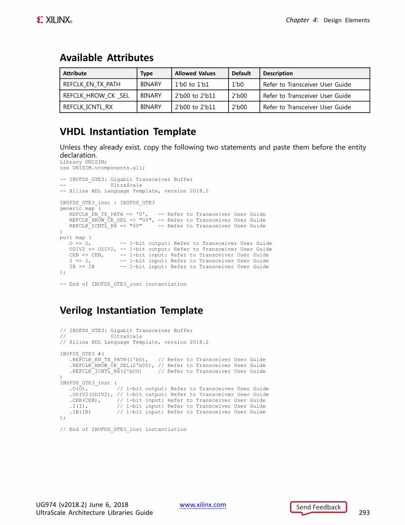
Chapter 4: Design Elements
Available AttributesAttribute Type Allowed Values Default Description
REFCLK_EN_TX_PATH BINARY 1'b0 to 1'b1 1'b0 Refer to Transceiver User Guide
REFCLK_HROW_CK _SEL BINARY 2'b00 to 2'b11 2'b00 Refer to Transceiver User Guide
REFCLK_ICNTL_RX BINARY 2'b00 to 2'b11 2'b00 Refer to Transceiver User Guide
VHDL Instantiation TemplateUnless they already exist, copy the following two statements and paste them before the entitydeclaration.Library UNISIM;use UNISIM.vcomponents.all;
-- IBUFDS_GTE3: Gigabit Transceiver Buffer-- UltraScale-- Xilinx HDL Language Template, version 2018.2
IBUFDS_GTE3_inst : IBUFDS_GTE3generic map (
REFCLK_EN_TX_PATH => '0', -- Refer to Transceiver User GuideREFCLK_HROW_CK_SEL => "00", -- Refer to Transceiver User GuideREFCLK_ICNTL_RX => "00" -- Refer to Transceiver User Guide
)port map (
O => O, -- 1-bit output: Refer to Transceiver User GuideODIV2 => ODIV2, -- 1-bit output: Refer to Transceiver User GuideCEB => CEB, -- 1-bit input: Refer to Transceiver User GuideI => I, -- 1-bit input: Refer to Transceiver User GuideIB => IB -- 1-bit input: Refer to Transceiver User Guide
);
-- End of IBUFDS_GTE3_inst instantiation
Verilog Instantiation Template
// IBUFDS_GTE3: Gigabit Transceiver Buffer// UltraScale// Xilinx HDL Language Template, version 2018.2
IBUFDS_GTE3 #(.REFCLK_EN_TX_PATH(1'b0), // Refer to Transceiver User Guide.REFCLK_HROW_CK_SEL(2'b00), // Refer to Transceiver User Guide.REFCLK_ICNTL_RX(2'b00) // Refer to Transceiver User Guide
)IBUFDS_GTE3_inst (
.O(O), // 1-bit output: Refer to Transceiver User Guide
.ODIV2(ODIV2), // 1-bit output: Refer to Transceiver User Guide
.CEB(CEB), // 1-bit input: Refer to Transceiver User Guide
.I(I), // 1-bit input: Refer to Transceiver User Guide
.IB(IB) // 1-bit input: Refer to Transceiver User Guide);
// End of IBUFDS_GTE3_inst instantiation
UG974 (v2018.2) June 6, 2018 www.xilinx.comUltraScale Architecture Libraries Guide 293
Send Feedback

Chapter 4: Design Elements
For More Information• See the UltraScale Architecture GTH Transceivers User Guide (UG576)
• See the UltraScale Architecture GTY Transceivers Advance Specification User Guide (UG578)
• See the UltraScale Programmable Devices Documentation.
UG974 (v2018.2) June 6, 2018 www.xilinx.comUltraScale Architecture Libraries Guide 294
Send Feedback
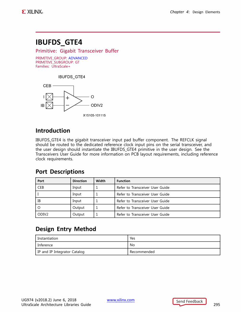
Chapter 4: Design Elements
IBUFDS_GTE4Primitive: Gigabit Transceiver BufferPRIMITIVE_GROUP: ADVANCEDPRIMITIVE_SUBGROUP: GTFamilies: UltraScale+
IntroductionIBUFDS_GTE4 is the gigabit transceiver input pad buffer component. The REFCLK signalshould be routed to the dedicated reference clock input pins on the serial transceiver, andthe user design should instantiate the IBUFDS_GTE4 primitive in the user design. See theTransceivers User Guide for more information on PCB layout requirements, including referenceclock requirements.
Port DescriptionsPort Direction Width Function
CEB Input 1 Refer to Transceiver User Guide
I Input 1 Refer to Transceiver User Guide
IB Input 1 Refer to Transceiver User Guide
O Output 1 Refer to Transceiver User Guide
ODIV2 Output 1 Refer to Transceiver User Guide
Design Entry MethodInstantiation Yes
Inference No
IP and IP Integrator Catalog Recommended
UG974 (v2018.2) June 6, 2018 www.xilinx.comUltraScale Architecture Libraries Guide 295
Send Feedback
Chapter 4: Design Elements
Available AttributesAttribute Type Allowed Values Default Description
REFCLK_EN_TX_PATH BINARY 1'b0 to 1'b1 1'b0 Refer to Transceiver User Guide
REFCLK_HROW_CK_SEL
BINARY 2'b00 to 2'b11 2'b00 Refer to Transceiver User Guide
REFCLK_ICNTL_RX BINARY 2'b00 to 2'b11 2'b00 Refer to Transceiver User Guide
VHDL Instantiation TemplateUnless they already exist, copy the following two statements and paste them before the entitydeclaration.Library UNISIM;use UNISIM.vcomponents.all;
-- IBUFDS_GTE4: Gigabit Transceiver Buffer-- UltraScale-- Xilinx HDL Language Template, version 2018.2
IBUFDS_GTE4_inst : IBUFDS_GTE4generic map (
REFCLK_EN_TX_PATH => '0', -- Refer to Transceiver User GuideREFCLK_HROW_CK_SEL => "00", -- Refer to Transceiver User GuideREFCLK_ICNTL_RX => "00" -- Refer to Transceiver User Guide
)port map (
O => O, -- 1-bit output: Refer to Transceiver User GuideODIV2 => ODIV2, -- 1-bit output: Refer to Transceiver User GuideCEB => CEB, -- 1-bit input: Refer to Transceiver User GuideI => I, -- 1-bit input: Refer to Transceiver User GuideIB => IB -- 1-bit input: Refer to Transceiver User Guide
);
-- End of IBUFDS_GTE4_inst instantiation
Verilog Instantiation Template
// IBUFDS_GTE4: Gigabit Transceiver Buffer// UltraScale// Xilinx HDL Language Template, version 2018.2
IBUFDS_GTE4 #(.REFCLK_EN_TX_PATH(1'b0), // Refer to Transceiver User Guide.REFCLK_HROW_CK_SEL(2'b00), // Refer to Transceiver User Guide.REFCLK_ICNTL_RX(2'b00) // Refer to Transceiver User Guide
)IBUFDS_GTE4_inst (
.O(O), // 1-bit output: Refer to Transceiver User Guide
.ODIV2(ODIV2), // 1-bit output: Refer to Transceiver User Guide
.CEB(CEB), // 1-bit input: Refer to Transceiver User Guide
.I(I), // 1-bit input: Refer to Transceiver User Guide
.IB(IB) // 1-bit input: Refer to Transceiver User Guide);
// End of IBUFDS_GTE4_inst instantiation
UG974 (v2018.2) June 6, 2018 www.xilinx.comUltraScale Architecture Libraries Guide 296
Send Feedback

Chapter 4: Design Elements
For More Information• See the UltraScale Architecture GTH Transceivers User Guide (UG576)
• See the UltraScale Architecture GTY Transceivers Advance Specification User Guide (UG578)
• See the UltraScale Programmable Devices Documentation.
UG974 (v2018.2) June 6, 2018 www.xilinx.comUltraScale Architecture Libraries Guide 297
Send Feedback
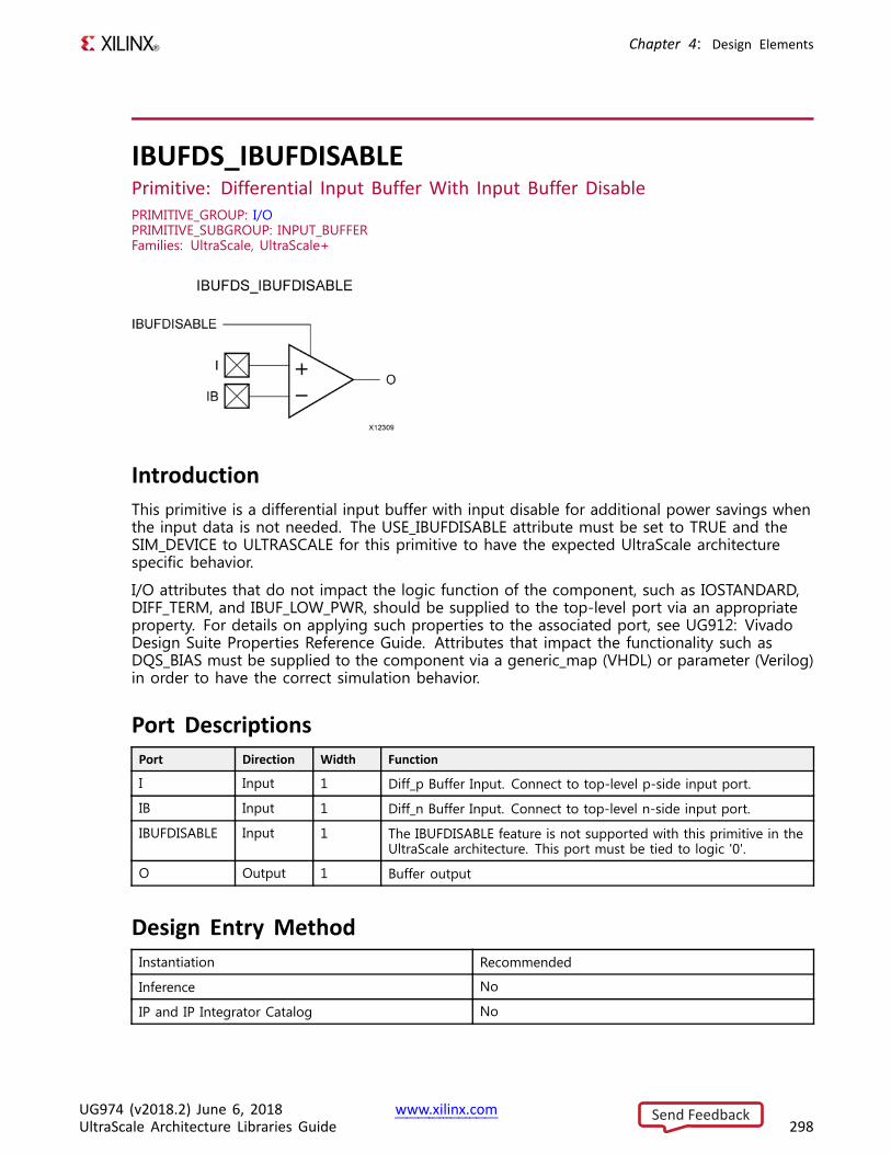
Chapter 4: Design Elements
IBUFDS_IBUFDISABLEPrimitive: Differential Input Buffer With Input Buffer DisablePRIMITIVE_GROUP: I/OPRIMITIVE_SUBGROUP: INPUT_BUFFERFamilies: UltraScale, UltraScale+
IntroductionThis primitive is a differential input buffer with input disable for additional power savings whenthe input data is not needed. The USE_IBUFDISABLE attribute must be set to TRUE and theSIM_DEVICE to ULTRASCALE for this primitive to have the expected UltraScale architecturespecific behavior.
I/O attributes that do not impact the logic function of the component, such as IOSTANDARD,DIFF_TERM, and IBUF_LOW_PWR, should be supplied to the top-level port via an appropriateproperty. For details on applying such properties to the associated port, see UG912: VivadoDesign Suite Properties Reference Guide. Attributes that impact the functionality such asDQS_BIAS must be supplied to the component via a generic_map (VHDL) or parameter (Verilog)in order to have the correct simulation behavior.
Port DescriptionsPort Direction Width Function
I Input 1 Diff_p Buffer Input. Connect to top-level p-side input port.
IB Input 1 Diff_n Buffer Input. Connect to top-level n-side input port.
IBUFDISABLE Input 1 The IBUFDISABLE feature is not supported with this primitive in theUltraScale architecture. This port must be tied to logic '0'.
O Output 1 Buffer output
Design Entry MethodInstantiation Recommended
Inference No
IP and IP Integrator Catalog No
UG974 (v2018.2) June 6, 2018 www.xilinx.comUltraScale Architecture Libraries Guide 298
Send Feedback
Chapter 4: Design Elements
Available AttributesAttribute Type Allowed Values Default Description
DQS_BIAS STRING "FALSE","TRUE"
"FALSE" Provides pull - up / pull - down featurerequired for some DQS memory interfacepins or provides DC bias for certain LVDSapplications.
SIM_DEVICE STRING "ULTRASCALE","7SERIES"
"7SERIES" This attribute must be set to "ULTRASCALE"in order to exhibit the proper simulationbehavior.
USE_IBUFDISABLE STRING "TRUE","FALSE"
"TRUE" This attribute must be unspecified or set to"TRUE" if specified.
VHDL Instantiation TemplateUnless they already exist, copy the following two statements and paste them before the entitydeclaration.Library UNISIM;use UNISIM.vcomponents.all;
-- IBUFDS_IBUFDISABLE: Differential Input Buffer With Input Buffer Disable-- UltraScale-- Xilinx HDL Language Template, version 2018.2
IBUFDS_IBUFDISABLE_inst : IBUFDS_IBUFDISABLEgeneric map (
DQS_BIAS => "FALSE", -- (FALSE, TRUE)SIM_DEVICE => "ULTRASCALE" -- Must be set to "ULTRASCALE"
)port map (
O => O, -- 1-bit output: Buffer outputI => I, -- 1-bit input: Diff_p buffer input (connect directly to top-level port)IB => IB, -- 1-bit input: Diff_n buffer input (connect directly to top-level port)IBUFDISABLE => IBUFDISABLE -- 1-bit input: Must be tied to a logic '0'
);
-- End of IBUFDS_IBUFDISABLE_inst instantiation
Verilog Instantiation Template
// IBUFDS_IBUFDISABLE: Differential Input Buffer With Input Buffer Disable// UltraScale// Xilinx HDL Language Template, version 2018.2
IBUFDS_IBUFDISABLE #(.DQS_BIAS("FALSE"), // (FALSE, TRUE).SIM_DEVICE("ULTRASCALE") // Must be set to "ULTRASCALE"
)IBUFDS_IBUFDISABLE_inst (
.O(O), // 1-bit output: Buffer output
.I(I), // 1-bit input: Diff_p buffer input (connect directly to top-level port)
.IB(IB), // 1-bit input: Diff_n buffer input (connect directly to top-level port)
.IBUFDISABLE(IBUFDISABLE) // 1-bit input: Must be tied to a logic '0');
// End of IBUFDS_IBUFDISABLE_inst instantiation
UG974 (v2018.2) June 6, 2018 www.xilinx.comUltraScale Architecture Libraries Guide 299
Send Feedback

Chapter 4: Design Elements
For More Information• See the UltraScale Architecture SelectIO Resources User Guide (UG571).
• See the UltraScale Programmable Devices Documentation.
UG974 (v2018.2) June 6, 2018 www.xilinx.comUltraScale Architecture Libraries Guide 300
Send Feedback
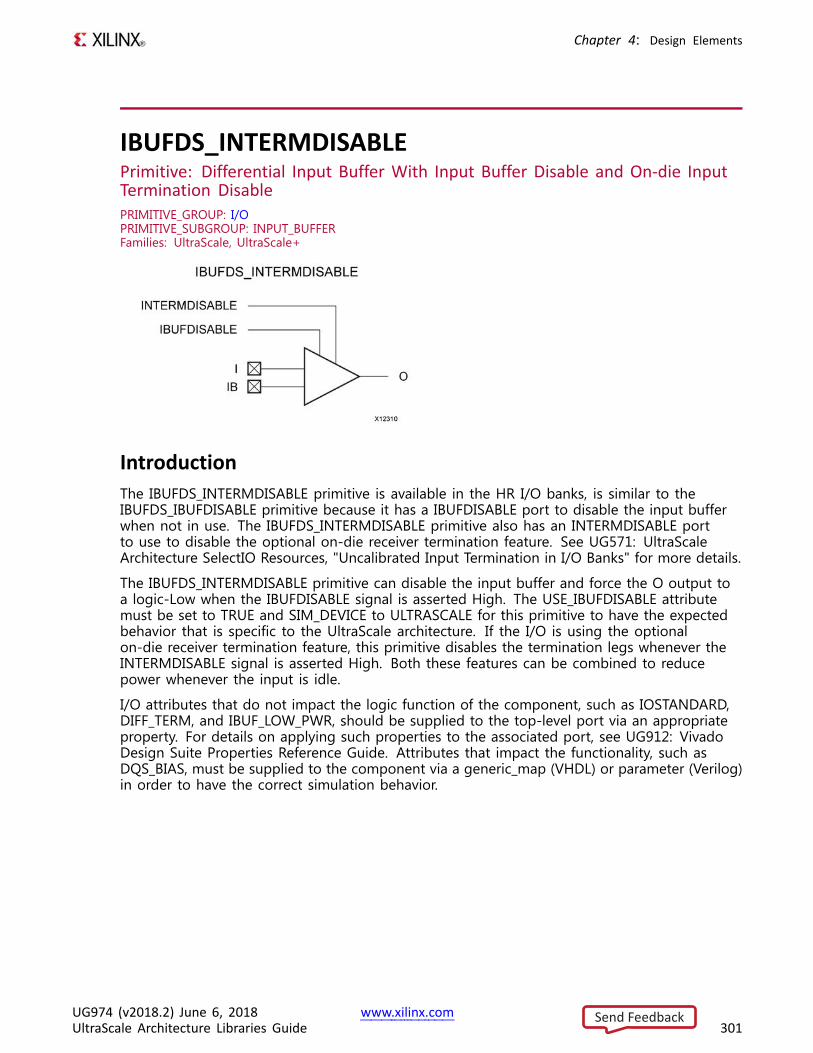
Chapter 4: Design Elements
IBUFDS_INTERMDISABLEPrimitive: Differential Input Buffer With Input Buffer Disable and On-die InputTermination DisablePRIMITIVE_GROUP: I/OPRIMITIVE_SUBGROUP: INPUT_BUFFERFamilies: UltraScale, UltraScale+
IntroductionThe IBUFDS_INTERMDISABLE primitive is available in the HR I/O banks, is similar to theIBUFDS_IBUFDISABLE primitive because it has a IBUFDISABLE port to disable the input bufferwhen not in use. The IBUFDS_INTERMDISABLE primitive also has an INTERMDISABLE portto use to disable the optional on-die receiver termination feature. See UG571: UltraScaleArchitecture SelectIO Resources, "Uncalibrated Input Termination in I/O Banks" for more details.
The IBUFDS_INTERMDISABLE primitive can disable the input buffer and force the O output toa logic-Low when the IBUFDISABLE signal is asserted High. The USE_IBUFDISABLE attributemust be set to TRUE and SIM_DEVICE to ULTRASCALE for this primitive to have the expectedbehavior that is specific to the UltraScale architecture. If the I/O is using the optionalon-die receiver termination feature, this primitive disables the termination legs whenever theINTERMDISABLE signal is asserted High. Both these features can be combined to reducepower whenever the input is idle.
I/O attributes that do not impact the logic function of the component, such as IOSTANDARD,DIFF_TERM, and IBUF_LOW_PWR, should be supplied to the top-level port via an appropriateproperty. For details on applying such properties to the associated port, see UG912: VivadoDesign Suite Properties Reference Guide. Attributes that impact the functionality, such asDQS_BIAS, must be supplied to the component via a generic_map (VHDL) or parameter (Verilog)in order to have the correct simulation behavior.
UG974 (v2018.2) June 6, 2018 www.xilinx.comUltraScale Architecture Libraries Guide 301
Send Feedback
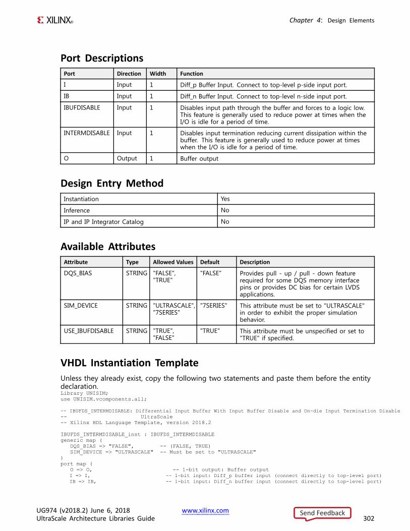
Chapter 4: Design Elements
Port DescriptionsPort Direction Width Function
I Input 1 Diff_p Buffer Input. Connect to top-level p-side input port.
IB Input 1 Diff_n Buffer Input. Connect to top-level n-side input port.
IBUFDISABLE Input 1 Disables input path through the buffer and forces to a logic low.This feature is generally used to reduce power at times when theI/O is idle for a period of time.
INTERMDISABLE Input 1 Disables input termination reducing current dissipation within thebuffer. This feature is generally used to reduce power at timeswhen the I/O is idle for a period of time.
O Output 1 Buffer output
Design Entry MethodInstantiation Yes
Inference No
IP and IP Integrator Catalog No
Available AttributesAttribute Type Allowed Values Default Description
DQS_BIAS STRING "FALSE","TRUE"
"FALSE" Provides pull - up / pull - down featurerequired for some DQS memory interfacepins or provides DC bias for certain LVDSapplications.
SIM_DEVICE STRING "ULTRASCALE","7SERIES"
"7SERIES" This attribute must be set to "ULTRASCALE"in order to exhibit the proper simulationbehavior.
USE_IBUFDISABLE STRING "TRUE","FALSE"
"TRUE" This attribute must be unspecified or set to"TRUE" if specified.
VHDL Instantiation TemplateUnless they already exist, copy the following two statements and paste them before the entitydeclaration.Library UNISIM;use UNISIM.vcomponents.all;
-- IBUFDS_INTERMDISABLE: Differential Input Buffer With Input Buffer Disable and On-die Input Termination Disable-- UltraScale-- Xilinx HDL Language Template, version 2018.2
IBUFDS_INTERMDISABLE_inst : IBUFDS_INTERMDISABLEgeneric map (
DQS_BIAS => "FALSE", -- (FALSE, TRUE)SIM_DEVICE => "ULTRASCALE" -- Must be set to "ULTRASCALE"
)port map (
O => O, -- 1-bit output: Buffer outputI => I, -- 1-bit input: Diff_p buffer input (connect directly to top-level port)IB => IB, -- 1-bit input: Diff_n buffer input (connect directly to top-level port)
UG974 (v2018.2) June 6, 2018 www.xilinx.comUltraScale Architecture Libraries Guide 302
Send Feedback
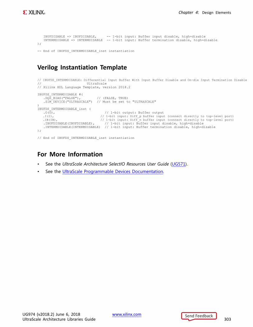
Chapter 4: Design Elements
IBUFDISABLE => IBUFDISABLE, -- 1-bit input: Buffer input disable, high=disableINTERMDISABLE => INTERMDISABLE -- 1-bit input: Buffer termination disable, high=disable
);
-- End of IBUFDS_INTERMDISABLE_inst instantiation
Verilog Instantiation Template
// IBUFDS_INTERMDISABLE: Differential Input Buffer With Input Buffer Disable and On-die Input Termination Disable// UltraScale// Xilinx HDL Language Template, version 2018.2
IBUFDS_INTERMDISABLE #(.DQS_BIAS("FALSE"), // (FALSE, TRUE).SIM_DEVICE("ULTRASCALE") // Must be set to "ULTRASCALE"
)IBUFDS_INTERMDISABLE_inst (
.O(O), // 1-bit output: Buffer output
.I(I), // 1-bit input: Diff_p buffer input (connect directly to top-level port)
.IB(IB), // 1-bit input: Diff_n buffer input (connect directly to top-level port)
.IBUFDISABLE(IBUFDISABLE), // 1-bit input: Buffer input disable, high=disable
.INTERMDISABLE(INTERMDISABLE) // 1-bit input: Buffer termination disable, high=disable);
// End of IBUFDS_INTERMDISABLE_inst instantiation
For More Information• See the UltraScale Architecture SelectIO Resources User Guide (UG571).
• See the UltraScale Programmable Devices Documentation.
UG974 (v2018.2) June 6, 2018 www.xilinx.comUltraScale Architecture Libraries Guide 303
Send Feedback
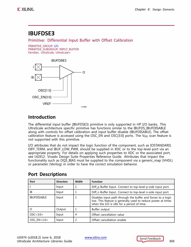
Chapter 4: Design Elements
IBUFDSE3Primitive: Differential Input Buffer with Offset CalibrationPRIMITIVE_GROUP: I/OPRIMITIVE_SUBGROUP: INPUT_BUFFERFamilies: UltraScale, UltraScale+
IntroductionThe differential input buffer (IBUFDSE3) primitive is only supported in HP I/O banks. ThisUltraScale architecture specific primitive has functions similar to the IBUFDS_IBUFDISABLEalong with controls for offset calibration and input buffer disable (IBUFDISABLE). The offsetcalibration feature is accessed using the OSC_EN and OSC[3:0] ports. The VREF scan feature isnot supported with this primitive.
I/O attributes that do not impact the logic function of the component, such as IOSTANDARD,DIFF_TERM, and IBUF_LOW_PWR, should be supplied in XDC or to the top-level port via anappropriate property. For details on applying such properties to XDC or the associated port,see UG912: Vivado Design Suite Properties Reference Guide. Attributes that impact thefunctionality such as DQS_BIAS must be supplied to the component via a generic_map (VHDL)or parameter (Verilog) in order to have the correct simulation behavior.
Port DescriptionsPort Direction Width Function
I Input 1 Diff_p Buffer Input. Connect to top-level p-side input port.
IB Input 1 Diff_n Buffer Input. Connect to top-level n-side input port.
IBUFDISABLE Input 1 Disables input path through the buffer and forces to a logiclow. This feature is generally used to reduce power at timeswhen the I/O is idle for a period of time.
O Output 1 Buffer output
OSC<3:0> Input 4 Offset cancellation value
OSC_EN<1:0> Input 2 Offset cancellation enable
UG974 (v2018.2) June 6, 2018 www.xilinx.comUltraScale Architecture Libraries Guide 304
Send Feedback
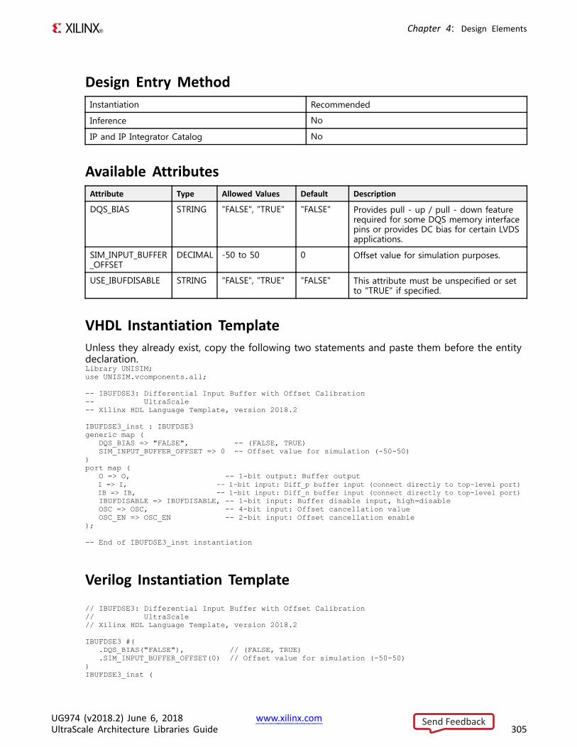
Chapter 4: Design Elements
Design Entry MethodInstantiation Recommended
Inference No
IP and IP Integrator Catalog No
Available AttributesAttribute Type Allowed Values Default Description
DQS_BIAS STRING "FALSE", "TRUE" "FALSE" Provides pull - up / pull - down featurerequired for some DQS memory interfacepins or provides DC bias for certain LVDSapplications.
SIM_INPUT_BUFFER_OFFSET
DECIMAL -50 to 50 0 Offset value for simulation purposes.
USE_IBUFDISABLE STRING "FALSE", "TRUE" "FALSE" This attribute must be unspecified or setto "TRUE" if specified.
VHDL Instantiation TemplateUnless they already exist, copy the following two statements and paste them before the entitydeclaration.Library UNISIM;use UNISIM.vcomponents.all;
-- IBUFDSE3: Differential Input Buffer with Offset Calibration-- UltraScale-- Xilinx HDL Language Template, version 2018.2
IBUFDSE3_inst : IBUFDSE3generic map (
DQS_BIAS => "FALSE", -- (FALSE, TRUE)SIM_INPUT_BUFFER_OFFSET => 0 -- Offset value for simulation (-50-50)
)port map (
O => O, -- 1-bit output: Buffer outputI => I, -- 1-bit input: Diff_p buffer input (connect directly to top-level port)IB => IB, -- 1-bit input: Diff_n buffer input (connect directly to top-level port)IBUFDISABLE => IBUFDISABLE, -- 1-bit input: Buffer disable input, high=disableOSC => OSC, -- 4-bit input: Offset cancellation valueOSC_EN => OSC_EN -- 2-bit input: Offset cancellation enable
);
-- End of IBUFDSE3_inst instantiation
Verilog Instantiation Template
// IBUFDSE3: Differential Input Buffer with Offset Calibration// UltraScale// Xilinx HDL Language Template, version 2018.2
IBUFDSE3 #(.DQS_BIAS("FALSE"), // (FALSE, TRUE).SIM_INPUT_BUFFER_OFFSET(0) // Offset value for simulation (-50-50)
)IBUFDSE3_inst (
UG974 (v2018.2) June 6, 2018 www.xilinx.comUltraScale Architecture Libraries Guide 305
Send Feedback
Chapter 4: Design Elements
.O(O), // 1-bit output: Buffer output
.I(I), // 1-bit input: Diff_p buffer input (connect directly to top-level port)
.IB(IB), // 1-bit input: Diff_n buffer input (connect directly to top-level port)
.IBUFDISABLE(IBUFDISABLE), // 1-bit input: Buffer disable input, high=disable
.OSC(OSC), // 4-bit input: Offset cancellation value
.OSC_EN(OSC_EN) // 2-bit input: Offset cancellation enable);
// End of IBUFDSE3_inst instantiation
For More Information• See the UltraScale Architecture SelectIO Resources User Guide (UG571).
• See the UltraScale Programmable Devices Documentation.
UG974 (v2018.2) June 6, 2018 www.xilinx.comUltraScale Architecture Libraries Guide 306
Send Feedback
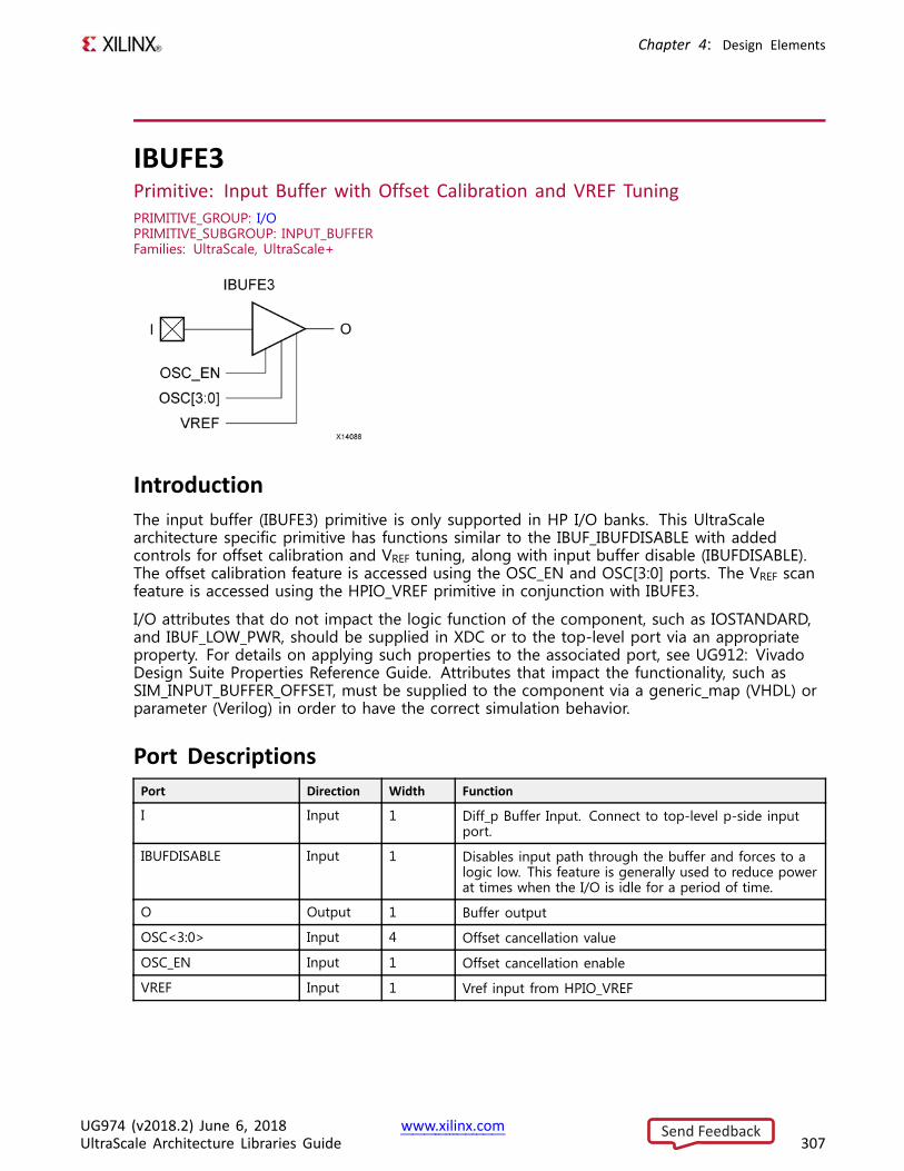
Chapter 4: Design Elements
IBUFE3Primitive: Input Buffer with Offset Calibration and VREF TuningPRIMITIVE_GROUP: I/OPRIMITIVE_SUBGROUP: INPUT_BUFFERFamilies: UltraScale, UltraScale+
IntroductionThe input buffer (IBUFE3) primitive is only supported in HP I/O banks. This UltraScalearchitecture specific primitive has functions similar to the IBUF_IBUFDISABLE with addedcontrols for offset calibration and VREF tuning, along with input buffer disable (IBUFDISABLE).The offset calibration feature is accessed using the OSC_EN and OSC[3:0] ports. The VREF scanfeature is accessed using the HPIO_VREF primitive in conjunction with IBUFE3.
I/O attributes that do not impact the logic function of the component, such as IOSTANDARD,and IBUF_LOW_PWR, should be supplied in XDC or to the top-level port via an appropriateproperty. For details on applying such properties to the associated port, see UG912: VivadoDesign Suite Properties Reference Guide. Attributes that impact the functionality, such asSIM_INPUT_BUFFER_OFFSET, must be supplied to the component via a generic_map (VHDL) orparameter (Verilog) in order to have the correct simulation behavior.
Port DescriptionsPort Direction Width Function
I Input 1 Diff_p Buffer Input. Connect to top-level p-side inputport.
IBUFDISABLE Input 1 Disables input path through the buffer and forces to alogic low. This feature is generally used to reduce powerat times when the I/O is idle for a period of time.
O Output 1 Buffer output
OSC<3:0> Input 4 Offset cancellation value
OSC_EN Input 1 Offset cancellation enable
VREF Input 1 Vref input from HPIO_VREF
UG974 (v2018.2) June 6, 2018 www.xilinx.comUltraScale Architecture Libraries Guide 307
Send Feedback
Chapter 4: Design Elements
Design Entry MethodInstantiation Yes
Inference No
IP and IP Integrator Catalog No
Available AttributesAttribute Type Allowed Values Default Description
SIM_INPUT_BUFFER_OFFSET
DECIMAL -50 to 50 0 Offset value for simulation purposes.
USE_IBUFDISABLE STRING "FALSE", "TRUE" "FALSE" This attribute must be unspecified or set to"TRUE" if specified.
VHDL Instantiation TemplateUnless they already exist, copy the following two statements and paste them before the entitydeclaration.Library UNISIM;use UNISIM.vcomponents.all;
-- IBUFE3: Input Buffer with Offset Calibration and VREF Tuning-- UltraScale-- Xilinx HDL Language Template, version 2018.2
IBUFE3_inst : IBUFE3generic map (
SIM_INPUT_BUFFER_OFFSET => 0 -- Offset value for simulation (-50-50))port map (
O => O, -- 1-bit output: Buffer outputI => I, -- 1-bit input: Buffer input (connect directly to top-level port)IBUFDISABLE => IBUFDISABLE, -- 1-bit input: Buffer disable input, high=disableOSC => OSC, -- 4-bit input: Offset cancellation valueOSC_EN => OSC_EN, -- 1-bit input: Offset cancellation enableVREF => VREF -- 1-bit input: Vref input from HPIO_VREF
);
-- End of IBUFE3_inst instantiation
Verilog Instantiation Template
// IBUFE3: Input Buffer with Offset Calibration and VREF Tuning// UltraScale// Xilinx HDL Language Template, version 2018.2
IBUFE3 #(.SIM_INPUT_BUFFER_OFFSET(0) // Offset value for simulation (-50-50)
)IBUFE3_inst (
.O(O), // 1-bit output: Buffer output
.I(I), // 1-bit input: Buffer input (connect directly to top-level port)
.IBUFDISABLE(IBUFDISABLE), // 1-bit input: Buffer disable input, high=disable
.OSC(OSC), // 4-bit input: Offset cancellation value
.OSC_EN(OSC_EN), // 1-bit input: Offset cancellation enable
.VREF(VREF) // 1-bit input: Vref input from HPIO_VREF);
UG974 (v2018.2) June 6, 2018 www.xilinx.comUltraScale Architecture Libraries Guide 308
Send Feedback

Chapter 4: Design Elements
// End of IBUFE3_inst instantiation
For More Information• See the UltraScale Architecture SelectIO Resources User Guide (UG571).
• See the UltraScale Programmable Devices Documentation.
UG974 (v2018.2) June 6, 2018 www.xilinx.comUltraScale Architecture Libraries Guide 309
Send Feedback
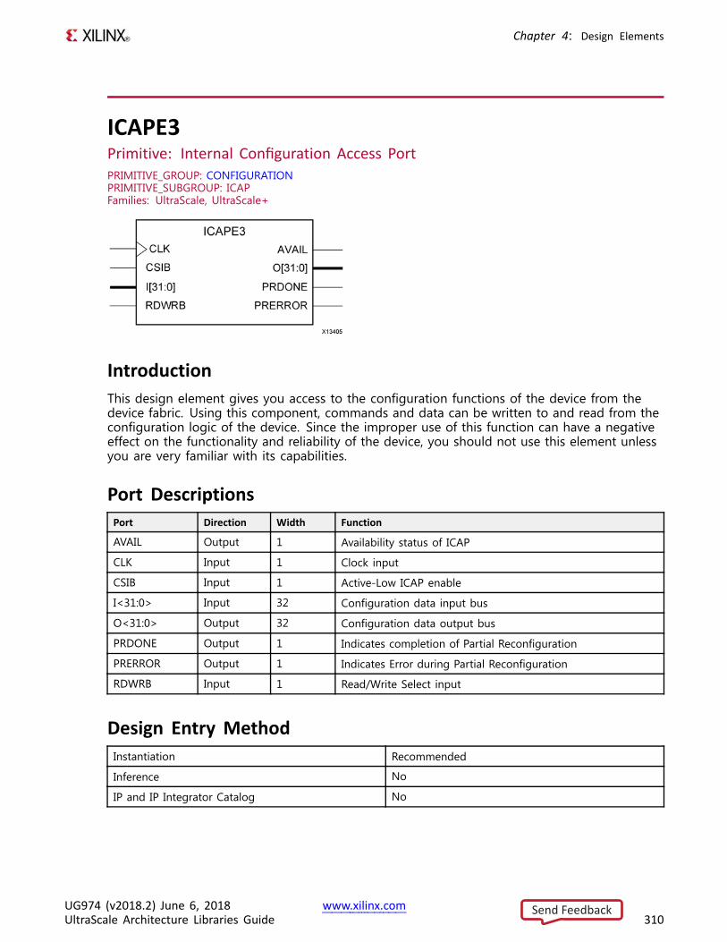
Chapter 4: Design Elements
ICAPE3Primitive: Internal Configuration Access PortPRIMITIVE_GROUP: CONFIGURATIONPRIMITIVE_SUBGROUP: ICAPFamilies: UltraScale, UltraScale+
IntroductionThis design element gives you access to the configuration functions of the device from thedevice fabric. Using this component, commands and data can be written to and read from theconfiguration logic of the device. Since the improper use of this function can have a negativeeffect on the functionality and reliability of the device, you should not use this element unlessyou are very familiar with its capabilities.
Port DescriptionsPort Direction Width Function
AVAIL Output 1 Availability status of ICAP
CLK Input 1 Clock input
CSIB Input 1 Active-Low ICAP enable
I<31:0> Input 32 Configuration data input bus
O<31:0> Output 32 Configuration data output bus
PRDONE Output 1 Indicates completion of Partial Reconfiguration
PRERROR Output 1 Indicates Error during Partial Reconfiguration
RDWRB Input 1 Read/Write Select input
Design Entry MethodInstantiation Recommended
Inference No
IP and IP Integrator Catalog No
UG974 (v2018.2) June 6, 2018 www.xilinx.comUltraScale Architecture Libraries Guide 310
Send Feedback
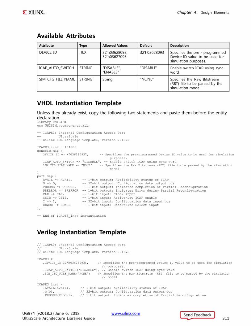
Chapter 4: Design Elements
Available AttributesAttribute Type Allowed Values Default Description
DEVICE_ID HEX 32'h03628093,32'h03627093
32'h03628093 Specifies the pre - programmedDevice ID value to be used forsimulation purposes.
ICAP_AUTO_SWITCH STRING "DISABLE","ENABLE"
"DISABLE" Enable switch ICAP using syncword
SIM_CFG_FILE_NAME STRING String "NONE" Specifies the Raw Bitstream(RBT) file to be parsed by thesimulation model
VHDL Instantiation TemplateUnless they already exist, copy the following two statements and paste them before the entitydeclaration.Library UNISIM;use UNISIM.vcomponents.all;
-- ICAPE3: Internal Configuration Access Port-- UltraScale-- Xilinx HDL Language Template, version 2018.2
ICAPE3_inst : ICAPE3generic map (
DEVICE_ID => X"03628093", -- Specifies the pre-programmed Device ID value to be used for simulation-- purposes.
ICAP_AUTO_SWITCH => "DISABLE", -- Enable switch ICAP using sync wordSIM_CFG_FILE_NAME => "NONE" -- Specifies the Raw Bitstream (RBT) file to be parsed by the simulation
-- model)port map (
AVAIL => AVAIL, -- 1-bit output: Availability status of ICAPO => O, -- 32-bit output: Configuration data output busPRDONE => PRDONE, -- 1-bit output: Indicates completion of Partial ReconfigurationPRERROR => PRERROR, -- 1-bit output: Indicates Error during Partial ReconfigurationCLK => CLK, -- 1-bit input: Clock inputCSIB => CSIB, -- 1-bit input: Active-Low ICAP enableI => I, -- 32-bit input: Configuration data input busRDWRB => RDWRB -- 1-bit input: Read/Write Select input
);
-- End of ICAPE3_inst instantiation
Verilog Instantiation Template
// ICAPE3: Internal Configuration Access Port// UltraScale// Xilinx HDL Language Template, version 2018.2
ICAPE3 #(.DEVICE_ID(32'h03628093), // Specifies the pre-programmed Device ID value to be used for simulation
// purposes..ICAP_AUTO_SWITCH("DISABLE"), // Enable switch ICAP using sync word.SIM_CFG_FILE_NAME("NONE") // Specifies the Raw Bitstream (RBT) file to be parsed by the simulation
// model)ICAPE3_inst (
.AVAIL(AVAIL), // 1-bit output: Availability status of ICAP
.O(O), // 32-bit output: Configuration data output bus
.PRDONE(PRDONE), // 1-bit output: Indicates completion of Partial Reconfiguration
UG974 (v2018.2) June 6, 2018 www.xilinx.comUltraScale Architecture Libraries Guide 311
Send Feedback
Chapter 4: Design Elements
.PRERROR(PRERROR), // 1-bit output: Indicates Error during Partial Reconfiguration
.CLK(CLK), // 1-bit input: Clock input
.CSIB(CSIB), // 1-bit input: Active-Low ICAP enable
.I(I), // 32-bit input: Configuration data input bus
.RDWRB(RDWRB) // 1-bit input: Read/Write Select input);
// End of ICAPE3_inst instantiation
For More Information• See the UltraScale Architecture Configuration User Guide (UG570).
• See the UltraScale Programmable Devices Documentation.
UG974 (v2018.2) June 6, 2018 www.xilinx.comUltraScale Architecture Libraries Guide 312
Send Feedback
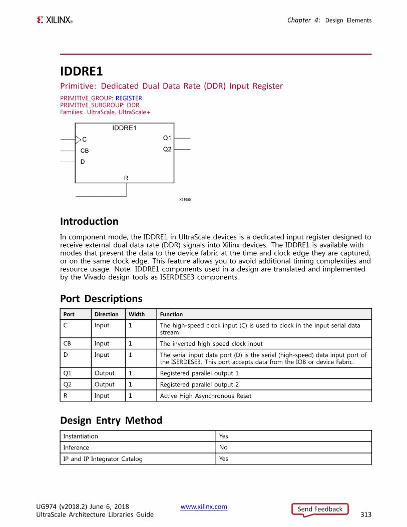
Chapter 4: Design Elements
IDDRE1Primitive: Dedicated Dual Data Rate (DDR) Input RegisterPRIMITIVE_GROUP: REGISTERPRIMITIVE_SUBGROUP: DDRFamilies: UltraScale, UltraScale+
IntroductionIn component mode, the IDDRE1 in UltraScale devices is a dedicated input register designed toreceive external dual data rate (DDR) signals into Xilinx devices. The IDDRE1 is available withmodes that present the data to the device fabric at the time and clock edge they are captured,or on the same clock edge. This feature allows you to avoid additional timing complexities andresource usage. Note: IDDRE1 components used in a design are translated and implementedby the Vivado design tools as ISERDESE3 components.
Port DescriptionsPort Direction Width Function
C Input 1 The high-speed clock input (C) is used to clock in the input serial datastream
CB Input 1 The inverted high-speed clock input
D Input 1 The serial input data port (D) is the serial (high-speed) data input port ofthe ISERDESE3. This port accepts data from the IOB or device Fabric.
Q1 Output 1 Registered parallel output 1
Q2 Output 1 Registered parallel output 2
R Input 1 Active High Asynchronous Reset
Design Entry MethodInstantiation Yes
Inference No
IP and IP Integrator Catalog Yes
UG974 (v2018.2) June 6, 2018 www.xilinx.comUltraScale Architecture Libraries Guide 313
Send Feedback
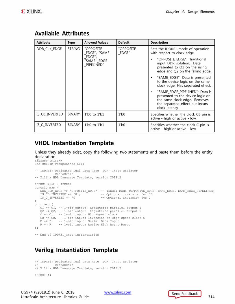
Chapter 4: Design Elements
Available AttributesAttribute Type Allowed Values Default Description
DDR_CLK_EDGE STRING "OPPOSITE_EDGE", "SAME_EDGE","SAME _EDGE_PIPELINED"
"OPPOSITE_EDGE"
Sets the IDDRE1 mode of operationwith respect to clock edge.
• "OPPOSITE_EDGE": Traditionalinput DDR solution. Datapresented to Q1 on the risingedge and Q2 on the falling edge.
• "SAME_EDGE": Data is presentedto the device logic on the sameclock edge. Has separated effect.
• "SAME_EDGE_PIPELINED": Data ispresented to the device logic onthe same clock edge. Removesthe separated effect but incursclock latency.
IS_CB_INVERTED BINARY 1'b0 to 1'b1 1'b0 Specifies whether the clock CB pin isactive - high or active - low.
IS_C_INVERTED BINARY 1'b0 to 1'b1 1'b0 Specifies whether the clock C pin isactive - high or active - low.
VHDL Instantiation TemplateUnless they already exist, copy the following two statements and paste them before the entitydeclaration.Library UNISIM;use UNISIM.vcomponents.all;
-- IDDRE1: Dedicated Dual Data Rate (DDR) Input Register-- UltraScale-- Xilinx HDL Language Template, version 2018.2
IDDRE1_inst : IDDRE1generic map (
DDR_CLK_EDGE => "OPPOSITE_EDGE", -- IDDRE1 mode (OPPOSITE_EDGE, SAME_EDGE, SAME_EDGE_PIPELINED)IS_CB_INVERTED => '0', -- Optional inversion for CBIS_C_INVERTED => '0' -- Optional inversion for C
)port map (
Q1 => Q1, -- 1-bit output: Registered parallel output 1Q2 => Q2, -- 1-bit output: Registered parallel output 2C => C, -- 1-bit input: High-speed clockCB => CB, -- 1-bit input: Inversion of High-speed clock CD => D, -- 1-bit input: Serial Data InputR => R -- 1-bit input: Active High Async Reset
);
-- End of IDDRE1_inst instantiation
Verilog Instantiation Template
// IDDRE1: Dedicated Dual Data Rate (DDR) Input Register// UltraScale// Xilinx HDL Language Template, version 2018.2
IDDRE1 #(
UG974 (v2018.2) June 6, 2018 www.xilinx.comUltraScale Architecture Libraries Guide 314
Send Feedback
Chapter 4: Design Elements
.DDR_CLK_EDGE("OPPOSITE_EDGE"), // IDDRE1 mode (OPPOSITE_EDGE, SAME_EDGE, SAME_EDGE_PIPELINED)
.IS_CB_INVERTED(1'b0), // Optional inversion for CB
.IS_C_INVERTED(1'b0) // Optional inversion for C)IDDRE1_inst (
.Q1(Q1), // 1-bit output: Registered parallel output 1
.Q2(Q2), // 1-bit output: Registered parallel output 2
.C(C), // 1-bit input: High-speed clock
.CB(CB), // 1-bit input: Inversion of High-speed clock C
.D(D), // 1-bit input: Serial Data Input
.R(R) // 1-bit input: Active High Async Reset);
// End of IDDRE1_inst instantiation
For More Information• See the UltraScale Architecture SelectIO Resources User Guide (UG571).
• See the UltraScale Programmable Devices Documentation.
UG974 (v2018.2) June 6, 2018 www.xilinx.comUltraScale Architecture Libraries Guide 315
Send Feedback
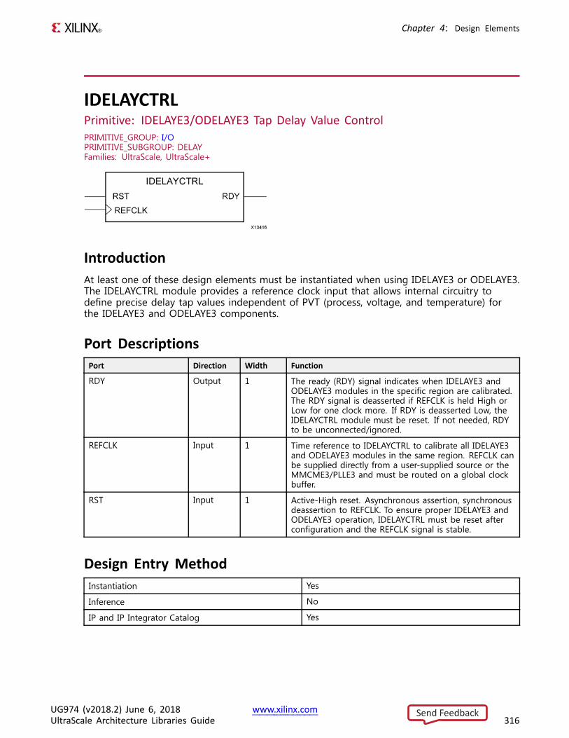
Chapter 4: Design Elements
IDELAYCTRLPrimitive: IDELAYE3/ODELAYE3 Tap Delay Value ControlPRIMITIVE_GROUP: I/OPRIMITIVE_SUBGROUP: DELAYFamilies: UltraScale, UltraScale+
IntroductionAt least one of these design elements must be instantiated when using IDELAYE3 or ODELAYE3.The IDELAYCTRL module provides a reference clock input that allows internal circuitry todefine precise delay tap values independent of PVT (process, voltage, and temperature) forthe IDELAYE3 and ODELAYE3 components.
Port DescriptionsPort Direction Width Function
RDY Output 1 The ready (RDY) signal indicates when IDELAYE3 andODELAYE3 modules in the specific region are calibrated.The RDY signal is deasserted if REFCLK is held High orLow for one clock more. If RDY is deasserted Low, theIDELAYCTRL module must be reset. If not needed, RDYto be unconnected/ignored.
REFCLK Input 1 Time reference to IDELAYCTRL to calibrate all IDELAYE3and ODELAYE3 modules in the same region. REFCLK canbe supplied directly from a user-supplied source or theMMCME3/PLLE3 and must be routed on a global clockbuffer.
RST Input 1 Active-High reset. Asynchronous assertion, synchronousdeassertion to REFCLK. To ensure proper IDELAYE3 andODELAYE3 operation, IDELAYCTRL must be reset afterconfiguration and the REFCLK signal is stable.
Design Entry MethodInstantiation Yes
Inference No
IP and IP Integrator Catalog Yes
UG974 (v2018.2) June 6, 2018 www.xilinx.comUltraScale Architecture Libraries Guide 316
Send Feedback
Chapter 4: Design Elements
VHDL Instantiation TemplateUnless they already exist, copy the following two statements and paste them before the entitydeclaration.Library UNISIM;use UNISIM.vcomponents.all;
-- IDELAYCTRL: IDELAYE3/ODELAYE3 Tap Delay Value Control-- UltraScale-- Xilinx HDL Language Template, version 2018.2
IDELAYCTRL_inst : IDELAYCTRLgeneric map (
SIM_DEVICE => "ULTRASCALE" -- Must be set to "ULTRASCALE")port map (
RDY => RDY, -- 1-bit output: Ready outputREFCLK => REFCLK, -- 1-bit input: Reference clock inputRST => RST -- 1-bit input: Active high reset input. Asynchronous assert, synchronous deassert to
-- REFCLK.
);
-- End of IDELAYCTRL_inst instantiation
Verilog Instantiation Template
// IDELAYCTRL: IDELAYE3/ODELAYE3 Tap Delay Value Control// UltraScale// Xilinx HDL Language Template, version 2018.2
IDELAYCTRL #(.SIM_DEVICE("ULTRASCALE") // Must be set to "ULTRASCALE"
)IDELAYCTRL_inst (
.RDY(RDY), // 1-bit output: Ready output
.REFCLK(REFCLK), // 1-bit input: Reference clock input
.RST(RST) // 1-bit input: Active high reset input. Asynchronous assert, synchronous deassert to// REFCLK.
);
// End of IDELAYCTRL_inst instantiation
For More Information• See the UltraScale Architecture SelectIO Resources User Guide (UG571).
• See the UltraScale Programmable Devices Documentation.
UG974 (v2018.2) June 6, 2018 www.xilinx.comUltraScale Architecture Libraries Guide 317
Send Feedback
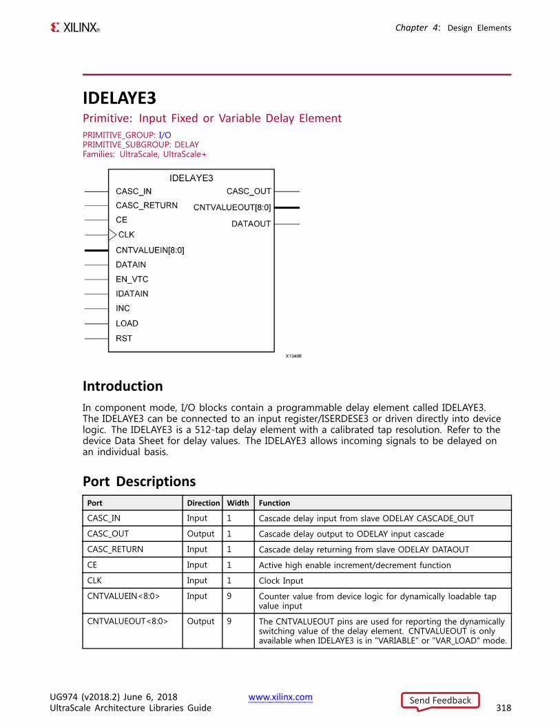
Chapter 4: Design Elements
IDELAYE3Primitive: Input Fixed or Variable Delay ElementPRIMITIVE_GROUP: I/OPRIMITIVE_SUBGROUP: DELAYFamilies: UltraScale, UltraScale+
IntroductionIn component mode, I/O blocks contain a programmable delay element called IDELAYE3.The IDELAYE3 can be connected to an input register/ISERDESE3 or driven directly into devicelogic. The IDELAYE3 is a 512-tap delay element with a calibrated tap resolution. Refer to thedevice Data Sheet for delay values. The IDELAYE3 allows incoming signals to be delayed onan individual basis.
Port DescriptionsPort Direction Width Function
CASC_IN Input 1 Cascade delay input from slave ODELAY CASCADE_OUT
CASC_OUT Output 1 Cascade delay output to ODELAY input cascade
CASC_RETURN Input 1 Cascade delay returning from slave ODELAY DATAOUT
CE Input 1 Active high enable increment/decrement function
CLK Input 1 Clock Input
CNTVALUEIN<8:0> Input 9 Counter value from device logic for dynamically loadable tapvalue input
CNTVALUEOUT<8:0> Output 9 The CNTVALUEOUT pins are used for reporting the dynamicallyswitching value of the delay element. CNTVALUEOUT is onlyavailable when IDELAYE3 is in "VARIABLE" or "VAR_LOAD" mode.
UG974 (v2018.2) June 6, 2018 www.xilinx.comUltraScale Architecture Libraries Guide 318
Send Feedback
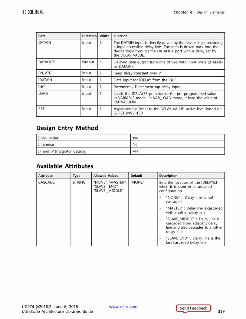
Chapter 4: Design Elements
Port Direction Width Function
DATAIN Input 1 The DATAIN input is directly driven by the device logic providinga logic accessible delay line. The data is driven back into thedevice logic through the DATAOUT port with a delay set bythe DELAY_VALUE.
DATAOUT Output 1 Delayed data output from one of two data input ports (IDATAINor DATAIN).
EN_VTC Input 1 Keep delay constant over VT
IDATAIN Input 1 Data input for IDELAY from the IBUF
INC Input 1 Increment / Decrement tap delay input
LOAD Input 1 Loads the IDELAYE3 primitive to the pre-programmed valuein VARIABLE mode. In VAR_LOAD mode, it load the value ofCNTVALUEIN.
RST Input 1 Asynchronous Reset to the DELAY_VALUE, active level based onIS_RST_INVERTED
Design Entry MethodInstantiation Yes
Inference No
IP and IP Integrator Catalog Yes
Available AttributesAttribute Type Allowed Values Default Description
CASCADE STRING "NONE", "MASTER","SLAVE _END","SLAVE _MIDDLE"
"NONE" Sets the location of the IDELAYE3when it is used in a cascadedconfiguration
• "NONE" : Delay line is notcascaded
• "MASTER" : Delay line is cascadedwith another delay line
• "SLAVE_MIDDLE" : Delay line iscascaded from adjacent delayline and also cascades to anotherdelay line
• "SLAVE_END" : Delay line is thelast cascaded delay line
UG974 (v2018.2) June 6, 2018 www.xilinx.comUltraScale Architecture Libraries Guide 319
Send Feedback
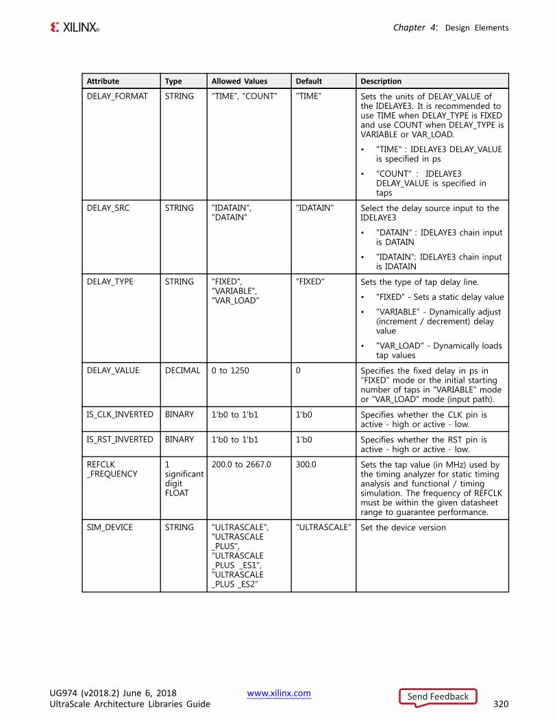
Chapter 4: Design Elements
Attribute Type Allowed Values Default Description
DELAY_FORMAT STRING "TIME", "COUNT" "TIME" Sets the units of DELAY_VALUE ofthe IDELAYE3. It is recommended touse TIME when DELAY_TYPE is FIXEDand use COUNT when DELAY_TYPE isVARIABLE or VAR_LOAD.
• "TIME" : IDELAYE3 DELAY_VALUEis specified in ps
• "COUNT" : IDELAYE3DELAY_VALUE is specified intaps
DELAY_SRC STRING "IDATAIN","DATAIN"
"IDATAIN" Select the delay source input to theIDELAYE3
• "DATAIN" : IDELAYE3 chain inputis DATAIN
• "IDATAIN": IDELAYE3 chain inputis IDATAIN
DELAY_TYPE STRING "FIXED","VARIABLE","VAR_LOAD"
"FIXED" Sets the type of tap delay line.
• "FIXED" - Sets a static delay value
• "VARIABLE" - Dynamically adjust(increment / decrement) delayvalue
• "VAR_LOAD" - Dynamically loadstap values
DELAY_VALUE DECIMAL 0 to 1250 0 Specifies the fixed delay in ps in"FIXED" mode or the initial startingnumber of taps in "VARIABLE" modeor "VAR_LOAD" mode (input path).
IS_CLK_INVERTED BINARY 1'b0 to 1'b1 1'b0 Specifies whether the CLK pin isactive - high or active - low.
IS_RST_INVERTED BINARY 1'b0 to 1'b1 1'b0 Specifies whether the RST pin isactive - high or active - low.
REFCLK_FREQUENCY
1significantdigitFLOAT
200.0 to 2667.0 300.0 Sets the tap value (in MHz) used bythe timing analyzer for static timinganalysis and functional / timingsimulation. The frequency of REFCLKmust be within the given datasheetrange to guarantee performance.
SIM_DEVICE STRING "ULTRASCALE","ULTRASCALE_PLUS","ULTRASCALE_PLUS _ES1","ULTRASCALE_PLUS _ES2"
"ULTRASCALE" Set the device version
UG974 (v2018.2) June 6, 2018 www.xilinx.comUltraScale Architecture Libraries Guide 320
Send Feedback
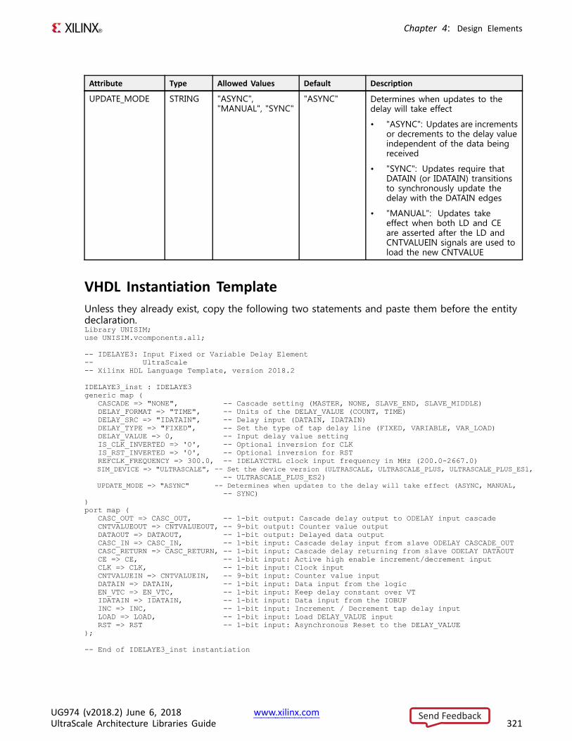
Chapter 4: Design Elements
Attribute Type Allowed Values Default Description
UPDATE_MODE STRING "ASYNC","MANUAL", "SYNC"
"ASYNC" Determines when updates to thedelay will take effect
• "ASYNC": Updates are incrementsor decrements to the delay valueindependent of the data beingreceived
• "SYNC": Updates require thatDATAIN (or IDATAIN) transitionsto synchronously update thedelay with the DATAIN edges
• "MANUAL": Updates takeeffect when both LD and CEare asserted after the LD andCNTVALUEIN signals are used toload the new CNTVALUE
VHDL Instantiation TemplateUnless they already exist, copy the following two statements and paste them before the entitydeclaration.Library UNISIM;use UNISIM.vcomponents.all;
-- IDELAYE3: Input Fixed or Variable Delay Element-- UltraScale-- Xilinx HDL Language Template, version 2018.2
IDELAYE3_inst : IDELAYE3generic map (
CASCADE => "NONE", -- Cascade setting (MASTER, NONE, SLAVE_END, SLAVE_MIDDLE)DELAY_FORMAT => "TIME", -- Units of the DELAY_VALUE (COUNT, TIME)DELAY_SRC => "IDATAIN", -- Delay input (DATAIN, IDATAIN)DELAY_TYPE => "FIXED", -- Set the type of tap delay line (FIXED, VARIABLE, VAR_LOAD)DELAY_VALUE => 0, -- Input delay value settingIS_CLK_INVERTED => '0', -- Optional inversion for CLKIS_RST_INVERTED => '0', -- Optional inversion for RSTREFCLK_FREQUENCY => 300.0, -- IDELAYCTRL clock input frequency in MHz (200.0-2667.0)SIM_DEVICE => "ULTRASCALE", -- Set the device version (ULTRASCALE, ULTRASCALE_PLUS, ULTRASCALE_PLUS_ES1,
-- ULTRASCALE_PLUS_ES2)UPDATE_MODE => "ASYNC" -- Determines when updates to the delay will take effect (ASYNC, MANUAL,
-- SYNC))port map (
CASC_OUT => CASC_OUT, -- 1-bit output: Cascade delay output to ODELAY input cascadeCNTVALUEOUT => CNTVALUEOUT, -- 9-bit output: Counter value outputDATAOUT => DATAOUT, -- 1-bit output: Delayed data outputCASC_IN => CASC_IN, -- 1-bit input: Cascade delay input from slave ODELAY CASCADE_OUTCASC_RETURN => CASC_RETURN, -- 1-bit input: Cascade delay returning from slave ODELAY DATAOUTCE => CE, -- 1-bit input: Active high enable increment/decrement inputCLK => CLK, -- 1-bit input: Clock inputCNTVALUEIN => CNTVALUEIN, -- 9-bit input: Counter value inputDATAIN => DATAIN, -- 1-bit input: Data input from the logicEN_VTC => EN_VTC, -- 1-bit input: Keep delay constant over VTIDATAIN => IDATAIN, -- 1-bit input: Data input from the IOBUFINC => INC, -- 1-bit input: Increment / Decrement tap delay inputLOAD => LOAD, -- 1-bit input: Load DELAY_VALUE inputRST => RST -- 1-bit input: Asynchronous Reset to the DELAY_VALUE
);
-- End of IDELAYE3_inst instantiation
UG974 (v2018.2) June 6, 2018 www.xilinx.comUltraScale Architecture Libraries Guide 321
Send Feedback
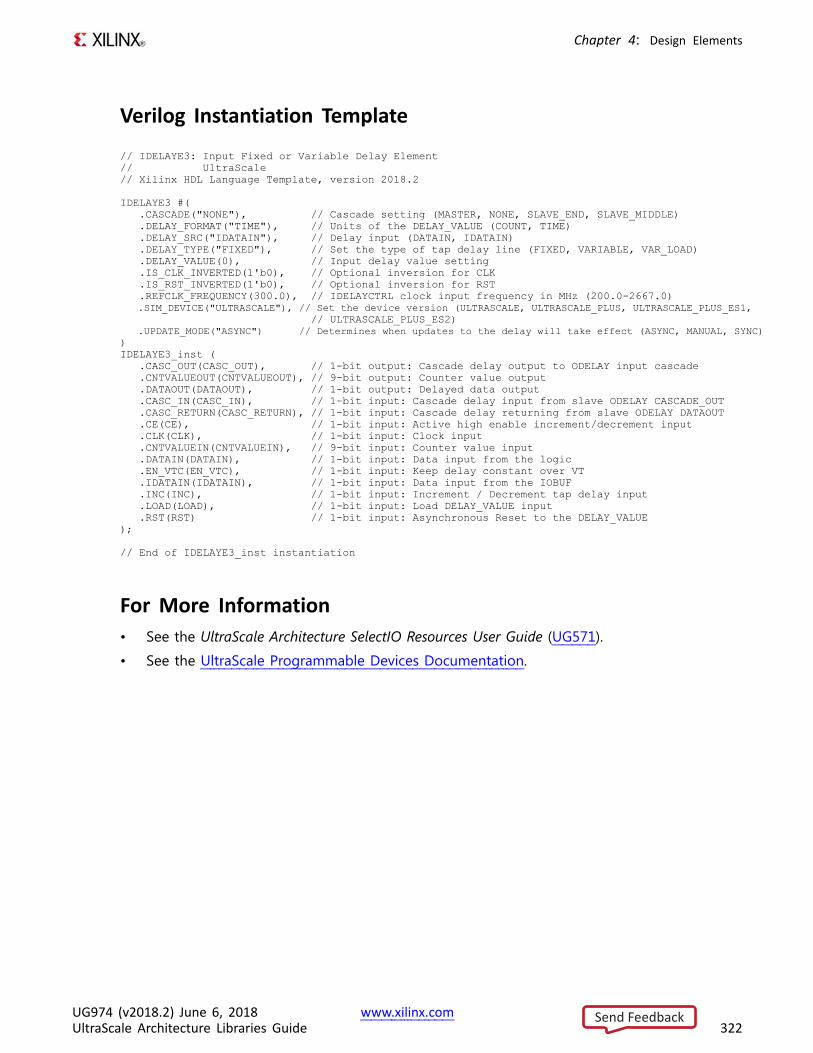
Chapter 4: Design Elements
Verilog Instantiation Template
// IDELAYE3: Input Fixed or Variable Delay Element// UltraScale// Xilinx HDL Language Template, version 2018.2
IDELAYE3 #(.CASCADE("NONE"), // Cascade setting (MASTER, NONE, SLAVE_END, SLAVE_MIDDLE).DELAY_FORMAT("TIME"), // Units of the DELAY_VALUE (COUNT, TIME).DELAY_SRC("IDATAIN"), // Delay input (DATAIN, IDATAIN).DELAY_TYPE("FIXED"), // Set the type of tap delay line (FIXED, VARIABLE, VAR_LOAD).DELAY_VALUE(0), // Input delay value setting.IS_CLK_INVERTED(1'b0), // Optional inversion for CLK.IS_RST_INVERTED(1'b0), // Optional inversion for RST.REFCLK_FREQUENCY(300.0), // IDELAYCTRL clock input frequency in MHz (200.0-2667.0).SIM_DEVICE("ULTRASCALE"), // Set the device version (ULTRASCALE, ULTRASCALE_PLUS, ULTRASCALE_PLUS_ES1,
// ULTRASCALE_PLUS_ES2).UPDATE_MODE("ASYNC") // Determines when updates to the delay will take effect (ASYNC, MANUAL, SYNC)
)IDELAYE3_inst (
.CASC_OUT(CASC_OUT), // 1-bit output: Cascade delay output to ODELAY input cascade
.CNTVALUEOUT(CNTVALUEOUT), // 9-bit output: Counter value output
.DATAOUT(DATAOUT), // 1-bit output: Delayed data output
.CASC_IN(CASC_IN), // 1-bit input: Cascade delay input from slave ODELAY CASCADE_OUT
.CASC_RETURN(CASC_RETURN), // 1-bit input: Cascade delay returning from slave ODELAY DATAOUT
.CE(CE), // 1-bit input: Active high enable increment/decrement input
.CLK(CLK), // 1-bit input: Clock input
.CNTVALUEIN(CNTVALUEIN), // 9-bit input: Counter value input
.DATAIN(DATAIN), // 1-bit input: Data input from the logic
.EN_VTC(EN_VTC), // 1-bit input: Keep delay constant over VT
.IDATAIN(IDATAIN), // 1-bit input: Data input from the IOBUF
.INC(INC), // 1-bit input: Increment / Decrement tap delay input
.LOAD(LOAD), // 1-bit input: Load DELAY_VALUE input
.RST(RST) // 1-bit input: Asynchronous Reset to the DELAY_VALUE);
// End of IDELAYE3_inst instantiation
For More Information• See the UltraScale Architecture SelectIO Resources User Guide (UG571).
• See the UltraScale Programmable Devices Documentation.
UG974 (v2018.2) June 6, 2018 www.xilinx.comUltraScale Architecture Libraries Guide 322
Send Feedback
Chapter 4: Design Elements
ILKNPrimitive: Interlaken MACPRIMITIVE_GROUP: ADVANCEDPRIMITIVE_SUBGROUP: INTERLAKENFamilies: UltraScale
IntroductionThe Interlaken protocol block provides a high-performance, low power implementation of theInterlaken protocol that provides a low risk, quick path for adopting Interlaken as a chip-to-chipinterconnect protocol. This block is designed to be integrated with GTs and device clockingresources using fabric interconnect. See PG169: UltraScale Architecture Integrated IP Core forInterlaken v1.4 Product Guide for further details on this component
Design Entry MethodInstantiation No
Inference No
IP and IP Integrator Catalog Recommended
For More Information• See the Integrated Interlaken up to 150G v1.7 Product Guide (PG169).
• See the UltraScale Programmable Devices Documentation.
UG974 (v2018.2) June 6, 2018 www.xilinx.comUltraScale Architecture Libraries Guide 323
Send Feedback

Chapter 4: Design Elements
ILKNE4Primitive: Interlaken MACPRIMITIVE_GROUP: ADVANCEDPRIMITIVE_SUBGROUP: INTERLAKENFamilies: UltraScale+
IntroductionThe Interlaken protocol block provides a high-performance, low power implementation of theInterlaken protocol that provides a low risk, quick path for adopting Interlaken as a chip-to-chipinterconnect protocol. This block is designed to be integrated with GTs and device clockingresources using fabric interconnect. See the UltraScale+ Architecture Integrated IP Core forInterlaken Product Guide for further details on this component
Design Entry MethodInstantiation No
Inference No
IP and IP Integrator Catalog Recommended
For More Information• See the Integrated Interlaken up to 150G v1.7 Product Guide (PG169).
• See the UltraScale Programmable Devices Documentation.
UG974 (v2018.2) June 6, 2018 www.xilinx.comUltraScale Architecture Libraries Guide 324
Send Feedback
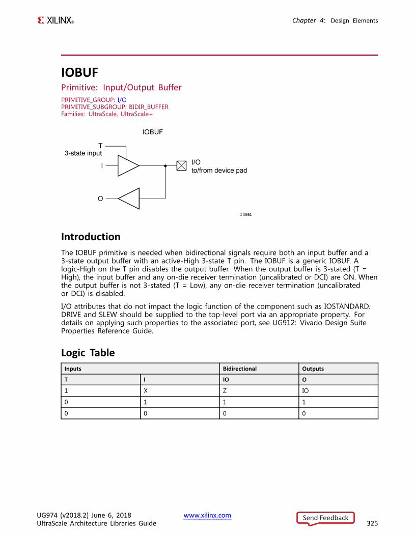
Chapter 4: Design Elements
IOBUFPrimitive: Input/Output BufferPRIMITIVE_GROUP: I/OPRIMITIVE_SUBGROUP: BIDIR_BUFFERFamilies: UltraScale, UltraScale+
IntroductionThe IOBUF primitive is needed when bidirectional signals require both an input buffer and a3-state output buffer with an active-High 3-state T pin. The IOBUF is a generic IOBUF. Alogic-High on the T pin disables the output buffer. When the output buffer is 3-stated (T =High), the input buffer and any on-die receiver termination (uncalibrated or DCI) are ON. Whenthe output buffer is not 3-stated (T = Low), any on-die receiver termination (uncalibratedor DCI) is disabled.
I/O attributes that do not impact the logic function of the component such as IOSTANDARD,DRIVE and SLEW should be supplied to the top-level port via an appropriate property. Fordetails on applying such properties to the associated port, see UG912: Vivado Design SuiteProperties Reference Guide.
Logic TableInputs Bidirectional Outputs
T I IO O
1 X Z IO
0 1 1 1
0 0 0 0
UG974 (v2018.2) June 6, 2018 www.xilinx.comUltraScale Architecture Libraries Guide 325
Send Feedback
Chapter 4: Design Elements
Port DescriptionsPort Direction Width Function
I Input 1 Input of OBUF. Connect to the logic drivingthe output port.
IO Inout 1 Bidirectional port to be connected directly totop-level inout port.
O Output 1 Output path of the buffer.
T Input 1 3-state enable input signifying whether thebuffer acts as an input or output.
Design Entry MethodInstantiation Yes
Inference Recommended
IP and IP Integrator Catalog No
VHDL Instantiation TemplateUnless they already exist, copy the following two statements and paste them before the entitydeclaration.Library UNISIM;use UNISIM.vcomponents.all;
-- IOBUF: Input/Output Buffer-- UltraScale-- Xilinx HDL Language Template, version 2018.2
IOBUF_inst : IOBUFport map (
O => O, -- 1-bit output: Buffer outputI => I, -- 1-bit input: Buffer inputIO => IO, -- 1-bit inout: Buffer inout (connect directly to top-level port)T => T -- 1-bit input: 3-state enable input
);
-- End of IOBUF_inst instantiation
Verilog Instantiation Template
// IOBUF: Input/Output Buffer// UltraScale// Xilinx HDL Language Template, version 2018.2
IOBUF IOBUF_inst (.O(O), // 1-bit output: Buffer output.I(I), // 1-bit input: Buffer input.IO(IO), // 1-bit inout: Buffer inout (connect directly to top-level port).T(T) // 1-bit input: 3-state enable input
);
// End of IOBUF_inst instantiation
UG974 (v2018.2) June 6, 2018 www.xilinx.comUltraScale Architecture Libraries Guide 326
Send Feedback

Chapter 4: Design Elements
For More Information• See the UltraScale Architecture SelectIO Resources User Guide (UG571).
• See the UltraScale Programmable Devices Documentation.
UG974 (v2018.2) June 6, 2018 www.xilinx.comUltraScale Architecture Libraries Guide 327
Send Feedback
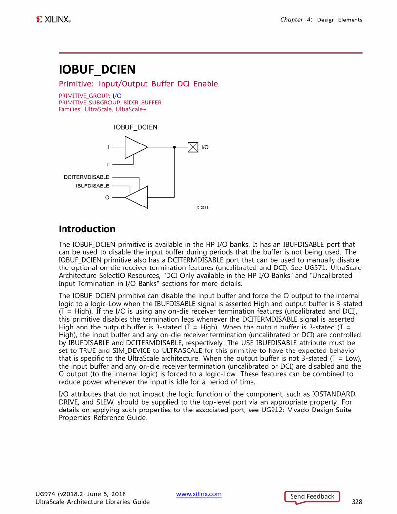
Chapter 4: Design Elements
IOBUF_DCIENPrimitive: Input/Output Buffer DCI EnablePRIMITIVE_GROUP: I/OPRIMITIVE_SUBGROUP: BIDIR_BUFFERFamilies: UltraScale, UltraScale+
IntroductionThe IOBUF_DCIEN primitive is available in the HP I/O banks. It has an IBUFDISABLE port thatcan be used to disable the input buffer during periods that the buffer is not being used. TheIOBUF_DCIEN primitive also has a DCITERMDISABLE port that can be used to manually disablethe optional on-die receiver termination features (uncalibrated and DCI). See UG571: UltraScaleArchitecture SelectIO Resources, "DCI Only available in the HP I/O Banks" and "UncalibratedInput Termination in I/O Banks" sections for more details.
The IOBUF_DCIEN primitive can disable the input buffer and force the O output to the internallogic to a logic-Low when the IBUFDISABLE signal is asserted High and output buffer is 3-stated(T = High). If the I/O is using any on-die receiver termination features (uncalibrated and DCI),this primitive disables the termination legs whenever the DCITERMDISABLE signal is assertedHigh and the output buffer is 3-stated (T = High). When the output buffer is 3-stated (T =High), the input buffer and any on-die receiver termination (uncalibrated or DCI) are controlledby IBUFDISABLE and DCITERMDISABLE, respectively. The USE_IBUFDISABLE attribute must beset to TRUE and SIM_DEVICE to ULTRASCALE for this primitive to have the expected behaviorthat is specific to the UltraScale architecture. When the output buffer is not 3-stated (T = Low),the input buffer and any on-die receiver termination (uncalibrated or DCI) are disabled and theO output (to the internal logic) is forced to a logic-Low. These features can be combined toreduce power whenever the input is idle for a period of time.
I/O attributes that do not impact the logic function of the component, such as IOSTANDARD,DRIVE, and SLEW, should be supplied to the top-level port via an appropriate property. Fordetails on applying such properties to the associated port, see UG912: Vivado Design SuiteProperties Reference Guide.
UG974 (v2018.2) June 6, 2018 www.xilinx.comUltraScale Architecture Libraries Guide 328
Send Feedback
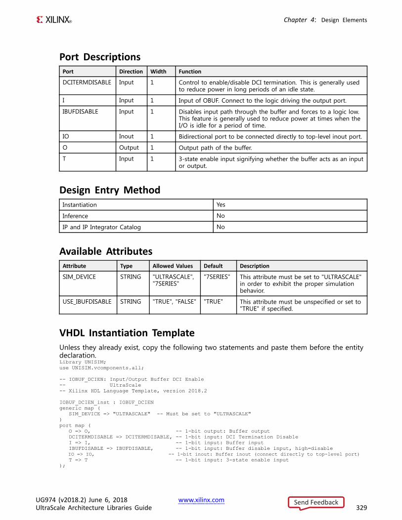
Chapter 4: Design Elements
Port DescriptionsPort Direction Width Function
DCITERMDISABLE Input 1 Control to enable/disable DCI termination. This is generally usedto reduce power in long periods of an idle state.
I Input 1 Input of OBUF. Connect to the logic driving the output port.
IBUFDISABLE Input 1 Disables input path through the buffer and forces to a logic low.This feature is generally used to reduce power at times when theI/O is idle for a period of time.
IO Inout 1 Bidirectional port to be connected directly to top-level inout port.
O Output 1 Output path of the buffer.
T Input 1 3-state enable input signifying whether the buffer acts as an inputor output.
Design Entry MethodInstantiation Yes
Inference No
IP and IP Integrator Catalog No
Available AttributesAttribute Type Allowed Values Default Description
SIM_DEVICE STRING "ULTRASCALE","7SERIES"
"7SERIES" This attribute must be set to "ULTRASCALE"in order to exhibit the proper simulationbehavior.
USE_IBUFDISABLE STRING "TRUE", "FALSE" "TRUE" This attribute must be unspecified or set to"TRUE" if specified.
VHDL Instantiation TemplateUnless they already exist, copy the following two statements and paste them before the entitydeclaration.Library UNISIM;use UNISIM.vcomponents.all;
-- IOBUF_DCIEN: Input/Output Buffer DCI Enable-- UltraScale-- Xilinx HDL Language Template, version 2018.2
IOBUF_DCIEN_inst : IOBUF_DCIENgeneric map (
SIM_DEVICE => "ULTRASCALE" -- Must be set to "ULTRASCALE")port map (
O => O, -- 1-bit output: Buffer outputDCITERMDISABLE => DCITERMDISABLE, -- 1-bit input: DCI Termination DisableI => I, -- 1-bit input: Buffer inputIBUFDISABLE => IBUFDISABLE, -- 1-bit input: Buffer disable input, high=disableIO => IO, -- 1-bit inout: Buffer inout (connect directly to top-level port)T => T -- 1-bit input: 3-state enable input
);
UG974 (v2018.2) June 6, 2018 www.xilinx.comUltraScale Architecture Libraries Guide 329
Send Feedback

Chapter 4: Design Elements
-- End of IOBUF_DCIEN_inst instantiation
Verilog Instantiation Template
// IOBUF_DCIEN: Input/Output Buffer DCI Enable// UltraScale// Xilinx HDL Language Template, version 2018.2
IOBUF_DCIEN #(.SIM_DEVICE("ULTRASCALE") // Must be set to "ULTRASCALE"
)IOBUF_DCIEN_inst (
.O(O), // 1-bit output: Buffer output
.DCITERMDISABLE(DCITERMDISABLE), // 1-bit input: DCI Termination Disable
.I(I), // 1-bit input: Buffer input
.IBUFDISABLE(IBUFDISABLE), // 1-bit input: Buffer disable input, high=disable
.IO(IO), // 1-bit inout: Buffer inout (connect directly to top-level port)
.T(T) // 1-bit input: 3-state enable input);
// End of IOBUF_DCIEN_inst instantiation
For More Information• See the UltraScale Architecture SelectIO Resources User Guide (UG571).
• See the UltraScale Programmable Devices Documentation.
UG974 (v2018.2) June 6, 2018 www.xilinx.comUltraScale Architecture Libraries Guide 330
Send Feedback
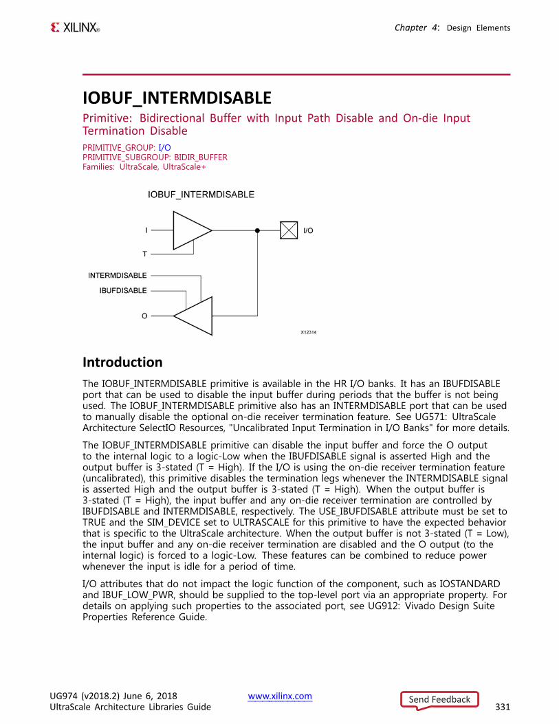
Chapter 4: Design Elements
IOBUF_INTERMDISABLEPrimitive: Bidirectional Buffer with Input Path Disable and On-die InputTermination DisablePRIMITIVE_GROUP: I/OPRIMITIVE_SUBGROUP: BIDIR_BUFFERFamilies: UltraScale, UltraScale+
IntroductionThe IOBUF_INTERMDISABLE primitive is available in the HR I/O banks. It has an IBUFDISABLEport that can be used to disable the input buffer during periods that the buffer is not beingused. The IOBUF_INTERMDISABLE primitive also has an INTERMDISABLE port that can be usedto manually disable the optional on-die receiver termination feature. See UG571: UltraScaleArchitecture SelectIO Resources, "Uncalibrated Input Termination in I/O Banks" for more details.
The IOBUF_INTERMDISABLE primitive can disable the input buffer and force the O outputto the internal logic to a logic-Low when the IBUFDISABLE signal is asserted High and theoutput buffer is 3-stated (T = High). If the I/O is using the on-die receiver termination feature(uncalibrated), this primitive disables the termination legs whenever the INTERMDISABLE signalis asserted High and the output buffer is 3-stated (T = High). When the output buffer is3-stated (T = High), the input buffer and any on-die receiver termination are controlled byIBUFDISABLE and INTERMDISABLE, respectively. The USE_IBUFDISABLE attribute must be set toTRUE and the SIM_DEVICE set to ULTRASCALE for this primitive to have the expected behaviorthat is specific to the UltraScale architecture. When the output buffer is not 3-stated (T = Low),the input buffer and any on-die receiver termination are disabled and the O output (to theinternal logic) is forced to a logic-Low. These features can be combined to reduce powerwhenever the input is idle for a period of time.
I/O attributes that do not impact the logic function of the component, such as IOSTANDARDand IBUF_LOW_PWR, should be supplied to the top-level port via an appropriate property. Fordetails on applying such properties to the associated port, see UG912: Vivado Design SuiteProperties Reference Guide.
UG974 (v2018.2) June 6, 2018 www.xilinx.comUltraScale Architecture Libraries Guide 331
Send Feedback
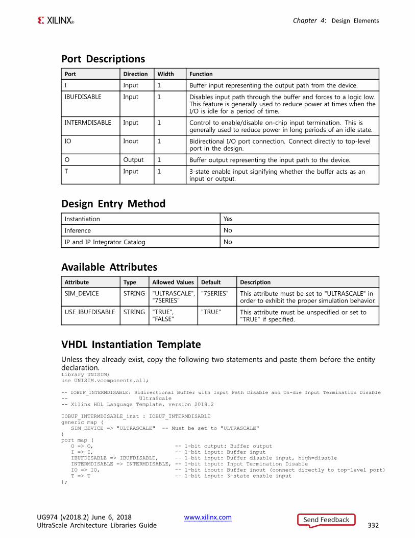
Chapter 4: Design Elements
Port DescriptionsPort Direction Width Function
I Input 1 Buffer input representing the output path from the device.
IBUFDISABLE Input 1 Disables input path through the buffer and forces to a logic low.This feature is generally used to reduce power at times when theI/O is idle for a period of time.
INTERMDISABLE Input 1 Control to enable/disable on-chip input termination. This isgenerally used to reduce power in long periods of an idle state.
IO Inout 1 Bidirectional I/O port connection. Connect directly to top-levelport in the design.
O Output 1 Buffer output representing the input path to the device.
T Input 1 3-state enable input signifying whether the buffer acts as aninput or output.
Design Entry MethodInstantiation Yes
Inference No
IP and IP Integrator Catalog No
Available AttributesAttribute Type Allowed Values Default Description
SIM_DEVICE STRING "ULTRASCALE","7SERIES"
"7SERIES" This attribute must be set to "ULTRASCALE" inorder to exhibit the proper simulation behavior.
USE_IBUFDISABLE STRING "TRUE","FALSE"
"TRUE" This attribute must be unspecified or set to"TRUE" if specified.
VHDL Instantiation TemplateUnless they already exist, copy the following two statements and paste them before the entitydeclaration.Library UNISIM;use UNISIM.vcomponents.all;
-- IOBUF_INTERMDISABLE: Bidirectional Buffer with Input Path Disable and On-die Input Termination Disable-- UltraScale-- Xilinx HDL Language Template, version 2018.2
IOBUF_INTERMDISABLE_inst : IOBUF_INTERMDISABLEgeneric map (
SIM_DEVICE => "ULTRASCALE" -- Must be set to "ULTRASCALE")port map (
O => O, -- 1-bit output: Buffer outputI => I, -- 1-bit input: Buffer inputIBUFDISABLE => IBUFDISABLE, -- 1-bit input: Buffer disable input, high=disableINTERMDISABLE => INTERMDISABLE, -- 1-bit input: Input Termination DisableIO => IO, -- 1-bit inout: Buffer inout (connect directly to top-level port)T => T -- 1-bit input: 3-state enable input
);
UG974 (v2018.2) June 6, 2018 www.xilinx.comUltraScale Architecture Libraries Guide 332
Send Feedback
Chapter 4: Design Elements
-- End of IOBUF_INTERMDISABLE_inst instantiation
Verilog Instantiation Template
// IOBUF_INTERMDISABLE: Bidirectional Buffer with Input Path Disable and On-die Input Termination Disable// UltraScale// Xilinx HDL Language Template, version 2018.2
IOBUF_INTERMDISABLE #(.SIM_DEVICE("ULTRASCALE") // Must be set to "ULTRASCALE"
)IOBUF_INTERMDISABLE_inst (
.O(O), // 1-bit output: Buffer output
.I(I), // 1-bit input: Buffer input
.IBUFDISABLE(IBUFDISABLE), // 1-bit input: Buffer disable input, high=disable
.INTERMDISABLE(INTERMDISABLE), // 1-bit input: Input Termination Disable
.IO(IO), // 1-bit inout: Buffer inout (connect directly to top-level port)
.T(T) // 1-bit input: 3-state enable input);
// End of IOBUF_INTERMDISABLE_inst instantiation
For More Information• See the UltraScale Architecture SelectIO Resources User Guide (UG571).
• See the UltraScale Programmable Devices Documentation.
UG974 (v2018.2) June 6, 2018 www.xilinx.comUltraScale Architecture Libraries Guide 333
Send Feedback
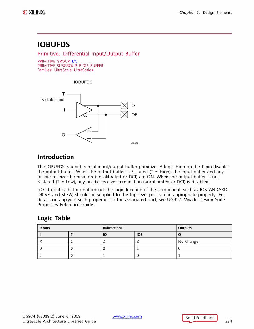
Chapter 4: Design Elements
IOBUFDSPrimitive: Differential Input/Output BufferPRIMITIVE_GROUP: I/OPRIMITIVE_SUBGROUP: BIDIR_BUFFERFamilies: UltraScale, UltraScale+
IntroductionThe IOBUFDS is a differential input/output buffer primitive. A logic-High on the T pin disablesthe output buffer. When the output buffer is 3-stated (T = High), the input buffer and anyon-die receiver termination (uncalibrated or DCI) are ON. When the output buffer is not3-stated (T = Low), any on-die receiver termination (uncalibrated or DCI) is disabled.
I/O attributes that do not impact the logic function of the component, such as IOSTANDARD,DRIVE, and SLEW, should be supplied to the top-level port via an appropriate property. Fordetails on applying such properties to the associated port, see UG912: Vivado Design SuiteProperties Reference Guide.
Logic TableInputs Bidirectional Outputs
I T IO IOB O
X 1 Z Z No Change
0 0 0 1 0
I 0 1 0 1
UG974 (v2018.2) June 6, 2018 www.xilinx.comUltraScale Architecture Libraries Guide 334
Send Feedback
Chapter 4: Design Elements
Port DescriptionsPort Direction Width Function
I Input 1 Input of OBUF. Connect to the logic driving the output port.
IO Inout 1 Bidirectional diff_p port to be connected directly to top-level inout port.
IOB Inout 1 Bidirectional diff_n port to be connected directly to top-level inout port.
O Output 1 Output path of the buffer.
T Input 1 3-state enable input signifying whether the buffer acts as an input oroutput.
Design Entry MethodInstantiation Recommended
Inference No
IP and IP Integrator Catalog No
Available AttributesAttribute Type Allowed Values Default Description
DQS_BIAS STRING "FALSE","TRUE"
"FALSE" Provides pull - up / pull - down feature required forsome DQS memory interface pins.
VHDL Instantiation TemplateUnless they already exist, copy the following two statements and paste them before the entitydeclaration.Library UNISIM;use UNISIM.vcomponents.all;
-- IOBUFDS: Differential Input/Output Buffer-- UltraScale-- Xilinx HDL Language Template, version 2018.2
IOBUFDS_inst : IOBUFDSgeneric map (
DQS_BIAS => "FALSE" -- (FALSE, TRUE))port map (
O => O, -- 1-bit output: Buffer outputI => I, -- 1-bit input: Buffer inputIO => IO, -- 1-bit inout: Diff_p inout (connect directly to top-level port)IOB => IOB, -- 1-bit inout: Diff_n inout (connect directly to top-level port)T => T -- 1-bit input: 3-state enable input
);
-- End of IOBUFDS_inst instantiation
Verilog Instantiation Template// IOBUFDS: Differential Input/Output Buffer// UltraScale// Xilinx HDL Language Template, version 2018.2
UG974 (v2018.2) June 6, 2018 www.xilinx.comUltraScale Architecture Libraries Guide 335
Send Feedback
Chapter 4: Design Elements
IOBUFDS #(.DQS_BIAS("FALSE") // (FALSE, TRUE)
)IOBUFDS_inst (
.O(O), // 1-bit output: Buffer output
.I(I), // 1-bit input: Buffer input
.IO(IO), // 1-bit inout: Diff_p inout (connect directly to top-level port)
.IOB(IOB), // 1-bit inout: Diff_n inout (connect directly to top-level port)
.T(T) // 1-bit input: 3-state enable input);
// End of IOBUFDS_inst instantiation
For More Information• See the UltraScale Architecture SelectIO Resources User Guide (UG571).
• See the UltraScale Programmable Devices Documentation.
UG974 (v2018.2) June 6, 2018 www.xilinx.comUltraScale Architecture Libraries Guide 336
Send Feedback
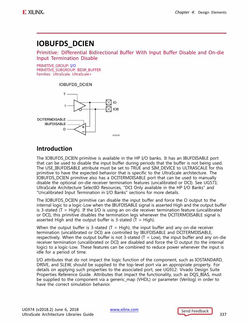
Chapter 4: Design Elements
IOBUFDS_DCIENPrimitive: Differential Bidirectional Buffer With Input Buffer Disable and On-dieInput Termination DisablePRIMITIVE_GROUP: I/OPRIMITIVE_SUBGROUP: BIDIR_BUFFERFamilies: UltraScale, UltraScale+
IntroductionThe IOBUFDS_DCIEN primitive is available in the HP I/O banks. It has an IBUFDISABLE portthat can be used to disable the input buffer during periods that the buffer is not being used.The USE_IBUFDISABLE attribute must be set to TRUE and SIM_DEVICE to ULTRASCALE for thisprimitive to have the expected behavior that is specific to the UltraScale architecture. TheIOBUFDS_DCIEN primitive also has a DCITERMDISABLE port that can be used to manuallydisable the optional on-die receiver termination features (uncalibrated or DCI). See UG571:UltraScale Architecture SelectIO Resources, "DCI Only available in the HP I/O Banks" and"Uncalibrated Input Termination in I/O Banks" sections for more details.
The IOBUFDS_DCIEN primitive can disable the input buffer and force the O output to theinternal logic to a logic-Low when the IBUFDISABLE signal is asserted High and the output bufferis 3-stated (T = High). If the I/O is using an on-die receiver termination feature (uncalibratedor DCI), this primitive disables the termination legs whenever the DCITERMDISABLE signal isasserted High and the output buffer is 3-stated (T = High).
When the output buffer is 3-stated (T = High), the input buffer and any on-die receivertermination (uncalibrated or DCI) are controlled by IBUFDISABLE and DCITERMDISABLE,respectively. When the output buffer is not 3-stated (T = Low), the input buffer and any on-diereceiver termination (uncalibrated or DCI) are disabled and force the O output (to the internallogic) to a logic-Low. These features can be combined to reduce power whenever the input isidle for a period of time.
I/O attributes that do not impact the logic function of the component, such as IOSTANDARD,DRIVE, and SLEW, should be supplied to the top-level port via an appropriate property. Fordetails on applying such properties to the associated port, see UG912: Vivado Design SuiteProperties Reference Guide. Attributes that impact the functionality, such as DQS_BIAS, mustbe supplied to the component via a generic_map (VHDL) or parameter (Verilog) in order tohave the correct simulation behavior.
UG974 (v2018.2) June 6, 2018 www.xilinx.comUltraScale Architecture Libraries Guide 337
Send Feedback
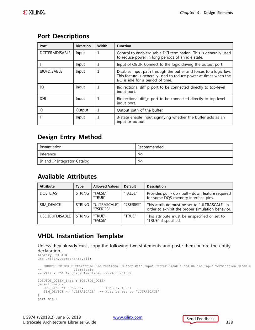
Chapter 4: Design Elements
Port DescriptionsPort Direction Width Function
DCITERMDISABLE Input 1 Control to enable/disable DCI termination. This is generally usedto reduce power in long periods of an idle state.
I Input 1 Input of OBUF. Connect to the logic driving the output port.
IBUFDISABLE Input 1 Disables input path through the buffer and forces to a logic low.This feature is generally used to reduce power at times when theI/O is idle for a period of time.
IO Inout 1 Bidirectional diff_p port to be connected directly to top-levelinout port.
IOB Inout 1 Bidirectional diff_n port to be connected directly to top-levelinout port.
O Output 1 Output path of the buffer.
T Input 1 3-state enable input signifying whether the buffer acts as aninput or output.
Design Entry MethodInstantiation Recommended
Inference No
IP and IP Integrator Catalog No
Available AttributesAttribute Type Allowed Values Default Description
DQS_BIAS STRING "FALSE","TRUE"
"FALSE" Provides pull - up / pull - down feature requiredfor some DQS memory interface pins.
SIM_DEVICE STRING "ULTRASCALE","7SERIES"
"7SERIES" This attribute must be set to "ULTRASCALE" inorder to exhibit the proper simulation behavior.
USE_IBUFDISABLE STRING "TRUE","FALSE"
"TRUE" This attribute must be unspecified or set to"TRUE" if specified.
VHDL Instantiation TemplateUnless they already exist, copy the following two statements and paste them before the entitydeclaration.Library UNISIM;use UNISIM.vcomponents.all;
-- IOBUFDS_DCIEN: Differential Bidirectional Buffer With Input Buffer Disable and On-die Input Termination Disable-- UltraScale-- Xilinx HDL Language Template, version 2018.2
IOBUFDS_DCIEN_inst : IOBUFDS_DCIENgeneric map (
DQS_BIAS => "FALSE", -- (FALSE, TRUE)SIM_DEVICE => "ULTRASCALE" -- Must be set to "ULTRASCALE"
)port map (
UG974 (v2018.2) June 6, 2018 www.xilinx.comUltraScale Architecture Libraries Guide 338
Send Feedback

Chapter 4: Design Elements
O => O, -- 1-bit output: Buffer outputDCITERMDISABLE => DCITERMDISABLE, -- 1-bit input: DCI Termination DisableI => I, -- 1-bit input: Buffer inputIBUFDISABLE => IBUFDISABLE, -- 1-bit input: Buffer disable input, high=disableIO => IO, -- 1-bit inout: Diff_p inout (connect directly to top-level port)IOB => IOB, -- 1-bit inout: Diff_n inout (connect directly to top-level port)T => T -- 1-bit input: 3-state enable input
);
-- End of IOBUFDS_DCIEN_inst instantiation
Verilog Instantiation Template
// IOBUFDS_DCIEN: Differential Bidirectional Buffer With Input Buffer Disable and On-die Input Termination Disable// UltraScale// Xilinx HDL Language Template, version 2018.2
IOBUFDS_DCIEN #(.DQS_BIAS("FALSE"), // (FALSE, TRUE).SIM_DEVICE("ULTRASCALE") // Must be set to "ULTRASCALE"
)IOBUFDS_DCIEN_inst (
.O(O), // 1-bit output: Buffer output
.DCITERMDISABLE(DCITERMDISABLE), // 1-bit input: DCI Termination Disable
.I(I), // 1-bit input: Buffer input
.IBUFDISABLE(IBUFDISABLE), // 1-bit input: Buffer disable input, high=disable
.IO(IO), // 1-bit inout: Diff_p inout (connect directly to top-level port)
.IOB(IOB), // 1-bit inout: Diff_n inout (connect directly to top-level port)
.T(T) // 1-bit input: 3-state enable input);
// End of IOBUFDS_DCIEN_inst instantiation
For More Information• See the UltraScale Architecture SelectIO Resources User Guide (UG571).
• See the UltraScale Programmable Devices Documentation.
UG974 (v2018.2) June 6, 2018 www.xilinx.comUltraScale Architecture Libraries Guide 339
Send Feedback
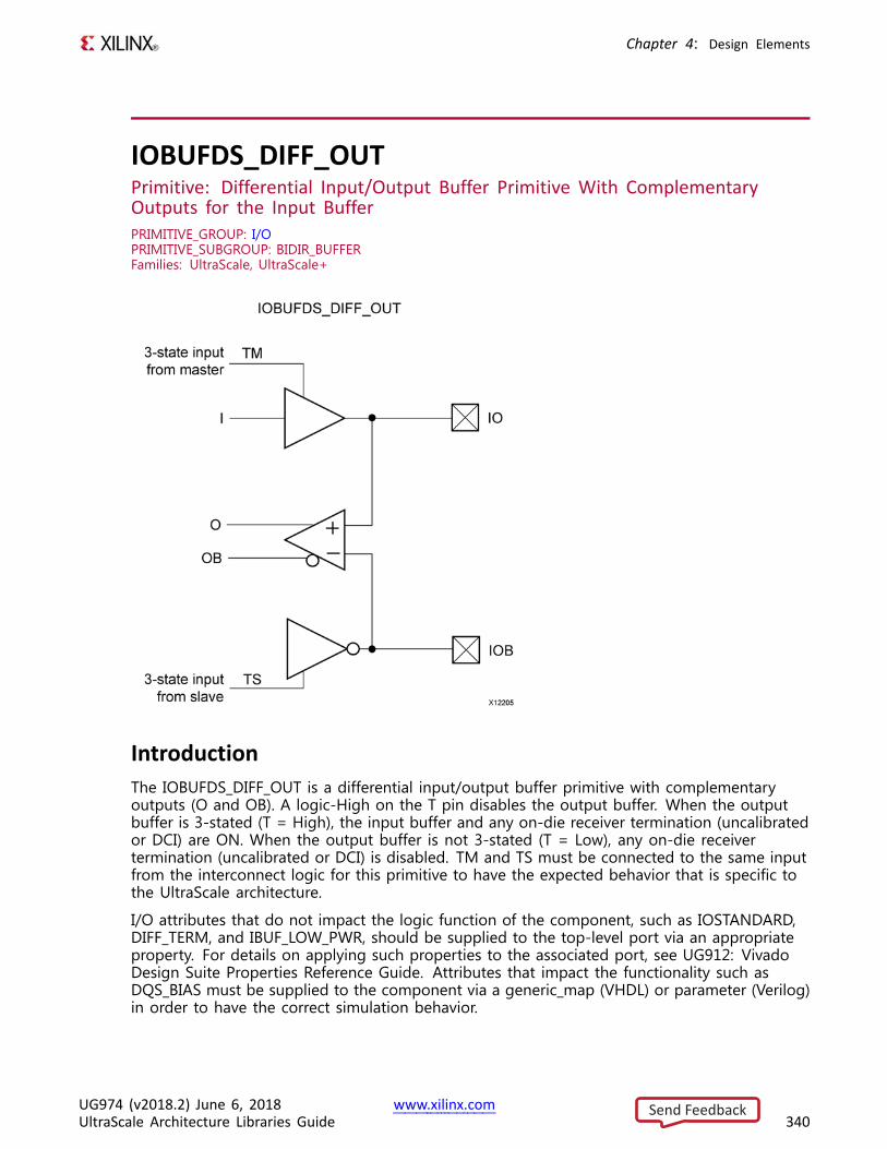
Chapter 4: Design Elements
IOBUFDS_DIFF_OUTPrimitive: Differential Input/Output Buffer Primitive With ComplementaryOutputs for the Input BufferPRIMITIVE_GROUP: I/OPRIMITIVE_SUBGROUP: BIDIR_BUFFERFamilies: UltraScale, UltraScale+
IntroductionThe IOBUFDS_DIFF_OUT is a differential input/output buffer primitive with complementaryoutputs (O and OB). A logic-High on the T pin disables the output buffer. When the outputbuffer is 3-stated (T = High), the input buffer and any on-die receiver termination (uncalibratedor DCI) are ON. When the output buffer is not 3-stated (T = Low), any on-die receivertermination (uncalibrated or DCI) is disabled. TM and TS must be connected to the same inputfrom the interconnect logic for this primitive to have the expected behavior that is specific tothe UltraScale architecture.
I/O attributes that do not impact the logic function of the component, such as IOSTANDARD,DIFF_TERM, and IBUF_LOW_PWR, should be supplied to the top-level port via an appropriateproperty. For details on applying such properties to the associated port, see UG912: VivadoDesign Suite Properties Reference Guide. Attributes that impact the functionality such asDQS_BIAS must be supplied to the component via a generic_map (VHDL) or parameter (Verilog)in order to have the correct simulation behavior.
UG974 (v2018.2) June 6, 2018 www.xilinx.comUltraScale Architecture Libraries Guide 340
Send Feedback
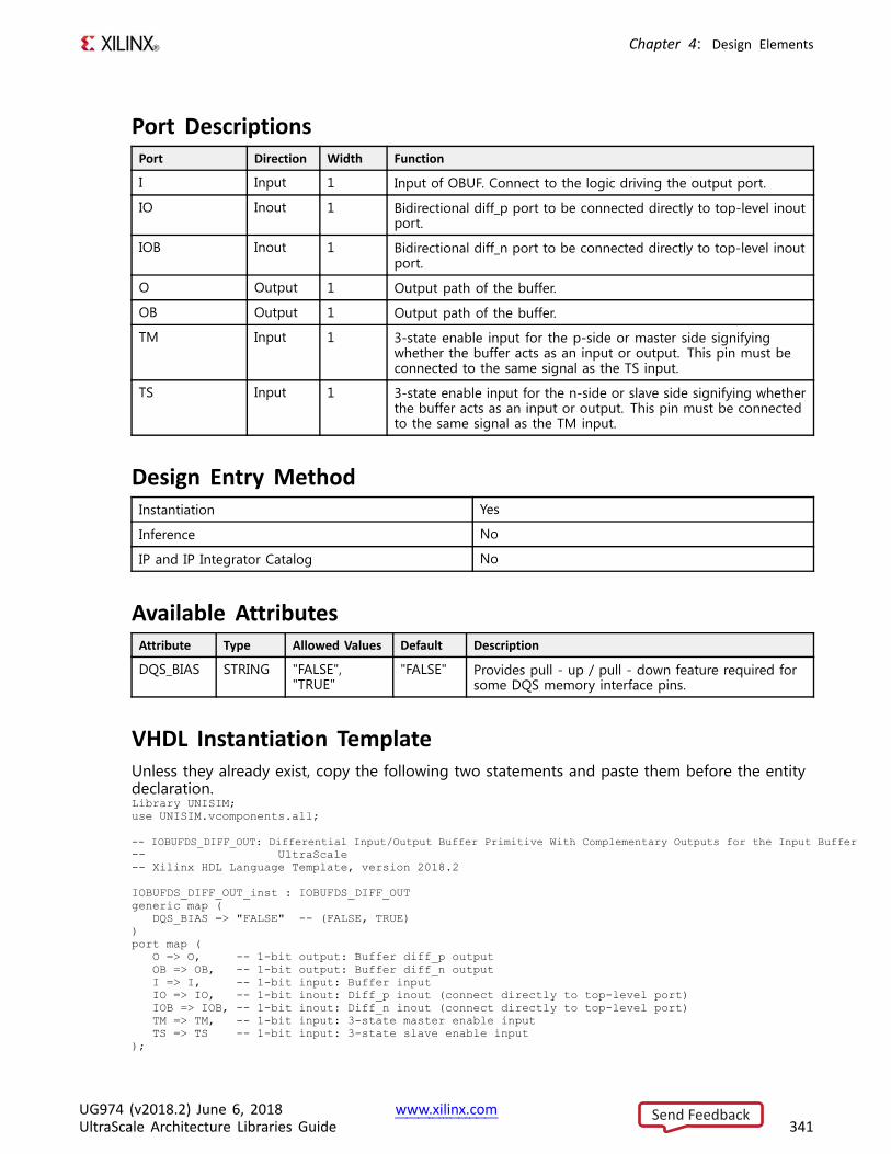
Chapter 4: Design Elements
Port DescriptionsPort Direction Width Function
I Input 1 Input of OBUF. Connect to the logic driving the output port.
IO Inout 1 Bidirectional diff_p port to be connected directly to top-level inoutport.
IOB Inout 1 Bidirectional diff_n port to be connected directly to top-level inoutport.
O Output 1 Output path of the buffer.
OB Output 1 Output path of the buffer.
TM Input 1 3-state enable input for the p-side or master side signifyingwhether the buffer acts as an input or output. This pin must beconnected to the same signal as the TS input.
TS Input 1 3-state enable input for the n-side or slave side signifying whetherthe buffer acts as an input or output. This pin must be connectedto the same signal as the TM input.
Design Entry MethodInstantiation Yes
Inference No
IP and IP Integrator Catalog No
Available AttributesAttribute Type Allowed Values Default Description
DQS_BIAS STRING "FALSE","TRUE"
"FALSE" Provides pull - up / pull - down feature required forsome DQS memory interface pins.
VHDL Instantiation TemplateUnless they already exist, copy the following two statements and paste them before the entitydeclaration.Library UNISIM;use UNISIM.vcomponents.all;
-- IOBUFDS_DIFF_OUT: Differential Input/Output Buffer Primitive With Complementary Outputs for the Input Buffer-- UltraScale-- Xilinx HDL Language Template, version 2018.2
IOBUFDS_DIFF_OUT_inst : IOBUFDS_DIFF_OUTgeneric map (
DQS_BIAS => "FALSE" -- (FALSE, TRUE))port map (
O => O, -- 1-bit output: Buffer diff_p outputOB => OB, -- 1-bit output: Buffer diff_n outputI => I, -- 1-bit input: Buffer inputIO => IO, -- 1-bit inout: Diff_p inout (connect directly to top-level port)IOB => IOB, -- 1-bit inout: Diff_n inout (connect directly to top-level port)TM => TM, -- 1-bit input: 3-state master enable inputTS => TS -- 1-bit input: 3-state slave enable input
);
UG974 (v2018.2) June 6, 2018 www.xilinx.comUltraScale Architecture Libraries Guide 341
Send Feedback
Chapter 4: Design Elements
-- End of IOBUFDS_DIFF_OUT_inst instantiation
Verilog Instantiation Template
// IOBUFDS_DIFF_OUT: Differential Input/Output Buffer Primitive With Complementary Outputs for the Input Buffer// UltraScale// Xilinx HDL Language Template, version 2018.2
IOBUFDS_DIFF_OUT #(.DQS_BIAS("FALSE") // (FALSE, TRUE)
)IOBUFDS_DIFF_OUT_inst (
.O(O), // 1-bit output: Buffer diff_p output
.OB(OB), // 1-bit output: Buffer diff_n output
.I(I), // 1-bit input: Buffer input
.IO(IO), // 1-bit inout: Diff_p inout (connect directly to top-level port)
.IOB(IOB), // 1-bit inout: Diff_n inout (connect directly to top-level port)
.TM(TM), // 1-bit input: 3-state master enable input
.TS(TS) // 1-bit input: 3-state slave enable input);
// End of IOBUFDS_DIFF_OUT_inst instantiation
For More Information• See the UltraScale Architecture SelectIO Resources User Guide (UG571).
• See the UltraScale Programmable Devices Documentation.
UG974 (v2018.2) June 6, 2018 www.xilinx.comUltraScale Architecture Libraries Guide 342
Send Feedback
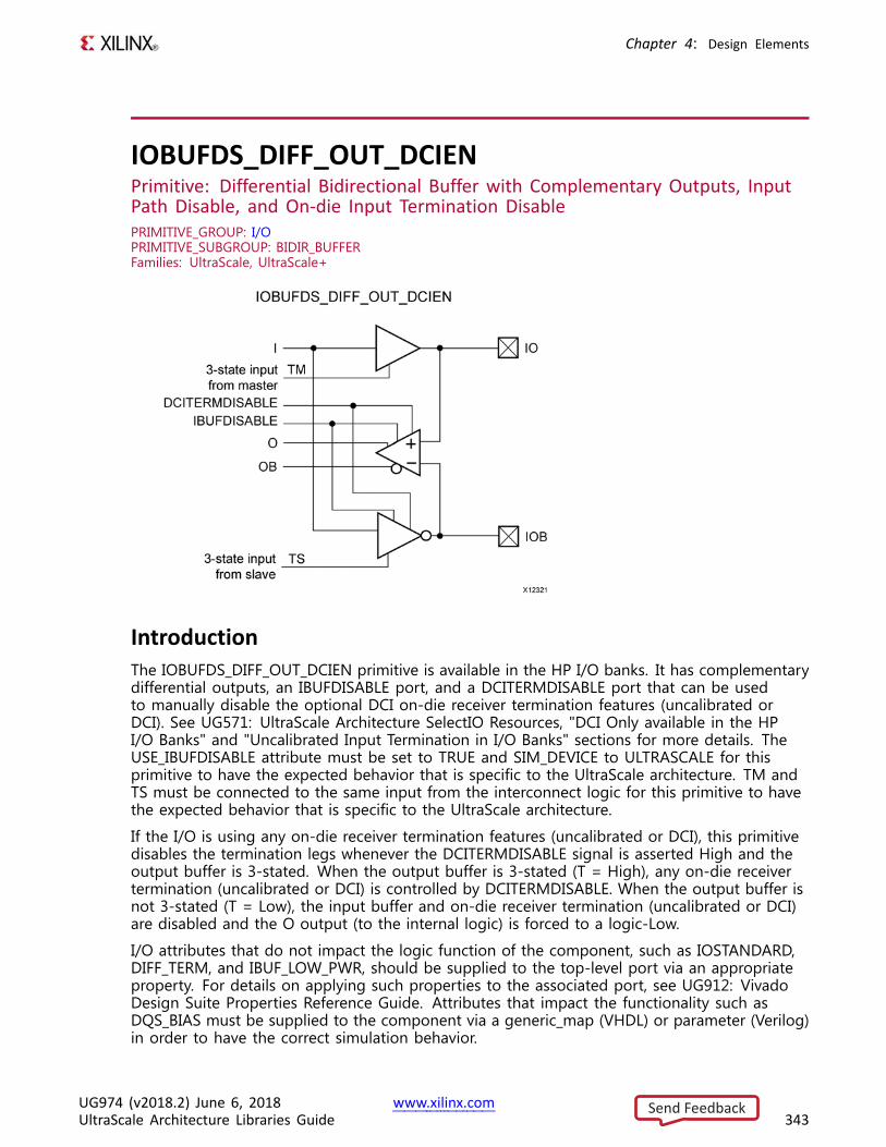
Chapter 4: Design Elements
IOBUFDS_DIFF_OUT_DCIENPrimitive: Differential Bidirectional Buffer with Complementary Outputs, InputPath Disable, and On-die Input Termination DisablePRIMITIVE_GROUP: I/OPRIMITIVE_SUBGROUP: BIDIR_BUFFERFamilies: UltraScale, UltraScale+
IntroductionThe IOBUFDS_DIFF_OUT_DCIEN primitive is available in the HP I/O banks. It has complementarydifferential outputs, an IBUFDISABLE port, and a DCITERMDISABLE port that can be usedto manually disable the optional DCI on-die receiver termination features (uncalibrated orDCI). See UG571: UltraScale Architecture SelectIO Resources, "DCI Only available in the HPI/O Banks" and "Uncalibrated Input Termination in I/O Banks" sections for more details. TheUSE_IBUFDISABLE attribute must be set to TRUE and SIM_DEVICE to ULTRASCALE for thisprimitive to have the expected behavior that is specific to the UltraScale architecture. TM andTS must be connected to the same input from the interconnect logic for this primitive to havethe expected behavior that is specific to the UltraScale architecture.
If the I/O is using any on-die receiver termination features (uncalibrated or DCI), this primitivedisables the termination legs whenever the DCITERMDISABLE signal is asserted High and theoutput buffer is 3-stated. When the output buffer is 3-stated (T = High), any on-die receivertermination (uncalibrated or DCI) is controlled by DCITERMDISABLE. When the output buffer isnot 3-stated (T = Low), the input buffer and on-die receiver termination (uncalibrated or DCI)are disabled and the O output (to the internal logic) is forced to a logic-Low.
I/O attributes that do not impact the logic function of the component, such as IOSTANDARD,DIFF_TERM, and IBUF_LOW_PWR, should be supplied to the top-level port via an appropriateproperty. For details on applying such properties to the associated port, see UG912: VivadoDesign Suite Properties Reference Guide. Attributes that impact the functionality such asDQS_BIAS must be supplied to the component via a generic_map (VHDL) or parameter (Verilog)in order to have the correct simulation behavior.
UG974 (v2018.2) June 6, 2018 www.xilinx.comUltraScale Architecture Libraries Guide 343
Send Feedback
Chapter 4: Design Elements
Port DescriptionsPort Direction Width Function
DCITERMDISABLE Input 1 Control to enable/disable DCI termination. This is generally usedto reduce power in long periods of an idle state.
I Input 1 Input of OBUF. Connect to the logic driving the output port.
IBUFDISABLE Input 1 The IBUFDISABLE feature is not supported with this primitive inthe UltraScale architecture. This port must be tied to logic '0'.
IO Inout 1 Bidirectional diff_p port to be connected directly to top-levelinout port.
IOB Inout 1 Bidirectional diff_n port to be connected directly to top-levelinout port.
O Output 1 Output path of the buffer.
OB Output 1 Output path of the buffer.
TM Input 1 3-state enable input for the p-side or master side signifyingwhether the buffer acts as an input or output. This pin must beconnected to the same signal as the TS input.
TS Input 1 3-state enable input for the n-side or slave side signifyingwhether the buffer acts as an input or output. This pin must beconnected to the same signal as the TM input.
Design Entry MethodInstantiation Yes
Inference No
IP and IP Integrator Catalog No
Available AttributesAttribute Type Allowed Values Default Description
DQS_BIAS STRING "FALSE","TRUE"
"FALSE" Provides pull - up / pull - down featurerequired for some DQS memory interface pins.
SIM_DEVICE STRING "ULTRASCALE","7SERIES"
"7SERIES" This attribute must be set to "ULTRASCALE" inorder to exhibit the proper simulation behavior.
USE_IBUFDISABLE STRING "TRUE","FALSE"
"TRUE" This attribute must be unspecified or set to"TRUE" if specified.
VHDL Instantiation TemplateUnless they already exist, copy the following two statements and paste them before the entitydeclaration.Library UNISIM;use UNISIM.vcomponents.all;
-- IOBUFDS_DIFF_OUT_DCIEN: Differential Bidirectional Buffer with Complementary Outputs, Input Path Disable, and On-die Input Termination Disable
-- UltraScale-- Xilinx HDL Language Template, version 2018.2
UG974 (v2018.2) June 6, 2018 www.xilinx.comUltraScale Architecture Libraries Guide 344
Send Feedback
Chapter 4: Design Elements
IOBUFDS_DIFF_OUT_DCIEN_inst : IOBUFDS_DIFF_OUT_DCIENgeneric map (
DQS_BIAS => "FALSE", -- (FALSE, TRUE)SIM_DEVICE => "ULTRASCALE" -- Must be set to "ULTRASCALE"
)port map (
O => O, -- 1-bit output: Buffer diff_p outputOB => OB, -- 1-bit output: Buffer diff_n outputDCITERMDISABLE => DCITERMDISABLE, -- 1-bit input: DCI Termination DisableI => I, -- 1-bit input: Buffer inputIBUFDISABLE => IBUFDISABLE, -- 1-bit input: Must be tied to a logic '0'IO => IO, -- 1-bit inout: Diff_p inout (connect directly to top-level port)IOB => IOB, -- 1-bit inout: Diff_n inout (connect directly to top-level port)TM => TM, -- 1-bit input: 3-state master enable inputTS => TS -- 1-bit input: 3-state slave enable input
);
-- End of IOBUFDS_DIFF_OUT_DCIEN_inst instantiation
Verilog Instantiation Template
// IOBUFDS_DIFF_OUT_DCIEN: Differential Bidirectional Buffer with Complementary Outputs, Input Path Disable, and On-die Input Termination Disable
// UltraScale// Xilinx HDL Language Template, version 2018.2
IOBUFDS_DIFF_OUT_DCIEN #(.DQS_BIAS("FALSE"), // (FALSE, TRUE).SIM_DEVICE("ULTRASCALE") // Must be set to "ULTRASCALE"
)IOBUFDS_DIFF_OUT_DCIEN_inst (
.O(O), // 1-bit output: Buffer diff_p output
.OB(OB), // 1-bit output: Buffer diff_n output
.DCITERMDISABLE(DCITERMDISABLE), // 1-bit input: DCI Termination Disable
.I(I), // 1-bit input: Buffer input
.IBUFDISABLE(IBUFDISABLE), // 1-bit input: Must be tied to a logic '0'
.IO(IO), // 1-bit inout: Diff_p inout (connect directly to top-level port)
.IOB(IOB), // 1-bit inout: Diff_n inout (connect directly to top-level port)
.TM(TM), // 1-bit input: 3-state master enable input
.TS(TS) // 1-bit input: 3-state slave enable input);
// End of IOBUFDS_DIFF_OUT_DCIEN_inst instantiation
For More Information• See the UltraScale Architecture SelectIO Resources User Guide (UG571).
• See the UltraScale Programmable Devices Documentation.
UG974 (v2018.2) June 6, 2018 www.xilinx.comUltraScale Architecture Libraries Guide 345
Send Feedback
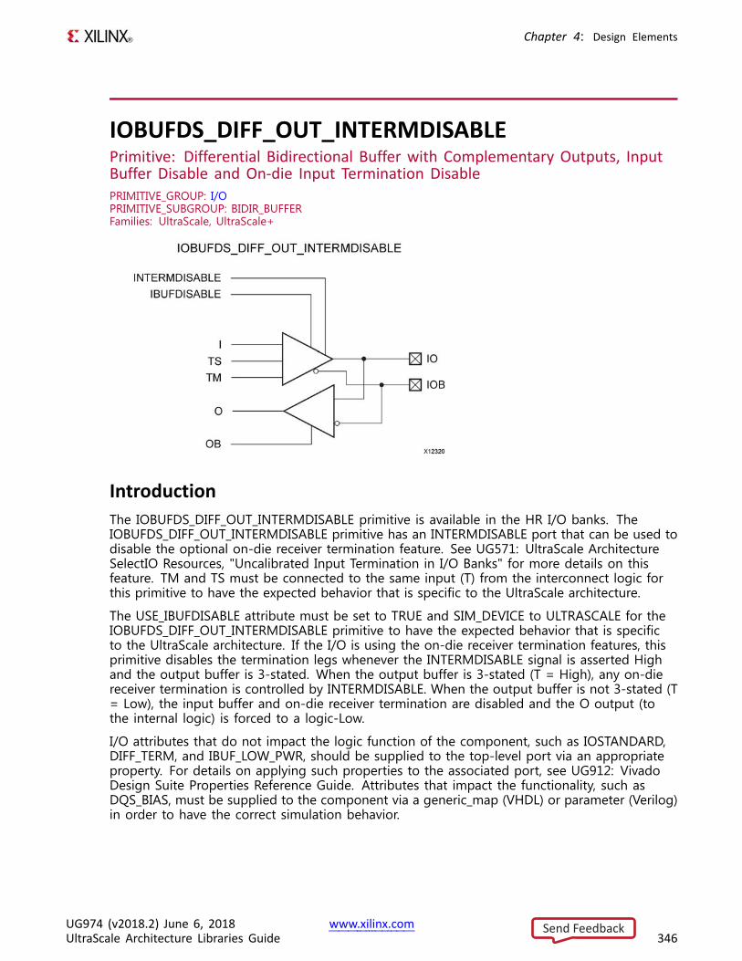
Chapter 4: Design Elements
IOBUFDS_DIFF_OUT_INTERMDISABLEPrimitive: Differential Bidirectional Buffer with Complementary Outputs, InputBuffer Disable and On-die Input Termination DisablePRIMITIVE_GROUP: I/OPRIMITIVE_SUBGROUP: BIDIR_BUFFERFamilies: UltraScale, UltraScale+
IntroductionThe IOBUFDS_DIFF_OUT_INTERMDISABLE primitive is available in the HR I/O banks. TheIOBUFDS_DIFF_OUT_INTERMDISABLE primitive has an INTERMDISABLE port that can be used todisable the optional on-die receiver termination feature. See UG571: UltraScale ArchitectureSelectIO Resources, "Uncalibrated Input Termination in I/O Banks" for more details on thisfeature. TM and TS must be connected to the same input (T) from the interconnect logic forthis primitive to have the expected behavior that is specific to the UltraScale architecture.
The USE_IBUFDISABLE attribute must be set to TRUE and SIM_DEVICE to ULTRASCALE for theIOBUFDS_DIFF_OUT_INTERMDISABLE primitive to have the expected behavior that is specificto the UltraScale architecture. If the I/O is using the on-die receiver termination features, thisprimitive disables the termination legs whenever the INTERMDISABLE signal is asserted Highand the output buffer is 3-stated. When the output buffer is 3-stated (T = High), any on-diereceiver termination is controlled by INTERMDISABLE. When the output buffer is not 3-stated (T= Low), the input buffer and on-die receiver termination are disabled and the O output (tothe internal logic) is forced to a logic-Low.
I/O attributes that do not impact the logic function of the component, such as IOSTANDARD,DIFF_TERM, and IBUF_LOW_PWR, should be supplied to the top-level port via an appropriateproperty. For details on applying such properties to the associated port, see UG912: VivadoDesign Suite Properties Reference Guide. Attributes that impact the functionality, such asDQS_BIAS, must be supplied to the component via a generic_map (VHDL) or parameter (Verilog)in order to have the correct simulation behavior.
UG974 (v2018.2) June 6, 2018 www.xilinx.comUltraScale Architecture Libraries Guide 346
Send Feedback
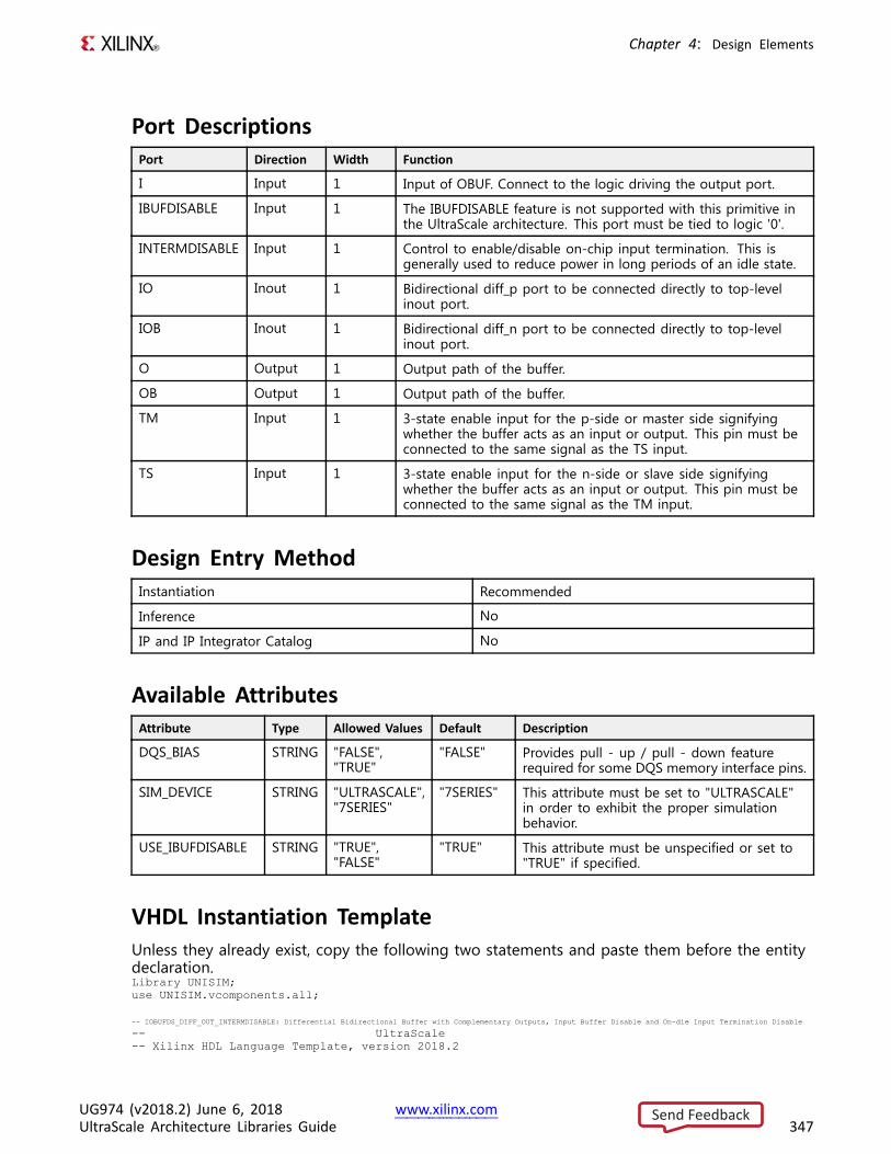
Chapter 4: Design Elements
Port DescriptionsPort Direction Width Function
I Input 1 Input of OBUF. Connect to the logic driving the output port.
IBUFDISABLE Input 1 The IBUFDISABLE feature is not supported with this primitive inthe UltraScale architecture. This port must be tied to logic '0'.
INTERMDISABLE Input 1 Control to enable/disable on-chip input termination. This isgenerally used to reduce power in long periods of an idle state.
IO Inout 1 Bidirectional diff_p port to be connected directly to top-levelinout port.
IOB Inout 1 Bidirectional diff_n port to be connected directly to top-levelinout port.
O Output 1 Output path of the buffer.
OB Output 1 Output path of the buffer.
TM Input 1 3-state enable input for the p-side or master side signifyingwhether the buffer acts as an input or output. This pin must beconnected to the same signal as the TS input.
TS Input 1 3-state enable input for the n-side or slave side signifyingwhether the buffer acts as an input or output. This pin must beconnected to the same signal as the TM input.
Design Entry MethodInstantiation Recommended
Inference No
IP and IP Integrator Catalog No
Available AttributesAttribute Type Allowed Values Default Description
DQS_BIAS STRING "FALSE","TRUE"
"FALSE" Provides pull - up / pull - down featurerequired for some DQS memory interface pins.
SIM_DEVICE STRING "ULTRASCALE","7SERIES"
"7SERIES" This attribute must be set to "ULTRASCALE"in order to exhibit the proper simulationbehavior.
USE_IBUFDISABLE STRING "TRUE","FALSE"
"TRUE" This attribute must be unspecified or set to"TRUE" if specified.
VHDL Instantiation TemplateUnless they already exist, copy the following two statements and paste them before the entitydeclaration.Library UNISIM;use UNISIM.vcomponents.all;
-- IOBUFDS_DIFF_OUT_INTERMDISABLE: Differential Bidirectional Buffer with Complementary Outputs, Input Buffer Disable and On-die Input Termination Disable
-- UltraScale-- Xilinx HDL Language Template, version 2018.2
UG974 (v2018.2) June 6, 2018 www.xilinx.comUltraScale Architecture Libraries Guide 347
Send Feedback
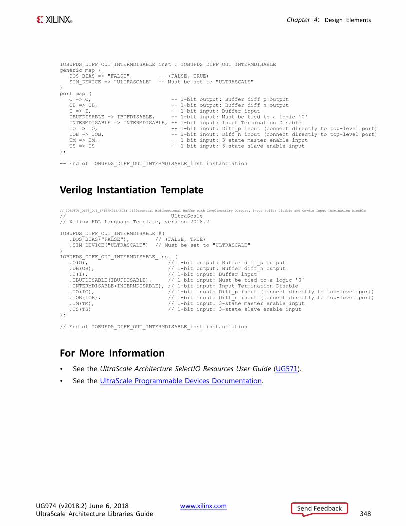
Chapter 4: Design Elements
IOBUFDS_DIFF_OUT_INTERMDISABLE_inst : IOBUFDS_DIFF_OUT_INTERMDISABLEgeneric map (
DQS_BIAS => "FALSE", -- (FALSE, TRUE)SIM_DEVICE => "ULTRASCALE" -- Must be set to "ULTRASCALE"
)port map (
O => O, -- 1-bit output: Buffer diff_p outputOB => OB, -- 1-bit output: Buffer diff_n outputI => I, -- 1-bit input: Buffer inputIBUFDISABLE => IBUFDISABLE, -- 1-bit input: Must be tied to a logic '0'INTERMDISABLE => INTERMDISABLE, -- 1-bit input: Input Termination DisableIO => IO, -- 1-bit inout: Diff_p inout (connect directly to top-level port)IOB => IOB, -- 1-bit inout: Diff_n inout (connect directly to top-level port)TM => TM, -- 1-bit input: 3-state master enable inputTS => TS -- 1-bit input: 3-state slave enable input
);
-- End of IOBUFDS_DIFF_OUT_INTERMDISABLE_inst instantiation
Verilog Instantiation Template
// IOBUFDS_DIFF_OUT_INTERMDISABLE: Differential Bidirectional Buffer with Complementary Outputs, Input Buffer Disable and On-die Input Termination Disable
// UltraScale// Xilinx HDL Language Template, version 2018.2
IOBUFDS_DIFF_OUT_INTERMDISABLE #(.DQS_BIAS("FALSE"), // (FALSE, TRUE).SIM_DEVICE("ULTRASCALE") // Must be set to "ULTRASCALE"
)IOBUFDS_DIFF_OUT_INTERMDISABLE_inst (
.O(O), // 1-bit output: Buffer diff_p output
.OB(OB), // 1-bit output: Buffer diff_n output
.I(I), // 1-bit input: Buffer input
.IBUFDISABLE(IBUFDISABLE), // 1-bit input: Must be tied to a logic '0'
.INTERMDISABLE(INTERMDISABLE), // 1-bit input: Input Termination Disable
.IO(IO), // 1-bit inout: Diff_p inout (connect directly to top-level port)
.IOB(IOB), // 1-bit inout: Diff_n inout (connect directly to top-level port)
.TM(TM), // 1-bit input: 3-state master enable input
.TS(TS) // 1-bit input: 3-state slave enable input);
// End of IOBUFDS_DIFF_OUT_INTERMDISABLE_inst instantiation
For More Information• See the UltraScale Architecture SelectIO Resources User Guide (UG571).
• See the UltraScale Programmable Devices Documentation.
UG974 (v2018.2) June 6, 2018 www.xilinx.comUltraScale Architecture Libraries Guide 348
Send Feedback
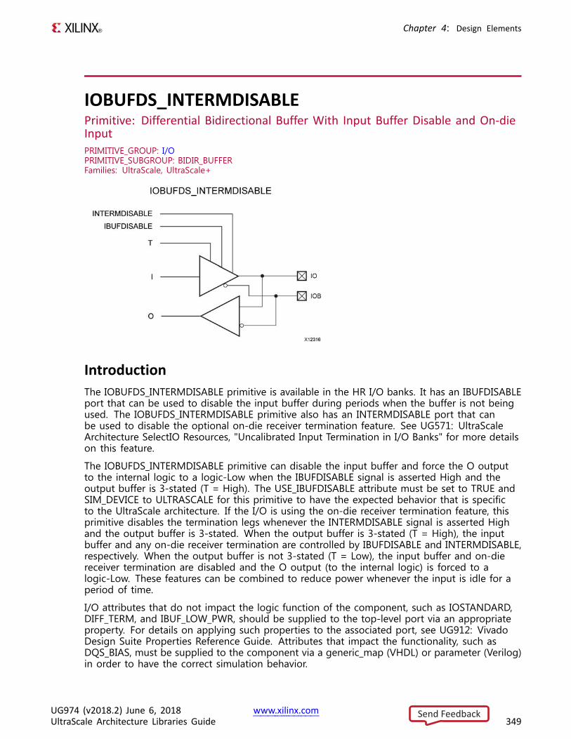
Chapter 4: Design Elements
IOBUFDS_INTERMDISABLEPrimitive: Differential Bidirectional Buffer With Input Buffer Disable and On-dieInputPRIMITIVE_GROUP: I/OPRIMITIVE_SUBGROUP: BIDIR_BUFFERFamilies: UltraScale, UltraScale+
IntroductionThe IOBUFDS_INTERMDISABLE primitive is available in the HR I/O banks. It has an IBUFDISABLEport that can be used to disable the input buffer during periods when the buffer is not beingused. The IOBUFDS_INTERMDISABLE primitive also has an INTERMDISABLE port that canbe used to disable the optional on-die receiver termination feature. See UG571: UltraScaleArchitecture SelectIO Resources, "Uncalibrated Input Termination in I/O Banks" for more detailson this feature.
The IOBUFDS_INTERMDISABLE primitive can disable the input buffer and force the O outputto the internal logic to a logic-Low when the IBUFDISABLE signal is asserted High and theoutput buffer is 3-stated (T = High). The USE_IBUFDISABLE attribute must be set to TRUE andSIM_DEVICE to ULTRASCALE for this primitive to have the expected behavior that is specificto the UltraScale architecture. If the I/O is using the on-die receiver termination feature, thisprimitive disables the termination legs whenever the INTERMDISABLE signal is asserted Highand the output buffer is 3-stated. When the output buffer is 3-stated (T = High), the inputbuffer and any on-die receiver termination are controlled by IBUFDISABLE and INTERMDISABLE,respectively. When the output buffer is not 3-stated (T = Low), the input buffer and on-diereceiver termination are disabled and the O output (to the internal logic) is forced to alogic-Low. These features can be combined to reduce power whenever the input is idle for aperiod of time.
I/O attributes that do not impact the logic function of the component, such as IOSTANDARD,DIFF_TERM, and IBUF_LOW_PWR, should be supplied to the top-level port via an appropriateproperty. For details on applying such properties to the associated port, see UG912: VivadoDesign Suite Properties Reference Guide. Attributes that impact the functionality, such asDQS_BIAS, must be supplied to the component via a generic_map (VHDL) or parameter (Verilog)in order to have the correct simulation behavior.
UG974 (v2018.2) June 6, 2018 www.xilinx.comUltraScale Architecture Libraries Guide 349
Send Feedback
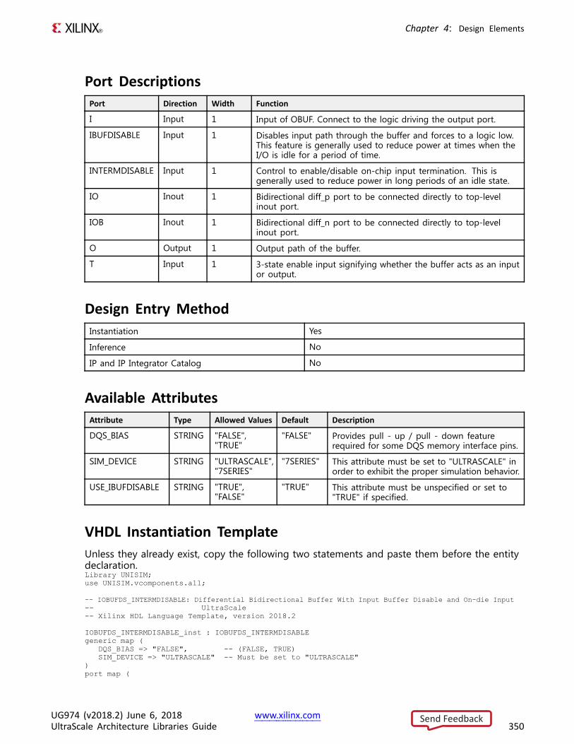
Chapter 4: Design Elements
Port DescriptionsPort Direction Width Function
I Input 1 Input of OBUF. Connect to the logic driving the output port.
IBUFDISABLE Input 1 Disables input path through the buffer and forces to a logic low.This feature is generally used to reduce power at times when theI/O is idle for a period of time.
INTERMDISABLE Input 1 Control to enable/disable on-chip input termination. This isgenerally used to reduce power in long periods of an idle state.
IO Inout 1 Bidirectional diff_p port to be connected directly to top-levelinout port.
IOB Inout 1 Bidirectional diff_n port to be connected directly to top-levelinout port.
O Output 1 Output path of the buffer.
T Input 1 3-state enable input signifying whether the buffer acts as an inputor output.
Design Entry MethodInstantiation Yes
Inference No
IP and IP Integrator Catalog No
Available AttributesAttribute Type Allowed Values Default Description
DQS_BIAS STRING "FALSE","TRUE"
"FALSE" Provides pull - up / pull - down featurerequired for some DQS memory interface pins.
SIM_DEVICE STRING "ULTRASCALE","7SERIES"
"7SERIES" This attribute must be set to "ULTRASCALE" inorder to exhibit the proper simulation behavior.
USE_IBUFDISABLE STRING "TRUE","FALSE"
"TRUE" This attribute must be unspecified or set to"TRUE" if specified.
VHDL Instantiation TemplateUnless they already exist, copy the following two statements and paste them before the entitydeclaration.Library UNISIM;use UNISIM.vcomponents.all;
-- IOBUFDS_INTERMDISABLE: Differential Bidirectional Buffer With Input Buffer Disable and On-die Input-- UltraScale-- Xilinx HDL Language Template, version 2018.2
IOBUFDS_INTERMDISABLE_inst : IOBUFDS_INTERMDISABLEgeneric map (
DQS_BIAS => "FALSE", -- (FALSE, TRUE)SIM_DEVICE => "ULTRASCALE" -- Must be set to "ULTRASCALE"
)port map (
UG974 (v2018.2) June 6, 2018 www.xilinx.comUltraScale Architecture Libraries Guide 350
Send Feedback
Chapter 4: Design Elements
O => O, -- 1-bit output: Buffer outputI => I, -- 1-bit input: Buffer inputIBUFDISABLE => IBUFDISABLE, -- 1-bit input: Buffer disable input, high=disableINTERMDISABLE => INTERMDISABLE, -- 1-bit input: Input Termination DisableIO => IO, -- 1-bit inout: Diff_p inout (connect directly to top-level port)IOB => IOB, -- 1-bit inout: Diff_n inout (connect directly to top-level port)T => T -- 1-bit input: 3-state enable input
);
-- End of IOBUFDS_INTERMDISABLE_inst instantiation
Verilog Instantiation Template
// IOBUFDS_INTERMDISABLE: Differential Bidirectional Buffer With Input Buffer Disable and On-die Input// UltraScale// Xilinx HDL Language Template, version 2018.2
IOBUFDS_INTERMDISABLE #(.DQS_BIAS("FALSE"), // (FALSE, TRUE).SIM_DEVICE("ULTRASCALE") // Must be set to "ULTRASCALE"
)IOBUFDS_INTERMDISABLE_inst (
.O(O), // 1-bit output: Buffer output
.I(I), // 1-bit input: Buffer input
.IBUFDISABLE(IBUFDISABLE), // 1-bit input: Buffer disable input, high=disable
.INTERMDISABLE(INTERMDISABLE), // 1-bit input: Input Termination Disable
.IO(IO), // 1-bit inout: Diff_p inout (connect directly to top-level port)
.IOB(IOB), // 1-bit inout: Diff_n inout (connect directly to top-level port)
.T(T) // 1-bit input: 3-state enable input);
// End of IOBUFDS_INTERMDISABLE_inst instantiation
For More Information• See the UltraScale Architecture SelectIO Resources User Guide (UG571).
• See the UltraScale Programmable Devices Documentation.
UG974 (v2018.2) June 6, 2018 www.xilinx.comUltraScale Architecture Libraries Guide 351
Send Feedback
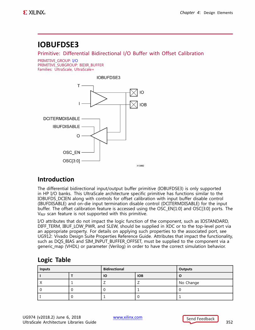
Chapter 4: Design Elements
IOBUFDSE3Primitive: Differential Bidirectional I/O Buffer with Offset CalibrationPRIMITIVE_GROUP: I/OPRIMITIVE_SUBGROUP: BIDIR_BUFFERFamilies: UltraScale, UltraScale+
IntroductionThe differential bidirectional input/output buffer primitive (IOBUFDSE3) is only supportedin HP I/O banks. This UltraScale architecture specific primitive has functions similar to theIOBUFDS_DCIEN along with controls for offset calibration with input buffer disable control(IBUFDISABLE) and on-die input termination disable control (DCITERMDISABLE) for the inputbuffer. The offset calibration feature is accessed using the OSC_EN[1:0] and OSC[3:0] ports. TheVREF scan feature is not supported with this primitive.
I/O attributes that do not impact the logic function of the component, such as IOSTANDARD,DIFF_TERM, IBUF_LOW_PWR, and SLEW, should be supplied in XDC or to the top-level port viaan appropriate property. For details on applying such properties to the associated port, seeUG912: Vivado Design Suite Properties Reference Guide. Attributes that impact the functionality,such as DQS_BIAS and SIM_INPUT_BUFFER_OFFSET, must be supplied to the component via ageneric_map (VHDL) or parameter (Verilog) in order to have the correct simulation behavior.
Logic TableInputs Bidirectional Outputs
I T IO IOB O
X 1 Z Z No Change
0 0 0 1 0
I 0 1 0 1
UG974 (v2018.2) June 6, 2018 www.xilinx.comUltraScale Architecture Libraries Guide 352
Send Feedback
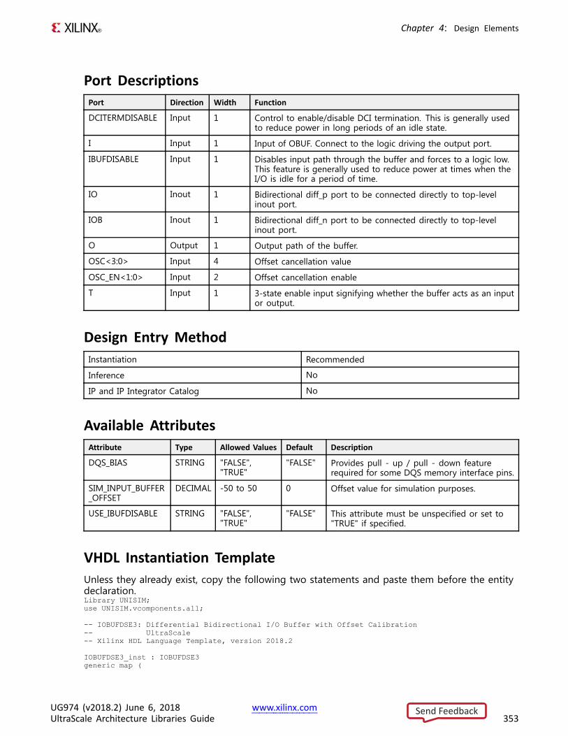
Chapter 4: Design Elements
Port DescriptionsPort Direction Width Function
DCITERMDISABLE Input 1 Control to enable/disable DCI termination. This is generally usedto reduce power in long periods of an idle state.
I Input 1 Input of OBUF. Connect to the logic driving the output port.
IBUFDISABLE Input 1 Disables input path through the buffer and forces to a logic low.This feature is generally used to reduce power at times when theI/O is idle for a period of time.
IO Inout 1 Bidirectional diff_p port to be connected directly to top-levelinout port.
IOB Inout 1 Bidirectional diff_n port to be connected directly to top-levelinout port.
O Output 1 Output path of the buffer.
OSC<3:0> Input 4 Offset cancellation value
OSC_EN<1:0> Input 2 Offset cancellation enable
T Input 1 3-state enable input signifying whether the buffer acts as an inputor output.
Design Entry MethodInstantiation Recommended
Inference No
IP and IP Integrator Catalog No
Available AttributesAttribute Type Allowed Values Default Description
DQS_BIAS STRING "FALSE","TRUE"
"FALSE" Provides pull - up / pull - down featurerequired for some DQS memory interface pins.
SIM_INPUT_BUFFER_OFFSET
DECIMAL -50 to 50 0 Offset value for simulation purposes.
USE_IBUFDISABLE STRING "FALSE","TRUE"
"FALSE" This attribute must be unspecified or set to"TRUE" if specified.
VHDL Instantiation TemplateUnless they already exist, copy the following two statements and paste them before the entitydeclaration.Library UNISIM;use UNISIM.vcomponents.all;
-- IOBUFDSE3: Differential Bidirectional I/O Buffer with Offset Calibration-- UltraScale-- Xilinx HDL Language Template, version 2018.2
IOBUFDSE3_inst : IOBUFDSE3generic map (
UG974 (v2018.2) June 6, 2018 www.xilinx.comUltraScale Architecture Libraries Guide 353
Send Feedback
Chapter 4: Design Elements
DQS_BIAS => "FALSE", -- (FALSE, TRUE)SIM_INPUT_BUFFER_OFFSET => 0 -- Offset value for simulation (-50-50)
)port map (
O => O, -- 1-bit output: Buffer outputDCITERMDISABLE => DCITERMDISABLE, -- 1-bit input: DCI Termination DisableI => I, -- 1-bit input: Buffer inputIBUFDISABLE => IBUFDISABLE, -- 1-bit input: Buffer disable input, high=disableIO => IO, -- 1-bit inout: Diff_p inout (connect directly to top-level port)IOB => IOB, -- 1-bit inout: Diff_n inout (connect directly to top-level port)OSC => OSC, -- 4-bit input: Offset cancellation valueOSC_EN => OSC_EN, -- 2-bit input: Offset cancellation enableT => T -- 1-bit input: 3-state enable input
);
-- End of IOBUFDSE3_inst instantiation
Verilog Instantiation Template
// IOBUFDSE3: Differential Bidirectional I/O Buffer with Offset Calibration// UltraScale// Xilinx HDL Language Template, version 2018.2
IOBUFDSE3 #(.DQS_BIAS("FALSE"), // (FALSE, TRUE).SIM_INPUT_BUFFER_OFFSET(0) // Offset value for simulation (-50-50)
)IOBUFDSE3_inst (
.O(O), // 1-bit output: Buffer output
.DCITERMDISABLE(DCITERMDISABLE), // 1-bit input: DCI Termination Disable
.I(I), // 1-bit input: Buffer input
.IBUFDISABLE(IBUFDISABLE), // 1-bit input: Buffer disable input, high=disable
.IO(IO), // 1-bit inout: Diff_p inout (connect directly to top-level port)
.IOB(IOB), // 1-bit inout: Diff_n inout (connect directly to top-level port)
.OSC(OSC), // 4-bit input: Offset cancellation value
.OSC_EN(OSC_EN), // 2-bit input: Offset cancellation enable
.T(T) // 1-bit input: 3-state enable input);
// End of IOBUFDSE3_inst instantiation
For More Information• See the UltraScale Architecture SelectIO Resources User Guide (UG571).
• See the UltraScale Programmable Devices Documentation.
UG974 (v2018.2) June 6, 2018 www.xilinx.comUltraScale Architecture Libraries Guide 354
Send Feedback
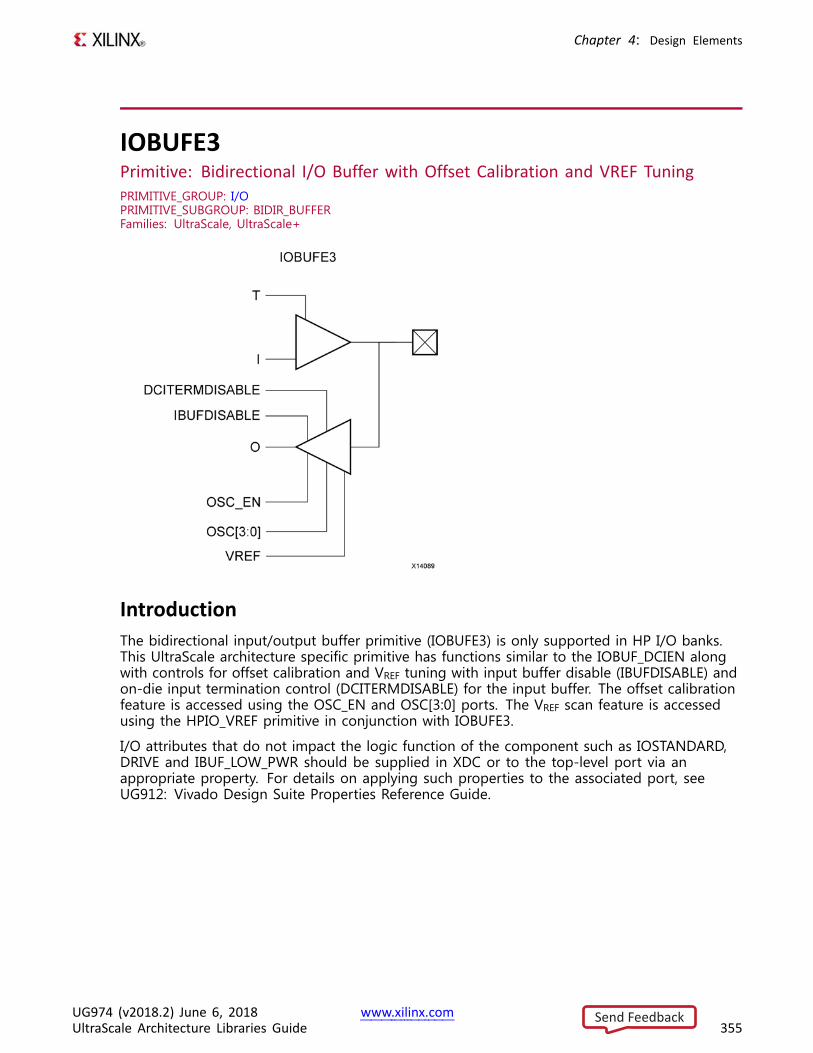
Chapter 4: Design Elements
IOBUFE3Primitive: Bidirectional I/O Buffer with Offset Calibration and VREF TuningPRIMITIVE_GROUP: I/OPRIMITIVE_SUBGROUP: BIDIR_BUFFERFamilies: UltraScale, UltraScale+
IntroductionThe bidirectional input/output buffer primitive (IOBUFE3) is only supported in HP I/O banks.This UltraScale architecture specific primitive has functions similar to the IOBUF_DCIEN alongwith controls for offset calibration and VREF tuning with input buffer disable (IBUFDISABLE) andon-die input termination control (DCITERMDISABLE) for the input buffer. The offset calibrationfeature is accessed using the OSC_EN and OSC[3:0] ports. The VREF scan feature is accessedusing the HPIO_VREF primitive in conjunction with IOBUFE3.
I/O attributes that do not impact the logic function of the component such as IOSTANDARD,DRIVE and IBUF_LOW_PWR should be supplied in XDC or to the top-level port via anappropriate property. For details on applying such properties to the associated port, seeUG912: Vivado Design Suite Properties Reference Guide.
UG974 (v2018.2) June 6, 2018 www.xilinx.comUltraScale Architecture Libraries Guide 355
Send Feedback
Chapter 4: Design Elements
Port DescriptionsPort Direction Width Function
DCITERMDISABLE Input 1 Control to enable/disable DCI termination. This isgenerally used to reduce power in long periods of anidle state.
I Input 1 Input of OBUF. Connect to the logic driving the outputport.
IBUFDISABLE Input 1 Disables input path through the buffer and forces to alogic low. This feature is generally used to reduce powerat times when the I/O is idle for a period of time.
IO Inout 1 Bidirectional port to be connected directly to top-levelinout port.
O Output 1 Output path of the buffer.
OSC<3:0> Input 4 Offset cancellation value
OSC_EN Input 1 Offset cancellation enable
T Input 1 3-state enable input signifying whether the buffer actsas an input or output.
VREF Input 1 Vref input from HPIO_VREF
Design Entry MethodInstantiation Yes
Inference No
IP and IP Integrator Catalog No
Available AttributesAttribute Type Allowed Values Default Description
SIM_INPUT_BUFFER_OFFSET
DECIMAL -50 to 50 0 Offset value for simulation purposes.
USE_IBUFDISABLE STRING "FALSE", "TRUE" "FALSE" This attribute must be unspecified or setto "TRUE" if specified.
VHDL Instantiation TemplateUnless they already exist, copy the following two statements and paste them before the entitydeclaration.Library UNISIM;use UNISIM.vcomponents.all;
-- IOBUFE3: Bidirectional I/O Buffer with Offset Calibration and VREF Tuning-- UltraScale-- Xilinx HDL Language Template, version 2018.2
IOBUFE3_inst : IOBUFE3generic map (
SIM_INPUT_BUFFER_OFFSET => 0 -- Offset value for simulation (-50-50))
UG974 (v2018.2) June 6, 2018 www.xilinx.comUltraScale Architecture Libraries Guide 356
Send Feedback
Chapter 4: Design Elements
port map (O => O, -- 1-bit output: Buffer outputDCITERMDISABLE => DCITERMDISABLE, -- 1-bit input: DCI Termination DisableI => I, -- 1-bit input: Buffer inputIBUFDISABLE => IBUFDISABLE, -- 1-bit input: Buffer disable input, high=disableIO => IO, -- 1-bit inout: Buffer inout (connect directly to top-level port)OSC => OSC, -- 4-bit input: Offset cancellation valueOSC_EN => OSC_EN, -- 1-bit input: Offset cancellation enableT => T, -- 1-bit input: 3-state enable inputVREF => VREF -- 1-bit input: Vref input from HPIO_VREF
);
-- End of IOBUFE3_inst instantiation
Verilog Instantiation Template
// IOBUFE3: Bidirectional I/O Buffer with Offset Calibration and VREF Tuning// UltraScale// Xilinx HDL Language Template, version 2018.2
IOBUFE3 #(.SIM_INPUT_BUFFER_OFFSET(0) // Offset value for simulation (-50-50)
)IOBUFE3_inst (
.O(O), // 1-bit output: Buffer output
.DCITERMDISABLE(DCITERMDISABLE), // 1-bit input: DCI Termination Disable
.I(I), // 1-bit input: Buffer input
.IBUFDISABLE(IBUFDISABLE), // 1-bit input: Buffer disable input, high=disable
.IO(IO), // 1-bit inout: Buffer inout (connect directly to top-level port)
.OSC(OSC), // 4-bit input: Offset cancellation value
.OSC_EN(OSC_EN), // 1-bit input: Offset cancellation enable
.T(T), // 1-bit input: 3-state enable input
.VREF(VREF) // 1-bit input: Vref input from HPIO_VREF);
// End of IOBUFE3_inst instantiation
For More Information• See the UltraScale Architecture SelectIO Resources User Guide (UG571).
• See the UltraScale Programmable Devices Documentation.
UG974 (v2018.2) June 6, 2018 www.xilinx.comUltraScale Architecture Libraries Guide 357
Send Feedback
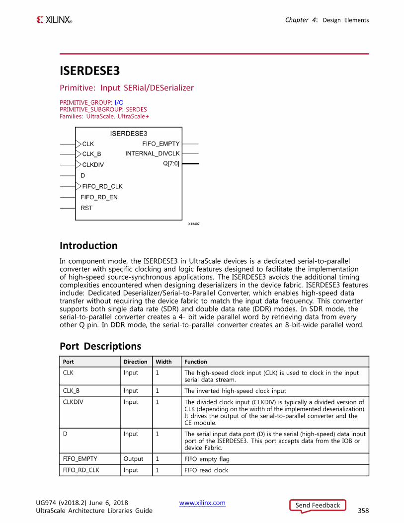
Chapter 4: Design Elements
ISERDESE3Primitive: Input SERial/DESerializerPRIMITIVE_GROUP: I/OPRIMITIVE_SUBGROUP: SERDESFamilies: UltraScale, UltraScale+
IntroductionIn component mode, the ISERDESE3 in UltraScale devices is a dedicated serial-to-parallelconverter with specific clocking and logic features designed to facilitate the implementationof high-speed source-synchronous applications. The ISERDESE3 avoids the additional timingcomplexities encountered when designing deserializers in the device fabric. ISERDESE3 featuresinclude: Dedicated Deserializer/Serial-to-Parallel Converter, which enables high-speed datatransfer without requiring the device fabric to match the input data frequency. This convertersupports both single data rate (SDR) and double data rate (DDR) modes. In SDR mode, theserial-to-parallel converter creates a 4- bit wide parallel word by retrieving data from everyother Q pin. In DDR mode, the serial-to-parallel converter creates an 8-bit-wide parallel word.
Port DescriptionsPort Direction Width Function
CLK Input 1 The high-speed clock input (CLK) is used to clock in the inputserial data stream.
CLK_B Input 1 The inverted high-speed clock input
CLKDIV Input 1 The divided clock input (CLKDIV) is typically a divided version ofCLK (depending on the width of the implemented deserialization).It drives the output of the serial-to-parallel converter and theCE module.
D Input 1 The serial input data port (D) is the serial (high-speed) data inputport of the ISERDESE3. This port accepts data from the IOB ordevice Fabric.
FIFO_EMPTY Output 1 FIFO empty flag
FIFO_RD_CLK Input 1 FIFO read clock
UG974 (v2018.2) June 6, 2018 www.xilinx.comUltraScale Architecture Libraries Guide 358
Send Feedback
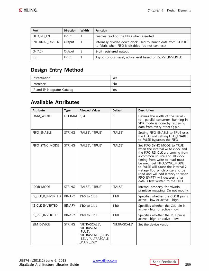
Chapter 4: Design Elements
Port Direction Width Function
FIFO_RD_EN Input 1 Enables reading the FIFO when asserted
INTERNAL_DIVCLK Output 1 Internally divided down clock used to launch data from ISERDESto fabric when FIFO is disabled (do not connect)
Q<7:0> Output 8 8-bit registered output
RST Input 1 Asynchronous Reset, active level based on IS_RST_INVERTED
Design Entry MethodInstantiation Yes
Inference No
IP and IP Integrator Catalog Yes
Available AttributesAttribute Type Allowed Values Default Description
DATA_WIDTH DECIMAL 8, 4 8 Defines the width of the serial -to - parallel converter. Running inSDR mode is done by retrievingdata from every other Q pin.
FIFO_ENABLE STRING "FALSE", "TRUE" "FALSE" Setting FIFO_ENABLE to TRUE usesthe FIFO and setting FIFO_ENABLEto FALSE bypasses the FIFO
FIFO_SYNC_MODE STRING "FALSE", "TRUE" "FALSE" Set FIFO_SYNC_MODE to TRUEwhen the internal write clock andthe FIFO_RD_CLK are coming froma common source and all clocktiming from write to read mustbe met. Set FIFO_SYNC_MODEto FALSE will cause the internal 2- stage flop synchronizers to beused and will add latency to whenFIFO_EMPTY will deassert afterdata is first written to the FIFO.
IDDR_MODE STRING "FALSE", "TRUE" "FALSE" Internal property for Vivadoprimitive mapping. Do not modify.
IS_CLK_B_INVERTED BINARY 1'b0 to 1'b1 1'b0 Specifies whether the CLK_B pin isactive - low or active - high.
IS_CLK_INVERTED BINARY 1'b0 to 1'b1 1'b0 Specifies whether the CLK pin isactive - high or active - low.
IS_RST_INVERTED BINARY 1'b0 to 1'b1 1'b0 Specifies whether the RST pin isactive - high or active - low.
SIM_DEVICE STRING "ULTRASCALE","ULTRASCALE_PLUS","ULTRASCALE _PLUS_ES1", "ULTRASCALE_PLUS _ES2"
"ULTRASCALE" Set the device version
UG974 (v2018.2) June 6, 2018 www.xilinx.comUltraScale Architecture Libraries Guide 359
Send Feedback
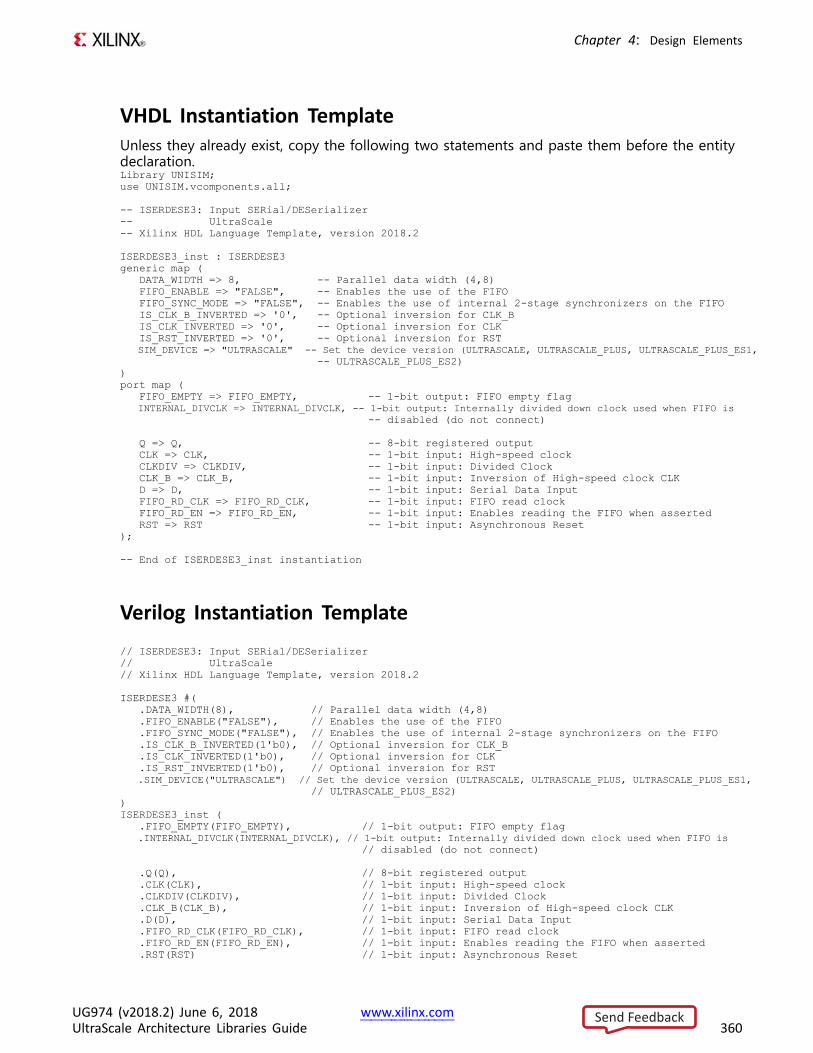
Chapter 4: Design Elements
VHDL Instantiation TemplateUnless they already exist, copy the following two statements and paste them before the entitydeclaration.Library UNISIM;use UNISIM.vcomponents.all;
-- ISERDESE3: Input SERial/DESerializer-- UltraScale-- Xilinx HDL Language Template, version 2018.2
ISERDESE3_inst : ISERDESE3generic map (
DATA_WIDTH => 8, -- Parallel data width (4,8)FIFO_ENABLE => "FALSE", -- Enables the use of the FIFOFIFO_SYNC_MODE => "FALSE", -- Enables the use of internal 2-stage synchronizers on the FIFOIS_CLK_B_INVERTED => '0', -- Optional inversion for CLK_BIS_CLK_INVERTED => '0', -- Optional inversion for CLKIS_RST_INVERTED => '0', -- Optional inversion for RSTSIM_DEVICE => "ULTRASCALE" -- Set the device version (ULTRASCALE, ULTRASCALE_PLUS, ULTRASCALE_PLUS_ES1,
-- ULTRASCALE_PLUS_ES2))port map (
FIFO_EMPTY => FIFO_EMPTY, -- 1-bit output: FIFO empty flagINTERNAL_DIVCLK => INTERNAL_DIVCLK, -- 1-bit output: Internally divided down clock used when FIFO is
-- disabled (do not connect)
Q => Q, -- 8-bit registered outputCLK => CLK, -- 1-bit input: High-speed clockCLKDIV => CLKDIV, -- 1-bit input: Divided ClockCLK_B => CLK_B, -- 1-bit input: Inversion of High-speed clock CLKD => D, -- 1-bit input: Serial Data InputFIFO_RD_CLK => FIFO_RD_CLK, -- 1-bit input: FIFO read clockFIFO_RD_EN => FIFO_RD_EN, -- 1-bit input: Enables reading the FIFO when assertedRST => RST -- 1-bit input: Asynchronous Reset
);
-- End of ISERDESE3_inst instantiation
Verilog Instantiation Template// ISERDESE3: Input SERial/DESerializer// UltraScale// Xilinx HDL Language Template, version 2018.2
ISERDESE3 #(.DATA_WIDTH(8), // Parallel data width (4,8).FIFO_ENABLE("FALSE"), // Enables the use of the FIFO.FIFO_SYNC_MODE("FALSE"), // Enables the use of internal 2-stage synchronizers on the FIFO.IS_CLK_B_INVERTED(1'b0), // Optional inversion for CLK_B.IS_CLK_INVERTED(1'b0), // Optional inversion for CLK.IS_RST_INVERTED(1'b0), // Optional inversion for RST.SIM_DEVICE("ULTRASCALE") // Set the device version (ULTRASCALE, ULTRASCALE_PLUS, ULTRASCALE_PLUS_ES1,
// ULTRASCALE_PLUS_ES2))ISERDESE3_inst (
.FIFO_EMPTY(FIFO_EMPTY), // 1-bit output: FIFO empty flag
.INTERNAL_DIVCLK(INTERNAL_DIVCLK), // 1-bit output: Internally divided down clock used when FIFO is// disabled (do not connect)
.Q(Q), // 8-bit registered output
.CLK(CLK), // 1-bit input: High-speed clock
.CLKDIV(CLKDIV), // 1-bit input: Divided Clock
.CLK_B(CLK_B), // 1-bit input: Inversion of High-speed clock CLK
.D(D), // 1-bit input: Serial Data Input
.FIFO_RD_CLK(FIFO_RD_CLK), // 1-bit input: FIFO read clock
.FIFO_RD_EN(FIFO_RD_EN), // 1-bit input: Enables reading the FIFO when asserted
.RST(RST) // 1-bit input: Asynchronous Reset
UG974 (v2018.2) June 6, 2018 www.xilinx.comUltraScale Architecture Libraries Guide 360
Send Feedback
Chapter 4: Design Elements
);
// End of ISERDESE3_inst instantiation
For More Information• See the UltraScale Architecture SelectIO Resources User Guide (UG571).
• See the UltraScale Programmable Devices Documentation.
UG974 (v2018.2) June 6, 2018 www.xilinx.comUltraScale Architecture Libraries Guide 361
Send Feedback
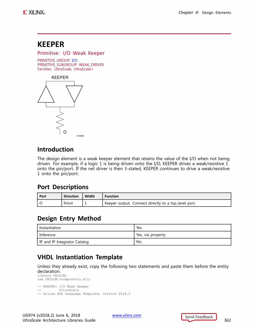
Chapter 4: Design Elements
KEEPERPrimitive: I/O Weak KeeperPRIMITIVE_GROUP: I/OPRIMITIVE_SUBGROUP: WEAK_DRIVERFamilies: UltraScale, UltraScale+
IntroductionThe design element is a weak keeper element that retains the value of the I/O when not beingdriven. For example, if a logic 1 is being driven onto the I/O, KEEPER drives a weak/resistive 1onto the pin/port. If the net driver is then 3-stated, KEEPER continues to drive a weak/resistive1 onto the pin/port.
Port DescriptionsPort Direction Width Function
O Inout 1 Keeper output. Connect directly to a top_level port.
Design Entry MethodInstantiation Yes
Inference Yes, via property
IP and IP Integrator Catalog No
VHDL Instantiation TemplateUnless they already exist, copy the following two statements and paste them before the entitydeclaration.Library UNISIM;use UNISIM.vcomponents.all;
-- KEEPER: I/O Weak Keeper-- UltraScale-- Xilinx HDL Language Template, version 2018.2
UG974 (v2018.2) June 6, 2018 www.xilinx.comUltraScale Architecture Libraries Guide 362
Send Feedback
Chapter 4: Design Elements
KEEPER_inst : KEEPERport map (
O => O -- 1-bit inout: Keeper output (connect directly to top-level port));
-- End of KEEPER_inst instantiation
Verilog Instantiation Template
// KEEPER: I/O Weak Keeper// UltraScale// Xilinx HDL Language Template, version 2018.2
KEEPER KEEPER_inst (.O(O) // 1-bit inout: Keeper output (connect directly to top-level port)
);
// End of KEEPER_inst instantiation
For More Information• See the UltraScale Architecture SelectIO Resources User Guide (UG571).
• See the UltraScale Programmable Devices Documentation.
UG974 (v2018.2) June 6, 2018 www.xilinx.comUltraScale Architecture Libraries Guide 363
Send Feedback
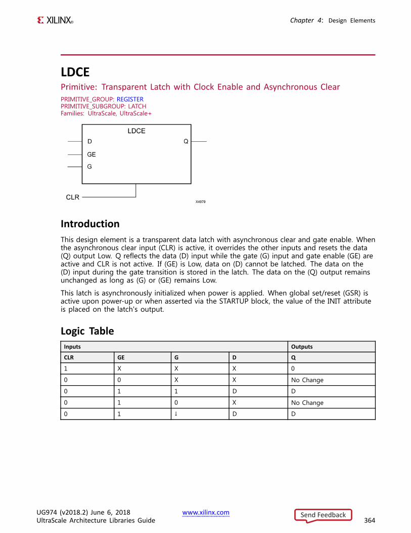
Chapter 4: Design Elements
LDCEPrimitive: Transparent Latch with Clock Enable and Asynchronous ClearPRIMITIVE_GROUP: REGISTERPRIMITIVE_SUBGROUP: LATCHFamilies: UltraScale, UltraScale+
IntroductionThis design element is a transparent data latch with asynchronous clear and gate enable. Whenthe asynchronous clear input (CLR) is active, it overrides the other inputs and resets the data(Q) output Low. Q reflects the data (D) input while the gate (G) input and gate enable (GE) areactive and CLR is not active. If (GE) is Low, data on (D) cannot be latched. The data on the(D) input during the gate transition is stored in the latch. The data on the (Q) output remainsunchanged as long as (G) or (GE) remains Low.
This latch is asynchronously initialized when power is applied. When global set/reset (GSR) isactive upon power-up or when asserted via the STARTUP block, the value of the INIT attributeis placed on the latch's output.
Logic TableInputs Outputs
CLR GE G D Q
1 X X X 0
0 0 X X No Change
0 1 1 D D
0 1 0 X No Change
0 1 ↓ D D
UG974 (v2018.2) June 6, 2018 www.xilinx.comUltraScale Architecture Libraries Guide 364
Send Feedback
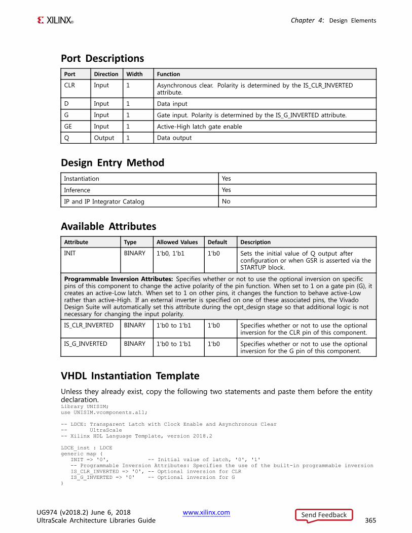
Chapter 4: Design Elements
Port DescriptionsPort Direction Width Function
CLR Input 1 Asynchronous clear. Polarity is determined by the IS_CLR_INVERTEDattribute.
D Input 1 Data input
G Input 1 Gate input. Polarity is determined by the IS_G_INVERTED attribute.
GE Input 1 Active-High latch gate enable
Q Output 1 Data output
Design Entry MethodInstantiation Yes
Inference Yes
IP and IP Integrator Catalog No
Available AttributesAttribute Type Allowed Values Default Description
INIT BINARY 1'b0, 1'b1 1'b0 Sets the initial value of Q output afterconfiguration or when GSR is asserted via theSTARTUP block.
Programmable Inversion Attributes: Specifies whether or not to use the optional inversion on specificpins of this component to change the active polarity of the pin function. When set to 1 on a gate pin (G), itcreates an active-Low latch. When set to 1 on other pins, it changes the function to behave active-Lowrather than active-High. If an external inverter is specified on one of these associated pins, the VivadoDesign Suite will automatically set this attribute during the opt_design stage so that additional logic is notnecessary for changing the input polarity.
IS_CLR_INVERTED BINARY 1'b0 to 1'b1 1'b0 Specifies whether or not to use the optionalinversion for the CLR pin of this component.
IS_G_INVERTED BINARY 1'b0 to 1'b1 1'b0 Specifies whether or not to use the optionalinversion for the G pin of this component.
VHDL Instantiation TemplateUnless they already exist, copy the following two statements and paste them before the entitydeclaration.Library UNISIM;use UNISIM.vcomponents.all;
-- LDCE: Transparent Latch with Clock Enable and Asynchronous Clear-- UltraScale-- Xilinx HDL Language Template, version 2018.2
LDCE_inst : LDCEgeneric map (
INIT => '0', -- Initial value of latch, '0', '1'-- Programmable Inversion Attributes: Specifies the use of the built-in programmable inversionIS_CLR_INVERTED => '0', -- Optional inversion for CLRIS_G_INVERTED => '0' -- Optional inversion for G
)
UG974 (v2018.2) June 6, 2018 www.xilinx.comUltraScale Architecture Libraries Guide 365
Send Feedback

Chapter 4: Design Elements
port map (Q => Q, -- 1-bit output: DataCLR => CLR, -- 1-bit input: Asynchronous clearD => D, -- 1-bit input: DataG => G, -- 1-bit input: GateGE => GE -- 1-bit input: Gate enable
);
-- End of LDCE_inst instantiation
Verilog Instantiation Template
// LDCE: Transparent Latch with Clock Enable and Asynchronous Clear// UltraScale// Xilinx HDL Language Template, version 2018.2
LDCE #(.INIT(1'b0), // Initial value of latch, 1'b0, 1'b1// Programmable Inversion Attributes: Specifies the use of the built-in programmable inversion.IS_CLR_INVERTED(1'b0), // Optional inversion for CLR.IS_G_INVERTED(1'b0) // Optional inversion for G
)LDCE_inst (
.Q(Q), // 1-bit output: Data
.CLR(CLR), // 1-bit input: Asynchronous clear
.D(D), // 1-bit input: Data
.G(G), // 1-bit input: Gate
.GE(GE) // 1-bit input: Gate enable);
// End of LDCE_inst instantiation
For More Information• See the UltraScale Architecture Migration: Methodology Guide (UG1026).
• See the UltraScale Programmable Devices Documentation.
UG974 (v2018.2) June 6, 2018 www.xilinx.comUltraScale Architecture Libraries Guide 366
Send Feedback

Chapter 4: Design Elements
LDPEPrimitive: Transparent Latch with Clock Enable and Asynchronous PresetPRIMITIVE_GROUP: REGISTERPRIMITIVE_SUBGROUP: LATCHFamilies: UltraScale, UltraScale+
IntroductionThis design element is a transparent data latch with asynchronous preset and gate enable.When the asynchronous preset input (PRE) is active, it overrides the other inputs and presetsthe data (Q) output High. Q reflects the data (D) input while the gate (G) input and gate enable(GE) are active and PRE is not active. If (GE) is Low, data on (D) cannot be latched. The dataon the (D) input during the gate transition is stored in the latch. The data on the (Q) outputremains unchanged as long as (G) or (GE) remains Low.
This latch is asynchronously initialized when power is applied. When global set/reset (GSR) isactive upon power-up or when asserted via the STARTUP block, the value of the INIT attributeis placed on the latch's output.
Logic TableInputs Outputs
PRE GE G D Q
1 X X X 1
0 0 X X No Change
0 1 1 D D
0 1 0 X No Change
0 1 ↓ D D
UG974 (v2018.2) June 6, 2018 www.xilinx.comUltraScale Architecture Libraries Guide 367
Send Feedback
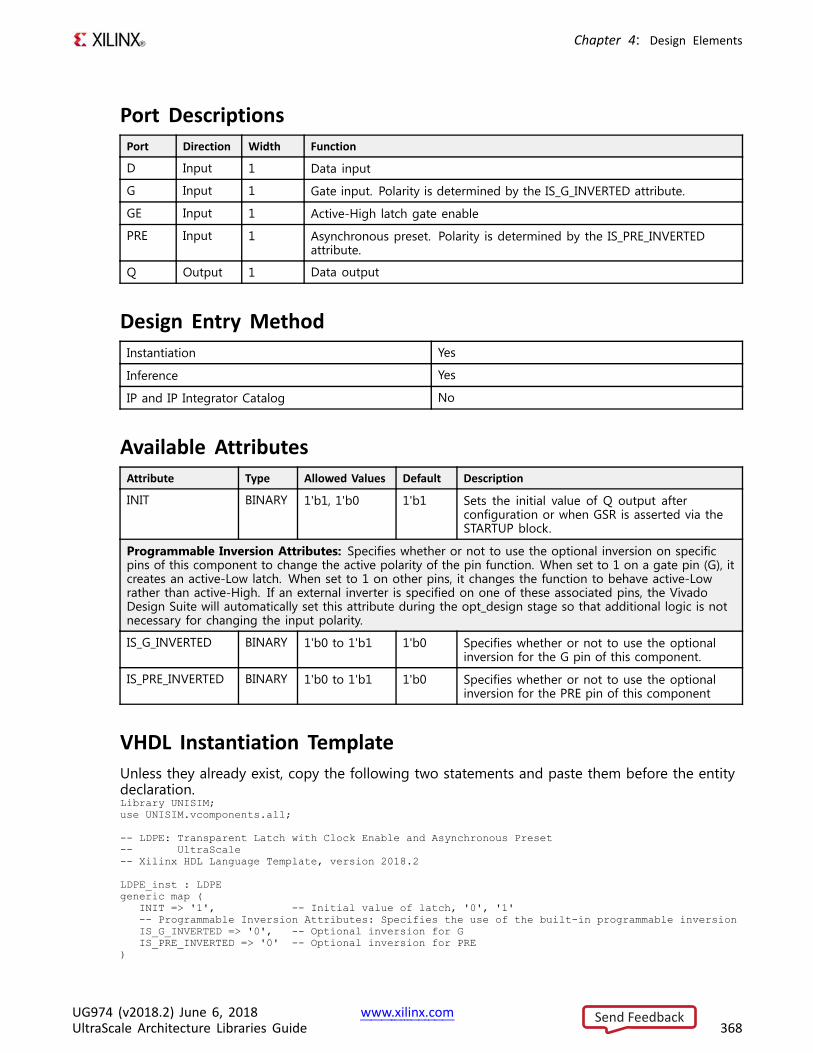
Chapter 4: Design Elements
Port DescriptionsPort Direction Width Function
D Input 1 Data input
G Input 1 Gate input. Polarity is determined by the IS_G_INVERTED attribute.
GE Input 1 Active-High latch gate enable
PRE Input 1 Asynchronous preset. Polarity is determined by the IS_PRE_INVERTEDattribute.
Q Output 1 Data output
Design Entry MethodInstantiation Yes
Inference Yes
IP and IP Integrator Catalog No
Available AttributesAttribute Type Allowed Values Default Description
INIT BINARY 1'b1, 1'b0 1'b1 Sets the initial value of Q output afterconfiguration or when GSR is asserted via theSTARTUP block.
Programmable Inversion Attributes: Specifies whether or not to use the optional inversion on specificpins of this component to change the active polarity of the pin function. When set to 1 on a gate pin (G), itcreates an active-Low latch. When set to 1 on other pins, it changes the function to behave active-Lowrather than active-High. If an external inverter is specified on one of these associated pins, the VivadoDesign Suite will automatically set this attribute during the opt_design stage so that additional logic is notnecessary for changing the input polarity.
IS_G_INVERTED BINARY 1'b0 to 1'b1 1'b0 Specifies whether or not to use the optionalinversion for the G pin of this component.
IS_PRE_INVERTED BINARY 1'b0 to 1'b1 1'b0 Specifies whether or not to use the optionalinversion for the PRE pin of this component
VHDL Instantiation TemplateUnless they already exist, copy the following two statements and paste them before the entitydeclaration.Library UNISIM;use UNISIM.vcomponents.all;
-- LDPE: Transparent Latch with Clock Enable and Asynchronous Preset-- UltraScale-- Xilinx HDL Language Template, version 2018.2
LDPE_inst : LDPEgeneric map (
INIT => '1', -- Initial value of latch, '0', '1'-- Programmable Inversion Attributes: Specifies the use of the built-in programmable inversionIS_G_INVERTED => '0', -- Optional inversion for GIS_PRE_INVERTED => '0' -- Optional inversion for PRE
)
UG974 (v2018.2) June 6, 2018 www.xilinx.comUltraScale Architecture Libraries Guide 368
Send Feedback
Chapter 4: Design Elements
port map (Q => Q, -- 1-bit output: DataD => D, -- 1-bit input: DataG => G, -- 1-bit input: GateGE => GE, -- 1-bit input: Gate enablePRE => PRE -- 1-bit input: Asynchronous preset
);
-- End of LDPE_inst instantiation
Verilog Instantiation Template
// LDPE: Transparent Latch with Clock Enable and Asynchronous Preset// UltraScale// Xilinx HDL Language Template, version 2018.2
LDPE #(.INIT(1'b1), // Initial value of latch, 1'b0, 1'b1// Programmable Inversion Attributes: Specifies the use of the built-in programmable inversion.IS_G_INVERTED(1'b0), // Optional inversion for G.IS_PRE_INVERTED(1'b0) // Optional inversion for PRE
)LDPE_inst (
.Q(Q), // 1-bit output: Data
.D(D), // 1-bit input: Data
.G(G), // 1-bit input: Gate
.GE(GE), // 1-bit input: Gate enable
.PRE(PRE) // 1-bit input: Asynchronous preset);
// End of LDPE_inst instantiation
For More Information• See the UltraScale Architecture Migration: Methodology Guide (UG1026).
• See the UltraScale Programmable Devices Documentation.
UG974 (v2018.2) June 6, 2018 www.xilinx.comUltraScale Architecture Libraries Guide 369
Send Feedback
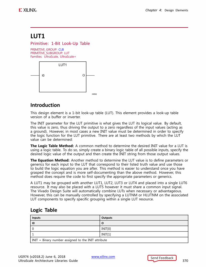
Chapter 4: Design Elements
LUT1Primitive: 1-Bit Look-Up TablePRIMITIVE_GROUP: CLBPRIMITIVE_SUBGROUP: LUTFamilies: UltraScale, UltraScale+
IntroductionThis design element is a 1-bit look-up table (LUT). This element provides a look-up tableversion of a buffer or inverter.
The INIT parameter for the LUT primitive is what gives the LUT its logical value. By default,this value is zero, thus driving the output to a zero regardless of the input values (acting asa ground). However, in most cases a new INIT value must be determined in order to specifythe logic function for the LUT primitive. There are at least two methods by which the LUTvalue can be determined:
The Logic Table Method: A common method to determine the desired INIT value for a LUT isusing a logic table. To do so, simply create a binary logic table of all possible inputs, specify thedesired logic value of the output and then create the INIT string from those output values.
The Equation Method: Another method to determine the LUT value is to define parameters orgenerics for each input to the LUT that correspond to their listed truth value and use thoseto build the logic equation you are after. This method is easier to understand once you havegrasped the concept and is more self-documenting than the above method. However, thismethod does require the code to first specify the appropriate parameters or generics.
A LUT1 may be grouped with another LUT1, LUT2, LUT3 or LUT4 and placed into a single LUT6resource. It may also be placed with a LUT5 however it must share a common input signal.The Vivado Design Suite will automatically combine LUTs when necessary or advantageous.However, this can be manually controlled by specifying a LUTNM or HLUTNM on the associatedLUT components to specify specific grouping within a single LUT resource.
Logic TableInputs Outputs
I0 O
0 INIT[0]
1 INIT[1]
INIT = Binary number assigned to the INIT attribute
UG974 (v2018.2) June 6, 2018 www.xilinx.comUltraScale Architecture Libraries Guide 370
Send Feedback
Chapter 4: Design Elements
Design Entry MethodInstantiation Yes
Inference Recommended
IP and IP Integrator Catalog No
Available AttributesAttribute Type Allowed Values Default Description
INIT HEX 2'h0 to 2'h3 2'h0 Specifies the logical expression ofthis element
VHDL Instantiation TemplateUnless they already exist, copy the following two statements and paste them before the entitydeclaration.Library UNISIM;use UNISIM.vcomponents.all;
-- LUT1: 1-Bit Look-Up Table-- UltraScale-- Xilinx HDL Language Template, version 2018.2
LUT1_inst : LUT1generic map (
INIT => X"0" -- Logic function)port map (
O => O, -- 1-bit output: LUTI0 => I0 -- 1-bit input: LUT
);
-- End of LUT1_inst instantiation
Verilog Instantiation Template
// LUT1: 1-Bit Look-Up Table// UltraScale// Xilinx HDL Language Template, version 2018.2
LUT1 #(.INIT(2'h0) // Logic function
)LUT1_inst (
.O(O), // 1-bit output: LUT
.I0(I0) // 1-bit input: LUT);
// End of LUT1_inst instantiation
For More Information• See the UltraScale Architecture Configurable Logic Block User Guide (UG574).
• See the UltraScale Programmable Devices Documentation.
UG974 (v2018.2) June 6, 2018 www.xilinx.comUltraScale Architecture Libraries Guide 371
Send Feedback

Chapter 4: Design Elements
LUT2Primitive: 2-Bit Look-Up TablePRIMITIVE_GROUP: CLBPRIMITIVE_SUBGROUP: LUTFamilies: UltraScale, UltraScale+
IntroductionThis design element is a 2-bit look-up table (LUT). This element allows the creation of anylogical function with two inputs.
The INIT parameter for the LUT primitive is what gives the LUT its logical value. By default,this value is zero, thus driving the output to a zero regardless of the input values (acting asa ground). However, in most cases a new INIT value must be determined in order to specifythe logic function for the LUT primitive. There are at least two methods by which the LUTvalue can be determined:
The Logic Table Method: A common method to determine the desired INIT value for a LUT isusing a logic table. To do so, simply create a binary logic table of all possible inputs, specify thedesired logic value of the output and then create the INIT string from those output values.
The Equation Method: Another method to determine the LUT value is to define parameters orgenerics for each input to the LUT that correspond to their listed truth value and use thoseto build the logic equation you are after. This method is easier to understand once you havegrasped the concept and is more self-documenting than the above method. However, thismethod does require the code to first specify the appropriate parameters or generics.
A LUT2 may be grouped with a LUT1, LUT2, LUT3, LUT4 or LUT5 and placed into a single LUT6resource as long as the combined input signals do not exceed 5 unique inputs. The VivadoDesign Suite will automatically combine LUTs when necessary or advantageous. Howeverthis can be manually controlled by specifying a LUTNM or HLUTNM on the associated LUTcomponents to specify specific grouping within a single LUT resource.
UG974 (v2018.2) June 6, 2018 www.xilinx.comUltraScale Architecture Libraries Guide 372
Send Feedback
Chapter 4: Design Elements
Logic TableInputs Outputs
I1 I0 O
0 0 INIT[0]
0 1 INIT[1]
1 0 INIT[2]
1 1 INIT[3]
INIT = Binary equivalent of the hexadecimal number assigned to the INIT attribute
Design Entry MethodInstantiation Yes
Inference Recommended
IP and IP Integrator Catalog No
Available AttributesAttribute Type Allowed Values Default Description
INIT HEX 4'h0 to 4'hf 4'h0 Specifies the logicalexpression of thiselement
VHDL Instantiation TemplateUnless they already exist, copy the following two statements and paste them before the entitydeclaration.Library UNISIM;use UNISIM.vcomponents.all;
-- LUT2: 2-Bit Look-Up Table-- UltraScale-- Xilinx HDL Language Template, version 2018.2
LUT2_inst : LUT2generic map (
INIT => X"0" -- Logic function)port map (
O => O, -- 1-bit output: LUTI0 => I0, -- 1-bit input: LUTI1 => I1 -- 1-bit input: LUT
);
-- End of LUT2_inst instantiation
Verilog Instantiation Template// LUT2: 2-Bit Look-Up Table// UltraScale// Xilinx HDL Language Template, version 2018.2
UG974 (v2018.2) June 6, 2018 www.xilinx.comUltraScale Architecture Libraries Guide 373
Send Feedback
Chapter 4: Design Elements
LUT2 #(.INIT(4'h0) // Logic function
)LUT2_inst (
.O(O), // 1-bit output: LUT
.I0(I0), // 1-bit input: LUT
.I1(I1) // 1-bit input: LUT);
// End of LUT2_inst instantiation
For More Information• See the UltraScale Architecture Configurable Logic Block User Guide (UG574).
• See the UltraScale Programmable Devices Documentation.
UG974 (v2018.2) June 6, 2018 www.xilinx.comUltraScale Architecture Libraries Guide 374
Send Feedback

Chapter 4: Design Elements
LUT3Primitive: 3-Bit Look-Up TablePRIMITIVE_GROUP: CLBPRIMITIVE_SUBGROUP: LUTFamilies: UltraScale, UltraScale+
IntroductionThis design element is a 3-bit look-up table (LUT). This element allows the creation of anylogical function with three inputs.
The INIT parameter for the LUT primitive is what gives the LUT its logical value. By default,this value is zero, thus driving the output to a zero regardless of the input values (acting asa ground). However, in most cases a new INIT value must be determined in order to specifythe logic function for the LUT primitive. There are at least two methods by which the LUTvalue can be determined:
The Logic Table Method: A common method to determine the desired INIT value for a LUT isusing a logic table. To do so, simply create a binary logic table of all possible inputs, specify thedesired logic value of the output and then create the INIT string from those output values.
The Equation Method: Another method to determine the LUT value is to define parameters orgenerics for each input to the LUT that correspond to their listed truth value and use thoseto build the logic equation you are after. This method is easier to understand once you havegrasped the concept and is more self-documenting than the above method. However, thismethod does require the code to first specify the appropriate parameters or generics.
A LUT3 may be grouped with a LUT1, LUT2, LUT3, LUT4 or LUT5 and placed into a single LUT6resource as long as the combined input signals do not exceed 5 unique inputs. The VivadoDesign Suite will automatically combine LUTs when necessary or advantageous. Howeverthis can be manually controlled by specifying a LUTNM or HLUTNM on the associated LUTcomponents to specify specific grouping within a single LUT resource.
UG974 (v2018.2) June 6, 2018 www.xilinx.comUltraScale Architecture Libraries Guide 375
Send Feedback
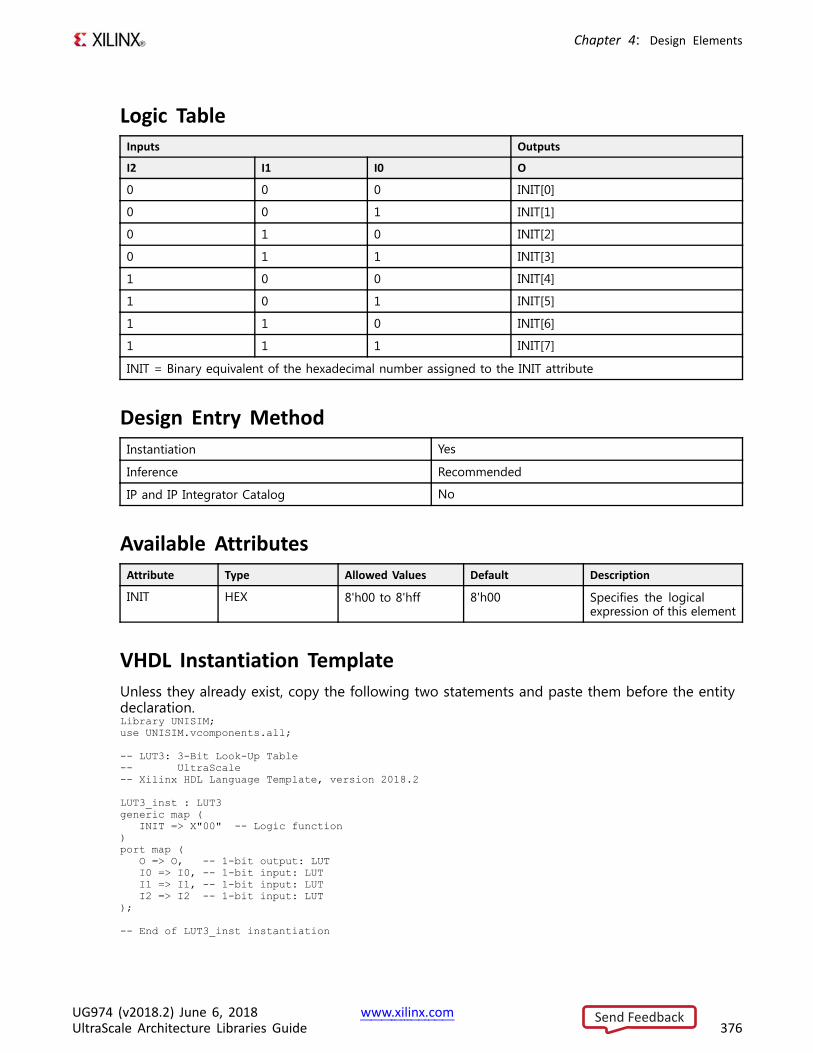
Chapter 4: Design Elements
Logic TableInputs Outputs
I2 I1 I0 O
0 0 0 INIT[0]
0 0 1 INIT[1]
0 1 0 INIT[2]
0 1 1 INIT[3]
1 0 0 INIT[4]
1 0 1 INIT[5]
1 1 0 INIT[6]
1 1 1 INIT[7]
INIT = Binary equivalent of the hexadecimal number assigned to the INIT attribute
Design Entry MethodInstantiation Yes
Inference Recommended
IP and IP Integrator Catalog No
Available AttributesAttribute Type Allowed Values Default Description
INIT HEX 8'h00 to 8'hff 8'h00 Specifies the logicalexpression of this element
VHDL Instantiation TemplateUnless they already exist, copy the following two statements and paste them before the entitydeclaration.Library UNISIM;use UNISIM.vcomponents.all;
-- LUT3: 3-Bit Look-Up Table-- UltraScale-- Xilinx HDL Language Template, version 2018.2
LUT3_inst : LUT3generic map (
INIT => X"00" -- Logic function)port map (
O => O, -- 1-bit output: LUTI0 => I0, -- 1-bit input: LUTI1 => I1, -- 1-bit input: LUTI2 => I2 -- 1-bit input: LUT
);
-- End of LUT3_inst instantiation
UG974 (v2018.2) June 6, 2018 www.xilinx.comUltraScale Architecture Libraries Guide 376
Send Feedback
Chapter 4: Design Elements
Verilog Instantiation Template
// LUT3: 3-Bit Look-Up Table// UltraScale// Xilinx HDL Language Template, version 2018.2
LUT3 #(.INIT(8'h00) // Logic function
)LUT3_inst (
.O(O), // 1-bit output: LUT
.I0(I0), // 1-bit input: LUT
.I1(I1), // 1-bit input: LUT
.I2(I2) // 1-bit input: LUT);
// End of LUT3_inst instantiation
For More Information• See the UltraScale Architecture Configurable Logic Block User Guide (UG574).
• See the UltraScale Programmable Devices Documentation.
UG974 (v2018.2) June 6, 2018 www.xilinx.comUltraScale Architecture Libraries Guide 377
Send Feedback
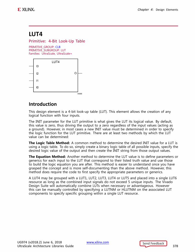
Chapter 4: Design Elements
LUT4Primitive: 4-Bit Look-Up TablePRIMITIVE_GROUP: CLBPRIMITIVE_SUBGROUP: LUTFamilies: UltraScale, UltraScale+
IntroductionThis design element is a 4-bit look-up table (LUT). This element allows the creation of anylogical function with four inputs.
The INIT parameter for the LUT primitive is what gives the LUT its logical value. By default,this value is zero, thus driving the output to a zero regardless of the input values (acting asa ground). However, in most cases a new INIT value must be determined in order to specifythe logic function for the LUT primitive. There are at least two methods by which the LUTvalue can be determined:
The Logic Table Method: A common method to determine the desired INIT value for a LUT isusing a logic table. To do so, simply create a binary logic table of all possible inputs, specify thedesired logic value of the output and then create the INIT string from those output values.
The Equation Method: Another method to determine the LUT value is to define parameters orgenerics for each input to the LUT that correspond to their listed truth value and use thoseto build the logic equation you are after. This method is easier to understand once you havegrasped the concept and is more self-documenting than the above method. However, thismethod does require the code to first specify the appropriate parameters or generics.
A LUT4 may be grouped with a LUT1, LUT2, LUT3, LUT4 or LUT5 and placed into a single LUT6resource as long as the combined input signals do not exceed 5 unique inputs. The VivadoDesign Suite will automatically combine LUTs when necessary or advantageous. Howeverthis can be manually controlled by specifying a LUTNM or HLUTNM on the associated LUTcomponents to specify specific grouping within a single LUT resource.
UG974 (v2018.2) June 6, 2018 www.xilinx.comUltraScale Architecture Libraries Guide 378
Send Feedback
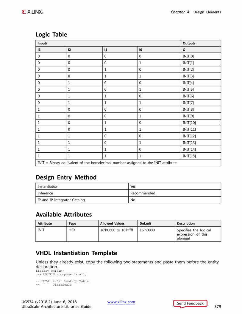
Chapter 4: Design Elements
Logic TableInputs Outputs
I3 I2 I1 I0 O
0 0 0 0 INIT[0]
0 0 0 1 INIT[1]
0 0 1 0 INIT[2]
0 0 1 1 INIT[3]
0 1 0 0 INIT[4]
0 1 0 1 INIT[5]
0 1 1 0 INIT[6]
0 1 1 1 INIT[7]
1 0 0 0 INIT[8]
1 0 0 1 INIT[9]
1 0 1 0 INIT[10]
1 0 1 1 INIT[11]
1 1 0 0 INIT[12]
1 1 0 1 INIT[13]
1 1 1 0 INIT[14]
1 1 1 1 INIT[15]
INIT = Binary equivalent of the hexadecimal number assigned to the INIT attribute
Design Entry MethodInstantiation Yes
Inference Recommended
IP and IP Integrator Catalog No
Available AttributesAttribute Type Allowed Values Default Description
INIT HEX 16'h0000 to 16'hffff 16'h0000 Specifies the logicalexpression of thiselement
VHDL Instantiation TemplateUnless they already exist, copy the following two statements and paste them before the entitydeclaration.Library UNISIM;use UNISIM.vcomponents.all;
-- LUT4: 4-Bit Look-Up Table-- UltraScale
UG974 (v2018.2) June 6, 2018 www.xilinx.comUltraScale Architecture Libraries Guide 379
Send Feedback
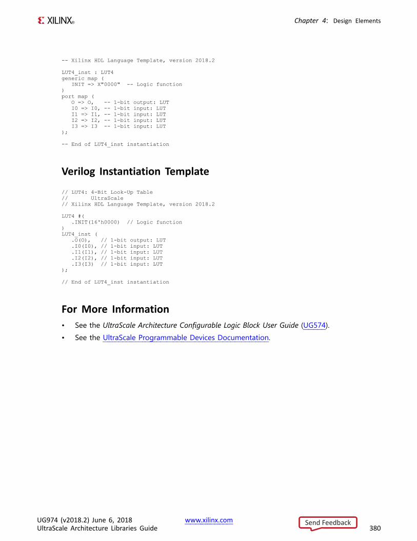
Chapter 4: Design Elements
-- Xilinx HDL Language Template, version 2018.2
LUT4_inst : LUT4generic map (
INIT => X"0000" -- Logic function)port map (
O => O, -- 1-bit output: LUTI0 => I0, -- 1-bit input: LUTI1 => I1, -- 1-bit input: LUTI2 => I2, -- 1-bit input: LUTI3 => I3 -- 1-bit input: LUT
);
-- End of LUT4_inst instantiation
Verilog Instantiation Template
// LUT4: 4-Bit Look-Up Table// UltraScale// Xilinx HDL Language Template, version 2018.2
LUT4 #(.INIT(16'h0000) // Logic function
)LUT4_inst (
.O(O), // 1-bit output: LUT
.I0(I0), // 1-bit input: LUT
.I1(I1), // 1-bit input: LUT
.I2(I2), // 1-bit input: LUT
.I3(I3) // 1-bit input: LUT);
// End of LUT4_inst instantiation
For More Information• See the UltraScale Architecture Configurable Logic Block User Guide (UG574).
• See the UltraScale Programmable Devices Documentation.
UG974 (v2018.2) June 6, 2018 www.xilinx.comUltraScale Architecture Libraries Guide 380
Send Feedback

Chapter 4: Design Elements
LUT5Primitive: 5-Bit Look-Up TablePRIMITIVE_GROUP: CLBPRIMITIVE_SUBGROUP: LUTFamilies: UltraScale, UltraScale+
IntroductionThis design element is a 5-bit look-up table (LUT). This element allows the creation of anylogical function with five inputs.
The INIT parameter for the LUT primitive is what gives the LUT its logical value. By default,this value is zero, thus driving the output to a zero regardless of the input values (acting asa ground). However, in most cases a new INIT value must be determined in order to specifythe logic function for the LUT primitive. There are at least two methods by which the LUTvalue can be determined:
The Logic Table Method: A common method to determine the desired INIT value for a LUT isusing a logic table. To do so, simply create a binary logic table of all possible inputs, specify thedesired logic value of the output and then create the INIT string from those output values.
The Equation Method: Another method to determine the LUT value is to define parameters orgenerics for each input to the LUT that correspond to their listed truth value and use thoseto build the logic equation you are after. This method is easier to understand once you havegrasped the concept and is more self-documenting than the above method. However, thismethod does require the code to first specify the appropriate parameters or generics.
A LUT5 may be grouped with a LUT1, LUT2, LUT3, LUT4 or LUT5 and placed into a single LUT6resource as long as the combined input signals do not exceed 5 unique inputs. The VivadoDesign Suite will automatically combine LUTs when necessary or advantageous. Howeverthis can be manually controlled by specifying a LUTNM or HLUTNM on the associated LUTcomponents to specify specific grouping within a single LUT resource.
UG974 (v2018.2) June 6, 2018 www.xilinx.comUltraScale Architecture Libraries Guide 381
Send Feedback
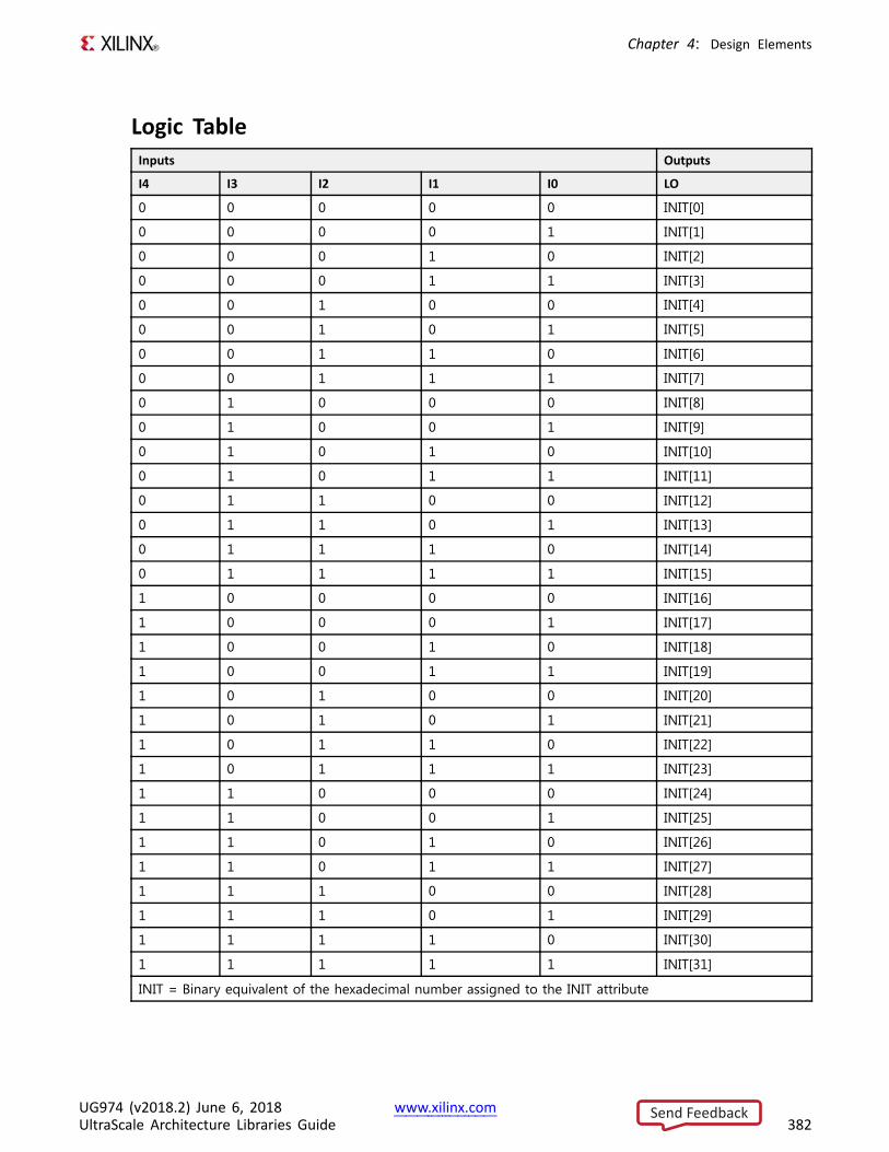
Chapter 4: Design Elements
Logic TableInputs Outputs
I4 I3 I2 I1 I0 LO
0 0 0 0 0 INIT[0]
0 0 0 0 1 INIT[1]
0 0 0 1 0 INIT[2]
0 0 0 1 1 INIT[3]
0 0 1 0 0 INIT[4]
0 0 1 0 1 INIT[5]
0 0 1 1 0 INIT[6]
0 0 1 1 1 INIT[7]
0 1 0 0 0 INIT[8]
0 1 0 0 1 INIT[9]
0 1 0 1 0 INIT[10]
0 1 0 1 1 INIT[11]
0 1 1 0 0 INIT[12]
0 1 1 0 1 INIT[13]
0 1 1 1 0 INIT[14]
0 1 1 1 1 INIT[15]
1 0 0 0 0 INIT[16]
1 0 0 0 1 INIT[17]
1 0 0 1 0 INIT[18]
1 0 0 1 1 INIT[19]
1 0 1 0 0 INIT[20]
1 0 1 0 1 INIT[21]
1 0 1 1 0 INIT[22]
1 0 1 1 1 INIT[23]
1 1 0 0 0 INIT[24]
1 1 0 0 1 INIT[25]
1 1 0 1 0 INIT[26]
1 1 0 1 1 INIT[27]
1 1 1 0 0 INIT[28]
1 1 1 0 1 INIT[29]
1 1 1 1 0 INIT[30]
1 1 1 1 1 INIT[31]
INIT = Binary equivalent of the hexadecimal number assigned to the INIT attribute
UG974 (v2018.2) June 6, 2018 www.xilinx.comUltraScale Architecture Libraries Guide 382
Send Feedback
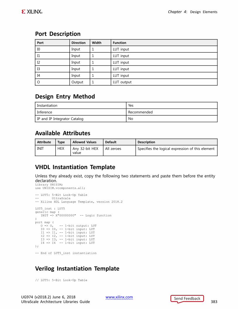
Chapter 4: Design Elements
Port DescriptionPort Direction Width Function
I0 Input 1 LUT input
I1 Input 1 LUT input
I2 Input 1 LUT input
I3 Input 1 LUT input
I4 Input 1 LUT input
O Output 1 LUT output
Design Entry MethodInstantiation Yes
Inference Recommended
IP and IP Integrator Catalog No
Available AttributesAttribute Type Allowed Values Default Description
INIT HEX Any 32-bit HEXvalue
All zeroes Specifies the logical expression of this element
VHDL Instantiation TemplateUnless they already exist, copy the following two statements and paste them before the entitydeclaration.Library UNISIM;use UNISIM.vcomponents.all;
-- LUT5: 5-Bit Look-Up Table-- UltraScale-- Xilinx HDL Language Template, version 2018.2
LUT5_inst : LUT5generic map (
INIT => X"00000000" -- Logic function)port map (
O => O, -- 1-bit output: LUTI0 => I0, -- 1-bit input: LUTI1 => I1, -- 1-bit input: LUTI2 => I2, -- 1-bit input: LUTI3 => I3, -- 1-bit input: LUTI4 => I4 -- 1-bit input: LUT
);
-- End of LUT5_inst instantiation
Verilog Instantiation Template// LUT5: 5-Bit Look-Up Table
UG974 (v2018.2) June 6, 2018 www.xilinx.comUltraScale Architecture Libraries Guide 383
Send Feedback
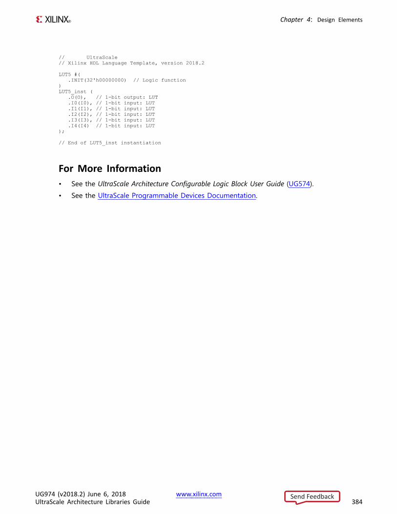
Chapter 4: Design Elements
// UltraScale// Xilinx HDL Language Template, version 2018.2
LUT5 #(.INIT(32'h00000000) // Logic function
)LUT5_inst (
.O(O), // 1-bit output: LUT
.I0(I0), // 1-bit input: LUT
.I1(I1), // 1-bit input: LUT
.I2(I2), // 1-bit input: LUT
.I3(I3), // 1-bit input: LUT
.I4(I4) // 1-bit input: LUT);
// End of LUT5_inst instantiation
For More Information• See the UltraScale Architecture Configurable Logic Block User Guide (UG574).
• See the UltraScale Programmable Devices Documentation.
UG974 (v2018.2) June 6, 2018 www.xilinx.comUltraScale Architecture Libraries Guide 384
Send Feedback
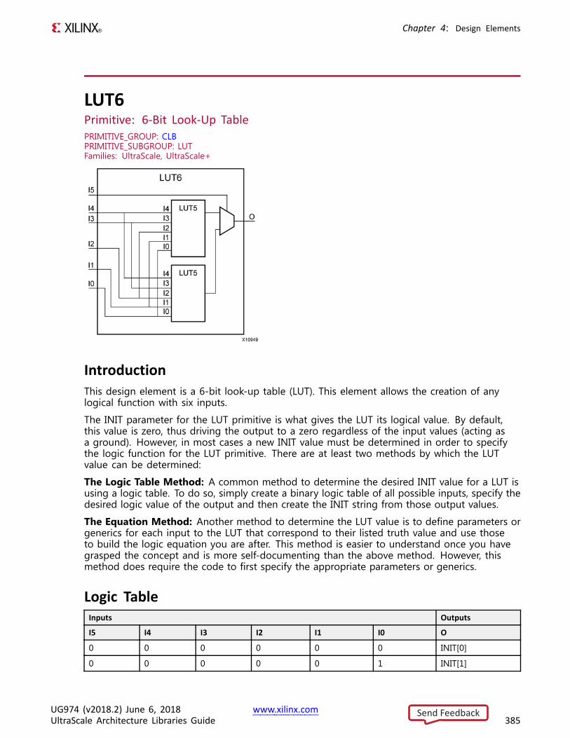
Chapter 4: Design Elements
LUT6Primitive: 6-Bit Look-Up TablePRIMITIVE_GROUP: CLBPRIMITIVE_SUBGROUP: LUTFamilies: UltraScale, UltraScale+
IntroductionThis design element is a 6-bit look-up table (LUT). This element allows the creation of anylogical function with six inputs.
The INIT parameter for the LUT primitive is what gives the LUT its logical value. By default,this value is zero, thus driving the output to a zero regardless of the input values (acting asa ground). However, in most cases a new INIT value must be determined in order to specifythe logic function for the LUT primitive. There are at least two methods by which the LUTvalue can be determined:
The Logic Table Method: A common method to determine the desired INIT value for a LUT isusing a logic table. To do so, simply create a binary logic table of all possible inputs, specify thedesired logic value of the output and then create the INIT string from those output values.
The Equation Method: Another method to determine the LUT value is to define parameters orgenerics for each input to the LUT that correspond to their listed truth value and use thoseto build the logic equation you are after. This method is easier to understand once you havegrasped the concept and is more self-documenting than the above method. However, thismethod does require the code to first specify the appropriate parameters or generics.
Logic TableInputs Outputs
I5 I4 I3 I2 I1 I0 O
0 0 0 0 0 0 INIT[0]
0 0 0 0 0 1 INIT[1]
UG974 (v2018.2) June 6, 2018 www.xilinx.comUltraScale Architecture Libraries Guide 385
Send Feedback
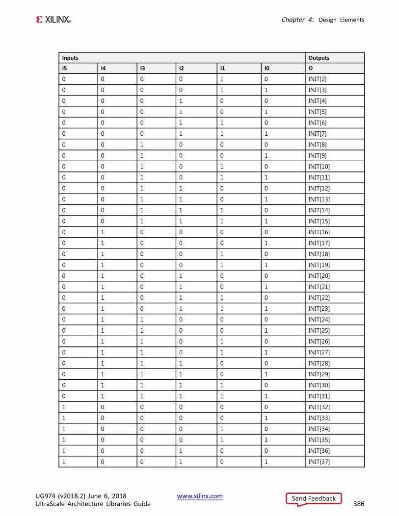
Chapter 4: Design Elements
Inputs Outputs
I5 I4 I3 I2 I1 I0 O
0 0 0 0 1 0 INIT[2]
0 0 0 0 1 1 INIT[3]
0 0 0 1 0 0 INIT[4]
0 0 0 1 0 1 INIT[5]
0 0 0 1 1 0 INIT[6]
0 0 0 1 1 1 INIT[7]
0 0 1 0 0 0 INIT[8]
0 0 1 0 0 1 INIT[9]
0 0 1 0 1 0 INIT[10]
0 0 1 0 1 1 INIT[11]
0 0 1 1 0 0 INIT[12]
0 0 1 1 0 1 INIT[13]
0 0 1 1 1 0 INIT[14]
0 0 1 1 1 1 INIT[15]
0 1 0 0 0 0 INIT[16]
0 1 0 0 0 1 INIT[17]
0 1 0 0 1 0 INIT[18]
0 1 0 0 1 1 INIT[19]
0 1 0 1 0 0 INIT[20]
0 1 0 1 0 1 INIT[21]
0 1 0 1 1 0 INIT[22]
0 1 0 1 1 1 INIT[23]
0 1 1 0 0 0 INIT[24]
0 1 1 0 0 1 INIT[25]
0 1 1 0 1 0 INIT[26]
0 1 1 0 1 1 INIT[27]
0 1 1 1 0 0 INIT[28]
0 1 1 1 0 1 INIT[29]
0 1 1 1 1 0 INIT[30]
0 1 1 1 1 1 INIT[31]
1 0 0 0 0 0 INIT[32]
1 0 0 0 0 1 INIT[33]
1 0 0 0 1 0 INIT[34]
1 0 0 0 1 1 INIT[35]
1 0 0 1 0 0 INIT[36]
1 0 0 1 0 1 INIT[37]
UG974 (v2018.2) June 6, 2018 www.xilinx.comUltraScale Architecture Libraries Guide 386
Send Feedback
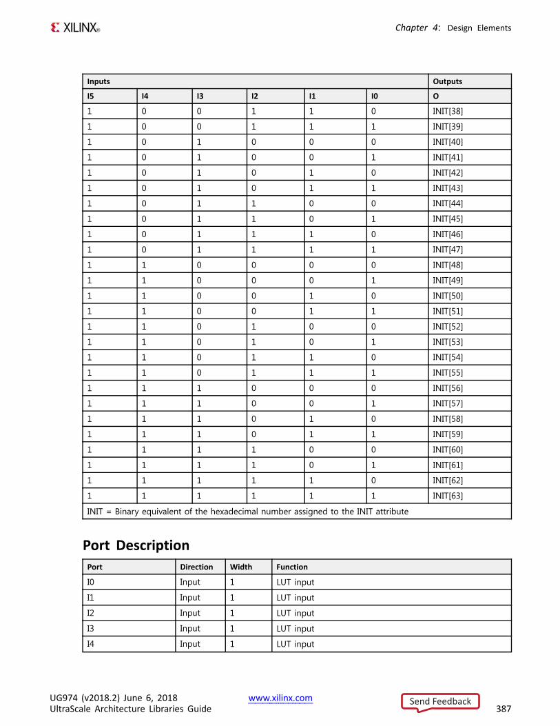
Chapter 4: Design Elements
Inputs Outputs
I5 I4 I3 I2 I1 I0 O
1 0 0 1 1 0 INIT[38]
1 0 0 1 1 1 INIT[39]
1 0 1 0 0 0 INIT[40]
1 0 1 0 0 1 INIT[41]
1 0 1 0 1 0 INIT[42]
1 0 1 0 1 1 INIT[43]
1 0 1 1 0 0 INIT[44]
1 0 1 1 0 1 INIT[45]
1 0 1 1 1 0 INIT[46]
1 0 1 1 1 1 INIT[47]
1 1 0 0 0 0 INIT[48]
1 1 0 0 0 1 INIT[49]
1 1 0 0 1 0 INIT[50]
1 1 0 0 1 1 INIT[51]
1 1 0 1 0 0 INIT[52]
1 1 0 1 0 1 INIT[53]
1 1 0 1 1 0 INIT[54]
1 1 0 1 1 1 INIT[55]
1 1 1 0 0 0 INIT[56]
1 1 1 0 0 1 INIT[57]
1 1 1 0 1 0 INIT[58]
1 1 1 0 1 1 INIT[59]
1 1 1 1 0 0 INIT[60]
1 1 1 1 0 1 INIT[61]
1 1 1 1 1 0 INIT[62]
1 1 1 1 1 1 INIT[63]
INIT = Binary equivalent of the hexadecimal number assigned to the INIT attribute
Port DescriptionPort Direction Width Function
I0 Input 1 LUT input
I1 Input 1 LUT input
I2 Input 1 LUT input
I3 Input 1 LUT input
I4 Input 1 LUT input
UG974 (v2018.2) June 6, 2018 www.xilinx.comUltraScale Architecture Libraries Guide 387
Send Feedback
Chapter 4: Design Elements
Port Direction Width Function
I5 Input 1 LUT input
O Output 1 LUT output
Design Entry MethodInstantiation Yes
Inference Recommended
IP and IP Integrator Catalog No
Available AttributesAttribute Type Allowed Values Default Description
INIT HEX Any 64-bit HEX value All zeroes Specifies the logical expression of thiselement
VHDL Instantiation TemplateUnless they already exist, copy the following two statements and paste them before the entitydeclaration.Library UNISIM;use UNISIM.vcomponents.all;
-- LUT6: 6-Bit Look-Up Table-- UltraScale-- Xilinx HDL Language Template, version 2018.2
LUT6_inst : LUT6generic map (
INIT => X"0000000000000000" -- Logic function)port map (
O => O, -- 1-bit output: LUTI0 => I0, -- 1-bit input: LUTI1 => I1, -- 1-bit input: LUTI2 => I2, -- 1-bit input: LUTI3 => I3, -- 1-bit input: LUTI4 => I4, -- 1-bit input: LUTI5 => I5 -- 1-bit input: LUT
);
-- End of LUT6_inst instantiation
Verilog Instantiation Template// LUT6: 6-Bit Look-Up Table// UltraScale// Xilinx HDL Language Template, version 2018.2
LUT6 #(.INIT(64'h0000000000000000) // Logic function
)LUT6_inst (
.O(O), // 1-bit output: LUT
.I0(I0), // 1-bit input: LUT
UG974 (v2018.2) June 6, 2018 www.xilinx.comUltraScale Architecture Libraries Guide 388
Send Feedback
Chapter 4: Design Elements
.I1(I1), // 1-bit input: LUT
.I2(I2), // 1-bit input: LUT
.I3(I3), // 1-bit input: LUT
.I4(I4), // 1-bit input: LUT
.I5(I5) // 1-bit input: LUT);
// End of LUT6_inst instantiation
For More Information• See the UltraScale Architecture Configurable Logic Block User Guide (UG574).
• See the UltraScale Programmable Devices Documentation.
UG974 (v2018.2) June 6, 2018 www.xilinx.comUltraScale Architecture Libraries Guide 389
Send Feedback
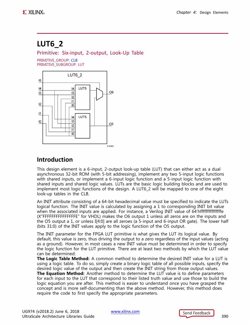
Chapter 4: Design Elements
LUT6_2Primitive: Six-input, 2-output, Look-Up TablePRIMITIVE_GROUP: CLBPRIMITIVE_SUBGROUP: LUT
IntroductionThis design element is a 6-input, 2-output look-up table (LUT) that can either act as a dualasynchronous 32-bit ROM (with 5-bit addressing), implement any two 5-input logic functionswith shared inputs, or implement a 6-input logic function and a 5-input logic function withshared inputs and shared logic values. LUTs are the basic logic building blocks and are used toimplement most logic functions of the design. A LUT6_2 will be mapped to one of the eightlook-up tables in the CLB.
An INIT attribute consisting of a 64-bit hexadecimal value must be specified to indicate the LUTslogical function. The INIT value is calculated by assigning a 1 to corresponding INIT bit valuewhen the associated inputs are applied. For instance, a Verilog INIT value of 64’hfffffffffffffffe(X"FFFFFFFFFFFFFFFE" for VHDL) makes the O6 output 1 unless all zeros are on the inputs andthe O5 output a 1, or unless I[4:0] are all zeroes (a 5-input and 6-input OR gate). The lower half(bits 31:0) of the INIT values apply to the logic function of the O5 output.
The INIT parameter for the FPGA LUT primitive is what gives the LUT its logical value. Bydefault, this value is zero, thus driving the output to a zero regardless of the input values (actingas a ground). However, in most cases a new INIT value must be determined in order to specifythe logic function for the LUT primitive. There are at least two methods by which the LUT valuecan be determined:The Logic Table Method: A common method to determine the desired INIT value for a LUT isusing a logic table. To do so, simply create a binary logic table of all possible inputs, specify thedesired logic value of the output and then create the INIT string from those output values.The Equation Method: Another method to determine the LUT value is to define parametersfor each input to the LUT that correspond to their listed truth value and use those to build thelogic equation you are after. This method is easier to understand once you have grasped theconcept and is more self-documenting than the above method. However, this method doesrequire the code to first specify the appropriate parameters.
UG974 (v2018.2) June 6, 2018 www.xilinx.comUltraScale Architecture Libraries Guide 390
Send Feedback
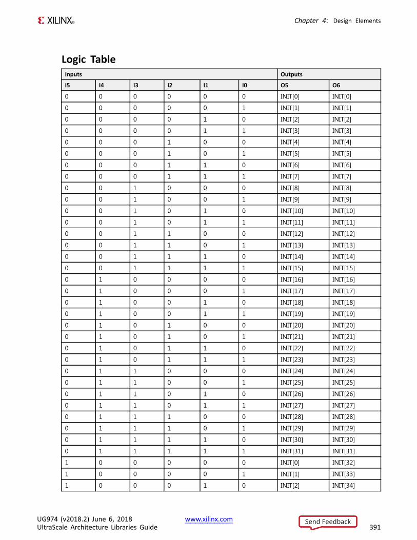
Chapter 4: Design Elements
Logic TableInputs Outputs
I5 I4 I3 I2 I1 I0 O5 O6
0 0 0 0 0 0 INIT[0] INIT[0]
0 0 0 0 0 1 INIT[1] INIT[1]
0 0 0 0 1 0 INIT[2] INIT[2]
0 0 0 0 1 1 INIT[3] INIT[3]
0 0 0 1 0 0 INIT[4] INIT[4]
0 0 0 1 0 1 INIT[5] INIT[5]
0 0 0 1 1 0 INIT[6] INIT[6]
0 0 0 1 1 1 INIT[7] INIT[7]
0 0 1 0 0 0 INIT[8] INIT[8]
0 0 1 0 0 1 INIT[9] INIT[9]
0 0 1 0 1 0 INIT[10] INIT[10]
0 0 1 0 1 1 INIT[11] INIT[11]
0 0 1 1 0 0 INIT[12] INIT[12]
0 0 1 1 0 1 INIT[13] INIT[13]
0 0 1 1 1 0 INIT[14] INIT[14]
0 0 1 1 1 1 INIT[15] INIT[15]
0 1 0 0 0 0 INIT[16] INIT[16]
0 1 0 0 0 1 INIT[17] INIT[17]
0 1 0 0 1 0 INIT[18] INIT[18]
0 1 0 0 1 1 INIT[19] INIT[19]
0 1 0 1 0 0 INIT[20] INIT[20]
0 1 0 1 0 1 INIT[21] INIT[21]
0 1 0 1 1 0 INIT[22] INIT[22]
0 1 0 1 1 1 INIT[23] INIT[23]
0 1 1 0 0 0 INIT[24] INIT[24]
0 1 1 0 0 1 INIT[25] INIT[25]
0 1 1 0 1 0 INIT[26] INIT[26]
0 1 1 0 1 1 INIT[27] INIT[27]
0 1 1 1 0 0 INIT[28] INIT[28]
0 1 1 1 0 1 INIT[29] INIT[29]
0 1 1 1 1 0 INIT[30] INIT[30]
0 1 1 1 1 1 INIT[31] INIT[31]
1 0 0 0 0 0 INIT[0] INIT[32]
1 0 0 0 0 1 INIT[1] INIT[33]
1 0 0 0 1 0 INIT[2] INIT[34]
UG974 (v2018.2) June 6, 2018 www.xilinx.comUltraScale Architecture Libraries Guide 391
Send Feedback
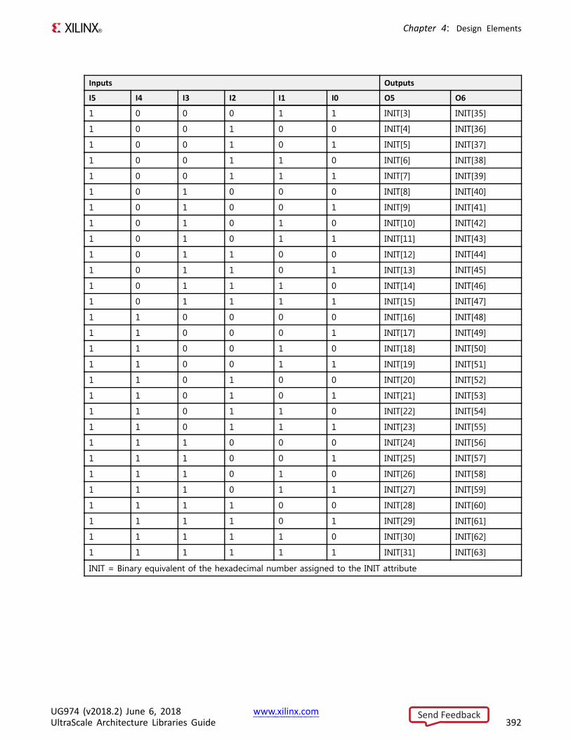
Chapter 4: Design Elements
Inputs Outputs
I5 I4 I3 I2 I1 I0 O5 O6
1 0 0 0 1 1 INIT[3] INIT[35]
1 0 0 1 0 0 INIT[4] INIT[36]
1 0 0 1 0 1 INIT[5] INIT[37]
1 0 0 1 1 0 INIT[6] INIT[38]
1 0 0 1 1 1 INIT[7] INIT[39]
1 0 1 0 0 0 INIT[8] INIT[40]
1 0 1 0 0 1 INIT[9] INIT[41]
1 0 1 0 1 0 INIT[10] INIT[42]
1 0 1 0 1 1 INIT[11] INIT[43]
1 0 1 1 0 0 INIT[12] INIT[44]
1 0 1 1 0 1 INIT[13] INIT[45]
1 0 1 1 1 0 INIT[14] INIT[46]
1 0 1 1 1 1 INIT[15] INIT[47]
1 1 0 0 0 0 INIT[16] INIT[48]
1 1 0 0 0 1 INIT[17] INIT[49]
1 1 0 0 1 0 INIT[18] INIT[50]
1 1 0 0 1 1 INIT[19] INIT[51]
1 1 0 1 0 0 INIT[20] INIT[52]
1 1 0 1 0 1 INIT[21] INIT[53]
1 1 0 1 1 0 INIT[22] INIT[54]
1 1 0 1 1 1 INIT[23] INIT[55]
1 1 1 0 0 0 INIT[24] INIT[56]
1 1 1 0 0 1 INIT[25] INIT[57]
1 1 1 0 1 0 INIT[26] INIT[58]
1 1 1 0 1 1 INIT[27] INIT[59]
1 1 1 1 0 0 INIT[28] INIT[60]
1 1 1 1 0 1 INIT[29] INIT[61]
1 1 1 1 1 0 INIT[30] INIT[62]
1 1 1 1 1 1 INIT[31] INIT[63]
INIT = Binary equivalent of the hexadecimal number assigned to the INIT attribute
UG974 (v2018.2) June 6, 2018 www.xilinx.comUltraScale Architecture Libraries Guide 392
Send Feedback
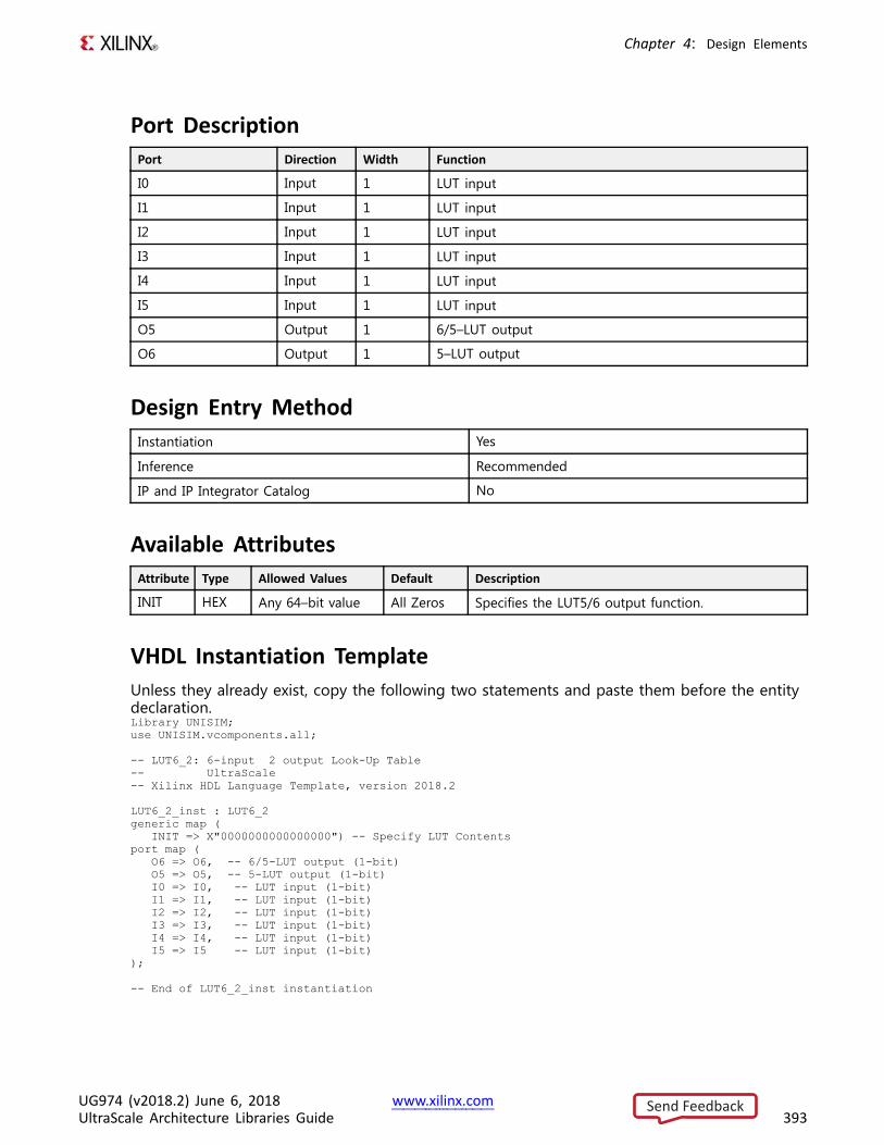
Chapter 4: Design Elements
Port DescriptionPort Direction Width Function
I0 Input 1 LUT input
I1 Input 1 LUT input
I2 Input 1 LUT input
I3 Input 1 LUT input
I4 Input 1 LUT input
I5 Input 1 LUT input
O5 Output 1 6/5–LUT output
O6 Output 1 5–LUT output
Design Entry MethodInstantiation Yes
Inference Recommended
IP and IP Integrator Catalog No
Available AttributesAttribute Type Allowed Values Default Description
INIT HEX Any 64–bit value All Zeros Specifies the LUT5/6 output function.
VHDL Instantiation TemplateUnless they already exist, copy the following two statements and paste them before the entitydeclaration.Library UNISIM;use UNISIM.vcomponents.all;
-- LUT6_2: 6-input 2 output Look-Up Table-- UltraScale-- Xilinx HDL Language Template, version 2018.2
LUT6_2_inst : LUT6_2generic map (
INIT => X"0000000000000000") -- Specify LUT Contentsport map (
O6 => O6, -- 6/5-LUT output (1-bit)O5 => O5, -- 5-LUT output (1-bit)I0 => I0, -- LUT input (1-bit)I1 => I1, -- LUT input (1-bit)I2 => I2, -- LUT input (1-bit)I3 => I3, -- LUT input (1-bit)I4 => I4, -- LUT input (1-bit)I5 => I5 -- LUT input (1-bit)
);
-- End of LUT6_2_inst instantiation
UG974 (v2018.2) June 6, 2018 www.xilinx.comUltraScale Architecture Libraries Guide 393
Send Feedback
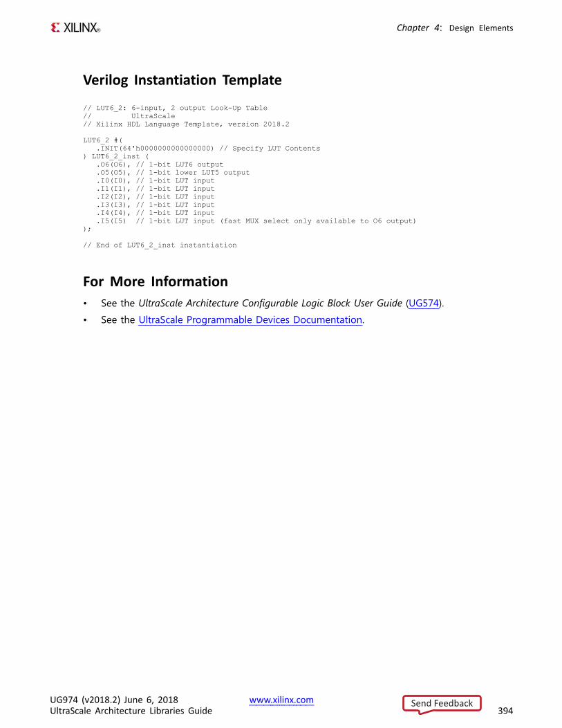
Chapter 4: Design Elements
Verilog Instantiation Template
// LUT6_2: 6-input, 2 output Look-Up Table// UltraScale// Xilinx HDL Language Template, version 2018.2
LUT6_2 #(.INIT(64'h0000000000000000) // Specify LUT Contents
) LUT6_2_inst (.O6(O6), // 1-bit LUT6 output.O5(O5), // 1-bit lower LUT5 output.I0(I0), // 1-bit LUT input.I1(I1), // 1-bit LUT input.I2(I2), // 1-bit LUT input.I3(I3), // 1-bit LUT input.I4(I4), // 1-bit LUT input.I5(I5) // 1-bit LUT input (fast MUX select only available to O6 output)
);
// End of LUT6_2_inst instantiation
For More Information• See the UltraScale Architecture Configurable Logic Block User Guide (UG574).
• See the UltraScale Programmable Devices Documentation.
UG974 (v2018.2) June 6, 2018 www.xilinx.comUltraScale Architecture Libraries Guide 394
Send Feedback
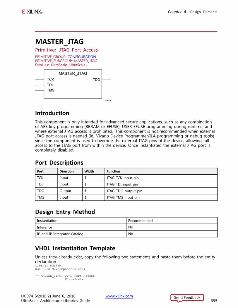
Chapter 4: Design Elements
MASTER_JTAGPrimitive: JTAG Port AccessPRIMITIVE_GROUP: CONFIGURATIONPRIMITIVE_SUBGROUP: MASTER_JTAGFamilies: UltraScale, UltraScale+
IntroductionThis component is only intended for advanced secure applications, such as any combinationof AES key programming (BBRAM or EFUSE), USER EFUSE programming during runtime, andwhere external JTAG access is prohibited. This component is not recommended when externalJTAG port access is needed (ie. Vivado Device Programmer/ILA programming or debug tools)since the component is used to override the external JTAG pins of the device, allowing fullaccess to the JTAG port from within the device. Once instantiated the external JTAG port iscompletely disabled.
Port DescriptionsPort Direction Width Function
TCK Input 1 JTAG TCK input pin
TDI Input 1 JTAG TDI input pin
TDO Output 1 JTAG TDO output pin
TMS Input 1 JTAG TMS input pin
Design Entry MethodInstantiation Recommended
Inference No
IP and IP Integrator Catalog No
VHDL Instantiation TemplateUnless they already exist, copy the following two statements and paste them before the entitydeclaration.Library UNISIM;use UNISIM.vcomponents.all;
-- MASTER_JTAG: JTAG Port Access-- UltraScale
UG974 (v2018.2) June 6, 2018 www.xilinx.comUltraScale Architecture Libraries Guide 395
Send Feedback
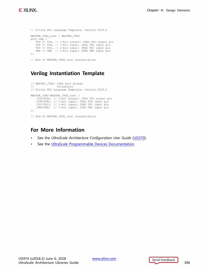
Chapter 4: Design Elements
-- Xilinx HDL Language Template, version 2018.2
MASTER_JTAG_inst : MASTER_JTAGport map (
TDO => TDO, -- 1-bit output: JTAG TDO output pinTCK => TCK, -- 1-bit input: JTAG TCK input pinTDI => TDI, -- 1-bit input: JTAG TDI input pinTMS => TMS -- 1-bit input: JTAG TMS input pin
);
-- End of MASTER_JTAG_inst instantiation
Verilog Instantiation Template
// MASTER_JTAG: JTAG Port Access// UltraScale// Xilinx HDL Language Template, version 2018.2
MASTER_JTAG MASTER_JTAG_inst (.TDO(TDO), // 1-bit output: JTAG TDO output pin.TCK(TCK), // 1-bit input: JTAG TCK input pin.TDI(TDI), // 1-bit input: JTAG TDI input pin.TMS(TMS) // 1-bit input: JTAG TMS input pin
);
// End of MASTER_JTAG_inst instantiation
For More Information• See the UltraScale Architecture Configuration User Guide (UG570).
• See the UltraScale Programmable Devices Documentation.
UG974 (v2018.2) June 6, 2018 www.xilinx.comUltraScale Architecture Libraries Guide 396
Send Feedback
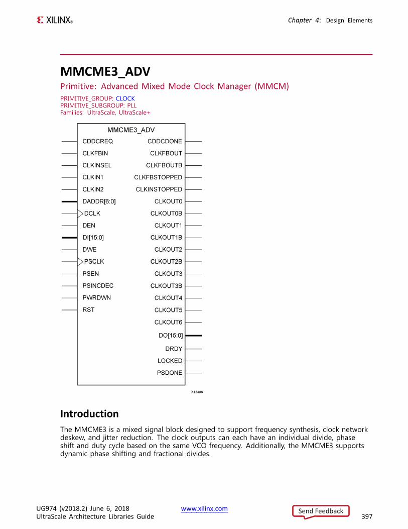
Chapter 4: Design Elements
MMCME3_ADVPrimitive: Advanced Mixed Mode Clock Manager (MMCM)PRIMITIVE_GROUP: CLOCKPRIMITIVE_SUBGROUP: PLLFamilies: UltraScale, UltraScale+
IntroductionThe MMCME3 is a mixed signal block designed to support frequency synthesis, clock networkdeskew, and jitter reduction. The clock outputs can each have an individual divide, phaseshift and duty cycle based on the same VCO frequency. Additionally, the MMCME3 supportsdynamic phase shifting and fractional divides.
UG974 (v2018.2) June 6, 2018 www.xilinx.comUltraScale Architecture Libraries Guide 397
Send Feedback
Chapter 4: Design Elements
Port DescriptionsPort Direction Width Function
CDDCREQ Input 1 Active high request signal for dynamically changing output clockdivide.
Clock Inputs: MMCM input clock(s). Connect CLKIN2 if input clock multiplexing feature is used.
CLKIN1 Input 1 Primary clock input.
CLKIN2 Input 1 Secondary clock input to dynamically switch the MMCM referenceclock.
Clock Outputs: User configurable clock outputs that can be divided versions of the VCO phase outputs(user controllable) from 1 (bypassed) to 128. The output clocks are phase aligned to each other (unlessphase shifted) and aligned to the input clock with a proper feedback configuration. The CLKOUT#B outputsare 180 degrees out of phase with the non-B outputs.
CLKOUT0 Output 1 CLKOUT0 output
CLKOUT0B Output 1 User configurable clock outputs that can be divided versions of theVCO phase outputs (user controllable) from 1 (bypassed) to 128.The output clocks are phase aligned to each other (unless phaseshifted) and aligned to the input clock with a proper feedbackconfiguration. The CLKOUT#B outputs are 180 degrees out ofphase with the non-B outputs.
CLKOUT1 Output 1 CLKOUT1 output
CLKOUT1B Output 1 Inverted CLKOUT1 output
CLKOUT2 Output 1 User configurable clock outputs that can be divided versions of theVCO phase outputs (user controllable) from 1 (bypassed) to 128.The output clocks are phase aligned to each other (unless phaseshifted) and aligned to the input clock with a proper feedbackconfiguration. The CLKOUT#B outputs are 180 degrees out ofphase with the non-B outputs.
CLKOUT2B Output 1 Inverted CLKOUT2 output
CLKOUT3 Output 1 CLKOUT3 output
CLKOUT3B Output 1 Inverted CLKOUT3 output
CLKOUT4 Output 1 CLKOUT4 output
CLKOUT5 Output 1 CLKOUT5 output
CLKOUT6 Output 1 CLKOUT6 output
Control Ports: MMCM control ports.
CLKINSEL Input 1 Signal controls the state of the input MUX, High = CLKIN1, Low= CLKIN2.
PWRDWN Input 1 Powers down MMCM components, thus reducing powerconsumption when derived clocks are not in use for sustainedperiods of time. Upon release of PWRDWN, the MMCM mustregain LOCK prior to use.
RST Input 1 Asynchronous reset signal. The MMCM will synchronously re-enableitself when this signal is released (i.e., MMCM re-enabled). A reset isrequired when the input clock conditions change (e.g., frequency).
DRP Ports: Ports used when using the dynamic reconfigurable ports for reading and writing theconfiguration of the MMCM.
UG974 (v2018.2) June 6, 2018 www.xilinx.comUltraScale Architecture Libraries Guide 398
Send Feedback
Chapter 4: Design Elements
Port Direction Width Function
DADDR<6:0> Input 7 The dynamic reconfiguration address (DADDR) input bus providesa reconfiguration address for the dynamic reconfiguration. Whennot used, all bits must be assigned zeroes.
DCLK Input 1 The DCLK signal is the reference clock for the dynamicreconfiguration port.
DEN Input 1 The dynamic reconfiguration enable (DEN) provides the enablecontrol signal to access the dynamic reconfiguration feature. Whenthe dynamic reconfiguration feature is not used, DEN must be tiedLow.
DI<15:0> Input 16 The dynamic reconfiguration data input (DI) bus providesreconfiguration data. When not used, all bits must be set to zero.
DO<15:0> Output 16 The dynamic reconfiguration output bus provides MMCM dataoutput when using dynamic reconfiguration.
DRDY Output 1 The dynamic reconfiguration ready output (DRDY) providesthe response to the DEN signal for the MMCMs dynamicreconfiguration feature.
DWE Input 1 The dynamic reconfiguration write enable (DWE) input pin providesthe write enable control signal to write the DI data into the DADDRaddress. When not used, it must be tied Low.
Dynamic Phase Shift Ports: Ports used when using the dynamic phase shift capability of the MMCM.
PSCLK Input 1 Phase shift clock.
PSDONE Output 1 Phase shift done.
PSEN Input 1 Phase shift enable
PSINCDEC Input 1 Phase shift increment/decrement control.
Feedback: Required ports to form the feedback path for the MMCM phase alignment capabilities.
CLKFBIN Input 1 Feedback clock pin to the MMCM
CLKFBOUT Output 1 Dedicated MMCM Feedback clock output
CLKFBOUTB Output 1 Inverted CLKFBOUT
Status Ports: MMCM status ports.
CDDCDONE Output 1 Acknowledge signal that output clock dynamic divide is done andthe output is valid.
CLKFBSTOPPED Output 1 Status pin indicating that the feedback clock has stopped.
CLKINSTOPPED Output 1 Status pin indicating that the input clock has stopped.
LOCKED Output 1 An output from the MMCM that indicates when the MMCMhas achieved phase alignment within a predefined window andfrequency matching within a predefined PPM range. The MMCMautomatically locks after power on, no extra reset is required.LOCKED will be deasserted if the input clock stops or the phasealignment is violated (e.g., input clock phase shift). The MMCMautomatically reacquires lock after LOCKED is deasserted.
UG974 (v2018.2) June 6, 2018 www.xilinx.comUltraScale Architecture Libraries Guide 399
Send Feedback
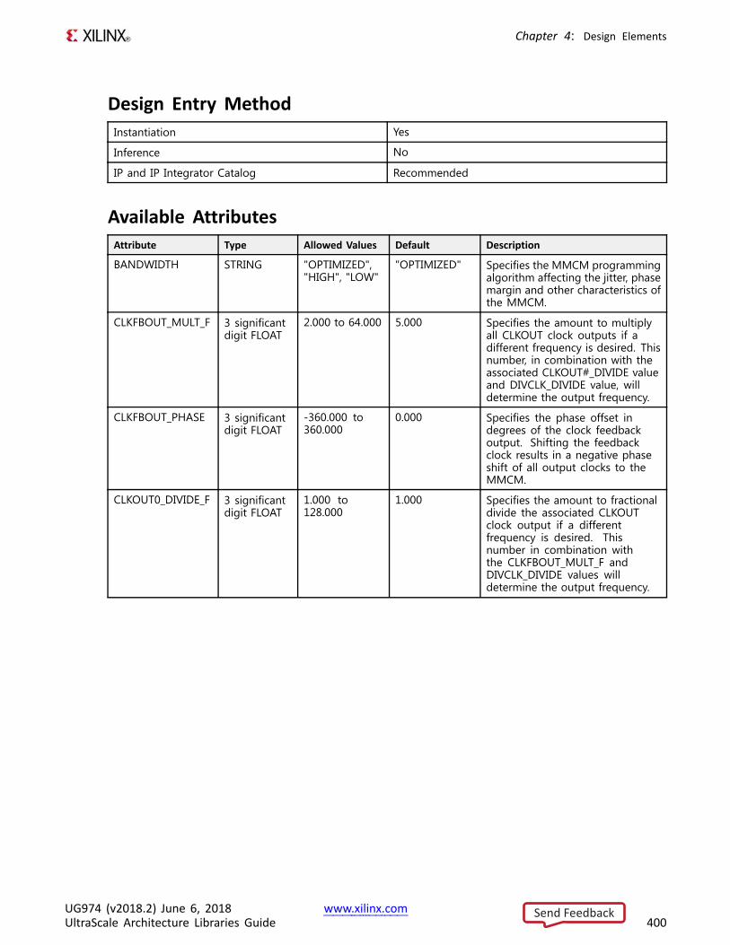
Chapter 4: Design Elements
Design Entry MethodInstantiation Yes
Inference No
IP and IP Integrator Catalog Recommended
Available AttributesAttribute Type Allowed Values Default Description
BANDWIDTH STRING "OPTIMIZED","HIGH", "LOW"
"OPTIMIZED" Specifies the MMCM programmingalgorithm affecting the jitter, phasemargin and other characteristics ofthe MMCM.
CLKFBOUT_MULT_F 3 significantdigit FLOAT
2.000 to 64.000 5.000 Specifies the amount to multiplyall CLKOUT clock outputs if adifferent frequency is desired. Thisnumber, in combination with theassociated CLKOUT#_DIVIDE valueand DIVCLK_DIVIDE value, willdetermine the output frequency.
CLKFBOUT_PHASE 3 significantdigit FLOAT
-360.000 to360.000
0.000 Specifies the phase offset indegrees of the clock feedbackoutput. Shifting the feedbackclock results in a negative phaseshift of all output clocks to theMMCM.
CLKOUT0_DIVIDE_F 3 significantdigit FLOAT
1.000 to128.000
1.000 Specifies the amount to fractionaldivide the associated CLKOUTclock output if a differentfrequency is desired. Thisnumber in combination withthe CLKFBOUT_MULT_F andDIVCLK_DIVIDE values willdetermine the output frequency.
UG974 (v2018.2) June 6, 2018 www.xilinx.comUltraScale Architecture Libraries Guide 400
Send Feedback
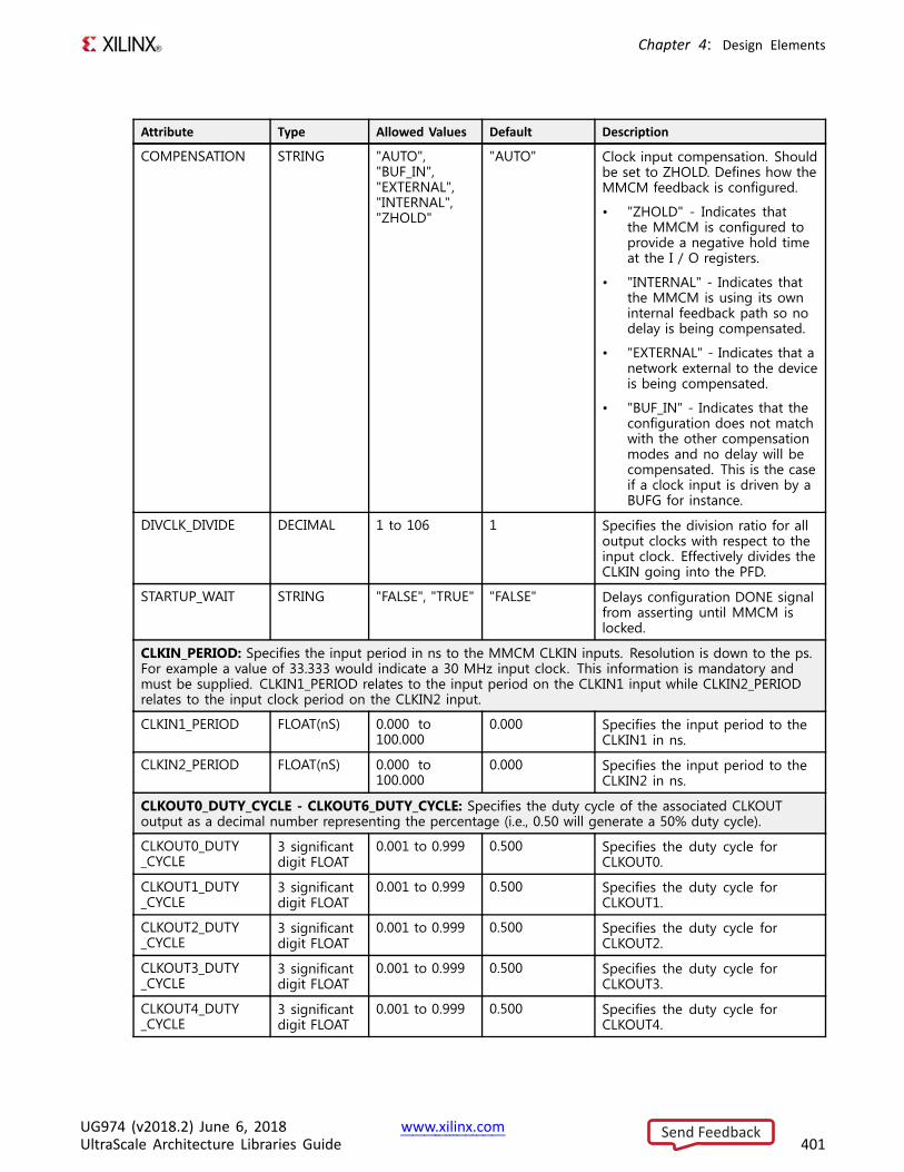
Chapter 4: Design Elements
Attribute Type Allowed Values Default Description
COMPENSATION STRING "AUTO","BUF_IN","EXTERNAL","INTERNAL","ZHOLD"
"AUTO" Clock input compensation. Shouldbe set to ZHOLD. Defines how theMMCM feedback is configured.
• "ZHOLD" - Indicates thatthe MMCM is configured toprovide a negative hold timeat the I / O registers.
• "INTERNAL" - Indicates thatthe MMCM is using its owninternal feedback path so nodelay is being compensated.
• "EXTERNAL" - Indicates that anetwork external to the deviceis being compensated.
• "BUF_IN" - Indicates that theconfiguration does not matchwith the other compensationmodes and no delay will becompensated. This is the caseif a clock input is driven by aBUFG for instance.
DIVCLK_DIVIDE DECIMAL 1 to 106 1 Specifies the division ratio for alloutput clocks with respect to theinput clock. Effectively divides theCLKIN going into the PFD.
STARTUP_WAIT STRING "FALSE", "TRUE" "FALSE" Delays configuration DONE signalfrom asserting until MMCM islocked.
CLKIN_PERIOD: Specifies the input period in ns to the MMCM CLKIN inputs. Resolution is down to the ps.For example a value of 33.333 would indicate a 30 MHz input clock. This information is mandatory andmust be supplied. CLKIN1_PERIOD relates to the input period on the CLKIN1 input while CLKIN2_PERIODrelates to the input clock period on the CLKIN2 input.
CLKIN1_PERIOD FLOAT(nS) 0.000 to100.000
0.000 Specifies the input period to theCLKIN1 in ns.
CLKIN2_PERIOD FLOAT(nS) 0.000 to100.000
0.000 Specifies the input period to theCLKIN2 in ns.
CLKOUT0_DUTY_CYCLE - CLKOUT6_DUTY_CYCLE: Specifies the duty cycle of the associated CLKOUToutput as a decimal number representing the percentage (i.e., 0.50 will generate a 50% duty cycle).
CLKOUT0_DUTY_CYCLE
3 significantdigit FLOAT
0.001 to 0.999 0.500 Specifies the duty cycle forCLKOUT0.
CLKOUT1_DUTY_CYCLE
3 significantdigit FLOAT
0.001 to 0.999 0.500 Specifies the duty cycle forCLKOUT1.
CLKOUT2_DUTY_CYCLE
3 significantdigit FLOAT
0.001 to 0.999 0.500 Specifies the duty cycle forCLKOUT2.
CLKOUT3_DUTY_CYCLE
3 significantdigit FLOAT
0.001 to 0.999 0.500 Specifies the duty cycle forCLKOUT3.
CLKOUT4_DUTY_CYCLE
3 significantdigit FLOAT
0.001 to 0.999 0.500 Specifies the duty cycle forCLKOUT4.
UG974 (v2018.2) June 6, 2018 www.xilinx.comUltraScale Architecture Libraries Guide 401
Send Feedback
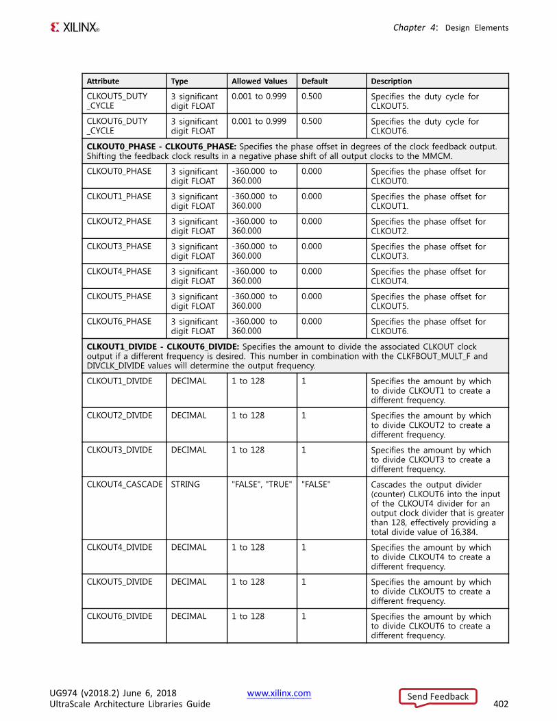
Chapter 4: Design Elements
Attribute Type Allowed Values Default Description
CLKOUT5_DUTY_CYCLE
3 significantdigit FLOAT
0.001 to 0.999 0.500 Specifies the duty cycle forCLKOUT5.
CLKOUT6_DUTY_CYCLE
3 significantdigit FLOAT
0.001 to 0.999 0.500 Specifies the duty cycle forCLKOUT6.
CLKOUT0_PHASE - CLKOUT6_PHASE: Specifies the phase offset in degrees of the clock feedback output.Shifting the feedback clock results in a negative phase shift of all output clocks to the MMCM.
CLKOUT0_PHASE 3 significantdigit FLOAT
-360.000 to360.000
0.000 Specifies the phase offset forCLKOUT0.
CLKOUT1_PHASE 3 significantdigit FLOAT
-360.000 to360.000
0.000 Specifies the phase offset forCLKOUT1.
CLKOUT2_PHASE 3 significantdigit FLOAT
-360.000 to360.000
0.000 Specifies the phase offset forCLKOUT2.
CLKOUT3_PHASE 3 significantdigit FLOAT
-360.000 to360.000
0.000 Specifies the phase offset forCLKOUT3.
CLKOUT4_PHASE 3 significantdigit FLOAT
-360.000 to360.000
0.000 Specifies the phase offset forCLKOUT4.
CLKOUT5_PHASE 3 significantdigit FLOAT
-360.000 to360.000
0.000 Specifies the phase offset forCLKOUT5.
CLKOUT6_PHASE 3 significantdigit FLOAT
-360.000 to360.000
0.000 Specifies the phase offset forCLKOUT6.
CLKOUT1_DIVIDE - CLKOUT6_DIVIDE: Specifies the amount to divide the associated CLKOUT clockoutput if a different frequency is desired. This number in combination with the CLKFBOUT_MULT_F andDIVCLK_DIVIDE values will determine the output frequency.
CLKOUT1_DIVIDE DECIMAL 1 to 128 1 Specifies the amount by whichto divide CLKOUT1 to create adifferent frequency.
CLKOUT2_DIVIDE DECIMAL 1 to 128 1 Specifies the amount by whichto divide CLKOUT2 to create adifferent frequency.
CLKOUT3_DIVIDE DECIMAL 1 to 128 1 Specifies the amount by whichto divide CLKOUT3 to create adifferent frequency.
CLKOUT4_CASCADE STRING "FALSE", "TRUE" "FALSE" Cascades the output divider(counter) CLKOUT6 into the inputof the CLKOUT4 divider for anoutput clock divider that is greaterthan 128, effectively providing atotal divide value of 16,384.
CLKOUT4_DIVIDE DECIMAL 1 to 128 1 Specifies the amount by whichto divide CLKOUT4 to create adifferent frequency.
CLKOUT5_DIVIDE DECIMAL 1 to 128 1 Specifies the amount by whichto divide CLKOUT5 to create adifferent frequency.
CLKOUT6_DIVIDE DECIMAL 1 to 128 1 Specifies the amount by whichto divide CLKOUT6 to create adifferent frequency.
UG974 (v2018.2) June 6, 2018 www.xilinx.comUltraScale Architecture Libraries Guide 402
Send Feedback
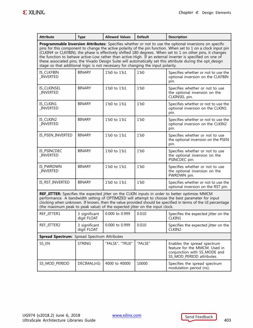
Chapter 4: Design Elements
Attribute Type Allowed Values Default Description
Programmable Inversion Attributes: Specifies whether or not to use the optional inversions on specificpins for this component to change the active polarity of the pin function. When set to 1 on a clock input pin(CLKIN# or CLKFBIN), the phase is effectively shifted 180 degrees. When set to 1 on other pins, it changesthe function to behave active-Low rather than active-High. If an external inverter is specified on one ofthese associated pins, the Vivado Design Suite will automatically set this attribute during the opt_designstage so that additional logic is not necessary for changing the input polarity.
IS_CLKFBIN_INVERTED
BINARY 1'b0 to 1'b1 1'b0 Specifies whether or not to use theoptional inversion on the CLKFBINpin.
IS_CLKINSEL_INVERTED
BINARY 1'b0 to 1'b1 1'b0 Specifies whether or not to usethe optional inversion on theCLKINSEL pin.
IS_CLKIN1_INVERTED
BINARY 1'b0 to 1'b1 1'b0 Specifies whether or not to use theoptional inversion on the CLKIN1pin.
IS_CLKIN2_INVERTED
BINARY 1'b0 to 1'b1 1'b0 Specifies whether or not to use theoptional inversion on the CLKIN2pin.
IS_PSEN_INVERTED BINARY 1'b0 to 1'b1 1'b0 Specifies whether or not to usethe optional inversion on the PSENpin.
IS_PSINCDEC_INVERTED
BINARY 1'b0 to 1'b1 1'b0 Specifies whether or not to usethe optional inversion on thePSINCDEC pin.
IS_PWRDWN_INVERTED
BINARY 1'b0 to 1'b1 1'b0 Specifies whether or not to usethe optional inversion on thePWRDWN pin.
IS_RST_INVERTED BINARY 1'b0 to 1'b1 1'b0 Specifies whether or not to use theoptional inversion on the RST pin.
REF_JITTER: Specifies the expected jitter on the CLKIN inputs in order to better optimize MMCMperformance. A bandwidth setting of OPTIMIZED will attempt to choose the best parameter for inputclocking when unknown. If known, then the value provided should be specified in terms of the UI percentage(the maximum peak to peak value) of the expected jitter on the input clock.
REF_JITTER1 3 significantdigit FLOAT
0.000 to 0.999 0.010 Specifies the expected jitter on theCLKIN1
REF_JITTER2 3 significantdigit FLOAT
0.000 to 0.999 0.010 Specifies the expected jitter on theCLKIN2
Spread Spectrum: Spread Spectrum Attributes
SS_EN STRING "FALSE", "TRUE" "FALSE" Enables the spread spectrumfeature for the MMCM. Used inconjunction with SS_MODE andSS_MOD_PERIOD attributes.
SS_MOD_PERIOD DECIMAL(nS) 4000 to 40000 10000 Specifies the spread spectrummodulation period (ns).
UG974 (v2018.2) June 6, 2018 www.xilinx.comUltraScale Architecture Libraries Guide 403
Send Feedback
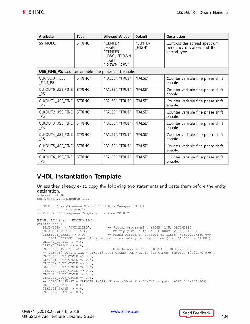
Chapter 4: Design Elements
Attribute Type Allowed Values Default Description
SS_MODE STRING "CENTER_HIGH","CENTER_LOW", "DOWN_HIGH","DOWN_LOW"
"CENTER_HIGH"
Controls the spread spectrumfrequency deviation and thespread type.
USE_FINE_PS: Counter variable fine phase shift enable.
CLKFBOUT_USE_FINE_PS
STRING "FALSE", "TRUE" "FALSE" Counter variable fine phase shiftenable.
CLKOUT0_USE_FINE_PS
STRING "FALSE", "TRUE" "FALSE" Counter variable fine phase shiftenable.
CLKOUT1_USE_FINE_PS
STRING "FALSE", "TRUE" "FALSE" Counter variable fine phase shiftenable.
CLKOUT2_USE_FINE_PS
STRING "FALSE", "TRUE" "FALSE" Counter variable fine phase shiftenable.
CLKOUT3_USE_FINE_PS
STRING "FALSE", "TRUE" "FALSE" Counter variable fine phase shiftenable.
CLKOUT4_USE_FINE_PS
STRING "FALSE", "TRUE" "FALSE" Counter variable fine phase shiftenable.
CLKOUT5_USE_FINE_PS
STRING "FALSE", "TRUE" "FALSE" Counter variable fine phase shiftenable.
CLKOUT6_USE_FINE_PS
STRING "FALSE", "TRUE" "FALSE" Counter variable fine phase shiftenable.
VHDL Instantiation TemplateUnless they already exist, copy the following two statements and paste them before the entitydeclaration.Library UNISIM;use UNISIM.vcomponents.all;
-- MMCME3_ADV: Advanced Mixed Mode Clock Manager (MMCM)-- UltraScale-- Xilinx HDL Language Template, version 2018.2
MMCME3_ADV_inst : MMCME3_ADVgeneric map (
BANDWIDTH => "OPTIMIZED", -- Jitter programming (HIGH, LOW, OPTIMIZED)CLKFBOUT_MULT_F => 5.0, -- Multiply value for all CLKOUT (2.000-64.000)CLKFBOUT_PHASE => 0.0, -- Phase offset in degrees of CLKFB (-360.000-360.000)-- CLKIN_PERIOD: Input clock period in ns units, ps resolution (i.e. 33.333 is 30 MHz).CLKIN1_PERIOD => 0.0,CLKIN2_PERIOD => 0.0,CLKOUT0_DIVIDE_F => 1.0, -- Divide amount for CLKOUT0 (1.000-128.000)-- CLKOUT0_DUTY_CYCLE - CLKOUT6_DUTY_CYCLE: Duty cycle for CLKOUT outputs (0.001-0.999).CLKOUT0_DUTY_CYCLE => 0.5,CLKOUT1_DUTY_CYCLE => 0.5,CLKOUT2_DUTY_CYCLE => 0.5,CLKOUT3_DUTY_CYCLE => 0.5,CLKOUT4_DUTY_CYCLE => 0.5,CLKOUT5_DUTY_CYCLE => 0.5,CLKOUT6_DUTY_CYCLE => 0.5,-- CLKOUT0_PHASE - CLKOUT6_PHASE: Phase offset for CLKOUT outputs (-360.000-360.000).CLKOUT0_PHASE => 0.0,CLKOUT1_PHASE => 0.0,CLKOUT2_PHASE => 0.0,
UG974 (v2018.2) June 6, 2018 www.xilinx.comUltraScale Architecture Libraries Guide 404
Send Feedback
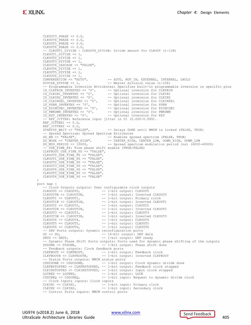
Chapter 4: Design Elements
CLKOUT3_PHASE => 0.0,CLKOUT4_PHASE => 0.0,CLKOUT5_PHASE => 0.0,CLKOUT6_PHASE => 0.0,-- CLKOUT1_DIVIDE - CLKOUT6_DIVIDE: Divide amount for CLKOUT (1-128)CLKOUT1_DIVIDE => 1,CLKOUT2_DIVIDE => 1,CLKOUT3_DIVIDE => 1,CLKOUT4_CASCADE => "FALSE",CLKOUT4_DIVIDE => 1,CLKOUT5_DIVIDE => 1,CLKOUT6_DIVIDE => 1,COMPENSATION => "AUTO", -- AUTO, BUF_IN, EXTERNAL, INTERNAL, ZHOLDDIVCLK_DIVIDE => 1, -- Master division value (1-106)-- Programmable Inversion Attributes: Specifies built-in programmable inversion on specific pinsIS_CLKFBIN_INVERTED => '0', -- Optional inversion for CLKFBINIS_CLKIN1_INVERTED => '0', -- Optional inversion for CLKIN1IS_CLKIN2_INVERTED => '0', -- Optional inversion for CLKIN2IS_CLKINSEL_INVERTED => '0', -- Optional inversion for CLKINSELIS_PSEN_INVERTED => '0', -- Optional inversion for PSENIS_PSINCDEC_INVERTED => '0', -- Optional inversion for PSINCDECIS_PWRDWN_INVERTED => '0', -- Optional inversion for PWRDWNIS_RST_INVERTED => '0', -- Optional inversion for RST-- REF_JITTER: Reference input jitter in UI (0.000-0.999).REF_JITTER1 => 0.0,REF_JITTER2 => 0.0,STARTUP_WAIT => "FALSE", -- Delays DONE until MMCM is locked (FALSE, TRUE)-- Spread Spectrum: Spread Spectrum AttributesSS_EN => "FALSE", -- Enables spread spectrum (FALSE, TRUE)SS_MODE => "CENTER_HIGH", -- CENTER_HIGH, CENTER_LOW, DOWN_HIGH, DOWN_LOWSS_MOD_PERIOD => 10000, -- Spread spectrum modulation period (ns) (4000-40000)-- USE_FINE_PS: Fine phase shift enable (TRUE/FALSE)CLKFBOUT_USE_FINE_PS => "FALSE",CLKOUT0_USE_FINE_PS => "FALSE",CLKOUT1_USE_FINE_PS => "FALSE",CLKOUT2_USE_FINE_PS => "FALSE",CLKOUT3_USE_FINE_PS => "FALSE",CLKOUT4_USE_FINE_PS => "FALSE",CLKOUT5_USE_FINE_PS => "FALSE",CLKOUT6_USE_FINE_PS => "FALSE"
)port map (
-- Clock Outputs outputs: User configurable clock outputsCLKOUT0 => CLKOUT0, -- 1-bit output: CLKOUT0CLKOUT0B => CLKOUT0B, -- 1-bit output: Inverted CLKOUT0CLKOUT1 => CLKOUT1, -- 1-bit output: Primary clockCLKOUT1B => CLKOUT1B, -- 1-bit output: Inverted CLKOUT1CLKOUT2 => CLKOUT2, -- 1-bit output: CLKOUT2CLKOUT2B => CLKOUT2B, -- 1-bit output: Inverted CLKOUT2CLKOUT3 => CLKOUT3, -- 1-bit output: CLKOUT3CLKOUT3B => CLKOUT3B, -- 1-bit output: Inverted CLKOUT3CLKOUT4 => CLKOUT4, -- 1-bit output: CLKOUT4CLKOUT5 => CLKOUT5, -- 1-bit output: CLKOUT5CLKOUT6 => CLKOUT6, -- 1-bit output: CLKOUT6-- DRP Ports outputs: Dynamic reconfiguration portsDO => DO, -- 16-bit output: DRP dataDRDY => DRDY, -- 1-bit output: DRP ready-- Dynamic Phase Shift Ports outputs: Ports used for dynamic phase shifting of the outputsPSDONE => PSDONE, -- 1-bit output: Phase shift done-- Feedback outputs: Clock feedback portsCLKFBOUT => CLKFBOUT, -- 1-bit output: Feedback clockCLKFBOUTB => CLKFBOUTB, -- 1-bit output: Inverted CLKFBOUT-- Status Ports outputs: MMCM status portsCDDCDONE => CDDCDONE, -- 1-bit output: Clock dynamic divide doneCLKFBSTOPPED => CLKFBSTOPPED, -- 1-bit output: Feedback clock stoppedCLKINSTOPPED => CLKINSTOPPED, -- 1-bit output: Input clock stoppedLOCKED => LOCKED, -- 1-bit output: LOCKCDDCREQ => CDDCREQ, -- 1-bit input: Request to dynamic divide clock-- Clock Inputs inputs: Clock inputsCLKIN1 => CLKIN1, -- 1-bit input: Primary clockCLKIN2 => CLKIN2, -- 1-bit input: Secondary clock-- Control Ports inputs: MMCM control ports
UG974 (v2018.2) June 6, 2018 www.xilinx.comUltraScale Architecture Libraries Guide 405
Send Feedback
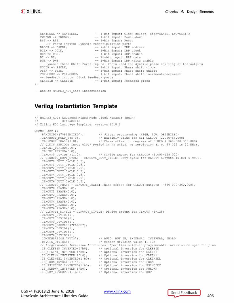
Chapter 4: Design Elements
CLKINSEL => CLKINSEL, -- 1-bit input: Clock select, High=CLKIN1 Low=CLKIN2PWRDWN => PWRDWN, -- 1-bit input: Power-downRST => RST, -- 1-bit input: Reset-- DRP Ports inputs: Dynamic reconfiguration portsDADDR => DADDR, -- 7-bit input: DRP addressDCLK => DCLK, -- 1-bit input: DRP clockDEN => DEN, -- 1-bit input: DRP enableDI => DI, -- 16-bit input: DRP dataDWE => DWE, -- 1-bit input: DRP write enable-- Dynamic Phase Shift Ports inputs: Ports used for dynamic phase shifting of the outputsPSCLK => PSCLK, -- 1-bit input: Phase shift clockPSEN => PSEN, -- 1-bit input: Phase shift enablePSINCDEC => PSINCDEC, -- 1-bit input: Phase shift increment/decrement-- Feedback inputs: Clock feedback portsCLKFBIN => CLKFBIN -- 1-bit input: Feedback clock
);
-- End of MMCME3_ADV_inst instantiation
Verilog Instantiation Template
// MMCME3_ADV: Advanced Mixed Mode Clock Manager (MMCM)// UltraScale// Xilinx HDL Language Template, version 2018.2
MMCME3_ADV #(.BANDWIDTH("OPTIMIZED"), // Jitter programming (HIGH, LOW, OPTIMIZED).CLKFBOUT_MULT_F(5.0), // Multiply value for all CLKOUT (2.000-64.000).CLKFBOUT_PHASE(0.0), // Phase offset in degrees of CLKFB (-360.000-360.000)// CLKIN_PERIOD: Input clock period in ns units, ps resolution (i.e. 33.333 is 30 MHz)..CLKIN1_PERIOD(0.0),.CLKIN2_PERIOD(0.0),.CLKOUT0_DIVIDE_F(1.0), // Divide amount for CLKOUT0 (1.000-128.000)// CLKOUT0_DUTY_CYCLE - CLKOUT6_DUTY_CYCLE: Duty cycle for CLKOUT outputs (0.001-0.999)..CLKOUT0_DUTY_CYCLE(0.5),.CLKOUT1_DUTY_CYCLE(0.5),.CLKOUT2_DUTY_CYCLE(0.5),.CLKOUT3_DUTY_CYCLE(0.5),.CLKOUT4_DUTY_CYCLE(0.5),.CLKOUT5_DUTY_CYCLE(0.5),.CLKOUT6_DUTY_CYCLE(0.5),// CLKOUT0_PHASE - CLKOUT6_PHASE: Phase offset for CLKOUT outputs (-360.000-360.000)..CLKOUT0_PHASE(0.0),.CLKOUT1_PHASE(0.0),.CLKOUT2_PHASE(0.0),.CLKOUT3_PHASE(0.0),.CLKOUT4_PHASE(0.0),.CLKOUT5_PHASE(0.0),.CLKOUT6_PHASE(0.0),// CLKOUT1_DIVIDE - CLKOUT6_DIVIDE: Divide amount for CLKOUT (1-128).CLKOUT1_DIVIDE(1),.CLKOUT2_DIVIDE(1),.CLKOUT3_DIVIDE(1),.CLKOUT4_CASCADE("FALSE"),.CLKOUT4_DIVIDE(1),.CLKOUT5_DIVIDE(1),.CLKOUT6_DIVIDE(1),.COMPENSATION("AUTO"), // AUTO, BUF_IN, EXTERNAL, INTERNAL, ZHOLD.DIVCLK_DIVIDE(1), // Master division value (1-106)// Programmable Inversion Attributes: Specifies built-in programmable inversion on specific pins.IS_CLKFBIN_INVERTED(1'b0), // Optional inversion for CLKFBIN.IS_CLKIN1_INVERTED(1'b0), // Optional inversion for CLKIN1.IS_CLKIN2_INVERTED(1'b0), // Optional inversion for CLKIN2.IS_CLKINSEL_INVERTED(1'b0), // Optional inversion for CLKINSEL.IS_PSEN_INVERTED(1'b0), // Optional inversion for PSEN.IS_PSINCDEC_INVERTED(1'b0), // Optional inversion for PSINCDEC.IS_PWRDWN_INVERTED(1'b0), // Optional inversion for PWRDWN.IS_RST_INVERTED(1'b0), // Optional inversion for RST
UG974 (v2018.2) June 6, 2018 www.xilinx.comUltraScale Architecture Libraries Guide 406
Send Feedback
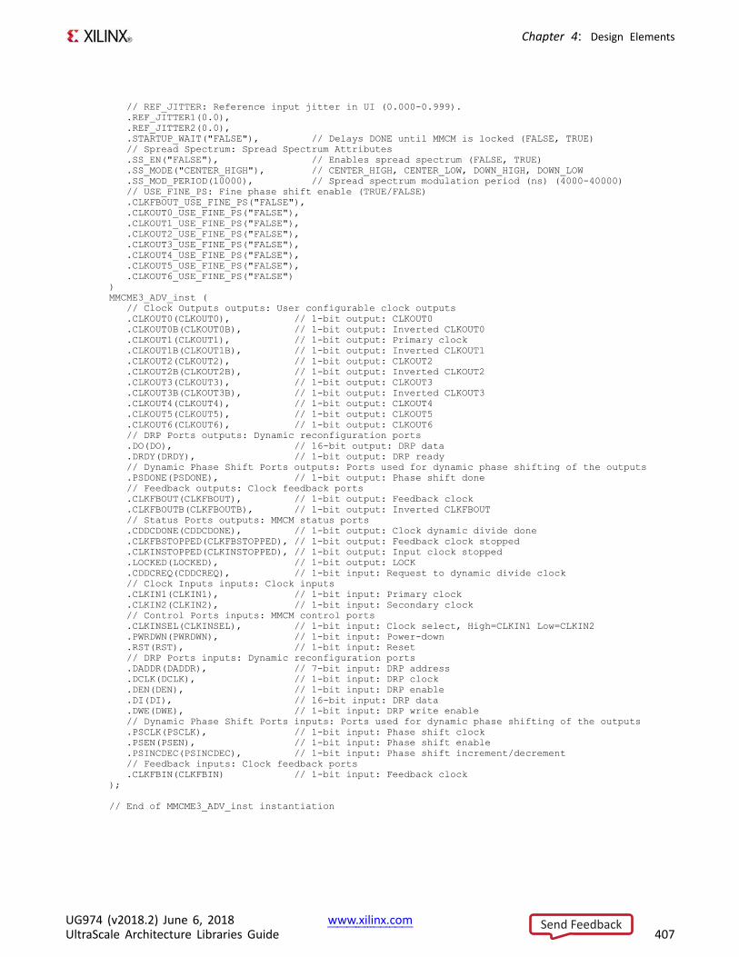
Chapter 4: Design Elements
// REF_JITTER: Reference input jitter in UI (0.000-0.999)..REF_JITTER1(0.0),.REF_JITTER2(0.0),.STARTUP_WAIT("FALSE"), // Delays DONE until MMCM is locked (FALSE, TRUE)// Spread Spectrum: Spread Spectrum Attributes.SS_EN("FALSE"), // Enables spread spectrum (FALSE, TRUE).SS_MODE("CENTER_HIGH"), // CENTER_HIGH, CENTER_LOW, DOWN_HIGH, DOWN_LOW.SS_MOD_PERIOD(10000), // Spread spectrum modulation period (ns) (4000-40000)// USE_FINE_PS: Fine phase shift enable (TRUE/FALSE).CLKFBOUT_USE_FINE_PS("FALSE"),.CLKOUT0_USE_FINE_PS("FALSE"),.CLKOUT1_USE_FINE_PS("FALSE"),.CLKOUT2_USE_FINE_PS("FALSE"),.CLKOUT3_USE_FINE_PS("FALSE"),.CLKOUT4_USE_FINE_PS("FALSE"),.CLKOUT5_USE_FINE_PS("FALSE"),.CLKOUT6_USE_FINE_PS("FALSE")
)MMCME3_ADV_inst (
// Clock Outputs outputs: User configurable clock outputs.CLKOUT0(CLKOUT0), // 1-bit output: CLKOUT0.CLKOUT0B(CLKOUT0B), // 1-bit output: Inverted CLKOUT0.CLKOUT1(CLKOUT1), // 1-bit output: Primary clock.CLKOUT1B(CLKOUT1B), // 1-bit output: Inverted CLKOUT1.CLKOUT2(CLKOUT2), // 1-bit output: CLKOUT2.CLKOUT2B(CLKOUT2B), // 1-bit output: Inverted CLKOUT2.CLKOUT3(CLKOUT3), // 1-bit output: CLKOUT3.CLKOUT3B(CLKOUT3B), // 1-bit output: Inverted CLKOUT3.CLKOUT4(CLKOUT4), // 1-bit output: CLKOUT4.CLKOUT5(CLKOUT5), // 1-bit output: CLKOUT5.CLKOUT6(CLKOUT6), // 1-bit output: CLKOUT6// DRP Ports outputs: Dynamic reconfiguration ports.DO(DO), // 16-bit output: DRP data.DRDY(DRDY), // 1-bit output: DRP ready// Dynamic Phase Shift Ports outputs: Ports used for dynamic phase shifting of the outputs.PSDONE(PSDONE), // 1-bit output: Phase shift done// Feedback outputs: Clock feedback ports.CLKFBOUT(CLKFBOUT), // 1-bit output: Feedback clock.CLKFBOUTB(CLKFBOUTB), // 1-bit output: Inverted CLKFBOUT// Status Ports outputs: MMCM status ports.CDDCDONE(CDDCDONE), // 1-bit output: Clock dynamic divide done.CLKFBSTOPPED(CLKFBSTOPPED), // 1-bit output: Feedback clock stopped.CLKINSTOPPED(CLKINSTOPPED), // 1-bit output: Input clock stopped.LOCKED(LOCKED), // 1-bit output: LOCK.CDDCREQ(CDDCREQ), // 1-bit input: Request to dynamic divide clock// Clock Inputs inputs: Clock inputs.CLKIN1(CLKIN1), // 1-bit input: Primary clock.CLKIN2(CLKIN2), // 1-bit input: Secondary clock// Control Ports inputs: MMCM control ports.CLKINSEL(CLKINSEL), // 1-bit input: Clock select, High=CLKIN1 Low=CLKIN2.PWRDWN(PWRDWN), // 1-bit input: Power-down.RST(RST), // 1-bit input: Reset// DRP Ports inputs: Dynamic reconfiguration ports.DADDR(DADDR), // 7-bit input: DRP address.DCLK(DCLK), // 1-bit input: DRP clock.DEN(DEN), // 1-bit input: DRP enable.DI(DI), // 16-bit input: DRP data.DWE(DWE), // 1-bit input: DRP write enable// Dynamic Phase Shift Ports inputs: Ports used for dynamic phase shifting of the outputs.PSCLK(PSCLK), // 1-bit input: Phase shift clock.PSEN(PSEN), // 1-bit input: Phase shift enable.PSINCDEC(PSINCDEC), // 1-bit input: Phase shift increment/decrement// Feedback inputs: Clock feedback ports.CLKFBIN(CLKFBIN) // 1-bit input: Feedback clock
);
// End of MMCME3_ADV_inst instantiation
UG974 (v2018.2) June 6, 2018 www.xilinx.comUltraScale Architecture Libraries Guide 407
Send Feedback

Chapter 4: Design Elements
For More Information• See the UltraScale Architecture Clocking Resources User Guide (UG572).
• See the UltraScale Programmable Devices Documentation.
UG974 (v2018.2) June 6, 2018 www.xilinx.comUltraScale Architecture Libraries Guide 408
Send Feedback
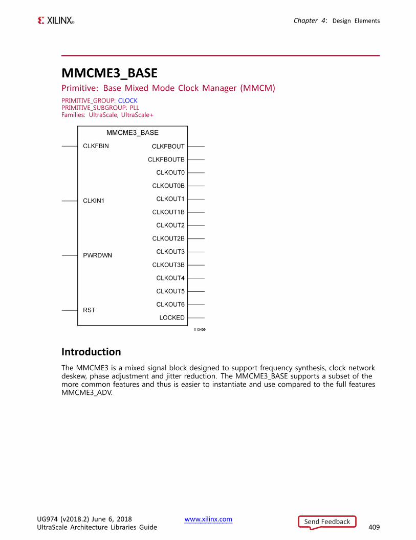
Chapter 4: Design Elements
MMCME3_BASEPrimitive: Base Mixed Mode Clock Manager (MMCM)PRIMITIVE_GROUP: CLOCKPRIMITIVE_SUBGROUP: PLLFamilies: UltraScale, UltraScale+
IntroductionThe MMCME3 is a mixed signal block designed to support frequency synthesis, clock networkdeskew, phase adjustment and jitter reduction. The MMCME3_BASE supports a subset of themore common features and thus is easier to instantiate and use compared to the full featuresMMCME3_ADV.
UG974 (v2018.2) June 6, 2018 www.xilinx.comUltraScale Architecture Libraries Guide 409
Send Feedback
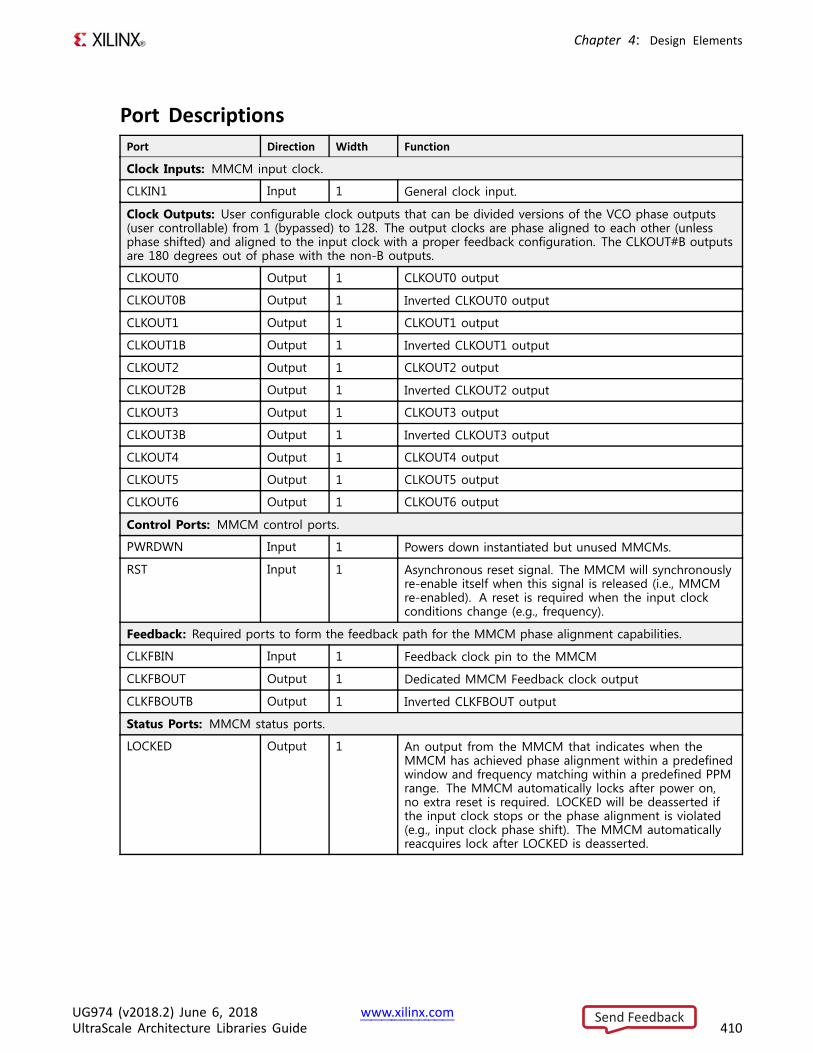
Chapter 4: Design Elements
Port DescriptionsPort Direction Width Function
Clock Inputs: MMCM input clock.
CLKIN1 Input 1 General clock input.
Clock Outputs: User configurable clock outputs that can be divided versions of the VCO phase outputs(user controllable) from 1 (bypassed) to 128. The output clocks are phase aligned to each other (unlessphase shifted) and aligned to the input clock with a proper feedback configuration. The CLKOUT#B outputsare 180 degrees out of phase with the non-B outputs.
CLKOUT0 Output 1 CLKOUT0 output
CLKOUT0B Output 1 Inverted CLKOUT0 output
CLKOUT1 Output 1 CLKOUT1 output
CLKOUT1B Output 1 Inverted CLKOUT1 output
CLKOUT2 Output 1 CLKOUT2 output
CLKOUT2B Output 1 Inverted CLKOUT2 output
CLKOUT3 Output 1 CLKOUT3 output
CLKOUT3B Output 1 Inverted CLKOUT3 output
CLKOUT4 Output 1 CLKOUT4 output
CLKOUT5 Output 1 CLKOUT5 output
CLKOUT6 Output 1 CLKOUT6 output
Control Ports: MMCM control ports.
PWRDWN Input 1 Powers down instantiated but unused MMCMs.
RST Input 1 Asynchronous reset signal. The MMCM will synchronouslyre-enable itself when this signal is released (i.e., MMCMre-enabled). A reset is required when the input clockconditions change (e.g., frequency).
Feedback: Required ports to form the feedback path for the MMCM phase alignment capabilities.
CLKFBIN Input 1 Feedback clock pin to the MMCM
CLKFBOUT Output 1 Dedicated MMCM Feedback clock output
CLKFBOUTB Output 1 Inverted CLKFBOUT output
Status Ports: MMCM status ports.
LOCKED Output 1 An output from the MMCM that indicates when theMMCM has achieved phase alignment within a predefinedwindow and frequency matching within a predefined PPMrange. The MMCM automatically locks after power on,no extra reset is required. LOCKED will be deasserted ifthe input clock stops or the phase alignment is violated(e.g., input clock phase shift). The MMCM automaticallyreacquires lock after LOCKED is deasserted.
UG974 (v2018.2) June 6, 2018 www.xilinx.comUltraScale Architecture Libraries Guide 410
Send Feedback
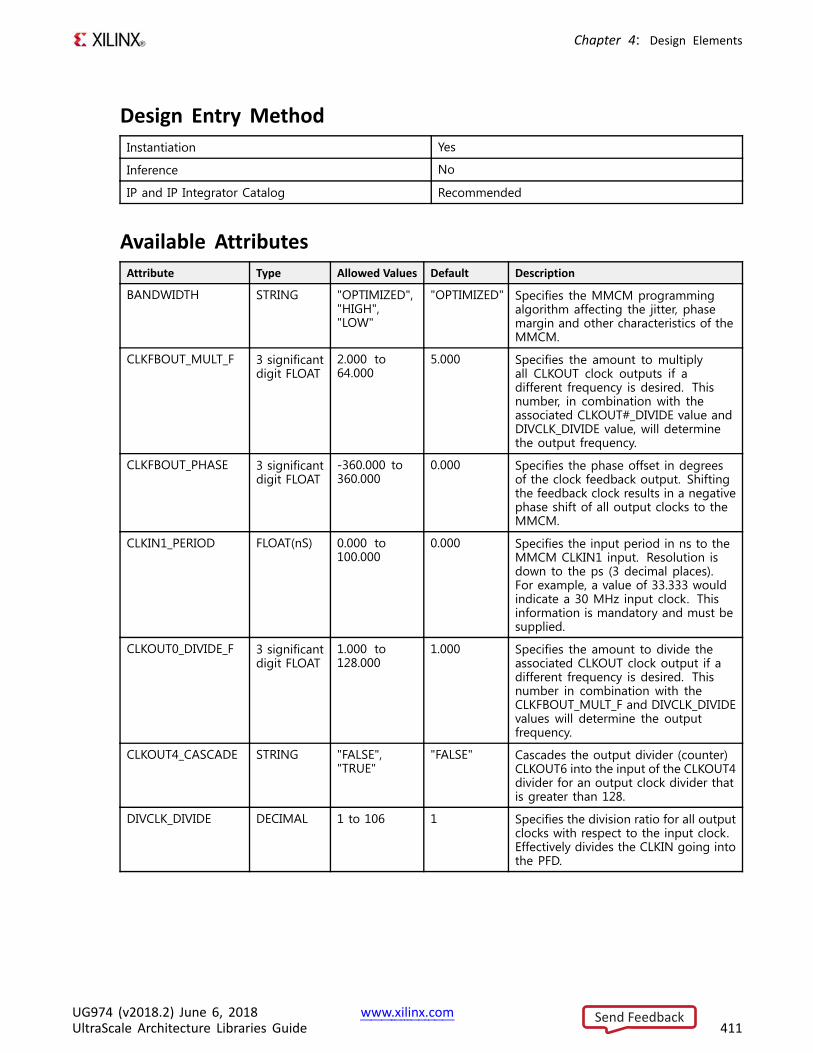
Chapter 4: Design Elements
Design Entry MethodInstantiation Yes
Inference No
IP and IP Integrator Catalog Recommended
Available AttributesAttribute Type Allowed Values Default Description
BANDWIDTH STRING "OPTIMIZED","HIGH","LOW"
"OPTIMIZED" Specifies the MMCM programmingalgorithm affecting the jitter, phasemargin and other characteristics of theMMCM.
CLKFBOUT_MULT_F 3 significantdigit FLOAT
2.000 to64.000
5.000 Specifies the amount to multiplyall CLKOUT clock outputs if adifferent frequency is desired. Thisnumber, in combination with theassociated CLKOUT#_DIVIDE value andDIVCLK_DIVIDE value, will determinethe output frequency.
CLKFBOUT_PHASE 3 significantdigit FLOAT
-360.000 to360.000
0.000 Specifies the phase offset in degreesof the clock feedback output. Shiftingthe feedback clock results in a negativephase shift of all output clocks to theMMCM.
CLKIN1_PERIOD FLOAT(nS) 0.000 to100.000
0.000 Specifies the input period in ns to theMMCM CLKIN1 input. Resolution isdown to the ps (3 decimal places).For example, a value of 33.333 wouldindicate a 30 MHz input clock. Thisinformation is mandatory and must besupplied.
CLKOUT0_DIVIDE_F 3 significantdigit FLOAT
1.000 to128.000
1.000 Specifies the amount to divide theassociated CLKOUT clock output if adifferent frequency is desired. Thisnumber in combination with theCLKFBOUT_MULT_F and DIVCLK_DIVIDEvalues will determine the outputfrequency.
CLKOUT4_CASCADE STRING "FALSE","TRUE"
"FALSE" Cascades the output divider (counter)CLKOUT6 into the input of the CLKOUT4divider for an output clock divider thatis greater than 128.
DIVCLK_DIVIDE DECIMAL 1 to 106 1 Specifies the division ratio for all outputclocks with respect to the input clock.Effectively divides the CLKIN going intothe PFD.
UG974 (v2018.2) June 6, 2018 www.xilinx.comUltraScale Architecture Libraries Guide 411
Send Feedback
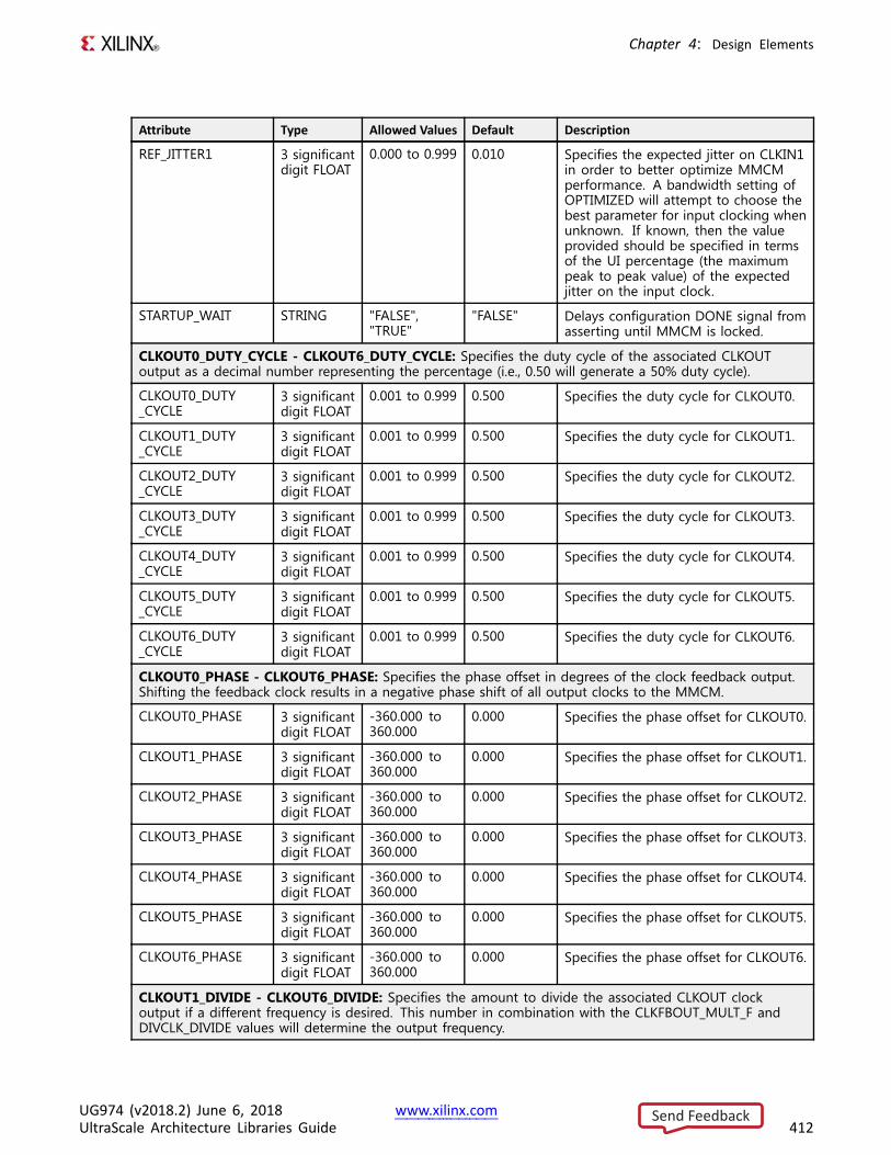
Chapter 4: Design Elements
Attribute Type Allowed Values Default Description
REF_JITTER1 3 significantdigit FLOAT
0.000 to 0.999 0.010 Specifies the expected jitter on CLKIN1in order to better optimize MMCMperformance. A bandwidth setting ofOPTIMIZED will attempt to choose thebest parameter for input clocking whenunknown. If known, then the valueprovided should be specified in termsof the UI percentage (the maximumpeak to peak value) of the expectedjitter on the input clock.
STARTUP_WAIT STRING "FALSE","TRUE"
"FALSE" Delays configuration DONE signal fromasserting until MMCM is locked.
CLKOUT0_DUTY_CYCLE - CLKOUT6_DUTY_CYCLE: Specifies the duty cycle of the associated CLKOUToutput as a decimal number representing the percentage (i.e., 0.50 will generate a 50% duty cycle).
CLKOUT0_DUTY_CYCLE
3 significantdigit FLOAT
0.001 to 0.999 0.500 Specifies the duty cycle for CLKOUT0.
CLKOUT1_DUTY_CYCLE
3 significantdigit FLOAT
0.001 to 0.999 0.500 Specifies the duty cycle for CLKOUT1.
CLKOUT2_DUTY_CYCLE
3 significantdigit FLOAT
0.001 to 0.999 0.500 Specifies the duty cycle for CLKOUT2.
CLKOUT3_DUTY_CYCLE
3 significantdigit FLOAT
0.001 to 0.999 0.500 Specifies the duty cycle for CLKOUT3.
CLKOUT4_DUTY_CYCLE
3 significantdigit FLOAT
0.001 to 0.999 0.500 Specifies the duty cycle for CLKOUT4.
CLKOUT5_DUTY_CYCLE
3 significantdigit FLOAT
0.001 to 0.999 0.500 Specifies the duty cycle for CLKOUT5.
CLKOUT6_DUTY_CYCLE
3 significantdigit FLOAT
0.001 to 0.999 0.500 Specifies the duty cycle for CLKOUT6.
CLKOUT0_PHASE - CLKOUT6_PHASE: Specifies the phase offset in degrees of the clock feedback output.Shifting the feedback clock results in a negative phase shift of all output clocks to the MMCM.
CLKOUT0_PHASE 3 significantdigit FLOAT
-360.000 to360.000
0.000 Specifies the phase offset for CLKOUT0.
CLKOUT1_PHASE 3 significantdigit FLOAT
-360.000 to360.000
0.000 Specifies the phase offset for CLKOUT1.
CLKOUT2_PHASE 3 significantdigit FLOAT
-360.000 to360.000
0.000 Specifies the phase offset for CLKOUT2.
CLKOUT3_PHASE 3 significantdigit FLOAT
-360.000 to360.000
0.000 Specifies the phase offset for CLKOUT3.
CLKOUT4_PHASE 3 significantdigit FLOAT
-360.000 to360.000
0.000 Specifies the phase offset for CLKOUT4.
CLKOUT5_PHASE 3 significantdigit FLOAT
-360.000 to360.000
0.000 Specifies the phase offset for CLKOUT5.
CLKOUT6_PHASE 3 significantdigit FLOAT
-360.000 to360.000
0.000 Specifies the phase offset for CLKOUT6.
CLKOUT1_DIVIDE - CLKOUT6_DIVIDE: Specifies the amount to divide the associated CLKOUT clockoutput if a different frequency is desired. This number in combination with the CLKFBOUT_MULT_F andDIVCLK_DIVIDE values will determine the output frequency.
UG974 (v2018.2) June 6, 2018 www.xilinx.comUltraScale Architecture Libraries Guide 412
Send Feedback
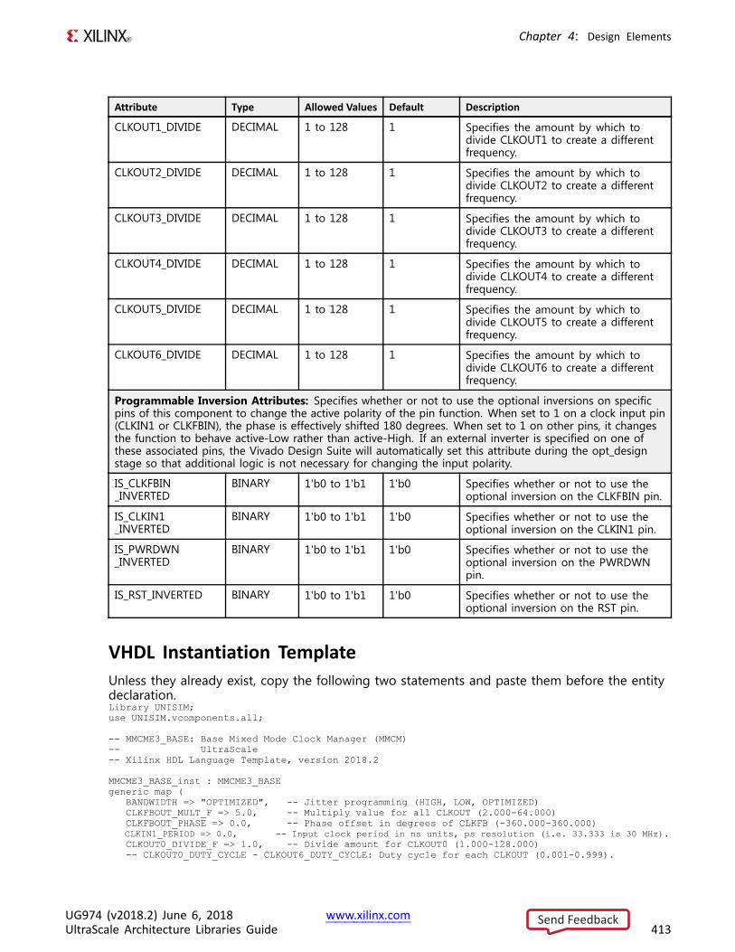
Chapter 4: Design Elements
Attribute Type Allowed Values Default Description
CLKOUT1_DIVIDE DECIMAL 1 to 128 1 Specifies the amount by which todivide CLKOUT1 to create a differentfrequency.
CLKOUT2_DIVIDE DECIMAL 1 to 128 1 Specifies the amount by which todivide CLKOUT2 to create a differentfrequency.
CLKOUT3_DIVIDE DECIMAL 1 to 128 1 Specifies the amount by which todivide CLKOUT3 to create a differentfrequency.
CLKOUT4_DIVIDE DECIMAL 1 to 128 1 Specifies the amount by which todivide CLKOUT4 to create a differentfrequency.
CLKOUT5_DIVIDE DECIMAL 1 to 128 1 Specifies the amount by which todivide CLKOUT5 to create a differentfrequency.
CLKOUT6_DIVIDE DECIMAL 1 to 128 1 Specifies the amount by which todivide CLKOUT6 to create a differentfrequency.
Programmable Inversion Attributes: Specifies whether or not to use the optional inversions on specificpins of this component to change the active polarity of the pin function. When set to 1 on a clock input pin(CLKIN1 or CLKFBIN), the phase is effectively shifted 180 degrees. When set to 1 on other pins, it changesthe function to behave active-Low rather than active-High. If an external inverter is specified on one ofthese associated pins, the Vivado Design Suite will automatically set this attribute during the opt_designstage so that additional logic is not necessary for changing the input polarity.
IS_CLKFBIN_INVERTED
BINARY 1'b0 to 1'b1 1'b0 Specifies whether or not to use theoptional inversion on the CLKFBIN pin.
IS_CLKIN1_INVERTED
BINARY 1'b0 to 1'b1 1'b0 Specifies whether or not to use theoptional inversion on the CLKIN1 pin.
IS_PWRDWN_INVERTED
BINARY 1'b0 to 1'b1 1'b0 Specifies whether or not to use theoptional inversion on the PWRDWNpin.
IS_RST_INVERTED BINARY 1'b0 to 1'b1 1'b0 Specifies whether or not to use theoptional inversion on the RST pin.
VHDL Instantiation TemplateUnless they already exist, copy the following two statements and paste them before the entitydeclaration.Library UNISIM;use UNISIM.vcomponents.all;
-- MMCME3_BASE: Base Mixed Mode Clock Manager (MMCM)-- UltraScale-- Xilinx HDL Language Template, version 2018.2
MMCME3_BASE_inst : MMCME3_BASEgeneric map (
BANDWIDTH => "OPTIMIZED", -- Jitter programming (HIGH, LOW, OPTIMIZED)CLKFBOUT_MULT_F => 5.0, -- Multiply value for all CLKOUT (2.000-64.000)CLKFBOUT_PHASE => 0.0, -- Phase offset in degrees of CLKFB (-360.000-360.000)CLKIN1_PERIOD => 0.0, -- Input clock period in ns units, ps resolution (i.e. 33.333 is 30 MHz).CLKOUT0_DIVIDE_F => 1.0, -- Divide amount for CLKOUT0 (1.000-128.000)-- CLKOUT0_DUTY_CYCLE - CLKOUT6_DUTY_CYCLE: Duty cycle for each CLKOUT (0.001-0.999).
UG974 (v2018.2) June 6, 2018 www.xilinx.comUltraScale Architecture Libraries Guide 413
Send Feedback
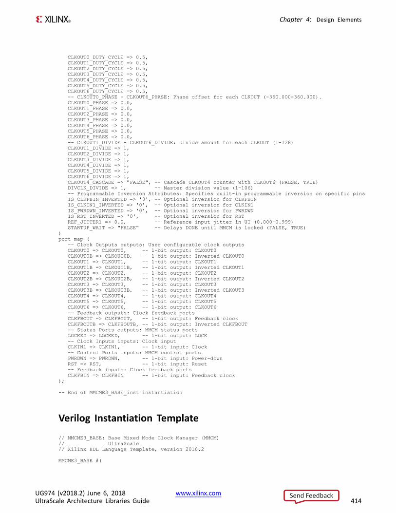
Chapter 4: Design Elements
CLKOUT0_DUTY_CYCLE => 0.5,CLKOUT1_DUTY_CYCLE => 0.5,CLKOUT2_DUTY_CYCLE => 0.5,CLKOUT3_DUTY_CYCLE => 0.5,CLKOUT4_DUTY_CYCLE => 0.5,CLKOUT5_DUTY_CYCLE => 0.5,CLKOUT6_DUTY_CYCLE => 0.5,-- CLKOUT0_PHASE - CLKOUT6_PHASE: Phase offset for each CLKOUT (-360.000-360.000).CLKOUT0_PHASE => 0.0,CLKOUT1_PHASE => 0.0,CLKOUT2_PHASE => 0.0,CLKOUT3_PHASE => 0.0,CLKOUT4_PHASE => 0.0,CLKOUT5_PHASE => 0.0,CLKOUT6_PHASE => 0.0,-- CLKOUT1_DIVIDE - CLKOUT6_DIVIDE: Divide amount for each CLKOUT (1-128)CLKOUT1_DIVIDE => 1,CLKOUT2_DIVIDE => 1,CLKOUT3_DIVIDE => 1,CLKOUT4_DIVIDE => 1,CLKOUT5_DIVIDE => 1,CLKOUT6_DIVIDE => 1,CLKOUT4_CASCADE => "FALSE", -- Cascade CLKOUT4 counter with CLKOUT6 (FALSE, TRUE)DIVCLK_DIVIDE => 1, -- Master division value (1-106)-- Programmable Inversion Attributes: Specifies built-in programmable inversion on specific pinsIS_CLKFBIN_INVERTED => '0', -- Optional inversion for CLKFBINIS_CLKIN1_INVERTED => '0', -- Optional inversion for CLKIN1IS_PWRDWN_INVERTED => '0', -- Optional inversion for PWRDWNIS_RST_INVERTED => '0', -- Optional inversion for RSTREF_JITTER1 => 0.0, -- Reference input jitter in UI (0.000-0.999)STARTUP_WAIT => "FALSE" -- Delays DONE until MMCM is locked (FALSE, TRUE)
)port map (
-- Clock Outputs outputs: User configurable clock outputsCLKOUT0 => CLKOUT0, -- 1-bit output: CLKOUT0CLKOUT0B => CLKOUT0B, -- 1-bit output: Inverted CLKOUT0CLKOUT1 => CLKOUT1, -- 1-bit output: CLKOUT1CLKOUT1B => CLKOUT1B, -- 1-bit output: Inverted CLKOUT1CLKOUT2 => CLKOUT2, -- 1-bit output: CLKOUT2CLKOUT2B => CLKOUT2B, -- 1-bit output: Inverted CLKOUT2CLKOUT3 => CLKOUT3, -- 1-bit output: CLKOUT3CLKOUT3B => CLKOUT3B, -- 1-bit output: Inverted CLKOUT3CLKOUT4 => CLKOUT4, -- 1-bit output: CLKOUT4CLKOUT5 => CLKOUT5, -- 1-bit output: CLKOUT5CLKOUT6 => CLKOUT6, -- 1-bit output: CLKOUT6-- Feedback outputs: Clock feedback portsCLKFBOUT => CLKFBOUT, -- 1-bit output: Feedback clockCLKFBOUTB => CLKFBOUTB, -- 1-bit output: Inverted CLKFBOUT-- Status Ports outputs: MMCM status portsLOCKED => LOCKED, -- 1-bit output: LOCK-- Clock Inputs inputs: Clock inputCLKIN1 => CLKIN1, -- 1-bit input: Clock-- Control Ports inputs: MMCM control portsPWRDWN => PWRDWN, -- 1-bit input: Power-downRST => RST, -- 1-bit input: Reset-- Feedback inputs: Clock feedback portsCLKFBIN => CLKFBIN -- 1-bit input: Feedback clock
);
-- End of MMCME3_BASE_inst instantiation
Verilog Instantiation Template
// MMCME3_BASE: Base Mixed Mode Clock Manager (MMCM)// UltraScale// Xilinx HDL Language Template, version 2018.2
MMCME3_BASE #(
UG974 (v2018.2) June 6, 2018 www.xilinx.comUltraScale Architecture Libraries Guide 414
Send Feedback
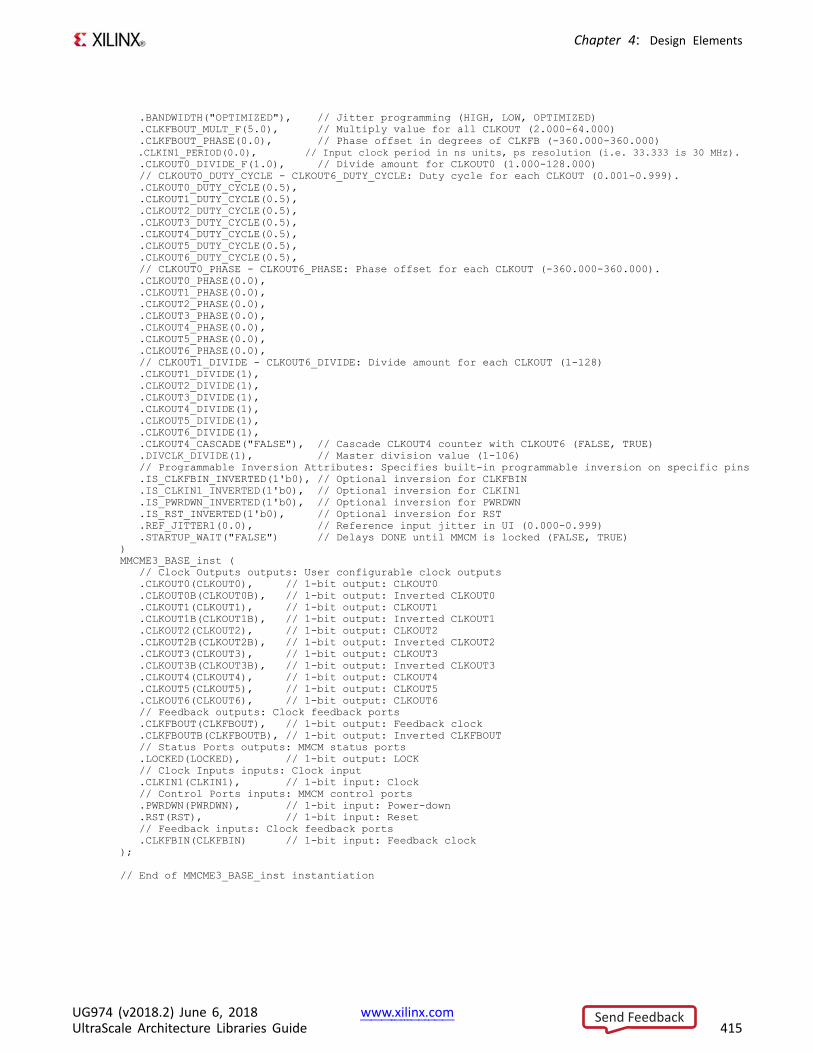
Chapter 4: Design Elements
.BANDWIDTH("OPTIMIZED"), // Jitter programming (HIGH, LOW, OPTIMIZED)
.CLKFBOUT_MULT_F(5.0), // Multiply value for all CLKOUT (2.000-64.000)
.CLKFBOUT_PHASE(0.0), // Phase offset in degrees of CLKFB (-360.000-360.000)
.CLKIN1_PERIOD(0.0), // Input clock period in ns units, ps resolution (i.e. 33.333 is 30 MHz).
.CLKOUT0_DIVIDE_F(1.0), // Divide amount for CLKOUT0 (1.000-128.000)// CLKOUT0_DUTY_CYCLE - CLKOUT6_DUTY_CYCLE: Duty cycle for each CLKOUT (0.001-0.999)..CLKOUT0_DUTY_CYCLE(0.5),.CLKOUT1_DUTY_CYCLE(0.5),.CLKOUT2_DUTY_CYCLE(0.5),.CLKOUT3_DUTY_CYCLE(0.5),.CLKOUT4_DUTY_CYCLE(0.5),.CLKOUT5_DUTY_CYCLE(0.5),.CLKOUT6_DUTY_CYCLE(0.5),// CLKOUT0_PHASE - CLKOUT6_PHASE: Phase offset for each CLKOUT (-360.000-360.000)..CLKOUT0_PHASE(0.0),.CLKOUT1_PHASE(0.0),.CLKOUT2_PHASE(0.0),.CLKOUT3_PHASE(0.0),.CLKOUT4_PHASE(0.0),.CLKOUT5_PHASE(0.0),.CLKOUT6_PHASE(0.0),// CLKOUT1_DIVIDE - CLKOUT6_DIVIDE: Divide amount for each CLKOUT (1-128).CLKOUT1_DIVIDE(1),.CLKOUT2_DIVIDE(1),.CLKOUT3_DIVIDE(1),.CLKOUT4_DIVIDE(1),.CLKOUT5_DIVIDE(1),.CLKOUT6_DIVIDE(1),.CLKOUT4_CASCADE("FALSE"), // Cascade CLKOUT4 counter with CLKOUT6 (FALSE, TRUE).DIVCLK_DIVIDE(1), // Master division value (1-106)// Programmable Inversion Attributes: Specifies built-in programmable inversion on specific pins.IS_CLKFBIN_INVERTED(1'b0), // Optional inversion for CLKFBIN.IS_CLKIN1_INVERTED(1'b0), // Optional inversion for CLKIN1.IS_PWRDWN_INVERTED(1'b0), // Optional inversion for PWRDWN.IS_RST_INVERTED(1'b0), // Optional inversion for RST.REF_JITTER1(0.0), // Reference input jitter in UI (0.000-0.999).STARTUP_WAIT("FALSE") // Delays DONE until MMCM is locked (FALSE, TRUE)
)MMCME3_BASE_inst (
// Clock Outputs outputs: User configurable clock outputs.CLKOUT0(CLKOUT0), // 1-bit output: CLKOUT0.CLKOUT0B(CLKOUT0B), // 1-bit output: Inverted CLKOUT0.CLKOUT1(CLKOUT1), // 1-bit output: CLKOUT1.CLKOUT1B(CLKOUT1B), // 1-bit output: Inverted CLKOUT1.CLKOUT2(CLKOUT2), // 1-bit output: CLKOUT2.CLKOUT2B(CLKOUT2B), // 1-bit output: Inverted CLKOUT2.CLKOUT3(CLKOUT3), // 1-bit output: CLKOUT3.CLKOUT3B(CLKOUT3B), // 1-bit output: Inverted CLKOUT3.CLKOUT4(CLKOUT4), // 1-bit output: CLKOUT4.CLKOUT5(CLKOUT5), // 1-bit output: CLKOUT5.CLKOUT6(CLKOUT6), // 1-bit output: CLKOUT6// Feedback outputs: Clock feedback ports.CLKFBOUT(CLKFBOUT), // 1-bit output: Feedback clock.CLKFBOUTB(CLKFBOUTB), // 1-bit output: Inverted CLKFBOUT// Status Ports outputs: MMCM status ports.LOCKED(LOCKED), // 1-bit output: LOCK// Clock Inputs inputs: Clock input.CLKIN1(CLKIN1), // 1-bit input: Clock// Control Ports inputs: MMCM control ports.PWRDWN(PWRDWN), // 1-bit input: Power-down.RST(RST), // 1-bit input: Reset// Feedback inputs: Clock feedback ports.CLKFBIN(CLKFBIN) // 1-bit input: Feedback clock
);
// End of MMCME3_BASE_inst instantiation
UG974 (v2018.2) June 6, 2018 www.xilinx.comUltraScale Architecture Libraries Guide 415
Send Feedback

Chapter 4: Design Elements
For More Information• See the UltraScale Architecture Clocking Resources User Guide (UG572).
• See the UltraScale Programmable Devices Documentation.
UG974 (v2018.2) June 6, 2018 www.xilinx.comUltraScale Architecture Libraries Guide 416
Send Feedback
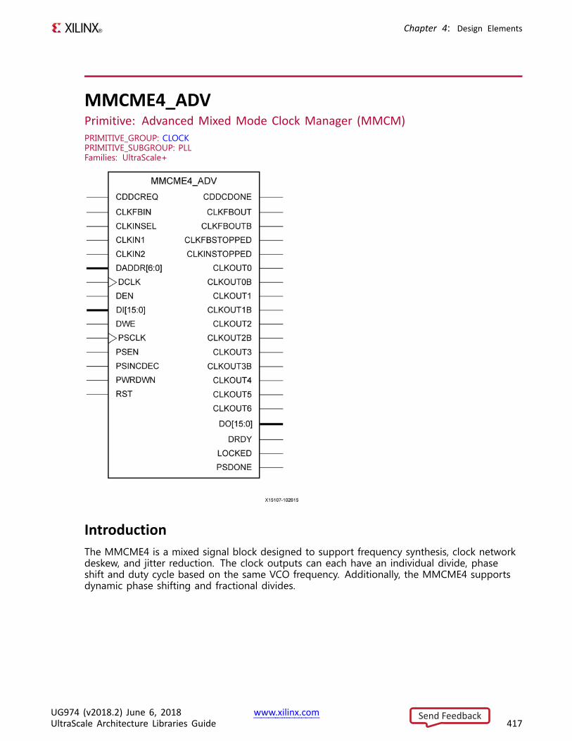
Chapter 4: Design Elements
MMCME4_ADVPrimitive: Advanced Mixed Mode Clock Manager (MMCM)PRIMITIVE_GROUP: CLOCKPRIMITIVE_SUBGROUP: PLLFamilies: UltraScale+
IntroductionThe MMCME4 is a mixed signal block designed to support frequency synthesis, clock networkdeskew, and jitter reduction. The clock outputs can each have an individual divide, phaseshift and duty cycle based on the same VCO frequency. Additionally, the MMCME4 supportsdynamic phase shifting and fractional divides.
UG974 (v2018.2) June 6, 2018 www.xilinx.comUltraScale Architecture Libraries Guide 417
Send Feedback
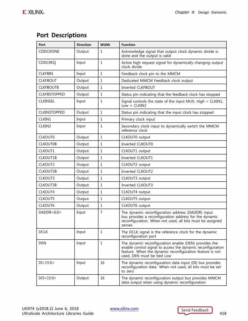
Chapter 4: Design Elements
Port DescriptionsPort Direction Width Function
CDDCDONE Output 1 Acknowledge signal that output clock dynamic divide isdone and the output is valid
CDDCREQ Input 1 Active high request signal for dynamically changing outputclock divide
CLKFBIN Input 1 Feedback clock pin to the MMCM
CLKFBOUT Output 1 Dedicated MMCM Feedback clock output
CLKFBOUTB Output 1 Inverted CLKFBOUT
CLKFBSTOPPED Output 1 Status pin indicating that the feedback clock has stopped
CLKINSEL Input 1 Signal controls the state of the input MUX, High = CLKIN1,Low = CLKIN2
CLKINSTOPPED Output 1 Status pin indicating that the input clock has stopped
CLKIN1 Input 1 Primary clock input
CLKIN2 Input 1 Secondary clock input to dynamically switch the MMCMreference clock
CLKOUT0 Output 1 CLKOUT0 output
CLKOUT0B Output 1 Inverted CLKOUT0
CLKOUT1 Output 1 CLKOUT1 output
CLKOUT1B Output 1 Inverted CLKOUT1
CLKOUT2 Output 1 CLKOUT2 output
CLKOUT2B Output 1 Inverted CLKOUT2
CLKOUT3 Output 1 CLKOUT3 output
CLKOUT3B Output 1 Inverted CLKOUT3
CLKOUT4 Output 1 CLKOUT4 output
CLKOUT5 Output 1 CLKOUT5 output
CLKOUT6 Output 1 CLKOUT6 output
DADDR<6:0> Input 7 The dynamic reconfiguration address (DADDR) inputbus provides a reconfiguration address for the dynamicreconfiguration. When not used, all bits must be assignedzeroes
DCLK Input 1 The DCLK signal is the reference clock for the dynamicreconfiguration port
DEN Input 1 The dynamic reconfiguration enable (DEN) provides theenable control signal to access the dynamic reconfigurationfeature. When the dynamic reconfiguration feature is notused, DEN must be tied Low
DI<15:0> Input 16 The dynamic reconfiguration data input (DI) bus providesreconfiguration data. When not used, all bits must be setto zero
DO<15:0> Output 16 The dynamic reconfiguration output bus provides MMCMdata output when using dynamic reconfiguration
UG974 (v2018.2) June 6, 2018 www.xilinx.comUltraScale Architecture Libraries Guide 418
Send Feedback
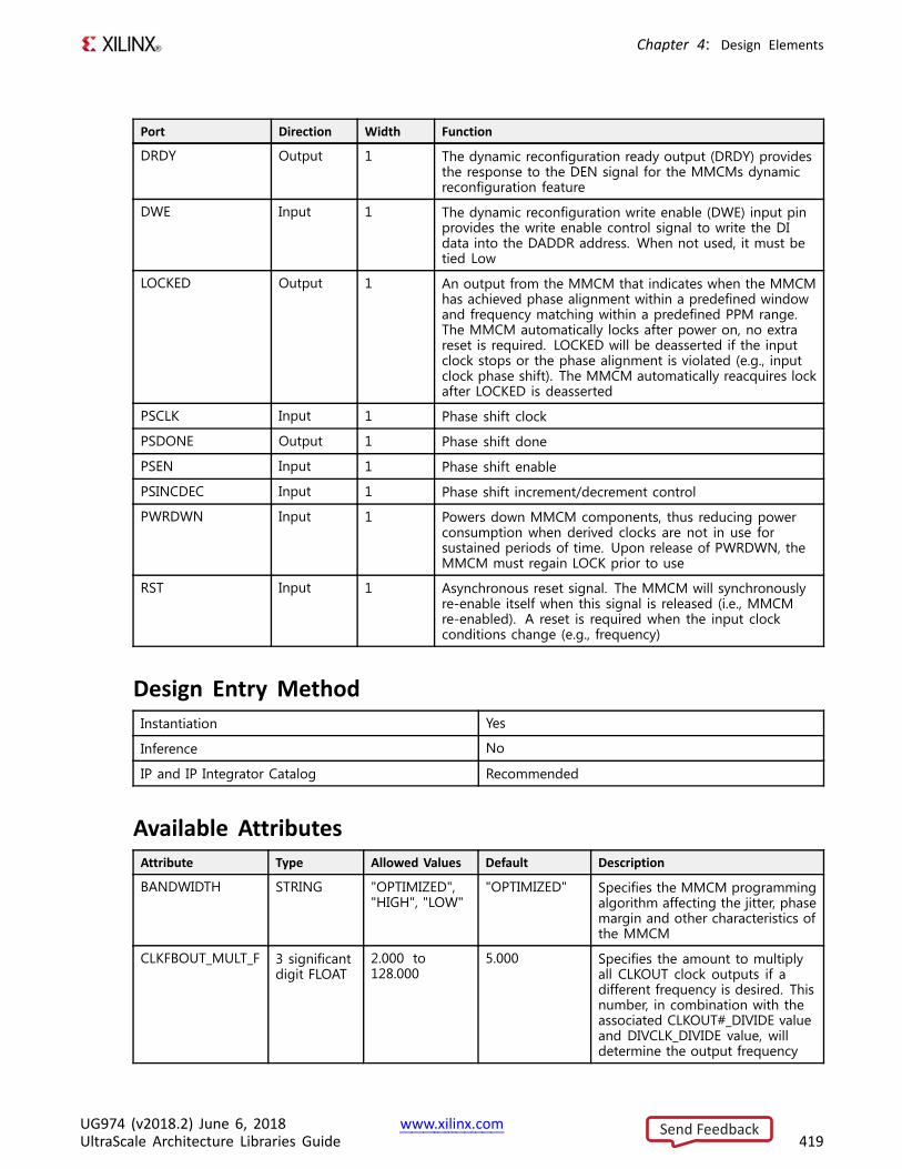
Chapter 4: Design Elements
Port Direction Width Function
DRDY Output 1 The dynamic reconfiguration ready output (DRDY) providesthe response to the DEN signal for the MMCMs dynamicreconfiguration feature
DWE Input 1 The dynamic reconfiguration write enable (DWE) input pinprovides the write enable control signal to write the DIdata into the DADDR address. When not used, it must betied Low
LOCKED Output 1 An output from the MMCM that indicates when the MMCMhas achieved phase alignment within a predefined windowand frequency matching within a predefined PPM range.The MMCM automatically locks after power on, no extrareset is required. LOCKED will be deasserted if the inputclock stops or the phase alignment is violated (e.g., inputclock phase shift). The MMCM automatically reacquires lockafter LOCKED is deasserted
PSCLK Input 1 Phase shift clock
PSDONE Output 1 Phase shift done
PSEN Input 1 Phase shift enable
PSINCDEC Input 1 Phase shift increment/decrement control
PWRDWN Input 1 Powers down MMCM components, thus reducing powerconsumption when derived clocks are not in use forsustained periods of time. Upon release of PWRDWN, theMMCM must regain LOCK prior to use
RST Input 1 Asynchronous reset signal. The MMCM will synchronouslyre-enable itself when this signal is released (i.e., MMCMre-enabled). A reset is required when the input clockconditions change (e.g., frequency)
Design Entry MethodInstantiation Yes
Inference No
IP and IP Integrator Catalog Recommended
Available AttributesAttribute Type Allowed Values Default Description
BANDWIDTH STRING "OPTIMIZED","HIGH", "LOW"
"OPTIMIZED" Specifies the MMCM programmingalgorithm affecting the jitter, phasemargin and other characteristics ofthe MMCM
CLKFBOUT_MULT_F 3 significantdigit FLOAT
2.000 to128.000
5.000 Specifies the amount to multiplyall CLKOUT clock outputs if adifferent frequency is desired. Thisnumber, in combination with theassociated CLKOUT#_DIVIDE valueand DIVCLK_DIVIDE value, willdetermine the output frequency
UG974 (v2018.2) June 6, 2018 www.xilinx.comUltraScale Architecture Libraries Guide 419
Send Feedback
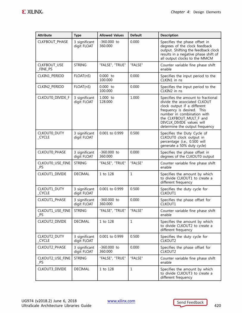
Chapter 4: Design Elements
Attribute Type Allowed Values Default Description
CLKFBOUT_PHASE 3 significantdigit FLOAT
-360.000 to360.000
0.000 Specifies the phase offset indegrees of the clock feedbackoutput. Shifting the feedback clockresults in a negative phase shift ofall output clocks to the MMCM
CLKFBOUT_USE_FINE_PS
STRING "FALSE", "TRUE" "FALSE" Counter variable fine phase shiftenable
CLKIN1_PERIOD FLOAT(nS) 0.000 to100.000
0.000 Specifies the input period to theCLKIN1 in ns
CLKIN2_PERIOD FLOAT(nS) 0.000 to100.000
0.000 Specifies the input period to theCLKIN2 in ns
CLKOUT0_DIVIDE_F 3 significantdigit FLOAT
1.000 to128.000
1.000 Specifies the amount to fractionaldivide the associated CLKOUTclock output if a differentfrequency is desired. Thisnumber in combination withthe CLKFBOUT_MULT_F andDIVCLK_DIVIDE values willdetermine the output frequency
CLKOUT0_DUTY_CYCLE
3 significantdigit FLOAT
0.001 to 0.999 0.500 Specifies the Duty Cycle ofCLKOUT0 clock output inpercentage (i.e., 0.500 willgenerate a 50% duty cycle)
CLKOUT0_PHASE 3 significantdigit FLOAT
-360.000 to360.000
0.000 Specifies the phase offset indegrees of the CLKOUT0 output
CLKOUT0_USE_FINE_PS
STRING "FALSE", "TRUE" "FALSE" Counter variable fine phase shiftenable
CLKOUT1_DIVIDE DECIMAL 1 to 128 1 Specifies the amount by whichto divide CLKOUT1 to create adifferent frequency
CLKOUT1_DUTY_CYCLE
3 significantdigit FLOAT
0.001 to 0.999 0.500 Specifies the duty cycle forCLKOUT1
CLKOUT1_PHASE 3 significantdigit FLOAT
-360.000 to360.000
0.000 Specifies the phase offset forCLKOUT1
CLKOUT1_USE_FINE_PS
STRING "FALSE", "TRUE" "FALSE" Counter variable fine phase shiftenable
CLKOUT2_DIVIDE DECIMAL 1 to 128 1 Specifies the amount by whichto divide CLKOUT2 to create adifferent frequency
CLKOUT2_DUTY_CYCLE
3 significantdigit FLOAT
0.001 to 0.999 0.500 Specifies the duty cycle forCLKOUT2
CLKOUT2_PHASE 3 significantdigit FLOAT
-360.000 to360.000
0.000 Specifies the phase offset forCLKOUT2
CLKOUT2_USE_FINE_PS
STRING "FALSE", "TRUE" "FALSE" Counter variable fine phase shiftenable
CLKOUT3_DIVIDE DECIMAL 1 to 128 1 Specifies the amount by whichto divide CLKOUT3 to create adifferent frequency
UG974 (v2018.2) June 6, 2018 www.xilinx.comUltraScale Architecture Libraries Guide 420
Send Feedback
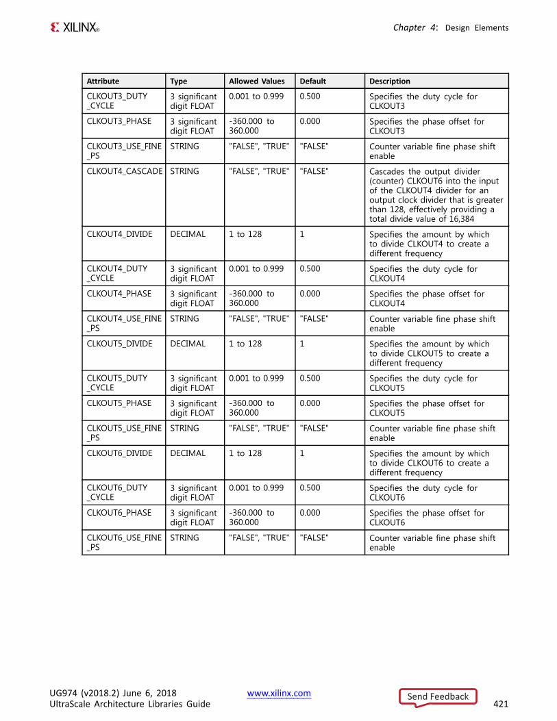
Chapter 4: Design Elements
Attribute Type Allowed Values Default Description
CLKOUT3_DUTY_CYCLE
3 significantdigit FLOAT
0.001 to 0.999 0.500 Specifies the duty cycle forCLKOUT3
CLKOUT3_PHASE 3 significantdigit FLOAT
-360.000 to360.000
0.000 Specifies the phase offset forCLKOUT3
CLKOUT3_USE_FINE_PS
STRING "FALSE", "TRUE" "FALSE" Counter variable fine phase shiftenable
CLKOUT4_CASCADE STRING "FALSE", "TRUE" "FALSE" Cascades the output divider(counter) CLKOUT6 into the inputof the CLKOUT4 divider for anoutput clock divider that is greaterthan 128, effectively providing atotal divide value of 16,384
CLKOUT4_DIVIDE DECIMAL 1 to 128 1 Specifies the amount by whichto divide CLKOUT4 to create adifferent frequency
CLKOUT4_DUTY_CYCLE
3 significantdigit FLOAT
0.001 to 0.999 0.500 Specifies the duty cycle forCLKOUT4
CLKOUT4_PHASE 3 significantdigit FLOAT
-360.000 to360.000
0.000 Specifies the phase offset forCLKOUT4
CLKOUT4_USE_FINE_PS
STRING "FALSE", "TRUE" "FALSE" Counter variable fine phase shiftenable
CLKOUT5_DIVIDE DECIMAL 1 to 128 1 Specifies the amount by whichto divide CLKOUT5 to create adifferent frequency
CLKOUT5_DUTY_CYCLE
3 significantdigit FLOAT
0.001 to 0.999 0.500 Specifies the duty cycle forCLKOUT5
CLKOUT5_PHASE 3 significantdigit FLOAT
-360.000 to360.000
0.000 Specifies the phase offset forCLKOUT5
CLKOUT5_USE_FINE_PS
STRING "FALSE", "TRUE" "FALSE" Counter variable fine phase shiftenable
CLKOUT6_DIVIDE DECIMAL 1 to 128 1 Specifies the amount by whichto divide CLKOUT6 to create adifferent frequency
CLKOUT6_DUTY_CYCLE
3 significantdigit FLOAT
0.001 to 0.999 0.500 Specifies the duty cycle forCLKOUT6
CLKOUT6_PHASE 3 significantdigit FLOAT
-360.000 to360.000
0.000 Specifies the phase offset forCLKOUT6
CLKOUT6_USE_FINE_PS
STRING "FALSE", "TRUE" "FALSE" Counter variable fine phase shiftenable
UG974 (v2018.2) June 6, 2018 www.xilinx.comUltraScale Architecture Libraries Guide 421
Send Feedback
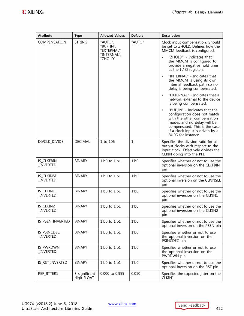
Chapter 4: Design Elements
Attribute Type Allowed Values Default Description
COMPENSATION STRING "AUTO","BUF_IN","EXTERNAL","INTERNAL","ZHOLD"
"AUTO" Clock input compensation. Shouldbe set to ZHOLD. Defines how theMMCM feedback is configured.
• "ZHOLD" - Indicates thatthe MMCM is configured toprovide a negative hold timeat the I / O registers.
• "INTERNAL" - Indicates thatthe MMCM is using its owninternal feedback path so nodelay is being compensated.
• "EXTERNAL" - Indicates that anetwork external to the deviceis being compensated.
• "BUF_IN" - Indicates that theconfiguration does not matchwith the other compensationmodes and no delay will becompensated. This is the caseif a clock input is driven by aBUFG for instance.
DIVCLK_DIVIDE DECIMAL 1 to 106 1 Specifies the division ratio for alloutput clocks with respect to theinput clock. Effectively divides theCLKIN going into the PFD
IS_CLKFBIN_INVERTED
BINARY 1'b0 to 1'b1 1'b0 Specifies whether or not to use theoptional inversion on the CLKFBINpin
IS_CLKINSEL_INVERTED
BINARY 1'b0 to 1'b1 1'b0 Specifies whether or not to use theoptional inversion on the CLKINSELpin
IS_CLKIN1_INVERTED
BINARY 1'b0 to 1'b1 1'b0 Specifies whether or not to use theoptional inversion on the CLKIN1pin
IS_CLKIN2_INVERTED
BINARY 1'b0 to 1'b1 1'b0 Specifies whether or not to use theoptional inversion on the CLKIN2pin
IS_PSEN_INVERTED BINARY 1'b0 to 1'b1 1'b0 Specifies whether or not to use theoptional inversion on the PSEN pin
IS_PSINCDEC_INVERTED
BINARY 1'b0 to 1'b1 1'b0 Specifies whether or not to usethe optional inversion on thePSINCDEC pin
IS_PWRDWN_INVERTED
BINARY 1'b0 to 1'b1 1'b0 Specifies whether or not to usethe optional inversion on thePWRDWN pin
IS_RST_INVERTED BINARY 1'b0 to 1'b1 1'b0 Specifies whether or not to use theoptional inversion on the RST pin
REF_JITTER1 3 significantdigit FLOAT
0.000 to 0.999 0.010 Specifies the expected jitter on theCLKIN1
UG974 (v2018.2) June 6, 2018 www.xilinx.comUltraScale Architecture Libraries Guide 422
Send Feedback
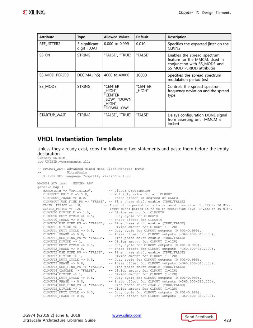
Chapter 4: Design Elements
Attribute Type Allowed Values Default Description
REF_JITTER2 3 significantdigit FLOAT
0.000 to 0.999 0.010 Specifies the expected jitter on theCLKIN2
SS_EN STRING "FALSE", "TRUE" "FALSE" Enables the spread spectrumfeature for the MMCM. Used inconjunction with SS_MODE andSS_MOD_PERIOD attributes
SS_MOD_PERIOD DECIMAL(nS) 4000 to 40000 10000 Specifies the spread spectrummodulation period (ns)
SS_MODE STRING "CENTER_HIGH","CENTER_LOW", "DOWN_HIGH","DOWN_LOW"
"CENTER_HIGH"
Controls the spread spectrumfrequency deviation and the spreadtype
STARTUP_WAIT STRING "FALSE", "TRUE" "FALSE" Delays configuration DONE signalfrom asserting until MMCM islocked
VHDL Instantiation TemplateUnless they already exist, copy the following two statements and paste them before the entitydeclaration.Library UNISIM;use UNISIM.vcomponents.all;
-- MMCME4_ADV: Advanced Mixed Mode Clock Manager (MMCM)-- UltraScale-- Xilinx HDL Language Template, version 2018.2
MMCME4_ADV_inst : MMCME4_ADVgeneric map (
BANDWIDTH => "OPTIMIZED", -- Jitter programmingCLKFBOUT_MULT_F => 5.0, -- Multiply value for all CLKOUTCLKFBOUT_PHASE => 0.0, -- Phase offset in degrees of CLKFBCLKFBOUT_USE_FINE_PS => "FALSE", -- Fine phase shift enable (TRUE/FALSE)CLKIN1_PERIOD => 0.0, -- Input clock period in ns to ps resolution (i.e. 33.333 is 30 MHz).CLKIN2_PERIOD => 0.0, -- Input clock period in ns to ps resolution (i.e. 33.333 is 30 MHz).CLKOUT0_DIVIDE_F => 1.0, -- Divide amount for CLKOUT0CLKOUT0_DUTY_CYCLE => 0.5, -- Duty cycle for CLKOUT0CLKOUT0_PHASE => 0.0, -- Phase offset for CLKOUT0CLKOUT0_USE_FINE_PS => "FALSE", -- Fine phase shift enable (TRUE/FALSE)CLKOUT1_DIVIDE => 1, -- Divide amount for CLKOUT (1-128)CLKOUT1_DUTY_CYCLE => 0.5, -- Duty cycle for CLKOUT outputs (0.001-0.999).CLKOUT1_PHASE => 0.0, -- Phase offset for CLKOUT outputs (-360.000-360.000).CLKOUT1_USE_FINE_PS => "FALSE", -- Fine phase shift enable (TRUE/FALSE)CLKOUT2_DIVIDE => 1, -- Divide amount for CLKOUT (1-128)CLKOUT2_DUTY_CYCLE => 0.5, -- Duty cycle for CLKOUT outputs (0.001-0.999).CLKOUT2_PHASE => 0.0, -- Phase offset for CLKOUT outputs (-360.000-360.000).CLKOUT2_USE_FINE_PS => "FALSE", -- Fine phase shift enable (TRUE/FALSE)CLKOUT3_DIVIDE => 1, -- Divide amount for CLKOUT (1-128)CLKOUT3_DUTY_CYCLE => 0.5, -- Duty cycle for CLKOUT outputs (0.001-0.999).CLKOUT3_PHASE => 0.0, -- Phase offset for CLKOUT outputs (-360.000-360.000).CLKOUT3_USE_FINE_PS => "FALSE", -- Fine phase shift enable (TRUE/FALSE)CLKOUT4_CASCADE => "FALSE", -- Divide amount for CLKOUT (1-128)CLKOUT4_DIVIDE => 1, -- Divide amount for CLKOUT (1-128)CLKOUT4_DUTY_CYCLE => 0.5, -- Duty cycle for CLKOUT outputs (0.001-0.999).CLKOUT4_PHASE => 0.0, -- Phase offset for CLKOUT outputs (-360.000-360.000).CLKOUT4_USE_FINE_PS => "FALSE", -- Fine phase shift enable (TRUE/FALSE)CLKOUT5_DIVIDE => 1, -- Divide amount for CLKOUT (1-128)CLKOUT5_DUTY_CYCLE => 0.5, -- Duty cycle for CLKOUT outputs (0.001-0.999).CLKOUT5_PHASE => 0.0, -- Phase offset for CLKOUT outputs (-360.000-360.000).
UG974 (v2018.2) June 6, 2018 www.xilinx.comUltraScale Architecture Libraries Guide 423
Send Feedback
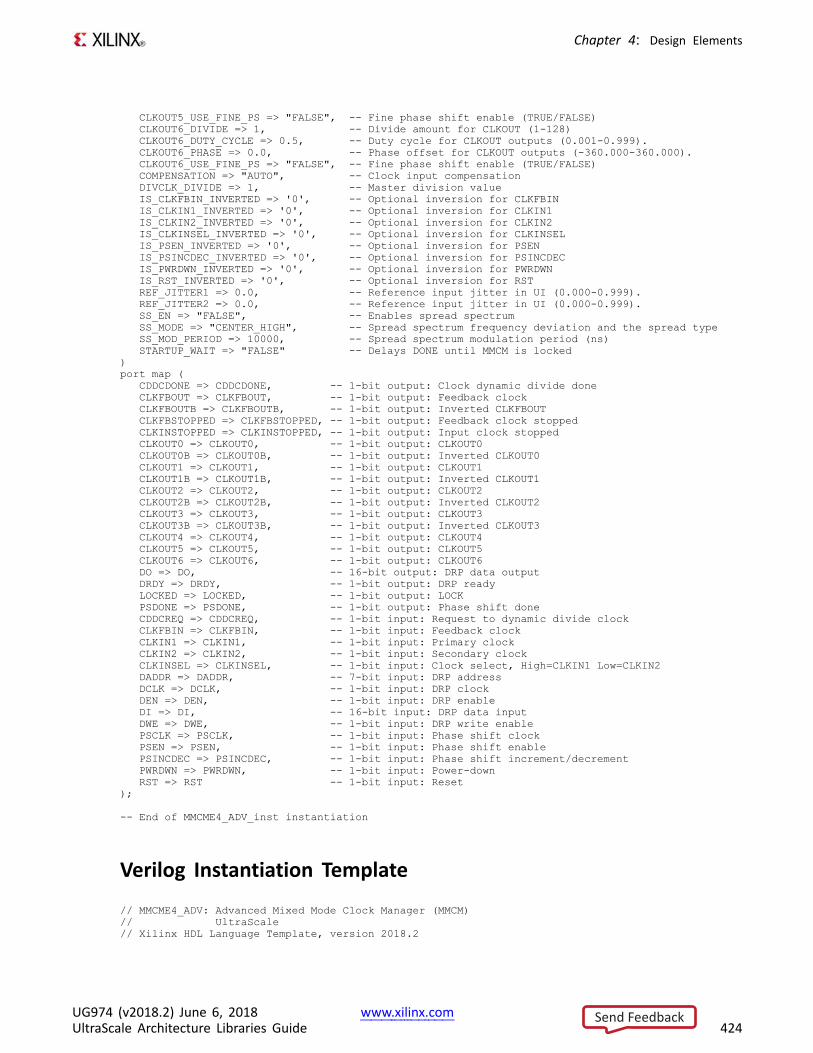
Chapter 4: Design Elements
CLKOUT5_USE_FINE_PS => "FALSE", -- Fine phase shift enable (TRUE/FALSE)CLKOUT6_DIVIDE => 1, -- Divide amount for CLKOUT (1-128)CLKOUT6_DUTY_CYCLE => 0.5, -- Duty cycle for CLKOUT outputs (0.001-0.999).CLKOUT6_PHASE => 0.0, -- Phase offset for CLKOUT outputs (-360.000-360.000).CLKOUT6_USE_FINE_PS => "FALSE", -- Fine phase shift enable (TRUE/FALSE)COMPENSATION => "AUTO", -- Clock input compensationDIVCLK_DIVIDE => 1, -- Master division valueIS_CLKFBIN_INVERTED => '0', -- Optional inversion for CLKFBINIS_CLKIN1_INVERTED => '0', -- Optional inversion for CLKIN1IS_CLKIN2_INVERTED => '0', -- Optional inversion for CLKIN2IS_CLKINSEL_INVERTED => '0', -- Optional inversion for CLKINSELIS_PSEN_INVERTED => '0', -- Optional inversion for PSENIS_PSINCDEC_INVERTED => '0', -- Optional inversion for PSINCDECIS_PWRDWN_INVERTED => '0', -- Optional inversion for PWRDWNIS_RST_INVERTED => '0', -- Optional inversion for RSTREF_JITTER1 => 0.0, -- Reference input jitter in UI (0.000-0.999).REF_JITTER2 => 0.0, -- Reference input jitter in UI (0.000-0.999).SS_EN => "FALSE", -- Enables spread spectrumSS_MODE => "CENTER_HIGH", -- Spread spectrum frequency deviation and the spread typeSS_MOD_PERIOD => 10000, -- Spread spectrum modulation period (ns)STARTUP_WAIT => "FALSE" -- Delays DONE until MMCM is locked
)port map (
CDDCDONE => CDDCDONE, -- 1-bit output: Clock dynamic divide doneCLKFBOUT => CLKFBOUT, -- 1-bit output: Feedback clockCLKFBOUTB => CLKFBOUTB, -- 1-bit output: Inverted CLKFBOUTCLKFBSTOPPED => CLKFBSTOPPED, -- 1-bit output: Feedback clock stoppedCLKINSTOPPED => CLKINSTOPPED, -- 1-bit output: Input clock stoppedCLKOUT0 => CLKOUT0, -- 1-bit output: CLKOUT0CLKOUT0B => CLKOUT0B, -- 1-bit output: Inverted CLKOUT0CLKOUT1 => CLKOUT1, -- 1-bit output: CLKOUT1CLKOUT1B => CLKOUT1B, -- 1-bit output: Inverted CLKOUT1CLKOUT2 => CLKOUT2, -- 1-bit output: CLKOUT2CLKOUT2B => CLKOUT2B, -- 1-bit output: Inverted CLKOUT2CLKOUT3 => CLKOUT3, -- 1-bit output: CLKOUT3CLKOUT3B => CLKOUT3B, -- 1-bit output: Inverted CLKOUT3CLKOUT4 => CLKOUT4, -- 1-bit output: CLKOUT4CLKOUT5 => CLKOUT5, -- 1-bit output: CLKOUT5CLKOUT6 => CLKOUT6, -- 1-bit output: CLKOUT6DO => DO, -- 16-bit output: DRP data outputDRDY => DRDY, -- 1-bit output: DRP readyLOCKED => LOCKED, -- 1-bit output: LOCKPSDONE => PSDONE, -- 1-bit output: Phase shift doneCDDCREQ => CDDCREQ, -- 1-bit input: Request to dynamic divide clockCLKFBIN => CLKFBIN, -- 1-bit input: Feedback clockCLKIN1 => CLKIN1, -- 1-bit input: Primary clockCLKIN2 => CLKIN2, -- 1-bit input: Secondary clockCLKINSEL => CLKINSEL, -- 1-bit input: Clock select, High=CLKIN1 Low=CLKIN2DADDR => DADDR, -- 7-bit input: DRP addressDCLK => DCLK, -- 1-bit input: DRP clockDEN => DEN, -- 1-bit input: DRP enableDI => DI, -- 16-bit input: DRP data inputDWE => DWE, -- 1-bit input: DRP write enablePSCLK => PSCLK, -- 1-bit input: Phase shift clockPSEN => PSEN, -- 1-bit input: Phase shift enablePSINCDEC => PSINCDEC, -- 1-bit input: Phase shift increment/decrementPWRDWN => PWRDWN, -- 1-bit input: Power-downRST => RST -- 1-bit input: Reset
);
-- End of MMCME4_ADV_inst instantiation
Verilog Instantiation Template
// MMCME4_ADV: Advanced Mixed Mode Clock Manager (MMCM)// UltraScale// Xilinx HDL Language Template, version 2018.2
UG974 (v2018.2) June 6, 2018 www.xilinx.comUltraScale Architecture Libraries Guide 424
Send Feedback
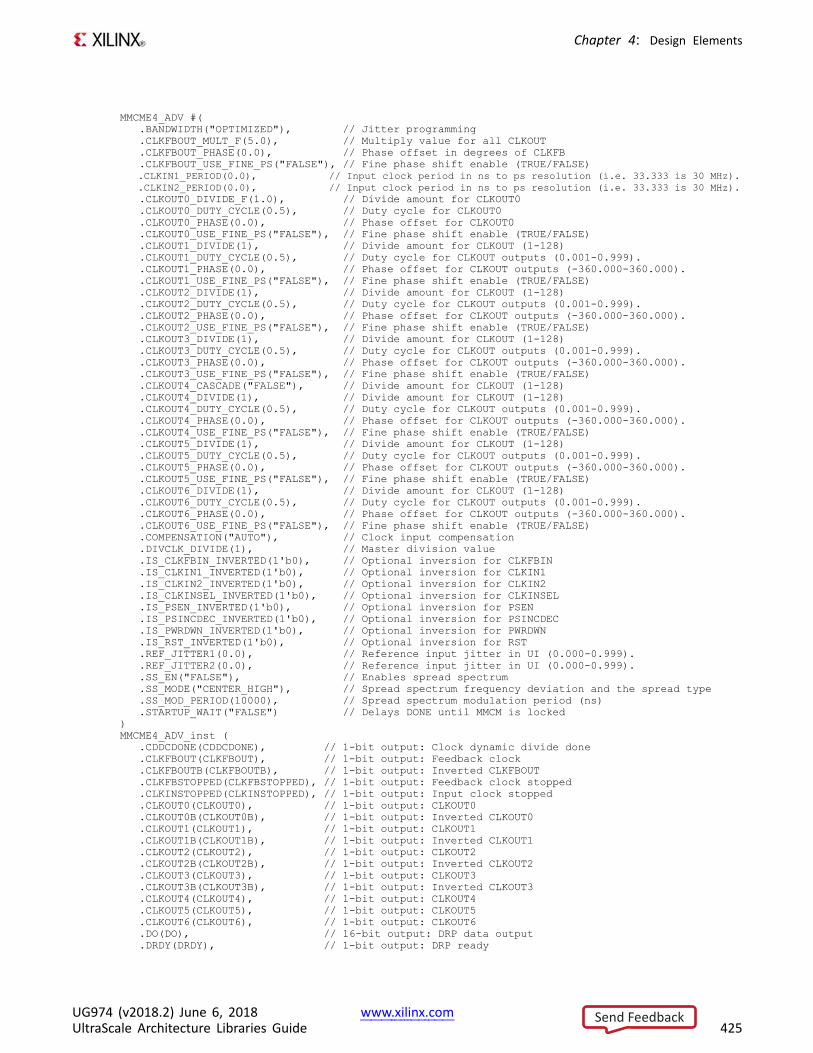
Chapter 4: Design Elements
MMCME4_ADV #(.BANDWIDTH("OPTIMIZED"), // Jitter programming.CLKFBOUT_MULT_F(5.0), // Multiply value for all CLKOUT.CLKFBOUT_PHASE(0.0), // Phase offset in degrees of CLKFB.CLKFBOUT_USE_FINE_PS("FALSE"), // Fine phase shift enable (TRUE/FALSE).CLKIN1_PERIOD(0.0), // Input clock period in ns to ps resolution (i.e. 33.333 is 30 MHz)..CLKIN2_PERIOD(0.0), // Input clock period in ns to ps resolution (i.e. 33.333 is 30 MHz)..CLKOUT0_DIVIDE_F(1.0), // Divide amount for CLKOUT0.CLKOUT0_DUTY_CYCLE(0.5), // Duty cycle for CLKOUT0.CLKOUT0_PHASE(0.0), // Phase offset for CLKOUT0.CLKOUT0_USE_FINE_PS("FALSE"), // Fine phase shift enable (TRUE/FALSE).CLKOUT1_DIVIDE(1), // Divide amount for CLKOUT (1-128).CLKOUT1_DUTY_CYCLE(0.5), // Duty cycle for CLKOUT outputs (0.001-0.999)..CLKOUT1_PHASE(0.0), // Phase offset for CLKOUT outputs (-360.000-360.000)..CLKOUT1_USE_FINE_PS("FALSE"), // Fine phase shift enable (TRUE/FALSE).CLKOUT2_DIVIDE(1), // Divide amount for CLKOUT (1-128).CLKOUT2_DUTY_CYCLE(0.5), // Duty cycle for CLKOUT outputs (0.001-0.999)..CLKOUT2_PHASE(0.0), // Phase offset for CLKOUT outputs (-360.000-360.000)..CLKOUT2_USE_FINE_PS("FALSE"), // Fine phase shift enable (TRUE/FALSE).CLKOUT3_DIVIDE(1), // Divide amount for CLKOUT (1-128).CLKOUT3_DUTY_CYCLE(0.5), // Duty cycle for CLKOUT outputs (0.001-0.999)..CLKOUT3_PHASE(0.0), // Phase offset for CLKOUT outputs (-360.000-360.000)..CLKOUT3_USE_FINE_PS("FALSE"), // Fine phase shift enable (TRUE/FALSE).CLKOUT4_CASCADE("FALSE"), // Divide amount for CLKOUT (1-128).CLKOUT4_DIVIDE(1), // Divide amount for CLKOUT (1-128).CLKOUT4_DUTY_CYCLE(0.5), // Duty cycle for CLKOUT outputs (0.001-0.999)..CLKOUT4_PHASE(0.0), // Phase offset for CLKOUT outputs (-360.000-360.000)..CLKOUT4_USE_FINE_PS("FALSE"), // Fine phase shift enable (TRUE/FALSE).CLKOUT5_DIVIDE(1), // Divide amount for CLKOUT (1-128).CLKOUT5_DUTY_CYCLE(0.5), // Duty cycle for CLKOUT outputs (0.001-0.999)..CLKOUT5_PHASE(0.0), // Phase offset for CLKOUT outputs (-360.000-360.000)..CLKOUT5_USE_FINE_PS("FALSE"), // Fine phase shift enable (TRUE/FALSE).CLKOUT6_DIVIDE(1), // Divide amount for CLKOUT (1-128).CLKOUT6_DUTY_CYCLE(0.5), // Duty cycle for CLKOUT outputs (0.001-0.999)..CLKOUT6_PHASE(0.0), // Phase offset for CLKOUT outputs (-360.000-360.000)..CLKOUT6_USE_FINE_PS("FALSE"), // Fine phase shift enable (TRUE/FALSE).COMPENSATION("AUTO"), // Clock input compensation.DIVCLK_DIVIDE(1), // Master division value.IS_CLKFBIN_INVERTED(1'b0), // Optional inversion for CLKFBIN.IS_CLKIN1_INVERTED(1'b0), // Optional inversion for CLKIN1.IS_CLKIN2_INVERTED(1'b0), // Optional inversion for CLKIN2.IS_CLKINSEL_INVERTED(1'b0), // Optional inversion for CLKINSEL.IS_PSEN_INVERTED(1'b0), // Optional inversion for PSEN.IS_PSINCDEC_INVERTED(1'b0), // Optional inversion for PSINCDEC.IS_PWRDWN_INVERTED(1'b0), // Optional inversion for PWRDWN.IS_RST_INVERTED(1'b0), // Optional inversion for RST.REF_JITTER1(0.0), // Reference input jitter in UI (0.000-0.999)..REF_JITTER2(0.0), // Reference input jitter in UI (0.000-0.999)..SS_EN("FALSE"), // Enables spread spectrum.SS_MODE("CENTER_HIGH"), // Spread spectrum frequency deviation and the spread type.SS_MOD_PERIOD(10000), // Spread spectrum modulation period (ns).STARTUP_WAIT("FALSE") // Delays DONE until MMCM is locked
)MMCME4_ADV_inst (
.CDDCDONE(CDDCDONE), // 1-bit output: Clock dynamic divide done
.CLKFBOUT(CLKFBOUT), // 1-bit output: Feedback clock
.CLKFBOUTB(CLKFBOUTB), // 1-bit output: Inverted CLKFBOUT
.CLKFBSTOPPED(CLKFBSTOPPED), // 1-bit output: Feedback clock stopped
.CLKINSTOPPED(CLKINSTOPPED), // 1-bit output: Input clock stopped
.CLKOUT0(CLKOUT0), // 1-bit output: CLKOUT0
.CLKOUT0B(CLKOUT0B), // 1-bit output: Inverted CLKOUT0
.CLKOUT1(CLKOUT1), // 1-bit output: CLKOUT1
.CLKOUT1B(CLKOUT1B), // 1-bit output: Inverted CLKOUT1
.CLKOUT2(CLKOUT2), // 1-bit output: CLKOUT2
.CLKOUT2B(CLKOUT2B), // 1-bit output: Inverted CLKOUT2
.CLKOUT3(CLKOUT3), // 1-bit output: CLKOUT3
.CLKOUT3B(CLKOUT3B), // 1-bit output: Inverted CLKOUT3
.CLKOUT4(CLKOUT4), // 1-bit output: CLKOUT4
.CLKOUT5(CLKOUT5), // 1-bit output: CLKOUT5
.CLKOUT6(CLKOUT6), // 1-bit output: CLKOUT6
.DO(DO), // 16-bit output: DRP data output
.DRDY(DRDY), // 1-bit output: DRP ready
UG974 (v2018.2) June 6, 2018 www.xilinx.comUltraScale Architecture Libraries Guide 425
Send Feedback
Chapter 4: Design Elements
.LOCKED(LOCKED), // 1-bit output: LOCK
.PSDONE(PSDONE), // 1-bit output: Phase shift done
.CDDCREQ(CDDCREQ), // 1-bit input: Request to dynamic divide clock
.CLKFBIN(CLKFBIN), // 1-bit input: Feedback clock
.CLKIN1(CLKIN1), // 1-bit input: Primary clock
.CLKIN2(CLKIN2), // 1-bit input: Secondary clock
.CLKINSEL(CLKINSEL), // 1-bit input: Clock select, High=CLKIN1 Low=CLKIN2
.DADDR(DADDR), // 7-bit input: DRP address
.DCLK(DCLK), // 1-bit input: DRP clock
.DEN(DEN), // 1-bit input: DRP enable
.DI(DI), // 16-bit input: DRP data input
.DWE(DWE), // 1-bit input: DRP write enable
.PSCLK(PSCLK), // 1-bit input: Phase shift clock
.PSEN(PSEN), // 1-bit input: Phase shift enable
.PSINCDEC(PSINCDEC), // 1-bit input: Phase shift increment/decrement
.PWRDWN(PWRDWN), // 1-bit input: Power-down
.RST(RST) // 1-bit input: Reset);
// End of MMCME4_ADV_inst instantiation
For More Information• See the UltraScale Architecture Clocking Resources User Guide (UG572).
• See the UltraScale Programmable Devices Documentation.
UG974 (v2018.2) June 6, 2018 www.xilinx.comUltraScale Architecture Libraries Guide 426
Send Feedback
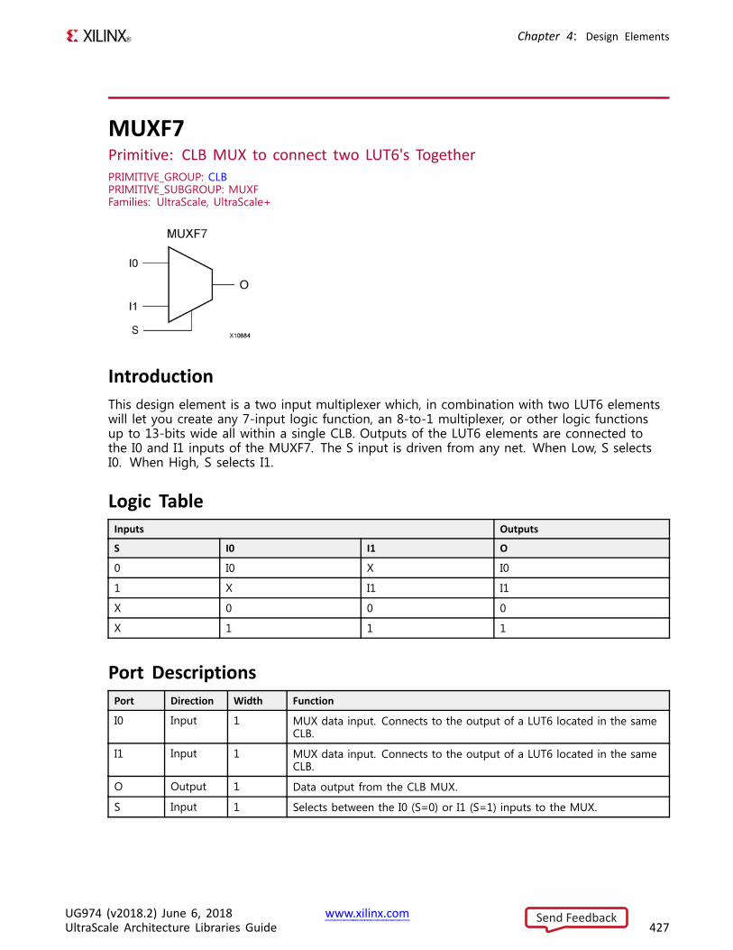
Chapter 4: Design Elements
MUXF7Primitive: CLB MUX to connect two LUT6's TogetherPRIMITIVE_GROUP: CLBPRIMITIVE_SUBGROUP: MUXFFamilies: UltraScale, UltraScale+
IntroductionThis design element is a two input multiplexer which, in combination with two LUT6 elementswill let you create any 7-input logic function, an 8-to-1 multiplexer, or other logic functionsup to 13-bits wide all within a single CLB. Outputs of the LUT6 elements are connected tothe I0 and I1 inputs of the MUXF7. The S input is driven from any net. When Low, S selectsI0. When High, S selects I1.
Logic TableInputs Outputs
S I0 I1 O
0 I0 X I0
1 X I1 I1
X 0 0 0
X 1 1 1
Port DescriptionsPort Direction Width Function
I0 Input 1 MUX data input. Connects to the output of a LUT6 located in the sameCLB.
I1 Input 1 MUX data input. Connects to the output of a LUT6 located in the sameCLB.
O Output 1 Data output from the CLB MUX.
S Input 1 Selects between the I0 (S=0) or I1 (S=1) inputs to the MUX.
UG974 (v2018.2) June 6, 2018 www.xilinx.comUltraScale Architecture Libraries Guide 427
Send Feedback
Chapter 4: Design Elements
Design Entry MethodInstantiation Yes
Inference Recommended
IP and IP Integrator Catalog No
VHDL Instantiation TemplateUnless they already exist, copy the following two statements and paste them before the entitydeclaration.Library UNISIM;use UNISIM.vcomponents.all;
-- MUXF7: CLB MUX to connect two LUT6's Together-- UltraScale-- Xilinx HDL Language Template, version 2018.2
MUXF7_inst : MUXF7port map (
O => O, -- 1-bit output: Output of MUXI0 => I0, -- 1-bit input: Connect to LUT6 outputI1 => I1, -- 1-bit input: Connect to LUT6 outputS => S -- 1-bit input: Input select to MUX
);
-- End of MUXF7_inst instantiation
Verilog Instantiation Template
// MUXF7: CLB MUX to connect two LUT6's Together// UltraScale// Xilinx HDL Language Template, version 2018.2
MUXF7 MUXF7_inst (.O(O), // 1-bit output: Output of MUX.I0(I0), // 1-bit input: Connect to LUT6 output.I1(I1), // 1-bit input: Connect to LUT6 output.S(S) // 1-bit input: Input select to MUX
);
// End of MUXF7_inst instantiation
For More Information• See the UltraScale Architecture Configurable Logic Block User Guide (UG574).
• See the UltraScale Programmable Devices Documentation.
UG974 (v2018.2) June 6, 2018 www.xilinx.comUltraScale Architecture Libraries Guide 428
Send Feedback
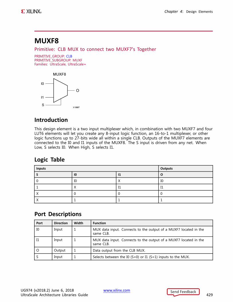
Chapter 4: Design Elements
MUXF8Primitive: CLB MUX to connect two MUXF7's TogetherPRIMITIVE_GROUP: CLBPRIMITIVE_SUBGROUP: MUXFFamilies: UltraScale, UltraScale+
IntroductionThis design element is a two input multiplexer which, in combination with two MUXF7 and fourLUT6 elements will let you create any 8-input logic function, an 16-to-1 multiplexer, or otherlogic functions up to 27-bits wide all within a single CLB. Outputs of the MUXF7 elements areconnected to the I0 and I1 inputs of the MUXF8. The S input is driven from any net. WhenLow, S selects I0. When High, S selects I1.
Logic TableInputs Outputs
S I0 I1 O
0 I0 X I0
1 X I1 I1
X 0 0 0
X 1 1 1
Port DescriptionsPort Direction Width Function
I0 Input 1 MUX data input. Connects to the output of a MUXF7 located in thesame CLB.
I1 Input 1 MUX data input. Connects to the output of a MUXF7 located in thesame CLB.
O Output 1 Data output from the CLB MUX.
S Input 1 Selects between the I0 (S=0) or I1 (S=1) inputs to the MUX.
UG974 (v2018.2) June 6, 2018 www.xilinx.comUltraScale Architecture Libraries Guide 429
Send Feedback

Chapter 4: Design Elements
Design Entry MethodInstantiation Yes
Inference Recommended
IP and IP Integrator Catalog No
VHDL Instantiation TemplateUnless they already exist, copy the following two statements and paste them before the entitydeclaration.Library UNISIM;use UNISIM.vcomponents.all;
-- MUXF8: CLB MUX to connect two MUXF7's Together-- UltraScale-- Xilinx HDL Language Template, version 2018.2
MUXF8_inst : MUXF8port map (
O => O, -- 1-bit output: Output of MUXI0 => I0, -- 1-bit input: Connect to MUXF7 outputI1 => I1, -- 1-bit input: Connect to MUXF7 outputS => S -- 1-bit input: Input select to MUX
);
-- End of MUXF8_inst instantiation
Verilog Instantiation Template
// MUXF8: CLB MUX to connect two MUXF7's Together// UltraScale// Xilinx HDL Language Template, version 2018.2
MUXF8 MUXF8_inst (.O(O), // 1-bit output: Output of MUX.I0(I0), // 1-bit input: Connect to MUXF7 output.I1(I1), // 1-bit input: Connect to MUXF7 output.S(S) // 1-bit input: Input select to MUX
);
// End of MUXF8_inst instantiation
For More Information• See the UltraScale Architecture Configurable Logic Block User Guide (UG574).
• See the UltraScale Programmable Devices Documentation.
UG974 (v2018.2) June 6, 2018 www.xilinx.comUltraScale Architecture Libraries Guide 430
Send Feedback
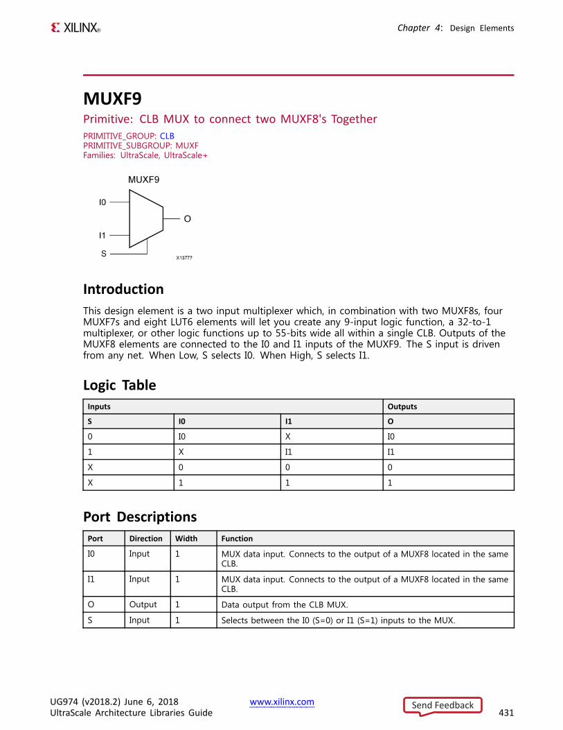
Chapter 4: Design Elements
MUXF9Primitive: CLB MUX to connect two MUXF8's TogetherPRIMITIVE_GROUP: CLBPRIMITIVE_SUBGROUP: MUXFFamilies: UltraScale, UltraScale+
IntroductionThis design element is a two input multiplexer which, in combination with two MUXF8s, fourMUXF7s and eight LUT6 elements will let you create any 9-input logic function, a 32-to-1multiplexer, or other logic functions up to 55-bits wide all within a single CLB. Outputs of theMUXF8 elements are connected to the I0 and I1 inputs of the MUXF9. The S input is drivenfrom any net. When Low, S selects I0. When High, S selects I1.
Logic TableInputs Outputs
S I0 I1 O
0 I0 X I0
1 X I1 I1
X 0 0 0
X 1 1 1
Port DescriptionsPort Direction Width Function
I0 Input 1 MUX data input. Connects to the output of a MUXF8 located in the sameCLB.
I1 Input 1 MUX data input. Connects to the output of a MUXF8 located in the sameCLB.
O Output 1 Data output from the CLB MUX.
S Input 1 Selects between the I0 (S=0) or I1 (S=1) inputs to the MUX.
UG974 (v2018.2) June 6, 2018 www.xilinx.comUltraScale Architecture Libraries Guide 431
Send Feedback

Chapter 4: Design Elements
Design Entry MethodInstantiation Yes
Inference Recommended
IP and IP Integrator Catalog No
VHDL Instantiation TemplateUnless they already exist, copy the following two statements and paste them before the entitydeclaration.Library UNISIM;use UNISIM.vcomponents.all;
-- MUXF9: CLB MUX to connect two MUXF8's Together-- UltraScale-- Xilinx HDL Language Template, version 2018.2
MUXF9_inst : MUXF9port map (
O => O, -- 1-bit output: Output of MUXI0 => I0, -- 1-bit input: Connect to MUXF8 outputI1 => I1, -- 1-bit input: Connect to MUXF8 outputS => S -- 1-bit input: Input select to MUX
);
-- End of MUXF9_inst instantiation
Verilog Instantiation Template
// MUXF9: CLB MUX to connect two MUXF8's Together// UltraScale// Xilinx HDL Language Template, version 2018.2
MUXF9 MUXF9_inst (.O(O), // 1-bit output: Output of MUX.I0(I0), // 1-bit input: Connect to MUXF8 output.I1(I1), // 1-bit input: Connect to MUXF8 output.S(S) // 1-bit input: Input select to MUX
);
// End of MUXF9_inst instantiation
For More Information• See the UltraScale Architecture Configurable Logic Block User Guide (UG574).
• See the UltraScale Programmable Devices Documentation.
UG974 (v2018.2) June 6, 2018 www.xilinx.comUltraScale Architecture Libraries Guide 432
Send Feedback
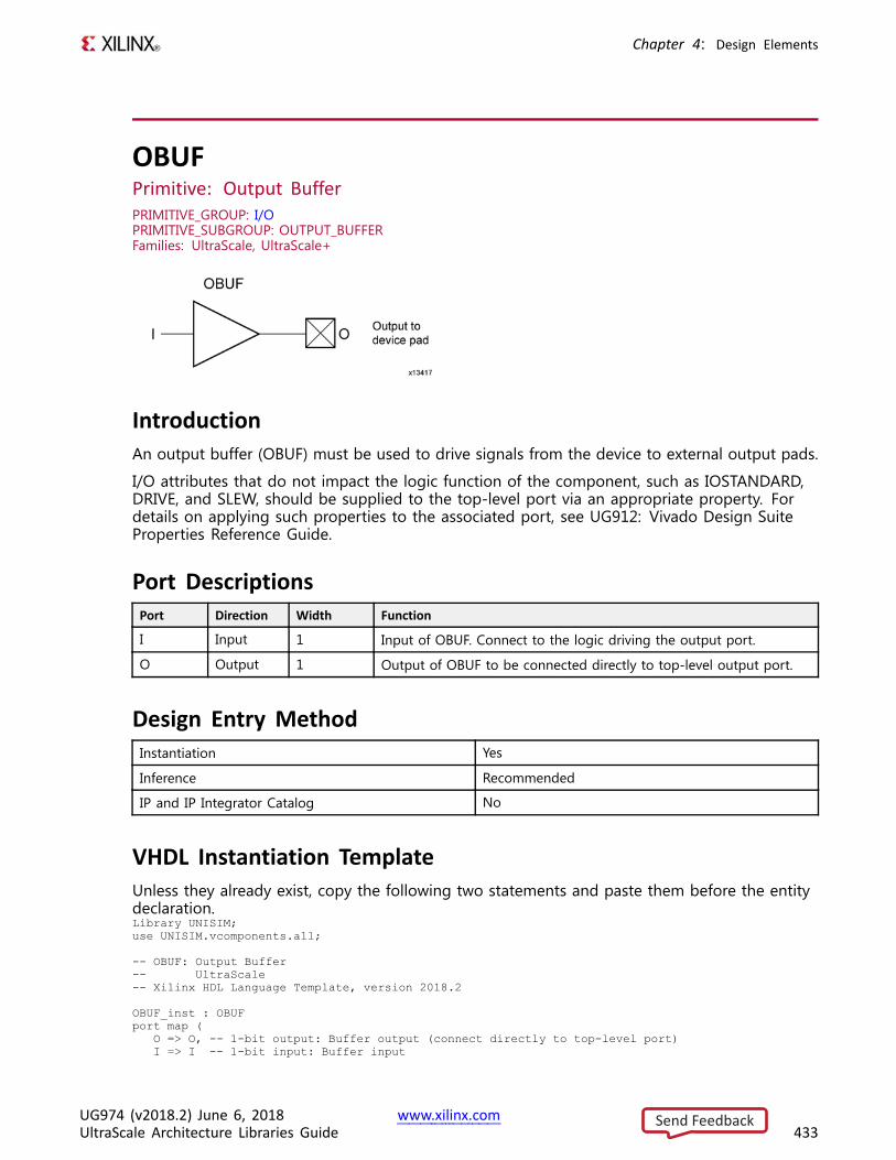
Chapter 4: Design Elements
OBUFPrimitive: Output BufferPRIMITIVE_GROUP: I/OPRIMITIVE_SUBGROUP: OUTPUT_BUFFERFamilies: UltraScale, UltraScale+
IntroductionAn output buffer (OBUF) must be used to drive signals from the device to external output pads.
I/O attributes that do not impact the logic function of the component, such as IOSTANDARD,DRIVE, and SLEW, should be supplied to the top-level port via an appropriate property. Fordetails on applying such properties to the associated port, see UG912: Vivado Design SuiteProperties Reference Guide.
Port DescriptionsPort Direction Width Function
I Input 1 Input of OBUF. Connect to the logic driving the output port.
O Output 1 Output of OBUF to be connected directly to top-level output port.
Design Entry MethodInstantiation Yes
Inference Recommended
IP and IP Integrator Catalog No
VHDL Instantiation TemplateUnless they already exist, copy the following two statements and paste them before the entitydeclaration.Library UNISIM;use UNISIM.vcomponents.all;
-- OBUF: Output Buffer-- UltraScale-- Xilinx HDL Language Template, version 2018.2
OBUF_inst : OBUFport map (
O => O, -- 1-bit output: Buffer output (connect directly to top-level port)I => I -- 1-bit input: Buffer input
UG974 (v2018.2) June 6, 2018 www.xilinx.comUltraScale Architecture Libraries Guide 433
Send Feedback
Chapter 4: Design Elements
);
-- End of OBUF_inst instantiation
Verilog Instantiation Template
// OBUF: Output Buffer// UltraScale// Xilinx HDL Language Template, version 2018.2
OBUF OBUF_inst (.O(O), // 1-bit output: Buffer output (connect directly to top-level port).I(I) // 1-bit input: Buffer input
);
// End of OBUF_inst instantiation
For More Information• See the UltraScale Architecture SelectIO Resources User Guide (UG571).
• See the UltraScale Programmable Devices Documentation.
UG974 (v2018.2) June 6, 2018 www.xilinx.comUltraScale Architecture Libraries Guide 434
Send Feedback
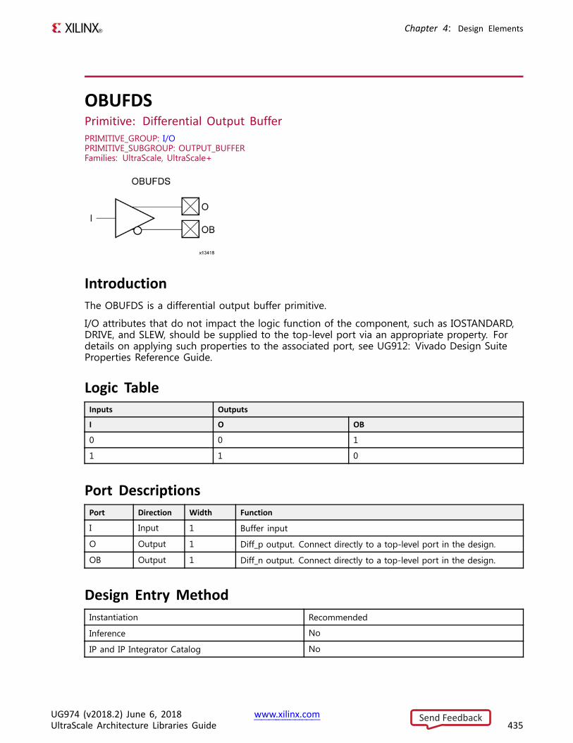
Chapter 4: Design Elements
OBUFDSPrimitive: Differential Output BufferPRIMITIVE_GROUP: I/OPRIMITIVE_SUBGROUP: OUTPUT_BUFFERFamilies: UltraScale, UltraScale+
IntroductionThe OBUFDS is a differential output buffer primitive.
I/O attributes that do not impact the logic function of the component, such as IOSTANDARD,DRIVE, and SLEW, should be supplied to the top-level port via an appropriate property. Fordetails on applying such properties to the associated port, see UG912: Vivado Design SuiteProperties Reference Guide.
Logic TableInputs Outputs
I O OB
0 0 1
1 1 0
Port DescriptionsPort Direction Width Function
I Input 1 Buffer input
O Output 1 Diff_p output. Connect directly to a top-level port in the design.
OB Output 1 Diff_n output. Connect directly to a top-level port in the design.
Design Entry MethodInstantiation Recommended
Inference No
IP and IP Integrator Catalog No
UG974 (v2018.2) June 6, 2018 www.xilinx.comUltraScale Architecture Libraries Guide 435
Send Feedback
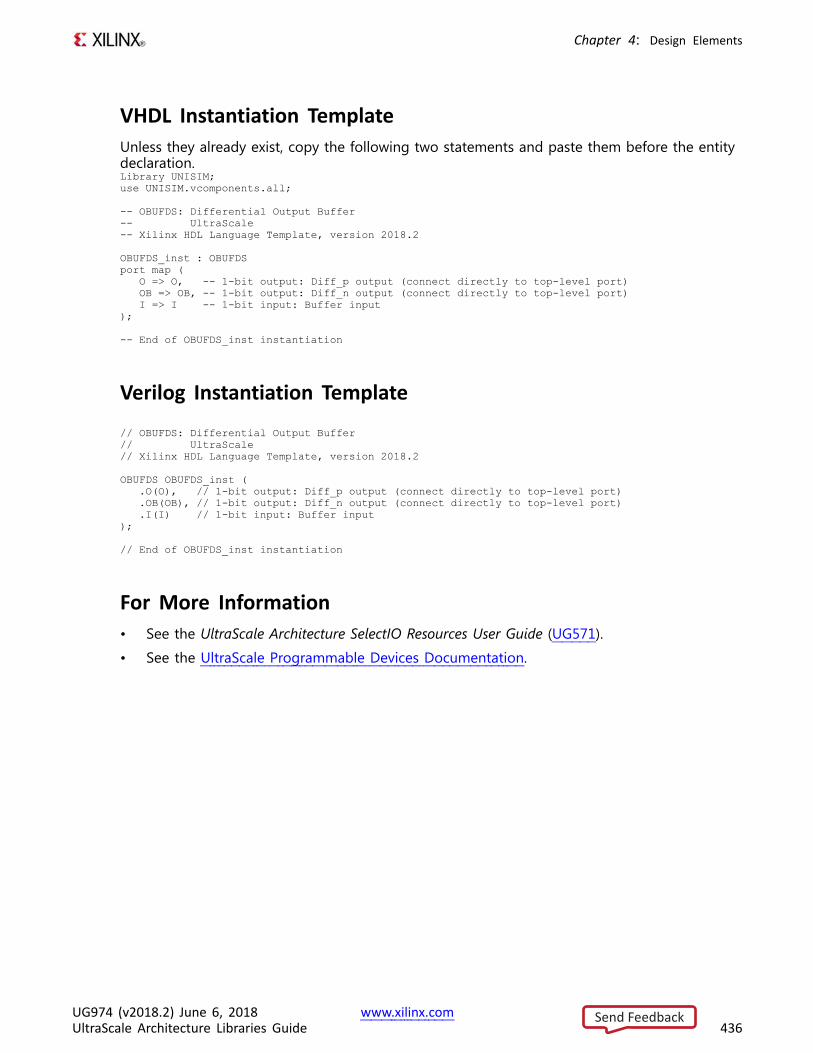
Chapter 4: Design Elements
VHDL Instantiation TemplateUnless they already exist, copy the following two statements and paste them before the entitydeclaration.Library UNISIM;use UNISIM.vcomponents.all;
-- OBUFDS: Differential Output Buffer-- UltraScale-- Xilinx HDL Language Template, version 2018.2
OBUFDS_inst : OBUFDSport map (
O => O, -- 1-bit output: Diff_p output (connect directly to top-level port)OB => OB, -- 1-bit output: Diff_n output (connect directly to top-level port)I => I -- 1-bit input: Buffer input
);
-- End of OBUFDS_inst instantiation
Verilog Instantiation Template
// OBUFDS: Differential Output Buffer// UltraScale// Xilinx HDL Language Template, version 2018.2
OBUFDS OBUFDS_inst (.O(O), // 1-bit output: Diff_p output (connect directly to top-level port).OB(OB), // 1-bit output: Diff_n output (connect directly to top-level port).I(I) // 1-bit input: Buffer input
);
// End of OBUFDS_inst instantiation
For More Information• See the UltraScale Architecture SelectIO Resources User Guide (UG571).
• See the UltraScale Programmable Devices Documentation.
UG974 (v2018.2) June 6, 2018 www.xilinx.comUltraScale Architecture Libraries Guide 436
Send Feedback
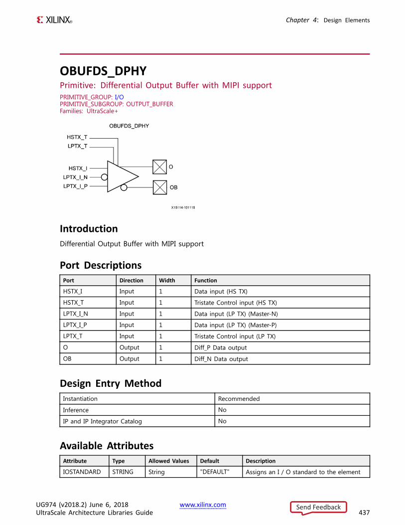
Chapter 4: Design Elements
OBUFDS_DPHYPrimitive: Differential Output Buffer with MIPI supportPRIMITIVE_GROUP: I/OPRIMITIVE_SUBGROUP: OUTPUT_BUFFERFamilies: UltraScale+
IntroductionDifferential Output Buffer with MIPI support
Port DescriptionsPort Direction Width Function
HSTX_I Input 1 Data input (HS TX)
HSTX_T Input 1 Tristate Control input (HS TX)
LPTX_I_N Input 1 Data input (LP TX) (Master-N)
LPTX_I_P Input 1 Data input (LP TX) (Master-P)
LPTX_T Input 1 Tristate Control input (LP TX)
O Output 1 Diff_P Data output
OB Output 1 Diff_N Data output
Design Entry MethodInstantiation Recommended
Inference No
IP and IP Integrator Catalog No
Available AttributesAttribute Type Allowed Values Default Description
IOSTANDARD STRING String "DEFAULT" Assigns an I / O standard to the element
UG974 (v2018.2) June 6, 2018 www.xilinx.comUltraScale Architecture Libraries Guide 437
Send Feedback
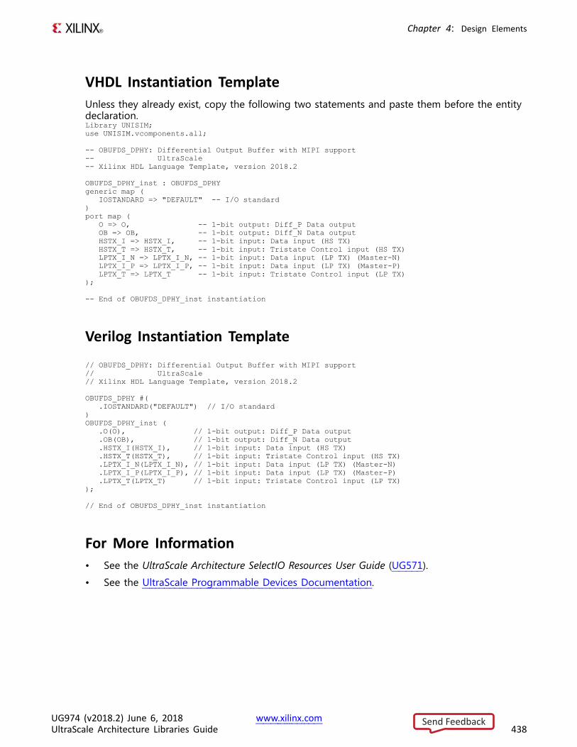
Chapter 4: Design Elements
VHDL Instantiation TemplateUnless they already exist, copy the following two statements and paste them before the entitydeclaration.Library UNISIM;use UNISIM.vcomponents.all;
-- OBUFDS_DPHY: Differential Output Buffer with MIPI support-- UltraScale-- Xilinx HDL Language Template, version 2018.2
OBUFDS_DPHY_inst : OBUFDS_DPHYgeneric map (
IOSTANDARD => "DEFAULT" -- I/O standard)port map (
O => O, -- 1-bit output: Diff_P Data outputOB => OB, -- 1-bit output: Diff_N Data outputHSTX_I => HSTX_I, -- 1-bit input: Data input (HS TX)HSTX_T => HSTX_T, -- 1-bit input: Tristate Control input (HS TX)LPTX_I_N => LPTX_I_N, -- 1-bit input: Data input (LP TX) (Master-N)LPTX_I_P => LPTX_I_P, -- 1-bit input: Data input (LP TX) (Master-P)LPTX_T => LPTX_T -- 1-bit input: Tristate Control input (LP TX)
);
-- End of OBUFDS_DPHY_inst instantiation
Verilog Instantiation Template
// OBUFDS_DPHY: Differential Output Buffer with MIPI support// UltraScale// Xilinx HDL Language Template, version 2018.2
OBUFDS_DPHY #(.IOSTANDARD("DEFAULT") // I/O standard
)OBUFDS_DPHY_inst (
.O(O), // 1-bit output: Diff_P Data output
.OB(OB), // 1-bit output: Diff_N Data output
.HSTX_I(HSTX_I), // 1-bit input: Data input (HS TX)
.HSTX_T(HSTX_T), // 1-bit input: Tristate Control input (HS TX)
.LPTX_I_N(LPTX_I_N), // 1-bit input: Data input (LP TX) (Master-N)
.LPTX_I_P(LPTX_I_P), // 1-bit input: Data input (LP TX) (Master-P)
.LPTX_T(LPTX_T) // 1-bit input: Tristate Control input (LP TX));
// End of OBUFDS_DPHY_inst instantiation
For More Information• See the UltraScale Architecture SelectIO Resources User Guide (UG571).
• See the UltraScale Programmable Devices Documentation.
UG974 (v2018.2) June 6, 2018 www.xilinx.comUltraScale Architecture Libraries Guide 438
Send Feedback
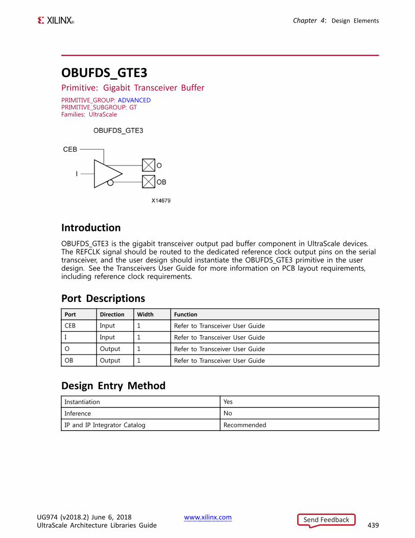
Chapter 4: Design Elements
OBUFDS_GTE3Primitive: Gigabit Transceiver BufferPRIMITIVE_GROUP: ADVANCEDPRIMITIVE_SUBGROUP: GTFamilies: UltraScale
IntroductionOBUFDS_GTE3 is the gigabit transceiver output pad buffer component in UltraScale devices.The REFCLK signal should be routed to the dedicated reference clock output pins on the serialtransceiver, and the user design should instantiate the OBUFDS_GTE3 primitive in the userdesign. See the Transceivers User Guide for more information on PCB layout requirements,including reference clock requirements.
Port DescriptionsPort Direction Width Function
CEB Input 1 Refer to Transceiver User Guide
I Input 1 Refer to Transceiver User Guide
O Output 1 Refer to Transceiver User Guide
OB Output 1 Refer to Transceiver User Guide
Design Entry MethodInstantiation Yes
Inference No
IP and IP Integrator Catalog Recommended
UG974 (v2018.2) June 6, 2018 www.xilinx.comUltraScale Architecture Libraries Guide 439
Send Feedback
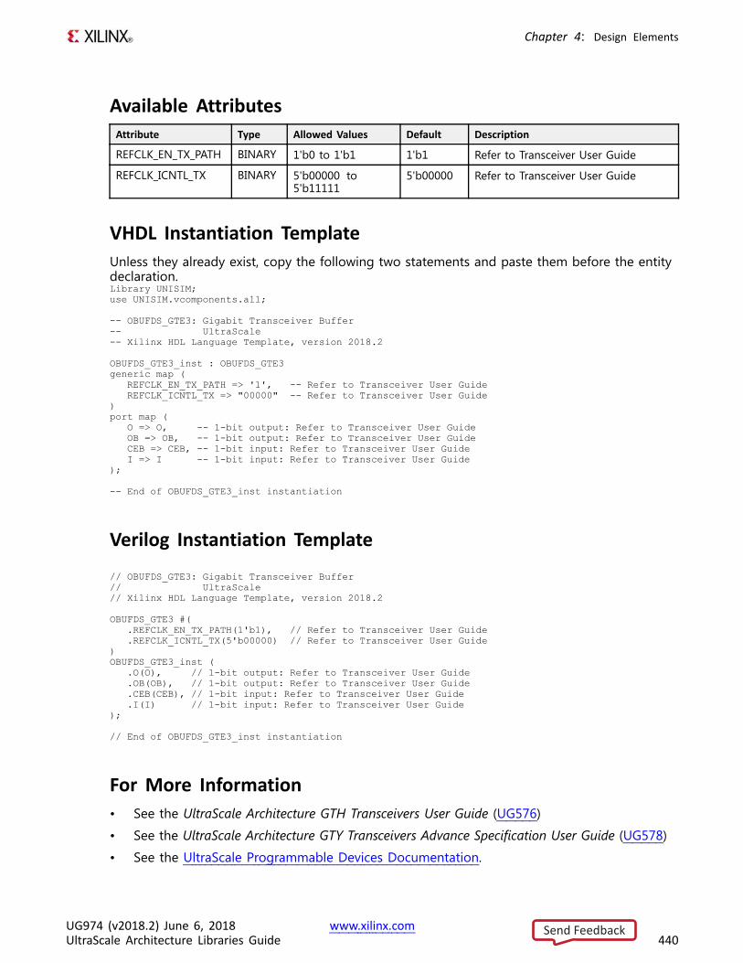
Chapter 4: Design Elements
Available AttributesAttribute Type Allowed Values Default Description
REFCLK_EN_TX_PATH BINARY 1'b0 to 1'b1 1'b1 Refer to Transceiver User Guide
REFCLK_ICNTL_TX BINARY 5'b00000 to5'b11111
5'b00000 Refer to Transceiver User Guide
VHDL Instantiation TemplateUnless they already exist, copy the following two statements and paste them before the entitydeclaration.Library UNISIM;use UNISIM.vcomponents.all;
-- OBUFDS_GTE3: Gigabit Transceiver Buffer-- UltraScale-- Xilinx HDL Language Template, version 2018.2
OBUFDS_GTE3_inst : OBUFDS_GTE3generic map (
REFCLK_EN_TX_PATH => '1', -- Refer to Transceiver User GuideREFCLK_ICNTL_TX => "00000" -- Refer to Transceiver User Guide
)port map (
O => O, -- 1-bit output: Refer to Transceiver User GuideOB => OB, -- 1-bit output: Refer to Transceiver User GuideCEB => CEB, -- 1-bit input: Refer to Transceiver User GuideI => I -- 1-bit input: Refer to Transceiver User Guide
);
-- End of OBUFDS_GTE3_inst instantiation
Verilog Instantiation Template
// OBUFDS_GTE3: Gigabit Transceiver Buffer// UltraScale// Xilinx HDL Language Template, version 2018.2
OBUFDS_GTE3 #(.REFCLK_EN_TX_PATH(1'b1), // Refer to Transceiver User Guide.REFCLK_ICNTL_TX(5'b00000) // Refer to Transceiver User Guide
)OBUFDS_GTE3_inst (
.O(O), // 1-bit output: Refer to Transceiver User Guide
.OB(OB), // 1-bit output: Refer to Transceiver User Guide
.CEB(CEB), // 1-bit input: Refer to Transceiver User Guide
.I(I) // 1-bit input: Refer to Transceiver User Guide);
// End of OBUFDS_GTE3_inst instantiation
For More Information• See the UltraScale Architecture GTH Transceivers User Guide (UG576)
• See the UltraScale Architecture GTY Transceivers Advance Specification User Guide (UG578)
• See the UltraScale Programmable Devices Documentation.
UG974 (v2018.2) June 6, 2018 www.xilinx.comUltraScale Architecture Libraries Guide 440
Send Feedback
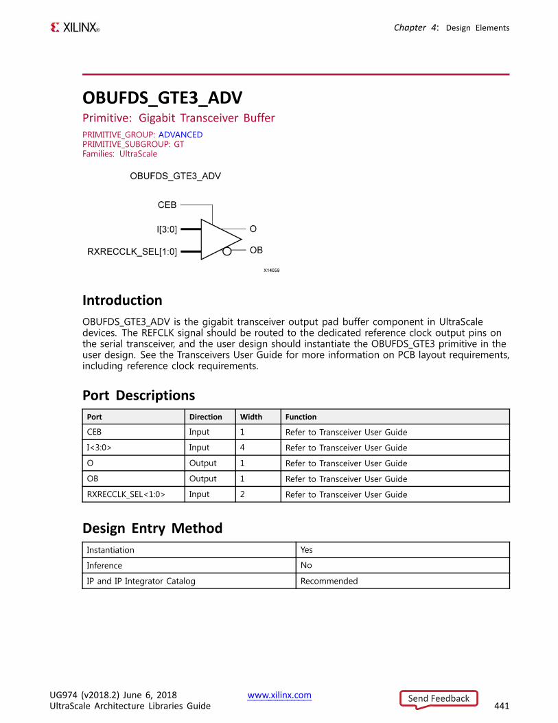
Chapter 4: Design Elements
OBUFDS_GTE3_ADVPrimitive: Gigabit Transceiver BufferPRIMITIVE_GROUP: ADVANCEDPRIMITIVE_SUBGROUP: GTFamilies: UltraScale
IntroductionOBUFDS_GTE3_ADV is the gigabit transceiver output pad buffer component in UltraScaledevices. The REFCLK signal should be routed to the dedicated reference clock output pins onthe serial transceiver, and the user design should instantiate the OBUFDS_GTE3 primitive in theuser design. See the Transceivers User Guide for more information on PCB layout requirements,including reference clock requirements.
Port DescriptionsPort Direction Width Function
CEB Input 1 Refer to Transceiver User Guide
I<3:0> Input 4 Refer to Transceiver User Guide
O Output 1 Refer to Transceiver User Guide
OB Output 1 Refer to Transceiver User Guide
RXRECCLK_SEL<1:0> Input 2 Refer to Transceiver User Guide
Design Entry MethodInstantiation Yes
Inference No
IP and IP Integrator Catalog Recommended
UG974 (v2018.2) June 6, 2018 www.xilinx.comUltraScale Architecture Libraries Guide 441
Send Feedback
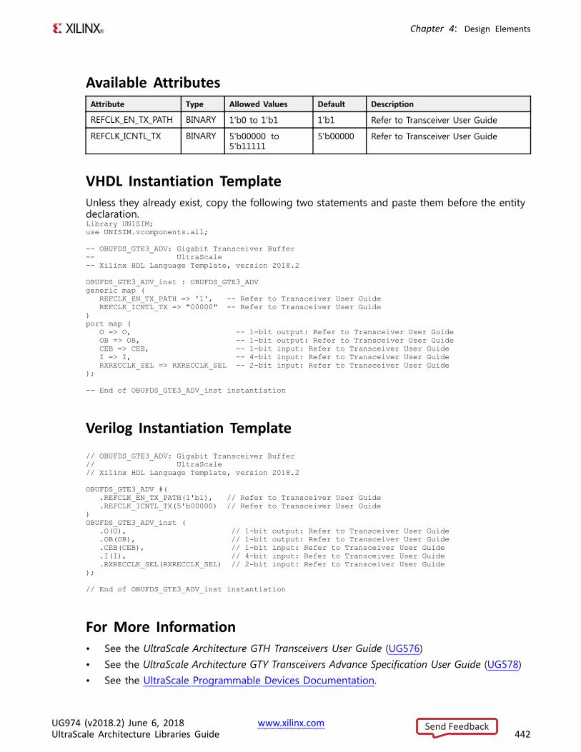
Chapter 4: Design Elements
Available AttributesAttribute Type Allowed Values Default Description
REFCLK_EN_TX_PATH BINARY 1'b0 to 1'b1 1'b1 Refer to Transceiver User Guide
REFCLK_ICNTL_TX BINARY 5'b00000 to5'b11111
5'b00000 Refer to Transceiver User Guide
VHDL Instantiation TemplateUnless they already exist, copy the following two statements and paste them before the entitydeclaration.Library UNISIM;use UNISIM.vcomponents.all;
-- OBUFDS_GTE3_ADV: Gigabit Transceiver Buffer-- UltraScale-- Xilinx HDL Language Template, version 2018.2
OBUFDS_GTE3_ADV_inst : OBUFDS_GTE3_ADVgeneric map (
REFCLK_EN_TX_PATH => '1', -- Refer to Transceiver User GuideREFCLK_ICNTL_TX => "00000" -- Refer to Transceiver User Guide
)port map (
O => O, -- 1-bit output: Refer to Transceiver User GuideOB => OB, -- 1-bit output: Refer to Transceiver User GuideCEB => CEB, -- 1-bit input: Refer to Transceiver User GuideI => I, -- 4-bit input: Refer to Transceiver User GuideRXRECCLK_SEL => RXRECCLK_SEL -- 2-bit input: Refer to Transceiver User Guide
);
-- End of OBUFDS_GTE3_ADV_inst instantiation
Verilog Instantiation Template// OBUFDS_GTE3_ADV: Gigabit Transceiver Buffer// UltraScale// Xilinx HDL Language Template, version 2018.2
OBUFDS_GTE3_ADV #(.REFCLK_EN_TX_PATH(1'b1), // Refer to Transceiver User Guide.REFCLK_ICNTL_TX(5'b00000) // Refer to Transceiver User Guide
)OBUFDS_GTE3_ADV_inst (
.O(O), // 1-bit output: Refer to Transceiver User Guide
.OB(OB), // 1-bit output: Refer to Transceiver User Guide
.CEB(CEB), // 1-bit input: Refer to Transceiver User Guide
.I(I), // 4-bit input: Refer to Transceiver User Guide
.RXRECCLK_SEL(RXRECCLK_SEL) // 2-bit input: Refer to Transceiver User Guide);
// End of OBUFDS_GTE3_ADV_inst instantiation
For More Information• See the UltraScale Architecture GTH Transceivers User Guide (UG576)• See the UltraScale Architecture GTY Transceivers Advance Specification User Guide (UG578)• See the UltraScale Programmable Devices Documentation.
UG974 (v2018.2) June 6, 2018 www.xilinx.comUltraScale Architecture Libraries Guide 442
Send Feedback
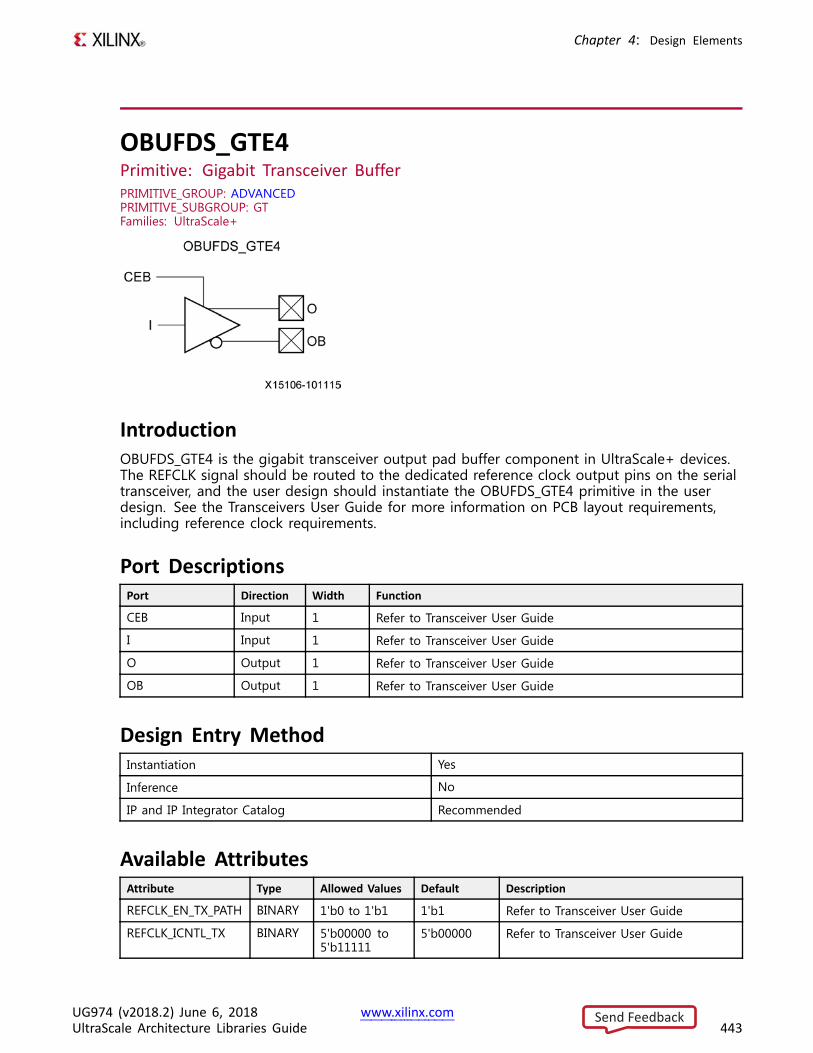
Chapter 4: Design Elements
OBUFDS_GTE4Primitive: Gigabit Transceiver BufferPRIMITIVE_GROUP: ADVANCEDPRIMITIVE_SUBGROUP: GTFamilies: UltraScale+
IntroductionOBUFDS_GTE4 is the gigabit transceiver output pad buffer component in UltraScale+ devices.The REFCLK signal should be routed to the dedicated reference clock output pins on the serialtransceiver, and the user design should instantiate the OBUFDS_GTE4 primitive in the userdesign. See the Transceivers User Guide for more information on PCB layout requirements,including reference clock requirements.
Port DescriptionsPort Direction Width Function
CEB Input 1 Refer to Transceiver User Guide
I Input 1 Refer to Transceiver User Guide
O Output 1 Refer to Transceiver User Guide
OB Output 1 Refer to Transceiver User Guide
Design Entry MethodInstantiation Yes
Inference No
IP and IP Integrator Catalog Recommended
Available AttributesAttribute Type Allowed Values Default Description
REFCLK_EN_TX_PATH BINARY 1'b0 to 1'b1 1'b1 Refer to Transceiver User Guide
REFCLK_ICNTL_TX BINARY 5'b00000 to5'b11111
5'b00000 Refer to Transceiver User Guide
UG974 (v2018.2) June 6, 2018 www.xilinx.comUltraScale Architecture Libraries Guide 443
Send Feedback
Chapter 4: Design Elements
VHDL Instantiation TemplateUnless they already exist, copy the following two statements and paste them before the entitydeclaration.Library UNISIM;use UNISIM.vcomponents.all;
-- OBUFDS_GTE4: Gigabit Transceiver Buffer-- UltraScale-- Xilinx HDL Language Template, version 2018.2
OBUFDS_GTE4_inst : OBUFDS_GTE4generic map (
REFCLK_EN_TX_PATH => '1', -- Refer to Transceiver User GuideREFCLK_ICNTL_TX => "00000" -- Refer to Transceiver User Guide
)port map (
O => O, -- 1-bit output: Refer to Transceiver User GuideOB => OB, -- 1-bit output: Refer to Transceiver User GuideCEB => CEB, -- 1-bit input: Refer to Transceiver User GuideI => I -- 1-bit input: Refer to Transceiver User Guide
);
-- End of OBUFDS_GTE4_inst instantiation
Verilog Instantiation Template
// OBUFDS_GTE4: Gigabit Transceiver Buffer// UltraScale// Xilinx HDL Language Template, version 2018.2
OBUFDS_GTE4 #(.REFCLK_EN_TX_PATH(1'b1), // Refer to Transceiver User Guide.REFCLK_ICNTL_TX(5'b00000) // Refer to Transceiver User Guide
)OBUFDS_GTE4_inst (
.O(O), // 1-bit output: Refer to Transceiver User Guide
.OB(OB), // 1-bit output: Refer to Transceiver User Guide
.CEB(CEB), // 1-bit input: Refer to Transceiver User Guide
.I(I) // 1-bit input: Refer to Transceiver User Guide);
// End of OBUFDS_GTE4_inst instantiation
For More Information• See the UltraScale Architecture GTH Transceivers User Guide (UG576)
• See the UltraScale Architecture GTY Transceivers Advance Specification User Guide (UG578)
• See the UltraScale Programmable Devices Documentation.
UG974 (v2018.2) June 6, 2018 www.xilinx.comUltraScale Architecture Libraries Guide 444
Send Feedback
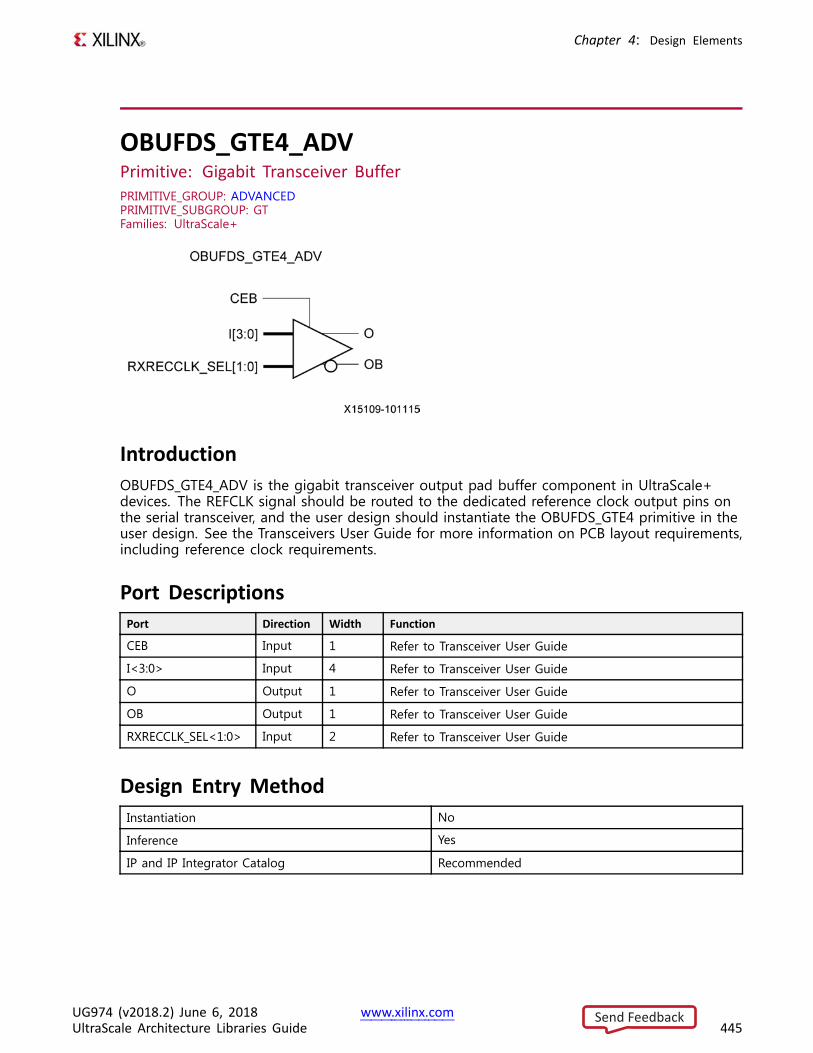
Chapter 4: Design Elements
OBUFDS_GTE4_ADVPrimitive: Gigabit Transceiver BufferPRIMITIVE_GROUP: ADVANCEDPRIMITIVE_SUBGROUP: GTFamilies: UltraScale+
IntroductionOBUFDS_GTE4_ADV is the gigabit transceiver output pad buffer component in UltraScale+devices. The REFCLK signal should be routed to the dedicated reference clock output pins onthe serial transceiver, and the user design should instantiate the OBUFDS_GTE4 primitive in theuser design. See the Transceivers User Guide for more information on PCB layout requirements,including reference clock requirements.
Port DescriptionsPort Direction Width Function
CEB Input 1 Refer to Transceiver User Guide
I<3:0> Input 4 Refer to Transceiver User Guide
O Output 1 Refer to Transceiver User Guide
OB Output 1 Refer to Transceiver User Guide
RXRECCLK_SEL<1:0> Input 2 Refer to Transceiver User Guide
Design Entry MethodInstantiation No
Inference Yes
IP and IP Integrator Catalog Recommended
UG974 (v2018.2) June 6, 2018 www.xilinx.comUltraScale Architecture Libraries Guide 445
Send Feedback
Chapter 4: Design Elements
Available AttributesAttribute Type Allowed Values Default Description
REFCLK_EN_TX_PATH BINARY 1'b0 to 1'b1 1'b1 Refer to Transceiver User Guide
REFCLK_ICNTL_TX BINARY 5'b00000 to5'b11111
5'b00000 Refer to Transceiver User Guide
VHDL Instantiation TemplateUnless they already exist, copy the following two statements and paste them before the entitydeclaration.Library UNISIM;use UNISIM.vcomponents.all;
-- OBUFDS_GTE4_ADV: Gigabit Transceiver Buffer-- UltraScale-- Xilinx HDL Language Template, version 2018.2
OBUFDS_GTE4_ADV_inst : OBUFDS_GTE4_ADVgeneric map (
REFCLK_EN_TX_PATH => '1', -- Refer to Transceiver User GuideREFCLK_ICNTL_TX => "00000" -- Refer to Transceiver User Guide
)port map (
O => O, -- 1-bit output: Refer to Transceiver User GuideOB => OB, -- 1-bit output: Refer to Transceiver User GuideCEB => CEB, -- 1-bit input: Refer to Transceiver User GuideI => I, -- 4-bit input: Refer to Transceiver User GuideRXRECCLK_SEL => RXRECCLK_SEL -- 2-bit input: Refer to Transceiver User Guide
);
-- End of OBUFDS_GTE4_ADV_inst instantiation
Verilog Instantiation Template// OBUFDS_GTE4_ADV: Gigabit Transceiver Buffer// UltraScale// Xilinx HDL Language Template, version 2018.2
OBUFDS_GTE4_ADV #(.REFCLK_EN_TX_PATH(1'b1), // Refer to Transceiver User Guide.REFCLK_ICNTL_TX(5'b00000) // Refer to Transceiver User Guide
)OBUFDS_GTE4_ADV_inst (
.O(O), // 1-bit output: Refer to Transceiver User Guide
.OB(OB), // 1-bit output: Refer to Transceiver User Guide
.CEB(CEB), // 1-bit input: Refer to Transceiver User Guide
.I(I), // 4-bit input: Refer to Transceiver User Guide
.RXRECCLK_SEL(RXRECCLK_SEL) // 2-bit input: Refer to Transceiver User Guide);
// End of OBUFDS_GTE4_ADV_inst instantiation
For More Information• See the UltraScale Architecture GTH Transceivers User Guide (UG576)• See the UltraScale Architecture GTY Transceivers Advance Specification User Guide (UG578)• See the UltraScale Programmable Devices Documentation.
UG974 (v2018.2) June 6, 2018 www.xilinx.comUltraScale Architecture Libraries Guide 446
Send Feedback
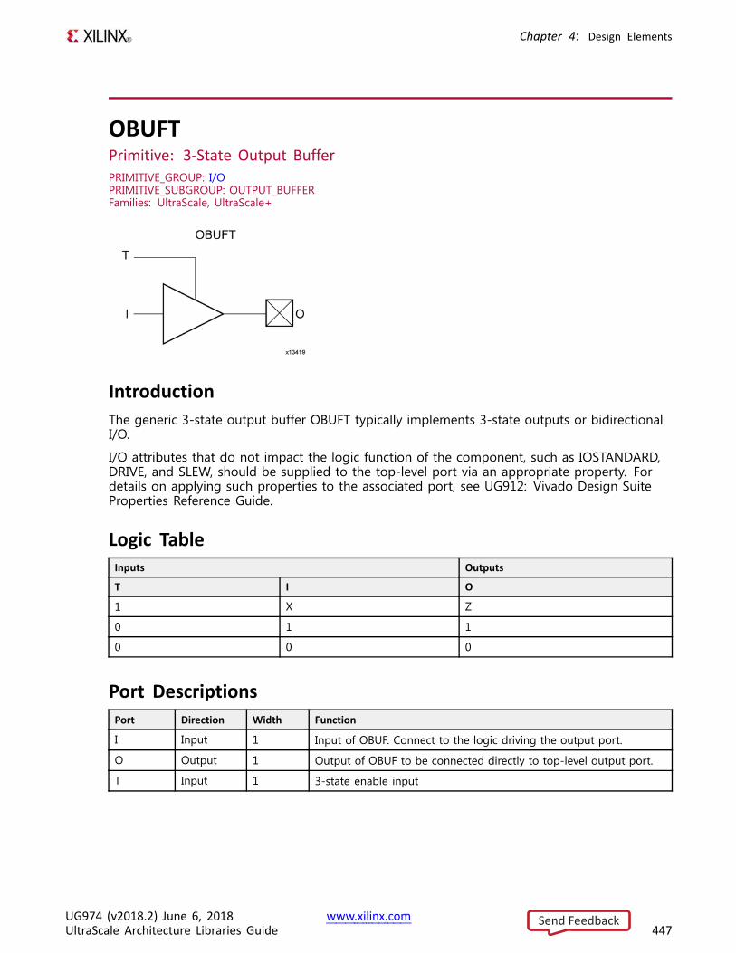
Chapter 4: Design Elements
OBUFTPrimitive: 3-State Output BufferPRIMITIVE_GROUP: I/OPRIMITIVE_SUBGROUP: OUTPUT_BUFFERFamilies: UltraScale, UltraScale+
IntroductionThe generic 3-state output buffer OBUFT typically implements 3-state outputs or bidirectionalI/O.
I/O attributes that do not impact the logic function of the component, such as IOSTANDARD,DRIVE, and SLEW, should be supplied to the top-level port via an appropriate property. Fordetails on applying such properties to the associated port, see UG912: Vivado Design SuiteProperties Reference Guide.
Logic TableInputs Outputs
T I O
1 X Z
0 1 1
0 0 0
Port DescriptionsPort Direction Width Function
I Input 1 Input of OBUF. Connect to the logic driving the output port.
O Output 1 Output of OBUF to be connected directly to top-level output port.
T Input 1 3-state enable input
UG974 (v2018.2) June 6, 2018 www.xilinx.comUltraScale Architecture Libraries Guide 447
Send Feedback
Chapter 4: Design Elements
Design Entry MethodInstantiation Yes
Inference Recommended
IP and IP Integrator Catalog No
VHDL Instantiation TemplateUnless they already exist, copy the following two statements and paste them before the entitydeclaration.Library UNISIM;use UNISIM.vcomponents.all;
-- OBUFT: 3-State Output Buffer-- UltraScale-- Xilinx HDL Language Template, version 2018.2
OBUFT_inst : OBUFTport map (
O => O, -- 1-bit output: Buffer output (connect directly to top-level port)I => I, -- 1-bit input: Buffer inputT => T -- 1-bit input: 3-state enable input
);
-- End of OBUFT_inst instantiation
Verilog Instantiation Template
// OBUFT: 3-State Output Buffer// UltraScale// Xilinx HDL Language Template, version 2018.2
OBUFT OBUFT_inst (.O(O), // 1-bit output: Buffer output (connect directly to top-level port).I(I), // 1-bit input: Buffer input.T(T) // 1-bit input: 3-state enable input
);
// End of OBUFT_inst instantiation
For More Information• See the UltraScale Architecture SelectIO Resources User Guide (UG571).
• See the UltraScale Programmable Devices Documentation.
UG974 (v2018.2) June 6, 2018 www.xilinx.comUltraScale Architecture Libraries Guide 448
Send Feedback
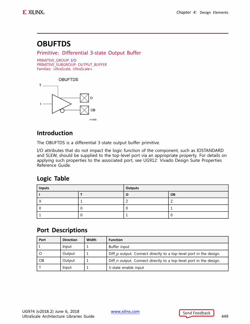
Chapter 4: Design Elements
OBUFTDSPrimitive: Differential 3-state Output BufferPRIMITIVE_GROUP: I/OPRIMITIVE_SUBGROUP: OUTPUT_BUFFERFamilies: UltraScale, UltraScale+
IntroductionThe OBUFTDS is a differential 3-state output buffer primitive.
I/O attributes that do not impact the logic function of the component, such as IOSTANDARDand SLEW, should be supplied to the top-level port via an appropriate property. For details onapplying such properties to the associated port, see UG912: Vivado Design Suite PropertiesReference Guide.
Logic TableInputs Outputs
I T O OB
X 1 Z Z
0 0 0 1
1 0 1 0
Port DescriptionsPort Direction Width Function
I Input 1 Buffer input
O Output 1 Diff_p output. Connect directly to a top-level port in the design.
OB Output 1 Diff_n output. Connect directly to a top-level port in the design.
T Input 1 3-state enable input
UG974 (v2018.2) June 6, 2018 www.xilinx.comUltraScale Architecture Libraries Guide 449
Send Feedback
Chapter 4: Design Elements
Design Entry MethodInstantiation Yes
Inference No
IP and IP Integrator Catalog No
VHDL Instantiation TemplateUnless they already exist, copy the following two statements and paste them before the entitydeclaration.Library UNISIM;use UNISIM.vcomponents.all;
-- OBUFTDS: Differential 3-state Output Buffer-- UltraScale-- Xilinx HDL Language Template, version 2018.2
OBUFTDS_inst : OBUFTDSport map (
O => O, -- 1-bit output: Diff_p output (connect directly to top-level port)OB => OB, -- 1-bit output: Diff_n output (connect directly to top-level port)I => I, -- 1-bit input: Buffer inputT => T -- 1-bit input: 3-state enable input
);
-- End of OBUFTDS_inst instantiation
Verilog Instantiation Template
// OBUFTDS: Differential 3-state Output Buffer// UltraScale// Xilinx HDL Language Template, version 2018.2
OBUFTDS OBUFTDS_inst (.O(O), // 1-bit output: Diff_p output (connect directly to top-level port).OB(OB), // 1-bit output: Diff_n output (connect directly to top-level port).I(I), // 1-bit input: Buffer input.T(T) // 1-bit input: 3-state enable input
);
// End of OBUFTDS_inst instantiation
For More Information• See the UltraScale Architecture SelectIO Resources User Guide (UG571).
• See the UltraScale Programmable Devices Documentation.
UG974 (v2018.2) June 6, 2018 www.xilinx.comUltraScale Architecture Libraries Guide 450
Send Feedback
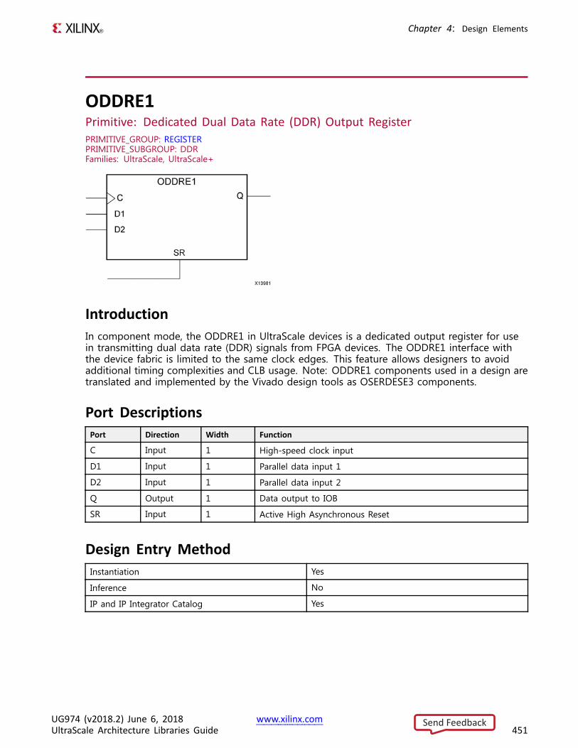
Chapter 4: Design Elements
ODDRE1Primitive: Dedicated Dual Data Rate (DDR) Output RegisterPRIMITIVE_GROUP: REGISTERPRIMITIVE_SUBGROUP: DDRFamilies: UltraScale, UltraScale+
IntroductionIn component mode, the ODDRE1 in UltraScale devices is a dedicated output register for usein transmitting dual data rate (DDR) signals from FPGA devices. The ODDRE1 interface withthe device fabric is limited to the same clock edges. This feature allows designers to avoidadditional timing complexities and CLB usage. Note: ODDRE1 components used in a design aretranslated and implemented by the Vivado design tools as OSERDESE3 components.
Port DescriptionsPort Direction Width Function
C Input 1 High-speed clock input
D1 Input 1 Parallel data input 1
D2 Input 1 Parallel data input 2
Q Output 1 Data output to IOB
SR Input 1 Active High Asynchronous Reset
Design Entry MethodInstantiation Yes
Inference No
IP and IP Integrator Catalog Yes
UG974 (v2018.2) June 6, 2018 www.xilinx.comUltraScale Architecture Libraries Guide 451
Send Feedback
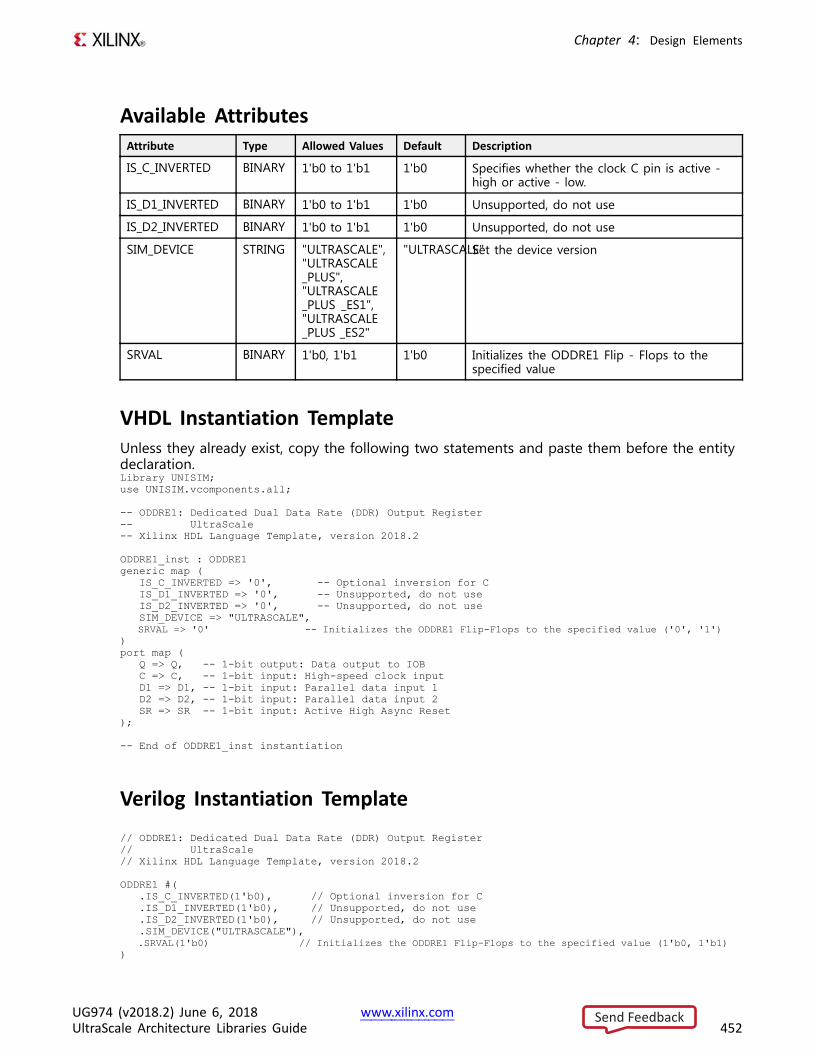
Chapter 4: Design Elements
Available AttributesAttribute Type Allowed Values Default Description
IS_C_INVERTED BINARY 1'b0 to 1'b1 1'b0 Specifies whether the clock C pin is active -high or active - low.
IS_D1_INVERTED BINARY 1'b0 to 1'b1 1'b0 Unsupported, do not use
IS_D2_INVERTED BINARY 1'b0 to 1'b1 1'b0 Unsupported, do not use
SIM_DEVICE STRING "ULTRASCALE","ULTRASCALE_PLUS","ULTRASCALE_PLUS _ES1","ULTRASCALE_PLUS _ES2"
"ULTRASCALE"Set the device version
SRVAL BINARY 1'b0, 1'b1 1'b0 Initializes the ODDRE1 Flip - Flops to thespecified value
VHDL Instantiation TemplateUnless they already exist, copy the following two statements and paste them before the entitydeclaration.Library UNISIM;use UNISIM.vcomponents.all;
-- ODDRE1: Dedicated Dual Data Rate (DDR) Output Register-- UltraScale-- Xilinx HDL Language Template, version 2018.2
ODDRE1_inst : ODDRE1generic map (
IS_C_INVERTED => '0', -- Optional inversion for CIS_D1_INVERTED => '0', -- Unsupported, do not useIS_D2_INVERTED => '0', -- Unsupported, do not useSIM_DEVICE => "ULTRASCALE",SRVAL => '0' -- Initializes the ODDRE1 Flip-Flops to the specified value ('0', '1')
)port map (
Q => Q, -- 1-bit output: Data output to IOBC => C, -- 1-bit input: High-speed clock inputD1 => D1, -- 1-bit input: Parallel data input 1D2 => D2, -- 1-bit input: Parallel data input 2SR => SR -- 1-bit input: Active High Async Reset
);
-- End of ODDRE1_inst instantiation
Verilog Instantiation Template// ODDRE1: Dedicated Dual Data Rate (DDR) Output Register// UltraScale// Xilinx HDL Language Template, version 2018.2
ODDRE1 #(.IS_C_INVERTED(1'b0), // Optional inversion for C.IS_D1_INVERTED(1'b0), // Unsupported, do not use.IS_D2_INVERTED(1'b0), // Unsupported, do not use.SIM_DEVICE("ULTRASCALE"),.SRVAL(1'b0) // Initializes the ODDRE1 Flip-Flops to the specified value (1'b0, 1'b1)
)
UG974 (v2018.2) June 6, 2018 www.xilinx.comUltraScale Architecture Libraries Guide 452
Send Feedback
Chapter 4: Design Elements
ODDRE1_inst (.Q(Q), // 1-bit output: Data output to IOB.C(C), // 1-bit input: High-speed clock input.D1(D1), // 1-bit input: Parallel data input 1.D2(D2), // 1-bit input: Parallel data input 2.SR(SR) // 1-bit input: Active High Async Reset
);
// End of ODDRE1_inst instantiation
For More Information• See the UltraScale Architecture SelectIO Resources User Guide (UG571).
• See the UltraScale Programmable Devices Documentation.
UG974 (v2018.2) June 6, 2018 www.xilinx.comUltraScale Architecture Libraries Guide 453
Send Feedback
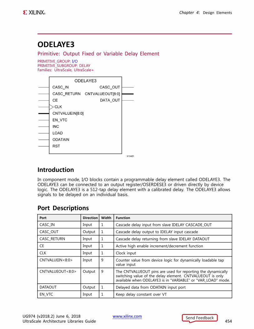
Chapter 4: Design Elements
ODELAYE3Primitive: Output Fixed or Variable Delay ElementPRIMITIVE_GROUP: I/OPRIMITIVE_SUBGROUP: DELAYFamilies: UltraScale, UltraScale+
IntroductionIn component mode, I/O blocks contain a programmable delay element called ODELAYE3. TheODELAYE3 can be connected to an output register/OSERDESE3 or driven directly by devicelogic. The ODELAYE3 is a 512-tap delay element with a calibrated delay. The ODELAYE3 allowssignals to be delayed on an individual basis.
Port DescriptionsPort Direction Width Function
CASC_IN Input 1 Cascade delay input from slave IDELAY CASCADE_OUT
CASC_OUT Output 1 Cascade delay output to IDELAY input cascade
CASC_RETURN Input 1 Cascade delay returning from slave IDELAY DATAOUT
CE Input 1 Active high enable increment/decrement function
CLK Input 1 Clock input
CNTVALUEIN<8:0> Input 9 Counter value from device logic for dynamically loadable tapvalue input
CNTVALUEOUT<8:0> Output 9 The CNTVALUEOUT pins are used for reporting the dynamicallyswitching value of the delay element. CNTVALUEOUT is onlyavailable when ODELAYE3 is in "VARIABLE" or "VAR_LOAD" mode.
DATAOUT Output 1 Delayed data from ODATAIN input port
EN_VTC Input 1 Keep delay constant over VT
UG974 (v2018.2) June 6, 2018 www.xilinx.comUltraScale Architecture Libraries Guide 454
Send Feedback
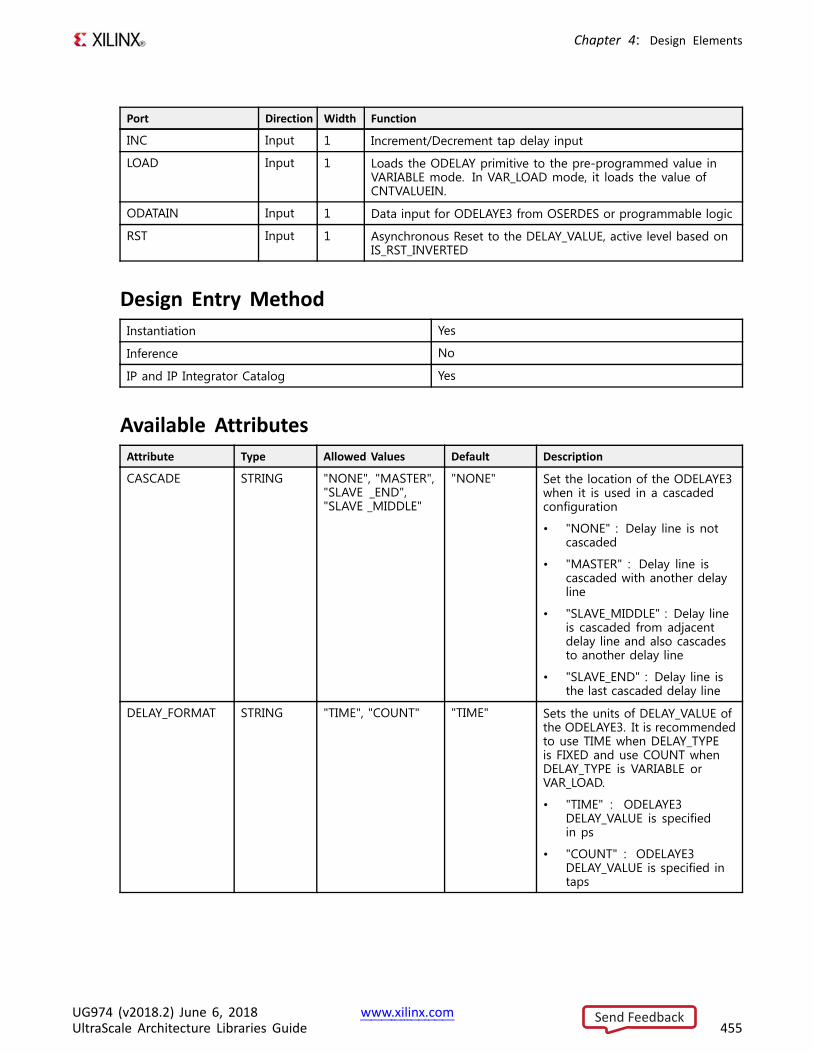
Chapter 4: Design Elements
Port Direction Width Function
INC Input 1 Increment/Decrement tap delay input
LOAD Input 1 Loads the ODELAY primitive to the pre-programmed value inVARIABLE mode. In VAR_LOAD mode, it loads the value ofCNTVALUEIN.
ODATAIN Input 1 Data input for ODELAYE3 from OSERDES or programmable logic
RST Input 1 Asynchronous Reset to the DELAY_VALUE, active level based onIS_RST_INVERTED
Design Entry MethodInstantiation Yes
Inference No
IP and IP Integrator Catalog Yes
Available AttributesAttribute Type Allowed Values Default Description
CASCADE STRING "NONE", "MASTER","SLAVE _END","SLAVE _MIDDLE"
"NONE" Set the location of the ODELAYE3when it is used in a cascadedconfiguration
• "NONE" : Delay line is notcascaded
• "MASTER" : Delay line iscascaded with another delayline
• "SLAVE_MIDDLE" : Delay lineis cascaded from adjacentdelay line and also cascadesto another delay line
• "SLAVE_END" : Delay line isthe last cascaded delay line
DELAY_FORMAT STRING "TIME", "COUNT" "TIME" Sets the units of DELAY_VALUE ofthe ODELAYE3. It is recommendedto use TIME when DELAY_TYPEis FIXED and use COUNT whenDELAY_TYPE is VARIABLE orVAR_LOAD.
• "TIME" : ODELAYE3DELAY_VALUE is specifiedin ps
• "COUNT" : ODELAYE3DELAY_VALUE is specified intaps
UG974 (v2018.2) June 6, 2018 www.xilinx.comUltraScale Architecture Libraries Guide 455
Send Feedback
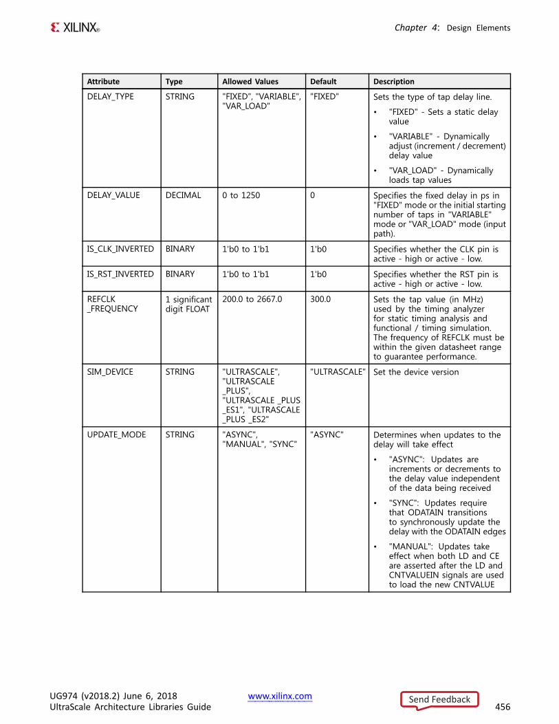
Chapter 4: Design Elements
Attribute Type Allowed Values Default Description
DELAY_TYPE STRING "FIXED", "VARIABLE","VAR_LOAD"
"FIXED" Sets the type of tap delay line.
• "FIXED" - Sets a static delayvalue
• "VARIABLE" - Dynamicallyadjust (increment / decrement)delay value
• "VAR_LOAD" - Dynamicallyloads tap values
DELAY_VALUE DECIMAL 0 to 1250 0 Specifies the fixed delay in ps in"FIXED" mode or the initial startingnumber of taps in "VARIABLE"mode or "VAR_LOAD" mode (inputpath).
IS_CLK_INVERTED BINARY 1'b0 to 1'b1 1'b0 Specifies whether the CLK pin isactive - high or active - low.
IS_RST_INVERTED BINARY 1'b0 to 1'b1 1'b0 Specifies whether the RST pin isactive - high or active - low.
REFCLK_FREQUENCY
1 significantdigit FLOAT
200.0 to 2667.0 300.0 Sets the tap value (in MHz)used by the timing analyzerfor static timing analysis andfunctional / timing simulation.The frequency of REFCLK must bewithin the given datasheet rangeto guarantee performance.
SIM_DEVICE STRING "ULTRASCALE","ULTRASCALE_PLUS","ULTRASCALE _PLUS_ES1", "ULTRASCALE_PLUS _ES2"
"ULTRASCALE" Set the device version
UPDATE_MODE STRING "ASYNC","MANUAL", "SYNC"
"ASYNC" Determines when updates to thedelay will take effect
• "ASYNC": Updates areincrements or decrements tothe delay value independentof the data being received
• "SYNC": Updates requirethat ODATAIN transitionsto synchronously update thedelay with the ODATAIN edges
• "MANUAL": Updates takeeffect when both LD and CEare asserted after the LD andCNTVALUEIN signals are usedto load the new CNTVALUE
UG974 (v2018.2) June 6, 2018 www.xilinx.comUltraScale Architecture Libraries Guide 456
Send Feedback
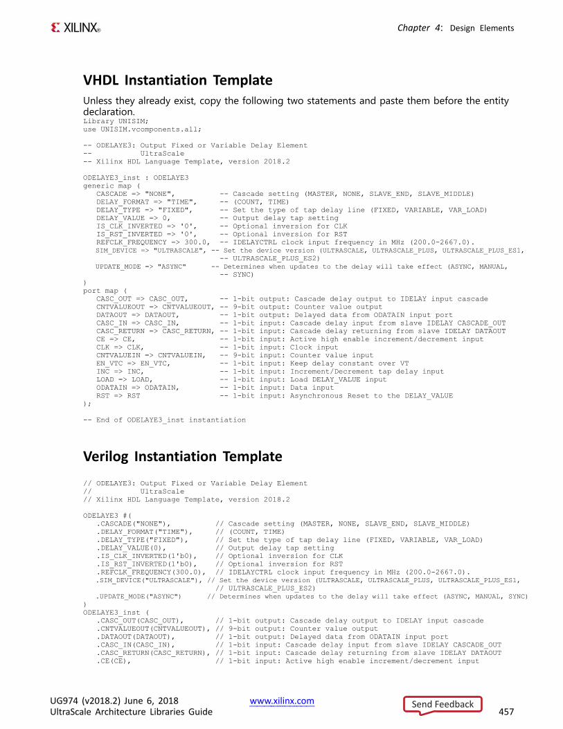
Chapter 4: Design Elements
VHDL Instantiation TemplateUnless they already exist, copy the following two statements and paste them before the entitydeclaration.Library UNISIM;use UNISIM.vcomponents.all;
-- ODELAYE3: Output Fixed or Variable Delay Element-- UltraScale-- Xilinx HDL Language Template, version 2018.2
ODELAYE3_inst : ODELAYE3generic map (
CASCADE => "NONE", -- Cascade setting (MASTER, NONE, SLAVE_END, SLAVE_MIDDLE)DELAY_FORMAT => "TIME", -- (COUNT, TIME)DELAY_TYPE => "FIXED", -- Set the type of tap delay line (FIXED, VARIABLE, VAR_LOAD)DELAY_VALUE => 0, -- Output delay tap settingIS_CLK_INVERTED => '0', -- Optional inversion for CLKIS_RST_INVERTED => '0', -- Optional inversion for RSTREFCLK_FREQUENCY => 300.0, -- IDELAYCTRL clock input frequency in MHz (200.0-2667.0).SIM_DEVICE => "ULTRASCALE", -- Set the device version (ULTRASCALE, ULTRASCALE_PLUS, ULTRASCALE_PLUS_ES1,
-- ULTRASCALE_PLUS_ES2)UPDATE_MODE => "ASYNC" -- Determines when updates to the delay will take effect (ASYNC, MANUAL,
-- SYNC))port map (
CASC_OUT => CASC_OUT, -- 1-bit output: Cascade delay output to IDELAY input cascadeCNTVALUEOUT => CNTVALUEOUT, -- 9-bit output: Counter value outputDATAOUT => DATAOUT, -- 1-bit output: Delayed data from ODATAIN input portCASC_IN => CASC_IN, -- 1-bit input: Cascade delay input from slave IDELAY CASCADE_OUTCASC_RETURN => CASC_RETURN, -- 1-bit input: Cascade delay returning from slave IDELAY DATAOUTCE => CE, -- 1-bit input: Active high enable increment/decrement inputCLK => CLK, -- 1-bit input: Clock inputCNTVALUEIN => CNTVALUEIN, -- 9-bit input: Counter value inputEN_VTC => EN_VTC, -- 1-bit input: Keep delay constant over VTINC => INC, -- 1-bit input: Increment/Decrement tap delay inputLOAD => LOAD, -- 1-bit input: Load DELAY_VALUE inputODATAIN => ODATAIN, -- 1-bit input: Data inputRST => RST -- 1-bit input: Asynchronous Reset to the DELAY_VALUE
);
-- End of ODELAYE3_inst instantiation
Verilog Instantiation Template// ODELAYE3: Output Fixed or Variable Delay Element// UltraScale// Xilinx HDL Language Template, version 2018.2
ODELAYE3 #(.CASCADE("NONE"), // Cascade setting (MASTER, NONE, SLAVE_END, SLAVE_MIDDLE).DELAY_FORMAT("TIME"), // (COUNT, TIME).DELAY_TYPE("FIXED"), // Set the type of tap delay line (FIXED, VARIABLE, VAR_LOAD).DELAY_VALUE(0), // Output delay tap setting.IS_CLK_INVERTED(1'b0), // Optional inversion for CLK.IS_RST_INVERTED(1'b0), // Optional inversion for RST.REFCLK_FREQUENCY(300.0), // IDELAYCTRL clock input frequency in MHz (200.0-2667.0)..SIM_DEVICE("ULTRASCALE"), // Set the device version (ULTRASCALE, ULTRASCALE_PLUS, ULTRASCALE_PLUS_ES1,
// ULTRASCALE_PLUS_ES2).UPDATE_MODE("ASYNC") // Determines when updates to the delay will take effect (ASYNC, MANUAL, SYNC)
)ODELAYE3_inst (
.CASC_OUT(CASC_OUT), // 1-bit output: Cascade delay output to IDELAY input cascade
.CNTVALUEOUT(CNTVALUEOUT), // 9-bit output: Counter value output
.DATAOUT(DATAOUT), // 1-bit output: Delayed data from ODATAIN input port
.CASC_IN(CASC_IN), // 1-bit input: Cascade delay input from slave IDELAY CASCADE_OUT
.CASC_RETURN(CASC_RETURN), // 1-bit input: Cascade delay returning from slave IDELAY DATAOUT
.CE(CE), // 1-bit input: Active high enable increment/decrement input
UG974 (v2018.2) June 6, 2018 www.xilinx.comUltraScale Architecture Libraries Guide 457
Send Feedback
Chapter 4: Design Elements
.CLK(CLK), // 1-bit input: Clock input
.CNTVALUEIN(CNTVALUEIN), // 9-bit input: Counter value input
.EN_VTC(EN_VTC), // 1-bit input: Keep delay constant over VT
.INC(INC), // 1-bit input: Increment/Decrement tap delay input
.LOAD(LOAD), // 1-bit input: Load DELAY_VALUE input
.ODATAIN(ODATAIN), // 1-bit input: Data input
.RST(RST) // 1-bit input: Asynchronous Reset to the DELAY_VALUE);
// End of ODELAYE3_inst instantiation
For More Information• See the UltraScale Architecture SelectIO Resources User Guide (UG571).
• See the UltraScale Programmable Devices Documentation.
UG974 (v2018.2) June 6, 2018 www.xilinx.comUltraScale Architecture Libraries Guide 458
Send Feedback
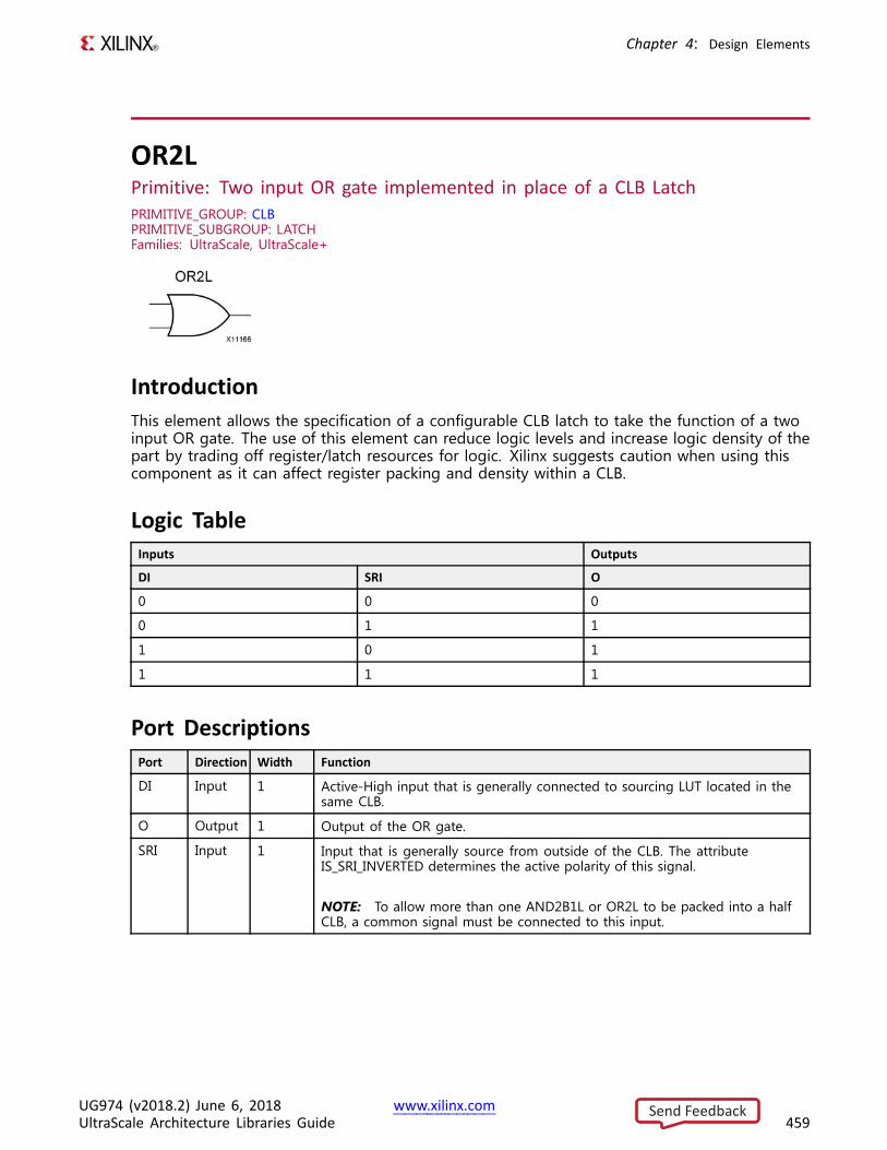
Chapter 4: Design Elements
OR2LPrimitive: Two input OR gate implemented in place of a CLB LatchPRIMITIVE_GROUP: CLBPRIMITIVE_SUBGROUP: LATCHFamilies: UltraScale, UltraScale+
IntroductionThis element allows the specification of a configurable CLB latch to take the function of a twoinput OR gate. The use of this element can reduce logic levels and increase logic density of thepart by trading off register/latch resources for logic. Xilinx suggests caution when using thiscomponent as it can affect register packing and density within a CLB.
Logic TableInputs Outputs
DI SRI O
0 0 0
0 1 1
1 0 1
1 1 1
Port DescriptionsPort Direction Width Function
DI Input 1 Active-High input that is generally connected to sourcing LUT located in thesame CLB.
O Output 1 Output of the OR gate.
SRI Input 1 Input that is generally source from outside of the CLB. The attributeIS_SRI_INVERTED determines the active polarity of this signal.
NOTE: To allow more than one AND2B1L or OR2L to be packed into a halfCLB, a common signal must be connected to this input.
UG974 (v2018.2) June 6, 2018 www.xilinx.comUltraScale Architecture Libraries Guide 459
Send Feedback
Chapter 4: Design Elements
Design Entry MethodInstantiation Yes
Inference No
IP and IP Integrator Catalog No
Available AttributesAttribute Type Allowed Values Default Description
IS_SRI_INVERTED BINARY 1'b0 to 1'b1 1'b0 Specifies whether or not to use theoptional inversion for the SRI pin of thiscomponent.
VHDL Instantiation TemplateUnless they already exist, copy the following two statements and paste them before the entitydeclaration.Library UNISIM;use UNISIM.vcomponents.all;
-- OR2L: Two input OR gate implemented in place of a CLB Latch-- UltraScale-- Xilinx HDL Language Template, version 2018.2
OR2L_inst : OR2Lgeneric map (
IS_SRI_INVERTED => '0' -- Optional inversion for SRI)port map (
O => O, -- 1-bit output: OR gate outputDI => DI, -- 1-bit input: Data input connected to LUT logicSRI => SRI -- 1-bit input: External CLB data
);
-- End of OR2L_inst instantiation
Verilog Instantiation Template
// OR2L: Two input OR gate implemented in place of a CLB Latch// UltraScale// Xilinx HDL Language Template, version 2018.2
OR2L #(.IS_SRI_INVERTED(1'b0) // Optional inversion for SRI
)OR2L_inst (
.O(O), // 1-bit output: OR gate output
.DI(DI), // 1-bit input: Data input connected to LUT logic
.SRI(SRI) // 1-bit input: External CLB data);
// End of OR2L_inst instantiation
UG974 (v2018.2) June 6, 2018 www.xilinx.comUltraScale Architecture Libraries Guide 460
Send Feedback

Chapter 4: Design Elements
For More Information• See the UltraScale Architecture Configurable Logic Block User Guide (UG574).
• See the UltraScale Programmable Devices Documentation.
UG974 (v2018.2) June 6, 2018 www.xilinx.comUltraScale Architecture Libraries Guide 461
Send Feedback
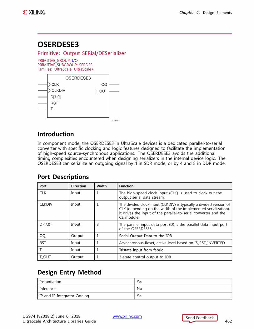
Chapter 4: Design Elements
OSERDESE3Primitive: Output SERial/DESerializerPRIMITIVE_GROUP: I/OPRIMITIVE_SUBGROUP: SERDESFamilies: UltraScale, UltraScale+
IntroductionIn component mode, the OSERDESE3 in UltraScale devices is a dedicated parallel-to-serialconverter with specific clocking and logic features designed to facilitate the implementationof high-speed source-synchronous applications. The OSERDESE3 avoids the additionaltiming complexities encountered when designing serializers in the internal device logic. TheOSERDESE3 can serialize an outgoing signal by 4 in SDR mode, or by 4 and 8 in DDR mode.
Port DescriptionsPort Direction Width Function
CLK Input 1 The high-speed clock input (CLK) is used to clock out theoutput serial data stream.
CLKDIV Input 1 The divided clock input (CLKDIV) is typically a divided version ofCLK (depending on the width of the implemented serialization).It drives the input of the parallel-to-serial converter and theCE module.
D<7:0> Input 8 The parallel input data port (D) is the parallel data input portof the OSERDESE3.
OQ Output 1 Serial Output Data to the IOB
RST Input 1 Asynchronous Reset, active level based on IS_RST_INVERTED
T Input 1 Tristate input from fabric
T_OUT Output 1 3-state control output to IOB
Design Entry MethodInstantiation Yes
Inference No
IP and IP Integrator Catalog Yes
UG974 (v2018.2) June 6, 2018 www.xilinx.comUltraScale Architecture Libraries Guide 462
Send Feedback
Chapter 4: Design Elements
Available AttributesAttribute Type Allowed Values Default Description
DATA_WIDTH DECIMAL 8, 4 8 Defines the width of the parallel - to- serial converter. When used withSDR clocking, the DATA_WIDTH isset to be twice the desired width.
INIT BINARY 1'b0, 1'b1 1'b0 Initializes the OSERDES flip - flopsto the value specified
IS_CLKDIV_INVERTED
BINARY 1'b0 to 1'b1 1'b0 Specifies whether the CLKDIV pin isactive - high or active - low.
IS_CLK_INVERTED BINARY 1'b0 to 1'b1 1'b0 Specifies whether the CLK pin isactive - high or active - low.
IS_RST_INVERTED BINARY 1'b0 to 1'b1 1'b0 Specifies whether the RST pin isactive - high or active - low.
ODDR_MODE STRING "FALSE", "TRUE" "FALSE" Internal property for Vivadoprimitive mapping. Do not modify.
SIM_DEVICE STRING "ULTRASCALE","ULTRASCALE_PLUS","ULTRASCALE _PLUS_ES1", "ULTRASCALE_PLUS _ES2"
"ULTRASCALE" Set the device version
VHDL Instantiation TemplateUnless they already exist, copy the following two statements and paste them before the entitydeclaration.Library UNISIM;use UNISIM.vcomponents.all;
-- OSERDESE3: Output SERial/DESerializer-- UltraScale-- Xilinx HDL Language Template, version 2018.2
OSERDESE3_inst : OSERDESE3generic map (
DATA_WIDTH => 8, -- Parallel Data Width (4-8)INIT => '0', -- Initialization value of the OSERDES flip-flopsIS_CLKDIV_INVERTED => '0', -- Optional inversion for CLKDIVIS_CLK_INVERTED => '0', -- Optional inversion for CLKIS_RST_INVERTED => '0', -- Optional inversion for RSTSIM_DEVICE => "ULTRASCALE" -- Set the device version (ULTRASCALE, ULTRASCALE_PLUS, ULTRASCALE_PLUS_ES1,
-- ULTRASCALE_PLUS_ES2))port map (
OQ => OQ, -- 1-bit output: Serial Output DataT_OUT => T_OUT, -- 1-bit output: 3-state control output to IOBCLK => CLK, -- 1-bit input: High-speed clockCLKDIV => CLKDIV, -- 1-bit input: Divided ClockD => D, -- 8-bit input: Parallel Data InputRST => RST, -- 1-bit input: Asynchronous ResetT => T -- 1-bit input: Tristate input from fabric
);
-- End of OSERDESE3_inst instantiation
UG974 (v2018.2) June 6, 2018 www.xilinx.comUltraScale Architecture Libraries Guide 463
Send Feedback
Chapter 4: Design Elements
Verilog Instantiation Template
// OSERDESE3: Output SERial/DESerializer// UltraScale// Xilinx HDL Language Template, version 2018.2
OSERDESE3 #(.DATA_WIDTH(8), // Parallel Data Width (4-8).INIT(1'b0), // Initialization value of the OSERDES flip-flops.IS_CLKDIV_INVERTED(1'b0), // Optional inversion for CLKDIV.IS_CLK_INVERTED(1'b0), // Optional inversion for CLK.IS_RST_INVERTED(1'b0), // Optional inversion for RST.SIM_DEVICE("ULTRASCALE") // Set the device version (ULTRASCALE, ULTRASCALE_PLUS, ULTRASCALE_PLUS_ES1,
// ULTRASCALE_PLUS_ES2))OSERDESE3_inst (
.OQ(OQ), // 1-bit output: Serial Output Data
.T_OUT(T_OUT), // 1-bit output: 3-state control output to IOB
.CLK(CLK), // 1-bit input: High-speed clock
.CLKDIV(CLKDIV), // 1-bit input: Divided Clock
.D(D), // 8-bit input: Parallel Data Input
.RST(RST), // 1-bit input: Asynchronous Reset
.T(T) // 1-bit input: Tristate input from fabric);
// End of OSERDESE3_inst instantiation
For More Information• See the UltraScale Architecture SelectIO Resources User Guide (UG571).
• See the UltraScale Programmable Devices Documentation.
UG974 (v2018.2) June 6, 2018 www.xilinx.comUltraScale Architecture Libraries Guide 464
Send Feedback
Chapter 4: Design Elements
PCIE40E4Primitive: Integrated Block for PCI ExpressPRIMITIVE_GROUP: ADVANCEDPRIMITIVE_SUBGROUP: PCIEFamilies: UltraScale+
IntroductionThe Integrated block for PCI Express is a hard macro primitive compliant with the PCIespecification. This block is designed to be integrated with GTs and device clocking resourcesusing fabric interconnect. See the Integrated Block for PCI Express User Guide for furtherdetails on this component.
Design Entry MethodInstantiation No
Inference No
IP and IP Integrator Catalog Recommended
For More Information• See the UltraScale Architecture Gen3 Integrated Block for PCI Express v4.1 Product Guide
(PG156).
• See the UltraScale Programmable Devices Documentation.
UG974 (v2018.2) June 6, 2018 www.xilinx.comUltraScale Architecture Libraries Guide 465
Send Feedback
Chapter 4: Design Elements
PCIE_3_1Primitive: Integrated Block for PCI ExpressPRIMITIVE_GROUP: ADVANCEDPRIMITIVE_SUBGROUP: PCIEFamilies: UltraScale
IntroductionThe Integrated block for PCI Express is a hard macro primitive compliant with the PCIespecification. This block is designed to be integrated with GTs and device clocking resourcesusing fabric interconnect. See the Integrated Block for PCI Express User Guide for furtherdetails on this component.
Design Entry MethodInstantiation No
Inference No
IP and IP Integrator Catalog Recommended
For More Information• See the UltraScale Architecture Gen3 Integrated Block for PCI Express v4.1 Product Guide
(PG156).
• See the UltraScale Programmable Devices Documentation.
UG974 (v2018.2) June 6, 2018 www.xilinx.comUltraScale Architecture Libraries Guide 466
Send Feedback
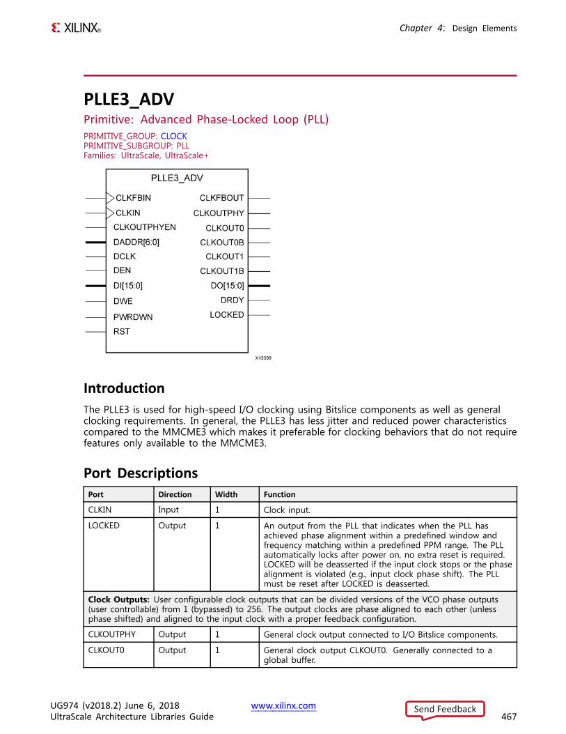
Chapter 4: Design Elements
PLLE3_ADVPrimitive: Advanced Phase-Locked Loop (PLL)PRIMITIVE_GROUP: CLOCKPRIMITIVE_SUBGROUP: PLLFamilies: UltraScale, UltraScale+
IntroductionThe PLLE3 is used for high-speed I/O clocking using Bitslice components as well as generalclocking requirements. In general, the PLLE3 has less jitter and reduced power characteristicscompared to the MMCME3 which makes it preferable for clocking behaviors that do not requirefeatures only available to the MMCME3.
Port DescriptionsPort Direction Width Function
CLKIN Input 1 Clock input.
LOCKED Output 1 An output from the PLL that indicates when the PLL hasachieved phase alignment within a predefined window andfrequency matching within a predefined PPM range. The PLLautomatically locks after power on, no extra reset is required.LOCKED will be deasserted if the input clock stops or the phasealignment is violated (e.g., input clock phase shift). The PLLmust be reset after LOCKED is deasserted.
Clock Outputs: User configurable clock outputs that can be divided versions of the VCO phase outputs(user controllable) from 1 (bypassed) to 256. The output clocks are phase aligned to each other (unlessphase shifted) and aligned to the input clock with a proper feedback configuration.
CLKOUTPHY Output 1 General clock output connected to I/O Bitslice components.
CLKOUT0 Output 1 General clock output CLKOUT0. Generally connected to aglobal buffer.
UG974 (v2018.2) June 6, 2018 www.xilinx.comUltraScale Architecture Libraries Guide 467
Send Feedback
Chapter 4: Design Elements
Port Direction Width Function
CLKOUT0B Output 1 Inverted CLKOUT0. Generally connected to a global buffer.
CLKOUT1 Output 1 General clock output CLKOUT1. Generally connected to aglobal buffer.
CLKOUT1B Output 1 Inverted CLKOUT1. Generally connected to a global buffer.
Control Ports: PLL control ports.
CLKOUTPHYEN Input 1 Enable signal for CLKOUTPHY.
PWRDWN Input 1 Powers down instantiated but unused PLLs.
RST Input 1 The RST signal is an asynchronous reset for the PLL. The PLLwill synchronously re-enable itself when this signal is releasedand go through a new phase alignment and lock cycle. Areset is required when the input clock conditions change (e.g.,frequency).
DRP Ports: Ports used when using the dynamic reconfigurable ports for reading and writing theconfiguration of the PLL.
DADDR<6:0> Input 7 The dynamic reconfiguration address (DADDR) inputbus provides a reconfiguration address for the dynamicreconfiguration. When not used, all bits must be assignedzeroes.
DCLK Input 1 The DCLK signal is the reference clock for the dynamicreconfiguration port.
DEN Input 1 The dynamic reconfiguration enable (DEN) provides the enablecontrol signal to access the dynamic reconfiguration feature.When the dynamic reconfiguration feature is not used, DENmust be tied Low.
DI<15:0> Input 16 The dynamic reconfiguration output bus provides PLL dataoutput when using dynamic reconfiguration.
DO<15:0> Output 16 The dynamic reconfiguration output bus provides PLL dataoutput when using dynamic reconfiguration.
DRDY Output 1 The dynamic reconfiguration ready output (DRDY) providesthe response to the DEN signal for the PLLs dynamicreconfiguration feature.
DWE Input 1 The dynamic reconfiguration write enable (DWE) input pinprovides the write enable control signal to write the DI datainto the DADDR address. When not used, it must be tied Low.
Feedback Clocks: Required ports to form the feedback path for the PLL phase alignment capabilities.
CLKFBIN Input 1 Feedback clock pin to the PLL
CLKFBOUT Output 1 Dedicated PLL Feedback clock output
Design Entry MethodInstantiation Yes
Inference No
IP and IP Integrator Catalog Recommended
UG974 (v2018.2) June 6, 2018 www.xilinx.comUltraScale Architecture Libraries Guide 468
Send Feedback
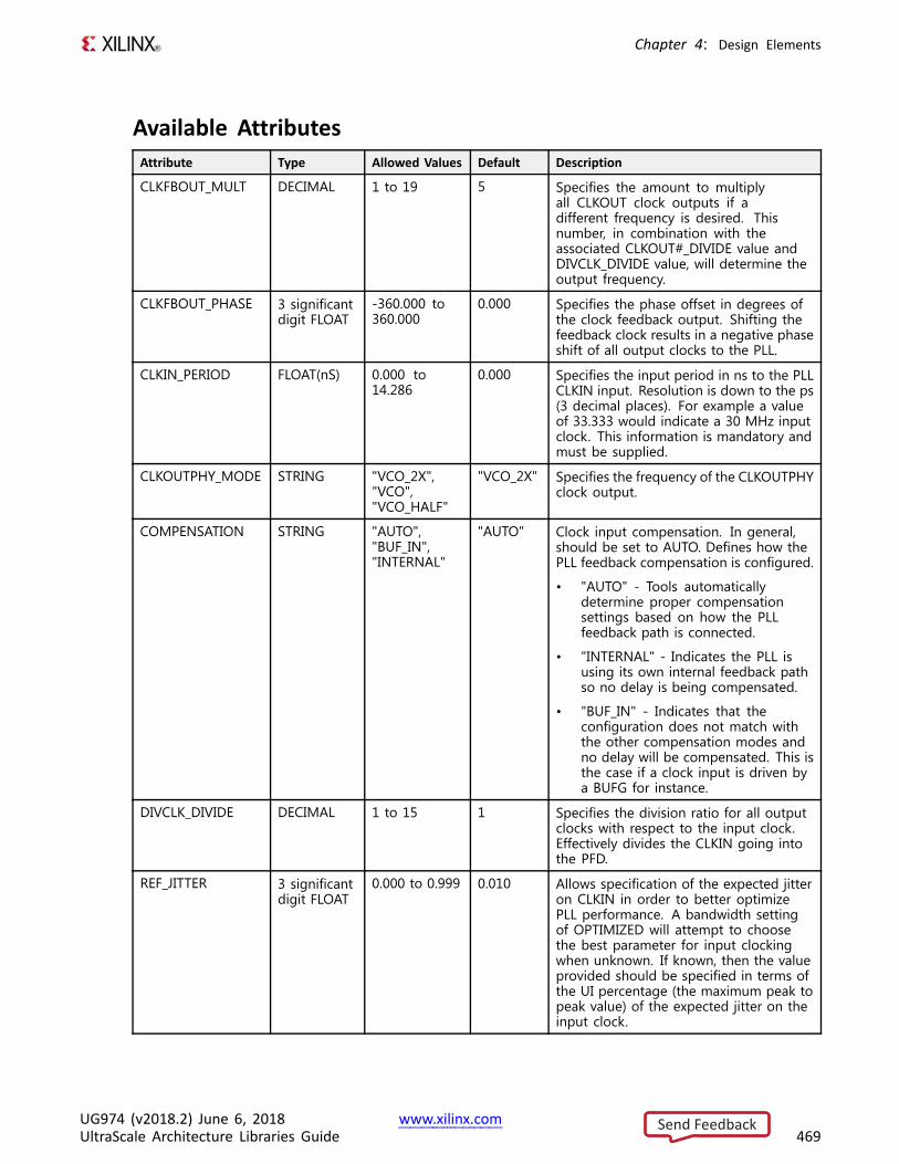
Chapter 4: Design Elements
Available AttributesAttribute Type Allowed Values Default Description
CLKFBOUT_MULT DECIMAL 1 to 19 5 Specifies the amount to multiplyall CLKOUT clock outputs if adifferent frequency is desired. Thisnumber, in combination with theassociated CLKOUT#_DIVIDE value andDIVCLK_DIVIDE value, will determine theoutput frequency.
CLKFBOUT_PHASE 3 significantdigit FLOAT
-360.000 to360.000
0.000 Specifies the phase offset in degrees ofthe clock feedback output. Shifting thefeedback clock results in a negative phaseshift of all output clocks to the PLL.
CLKIN_PERIOD FLOAT(nS) 0.000 to14.286
0.000 Specifies the input period in ns to the PLLCLKIN input. Resolution is down to the ps(3 decimal places). For example a valueof 33.333 would indicate a 30 MHz inputclock. This information is mandatory andmust be supplied.
CLKOUTPHY_MODE STRING "VCO_2X","VCO","VCO_HALF"
"VCO_2X" Specifies the frequency of the CLKOUTPHYclock output.
COMPENSATION STRING "AUTO","BUF_IN","INTERNAL"
"AUTO" Clock input compensation. In general,should be set to AUTO. Defines how thePLL feedback compensation is configured.
• "AUTO" - Tools automaticallydetermine proper compensationsettings based on how the PLLfeedback path is connected.
• "INTERNAL" - Indicates the PLL isusing its own internal feedback pathso no delay is being compensated.
• "BUF_IN" - Indicates that theconfiguration does not match withthe other compensation modes andno delay will be compensated. This isthe case if a clock input is driven bya BUFG for instance.
DIVCLK_DIVIDE DECIMAL 1 to 15 1 Specifies the division ratio for all outputclocks with respect to the input clock.Effectively divides the CLKIN going intothe PFD.
REF_JITTER 3 significantdigit FLOAT
0.000 to 0.999 0.010 Allows specification of the expected jitteron CLKIN in order to better optimizePLL performance. A bandwidth settingof OPTIMIZED will attempt to choosethe best parameter for input clockingwhen unknown. If known, then the valueprovided should be specified in terms ofthe UI percentage (the maximum peak topeak value) of the expected jitter on theinput clock.
UG974 (v2018.2) June 6, 2018 www.xilinx.comUltraScale Architecture Libraries Guide 469
Send Feedback
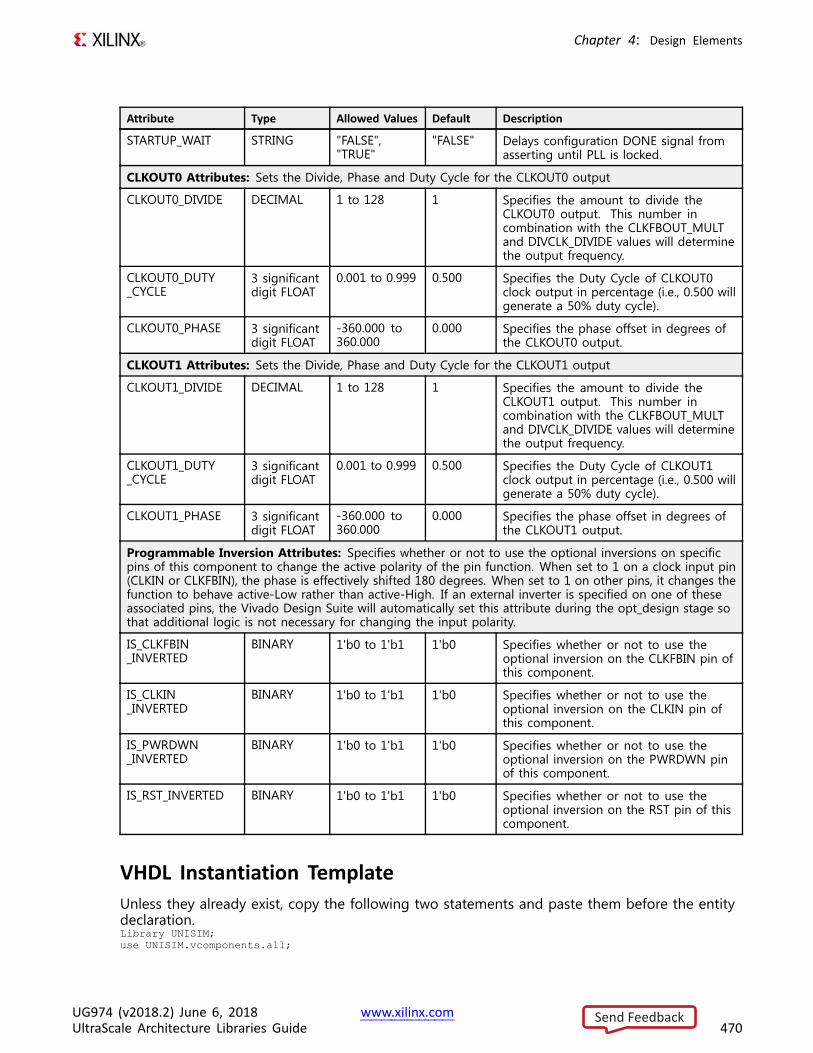
Chapter 4: Design Elements
Attribute Type Allowed Values Default Description
STARTUP_WAIT STRING "FALSE","TRUE"
"FALSE" Delays configuration DONE signal fromasserting until PLL is locked.
CLKOUT0 Attributes: Sets the Divide, Phase and Duty Cycle for the CLKOUT0 output
CLKOUT0_DIVIDE DECIMAL 1 to 128 1 Specifies the amount to divide theCLKOUT0 output. This number incombination with the CLKFBOUT_MULTand DIVCLK_DIVIDE values will determinethe output frequency.
CLKOUT0_DUTY_CYCLE
3 significantdigit FLOAT
0.001 to 0.999 0.500 Specifies the Duty Cycle of CLKOUT0clock output in percentage (i.e., 0.500 willgenerate a 50% duty cycle).
CLKOUT0_PHASE 3 significantdigit FLOAT
-360.000 to360.000
0.000 Specifies the phase offset in degrees ofthe CLKOUT0 output.
CLKOUT1 Attributes: Sets the Divide, Phase and Duty Cycle for the CLKOUT1 output
CLKOUT1_DIVIDE DECIMAL 1 to 128 1 Specifies the amount to divide theCLKOUT1 output. This number incombination with the CLKFBOUT_MULTand DIVCLK_DIVIDE values will determinethe output frequency.
CLKOUT1_DUTY_CYCLE
3 significantdigit FLOAT
0.001 to 0.999 0.500 Specifies the Duty Cycle of CLKOUT1clock output in percentage (i.e., 0.500 willgenerate a 50% duty cycle).
CLKOUT1_PHASE 3 significantdigit FLOAT
-360.000 to360.000
0.000 Specifies the phase offset in degrees ofthe CLKOUT1 output.
Programmable Inversion Attributes: Specifies whether or not to use the optional inversions on specificpins of this component to change the active polarity of the pin function. When set to 1 on a clock input pin(CLKIN or CLKFBIN), the phase is effectively shifted 180 degrees. When set to 1 on other pins, it changes thefunction to behave active-Low rather than active-High. If an external inverter is specified on one of theseassociated pins, the Vivado Design Suite will automatically set this attribute during the opt_design stage sothat additional logic is not necessary for changing the input polarity.
IS_CLKFBIN_INVERTED
BINARY 1'b0 to 1'b1 1'b0 Specifies whether or not to use theoptional inversion on the CLKFBIN pin ofthis component.
IS_CLKIN_INVERTED
BINARY 1'b0 to 1'b1 1'b0 Specifies whether or not to use theoptional inversion on the CLKIN pin ofthis component.
IS_PWRDWN_INVERTED
BINARY 1'b0 to 1'b1 1'b0 Specifies whether or not to use theoptional inversion on the PWRDWN pinof this component.
IS_RST_INVERTED BINARY 1'b0 to 1'b1 1'b0 Specifies whether or not to use theoptional inversion on the RST pin of thiscomponent.
VHDL Instantiation TemplateUnless they already exist, copy the following two statements and paste them before the entitydeclaration.Library UNISIM;use UNISIM.vcomponents.all;
UG974 (v2018.2) June 6, 2018 www.xilinx.comUltraScale Architecture Libraries Guide 470
Send Feedback
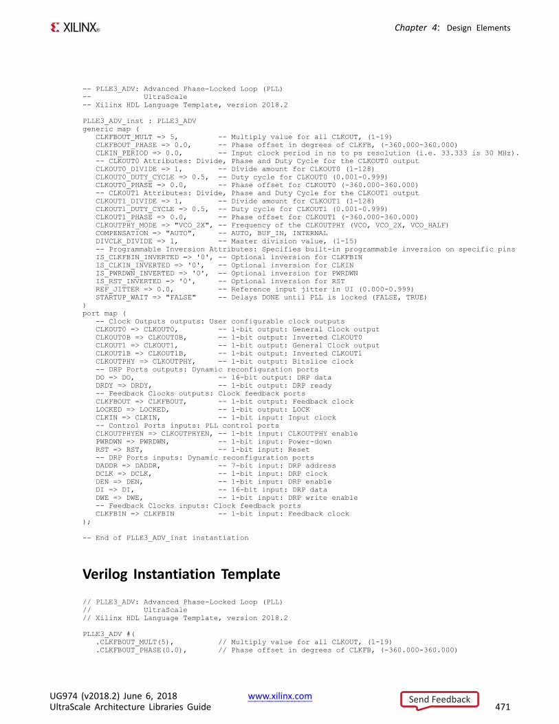
Chapter 4: Design Elements
-- PLLE3_ADV: Advanced Phase-Locked Loop (PLL)-- UltraScale-- Xilinx HDL Language Template, version 2018.2
PLLE3_ADV_inst : PLLE3_ADVgeneric map (
CLKFBOUT_MULT => 5, -- Multiply value for all CLKOUT, (1-19)CLKFBOUT_PHASE => 0.0, -- Phase offset in degrees of CLKFB, (-360.000-360.000)CLKIN_PERIOD => 0.0, -- Input clock period in ns to ps resolution (i.e. 33.333 is 30 MHz).-- CLKOUT0 Attributes: Divide, Phase and Duty Cycle for the CLKOUT0 outputCLKOUT0_DIVIDE => 1, -- Divide amount for CLKOUT0 (1-128)CLKOUT0_DUTY_CYCLE => 0.5, -- Duty cycle for CLKOUT0 (0.001-0.999)CLKOUT0_PHASE => 0.0, -- Phase offset for CLKOUT0 (-360.000-360.000)-- CLKOUT1 Attributes: Divide, Phase and Duty Cycle for the CLKOUT1 outputCLKOUT1_DIVIDE => 1, -- Divide amount for CLKOUT1 (1-128)CLKOUT1_DUTY_CYCLE => 0.5, -- Duty cycle for CLKOUT1 (0.001-0.999)CLKOUT1_PHASE => 0.0, -- Phase offset for CLKOUT1 (-360.000-360.000)CLKOUTPHY_MODE => "VCO_2X", -- Frequency of the CLKOUTPHY (VCO, VCO_2X, VCO_HALF)COMPENSATION => "AUTO", -- AUTO, BUF_IN, INTERNALDIVCLK_DIVIDE => 1, -- Master division value, (1-15)-- Programmable Inversion Attributes: Specifies built-in programmable inversion on specific pinsIS_CLKFBIN_INVERTED => '0', -- Optional inversion for CLKFBINIS_CLKIN_INVERTED => '0', -- Optional inversion for CLKINIS_PWRDWN_INVERTED => '0', -- Optional inversion for PWRDWNIS_RST_INVERTED => '0', -- Optional inversion for RSTREF_JITTER => 0.0, -- Reference input jitter in UI (0.000-0.999)STARTUP_WAIT => "FALSE" -- Delays DONE until PLL is locked (FALSE, TRUE)
)port map (
-- Clock Outputs outputs: User configurable clock outputsCLKOUT0 => CLKOUT0, -- 1-bit output: General Clock outputCLKOUT0B => CLKOUT0B, -- 1-bit output: Inverted CLKOUT0CLKOUT1 => CLKOUT1, -- 1-bit output: General Clock outputCLKOUT1B => CLKOUT1B, -- 1-bit output: Inverted CLKOUT1CLKOUTPHY => CLKOUTPHY, -- 1-bit output: Bitslice clock-- DRP Ports outputs: Dynamic reconfiguration portsDO => DO, -- 16-bit output: DRP dataDRDY => DRDY, -- 1-bit output: DRP ready-- Feedback Clocks outputs: Clock feedback portsCLKFBOUT => CLKFBOUT, -- 1-bit output: Feedback clockLOCKED => LOCKED, -- 1-bit output: LOCKCLKIN => CLKIN, -- 1-bit input: Input clock-- Control Ports inputs: PLL control portsCLKOUTPHYEN => CLKOUTPHYEN, -- 1-bit input: CLKOUTPHY enablePWRDWN => PWRDWN, -- 1-bit input: Power-downRST => RST, -- 1-bit input: Reset-- DRP Ports inputs: Dynamic reconfiguration portsDADDR => DADDR, -- 7-bit input: DRP addressDCLK => DCLK, -- 1-bit input: DRP clockDEN => DEN, -- 1-bit input: DRP enableDI => DI, -- 16-bit input: DRP dataDWE => DWE, -- 1-bit input: DRP write enable-- Feedback Clocks inputs: Clock feedback portsCLKFBIN => CLKFBIN -- 1-bit input: Feedback clock
);
-- End of PLLE3_ADV_inst instantiation
Verilog Instantiation Template
// PLLE3_ADV: Advanced Phase-Locked Loop (PLL)// UltraScale// Xilinx HDL Language Template, version 2018.2
PLLE3_ADV #(.CLKFBOUT_MULT(5), // Multiply value for all CLKOUT, (1-19).CLKFBOUT_PHASE(0.0), // Phase offset in degrees of CLKFB, (-360.000-360.000)
UG974 (v2018.2) June 6, 2018 www.xilinx.comUltraScale Architecture Libraries Guide 471
Send Feedback
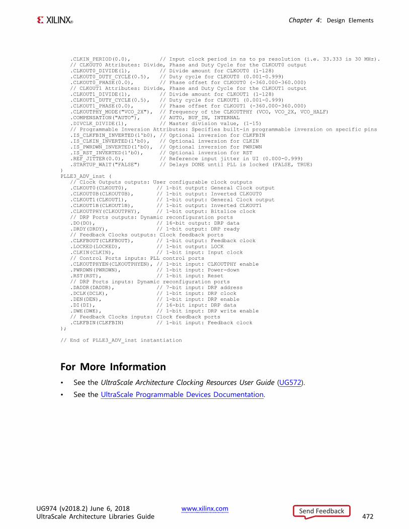
Chapter 4: Design Elements
.CLKIN_PERIOD(0.0), // Input clock period in ns to ps resolution (i.e. 33.333 is 30 MHz).// CLKOUT0 Attributes: Divide, Phase and Duty Cycle for the CLKOUT0 output.CLKOUT0_DIVIDE(1), // Divide amount for CLKOUT0 (1-128).CLKOUT0_DUTY_CYCLE(0.5), // Duty cycle for CLKOUT0 (0.001-0.999).CLKOUT0_PHASE(0.0), // Phase offset for CLKOUT0 (-360.000-360.000)// CLKOUT1 Attributes: Divide, Phase and Duty Cycle for the CLKOUT1 output.CLKOUT1_DIVIDE(1), // Divide amount for CLKOUT1 (1-128).CLKOUT1_DUTY_CYCLE(0.5), // Duty cycle for CLKOUT1 (0.001-0.999).CLKOUT1_PHASE(0.0), // Phase offset for CLKOUT1 (-360.000-360.000).CLKOUTPHY_MODE("VCO_2X"), // Frequency of the CLKOUTPHY (VCO, VCO_2X, VCO_HALF).COMPENSATION("AUTO"), // AUTO, BUF_IN, INTERNAL.DIVCLK_DIVIDE(1), // Master division value, (1-15)// Programmable Inversion Attributes: Specifies built-in programmable inversion on specific pins.IS_CLKFBIN_INVERTED(1'b0), // Optional inversion for CLKFBIN.IS_CLKIN_INVERTED(1'b0), // Optional inversion for CLKIN.IS_PWRDWN_INVERTED(1'b0), // Optional inversion for PWRDWN.IS_RST_INVERTED(1'b0), // Optional inversion for RST.REF_JITTER(0.0), // Reference input jitter in UI (0.000-0.999).STARTUP_WAIT("FALSE") // Delays DONE until PLL is locked (FALSE, TRUE)
)PLLE3_ADV_inst (
// Clock Outputs outputs: User configurable clock outputs.CLKOUT0(CLKOUT0), // 1-bit output: General Clock output.CLKOUT0B(CLKOUT0B), // 1-bit output: Inverted CLKOUT0.CLKOUT1(CLKOUT1), // 1-bit output: General Clock output.CLKOUT1B(CLKOUT1B), // 1-bit output: Inverted CLKOUT1.CLKOUTPHY(CLKOUTPHY), // 1-bit output: Bitslice clock// DRP Ports outputs: Dynamic reconfiguration ports.DO(DO), // 16-bit output: DRP data.DRDY(DRDY), // 1-bit output: DRP ready// Feedback Clocks outputs: Clock feedback ports.CLKFBOUT(CLKFBOUT), // 1-bit output: Feedback clock.LOCKED(LOCKED), // 1-bit output: LOCK.CLKIN(CLKIN), // 1-bit input: Input clock// Control Ports inputs: PLL control ports.CLKOUTPHYEN(CLKOUTPHYEN), // 1-bit input: CLKOUTPHY enable.PWRDWN(PWRDWN), // 1-bit input: Power-down.RST(RST), // 1-bit input: Reset// DRP Ports inputs: Dynamic reconfiguration ports.DADDR(DADDR), // 7-bit input: DRP address.DCLK(DCLK), // 1-bit input: DRP clock.DEN(DEN), // 1-bit input: DRP enable.DI(DI), // 16-bit input: DRP data.DWE(DWE), // 1-bit input: DRP write enable// Feedback Clocks inputs: Clock feedback ports.CLKFBIN(CLKFBIN) // 1-bit input: Feedback clock
);
// End of PLLE3_ADV_inst instantiation
For More Information• See the UltraScale Architecture Clocking Resources User Guide (UG572).
• See the UltraScale Programmable Devices Documentation.
UG974 (v2018.2) June 6, 2018 www.xilinx.comUltraScale Architecture Libraries Guide 472
Send Feedback
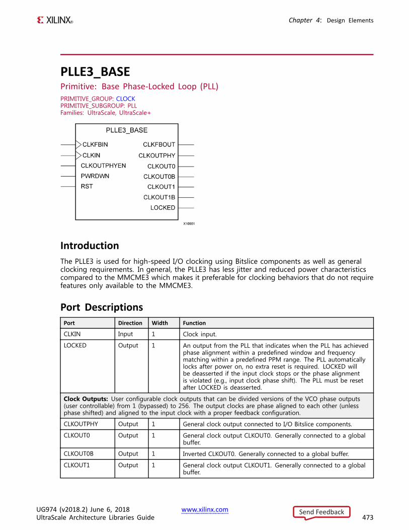
Chapter 4: Design Elements
PLLE3_BASEPrimitive: Base Phase-Locked Loop (PLL)PRIMITIVE_GROUP: CLOCKPRIMITIVE_SUBGROUP: PLLFamilies: UltraScale, UltraScale+
IntroductionThe PLLE3 is used for high-speed I/O clocking using Bitslice components as well as generalclocking requirements. In general, the PLLE3 has less jitter and reduced power characteristicscompared to the MMCME3 which makes it preferable for clocking behaviors that do not requirefeatures only available to the MMCME3.
Port DescriptionsPort Direction Width Function
CLKIN Input 1 Clock input.
LOCKED Output 1 An output from the PLL that indicates when the PLL has achievedphase alignment within a predefined window and frequencymatching within a predefined PPM range. The PLL automaticallylocks after power on, no extra reset is required. LOCKED willbe deasserted if the input clock stops or the phase alignmentis violated (e.g., input clock phase shift). The PLL must be resetafter LOCKED is deasserted.
Clock Outputs: User configurable clock outputs that can be divided versions of the VCO phase outputs(user controllable) from 1 (bypassed) to 256. The output clocks are phase aligned to each other (unlessphase shifted) and aligned to the input clock with a proper feedback configuration.
CLKOUTPHY Output 1 General clock output connected to I/O Bitslice components.
CLKOUT0 Output 1 General clock output CLKOUT0. Generally connected to a globalbuffer.
CLKOUT0B Output 1 Inverted CLKOUT0. Generally connected to a global buffer.
CLKOUT1 Output 1 General clock output CLKOUT1. Generally connected to a globalbuffer.
UG974 (v2018.2) June 6, 2018 www.xilinx.comUltraScale Architecture Libraries Guide 473
Send Feedback
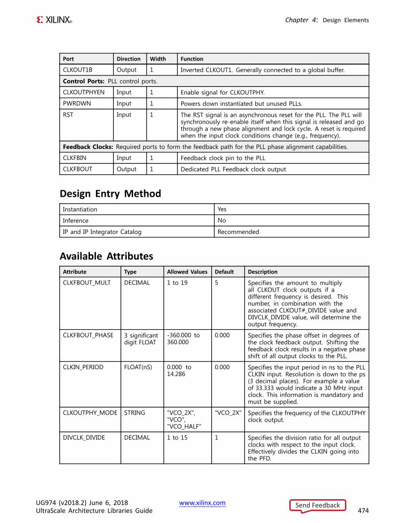
Chapter 4: Design Elements
Port Direction Width Function
CLKOUT1B Output 1 Inverted CLKOUT1. Generally connected to a global buffer.
Control Ports: PLL control ports.
CLKOUTPHYEN Input 1 Enable signal for CLKOUTPHY.
PWRDWN Input 1 Powers down instantiated but unused PLLs.
RST Input 1 The RST signal is an asynchronous reset for the PLL. The PLL willsynchronously re-enable itself when this signal is released and gothrough a new phase alignment and lock cycle. A reset is requiredwhen the input clock conditions change (e.g., frequency).
Feedback Clocks: Required ports to form the feedback path for the PLL phase alignment capabilities.
CLKFBIN Input 1 Feedback clock pin to the PLL
CLKFBOUT Output 1 Dedicated PLL Feedback clock output
Design Entry MethodInstantiation Yes
Inference No
IP and IP Integrator Catalog Recommended
Available AttributesAttribute Type Allowed Values Default Description
CLKFBOUT_MULT DECIMAL 1 to 19 5 Specifies the amount to multiplyall CLKOUT clock outputs if adifferent frequency is desired. Thisnumber, in combination with theassociated CLKOUT#_DIVIDE value andDIVCLK_DIVIDE value, will determine theoutput frequency.
CLKFBOUT_PHASE 3 significantdigit FLOAT
-360.000 to360.000
0.000 Specifies the phase offset in degrees ofthe clock feedback output. Shifting thefeedback clock results in a negative phaseshift of all output clocks to the PLL.
CLKIN_PERIOD FLOAT(nS) 0.000 to14.286
0.000 Specifies the input period in ns to the PLLCLKIN input. Resolution is down to the ps(3 decimal places). For example a valueof 33.333 would indicate a 30 MHz inputclock. This information is mandatory andmust be supplied.
CLKOUTPHY_MODE STRING "VCO_2X","VCO","VCO_HALF"
"VCO_2X" Specifies the frequency of the CLKOUTPHYclock output.
DIVCLK_DIVIDE DECIMAL 1 to 15 1 Specifies the division ratio for all outputclocks with respect to the input clock.Effectively divides the CLKIN going intothe PFD.
UG974 (v2018.2) June 6, 2018 www.xilinx.comUltraScale Architecture Libraries Guide 474
Send Feedback
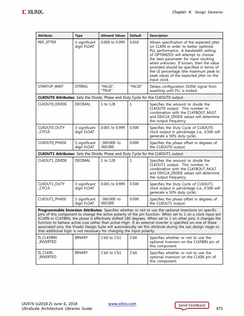
Chapter 4: Design Elements
Attribute Type Allowed Values Default Description
REF_JITTER 3 significantdigit FLOAT
0.000 to 0.999 0.010 Allows specification of the expected jitteron CLKIN in order to better optimizePLL performance. A bandwidth settingof OPTIMIZED will attempt to choosethe best parameter for input clockingwhen unknown. If known, then the valueprovided should be specified in terms ofthe UI percentage (the maximum peak topeak value) of the expected jitter on theinput clock.
STARTUP_WAIT STRING "FALSE","TRUE"
"FALSE" Delays configuration DONE signal fromasserting until PLL is locked.
CLKOUT0 Attributes: Sets the Divide, Phase and Duty Cycle for the CLKOUT0 output
CLKOUT0_DIVIDE DECIMAL 1 to 128 1 Specifies the amount to divide theCLKOUT0 output. This number incombination with the CLKFBOUT_MULTand DIVCLK_DIVIDE values will determinethe output frequency.
CLKOUT0_DUTY_CYCLE
3 significantdigit FLOAT
0.001 to 0.999 0.500 Specifies the Duty Cycle of CLKOUT0clock output in percentage (i.e., 0.500 willgenerate a 50% duty cycle).
CLKOUT0_PHASE 3 significantdigit FLOAT
-360.000 to360.000
0.000 Specifies the phase offset in degrees ofthe CLKOUT0 output.
CLKOUT1 Attributes: Sets the Divide, Phase and Duty Cycle for the CLKOUT1 output
CLKOUT1_DIVIDE DECIMAL 1 to 128 1 Specifies the amount to divide theCLKOUT1 output. This number incombination with the CLKFBOUT_MULTand DIVCLK_DIVIDE values will determinethe output frequency.
CLKOUT1_DUTY_CYCLE
3 significantdigit FLOAT
0.001 to 0.999 0.500 Specifies the Duty Cycle of CLKOUT1clock output in percentage (i.e., 0.500 willgenerate a 50% duty cycle).
CLKOUT1_PHASE 3 significantdigit FLOAT
-360.000 to360.000
0.000 Specifies the phase offset in degrees ofthe CLKOUT1 output.
Programmable Inversion Attributes: Specifies whether or not to use the optional inversions on specificpins of this component to change the active polarity of the pin function. When set to 1 on a clock input pin(CLKIN or CLKFBIN), the phase is effectively shifted 180 degrees. When set to 1 on other pins, it changes thefunction to behave active-Low rather than active-High. If an external inverter is specified on one of theseassociated pins, the Vivado Design Suite will automatically set this attribute during the opt_design stage sothat additional logic is not necessary for changing the input polarity.
IS_CLKFBIN_INVERTED
BINARY 1'b0 to 1'b1 1'b0 Specifies whether or not to use theoptional inversion on the CLKFBIN pin ofthis component.
IS_CLKIN_INVERTED
BINARY 1'b0 to 1'b1 1'b0 Specifies whether or not to use theoptional inversion on the CLKIN pin ofthis component.
UG974 (v2018.2) June 6, 2018 www.xilinx.comUltraScale Architecture Libraries Guide 475
Send Feedback
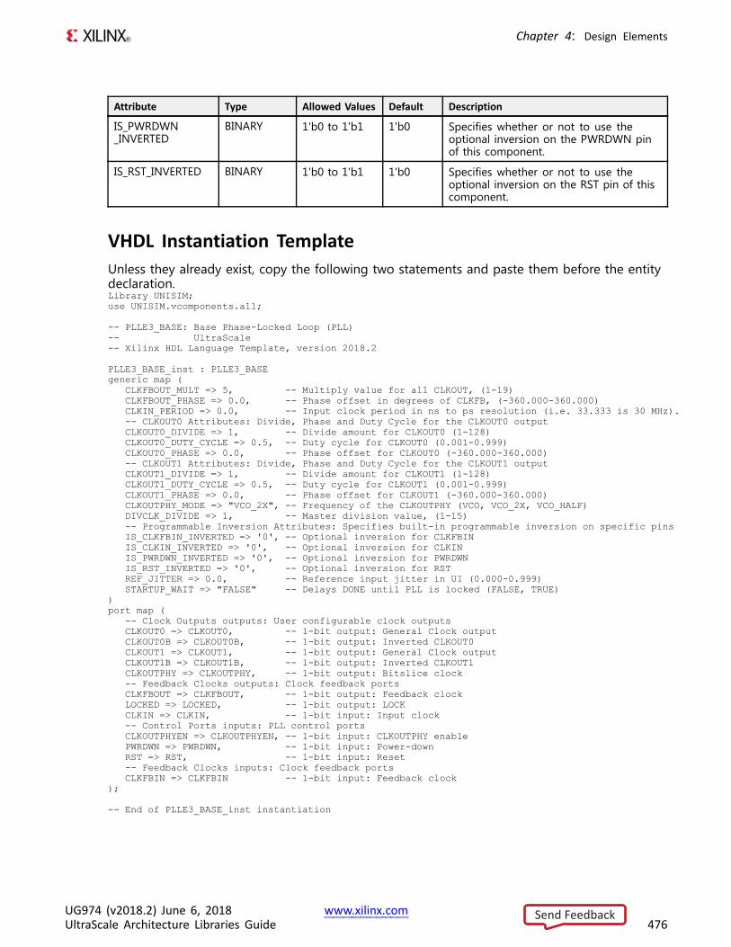
Chapter 4: Design Elements
Attribute Type Allowed Values Default Description
IS_PWRDWN_INVERTED
BINARY 1'b0 to 1'b1 1'b0 Specifies whether or not to use theoptional inversion on the PWRDWN pinof this component.
IS_RST_INVERTED BINARY 1'b0 to 1'b1 1'b0 Specifies whether or not to use theoptional inversion on the RST pin of thiscomponent.
VHDL Instantiation TemplateUnless they already exist, copy the following two statements and paste them before the entitydeclaration.Library UNISIM;use UNISIM.vcomponents.all;
-- PLLE3_BASE: Base Phase-Locked Loop (PLL)-- UltraScale-- Xilinx HDL Language Template, version 2018.2
PLLE3_BASE_inst : PLLE3_BASEgeneric map (
CLKFBOUT_MULT => 5, -- Multiply value for all CLKOUT, (1-19)CLKFBOUT_PHASE => 0.0, -- Phase offset in degrees of CLKFB, (-360.000-360.000)CLKIN_PERIOD => 0.0, -- Input clock period in ns to ps resolution (i.e. 33.333 is 30 MHz).-- CLKOUT0 Attributes: Divide, Phase and Duty Cycle for the CLKOUT0 outputCLKOUT0_DIVIDE => 1, -- Divide amount for CLKOUT0 (1-128)CLKOUT0_DUTY_CYCLE => 0.5, -- Duty cycle for CLKOUT0 (0.001-0.999)CLKOUT0_PHASE => 0.0, -- Phase offset for CLKOUT0 (-360.000-360.000)-- CLKOUT1 Attributes: Divide, Phase and Duty Cycle for the CLKOUT1 outputCLKOUT1_DIVIDE => 1, -- Divide amount for CLKOUT1 (1-128)CLKOUT1_DUTY_CYCLE => 0.5, -- Duty cycle for CLKOUT1 (0.001-0.999)CLKOUT1_PHASE => 0.0, -- Phase offset for CLKOUT1 (-360.000-360.000)CLKOUTPHY_MODE => "VCO_2X", -- Frequency of the CLKOUTPHY (VCO, VCO_2X, VCO_HALF)DIVCLK_DIVIDE => 1, -- Master division value, (1-15)-- Programmable Inversion Attributes: Specifies built-in programmable inversion on specific pinsIS_CLKFBIN_INVERTED => '0', -- Optional inversion for CLKFBINIS_CLKIN_INVERTED => '0', -- Optional inversion for CLKINIS_PWRDWN_INVERTED => '0', -- Optional inversion for PWRDWNIS_RST_INVERTED => '0', -- Optional inversion for RSTREF_JITTER => 0.0, -- Reference input jitter in UI (0.000-0.999)STARTUP_WAIT => "FALSE" -- Delays DONE until PLL is locked (FALSE, TRUE)
)port map (
-- Clock Outputs outputs: User configurable clock outputsCLKOUT0 => CLKOUT0, -- 1-bit output: General Clock outputCLKOUT0B => CLKOUT0B, -- 1-bit output: Inverted CLKOUT0CLKOUT1 => CLKOUT1, -- 1-bit output: General Clock outputCLKOUT1B => CLKOUT1B, -- 1-bit output: Inverted CLKOUT1CLKOUTPHY => CLKOUTPHY, -- 1-bit output: Bitslice clock-- Feedback Clocks outputs: Clock feedback portsCLKFBOUT => CLKFBOUT, -- 1-bit output: Feedback clockLOCKED => LOCKED, -- 1-bit output: LOCKCLKIN => CLKIN, -- 1-bit input: Input clock-- Control Ports inputs: PLL control portsCLKOUTPHYEN => CLKOUTPHYEN, -- 1-bit input: CLKOUTPHY enablePWRDWN => PWRDWN, -- 1-bit input: Power-downRST => RST, -- 1-bit input: Reset-- Feedback Clocks inputs: Clock feedback portsCLKFBIN => CLKFBIN -- 1-bit input: Feedback clock
);
-- End of PLLE3_BASE_inst instantiation
UG974 (v2018.2) June 6, 2018 www.xilinx.comUltraScale Architecture Libraries Guide 476
Send Feedback
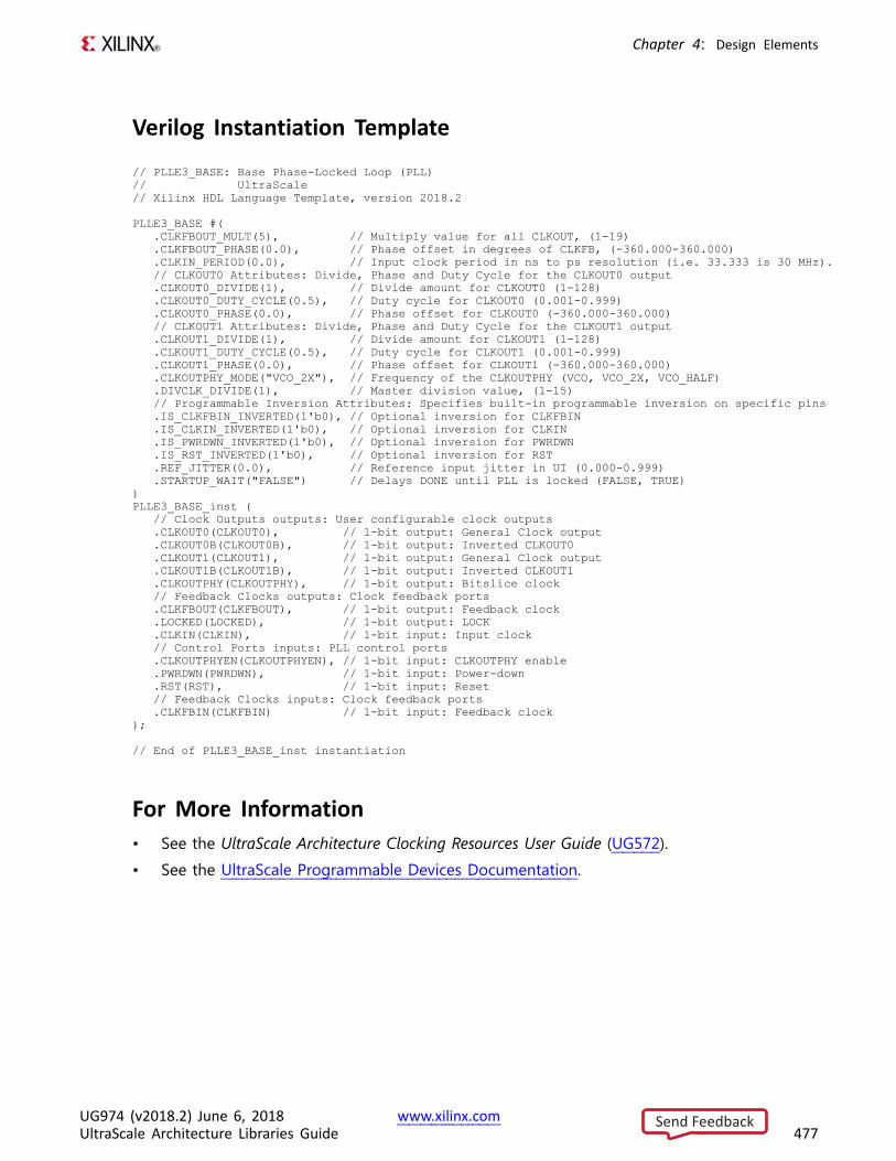
Chapter 4: Design Elements
Verilog Instantiation Template
// PLLE3_BASE: Base Phase-Locked Loop (PLL)// UltraScale// Xilinx HDL Language Template, version 2018.2
PLLE3_BASE #(.CLKFBOUT_MULT(5), // Multiply value for all CLKOUT, (1-19).CLKFBOUT_PHASE(0.0), // Phase offset in degrees of CLKFB, (-360.000-360.000).CLKIN_PERIOD(0.0), // Input clock period in ns to ps resolution (i.e. 33.333 is 30 MHz).// CLKOUT0 Attributes: Divide, Phase and Duty Cycle for the CLKOUT0 output.CLKOUT0_DIVIDE(1), // Divide amount for CLKOUT0 (1-128).CLKOUT0_DUTY_CYCLE(0.5), // Duty cycle for CLKOUT0 (0.001-0.999).CLKOUT0_PHASE(0.0), // Phase offset for CLKOUT0 (-360.000-360.000)// CLKOUT1 Attributes: Divide, Phase and Duty Cycle for the CLKOUT1 output.CLKOUT1_DIVIDE(1), // Divide amount for CLKOUT1 (1-128).CLKOUT1_DUTY_CYCLE(0.5), // Duty cycle for CLKOUT1 (0.001-0.999).CLKOUT1_PHASE(0.0), // Phase offset for CLKOUT1 (-360.000-360.000).CLKOUTPHY_MODE("VCO_2X"), // Frequency of the CLKOUTPHY (VCO, VCO_2X, VCO_HALF).DIVCLK_DIVIDE(1), // Master division value, (1-15)// Programmable Inversion Attributes: Specifies built-in programmable inversion on specific pins.IS_CLKFBIN_INVERTED(1'b0), // Optional inversion for CLKFBIN.IS_CLKIN_INVERTED(1'b0), // Optional inversion for CLKIN.IS_PWRDWN_INVERTED(1'b0), // Optional inversion for PWRDWN.IS_RST_INVERTED(1'b0), // Optional inversion for RST.REF_JITTER(0.0), // Reference input jitter in UI (0.000-0.999).STARTUP_WAIT("FALSE") // Delays DONE until PLL is locked (FALSE, TRUE)
)PLLE3_BASE_inst (
// Clock Outputs outputs: User configurable clock outputs.CLKOUT0(CLKOUT0), // 1-bit output: General Clock output.CLKOUT0B(CLKOUT0B), // 1-bit output: Inverted CLKOUT0.CLKOUT1(CLKOUT1), // 1-bit output: General Clock output.CLKOUT1B(CLKOUT1B), // 1-bit output: Inverted CLKOUT1.CLKOUTPHY(CLKOUTPHY), // 1-bit output: Bitslice clock// Feedback Clocks outputs: Clock feedback ports.CLKFBOUT(CLKFBOUT), // 1-bit output: Feedback clock.LOCKED(LOCKED), // 1-bit output: LOCK.CLKIN(CLKIN), // 1-bit input: Input clock// Control Ports inputs: PLL control ports.CLKOUTPHYEN(CLKOUTPHYEN), // 1-bit input: CLKOUTPHY enable.PWRDWN(PWRDWN), // 1-bit input: Power-down.RST(RST), // 1-bit input: Reset// Feedback Clocks inputs: Clock feedback ports.CLKFBIN(CLKFBIN) // 1-bit input: Feedback clock
);
// End of PLLE3_BASE_inst instantiation
For More Information• See the UltraScale Architecture Clocking Resources User Guide (UG572).
• See the UltraScale Programmable Devices Documentation.
UG974 (v2018.2) June 6, 2018 www.xilinx.comUltraScale Architecture Libraries Guide 477
Send Feedback
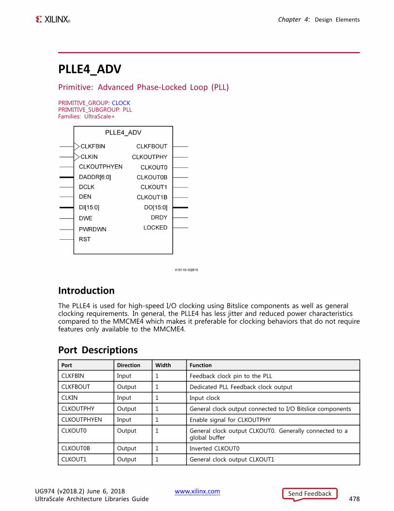
Chapter 4: Design Elements
PLLE4_ADVPrimitive: Advanced Phase-Locked Loop (PLL)
PRIMITIVE_GROUP: CLOCKPRIMITIVE_SUBGROUP: PLLFamilies: UltraScale+
IntroductionThe PLLE4 is used for high-speed I/O clocking using Bitslice components as well as generalclocking requirements. In general, the PLLE4 has less jitter and reduced power characteristicscompared to the MMCME4 which makes it preferable for clocking behaviors that do not requirefeatures only available to the MMCME4.
Port DescriptionsPort Direction Width Function
CLKFBIN Input 1 Feedback clock pin to the PLL
CLKFBOUT Output 1 Dedicated PLL Feedback clock output
CLKIN Input 1 Input clock
CLKOUTPHY Output 1 General clock output connected to I/O Bitslice components
CLKOUTPHYEN Input 1 Enable signal for CLKOUTPHY
CLKOUT0 Output 1 General clock output CLKOUT0. Generally connected to aglobal buffer
CLKOUT0B Output 1 Inverted CLKOUT0
CLKOUT1 Output 1 General clock output CLKOUT1
UG974 (v2018.2) June 6, 2018 www.xilinx.comUltraScale Architecture Libraries Guide 478
Send Feedback
Chapter 4: Design Elements
Port Direction Width Function
CLKOUT1B Output 1 Inverted CLKOUT1
DADDR<6:0> Input 7 The dynamic reconfiguration address (DADDR) inputbus provides a reconfiguration address for the dynamicreconfiguration. When not used, all bits must be assignedzeroes
DCLK Input 1 The DCLK signal is the reference clock for the dynamicreconfiguration port
DEN Input 1 The dynamic reconfiguration enable (DEN) provides theenable control signal to access the dynamic reconfigurationfeature. When the dynamic reconfiguration feature is notused, DEN must be tied Low
DI<15:0> Input 16 The dynamic reconfiguration output bus provides PLL dataoutput when using dynamic reconfiguration
DO<15:0> Output 16 The dynamic reconfiguration output bus provides PLL dataoutput when using dynamic reconfiguration
DRDY Output 1 The dynamic reconfiguration ready output (DRDY) providesthe response to the DEN signal for the PLLs dynamicreconfiguration feature
DWE Input 1 The dynamic reconfiguration write enable (DWE) input pinprovides the write enable control signal to write the DI datainto the DADDR address. When not used, it must be tied Low
LOCKED Output 1 An output from the PLL that indicates when the PLL hasachieved phase alignment within a predefined window andfrequency matching within a predefined PPM range. The PLLautomatically locks after power on, no extra reset is required.LOCKED will be deasserted if the input clock stops or thephase alignment is violated (e.g., input clock phase shift). ThePLL must be reset after LOCKED is deasserted
PWRDWN Input 1 Powers down instantiated but unused PLLs
RST Input 1 The RST signal is an asynchronous reset for the PLL. The PLLwill synchronously re-enable itself when this signal is releasedand go through a new phase alignment and lock cycle. Areset is required when the input clock conditions change(e.g., frequency)
Design Entry MethodInstantiation Yes
Inference No
IP and IP Integrator Catalog Recommended
UG974 (v2018.2) June 6, 2018 www.xilinx.comUltraScale Architecture Libraries Guide 479
Send Feedback
Chapter 4: Design Elements
Available Attributes
Attribute TypeAllowedValues Default Description
CLKFBOUT_MULT DECIMAL 2 to 21 5 Specifies the amount to multiply all CLKOUTclock outputs if a different frequency isdesired. This number, in combination withthe associated CLKOUT#_DIVIDE value andDIVCLK_DIVIDE value, will determine theoutput frequency
CLKFBOUT_PHASE 3 significantdigit FLOAT
-360.000 to360.000
0.000 Specifies the phase offset in degrees of theclock feedback output. Shifting the feedbackclock results in a negative phase shift of alloutput clocks to the PLL
CLKIN_PERIOD FLOAT(nS) 0.000 to14.286
0.000 Specifies the input period in ns to the PLLCLKIN input. Resolution is down to the ps(3 decimal places). For example a value of33.333 would indicate a 30 MHz input clock.This information is mandatory and must besupplied
CLKOUTPHY_MODE STRING "VCO_2X","VCO","VCO_HALF"
"VCO_2X" Specifies the frequency of the CLKOUTPHYclock output
CLKOUT0_DIVIDE DECIMAL 1 to 128 1 Specifies the amount to divide the CLKOUT0output. This number in combination with theCLKFBOUT_MULT and DIVCLK_DIVIDE valueswill determine the output frequency
CLKOUT0_DUTY_CYCLE
3 significantdigit FLOAT
0.001 to0.999
0.500 Specifies the Duty Cycle of CLKOUT0 clockoutput in percentage (i.e., 0.500 will generatea 50% duty cycle)
CLKOUT0_PHASE 3 significantdigit FLOAT
-360.000 to360.000
0.000 Specifies the phase offset in degrees of theCLKOUT0 output
CLKOUT1_DIVIDE DECIMAL 1 to 128 1 Specifies the amount to divide the CLKOUT1output. This number in combination with theCLKFBOUT_MULT and DIVCLK_DIVIDE valueswill determine the output frequency
CLKOUT1_DUTY_CYCLE
3 significantdigit FLOAT
0.001 to0.999
0.500 Specifies the Duty Cycle of CLKOUT1 clockoutput in percentage (i.e., 0.500 will generatea 50% duty cycle)
CLKOUT1_PHASE 3 significantdigit FLOAT
-360.000 to360.000
0.000 Specifies the phase offset in degrees of theCLKOUT1 output
UG974 (v2018.2) June 6, 2018 www.xilinx.comUltraScale Architecture Libraries Guide 480
Send Feedback
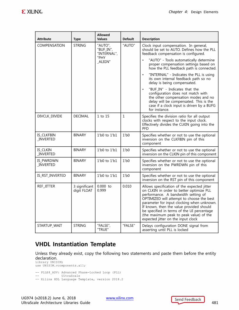
Chapter 4: Design Elements
Attribute TypeAllowedValues Default Description
COMPENSATION STRING "AUTO","BUF_IN","INTERNAL","PHY_ALIGN"
"AUTO" Clock input compensation. In general,should be set to AUTO. Defines how the PLLfeedback compensation is configured.
• "AUTO" - Tools automatically determineproper compensation settings based onhow the PLL feedback path is connected.
• "INTERNAL" - Indicates the PLL is usingits own internal feedback path so nodelay is being compensated.
• "BUF_IN" - Indicates that theconfiguration does not match withthe other compensation modes and nodelay will be compensated. This is thecase if a clock input is driven by a BUFGfor instance.
DIVCLK_DIVIDE DECIMAL 1 to 15 1 Specifies the division ratio for all outputclocks with respect to the input clock.Effectively divides the CLKIN going into thePFD
IS_CLKFBIN_INVERTED
BINARY 1'b0 to 1'b1 1'b0 Specifies whether or not to use the optionalinversion on the CLKFBIN pin of thiscomponent
IS_CLKIN_INVERTED
BINARY 1'b0 to 1'b1 1'b0 Specifies whether or not to use the optionalinversion on the CLKIN pin of this component
IS_PWRDWN_INVERTED
BINARY 1'b0 to 1'b1 1'b0 Specifies whether or not to use the optionalinversion on the PWRDWN pin of thiscomponent
IS_RST_INVERTED BINARY 1'b0 to 1'b1 1'b0 Specifies whether or not to use the optionalinversion on the RST pin of this component
REF_JITTER 3 significantdigit FLOAT
0.000 to0.999
0.010 Allows specification of the expected jitteron CLKIN in order to better optimize PLLperformance. A bandwidth setting ofOPTIMIZED will attempt to choose the bestparameter for input clocking when unknown.If known, then the value provided shouldbe specified in terms of the UI percentage(the maximum peak to peak value) of theexpected jitter on the input clock
STARTUP_WAIT STRING "FALSE","TRUE"
"FALSE" Delays configuration DONE signal fromasserting until PLL is locked
VHDL Instantiation TemplateUnless they already exist, copy the following two statements and paste them before the entitydeclaration.Library UNISIM;use UNISIM.vcomponents.all;
-- PLLE4_ADV: Advanced Phase-Locked Loop (PLL)-- UltraScale-- Xilinx HDL Language Template, version 2018.2
UG974 (v2018.2) June 6, 2018 www.xilinx.comUltraScale Architecture Libraries Guide 481
Send Feedback
Chapter 4: Design Elements
PLLE4_ADV_inst : PLLE4_ADVgeneric map (
CLKFBOUT_MULT => 5, -- Multiply value for all CLKOUTCLKFBOUT_PHASE => 0.0, -- Phase offset in degrees of CLKFBCLKIN_PERIOD => 0.0, -- Input clock period in ns to ps resolution (i.e. 33.333 is 30 MHz).CLKOUT0_DIVIDE => 1, -- Divide amount for CLKOUT0CLKOUT0_DUTY_CYCLE => 0.5, -- Duty cycle for CLKOUT0CLKOUT0_PHASE => 0.0, -- Phase offset for CLKOUT0CLKOUT1_DIVIDE => 1, -- Divide amount for CLKOUT1CLKOUT1_DUTY_CYCLE => 0.5, -- Duty cycle for CLKOUT1CLKOUT1_PHASE => 0.0, -- Phase offset for CLKOUT1CLKOUTPHY_MODE => "VCO_2X", -- Frequency of the CLKOUTPHYCOMPENSATION => "AUTO", -- Clock input compensationDIVCLK_DIVIDE => 1, -- Master division valueIS_CLKFBIN_INVERTED => '0', -- Optional inversion for CLKFBINIS_CLKIN_INVERTED => '0', -- Optional inversion for CLKINIS_PWRDWN_INVERTED => '0', -- Optional inversion for PWRDWNIS_RST_INVERTED => '0', -- Optional inversion for RSTREF_JITTER => 0.0, -- Reference input jitter in UISTARTUP_WAIT => "FALSE" -- Delays DONE until PLL is locked
)port map (
CLKFBOUT => CLKFBOUT, -- 1-bit output: Feedback clockCLKOUT0 => CLKOUT0, -- 1-bit output: General Clock outputCLKOUT0B => CLKOUT0B, -- 1-bit output: Inverted CLKOUT0CLKOUT1 => CLKOUT1, -- 1-bit output: General Clock outputCLKOUT1B => CLKOUT1B, -- 1-bit output: Inverted CLKOUT1CLKOUTPHY => CLKOUTPHY, -- 1-bit output: Bitslice clockDO => DO, -- 16-bit output: DRP data outputDRDY => DRDY, -- 1-bit output: DRP readyLOCKED => LOCKED, -- 1-bit output: LOCKCLKFBIN => CLKFBIN, -- 1-bit input: Feedback clockCLKIN => CLKIN, -- 1-bit input: Input clockCLKOUTPHYEN => CLKOUTPHYEN, -- 1-bit input: CLKOUTPHY enableDADDR => DADDR, -- 7-bit input: DRP addressDCLK => DCLK, -- 1-bit input: DRP clockDEN => DEN, -- 1-bit input: DRP enableDI => DI, -- 16-bit input: DRP data inputDWE => DWE, -- 1-bit input: DRP write enablePWRDWN => PWRDWN, -- 1-bit input: Power-downRST => RST -- 1-bit input: Reset
);
-- End of PLLE4_ADV_inst instantiation
Verilog Instantiation Template
// PLLE4_ADV: Advanced Phase-Locked Loop (PLL)// UltraScale// Xilinx HDL Language Template, version 2018.2
PLLE4_ADV #(.CLKFBOUT_MULT(5), // Multiply value for all CLKOUT.CLKFBOUT_PHASE(0.0), // Phase offset in degrees of CLKFB.CLKIN_PERIOD(0.0), // Input clock period in ns to ps resolution (i.e. 33.333 is 30 MHz)..CLKOUT0_DIVIDE(1), // Divide amount for CLKOUT0.CLKOUT0_DUTY_CYCLE(0.5), // Duty cycle for CLKOUT0.CLKOUT0_PHASE(0.0), // Phase offset for CLKOUT0.CLKOUT1_DIVIDE(1), // Divide amount for CLKOUT1.CLKOUT1_DUTY_CYCLE(0.5), // Duty cycle for CLKOUT1.CLKOUT1_PHASE(0.0), // Phase offset for CLKOUT1.CLKOUTPHY_MODE("VCO_2X"), // Frequency of the CLKOUTPHY.COMPENSATION("AUTO"), // Clock input compensation.DIVCLK_DIVIDE(1), // Master division value.IS_CLKFBIN_INVERTED(1'b0), // Optional inversion for CLKFBIN.IS_CLKIN_INVERTED(1'b0), // Optional inversion for CLKIN.IS_PWRDWN_INVERTED(1'b0), // Optional inversion for PWRDWN
UG974 (v2018.2) June 6, 2018 www.xilinx.comUltraScale Architecture Libraries Guide 482
Send Feedback
Chapter 4: Design Elements
.IS_RST_INVERTED(1'b0), // Optional inversion for RST
.REF_JITTER(0.0), // Reference input jitter in UI
.STARTUP_WAIT("FALSE") // Delays DONE until PLL is locked)PLLE4_ADV_inst (
.CLKFBOUT(CLKFBOUT), // 1-bit output: Feedback clock
.CLKOUT0(CLKOUT0), // 1-bit output: General Clock output
.CLKOUT0B(CLKOUT0B), // 1-bit output: Inverted CLKOUT0
.CLKOUT1(CLKOUT1), // 1-bit output: General Clock output
.CLKOUT1B(CLKOUT1B), // 1-bit output: Inverted CLKOUT1
.CLKOUTPHY(CLKOUTPHY), // 1-bit output: Bitslice clock
.DO(DO), // 16-bit output: DRP data output
.DRDY(DRDY), // 1-bit output: DRP ready
.LOCKED(LOCKED), // 1-bit output: LOCK
.CLKFBIN(CLKFBIN), // 1-bit input: Feedback clock
.CLKIN(CLKIN), // 1-bit input: Input clock
.CLKOUTPHYEN(CLKOUTPHYEN), // 1-bit input: CLKOUTPHY enable
.DADDR(DADDR), // 7-bit input: DRP address
.DCLK(DCLK), // 1-bit input: DRP clock
.DEN(DEN), // 1-bit input: DRP enable
.DI(DI), // 16-bit input: DRP data input
.DWE(DWE), // 1-bit input: DRP write enable
.PWRDWN(PWRDWN), // 1-bit input: Power-down
.RST(RST) // 1-bit input: Reset);
// End of PLLE4_ADV_inst instantiation
For More Information• See the UltraScale Architecture Clocking Resources User Guide (UG572).
• See the UltraScale Programmable Devices Documentation.
UG974 (v2018.2) June 6, 2018 www.xilinx.comUltraScale Architecture Libraries Guide 483
Send Feedback
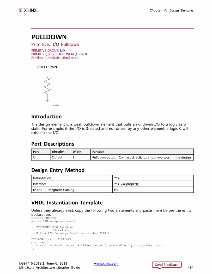
Chapter 4: Design Elements
PULLDOWNPrimitive: I/O PulldownPRIMITIVE_GROUP: I/OPRIMITIVE_SUBGROUP: WEAK_DRIVERFamilies: UltraScale, UltraScale+
IntroductionThe design element is a weak pulldown element that pulls an undriven I/O to a logic zerostate. For example, if the I/O is 3-stated and not driven by any other element, a logic 0 willexist on the I/O.
Port DescriptionsPort Direction Width Function
O Output 1 Pulldown output. Connect directly to a top-level port in the design.
Design Entry MethodInstantiation Yes
Inference Yes, via property
IP and IP Integrator Catalog No
VHDL Instantiation TemplateUnless they already exist, copy the following two statements and paste them before the entitydeclaration.Library UNISIM;use UNISIM.vcomponents.all;
-- PULLDOWN: I/O Pulldown-- UltraScale-- Xilinx HDL Language Template, version 2018.2
PULLDOWN_inst : PULLDOWNport map (
O => O -- 1-bit output: Pulldown output (connect directly to top-level port));
UG974 (v2018.2) June 6, 2018 www.xilinx.comUltraScale Architecture Libraries Guide 484
Send Feedback
Chapter 4: Design Elements
-- End of PULLDOWN_inst instantiation
Verilog Instantiation Template
// PULLDOWN: I/O Pulldown// UltraScale// Xilinx HDL Language Template, version 2018.2
PULLDOWN PULLDOWN_inst (.O(O) // 1-bit output: Pulldown output (connect directly to top-level port)
);
// End of PULLDOWN_inst instantiation
For More Information• See the UltraScale Architecture SelectIO Resources User Guide (UG571).
• See the UltraScale Programmable Devices Documentation.
UG974 (v2018.2) June 6, 2018 www.xilinx.comUltraScale Architecture Libraries Guide 485
Send Feedback
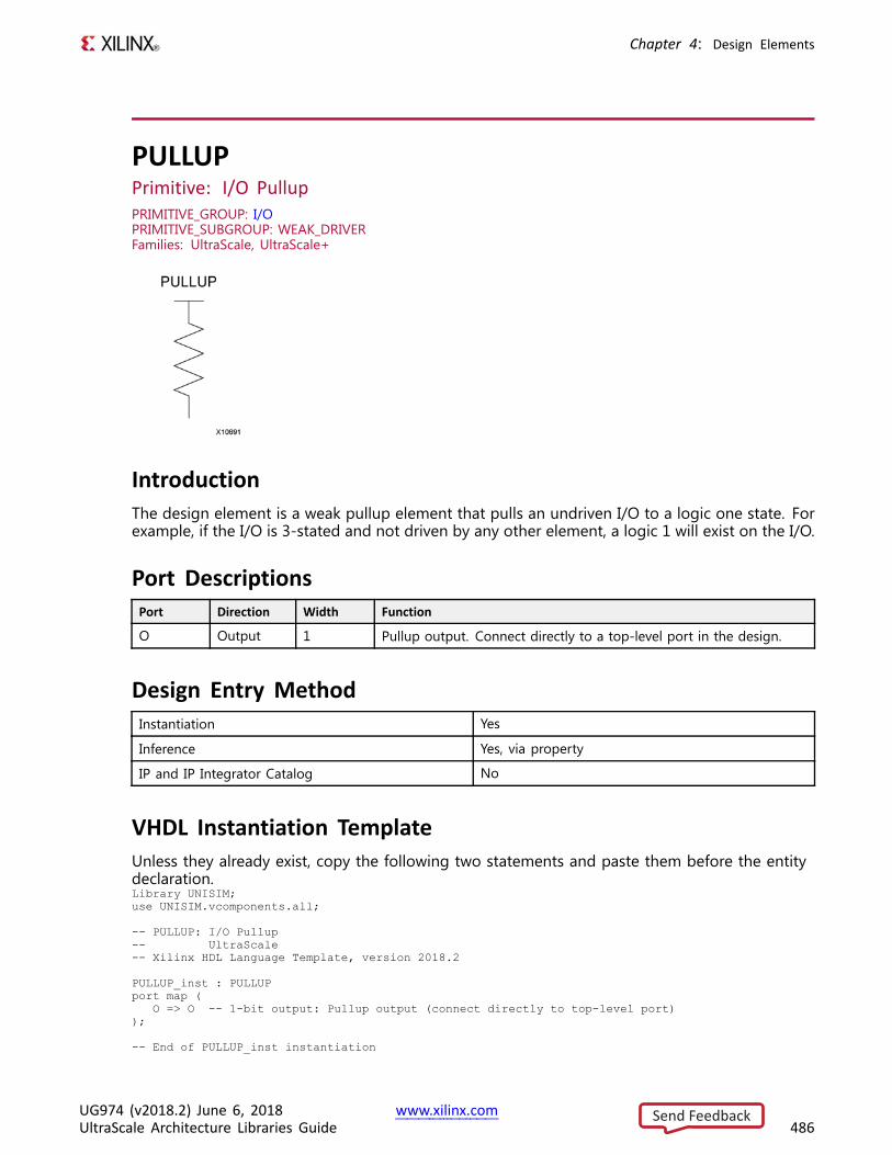
Chapter 4: Design Elements
PULLUPPrimitive: I/O PullupPRIMITIVE_GROUP: I/OPRIMITIVE_SUBGROUP: WEAK_DRIVERFamilies: UltraScale, UltraScale+
IntroductionThe design element is a weak pullup element that pulls an undriven I/O to a logic one state. Forexample, if the I/O is 3-stated and not driven by any other element, a logic 1 will exist on the I/O.
Port DescriptionsPort Direction Width Function
O Output 1 Pullup output. Connect directly to a top-level port in the design.
Design Entry MethodInstantiation Yes
Inference Yes, via property
IP and IP Integrator Catalog No
VHDL Instantiation TemplateUnless they already exist, copy the following two statements and paste them before the entitydeclaration.Library UNISIM;use UNISIM.vcomponents.all;
-- PULLUP: I/O Pullup-- UltraScale-- Xilinx HDL Language Template, version 2018.2
PULLUP_inst : PULLUPport map (
O => O -- 1-bit output: Pullup output (connect directly to top-level port));
-- End of PULLUP_inst instantiation
UG974 (v2018.2) June 6, 2018 www.xilinx.comUltraScale Architecture Libraries Guide 486
Send Feedback
Chapter 4: Design Elements
Verilog Instantiation Template
// PULLUP: I/O Pullup// UltraScale// Xilinx HDL Language Template, version 2018.2
PULLUP PULLUP_inst (.O(O) // 1-bit output: Pullup output (connect directly to top-level port)
);
// End of PULLUP_inst instantiation
For More Information• See the UltraScale Architecture SelectIO Resources User Guide (UG571).
• See the UltraScale Programmable Devices Documentation.
UG974 (v2018.2) June 6, 2018 www.xilinx.comUltraScale Architecture Libraries Guide 487
Send Feedback
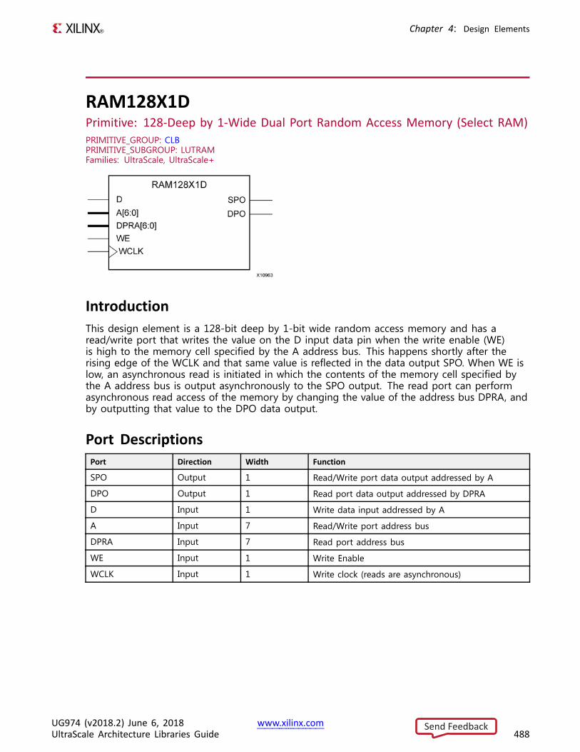
Chapter 4: Design Elements
RAM128X1DPrimitive: 128-Deep by 1-Wide Dual Port Random Access Memory (Select RAM)PRIMITIVE_GROUP: CLBPRIMITIVE_SUBGROUP: LUTRAMFamilies: UltraScale, UltraScale+
IntroductionThis design element is a 128-bit deep by 1-bit wide random access memory and has aread/write port that writes the value on the D input data pin when the write enable (WE)is high to the memory cell specified by the A address bus. This happens shortly after therising edge of the WCLK and that same value is reflected in the data output SPO. When WE islow, an asynchronous read is initiated in which the contents of the memory cell specified bythe A address bus is output asynchronously to the SPO output. The read port can performasynchronous read access of the memory by changing the value of the address bus DPRA, andby outputting that value to the DPO data output.
Port DescriptionsPort Direction Width Function
SPO Output 1 Read/Write port data output addressed by A
DPO Output 1 Read port data output addressed by DPRA
D Input 1 Write data input addressed by A
A Input 7 Read/Write port address bus
DPRA Input 7 Read port address bus
WE Input 1 Write Enable
WCLK Input 1 Write clock (reads are asynchronous)
UG974 (v2018.2) June 6, 2018 www.xilinx.comUltraScale Architecture Libraries Guide 488
Send Feedback
Chapter 4: Design Elements
If instantiated, the following connections should be made to this component:
• Tie the WCLK input to the desired clock source, the D input to the data source to be storedand the DPO output to an FDCE D input or other appropriate data destination.
• Optionally, the SPO output can also be connected to the appropriate data destinationor else left unconnected.
• Connect the WE clock enable pin to the proper write enable source in the design.
• Connect the 7-bit A bus to the source for the read/write addressing and the 7-bit DPRAbus to the appropriate read address connections.
You can use the INIT attribute to specify the initial contents of the RAM. If left unspecified, theinitial contents default to all zeros.
Design Entry MethodInstantiation Yes
Inference Recommended
IP Catalog No
Available AttributesAttribute Type Allowed Values Default Description
INIT HEX Any 128-bit value All zeros Specifies the initial contents of the RAM.
IS_WCLK_INVERTED BINARY 1'b0 to 1'b1 1'b0 Specifies whether or not to use theoptional inversion on the WCLK pin.
VHDL Instantiation TemplateUnless they already exist, copy the following two statements and paste them before the entitydeclaration.Library UNISIM;use UNISIM.vcomponents.all;
-- RAM128X1D: 128-deep by 1-wide positive edge write, asynchronous read-- dual-port distributed LUT RAM-- UltraScale-- Xilinx HDL Language Template, version 2018.2
RAM128X1D_inst : RAM128X1Dgeneric map (
INIT => X"00000000000000000000000000000000", -- Initial contents of RAMIS_WCLK_INVERTED => '0') -- Specifies active high/low WCLK
port map (DPO => DPO, -- Read/Write port 1-bit ouputSPO => SPO, -- Read port 1-bit outputA => A, -- Read/Write port 7-bit address inputD => D, -- RAM data inputDPRA => DPRA, -- Read port 7-bit address inputWCLK => WCLK, -- Write clock inputWE => WE -- RAM data input
);
-- End of RAM128X1D_inst instantiation
UG974 (v2018.2) June 6, 2018 www.xilinx.comUltraScale Architecture Libraries Guide 489
Send Feedback
Chapter 4: Design Elements
Verilog Instantiation Template
// RAM128X1D: 128-deep by 1-wide positive edge write, asynchronous read// dual-port distributed LUT RAM// UltraScale// Xilinx HDL Language Template, version 2018.2
RAM128X1D #(.INIT(128'h00000000000000000000000000000000),.IS_WCLK_INVERTED(1'b0) // Specifies active high/low WCLK
) RAM128X1D_inst (.DPO(DPO), // Read port 1-bit output.SPO(SPO), // Read/write port 1-bit output.A(A), // Read/write port 7-bit address input.D(D), // RAM data input.DPRA(DPRA), // Read port 7-bit address input.WCLK(WCLK), // Write clock input.WE(WE) // Write enable input
);
// End of RAM128X1D_inst instantiation
For More Information• See the UltraScale Architecture Migration: Methodology Guide (UG1026).
• See the UltraScale Programmable Devices Documentation.
UG974 (v2018.2) June 6, 2018 www.xilinx.comUltraScale Architecture Libraries Guide 490
Send Feedback

Chapter 4: Design Elements
RAM128X1SPrimitive: 128-Deep by 1-Wide Random Access Memory (Select RAM)PRIMITIVE_GROUP: CLBPRIMITIVE_SUBGROUP: LUTRAMFamilies: UltraScale, UltraScale+
IntroductionThis design element is a 128-bit deep by 1-bit wide random access memory with synchronouswrite and asynchronous read capability. This RAM is implemented using the LUT resources ofthe device (also known as Select RAM), and does not consume any of the block RAM resourcesof the device. If a synchronous read capability is preferred, a register can be attached to theoutput and placed in the same CLB.
The RAM128X1S has an active-High write enable (WE) so that when that signal is High, anda rising edge occurs on the WCLK pin, a write is performed recording the value of the Dinput data pin into the memory array. The output O displays the contents of the memory celladdressed by A, regardless of the WE value. When a write is performed, the output is updatedto the new value shortly after the write completes.
Port DescriptionsPort Direction Width Function
O Output 1 Read/Write port data output addressedby A
D Input 1 Write data input addressed by A
A Input 7 Read/Write port address bus
WE Input 1 Write Enable
WCLK Input 1 Write clock (reads are asynchronous)
Design Entry MethodInstantiation Yes
Inference Recommended
IP Catalog No
UG974 (v2018.2) June 6, 2018 www.xilinx.comUltraScale Architecture Libraries Guide 491
Send Feedback
Chapter 4: Design Elements
If instantiated, the following connections should be made to this component:• Tie the WCLK input to the desired clock source, the D input to the data source to be stored,
and the O output to an FDCE D input or other appropriate data destination.• Connect the WE clock enable pin to the proper write enable source in the design.• Connect the 7-bit A bus to the source for the read/write.
You can use the INIT attribute to specify the initial contents of the RAM. If left unspecified, theinitial contents default to all zeros.
Available AttributesAttribute Type Allowed Values Default Description
INIT HEX Any 128-bit value All zeros Specifies the initial contents of the RAM.
IS_WCLK_INVERTED BINARY 1'b0 to 1'b1 1'b0 Specifies whether or not to use theoptional inversion on the WCLK pin.
VHDL Instantiation TemplateUnless they already exist, copy the following two statements and paste them before the entitydeclaration.Library UNISIM;use UNISIM.vcomponents.all;
-- RAM128X1S: 128-deep x 1 positive edge write, asynchronous read-- single-port distributed RAM-- UltraScale-- Xilinx HDL Language Template, version 2018.2
RAM128X1S_inst : RAM128X1Sgeneric map (
INIT => X"00000000000000000000000000000000", -- Initial contents of RAMIS_WCLK_INVERTED => '0') -- Specifies active high/low WCLK
port map (O => O, -- 1-bit data outputA0 => A0, -- Address[0] input bitA1 => A1, -- Address[1] input bitA2 => A2, -- Address[2] input bitA3 => A3, -- Address[3] input bitA4 => A4, -- Address[4] input bitA5 => A5, -- Address[5] input bitA6 => A6, -- Address[6] input bitD => D, -- 1-bit data inputWCLK => WCLK, -- Write clock inputWE => WE -- RAM data input
);
-- End of RAM128X1S_inst instantiation
Verilog Instantiation Template// RAM128X1S: 128 x 1 positive edge write, asynchronous read single-port// distributed RAM (Mapped to two LUT6s)// UltraScale// Xilinx HDL Language Template, version 2018.2
RAM128X1S #(.INIT(128'h00000000000000000000000000000000), // Initial contents of RAM.IS_WCLK_INVERTED(1'b0) // Specifies active high/low WCLK
UG974 (v2018.2) June 6, 2018 www.xilinx.comUltraScale Architecture Libraries Guide 492
Send Feedback
Chapter 4: Design Elements
) RAM128X1S_inst (.O(O), // 1-bit data output.A0(A0), // Address[0] input bit.A1(A1), // Address[1] input bit.A2(A2), // Address[2] input bit.A3(A3), // Address[3] input bit.A4(A4), // Address[4] input bit.A5(A5), // Address[5] input bit.A6(A6), // Address[6] input bit.D(D), // 1-bit data input.WCLK(WCLK), // Write clock input.WE(WE) // Write enable input
);
// End of RAM128X1S_inst instantiation
For More Information• See the UltraScale Architecture Configurable Logic Block User Guide (UG574).
• See the UltraScale Programmable Devices Documentation.
UG974 (v2018.2) June 6, 2018 www.xilinx.comUltraScale Architecture Libraries Guide 493
Send Feedback
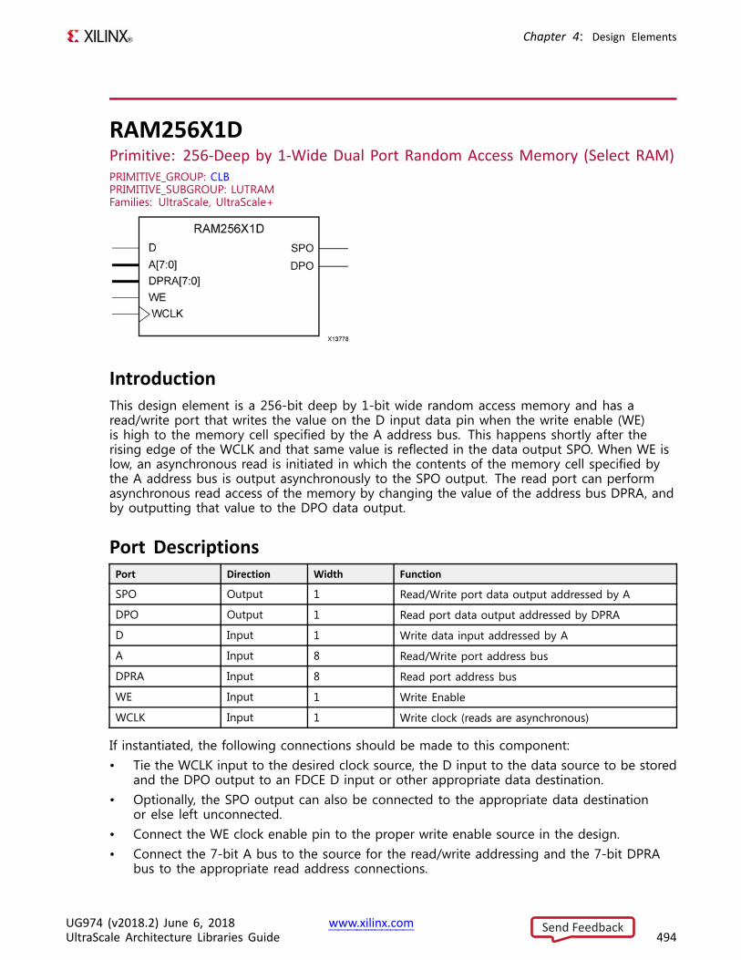
Chapter 4: Design Elements
RAM256X1DPrimitive: 256-Deep by 1-Wide Dual Port Random Access Memory (Select RAM)PRIMITIVE_GROUP: CLBPRIMITIVE_SUBGROUP: LUTRAMFamilies: UltraScale, UltraScale+
IntroductionThis design element is a 256-bit deep by 1-bit wide random access memory and has aread/write port that writes the value on the D input data pin when the write enable (WE)is high to the memory cell specified by the A address bus. This happens shortly after therising edge of the WCLK and that same value is reflected in the data output SPO. When WE islow, an asynchronous read is initiated in which the contents of the memory cell specified bythe A address bus is output asynchronously to the SPO output. The read port can performasynchronous read access of the memory by changing the value of the address bus DPRA, andby outputting that value to the DPO data output.
Port DescriptionsPort Direction Width Function
SPO Output 1 Read/Write port data output addressed by A
DPO Output 1 Read port data output addressed by DPRA
D Input 1 Write data input addressed by A
A Input 8 Read/Write port address bus
DPRA Input 8 Read port address bus
WE Input 1 Write Enable
WCLK Input 1 Write clock (reads are asynchronous)
If instantiated, the following connections should be made to this component:• Tie the WCLK input to the desired clock source, the D input to the data source to be stored
and the DPO output to an FDCE D input or other appropriate data destination.• Optionally, the SPO output can also be connected to the appropriate data destination
or else left unconnected.• Connect the WE clock enable pin to the proper write enable source in the design.• Connect the 7-bit A bus to the source for the read/write addressing and the 7-bit DPRA
bus to the appropriate read address connections.
UG974 (v2018.2) June 6, 2018 www.xilinx.comUltraScale Architecture Libraries Guide 494
Send Feedback
Chapter 4: Design Elements
You can use the INIT attribute to specify the initial contents of the RAM. If left unspecified, theinitial contents default to all zeros.
Design Entry MethodInstantiation Yes
Inference Recommended
IP Catalog No
Available AttributesAttribute Type Allowed Values Default Description
INIT HEX Any 256-bit value All zeros Specifies the initial contents of the RAM.
IS_WCLK_INVERTED BINARY 1'b0 to 1'b1 1'b0 Specifies whether or not to use theoptional inversion on the WCLK pin.
VHDL Instantiation TemplateUnless they already exist, copy the following two statements and paste them before the entitydeclaration.Library UNISIM;use UNISIM.vcomponents.all;
-- RAM256X1D: 256-deep by 1-wide positive edge write, asynchronous read-- dual-port distributed LUT RAM-- UltraScale-- Xilinx HDL Language Template, version 2018.2
RAM256X1D_inst : RAM256X1Dgeneric map (
INIT => X"0000000000000000000000000000000000000000000000000000000000000000", -- Initial contents of RAMIS_WCLK_INVERTED => '0') -- Specifies active high/low WCLK
port map (DPO => DPO, -- Read/Write port 1-bit ouputSPO => SPO, -- Read port 1-bit outputA => A, -- Read/Write port 8-bit address inputD => D, -- RAM data inputDPRA => DPRA, -- Read port 8-bit address inputWCLK => WCLK, -- Write clock inputWE => WE -- RAM data input
);
-- End of RAM256X1D_inst instantiation
Verilog Instantiation Template
// RAM256X1D: 256-deep by 1-wide positive edge write, asynchronous read// dual-port distributed LUT RAM// UltraScale// Xilinx HDL Language Template, version 2018.2
RAM256X1D #(.INIT(256'h0000000000000000000000000000000000000000000000000000000000000000),.IS_WCLK_INVERTED(1'b0) // Specifies active high/low WCLK
) RAM256X1D_inst (.DPO(DPO), // Read port 1-bit output
UG974 (v2018.2) June 6, 2018 www.xilinx.comUltraScale Architecture Libraries Guide 495
Send Feedback
Chapter 4: Design Elements
.SPO(SPO), // Read/write port 1-bit output
.A(A), // Read/write port 8-bit address input
.D(D), // RAM data input
.DPRA(DPRA), // Read port 8-bit address input
.WCLK(WCLK), // Write clock input
.WE(WE) // Write enable input);
// End of RAM256X1D_inst instantiation
For More Information• See the UltraScale Architecture Migration: Methodology Guide (UG1026).
• See the UltraScale Programmable Devices Documentation.
UG974 (v2018.2) June 6, 2018 www.xilinx.comUltraScale Architecture Libraries Guide 496
Send Feedback
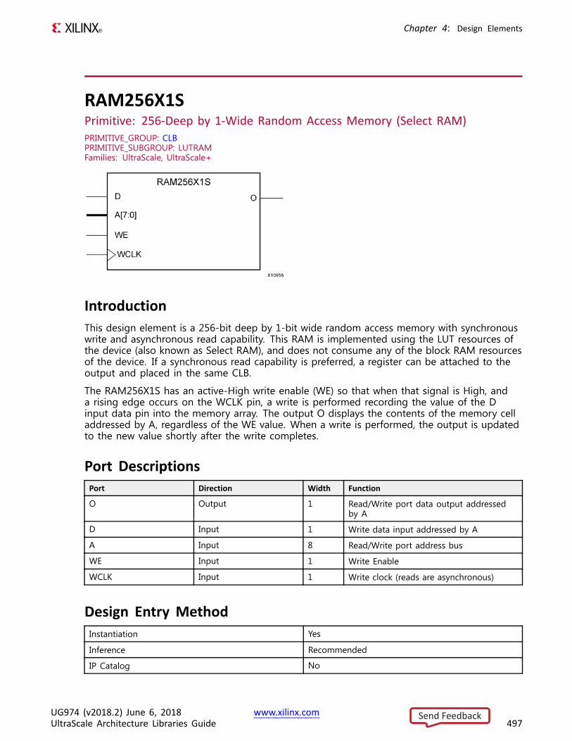
Chapter 4: Design Elements
RAM256X1SPrimitive: 256-Deep by 1-Wide Random Access Memory (Select RAM)PRIMITIVE_GROUP: CLBPRIMITIVE_SUBGROUP: LUTRAMFamilies: UltraScale, UltraScale+
IntroductionThis design element is a 256-bit deep by 1-bit wide random access memory with synchronouswrite and asynchronous read capability. This RAM is implemented using the LUT resources ofthe device (also known as Select RAM), and does not consume any of the block RAM resourcesof the device. If a synchronous read capability is preferred, a register can be attached to theoutput and placed in the same CLB.
The RAM256X1S has an active-High write enable (WE) so that when that signal is High, anda rising edge occurs on the WCLK pin, a write is performed recording the value of the Dinput data pin into the memory array. The output O displays the contents of the memory celladdressed by A, regardless of the WE value. When a write is performed, the output is updatedto the new value shortly after the write completes.
Port DescriptionsPort Direction Width Function
O Output 1 Read/Write port data output addressedby A
D Input 1 Write data input addressed by A
A Input 8 Read/Write port address bus
WE Input 1 Write Enable
WCLK Input 1 Write clock (reads are asynchronous)
Design Entry MethodInstantiation Yes
Inference Recommended
IP Catalog No
UG974 (v2018.2) June 6, 2018 www.xilinx.comUltraScale Architecture Libraries Guide 497
Send Feedback
Chapter 4: Design Elements
If instantiated, the following connections should be made to this component:• Tie the WCLK input to the desired clock source, the D input to the data source to be stored,
and the O output to an FDCE D input or other appropriate data destination.• Connect the WE clock enable pin to the proper write enable source in the design.• Connect the 8-bit A bus to the source for the read/write.
You can use the INIT attribute to specify the initial contents of the RAM. If left unspecified, theinitial contents default to all zeros.
Available AttributesAttribute Type Allowed Values Default Description
INIT HEX Any 256-bit value All zeros Specifies the initial contents of the RAM.
IS_WCLK_INVERTED BINARY 1'b0 to 1'b1 1'b0 Specifies whether or not to use theoptional inversion on the WCLK pin.
VHDL Instantiation TemplateUnless they already exist, copy the following two statements and paste them before the entitydeclaration.Library UNISIM;use UNISIM.vcomponents.all;
-- RAM256X1S: 256-deep by 1-wide positive edge write, asynchronous read-- single-port distributed LUT RAM-- UltraScale-- Xilinx HDL Language Template, version 2018.2
RAM256X1S_inst : RAM256X1Sgeneric map (
INIT => X"0000000000000000000000000000000000000000000000000000000000000000", -- Initial contents of RAMIS_WCLK_INVERTED => '0') -- Specifies active high/low WCLK
port map (O => O, -- Read/Write port 1-bit ouputA => A, -- Read/Write port 8-bit address inputD => D, -- RAM data inputWCLK => WCLK, -- Write clock inputWE => WE -- Write enable input
);
-- End of RAM256X1S_inst instantiation
Verilog Instantiation Template// RAM256X1S: 256-deep by 1-wide positive edge write, asynchronous read (Mapped to four LUT6s)// single-port distributed LUT RAM// UltraScale// Xilinx HDL Language Template, version 2018.2
RAM256X1S #(.INIT(256'h0000000000000000000000000000000000000000000000000000000000000000),.IS_WCLK_INVERTED(1'b0) // Specifies active high/low WCLK
) RAM256X1S_inst (.O(O), // Read/write port 1-bit output.A(A), // Read/write port 8-bit address input.WE(WE), // Write enable input.WCLK(WCLK), // Write clock input.D(D) // RAM data input
UG974 (v2018.2) June 6, 2018 www.xilinx.comUltraScale Architecture Libraries Guide 498
Send Feedback
Chapter 4: Design Elements
);
// End of RAM256X1S_inst instantiation
For More Information• See the UltraScale Architecture Configurable Logic Block User Guide (UG574).
• See the UltraScale Programmable Devices Documentation.
UG974 (v2018.2) June 6, 2018 www.xilinx.comUltraScale Architecture Libraries Guide 499
Send Feedback
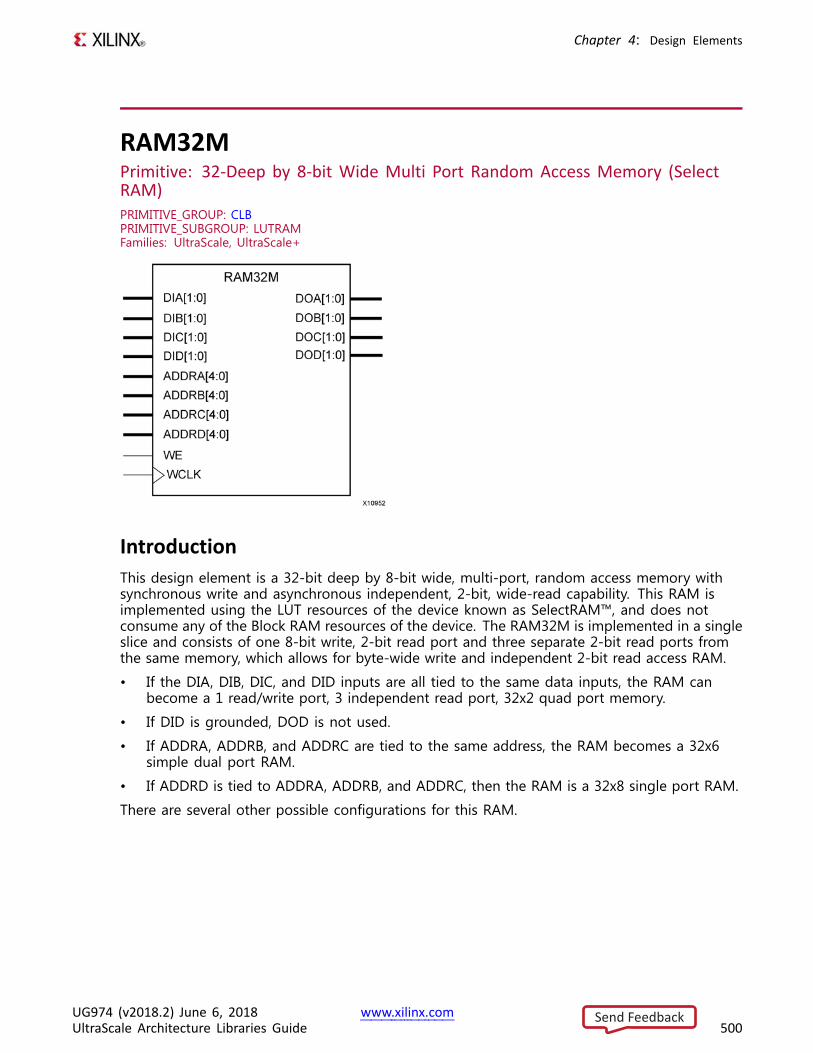
Chapter 4: Design Elements
RAM32MPrimitive: 32-Deep by 8-bit Wide Multi Port Random Access Memory (SelectRAM)PRIMITIVE_GROUP: CLBPRIMITIVE_SUBGROUP: LUTRAMFamilies: UltraScale, UltraScale+
IntroductionThis design element is a 32-bit deep by 8-bit wide, multi-port, random access memory withsynchronous write and asynchronous independent, 2-bit, wide-read capability. This RAM isimplemented using the LUT resources of the device known as SelectRAM™, and does notconsume any of the Block RAM resources of the device. The RAM32M is implemented in a singleslice and consists of one 8-bit write, 2-bit read port and three separate 2-bit read ports fromthe same memory, which allows for byte-wide write and independent 2-bit read access RAM.
• If the DIA, DIB, DIC, and DID inputs are all tied to the same data inputs, the RAM canbecome a 1 read/write port, 3 independent read port, 32x2 quad port memory.
• If DID is grounded, DOD is not used.
• If ADDRA, ADDRB, and ADDRC are tied to the same address, the RAM becomes a 32x6simple dual port RAM.
• If ADDRD is tied to ADDRA, ADDRB, and ADDRC, then the RAM is a 32x8 single port RAM.
There are several other possible configurations for this RAM.
UG974 (v2018.2) June 6, 2018 www.xilinx.comUltraScale Architecture Libraries Guide 500
Send Feedback
Chapter 4: Design Elements
Port DescriptionsPort Direction Width Function
DOA Output 2 Read port data outputs addressed by ADDRA
DOB Output 2 Read port data outputs addressed by ADDRB
DOC Output 2 Read port data outputs addressed by ADDRC
DOD Output 2 Read/Write port data outputs addressed by ADDRD
DIA Input 2 Write data inputs addressed by ADDRD (read outputis addressed by ADDRA)
DIB Input 2 Write data inputs addressed by ADDRD (read outputis addressed by ADDRB)
DIC Input 2 Write data inputs addressed by ADDRD (read outputis addressed by ADDRC)
DID Input 2 Write data inputs addressed by ADDRD
ADDRA Input 5 Read address bus A
ADDRB Input 5 Read address bus B
ADDRC Input 5 Read address bus C
ADDRD Input 5 8-bit data write port, 2-bit data read port addressbus D
WE Input 1 Write Enable
WCLK Input 1 Write clock (reads are asynchronous)
Design Entry MethodInstantiation Yes
Inference Recommended
IP Catalog No
This element can be inferred by some synthesis tools by describing a RAM with a synchronouswrite and asynchronous read capability. Consult your synthesis tool documentation for detailson RAM inference capabilities and coding examples. You should instantiate this component ifyou have a need to implicitly specify the RAM function, or if you need to manually place orrelationally place the component.
If synchronous read capability is desired, the outputs can be connected to an FDRE/FDSE(FDCE/FDPE if asynchronous reset is needed) in order to improve the output timing of thefunction. However, this is not necessary for the proper operation of the RAM. If you wantto have the data clocked on the negative edge of a clock, an inverter can be described onthe clock input to this component. This inverter will be absorbed into the block duringimplementation and set as the IS_WCLK_INVERTED attribute giving the ability to write to theRAM on falling clock edges.
UG974 (v2018.2) June 6, 2018 www.xilinx.comUltraScale Architecture Libraries Guide 501
Send Feedback
Chapter 4: Design Elements
If instantiated, the following connections should be made to this component:• Connect the WCLK input to the desired clock source• Connect the DIA, DIB, DIC, and DID inputs to the data source to be stored• Connect the DOA, DOB, DOC, and DOD outputs to an FDCE D input or other appropriate
data destination, or leave unconnected if not used• Connect the WE clock enable pin to the proper write enable source in the design• Connect the ADDRD bus to the source for the read/write addressing• Connect the ADDRA, ADDRB, and ADDRC buses to the appropriate read address
connections
The optional INIT_A, INIT_B, INIT_C and INIT_D attributes let you specify the initial memorycontents of each port using a 64-bit hexadecimal value. The INIT value correlates to the RAMaddressing by the following equation: ADDRy[z] = INIT_y[2*z+1:2*z]. For instance, if the RAMADDRC port is addressed to 00001, then the INIT_C[3:2] values would be the initial valuesshown on the DOC port before the first write occurs at that address. If left unspecified, theinitial contents will be all zeros.
Available AttributesAttribute Type Allowed Values Default Description
INIT_A HEX Any 64-bit value All zeros Specifies the initial contents of the RAMon port A.
INIT_B HEX Any 64-bit value All zeros Specifies the initial contents of the RAMon port B.
INIT_C HEX Any 64-bit value All zeros Specifies the initial contents of the RAMon port C.
INIT_D HEX Any 64-bit value All zeros Specifies the initial contents of the RAMon port D.
IS_WCLK_INVERTED BINARY 1'b0 to 1'b1 1'b0 Specifies whether or not to use theoptional inversion on the WCLK pin.
VHDL Instantiation TemplateUnless they already exist, copy the following two statements and paste them before the entitydeclaration.Library UNISIM;use UNISIM.vcomponents.all;
-- RAM32M: 32-deep by 8-wide Multi Port LUT RAM-- UltraScale-- Xilinx HDL Language Template, version 2018.2
RAM32M_inst : RAM32Mgeneric map (
INIT_A => X"0000000000000000", -- Initial contents of A portINIT_B => X"0000000000000000", -- Initial contents of B portINIT_C => X"0000000000000000", -- Initial contents of C portINIT_D => X"0000000000000000", -- Initial contents of D portIS_WCLK_INVERTED => '0') -- Specifies active high/low WCLK
port map (DOA => DOA, -- Read port A 2-bit outputDOB => DOB, -- Read port B 2-bit outputDOC => DOC, -- Read port C 2-bit outputDOD => DOD, -- Read/Write port D 2-bit output
UG974 (v2018.2) June 6, 2018 www.xilinx.comUltraScale Architecture Libraries Guide 502
Send Feedback
Chapter 4: Design Elements
ADDRA => ADDRA, -- Read port A 5-bit address inputADDRB => ADDRB, -- Read port B 5-bit address inputADDRC => ADDRC, -- Read port C 5-bit address inputADDRD => ADDRD, -- Read/Write port D 5-bit address inputDIA => DIA, -- RAM 2-bit data write input addressed by ADDRD,
-- read addressed by ADDRADIB => DIB, -- RAM 2-bit data write input addressed by ADDRD,
-- read addressed by ADDRBDIC => DIC, -- RAM 2-bit data write input addressed by ADDRD,
-- read addressed by ADDRCDID => DID, -- RAM 2-bit data write input addressed by ADDRD,
-- read addressed by ADDRDWCLK => WCLK, -- Write clock inputWE => WE -- Write enable input
);-- End of RAM32M_inst instantiation
Verilog Instantiation Template
// RAM32M: 32-deep by 8-wide Multi Port LUT RAM (Mapped to four LUT6s)// UltraScale// Xilinx HDL Language Template, version 2018.2
RAM32M #(.INIT_A(64'h0000000000000000), // Initial contents of A Port.INIT_B(64'h0000000000000000), // Initial contents of B Port.INIT_C(64'h0000000000000000), // Initial contents of C Port.INIT_D(64'h0000000000000000), // Initial contents of D Port.IS_WCLK_INVERTED(1'b0) // Specifies active high/low WCLK
) RAM32M_inst (.DOA(DOA), // Read port A 2-bit output.DOB(DOB), // Read port B 2-bit output.DOC(DOC), // Read port C 2-bit output.DOD(DOD), // Read/write port D 2-bit output.ADDRA(ADDRA), // Read port A 5-bit address input.ADDRB(ADDRB), // Read port B 5-bit address input.ADDRC(ADDRC), // Read port C 5-bit address input.ADDRD(ADDRD), // Read/write port D 5-bit address input.DIA(DIA), // RAM 2-bit data write input addressed by ADDRD,
// read addressed by ADDRA.DIB(DIB), // RAM 2-bit data write input addressed by ADDRD,
// read addressed by ADDRB.DIC(DIC), // RAM 2-bit data write input addressed by ADDRD,
// read addressed by ADDRC.DID(DID), // RAM 2-bit data write input addressed by ADDRD,
// read addressed by ADDRD.WCLK(WCLK), // Write clock input.WE(WE) // Write enable input
);
// End of RAM32M_inst instantiation
For More Information• See the UltraScale Architecture Migration: Methodology Guide (UG1026).
• See the UltraScale Programmable Devices Documentation.
UG974 (v2018.2) June 6, 2018 www.xilinx.comUltraScale Architecture Libraries Guide 503
Send Feedback
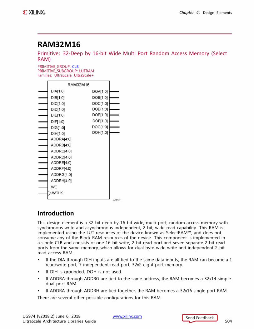
Chapter 4: Design Elements
RAM32M16Primitive: 32-Deep by 16-bit Wide Multi Port Random Access Memory (SelectRAM)PRIMITIVE_GROUP: CLBPRIMITIVE_SUBGROUP: LUTRAMFamilies: UltraScale, UltraScale+
IntroductionThis design element is a 32-bit deep by 16-bit wide, multi-port, random access memory withsynchronous write and asynchronous independent, 2-bit, wide-read capability. This RAM isimplemented using the LUT resources of the device known as SelectRAM™, and does notconsume any of the Block RAM resources of the device. This component is implemented ina single CLB and consists of one 16-bit write, 2-bit read port and seven separate 2-bit readports from the same memory, which allows for dual byte-wide write and independent 2-bitread access RAM.• If the DIA through DIH inputs are all tied to the same data inputs, the RAM can become a 1
read/write port, 7 independent read port, 32x2 eight port memory.• If DIH is grounded, DOH is not used.• If ADDRA through ADDRG are tied to the same address, the RAM becomes a 32x14 simple
dual port RAM.• If ADDRA through ADDRH are tied together, the RAM becomes a 32x16 single port RAM.There are several other possible configurations for this RAM.
UG974 (v2018.2) June 6, 2018 www.xilinx.comUltraScale Architecture Libraries Guide 504
Send Feedback
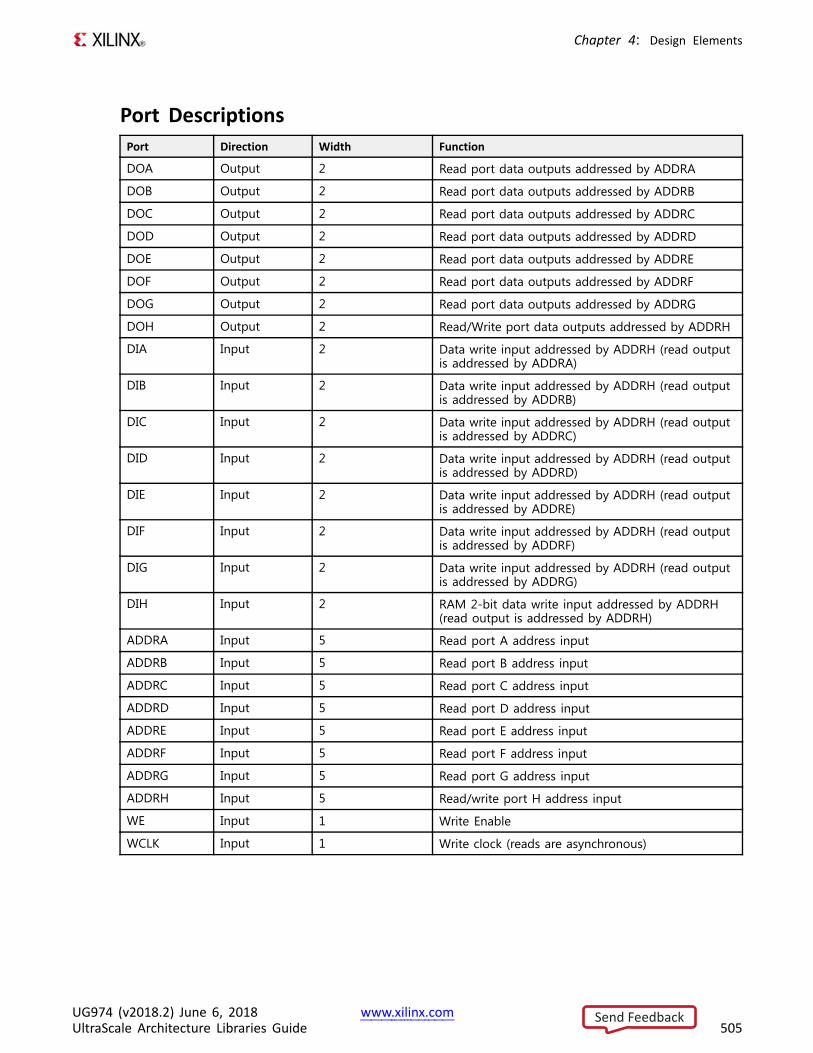
Chapter 4: Design Elements
Port DescriptionsPort Direction Width Function
DOA Output 2 Read port data outputs addressed by ADDRA
DOB Output 2 Read port data outputs addressed by ADDRB
DOC Output 2 Read port data outputs addressed by ADDRC
DOD Output 2 Read port data outputs addressed by ADDRD
DOE Output 2 Read port data outputs addressed by ADDRE
DOF Output 2 Read port data outputs addressed by ADDRF
DOG Output 2 Read port data outputs addressed by ADDRG
DOH Output 2 Read/Write port data outputs addressed by ADDRH
DIA Input 2 Data write input addressed by ADDRH (read outputis addressed by ADDRA)
DIB Input 2 Data write input addressed by ADDRH (read outputis addressed by ADDRB)
DIC Input 2 Data write input addressed by ADDRH (read outputis addressed by ADDRC)
DID Input 2 Data write input addressed by ADDRH (read outputis addressed by ADDRD)
DIE Input 2 Data write input addressed by ADDRH (read outputis addressed by ADDRE)
DIF Input 2 Data write input addressed by ADDRH (read outputis addressed by ADDRF)
DIG Input 2 Data write input addressed by ADDRH (read outputis addressed by ADDRG)
DIH Input 2 RAM 2-bit data write input addressed by ADDRH(read output is addressed by ADDRH)
ADDRA Input 5 Read port A address input
ADDRB Input 5 Read port B address input
ADDRC Input 5 Read port C address input
ADDRD Input 5 Read port D address input
ADDRE Input 5 Read port E address input
ADDRF Input 5 Read port F address input
ADDRG Input 5 Read port G address input
ADDRH Input 5 Read/write port H address input
WE Input 1 Write Enable
WCLK Input 1 Write clock (reads are asynchronous)
UG974 (v2018.2) June 6, 2018 www.xilinx.comUltraScale Architecture Libraries Guide 505
Send Feedback
Chapter 4: Design Elements
Design Entry MethodInstantiation Yes
Inference Recommended
IP Catalog No
This element can be inferred by some synthesis tools by describing a RAM with a synchronouswrite and asynchronous read capability. Consult your synthesis tool documentation for detailson RAM inference capabilities and coding examples. You should instantiate this component ifyou have a need to implicitly specify the RAM function, or if you need to manually place orrelationally place the component.
If synchronous read capability is desired, the outputs can be connected to an FDRE/FDSE(FDCE/FDPE if asynchronous reset is needed) in order to improve the output timing of thefunction. However, this is not necessary for the proper operation of the RAM. If you wantto have the data clocked on the negative edge of a clock, an inverter can be described onthe clock input to this component. This inverter will be absorbed into the block duringimplementation and set as the IS_WCLK_INVERTED attribute giving the ability to write to theRAM on falling clock edges.
If instantiated, the following connections should be made to this component:• Connect the WCLK input to the desired clock source• Connect the DIA–DIH inputs to the data source to be stored• Connect the DOA–DOH outputs to an FD* D input or other appropriate data destination,
or leave unconnected if not used• Connect the WE clock enable pin to the proper write enable source in the design• Connect the ADDRD bus to the source for the read/write addressing• Connect the ADDRA–ADDRG buses to the appropriate read address connections
The optional INIT_A–INIT_H attributes let you specify the initial memory contents of eachport using a 64-bit hexadecimal value. The INIT value correlates to the RAM addressing bythe following equation: ADDRy[z] = INIT_y[2*z+1:2*z]. For instance, if the RAM ADDRC portis addressed to 00001, then the INIT_C[3:2] values would be the initial values shown on theDOC port before the first write occurs at that address. If left unspecified, the initial contentswill be all zeros.
Available AttributesAttribute Type Allowed Values Default Description
INIT_A HEX Any 128-bit value All zeros Specifies the initial contents of the RAMon port A.
INIT_B HEX Any 128-bit value All zeros Specifies the initial contents of the RAMon port B.
INIT_C HEX Any 128-bit value All zeros Specifies the initial contents of the RAMon port C.
INIT_D HEX Any 128-bit value All zeros Specifies the initial contents of the RAMon port D.
INIT_E HEX Any 128-bit value All zeros Specifies the initial contents of the RAMon port E.
UG974 (v2018.2) June 6, 2018 www.xilinx.comUltraScale Architecture Libraries Guide 506
Send Feedback
Chapter 4: Design Elements
Attribute Type Allowed Values Default Description
INIT_F HEX Any 128-bit value All zeros Specifies the initial contents of the RAMon port F.
INIT_G HEX Any 128-bit value All zeros Specifies the initial contents of the RAMon port G.
INIT_H HEX Any 128-bit value All zeros Specifies the initial contents of the RAMon port H.
IS_WCLK_INVERTED BINARY 1'b0 to 1'b1 1'b0 Specifies whether or not to use the optionalinversion on the WCLK pin.
VHDL Instantiation TemplateUnless they already exist, copy the following two statements and paste them before the entitydeclaration.Library UNISIM;use UNISIM.vcomponents.all;
-- RAM32M16: 32-deep by 16-wide Multi Port LUT RAM-- UltraScale-- Xilinx HDL Language Template, version 2018.2RAM32M16_inst : RAM32M16generic map (
INIT_A => X"0000000000000000", -- Initial contents of A portINIT_B => X"0000000000000000", -- Initial contents of B portINIT_C => X"0000000000000000", -- Initial contents of C portINIT_D => X"0000000000000000", -- Initial contents of D portINIT_E => X"0000000000000000", -- Initial contents of E portINIT_F => X"0000000000000000", -- Initial contents of F portINIT_G => X"0000000000000000", -- Initial contents of G portINIT_H => X"0000000000000000", -- Initial contents of H portIS_WCLK_INVERTED => '0') -- Specifies active high/low WCLK
port map (DOA => DOA, -- Read port A 2-bit outputDOB => DOB, -- Read port B 2-bit outputDOC => DOC, -- Read port C 2-bit outputDOD => DOD, -- Read port D 2-bit outputDOE => DOE, -- Read port E 2-bit outputDOF => DOF, -- Read port F 2-bit outputDOG => DOG, -- Read port G 2-bit outputDOH => DOH, -- Read/write port H 2-bit outputADDRA => ADDRA, -- Read port A 5-bit address inputADDRB => ADDRB, -- Read port B 5-bit address inputADDRC => ADDRC, -- Read port C 5-bit address inputADDRD => ADDRD, -- Read port D 5-bit address inputADDRE => ADDRE, -- Read port E 5-bit address inputADDRF => ADDRF, -- Read port F 5-bit address inputADDRG => ADDRG, -- Read port G 5-bit address inputADDRH => ADDRH, -- Read/write port H 5-bit address inputDIA => DIA, -- RAM 2-bit data write input addressed by ADDRD,
-- read addressed by ADDRADIB => DIB, -- RAM 2-bit data write input addressed by ADDRD,
-- read addressed by ADDRBDIC => DIC, -- RAM 2-bit data write input addressed by ADDRD,
-- read addressed by ADDRCDID => DID, -- RAM 2-bit data write input addressed by ADDRD,
-- read addressed by ADDRDDIE => DIE, -- RAM 2-bit data write input addressed by ADDRE,
-- read addressed by ADDREDIF => DIF, -- RAM 2-bit data write input addressed by ADDRF,
-- read addressed by ADDRFDIG => DIG, -- RAM 2-bit data write input addressed by ADDRG,
-- read addressed by ADDRGDIH => DIH, -- RAM 2-bit data write input addressed by ADDRH,
-- read addressed by ADDRH
UG974 (v2018.2) June 6, 2018 www.xilinx.comUltraScale Architecture Libraries Guide 507
Send Feedback
Chapter 4: Design Elements
WCLK => WCLK, -- Write clock inputWE => WE -- Write enable input
);-- End of RAM32M16_inst instantiation
Verilog Instantiation Template
// RAM32M16: 32-deep by 16-wide Multi Port LUT RAM (Mapped to eight LUT6s)// UltraScale// Xilinx HDL Language Template, version 2018.2
RAM32M16 #(.INIT_A(64'h0000000000000000), // Initial contents of A Port.INIT_B(64'h0000000000000000), // Initial contents of B Port.INIT_C(64'h0000000000000000), // Initial contents of C Port.INIT_D(64'h0000000000000000), // Initial contents of D Port.INIT_E(64'h0000000000000000), // Initial contents of E Port.INIT_F(64'h0000000000000000), // Initial contents of F Port.INIT_G(64'h0000000000000000), // Initial contents of G Port.INIT_H(64'h0000000000000000), // Initial contents of H Port.IS_WCLK_INVERTED(1'b0) // Specifies active high/low WCLK
) RAM32M16_inst (.DOA(DOA), // Read port A 2-bit output.DOB(DOB), // Read port B 2-bit output.DOC(DOC), // Read port C 2-bit output.DOD(DOD), // Read port D 2-bit output.DOE(DOE), // Read port E 2-bit output.DOF(DOF), // Read port F 2-bit output.DOG(DOG), // Read port G 2-bit output.DOH(DOH), // Read/write port H 2-bit output.ADDRA(ADDRA), // Read port A 5-bit address input.ADDRB(ADDRB), // Read port B 5-bit address input.ADDRC(ADDRC), // Read port C 5-bit address input.ADDRD(ADDRD), // Read port D 5-bit address input.ADDRE(ADDRE), // Read port E 5-bit address input.ADDRF(ADDRF), // Read port F 5-bit address input.ADDRG(ADDRG), // Read port G 5-bit address input.ADDRH(ADDRH), // Read/write port H 5-bit address input.DIA(DIA), // RAM 2-bit data write input addressed by ADDRD,
// read addressed by ADDRA.DIB(DIB), // RAM 2-bit data write input addressed by ADDRD,
// read addressed by ADDRB.DIC(DIC), // RAM 2-bit data write input addressed by ADDRD,
// read addressed by ADDRC.DID(DID), // RAM 2-bit data write input addressed by ADDRD,
// read addressed by ADDRD.DIE(DIE), // RAM 2-bit data write input addressed by ADDRD,
// read addressed by ADDRE.DIF(DIF), // RAM 2-bit data write input addressed by ADDRD,
// read addressed by ADDRF.DIG(DIG), // RAM 2-bit data write input addressed by ADDRD,
// read addressed by ADDRG.DIH(DIH), // RAM 2-bit data write input addressed by ADDRD,
// read addressed by ADDRH.WCLK(WCLK), // Write clock input.WE(WE) // Write enable input
);
// End of RAM32M16_inst instantiation
For More Information• See the UltraScale Architecture Configurable Logic Block User Guide (UG574).
• See the UltraScale Programmable Devices Documentation.
UG974 (v2018.2) June 6, 2018 www.xilinx.comUltraScale Architecture Libraries Guide 508
Send Feedback
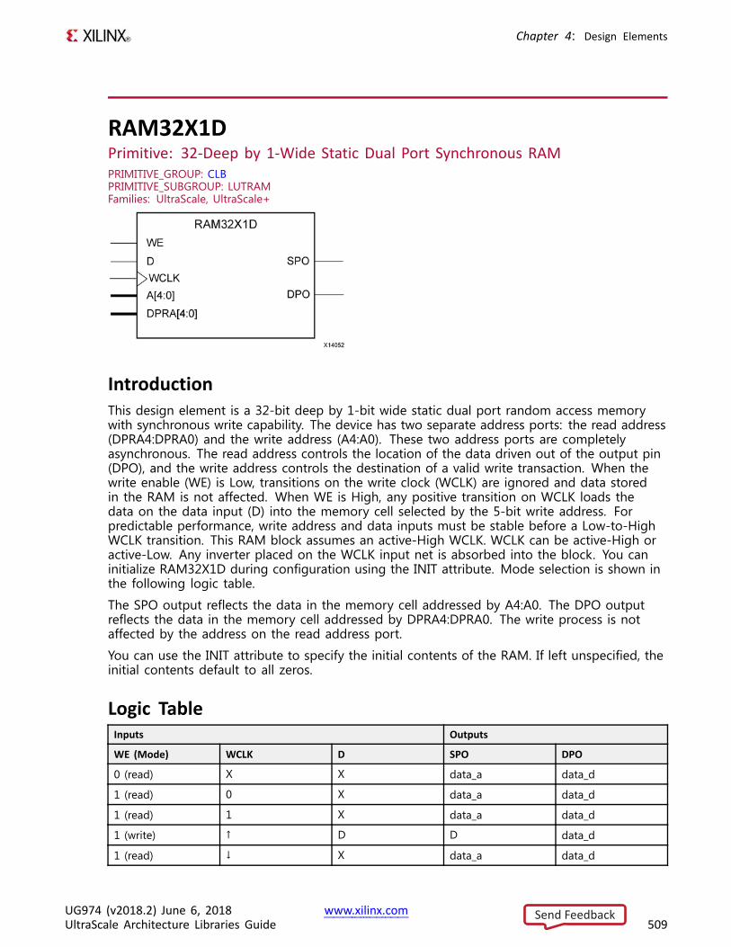
Chapter 4: Design Elements
RAM32X1DPrimitive: 32-Deep by 1-Wide Static Dual Port Synchronous RAMPRIMITIVE_GROUP: CLBPRIMITIVE_SUBGROUP: LUTRAMFamilies: UltraScale, UltraScale+
IntroductionThis design element is a 32-bit deep by 1-bit wide static dual port random access memorywith synchronous write capability. The device has two separate address ports: the read address(DPRA4:DPRA0) and the write address (A4:A0). These two address ports are completelyasynchronous. The read address controls the location of the data driven out of the output pin(DPO), and the write address controls the destination of a valid write transaction. When thewrite enable (WE) is Low, transitions on the write clock (WCLK) are ignored and data storedin the RAM is not affected. When WE is High, any positive transition on WCLK loads thedata on the data input (D) into the memory cell selected by the 5-bit write address. Forpredictable performance, write address and data inputs must be stable before a Low-to-HighWCLK transition. This RAM block assumes an active-High WCLK. WCLK can be active-High oractive-Low. Any inverter placed on the WCLK input net is absorbed into the block. You caninitialize RAM32X1D during configuration using the INIT attribute. Mode selection is shown inthe following logic table.
The SPO output reflects the data in the memory cell addressed by A4:A0. The DPO outputreflects the data in the memory cell addressed by DPRA4:DPRA0. The write process is notaffected by the address on the read address port.
You can use the INIT attribute to specify the initial contents of the RAM. If left unspecified, theinitial contents default to all zeros.
Logic TableInputs Outputs
WE (Mode) WCLK D SPO DPO
0 (read) X X data_a data_d
1 (read) 0 X data_a data_d
1 (read) 1 X data_a data_d
1 (write) ↑ D D data_d
1 (read) ↓ X data_a data_d
UG974 (v2018.2) June 6, 2018 www.xilinx.comUltraScale Architecture Libraries Guide 509
Send Feedback

Chapter 4: Design Elements
Design Entry MethodInstantiation Yes
Inference Recommended
IP Catalog No
Available AttributesAttribute Type Allowed Values Default Description
INIT HEX Any 32-bit value All zeros Specifies the initial contents of the RAM.
IS_WCLK_INVERTED BINARY 1'b0 to 1'b1 1'b0 Specifies whether or not to use theoptional inversion on the WCLK pin.
VHDL Instantiation TemplateUnless they already exist, copy the following two statements and paste them before the entitydeclaration.Library UNISIM;use UNISIM.vcomponents.all;
-- RAM32X1D: 32 x 1 positive edge write, asynchronous read-- dual-port distributed RAM-- UltraScale-- Xilinx HDL Language Template, version 2018.2
RAM32X1D_inst : RAM32X1Dgeneric map (
INIT => X"00000000", -- Initial contents of RAMIS_WCLK_INVERTED => '0') -- Specifies active high/low WCLK
port map (DPO => DPO, -- Read-only 1-bit data outputSPO => SPO, -- R/W 1-bit data outputA0 => A0, -- R/W address[0] input bitA1 => A1, -- R/W address[1] input bitA2 => A2, -- R/W address[2] input bitA3 => A3, -- R/W address[3] input bitA4 => A4, -- R/W address[4] input bitD => D, -- Write 1-bit data inputDPRA0 => DPRA0, -- Read-only address[0] input bitDPRA1 => DPRA1, -- Read-only address[1] input bitDPRA2 => DPRA2, -- Read-only address[2] input bitDPRA3 => DPRA3, -- Read-only address[3] input bitDPRA4 => DPRA4, -- Read-only address[4] input bitWCLK => WCLK, -- Write clock inputWE => WE -- Write enable input
);
-- End of RAM32X1D_inst instantiation
Verilog Instantiation Template
// RAM32X1D: 32 x 1 positive edge write, asynchronous read dual-port// distributed RAM (Mapped to two LUT6s)// UltraScale// Xilinx HDL Language Template, version 2018.2
RAM32X1D #(.INIT(32'h00000000), // Initial contents of RAM
UG974 (v2018.2) June 6, 2018 www.xilinx.comUltraScale Architecture Libraries Guide 510
Send Feedback
Chapter 4: Design Elements
.IS_WCLK_INVERTED(1'b0) // Specifies active high/low WCLK) RAM32X1D_inst (
.DPO(DPO), // Read-only 1-bit data output
.SPO(SPO), // Rw/ 1-bit data output
.A0(A0), // Rw/ address[0] input bit
.A1(A1), // Rw/ address[1] input bit
.A2(A2), // Rw/ address[2] input bit
.A3(A3), // Rw/ address[3] input bit
.A4(A4), // Rw/ address[4] input bit
.D(D), // Write 1-bit data input
.DPRA0(DPRA0), // Read-only address[0] input bit
.DPRA1(DPRA1), // Read-only address[1] input bit
.DPRA2(DPRA2), // Read-only address[2] input bit
.DPRA3(DPRA3), // Read-only address[3] input bit
.DPRA4(DPRA4), // Read-only address[4] input bit
.WCLK(WCLK), // Write clock input
.WE(WE) // Write enable input);
// End of RAM32X1D_inst instantiation
For More Information• See the UltraScale Architecture Migration: Methodology Guide (UG1026).
• See the UltraScale Programmable Devices Documentation.
UG974 (v2018.2) June 6, 2018 www.xilinx.comUltraScale Architecture Libraries Guide 511
Send Feedback
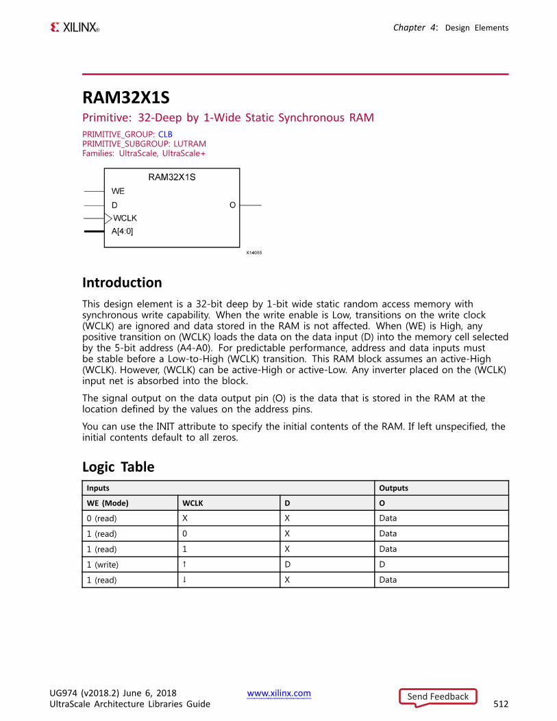
Chapter 4: Design Elements
RAM32X1SPrimitive: 32-Deep by 1-Wide Static Synchronous RAMPRIMITIVE_GROUP: CLBPRIMITIVE_SUBGROUP: LUTRAMFamilies: UltraScale, UltraScale+
IntroductionThis design element is a 32-bit deep by 1-bit wide static random access memory withsynchronous write capability. When the write enable is Low, transitions on the write clock(WCLK) are ignored and data stored in the RAM is not affected. When (WE) is High, anypositive transition on (WCLK) loads the data on the data input (D) into the memory cell selectedby the 5-bit address (A4-A0). For predictable performance, address and data inputs mustbe stable before a Low-to-High (WCLK) transition. This RAM block assumes an active-High(WCLK). However, (WCLK) can be active-High or active-Low. Any inverter placed on the (WCLK)input net is absorbed into the block.
The signal output on the data output pin (O) is the data that is stored in the RAM at thelocation defined by the values on the address pins.
You can use the INIT attribute to specify the initial contents of the RAM. If left unspecified, theinitial contents default to all zeros.
Logic TableInputs Outputs
WE (Mode) WCLK D O
0 (read) X X Data
1 (read) 0 X Data
1 (read) 1 X Data
1 (write) ↑ D D
1 (read) ↓ X Data
UG974 (v2018.2) June 6, 2018 www.xilinx.comUltraScale Architecture Libraries Guide 512
Send Feedback
Chapter 4: Design Elements
Design Entry MethodInstantiation Yes
Inference Recommended
IP Catalog No
Available AttributesAttribute Type Allowed Values Default Description
INIT HEX Any 32-bit value All zeros Specifies the initial contents of the RAM.
IS_WCLK_INVERTED BINARY 1'b0 to 1'b1 1'b0 Specifies whether or not to use theoptional inversion on the WCLK pin.
VHDL Instantiation TemplateUnless they already exist, copy the following two statements and paste them before the entitydeclaration.Library UNISIM;use UNISIM.vcomponents.all;
-- RAM32X1S: 32 x 1 posedge write distributed (LUT) RAM-- UltraScale-- Xilinx HDL Language Template, version 2018.2
RAM32X1S_inst : RAM32X1Sgeneric map (
INIT => X"00000000", -- Initial contents of RAMIS_WCLK_INVERTED => '0') -- Specifies active high/low WCLK
port map (O => O, -- RAM outputA0 => A0, -- RAM address[0] inputA1 => A1, -- RAM address[1] inputA2 => A2, -- RAM address[2] inputA3 => A3, -- RAM address[3] inputA4 => A4, -- RAM address[4] inputD => D, -- RAM data inputWCLK => WCLK, -- Write clock inputWE => WE -- Write enable input
);
-- End of RAM32X1S_inst instantiation
Verilog Instantiation Template
// RAM32X1S: 32 x 1 posedge write distributed (LUT) RAM (Mapped to a LUT6)// UltraScale// Xilinx HDL Language Template, version 2018.2
RAM32X1S #(.INIT(32'h00000000), // Initial contents of RAM.IS_WCLK_INVERTED(1'b0) // Specifies active high/low WCLK
) RAM32X1S_inst (.O(O), // RAM output.A0(A0), // RAM address[0] input.A1(A1), // RAM address[1] input.A2(A2), // RAM address[2] input.A3(A3), // RAM address[3] input.A4(A4), // RAM address[4] input
UG974 (v2018.2) June 6, 2018 www.xilinx.comUltraScale Architecture Libraries Guide 513
Send Feedback
Chapter 4: Design Elements
.D(D), // RAM data input
.WCLK(WCLK), // Write clock input
.WE(WE) // Write enable input);
// End of RAM32X1S_inst instantiation
For More Information• See the UltraScale Architecture Configurable Logic Block User Guide (UG574).
• See the UltraScale Programmable Devices Documentation.
UG974 (v2018.2) June 6, 2018 www.xilinx.comUltraScale Architecture Libraries Guide 514
Send Feedback
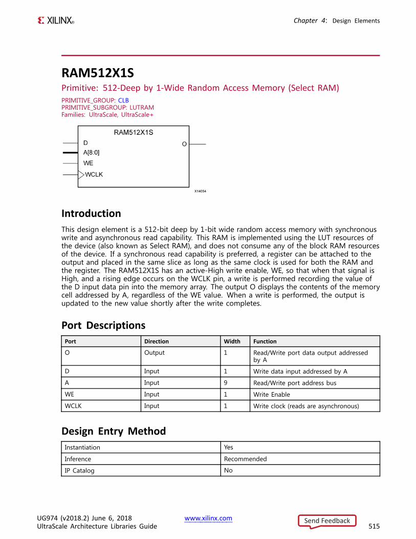
Chapter 4: Design Elements
RAM512X1SPrimitive: 512-Deep by 1-Wide Random Access Memory (Select RAM)PRIMITIVE_GROUP: CLBPRIMITIVE_SUBGROUP: LUTRAMFamilies: UltraScale, UltraScale+
IntroductionThis design element is a 512-bit deep by 1-bit wide random access memory with synchronouswrite and asynchronous read capability. This RAM is implemented using the LUT resources ofthe device (also known as Select RAM), and does not consume any of the block RAM resourcesof the device. If a synchronous read capability is preferred, a register can be attached to theoutput and placed in the same slice as long as the same clock is used for both the RAM andthe register. The RAM512X1S has an active-High write enable, WE, so that when that signal isHigh, and a rising edge occurs on the WCLK pin, a write is performed recording the value ofthe D input data pin into the memory array. The output O displays the contents of the memorycell addressed by A, regardless of the WE value. When a write is performed, the output isupdated to the new value shortly after the write completes.
Port DescriptionsPort Direction Width Function
O Output 1 Read/Write port data output addressedby A
D Input 1 Write data input addressed by A
A Input 9 Read/Write port address bus
WE Input 1 Write Enable
WCLK Input 1 Write clock (reads are asynchronous)
Design Entry MethodInstantiation Yes
Inference Recommended
IP Catalog No
UG974 (v2018.2) June 6, 2018 www.xilinx.comUltraScale Architecture Libraries Guide 515
Send Feedback

Chapter 4: Design Elements
If instantiated, the following connections should be made to this component:• Tie the WCLK input to the desired clock source, the D input to the data source to be stored,
and the O output to an FDCE D input or other appropriate data destination.• Connect the WE clock enable pin to the proper write enable source in the design.• Connect the 8-bit A bus to the source for the read/write.
You can use the INIT attribute to specify the initial contents of the RAM. If left unspecified, theinitial contents default to all zeros.
Available AttributesAttribute Type Allowed Values Default Description
INIT HEX Any 512-bit value All zeros Specifies the initial contents of the RAM.
IS_WCLK_INVERTED BINARY 1'b0 to 1'b1 1'b0 Specifies whether or not to use theoptional inversion on the WCLK pin.
VHDL Instantiation TemplateUnless they already exist, copy the following two statements and paste them before the entitydeclaration.Library UNISIM;use UNISIM.vcomponents.all;
-- RAM512X1S: 512-deep by 1-wide positive edge write, asynchronous read-- single-port distributed LUT RAM-- UltraScale-- Xilinx HDL Language Template, version 2018.2
RAM512X1S_inst : RAM512X1Sgeneric map (
INIT => X"00000000000000000000000000000000000000000000000000000000000000000000000000000000000000000000000000000000000000000000000000000000", -- Initial contents of RAM
IS_WCLK_INVERTED => '0') -- Specifies active high/low WCLKport map (
O => O, -- Read/Write port 1-bit ouputA => A, -- Read/Write port 9-bit address inputD => D, -- RAM data inputWCLK => WCLK, -- Write clock inputWE => WE -- Write enable input
);
-- End of RAM512X1S_inst instantiation
Verilog Instantiation Template// RAM512X1S: 512-deep by 1-wide positive edge write, asynchronous read (Mapped to eight LUT6s)// single-port distributed LUT RAM// UltraScale// Xilinx HDL Language Template, version 2018.2
RAM512X1S #(.INIT(512'h00000000000000000000000000000000000000000000000000000000000000000000000000000000000000000000000000000000000000000000000000000000),
.IS_WCLK_INVERTED(1'b0) // Specifies active high/low WCLK) RAM512X1S_inst (
.O(O), // Read/write port 1-bit output
.A(A), // Read/write port 9-bit address input
.WE(WE), // Write enable input
.WCLK(WCLK), // Write clock input
.D(D) // RAM data input
UG974 (v2018.2) June 6, 2018 www.xilinx.comUltraScale Architecture Libraries Guide 516
Send Feedback

Chapter 4: Design Elements
);
// End of RAM512X1S_inst instantiation
For More Information• See the UltraScale Architecture Configurable Logic Block User Guide (UG574).
• See the UltraScale Programmable Devices Documentation.
UG974 (v2018.2) June 6, 2018 www.xilinx.comUltraScale Architecture Libraries Guide 517
Send Feedback
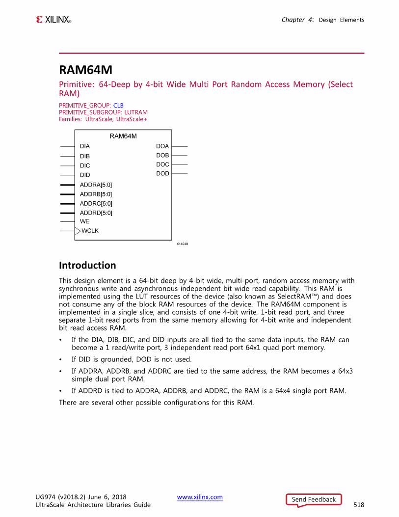
Chapter 4: Design Elements
RAM64MPrimitive: 64-Deep by 4-bit Wide Multi Port Random Access Memory (SelectRAM)PRIMITIVE_GROUP: CLBPRIMITIVE_SUBGROUP: LUTRAMFamilies: UltraScale, UltraScale+
IntroductionThis design element is a 64-bit deep by 4-bit wide, multi-port, random access memory withsynchronous write and asynchronous independent bit wide read capability. This RAM isimplemented using the LUT resources of the device (also known as SelectRAM™) and doesnot consume any of the block RAM resources of the device. The RAM64M component isimplemented in a single slice, and consists of one 4-bit write, 1-bit read port, and threeseparate 1-bit read ports from the same memory allowing for 4-bit write and independentbit read access RAM.
• If the DIA, DIB, DIC, and DID inputs are all tied to the same data inputs, the RAM canbecome a 1 read/write port, 3 independent read port 64x1 quad port memory.
• If DID is grounded, DOD is not used.
• If ADDRA, ADDRB, and ADDRC are tied to the same address, the RAM becomes a 64x3simple dual port RAM.
• If ADDRD is tied to ADDRA, ADDRB, and ADDRC, the RAM is a 64x4 single port RAM.
There are several other possible configurations for this RAM.
UG974 (v2018.2) June 6, 2018 www.xilinx.comUltraScale Architecture Libraries Guide 518
Send Feedback
Chapter 4: Design Elements
Port DescriptionsPort Direction Width Function
DOA Output 1 Read port data outputs addressed by ADDRA
DOB Output 1 Read port data outputs addressed by ADDRB
DOC Output 1 Read port data outputs addressed by ADDRC
DOD Output 1 Read/Write port data outputs addressed by ADDRD
DIA Input 1 Write data inputs addressed by ADDRD (read output isaddressed by ADDRA)
DIB Input 1 Write data inputs addressed by ADDRD (read output isaddressed by ADDRB)
DIC Input 1 Write data inputs addressed by ADDRD (read output isaddressed by ADDRC)
DID Input 1 Write data inputs addressed by ADDRD
ADDRA Input 6 Read address bus A
ADDRB Input 6 Read address bus B
ADDRC Input 6 Read address bus C
ADDRD Input 6 4-bit data write port, 1-bit data read port address bus D
WE Input 1 Write Enable
WCLK Input 1 Write clock (reads are asynchronous)
Design Entry MethodInstantiation Yes
Inference Recommended
IP Catalog No
This element can be inferred by some synthesis tools by describing a RAM with a synchronouswrite and asynchronous read capability. Consult your synthesis tool documentation for detailson RAM inference capabilities and coding examples. Xilinx suggests that you instantiate thiscomponent if you have a need to implicitly specify the RAM function, or if you need tomanually place or relationally place the component.
If synchronous read capability is desired, the outputs can be connected to an FDRE/FDSE(FDCE/FDPE if asynchronous reset is needed) in order to improve the output timing of thefunction. However, this is not necessary for the proper operation of the RAM. If you wantto have the data clocked on the negative edge of a clock, an inverter can be described onthe clock input to this component. This inverter will be absorbed into the block duringimplementation and set as the IS_WCLK_INVERTED attribute giving the ability to write to theRAM on falling clock edges.
UG974 (v2018.2) June 6, 2018 www.xilinx.comUltraScale Architecture Libraries Guide 519
Send Feedback
Chapter 4: Design Elements
If instantiated, the following connections should be made to this component:• Connect the WCLK input to the desired clock source, the DIA, DIB, DIC• Connect the DIA, DIB, DIC, and DID inputs to the data source to be stored• Connect the DOA, DOB, DOC, and DOD outputs to an FDCE D input or other appropriate
data destination, or leave unconnected if not used• Connect the WE clock enable pin to the proper write enable source in the design• Connect the ADDRD bus to the source for the read/write addressing• Connect the ADDRA, ADDRB, and ADDRC buses to the appropriate read address
connections
The optional INIT_A, INIT_B, INIT_C and INIT_D attributes let you specify the initial memorycontents of each port using a 64-bit hexadecimal value. The INIT value correlates to the RAMaddressing by the following equation: ADDRy[z] = INIT_y[z]. For instance, if the RAM ADDRCport is addressed to 00001, then the INIT_C[1] values would be the initial values shown on theDOC port before the first write occurs at that address. If left unspecified, the initial contents willdefault to all zeros.
Available AttributesAttribute Type Allowed Values Default Description
INIT_A HEX Any 64-bit value All zeros Specifies the initial contents of the RAM onport A.
INIT_B HEX Any 64-bit value All zeros Specifies the initial contents of the RAM onport B.
INIT_C HEX Any 64-bit value All zeros Specifies the initial contents of the RAM onport C.
INIT_D HEX Any 64-bit value All zeros Specifies the initial contents of the RAM onport D.
IS_WCLK_INVERTED BINARY 1'b0 to 1'b1 1'b0 Specifies whether or not to use the optionalinversion on the WCLK pin.
VHDL Instantiation TemplateUnless they already exist, copy the following two statements and paste them before the entitydeclaration.Library UNISIM;use UNISIM.vcomponents.all;
-- RAM64M: 64-deep by 4-wide Multi Port LUT RAM-- UltraScale-- Xilinx HDL Language Template, version 2018.2
RAM64M_inst : RAM64Mgeneric map (
INIT_A => X"0000000000000000", -- Initial contents of A portINIT_B => X"0000000000000000", -- Initial contents of B portINIT_C => X"0000000000000000", -- Initial contents of C portINIT_D => X"0000000000000000", -- Initial contents of D portIS_WCLK_INVERTED => '0') -- Specifies active high/low WCLK
port map (DOA => DOA, -- Read port A 1-bit outputDOB => DOB, -- Read port B 1-bit output
UG974 (v2018.2) June 6, 2018 www.xilinx.comUltraScale Architecture Libraries Guide 520
Send Feedback
Chapter 4: Design Elements
DOC => DOC, -- Read port C 1-bit outputDOD => DOD, -- Read/Write port D 1-bit outputADDRA => ADDRA, -- Read port A 6-bit address inputADDRB => ADDRB, -- Read port B 6-bit address inputADDRC => ADDRC, -- Read port C 6-bit address inputADDRD => ADDRD, -- Read/Write port D 6-bit address inputDIA => DIA, -- RAM 1-bit data write input addressed by ADDRD,
-- read addressed by ADDRADIB => DIB, -- RAM 1-bit data write input addressed by ADDRD,
-- read addressed by ADDRBDIC => DIC, -- RAM 1-bit data write input addressed by ADDRD,
-- read addressed by ADDRCDID => DID, -- RAM 1-bit data write input addressed by ADDRD,
-- read addressed by ADDRDWCLK => WCLK, -- Write clock inputWE => WE -- Write enable input
);-- End of RAM64M_inst instantiation
Verilog Instantiation Template
// RAM64M: 64-deep by 4-wide Multi Port LUT RAM (Mapped to four LUT6s)// UltraScale// Xilinx HDL Language Template, version 2018.2
RAM64M #(.INIT_A(64'h0000000000000000), // Initial contents of A Port.INIT_B(64'h0000000000000000), // Initial contents of B Port.INIT_C(64'h0000000000000000), // Initial contents of C Port.INIT_D(64'h0000000000000000), // Initial contents of D Port.IS_WCLK_INVERTED(1'b0) // Specifies active high/low WCLK
) RAM64M_inst (.DOA(DOA), // Read port A 1-bit output.DOB(DOB), // Read port B 1-bit output.DOC(DOC), // Read port C 1-bit output.DOD(DOD), // Read/write port D 1-bit output.DIA(DIA), // RAM 1-bit data write input addressed by ADDRD,
// read addressed by ADDRA.DIB(DIB), // RAM 1-bit data write input addressed by ADDRD,
// read addressed by ADDRB.DIC(DIC), // RAM 1-bit data write input addressed by ADDRD,
// read addressed by ADDRC.DID(DID), // RAM 1-bit data write input addressed by ADDRD,
// read addressed by ADDRD.ADDRA(ADDRA), // Read port A 6-bit address input.ADDRB(ADDRB), // Read port B 6-bit address input.ADDRC(ADDRC), // Read port C 6-bit address input.ADDRD(ADDRD), // Read/write port D 6-bit address input.WE(WE), // Write enable input.WCLK(WCLK) // Write clock input
);
// End of RAM64M_inst instantiation
For More Information• See the UltraScale Architecture Migration: Methodology Guide (UG1026).
• See the UltraScale Programmable Devices Documentation.
UG974 (v2018.2) June 6, 2018 www.xilinx.comUltraScale Architecture Libraries Guide 521
Send Feedback
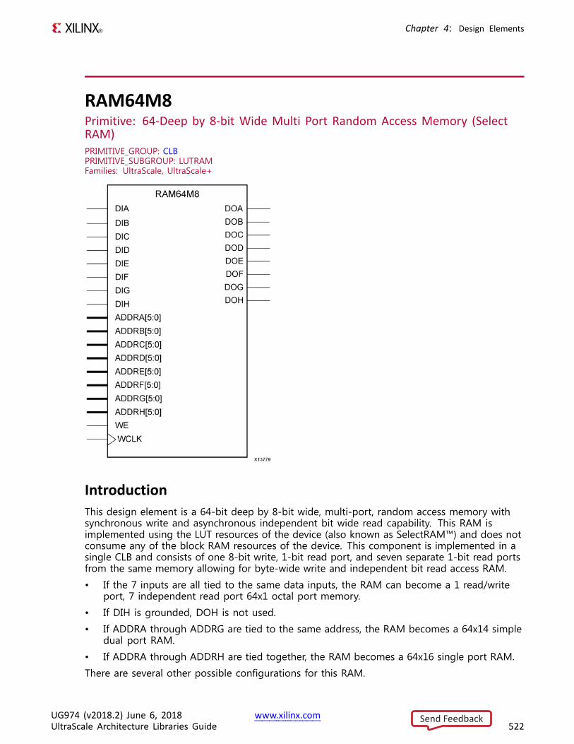
Chapter 4: Design Elements
RAM64M8Primitive: 64-Deep by 8-bit Wide Multi Port Random Access Memory (SelectRAM)PRIMITIVE_GROUP: CLBPRIMITIVE_SUBGROUP: LUTRAMFamilies: UltraScale, UltraScale+
IntroductionThis design element is a 64-bit deep by 8-bit wide, multi-port, random access memory withsynchronous write and asynchronous independent bit wide read capability. This RAM isimplemented using the LUT resources of the device (also known as SelectRAM™) and does notconsume any of the block RAM resources of the device. This component is implemented in asingle CLB and consists of one 8-bit write, 1-bit read port, and seven separate 1-bit read portsfrom the same memory allowing for byte-wide write and independent bit read access RAM.• If the 7 inputs are all tied to the same data inputs, the RAM can become a 1 read/write
port, 7 independent read port 64x1 octal port memory.• If DIH is grounded, DOH is not used.• If ADDRA through ADDRG are tied to the same address, the RAM becomes a 64x14 simple
dual port RAM.• If ADDRA through ADDRH are tied together, the RAM becomes a 64x16 single port RAM.There are several other possible configurations for this RAM.
UG974 (v2018.2) June 6, 2018 www.xilinx.comUltraScale Architecture Libraries Guide 522
Send Feedback
Chapter 4: Design Elements
Port DescriptionsPort Direction Width Function
DOA Output 1 Read port data outputs addressed by ADDRA
DOB Output 1 Read port data outputs addressed by ADDRB
DOC Output 1 Read port data outputs addressed by ADDRC
DOD Output 1 Read port data outputs addressed by ADDRD
DOE Output 1 Read port data outputs addressed by ADDRE
DOF Output 1 Read port data outputs addressed by ADDRF
DOG Output 1 Read port data outputs addressed by ADDRG
DOH Output 1 Read/Write port data outputs addressed by ADDRH
DIA Input 1 Data write input addressed by ADDRH (read output isaddressed by ADDRA)
DIB Input 1 Data write input addressed by ADDRH (read output isaddressed by ADDRB)
DIC Input 1 Data write input addressed by ADDRH (read output isaddressed by ADDRC)
DID Input 1 Data write input addressed by ADDRH (read output isaddressed by ADDRD)
DIE Input 1 Data write input addressed by ADDRH (read output isaddressed by ADDRE)
DIF Input 1 Data write input addressed by ADDRH (read output isaddressed by ADDRF)
DIG Input 1 Data write input addressed by ADDRH (read output isaddressed by ADDRG)
DIH Input 1 RAM 2-bit data write input addressed by ADDRH (readoutput is addressed by ADDRH)
ADDRA Input 6 Read port A address input
ADDRB Input 6 Read port B address input
ADDRC Input 6 Read port C address input
ADDRD Input 6 Read port D address input
ADDRE Input 6 Read port E address input
ADDRF Input 6 Read port F address input
ADDRG Input 6 Read port G address input
ADDRH Input 6 Read/write port H address input
WE Input 1 Write Enable
WCLK Input 1 Write clock (reads are asynchronous)
UG974 (v2018.2) June 6, 2018 www.xilinx.comUltraScale Architecture Libraries Guide 523
Send Feedback
Chapter 4: Design Elements
Design Entry MethodInstantiation Yes
Inference Recommended
IP Catalog No
This element can be inferred by some synthesis tools by describing a RAM with a synchronouswrite and asynchronous read capability. Consult your synthesis tool documentation for detailson RAM inference capabilities and coding examples. Xilinx suggests that you instantiate thiscomponent if you have a need to implicitly specify the RAM function, or if you need tomanually place or relationally place the component.
If synchronous read capability is desired, the outputs can be connected to an FDRE/FDSE(FDCE/FDPE if asynchronous reset is needed) in order to improve the output timing of thefunction. However, this is not necessary for the proper operation of the RAM. If you wantto have the data clocked on the negative edge of a clock, an inverter can be described onthe clock input to this component. This inverter will be absorbed into the block duringimplementation and set as the IS_WCLK_INVERTED attribute giving the ability to write to theRAM on falling clock edges.
If instantiated, the following connections should be made to this component:• Connect the WCLK input to the desired clock source• Connect the DIA–DIH inputs to the data source to be stored• Connect the DOA–DOH outputs to an FD* D input or other appropriate data destination,
or leave unconnected if not used• Connect the WE clock enable pin to the proper write enable source in the design• Connect the ADDRH bus to the source for the read/write addressing• Connect the ADDRA–ADDRG buses to the appropriate read address connections
The optional INIT_A–INIT_H attributes let you specify the initial memory contents of each portusing a 64-bit hexadecimal value. The INIT value correlates to the RAM addressing by thefollowing equation: ADDRy[z] = INIT_y[z]. For instance, if the RAM ADDRC port is addressed to00001, then the INIT_C[1] values would be the initial values shown on the DOC port before thefirst write occurs at that address. If left unspecified, the initial contents will default to all zeros.
Available AttributesAttribute Type Allowed Values Default Description
INIT_A HEX Any 128-bit value All zeros Specifies the initial contents of the RAMon port A.
INIT_B HEX Any 128-bit value All zeros Specifies the initial contents of the RAMon port B.
INIT_C HEX Any 128-bit value All zeros Specifies the initial contents of the RAMon port C.
INIT_D HEX Any 128-bit value All zeros Specifies the initial contents of the RAMon port D.
INIT_E HEX Any 128-bit value All zeros Specifies the initial contents of the RAMon port E.
UG974 (v2018.2) June 6, 2018 www.xilinx.comUltraScale Architecture Libraries Guide 524
Send Feedback
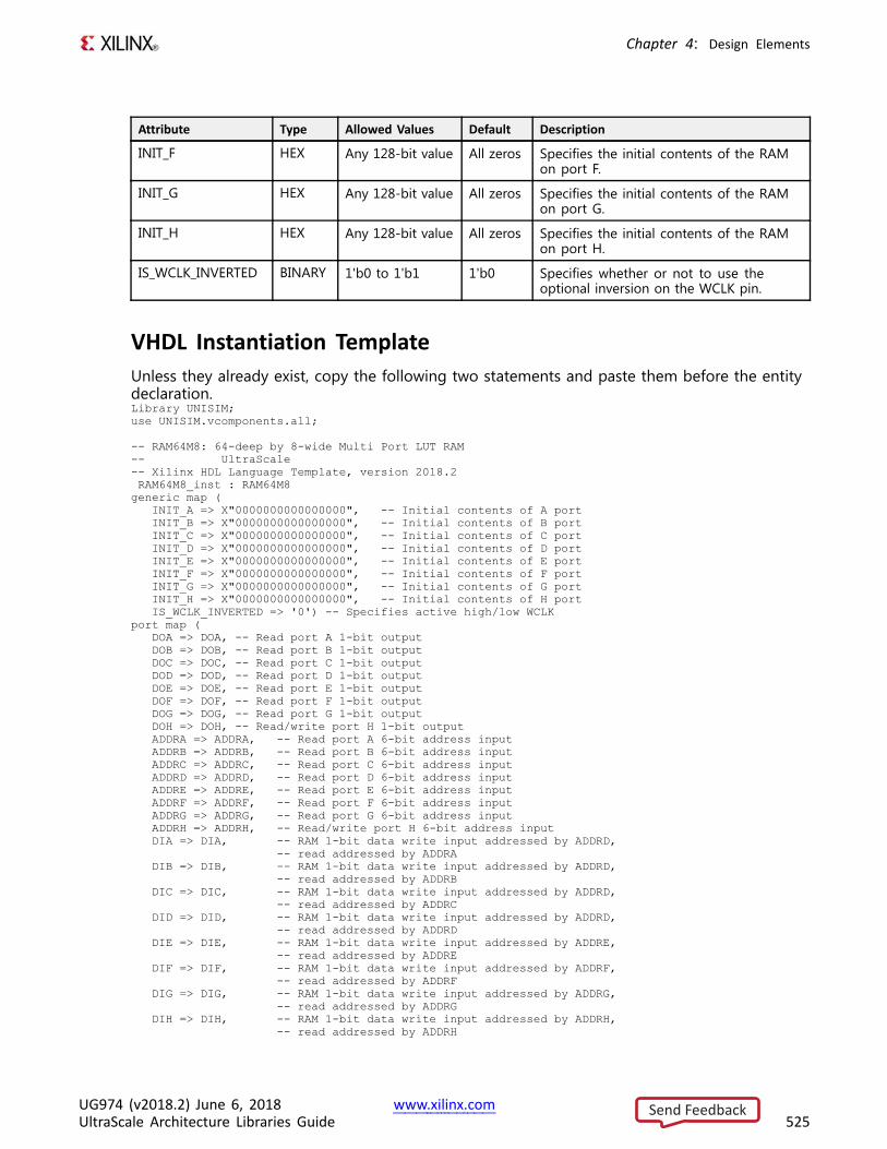
Chapter 4: Design Elements
Attribute Type Allowed Values Default Description
INIT_F HEX Any 128-bit value All zeros Specifies the initial contents of the RAMon port F.
INIT_G HEX Any 128-bit value All zeros Specifies the initial contents of the RAMon port G.
INIT_H HEX Any 128-bit value All zeros Specifies the initial contents of the RAMon port H.
IS_WCLK_INVERTED BINARY 1'b0 to 1'b1 1'b0 Specifies whether or not to use theoptional inversion on the WCLK pin.
VHDL Instantiation TemplateUnless they already exist, copy the following two statements and paste them before the entitydeclaration.Library UNISIM;use UNISIM.vcomponents.all;
-- RAM64M8: 64-deep by 8-wide Multi Port LUT RAM-- UltraScale-- Xilinx HDL Language Template, version 2018.2RAM64M8_inst : RAM64M8generic map (
INIT_A => X"0000000000000000", -- Initial contents of A portINIT_B => X"0000000000000000", -- Initial contents of B portINIT_C => X"0000000000000000", -- Initial contents of C portINIT_D => X"0000000000000000", -- Initial contents of D portINIT_E => X"0000000000000000", -- Initial contents of E portINIT_F => X"0000000000000000", -- Initial contents of F portINIT_G => X"0000000000000000", -- Initial contents of G portINIT_H => X"0000000000000000", -- Initial contents of H portIS_WCLK_INVERTED => '0') -- Specifies active high/low WCLK
port map (DOA => DOA, -- Read port A 1-bit outputDOB => DOB, -- Read port B 1-bit outputDOC => DOC, -- Read port C 1-bit outputDOD => DOD, -- Read port D 1-bit outputDOE => DOE, -- Read port E 1-bit outputDOF => DOF, -- Read port F 1-bit outputDOG => DOG, -- Read port G 1-bit outputDOH => DOH, -- Read/write port H 1-bit outputADDRA => ADDRA, -- Read port A 6-bit address inputADDRB => ADDRB, -- Read port B 6-bit address inputADDRC => ADDRC, -- Read port C 6-bit address inputADDRD => ADDRD, -- Read port D 6-bit address inputADDRE => ADDRE, -- Read port E 6-bit address inputADDRF => ADDRF, -- Read port F 6-bit address inputADDRG => ADDRG, -- Read port G 6-bit address inputADDRH => ADDRH, -- Read/write port H 6-bit address inputDIA => DIA, -- RAM 1-bit data write input addressed by ADDRD,
-- read addressed by ADDRADIB => DIB, -- RAM 1-bit data write input addressed by ADDRD,
-- read addressed by ADDRBDIC => DIC, -- RAM 1-bit data write input addressed by ADDRD,
-- read addressed by ADDRCDID => DID, -- RAM 1-bit data write input addressed by ADDRD,
-- read addressed by ADDRDDIE => DIE, -- RAM 1-bit data write input addressed by ADDRE,
-- read addressed by ADDREDIF => DIF, -- RAM 1-bit data write input addressed by ADDRF,
-- read addressed by ADDRFDIG => DIG, -- RAM 1-bit data write input addressed by ADDRG,
-- read addressed by ADDRGDIH => DIH, -- RAM 1-bit data write input addressed by ADDRH,
-- read addressed by ADDRH
UG974 (v2018.2) June 6, 2018 www.xilinx.comUltraScale Architecture Libraries Guide 525
Send Feedback
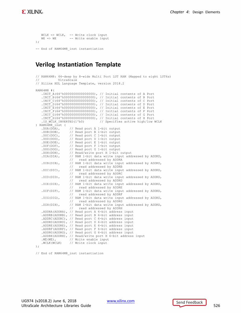
Chapter 4: Design Elements
WCLK => WCLK, -- Write clock inputWE => WE -- Write enable input
);
-- End of RAM64M8_inst instantiation
Verilog Instantiation Template
// RAM64M8: 64-deep by 8-wide Multi Port LUT RAM (Mapped to eight LUT6s)// UltraScale// Xilinx HDL Language Template, version 2018.2
RAM64M8 #(.INIT_A(64'h0000000000000000), // Initial contents of A Port.INIT_B(64'h0000000000000000), // Initial contents of B Port.INIT_C(64'h0000000000000000), // Initial contents of C Port.INIT_D(64'h0000000000000000), // Initial contents of D Port.INIT_E(64'h0000000000000000), // Initial contents of E Port.INIT_F(64'h0000000000000000), // Initial contents of F Port.INIT_G(64'h0000000000000000), // Initial contents of G Port.INIT_H(64'h0000000000000000), // Initial contents of H Port.IS_WCLK_INVERTED(1'b0) // Specifies active high/low WCLK
) RAM64M8_inst (.DOA(DOA), // Read port A 1-bit output.DOB(DOB), // Read port B 1-bit output.DOC(DOC), // Read port C 1-bit output.DOD(DOD), // Read port D 1-bit output.DOE(DOE), // Read port E 1-bit output.DOF(DOF), // Read port F 1-bit output.DOG(DOG), // Read port G 1-bit output.DOH(DOH), // Read/write port H 1-bit output.DIA(DIA), // RAM 1-bit data write input addressed by ADDRD,
// read addressed by ADDRA.DIB(DIB), // RAM 1-bit data write input addressed by ADDRD,
// read addressed by ADDRB.DIC(DIC), // RAM 1-bit data write input addressed by ADDRD,
// read addressed by ADDRC.DID(DID), // RAM 1-bit data write input addressed by ADDRD,
// read addressed by ADDRD.DIE(DIE), // RAM 1-bit data write input addressed by ADDRD,
// read addressed by ADDRE.DIF(DIF), // RAM 1-bit data write input addressed by ADDRD,
// read addressed by ADDRF.DIG(DIG), // RAM 1-bit data write input addressed by ADDRD,
// read addressed by ADDRG.DIH(DIH), // RAM 1-bit data write input addressed by ADDRD,
// read addressed by ADDRH.ADDRA(ADDRA), // Read port A 6-bit address input.ADDRB(ADDRB), // Read port B 6-bit address input.ADDRC(ADDRC), // Read port C 6-bit address input.ADDRD(ADDRD), // Read port D 6-bit address input.ADDRE(ADDRE), // Read port E 6-bit address input.ADDRF(ADDRF), // Read port F 6-bit address input.ADDRG(ADDRG), // Read port G 6-bit address input.ADDRH(ADDRH), // Read/write port H 6-bit address input.WE(WE), // Write enable input.WCLK(WCLK) // Write clock input
);
// End of RAM64M8_inst instantiation
UG974 (v2018.2) June 6, 2018 www.xilinx.comUltraScale Architecture Libraries Guide 526
Send Feedback

Chapter 4: Design Elements
For More Information• See the UltraScale Architecture Configurable Logic Block User Guide (UG574).
• See the UltraScale Programmable Devices Documentation.
UG974 (v2018.2) June 6, 2018 www.xilinx.comUltraScale Architecture Libraries Guide 527
Send Feedback
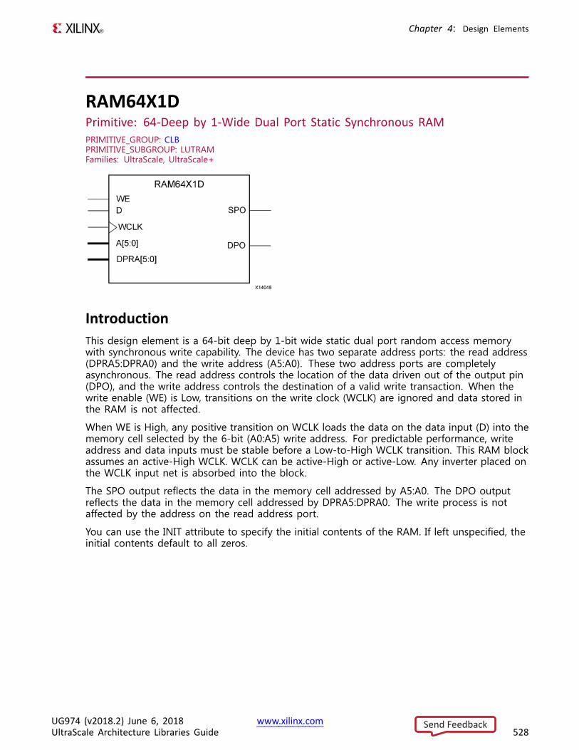
Chapter 4: Design Elements
RAM64X1DPrimitive: 64-Deep by 1-Wide Dual Port Static Synchronous RAMPRIMITIVE_GROUP: CLBPRIMITIVE_SUBGROUP: LUTRAMFamilies: UltraScale, UltraScale+
IntroductionThis design element is a 64-bit deep by 1-bit wide static dual port random access memorywith synchronous write capability. The device has two separate address ports: the read address(DPRA5:DPRA0) and the write address (A5:A0). These two address ports are completelyasynchronous. The read address controls the location of the data driven out of the output pin(DPO), and the write address controls the destination of a valid write transaction. When thewrite enable (WE) is Low, transitions on the write clock (WCLK) are ignored and data stored inthe RAM is not affected.
When WE is High, any positive transition on WCLK loads the data on the data input (D) into thememory cell selected by the 6-bit (A0:A5) write address. For predictable performance, writeaddress and data inputs must be stable before a Low-to-High WCLK transition. This RAM blockassumes an active-High WCLK. WCLK can be active-High or active-Low. Any inverter placed onthe WCLK input net is absorbed into the block.
The SPO output reflects the data in the memory cell addressed by A5:A0. The DPO outputreflects the data in the memory cell addressed by DPRA5:DPRA0. The write process is notaffected by the address on the read address port.
You can use the INIT attribute to specify the initial contents of the RAM. If left unspecified, theinitial contents default to all zeros.
UG974 (v2018.2) June 6, 2018 www.xilinx.comUltraScale Architecture Libraries Guide 528
Send Feedback
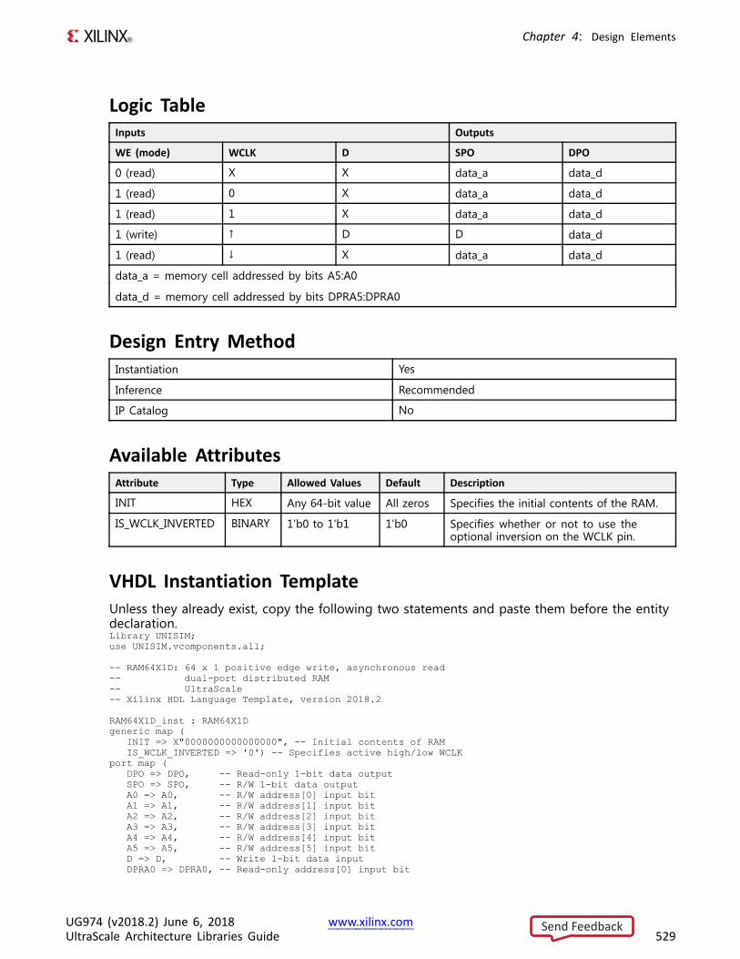
Chapter 4: Design Elements
Logic TableInputs Outputs
WE (mode) WCLK D SPO DPO
0 (read) X X data_a data_d
1 (read) 0 X data_a data_d
1 (read) 1 X data_a data_d
1 (write) ↑ D D data_d
1 (read) ↓ X data_a data_d
data_a = memory cell addressed by bits A5:A0
data_d = memory cell addressed by bits DPRA5:DPRA0
Design Entry MethodInstantiation Yes
Inference Recommended
IP Catalog No
Available AttributesAttribute Type Allowed Values Default Description
INIT HEX Any 64-bit value All zeros Specifies the initial contents of the RAM.
IS_WCLK_INVERTED BINARY 1'b0 to 1'b1 1'b0 Specifies whether or not to use theoptional inversion on the WCLK pin.
VHDL Instantiation TemplateUnless they already exist, copy the following two statements and paste them before the entitydeclaration.Library UNISIM;use UNISIM.vcomponents.all;
-- RAM64X1D: 64 x 1 positive edge write, asynchronous read-- dual-port distributed RAM-- UltraScale-- Xilinx HDL Language Template, version 2018.2
RAM64X1D_inst : RAM64X1Dgeneric map (
INIT => X"0000000000000000", -- Initial contents of RAMIS_WCLK_INVERTED => '0') -- Specifies active high/low WCLK
port map (DPO => DPO, -- Read-only 1-bit data outputSPO => SPO, -- R/W 1-bit data outputA0 => A0, -- R/W address[0] input bitA1 => A1, -- R/W address[1] input bitA2 => A2, -- R/W address[2] input bitA3 => A3, -- R/W address[3] input bitA4 => A4, -- R/W address[4] input bitA5 => A5, -- R/W address[5] input bitD => D, -- Write 1-bit data inputDPRA0 => DPRA0, -- Read-only address[0] input bit
UG974 (v2018.2) June 6, 2018 www.xilinx.comUltraScale Architecture Libraries Guide 529
Send Feedback
Chapter 4: Design Elements
DPRA1 => DPRA1, -- Read-only address[1] input bitDPRA2 => DPRA2, -- Read-only address[2] input bitDPRA3 => DPRA3, -- Read-only address[3] input bitDPRA4 => DPRA4, -- Read-only address[4] input bitDPRA5 => DPRA5, -- Read-only address[5] input bitWCLK => WCLK, -- Write clock inputWE => WE -- Write enable input
);
-- End of RAM64X1D_inst instantiation
Verilog Instantiation Template
// RAM64X1D: 64 x 1 positive edge write, asynchronous read dual-port// distributed RAM (Mapped to two LUT6s)// UltraScale// Xilinx HDL Language Template, version 2018.2
RAM64X1D #(.INIT(64'h0000000000000000), // Initial contents of RAM.IS_WCLK_INVERTED(1'b0) // Specifies active high/low WCLK
) RAM64X1D_inst (.DPO(DPO), // Read-only 1-bit data output.SPO(SPO), // Rw/ 1-bit data output.A0(A0), // Rw/ address[0] input bit.A1(A1), // Rw/ address[1] input bit.A2(A2), // Rw/ address[2] input bit.A3(A3), // Rw/ address[3] input bit.A4(A4), // Rw/ address[4] input bit.A5(A5), // Rw/ address[5] input bit.D(D), // Write 1-bit data input.DPRA0(DPRA0), // Read-only address[0] input bit.DPRA1(DPRA1), // Read-only address[1] input bit.DPRA2(DPRA2), // Read-only address[2] input bit.DPRA3(DPRA3), // Read-only address[3] input bit.DPRA4(DPRA4), // Read-only address[4] input bit.DPRA5(DPRA5), // Read-only address[5] input bit.WCLK(WCLK), // Write clock input.WE(WE) // Write enable input
);
// End of RAM64X1D_inst instantiation
For More Information• See the UltraScale Architecture Configurable Logic Block User Guide (UG574).
• See the UltraScale Programmable Devices Documentation.
UG974 (v2018.2) June 6, 2018 www.xilinx.comUltraScale Architecture Libraries Guide 530
Send Feedback
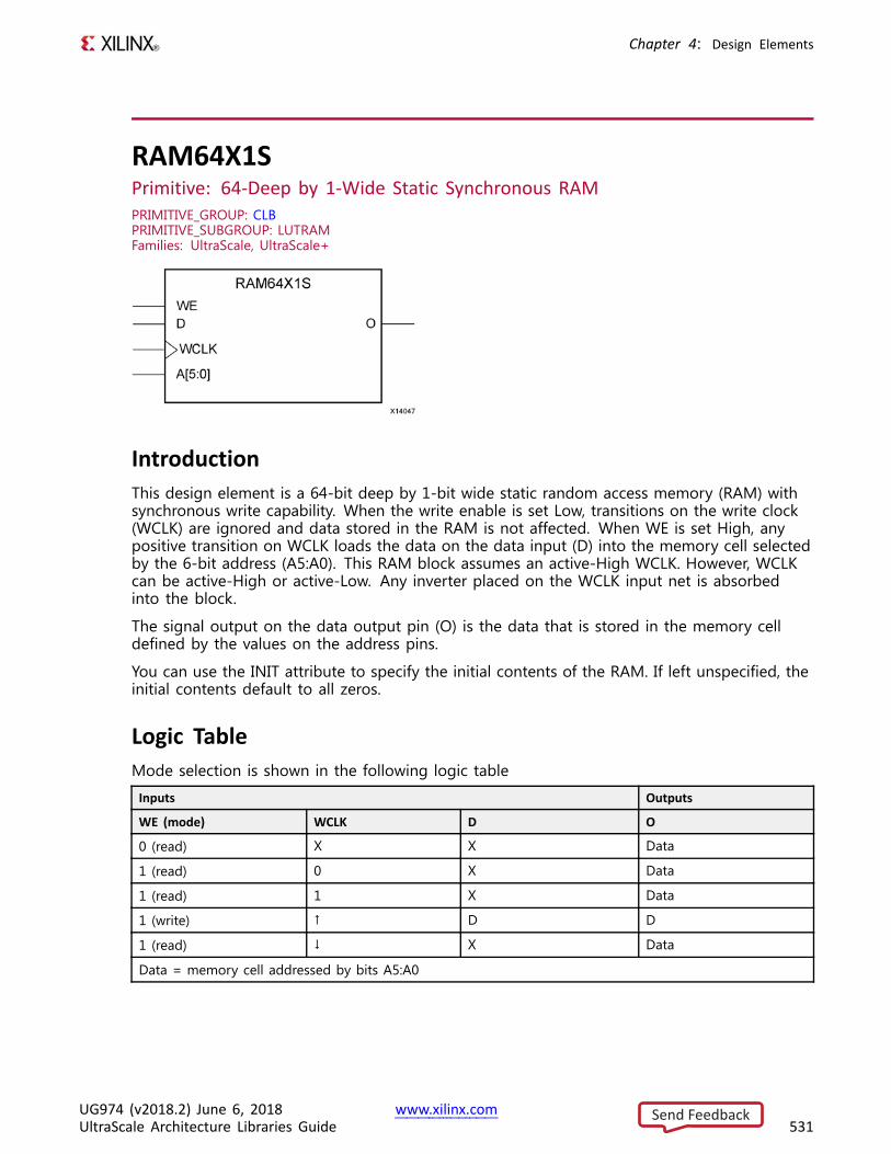
Chapter 4: Design Elements
RAM64X1SPrimitive: 64-Deep by 1-Wide Static Synchronous RAMPRIMITIVE_GROUP: CLBPRIMITIVE_SUBGROUP: LUTRAMFamilies: UltraScale, UltraScale+
IntroductionThis design element is a 64-bit deep by 1-bit wide static random access memory (RAM) withsynchronous write capability. When the write enable is set Low, transitions on the write clock(WCLK) are ignored and data stored in the RAM is not affected. When WE is set High, anypositive transition on WCLK loads the data on the data input (D) into the memory cell selectedby the 6-bit address (A5:A0). This RAM block assumes an active-High WCLK. However, WCLKcan be active-High or active-Low. Any inverter placed on the WCLK input net is absorbedinto the block.
The signal output on the data output pin (O) is the data that is stored in the memory celldefined by the values on the address pins.
You can use the INIT attribute to specify the initial contents of the RAM. If left unspecified, theinitial contents default to all zeros.
Logic TableMode selection is shown in the following logic table
Inputs Outputs
WE (mode) WCLK D O
0 (read) X X Data
1 (read) 0 X Data
1 (read) 1 X Data
1 (write) ↑ D D
1 (read) ↓ X Data
Data = memory cell addressed by bits A5:A0
UG974 (v2018.2) June 6, 2018 www.xilinx.comUltraScale Architecture Libraries Guide 531
Send Feedback

Chapter 4: Design Elements
Design Entry MethodInstantiation Yes
Inference Recommended
IP Catalog No
Available AttributesAttribute Type Allowed Values Default Description
INIT HEX Any 64-bit value All zeros Specifies the initial contents of the RAM.
IS_WCLK_INVERTED BINARY 1'b0 to 1'b1 1'b0 Specifies whether or not to use theoptional inversion on the WCLK pin.
VHDL Instantiation TemplateUnless they already exist, copy the following two statements and paste them before the entitydeclaration.Library UNISIM;use UNISIM.vcomponents.all;
-- RAM64X1S: 64 x 1 positive edge write, asynchronous read single-port distributed RAM-- UltraScale-- Xilinx HDL Language Template, version 2018.2
RAM64X1S_inst : RAM64X1Sgeneric map (
INIT => X"0000000000000000", -- Initial contents of RAMIS_WCLK_INVERTED => '0') -- Specifies active high/low WCLK
port map (O => O, -- 1-bit data outputA0 => A0, -- Address[0] input bitA1 => A1, -- Address[1] input bitA2 => A2, -- Address[2] input bitA3 => A3, -- Address[3] input bitA4 => A4, -- Address[4] input bitA5 => A5, -- Address[5] input bitD => D, -- 1-bit data inputWCLK => WCLK, -- Write clock inputWE => WE -- Write enable input
);
-- End of RAM64X1S_inst instantiation
Verilog Instantiation Template
// RAM64X1S: 64 x 1 positive edge write, asynchronous read single-port// distributed RAM (Mapped to a LUT6)// UltraScale// Xilinx HDL Language Template, version 2018.2
RAM64X1S #(.INIT(64'h0000000000000000), // Initial contents of RAM.IS_WCLK_INVERTED(1'b0) // Specifies active high/low WCLK
) RAM64X1S_inst (.O(O), // 1-bit data output.A0(A0), // Address[0] input bit.A1(A1), // Address[1] input bit.A2(A2), // Address[2] input bit
UG974 (v2018.2) June 6, 2018 www.xilinx.comUltraScale Architecture Libraries Guide 532
Send Feedback
Chapter 4: Design Elements
.A3(A3), // Address[3] input bit
.A4(A4), // Address[4] input bit
.A5(A5), // Address[5] input bit
.D(D), // 1-bit data input
.WCLK(WCLK), // Write clock input
.WE(WE) // Write enable input);
// End of RAM64X1S_inst instantiation
For More Information• See the UltraScale Architecture Configurable Logic Block User Guide (UG574).
• See the UltraScale Programmable Devices Documentation.
UG974 (v2018.2) June 6, 2018 www.xilinx.comUltraScale Architecture Libraries Guide 533
Send Feedback
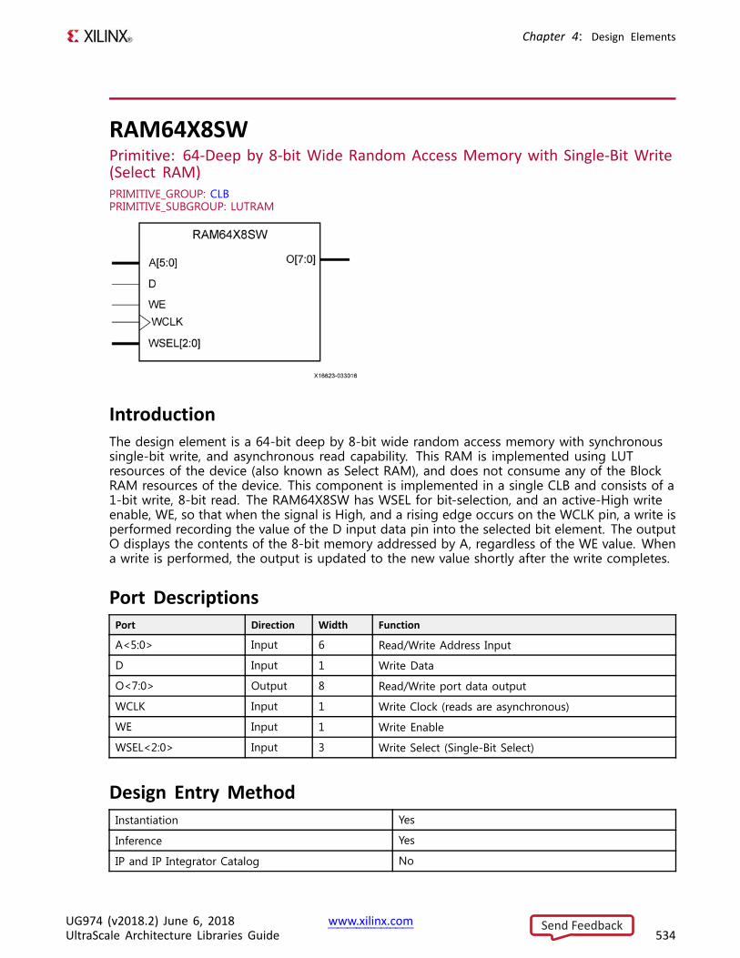
Chapter 4: Design Elements
RAM64X8SWPrimitive: 64-Deep by 8-bit Wide Random Access Memory with Single-Bit Write(Select RAM)PRIMITIVE_GROUP: CLBPRIMITIVE_SUBGROUP: LUTRAM
IntroductionThe design element is a 64-bit deep by 8-bit wide random access memory with synchronoussingle-bit write, and asynchronous read capability. This RAM is implemented using LUTresources of the device (also known as Select RAM), and does not consume any of the BlockRAM resources of the device. This component is implemented in a single CLB and consists of a1-bit write, 8-bit read. The RAM64X8SW has WSEL for bit-selection, and an active-High writeenable, WE, so that when the signal is High, and a rising edge occurs on the WCLK pin, a write isperformed recording the value of the D input data pin into the selected bit element. The outputO displays the contents of the 8-bit memory addressed by A, regardless of the WE value. Whena write is performed, the output is updated to the new value shortly after the write completes.
Port DescriptionsPort Direction Width Function
A<5:0> Input 6 Read/Write Address Input
D Input 1 Write Data
O<7:0> Output 8 Read/Write port data output
WCLK Input 1 Write Clock (reads are asynchronous)
WE Input 1 Write Enable
WSEL<2:0> Input 3 Write Select (Single-Bit Select)
Design Entry MethodInstantiation Yes
Inference Yes
IP and IP Integrator Catalog No
UG974 (v2018.2) June 6, 2018 www.xilinx.comUltraScale Architecture Libraries Guide 534
Send Feedback
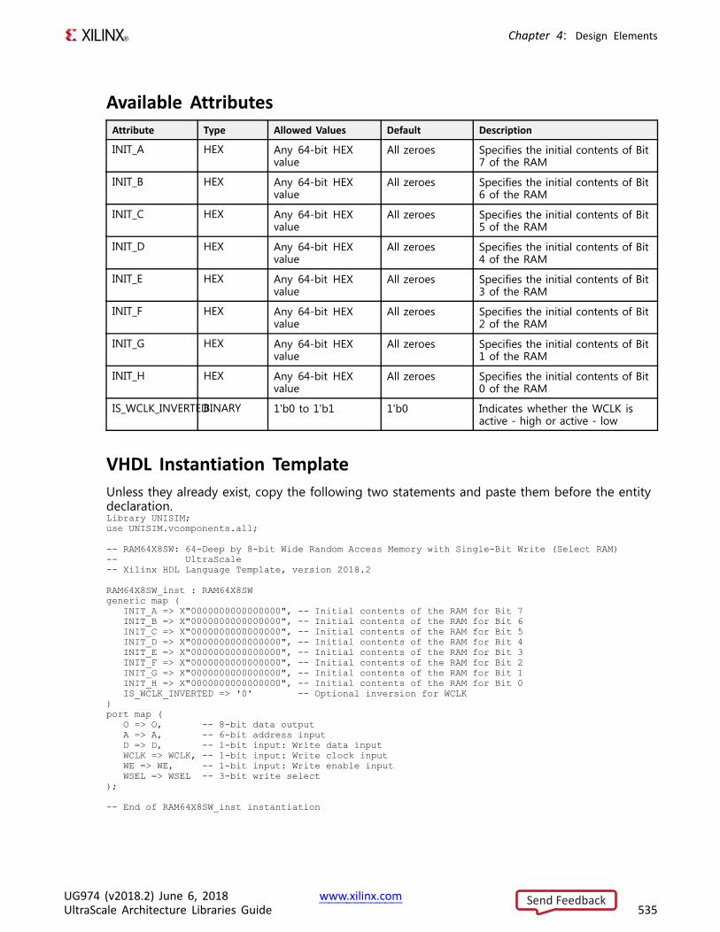
Chapter 4: Design Elements
Available AttributesAttribute Type Allowed Values Default Description
INIT_A HEX Any 64-bit HEXvalue
All zeroes Specifies the initial contents of Bit7 of the RAM
INIT_B HEX Any 64-bit HEXvalue
All zeroes Specifies the initial contents of Bit6 of the RAM
INIT_C HEX Any 64-bit HEXvalue
All zeroes Specifies the initial contents of Bit5 of the RAM
INIT_D HEX Any 64-bit HEXvalue
All zeroes Specifies the initial contents of Bit4 of the RAM
INIT_E HEX Any 64-bit HEXvalue
All zeroes Specifies the initial contents of Bit3 of the RAM
INIT_F HEX Any 64-bit HEXvalue
All zeroes Specifies the initial contents of Bit2 of the RAM
INIT_G HEX Any 64-bit HEXvalue
All zeroes Specifies the initial contents of Bit1 of the RAM
INIT_H HEX Any 64-bit HEXvalue
All zeroes Specifies the initial contents of Bit0 of the RAM
IS_WCLK_INVERTEDBINARY 1'b0 to 1'b1 1'b0 Indicates whether the WCLK isactive - high or active - low
VHDL Instantiation TemplateUnless they already exist, copy the following two statements and paste them before the entitydeclaration.Library UNISIM;use UNISIM.vcomponents.all;
-- RAM64X8SW: 64-Deep by 8-bit Wide Random Access Memory with Single-Bit Write (Select RAM)-- UltraScale-- Xilinx HDL Language Template, version 2018.2
RAM64X8SW_inst : RAM64X8SWgeneric map (
INIT_A => X"0000000000000000", -- Initial contents of the RAM for Bit 7INIT_B => X"0000000000000000", -- Initial contents of the RAM for Bit 6INIT_C => X"0000000000000000", -- Initial contents of the RAM for Bit 5INIT_D => X"0000000000000000", -- Initial contents of the RAM for Bit 4INIT_E => X"0000000000000000", -- Initial contents of the RAM for Bit 3INIT_F => X"0000000000000000", -- Initial contents of the RAM for Bit 2INIT_G => X"0000000000000000", -- Initial contents of the RAM for Bit 1INIT_H => X"0000000000000000", -- Initial contents of the RAM for Bit 0IS_WCLK_INVERTED => '0' -- Optional inversion for WCLK
)port map (
O => O, -- 8-bit data outputA => A, -- 6-bit address inputD => D, -- 1-bit input: Write data inputWCLK => WCLK, -- 1-bit input: Write clock inputWE => WE, -- 1-bit input: Write enable inputWSEL => WSEL -- 3-bit write select
);
-- End of RAM64X8SW_inst instantiation
UG974 (v2018.2) June 6, 2018 www.xilinx.comUltraScale Architecture Libraries Guide 535
Send Feedback
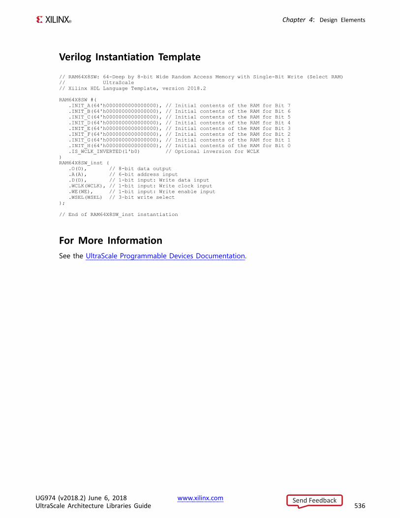
Chapter 4: Design Elements
Verilog Instantiation Template
// RAM64X8SW: 64-Deep by 8-bit Wide Random Access Memory with Single-Bit Write (Select RAM)// UltraScale// Xilinx HDL Language Template, version 2018.2
RAM64X8SW #(.INIT_A(64'h0000000000000000), // Initial contents of the RAM for Bit 7.INIT_B(64'h0000000000000000), // Initial contents of the RAM for Bit 6.INIT_C(64'h0000000000000000), // Initial contents of the RAM for Bit 5.INIT_D(64'h0000000000000000), // Initial contents of the RAM for Bit 4.INIT_E(64'h0000000000000000), // Initial contents of the RAM for Bit 3.INIT_F(64'h0000000000000000), // Initial contents of the RAM for Bit 2.INIT_G(64'h0000000000000000), // Initial contents of the RAM for Bit 1.INIT_H(64'h0000000000000000), // Initial contents of the RAM for Bit 0.IS_WCLK_INVERTED(1'b0) // Optional inversion for WCLK
)RAM64X8SW_inst (
.O(O), // 8-bit data output
.A(A), // 6-bit address input
.D(D), // 1-bit input: Write data input
.WCLK(WCLK), // 1-bit input: Write clock input
.WE(WE), // 1-bit input: Write enable input
.WSEL(WSEL) // 3-bit write select);
// End of RAM64X8SW_inst instantiation
For More InformationSee the UltraScale Programmable Devices Documentation.
UG974 (v2018.2) June 6, 2018 www.xilinx.comUltraScale Architecture Libraries Guide 536
Send Feedback
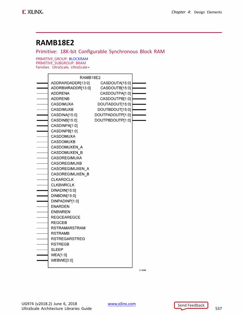
Chapter 4: Design Elements
RAMB18E2Primitive: 18K-bit Configurable Synchronous Block RAMPRIMITIVE_GROUP: BLOCKRAMPRIMITIVE_SUBGROUP: BRAMFamilies: UltraScale, UltraScale+
UG974 (v2018.2) June 6, 2018 www.xilinx.comUltraScale Architecture Libraries Guide 537
Send Feedback
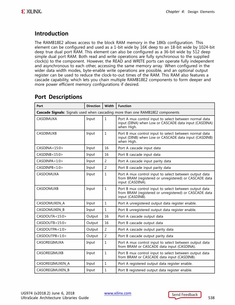
Chapter 4: Design Elements
IntroductionThe RAMB18E2 allows access to the block RAM memory in the 18Kb configuration. Thiselement can be configured and used as a 1-bit wide by 16K deep to an 18-bit wide by 1024-bitdeep true dual port RAM. This element can also be configured as a 36-bit wide by 512 deepsimple dual port RAM. Both read and write operations are fully synchronous to the suppliedclock(s) to the component. However, the READ and WRITE ports can operate fully independentand asynchronous to each other, accessing the same memory array. When configured in thewider data width modes, byte-enable write operations are possible, and an optional outputregister can be used to reduce the clock-to-out times of the RAM. This RAM also features acascade capability, which lets you chain multiple RAMB18E2 components to form deeper andmore power efficient memory configurations if desired.
Port DescriptionsPort Direction Width Function
Cascade Signals: Signals used when cascading more than one RAMB18E2 components
CASDIMUXA Input 1 Port A mux control input to select between normal datainput (DINA) when Low or CASCADE data input (CASDINA)when High.
CASDIMUXB Input 1 Port B mux control input to select between normal datainput (DINB) when Low or CASCADE data input (CASDINB)when High.
CASDINA<15:0> Input 16 Port A cascade input data
CASDINB<15:0> Input 16 Port B cascade input data
CASDINPA<1:0> Input 2 Port A cascade input parity data
CASDINPB<1:0> Input 2 Port B cascade input parity data
CASDOMUXA Input 1 Port A mux control input to select between output datafrom BRAM (registered or unregistered) or CASCADE datainput (CASDINA).
CASDOMUXB Input 1 Port B mux control input to select between output datafrom BRAM (registered or unregistered) or CASCADE datainput (CASDINB).
CASDOMUXEN_A Input 1 Port A unregistered output data register enable.
CASDOMUXEN_B Input 1 Port B unregistered output data register enable.
CASDOUTA<15:0> Output 16 Port A cascade output data
CASDOUTB<15:0> Output 16 Port B cascade output data
CASDOUTPA<1:0> Output 2 Port A cascade output parity data
CASDOUTPB<1:0> Output 2 Port B cascade output parity data
CASOREGIMUXA Input 1 Port A mux control input to select between output datafrom BRAM or CASCADE data input (CASDINA).
CASOREGIMUXB Input 1 Port B mux control input to select between output datafrom BRAM or CASCADE data input (CASDINB).
CASOREGIMUXEN_A Input 1 Port A registered output data register enable.
CASOREGIMUXEN_B Input 1 Port B registered output data register enable.
UG974 (v2018.2) June 6, 2018 www.xilinx.comUltraScale Architecture Libraries Guide 538
Send Feedback
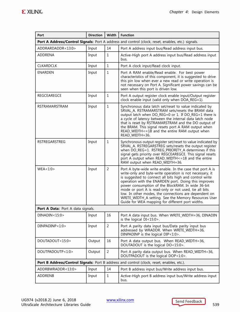
Chapter 4: Design Elements
Port Direction Width Function
Port A Address/Control Signals: Port A address and control (clock, reset, enables, etc.) signals.
ADDRARDADDR<13:0> Input 14 Port A address input bus/Read address input bus.
ADDRENA Input 1 Active-High port A address input bus/Read address inputbus.
CLKARDCLK Input 1 Port A clock input/Read clock input.
ENARDEN Input 1 Port A RAM enable/Read enable. For best powercharacteristics of this component, it is suggested to drivethis pin low when ever a new read or write operation isnot necessary on Port A. Significant power savings can beseen when this port is driven low.
REGCEAREGCE Input 1 Port A output register clock enable input/Output registerclock enable input (valid only when DOA_REG=1).
RSTRAMARSTRAM Input 1 Synchronous data latch set/reset to value indicated bySRVAL_A. RSTRAMARSTRAM sets/resets the BRAM dataoutput latch when DO_REG=0 or 1. If DO_REG=1 there isa cycle of latency between the internal data latch nodethat is reset by RSTRAMARSTRAM and the DO output ofthe BRAM. This signal resets port A RAM output whenREAD_WIDTH<=18 and the entire RAM output whenREAD_WIDTH=36.
RSTREGARSTREG Input 1 Synchronous output register set/reset to value indicated bySRVAL_A. RSTREGARSTREG sets/resets the output registerwhen DO_REG=1. RSTREG_PRIORITY_A determines if thissignal gets priority over REGCEAREGCE. This signal resetsport A output when READ_WIDTH<=18 and the entireRAM output when READ_WIDTH=36.
WEA<1:0> Input 2 Port A byte-wide write enable. In the case that port A iswrite-only and byte-write operation is not necessary, itis suggested to connect all bits high and control writeoperation with the ENARDEN port. Doing this improvespower consumption of the BlockRAM. In wide 36-bitmode or port A is read-only or not used, tie all bitslow. In other modes, the connections are dependent onWRITE_WIDTH_A setting. See the Memory Resources UserGuide for WEA mapping for different port widths.
Port A Data: Port A data signals.
DINADIN<15:0> Input 16 Port A data input bus. When WRITE_WIDTH=36, DINADINis the logical DI<15:0>.
DINPADINP<1:0> Input 2 Port A parity data input bus/Data parity input busaddressed by WRADDR. When WRITE_WIDTH=36,DINPADINP is the logical DIP<1:0>.
DOUTADOUT<15:0> Output 16 Port A data output bus. When READ_WIDTH=36,DOUTADOUT is the logical DO<15:0>.
DOUTPADOUTP<1:0> Output 2 Port A parity data output bus. When READ_WIDTH=36,DOUTPADOUT is the logical DOP<1:0>.
Port B Address/Control Signals: Port B address and control (clock, reset, enables, etc.).
ADDRBWRADDR<13:0> Input 14 Port B address input bus/Write address input bus.
ADDRENB Input 1 Active-High port B address input bus/Write address inputbus.
UG974 (v2018.2) June 6, 2018 www.xilinx.comUltraScale Architecture Libraries Guide 539
Send Feedback
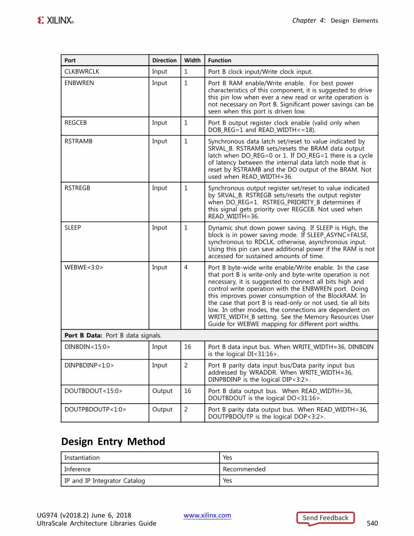
Chapter 4: Design Elements
Port Direction Width Function
CLKBWRCLK Input 1 Port B clock input/Write clock input.
ENBWREN Input 1 Port B RAM enable/Write enable. For best powercharacteristics of this component, it is suggested to drivethis pin low when ever a new read or write operation isnot necessary on Port B. Significant power savings can beseen when this port is driven low.
REGCEB Input 1 Port B output register clock enable (valid only whenDOB_REG=1 and READ_WIDTH<=18).
RSTRAMB Input 1 Synchronous data latch set/reset to value indicated bySRVAL_B. RSTRAMB sets/resets the BRAM data outputlatch when DO_REG=0 or 1. If DO_REG=1 there is a cycleof latency between the internal data latch node that isreset by RSTRAMB and the DO output of the BRAM. Notused when READ_WIDTH=36.
RSTREGB Input 1 Synchronous output register set/reset to value indicatedby SRVAL_B. RSTREGB sets/resets the output registerwhen DO_REG=1. RSTREG_PRIORITY_B determines ifthis signal gets priority over REGCEB. Not used whenREAD_WIDTH=36.
SLEEP Input 1 Dynamic shut down power saving. If SLEEP is High, theblock is in power saving mode. If SLEEP_ASYNC=FALSE,synchronous to RDCLK, otherwise, asynchronous input.Using this pin can save additional power if the RAM is notaccessed for sustained amounts of time.
WEBWE<3:0> Input 4 Port B byte-wide write enable/Write enable. In the casethat port B is write-only and byte-write operation is notnecessary, it is suggested to connect all bits high andcontrol write operation with the ENBWREN port. Doingthis improves power consumption of the BlockRAM. Inthe case that port B is read-only or not used, tie all bitslow. In other modes, the connections are dependent onWRITE_WIDTH_B setting. See the Memory Resources UserGuide for WEBWE mapping for different port widths.
Port B Data: Port B data signals.
DINBDIN<15:0> Input 16 Port B data input bus. When WRITE_WIDTH=36, DINBDINis the logical DI<31:16>.
DINPBDINP<1:0> Input 2 Port B parity data input bus/Data parity input busaddressed by WRADDR. When WRITE_WIDTH=36,DINPBDINP is the logical DIP<3:2>.
DOUTBDOUT<15:0> Output 16 Port B data output bus. When READ_WIDTH=36,DOUTBDOUT is the logical DO<31:16>.
DOUTPBDOUTP<1:0> Output 2 Port B parity data output bus. When READ_WIDTH=36,DOUTPBDOUTP is the logical DOP<3:2>.
Design Entry MethodInstantiation Yes
Inference Recommended
IP and IP Integrator Catalog Yes
UG974 (v2018.2) June 6, 2018 www.xilinx.comUltraScale Architecture Libraries Guide 540
Send Feedback
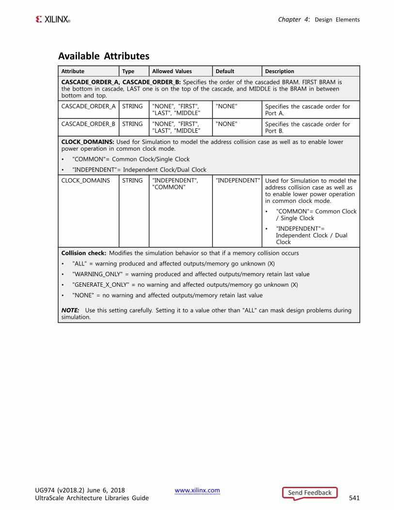
Chapter 4: Design Elements
Available AttributesAttribute Type Allowed Values Default Description
CASCADE_ORDER_A, CASCADE_ORDER_B: Specifies the order of the cascaded BRAM. FIRST BRAM isthe bottom in cascade, LAST one is on the top of the cascade, and MIDDLE is the BRAM in betweenbottom and top.
CASCADE_ORDER_A STRING "NONE", "FIRST","LAST", "MIDDLE"
"NONE" Specifies the cascade order forPort A.
CASCADE_ORDER_B STRING "NONE", "FIRST","LAST", "MIDDLE"
"NONE" Specifies the cascade order forPort B.
CLOCK_DOMAINS: Used for Simulation to model the address collision case as well as to enable lowerpower operation in common clock mode.
• "COMMON"= Common Clock/Single Clock
• "INDEPENDENT"= Independent Clock/Dual Clock
CLOCK_DOMAINS STRING "INDEPENDENT","COMMON"
"INDEPENDENT" Used for Simulation to model theaddress collision case as well asto enable lower power operationin common clock mode.
• "COMMON"= Common Clock/ Single Clock
• "INDEPENDENT"=Independent Clock / DualClock
Collision check: Modifies the simulation behavior so that if a memory collision occurs
• "ALL" = warning produced and affected outputs/memory go unknown (X)
• "WARNING_ONLY" = warning produced and affected outputs/memory retain last value
• "GENERATE_X_ONLY" = no warning and affected outputs/memory go unknown (X)
• "NONE" = no warning and affected outputs/memory retain last value
NOTE: Use this setting carefully. Setting it to a value other than "ALL" can mask design problems duringsimulation.
UG974 (v2018.2) June 6, 2018 www.xilinx.comUltraScale Architecture Libraries Guide 541
Send Feedback
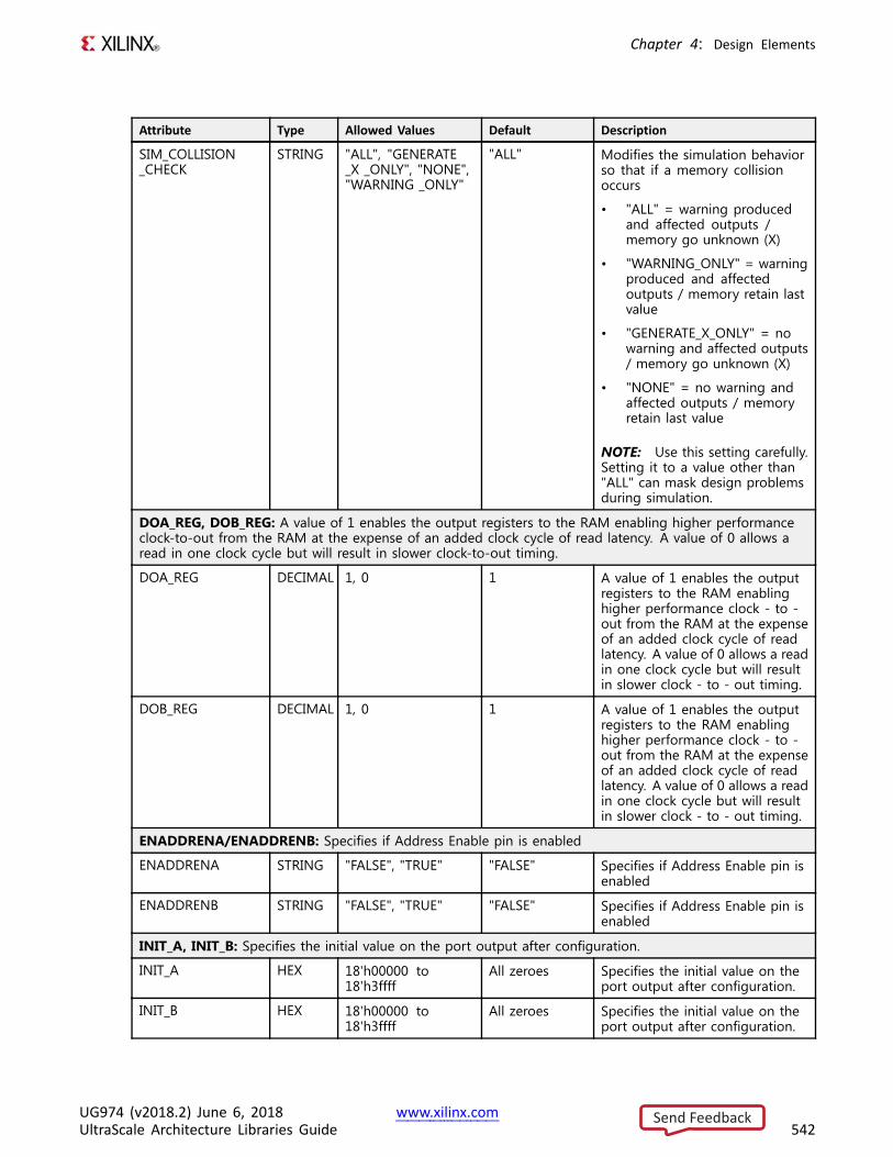
Chapter 4: Design Elements
Attribute Type Allowed Values Default Description
SIM_COLLISION_CHECK
STRING "ALL", "GENERATE_X _ONLY", "NONE","WARNING _ONLY"
"ALL" Modifies the simulation behaviorso that if a memory collisionoccurs
• "ALL" = warning producedand affected outputs /memory go unknown (X)
• "WARNING_ONLY" = warningproduced and affectedoutputs / memory retain lastvalue
• "GENERATE_X_ONLY" = nowarning and affected outputs/ memory go unknown (X)
• "NONE" = no warning andaffected outputs / memoryretain last value
NOTE: Use this setting carefully.Setting it to a value other than"ALL" can mask design problemsduring simulation.
DOA_REG, DOB_REG: A value of 1 enables the output registers to the RAM enabling higher performanceclock-to-out from the RAM at the expense of an added clock cycle of read latency. A value of 0 allows aread in one clock cycle but will result in slower clock-to-out timing.
DOA_REG DECIMAL 1, 0 1 A value of 1 enables the outputregisters to the RAM enablinghigher performance clock - to -out from the RAM at the expenseof an added clock cycle of readlatency. A value of 0 allows a readin one clock cycle but will resultin slower clock - to - out timing.
DOB_REG DECIMAL 1, 0 1 A value of 1 enables the outputregisters to the RAM enablinghigher performance clock - to -out from the RAM at the expenseof an added clock cycle of readlatency. A value of 0 allows a readin one clock cycle but will resultin slower clock - to - out timing.
ENADDRENA/ENADDRENB: Specifies if Address Enable pin is enabled
ENADDRENA STRING "FALSE", "TRUE" "FALSE" Specifies if Address Enable pin isenabled
ENADDRENB STRING "FALSE", "TRUE" "FALSE" Specifies if Address Enable pin isenabled
INIT_A, INIT_B: Specifies the initial value on the port output after configuration.
INIT_A HEX 18'h00000 to18'h3ffff
All zeroes Specifies the initial value on theport output after configuration.
INIT_B HEX 18'h00000 to18'h3ffff
All zeroes Specifies the initial value on theport output after configuration.
UG974 (v2018.2) June 6, 2018 www.xilinx.comUltraScale Architecture Libraries Guide 542
Send Feedback
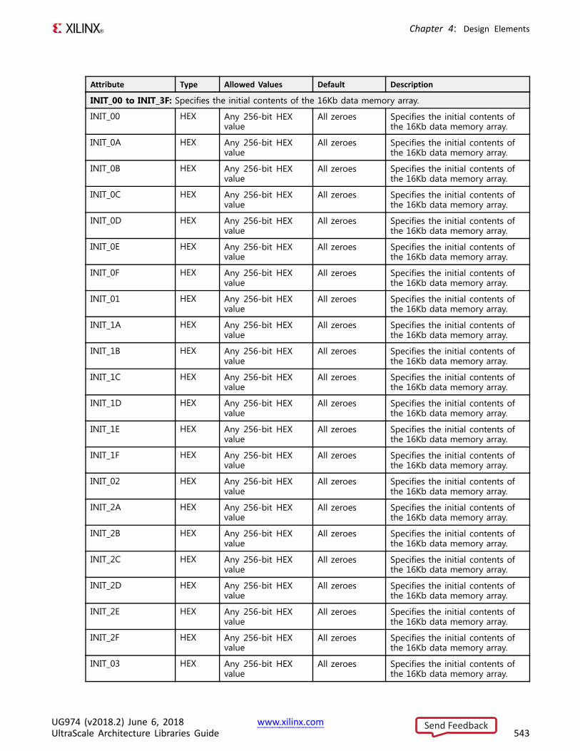
Chapter 4: Design Elements
Attribute Type Allowed Values Default Description
INIT_00 to INIT_3F: Specifies the initial contents of the 16Kb data memory array.
INIT_00 HEX Any 256-bit HEXvalue
All zeroes Specifies the initial contents ofthe 16Kb data memory array.
INIT_0A HEX Any 256-bit HEXvalue
All zeroes Specifies the initial contents ofthe 16Kb data memory array.
INIT_0B HEX Any 256-bit HEXvalue
All zeroes Specifies the initial contents ofthe 16Kb data memory array.
INIT_0C HEX Any 256-bit HEXvalue
All zeroes Specifies the initial contents ofthe 16Kb data memory array.
INIT_0D HEX Any 256-bit HEXvalue
All zeroes Specifies the initial contents ofthe 16Kb data memory array.
INIT_0E HEX Any 256-bit HEXvalue
All zeroes Specifies the initial contents ofthe 16Kb data memory array.
INIT_0F HEX Any 256-bit HEXvalue
All zeroes Specifies the initial contents ofthe 16Kb data memory array.
INIT_01 HEX Any 256-bit HEXvalue
All zeroes Specifies the initial contents ofthe 16Kb data memory array.
INIT_1A HEX Any 256-bit HEXvalue
All zeroes Specifies the initial contents ofthe 16Kb data memory array.
INIT_1B HEX Any 256-bit HEXvalue
All zeroes Specifies the initial contents ofthe 16Kb data memory array.
INIT_1C HEX Any 256-bit HEXvalue
All zeroes Specifies the initial contents ofthe 16Kb data memory array.
INIT_1D HEX Any 256-bit HEXvalue
All zeroes Specifies the initial contents ofthe 16Kb data memory array.
INIT_1E HEX Any 256-bit HEXvalue
All zeroes Specifies the initial contents ofthe 16Kb data memory array.
INIT_1F HEX Any 256-bit HEXvalue
All zeroes Specifies the initial contents ofthe 16Kb data memory array.
INIT_02 HEX Any 256-bit HEXvalue
All zeroes Specifies the initial contents ofthe 16Kb data memory array.
INIT_2A HEX Any 256-bit HEXvalue
All zeroes Specifies the initial contents ofthe 16Kb data memory array.
INIT_2B HEX Any 256-bit HEXvalue
All zeroes Specifies the initial contents ofthe 16Kb data memory array.
INIT_2C HEX Any 256-bit HEXvalue
All zeroes Specifies the initial contents ofthe 16Kb data memory array.
INIT_2D HEX Any 256-bit HEXvalue
All zeroes Specifies the initial contents ofthe 16Kb data memory array.
INIT_2E HEX Any 256-bit HEXvalue
All zeroes Specifies the initial contents ofthe 16Kb data memory array.
INIT_2F HEX Any 256-bit HEXvalue
All zeroes Specifies the initial contents ofthe 16Kb data memory array.
INIT_03 HEX Any 256-bit HEXvalue
All zeroes Specifies the initial contents ofthe 16Kb data memory array.
UG974 (v2018.2) June 6, 2018 www.xilinx.comUltraScale Architecture Libraries Guide 543
Send Feedback
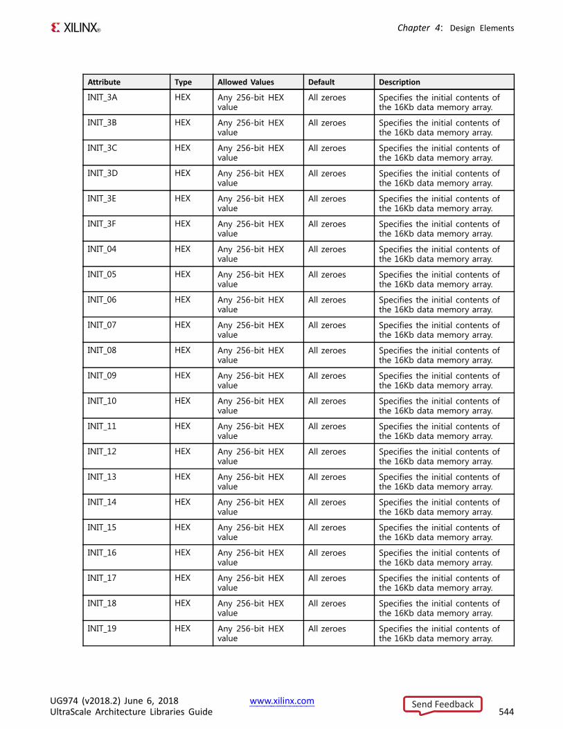
Chapter 4: Design Elements
Attribute Type Allowed Values Default Description
INIT_3A HEX Any 256-bit HEXvalue
All zeroes Specifies the initial contents ofthe 16Kb data memory array.
INIT_3B HEX Any 256-bit HEXvalue
All zeroes Specifies the initial contents ofthe 16Kb data memory array.
INIT_3C HEX Any 256-bit HEXvalue
All zeroes Specifies the initial contents ofthe 16Kb data memory array.
INIT_3D HEX Any 256-bit HEXvalue
All zeroes Specifies the initial contents ofthe 16Kb data memory array.
INIT_3E HEX Any 256-bit HEXvalue
All zeroes Specifies the initial contents ofthe 16Kb data memory array.
INIT_3F HEX Any 256-bit HEXvalue
All zeroes Specifies the initial contents ofthe 16Kb data memory array.
INIT_04 HEX Any 256-bit HEXvalue
All zeroes Specifies the initial contents ofthe 16Kb data memory array.
INIT_05 HEX Any 256-bit HEXvalue
All zeroes Specifies the initial contents ofthe 16Kb data memory array.
INIT_06 HEX Any 256-bit HEXvalue
All zeroes Specifies the initial contents ofthe 16Kb data memory array.
INIT_07 HEX Any 256-bit HEXvalue
All zeroes Specifies the initial contents ofthe 16Kb data memory array.
INIT_08 HEX Any 256-bit HEXvalue
All zeroes Specifies the initial contents ofthe 16Kb data memory array.
INIT_09 HEX Any 256-bit HEXvalue
All zeroes Specifies the initial contents ofthe 16Kb data memory array.
INIT_10 HEX Any 256-bit HEXvalue
All zeroes Specifies the initial contents ofthe 16Kb data memory array.
INIT_11 HEX Any 256-bit HEXvalue
All zeroes Specifies the initial contents ofthe 16Kb data memory array.
INIT_12 HEX Any 256-bit HEXvalue
All zeroes Specifies the initial contents ofthe 16Kb data memory array.
INIT_13 HEX Any 256-bit HEXvalue
All zeroes Specifies the initial contents ofthe 16Kb data memory array.
INIT_14 HEX Any 256-bit HEXvalue
All zeroes Specifies the initial contents ofthe 16Kb data memory array.
INIT_15 HEX Any 256-bit HEXvalue
All zeroes Specifies the initial contents ofthe 16Kb data memory array.
INIT_16 HEX Any 256-bit HEXvalue
All zeroes Specifies the initial contents ofthe 16Kb data memory array.
INIT_17 HEX Any 256-bit HEXvalue
All zeroes Specifies the initial contents ofthe 16Kb data memory array.
INIT_18 HEX Any 256-bit HEXvalue
All zeroes Specifies the initial contents ofthe 16Kb data memory array.
INIT_19 HEX Any 256-bit HEXvalue
All zeroes Specifies the initial contents ofthe 16Kb data memory array.
UG974 (v2018.2) June 6, 2018 www.xilinx.comUltraScale Architecture Libraries Guide 544
Send Feedback
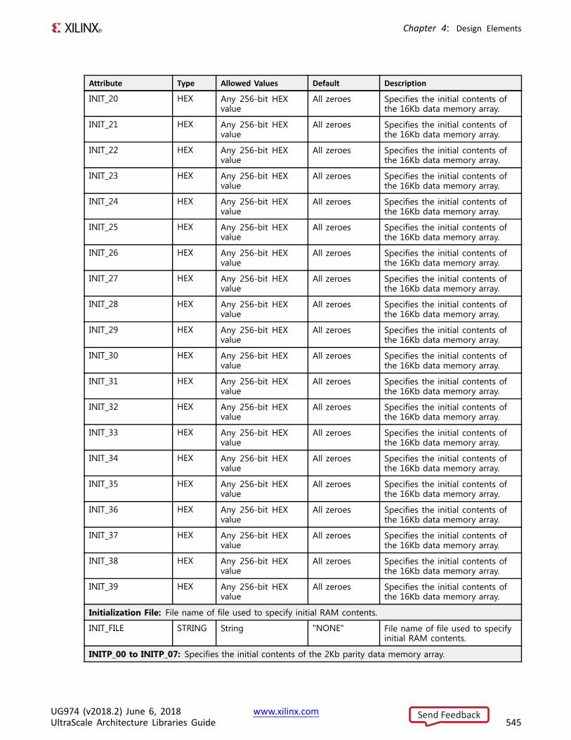
Chapter 4: Design Elements
Attribute Type Allowed Values Default Description
INIT_20 HEX Any 256-bit HEXvalue
All zeroes Specifies the initial contents ofthe 16Kb data memory array.
INIT_21 HEX Any 256-bit HEXvalue
All zeroes Specifies the initial contents ofthe 16Kb data memory array.
INIT_22 HEX Any 256-bit HEXvalue
All zeroes Specifies the initial contents ofthe 16Kb data memory array.
INIT_23 HEX Any 256-bit HEXvalue
All zeroes Specifies the initial contents ofthe 16Kb data memory array.
INIT_24 HEX Any 256-bit HEXvalue
All zeroes Specifies the initial contents ofthe 16Kb data memory array.
INIT_25 HEX Any 256-bit HEXvalue
All zeroes Specifies the initial contents ofthe 16Kb data memory array.
INIT_26 HEX Any 256-bit HEXvalue
All zeroes Specifies the initial contents ofthe 16Kb data memory array.
INIT_27 HEX Any 256-bit HEXvalue
All zeroes Specifies the initial contents ofthe 16Kb data memory array.
INIT_28 HEX Any 256-bit HEXvalue
All zeroes Specifies the initial contents ofthe 16Kb data memory array.
INIT_29 HEX Any 256-bit HEXvalue
All zeroes Specifies the initial contents ofthe 16Kb data memory array.
INIT_30 HEX Any 256-bit HEXvalue
All zeroes Specifies the initial contents ofthe 16Kb data memory array.
INIT_31 HEX Any 256-bit HEXvalue
All zeroes Specifies the initial contents ofthe 16Kb data memory array.
INIT_32 HEX Any 256-bit HEXvalue
All zeroes Specifies the initial contents ofthe 16Kb data memory array.
INIT_33 HEX Any 256-bit HEXvalue
All zeroes Specifies the initial contents ofthe 16Kb data memory array.
INIT_34 HEX Any 256-bit HEXvalue
All zeroes Specifies the initial contents ofthe 16Kb data memory array.
INIT_35 HEX Any 256-bit HEXvalue
All zeroes Specifies the initial contents ofthe 16Kb data memory array.
INIT_36 HEX Any 256-bit HEXvalue
All zeroes Specifies the initial contents ofthe 16Kb data memory array.
INIT_37 HEX Any 256-bit HEXvalue
All zeroes Specifies the initial contents ofthe 16Kb data memory array.
INIT_38 HEX Any 256-bit HEXvalue
All zeroes Specifies the initial contents ofthe 16Kb data memory array.
INIT_39 HEX Any 256-bit HEXvalue
All zeroes Specifies the initial contents ofthe 16Kb data memory array.
Initialization File: File name of file used to specify initial RAM contents.
INIT_FILE STRING String "NONE" File name of file used to specifyinitial RAM contents.
INITP_00 to INITP_07: Specifies the initial contents of the 2Kb parity data memory array.
UG974 (v2018.2) June 6, 2018 www.xilinx.comUltraScale Architecture Libraries Guide 545
Send Feedback
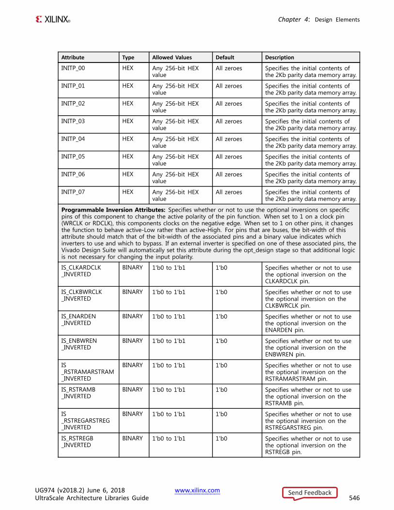
Chapter 4: Design Elements
Attribute Type Allowed Values Default Description
INITP_00 HEX Any 256-bit HEXvalue
All zeroes Specifies the initial contents ofthe 2Kb parity data memory array.
INITP_01 HEX Any 256-bit HEXvalue
All zeroes Specifies the initial contents ofthe 2Kb parity data memory array.
INITP_02 HEX Any 256-bit HEXvalue
All zeroes Specifies the initial contents ofthe 2Kb parity data memory array.
INITP_03 HEX Any 256-bit HEXvalue
All zeroes Specifies the initial contents ofthe 2Kb parity data memory array.
INITP_04 HEX Any 256-bit HEXvalue
All zeroes Specifies the initial contents ofthe 2Kb parity data memory array.
INITP_05 HEX Any 256-bit HEXvalue
All zeroes Specifies the initial contents ofthe 2Kb parity data memory array.
INITP_06 HEX Any 256-bit HEXvalue
All zeroes Specifies the initial contents ofthe 2Kb parity data memory array.
INITP_07 HEX Any 256-bit HEXvalue
All zeroes Specifies the initial contents ofthe 2Kb parity data memory array.
Programmable Inversion Attributes: Specifies whether or not to use the optional inversions on specificpins of this component to change the active polarity of the pin function. When set to 1 on a clock pin(WRCLK or RDCLK), this components clocks on the negative edge. When set to 1 on other pins, it changesthe function to behave active-Low rather than active-High. For pins that are buses, the bit-width of thisattribute should match that of the bit-width of the associated pins and a binary value indicates whichinverters to use and which to bypass. If an external inverter is specified on one of these associated pins, theVivado Design Suite will automatically set this attribute during the opt_design stage so that additional logicis not necessary for changing the input polarity.
IS_CLKARDCLK_INVERTED
BINARY 1'b0 to 1'b1 1'b0 Specifies whether or not to usethe optional inversion on theCLKARDCLK pin.
IS_CLKBWRCLK_INVERTED
BINARY 1'b0 to 1'b1 1'b0 Specifies whether or not to usethe optional inversion on theCLKBWRCLK pin.
IS_ENARDEN_INVERTED
BINARY 1'b0 to 1'b1 1'b0 Specifies whether or not to usethe optional inversion on theENARDEN pin.
IS_ENBWREN_INVERTED
BINARY 1'b0 to 1'b1 1'b0 Specifies whether or not to usethe optional inversion on theENBWREN pin.
IS_RSTRAMARSTRAM_INVERTED
BINARY 1'b0 to 1'b1 1'b0 Specifies whether or not to usethe optional inversion on theRSTRAMARSTRAM pin.
IS_RSTRAMB_INVERTED
BINARY 1'b0 to 1'b1 1'b0 Specifies whether or not to usethe optional inversion on theRSTRAMB pin.
IS_RSTREGARSTREG_INVERTED
BINARY 1'b0 to 1'b1 1'b0 Specifies whether or not to usethe optional inversion on theRSTREGARSTREG pin.
IS_RSTREGB_INVERTED
BINARY 1'b0 to 1'b1 1'b0 Specifies whether or not to usethe optional inversion on theRSTREGB pin.
UG974 (v2018.2) June 6, 2018 www.xilinx.comUltraScale Architecture Libraries Guide 546
Send Feedback
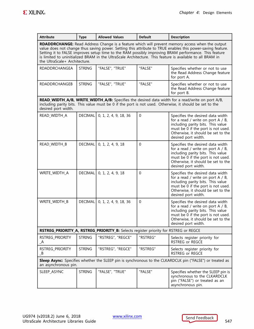
Chapter 4: Design Elements
Attribute Type Allowed Values Default Description
RDADDRCHANGE: Read Address Change is a feature which will prevent memory access when the outputvalue does not change thus saving power. Setting this attribute to TRUE enables this power-saving feature.Setting it to FALSE improves setup time to the RAM possibly improving BRAM performance. This featureis limited to uninitialized BRAM in the UltraScale Architecture. This feature is available to all BRAM inthe UltraScale+ Architecture.
RDADDRCHANGEA STRING "FALSE", "TRUE" "FALSE" Specifies whether or not to usethe Read Address Change featurefor port A.
RDADDRCHANGEB STRING "FALSE", "TRUE" "FALSE" Specifies whether or not to usethe Read Address Change featurefor port B.
READ_WIDTH_A/B, WRITE_WIDTH_A/B: Specifies the desired data width for a read/write on port A/B,including parity bits. This value must be 0 if the port is not used. Otherwise, it should be set to thedesired port width.
READ_WIDTH_A DECIMAL 0, 1, 2, 4, 9, 18, 36 0 Specifies the desired data widthfor a read / write on port A / B,including parity bits. This valuemust be 0 if the port is not used.Otherwise, it should be set to thedesired port width.
READ_WIDTH_B DECIMAL 0, 1, 2, 4, 9, 18 0 Specifies the desired data widthfor a read / write on port A / B,including parity bits. This valuemust be 0 if the port is not used.Otherwise, it should be set to thedesired port width.
WRITE_WIDTH_A DECIMAL 0, 1, 2, 4, 9, 18 0 Specifies the desired data widthfor a read / write on port A / B,including parity bits. This valuemust be 0 if the port is not used.Otherwise, it should be set to thedesired port width.
WRITE_WIDTH_B DECIMAL 0, 1, 2, 4, 9, 18, 36 0 Specifies the desired data widthfor a read / write on port A / B,including parity bits. This valuemust be 0 if the port is not used.Otherwise, it should be set to thedesired port width.
RSTREG_PRIORITY_A, RSTREG_PRIORITY_B: Selects register priority for RSTREG or REGCE
RSTREG_PRIORITY_A
STRING "RSTREG", "REGCE" "RSTREG" Selects register priority forRSTREG or REGCE
RSTREG_PRIORITY_B
STRING "RSTREG", "REGCE" "RSTREG" Selects register priority forRSTREG or REGCE
Sleep Async: Specifies whether the SLEEP pin is synchronous to the CLKARDCLK pin ("FALSE") or treated asan asynchronous pin.
SLEEP_ASYNC STRING "FALSE", "TRUE" "FALSE" Specifies whether the SLEEP pin issynchronous to the CLKARDCLKpin ("FALSE") or treated as anasynchronous pin.
UG974 (v2018.2) June 6, 2018 www.xilinx.comUltraScale Architecture Libraries Guide 547
Send Feedback
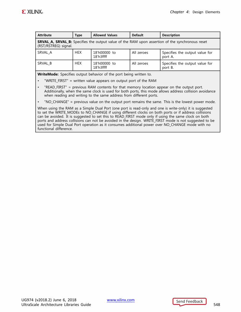
Chapter 4: Design Elements
Attribute Type Allowed Values Default Description
SRVAL_A, SRVAL_B: Specifies the output value of the RAM upon assertion of the synchronous reset(RST/RSTREG) signal.
SRVAL_A HEX 18'h00000 to18'h3ffff
All zeroes Specifies the output value forport A.
SRVAL_B HEX 18'h00000 to18'h3ffff
All zeroes Specifies the output value forport B.
WriteMode: Specifies output behavior of the port being written to.
• "WRITE_FIRST" = written value appears on output port of the RAM
• "READ_FIRST" = previous RAM contents for that memory location appear on the output port.Additionally, when the same clock is used for both ports, this mode allows address collision avoidancewhen reading and writing to the same address from different ports.
• "NO_CHANGE" = previous value on the output port remains the same. This is the lowest power mode.
When using the RAM as a Simple Dual Port (one port is read-only and one is write-only) it is suggestedto set the WRITE_MODEs to NO_CHANGE if using different clocks on both ports or if address collisionscan be avoided. It is suggested to set this to READ_FIRST mode only if using the same clock on bothports and address collisions can not be avoided in the design. WRITE_FIRST mode is not suggested to beused for Simple Dual Port operation as it consumes additional power over NO_CHANGE mode with nofunctional difference.
UG974 (v2018.2) June 6, 2018 www.xilinx.comUltraScale Architecture Libraries Guide 548
Send Feedback
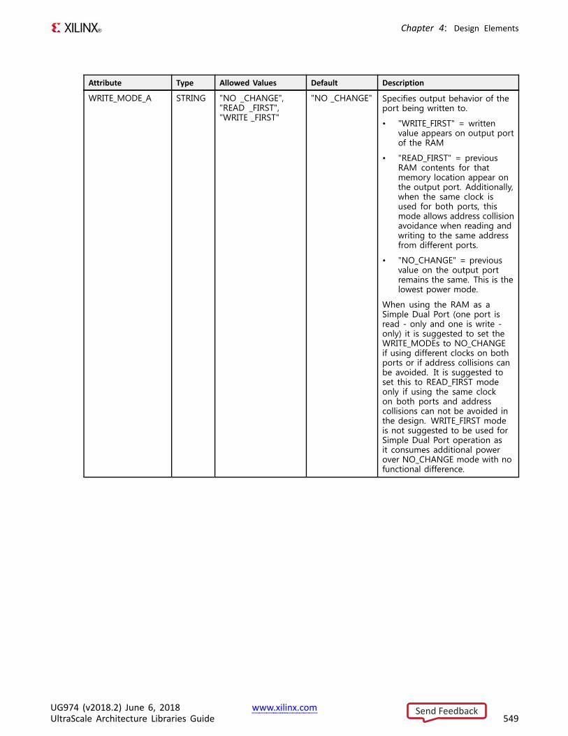
Chapter 4: Design Elements
Attribute Type Allowed Values Default Description
WRITE_MODE_A STRING "NO _CHANGE","READ _FIRST","WRITE _FIRST"
"NO _CHANGE" Specifies output behavior of theport being written to.
• "WRITE_FIRST" = writtenvalue appears on output portof the RAM
• "READ_FIRST" = previousRAM contents for thatmemory location appear onthe output port. Additionally,when the same clock isused for both ports, thismode allows address collisionavoidance when reading andwriting to the same addressfrom different ports.
• "NO_CHANGE" = previousvalue on the output portremains the same. This is thelowest power mode.
When using the RAM as aSimple Dual Port (one port isread - only and one is write -only) it is suggested to set theWRITE_MODEs to NO_CHANGEif using different clocks on bothports or if address collisions canbe avoided. It is suggested toset this to READ_FIRST modeonly if using the same clockon both ports and addresscollisions can not be avoided inthe design. WRITE_FIRST modeis not suggested to be used forSimple Dual Port operation asit consumes additional powerover NO_CHANGE mode with nofunctional difference.
UG974 (v2018.2) June 6, 2018 www.xilinx.comUltraScale Architecture Libraries Guide 549
Send Feedback

Chapter 4: Design Elements
Attribute Type Allowed Values Default Description
WRITE_MODE_B STRING "NO _CHANGE","READ _FIRST","WRITE _FIRST"
"NO _CHANGE" Specifies output behavior of theport being written to.
• "WRITE_FIRST" = writtenvalue appears on output portof the RAM
• "READ_FIRST" = previousRAM contents for thatmemory location appear onthe output port. Additionally,when the same clock isused for both ports, thismode allows address collisionavoidance when reading andwriting to the same addressfrom different ports.
• "NO_CHANGE" = previousvalue on the output portremains the same. This is thelowest power mode.
When using the RAM as aSimple Dual Port (one port isread - only and one is write -only) it is suggested to set theWRITE_MODEs to NO_CHANGEif using different clocks on bothports or if address collisions canbe avoided. It is suggested toset this to READ_FIRST modeonly if using the same clockon both ports and addresscollisions can not be avoided inthe design. WRITE_FIRST modeis not suggested to be used forSimple Dual Port operation asit consumes additional powerover NO_CHANGE mode with nofunctional difference.
VHDL Instantiation TemplateUnless they already exist, copy the following two statements and paste them before the entitydeclaration.Library UNISIM;use UNISIM.vcomponents.all;
-- RAMB18E2: 18K-bit Configurable Synchronous Block RAM-- UltraScale-- Xilinx HDL Language Template, version 2018.2
RAMB18E2_inst : RAMB18E2generic map (
-- CASCADE_ORDER_A, CASCADE_ORDER_B: "FIRST", "MIDDLE", "LAST", "NONE"CASCADE_ORDER_A => "NONE",CASCADE_ORDER_B => "NONE",-- CLOCK_DOMAINS: "COMMON", "INDEPENDENT"CLOCK_DOMAINS => "INDEPENDENT",-- Collision check: "ALL", "GENERATE_X_ONLY", "NONE", "WARNING_ONLY"SIM_COLLISION_CHECK => "ALL",
UG974 (v2018.2) June 6, 2018 www.xilinx.comUltraScale Architecture Libraries Guide 550
Send Feedback
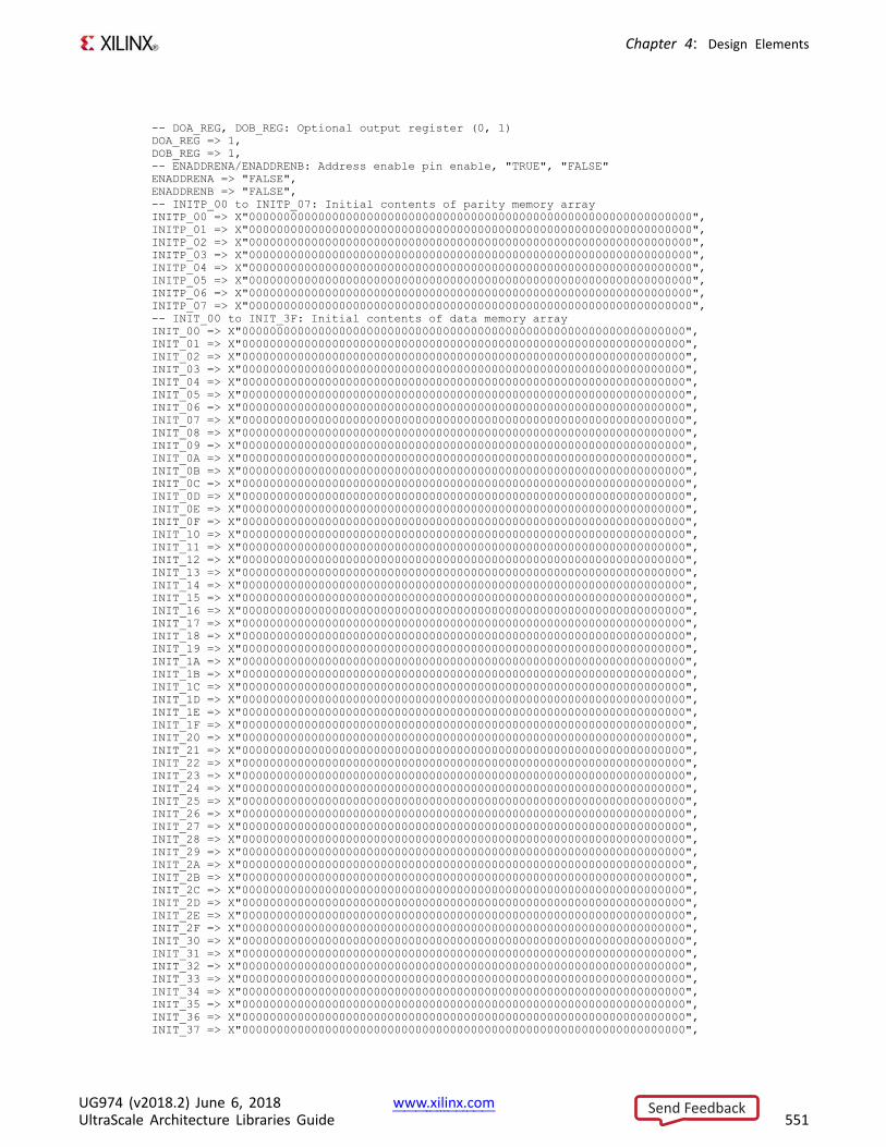
Chapter 4: Design Elements
-- DOA_REG, DOB_REG: Optional output register (0, 1)DOA_REG => 1,DOB_REG => 1,-- ENADDRENA/ENADDRENB: Address enable pin enable, "TRUE", "FALSE"ENADDRENA => "FALSE",ENADDRENB => "FALSE",-- INITP_00 to INITP_07: Initial contents of parity memory arrayINITP_00 => X"0000000000000000000000000000000000000000000000000000000000000000",INITP_01 => X"0000000000000000000000000000000000000000000000000000000000000000",INITP_02 => X"0000000000000000000000000000000000000000000000000000000000000000",INITP_03 => X"0000000000000000000000000000000000000000000000000000000000000000",INITP_04 => X"0000000000000000000000000000000000000000000000000000000000000000",INITP_05 => X"0000000000000000000000000000000000000000000000000000000000000000",INITP_06 => X"0000000000000000000000000000000000000000000000000000000000000000",INITP_07 => X"0000000000000000000000000000000000000000000000000000000000000000",-- INIT_00 to INIT_3F: Initial contents of data memory arrayINIT_00 => X"0000000000000000000000000000000000000000000000000000000000000000",INIT_01 => X"0000000000000000000000000000000000000000000000000000000000000000",INIT_02 => X"0000000000000000000000000000000000000000000000000000000000000000",INIT_03 => X"0000000000000000000000000000000000000000000000000000000000000000",INIT_04 => X"0000000000000000000000000000000000000000000000000000000000000000",INIT_05 => X"0000000000000000000000000000000000000000000000000000000000000000",INIT_06 => X"0000000000000000000000000000000000000000000000000000000000000000",INIT_07 => X"0000000000000000000000000000000000000000000000000000000000000000",INIT_08 => X"0000000000000000000000000000000000000000000000000000000000000000",INIT_09 => X"0000000000000000000000000000000000000000000000000000000000000000",INIT_0A => X"0000000000000000000000000000000000000000000000000000000000000000",INIT_0B => X"0000000000000000000000000000000000000000000000000000000000000000",INIT_0C => X"0000000000000000000000000000000000000000000000000000000000000000",INIT_0D => X"0000000000000000000000000000000000000000000000000000000000000000",INIT_0E => X"0000000000000000000000000000000000000000000000000000000000000000",INIT_0F => X"0000000000000000000000000000000000000000000000000000000000000000",INIT_10 => X"0000000000000000000000000000000000000000000000000000000000000000",INIT_11 => X"0000000000000000000000000000000000000000000000000000000000000000",INIT_12 => X"0000000000000000000000000000000000000000000000000000000000000000",INIT_13 => X"0000000000000000000000000000000000000000000000000000000000000000",INIT_14 => X"0000000000000000000000000000000000000000000000000000000000000000",INIT_15 => X"0000000000000000000000000000000000000000000000000000000000000000",INIT_16 => X"0000000000000000000000000000000000000000000000000000000000000000",INIT_17 => X"0000000000000000000000000000000000000000000000000000000000000000",INIT_18 => X"0000000000000000000000000000000000000000000000000000000000000000",INIT_19 => X"0000000000000000000000000000000000000000000000000000000000000000",INIT_1A => X"0000000000000000000000000000000000000000000000000000000000000000",INIT_1B => X"0000000000000000000000000000000000000000000000000000000000000000",INIT_1C => X"0000000000000000000000000000000000000000000000000000000000000000",INIT_1D => X"0000000000000000000000000000000000000000000000000000000000000000",INIT_1E => X"0000000000000000000000000000000000000000000000000000000000000000",INIT_1F => X"0000000000000000000000000000000000000000000000000000000000000000",INIT_20 => X"0000000000000000000000000000000000000000000000000000000000000000",INIT_21 => X"0000000000000000000000000000000000000000000000000000000000000000",INIT_22 => X"0000000000000000000000000000000000000000000000000000000000000000",INIT_23 => X"0000000000000000000000000000000000000000000000000000000000000000",INIT_24 => X"0000000000000000000000000000000000000000000000000000000000000000",INIT_25 => X"0000000000000000000000000000000000000000000000000000000000000000",INIT_26 => X"0000000000000000000000000000000000000000000000000000000000000000",INIT_27 => X"0000000000000000000000000000000000000000000000000000000000000000",INIT_28 => X"0000000000000000000000000000000000000000000000000000000000000000",INIT_29 => X"0000000000000000000000000000000000000000000000000000000000000000",INIT_2A => X"0000000000000000000000000000000000000000000000000000000000000000",INIT_2B => X"0000000000000000000000000000000000000000000000000000000000000000",INIT_2C => X"0000000000000000000000000000000000000000000000000000000000000000",INIT_2D => X"0000000000000000000000000000000000000000000000000000000000000000",INIT_2E => X"0000000000000000000000000000000000000000000000000000000000000000",INIT_2F => X"0000000000000000000000000000000000000000000000000000000000000000",INIT_30 => X"0000000000000000000000000000000000000000000000000000000000000000",INIT_31 => X"0000000000000000000000000000000000000000000000000000000000000000",INIT_32 => X"0000000000000000000000000000000000000000000000000000000000000000",INIT_33 => X"0000000000000000000000000000000000000000000000000000000000000000",INIT_34 => X"0000000000000000000000000000000000000000000000000000000000000000",INIT_35 => X"0000000000000000000000000000000000000000000000000000000000000000",INIT_36 => X"0000000000000000000000000000000000000000000000000000000000000000",INIT_37 => X"0000000000000000000000000000000000000000000000000000000000000000",
UG974 (v2018.2) June 6, 2018 www.xilinx.comUltraScale Architecture Libraries Guide 551
Send Feedback
Chapter 4: Design Elements
INIT_38 => X"0000000000000000000000000000000000000000000000000000000000000000",INIT_39 => X"0000000000000000000000000000000000000000000000000000000000000000",INIT_3A => X"0000000000000000000000000000000000000000000000000000000000000000",INIT_3B => X"0000000000000000000000000000000000000000000000000000000000000000",INIT_3C => X"0000000000000000000000000000000000000000000000000000000000000000",INIT_3D => X"0000000000000000000000000000000000000000000000000000000000000000",INIT_3E => X"0000000000000000000000000000000000000000000000000000000000000000",INIT_3F => X"0000000000000000000000000000000000000000000000000000000000000000",-- INIT_A, INIT_B: Initial values on output portsINIT_A => X"00000",INIT_B => X"00000",-- Initialization File: RAM initialization fileINIT_FILE => "NONE",-- Programmable Inversion Attributes: Specifies the use of the built-in programmable inversionIS_CLKARDCLK_INVERTED => '0',IS_CLKBWRCLK_INVERTED => '0',IS_ENARDEN_INVERTED => '0',IS_ENBWREN_INVERTED => '0',IS_RSTRAMARSTRAM_INVERTED => '0',IS_RSTRAMB_INVERTED => '0',IS_RSTREGARSTREG_INVERTED => '0',IS_RSTREGB_INVERTED => '0',-- RDADDRCHANGE: Disable memory access when output value does not change ("TRUE", "FALSE")RDADDRCHANGEA => "FALSE",RDADDRCHANGEB => "FALSE",-- READ_WIDTH_A/B, WRITE_WIDTH_A/B: Read/write width per portREAD_WIDTH_A => 0, -- 0-9READ_WIDTH_B => 0, -- 0-9WRITE_WIDTH_A => 0, -- 0-9WRITE_WIDTH_B => 0, -- 0-9-- RSTREG_PRIORITY_A, RSTREG_PRIORITY_B: Reset or enable priority ("RSTREG", "REGCE")RSTREG_PRIORITY_A => "RSTREG",RSTREG_PRIORITY_B => "RSTREG",-- SRVAL_A, SRVAL_B: Set/reset value for outputSRVAL_A => X"00000",SRVAL_B => X"00000",-- Sleep Async: Sleep function asynchronous or synchronous ("TRUE", "FALSE")SLEEP_ASYNC => "FALSE",-- WriteMode: "WRITE_FIRST", "NO_CHANGE", "READ_FIRST"WRITE_MODE_A => "NO_CHANGE",WRITE_MODE_B => "NO_CHANGE"
)port map (
-- Cascade Signals outputs: Multi-BRAM cascade signalsCASDOUTA => CASDOUTA, -- 16-bit output: Port A cascade output dataCASDOUTB => CASDOUTB, -- 16-bit output: Port B cascade output dataCASDOUTPA => CASDOUTPA, -- 2-bit output: Port A cascade output parity dataCASDOUTPB => CASDOUTPB, -- 2-bit output: Port B cascade output parity data-- Port A Data outputs: Port A dataDOUTADOUT => DOUTADOUT, -- 16-bit output: Port A data/LSB dataDOUTPADOUTP => DOUTPADOUTP, -- 2-bit output: Port A parity/LSB parity-- Port B Data outputs: Port B dataDOUTBDOUT => DOUTBDOUT, -- 16-bit output: Port B data/MSB dataDOUTPBDOUTP => DOUTPBDOUTP, -- 2-bit output: Port B parity/MSB parity-- Cascade Signals inputs: Multi-BRAM cascade signalsCASDIMUXA => CASDIMUXA, -- 1-bit input: Port A input data (0=DINA, 1=CASDINA)CASDIMUXB => CASDIMUXB, -- 1-bit input: Port B input data (0=DINB, 1=CASDINB)CASDINA => CASDINA, -- 16-bit input: Port A cascade input dataCASDINB => CASDINB, -- 16-bit input: Port B cascade input dataCASDINPA => CASDINPA, -- 2-bit input: Port A cascade input parity dataCASDINPB => CASDINPB, -- 2-bit input: Port B cascade input parity dataCASDOMUXA => CASDOMUXA, -- 1-bit input: Port A unregistered data (0=BRAM data, 1=CASDINA)CASDOMUXB => CASDOMUXB, -- 1-bit input: Port B unregistered data (0=BRAM data, 1=CASDINB)CASDOMUXEN_A => CASDOMUXEN_A, -- 1-bit input: Port A unregistered output data enableCASDOMUXEN_B => CASDOMUXEN_B, -- 1-bit input: Port B unregistered output data enableCASOREGIMUXA => CASOREGIMUXA, -- 1-bit input: Port A registered data (0=BRAM data, 1=CASDINA)CASOREGIMUXB => CASOREGIMUXB, -- 1-bit input: Port B registered data (0=BRAM data, 1=CASDINB)CASOREGIMUXEN_A => CASOREGIMUXEN_A, -- 1-bit input: Port A registered output data enableCASOREGIMUXEN_B => CASOREGIMUXEN_B, -- 1-bit input: Port B registered output data enable-- Port A Address/Control Signals inputs: Port A address and control signalsADDRARDADDR => ADDRARDADDR, -- 14-bit input: A/Read port addressADDRENA => ADDRENA, -- 1-bit input: Active-High A/Read port address enable
UG974 (v2018.2) June 6, 2018 www.xilinx.comUltraScale Architecture Libraries Guide 552
Send Feedback
Chapter 4: Design Elements
CLKARDCLK => CLKARDCLK, -- 1-bit input: A/Read port clockENARDEN => ENARDEN, -- 1-bit input: Port A enable/Read enableREGCEAREGCE => REGCEAREGCE, -- 1-bit input: Port A register enable/Register enableRSTRAMARSTRAM => RSTRAMARSTRAM, -- 1-bit input: Port A set/resetRSTREGARSTREG => RSTREGARSTREG, -- 1-bit input: Port A register set/resetWEA => WEA, -- 2-bit input: Port A write enable-- Port A Data inputs: Port A dataDINADIN => DINADIN, -- 16-bit input: Port A data/LSB dataDINPADINP => DINPADINP, -- 2-bit input: Port A parity/LSB parity-- Port B Address/Control Signals inputs: Port B address and control signalsADDRBWRADDR => ADDRBWRADDR, -- 14-bit input: B/Write port addressADDRENB => ADDRENB, -- 1-bit input: Active-High B/Write port address enableCLKBWRCLK => CLKBWRCLK, -- 1-bit input: B/Write port clockENBWREN => ENBWREN, -- 1-bit input: Port B enable/Write enableREGCEB => REGCEB, -- 1-bit input: Port B register enableRSTRAMB => RSTRAMB, -- 1-bit input: Port B set/resetRSTREGB => RSTREGB, -- 1-bit input: Port B register set/resetSLEEP => SLEEP, -- 1-bit input: Sleep ModeWEBWE => WEBWE, -- 4-bit input: Port B write enable/Write enable-- Port B Data inputs: Port B dataDINBDIN => DINBDIN, -- 16-bit input: Port B data/MSB dataDINPBDINP => DINPBDINP -- 2-bit input: Port B parity/MSB parity
);
-- End of RAMB18E2_inst instantiation
Verilog Instantiation Template
// RAMB18E2: 18K-bit Configurable Synchronous Block RAM// UltraScale// Xilinx HDL Language Template, version 2018.2
RAMB18E2 #(// CASCADE_ORDER_A, CASCADE_ORDER_B: "FIRST", "MIDDLE", "LAST", "NONE".CASCADE_ORDER_A("NONE"),.CASCADE_ORDER_B("NONE"),// CLOCK_DOMAINS: "COMMON", "INDEPENDENT".CLOCK_DOMAINS("INDEPENDENT"),// Collision check: "ALL", "GENERATE_X_ONLY", "NONE", "WARNING_ONLY".SIM_COLLISION_CHECK("ALL"),// DOA_REG, DOB_REG: Optional output register (0, 1).DOA_REG(1),.DOB_REG(1),// ENADDRENA/ENADDRENB: Address enable pin enable, "TRUE", "FALSE".ENADDRENA("FALSE"),.ENADDRENB("FALSE"),// INITP_00 to INITP_07: Initial contents of parity memory array.INITP_00(256'h0000000000000000000000000000000000000000000000000000000000000000),.INITP_01(256'h0000000000000000000000000000000000000000000000000000000000000000),.INITP_02(256'h0000000000000000000000000000000000000000000000000000000000000000),.INITP_03(256'h0000000000000000000000000000000000000000000000000000000000000000),.INITP_04(256'h0000000000000000000000000000000000000000000000000000000000000000),.INITP_05(256'h0000000000000000000000000000000000000000000000000000000000000000),.INITP_06(256'h0000000000000000000000000000000000000000000000000000000000000000),.INITP_07(256'h0000000000000000000000000000000000000000000000000000000000000000),// INIT_00 to INIT_3F: Initial contents of data memory array.INIT_00(256'h0000000000000000000000000000000000000000000000000000000000000000),.INIT_01(256'h0000000000000000000000000000000000000000000000000000000000000000),.INIT_02(256'h0000000000000000000000000000000000000000000000000000000000000000),.INIT_03(256'h0000000000000000000000000000000000000000000000000000000000000000),.INIT_04(256'h0000000000000000000000000000000000000000000000000000000000000000),.INIT_05(256'h0000000000000000000000000000000000000000000000000000000000000000),.INIT_06(256'h0000000000000000000000000000000000000000000000000000000000000000),.INIT_07(256'h0000000000000000000000000000000000000000000000000000000000000000),.INIT_08(256'h0000000000000000000000000000000000000000000000000000000000000000),.INIT_09(256'h0000000000000000000000000000000000000000000000000000000000000000),.INIT_0A(256'h0000000000000000000000000000000000000000000000000000000000000000),.INIT_0B(256'h0000000000000000000000000000000000000000000000000000000000000000),
UG974 (v2018.2) June 6, 2018 www.xilinx.comUltraScale Architecture Libraries Guide 553
Send Feedback
Chapter 4: Design Elements
.INIT_0C(256'h0000000000000000000000000000000000000000000000000000000000000000),
.INIT_0D(256'h0000000000000000000000000000000000000000000000000000000000000000),
.INIT_0E(256'h0000000000000000000000000000000000000000000000000000000000000000),
.INIT_0F(256'h0000000000000000000000000000000000000000000000000000000000000000),
.INIT_10(256'h0000000000000000000000000000000000000000000000000000000000000000),
.INIT_11(256'h0000000000000000000000000000000000000000000000000000000000000000),
.INIT_12(256'h0000000000000000000000000000000000000000000000000000000000000000),
.INIT_13(256'h0000000000000000000000000000000000000000000000000000000000000000),
.INIT_14(256'h0000000000000000000000000000000000000000000000000000000000000000),
.INIT_15(256'h0000000000000000000000000000000000000000000000000000000000000000),
.INIT_16(256'h0000000000000000000000000000000000000000000000000000000000000000),
.INIT_17(256'h0000000000000000000000000000000000000000000000000000000000000000),
.INIT_18(256'h0000000000000000000000000000000000000000000000000000000000000000),
.INIT_19(256'h0000000000000000000000000000000000000000000000000000000000000000),
.INIT_1A(256'h0000000000000000000000000000000000000000000000000000000000000000),
.INIT_1B(256'h0000000000000000000000000000000000000000000000000000000000000000),
.INIT_1C(256'h0000000000000000000000000000000000000000000000000000000000000000),
.INIT_1D(256'h0000000000000000000000000000000000000000000000000000000000000000),
.INIT_1E(256'h0000000000000000000000000000000000000000000000000000000000000000),
.INIT_1F(256'h0000000000000000000000000000000000000000000000000000000000000000),
.INIT_20(256'h0000000000000000000000000000000000000000000000000000000000000000),
.INIT_21(256'h0000000000000000000000000000000000000000000000000000000000000000),
.INIT_22(256'h0000000000000000000000000000000000000000000000000000000000000000),
.INIT_23(256'h0000000000000000000000000000000000000000000000000000000000000000),
.INIT_24(256'h0000000000000000000000000000000000000000000000000000000000000000),
.INIT_25(256'h0000000000000000000000000000000000000000000000000000000000000000),
.INIT_26(256'h0000000000000000000000000000000000000000000000000000000000000000),
.INIT_27(256'h0000000000000000000000000000000000000000000000000000000000000000),
.INIT_28(256'h0000000000000000000000000000000000000000000000000000000000000000),
.INIT_29(256'h0000000000000000000000000000000000000000000000000000000000000000),
.INIT_2A(256'h0000000000000000000000000000000000000000000000000000000000000000),
.INIT_2B(256'h0000000000000000000000000000000000000000000000000000000000000000),
.INIT_2C(256'h0000000000000000000000000000000000000000000000000000000000000000),
.INIT_2D(256'h0000000000000000000000000000000000000000000000000000000000000000),
.INIT_2E(256'h0000000000000000000000000000000000000000000000000000000000000000),
.INIT_2F(256'h0000000000000000000000000000000000000000000000000000000000000000),
.INIT_30(256'h0000000000000000000000000000000000000000000000000000000000000000),
.INIT_31(256'h0000000000000000000000000000000000000000000000000000000000000000),
.INIT_32(256'h0000000000000000000000000000000000000000000000000000000000000000),
.INIT_33(256'h0000000000000000000000000000000000000000000000000000000000000000),
.INIT_34(256'h0000000000000000000000000000000000000000000000000000000000000000),
.INIT_35(256'h0000000000000000000000000000000000000000000000000000000000000000),
.INIT_36(256'h0000000000000000000000000000000000000000000000000000000000000000),
.INIT_37(256'h0000000000000000000000000000000000000000000000000000000000000000),
.INIT_38(256'h0000000000000000000000000000000000000000000000000000000000000000),
.INIT_39(256'h0000000000000000000000000000000000000000000000000000000000000000),
.INIT_3A(256'h0000000000000000000000000000000000000000000000000000000000000000),
.INIT_3B(256'h0000000000000000000000000000000000000000000000000000000000000000),
.INIT_3C(256'h0000000000000000000000000000000000000000000000000000000000000000),
.INIT_3D(256'h0000000000000000000000000000000000000000000000000000000000000000),
.INIT_3E(256'h0000000000000000000000000000000000000000000000000000000000000000),
.INIT_3F(256'h0000000000000000000000000000000000000000000000000000000000000000),// INIT_A, INIT_B: Initial values on output ports.INIT_A(18'h00000),.INIT_B(18'h00000),// Initialization File: RAM initialization file.INIT_FILE("NONE"),// Programmable Inversion Attributes: Specifies the use of the built-in programmable inversion.IS_CLKARDCLK_INVERTED(1'b0),.IS_CLKBWRCLK_INVERTED(1'b0),.IS_ENARDEN_INVERTED(1'b0),.IS_ENBWREN_INVERTED(1'b0),.IS_RSTRAMARSTRAM_INVERTED(1'b0),.IS_RSTRAMB_INVERTED(1'b0),.IS_RSTREGARSTREG_INVERTED(1'b0),.IS_RSTREGB_INVERTED(1'b0),// RDADDRCHANGE: Disable memory access when output value does not change ("TRUE", "FALSE").RDADDRCHANGEA("FALSE"),.RDADDRCHANGEB("FALSE"),// READ_WIDTH_A/B, WRITE_WIDTH_A/B: Read/write width per port.READ_WIDTH_A(0), // 0-9.READ_WIDTH_B(0), // 0-9
UG974 (v2018.2) June 6, 2018 www.xilinx.comUltraScale Architecture Libraries Guide 554
Send Feedback
Chapter 4: Design Elements
.WRITE_WIDTH_A(0), // 0-9
.WRITE_WIDTH_B(0), // 0-9// RSTREG_PRIORITY_A, RSTREG_PRIORITY_B: Reset or enable priority ("RSTREG", "REGCE").RSTREG_PRIORITY_A("RSTREG"),.RSTREG_PRIORITY_B("RSTREG"),// SRVAL_A, SRVAL_B: Set/reset value for output.SRVAL_A(18'h00000),.SRVAL_B(18'h00000),// Sleep Async: Sleep function asynchronous or synchronous ("TRUE", "FALSE").SLEEP_ASYNC("FALSE"),// WriteMode: "WRITE_FIRST", "NO_CHANGE", "READ_FIRST".WRITE_MODE_A("NO_CHANGE"),.WRITE_MODE_B("NO_CHANGE")
)RAMB18E2_inst (
// Cascade Signals outputs: Multi-BRAM cascade signals.CASDOUTA(CASDOUTA), // 16-bit output: Port A cascade output data.CASDOUTB(CASDOUTB), // 16-bit output: Port B cascade output data.CASDOUTPA(CASDOUTPA), // 2-bit output: Port A cascade output parity data.CASDOUTPB(CASDOUTPB), // 2-bit output: Port B cascade output parity data// Port A Data outputs: Port A data.DOUTADOUT(DOUTADOUT), // 16-bit output: Port A data/LSB data.DOUTPADOUTP(DOUTPADOUTP), // 2-bit output: Port A parity/LSB parity// Port B Data outputs: Port B data.DOUTBDOUT(DOUTBDOUT), // 16-bit output: Port B data/MSB data.DOUTPBDOUTP(DOUTPBDOUTP), // 2-bit output: Port B parity/MSB parity// Cascade Signals inputs: Multi-BRAM cascade signals.CASDIMUXA(CASDIMUXA), // 1-bit input: Port A input data (0=DINA, 1=CASDINA).CASDIMUXB(CASDIMUXB), // 1-bit input: Port B input data (0=DINB, 1=CASDINB).CASDINA(CASDINA), // 16-bit input: Port A cascade input data.CASDINB(CASDINB), // 16-bit input: Port B cascade input data.CASDINPA(CASDINPA), // 2-bit input: Port A cascade input parity data.CASDINPB(CASDINPB), // 2-bit input: Port B cascade input parity data.CASDOMUXA(CASDOMUXA), // 1-bit input: Port A unregistered data (0=BRAM data, 1=CASDINA).CASDOMUXB(CASDOMUXB), // 1-bit input: Port B unregistered data (0=BRAM data, 1=CASDINB).CASDOMUXEN_A(CASDOMUXEN_A), // 1-bit input: Port A unregistered output data enable.CASDOMUXEN_B(CASDOMUXEN_B), // 1-bit input: Port B unregistered output data enable.CASOREGIMUXA(CASOREGIMUXA), // 1-bit input: Port A registered data (0=BRAM data, 1=CASDINA).CASOREGIMUXB(CASOREGIMUXB), // 1-bit input: Port B registered data (0=BRAM data, 1=CASDINB).CASOREGIMUXEN_A(CASOREGIMUXEN_A), // 1-bit input: Port A registered output data enable.CASOREGIMUXEN_B(CASOREGIMUXEN_B), // 1-bit input: Port B registered output data enable// Port A Address/Control Signals inputs: Port A address and control signals.ADDRARDADDR(ADDRARDADDR), // 14-bit input: A/Read port address.ADDRENA(ADDRENA), // 1-bit input: Active-High A/Read port address enable.CLKARDCLK(CLKARDCLK), // 1-bit input: A/Read port clock.ENARDEN(ENARDEN), // 1-bit input: Port A enable/Read enable.REGCEAREGCE(REGCEAREGCE), // 1-bit input: Port A register enable/Register enable.RSTRAMARSTRAM(RSTRAMARSTRAM), // 1-bit input: Port A set/reset.RSTREGARSTREG(RSTREGARSTREG), // 1-bit input: Port A register set/reset.WEA(WEA), // 2-bit input: Port A write enable// Port A Data inputs: Port A data.DINADIN(DINADIN), // 16-bit input: Port A data/LSB data.DINPADINP(DINPADINP), // 2-bit input: Port A parity/LSB parity// Port B Address/Control Signals inputs: Port B address and control signals.ADDRBWRADDR(ADDRBWRADDR), // 14-bit input: B/Write port address.ADDRENB(ADDRENB), // 1-bit input: Active-High B/Write port address enable.CLKBWRCLK(CLKBWRCLK), // 1-bit input: B/Write port clock.ENBWREN(ENBWREN), // 1-bit input: Port B enable/Write enable.REGCEB(REGCEB), // 1-bit input: Port B register enable.RSTRAMB(RSTRAMB), // 1-bit input: Port B set/reset.RSTREGB(RSTREGB), // 1-bit input: Port B register set/reset.SLEEP(SLEEP), // 1-bit input: Sleep Mode.WEBWE(WEBWE), // 4-bit input: Port B write enable/Write enable// Port B Data inputs: Port B data.DINBDIN(DINBDIN), // 16-bit input: Port B data/MSB data.DINPBDINP(DINPBDINP) // 2-bit input: Port B parity/MSB parity
);
// End of RAMB18E2_inst instantiation
UG974 (v2018.2) June 6, 2018 www.xilinx.comUltraScale Architecture Libraries Guide 555
Send Feedback

Chapter 4: Design Elements
For More Information• See the UltraScale Architecture Memory Resources User Guide (UG573).
• See the UltraScale Programmable Devices Documentation.
UG974 (v2018.2) June 6, 2018 www.xilinx.comUltraScale Architecture Libraries Guide 556
Send Feedback
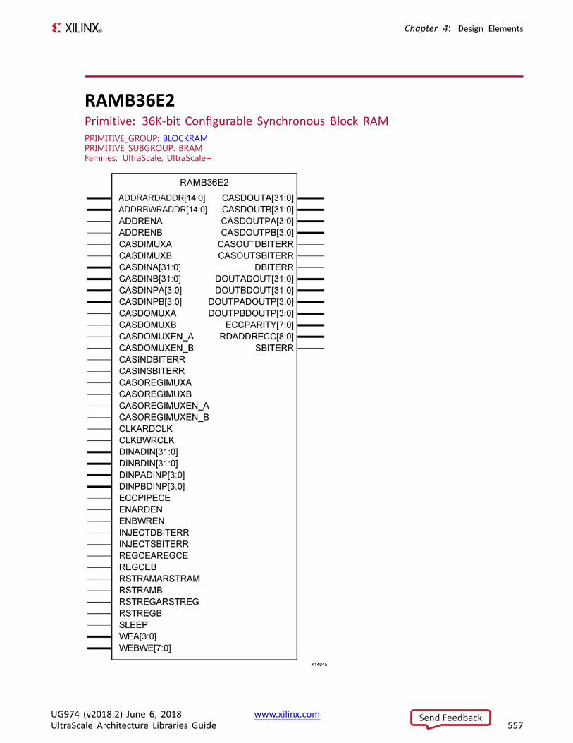
Chapter 4: Design Elements
RAMB36E2Primitive: 36K-bit Configurable Synchronous Block RAMPRIMITIVE_GROUP: BLOCKRAMPRIMITIVE_SUBGROUP: BRAMFamilies: UltraScale, UltraScale+
UG974 (v2018.2) June 6, 2018 www.xilinx.comUltraScale Architecture Libraries Guide 557
Send Feedback
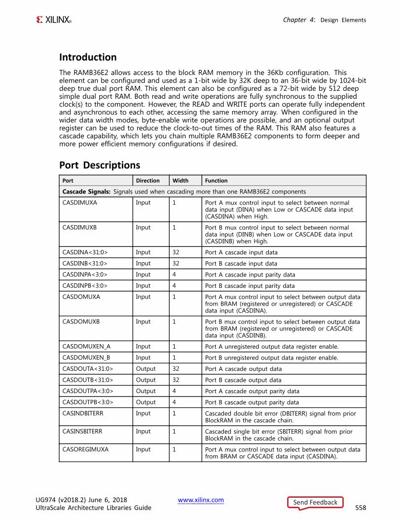
Chapter 4: Design Elements
IntroductionThe RAMB36E2 allows access to the block RAM memory in the 36Kb configuration. Thiselement can be configured and used as a 1-bit wide by 32K deep to an 36-bit wide by 1024-bitdeep true dual port RAM. This element can also be configured as a 72-bit wide by 512 deepsimple dual port RAM. Both read and write operations are fully synchronous to the suppliedclock(s) to the component. However, the READ and WRITE ports can operate fully independentand asynchronous to each other, accessing the same memory array. When configured in thewider data width modes, byte-enable write operations are possible, and an optional outputregister can be used to reduce the clock-to-out times of the RAM. This RAM also features acascade capability, which lets you chain multiple RAMB36E2 components to form deeper andmore power efficient memory configurations if desired.
Port DescriptionsPort Direction Width Function
Cascade Signals: Signals used when cascading more than one RAMB36E2 components
CASDIMUXA Input 1 Port A mux control input to select between normaldata input (DINA) when Low or CASCADE data input(CASDINA) when High.
CASDIMUXB Input 1 Port B mux control input to select between normaldata input (DINB) when Low or CASCADE data input(CASDINB) when High.
CASDINA<31:0> Input 32 Port A cascade input data
CASDINB<31:0> Input 32 Port B cascade input data
CASDINPA<3:0> Input 4 Port A cascade input parity data
CASDINPB<3:0> Input 4 Port B cascade input parity data
CASDOMUXA Input 1 Port A mux control input to select between output datafrom BRAM (registered or unregistered) or CASCADEdata input (CASDINA).
CASDOMUXB Input 1 Port B mux control input to select between output datafrom BRAM (registered or unregistered) or CASCADEdata input (CASDINB).
CASDOMUXEN_A Input 1 Port A unregistered output data register enable.
CASDOMUXEN_B Input 1 Port B unregistered output data register enable.
CASDOUTA<31:0> Output 32 Port A cascade output data
CASDOUTB<31:0> Output 32 Port B cascade output data
CASDOUTPA<3:0> Output 4 Port A cascade output parity data
CASDOUTPB<3:0> Output 4 Port B cascade output parity data
CASINDBITERR Input 1 Cascaded double bit error (DBITERR) signal from priorBlockRAM in the cascade chain.
CASINSBITERR Input 1 Cascaded single bit error (SBITERR) signal from priorBlockRAM in the cascade chain.
CASOREGIMUXA Input 1 Port A mux control input to select between output datafrom BRAM or CASCADE data input (CASDINA).
UG974 (v2018.2) June 6, 2018 www.xilinx.comUltraScale Architecture Libraries Guide 558
Send Feedback
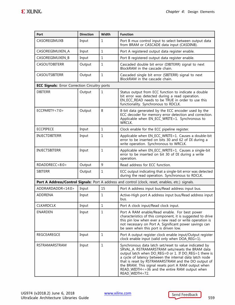
Chapter 4: Design Elements
Port Direction Width Function
CASOREGIMUXB Input 1 Port B mux control input to select between output datafrom BRAM or CASCADE data input (CASDINB).
CASOREGIMUXEN_A Input 1 Port A registered output data register enable.
CASOREGIMUXEN_B Input 1 Port B registered output data register enable.
CASOUTDBITERR Output 1 Cascaded double bit error (DBITERR) signal to nextBlockRAM in the cascade chain.
CASOUTSBITERR Output 1 Cascaded single bit error (SBITERR) signal to nextBlockRAM in the cascade chain.
ECC Signals: Error Correction Circuitry ports
DBITERR Output 1 Status output from ECC function to indicate a doublebit error was detected during a read operation.EN_ECC_READ needs to be TRUE in order to use thisfunctionality. Synchronous to RDCLK.
ECCPARITY<7:0> Output 8 8-bit data generated by the ECC encoder used by theECC decoder for memory error detection and correction.Applicable when EN_ECC_WRITE=1. Synchronous toWRCLK.
ECCPIPECE Input 1 Clock enable for the ECC pipeline register.
INJECTDBITERR Input 1 Applicable when EN_ECC_WRITE=1. Causes a double-biterror to be inserted on bits 30 and 62 of DI during awrite operation. Synchronous to WRCLK.
INJECTSBITERR Input 1 Applicable when EN_ECC_WRITE=1. Causes a single-biterror to be inserted on bit 30 of DI during a writeoperation.
RDADDRECC<8:0> Output 9 Read address for ECC function.
SBITERR Output 1 ECC output indicating that a single-bit error was detectedduring the read operation. Synchronous to RDCLK.
Port A Address/Control Signals: Port A address and control (clock, reset, enables, etc.) signals.
ADDRARDADDR<14:0> Input 15 Port A address input bus/Read address input bus.
ADDRENA Input 1 Active-High port A address input bus/Read address inputbus.
CLKARDCLK Input 1 Port A clock input/Read clock input.
ENARDEN Input 1 Port A RAM enable/Read enable. For best powercharacteristics of this component, it is suggested to drivethis pin low when ever a new read or write operation isnot necessary on Port A. Significant power savings canbe seen when this port is driven low.
REGCEAREGCE Input 1 Port A output register clock enable input/Output registerclock enable input (valid only when DOA_REG=1).
RSTRAMARSTRAM Input 1 Synchronous data latch set/reset to value indicated bySRVAL_A. RSTRAMARSTRAM sets/resets the BRAM dataoutput latch when DO_REG=0 or 1. If DO_REG=1 there isa cycle of latency between the internal data latch nodethat is reset by RSTRAMARSTRAM and the DO output ofthe BRAM. This signal resets port A RAM output whenREAD_WIDTH<=36 and the entire RAM output whenREAD_WIDTH=72.
UG974 (v2018.2) June 6, 2018 www.xilinx.comUltraScale Architecture Libraries Guide 559
Send Feedback
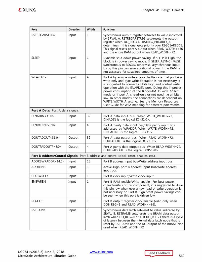
Chapter 4: Design Elements
Port Direction Width Function
RSTREGARSTREG Input 1 Synchronous output register set/reset to value indicatedby SRVAL_A. RSTREGARSTREG sets/resets the outputregister when DO_REG=1. RSTREG_PRIORITY_Adetermines if this signal gets priority over REGCEAREGCE.This signal resets port A output when READ_WIDTH<=36and the entire RAM output when READ_WIDTH=72.
SLEEP Input 1 Dynamic shut down power saving. If SLEEP is High, theblock is in power saving mode. If SLEEP_ASYNC=FALSE,synchronous to RDCLK, otherwise, asynchronous input.Using this pin can save additional power if the RAM isnot accessed for sustained amounts of time.
WEA<3:0> Input 4 Port A byte-wide write enable. In the case that port A iswrite-only and byte-write operation is not necessary, itis suggested to connect all bits high and control writeoperation with the ENARDEN port. Doing this improvespower consumption of the BlockRAM. In wide 72-bitmode or if port A is read-only or not used, tie all bitslow. In other modes, the connections are dependent onWRITE_WIDTH_A setting. See the Memory ResourcesUser Guide for WEA mapping for different port widths.
Port A Data: Port A data signals.
DINADIN<31:0> Input 32 Port A data input bus. When WRITE_WIDTH=72,DINADIN is the logical DI<31:0>.
DINPADINP<3:0> Input 4 Port A parity data input bus/Data parity input busaddressed by WRADDR. When WRITE_WIDTH=72,DINPADINP is the logical DIP<3:0>.
DOUTADOUT<31:0> Output 32 Port A data output bus. When READ_WIDTH=72,DOUTADOUT is the logical DO<31:0>.
DOUTPADOUTP<3:0> Output 4 Port A parity data output bus. When READ_WIDTH=72,DOUTPADOUT is the logical DOP<3:0>.
Port B Address/Control Signals: Port B address and control (clock, reset, enables, etc.).
ADDRBWRADDR<14:0> Input 15 Port B address input bus/Write address input bus.
ADDRENB Input 1 Active-High port B address input bus/Write addressinput bus.
CLKBWRCLK Input 1 Port B clock input/Write clock input.
ENBWREN Input 1 Port B RAM enable/Write enable. For best powercharacteristics of this component, it is suggested to drivethis pin low when ever a new read or write operation isnot necessary on Port B. Significant power savings canbe seen when this port is driven low.
REGCEB Input 1 Port B output register clock enable (valid only whenDOB_REG=1 and READ_WIDTH<=36).
RSTRAMB Input 1 Synchronous data latch set/reset to value indicated bySRVAL_B. RSTRAMB sets/resets the BRAM data outputlatch when DO_REG=0 or 1. If DO_REG=1 there is a cycleof latency between the internal data latch node that isreset by RSTRAMB and the DO output of the BRAM. Notused when READ_WIDTH=72.
UG974 (v2018.2) June 6, 2018 www.xilinx.comUltraScale Architecture Libraries Guide 560
Send Feedback
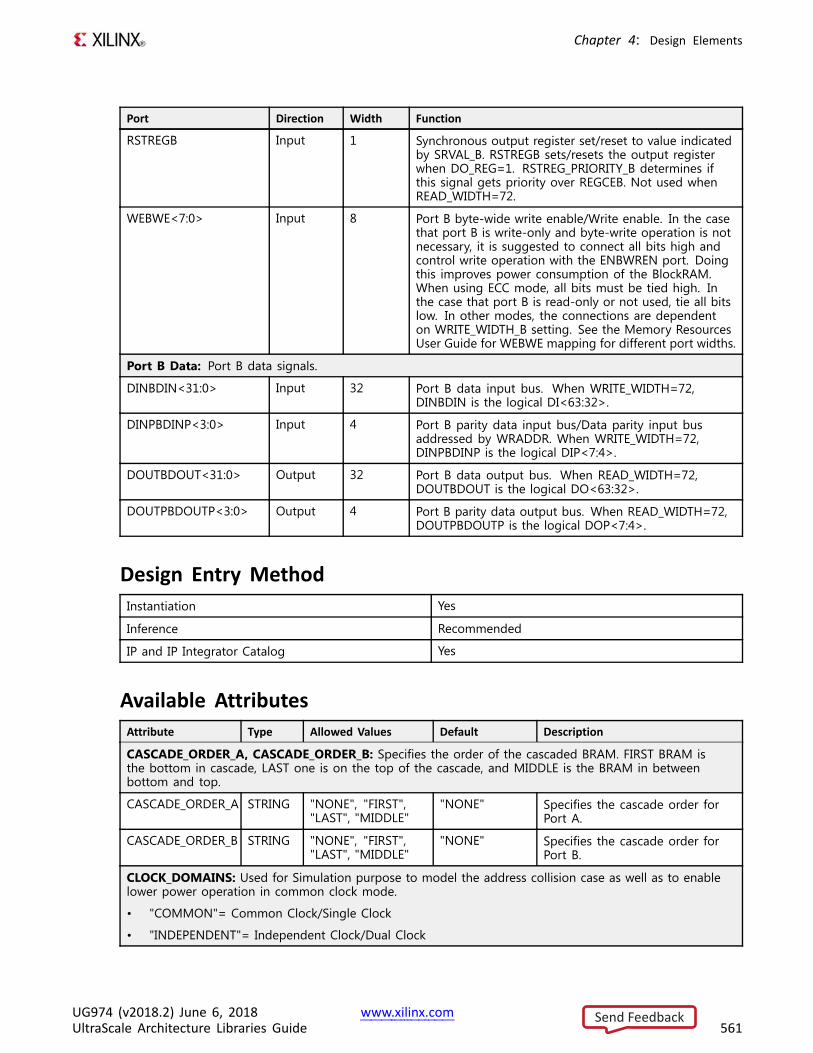
Chapter 4: Design Elements
Port Direction Width Function
RSTREGB Input 1 Synchronous output register set/reset to value indicatedby SRVAL_B. RSTREGB sets/resets the output registerwhen DO_REG=1. RSTREG_PRIORITY_B determines ifthis signal gets priority over REGCEB. Not used whenREAD_WIDTH=72.
WEBWE<7:0> Input 8 Port B byte-wide write enable/Write enable. In the casethat port B is write-only and byte-write operation is notnecessary, it is suggested to connect all bits high andcontrol write operation with the ENBWREN port. Doingthis improves power consumption of the BlockRAM.When using ECC mode, all bits must be tied high. Inthe case that port B is read-only or not used, tie all bitslow. In other modes, the connections are dependenton WRITE_WIDTH_B setting. See the Memory ResourcesUser Guide for WEBWE mapping for different port widths.
Port B Data: Port B data signals.
DINBDIN<31:0> Input 32 Port B data input bus. When WRITE_WIDTH=72,DINBDIN is the logical DI<63:32>.
DINPBDINP<3:0> Input 4 Port B parity data input bus/Data parity input busaddressed by WRADDR. When WRITE_WIDTH=72,DINPBDINP is the logical DIP<7:4>.
DOUTBDOUT<31:0> Output 32 Port B data output bus. When READ_WIDTH=72,DOUTBDOUT is the logical DO<63:32>.
DOUTPBDOUTP<3:0> Output 4 Port B parity data output bus. When READ_WIDTH=72,DOUTPBDOUTP is the logical DOP<7:4>.
Design Entry MethodInstantiation Yes
Inference Recommended
IP and IP Integrator Catalog Yes
Available AttributesAttribute Type Allowed Values Default Description
CASCADE_ORDER_A, CASCADE_ORDER_B: Specifies the order of the cascaded BRAM. FIRST BRAM isthe bottom in cascade, LAST one is on the top of the cascade, and MIDDLE is the BRAM in betweenbottom and top.
CASCADE_ORDER_A STRING "NONE", "FIRST","LAST", "MIDDLE"
"NONE" Specifies the cascade order forPort A.
CASCADE_ORDER_B STRING "NONE", "FIRST","LAST", "MIDDLE"
"NONE" Specifies the cascade order forPort B.
CLOCK_DOMAINS: Used for Simulation purpose to model the address collision case as well as to enablelower power operation in common clock mode.
• "COMMON"= Common Clock/Single Clock
• "INDEPENDENT"= Independent Clock/Dual Clock
UG974 (v2018.2) June 6, 2018 www.xilinx.comUltraScale Architecture Libraries Guide 561
Send Feedback
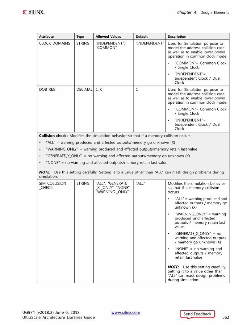
Chapter 4: Design Elements
Attribute Type Allowed Values Default Description
CLOCK_DOMAINS STRING "INDEPENDENT","COMMON"
"INDEPENDENT" Used for Simulation purpose tomodel the address collision caseas well as to enable lower poweroperation in common clock mode.
• "COMMON"= Common Clock/ Single Clock
• "INDEPENDENT"=Independent Clock / DualClock
DOB_REG DECIMAL 1, 0 1 Used for Simulation purpose tomodel the address collision caseas well as to enable lower poweroperation in common clock mode.
• "COMMON"= Common Clock/ Single Clock
• "INDEPENDENT"=Independent Clock / DualClock
Collision check: Modifies the simulation behavior so that if a memory collision occurs
• "ALL" = warning produced and affected outputs/memory go unknown (X)
• "WARNING_ONLY" = warning produced and affected outputs/memory retain last value
• "GENERATE_X_ONLY" = no warning and affected outputs/memory go unknown (X)
• "NONE" = no warning and affected outputs/memory retain last value
NOTE: Use this setting carefully. Setting it to a value other than "ALL" can mask design problems duringsimulation.
SIM_COLLISION_CHECK
STRING "ALL", "GENERATE_X _ONLY", "NONE","WARNING _ONLY"
"ALL" Modifies the simulation behaviorso that if a memory collisionoccurs
• "ALL" = warning produced andaffected outputs / memory gounknown (X)
• "WARNING_ONLY" = warningproduced and affectedoutputs / memory retain lastvalue
• "GENERATE_X_ONLY" = nowarning and affected outputs/ memory go unknown (X)
• "NONE" = no warning andaffected outputs / memoryretain last value
NOTE: Use this setting carefully.Setting it to a value other than"ALL" can mask design problemsduring simulation.
UG974 (v2018.2) June 6, 2018 www.xilinx.comUltraScale Architecture Libraries Guide 562
Send Feedback
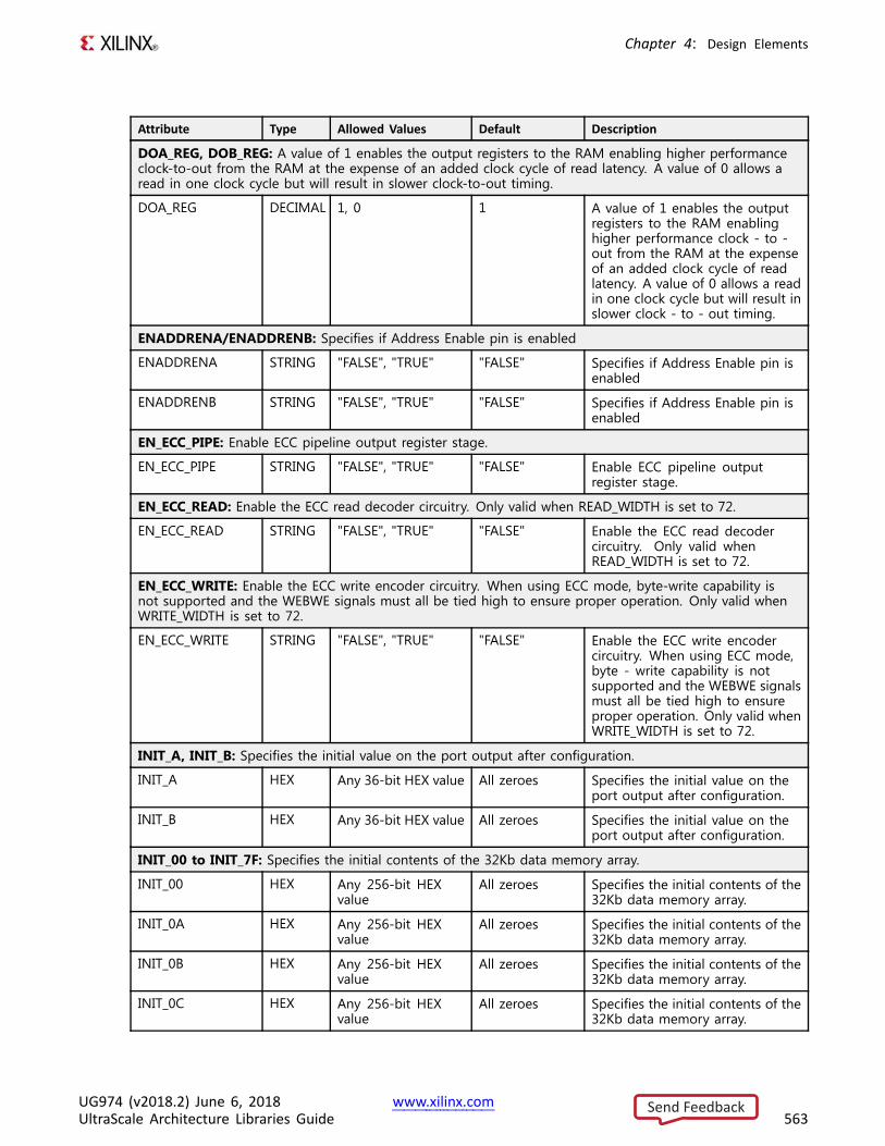
Chapter 4: Design Elements
Attribute Type Allowed Values Default Description
DOA_REG, DOB_REG: A value of 1 enables the output registers to the RAM enabling higher performanceclock-to-out from the RAM at the expense of an added clock cycle of read latency. A value of 0 allows aread in one clock cycle but will result in slower clock-to-out timing.
DOA_REG DECIMAL 1, 0 1 A value of 1 enables the outputregisters to the RAM enablinghigher performance clock - to -out from the RAM at the expenseof an added clock cycle of readlatency. A value of 0 allows a readin one clock cycle but will result inslower clock - to - out timing.
ENADDRENA/ENADDRENB: Specifies if Address Enable pin is enabled
ENADDRENA STRING "FALSE", "TRUE" "FALSE" Specifies if Address Enable pin isenabled
ENADDRENB STRING "FALSE", "TRUE" "FALSE" Specifies if Address Enable pin isenabled
EN_ECC_PIPE: Enable ECC pipeline output register stage.
EN_ECC_PIPE STRING "FALSE", "TRUE" "FALSE" Enable ECC pipeline outputregister stage.
EN_ECC_READ: Enable the ECC read decoder circuitry. Only valid when READ_WIDTH is set to 72.
EN_ECC_READ STRING "FALSE", "TRUE" "FALSE" Enable the ECC read decodercircuitry. Only valid whenREAD_WIDTH is set to 72.
EN_ECC_WRITE: Enable the ECC write encoder circuitry. When using ECC mode, byte-write capability isnot supported and the WEBWE signals must all be tied high to ensure proper operation. Only valid whenWRITE_WIDTH is set to 72.
EN_ECC_WRITE STRING "FALSE", "TRUE" "FALSE" Enable the ECC write encodercircuitry. When using ECC mode,byte - write capability is notsupported and the WEBWE signalsmust all be tied high to ensureproper operation. Only valid whenWRITE_WIDTH is set to 72.
INIT_A, INIT_B: Specifies the initial value on the port output after configuration.
INIT_A HEX Any 36-bit HEX value All zeroes Specifies the initial value on theport output after configuration.
INIT_B HEX Any 36-bit HEX value All zeroes Specifies the initial value on theport output after configuration.
INIT_00 to INIT_7F: Specifies the initial contents of the 32Kb data memory array.
INIT_00 HEX Any 256-bit HEXvalue
All zeroes Specifies the initial contents of the32Kb data memory array.
INIT_0A HEX Any 256-bit HEXvalue
All zeroes Specifies the initial contents of the32Kb data memory array.
INIT_0B HEX Any 256-bit HEXvalue
All zeroes Specifies the initial contents of the32Kb data memory array.
INIT_0C HEX Any 256-bit HEXvalue
All zeroes Specifies the initial contents of the32Kb data memory array.
UG974 (v2018.2) June 6, 2018 www.xilinx.comUltraScale Architecture Libraries Guide 563
Send Feedback

Chapter 4: Design Elements
Attribute Type Allowed Values Default Description
INIT_0D HEX Any 256-bit HEXvalue
All zeroes Specifies the initial contents of the32Kb data memory array.
INIT_0E HEX Any 256-bit HEXvalue
All zeroes Specifies the initial contents of the32Kb data memory array.
INIT_0F HEX Any 256-bit HEXvalue
All zeroes Specifies the initial contents of the32Kb data memory array.
INIT_01 HEX Any 256-bit HEXvalue
All zeroes Specifies the initial contents of the32Kb data memory array.
INIT_1A HEX Any 256-bit HEXvalue
All zeroes Specifies the initial contents of the32Kb data memory array.
INIT_1B HEX Any 256-bit HEXvalue
All zeroes Specifies the initial contents of the32Kb data memory array.
INIT_1C HEX Any 256-bit HEXvalue
All zeroes Specifies the initial contents of the32Kb data memory array.
INIT_1D HEX Any 256-bit HEXvalue
All zeroes Specifies the initial contents of the32Kb data memory array.
INIT_1E HEX Any 256-bit HEXvalue
All zeroes Specifies the initial contents of the32Kb data memory array.
INIT_1F HEX Any 256-bit HEXvalue
All zeroes Specifies the initial contents of the32Kb data memory array.
INIT_02 HEX Any 256-bit HEXvalue
All zeroes Specifies the initial contents of the32Kb data memory array.
INIT_2A HEX Any 256-bit HEXvalue
All zeroes Specifies the initial contents of the32Kb data memory array.
INIT_2B HEX Any 256-bit HEXvalue
All zeroes Specifies the initial contents of the32Kb data memory array.
INIT_2C HEX Any 256-bit HEXvalue
All zeroes Specifies the initial contents of the32Kb data memory array.
INIT_2D HEX Any 256-bit HEXvalue
All zeroes Specifies the initial contents of the32Kb data memory array.
INIT_2E HEX Any 256-bit HEXvalue
All zeroes Specifies the initial contents of the32Kb data memory array.
INIT_2F HEX Any 256-bit HEXvalue
All zeroes Specifies the initial contents of the32Kb data memory array.
INIT_03 HEX Any 256-bit HEXvalue
All zeroes Specifies the initial contents of the32Kb data memory array.
INIT_3A HEX Any 256-bit HEXvalue
All zeroes Specifies the initial contents of the32Kb data memory array.
INIT_3B HEX Any 256-bit HEXvalue
All zeroes Specifies the initial contents of the32Kb data memory array.
INIT_3C HEX Any 256-bit HEXvalue
All zeroes Specifies the initial contents of the32Kb data memory array.
INIT_3D HEX Any 256-bit HEXvalue
All zeroes Specifies the initial contents of the32Kb data memory array.
UG974 (v2018.2) June 6, 2018 www.xilinx.comUltraScale Architecture Libraries Guide 564
Send Feedback

Chapter 4: Design Elements
Attribute Type Allowed Values Default Description
INIT_3E HEX Any 256-bit HEXvalue
All zeroes Specifies the initial contents of the32Kb data memory array.
INIT_3F HEX Any 256-bit HEXvalue
All zeroes Specifies the initial contents of the32Kb data memory array.
INIT_04 HEX Any 256-bit HEXvalue
All zeroes Specifies the initial contents of the32Kb data memory array.
INIT_4A HEX Any 256-bit HEXvalue
All zeroes Specifies the initial contents of the32Kb data memory array.
INIT_4B HEX Any 256-bit HEXvalue
All zeroes Specifies the initial contents of the32Kb data memory array.
INIT_4C HEX Any 256-bit HEXvalue
All zeroes Specifies the initial contents of the32Kb data memory array.
INIT_4D HEX Any 256-bit HEXvalue
All zeroes Specifies the initial contents of the32Kb data memory array.
INIT_4E HEX Any 256-bit HEXvalue
All zeroes Specifies the initial contents of the32Kb data memory array.
INIT_4F HEX Any 256-bit HEXvalue
All zeroes Specifies the initial contents of the32Kb data memory array.
INIT_05 HEX Any 256-bit HEXvalue
All zeroes Specifies the initial contents of the32Kb data memory array.
INIT_5A HEX Any 256-bit HEXvalue
All zeroes Specifies the initial contents of the32Kb data memory array.
INIT_5B HEX Any 256-bit HEXvalue
All zeroes Specifies the initial contents of the32Kb data memory array.
INIT_5C HEX Any 256-bit HEXvalue
All zeroes Specifies the initial contents of the32Kb data memory array.
INIT_5D HEX Any 256-bit HEXvalue
All zeroes Specifies the initial contents of the32Kb data memory array.
INIT_5E HEX Any 256-bit HEXvalue
All zeroes Specifies the initial contents of the32Kb data memory array.
INIT_5F HEX Any 256-bit HEXvalue
All zeroes Specifies the initial contents of the32Kb data memory array.
INIT_06 HEX Any 256-bit HEXvalue
All zeroes Specifies the initial contents of the32Kb data memory array.
INIT_6A HEX Any 256-bit HEXvalue
All zeroes Specifies the initial contents of the32Kb data memory array.
INIT_6B HEX Any 256-bit HEXvalue
All zeroes Specifies the initial contents of the32Kb data memory array.
INIT_6C HEX Any 256-bit HEXvalue
All zeroes Specifies the initial contents of the32Kb data memory array.
INIT_6D HEX Any 256-bit HEXvalue
All zeroes Specifies the initial contents of the32Kb data memory array.
INIT_6E HEX Any 256-bit HEXvalue
All zeroes Specifies the initial contents of the32Kb data memory array.
UG974 (v2018.2) June 6, 2018 www.xilinx.comUltraScale Architecture Libraries Guide 565
Send Feedback
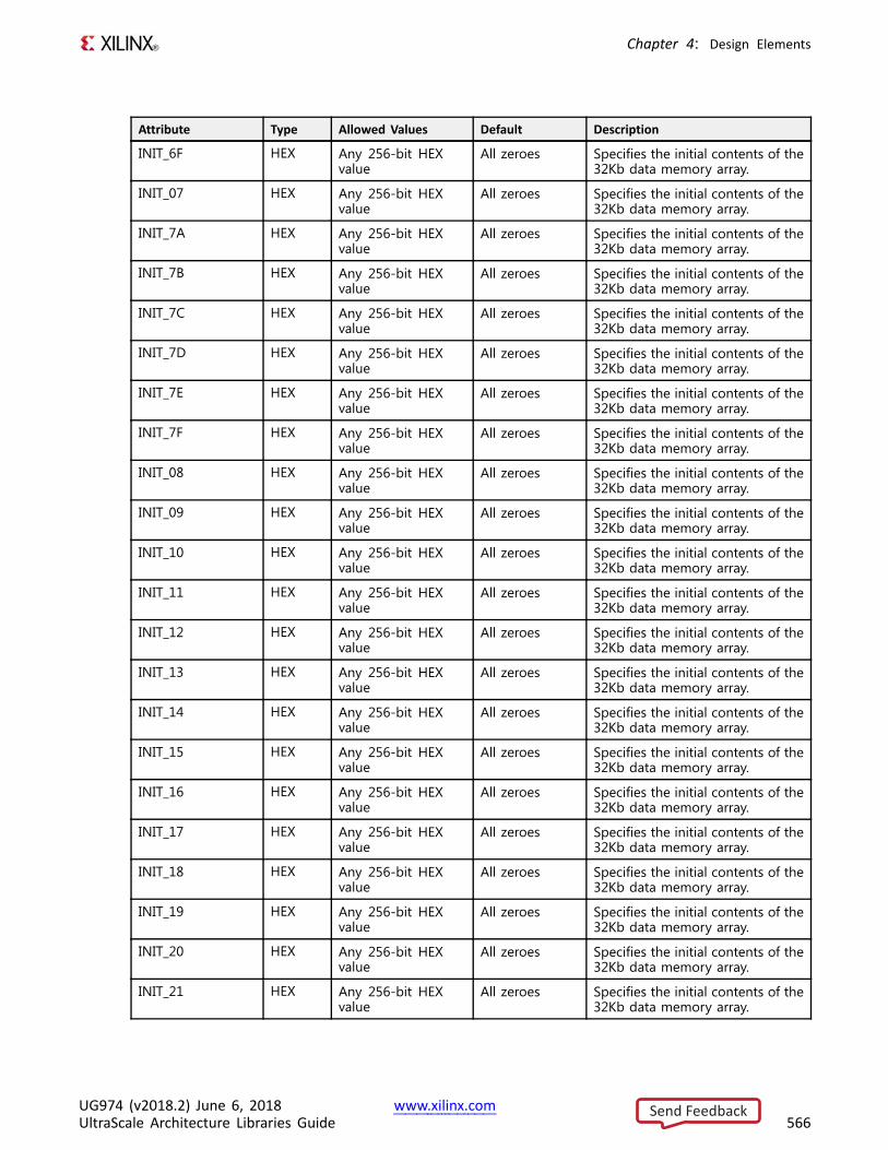
Chapter 4: Design Elements
Attribute Type Allowed Values Default Description
INIT_6F HEX Any 256-bit HEXvalue
All zeroes Specifies the initial contents of the32Kb data memory array.
INIT_07 HEX Any 256-bit HEXvalue
All zeroes Specifies the initial contents of the32Kb data memory array.
INIT_7A HEX Any 256-bit HEXvalue
All zeroes Specifies the initial contents of the32Kb data memory array.
INIT_7B HEX Any 256-bit HEXvalue
All zeroes Specifies the initial contents of the32Kb data memory array.
INIT_7C HEX Any 256-bit HEXvalue
All zeroes Specifies the initial contents of the32Kb data memory array.
INIT_7D HEX Any 256-bit HEXvalue
All zeroes Specifies the initial contents of the32Kb data memory array.
INIT_7E HEX Any 256-bit HEXvalue
All zeroes Specifies the initial contents of the32Kb data memory array.
INIT_7F HEX Any 256-bit HEXvalue
All zeroes Specifies the initial contents of the32Kb data memory array.
INIT_08 HEX Any 256-bit HEXvalue
All zeroes Specifies the initial contents of the32Kb data memory array.
INIT_09 HEX Any 256-bit HEXvalue
All zeroes Specifies the initial contents of the32Kb data memory array.
INIT_10 HEX Any 256-bit HEXvalue
All zeroes Specifies the initial contents of the32Kb data memory array.
INIT_11 HEX Any 256-bit HEXvalue
All zeroes Specifies the initial contents of the32Kb data memory array.
INIT_12 HEX Any 256-bit HEXvalue
All zeroes Specifies the initial contents of the32Kb data memory array.
INIT_13 HEX Any 256-bit HEXvalue
All zeroes Specifies the initial contents of the32Kb data memory array.
INIT_14 HEX Any 256-bit HEXvalue
All zeroes Specifies the initial contents of the32Kb data memory array.
INIT_15 HEX Any 256-bit HEXvalue
All zeroes Specifies the initial contents of the32Kb data memory array.
INIT_16 HEX Any 256-bit HEXvalue
All zeroes Specifies the initial contents of the32Kb data memory array.
INIT_17 HEX Any 256-bit HEXvalue
All zeroes Specifies the initial contents of the32Kb data memory array.
INIT_18 HEX Any 256-bit HEXvalue
All zeroes Specifies the initial contents of the32Kb data memory array.
INIT_19 HEX Any 256-bit HEXvalue
All zeroes Specifies the initial contents of the32Kb data memory array.
INIT_20 HEX Any 256-bit HEXvalue
All zeroes Specifies the initial contents of the32Kb data memory array.
INIT_21 HEX Any 256-bit HEXvalue
All zeroes Specifies the initial contents of the32Kb data memory array.
UG974 (v2018.2) June 6, 2018 www.xilinx.comUltraScale Architecture Libraries Guide 566
Send Feedback

Chapter 4: Design Elements
Attribute Type Allowed Values Default Description
INIT_22 HEX Any 256-bit HEXvalue
All zeroes Specifies the initial contents of the32Kb data memory array.
INIT_23 HEX Any 256-bit HEXvalue
All zeroes Specifies the initial contents of the32Kb data memory array.
INIT_24 HEX Any 256-bit HEXvalue
All zeroes Specifies the initial contents of the32Kb data memory array.
INIT_25 HEX Any 256-bit HEXvalue
All zeroes Specifies the initial contents of the32Kb data memory array.
INIT_26 HEX Any 256-bit HEXvalue
All zeroes Specifies the initial contents of the32Kb data memory array.
INIT_27 HEX Any 256-bit HEXvalue
All zeroes Specifies the initial contents of the32Kb data memory array.
INIT_28 HEX Any 256-bit HEXvalue
All zeroes Specifies the initial contents of the32Kb data memory array.
INIT_29 HEX Any 256-bit HEXvalue
All zeroes Specifies the initial contents of the32Kb data memory array.
INIT_30 HEX Any 256-bit HEXvalue
All zeroes Specifies the initial contents of the32Kb data memory array.
INIT_31 HEX Any 256-bit HEXvalue
All zeroes Specifies the initial contents of the32Kb data memory array.
INIT_32 HEX Any 256-bit HEXvalue
All zeroes Specifies the initial contents of the32Kb data memory array.
INIT_33 HEX Any 256-bit HEXvalue
All zeroes Specifies the initial contents of the32Kb data memory array.
INIT_34 HEX Any 256-bit HEXvalue
All zeroes Specifies the initial contents of the32Kb data memory array.
INIT_35 HEX Any 256-bit HEXvalue
All zeroes Specifies the initial contents of the32Kb data memory array.
INIT_36 HEX Any 256-bit HEXvalue
All zeroes Specifies the initial contents of the32Kb data memory array.
INIT_37 HEX Any 256-bit HEXvalue
All zeroes Specifies the initial contents of the32Kb data memory array.
INIT_38 HEX Any 256-bit HEXvalue
All zeroes Specifies the initial contents of the32Kb data memory array.
INIT_39 HEX Any 256-bit HEXvalue
All zeroes Specifies the initial contents of the32Kb data memory array.
INIT_40 HEX Any 256-bit HEXvalue
All zeroes Specifies the initial contents of the32Kb data memory array.
INIT_41 HEX Any 256-bit HEXvalue
All zeroes Specifies the initial contents of the32Kb data memory array.
INIT_42 HEX Any 256-bit HEXvalue
All zeroes Specifies the initial contents of the32Kb data memory array.
INIT_43 HEX Any 256-bit HEXvalue
All zeroes Specifies the initial contents of the32Kb data memory array.
UG974 (v2018.2) June 6, 2018 www.xilinx.comUltraScale Architecture Libraries Guide 567
Send Feedback
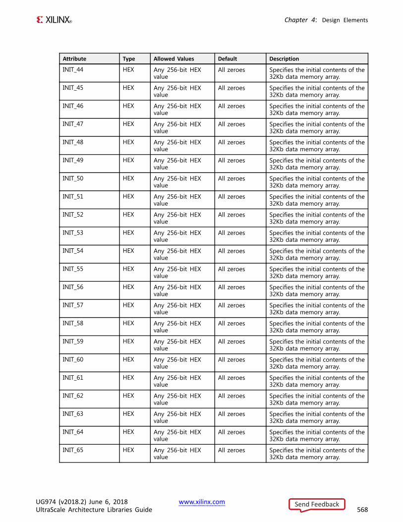
Chapter 4: Design Elements
Attribute Type Allowed Values Default Description
INIT_44 HEX Any 256-bit HEXvalue
All zeroes Specifies the initial contents of the32Kb data memory array.
INIT_45 HEX Any 256-bit HEXvalue
All zeroes Specifies the initial contents of the32Kb data memory array.
INIT_46 HEX Any 256-bit HEXvalue
All zeroes Specifies the initial contents of the32Kb data memory array.
INIT_47 HEX Any 256-bit HEXvalue
All zeroes Specifies the initial contents of the32Kb data memory array.
INIT_48 HEX Any 256-bit HEXvalue
All zeroes Specifies the initial contents of the32Kb data memory array.
INIT_49 HEX Any 256-bit HEXvalue
All zeroes Specifies the initial contents of the32Kb data memory array.
INIT_50 HEX Any 256-bit HEXvalue
All zeroes Specifies the initial contents of the32Kb data memory array.
INIT_51 HEX Any 256-bit HEXvalue
All zeroes Specifies the initial contents of the32Kb data memory array.
INIT_52 HEX Any 256-bit HEXvalue
All zeroes Specifies the initial contents of the32Kb data memory array.
INIT_53 HEX Any 256-bit HEXvalue
All zeroes Specifies the initial contents of the32Kb data memory array.
INIT_54 HEX Any 256-bit HEXvalue
All zeroes Specifies the initial contents of the32Kb data memory array.
INIT_55 HEX Any 256-bit HEXvalue
All zeroes Specifies the initial contents of the32Kb data memory array.
INIT_56 HEX Any 256-bit HEXvalue
All zeroes Specifies the initial contents of the32Kb data memory array.
INIT_57 HEX Any 256-bit HEXvalue
All zeroes Specifies the initial contents of the32Kb data memory array.
INIT_58 HEX Any 256-bit HEXvalue
All zeroes Specifies the initial contents of the32Kb data memory array.
INIT_59 HEX Any 256-bit HEXvalue
All zeroes Specifies the initial contents of the32Kb data memory array.
INIT_60 HEX Any 256-bit HEXvalue
All zeroes Specifies the initial contents of the32Kb data memory array.
INIT_61 HEX Any 256-bit HEXvalue
All zeroes Specifies the initial contents of the32Kb data memory array.
INIT_62 HEX Any 256-bit HEXvalue
All zeroes Specifies the initial contents of the32Kb data memory array.
INIT_63 HEX Any 256-bit HEXvalue
All zeroes Specifies the initial contents of the32Kb data memory array.
INIT_64 HEX Any 256-bit HEXvalue
All zeroes Specifies the initial contents of the32Kb data memory array.
INIT_65 HEX Any 256-bit HEXvalue
All zeroes Specifies the initial contents of the32Kb data memory array.
UG974 (v2018.2) June 6, 2018 www.xilinx.comUltraScale Architecture Libraries Guide 568
Send Feedback
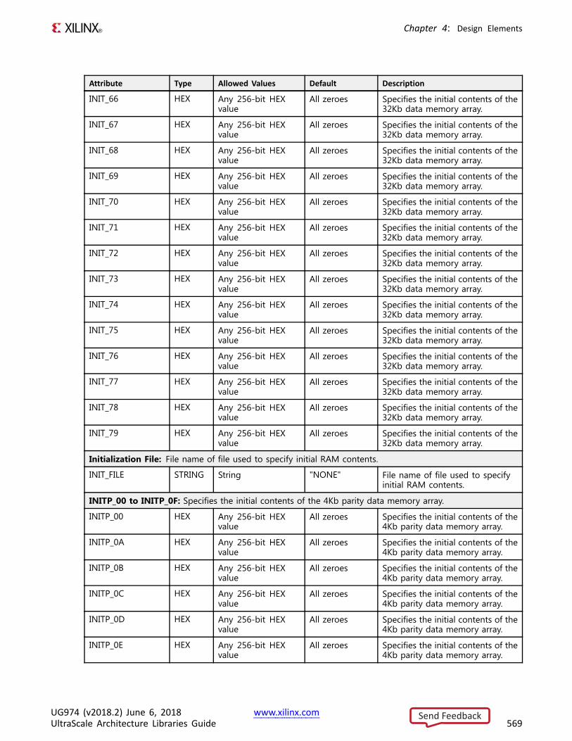
Chapter 4: Design Elements
Attribute Type Allowed Values Default Description
INIT_66 HEX Any 256-bit HEXvalue
All zeroes Specifies the initial contents of the32Kb data memory array.
INIT_67 HEX Any 256-bit HEXvalue
All zeroes Specifies the initial contents of the32Kb data memory array.
INIT_68 HEX Any 256-bit HEXvalue
All zeroes Specifies the initial contents of the32Kb data memory array.
INIT_69 HEX Any 256-bit HEXvalue
All zeroes Specifies the initial contents of the32Kb data memory array.
INIT_70 HEX Any 256-bit HEXvalue
All zeroes Specifies the initial contents of the32Kb data memory array.
INIT_71 HEX Any 256-bit HEXvalue
All zeroes Specifies the initial contents of the32Kb data memory array.
INIT_72 HEX Any 256-bit HEXvalue
All zeroes Specifies the initial contents of the32Kb data memory array.
INIT_73 HEX Any 256-bit HEXvalue
All zeroes Specifies the initial contents of the32Kb data memory array.
INIT_74 HEX Any 256-bit HEXvalue
All zeroes Specifies the initial contents of the32Kb data memory array.
INIT_75 HEX Any 256-bit HEXvalue
All zeroes Specifies the initial contents of the32Kb data memory array.
INIT_76 HEX Any 256-bit HEXvalue
All zeroes Specifies the initial contents of the32Kb data memory array.
INIT_77 HEX Any 256-bit HEXvalue
All zeroes Specifies the initial contents of the32Kb data memory array.
INIT_78 HEX Any 256-bit HEXvalue
All zeroes Specifies the initial contents of the32Kb data memory array.
INIT_79 HEX Any 256-bit HEXvalue
All zeroes Specifies the initial contents of the32Kb data memory array.
Initialization File: File name of file used to specify initial RAM contents.
INIT_FILE STRING String "NONE" File name of file used to specifyinitial RAM contents.
INITP_00 to INITP_0F: Specifies the initial contents of the 4Kb parity data memory array.
INITP_00 HEX Any 256-bit HEXvalue
All zeroes Specifies the initial contents of the4Kb parity data memory array.
INITP_0A HEX Any 256-bit HEXvalue
All zeroes Specifies the initial contents of the4Kb parity data memory array.
INITP_0B HEX Any 256-bit HEXvalue
All zeroes Specifies the initial contents of the4Kb parity data memory array.
INITP_0C HEX Any 256-bit HEXvalue
All zeroes Specifies the initial contents of the4Kb parity data memory array.
INITP_0D HEX Any 256-bit HEXvalue
All zeroes Specifies the initial contents of the4Kb parity data memory array.
INITP_0E HEX Any 256-bit HEXvalue
All zeroes Specifies the initial contents of the4Kb parity data memory array.
UG974 (v2018.2) June 6, 2018 www.xilinx.comUltraScale Architecture Libraries Guide 569
Send Feedback
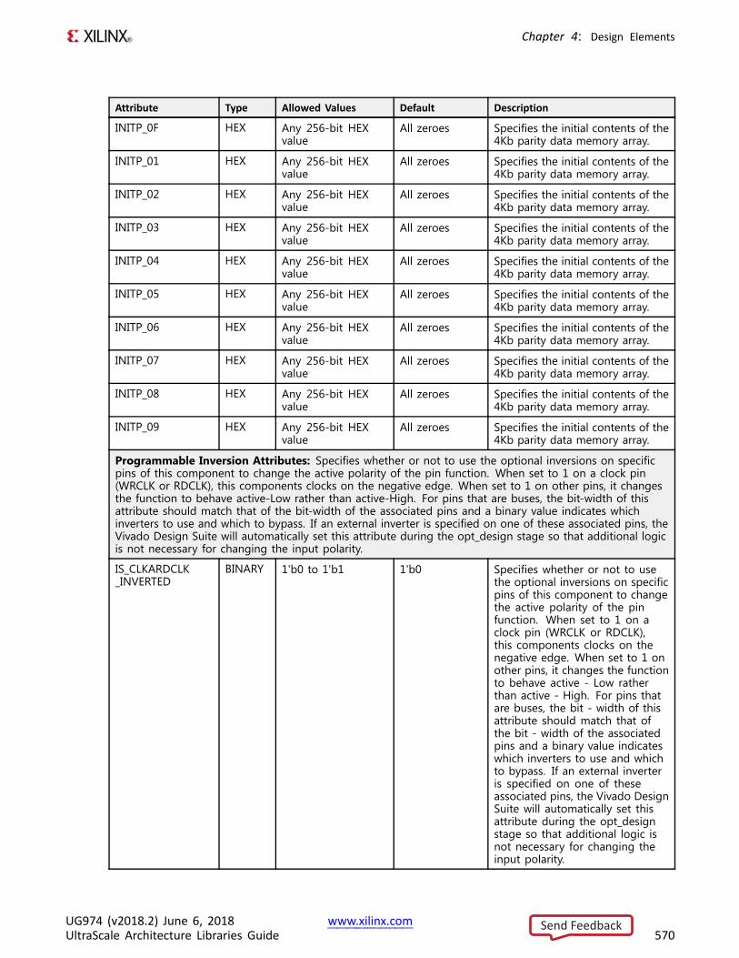
Chapter 4: Design Elements
Attribute Type Allowed Values Default Description
INITP_0F HEX Any 256-bit HEXvalue
All zeroes Specifies the initial contents of the4Kb parity data memory array.
INITP_01 HEX Any 256-bit HEXvalue
All zeroes Specifies the initial contents of the4Kb parity data memory array.
INITP_02 HEX Any 256-bit HEXvalue
All zeroes Specifies the initial contents of the4Kb parity data memory array.
INITP_03 HEX Any 256-bit HEXvalue
All zeroes Specifies the initial contents of the4Kb parity data memory array.
INITP_04 HEX Any 256-bit HEXvalue
All zeroes Specifies the initial contents of the4Kb parity data memory array.
INITP_05 HEX Any 256-bit HEXvalue
All zeroes Specifies the initial contents of the4Kb parity data memory array.
INITP_06 HEX Any 256-bit HEXvalue
All zeroes Specifies the initial contents of the4Kb parity data memory array.
INITP_07 HEX Any 256-bit HEXvalue
All zeroes Specifies the initial contents of the4Kb parity data memory array.
INITP_08 HEX Any 256-bit HEXvalue
All zeroes Specifies the initial contents of the4Kb parity data memory array.
INITP_09 HEX Any 256-bit HEXvalue
All zeroes Specifies the initial contents of the4Kb parity data memory array.
Programmable Inversion Attributes: Specifies whether or not to use the optional inversions on specificpins of this component to change the active polarity of the pin function. When set to 1 on a clock pin(WRCLK or RDCLK), this components clocks on the negative edge. When set to 1 on other pins, it changesthe function to behave active-Low rather than active-High. For pins that are buses, the bit-width of thisattribute should match that of the bit-width of the associated pins and a binary value indicates whichinverters to use and which to bypass. If an external inverter is specified on one of these associated pins, theVivado Design Suite will automatically set this attribute during the opt_design stage so that additional logicis not necessary for changing the input polarity.
IS_CLKARDCLK_INVERTED
BINARY 1'b0 to 1'b1 1'b0 Specifies whether or not to usethe optional inversions on specificpins of this component to changethe active polarity of the pinfunction. When set to 1 on aclock pin (WRCLK or RDCLK),this components clocks on thenegative edge. When set to 1 onother pins, it changes the functionto behave active - Low ratherthan active - High. For pins thatare buses, the bit - width of thisattribute should match that ofthe bit - width of the associatedpins and a binary value indicateswhich inverters to use and whichto bypass. If an external inverteris specified on one of theseassociated pins, the Vivado DesignSuite will automatically set thisattribute during the opt_designstage so that additional logic isnot necessary for changing theinput polarity.
UG974 (v2018.2) June 6, 2018 www.xilinx.comUltraScale Architecture Libraries Guide 570
Send Feedback

Chapter 4: Design Elements
Attribute Type Allowed Values Default Description
IS_CLKBWRCLK_INVERTED
BINARY 1'b0 to 1'b1 1'b0 Specifies whether or not to usethe optional inversions on specificpins of this component to changethe active polarity of the pinfunction. When set to 1 on aclock pin (WRCLK or RDCLK),this components clocks on thenegative edge. When set to 1 onother pins, it changes the functionto behave active - Low ratherthan active - High. For pins thatare buses, the bit - width of thisattribute should match that ofthe bit - width of the associatedpins and a binary value indicateswhich inverters to use and whichto bypass. If an external inverteris specified on one of theseassociated pins, the Vivado DesignSuite will automatically set thisattribute during the opt_designstage so that additional logic isnot necessary for changing theinput polarity.
IS_ENARDEN_INVERTED
BINARY 1'b0 to 1'b1 1'b0 Specifies whether or not to usethe optional inversions on specificpins of this component to changethe active polarity of the pinfunction. When set to 1 on aclock pin (WRCLK or RDCLK),this components clocks on thenegative edge. When set to 1 onother pins, it changes the functionto behave active - Low ratherthan active - High. For pins thatare buses, the bit - width of thisattribute should match that ofthe bit - width of the associatedpins and a binary value indicateswhich inverters to use and whichto bypass. If an external inverteris specified on one of theseassociated pins, the Vivado DesignSuite will automatically set thisattribute during the opt_designstage so that additional logic isnot necessary for changing theinput polarity.
UG974 (v2018.2) June 6, 2018 www.xilinx.comUltraScale Architecture Libraries Guide 571
Send Feedback

Chapter 4: Design Elements
Attribute Type Allowed Values Default Description
IS_ENBWREN_INVERTED
BINARY 1'b0 to 1'b1 1'b0 Specifies whether or not to usethe optional inversions on specificpins of this component to changethe active polarity of the pinfunction. When set to 1 on aclock pin (WRCLK or RDCLK),this components clocks on thenegative edge. When set to 1 onother pins, it changes the functionto behave active - Low ratherthan active - High. For pins thatare buses, the bit - width of thisattribute should match that ofthe bit - width of the associatedpins and a binary value indicateswhich inverters to use and whichto bypass. If an external inverteris specified on one of theseassociated pins, the Vivado DesignSuite will automatically set thisattribute during the opt_designstage so that additional logic isnot necessary for changing theinput polarity.
IS_RSTRAMARSTRAM_INVERTED
BINARY 1'b0 to 1'b1 1'b0 Specifies whether or not to usethe optional inversions on specificpins of this component to changethe active polarity of the pinfunction. When set to 1 on aclock pin (WRCLK or RDCLK),this components clocks on thenegative edge. When set to 1 onother pins, it changes the functionto behave active - Low ratherthan active - High. For pins thatare buses, the bit - width of thisattribute should match that ofthe bit - width of the associatedpins and a binary value indicateswhich inverters to use and whichto bypass. If an external inverteris specified on one of theseassociated pins, the Vivado DesignSuite will automatically set thisattribute during the opt_designstage so that additional logic isnot necessary for changing theinput polarity.
UG974 (v2018.2) June 6, 2018 www.xilinx.comUltraScale Architecture Libraries Guide 572
Send Feedback
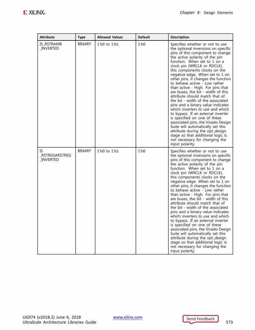
Chapter 4: Design Elements
Attribute Type Allowed Values Default Description
IS_RSTRAMB_INVERTED
BINARY 1'b0 to 1'b1 1'b0 Specifies whether or not to usethe optional inversions on specificpins of this component to changethe active polarity of the pinfunction. When set to 1 on aclock pin (WRCLK or RDCLK),this components clocks on thenegative edge. When set to 1 onother pins, it changes the functionto behave active - Low ratherthan active - High. For pins thatare buses, the bit - width of thisattribute should match that ofthe bit - width of the associatedpins and a binary value indicateswhich inverters to use and whichto bypass. If an external inverteris specified on one of theseassociated pins, the Vivado DesignSuite will automatically set thisattribute during the opt_designstage so that additional logic isnot necessary for changing theinput polarity.
IS_RSTREGARSTREG_INVERTED
BINARY 1'b0 to 1'b1 1'b0 Specifies whether or not to usethe optional inversions on specificpins of this component to changethe active polarity of the pinfunction. When set to 1 on aclock pin (WRCLK or RDCLK),this components clocks on thenegative edge. When set to 1 onother pins, it changes the functionto behave active - Low ratherthan active - High. For pins thatare buses, the bit - width of thisattribute should match that ofthe bit - width of the associatedpins and a binary value indicateswhich inverters to use and whichto bypass. If an external inverteris specified on one of theseassociated pins, the Vivado DesignSuite will automatically set thisattribute during the opt_designstage so that additional logic isnot necessary for changing theinput polarity.
UG974 (v2018.2) June 6, 2018 www.xilinx.comUltraScale Architecture Libraries Guide 573
Send Feedback
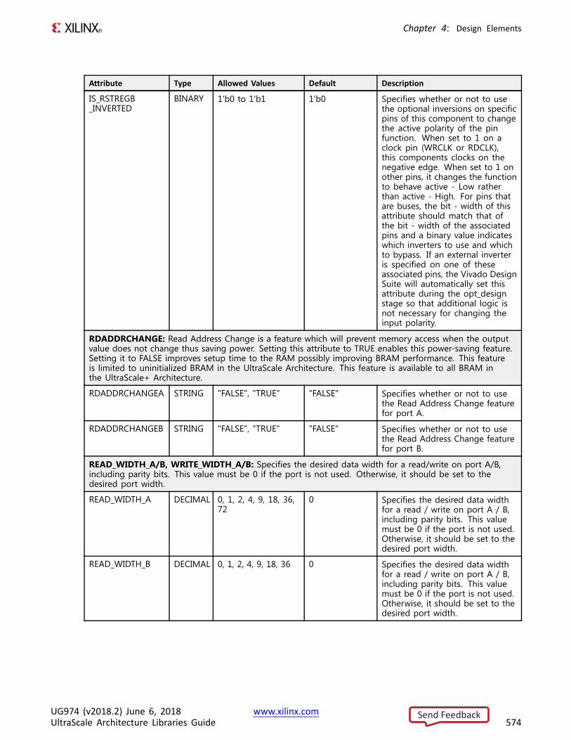
Chapter 4: Design Elements
Attribute Type Allowed Values Default Description
IS_RSTREGB_INVERTED
BINARY 1'b0 to 1'b1 1'b0 Specifies whether or not to usethe optional inversions on specificpins of this component to changethe active polarity of the pinfunction. When set to 1 on aclock pin (WRCLK or RDCLK),this components clocks on thenegative edge. When set to 1 onother pins, it changes the functionto behave active - Low ratherthan active - High. For pins thatare buses, the bit - width of thisattribute should match that ofthe bit - width of the associatedpins and a binary value indicateswhich inverters to use and whichto bypass. If an external inverteris specified on one of theseassociated pins, the Vivado DesignSuite will automatically set thisattribute during the opt_designstage so that additional logic isnot necessary for changing theinput polarity.
RDADDRCHANGE: Read Address Change is a feature which will prevent memory access when the outputvalue does not change thus saving power. Setting this attribute to TRUE enables this power-saving feature.Setting it to FALSE improves setup time to the RAM possibly improving BRAM performance. This featureis limited to uninitialized BRAM in the UltraScale Architecture. This feature is available to all BRAM inthe UltraScale+ Architecture.
RDADDRCHANGEA STRING "FALSE", "TRUE" "FALSE" Specifies whether or not to usethe Read Address Change featurefor port A.
RDADDRCHANGEB STRING "FALSE", "TRUE" "FALSE" Specifies whether or not to usethe Read Address Change featurefor port B.
READ_WIDTH_A/B, WRITE_WIDTH_A/B: Specifies the desired data width for a read/write on port A/B,including parity bits. This value must be 0 if the port is not used. Otherwise, it should be set to thedesired port width.
READ_WIDTH_A DECIMAL 0, 1, 2, 4, 9, 18, 36,72
0 Specifies the desired data widthfor a read / write on port A / B,including parity bits. This valuemust be 0 if the port is not used.Otherwise, it should be set to thedesired port width.
READ_WIDTH_B DECIMAL 0, 1, 2, 4, 9, 18, 36 0 Specifies the desired data widthfor a read / write on port A / B,including parity bits. This valuemust be 0 if the port is not used.Otherwise, it should be set to thedesired port width.
UG974 (v2018.2) June 6, 2018 www.xilinx.comUltraScale Architecture Libraries Guide 574
Send Feedback
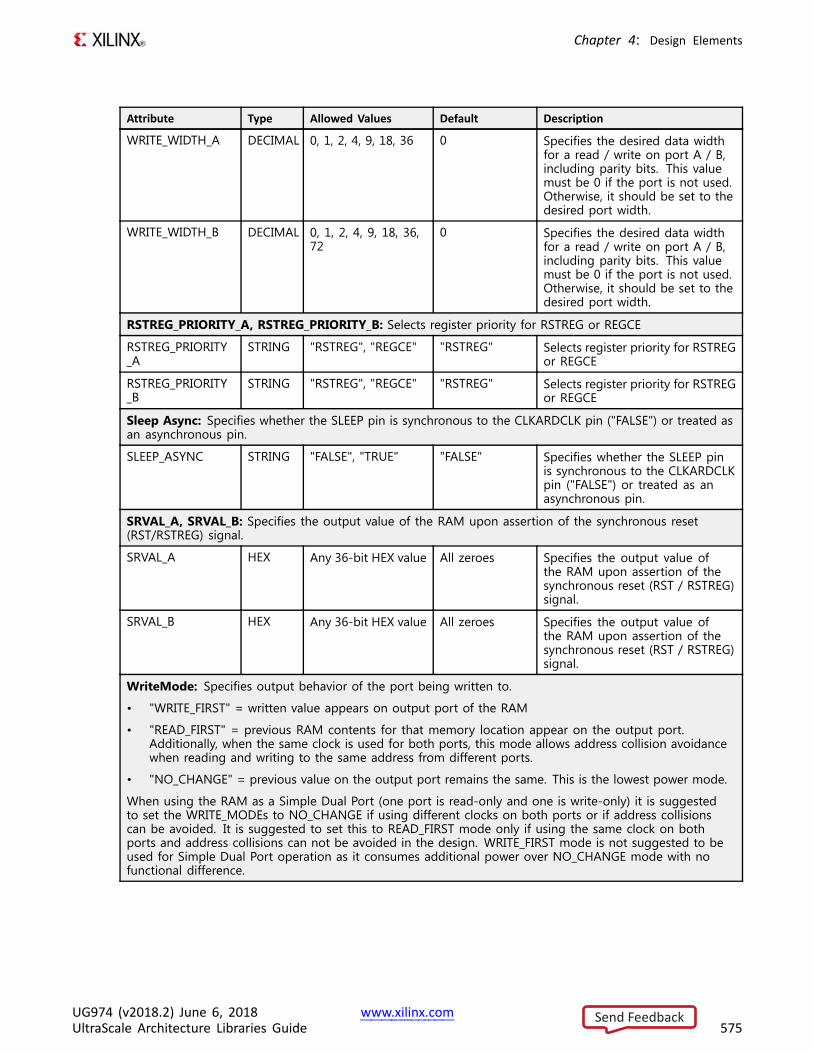
Chapter 4: Design Elements
Attribute Type Allowed Values Default Description
WRITE_WIDTH_A DECIMAL 0, 1, 2, 4, 9, 18, 36 0 Specifies the desired data widthfor a read / write on port A / B,including parity bits. This valuemust be 0 if the port is not used.Otherwise, it should be set to thedesired port width.
WRITE_WIDTH_B DECIMAL 0, 1, 2, 4, 9, 18, 36,72
0 Specifies the desired data widthfor a read / write on port A / B,including parity bits. This valuemust be 0 if the port is not used.Otherwise, it should be set to thedesired port width.
RSTREG_PRIORITY_A, RSTREG_PRIORITY_B: Selects register priority for RSTREG or REGCE
RSTREG_PRIORITY_A
STRING "RSTREG", "REGCE" "RSTREG" Selects register priority for RSTREGor REGCE
RSTREG_PRIORITY_B
STRING "RSTREG", "REGCE" "RSTREG" Selects register priority for RSTREGor REGCE
Sleep Async: Specifies whether the SLEEP pin is synchronous to the CLKARDCLK pin ("FALSE") or treated asan asynchronous pin.
SLEEP_ASYNC STRING "FALSE", "TRUE" "FALSE" Specifies whether the SLEEP pinis synchronous to the CLKARDCLKpin ("FALSE") or treated as anasynchronous pin.
SRVAL_A, SRVAL_B: Specifies the output value of the RAM upon assertion of the synchronous reset(RST/RSTREG) signal.
SRVAL_A HEX Any 36-bit HEX value All zeroes Specifies the output value ofthe RAM upon assertion of thesynchronous reset (RST / RSTREG)signal.
SRVAL_B HEX Any 36-bit HEX value All zeroes Specifies the output value ofthe RAM upon assertion of thesynchronous reset (RST / RSTREG)signal.
WriteMode: Specifies output behavior of the port being written to.
• "WRITE_FIRST" = written value appears on output port of the RAM
• "READ_FIRST" = previous RAM contents for that memory location appear on the output port.Additionally, when the same clock is used for both ports, this mode allows address collision avoidancewhen reading and writing to the same address from different ports.
• "NO_CHANGE" = previous value on the output port remains the same. This is the lowest power mode.
When using the RAM as a Simple Dual Port (one port is read-only and one is write-only) it is suggestedto set the WRITE_MODEs to NO_CHANGE if using different clocks on both ports or if address collisionscan be avoided. It is suggested to set this to READ_FIRST mode only if using the same clock on bothports and address collisions can not be avoided in the design. WRITE_FIRST mode is not suggested to beused for Simple Dual Port operation as it consumes additional power over NO_CHANGE mode with nofunctional difference.
UG974 (v2018.2) June 6, 2018 www.xilinx.comUltraScale Architecture Libraries Guide 575
Send Feedback
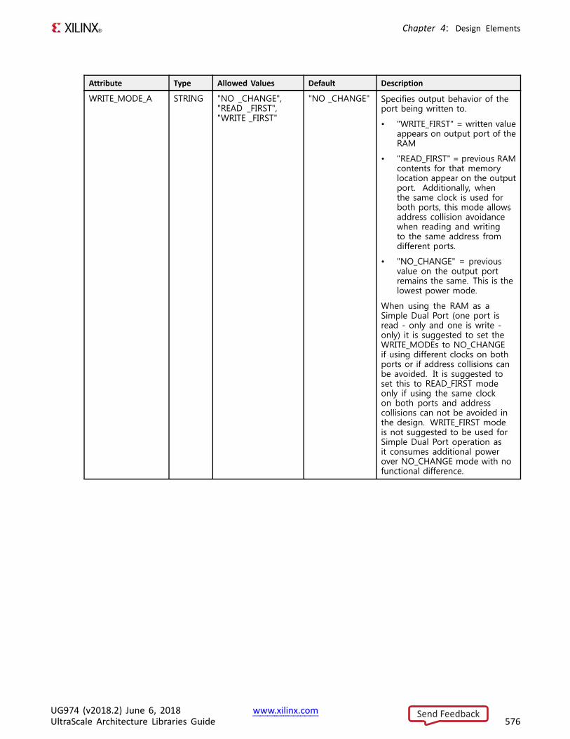
Chapter 4: Design Elements
Attribute Type Allowed Values Default Description
WRITE_MODE_A STRING "NO _CHANGE","READ _FIRST","WRITE _FIRST"
"NO _CHANGE" Specifies output behavior of theport being written to.
• "WRITE_FIRST" = written valueappears on output port of theRAM
• "READ_FIRST" = previous RAMcontents for that memorylocation appear on the outputport. Additionally, whenthe same clock is used forboth ports, this mode allowsaddress collision avoidancewhen reading and writingto the same address fromdifferent ports.
• "NO_CHANGE" = previousvalue on the output portremains the same. This is thelowest power mode.
When using the RAM as aSimple Dual Port (one port isread - only and one is write -only) it is suggested to set theWRITE_MODEs to NO_CHANGEif using different clocks on bothports or if address collisions canbe avoided. It is suggested toset this to READ_FIRST modeonly if using the same clockon both ports and addresscollisions can not be avoided inthe design. WRITE_FIRST modeis not suggested to be used forSimple Dual Port operation asit consumes additional powerover NO_CHANGE mode with nofunctional difference.
UG974 (v2018.2) June 6, 2018 www.xilinx.comUltraScale Architecture Libraries Guide 576
Send Feedback
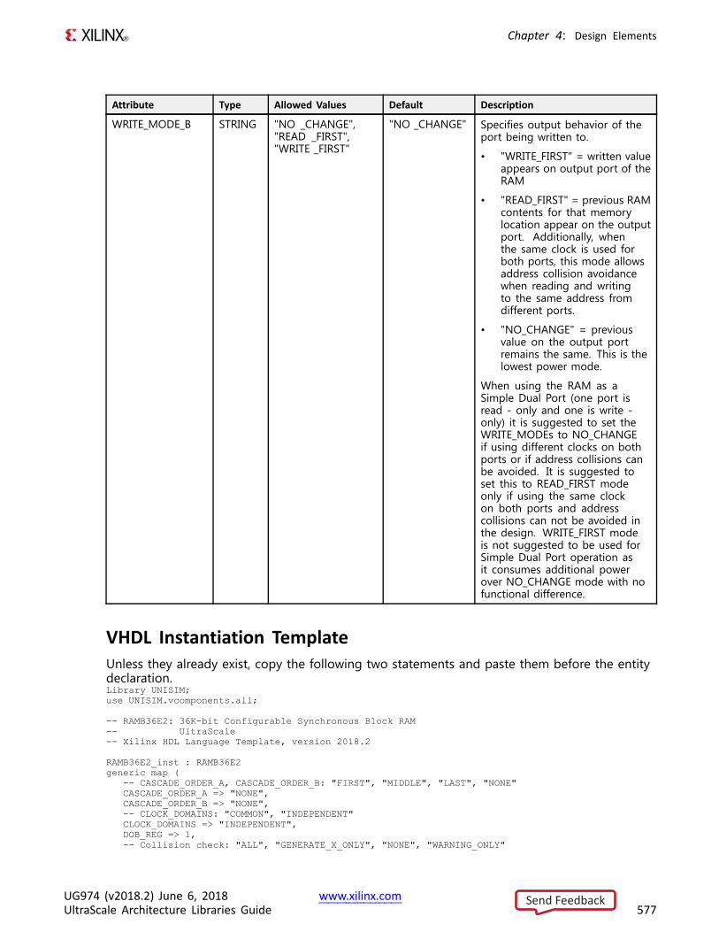
Chapter 4: Design Elements
Attribute Type Allowed Values Default Description
WRITE_MODE_B STRING "NO _CHANGE","READ _FIRST","WRITE _FIRST"
"NO _CHANGE" Specifies output behavior of theport being written to.
• "WRITE_FIRST" = written valueappears on output port of theRAM
• "READ_FIRST" = previous RAMcontents for that memorylocation appear on the outputport. Additionally, whenthe same clock is used forboth ports, this mode allowsaddress collision avoidancewhen reading and writingto the same address fromdifferent ports.
• "NO_CHANGE" = previousvalue on the output portremains the same. This is thelowest power mode.
When using the RAM as aSimple Dual Port (one port isread - only and one is write -only) it is suggested to set theWRITE_MODEs to NO_CHANGEif using different clocks on bothports or if address collisions canbe avoided. It is suggested toset this to READ_FIRST modeonly if using the same clockon both ports and addresscollisions can not be avoided inthe design. WRITE_FIRST modeis not suggested to be used forSimple Dual Port operation asit consumes additional powerover NO_CHANGE mode with nofunctional difference.
VHDL Instantiation TemplateUnless they already exist, copy the following two statements and paste them before the entitydeclaration.Library UNISIM;use UNISIM.vcomponents.all;
-- RAMB36E2: 36K-bit Configurable Synchronous Block RAM-- UltraScale-- Xilinx HDL Language Template, version 2018.2
RAMB36E2_inst : RAMB36E2generic map (
-- CASCADE_ORDER_A, CASCADE_ORDER_B: "FIRST", "MIDDLE", "LAST", "NONE"CASCADE_ORDER_A => "NONE",CASCADE_ORDER_B => "NONE",-- CLOCK_DOMAINS: "COMMON", "INDEPENDENT"CLOCK_DOMAINS => "INDEPENDENT",DOB_REG => 1,-- Collision check: "ALL", "GENERATE_X_ONLY", "NONE", "WARNING_ONLY"
UG974 (v2018.2) June 6, 2018 www.xilinx.comUltraScale Architecture Libraries Guide 577
Send Feedback
Chapter 4: Design Elements
SIM_COLLISION_CHECK => "ALL",-- DOA_REG, DOB_REG: Optional output register (0, 1)DOA_REG => 1,-- ENADDRENA/ENADDRENB: Address enable pin enable, "TRUE", "FALSE"ENADDRENA => "FALSE",ENADDRENB => "FALSE",-- EN_ECC_PIPE: ECC pipeline register, "TRUE"/"FALSE"EN_ECC_PIPE => "FALSE",-- EN_ECC_READ: Enable ECC decoder, "TRUE"/"FALSE"EN_ECC_READ => "FALSE",-- EN_ECC_WRITE: Enable ECC encoder, "TRUE"/"FALSE"EN_ECC_WRITE => "FALSE",-- INITP_00 to INITP_0F: Initial contents of parity memory arrayINITP_00 => X"0000000000000000000000000000000000000000000000000000000000000000",INITP_01 => X"0000000000000000000000000000000000000000000000000000000000000000",INITP_02 => X"0000000000000000000000000000000000000000000000000000000000000000",INITP_03 => X"0000000000000000000000000000000000000000000000000000000000000000",INITP_04 => X"0000000000000000000000000000000000000000000000000000000000000000",INITP_05 => X"0000000000000000000000000000000000000000000000000000000000000000",INITP_06 => X"0000000000000000000000000000000000000000000000000000000000000000",INITP_07 => X"0000000000000000000000000000000000000000000000000000000000000000",INITP_08 => X"0000000000000000000000000000000000000000000000000000000000000000",INITP_09 => X"0000000000000000000000000000000000000000000000000000000000000000",INITP_0A => X"0000000000000000000000000000000000000000000000000000000000000000",INITP_0B => X"0000000000000000000000000000000000000000000000000000000000000000",INITP_0C => X"0000000000000000000000000000000000000000000000000000000000000000",INITP_0D => X"0000000000000000000000000000000000000000000000000000000000000000",INITP_0E => X"0000000000000000000000000000000000000000000000000000000000000000",INITP_0F => X"0000000000000000000000000000000000000000000000000000000000000000",-- INIT_00 to INIT_7F: Initial contents of data memory arrayINIT_00 => X"0000000000000000000000000000000000000000000000000000000000000000",INIT_01 => X"0000000000000000000000000000000000000000000000000000000000000000",INIT_02 => X"0000000000000000000000000000000000000000000000000000000000000000",INIT_03 => X"0000000000000000000000000000000000000000000000000000000000000000",INIT_04 => X"0000000000000000000000000000000000000000000000000000000000000000",INIT_05 => X"0000000000000000000000000000000000000000000000000000000000000000",INIT_06 => X"0000000000000000000000000000000000000000000000000000000000000000",INIT_07 => X"0000000000000000000000000000000000000000000000000000000000000000",INIT_08 => X"0000000000000000000000000000000000000000000000000000000000000000",INIT_09 => X"0000000000000000000000000000000000000000000000000000000000000000",INIT_0A => X"0000000000000000000000000000000000000000000000000000000000000000",INIT_0B => X"0000000000000000000000000000000000000000000000000000000000000000",INIT_0C => X"0000000000000000000000000000000000000000000000000000000000000000",INIT_0D => X"0000000000000000000000000000000000000000000000000000000000000000",INIT_0E => X"0000000000000000000000000000000000000000000000000000000000000000",INIT_0F => X"0000000000000000000000000000000000000000000000000000000000000000",INIT_10 => X"0000000000000000000000000000000000000000000000000000000000000000",INIT_11 => X"0000000000000000000000000000000000000000000000000000000000000000",INIT_12 => X"0000000000000000000000000000000000000000000000000000000000000000",INIT_13 => X"0000000000000000000000000000000000000000000000000000000000000000",INIT_14 => X"0000000000000000000000000000000000000000000000000000000000000000",INIT_15 => X"0000000000000000000000000000000000000000000000000000000000000000",INIT_16 => X"0000000000000000000000000000000000000000000000000000000000000000",INIT_17 => X"0000000000000000000000000000000000000000000000000000000000000000",INIT_18 => X"0000000000000000000000000000000000000000000000000000000000000000",INIT_19 => X"0000000000000000000000000000000000000000000000000000000000000000",INIT_1A => X"0000000000000000000000000000000000000000000000000000000000000000",INIT_1B => X"0000000000000000000000000000000000000000000000000000000000000000",INIT_1C => X"0000000000000000000000000000000000000000000000000000000000000000",INIT_1D => X"0000000000000000000000000000000000000000000000000000000000000000",INIT_1E => X"0000000000000000000000000000000000000000000000000000000000000000",INIT_1F => X"0000000000000000000000000000000000000000000000000000000000000000",INIT_20 => X"0000000000000000000000000000000000000000000000000000000000000000",INIT_21 => X"0000000000000000000000000000000000000000000000000000000000000000",INIT_22 => X"0000000000000000000000000000000000000000000000000000000000000000",INIT_23 => X"0000000000000000000000000000000000000000000000000000000000000000",INIT_24 => X"0000000000000000000000000000000000000000000000000000000000000000",INIT_25 => X"0000000000000000000000000000000000000000000000000000000000000000",INIT_26 => X"0000000000000000000000000000000000000000000000000000000000000000",INIT_27 => X"0000000000000000000000000000000000000000000000000000000000000000",INIT_28 => X"0000000000000000000000000000000000000000000000000000000000000000",INIT_29 => X"0000000000000000000000000000000000000000000000000000000000000000",
UG974 (v2018.2) June 6, 2018 www.xilinx.comUltraScale Architecture Libraries Guide 578
Send Feedback
Chapter 4: Design Elements
INIT_2A => X"0000000000000000000000000000000000000000000000000000000000000000",INIT_2B => X"0000000000000000000000000000000000000000000000000000000000000000",INIT_2C => X"0000000000000000000000000000000000000000000000000000000000000000",INIT_2D => X"0000000000000000000000000000000000000000000000000000000000000000",INIT_2E => X"0000000000000000000000000000000000000000000000000000000000000000",INIT_2F => X"0000000000000000000000000000000000000000000000000000000000000000",INIT_30 => X"0000000000000000000000000000000000000000000000000000000000000000",INIT_31 => X"0000000000000000000000000000000000000000000000000000000000000000",INIT_32 => X"0000000000000000000000000000000000000000000000000000000000000000",INIT_33 => X"0000000000000000000000000000000000000000000000000000000000000000",INIT_34 => X"0000000000000000000000000000000000000000000000000000000000000000",INIT_35 => X"0000000000000000000000000000000000000000000000000000000000000000",INIT_36 => X"0000000000000000000000000000000000000000000000000000000000000000",INIT_37 => X"0000000000000000000000000000000000000000000000000000000000000000",INIT_38 => X"0000000000000000000000000000000000000000000000000000000000000000",INIT_39 => X"0000000000000000000000000000000000000000000000000000000000000000",INIT_3A => X"0000000000000000000000000000000000000000000000000000000000000000",INIT_3B => X"0000000000000000000000000000000000000000000000000000000000000000",INIT_3C => X"0000000000000000000000000000000000000000000000000000000000000000",INIT_3D => X"0000000000000000000000000000000000000000000000000000000000000000",INIT_3E => X"0000000000000000000000000000000000000000000000000000000000000000",INIT_3F => X"0000000000000000000000000000000000000000000000000000000000000000",INIT_40 => X"0000000000000000000000000000000000000000000000000000000000000000",INIT_41 => X"0000000000000000000000000000000000000000000000000000000000000000",INIT_42 => X"0000000000000000000000000000000000000000000000000000000000000000",INIT_43 => X"0000000000000000000000000000000000000000000000000000000000000000",INIT_44 => X"0000000000000000000000000000000000000000000000000000000000000000",INIT_45 => X"0000000000000000000000000000000000000000000000000000000000000000",INIT_46 => X"0000000000000000000000000000000000000000000000000000000000000000",INIT_47 => X"0000000000000000000000000000000000000000000000000000000000000000",INIT_48 => X"0000000000000000000000000000000000000000000000000000000000000000",INIT_49 => X"0000000000000000000000000000000000000000000000000000000000000000",INIT_4A => X"0000000000000000000000000000000000000000000000000000000000000000",INIT_4B => X"0000000000000000000000000000000000000000000000000000000000000000",INIT_4C => X"0000000000000000000000000000000000000000000000000000000000000000",INIT_4D => X"0000000000000000000000000000000000000000000000000000000000000000",INIT_4E => X"0000000000000000000000000000000000000000000000000000000000000000",INIT_4F => X"0000000000000000000000000000000000000000000000000000000000000000",INIT_50 => X"0000000000000000000000000000000000000000000000000000000000000000",INIT_51 => X"0000000000000000000000000000000000000000000000000000000000000000",INIT_52 => X"0000000000000000000000000000000000000000000000000000000000000000",INIT_53 => X"0000000000000000000000000000000000000000000000000000000000000000",INIT_54 => X"0000000000000000000000000000000000000000000000000000000000000000",INIT_55 => X"0000000000000000000000000000000000000000000000000000000000000000",INIT_56 => X"0000000000000000000000000000000000000000000000000000000000000000",INIT_57 => X"0000000000000000000000000000000000000000000000000000000000000000",INIT_58 => X"0000000000000000000000000000000000000000000000000000000000000000",INIT_59 => X"0000000000000000000000000000000000000000000000000000000000000000",INIT_5A => X"0000000000000000000000000000000000000000000000000000000000000000",INIT_5B => X"0000000000000000000000000000000000000000000000000000000000000000",INIT_5C => X"0000000000000000000000000000000000000000000000000000000000000000",INIT_5D => X"0000000000000000000000000000000000000000000000000000000000000000",INIT_5E => X"0000000000000000000000000000000000000000000000000000000000000000",INIT_5F => X"0000000000000000000000000000000000000000000000000000000000000000",INIT_60 => X"0000000000000000000000000000000000000000000000000000000000000000",INIT_61 => X"0000000000000000000000000000000000000000000000000000000000000000",INIT_62 => X"0000000000000000000000000000000000000000000000000000000000000000",INIT_63 => X"0000000000000000000000000000000000000000000000000000000000000000",INIT_64 => X"0000000000000000000000000000000000000000000000000000000000000000",INIT_65 => X"0000000000000000000000000000000000000000000000000000000000000000",INIT_66 => X"0000000000000000000000000000000000000000000000000000000000000000",INIT_67 => X"0000000000000000000000000000000000000000000000000000000000000000",INIT_68 => X"0000000000000000000000000000000000000000000000000000000000000000",INIT_69 => X"0000000000000000000000000000000000000000000000000000000000000000",INIT_6A => X"0000000000000000000000000000000000000000000000000000000000000000",INIT_6B => X"0000000000000000000000000000000000000000000000000000000000000000",INIT_6C => X"0000000000000000000000000000000000000000000000000000000000000000",INIT_6D => X"0000000000000000000000000000000000000000000000000000000000000000",INIT_6E => X"0000000000000000000000000000000000000000000000000000000000000000",INIT_6F => X"0000000000000000000000000000000000000000000000000000000000000000",INIT_70 => X"0000000000000000000000000000000000000000000000000000000000000000",INIT_71 => X"0000000000000000000000000000000000000000000000000000000000000000",
UG974 (v2018.2) June 6, 2018 www.xilinx.comUltraScale Architecture Libraries Guide 579
Send Feedback
Chapter 4: Design Elements
INIT_72 => X"0000000000000000000000000000000000000000000000000000000000000000",INIT_73 => X"0000000000000000000000000000000000000000000000000000000000000000",INIT_74 => X"0000000000000000000000000000000000000000000000000000000000000000",INIT_75 => X"0000000000000000000000000000000000000000000000000000000000000000",INIT_76 => X"0000000000000000000000000000000000000000000000000000000000000000",INIT_77 => X"0000000000000000000000000000000000000000000000000000000000000000",INIT_78 => X"0000000000000000000000000000000000000000000000000000000000000000",INIT_79 => X"0000000000000000000000000000000000000000000000000000000000000000",INIT_7A => X"0000000000000000000000000000000000000000000000000000000000000000",INIT_7B => X"0000000000000000000000000000000000000000000000000000000000000000",INIT_7C => X"0000000000000000000000000000000000000000000000000000000000000000",INIT_7D => X"0000000000000000000000000000000000000000000000000000000000000000",INIT_7E => X"0000000000000000000000000000000000000000000000000000000000000000",INIT_7F => X"0000000000000000000000000000000000000000000000000000000000000000",-- INIT_A, INIT_B: Initial values on output portsINIT_A => X"000000000",INIT_B => X"000000000",-- Initialization File: RAM initialization fileINIT_FILE => "NONE",-- Programmable Inversion Attributes: Specifies the use of the built-in programmable inversionIS_CLKARDCLK_INVERTED => '0',IS_CLKBWRCLK_INVERTED => '0',IS_ENARDEN_INVERTED => '0',IS_ENBWREN_INVERTED => '0',IS_RSTRAMARSTRAM_INVERTED => '0',IS_RSTRAMB_INVERTED => '0',IS_RSTREGARSTREG_INVERTED => '0',IS_RSTREGB_INVERTED => '0',-- RDADDRCHANGE: Disable memory access when output value does not change ("TRUE", "FALSE")RDADDRCHANGEA => "FALSE",RDADDRCHANGEB => "FALSE",-- READ_WIDTH_A/B, WRITE_WIDTH_A/B: Read/write width per portREAD_WIDTH_A => 0, -- 0-9READ_WIDTH_B => 0, -- 0-9WRITE_WIDTH_A => 0, -- 0-9WRITE_WIDTH_B => 0, -- 0-9-- RSTREG_PRIORITY_A, RSTREG_PRIORITY_B: Reset or enable priority ("RSTREG", "REGCE")RSTREG_PRIORITY_A => "RSTREG",RSTREG_PRIORITY_B => "RSTREG",-- SRVAL_A, SRVAL_B: Set/reset value for outputSRVAL_A => X"000000000",SRVAL_B => X"000000000",-- Sleep Async: Sleep function asynchronous or synchronous ("TRUE", "FALSE")SLEEP_ASYNC => "FALSE",-- WriteMode: "WRITE_FIRST", "NO_CHANGE", "READ_FIRST"WRITE_MODE_A => "NO_CHANGE",WRITE_MODE_B => "NO_CHANGE"
)port map (
-- Cascade Signals outputs: Multi-BRAM cascade signalsCASDOUTA => CASDOUTA, -- 32-bit output: Port A cascade output dataCASDOUTB => CASDOUTB, -- 32-bit output: Port B cascade output dataCASDOUTPA => CASDOUTPA, -- 4-bit output: Port A cascade output parity dataCASDOUTPB => CASDOUTPB, -- 4-bit output: Port B cascade output parity dataCASOUTDBITERR => CASOUTDBITERR, -- 1-bit output: DBITERR cascade outputCASOUTSBITERR => CASOUTSBITERR, -- 1-bit output: SBITERR cascade output-- ECC Signals outputs: Error Correction Circuitry portsDBITERR => DBITERR, -- 1-bit output: Double bit error statusECCPARITY => ECCPARITY, -- 8-bit output: Generated error correction parityRDADDRECC => RDADDRECC, -- 9-bit output: ECC Read AddressSBITERR => SBITERR, -- 1-bit output: Single bit error status-- Port A Data outputs: Port A dataDOUTADOUT => DOUTADOUT, -- 32-bit output: Port A ata/LSB dataDOUTPADOUTP => DOUTPADOUTP, -- 4-bit output: Port A parity/LSB parity-- Port B Data outputs: Port B dataDOUTBDOUT => DOUTBDOUT, -- 32-bit output: Port B data/MSB dataDOUTPBDOUTP => DOUTPBDOUTP, -- 4-bit output: Port B parity/MSB parity-- Cascade Signals inputs: Multi-BRAM cascade signalsCASDIMUXA => CASDIMUXA, -- 1-bit input: Port A input data (0=DINA, 1=CASDINA)CASDIMUXB => CASDIMUXB, -- 1-bit input: Port B input data (0=DINB, 1=CASDINB)CASDINA => CASDINA, -- 32-bit input: Port A cascade input dataCASDINB => CASDINB, -- 32-bit input: Port B cascade input data
UG974 (v2018.2) June 6, 2018 www.xilinx.comUltraScale Architecture Libraries Guide 580
Send Feedback
Chapter 4: Design Elements
CASDINPA => CASDINPA, -- 4-bit input: Port A cascade input parity dataCASDINPB => CASDINPB, -- 4-bit input: Port B cascade input parity dataCASDOMUXA => CASDOMUXA, -- 1-bit input: Port A unregistered data (0=BRAM data, 1=CASDINA)CASDOMUXB => CASDOMUXB, -- 1-bit input: Port B unregistered data (0=BRAM data, 1=CASDINB)CASDOMUXEN_A => CASDOMUXEN_A, -- 1-bit input: Port A unregistered output data enableCASDOMUXEN_B => CASDOMUXEN_B, -- 1-bit input: Port B unregistered output data enableCASINDBITERR => CASINDBITERR, -- 1-bit input: DBITERR cascade inputCASINSBITERR => CASINSBITERR, -- 1-bit input: SBITERR cascade inputCASOREGIMUXA => CASOREGIMUXA, -- 1-bit input: Port A registered data (0=BRAM data, 1=CASDINA)CASOREGIMUXB => CASOREGIMUXB, -- 1-bit input: Port B registered data (0=BRAM data, 1=CASDINB)CASOREGIMUXEN_A => CASOREGIMUXEN_A, -- 1-bit input: Port A registered output data enableCASOREGIMUXEN_B => CASOREGIMUXEN_B, -- 1-bit input: Port B registered output data enable-- ECC Signals inputs: Error Correction Circuitry portsECCPIPECE => ECCPIPECE, -- 1-bit input: ECC Pipeline Register EnableINJECTDBITERR => INJECTDBITERR, -- 1-bit input: Inject a double bit errorINJECTSBITERR => INJECTSBITERR,-- Port A Address/Control Signals inputs: Port A address and control signalsADDRARDADDR => ADDRARDADDR, -- 15-bit input: A/Read port addressADDRENA => ADDRENA, -- 1-bit input: Active-High A/Read port address enableCLKARDCLK => CLKARDCLK, -- 1-bit input: A/Read port clockENARDEN => ENARDEN, -- 1-bit input: Port A enable/Read enableREGCEAREGCE => REGCEAREGCE, -- 1-bit input: Port A register enable/Register enableRSTRAMARSTRAM => RSTRAMARSTRAM, -- 1-bit input: Port A set/resetRSTREGARSTREG => RSTREGARSTREG, -- 1-bit input: Port A register set/resetSLEEP => SLEEP, -- 1-bit input: Sleep ModeWEA => WEA, -- 4-bit input: Port A write enable-- Port A Data inputs: Port A dataDINADIN => DINADIN, -- 32-bit input: Port A data/LSB dataDINPADINP => DINPADINP, -- 4-bit input: Port A parity/LSB parity-- Port B Address/Control Signals inputs: Port B address and control signalsADDRBWRADDR => ADDRBWRADDR, -- 15-bit input: B/Write port addressADDRENB => ADDRENB, -- 1-bit input: Active-High B/Write port address enableCLKBWRCLK => CLKBWRCLK, -- 1-bit input: B/Write port clockENBWREN => ENBWREN, -- 1-bit input: Port B enable/Write enableREGCEB => REGCEB, -- 1-bit input: Port B register enableRSTRAMB => RSTRAMB, -- 1-bit input: Port B set/resetRSTREGB => RSTREGB, -- 1-bit input: Port B register set/resetWEBWE => WEBWE, -- 8-bit input: Port B write enable/Write enable-- Port B Data inputs: Port B dataDINBDIN => DINBDIN, -- 32-bit input: Port B data/MSB dataDINPBDINP => DINPBDINP -- 4-bit input: Port B parity/MSB parity
);
-- End of RAMB36E2_inst instantiation
Verilog Instantiation Template
// RAMB36E2: 36K-bit Configurable Synchronous Block RAM// UltraScale// Xilinx HDL Language Template, version 2018.2
RAMB36E2 #(// CASCADE_ORDER_A, CASCADE_ORDER_B: "FIRST", "MIDDLE", "LAST", "NONE".CASCADE_ORDER_A("NONE"),.CASCADE_ORDER_B("NONE"),// CLOCK_DOMAINS: "COMMON", "INDEPENDENT".CLOCK_DOMAINS("INDEPENDENT"),.DOB_REG(1),// Collision check: "ALL", "GENERATE_X_ONLY", "NONE", "WARNING_ONLY".SIM_COLLISION_CHECK("ALL"),// DOA_REG, DOB_REG: Optional output register (0, 1).DOA_REG(1),// ENADDRENA/ENADDRENB: Address enable pin enable, "TRUE", "FALSE".ENADDRENA("FALSE"),.ENADDRENB("FALSE"),// EN_ECC_PIPE: ECC pipeline register, "TRUE"/"FALSE".EN_ECC_PIPE("FALSE"),// EN_ECC_READ: Enable ECC decoder, "TRUE"/"FALSE"
UG974 (v2018.2) June 6, 2018 www.xilinx.comUltraScale Architecture Libraries Guide 581
Send Feedback
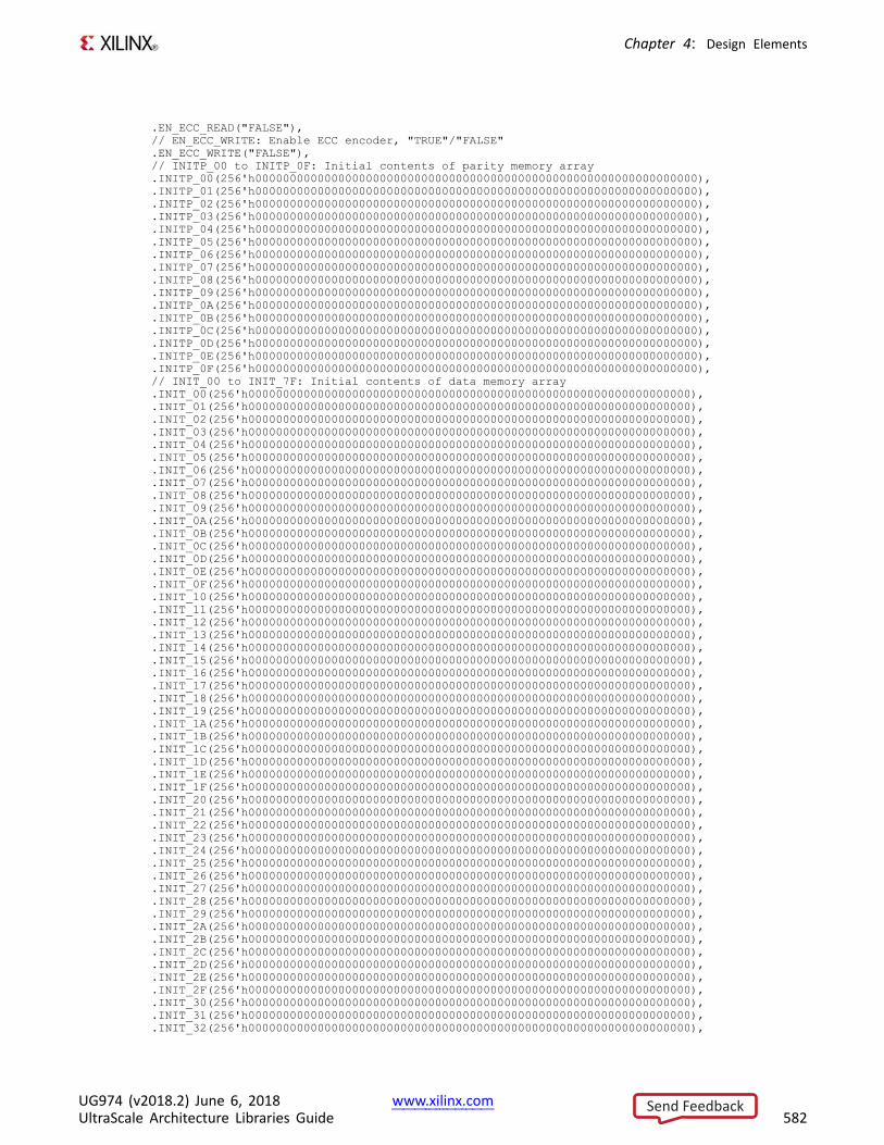
Chapter 4: Design Elements
.EN_ECC_READ("FALSE"),// EN_ECC_WRITE: Enable ECC encoder, "TRUE"/"FALSE".EN_ECC_WRITE("FALSE"),// INITP_00 to INITP_0F: Initial contents of parity memory array.INITP_00(256'h0000000000000000000000000000000000000000000000000000000000000000),.INITP_01(256'h0000000000000000000000000000000000000000000000000000000000000000),.INITP_02(256'h0000000000000000000000000000000000000000000000000000000000000000),.INITP_03(256'h0000000000000000000000000000000000000000000000000000000000000000),.INITP_04(256'h0000000000000000000000000000000000000000000000000000000000000000),.INITP_05(256'h0000000000000000000000000000000000000000000000000000000000000000),.INITP_06(256'h0000000000000000000000000000000000000000000000000000000000000000),.INITP_07(256'h0000000000000000000000000000000000000000000000000000000000000000),.INITP_08(256'h0000000000000000000000000000000000000000000000000000000000000000),.INITP_09(256'h0000000000000000000000000000000000000000000000000000000000000000),.INITP_0A(256'h0000000000000000000000000000000000000000000000000000000000000000),.INITP_0B(256'h0000000000000000000000000000000000000000000000000000000000000000),.INITP_0C(256'h0000000000000000000000000000000000000000000000000000000000000000),.INITP_0D(256'h0000000000000000000000000000000000000000000000000000000000000000),.INITP_0E(256'h0000000000000000000000000000000000000000000000000000000000000000),.INITP_0F(256'h0000000000000000000000000000000000000000000000000000000000000000),// INIT_00 to INIT_7F: Initial contents of data memory array.INIT_00(256'h0000000000000000000000000000000000000000000000000000000000000000),.INIT_01(256'h0000000000000000000000000000000000000000000000000000000000000000),.INIT_02(256'h0000000000000000000000000000000000000000000000000000000000000000),.INIT_03(256'h0000000000000000000000000000000000000000000000000000000000000000),.INIT_04(256'h0000000000000000000000000000000000000000000000000000000000000000),.INIT_05(256'h0000000000000000000000000000000000000000000000000000000000000000),.INIT_06(256'h0000000000000000000000000000000000000000000000000000000000000000),.INIT_07(256'h0000000000000000000000000000000000000000000000000000000000000000),.INIT_08(256'h0000000000000000000000000000000000000000000000000000000000000000),.INIT_09(256'h0000000000000000000000000000000000000000000000000000000000000000),.INIT_0A(256'h0000000000000000000000000000000000000000000000000000000000000000),.INIT_0B(256'h0000000000000000000000000000000000000000000000000000000000000000),.INIT_0C(256'h0000000000000000000000000000000000000000000000000000000000000000),.INIT_0D(256'h0000000000000000000000000000000000000000000000000000000000000000),.INIT_0E(256'h0000000000000000000000000000000000000000000000000000000000000000),.INIT_0F(256'h0000000000000000000000000000000000000000000000000000000000000000),.INIT_10(256'h0000000000000000000000000000000000000000000000000000000000000000),.INIT_11(256'h0000000000000000000000000000000000000000000000000000000000000000),.INIT_12(256'h0000000000000000000000000000000000000000000000000000000000000000),.INIT_13(256'h0000000000000000000000000000000000000000000000000000000000000000),.INIT_14(256'h0000000000000000000000000000000000000000000000000000000000000000),.INIT_15(256'h0000000000000000000000000000000000000000000000000000000000000000),.INIT_16(256'h0000000000000000000000000000000000000000000000000000000000000000),.INIT_17(256'h0000000000000000000000000000000000000000000000000000000000000000),.INIT_18(256'h0000000000000000000000000000000000000000000000000000000000000000),.INIT_19(256'h0000000000000000000000000000000000000000000000000000000000000000),.INIT_1A(256'h0000000000000000000000000000000000000000000000000000000000000000),.INIT_1B(256'h0000000000000000000000000000000000000000000000000000000000000000),.INIT_1C(256'h0000000000000000000000000000000000000000000000000000000000000000),.INIT_1D(256'h0000000000000000000000000000000000000000000000000000000000000000),.INIT_1E(256'h0000000000000000000000000000000000000000000000000000000000000000),.INIT_1F(256'h0000000000000000000000000000000000000000000000000000000000000000),.INIT_20(256'h0000000000000000000000000000000000000000000000000000000000000000),.INIT_21(256'h0000000000000000000000000000000000000000000000000000000000000000),.INIT_22(256'h0000000000000000000000000000000000000000000000000000000000000000),.INIT_23(256'h0000000000000000000000000000000000000000000000000000000000000000),.INIT_24(256'h0000000000000000000000000000000000000000000000000000000000000000),.INIT_25(256'h0000000000000000000000000000000000000000000000000000000000000000),.INIT_26(256'h0000000000000000000000000000000000000000000000000000000000000000),.INIT_27(256'h0000000000000000000000000000000000000000000000000000000000000000),.INIT_28(256'h0000000000000000000000000000000000000000000000000000000000000000),.INIT_29(256'h0000000000000000000000000000000000000000000000000000000000000000),.INIT_2A(256'h0000000000000000000000000000000000000000000000000000000000000000),.INIT_2B(256'h0000000000000000000000000000000000000000000000000000000000000000),.INIT_2C(256'h0000000000000000000000000000000000000000000000000000000000000000),.INIT_2D(256'h0000000000000000000000000000000000000000000000000000000000000000),.INIT_2E(256'h0000000000000000000000000000000000000000000000000000000000000000),.INIT_2F(256'h0000000000000000000000000000000000000000000000000000000000000000),.INIT_30(256'h0000000000000000000000000000000000000000000000000000000000000000),.INIT_31(256'h0000000000000000000000000000000000000000000000000000000000000000),.INIT_32(256'h0000000000000000000000000000000000000000000000000000000000000000),
UG974 (v2018.2) June 6, 2018 www.xilinx.comUltraScale Architecture Libraries Guide 582
Send Feedback
Chapter 4: Design Elements
.INIT_33(256'h0000000000000000000000000000000000000000000000000000000000000000),
.INIT_34(256'h0000000000000000000000000000000000000000000000000000000000000000),
.INIT_35(256'h0000000000000000000000000000000000000000000000000000000000000000),
.INIT_36(256'h0000000000000000000000000000000000000000000000000000000000000000),
.INIT_37(256'h0000000000000000000000000000000000000000000000000000000000000000),
.INIT_38(256'h0000000000000000000000000000000000000000000000000000000000000000),
.INIT_39(256'h0000000000000000000000000000000000000000000000000000000000000000),
.INIT_3A(256'h0000000000000000000000000000000000000000000000000000000000000000),
.INIT_3B(256'h0000000000000000000000000000000000000000000000000000000000000000),
.INIT_3C(256'h0000000000000000000000000000000000000000000000000000000000000000),
.INIT_3D(256'h0000000000000000000000000000000000000000000000000000000000000000),
.INIT_3E(256'h0000000000000000000000000000000000000000000000000000000000000000),
.INIT_3F(256'h0000000000000000000000000000000000000000000000000000000000000000),
.INIT_40(256'h0000000000000000000000000000000000000000000000000000000000000000),
.INIT_41(256'h0000000000000000000000000000000000000000000000000000000000000000),
.INIT_42(256'h0000000000000000000000000000000000000000000000000000000000000000),
.INIT_43(256'h0000000000000000000000000000000000000000000000000000000000000000),
.INIT_44(256'h0000000000000000000000000000000000000000000000000000000000000000),
.INIT_45(256'h0000000000000000000000000000000000000000000000000000000000000000),
.INIT_46(256'h0000000000000000000000000000000000000000000000000000000000000000),
.INIT_47(256'h0000000000000000000000000000000000000000000000000000000000000000),
.INIT_48(256'h0000000000000000000000000000000000000000000000000000000000000000),
.INIT_49(256'h0000000000000000000000000000000000000000000000000000000000000000),
.INIT_4A(256'h0000000000000000000000000000000000000000000000000000000000000000),
.INIT_4B(256'h0000000000000000000000000000000000000000000000000000000000000000),
.INIT_4C(256'h0000000000000000000000000000000000000000000000000000000000000000),
.INIT_4D(256'h0000000000000000000000000000000000000000000000000000000000000000),
.INIT_4E(256'h0000000000000000000000000000000000000000000000000000000000000000),
.INIT_4F(256'h0000000000000000000000000000000000000000000000000000000000000000),
.INIT_50(256'h0000000000000000000000000000000000000000000000000000000000000000),
.INIT_51(256'h0000000000000000000000000000000000000000000000000000000000000000),
.INIT_52(256'h0000000000000000000000000000000000000000000000000000000000000000),
.INIT_53(256'h0000000000000000000000000000000000000000000000000000000000000000),
.INIT_54(256'h0000000000000000000000000000000000000000000000000000000000000000),
.INIT_55(256'h0000000000000000000000000000000000000000000000000000000000000000),
.INIT_56(256'h0000000000000000000000000000000000000000000000000000000000000000),
.INIT_57(256'h0000000000000000000000000000000000000000000000000000000000000000),
.INIT_58(256'h0000000000000000000000000000000000000000000000000000000000000000),
.INIT_59(256'h0000000000000000000000000000000000000000000000000000000000000000),
.INIT_5A(256'h0000000000000000000000000000000000000000000000000000000000000000),
.INIT_5B(256'h0000000000000000000000000000000000000000000000000000000000000000),
.INIT_5C(256'h0000000000000000000000000000000000000000000000000000000000000000),
.INIT_5D(256'h0000000000000000000000000000000000000000000000000000000000000000),
.INIT_5E(256'h0000000000000000000000000000000000000000000000000000000000000000),
.INIT_5F(256'h0000000000000000000000000000000000000000000000000000000000000000),
.INIT_60(256'h0000000000000000000000000000000000000000000000000000000000000000),
.INIT_61(256'h0000000000000000000000000000000000000000000000000000000000000000),
.INIT_62(256'h0000000000000000000000000000000000000000000000000000000000000000),
.INIT_63(256'h0000000000000000000000000000000000000000000000000000000000000000),
.INIT_64(256'h0000000000000000000000000000000000000000000000000000000000000000),
.INIT_65(256'h0000000000000000000000000000000000000000000000000000000000000000),
.INIT_66(256'h0000000000000000000000000000000000000000000000000000000000000000),
.INIT_67(256'h0000000000000000000000000000000000000000000000000000000000000000),
.INIT_68(256'h0000000000000000000000000000000000000000000000000000000000000000),
.INIT_69(256'h0000000000000000000000000000000000000000000000000000000000000000),
.INIT_6A(256'h0000000000000000000000000000000000000000000000000000000000000000),
.INIT_6B(256'h0000000000000000000000000000000000000000000000000000000000000000),
.INIT_6C(256'h0000000000000000000000000000000000000000000000000000000000000000),
.INIT_6D(256'h0000000000000000000000000000000000000000000000000000000000000000),
.INIT_6E(256'h0000000000000000000000000000000000000000000000000000000000000000),
.INIT_6F(256'h0000000000000000000000000000000000000000000000000000000000000000),
.INIT_70(256'h0000000000000000000000000000000000000000000000000000000000000000),
.INIT_71(256'h0000000000000000000000000000000000000000000000000000000000000000),
.INIT_72(256'h0000000000000000000000000000000000000000000000000000000000000000),
.INIT_73(256'h0000000000000000000000000000000000000000000000000000000000000000),
.INIT_74(256'h0000000000000000000000000000000000000000000000000000000000000000),
.INIT_75(256'h0000000000000000000000000000000000000000000000000000000000000000),
.INIT_76(256'h0000000000000000000000000000000000000000000000000000000000000000),
.INIT_77(256'h0000000000000000000000000000000000000000000000000000000000000000),
.INIT_78(256'h0000000000000000000000000000000000000000000000000000000000000000),
.INIT_79(256'h0000000000000000000000000000000000000000000000000000000000000000),
.INIT_7A(256'h0000000000000000000000000000000000000000000000000000000000000000),
UG974 (v2018.2) June 6, 2018 www.xilinx.comUltraScale Architecture Libraries Guide 583
Send Feedback
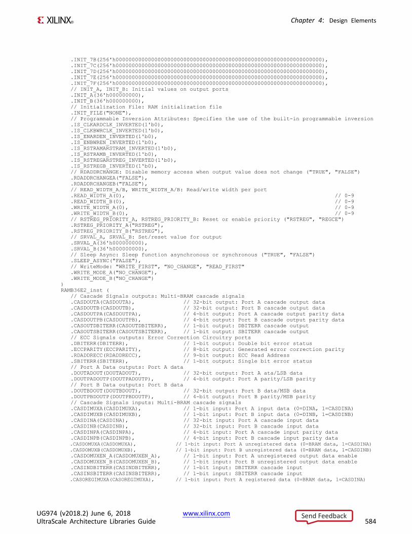
Chapter 4: Design Elements
.INIT_7B(256'h0000000000000000000000000000000000000000000000000000000000000000),
.INIT_7C(256'h0000000000000000000000000000000000000000000000000000000000000000),
.INIT_7D(256'h0000000000000000000000000000000000000000000000000000000000000000),
.INIT_7E(256'h0000000000000000000000000000000000000000000000000000000000000000),
.INIT_7F(256'h0000000000000000000000000000000000000000000000000000000000000000),// INIT_A, INIT_B: Initial values on output ports.INIT_A(36'h000000000),.INIT_B(36'h000000000),// Initialization File: RAM initialization file.INIT_FILE("NONE"),// Programmable Inversion Attributes: Specifies the use of the built-in programmable inversion.IS_CLKARDCLK_INVERTED(1'b0),.IS_CLKBWRCLK_INVERTED(1'b0),.IS_ENARDEN_INVERTED(1'b0),.IS_ENBWREN_INVERTED(1'b0),.IS_RSTRAMARSTRAM_INVERTED(1'b0),.IS_RSTRAMB_INVERTED(1'b0),.IS_RSTREGARSTREG_INVERTED(1'b0),.IS_RSTREGB_INVERTED(1'b0),// RDADDRCHANGE: Disable memory access when output value does not change ("TRUE", "FALSE").RDADDRCHANGEA("FALSE"),.RDADDRCHANGEB("FALSE"),// READ_WIDTH_A/B, WRITE_WIDTH_A/B: Read/write width per port.READ_WIDTH_A(0), // 0-9.READ_WIDTH_B(0), // 0-9.WRITE_WIDTH_A(0), // 0-9.WRITE_WIDTH_B(0), // 0-9// RSTREG_PRIORITY_A, RSTREG_PRIORITY_B: Reset or enable priority ("RSTREG", "REGCE").RSTREG_PRIORITY_A("RSTREG"),.RSTREG_PRIORITY_B("RSTREG"),// SRVAL_A, SRVAL_B: Set/reset value for output.SRVAL_A(36'h000000000),.SRVAL_B(36'h000000000),// Sleep Async: Sleep function asynchronous or synchronous ("TRUE", "FALSE").SLEEP_ASYNC("FALSE"),// WriteMode: "WRITE_FIRST", "NO_CHANGE", "READ_FIRST".WRITE_MODE_A("NO_CHANGE"),.WRITE_MODE_B("NO_CHANGE")
)RAMB36E2_inst (
// Cascade Signals outputs: Multi-BRAM cascade signals.CASDOUTA(CASDOUTA), // 32-bit output: Port A cascade output data.CASDOUTB(CASDOUTB), // 32-bit output: Port B cascade output data.CASDOUTPA(CASDOUTPA), // 4-bit output: Port A cascade output parity data.CASDOUTPB(CASDOUTPB), // 4-bit output: Port B cascade output parity data.CASOUTDBITERR(CASOUTDBITERR), // 1-bit output: DBITERR cascade output.CASOUTSBITERR(CASOUTSBITERR), // 1-bit output: SBITERR cascade output// ECC Signals outputs: Error Correction Circuitry ports.DBITERR(DBITERR), // 1-bit output: Double bit error status.ECCPARITY(ECCPARITY), // 8-bit output: Generated error correction parity.RDADDRECC(RDADDRECC), // 9-bit output: ECC Read Address.SBITERR(SBITERR), // 1-bit output: Single bit error status// Port A Data outputs: Port A data.DOUTADOUT(DOUTADOUT), // 32-bit output: Port A ata/LSB data.DOUTPADOUTP(DOUTPADOUTP), // 4-bit output: Port A parity/LSB parity// Port B Data outputs: Port B data.DOUTBDOUT(DOUTBDOUT), // 32-bit output: Port B data/MSB data.DOUTPBDOUTP(DOUTPBDOUTP), // 4-bit output: Port B parity/MSB parity// Cascade Signals inputs: Multi-BRAM cascade signals.CASDIMUXA(CASDIMUXA), // 1-bit input: Port A input data (0=DINA, 1=CASDINA).CASDIMUXB(CASDIMUXB), // 1-bit input: Port B input data (0=DINB, 1=CASDINB).CASDINA(CASDINA), // 32-bit input: Port A cascade input data.CASDINB(CASDINB), // 32-bit input: Port B cascade input data.CASDINPA(CASDINPA), // 4-bit input: Port A cascade input parity data.CASDINPB(CASDINPB), // 4-bit input: Port B cascade input parity data.CASDOMUXA(CASDOMUXA), // 1-bit input: Port A unregistered data (0=BRAM data, 1=CASDINA).CASDOMUXB(CASDOMUXB), // 1-bit input: Port B unregistered data (0=BRAM data, 1=CASDINB).CASDOMUXEN_A(CASDOMUXEN_A), // 1-bit input: Port A unregistered output data enable.CASDOMUXEN_B(CASDOMUXEN_B), // 1-bit input: Port B unregistered output data enable.CASINDBITERR(CASINDBITERR), // 1-bit input: DBITERR cascade input.CASINSBITERR(CASINSBITERR), // 1-bit input: SBITERR cascade input.CASOREGIMUXA(CASOREGIMUXA), // 1-bit input: Port A registered data (0=BRAM data, 1=CASDINA)
UG974 (v2018.2) June 6, 2018 www.xilinx.comUltraScale Architecture Libraries Guide 584
Send Feedback
Chapter 4: Design Elements
.CASOREGIMUXB(CASOREGIMUXB), // 1-bit input: Port B registered data (0=BRAM data, 1=CASDINB)
.CASOREGIMUXEN_A(CASOREGIMUXEN_A), // 1-bit input: Port A registered output data enable
.CASOREGIMUXEN_B(CASOREGIMUXEN_B), // 1-bit input: Port B registered output data enable// ECC Signals inputs: Error Correction Circuitry ports.ECCPIPECE(ECCPIPECE), // 1-bit input: ECC Pipeline Register Enable.INJECTDBITERR(INJECTDBITERR), // 1-bit input: Inject a double bit error.INJECTSBITERR(INJECTSBITERR),// Port A Address/Control Signals inputs: Port A address and control signals.ADDRARDADDR(ADDRARDADDR), // 15-bit input: A/Read port address.ADDRENA(ADDRENA), // 1-bit input: Active-High A/Read port address enable.CLKARDCLK(CLKARDCLK), // 1-bit input: A/Read port clock.ENARDEN(ENARDEN), // 1-bit input: Port A enable/Read enable.REGCEAREGCE(REGCEAREGCE), // 1-bit input: Port A register enable/Register enable.RSTRAMARSTRAM(RSTRAMARSTRAM), // 1-bit input: Port A set/reset.RSTREGARSTREG(RSTREGARSTREG), // 1-bit input: Port A register set/reset.SLEEP(SLEEP), // 1-bit input: Sleep Mode.WEA(WEA), // 4-bit input: Port A write enable// Port A Data inputs: Port A data.DINADIN(DINADIN), // 32-bit input: Port A data/LSB data.DINPADINP(DINPADINP), // 4-bit input: Port A parity/LSB parity// Port B Address/Control Signals inputs: Port B address and control signals.ADDRBWRADDR(ADDRBWRADDR), // 15-bit input: B/Write port address.ADDRENB(ADDRENB), // 1-bit input: Active-High B/Write port address enable.CLKBWRCLK(CLKBWRCLK), // 1-bit input: B/Write port clock.ENBWREN(ENBWREN), // 1-bit input: Port B enable/Write enable.REGCEB(REGCEB), // 1-bit input: Port B register enable.RSTRAMB(RSTRAMB), // 1-bit input: Port B set/reset.RSTREGB(RSTREGB), // 1-bit input: Port B register set/reset.WEBWE(WEBWE), // 8-bit input: Port B write enable/Write enable// Port B Data inputs: Port B data.DINBDIN(DINBDIN), // 32-bit input: Port B data/MSB data.DINPBDINP(DINPBDINP) // 4-bit input: Port B parity/MSB parity
);
// End of RAMB36E2_inst instantiation
For More Information• See the UltraScale Architecture Memory Resources User Guide (UG573).
• See the UltraScale Programmable Devices Documentation.
UG974 (v2018.2) June 6, 2018 www.xilinx.comUltraScale Architecture Libraries Guide 585
Send Feedback
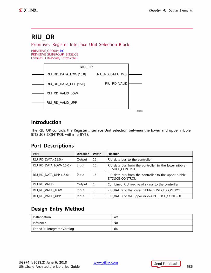
Chapter 4: Design Elements
RIU_ORPrimitive: Register Interface Unit Selection BlockPRIMITIVE_GROUP: I/OPRIMITIVE_SUBGROUP: BITSLICEFamilies: UltraScale, UltraScale+
IntroductionThe RIU_OR controls the Register Interface Unit selection between the lower and upper nibbleBITSLICE_CONTROL within a BYTE.
Port DescriptionsPort Direction Width Function
RIU_RD_DATA<15:0> Output 16 RIU data bus to the controller
RIU_RD_DATA_LOW<15:0> Input 16 RIU data bus from the controller to the lower nibbleBITSLICE_CONTROL
RIU_RD_DATA_UPP<15:0> Input 16 RIU data bus from the controller to the upper nibbleBITSLICE_CONTROL
RIU_RD_VALID Output 1 Combined RIU read valid signal to the controller
RIU_RD_VALID_LOW Input 1 RIU_VALID of the lower nibble BITSLICE_CONTROL
RIU_RD_VALID_UPP Input 1 RIU_VALID of the upper nibble BITSLICE_CONTROL
Design Entry MethodInstantiation Yes
Inference No
IP and IP Integrator Catalog Yes
UG974 (v2018.2) June 6, 2018 www.xilinx.comUltraScale Architecture Libraries Guide 586
Send Feedback
Chapter 4: Design Elements
VHDL Instantiation TemplateUnless they already exist, copy the following two statements and paste them before the entitydeclaration.Library UNISIM;use UNISIM.vcomponents.all;
-- RIU_OR: Register Interface Unit Selection Block-- UltraScale-- Xilinx HDL Language Template, version 2018.2
RIU_OR_inst : RIU_ORgeneric map (
SIM_DEVICE => "ULTRASCALE" -- Set the device version (ULTRASCALE, ULTRASCALE_PLUS, ULTRASCALE_PLUS_ES1,-- ULTRASCALE_PLUS_ES2)
)port map (
RIU_RD_DATA => RIU_RD_DATA, -- 16-bit output: RIU data bus to the controllerRIU_RD_VALID => RIU_RD_VALID, -- 1-bit output: Combined RIU read valid signal to the controllerRIU_RD_DATA_LOW => RIU_RD_DATA_LOW, -- 16-bit input: RIU data bus from the controller to the lower
-- nibble BITSLICE_CONTROL
RIU_RD_DATA_UPP => RIU_RD_DATA_UPP, -- 16-bit input: RIU data bus from the controller to the upper-- nibble BITSLICE_CONTROL
RIU_RD_VALID_LOW => RIU_RD_VALID_LOW, -- 1-bit input: RIU_VALID of the lower nibble BITSLICE_CONTROLRIU_RD_VALID_UPP => RIU_RD_VALID_UPP -- 1-bit input: RIU_VALID of the upper nibble BITSLICE_CONTROL
);
-- End of RIU_OR_inst instantiation
Verilog Instantiation Template
// RIU_OR: Register Interface Unit Selection Block// UltraScale// Xilinx HDL Language Template, version 2018.2
RIU_OR #(.SIM_DEVICE("ULTRASCALE") // Set the device version (ULTRASCALE, ULTRASCALE_PLUS, ULTRASCALE_PLUS_ES1,
// ULTRASCALE_PLUS_ES2))RIU_OR_inst (
.RIU_RD_DATA(RIU_RD_DATA), // 16-bit output: RIU data bus to the controller
.RIU_RD_VALID(RIU_RD_VALID), // 1-bit output: Combined RIU read valid signal to the controller
.RIU_RD_DATA_LOW(RIU_RD_DATA_LOW), // 16-bit input: RIU data bus from the controller to the lower// nibble BITSLICE_CONTROL
.RIU_RD_DATA_UPP(RIU_RD_DATA_UPP), // 16-bit input: RIU data bus from the controller to the upper// nibble BITSLICE_CONTROL
.RIU_RD_VALID_LOW(RIU_RD_VALID_LOW), // 1-bit input: RIU_VALID of the lower nibble BITSLICE_CONTROL
.RIU_RD_VALID_UPP(RIU_RD_VALID_UPP) // 1-bit input: RIU_VALID of the upper nibble BITSLICE_CONTROL);
// End of RIU_OR_inst instantiation
For More Information• See the UltraScale Architecture SelectIO Resources User Guide (UG571).
• See the UltraScale Programmable Devices Documentation.
UG974 (v2018.2) June 6, 2018 www.xilinx.comUltraScale Architecture Libraries Guide 587
Send Feedback
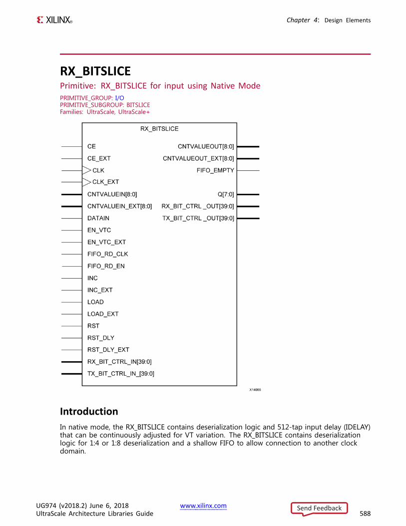
Chapter 4: Design Elements
RX_BITSLICEPrimitive: RX_BITSLICE for input using Native ModePRIMITIVE_GROUP: I/OPRIMITIVE_SUBGROUP: BITSLICEFamilies: UltraScale, UltraScale+
IntroductionIn native mode, the RX_BITSLICE contains deserialization logic and 512-tap input delay (IDELAY)that can be continuously adjusted for VT variation. The RX_BITSLICE contains deserializationlogic for 1:4 or 1:8 deserialization and a shallow FIFO to allow connection to another clockdomain.
UG974 (v2018.2) June 6, 2018 www.xilinx.comUltraScale Architecture Libraries Guide 588
Send Feedback
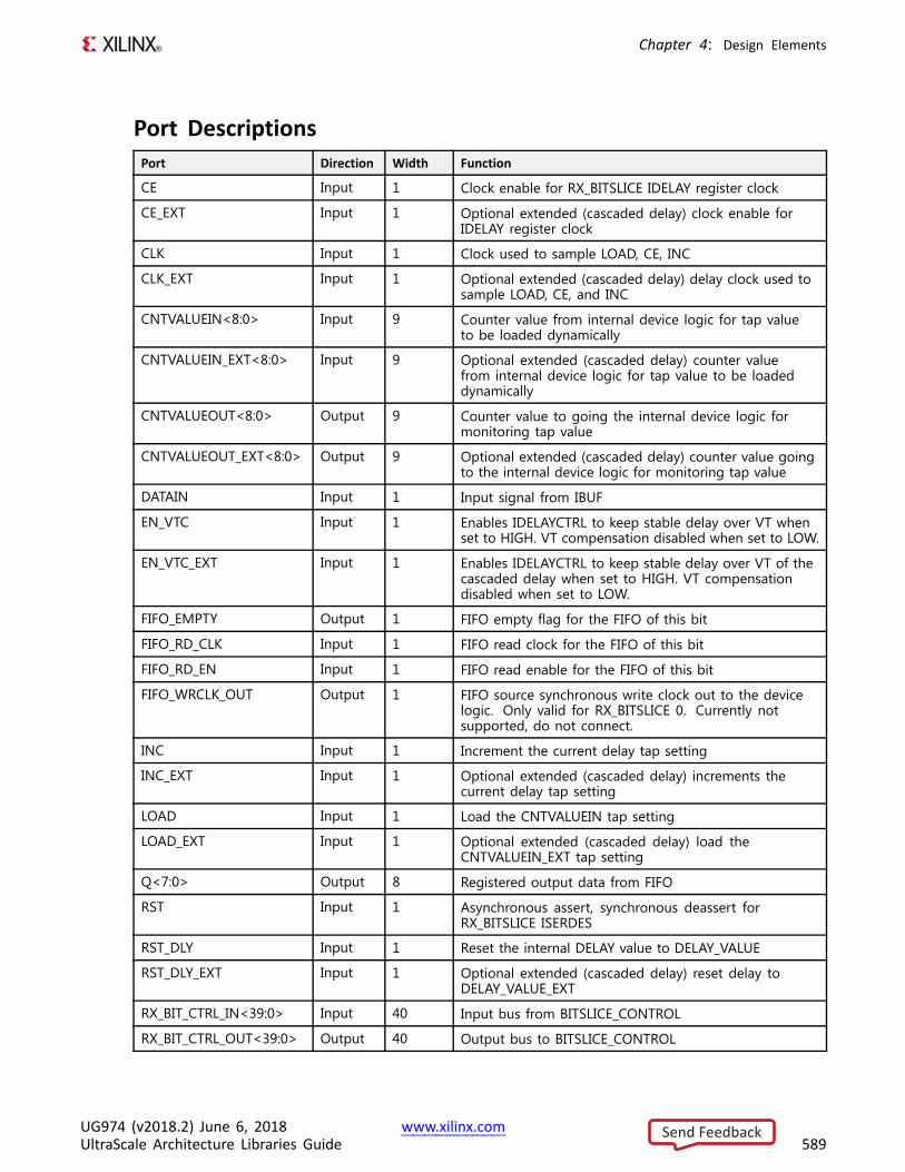
Chapter 4: Design Elements
Port DescriptionsPort Direction Width Function
CE Input 1 Clock enable for RX_BITSLICE IDELAY register clock
CE_EXT Input 1 Optional extended (cascaded delay) clock enable forIDELAY register clock
CLK Input 1 Clock used to sample LOAD, CE, INC
CLK_EXT Input 1 Optional extended (cascaded delay) delay clock used tosample LOAD, CE, and INC
CNTVALUEIN<8:0> Input 9 Counter value from internal device logic for tap valueto be loaded dynamically
CNTVALUEIN_EXT<8:0> Input 9 Optional extended (cascaded delay) counter valuefrom internal device logic for tap value to be loadeddynamically
CNTVALUEOUT<8:0> Output 9 Counter value to going the internal device logic formonitoring tap value
CNTVALUEOUT_EXT<8:0> Output 9 Optional extended (cascaded delay) counter value goingto the internal device logic for monitoring tap value
DATAIN Input 1 Input signal from IBUF
EN_VTC Input 1 Enables IDELAYCTRL to keep stable delay over VT whenset to HIGH. VT compensation disabled when set to LOW.
EN_VTC_EXT Input 1 Enables IDELAYCTRL to keep stable delay over VT of thecascaded delay when set to HIGH. VT compensationdisabled when set to LOW.
FIFO_EMPTY Output 1 FIFO empty flag for the FIFO of this bit
FIFO_RD_CLK Input 1 FIFO read clock for the FIFO of this bit
FIFO_RD_EN Input 1 FIFO read enable for the FIFO of this bit
FIFO_WRCLK_OUT Output 1 FIFO source synchronous write clock out to the devicelogic. Only valid for RX_BITSLICE 0. Currently notsupported, do not connect.
INC Input 1 Increment the current delay tap setting
INC_EXT Input 1 Optional extended (cascaded delay) increments thecurrent delay tap setting
LOAD Input 1 Load the CNTVALUEIN tap setting
LOAD_EXT Input 1 Optional extended (cascaded delay) load theCNTVALUEIN_EXT tap setting
Q<7:0> Output 8 Registered output data from FIFO
RST Input 1 Asynchronous assert, synchronous deassert forRX_BITSLICE ISERDES
RST_DLY Input 1 Reset the internal DELAY value to DELAY_VALUE
RST_DLY_EXT Input 1 Optional extended (cascaded delay) reset delay toDELAY_VALUE_EXT
RX_BIT_CTRL_IN<39:0> Input 40 Input bus from BITSLICE_CONTROL
RX_BIT_CTRL_OUT<39:0> Output 40 Output bus to BITSLICE_CONTROL
UG974 (v2018.2) June 6, 2018 www.xilinx.comUltraScale Architecture Libraries Guide 589
Send Feedback
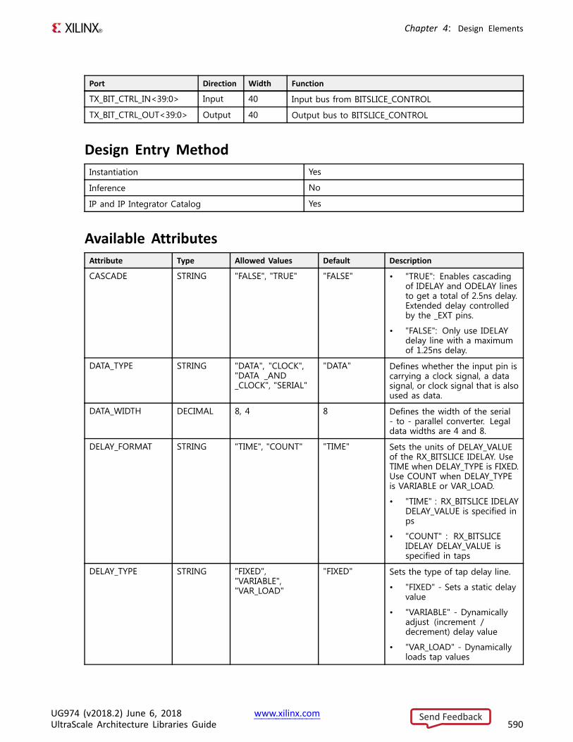
Chapter 4: Design Elements
Port Direction Width Function
TX_BIT_CTRL_IN<39:0> Input 40 Input bus from BITSLICE_CONTROL
TX_BIT_CTRL_OUT<39:0> Output 40 Output bus to BITSLICE_CONTROL
Design Entry MethodInstantiation Yes
Inference No
IP and IP Integrator Catalog Yes
Available AttributesAttribute Type Allowed Values Default Description
CASCADE STRING "FALSE", "TRUE" "FALSE" • "TRUE": Enables cascadingof IDELAY and ODELAY linesto get a total of 2.5ns delay.Extended delay controlledby the _EXT pins.
• "FALSE": Only use IDELAYdelay line with a maximumof 1.25ns delay.
DATA_TYPE STRING "DATA", "CLOCK","DATA _AND_CLOCK", "SERIAL"
"DATA" Defines whether the input pin iscarrying a clock signal, a datasignal, or clock signal that is alsoused as data.
DATA_WIDTH DECIMAL 8, 4 8 Defines the width of the serial- to - parallel converter. Legaldata widths are 4 and 8.
DELAY_FORMAT STRING "TIME", "COUNT" "TIME" Sets the units of DELAY_VALUEof the RX_BITSLICE IDELAY. UseTIME when DELAY_TYPE is FIXED.Use COUNT when DELAY_TYPEis VARIABLE or VAR_LOAD.
• "TIME" : RX_BITSLICE IDELAYDELAY_VALUE is specified inps
• "COUNT" : RX_BITSLICEIDELAY DELAY_VALUE isspecified in taps
DELAY_TYPE STRING "FIXED","VARIABLE","VAR_LOAD"
"FIXED" Sets the type of tap delay line.
• "FIXED" - Sets a static delayvalue
• "VARIABLE" - Dynamicallyadjust (increment /decrement) delay value
• "VAR_LOAD" - Dynamicallyloads tap values
UG974 (v2018.2) June 6, 2018 www.xilinx.comUltraScale Architecture Libraries Guide 590
Send Feedback
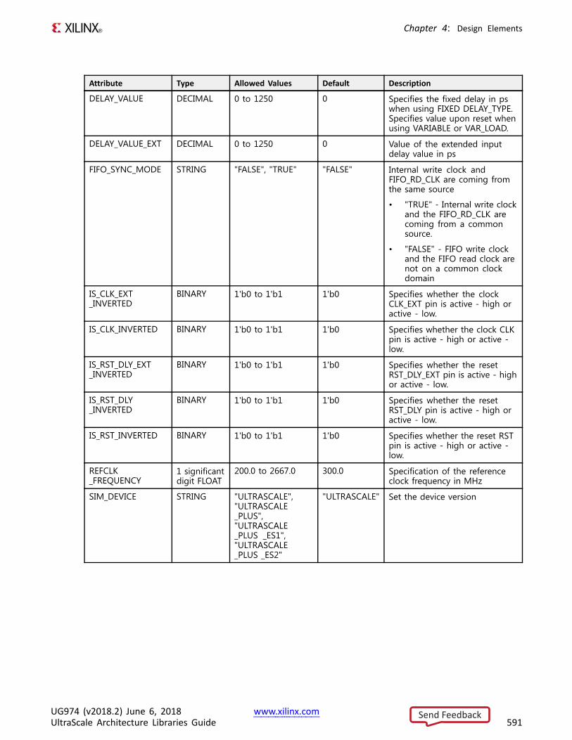
Chapter 4: Design Elements
Attribute Type Allowed Values Default Description
DELAY_VALUE DECIMAL 0 to 1250 0 Specifies the fixed delay in pswhen using FIXED DELAY_TYPE.Specifies value upon reset whenusing VARIABLE or VAR_LOAD.
DELAY_VALUE_EXT DECIMAL 0 to 1250 0 Value of the extended inputdelay value in ps
FIFO_SYNC_MODE STRING "FALSE", "TRUE" "FALSE" Internal write clock andFIFO_RD_CLK are coming fromthe same source
• "TRUE" - Internal write clockand the FIFO_RD_CLK arecoming from a commonsource.
• "FALSE" - FIFO write clockand the FIFO read clock arenot on a common clockdomain
IS_CLK_EXT_INVERTED
BINARY 1'b0 to 1'b1 1'b0 Specifies whether the clockCLK_EXT pin is active - high oractive - low.
IS_CLK_INVERTED BINARY 1'b0 to 1'b1 1'b0 Specifies whether the clock CLKpin is active - high or active -low.
IS_RST_DLY_EXT_INVERTED
BINARY 1'b0 to 1'b1 1'b0 Specifies whether the resetRST_DLY_EXT pin is active - highor active - low.
IS_RST_DLY_INVERTED
BINARY 1'b0 to 1'b1 1'b0 Specifies whether the resetRST_DLY pin is active - high oractive - low.
IS_RST_INVERTED BINARY 1'b0 to 1'b1 1'b0 Specifies whether the reset RSTpin is active - high or active -low.
REFCLK_FREQUENCY
1 significantdigit FLOAT
200.0 to 2667.0 300.0 Specification of the referenceclock frequency in MHz
SIM_DEVICE STRING "ULTRASCALE","ULTRASCALE_PLUS","ULTRASCALE_PLUS _ES1","ULTRASCALE_PLUS _ES2"
"ULTRASCALE" Set the device version
UG974 (v2018.2) June 6, 2018 www.xilinx.comUltraScale Architecture Libraries Guide 591
Send Feedback
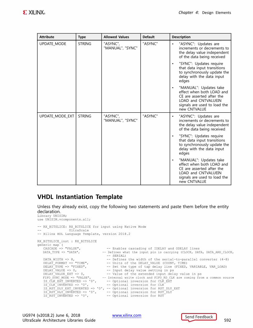
Chapter 4: Design Elements
Attribute Type Allowed Values Default Description
UPDATE_MODE STRING "ASYNC","MANUAL", "SYNC"
"ASYNC" • "ASYNC": Updates areincrements or decrements tothe delay value independentof the data being received
• "SYNC": Updates requirethat data input transitionsto synchronously update thedelay with the data inputedges
• "MANUAL": Updates takeeffect when both LOAD andCE are asserted after theLOAD and CNTVALUEINsignals are used to load thenew CNTVALUE
UPDATE_MODE_EXT STRING "ASYNC","MANUAL", "SYNC"
"ASYNC" • "ASYNC": Updates areincrements or decrements tothe delay value independentof the data being received
• "SYNC": Updates requirethat data input transitionsto synchronously update thedelay with the data inputedges
• "MANUAL": Updates takeeffect when both LOAD andCE are asserted after theLOAD and CNTVALUEINsignals are used to load thenew CNTVALUE
VHDL Instantiation TemplateUnless they already exist, copy the following two statements and paste them before the entitydeclaration.Library UNISIM;use UNISIM.vcomponents.all;
-- RX_BITSLICE: RX_BITSLICE for input using Native Mode-- UltraScale-- Xilinx HDL Language Template, version 2018.2
RX_BITSLICE_inst : RX_BITSLICEgeneric map (
CASCADE => "FALSE", -- Enables cascading of IDELAY and ODELAY linesDATA_TYPE => "DATA", -- Defines what the input pin is carrying (CLOCK, DATA, DATA_AND_CLOCK,
-- SERIAL)DATA_WIDTH => 8, -- Defines the width of the serial-to-parallel converter (4-8)DELAY_FORMAT => "TIME", -- Units of the DELAY_VALUE (COUNT, TIME)DELAY_TYPE => "FIXED", -- Set the type of tap delay line (FIXED, VARIABLE, VAR_LOAD)DELAY_VALUE => 0, -- Input delay value setting in psDELAY_VALUE_EXT => 0, -- Value of the extended input delay value in psFIFO_SYNC_MODE => "FALSE", -- Internal write clock and FIFO_RD_CLK are coming from a common sourceIS_CLK_EXT_INVERTED => '0', -- Optional inversion for CLK_EXTIS_CLK_INVERTED => '0', -- Optional inversion for CLKIS_RST_DLY_EXT_INVERTED => '0', -- Optional inversion for RST_DLY_EXTIS_RST_DLY_INVERTED => '0', -- Optional inversion for RST_DLYIS_RST_INVERTED => '0', -- Optional inversion for RST
UG974 (v2018.2) June 6, 2018 www.xilinx.comUltraScale Architecture Libraries Guide 592
Send Feedback
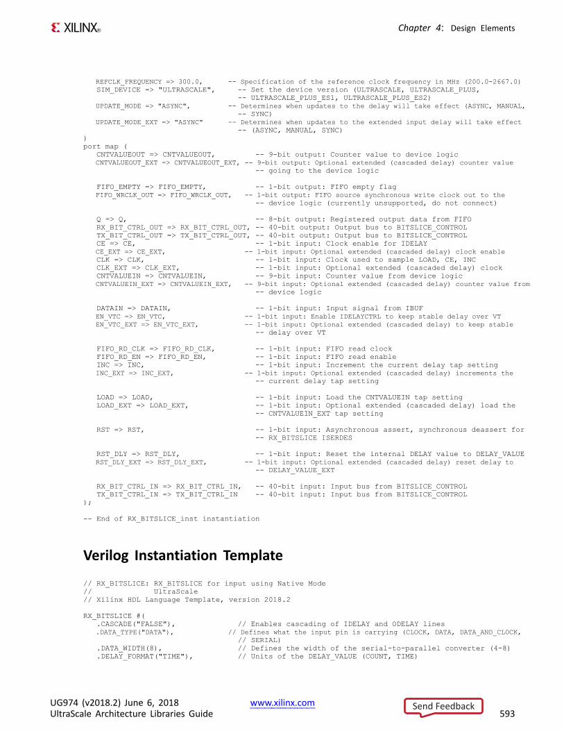
Chapter 4: Design Elements
REFCLK_FREQUENCY => 300.0, -- Specification of the reference clock frequency in MHz (200.0-2667.0)SIM_DEVICE => "ULTRASCALE", -- Set the device version (ULTRASCALE, ULTRASCALE_PLUS,
-- ULTRASCALE_PLUS_ES1, ULTRASCALE_PLUS_ES2)UPDATE_MODE => "ASYNC", -- Determines when updates to the delay will take effect (ASYNC, MANUAL,
-- SYNC)UPDATE_MODE_EXT => "ASYNC" -- Determines when updates to the extended input delay will take effect
-- (ASYNC, MANUAL, SYNC))port map (
CNTVALUEOUT => CNTVALUEOUT, -- 9-bit output: Counter value to device logicCNTVALUEOUT_EXT => CNTVALUEOUT_EXT, -- 9-bit output: Optional extended (cascaded delay) counter value
-- going to the device logic
FIFO_EMPTY => FIFO_EMPTY, -- 1-bit output: FIFO empty flagFIFO_WRCLK_OUT => FIFO_WRCLK_OUT, -- 1-bit output: FIFO source synchronous write clock out to the
-- device logic (currently unsupported, do not connect)
Q => Q, -- 8-bit output: Registered output data from FIFORX_BIT_CTRL_OUT => RX_BIT_CTRL_OUT, -- 40-bit output: Output bus to BITSLICE_CONTROLTX_BIT_CTRL_OUT => TX_BIT_CTRL_OUT, -- 40-bit output: Output bus to BITSLICE_CONTROLCE => CE, -- 1-bit input: Clock enable for IDELAYCE_EXT => CE_EXT, -- 1-bit input: Optional extended (cascaded delay) clock enableCLK => CLK, -- 1-bit input: Clock used to sample LOAD, CE, INCCLK_EXT => CLK_EXT, -- 1-bit input: Optional extended (cascaded delay) clockCNTVALUEIN => CNTVALUEIN, -- 9-bit input: Counter value from device logicCNTVALUEIN_EXT => CNTVALUEIN_EXT, -- 9-bit input: Optional extended (cascaded delay) counter value from
-- device logic
DATAIN => DATAIN, -- 1-bit input: Input signal from IBUFEN_VTC => EN_VTC, -- 1-bit input: Enable IDELAYCTRL to keep stable delay over VTEN_VTC_EXT => EN_VTC_EXT, -- 1-bit input: Optional extended (cascaded delay) to keep stable
-- delay over VT
FIFO_RD_CLK => FIFO_RD_CLK, -- 1-bit input: FIFO read clockFIFO_RD_EN => FIFO_RD_EN, -- 1-bit input: FIFO read enableINC => INC, -- 1-bit input: Increment the current delay tap settingINC_EXT => INC_EXT, -- 1-bit input: Optional extended (cascaded delay) increments the
-- current delay tap setting
LOAD => LOAD, -- 1-bit input: Load the CNTVALUEIN tap settingLOAD_EXT => LOAD_EXT, -- 1-bit input: Optional extended (cascaded delay) load the
-- CNTVALUEIN_EXT tap setting
RST => RST, -- 1-bit input: Asynchronous assert, synchronous deassert for-- RX_BITSLICE ISERDES
RST_DLY => RST_DLY, -- 1-bit input: Reset the internal DELAY value to DELAY_VALUERST_DLY_EXT => RST_DLY_EXT, -- 1-bit input: Optional extended (cascaded delay) reset delay to
-- DELAY_VALUE_EXT
RX_BIT_CTRL_IN => RX_BIT_CTRL_IN, -- 40-bit input: Input bus from BITSLICE_CONTROLTX_BIT_CTRL_IN => TX_BIT_CTRL_IN -- 40-bit input: Input bus from BITSLICE_CONTROL
);
-- End of RX_BITSLICE_inst instantiation
Verilog Instantiation Template
// RX_BITSLICE: RX_BITSLICE for input using Native Mode// UltraScale// Xilinx HDL Language Template, version 2018.2
RX_BITSLICE #(.CASCADE("FALSE"), // Enables cascading of IDELAY and ODELAY lines.DATA_TYPE("DATA"), // Defines what the input pin is carrying (CLOCK, DATA, DATA_AND_CLOCK,
// SERIAL).DATA_WIDTH(8), // Defines the width of the serial-to-parallel converter (4-8).DELAY_FORMAT("TIME"), // Units of the DELAY_VALUE (COUNT, TIME)
UG974 (v2018.2) June 6, 2018 www.xilinx.comUltraScale Architecture Libraries Guide 593
Send Feedback
Chapter 4: Design Elements
.DELAY_TYPE("FIXED"), // Set the type of tap delay line (FIXED, VARIABLE, VAR_LOAD)
.DELAY_VALUE(0), // Input delay value setting in ps
.DELAY_VALUE_EXT(0), // Value of the extended input delay value in ps
.FIFO_SYNC_MODE("FALSE"), // Internal write clock and FIFO_RD_CLK are coming from a common source
.IS_CLK_EXT_INVERTED(1'b0), // Optional inversion for CLK_EXT
.IS_CLK_INVERTED(1'b0), // Optional inversion for CLK
.IS_RST_DLY_EXT_INVERTED(1'b0), // Optional inversion for RST_DLY_EXT
.IS_RST_DLY_INVERTED(1'b0), // Optional inversion for RST_DLY
.IS_RST_INVERTED(1'b0), // Optional inversion for RST
.REFCLK_FREQUENCY(300.0), // Specification of the reference clock frequency in MHz (200.0-2667.0)
.SIM_DEVICE("ULTRASCALE"), // Set the device version (ULTRASCALE, ULTRASCALE_PLUS,// ULTRASCALE_PLUS_ES1, ULTRASCALE_PLUS_ES2)
.UPDATE_MODE("ASYNC"), // Determines when updates to the delay will take effect (ASYNC, MANUAL,// SYNC)
.UPDATE_MODE_EXT("ASYNC") // Determines when updates to the extended input delay will take effect// (ASYNC, MANUAL, SYNC)
)RX_BITSLICE_inst (
.CNTVALUEOUT(CNTVALUEOUT), // 9-bit output: Counter value to device logic
.CNTVALUEOUT_EXT(CNTVALUEOUT_EXT), // 9-bit output: Optional extended (cascaded delay) counter value// going to the device logic
.FIFO_EMPTY(FIFO_EMPTY), // 1-bit output: FIFO empty flag
.FIFO_WRCLK_OUT(FIFO_WRCLK_OUT), // 1-bit output: FIFO source synchronous write clock out to the device// logic (currently unsupported, do not connect)
.Q(Q), // 8-bit output: Registered output data from FIFO
.RX_BIT_CTRL_OUT(RX_BIT_CTRL_OUT), // 40-bit output: Output bus to BITSLICE_CONTROL
.TX_BIT_CTRL_OUT(TX_BIT_CTRL_OUT), // 40-bit output: Output bus to BITSLICE_CONTROL
.CE(CE), // 1-bit input: Clock enable for IDELAY
.CE_EXT(CE_EXT), // 1-bit input: Optional extended (cascaded delay) clock enable
.CLK(CLK), // 1-bit input: Clock used to sample LOAD, CE, INC
.CLK_EXT(CLK_EXT), // 1-bit input: Optional extended (cascaded delay) clock
.CNTVALUEIN(CNTVALUEIN), // 9-bit input: Counter value from device logic
.CNTVALUEIN_EXT(CNTVALUEIN_EXT), // 9-bit input: Optional extended (cascaded delay) counter value from// device logic
.DATAIN(DATAIN), // 1-bit input: Input signal from IBUF
.EN_VTC(EN_VTC), // 1-bit input: Enable IDELAYCTRL to keep stable delay over VT
.EN_VTC_EXT(EN_VTC_EXT), // 1-bit input: Optional extended (cascaded delay) to keep stable// delay over VT
.FIFO_RD_CLK(FIFO_RD_CLK), // 1-bit input: FIFO read clock
.FIFO_RD_EN(FIFO_RD_EN), // 1-bit input: FIFO read enable
.INC(INC), // 1-bit input: Increment the current delay tap setting
.INC_EXT(INC_EXT), // 1-bit input: Optional extended (cascaded delay) increments the// current delay tap setting
.LOAD(LOAD), // 1-bit input: Load the CNTVALUEIN tap setting
.LOAD_EXT(LOAD_EXT), // 1-bit input: Optional extended (cascaded delay) load the// CNTVALUEIN_EXT tap setting
.RST(RST), // 1-bit input: Asynchronous assert, synchronous deassert for// RX_BITSLICE ISERDES
.RST_DLY(RST_DLY), // 1-bit input: Reset the internal DELAY value to DELAY_VALUE
.RST_DLY_EXT(RST_DLY_EXT), // 1-bit input: Optional extended (cascaded delay) reset delay to// DELAY_VALUE_EXT
.RX_BIT_CTRL_IN(RX_BIT_CTRL_IN), // 40-bit input: Input bus from BITSLICE_CONTROL
.TX_BIT_CTRL_IN(TX_BIT_CTRL_IN) // 40-bit input: Input bus from BITSLICE_CONTROL);
// End of RX_BITSLICE_inst instantiation
UG974 (v2018.2) June 6, 2018 www.xilinx.comUltraScale Architecture Libraries Guide 594
Send Feedback

Chapter 4: Design Elements
For More Information• See the UltraScale Architecture SelectIO Resources User Guide (UG571).
• See the UltraScale Programmable Devices Documentation.
UG974 (v2018.2) June 6, 2018 www.xilinx.comUltraScale Architecture Libraries Guide 595
Send Feedback
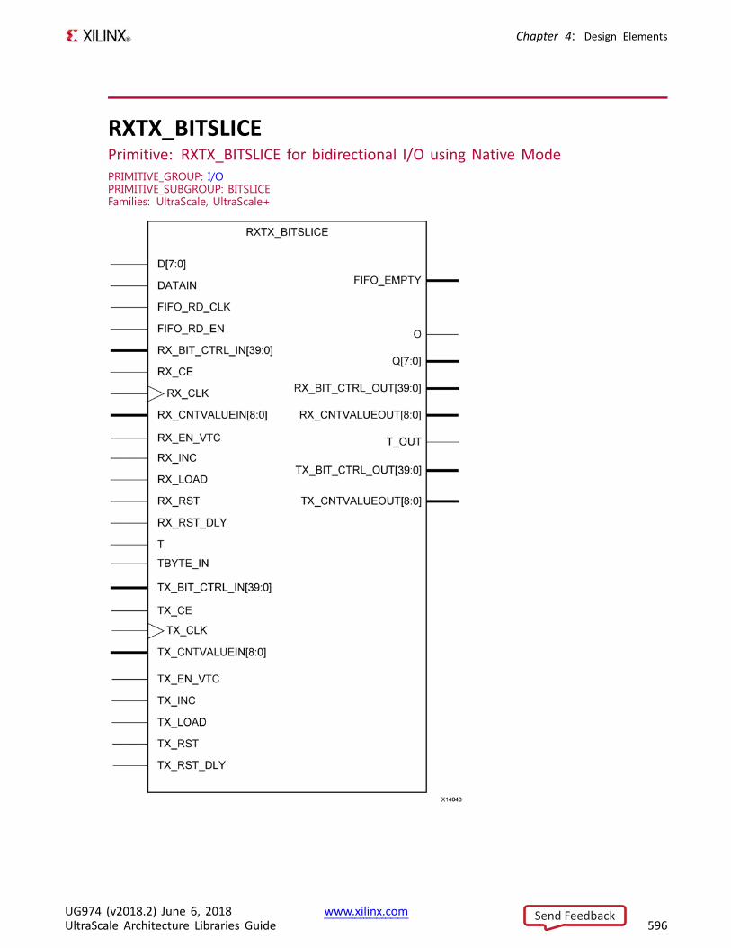
Chapter 4: Design Elements
RXTX_BITSLICEPrimitive: RXTX_BITSLICE for bidirectional I/O using Native ModePRIMITIVE_GROUP: I/OPRIMITIVE_SUBGROUP: BITSLICEFamilies: UltraScale, UltraScale+
UG974 (v2018.2) June 6, 2018 www.xilinx.comUltraScale Architecture Libraries Guide 596
Send Feedback
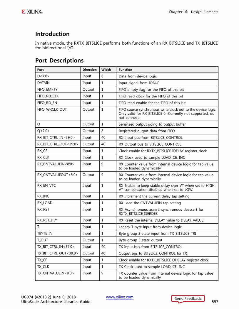
Chapter 4: Design Elements
IntroductionIn native mode, the RXTX_BITSLICE performs both functions of an RX_BITSLICE and TX_BITSLICEfor bidirectional I/O.
Port DescriptionsPort Direction Width Function
D<7:0> Input 8 Data from device logic
DATAIN Input 1 Input signal from IOBUF
FIFO_EMPTY Output 1 FIFO empty flag for the FIFO of this bit
FIFO_RD_CLK Input 1 FIFO read clock for the FIFO of this bit
FIFO_RD_EN Input 1 FIFO read enable for the FIFO of this bit
FIFO_WRCLK_OUT Output 1 FIFO source synchronous write clock out to the device logic.Only valid for RX_BITSLICE 0. Currently not supported, donot connect.
O Output 1 Serialized output going to output buffer
Q<7:0> Output 8 Registered output data from FIFO
RX_BIT_CTRL_IN<39:0> Input 40 RX Input bus from BITSLICE_CONTROL
RX_BIT_CTRL_OUT<39:0> Output 40 RX Output bus to BITSLICE_CONTROL
RX_CE Input 1 Clock enable for RXTX_BITSLICE IDELAY register clock
RX_CLK Input 1 RX Clock used to sample LOAD, CE, INC
RX_CNTVALUEIN<8:0> Input 9 RX Counter value from internal device logic for tap valueto be loaded dynamically
RX_CNTVALUEOUT<8:0> Output 9 RX Counter value from internal device logic for tap valueto be loaded dynamically
RX_EN_VTC Input 1 RX Enable to keep stable delay over VT when set to HIGH.VT compensation disabled when set to LOW.
RX_INC Input 1 RX Increment the current delay tap setting
RX_LOAD Input 1 RX Load the CNTVALUEIN tap setting
RX_RST Input 1 RX Asynchronous assert, synchronous deassert forRXTX_BITSLICE ISERDES
RX_RST_DLY Input 1 RX Reset the internal DELAY value to DELAY_VALUE
T Input 1 Legacy T byte input from device logic
TBYTE_IN Input 1 Byte group 3-state input from TX_BITSLICE_TRI
T_OUT Output 1 Byte group 3-state output
TX_BIT_CTRL_IN<39:0> Input 40 TX Input bus from BITSLICE_CONTROL
TX_BIT_CTRL_OUT<39:0> Output 40 Output bus to BITSLICE_CONTROL for TX
TX_CE Input 1 Clock enable for RXTX_BITSLICE ODELAY register clock
TX_CLK Input 1 TX Clock used to sample LOAD, CE, INC
TX_CNTVALUEIN<8:0> Input 9 TX Counter value from internal device logic for tap valueto be loaded dynamically
UG974 (v2018.2) June 6, 2018 www.xilinx.comUltraScale Architecture Libraries Guide 597
Send Feedback
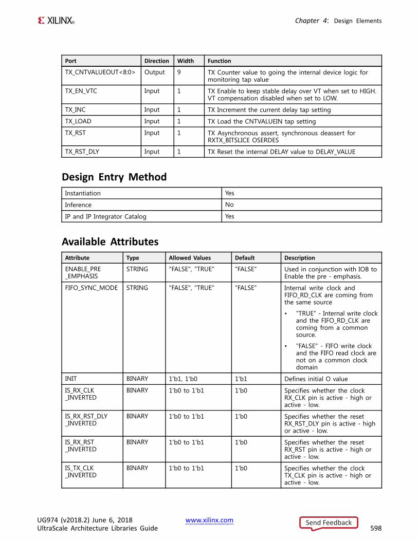
Chapter 4: Design Elements
Port Direction Width Function
TX_CNTVALUEOUT<8:0> Output 9 TX Counter value to going the internal device logic formonitoring tap value
TX_EN_VTC Input 1 TX Enable to keep stable delay over VT when set to HIGH.VT compensation disabled when set to LOW.
TX_INC Input 1 TX Increment the current delay tap setting
TX_LOAD Input 1 TX Load the CNTVALUEIN tap setting
TX_RST Input 1 TX Asynchronous assert, synchronous deassert forRXTX_BITSLICE OSERDES
TX_RST_DLY Input 1 TX Reset the internal DELAY value to DELAY_VALUE
Design Entry MethodInstantiation Yes
Inference No
IP and IP Integrator Catalog Yes
Available AttributesAttribute Type Allowed Values Default Description
ENABLE_PRE_EMPHASIS
STRING "FALSE", "TRUE" "FALSE" Used in conjunction with IOB toEnable the pre - emphasis.
FIFO_SYNC_MODE STRING "FALSE", "TRUE" "FALSE" Internal write clock andFIFO_RD_CLK are coming fromthe same source
• "TRUE" - Internal write clockand the FIFO_RD_CLK arecoming from a commonsource.
• "FALSE" - FIFO write clockand the FIFO read clock arenot on a common clockdomain
INIT BINARY 1'b1, 1'b0 1'b1 Defines initial O value
IS_RX_CLK_INVERTED
BINARY 1'b0 to 1'b1 1'b0 Specifies whether the clockRX_CLK pin is active - high oractive - low.
IS_RX_RST_DLY_INVERTED
BINARY 1'b0 to 1'b1 1'b0 Specifies whether the resetRX_RST_DLY pin is active - highor active - low.
IS_RX_RST_INVERTED
BINARY 1'b0 to 1'b1 1'b0 Specifies whether the resetRX_RST pin is active - high oractive - low.
IS_TX_CLK_INVERTED
BINARY 1'b0 to 1'b1 1'b0 Specifies whether the clockTX_CLK pin is active - high oractive - low.
UG974 (v2018.2) June 6, 2018 www.xilinx.comUltraScale Architecture Libraries Guide 598
Send Feedback
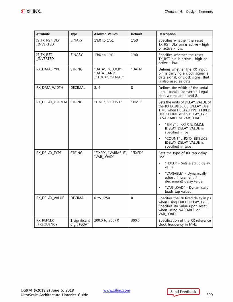
Chapter 4: Design Elements
Attribute Type Allowed Values Default Description
IS_TX_RST_DLY_INVERTED
BINARY 1'b0 to 1'b1 1'b0 Specifies whether the resetTX_RST_DLY pin is active - highor active - low.
IS_TX_RST_INVERTED
BINARY 1'b0 to 1'b1 1'b0 Specifies whether the resetTX_RST pin is active - high oractive - low.
RX_DATA_TYPE STRING "DATA", "CLOCK","DATA _AND_CLOCK", "SERIAL"
"DATA" Defines whether the RX inputpin is carrying a clock signal, adata signal, or clock signal thatis also used as data.
RX_DATA_WIDTH DECIMAL 8, 4 8 Defines the width of the serial- to - parallel converter. Legaldata widths are 4 and 8.
RX_DELAY_FORMAT STRING "TIME", "COUNT" "TIME" Sets the units of DELAY_VALUE ofthe RXTX_BITSLICE IDELAY. UseTIME when DELAY_TYPE is FIXED.Use COUNT when DELAY_TYPEis VARIABLE or VAR_LOAD.
• "TIME" : RXTX_BITSLICEIDELAY DELAY_VALUE isspecified in ps
• "COUNT" : RXTX_BITSLICEIDELAY DELAY_VALUE isspecified in taps
RX_DELAY_TYPE STRING "FIXED", "VARIABLE","VAR_LOAD"
"FIXED" Sets the type of RX tap delayline.
• "FIXED" - Sets a static delayvalue
• "VARIABLE" - Dynamicallyadjust (increment /decrement) delay value
• "VAR_LOAD" - Dynamicallyloads tap values
RX_DELAY_VALUE DECIMAL 0 to 1250 0 Specifies the RX fixed delay in pswhen using FIXED DELAY_TYPE.Specifies RX value upon resetwhen using VARIABLE orVAR_LOAD.
RX_REFCLK_FREQUENCY
1 significantdigit FLOAT
200.0 to 2667.0 300.0 Specification of the RX referenceclock frequency in MHz
UG974 (v2018.2) June 6, 2018 www.xilinx.comUltraScale Architecture Libraries Guide 599
Send Feedback
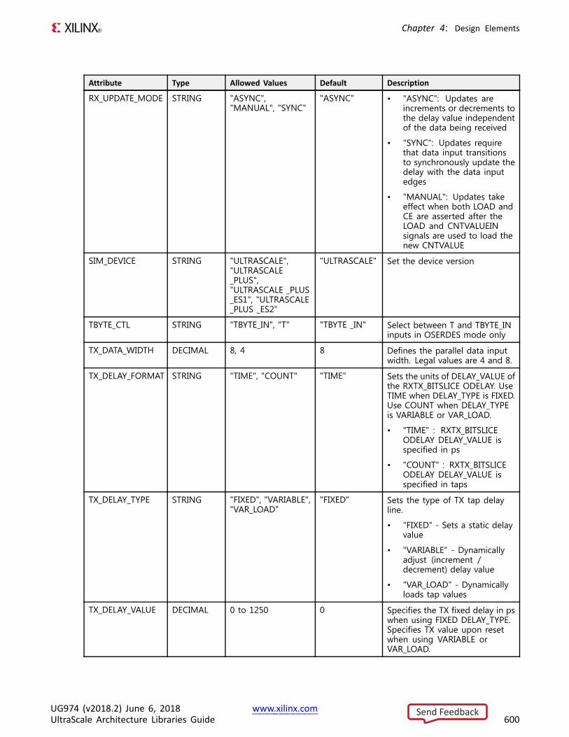
Chapter 4: Design Elements
Attribute Type Allowed Values Default Description
RX_UPDATE_MODE STRING "ASYNC","MANUAL", "SYNC"
"ASYNC" • "ASYNC": Updates areincrements or decrements tothe delay value independentof the data being received
• "SYNC": Updates requirethat data input transitionsto synchronously update thedelay with the data inputedges
• "MANUAL": Updates takeeffect when both LOAD andCE are asserted after theLOAD and CNTVALUEINsignals are used to load thenew CNTVALUE
SIM_DEVICE STRING "ULTRASCALE","ULTRASCALE_PLUS","ULTRASCALE _PLUS_ES1", "ULTRASCALE_PLUS _ES2"
"ULTRASCALE" Set the device version
TBYTE_CTL STRING "TBYTE_IN", "T" "TBYTE _IN" Select between T and TBYTE_INinputs in OSERDES mode only
TX_DATA_WIDTH DECIMAL 8, 4 8 Defines the parallel data inputwidth. Legal values are 4 and 8.
TX_DELAY_FORMAT STRING "TIME", "COUNT" "TIME" Sets the units of DELAY_VALUE ofthe RXTX_BITSLICE ODELAY. UseTIME when DELAY_TYPE is FIXED.Use COUNT when DELAY_TYPEis VARIABLE or VAR_LOAD.
• "TIME" : RXTX_BITSLICEODELAY DELAY_VALUE isspecified in ps
• "COUNT" : RXTX_BITSLICEODELAY DELAY_VALUE isspecified in taps
TX_DELAY_TYPE STRING "FIXED", "VARIABLE","VAR_LOAD"
"FIXED" Sets the type of TX tap delayline.
• "FIXED" - Sets a static delayvalue
• "VARIABLE" - Dynamicallyadjust (increment /decrement) delay value
• "VAR_LOAD" - Dynamicallyloads tap values
TX_DELAY_VALUE DECIMAL 0 to 1250 0 Specifies the TX fixed delay in pswhen using FIXED DELAY_TYPE.Specifies TX value upon resetwhen using VARIABLE orVAR_LOAD.
UG974 (v2018.2) June 6, 2018 www.xilinx.comUltraScale Architecture Libraries Guide 600
Send Feedback
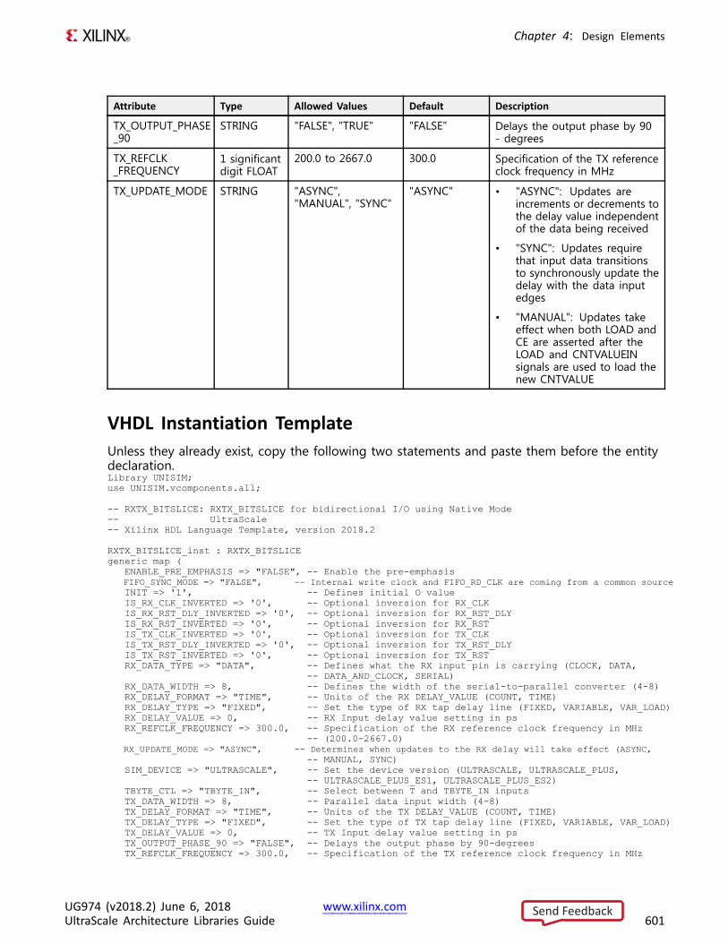
Chapter 4: Design Elements
Attribute Type Allowed Values Default Description
TX_OUTPUT_PHASE_90
STRING "FALSE", "TRUE" "FALSE" Delays the output phase by 90- degrees
TX_REFCLK_FREQUENCY
1 significantdigit FLOAT
200.0 to 2667.0 300.0 Specification of the TX referenceclock frequency in MHz
TX_UPDATE_MODE STRING "ASYNC","MANUAL", "SYNC"
"ASYNC" • "ASYNC": Updates areincrements or decrements tothe delay value independentof the data being received
• "SYNC": Updates requirethat input data transitionsto synchronously update thedelay with the data inputedges
• "MANUAL": Updates takeeffect when both LOAD andCE are asserted after theLOAD and CNTVALUEINsignals are used to load thenew CNTVALUE
VHDL Instantiation TemplateUnless they already exist, copy the following two statements and paste them before the entitydeclaration.Library UNISIM;use UNISIM.vcomponents.all;
-- RXTX_BITSLICE: RXTX_BITSLICE for bidirectional I/O using Native Mode-- UltraScale-- Xilinx HDL Language Template, version 2018.2
RXTX_BITSLICE_inst : RXTX_BITSLICEgeneric map (
ENABLE_PRE_EMPHASIS => "FALSE", -- Enable the pre-emphasisFIFO_SYNC_MODE => "FALSE", -- Internal write clock and FIFO_RD_CLK are coming from a common sourceINIT => '1', -- Defines initial O valueIS_RX_CLK_INVERTED => '0', -- Optional inversion for RX_CLKIS_RX_RST_DLY_INVERTED => '0', -- Optional inversion for RX_RST_DLYIS_RX_RST_INVERTED => '0', -- Optional inversion for RX_RSTIS_TX_CLK_INVERTED => '0', -- Optional inversion for TX_CLKIS_TX_RST_DLY_INVERTED => '0', -- Optional inversion for TX_RST_DLYIS_TX_RST_INVERTED => '0', -- Optional inversion for TX_RSTRX_DATA_TYPE => "DATA", -- Defines what the RX input pin is carrying (CLOCK, DATA,
-- DATA_AND_CLOCK, SERIAL)RX_DATA_WIDTH => 8, -- Defines the width of the serial-to-parallel converter (4-8)RX_DELAY_FORMAT => "TIME", -- Units of the RX DELAY_VALUE (COUNT, TIME)RX_DELAY_TYPE => "FIXED", -- Set the type of RX tap delay line (FIXED, VARIABLE, VAR_LOAD)RX_DELAY_VALUE => 0, -- RX Input delay value setting in psRX_REFCLK_FREQUENCY => 300.0, -- Specification of the RX reference clock frequency in MHz
-- (200.0-2667.0)RX_UPDATE_MODE => "ASYNC", -- Determines when updates to the RX delay will take effect (ASYNC,
-- MANUAL, SYNC)SIM_DEVICE => "ULTRASCALE", -- Set the device version (ULTRASCALE, ULTRASCALE_PLUS,
-- ULTRASCALE_PLUS_ES1, ULTRASCALE_PLUS_ES2)TBYTE_CTL => "TBYTE_IN", -- Select between T and TBYTE_IN inputsTX_DATA_WIDTH => 8, -- Parallel data input width (4-8)TX_DELAY_FORMAT => "TIME", -- Units of the TX DELAY_VALUE (COUNT, TIME)TX_DELAY_TYPE => "FIXED", -- Set the type of TX tap delay line (FIXED, VARIABLE, VAR_LOAD)TX_DELAY_VALUE => 0, -- TX Input delay value setting in psTX_OUTPUT_PHASE_90 => "FALSE", -- Delays the output phase by 90-degreesTX_REFCLK_FREQUENCY => 300.0, -- Specification of the TX reference clock frequency in MHz
UG974 (v2018.2) June 6, 2018 www.xilinx.comUltraScale Architecture Libraries Guide 601
Send Feedback
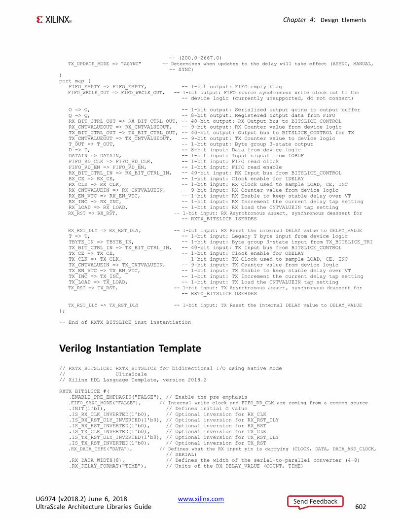
Chapter 4: Design Elements
-- (200.0-2667.0)TX_UPDATE_MODE => "ASYNC" -- Determines when updates to the delay will take effect (ASYNC, MANUAL,
-- SYNC))port map (
FIFO_EMPTY => FIFO_EMPTY, -- 1-bit output: FIFO empty flagFIFO_WRCLK_OUT => FIFO_WRCLK_OUT, -- 1-bit output: FIFO source synchronous write clock out to the
-- device logic (currently unsupported, do not connect)
O => O, -- 1-bit output: Serialized output going to output bufferQ => Q, -- 8-bit output: Registered output data from FIFORX_BIT_CTRL_OUT => RX_BIT_CTRL_OUT, -- 40-bit output: RX Output bus to BITSLICE_CONTROLRX_CNTVALUEOUT => RX_CNTVALUEOUT, -- 9-bit output: RX Counter value from device logicTX_BIT_CTRL_OUT => TX_BIT_CTRL_OUT, -- 40-bit output: Output bus to BITSLICE_CONTROL for TXTX_CNTVALUEOUT => TX_CNTVALUEOUT, -- 9-bit output: TX Counter value to device logicT_OUT => T_OUT, -- 1-bit output: Byte group 3-state outputD => D, -- 8-bit input: Data from device logicDATAIN => DATAIN, -- 1-bit input: Input signal from IOBUFFIFO_RD_CLK => FIFO_RD_CLK, -- 1-bit input: FIFO read clockFIFO_RD_EN => FIFO_RD_EN, -- 1-bit input: FIFO read enableRX_BIT_CTRL_IN => RX_BIT_CTRL_IN, -- 40-bit input: RX Input bus from BITSLICE_CONTROLRX_CE => RX_CE, -- 1-bit input: Clock enable for IDELAYRX_CLK => RX_CLK, -- 1-bit input: RX Clock used to sample LOAD, CE, INCRX_CNTVALUEIN => RX_CNTVALUEIN, -- 9-bit input: RX Counter value from device logicRX_EN_VTC => RX_EN_VTC, -- 1-bit input: RX Enable to keep stable delay over VTRX_INC => RX_INC, -- 1-bit input: RX Increment the current delay tap settingRX_LOAD => RX_LOAD, -- 1-bit input: RX Load the CNTVALUEIN tap settingRX_RST => RX_RST, -- 1-bit input: RX Asynchronous assert, synchronous deassert for
-- RXTX_BITSLICE ISERDES
RX_RST_DLY => RX_RST_DLY, -- 1-bit input: RX Reset the internal DELAY value to DELAY_VALUET => T, -- 1-bit input: Legacy T byte input from device logicTBYTE_IN => TBYTE_IN, -- 1-bit input: Byte group 3-state input from TX_BITSLICE_TRITX_BIT_CTRL_IN => TX_BIT_CTRL_IN, -- 40-bit input: TX Input bus from BITSLICE_CONTROLTX_CE => TX_CE, -- 1-bit input: Clock enable for ODELAYTX_CLK => TX_CLK, -- 1-bit input: TX Clock used to sample LOAD, CE, INCTX_CNTVALUEIN => TX_CNTVALUEIN, -- 9-bit input: TX Counter value from device logicTX_EN_VTC => TX_EN_VTC, -- 1-bit input: TX Enable to keep stable delay over VTTX_INC => TX_INC, -- 1-bit input: TX Increment the current delay tap settingTX_LOAD => TX_LOAD, -- 1-bit input: TX Load the CNTVALUEIN tap settingTX_RST => TX_RST, -- 1-bit input: TX Asynchronous assert, synchronous deassert for
-- RXTX_BITSLICE OSERDES
TX_RST_DLY => TX_RST_DLY -- 1-bit input: TX Reset the internal DELAY value to DELAY_VALUE);
-- End of RXTX_BITSLICE_inst instantiation
Verilog Instantiation Template
// RXTX_BITSLICE: RXTX_BITSLICE for bidirectional I/O using Native Mode// UltraScale// Xilinx HDL Language Template, version 2018.2
RXTX_BITSLICE #(.ENABLE_PRE_EMPHASIS("FALSE"), // Enable the pre-emphasis.FIFO_SYNC_MODE("FALSE"), // Internal write clock and FIFO_RD_CLK are coming from a common source.INIT(1'b1), // Defines initial O value.IS_RX_CLK_INVERTED(1'b0), // Optional inversion for RX_CLK.IS_RX_RST_DLY_INVERTED(1'b0), // Optional inversion for RX_RST_DLY.IS_RX_RST_INVERTED(1'b0), // Optional inversion for RX_RST.IS_TX_CLK_INVERTED(1'b0), // Optional inversion for TX_CLK.IS_TX_RST_DLY_INVERTED(1'b0), // Optional inversion for TX_RST_DLY.IS_TX_RST_INVERTED(1'b0), // Optional inversion for TX_RST.RX_DATA_TYPE("DATA"), // Defines what the RX input pin is carrying (CLOCK, DATA, DATA_AND_CLOCK,
// SERIAL).RX_DATA_WIDTH(8), // Defines the width of the serial-to-parallel converter (4-8).RX_DELAY_FORMAT("TIME"), // Units of the RX DELAY_VALUE (COUNT, TIME)
UG974 (v2018.2) June 6, 2018 www.xilinx.comUltraScale Architecture Libraries Guide 602
Send Feedback
Chapter 4: Design Elements
.RX_DELAY_TYPE("FIXED"), // Set the type of RX tap delay line (FIXED, VARIABLE, VAR_LOAD)
.RX_DELAY_VALUE(0), // RX Input delay value setting in ps
.RX_REFCLK_FREQUENCY(300.0), // Specification of the RX reference clock frequency in MHz (200.0-2667.0)
.RX_UPDATE_MODE("ASYNC"), // Determines when updates to the RX delay will take effect (ASYNC,// MANUAL, SYNC)
.SIM_DEVICE("ULTRASCALE"), // Set the device version (ULTRASCALE, ULTRASCALE_PLUS,// ULTRASCALE_PLUS_ES1, ULTRASCALE_PLUS_ES2)
.TBYTE_CTL("TBYTE_IN"), // Select between T and TBYTE_IN inputs
.TX_DATA_WIDTH(8), // Parallel data input width (4-8)
.TX_DELAY_FORMAT("TIME"), // Units of the TX DELAY_VALUE (COUNT, TIME)
.TX_DELAY_TYPE("FIXED"), // Set the type of TX tap delay line (FIXED, VARIABLE, VAR_LOAD)
.TX_DELAY_VALUE(0), // TX Input delay value setting in ps
.TX_OUTPUT_PHASE_90("FALSE"), // Delays the output phase by 90-degrees
.TX_REFCLK_FREQUENCY(300.0), // Specification of the TX reference clock frequency in MHz (200.0-2667.0)
.TX_UPDATE_MODE("ASYNC") // Determines when updates to the delay will take effect (ASYNC, MANUAL,// SYNC)
)RXTX_BITSLICE_inst (
.FIFO_EMPTY(FIFO_EMPTY), // 1-bit output: FIFO empty flag
.FIFO_WRCLK_OUT(FIFO_WRCLK_OUT), // 1-bit output: FIFO source synchronous write clock out to the device// logic (currently unsupported, do not connect)
.O(O), // 1-bit output: Serialized output going to output buffer
.Q(Q), // 8-bit output: Registered output data from FIFO
.RX_BIT_CTRL_OUT(RX_BIT_CTRL_OUT), // 40-bit output: RX Output bus to BITSLICE_CONTROL
.RX_CNTVALUEOUT(RX_CNTVALUEOUT), // 9-bit output: RX Counter value from device logic
.TX_BIT_CTRL_OUT(TX_BIT_CTRL_OUT), // 40-bit output: Output bus to BITSLICE_CONTROL for TX
.TX_CNTVALUEOUT(TX_CNTVALUEOUT), // 9-bit output: TX Counter value to device logic
.T_OUT(T_OUT), // 1-bit output: Byte group 3-state output
.D(D), // 8-bit input: Data from device logic
.DATAIN(DATAIN), // 1-bit input: Input signal from IOBUF
.FIFO_RD_CLK(FIFO_RD_CLK), // 1-bit input: FIFO read clock
.FIFO_RD_EN(FIFO_RD_EN), // 1-bit input: FIFO read enable
.RX_BIT_CTRL_IN(RX_BIT_CTRL_IN), // 40-bit input: RX Input bus from BITSLICE_CONTROL
.RX_CE(RX_CE), // 1-bit input: Clock enable for IDELAY
.RX_CLK(RX_CLK), // 1-bit input: RX Clock used to sample LOAD, CE, INC
.RX_CNTVALUEIN(RX_CNTVALUEIN), // 9-bit input: RX Counter value from device logic
.RX_EN_VTC(RX_EN_VTC), // 1-bit input: RX Enable to keep stable delay over VT
.RX_INC(RX_INC), // 1-bit input: RX Increment the current delay tap setting
.RX_LOAD(RX_LOAD), // 1-bit input: RX Load the CNTVALUEIN tap setting
.RX_RST(RX_RST), // 1-bit input: RX Asynchronous assert, synchronous deassert for// RXTX_BITSLICE ISERDES
.RX_RST_DLY(RX_RST_DLY), // 1-bit input: RX Reset the internal DELAY value to DELAY_VALUE
.T(T), // 1-bit input: Legacy T byte input from device logic
.TBYTE_IN(TBYTE_IN), // 1-bit input: Byte group 3-state input from TX_BITSLICE_TRI
.TX_BIT_CTRL_IN(TX_BIT_CTRL_IN), // 40-bit input: TX Input bus from BITSLICE_CONTROL
.TX_CE(TX_CE), // 1-bit input: Clock enable for ODELAY
.TX_CLK(TX_CLK), // 1-bit input: TX Clock used to sample LOAD, CE, INC
.TX_CNTVALUEIN(TX_CNTVALUEIN), // 9-bit input: TX Counter value from device logic
.TX_EN_VTC(TX_EN_VTC), // 1-bit input: TX Enable to keep stable delay over VT
.TX_INC(TX_INC), // 1-bit input: TX Increment the current delay tap setting
.TX_LOAD(TX_LOAD), // 1-bit input: TX Load the CNTVALUEIN tap setting
.TX_RST(TX_RST), // 1-bit input: TX Asynchronous assert, synchronous deassert for// RXTX_BITSLICE OSERDES
.TX_RST_DLY(TX_RST_DLY) // 1-bit input: TX Reset the internal DELAY value to DELAY_VALUE);
// End of RXTX_BITSLICE_inst instantiation
For More Information• See the UltraScale Architecture SelectIO Resources User Guide (UG571).
• See the UltraScale Programmable Devices Documentation.
UG974 (v2018.2) June 6, 2018 www.xilinx.comUltraScale Architecture Libraries Guide 603
Send Feedback
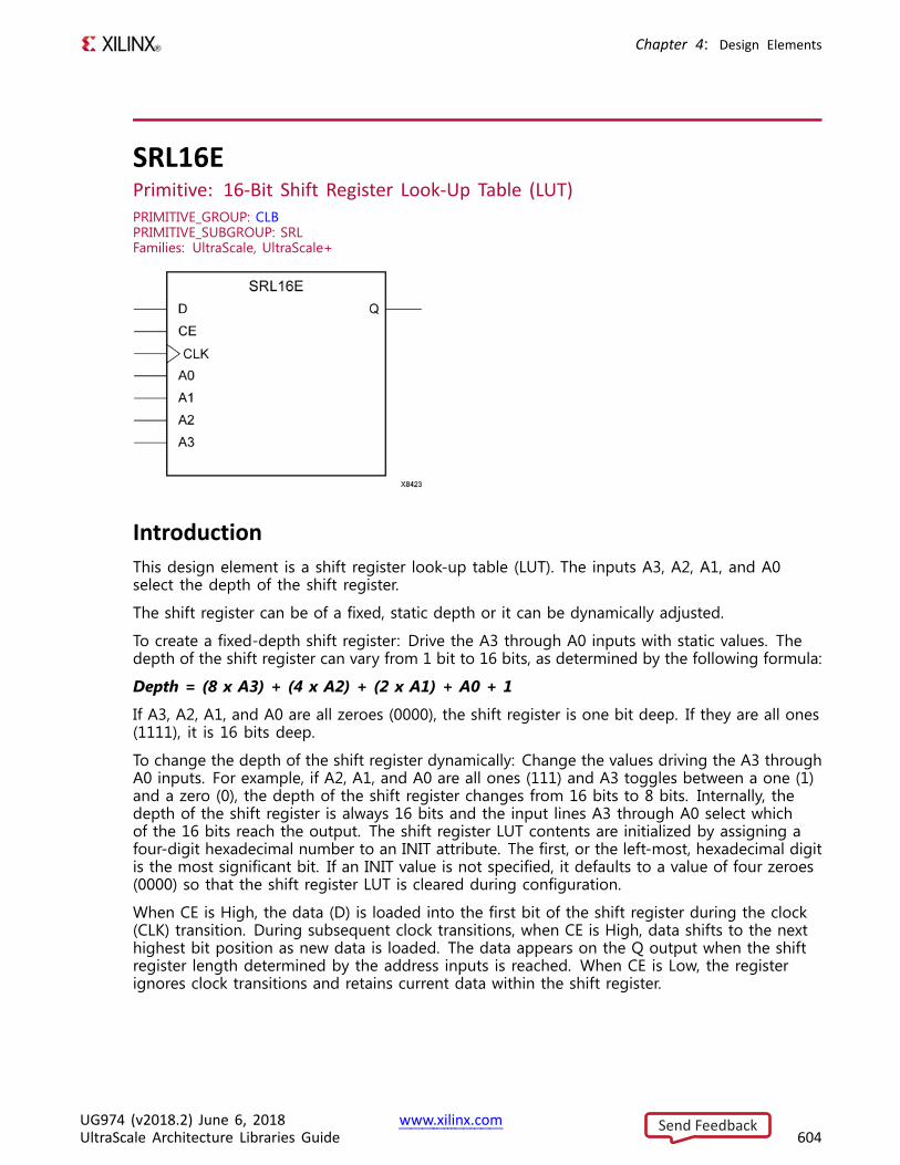
Chapter 4: Design Elements
SRL16EPrimitive: 16-Bit Shift Register Look-Up Table (LUT)PRIMITIVE_GROUP: CLBPRIMITIVE_SUBGROUP: SRLFamilies: UltraScale, UltraScale+
IntroductionThis design element is a shift register look-up table (LUT). The inputs A3, A2, A1, and A0select the depth of the shift register.
The shift register can be of a fixed, static depth or it can be dynamically adjusted.
To create a fixed-depth shift register: Drive the A3 through A0 inputs with static values. Thedepth of the shift register can vary from 1 bit to 16 bits, as determined by the following formula:
Depth = (8 x A3) + (4 x A2) + (2 x A1) + A0 + 1
If A3, A2, A1, and A0 are all zeroes (0000), the shift register is one bit deep. If they are all ones(1111), it is 16 bits deep.
To change the depth of the shift register dynamically: Change the values driving the A3 throughA0 inputs. For example, if A2, A1, and A0 are all ones (111) and A3 toggles between a one (1)and a zero (0), the depth of the shift register changes from 16 bits to 8 bits. Internally, thedepth of the shift register is always 16 bits and the input lines A3 through A0 select whichof the 16 bits reach the output. The shift register LUT contents are initialized by assigning afour-digit hexadecimal number to an INIT attribute. The first, or the left-most, hexadecimal digitis the most significant bit. If an INIT value is not specified, it defaults to a value of four zeroes(0000) so that the shift register LUT is cleared during configuration.
When CE is High, the data (D) is loaded into the first bit of the shift register during the clock(CLK) transition. During subsequent clock transitions, when CE is High, data shifts to the nexthighest bit position as new data is loaded. The data appears on the Q output when the shiftregister length determined by the address inputs is reached. When CE is Low, the registerignores clock transitions and retains current data within the shift register.
UG974 (v2018.2) June 6, 2018 www.xilinx.comUltraScale Architecture Libraries Guide 604
Send Feedback
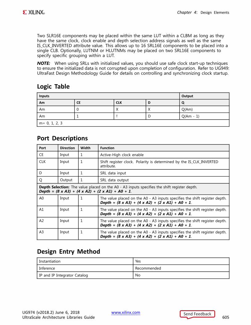
Chapter 4: Design Elements
Two SLR16E components may be placed within the same LUT within a CLBM as long as theyhave the same clock, clock enable and depth selection address signals as well as the sameIS_CLK_INVERTED attribute value. This allows up to 16 SRL16E components to be placed into asingle CLB. Optionally, LUTNM or HLUTNMs may be placed on two SRL16E components tospecify specific grouping within a LUT.
NOTE: When using SRLs with initialized values, you should use safe clock start-up techniquesto ensure the initialized data is not corrupted upon completion of configuration. Refer to UG949:UltraFast Design Methodology Guide for details on controlling and synchronizing clock startup.
Logic TableInputs Output
Am CE CLK D Q
Am 0 X X Q(Am)
Am 1 ↑ D Q(Am - 1)
m= 0, 1, 2, 3
Port DescriptionsPort Direction Width Function
CE Input 1 Active-High clock enable
CLK Input 1 Shift register clock. Polarity is determined by the IS_CLK_INVERTEDattribute.
D Input 1 SRL data input
Q Output 1 SRL data output
Depth Selection: The value placed on the A0 - A3 inputs specifies the shift register depth.Depth = (8 x A3) + (4 x A2) + (2 x A1) + A0 + 1.
A0 Input 1 The value placed on the A0 - A3 inputs specifies the shift register depth.Depth = (8 x A3) + (4 x A2) + (2 x A1) + A0 + 1.
A1 Input 1 The value placed on the A0 - A3 inputs specifies the shift register depth.Depth = (8 x A3) + (4 x A2) + (2 x A1) + A0 + 1.
A2 Input 1 The value placed on the A0 - A3 inputs specifies the shift register depth.Depth = (8 x A3) + (4 x A2) + (2 x A1) + A0 + 1.
A3 Input 1 The value placed on the A0 - A3 inputs specifies the shift register depth.Depth = (8 x A3) + (4 x A2) + (2 x A1) + A0 + 1.
Design Entry MethodInstantiation Yes
Inference Recommended
IP and IP Integrator Catalog No
UG974 (v2018.2) June 6, 2018 www.xilinx.comUltraScale Architecture Libraries Guide 605
Send Feedback
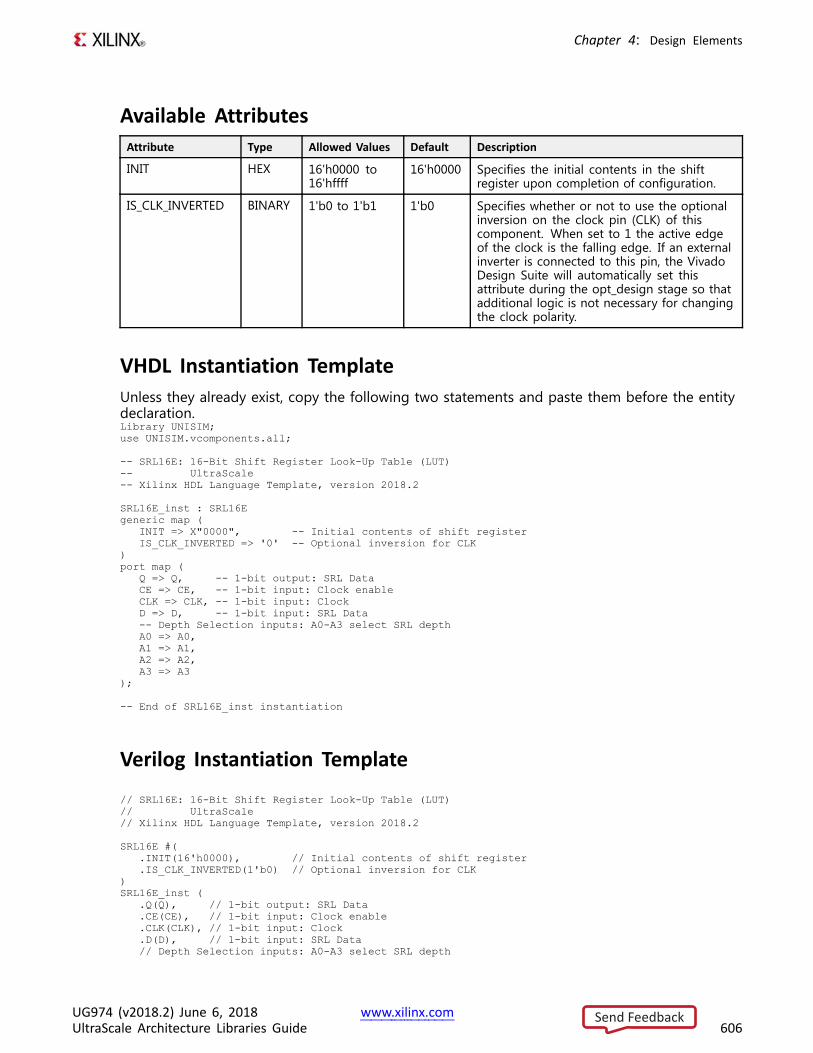
Chapter 4: Design Elements
Available AttributesAttribute Type Allowed Values Default Description
INIT HEX 16'h0000 to16'hffff
16'h0000 Specifies the initial contents in the shiftregister upon completion of configuration.
IS_CLK_INVERTED BINARY 1'b0 to 1'b1 1'b0 Specifies whether or not to use the optionalinversion on the clock pin (CLK) of thiscomponent. When set to 1 the active edgeof the clock is the falling edge. If an externalinverter is connected to this pin, the VivadoDesign Suite will automatically set thisattribute during the opt_design stage so thatadditional logic is not necessary for changingthe clock polarity.
VHDL Instantiation TemplateUnless they already exist, copy the following two statements and paste them before the entitydeclaration.Library UNISIM;use UNISIM.vcomponents.all;
-- SRL16E: 16-Bit Shift Register Look-Up Table (LUT)-- UltraScale-- Xilinx HDL Language Template, version 2018.2
SRL16E_inst : SRL16Egeneric map (
INIT => X"0000", -- Initial contents of shift registerIS_CLK_INVERTED => '0' -- Optional inversion for CLK
)port map (
Q => Q, -- 1-bit output: SRL DataCE => CE, -- 1-bit input: Clock enableCLK => CLK, -- 1-bit input: ClockD => D, -- 1-bit input: SRL Data-- Depth Selection inputs: A0-A3 select SRL depthA0 => A0,A1 => A1,A2 => A2,A3 => A3
);
-- End of SRL16E_inst instantiation
Verilog Instantiation Template
// SRL16E: 16-Bit Shift Register Look-Up Table (LUT)// UltraScale// Xilinx HDL Language Template, version 2018.2
SRL16E #(.INIT(16'h0000), // Initial contents of shift register.IS_CLK_INVERTED(1'b0) // Optional inversion for CLK
)SRL16E_inst (
.Q(Q), // 1-bit output: SRL Data
.CE(CE), // 1-bit input: Clock enable
.CLK(CLK), // 1-bit input: Clock
.D(D), // 1-bit input: SRL Data// Depth Selection inputs: A0-A3 select SRL depth
UG974 (v2018.2) June 6, 2018 www.xilinx.comUltraScale Architecture Libraries Guide 606
Send Feedback
Chapter 4: Design Elements
.A0(A0),
.A1(A1),
.A2(A2),
.A3(A3));
// End of SRL16E_inst instantiation
For More Information• See the UltraScale Architecture Configurable Logic Block User Guide (UG574).
• See the UltraScale Programmable Devices Documentation.
UG974 (v2018.2) June 6, 2018 www.xilinx.comUltraScale Architecture Libraries Guide 607
Send Feedback
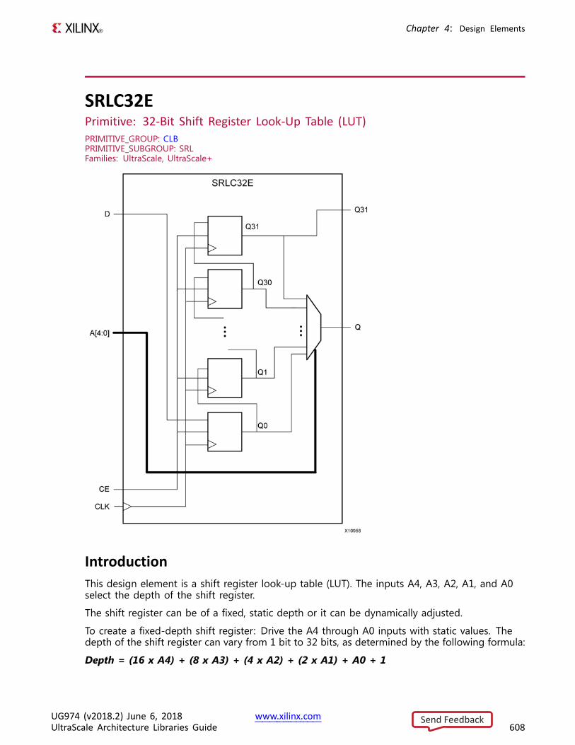
Chapter 4: Design Elements
SRLC32EPrimitive: 32-Bit Shift Register Look-Up Table (LUT)PRIMITIVE_GROUP: CLBPRIMITIVE_SUBGROUP: SRLFamilies: UltraScale, UltraScale+
IntroductionThis design element is a shift register look-up table (LUT). The inputs A4, A3, A2, A1, and A0select the depth of the shift register.
The shift register can be of a fixed, static depth or it can be dynamically adjusted.
To create a fixed-depth shift register: Drive the A4 through A0 inputs with static values. Thedepth of the shift register can vary from 1 bit to 32 bits, as determined by the following formula:
Depth = (16 x A4) + (8 x A3) + (4 x A2) + (2 x A1) + A0 + 1
UG974 (v2018.2) June 6, 2018 www.xilinx.comUltraScale Architecture Libraries Guide 608
Send Feedback
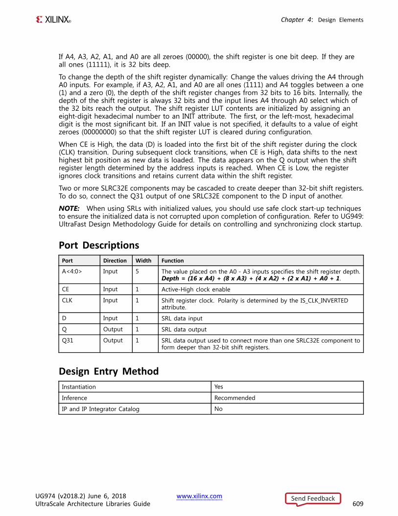
Chapter 4: Design Elements
If A4, A3, A2, A1, and A0 are all zeroes (00000), the shift register is one bit deep. If they areall ones (11111), it is 32 bits deep.
To change the depth of the shift register dynamically: Change the values driving the A4 throughA0 inputs. For example, if A3, A2, A1, and A0 are all ones (1111) and A4 toggles between a one(1) and a zero (0), the depth of the shift register changes from 32 bits to 16 bits. Internally, thedepth of the shift register is always 32 bits and the input lines A4 through A0 select which ofthe 32 bits reach the output. The shift register LUT contents are initialized by assigning aneight-digit hexadecimal number to an INIT attribute. The first, or the left-most, hexadecimaldigit is the most significant bit. If an INIT value is not specified, it defaults to a value of eightzeroes (00000000) so that the shift register LUT is cleared during configuration.
When CE is High, the data (D) is loaded into the first bit of the shift register during the clock(CLK) transition. During subsequent clock transitions, when CE is High, data shifts to the nexthighest bit position as new data is loaded. The data appears on the Q output when the shiftregister length determined by the address inputs is reached. When CE is Low, the registerignores clock transitions and retains current data within the shift register.
Two or more SLRC32E components may be cascaded to create deeper than 32-bit shift registers.To do so, connect the Q31 output of one SRLC32E component to the D input of another.
NOTE: When using SRLs with initialized values, you should use safe clock start-up techniquesto ensure the initialized data is not corrupted upon completion of configuration. Refer to UG949:UltraFast Design Methodology Guide for details on controlling and synchronizing clock startup.
Port DescriptionsPort Direction Width Function
A<4:0> Input 5 The value placed on the A0 - A3 inputs specifies the shift register depth.Depth = (16 x A4) + (8 x A3) + (4 x A2) + (2 x A1) + A0 + 1.
CE Input 1 Active-High clock enable
CLK Input 1 Shift register clock. Polarity is determined by the IS_CLK_INVERTEDattribute.
D Input 1 SRL data input
Q Output 1 SRL data output
Q31 Output 1 SRL data output used to connect more than one SRLC32E component toform deeper than 32-bit shift registers.
Design Entry MethodInstantiation Yes
Inference Recommended
IP and IP Integrator Catalog No
UG974 (v2018.2) June 6, 2018 www.xilinx.comUltraScale Architecture Libraries Guide 609
Send Feedback
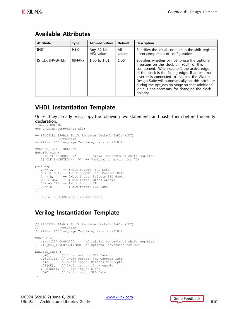
Chapter 4: Design Elements
Available AttributesAttribute Type Allowed Values Default Description
INIT HEX Any 32-bitHEX value
Allzeroes
Specifies the initial contents in the shift registerupon completion of configuration.
IS_CLK_INVERTED BINARY 1'b0 to 1'b1 1'b0 Specifies whether or not to use the optionalinversion on the clock pin (CLK) of thiscomponent. When set to 1 the active edgeof the clock is the falling edge. If an externalinverter is connected to this pin, the VivadoDesign Suite will automatically set this attributeduring the opt_design stage so that additionallogic is not necessary for changing the clockpolarity.
VHDL Instantiation TemplateUnless they already exist, copy the following two statements and paste them before the entitydeclaration.Library UNISIM;use UNISIM.vcomponents.all;
-- SRLC32E: 32-Bit Shift Register Look-Up Table (LUT)-- UltraScale-- Xilinx HDL Language Template, version 2018.2
SRLC32E_inst : SRLC32Egeneric map (
INIT => X"00000000", -- Initial contents of shift registerIS_CLK_INVERTED => '0' -- Optional inversion for CLK
)port map (
Q => Q, -- 1-bit output: SRL DataQ31 => Q31, -- 1-bit output: SRL Cascade DataA => A, -- 5-bit input: Selects SRL depthCE => CE, -- 1-bit input: Clock enableCLK => CLK, -- 1-bit input: ClockD => D -- 1-bit input: SRL Data
);
-- End of SRLC32E_inst instantiation
Verilog Instantiation Template
// SRLC32E: 32-Bit Shift Register Look-Up Table (LUT)// UltraScale// Xilinx HDL Language Template, version 2018.2
SRLC32E #(.INIT(32'h00000000), // Initial contents of shift register.IS_CLK_INVERTED(1'b0) // Optional inversion for CLK
)SRLC32E_inst (
.Q(Q), // 1-bit output: SRL Data
.Q31(Q31), // 1-bit output: SRL Cascade Data
.A(A), // 5-bit input: Selects SRL depth
.CE(CE), // 1-bit input: Clock enable
.CLK(CLK), // 1-bit input: Clock
.D(D) // 1-bit input: SRL Data);
UG974 (v2018.2) June 6, 2018 www.xilinx.comUltraScale Architecture Libraries Guide 610
Send Feedback

Chapter 4: Design Elements
// End of SRLC32E_inst instantiation
For More Information• See the UltraScale Architecture Configurable Logic Block User Guide (UG574).
• See the UltraScale Programmable Devices Documentation.
UG974 (v2018.2) June 6, 2018 www.xilinx.comUltraScale Architecture Libraries Guide 611
Send Feedback
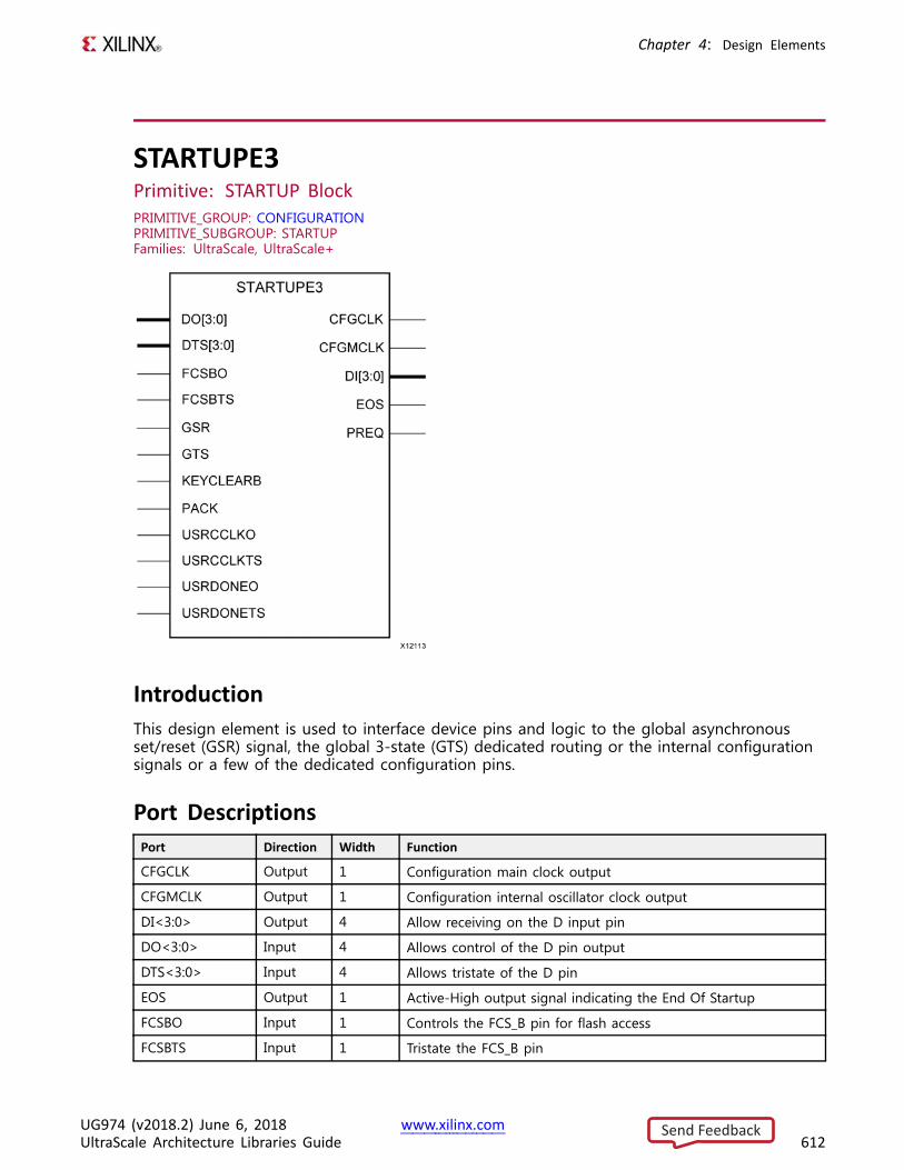
Chapter 4: Design Elements
STARTUPE3Primitive: STARTUP BlockPRIMITIVE_GROUP: CONFIGURATIONPRIMITIVE_SUBGROUP: STARTUPFamilies: UltraScale, UltraScale+
IntroductionThis design element is used to interface device pins and logic to the global asynchronousset/reset (GSR) signal, the global 3-state (GTS) dedicated routing or the internal configurationsignals or a few of the dedicated configuration pins.
Port DescriptionsPort Direction Width Function
CFGCLK Output 1 Configuration main clock output
CFGMCLK Output 1 Configuration internal oscillator clock output
DI<3:0> Output 4 Allow receiving on the D input pin
DO<3:0> Input 4 Allows control of the D pin output
DTS<3:0> Input 4 Allows tristate of the D pin
EOS Output 1 Active-High output signal indicating the End Of Startup
FCSBO Input 1 Controls the FCS_B pin for flash access
FCSBTS Input 1 Tristate the FCS_B pin
UG974 (v2018.2) June 6, 2018 www.xilinx.comUltraScale Architecture Libraries Guide 612
Send Feedback
Chapter 4: Design Elements
Port Direction Width Function
GSR Input 1 Global Set/Reset input (GSR cannot be used for the port)
GTS Input 1 Global 3-state input (GTS cannot be used for the port name)
KEYCLEARB Input 1 Clear AES Decrypter Key input from Battery-Backed RAM (BBRAM)
PACK Input 1 PROGRAM acknowledge input
PREQ Output 1 PROGRAM request to fabric output
USRCCLKO Input 1 User CCLK input
USRCCLKTS Input 1 User CCLK 3-state enable input
USRDONEO Input 1 User DONE pin output control
USRDONETS Input 1 User DONE 3-state enable output
Design Entry MethodInstantiation Recommended
Inference No
IP and IP Integrator Catalog No
Available AttributesAttribute Type Allowed Values Default Description
PROG_USR STRING "FALSE", "TRUE" "FALSE" Activate program event security feature.Requires encrypted bitstreams.
SIM_CCLK_FREQ FLOAT(nS) 0.0 to 10.0 0.0 Set the Configuration Clock Frequency (ns)for simulation
VHDL Instantiation TemplateUnless they already exist, copy the following two statements and paste them before the entitydeclaration.Library UNISIM;use UNISIM.vcomponents.all;
-- STARTUPE3: STARTUP Block-- UltraScale-- Xilinx HDL Language Template, version 2018.2
STARTUPE3_inst : STARTUPE3generic map (
PROG_USR => "FALSE", -- Activate program event security feature. Requires encrypted bitstreams.SIM_CCLK_FREQ => 0.0 -- Set the Configuration Clock Frequency (ns) for simulation
)port map (
CFGCLK => CFGCLK, -- 1-bit output: Configuration main clock outputCFGMCLK => CFGMCLK, -- 1-bit output: Configuration internal oscillator clock outputDI => DI, -- 4-bit output: Allow receiving on the D input pinEOS => EOS, -- 1-bit output: Active-High output signal indicating the End Of StartupPREQ => PREQ, -- 1-bit output: PROGRAM request to fabric outputDO => DO, -- 4-bit input: Allows control of the D pin outputDTS => DTS, -- 4-bit input: Allows tristate of the D pinFCSBO => FCSBO, -- 1-bit input: Controls the FCS_B pin for flash accessFCSBTS => FCSBTS, -- 1-bit input: Tristate the FCS_B pin
UG974 (v2018.2) June 6, 2018 www.xilinx.comUltraScale Architecture Libraries Guide 613
Send Feedback
Chapter 4: Design Elements
GSR => GSR, -- 1-bit input: Global Set/Reset input (GSR cannot be used for the port)GTS => GTS, -- 1-bit input: Global 3-state input (GTS cannot be used for the port name)KEYCLEARB => KEYCLEARB, -- 1-bit input: Clear AES Decrypter Key input from Battery-Backed RAM (BBRAM)PACK => PACK, -- 1-bit input: PROGRAM acknowledge inputUSRCCLKO => USRCCLKO, -- 1-bit input: User CCLK inputUSRCCLKTS => USRCCLKTS, -- 1-bit input: User CCLK 3-state enable inputUSRDONEO => USRDONEO, -- 1-bit input: User DONE pin output controlUSRDONETS => USRDONETS -- 1-bit input: User DONE 3-state enable output
);
-- End of STARTUPE3_inst instantiation
Verilog Instantiation Template
// STARTUPE3: STARTUP Block// UltraScale// Xilinx HDL Language Template, version 2018.2
STARTUPE3 #(.PROG_USR("FALSE"), // Activate program event security feature. Requires encrypted bitstreams..SIM_CCLK_FREQ(0.0) // Set the Configuration Clock Frequency (ns) for simulation
)STARTUPE3_inst (
.CFGCLK(CFGCLK), // 1-bit output: Configuration main clock output
.CFGMCLK(CFGMCLK), // 1-bit output: Configuration internal oscillator clock output
.DI(DI), // 4-bit output: Allow receiving on the D input pin
.EOS(EOS), // 1-bit output: Active-High output signal indicating the End Of Startup
.PREQ(PREQ), // 1-bit output: PROGRAM request to fabric output
.DO(DO), // 4-bit input: Allows control of the D pin output
.DTS(DTS), // 4-bit input: Allows tristate of the D pin
.FCSBO(FCSBO), // 1-bit input: Controls the FCS_B pin for flash access
.FCSBTS(FCSBTS), // 1-bit input: Tristate the FCS_B pin
.GSR(GSR), // 1-bit input: Global Set/Reset input (GSR cannot be used for the port)
.GTS(GTS), // 1-bit input: Global 3-state input (GTS cannot be used for the port name)
.KEYCLEARB(KEYCLEARB), // 1-bit input: Clear AES Decrypter Key input from Battery-Backed RAM (BBRAM)
.PACK(PACK), // 1-bit input: PROGRAM acknowledge input
.USRCCLKO(USRCCLKO), // 1-bit input: User CCLK input
.USRCCLKTS(USRCCLKTS), // 1-bit input: User CCLK 3-state enable input
.USRDONEO(USRDONEO), // 1-bit input: User DONE pin output control
.USRDONETS(USRDONETS) // 1-bit input: User DONE 3-state enable output);
// End of STARTUPE3_inst instantiation
For More Information• See the UltraScale Architecture Configuration User Guide (UG570).
• See the UltraScale Programmable Devices Documentation.
UG974 (v2018.2) June 6, 2018 www.xilinx.comUltraScale Architecture Libraries Guide 614
Send Feedback
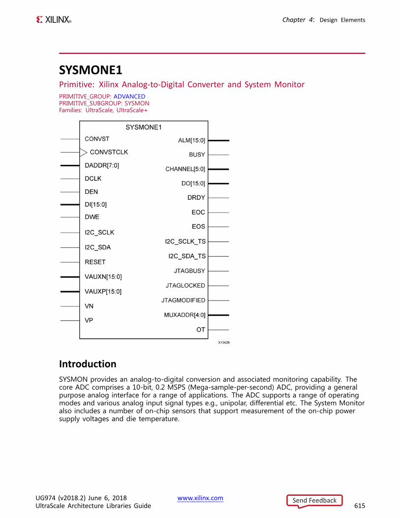
Chapter 4: Design Elements
SYSMONE1Primitive: Xilinx Analog-to-Digital Converter and System MonitorPRIMITIVE_GROUP: ADVANCEDPRIMITIVE_SUBGROUP: SYSMONFamilies: UltraScale, UltraScale+
IntroductionSYSMON provides an analog-to-digital conversion and associated monitoring capability. Thecore ADC comprises a 10-bit, 0.2 MSPS (Mega-sample-per-second) ADC, providing a generalpurpose analog interface for a range of applications. The ADC supports a range of operatingmodes and various analog input signal types e.g., unipolar, differential etc. The System Monitoralso includes a number of on-chip sensors that support measurement of the on-chip powersupply voltages and die temperature.
UG974 (v2018.2) June 6, 2018 www.xilinx.comUltraScale Architecture Libraries Guide 615
Send Feedback
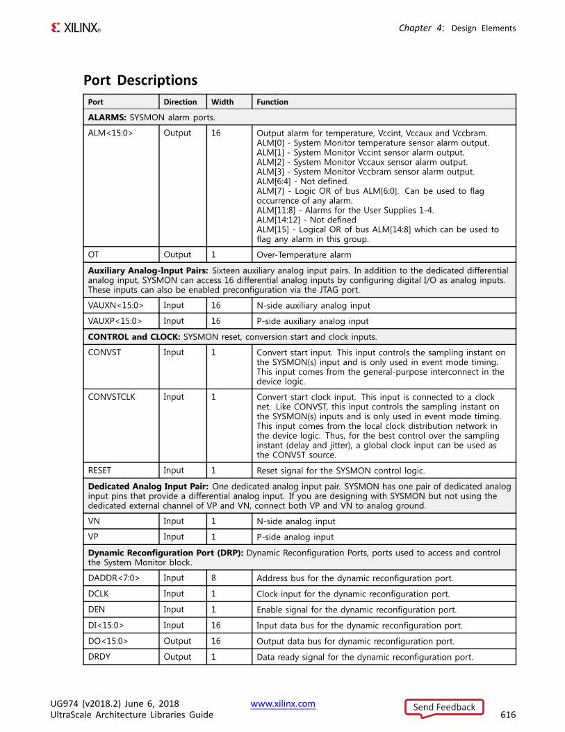
Chapter 4: Design Elements
Port DescriptionsPort Direction Width Function
ALARMS: SYSMON alarm ports.
ALM<15:0> Output 16 Output alarm for temperature, Vccint, Vccaux and Vccbram.ALM[0] - System Monitor temperature sensor alarm output.ALM[1] - System Monitor Vccint sensor alarm output.ALM[2] - System Monitor Vccaux sensor alarm output.ALM[3] - System Monitor Vccbram sensor alarm output.ALM[6:4] - Not defined.ALM[7] - Logic OR of bus ALM[6:0]. Can be used to flagoccurrence of any alarm.ALM[11:8] - Alarms for the User Supplies 1-4.ALM[14:12] - Not definedALM[15] - Logical OR of bus ALM[14:8] which can be used toflag any alarm in this group.
OT Output 1 Over-Temperature alarm
Auxiliary Analog-Input Pairs: Sixteen auxiliary analog input pairs. In addition to the dedicated differentialanalog input, SYSMON can access 16 differential analog inputs by configuring digital I/O as analog inputs.These inputs can also be enabled preconfiguration via the JTAG port.
VAUXN<15:0> Input 16 N-side auxiliary analog input
VAUXP<15:0> Input 16 P-side auxiliary analog input
CONTROL and CLOCK: SYSMON reset, conversion start and clock inputs.
CONVST Input 1 Convert start input. This input controls the sampling instant onthe SYSMON(s) input and is only used in event mode timing.This input comes from the general-purpose interconnect in thedevice logic.
CONVSTCLK Input 1 Convert start clock input. This input is connected to a clocknet. Like CONVST, this input controls the sampling instant onthe SYSMON(s) inputs and is only used in event mode timing.This input comes from the local clock distribution network inthe device logic. Thus, for the best control over the samplinginstant (delay and jitter), a global clock input can be used asthe CONVST source.
RESET Input 1 Reset signal for the SYSMON control logic.
Dedicated Analog Input Pair: One dedicated analog input pair. SYSMON has one pair of dedicated analoginput pins that provide a differential analog input. If you are designing with SYSMON but not using thededicated external channel of VP and VN, connect both VP and VN to analog ground.
VN Input 1 N-side analog input
VP Input 1 P-side analog input
Dynamic Reconfiguration Port (DRP): Dynamic Reconfiguration Ports, ports used to access and controlthe System Monitor block.
DADDR<7:0> Input 8 Address bus for the dynamic reconfiguration port.
DCLK Input 1 Clock input for the dynamic reconfiguration port.
DEN Input 1 Enable signal for the dynamic reconfiguration port.
DI<15:0> Input 16 Input data bus for the dynamic reconfiguration port.
DO<15:0> Output 16 Output data bus for dynamic reconfiguration port.
DRDY Output 1 Data ready signal for the dynamic reconfiguration port.
UG974 (v2018.2) June 6, 2018 www.xilinx.comUltraScale Architecture Libraries Guide 616
Send Feedback
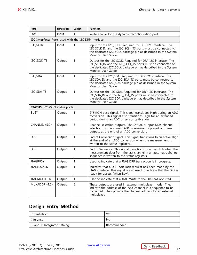
Chapter 4: Design Elements
Port Direction Width Function
DWE Input 1 Write enable for the dynamic reconfiguration port.
I2C Interface: Ports used with the I2C DRP interface
I2C_SCLK Input 1 Input for the I2C_SCLK. Required for DRP I2C interface. TheI2C_SCLK_IN and the I2C_SCLK_TS ports must be connected tothe dedicated I2C_SCLK package pin as described in the SystemMonitor User Guide.
I2C_SCLK_TS Output 1 Output for the I2C_SCLK. Required for DRP I2C interface. TheI2C_SCLK_IN and the I2C_SCLK_TS ports must be connected tothe dedicated I2C_SCLK package pin as described in the SystemMonitor User Guide.
I2C_SDA Input 1 Input for the I2C_SDA. Required for DRP I2C interface. TheI2C_SDA_IN and the I2C_SDA_TS ports must be connected tothe dedicated I2C_SDA package pin as described in the SystemMonitor User Guide.
I2C_SDA_TS Output 1 Output for the I2C_SDA. Required for DRP I2C interface. TheI2C_SDA_IN and the I2C_SDA_TS ports must be connected tothe dedicated I2C_SDA package pin as described in the SystemMonitor User Guide.
STATUS: SYSMON status ports.
BUSY Output 1 SYSMON busy signal. This signal transitions High during an ADCconversion. This signal also transitions High for an extendedperiod during an ADC or sensor calibration.
CHANNEL<5:0> Output 6 Channel selection outputs. The SYSMON input MUX channelselection for the current ADC conversion is placed on theseoutputs at the end of an ADC conversion.
EOC Output 1 End of Conversion signal. This signal transitions to an active-Highat the end of an ADC conversion when the measurement iswritten to the status registers.
EOS Output 1 End of Sequence. This signal transitions to active-High when themeasurement data from the last channel in an automatic channelsequence is written to the status registers.
JTAGBUSY Output 1 Used to indicate that a JTAG DRP transaction is in progress.
JTAGLOCKED Output 1 Indicates that a DRP port lock request has been made by theJTAG interface. This signal is also used to indicate that the DRP isready for access (when Low).
JTAGMODIFIED Output 1 Used to indicate that a JTAG Write to the DRP has occurred.
MUXADDR<4:0> Output 5 These outputs are used in external multiplexer mode. Theyindicate the address of the next channel in a sequence to beconverted. They provide the channel address for an externalmultiplexer.
Design Entry MethodInstantiation Yes
Inference No
IP and IP Integrator Catalog Recommended
UG974 (v2018.2) June 6, 2018 www.xilinx.comUltraScale Architecture Libraries Guide 617
Send Feedback
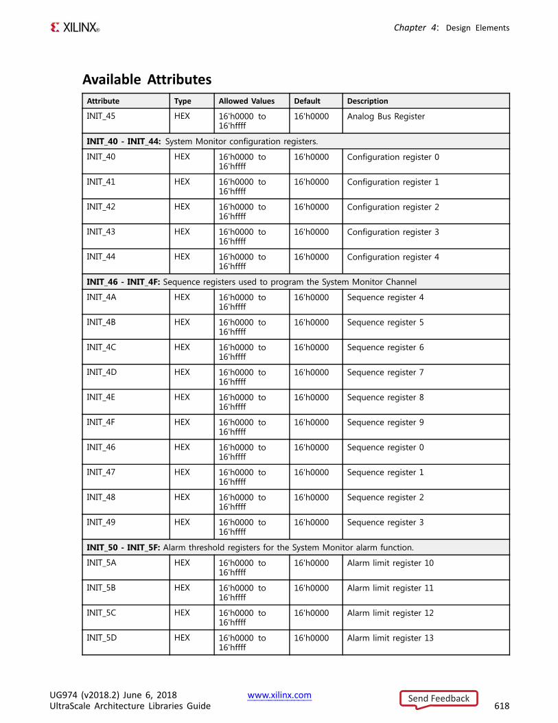
Chapter 4: Design Elements
Available AttributesAttribute Type Allowed Values Default Description
INIT_45 HEX 16'h0000 to16'hffff
16'h0000 Analog Bus Register
INIT_40 - INIT_44: System Monitor configuration registers.
INIT_40 HEX 16'h0000 to16'hffff
16'h0000 Configuration register 0
INIT_41 HEX 16'h0000 to16'hffff
16'h0000 Configuration register 1
INIT_42 HEX 16'h0000 to16'hffff
16'h0000 Configuration register 2
INIT_43 HEX 16'h0000 to16'hffff
16'h0000 Configuration register 3
INIT_44 HEX 16'h0000 to16'hffff
16'h0000 Configuration register 4
INIT_46 - INIT_4F: Sequence registers used to program the System Monitor Channel
INIT_4A HEX 16'h0000 to16'hffff
16'h0000 Sequence register 4
INIT_4B HEX 16'h0000 to16'hffff
16'h0000 Sequence register 5
INIT_4C HEX 16'h0000 to16'hffff
16'h0000 Sequence register 6
INIT_4D HEX 16'h0000 to16'hffff
16'h0000 Sequence register 7
INIT_4E HEX 16'h0000 to16'hffff
16'h0000 Sequence register 8
INIT_4F HEX 16'h0000 to16'hffff
16'h0000 Sequence register 9
INIT_46 HEX 16'h0000 to16'hffff
16'h0000 Sequence register 0
INIT_47 HEX 16'h0000 to16'hffff
16'h0000 Sequence register 1
INIT_48 HEX 16'h0000 to16'hffff
16'h0000 Sequence register 2
INIT_49 HEX 16'h0000 to16'hffff
16'h0000 Sequence register 3
INIT_50 - INIT_5F: Alarm threshold registers for the System Monitor alarm function.
INIT_5A HEX 16'h0000 to16'hffff
16'h0000 Alarm limit register 10
INIT_5B HEX 16'h0000 to16'hffff
16'h0000 Alarm limit register 11
INIT_5C HEX 16'h0000 to16'hffff
16'h0000 Alarm limit register 12
INIT_5D HEX 16'h0000 to16'hffff
16'h0000 Alarm limit register 13
UG974 (v2018.2) June 6, 2018 www.xilinx.comUltraScale Architecture Libraries Guide 618
Send Feedback
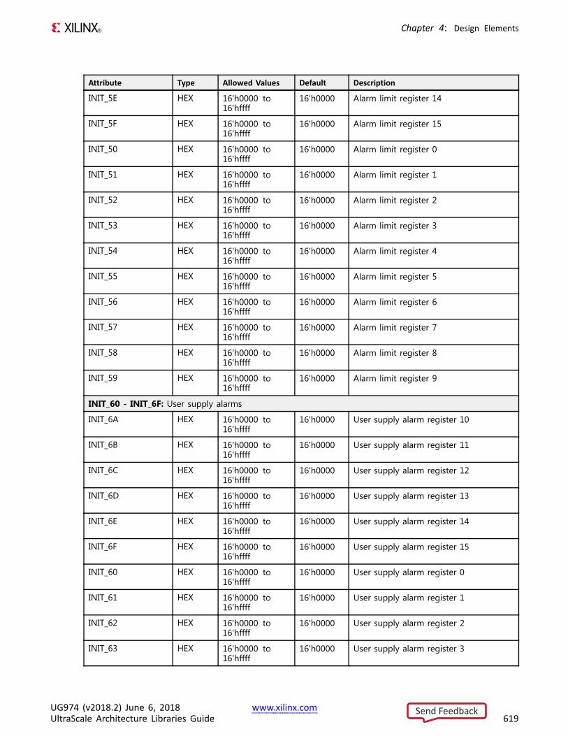
Chapter 4: Design Elements
Attribute Type Allowed Values Default Description
INIT_5E HEX 16'h0000 to16'hffff
16'h0000 Alarm limit register 14
INIT_5F HEX 16'h0000 to16'hffff
16'h0000 Alarm limit register 15
INIT_50 HEX 16'h0000 to16'hffff
16'h0000 Alarm limit register 0
INIT_51 HEX 16'h0000 to16'hffff
16'h0000 Alarm limit register 1
INIT_52 HEX 16'h0000 to16'hffff
16'h0000 Alarm limit register 2
INIT_53 HEX 16'h0000 to16'hffff
16'h0000 Alarm limit register 3
INIT_54 HEX 16'h0000 to16'hffff
16'h0000 Alarm limit register 4
INIT_55 HEX 16'h0000 to16'hffff
16'h0000 Alarm limit register 5
INIT_56 HEX 16'h0000 to16'hffff
16'h0000 Alarm limit register 6
INIT_57 HEX 16'h0000 to16'hffff
16'h0000 Alarm limit register 7
INIT_58 HEX 16'h0000 to16'hffff
16'h0000 Alarm limit register 8
INIT_59 HEX 16'h0000 to16'hffff
16'h0000 Alarm limit register 9
INIT_60 - INIT_6F: User supply alarms
INIT_6A HEX 16'h0000 to16'hffff
16'h0000 User supply alarm register 10
INIT_6B HEX 16'h0000 to16'hffff
16'h0000 User supply alarm register 11
INIT_6C HEX 16'h0000 to16'hffff
16'h0000 User supply alarm register 12
INIT_6D HEX 16'h0000 to16'hffff
16'h0000 User supply alarm register 13
INIT_6E HEX 16'h0000 to16'hffff
16'h0000 User supply alarm register 14
INIT_6F HEX 16'h0000 to16'hffff
16'h0000 User supply alarm register 15
INIT_60 HEX 16'h0000 to16'hffff
16'h0000 User supply alarm register 0
INIT_61 HEX 16'h0000 to16'hffff
16'h0000 User supply alarm register 1
INIT_62 HEX 16'h0000 to16'hffff
16'h0000 User supply alarm register 2
INIT_63 HEX 16'h0000 to16'hffff
16'h0000 User supply alarm register 3
UG974 (v2018.2) June 6, 2018 www.xilinx.comUltraScale Architecture Libraries Guide 619
Send Feedback
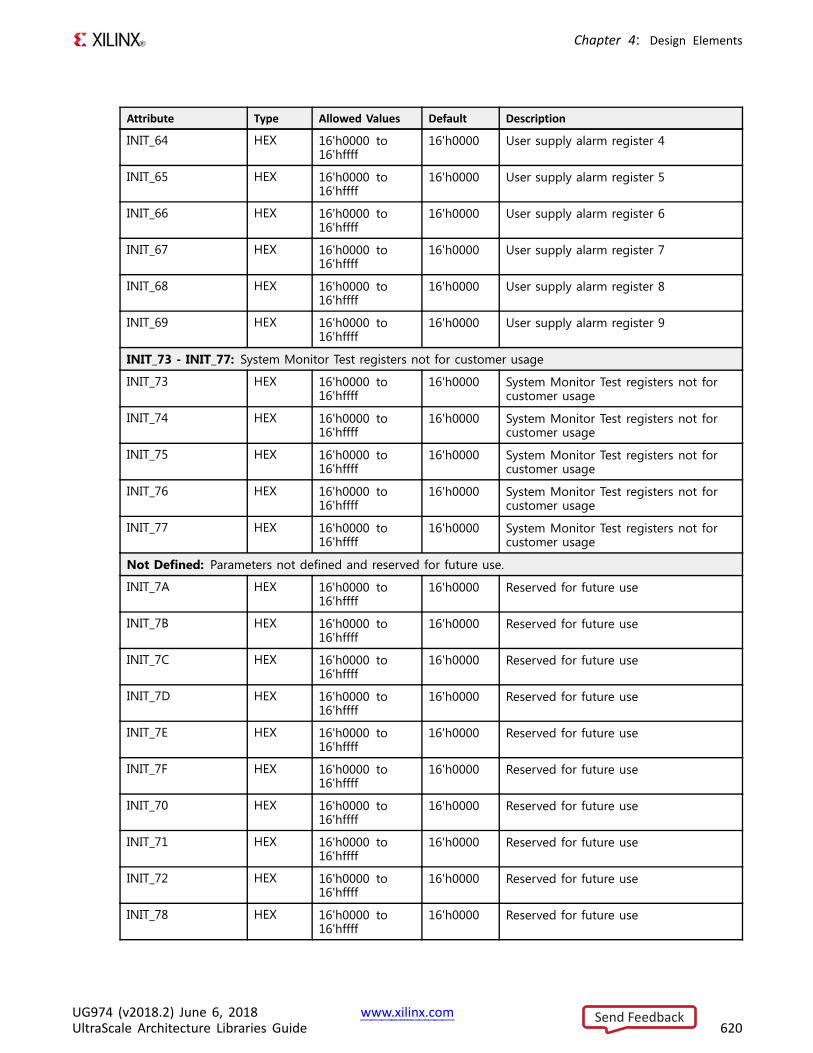
Chapter 4: Design Elements
Attribute Type Allowed Values Default Description
INIT_64 HEX 16'h0000 to16'hffff
16'h0000 User supply alarm register 4
INIT_65 HEX 16'h0000 to16'hffff
16'h0000 User supply alarm register 5
INIT_66 HEX 16'h0000 to16'hffff
16'h0000 User supply alarm register 6
INIT_67 HEX 16'h0000 to16'hffff
16'h0000 User supply alarm register 7
INIT_68 HEX 16'h0000 to16'hffff
16'h0000 User supply alarm register 8
INIT_69 HEX 16'h0000 to16'hffff
16'h0000 User supply alarm register 9
INIT_73 - INIT_77: System Monitor Test registers not for customer usage
INIT_73 HEX 16'h0000 to16'hffff
16'h0000 System Monitor Test registers not forcustomer usage
INIT_74 HEX 16'h0000 to16'hffff
16'h0000 System Monitor Test registers not forcustomer usage
INIT_75 HEX 16'h0000 to16'hffff
16'h0000 System Monitor Test registers not forcustomer usage
INIT_76 HEX 16'h0000 to16'hffff
16'h0000 System Monitor Test registers not forcustomer usage
INIT_77 HEX 16'h0000 to16'hffff
16'h0000 System Monitor Test registers not forcustomer usage
Not Defined: Parameters not defined and reserved for future use.
INIT_7A HEX 16'h0000 to16'hffff
16'h0000 Reserved for future use
INIT_7B HEX 16'h0000 to16'hffff
16'h0000 Reserved for future use
INIT_7C HEX 16'h0000 to16'hffff
16'h0000 Reserved for future use
INIT_7D HEX 16'h0000 to16'hffff
16'h0000 Reserved for future use
INIT_7E HEX 16'h0000 to16'hffff
16'h0000 Reserved for future use
INIT_7F HEX 16'h0000 to16'hffff
16'h0000 Reserved for future use
INIT_70 HEX 16'h0000 to16'hffff
16'h0000 Reserved for future use
INIT_71 HEX 16'h0000 to16'hffff
16'h0000 Reserved for future use
INIT_72 HEX 16'h0000 to16'hffff
16'h0000 Reserved for future use
INIT_78 HEX 16'h0000 to16'hffff
16'h0000 Reserved for future use
UG974 (v2018.2) June 6, 2018 www.xilinx.comUltraScale Architecture Libraries Guide 620
Send Feedback
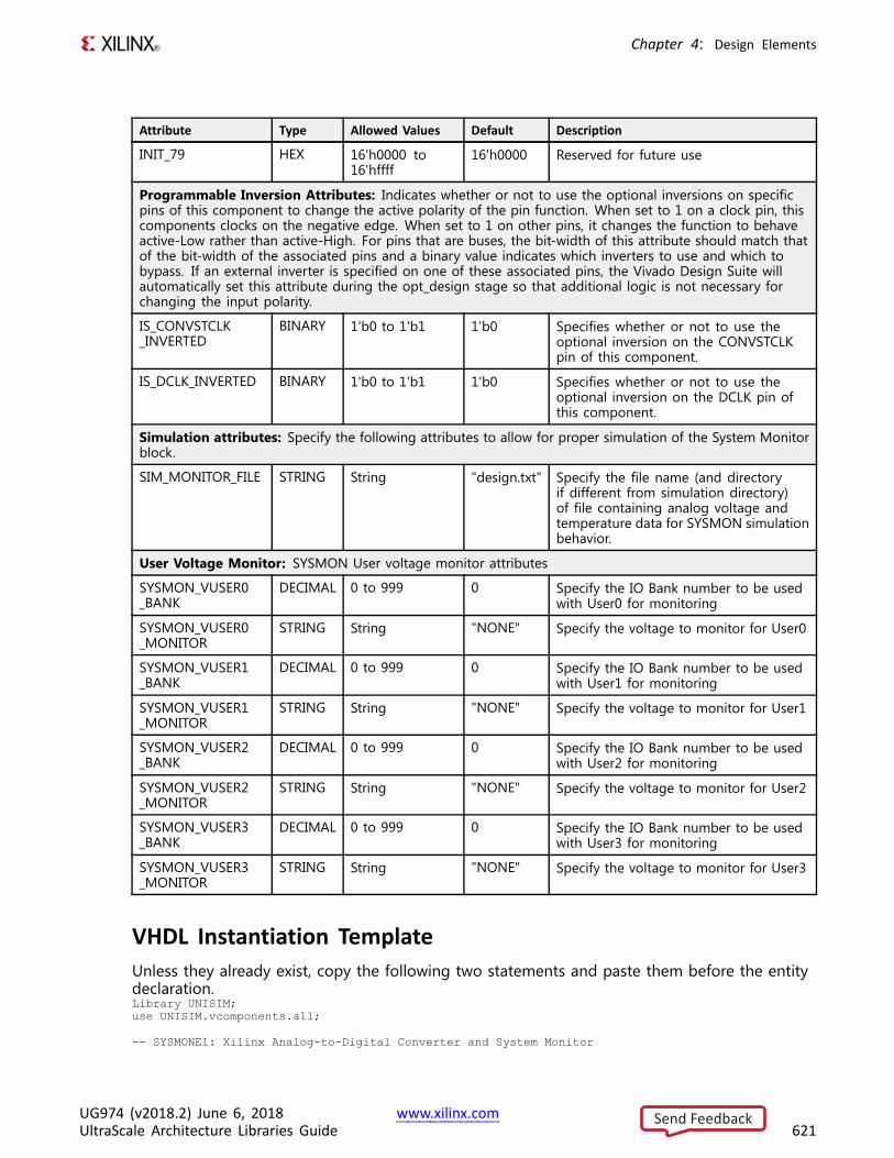
Chapter 4: Design Elements
Attribute Type Allowed Values Default Description
INIT_79 HEX 16'h0000 to16'hffff
16'h0000 Reserved for future use
Programmable Inversion Attributes: Indicates whether or not to use the optional inversions on specificpins of this component to change the active polarity of the pin function. When set to 1 on a clock pin, thiscomponents clocks on the negative edge. When set to 1 on other pins, it changes the function to behaveactive-Low rather than active-High. For pins that are buses, the bit-width of this attribute should match thatof the bit-width of the associated pins and a binary value indicates which inverters to use and which tobypass. If an external inverter is specified on one of these associated pins, the Vivado Design Suite willautomatically set this attribute during the opt_design stage so that additional logic is not necessary forchanging the input polarity.
IS_CONVSTCLK_INVERTED
BINARY 1'b0 to 1'b1 1'b0 Specifies whether or not to use theoptional inversion on the CONVSTCLKpin of this component.
IS_DCLK_INVERTED BINARY 1'b0 to 1'b1 1'b0 Specifies whether or not to use theoptional inversion on the DCLK pin ofthis component.
Simulation attributes: Specify the following attributes to allow for proper simulation of the System Monitorblock.
SIM_MONITOR_FILE STRING String "design.txt" Specify the file name (and directoryif different from simulation directory)of file containing analog voltage andtemperature data for SYSMON simulationbehavior.
User Voltage Monitor: SYSMON User voltage monitor attributes
SYSMON_VUSER0_BANK
DECIMAL 0 to 999 0 Specify the IO Bank number to be usedwith User0 for monitoring
SYSMON_VUSER0_MONITOR
STRING String "NONE" Specify the voltage to monitor for User0
SYSMON_VUSER1_BANK
DECIMAL 0 to 999 0 Specify the IO Bank number to be usedwith User1 for monitoring
SYSMON_VUSER1_MONITOR
STRING String "NONE" Specify the voltage to monitor for User1
SYSMON_VUSER2_BANK
DECIMAL 0 to 999 0 Specify the IO Bank number to be usedwith User2 for monitoring
SYSMON_VUSER2_MONITOR
STRING String "NONE" Specify the voltage to monitor for User2
SYSMON_VUSER3_BANK
DECIMAL 0 to 999 0 Specify the IO Bank number to be usedwith User3 for monitoring
SYSMON_VUSER3_MONITOR
STRING String "NONE" Specify the voltage to monitor for User3
VHDL Instantiation TemplateUnless they already exist, copy the following two statements and paste them before the entitydeclaration.Library UNISIM;use UNISIM.vcomponents.all;
-- SYSMONE1: Xilinx Analog-to-Digital Converter and System Monitor
UG974 (v2018.2) June 6, 2018 www.xilinx.comUltraScale Architecture Libraries Guide 621
Send Feedback
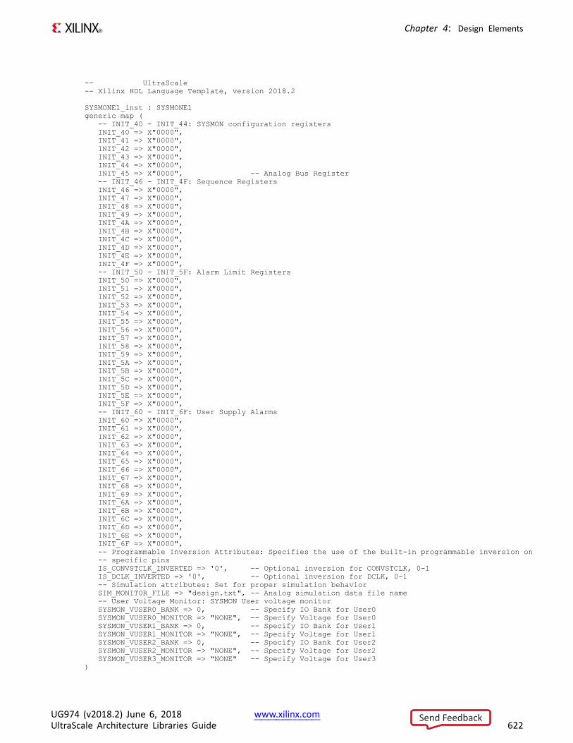
Chapter 4: Design Elements
-- UltraScale-- Xilinx HDL Language Template, version 2018.2
SYSMONE1_inst : SYSMONE1generic map (
-- INIT_40 - INIT_44: SYSMON configuration registersINIT_40 => X"0000",INIT_41 => X"0000",INIT_42 => X"0000",INIT_43 => X"0000",INIT_44 => X"0000",INIT_45 => X"0000", -- Analog Bus Register-- INIT_46 - INIT_4F: Sequence RegistersINIT_46 => X"0000",INIT_47 => X"0000",INIT_48 => X"0000",INIT_49 => X"0000",INIT_4A => X"0000",INIT_4B => X"0000",INIT_4C => X"0000",INIT_4D => X"0000",INIT_4E => X"0000",INIT_4F => X"0000",-- INIT_50 - INIT_5F: Alarm Limit RegistersINIT_50 => X"0000",INIT_51 => X"0000",INIT_52 => X"0000",INIT_53 => X"0000",INIT_54 => X"0000",INIT_55 => X"0000",INIT_56 => X"0000",INIT_57 => X"0000",INIT_58 => X"0000",INIT_59 => X"0000",INIT_5A => X"0000",INIT_5B => X"0000",INIT_5C => X"0000",INIT_5D => X"0000",INIT_5E => X"0000",INIT_5F => X"0000",-- INIT_60 - INIT_6F: User Supply AlarmsINIT_60 => X"0000",INIT_61 => X"0000",INIT_62 => X"0000",INIT_63 => X"0000",INIT_64 => X"0000",INIT_65 => X"0000",INIT_66 => X"0000",INIT_67 => X"0000",INIT_68 => X"0000",INIT_69 => X"0000",INIT_6A => X"0000",INIT_6B => X"0000",INIT_6C => X"0000",INIT_6D => X"0000",INIT_6E => X"0000",INIT_6F => X"0000",-- Programmable Inversion Attributes: Specifies the use of the built-in programmable inversion on-- specific pinsIS_CONVSTCLK_INVERTED => '0', -- Optional inversion for CONVSTCLK, 0-1IS_DCLK_INVERTED => '0', -- Optional inversion for DCLK, 0-1-- Simulation attributes: Set for proper simulation behaviorSIM_MONITOR_FILE => "design.txt", -- Analog simulation data file name-- User Voltage Monitor: SYSMON User voltage monitorSYSMON_VUSER0_BANK => 0, -- Specify IO Bank for User0SYSMON_VUSER0_MONITOR => "NONE", -- Specify Voltage for User0SYSMON_VUSER1_BANK => 0, -- Specify IO Bank for User1SYSMON_VUSER1_MONITOR => "NONE", -- Specify Voltage for User1SYSMON_VUSER2_BANK => 0, -- Specify IO Bank for User2SYSMON_VUSER2_MONITOR => "NONE", -- Specify Voltage for User2SYSMON_VUSER3_MONITOR => "NONE" -- Specify Voltage for User3
)
UG974 (v2018.2) June 6, 2018 www.xilinx.comUltraScale Architecture Libraries Guide 622
Send Feedback
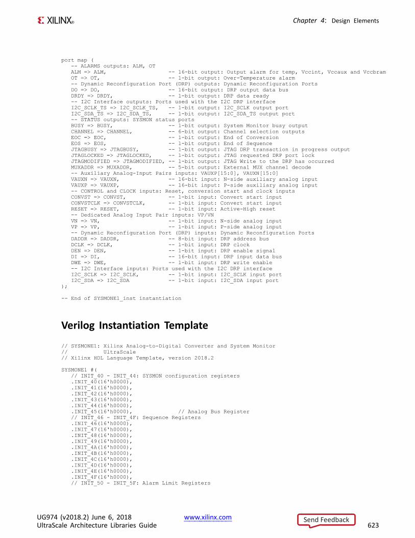
Chapter 4: Design Elements
port map (-- ALARMS outputs: ALM, OTALM => ALM, -- 16-bit output: Output alarm for temp, Vccint, Vccaux and VccbramOT => OT, -- 1-bit output: Over-Temperature alarm-- Dynamic Reconfiguration Port (DRP) outputs: Dynamic Reconfiguration PortsDO => DO, -- 16-bit output: DRP output data busDRDY => DRDY, -- 1-bit output: DRP data ready-- I2C Interface outputs: Ports used with the I2C DRP interfaceI2C_SCLK_TS => I2C_SCLK_TS, -- 1-bit output: I2C_SCLK output portI2C_SDA_TS => I2C_SDA_TS, -- 1-bit output: I2C_SDA_TS output port-- STATUS outputs: SYSMON status portsBUSY => BUSY, -- 1-bit output: System Monitor busy outputCHANNEL => CHANNEL, -- 6-bit output: Channel selection outputsEOC => EOC, -- 1-bit output: End of ConversionEOS => EOS, -- 1-bit output: End of SequenceJTAGBUSY => JTAGBUSY, -- 1-bit output: JTAG DRP transaction in progress outputJTAGLOCKED => JTAGLOCKED, -- 1-bit output: JTAG requested DRP port lockJTAGMODIFIED => JTAGMODIFIED, -- 1-bit output: JTAG Write to the DRP has occurredMUXADDR => MUXADDR, -- 5-bit output: External MUX channel decode-- Auxiliary Analog-Input Pairs inputs: VAUXP[15:0], VAUXN[15:0]VAUXN => VAUXN, -- 16-bit input: N-side auxiliary analog inputVAUXP => VAUXP, -- 16-bit input: P-side auxiliary analog input-- CONTROL and CLOCK inputs: Reset, conversion start and clock inputsCONVST => CONVST, -- 1-bit input: Convert start inputCONVSTCLK => CONVSTCLK, -- 1-bit input: Convert start inputRESET => RESET, -- 1-bit input: Active-High reset-- Dedicated Analog Input Pair inputs: VP/VNVN => VN, -- 1-bit input: N-side analog inputVP => VP, -- 1-bit input: P-side analog input-- Dynamic Reconfiguration Port (DRP) inputs: Dynamic Reconfiguration PortsDADDR => DADDR, -- 8-bit input: DRP address busDCLK => DCLK, -- 1-bit input: DRP clockDEN => DEN, -- 1-bit input: DRP enable signalDI => DI, -- 16-bit input: DRP input data busDWE => DWE, -- 1-bit input: DRP write enable-- I2C Interface inputs: Ports used with the I2C DRP interfaceI2C_SCLK => I2C_SCLK, -- 1-bit input: I2C_SCLK input portI2C_SDA => I2C_SDA -- 1-bit input: I2C_SDA input port
);
-- End of SYSMONE1_inst instantiation
Verilog Instantiation Template
// SYSMONE1: Xilinx Analog-to-Digital Converter and System Monitor// UltraScale// Xilinx HDL Language Template, version 2018.2
SYSMONE1 #(// INIT_40 - INIT_44: SYSMON configuration registers.INIT_40(16'h0000),.INIT_41(16'h0000),.INIT_42(16'h0000),.INIT_43(16'h0000),.INIT_44(16'h0000),.INIT_45(16'h0000), // Analog Bus Register// INIT_46 - INIT_4F: Sequence Registers.INIT_46(16'h0000),.INIT_47(16'h0000),.INIT_48(16'h0000),.INIT_49(16'h0000),.INIT_4A(16'h0000),.INIT_4B(16'h0000),.INIT_4C(16'h0000),.INIT_4D(16'h0000),.INIT_4E(16'h0000),.INIT_4F(16'h0000),// INIT_50 - INIT_5F: Alarm Limit Registers
UG974 (v2018.2) June 6, 2018 www.xilinx.comUltraScale Architecture Libraries Guide 623
Send Feedback
Chapter 4: Design Elements
.INIT_50(16'h0000),
.INIT_51(16'h0000),
.INIT_52(16'h0000),
.INIT_53(16'h0000),
.INIT_54(16'h0000),
.INIT_55(16'h0000),
.INIT_56(16'h0000),
.INIT_57(16'h0000),
.INIT_58(16'h0000),
.INIT_59(16'h0000),
.INIT_5A(16'h0000),
.INIT_5B(16'h0000),
.INIT_5C(16'h0000),
.INIT_5D(16'h0000),
.INIT_5E(16'h0000),
.INIT_5F(16'h0000),// INIT_60 - INIT_6F: User Supply Alarms.INIT_60(16'h0000),.INIT_61(16'h0000),.INIT_62(16'h0000),.INIT_63(16'h0000),.INIT_64(16'h0000),.INIT_65(16'h0000),.INIT_66(16'h0000),.INIT_67(16'h0000),.INIT_68(16'h0000),.INIT_69(16'h0000),.INIT_6A(16'h0000),.INIT_6B(16'h0000),.INIT_6C(16'h0000),.INIT_6D(16'h0000),.INIT_6E(16'h0000),.INIT_6F(16'h0000),// Programmable Inversion Attributes: Specifies the use of the built-in programmable inversion on// specific pins.IS_CONVSTCLK_INVERTED(1'b0), // Optional inversion for CONVSTCLK, 0-1.IS_DCLK_INVERTED(1'b0), // Optional inversion for DCLK, 0-1// Simulation attributes: Set for proper simulation behavior.SIM_MONITOR_FILE("design.txt"), // Analog simulation data file name// User Voltage Monitor: SYSMON User voltage monitor.SYSMON_VUSER0_BANK(0), // Specify IO Bank for User0.SYSMON_VUSER0_MONITOR("NONE"), // Specify Voltage for User0.SYSMON_VUSER1_BANK(0), // Specify IO Bank for User1.SYSMON_VUSER1_MONITOR("NONE"), // Specify Voltage for User1.SYSMON_VUSER2_BANK(0), // Specify IO Bank for User2.SYSMON_VUSER2_MONITOR("NONE"), // Specify Voltage for User2.SYSMON_VUSER3_MONITOR("NONE") // Specify Voltage for User3
)SYSMONE1_inst (
// ALARMS outputs: ALM, OT.ALM(ALM), // 16-bit output: Output alarm for temp, Vccint, Vccaux and Vccbram.OT(OT), // 1-bit output: Over-Temperature alarm// Dynamic Reconfiguration Port (DRP) outputs: Dynamic Reconfiguration Ports.DO(DO), // 16-bit output: DRP output data bus.DRDY(DRDY), // 1-bit output: DRP data ready// I2C Interface outputs: Ports used with the I2C DRP interface.I2C_SCLK_TS(I2C_SCLK_TS), // 1-bit output: I2C_SCLK output port.I2C_SDA_TS(I2C_SDA_TS), // 1-bit output: I2C_SDA_TS output port// STATUS outputs: SYSMON status ports.BUSY(BUSY), // 1-bit output: System Monitor busy output.CHANNEL(CHANNEL), // 6-bit output: Channel selection outputs.EOC(EOC), // 1-bit output: End of Conversion.EOS(EOS), // 1-bit output: End of Sequence.JTAGBUSY(JTAGBUSY), // 1-bit output: JTAG DRP transaction in progress output.JTAGLOCKED(JTAGLOCKED), // 1-bit output: JTAG requested DRP port lock.JTAGMODIFIED(JTAGMODIFIED), // 1-bit output: JTAG Write to the DRP has occurred.MUXADDR(MUXADDR), // 5-bit output: External MUX channel decode// Auxiliary Analog-Input Pairs inputs: VAUXP[15:0], VAUXN[15:0].VAUXN(VAUXN), // 16-bit input: N-side auxiliary analog input.VAUXP(VAUXP), // 16-bit input: P-side auxiliary analog input// CONTROL and CLOCK inputs: Reset, conversion start and clock inputs.CONVST(CONVST), // 1-bit input: Convert start input
UG974 (v2018.2) June 6, 2018 www.xilinx.comUltraScale Architecture Libraries Guide 624
Send Feedback
Chapter 4: Design Elements
.CONVSTCLK(CONVSTCLK), // 1-bit input: Convert start input
.RESET(RESET), // 1-bit input: Active-High reset// Dedicated Analog Input Pair inputs: VP/VN.VN(VN), // 1-bit input: N-side analog input.VP(VP), // 1-bit input: P-side analog input// Dynamic Reconfiguration Port (DRP) inputs: Dynamic Reconfiguration Ports.DADDR(DADDR), // 8-bit input: DRP address bus.DCLK(DCLK), // 1-bit input: DRP clock.DEN(DEN), // 1-bit input: DRP enable signal.DI(DI), // 16-bit input: DRP input data bus.DWE(DWE), // 1-bit input: DRP write enable// I2C Interface inputs: Ports used with the I2C DRP interface.I2C_SCLK(I2C_SCLK), // 1-bit input: I2C_SCLK input port.I2C_SDA(I2C_SDA) // 1-bit input: I2C_SDA input port
);
// End of SYSMONE1_inst instantiation
For More Information• See the UltraScale Architecture System Monitor User Guide (UG580).
• See the UltraScale Programmable Devices Documentation.
UG974 (v2018.2) June 6, 2018 www.xilinx.comUltraScale Architecture Libraries Guide 625
Send Feedback
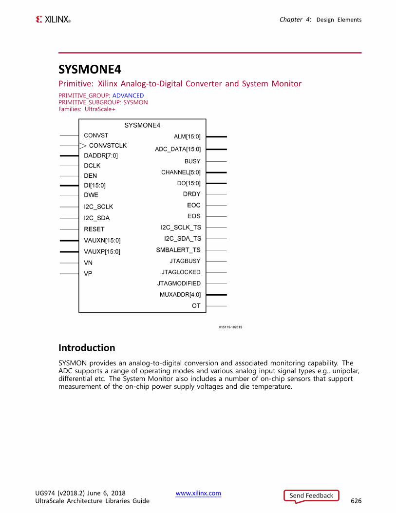
Chapter 4: Design Elements
SYSMONE4Primitive: Xilinx Analog-to-Digital Converter and System MonitorPRIMITIVE_GROUP: ADVANCEDPRIMITIVE_SUBGROUP: SYSMONFamilies: UltraScale+
IntroductionSYSMON provides an analog-to-digital conversion and associated monitoring capability. TheADC supports a range of operating modes and various analog input signal types e.g., unipolar,differential etc. The System Monitor also includes a number of on-chip sensors that supportmeasurement of the on-chip power supply voltages and die temperature.
UG974 (v2018.2) June 6, 2018 www.xilinx.comUltraScale Architecture Libraries Guide 626
Send Feedback
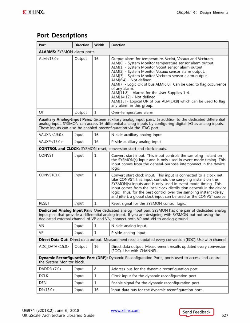
Chapter 4: Design Elements
Port DescriptionsPort Direction Width Function
ALARMS: SYSMON alarm ports.
ALM<15:0> Output 16 Output alarm for temperature, Vccint, Vccaux and Vccbram.ALM[0] - System Monitor temperature sensor alarm output.ALM[1] - System Monitor Vccint sensor alarm output.ALM[2] - System Monitor Vccaux sensor alarm output.ALM[3] - System Monitor Vccbram sensor alarm output.ALM[6:4] - Not defined.ALM[7] - Logic OR of bus ALM[6:0]. Can be used to flag occurrenceof any alarm.ALM[11:8] - Alarms for the User Supplies 1-4.ALM[14:12] - Not definedALM[15] - Logical OR of bus ALM[14:8] which can be used to flagany alarm in this group.
OT Output 1 Over-Temperature alarm
Auxiliary Analog-Input Pairs: Sixteen auxiliary analog input pairs. In addition to the dedicated differentialanalog input, SYSMON can access 16 differential analog inputs by configuring digital I/O as analog inputs.These inputs can also be enabled preconfiguration via the JTAG port.
VAUXN<15:0> Input 16 N-side auxiliary analog input
VAUXP<15:0> Input 16 P-side auxiliary analog input
CONTROL and CLOCK: SYSMON reset, conversion start and clock inputs.
CONVST Input 1 Convert start input. This input controls the sampling instant onthe SYSMON(s) input and is only used in event mode timing. Thisinput comes from the general-purpose interconnect in the devicelogic.
CONVSTCLK Input 1 Convert start clock input. This input is connected to a clock net.Like CONVST, this input controls the sampling instant on theSYSMON(s) inputs and is only used in event mode timing. Thisinput comes from the local clock distribution network in the devicelogic. Thus, for the best control over the sampling instant (delayand jitter), a global clock input can be used as the CONVST source.
RESET Input 1 Reset signal for the SYSMON control logic.
Dedicated Analog Input Pair: One dedicated analog input pair. SYSMON has one pair of dedicated analoginput pins that provide a differential analog input. If you are designing with SYSMON but not using thededicated external channel of VP and VN, connect both VP and VN to analog ground.
VN Input 1 N-side analog input
VP Input 1 P-side analog input
Direct Data Out: Direct data output. Measurement results updated every conversion (EOC). Use with channel
ADC_DATA<15:0> Output 16 Direct data output. Measurement results updated every conversion(EOC). Use with CHANNEL.
Dynamic Reconfiguration Port (DRP): Dynamic Reconfiguration Ports, ports used to access and controlthe System Monitor block.
DADDR<7:0> Input 8 Address bus for the dynamic reconfiguration port.
DCLK Input 1 Clock input for the dynamic reconfiguration port.
DEN Input 1 Enable signal for the dynamic reconfiguration port.
DI<15:0> Input 16 Input data bus for the dynamic reconfiguration port.
UG974 (v2018.2) June 6, 2018 www.xilinx.comUltraScale Architecture Libraries Guide 627
Send Feedback
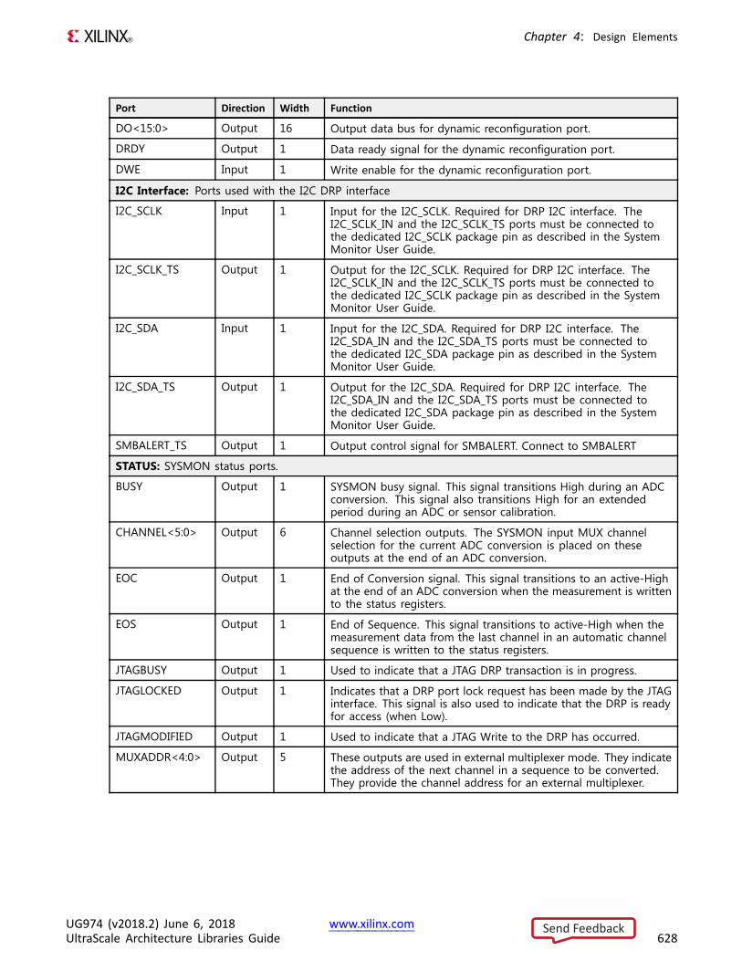
Chapter 4: Design Elements
Port Direction Width Function
DO<15:0> Output 16 Output data bus for dynamic reconfiguration port.
DRDY Output 1 Data ready signal for the dynamic reconfiguration port.
DWE Input 1 Write enable for the dynamic reconfiguration port.
I2C Interface: Ports used with the I2C DRP interface
I2C_SCLK Input 1 Input for the I2C_SCLK. Required for DRP I2C interface. TheI2C_SCLK_IN and the I2C_SCLK_TS ports must be connected tothe dedicated I2C_SCLK package pin as described in the SystemMonitor User Guide.
I2C_SCLK_TS Output 1 Output for the I2C_SCLK. Required for DRP I2C interface. TheI2C_SCLK_IN and the I2C_SCLK_TS ports must be connected tothe dedicated I2C_SCLK package pin as described in the SystemMonitor User Guide.
I2C_SDA Input 1 Input for the I2C_SDA. Required for DRP I2C interface. TheI2C_SDA_IN and the I2C_SDA_TS ports must be connected tothe dedicated I2C_SDA package pin as described in the SystemMonitor User Guide.
I2C_SDA_TS Output 1 Output for the I2C_SDA. Required for DRP I2C interface. TheI2C_SDA_IN and the I2C_SDA_TS ports must be connected tothe dedicated I2C_SDA package pin as described in the SystemMonitor User Guide.
SMBALERT_TS Output 1 Output control signal for SMBALERT. Connect to SMBALERT
STATUS: SYSMON status ports.
BUSY Output 1 SYSMON busy signal. This signal transitions High during an ADCconversion. This signal also transitions High for an extendedperiod during an ADC or sensor calibration.
CHANNEL<5:0> Output 6 Channel selection outputs. The SYSMON input MUX channelselection for the current ADC conversion is placed on theseoutputs at the end of an ADC conversion.
EOC Output 1 End of Conversion signal. This signal transitions to an active-Highat the end of an ADC conversion when the measurement is writtento the status registers.
EOS Output 1 End of Sequence. This signal transitions to active-High when themeasurement data from the last channel in an automatic channelsequence is written to the status registers.
JTAGBUSY Output 1 Used to indicate that a JTAG DRP transaction is in progress.
JTAGLOCKED Output 1 Indicates that a DRP port lock request has been made by the JTAGinterface. This signal is also used to indicate that the DRP is readyfor access (when Low).
JTAGMODIFIED Output 1 Used to indicate that a JTAG Write to the DRP has occurred.
MUXADDR<4:0> Output 5 These outputs are used in external multiplexer mode. They indicatethe address of the next channel in a sequence to be converted.They provide the channel address for an external multiplexer.
UG974 (v2018.2) June 6, 2018 www.xilinx.comUltraScale Architecture Libraries Guide 628
Send Feedback
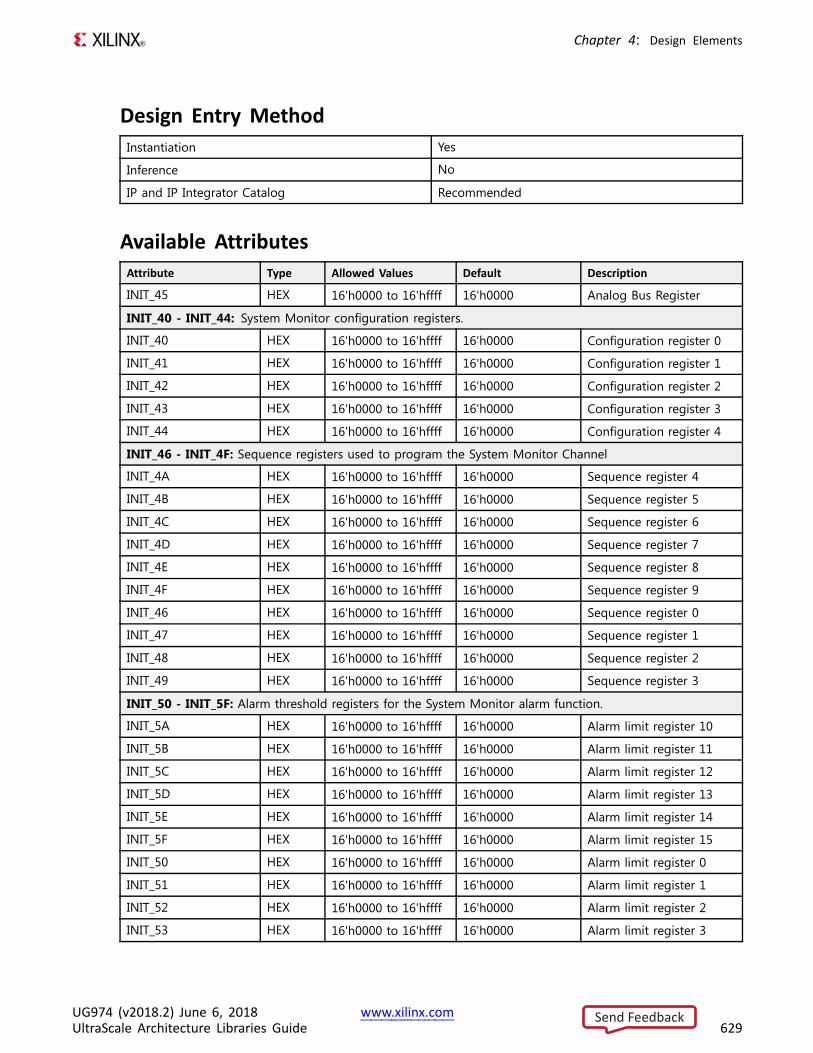
Chapter 4: Design Elements
Design Entry MethodInstantiation Yes
Inference No
IP and IP Integrator Catalog Recommended
Available AttributesAttribute Type Allowed Values Default Description
INIT_45 HEX 16'h0000 to 16'hffff 16'h0000 Analog Bus Register
INIT_40 - INIT_44: System Monitor configuration registers.
INIT_40 HEX 16'h0000 to 16'hffff 16'h0000 Configuration register 0
INIT_41 HEX 16'h0000 to 16'hffff 16'h0000 Configuration register 1
INIT_42 HEX 16'h0000 to 16'hffff 16'h0000 Configuration register 2
INIT_43 HEX 16'h0000 to 16'hffff 16'h0000 Configuration register 3
INIT_44 HEX 16'h0000 to 16'hffff 16'h0000 Configuration register 4
INIT_46 - INIT_4F: Sequence registers used to program the System Monitor Channel
INIT_4A HEX 16'h0000 to 16'hffff 16'h0000 Sequence register 4
INIT_4B HEX 16'h0000 to 16'hffff 16'h0000 Sequence register 5
INIT_4C HEX 16'h0000 to 16'hffff 16'h0000 Sequence register 6
INIT_4D HEX 16'h0000 to 16'hffff 16'h0000 Sequence register 7
INIT_4E HEX 16'h0000 to 16'hffff 16'h0000 Sequence register 8
INIT_4F HEX 16'h0000 to 16'hffff 16'h0000 Sequence register 9
INIT_46 HEX 16'h0000 to 16'hffff 16'h0000 Sequence register 0
INIT_47 HEX 16'h0000 to 16'hffff 16'h0000 Sequence register 1
INIT_48 HEX 16'h0000 to 16'hffff 16'h0000 Sequence register 2
INIT_49 HEX 16'h0000 to 16'hffff 16'h0000 Sequence register 3
INIT_50 - INIT_5F: Alarm threshold registers for the System Monitor alarm function.
INIT_5A HEX 16'h0000 to 16'hffff 16'h0000 Alarm limit register 10
INIT_5B HEX 16'h0000 to 16'hffff 16'h0000 Alarm limit register 11
INIT_5C HEX 16'h0000 to 16'hffff 16'h0000 Alarm limit register 12
INIT_5D HEX 16'h0000 to 16'hffff 16'h0000 Alarm limit register 13
INIT_5E HEX 16'h0000 to 16'hffff 16'h0000 Alarm limit register 14
INIT_5F HEX 16'h0000 to 16'hffff 16'h0000 Alarm limit register 15
INIT_50 HEX 16'h0000 to 16'hffff 16'h0000 Alarm limit register 0
INIT_51 HEX 16'h0000 to 16'hffff 16'h0000 Alarm limit register 1
INIT_52 HEX 16'h0000 to 16'hffff 16'h0000 Alarm limit register 2
INIT_53 HEX 16'h0000 to 16'hffff 16'h0000 Alarm limit register 3
UG974 (v2018.2) June 6, 2018 www.xilinx.comUltraScale Architecture Libraries Guide 629
Send Feedback
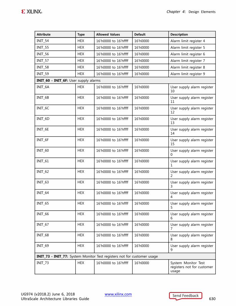
Chapter 4: Design Elements
Attribute Type Allowed Values Default Description
INIT_54 HEX 16'h0000 to 16'hffff 16'h0000 Alarm limit register 4
INIT_55 HEX 16'h0000 to 16'hffff 16'h0000 Alarm limit register 5
INIT_56 HEX 16'h0000 to 16'hffff 16'h0000 Alarm limit register 6
INIT_57 HEX 16'h0000 to 16'hffff 16'h0000 Alarm limit register 7
INIT_58 HEX 16'h0000 to 16'hffff 16'h0000 Alarm limit register 8
INIT_59 HEX 16'h0000 to 16'hffff 16'h0000 Alarm limit register 9
INIT_60 - INIT_6F: User supply alarms
INIT_6A HEX 16'h0000 to 16'hffff 16'h0000 User supply alarm register10
INIT_6B HEX 16'h0000 to 16'hffff 16'h0000 User supply alarm register11
INIT_6C HEX 16'h0000 to 16'hffff 16'h0000 User supply alarm register12
INIT_6D HEX 16'h0000 to 16'hffff 16'h0000 User supply alarm register13
INIT_6E HEX 16'h0000 to 16'hffff 16'h0000 User supply alarm register14
INIT_6F HEX 16'h0000 to 16'hffff 16'h0000 User supply alarm register15
INIT_60 HEX 16'h0000 to 16'hffff 16'h0000 User supply alarm register0
INIT_61 HEX 16'h0000 to 16'hffff 16'h0000 User supply alarm register1
INIT_62 HEX 16'h0000 to 16'hffff 16'h0000 User supply alarm register2
INIT_63 HEX 16'h0000 to 16'hffff 16'h0000 User supply alarm register3
INIT_64 HEX 16'h0000 to 16'hffff 16'h0000 User supply alarm register4
INIT_65 HEX 16'h0000 to 16'hffff 16'h0000 User supply alarm register5
INIT_66 HEX 16'h0000 to 16'hffff 16'h0000 User supply alarm register6
INIT_67 HEX 16'h0000 to 16'hffff 16'h0000 User supply alarm register7
INIT_68 HEX 16'h0000 to 16'hffff 16'h0000 User supply alarm register8
INIT_69 HEX 16'h0000 to 16'hffff 16'h0000 User supply alarm register9
INIT_73 - INIT_77: System Monitor Test registers not for customer usage
INIT_73 HEX 16'h0000 to 16'hffff 16'h0000 System Monitor Testregisters not for customerusage
UG974 (v2018.2) June 6, 2018 www.xilinx.comUltraScale Architecture Libraries Guide 630
Send Feedback
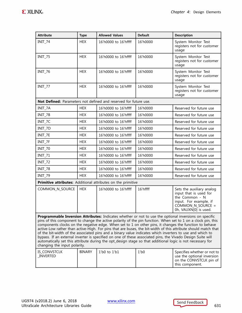
Chapter 4: Design Elements
Attribute Type Allowed Values Default Description
INIT_74 HEX 16'h0000 to 16'hffff 16'h0000 System Monitor Testregisters not for customerusage
INIT_75 HEX 16'h0000 to 16'hffff 16'h0000 System Monitor Testregisters not for customerusage
INIT_76 HEX 16'h0000 to 16'hffff 16'h0000 System Monitor Testregisters not for customerusage
INIT_77 HEX 16'h0000 to 16'hffff 16'h0000 System Monitor Testregisters not for customerusage
Not Defined: Parameters not defined and reserved for future use.
INIT_7A HEX 16'h0000 to 16'hffff 16'h0000 Reserved for future use
INIT_7B HEX 16'h0000 to 16'hffff 16'h0000 Reserved for future use
INIT_7C HEX 16'h0000 to 16'hffff 16'h0000 Reserved for future use
INIT_7D HEX 16'h0000 to 16'hffff 16'h0000 Reserved for future use
INIT_7E HEX 16'h0000 to 16'hffff 16'h0000 Reserved for future use
INIT_7F HEX 16'h0000 to 16'hffff 16'h0000 Reserved for future use
INIT_70 HEX 16'h0000 to 16'hffff 16'h0000 Reserved for future use
INIT_71 HEX 16'h0000 to 16'hffff 16'h0000 Reserved for future use
INIT_72 HEX 16'h0000 to 16'hffff 16'h0000 Reserved for future use
INIT_78 HEX 16'h0000 to 16'hffff 16'h0000 Reserved for future use
INIT_79 HEX 16'h0000 to 16'hffff 16'h0000 Reserved for future use
Primitive attributes: Additional attributes on the primitive
COMMON_N_SOURCE HEX 16'h0000 to 16'hffff 16'hffff Sets the auxiliary analoginput that is used forthe Common - Ninput. For example, ifCOMMON_N_SOURCE =0h, VAUXN[0] is used.
Programmable Inversion Attributes: Indicates whether or not to use the optional inversions on specificpins of this component to change the active polarity of the pin function. When set to 1 on a clock pin, thiscomponents clocks on the negative edge. When set to 1 on other pins, it changes the function to behaveactive-Low rather than active-High. For pins that are buses, the bit-width of this attribute should match thatof the bit-width of the associated pins and a binary value indicates which inverters to use and which tobypass. If an external inverter is specified on one of these associated pins, the Vivado Design Suite willautomatically set this attribute during the opt_design stage so that additional logic is not necessary forchanging the input polarity.
IS_CONVSTCLK_INVERTED
BINARY 1'b0 to 1'b1 1'b0 Specifies whether or not touse the optional inversionon the CONVSTCLK pin ofthis component.
UG974 (v2018.2) June 6, 2018 www.xilinx.comUltraScale Architecture Libraries Guide 631
Send Feedback
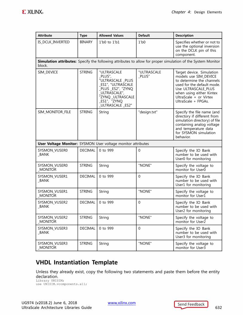
Chapter 4: Design Elements
Attribute Type Allowed Values Default Description
IS_DCLK_INVERTED BINARY 1'b0 to 1'b1 1'b0 Specifies whether or not touse the optional inversionon the DCLK pin of thiscomponent.
Simulation attributes: Specify the following attributes to allow for proper simulation of the System Monitorblock.
SIM_DEVICE STRING "ULTRASCALE_PLUS","ULTRASCALE _PLUS_ES1", "ULTRASCALE_PLUS _ES2", "ZYNQ_ULTRASCALE","ZYNQ _ULTRASCALE_ES1", "ZYNQ_ULTRASCALE _ES2"
"ULTRASCALE_PLUS"
Target device. Simulationmodels use SIM_DEVICEto determine the channelsused for the default mode.Use ULTRASCALE_PLUSwhen using either KintexUltraScale + or VirtexUltraScale + FPGAs.
SIM_MONITOR_FILE STRING String "design.txt" Specify the file name (anddirectory if different fromsimulation directory) of filecontaining analog voltageand temperature datafor SYSMON simulationbehavior.
User Voltage Monitor: SYSMON User voltage monitor attributes
SYSMON_VUSER0_BANK
DECIMAL 0 to 999 0 Specify the IO Banknumber to be used withUser0 for monitoring
SYSMON_VUSER0_MONITOR
STRING String "NONE" Specify the voltage tomonitor for User0
SYSMON_VUSER1_BANK
DECIMAL 0 to 999 0 Specify the IO Banknumber to be used withUser1 for monitoring
SYSMON_VUSER1_MONITOR
STRING String "NONE" Specify the voltage tomonitor for User1
SYSMON_VUSER2_BANK
DECIMAL 0 to 999 0 Specify the IO Banknumber to be used withUser2 for monitoring
SYSMON_VUSER2_MONITOR
STRING String "NONE" Specify the voltage tomonitor for User2
SYSMON_VUSER3_BANK
DECIMAL 0 to 999 0 Specify the IO Banknumber to be used withUser3 for monitoring
SYSMON_VUSER3_MONITOR
STRING String "NONE" Specify the voltage tomonitor for User3
VHDL Instantiation TemplateUnless they already exist, copy the following two statements and paste them before the entitydeclaration.Library UNISIM;use UNISIM.vcomponents.all;
UG974 (v2018.2) June 6, 2018 www.xilinx.comUltraScale Architecture Libraries Guide 632
Send Feedback
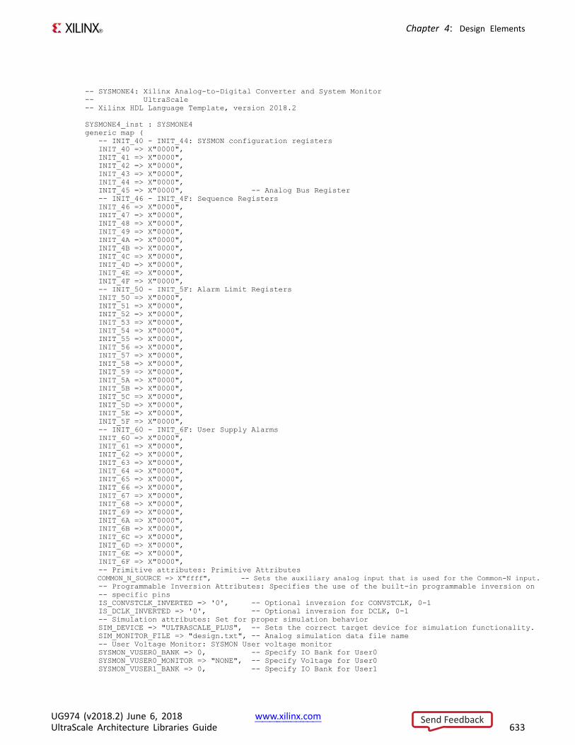
Chapter 4: Design Elements
-- SYSMONE4: Xilinx Analog-to-Digital Converter and System Monitor-- UltraScale-- Xilinx HDL Language Template, version 2018.2
SYSMONE4_inst : SYSMONE4generic map (
-- INIT_40 - INIT_44: SYSMON configuration registersINIT_40 => X"0000",INIT_41 => X"0000",INIT_42 => X"0000",INIT_43 => X"0000",INIT_44 => X"0000",INIT_45 => X"0000", -- Analog Bus Register-- INIT_46 - INIT_4F: Sequence RegistersINIT_46 => X"0000",INIT_47 => X"0000",INIT_48 => X"0000",INIT_49 => X"0000",INIT_4A => X"0000",INIT_4B => X"0000",INIT_4C => X"0000",INIT_4D => X"0000",INIT_4E => X"0000",INIT_4F => X"0000",-- INIT_50 - INIT_5F: Alarm Limit RegistersINIT_50 => X"0000",INIT_51 => X"0000",INIT_52 => X"0000",INIT_53 => X"0000",INIT_54 => X"0000",INIT_55 => X"0000",INIT_56 => X"0000",INIT_57 => X"0000",INIT_58 => X"0000",INIT_59 => X"0000",INIT_5A => X"0000",INIT_5B => X"0000",INIT_5C => X"0000",INIT_5D => X"0000",INIT_5E => X"0000",INIT_5F => X"0000",-- INIT_60 - INIT_6F: User Supply AlarmsINIT_60 => X"0000",INIT_61 => X"0000",INIT_62 => X"0000",INIT_63 => X"0000",INIT_64 => X"0000",INIT_65 => X"0000",INIT_66 => X"0000",INIT_67 => X"0000",INIT_68 => X"0000",INIT_69 => X"0000",INIT_6A => X"0000",INIT_6B => X"0000",INIT_6C => X"0000",INIT_6D => X"0000",INIT_6E => X"0000",INIT_6F => X"0000",-- Primitive attributes: Primitive AttributesCOMMON_N_SOURCE => X"ffff", -- Sets the auxiliary analog input that is used for the Common-N input.-- Programmable Inversion Attributes: Specifies the use of the built-in programmable inversion on-- specific pinsIS_CONVSTCLK_INVERTED => '0', -- Optional inversion for CONVSTCLK, 0-1IS_DCLK_INVERTED => '0', -- Optional inversion for DCLK, 0-1-- Simulation attributes: Set for proper simulation behaviorSIM_DEVICE => "ULTRASCALE_PLUS", -- Sets the correct target device for simulation functionality.SIM_MONITOR_FILE => "design.txt", -- Analog simulation data file name-- User Voltage Monitor: SYSMON User voltage monitorSYSMON_VUSER0_BANK => 0, -- Specify IO Bank for User0SYSMON_VUSER0_MONITOR => "NONE", -- Specify Voltage for User0SYSMON_VUSER1_BANK => 0, -- Specify IO Bank for User1
UG974 (v2018.2) June 6, 2018 www.xilinx.comUltraScale Architecture Libraries Guide 633
Send Feedback
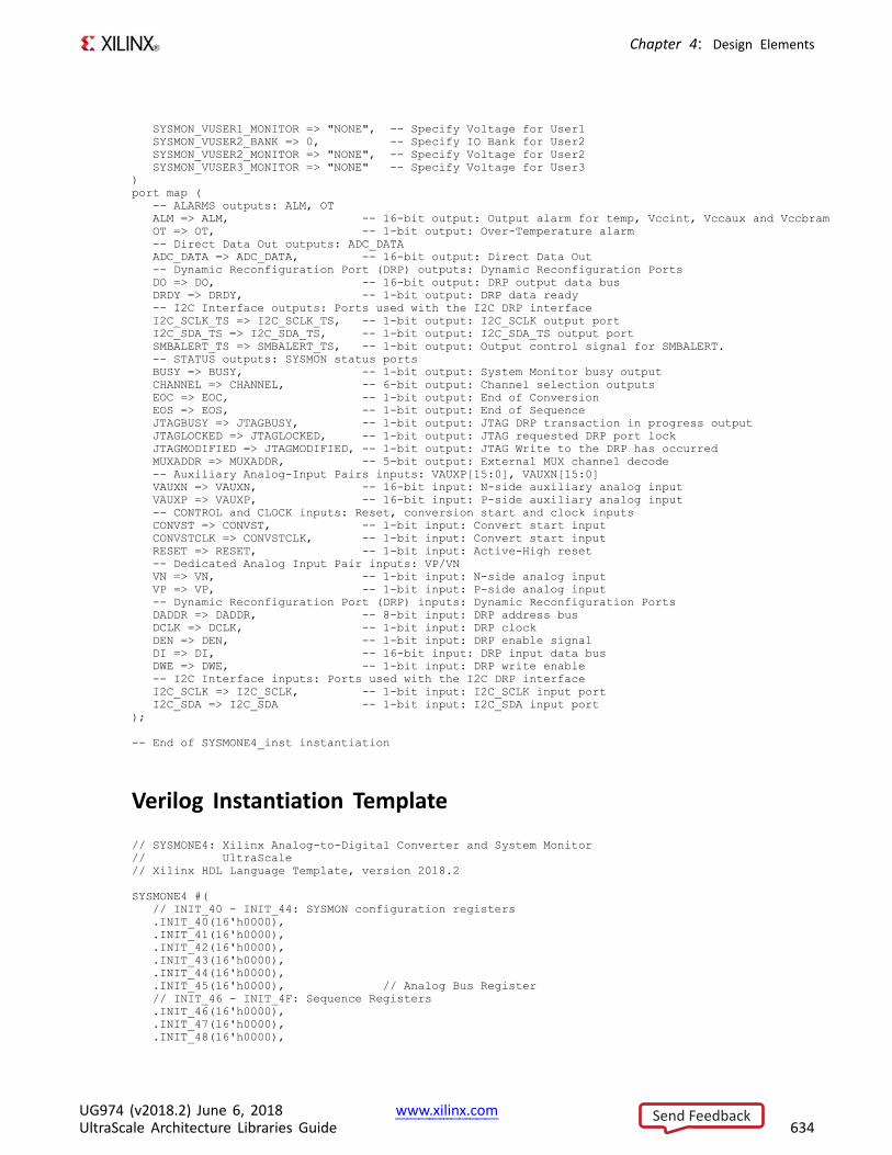
Chapter 4: Design Elements
SYSMON_VUSER1_MONITOR => "NONE", -- Specify Voltage for User1SYSMON_VUSER2_BANK => 0, -- Specify IO Bank for User2SYSMON_VUSER2_MONITOR => "NONE", -- Specify Voltage for User2SYSMON_VUSER3_MONITOR => "NONE" -- Specify Voltage for User3
)port map (
-- ALARMS outputs: ALM, OTALM => ALM, -- 16-bit output: Output alarm for temp, Vccint, Vccaux and VccbramOT => OT, -- 1-bit output: Over-Temperature alarm-- Direct Data Out outputs: ADC_DATAADC_DATA => ADC_DATA, -- 16-bit output: Direct Data Out-- Dynamic Reconfiguration Port (DRP) outputs: Dynamic Reconfiguration PortsDO => DO, -- 16-bit output: DRP output data busDRDY => DRDY, -- 1-bit output: DRP data ready-- I2C Interface outputs: Ports used with the I2C DRP interfaceI2C_SCLK_TS => I2C_SCLK_TS, -- 1-bit output: I2C_SCLK output portI2C_SDA_TS => I2C_SDA_TS, -- 1-bit output: I2C_SDA_TS output portSMBALERT_TS => SMBALERT_TS, -- 1-bit output: Output control signal for SMBALERT.-- STATUS outputs: SYSMON status portsBUSY => BUSY, -- 1-bit output: System Monitor busy outputCHANNEL => CHANNEL, -- 6-bit output: Channel selection outputsEOC => EOC, -- 1-bit output: End of ConversionEOS => EOS, -- 1-bit output: End of SequenceJTAGBUSY => JTAGBUSY, -- 1-bit output: JTAG DRP transaction in progress outputJTAGLOCKED => JTAGLOCKED, -- 1-bit output: JTAG requested DRP port lockJTAGMODIFIED => JTAGMODIFIED, -- 1-bit output: JTAG Write to the DRP has occurredMUXADDR => MUXADDR, -- 5-bit output: External MUX channel decode-- Auxiliary Analog-Input Pairs inputs: VAUXP[15:0], VAUXN[15:0]VAUXN => VAUXN, -- 16-bit input: N-side auxiliary analog inputVAUXP => VAUXP, -- 16-bit input: P-side auxiliary analog input-- CONTROL and CLOCK inputs: Reset, conversion start and clock inputsCONVST => CONVST, -- 1-bit input: Convert start inputCONVSTCLK => CONVSTCLK, -- 1-bit input: Convert start inputRESET => RESET, -- 1-bit input: Active-High reset-- Dedicated Analog Input Pair inputs: VP/VNVN => VN, -- 1-bit input: N-side analog inputVP => VP, -- 1-bit input: P-side analog input-- Dynamic Reconfiguration Port (DRP) inputs: Dynamic Reconfiguration PortsDADDR => DADDR, -- 8-bit input: DRP address busDCLK => DCLK, -- 1-bit input: DRP clockDEN => DEN, -- 1-bit input: DRP enable signalDI => DI, -- 16-bit input: DRP input data busDWE => DWE, -- 1-bit input: DRP write enable-- I2C Interface inputs: Ports used with the I2C DRP interfaceI2C_SCLK => I2C_SCLK, -- 1-bit input: I2C_SCLK input portI2C_SDA => I2C_SDA -- 1-bit input: I2C_SDA input port
);
-- End of SYSMONE4_inst instantiation
Verilog Instantiation Template
// SYSMONE4: Xilinx Analog-to-Digital Converter and System Monitor// UltraScale// Xilinx HDL Language Template, version 2018.2
SYSMONE4 #(// INIT_40 - INIT_44: SYSMON configuration registers.INIT_40(16'h0000),.INIT_41(16'h0000),.INIT_42(16'h0000),.INIT_43(16'h0000),.INIT_44(16'h0000),.INIT_45(16'h0000), // Analog Bus Register// INIT_46 - INIT_4F: Sequence Registers.INIT_46(16'h0000),.INIT_47(16'h0000),.INIT_48(16'h0000),
UG974 (v2018.2) June 6, 2018 www.xilinx.comUltraScale Architecture Libraries Guide 634
Send Feedback
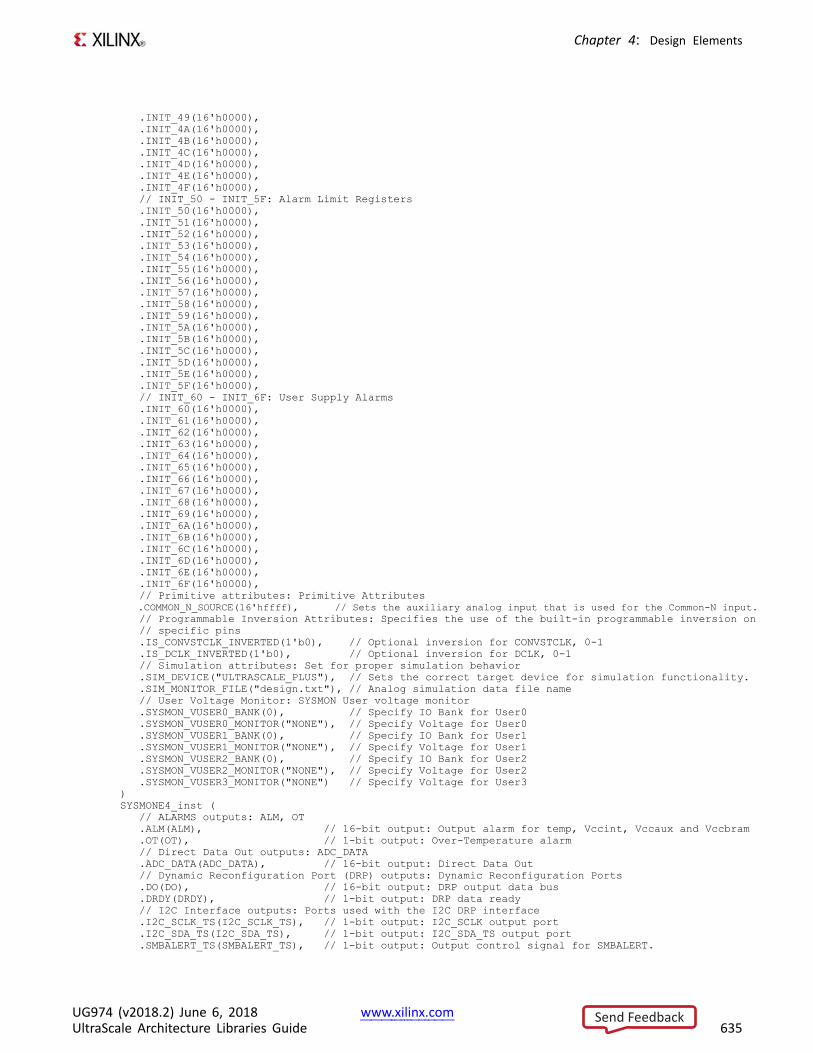
Chapter 4: Design Elements
.INIT_49(16'h0000),
.INIT_4A(16'h0000),
.INIT_4B(16'h0000),
.INIT_4C(16'h0000),
.INIT_4D(16'h0000),
.INIT_4E(16'h0000),
.INIT_4F(16'h0000),// INIT_50 - INIT_5F: Alarm Limit Registers.INIT_50(16'h0000),.INIT_51(16'h0000),.INIT_52(16'h0000),.INIT_53(16'h0000),.INIT_54(16'h0000),.INIT_55(16'h0000),.INIT_56(16'h0000),.INIT_57(16'h0000),.INIT_58(16'h0000),.INIT_59(16'h0000),.INIT_5A(16'h0000),.INIT_5B(16'h0000),.INIT_5C(16'h0000),.INIT_5D(16'h0000),.INIT_5E(16'h0000),.INIT_5F(16'h0000),// INIT_60 - INIT_6F: User Supply Alarms.INIT_60(16'h0000),.INIT_61(16'h0000),.INIT_62(16'h0000),.INIT_63(16'h0000),.INIT_64(16'h0000),.INIT_65(16'h0000),.INIT_66(16'h0000),.INIT_67(16'h0000),.INIT_68(16'h0000),.INIT_69(16'h0000),.INIT_6A(16'h0000),.INIT_6B(16'h0000),.INIT_6C(16'h0000),.INIT_6D(16'h0000),.INIT_6E(16'h0000),.INIT_6F(16'h0000),// Primitive attributes: Primitive Attributes.COMMON_N_SOURCE(16'hffff), // Sets the auxiliary analog input that is used for the Common-N input.// Programmable Inversion Attributes: Specifies the use of the built-in programmable inversion on// specific pins.IS_CONVSTCLK_INVERTED(1'b0), // Optional inversion for CONVSTCLK, 0-1.IS_DCLK_INVERTED(1'b0), // Optional inversion for DCLK, 0-1// Simulation attributes: Set for proper simulation behavior.SIM_DEVICE("ULTRASCALE_PLUS"), // Sets the correct target device for simulation functionality..SIM_MONITOR_FILE("design.txt"), // Analog simulation data file name// User Voltage Monitor: SYSMON User voltage monitor.SYSMON_VUSER0_BANK(0), // Specify IO Bank for User0.SYSMON_VUSER0_MONITOR("NONE"), // Specify Voltage for User0.SYSMON_VUSER1_BANK(0), // Specify IO Bank for User1.SYSMON_VUSER1_MONITOR("NONE"), // Specify Voltage for User1.SYSMON_VUSER2_BANK(0), // Specify IO Bank for User2.SYSMON_VUSER2_MONITOR("NONE"), // Specify Voltage for User2.SYSMON_VUSER3_MONITOR("NONE") // Specify Voltage for User3
)SYSMONE4_inst (
// ALARMS outputs: ALM, OT.ALM(ALM), // 16-bit output: Output alarm for temp, Vccint, Vccaux and Vccbram.OT(OT), // 1-bit output: Over-Temperature alarm// Direct Data Out outputs: ADC_DATA.ADC_DATA(ADC_DATA), // 16-bit output: Direct Data Out// Dynamic Reconfiguration Port (DRP) outputs: Dynamic Reconfiguration Ports.DO(DO), // 16-bit output: DRP output data bus.DRDY(DRDY), // 1-bit output: DRP data ready// I2C Interface outputs: Ports used with the I2C DRP interface.I2C_SCLK_TS(I2C_SCLK_TS), // 1-bit output: I2C_SCLK output port.I2C_SDA_TS(I2C_SDA_TS), // 1-bit output: I2C_SDA_TS output port.SMBALERT_TS(SMBALERT_TS), // 1-bit output: Output control signal for SMBALERT.
UG974 (v2018.2) June 6, 2018 www.xilinx.comUltraScale Architecture Libraries Guide 635
Send Feedback
Chapter 4: Design Elements
// STATUS outputs: SYSMON status ports.BUSY(BUSY), // 1-bit output: System Monitor busy output.CHANNEL(CHANNEL), // 6-bit output: Channel selection outputs.EOC(EOC), // 1-bit output: End of Conversion.EOS(EOS), // 1-bit output: End of Sequence.JTAGBUSY(JTAGBUSY), // 1-bit output: JTAG DRP transaction in progress output.JTAGLOCKED(JTAGLOCKED), // 1-bit output: JTAG requested DRP port lock.JTAGMODIFIED(JTAGMODIFIED), // 1-bit output: JTAG Write to the DRP has occurred.MUXADDR(MUXADDR), // 5-bit output: External MUX channel decode// Auxiliary Analog-Input Pairs inputs: VAUXP[15:0], VAUXN[15:0].VAUXN(VAUXN), // 16-bit input: N-side auxiliary analog input.VAUXP(VAUXP), // 16-bit input: P-side auxiliary analog input// CONTROL and CLOCK inputs: Reset, conversion start and clock inputs.CONVST(CONVST), // 1-bit input: Convert start input.CONVSTCLK(CONVSTCLK), // 1-bit input: Convert start input.RESET(RESET), // 1-bit input: Active-High reset// Dedicated Analog Input Pair inputs: VP/VN.VN(VN), // 1-bit input: N-side analog input.VP(VP), // 1-bit input: P-side analog input// Dynamic Reconfiguration Port (DRP) inputs: Dynamic Reconfiguration Ports.DADDR(DADDR), // 8-bit input: DRP address bus.DCLK(DCLK), // 1-bit input: DRP clock.DEN(DEN), // 1-bit input: DRP enable signal.DI(DI), // 16-bit input: DRP input data bus.DWE(DWE), // 1-bit input: DRP write enable// I2C Interface inputs: Ports used with the I2C DRP interface.I2C_SCLK(I2C_SCLK), // 1-bit input: I2C_SCLK input port.I2C_SDA(I2C_SDA) // 1-bit input: I2C_SDA input port
);
// End of SYSMONE4_inst instantiation
For More Information• See the UltraScale Architecture System Monitor User Guide (UG580).
• See the UltraScale Programmable Devices Documentation.
UG974 (v2018.2) June 6, 2018 www.xilinx.comUltraScale Architecture Libraries Guide 636
Send Feedback
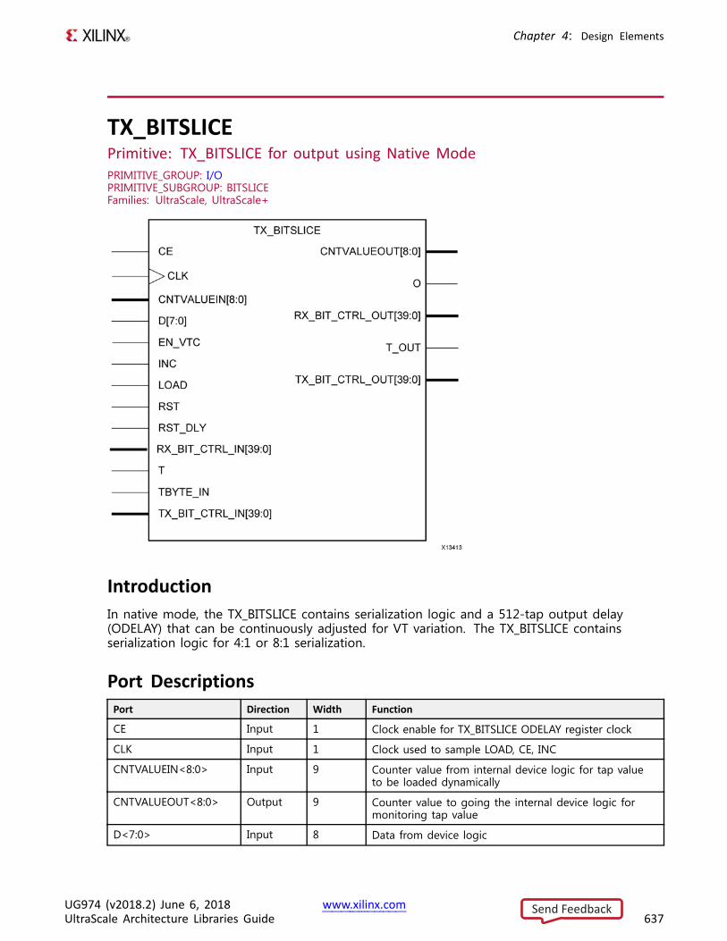
Chapter 4: Design Elements
TX_BITSLICEPrimitive: TX_BITSLICE for output using Native ModePRIMITIVE_GROUP: I/OPRIMITIVE_SUBGROUP: BITSLICEFamilies: UltraScale, UltraScale+
IntroductionIn native mode, the TX_BITSLICE contains serialization logic and a 512-tap output delay(ODELAY) that can be continuously adjusted for VT variation. The TX_BITSLICE containsserialization logic for 4:1 or 8:1 serialization.
Port DescriptionsPort Direction Width Function
CE Input 1 Clock enable for TX_BITSLICE ODELAY register clock
CLK Input 1 Clock used to sample LOAD, CE, INC
CNTVALUEIN<8:0> Input 9 Counter value from internal device logic for tap valueto be loaded dynamically
CNTVALUEOUT<8:0> Output 9 Counter value to going the internal device logic formonitoring tap value
D<7:0> Input 8 Data from device logic
UG974 (v2018.2) June 6, 2018 www.xilinx.comUltraScale Architecture Libraries Guide 637
Send Feedback
Chapter 4: Design Elements
Port Direction Width Function
EN_VTC Input 1 Enable to keep stable delay over VT when set to HIGH.VT compensation disabled when set to LOW.
INC Input 1 Increment the current delay tap setting
LOAD Input 1 Load the CNTVALUEIN tap setting
O Output 1 Serialized output going to output buffer
RST Input 1 Asynchronous assert, synchronous deassert forTX_BITSLICE OSERDES
RST_DLY Input 1 Reset the internal DELAY value to DELAY_VALUE
RX_BIT_CTRL_IN<39:0> Input 40 Input bus from BITSLICE_CONTROL
RX_BIT_CTRL_OUT<39:0> Output 40 Output bus to BITSLICE_CONTROL
T Input 1 Legacy T byte input from device logic
TBYTE_IN Input 1 Byte group 3-state input from TX_BITSLICE_TRI
T_OUT Output 1 Byte group 3-state output
TX_BIT_CTRL_IN<39:0> Input 40 Input bus from BITSLICE_CONTROL
TX_BIT_CTRL_OUT<39:0> Output 40 Output bus to BITSLICE_CONTROL
Design Entry MethodInstantiation Yes
Inference No
IP and IP Integrator Catalog Yes
Available AttributesAttribute Type Allowed Values Default Description
DATA_WIDTH DECIMAL 8, 4 8 Defines the parallel data inputwidth. Legal values are 4 and 8.
DELAY_FORMAT STRING "TIME", "COUNT" "TIME" Sets the units of DELAY_VALUEof the TX_BITSLICE ODELAY. UseTIME when DELAY_TYPE is FIXED.Use COUNT when DELAY_TYPE isVARIABLE or VAR_LOAD.
• "TIME" : TX_BITSLICE ODELAYDELAY_VALUE is specified inps
• "COUNT" : TX_BITSLICEODELAY DELAY_VALUE isspecified in taps
UG974 (v2018.2) June 6, 2018 www.xilinx.comUltraScale Architecture Libraries Guide 638
Send Feedback
Chapter 4: Design Elements
Attribute Type Allowed Values Default Description
DELAY_TYPE STRING "FIXED","VARIABLE","VAR_LOAD"
"FIXED" Sets the type of tap delay line.
• "FIXED" - Sets a static delayvalue
• "VARIABLE" - Dynamicallyadjust (increment /decrement) delay value
• "VAR_LOAD" - Dynamicallyloads tap values
DELAY_VALUE DECIMAL 0 to 1250 0 Specifies the fixed delay in pswhen using FIXED DELAY_TYPE.Specifies value upon reset whenusing VARIABLE or VAR_LOAD.
ENABLE_PRE_EMPHASIS
STRING "FALSE", "TRUE" "FALSE" Used in conjunction with IOB toEnable the pre - emphasis.
INIT BINARY 1'b1, 1'b0 1'b1 Defines initial O value
IS_CLK_INVERTED BINARY 1'b0 to 1'b1 1'b0 Specifies whether the clock CLKpin is active - high or active - low.
IS_RST_DLY_INVERTED
BINARY 1'b0 to 1'b1 1'b0 Specifies whether the resetRST_DLY pin is active - high oractive - low.
IS_RST_INVERTED BINARY 1'b0 to 1'b1 1'b0 Specifies whether the reset RSTpin is active - high or active - low.
OUTPUT_PHASE_90 STRING "FALSE", "TRUE" "FALSE" Delays the output phase by 90 -degrees
REFCLK_FREQUENCY
1 significantdigit FLOAT
200.0 to 2667.0 300.0 Specification of the referenceclock frequency in MHz
SIM_DEVICE STRING "ULTRASCALE","ULTRASCALE_PLUS","ULTRASCALE_PLUS _ES1","ULTRASCALE_PLUS _ES2"
"ULTRASCALE" Set the device version
TBYTE_CTL STRING "TBYTE_IN", "T" "TBYTE _IN" Select between T and TBYTE_INinputs in OSERDES mode only
UG974 (v2018.2) June 6, 2018 www.xilinx.comUltraScale Architecture Libraries Guide 639
Send Feedback
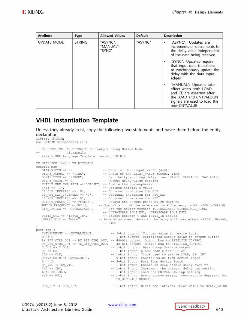
Chapter 4: Design Elements
Attribute Type Allowed Values Default Description
UPDATE_MODE STRING "ASYNC","MANUAL","SYNC"
"ASYNC" • "ASYNC": Updates areincrements or decrements tothe delay value independentof the data being received
• "SYNC": Updates requirethat input data transitionsto synchronously update thedelay with the data inputedges
• "MANUAL": Updates takeeffect when both LOADand CE are asserted afterthe LOAD and CNTVALUEINsignals are used to load thenew CNTVALUE
VHDL Instantiation TemplateUnless they already exist, copy the following two statements and paste them before the entitydeclaration.Library UNISIM;use UNISIM.vcomponents.all;
-- TX_BITSLICE: TX_BITSLICE for output using Native Mode-- UltraScale-- Xilinx HDL Language Template, version 2018.2
TX_BITSLICE_inst : TX_BITSLICEgeneric map (
DATA_WIDTH => 8, -- Parallel data input width (4-8)DELAY_FORMAT => "TIME", -- Units of the DELAY_VALUE (COUNT, TIME)DELAY_TYPE => "FIXED", -- Set the type of tap delay line (FIXED, VARIABLE, VAR_LOAD)DELAY_VALUE => 0, -- Output delay value settingENABLE_PRE_EMPHASIS => "FALSE", -- Enable the pre-emphasisINIT => '1', -- Defines initial O valueIS_CLK_INVERTED => '0', -- Optional inversion for CLKIS_RST_DLY_INVERTED => '0', -- Optional inversion for RST_DLYIS_RST_INVERTED => '0', -- Optional inversion for RSTOUTPUT_PHASE_90 => "FALSE", -- Delays the output phase by 90-degreesREFCLK_FREQUENCY => 300.0, -- Specification of the reference clock frequency in MHz (200.0-2667.0)SIM_DEVICE => "ULTRASCALE", -- Set the device version (ULTRASCALE, ULTRASCALE_PLUS,
-- ULTRASCALE_PLUS_ES1, ULTRASCALE_PLUS_ES2)TBYTE_CTL => "TBYTE_IN", -- Select between T and TBYTE_IN inputsUPDATE_MODE => "ASYNC" -- Determines when updates to the delay will take effect (ASYNC, MANUAL,
-- SYNC))port map (
CNTVALUEOUT => CNTVALUEOUT, -- 9-bit output: Counter value to device logicO => O, -- 1-bit output: Serialized output going to output bufferRX_BIT_CTRL_OUT => RX_BIT_CTRL_OUT, -- 40-bit output: Output bus to BITSLICE_CONTROLTX_BIT_CTRL_OUT => TX_BIT_CTRL_OUT, -- 40-bit output: Output bus to BITSLICE_CONTROLT_OUT => T_OUT, -- 1-bit output: Byte group 3-state outputCE => CE, -- 1-bit input: Clock enable for ODELAYCLK => CLK, -- 1-bit input: Clock used to sample LOAD, CE, INCCNTVALUEIN => CNTVALUEIN, -- 9-bit input: Counter value from device logicD => D, -- 8-bit input: Data from device logicEN_VTC => EN_VTC, -- 1-bit input: Enable to keep stable delay over VTINC => INC, -- 1-bit input: Increment the current delay tap settingLOAD => LOAD, -- 1-bit input: Load the CNTVALUEIN tap settingRST => RST, -- 1-bit input: Asynchronous assert, synchronous deassert for
-- TX_BITSLICE OSERDES
RST_DLY => RST_DLY, -- 1-bit input: Reset the internal DELAY value to DELAY_VALUE
UG974 (v2018.2) June 6, 2018 www.xilinx.comUltraScale Architecture Libraries Guide 640
Send Feedback
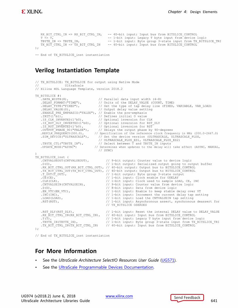
Chapter 4: Design Elements
RX_BIT_CTRL_IN => RX_BIT_CTRL_IN, -- 40-bit input: Input bus from BITSLICE_CONTROLT => T, -- 1-bit input: Legacy T byte input from device logicTBYTE_IN => TBYTE_IN, -- 1-bit input: Byte group 3-state input from TX_BITSLICE_TRITX_BIT_CTRL_IN => TX_BIT_CTRL_IN -- 40-bit input: Input bus from BITSLICE_CONTROL
);
-- End of TX_BITSLICE_inst instantiation
Verilog Instantiation Template
// TX_BITSLICE: TX_BITSLICE for output using Native Mode// UltraScale// Xilinx HDL Language Template, version 2018.2
TX_BITSLICE #(.DATA_WIDTH(8), // Parallel data input width (4-8).DELAY_FORMAT("TIME"), // Units of the DELAY_VALUE (COUNT, TIME).DELAY_TYPE("FIXED"), // Set the type of tap delay line (FIXED, VARIABLE, VAR_LOAD).DELAY_VALUE(0), // Output delay value setting.ENABLE_PRE_EMPHASIS("FALSE"), // Enable the pre-emphasis.INIT(1'b1), // Defines initial O value.IS_CLK_INVERTED(1'b0), // Optional inversion for CLK.IS_RST_DLY_INVERTED(1'b0), // Optional inversion for RST_DLY.IS_RST_INVERTED(1'b0), // Optional inversion for RST.OUTPUT_PHASE_90("FALSE"), // Delays the output phase by 90-degrees.REFCLK_FREQUENCY(300.0), // Specification of the reference clock frequency in MHz (200.0-2667.0).SIM_DEVICE("ULTRASCALE"), // Set the device version (ULTRASCALE, ULTRASCALE_PLUS,
// ULTRASCALE_PLUS_ES1, ULTRASCALE_PLUS_ES2).TBYTE_CTL("TBYTE_IN"), // Select between T and TBYTE_IN inputs.UPDATE_MODE("ASYNC") // Determines when updates to the delay will take effect (ASYNC, MANUAL,
// SYNC))TX_BITSLICE_inst (
.CNTVALUEOUT(CNTVALUEOUT), // 9-bit output: Counter value to device logic
.O(O), // 1-bit output: Serialized output going to output buffer
.RX_BIT_CTRL_OUT(RX_BIT_CTRL_OUT), // 40-bit output: Output bus to BITSLICE_CONTROL
.TX_BIT_CTRL_OUT(TX_BIT_CTRL_OUT), // 40-bit output: Output bus to BITSLICE_CONTROL
.T_OUT(T_OUT), // 1-bit output: Byte group 3-state output
.CE(CE), // 1-bit input: Clock enable for ODELAY
.CLK(CLK), // 1-bit input: Clock used to sample LOAD, CE, INC
.CNTVALUEIN(CNTVALUEIN), // 9-bit input: Counter value from device logic
.D(D), // 8-bit input: Data from device logic
.EN_VTC(EN_VTC), // 1-bit input: Enable to keep stable delay over VT
.INC(INC), // 1-bit input: Increment the current delay tap setting
.LOAD(LOAD), // 1-bit input: Load the CNTVALUEIN tap setting
.RST(RST), // 1-bit input: Asynchronous assert, synchronous deassert for// TX_BITSLICE OSERDES
.RST_DLY(RST_DLY), // 1-bit input: Reset the internal DELAY value to DELAY_VALUE
.RX_BIT_CTRL_IN(RX_BIT_CTRL_IN), // 40-bit input: Input bus from BITSLICE_CONTROL
.T(T), // 1-bit input: Legacy T byte input from device logic
.TBYTE_IN(TBYTE_IN), // 1-bit input: Byte group 3-state input from TX_BITSLICE_TRI
.TX_BIT_CTRL_IN(TX_BIT_CTRL_IN) // 40-bit input: Input bus from BITSLICE_CONTROL);
// End of TX_BITSLICE_inst instantiation
For More Information• See the UltraScale Architecture SelectIO Resources User Guide (UG571).
• See the UltraScale Programmable Devices Documentation.
UG974 (v2018.2) June 6, 2018 www.xilinx.comUltraScale Architecture Libraries Guide 641
Send Feedback
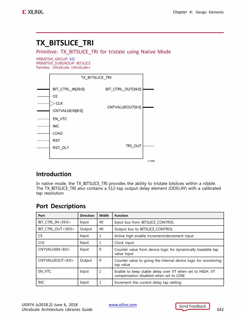
Chapter 4: Design Elements
TX_BITSLICE_TRIPrimitive: TX_BITSLICE_TRI for tristate using Native ModePRIMITIVE_GROUP: I/OPRIMITIVE_SUBGROUP: BITSLICEFamilies: UltraScale, UltraScale+
IntroductionIn native mode, the TX_BITSLICE_TRI provides the ability to tristate bitslices within a nibble.The TX_BITSLICE_TRI also contains a 512-tap output delay element (ODELAY) with a calibratedtap resolution.
Port DescriptionsPort Direction Width Function
BIT_CTRL_IN<39:0> Input 40 Input bus from BITSLICE_CONTROL
BIT_CTRL_OUT<39:0> Output 40 Output bus to BITSLICE_CONTROL
CE Input 1 Active high enable increment/decrement input
CLK Input 1 Clock input
CNTVALUEIN<8:0> Input 9 Counter value from device logic for dynamically loadable tapvalue input
CNTVALUEOUT<8:0> Output 9 Counter value to going the internal device logic for monitoringtap value
EN_VTC Input 1 Enable to keep stable delay over VT when set to HIGH. VTcompensation disabled when set to LOW.
INC Input 1 Increment the current delay tap setting
UG974 (v2018.2) June 6, 2018 www.xilinx.comUltraScale Architecture Libraries Guide 642
Send Feedback
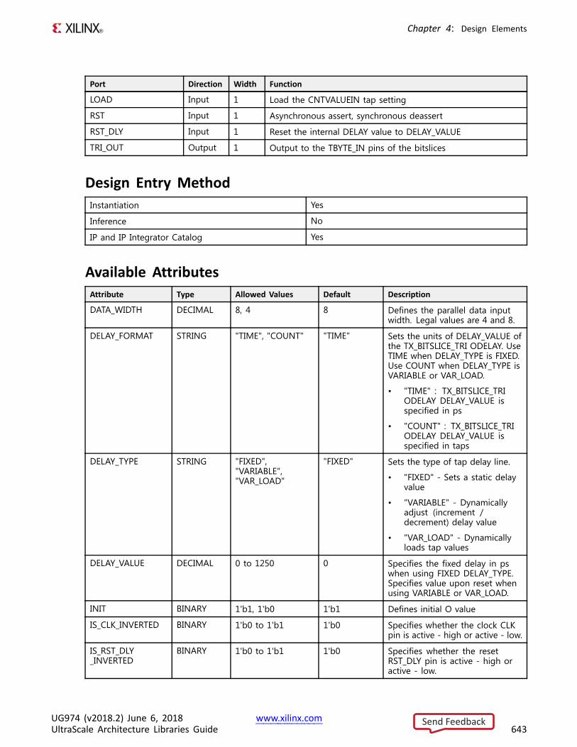
Chapter 4: Design Elements
Port Direction Width Function
LOAD Input 1 Load the CNTVALUEIN tap setting
RST Input 1 Asynchronous assert, synchronous deassert
RST_DLY Input 1 Reset the internal DELAY value to DELAY_VALUE
TRI_OUT Output 1 Output to the TBYTE_IN pins of the bitslices
Design Entry MethodInstantiation Yes
Inference No
IP and IP Integrator Catalog Yes
Available AttributesAttribute Type Allowed Values Default Description
DATA_WIDTH DECIMAL 8, 4 8 Defines the parallel data inputwidth. Legal values are 4 and 8.
DELAY_FORMAT STRING "TIME", "COUNT" "TIME" Sets the units of DELAY_VALUE ofthe TX_BITSLICE_TRI ODELAY. UseTIME when DELAY_TYPE is FIXED.Use COUNT when DELAY_TYPE isVARIABLE or VAR_LOAD.
• "TIME" : TX_BITSLICE_TRIODELAY DELAY_VALUE isspecified in ps
• "COUNT" : TX_BITSLICE_TRIODELAY DELAY_VALUE isspecified in taps
DELAY_TYPE STRING "FIXED","VARIABLE","VAR_LOAD"
"FIXED" Sets the type of tap delay line.
• "FIXED" - Sets a static delayvalue
• "VARIABLE" - Dynamicallyadjust (increment /decrement) delay value
• "VAR_LOAD" - Dynamicallyloads tap values
DELAY_VALUE DECIMAL 0 to 1250 0 Specifies the fixed delay in pswhen using FIXED DELAY_TYPE.Specifies value upon reset whenusing VARIABLE or VAR_LOAD.
INIT BINARY 1'b1, 1'b0 1'b1 Defines initial O value
IS_CLK_INVERTED BINARY 1'b0 to 1'b1 1'b0 Specifies whether the clock CLKpin is active - high or active - low.
IS_RST_DLY_INVERTED
BINARY 1'b0 to 1'b1 1'b0 Specifies whether the resetRST_DLY pin is active - high oractive - low.
UG974 (v2018.2) June 6, 2018 www.xilinx.comUltraScale Architecture Libraries Guide 643
Send Feedback
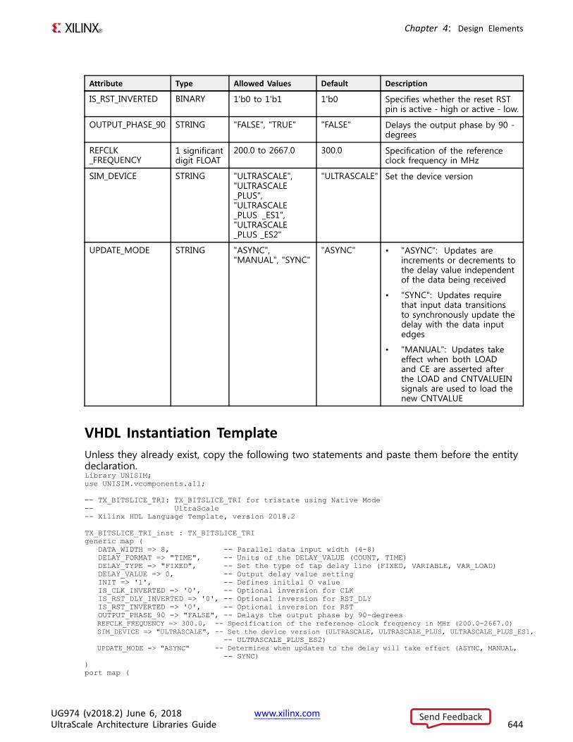
Chapter 4: Design Elements
Attribute Type Allowed Values Default Description
IS_RST_INVERTED BINARY 1'b0 to 1'b1 1'b0 Specifies whether the reset RSTpin is active - high or active - low.
OUTPUT_PHASE_90 STRING "FALSE", "TRUE" "FALSE" Delays the output phase by 90 -degrees
REFCLK_FREQUENCY
1 significantdigit FLOAT
200.0 to 2667.0 300.0 Specification of the referenceclock frequency in MHz
SIM_DEVICE STRING "ULTRASCALE","ULTRASCALE_PLUS","ULTRASCALE_PLUS _ES1","ULTRASCALE_PLUS _ES2"
"ULTRASCALE" Set the device version
UPDATE_MODE STRING "ASYNC","MANUAL", "SYNC"
"ASYNC" • "ASYNC": Updates areincrements or decrements tothe delay value independentof the data being received
• "SYNC": Updates requirethat input data transitionsto synchronously update thedelay with the data inputedges
• "MANUAL": Updates takeeffect when both LOADand CE are asserted afterthe LOAD and CNTVALUEINsignals are used to load thenew CNTVALUE
VHDL Instantiation TemplateUnless they already exist, copy the following two statements and paste them before the entitydeclaration.Library UNISIM;use UNISIM.vcomponents.all;
-- TX_BITSLICE_TRI: TX_BITSLICE_TRI for tristate using Native Mode-- UltraScale-- Xilinx HDL Language Template, version 2018.2
TX_BITSLICE_TRI_inst : TX_BITSLICE_TRIgeneric map (
DATA_WIDTH => 8, -- Parallel data input width (4-8)DELAY_FORMAT => "TIME", -- Units of the DELAY_VALUE (COUNT, TIME)DELAY_TYPE => "FIXED", -- Set the type of tap delay line (FIXED, VARIABLE, VAR_LOAD)DELAY_VALUE => 0, -- Output delay value settingINIT => '1', -- Defines initial O valueIS_CLK_INVERTED => '0', -- Optional inversion for CLKIS_RST_DLY_INVERTED => '0', -- Optional inversion for RST_DLYIS_RST_INVERTED => '0', -- Optional inversion for RSTOUTPUT_PHASE_90 => "FALSE", -- Delays the output phase by 90-degreesREFCLK_FREQUENCY => 300.0, -- Specification of the reference clock frequency in MHz (200.0-2667.0)SIM_DEVICE => "ULTRASCALE", -- Set the device version (ULTRASCALE, ULTRASCALE_PLUS, ULTRASCALE_PLUS_ES1,
-- ULTRASCALE_PLUS_ES2)UPDATE_MODE => "ASYNC" -- Determines when updates to the delay will take effect (ASYNC, MANUAL,
-- SYNC))port map (
UG974 (v2018.2) June 6, 2018 www.xilinx.comUltraScale Architecture Libraries Guide 644
Send Feedback
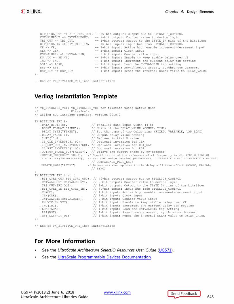
Chapter 4: Design Elements
BIT_CTRL_OUT => BIT_CTRL_OUT, -- 40-bit output: Output bus to BITSLICE_CONTROLCNTVALUEOUT => CNTVALUEOUT, -- 9-bit output: Counter value to device logicTRI_OUT => TRI_OUT, -- 1-bit output: Output to the TBYTE_IN pins of the bitslicesBIT_CTRL_IN => BIT_CTRL_IN, -- 40-bit input: Input bus from BITSLICE_CONTROLCE => CE, -- 1-bit input: Active high enable increment/decrement inputCLK => CLK, -- 1-bit input: Clock inputCNTVALUEIN => CNTVALUEIN, -- 9-bit input: Counter value inputEN_VTC => EN_VTC, -- 1-bit input: Enable to keep stable delay over VTINC => INC, -- 1-bit input: Increment the current delay tap settingLOAD => LOAD, -- 1-bit input: Load the CNTVALUEIN tap settingRST => RST, -- 1-bit input: Asynchronous assert, synchronous deassertRST_DLY => RST_DLY -- 1-bit input: Reset the internal DELAY value to DELAY_VALUE
);
-- End of TX_BITSLICE_TRI_inst instantiation
Verilog Instantiation Template
// TX_BITSLICE_TRI: TX_BITSLICE_TRI for tristate using Native Mode// UltraScale// Xilinx HDL Language Template, version 2018.2
TX_BITSLICE_TRI #(.DATA_WIDTH(8), // Parallel data input width (4-8).DELAY_FORMAT("TIME"), // Units of the DELAY_VALUE (COUNT, TIME).DELAY_TYPE("FIXED"), // Set the type of tap delay line (FIXED, VARIABLE, VAR_LOAD).DELAY_VALUE(0), // Output delay value setting.INIT(1'b1), // Defines initial O value.IS_CLK_INVERTED(1'b0), // Optional inversion for CLK.IS_RST_DLY_INVERTED(1'b0), // Optional inversion for RST_DLY.IS_RST_INVERTED(1'b0), // Optional inversion for RST.OUTPUT_PHASE_90("FALSE"), // Delays the output phase by 90-degrees.REFCLK_FREQUENCY(300.0), // Specification of the reference clock frequency in MHz (200.0-2667.0).SIM_DEVICE("ULTRASCALE"), // Set the device version (ULTRASCALE, ULTRASCALE_PLUS, ULTRASCALE_PLUS_ES1,
// ULTRASCALE_PLUS_ES2).UPDATE_MODE("ASYNC") // Determines when updates to the delay will take effect (ASYNC, MANUAL,
// SYNC))TX_BITSLICE_TRI_inst (
.BIT_CTRL_OUT(BIT_CTRL_OUT), // 40-bit output: Output bus to BITSLICE_CONTROL
.CNTVALUEOUT(CNTVALUEOUT), // 9-bit output: Counter value to device logic
.TRI_OUT(TRI_OUT), // 1-bit output: Output to the TBYTE_IN pins of the bitslices
.BIT_CTRL_IN(BIT_CTRL_IN), // 40-bit input: Input bus from BITSLICE_CONTROL
.CE(CE), // 1-bit input: Active high enable increment/decrement input
.CLK(CLK), // 1-bit input: Clock input
.CNTVALUEIN(CNTVALUEIN), // 9-bit input: Counter value input
.EN_VTC(EN_VTC), // 1-bit input: Enable to keep stable delay over VT
.INC(INC), // 1-bit input: Increment the current delay tap setting
.LOAD(LOAD), // 1-bit input: Load the CNTVALUEIN tap setting
.RST(RST), // 1-bit input: Asynchronous assert, synchronous deassert
.RST_DLY(RST_DLY) // 1-bit input: Reset the internal DELAY value to DELAY_VALUE);
// End of TX_BITSLICE_TRI_inst instantiation
For More Information• See the UltraScale Architecture SelectIO Resources User Guide (UG571).
• See the UltraScale Programmable Devices Documentation.
UG974 (v2018.2) June 6, 2018 www.xilinx.comUltraScale Architecture Libraries Guide 645
Send Feedback
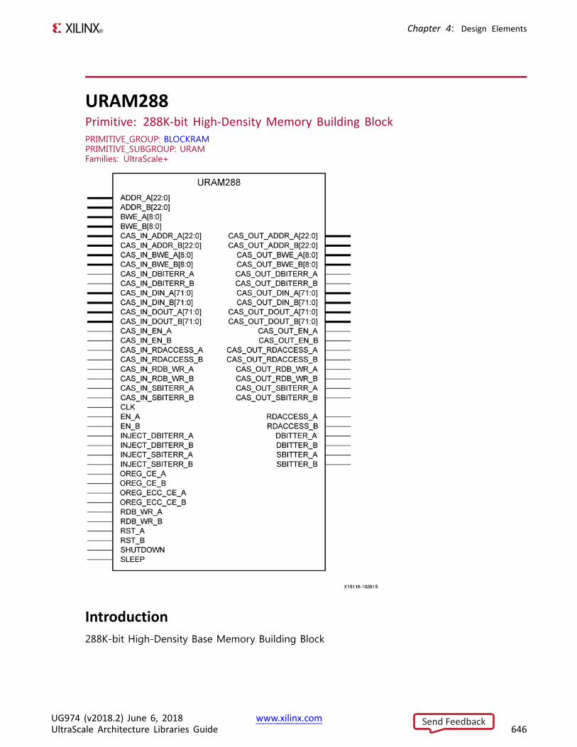
Chapter 4: Design Elements
URAM288Primitive: 288K-bit High-Density Memory Building BlockPRIMITIVE_GROUP: BLOCKRAMPRIMITIVE_SUBGROUP: URAMFamilies: UltraScale+
Introduction288K-bit High-Density Base Memory Building Block
UG974 (v2018.2) June 6, 2018 www.xilinx.comUltraScale Architecture Libraries Guide 646
Send Feedback
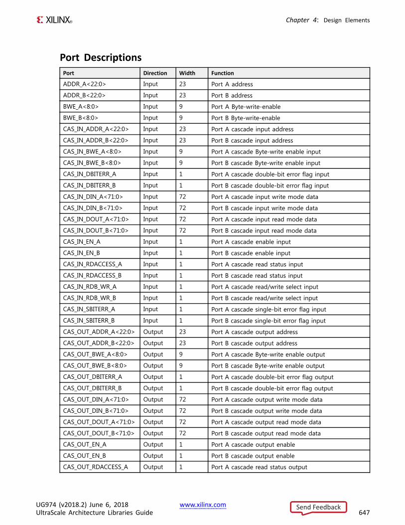
Chapter 4: Design Elements
Port DescriptionsPort Direction Width Function
ADDR_A<22:0> Input 23 Port A address
ADDR_B<22:0> Input 23 Port B address
BWE_A<8:0> Input 9 Port A Byte-write-enable
BWE_B<8:0> Input 9 Port B Byte-write-enable
CAS_IN_ADDR_A<22:0> Input 23 Port A cascade input address
CAS_IN_ADDR_B<22:0> Input 23 Port B cascade input address
CAS_IN_BWE_A<8:0> Input 9 Port A cascade Byte-write enable input
CAS_IN_BWE_B<8:0> Input 9 Port B cascade Byte-write enable input
CAS_IN_DBITERR_A Input 1 Port A cascade double-bit error flag input
CAS_IN_DBITERR_B Input 1 Port B cascade double-bit error flag input
CAS_IN_DIN_A<71:0> Input 72 Port A cascade input write mode data
CAS_IN_DIN_B<71:0> Input 72 Port B cascade input write mode data
CAS_IN_DOUT_A<71:0> Input 72 Port A cascade input read mode data
CAS_IN_DOUT_B<71:0> Input 72 Port B cascade input read mode data
CAS_IN_EN_A Input 1 Port A cascade enable input
CAS_IN_EN_B Input 1 Port B cascade enable input
CAS_IN_RDACCESS_A Input 1 Port A cascade read status input
CAS_IN_RDACCESS_B Input 1 Port B cascade read status input
CAS_IN_RDB_WR_A Input 1 Port A cascade read/write select input
CAS_IN_RDB_WR_B Input 1 Port B cascade read/write select input
CAS_IN_SBITERR_A Input 1 Port A cascade single-bit error flag input
CAS_IN_SBITERR_B Input 1 Port B cascade single-bit error flag input
CAS_OUT_ADDR_A<22:0> Output 23 Port A cascade output address
CAS_OUT_ADDR_B<22:0> Output 23 Port B cascade output address
CAS_OUT_BWE_A<8:0> Output 9 Port A cascade Byte-write enable output
CAS_OUT_BWE_B<8:0> Output 9 Port B cascade Byte-write enable output
CAS_OUT_DBITERR_A Output 1 Port A cascade double-bit error flag output
CAS_OUT_DBITERR_B Output 1 Port B cascade double-bit error flag output
CAS_OUT_DIN_A<71:0> Output 72 Port A cascade output write mode data
CAS_OUT_DIN_B<71:0> Output 72 Port B cascade output write mode data
CAS_OUT_DOUT_A<71:0> Output 72 Port A cascade output read mode data
CAS_OUT_DOUT_B<71:0> Output 72 Port B cascade output read mode data
CAS_OUT_EN_A Output 1 Port A cascade output enable
CAS_OUT_EN_B Output 1 Port B cascade output enable
CAS_OUT_RDACCESS_A Output 1 Port A cascade read status output
UG974 (v2018.2) June 6, 2018 www.xilinx.comUltraScale Architecture Libraries Guide 647
Send Feedback
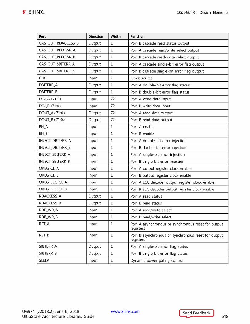
Chapter 4: Design Elements
Port Direction Width Function
CAS_OUT_RDACCESS_B Output 1 Port B cascade read status output
CAS_OUT_RDB_WR_A Output 1 Port A cascade read/write select output
CAS_OUT_RDB_WR_B Output 1 Port B cascade read/write select output
CAS_OUT_SBITERR_A Output 1 Port A cascade single-bit error flag output
CAS_OUT_SBITERR_B Output 1 Port B cascade single-bit error flag output
CLK Input 1 Clock source
DBITERR_A Output 1 Port A double-bit error flag status
DBITERR_B Output 1 Port B double-bit error flag status
DIN_A<71:0> Input 72 Port A write data input
DIN_B<71:0> Input 72 Port B write data input
DOUT_A<71:0> Output 72 Port A read data output
DOUT_B<71:0> Output 72 Port B read data output
EN_A Input 1 Port A enable
EN_B Input 1 Port B enable
INJECT_DBITERR_A Input 1 Port A double-bit error injection
INJECT_DBITERR_B Input 1 Port B double-bit error injection
INJECT_SBITERR_A Input 1 Port A single-bit error injection
INJECT_SBITERR_B Input 1 Port B single-bit error injection
OREG_CE_A Input 1 Port A output register clock enable
OREG_CE_B Input 1 Port B output register clock enable
OREG_ECC_CE_A Input 1 Port A ECC decoder output register clock enable
OREG_ECC_CE_B Input 1 Port B ECC decoder output register clock enable
RDACCESS_A Output 1 Port A read status
RDACCESS_B Output 1 Port B read status
RDB_WR_A Input 1 Port A read/write select
RDB_WR_B Input 1 Port B read/write select
RST_A Input 1 Port A asynchronous or synchronous reset for outputregisters
RST_B Input 1 Port B asynchronous or synchronous reset for outputregisters
SBITERR_A Output 1 Port A single-bit error flag status
SBITERR_B Output 1 Port B single-bit error flag status
SLEEP Input 1 Dynamic power gating control
UG974 (v2018.2) June 6, 2018 www.xilinx.comUltraScale Architecture Libraries Guide 648
Send Feedback
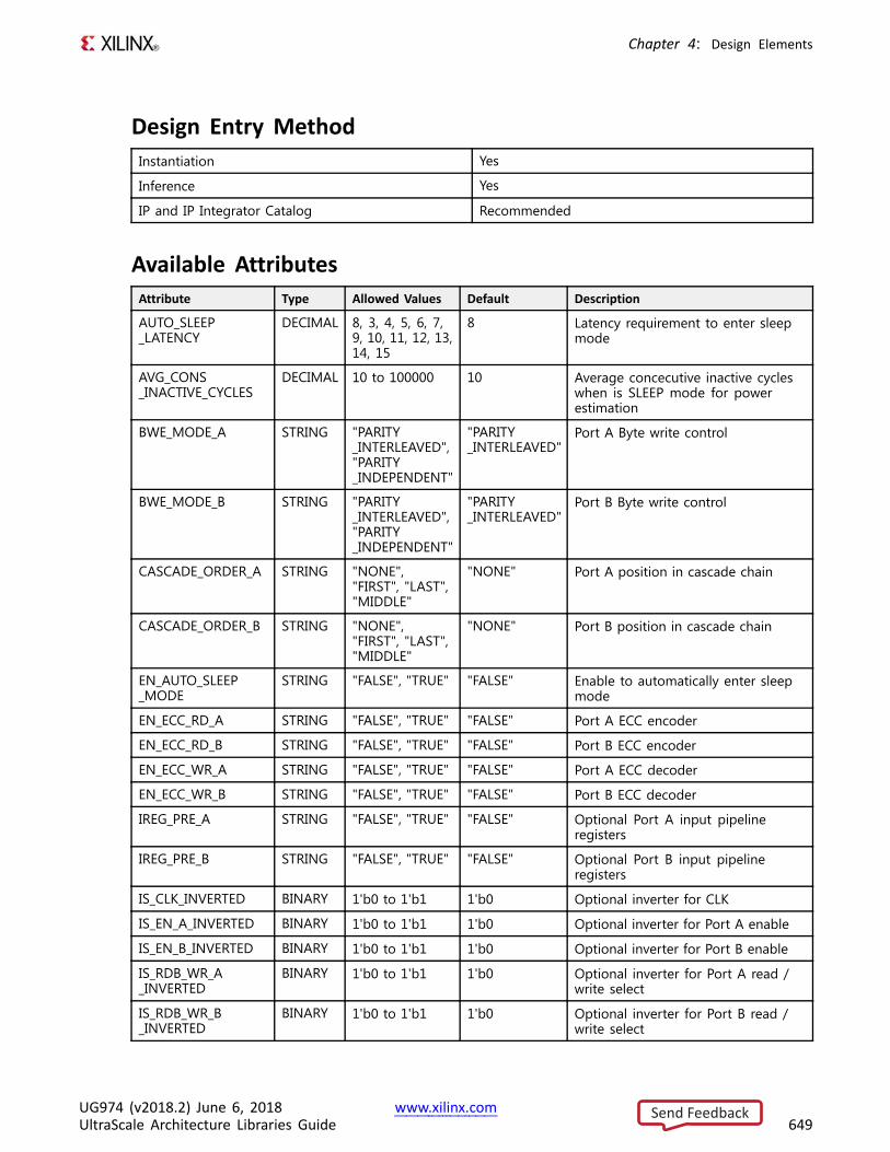
Chapter 4: Design Elements
Design Entry MethodInstantiation Yes
Inference Yes
IP and IP Integrator Catalog Recommended
Available AttributesAttribute Type Allowed Values Default Description
AUTO_SLEEP_LATENCY
DECIMAL 8, 3, 4, 5, 6, 7,9, 10, 11, 12, 13,14, 15
8 Latency requirement to enter sleepmode
AVG_CONS_INACTIVE_CYCLES
DECIMAL 10 to 100000 10 Average concecutive inactive cycleswhen is SLEEP mode for powerestimation
BWE_MODE_A STRING "PARITY_INTERLEAVED","PARITY_INDEPENDENT"
"PARITY_INTERLEAVED"
Port A Byte write control
BWE_MODE_B STRING "PARITY_INTERLEAVED","PARITY_INDEPENDENT"
"PARITY_INTERLEAVED"
Port B Byte write control
CASCADE_ORDER_A STRING "NONE","FIRST", "LAST","MIDDLE"
"NONE" Port A position in cascade chain
CASCADE_ORDER_B STRING "NONE","FIRST", "LAST","MIDDLE"
"NONE" Port B position in cascade chain
EN_AUTO_SLEEP_MODE
STRING "FALSE", "TRUE" "FALSE" Enable to automatically enter sleepmode
EN_ECC_RD_A STRING "FALSE", "TRUE" "FALSE" Port A ECC encoder
EN_ECC_RD_B STRING "FALSE", "TRUE" "FALSE" Port B ECC encoder
EN_ECC_WR_A STRING "FALSE", "TRUE" "FALSE" Port A ECC decoder
EN_ECC_WR_B STRING "FALSE", "TRUE" "FALSE" Port B ECC decoder
IREG_PRE_A STRING "FALSE", "TRUE" "FALSE" Optional Port A input pipelineregisters
IREG_PRE_B STRING "FALSE", "TRUE" "FALSE" Optional Port B input pipelineregisters
IS_CLK_INVERTED BINARY 1'b0 to 1'b1 1'b0 Optional inverter for CLK
IS_EN_A_INVERTED BINARY 1'b0 to 1'b1 1'b0 Optional inverter for Port A enable
IS_EN_B_INVERTED BINARY 1'b0 to 1'b1 1'b0 Optional inverter for Port B enable
IS_RDB_WR_A_INVERTED
BINARY 1'b0 to 1'b1 1'b0 Optional inverter for Port A read /write select
IS_RDB_WR_B_INVERTED
BINARY 1'b0 to 1'b1 1'b0 Optional inverter for Port B read /write select
UG974 (v2018.2) June 6, 2018 www.xilinx.comUltraScale Architecture Libraries Guide 649
Send Feedback
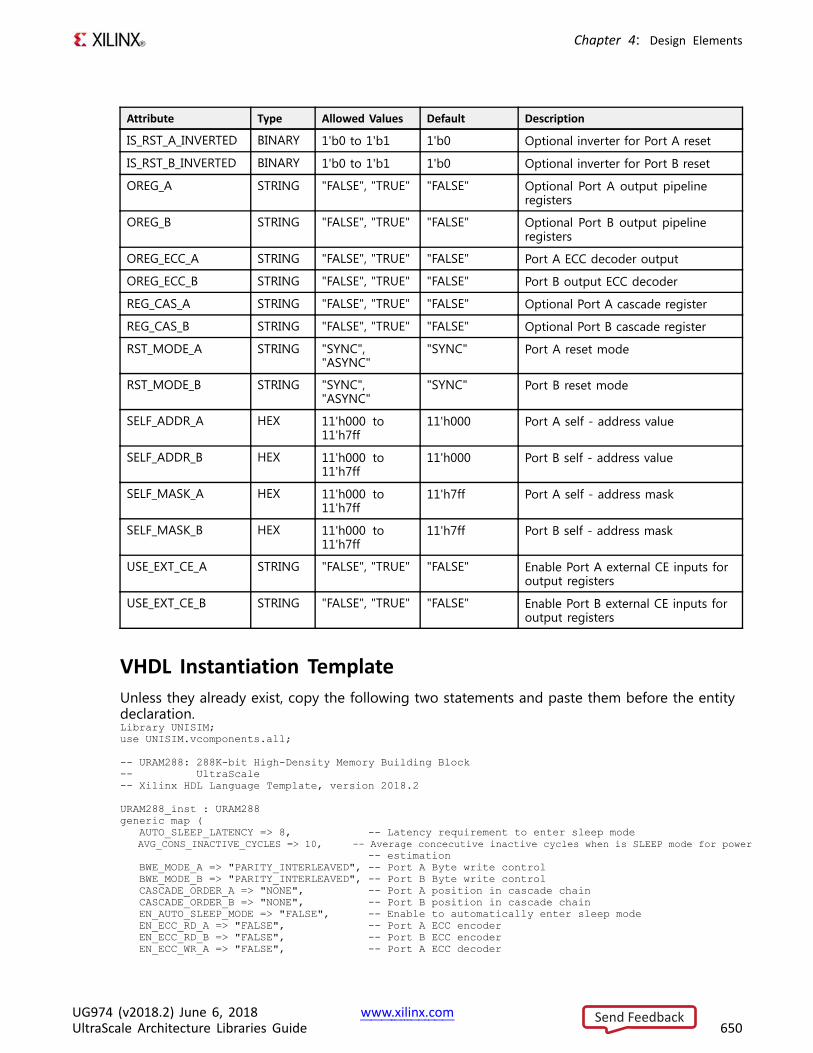
Chapter 4: Design Elements
Attribute Type Allowed Values Default Description
IS_RST_A_INVERTED BINARY 1'b0 to 1'b1 1'b0 Optional inverter for Port A reset
IS_RST_B_INVERTED BINARY 1'b0 to 1'b1 1'b0 Optional inverter for Port B reset
OREG_A STRING "FALSE", "TRUE" "FALSE" Optional Port A output pipelineregisters
OREG_B STRING "FALSE", "TRUE" "FALSE" Optional Port B output pipelineregisters
OREG_ECC_A STRING "FALSE", "TRUE" "FALSE" Port A ECC decoder output
OREG_ECC_B STRING "FALSE", "TRUE" "FALSE" Port B output ECC decoder
REG_CAS_A STRING "FALSE", "TRUE" "FALSE" Optional Port A cascade register
REG_CAS_B STRING "FALSE", "TRUE" "FALSE" Optional Port B cascade register
RST_MODE_A STRING "SYNC","ASYNC"
"SYNC" Port A reset mode
RST_MODE_B STRING "SYNC","ASYNC"
"SYNC" Port B reset mode
SELF_ADDR_A HEX 11'h000 to11'h7ff
11'h000 Port A self - address value
SELF_ADDR_B HEX 11'h000 to11'h7ff
11'h000 Port B self - address value
SELF_MASK_A HEX 11'h000 to11'h7ff
11'h7ff Port A self - address mask
SELF_MASK_B HEX 11'h000 to11'h7ff
11'h7ff Port B self - address mask
USE_EXT_CE_A STRING "FALSE", "TRUE" "FALSE" Enable Port A external CE inputs foroutput registers
USE_EXT_CE_B STRING "FALSE", "TRUE" "FALSE" Enable Port B external CE inputs foroutput registers
VHDL Instantiation TemplateUnless they already exist, copy the following two statements and paste them before the entitydeclaration.Library UNISIM;use UNISIM.vcomponents.all;
-- URAM288: 288K-bit High-Density Memory Building Block-- UltraScale-- Xilinx HDL Language Template, version 2018.2
URAM288_inst : URAM288generic map (
AUTO_SLEEP_LATENCY => 8, -- Latency requirement to enter sleep modeAVG_CONS_INACTIVE_CYCLES => 10, -- Average concecutive inactive cycles when is SLEEP mode for power
-- estimationBWE_MODE_A => "PARITY_INTERLEAVED", -- Port A Byte write controlBWE_MODE_B => "PARITY_INTERLEAVED", -- Port B Byte write controlCASCADE_ORDER_A => "NONE", -- Port A position in cascade chainCASCADE_ORDER_B => "NONE", -- Port B position in cascade chainEN_AUTO_SLEEP_MODE => "FALSE", -- Enable to automatically enter sleep modeEN_ECC_RD_A => "FALSE", -- Port A ECC encoderEN_ECC_RD_B => "FALSE", -- Port B ECC encoderEN_ECC_WR_A => "FALSE", -- Port A ECC decoder
UG974 (v2018.2) June 6, 2018 www.xilinx.comUltraScale Architecture Libraries Guide 650
Send Feedback
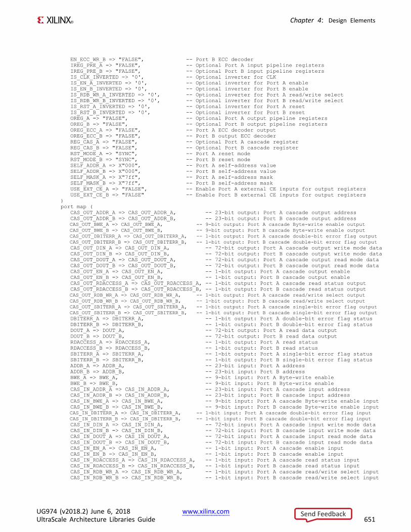
Chapter 4: Design Elements
EN_ECC_WR_B => "FALSE", -- Port B ECC decoderIREG_PRE_A => "FALSE", -- Optional Port A input pipeline registersIREG_PRE_B => "FALSE", -- Optional Port B input pipeline registersIS_CLK_INVERTED => '0', -- Optional inverter for CLKIS_EN_A_INVERTED => '0', -- Optional inverter for Port A enableIS_EN_B_INVERTED => '0', -- Optional inverter for Port B enableIS_RDB_WR_A_INVERTED => '0', -- Optional inverter for Port A read/write selectIS_RDB_WR_B_INVERTED => '0', -- Optional inverter for Port B read/write selectIS_RST_A_INVERTED => '0', -- Optional inverter for Port A resetIS_RST_B_INVERTED => '0', -- Optional inverter for Port B resetOREG_A => "FALSE", -- Optional Port A output pipeline registersOREG_B => "FALSE", -- Optional Port B output pipeline registersOREG_ECC_A => "FALSE", -- Port A ECC decoder outputOREG_ECC_B => "FALSE", -- Port B output ECC decoderREG_CAS_A => "FALSE", -- Optional Port A cascade registerREG_CAS_B => "FALSE", -- Optional Port B cascade registerRST_MODE_A => "SYNC", -- Port A reset modeRST_MODE_B => "SYNC", -- Port B reset modeSELF_ADDR_A => X"000", -- Port A self-address valueSELF_ADDR_B => X"000", -- Port B self-address valueSELF_MASK_A => X"7ff", -- Port A self-address maskSELF_MASK_B => X"7ff", -- Port B self-address maskUSE_EXT_CE_A => "FALSE", -- Enable Port A external CE inputs for output registersUSE_EXT_CE_B => "FALSE" -- Enable Port B external CE inputs for output registers
)port map (
CAS_OUT_ADDR_A => CAS_OUT_ADDR_A, -- 23-bit output: Port A cascade output addressCAS_OUT_ADDR_B => CAS_OUT_ADDR_B, -- 23-bit output: Port B cascade output addressCAS_OUT_BWE_A => CAS_OUT_BWE_A, -- 9-bit output: Port A cascade Byte-write enable outputCAS_OUT_BWE_B => CAS_OUT_BWE_B, -- 9-bit output: Port B cascade Byte-write enable outputCAS_OUT_DBITERR_A => CAS_OUT_DBITERR_A, -- 1-bit output: Port A cascade double-bit error flag outputCAS_OUT_DBITERR_B => CAS_OUT_DBITERR_B, -- 1-bit output: Port B cascade double-bit error flag outputCAS_OUT_DIN_A => CAS_OUT_DIN_A, -- 72-bit output: Port A cascade output write mode dataCAS_OUT_DIN_B => CAS_OUT_DIN_B, -- 72-bit output: Port B cascade output write mode dataCAS_OUT_DOUT_A => CAS_OUT_DOUT_A, -- 72-bit output: Port A cascade output read mode dataCAS_OUT_DOUT_B => CAS_OUT_DOUT_B, -- 72-bit output: Port B cascade output read mode dataCAS_OUT_EN_A => CAS_OUT_EN_A, -- 1-bit output: Port A cascade output enableCAS_OUT_EN_B => CAS_OUT_EN_B, -- 1-bit output: Port B cascade output enableCAS_OUT_RDACCESS_A => CAS_OUT_RDACCESS_A, -- 1-bit output: Port A cascade read status outputCAS_OUT_RDACCESS_B => CAS_OUT_RDACCESS_B, -- 1-bit output: Port B cascade read status outputCAS_OUT_RDB_WR_A => CAS_OUT_RDB_WR_A, -- 1-bit output: Port A cascade read/write select outputCAS_OUT_RDB_WR_B => CAS_OUT_RDB_WR_B, -- 1-bit output: Port B cascade read/write select outputCAS_OUT_SBITERR_A => CAS_OUT_SBITERR_A, -- 1-bit output: Port A cascade single-bit error flag outputCAS_OUT_SBITERR_B => CAS_OUT_SBITERR_B, -- 1-bit output: Port B cascade single-bit error flag outputDBITERR_A => DBITERR_A, -- 1-bit output: Port A double-bit error flag statusDBITERR_B => DBITERR_B, -- 1-bit output: Port B double-bit error flag statusDOUT_A => DOUT_A, -- 72-bit output: Port A read data outputDOUT_B => DOUT_B, -- 72-bit output: Port B read data outputRDACCESS_A => RDACCESS_A, -- 1-bit output: Port A read statusRDACCESS_B => RDACCESS_B, -- 1-bit output: Port B read statusSBITERR_A => SBITERR_A, -- 1-bit output: Port A single-bit error flag statusSBITERR_B => SBITERR_B, -- 1-bit output: Port B single-bit error flag statusADDR_A => ADDR_A, -- 23-bit input: Port A addressADDR_B => ADDR_B, -- 23-bit input: Port B addressBWE_A => BWE_A, -- 9-bit input: Port A Byte-write enableBWE_B => BWE_B, -- 9-bit input: Port B Byte-write enableCAS_IN_ADDR_A => CAS_IN_ADDR_A, -- 23-bit input: Port A cascade input addressCAS_IN_ADDR_B => CAS_IN_ADDR_B, -- 23-bit input: Port B cascade input addressCAS_IN_BWE_A => CAS_IN_BWE_A, -- 9-bit input: Port A cascade Byte-write enable inputCAS_IN_BWE_B => CAS_IN_BWE_B, -- 9-bit input: Port B cascade Byte-write enable inputCAS_IN_DBITERR_A => CAS_IN_DBITERR_A, -- 1-bit input: Port A cascade double-bit error flag inputCAS_IN_DBITERR_B => CAS_IN_DBITERR_B, -- 1-bit input: Port B cascade double-bit error flag inputCAS_IN_DIN_A => CAS_IN_DIN_A, -- 72-bit input: Port A cascade input write mode dataCAS_IN_DIN_B => CAS_IN_DIN_B, -- 72-bit input: Port B cascade input write mode dataCAS_IN_DOUT_A => CAS_IN_DOUT_A, -- 72-bit input: Port A cascade input read mode dataCAS_IN_DOUT_B => CAS_IN_DOUT_B, -- 72-bit input: Port B cascade input read mode dataCAS_IN_EN_A => CAS_IN_EN_A, -- 1-bit input: Port A cascade enable inputCAS_IN_EN_B => CAS_IN_EN_B, -- 1-bit input: Port B cascade enable inputCAS_IN_RDACCESS_A => CAS_IN_RDACCESS_A, -- 1-bit input: Port A cascade read status inputCAS_IN_RDACCESS_B => CAS_IN_RDACCESS_B, -- 1-bit input: Port B cascade read status inputCAS_IN_RDB_WR_A => CAS_IN_RDB_WR_A, -- 1-bit input: Port A cascade read/write select inputCAS_IN_RDB_WR_B => CAS_IN_RDB_WR_B, -- 1-bit input: Port B cascade read/write select input
UG974 (v2018.2) June 6, 2018 www.xilinx.comUltraScale Architecture Libraries Guide 651
Send Feedback
Chapter 4: Design Elements
CAS_IN_SBITERR_A => CAS_IN_SBITERR_A, -- 1-bit input: Port A cascade single-bit error flag inputCAS_IN_SBITERR_B => CAS_IN_SBITERR_B, -- 1-bit input: Port B cascade single-bit error flag inputCLK => CLK, -- 1-bit input: Clock sourceDIN_A => DIN_A, -- 72-bit input: Port A write data inputDIN_B => DIN_B, -- 72-bit input: Port B write data inputEN_A => EN_A, -- 1-bit input: Port A enableEN_B => EN_B, -- 1-bit input: Port B enableINJECT_DBITERR_A => INJECT_DBITERR_A, -- 1-bit input: Port A double-bit error injectionINJECT_DBITERR_B => INJECT_DBITERR_B, -- 1-bit input: Port B double-bit error injectionINJECT_SBITERR_A => INJECT_SBITERR_A, -- 1-bit input: Port A single-bit error injectionINJECT_SBITERR_B => INJECT_SBITERR_B, -- 1-bit input: Port B single-bit error injectionOREG_CE_A => OREG_CE_A, -- 1-bit input: Port A output register clock enableOREG_CE_B => OREG_CE_B, -- 1-bit input: Port B output register clock enableOREG_ECC_CE_A => OREG_ECC_CE_A, -- 1-bit input: Port A ECC decoder output register clock enableOREG_ECC_CE_B => OREG_ECC_CE_B, -- 1-bit input: Port B ECC decoder output register clock enableRDB_WR_A => RDB_WR_A, -- 1-bit input: Port A read/write selectRDB_WR_B => RDB_WR_B, -- 1-bit input: Port B read/write selectRST_A => RST_A, -- 1-bit input: Port A asynchronous or synchronous reset for
-- output registers
RST_B => RST_B, -- 1-bit input: Port B asynchronous or synchronous reset for-- output registers
SLEEP => SLEEP -- 1-bit input: Dynamic power gating control);
-- End of URAM288_inst instantiation
Verilog Instantiation Template
// URAM288: 288K-bit High-Density Memory Building Block// UltraScale// Xilinx HDL Language Template, version 2018.2
URAM288 #(.AUTO_SLEEP_LATENCY(8), // Latency requirement to enter sleep mode.AVG_CONS_INACTIVE_CYCLES(10), // Average concecutive inactive cycles when is SLEEP mode for power
// estimation.BWE_MODE_A("PARITY_INTERLEAVED"), // Port A Byte write control.BWE_MODE_B("PARITY_INTERLEAVED"), // Port B Byte write control.CASCADE_ORDER_A("NONE"), // Port A position in cascade chain.CASCADE_ORDER_B("NONE"), // Port B position in cascade chain.EN_AUTO_SLEEP_MODE("FALSE"), // Enable to automatically enter sleep mode.EN_ECC_RD_A("FALSE"), // Port A ECC encoder.EN_ECC_RD_B("FALSE"), // Port B ECC encoder.EN_ECC_WR_A("FALSE"), // Port A ECC decoder.EN_ECC_WR_B("FALSE"), // Port B ECC decoder.IREG_PRE_A("FALSE"), // Optional Port A input pipeline registers.IREG_PRE_B("FALSE"), // Optional Port B input pipeline registers.IS_CLK_INVERTED(1'b0), // Optional inverter for CLK.IS_EN_A_INVERTED(1'b0), // Optional inverter for Port A enable.IS_EN_B_INVERTED(1'b0), // Optional inverter for Port B enable.IS_RDB_WR_A_INVERTED(1'b0), // Optional inverter for Port A read/write select.IS_RDB_WR_B_INVERTED(1'b0), // Optional inverter for Port B read/write select.IS_RST_A_INVERTED(1'b0), // Optional inverter for Port A reset.IS_RST_B_INVERTED(1'b0), // Optional inverter for Port B reset.OREG_A("FALSE"), // Optional Port A output pipeline registers.OREG_B("FALSE"), // Optional Port B output pipeline registers.OREG_ECC_A("FALSE"), // Port A ECC decoder output.OREG_ECC_B("FALSE"), // Port B output ECC decoder.REG_CAS_A("FALSE"), // Optional Port A cascade register.REG_CAS_B("FALSE"), // Optional Port B cascade register.RST_MODE_A("SYNC"), // Port A reset mode.RST_MODE_B("SYNC"), // Port B reset mode.SELF_ADDR_A(11'h000), // Port A self-address value.SELF_ADDR_B(11'h000), // Port B self-address value.SELF_MASK_A(11'h7ff), // Port A self-address mask.SELF_MASK_B(11'h7ff), // Port B self-address mask
UG974 (v2018.2) June 6, 2018 www.xilinx.comUltraScale Architecture Libraries Guide 652
Send Feedback
Chapter 4: Design Elements
.USE_EXT_CE_A("FALSE"), // Enable Port A external CE inputs for output registers
.USE_EXT_CE_B("FALSE") // Enable Port B external CE inputs for output registers)URAM288_inst (
.CAS_OUT_ADDR_A(CAS_OUT_ADDR_A), // 23-bit output: Port A cascade output address
.CAS_OUT_ADDR_B(CAS_OUT_ADDR_B), // 23-bit output: Port B cascade output address
.CAS_OUT_BWE_A(CAS_OUT_BWE_A), // 9-bit output: Port A cascade Byte-write enable output
.CAS_OUT_BWE_B(CAS_OUT_BWE_B), // 9-bit output: Port B cascade Byte-write enable output
.CAS_OUT_DBITERR_A(CAS_OUT_DBITERR_A), // 1-bit output: Port A cascade double-bit error flag output
.CAS_OUT_DBITERR_B(CAS_OUT_DBITERR_B), // 1-bit output: Port B cascade double-bit error flag output
.CAS_OUT_DIN_A(CAS_OUT_DIN_A), // 72-bit output: Port A cascade output write mode data
.CAS_OUT_DIN_B(CAS_OUT_DIN_B), // 72-bit output: Port B cascade output write mode data
.CAS_OUT_DOUT_A(CAS_OUT_DOUT_A), // 72-bit output: Port A cascade output read mode data
.CAS_OUT_DOUT_B(CAS_OUT_DOUT_B), // 72-bit output: Port B cascade output read mode data
.CAS_OUT_EN_A(CAS_OUT_EN_A), // 1-bit output: Port A cascade output enable
.CAS_OUT_EN_B(CAS_OUT_EN_B), // 1-bit output: Port B cascade output enable
.CAS_OUT_RDACCESS_A(CAS_OUT_RDACCESS_A), // 1-bit output: Port A cascade read status output
.CAS_OUT_RDACCESS_B(CAS_OUT_RDACCESS_B), // 1-bit output: Port B cascade read status output
.CAS_OUT_RDB_WR_A(CAS_OUT_RDB_WR_A), // 1-bit output: Port A cascade read/write select output
.CAS_OUT_RDB_WR_B(CAS_OUT_RDB_WR_B), // 1-bit output: Port B cascade read/write select output
.CAS_OUT_SBITERR_A(CAS_OUT_SBITERR_A), // 1-bit output: Port A cascade single-bit error flag output
.CAS_OUT_SBITERR_B(CAS_OUT_SBITERR_B), // 1-bit output: Port B cascade single-bit error flag output
.DBITERR_A(DBITERR_A), // 1-bit output: Port A double-bit error flag status
.DBITERR_B(DBITERR_B), // 1-bit output: Port B double-bit error flag status
.DOUT_A(DOUT_A), // 72-bit output: Port A read data output
.DOUT_B(DOUT_B), // 72-bit output: Port B read data output
.RDACCESS_A(RDACCESS_A), // 1-bit output: Port A read status
.RDACCESS_B(RDACCESS_B), // 1-bit output: Port B read status
.SBITERR_A(SBITERR_A), // 1-bit output: Port A single-bit error flag status
.SBITERR_B(SBITERR_B), // 1-bit output: Port B single-bit error flag status
.ADDR_A(ADDR_A), // 23-bit input: Port A address
.ADDR_B(ADDR_B), // 23-bit input: Port B address
.BWE_A(BWE_A), // 9-bit input: Port A Byte-write enable
.BWE_B(BWE_B), // 9-bit input: Port B Byte-write enable
.CAS_IN_ADDR_A(CAS_IN_ADDR_A), // 23-bit input: Port A cascade input address
.CAS_IN_ADDR_B(CAS_IN_ADDR_B), // 23-bit input: Port B cascade input address
.CAS_IN_BWE_A(CAS_IN_BWE_A), // 9-bit input: Port A cascade Byte-write enable input
.CAS_IN_BWE_B(CAS_IN_BWE_B), // 9-bit input: Port B cascade Byte-write enable input
.CAS_IN_DBITERR_A(CAS_IN_DBITERR_A), // 1-bit input: Port A cascade double-bit error flag input
.CAS_IN_DBITERR_B(CAS_IN_DBITERR_B), // 1-bit input: Port B cascade double-bit error flag input
.CAS_IN_DIN_A(CAS_IN_DIN_A), // 72-bit input: Port A cascade input write mode data
.CAS_IN_DIN_B(CAS_IN_DIN_B), // 72-bit input: Port B cascade input write mode data
.CAS_IN_DOUT_A(CAS_IN_DOUT_A), // 72-bit input: Port A cascade input read mode data
.CAS_IN_DOUT_B(CAS_IN_DOUT_B), // 72-bit input: Port B cascade input read mode data
.CAS_IN_EN_A(CAS_IN_EN_A), // 1-bit input: Port A cascade enable input
.CAS_IN_EN_B(CAS_IN_EN_B), // 1-bit input: Port B cascade enable input
.CAS_IN_RDACCESS_A(CAS_IN_RDACCESS_A), // 1-bit input: Port A cascade read status input
.CAS_IN_RDACCESS_B(CAS_IN_RDACCESS_B), // 1-bit input: Port B cascade read status input
.CAS_IN_RDB_WR_A(CAS_IN_RDB_WR_A), // 1-bit input: Port A cascade read/write select input
.CAS_IN_RDB_WR_B(CAS_IN_RDB_WR_B), // 1-bit input: Port B cascade read/write select input
.CAS_IN_SBITERR_A(CAS_IN_SBITERR_A), // 1-bit input: Port A cascade single-bit error flag input
.CAS_IN_SBITERR_B(CAS_IN_SBITERR_B), // 1-bit input: Port B cascade single-bit error flag input
.CLK(CLK), // 1-bit input: Clock source
.DIN_A(DIN_A), // 72-bit input: Port A write data input
.DIN_B(DIN_B), // 72-bit input: Port B write data input
.EN_A(EN_A), // 1-bit input: Port A enable
.EN_B(EN_B), // 1-bit input: Port B enable
.INJECT_DBITERR_A(INJECT_DBITERR_A), // 1-bit input: Port A double-bit error injection
.INJECT_DBITERR_B(INJECT_DBITERR_B), // 1-bit input: Port B double-bit error injection
.INJECT_SBITERR_A(INJECT_SBITERR_A), // 1-bit input: Port A single-bit error injection
.INJECT_SBITERR_B(INJECT_SBITERR_B), // 1-bit input: Port B single-bit error injection
.OREG_CE_A(OREG_CE_A), // 1-bit input: Port A output register clock enable
.OREG_CE_B(OREG_CE_B), // 1-bit input: Port B output register clock enable
.OREG_ECC_CE_A(OREG_ECC_CE_A), // 1-bit input: Port A ECC decoder output register clock enable
.OREG_ECC_CE_B(OREG_ECC_CE_B), // 1-bit input: Port B ECC decoder output register clock enable
.RDB_WR_A(RDB_WR_A), // 1-bit input: Port A read/write select
.RDB_WR_B(RDB_WR_B), // 1-bit input: Port B read/write select
.RST_A(RST_A), // 1-bit input: Port A asynchronous or synchronous reset for// output registers
.RST_B(RST_B), // 1-bit input: Port B asynchronous or synchronous reset for// output registers
UG974 (v2018.2) June 6, 2018 www.xilinx.comUltraScale Architecture Libraries Guide 653
Send Feedback
Chapter 4: Design Elements
.SLEEP(SLEEP) // 1-bit input: Dynamic power gating control);
// End of URAM288_inst instantiation
For More Information• See the UltraScale Architecture Memory Resources User Guide (UG573).
• See the UltraScale Programmable Devices Documentation.
UG974 (v2018.2) June 6, 2018 www.xilinx.comUltraScale Architecture Libraries Guide 654
Send Feedback
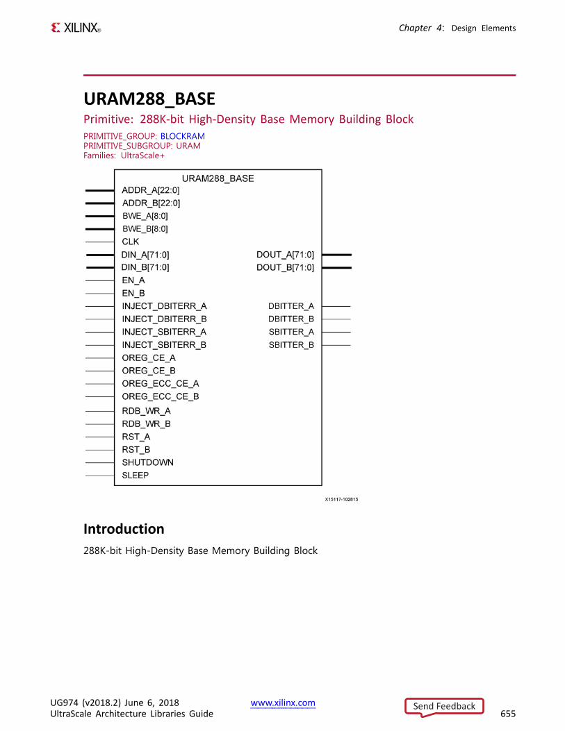
Chapter 4: Design Elements
URAM288_BASEPrimitive: 288K-bit High-Density Base Memory Building BlockPRIMITIVE_GROUP: BLOCKRAMPRIMITIVE_SUBGROUP: URAMFamilies: UltraScale+
Introduction288K-bit High-Density Base Memory Building Block
UG974 (v2018.2) June 6, 2018 www.xilinx.comUltraScale Architecture Libraries Guide 655
Send Feedback
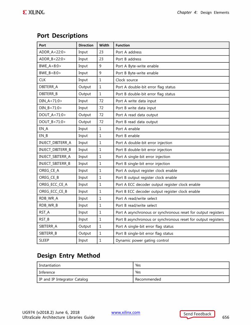
Chapter 4: Design Elements
Port DescriptionsPort Direction Width Function
ADDR_A<22:0> Input 23 Port A address
ADDR_B<22:0> Input 23 Port B address
BWE_A<8:0> Input 9 Port A Byte-write enable
BWE_B<8:0> Input 9 Port B Byte-write enable
CLK Input 1 Clock source
DBITERR_A Output 1 Port A double-bit error flag status
DBITERR_B Output 1 Port B double-bit error flag status
DIN_A<71:0> Input 72 Port A write data input
DIN_B<71:0> Input 72 Port B write data input
DOUT_A<71:0> Output 72 Port A read data output
DOUT_B<71:0> Output 72 Port B read data output
EN_A Input 1 Port A enable
EN_B Input 1 Port B enable
INJECT_DBITERR_A Input 1 Port A double-bit error injection
INJECT_DBITERR_B Input 1 Port B double-bit error injection
INJECT_SBITERR_A Input 1 Port A single-bit error injection
INJECT_SBITERR_B Input 1 Port B single-bit error injection
OREG_CE_A Input 1 Port A output register clock enable
OREG_CE_B Input 1 Port B output register clock enable
OREG_ECC_CE_A Input 1 Port A ECC decoder output register clock enable
OREG_ECC_CE_B Input 1 Port B ECC decoder output register clock enable
RDB_WR_A Input 1 Port A read/write select
RDB_WR_B Input 1 Port B read/write select
RST_A Input 1 Port A asynchronous or synchronous reset for output registers
RST_B Input 1 Port B asynchronous or synchronous reset for output registers
SBITERR_A Output 1 Port A single-bit error flag status
SBITERR_B Output 1 Port B single-bit error flag status
SLEEP Input 1 Dynamic power gating control
Design Entry MethodInstantiation Yes
Inference Yes
IP and IP Integrator Catalog Recommended
UG974 (v2018.2) June 6, 2018 www.xilinx.comUltraScale Architecture Libraries Guide 656
Send Feedback
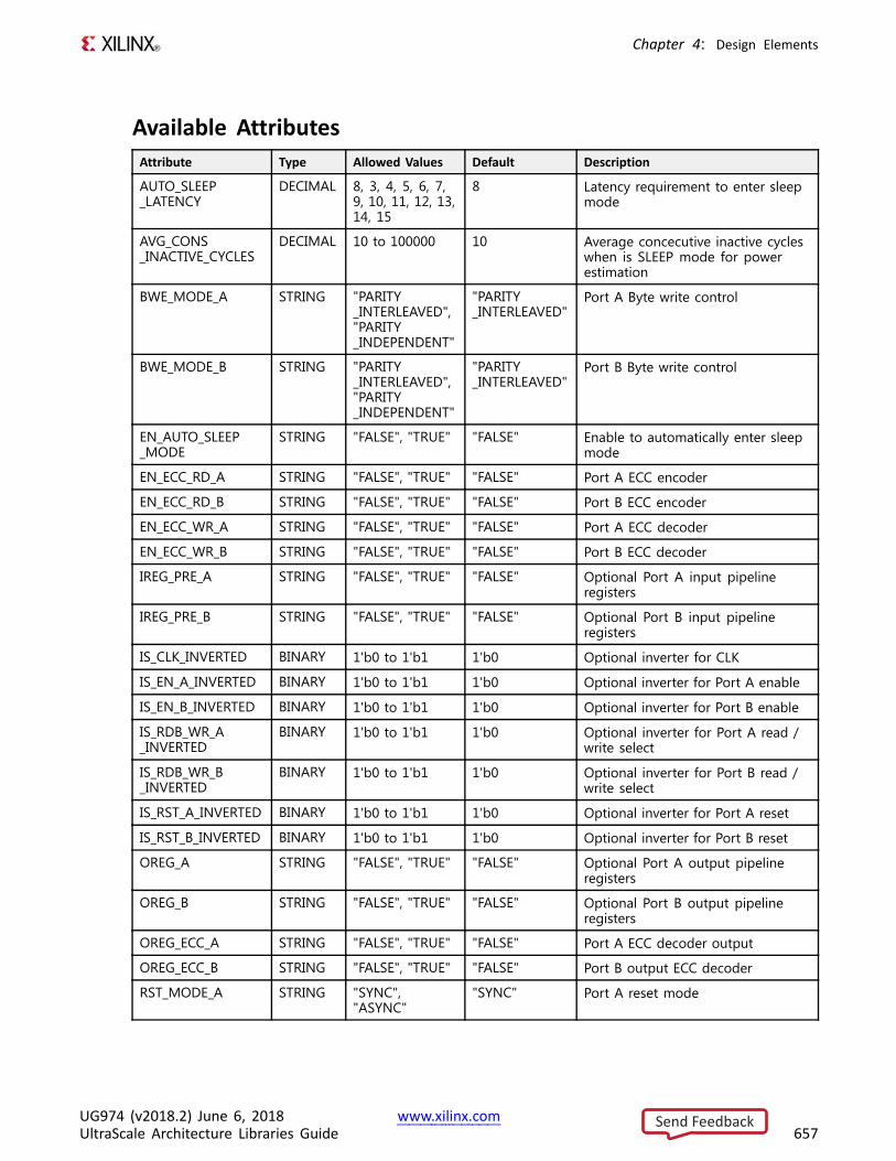
Chapter 4: Design Elements
Available AttributesAttribute Type Allowed Values Default Description
AUTO_SLEEP_LATENCY
DECIMAL 8, 3, 4, 5, 6, 7,9, 10, 11, 12, 13,14, 15
8 Latency requirement to enter sleepmode
AVG_CONS_INACTIVE_CYCLES
DECIMAL 10 to 100000 10 Average concecutive inactive cycleswhen is SLEEP mode for powerestimation
BWE_MODE_A STRING "PARITY_INTERLEAVED","PARITY_INDEPENDENT"
"PARITY_INTERLEAVED"
Port A Byte write control
BWE_MODE_B STRING "PARITY_INTERLEAVED","PARITY_INDEPENDENT"
"PARITY_INTERLEAVED"
Port B Byte write control
EN_AUTO_SLEEP_MODE
STRING "FALSE", "TRUE" "FALSE" Enable to automatically enter sleepmode
EN_ECC_RD_A STRING "FALSE", "TRUE" "FALSE" Port A ECC encoder
EN_ECC_RD_B STRING "FALSE", "TRUE" "FALSE" Port B ECC encoder
EN_ECC_WR_A STRING "FALSE", "TRUE" "FALSE" Port A ECC decoder
EN_ECC_WR_B STRING "FALSE", "TRUE" "FALSE" Port B ECC decoder
IREG_PRE_A STRING "FALSE", "TRUE" "FALSE" Optional Port A input pipelineregisters
IREG_PRE_B STRING "FALSE", "TRUE" "FALSE" Optional Port B input pipelineregisters
IS_CLK_INVERTED BINARY 1'b0 to 1'b1 1'b0 Optional inverter for CLK
IS_EN_A_INVERTED BINARY 1'b0 to 1'b1 1'b0 Optional inverter for Port A enable
IS_EN_B_INVERTED BINARY 1'b0 to 1'b1 1'b0 Optional inverter for Port B enable
IS_RDB_WR_A_INVERTED
BINARY 1'b0 to 1'b1 1'b0 Optional inverter for Port A read /write select
IS_RDB_WR_B_INVERTED
BINARY 1'b0 to 1'b1 1'b0 Optional inverter for Port B read /write select
IS_RST_A_INVERTED BINARY 1'b0 to 1'b1 1'b0 Optional inverter for Port A reset
IS_RST_B_INVERTED BINARY 1'b0 to 1'b1 1'b0 Optional inverter for Port B reset
OREG_A STRING "FALSE", "TRUE" "FALSE" Optional Port A output pipelineregisters
OREG_B STRING "FALSE", "TRUE" "FALSE" Optional Port B output pipelineregisters
OREG_ECC_A STRING "FALSE", "TRUE" "FALSE" Port A ECC decoder output
OREG_ECC_B STRING "FALSE", "TRUE" "FALSE" Port B output ECC decoder
RST_MODE_A STRING "SYNC","ASYNC"
"SYNC" Port A reset mode
UG974 (v2018.2) June 6, 2018 www.xilinx.comUltraScale Architecture Libraries Guide 657
Send Feedback
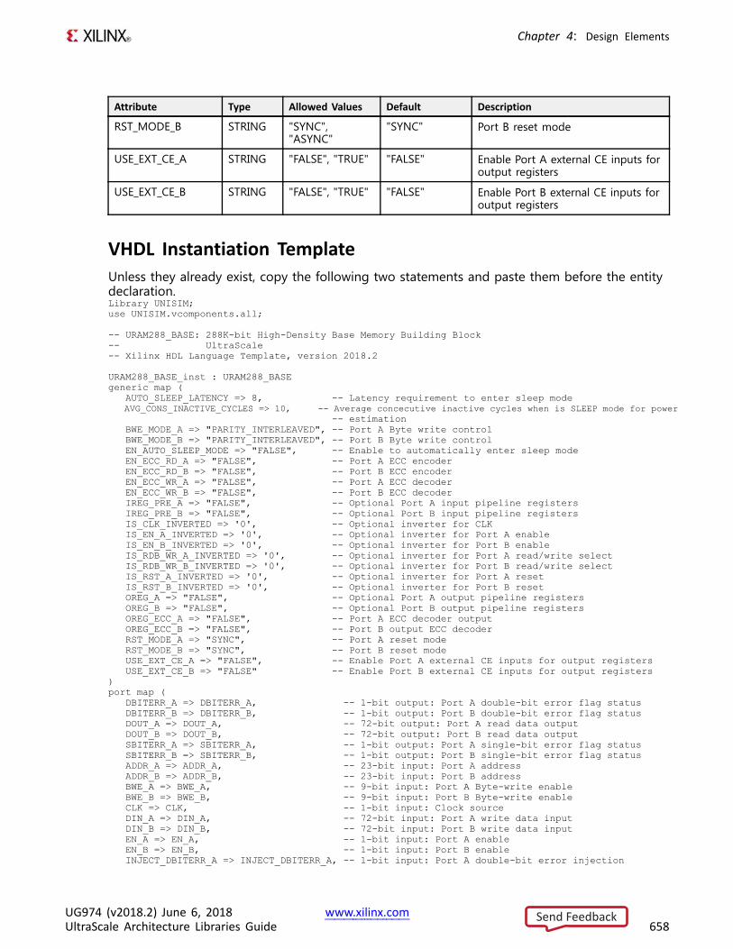
Chapter 4: Design Elements
Attribute Type Allowed Values Default Description
RST_MODE_B STRING "SYNC","ASYNC"
"SYNC" Port B reset mode
USE_EXT_CE_A STRING "FALSE", "TRUE" "FALSE" Enable Port A external CE inputs foroutput registers
USE_EXT_CE_B STRING "FALSE", "TRUE" "FALSE" Enable Port B external CE inputs foroutput registers
VHDL Instantiation TemplateUnless they already exist, copy the following two statements and paste them before the entitydeclaration.Library UNISIM;use UNISIM.vcomponents.all;
-- URAM288_BASE: 288K-bit High-Density Base Memory Building Block-- UltraScale-- Xilinx HDL Language Template, version 2018.2
URAM288_BASE_inst : URAM288_BASEgeneric map (
AUTO_SLEEP_LATENCY => 8, -- Latency requirement to enter sleep modeAVG_CONS_INACTIVE_CYCLES => 10, -- Average concecutive inactive cycles when is SLEEP mode for power
-- estimationBWE_MODE_A => "PARITY_INTERLEAVED", -- Port A Byte write controlBWE_MODE_B => "PARITY_INTERLEAVED", -- Port B Byte write controlEN_AUTO_SLEEP_MODE => "FALSE", -- Enable to automatically enter sleep modeEN_ECC_RD_A => "FALSE", -- Port A ECC encoderEN_ECC_RD_B => "FALSE", -- Port B ECC encoderEN_ECC_WR_A => "FALSE", -- Port A ECC decoderEN_ECC_WR_B => "FALSE", -- Port B ECC decoderIREG_PRE_A => "FALSE", -- Optional Port A input pipeline registersIREG_PRE_B => "FALSE", -- Optional Port B input pipeline registersIS_CLK_INVERTED => '0', -- Optional inverter for CLKIS_EN_A_INVERTED => '0', -- Optional inverter for Port A enableIS_EN_B_INVERTED => '0', -- Optional inverter for Port B enableIS_RDB_WR_A_INVERTED => '0', -- Optional inverter for Port A read/write selectIS_RDB_WR_B_INVERTED => '0', -- Optional inverter for Port B read/write selectIS_RST_A_INVERTED => '0', -- Optional inverter for Port A resetIS_RST_B_INVERTED => '0', -- Optional inverter for Port B resetOREG_A => "FALSE", -- Optional Port A output pipeline registersOREG_B => "FALSE", -- Optional Port B output pipeline registersOREG_ECC_A => "FALSE", -- Port A ECC decoder outputOREG_ECC_B => "FALSE", -- Port B output ECC decoderRST_MODE_A => "SYNC", -- Port A reset modeRST_MODE_B => "SYNC", -- Port B reset modeUSE_EXT_CE_A => "FALSE", -- Enable Port A external CE inputs for output registersUSE_EXT_CE_B => "FALSE" -- Enable Port B external CE inputs for output registers
)port map (
DBITERR_A => DBITERR_A, -- 1-bit output: Port A double-bit error flag statusDBITERR_B => DBITERR_B, -- 1-bit output: Port B double-bit error flag statusDOUT_A => DOUT_A, -- 72-bit output: Port A read data outputDOUT_B => DOUT_B, -- 72-bit output: Port B read data outputSBITERR_A => SBITERR_A, -- 1-bit output: Port A single-bit error flag statusSBITERR_B => SBITERR_B, -- 1-bit output: Port B single-bit error flag statusADDR_A => ADDR_A, -- 23-bit input: Port A addressADDR_B => ADDR_B, -- 23-bit input: Port B addressBWE_A => BWE_A, -- 9-bit input: Port A Byte-write enableBWE_B => BWE_B, -- 9-bit input: Port B Byte-write enableCLK => CLK, -- 1-bit input: Clock sourceDIN_A => DIN_A, -- 72-bit input: Port A write data inputDIN_B => DIN_B, -- 72-bit input: Port B write data inputEN_A => EN_A, -- 1-bit input: Port A enableEN_B => EN_B, -- 1-bit input: Port B enableINJECT_DBITERR_A => INJECT_DBITERR_A, -- 1-bit input: Port A double-bit error injection
UG974 (v2018.2) June 6, 2018 www.xilinx.comUltraScale Architecture Libraries Guide 658
Send Feedback
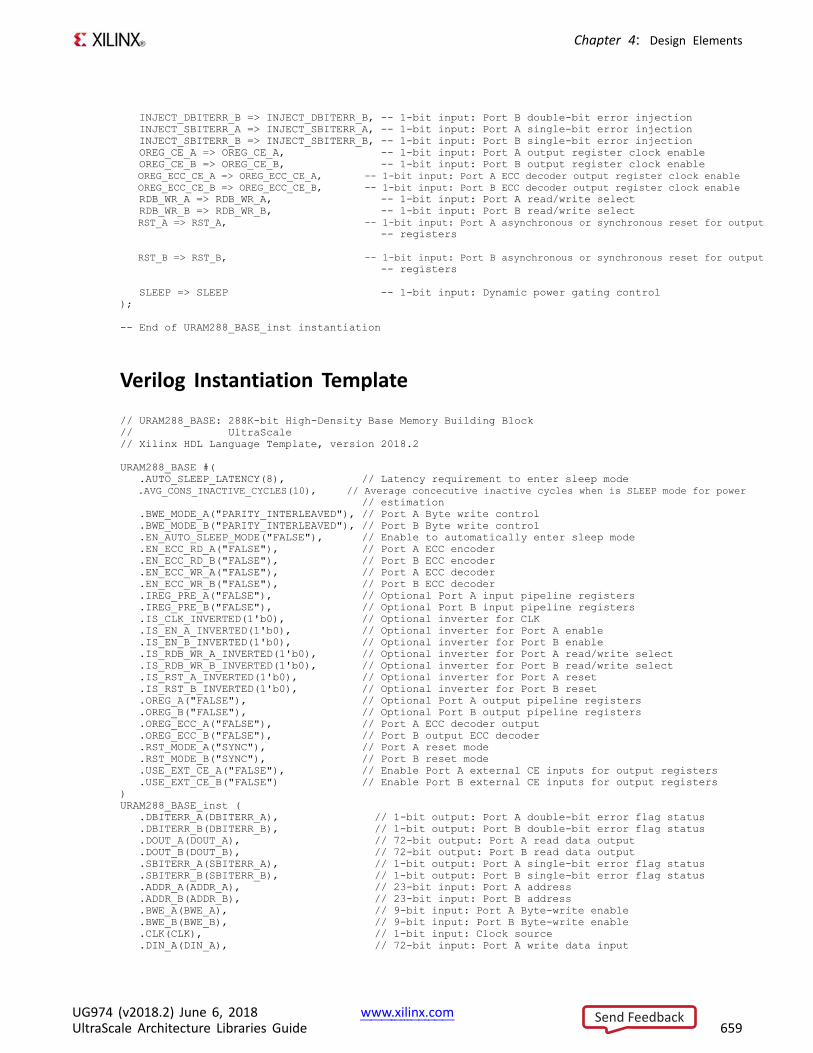
Chapter 4: Design Elements
INJECT_DBITERR_B => INJECT_DBITERR_B, -- 1-bit input: Port B double-bit error injectionINJECT_SBITERR_A => INJECT_SBITERR_A, -- 1-bit input: Port A single-bit error injectionINJECT_SBITERR_B => INJECT_SBITERR_B, -- 1-bit input: Port B single-bit error injectionOREG_CE_A => OREG_CE_A, -- 1-bit input: Port A output register clock enableOREG_CE_B => OREG_CE_B, -- 1-bit input: Port B output register clock enableOREG_ECC_CE_A => OREG_ECC_CE_A, -- 1-bit input: Port A ECC decoder output register clock enableOREG_ECC_CE_B => OREG_ECC_CE_B, -- 1-bit input: Port B ECC decoder output register clock enableRDB_WR_A => RDB_WR_A, -- 1-bit input: Port A read/write selectRDB_WR_B => RDB_WR_B, -- 1-bit input: Port B read/write selectRST_A => RST_A, -- 1-bit input: Port A asynchronous or synchronous reset for output
-- registers
RST_B => RST_B, -- 1-bit input: Port B asynchronous or synchronous reset for output-- registers
SLEEP => SLEEP -- 1-bit input: Dynamic power gating control);
-- End of URAM288_BASE_inst instantiation
Verilog Instantiation Template
// URAM288_BASE: 288K-bit High-Density Base Memory Building Block// UltraScale// Xilinx HDL Language Template, version 2018.2
URAM288_BASE #(.AUTO_SLEEP_LATENCY(8), // Latency requirement to enter sleep mode.AVG_CONS_INACTIVE_CYCLES(10), // Average concecutive inactive cycles when is SLEEP mode for power
// estimation.BWE_MODE_A("PARITY_INTERLEAVED"), // Port A Byte write control.BWE_MODE_B("PARITY_INTERLEAVED"), // Port B Byte write control.EN_AUTO_SLEEP_MODE("FALSE"), // Enable to automatically enter sleep mode.EN_ECC_RD_A("FALSE"), // Port A ECC encoder.EN_ECC_RD_B("FALSE"), // Port B ECC encoder.EN_ECC_WR_A("FALSE"), // Port A ECC decoder.EN_ECC_WR_B("FALSE"), // Port B ECC decoder.IREG_PRE_A("FALSE"), // Optional Port A input pipeline registers.IREG_PRE_B("FALSE"), // Optional Port B input pipeline registers.IS_CLK_INVERTED(1'b0), // Optional inverter for CLK.IS_EN_A_INVERTED(1'b0), // Optional inverter for Port A enable.IS_EN_B_INVERTED(1'b0), // Optional inverter for Port B enable.IS_RDB_WR_A_INVERTED(1'b0), // Optional inverter for Port A read/write select.IS_RDB_WR_B_INVERTED(1'b0), // Optional inverter for Port B read/write select.IS_RST_A_INVERTED(1'b0), // Optional inverter for Port A reset.IS_RST_B_INVERTED(1'b0), // Optional inverter for Port B reset.OREG_A("FALSE"), // Optional Port A output pipeline registers.OREG_B("FALSE"), // Optional Port B output pipeline registers.OREG_ECC_A("FALSE"), // Port A ECC decoder output.OREG_ECC_B("FALSE"), // Port B output ECC decoder.RST_MODE_A("SYNC"), // Port A reset mode.RST_MODE_B("SYNC"), // Port B reset mode.USE_EXT_CE_A("FALSE"), // Enable Port A external CE inputs for output registers.USE_EXT_CE_B("FALSE") // Enable Port B external CE inputs for output registers
)URAM288_BASE_inst (
.DBITERR_A(DBITERR_A), // 1-bit output: Port A double-bit error flag status
.DBITERR_B(DBITERR_B), // 1-bit output: Port B double-bit error flag status
.DOUT_A(DOUT_A), // 72-bit output: Port A read data output
.DOUT_B(DOUT_B), // 72-bit output: Port B read data output
.SBITERR_A(SBITERR_A), // 1-bit output: Port A single-bit error flag status
.SBITERR_B(SBITERR_B), // 1-bit output: Port B single-bit error flag status
.ADDR_A(ADDR_A), // 23-bit input: Port A address
.ADDR_B(ADDR_B), // 23-bit input: Port B address
.BWE_A(BWE_A), // 9-bit input: Port A Byte-write enable
.BWE_B(BWE_B), // 9-bit input: Port B Byte-write enable
.CLK(CLK), // 1-bit input: Clock source
.DIN_A(DIN_A), // 72-bit input: Port A write data input
UG974 (v2018.2) June 6, 2018 www.xilinx.comUltraScale Architecture Libraries Guide 659
Send Feedback
Chapter 4: Design Elements
.DIN_B(DIN_B), // 72-bit input: Port B write data input
.EN_A(EN_A), // 1-bit input: Port A enable
.EN_B(EN_B), // 1-bit input: Port B enable
.INJECT_DBITERR_A(INJECT_DBITERR_A), // 1-bit input: Port A double-bit error injection
.INJECT_DBITERR_B(INJECT_DBITERR_B), // 1-bit input: Port B double-bit error injection
.INJECT_SBITERR_A(INJECT_SBITERR_A), // 1-bit input: Port A single-bit error injection
.INJECT_SBITERR_B(INJECT_SBITERR_B), // 1-bit input: Port B single-bit error injection
.OREG_CE_A(OREG_CE_A), // 1-bit input: Port A output register clock enable
.OREG_CE_B(OREG_CE_B), // 1-bit input: Port B output register clock enable
.OREG_ECC_CE_A(OREG_ECC_CE_A), // 1-bit input: Port A ECC decoder output register clock enable
.OREG_ECC_CE_B(OREG_ECC_CE_B), // 1-bit input: Port B ECC decoder output register clock enable
.RDB_WR_A(RDB_WR_A), // 1-bit input: Port A read/write select
.RDB_WR_B(RDB_WR_B), // 1-bit input: Port B read/write select
.RST_A(RST_A), // 1-bit input: Port A asynchronous or synchronous reset for output// registers
.RST_B(RST_B), // 1-bit input: Port B asynchronous or synchronous reset for output// registers
.SLEEP(SLEEP) // 1-bit input: Dynamic power gating control);
// End of URAM288_BASE_inst instantiation
For More Information• See the UltraScale Architecture Memory Resources User Guide (UG573).
• See the UltraScale Programmable Devices Documentation.
UG974 (v2018.2) June 6, 2018 www.xilinx.comUltraScale Architecture Libraries Guide 660
Send Feedback
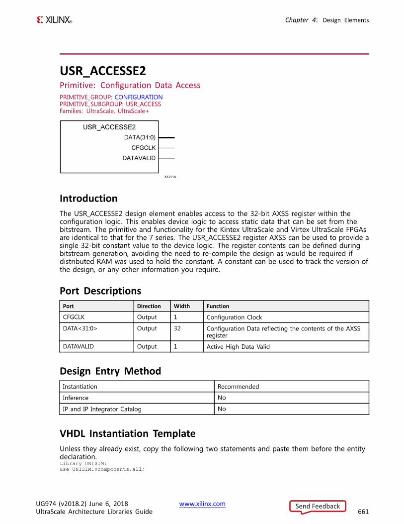
Chapter 4: Design Elements
USR_ACCESSE2Primitive: Configuration Data AccessPRIMITIVE_GROUP: CONFIGURATIONPRIMITIVE_SUBGROUP: USR_ACCESSFamilies: UltraScale, UltraScale+
IntroductionThe USR_ACCESSE2 design element enables access to the 32-bit AXSS register within theconfiguration logic. This enables device logic to access static data that can be set from thebitstream. The primitive and functionality for the Kintex UltraScale and Virtex UltraScale FPGAsare identical to that for the 7 series. The USR_ACCESSE2 register AXSS can be used to provide asingle 32-bit constant value to the device logic. The register contents can be defined duringbitstream generation, avoiding the need to re-compile the design as would be required ifdistributed RAM was used to hold the constant. A constant can be used to track the version ofthe design, or any other information you require.
Port DescriptionsPort Direction Width Function
CFGCLK Output 1 Configuration Clock
DATA<31:0> Output 32 Configuration Data reflecting the contents of the AXSSregister
DATAVALID Output 1 Active High Data Valid
Design Entry MethodInstantiation Recommended
Inference No
IP and IP Integrator Catalog No
VHDL Instantiation TemplateUnless they already exist, copy the following two statements and paste them before the entitydeclaration.Library UNISIM;use UNISIM.vcomponents.all;
UG974 (v2018.2) June 6, 2018 www.xilinx.comUltraScale Architecture Libraries Guide 661
Send Feedback
Chapter 4: Design Elements
-- USR_ACCESSE2: Configuration Data Access-- UltraScale-- Xilinx HDL Language Template, version 2018.2
USR_ACCESSE2_inst : USR_ACCESSE2port map (
CFGCLK => CFGCLK, -- 1-bit output: Configuration ClockDATA => DATA, -- 32-bit output: Configuration Data reflecting the contents of the AXSS registerDATAVALID => DATAVALID -- 1-bit output: Active High Data Valid
);
-- End of USR_ACCESSE2_inst instantiation
Verilog Instantiation Template
// USR_ACCESSE2: Configuration Data Access// UltraScale// Xilinx HDL Language Template, version 2018.2
USR_ACCESSE2 USR_ACCESSE2_inst (.CFGCLK(CFGCLK), // 1-bit output: Configuration Clock.DATA(DATA), // 32-bit output: Configuration Data reflecting the contents of the AXSS register.DATAVALID(DATAVALID) // 1-bit output: Active High Data Valid
);
// End of USR_ACCESSE2_inst instantiation
For More Information• See the UltraScale Architecture Configuration User Guide (UG570).
• See the UltraScale Programmable Devices Documentation.
UG974 (v2018.2) June 6, 2018 www.xilinx.comUltraScale Architecture Libraries Guide 662
Send Feedback

Appendix A
Additional Resources and Legal Notices
Xilinx ResourcesFor support resources such as Answers, Documentation, Downloads, and Forums, see XilinxSupport.
Solution CentersSee the Xilinx Solution Centers for support on devices, software tools, and intellectualproperty at all stages of the design cycle. Topics include design assistance, advisories, andtroubleshooting tips.
Documentation Navigator and Design HubsXilinx Documentation Navigator provides access to Xilinx documents, videos, and supportresources, which you can filter and search to find information. To open the Xilinx DocumentationNavigator (DocNav):
• From the Vivado IDE, select Help > Documentation and Tutorials.• On Windows, select Start > All Programs > Xilinx Design Tools > DocNav.• At the Linux command prompt, enter docnav.
Xilinx Design Hubs provide links to documentation organized by design tasks and other topics,which you can use to learn key concepts and address frequently asked questions. To accessthe Design Hubs:
• In the Xilinx Documentation Navigator, click the Design Hubs View tab.
• On the Xilinx website, see the Design Hubs page.
NOTE: For more information on Documentation Navigator, see the Documentation Navigatorpage on the Xilinx website.
UltraScale Architecture Libraries Guide www.xilinx.com 663UG974 (v2018.2) June 6, 2018
Send Feedback

Appendix A: Additional Resources and Legal Notices
Please Read: Important Legal NoticesThe information disclosed to you hereunder (the "Materials") is provided solely for the selectionand use of Xilinx products. To the maximum extent permitted by applicable law: (1) Materialsare made available "AS IS" and with all faults, Xilinx hereby DISCLAIMS ALL WARRANTIESAND CONDITIONS, EXPRESS, IMPLIED, OR STATUTORY, INCLUDING BUT NOT LIMITED TOWARRANTIES OF MERCHANTABILITY, NON-INFRINGEMENT, OR FITNESS FOR ANY PARTICULARPURPOSE; and (2) Xilinx shall not be liable (whether in contract or tort, including negligence,or under any other theory of liability) for any loss or damage of any kind or nature relatedto, arising under, or in connection with, the Materials (including your use of the Materials),including for any direct, indirect, special, incidental, or consequential loss or damage (includingloss of data, profits, goodwill, or any type of loss or damage suffered as a result of any actionbrought by a third party) even if such damage or loss was reasonably foreseeable or Xilinxhad been advised of the possibility of the same. Xilinx assumes no obligation to correct anyerrors contained in the Materials or to notify you of updates to the Materials or to productspecifications. You may not reproduce, modify, distribute, or publicly display the Materialswithout prior written consent. Certain products are subject to the terms and conditionsof Xilinx's limited warranty, please refer to Xilinx's Terms of Sale which can be viewed athttps://www.xilinx.com/legal.htm#tos; IP cores may be subject to warranty and support termscontained in a license issued to you by Xilinx. Xilinx products are not designed or intended tobe fail-safe or for use in any application requiring fail-safe performance; you assume sole riskand liability for use of Xilinx products in such critical applications, please refer to Xilinx's Termsof Sale which can be viewed at https://www.xilinx.com/legal.htm#tos.
AUTOMOTIVE APPLICATIONS DISCLAIMER
AUTOMOTIVE PRODUCTS (IDENTIFIED AS “XA” IN THE PART NUMBER) ARE NOT WARRANTEDFOR USE IN THE DEPLOYMENT OF AIRBAGS OR FOR USE IN APPLICATIONS THAT AFFECTCONTROL OF A VEHICLE (“SAFETY APPLICATION”) UNLESS THERE IS A SAFETY CONCEPT ORREDUNDANCY FEATURE CONSISTENT WITH THE ISO 26262 AUTOMOTIVE SAFETY STANDARD(“SAFETY DESIGN”). CUSTOMER SHALL, PRIOR TO USING OR DISTRIBUTING ANY SYSTEMSTHAT INCORPORATE PRODUCTS, THOROUGHLY TEST SUCH SYSTEMS FOR SAFETY PURPOSES.USE OF PRODUCTS IN A SAFETY APPLICATION WITHOUT A SAFETY DESIGN IS FULLY AT THERISK OF CUSTOMER, SUBJECT ONLY TO APPLICABLE LAWS AND REGULATIONS GOVERNINGLIMITATIONS ON PRODUCT LIABILITY.
© Copyright 2018 Xilinx, Inc. Xilinx, the Xilinx logo, Artix, ISE, Kintex, Spartan, Virtex, Vivado,Zynq, and other designated brands included herein are trademarks of Xilinx in the United Statesand other countries. All other trademarks are the property of their respective owners.
UltraScale Architecture Libraries Guide www.xilinx.com 664UG974 (v2018.2) June 6, 2018
Send Feedback