ultrascale devices integrated 100g ethernet v2 - xilinx · pdf fileultrascale devices...
TRANSCRIPT

UltraScale Devices Integrated 100G Ethernet v2.3LogiCORE IP Product Guide
Vivado Design Suite
PG165 April 4, 2018
Integrated 100G Ethernet v2.3 2PG165 April 4, 2018 www.xilinx.com
Table of ContentsIP Facts
Chapter 1: OverviewFeature Summary. . . . . . . . . . . . . . . . . . . . . . . . . . . . . . . . . . . . . . . . . . . . . . . . . . . . . . . . . . . . . . . . . . 5Licensing and Ordering . . . . . . . . . . . . . . . . . . . . . . . . . . . . . . . . . . . . . . . . . . . . . . . . . . . . . . . . . . . . . 7
Chapter 2: Product SpecificationTypical Operation. . . . . . . . . . . . . . . . . . . . . . . . . . . . . . . . . . . . . . . . . . . . . . . . . . . . . . . . . . . . . . . . . 11Statistics Gathering . . . . . . . . . . . . . . . . . . . . . . . . . . . . . . . . . . . . . . . . . . . . . . . . . . . . . . . . . . . . . . . 11Testability Functions . . . . . . . . . . . . . . . . . . . . . . . . . . . . . . . . . . . . . . . . . . . . . . . . . . . . . . . . . . . . . . 11Pause Operation. . . . . . . . . . . . . . . . . . . . . . . . . . . . . . . . . . . . . . . . . . . . . . . . . . . . . . . . . . . . . . . . . . 12Standards . . . . . . . . . . . . . . . . . . . . . . . . . . . . . . . . . . . . . . . . . . . . . . . . . . . . . . . . . . . . . . . . . . . . . . . 12Performance. . . . . . . . . . . . . . . . . . . . . . . . . . . . . . . . . . . . . . . . . . . . . . . . . . . . . . . . . . . . . . . . . . . . . 12Resource Utilization. . . . . . . . . . . . . . . . . . . . . . . . . . . . . . . . . . . . . . . . . . . . . . . . . . . . . . . . . . . . . . . 12Port Descriptions . . . . . . . . . . . . . . . . . . . . . . . . . . . . . . . . . . . . . . . . . . . . . . . . . . . . . . . . . . . . . . . . . 13Attribute Descriptions . . . . . . . . . . . . . . . . . . . . . . . . . . . . . . . . . . . . . . . . . . . . . . . . . . . . . . . . . . . . . 42
Chapter 3: Designing with the CoreClocking. . . . . . . . . . . . . . . . . . . . . . . . . . . . . . . . . . . . . . . . . . . . . . . . . . . . . . . . . . . . . . . . . . . . . . . . . 50Resets . . . . . . . . . . . . . . . . . . . . . . . . . . . . . . . . . . . . . . . . . . . . . . . . . . . . . . . . . . . . . . . . . . . . . . . . . . 51Protocol Description . . . . . . . . . . . . . . . . . . . . . . . . . . . . . . . . . . . . . . . . . . . . . . . . . . . . . . . . . . . . . . 54PCS . . . . . . . . . . . . . . . . . . . . . . . . . . . . . . . . . . . . . . . . . . . . . . . . . . . . . . . . . . . . . . . . . . . . . . . . . . . . 54MAC . . . . . . . . . . . . . . . . . . . . . . . . . . . . . . . . . . . . . . . . . . . . . . . . . . . . . . . . . . . . . . . . . . . . . . . . . . . 581588v2 Timestamping . . . . . . . . . . . . . . . . . . . . . . . . . . . . . . . . . . . . . . . . . . . . . . . . . . . . . . . . . . . . . 79Transceiver Selection Rules. . . . . . . . . . . . . . . . . . . . . . . . . . . . . . . . . . . . . . . . . . . . . . . . . . . . . . . . . 85Dynamic Reconfiguration Port . . . . . . . . . . . . . . . . . . . . . . . . . . . . . . . . . . . . . . . . . . . . . . . . . . . . . . 86
Chapter 4: Design Flow StepsCustomizing and Generating the Core . . . . . . . . . . . . . . . . . . . . . . . . . . . . . . . . . . . . . . . . . . . . . . . . 95Constraining the Core . . . . . . . . . . . . . . . . . . . . . . . . . . . . . . . . . . . . . . . . . . . . . . . . . . . . . . . . . . . . 106Simulation . . . . . . . . . . . . . . . . . . . . . . . . . . . . . . . . . . . . . . . . . . . . . . . . . . . . . . . . . . . . . . . . . . . . . 107Synthesis and Implementation . . . . . . . . . . . . . . . . . . . . . . . . . . . . . . . . . . . . . . . . . . . . . . . . . . . . . 107
Send Feedback
Integrated 100G Ethernet v2.3 3PG165 April 4, 2018 www.xilinx.com
Chapter 5: Example DesignOverview . . . . . . . . . . . . . . . . . . . . . . . . . . . . . . . . . . . . . . . . . . . . . . . . . . . . . . . . . . . . . . . . . . . . . . 108User Interface. . . . . . . . . . . . . . . . . . . . . . . . . . . . . . . . . . . . . . . . . . . . . . . . . . . . . . . . . . . . . . . . . . . 113CORE XCI Top Level Port List . . . . . . . . . . . . . . . . . . . . . . . . . . . . . . . . . . . . . . . . . . . . . . . . . . . . . . . 115Modes of Operation. . . . . . . . . . . . . . . . . . . . . . . . . . . . . . . . . . . . . . . . . . . . . . . . . . . . . . . . . . . . . . 156Transaction Flow . . . . . . . . . . . . . . . . . . . . . . . . . . . . . . . . . . . . . . . . . . . . . . . . . . . . . . . . . . . . . . . . 160CORE DRP Operation . . . . . . . . . . . . . . . . . . . . . . . . . . . . . . . . . . . . . . . . . . . . . . . . . . . . . . . . . . . . . 169AXI4-Lite Interface Implementation . . . . . . . . . . . . . . . . . . . . . . . . . . . . . . . . . . . . . . . . . . . . . . . . . 169IEEE 802.3bj RS-FEC Integration . . . . . . . . . . . . . . . . . . . . . . . . . . . . . . . . . . . . . . . . . . . . . . . . . . . . 200Core Bring Up Sequence . . . . . . . . . . . . . . . . . . . . . . . . . . . . . . . . . . . . . . . . . . . . . . . . . . . . . . . . . . 201Use Case for Different Modes . . . . . . . . . . . . . . . . . . . . . . . . . . . . . . . . . . . . . . . . . . . . . . . . . . . . . . 202Simulating the Example Design. . . . . . . . . . . . . . . . . . . . . . . . . . . . . . . . . . . . . . . . . . . . . . . . . . . . . 209Synthesizing and Implementing the Example Design . . . . . . . . . . . . . . . . . . . . . . . . . . . . . . . . . . . 211
Appendix A: Auto-Negotiation and Link TrainingAuto-Negotiation . . . . . . . . . . . . . . . . . . . . . . . . . . . . . . . . . . . . . . . . . . . . . . . . . . . . . . . . . . . . . . . . 213Link Training . . . . . . . . . . . . . . . . . . . . . . . . . . . . . . . . . . . . . . . . . . . . . . . . . . . . . . . . . . . . . . . . . . . . 216Port Descriptions . . . . . . . . . . . . . . . . . . . . . . . . . . . . . . . . . . . . . . . . . . . . . . . . . . . . . . . . . . . . . . . . 219
Appendix B: Upgrading
Appendix C: DebuggingFinding Help on Xilinx.com . . . . . . . . . . . . . . . . . . . . . . . . . . . . . . . . . . . . . . . . . . . . . . . . . . . . . . . . 229Debug Tools . . . . . . . . . . . . . . . . . . . . . . . . . . . . . . . . . . . . . . . . . . . . . . . . . . . . . . . . . . . . . . . . . . . . 230Simulation Debug. . . . . . . . . . . . . . . . . . . . . . . . . . . . . . . . . . . . . . . . . . . . . . . . . . . . . . . . . . . . . . . . 231Hardware Debug . . . . . . . . . . . . . . . . . . . . . . . . . . . . . . . . . . . . . . . . . . . . . . . . . . . . . . . . . . . . . . . . 232Interface Debug . . . . . . . . . . . . . . . . . . . . . . . . . . . . . . . . . . . . . . . . . . . . . . . . . . . . . . . . . . . . . . . . . 234Protocol Debug. . . . . . . . . . . . . . . . . . . . . . . . . . . . . . . . . . . . . . . . . . . . . . . . . . . . . . . . . . . . . . . . . . 235
Appendix D: Additional Resources and Legal NoticesXilinx Resources . . . . . . . . . . . . . . . . . . . . . . . . . . . . . . . . . . . . . . . . . . . . . . . . . . . . . . . . . . . . . . . . . 237Documentation Navigator and Design Hubs . . . . . . . . . . . . . . . . . . . . . . . . . . . . . . . . . . . . . . . . . . 237References . . . . . . . . . . . . . . . . . . . . . . . . . . . . . . . . . . . . . . . . . . . . . . . . . . . . . . . . . . . . . . . . . . . . . 237Revision History . . . . . . . . . . . . . . . . . . . . . . . . . . . . . . . . . . . . . . . . . . . . . . . . . . . . . . . . . . . . . . . . . 239Please Read: Important Legal Notices . . . . . . . . . . . . . . . . . . . . . . . . . . . . . . . . . . . . . . . . . . . . . . . 244
Send Feedback
Integrated 100G Ethernet v2.3 4PG165 April 4, 2018 www.xilinx.com Product Specification
IntroductionThe Xilinx® UltraScale™ Devices Integrated 100G Ethernet IP core provides a high performance, low latency 100 Gb/s Ethernet port that allows for a wide range of user customization and statistics gathering. The dedicated block provides both the 100G Ethernet media access control (MAC) and physical coding sublayer (PCS) logic with support for IEEE 1588-2008 [Ref 1] one-step and two-step hardware timestamping.
The 100G Ethernet IP core provides three configurations: (CAUI-10) 10x10.3125G, (CAUI-4) 4x25.78125G, and runtime switchable between CAUI-4 and CAUI-10 mode. The 100G Ethernet IP core is designed to the IEEE std 802.3-2012 [Ref 2] specification.
Features• Supports CAUI-10, CAUI-4, and runtime
switchable between CAUI-4 and CAUI-10 modes
• 512-bit segmented local bus (LBUS) user interface at ~322 MHz
• 32-bit interface to the serial transceiver for CAUI-10 lanes and 80-bit interface to the serial transceiver for CAUI-4 lanes
• Optional fee-based soft 100G RS-FEC for CAUI-4 and runtime switch CAUI-4 modes
• IEEE 1588-2008 [Ref 1] one-step and two-step hardware timestamping at ingress and egress at full 80-bits
• Pause frame processing including priority based flow control per IEEE std 802.3-2012 Annex 31 [Ref 2]
• Dynamic and static deskew support
• Optional fee-based Auto-negotiation and Link Training feature for CAUI-4 mode
• Supports 100GBASE-CR4, 100GBASE-KR4, 100GBASE-SR, 100GBASE-LR4, etc.
See Feature Summary in Chapter 1 for a list of additional features.
IP Facts
LogiCORE™ IP Facts Table
Core SpecificsSupported Device Family(1) Kintex® UltraScale, Virtex® UltraScale
Supported User Interfaces Segmented LBUS
Resources Performance and Resource Utilization web page
Provided with CoreDesign Files Verilog
Example Design Verilog
Test Bench Verilog
Constraints File Xilinx Design Constraints (XDC)
Simulation Model Verilog
Supported S/W Driver Linux(2)
Tested Design Flows(3)
Design Entry Vivado® Design Suite
Simulation For supported simulators, see theXilinx Design Tools: Release Notes Guide.
Synthesis Vivado synthesis
SupportProvided by Xilinx at the Xilinx Support web page
Notes: 1. For a complete list of supported devices, see the Vivado IP
catalog.2. Contact [email protected] for 100G Ethernet
driver early access.3. For the supported versions of the tools, see the
Xilinx Design Tools: Release Notes Guide.
Send Feedback
Integrated 100G Ethernet v2.3 5PG165 April 4, 2018 www.xilinx.com
Chapter 1
OverviewThis product guide describes the function and operation of the Xilinx® UltraScale™ Devices Integrated 100G Ethernet IP core, including how to design, customize, and implement it.
The core is designed to the IEEE std 802.3-2012 [Ref 2] specification with an option for IEEE 1588-2008 [Ref 1] hardware timestamping. The core instantiates the UltraScale Devices Integrated 100G Ethernet. This core simplifies the design process and reduces time to market.
Although the core is a fully-verified solution, implementing a complete design varies depending on the configuration and functionality of the application. See Chapter 2, Product Specification for details about the core.
RECOMMENDED: For best results, previous experience building high performance, pipelined FPGA designs using Xilinx implementation design tools and constraint files is recommended.
IMPORTANT: CAUI-4 and switchable CAUI-10/CAUI-4 require GTY transceivers that are available in Virtex® UltraScale and Kintex® UltraScale devices.
Feature Summary• One-step and two-step IEEE 1588-2008 [Ref 1] hardware timestamping with
transparent clock and ordinary clock support
• 20 PCS lanes (PCSLs) for the 100G Ethernet IP core
• GTY or GTH transceivers used for UltraScale devices
• PCS Lane marker framing and de-framing including reordering of each PCS lane
• Link status and alignment monitoring reporting
• 64B/66B decoding and encoding as defined in IEEE std 802.3-2012 Clause 82 [Ref 2]
• Scrambling and descrambling using x58 + x39 + 1 polynomial
• Standard Inter-Packet gap (IPG) insertion and deletion as required by IEEE std 802.3-2012 Clause 82 [Ref 2]
• Optional frame check sequence (FCS) calculation and addition in the transmit direction
Send Feedback

Integrated 100G Ethernet v2.3 6PG165 April 4, 2018 www.xilinx.com
Chapter 1: Overview
• FCS checking and optional FCS removal in the receive direction
• Support for 802.3x and priority-based pause operation
• DRP interface for dynamic reconfiguration of the core
• Detailed statistics gathering
° Total bytes
° Total packets
° Good bytes
° Good packets
° Unicast packets
° Multicast packets
° Broadcast packets
° Pause packets
° Virtual local area network (VLAN) tagged packets
° 64B/66B code violations
° Bad preambles
° Bad FCS
° Packet histogram for varied packet sizes.
Send Feedback
Integrated 100G Ethernet v2.3 7PG165 April 4, 2018 www.xilinx.com
Chapter 1: Overview
Licensing and OrderingThis Xilinx UltraScale Devices 100G Ethernet MAC and PCS IP module is provided at no additional cost with the Xilinx Vivado® Design Suite under the terms of the Xilinx End User License.
The soft IEEE 802.3 RS-FEC is a fee-based license provided under the terms of the Xilinx Core License Agreement.
Information about this and other Xilinx LogiCORE™ IP modules is available at the Xilinx Intellectual Property page. For information about pricing and availability of other Xilinx LogiCORE IP modules and tools, contact your local Xilinx sales representative.
For more information on the 100G Ethernet MAC and PCS IP and to generate a no-charge license key, visit the UltraScale Integrated 100G Ethernet MAC/PCS Subsystem page.
For more information on generating a hardware evaluation license and ordering for the soft IEEE 802.3 RS-FEC, visit the IEEE 802.3bj Reed-Solomon Forward Error Correction page.
For more information on generating a hardware evaluation license and ordering for the soft AN/LT, visit the UltraScale Integrated 100G Ethernet MAC/PCS Subsystem page.
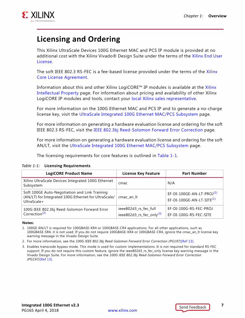
The licensing requirements for core features is outlined in Table 1-1.
Table 1-1: Licensing Requirements
LogiCORE Product Name License Key Feature Part Number
Xilinx UltraScale Devices Integrated 100G Ethernet Subsystem cmac N/A
Soft 100GE Auto-Negotiation and Link Training (AN/LT) for Integrated 100G Ethernet for UltraScale/UltraScale+
cmac_an_ltEF-DI-100GE-AN-LT-PROJ(1)
EF-DI-100GE-AN-LT-SITE(1)
100G IEEE 802.3bj Reed-Solomon Forward Error Correction(2)
ieee802d3_rs_fec_full
ieee802d3_rs_fec_only(3)EF-DI-100G-RS-FEC-PROJ
EF-DI-100G-RS-FEC-SITE
Notes: 1. 100GE AN/LT is required for 100GBASE-KR4 or 100GBASE-CR4 applications. For all other applications, such as
100GBASE-SR4, it is not used. If you do not require 100GBASE-KR4 or 100GBASE-CR4, ignore the cmac_an_lt license key warning message in the Vivado Design Suite.
2. For more information, see the 100G IEEE 802.3bj Reed-Solomon Forward Error Correction (PG197)[Ref 13].3. Enables transcode bypass mode. This mode is used for custom implementations. It is not required for standard RS-FEC
support. If you do not require this custom feature, ignore the ieee802d3_rs_fec_only license key warning message in the Vivado Design Suite. For more information, see the 100G IEEE 802.3bj Reed-Solomon Forward Error Correction (PG197)[Ref 13].
Send Feedback

Chapter 1: Overview
Integrated 100G Ethernet v2.3 8PG165 April 4, 2018 www.xilinx.com
Further licensing details are provided in Table 1-2.
Table 1-2: Licensing Details
PhysicalMedium IEEE PMD Module Interface Auto Negotiation and
Link Training
FEC Modes Required for PMD
IP License RequiredNo FEC
KR FEC RS-FEC
Chip 2 Chip N/A CEI-25G-VSR/SR/ MR/LR N/A Yes N/A Yes Included with Vivado
Backplane 100GBASE-KR4 N/A Yes N/A N/A YesEF-DI-100GE-AN-LT-PROJ
EF-100GE-RS-FEC-PROJ
Twinax Cable 100GBASE-CR4 N/A Yes N/A N/A YesEF-DI-100GE-AN-LT-PROJ
EF-100GE-RS-FEC-PROJ
100M MMF 100GBASE-SR4 CAUI-4 N/A N/A N/A Yes Included with Vivado
Parallel SMF 100GBASE-PSM4 CAUI-4 N/A N/A N/A Yes Included with Vivado
40KM SMF 100GBASE-ER4 CAUI-4 N/A N/A N/A N/A Included with Vivado
10KM SMF 100GBASE-LR4 CAUI-4 N/A N/A N/A N/A Included with Vivado
2KM SMF100GBASE-CWDM4
100GBASE-CLR4CAUI-4 N/A N/A N/A Yes Included with Vivado
Integrated 100G Ethernet v2.3 9PG165 April 4, 2018 www.xilinx.com
Chapter 2
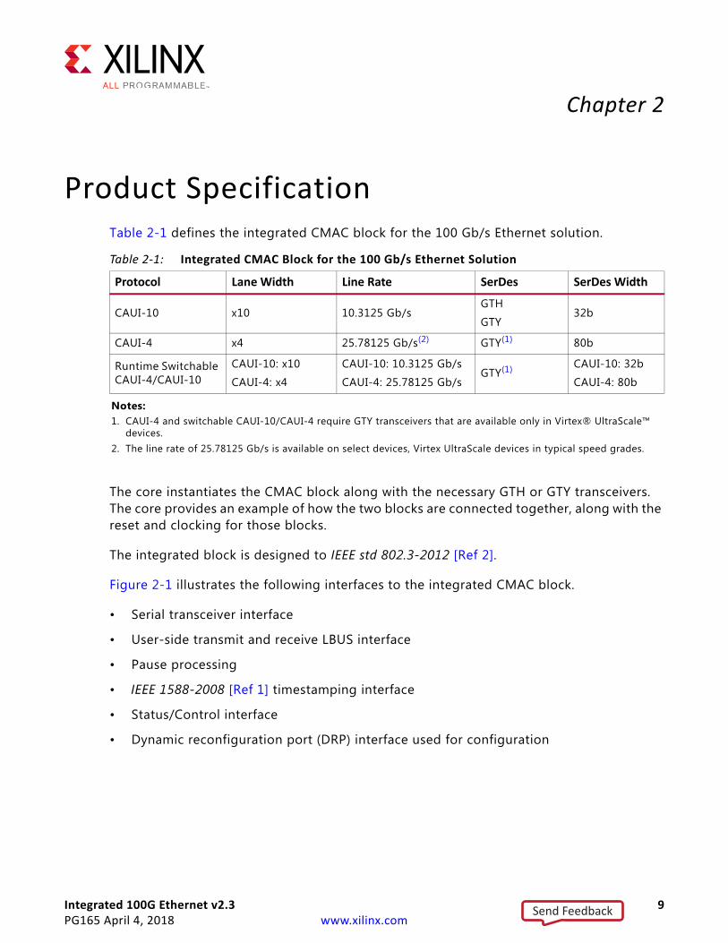
Product SpecificationTable 2-1 defines the integrated CMAC block for the 100 Gb/s Ethernet solution.
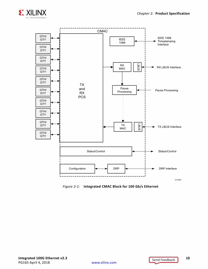
The core instantiates the CMAC block along with the necessary GTH or GTY transceivers. The core provides an example of how the two blocks are connected together, along with the reset and clocking for those blocks.
The integrated block is designed to IEEE std 802.3-2012 [Ref 2].
Figure 2-1 illustrates the following interfaces to the integrated CMAC block.
• Serial transceiver interface
• User-side transmit and receive LBUS interface
• Pause processing
• IEEE 1588-2008 [Ref 1] timestamping interface
• Status/Control interface
• Dynamic reconfiguration port (DRP) interface used for configuration
Table 2-1: Integrated CMAC Block for the 100 Gb/s Ethernet Solution
Protocol Lane Width Line Rate SerDes SerDes Width
CAUI-10 x10 10.3125 Gb/sGTH
GTY32b
CAUI-4 x4 25.78125 Gb/s(2) GTY(1) 80b
Runtime Switchable CAUI-4/CAUI-10
CAUI-10: x10
CAUI-4: x4
CAUI-10: 10.3125 Gb/s
CAUI-4: 25.78125 Gb/sGTY(1) CAUI-10: 32b
CAUI-4: 80b
Notes: 1. CAUI-4 and switchable CAUI-10/CAUI-4 require GTY transceivers that are available only in Virtex® UltraScale™
devices. 2. The line rate of 25.78125 Gb/s is available on select devices, Virtex UltraScale devices in typical speed grades.
Send Feedback
Integrated 100G Ethernet v2.3 10PG165 April 4, 2018 www.xilinx.com
Chapter 2: Product Specification
X-Ref Target - Figure 2-1
Figure 2-1: Integrated CMAC Block for 100 Gb/s Ethernet
GTH/GTY
GTH/GTY
GTH/GTY
GTH/GTY
GTH/GTY
GTH/GTY
GTH/GTY
GTH/GTY
GTH/GTY
GTH/GTY
Status/Control
TX and RX
PCS
IEEE1588
RX MAC
Pause Processing
TX MAC
LBUS
LBUS
IEEE 1588TimestampingInterface
RX LBUS Interface
TX LBUS Interface
Pause Processing
Status/Control
X13349
Configuration DRP DRP Interface
CMAC
Send Feedback
Integrated 100G Ethernet v2.3 11PG165 April 4, 2018 www.xilinx.com
Chapter 2: Product Specification
Typical OperationThe 100G Ethernet IP core handles all protocol related functions to communicate to the other devices PCS and Ethernet MAC interface. This includes handshaking, synchronizing and error checking. You provide packet data through the Local Bus (LBUS) TX interface and receive packet data from the LBUS RX interface. The LBUS is designed to match commonly used packet bus protocols made common by the SPI4.2 and Interlaken protocols. A detailed description is given in User Side LBUS Interface in Chapter 3.
The core is designed to be flexible and used in many different applications. The RX path does not perform any buffering other than the pipelining required to perform the required operations. Received data is passed directly to the user interface in a cut-through manner, allowing you the flexibility to implement any required buffering scheme. Also, the core TX path consists of a single pipeline with minimal buffering to provide reliable cut-through operation.
Statistics GatheringThe 100G Ethernet IP core provides a flexible and user-friendly mechanism for gathering statistics. For all the supported statistics, the core has an output signal (or bus if needed) that indicates an increment value for the statistic in a given clock cycle. This allows the increment value to build the required counter mechanism. This mechanism allows you to select which statistics are required in the system without having the cost overhead of a full set of counters. Additionally, and more importantly, you can implement any counter and statistics gathering mechanism required by the system. For example, you can build 32-bit or 64-bit counters as needed, or implement clear-on-read or saturated counters, as required.
For the purposes of TX statistics, good packets are defined as packets without FCS or other errors; bad packets are defined as packets with FCS or any other error.
For the purposes of RX statistics, good packets are defined as packets without FCS or other errors including length error. Bad packets are defined as packets with FCS or any other error. The length field error includes length field error, oversize and undersize packets.
Testability FunctionsThe 100G Ethernet example design implements the test pattern generation and checking as defined in Clause 82.2.10 (Test-pattern generators) and Clause 82.2.17 (Test-pattern checker). See the IEEE 802.3 documents for details.
Send Feedback
Integrated 100G Ethernet v2.3 12PG165 April 4, 2018 www.xilinx.com
Chapter 2: Product Specification
Pause OperationThe 100G Ethernet IP core is capable of handling 802.3x and priority-based pause operation. The RX path parses pause packets and presents the extracted quanta on the status interface; the TX path can accept pause packet requests from the control interface and will inject the requested packets into the data stream. Both global pause packets and priority-based pause packets are handled. Details are described in Pause Processing Interface in Chapter 3.
Note: “802.3x” and “global pause” are used interchangeably throughout the document.
StandardsThe 100G Ethernet IP core is designed to be compliant with the IEEE std 802.3-2012 [Ref 2] specification. The timestamping feature is designed to be compliant with IEEE 1588-2008 [Ref 1].
PerformanceThe 100G Ethernet IP core is designed to operate with the performance characteristics of the CMAC primitive it instantiates.
See the Virtex UltraScale Architecture Data Sheet: DC and AC Switching Characteristics (DS893) [Ref 3] for the maximum frequencies allowed on the 100G Ethernet IP core specified by speed grade.
IMPORTANT: A free-running clock input, init_clk, is required for the transceiver portion of the 100G Ethernet IP core. See the UltraScale FPGAs Transceiver Wizards (PG182) [Ref 4] for more information on the gtwiz_reset_clk_freerun_in input port.
Resource UtilizationFor full details about performance and resource utilization, visit Performance and Resource Utilization.
Send Feedback
Chapter 2: Product Specification
Integrated 100G Ethernet v2.3 13PG165 April 4, 2018 www.xilinx.com
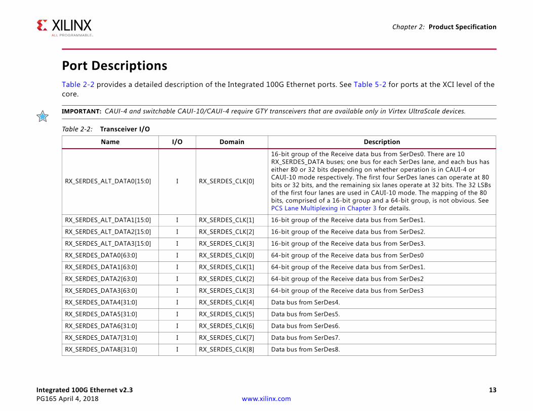
Port DescriptionsTable 2-2 provides a detailed description of the Integrated 100G Ethernet ports. See Table 5-2 for ports at the XCI level of the core.
IMPORTANT: CAUI-4 and switchable CAUI-10/CAUI-4 require GTY transceivers that are available only in Virtex UltraScale devices.
Table 2-2: Transceiver I/O
Name I/O Domain Description
RX_SERDES_ALT_DATA0[15:0] I RX_SERDES_CLK[0]
16-bit group of the Receive data bus from SerDes0. There are 10 RX_SERDES_DATA buses; one bus for each SerDes lane, and each bus has either 80 or 32 bits depending on whether operation is in CAUI-4 or CAUI-10 mode respectively. The first four SerDes lanes can operate at 80 bits or 32 bits, and the remaining six lanes operate at 32 bits. The 32 LSBs of the first four lanes are used in CAUI-10 mode. The mapping of the 80 bits, comprised of a 16-bit group and a 64-bit group, is not obvious. See PCS Lane Multiplexing in Chapter 3 for details.
RX_SERDES_ALT_DATA1[15:0] I RX_SERDES_CLK[1] 16-bit group of the Receive data bus from SerDes1.
RX_SERDES_ALT_DATA2[15:0] I RX_SERDES_CLK[2] 16-bit group of the Receive data bus from SerDes2.
RX_SERDES_ALT_DATA3[15:0] I RX_SERDES_CLK[3] 16-bit group of the Receive data bus from SerDes3.
RX_SERDES_DATA0[63:0] I RX_SERDES_CLK[0] 64-bit group of the Receive data bus from SerDes0
RX_SERDES_DATA1[63:0] I RX_SERDES_CLK[1] 64-bit group of the Receive data bus from SerDes1.
RX_SERDES_DATA2[63:0] I RX_SERDES_CLK[2] 64-bit group of the Receive data bus from SerDes2
RX_SERDES_DATA3[63:0] I RX_SERDES_CLK[3] 64-bit group of the Receive data bus from SerDes3
RX_SERDES_DATA4[31:0] I RX_SERDES_CLK[4] Data bus from SerDes4.
RX_SERDES_DATA5[31:0] I RX_SERDES_CLK[5] Data bus from SerDes5.
RX_SERDES_DATA6[31:0] I RX_SERDES_CLK[6] Data bus from SerDes6.
RX_SERDES_DATA7[31:0] I RX_SERDES_CLK[7] Data bus from SerDes7.
RX_SERDES_DATA8[31:0] I RX_SERDES_CLK[8] Data bus from SerDes8.
Chapter 2: Product Specification
Integrated 100G Ethernet v2.3 14PG165 April 4, 2018 www.xilinx.com
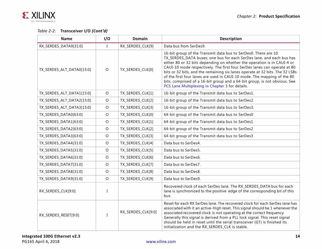
RX_SERDES_DATA9[31:0] I RX_SERDES_CLK[9] Data bus from SerDes9.
TX_SERDES_ALT_DATA0[15:0] O TX_SERDES_CLK[0]
16-bit group of the Transmit data bus to SerDes0. There are 10 TX_SERDES_DATA buses; one bus for each SerDes lane, and each bus has either 80 or 32 bits depending on whether the operation is in CAUI-4 or CAUI-10 mode respectively. The first four SerDes lanes can operate at 80 bits or 32 bits, and the remaining six lanes operate at 32 bits. The 32 LSBs of the first four lanes are used in CAUI-10 mode. The mapping of the 80 bits, comprised of a 16-bit group and a 64-bit group, is not obvious. See PCS Lane Multiplexing in Chapter 3 for details.
TX_SERDES_ALT_DATA1[15:0] O TX_SERDES_CLK[1] 16-bit group of the Transmit data bus to SerDes1.
TX_SERDES_ALT_DATA2[15:0] O TX_SERDES_CLK[2] 16-bit group of the Transmit data bus to SerDes2.
TX_SERDES_ALT_DATA3[15:0] O TX_SERDES_CLK[3] 16-bit group of the Transmit data bus to SerDes3.
TX_SERDES_DATA0[63:0] O TX_SERDES_CLK[0] 64-bit group of the Transmit data bus to SerDes0
TX_SERDES_DATA1[63:0] O TX_SERDES_CLK[1] 64-bit group of the Transmit data bus to SerDes1
TX_SERDES_DATA2[63:0] O TX_SERDES_CLK[2] 64-bit group of the Transmit data bus to SerDes2
TX_SERDES_DATA3[63:0] O TX_SERDES_CLK[3] 64-bit group of the Transmit data bus to SerDes3
TX_SERDES_DATA4[31:0] O TX_SERDES_CLK[4] Data bus to SerDes4.
TX_SERDES_DATA5[31:0] O TX_SERDES_CLK[5] Data bus to SerDes5.
TX_SERDES_DATA6[31:0] O TX_SERDES_CLK[6] Data bus to SerDes6.
TX_SERDES_DATA7[31:0] O TX_SERDES_CLK[7] Data bus to SerDes7.
TX_SERDES_DATA8[31:0] O TX_SERDES_CLK[8] Data bus to SerDes8.
TX_SERDES_DATA9[31:0] O TX_SERDES_CLK[9] Data bus to SerDes9.
RX_SERDES_CLK[9:0] IRecovered clock of each SerDes lane. The RX_SERDES_DATA bus for each lane is synchronized to the positive edge of the corresponding bit of this bus.
RX_SERDES_RESET[9:0] IRX_SERDES_CLK[9:0]
Reset for each RX SerDes lane. The recovered clock for each SerDes lane has associated with it an active-High reset. This signal should be 1 whenever the associated recovered clock is not operating at the correct frequency. Generally this signal is derived from a PLL lock signal. This reset signal should be held in reset until the serial transceiver (GT) is finished its initialization and the RX_SERDES_CLK is stable.
Table 2-2: Transceiver I/O (Cont’d)
Name I/O Domain Description
Integrated 100G Ethernet v2.3 15PG165 April 4, 2018 www.xilinx.com
Chapter 2: Product Specification
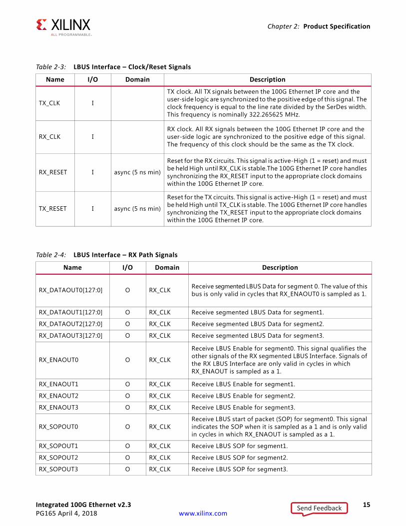
Table 2-3: LBUS Interface – Clock/Reset Signals
Name I/O Domain Description
TX_CLK I
TX clock. All TX signals between the 100G Ethernet IP core and the user-side logic are synchronized to the positive edge of this signal. The clock frequency is equal to the line rate divided by the SerDes width. This frequency is nominally 322.265625 MHz.
RX_CLK IRX clock. All RX signals between the 100G Ethernet IP core and the user-side logic are synchronized to the positive edge of this signal. The frequency of this clock should be the same as the TX clock.
RX_RESET I async (5 ns min)
Reset for the RX circuits. This signal is active-High (1 = reset) and must be held High until RX_CLK is stable.The 100G Ethernet IP core handles synchronizing the RX_RESET input to the appropriate clock domains within the 100G Ethernet IP core.
TX_RESET I async (5 ns min)
Reset for the TX circuits. This signal is active-High (1 = reset) and must be held High until TX_CLK is stable. The 100G Ethernet IP core handles synchronizing the TX_RESET input to the appropriate clock domains within the 100G Ethernet IP core.
Table 2-4: LBUS Interface – RX Path Signals
Name I/O Domain Description
RX_DATAOUT0[127:0] O RX_CLK Receive segmented LBUS Data for segment 0. The value of this bus is only valid in cycles that RX_ENAOUT0 is sampled as 1.
RX_DATAOUT1[127:0] O RX_CLK Receive segmented LBUS Data for segment1.
RX_DATAOUT2[127:0] O RX_CLK Receive segmented LBUS Data for segment2.
RX_DATAOUT3[127:0] O RX_CLK Receive segmented LBUS Data for segment3.
RX_ENAOUT0 O RX_CLK
Receive LBUS Enable for segment0. This signal qualifies the other signals of the RX segmented LBUS Interface. Signals of the RX LBUS Interface are only valid in cycles in which RX_ENAOUT is sampled as a 1.
RX_ENAOUT1 O RX_CLK Receive LBUS Enable for segment1.
RX_ENAOUT2 O RX_CLK Receive LBUS Enable for segment2.
RX_ENAOUT3 O RX_CLK Receive LBUS Enable for segment3.
RX_SOPOUT0 O RX_CLKReceive LBUS start of packet (SOP) for segment0. This signal indicates the SOP when it is sampled as a 1 and is only valid in cycles in which RX_ENAOUT is sampled as a 1.
RX_SOPOUT1 O RX_CLK Receive LBUS SOP for segment1.
RX_SOPOUT2 O RX_CLK Receive LBUS SOP for segment2.
RX_SOPOUT3 O RX_CLK Receive LBUS SOP for segment3.
Send Feedback
Integrated 100G Ethernet v2.3 16PG165 April 4, 2018 www.xilinx.com
Chapter 2: Product Specification
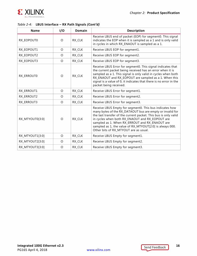
RX_EOPOUT0 O RX_CLKReceive LBUS end of packet (EOP) for segment0. This signal indicates the EOP when it is sampled as a 1 and is only valid in cycles in which RX_ENAOUT is sampled as a 1.
RX_EOPOUT1 O RX_CLK Receive LBUS EOP for segment1.
RX_EOPOUT2 O RX_CLK Receive LBUS EOP for segment2.
RX_EOPOUT3 O RX_CLK Receive LBUS EOP for segment3.
RX_ERROUT0 O RX_CLK
Receive LBUS Error for segment0. This signal indicates that the current packet being received has an error when it is sampled as a 1. This signal is only valid in cycles when both RX_ENAOUT and RX_EOPOUT are sampled as a 1. When this signal is a value of 0, it indicates that there is no error in the packet being received.
RX_ERROUT1 O RX_CLK Receive LBUS Error for segment1.
RX_ERROUT2 O RX_CLK Receive LBUS Error for segment2.
RX_ERROUT3 O RX_CLK Receive LBUS Error for segment3.
RX_MTYOUT0[3:0] O RX_CLK
Receive LBUS Empty for segment0. This bus indicates how many bytes of the RX_DATAOUT bus are empty or invalid for the last transfer of the current packet. This bus is only valid in cycles when both RX_ENAOUT and RX_EOPOUT are sampled as 1. When RX_ERROUT and RX_ENAOUT are sampled as 1, the value of RX_MTYOUT[2:0] is always 000. Other bits of RX_MTYOUT are as usual.
RX_MTYOUT1[3:0] O RX_CLK Receive LBUS Empty for segment1.
RX_MTYOUT2[3:0] O RX_CLK Receive LBUS Empty for segment2.
RX_MTYOUT3[3:0] O RX_CLK Receive LBUS Empty for segment3.
Table 2-4: LBUS Interface – RX Path Signals (Cont’d)
Name I/O Domain Description
Send Feedback
Integrated 100G Ethernet v2.3 17PG165 April 4, 2018 www.xilinx.com
Chapter 2: Product Specification
Table 2-5: LBUS Interface – TX Path Signals
Name I/O Domain Description
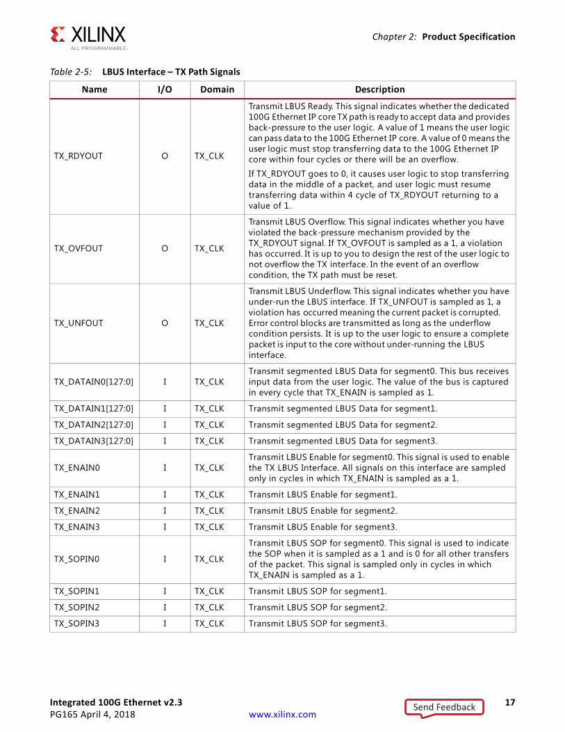
TX_RDYOUT O TX_CLK
Transmit LBUS Ready. This signal indicates whether the dedicated 100G Ethernet IP core TX path is ready to accept data and provides back-pressure to the user logic. A value of 1 means the user logic can pass data to the 100G Ethernet IP core. A value of 0 means the user logic must stop transferring data to the 100G Ethernet IP core within four cycles or there will be an overflow.
If TX_RDYOUT goes to 0, it causes user logic to stop transferring data in the middle of a packet, and user logic must resume transferring data within 4 cycle of TX_RDYOUT returning to a value of 1.
TX_OVFOUT O TX_CLK
Transmit LBUS Overflow. This signal indicates whether you have violated the back-pressure mechanism provided by the TX_RDYOUT signal. If TX_OVFOUT is sampled as a 1, a violation has occurred. It is up to you to design the rest of the user logic to not overflow the TX interface. In the event of an overflow condition, the TX path must be reset.
TX_UNFOUT O TX_CLK
Transmit LBUS Underflow. This signal indicates whether you have under-run the LBUS interface. If TX_UNFOUT is sampled as 1, a violation has occurred meaning the current packet is corrupted. Error control blocks are transmitted as long as the underflow condition persists. It is up to the user logic to ensure a complete packet is input to the core without under-running the LBUS interface.
TX_DATAIN0[127:0] I TX_CLKTransmit segmented LBUS Data for segment0. This bus receives input data from the user logic. The value of the bus is captured in every cycle that TX_ENAIN is sampled as 1.
TX_DATAIN1[127:0] I TX_CLK Transmit segmented LBUS Data for segment1.
TX_DATAIN2[127:0] I TX_CLK Transmit segmented LBUS Data for segment2.
TX_DATAIN3[127:0] I TX_CLK Transmit segmented LBUS Data for segment3.
TX_ENAIN0 I TX_CLKTransmit LBUS Enable for segment0. This signal is used to enable the TX LBUS Interface. All signals on this interface are sampled only in cycles in which TX_ENAIN is sampled as a 1.
TX_ENAIN1 I TX_CLK Transmit LBUS Enable for segment1.
TX_ENAIN2 I TX_CLK Transmit LBUS Enable for segment2.
TX_ENAIN3 I TX_CLK Transmit LBUS Enable for segment3.
TX_SOPIN0 I TX_CLK
Transmit LBUS SOP for segment0. This signal is used to indicate the SOP when it is sampled as a 1 and is 0 for all other transfers of the packet. This signal is sampled only in cycles in which TX_ENAIN is sampled as a 1.
TX_SOPIN1 I TX_CLK Transmit LBUS SOP for segment1.
TX_SOPIN2 I TX_CLK Transmit LBUS SOP for segment2.
TX_SOPIN3 I TX_CLK Transmit LBUS SOP for segment3.
Send Feedback
Integrated 100G Ethernet v2.3 18PG165 April 4, 2018 www.xilinx.com
Chapter 2: Product Specification
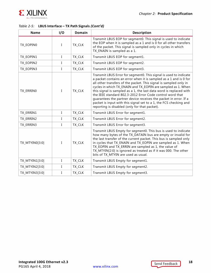
TX_EOPIN0 I TX_CLK
Transmit LBUS EOP for segment0. This signal is used to indicate the EOP when it is sampled as a 1 and is 0 for all other transfers of the packet. This signal is sampled only in cycles in which TX_ENAIN is sampled as a 1.
TX_EOPIN1 I TX_CLK Transmit LBUS EOP for segment1.
TX_EOPIN2 I TX_CLK Transmit LBUS EOP for segment2.
TX_EOPIN3 I TX_CLK Transmit LBUS EOP for segment3.
TX_ERRIN0 I TX_CLK
Transmit LBUS Error for segment0. This signal is used to indicate a packet contains an error when it is sampled as a 1 and is 0 for all other transfers of the packet. This signal is sampled only in cycles in which TX_ENAIN and TX_EOPIN are sampled as 1. When this signal is sampled as a 1, the last data word is replaced with the IEEE standard 802.3-2012 Error Code control word that guarantees the partner device receives the packet in error. If a packet is input with this signal set to a 1, the FCS checking and reporting is disabled (only for that packet).
TX_ERRIN1 I TX_CLK Transmit LBUS Error for segment1.
TX_ERRIN2 I TX_CLK Transmit LBUS Error for segment2.
TX_ERRIN3 I TX_CLK Transmit LBUS Error for segment3.
TX_MTYIN0[3:0] I TX_CLK
Transmit LBUS Empty for segment0. This bus is used to indicate how many bytes of the TX_DATAIN bus are empty or invalid for the last transfer of the current packet. This bus is sampled only in cycles that TX_ENAIN and TX_EOPIN are sampled as 1. When TX_EOPIN and TX_ERRIN are sampled as 1, the value of TX_MTYIN[2:0] is ignored as treated as if it was 000. The other bits of TX_MTYIN are used as usual.
TX_MTYIN1[3:0] I TX_CLK Transmit LBUS Empty for segment1.
TX_MTYIN2[3:0] I TX_CLK Transmit LBUS Empty for segment2.
TX_MTYIN3[3:0] I TX_CLK Transmit LBUS Empty for segment3.
Table 2-5: LBUS Interface – TX Path Signals (Cont’d)
Name I/O Domain Description
Send Feedback
Integrated 100G Ethernet v2.3 19PG165 April 4, 2018 www.xilinx.com
Chapter 2: Product Specification
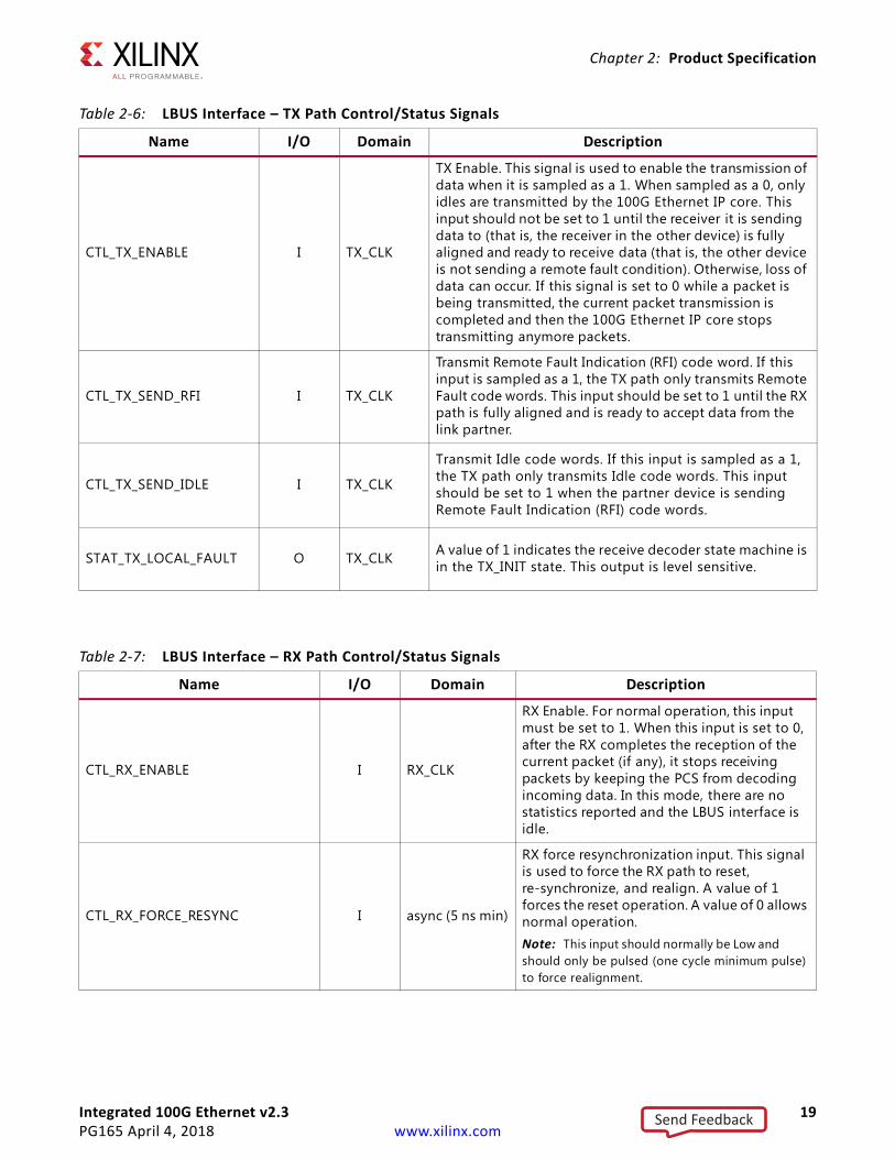
Table 2-6: LBUS Interface – TX Path Control/Status Signals
Name I/O Domain Description
CTL_TX_ENABLE I TX_CLK
TX Enable. This signal is used to enable the transmission of data when it is sampled as a 1. When sampled as a 0, only idles are transmitted by the 100G Ethernet IP core. This input should not be set to 1 until the receiver it is sending data to (that is, the receiver in the other device) is fully aligned and ready to receive data (that is, the other device is not sending a remote fault condition). Otherwise, loss of data can occur. If this signal is set to 0 while a packet is being transmitted, the current packet transmission is completed and then the 100G Ethernet IP core stops transmitting anymore packets.
CTL_TX_SEND_RFI I TX_CLK
Transmit Remote Fault Indication (RFI) code word. If this input is sampled as a 1, the TX path only transmits Remote Fault code words. This input should be set to 1 until the RX path is fully aligned and is ready to accept data from the link partner.
CTL_TX_SEND_IDLE I TX_CLK
Transmit Idle code words. If this input is sampled as a 1, the TX path only transmits Idle code words. This input should be set to 1 when the partner device is sending Remote Fault Indication (RFI) code words.
STAT_TX_LOCAL_FAULT O TX_CLK A value of 1 indicates the receive decoder state machine is in the TX_INIT state. This output is level sensitive.
Table 2-7: LBUS Interface – RX Path Control/Status Signals
Name I/O Domain Description
CTL_RX_ENABLE I RX_CLK
RX Enable. For normal operation, this input must be set to 1. When this input is set to 0, after the RX completes the reception of the current packet (if any), it stops receiving packets by keeping the PCS from decoding incoming data. In this mode, there are no statistics reported and the LBUS interface is idle.
CTL_RX_FORCE_RESYNC I async (5 ns min)
RX force resynchronization input. This signal is used to force the RX path to reset, re-synchronize, and realign. A value of 1 forces the reset operation. A value of 0 allows normal operation. Note: This input should normally be Low and should only be pulsed (one cycle minimum pulse) to force realignment.
Send Feedback
Integrated 100G Ethernet v2.3 20PG165 April 4, 2018 www.xilinx.com
Chapter 2: Product Specification
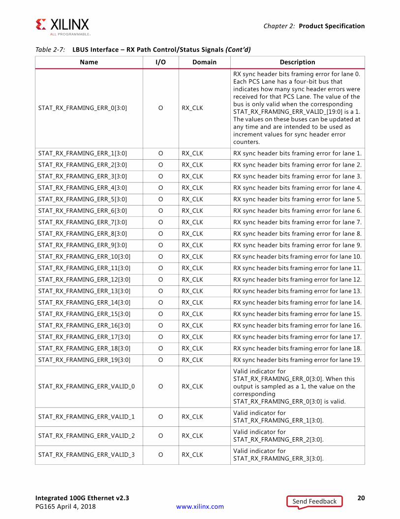
STAT_RX_FRAMING_ERR_0[3:0] O RX_CLK
RX sync header bits framing error for lane 0. Each PCS Lane has a four-bit bus that indicates how many sync header errors were received for that PCS Lane. The value of the bus is only valid when the corresponding STAT_RX_FRAMING_ERR_VALID_[19:0] is a 1. The values on these buses can be updated at any time and are intended to be used as increment values for sync header error counters.
STAT_RX_FRAMING_ERR_1[3:0] O RX_CLK RX sync header bits framing error for lane 1.
STAT_RX_FRAMING_ERR_2[3:0] O RX_CLK RX sync header bits framing error for lane 2.
STAT_RX_FRAMING_ERR_3[3:0] O RX_CLK RX sync header bits framing error for lane 3.
STAT_RX_FRAMING_ERR_4[3:0] O RX_CLK RX sync header bits framing error for lane 4.
STAT_RX_FRAMING_ERR_5[3:0] O RX_CLK RX sync header bits framing error for lane 5.
STAT_RX_FRAMING_ERR_6[3:0] O RX_CLK RX sync header bits framing error for lane 6.
STAT_RX_FRAMING_ERR_7[3:0] O RX_CLK RX sync header bits framing error for lane 7.
STAT_RX_FRAMING_ERR_8[3:0] O RX_CLK RX sync header bits framing error for lane 8.
STAT_RX_FRAMING_ERR_9[3:0] O RX_CLK RX sync header bits framing error for lane 9.
STAT_RX_FRAMING_ERR_10[3:0] O RX_CLK RX sync header bits framing error for lane 10.
STAT_RX_FRAMING_ERR_11[3:0] O RX_CLK RX sync header bits framing error for lane 11.
STAT_RX_FRAMING_ERR_12[3:0] O RX_CLK RX sync header bits framing error for lane 12.
STAT_RX_FRAMING_ERR_13[3:0] O RX_CLK RX sync header bits framing error for lane 13.
STAT_RX_FRAMING_ERR_14[3:0] O RX_CLK RX sync header bits framing error for lane 14.
STAT_RX_FRAMING_ERR_15[3:0] O RX_CLK RX sync header bits framing error for lane 15.
STAT_RX_FRAMING_ERR_16[3:0] O RX_CLK RX sync header bits framing error for lane 16.
STAT_RX_FRAMING_ERR_17[3:0] O RX_CLK RX sync header bits framing error for lane 17.
STAT_RX_FRAMING_ERR_18[3:0] O RX_CLK RX sync header bits framing error for lane 18.
STAT_RX_FRAMING_ERR_19[3:0] O RX_CLK RX sync header bits framing error for lane 19.
STAT_RX_FRAMING_ERR_VALID_0 O RX_CLK
Valid indicator for STAT_RX_FRAMING_ERR_0[3:0]. When this output is sampled as a 1, the value on the corresponding STAT_RX_FRAMING_ERR_0[3:0] is valid.
STAT_RX_FRAMING_ERR_VALID_1 O RX_CLK Valid indicator for STAT_RX_FRAMING_ERR_1[3:0].
STAT_RX_FRAMING_ERR_VALID_2 O RX_CLK Valid indicator for STAT_RX_FRAMING_ERR_2[3:0].
STAT_RX_FRAMING_ERR_VALID_3 O RX_CLK Valid indicator for STAT_RX_FRAMING_ERR_3[3:0].
Table 2-7: LBUS Interface – RX Path Control/Status Signals (Cont’d)
Name I/O Domain Description
Send Feedback
Integrated 100G Ethernet v2.3 21PG165 April 4, 2018 www.xilinx.com
Chapter 2: Product Specification
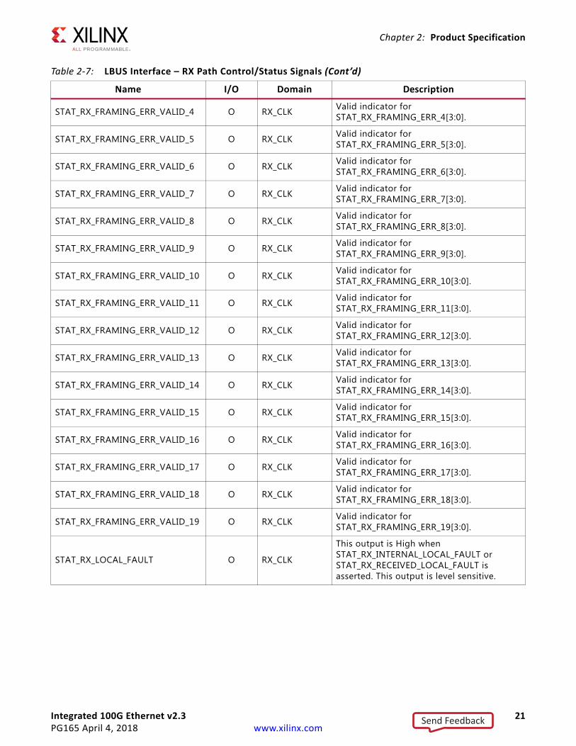
STAT_RX_FRAMING_ERR_VALID_4 O RX_CLK Valid indicator for STAT_RX_FRAMING_ERR_4[3:0].
STAT_RX_FRAMING_ERR_VALID_5 O RX_CLK Valid indicator for STAT_RX_FRAMING_ERR_5[3:0].
STAT_RX_FRAMING_ERR_VALID_6 O RX_CLK Valid indicator for STAT_RX_FRAMING_ERR_6[3:0].
STAT_RX_FRAMING_ERR_VALID_7 O RX_CLK Valid indicator for STAT_RX_FRAMING_ERR_7[3:0].
STAT_RX_FRAMING_ERR_VALID_8 O RX_CLK Valid indicator for STAT_RX_FRAMING_ERR_8[3:0].
STAT_RX_FRAMING_ERR_VALID_9 O RX_CLK Valid indicator for STAT_RX_FRAMING_ERR_9[3:0].
STAT_RX_FRAMING_ERR_VALID_10 O RX_CLK Valid indicator for STAT_RX_FRAMING_ERR_10[3:0].
STAT_RX_FRAMING_ERR_VALID_11 O RX_CLK Valid indicator for STAT_RX_FRAMING_ERR_11[3:0].
STAT_RX_FRAMING_ERR_VALID_12 O RX_CLK Valid indicator for STAT_RX_FRAMING_ERR_12[3:0].
STAT_RX_FRAMING_ERR_VALID_13 O RX_CLK Valid indicator for STAT_RX_FRAMING_ERR_13[3:0].
STAT_RX_FRAMING_ERR_VALID_14 O RX_CLK Valid indicator for STAT_RX_FRAMING_ERR_14[3:0].
STAT_RX_FRAMING_ERR_VALID_15 O RX_CLK Valid indicator for STAT_RX_FRAMING_ERR_15[3:0].
STAT_RX_FRAMING_ERR_VALID_16 O RX_CLK Valid indicator for STAT_RX_FRAMING_ERR_16[3:0].
STAT_RX_FRAMING_ERR_VALID_17 O RX_CLK Valid indicator for STAT_RX_FRAMING_ERR_17[3:0].
STAT_RX_FRAMING_ERR_VALID_18 O RX_CLK Valid indicator for STAT_RX_FRAMING_ERR_18[3:0].
STAT_RX_FRAMING_ERR_VALID_19 O RX_CLK Valid indicator for STAT_RX_FRAMING_ERR_19[3:0].
STAT_RX_LOCAL_FAULT O RX_CLK
This output is High when STAT_RX_INTERNAL_LOCAL_FAULT or STAT_RX_RECEIVED_LOCAL_FAULT is asserted. This output is level sensitive.
Table 2-7: LBUS Interface – RX Path Control/Status Signals (Cont’d)
Name I/O Domain Description
Send Feedback
Integrated 100G Ethernet v2.3 22PG165 April 4, 2018 www.xilinx.com
Chapter 2: Product Specification
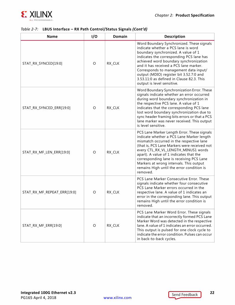
STAT_RX_SYNCED[19:0] O RX_CLK
Word Boundary Synchronized. These signals indicate whether a PCS lane is word boundary synchronized. A value of 1 indicates the corresponding PCS lane has achieved word boundary synchronization and it has received a PCS lane marker. Corresponds to management data input/output (MDIO) register bit 3.52.7:0 and 3.53.11:0 as defined in Clause 82.3. This output is level sensitive.
STAT_RX_SYNCED_ERR[19:0] O RX_CLK
Word Boundary Synchronization Error. These signals indicate whether an error occurred during word boundary synchronization in the respective PCS lane. A value of 1 indicates that the corresponding PCS lane lost word boundary synchronization due to sync header framing bits errors or that a PCS lane marker was never received. This output is level sensitive.
STAT_RX_MF_LEN_ERR[19:0] O RX_CLK
PCS Lane Marker Length Error. These signals indicate whether a PCS Lane Marker length mismatch occurred in the respective lane (that is, PCS Lane Markers were received not every CTL_RX_VL_LENGTH_MINUS1 words apart). A value of 1 indicates that the corresponding lane is receiving PCS Lane Markers at wrong intervals. This output remains High until the error condition is removed.
STAT_RX_MF_REPEAT_ERR[19:0] O RX_CLK
PCS Lane Marker Consecutive Error. These signals indicate whether four consecutive PCS Lane Marker errors occurred in the respective lane. A value of 1 indicates an error in the corresponding lane. This output remains High until the error condition is removed.
STAT_RX_MF_ERR[19:0] O RX_CLK
PCS Lane Marker Word Error. These signals indicate that an incorrectly formed PCS Lane Marker Word was detected in the respective lane. A value of 1 indicates an error occurred. This output is pulsed for one clock cycle to indicate the error condition. Pulses can occur in back-to-back cycles.
Table 2-7: LBUS Interface – RX Path Control/Status Signals (Cont’d)
Name I/O Domain Description
Send Feedback
Integrated 100G Ethernet v2.3 23PG165 April 4, 2018 www.xilinx.com
Chapter 2: Product Specification
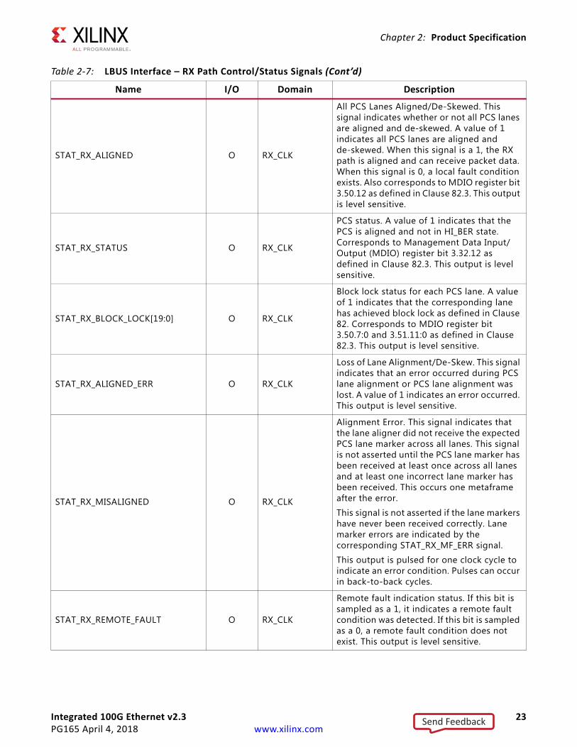
STAT_RX_ALIGNED O RX_CLK
All PCS Lanes Aligned/De-Skewed. This signal indicates whether or not all PCS lanes are aligned and de-skewed. A value of 1 indicates all PCS lanes are aligned and de-skewed. When this signal is a 1, the RX path is aligned and can receive packet data. When this signal is 0, a local fault condition exists. Also corresponds to MDIO register bit 3.50.12 as defined in Clause 82.3. This output is level sensitive.
STAT_RX_STATUS O RX_CLK
PCS status. A value of 1 indicates that the PCS is aligned and not in HI_BER state. Corresponds to Management Data Input/Output (MDIO) register bit 3.32.12 as defined in Clause 82.3. This output is level sensitive.
STAT_RX_BLOCK_LOCK[19:0] O RX_CLK
Block lock status for each PCS lane. A value of 1 indicates that the corresponding lane has achieved block lock as defined in Clause 82. Corresponds to MDIO register bit 3.50.7:0 and 3.51.11:0 as defined in Clause 82.3. This output is level sensitive.
STAT_RX_ALIGNED_ERR O RX_CLK
Loss of Lane Alignment/De-Skew. This signal indicates that an error occurred during PCS lane alignment or PCS lane alignment was lost. A value of 1 indicates an error occurred. This output is level sensitive.
STAT_RX_MISALIGNED O RX_CLK
Alignment Error. This signal indicates that the lane aligner did not receive the expected PCS lane marker across all lanes. This signal is not asserted until the PCS lane marker has been received at least once across all lanes and at least one incorrect lane marker has been received. This occurs one metaframe after the error.
This signal is not asserted if the lane markers have never been received correctly. Lane marker errors are indicated by the corresponding STAT_RX_MF_ERR signal.
This output is pulsed for one clock cycle to indicate an error condition. Pulses can occur in back-to-back cycles.
STAT_RX_REMOTE_FAULT O RX_CLK
Remote fault indication status. If this bit is sampled as a 1, it indicates a remote fault condition was detected. If this bit is sampled as a 0, a remote fault condition does not exist. This output is level sensitive.
Table 2-7: LBUS Interface – RX Path Control/Status Signals (Cont’d)
Name I/O Domain Description
Send Feedback
Integrated 100G Ethernet v2.3 24PG165 April 4, 2018 www.xilinx.com
Chapter 2: Product Specification
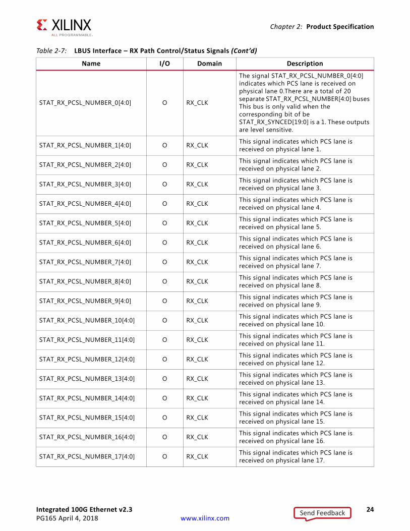
STAT_RX_PCSL_NUMBER_0[4:0] O RX_CLK
The signal STAT_RX_PCSL_NUMBER_0[4:0] indicates which PCS lane is received on physical lane 0.There are a total of 20 separate STAT_RX_PCSL_NUMBER[4:0] buses This bus is only valid when the corresponding bit of be STAT_RX_SYNCED[19:0] is a 1. These outputs are level sensitive.
STAT_RX_PCSL_NUMBER_1[4:0] O RX_CLK This signal indicates which PCS lane is received on physical lane 1.
STAT_RX_PCSL_NUMBER_2[4:0] O RX_CLK This signal indicates which PCS lane is received on physical lane 2.
STAT_RX_PCSL_NUMBER_3[4:0] O RX_CLK This signal indicates which PCS lane is received on physical lane 3.
STAT_RX_PCSL_NUMBER_4[4:0] O RX_CLK This signal indicates which PCS lane is received on physical lane 4.
STAT_RX_PCSL_NUMBER_5[4:0] O RX_CLK This signal indicates which PCS lane is received on physical lane 5.
STAT_RX_PCSL_NUMBER_6[4:0] O RX_CLK This signal indicates which PCS lane is received on physical lane 6.
STAT_RX_PCSL_NUMBER_7[4:0] O RX_CLK This signal indicates which PCS lane is received on physical lane 7.
STAT_RX_PCSL_NUMBER_8[4:0] O RX_CLK This signal indicates which PCS lane is received on physical lane 8.
STAT_RX_PCSL_NUMBER_9[4:0] O RX_CLK This signal indicates which PCS lane is received on physical lane 9.
STAT_RX_PCSL_NUMBER_10[4:0] O RX_CLK This signal indicates which PCS lane is received on physical lane 10.
STAT_RX_PCSL_NUMBER_11[4:0] O RX_CLK This signal indicates which PCS lane is received on physical lane 11.
STAT_RX_PCSL_NUMBER_12[4:0] O RX_CLK This signal indicates which PCS lane is received on physical lane 12.
STAT_RX_PCSL_NUMBER_13[4:0] O RX_CLK This signal indicates which PCS lane is received on physical lane 13.
STAT_RX_PCSL_NUMBER_14[4:0] O RX_CLK This signal indicates which PCS lane is received on physical lane 14.
STAT_RX_PCSL_NUMBER_15[4:0] O RX_CLK This signal indicates which PCS lane is received on physical lane 15.
STAT_RX_PCSL_NUMBER_16[4:0] O RX_CLK This signal indicates which PCS lane is received on physical lane 16.
STAT_RX_PCSL_NUMBER_17[4:0] O RX_CLK This signal indicates which PCS lane is received on physical lane 17.
Table 2-7: LBUS Interface – RX Path Control/Status Signals (Cont’d)
Name I/O Domain Description
Send Feedback
Integrated 100G Ethernet v2.3 25PG165 April 4, 2018 www.xilinx.com
Chapter 2: Product Specification
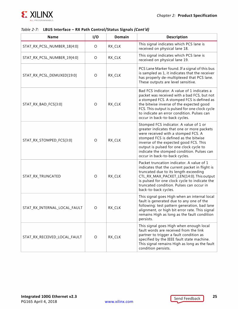
STAT_RX_PCSL_NUMBER_18[4:0] O RX_CLK This signal indicates which PCS lane is received on physical lane 18.
STAT_RX_PCSL_NUMBER_19[4:0] O RX_CLK This signal indicates which PCS lane is received on physical lane 19.
STAT_RX_PCSL_DEMUXED[19:0] O RX_CLK
PCS Lane Marker found. If a signal of this bus is sampled as 1, it indicates that the receiver has properly de-multiplexed that PCS lane. These outputs are level sensitive.
STAT_RX_BAD_FCS[3:0] O RX_CLK
Bad FCS indicator. A value of 1 indicates a packet was received with a bad FCS, but not a stomped FCS. A stomped FCS is defined as the bitwise inverse of the expected good FCS. This output is pulsed for one clock cycle to indicate an error condition. Pulses can occur in back-to-back cycles.
STAT_RX_STOMPED_FCS[3:0] O RX_CLK
Stomped FCS indicator. A value of 1 or greater indicates that one or more packets were received with a stomped FCS. A stomped FCS is defined as the bitwise inverse of the expected good FCS. This output is pulsed for one clock cycle to indicate the stomped condition. Pulses can occur in back-to-back cycles.
STAT_RX_TRUNCATED O RX_CLK
Packet truncation indicator. A value of 1 indicates that the current packet in flight is truncated due to its length exceeding CTL_RX_MAX_PACKET_LEN[14:0]. This output is pulsed for one clock cycle to indicate the truncated condition. Pulses can occur in back-to-back cycles.
STAT_RX_INTERNAL_LOCAL_FAULT O RX_CLK
This signal goes High when an internal local fault is generated due to any one of the following: test pattern generation, bad lane alignment, or high bit error rate. This signal remains High as long as the fault condition persists.
STAT_RX_RECEIVED_LOCAL_FAULT O RX_CLK
This signal goes High when enough local fault words are received from the link partner to trigger a fault condition as specified by the IEEE fault state machine. This signal remains High as long as the fault condition persists.
Table 2-7: LBUS Interface – RX Path Control/Status Signals (Cont’d)
Name I/O Domain Description
Send Feedback
Integrated 100G Ethernet v2.3 26PG165 April 4, 2018 www.xilinx.com
Chapter 2: Product Specification
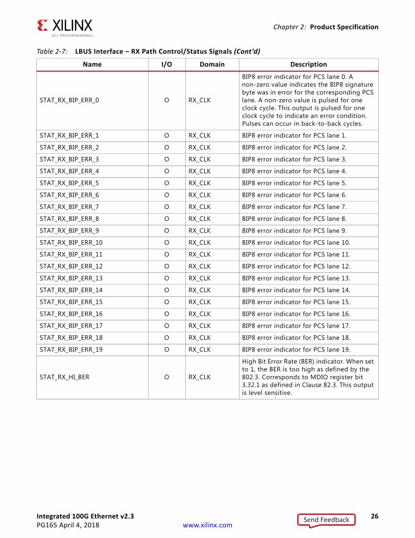
STAT_RX_BIP_ERR_0 O RX_CLK
BIP8 error indicator for PCS lane 0. A non-zero value indicates the BIP8 signature byte was in error for the corresponding PCS lane. A non-zero value is pulsed for one clock cycle. This output is pulsed for one clock cycle to indicate an error condition. Pulses can occur in back-to-back cycles.
STAT_RX_BIP_ERR_1 O RX_CLK BIP8 error indicator for PCS lane 1.
STAT_RX_BIP_ERR_2 O RX_CLK BIP8 error indicator for PCS lane 2.
STAT_RX_BIP_ERR_3 O RX_CLK BIP8 error indicator for PCS lane 3.
STAT_RX_BIP_ERR_4 O RX_CLK BIP8 error indicator for PCS lane 4.
STAT_RX_BIP_ERR_5 O RX_CLK BIP8 error indicator for PCS lane 5.
STAT_RX_BIP_ERR_6 O RX_CLK BIP8 error indicator for PCS lane 6.
STAT_RX_BIP_ERR_7 O RX_CLK BIP8 error indicator for PCS lane 7.
STAT_RX_BIP_ERR_8 O RX_CLK BIP8 error indicator for PCS lane 8.
STAT_RX_BIP_ERR_9 O RX_CLK BIP8 error indicator for PCS lane 9.
STAT_RX_BIP_ERR_10 O RX_CLK BIP8 error indicator for PCS lane 10.
STAT_RX_BIP_ERR_11 O RX_CLK BIP8 error indicator for PCS lane 11.
STAT_RX_BIP_ERR_12 O RX_CLK BIP8 error indicator for PCS lane 12.
STAT_RX_BIP_ERR_13 O RX_CLK BIP8 error indicator for PCS lane 13.
STAT_RX_BIP_ERR_14 O RX_CLK BIP8 error indicator for PCS lane 14.
STAT_RX_BIP_ERR_15 O RX_CLK BIP8 error indicator for PCS lane 15.
STAT_RX_BIP_ERR_16 O RX_CLK BIP8 error indicator for PCS lane 16.
STAT_RX_BIP_ERR_17 O RX_CLK BIP8 error indicator for PCS lane 17.
STAT_RX_BIP_ERR_18 O RX_CLK BIP8 error indicator for PCS lane 18.
STAT_RX_BIP_ERR_19 O RX_CLK BIP8 error indicator for PCS lane 19.
STAT_RX_HI_BER O RX_CLK
High Bit Error Rate (BER) indicator. When set to 1, the BER is too high as defined by the 802.3. Corresponds to MDIO register bit 3.32.1 as defined in Clause 82.3. This output is level sensitive.
Table 2-7: LBUS Interface – RX Path Control/Status Signals (Cont’d)
Name I/O Domain Description
Send Feedback
Integrated 100G Ethernet v2.3 27PG165 April 4, 2018 www.xilinx.com
Chapter 2: Product Specification
Table 2-8: Miscellaneous Status/Control Signals
Name I/O Domain Description
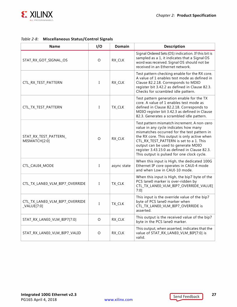
STAT_RX_GOT_SIGNAL_OS O RX_CLK
Signal Ordered Sets (OS) indication. If this bit is sampled as a 1, it indicates that a Signal OS word was received. Signal OS should not be received in an Ethernet network.
CTL_RX_TEST_PATTERN I RX_CLK
Test pattern checking enable for the RX core. A value of 1 enables test mode as defined in Clause 82.2.18. Corresponds to MDIO register bit 3.42.2 as defined in Clause 82.3. Checks for scrambled idle pattern.
CTL_TX_TEST_PATTERN I TX_CLK
Test pattern generation enable for the TX core. A value of 1 enables test mode as defined in Clause 82.2.18. Corresponds to MDIO register bit 3.42.3 as defined in Clause 82.3. Generates a scrambled idle pattern.
STAT_RX_TEST_PATTERN_MISMATCH[2:0] O RX_CLK
Test pattern mismatch increment. A non-zero value in any cycle indicates how many mismatches occurred for the test pattern in the RX core. This output is only active when CTL_RX_TEST_PATTERN is set to a 1. This output can be used to generate MDIO register 3.43.15:0 as defined in Clause 82.3. This output is pulsed for one clock cycle.
CTL_CAUI4_MODE I async stateWhen this input is High, the dedicated 100G Ethernet IP core operates in CAUI-4 mode and when Low in CAUI-10 mode.
CTL_TX_LANE0_VLM_BIP7_OVERRIDE I TX_CLK
When this input is High, the bip7 byte of the PCS lane0 marker is over-ridden by CTL_TX_LANE0_VLM_BIP7_OVERRIDE_VALUE[7:0]
CTL_TX_LANE0_VLM_BIP7_OVERRIDE_VALUE[7:0] I TX_CLK
This input is the override value of the bip7 byte of PCS lane0 marker when CTL_TX_LANE0_VLM_BIP7_OVERRIDE is asserted.
STAT_RX_LANE0_VLM_BIP7[7:0] O RX_CLK This output is the received value of the bip7 byte in the PCS lane0 marker.
STAT_RX_LANE0_VLM_BIP7_VALID O RX_CLKThis output, when asserted, indicates that the value of STAT_RX_LANE0_VLM_BIP[7:0] is valid.
Send Feedback
Integrated 100G Ethernet v2.3 28PG165 April 4, 2018 www.xilinx.com
Chapter 2: Product Specification
Table 2-9: Statistics Interface – RX Path
Name I/O Domain Description
STAT_RX_TOTAL_BYTES[7:0] O RX_CLK Increment for the total number of bytes received.
STAT_RX_TOTAL_PACKETS[3:0] O RX_CLK Increment for the total number of packets received.
STAT_RX_TOTAL_GOOD_BYTES[13:0] O RX_CLK
Increment for the total number of good bytes received. This value is only non-zero when a packet is received completely and contains no errors.
STAT_RX_TOTAL_GOOD_PACKETS O RX_CLK
Increment for the total number of good packets received. This value is only non-zero when a packet is received completely and contains no errors.
STAT_RX_PACKET_BAD_FCS O RX_CLKIncrement for packets between 64 and ctl_rx_max_packet_len bytes that have FCS errors.
STAT_RX_PACKET_64_BYTES O RX_CLK Increment for good and bad packets received that contain 64 bytes.
STAT_RX_PACKET_65_127_BYTES O RX_CLK Increment for good and bad packets received that contain 65 to 127 bytes.
STAT_RX_PACKET_128_255_BYTES O RX_CLK Increment for good and bad packets received that contain 128 to 255 bytes.
STAT_RX_PACKET_256_511_BYTES O RX_CLK Increment for good and bad packets received that contain 256 to 511 bytes.
STAT_RX_PACKET_512_1023_BYTES O RX_CLK Increment for good and bad packets received that contain 512 to 1,023 bytes.
STAT_RX_PACKET_1024_1518_BYTES O RX_CLK Increment for good and bad packets received that contain 1,024 to 1,518 bytes.
STAT_RX_PACKET_1519_1522_BYTES O RX_CLK Increment for good and bad packets received that contain 1,519 to 1,522 bytes.
STAT_RX_PACKET_1523_1548_BYTES O RX_CLK Increment for good and bad packets received that contain 1,523 to 1,548 bytes.
STAT_RX_PACKET_1549_2047_BYTES O RX_CLK Increment for good and bad packets received that contain 1,549 to 2,047 bytes.
STAT_RX_PACKET_2048_4095_BYTES O RX_CLK Increment for good and bad packets received that contain 2,048 to 4,095 bytes.
STAT_RX_PACKET_4096_8191_BYTES O RX_CLK Increment for good and bad packets received that contain 4,096 to 8,191 bytes.
Send Feedback
Integrated 100G Ethernet v2.3 29PG165 April 4, 2018 www.xilinx.com
Chapter 2: Product Specification
STAT_RX_PACKET_8192_9215_BYTES O RX_CLK Increment for good and bad packets received that contain 8,192 to 9,215 bytes.
STAT_RX_PACKET_SMALL[3:0] O RX_CLK Increment for all packets that are less than 64 bytes long.
STAT_RX_PACKET_LARGE O RX_CLK Increment for all packets that are more than 9,215 bytes long.
STAT_RX_UNICAST O RX_CLK Increment for good unicast packets.
STAT_RX_MULTICAST O RX_CLK Increment for good multicast packets.
STAT_RX_BROADCAST O RX_CLK Increment for good broadcast packets.
STAT_RX_OVERSIZE O RX_CLK Increment for packets longer than CTL_RX_MAX_PACKET_LEN with good FCS.
STAT_RX_TOOLONG O RX_CLKIncrement for packets longer than CTL_RX_MAX_PACKET_LEN with good and bad FCS.
STAT_RX_UNDERSIZE[3:0] O RX_CLK Increment for packets shorter than STAT_RX_MIN_PACKET_LEN with good FCS.
STAT_RX_FRAGMENT[3:0] O RX_CLK Increment for packets shorter than stat_rx_min_packet_len with bad FCS.
STAT_RX_VLAN O RX_CLK Increment for good 802.1Q tagged VLAN packets.
STAT_RX_INRANGEERR O RX_CLK Increment for packets with Length field error but with good FCS.
STAT_RX_JABBER O RX_CLK Increment for packets longer than CTL_RX_MAX_PACKET_LEN with bad FCS.
STAT_RX_PAUSE O RX_CLK Increment for 802.3x Ethernet MAC Pause packet with good FCS.
STAT_RX_USER_PAUSE O RX_CLK Increment for priority based pause packets with good FCS.
STAT_RX_BAD_CODE[2:0] O RX_CLK
Increment for 64B/66B code violations. This signal indicates that the RX PCS receive state machine is in the RX_E state as specified by the 802.3 specifications. This output can be used to generate MDIO register 3.33:7:0 as defined in Clause 82.3.
STAT_RX_BAD_SFD O RX_CLK
Increment bad SFD. This signal indicates if the Ethernet packet received was preceded by a valid start of frame delimiter (SFD). A value of 1 indicates that an invalid SFD was received.
STAT_RX_BAD_PREAMBLE O RX_CLK
Increment bad preamble. This signal indicates if the Ethernet packet received was preceded by a valid preamble. A value of 1 indicates that an invalid preamble was received.
Table 2-9: Statistics Interface – RX Path (Cont’d)
Name I/O Domain Description
Send Feedback
Integrated 100G Ethernet v2.3 30PG165 April 4, 2018 www.xilinx.com
Chapter 2: Product Specification
Table 2-10: Statistics Interface – TX Path
Name I/O Domain Description
STAT_TX_TOTAL_BYTES[6:0] O TX_CLK Increment for the total number of bytes transmitted.
STAT_TX_TOTAL_PACKETS O TX_CLK Increment for the total number of packets transmitted.
STAT_TX_TOTAL_GOOD_BYTES[13:0] O TX_CLK
Increment for the total number of good bytes transmitted. This value is only non-zero when a packet is transmitted completely and contains no errors.
STAT_TX_TOTAL_GOOD_PACKETS O TX_CLK Increment for the total number of good packets transmitted.
STAT_TX_BAD_FCS O TX_CLK Increment for packets greater than 64 bytes that have FCS errors.
STAT_TX_PACKET_64_BYTES O TX_CLK Increment for good and bad packets transmitted that contain 64 bytes.
STAT_TX_PACKET_65_127_BYTES O TX_CLK Increment for good and bad packets transmitted that contain 65 to 127 bytes.
STAT_TX_PACKET_128_255_BYTES O TX_CLK Increment for good and bad packets transmitted that contain 128 to 255 bytes.
STAT_TX_PACKET_256_511_BYTES O TX_CLK Increment for good and bad packets transmitted that contain 256 to 511 bytes.
STAT_TX_PACKET_512_1023_BYTES O TX_CLKIncrement for good and bad packets transmitted that contain 512 to 1,023 bytes.
STAT_TX_PACKET_1024_1518_BYTES O TX_CLKIncrement for good and bad packets transmitted that contain 1,024 to 1,518 bytes.
STAT_TX_PACKET_1519_1522_BYTES O TX_CLKIncrement for good and bad packets transmitted that contain 1,519 to 1,522 bytes.
STAT_TX_PACKET_1523_1548_BYTES O TX_CLKIncrement for good and bad packets transmitted that contain 1,523 to 1,548 bytes.
STAT_TX_PACKET_1549_2047_BYTES O TX_CLKIncrement for good and bad packets transmitted that contain 1,549 to 2,047 bytes.
STAT_TX_PACKET_2048_4095_BYTES O TX_CLKIncrement for good and bad packets transmitted that contain 2,048 to 4,095 bytes.
STAT_TX_PACKET_4096_8191_BYTES O TX_CLKIncrement for good and bad packets transmitted that contain 4,096 to 8,191 bytes.
STAT_TX_PACKET_8192_9215_BYTES O TX_CLKIncrement for good and bad packets transmitted that contain 8,192 to 9,215 bytes.
Send Feedback
Integrated 100G Ethernet v2.3 31PG165 April 4, 2018 www.xilinx.com
Chapter 2: Product Specification
STAT_TX_PACKET_SMALL O TX_CLKIncrement for all packets that are less than 64 bytes long. Packet transfers of less than 64 bytes are not permitted.
STAT_TX_PACKET_LARGE O TX_CLK Increment for all packets that are more than 9,215 bytes long.
STAT_TX_UNICAST O TX_CLK Increment for good unicast packets.
STAT_TX_MULTICAST O TX_CLK Increment for good multicast packets.
STAT_TX_BROADCAST O TX_CLK Increment for good broadcast packets.
STAT_TX_VLAN O TX_CLK Increment for good 802.1Q tagged VLAN packets.
STAT_TX_PAUSE O TX_CLK Increment for 802.3x Ethernet MAC Pause packet with good FCS.
STAT_TX_USER_PAUSE O TX_CLK Increment for priority based pause packets with good FCS.
STAT_TX_FRAME_ERROR O TX_CLK Increment for packets with tx_errin set to indicate an EOP abort.
Table 2-10: Statistics Interface – TX Path (Cont’d)
Name I/O Domain Description
Table 2-11: Pause Interface – Control Signals
Name I/O Domain Description
CTL_RX_PAUSE_ENABLE[8:0] I RX_CLK
RX pause enable signal. This input is used to enable the processing of the pause quanta for the corresponding priority.
This signal only affects the RX user interface, not the pause processing logic.
CTL_TX_PAUSE_ENABLE[8:0] I TX_CLKTX pause enable signal. This input is used to enable the processing of the pause quanta for the corresponding priority. This signal gates transmission of pause packets.
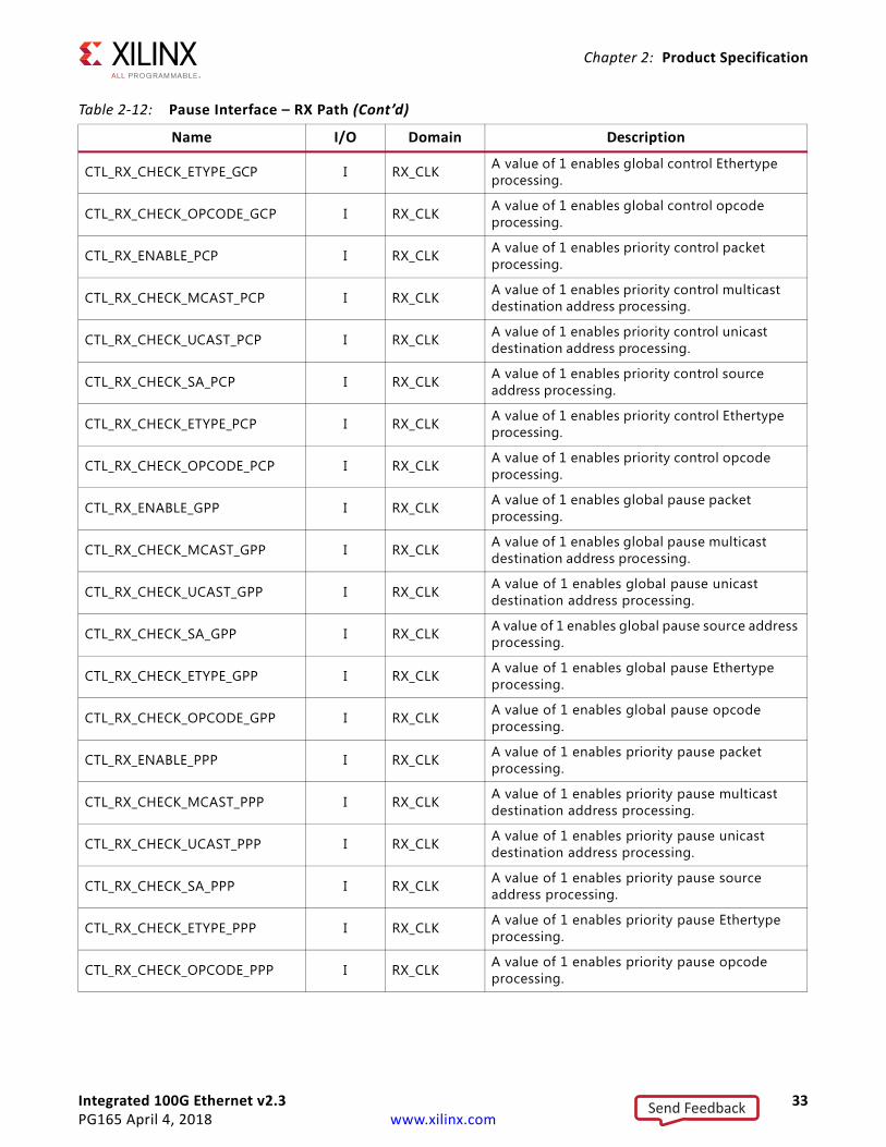
Table 2-12: Pause Interface – RX Path
Name I/O Domain Description
CTL_RX_ENABLE_GCP I RX_CLK A value of 1 enables global control packet processing.
CTL_RX_CHECK_MCAST_GCP I RX_CLK A value of 1 enables global control multicast destination address processing.
CTL_RX_CHECK_UCAST_GCP I RX_CLK A value of 1 enables global control unicast destination address processing.
CTL_RX_CHECK_SA_GCP I RX_CLK A value of 1 enables global control source address processing.
Send Feedback

Integrated 100G Ethernet v2.3 32PG165 April 4, 2018 www.xilinx.com
Chapter 2: Product Specification
CTL_RX_CHECK_ETYPE_GCP I RX_CLK A value of 1 enables global control Ethertype processing.
CTL_RX_CHECK_OPCODE_GCP I RX_CLK A value of 1 enables global control opcode processing.
CTL_RX_ENABLE_PCP I RX_CLK A value of 1 enables priority control packet processing.
CTL_RX_CHECK_MCAST_PCP I RX_CLK A value of 1 enables priority control multicast destination address processing.
CTL_RX_CHECK_UCAST_PCP I RX_CLK A value of 1 enables priority control unicast destination address processing.
CTL_RX_CHECK_SA_PCP I RX_CLK A value of 1 enables priority control source address processing.
CTL_RX_CHECK_ETYPE_PCP I RX_CLK A value of 1 enables priority control Ethertype processing.
CTL_RX_CHECK_OPCODE_PCP I RX_CLK A value of 1 enables priority control opcode processing.
CTL_RX_ENABLE_GPP I RX_CLK A value of 1 enables global pause packet processing.
CTL_RX_CHECK_MCAST_GPP I RX_CLK A value of 1 enables global pause multicast destination address processing.
CTL_RX_CHECK_UCAST_GPP I RX_CLK A value of 1 enables global pause unicast destination address processing.
CTL_RX_CHECK_SA_GPP I RX_CLK A value of 1 enables global pause source address processing.
CTL_RX_CHECK_ETYPE_GPP I RX_CLK A value of 1 enables global pause Ethertype processing.
CTL_RX_CHECK_OPCODE_GPP I RX_CLK A value of 1 enables global pause opcode processing.
CTL_RX_ENABLE_PPP I RX_CLK A value of 1 enables priority pause packet processing.
CTL_RX_CHECK_MCAST_PPP I RX_CLK A value of 1 enables priority pause multicast destination address processing.
CTL_RX_CHECK_UCAST_PPP I RX_CLK A value of 1 enables priority pause unicast destination address processing.
CTL_RX_CHECK_SA_PPP I RX_CLK A value of 1 enables priority pause source address processing.
CTL_RX_CHECK_ETYPE_PPP I RX_CLK A value of 1 enables priority pause Ethertype processing.
CTL_RX_CHECK_OPCODE_PPP I RX_CLK A value of 1 enables priority pause opcode processing.
Table 2-12: Pause Interface – RX Path (Cont’d)
Name I/O Domain Description
Send Feedback
Integrated 100G Ethernet v2.3 33PG165 April 4, 2018 www.xilinx.com
Chapter 2: Product Specification
CTL_RX_CHECK_ETYPE_GCP I RX_CLK A value of 1 enables global control Ethertype processing.
CTL_RX_CHECK_OPCODE_GCP I RX_CLK A value of 1 enables global control opcode processing.
CTL_RX_ENABLE_PCP I RX_CLK A value of 1 enables priority control packet processing.
CTL_RX_CHECK_MCAST_PCP I RX_CLK A value of 1 enables priority control multicast destination address processing.
CTL_RX_CHECK_UCAST_PCP I RX_CLK A value of 1 enables priority control unicast destination address processing.
CTL_RX_CHECK_SA_PCP I RX_CLK A value of 1 enables priority control source address processing.
CTL_RX_CHECK_ETYPE_PCP I RX_CLK A value of 1 enables priority control Ethertype processing.
CTL_RX_CHECK_OPCODE_PCP I RX_CLK A value of 1 enables priority control opcode processing.
CTL_RX_ENABLE_GPP I RX_CLK A value of 1 enables global pause packet processing.
CTL_RX_CHECK_MCAST_GPP I RX_CLK A value of 1 enables global pause multicast destination address processing.
CTL_RX_CHECK_UCAST_GPP I RX_CLK A value of 1 enables global pause unicast destination address processing.
CTL_RX_CHECK_SA_GPP I RX_CLK A value of 1 enables global pause source address processing.
CTL_RX_CHECK_ETYPE_GPP I RX_CLK A value of 1 enables global pause Ethertype processing.
CTL_RX_CHECK_OPCODE_GPP I RX_CLK A value of 1 enables global pause opcode processing.
CTL_RX_ENABLE_PPP I RX_CLK A value of 1 enables priority pause packet processing.
CTL_RX_CHECK_MCAST_PPP I RX_CLK A value of 1 enables priority pause multicast destination address processing.
CTL_RX_CHECK_UCAST_PPP I RX_CLK A value of 1 enables priority pause unicast destination address processing.
CTL_RX_CHECK_SA_PPP I RX_CLK A value of 1 enables priority pause source address processing.
CTL_RX_CHECK_ETYPE_PPP I RX_CLK A value of 1 enables priority pause Ethertype processing.
CTL_RX_CHECK_OPCODE_PPP I RX_CLK A value of 1 enables priority pause opcode processing.
Table 2-12: Pause Interface – RX Path (Cont’d)
Name I/O Domain Description
Send Feedback
Integrated 100G Ethernet v2.3 34PG165 April 4, 2018 www.xilinx.com
Chapter 2: Product Specification
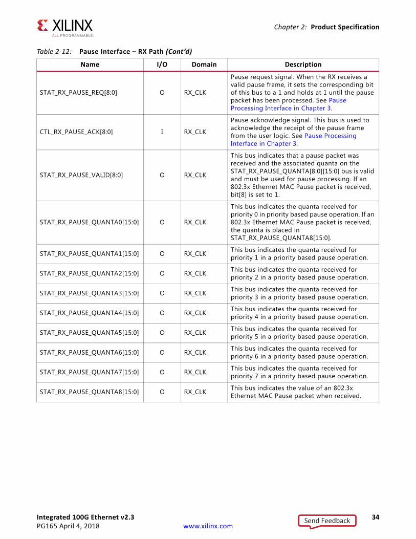
STAT_RX_PAUSE_REQ[8:0] O RX_CLK
Pause request signal. When the RX receives a valid pause frame, it sets the corresponding bit of this bus to a 1 and holds at 1 until the pause packet has been processed. See Pause Processing Interface in Chapter 3.
CTL_RX_PAUSE_ACK[8:0] I RX_CLK
Pause acknowledge signal. This bus is used to acknowledge the receipt of the pause frame from the user logic. See Pause Processing Interface in Chapter 3.
STAT_RX_PAUSE_VALID[8:0] O RX_CLK
This bus indicates that a pause packet was received and the associated quanta on the STAT_RX_PAUSE_QUANTA[8:0][15:0] bus is valid and must be used for pause processing. If an 802.3x Ethernet MAC Pause packet is received, bit[8] is set to 1.
STAT_RX_PAUSE_QUANTA0[15:0] O RX_CLK
This bus indicates the quanta received for priority 0 in priority based pause operation. If an 802.3x Ethernet MAC Pause packet is received, the quanta is placed in STAT_RX_PAUSE_QUANTA8[15:0].
STAT_RX_PAUSE_QUANTA1[15:0] O RX_CLK This bus indicates the quanta received for priority 1 in a priority based pause operation.
STAT_RX_PAUSE_QUANTA2[15:0] O RX_CLK This bus indicates the quanta received for priority 2 in a priority based pause operation.
STAT_RX_PAUSE_QUANTA3[15:0] O RX_CLK This bus indicates the quanta received for priority 3 in a priority based pause operation.
STAT_RX_PAUSE_QUANTA4[15:0] O RX_CLK This bus indicates the quanta received for priority 4 in a priority based pause operation.
STAT_RX_PAUSE_QUANTA5[15:0] O RX_CLK This bus indicates the quanta received for priority 5 in a priority based pause operation.
STAT_RX_PAUSE_QUANTA6[15:0] O RX_CLK This bus indicates the quanta received for priority 6 in a priority based pause operation.
STAT_RX_PAUSE_QUANTA7[15:0] O RX_CLK This bus indicates the quanta received for priority 7 in a priority based pause operation.
STAT_RX_PAUSE_QUANTA8[15:0] O RX_CLK This bus indicates the value of an 802.3x Ethernet MAC Pause packet when received.
Table 2-12: Pause Interface – RX Path (Cont’d)
Name I/O Domain Description
Send Feedback
Integrated 100G Ethernet v2.3 35PG165 April 4, 2018 www.xilinx.com
Chapter 2: Product Specification
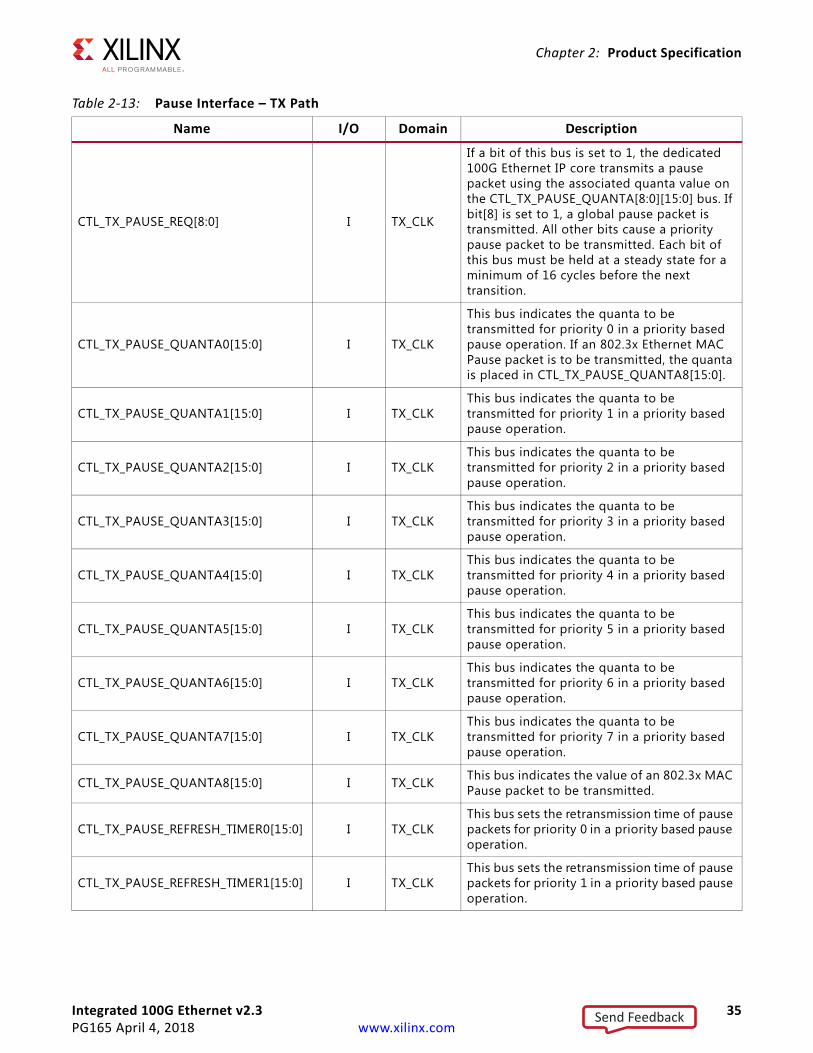
Table 2-13: Pause Interface – TX Path
Name I/O Domain Description
CTL_TX_PAUSE_REQ[8:0] I TX_CLK
If a bit of this bus is set to 1, the dedicated 100G Ethernet IP core transmits a pause packet using the associated quanta value on the CTL_TX_PAUSE_QUANTA[8:0][15:0] bus. If bit[8] is set to 1, a global pause packet is transmitted. All other bits cause a priority pause packet to be transmitted. Each bit of this bus must be held at a steady state for a minimum of 16 cycles before the next transition.
CTL_TX_PAUSE_QUANTA0[15:0] I TX_CLK
This bus indicates the quanta to be transmitted for priority 0 in a priority based pause operation. If an 802.3x Ethernet MAC Pause packet is to be transmitted, the quanta is placed in CTL_TX_PAUSE_QUANTA8[15:0].
CTL_TX_PAUSE_QUANTA1[15:0] I TX_CLKThis bus indicates the quanta to be transmitted for priority 1 in a priority based pause operation.
CTL_TX_PAUSE_QUANTA2[15:0] I TX_CLKThis bus indicates the quanta to be transmitted for priority 2 in a priority based pause operation.
CTL_TX_PAUSE_QUANTA3[15:0] I TX_CLKThis bus indicates the quanta to be transmitted for priority 3 in a priority based pause operation.
CTL_TX_PAUSE_QUANTA4[15:0] I TX_CLKThis bus indicates the quanta to be transmitted for priority 4 in a priority based pause operation.
CTL_TX_PAUSE_QUANTA5[15:0] I TX_CLKThis bus indicates the quanta to be transmitted for priority 5 in a priority based pause operation.
CTL_TX_PAUSE_QUANTA6[15:0] I TX_CLKThis bus indicates the quanta to be transmitted for priority 6 in a priority based pause operation.
CTL_TX_PAUSE_QUANTA7[15:0] I TX_CLKThis bus indicates the quanta to be transmitted for priority 7 in a priority based pause operation.
CTL_TX_PAUSE_QUANTA8[15:0] I TX_CLK This bus indicates the value of an 802.3x MAC Pause packet to be transmitted.
CTL_TX_PAUSE_REFRESH_TIMER0[15:0] I TX_CLKThis bus sets the retransmission time of pause packets for priority 0 in a priority based pause operation.
CTL_TX_PAUSE_REFRESH_TIMER1[15:0] I TX_CLKThis bus sets the retransmission time of pause packets for priority 1 in a priority based pause operation.
Send Feedback
Integrated 100G Ethernet v2.3 36PG165 April 4, 2018 www.xilinx.com
Chapter 2: Product Specification
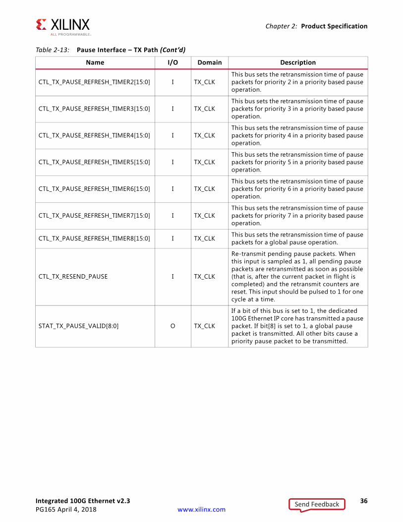
CTL_TX_PAUSE_REFRESH_TIMER2[15:0] I TX_CLKThis bus sets the retransmission time of pause packets for priority 2 in a priority based pause operation.
CTL_TX_PAUSE_REFRESH_TIMER3[15:0] I TX_CLKThis bus sets the retransmission time of pause packets for priority 3 in a priority based pause operation.
CTL_TX_PAUSE_REFRESH_TIMER4[15:0] I TX_CLKThis bus sets the retransmission time of pause packets for priority 4 in a priority based pause operation.
CTL_TX_PAUSE_REFRESH_TIMER5[15:0] I TX_CLKThis bus sets the retransmission time of pause packets for priority 5 in a priority based pause operation.
CTL_TX_PAUSE_REFRESH_TIMER6[15:0] I TX_CLKThis bus sets the retransmission time of pause packets for priority 6 in a priority based pause operation.
CTL_TX_PAUSE_REFRESH_TIMER7[15:0] I TX_CLKThis bus sets the retransmission time of pause packets for priority 7 in a priority based pause operation.
CTL_TX_PAUSE_REFRESH_TIMER8[15:0] I TX_CLK This bus sets the retransmission time of pause packets for a global pause operation.
CTL_TX_RESEND_PAUSE I TX_CLK
Re-transmit pending pause packets. When this input is sampled as 1, all pending pause packets are retransmitted as soon as possible (that is, after the current packet in flight is completed) and the retransmit counters are reset. This input should be pulsed to 1 for one cycle at a time.
STAT_TX_PAUSE_VALID[8:0] O TX_CLK
If a bit of this bus is set to 1, the dedicated 100G Ethernet IP core has transmitted a pause packet. If bit[8] is set to 1, a global pause packet is transmitted. All other bits cause a priority pause packet to be transmitted.
Table 2-13: Pause Interface – TX Path (Cont’d)
Name I/O Domain Description
Send Feedback
Integrated 100G Ethernet v2.3 37PG165 April 4, 2018 www.xilinx.com
Chapter 2: Product Specification
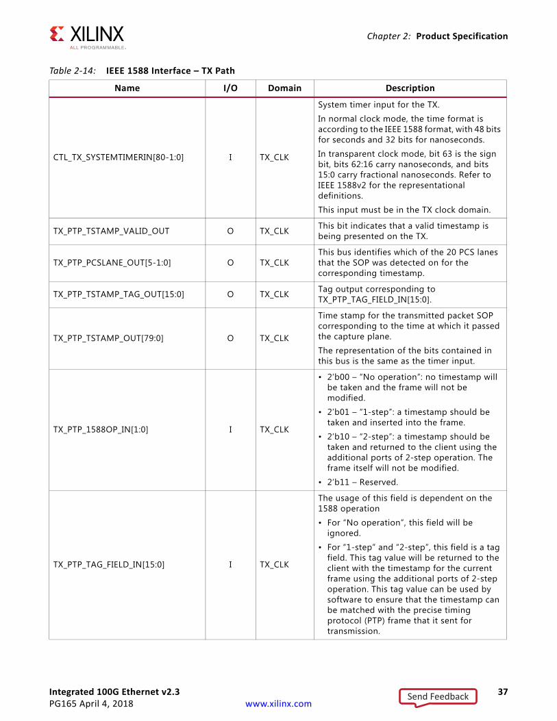
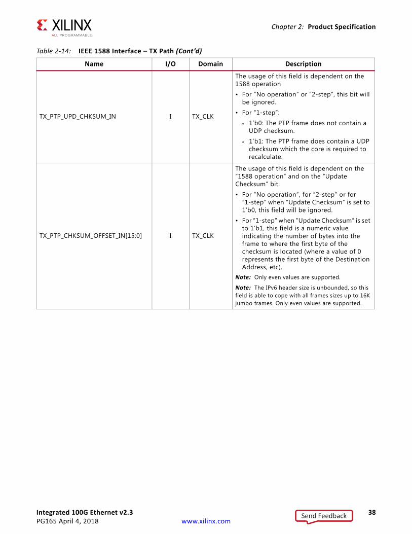
Table 2-14: IEEE 1588 Interface – TX Path
Name I/O Domain Description
CTL_TX_SYSTEMTIMERIN[80-1:0] I TX_CLK
System timer input for the TX.
In normal clock mode, the time format is according to the IEEE 1588 format, with 48 bits for seconds and 32 bits for nanoseconds.
In transparent clock mode, bit 63 is the sign bit, bits 62:16 carry nanoseconds, and bits 15:0 carry fractional nanoseconds. Refer to IEEE 1588v2 for the representational definitions.
This input must be in the TX clock domain.
TX_PTP_TSTAMP_VALID_OUT O TX_CLK This bit indicates that a valid timestamp is being presented on the TX.
TX_PTP_PCSLANE_OUT[5-1:0] O TX_CLKThis bus identifies which of the 20 PCS lanes that the SOP was detected on for the corresponding timestamp.
TX_PTP_TSTAMP_TAG_OUT[15:0] O TX_CLK Tag output corresponding to TX_PTP_TAG_FIELD_IN[15:0].
TX_PTP_TSTAMP_OUT[79:0] O TX_CLK
Time stamp for the transmitted packet SOP corresponding to the time at which it passed the capture plane.
The representation of the bits contained in this bus is the same as the timer input.
TX_PTP_1588OP_IN[1:0] I TX_CLK
• 2’b00 – “No operation”: no timestamp will be taken and the frame will not be modified.
• 2’b01 – “1-step”: a timestamp should be taken and inserted into the frame.
• 2’b10 – “2-step”: a timestamp should be taken and returned to the client using the additional ports of 2-step operation. The frame itself will not be modified.
• 2’b11 – Reserved.
TX_PTP_TAG_FIELD_IN[15:0] I TX_CLK
The usage of this field is dependent on the 1588 operation
• For “No operation”, this field will be ignored.
• For “1-step” and “2-step”, this field is a tag field. This tag value will be returned to the client with the timestamp for the current frame using the additional ports of 2-step operation. This tag value can be used by software to ensure that the timestamp can be matched with the precise timing protocol (PTP) frame that it sent for transmission.
Send Feedback
Integrated 100G Ethernet v2.3 38PG165 April 4, 2018 www.xilinx.com
Chapter 2: Product Specification
TX_PTP_UPD_CHKSUM_IN I TX_CLK
The usage of this field is dependent on the 1588 operation
• For “No operation” or “2-step”, this bit will be ignored.
• For “1-step”:
° 1’b0: The PTP frame does not contain a UDP checksum.
° 1’b1: The PTP frame does contain a UDP checksum which the core is required to recalculate.
TX_PTP_CHKSUM_OFFSET_IN[15:0] I TX_CLK
The usage of this field is dependent on the “1588 operation” and on the “Update Checksum” bit.
• For “No operation”, for “2-step” or for “1-step” when “Update Checksum” is set to 1’b0, this field will be ignored.
• For “1-step” when “Update Checksum” is set to 1’b1, this field is a numeric value indicating the number of bytes into the frame to where the first byte of the checksum is located (where a value of 0 represents the first byte of the Destination Address, etc).
Note: Only even values are supported.
Note: The IPv6 header size is unbounded, so this field is able to cope with all frames sizes up to 16K jumbo frames. Only even values are supported.
Table 2-14: IEEE 1588 Interface – TX Path (Cont’d)
Name I/O Domain Description
Send Feedback
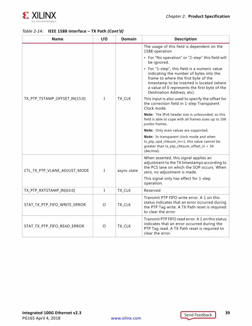
Integrated 100G Ethernet v2.3 39PG165 April 4, 2018 www.xilinx.com
Chapter 2: Product Specification
TX_PTP_TSTAMP_OFFSET_IN[15:0] I TX_CLK
The usage of this field is dependent on the 1588 operation
• For “No operation” or “2-step” this field will be ignored.
• For “1-step”, this field is a numeric value indicating the number of bytes into the frame to where the first byte of the timestamp to be inserted is located (where a value of 0 represents the first byte of the Destination Address, etc).
This input is also used to specify the offset for the correction field in 1-step Transparent Clock mode.Note: The IPv6 header size is unbounded, so this field is able to cope with all frames sizes up to 16K jumbo frames.
Note: Only even values are supported.
Note: In transparent clock mode and when tx_ptp_upd_chksum_in=1, this value cannot be greater than tx_ptp_chksum_offset_in + 34 (decimal).
CTL_TX_PTP_VLANE_ADJUST_MODE I async state
When asserted, this signal applies an adjustment to the TX timestamps according to the PCS lane on which the SOP occurs. When zero, no adjustment is made.
This signal only has effect for 1-step operation.
TX_PTP_RXTSTAMP_IN[63:0] I TX_CLK Reserved
STAT_TX_PTP_FIFO_WRITE_ERROR O TX_CLK
Transmit PTP FIFO write error. A 1 on this status indicates that an error occurred during the PTP Tag write. A TX Path reset is required to clear the error.
STAT_TX_PTP_FIFO_READ_ERROR O TX_CLK
Transmit PTP FIFO read error. A 1 on this status indicates that an error occurred during the PTP Tag read. A TX Path reset is required to clear the error.
Table 2-14: IEEE 1588 Interface – TX Path (Cont’d)
Name I/O Domain Description
Send Feedback
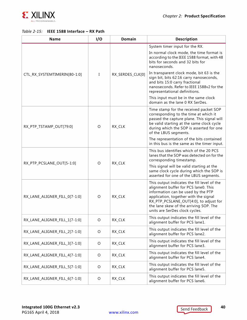
Integrated 100G Ethernet v2.3 40PG165 April 4, 2018 www.xilinx.com
Chapter 2: Product Specification
Table 2-15: IEEE 1588 Interface – RX Path
Name I/O Domain Description
CTL_RX_SYSTEMTIMERIN[80-1:0] I RX_SERDES_CLK[0]
System timer input for the RX.
In normal clock mode, the time format is according to the IEEE 1588 format, with 48 bits for seconds and 32 bits for nanoseconds.
In transparent clock mode, bit 63 is the sign bit, bits 62:16 carry nanoseconds, and bits 15:0 carry fractional nanoseconds. Refer to IEEE 1588v2 for the representational definitions.
This input must be in the same clock domain as the lane 0 RX SerDes.
RX_PTP_TSTAMP_OUT[79:0] O RX_CLK
Time stamp for the received packet SOP corresponding to the time at which it passed the capture plane. This signal will be valid starting at the same clock cycle during which the SOP is asserted for one of the LBUS segments.
The representation of the bits contained in this bus is the same as the timer input.
RX_PTP_PCSLANE_OUT[5-1:0] O RX_CLK
This bus identifies which of the 20 PCS lanes that the SOP was detected on for the corresponding timestamp.
This signal will be valid starting at the same clock cycle during which the SOP is asserted for one of the LBUS segments.
RX_LANE_ALIGNER_FILL_0[7-1:0] O RX_CLK
This output indicates the fill level of the alignment buffer for PCS lane0. This information can be used by the PTP application, together with the signal RX_PTP_PCSLANE_OUT[4:0], to adjust for the lane skew of the arriving SOP. The units are SerDes clock cycles.
RX_LANE_ALIGNER_FILL_1[7-1:0] O RX_CLK This output indicates the fill level of the alignment buffer for PCS lane1.
RX_LANE_ALIGNER_FILL_2[7-1:0] O RX_CLK This output indicates the fill level of the alignment buffer for PCS lane2.
RX_LANE_ALIGNER_FILL_3[7-1:0] O RX_CLK This output indicates the fill level of the alignment buffer for PCS lane3.
RX_LANE_ALIGNER_FILL_4[7-1:0] O RX_CLK This output indicates the fill level of the alignment buffer for PCS lane4.
RX_LANE_ALIGNER_FILL_5[7-1:0] O RX_CLK This output indicates the fill level of the alignment buffer for PCS lane5.
RX_LANE_ALIGNER_FILL_6[7-1:0] O RX_CLK This output indicates the fill level of the alignment buffer for PCS lane6.
Send Feedback
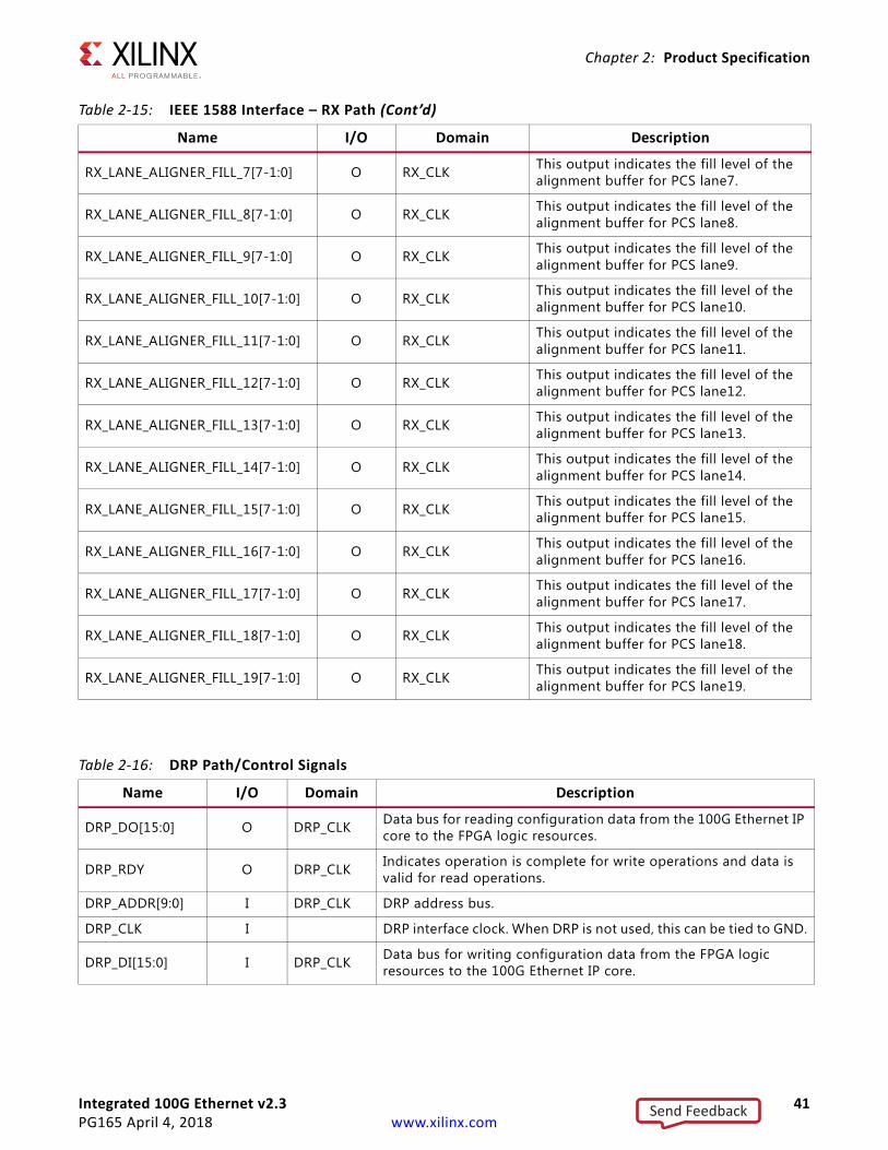
Integrated 100G Ethernet v2.3 41PG165 April 4, 2018 www.xilinx.com
Chapter 2: Product Specification
RX_LANE_ALIGNER_FILL_7[7-1:0] O RX_CLK This output indicates the fill level of the alignment buffer for PCS lane7.
RX_LANE_ALIGNER_FILL_8[7-1:0] O RX_CLK This output indicates the fill level of the alignment buffer for PCS lane8.
RX_LANE_ALIGNER_FILL_9[7-1:0] O RX_CLK This output indicates the fill level of the alignment buffer for PCS lane9.
RX_LANE_ALIGNER_FILL_10[7-1:0] O RX_CLK This output indicates the fill level of the alignment buffer for PCS lane10.
RX_LANE_ALIGNER_FILL_11[7-1:0] O RX_CLK This output indicates the fill level of the alignment buffer for PCS lane11.
RX_LANE_ALIGNER_FILL_12[7-1:0] O RX_CLK This output indicates the fill level of the alignment buffer for PCS lane12.
RX_LANE_ALIGNER_FILL_13[7-1:0] O RX_CLK This output indicates the fill level of the alignment buffer for PCS lane13.
RX_LANE_ALIGNER_FILL_14[7-1:0] O RX_CLK This output indicates the fill level of the alignment buffer for PCS lane14.
RX_LANE_ALIGNER_FILL_15[7-1:0] O RX_CLK This output indicates the fill level of the alignment buffer for PCS lane15.
RX_LANE_ALIGNER_FILL_16[7-1:0] O RX_CLK This output indicates the fill level of the alignment buffer for PCS lane16.
RX_LANE_ALIGNER_FILL_17[7-1:0] O RX_CLK This output indicates the fill level of the alignment buffer for PCS lane17.
RX_LANE_ALIGNER_FILL_18[7-1:0] O RX_CLK This output indicates the fill level of the alignment buffer for PCS lane18.
RX_LANE_ALIGNER_FILL_19[7-1:0] O RX_CLK This output indicates the fill level of the alignment buffer for PCS lane19.
Table 2-15: IEEE 1588 Interface – RX Path (Cont’d)
Name I/O Domain Description
Table 2-16: DRP Path/Control Signals
Name I/O Domain Description
DRP_DO[15:0] O DRP_CLK Data bus for reading configuration data from the 100G Ethernet IP core to the FPGA logic resources.
DRP_RDY O DRP_CLK Indicates operation is complete for write operations and data is valid for read operations.
DRP_ADDR[9:0] I DRP_CLK DRP address bus.
DRP_CLK I DRP interface clock. When DRP is not used, this can be tied to GND.
DRP_DI[15:0] I DRP_CLK Data bus for writing configuration data from the FPGA logic resources to the 100G Ethernet IP core.
Send Feedback
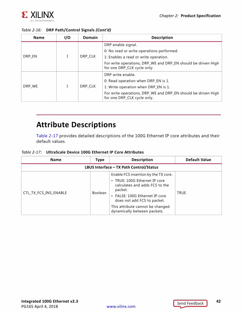
Integrated 100G Ethernet v2.3 42PG165 April 4, 2018 www.xilinx.com
Chapter 2: Product Specification
Attribute DescriptionsTable 2-17 provides detailed descriptions of the 100G Ethernet IP core attributes and their default values.
DRP_EN I DRP_CLK
DRP enable signal.
0: No read or write operations performed.
1: Enables a read or write operation.
For write operations, DRP_WE and DRP_EN should be driven High for one DRP_CLK cycle only.
DRP_WE I DRP_CLK
DRP write enable.
0: Read operation when DRP_EN is 1.
1: Write operation when DRP_EN is 1.
For write operations, DRP_WE and DRP_EN should be driven High for one DRP_CLK cycle only.
Table 2-16: DRP Path/Control Signals (Cont’d)
Name I/O Domain Description
Table 2-17: UltraScale Device 100G Ethernet IP Core Attributes
Name Type Description Default Value
LBUS Interface – TX Path Control/Status
CTL_TX_FCS_INS_ENABLE Boolean
Enable FCS insertion by the TX core.
• TRUE: 100G Ethernet IP core calculates and adds FCS to the packet.
• FALSE: 100G Ethernet IP core does not add FCS to packet.
This attribute cannot be changed dynamically between packets.
TRUE
Send Feedback
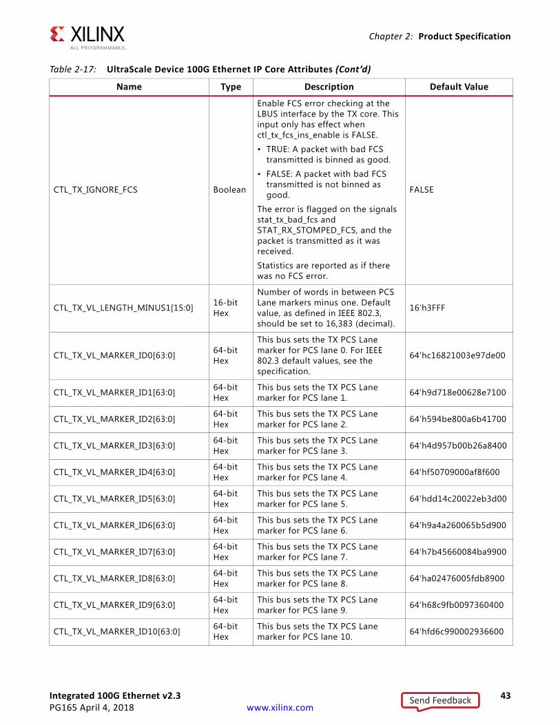
Integrated 100G Ethernet v2.3 43PG165 April 4, 2018 www.xilinx.com
Chapter 2: Product Specification
CTL_TX_IGNORE_FCS Boolean
Enable FCS error checking at the LBUS interface by the TX core. This input only has effect when ctl_tx_fcs_ins_enable is FALSE.
• TRUE: A packet with bad FCS transmitted is binned as good.
• FALSE: A packet with bad FCS transmitted is not binned as good.
The error is flagged on the signals stat_tx_bad_fcs and STAT_RX_STOMPED_FCS, and the packet is transmitted as it was received.
Statistics are reported as if there was no FCS error.
FALSE
CTL_TX_VL_LENGTH_MINUS1[15:0] 16-bit Hex
Number of words in between PCS Lane markers minus one. Default value, as defined in IEEE 802.3, should be set to 16,383 (decimal).
16’h3FFF
CTL_TX_VL_MARKER_ID0[63:0] 64-bit Hex
This bus sets the TX PCS Lane marker for PCS lane 0. For IEEE 802.3 default values, see the specification.
64'hc16821003e97de00
CTL_TX_VL_MARKER_ID1[63:0] 64-bit Hex
This bus sets the TX PCS Lane marker for PCS lane 1. 64’h9d718e00628e7100
CTL_TX_VL_MARKER_ID2[63:0] 64-bit Hex
This bus sets the TX PCS Lane marker for PCS lane 2. 64’h594be800a6b41700
CTL_TX_VL_MARKER_ID3[63:0] 64-bit Hex
This bus sets the TX PCS Lane marker for PCS lane 3. 64’h4d957b00b26a8400
CTL_TX_VL_MARKER_ID4[63:0] 64-bit Hex
This bus sets the TX PCS Lane marker for PCS lane 4. 64’hf50709000af8f600
CTL_TX_VL_MARKER_ID5[63:0] 64-bit Hex
This bus sets the TX PCS Lane marker for PCS lane 5. 64’hdd14c20022eb3d00
CTL_TX_VL_MARKER_ID6[63:0] 64-bit Hex
This bus sets the TX PCS Lane marker for PCS lane 6. 64’h9a4a260065b5d900
CTL_TX_VL_MARKER_ID7[63:0] 64-bit Hex
This bus sets the TX PCS Lane marker for PCS lane 7. 64’h7b45660084ba9900
CTL_TX_VL_MARKER_ID8[63:0] 64-bit Hex
This bus sets the TX PCS Lane marker for PCS lane 8. 64’ha02476005fdb8900
CTL_TX_VL_MARKER_ID9[63:0] 64-bit Hex
This bus sets the TX PCS Lane marker for PCS lane 9. 64’h68c9fb0097360400
CTL_TX_VL_MARKER_ID10[63:0] 64-bit Hex
This bus sets the TX PCS Lane marker for PCS lane 10. 64’hfd6c990002936600
Table 2-17: UltraScale Device 100G Ethernet IP Core Attributes (Cont’d)
Name Type Description Default Value
Send Feedback
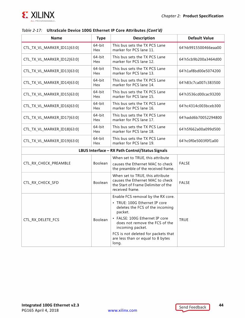
Integrated 100G Ethernet v2.3 44PG165 April 4, 2018 www.xilinx.com
Chapter 2: Product Specification
CTL_TX_VL_MARKER_ID11[63:0] 64-bit Hex
This bus sets the TX PCS Lane marker for PCS lane 11. 64’hb9915500466eaa00
CTL_TX_VL_MARKER_ID12[63:0] 64-bit Hex
This bus sets the TX PCS Lane marker for PCS lane 12. 64’h5cb9b200a3464d00
CTL_TX_VL_MARKER_ID13[63:0] 64-bit Hex
This bus sets the TX PCS Lane marker for PCS lane 13. 64’h1af8bd00e5074200
CTL_TX_VL_MARKER_ID14[63:0] 64-bit Hex
This bus sets the TX PCS Lane marker for PCS lane 14. 64’h83c7ca007c383500
CTL_TX_VL_MARKER_ID15[63:0] 64-bit Hex
This bus sets the TX PCS Lane marker for PCS lane 15. 64’h3536cd00cac93200
CTL_TX_VL_MARKER_ID16[63:0] 64-bit Hex
This bus sets the TX PCS Lane marker for PCS lane 16. 64’hc4314c003bceb300
CTL_TX_VL_MARKER_ID17[63:0] 64-bit Hex
This bus sets the TX PCS Lane marker for PCS lane 17. 64’hadd6b70052294800
CTL_TX_VL_MARKER_ID18[63:0] 64-bit Hex
This bus sets the TX PCS Lane marker for PCS lane 18. 64’h5f662a00a099d500
CTL_TX_VL_MARKER_ID19[63:0] 64-bit Hex
This bus sets the TX PCS Lane marker for PCS lane 19. 64’hc0f0e5003f0f1a00
LBUS Interface – RX Path Control/Status Signals
CTL_RX_CHECK_PREAMBLE BooleanWhen set to TRUE, this attribute
causes the Ethernet MAC to check the preamble of the received frame.
FALSE
CTL_RX_CHECK_SFD Boolean
When set to TRUE, this attribute causes the Ethernet MAC to check the Start of Frame Delimiter of the received frame.
FALSE
CTL_RX_DELETE_FCS Boolean
Enable FCS removal by the RX core.
• TRUE: 100G Ethernet IP core deletes the FCS of the incoming packet.
• FALSE: 100G Ethernet IP core does not remove the FCS of the incoming packet.
FCS is not deleted for packets that are less than or equal to 8 bytes long.
TRUE
Table 2-17: UltraScale Device 100G Ethernet IP Core Attributes (Cont’d)
Name Type Description Default Value
Send Feedback
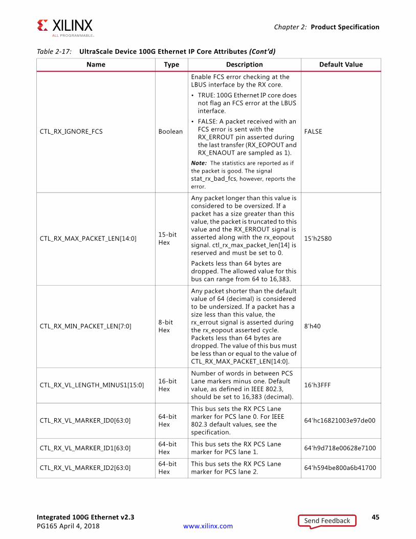
Integrated 100G Ethernet v2.3 45PG165 April 4, 2018 www.xilinx.com
Chapter 2: Product Specification
CTL_RX_IGNORE_FCS Boolean
Enable FCS error checking at the LBUS interface by the RX core.
• TRUE: 100G Ethernet IP core does not flag an FCS error at the LBUS interface.
• FALSE: A packet received with an FCS error is sent with the RX_ERROUT pin asserted during the last transfer (RX_EOPOUT and RX_ENAOUT are sampled as 1).
Note: The statistics are reported as if the packet is good. The signal stat_rx_bad_fcs, however, reports the error.
FALSE
CTL_RX_MAX_PACKET_LEN[14:0] 15-bit Hex
Any packet longer than this value is considered to be oversized. If a packet has a size greater than this value, the packet is truncated to this value and the RX_ERROUT signal is asserted along with the rx_eopout signal. ctl_rx_max_packet_len[14] is reserved and must be set to 0.
Packets less than 64 bytes are dropped. The allowed value for this bus can range from 64 to 16,383.
15’h2580
CTL_RX_MIN_PACKET_LEN[7:0] 8-bit Hex
Any packet shorter than the default value of 64 (decimal) is considered to be undersized. If a packet has a size less than this value, the rx_errout signal is asserted during the rx_eopout asserted cycle. Packets less than 64 bytes are dropped. The value of this bus must be less than or equal to the value of CTL_RX_MAX_PACKET_LEN[14:0].
8’h40
CTL_RX_VL_LENGTH_MINUS1[15:0] 16-bit Hex
Number of words in between PCS Lane markers minus one. Default value, as defined in IEEE 802.3, should be set to 16,383 (decimal).
16’h3FFF
CTL_RX_VL_MARKER_ID0[63:0] 64-bit Hex
This bus sets the RX PCS Lane marker for PCS lane 0. For IEEE 802.3 default values, see the specification.
64’hc16821003e97de00
CTL_RX_VL_MARKER_ID1[63:0] 64-bit Hex
This bus sets the RX PCS Lane marker for PCS lane 1. 64’h9d718e00628e7100
CTL_RX_VL_MARKER_ID2[63:0] 64-bit Hex
This bus sets the RX PCS Lane marker for PCS lane 2. 64’h594be800a6b41700
Table 2-17: UltraScale Device 100G Ethernet IP Core Attributes (Cont’d)
Name Type Description Default Value
Send Feedback
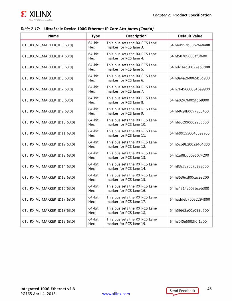
Integrated 100G Ethernet v2.3 46PG165 April 4, 2018 www.xilinx.com
Chapter 2: Product Specification
CTL_RX_VL_MARKER_ID3[63:0] 64-bit Hex
This bus sets the RX PCS Lane marker for PCS lane 3. 64’h4d957b00b26a8400
CTL_RX_VL_MARKER_ID4[63:0] 64-bit Hex
This bus sets the RX PCS Lane marker for PCS lane 4. 64’hf50709000af8f600
CTL_RX_VL_MARKER_ID5[63:0] 64-bit Hex
This bus sets the RX PCS Lane marker for PCS lane 5. 64’hdd14c20022eb3d00
CTL_RX_VL_MARKER_ID6[63:0] 64-bit Hex
This bus sets the RX PCS Lane marker for PCS lane 6. 64’h9a4a260065b5d900
CTL_RX_VL_MARKER_ID7[63:0] 64-bit Hex
This bus sets the RX PCS Lane marker for PCS lane 7. 64’h7b45660084ba9900
CTL_RX_VL_MARKER_ID8[63:0] 64-bit Hex
This bus sets the RX PCS Lane marker for PCS lane 8. 64’ha02476005fdb8900
CTL_RX_VL_MARKER_ID9[63:0] 64-bit Hex
This bus sets the RX PCS Lane marker for PCS lane 9. 64’h68c9fb0097360400
CTL_RX_VL_MARKER_ID10[63:0] 64-bit Hex
This bus sets the RX PCS Lane marker for PCS lane 10. 64’hfd6c990002936600
CTL_RX_VL_MARKER_ID11[63:0] 64-bit Hex
This bus sets the RX PCS Lane marker for PCS lane 11. 64’hb9915500466eaa00
CTL_RX_VL_MARKER_ID12[63:0] 64-bit Hex
This bus sets the RX PCS Lane marker for PCS lane 12. 64’h5cb9b200a3464d00
CTL_RX_VL_MARKER_ID13[63:0] 64-bit Hex
This bus sets the RX PCS Lane marker for PCS lane 13. 64’h1af8bd00e5074200
CTL_RX_VL_MARKER_ID14[63:0] 64-bit Hex
This bus sets the RX PCS Lane marker for PCS lane 14. 64’h83c7ca007c383500
CTL_RX_VL_MARKER_ID15[63:0] 64-bit Hex
This bus sets the RX PCS Lane marker for PCS lane 15. 64’h3536cd00cac93200
CTL_RX_VL_MARKER_ID16[63:0] 64-bit Hex
This bus sets the RX PCS Lane marker for PCS lane 16. 64’hc4314c003bceb300
CTL_RX_VL_MARKER_ID17[63:0] 64-bit Hex
This bus sets the RX PCS Lane marker for PCS lane 17. 64’hadd6b70052294800
CTL_RX_VL_MARKER_ID18[63:0] 64-bit Hex
This bus sets the RX PCS Lane marker for PCS lane 18. 64’h5f662a00a099d500
CTL_RX_VL_MARKER_ID19[63:0] 64-bit Hex
This bus sets the RX PCS Lane marker for PCS lane 19. 64’hc0f0e5003f0f1a00
Table 2-17: UltraScale Device 100G Ethernet IP Core Attributes (Cont’d)
Name Type Description Default Value
Send Feedback
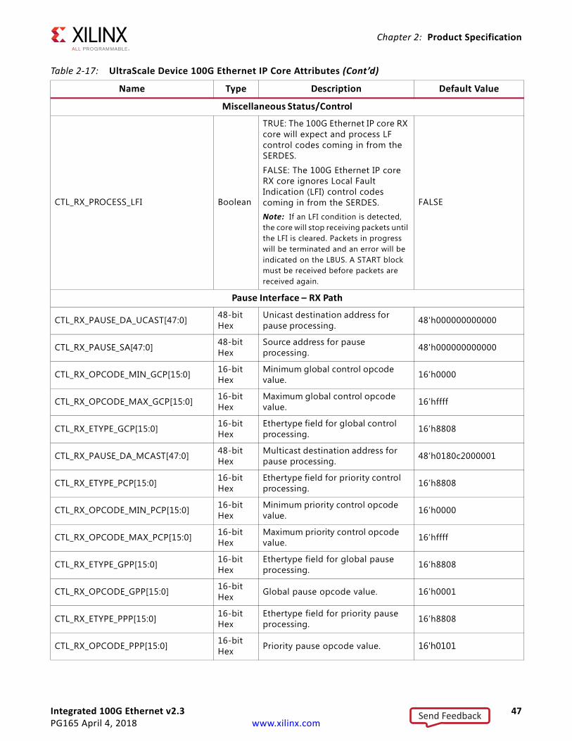
Integrated 100G Ethernet v2.3 47PG165 April 4, 2018 www.xilinx.com
Chapter 2: Product Specification
Miscellaneous Status/Control
CTL_RX_PROCESS_LFI Boolean
TRUE: The 100G Ethernet IP core RX core will expect and process LF control codes coming in from the SERDES.
FALSE: The 100G Ethernet IP core RX core ignores Local Fault Indication (LFI) control codes coming in from the SERDES.Note: If an LFI condition is detected, the core will stop receiving packets until the LFI is cleared. Packets in progress will be terminated and an error will be indicated on the LBUS. A START block must be received before packets are received again.
FALSE
Pause Interface – RX Path
CTL_RX_PAUSE_DA_UCAST[47:0] 48-bit Hex
Unicast destination address for pause processing. 48'h000000000000
CTL_RX_PAUSE_SA[47:0] 48-bit Hex
Source address for pause processing. 48'h000000000000
CTL_RX_OPCODE_MIN_GCP[15:0] 16-bit Hex
Minimum global control opcode value. 16’h0000
CTL_RX_OPCODE_MAX_GCP[15:0] 16-bit Hex
Maximum global control opcode value. 16’hffff
CTL_RX_ETYPE_GCP[15:0] 16-bit Hex
Ethertype field for global control processing. 16’h8808
CTL_RX_PAUSE_DA_MCAST[47:0] 48-bit Hex
Multicast destination address for pause processing. 48’h0180c2000001
CTL_RX_ETYPE_PCP[15:0] 16-bit Hex
Ethertype field for priority control processing. 16’h8808
CTL_RX_OPCODE_MIN_PCP[15:0] 16-bit Hex
Minimum priority control opcode value. 16’h0000
CTL_RX_OPCODE_MAX_PCP[15:0] 16-bit Hex
Maximum priority control opcode value. 16’hffff
CTL_RX_ETYPE_GPP[15:0] 16-bit Hex
Ethertype field for global pause processing. 16’h8808
CTL_RX_OPCODE_GPP[15:0] 16-bit Hex Global pause opcode value. 16’h0001
CTL_RX_ETYPE_PPP[15:0] 16-bit Hex
Ethertype field for priority pause processing. 16’h8808
CTL_RX_OPCODE_PPP[15:0] 16-bit Hex Priority pause opcode value. 16'h0101
Table 2-17: UltraScale Device 100G Ethernet IP Core Attributes (Cont’d)
Name Type Description Default Value
Send Feedback
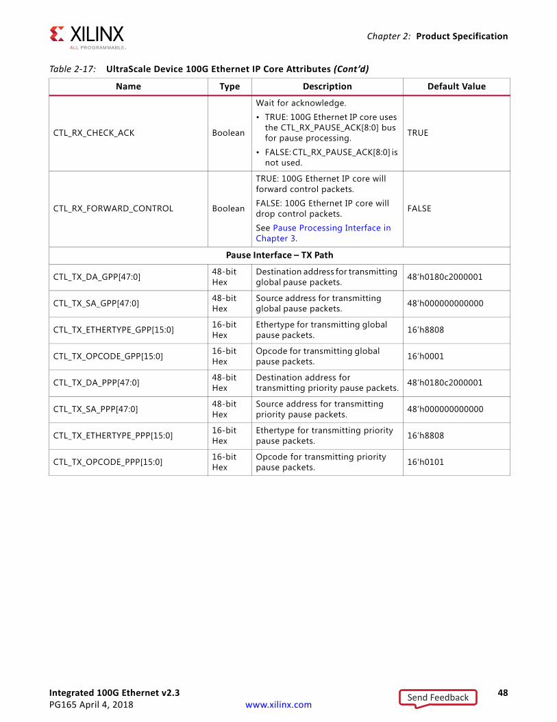
Integrated 100G Ethernet v2.3 48PG165 April 4, 2018 www.xilinx.com
Chapter 2: Product Specification
CTL_RX_CHECK_ACK Boolean
Wait for acknowledge.
• TRUE: 100G Ethernet IP core uses the CTL_RX_PAUSE_ACK[8:0] bus for pause processing.
• FALSE: CTL_RX_PAUSE_ACK[8:0] is not used.
TRUE
CTL_RX_FORWARD_CONTROL Boolean
TRUE: 100G Ethernet IP core will forward control packets.
FALSE: 100G Ethernet IP core will drop control packets.
See Pause Processing Interface in Chapter 3.
FALSE
Pause Interface – TX Path
CTL_TX_DA_GPP[47:0] 48-bit Hex
Destination address for transmitting global pause packets. 48’h0180c2000001
CTL_TX_SA_GPP[47:0] 48-bit Hex
Source address for transmitting global pause packets. 48’h000000000000
CTL_TX_ETHERTYPE_GPP[15:0] 16-bit Hex
Ethertype for transmitting global pause packets. 16’h8808
CTL_TX_OPCODE_GPP[15:0] 16-bit Hex
Opcode for transmitting global pause packets. 16’h0001
CTL_TX_DA_PPP[47:0] 48-bit Hex
Destination address for transmitting priority pause packets. 48’h0180c2000001
CTL_TX_SA_PPP[47:0] 48-bit Hex
Source address for transmitting priority pause packets. 48’h000000000000
CTL_TX_ETHERTYPE_PPP[15:0] 16-bit Hex
Ethertype for transmitting priority pause packets. 16’h8808
CTL_TX_OPCODE_PPP[15:0] 16-bit Hex
Opcode for transmitting priority pause packets. 16'h0101
Table 2-17: UltraScale Device 100G Ethernet IP Core Attributes (Cont’d)
Name Type Description Default Value
Send Feedback
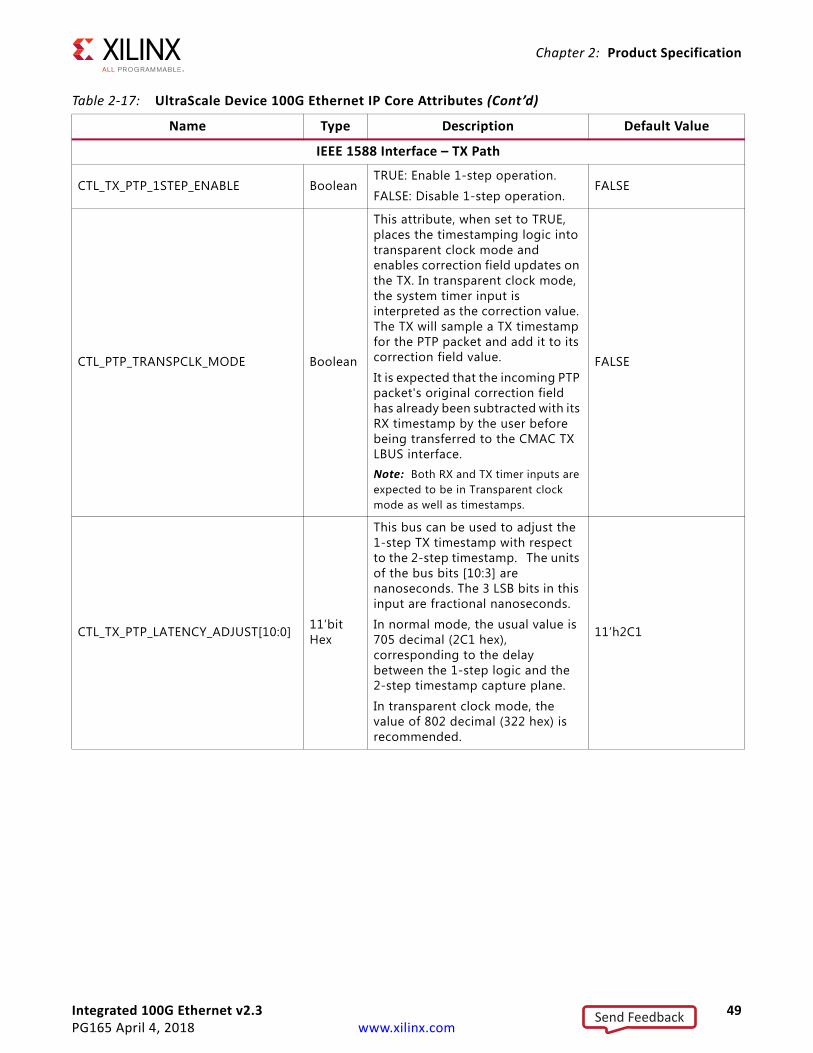
Integrated 100G Ethernet v2.3 49PG165 April 4, 2018 www.xilinx.com
Chapter 2: Product Specification
IEEE 1588 Interface – TX Path
CTL_TX_PTP_1STEP_ENABLE BooleanTRUE: Enable 1-step operation.
FALSE: Disable 1-step operation.FALSE
CTL_PTP_TRANSPCLK_MODE Boolean
This attribute, when set to TRUE, places the timestamping logic into transparent clock mode and enables correction field updates on the TX. In transparent clock mode, the system timer input is interpreted as the correction value. The TX will sample a TX timestamp for the PTP packet and add it to its correction field value.
It is expected that the incoming PTP packet's original correction field has already been subtracted with its RX timestamp by the user before being transferred to the CMAC TX LBUS interface.Note: Both RX and TX timer inputs are expected to be in Transparent clock mode as well as timestamps.
FALSE
CTL_TX_PTP_LATENCY_ADJUST[10:0] 11’bit Hex
This bus can be used to adjust the 1-step TX timestamp with respect to the 2-step timestamp. The units of the bus bits [10:3] are nanoseconds. The 3 LSB bits in this input are fractional nanoseconds.
In normal mode, the usual value is 705 decimal (2C1 hex), corresponding to the delay between the 1-step logic and the 2-step timestamp capture plane.
In transparent clock mode, the value of 802 decimal (322 hex) is recommended.
11’h2C1
Table 2-17: UltraScale Device 100G Ethernet IP Core Attributes (Cont’d)
Name Type Description Default Value
Send Feedback

Integrated 100G Ethernet v2.3 50PG165 April 4, 2018 www.xilinx.com
Chapter 3
Designing with the CoreThis chapter includes guidelines and additional information to facilitate designing with the core.
ClockingThe UltraScale™ devices integrated CMAC block has up to 13 clock inputs for the CAUI-10 interface and up to seven clock inputs for the CAUI-4 interface. These clocks include the RX_SERDES_CLK[9:0] and RX_SERDES_CLK[3:0] respectively for the CAUI-10 and CAUI-4 modes, TX_CLK, RX_CLK and the DRP_CLK. The DRP_CLK is optional and is necessary only during a DRP operation.
The 10 CAUI-10 or 4 CAUI-4 RX_SERDES_CLK clocks must not have an FPGA induced dynamic skew of more than 1000 ps. More details on the clocks are provided in the following sections.
The Runtime Switchable mode follows the same clocking structure as the one from CAUI-10 described previously.
RX GT/Lane Logic Clock (RX_SERDES_CLK)These clocks are provided to the CMAC block from the serial transceiver (GT) to clock the Lane Logic RX interface. The clocks must be 322.266 MHz for both CAUI-10 and CAUI-4 operation. The GT interface datapath is 32 bits per lane for CAUI-10 and 80 bits per lane for CAUI-4.
The other implementation allows only one RX_SERDES_CLK to go to the Ethernet MAC RX_SERDES_CLK inputs. The serial transceiver will also be in raw mode but this time the buffer is used. This mode is used when you can tolerate higher latency and are interested in saving FPGA clocking resources.
Send Feedback
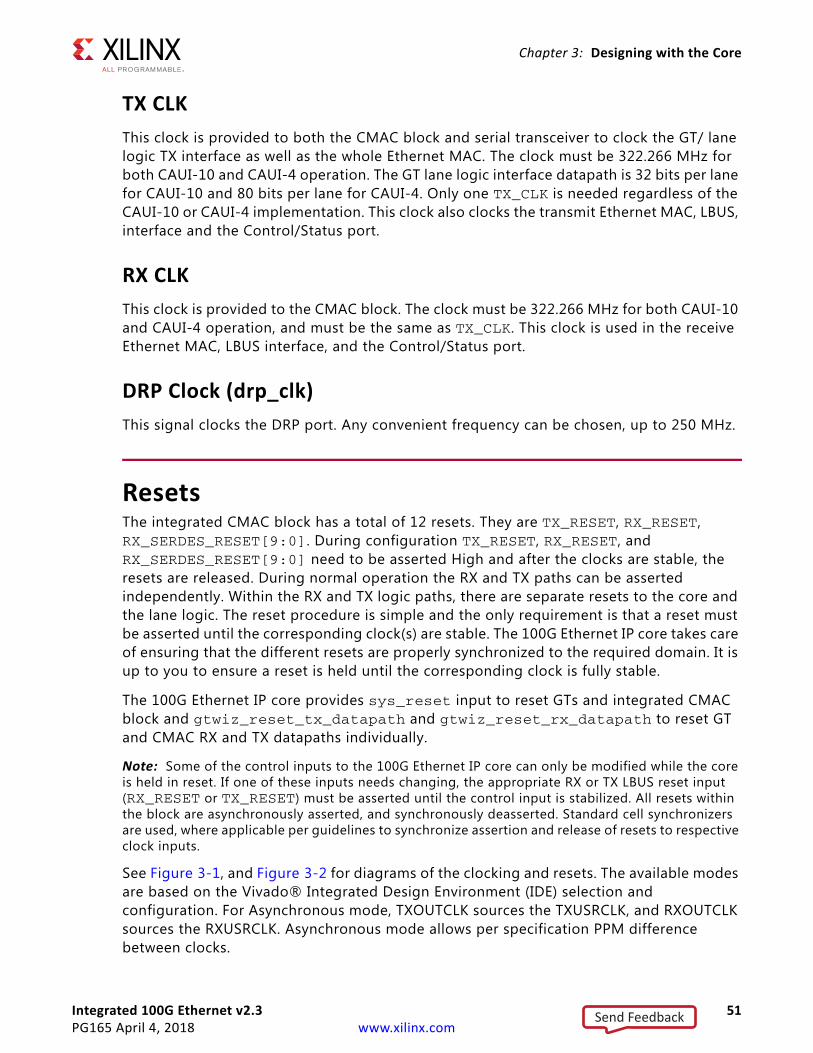
Integrated 100G Ethernet v2.3 51PG165 April 4, 2018 www.xilinx.com
Chapter 3: Designing with the Core
TX CLKThis clock is provided to both the CMAC block and serial transceiver to clock the GT/ lane logic TX interface as well as the whole Ethernet MAC. The clock must be 322.266 MHz for both CAUI-10 and CAUI-4 operation. The GT lane logic interface datapath is 32 bits per lane for CAUI-10 and 80 bits per lane for CAUI-4. Only one TX_CLK is needed regardless of the CAUI-10 or CAUI-4 implementation. This clock also clocks the transmit Ethernet MAC, LBUS, interface and the Control/Status port.
RX CLKThis clock is provided to the CMAC block. The clock must be 322.266 MHz for both CAUI-10 and CAUI-4 operation, and must be the same as TX_CLK. This clock is used in the receive Ethernet MAC, LBUS interface, and the Control/Status port.
DRP Clock (drp_clk) This signal clocks the DRP port. Any convenient frequency can be chosen, up to 250 MHz.
ResetsThe integrated CMAC block has a total of 12 resets. They are TX_RESET, RX_RESET, RX_SERDES_RESET[9:0]. During configuration TX_RESET, RX_RESET, and RX_SERDES_RESET[9:0] need to be asserted High and after the clocks are stable, the resets are released. During normal operation the RX and TX paths can be asserted independently. Within the RX and TX logic paths, there are separate resets to the core and the lane logic. The reset procedure is simple and the only requirement is that a reset must be asserted until the corresponding clock(s) are stable. The 100G Ethernet IP core takes care of ensuring that the different resets are properly synchronized to the required domain. It is up to you to ensure a reset is held until the corresponding clock is fully stable.
The 100G Ethernet IP core provides sys_reset input to reset GTs and integrated CMAC block and gtwiz_reset_tx_datapath and gtwiz_reset_rx_datapath to reset GT and CMAC RX and TX datapaths individually.
Note: Some of the control inputs to the 100G Ethernet IP core can only be modified while the core is held in reset. If one of these inputs needs changing, the appropriate RX or TX LBUS reset input (RX_RESET or TX_RESET) must be asserted until the control input is stabilized. All resets within the block are asynchronously asserted, and synchronously deasserted. Standard cell synchronizers are used, where applicable per guidelines to synchronize assertion and release of resets to respective clock inputs.
See Figure 3-1, and Figure 3-2 for diagrams of the clocking and resets. The available modes are based on the Vivado® Integrated Design Environment (IDE) selection and configuration. For Asynchronous mode, TXOUTCLK sources the TXUSRCLK, and RXOUTCLK sources the RXUSRCLK. Asynchronous mode allows per specification PPM difference between clocks.
Send Feedback
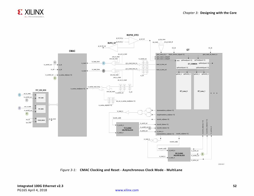
Chapter 3: Designing with the Core
Integrated 100G Ethernet v2.3 52PG165 April 4, 2018 www.xilinx.com
X-Ref Target - Figure 3-1
Figure 3-1: CMAC Clocking and Reset - Asynchronous Clock Mode - MultiLane
GT_Lane_0
GT_COMMON
refclk
qpll0outclk[quad-1:0] qpll0outrefclk[quad-1:0]
GT_Lane_1 . . .
qpll0reset[quad-1:0] qpll1reset[quad-1:0]
gtwiz_reset_all_in gtwiz_reset_clk_freerun_in
init_clk
qpll0clk_in qpll0refclk_in qpll0clk_in qpll0refclk_in
qpll0lock[quad-1:0]
GT
reset_tx_done_out
reset_rx_done_out
txusrclk_in[lanes-1:0]
txusrclk2_in[lanes-1:0]
rxusr
clk_
in[la
nes-
1:0
]
rxusr
clk2
_in
[lanes-
1:0
]txoutclk_out[lanes-1:0]
rxoutclk_out[lanes-1:0]tx_active_in
rx_act
ive_in
TX CLKING
HELPER BLOCK
tx_srcclk_in
tx_reset_in
tx_usrclk_out
txoutclk_out[0]
tx_usrclk2_out
tx_active_out
RX CLKING
HELPER BLOCK
rx_usrclk_out
rx_usrclk2_out
rx_active_out
rxpmaresetdone_out[lanes-1:0]
rx_reset_in
rxoutclk_out[0]
rxoutclk_out[0]
rx_reset_in
A
B
init_clk
drpclk_common_in[quad-1:0]
rx_srcclk_in
rx_reset_in
txprgdivresetdone_out[lanes-1:0]
tx_reset_in txpmaresetdone_out[lanes-1:0]
sys_reset
gt_drp_done
axi_gt_reset_all
IBUFDS_GTE3
gt_ref_clk_p
gt_ref_clk_n
gt_ref_clk
tx_reset
rx_reset
CMAC
tx_clk
rx_serdes_clk[lanes-1:0]
tx_reset_done
tx_usrclk2_out
rx_usrclk2_out
TRANS_DEBUGinit_clk
sys_reset
A
B
rx_clk
PKT_GEN_MON
PKT_GENtx_usrclk2_out
PKT_MON
rx_reset_done
rx_serdes_reset_donerx_serdes_reset[lanes-1:0]
A
rx_usrclk2_out
B
core_drp_reset
core_drp_reset
C
core_drp_reset
core_tx_reset
core_rx_reset
C
D
D
usr_tx_reset
usr_rx_reset
axi_usr_tx_reset
axi_usr_rx_reset
gt_drp_done
rx_clk
REG
rx_clk
REG
REG
rx_usrclk2_out
gt_tx_reset_done_inv
gt_rx_reset_done_inv
REG
tx_usrclk2_out
REG
rx_clk
REG
REG
axi_usr_rx_serdes_reset[lanes-1:0]
REG
REG
rx_serdes_clk[lanes-1:0]
gtwiz_reset_tx_datapathgtwiz_reset_rx_datapath
gt_ref_clk_out
BUFG_GT
X18950-083017
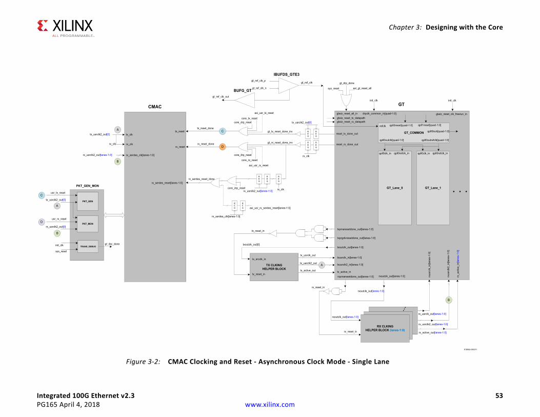
Chapter 3: Designing with the Core
Integrated 100G Ethernet v2.3 53PG165 April 4, 2018 www.xilinx.com
X-Ref Target - Figure 3-2
Figure 3-2: CMAC Clocking and Reset - Asynchronous Clock Mode - Single Lane
GT_Lane_0
GT_COMMON
refclk
qpll0outclk[quad-1:0] qpll0outrefclk[quad-1:0]
GT_Lane_1 . . .
qpll0reset[quad-1:0] qpll1reset[quad-1:0]
gtwiz_reset_all_in gtwiz_reset_clk_freerun_in
init_clk
qpll0clk_in qpll0refclk_in qpll0clk_in qpll0refclk_in
qpll0lock[quad-1:0]
GT
reset_tx_done_out
reset_rx_done_out
txusrclk_in[lanes-1:0]
txusrclk2_in[lanes-1:0]
rxus
rclk
_in[
lane
s-1:
0]
rxus
rclk
2_in
[lane
s-1:
0]
txoutclk_out[lanes-1:0]
rxoutclk_out[lanes-1:0]tx_active_in
rx_a
ctiv
e_in
[lane
s-1:
0]
TX CLKING
HELPER BLOCK
tx_srcclk_in
tx_reset_in
tx_usrclk_out
txoutclk_out[0]
tx_usrclk2_out
tx_active_out
rx_usrclk_out[lanes-1:0]
rx_usrclk2_out[lanes-1:0]
rx_active_out[lanes-1:0]
rxpmaresetdone_out[lanes-1:0]
rx_reset_in
rxoutclk_out[lanes-1:0]
rxoutclk_out[lanes-1:0]
rx_reset_in
A
B
init_clk
drpclk_common_in[quad-1:0]
rx_srcclk_in[lanes-1:0]
rx_reset_in
txprgdivresetdone_out[lanes-1:0]
tx_reset_in txpmaresetdone_out[lanes-1:0]
RX CLKING
HELPER BLOCK (lanes-1:0)
…
sys_reset
gt_drp_done
axi_gt_reset_all
tx_reset
rx_reset
CMAC
tx_clk
rx_serdes_clk[lanes-1:0]
tx_reset_done
tx_usrclk2_out[0]
rx_usrclk2_out[lanes-1:0]
TRANS_DEBUGinit_clk
sys_reset
A
B
rx_clk
PKT_GEN_MON
PKT_GENtx_usrclk2_out[0]
PKT_MON
rx_reset_done
rx_serdes_reset_donerx_serdes_reset[lanes-1:0]
A
rx_usrclk2_out[0]
B
core_drp_reset
core_drp_reset
C
core_drp_reset
core_tx_reset
core_rx_reset
D
usr_tx_reset
usr_rx_reset
axi_usr_tx_reset
axi_usr_rx_reset
gt_drp_done
rx_clk
REG
rx_clk
REG
REG
rx_usrclk2_out[lanes-1:0]
C
D
gt_tx_reset_done_inv
gt_rx_reset_done_inv
REG
tx_usrclk2_out[0]
REG
REG
REG
rx_clk
axi_usr_rx_serdes_reset[lanes-1:0]
REG
REG
rx_serdes_clk[lanes-1:0]
gtwiz_reset_tx_datapathgtwiz_reset_rx_datapath
IBUFDS_GTE3
gt_ref_clk_p
gt_ref_clk_n
gt_ref_clk
gt_ref_clk_out
BUFG_GT
X18955-083017
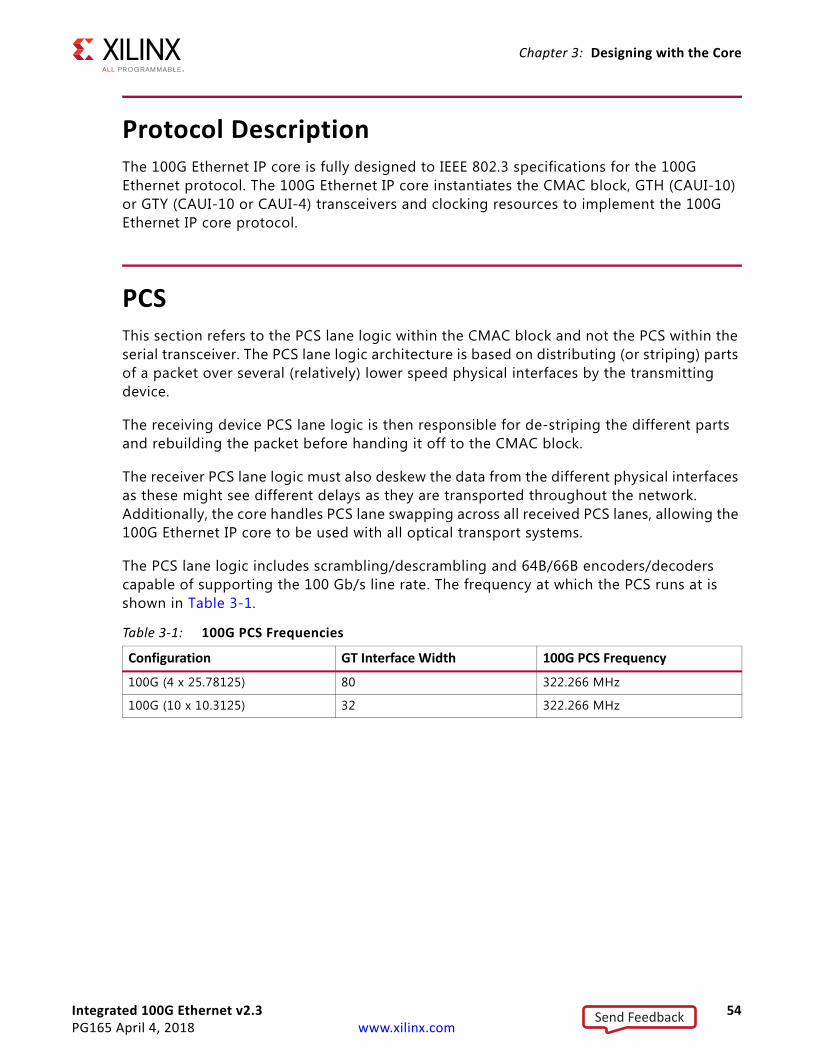
Integrated 100G Ethernet v2.3 54PG165 April 4, 2018 www.xilinx.com
Chapter 3: Designing with the Core
Protocol DescriptionThe 100G Ethernet IP core is fully designed to IEEE 802.3 specifications for the 100G Ethernet protocol. The 100G Ethernet IP core instantiates the CMAC block, GTH (CAUI-10) or GTY (CAUI-10 or CAUI-4) transceivers and clocking resources to implement the 100G Ethernet IP core protocol.
PCSThis section refers to the PCS lane logic within the CMAC block and not the PCS within the serial transceiver. The PCS lane logic architecture is based on distributing (or striping) parts of a packet over several (relatively) lower speed physical interfaces by the transmitting device.
The receiving device PCS lane logic is then responsible for de-striping the different parts and rebuilding the packet before handing it off to the CMAC block.
The receiver PCS lane logic must also deskew the data from the different physical interfaces as these might see different delays as they are transported throughout the network. Additionally, the core handles PCS lane swapping across all received PCS lanes, allowing the 100G Ethernet IP core to be used with all optical transport systems.
The PCS lane logic includes scrambling/descrambling and 64B/66B encoders/decoders capable of supporting the 100 Gb/s line rate. The frequency at which the PCS runs at is shown in Table 3-1.
Table 3-1: 100G PCS Frequencies
Configuration GT Interface Width 100G PCS Frequency
100G (4 x 25.78125) 80 322.266 MHz
100G (10 x 10.3125) 32 322.266 MHz
Send Feedback
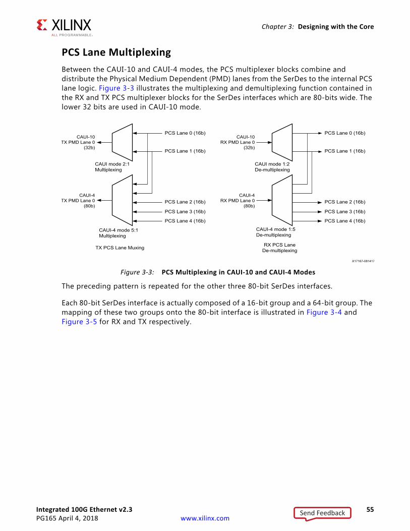
Integrated 100G Ethernet v2.3 55PG165 April 4, 2018 www.xilinx.com
Chapter 3: Designing with the Core
PCS Lane MultiplexingBetween the CAUI-10 and CAUI-4 modes, the PCS multiplexer blocks combine and distribute the Physical Medium Dependent (PMD) lanes from the SerDes to the internal PCS lane logic. Figure 3-3 illustrates the multiplexing and demultiplexing function contained in the RX and TX PCS multiplexer blocks for the SerDes interfaces which are 80-bits wide. The lower 32 bits are used in CAUI-10 mode.
The preceding pattern is repeated for the other three 80-bit SerDes interfaces.
Each 80-bit SerDes interface is actually composed of a 16-bit group and a 64-bit group. The mapping of these two groups onto the 80-bit interface is illustrated in Figure 3-4 and Figure 3-5 for RX and TX respectively.
X-Ref Target - Figure 3-3
Figure 3-3: PCS Multiplexing in CAUI-10 and CAUI-4 Modes
PCS Lane 0 (16b)
PCS Lane 1 (16b)
PCS Lane 2 (16b)
PCS Lane 3 (16b)
PCS Lane 4 (16b)
CAUI mode 2:1 Multiplexing
CAUI-4 mode 5:1 Multiplexing
CAUI-10TX PMD Lane 0
(32b)
CAUI-4TX PMD Lane 0
(80b)
PCS Lane 0 (16b)
PCS Lane 1 (16b)
PCS Lane 2 (16b)
PCS Lane 3 (16b)
PCS Lane 4 (16b)
CAUI mode 1:2 De-multiplexing
CAUI-4 mode 1:5 De-multiplexing
CAUI-10RX PMD Lane 0
(32b)
CAUI-4RX PMD Lane 0
(80b)
TX PCS Lane Muxing RX PCS Lane De-multiplexing
X17167-081417
Send Feedback
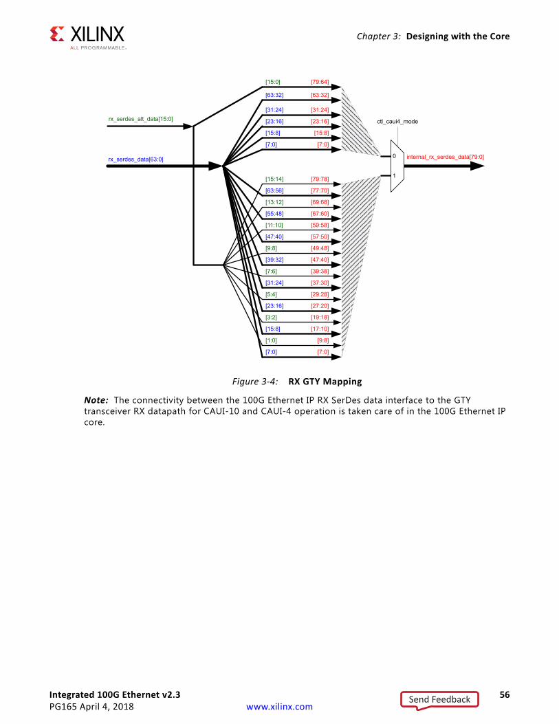
Integrated 100G Ethernet v2.3 56PG165 April 4, 2018 www.xilinx.com
Chapter 3: Designing with the Core
Note: The connectivity between the 100G Ethernet IP RX SerDes data interface to the GTY transceiver RX datapath for CAUI-10 and CAUI-4 operation is taken care of in the 100G Ethernet IP core.
X-Ref Target - Figure 3-4
Figure 3-4: RX GTY Mapping
[15:14]
[63:56]
[13:12]
[55:48]
[11:10]
[47:40]
[9:8]
[39:32]
[7:0]
[1:0]
[15:8]
[3:2]
[23:16]
[5:4]
[31:24]
[7:6]
internal_rx_serdes_data[79:0]rx_serdes_data[63:0]
[15:8]
[23:16]
[31:24]
[63:32]
[7:0]
ctl_caui4_mode
0
1[79:78]
[77:70]
[69:68]
[67:60]
[59:58]
[57:50]
[49:48]
[47:40]
[7:0]
[9:8]
[17:10]
[19:18]
[27:20]
[29:28]
[37:30]
[39:38]
[15:8]
[23:16]
[31:24]
[63:32]
[7:0]
rx_serdes_alt_data[15:0]
[79:64][15:0]
Send Feedback
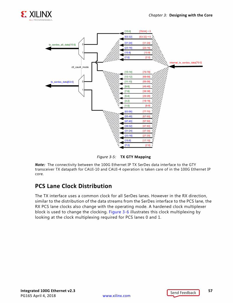
Integrated 100G Ethernet v2.3 57PG165 April 4, 2018 www.xilinx.com
Chapter 3: Designing with the Core
Note: The connectivity between the 100G Ethernet IP TX SerDes data interface to the GTY transceiver TX datapath for CAUI-10 and CAUI-4 operation is taken care of in the 100G Ethernet IP core.
PCS Lane Clock DistributionThe TX interface uses a common clock for all SerDes lanes. However in the RX direction, similar to the distribution of the data streams from the SerDes interface to the PCS lane, the RX PCS lane clocks also change with the operating mode. A hardened clock multiplexer block is used to change the clocking. Figure 3-6 illustrates this clock multiplexing by looking at the clock multiplexing required for PCS lanes 0 and 1.
X-Ref Target - Figure 3-5
Figure 3-5: TX GTY Mapping
[79:78]
[69:68]
[59:58]
[49:48]
[39:38]
[29:28]
[19:18]
[9:8]
[7:0]
[17:10]
[27:20]
[37:30]
[47:40]
[57:50]
[67:60]
[77:70]
internal_tx_serdes_data[79:0]
tx_serdes_data[63:0]
[15:8]
[23:16]
[31:24]
[63:32] = 0
[7:0]
ctl_caui4_mode
[7:0]
[15:8]
[23:16]
[31:24]
[39:32]
[47:40]
[55:48]
[63:56]
[1:0]
[3:2]
[5:4]
[7:6]
[9:8]
[11:10]
[13:12]
[15:14]
[7:0]
[15:8]
[23:16]
[31:24]
[63:32]
[79:64] = 0[15:0]
tx_serdes_alt_data[15:0]
0
1
0
1
Send Feedback
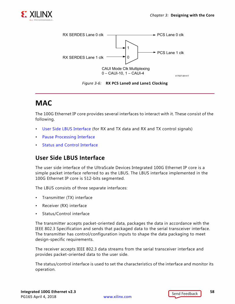
Integrated 100G Ethernet v2.3 58PG165 April 4, 2018 www.xilinx.com
Chapter 3: Designing with the Core
MACThe 100G Ethernet IP core provides several interfaces to interact with it. These consist of the following.
• User Side LBUS Interface (for RX and TX data and RX and TX control signals)
• Pause Processing Interface
• Status and Control Interface
User Side LBUS InterfaceThe user side interface of the UltraScale Devices Integrated 100G Ethernet IP core is a simple packet interface referred to as the LBUS. The LBUS interface implemented in the 100G Ethernet IP core is 512-bits segmented.
The LBUS consists of three separate interfaces:
• Transmitter (TX) interface
• Receiver (RX) interface
• Status/Control interface
The transmitter accepts packet-oriented data, packages the data in accordance with the IEEE 802.3 Specification and sends that packaged data to the serial transceiver interface. The transmitter has control/configuration inputs to shape the data packaging to meet design-specific requirements.
The receiver accepts IEEE 802.3 data streams from the serial transceiver interface and provides packet-oriented data to the user side.
The status/control interface is used to set the characteristics of the interface and monitor its operation.
X-Ref Target - Figure 3-6
Figure 3-6: RX PCS Lane0 and Lane1 Clocking
PCS Lane 0 clk
PCS Lane 1 clk
CAUI Mode Clk Multiplexing0 – CAUI-10, 1 – CAUI-4
RX SERDES Lane 0 clk
RX SERDES Lane 1 clk
1
0
X17937-081417
Send Feedback
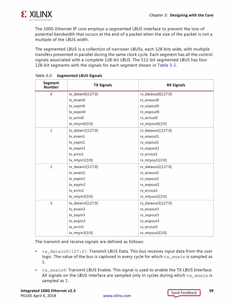
Integrated 100G Ethernet v2.3 59PG165 April 4, 2018 www.xilinx.com
Chapter 3: Designing with the Core
The 100G Ethernet IP core employs a segmented LBUS interface to prevent the loss of potential bandwidth that occurs at the end of a packet when the size of the packet is not a multiple of the LBUS width.
The segmented LBUS is a collection of narrower LBUSs, each 128 bits wide, with multiple transfers presented in parallel during the same clock cycle. Each segment has all the control signals associated with a complete 128-bit LBUS. The 512-bit segmented LBUS has four 128-bit segments with the signals for each segment shown in Table 3-2.
The transmit and receive signals are defined as follows:
• tx_datain0[127:0]: Transmit LBUS Data. This bus receives input data from the user logic. The value of the bus is captured in every cycle for which tx_enain is sampled as 1.
• tx_enain0: Transmit LBUS Enable. This signal is used to enable the TX LBUS Interface. All signals on the LBUS interface are sampled only in cycles during which tx_enain is sampled as 1.
Table 3-2: Segmented LBUS Signals
Segment Number TX Signals RX Signals
0 tx_datain0[127:0]
tx_enain0
tx_sopin0
tx_eopin0
tx_errin0
tx_mtyin0[3:0]
rx_dataout0[127:0]
rx_enaout0
rx_sopout0
rx_eopout0
rx_errout0
rx_mtyout0[3:0]
1 tx_datain1[127:0]
tx_enain1
tx_sopin1
tx_eopin1
tx_errin1
tx_mtyin1[3:0]
rx_dataout1[127:0]
rx_enaout1
rx_sopout1
rx_eopout1
rx_errout1
rx_mtyout1[3:0]
2 tx_datain2[127:0]
tx_enain2
tx_sopin2
tx_eopin2
tx_errin2
tx_mtyin2[3:0]
rx_dataout2[127:0]
rx_enaout2
rx_sopout2
rx_eopout2
rx_errout2
rx_mtyout2[3:0]
3 tx_datain3[127:0]
tx_enain3
tx_sopin3
tx_eopin3
tx_errin3
tx_mtyin3[3:0]
rx_dataout3[127:0]
rx_enaout3
rx_sopout3
rx_eopout3
rx_errout3
rx_mtyout3[3:0]
Send Feedback
Integrated 100G Ethernet v2.3 60PG165 April 4, 2018 www.xilinx.com
Chapter 3: Designing with the Core
• tx_sopin0: Transmit LBUS Start Of Packet. This signal is used to indicate the Start Of Packet (SOP) when it is sampled as a 1 and is 0 for all other transfers of the packet. This signal is sampled only in cycles during which tx_enain is sampled as 1.
• tx_eopin0: Transmit LBUS End Of Packet. This signal is used to indicate the EOP when it is sampled as a 1 and is 0 for all other transfers of the packet. This signal is sampled only in cycles during which tx_enain is sampled as 1.
• tx_errin0: Transmit LBUS Error. This signal is used to indicate that a packet contains an error when it is sampled as a 1 and is 0 for all other transfers of the packet. This signal is sampled only in cycles during which tx_enain and tx_eopin are sampled as 1.
• tx_mtyin0[3:0]: Transmit LBUS Empty. This bus is used to indicate how many bytes of the tx_datain bus are empty or invalid for the last transfer of the current packet. This bus is sampled only in cycles that tx_enain and tx_eopin are sampled as 1.
When tx_eopin and tx_errin are sampled as 1, the value of tx_mtyin[2:0] is ignored and treated as if it is 000. The other bits of tx_mtyin are used as usual.
• rx_dataout0[127:0]: Receive LBUS Data. The value of the bus is only valid in cycles during which rx_enaout is sampled as 1.
• rx_enaout0: Receive LBUS Enable. This signal qualifies the other signal of the RX LBUS Interface. Signals of the RX LBUS Interface are only valid in cycles during which rx_enaout is sampled as 1.
• rx_sopout0: Receive LBUS SOP. This signal indicates the SOP when it is sampled as 1 and is only valid in cycles during which rx_enaout is sampled as a 1.
• rx_eopout0: Receive LBUS EOP. This signal indicates the EOP when it is sampled as 1 and is only valid in cycles during which rx_enaout is sampled as a 1.
• rx_errout0: Receive LBUS Error. This signal indicates that the current packet being received has an error when it is sampled as 1. This signal is only valid in cycles when both rx_enaout and rx_eopout are sampled as a 1. When this signal is 0, it indicates that there is no error in the packet being received.
• rx_mtyout0[3:0]: Receive LBUS Empty. This bus indicates how many bytes of the rx_dataout bus are empty or invalid for the last transfer of the current packet. This bus is only valid in cycles when both rx_enaout and rx_eopout are sampled as 1.
When rx_errout and rx_enaout are sampled as 1, the value of rx_mtyout[2:0] is always 000. Other bits of rx_mtyout are as usual.
The transmitter accepts packet-oriented data. The transmitter has control/configuration inputs to shape the data packaging to meet design-specific requirements. The receiver accepts Ethernet bitstreams from the SerDes and provides packet-oriented data to the user side segmented LBUS.
Send Feedback
Integrated 100G Ethernet v2.3 61PG165 April 4, 2018 www.xilinx.com
Chapter 3: Designing with the Core
IMPORTANT: In the following section, the term "asserting" is used to mean "assigning a value of 1," and the term "negating" is used to mean "assigning a value of 0."
TX LBUS Interface
The synchronous TX Local bus interface accepts packet-oriented data of an arbitrary length. All signals are synchronous relative to the rising-edge of the clk port. Figure 3-7 shows a sample waveform for data transactions for two consecutive 65-byte packets using a 512-bit segmented bus. Each of the four segments is 128-bits wide.
Send Feedback
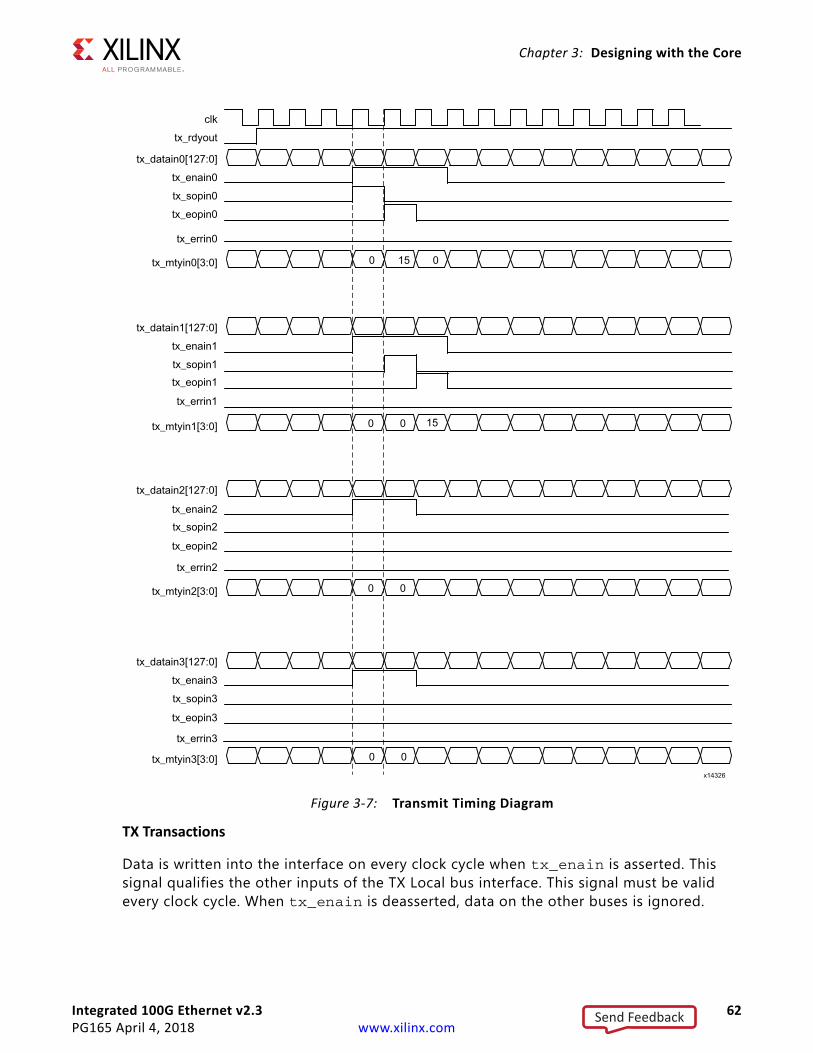
Integrated 100G Ethernet v2.3 62PG165 April 4, 2018 www.xilinx.com
Chapter 3: Designing with the Core
TX Transactions
Data is written into the interface on every clock cycle when tx_enain is asserted. This signal qualifies the other inputs of the TX Local bus interface. This signal must be valid every clock cycle. When tx_enain is deasserted, data on the other buses is ignored.
X-Ref Target - Figure 3-7
Figure 3-7: Transmit Timing Diagram
Send Feedback
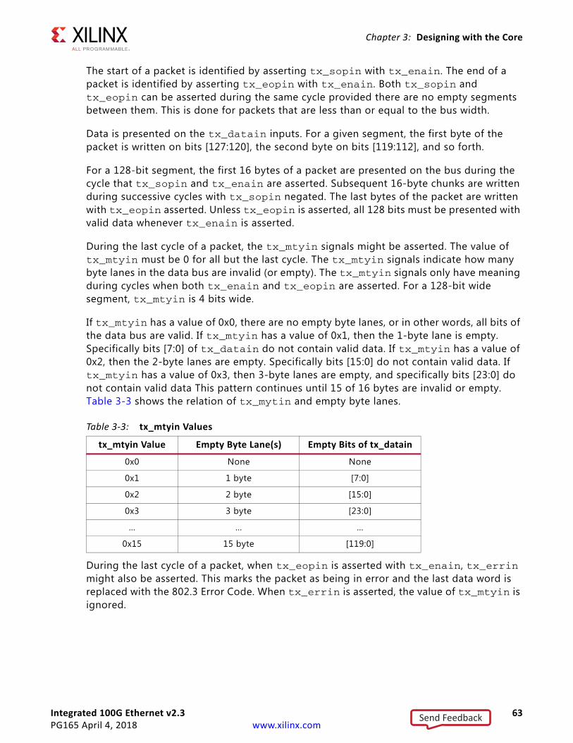
Integrated 100G Ethernet v2.3 63PG165 April 4, 2018 www.xilinx.com
Chapter 3: Designing with the Core
The start of a packet is identified by asserting tx_sopin with tx_enain. The end of a packet is identified by asserting tx_eopin with tx_enain. Both tx_sopin and tx_eopin can be asserted during the same cycle provided there are no empty segments between them. This is done for packets that are less than or equal to the bus width.
Data is presented on the tx_datain inputs. For a given segment, the first byte of the packet is written on bits [127:120], the second byte on bits [119:112], and so forth.
For a 128-bit segment, the first 16 bytes of a packet are presented on the bus during the cycle that tx_sopin and tx_enain are asserted. Subsequent 16-byte chunks are written during successive cycles with tx_sopin negated. The last bytes of the packet are written with tx_eopin asserted. Unless tx_eopin is asserted, all 128 bits must be presented with valid data whenever tx_enain is asserted.
During the last cycle of a packet, the tx_mtyin signals might be asserted. The value of tx_mtyin must be 0 for all but the last cycle. The tx_mtyin signals indicate how many byte lanes in the data bus are invalid (or empty). The tx_mtyin signals only have meaning during cycles when both tx_enain and tx_eopin are asserted. For a 128-bit wide segment, tx_mtyin is 4 bits wide.
If tx_mtyin has a value of 0x0, there are no empty byte lanes, or in other words, all bits of the data bus are valid. If tx_mtyin has a value of 0x1, then the 1-byte lane is empty. Specifically bits [7:0] of tx_datain do not contain valid data. If tx_mtyin has a value of 0x2, then the 2-byte lanes are empty. Specifically bits [15:0] do not contain valid data. If tx_mtyin has a value of 0x3, then 3-byte lanes are empty, and specifically bits [23:0] do not contain valid data This pattern continues until 15 of 16 bytes are invalid or empty. Table 3-3 shows the relation of tx_mytin and empty byte lanes.
During the last cycle of a packet, when tx_eopin is asserted with tx_enain, tx_errin might also be asserted. This marks the packet as being in error and the last data word is replaced with the 802.3 Error Code. When tx_errin is asserted, the value of tx_mtyin is ignored.
Table 3-3: tx_mtyin Values
tx_mtyin Value Empty Byte Lane(s) Empty Bits of tx_datain
0x0 None None
0x1 1 byte [7:0]
0x2 2 byte [15:0]
0x3 3 byte [23:0]
... ... ...
0x15 15 byte [119:0]
Send Feedback
Integrated 100G Ethernet v2.3 64PG165 April 4, 2018 www.xilinx.com
Chapter 3: Designing with the Core
tx_rdyout
Data can be safely written, that is, tx_enain asserted, when tx_rdyout is asserted. After tx_rdyout is negated, additional writes using tx_enain can be safely performed provided tx_ovfout is never asserted. When tx_rdyout is asserted again, additional data can be written. If at any time the back-pressure mechanism is violated, the tx_ovfout is asserted to indicate the violation. Up to four write cycles might be safely performed after tx_rdyout is negated, but no more until tx_rdyout is asserted again.
RX LBUS Interface
The synchronous RX Local bus interface provides packet-oriented data much like the TX Local bus interface accepts. All signals are synchronous with the rising-edge of the Local bus clock. Figure 3-8 shows a sample waveform for two data transactions for 65-byte packets using a 512-bit segmented LBUS.
Send Feedback
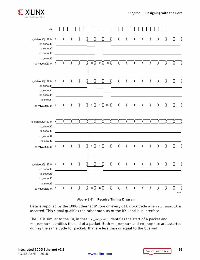
Integrated 100G Ethernet v2.3 65PG165 April 4, 2018 www.xilinx.com
Chapter 3: Designing with the Core
Data is supplied by the 100G Ethernet IP core on every clk clock cycle when rx_enaout is asserted. This signal qualifies the other outputs of the RX Local bus interface.
The RX is similar to the TX, in that rx_sopout identifies the start of a packet and rx_eopout identifies the end of a packet. Both rx_sopout and rx_eopout are asserted during the same cycle for packets that are less than or equal to the bus width.
X-Ref Target - Figure 3-8
Figure 3-8: Receive Timing Diagram
Send Feedback
Integrated 100G Ethernet v2.3 66PG165 April 4, 2018 www.xilinx.com
Chapter 3: Designing with the Core
As in the TX, the first byte of a packet is supplied on the most significant bits of rx_dataout. For a 128-bit wide segment, the first byte of the packet is written on bits [127:120], the second byte on bits [119:112], and so forth.
As in the TX, portions of packets are written on the bus in the full width of the bus unless rx_eopout is asserted. When rx_eopout is asserted, the rx_mtyout bus indicates how many byte lanes in the data bus are invalid. The encoding is the same as for tx_mtyin.
During the last cycle of a packet, when rx_eopout is asserted with rx_enaout, rx_errout might also be asserted. This indicates the packet received had one of the following errors:
• FCS error
• Length out of the valid range (64 to CTL_RX_MAX_PACKET_LEN[14:0] bytes)
• Bad 64B/66B code received during receipt of the packet
There is no mechanism to back-pressure the RX Local bus interface. The user logic must be capable of receiving data when rx_enaout is asserted.
Bus Rules
This section describes the rules that govern the successful use of the segmented LBUS protocol.
Segment Ordering
The 128-bit segments are ordered 0 to 3 (for a 512-bit segmented LBUS). The first of the 128-bit transfers occurs on segment 0, the second on segment 1, and so forth. During each local bus clock cycle that data is transferred on the segmented LBUS, segment 0 must be active. The segmented bus is aligned so that the first bit of the incoming data is placed at the MSB of segment 0.
Active Segments
Data is transferred in a segment on the TX interface when the corresponding tx_enainS is a value of 1. The TX interface buffers data, but packets must be written in their entirety unless backpressure is applied (see Gaps). Therefore, it is acceptable to have clock cycles in which none of the tx_enainS signals are active during backpressure. However, during a clock cycle with tx_enain0 active, segments must be filled in sequence with no gaps between active segments. The following are some of the illegal combinations of tx_enainX:
Send Feedback
Integrated 100G Ethernet v2.3 67PG165 April 4, 2018 www.xilinx.com
Chapter 3: Designing with the Core
• tx_enain0=0, tx_enain1=1, tx_enain2=1, tx_enain3=1
• tx_enain0=1, tx_enain1=0, tx_enain2=1, tx_enain3=1
• tx_enain0=1, tx_enain1=1, tx_enain2=0, tx_enain3=1
Data is transferred in a segment on the RX interface when the corresponding rx_enainS is a value of 1. Similarly, the RX interface buffers data and does not forward until it has a sufficient quantity. Therefore, there are clock cycles in which none of the rx_enainS signals are active.
TX Backpressure
The optimal use of bandwidth requires that TX local bus data can be written at a rate faster than it can be delivered on the serial interface. This means that there must be backpressure, or flow-control, on the TX segmented LBUS. The signals used to implement backpressure are tx_rdyout and tx_ovfout. These signals are common for all segments. When responding to backpressure during a clock cycle, none of the tx_enainS can be active.
Gaps
The purpose of the segmented LBUS is to provide a means to optimally use the data bus. Therefore, as discussed in Active Segments, segments must be filled in sequence with no gaps between used segments. However, if a segment has an EOP, the following segments might be inactive. For example, the following combinations are permitted during a single clock cycle:
• tx_enain0=1 tx_eopin0=0 tx_enain1=1 tx_eopin1=0 tx_enain2=1 tx_eopin2=1 tx_enain3=0 tx_eopin3=0
• tx_enain0=1 tx_eopin0=0 tx_enain1=1 tx_eopin1=1 tx_enain2=0 tx_eopin2=0 tx_enain3=0 tx_eopin3=0
• tx_enain0=1 tx_eopin0=1 tx_enain1=0 tx_eopin1=0 tx_enain2=0 tx_eopin2=0 tx_enain3=0 tx_eopin3=0
Examples
This section contains examples that illustrate segmented LBUS cycles covering various combinations of SOP, Dat (data in the middle of a packet), EOP, and idle (no data on the bus). Valid and invalid cycles are shown.
The segmented LBUS is assumed to be 512 bits wide and each segment is 128 bits wide (16 bytes). The TX direction is illustrated. The RX direction has analogous behavior, but there are no invalid cycles on the receive segmented LBUS.
Send Feedback
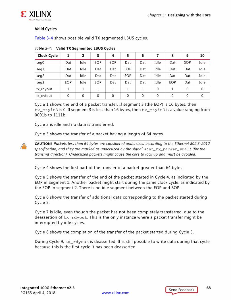
Integrated 100G Ethernet v2.3 68PG165 April 4, 2018 www.xilinx.com
Chapter 3: Designing with the Core
Valid Cycles
Table 3-4 shows possible valid TX segmented LBUS cycles.
Cycle 1 shows the end of a packet transfer. If segment 3 (the EOP) is 16 bytes, then tx_mtyin3 is 0. If segment 3 is less than 16 bytes, then tx_mtyin3 is a value ranging from 0001b to 1111b.
Cycle 2 is idle and no data is transferred.
Cycle 3 shows the transfer of a packet having a length of 64 bytes.
CAUTION! Packets less than 64 bytes are considered undersized according to the Ethernet 802.3-2012 specification, and they are marked as undersized by the signal stat_tx_packet_small (for the transmit direction). Undersized packets might cause the core to lock up and must be avoided.
Cycle 4 shows the first part of the transfer of a packet greater than 64 bytes.
Cycle 5 shows the transfer of the end of the packet started in Cycle 4, as indicated by the EOP in Segment 1. Another packet might start during the same clock cycle, as indicated by the SOP in segment 2. There is no idle segment between the EOP and SOP.
Cycle 6 shows the transfer of additional data corresponding to the packet started during Cycle 5.
Cycle 7 is idle, even though the packet has not been completely transferred, due to the deassertion of tx_rdyout. This is the only instance where a packet transfer might be interrupted by idle cycles.
Cycle 8 shows the completion of the transfer of the packet started during Cycle 5.
During Cycle 9, tx_rdyout is deasserted. It is still possible to write data during that cycle because this is the first cycle it has been deasserted.
Table 3-4: Valid TX Segmented LBUS Cycles
Clock Cycle 1 2 3 4 5 6 7 8 9 10
seg0 Dat Idle SOP SOP Dat Dat Idle Dat SOP Idle
seg1 Dat Idle Dat Dat EOP Dat Idle Dat Dat Idle
seg2 Dat Idle Dat Dat SOP Dat Idle Dat Dat Idle
seg3 EOP Idle EOP Dat Dat Dat Idle EOP Dat Idle
tx_rdyout 1 1 1 1 1 1 0 1 0 0
tx_ovfout 0 0 0 0 0 0 0 0 0 0
Send Feedback
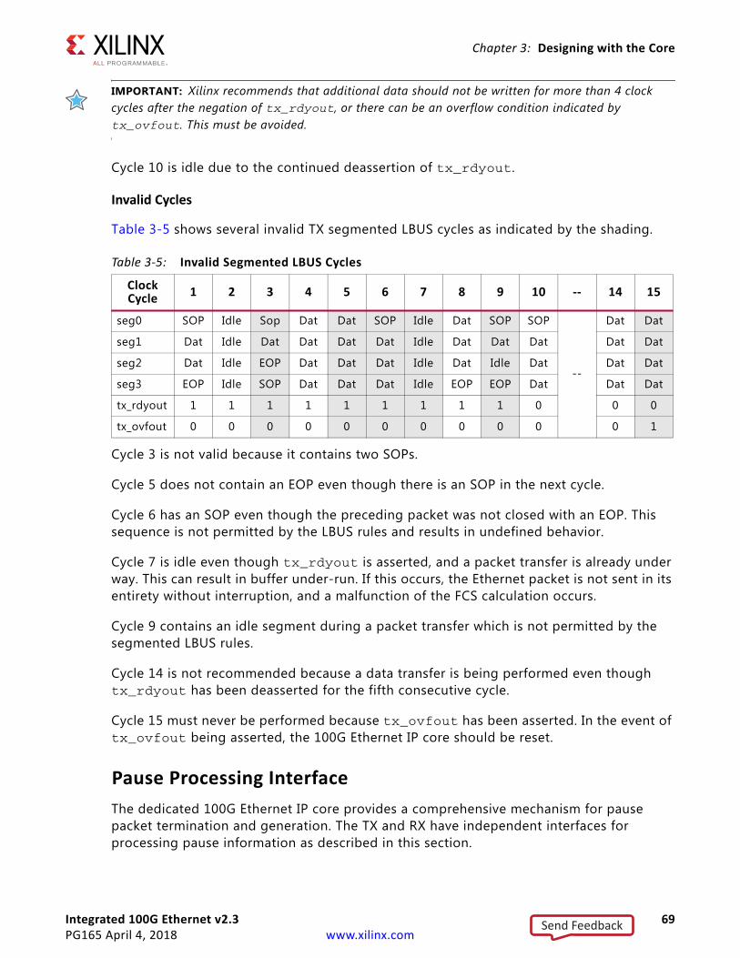
Integrated 100G Ethernet v2.3 69PG165 April 4, 2018 www.xilinx.com
Chapter 3: Designing with the Core
IMPORTANT: Xilinx recommends that additional data should not be written for more than 4 clock cycles after the negation of tx_rdyout, or there can be an overflow condition indicated by tx_ovfout. This must be avoided.
Cycle 10 is idle due to the continued deassertion of tx_rdyout.
Invalid Cycles
Table 3-5 shows several invalid TX segmented LBUS cycles as indicated by the shading.
Cycle 3 is not valid because it contains two SOPs.
Cycle 5 does not contain an EOP even though there is an SOP in the next cycle.
Cycle 6 has an SOP even though the preceding packet was not closed with an EOP. This sequence is not permitted by the LBUS rules and results in undefined behavior.
Cycle 7 is idle even though tx_rdyout is asserted, and a packet transfer is already under way. This can result in buffer under-run. If this occurs, the Ethernet packet is not sent in its entirety without interruption, and a malfunction of the FCS calculation occurs.
Cycle 9 contains an idle segment during a packet transfer which is not permitted by the segmented LBUS rules.
Cycle 14 is not recommended because a data transfer is being performed even though tx_rdyout has been deasserted for the fifth consecutive cycle.
Cycle 15 must never be performed because tx_ovfout has been asserted. In the event of tx_ovfout being asserted, the 100G Ethernet IP core should be reset.
Pause Processing InterfaceThe dedicated 100G Ethernet IP core provides a comprehensive mechanism for pause packet termination and generation. The TX and RX have independent interfaces for processing pause information as described in this section.
Table 3-5: Invalid Segmented LBUS Cycles
Clock Cycle 1 2 3 4 5 6 7 8 9 10 -- 14 15
seg0 SOP Idle Sop Dat Dat SOP Idle Dat SOP SOP
--
Dat Dat
seg1 Dat Idle Dat Dat Dat Dat Idle Dat Dat Dat Dat Dat
seg2 Dat Idle EOP Dat Dat Dat Idle Dat Idle Dat Dat Dat
seg3 EOP Idle SOP Dat Dat Dat Idle EOP EOP Dat Dat Dat
tx_rdyout 1 1 1 1 1 1 1 1 1 0 0 0
tx_ovfout 0 0 0 0 0 0 0 0 0 0 0 1
Send Feedback
Integrated 100G Ethernet v2.3 70PG165 April 4, 2018 www.xilinx.com
Chapter 3: Designing with the Core
TX Pause Generation
You can request a pause packet to be transmitted using the CTL_TX_PAUSE_REQ[8:0] and CTL_TX_PAUSE_ENABLE[8:0] input buses. Bit 8 corresponds to global pause packets and bits [7:0] correspond to priority pause packets.
Each bit of this bus must be held at a steady state for a minimum of 16 cycles before the next transition.
IMPORTANT: The 100G Ethernet IP core does not support assertion of global and priority pause packets at the same time.
The contents of the pause packet are determined using the following input pins.
Global pause packets:
• CTL_TX_DA_GPP[47:0]
• CTL_TX_SA_GPP[47:0]
• CTL_TX_ETHERTYPE_GPP[15:0]
• CTL_TX_OPCODE_GPP[15:0]
• CTL_TX_PAUSE_QUANTA8[15:0]
Priority pause packets:
• CTL_TX_DA_PPP[47:0]
• CTL_TX_SA_PPP[47:0]
• CTL_TX_ETHERTYPE_PPP[15:0]
• CTL_TX_OPCODE_PPP[15:0]
• CTL_TX_PAUSE_QUANTA0[15:0]
• CTL_TX_PAUSE_QUANTA1[15:0]
• CTL_TX_PAUSE_QUANTA2[15:0]
• CTL_TX_PAUSE_QUANTA3[15:0]
• CTL_TX_PAUSE_QUANTA4[15:0]
• CTL_TX_PAUSE_QUANTA5[15:0]
• CTL_TX_PAUSE_QUANTA6[15:0]
• CTL_TX_PAUSE_QUANTA7[15:0]
Send Feedback
Integrated 100G Ethernet v2.3 71PG165 April 4, 2018 www.xilinx.com
Chapter 3: Designing with the Core
The dedicated 100G Ethernet IP core automatically calculates and adds the FCS to the packet. For priority pause packets, the dedicated 100G Ethernet IP core also automatically generates the enable vector based on the priorities that are requested.
To request a pause packet, you must set the corresponding bit of the CTL_TX_PAUSE_REQ[8:0] and CTL_TX_PAUSE_ENABLE[8:0] bus to a 1 and keep it at 1 for the duration of the pause request (that is, if these inputs are set to 0, all pending pause packets are cancelled. Pause is cancelled by sending out additional pause packet with pause quanta set to 0).
The dedicated 100G Ethernet IP core will transmit the pause packet immediately after the current packet in flight is completed. Each bit of this bus must be held at a steady state for a minimum of 16 cycles before the next transition.
To retransmit pause packets, the dedicated 100G Ethernet IP core maintains a total of nine independent timers: one for each priority and one for global pause. These timers are loaded with the value of the corresponding input buses. After a pause packet is transmitted the corresponding timer is loaded with the corresponding value of the CTL_TX_PAUSE_REFRESH_TIMER[8:0] input bus. When a timer times out, another packet for that priority (or global) is transmitted as soon as the current packet in flight is completed. Additionally, you can manually force the timers to 0, and therefore, force a retransmission by setting the CTL_TX_RESEND_PAUSE input to 1 for one clock cycle.
To reduce the number of pause packets for priority mode operation, a timer is considered "timed out" if any of the other timers time out. Additionally, while waiting for the current packet in flight to be completed, any new timer that times out or any new requests from the you will be merged into a single pause frame. For example, if two timers are counting down, and you send a request for a third priority, the two timers are forced to be timed out and a pause packet for all three priorities is sent as soon as the current in-flight packet (if any) is transmitted.
Similarly, if one of the two timers times out without an additional request from you, both timers are forced to be timed out and a pause packet for both priorities is sent as soon as the current in-flight packet (if any) is transmitted.
You can stop pause packet generation by setting the appropriate bits of CTL_TX_PAUSE_REQ[8:0] or CTL_TX_PAUSE_ENABLE[8:0] to 0.
Send Feedback
Integrated 100G Ethernet v2.3 72PG165 April 4, 2018 www.xilinx.com
Chapter 3: Designing with the Core
RX Pause Termination
The dedicated 100G Ethernet IP core terminates global and priority pause frames and provides a simple hand-shaking interface to allow user logic to respond to pause packets.
Determining Pause Packets
There are three steps in determining pause packets:
1. Checks are performed to see if a packet is a global or a priority control packet. Packets that pass step 1 are forwarded to you only if CTL_RX_FORWARD_CONTROL is set to 1.
2. If step 1 passes, the packet is checked to determine if it is a global pause packet.
3. If step 2 fails, the packet is checked to determine if it is a priority pause packet.
For step 1, the following pseudo code shows the checking function:
assign da_match_gcp = (!ctl_rx_check_mcast_gcp && !ctl_rx_check_ucast_gcp) || ((DA == ctl_rx_pause_da_ucast) && ctl_rx_check_ucast_gcp) || ((DA == 48'h0180c2000001) && ctl_rx_check_mcast_gcp);
assign sa_match_gcp = !ctl_rx_check_sa_gcp || (SA == ctl_rx_pause_sa);
assign etype_match_gcp = !ctl_rx_check_etype_gcp || (ETYPE == ctl_rx_etype_gcp);
assign opcode_match_gcp = !ctl_rx_check_opcode_gcp || ((OPCODE >= ctl_rx_opcode_min_gcp) && (OPCODE <= ctl_rx_opcode_max_gcp));
assign global_control_packet = da_match_gcp && sa_match_gcp && etype_match_gcp &&opcode_match_gcp && ctl_rx_enable_gcp;
assign da_match_pcp = (!ctl_rx_check_mcast_pcp && !ctl_rx_check_ucast_pcp) || ((DA == ctl_rx_pause_da_ucast) && ctl_rx_check_ucast_pcp) || ((DA == ctl_rx_pause_da_mcast) && ctl_rx_check_mcast_pcp);
assign sa_match_pcp = !ctl_rx_check_sa_pcp || (SA == ctl_rx_pause_sa);
assign etype_match_pcp = !ctl_rx_check_etype_pcp || (ETYPE == ctl_rx_etype_pcp);
assign opcode_match_pcp = !ctl_rx_check_opcode_pcp || ((OPCODE >= ctl_rx_opcode_min_pcp) && (OPCODE <= ctl_rx_opcode_max_pcp));
assign priority_control_packet = da_match_pcp && sa_match_pcp && etype_match_pcp && opcode_match_pcp && ctl_rx_enable_pcp;
assign control_packet = global_control_packet || priority_control_packet;
where DA is the destination address, SA is the source address, OPCODE is the opcode, and ETYPE is the ethertype/length field that is extracted from the incoming packet.
Send Feedback
Integrated 100G Ethernet v2.3 73PG165 April 4, 2018 www.xilinx.com
Chapter 3: Designing with the Core
For step 2, the following pseudo code shows the checking function:
assign da_match_gpp = (!ctl_rx_check_mcast_gpp && !ctl_rx_check_ucast_gpp) || ((DA == ctl_rx_pause_da_ucast) && ctl_rx_check_ucast_gpp) || ((DA == 48'h0180c2000001) && ctl_rx_check_mcast_gpp);
assign sa_match_gpp = !ctl_rx_check_sa_gpp || (SA == ctl_rx_pause_sa);
assign etype_match_gpp = !ctl_rx_check_etype_gpp || (ETYPE == ctl_rx_etype_gpp);
assign opcode_match_gpp = !ctl_rx_check_opcode_gpp || (OPCODE == ctl_rx_opcode_gpp);
assign global_pause_packet = da_match_gpp && sa_match_gpp && etype_match_gpp && opcode_match_gpp && ctl_rx_enable_gpp;
where DA is the destination address, SA is the source address, OPCODE is the opcode, and ETYPE is the ethertype/length field that is extracted from the incoming packet.
For step 3, the following pseudo code shows the checking function:
assign da_match_ppp = (!ctl_rx_check_mcast_ppp && !ctl_rx_check_ucast_ppp) || ((DA == ctl_rx_pause_da_ucast) && ctl_rx_check_ucast_ppp) || ((DA == ctl_rx_pause_da_mcast) && ctl_rx_check_mcast_ppp);
assign sa_match_ppp = !ctl_rx_check_sa_ppp || (SA == ctl_rx_pause_sa);
assign etype_match_ppp = !ctl_rx_check_etype_ppp || (ETYPE == ctl_rx_etype_ppp);
assign opcode_match_ppp = !ctl_rx_check_opcode_ppp || (OPCODE == ctl_rx_opcode_ppp);
assign priority_pause_packet = da_match_ppp && sa_match_ppp && etype_match_ppp && opcode_match_ppp && ctl_rx_enable_ppp;
where DA is the destination address, SA is the source address, OPCODE is the opcode, and ETYPE is the ethertype/length field that is extracted from the incoming packet.
User Interface
A simple hand-shaking protocol alerts you of the reception of pause packets using the CTL_RX_PAUSE_ENABLE[8:0], STAT_RX_PAUSE_REQ[8:0] and CTL_RX_PAUSE_ACK[8:0] buses. For both buses, bit [8] corresponds to global pause packets and bits [7:0] correspond to priority pause packets.
The following steps occur when a pause packet is received:
1. If the corresponding bit of CTL_RX_PAUSE_ENABLE[8:0] is 0, the quanta is ignored and the dedicated 100G Ethernet IP core stays in step 1. Otherwise, the corresponding bit of the STAT_RX_PAUSE_REQ[8:0] bus is set to 1, and the received quanta is loaded into a timer.
Note: If one of the bits of CTL_RX_PAUSE_ENABLE[8:0] is set to 0 (that is, disabled) when the pause processing is in step 2 or later, the dedicated 100G Ethernet IP core completes the steps as normal until it comes back to step 1.
Send Feedback
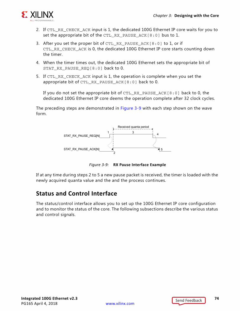
Integrated 100G Ethernet v2.3 74PG165 April 4, 2018 www.xilinx.com
Chapter 3: Designing with the Core
2. If CTL_RX_CHECK_ACK input is 1, the dedicated 100G Ethernet IP core waits for you to set the appropriate bit of the CTL_RX_PAUSE_ACK[8:0] bus to 1.
3. After you set the proper bit of CTL_RX_PAUSE_ACK[8:0] to 1, or if CTL_RX_CHECK_ACK is 0, the dedicated 100G Ethernet IP core starts counting down the timer.
4. When the timer times out, the dedicated 100G Ethernet sets the appropriate bit of STAT_RX_PAUSE_REQ[8:0] back to 0.
5. If CTL_RX_CHECK_ACK input is 1, the operation is complete when you set the appropriate bit of CTL_RX_PAUSE_ACK[8:0] back to 0.
If you do not set the appropriate bit of CTL_RX_PAUSE_ACK[8:0] back to 0, the dedicated 100G Ethernet IP core deems the operation complete after 32 clock cycles.
The preceding steps are demonstrated in Figure 3-9 with each step shown on the wave form.
If at any time during steps 2 to 5 a new pause packet is received, the timer is loaded with the newly acquired quanta value and the and the process continues.
Status and Control InterfaceThe status/control interface allows you to set up the 100G Ethernet IP core configuration and to monitor the status of the core. The following subsections describe the various status and control signals.
X-Ref Target - Figure 3-9
Figure 3-9: RX Pause Interface Example
STAT_RX_PAUSE_REQ[N]1 4
STAT_RX_PAUSE_ACK[N]
Received quanta period
2
3
5
Send Feedback
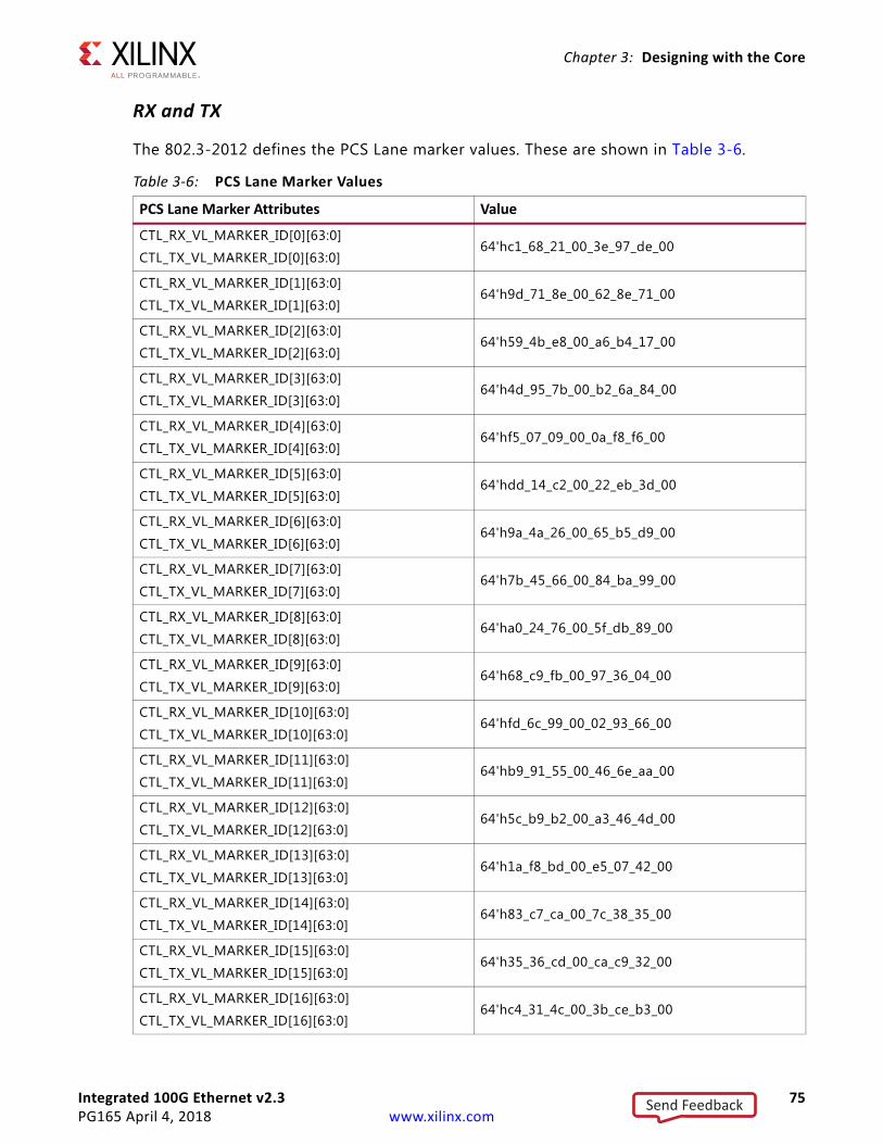
Integrated 100G Ethernet v2.3 75PG165 April 4, 2018 www.xilinx.com
Chapter 3: Designing with the Core
RX and TX
The 802.3-2012 defines the PCS Lane marker values. These are shown in Table 3-6.
Table 3-6: PCS Lane Marker Values
PCS Lane Marker Attributes Value
CTL_RX_VL_MARKER_ID[0][63:0]
CTL_TX_VL_MARKER_ID[0][63:0]64'hc1_68_21_00_3e_97_de_00
CTL_RX_VL_MARKER_ID[1][63:0]
CTL_TX_VL_MARKER_ID[1][63:0]64'h9d_71_8e_00_62_8e_71_00
CTL_RX_VL_MARKER_ID[2][63:0]
CTL_TX_VL_MARKER_ID[2][63:0]64'h59_4b_e8_00_a6_b4_17_00
CTL_RX_VL_MARKER_ID[3][63:0]
CTL_TX_VL_MARKER_ID[3][63:0]64'h4d_95_7b_00_b2_6a_84_00
CTL_RX_VL_MARKER_ID[4][63:0]
CTL_TX_VL_MARKER_ID[4][63:0]64'hf5_07_09_00_0a_f8_f6_00
CTL_RX_VL_MARKER_ID[5][63:0]
CTL_TX_VL_MARKER_ID[5][63:0]64'hdd_14_c2_00_22_eb_3d_00
CTL_RX_VL_MARKER_ID[6][63:0]
CTL_TX_VL_MARKER_ID[6][63:0]64'h9a_4a_26_00_65_b5_d9_00
CTL_RX_VL_MARKER_ID[7][63:0]
CTL_TX_VL_MARKER_ID[7][63:0]64'h7b_45_66_00_84_ba_99_00
CTL_RX_VL_MARKER_ID[8][63:0]
CTL_TX_VL_MARKER_ID[8][63:0]64'ha0_24_76_00_5f_db_89_00
CTL_RX_VL_MARKER_ID[9][63:0]
CTL_TX_VL_MARKER_ID[9][63:0]64'h68_c9_fb_00_97_36_04_00
CTL_RX_VL_MARKER_ID[10][63:0]
CTL_TX_VL_MARKER_ID[10][63:0]64'hfd_6c_99_00_02_93_66_00
CTL_RX_VL_MARKER_ID[11][63:0]
CTL_TX_VL_MARKER_ID[11][63:0]64'hb9_91_55_00_46_6e_aa_00
CTL_RX_VL_MARKER_ID[12][63:0]
CTL_TX_VL_MARKER_ID[12][63:0]64'h5c_b9_b2_00_a3_46_4d_00
CTL_RX_VL_MARKER_ID[13][63:0]
CTL_TX_VL_MARKER_ID[13][63:0]64'h1a_f8_bd_00_e5_07_42_00
CTL_RX_VL_MARKER_ID[14][63:0]
CTL_TX_VL_MARKER_ID[14][63:0]64'h83_c7_ca_00_7c_38_35_00
CTL_RX_VL_MARKER_ID[15][63:0]
CTL_TX_VL_MARKER_ID[15][63:0]64'h35_36_cd_00_ca_c9_32_00
CTL_RX_VL_MARKER_ID[16][63:0]
CTL_TX_VL_MARKER_ID[16][63:0]64'hc4_31_4c_00_3b_ce_b3_00
Send Feedback
Integrated 100G Ethernet v2.3 76PG165 April 4, 2018 www.xilinx.com
Chapter 3: Designing with the Core
RX PCS Lane Alignment Status
The 100G Ethernet IP core provides status bits to indicate the state of word boundary synchronization and PCS lane alignment. All signals are synchronous with the rising-edge of RX_CLK. A detailed description of each signal follows.
STAT_RX_SYNCED[19:0]
When a bit of this bus is 0, it indicates that word boundary synchronization of the corresponding lane is not complete or that an error has occurred as identified by another status bit.
When a bit of this bus is 1, it indicates that the corresponding lane is word boundary synchronized and is receiving PCS Lane Marker Words as expected.
STAT_RX_SYNCED_ERR[19:0]
When a bit of this bus is 1, it indicates one of several possible failures on the corresponding lane.
• Word boundary synchronization in the lane was not possible using Framing bits [65:64].
• After word boundary synchronization in the lane was achieved, errors were detected on Framing bits [65:64].
• After word boundary synchronization in the lane was achieved, a valid PCS Lane Marker Word was never received.
The bits of the bus remain asserted until word boundary synchronization occurs or until some other error/failure is signaled for the corresponding lane.
STAT_RX_MF_LEN_ERR[19:0]
When a bit of this bus is 1, it indicates that PCS Lane Marker Words are being received but not at the expected rate in the corresponding lane. The transmitter and receiver must be re-configured with the same Meta Frame length.
CTL_RX_VL_MARKER_ID[17][63:0]
CTL_TX_VL_MARKER_ID[17][63:0]64'had_d6_b7_00_52_29_48_00
CTL_RX_VL_MARKER_ID[18][63:0]
CTL_TX_VL_MARKER_ID[18][63:0]64'h5f_66_2a_00_a0_99_d5_00
CTL_RX_VL_MARKER_ID[19][63:0]
CTL_TX_VL_MARKER_ID[19][63:0]64'hc0_f0_e5_00_3f_0f_1a_00
Table 3-6: PCS Lane Marker Values (Cont’d)
PCS Lane Marker Attributes Value
Send Feedback
Integrated 100G Ethernet v2.3 77PG165 April 4, 2018 www.xilinx.com
Chapter 3: Designing with the Core
The bits of the bus remain asserted until word boundary synchronization occurs or until some other error/failure is signaled for the corresponding lane.
STAT_RX_MF_REPEAT_ERR[19:0]
After word boundary synchronization is achieved in a lane, if a bit of this bus is a 1, it indicates that four consecutive invalid PCS Lane Marker Words were detected in the corresponding lane.
The bits of the bus remain asserted until re- synchronization occurs or until some other error/failure is signaled for the corresponding lane.
STAT_RX_MF_ERR[19:0]
When a bit of this bus is 1, it indicates that an invalid PCS Lane Marker Word was received on the corresponding lane. This bit is only asserted after word boundary synchronization is achieved. This output is asserted for one clock period each time an invalid Meta Packet Synchronization Word is detected.
STAT_RX_ALIGNED
When STAT_RX_ALIGNED is a value of 1, all of the lanes are aligned/de-skewed and the receiver is ready to receive packet data.
STAT_RX_ALIGNED_ERR
When STAT_RX_ALIGNED_ERR is a value of 1, one of two things occurred. Lane alignment failed after several attempts, or lane alignment was lost (STAT_RX_ALIGNED was asserted and then it was negated).
STAT_RX_MISALIGNED
When STAT_RX_MISALIGNED is a value of 1, a valid PCS Lane Marker Word was not received on all PCS lanes simultaneously. This output is asserted for one clock period each time this error condition is detected.
STAT_RX_FRAMING_ERR_[0-19][3:0] and STAT_RX_FRAMING_ERR_VALID_[0-19]
This set of buses is intended to be used to keep track of sync header errors. There is a pair of outputs for each PCS Lane. The STAT_RX_FRAMING_ERR_[0-19] output bus indicates how many sync header errors were received and it is qualified (that is, the value is only valid) when the corresponding STAT_RX_FRAMING_ERR_VALID[0-19] is sampled as a 1.
STAT_RX_PCSL_NUMBER_[0-19][4:0]
Each bus indicates which PCS lane will have its status reflected on a specific status pins. For example, STAT_RX_PCSL_NUMBER_0 indicates which PCS lane will have its status reflected on pin 0 of the other status signals. These buses can be used to detect if a PCS lane has not been found or if one has been mapped to multiple status pins.
Send Feedback
Integrated 100G Ethernet v2.3 78PG165 April 4, 2018 www.xilinx.com
Chapter 3: Designing with the Core
In CAUI-10 mode:
• The physical lanes 0, 1 map to GT0,
• The physical lanes 2, 3 map to GT1,
• The physical lanes 4, 5 map to GT2, and so forth.
In CAUI-4 mode:
• The physical lanes 0, 1, 2, 3, 4 map to GT0,
• The physical lanes 5, 6, 7, 8, 9 map to GT1,
• The physical lanes 10, 11, 12, 13, 14 map to GT2, and
• The physical lanes 15, 16, 17, 18, 19 map to GT3.
STAT_RX_PCSL_DEMUXED[19:0]
After word boundary synchronization is achieved on each lane, if a bit of this bus is 1 it indicates that the corresponding PCS lane was properly found and demultiplexed.
STAT_RX_BLOCK_LOCK[19:0]
Each bit indicates that the corresponding PCS lane has achieved sync header lock as defined by the 802.3-2012. A value of 1 indicates block lock is achieved.
STAT_RX_STATUS
This output is set to a 1 when STAT_RX_ALIGNED is a 1 and STAT_RX_HI_BER is a 0. This is defined by the 802.3-2012.
STAT_RX_LOCAL_FAULT
This output is High when STAT_RX_INTERNAL_LOCAL_FAULT or STAT_RX_RECEIVED_LOCAL_FAULT is asserted. This output is level sensitive.
RX Error Status
The 100G Ethernet IP core provides status signals to identify 64B/66B words and sequences violations and CRC32 checking failures. All signals are synchronous with the rising-edge of CLK. A detailed description of each signal follows.
STAT_RX_BAD_FCS[3:0]
When this signal is a value of 1, it indicates that the error detection logic has identified a mismatch between the expected and received value of CRC32 in the received packet.
When a CRC32 error is detected, the received packet is marked as containing an error and it is sent with RX_ERROUT asserted during the last transfer (the cycle with RX_EOPOUT
Send Feedback

Integrated 100G Ethernet v2.3 79PG165 April 4, 2018 www.xilinx.com
Chapter 3: Designing with the Core
asserted), unless CTL_RX_IGNORE_FCS is asserted. This signal is asserted for one clock period each time a CRC32 error is detected.
STAT_RX_BAD_CODE[2:0]
This signal indicates how many cycles the RX PCS receive state machine is in the RX_E state as defined by the 802.3-2012 specifications.
1588v2 TimestampingThe Integrated 100G Ethernet IP core supports 1588v2 timestamping. All the necessary signals are provided to allow external soft logic to make precise corrections to the timestamp captured by the IP. The core supports 2-step 1588v2 clocks through ingress and egress timestamp captures.
According to the IEEE 1588v2 standard, there are various PTP message encapsulations [Ref 1]. In the case of 2-step clocks, all types of encapsulation are possible with the 100G Ethernet IP core if the design includes a PTP-specific (software) implementation.
For a 1-step clock, the encapsulation protocol (PTP message offset) must be defined. Therefore, the integrated CMAC supports the following encapsulations for 1-step operation:
• Ethernet
• IPv4 UDP
• IPv6 UDP
Inputs are provided for the timestamp offset value in the message, and for the RX path timestamp to use for the field adjustment. Further details on the function of the control inputs are found in Table 2-2.
Receive Timestamp FunctionThe ingress logic does not parse the ingress packets to search for 1588 (PTP) frames. Instead, it takes a timestamp for every received frame and outputs this value to the user logic. The feature is always enabled, but the timestamp output can be ignored by users not requiring this function.
See Table 2-2 for a detailed description of signals related to the RX timestamping function.
To compensate for lane skew, the alignment buffer fill levels for each PCS lane are provided as outputs. The RX timestamp function is shown in Figure 3-10.
Send Feedback
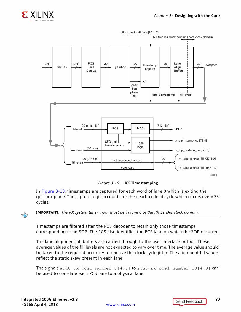
Integrated 100G Ethernet v2.3 80PG165 April 4, 2018 www.xilinx.com
Chapter 3: Designing with the Core
In Figure 3-10, timestamps are captured for each word of lane 0 which is exiting the gearbox plane. The capture logic accounts for the gearbox dead cycle which occurs every 33 cycles.
IMPORTANT: The RX system timer input must be in lane 0 of the RX SerDes clock domain.
Timestamps are filtered after the PCS decoder to retain only those timestamps corresponding to an SOP. The PCS also identifies the PCS lane on which the SOP occurred.
The lane alignment fill buffers are carried through to the user interface output. These average values of the fill levels are not expected to vary over time. The average value should be taken to the required accuracy to remove the clock cycle jitter. The alignment fill values reflect the static skew present in each lane.
The signals stat_rx_pcsl_number_0[4:0] to stat_rx_pcsl_number_19[4:0] can be used to correlate each PCS lane to a physical lane.
X-Ref Target - Figure 3-10
Figure 3-10: RX Timestamping
SerDesPCSLane
Demux
10(4) 10(4)gearbox
20 timestamp capture
20 Lane AlignBuffers
20 20
ctl_rx_systemtimerin[80-1:0]RX SerDes clock domain core clock domain
gear box
phase adj lane 0 timestamp fill levels
PCS MAC
1588logic
SFD andlane detection
20 (x 16 bits)datapath
(512 bits)LBUS
(80 bits)timestamp rx_ptp_pcslane_out[5-1:0]
rx_ptp_tstamp_out[79:0]
20 (x 7 bits)fill levels not processed by core
core logic
20
+/-
rx_lane_aligner_fill_0[7-1:0]. . .
rx_lane_aligner_fill_19[7-1:0]
datapath
X14342
Send Feedback
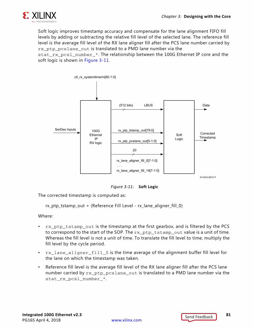
Integrated 100G Ethernet v2.3 81PG165 April 4, 2018 www.xilinx.com
Chapter 3: Designing with the Core
Soft logic improves timestamp accuracy and compensate for the lane alignment FIFO fill levels by adding or subtracting the relative fill level of the selected lane. The reference fill level is the average fill level of the RX lane aligner fill after the PCS lane number carried by rx_ptp_pcslane_out is translated to a PMD lane number via the stat_rx_pcsl_number_*. The relationship between the 100G Ethernet IP core and the soft logic is shown in Figure 3-11.
The corrected timestamp is computed as:
rx_ptp_tstamp_out + (Reference Fill Level - rx_lane_aligner_fill_0)
Where:
• rx_ptp_tstamp_out is the timestamp at the first gearbox, and is filtered by the PCS to correspond to the start of the SOP. The rx_ptp_tstamp_out value is a unit of time. Whereas the fill level is not a unit of time. To translate the fill level to time, multiply the fill level by the cycle period.
• rx_lane_aligner_fill_0 is the time average of the alignment buffer fill level for the lane on which the timestamp was taken.
• Reference fill level is the average fill level of the RX lane aligner fill after the PCS lane number carried by rx_ptp_pcslane_out is translated to a PMD lane number via the stat_rx_pcsl_number_*.
X-Ref Target - Figure 3-11
Figure 3-11: Soft Logic
100GEthernet
IPRX logic
ctl_rx_systemtimerin[80-1:0]
SerDes InputsSoft
Logic
(512 bits) LBUS Data
Corrected Timestamp
rx_ptp_pcslane_out[5-1:0]
rx_ptp_tstamp_out[79:0]
20
rx_lane_aligner_fill_0[7-1:0]. . .
rx_lane_aligner_fill_19[7-1:0]
X14343-081417
Send Feedback
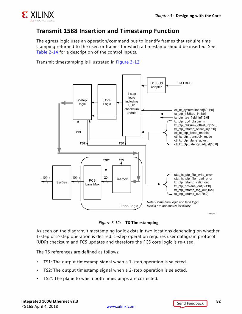
Integrated 100G Ethernet v2.3 82PG165 April 4, 2018 www.xilinx.com
Chapter 3: Designing with the Core
Transmit 1588 Insertion and Timestamp FunctionThe egress logic uses an operation/command bus to identify frames that require time stamping returned to the user, or frames for which a timestamp should be inserted. See Table 2-14 for a description of the control inputs.
Transmit timestamping is illustrated in Figure 3-12.
As seen on the diagram, timestamping logic exists in two locations depending on whether 1-step or 2-step operation is desired. 1-step operation requires user datagram protocol (UDP) checksum and FCS updates and therefore the FCS core logic is re-used.
The TS references are defined as follows:
• TS1: The output timestamp signal when a 1-step operation is selected.
• TS2: The output timestamp signal when a 2-step operation is selected.
• TS2': The plane to which both timestamps are corrected.
X-Ref Target - Figure 3-12
Figure 3-12: TX Timestamping
10(4)
2-steplogic
ctl_tx_systemtimerin[80-1:0]tx_ptp_1588op_in[1:0]tx_ptp_tag_field_in[15:0]tx_ptp_upd_cksum_intx_ptp_chksum_offset_in[15:0]tx_ptp_tstamp_offset_in[15:0]ctl_tx_ptp_1step_enablectl_tx_ptp_transpclk_modectl_tx_ptp_vlane_adjustctl_tx_ptp_latency_adjust[10:0]
CoreLogic
1-step logic
including UDP
checksum update
TX LBUS adapter
TX LBUS
stat_tx_ptp_fifo_write_errorstat_tx_ptp_fifo_read_errortx_ptp_tstamp_valid_outtx_ptp_pcslane_out[5-1:0]tx_ptp_tstamp_tag_out[15:0]tx_ptp_tstamp_out[79:0]
SerDes10(4)
PCS Lane Mux
20 Gearbox
seq
TS2 TS1
Lane LogicNote: Some core logic and lane logic blocks are not shown for clarity
X14344
TS2' seq
Send Feedback
Integrated 100G Ethernet v2.3 83PG165 April 4, 2018 www.xilinx.com
Chapter 3: Designing with the Core
TS2 always has a correction applied so that it is referenced to the TS2' plane. TS1 might or might not have the TS2' correction applied, depending on the value of the signal ctl_tx_ptp_latency_adjust[10:0]. The default value of this signal is 705 (decimal).
On the transmit side, a control input is provided by the client to the subsystem in parallel with the frame sent for transmission. This indicates, on a frame-by-frame basis, the 1588 function to perform (either no-operation, 1-step, or 2-step) and also indicates, for 1-step frames, whether there is a UDP checksum field to update.
• If using the Ordinary Clock mode, then for both 1-step and 2-step operations, the full captured 80-bit ToD timestamp is returned to the client logic using the additional ports defined in Table 2-14 and Table 2-15.
• If using the Transparent clock mode, then for both 1-step and 2-step operations, the full captured 64-bit timestamp is returned to the client logic using the additional ports defined in Table 2-14 and Table 2-15 (with the upper bits of data set to zero as defined in the table).
• If using the Ordinary Clock mode, then for a 1-step operation, the full captured 80-bit ToD timestamp is inserted into the frame. If using the Transparent clock mode, then for 1-step operation, the captured 64-bit timestamp is summed with the existing Correction Field contained within the frame and the summed result is overwritten into the original Correction Field of the frame. Supported frame types for 1-step timestamping are:
° Raw Ethernet
° UDP/IPv4
° UDP/IPv6
For 1-step UDP frame types, the UDP checksum is updated in accordance with IETF RFC 1624. For all 1-step frames, the Ethernet Frame Check Sequence (FCS) field is calculated after all frame modifications have been completed. For 2-step transmit operation, all Precision Time Protocol (PTP) frame types are supported.
Frame-by-Frame Timestamping Operation
The operational mode of the egress timestamping function is determined by the settings on the TX_PTP_1588OP_IN port. The information contained within the command port indicates one of the following:
• No operation: the frame is not a PTP frame and no timestamp action should be taken.
• Two-step operation requires a tag value (user-sequence ID) which is provided as part of the control input; the frame should be timestamped, and the timestamp is made available to the client logic along with the provided tag value for the frame. The additional MAC transmitter ports provide this function.
Send Feedback
Integrated 100G Ethernet v2.3 84PG165 April 4, 2018 www.xilinx.com
Chapter 3: Designing with the Core
• 1-step operation requirements:
° For the ToD timer and timestamp format, a timestamp offset value is provided as part of the command port; the frame should be timestamped, and the timestamp should be inserted into the frame at the provided offset (number of bytes) into the frame.
° For the Transparent clock mode, a Correction Field offset value is provided as part of the command port; the frame should be timestamped, and the captured 64-bit Timestamp is summed with the existing Correction Field contained within the frame and the summed result is overwritten into original Correction Field of the frame.
For a 1-step operation following the frame modification, the cyclic redundancy check (CRC) value of the frame should also be updated/recalculated. For UDP IPv4 and IPv6 PTP formatted frames, the checksum value in the header of the frame needs to be updated/recalculated.
• For 1-step UDP frame types, the UDP checksum is updated in accordance with IETF RFC 1624.
° If using the Ordinary Clock mode, in order for this update function to work correctly, the original checksum value for the frame sent for transmission should be calculated using a zero value for the timestamp data. This particular restriction does not apply when using the Transparent clock mode.
° If using the Transparent clock mode, a different restriction does apply; the separation between the UDP Checksum field and the Correction Field within the 1588 PTP frame header is a fixed interval of bytes, supporting the 1588 PTP frame definition. This is a requirement to minimize the latency through the MAC since both the checksum and the correction field must both be fully contained in the MAC pipeline in order for the checksum to be correctly updated. This particular restriction does not apply to the Ordinary Clock mode because the original timestamp data is calculated as a zero value; consequently the checksum and timestamp position can be independently located within the frame.
Transmit 1588 Gearbox Jitter CompensationThe 1588 timestamp capture on the TX accounts for the jitter introduced by the transmit gearbox. The gearbox takes in 66-bit timestamped frames in 34/32 bit chunks and outputs data 32 bits at a time. Because 66 bits is not a multiple of 32, the gearbox accumulates excess data that is added to the beginning of subsequent cycles of data output. When data is appended from the gearbox buffer, jitter is introduced to the timestamped frames received by the gearbox. The gearbox has a state that is called the sequence number. For each sequence number, the gearbox has a specific number of bits buffered for adding to the beginning of the output data. The amount of jitter introduced by the gearbox can be represented by the graph in Figure 3-13.
Send Feedback
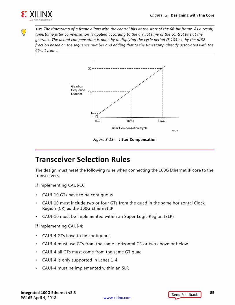
Integrated 100G Ethernet v2.3 85PG165 April 4, 2018 www.xilinx.com
Chapter 3: Designing with the Core
TIP: The timestamp of a frame aligns with the control bits at the start of the 66-bit frame. As a result, timestamp jitter compensation is applied according to the arrival time of the control bits at the gearbox. The actual compensation is done by multiplying the cycle period (3.103 ns) by the n/32 fraction based on the sequence number and adding that to the timestamp already associated with the 66-bit frame.
Transceiver Selection RulesThe design must meet the following rules when connecting the 100G Ethernet IP core to the transceivers.
If implementing CAUI-10:
• CAUI-10 GTs have to be contiguous
• CAUI-10 must include two or four GTs from the quad in the same horizontal Clock Region (CR) as the 100G Ethernet IP
• CAUI-10 must be implemented within an Super Logic Region (SLR)
If implementing CAUI-4:
• CAUI-4 GTs have to be contiguous
• CAUI-4 must use GTs from the same horizontal CR or two above or below
• CAUI-4 all GTs must come from the same GT quad
• CAUI-4 is only supported in Lanes 1-4
• CAUI-4 must be implemented within an SLR
X-Ref Target - Figure 3-13
Figure 3-13: Jitter Compensation
Jitter Compensation Cycle
1/32
1
16
32
16/32 32/32
GearboxSequenceNumber
X14345
Send Feedback
Integrated 100G Ethernet v2.3 86PG165 April 4, 2018 www.xilinx.com
Chapter 3: Designing with the Core
If implementing Runtime Switchable CAUI-10/CAUI-4, follow the preceding rules for both CAUI-10 and CAUI-4 rules.
IMPORTANT: For Runtime Switchable mode, if the GT group is selected as two GTs from bottom quad, four GTs from middle and four GTs from upper quad, then when it switches from CAUI10 to CAUI4, the upper GT quad is used for CAUI4.
Note that the 100G Ethernet IP core is optimized to use GTY transceiver locations. Therefore GTH transceiver locations relative to the CMAC block span a significant distance. Timing closure can be affected.
RECOMMENDED: For transceiver selections outside of these rules, contact Xilinx® support or your local FAE.
See the UltraScale Architecture Clocking Resource User Guide (UG572) [Ref 5] for more information on clock region.
Dynamic Reconfiguration PortThe dynamic reconfiguration port (DRP) allows the dynamic change of attributes to the 100G Ethernet IP core. The DRP interface is a processor-friendly synchronous interface with an address bus (DRP_ADDR) and separated data buses for reading (DRP_DO) and writing (DRP_DI) configuration data to the CMAC block. An enable signal (DRP_EN), a read/write signal (DRP_WE), and a ready/valid signal (DRP_RDY) are the control signals that implement read and write operations, indicate that the operation is completion, or indicate the availability of data.
For the DRP to work, a clock must be provided to the DRP_CLK port. See the Virtex UltraScale Architecture Data Sheet: DC and AC Switching Characteristics Data Sheet (DS893) [Ref 3], for the maximum allowed clock frequency.
The CMAC block must be held in reset when you want to dynamically change the attributes through the DRP. That is, TX_RESET, RX_RESET, and the RX_SERDES_RESET[9:0] need to be asserted High.
Send Feedback
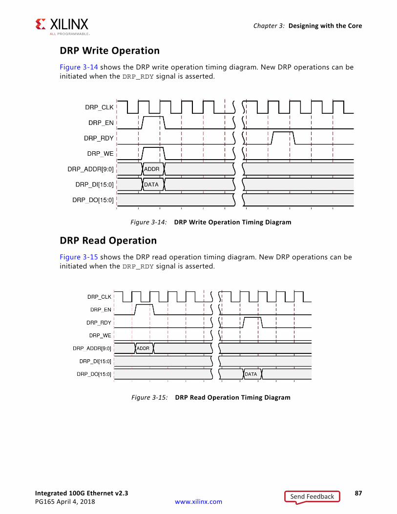
Integrated 100G Ethernet v2.3 87PG165 April 4, 2018 www.xilinx.com
Chapter 3: Designing with the Core
DRP Write OperationFigure 3-14 shows the DRP write operation timing diagram. New DRP operations can be initiated when the DRP_RDY signal is asserted.
DRP Read OperationFigure 3-15 shows the DRP read operation timing diagram. New DRP operations can be initiated when the DRP_RDY signal is asserted.
X-Ref Target - Figure 3-14
Figure 3-14: DRP Write Operation Timing Diagram
X-Ref Target - Figure 3-15
Figure 3-15: DRP Read Operation Timing Diagram
Send Feedback
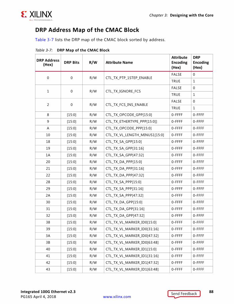
Integrated 100G Ethernet v2.3 88PG165 April 4, 2018 www.xilinx.com
Chapter 3: Designing with the Core
DRP Address Map of the CMAC BlockTable 3-7 lists the DRP map of the CMAC block sorted by address.
Table 3-7: DRP Map of the CMAC Block
DRP Address (Hex) DRP Bits R/W Attribute Name
Attribute Encoding (Hex)
DRP Encoding (Hex)
0 0 R/W CTL_TX_PTP_1STEP_ENABLEFALSE 0
TRUE 1
1 0 R/W CTL_TX_IGNORE_FCSFALSE 0
TRUE 1
2 0 R/W CTL_TX_FCS_INS_ENABLEFALSE 0
TRUE 1
8 [15:0] R/W CTL_TX_OPCODE_GPP[15:0] 0-FFFF 0-FFFF
9 [15:0] R/W CTL_TX_ETHERTYPE_PPP[15:0]] 0-FFFF 0-FFFF
A [15:0] R/W CTL_TX_OPCODE_PPP[15:0] 0-FFFF 0-FFFF
10 [15:0] R/W CTL_TX_VL_LENGTH_MINUS1[15:0] 0-FFFF 0-FFFF
18 [15:0] R/W CTL_TX_SA_GPP[15:0] 0-FFFF 0-FFFF
19 [15:0] R/W CTL_TX_SA_GPP[31:16] 0-FFFF 0-FFFF
1A [15:0] R/W CTL_TX_SA_GPP[47:32] 0-FFFF 0-FFFF
20 [15:0] R/W CTL_TX_DA_PPP[15:0] 0-FFFF 0-FFFF
21 [15:0] R/W CTL_TX_DA_PPP[31:16] 0-FFFF 0-FFFF
22 [15:0] R/W CTL_TX_DA_PPP[47:32] 0-FFFF 0-FFFF
28 [15:0] R/W CTL_TX_SA_PPP[15:0] 0-FFFF 0-FFFF
29 [15:0] R/W CTL_TX_SA_PPP[31:16] 0-FFFF 0-FFFF
2A [15:0] R/W CTL_TX_SA_PPP[47:32] 0-FFFF 0-FFFF
30 [15:0] R/W CTL_TX_DA_GPP[15:0] 0-FFFF 0-FFFF
31 [15:0] R/W CTL_TX_DA_GPP[31:16] 0-FFFF 0-FFFF
32 [15:0] R/W CTL_TX_DA_GPP[47:32] 0-FFFF 0-FFFF
38 [15:0] R/W CTL_TX_VL_MARKER_ID0[15:0] 0-FFFF 0-FFFF
39 [15:0] R/W CTL_TX_VL_MARKER_ID0[31:16] 0-FFFF 0-FFFF
3A [15:0] R/W CTL_TX_VL_MARKER_ID0[47:32] 0-FFFF 0-FFFF
3B [15:0] R/W CTL_TX_VL_MARKER_ID0[63:48] 0-FFFF 0-FFFF
40 [15:0] R/W CTL_TX_VL_MARKER_ID1[15:0] 0-FFFF 0-FFFF
41 [15:0] R/W CTL_TX_VL_MARKER_ID1[31:16] 0-FFFF 0-FFFF
42 [15:0] R/W CTL_TX_VL_MARKER_ID1[47:32] 0-FFFF 0-FFFF
43 [15:0] R/W CTL_TX_VL_MARKER_ID1[63:48] 0-FFFF 0-FFFF
Send Feedback
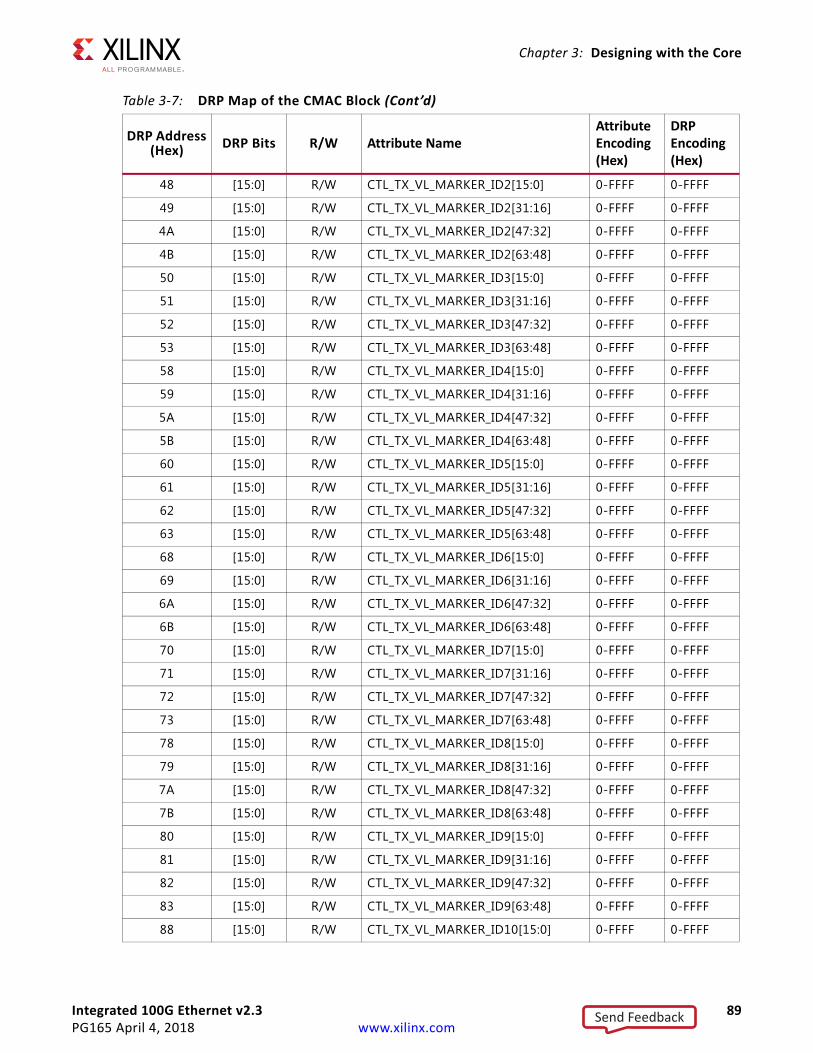
Integrated 100G Ethernet v2.3 89PG165 April 4, 2018 www.xilinx.com
Chapter 3: Designing with the Core
48 [15:0] R/W CTL_TX_VL_MARKER_ID2[15:0] 0-FFFF 0-FFFF
49 [15:0] R/W CTL_TX_VL_MARKER_ID2[31:16] 0-FFFF 0-FFFF
4A [15:0] R/W CTL_TX_VL_MARKER_ID2[47:32] 0-FFFF 0-FFFF
4B [15:0] R/W CTL_TX_VL_MARKER_ID2[63:48] 0-FFFF 0-FFFF
50 [15:0] R/W CTL_TX_VL_MARKER_ID3[15:0] 0-FFFF 0-FFFF
51 [15:0] R/W CTL_TX_VL_MARKER_ID3[31:16] 0-FFFF 0-FFFF
52 [15:0] R/W CTL_TX_VL_MARKER_ID3[47:32] 0-FFFF 0-FFFF
53 [15:0] R/W CTL_TX_VL_MARKER_ID3[63:48] 0-FFFF 0-FFFF
58 [15:0] R/W CTL_TX_VL_MARKER_ID4[15:0] 0-FFFF 0-FFFF
59 [15:0] R/W CTL_TX_VL_MARKER_ID4[31:16] 0-FFFF 0-FFFF
5A [15:0] R/W CTL_TX_VL_MARKER_ID4[47:32] 0-FFFF 0-FFFF
5B [15:0] R/W CTL_TX_VL_MARKER_ID4[63:48] 0-FFFF 0-FFFF
60 [15:0] R/W CTL_TX_VL_MARKER_ID5[15:0] 0-FFFF 0-FFFF
61 [15:0] R/W CTL_TX_VL_MARKER_ID5[31:16] 0-FFFF 0-FFFF
62 [15:0] R/W CTL_TX_VL_MARKER_ID5[47:32] 0-FFFF 0-FFFF
63 [15:0] R/W CTL_TX_VL_MARKER_ID5[63:48] 0-FFFF 0-FFFF
68 [15:0] R/W CTL_TX_VL_MARKER_ID6[15:0] 0-FFFF 0-FFFF
69 [15:0] R/W CTL_TX_VL_MARKER_ID6[31:16] 0-FFFF 0-FFFF
6A [15:0] R/W CTL_TX_VL_MARKER_ID6[47:32] 0-FFFF 0-FFFF
6B [15:0] R/W CTL_TX_VL_MARKER_ID6[63:48] 0-FFFF 0-FFFF
70 [15:0] R/W CTL_TX_VL_MARKER_ID7[15:0] 0-FFFF 0-FFFF
71 [15:0] R/W CTL_TX_VL_MARKER_ID7[31:16] 0-FFFF 0-FFFF
72 [15:0] R/W CTL_TX_VL_MARKER_ID7[47:32] 0-FFFF 0-FFFF
73 [15:0] R/W CTL_TX_VL_MARKER_ID7[63:48] 0-FFFF 0-FFFF
78 [15:0] R/W CTL_TX_VL_MARKER_ID8[15:0] 0-FFFF 0-FFFF
79 [15:0] R/W CTL_TX_VL_MARKER_ID8[31:16] 0-FFFF 0-FFFF
7A [15:0] R/W CTL_TX_VL_MARKER_ID8[47:32] 0-FFFF 0-FFFF
7B [15:0] R/W CTL_TX_VL_MARKER_ID8[63:48] 0-FFFF 0-FFFF
80 [15:0] R/W CTL_TX_VL_MARKER_ID9[15:0] 0-FFFF 0-FFFF
81 [15:0] R/W CTL_TX_VL_MARKER_ID9[31:16] 0-FFFF 0-FFFF
82 [15:0] R/W CTL_TX_VL_MARKER_ID9[47:32] 0-FFFF 0-FFFF
83 [15:0] R/W CTL_TX_VL_MARKER_ID9[63:48] 0-FFFF 0-FFFF
88 [15:0] R/W CTL_TX_VL_MARKER_ID10[15:0] 0-FFFF 0-FFFF
Table 3-7: DRP Map of the CMAC Block (Cont’d)
DRP Address (Hex) DRP Bits R/W Attribute Name
Attribute Encoding (Hex)
DRP Encoding (Hex)
Send Feedback

Integrated 100G Ethernet v2.3 90PG165 April 4, 2018 www.xilinx.com
Chapter 3: Designing with the Core
89 [15:0] R/W CTL_TX_VL_MARKER_ID10[31:16] 0-FFFF 0-FFFF
8A [15:0] R/W CTL_TX_VL_MARKER_ID10[47:32] 0-FFFF 0-FFFF
8B [15:0] R/W CTL_TX_VL_MARKER_ID10[63:48] 0-FFFF 0-FFFF
90 [15:0] R/W CTL_TX_VL_MARKER_ID11[15:0] 0-FFFF 0-FFFF
91 [15:0] R/W CTL_TX_VL_MARKER_ID11[31:16] 0-FFFF 0-FFFF
92 [15:0] R/W CTL_TX_VL_MARKER_ID11[47:32] 0-FFFF 0-FFFF
93 [15:0] R/W CTL_TX_VL_MARKER_ID11[63:48] 0-FFFF 0-FFFF
98 [15:0] R/W CTL_TX_VL_MARKER_ID12[15:0] 0-FFFF 0-FFFF
99 [15:0] R/W CTL_TX_VL_MARKER_ID12[31:16] 0-FFFF 0-FFFF
9A [15:0] R/W CTL_TX_VL_MARKER_ID12[47:32] 0-FFFF 0-FFFF
9B [15:0] R/W CTL_TX_VL_MARKER_ID12[63:48] 0-FFFF 0-FFFF
A0 [15:0] R/W CTL_TX_VL_MARKER_ID13[15:0] 0-FFFF 0-FFFF
A1 [15:0] R/W CTL_TX_VL_MARKER_ID13[31:16] 0-FFFF 0-FFFF
A2 [15:0] R/W CTL_TX_VL_MARKER_ID13[47:32] 0-FFFF 0-FFFF
A3 [15:0] R/W CTL_TX_VL_MARKER_ID13[63:48] 0-FFFF 0-FFFF
A8 [15:0] R/W CTL_TX_VL_MARKER_ID14[15:0] 0-FFFF 0-FFFF
A9 [15:0] R/W CTL_TX_VL_MARKER_ID14[31:16] 0-FFFF 0-FFFF
AA [15:0] R/W CTL_TX_VL_MARKER_ID14[47:32] 0-FFFF 0-FFFF
AB [15:0] R/W CTL_TX_VL_MARKER_ID14[63:48] 0-FFFF 0-FFFF
B0 [15:0] R/W CTL_TX_VL_MARKER_ID15[15:0] 0-FFFF 0-FFFF
B1 [15:0] R/W CTL_TX_VL_MARKER_ID15[31:16] 0-FFFF 0-FFFF
B2 [15:0] R/W CTL_TX_VL_MARKER_ID15[47:32] 0-FFFF 0-FFFF
B3 [15:0] R/W CTL_TX_VL_MARKER_ID15[63:48] 0-FFFF 0-FFFF
B8 [15:0] R/W CTL_TX_VL_MARKER_ID16[15:0] 0-FFFF 0-FFFF
B9 [15:0] R/W CTL_TX_VL_MARKER_ID16[31:16] 0-FFFF 0-FFFF
BA [15:0] R/W CTL_TX_VL_MARKER_ID16[47:32] 0-FFFF 0-FFFF
BB [15:0] R/W CTL_TX_VL_MARKER_ID16[63:48] 0-FFFF 0-FFFF
C0 [15:0] R/W CTL_TX_VL_MARKER_ID17[15:0] 0-FFFF 0-FFFF
C1 [15:0] R/W CTL_TX_VL_MARKER_ID17[31:16] 0-FFFF 0-FFFF
C2 [15:0] R/W CTL_TX_VL_MARKER_ID17[47:32] 0-FFFF 0-FFFF
C3 [15:0] R/W CTL_TX_VL_MARKER_ID17[63:48] 0-FFFF 0-FFFF
C8 [15:0] R/W CTL_TX_VL_MARKER_ID18[15:0] 0-FFFF 0-FFFF
C9 [15:0] R/W CTL_TX_VL_MARKER_ID18[31:16] 0-FFFF 0-FFFF
Table 3-7: DRP Map of the CMAC Block (Cont’d)
DRP Address (Hex) DRP Bits R/W Attribute Name
Attribute Encoding (Hex)
DRP Encoding (Hex)
Send Feedback
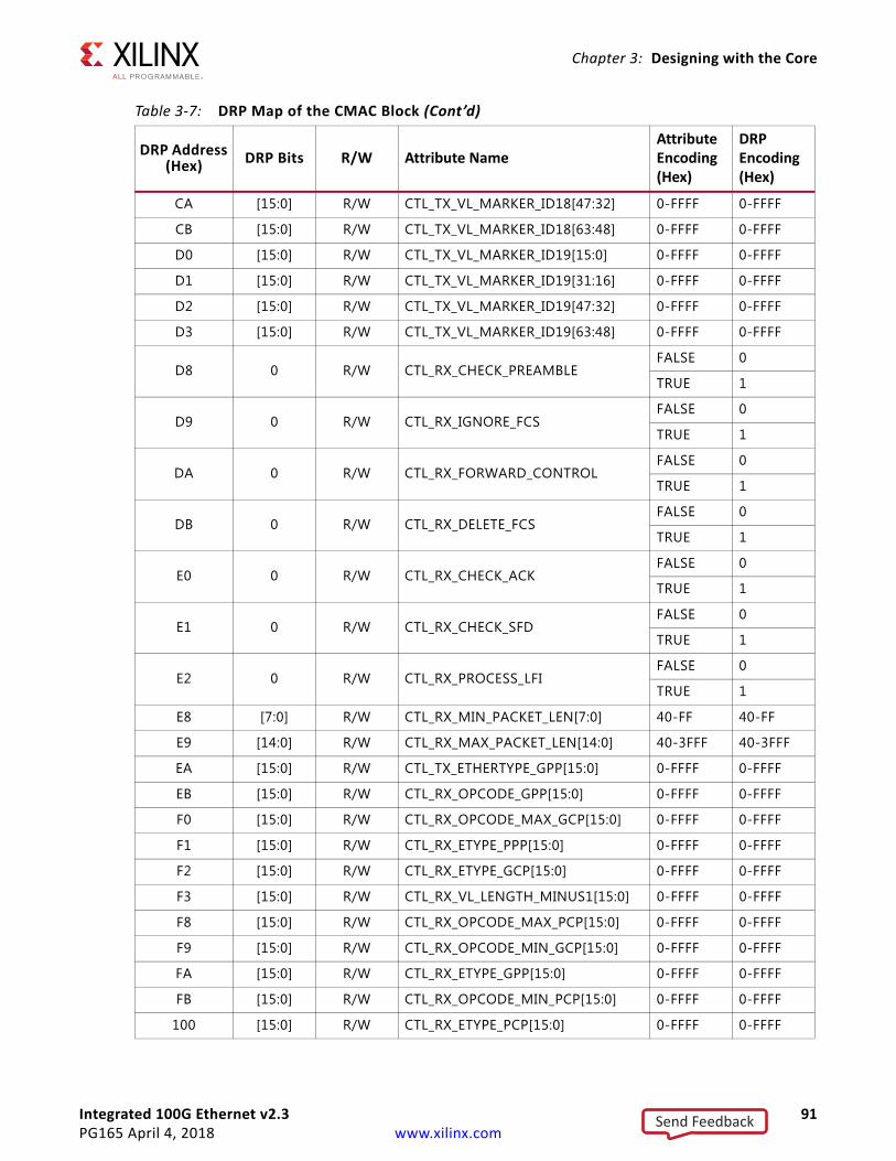
Integrated 100G Ethernet v2.3 91PG165 April 4, 2018 www.xilinx.com
Chapter 3: Designing with the Core
CA [15:0] R/W CTL_TX_VL_MARKER_ID18[47:32] 0-FFFF 0-FFFF
CB [15:0] R/W CTL_TX_VL_MARKER_ID18[63:48] 0-FFFF 0-FFFF
D0 [15:0] R/W CTL_TX_VL_MARKER_ID19[15:0] 0-FFFF 0-FFFF
D1 [15:0] R/W CTL_TX_VL_MARKER_ID19[31:16] 0-FFFF 0-FFFF
D2 [15:0] R/W CTL_TX_VL_MARKER_ID19[47:32] 0-FFFF 0-FFFF
D3 [15:0] R/W CTL_TX_VL_MARKER_ID19[63:48] 0-FFFF 0-FFFF
D8 0 R/W CTL_RX_CHECK_PREAMBLEFALSE 0
TRUE 1
D9 0 R/W CTL_RX_IGNORE_FCSFALSE 0
TRUE 1
DA 0 R/W CTL_RX_FORWARD_CONTROLFALSE 0
TRUE 1
DB 0 R/W CTL_RX_DELETE_FCSFALSE 0
TRUE 1
E0 0 R/W CTL_RX_CHECK_ACKFALSE 0
TRUE 1
E1 0 R/W CTL_RX_CHECK_SFDFALSE 0
TRUE 1
E2 0 R/W CTL_RX_PROCESS_LFIFALSE 0
TRUE 1
E8 [7:0] R/W CTL_RX_MIN_PACKET_LEN[7:0] 40-FF 40-FF
E9 [14:0] R/W CTL_RX_MAX_PACKET_LEN[14:0] 40-3FFF 40-3FFF
EA [15:0] R/W CTL_TX_ETHERTYPE_GPP[15:0] 0-FFFF 0-FFFF
EB [15:0] R/W CTL_RX_OPCODE_GPP[15:0] 0-FFFF 0-FFFF
F0 [15:0] R/W CTL_RX_OPCODE_MAX_GCP[15:0] 0-FFFF 0-FFFF
F1 [15:0] R/W CTL_RX_ETYPE_PPP[15:0] 0-FFFF 0-FFFF
F2 [15:0] R/W CTL_RX_ETYPE_GCP[15:0] 0-FFFF 0-FFFF
F3 [15:0] R/W CTL_RX_VL_LENGTH_MINUS1[15:0] 0-FFFF 0-FFFF
F8 [15:0] R/W CTL_RX_OPCODE_MAX_PCP[15:0] 0-FFFF 0-FFFF
F9 [15:0] R/W CTL_RX_OPCODE_MIN_GCP[15:0] 0-FFFF 0-FFFF
FA [15:0] R/W CTL_RX_ETYPE_GPP[15:0] 0-FFFF 0-FFFF
FB [15:0] R/W CTL_RX_OPCODE_MIN_PCP[15:0] 0-FFFF 0-FFFF
100 [15:0] R/W CTL_RX_ETYPE_PCP[15:0] 0-FFFF 0-FFFF
Table 3-7: DRP Map of the CMAC Block (Cont’d)
DRP Address (Hex) DRP Bits R/W Attribute Name
Attribute Encoding (Hex)
DRP Encoding (Hex)
Send Feedback
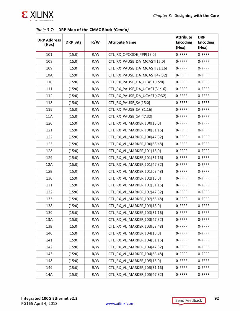
Integrated 100G Ethernet v2.3 92PG165 April 4, 2018 www.xilinx.com
Chapter 3: Designing with the Core
101 [15:0] R/W CTL_RX_OPCODE_PPP[15:0] 0-FFFF 0-FFFF
108 [15:0] R/W CTL_RX_PAUSE_DA_MCAST[15:0] 0-FFFF 0-FFFF
109 [15:0] R/W CTL_RX_PAUSE_DA_MCAST[31:16] 0-FFFF 0-FFFF
10A [15:0] R/W CTL_RX_PAUSE_DA_MCAST[47:32] 0-FFFF 0-FFFF
110 [15:0] R/W CTL_RX_PAUSE_DA_UCAST[15:0] 0-FFFF 0-FFFF
111 [15:0] R/W CTL_RX_PAUSE_DA_UCAST[31:16] 0-FFFF 0-FFFF
112 [15:0] R/W CTL_RX_PAUSE_DA_UCAST[47:32] 0-FFFF 0-FFFF
118 [15:0] R/W CTL_RX_PAUSE_SA[15:0] 0-FFFF 0-FFFF
119 [15:0] R/W CTL_RX_PAUSE_SA[31:16] 0-FFFF 0-FFFF
11A [15:0] R/W CTL_RX_PAUSE_SA[47:32] 0-FFFF 0-FFFF
120 [15:0] R/W CTL_RX_VL_MARKER_ID0[15:0] 0-FFFF 0-FFFF
121 [15:0] R/W CTL_RX_VL_MARKER_ID0[31:16] 0-FFFF 0-FFFF
122 [15:0] R/W CTL_RX_VL_MARKER_ID0[47:32] 0-FFFF 0-FFFF
123 [15:0] R/W CTL_RX_VL_MARKER_ID0[63:48] 0-FFFF 0-FFFF
128 [15:0] R/W CTL_RX_VL_MARKER_ID1[15:0] 0-FFFF 0-FFFF
129 [15:0] R/W CTL_RX_VL_MARKER_ID1[31:16] 0-FFFF 0-FFFF
12A [15:0] R/W CTL_RX_VL_MARKER_ID1[47:32] 0-FFFF 0-FFFF
12B [15:0] R/W CTL_RX_VL_MARKER_ID1[63:48] 0-FFFF 0-FFFF
130 [15:0] R/W CTL_RX_VL_MARKER_ID2[15:0] 0-FFFF 0-FFFF
131 [15:0] R/W CTL_RX_VL_MARKER_ID2[31:16] 0-FFFF 0-FFFF
132 [15:0] R/W CTL_RX_VL_MARKER_ID2[47:32] 0-FFFF 0-FFFF
133 [15:0] R/W CTL_RX_VL_MARKER_ID2[63:48] 0-FFFF 0-FFFF
138 [15:0] R/W CTL_RX_VL_MARKER_ID3[15:0] 0-FFFF 0-FFFF
139 [15:0] R/W CTL_RX_VL_MARKER_ID3[31:16] 0-FFFF 0-FFFF
13A [15:0] R/W CTL_RX_VL_MARKER_ID3[47:32] 0-FFFF 0-FFFF
13B [15:0] R/W CTL_RX_VL_MARKER_ID3[63:48] 0-FFFF 0-FFFF
140 [15:0] R/W CTL_RX_VL_MARKER_ID4[15:0] 0-FFFF 0-FFFF
141 [15:0] R/W CTL_RX_VL_MARKER_ID4[31:16] 0-FFFF 0-FFFF
142 [15:0] R/W CTL_RX_VL_MARKER_ID4[47:32] 0-FFFF 0-FFFF
143 [15:0] R/W CTL_RX_VL_MARKER_ID4[63:48] 0-FFFF 0-FFFF
148 [15:0] R/W CTL_RX_VL_MARKER_ID5[15:0] 0-FFFF 0-FFFF
149 [15:0] R/W CTL_RX_VL_MARKER_ID5[31:16] 0-FFFF 0-FFFF
14A [15:0] R/W CTL_RX_VL_MARKER_ID5[47:32] 0-FFFF 0-FFFF
Table 3-7: DRP Map of the CMAC Block (Cont’d)
DRP Address (Hex) DRP Bits R/W Attribute Name
Attribute Encoding (Hex)
DRP Encoding (Hex)
Send Feedback

Integrated 100G Ethernet v2.3 93PG165 April 4, 2018 www.xilinx.com
Chapter 3: Designing with the Core
14B [15:0] R/W CTL_RX_VL_MARKER_ID5[63:48] 0-FFFF 0-FFFF
150 [15:0] R/W CTL_RX_VL_MARKER_ID6[15:0] 0-FFFF 0-FFFF
151 [15:0] R/W CTL_RX_VL_MARKER_ID6[31:16] 0-FFFF 0-FFFF
152 [15:0] R/W CTL_RX_VL_MARKER_ID6[47:32] 0-FFFF 0-FFFF
153 [15:0] R/W CTL_RX_VL_MARKER_ID6[63:48] 0-FFFF 0-FFFF
158 [15:0] R/W CTL_RX_VL_MARKER_ID7[15:0] 0-FFFF 0-FFFF
159 [15:0] R/W CTL_RX_VL_MARKER_ID7[31:16] 0-FFFF 0-FFFF
15A [15:0] R/W CTL_RX_VL_MARKER_ID7[47:32] 0-FFFF 0-FFFF
15B [15:0] R/W CTL_RX_VL_MARKER_ID7[63:48] 0-FFFF 0-FFFF
160 [15:0] R/W CTL_RX_VL_MARKER_ID8[15:0] 0-FFFF 0-FFFF
161 [15:0] R/W CTL_RX_VL_MARKER_ID8[31:16] 0-FFFF 0-FFFF
162 [15:0] R/W CTL_RX_VL_MARKER_ID8[47:32] 0-FFFF 0-FFFF
163 [15:0] R/W CTL_RX_VL_MARKER_ID8[63:48] 0-FFFF 0-FFFF
168 [15:0] R/W CTL_RX_VL_MARKER_ID9[15:0] 0-FFFF 0-FFFF
169 [15:0] R/W CTL_RX_VL_MARKER_ID9[31:16] 0-FFFF 0-FFFF
16A [15:0] R/W CTL_RX_VL_MARKER_ID9[47:32] 0-FFFF 0-FFFF
16B [15:0] R/W CTL_RX_VL_MARKER_ID9[63:48] 0-FFFF 0-FFFF
170 [15:0] R/W CTL_RX_VL_MARKER_ID10[15:0] 0-FFFF 0-FFFF
171 [15:0] R/W CTL_RX_VL_MARKER_ID10[31:16] 0-FFFF 0-FFFF
172 [15:0] R/W CTL_RX_VL_MARKER_ID10[47:32] 0-FFFF 0-FFFF
173 [15:0] R/W CTL_RX_VL_MARKER_ID10[63:48] 0-FFFF 0-FFFF
178 [15:0] R/W CTL_RX_VL_MARKER_ID11[15:0] 0-FFFF 0-FFFF
179 [15:0] R/W CTL_RX_VL_MARKER_ID11[31:16] 0-FFFF 0-FFFF
17A [15:0] R/W CTL_RX_VL_MARKER_ID11[47:32] 0-FFFF 0-FFFF
17B [15:0] R/W CTL_RX_VL_MARKER_ID11[63:48] 0-FFFF 0-FFFF
180 [15:0] R/W CTL_RX_VL_MARKER_ID12[15:0] 0-FFFF 0-FFFF
181 [15:0] R/W CTL_RX_VL_MARKER_ID12[31:16] 0-FFFF 0-FFFF
182 [15:0] R/W CTL_RX_VL_MARKER_ID12[47:32] 0-FFFF 0-FFFF
183 [15:0] R/W CTL_RX_VL_MARKER_ID12[63:48] 0-FFFF 0-FFFF
188 [15:0] R/W CTL_RX_VL_MARKER_ID13[15:0] 0-FFFF 0-FFFF
189 [15:0] R/W CTL_RX_VL_MARKER_ID13[31:16] 0-FFFF 0-FFFF
18A [15:0] R/W CTL_RX_VL_MARKER_ID13[47:32] 0-FFFF 0-FFFF
18B [15:0] R/W CTL_RX_VL_MARKER_ID13[63:48] 0-FFFF 0-FFFF
Table 3-7: DRP Map of the CMAC Block (Cont’d)
DRP Address (Hex) DRP Bits R/W Attribute Name
Attribute Encoding (Hex)
DRP Encoding (Hex)
Send Feedback
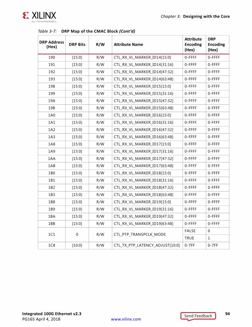
Integrated 100G Ethernet v2.3 94PG165 April 4, 2018 www.xilinx.com
Chapter 3: Designing with the Core
190 [15:0] R/W CTL_RX_VL_MARKER_ID14[15:0] 0-FFFF 0-FFFF
191 [15:0] R/W CTL_RX_VL_MARKER_ID14[31:16] 0-FFFF 0-FFFF
192 [15:0] R/W CTL_RX_VL_MARKER_ID14[47:32] 0-FFFF 0-FFFF
193 [15:0] R/W CTL_RX_VL_MARKER_ID14[63:48] 0-FFFF 0-FFFF
198 [15:0] R/W CTL_RX_VL_MARKER_ID15[15:0] 0-FFFF 0-FFFF
199 [15:0] R/W CTL_RX_VL_MARKER_ID15[31:16] 0-FFFF 0-FFFF
19A [15:0] R/W CTL_RX_VL_MARKER_ID15[47:32] 0-FFFF 0-FFFF
19B [15:0] R/W CTL_RX_VL_MARKER_ID15[63:48] 0-FFFF 0-FFFF
1A0 [15:0] R/W CTL_RX_VL_MARKER_ID16[15:0] 0-FFFF 0-FFFF
1A1 [15:0] R/W CTL_RX_VL_MARKER_ID16[31:16] 0-FFFF 0-FFFF
1A2 [15:0] R/W CTL_RX_VL_MARKER_ID16[47:32] 0-FFFF 0-FFFF
1A3 [15:0] R/W CTL_RX_VL_MARKER_ID16[63:48] 0-FFFF 0-FFFF
1A8 [15:0] R/W CTL_RX_VL_MARKER_ID17[15:0] 0-FFFF 0-FFFF
1A9 [15:0] R/W CTL_RX_VL_MARKER_ID17[31:16] 0-FFFF 0-FFFF
1AA [15:0] R/W CTL_RX_VL_MARKER_ID17[47:32] 0-FFFF 0-FFFF
1AB [15:0] R/W CTL_RX_VL_MARKER_ID17[63:48] 0-FFFF 0-FFFF
1B0 [15:0] R/W CTL_RX_VL_MARKER_ID18[15:0] 0-FFFF 0-FFFF
1B1 [15:0] R/W CTL_RX_VL_MARKER_ID18[31:16] 0-FFFF 0-FFFF
1B2 [15:0] R/W CTL_RX_VL_MARKER_ID18[47:32] 0-FFFF 0-FFFF
1B3 [15:0] R/W CTL_RX_VL_MARKER_ID18[63:48] 0-FFFF 0-FFFF
1B8 [15:0] R/W CTL_RX_VL_MARKER_ID19[15:0] 0-FFFF 0-FFFF
1B9 [15:0] R/W CTL_RX_VL_MARKER_ID19[31:16] 0-FFFF 0-FFFF
1BA [15:0] R/W CTL_RX_VL_MARKER_ID19[47:32] 0-FFFF 0-FFFF
1BB [15:0] R/W CTL_RX_VL_MARKER_ID19[63:48] 0-FFFF 0-FFFF
1C1 0 R/W CTL_PTP_TRANSPCLK_MODEFALSE 0
TRUE 1
1C8 [10:0] R/W CTL_TX_PTP_LATENCY_ADJUST[10:0] 0-7FF 0-7FF
Table 3-7: DRP Map of the CMAC Block (Cont’d)
DRP Address (Hex) DRP Bits R/W Attribute Name
Attribute Encoding (Hex)
DRP Encoding (Hex)
Send Feedback
Integrated 100G Ethernet v2.3 95PG165 April 4, 2018 www.xilinx.com
Chapter 4
Design Flow StepsThis chapter describes customizing and generating the core, constraining the core, and the simulation, synthesis and implementation steps that are specific to this IP core. More detailed information about the standard Vivado® design flows and the IP integrator can be found in the following Vivado Design Suite user guides:
• Vivado Design Suite User Guide: Designing IP Subsystems using IP Integrator (UG994) [Ref 6]
• Vivado Design Suite User Guide: Designing with IP (UG896) [Ref 7]
• Vivado Design Suite User Guide: Getting Started (UG910) [Ref 8]
• Vivado Design Suite User Guide: Logic Simulation (UG900) [Ref 9]
Customizing and Generating the CoreThis section includes information about using Xilinx® tools to customize and generate the core in the Vivado Design Suite.
If you are customizing and generating the core in the Vivado IP integrator, see the Vivado Design Suite User Guide: Designing IP Subsystems using IP Integrator (UG994) [Ref 6] for detailed information. IP integrator might auto-compute certain configuration values when validating or generating the design. To check whether the values do change, see the description of the parameter in this chapter. To view the parameter value, run the validate_bd_design command in the Tcl Console.
You can customize the IP for use in your design by specifying values for the various parameters associated with the IP core using the following steps:
1. Select the IP from the Vivado IP catalog.
2. Double-click the selected IP or select the Customize IP command from the toolbar or right-click menu.
For details, see the Vivado Design Suite User Guide: Designing with IP (UG896) [Ref 7] and the Vivado Design Suite User Guide: Getting Started (UG910) [Ref 8].
Note: Figures in this chapter are illustrations of the Vivado Integrated Design Environment (IDE). This layout might vary from the current version.
Send Feedback
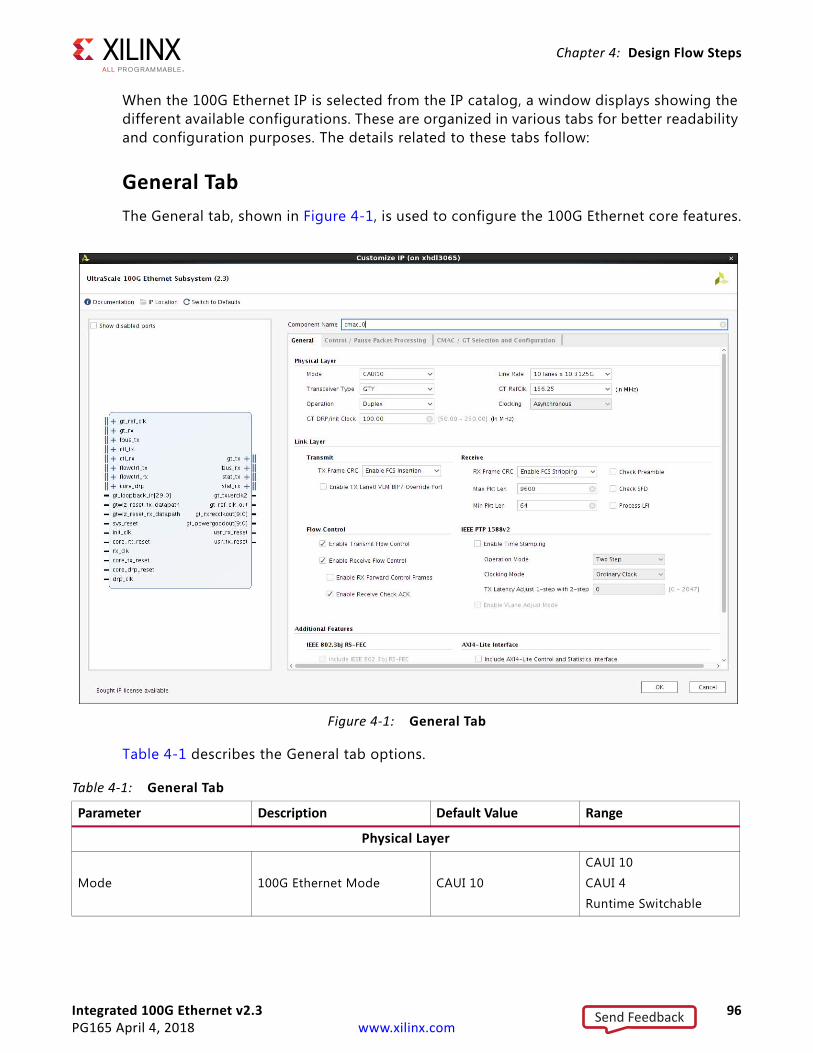
Integrated 100G Ethernet v2.3 96PG165 April 4, 2018 www.xilinx.com
Chapter 4: Design Flow Steps
When the 100G Ethernet IP is selected from the IP catalog, a window displays showing the different available configurations. These are organized in various tabs for better readability and configuration purposes. The details related to these tabs follow:
General TabThe General tab, shown in Figure 4-1, is used to configure the 100G Ethernet core features.
Table 4-1 describes the General tab options.
X-Ref Target - Figure 4-1
Figure 4-1: General Tab
Table 4-1: General Tab
Parameter Description Default Value Range
Physical Layer
Mode 100G Ethernet Mode CAUI 10
CAUI 10
CAUI 4
Runtime Switchable
Send Feedback
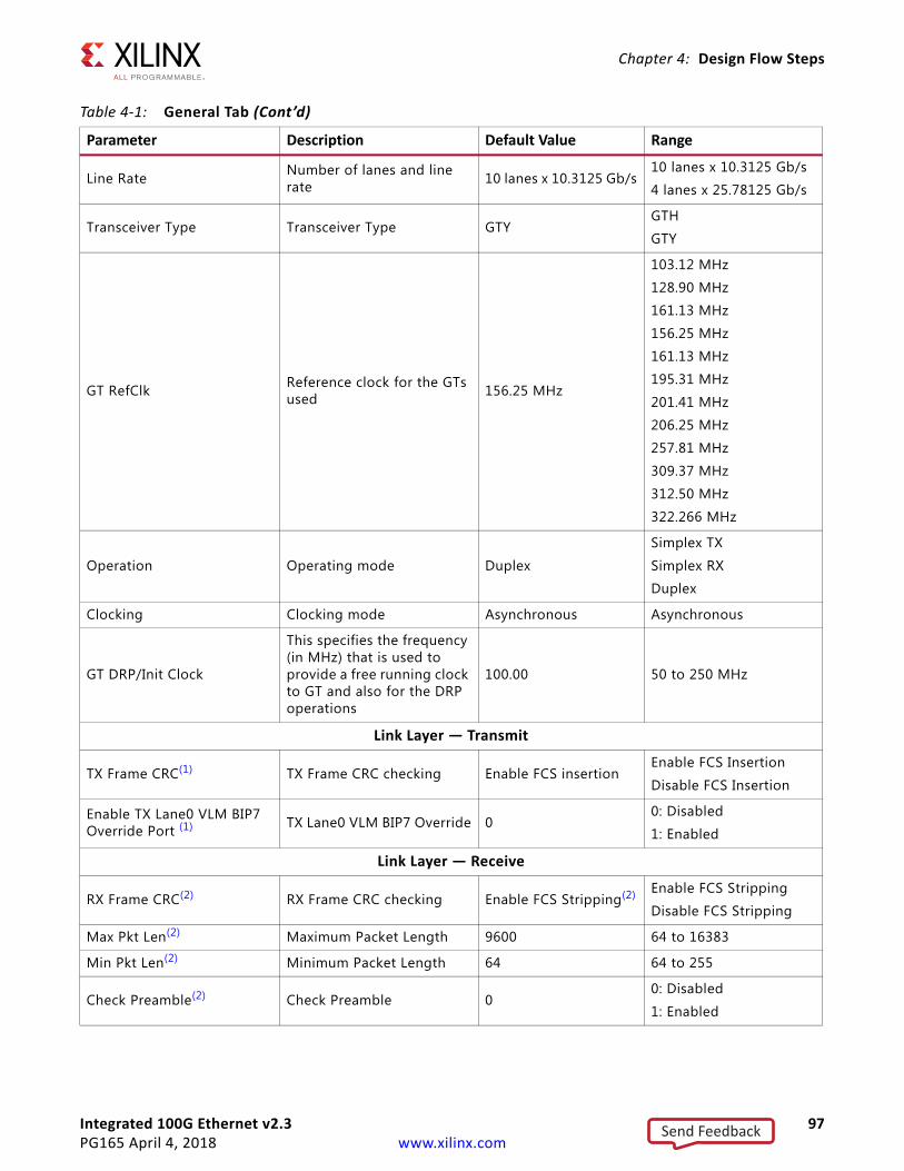
Integrated 100G Ethernet v2.3 97PG165 April 4, 2018 www.xilinx.com
Chapter 4: Design Flow Steps
Line Rate Number of lanes and line rate 10 lanes x 10.3125 Gb/s
10 lanes x 10.3125 Gb/s
4 lanes x 25.78125 Gb/s
Transceiver Type Transceiver Type GTYGTH
GTY
GT RefClk Reference clock for the GTs used 156.25 MHz
103.12 MHz
128.90 MHz
161.13 MHz
156.25 MHz
161.13 MHz
195.31 MHz
201.41 MHz
206.25 MHz
257.81 MHz
309.37 MHz
312.50 MHz
322.266 MHz
Operation Operating mode Duplex
Simplex TX
Simplex RX
Duplex
Clocking Clocking mode Asynchronous Asynchronous
GT DRP/Init Clock
This specifies the frequency (in MHz) that is used to provide a free running clock to GT and also for the DRP operations
100.00 50 to 250 MHz
Link Layer — Transmit
TX Frame CRC(1) TX Frame CRC checking Enable FCS insertionEnable FCS Insertion
Disable FCS Insertion
Enable TX Lane0 VLM BIP7 Override Port (1) TX Lane0 VLM BIP7 Override 0
0: Disabled
1: Enabled
Link Layer — Receive
RX Frame CRC(2) RX Frame CRC checking Enable FCS Stripping(2) Enable FCS Stripping
Disable FCS Stripping
Max Pkt Len(2) Maximum Packet Length 9600 64 to 16383
Min Pkt Len(2) Minimum Packet Length 64 64 to 255
Check Preamble(2) Check Preamble 00: Disabled
1: Enabled
Table 4-1: General Tab (Cont’d)
Parameter Description Default Value Range
Send Feedback
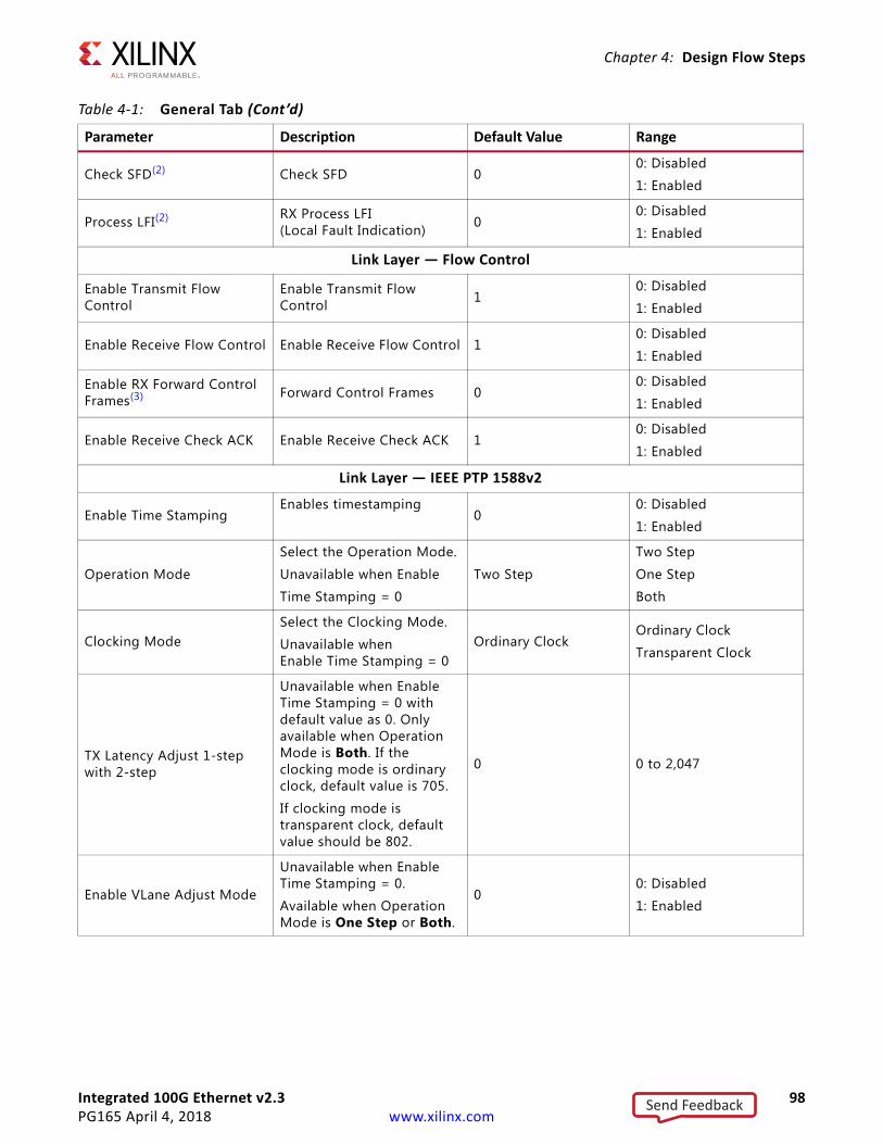
Integrated 100G Ethernet v2.3 98PG165 April 4, 2018 www.xilinx.com
Chapter 4: Design Flow Steps
Check SFD(2) Check SFD 00: Disabled
1: Enabled
Process LFI(2) RX Process LFI (Local Fault Indication) 0
0: Disabled
1: Enabled
Link Layer — Flow Control
Enable Transmit Flow Control
Enable Transmit Flow Control 1
0: Disabled
1: Enabled
Enable Receive Flow Control Enable Receive Flow Control 10: Disabled
1: Enabled
Enable RX Forward Control Frames(3) Forward Control Frames 0
0: Disabled
1: Enabled
Enable Receive Check ACK Enable Receive Check ACK 10: Disabled
1: Enabled
Link Layer — IEEE PTP 1588v2
Enable Time StampingEnables timestamping
00: Disabled
1: Enabled
Operation Mode
Select the Operation Mode.
Unavailable when Enable
Time Stamping = 0
Two Step
Two Step
One Step
Both
Clocking ModeSelect the Clocking Mode.
Unavailable when Enable Time Stamping = 0
Ordinary ClockOrdinary Clock
Transparent Clock
TX Latency Adjust 1-step with 2-step
Unavailable when Enable Time Stamping = 0 with default value as 0. Only available when Operation Mode is Both. If the clocking mode is ordinary clock, default value is 705.
If clocking mode is transparent clock, default value should be 802.
0 0 to 2,047
Enable VLane Adjust Mode
Unavailable when Enable Time Stamping = 0.
Available when Operation Mode is One Step or Both.
00: Disabled
1: Enabled
Table 4-1: General Tab (Cont’d)
Parameter Description Default Value Range
Send Feedback

Integrated 100G Ethernet v2.3 99PG165 April 4, 2018 www.xilinx.com
Chapter 4: Design Flow Steps
Additional Features
Include IEEE 802.3bj RS-FEC
Selecting this option will include IEEE 802.3bj RS-FEC in between CMAC and GT.Note: This feature is available in CAUI4 and Runtime Switchable mode.
00: Disabled
1: Enabled
Include AXI4-Lite Control and Statistics Interface
When you enable, the AXI4-Lite interface is provided in the core.
00: Disabled
1: Enabled
Include AN/LT Logic Selecting this option will include AN/LT soft logic.Note: This feature is available in CAUI-4 mode only.
00: Disabled
1: Enabled
Notes: 1. Requires TX to be enabled. Operation = Simplex TX or Duplex modes only.2. Requires RX to be enabled. Operation = Simplex RX or Duplex modes only.3. Option is disabled when receive flow control is disabled.
Table 4-1: General Tab (Cont’d)
Parameter Description Default Value Range
Send Feedback
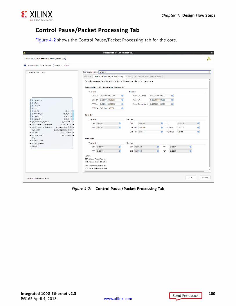
Integrated 100G Ethernet v2.3 100PG165 April 4, 2018 www.xilinx.com
Chapter 4: Design Flow Steps
Control Pause/Packet Processing TabFigure 4-2 shows the Control Pause/Packet Processing tab for the core.
X-Ref Target - Figure 4-2
Figure 4-2: Control Pause/Packet Processing Tab
Send Feedback
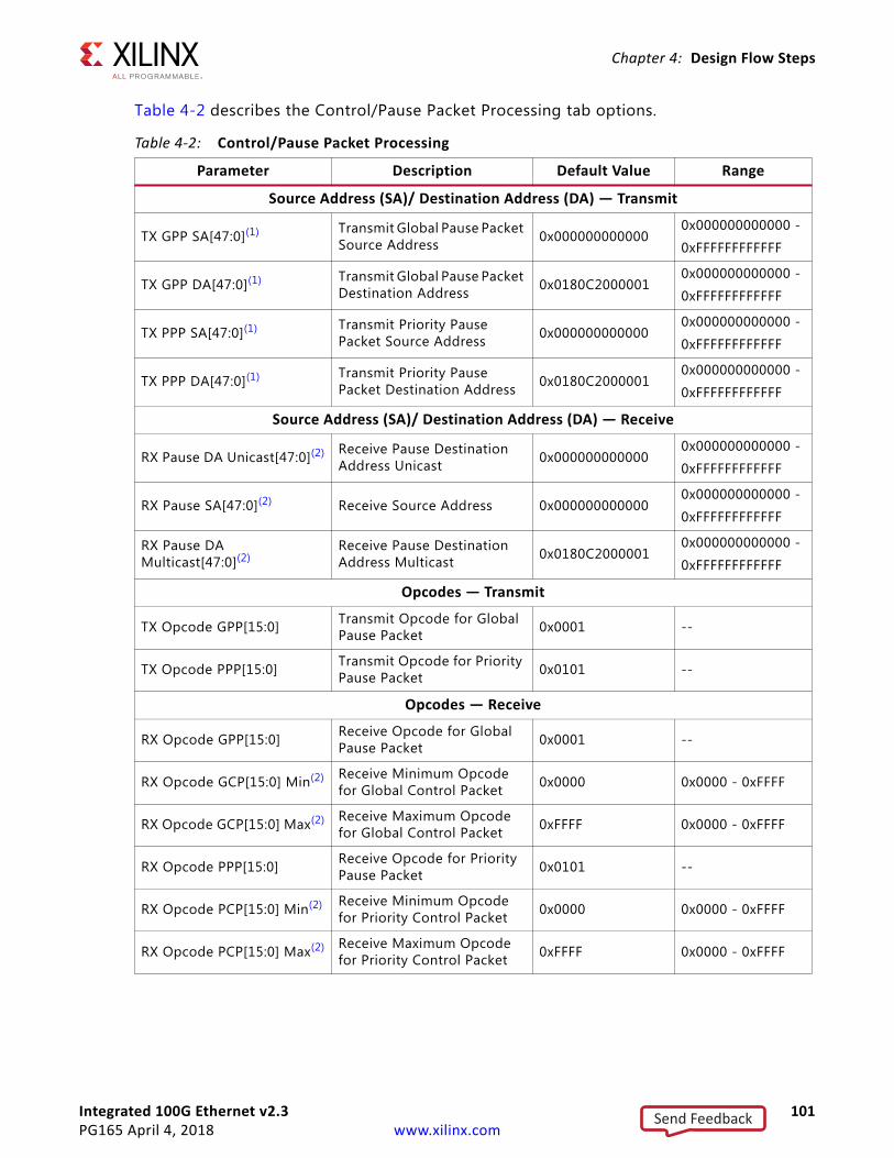
Integrated 100G Ethernet v2.3 101PG165 April 4, 2018 www.xilinx.com
Chapter 4: Design Flow Steps
Table 4-2 describes the Control/Pause Packet Processing tab options.
Table 4-2: Control/Pause Packet Processing
Parameter Description Default Value Range
Source Address (SA)/ Destination Address (DA) — Transmit
TX GPP SA[47:0](1) Transmit Global Pause Packet Source Address 0x000000000000
0x000000000000 -
0xFFFFFFFFFFFF
TX GPP DA[47:0](1) Transmit Global Pause Packet Destination Address 0x0180C2000001
0x000000000000 -
0xFFFFFFFFFFFF
TX PPP SA[47:0](1) Transmit Priority Pause Packet Source Address 0x000000000000
0x000000000000 -
0xFFFFFFFFFFFF
TX PPP DA[47:0](1) Transmit Priority Pause Packet Destination Address 0x0180C2000001
0x000000000000 -
0xFFFFFFFFFFFF
Source Address (SA)/ Destination Address (DA) — Receive
RX Pause DA Unicast[47:0](2) Receive Pause Destination Address Unicast 0x000000000000
0x000000000000 -
0xFFFFFFFFFFFF
RX Pause SA[47:0](2) Receive Source Address 0x0000000000000x000000000000 -
0xFFFFFFFFFFFF
RX Pause DA Multicast[47:0](2)
Receive Pause Destination Address Multicast 0x0180C2000001
0x000000000000 -
0xFFFFFFFFFFFF
Opcodes — Transmit
TX Opcode GPP[15:0] Transmit Opcode for Global Pause Packet 0x0001 --
TX Opcode PPP[15:0] Transmit Opcode for Priority Pause Packet 0x0101 --
Opcodes — Receive
RX Opcode GPP[15:0] Receive Opcode for Global Pause Packet 0x0001 --
RX Opcode GCP[15:0] Min(2) Receive Minimum Opcode for Global Control Packet 0x0000 0x0000 - 0xFFFF
RX Opcode GCP[15:0] Max(2) Receive Maximum Opcode for Global Control Packet 0xFFFF 0x0000 - 0xFFFF
RX Opcode PPP[15:0] Receive Opcode for Priority Pause Packet 0x0101 --
RX Opcode PCP[15:0] Min(2) Receive Minimum Opcode for Priority Control Packet 0x0000 0x0000 - 0xFFFF
RX Opcode PCP[15:0] Max(2) Receive Maximum Opcode for Priority Control Packet 0xFFFF 0x0000 - 0xFFFF
Send Feedback
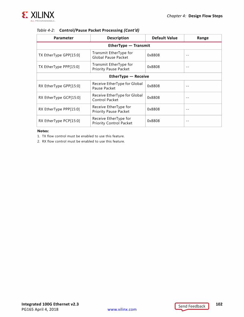
Integrated 100G Ethernet v2.3 102PG165 April 4, 2018 www.xilinx.com
Chapter 4: Design Flow Steps
EtherType — Transmit
TX EtherType GPP[15:0] Transmit EtherType for Global Pause Packet 0x8808 --
TX EtherType PPP[15:0] Transmit EtherType for Priority Pause Packet 0x8808 --
EtherType — Receive
RX EtherType GPP[15:0] Receive EtherType for Global Pause Packet 0x8808 --
RX EtherType GCP[15:0] Receive EtherType for Global Control Packet 0x8808 --
RX EtherType PPP[15:0] Receive EtherType for Priority Pause Packet 0x8808 --
RX EtherType PCP[15:0] Receive EtherType for Priority Control Packet 0x8808 --
Notes: 1. TX flow control must be enabled to use this feature.2. RX flow control must be enabled to use this feature.
Table 4-2: Control/Pause Packet Processing (Cont’d)
Parameter Description Default Value Range
Send Feedback
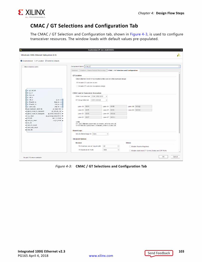
Integrated 100G Ethernet v2.3 103PG165 April 4, 2018 www.xilinx.com
Chapter 4: Design Flow Steps
CMAC / GT Selections and Configuration TabThe CMAC / GT Selection and Configuration tab, shown in Figure 4-3, is used to configure transceiver resources. The window loads with default values pre-populated.
X-Ref Target - Figure 4-3
Figure 4-3: CMAC / GT Selections and Configuration Tab
Send Feedback
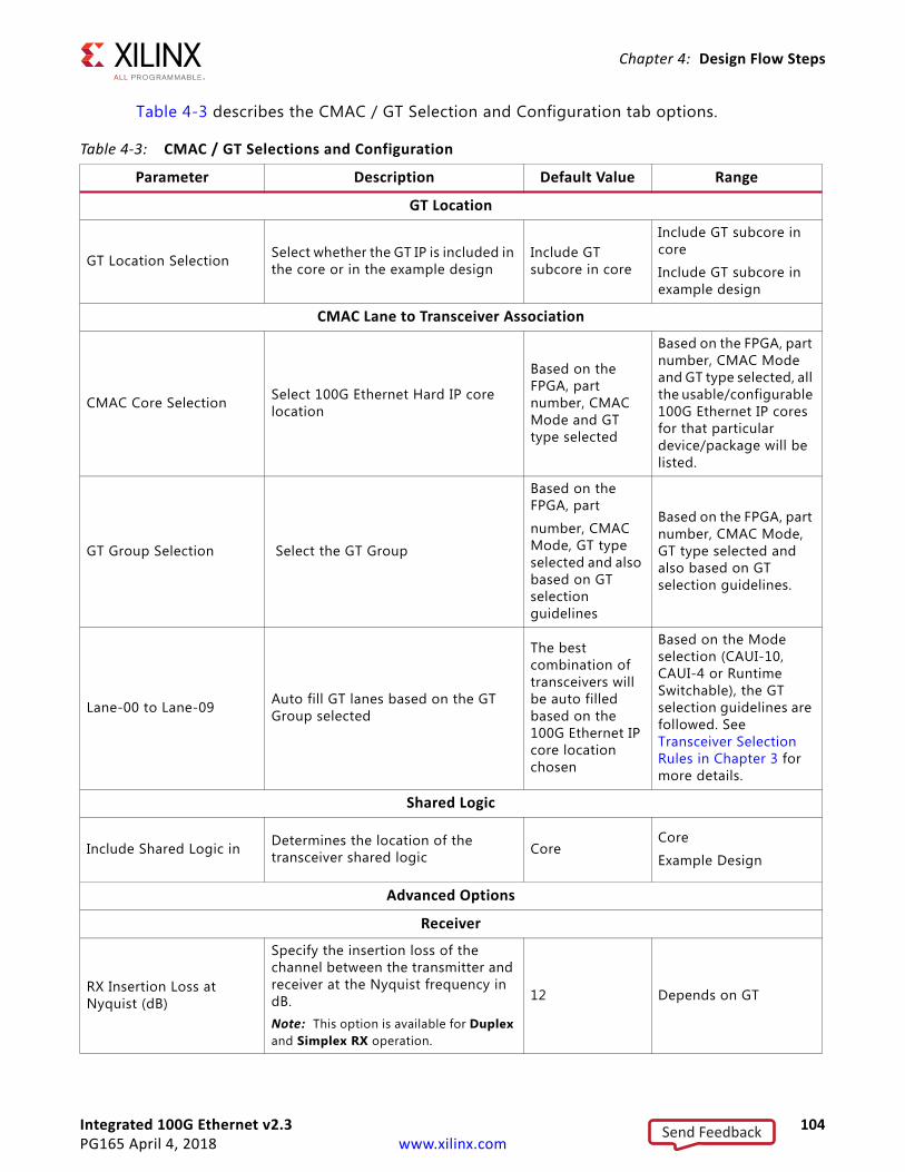
Integrated 100G Ethernet v2.3 104PG165 April 4, 2018 www.xilinx.com
Chapter 4: Design Flow Steps
Table 4-3 describes the CMAC / GT Selection and Configuration tab options.
Table 4-3: CMAC / GT Selections and Configuration
Parameter Description Default Value Range
GT Location
GT Location Selection Select whether the GT IP is included in the core or in the example design
Include GT subcore in core
Include GT subcore in core
Include GT subcore in example design
CMAC Lane to Transceiver Association
CMAC Core Selection Select 100G Ethernet Hard IP core location
Based on the FPGA, part number, CMAC Mode and GT type selected
Based on the FPGA, part number, CMAC Mode and GT type selected, all the usable/configurable 100G Ethernet IP cores for that particular device/package will be listed.
GT Group Selection Select the GT Group
Based on the FPGA, part
number, CMAC Mode, GT type selected and also based on GT selection guidelines
Based on the FPGA, part number, CMAC Mode, GT type selected and also based on GT selection guidelines.
Lane-00 to Lane-09 Auto fill GT lanes based on the GT Group selected
The best combination of transceivers will be auto filled based on the 100G Ethernet IP core location chosen
Based on the Mode selection (CAUI-10, CAUI-4 or Runtime Switchable), the GT selection guidelines are followed. See Transceiver Selection Rules in Chapter 3 for more details.
Shared Logic
Include Shared Logic in Determines the location of the transceiver shared logic Core
Core
Example Design
Advanced Options
Receiver
RX Insertion Loss at Nyquist (dB)
Specify the insertion loss of the channel between the transmitter and receiver at the Nyquist frequency in dB.Note: This option is available for Duplex and Simplex RX operation.
12 Depends on GT
Send Feedback
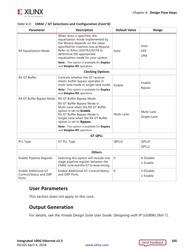
Integrated 100G Ethernet v2.3 105PG165 April 4, 2018 www.xilinx.com
Chapter 4: Design Flow Steps
User ParametersThis section does not apply to this core.
Output GenerationFor details, see the Vivado Design Suite User Guide: Designing with IP (UG896) [Ref 7].
RX Equalization Mode
When Auto is specified, the equalization mode implemented by the Wizard depends on the value specified for insertion loss at Nyquist. Refer to Xilinx UG576/UG578 to determine the appropriate equalization mode for your system.Note: This option is available for Duplex and Simplex RX operation.
Auto
Auto
DFE
LPM
Clocking Options
RX GT Buffer Controls whether the GT receiver elastic buffer bypass operates in multi-lane mode or single-lane mode.Note: This option is available for Duplex and Simplex RX operation.
EnableEnable
Bypass
RX GT Buffer Bypass Mode RX GT Buffer Bypass Mode.
RX GT Buffer Bypass Mode is Multi-Lane when the RX GT Buffer option is set to Enable. RX GT Buffer Bypass Mode is Single-Lane when the RX GT Buffer option is set to Bypass.Note: This option is available for Duplex and Simplex RX operation.
Multi-LaneMulti-Lane
Single-Lane
GT QPLL
PLL Type GT PLL Type QPLL0 QPLL0
QPLL1
Others
Enable Pipeline Register Selecting this option will include one stage pipeline register between the CMAC core and the GT to ease timing.
0 0-Disable
1-Enable
Enable Additional GT Control/Status and DRP Ports
Enable Additional GT Control/Status and DRP Ports
0 0-Disable
1-Enable
Table 4-3: CMAC / GT Selections and Configuration (Cont’d)
Parameter Description Default Value Range
Send Feedback
Integrated 100G Ethernet v2.3 106PG165 April 4, 2018 www.xilinx.com
Chapter 4: Design Flow Steps
Constraining the CoreThis section contains information about constraining the core in the Vivado Design Suite.
Required ConstraintsThe UltraScale™ Devices Integrated 100G Ethernet IP core solution requires the specification of timing and other physical implementation constraints to meet the specified performance requirements. These constraints are provided in a Xilinx® Device Constraints (XDC) file. Pinouts and hierarchy names in the generated XDC correspond to the provided example design of the 100G Ethernet IP core.
To achieve consistent implementation results, an XDC containing these original, unmodified constraints must be used when a design is run through the Xilinx tools. For additional details on the definition and use of an XDC or specific constraints, see the Vivado Design Suite User Guide: Using Constraints (UG903) [Ref 10].
Constraints provided in the 100G Ethernet IP core have been verified through implementation and provide consistent results. Constraints can be modified, but modifications should only be made with a thorough understanding of the effect of each constraint.
Device, Package, and Speed Grade SelectionsThis section is not applicable for this IP core.
Clock FrequenciesThis section is not applicable for this IP core.
Clock ManagementThis section is not applicable for this IP core.
Clock PlacementThis section is not applicable for this IP core.
BankingThis section is not applicable for this IP core.
Send Feedback
Integrated 100G Ethernet v2.3 107PG165 April 4, 2018 www.xilinx.com
Chapter 4: Design Flow Steps
Transceiver PlacementThis section is not applicable for this IP core.
I/O Standard and PlacementThis section is not applicable for this IP core.
SimulationFor comprehensive information about Vivado simulation components, as well as information about using supported third-party tools, see the Vivado Design Suite User Guide: Logic Simulation (UG900) [Ref 9].
For information regarding simulating the example design, see Simulating the Example Design in Chapter 5.
Synthesis and ImplementationFor details about synthesis and implementation, see the Vivado Design Suite User Guide: Designing with IP (UG896) [Ref 7].
For information regarding synthesizing and implementing the example design, see Synthesizing and Implementing the Example Design in Chapter 5.
Send Feedback
Integrated 100G Ethernet v2.3 108PG165 April 4, 2018 www.xilinx.com
Chapter 5
Example Design
OverviewThis chapter briefly explains the 100G Ethernet IP core example design and the various test scenarios implemented within the example design.
Example Design Hierarchy (GT Subcore in Core)Figure 5-1 shows the example design hierarchy (GT subcore in core).
Send Feedback
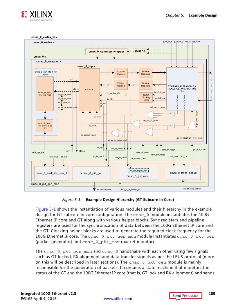
Integrated 100G Ethernet v2.3 109PG165 April 4, 2018 www.xilinx.com
Chapter 5: Example Design
Figure 5-1 shows the instantiation of various modules and their hierarchy in the example design for GT subcore in core configuration. The cmac_0 module instantiates the 100G Ethernet IP core and GT along with various helper blocks. Sync registers and pipeline registers are used for the synchronization of data between the 100G Ethernet IP core and the GT. Clocking helper blocks are used to generate the required clock frequency for the 100G Ethernet IP core. The cmac_0_pkt_gen_mon module instantiates cmac_0_pkt_gen (packet generator) and cmac_0_pkt_mon (packet monitor).
The cmac_0_pkt_gen_mon and cmac_0 handshake with each other using few signals such as GT locked, RX alignment, and data transfer signals as per the LBUS protocol (more on this will be described in later sections). The cmac_0_pkt_gen module is mainly responsible for the generation of packets. It contains a state machine that monitors the status of the GT and the 100G Ethernet IP core (that is, GT lock and RX alignment) and sends
X-Ref Target - Figure 5-1
Figure 5-1: Example Design Hierarchy (GT Subcore in Core)
cmac_0_exdes_tb.v
`
cmac_0_exdes.v
cmac_0.v
tx_clk
GTWIZARD_ULTRASCALE_0
_EXAMPLE_WRAPPER_INS
T.v
cmac_0_pkt_gen_mon
cmac_0_pkt_gencmac_0_pkt_mon
tx_reset
rx_reset
rx_clk
init_clk sys_reset
txoutclk_out
led output ports lbus_tx_rx_restart_in
cmac_0_trans_debug
usr_tx_reset
gt_tx_usrclk2 sys_reset init_clk
cmac_0_common_wrapper
cmac_0_wrapper.v
TX SyncRegisters
PipelineRegisters
PipelineRegisters
RX SyncRegisters
CMAC.V
cmac_0_top.v
gtwiz_reset_all_in
rx_ptp_adjust_top
IBUFDS
TX/RX Clocking Helper
rxoutclk_out
rx_serdes_reset
rx_serdes_clk0
core_drp_reset
rx_serdes_clk
switch_caui_mode
cmac_0_trans_debugcmac_0_axi4_lite_user_if
sys_reset axi_aclk
sys_reset
core_tx_resetcore_rx_reset
axi_gt_reset_all
cmac_0_axi4_lite_reg_map
cmac_0_axi4_lite_slave_2_ip
if
ctrl
stats
AXI4_lite_intfgt _drp_done
cmac_0_axi4_lite_if_wrapper
usr_rx_reset
axi_usr_rx_serdes_reset
statsrx_clk
reset_tx_done_out
reset_rx_done_out
axi_usr_rx_reset
axi_usr_tx_reset
ctrl
axi_usr_tx_reset
axi_usr_rx_reset
axi_gt_reset_all
axi_usr_rx_serdes_reset
gt_ref_clk_pgt_ref_clk_n
Send Feedback
Integrated 100G Ethernet v2.3 110PG165 April 4, 2018 www.xilinx.com
Chapter 5: Example Design
traffic to the core. Similarly the cmac_0_pkt_mon module is mainly responsible for the reception and checking of packets from the core. It also contains a state machine that monitors the status of the GT and 100G Ethernet IP core (that is, GT lock and RX alignment) and receives traffic from the core.
Other optional modules instantiated in the example design are as follows:
• cmac_0_trans_debug: This module brings out all the DRP ports of the transceiver module out of the 100G Ethernet IP core. This module is present in the example design for the following conditions:
° When you select the Runtime Switchable mode in the 100G Ethernet IP Vivado® Integrated Design Environment (IDE), this module is used to perform the GT DRP writes to change the GT configuration (that is, from CAUI-4 to CAUI-10 / CAUI-10 to CAUI-4). After completion of the DRP write, this module generates the gt_drp_done signal that is used to reset the GT.
° When you select Enable Additional GT Control/Status and DRP Ports in the CMAC/GT Selection and Configuration Tab of the 100G Ethernet IP Vivado IDE.
• cmac_0_shared_logic_wrapper: When you select Include Shared Logic in example design in the CMAC / GT Selections and Configuration Tab of the 100G Ethernet IP Vivado IDE, this module will be available in the example design. This wrapper contains three modules: cmac_0_clocking_wrapper, cmac_0_reset_wrapper, and cmac_0_common wrapper. The cmac_0_clocking_wrapper has the instantiation of the IBUFDS for the gt_ref_clk, and the cmac_0_reset_wrapper brings out the reset architecture instantiated between the core and the GT. The cmac_0_common_wrapper brings the transceiver common module out of the 100G Ethernet IP core.
• Pipeline registers: Single-stage pipeline registers are introduced between the 100G Ethernet IP core and the transceiver when you select Enable Pipeline register in the CMAC / GT Selections and Configuration Tab. This includes a one-stage pipeline register between the 100G Ethernet IP core macro and the transceiver to ease timing, using the gt_txusrclk2 and gt_rxusrclk2 for the TX and RX paths respectively.
• TX / RX Sync register: The TX Sync register double synchronizes the data between the 100G Ethernet IP core and the transceiver with respect to the tx_clk. The RX Sync register double synchronizes the data between the transceiver and the 100G Ethernet IP core with respect to rx_serdes_clk.
• rx_ptp_adjust_top: When you select Enable time stamping in the General Tab, this module is present inside the packet monitor module. This soft logic improves timestamp accuracy and compensate for the lane alignment FIFO fill levels by adding or subtracting the relative fill level of the selected lane. This module has a window averaging block with fixed window size of 32.
• cmac_0_axi4_lite_if_wrapper: When selected with the Include AXI4-Lite Control and Statistics Interface option from the General Tab, this module will be included inside the cmac_0_wrapper. This wrapper contains two modules
Send Feedback
Integrated 100G Ethernet v2.3 111PG165 April 4, 2018 www.xilinx.com
Chapter 5: Example Design
cmac_0_axi4_lite_reg_map and cmac_0_axi4_lite_slave_2_ipif. The details of these modules are described in AXI4-Lite Interface Implementation.
• cmac_0_axi4_lite_user_if: When selected with the Include AXI4-Lite Control and Statistics option from the General Tab, this module will be present inside the cmac_0_pkt_gen_mon. The details about this module are described in section AXI4-Lite Interface Implementation.
• cmac_0_rs_fec: In CAUI-4 mode of operation, when you select the Include IEEE 802.3bj RS-FEC option from the General Tab, the IEEE 802.3bj RS-FEC soft IP will be instantiated inside the cmac_0_wrapper. This module is meant for forward error correction coding. The RS-FEC IP will be integrated in between CMAC and GT. The details of this module are described in IEEE 802.3bj RS-FEC Integration.
• cmac_0_xbar: In CAUI-4 mode of operation, when you select Include IEEE 802.3bj RS-FEC along with the Include AXI4-Lite Control and Statistics Interface option from the General Tab, the AXI Crossbar soft IP will be instantiated inside the cmac_0_wrapper. The AXI4-Lite interface for both CMAC and RS-FEC will be accessed through the AXI Crossbar IP. The details of this module are described in IEEE 802.3bj RS-FEC Integration.
Example Design Hierarchy (GT Subcore in Example Design)Figure 5-2 shows the instantiation of various modules and their hierarchy in the example design when the GT (serial transceiver) is outside the IP core, that is, in the example design. This hierarchical example design is delivered when you select the Include GT subcore in example design option from the CMAC / GT Selections and Configuration Tab.
Send Feedback
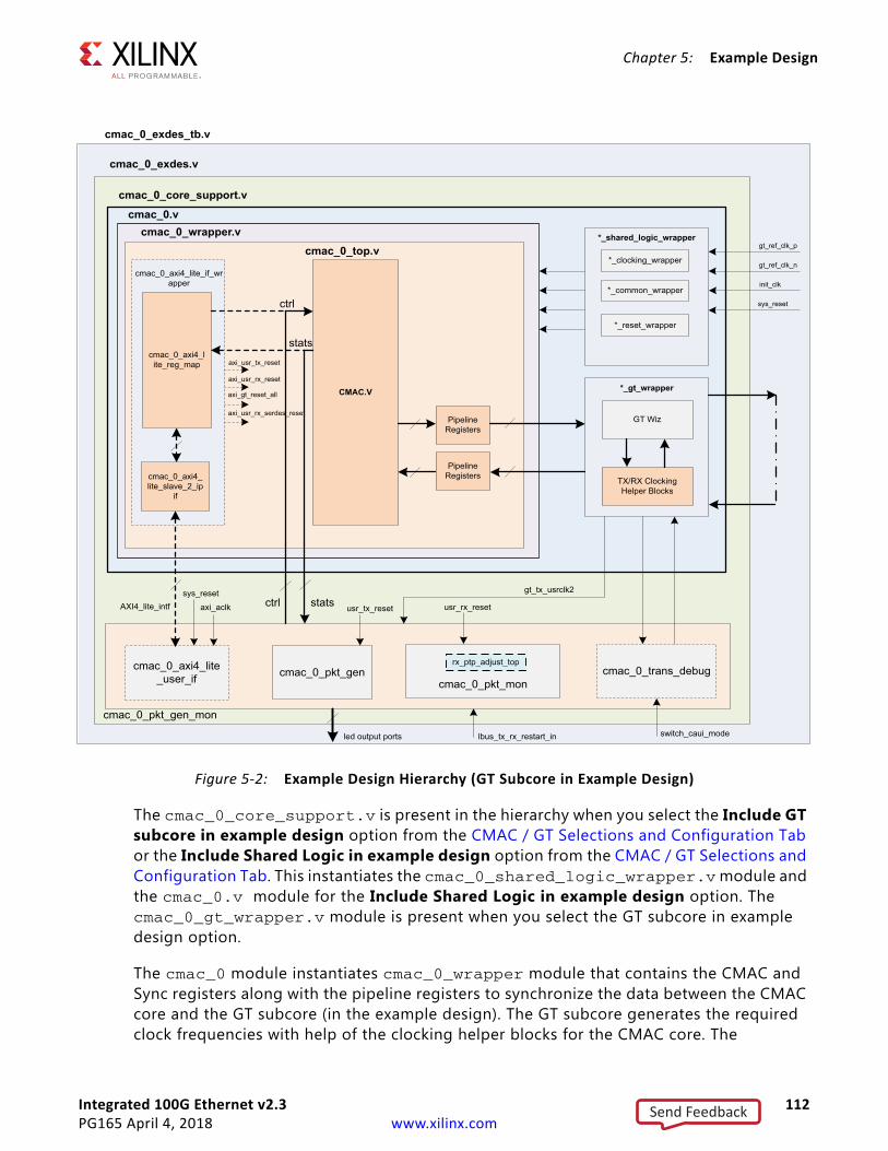
Integrated 100G Ethernet v2.3 112PG165 April 4, 2018 www.xilinx.com
Chapter 5: Example Design
The cmac_0_core_support.v is present in the hierarchy when you select the Include GT subcore in example design option from the CMAC / GT Selections and Configuration Tab or the Include Shared Logic in example design option from the CMAC / GT Selections and Configuration Tab. This instantiates the cmac_0_shared_logic_wrapper.v module and the cmac_0.v module for the Include Shared Logic in example design option. The cmac_0_gt_wrapper.v module is present when you select the GT subcore in example design option.
The cmac_0 module instantiates cmac_0_wrapper module that contains the CMAC and Sync registers along with the pipeline registers to synchronize the data between the CMAC core and the GT subcore (in the example design). The GT subcore generates the required clock frequencies with help of the clocking helper blocks for the CMAC core. The
X-Ref Target - Figure 5-2
Figure 5-2: Example Design Hierarchy (GT Subcore in Example Design)
cmac_0_exdes_tb.v
cmac_0_exdes.v
cmac_0.v
*_gt_wrapper`
cmac_0_pkt_gen_mon
cmac_0_pkt_gencmac_0_pkt_mon
init_clk
sys_reset
led output ports lbus_tx_rx_restart_in
usr_tx_reset
cmac_0_wrapper.v
PipelineRegisters
PipelineRegisters
CMAC.V
cmac_0_top.v
rx_ptp_adjust_top
TX/RX Clocking Helper Blocks
switch_caui_mode
cmac_0_trans_debugcmac_0_axi4_lite_user_if
sys_reset
axi_aclk
cmac_0_axi4_lite_reg_map
cmac_0_axi4_lite_slave_2_ip
if
ctrl
stats
AXI4_lite_intf
cmac_0_axi4_lite_if_wrapper
usr_rx_resetstatsctrl
axi_usr_tx_reset
axi_usr_rx_reset
axi_gt_reset_all
axi_usr_rx_serdes_reset
gt_ref_clk_p
gt_ref_clk_n
GT Wiz
*_shared_logic_wrapper
*_clocking_wrapper
*_common_wrapper
*_reset_wrapper
cmac_0_core_support.v
gt_tx_usrclk2
Send Feedback
Integrated 100G Ethernet v2.3 113PG165 April 4, 2018 www.xilinx.com
Chapter 5: Example Design
cmac_0_pkt_gen_mon module instantiates cmac_0_pkt_gen (packet generator) and cmac_0_pkt_mon (packet monitor). The cmac_0_pkt_gen_mon and cmac_0_core_support handshake with each other using several signals such as GT locked, RX alignment and data transfer signals as per LBUS protocol (described in more detail later). The cmac_0_pkt_gen module is mainly responsible for the generation of packets. It contains a state machine that monitors the status of GT and CMAC (that is, GT lock and RX alignment) and sends traffic to the core. Similarly the cmac_0_pkt_mon module is mainly responsible for reception and checking of packets from the core. It also contains a state machine that monitors the status of GT and CMAC (that is, GT lock and RX alignment) and receives traffic from the core.
Other optional modules instantiated in the example design are as follows:
• cmac_0_shared_logic_wrapper: When you select Include GT subcore in example design or Include Shared Logic in example design in the CMAC / GT Selections and Configuration Tab of the 100G Ethernet IP Vivado IDE, this module will be available in the example design. This wrapper contains three modules: cmac_0_clocking_wrapper, cmac_0_reset_wrapper, and cmac_0_common_wrapper. The cmac_0_clocking_wrapper has the instantiation of the IBUFDS for the gt_ref_clk, and the cmac_0_reset_wrapper brings out the reset architecture instantiated between the core and the GT. The cmac_0_common_wrapper brings the transceiver common module out of the 100G Ethernet IP core.
• cmac_0_gt_wrapper: This module is present in the example design when you select the Include GT subcore in example design option from the CMAC / GT Selections and Configuration Tab. This module is having instantiations of the GT along with various helper blocks. The clocking helper blocks are used to generate the required clock frequency for the core.
User InterfaceGeneral purpose I/Os (GPIOs. have been provided to control the example design. I/Os are as listed in Table 5-1.
Note: For all the input and output signals mentioned in Table 5-1, a three-stage registering has been done internally.
Table 5-1: User I/O Ports
Name Size I/O Description
sys_reset 1 I Reset for cmac_0
gt_ref_clk_p 1 I Differential clk input to GT.
gt_ref_clk_n 1 I Differential clk input to GT.
init_clk 1 I Stable and free-running clk input to GT.
Send Feedback
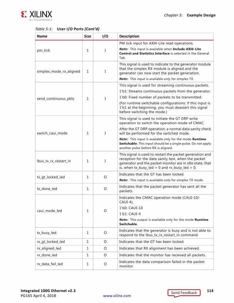
Integrated 100G Ethernet v2.3 114PG165 April 4, 2018 www.xilinx.com
Chapter 5: Example Design
pm_tick 1 I
PM tick input for AXI4-Lite read operations.Note: This input is available when Include AXI4-Lite Control and Statistics Interface is selected in the General Tab.
simplex_mode_rx_aligned 1 I
This signal is used to indicate to the generator module that the simplex RX module is aligned and the generator can now start the packet generation.Note: This input is available only for simplex TX.
send_continuous_pkts 1 I
This signal is used for streaming continuous packets.
1'b1: Streams continuous packets from the generator.
1'b0: Fixed number of packets to be transmitted.
(For runtime switchable configurations: if this input is 1'b1 at the beginning, you must deassert this signal before switching the mode.)
switch_caui_mode 1 I
This signal is used to initiate the GT DRP write operation to switch the operation mode of CMAC.
After the GT DRP operation, a normal data sanity check will be performed for the switched mode.Note: This input is available only for the mode Runtime Switchable. This input should be a single pulse. Do not apply another pulse before RX is aligned.
lbus_tx_rx_restart_in 1 I
This signal is used to restart the packet generation and reception for the data sanity test, when the packet generator and the packet monitor are in idle state, that is, when tx_busy_led = 0 and rx_busy_led = 0.
tx_gt_locked_led 1 OIndicates that the GT has been locked. Note: This input is available only for simplex TX mode.
tx_done_led 1 O Indicates that the packet generator has sent all the packets.
caui_mode_led 1 O
Indicates the CMAC operation mode (CAUI-10/CAUI-4).
1’b0: CAUI-10
1’b1: CAUI-4Note: This output is available only for the mode Runtime Switchable.
tx_busy_led 1 O Indicates that the generator is busy and is not able to respond to the lbus_tx_rx_restart_in command.
rx_gt_locked_led 1 O Indicates that the GT has been locked.
rx_aligned_led 1 O Indicates that RX alignment has been achieved.
rx_done_led 1 O Indicates that the monitor has received all packets.
rx_data_fail_led 1 O Indicates the data comparison failed in the packet monitor.
Table 5-1: User I/O Ports (Cont’d)
Name Size I/O Description
Send Feedback

Integrated 100G Ethernet v2.3 115PG165 April 4, 2018 www.xilinx.com
Chapter 5: Example Design
CORE XCI Top Level Port ListThe top-level port list for the core XCI with all features enabled is shown in Table 5-2.
rx_busy_led 1 O Indicates that the monitor is busy and is not able to respond to the lbus_tx_rx_restart_in command.
stat_reg_compare_out 1 O
Indicates TX and RX statistics registers comparison status.
1'b1: Indicates both the TX and RX statistics matched.
1'b0: Indicates if there is any mismatch between TX and RX statistics. Note: This output is available when Include AXI4-Lite Control and Statistics Interface is selected in the General Tab.
Table 5-1: User I/O Ports (Cont’d)
Name Size I/O Description
Table 5-2: CORE XCI Top-Level Port List
Name Size I/O Description
sys_reset 1 I Reset for the CMAC core.
gt_ref_clk_p 1 I Differential clk input to GT.
gt_ref_clk_n 1 I Differential clk input to GT.
init_clk 1 IStable and free-running clk input to GT. This is used as the clock for the GT reset state machines, and the GT Channel and Common DRP ports, if included.
gt_loopback_in 30/12 I
GT loopback input signal. Refer to the applicable GT user guide. [Ref 11][Ref 12]
30-bit width for CAUI-10 or Runtime Switchable case, 12-bit width for CAUI-4 mode.
gt_rxrecclkout 10/4 O
Refer to the applicable GT user guide for the port description.[Ref 11][Ref 12]
Port width: 10-bit for CAUI-10 or Runtime Switchable case and 4-bit width for CAUI-4 mode.
gt_ref_clk_out 1 O GT reference clock output.
gt_powergoodout 10/4 O
Refer to the applicable GT user guide for the port description.[Ref 11][Ref 12]
Port width: 10-bit for CAUI-10 or Runtime Switchable case and 4-bit width for CAUI-4 mode.
gt0_rxp_in 1 I Differential serial GT RX input for lane 0.
gt0_rxn_in 1 I Differential serial GT RX input for lane 0.
gt1_rxp_in 1 I Differential serial GT RX input for lane 1.
Send Feedback
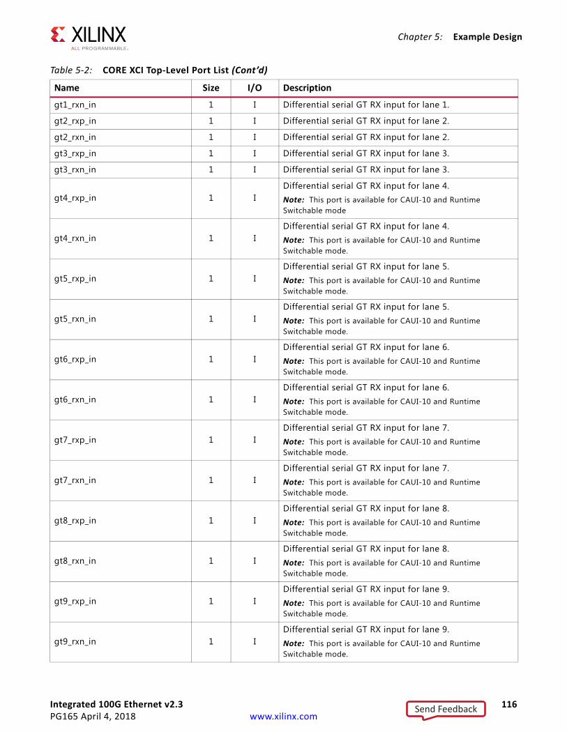
Integrated 100G Ethernet v2.3 116PG165 April 4, 2018 www.xilinx.com
Chapter 5: Example Design
gt1_rxn_in 1 I Differential serial GT RX input for lane 1.
gt2_rxp_in 1 I Differential serial GT RX input for lane 2.
gt2_rxn_in 1 I Differential serial GT RX input for lane 2.
gt3_rxp_in 1 I Differential serial GT RX input for lane 3.
gt3_rxn_in 1 I Differential serial GT RX input for lane 3.
gt4_rxp_in 1 IDifferential serial GT RX input for lane 4.Note: This port is available for CAUI-10 and Runtime Switchable mode
gt4_rxn_in 1 IDifferential serial GT RX input for lane 4.Note: This port is available for CAUI-10 and Runtime Switchable mode.
gt5_rxp_in 1 IDifferential serial GT RX input for lane 5.Note: This port is available for CAUI-10 and Runtime Switchable mode.
gt5_rxn_in 1 IDifferential serial GT RX input for lane 5.Note: This port is available for CAUI-10 and Runtime Switchable mode.
gt6_rxp_in 1 IDifferential serial GT RX input for lane 6.Note: This port is available for CAUI-10 and Runtime Switchable mode.
gt6_rxn_in 1 IDifferential serial GT RX input for lane 6.Note: This port is available for CAUI-10 and Runtime Switchable mode.
gt7_rxp_in 1 IDifferential serial GT RX input for lane 7.Note: This port is available for CAUI-10 and Runtime Switchable mode.
gt7_rxn_in 1 IDifferential serial GT RX input for lane 7.Note: This port is available for CAUI-10 and Runtime Switchable mode.
gt8_rxp_in 1 IDifferential serial GT RX input for lane 8.Note: This port is available for CAUI-10 and Runtime Switchable mode.
gt8_rxn_in 1 IDifferential serial GT RX input for lane 8.Note: This port is available for CAUI-10 and Runtime Switchable mode.
gt9_rxp_in 1 IDifferential serial GT RX input for lane 9.Note: This port is available for CAUI-10 and Runtime Switchable mode.
gt9_rxn_in 1 IDifferential serial GT RX input for lane 9.Note: This port is available for CAUI-10 and Runtime Switchable mode.
Table 5-2: CORE XCI Top-Level Port List (Cont’d)
Name Size I/O Description
Send Feedback
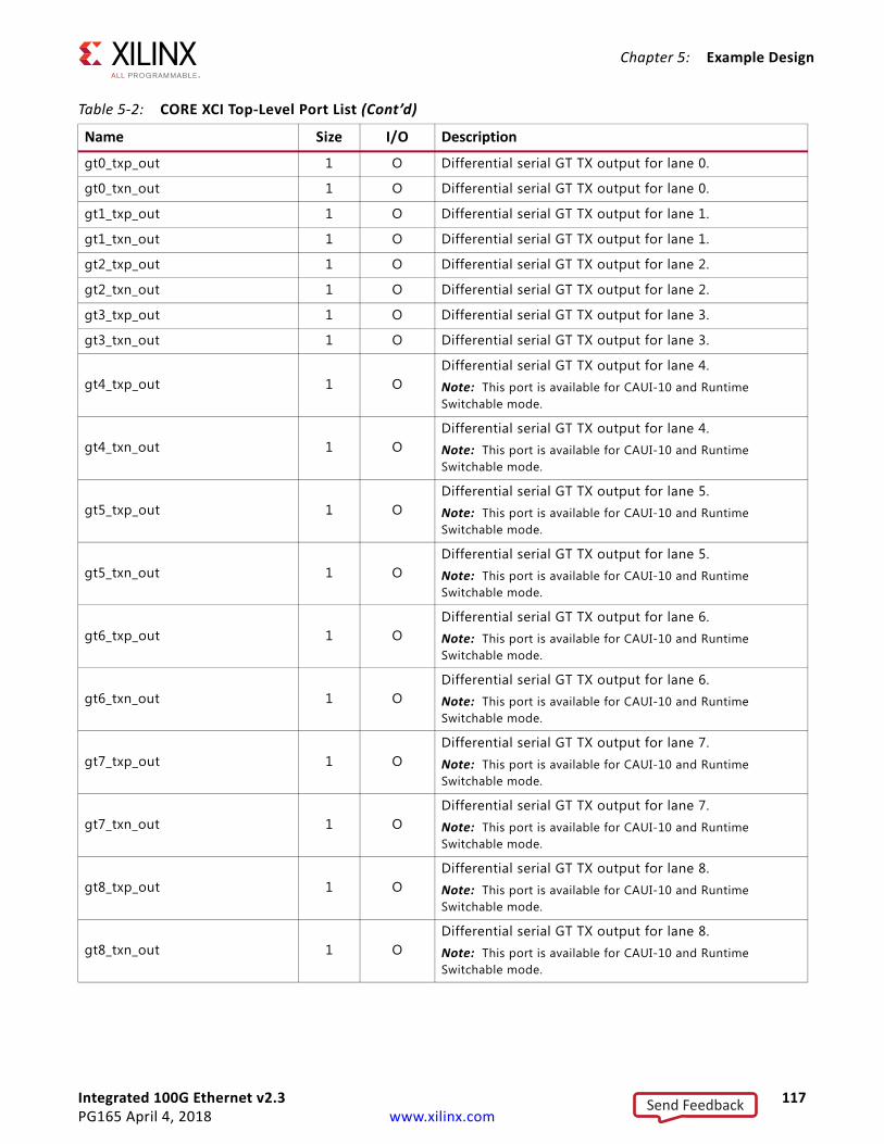
Integrated 100G Ethernet v2.3 117PG165 April 4, 2018 www.xilinx.com
Chapter 5: Example Design
gt0_txp_out 1 O Differential serial GT TX output for lane 0.
gt0_txn_out 1 O Differential serial GT TX output for lane 0.
gt1_txp_out 1 O Differential serial GT TX output for lane 1.
gt1_txn_out 1 O Differential serial GT TX output for lane 1.
gt2_txp_out 1 O Differential serial GT TX output for lane 2.
gt2_txn_out 1 O Differential serial GT TX output for lane 2.
gt3_txp_out 1 O Differential serial GT TX output for lane 3.
gt3_txn_out 1 O Differential serial GT TX output for lane 3.
gt4_txp_out 1 ODifferential serial GT TX output for lane 4.Note: This port is available for CAUI-10 and Runtime Switchable mode.
gt4_txn_out 1 ODifferential serial GT TX output for lane 4.Note: This port is available for CAUI-10 and Runtime Switchable mode.
gt5_txp_out 1 ODifferential serial GT TX output for lane 5.Note: This port is available for CAUI-10 and Runtime Switchable mode.
gt5_txn_out 1 ODifferential serial GT TX output for lane 5.Note: This port is available for CAUI-10 and Runtime Switchable mode.
gt6_txp_out 1 ODifferential serial GT TX output for lane 6.Note: This port is available for CAUI-10 and Runtime Switchable mode.
gt6_txn_out 1 ODifferential serial GT TX output for lane 6.Note: This port is available for CAUI-10 and Runtime Switchable mode.
gt7_txp_out 1 ODifferential serial GT TX output for lane 7.Note: This port is available for CAUI-10 and Runtime Switchable mode.
gt7_txn_out 1 ODifferential serial GT TX output for lane 7.Note: This port is available for CAUI-10 and Runtime Switchable mode.
gt8_txp_out 1 ODifferential serial GT TX output for lane 8.Note: This port is available for CAUI-10 and Runtime Switchable mode.
gt8_txn_out 1 ODifferential serial GT TX output for lane 8.Note: This port is available for CAUI-10 and Runtime Switchable mode.
Table 5-2: CORE XCI Top-Level Port List (Cont’d)
Name Size I/O Description
Send Feedback
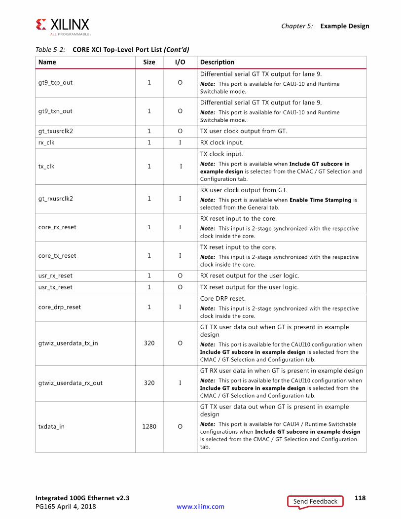
Integrated 100G Ethernet v2.3 118PG165 April 4, 2018 www.xilinx.com
Chapter 5: Example Design
gt9_txp_out 1 ODifferential serial GT TX output for lane 9.Note: This port is available for CAUI-10 and Runtime Switchable mode.
gt9_txn_out 1 ODifferential serial GT TX output for lane 9.Note: This port is available for CAUI-10 and Runtime Switchable mode.
gt_txusrclk2 1 O TX user clock output from GT.
rx_clk 1 I RX clock input.
tx_clk 1 I
TX clock input.Note: This port is available when Include GT subcore in example design is selected from the CMAC / GT Selection and Configuration tab.
gt_rxusrclk2 1 IRX user clock output from GT.Note: This port is available when Enable Time Stamping is selected from the General tab.
core_rx_reset 1 IRX reset input to the core.Note: This input is 2-stage synchronized with the respective clock inside the core.
core_tx_reset 1 ITX reset input to the core.Note: This input is 2-stage synchronized with the respective clock inside the core.
usr_rx_reset 1 O RX reset output for the user logic.
usr_tx_reset 1 O TX reset output for the user logic.
core_drp_reset 1 ICore DRP reset.Note: This input is 2-stage synchronized with the respective clock inside the core.
gtwiz_userdata_tx_in 320 O
GT TX user data out when GT is present in example designNote: This port is available for the CAUI10 configuration when Include GT subcore in example design is selected from the CMAC / GT Selection and Configuration tab.
gtwiz_userdata_rx_out 320 I
GT RX user data in when GT is present in example designNote: This port is available for the CAUI10 configuration when Include GT subcore in example design is selected from the CMAC / GT Selection and Configuration tab.
txdata_in 1280 O
GT TX user data out when GT is present in example designNote: This port is available for CAUI4 / Runtime Switchable configurations when Include GT subcore in example design is selected from the CMAC / GT Selection and Configuration tab.
Table 5-2: CORE XCI Top-Level Port List (Cont’d)
Name Size I/O Description
Send Feedback
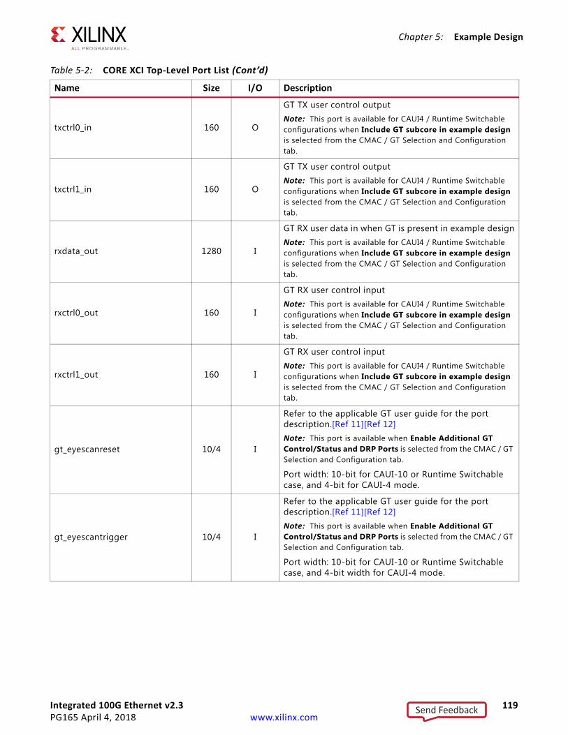
Integrated 100G Ethernet v2.3 119PG165 April 4, 2018 www.xilinx.com
Chapter 5: Example Design
txctrl0_in 160 O
GT TX user control outputNote: This port is available for CAUI4 / Runtime Switchable configurations when Include GT subcore in example design is selected from the CMAC / GT Selection and Configuration tab.
txctrl1_in 160 O
GT TX user control outputNote: This port is available for CAUI4 / Runtime Switchable configurations when Include GT subcore in example design is selected from the CMAC / GT Selection and Configuration tab.
rxdata_out 1280 I
GT RX user data in when GT is present in example designNote: This port is available for CAUI4 / Runtime Switchable configurations when Include GT subcore in example design is selected from the CMAC / GT Selection and Configuration tab.
rxctrl0_out 160 I
GT RX user control inputNote: This port is available for CAUI4 / Runtime Switchable configurations when Include GT subcore in example design is selected from the CMAC / GT Selection and Configuration tab.
rxctrl1_out 160 I
GT RX user control inputNote: This port is available for CAUI4 / Runtime Switchable configurations when Include GT subcore in example design is selected from the CMAC / GT Selection and Configuration tab.
gt_eyescanreset 10/4 I
Refer to the applicable GT user guide for the port description.[Ref 11][Ref 12]Note: This port is available when Enable Additional GT Control/Status and DRP Ports is selected from the CMAC / GT Selection and Configuration tab.
Port width: 10-bit for CAUI-10 or Runtime Switchable case, and 4-bit for CAUI-4 mode.
gt_eyescantrigger 10/4 I
Refer to the applicable GT user guide for the port description.[Ref 11][Ref 12]Note: This port is available when Enable Additional GT Control/Status and DRP Ports is selected from the CMAC / GT Selection and Configuration tab.
Port width: 10-bit for CAUI-10 or Runtime Switchable case, and 4-bit width for CAUI-4 mode.
Table 5-2: CORE XCI Top-Level Port List (Cont’d)
Name Size I/O Description
Send Feedback
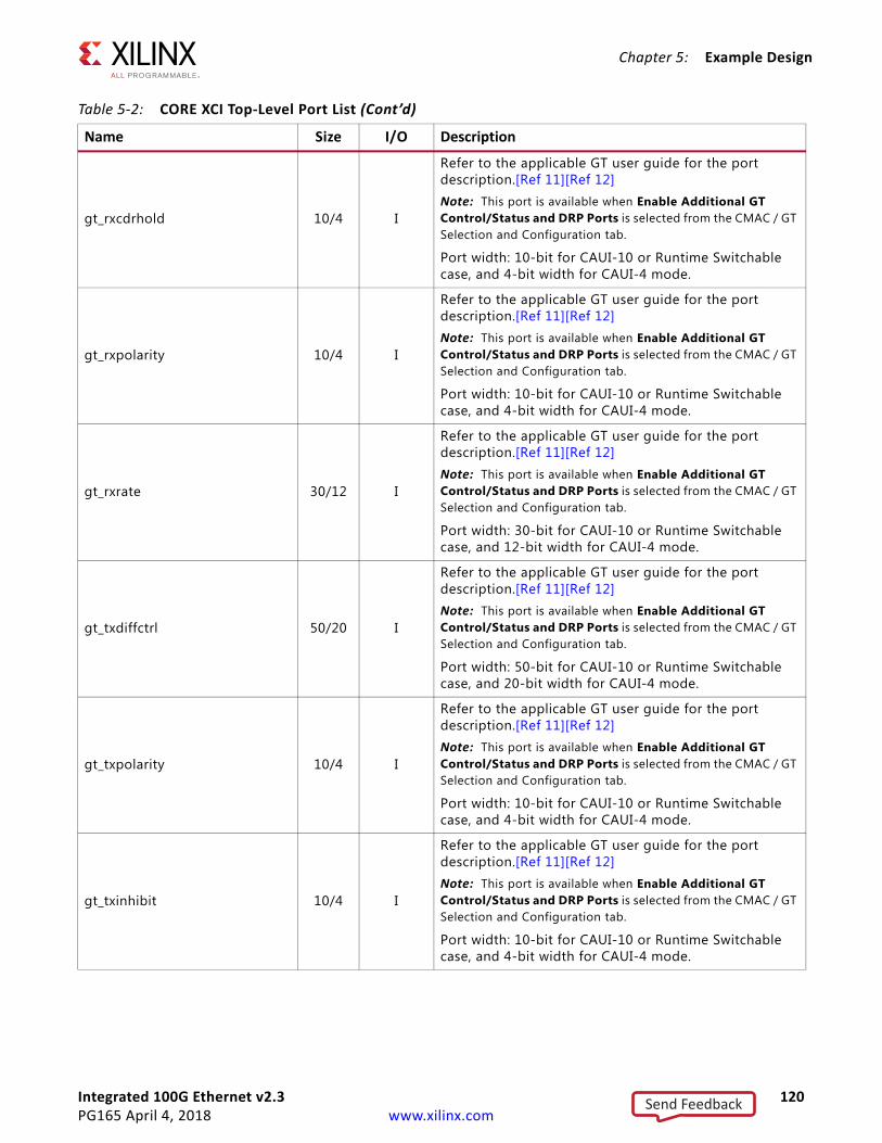
Integrated 100G Ethernet v2.3 120PG165 April 4, 2018 www.xilinx.com
Chapter 5: Example Design
gt_rxcdrhold 10/4 I
Refer to the applicable GT user guide for the port description.[Ref 11][Ref 12]Note: This port is available when Enable Additional GT Control/Status and DRP Ports is selected from the CMAC / GT Selection and Configuration tab.
Port width: 10-bit for CAUI-10 or Runtime Switchable case, and 4-bit width for CAUI-4 mode.
gt_rxpolarity 10/4 I
Refer to the applicable GT user guide for the port description.[Ref 11][Ref 12]Note: This port is available when Enable Additional GT Control/Status and DRP Ports is selected from the CMAC / GT Selection and Configuration tab.
Port width: 10-bit for CAUI-10 or Runtime Switchable case, and 4-bit width for CAUI-4 mode.
gt_rxrate 30/12 I
Refer to the applicable GT user guide for the port description.[Ref 11][Ref 12]Note: This port is available when Enable Additional GT Control/Status and DRP Ports is selected from the CMAC / GT Selection and Configuration tab.
Port width: 30-bit for CAUI-10 or Runtime Switchable case, and 12-bit width for CAUI-4 mode.
gt_txdiffctrl 50/20 I
Refer to the applicable GT user guide for the port description.[Ref 11][Ref 12]Note: This port is available when Enable Additional GT Control/Status and DRP Ports is selected from the CMAC / GT Selection and Configuration tab.
Port width: 50-bit for CAUI-10 or Runtime Switchable case, and 20-bit width for CAUI-4 mode.
gt_txpolarity 10/4 I
Refer to the applicable GT user guide for the port description.[Ref 11][Ref 12]Note: This port is available when Enable Additional GT Control/Status and DRP Ports is selected from the CMAC / GT Selection and Configuration tab.
Port width: 10-bit for CAUI-10 or Runtime Switchable case, and 4-bit width for CAUI-4 mode.
gt_txinhibit 10/4 I
Refer to the applicable GT user guide for the port description.[Ref 11][Ref 12]Note: This port is available when Enable Additional GT Control/Status and DRP Ports is selected from the CMAC / GT Selection and Configuration tab.
Port width: 10-bit for CAUI-10 or Runtime Switchable case, and 4-bit width for CAUI-4 mode.
Table 5-2: CORE XCI Top-Level Port List (Cont’d)
Name Size I/O Description
Send Feedback

Integrated 100G Ethernet v2.3 121PG165 April 4, 2018 www.xilinx.com
Chapter 5: Example Design
gt_txpippmen 10/4 I
Refer to the applicable GT user guide for the port description.[Ref 11][Ref 12]Note: This port is available when Enable Additional GT Control/Status and DRP Ports is selected from the CMAC / GT Selection and Configuration tab.
Port width: 10-bit for CAUI-10 or Runtime Switchable case, and 4-bit width for CAUI-4 mode.
gt_txpippmsel 10/4 I
Refer to the applicable GT user guide for the port description.[Ref 11][Ref 12]Note: This port is available when Enable Additional GT Control/Status and DRP Ports is selected from the CMAC / GT Selection and Configuration tab.
Port width: 10-bit for CAUI-10 or Runtime Switchable case, and 4-bit width for CAUI-4 mode.
gt_txpostcursor 50/20 I
Refer to the applicable GT user guide for the port description.[Ref 11][Ref 12]Note: This port is available when Enable Additional GT Control/Status and DRP Ports is selected from the CMAC / GT Selection and Configuration tab.
Port width: 50-bit for CAUI-10 or Runtime Switchable case, and 20-bit width for CAUI-4 mode.
gt_txprbsforceerr 10/4 I
Refer to the applicable GT user guide for the port description.[Ref 11][Ref 12]Note: This port is available when Enable Additional GT Control/Status and DRP Ports is selected from the CMAC / GT Selection and Configuration tab.
Port width: 10-bit for CAUI-10 or Runtime Switchable case, and 4-bit width for CAUI-4 mode.
gt_txprecursor 50/20 I
Refer to the applicable GT user guide for the port description.[Ref 11][Ref 12]Note: This port is available when Enable Additional GT Control/Status and DRP Ports is selected from the CMAC / GT Selection and Configuration tab.
Port width: 50-bit for CAUI-10 or Runtime Switchable case, and 20-bit width for CAUI-4 mode.
gt_eyescandataerror 10/4 O
Refer to the applicable GT user guide for the port description.[Ref 11][Ref 12]Note: This port is available when Enable Additional GT Control/Status and DRP Ports is selected from the CMAC / GT Selection and Configuration tab.
Port width: 10-bit for CAUI-10 or Runtime Switchable case, and 4-bit width for CAUI-4 mode.
Table 5-2: CORE XCI Top-Level Port List (Cont’d)
Name Size I/O Description
Send Feedback
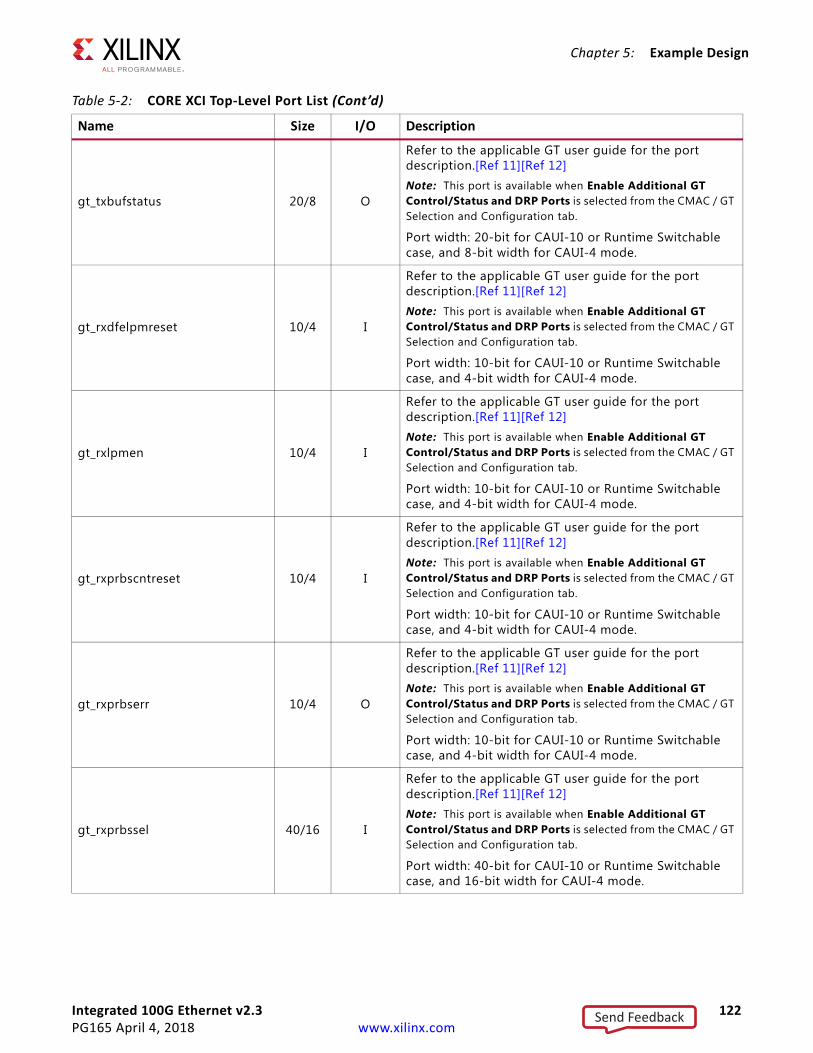
Integrated 100G Ethernet v2.3 122PG165 April 4, 2018 www.xilinx.com
Chapter 5: Example Design
gt_txbufstatus 20/8 O
Refer to the applicable GT user guide for the port description.[Ref 11][Ref 12]Note: This port is available when Enable Additional GT Control/Status and DRP Ports is selected from the CMAC / GT Selection and Configuration tab.
Port width: 20-bit for CAUI-10 or Runtime Switchable case, and 8-bit width for CAUI-4 mode.
gt_rxdfelpmreset 10/4 I
Refer to the applicable GT user guide for the port description.[Ref 11][Ref 12]Note: This port is available when Enable Additional GT Control/Status and DRP Ports is selected from the CMAC / GT Selection and Configuration tab.
Port width: 10-bit for CAUI-10 or Runtime Switchable case, and 4-bit width for CAUI-4 mode.
gt_rxlpmen 10/4 I
Refer to the applicable GT user guide for the port description.[Ref 11][Ref 12]Note: This port is available when Enable Additional GT Control/Status and DRP Ports is selected from the CMAC / GT Selection and Configuration tab.
Port width: 10-bit for CAUI-10 or Runtime Switchable case, and 4-bit width for CAUI-4 mode.
gt_rxprbscntreset 10/4 I
Refer to the applicable GT user guide for the port description.[Ref 11][Ref 12]Note: This port is available when Enable Additional GT Control/Status and DRP Ports is selected from the CMAC / GT Selection and Configuration tab.
Port width: 10-bit for CAUI-10 or Runtime Switchable case, and 4-bit width for CAUI-4 mode.
gt_rxprbserr 10/4 O
Refer to the applicable GT user guide for the port description.[Ref 11][Ref 12]Note: This port is available when Enable Additional GT Control/Status and DRP Ports is selected from the CMAC / GT Selection and Configuration tab.
Port width: 10-bit for CAUI-10 or Runtime Switchable case, and 4-bit width for CAUI-4 mode.
gt_rxprbssel 40/16 I
Refer to the applicable GT user guide for the port description.[Ref 11][Ref 12]Note: This port is available when Enable Additional GT Control/Status and DRP Ports is selected from the CMAC / GT Selection and Configuration tab.
Port width: 40-bit for CAUI-10 or Runtime Switchable case, and 16-bit width for CAUI-4 mode.
Table 5-2: CORE XCI Top-Level Port List (Cont’d)
Name Size I/O Description
Send Feedback
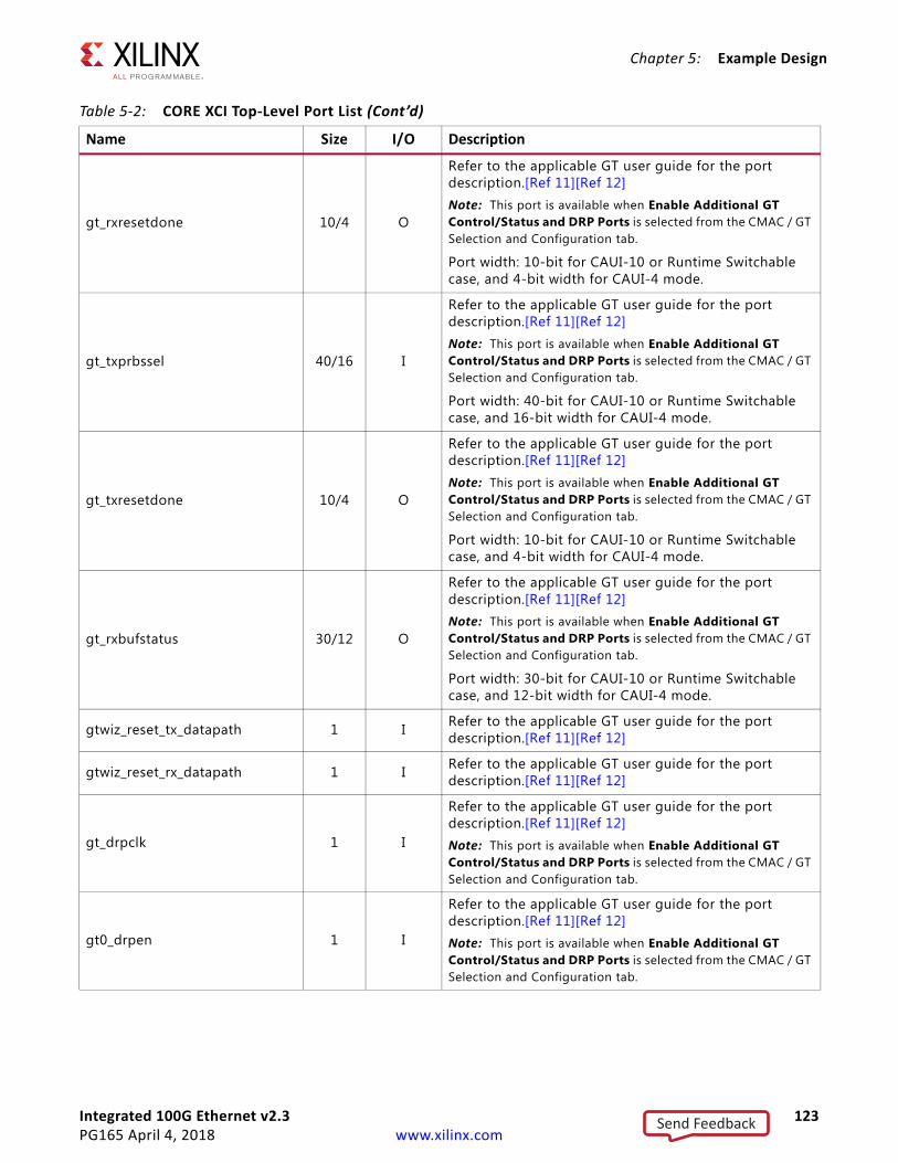
Integrated 100G Ethernet v2.3 123PG165 April 4, 2018 www.xilinx.com
Chapter 5: Example Design
gt_rxresetdone 10/4 O
Refer to the applicable GT user guide for the port description.[Ref 11][Ref 12]Note: This port is available when Enable Additional GT Control/Status and DRP Ports is selected from the CMAC / GT Selection and Configuration tab.
Port width: 10-bit for CAUI-10 or Runtime Switchable case, and 4-bit width for CAUI-4 mode.
gt_txprbssel 40/16 I
Refer to the applicable GT user guide for the port description.[Ref 11][Ref 12]Note: This port is available when Enable Additional GT Control/Status and DRP Ports is selected from the CMAC / GT Selection and Configuration tab.
Port width: 40-bit for CAUI-10 or Runtime Switchable case, and 16-bit width for CAUI-4 mode.
gt_txresetdone 10/4 O
Refer to the applicable GT user guide for the port description.[Ref 11][Ref 12]Note: This port is available when Enable Additional GT Control/Status and DRP Ports is selected from the CMAC / GT Selection and Configuration tab.
Port width: 10-bit for CAUI-10 or Runtime Switchable case, and 4-bit width for CAUI-4 mode.
gt_rxbufstatus 30/12 O
Refer to the applicable GT user guide for the port description.[Ref 11][Ref 12]Note: This port is available when Enable Additional GT Control/Status and DRP Ports is selected from the CMAC / GT Selection and Configuration tab.
Port width: 30-bit for CAUI-10 or Runtime Switchable case, and 12-bit width for CAUI-4 mode.
gtwiz_reset_tx_datapath 1 I Refer to the applicable GT user guide for the port description.[Ref 11][Ref 12]
gtwiz_reset_rx_datapath 1 I Refer to the applicable GT user guide for the port description.[Ref 11][Ref 12]
gt_drpclk 1 I
Refer to the applicable GT user guide for the port description.[Ref 11][Ref 12]Note: This port is available when Enable Additional GT Control/Status and DRP Ports is selected from the CMAC / GT Selection and Configuration tab.
gt0_drpen 1 I
Refer to the applicable GT user guide for the port description.[Ref 11][Ref 12]Note: This port is available when Enable Additional GT Control/Status and DRP Ports is selected from the CMAC / GT Selection and Configuration tab.
Table 5-2: CORE XCI Top-Level Port List (Cont’d)
Name Size I/O Description
Send Feedback

Integrated 100G Ethernet v2.3 124PG165 April 4, 2018 www.xilinx.com
Chapter 5: Example Design
gt0_drpwe 1 I
Refer to the applicable GT user guide for the port description.[Ref 11][Ref 12]Note: This port is available when Enable Additional GT Control/Status and DRP Ports is selected from the CMAC / GT Selection and Configuration tab.
gt0_drpaddr 10 I
Refer to the applicable GT user guide for the port description.[Ref 11][Ref 12]Note: This port is available when Enable Additional GT Control/Status and DRP Ports is selected from the CMAC / GT Selection and Configuration tab.
gt0_drpdi 16 I
Refer to the applicable GT user guide for the port description.[Ref 11][Ref 12]Note: This port is available when Enable Additional GT Control/Status and DRP Ports is selected from the CMAC / GT Selection and Configuration tab.
gt0_drpdo 16 O
Refer to the applicable GT user guide for the port description.Note: This port is available when Enable Additional GT Control/Status and DRP Ports is selected from the CMAC / GT Selection and Configuration tab.
gt0_drprdy 1 O
Refer to the applicable GT user guide for the port description.[Ref 11][Ref 12]Note: This port is available when Enable Additional GT Control/Status and DRP Ports is selected from the CMAC / GT Selection and Configuration tab.
gt1_drpen 1 I
Refer to the applicable GT user guide for the port description.[Ref 11][Ref 12]Note: This port is available when Enable Additional GT Control/Status and DRP Ports is selected from the CMAC / GT Selection and Configuration tab.
gt1_drpwe 1 I
Refer to the applicable GT user guide for the port description.[Ref 11][Ref 12]Note: This port is available when Enable Additional GT Control/Status and DRP Ports is selected from the CMAC / GT Selection and Configuration tab.
gt1_drpaddr 10 I
Refer to the applicable GT user guide for the port description.[Ref 11][Ref 12]Note: This port is available when Enable Additional GT Control/Status and DRP Ports is selected from the CMAC / GT Selection and Configuration tab.
gt1_drpdi 16 I
Refer to the applicable GT user guide for the port description.[Ref 11][Ref 12]Note: This port is available when Enable Additional GT Control/Status and DRP Ports is selected from the CMAC / GT Selection and Configuration tab.
Table 5-2: CORE XCI Top-Level Port List (Cont’d)
Name Size I/O Description
Send Feedback
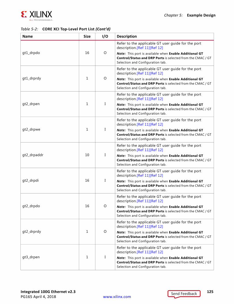
Integrated 100G Ethernet v2.3 125PG165 April 4, 2018 www.xilinx.com
Chapter 5: Example Design
gt1_drpdo 16 O
Refer to the applicable GT user guide for the port description.[Ref 11][Ref 12]Note: This port is available when Enable Additional GT Control/Status and DRP Ports is selected from the CMAC / GT Selection and Configuration tab.
gt1_drprdy 1 O
Refer to the applicable GT user guide for the port description.[Ref 11][Ref 12]Note: This port is available when Enable Additional GT Control/Status and DRP Ports is selected from the CMAC / GT Selection and Configuration tab.
gt2_drpen 1 I
Refer to the applicable GT user guide for the port description.[Ref 11][Ref 12]Note: This port is available when Enable Additional GT Control/Status and DRP Ports is selected from the CMAC / GT Selection and Configuration tab.
gt2_drpwe 1 I
Refer to the applicable GT user guide for the port description.[Ref 11][Ref 12]Note: This port is available when Enable Additional GT Control/Status and DRP Ports is selected from the CMAC / GT Selection and Configuration tab.
gt2_drpaddr 10 I
Refer to the applicable GT user guide for the port description.[Ref 11][Ref 12]Note: This port is available when Enable Additional GT Control/Status and DRP Ports is selected from the CMAC / GT Selection and Configuration tab.
gt2_drpdi 16 I
Refer to the applicable GT user guide for the port description.[Ref 11][Ref 12]Note: This port is available when Enable Additional GT Control/Status and DRP Ports is selected from the CMAC / GT Selection and Configuration tab.
gt2_drpdo 16 O
Refer to the applicable GT user guide for the port description.[Ref 11][Ref 12]Note: This port is available when Enable Additional GT Control/Status and DRP Ports is selected from the CMAC / GT Selection and Configuration tab.
gt2_drprdy 1 O
Refer to the applicable GT user guide for the port description.[Ref 11][Ref 12]Note: This port is available when Enable Additional GT Control/Status and DRP Ports is selected from the CMAC / GT Selection and Configuration tab.
gt3_drpen 1 I
Refer to the applicable GT user guide for the port description.[Ref 11][Ref 12]Note: This port is available when Enable Additional GT Control/Status and DRP Ports is selected from the CMAC / GT Selection and Configuration tab.
Table 5-2: CORE XCI Top-Level Port List (Cont’d)
Name Size I/O Description
Send Feedback
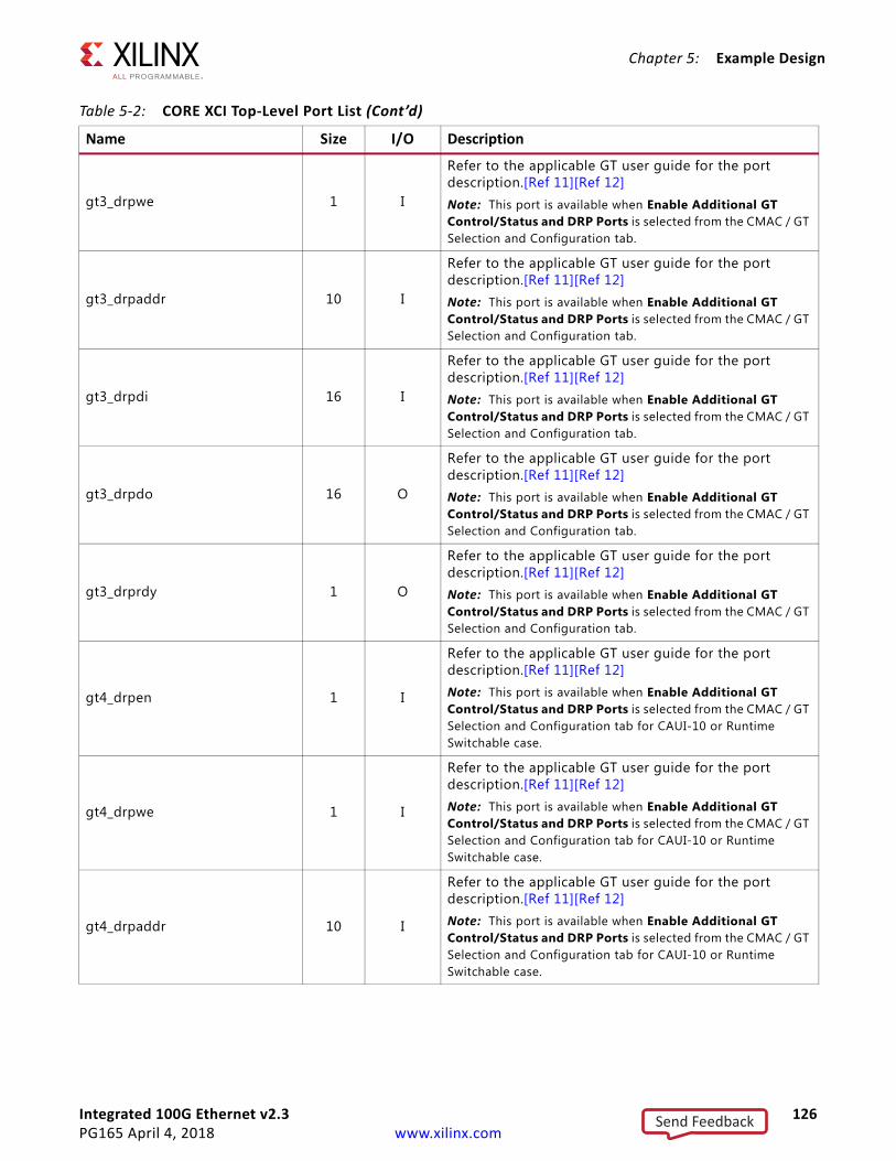
Integrated 100G Ethernet v2.3 126PG165 April 4, 2018 www.xilinx.com
Chapter 5: Example Design
gt3_drpwe 1 I
Refer to the applicable GT user guide for the port description.[Ref 11][Ref 12]Note: This port is available when Enable Additional GT Control/Status and DRP Ports is selected from the CMAC / GT Selection and Configuration tab.
gt3_drpaddr 10 I
Refer to the applicable GT user guide for the port description.[Ref 11][Ref 12]Note: This port is available when Enable Additional GT Control/Status and DRP Ports is selected from the CMAC / GT Selection and Configuration tab.
gt3_drpdi 16 I
Refer to the applicable GT user guide for the port description.[Ref 11][Ref 12]Note: This port is available when Enable Additional GT Control/Status and DRP Ports is selected from the CMAC / GT Selection and Configuration tab.
gt3_drpdo 16 O
Refer to the applicable GT user guide for the port description.[Ref 11][Ref 12]Note: This port is available when Enable Additional GT Control/Status and DRP Ports is selected from the CMAC / GT Selection and Configuration tab.
gt3_drprdy 1 O
Refer to the applicable GT user guide for the port description.[Ref 11][Ref 12]Note: This port is available when Enable Additional GT Control/Status and DRP Ports is selected from the CMAC / GT Selection and Configuration tab.
gt4_drpen 1 I
Refer to the applicable GT user guide for the port description.[Ref 11][Ref 12]Note: This port is available when Enable Additional GT Control/Status and DRP Ports is selected from the CMAC / GT Selection and Configuration tab for CAUI-10 or Runtime Switchable case.
gt4_drpwe 1 I
Refer to the applicable GT user guide for the port description.[Ref 11][Ref 12]Note: This port is available when Enable Additional GT Control/Status and DRP Ports is selected from the CMAC / GT Selection and Configuration tab for CAUI-10 or Runtime Switchable case.
gt4_drpaddr 10 I
Refer to the applicable GT user guide for the port description.[Ref 11][Ref 12]Note: This port is available when Enable Additional GT Control/Status and DRP Ports is selected from the CMAC / GT Selection and Configuration tab for CAUI-10 or Runtime Switchable case.
Table 5-2: CORE XCI Top-Level Port List (Cont’d)
Name Size I/O Description
Send Feedback

Integrated 100G Ethernet v2.3 127PG165 April 4, 2018 www.xilinx.com
Chapter 5: Example Design
gt4_drpdi 16 I
Refer to the applicable GT user guide for the port description.[Ref 11][Ref 12]Note: This port is available when Enable Additional GT Control/Status and DRP Ports is selected from the CMAC / GT Selection and Configuration tab for CAUI-10 or Runtime Switchable case.
gt4_drpdo 16 O
Refer to the applicable GT user guide for the port description.[Ref 11][Ref 12]Note: This port is available when Enable Additional GT Control/Status and DRP Ports is selected from the CMAC / GT Selection and Configuration tab for CAUI-10 or Runtime Switchable case.
gt4_drprdy 1 O
Refer to the applicable GT user guide for the port description.[Ref 11][Ref 12]Note: This port is available when Enable Additional GT Control/Status and DRP Ports is selected from the CMAC / GT Selection and Configuration tab for CAUI-10 or Runtime Switchable case.
gt5_drpen 1 I
Refer to the applicable GT user guide for the port description.[Ref 11][Ref 12]Note: This port is available when Enable Additional GT Control/Status and DRP Ports is selected from the CMAC / GT Selection and Configuration tab for CAUI-10 or Runtime Switchable case.
gt5_drpwe 1 I
Refer to the applicable GT user guide for the port description.[Ref 11][Ref 12]Note: This port is available when Enable Additional GT Control/Status and DRP Ports is selected from the CMAC / GT Selection and Configuration tab for CAUI-10 or Runtime Switchable case.
gt5_drpaddr 10 I
Refer to the applicable GT user guide for the port description.[Ref 11][Ref 12]Note: This port is available when Enable Additional GT Control/Status and DRP Ports is selected from the CMAC / GT Selection and Configuration tab for CAUI-10 or Runtime Switchable case.
gt5_drpdi 16 I
Refer to the applicable GT user guide for the port description.[Ref 11][Ref 12]Note: This port is available when Enable Additional GT Control/Status and DRP Ports is selected from the CMAC / GT Selection and Configuration tab for CAUI-10 or Runtime Switchable case.
Table 5-2: CORE XCI Top-Level Port List (Cont’d)
Name Size I/O Description
Send Feedback
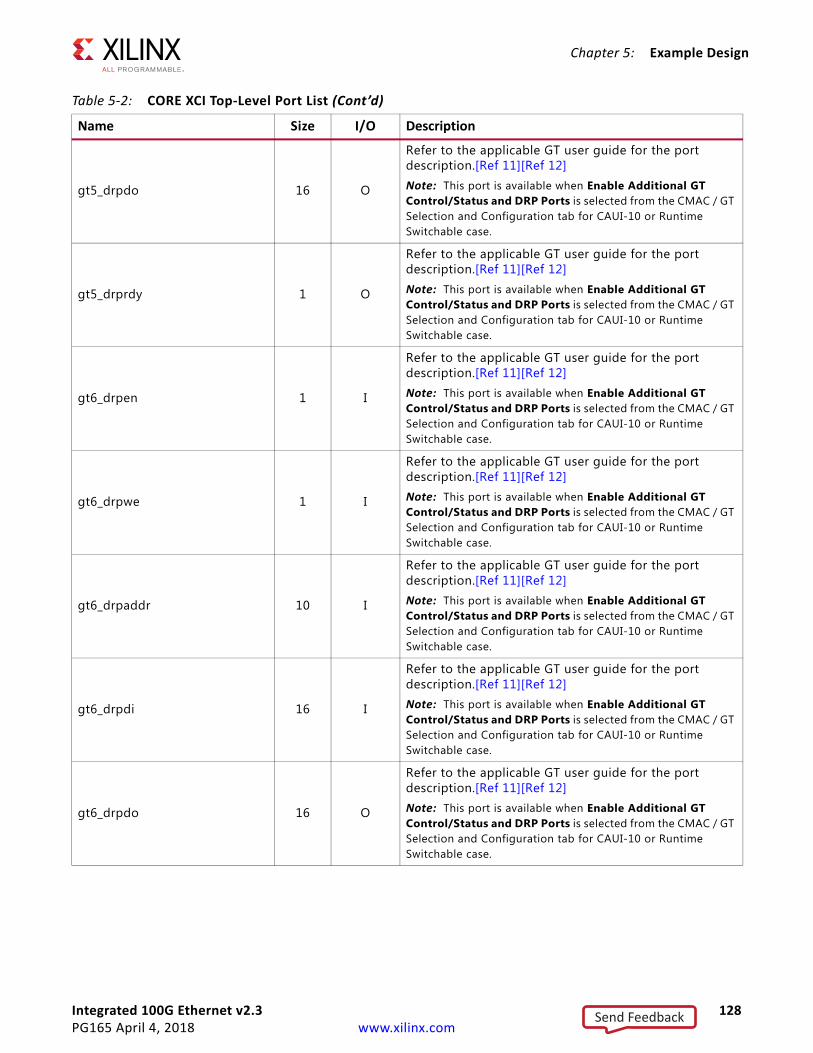
Integrated 100G Ethernet v2.3 128PG165 April 4, 2018 www.xilinx.com
Chapter 5: Example Design
gt5_drpdo 16 O
Refer to the applicable GT user guide for the port description.[Ref 11][Ref 12]Note: This port is available when Enable Additional GT Control/Status and DRP Ports is selected from the CMAC / GT Selection and Configuration tab for CAUI-10 or Runtime Switchable case.
gt5_drprdy 1 O
Refer to the applicable GT user guide for the port description.[Ref 11][Ref 12]Note: This port is available when Enable Additional GT Control/Status and DRP Ports is selected from the CMAC / GT Selection and Configuration tab for CAUI-10 or Runtime Switchable case.
gt6_drpen 1 I
Refer to the applicable GT user guide for the port description.[Ref 11][Ref 12]Note: This port is available when Enable Additional GT Control/Status and DRP Ports is selected from the CMAC / GT Selection and Configuration tab for CAUI-10 or Runtime Switchable case.
gt6_drpwe 1 I
Refer to the applicable GT user guide for the port description.[Ref 11][Ref 12]Note: This port is available when Enable Additional GT Control/Status and DRP Ports is selected from the CMAC / GT Selection and Configuration tab for CAUI-10 or Runtime Switchable case.
gt6_drpaddr 10 I
Refer to the applicable GT user guide for the port description.[Ref 11][Ref 12]Note: This port is available when Enable Additional GT Control/Status and DRP Ports is selected from the CMAC / GT Selection and Configuration tab for CAUI-10 or Runtime Switchable case.
gt6_drpdi 16 I
Refer to the applicable GT user guide for the port description.[Ref 11][Ref 12]Note: This port is available when Enable Additional GT Control/Status and DRP Ports is selected from the CMAC / GT Selection and Configuration tab for CAUI-10 or Runtime Switchable case.
gt6_drpdo 16 O
Refer to the applicable GT user guide for the port description.[Ref 11][Ref 12]Note: This port is available when Enable Additional GT Control/Status and DRP Ports is selected from the CMAC / GT Selection and Configuration tab for CAUI-10 or Runtime Switchable case.
Table 5-2: CORE XCI Top-Level Port List (Cont’d)
Name Size I/O Description
Send Feedback

Integrated 100G Ethernet v2.3 129PG165 April 4, 2018 www.xilinx.com
Chapter 5: Example Design
gt6_drprdy 1 O
Refer to the applicable GT user guide for the port description.[Ref 11][Ref 12]Note: This port is available when Enable Additional GT Control/Status and DRP Ports is selected from the CMAC / GT Selection and Configuration tab for CAUI-10 or Runtime Switchable case.
gt7_drpen 1 I
Refer to the applicable GT user guide for the port description.[Ref 11][Ref 12]Note: This port is available when Enable Additional GT Control/Status and DRP Ports is selected from the CMAC / GT Selection and Configuration tab for CAUI-10 or Runtime Switchable case.
gt7_drpwe 1 I
Refer to the applicable GT user guide for the port description.[Ref 11][Ref 12]Note: This port is available when Enable Additional GT Control/Status and DRP Ports is selected from the CMAC / GT Selection and Configuration tab for CAUI-10 or Runtime Switchable case.
gt7_drpaddr 10 I
Refer to the applicable GT user guide for the port description.[Ref 11][Ref 12]Note: This port is available when Enable Additional GT Control/Status and DRP Ports is selected from the CMAC / GT Selection and Configuration tab for CAUI-10 or Runtime Switchable case.
gt7_drpdi 16 I
Refer to the applicable GT user guide for the port description.[Ref 11][Ref 12]Note: This port is available when Enable Additional GT Control/Status and DRP Ports is selected from the CMAC / GT Selection and Configuration tab for CAUI-10 or Runtime Switchable case.
gt7_drpdo 16 O
Refer to the applicable GT user guide for the port description.[Ref 11][Ref 12]Note: This port is available when Enable Additional GT Control/Status and DRP Ports is selected from the CMAC / GT Selection and Configuration tab for CAUI-10 or Runtime Switchable case.
gt7_drprdy 1 O
Refer to the applicable GT user guide for the port description.[Ref 11][Ref 12]Note: This port is available when Enable Additional GT Control/Status and DRP Ports is selected from the CMAC / GT Selection and Configuration tab for CAUI-10 or Runtime Switchable case.
Table 5-2: CORE XCI Top-Level Port List (Cont’d)
Name Size I/O Description
Send Feedback

Integrated 100G Ethernet v2.3 130PG165 April 4, 2018 www.xilinx.com
Chapter 5: Example Design
gt8_drpen 1 I
Refer to the applicable GT user guide for the port description.[Ref 11][Ref 12]Note: This port is available when Enable Additional GT Control/Status and DRP Ports is selected from the CMAC / GT Selection and Configuration tab for CAUI-10 or Runtime Switchable case.
gt8_drpwe 1 I
Refer to the applicable GT user guide for the port description.[Ref 11][Ref 12]Note: This port is available when Enable Additional GT Control/Status and DRP Ports is selected from the CMAC / GT Selection and Configuration tab for CAUI-10 or Runtime Switchable case.
gt8_drpaddr 10 I
Refer to the applicable GT user guide for the port description.[Ref 11][Ref 12]Note: This port is available when Enable Additional GT Control/Status and DRP Ports is selected from the CMAC / GT Selection and Configuration tab for CAUI-10 or Runtime Switchable case.
gt8_drpdi 16 I
Refer to the applicable GT user guide for the port description.[Ref 11][Ref 12]Note: This port is available when Enable Additional GT Control/Status and DRP Ports is selected from the CMAC / GT Selection and Configuration tab for CAUI-10 or Runtime Switchable case.
gt8_drpdo 16 O
Refer to the applicable GT user guide for the port description.[Ref 11][Ref 12]Note: This port is available when Enable Additional GT Control/Status and DRP Ports is selected from the CMAC / GT Selection and Configuration tab for CAUI-10 or Runtime Switchable case.
gt8_drprdy 1 O
Refer to the applicable GT user guide for the port description.[Ref 11][Ref 12]Note: This port is available when Enable Additional GT Control/Status and DRP Ports is selected from the CMAC / GT Selection and Configuration tab for CAUI-10 or Runtime Switchable case.
gt9_drpen 1 I
Refer to the applicable GT user guide for the port description.[Ref 11][Ref 12]Note: This port is available when Enable Additional GT Control/Status and DRP Ports is selected from the CMAC / GT Selection and Configuration tab for CAUI-10 or Runtime Switchable case.
Table 5-2: CORE XCI Top-Level Port List (Cont’d)
Name Size I/O Description
Send Feedback
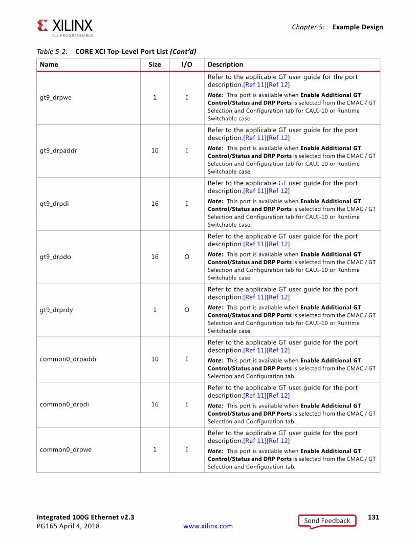
Integrated 100G Ethernet v2.3 131PG165 April 4, 2018 www.xilinx.com
Chapter 5: Example Design
gt9_drpwe 1 I
Refer to the applicable GT user guide for the port description.[Ref 11][Ref 12]Note: This port is available when Enable Additional GT Control/Status and DRP Ports is selected from the CMAC / GT Selection and Configuration tab for CAUI-10 or Runtime Switchable case.
gt9_drpaddr 10 I
Refer to the applicable GT user guide for the port description.[Ref 11][Ref 12]Note: This port is available when Enable Additional GT Control/Status and DRP Ports is selected from the CMAC / GT Selection and Configuration tab for CAUI-10 or Runtime Switchable case.
gt9_drpdi 16 I
Refer to the applicable GT user guide for the port description.[Ref 11][Ref 12]Note: This port is available when Enable Additional GT Control/Status and DRP Ports is selected from the CMAC / GT Selection and Configuration tab for CAUI-10 or Runtime Switchable case.
gt9_drpdo 16 O
Refer to the applicable GT user guide for the port description.[Ref 11][Ref 12]Note: This port is available when Enable Additional GT Control/Status and DRP Ports is selected from the CMAC / GT Selection and Configuration tab for CAUI-10 or Runtime Switchable case.
gt9_drprdy 1 O
Refer to the applicable GT user guide for the port description.[Ref 11][Ref 12]Note: This port is available when Enable Additional GT Control/Status and DRP Ports is selected from the CMAC / GT Selection and Configuration tab for CAUI-10 or Runtime Switchable case.
common0_drpaddr 10 I
Refer to the applicable GT user guide for the port description.[Ref 11][Ref 12]Note: This port is available when Enable Additional GT Control/Status and DRP Ports is selected from the CMAC / GT Selection and Configuration tab.
common0_drpdi 16 I
Refer to the applicable GT user guide for the port description.[Ref 11][Ref 12]Note: This port is available when Enable Additional GT Control/Status and DRP Ports is selected from the CMAC / GT Selection and Configuration tab.
common0_drpwe 1 I
Refer to the applicable GT user guide for the port description.[Ref 11][Ref 12]Note: This port is available when Enable Additional GT Control/Status and DRP Ports is selected from the CMAC / GT Selection and Configuration tab.
Table 5-2: CORE XCI Top-Level Port List (Cont’d)
Name Size I/O Description
Send Feedback
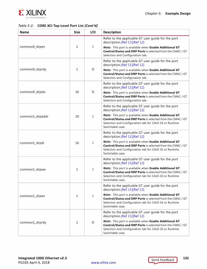
Integrated 100G Ethernet v2.3 132PG165 April 4, 2018 www.xilinx.com
Chapter 5: Example Design
common0_drpen 1 I
Refer to the applicable GT user guide for the port description.[Ref 11][Ref 12]Note: This port is available when Enable Additional GT Control/Status and DRP Ports is selected from the CMAC / GT Selection and Configuration tab.
common0_drprdy 1 O
Refer to the applicable GT user guide for the port description.[Ref 11][Ref 12]Note: This port is available when Enable Additional GT Control/Status and DRP Ports is selected from the CMAC / GT Selection and Configuration tab.
common0_drpdo 16 O
Refer to the applicable GT user guide for the port description.[Ref 11][Ref 12]Note: This port is available when Enable Additional GT Control/Status and DRP Ports is selected from the CMAC / GT Selection and Configuration tab.
common1_drpaddr 10 I
Refer to the applicable GT user guide for the port description.[Ref 11][Ref 12]Note: This port is available when Enable Additional GT Control/Status and DRP Ports is selected from the CMAC / GT Selection and Configuration tab for CAUI-10 or Runtime Switchable case.
common1_drpdi 16 I
Refer to the applicable GT user guide for the port description.[Ref 11][Ref 12]Note: This port is available when Enable Additional GT Control/Status and DRP Ports is selected from the CMAC / GT Selection and Configuration tab for CAUI-10 or Runtime Switchable case.
common1_drpwe 1 I
Refer to the applicable GT user guide for the port description.[Ref 11][Ref 12]Note: This port is available when Enable Additional GT Control/Status and DRP Ports is selected from the CMAC / GT Selection and Configuration tab for CAUI-10 or Runtime Switchable case.
common1_drpen 1 I
Refer to the applicable GT user guide for the port description.[Ref 11][Ref 12]Note: This port is available when Enable Additional GT Control/Status and DRP Ports is selected from the CMAC / GT Selection and Configuration tab for CAUI-10 or Runtime Switchable case.
common1_drprdy 1 O
Refer to the applicable GT user guide for the port description.[Ref 11][Ref 12]Note: This port is available when Enable Additional GT Control/Status and DRP Ports is selected from the CMAC / GT Selection and Configuration tab for CAUI-10 or Runtime Switchable case.
Table 5-2: CORE XCI Top-Level Port List (Cont’d)
Name Size I/O Description
Send Feedback
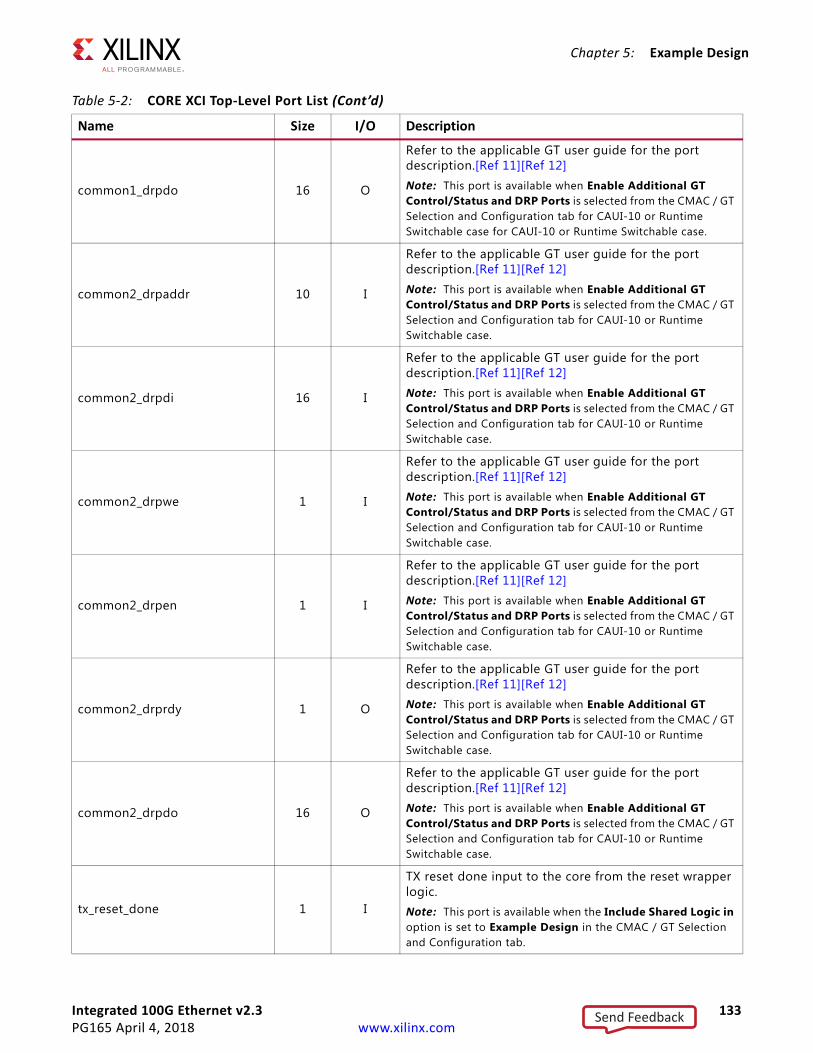
Integrated 100G Ethernet v2.3 133PG165 April 4, 2018 www.xilinx.com
Chapter 5: Example Design
common1_drpdo 16 O
Refer to the applicable GT user guide for the port description.[Ref 11][Ref 12]Note: This port is available when Enable Additional GT Control/Status and DRP Ports is selected from the CMAC / GT Selection and Configuration tab for CAUI-10 or Runtime Switchable case for CAUI-10 or Runtime Switchable case.
common2_drpaddr 10 I
Refer to the applicable GT user guide for the port description.[Ref 11][Ref 12]Note: This port is available when Enable Additional GT Control/Status and DRP Ports is selected from the CMAC / GT Selection and Configuration tab for CAUI-10 or Runtime Switchable case.
common2_drpdi 16 I
Refer to the applicable GT user guide for the port description.[Ref 11][Ref 12]Note: This port is available when Enable Additional GT Control/Status and DRP Ports is selected from the CMAC / GT Selection and Configuration tab for CAUI-10 or Runtime Switchable case.
common2_drpwe 1 I
Refer to the applicable GT user guide for the port description.[Ref 11][Ref 12]Note: This port is available when Enable Additional GT Control/Status and DRP Ports is selected from the CMAC / GT Selection and Configuration tab for CAUI-10 or Runtime Switchable case.
common2_drpen 1 I
Refer to the applicable GT user guide for the port description.[Ref 11][Ref 12]Note: This port is available when Enable Additional GT Control/Status and DRP Ports is selected from the CMAC / GT Selection and Configuration tab for CAUI-10 or Runtime Switchable case.
common2_drprdy 1 O
Refer to the applicable GT user guide for the port description.[Ref 11][Ref 12]Note: This port is available when Enable Additional GT Control/Status and DRP Ports is selected from the CMAC / GT Selection and Configuration tab for CAUI-10 or Runtime Switchable case.
common2_drpdo 16 O
Refer to the applicable GT user guide for the port description.[Ref 11][Ref 12]Note: This port is available when Enable Additional GT Control/Status and DRP Ports is selected from the CMAC / GT Selection and Configuration tab for CAUI-10 or Runtime Switchable case.
tx_reset_done 1 I
TX reset done input to the core from the reset wrapper logic.Note: This port is available when the Include Shared Logic in option is set to Example Design in the CMAC / GT Selection and Configuration tab.
Table 5-2: CORE XCI Top-Level Port List (Cont’d)
Name Size I/O Description
Send Feedback
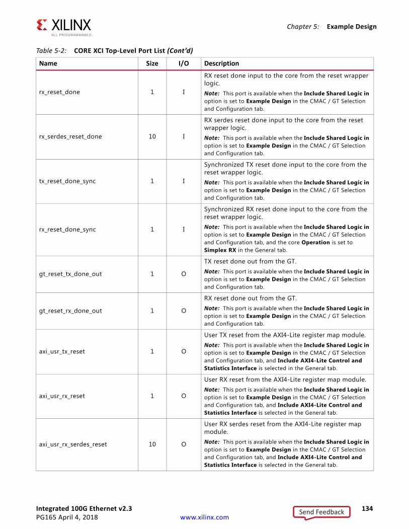
Integrated 100G Ethernet v2.3 134PG165 April 4, 2018 www.xilinx.com
Chapter 5: Example Design
rx_reset_done 1 I
RX reset done input to the core from the reset wrapper logic.Note: This port is available when the Include Shared Logic in option is set to Example Design in the CMAC / GT Selection and Configuration tab.
rx_serdes_reset_done 10 I
RX serdes reset done input to the core from the reset wrapper logic.Note: This port is available when the Include Shared Logic in option is set to Example Design in the CMAC / GT Selection and Configuration tab.
tx_reset_done_sync 1 I
Synchronized TX reset done input to the core from the reset wrapper logic.Note: This port is available when the Include Shared Logic in option is set to Example Design in the CMAC / GT Selection and Configuration tab.
rx_reset_done_sync 1 I
Synchronized RX reset done input to the core from the reset wrapper logic.Note: This port is available when the Include Shared Logic in option is set to Example Design in the CMAC / GT Selection and Configuration tab, and the core Operation is set to Simplex RX in the General tab.
gt_reset_tx_done_out 1 O
TX reset done out from the GT.Note: This port is available when the Include Shared Logic in option is set to Example Design in the CMAC / GT Selection and Configuration tab.
gt_reset_rx_done_out 1 O
RX reset done out from the GT.Note: This port is available when the Include Shared Logic in option is set to Example Design in the CMAC / GT Selection and Configuration tab.
axi_usr_tx_reset 1 O
User TX reset from the AXI4-Lite register map module.Note: This port is available when the Include Shared Logic in option is set to Example Design in the CMAC / GT Selection and Configuration tab, and Include AXI4-Lite Control and Statistics Interface is selected in the General tab.
axi_usr_rx_reset 1 O
User RX reset from the AXI4-Lite register map module.Note: This port is available when the Include Shared Logic in option is set to Example Design in the CMAC / GT Selection and Configuration tab, and Include AXI4-Lite Control and Statistics Interface is selected in the General tab.
axi_usr_rx_serdes_reset 10 O
User RX serdes reset from the AXI4-Lite register map module.Note: This port is available when the Include Shared Logic in option is set to Example Design in the CMAC / GT Selection and Configuration tab, and Include AXI4-Lite Control and Statistics Interface is selected in the General tab.
Table 5-2: CORE XCI Top-Level Port List (Cont’d)
Name Size I/O Description
Send Feedback
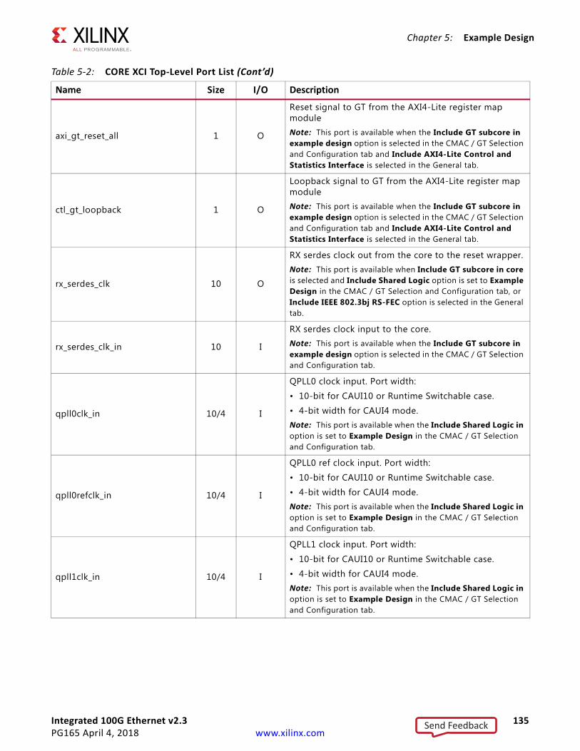
Integrated 100G Ethernet v2.3 135PG165 April 4, 2018 www.xilinx.com
Chapter 5: Example Design
axi_gt_reset_all 1 O
Reset signal to GT from the AXI4-Lite register map moduleNote: This port is available when the Include GT subcore in example design option is selected in the CMAC / GT Selection and Configuration tab and Include AXI4-Lite Control and Statistics Interface is selected in the General tab.
ctl_gt_loopback 1 O
Loopback signal to GT from the AXI4-Lite register map moduleNote: This port is available when the Include GT subcore in example design option is selected in the CMAC / GT Selection and Configuration tab and Include AXI4-Lite Control and Statistics Interface is selected in the General tab.
rx_serdes_clk 10 O
RX serdes clock out from the core to the reset wrapper.Note: This port is available when Include GT subcore in core is selected and Include Shared Logic option is set to Example Design in the CMAC / GT Selection and Configuration tab, or Include IEEE 802.3bj RS-FEC option is selected in the General tab.
rx_serdes_clk_in 10 I
RX serdes clock input to the core.Note: This port is available when the Include GT subcore in example design option is selected in the CMAC / GT Selection and Configuration tab.
qpll0clk_in 10/4 I
QPLL0 clock input. Port width:
• 10-bit for CAUI10 or Runtime Switchable case.
• 4-bit width for CAUI4 mode.Note: This port is available when the Include Shared Logic in option is set to Example Design in the CMAC / GT Selection and Configuration tab.
qpll0refclk_in 10/4 I
QPLL0 ref clock input. Port width:
• 10-bit for CAUI10 or Runtime Switchable case.
• 4-bit width for CAUI4 mode.Note: This port is available when the Include Shared Logic in option is set to Example Design in the CMAC / GT Selection and Configuration tab.
qpll1clk_in 10/4 I
QPLL1 clock input. Port width:
• 10-bit for CAUI10 or Runtime Switchable case.
• 4-bit width for CAUI4 mode.Note: This port is available when the Include Shared Logic in option is set to Example Design in the CMAC / GT Selection and Configuration tab.
Table 5-2: CORE XCI Top-Level Port List (Cont’d)
Name Size I/O Description
Send Feedback
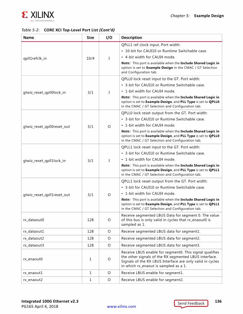
Integrated 100G Ethernet v2.3 136PG165 April 4, 2018 www.xilinx.com
Chapter 5: Example Design
qpll1refclk_in 10/4 I
QPLL1 ref clock input. Port width:
• 10-bit for CAUI10 or Runtime Switchable case.
• 4-bit width for CAUI4 mode.Note: This port is available when the Include Shared Logic in option is set to Example Design in the CMAC / GT Selection and Configuration tab.
gtwiz_reset_qpll0lock_in 3/1 I
QPLL0 lock reset input to the GT. Port width:
• 3-bit for CAUI10 or Runtime Switchable case.
• 1-bit width for CAUI4 mode.Note: This port is available when the Include Shared Logic in option is set to Example Design, and PLL Type is set to QPLL0 in the CMAC / GT Selection and Configuration tab.
gtwiz_reset_qpll0reset_out 3/1 O
QPLL0 lock reset output from the GT. Port width:
• 3-bit for CAUI10 or Runtime Switchable case.
• 1-bit width for CAUI4 mode.Note: This port is available when the Include Shared Logic in option is set to Example Design, and PLL Type is set to QPLL0 in the CMAC / GT Selection and Configuration tab.
gtwiz_reset_qpll1lock_in 3/1 I
QPLL1 lock reset input to the GT. Port width:
• 3-bit for CAUI10 or Runtime Switchable case.
• 1-bit width for CAUI4 mode.Note: This port is available when the Include Shared Logic in option is set to Example Design, and PLL Type is set to QPLL1 in the CMAC / GT Selection and Configuration tab.
gtwiz_reset_qpll1reset_out 3/1 O
QPLL1 lock reset output from the GT. Port width:
• 3-bit for CAUI10 or Runtime Switchable case.
• 1-bit width for CAUI4 mode.Note: This port is available when the Include Shared Logic in option is set to Example Design, and PLL Type is set to QPLL1 in the CMAC / GT Selection and Configuration tab.
rx_dataout0 128 OReceive segmented LBUS Data for segment 0. The value of this bus is only valid in cycles that rx_enaout0 is sampled as 1.
rx_dataout1 128 O Receive segmented LBUS data for segment1.
rx_dataout2 128 O Receive segmented LBUS data for segment2.
rx_dataout3 128 O Receive segmented LBUS data for segment3.
rx_enaout0 1 O
Receive LBUS enable for segment0. This signal qualifies the other signals of the RX segmented LBUS interface. Signals of the RX LBUS Interface are only valid in cycles in which rx_enaout is sampled as a 1.
rx_enaout1 1 O Receive LBUS enable for segment1.
rx_enaout2 1 O Receive LBUS enable for segment2.
Table 5-2: CORE XCI Top-Level Port List (Cont’d)
Name Size I/O Description
Send Feedback
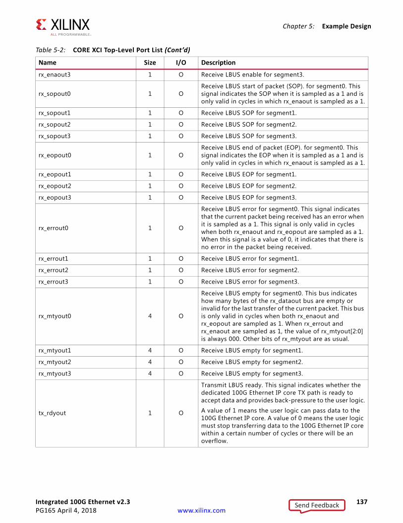
Integrated 100G Ethernet v2.3 137PG165 April 4, 2018 www.xilinx.com
Chapter 5: Example Design
rx_enaout3 1 O Receive LBUS enable for segment3.
rx_sopout0 1 OReceive LBUS start of packet (SOP). for segment0. This signal indicates the SOP when it is sampled as a 1 and is only valid in cycles in which rx_enaout is sampled as a 1.
rx_sopout1 1 O Receive LBUS SOP for segment1.
rx_sopout2 1 O Receive LBUS SOP for segment2.
rx_sopout3 1 O Receive LBUS SOP for segment3.
rx_eopout0 1 OReceive LBUS end of packet (EOP). for segment0. This signal indicates the EOP when it is sampled as a 1 and is only valid in cycles in which rx_enaout is sampled as a 1.
rx_eopout1 1 O Receive LBUS EOP for segment1.
rx_eopout2 1 O Receive LBUS EOP for segment2.
rx_eopout3 1 O Receive LBUS EOP for segment3.
rx_errout0 1 O
Receive LBUS error for segment0. This signal indicates that the current packet being received has an error when it is sampled as a 1. This signal is only valid in cycles when both rx_enaout and rx_eopout are sampled as a 1. When this signal is a value of 0, it indicates that there is no error in the packet being received.
rx_errout1 1 O Receive LBUS error for segment1.
rx_errout2 1 O Receive LBUS error for segment2.
rx_errout3 1 O Receive LBUS error for segment3.
rx_mtyout0 4 O
Receive LBUS empty for segment0. This bus indicates how many bytes of the rx_dataout bus are empty or invalid for the last transfer of the current packet. This bus is only valid in cycles when both rx_enaout and rx_eopout are sampled as 1. When rx_errout and rx_enaout are sampled as 1, the value of rx_mtyout[2:0] is always 000. Other bits of rx_mtyout are as usual.
rx_mtyout1 4 O Receive LBUS empty for segment1.
rx_mtyout2 4 O Receive LBUS empty for segment2.
rx_mtyout3 4 O Receive LBUS empty for segment3.
tx_rdyout 1 O
Transmit LBUS ready. This signal indicates whether the dedicated 100G Ethernet IP core TX path is ready to accept data and provides back-pressure to the user logic.
A value of 1 means the user logic can pass data to the 100G Ethernet IP core. A value of 0 means the user logic must stop transferring data to the 100G Ethernet IP core within a certain number of cycles or there will be an overflow.
Table 5-2: CORE XCI Top-Level Port List (Cont’d)
Name Size I/O Description
Send Feedback
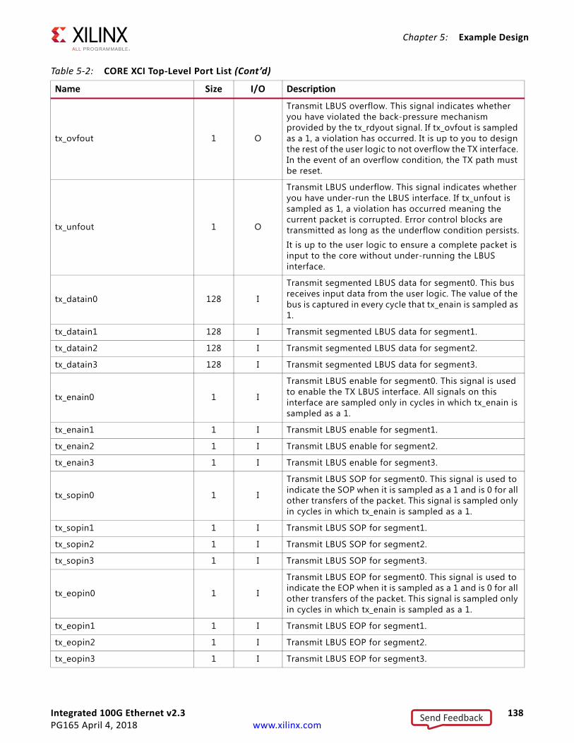
Integrated 100G Ethernet v2.3 138PG165 April 4, 2018 www.xilinx.com
Chapter 5: Example Design
tx_ovfout 1 O
Transmit LBUS overflow. This signal indicates whether you have violated the back-pressure mechanism provided by the tx_rdyout signal. If tx_ovfout is sampled as a 1, a violation has occurred. It is up to you to design the rest of the user logic to not overflow the TX interface. In the event of an overflow condition, the TX path must be reset.
tx_unfout 1 O
Transmit LBUS underflow. This signal indicates whether you have under-run the LBUS interface. If tx_unfout is sampled as 1, a violation has occurred meaning the current packet is corrupted. Error control blocks are transmitted as long as the underflow condition persists.
It is up to the user logic to ensure a complete packet is input to the core without under-running the LBUS interface.
tx_datain0 128 I
Transmit segmented LBUS data for segment0. This bus receives input data from the user logic. The value of the bus is captured in every cycle that tx_enain is sampled as 1.
tx_datain1 128 I Transmit segmented LBUS data for segment1.
tx_datain2 128 I Transmit segmented LBUS data for segment2.
tx_datain3 128 I Transmit segmented LBUS data for segment3.
tx_enain0 1 I
Transmit LBUS enable for segment0. This signal is used to enable the TX LBUS interface. All signals on this interface are sampled only in cycles in which tx_enain is sampled as a 1.
tx_enain1 1 I Transmit LBUS enable for segment1.
tx_enain2 1 I Transmit LBUS enable for segment2.
tx_enain3 1 I Transmit LBUS enable for segment3.
tx_sopin0 1 I
Transmit LBUS SOP for segment0. This signal is used to indicate the SOP when it is sampled as a 1 and is 0 for all other transfers of the packet. This signal is sampled only in cycles in which tx_enain is sampled as a 1.
tx_sopin1 1 I Transmit LBUS SOP for segment1.
tx_sopin2 1 I Transmit LBUS SOP for segment2.
tx_sopin3 1 I Transmit LBUS SOP for segment3.
tx_eopin0 1 I
Transmit LBUS EOP for segment0. This signal is used to indicate the EOP when it is sampled as a 1 and is 0 for all other transfers of the packet. This signal is sampled only in cycles in which tx_enain is sampled as a 1.
tx_eopin1 1 I Transmit LBUS EOP for segment1.
tx_eopin2 1 I Transmit LBUS EOP for segment2.
tx_eopin3 1 I Transmit LBUS EOP for segment3.
Table 5-2: CORE XCI Top-Level Port List (Cont’d)
Name Size I/O Description
Send Feedback
Integrated 100G Ethernet v2.3 139PG165 April 4, 2018 www.xilinx.com
Chapter 5: Example Design
tx_errin0 1 I
Transmit LBUS error for segment0. This signal is used to indicate a packet contains an error when it is sampled as a 1 and is 0 for all other transfers of the packet. This signal is sampled only in cycles in which tx_enain and tx_eopin are sampled as 1. When this signal is sampled as a 1, the last data word is replaced with the IEEE standard 802.3-2012 Error Code control word that guarantees the partner device receives the packet in error. If a packet is input with this signal set to a 1, the FCS checking and reporting is disabled (only for that packet).
tx_errin1 1 I Transmit LBUS error for segment1.
tx_errin2 1 I Transmit LBUS error for segment2.
tx_errin3 1 I Transmit LBUS error for segment3.
tx_mtyin0 4 I
Transmit LBUS empty for segment0. This bus is used to indicate how many bytes of the tx_datain bus are empty or invalid for the last transfer of the current packet. This bus is sampled only in cycles that tx_enain and tx_eopin are sampled as 1. When tx_eopin and tx_errin are sampled as 1, the value of tx_mtyin[2:0] is ignored as treated as if it was 000. The other bits of tx_mtyin are used as usual.
tx_mtyin1 4 I Receive LBUS empty for segment1.
tx_mtyin2 4 I Receive LBUS empty for segment2.
tx_mtyin3 4 I Receive LBUS empty for segment3.
ctl_tx_enable 1 I
TX Enable. This signal is used to enable the transmission of data when it is sampled as a 1. When sampled as a 0, only idles are transmitted by CMAC. This input should not be set to 1 until the receiver it is sending data to (that is, the receiver in the other device) is fully aligned and ready to receive data (that is, the other device is not sending a remote fault condition). Otherwise, loss of data can occur. If this signal is set to 0 while a packet is being transmitted, the current packet transmission is completed and then the CMAC stops transmitting any more packets.
ctl_tx_send_rfi 1 I
Transmit Remote Fault Indication (RFI) code word. If this input is sampled as a 1, the TX path only transmits Remote Fault code words. This input should be set to 1 until the RX path is fully aligned and is ready to accept data from the link partner.
ctl_tx_send_idle 1 I
Transmit Idle code words. If this input is sampled as a 1, the TX path only transmits Idle code words. This input should be set to 1 when the partner device is sending Remote Fault Indication (RFI) code words.
stat_tx_local_fault 1 O A value of 1 indicates the receive decoder state machine is in the TX_INIT state. This output is level sensitive.
Table 5-2: CORE XCI Top-Level Port List (Cont’d)
Name Size I/O Description
Send Feedback

Integrated 100G Ethernet v2.3 140PG165 April 4, 2018 www.xilinx.com
Chapter 5: Example Design
ctl_rx_enable 1 I
RX Enable. For normal operation, this input must be set to 1. When this input is set to 0, after the RX completes the reception of the current packet (if any), it stops receiving packets by keeping the PCS from decoding incoming data. In this mode, there are no statistics reported and the LBUS interface is idle.
ctl_rx_force_resync 1 I
RX force resynchronization input. This signal is used to force the RX path to reset, re-synchronize, and realign. A value of 1 forces the reset operation. A value of 0 allows normal operation.Note: This input should normally be Low and should only be pulsed (one cycle minimum pulse) to force realignment.
stat_rx_framing_err_0 4 O
RX sync header bits framing error for lane 0. Each PCS Lane has a four-bit bus that indicates how many sync header errors were received for that PCS Lane. The value of the bus is only valid when the corresponding stat_rx_framing_err_valid_[19:0] is a 1. The values on these buses can be updated at any time and are intended to be used as increment values for sync header error counters.
stat_rx_framing_err_1 4 O RX sync header bits framing error for lane 1.
stat_rx_framing_err_2 4 O RX sync header bits framing error for lane 2.
stat_rx_framing_err_3 4 O RX sync header bits framing error for lane 3.
stat_rx_framing_err_4 4 O RX sync header bits framing error for lane 4.
stat_rx_framing_err_5 4 O RX sync header bits framing error for lane 5.
stat_rx_framing_err_6 4 O RX sync header bits framing error for lane 6.
stat_rx_framing_err_7 4 O RX sync header bits framing error for lane 7.
stat_rx_framing_err_8 4 O RX sync header bits framing error for lane 8.
stat_rx_framing_err_9 4 O RX sync header bits framing error for lane 9.
stat_rx_framing_err_10 4 O RX sync header bits framing error for lane 10.
stat_rx_framing_err_11 4 O RX sync header bits framing error for lane 11.
stat_rx_framing_err_12 4 O RX sync header bits framing error for lane 12.
stat_rx_framing_err_13 4 O RX sync header bits framing error for lane 13.
stat_rx_framing_err_14 4 O RX sync header bits framing error for lane 14.
stat_rx_framing_err_15 4 O RX sync header bits framing error for lane 15.
stat_rx_framing_err_16 4 O RX sync header bits framing error for lane 16.
stat_rx_framing_err_17 4 O RX sync header bits framing error for lane 17.
stat_rx_framing_err_18 4 O RX sync header bits framing error for lane 18.
stat_rx_framing_err_19 4 O RX sync header bits framing error for lane 19.
Table 5-2: CORE XCI Top-Level Port List (Cont’d)
Name Size I/O Description
Send Feedback
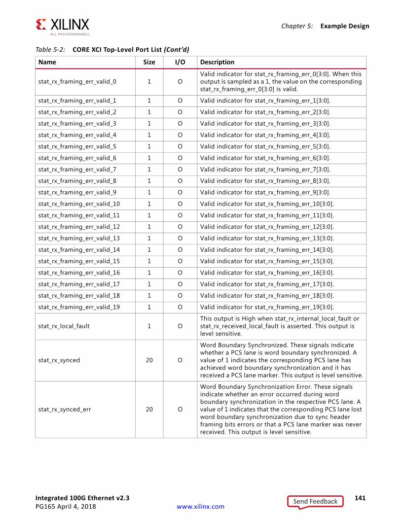
Integrated 100G Ethernet v2.3 141PG165 April 4, 2018 www.xilinx.com
Chapter 5: Example Design
stat_rx_framing_err_valid_0 1 OValid indicator for stat_rx_framing_err_0[3:0]. When this output is sampled as a 1, the value on the corresponding stat_rx_framing_err_0[3:0] is valid.
stat_rx_framing_err_valid_1 1 O Valid indicator for stat_rx_framing_err_1[3:0].
stat_rx_framing_err_valid_2 1 O Valid indicator for stat_rx_framing_err_2[3:0].
stat_rx_framing_err_valid_3 1 O Valid indicator for stat_rx_framing_err_3[3:0].
stat_rx_framing_err_valid_4 1 O Valid indicator for stat_rx_framing_err_4[3:0].
stat_rx_framing_err_valid_5 1 O Valid indicator for stat_rx_framing_err_5[3:0].
stat_rx_framing_err_valid_6 1 O Valid indicator for stat_rx_framing_err_6[3:0].
stat_rx_framing_err_valid_7 1 O Valid indicator for stat_rx_framing_err_7[3:0].
stat_rx_framing_err_valid_8 1 O Valid indicator for stat_rx_framing_err_8[3:0].
stat_rx_framing_err_valid_9 1 O Valid indicator for stat_rx_framing_err_9[3:0].
stat_rx_framing_err_valid_10 1 O Valid indicator for stat_rx_framing_err_10[3:0].
stat_rx_framing_err_valid_11 1 O Valid indicator for stat_rx_framing_err_11[3:0].
stat_rx_framing_err_valid_12 1 O Valid indicator for stat_rx_framing_err_12[3:0].
stat_rx_framing_err_valid_13 1 O Valid indicator for stat_rx_framing_err_13[3:0].
stat_rx_framing_err_valid_14 1 O Valid indicator for stat_rx_framing_err_14[3:0].
stat_rx_framing_err_valid_15 1 O Valid indicator for stat_rx_framing_err_15[3:0].
stat_rx_framing_err_valid_16 1 O Valid indicator for stat_rx_framing_err_16[3:0].
stat_rx_framing_err_valid_17 1 O Valid indicator for stat_rx_framing_err_17[3:0].
stat_rx_framing_err_valid_18 1 O Valid indicator for stat_rx_framing_err_18[3:0].
stat_rx_framing_err_valid_19 1 O Valid indicator for stat_rx_framing_err_19[3:0].
stat_rx_local_fault 1 OThis output is High when stat_rx_internal_local_fault or stat_rx_received_local_fault is asserted. This output is level sensitive.
stat_rx_synced 20 O
Word Boundary Synchronized. These signals indicate whether a PCS lane is word boundary synchronized. A value of 1 indicates the corresponding PCS lane has achieved word boundary synchronization and it has received a PCS lane marker. This output is level sensitive.
stat_rx_synced_err 20 O
Word Boundary Synchronization Error. These signals indicate whether an error occurred during word boundary synchronization in the respective PCS lane. A value of 1 indicates that the corresponding PCS lane lost word boundary synchronization due to sync header framing bits errors or that a PCS lane marker was never received. This output is level sensitive.
Table 5-2: CORE XCI Top-Level Port List (Cont’d)
Name Size I/O Description
Send Feedback
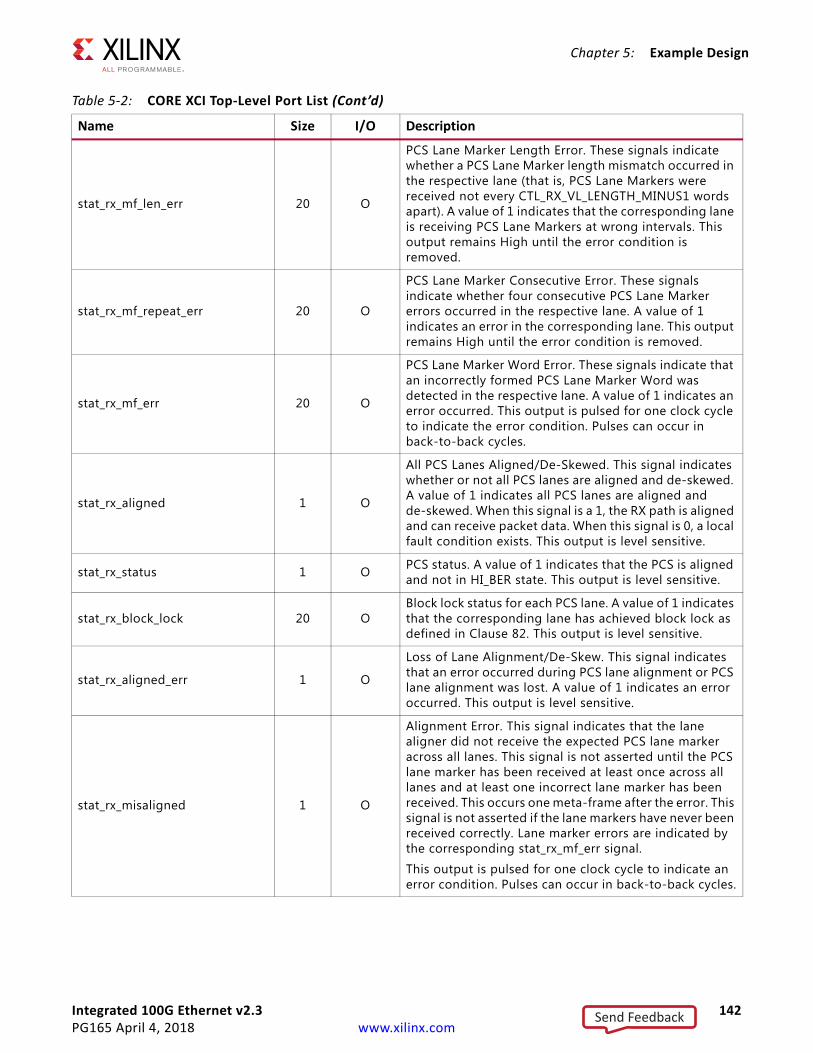
Integrated 100G Ethernet v2.3 142PG165 April 4, 2018 www.xilinx.com
Chapter 5: Example Design
stat_rx_mf_len_err 20 O
PCS Lane Marker Length Error. These signals indicate whether a PCS Lane Marker length mismatch occurred in the respective lane (that is, PCS Lane Markers were received not every CTL_RX_VL_LENGTH_MINUS1 words apart). A value of 1 indicates that the corresponding lane is receiving PCS Lane Markers at wrong intervals. This output remains High until the error condition is removed.
stat_rx_mf_repeat_err 20 O
PCS Lane Marker Consecutive Error. These signals indicate whether four consecutive PCS Lane Marker errors occurred in the respective lane. A value of 1 indicates an error in the corresponding lane. This output remains High until the error condition is removed.
stat_rx_mf_err 20 O
PCS Lane Marker Word Error. These signals indicate that an incorrectly formed PCS Lane Marker Word was detected in the respective lane. A value of 1 indicates an error occurred. This output is pulsed for one clock cycle to indicate the error condition. Pulses can occur in back-to-back cycles.
stat_rx_aligned 1 O
All PCS Lanes Aligned/De-Skewed. This signal indicates whether or not all PCS lanes are aligned and de-skewed. A value of 1 indicates all PCS lanes are aligned and de-skewed. When this signal is a 1, the RX path is aligned and can receive packet data. When this signal is 0, a local fault condition exists. This output is level sensitive.
stat_rx_status 1 O PCS status. A value of 1 indicates that the PCS is aligned and not in HI_BER state. This output is level sensitive.
stat_rx_block_lock 20 OBlock lock status for each PCS lane. A value of 1 indicates that the corresponding lane has achieved block lock as defined in Clause 82. This output is level sensitive.
stat_rx_aligned_err 1 O
Loss of Lane Alignment/De-Skew. This signal indicates that an error occurred during PCS lane alignment or PCS lane alignment was lost. A value of 1 indicates an error occurred. This output is level sensitive.
stat_rx_misaligned 1 O
Alignment Error. This signal indicates that the lane aligner did not receive the expected PCS lane marker across all lanes. This signal is not asserted until the PCS lane marker has been received at least once across all lanes and at least one incorrect lane marker has been received. This occurs one meta-frame after the error. This signal is not asserted if the lane markers have never been received correctly. Lane marker errors are indicated by the corresponding stat_rx_mf_err signal.
This output is pulsed for one clock cycle to indicate an error condition. Pulses can occur in back-to-back cycles.
Table 5-2: CORE XCI Top-Level Port List (Cont’d)
Name Size I/O Description
Send Feedback
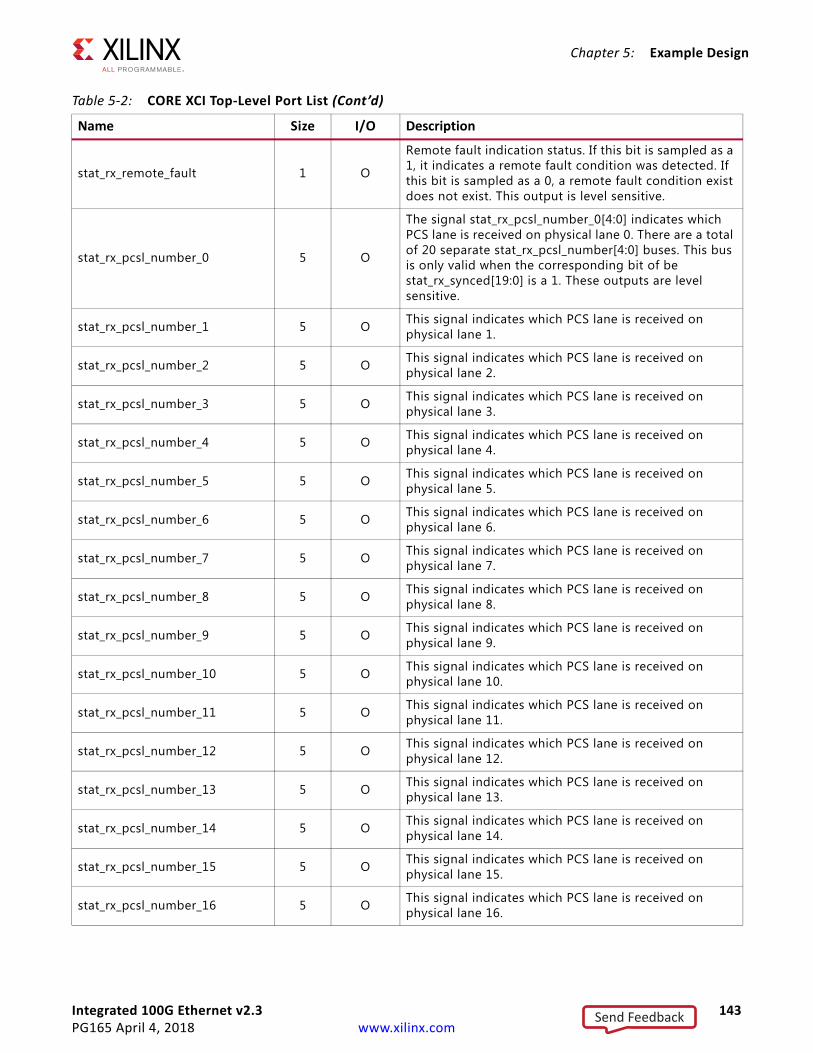
Integrated 100G Ethernet v2.3 143PG165 April 4, 2018 www.xilinx.com
Chapter 5: Example Design
stat_rx_remote_fault 1 O
Remote fault indication status. If this bit is sampled as a 1, it indicates a remote fault condition was detected. If this bit is sampled as a 0, a remote fault condition exist does not exist. This output is level sensitive.
stat_rx_pcsl_number_0 5 O
The signal stat_rx_pcsl_number_0[4:0] indicates which PCS lane is received on physical lane 0. There are a total of 20 separate stat_rx_pcsl_number[4:0] buses. This bus is only valid when the corresponding bit of be stat_rx_synced[19:0] is a 1. These outputs are level sensitive.
stat_rx_pcsl_number_1 5 O This signal indicates which PCS lane is received on physical lane 1.
stat_rx_pcsl_number_2 5 O This signal indicates which PCS lane is received on physical lane 2.
stat_rx_pcsl_number_3 5 O This signal indicates which PCS lane is received on physical lane 3.
stat_rx_pcsl_number_4 5 O This signal indicates which PCS lane is received on physical lane 4.
stat_rx_pcsl_number_5 5 O This signal indicates which PCS lane is received on physical lane 5.
stat_rx_pcsl_number_6 5 O This signal indicates which PCS lane is received on physical lane 6.
stat_rx_pcsl_number_7 5 O This signal indicates which PCS lane is received on physical lane 7.
stat_rx_pcsl_number_8 5 O This signal indicates which PCS lane is received on physical lane 8.
stat_rx_pcsl_number_9 5 O This signal indicates which PCS lane is received on physical lane 9.
stat_rx_pcsl_number_10 5 O This signal indicates which PCS lane is received on physical lane 10.
stat_rx_pcsl_number_11 5 O This signal indicates which PCS lane is received on physical lane 11.
stat_rx_pcsl_number_12 5 O This signal indicates which PCS lane is received on physical lane 12.
stat_rx_pcsl_number_13 5 O This signal indicates which PCS lane is received on physical lane 13.
stat_rx_pcsl_number_14 5 O This signal indicates which PCS lane is received on physical lane 14.
stat_rx_pcsl_number_15 5 O This signal indicates which PCS lane is received on physical lane 15.
stat_rx_pcsl_number_16 5 O This signal indicates which PCS lane is received on physical lane 16.
Table 5-2: CORE XCI Top-Level Port List (Cont’d)
Name Size I/O Description
Send Feedback

Integrated 100G Ethernet v2.3 144PG165 April 4, 2018 www.xilinx.com
Chapter 5: Example Design
stat_rx_pcsl_number_17 5 O This signal indicates which PCS lane is received on physical lane 17.
stat_rx_pcsl_number_18 5 O This signal indicates which PCS lane is received on physical lane 18.
stat_rx_pcsl_number_19 5 O This signal indicates which PCS lane is received on physical lane 19.
stat_rx_pcsl_demuxed 20 O
PCS Lane Marker found. If a signal of this bus is sampled as 1, it indicates that the receiver has properly de-multiplexed that PCS lane. These outputs are level sensitive.
stat_rx_bad_fcs 4 O
Bad FCS indicator. A value of 1 indicates a packet was received with a bad FCS, but not a stomped FCS. A stomped FCS is defined as the bitwise inverse of the expected good FCS. This output is pulsed for one clock cycle to indicate an error condition. Pulses can occur in back-to-back cycles.
stat_rx_stomped_fcs 4 O
Stomped FCS indicator. A value of 1 or greater indicates that one or more packets were received with a stomped FCS. A stomped FCS is defined as the bitwise inverse of the expected good FCS. This output is pulsed for one clock cycle to indicate the stomped condition. Pulses can occur in back-to-back cycles.
stat_rx_truncated 1 O
Packet truncation indicator. A value of 1 indicates that the current packet in flight is truncated due to its length exceeding ctl_rx_max_packet_len[14:0]. This output is pulsed for one clock cycle to indicate the truncated condition. Pulses can occur in back-to-back cycles.
stat_rx_internal_local_fault 1 O
This signal goes High when an internal local fault is generated due to any one of the following: test pattern generation, bad lane alignment, or high bit error rate. This signal remains High as long as the fault condition persists.
stat_rx_received_local_fault 1 O
This signal goes High when enough local fault words are received from the link partner to trigger a fault condition as specified by the IEEE fault state machine.
This signal remains High as long as the fault condition persists.
stat_rx_bip_err_0 1 O
BIP8 error indicator for PCS lane 0. A non-zero value indicates the BIP8 signature byte was in error for the corresponding PCS lane. A non-zero value is pulsed for one clock cycle. This output is pulsed for one clock cycle to indicate an error condition. Pulses can occur in back-to-back cycles.
stat_rx_bip_err_1 1 O BIP8 error indicator for PCS lane 1.
stat_rx_bip_err_2 1 O BIP8 error indicator for PCS lane 2.
stat_rx_bip_err_3 1 O BIP8 error indicator for PCS lane 3.
Table 5-2: CORE XCI Top-Level Port List (Cont’d)
Name Size I/O Description
Send Feedback
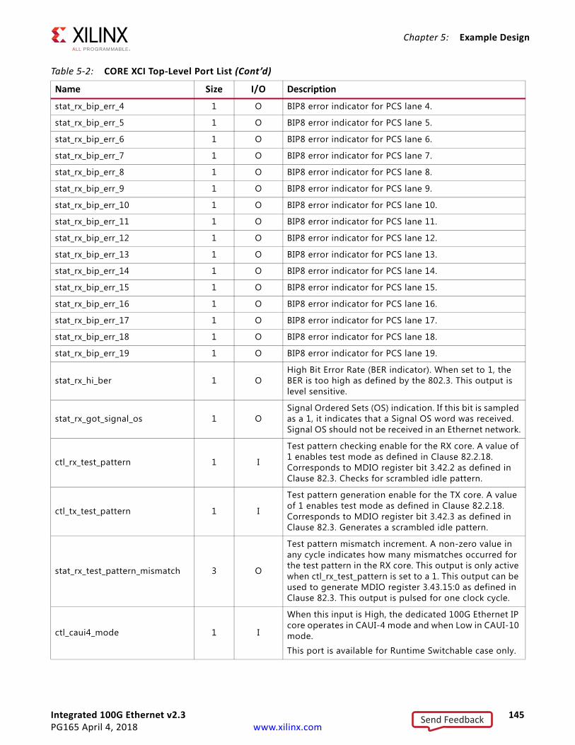
Integrated 100G Ethernet v2.3 145PG165 April 4, 2018 www.xilinx.com
Chapter 5: Example Design
stat_rx_bip_err_4 1 O BIP8 error indicator for PCS lane 4.
stat_rx_bip_err_5 1 O BIP8 error indicator for PCS lane 5.
stat_rx_bip_err_6 1 O BIP8 error indicator for PCS lane 6.
stat_rx_bip_err_7 1 O BIP8 error indicator for PCS lane 7.
stat_rx_bip_err_8 1 O BIP8 error indicator for PCS lane 8.
stat_rx_bip_err_9 1 O BIP8 error indicator for PCS lane 9.
stat_rx_bip_err_10 1 O BIP8 error indicator for PCS lane 10.
stat_rx_bip_err_11 1 O BIP8 error indicator for PCS lane 11.
stat_rx_bip_err_12 1 O BIP8 error indicator for PCS lane 12.
stat_rx_bip_err_13 1 O BIP8 error indicator for PCS lane 13.
stat_rx_bip_err_14 1 O BIP8 error indicator for PCS lane 14.
stat_rx_bip_err_15 1 O BIP8 error indicator for PCS lane 15.
stat_rx_bip_err_16 1 O BIP8 error indicator for PCS lane 16.
stat_rx_bip_err_17 1 O BIP8 error indicator for PCS lane 17.
stat_rx_bip_err_18 1 O BIP8 error indicator for PCS lane 18.
stat_rx_bip_err_19 1 O BIP8 error indicator for PCS lane 19.
stat_rx_hi_ber 1 OHigh Bit Error Rate (BER indicator). When set to 1, the BER is too high as defined by the 802.3. This output is level sensitive.
stat_rx_got_signal_os 1 OSignal Ordered Sets (OS) indication. If this bit is sampled as a 1, it indicates that a Signal OS word was received. Signal OS should not be received in an Ethernet network.
ctl_rx_test_pattern 1 I
Test pattern checking enable for the RX core. A value of 1 enables test mode as defined in Clause 82.2.18. Corresponds to MDIO register bit 3.42.2 as defined in Clause 82.3. Checks for scrambled idle pattern.
ctl_tx_test_pattern 1 I
Test pattern generation enable for the TX core. A value of 1 enables test mode as defined in Clause 82.2.18. Corresponds to MDIO register bit 3.42.3 as defined in Clause 82.3. Generates a scrambled idle pattern.
stat_rx_test_pattern_mismatch 3 O
Test pattern mismatch increment. A non-zero value in any cycle indicates how many mismatches occurred for the test pattern in the RX core. This output is only active when ctl_rx_test_pattern is set to a 1. This output can be used to generate MDIO register 3.43.15:0 as defined in Clause 82.3. This output is pulsed for one clock cycle.
ctl_caui4_mode 1 I
When this input is High, the dedicated 100G Ethernet IP core operates in CAUI-4 mode and when Low in CAUI-10 mode.
This port is available for Runtime Switchable case only.
Table 5-2: CORE XCI Top-Level Port List (Cont’d)
Name Size I/O Description
Send Feedback

Integrated 100G Ethernet v2.3 146PG165 April 4, 2018 www.xilinx.com
Chapter 5: Example Design
ctl_tx_lane0_vlm_bip7_override 1 IWhen this input is High, the bip7 byte of the PCS lane0 marker is over-ridden by ctl_tx_lane0_vlm_bip7_override_value[7:0]
ctl_tx_lane0_vlm_bip7_override_value 8 I
This input is the override value of the bip7 byte of PCS lane0 marker when ctl_tx_lane0_vlm_bip7_override is asserted.
stat_rx_lane0_vlm_bip7 8 O This output is the received value of the bip7 byte in the PCS lane0 marker.
stat_rx_lane0_vlm_bip7_valid 1 O This output, when asserted, indicates that the value of stat_rx_lane0_vlm_bip7[7:0] is valid.
stat_rx_total_bytes 8 O Increment for the total number of bytes received.
stat_rx_total_packets 4 I Increment for the total number of packets received.
stat_rx_total_good_bytes 14 OIncrement for the total number of good bytes received. This value is only non-zero when a packet is received completely and contains no errors.
stat_rx_total_good_packets 1 OIncrement for the total number of good packets received. This value is only non-zero when a packet is received completely and contains no errors.
stat_rx_packet_bad_fcs 1 O Increment for packets between 64 and ctl_rx_max_packet_len bytes that have FCS errors.
stat_rx_packet_64_bytes 1 O Increment for good and bad packets received that contain 64 bytes.
stat_rx_packet_65_127_bytes 1 O Increment for good and bad packets received that contain 65 to 127 bytes.
stat_rx_packet_128_255_bytes 1 O Increment for good and bad packets received that contain 128 to 255 bytes.
stat_rx_packet_256_511_bytes 1 O Increment for good and bad packets received that contain 256 to 511 bytes.
stat_rx_packet_512_1023_bytes 1 O Increment for good and bad packets received that contain 512 to 1,023 bytes.
stat_rx_packet_1024_1518_bytes 1 O Increment for good and bad packets received that contain 1,024 to 1,518 bytes.
stat_rx_packet_1519_1522_bytes 1 O Increment for good and bad packets received that contain 1,519 to 1,522 bytes.
stat_rx_packet_1523_1548_bytes 1 O Increment for good and bad packets received that contain 1,523 to 1,548 bytes.
stat_rx_packet_1549_2047_bytes 1 O Increment for good and bad packets received that contain 1,549 to 2,047 bytes.
stat_rx_packet_2048_4095_bytes 1 O Increment for good and bad packets received that contain 2,048 to 4,095 bytes.
stat_rx_packet_4096_8191_bytes 1 O Increment for good and bad packets received that contain 4,096 to 8,191 bytes.
Table 5-2: CORE XCI Top-Level Port List (Cont’d)
Name Size I/O Description
Send Feedback
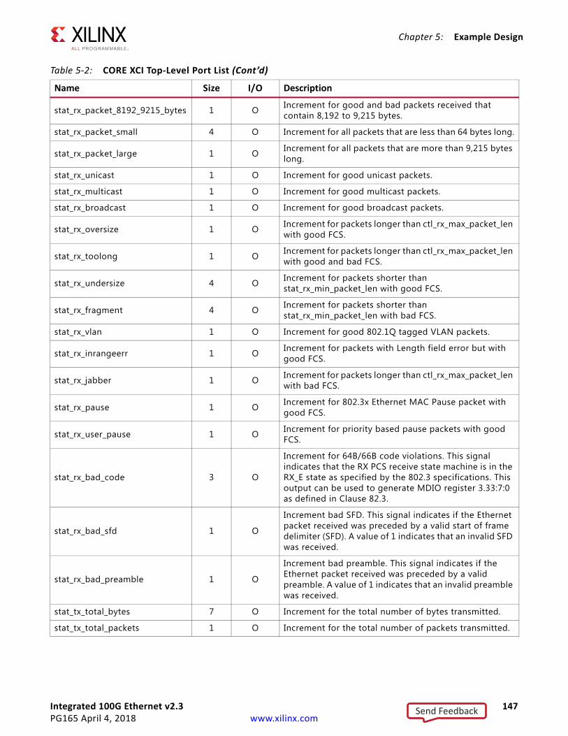
Integrated 100G Ethernet v2.3 147PG165 April 4, 2018 www.xilinx.com
Chapter 5: Example Design
stat_rx_packet_8192_9215_bytes 1 O Increment for good and bad packets received that contain 8,192 to 9,215 bytes.
stat_rx_packet_small 4 O Increment for all packets that are less than 64 bytes long.
stat_rx_packet_large 1 O Increment for all packets that are more than 9,215 bytes long.
stat_rx_unicast 1 O Increment for good unicast packets.
stat_rx_multicast 1 O Increment for good multicast packets.
stat_rx_broadcast 1 O Increment for good broadcast packets.
stat_rx_oversize 1 O Increment for packets longer than ctl_rx_max_packet_len with good FCS.
stat_rx_toolong 1 O Increment for packets longer than ctl_rx_max_packet_len with good and bad FCS.
stat_rx_undersize 4 O Increment for packets shorter than stat_rx_min_packet_len with good FCS.
stat_rx_fragment 4 O Increment for packets shorter than stat_rx_min_packet_len with bad FCS.
stat_rx_vlan 1 O Increment for good 802.1Q tagged VLAN packets.
stat_rx_inrangeerr 1 O Increment for packets with Length field error but with good FCS.
stat_rx_jabber 1 O Increment for packets longer than ctl_rx_max_packet_len with bad FCS.
stat_rx_pause 1 O Increment for 802.3x Ethernet MAC Pause packet with good FCS.
stat_rx_user_pause 1 O Increment for priority based pause packets with good FCS.
stat_rx_bad_code 3 O
Increment for 64B/66B code violations. This signal indicates that the RX PCS receive state machine is in the RX_E state as specified by the 802.3 specifications. This output can be used to generate MDIO register 3.33:7:0 as defined in Clause 82.3.
stat_rx_bad_sfd 1 O
Increment bad SFD. This signal indicates if the Ethernet packet received was preceded by a valid start of frame delimiter (SFD). A value of 1 indicates that an invalid SFD was received.
stat_rx_bad_preamble 1 O
Increment bad preamble. This signal indicates if the Ethernet packet received was preceded by a valid preamble. A value of 1 indicates that an invalid preamble was received.
stat_tx_total_bytes 7 O Increment for the total number of bytes transmitted.
stat_tx_total_packets 1 O Increment for the total number of packets transmitted.
Table 5-2: CORE XCI Top-Level Port List (Cont’d)
Name Size I/O Description
Send Feedback
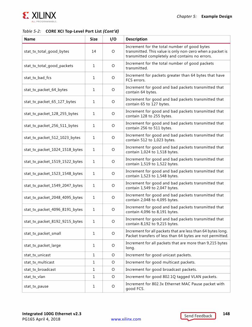
Integrated 100G Ethernet v2.3 148PG165 April 4, 2018 www.xilinx.com
Chapter 5: Example Design
stat_tx_total_good_bytes 14 OIncrement for the total number of good bytes transmitted. This value is only non-zero when a packet is transmitted completely and contains no errors.
stat_tx_total_good_packets 1 O Increment for the total number of good packets transmitted.
stat_tx_bad_fcs 1 O Increment for packets greater than 64 bytes that have FCS errors.
stat_tx_packet_64_bytes 1 O Increment for good and bad packets transmitted that contain 64 bytes.
stat_tx_packet_65_127_bytes 1 O Increment for good and bad packets transmitted that contain 65 to 127 bytes.
stat_tx_packet_128_255_bytes 1 O Increment for good and bad packets transmitted that contain 128 to 255 bytes.
stat_tx_packet_256_511_bytes 1 O Increment for good and bad packets transmitted that contain 256 to 511 bytes.
stat_tx_packet_512_1023_bytes 1 O Increment for good and bad packets transmitted that contain 512 to 1,023 bytes.
stat_tx_packet_1024_1518_bytes 1 O Increment for good and bad packets transmitted that contain 1,024 to 1,518 bytes.
stat_tx_packet_1519_1522_bytes 1 O Increment for good and bad packets transmitted that contain 1,519 to 1,522 bytes.
stat_tx_packet_1523_1548_bytes 1 O Increment for good and bad packets transmitted that contain 1,523 to 1,548 bytes.
stat_tx_packet_1549_2047_bytes 1 O Increment for good and bad packets transmitted that contain 1,549 to 2,047 bytes.
stat_tx_packet_2048_4095_bytes 1 O Increment for good and bad packets transmitted that contain 2,048 to 4,095 bytes.
stat_tx_packet_4096_8191_bytes 1 O Increment for good and bad packets transmitted that contain 4,096 to 8,191 bytes.
stat_tx_packet_8192_9215_bytes 1 O Increment for good and bad packets transmitted that contain 8,192 to 9,215 bytes.
stat_tx_packet_small 1 O Increment for all packets that are less than 64 bytes long. Packet transfers of less than 64 bytes are not permitted.
stat_tx_packet_large 1 O Increment for all packets that are more than 9,215 bytes long.
stat_tx_unicast 1 O Increment for good unicast packets.
stat_tx_multicast 1 O Increment for good multicast packets.
stat_tx_broadcast 1 O Increment for good broadcast packets.
stat_tx_vlan 1 O Increment for good 802.1Q tagged VLAN packets.
stat_tx_pause 1 O Increment for 802.3x Ethernet MAC Pause packet with good FCS.
Table 5-2: CORE XCI Top-Level Port List (Cont’d)
Name Size I/O Description
Send Feedback
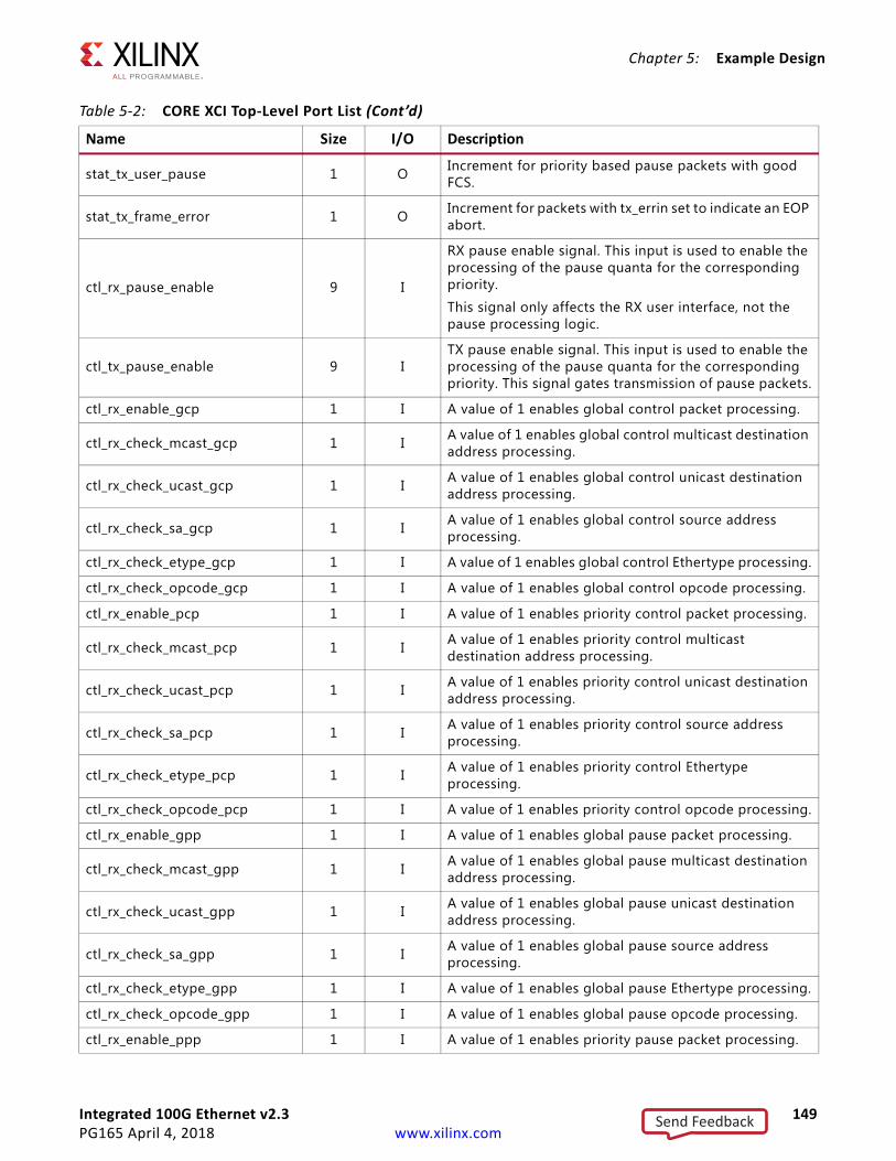
Integrated 100G Ethernet v2.3 149PG165 April 4, 2018 www.xilinx.com
Chapter 5: Example Design
stat_tx_user_pause 1 O Increment for priority based pause packets with good FCS.
stat_tx_frame_error 1 O Increment for packets with tx_errin set to indicate an EOP abort.
ctl_rx_pause_enable 9 I
RX pause enable signal. This input is used to enable the processing of the pause quanta for the corresponding priority.
This signal only affects the RX user interface, not the pause processing logic.
ctl_tx_pause_enable 9 ITX pause enable signal. This input is used to enable the processing of the pause quanta for the corresponding priority. This signal gates transmission of pause packets.
ctl_rx_enable_gcp 1 I A value of 1 enables global control packet processing.
ctl_rx_check_mcast_gcp 1 I A value of 1 enables global control multicast destination address processing.
ctl_rx_check_ucast_gcp 1 I A value of 1 enables global control unicast destination address processing.
ctl_rx_check_sa_gcp 1 I A value of 1 enables global control source address processing.
ctl_rx_check_etype_gcp 1 I A value of 1 enables global control Ethertype processing.
ctl_rx_check_opcode_gcp 1 I A value of 1 enables global control opcode processing.
ctl_rx_enable_pcp 1 I A value of 1 enables priority control packet processing.
ctl_rx_check_mcast_pcp 1 I A value of 1 enables priority control multicast destination address processing.
ctl_rx_check_ucast_pcp 1 I A value of 1 enables priority control unicast destination address processing.
ctl_rx_check_sa_pcp 1 I A value of 1 enables priority control source address processing.
ctl_rx_check_etype_pcp 1 I A value of 1 enables priority control Ethertype processing.
ctl_rx_check_opcode_pcp 1 I A value of 1 enables priority control opcode processing.
ctl_rx_enable_gpp 1 I A value of 1 enables global pause packet processing.
ctl_rx_check_mcast_gpp 1 I A value of 1 enables global pause multicast destination address processing.
ctl_rx_check_ucast_gpp 1 I A value of 1 enables global pause unicast destination address processing.
ctl_rx_check_sa_gpp 1 I A value of 1 enables global pause source address processing.
ctl_rx_check_etype_gpp 1 I A value of 1 enables global pause Ethertype processing.
ctl_rx_check_opcode_gpp 1 I A value of 1 enables global pause opcode processing.
ctl_rx_enable_ppp 1 I A value of 1 enables priority pause packet processing.
Table 5-2: CORE XCI Top-Level Port List (Cont’d)
Name Size I/O Description
Send Feedback
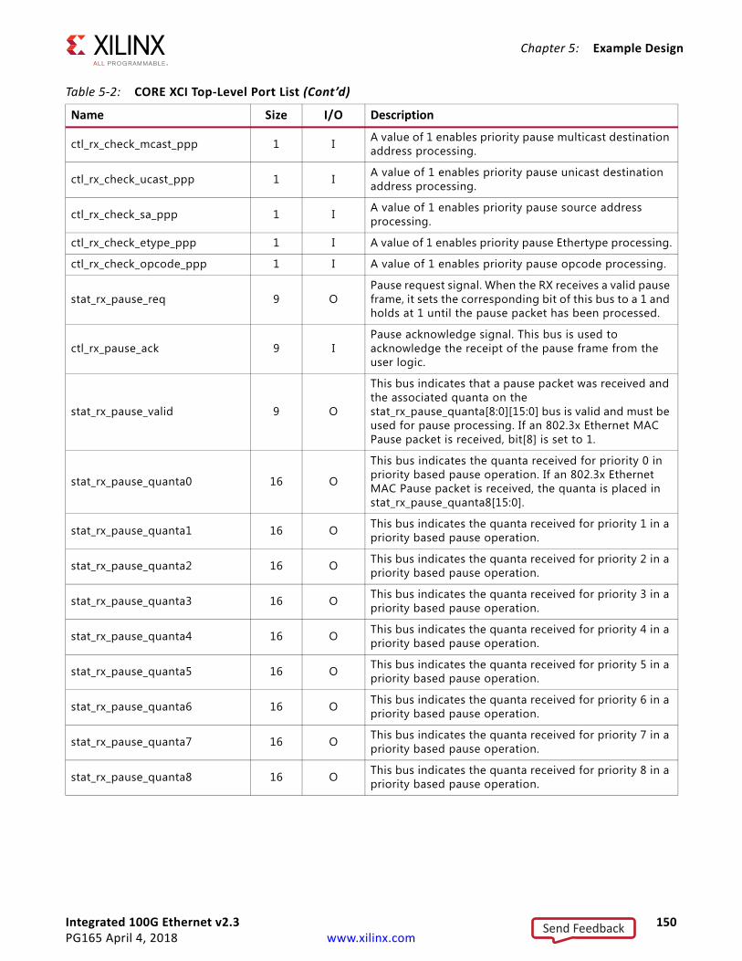
Integrated 100G Ethernet v2.3 150PG165 April 4, 2018 www.xilinx.com
Chapter 5: Example Design
ctl_rx_check_mcast_ppp 1 I A value of 1 enables priority pause multicast destination address processing.
ctl_rx_check_ucast_ppp 1 I A value of 1 enables priority pause unicast destination address processing.
ctl_rx_check_sa_ppp 1 I A value of 1 enables priority pause source address processing.
ctl_rx_check_etype_ppp 1 I A value of 1 enables priority pause Ethertype processing.
ctl_rx_check_opcode_ppp 1 I A value of 1 enables priority pause opcode processing.
stat_rx_pause_req 9 OPause request signal. When the RX receives a valid pause frame, it sets the corresponding bit of this bus to a 1 and holds at 1 until the pause packet has been processed.
ctl_rx_pause_ack 9 IPause acknowledge signal. This bus is used to acknowledge the receipt of the pause frame from the user logic.
stat_rx_pause_valid 9 O
This bus indicates that a pause packet was received and the associated quanta on the stat_rx_pause_quanta[8:0][15:0] bus is valid and must be used for pause processing. If an 802.3x Ethernet MAC Pause packet is received, bit[8] is set to 1.
stat_rx_pause_quanta0 16 O
This bus indicates the quanta received for priority 0 in priority based pause operation. If an 802.3x Ethernet MAC Pause packet is received, the quanta is placed in stat_rx_pause_quanta8[15:0].
stat_rx_pause_quanta1 16 O This bus indicates the quanta received for priority 1 in a priority based pause operation.
stat_rx_pause_quanta2 16 O This bus indicates the quanta received for priority 2 in a priority based pause operation.
stat_rx_pause_quanta3 16 O This bus indicates the quanta received for priority 3 in a priority based pause operation.
stat_rx_pause_quanta4 16 O This bus indicates the quanta received for priority 4 in a priority based pause operation.
stat_rx_pause_quanta5 16 O This bus indicates the quanta received for priority 5 in a priority based pause operation.
stat_rx_pause_quanta6 16 O This bus indicates the quanta received for priority 6 in a priority based pause operation.
stat_rx_pause_quanta7 16 O This bus indicates the quanta received for priority 7 in a priority based pause operation.
stat_rx_pause_quanta8 16 O This bus indicates the quanta received for priority 8 in a priority based pause operation.
Table 5-2: CORE XCI Top-Level Port List (Cont’d)
Name Size I/O Description
Send Feedback
Integrated 100G Ethernet v2.3 151PG165 April 4, 2018 www.xilinx.com
Chapter 5: Example Design
ctl_tx_pause_req 9 I
If a bit of this bus is set to 1, the dedicated 100G Ethernet IP core transmits a pause packet using the associated quanta value on the ctl_tx_pause_quanta[8:0][15:0] bus. If bit[8] is set to 1, a global pause packet is transmitted. All other bits cause a priority pause packet to be transmitted. Each bit of this bus must be held at a steady state for a minimum of 16 cycles before the next transition.
ctl_tx_pause_quanta0 16 I
This bus indicates the quanta to be transmitted for priority 0 in a priority based pause operation. If an 802.3x Ethernet MAC Pause packet is to be transmitted, the quanta is placed in ctl_tx_pause_quanta8[15:0].
ctl_tx_pause_quanta1 16 I This bus indicates the quanta to be transmitted for priority 1 in a priority based pause operation.
ctl_tx_pause_quanta2 16 I This bus indicates the quanta to be transmitted for priority 2 in a priority based pause operation.
ctl_tx_pause_quanta3 16 I This bus indicates the quanta to be transmitted for priority 3 in a priority based pause operation.
ctl_tx_pause_quanta4 16 I This bus indicates the quanta to be transmitted for priority 4 in a priority based pause operation.
ctl_tx_pause_quanta5 16 I This bus indicates the quanta to be transmitted for priority 5 in a priority based pause operation.
ctl_tx_pause_quanta6 16 I This bus indicates the quanta to be transmitted for priority 6 in a priority based pause operation.
ctl_tx_pause_quanta7 16 I This bus indicates the quanta to be transmitted for priority 7 in a priority based pause operation.
ctl_tx_pause_quanta8 16 I This bus indicates the quanta to be transmitted for priority 8 in a priority based pause operation.
ctl_tx_pause_refresh_timer0 16 I This bus sets the retransmission time of pause packets for priority 0 in a priority based pause operation.
ctl_tx_pause_refresh_timer1 16 I This bus sets the retransmission time of pause packets for priority 1 in a priority based pause operation.
ctl_tx_pause_refresh_timer2 16 I This bus sets the retransmission time of pause packets for priority 2 in a priority based pause operation.
ctl_tx_pause_refresh_timer3 16 I This bus sets the retransmission time of pause packets for priority 3 in a priority based pause operation.
ctl_tx_pause_refresh_timer4 16 I This bus sets the retransmission time of pause packets for priority 4 in a priority based pause operation.
ctl_tx_pause_refresh_timer5 16 I This bus sets the retransmission time of pause packets for priority 5 in a priority based pause operation.
ctl_tx_pause_refresh_timer6 16 I This bus sets the retransmission time of pause packets for priority 6 in a priority based pause operation.
ctl_tx_pause_refresh_timer7 16 I This bus sets the retransmission time of pause packets for priority 7 in a priority based pause operation.
Table 5-2: CORE XCI Top-Level Port List (Cont’d)
Name Size I/O Description
Send Feedback
Integrated 100G Ethernet v2.3 152PG165 April 4, 2018 www.xilinx.com
Chapter 5: Example Design
ctl_tx_pause_refresh_timer8 16 I This bus sets the retransmission time of pause packets for priority 8 in a priority based pause operation.
ctl_tx_resend_pause 1 I
Re-transmit pending pause packets. When this input is sampled as 1, all pending pause packets are retransmitted as soon as possible (that is, after the current packet in flight is completed) and the retransmit counters are reset. This input should be pulsed to 1 for one cycle at a time.
stat_tx_pause_valid 9 O
If a bit of this bus is set to 1, the dedicated 100G Ethernet IP core has transmitted a pause packet. If bit[8] is set to 1, a global pause packet is transmitted. All other bits cause a priority pause packet to be transmitted.
ctl_tx_systemtimerin 80 I
System timer input for the TX. In normal clock mode, the time format is according to the IEEE 1588 format, with 48 bits for seconds and 32 bits for nanoseconds. In transparent clock mode, bit 63 is the sign bit, bits 62:16 carry nanoseconds, and bits 15:0 carry fractional nanoseconds. Refer to the IEEE 1588v2 for the representational definitions. This input must be in the TX clock domain.
tx_ptp_tstamp_valid_out 1 O This bit indicates that a valid timestamp is being presented on the TX.
tx_ptp_pcslane_out 5 O This bus identifies which of the 20 PCS lanes that the SOP was detected on for the corresponding timestamp.
tx_ptp_tstamp_tag_out 16 O Tag output corresponding to tx_ptp_tag_field_in[15:0].
tx_ptp_tstamp_out 80 O
Time stamp for the transmitted packet SOP corresponding to the time at which it passed the capture plane. The representation of the bits contained in this bus is the same as the timer input.
tx_ptp_1588op_in 2 I
2’b00 – “No operation”: no timestamp will be taken and the frame will not be modified.
2’b01 – “1-step”: a timestamp should be taken and
inserted into the frame.
2’b10 – “2-step”: a timestamp should be taken and
returned to the client using the additional ports of 2-step operation. The frame itself will not be modified.
2’b11 – Reserved.
Table 5-2: CORE XCI Top-Level Port List (Cont’d)
Name Size I/O Description
Send Feedback
Integrated 100G Ethernet v2.3 153PG165 April 4, 2018 www.xilinx.com
Chapter 5: Example Design
tx_ptp_tag_field_in 16 I
The usage of this field is dependent on the 1588 operation
For “No operation”, this field will be ignored.
For “1-step” and “2-step”, this field is a tag field. This tag value will be returned to the client with the timestamp for the current frame using the additional ports of 2-step operation. This tag value can be used by software to ensure that the timestamp can be matched with the precise timing protocol (PTP) frame that it sent for transmission.
tx_ptp_upd_chksum_in 1 I
The usage of this field is dependent on the 1588 operation.
For “No operation” or “2-step”, this bit will be ignored.
For “1-step”:
1’b0: The PTP frame does not contain a UDP checksum.
1’b1: The PTP frame does contain a UDP checksum which the core is required to recalculate.
tx_ptp_chksum_offset_in 16 I
The usage of this field is dependent on the “1588 operation” and on the “Update Checksum” bit.
For “No operation”, for “2-step” or for “1-step” when “Update Checksum” is set to 1’b0, this field will be ignored.
For “1-step” when “Update Checksum” is set to 1’b1, this field is a numeric value indicating the number of bytes into the frame to where the first byte of the checksum is located (where a value of 0 represents the first byte of the Destination Address, etc).Note: The IPv6 header size is unbounded, so this field is able to cope with all frames sizes up to 16K jumbo frames. Only even values are supported.
tx_ptp_tstamp_offset_in 16 I
The usage of this field is dependent on the 1588 operation
For “No operation” or “2-step” this field is ignored.
For “1-step”, this field is a numeric value indicating the number of bytes into the frame to where the first byte of the timestamp to be inserted is located (where a value of 0 represents the first byte of the Destination Address, etc).
This input is also used to specify the offset for the correction field in 1-step Transparent Clock mode.Note: The IPv6 header size is unbounded, so this field is able to cope with all frames sizes up to 16K jumbo frames.
Note: Only even values are supported.
Note: In transparent clock mode and when tx_ptp_upd_chksum_in=1, this value cannot be greater than tx_ptp_chksum_offset_in + 34 (decimal).
Table 5-2: CORE XCI Top-Level Port List (Cont’d)
Name Size I/O Description
Send Feedback
Integrated 100G Ethernet v2.3 154PG165 April 4, 2018 www.xilinx.com
Chapter 5: Example Design
ctl_tx_ptp_vlane_adjust_mode 1 I
When asserted, this signal applies an adjustment to the TX timestamps according to the PCS lane on which the SOP occurs. When zero, no adjustment is made. This signal only has effect for 1-step operation.
stat_tx_ptp_fifo_write_error 1 OTransmit PTP FIFO write error. A 1 on this status indicates that an error occurred during the PTP Tag write. A TX Path reset is required to clear the error.
stat_tx_ptp_fifo_read_error 1 OTransmit PTP FIFO read error. A 1 on this status indicates that an error occurred during the PTP Tag read. A TX Path reset is required to clear the error.
ctl_rx_systemtimerin 80 I
System timer input for the RX.
In normal clock mode, the time format is according to the IEEE 1588 format, with 48 bits for seconds and 32 bits for nanoseconds.
In transparent clock mode, bit 63 is the sign bit, bits 62:16 carry nanoseconds, and bits 15:0 carry fractional nanoseconds. Refer to the IEEE 1588v2 for the representational definitions.
This input must be in the same clock domain as the lane 0 RX SerDes.
rx_ptp_tstamp_out 80 O
Time stamp for the received packet SOP corresponding to the time at which it passed the capture plane. This signal will be valid starting at the same clock cycle during which the SOP is asserted for one of the LBUS segments.
The representation of the bits contained in this bus is the same as the timer input.
rx_ptp_pcslane_out 5 O
This bus identifies which of the 20 PCS lanes that the SOP was detected on for the corresponding timestamp.
This signal will be valid starting at the same clock cycle during which the SOP is asserted for one of the LBUS segments.
rx_lane_aligner_fill_0 7 O
This output indicates the fill level of the alignment buffer for PCS lane0. This information can be used by the PTP application, together with the signal rx_ptp_pcslane_out[4:0], to adjust for the lane skew of the arriving SOP. The units are SerDes clock cycles.
rx_lane_aligner_fill_1 7 O This output indicates the fill level of the alignment buffer for PCS lane1.
rx_lane_aligner_fill_2 7 O This output indicates the fill level of the alignment buffer for PCS lane2.
rx_lane_aligner_fill_3 7 O This output indicates the fill level of the alignment buffer for PCS lane3.
rx_lane_aligner_fill_4 7 O This output indicates the fill level of the alignment buffer for PCS lane4.
Table 5-2: CORE XCI Top-Level Port List (Cont’d)
Name Size I/O Description
Send Feedback
Integrated 100G Ethernet v2.3 155PG165 April 4, 2018 www.xilinx.com
Chapter 5: Example Design
rx_lane_aligner_fill_5 7 O This output indicates the fill level of the alignment buffer for PCS lane5.
rx_lane_aligner_fill_6 7 O This output indicates the fill level of the alignment buffer for PCS lane6.
rx_lane_aligner_fill_7 7 O This output indicates the fill level of the alignment buffer for PCS lane7.
rx_lane_aligner_fill_8 7 O This output indicates the fill level of the alignment buffer for PCS lane8.
rx_lane_aligner_fill_9 7 O This output indicates the fill level of the alignment buffer for PCS lane9.
rx_lane_aligner_fill_10 7 O This output indicates the fill level of the alignment buffer for PCS lane10.
rx_lane_aligner_fill_11 7 O This output indicates the fill level of the alignment buffer for PCS lane11.
rx_lane_aligner_fill_12 7 O This output indicates the fill level of the alignment buffer for PCS lane12.
rx_lane_aligner_fill_13 7 O This output indicates the fill level of the alignment buffer for PCS lane13.
rx_lane_aligner_fill_14 7 O This output indicates the fill level of the alignment buffer for PCS lane14.
rx_lane_aligner_fill_15 7 O This output indicates the fill level of the alignment buffer for PCS lane15.
rx_lane_aligner_fill_16 7 O This output indicates the fill level of the alignment buffer for PCS lane16.
rx_lane_aligner_fill_17 7 O This output indicates the fill level of the alignment buffer for PCS lane17.
rx_lane_aligner_fill_18 7 O This output indicates the fill level of the alignment buffer for PCS lane18.
rx_lane_aligner_fill_19 7 O This output indicates the fill level of the alignment buffer for PCS lane19.
drp_clk 1 I DRP interface clock. When DRP is not used, this can be tied to GND.
drp_addr 10 I DRP address bus.
drp_di 16 I Data bus for writing configuration data from the FPGA logic resources to the 100G Ethernet IP core.
drp_en 1 I
DRP enable signal.
0: No read or write operations performed.
1: Enables a read or write operation.
For write operations, DRP_WE and DRP_EN should be driven High for one DRP_CLK cycle only.
drp_do 16 O Data bus for reading configuration data from the 100G Ethernet IP core to the FPGA logic resources.
Table 5-2: CORE XCI Top-Level Port List (Cont’d)
Name Size I/O Description
Send Feedback
Integrated 100G Ethernet v2.3 156PG165 April 4, 2018 www.xilinx.com
Chapter 5: Example Design
Note: AXI4-Lite interface ports are visible only when you select the Include AXI4-Lite Control and Statistics Interface option from the General Tab. Refer to AXI User Interface Ports for the AXI4-Lite port list and descriptions.
Modes of OperationThree modes of operations are supported for this example design which are:
• Duplex Mode
• Simplex TX Mode
• Simplex RX Mode
Duplex ModeIn this mode of operation both the 100G Ethernet IP core transmitter and receiver are active and loopback is provided at the GT output interface, that is, output is fed back as input. Packet generation and monitor are also active in this mode.
drp_rdy 1 O Indicates operation is complete for write operations and data is valid for read operations.
drp_we 1 I
DRP write enable.
0: Read operation when DRP_EN is 1.
1: Write operation when DRP_EN is 1.
For write operations, DRP_WE and DRP_EN should be driven High for one DRP_CLK cycle only.
Table 5-2: CORE XCI Top-Level Port List (Cont’d)
Name Size I/O Description
Send Feedback
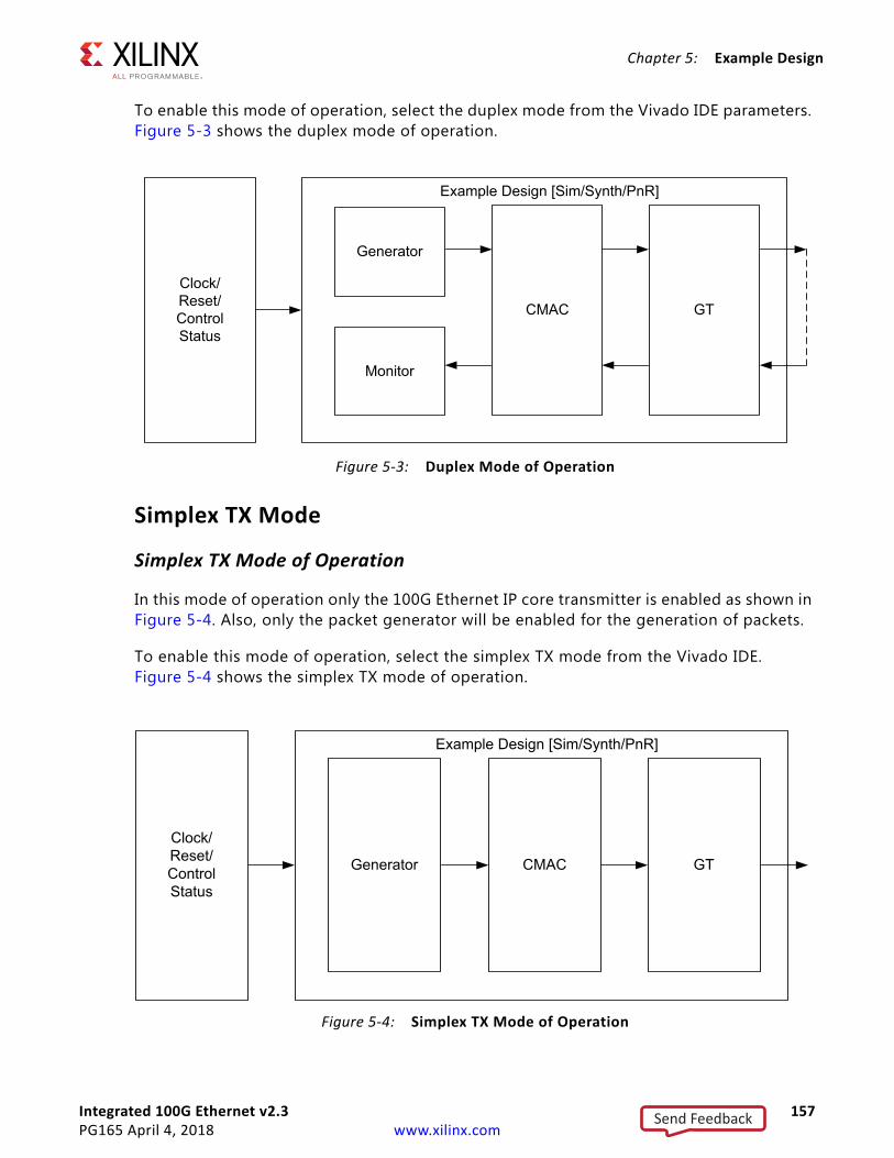
Integrated 100G Ethernet v2.3 157PG165 April 4, 2018 www.xilinx.com
Chapter 5: Example Design
To enable this mode of operation, select the duplex mode from the Vivado IDE parameters. Figure 5-3 shows the duplex mode of operation.
Simplex TX Mode
Simplex TX Mode of Operation
In this mode of operation only the 100G Ethernet IP core transmitter is enabled as shown in Figure 5-4. Also, only the packet generator will be enabled for the generation of packets.
To enable this mode of operation, select the simplex TX mode from the Vivado IDE. Figure 5-4 shows the simplex TX mode of operation.
X-Ref Target - Figure 5-3
Figure 5-3: Duplex Mode of Operation
X-Ref Target - Figure 5-4
Figure 5-4: Simplex TX Mode of Operation
Generator
CMAC
Monitor
GT
Example Design [Sim/Synth/PnR]
Clock/Reset/ControlStatus
Clock/Reset/ControlStatus
Generator GT
Example Design [Sim/Synth/PnR]
CMAC
Send Feedback
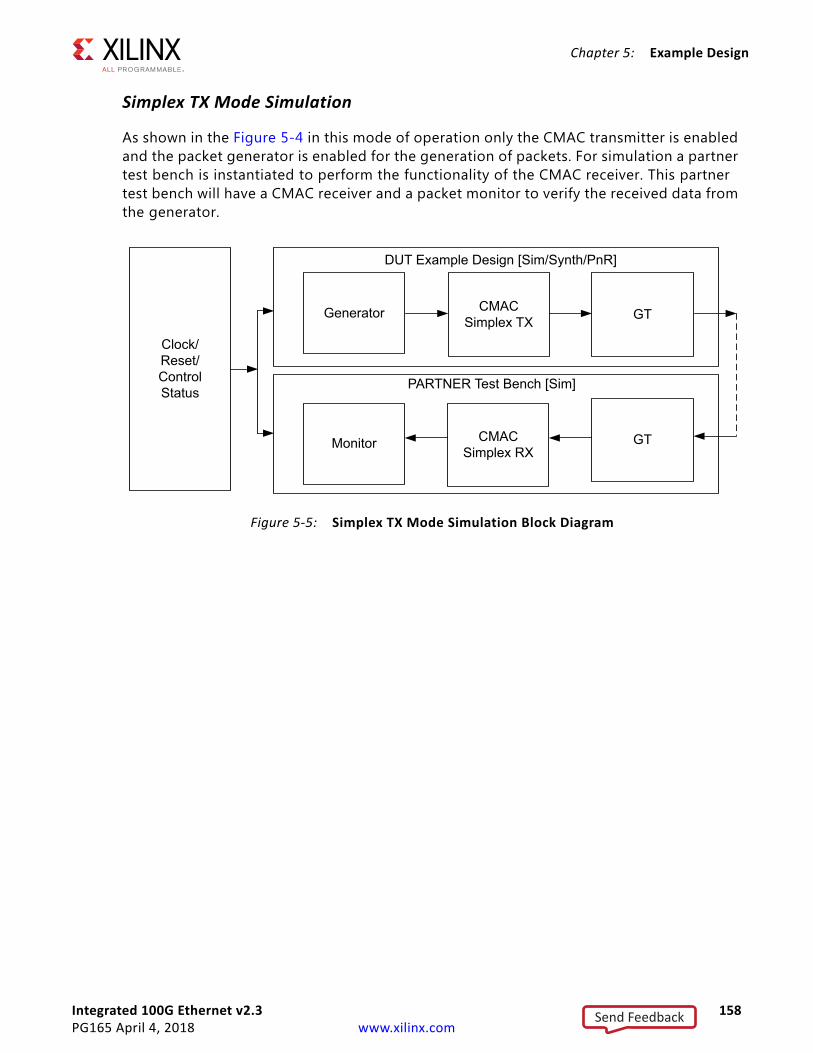
Integrated 100G Ethernet v2.3 158PG165 April 4, 2018 www.xilinx.com
Chapter 5: Example Design
Simplex TX Mode Simulation
As shown in the Figure 5-4 in this mode of operation only the CMAC transmitter is enabled and the packet generator is enabled for the generation of packets. For simulation a partner test bench is instantiated to perform the functionality of the CMAC receiver. This partner test bench will have a CMAC receiver and a packet monitor to verify the received data from the generator.
X-Ref Target - Figure 5-5
Figure 5-5: Simplex TX Mode Simulation Block Diagram
Clock/Reset/ControlStatus
Generator CMACSimplex TX
Monitor
GT
DUT Example Design [Sim/Synth/PnR]
CMACSimplex RX
GT
PARTNER Test Bench [Sim]
Send Feedback
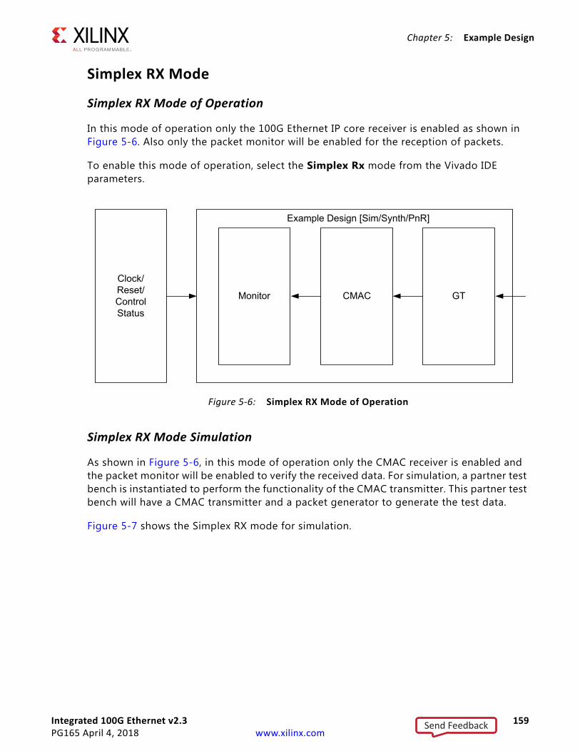
Integrated 100G Ethernet v2.3 159PG165 April 4, 2018 www.xilinx.com
Chapter 5: Example Design
Simplex RX Mode
Simplex RX Mode of Operation
In this mode of operation only the 100G Ethernet IP core receiver is enabled as shown in Figure 5-6. Also only the packet monitor will be enabled for the reception of packets.
To enable this mode of operation, select the Simplex Rx mode from the Vivado IDE parameters.
Simplex RX Mode Simulation
As shown in Figure 5-6, in this mode of operation only the CMAC receiver is enabled and the packet monitor will be enabled to verify the received data. For simulation, a partner test bench is instantiated to perform the functionality of the CMAC transmitter. This partner test bench will have a CMAC transmitter and a packet generator to generate the test data.
Figure 5-7 shows the Simplex RX mode for simulation.
X-Ref Target - Figure 5-6
Figure 5-6: Simplex RX Mode of Operation
Clock/Reset/ControlStatus
Monitor GT
Example Design [Sim/Synth/PnR]
CMAC
Send Feedback

Integrated 100G Ethernet v2.3 160PG165 April 4, 2018 www.xilinx.com
Chapter 5: Example Design
Transaction Flow This section describes the flow of data between cmac_0_pkt_gen_mon and cmac_0 and various state transitions that happen within cmac_0_pkt_gen and cmac_0_pkt_mon.
Packet GenerationThe module cmac_0_pkt_gen is responsible for the generation of LBUS packets. Typically the packet generator waits for the GT to achieve lock and for the core RX to get aligned. After this has occurred, the packet generator sends a predefined number of packets. A Finite State Machine (FSM) is used to generate the LBUS packets. A functional description of each state follows:
• STATE_TX_IDLE: By default the controller is in the STATE_TX_IDLE state. When reset_done becomes High, it moves to the STATE_GT_LOCKED state.
• STATE_GT_LOCKED: This state sets ctl_tx_send_rfi=1, tx_core_busy_led=1 and gt_lock_led=1. It then moves to the STATE_WAIT_RX_ALIGNED state.
• STATE_WAIT_RX_ALIGNED: This state waits for the 100G Ethernet IP cores to indicate stat_rx_aligned=1, which means that the 100G Ethernet IP RX core is locked. After that, it moves to the STATE_PKT_TRANSFER_INIT state.
• STATE_PKT_TRANSFER_INIT: This state sets rx_aligned_led=1 and tx_core_busy_led=1. It then initializes all signals to start LBUS packet generation and moves to the STATE_LBUS_TX_ENABLE state.
X-Ref Target - Figure 5-7
Figure 5-7: Simplex RX Mode Simulation Block Diagram
Clock/Reset/ControlStatus
Generator CMACSimplex TX
Monitor
GT
DUT Example Design [Sim/Synth/PnR]
CMACSimplex RX
GT
PARTNER Test Bench [Sim]
Send Feedback
Integrated 100G Ethernet v2.3 161PG165 April 4, 2018 www.xilinx.com
Chapter 5: Example Design
• STATE_LBUS_TX_ENABLE: This state checks for the number of packets to be generated and sends LBUS packets of a predefined size. After sending all the packets, the FSM moves to the STATE_LBUS_TX_DONE state. During transmission of the packets, if tx_rdyout=0, tc_ovfout=1 or tx_unfout=1, the FSM controller moves to the STATE_LBUS_TX_HALT state.
• STATE_LBUS_TX_HALT: In this state, the controller generates the tx_fail_reg flag if tc_ovfout or tx_unfout is High. Then the FSM moves to the STATE_LBUS_TX_DONE state. If tx_rdyout becomes High, the FSM moves to the STATE_LBUS_TX_ENABLE state to proceed with packet generation.
• STATE_LBUS_TX_DONE: This state resets all signals related to packet generation and sets tx_done_led =1. If the 1588 "1-step" or "Both" option with FCS insertion is enabled, FSM moves to the STATE_PTP_PKT_INIT state; otherwise it checks if TX_FLOW_CONTROL is enabled. If enabled, the FSM moves to the STATE_TX_PAUSE_INIT state. If TX_FLOW_CONTROL is now enabled, the FSM moves to the STATE_WAIT_FOR_RESTART state.
• STATE_WAIT_FOR_RESTART: In this state, all the packet generator parameters reset to the default values and reset tx_busy_led=0. The FSM moves to STATE_PKT_TRANSFER_INIT at tx_restart_rising_edge.
• STATE_PTP_PKT_INIT: Reset all the signals used for LBUS transactions. Move to the STATE_PTP_PKT_READ state wait until the initialization counter is done and set the ptp_pkt_transfer flag to one. After sending three 1588 PTP packets (Ethernet, IPV4 and IPV6), FSM moves to the STATE_TX_PAUSE_INIT state if the TX_FLOW_CONTROL is enabled; otherwise FSM moves to STATE_WAIT_FOR_RESTART state.
• STATE_PTP_PKT_READ: In case of IPV4 or IPV6, increment the tx_ptp_pkt_index and move to the STATE_PTP_PKT_TRANSFER state.
• STATE_TX_PTP_PKT_TRANSFER: Read the data from the ptp_pkt_gen module after sending the complete ptp packet, move to the STATE_PTP_PKT_INIT state.
• STATE_TX_PAUSE_INIT: Set the ctl_tx_pause_enable = 9’h100 and ctl_tx_pause_req[8] = 1 and wait for the stat_tx_pause signal to become High and the FSM moves to the STATE_TX_PPP_INIT state.
• STATE_TX_PPP_INIT: In this state, the controller sets ctl_tx_pause_enable = 9'h0ff and ctl_tx_pause_req[7:0] one bit at a time in decrementing order (bit 7 to bit 0). It then waits for stat_tx_pause_valid[0] to become High and moves to the STATE_TX_PAUSE_DONE state.
• STATE_TX_PAUSE_DONE: In this state, all the pause signals are reset. The controller then moves to the STATE_WAIT_FOR_RESTART state.
Send Feedback
Integrated 100G Ethernet v2.3 162PG165 April 4, 2018 www.xilinx.com
Chapter 5: Example Design
Notes:
• If any time stat_rx_aligned = 0, the FSM moves to STATE_TX_IDLE.
• In the simplex TX mode of operation because RX alignment information will not be available, the state machine waits for you to input simplex_mode_rx_aligned. After you assert this input to High, packet transmission starts.
• If you select the Disable FCS Insertion option in the General Tab, the CMAC core will not insert the CRC value for the data packets. So a CRC_Mapping_LUT module will be instantiated inside the cmac_0_pkt_gen module that contains the pre-calculated CRC values for the current LBUS predefined data packet of the packet size 522 bytes. These CRC values will be appended at the end of each LBUS packet.|
Therefore, if you are changing the packet size, you must change the CRC values for this new module as appropriate for the new packet and/or packet size.
If the 1588 Transparent Clock 1-step or Both option is selected and if FCS insertion is disabled in Vivado IDE, the 1588 Transparent Clock testing will not be performed in the example design because of the unpredictable PTP frame CRC values as the core will modify the packet.
• If you select the 1-step or Both option in the General Tab, then the ptp_packet_gen module will be instantiated inside the cmac_0_packet_gen module. This module contains three 1588 PTP packets (Ethernet, IPV4 and IPV6) with or without the CRC values based on the Disable FCS Insertion or Enable FCS Insertion option in the General Tab.
The state transition that occurs during this process is shown in Figure 5-8.
Send Feedback
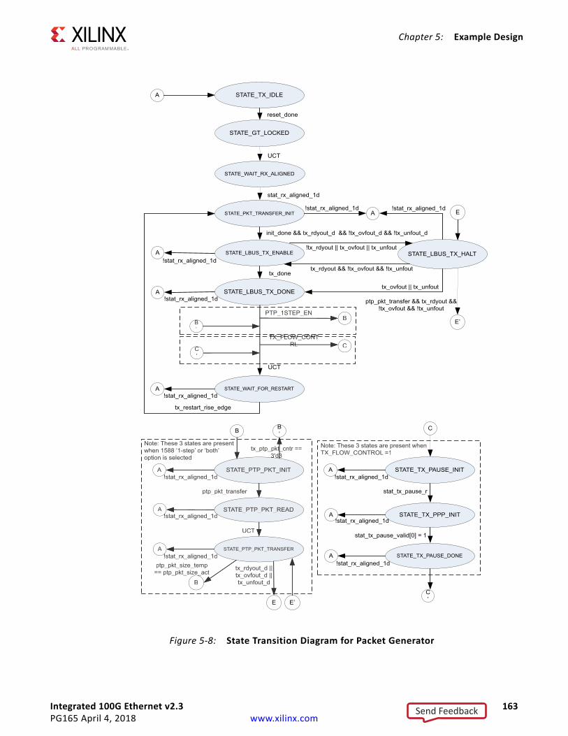
Integrated 100G Ethernet v2.3 163PG165 April 4, 2018 www.xilinx.com
Chapter 5: Example Design
X-Ref Target - Figure 5-8
Figure 5-8: State Transition Diagram for Packet Generator
STATE_TX_IDLE
STATE_GT_LOCKED
STATE_WAIT_RX_ALIGNED
STATE_PKT_TRANSFER_INIT
STATE_LBUS_TX_ENABLE STATE_LBUS_TX_HALT
STATE_LBUS_TX_DONE
STATE_WAIT_FOR_RESTART
reset_done
UCT
stat_rx_aligned_1d
init_done && tx_rdyout_d && !tx_ovfout_d && !tx_unfout_d
!tx_rdyout || tx_ovfout || tx_unfout
tx_donetx_rdyout && !tx_ovfout && !tx_unfout
tx_ovfout || tx_unfout
UCT
!stat_rx_aligned_1dA
A
A!stat_rx_aligned_1d
!stat_rx_aligned_1d
A!stat_rx_aligned_1d
TX_FLOW_CONTRL
A!stat_rx_aligned_1d
tx_restart_rise_edge
B
C
PTP_1STEP_ENB’
C’
STATE_PTP_PKT_INIT
STATE_PTP_PKT_READ
STATE_PTP_PKT_TRANSFER
ptp_pkt_transfer
Note: These 3 states are present when TX_FLOW_CONTROL =1
A!stat_rx_aligned_1d
A!stat_rx_aligned_1d
A!stat_rx_aligned_1d
B
B
BPTP_1STEP_EN
BB’
TX_FLOW_CONTRL CCC
’
Note: These 3 states are present whenTX_FLOW_CONTROL =1X
STATE_TX_PAUSE_INIT
STATE_TX_PPP_INIT
STATE_TX_PAUSE_DONE
stat_tx_pause_r
stat_tx_pause_valid[0] = 1
A!stat_rx_aligned_1d
A!stat_rx_aligned_1d
A!stat_rx_aligned_1d
C
Note: These 3 states are present when 1588 ‘1-step’ or ‘both’ option is selected
C’
UCT
ptp_pkt_size_temp == ptp_pkt_size_act
B’
tx_ptp_pkt_cntr == 3'd3
E
tx_rdyout_d || tx_ovfout_d || tx_unfout_d
E
E’
ptp_pkt_transfer && tx_rdyout && !tx_ovfout && !tx_unfout
E’
STATE_PTP_PKT_INIT
STATE_PTP_PKT_READ
STATE_PTP_PKT_TRANSFER
ptp_pkt_transfer
A!stat_rx_aligned_1dd
A!stat_rx_aligned_1ddd!!
A!stat_rx_aligned_1d!
B
Note: These 3 states are present when 1588 ‘1-step’ or ‘both’option is selected
UCT
ptp_pkt_size_temp == ptp_pkt_size_act_
tx_ptp_pkt_cntr == t_333'd33
tx_rdyout_d || tx_ovfout_d || xtx_unfout_dx
Send Feedback
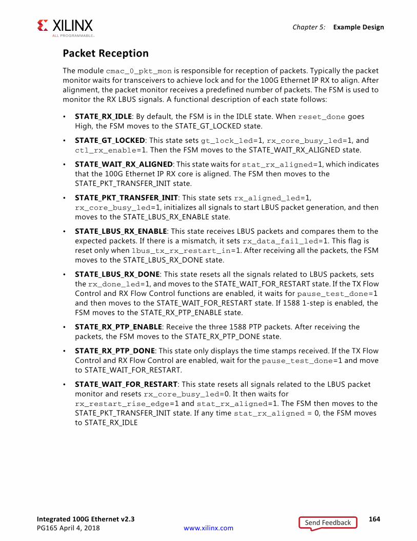
Integrated 100G Ethernet v2.3 164PG165 April 4, 2018 www.xilinx.com
Chapter 5: Example Design
Packet ReceptionThe module cmac_0_pkt_mon is responsible for reception of packets. Typically the packet monitor waits for transceivers to achieve lock and for the 100G Ethernet IP RX to align. After alignment, the packet monitor receives a predefined number of packets. The FSM is used to monitor the RX LBUS signals. A functional description of each state follows:
• STATE_RX_IDLE: By default, the FSM is in the IDLE state. When reset_done goes High, the FSM moves to the STATE_GT_LOCKED state.
• STATE_GT_LOCKED: This state sets gt_lock_led=1, rx_core_busy_led=1, and ctl_rx_enable=1. Then the FSM moves to the STATE_WAIT_RX_ALIGNED state.
• STATE_WAIT_RX_ALIGNED: This state waits for stat_rx_aligned=1, which indicates that the 100G Ethernet IP RX core is aligned. The FSM then moves to the STATE_PKT_TRANSFER_INIT state.
• STATE_PKT_TRANSFER_INIT: This state sets rx_aligned_led=1, rx_core_busy_led=1, initializes all signals to start LBUS packet generation, and then moves to the STATE_LBUS_RX_ENABLE state.
• STATE_LBUS_RX_ENABLE: This state receives LBUS packets and compares them to the expected packets. If there is a mismatch, it sets rx_data_fail_led=1. This flag is reset only when lbus_tx_rx_restart_in=1. After receiving all the packets, the FSM moves to the STATE_LBUS_RX_DONE state.
• STATE_LBUS_RX_DONE: This state resets all the signals related to LBUS packets, sets the rx_done_led=1, and moves to the STATE_WAIT_FOR_RESTART state. If the TX Flow Control and RX Flow Control functions are enabled, it waits for pause_test_done=1 and then moves to the STATE_WAIT_FOR_RESTART state. If 1588 1-step is enabled, the FSM moves to the STATE_RX_PTP_ENABLE state.
• STATE_RX_PTP_ENABLE: Receive the three 1588 PTP packets. After receiving the packets, the FSM moves to the STATE_RX_PTP_DONE state.
• STATE_RX_PTP_DONE: This state only displays the time stamps received. If the TX Flow Control and RX Flow Control are enabled, wait for the pause_test_done=1 and move to STATE_WAIT_FOR_RESTART.
• STATE_WAIT_FOR_RESTART: This state resets all signals related to the LBUS packet monitor and resets rx_core_busy_led=0. It then waits for rx_restart_rise_edge=1 and stat_rx_aligned=1. The FSM then moves to the STATE_PKT_TRANSFER_INIT state. If any time stat_rx_aligned = 0, the FSM moves to STATE_RX_IDLE
Send Feedback
Integrated 100G Ethernet v2.3 165PG165 April 4, 2018 www.xilinx.com
Chapter 5: Example Design
Notes:
• If any time stat_rx_aligned = 0, then the FSM moves to STATE_RX_IDLE.
• When RX_FLOW_CONTROL is enabled, the corresponding input control signals are initialized to enable Pause and Priority Pause frames reception.
• If you select the Disable FCS Stripping option in the General Tab, the CRC_Mapping_LUT module will be instantiated inside the cmac_0_pkt_mon module. This CRC_Mapping_LUT module contains the pre-calculated CRC values for the received LBUS data packets of packet size 522 bytes. These CRC values will be compared with the received LBUS packet CRC.
• If you change the packet size, you must provide the new CRC values as appropriate for the new packet size.
The state transition that occurs during this process is shown in Figure 5-9.
Send Feedback
Integrated 100G Ethernet v2.3 166PG165 April 4, 2018 www.xilinx.com
Chapter 5: Example Design
X-Ref Target - Figure 5-9
Figure 5-9: State Transition Diagram for Packet Monitor
STATE_RX_IDLE
STATE_GT_LOCKED
STATE_WAIT_RX_ALIGNED
STATE_PKT_TRANSFER_INIT
STATE_LBUS_RX_ENABLE
STATE_LBUS_RX_DONE
STATE_WAIT_FOR_RESTART
reset_done
UCT
stat_rx_aligned_1d
rx_enaout0 ||rx_enaout1||rx_enaout2||rx_enaout3
rx_done_reg
pause_testdone / UCT
rx_core_busy_led &&
rx_restart_rise_edge &&
stat_rx_aligned_1d
!stat_rx_aligned_1d
A
A
!stat_rx_aligned_1d A
!stat_rx_aligned_1d A
!stat_rx_aligned_1d A
STATE_RX_PTP_ENABLE
STATE_RX_PTP_DONE
rx_ptp_pkt_cntr == 3'd3
p
A
ANote: These 2 states are present when 1588 ‘1-step’ or ‘Both’ option is selected
!stat_rx_aligned_1d
!stat_rx_aligned_1d
Send Feedback
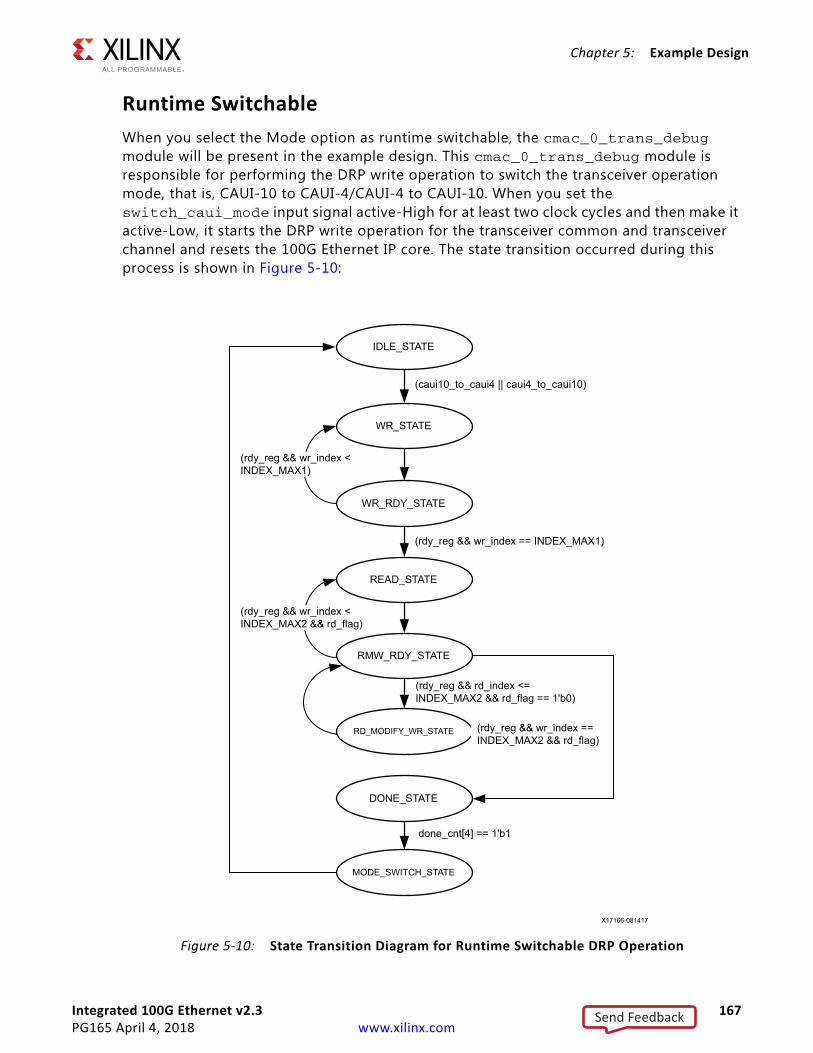
Integrated 100G Ethernet v2.3 167PG165 April 4, 2018 www.xilinx.com
Chapter 5: Example Design
Runtime SwitchableWhen you select the Mode option as runtime switchable, the cmac_0_trans_debug module will be present in the example design. This cmac_0_trans_debug module is responsible for performing the DRP write operation to switch the transceiver operation mode, that is, CAUI-10 to CAUI-4/CAUI-4 to CAUI-10. When you set the switch_caui_mode input signal active-High for at least two clock cycles and then make it active-Low, it starts the DRP write operation for the transceiver common and transceiver channel and resets the 100G Ethernet IP core. The state transition occurred during this process is shown in Figure 5-10:
X-Ref Target - Figure 5-10
Figure 5-10: State Transition Diagram for Runtime Switchable DRP Operation
IDLE_STATE
(caui10_to_caui4 || caui4_to_caui10)
done_cnt[4] == 1'b1
WR_STATE
WR_RDY_STATE
READ_STATE
RMW_RDY_STATE
RD_MODIFY_WR_STATE
DONE_STATE
MODE_SWITCH_STATE
(rdy_reg && wr_index == INDEX_MAX1)
(rdy_reg && wr_index < INDEX_MAX1)
(rdy_reg && wr_index == INDEX_MAX2 && rd_flag)
(rdy_reg && wr_index < INDEX_MAX2 && rd_flag)
(rdy_reg && rd_index <= INDEX_MAX2 && rd_flag == 1'b0)
X17166-081417
Send Feedback
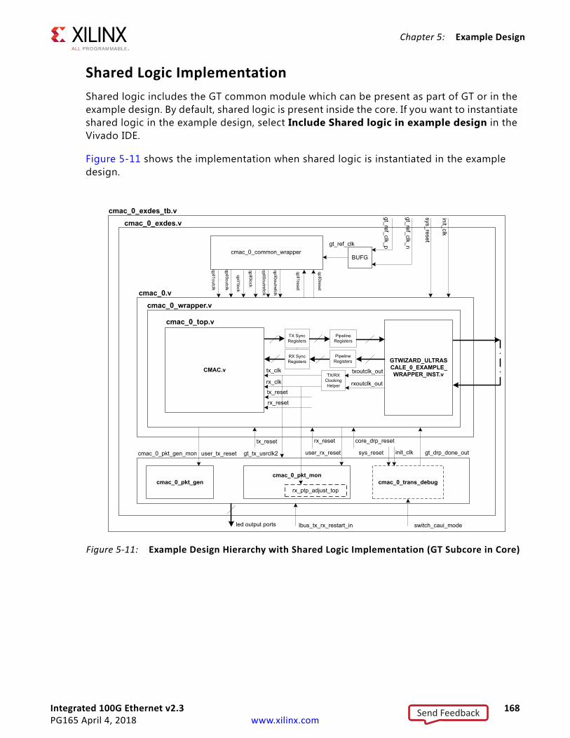
Integrated 100G Ethernet v2.3 168PG165 April 4, 2018 www.xilinx.com
Chapter 5: Example Design
Shared Logic ImplementationShared logic includes the GT common module which can be present as part of GT or in the example design. By default, shared logic is present inside the core. If you want to instantiate shared logic in the example design, select Include Shared logic in example design in the Vivado IDE.
Figure 5-11 shows the implementation when shared logic is instantiated in the example design.
X-Ref Target - Figure 5-11
Figure 5-11: Example Design Hierarchy with Shared Logic Implementation (GT Subcore in Core)
cmac_0_exdes_tb.v
cmac_0_exdes.v
cmac_0.v
GTWIZARD_ULTRAS
CALE_0_EXAMPLE_
WRAPPER_INST.vtx_clk
cmac_0_pkt_gen_mon
cmac_0_pkt_gen
cmac_0_pkt_mon
tx_reset
rx_reset
TX/RX Clocking Helper
rx_clk
init_clk
gt_ref_clk_p
gt_ref_clk_n
sys_reset
txoutclk_out
led output ports lbus_tx_rx_restart_in
cmac_0_trans_debug
user_rx_resetgt_tx_usrclk2 sys_reset
cmac_0_common_wrapperBUFG
gt_ref_clkqpll0reset
qpll1reset
qpll0lock
qpll1lock
qpll0outclk
qpll1outclk
qpll0outrefclk
qpll0outrefclk
TX SyncRegisters
PipelineRegisters
PipelineRegisters
cmac_0_wrapper.v
CMAC.v
RX SyncRegisters
cmac_0_top.v
init_clk gt_drp_done_out
rx_ptp_adjust_top
rxoutclk_out
switch_caui_mode
user_tx_reset
core_drp_resetrx_resettx_reset
Send Feedback
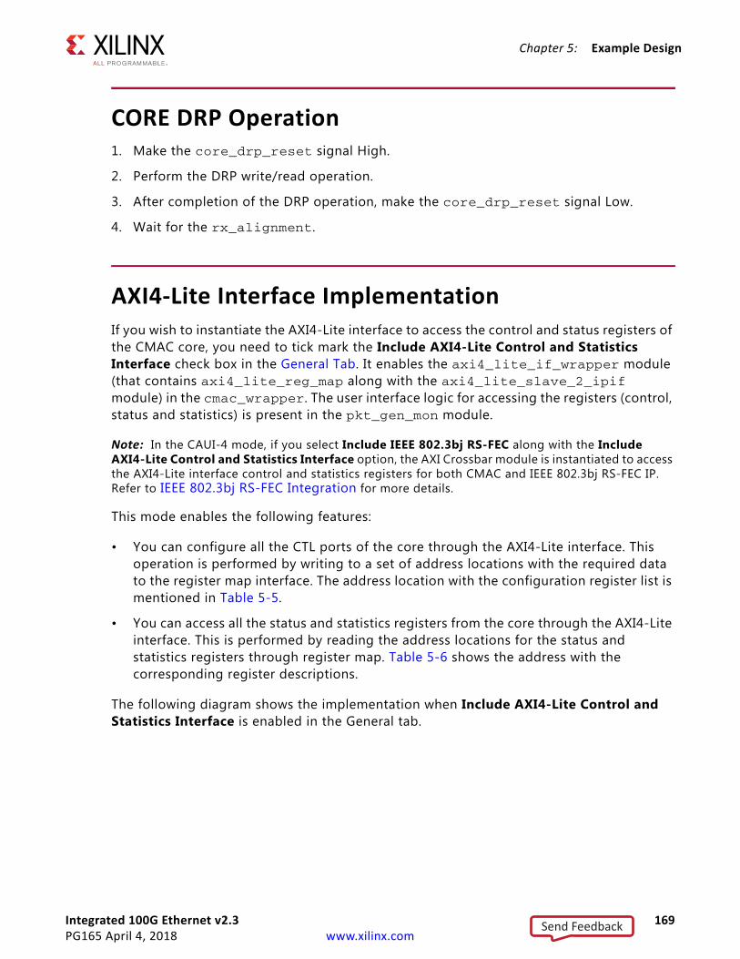
Integrated 100G Ethernet v2.3 169PG165 April 4, 2018 www.xilinx.com
Chapter 5: Example Design
CORE DRP Operation1. Make the core_drp_reset signal High.
2. Perform the DRP write/read operation.
3. After completion of the DRP operation, make the core_drp_reset signal Low.
4. Wait for the rx_alignment.
AXI4-Lite Interface ImplementationIf you wish to instantiate the AXI4-Lite interface to access the control and status registers of the CMAC core, you need to tick mark the Include AXI4-Lite Control and Statistics Interface check box in the General Tab. It enables the axi4_lite_if_wrapper module (that contains axi4_lite_reg_map along with the axi4_lite_slave_2_ipif module) in the cmac_wrapper. The user interface logic for accessing the registers (control, status and statistics) is present in the pkt_gen_mon module.
Note: In the CAUI-4 mode, if you select Include IEEE 802.3bj RS-FEC along with the Include AXI4-Lite Control and Statistics Interface option, the AXI Crossbar module is instantiated to access the AXI4-Lite interface control and statistics registers for both CMAC and IEEE 802.3bj RS-FEC IP. Refer to IEEE 802.3bj RS-FEC Integration for more details.
This mode enables the following features:
• You can configure all the CTL ports of the core through the AXI4-Lite interface. This operation is performed by writing to a set of address locations with the required data to the register map interface. The address location with the configuration register list is mentioned in Table 5-5.
• You can access all the status and statistics registers from the core through the AXI4-Lite interface. This is performed by reading the address locations for the status and statistics registers through register map. Table 5-6 shows the address with the corresponding register descriptions.
The following diagram shows the implementation when Include AXI4-Lite Control and Statistics Interface is enabled in the General tab.
Send Feedback
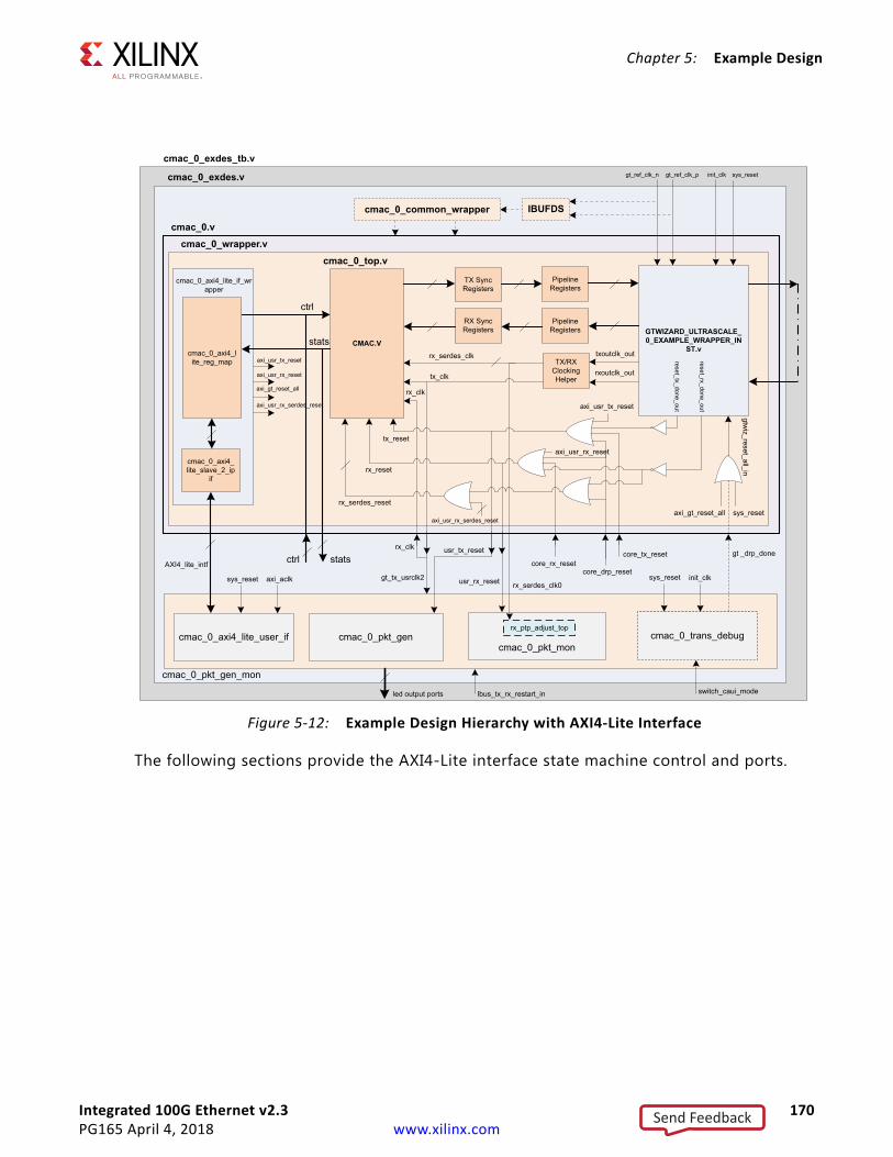
Integrated 100G Ethernet v2.3 170PG165 April 4, 2018 www.xilinx.com
Chapter 5: Example Design
The following sections provide the AXI4-Lite interface state machine control and ports.
X-Ref Target - Figure 5-12
Figure 5-12: Example Design Hierarchy with AXI4-Lite Interface
cmac_0_exdes_tb.v
`
cmac_0_exdes.v
cmac_0.v
tx_clk
GTWIZARD_ULTRASCALE_
0_EXAMPLE_WRAPPER_IN
ST.v
cmac_0_pkt_gen_mon
cmac_0_pkt_gencmac_0_pkt_mon
tx_reset
rx_reset
rx_clk
init_clk sys_reset
txoutclk_out
led output ports lbus_tx_rx_restart_in
cmac_0_trans_debug
usr_tx_reset
gt_tx_usrclk2 sys_reset init_clk
cmac_0_common_wrapper
cmac_0_wrapper.v
TX SyncRegisters
PipelineRegisters
PipelineRegisters
RX SyncRegisters
CMAC.V
cmac_0_top.v
gtwiz_reset_all_in
rx_ptp_adjust_top
IBUFDS
TX/RX Clocking Helper
rxoutclk_out
rx_serdes_reset
rx_serdes_clk0
core_drp_reset
rx_serdes_clk
switch_caui_mode
cmac_0_trans_debugcmac_0_axi4_lite_user_if
sys_reset axi_aclk
sys_reset
core_tx_resetcore_rx_reset
axi_gt_reset_all
cmac_0_axi4_lite_reg_map
cmac_0_axi4_lite_slave_2_ip
if
ctrl
stats
AXI4_lite_intfgt _drp_done
cmac_0_axi4_lite_if_wrapper
usr_rx_reset
axi_usr_rx_serdes_reset
statsrx_clk
reset_tx_done_out
reset_rx_done_out
axi_usr_rx_reset
axi_usr_tx_reset
ctrl
axi_usr_tx_reset
axi_usr_rx_reset
axi_gt_reset_all
axi_usr_rx_serdes_reset
gt_ref_clk_pgt_ref_clk_n
Send Feedback
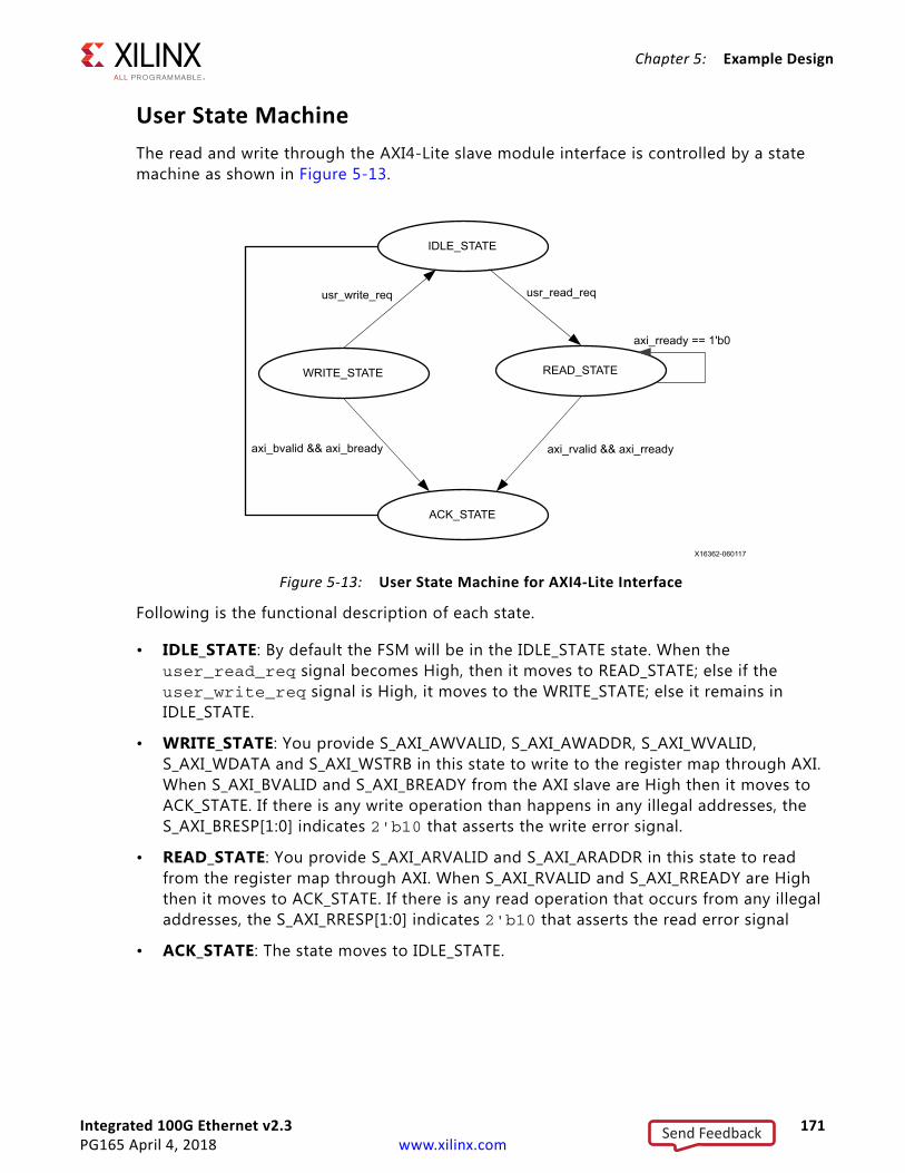
Integrated 100G Ethernet v2.3 171PG165 April 4, 2018 www.xilinx.com
Chapter 5: Example Design
User State MachineThe read and write through the AXI4-Lite slave module interface is controlled by a state machine as shown in Figure 5-13.
Following is the functional description of each state.
• IDLE_STATE: By default the FSM will be in the IDLE_STATE state. When the user_read_req signal becomes High, then it moves to READ_STATE; else if the user_write_req signal is High, it moves to the WRITE_STATE; else it remains in IDLE_STATE.
• WRITE_STATE: You provide S_AXI_AWVALID, S_AXI_AWADDR, S_AXI_WVALID, S_AXI_WDATA and S_AXI_WSTRB in this state to write to the register map through AXI. When S_AXI_BVALID and S_AXI_BREADY from the AXI slave are High then it moves to ACK_STATE. If there is any write operation than happens in any illegal addresses, the S_AXI_BRESP[1:0] indicates 2'b10 that asserts the write error signal.
• READ_STATE: You provide S_AXI_ARVALID and S_AXI_ARADDR in this state to read from the register map through AXI. When S_AXI_RVALID and S_AXI_RREADY are High then it moves to ACK_STATE. If there is any read operation that occurs from any illegal addresses, the S_AXI_RRESP[1:0] indicates 2'b10 that asserts the read error signal
• ACK_STATE: The state moves to IDLE_STATE.
X-Ref Target - Figure 5-13
Figure 5-13: User State Machine for AXI4-Lite Interface
usr_write_req usr_read_req
axi_bvalid && axi_bready axi_rvalid && axi_rready
IDLE_STATE
WRITE_STATE
ACK_STATE
READ_STATE
axi_rready == 1'b0
X16362-060117
Send Feedback
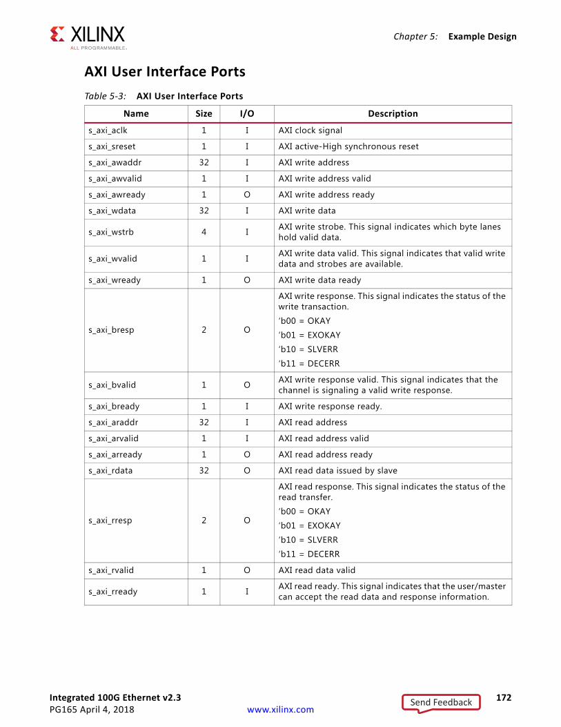
Integrated 100G Ethernet v2.3 172PG165 April 4, 2018 www.xilinx.com
Chapter 5: Example Design
AXI User Interface Ports Table 5-3: AXI User Interface Ports
Name Size I/O Description
s_axi_aclk 1 I AXI clock signal
s_axi_sreset 1 I AXI active-High synchronous reset
s_axi_awaddr 32 I AXI write address
s_axi_awvalid 1 I AXI write address valid
s_axi_awready 1 O AXI write address ready
s_axi_wdata 32 I AXI write data
s_axi_wstrb 4 I AXI write strobe. This signal indicates which byte lanes hold valid data.
s_axi_wvalid 1 I AXI write data valid. This signal indicates that valid write data and strobes are available.
s_axi_wready 1 O AXI write data ready
s_axi_bresp 2 O
AXI write response. This signal indicates the status of the write transaction.
‘b00 = OKAY
‘b01 = EXOKAY
‘b10 = SLVERR
‘b11 = DECERR
s_axi_bvalid 1 O AXI write response valid. This signal indicates that the channel is signaling a valid write response.
s_axi_bready 1 I AXI write response ready.
s_axi_araddr 32 I AXI read address
s_axi_arvalid 1 I AXI read address valid
s_axi_arready 1 O AXI read address ready
s_axi_rdata 32 O AXI read data issued by slave
s_axi_rresp 2 O
AXI read response. This signal indicates the status of the read transfer.
‘b00 = OKAY
‘b01 = EXOKAY
‘b10 = SLVERR
‘b11 = DECERR
s_axi_rvalid 1 O AXI read data valid
s_axi_rready 1 I AXI read ready. This signal indicates that the user/master can accept the read data and response information.
Send Feedback
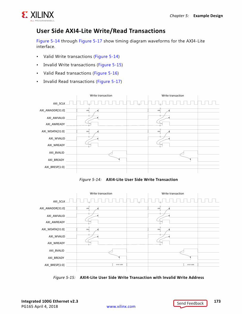
Integrated 100G Ethernet v2.3 173PG165 April 4, 2018 www.xilinx.com
Chapter 5: Example Design
User Side AXI4-Lite Write/Read TransactionsFigure 5-14 through Figure 5-17 show timing diagram waveforms for the AXI4-Lite interface.
• Valid Write transactions (Figure 5-14)
• Invalid Write transactions (Figure 5-15)
• Valid Read transactions (Figure 5-16)
• Invalid Read transactions (Figure 5-17).X-Ref Target - Figure 5-14
Figure 5-14: AXI4-Lite User Side Write TransactionX-Ref Target - Figure 5-15
Figure 5-15: AXI4-Lite User Side Write Transaction with Invalid Write Address
AXI_SCLK
AXI_AWREADY
AXI_WVALID
AXI_WREADY
AXI_BVALID
AXI_BREADY
AXI_BRESP[1:0]
Write transaction Write transaction
AXI_AWADDR[31:0] addr
AXI_AWVALID
addr
data dataAXI_WDATA[31:0]
AXI_SCLK
AXI_AWREADY
AXI_WVALID
AXI_WREADY
AXI_BVALID
AXI_BREADY
AXI_BRESP[1:0]
Write transaction Write transaction
AXI_AWADDR[31:0] addr
AXI_AWVALID
addr
data dataAXI_WDATA[31:0]
error code error code
Send Feedback
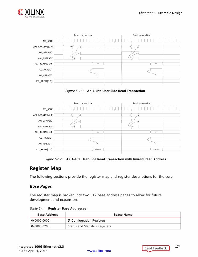
Integrated 100G Ethernet v2.3 174PG165 April 4, 2018 www.xilinx.com
Chapter 5: Example Design
Register MapThe following sections provide the register map and register descriptions for the core.
Base Pages
The register map is broken into two 512 base address pages to allow for future development and expansion.
X-Ref Target - Figure 5-16
Figure 5-16: AXI4-Lite User Side Read Transaction
X-Ref Target - Figure 5-17
Figure 5-17: AXI4-Lite User Side Read Transaction with Invalid Read Address
Table 5-4: Register Base Addresses
Base Address Space Name
0x0000 0000 IP Configuration Registers
0x0000 0200 Status and Statistics Registers
AXI_SCLK
AXI_ARVALID
AXI_ARREADY
AXI_RDATA[31:0]
AXI_RVALID
AXI_RREADY
data data
AXI_RRESP[1:0]
Read transaction Read transaction
AXI_ARADDR[31:0] addr addr
AXI_SCLK
AXI_ARVALID
AXI_ARREADY
AXI_RDATA[31:0]
AXI_RVALID
AXI_RREADY
data data
AXI_RRESP[1:0]
Read transaction Read transaction
AXI_ARADDR[31:0] addr addr
error code error code
Send Feedback

Integrated 100G Ethernet v2.3 175PG165 April 4, 2018 www.xilinx.com
Chapter 5: Example Design
All registers are 32 bytes in size and aligned on 32-byte addressing. In the following register space maps, any holes in the address space should be considered RESERVED and can cause the AXI Control interface IP to respond with an error if accessed.
Configuration Register Space
The configuration space provides the ability to configure the core for various use cases.
The integrated UltraScale™ CMAC IP makes use of a dynamic reconfiguration port (DRP) to provide the ability to configure aspects of the core without the need for fabric logic connections. In this case those configuration bits in the soft AXI Control register set will become RESERVED (unused) and the software should use the DRP operation registers to configure those attributes of the core. See Table 3-7 for the DRP address map.
Table 5-5: Configuration Register Map
Address Register Name
0x0000 GT_RESET_REG
0x0004 RESET_REG
0x0008 SWITCH_CORE_MODE_REG
0x000C CONFIGURATION_TX_REG1
0x0010 Reserved
0x0014 CONFIGURATION_RX_REG1
0x0018-0x001C Reserved
0x0020 CORE_MODE_REG
0x0024 CORE_VERSION_REG
0x0028 Reserved
0x002C CONFIGURATION_TX_BIP_OVERRIDE
0x0030 CONFIGURATION_TX_FLOW_CONTROL_CONTROL_REG1
0x0034 CONFIGURATION_TX_FLOW_CONTROL_REFRESH_REG1
0x0038 CONFIGURATION_TX_FLOW_CONTROL_REFRESH_REG2
0x003C CONFIGURATION_TX_FLOW_CONTROL_REFRESH_REG3
0x0040 CONFIGURATION_TX_FLOW_CONTROL_REFRESH_REG4
0x0044 CONFIGURATION_TX_FLOW_CONTROL_REFRESH_REG5
0x0048 CONFIGURATION_TX_FLOW_CONTROL_QUANTA_REG1
0x004C CONFIGURATION_TX_FLOW_CONTROL_QUANTA_REG2
0x0050 CONFIGURATION_TX_FLOW_CONTROL_QUANTA_REG3
0x0054 CONFIGURATION_TX_FLOW_CONTROL_QUANTA_REG4
0x0058 CONFIGURATION_TX_FLOW_CONTROL_QUANTA_REG5
0x005C-0x0080 Reserved
0x0084 CONFIGURATION_RX_FLOW_CONTROL_CONTROL_REG1
Send Feedback
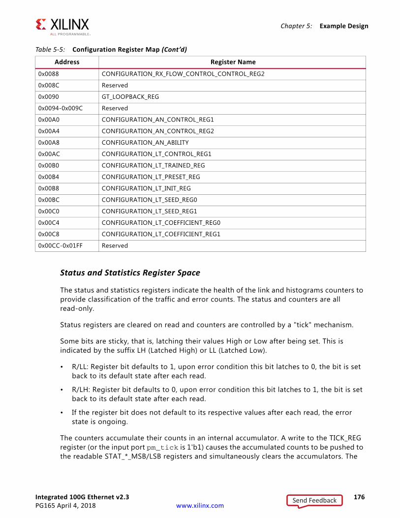
Integrated 100G Ethernet v2.3 176PG165 April 4, 2018 www.xilinx.com
Chapter 5: Example Design
Status and Statistics Register Space
The status and statistics registers indicate the health of the link and histograms counters to provide classification of the traffic and error counts. The status and counters are all read-only.
Status registers are cleared on read and counters are controlled by a "tick" mechanism.
Some bits are sticky, that is, latching their values High or Low after being set. This is indicated by the suffix LH (Latched High) or LL (Latched Low).
• R/LL: Register bit defaults to 1, upon error condition this bit latches to 0, the bit is set back to its default state after each read.
• R/LH: Register bit defaults to 0, upon error condition this bit latches to 1, the bit is set back to its default state after each read.
• If the register bit does not default to its respective values after each read, the error state is ongoing.
The counters accumulate their counts in an internal accumulator. A write to the TICK_REG register (or the input port pm_tick is 1'b1) causes the accumulated counts to be pushed to the readable STAT_*_MSB/LSB registers and simultaneously clears the accumulators. The
0x0088 CONFIGURATION_RX_FLOW_CONTROL_CONTROL_REG2
0x008C Reserved
0x0090 GT_LOOPBACK_REG
0x0094-0x009C Reserved
0x00A0 CONFIGURATION_AN_CONTROL_REG1
0x00A4 CONFIGURATION_AN_CONTROL_REG2
0x00A8 CONFIGURATION_AN_ABILITY
0x00AC CONFIGURATION_LT_CONTROL_REG1
0x00B0 CONFIGURATION_LT_TRAINED_REG
0x00B4 CONFIGURATION_LT_PRESET_REG
0x00B8 CONFIGURATION_LT_INIT_REG
0x00BC CONFIGURATION_LT_SEED_REG0
0x00C0 CONFIGURATION_LT_SEED_REG1
0x00C4 CONFIGURATION_LT_COEFFICIENT_REG0
0x00C8 CONFIGURATION_LT_COEFFICIENT_REG1
0x00CC-0x01FF Reserved
Table 5-5: Configuration Register Map (Cont’d)
Address Register Name
Send Feedback
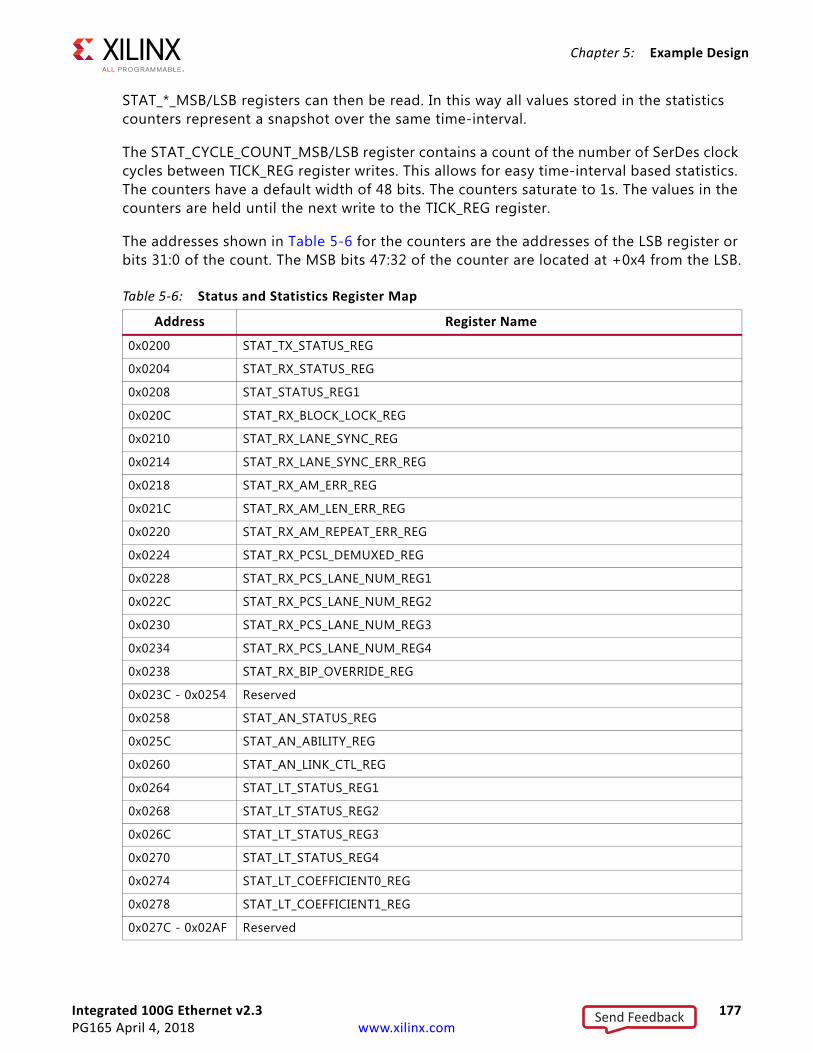
Integrated 100G Ethernet v2.3 177PG165 April 4, 2018 www.xilinx.com
Chapter 5: Example Design
STAT_*_MSB/LSB registers can then be read. In this way all values stored in the statistics counters represent a snapshot over the same time-interval.
The STAT_CYCLE_COUNT_MSB/LSB register contains a count of the number of SerDes clock cycles between TICK_REG register writes. This allows for easy time-interval based statistics. The counters have a default width of 48 bits. The counters saturate to 1s. The values in the counters are held until the next write to the TICK_REG register.
The addresses shown in Table 5-6 for the counters are the addresses of the LSB register or bits 31:0 of the count. The MSB bits 47:32 of the counter are located at +0x4 from the LSB.
Table 5-6: Status and Statistics Register Map
Address Register Name
0x0200 STAT_TX_STATUS_REG
0x0204 STAT_RX_STATUS_REG
0x0208 STAT_STATUS_REG1
0x020C STAT_RX_BLOCK_LOCK_REG
0x0210 STAT_RX_LANE_SYNC_REG
0x0214 STAT_RX_LANE_SYNC_ERR_REG
0x0218 STAT_RX_AM_ERR_REG
0x021C STAT_RX_AM_LEN_ERR_REG
0x0220 STAT_RX_AM_REPEAT_ERR_REG
0x0224 STAT_RX_PCSL_DEMUXED_REG
0x0228 STAT_RX_PCS_LANE_NUM_REG1
0x022C STAT_RX_PCS_LANE_NUM_REG2
0x0230 STAT_RX_PCS_LANE_NUM_REG3
0x0234 STAT_RX_PCS_LANE_NUM_REG4
0x0238 STAT_RX_BIP_OVERRIDE_REG
0x023C - 0x0254 Reserved
0x0258 STAT_AN_STATUS_REG
0x025C STAT_AN_ABILITY_REG
0x0260 STAT_AN_LINK_CTL_REG
0x0264 STAT_LT_STATUS_REG1
0x0268 STAT_LT_STATUS_REG2
0x026C STAT_LT_STATUS_REG3
0x0270 STAT_LT_STATUS_REG4
0x0274 STAT_LT_COEFFICIENT0_REG
0x0278 STAT_LT_COEFFICIENT1_REG
0x027C - 0x02AF Reserved
Send Feedback
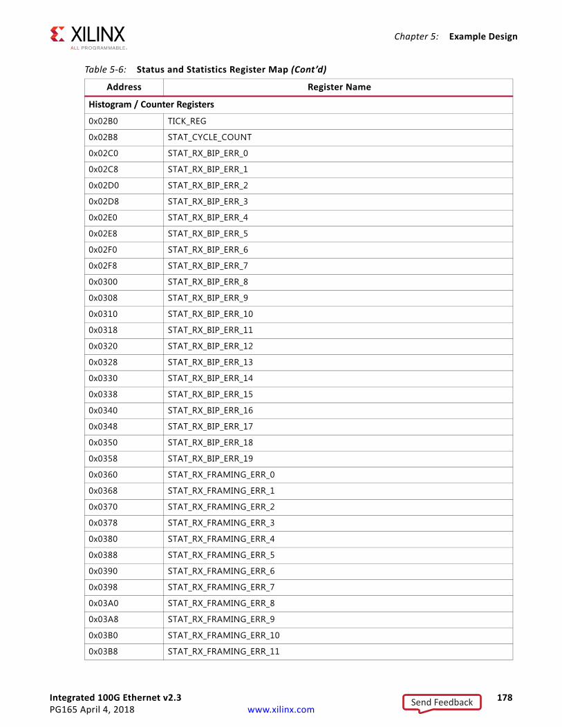
Integrated 100G Ethernet v2.3 178PG165 April 4, 2018 www.xilinx.com
Chapter 5: Example Design
Histogram / Counter Registers
0x02B0 TICK_REG
0x02B8 STAT_CYCLE_COUNT
0x02C0 STAT_RX_BIP_ERR_0
0x02C8 STAT_RX_BIP_ERR_1
0x02D0 STAT_RX_BIP_ERR_2
0x02D8 STAT_RX_BIP_ERR_3
0x02E0 STAT_RX_BIP_ERR_4
0x02E8 STAT_RX_BIP_ERR_5
0x02F0 STAT_RX_BIP_ERR_6
0x02F8 STAT_RX_BIP_ERR_7
0x0300 STAT_RX_BIP_ERR_8
0x0308 STAT_RX_BIP_ERR_9
0x0310 STAT_RX_BIP_ERR_10
0x0318 STAT_RX_BIP_ERR_11
0x0320 STAT_RX_BIP_ERR_12
0x0328 STAT_RX_BIP_ERR_13
0x0330 STAT_RX_BIP_ERR_14
0x0338 STAT_RX_BIP_ERR_15
0x0340 STAT_RX_BIP_ERR_16
0x0348 STAT_RX_BIP_ERR_17
0x0350 STAT_RX_BIP_ERR_18
0x0358 STAT_RX_BIP_ERR_19
0x0360 STAT_RX_FRAMING_ERR_0
0x0368 STAT_RX_FRAMING_ERR_1
0x0370 STAT_RX_FRAMING_ERR_2
0x0378 STAT_RX_FRAMING_ERR_3
0x0380 STAT_RX_FRAMING_ERR_4
0x0388 STAT_RX_FRAMING_ERR_5
0x0390 STAT_RX_FRAMING_ERR_6
0x0398 STAT_RX_FRAMING_ERR_7
0x03A0 STAT_RX_FRAMING_ERR_8
0x03A8 STAT_RX_FRAMING_ERR_9
0x03B0 STAT_RX_FRAMING_ERR_10
0x03B8 STAT_RX_FRAMING_ERR_11
Table 5-6: Status and Statistics Register Map (Cont’d)
Address Register Name
Send Feedback
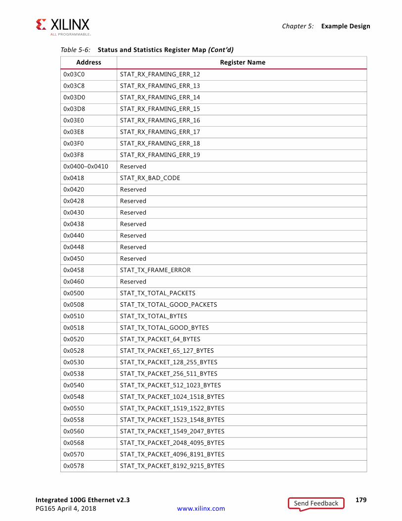
Integrated 100G Ethernet v2.3 179PG165 April 4, 2018 www.xilinx.com
Chapter 5: Example Design
0x03C0 STAT_RX_FRAMING_ERR_12
0x03C8 STAT_RX_FRAMING_ERR_13
0x03D0 STAT_RX_FRAMING_ERR_14
0x03D8 STAT_RX_FRAMING_ERR_15
0x03E0 STAT_RX_FRAMING_ERR_16
0x03E8 STAT_RX_FRAMING_ERR_17
0x03F0 STAT_RX_FRAMING_ERR_18
0x03F8 STAT_RX_FRAMING_ERR_19
0x0400–0x0410 Reserved
0x0418 STAT_RX_BAD_CODE
0x0420 Reserved
0x0428 Reserved
0x0430 Reserved
0x0438 Reserved
0x0440 Reserved
0x0448 Reserved
0x0450 Reserved
0x0458 STAT_TX_FRAME_ERROR
0x0460 Reserved
0x0500 STAT_TX_TOTAL_PACKETS
0x0508 STAT_TX_TOTAL_GOOD_PACKETS
0x0510 STAT_TX_TOTAL_BYTES
0x0518 STAT_TX_TOTAL_GOOD_BYTES
0x0520 STAT_TX_PACKET_64_BYTES
0x0528 STAT_TX_PACKET_65_127_BYTES
0x0530 STAT_TX_PACKET_128_255_BYTES
0x0538 STAT_TX_PACKET_256_511_BYTES
0x0540 STAT_TX_PACKET_512_1023_BYTES
0x0548 STAT_TX_PACKET_1024_1518_BYTES
0x0550 STAT_TX_PACKET_1519_1522_BYTES
0x0558 STAT_TX_PACKET_1523_1548_BYTES
0x0560 STAT_TX_PACKET_1549_2047_BYTES
0x0568 STAT_TX_PACKET_2048_4095_BYTES
0x0570 STAT_TX_PACKET_4096_8191_BYTES
0x0578 STAT_TX_PACKET_8192_9215_BYTES
Table 5-6: Status and Statistics Register Map (Cont’d)
Address Register Name
Send Feedback

Integrated 100G Ethernet v2.3 180PG165 April 4, 2018 www.xilinx.com
Chapter 5: Example Design
0x0580 STAT_TX_PACKET_LARGE
0x0588 STAT_TX_PACKET_SMALL
0x0590–0x05B0 Reserved
0x05B8 STAT_TX_BAD_FCS
0x05C0 Reserved
0x05C8 Reserved
0x05D0 STAT_TX_UNICAST
0x05D8 STAT_TX_MULTICAST
0x05E0 STAT_TX_BROADCAST
0x05E8 STAT_TX_VLAN
0x05F0 STAT_TX_PAUSE
0x05F8 STAT_TX_USER_PAUSE
0x0600 Reserved
0x0608 STAT_RX_TOTAL_PACKETS
0x0610 STAT_RX_TOTAL_GOOD_PACKETS
0x0618 STAT_RX_TOTAL_BYTES
0x0620 STAT_RX_TOTAL_GOOD_BYTES
0x0628 STAT_RX_PACKET_64_BYTES
0x0630 STAT_RX_PACKET_65_127_BYTES
0x0638 STAT_RX_PACKET_128_255_BYTES
0x0640 STAT_RX_PACKET_256_511_BYTES
0x0648 STAT_RX_PACKET_512_1023_BYTES
0x0650 STAT_RX_PACKET_1024_1518_BYTES
0x0658 STAT_RX_PACKET_1519_1522_BYTES
0x0660 STAT_RX_PACKET_1523_1548_BYTES
0x0668 STAT_RX_PACKET_1549_2047_BYTES
0x0670 STAT_RX_PACKET_2048_4095_BYTES
0x0678 STAT_RX_PACKET_4096_8191_BYTES
0x0680 STAT_RX_PACKET_8192_9215_BYTES
0x0688 STAT_RX_PACKET_LARGE
0x0690 STAT_RX_PACKET_SMALL
0x0698 STAT_RX_UNDERSIZE
0x06A0 STAT_RX_FRAGMENT
0x06A8 STAT_RX_OVERSIZE
0x06B0 STAT_RX_TOOLONG
Table 5-6: Status and Statistics Register Map (Cont’d)
Address Register Name
Send Feedback
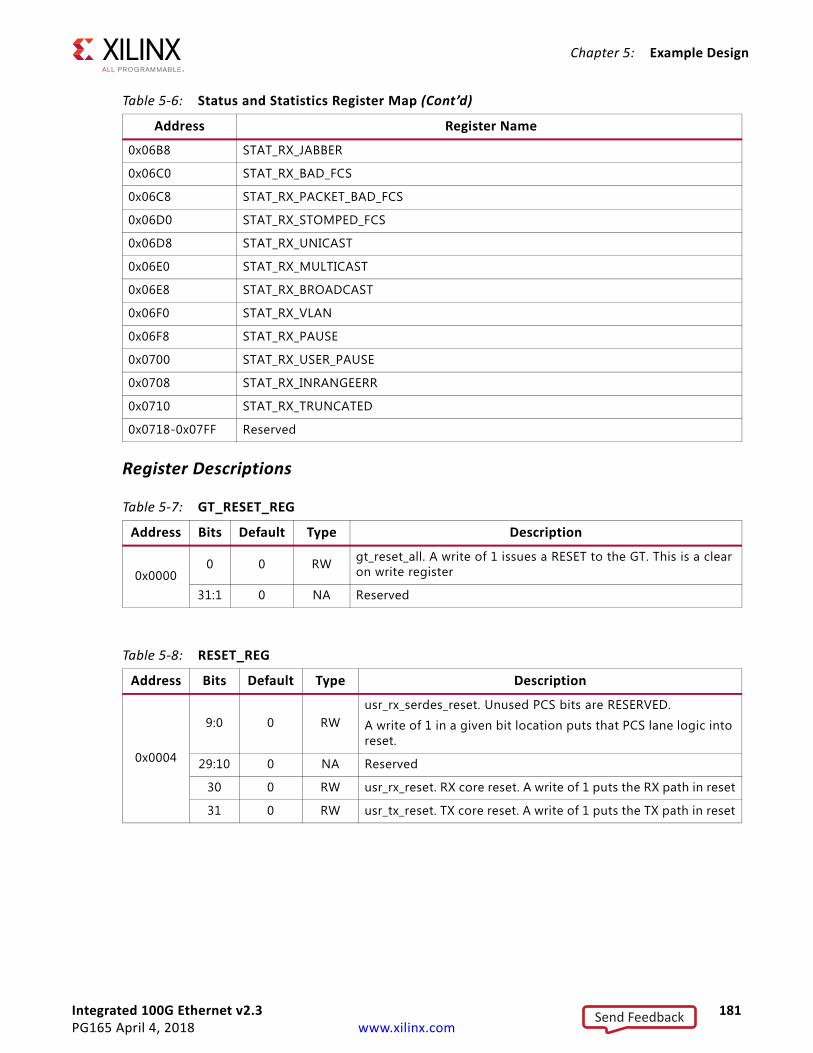
Integrated 100G Ethernet v2.3 181PG165 April 4, 2018 www.xilinx.com
Chapter 5: Example Design
Register Descriptions
0x06B8 STAT_RX_JABBER
0x06C0 STAT_RX_BAD_FCS
0x06C8 STAT_RX_PACKET_BAD_FCS
0x06D0 STAT_RX_STOMPED_FCS
0x06D8 STAT_RX_UNICAST
0x06E0 STAT_RX_MULTICAST
0x06E8 STAT_RX_BROADCAST
0x06F0 STAT_RX_VLAN
0x06F8 STAT_RX_PAUSE
0x0700 STAT_RX_USER_PAUSE
0x0708 STAT_RX_INRANGEERR
0x0710 STAT_RX_TRUNCATED
0x0718-0x07FF Reserved
Table 5-7: GT_RESET_REG
Address Bits Default Type Description
0x00000 0 RW gt_reset_all. A write of 1 issues a RESET to the GT. This is a clear
on write register
31:1 0 NA Reserved
Table 5-8: RESET_REG
Address Bits Default Type Description
0x0004
9:0 0 RWusr_rx_serdes_reset. Unused PCS bits are RESERVED.
A write of 1 in a given bit location puts that PCS lane logic into reset.
29:10 0 NA Reserved
30 0 RW usr_rx_reset. RX core reset. A write of 1 puts the RX path in reset
31 0 RW usr_tx_reset. TX core reset. A write of 1 puts the TX path in reset
Table 5-6: Status and Statistics Register Map (Cont’d)
Address Register Name
Send Feedback
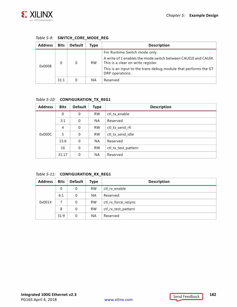
Integrated 100G Ethernet v2.3 182PG165 April 4, 2018 www.xilinx.com
Chapter 5: Example Design
Table 5-9: SWITCH_CORE_MODE_REG
Address Bits Default Type Description
0x00080 0 RW
For Runtime Switch mode only.
A write of 1 enables the mode switch between CAUI10 and CAUI4. This is a clear on write register.
This is an input to the trans debug module that performs the GT DRP operations.
31:1 0 NA Reserved
Table 5-10: CONFIGURATION_TX_REG1
Address Bits Default Type Description
0x000C
0 0 RW ctl_tx_enable
3:1 0 NA Reserved
4 0 RW ctl_tx_send_rfi
5 0 RW ctl_tx_send_idle
15:6 0 NA Reserved
16 0 RW ctl_tx_test_pattern
31:17 0 NA Reserved
Table 5-11: CONFIGURATION_RX_REG1
Address Bits Default Type Description
0x0014
0 0 RW ctl_rx_enable
6:1 0 NA Reserved
7 0 RW ctl_rx_force_resync
8 0 RW ctl_rx_test_pattern
31:9 0 NA Reserved
Send Feedback

Integrated 100G Ethernet v2.3 183PG165 April 4, 2018 www.xilinx.com
Chapter 5: Example Design
Table 5-12: CORE_MODE_REG
Address Bits Default Type Description
0x00201:0 (1) R
Core mode register:
• 2'b00: CAUI10
• 2'b01: CAUI4
• 2'b10: Runtime Switchable CAUI10
• 2'b11: Runtime Switchable CAUI4
31:2 0 NA Reserved
Notes: 1. Based on core configuration.
Table 5-13: CORE_VERSION_REG
Address Bits Default Type Description
0x0024
7:0 minor R Current version of the core in the format “major.minor”
For example core version 1.7
Bits [7:0] represents minor version that is 7Bits [15:8] represents major version that is 1
15:8 major R
31:16 0 NA Reserved
Table 5-14: CONFIGURATION_TX_BIP_OVERRIDE
Address Bits Default Type Description
0x002C
7:0 0 RW ctl_tx_lane0_vlm_bip7_override_value
8 0 RW ctl_tx_lane0_vlm_bip7_override
31:9 0 NA Reserved
Table 5-15: CONFIGURATION_TX_FLOW_CONTROL_CONTROL_REG1
Address Bits Default Type Description
0x00308:0 0 RW ctl_tx_pause_enable
31:9 0 NA Reserved
Send Feedback
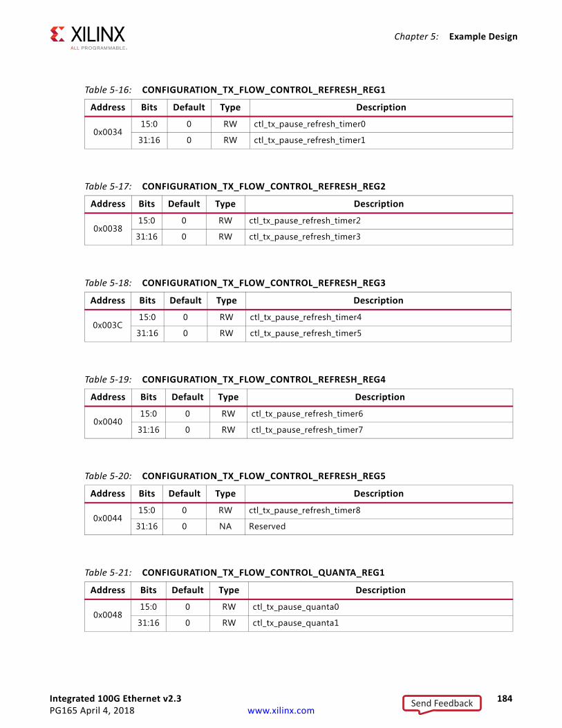
Integrated 100G Ethernet v2.3 184PG165 April 4, 2018 www.xilinx.com
Chapter 5: Example Design
Table 5-16: CONFIGURATION_TX_FLOW_CONTROL_REFRESH_REG1
Address Bits Default Type Description
0x003415:0 0 RW ctl_tx_pause_refresh_timer0
31:16 0 RW ctl_tx_pause_refresh_timer1
Table 5-17: CONFIGURATION_TX_FLOW_CONTROL_REFRESH_REG2
Address Bits Default Type Description
0x003815:0 0 RW ctl_tx_pause_refresh_timer2
31:16 0 RW ctl_tx_pause_refresh_timer3
Table 5-18: CONFIGURATION_TX_FLOW_CONTROL_REFRESH_REG3
Address Bits Default Type Description
0x003C15:0 0 RW ctl_tx_pause_refresh_timer4
31:16 0 RW ctl_tx_pause_refresh_timer5
Table 5-19: CONFIGURATION_TX_FLOW_CONTROL_REFRESH_REG4
Address Bits Default Type Description
0x004015:0 0 RW ctl_tx_pause_refresh_timer6
31:16 0 RW ctl_tx_pause_refresh_timer7
Table 5-20: CONFIGURATION_TX_FLOW_CONTROL_REFRESH_REG5
Address Bits Default Type Description
0x004415:0 0 RW ctl_tx_pause_refresh_timer8
31:16 0 NA Reserved
Table 5-21: CONFIGURATION_TX_FLOW_CONTROL_QUANTA_REG1
Address Bits Default Type Description
0x004815:0 0 RW ctl_tx_pause_quanta0
31:16 0 RW ctl_tx_pause_quanta1
Send Feedback
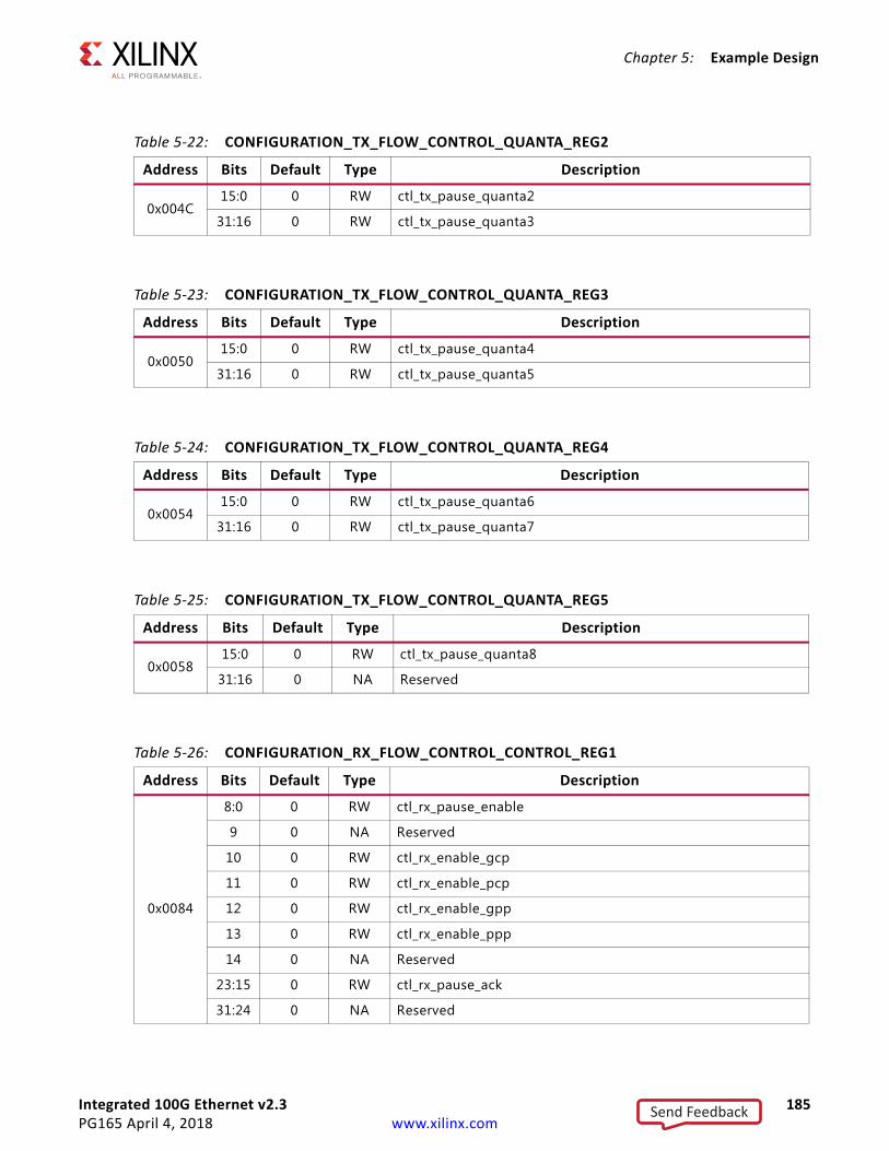
Integrated 100G Ethernet v2.3 185PG165 April 4, 2018 www.xilinx.com
Chapter 5: Example Design
Table 5-22: CONFIGURATION_TX_FLOW_CONTROL_QUANTA_REG2
Address Bits Default Type Description
0x004C15:0 0 RW ctl_tx_pause_quanta2
31:16 0 RW ctl_tx_pause_quanta3
Table 5-23: CONFIGURATION_TX_FLOW_CONTROL_QUANTA_REG3
Address Bits Default Type Description
0x005015:0 0 RW ctl_tx_pause_quanta4
31:16 0 RW ctl_tx_pause_quanta5
Table 5-24: CONFIGURATION_TX_FLOW_CONTROL_QUANTA_REG4
Address Bits Default Type Description
0x005415:0 0 RW ctl_tx_pause_quanta6
31:16 0 RW ctl_tx_pause_quanta7
Table 5-25: CONFIGURATION_TX_FLOW_CONTROL_QUANTA_REG5
Address Bits Default Type Description
0x005815:0 0 RW ctl_tx_pause_quanta8
31:16 0 NA Reserved
Table 5-26: CONFIGURATION_RX_FLOW_CONTROL_CONTROL_REG1
Address Bits Default Type Description
0x0084
8:0 0 RW ctl_rx_pause_enable
9 0 NA Reserved
10 0 RW ctl_rx_enable_gcp
11 0 RW ctl_rx_enable_pcp
12 0 RW ctl_rx_enable_gpp
13 0 RW ctl_rx_enable_ppp
14 0 NA Reserved
23:15 0 RW ctl_rx_pause_ack
31:24 0 NA Reserved
Send Feedback
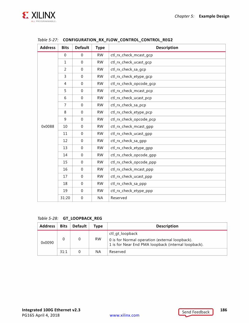
Integrated 100G Ethernet v2.3 186PG165 April 4, 2018 www.xilinx.com
Chapter 5: Example Design
Table 5-27: CONFIGURATION_RX_FLOW_CONTROL_CONTROL_REG2
Address Bits Default Type Description
0x0088
0 0 RW ctl_rx_check_mcast_gcp
1 0 RW ctl_rx_check_ucast_gcp
2 0 RW ctl_rx_check_sa_gcp
3 0 RW ctl_rx_check_etype_gcp
4 0 RW ctl_rx_check_opcode_gcp
5 0 RW ctl_rx_check_mcast_pcp
6 0 RW ctl_rx_check_ucast_pcp
7 0 RW ctl_rx_check_sa_pcp
8 0 RW ctl_rx_check_etype_pcp
9 0 RW ctl_rx_check_opcode_pcp
10 0 RW ctl_rx_check_mcast_gpp
11 0 RW ctl_rx_check_ucast_gpp
12 0 RW ctl_rx_check_sa_gpp
13 0 RW ctl_rx_check_etype_gpp
14 0 RW ctl_rx_check_opcode_gpp
15 0 RW ctl_rx_check_opcode_ppp
16 0 RW ctl_rx_check_mcast_ppp
17 0 RW ctl_rx_check_ucast_ppp
18 0 RW ctl_rx_check_sa_ppp
19 0 RW ctl_rx_check_etype_ppp
31:20 0 NA Reserved
Table 5-28: GT_LOOPBACK_REG
Address Bits Default Type Description
0x00900 0 RW
ctl_gt_loopback
0 is for Normal operation (external loopback).1 is for Near End PMA loopback (internal loopback).
31:1 0 NA Reserved
Send Feedback
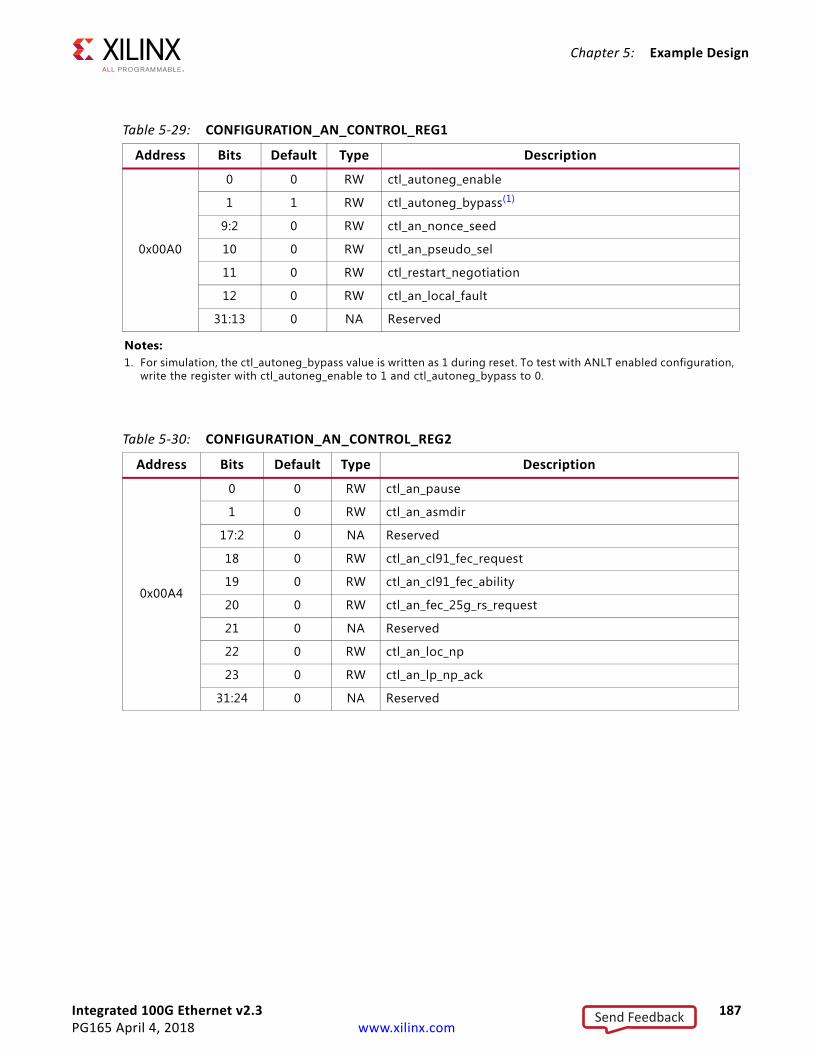
Integrated 100G Ethernet v2.3 187PG165 April 4, 2018 www.xilinx.com
Chapter 5: Example Design
Table 5-29: CONFIGURATION_AN_CONTROL_REG1
Address Bits Default Type Description
0x00A0
0 0 RW ctl_autoneg_enable
1 1 RW ctl_autoneg_bypass(1)
9:2 0 RW ctl_an_nonce_seed
10 0 RW ctl_an_pseudo_sel
11 0 RW ctl_restart_negotiation
12 0 RW ctl_an_local_fault
31:13 0 NA Reserved
Notes: 1. For simulation, the ctl_autoneg_bypass value is written as 1 during reset. To test with ANLT enabled configuration,
write the register with ctl_autoneg_enable to 1 and ctl_autoneg_bypass to 0.
Table 5-30: CONFIGURATION_AN_CONTROL_REG2
Address Bits Default Type Description
0x00A4
0 0 RW ctl_an_pause
1 0 RW ctl_an_asmdir
17:2 0 NA Reserved
18 0 RW ctl_an_cl91_fec_request
19 0 RW ctl_an_cl91_fec_ability
20 0 RW ctl_an_fec_25g_rs_request
21 0 NA Reserved
22 0 RW ctl_an_loc_np
23 0 RW ctl_an_lp_np_ack
31:24 0 NA Reserved
Send Feedback
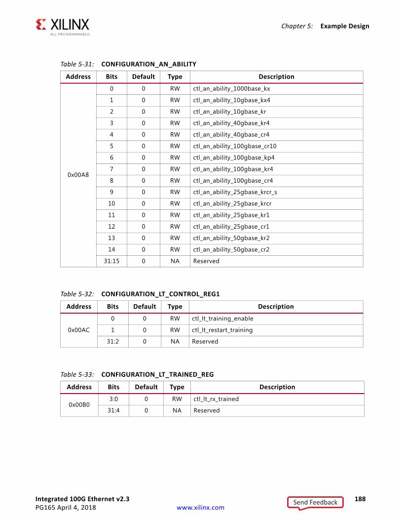
Integrated 100G Ethernet v2.3 188PG165 April 4, 2018 www.xilinx.com
Chapter 5: Example Design
Table 5-31: CONFIGURATION_AN_ABILITY
Address Bits Default Type Description
0x00A8
0 0 RW ctl_an_ability_1000base_kx
1 0 RW ctl_an_ability_10gbase_kx4
2 0 RW ctl_an_ability_10gbase_kr
3 0 RW ctl_an_ability_40gbase_kr4
4 0 RW ctl_an_ability_40gbase_cr4
5 0 RW ctl_an_ability_100gbase_cr10
6 0 RW ctl_an_ability_100gbase_kp4
7 0 RW ctl_an_ability_100gbase_kr4
8 0 RW ctl_an_ability_100gbase_cr4
9 0 RW ctl_an_ability_25gbase_krcr_s
10 0 RW ctl_an_ability_25gbase_krcr
11 0 RW ctl_an_ability_25gbase_kr1
12 0 RW ctl_an_ability_25gbase_cr1
13 0 RW ctl_an_ability_50gbase_kr2
14 0 RW ctl_an_ability_50gbase_cr2
31:15 0 NA Reserved
Table 5-32: CONFIGURATION_LT_CONTROL_REG1
Address Bits Default Type Description
0x00AC
0 0 RW ctl_lt_training_enable
1 0 RW ctl_lt_restart_training
31:2 0 NA Reserved
Table 5-33: CONFIGURATION_LT_TRAINED_REG
Address Bits Default Type Description
0x00B03:0 0 RW ctl_lt_rx_trained
31:4 0 NA Reserved
Send Feedback
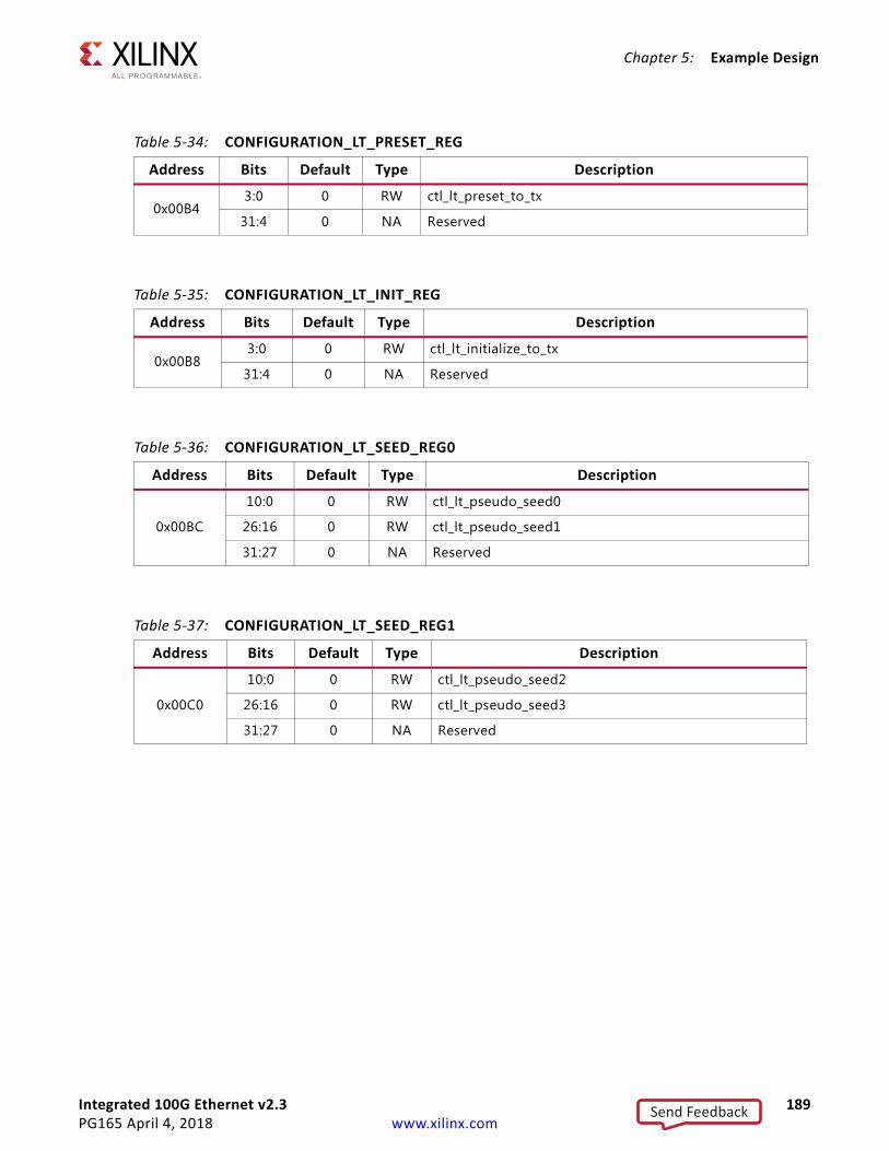
Integrated 100G Ethernet v2.3 189PG165 April 4, 2018 www.xilinx.com
Chapter 5: Example Design
Table 5-34: CONFIGURATION_LT_PRESET_REG
Address Bits Default Type Description
0x00B43:0 0 RW ctl_lt_preset_to_tx
31:4 0 NA Reserved
Table 5-35: CONFIGURATION_LT_INIT_REG
Address Bits Default Type Description
0x00B83:0 0 RW ctl_lt_initialize_to_tx
31:4 0 NA Reserved
Table 5-36: CONFIGURATION_LT_SEED_REG0
Address Bits Default Type Description
0x00BC
10:0 0 RW ctl_lt_pseudo_seed0
26:16 0 RW ctl_lt_pseudo_seed1
31:27 0 NA Reserved
Table 5-37: CONFIGURATION_LT_SEED_REG1
Address Bits Default Type Description
0x00C0
10:0 0 RW ctl_lt_pseudo_seed2
26:16 0 RW ctl_lt_pseudo_seed3
31:27 0 NA Reserved
Send Feedback
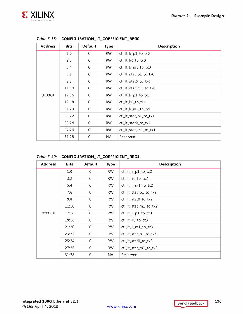
Integrated 100G Ethernet v2.3 190PG165 April 4, 2018 www.xilinx.com
Chapter 5: Example Design
Table 5-38: CONFIGURATION_LT_COEFFICIENT_REG0
Address Bits Default Type Description
0x00C4
1:0 0 RW ctl_lt_k_p1_to_tx0
3:2 0 RW ctl_lt_k0_to_tx0
5:4 0 RW ctl_lt_k_m1_to_tx0
7:6 0 RW ctl_lt_stat_p1_to_tx0
9:8 0 RW ctl_lt_stat0_to_tx0
11:10 0 RW ctl_lt_stat_m1_to_tx0
17:16 0 RW ctl_lt_k_p1_to_tx1
19:18 0 RW ctl_lt_k0_to_tx1
21:20 0 RW ctl_lt_k_m1_to_tx1
23:22 0 RW ctl_lt_stat_p1_to_tx1
25:24 0 RW ctl_lt_stat0_to_tx1
27:26 0 RW ctl_lt_stat_m1_to_tx1
31:28 0 NA Reserved
Table 5-39: CONFIGURATION_LT_COEFFICIENT_REG1
Address Bits Default Type Description
0x00C8
1:0 0 RW ctl_lt_k_p1_to_tx2
3:2 0 RW ctl_lt_k0_to_tx2
5:4 0 RW ctl_lt_k_m1_to_tx2
7:6 0 RW ctl_lt_stat_p1_to_tx2
9:8 0 RW ctl_lt_stat0_to_tx2
11:10 0 RW ctl_lt_stat_m1_to_tx2
17:16 0 RW ctl_lt_k_p1_to_tx3
19:18 0 RW ctl_lt_k0_to_tx3
21:20 0 RW ctl_lt_k_m1_to_tx3
23:22 0 RW ctl_lt_stat_p1_to_tx3
25:24 0 RW ctl_lt_stat0_to_tx3
27:26 0 RW ctl_lt_stat_m1_to_tx3
31:28 0 NA Reserved
Send Feedback
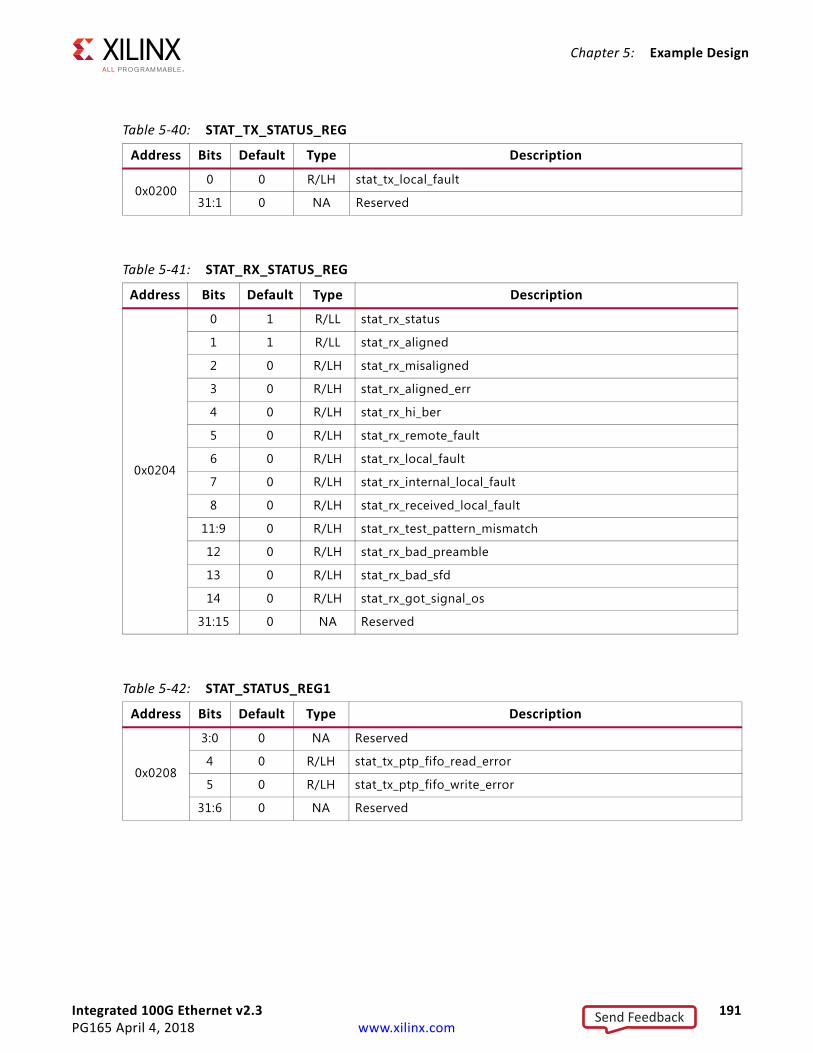
Integrated 100G Ethernet v2.3 191PG165 April 4, 2018 www.xilinx.com
Chapter 5: Example Design
Table 5-40: STAT_TX_STATUS_REG
Address Bits Default Type Description
0x02000 0 R/LH stat_tx_local_fault
31:1 0 NA Reserved
Table 5-41: STAT_RX_STATUS_REG
Address Bits Default Type Description
0x0204
0 1 R/LL stat_rx_status
1 1 R/LL stat_rx_aligned
2 0 R/LH stat_rx_misaligned
3 0 R/LH stat_rx_aligned_err
4 0 R/LH stat_rx_hi_ber
5 0 R/LH stat_rx_remote_fault
6 0 R/LH stat_rx_local_fault
7 0 R/LH stat_rx_internal_local_fault
8 0 R/LH stat_rx_received_local_fault
11:9 0 R/LH stat_rx_test_pattern_mismatch
12 0 R/LH stat_rx_bad_preamble
13 0 R/LH stat_rx_bad_sfd
14 0 R/LH stat_rx_got_signal_os
31:15 0 NA Reserved
Table 5-42: STAT_STATUS_REG1
Address Bits Default Type Description
0x0208
3:0 0 NA Reserved
4 0 R/LH stat_tx_ptp_fifo_read_error
5 0 R/LH stat_tx_ptp_fifo_write_error
31:6 0 NA Reserved
Send Feedback
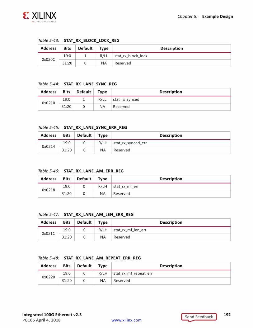
Integrated 100G Ethernet v2.3 192PG165 April 4, 2018 www.xilinx.com
Chapter 5: Example Design
Table 5-43: STAT_RX_BLOCK_LOCK_REG
Address Bits Default Type Description
0x020C19:0 1 R/LL stat_rx_block_lock
31:20 0 NA Reserved
Table 5-44: STAT_RX_LANE_SYNC_REG
Address Bits Default Type Description
0x021019:0 1 R/LL stat_rx_synced
31:20 0 NA Reserved
Table 5-45: STAT_RX_LANE_SYNC_ERR_REG
Address Bits Default Type Description
0x021419:0 0 R/LH stat_rx_synced_err
31:20 0 NA Reserved
Table 5-46: STAT_RX_LANE_AM_ERR_REG
Address Bits Default Type Description
0x021819:0 0 R/LH stat_rx_mf_err
31:20 0 NA Reserved
Table 5-47: STAT_RX_LANE_AM_LEN_ERR_REG
Address Bits Default Type Description
0x021C19:0 0 R/LH stat_rx_mf_len_err
31:20 0 NA Reserved
Table 5-48: STAT_RX_LANE_AM_REPEAT_ERR_REG
Address Bits Default Type Description
0x022019:0 0 R/LH stat_rx_mf_repeat_err
31:20 0 NA Reserved
Send Feedback
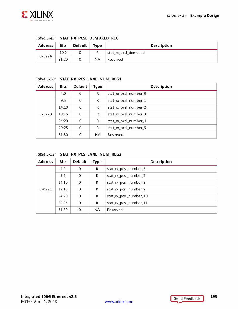
Integrated 100G Ethernet v2.3 193PG165 April 4, 2018 www.xilinx.com
Chapter 5: Example Design
Table 5-49: STAT_RX_PCSL_DEMUXED_REG
Address Bits Default Type Description
0x022419:0 0 R stat_rx_pcsl_demuxed
31:20 0 NA Reserved
Table 5-50: STAT_RX_PCS_LANE_NUM_REG1
Address Bits Default Type Description
0x0228
4:0 0 R stat_rx_pcsl_number_0
9:5 0 R stat_rx_pcsl_number_1
14:10 0 R stat_rx_pcsl_number_2
19:15 0 R stat_rx_pcsl_number_3
24:20 0 R stat_rx_pcsl_number_4
29:25 0 R stat_rx_pcsl_number_5
31:30 0 NA Reserved
Table 5-51: STAT_RX_PCS_LANE_NUM_REG2
Address Bits Default Type Description
0x022C
4:0 0 R stat_rx_pcsl_number_6
9:5 0 R stat_rx_pcsl_number_7
14:10 0 R stat_rx_pcsl_number_8
19:15 0 R stat_rx_pcsl_number_9
24:20 0 R stat_rx_pcsl_number_10
29:25 0 R stat_rx_pcsl_number_11
31:30 0 NA Reserved
Send Feedback

Integrated 100G Ethernet v2.3 194PG165 April 4, 2018 www.xilinx.com
Chapter 5: Example Design
Table 5-52: STAT_RX_PCS_LANE_NUM_REG3
Address Bits Default Type Description
0x0230
4:0 0 R stat_rx_pcsl_number_12
9:5 0 R stat_rx_pcsl_number_13
14:10 0 R stat_rx_pcsl_number_14
19:15 0 R stat_rx_pcsl_number_15
24:20 0 R stat_rx_pcsl_number_16
29:25 0 R stat_rx_pcsl_number_17
31:30 0 NA Reserved
Table 5-53: STAT_RX_PCS_LANE_NUM_REG4
Address Bits Default Type Description
0x0234
4:0 0 R stat_rx_pcsl_number_18
9:5 0 R stat_rx_pcsl_number_19
31:10 0 NA Reserved
Table 5-54: STAT_RX_BIP_OVERRIDE_REG
Address Bits Default Type Description
0x0238
7:0 0 R stat_rx_lane0_vlm_bip7
8 0 R stat_rx_lane0_vlm_bip7_valid
31:9 0 NA Reserved
Send Feedback
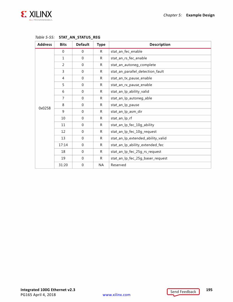
Integrated 100G Ethernet v2.3 195PG165 April 4, 2018 www.xilinx.com
Chapter 5: Example Design
Table 5-55: STAT_AN_STATUS_REG
Address Bits Default Type Description
0x0258
0 0 R stat_an_fec_enable
1 0 R stat_an_rs_fec_enable
2 0 R stat_an_autoneg_complete
3 0 R stat_an_parallel_detection_fault
4 0 R stat_an_tx_pause_enable
5 0 R stat_an_rx_pause_enable
6 0 R stat_an_lp_ability_valid
7 0 R stat_an_lp_autoneg_able
8 0 R stat_an_lp_pause
9 0 R stat_an_lp_asm_dir
10 0 R stat_an_lp_rf
11 0 R stat_an_lp_fec_10g_ability
12 0 R stat_an_lp_fec_10g_request
13 0 R stat_an_lp_extended_ability_valid
17:14 0 R stat_an_lp_ability_extended_fec
18 0 R stat_an_lp_fec_25g_rs_request
19 0 R stat_an_lp_fec_25g_baser_request
31:20 0 NA Reserved
Send Feedback
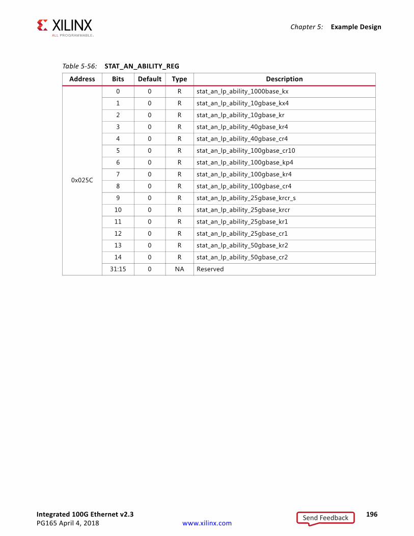
Integrated 100G Ethernet v2.3 196PG165 April 4, 2018 www.xilinx.com
Chapter 5: Example Design
Table 5-56: STAT_AN_ABILITY_REG
Address Bits Default Type Description
0x025C
0 0 R stat_an_lp_ability_1000base_kx
1 0 R stat_an_lp_ability_10gbase_kx4
2 0 R stat_an_lp_ability_10gbase_kr
3 0 R stat_an_lp_ability_40gbase_kr4
4 0 R stat_an_lp_ability_40gbase_cr4
5 0 R stat_an_lp_ability_100gbase_cr10
6 0 R stat_an_lp_ability_100gbase_kp4
7 0 R stat_an_lp_ability_100gbase_kr4
8 0 R stat_an_lp_ability_100gbase_cr4
9 0 R stat_an_lp_ability_25gbase_krcr_s
10 0 R stat_an_lp_ability_25gbase_krcr
11 0 R stat_an_lp_ability_25gbase_kr1
12 0 R stat_an_lp_ability_25gbase_cr1
13 0 R stat_an_lp_ability_50gbase_kr2
14 0 R stat_an_lp_ability_50gbase_cr2
31:15 0 NA Reserved
Send Feedback
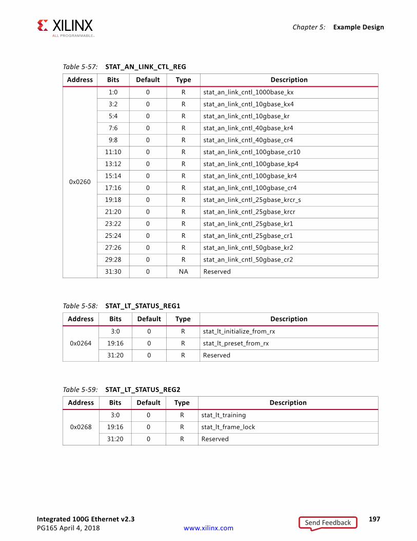
Integrated 100G Ethernet v2.3 197PG165 April 4, 2018 www.xilinx.com
Chapter 5: Example Design
Table 5-57: STAT_AN_LINK_CTL_REG
Address Bits Default Type Description
0x0260
1:0 0 R stat_an_link_cntl_1000base_kx
3:2 0 R stat_an_link_cntl_10gbase_kx4
5:4 0 R stat_an_link_cntl_10gbase_kr
7:6 0 R stat_an_link_cntl_40gbase_kr4
9:8 0 R stat_an_link_cntl_40gbase_cr4
11:10 0 R stat_an_link_cntl_100gbase_cr10
13:12 0 R stat_an_link_cntl_100gbase_kp4
15:14 0 R stat_an_link_cntl_100gbase_kr4
17:16 0 R stat_an_link_cntl_100gbase_cr4
19:18 0 R stat_an_link_cntl_25gbase_krcr_s
21:20 0 R stat_an_link_cntl_25gbase_krcr
23:22 0 R stat_an_link_cntl_25gbase_kr1
25:24 0 R stat_an_link_cntl_25gbase_cr1
27:26 0 R stat_an_link_cntl_50gbase_kr2
29:28 0 R stat_an_link_cntl_50gbase_cr2
31:30 0 NA Reserved
Table 5-58: STAT_LT_STATUS_REG1
Address Bits Default Type Description
0x0264
3:0 0 R stat_lt_initialize_from_rx
19:16 0 R stat_lt_preset_from_rx
31:20 0 R Reserved
Table 5-59: STAT_LT_STATUS_REG2
Address Bits Default Type Description
0x0268
3:0 0 R stat_lt_training
19:16 0 R stat_lt_frame_lock
31:20 0 R Reserved
Send Feedback
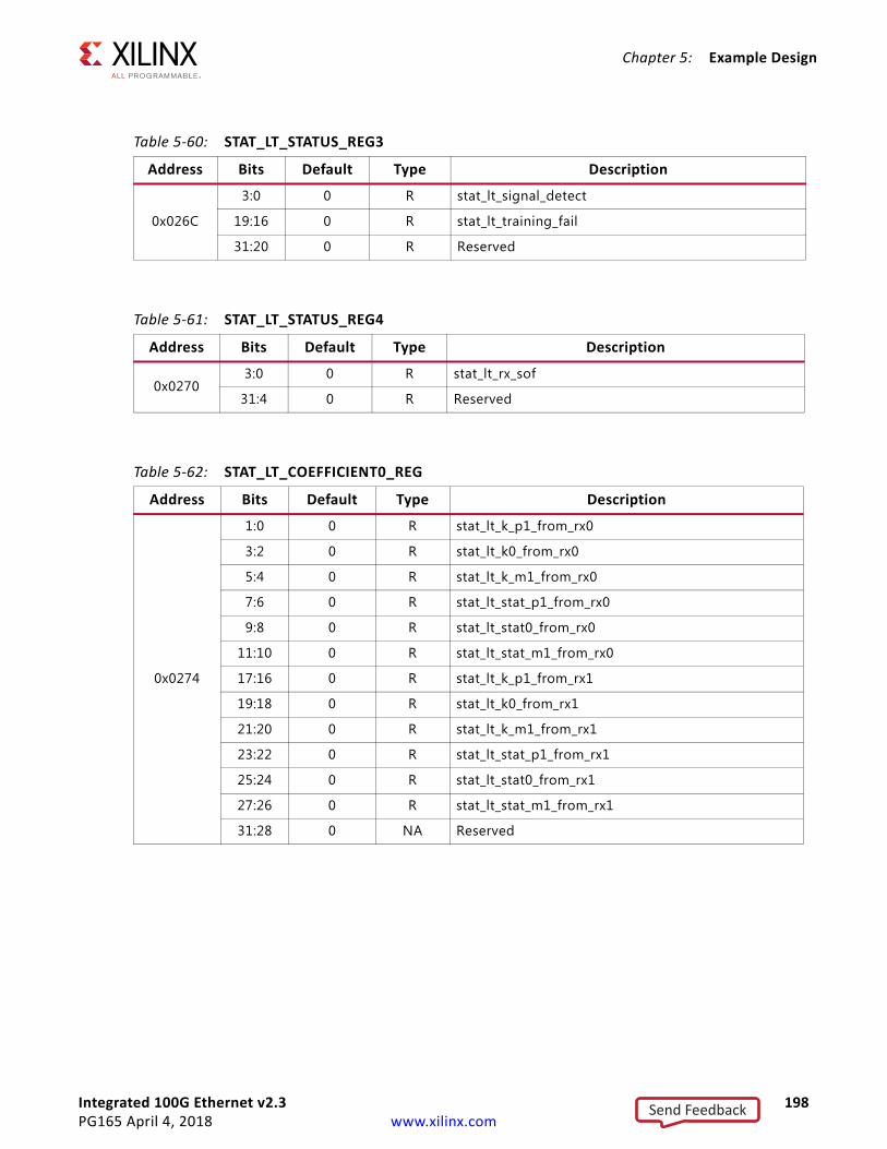
Integrated 100G Ethernet v2.3 198PG165 April 4, 2018 www.xilinx.com
Chapter 5: Example Design
Table 5-60: STAT_LT_STATUS_REG3
Address Bits Default Type Description
0x026C
3:0 0 R stat_lt_signal_detect
19:16 0 R stat_lt_training_fail
31:20 0 R Reserved
Table 5-61: STAT_LT_STATUS_REG4
Address Bits Default Type Description
0x02703:0 0 R stat_lt_rx_sof
31:4 0 R Reserved
Table 5-62: STAT_LT_COEFFICIENT0_REG
Address Bits Default Type Description
0x0274
1:0 0 R stat_lt_k_p1_from_rx0
3:2 0 R stat_lt_k0_from_rx0
5:4 0 R stat_lt_k_m1_from_rx0
7:6 0 R stat_lt_stat_p1_from_rx0
9:8 0 R stat_lt_stat0_from_rx0
11:10 0 R stat_lt_stat_m1_from_rx0
17:16 0 R stat_lt_k_p1_from_rx1
19:18 0 R stat_lt_k0_from_rx1
21:20 0 R stat_lt_k_m1_from_rx1
23:22 0 R stat_lt_stat_p1_from_rx1
25:24 0 R stat_lt_stat0_from_rx1
27:26 0 R stat_lt_stat_m1_from_rx1
31:28 0 NA Reserved
Send Feedback
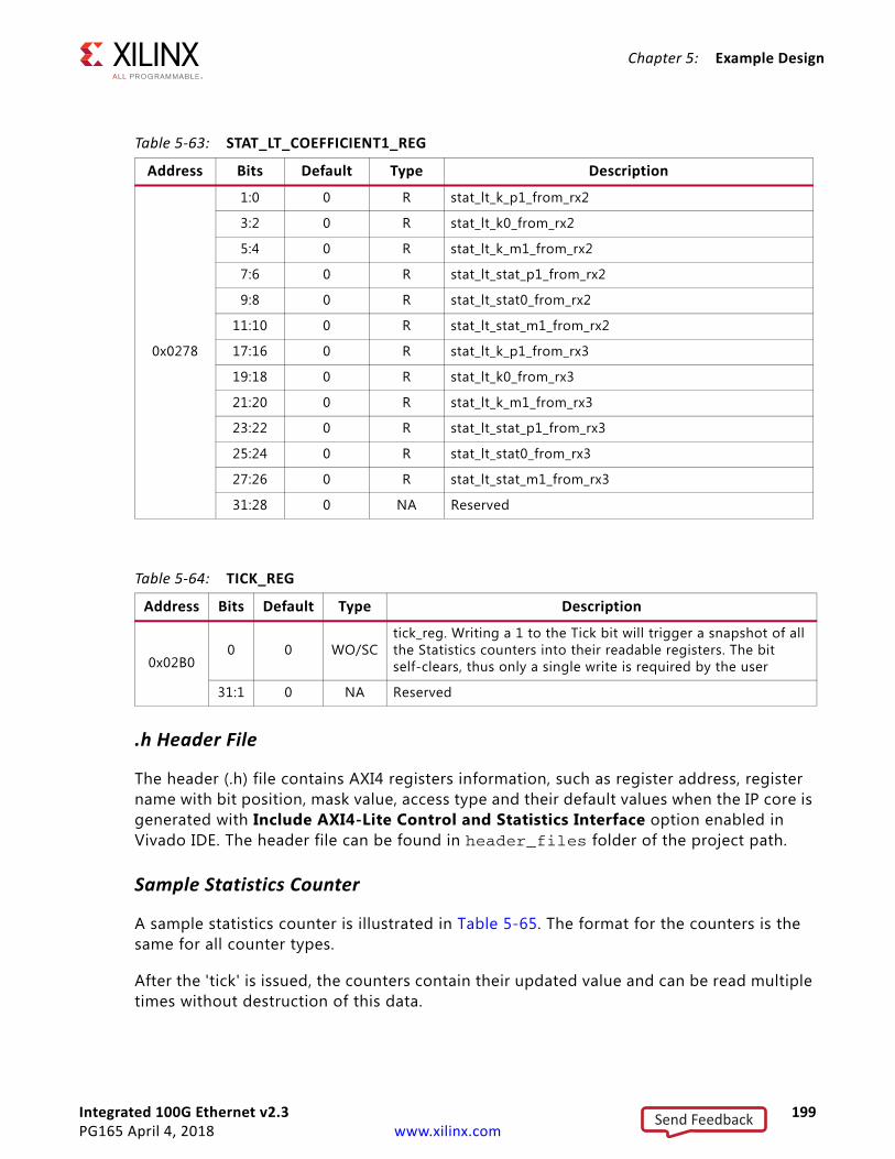
Integrated 100G Ethernet v2.3 199PG165 April 4, 2018 www.xilinx.com
Chapter 5: Example Design
.h Header File
The header (.h) file contains AXI4 registers information, such as register address, register name with bit position, mask value, access type and their default values when the IP core is generated with Include AXI4-Lite Control and Statistics Interface option enabled in Vivado IDE. The header file can be found in header_files folder of the project path.
Sample Statistics Counter
A sample statistics counter is illustrated in Table 5-65. The format for the counters is the same for all counter types.
After the 'tick' is issued, the counters contain their updated value and can be read multiple times without destruction of this data.
Table 5-63: STAT_LT_COEFFICIENT1_REG
Address Bits Default Type Description
0x0278
1:0 0 R stat_lt_k_p1_from_rx2
3:2 0 R stat_lt_k0_from_rx2
5:4 0 R stat_lt_k_m1_from_rx2
7:6 0 R stat_lt_stat_p1_from_rx2
9:8 0 R stat_lt_stat0_from_rx2
11:10 0 R stat_lt_stat_m1_from_rx2
17:16 0 R stat_lt_k_p1_from_rx3
19:18 0 R stat_lt_k0_from_rx3
21:20 0 R stat_lt_k_m1_from_rx3
23:22 0 R stat_lt_stat_p1_from_rx3
25:24 0 R stat_lt_stat0_from_rx3
27:26 0 R stat_lt_stat_m1_from_rx3
31:28 0 NA Reserved
Table 5-64: TICK_REG
Address Bits Default Type Description
0x02B00 0 WO/SC
tick_reg. Writing a 1 to the Tick bit will trigger a snapshot of all the Statistics counters into their readable registers. The bit self-clears, thus only a single write is required by the user
31:1 0 NA Reserved
Send Feedback
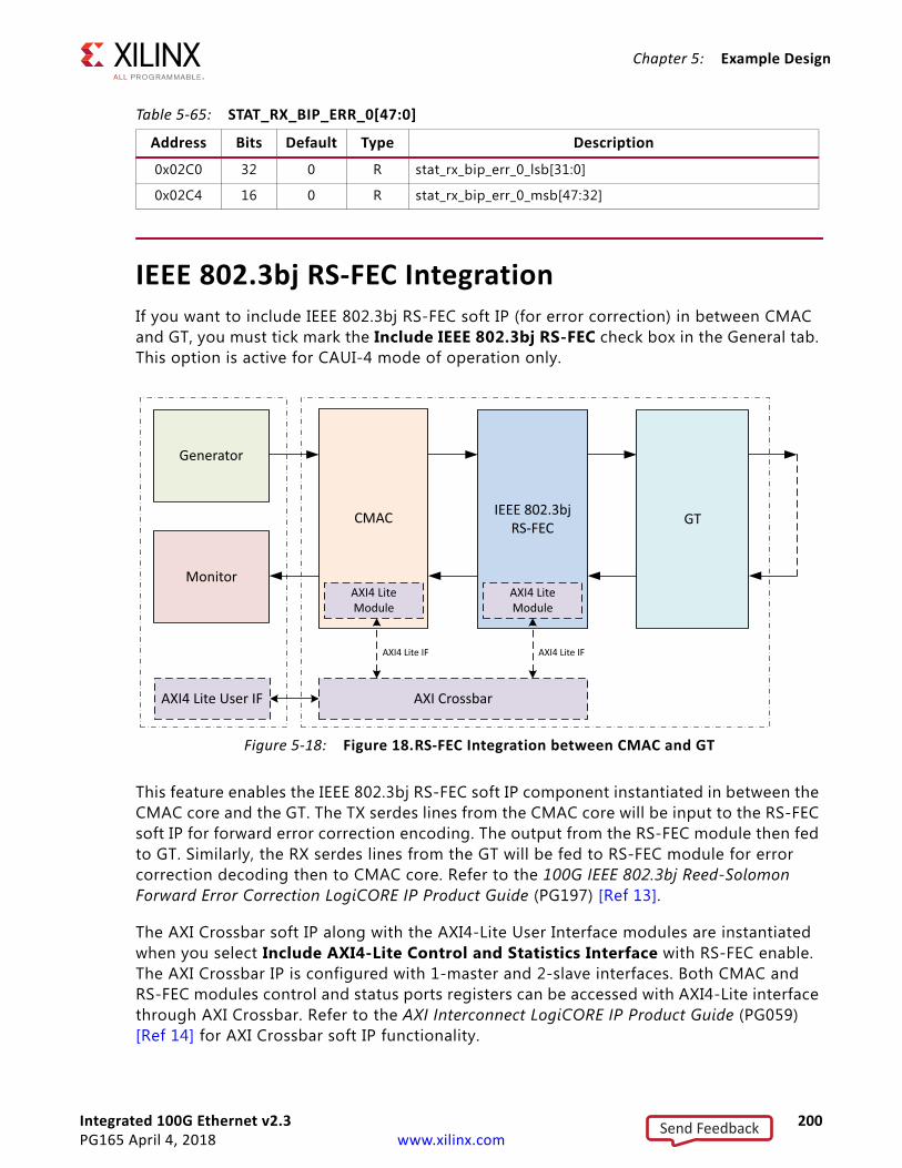
Integrated 100G Ethernet v2.3 200PG165 April 4, 2018 www.xilinx.com
Chapter 5: Example Design
IEEE 802.3bj RS-FEC IntegrationIf you want to include IEEE 802.3bj RS-FEC soft IP (for error correction) in between CMAC and GT, you must tick mark the Include IEEE 802.3bj RS-FEC check box in the General tab. This option is active for CAUI-4 mode of operation only.
This feature enables the IEEE 802.3bj RS-FEC soft IP component instantiated in between the CMAC core and the GT. The TX serdes lines from the CMAC core will be input to the RS-FEC soft IP for forward error correction encoding. The output from the RS-FEC module then fed to GT. Similarly, the RX serdes lines from the GT will be fed to RS-FEC module for error correction decoding then to CMAC core. Refer to the 100G IEEE 802.3bj Reed-Solomon Forward Error Correction LogiCORE IP Product Guide (PG197) [Ref 13].
The AXI Crossbar soft IP along with the AXI4-Lite User Interface modules are instantiated when you select Include AXI4-Lite Control and Statistics Interface with RS-FEC enable. The AXI Crossbar IP is configured with 1-master and 2-slave interfaces. Both CMAC and RS-FEC modules control and status ports registers can be accessed with AXI4-Lite interface through AXI Crossbar. Refer to the AXI Interconnect LogiCORE IP Product Guide (PG059) [Ref 14] for AXI Crossbar soft IP functionality.
Table 5-65: STAT_RX_BIP_ERR_0[47:0]
Address Bits Default Type Description
0x02C0 32 0 R stat_rx_bip_err_0_lsb[31:0]
0x02C4 16 0 R stat_rx_bip_err_0_msb[47:32]
X-Ref Target - Figure 5-18
Figure 5-18: Figure 18.RS-FEC Integration between CMAC and GT
Generator
CMAC
Monitor
IEEE 802.3bj RS-FEC GT
AXI Crossbar
AXI4 Lite IF AXI4 Lite IF
AXI4 Lite User IF
AXI4 Lite Module
AXI4 Lite Module
Send Feedback
Integrated 100G Ethernet v2.3 201PG165 April 4, 2018 www.xilinx.com
Chapter 5: Example Design
The base address locations for CMAC control and status registers and RS-FEC control and status registers in the AXI Crossbar soft IP are configured as shown:
• 0x0000_0000 to 0x0000_0FFF: Address locations for CMAC
• 0x0000_1000 to 0x0000_1FFF: Address locations for RS-FEC
For IEEE 802.3bj RS-FEC IP, the address location for the input rs_fec_ctrl_in is 0x0000_1000.
Core Bring Up Sequence
Without AXI4-Lite Interface1. Assert the below signals:
ctl_rx_enable = 1’b1ctl_tx_send_rfi = 1’b1
2. Wait for RX_aligned then deassert / assert the below signals:
ctl_tx_send_rfi = 1’b0ctl_tx_enable = 1’b1
3. When TX/RX flow control is enabled in the Vivado IDE (the default setting), assign the signals below.
Note: If you have disabled TX/RX flow control in the Vivado IDE, skip to step 4.
ctl_tx_pause_req[8:0] = 9’b100ctl_rx_pause_enable[8:0] = 9’b1FFctl_tx_pause_enable[8:0] = 9’b1FFctl_tx_pause_quanta8[15:0] = 16’bFFFFctl_tx_pause_refresh_timer8[15:0] = 16’bFFFF
4. Data transmission and reception can be performed.
With AXI4-Lite Interface1. Write the below registers:
0x00014 : 32'h00000001 [CONFIGURATION_RX_REG1 for ctl_rx_enable]0x0000C : 32'h00000010 [CONFIGURATION_TX_REG1 for ctl_tx_send_rfi]
2. Wait for RX_aligned then write the below registers:
0x0000C : 32'h00000001 [CONFIGURATION_TX_REG1 for ctl_tx_enable to 1’b1 and ctl_tx_send_rfi to 1’b0]
3. When TX/RX flow control is enabled in the Vivado IDE (the default setting), write the registers below.
Note: If you have disabled TX/RX flow control in the Vivado IDE, skip to step 4.
Send Feedback
Integrated 100G Ethernet v2.3 202PG165 April 4, 2018 www.xilinx.com
Chapter 5: Example Design
0x0084 : 32'h00003DFF [CONFIGURATION_RX_FLOW_CONTROL_CONTROL_REG1]0x0088 : 32'h0001C631 [CONFIGURATION_RX_FLOW_CONTROL_CONTROL_REG2]0x0048 : 32'hFFFFFFFF [CONFIGURATION_TX_FLOW_CONTROL_QUANTA_REG1]0x004C : 32'hFFFFFFFF [CONFIGURATION_TX_FLOW_CONTROL_QUANTA_REG2]0x0050 : 32'hFFFFFFFF [CONFIGURATION_TX_FLOW_CONTROL_QUANTA_REG3]0x0054 : 32'hFFFFFFFF [CONFIGURATION_TX_FLOW_CONTROL_QUANTA_REG4]0x0058 : 32'h0000FFFF [CONFIGURATION_TX_FLOW_CONTROL_QUANTA_REG5]0x0034 : 32'hFFFFFFFF [CONFIGURATION_TX_FLOW_CONTROL_REFRESH_REG1]0x0038 : 32'hFFFFFFFF [CONFIGURATION_TX_FLOW_CONTROL_REFRESH_REG2]0x003C : 32'hFFFFFFFF [CONFIGURATION_TX_FLOW_CONTROL_REFRESH_REG3]0x0040 : 32'hFFFFFFFF [CONFIGURATION_TX_FLOW_CONTROL_REFRESH_REG4]0x0044 : 32'h0000FFFF [CONFIGURATION_TX_FLOW_CONTROL_REFRESH_REG5]0x0030 : 32'h000001FF [CONFIGURATION_TX_FLOW_CONTROL_CONTROL_REG1]
4. Data transmission and reception can be performed.
Use Case for Different Modes This section describes the use case for different modes of operation of the 100G Ethernet IP core.
Send Feedback
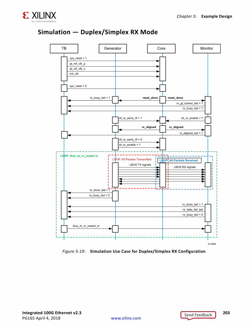
Integrated 100G Ethernet v2.3 203PG165 April 4, 2018 www.xilinx.com
Chapter 5: Example Design
Simulation — Duplex/Simplex RX Mode X-Ref Target - Figure 5-19
Figure 5-19: Simulation Use Case for Duplex/Simplex RX Configuration
X13995
TB Generator Core Monitor
sys_reset = 1
gt_ref_clk_p
gt_ref_clk_n
init_clk
sys_reset = 0
tx_busy_led = 1 reset_done reset_done
rx_gt_locked_led = 1
rx_busy_led = 1
ctl_tx_send_rfi = 1 ctl_rx_enable = 1
rx_aligned rx_aligned
rx_aligned_led = 1
ctl_tx_send_rfi = 0
ctl_tx_enable = 1
LBUS TX signalsLBUS RX signals
tx_done_led = 1
tx_busy_led = 0
rx_done_led = 1
rx_data_fail_led
rx_busy_led = 0
lbus_tx_rx_restart_in
LOOP: lbus_tx_rx_restart in
LOOP: All Packets Transmitted LOOP: All Packets Received
Send Feedback
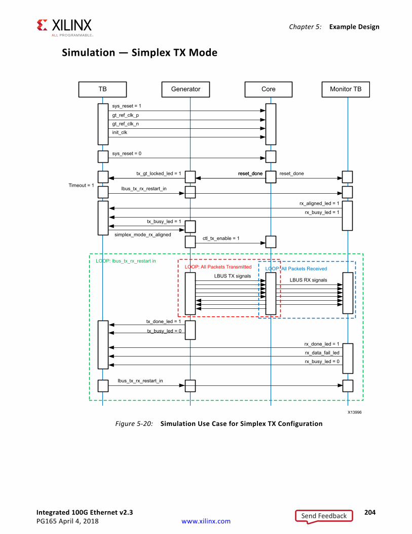
Integrated 100G Ethernet v2.3 204PG165 April 4, 2018 www.xilinx.com
Chapter 5: Example Design
Simulation — Simplex TX ModeX-Ref Target - Figure 5-20
Figure 5-20: Simulation Use Case for Simplex TX Configuration
X13996
TB Generator Core Monitor TB
sys_reset = 1
gt_ref_clk_p
gt_ref_clk_n
init_clk
sys_reset = 0
tx_gt_locked_led = 1 reset_done reset_done
LBUS TX signalsLBUS RX signals
tx_done_led = 1
tx_busy_led = 0
rx_done_led = 1
rx_data_fail_led
rx_busy_led = 0
lbus_tx_rx_restart_in
LOOP: lbus_tx_rx_restart inLOOP: All Packets Transmitted LOOP: All Packets Received
lbus_tx_rx_restart_in
rx_aligned_led = 1
rx_busy_led = 1
tx_busy_led = 1
reset_done
ctl_tx_enable = 1simplex_mode_rx_aligned
Timeout = 1
Send Feedback
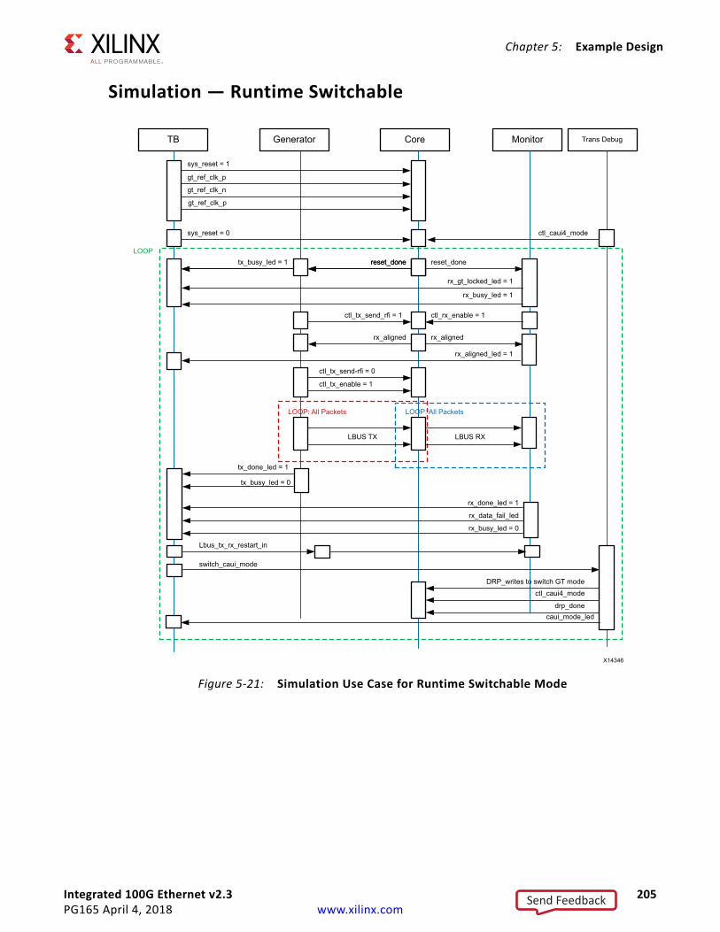
Integrated 100G Ethernet v2.3 205PG165 April 4, 2018 www.xilinx.com
Chapter 5: Example Design
Simulation — Runtime SwitchableX-Ref Target - Figure 5-21
Figure 5-21: Simulation Use Case for Runtime Switchable Mode
X14346
TB Generator Core Monitor
sys_reset = 1
gt_ref_clk_p
gt_ref_clk_n
sys_reset = 0
tx_busy_led = 1 reset_done reset_doneLOOP
LOOP: All Packets LOOP: All Packets
reset_done
Trans Debug
ctl_caui4_mode
rx_gt_locked_led = 1
rx_busy_led = 1
rx_alignedrx_aligned
rx_aligned_led = 1
ctl_tx_send-rfi = 0
ctl_tx_enable = 1
LBUS TX LBUS RX
tx_done_led = 1
tx_busy_led = 0
rx_done_led = 1
rx_data_fail_led
rx_busy_led = 0
switch_caui_mode
DRP_writes to switch GT modectl_caui4_mode
drp_done
ctl_rx_enable = 1ctl_tx_send_rfi = 1
gt_ref_clk_p
Lbus_tx_rx_restart_in
caui_mode_led
Send Feedback
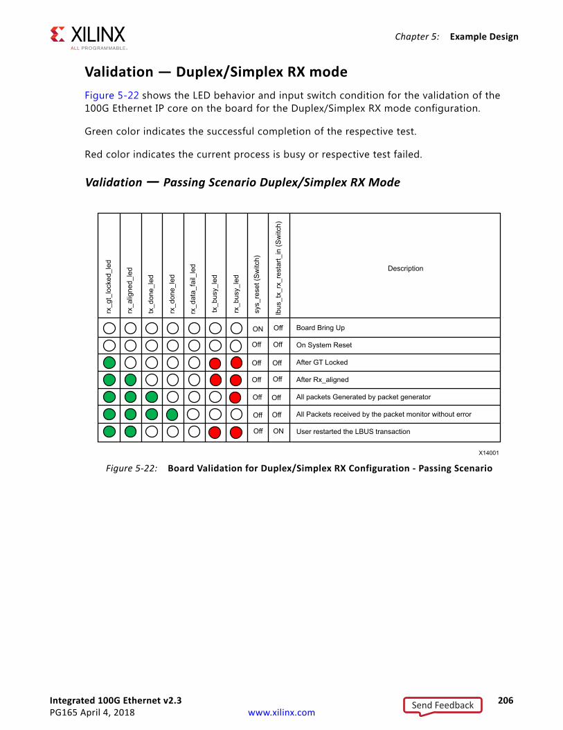
Integrated 100G Ethernet v2.3 206PG165 April 4, 2018 www.xilinx.com
Chapter 5: Example Design
Validation — Duplex/Simplex RX modeFigure 5-22 shows the LED behavior and input switch condition for the validation of the 100G Ethernet IP core on the board for the Duplex/Simplex RX mode configuration.
Green color indicates the successful completion of the respective test.
Red color indicates the current process is busy or respective test failed.
Validation — Passing Scenario Duplex/Simplex RX ModeX-Ref Target - Figure 5-22
Figure 5-22: Board Validation for Duplex/Simplex RX Configuration - Passing Scenario
X14001
rx_g
t_lo
cked
_led
rx_a
ligne
d_le
d
tx_d
one_
led
rx_d
one_
led
rx_d
ata_
fail_
led
tx_b
usy_
led
rx_b
usy_
led
sys_
rese
t (S
witc
h)
lbus
_tx_
rx_r
esta
rt_in
(Sw
itch)
Board Bring Up
On System Reset
After GT Locked
After Rx_aligned
All packets Generated by packet generator
All Packets received by the packet monitor without error
User restarted the LBUS transaction
Off
Off
Off
Off
Off
Off
ON
ON
Off
Off
Off
Off
Off
Off
Description
Send Feedback
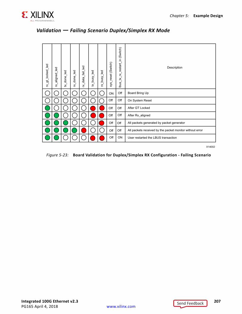
Integrated 100G Ethernet v2.3 207PG165 April 4, 2018 www.xilinx.com
Chapter 5: Example Design
Validation — Failing Scenario Duplex/Simplex RX ModeX-Ref Target - Figure 5-23
Figure 5-23: Board Validation for Duplex/Simplex RX Configuration - Failing Scenario
X14002
rx_g
t_lo
cked
_led
rx_a
ligne
d_le
d
tx_d
one_
led
rx_d
one_
led
rx_d
ata_
fail_
led
tx_b
usy_
led
rx_b
usy_
led
sys_
rese
t (S
witc
h)
lbus
_tx_
rx_r
esta
rt_in
(Sw
itch)
Board Bring Up
On System Reset
After GT Locked
After Rx_aligned
All packets generated by packet generator
All packets received by the packet monitor without error
User restarted the LBUS transaction
Off
Off
Off
Off
Off
Off
ON
ON
Off
Off
Off
Off
Off
Off
Description
Send Feedback
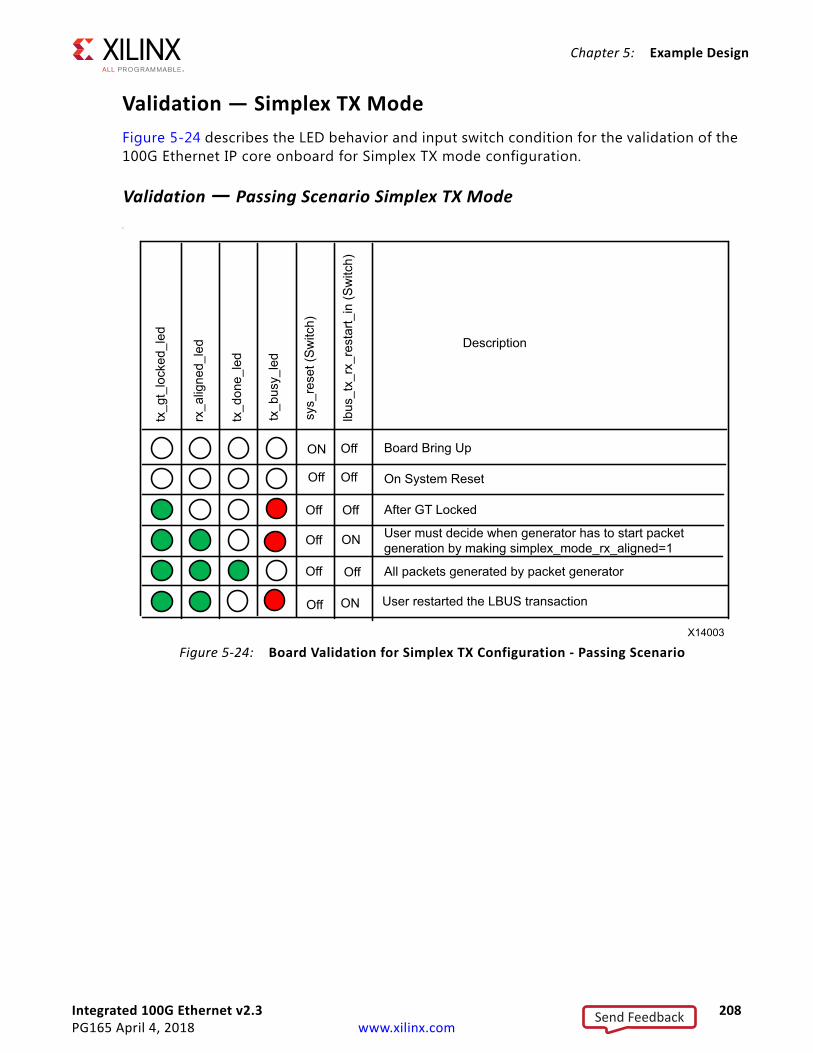
Integrated 100G Ethernet v2.3 208PG165 April 4, 2018 www.xilinx.com
Chapter 5: Example Design
Validation — Simplex TX ModeFigure 5-24 describes the LED behavior and input switch condition for the validation of the 100G Ethernet IP core onboard for Simplex TX mode configuration.
Validation — Passing Scenario Simplex TX Mode\X-Ref Target - Figure 5-24
Figure 5-24: Board Validation for Simplex TX Configuration - Passing Scenario X14003
tx_g
t_lo
cked
_led
rx_a
ligne
d_le
d
tx_d
one_
led
tx_b
usy_
led
sys_
rese
t (Sw
itch)
lbus
_tx_
rx_r
esta
rt_in
(Sw
itch)
Board Bring Up
On System Reset
After GT Locked
User must decide when generator has to start packet generation by making simplex_mode_rx_aligned=1
All packets generated by packet generator
User restarted the LBUS transaction
Off
Off
Off
Off
ON
Off
Off
Off
Off
Off
Description
ON
ON
Send Feedback
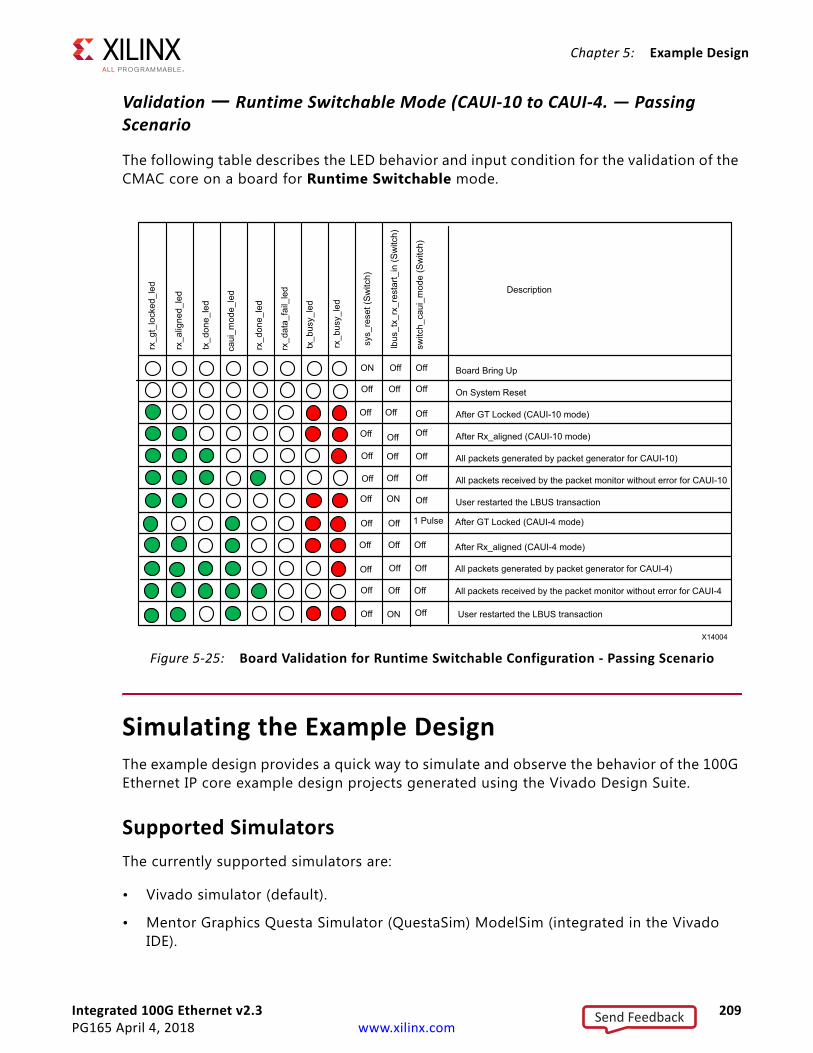
Integrated 100G Ethernet v2.3 209PG165 April 4, 2018 www.xilinx.com
Chapter 5: Example Design
Validation — Runtime Switchable Mode (CAUI-10 to CAUI-4. — Passing Scenario
The following table describes the LED behavior and input condition for the validation of the CMAC core on a board for Runtime Switchable mode.
Simulating the Example DesignThe example design provides a quick way to simulate and observe the behavior of the 100G Ethernet IP core example design projects generated using the Vivado Design Suite.
Supported SimulatorsThe currently supported simulators are:
• Vivado simulator (default).
• Mentor Graphics Questa Simulator (QuestaSim) ModelSim (integrated in the Vivado IDE).
X-Ref Target - Figure 5-25
Figure 5-25: Board Validation for Runtime Switchable Configuration - Passing Scenario X14004
rx_g
t_lo
cked
_led
rx_a
ligne
d_le
d
tx_d
one_
led
rx_d
one_
led
rx_d
ata_
fail_
led
tx_b
usy_
led
rx_b
usy_
led
sys_
rese
t (S
witc
h)
lbus
_tx_
rx_r
esta
rt_in
(Sw
itch)
Board Bring Up
On System Reset
After GT Locked (CAUI-10 mode)
After Rx_aligned (CAUI-10 mode)
All packets generated by packet generator for CAUI-10)
All packets received by the packet monitor without error for CAUI-10
User restarted the LBUS transaction
Off
Off
Off
Off
Off
ON
ON
Off
Off
Off
Off
Off
Off
Description
switc
h_ca
ui_m
ode
(Sw
itch)
Off
Off
Off
Off
Off
caui
_mod
e_le
d
Off
Off Off
Off Off
Off Off
Off
1 PulseOff
Off
Off
Off
Off
Off
ON
Off
Off
After GT Locked (CAUI-4 mode)
After Rx_aligned (CAUI-4 mode)
All packets generated by packet generator for CAUI-4)
All packets received by the packet monitor without error for CAUI-4
User restarted the LBUS transaction
Send Feedback
Integrated 100G Ethernet v2.3 210PG165 April 4, 2018 www.xilinx.com
Chapter 5: Example Design
• Cadence Incisive Enterprise Simulator (IES).
• Synopsys VCS and VCS MX.
The simulator uses the example design test bench and test cases provided along with the example design.
Running a SimulationFor any project (100G Ethernet IP core) generated out of context (OOC), the simulations can be run in the following ways:
1. In the Sources Window, right-click the example project file (.xci), and select Open IP Example Design. The example project is created.
2. In the Flow Navigator (left-hand pane) under Simulation, right-click Run Simulation and select Run Behavioral Simulation.
Note: The post-synthesis and post-implementation simulation options are not supported for the 100G Ethernet IP core.
After the Run Behavioral Simulation Option is running, you can observe the compilation and elaboration phase through the activity in the Tcl Console, and in the Simulation tab of the Log Window.
3. In Tcl Console, type the run all command and press Enter. This runs the complete simulation as per the test case provided in example design test bench.
After the simulation is complete, the result can be viewed in the Tcl Console.
Changing the SimulatorTo change the simulator:
1. In the Flow Navigator, under Simulation, select Simulation Settings.
2. In the Project Settings for Simulation dialog box, change the Target Simulator to QuestaSim/ModelSim.
3. When prompted, click Yes to change and then run the simulator.
Simulation Speed UpSimulation can take a long time to complete due to the time required to complete alignment. A ̀ define SIM_SPEED_UP is available to improve simulation time by reducing the PCS lane Alignment Marker (AM) spacing in order to speed up the time the IP will take to achieve alignment. Setting `define SIM_SPEED_UP will change CTL_TX_VL_LENGTH_MINUS1 and CTL_RX_VL_LENGTH_MINUS1 from 16'h3FFF to 16'h03FF.
Send Feedback
Integrated 100G Ethernet v2.3 211PG165 April 4, 2018 www.xilinx.com
Chapter 5: Example Design
The SIM_SPEED_UP option can be used for simulation when in serial loopback or if the Alignment Marker spacing can be reduced at both endpoints. This option is compatible with the example design simulation which uses serial loopback.
Notes
• Altering the value of CTL_TX_VL_LENGTH_MINUS1 and CTL_RX_VL_LENGTH_MINUS1 from the default value of 0x3FFF will violate the IEEE 802.3 specification.
• Decreasing the AM spacing will result in less than 100G Ethernet bandwidth being available on the link.
• This change can be made only in simulation. For a design to work in hardware, the default value of 0x3FFF must be used.
• Full-rate simulation without the SIM_SPEED_UP option should still be run.
• SIM_SPEED_UP is available only when running RTL simulations. The option is not available for post-synthesis or post-implementation simulations.
VCS
Use the vlogan option: +define+SIM_SPEED_UP
QuestaSim
Use the vlog option: +define+SIM_SPEED_UP
IES
Use the ncvlog option: +define+SIM_SPEED_UP
Vivado Simulator
Use the xvlog option: -d SIM_SPEED_UP
Synthesizing and Implementing the Example DesignTo run synthesis and implementation on the example design in the Vivado Design Suite, do the following steps:
1. Go to the XCI file, right-click, and select Open IP Example Design.
A new Vivado tool window opens with the project name "example_project" within the project directory.
Send Feedback
Integrated 100G Ethernet v2.3 212PG165 April 4, 2018 www.xilinx.com
Chapter 5: Example Design
2. In the Flow Navigator, click Run Synthesis and Run Implementation.
TIP: Click Run Implementation first to run both synthesis and implementation.
Click Generate Bitstream to run synthesis, implementation, and then bitstream.
Send Feedback
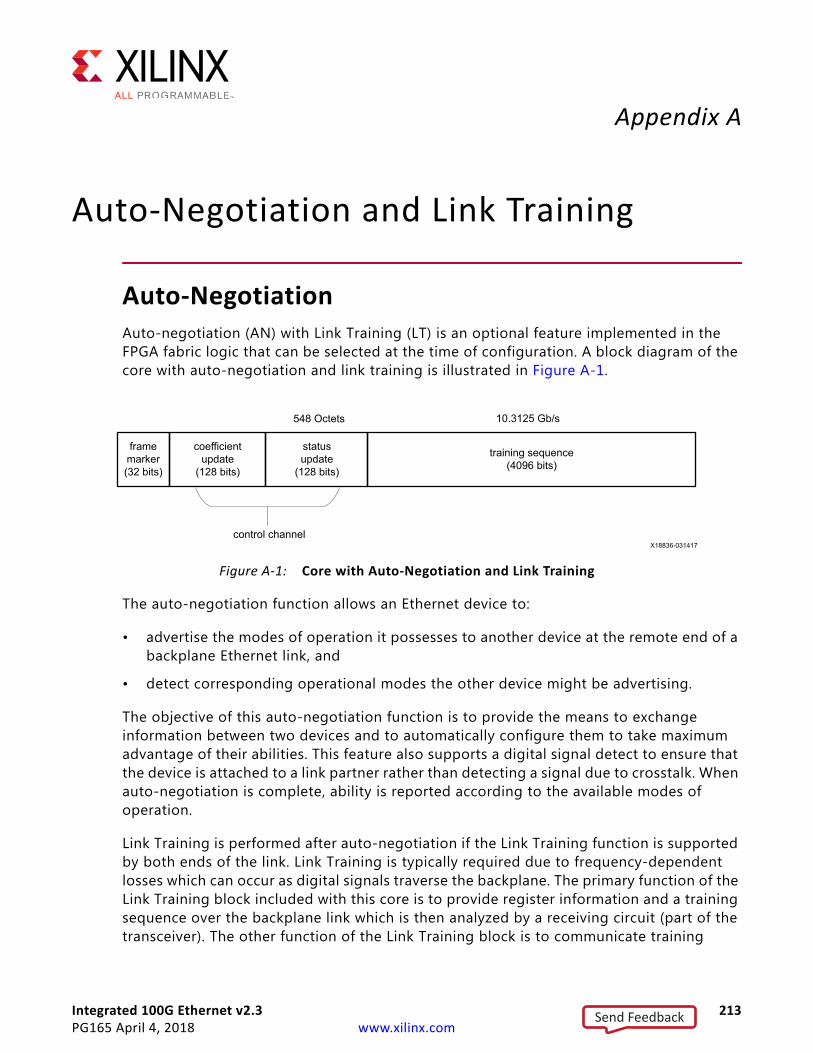
Integrated 100G Ethernet v2.3 213PG165 April 4, 2018 www.xilinx.com
Appendix A
Auto-Negotiation and Link Training
Auto-NegotiationAuto-negotiation (AN) with Link Training (LT) is an optional feature implemented in the FPGA fabric logic that can be selected at the time of configuration. A block diagram of the core with auto-negotiation and link training is illustrated in Figure A-1.
The auto-negotiation function allows an Ethernet device to:
• advertise the modes of operation it possesses to another device at the remote end of a backplane Ethernet link, and
• detect corresponding operational modes the other device might be advertising.
The objective of this auto-negotiation function is to provide the means to exchange information between two devices and to automatically configure them to take maximum advantage of their abilities. This feature also supports a digital signal detect to ensure that the device is attached to a link partner rather than detecting a signal due to crosstalk. When auto-negotiation is complete, ability is reported according to the available modes of operation.
Link Training is performed after auto-negotiation if the Link Training function is supported by both ends of the link. Link Training is typically required due to frequency-dependent losses which can occur as digital signals traverse the backplane. The primary function of the Link Training block included with this core is to provide register information and a training sequence over the backplane link which is then analyzed by a receiving circuit (part of the transceiver). The other function of the Link Training block is to communicate training
X-Ref Target - Figure A-1
Figure A-1: Core with Auto-Negotiation and Link Training
frame marker (32 bits)
coefficient update
(128 bits)
status update
(128 bits)
training sequence (4096 bits)
control channel
548 Octets 10.3125 Gb/s
Send Feedback
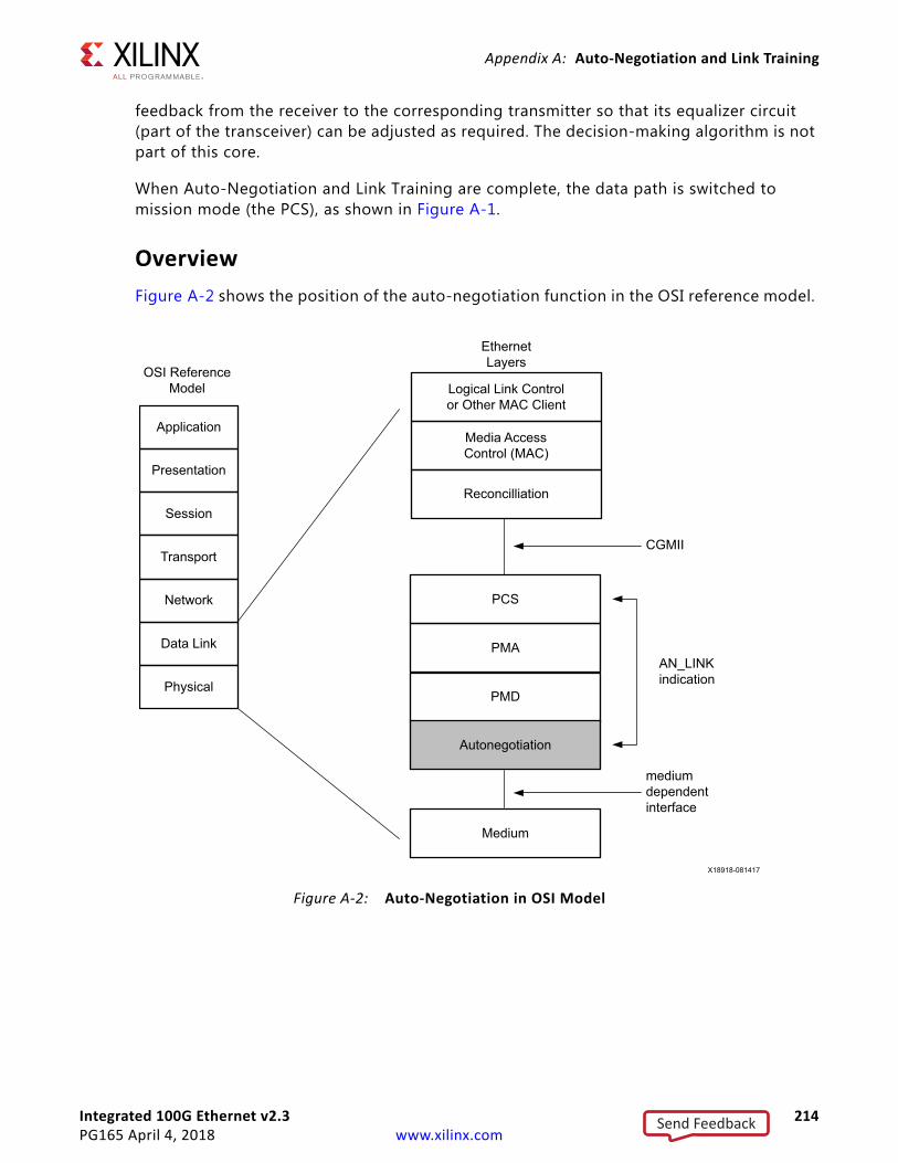
Integrated 100G Ethernet v2.3 214PG165 April 4, 2018 www.xilinx.com
Appendix A: Auto-Negotiation and Link Training
feedback from the receiver to the corresponding transmitter so that its equalizer circuit (part of the transceiver) can be adjusted as required. The decision-making algorithm is not part of this core.
When Auto-Negotiation and Link Training are complete, the data path is switched to mission mode (the PCS), as shown in Figure A-1.
OverviewFigure A-2 shows the position of the auto-negotiation function in the OSI reference model.
X-Ref Target - Figure A-2
Figure A-2: Auto-Negotiation in OSI Model
Application
Presentation
Session
Transport
Network
Data Link
Physical
Logical Link Control or Other MAC Client
Media AccessControl (MAC)
Reconcilliation
PCS
PMA
PMD
Autonegotiation
Medium
OSI Reference Model
Ethernet Layers
medium dependent interface
CGMII
AN_LINKindication
X18918-081417
Send Feedback
Integrated 100G Ethernet v2.3 215PG165 April 4, 2018 www.xilinx.com
Appendix A: Auto-Negotiation and Link Training
The 100G Base-KR4 auto-negotiation logic core implements the requirements as specified in Clause 73, IEEE Std 802.3-2015. The functions of the Auto-Negotiation are listed in clause 73, specifically in “Figure 73-11, Arbitration state diagram” in section 73.10.4, State Diagrams.
During normal mission mode operation, with link control outputs set to 11 (binary), the bit operating frequency of the transceiver input and output is typically 25.78125 Gb/s. However, the Dual Manchester Encoding (DME) bit rate used on the lane during Auto-Negotiation is different to the mission mode operation. To accommodate this requirement, the auto-negotiation core uses over-sampling and over-driving to match the 156.25 Mb/s Auto-Negotiation speed (DME clock frequency 312.5 MHz) with the mission mode 25.78125 Gb/s physical lane speed.
Auto-Negotiation is only performed on one lane. Therefore, by convention, for multi-lane Ethernet protocols lane 0 is used for AN.
IMPORTANT: Some protocols allow lanes to be swapped; however, for AN to work, lane 0 must connect to lane 0 of the link partner.
Functional Description
autoneg_enable
When the ctl_autoneg_enable input signal is set to 1, auto negotiation begins automatically at power-up, or if the carrier signal is lost, or if the input ctl_restart_negotiation signal is cycled from a 0 to a 1. All of the Ability input signals as well as the two input signals pause and asm_dir are tied Low or High to indicate the capability of the hardware. The nonce_seed[7:0] input must be set to a unique non-zero value for every instance of the auto negotiator. This is important to guarantee that no dead-locks occur at power-up. If two link partners connected together attempt to auto-negotiate with their nonce_seed[7:0] inputs set to the same value, the auto-negotiation fails continuously. The ctl_an_pseudo_sel input is an arbitrary selection that is used to select the polynomial of the random bit generator used in bit position 49 of the DME pages used during auto-negotiation. Any selection on this input is valid and does not result in any adverse behavior.
Link Control
When auto negotiation begins, the various link control signals are activated, depending on the disposition of the corresponding Ability inputs for those links. Subsequently, the corresponding link status signals are monitored by the ANIPC hardware for an indication of the state of the various links that are connected. If particular links are unused, the corresponding link control outputs are unconnected, and the corresponding link-status inputs should be tied Low. During this time, AN sets up a communication link with the link partner and uses this link to negotiate the capabilities of the connection.
Send Feedback
Integrated 100G Ethernet v2.3 216PG165 April 4, 2018 www.xilinx.com
Appendix A: Auto-Negotiation and Link Training
Autoneg Complete
When Auto-Negotiation is complete, the stat_an_autoneg_complete output signal is asserted. In addition, the ctl_an_fec_enable output signal is asserted if the Forward Error Correction hardware is to be used; the ctl_tx_pause_en output signal is asserted if the transmitter hardware is allowed to generate PAUSE control packets, the output signal ctl_rx_pause_en is asserted if the receiver hardware is allowed to detect PAUSE control packets, and the output link control of the selected link is set to its mission mode value (bin) 11.
The results of the auto negotiation do not directly cause the interface to change its behavior. External logic must determine how the ability information is to be used. For example, the appropriate logic level can be applied to ctl_tx_FEC_enable, ctl_tx_pause_enable, ctl_rx_FEC_enable, or ctl_rx_pause_enable.
Note: The stat_an_autoneg_complete signal is not asserted until rx_status is received from the PCS. That means that, where link training is included, the stat_an_autoneg_complete output signal is not asserted until after link training has completed.
Link Training
OverviewLink training (LT) is performed after auto-negotiation (AN) converges to a backplane or copper technology. Technology selection can also be the result of a manual entry or parallel detection. Link training can be required due to frequency-dependent losses, which can occur as digital signals traverse the backplane or a copper cable. The primary function of the LT IP core is to provide register information and a training sequence over the backplane link, which is then analyzed by a receiving circuit not part of the core. The other function of the core with LT is to communicate training feedback from the receiver to the corresponding transmitter so that its equalizer circuit (not part of the core) can be adjusted as required. The two circuits comprising the core are the receive Link Training block and the transmit Link Training block.
Send Feedback
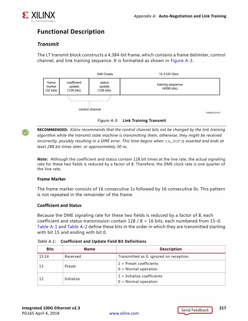
Integrated 100G Ethernet v2.3 217PG165 April 4, 2018 www.xilinx.com
Appendix A: Auto-Negotiation and Link Training
Functional Description
Transmit
The LT transmit block constructs a 4,384-bit frame, which contains a frame delimiter, control channel, and link training sequence. It is formatted as shown in Figure A-3.
RECOMMENDED: Xilinx recommends that the control channel bits not be changed by the link training algorithm while the transmit state machine is transmitting them, otherwise, they might be received incorrectly, possibly resulting in a DME error. This time begins when tx_SOF is asserted and ends at least 288 bit times later, or approximately 30 ns.
Note: Although the coefficient and status contain 128 bit times at the line rate, the actual signaling rate for these two fields is reduced by a factor of 8. Therefore, the DME clock rate is one quarter of the line rate.
Frame Marker
The frame marker consists of 16 consecutive 1s followed by 16 consecutive 0s. This pattern is not repeated in the remainder of the frame.
Coefficient and Status
Because the DME signaling rate for these two fields is reduced by a factor of 8, each coefficient and status transmission contain 128 / 8 = 16 bits, each numbered from 15–0. Table A-1 and Table A-2 define these bits in the order in which they are transmitted starting with bit 15 and ending with bit 0.
X-Ref Target - Figure A-3
Figure A-3: Link Training Transmit
frame marker (32 bits)
coefficient update
(128 bits)
status update
(128 bits)
training sequence (4096 bits)
control channel
548 Octets 10.3125 Gb/s
Table A-1: Coefficient and Update Field Bit Definitions
Bits Name Description
15:14 Reserved Transmitted as 0, ignored on reception.
13 Preset1 = Preset coefficients 0 = Normal operation
12 Initialize1 = Initialize coefficients 0 = Normal operation
Send Feedback
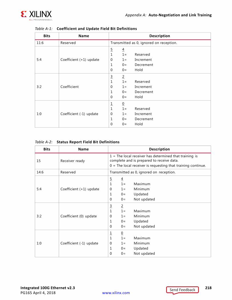
Integrated 100G Ethernet v2.3 218PG165 April 4, 2018 www.xilinx.com
Appendix A: Auto-Negotiation and Link Training
11:6 Reserved Transmitted as 0, ignored on reception.
5:4 Coefficient (+1) update
51010
41=1=0=0=
ReservedIncrementDecrementHold
3:2 Coefficient
31010
21=1=0=0=
ReservedIncrementDecrementHold
1:0 Coefficient (-1) update
11010
01=1=0=0=
ReservedIncrementDecrementHold
Table A-2: Status Report Field Bit Definitions
Bits Name Description
15 Receiver ready1 = The local receiver has determined that training is complete and is prepared to receive data.0 = The local receiver is requesting that training continue.
14:6 Reserved Transmitted as 0, ignored on reception.
5:4 Coefficient (+1) update
51010
41=1=0=0=
MaximumMinimumUpdatedNot updated
3:2 Coefficient (0) update
31010
21=1=0=0=
MaximumMinimumUpdatedNot updated
1:0 Coefficient (-1) update
11010
01=1=0=0=
MaximumMinimumUpdatedNot updated
Table A-1: Coefficient and Update Field Bit Definitions
Bits Name Description
Send Feedback
Integrated 100G Ethernet v2.3 219PG165 April 4, 2018 www.xilinx.com
Appendix A: Auto-Negotiation and Link Training
The functions of each bit are defined in IEEE 802.3 Clause 72, “72.6.10.2 Training frame structure”. Their purpose is to communicate the adjustments of the transmit equalizer during the process of link training. The corresponding signal names are defined in Port Descriptions.
Training Sequence
The training sequence consists of a Pseudo Random Bit Sequence (PRBS) of 4094 bits followed by two 0s, for a total of 4096 bits. The PRBS is transmitted at the line rate of 10.3125 Gb/s. The PRBS generator receives an 11-bit seed from an external source. Subsequent to the initial seed being loaded, the PRBS generator continues to run with no further intervention being required.
The PRBS generator itself is implemented with a circuit that corresponds to this polynomial:
G(x) = 1 + x9 + x11
Receive
The receive block implements the frame alignment state diagram illustrated in IEEE 802.3, Clause 72, Figure 72-4.
Frame Lock State Machine
The frame lock state machine searches for the frame marker, consisting of 16 consecutive 1s followed by 16 consecutive 0s. This functionality is fully specified in IEEE 802.3, Clause 72, Figure 72-4. When frame lock is achieved, the frame_lock signal is set to a value of TRUE.
Received Data
The receiver outputs the control channel with the bit definitions defined in Table A-1 and Table A-2.
If a DME error occurs during the reception of a particular DME frame, the control channel outputs are not updated but retain the value of the last received good DME frame. They are updated when the next good DME frame is received.
Port Descriptions
Auto-Negotiation SignalsTable A-3 lists the additional signals available when the auto-negotiation feature is present.
Send Feedback
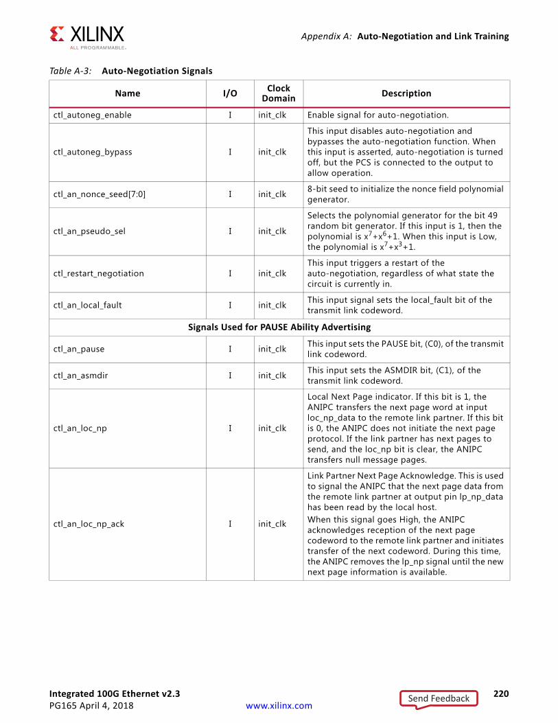
Integrated 100G Ethernet v2.3 220PG165 April 4, 2018 www.xilinx.com
Appendix A: Auto-Negotiation and Link Training
Table A-3: Auto-Negotiation Signals
Name I/O Clock Domain Description
ctl_autoneg_enable I init_clk Enable signal for auto-negotiation.
ctl_autoneg_bypass I init_clk
This input disables auto-negotiation and bypasses the auto-negotiation function. When this input is asserted, auto-negotiation is turned off, but the PCS is connected to the output to allow operation.
ctl_an_nonce_seed[7:0] I init_clk 8-bit seed to initialize the nonce field polynomial generator.
ctl_an_pseudo_sel I init_clk
Selects the polynomial generator for the bit 49 random bit generator. If this input is 1, then the polynomial is x7+x6+1. When this input is Low, the polynomial is x7+x3+1.
ctl_restart_negotiation I init_clkThis input triggers a restart of the auto-negotiation, regardless of what state the circuit is currently in.
ctl_an_local_fault I init_clk This input signal sets the local_fault bit of the transmit link codeword.
Signals Used for PAUSE Ability Advertising
ctl_an_pause I init_clk This input sets the PAUSE bit, (C0), of the transmit link codeword.
ctl_an_asmdir I init_clk This input sets the ASMDIR bit, (C1), of the transmit link codeword.
ctl_an_loc_np I init_clk
Local Next Page indicator. If this bit is 1, the ANIPC transfers the next page word at input loc_np_data to the remote link partner. If this bit is 0, the ANIPC does not initiate the next page protocol. If the link partner has next pages to send, and the loc_np bit is clear, the ANIPC transfers null message pages.
ctl_an_loc_np_ack I init_clk
Link Partner Next Page Acknowledge. This is used to signal the ANIPC that the next page data from the remote link partner at output pin lp_np_data has been read by the local host.When this signal goes High, the ANIPC acknowledges reception of the next page codeword to the remote link partner and initiates transfer of the next codeword. During this time, the ANIPC removes the lp_np signal until the new next page information is available.
Send Feedback
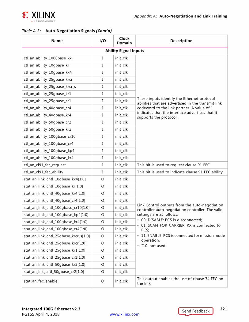
Integrated 100G Ethernet v2.3 221PG165 April 4, 2018 www.xilinx.com
Appendix A: Auto-Negotiation and Link Training
Ability Signal Inputs
ctl_an_ability_1000base_kx I init_clk
These inputs identify the Ethernet protocol abilities that are advertised in the transmit link codeword to the link partner. A value of 1 indicates that the interface advertises that it supports the protocol.
ctl_an_ability_10gbase_kr I init_clk
ctl_an_ability_10gbase_kx4 I init_clk
ctl_an_ability_25gbase_krcr I init_clk
ctl_an_ability_25gbase_krcr_s I init_clk
ctl_an_ability_25gbase_kr1 I init_clk
ctl_an_ability_25gbase_cr1 I init_clk
ctl_an_ability_40gbase_cr4 I init_clk
ctl_an_ability_40gbase_kr4 I init_clk
ctl_an_ability_50gbase_cr2 I init_clk
ctl_an_ability_50gbase_kr2 I init_clk
ctl_an_ability_100gbase_cr10 I init_clk
ctl_an_ability_100gbase_cr4 I init_clk
ctl_an_ability_100gbase_kp4 I init_clk
ctl_an_ability_100gbase_kr4 I init_clk
ctl_an_cl91_fec_request I init_clk This bit is used to request clause 91 FEC.
ctl_an_cl91_fec_ability I init_clk This bit is used to indicate clause 91 FEC ability.
stat_an_link_cntl_10gbase_kx4[1:0] O init_clk
Link Control outputs from the auto-negotiation controller auto-negotiation controller. The valid settings are as follows: • 00: DISABLE; PCS is disconnected;• 01: SCAN_FOR_CARRIER; RX is connected to
PCS;• 11: ENABLE; PCS is connected for mission mode
operation.• "10: not used.
stat_an_link_cntl_10gbase_kr[1:0] O init_clk
stat_an_link_cntl_40gbase_kr4[1:0] O init_clk
stat_an_link_cntl_40gbase_cr4[1:0] O init_clk
stat_an_link_cntl_100gbase_cr10[1:0] O init_clk
stat_an_link_cntl_100gbase_kp4[1:0] O init_clk
stat_an_link_cntl_100gbase_kr4[1:0] O init_clk
stat_an_link_cntl_100gbase_cr4[1:0] O init_clk
stat_an_link_cntl_25gbase_krcr_s[1:0] O init_clk
stat_an_link_cntl_25gbase_krcr[1:0] O init_clk
stat_an_link_cntl_25gbase_kr1[1:0] O init_clk
stat_an_link_cntl_25gbase_cr1[1:0] O init_clk
stat_an_link_cntl_50gbase_kr2[1:0] O init_clk
stat_an_lnk_cntl_50gbase_cr2[1:0] O init_clk
stat_an_fec_enable O init_clk This output enables the use of clause 74 FEC on the link.
Table A-3: Auto-Negotiation Signals (Cont’d)
Name I/O Clock Domain Description
Send Feedback
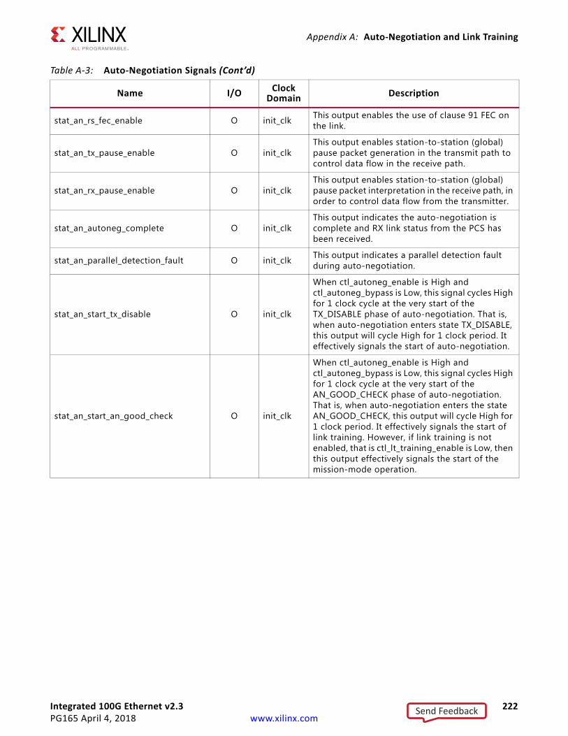
Integrated 100G Ethernet v2.3 222PG165 April 4, 2018 www.xilinx.com
Appendix A: Auto-Negotiation and Link Training
stat_an_rs_fec_enable O init_clk This output enables the use of clause 91 FEC on the link.
stat_an_tx_pause_enable O init_clkThis output enables station-to-station (global) pause packet generation in the transmit path to control data flow in the receive path.
stat_an_rx_pause_enable O init_clkThis output enables station-to-station (global) pause packet interpretation in the receive path, in order to control data flow from the transmitter.
stat_an_autoneg_complete O init_clkThis output indicates the auto-negotiation is complete and RX link status from the PCS has been received.
stat_an_parallel_detection_fault O init_clk This output indicates a parallel detection fault during auto-negotiation.
stat_an_start_tx_disable O init_clk
When ctl_autoneg_enable is High and ctl_autoneg_bypass is Low, this signal cycles High for 1 clock cycle at the very start of the TX_DISABLE phase of auto-negotiation. That is, when auto-negotiation enters state TX_DISABLE, this output will cycle High for 1 clock period. It effectively signals the start of auto-negotiation.
stat_an_start_an_good_check O init_clk
When ctl_autoneg_enable is High and ctl_autoneg_bypass is Low, this signal cycles High for 1 clock cycle at the very start of the AN_GOOD_CHECK phase of auto-negotiation. That is, when auto-negotiation enters the state AN_GOOD_CHECK, this output will cycle High for 1 clock period. It effectively signals the start of link training. However, if link training is not enabled, that is ctl_lt_training_enable is Low, then this output effectively signals the start of the mission-mode operation.
Table A-3: Auto-Negotiation Signals (Cont’d)
Name I/O Clock Domain Description
Send Feedback
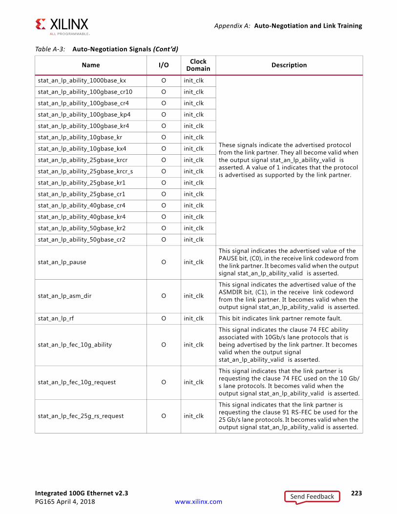
Integrated 100G Ethernet v2.3 223PG165 April 4, 2018 www.xilinx.com
Appendix A: Auto-Negotiation and Link Training
stat_an_lp_ability_1000base_kx O init_clk
These signals indicate the advertised protocol from the link partner. They all become valid when the output signal stat_an_lp_ability_valid is asserted. A value of 1 indicates that the protocol is advertised as supported by the link partner.
stat_an_lp_ability_100gbase_cr10 O init_clk
stat_an_lp_ability_100gbase_cr4 O init_clk
stat_an_lp_ability_100gbase_kp4 O init_clk
stat_an_lp_ability_100gbase_kr4 O init_clk
stat_an_lp_ability_10gbase_kr O init_clk
stat_an_lp_ability_10gbase_kx4 O init_clk
stat_an_lp_ability_25gbase_krcr O init_clk
stat_an_lp_ability_25gbase_krcr_s O init_clk
stat_an_lp_ability_25gbase_kr1 O init_clk
stat_an_lp_ability_25gbase_cr1 O init_clk
stat_an_lp_ability_40gbase_cr4 O init_clk
stat_an_lp_ability_40gbase_kr4 O init_clk
stat_an_lp_ability_50gbase_kr2 O init_clk
stat_an_lp_ability_50gbase_cr2 O init_clk
stat_an_lp_pause O init_clk
This signal indicates the advertised value of the PAUSE bit, (C0), in the receive link codeword from the link partner. It becomes valid when the output signal stat_an_lp_ability_valid is asserted.
stat_an_lp_asm_dir O init_clk
This signal indicates the advertised value of the ASMDIR bit, (C1), in the receive link codeword from the link partner. It becomes valid when the output signal stat_an_lp_ability_valid is asserted.
stat_an_lp_rf O init_clk This bit indicates link partner remote fault.
stat_an_lp_fec_10g_ability O init_clk
This signal indicates the clause 74 FEC ability associated with 10Gb/s lane protocols that is being advertised by the link partner. It becomes valid when the output signal stat_an_lp_ability_valid is asserted.
stat_an_lp_fec_10g_request O init_clk
This signal indicates that the link partner is requesting the clause 74 FEC used on the 10 Gb/s lane protocols. It becomes valid when the output signal stat_an_lp_ability_valid is asserted.
stat_an_lp_fec_25g_rs_request O init_clk
This signal indicates that the link partner is requesting the clause 91 RS-FEC be used for the 25 Gb/s lane protocols. It becomes valid when the output signal stat_an_lp_ability_valid is asserted.
Table A-3: Auto-Negotiation Signals (Cont’d)
Name I/O Clock Domain Description
Send Feedback
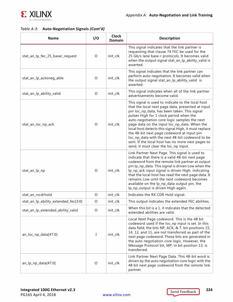
Integrated 100G Ethernet v2.3 224PG165 April 4, 2018 www.xilinx.com
Appendix A: Auto-Negotiation and Link Training
stat_an_lp_fec_25_baser_request O init_clk
This signal indicates that the link partner is requesting that clause 74 FEC be used for the 25 Gb/s lane base-r protocols. It becomes valid when the output signal stat_an_lp_ability_valid is asserted.
stat_an_lp_autoneg_able O init_clk
This signal indicates that the link partner can perform auto-negotiation. It becomes valid when the output signal stat_an_lp_ability_valid is asserted.
stat_an_lp_ability_valid O init_clk This signal indicates when all of the link partner advertisements become valid.
stat_an_loc_np_ack O init_clk
This signal is used to indicate to the local host that the local next page data, presented at input pin loc_np_data, has been taken. This signal pulses High for 1 clock period when the auto-negotiation core logic samples the next page data on the input loc_np_data. When the local host detects this signal High, it must replace the 48-bit next page codeword at input pin loc_np_data with the next 48-bit codeword to be sent. If the local host has no more next pages to send, it must clear the loc_np input.
stat_an_lp_np O init_clk
Link Partner Next Page. This signal is used to indicate that there is a valid 48-bit next page codeword from the remote link partner at output pin lp_np_data. This signal is driven Low when the lp_np_ack input signal is driven High, indicating that the local host has read the next page data. It remains Low until the next codeword becomes available on the lp_np_data output pin, the lp_np_output is driven High again.
stat_an_rxcdrhold O init_clk Indicates the RX CDR Hold signal.
stat_an_lp_ability_extended_fec[3:0] O init_clk This output indicates the extended FEC abilities.
stat_an_lp_extended_ability_valid O init_clk When this bit is a 1, it indicates that the detected extended abilities are valid.
an_loc_np_data[47:0] I init_clk
Local Next Page codeword. This is the 48 bit codeword used if the loc_np input is set. In this data field, the bits NP, ACK, & T, bit positions 15, 14, 12, and 11, are not transferred as part of the next page codeword. These bits are generated in the auto negotiation core logic. However, the Message Protocol bit, MP, in bit position 13, is transferred.
an_lp_np_data[47:0] O init_clk
Link Partner Next Page Data. This 48-bit word is driven by the auto negotiation core logic with the 48 bit next page codeword from the remote link partner.
Table A-3: Auto-Negotiation Signals (Cont’d)
Name I/O Clock Domain Description
Send Feedback
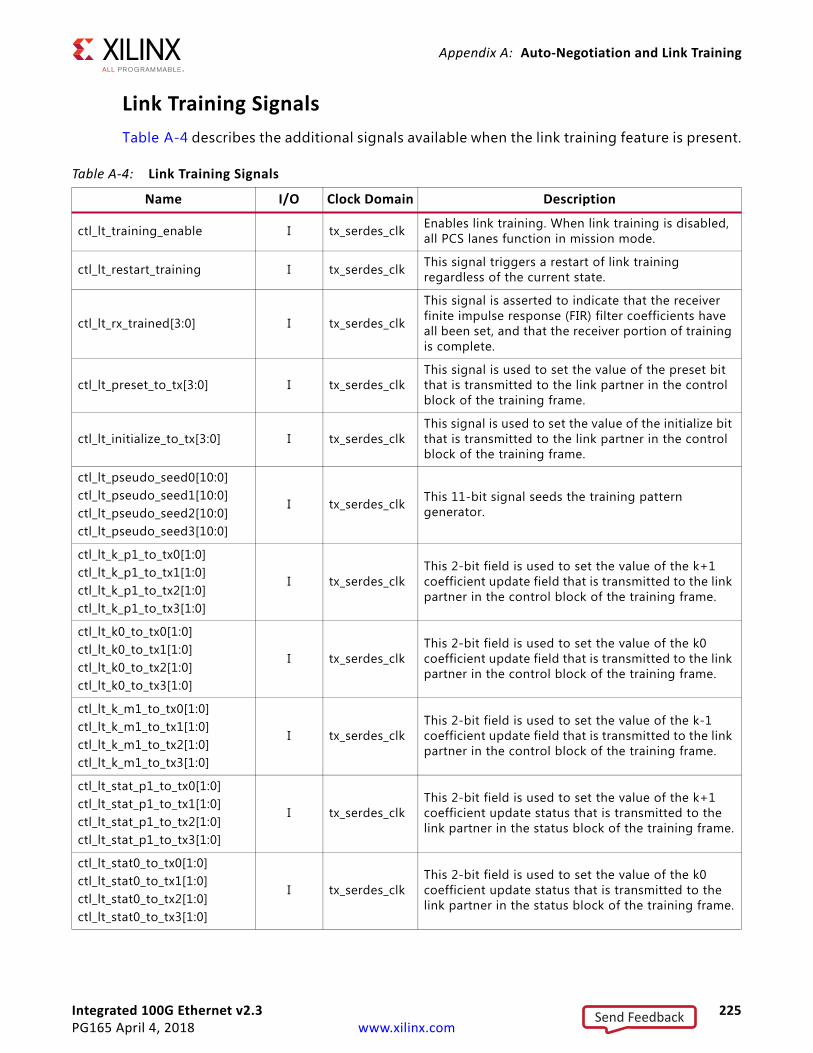
Integrated 100G Ethernet v2.3 225PG165 April 4, 2018 www.xilinx.com
Appendix A: Auto-Negotiation and Link Training
Link Training SignalsTable A-4 describes the additional signals available when the link training feature is present.
Table A-4: Link Training Signals
Name I/O Clock Domain Description
ctl_lt_training_enable I tx_serdes_clk Enables link training. When link training is disabled, all PCS lanes function in mission mode.
ctl_lt_restart_training I tx_serdes_clk This signal triggers a restart of link training regardless of the current state.
ctl_lt_rx_trained[3:0] I tx_serdes_clk
This signal is asserted to indicate that the receiver finite impulse response (FIR) filter coefficients have all been set, and that the receiver portion of training is complete.
ctl_lt_preset_to_tx[3:0] I tx_serdes_clkThis signal is used to set the value of the preset bit that is transmitted to the link partner in the control block of the training frame.
ctl_lt_initialize_to_tx[3:0] I tx_serdes_clkThis signal is used to set the value of the initialize bit that is transmitted to the link partner in the control block of the training frame.
ctl_lt_pseudo_seed0[10:0]ctl_lt_pseudo_seed1[10:0]ctl_lt_pseudo_seed2[10:0]ctl_lt_pseudo_seed3[10:0]
I tx_serdes_clk This 11-bit signal seeds the training pattern generator.
ctl_lt_k_p1_to_tx0[1:0]ctl_lt_k_p1_to_tx1[1:0]ctl_lt_k_p1_to_tx2[1:0]ctl_lt_k_p1_to_tx3[1:0]
I tx_serdes_clkThis 2-bit field is used to set the value of the k+1 coefficient update field that is transmitted to the link partner in the control block of the training frame.
ctl_lt_k0_to_tx0[1:0]ctl_lt_k0_to_tx1[1:0]ctl_lt_k0_to_tx2[1:0]ctl_lt_k0_to_tx3[1:0]
I tx_serdes_clkThis 2-bit field is used to set the value of the k0 coefficient update field that is transmitted to the link partner in the control block of the training frame.
ctl_lt_k_m1_to_tx0[1:0]ctl_lt_k_m1_to_tx1[1:0]ctl_lt_k_m1_to_tx2[1:0]ctl_lt_k_m1_to_tx3[1:0]
I tx_serdes_clkThis 2-bit field is used to set the value of the k-1 coefficient update field that is transmitted to the link partner in the control block of the training frame.
ctl_lt_stat_p1_to_tx0[1:0]ctl_lt_stat_p1_to_tx1[1:0]ctl_lt_stat_p1_to_tx2[1:0]ctl_lt_stat_p1_to_tx3[1:0]
I tx_serdes_clkThis 2-bit field is used to set the value of the k+1 coefficient update status that is transmitted to the link partner in the status block of the training frame.
ctl_lt_stat0_to_tx0[1:0]ctl_lt_stat0_to_tx1[1:0]ctl_lt_stat0_to_tx2[1:0]ctl_lt_stat0_to_tx3[1:0]
I tx_serdes_clkThis 2-bit field is used to set the value of the k0 coefficient update status that is transmitted to the link partner in the status block of the training frame.
Send Feedback
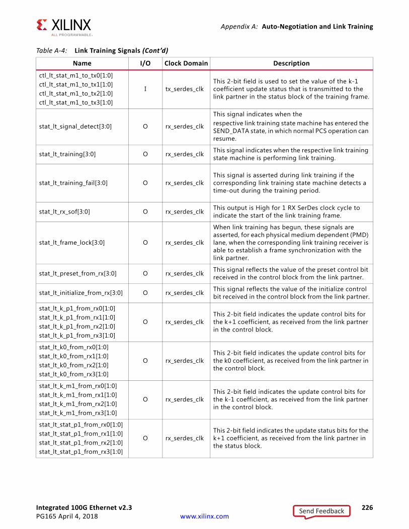
Integrated 100G Ethernet v2.3 226PG165 April 4, 2018 www.xilinx.com
Appendix A: Auto-Negotiation and Link Training
ctl_lt_stat_m1_to_tx0[1:0]ctl_lt_stat_m1_to_tx1[1:0]ctl_lt_stat_m1_to_tx2[1:0]ctl_lt_stat_m1_to_tx3[1:0]
I tx_serdes_clkThis 2-bit field is used to set the value of the k-1 coefficient update status that is transmitted to the link partner in the status block of the training frame.
stat_lt_signal_detect[3:0] O rx_serdes_clk
This signal indicates when therespective link training state machine has entered the SEND_DATA state, in which normal PCS operation can resume.
stat_lt_training[3:0] O rx_serdes_clk This signal indicates when the respective link training state machine is performing link training.
stat_lt_training_fail[3:0] O rx_serdes_clkThis signal is asserted during link training if the corresponding link training state machine detects a time-out during the training period.
stat_lt_rx_sof[3:0] O rx_serdes_clk This output is High for 1 RX SerDes clock cycle to indicate the start of the link training frame.
stat_lt_frame_lock[3:0] O rx_serdes_clk
When link training has begun, these signals are asserted, for each physical medium dependent (PMD) lane, when the corresponding link training receiver is able to establish a frame synchronization with the link partner.
stat_lt_preset_from_rx[3:0] O rx_serdes_clk This signal reflects the value of the preset control bit received in the control block from the link partner.
stat_lt_initialize_from_rx[3:0] O rx_serdes_clk This signal reflects the value of the initialize control bit received in the control block from the link partner.
stat_lt_k_p1_from_rx0[1:0]stat_lt_k_p1_from_rx1[1:0]stat_lt_k_p1_from_rx2[1:0]stat_lt_k_p1_from_rx3[1:0]
O rx_serdes_clkThis 2-bit field indicates the update control bits for the k+1 coefficient, as received from the link partner in the control block.
stat_lt_k0_from_rx0[1:0]stat_lt_k0_from_rx1[1:0]stat_lt_k0_from_rx2[1:0]stat_lt_k0_from_rx3[1:0]
O rx_serdes_clkThis 2-bit field indicates the update control bits for the k0 coefficient, as received from the link partner in the control block.
stat_lt_k_m1_from_rx0[1:0]stat_lt_k_m1_from_rx1[1:0]stat_lt_k_m1_from_rx2[1:0]stat_lt_k_m1_from_rx3[1:0]
O rx_serdes_clkThis 2-bit field indicates the update control bits for the k-1 coefficient, as received from the link partner in the control block.
stat_lt_stat_p1_from_rx0[1:0]stat_lt_stat_p1_from_rx1[1:0]stat_lt_stat_p1_from_rx2[1:0]stat_lt_stat_p1_from_rx3[1:0]
O rx_serdes_clkThis 2-bit field indicates the update status bits for the k+1 coefficient, as received from the link partner in the status block.
Table A-4: Link Training Signals (Cont’d)
Name I/O Clock Domain Description
Send Feedback
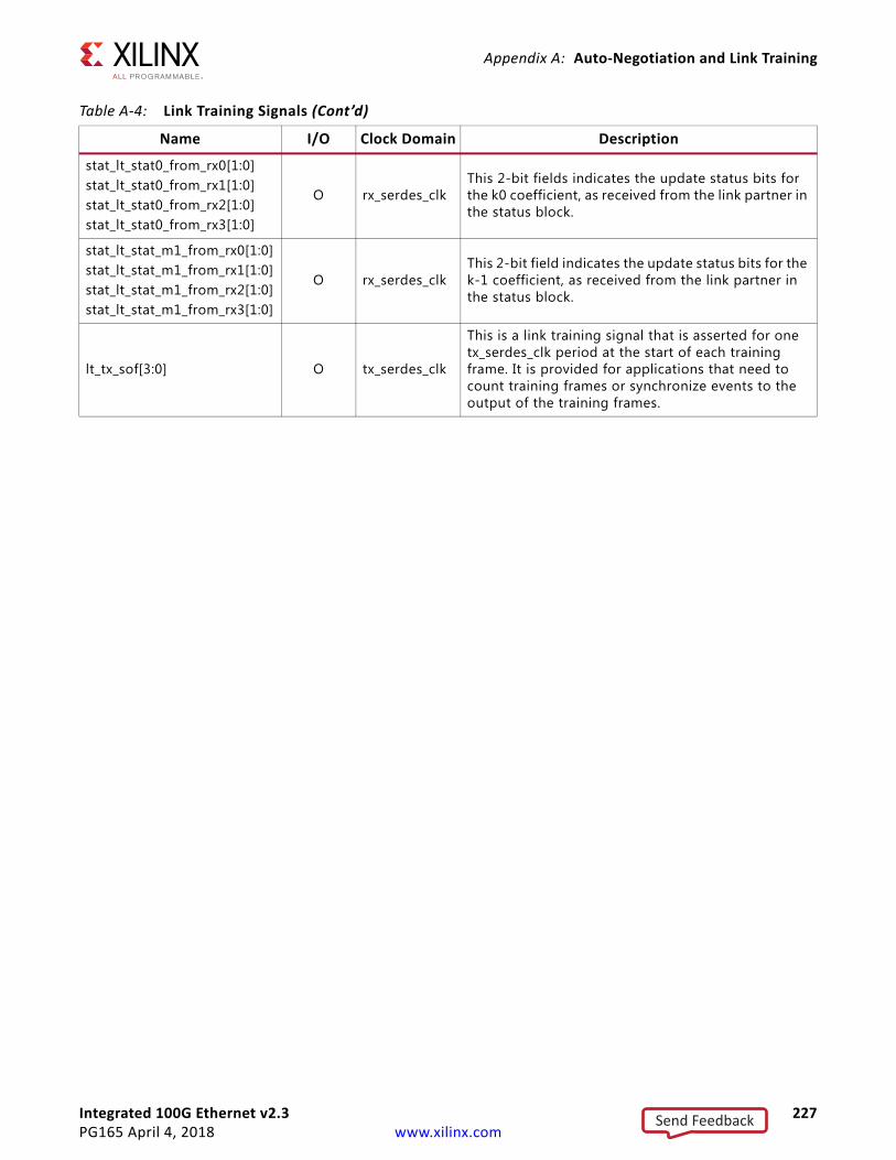
Integrated 100G Ethernet v2.3 227PG165 April 4, 2018 www.xilinx.com
Appendix A: Auto-Negotiation and Link Training
stat_lt_stat0_from_rx0[1:0]stat_lt_stat0_from_rx1[1:0]stat_lt_stat0_from_rx2[1:0]stat_lt_stat0_from_rx3[1:0]
O rx_serdes_clkThis 2-bit fields indicates the update status bits for the k0 coefficient, as received from the link partner in the status block.
stat_lt_stat_m1_from_rx0[1:0]stat_lt_stat_m1_from_rx1[1:0]stat_lt_stat_m1_from_rx2[1:0]stat_lt_stat_m1_from_rx3[1:0]
O rx_serdes_clkThis 2-bit field indicates the update status bits for the k-1 coefficient, as received from the link partner in the status block.
lt_tx_sof[3:0] O tx_serdes_clk
This is a link training signal that is asserted for one tx_serdes_clk period at the start of each training frame. It is provided for applications that need to count training frames or synchronize events to the output of the training frames.
Table A-4: Link Training Signals (Cont’d)
Name I/O Clock Domain Description
Send Feedback
Integrated 100G Ethernet v2.3 228PG165 April 4, 2018 www.xilinx.com
Appendix B
UpgradingThis appendix is not applicable to this release of the core, because there are no port or parameter changes.
Send Feedback
Integrated 100G Ethernet v2.3 229PG165 April 4, 2018 www.xilinx.com
Appendix C
DebuggingThis appendix includes details about resources available on the Xilinx® Support website and debugging tools.
Finding Help on Xilinx.comTo help in the design and debug process when using the 100G Ethernet IP core, the Xilinx Support web page contains key resources such as product documentation, release notes, answer records, information about known issues, and links for obtaining further product support.
DocumentationThis product guide is the main document associated with the 100G Ethernet MAC core. This guide, along with documentation related to all products that aid in the design process, can be found on the Xilinx Support web page or by using the Xilinx Documentation Navigator.
Download the Xilinx Documentation Navigator from the Downloads page. For more information about this tool and the features available, open the online help after installation.
Solution CentersSee the Xilinx Solution Centers for support on devices, design tools, and intellectual property at all stages of the design cycle. Topics include design assistance, advisories, and troubleshooting tips.
The Solution Center specific to the 100G Ethernet MAC core is Xilinx Ethernet IP Solution Center.
Send Feedback

Integrated 100G Ethernet v2.3 230PG165 April 4, 2018 www.xilinx.com
Appendix C: Debugging
Answer Records Answer Records include information about commonly encountered problems, helpful information on how to resolve these problems, and any known issues with a Xilinx product. Answer Records are created and maintained daily ensuring that users have access to the most accurate information available.
Answer Records for this core can be located by using the Search Support box on the main Xilinx support web page. To maximize your search results, use proper keywords such as
• Product name
• Tool message(s)
• Summary of the issue encountered
A filter search is available after results are returned to further target the results.
Master Answer Record for the 100G Ethernet MAC core
AR: 58696
Technical SupportXilinx provides technical support at the Xilinx support web page for this LogiCORE™ IP product when used as described in the product documentation. Xilinx cannot guarantee timing, functionality, or support if you do any of the following:
• Implement the solution in devices that are not defined in the documentation.
• Customize the solution beyond that allowed in the product documentation.
• Change any section of the design labeled DO NOT MODIFY.
To contact Xilinx Technical Support, navigate to the Xilinx Support web page.
Debug Tools
Vivado Design Suite Debug FeatureThe Vivado® Design Suite debug feature inserts logic analyzer and virtual I/O cores directly into your design. The debug feature also allows you to set trigger conditions to capture application and integrated block port signals in hardware. Captured signals can then be analyzed. This feature in the Vivado Integrated Design Environment (IDE) is used for logic debugging and validation of a design running in Xilinx devices.
Send Feedback
Integrated 100G Ethernet v2.3 231PG165 April 4, 2018 www.xilinx.com
Appendix C: Debugging
The Vivado logic analyzer is used with the logic debug IP cores, including:
• ILA 2.0 (and later versions)
• VIO 2.0 (and later versions)
See the Vivado Design Suite User Guide: Programming and Debugging (UG908) [Ref 15].
Simulation DebugThe 100G Ethernet IP core example design includes a sample simulation test bench. This consists of a loopback from the TX side of the user interface, through the TX circuit, looping back to the RX circuit, and checking the received packets at the RX side of the user interface.
This section contains details about items that should be checked if the simulation does not run properly from the scripts.
Slow SimulationSimulations can appear to run slowly under some circumstances. If a simulation is unacceptably slow, the following suggestions can improve the run-time performance.
• Use a faster computer with more memory.
• Make use of a Platform LSF (Load Sharing Facility), if available.
• Bypass the Xilinx transceiver (this might require creating your own test bench).
• Send fewer packets. This can be accomplished by modifying the appropriate parameter in the provided sample test bench.
• Specify a shorter time between alignment markers. This should result in a shorter lane alignment phase at the expense of more overhead. However, when the 100G Ethernet IP core is implemented in hardware, the distance between alignment markers should follow the specification recommendations (after every 16,383 words). For more information, see Simulation Speed Up in Chapter 5.
Simulation Fails Before CompletionIf the sample simulation fails or hangs before successfully completing, then it is possible that a timeout has occurred. Ensure that the simulator timeouts are long enough to accommodate the waiting periods in the simulation, for example during the lane alignment phase.
Send Feedback
Integrated 100G Ethernet v2.3 232PG165 April 4, 2018 www.xilinx.com
Appendix C: Debugging
Simulation Completes But FailsIf the sample simulation completes with a failure, contact Xilinx technical support. The test will normally complete successfully. Consult the sample simulation log file for the expected behavior.
Hardware DebugHardware issues range from link bring-up to problems seen after hours of testing. This section provides debug steps for common issues.
General ChecksEnsure that all the timing constraints for the core are properly incorporated from the example design and that all constraints are met during implementation.
• Does it work in post-place and route timing simulation? If problems are seen in hardware but not in timing simulation, this could indicate a PCB issue. Ensure that all clock sources are active and clean.
• If using mixed-mode clock managers (MMCMs) in the design, ensure that all MMCMs have obtained lock by monitoring the LOCKED port.
Ethernet Specific ChecksMany issues can occur during the first hardware test. This section details the debugging process. It is assumed that the 100G Ethernet IP core has already passed all simulation testing which is being implemented in hardware. This is a pre-requisite for any kind of hardware debug.
The following sequence helps to isolate ethernet-specific problems:
1. Clean up Signal Integrity.
2. Ensure that each SerDes achieves clock data recovery (CDR) lock.
3. Check that each lane has achieved word alignment.
4. Check that lane alignment has been achieved.
5. Proceed to Interface Debug and Protocol Debug.
Signal IntegrityIf you are bringing up a board for the first time and the 100G Ethernet IP core does not seem to be achieving lane alignment, the most likely problem is related to signal integrity. Signal integrity issues must be addressed before any other debugging can take place.
Send Feedback
Integrated 100G Ethernet v2.3 233PG165 April 4, 2018 www.xilinx.com
Appendix C: Debugging
Even if lane alignment is achieved, periodic BIP8 errors create signal integrity issues. Check the BIP8 signals to assist with debugging.
IMPORTANT: It assumed that the PCB itself has been designed and manufactured in accordance with the required trace impedances and trace lengths, including the requirements for skew set out in the IEEE 802.3 specification.)
Signal integrity should be debugged independently from the 100G Ethernet IP core. The following checks should be made:
• Transceiver Settings
• Checking For Noise
• Bit Error Rate Testing
If assistance is required for transceiver and signal integrity debugging, contactXilinx technical support.
Lane SwappingIn Ethernet, physical lanes can be swapped and the protocol will align lanes correctly. Therefore lane swapping should not cause any problems.
N/P SwappingIf the positive and negative signals of a differential pair are swapped, data will not be correctly received on that lane. Verify that each link has the correct polarity of each differential pair.
PCS Lane MappingThe stat_rx_pcsl_number_[0:19][4:0] signal indicates which physical lane is receiving PCS lanes [0:19]. See PCS Lane Multiplexing in Chapter 3 to understand the mapping of these 20 Physical lanes to the 4 GT lanes in the case of CAUI-4 or 10 GT lanes in the case of CAUI-10.
In CAUI-10 mode, data on GT0 maps to physical lanes 0 and 1, and so forth; GT9 maps to physical lanes 18 and 19. In CAUI-4 mode, data on GT0 maps to physical lanes 0:4, and so forth; GT3 maps to physical lanes 15:19.
Clocking and ResetsSee Clocking and Resets in Chapter 3 for these requirements.
Ensure that the clock frequencies for both the 100G Ethernet IP core as well as the Xilinx transceiver reference clock match the configuration requested when the IP core was
Send Feedback
Integrated 100G Ethernet v2.3 234PG165 April 4, 2018 www.xilinx.com
Appendix C: Debugging
ordered. The core clock has a minimum frequency associated with it. The maximum core clock frequency is determined by timing constraints. The minimum core clock frequency is derived from the required Ethernet bandwidth plus the margin reserved for clock tolerance, wander and jitter.
The first thing to verify during debugging is to ensure that resets remain asserted until the clock is stable. It must be frequency-stable as well as free from glitches before the 100G Ethernet IP core is taken out of reset. This applies to both the SerDes clock as well as the IP core clock.
If any subsequent instability is detected in a clock, the 100G Ethernet IP core must be reset. One example of such instability is a loss of CDR lock. The user logic should determine all external conditions that would require a reset (for example, clock glitches, loss of CDR lock, or power supply glitches).
The GT requires a GTRXRESET after the serial data becomes valid to insure correct CDR lock to the data. This is required after a cable pull and re-plug, or after powering on or resetting the link partner. At the core level to avoid interruption on the TX side of the link, the reset can be triggered using gtwiz_reset_rx_datapath. If available, signal detect or inversion of loss of signal from the optics can be used to trigger the reset. If signal detect or loss of signal is not available, timeout logic can be added to monitor if alignment has not completed and to issue the gtwiz_reset_rx_datapath reset.
Configuration changes cannot be made unless the IP core is reset. An example of a configuration change would be setting a different maximum packet length. Check the description for the particular signal on the port list to determine if this requirement applies to the parameter that is being changed (Table 2-2).
Interface DebugThe 100G Ethernet IP core user interface is the segmented LBUS (Local bus). This section details debugging information for the TX and RX interfaces.
TX DebugTX debugging is assisted using several diagnostic signals. See Table 2-2 for more details.
Data must be written to the TX LBUS so that there are no overflow or underflow conditions.
The LBUS bandwidth must always be greater than the Ethernet bandwidth to guarantee that data can be sent without interruption.
When writing data to the LBUS, the tx_rdyout signal must always be observed. This signal indicates whether the fill level of the TX buffer is within an acceptable range or not. If this signal is ever asserted, you must stop writing to the TX LBUS until the signal is deasserted.
Send Feedback
Integrated 100G Ethernet v2.3 235PG165 April 4, 2018 www.xilinx.com
Appendix C: Debugging
Because the TX LBUS has greater bandwidth than the TX Ethernet interface, it is not unusual to see this signal being frequently asserted and this is not a cause for concern. You must ensure that TX writes are stopped when tx_rdyout is asserted.
The level at which tx_rdyout becomes asserted is set by a pre-determined threshold.
IMPORTANT: If tx_rdyout is ignored, the signal tx_ovfout might be asserted, indicating a buffer overflow. This should be prevented. Xilinx recommends that the core be reset if tx_ovfout is asserted. Do not attempt to continue debugging after tx_ovfout has been asserted until the cause of the overflow has been addressed.
When a packet data transaction has begun in the TX direction, it must continue until completion or there might be a buffer underflow as indicated by the signal stat_tx_underflow_err. This must not be allowed to occur. Data must be written on the TX LBUS without interruption. Ethernet packets must be present on the line from start to end with no gaps or idles. If stat_tx_underflow_err is asserted, debugging must stop until the condition which caused the underflow has been addressed.
RX DebugSee the port list in Table 2-2 for a complete description of the diagnostic signals that are available to debug the RX.
If the Ethernet packets are being transmitted properly according to the 802.3 protocol, there should not be RX errors. However, the signal integrity of the received signals must be verified first.
The stat_rx_bip_err signals provide a per-lane indicator of signal quality. The stat_rx_hi_ber signal is asserted when the bit error rate is too high, according to the 802.3 protocol. The threshold is BER = 10-4.
To aid in debug, a local loopback can be performed at the transceiver level. This connects the TX SerDes to the RX SerDes and bypasses potential signal integrity problems. The received data can be checked against the transmitted packets to verify that the logic is operating properly.
Protocol DebugTo achieve error-free data transfers with the 100G Ethernet IP core, the 802.3 specification should be followed. Note that signal integrity should always be ensured before proceeding to the protocol debug.
Send Feedback
Integrated 100G Ethernet v2.3 236PG165 April 4, 2018 www.xilinx.com
Appendix C: Debugging
Alignment Marker SpacingAccording to the 802.3 specification, the alignment marker spacing should be set to 16,383 for both the TX and RX. Check that both ends of the link are programmed to this value.
Diagnostic SignalsThere are many error indicators available to check for protocol violations. Carefully read the description of each one to see if it is useful for a particular debugging issue. See Table 2-2 for more details.
The following is a suggested debug sequence.
1. Ensure that Word sync has been achieved.
2. Ensure that Lane sync has been achieved (this uses the lane marker alignment words which occur after every 16,383 words).
3. Verify that the BIP8 indicators are clean.
4. Make sure there are no descrambler state errors.
5. Eliminate CRC32 errors, if any.
6. Make sure the LBUS protocol is being followed correctly.
7. Ensure that there are no overflow or underflow conditions when packets are sent.
Statistics CountersWhen error-free communication has been achieved, the statistics indicators can be monitored to ensure that traffic characteristics meet expectations. Some signals are strobes only, which means that the counters are not part of the core. This is done so that the counter size can be customized. The counters are optional.
Send Feedback

Integrated 100G Ethernet v2.3 237PG165 April 4, 2018 www.xilinx.com
Appendix D
Additional Resources and Legal Notices
Xilinx ResourcesFor support resources such as Answers, Documentation, Downloads, and Forums, see Xilinx Support.
Documentation Navigator and Design HubsXilinx® Documentation Navigator provides access to Xilinx documents, videos, and support resources, which you can filter and search to find information. To open the Xilinx Documentation Navigator (DocNav):
• From the Vivado® IDE, select Help > Documentation and Tutorials.
• On Windows, select Start > All Programs > Xilinx Design Tools > DocNav.
• At the Linux command prompt, enter docnav.
Xilinx Design Hubs provide links to documentation organized by design tasks and other topics, which you can use to learn key concepts and address frequently asked questions. To access the Design Hubs:
• In the Xilinx Documentation Navigator, click the Design Hubs View tab.
• On the Xilinx website, see the Design Hubs page.
Note: For more information on Documentation Navigator, see the Documentation Navigator page on the Xilinx website.
ReferencesThese documents provide supplemental material useful with this product guide:
1. IEEE 1588-2008 (standards.ieee.org/findstds/standard/1588-2008.html)
2. IEEE std 802.3-2012 (standards.ieee.org/findstds/standard/802.3-2012.html)
Send Feedback
Integrated 100G Ethernet v2.3 238PG165 April 4, 2018 www.xilinx.com
Appendix D: Additional Resources and Legal Notices
3. Virtex UltraScale Architecture Data Sheet: DC and AC Switching Characteristics (DS893)
4. UltraScale FPGAs Transceiver Wizards (PG182)
5. UltraScale Architecture Clocking Resource User Guide (UG572)
6. Vivado Design Suite User Guide: Designing IP Subsystems using IP Integrator (UG994)
7. Vivado Design Suite User Guide: Designing with IP (UG896)
8. Vivado Design Suite User Guide: Getting Started (UG910)
9. Vivado Design Suite User Guide: Logic Simulation (UG900)
10. Vivado Design Suite User Guide: Using Constraints (UG903)
11. UltraScale FPGAs GTH Transceivers User Guide (UG576)
12. UltraScale FPGAs GTY Transceivers User Guide (UG578)
13. 100G IEEE 802.3bj Reed-Solomon Forward Error Correction (PG197) — Access in lounge
14. AXI Interconnect LogiCORE IP Product Guide (PG059)
15. Vivado Design Suite User Guide: Programming and Debugging (UG908)
16. ISE to Vivado Design Suite Migration Guide (UG911)
17. Vivado Design Suite User Guide: Implementation (UG904)
Send Feedback
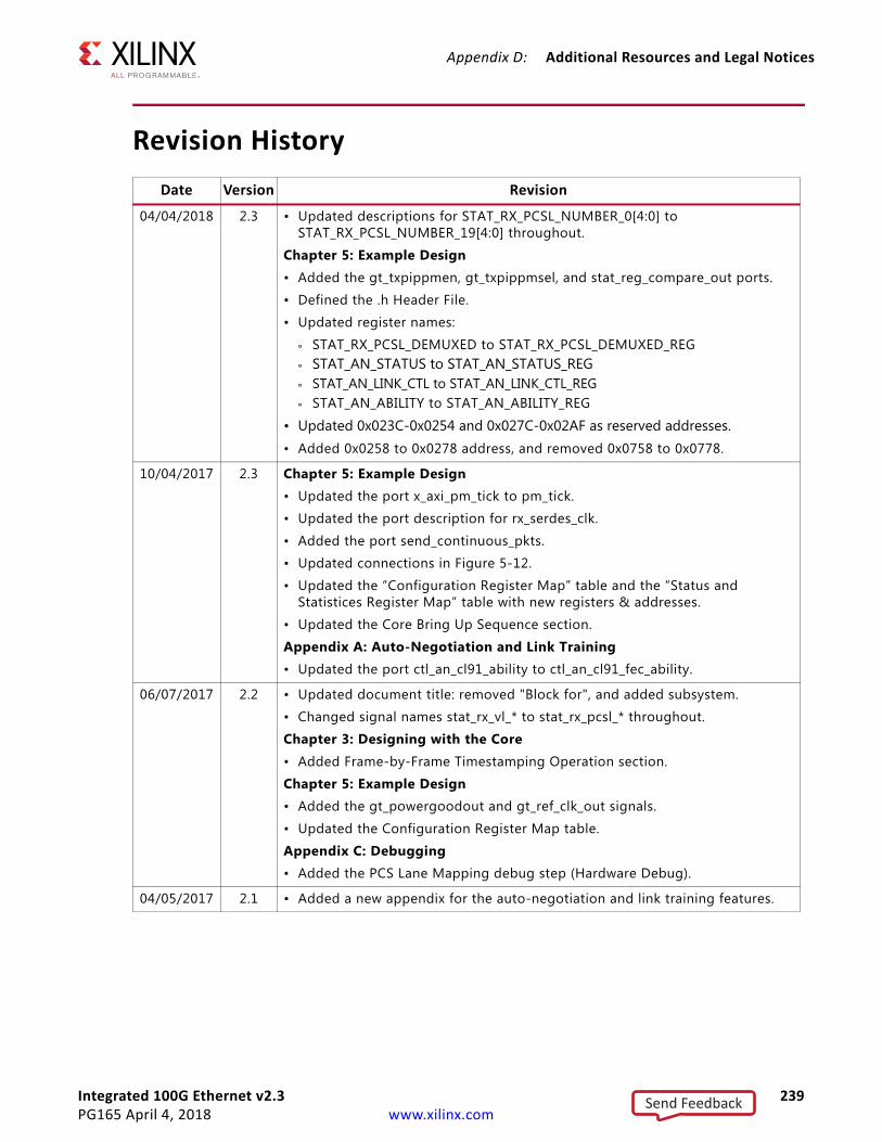
Integrated 100G Ethernet v2.3 239PG165 April 4, 2018 www.xilinx.com
Appendix D: Additional Resources and Legal Notices
Revision History
Date Version Revision
04/04/2018 2.3 • Updated descriptions for STAT_RX_PCSL_NUMBER_0[4:0] to STAT_RX_PCSL_NUMBER_19[4:0] throughout.
Chapter 5: Example Design• Added the gt_txpippmen, gt_txpippmsel, and stat_reg_compare_out ports.
• Defined the .h Header File.
• Updated register names:
° STAT_RX_PCSL_DEMUXED to STAT_RX_PCSL_DEMUXED_REG
° STAT_AN_STATUS to STAT_AN_STATUS_REG° STAT_AN_LINK_CTL to STAT_AN_LINK_CTL_REG
° STAT_AN_ABILITY to STAT_AN_ABILITY_REG
• Updated 0x023C-0x0254 and 0x027C-0x02AF as reserved addresses.• Added 0x0258 to 0x0278 address, and removed 0x0758 to 0x0778.
10/04/2017 2.3 Chapter 5: Example Design• Updated the port x_axi_pm_tick to pm_tick.
• Updated the port description for rx_serdes_clk.
• Added the port send_continuous_pkts.
• Updated connections in Figure 5-12.
• Updated the “Configuration Register Map” table and the “Status and Statistices Register Map” table with new registers & addresses.
• Updated the Core Bring Up Sequence section.
Appendix A: Auto-Negotiation and Link Training• Updated the port ctl_an_cl91_ability to ctl_an_cl91_fec_ability.
06/07/2017 2.2 • Updated document title: removed "Block for", and added subsystem.
• Changed signal names stat_rx_vl_* to stat_rx_pcsl_* throughout.
Chapter 3: Designing with the Core• Added Frame-by-Frame Timestamping Operation section.
Chapter 5: Example Design• Added the gt_powergoodout and gt_ref_clk_out signals.
• Updated the Configuration Register Map table.
Appendix C: Debugging• Added the PCS Lane Mapping debug step (Hardware Debug).
04/05/2017 2.1 • Added a new appendix for the auto-negotiation and link training features.
Send Feedback
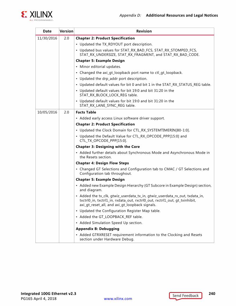
Integrated 100G Ethernet v2.3 240PG165 April 4, 2018 www.xilinx.com
Appendix D: Additional Resources and Legal Notices
11/30/2016 2.0 Chapter 2: Product Specification• Updated the TX_RDYOUT port description.
• Updated bus values for STAT_RX_BAD_FCS, STAT_RX_STOMPED_FCS, STAT_RX_UNDERSIZE, STAT_RX_FRAGMENT, and STAT_RX_BAD_CODE.
Chapter 5: Example Design• Minor editorial updates.
• Changed the axi_gt_loopback port name to ctl_gt_loopback.
• Updated the drp_addr port description.
• Updated default values for bit 0 and bit 1 in the STAT_RX_STATUS_REG table.
• Updated default values for bit 19:0 and bit 31:20 in the STAT_RX_BLOCK_LOCK_REG table.
• Updated default values for bit 19:0 and bit 31:20 in the STAT_RX_LANE_SYNC_REG table.
10/05/2016 2.0 Facts Table• Added early access Linux software driver support.
Chapter 2: Product Specification• Updated the Clock Domain for CTL_RX_SYSTEMTIMERIN[80-1:0].
• Updated the Default Value for CTL_RX_OPCODE_PPP[15:0] and CTL_TX_OPCODE_PPP[15:0].
Chapter 3: Designing with the Core• Added further details about Synchronous Mode and Asynchronous Mode in
the Resets section.
Chapter 4: Design Flow Steps• Changed GT Selections and Configuration tab to CMAC / GT Selections and
Configuration tab throughout.
Chapter 5: Example Design• Added new Example Design Hierarchy (GT Subcore in Example Design) section,
and diagram.
• Added the tx_clk, gtwiz_userdata_tx_in, gtwiz_userdata_rx_out, txdata_in, txctrl0_in, txctrl1_in, rxdata_out, rxctrl0_out, rxctrl1_out, gt_txinhibit, axi_gt_reset_all, and axi_gt_loopback signals.
• Updated the Configuration Register Map table.
• Added the GT_LOOPBACK_REF table.
• Added Simulation Speed Up section.
Appendix B: Debugging• Added GTRXRESET requirement information to the Clocking and Resets
section under Hardware Debug.
Date Version Revision
Send Feedback
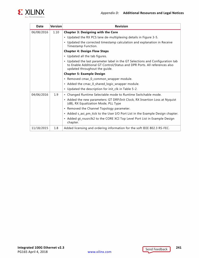
Integrated 100G Ethernet v2.3 241PG165 April 4, 2018 www.xilinx.com
Appendix D: Additional Resources and Legal Notices
06/08/2016 1.10 Chapter 3: Designing with the Core• Updated the RX PCS lane de-multiplexing details in Figure 3-5.
• Updated the corrected timestamp calculation and explanation in Receive Timestamp Function.
Chapter 4: Design Flow Steps• Updated all the tab figures.
• Updated the last parameter label in the GT Selections and Configuration tab to Enable Additional GT Control/Status and DPR Ports. All references also updated throughout the guide.
Chapter 5: Example Design• Removed cmac_0_common_wrapper module.
• Added the cmac_0_shared_logic_wrapper module.
• Updated the description for init_clk in Table 5-2.
04/06/2016 1.9 • Changed Runtime Selectable mode to Runtime Switchable mode.
• Added the new parameters: GT DRP/Init Clock, RX Insertion Loss at Nyquist (dB), RX Equalization Mode, PLL Type
• Removed the Channel Topology parameter.
• Added s_axi_pm_tick to the User I/O Port List in the Example Design chapter.
• Added gt_rxusrclk2 to the CORE XCI Top Level Port List in Example Design chapter.
11/18/2015 1.8 Added licensing and ordering information for the soft IEEE 802.3 RS-FEC.
Date Version Revision
Send Feedback
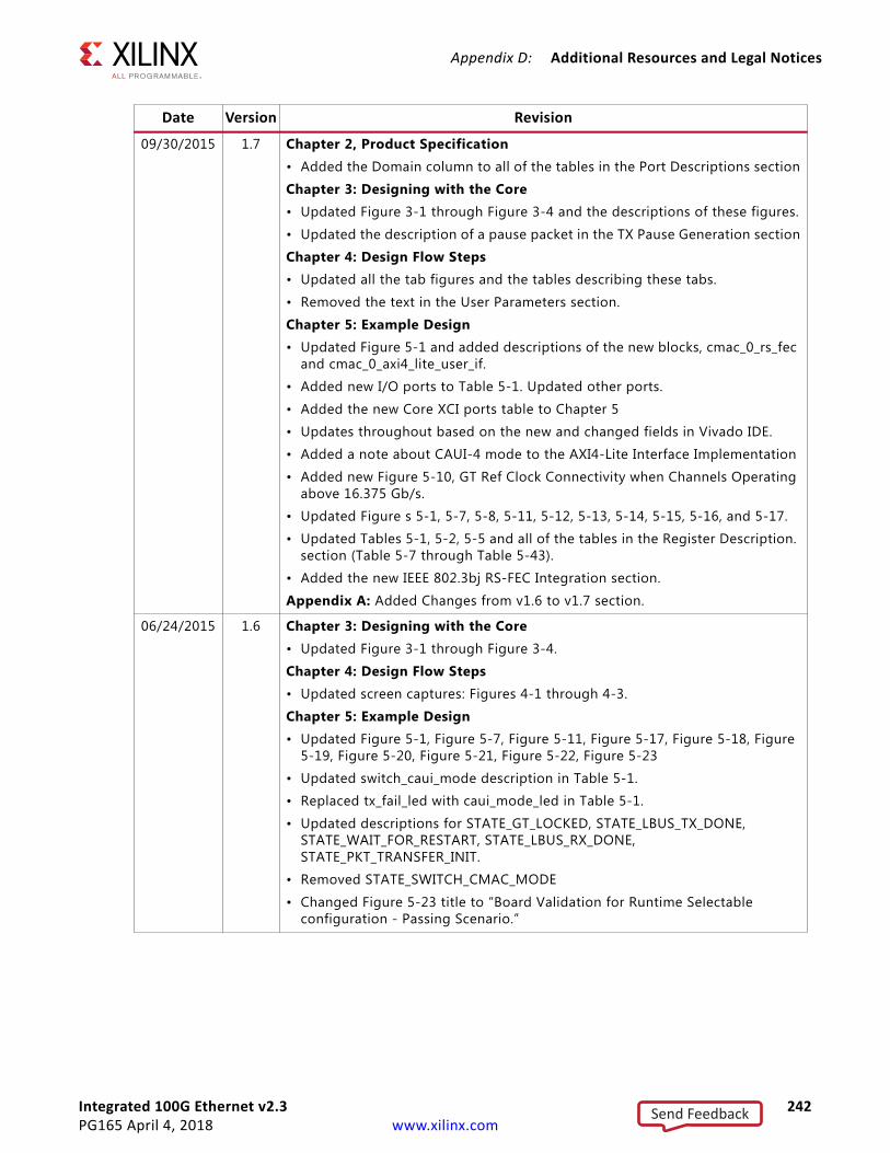
Integrated 100G Ethernet v2.3 242PG165 April 4, 2018 www.xilinx.com
Appendix D: Additional Resources and Legal Notices
09/30/2015 1.7 Chapter 2, Product Specification• Added the Domain column to all of the tables in the Port Descriptions section
Chapter 3: Designing with the Core• Updated Figure 3-1 through Figure 3-4 and the descriptions of these figures.
• Updated the description of a pause packet in the TX Pause Generation section
Chapter 4: Design Flow Steps• Updated all the tab figures and the tables describing these tabs.
• Removed the text in the User Parameters section.
Chapter 5: Example Design• Updated Figure 5-1 and added descriptions of the new blocks, cmac_0_rs_fec
and cmac_0_axi4_lite_user_if.
• Added new I/O ports to Table 5-1. Updated other ports.
• Added the new Core XCI ports table to Chapter 5
• Updates throughout based on the new and changed fields in Vivado IDE.
• Added a note about CAUI-4 mode to the AXI4-Lite Interface Implementation
• Added new Figure 5-10, GT Ref Clock Connectivity when Channels Operating above 16.375 Gb/s.
• Updated Figure s 5-1, 5-7, 5-8, 5-11, 5-12, 5-13, 5-14, 5-15, 5-16, and 5-17.
• Updated Tables 5-1, 5-2, 5-5 and all of the tables in the Register Description. section (Table 5-7 through Table 5-43).
• Added the new IEEE 802.3bj RS-FEC Integration section.
Appendix A: Added Changes from v1.6 to v1.7 section.
06/24/2015 1.6 Chapter 3: Designing with the Core• Updated Figure 3-1 through Figure 3-4.
Chapter 4: Design Flow Steps• Updated screen captures: Figures 4-1 through 4-3.
Chapter 5: Example Design• Updated Figure 5-1, Figure 5-7, Figure 5-11, Figure 5-17, Figure 5-18, Figure
5-19, Figure 5-20, Figure 5-21, Figure 5-22, Figure 5-23
• Updated switch_caui_mode description in Table 5-1.
• Replaced tx_fail_led with caui_mode_led in Table 5-1.
• Updated descriptions for STATE_GT_LOCKED, STATE_LBUS_TX_DONE, STATE_WAIT_FOR_RESTART, STATE_LBUS_RX_DONE, STATE_PKT_TRANSFER_INIT.
• Removed STATE_SWITCH_CMAC_MODE
• Changed Figure 5-23 title to “Board Validation for Runtime Selectable configuration - Passing Scenario.”
Date Version Revision
Send Feedback
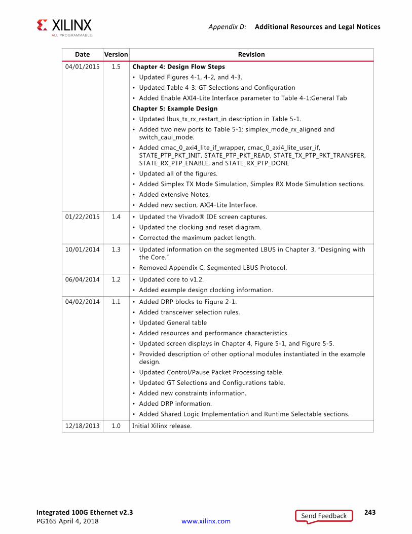
Integrated 100G Ethernet v2.3 243PG165 April 4, 2018 www.xilinx.com
Appendix D: Additional Resources and Legal Notices
04/01/2015 1.5 Chapter 4: Design Flow Steps• Updated Figures 4-1, 4-2, and 4-3.
• Updated Table 4-3: GT Selections and Configuration
• Added Enable AXI4-Lite Interface parameter to Table 4-1:General Tab
Chapter 5: Example Design• Updated lbus_tx_rx_restart_in description in Table 5-1.
• Added two new ports to Table 5-1: simplex_mode_rx_aligned and switch_caui_mode.
• Added cmac_0_axi4_lite_if_wrapper, cmac_0_axi4_lite_user_if, STATE_PTP_PKT_INIT, STATE_PTP_PKT_READ, STATE_TX_PTP_PKT_TRANSFER, STATE_RX_PTP_ENABLE, and STATE_RX_PTP_DONE
• Updated all of the figures.
• Added Simplex TX Mode Simulation, Simplex RX Mode Simulation sections.
• Added extensive Notes.
• Added new section, AXI4-Lite Interface.
01/22/2015 1.4 • Updated the Vivado® IDE screen captures.
• Updated the clocking and reset diagram.
• Corrected the maximum packet length.
10/01/2014 1.3 • Updated information on the segmented LBUS in Chapter 3, “Designing with the Core.”
• Removed Appendix C, Segmented LBUS Protocol.
06/04/2014 1.2 • Updated core to v1.2.
• Added example design clocking information.
04/02/2014 1.1 • Added DRP blocks to Figure 2-1.
• Added transceiver selection rules.
• Updated General table
• Added resources and performance characteristics.
• Updated screen displays in Chapter 4, Figure 5-1, and Figure 5-5.
• Provided description of other optional modules instantiated in the example design.
• Updated Control/Pause Packet Processing table.
• Updated GT Selections and Configurations table.
• Added new constraints information.
• Added DRP information.
• Added Shared Logic Implementation and Runtime Selectable sections.
12/18/2013 1.0 Initial Xilinx release.
Date Version Revision
Send Feedback
Integrated 100G Ethernet v2.3 244PG165 April 4, 2018 www.xilinx.com
Appendix D: Additional Resources and Legal Notices
Please Read: Important Legal NoticesThe information disclosed to you hereunder (the "Materials") is provided solely for the selection and use of Xilinx products. To the maximum extent permitted by applicable law: (1) Materials are made available "AS IS" and with all faults, Xilinx hereby DISCLAIMS ALL WARRANTIES AND CONDITIONS, EXPRESS, IMPLIED, OR STATUTORY, INCLUDING BUT NOT LIMITED TO WARRANTIES OF MERCHANTABILITY, NON-INFRINGEMENT, OR FITNESS FOR ANY PARTICULAR PURPOSE; and (2) Xilinx shall not be liable (whether in contract or tort, including negligence, or under any other theory of liability) for any loss or damage of any kind or nature related to, arising under, or in connection with, the Materials (including your use of the Materials), including for any direct, indirect, special, incidental, or consequential loss or damage (including loss of data, profits, goodwill, or any type of loss or damage suffered as a result of any action brought by a third party) even if such damage or loss was reasonably foreseeable or Xilinx had been advised of the possibility of the same. Xilinx assumes no obligation to correct any errors contained in the Materials or to notify you of updates to the Materials or to product specifications. You may not reproduce, modify, distribute, or publicly display the Materials without prior written consent. Certain products are subject to the terms and conditions of Xilinx's limited warranty, please refer to Xilinx's Terms of Sale which can be viewed at https://www.xilinx.com/legal.htm#tos; IP cores may be subject to warranty and support terms contained in a license issued to you by Xilinx. Xilinx products are not designed or intended to be fail-safe or for use in any application requiring fail-safe performance; you assume sole risk and liability for use of Xilinx products in such critical applications, please refer to Xilinx's Terms of Sale which can be viewed at https://www.xilinx.com/legal.htm#tos.AUTOMOTIVE APPLICATIONS DISCLAIMERAUTOMOTIVE PRODUCTS (IDENTIFIED AS “XA” IN THE PART NUMBER) ARE NOT WARRANTED FOR USE IN THE DEPLOYMENT OF AIRBAGS OR FOR USE IN APPLICATIONS THAT AFFECT CONTROL OF A VEHICLE (“SAFETY APPLICATION”) UNLESS THERE IS A SAFETY CONCEPT OR REDUNDANCY FEATURE CONSISTENT WITH THE ISO 26262 AUTOMOTIVE SAFETY STANDARD (“SAFETY DESIGN”). CUSTOMER SHALL, PRIOR TO USING OR DISTRIBUTING ANY SYSTEMS THAT INCORPORATE PRODUCTS, THOROUGHLY TEST SUCH SYSTEMS FOR SAFETY PURPOSES. USE OF PRODUCTS IN A SAFETY APPLICATION WITHOUT A SAFETY DESIGN IS FULLY AT THE RISK OF CUSTOMER, SUBJECT ONLY TO APPLICABLE LAWS AND REGULATIONS GOVERNING LIMITATIONS ON PRODUCT LIABILITY.© Copyright 2013–2018 Xilinx, Inc. Xilinx, the Xilinx logo, Artix, ISE, Kintex, Spartan, Virtex, Vivado, Zynq, and other designated brands included herein are trademarks of Xilinx in the United States and other countries. All other trademarks are the property of their respective owners.
Send Feedback