ultrasonic assisted nanomanipulations with atomic force ... · semiconductor physics, quantum...
TRANSCRIPT

Semiconductor Physics, Quantum Electronics & Optoelectronics, 2010. V. 13, N 1. P. 36-42.
© 2010, V. Lashkaryov Institute of Semiconductor Physics, National Academy of Sciences of Ukraine
36
PACS 07.79.Sp, 43.35.-c, 68.37.Ps, 81.16.-c
Ultrasonic assisted nanomanipulations with atomic force microscope
P.M. Lytvyn1, O.Ya. Olikh2, O.S. Lytvyn1, O.M. Dyachyns’ka1, I.V. Prokopenko1
1V. Lashkaryov Institute of Semiconductor Physics, NAS of Ukraine, 41, prospect Nauky, 03028 Kyiv, Ukraine; e-mail: [email protected] Shevchenko Kyiv National University, 64, Volodymyrs’ka, 01601 Kyiv, Ukraine
Abstract. Demonstrated experimentally in this work was the possibility of controlled handling the nanoparticles with the size from 50 up to 250 nm on a semiconductor surface by using an atomic force microscope under conditions of acoustic excitation. It has been shown that the selective transport of particles of a certain size is possible owing to the change of an ultrasonic vibration amplitude. Also in this study, possible mechanisms in which ultrasound may influence the particle-surface interaction and the probe-particle (surface) interaction have been analyzed.
Keywords: atomic force microscope, nanoparticle, nanomanipulations, ultrasound.
Manuscript received 10.09.09; accepted for publication 22.10.09; published online 04.12.09.
1. Introduction
Manipulation of nanometer scale objects of any nature and their positioning with subnanometer accuracy is becoming an inalienable part of current nanotechnology. Nanomanipulation means that objects can be displaced, drawn, repositioned, assembled, cut off under the influence of external factors. The most promising instrument for such purposes is a scanning probe microscope (SPM), which can operate simultaneously as a diagnostic device and manipulator. In a number of cases, a SPM probe operates as an ultra precise robot that performs accurate repositioning with three degrees of freedom employing various types of interaction (mechanical, electrical, magnetic, optical, thermal) depending on the required task. Besides, different methods of nanolithography, which are carried out by SPM, enable one both to perform nanoassemblies and to integrate them into micrometer-scale structures manufactured by means of traditional electron-beam lithography [1-4].
Among nanometer objects, nanoparticles (NP) of different nature receive special attention. In particular, colloid NP can be obtained having an exact predefinedsize by using the relatively inexpensive technologies; in addition, planar structures with NP also demonstrate great technological potential. For example, it has been shown [5-6] that, at a certain placement of gold NP into the points of nanometer mesh, it is possible to achieve the density of information recording on its surface of the order of several Tb/in2. Furthermore, SPM has been
instrumental in creating numerous up-to-date prototypes of electronic and optoelectronic devices. Thus, by means of placing nanoparticles in the tunneling gap between two electrodes (source and drain), one can make a single-electron transistor [7-11]; and using a metal NP chain, it is possible to create a “plasmonic” waveguide [12-14]. Nanomanipulations of metal NP and carbon nanotubes with the use of an atomic force microscope (AFM) make it possible to produce both separate elements and structured surfaces for subsequent manufacturing of matrixed nanoelectromechanical systems (NEMS) [15-17]. In nanomedicine and biotechnology, high-precision manipulations, micro-preparations, and nanoextraction of genetic material [18, 19] enable one to develop biosensors for genetic analyses and to produce integrated smart-sensors (lab-on-a chip diagnostic devices).
It is obvious that to ensure a successful nanomanipulation, a number of problems connected with the specific character of physical interactions between objects whose size is measured on a nanometer scale have to be solved first. In many cases, we should take into consideration the interaction of nanoobjects with the environment and a substrate, their interaction, the interaction with the nanoprobe and possible effects from external disturbances (electromagnetic fields, temperatures, humidity etc.). In addition, the technical side of the process also presents some challenges, such as the detection of the required nanoobjects on substrates of a microscopic size and their accurate and controlled movement.
Semiconductor Physics, Quantum Electronics & Optoelectronics, 2010. V. 13, N 1. P. 36-42.
© 2010, V. Lashkaryov Institute of Semiconductor Physics, National Academy of Sciences of Ukraine
37
Since the matter of stabilizing and fixing nanoobjects on substrates can be successfully dealt with at the stage of a sample preparation (preparation component), the task of accomplishing the optimal substrate – nanoobject – SPM nanoprobe (AFM tip) interaction gains particular importance in the process of nanomanipulation. Thus, in the contact operational mode of AFM, which is one of the SPM modes, the load of several nanoNewtons results in the under-tip pressure of the order of several gigaPascals, which is unacceptable when handling polymers and biological samples. Using the dynamic mode of AFM operation (tapping mode) [20], it is possible to significantly reduce the mechanical effect of the probe on the surface. However, in this situation, the transport of the particles attached to the surface presents some difficulties. For example, under the conditions of a weak coupling, nanoparticles often attach to the AFM tip in an uncontrolled manner. Even though, there are publications in which, for particular systems, the matter of a control over the processes of NP attachment (detachment) to a SPM probe is proposed to be solved using electrostatic “nanocranes” [9, 20, 21] and optical tweezers [18]; in our opinion, the more promising technique for this purpose is control over the force of an interaction between a substrate and NP.
In this work, we show how by applying an additional ultrasonic (US) excitation to the surface it is possible effectively and in a controlled way to reduce the strength of the coupling between the surface and NP. What is more, it is demonstrated that a specific change in the ultrasonic vibrations amplitude allows one to selectively transport particles of a certain size. This approach to carrying out a precise manipulation seems more versatile, that is why it is surprising that there are so few studies dealing with the issue [22]. On the other hand, it is worth noting that an additional acoustic excitation during the characterization of mechanical properties of surfaces by SPM methods has been used quite extensively [23-27].
2. Experimental setup and samples
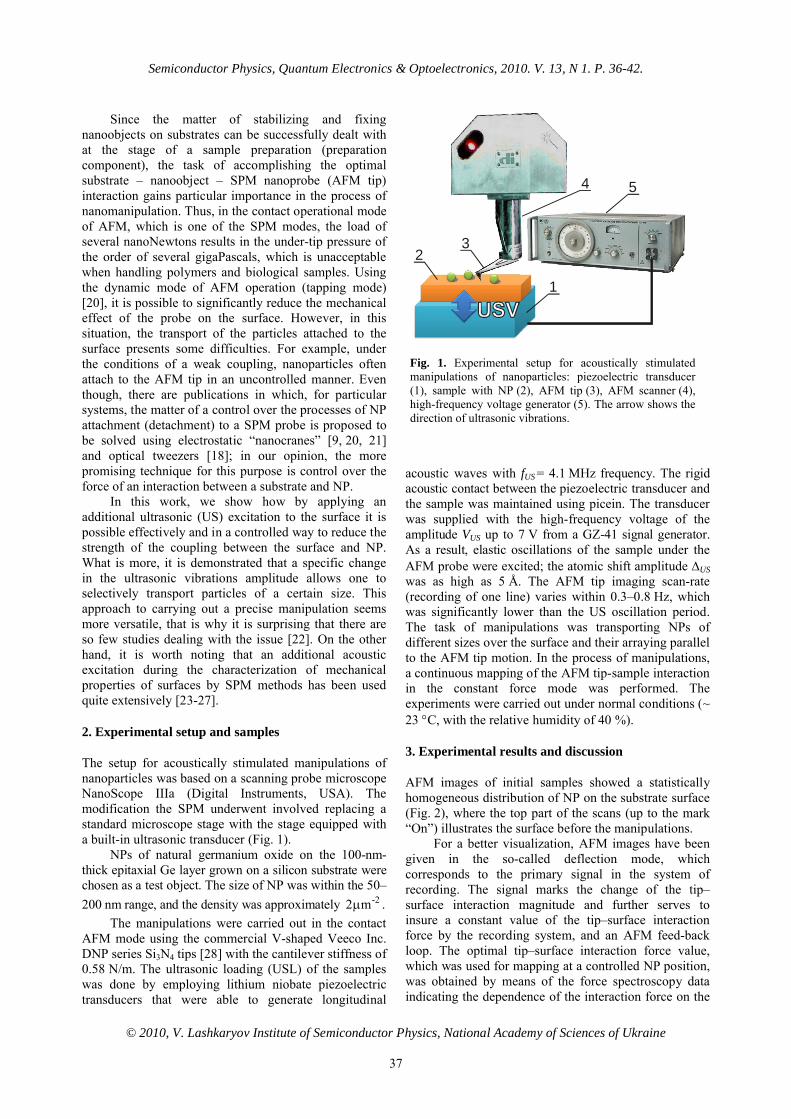
The setup for acoustically stimulated manipulations of nanoparticles was based on a scanning probe microscope NanoScope IIIa (Digital Instruments, USA). The modification the SPM underwent involved replacing a standard microscope stage with the stage equipped with a built-in ultrasonic transducer (Fig. 1).
NPs of natural germanium oxide on the 100-nm-thick epitaxial Ge layer grown on a silicon substrate were chosen as a test object. The size of NP was within the 50–
200 nm range, and the density was approximately -2m2 .
The manipulations were carried out in the contact AFM mode using the commercial V-shaped Veeco Inc. DNP series Si3N4 tips [28] with the cantilever stiffness of 0.58 N/m. The ultrasonic loading (USL) of the samples was done by employing lithium niobate piezoelectric transducers that were able to generate longitudinal
acoustic waves with fUS = 4.1 MHz frequency. The rigid acoustic contact between the piezoelectric transducer and the sample was maintained using picein. The transducer was supplied with the high-frequency voltage of the amplitude VUS up to 7 V from a GZ-41 signal generator. As a result, elastic oscillations of the sample under the AFM probe were excited; the atomic shift amplitude US
was as high as 5 Å. The AFM tip imaging scan-rate (recording of one line) varies within 0.3–0.8 Hz, which was significantly lower than the US oscillation period. The task of manipulations was transporting NPs of different sizes over the surface and their arraying parallel to the AFM tip motion. In the process of manipulations, a continuous mapping of the AFM tip-sample interaction in the constant force mode was performed. The experiments were carried out under normal conditions (~ 23 С, with the relative humidity of 40 %).
3. Experimental results and discussion
AFM images of initial samples showed a statistically homogeneous distribution of NP on the substrate surface (Fig. 2), where the top part of the scans (up to the mark “On”) illustrates the surface before the manipulations.
For a better visualization, AFM images have been given in the so-called deflection mode, which corresponds to the primary signal in the system of recording. The signal marks the change of the tip–surface interaction magnitude and further serves to insure a constant value of the tip–surface interaction force by the recording system, and an AFM feed-back loop. The optimal tip–surface interaction force value, which was used for mapping at a controlled NP position, was obtained by means of the force spectroscopy data indicating the dependence of the interaction force on the
1
23
4 5
Fig. 1. Experimental setup for acoustically stimulated manipulations of nanoparticles: piezoelectric transducer (1), sample with NP (2), AFM tip (3), AFM scanner (4), high-frequency voltage generator (5). The arrow shows the direction of ultrasonic vibrations.

Semiconductor Physics, Quantum Electronics & Optoelectronics, 2010. V. 13, N 1. P. 36-42.
© 2010, V. Lashkaryov Institute of Semiconductor Physics, National Academy of Sciences of Ukraine
38
tip–surface distance. In our case, the optimal force was close to 20 nN. This force magnitude guaranteed a sure interaction between the AFM tip and the surface during the measurements and, at the same time, was quite small so as to prevent any possible damages of the tip apex and the surface as a result of a mechanical contact.
If we set a bigger magnitude of the tip–surface interaction force or switch into a constant height mode (in which the AFM probe moves only in the sample plane), then it is expected to observe the NP transport on the surface by the AFM tip. However, experiments demonstrated that it is quite impossible to perform NP transport over the surface using tips with a given stiffness. At the same time, the maximum lateral force (torsion deformation of the AFM tip cantilever) was equal 60 nN, which, in its turn, indicates an exceeding value of the NP–surface binding force.
The situation changes to the reverse when ultrasonic oscillations are excited in the sample: even at the optimal for mapping tip–surface interaction force, one can detect effective NP movements. Fig. 2a presents an AFM image of a surface area with NP without excitation of US oscillations and with them. As we can observe, under the US excitation AFM does not record single NP, but only the tracks of their movements. Besides, the scanner continues performing standard for
mapping raster scanning of the surface and NP move over the surface only at the moments of a direct contact with the AFM tip in the direction of slow scanning (the insert in Fig. 2c, SS direction). Immediately after switching off the US, NP motions stop and the AFM records NP with the size of up to 150 nm arrayed along fast scanning direction (Fig. 2a, the first mark “Off”). After resuming US, the next along the way of the probe group of NP starts moving. During repeated scanning under the conditions of USL, an arrayed before NP group gets mixed (see the tracks in Fig. 2b), as a result, in a cleared field one can only see a few big particles (with a size greater than 200 nm), whose position did not change after the excitation of US oscillations. This indicates that these NP have a stronger bond with the surface compared to the particles of a smaller size. Experiments showed that by increasing the US oscillations amplitude, one could successfully achieve the transport of even these NP. As an example, see Fig. 3, which demonstrates the images of the particles with a size in the range of 150–200 nm arraying into a line. Thus, by means of changing the wave’s amplitude, NP separation based on their size is performed. It is also expected that US frequency variation can also be effective for NP selection by size when there is a case of an effect of certain resonance phenomena.
(a) (b) (c)
Fig. 2. US stimulated AFM manipulations of NPs: the first stage of NPs manipulation (a) with turn-on and turn-off USL of the sample; the second stage of NPs manipulations (b) which illustrates a “sweeping out” process of surface under USL; swept surface (c), no USL applied. The top part of (a)-(c) illustrate the reference image of the non-modified surface area. The lines mark the moments of the beginning (mark “On”) and the end (mark “Off”) of excitation of US oscillations (fUS = 4.1 МHz, ΔUS = 1.4 Å).
Fig. 3. US stimulated arraying of particles with a size of about 200 nm. fUS = 4.1 МHz, ΔUS = 2.8 Å.
Semiconductor Physics, Quantum Electronics & Optoelectronics, 2010. V. 13, N 1. P. 36-42.
© 2010, V. Lashkaryov Institute of Semiconductor Physics, National Academy of Sciences of Ukraine
39
To understand the mechanism of US action during nanomanipulation, it is important to specify two separate factors behind the abovementioned effect: 1) the decrease of the effective value of NP bonding with the surface (adhesion); 2) the decrease of the friction force between a moving particle and the surface (the movement of a particle over the surface under its repulsive interaction with the tip).
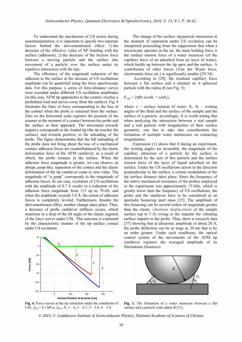
The efficiency of the magnitude reduction of the adhesion to the surface at the increase of US oscillations amplitude can be quantified using the force spectroscopy data. For this purpose, a series of force-distance curves were recorded under different US oscillation amplitudes (in this case, AFM tip approaches to the contact, reaches a predefined load and moves away from the surface). Fig. 4 illustrates the lines of force corresponding to the loss of the contact when the probe is retracted from the surface. Zero on the horizontal scale registers the position of the scanner at the moment of a contact between the probe and the surface at their approach. The movement towards negative corresponds to the loaded tip (the tip touches the surface), and towards positive, to the unloading of the probe. The figure demonstrates that the full unloading of the probe does not bring about the loss of a mechanical contact: adhesion forces are counterbalanced by the elastic deformation force of the AFM cantilever, as a result of which, the probe remains at the surface. When the adhesion force magnitude is greater, we can observe an abrupt, jump-like, separation of the contact and the elastic deformation of the tip cantilever come to zero value. The magnitude of “a jump” corresponds to the magnitude of adhesion forces. In our case, excitation of US oscillations with the amplitude of 0.7 Å results in a reduction of the adhesion force magnitude from 115 up to 78 nN, and when the amplitude exceeds 3.8 Å, the action of adhesion forces is completely leveled. Furthermore, besides the abovementioned effect, another change takes place. Thus, a decrease of probe cantilever stiffness occurs, which manifests in a drop of the tilt angle of the elastic segment of the force curves under USL. This outcome is explained by the characteristic manner of the tip–surface contact under US excitation.
0 100 200 300-125
-100
-75
-50
-25
0
25
Fo
rce
[nN
]
Vertical Position of Scanner [nm]
1
2
3
4
Fig. 4. Force curves at the tip retraction under the conditions of USL. fUS = 4.1 МГц; ΔUS, Å: 1 – 0, 2 – 0.7, 3 – 3.0, 4 – 3.8.
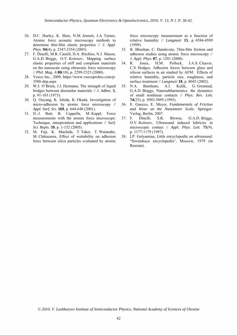
The change of the surface–tip/particle interaction at the moment of separation under US excitation can be interpreted proceeding from the supposition that when a microscope operates in the air, the main holding force is the surface tension force of a water meniscus (of the capillary force of an adsorbed from air layer of water), which builds up between the tip apex and the surface. A contribution of other forces (Van der Waals force, electrostatic force etc.) is significantly smaller [29-34].
According to [29], the resultant capillary force between a flat surface and a situated on it spherical particle with the radius R (see Fig. 5):
Fcap = 2πRγ (cosθ1 + cosθ2),
where γ – surface tension of water; θ1, θ2 – wetting angles of the fluid and the surface of the sample and the surface of a particle, accordingly. It is worth noting that when analyzing the interaction between a real sample and a real particle with irregularities of their surface geometry, one has to take into consideration the formation of multiple water meniscuses on contacting irregularities.
Expression (1) shows that if during an experiment, the wetting angles are invariable, the magnitude of the capillary attraction of a particle by the surface is determined by the size of this particle and the surface tension force of the layer of liquid adsorbed on the surface. Under the US oscillations action in the direction perpendicular to the surface, a certain modulation of the tip–surface distance takes place. Since the frequency of the native mechanical resonance of the probes employed in the experiment was approximately 75 kHz, which is greatly lower than the frequency of US oscillations, the probe and the cantilever have to be considered as an aperiodic bouncing inert mass [35]. The amplitude of this bouncing can be several orders of magnitude greater than the elastic vibrations displacement of the sample surface (up to 5 Å) owing to the impulse the vibrating surface imparts to the probe. Thus, there is research data [37] showing that at ultrasonic amplitude of about 20 Å, the probe deflection can be as large as 20 nm that is by an order greater. Under such conditions, the optical control system of the movements of the AFM tip cantilever registers the averaged amplitude of its fluctuations (bounces).
Fig. 5. The formation of a water meniscus between a flat surface and a particle with radius R [31].

Semiconductor Physics, Quantum Electronics & Optoelectronics, 2010. V. 13, N 1. P. 36-42.
© 2010, V. Lashkaryov Institute of Semiconductor Physics, National Academy of Sciences of Ukraine
40
0 7.5 15.0 22.5 30.0 37.5 45.0 52.5
0
2
4
6
8
10
Tip
Os
cil
lati
on
Am
pli
tud
e[n
m]
Loading Force [nN]
60.0
Fig. 6. The dependence of the amplitude of the tip cantilever’s vertical oscillations on the applied loading force at different US amplitudes. fUS = 4.1 МHz; ΔUS, Å: 1 – 0, 2 – 0.7, 3 – 3.0, 4 – 3.8, 5 – 4.8.
Based on the force curves of the probe approach to the surface, we determined dependencies of the averaged amplitude of the probe vertical oscillations on the pressing force the probe exerts on the surface at different US oscillations amplitudes (Fig. 6). Zero value of the excitation force corresponds to the moment of the contact the probe makes with the surface, at the same time, a jump-like holding of the probe takes place and the cantilever from the state of equilibrium (beyond our diagram) bends down. If the pressing force the probe applies on the surface is approximately 4 nN, the transitional process finishes. The curve of the surface without USL illustrates the noise level in the measurement system. The diagram demonstrates that at the amplitude of ΔUS =0.7 Å and the excitation force not exceeding 20 nN, the probe oscillates with the amplitude of below 1 nm. Moreover, even though this amplitude of the oscillations surpasses the amplitude of atomic displacements in an US wave practically by an order of magnitude, it is still too small to break a water meniscus, and it damps the oscillations. At an increase of the tip–surface contact force, the amplitude of the oscillations somewhat rises, though does not exceed 2 nm. When US is applied with an amplitude corresponding to the disappearance of adhesive hysteresis on the force curves, the tip gains subharmonic oscillations. The amplitude of these vibrations increases and reaches the highest magnitude at a small tip–surface contact force (Fig. 6, curves 3–5). When the contact force goes up, the oscillations amplitude somewhat decreases due to damping of the tip’s bouncing off the cantilever surface, unlike the cases with small US amplitudes, when an increase of the contact force stimulates a better transfer of an impulse from the surface.
Therefore, the vibrating under US action surface can give the tip (and hence particles on the surface) pushes in the vertical direction with amplitudes from
single digits up to decades of nanometres. In addition, we can expect a change of effective wetting angles of NP and the surface owing to visco-elastic excitations in the adsorbed layer of fluid under the action of US. Specifically, when US spreads to the fluid, one can observe the expansion of the air bubbles found in the liquid, which happens because the pressure inside them surpasses the pressure in the surrounding fluid in the area of an acoustic wave spreading, that is due to acoustic cavitation (other cavitation mechanisms, such as diffusion etc, at these US frequencies can be disregarded). It is known that at the sound intensity of the order of 1 W/cm2, cavitation processes take place in a such effective manner that they can be perceived with the naked eye. In our experiment, the sound intensity was about eight times as small, however, here we have to take into account that in this case we were dealing with nanovolumes of liquid. Such formation of pulsating cavities in liquid must result in a decrease of the average force of atomic interaction and consequently, γ.
The abovementioned effects of the detachment of AFM tip (NP) from the surface under the influence of US oscillations are a well-known cause of a decrease of the friction force when vibration displacements are directed perpendicular to the contact area of two bodies. These phenomena on a nanometer level are frequently called sonolubrication, and, sometimes, acoustic levitation [36-38]. Naturally, under the conditions of water meniscus breaking and a decrease of the friction force, nanoparticles whose size is significantly smaller than the size of the AFM tip, will be repulsed from it. In addition, as one can see in Figs 1 and 2, NP that were set in motion do not touch each other after the action of US stops, despite the fact of their arraying exactly along the line of the AFM probe movement. Thus, vibrating NP are effectively repulsed from each other, which is of a great importance in the sphere of manipulations of nanodisperse powders, where there exists a problem of significant adherence among NP.
4. Conclusions
The modification of an atomic force microscope by means of incorporating some additional units into its structural setup for exciting ultrasonic oscillations in the object under examination, made it possible to realize the method of selective nanomanipulation of particles of different sizes.
It has been demonstrated that under excitation of US oscillations with the amplitude of atomic displacements even in the order of 1 Å, nanoparticles on the surface, when the probe approaches them, are set in motion, which can be a result of an acoustically operated decrease of the effective magnitude of the coupling nanoparticles have with the surface. A change of US amplitude is instrumental in the selection process of particles, namely, an increase of the amplitude brings about a transport of big-sized particles.
5
4
3
2
1

Semiconductor Physics, Quantum Electronics & Optoelectronics, 2010. V. 13, N 1. P. 36-42.
© 2010, V. Lashkaryov Institute of Semiconductor Physics, National Academy of Sciences of Ukraine
41
This effect can be employed in the course of manufacturing the model samples of nanostructures to ensure separation and positioning the nanoparticles.
References
1. S Y. Takemura, J. Shirakashi, AFM lithography for fabrication of magnetic nanostructures and devices. // J. Magn. Magn. Mater. 304(1), p. 19-22 (2006).
2. Z. Davis, G. Abadal, O. Hansen, X. Borise, N. Barniol, F. Perez-Murano, A. Boisen, AFM lithography of aluminum for fabrication of nanomechanical systems // Ultramicroscopy 97(1-4), p. 467-472 (2003).
3. M. Villarroya, F. Perez-Murano, C. Martin, Z. Davis, A. Boisen, J. Esteve, E. Figueras, J. Montserrat, N. Barniol, AFM lithography for the definition of nanometre scale gaps: application to the fabrication of a cantilever-based sensor with electrochemical current detection // Nanotechnology 15(7), p. 771-776 (2004).
4. M. Kato, M. Ishibashi, S. Heike, T. Hashizume, Nanofabrication using atomic force microscopy lithography for molecular devices // Jpn. J. Appl. Phys. B 41(7), p. 4916-4918 (2002).
5. C. Baur, A. Bugacov, B.E. Koel, A. Madhukar, N. Montoya, T.R. Ramachandran, A.A.G. Requi-cha, R. Resch, P. Will, Nanoparticle manipulation by mechanical pushing: underlying phenomena and real-time monitoring // Nanotechnology 9, p. 360-365 (1998).
6. A.A.G. Requicha, Massively parallel nanorobotics for lithography and data storage // Intern. J. Robotics Res. 18(3), p. 344-350 (1999).
7. T. Junno, S.B. Carlsson, H. Xu, L. Montelius, L. Samuelson, Fabrication of quantum devices by Еngstrom-level manipulation of nanoparticles with an atomic force microscope // Appl. Phys. Lett. 72(5), p. 548-550 (1998).
8. A.A.G. Requicha, Nanorobots, NEMS, and nanoassembly // Proc. IEEE 91, p. 1922-1933 (2003).
9. S. Decossas, F. Mazen, T. Baron, G. Bremond, A. Souifi, Atomic force microscopy nanomanipu-lation of silicon nanocrystals for nanodevice fabrication // Nanotechnology, 14(12), p. 1272-1278 (2003).
10. L. Roschier, R. Tarkiainen, M. Ahlskog, M. Paa-lanen, P. Hakonen, Manufacture of single electron transistors using AFM manipulation on multiwalled carbon nanotubes // Microelectron. Eng. 61, p. 687-691 (2002).
11. E. Harel, S.E. Meltzer, A.A.G. Requicha, M.E. Thompson, B.E. Koel, Fabrication of poly-styrene latex nanostructures by nanomanipulation and thermal processing // Nano Letters 5(12), p. 2624-2629 (2005).
12. S.A. Maier, M.L. Brongersma, P.G. Kik, S. Meltzer, A.A.G. Requicha, H.A. Atwater,
Plasmonics-A route to nanoscale optical devices // Adv. Mater. 13(19), p. 1501-1505 (2001).
13. S.A. Maier, P.G. Kik, H.A. Atwater, S. Meltzer, E. Harel, B.E. Koel, A.A.G. Requicha, Local detection of electromagnetic energy transport below the diffraction limit in metal nanoparticle plasmon waveguides // Nature Materials 2(4), p. 229-232 (2003).
14. L. Tong, T. Zhu, Z. Liu, Atomic force microscope manipulation of gold nanoparticles for controlled Raman enhancement // Appl. Phys. Lett. 92, 023109 (2008).
15. S. Hsieh, S. Meltzer, C.R.C. Wang, A.A.G. Re-quicha, M.E. Thompson, B.E. Koel, Imaging and manipulation of gold nanorods with an atomic force microscope // J. Phys. Chem. B – Condens. Phase 106(2), p. 231-234 (2002).
16. S. Decossas, L. Patrone, A.M. Bonnot, F. Comin, M. Derivaz, A. Barski, J. Chevrier, Nanomanipu-lation by atomic force microscopy of carbon nanotubes on a nanostructured surface // Surf. Sci. 543(1-3), p. 57-62 (2003).
17. L. Liu, C.S. Jayanthi, M. Tang, S.Y. Wu, T.W. Tombler, C. Zhou, L. Alexseyev, J. Kong, H. Dai, Controllable reversibility of an sp2 to sp3 transition of a single wall nanotube under the manipulation of an AFM tip: A nanoscale electromechanical switch? // Phys. Rev. Lett. 84(21), p. 4950-4953 (2000).
18. G.V. Shivashankar, A. Libchaber, Single DNA molecule grafting and manipulation using a combined atomic force microscope and an optical tweezer // Appl. Phys. Lett. 71, p. 3727 (1997).
19. S. Thalhammer, W.M. Heckl, Manipulating genetic material // Materials Today 8(5S1), p. 40-49 (2005).
20. R. Resch, A. Bugacov, C. Baur, B.E. Koel, A. Madhukar, A.A.G. Requicha, P. Will, Manipulation of nanoparticles using dynamic force microscopy: simulation and experiments // Appl. Phys. A: Mater. Sci. & Proc. 67(3), p. 265-271 (1998).
21. P. Mesquida, A. Stemmer, Maskless nano-fabrication using the electrostatic attachment of gold particles to electrically patterned surfaces // Microelectron. Eng. 61, p. 671-674 (2002).
22. M.T. Cuberes, Atomic force microscopy manipulation with ultrasonic excitation // J. Phys.100(5), 052013 (2008).
23. U. Rabe, W. Arnold, Acoustic microscopy by atomic force microscopy // Appl. Phys. Lett.64(12), p. 1493-1495 (1994).
24. B. Cretin, F. Sthal, Scanning microdeformation microscopy // Appl. Phys. Lett. 62(8), p. 829-831 (1993).
25. K. Yamanaka, H. Ogiso, O.V. Kolosov, Ultrasonic force microscopy for nanometer resolution subsurface imaging // Appl. Phys. Lett. 64(2), p. 178-180 (1994).
Semiconductor Physics, Quantum Electronics & Optoelectronics, 2010. V. 13, N 1. P. 36-42.
© 2010, V. Lashkaryov Institute of Semiconductor Physics, National Academy of Sciences of Ukraine
42
26. D.C. Hurley, K. Shen, N.M. Jennett, J.A. Turner, Atomic force acoustic microscopy methods to determine thin-film elastic properties // J. Appl. Phys. 94(4), p. 2347-2354 (2003).
27. F. Dinelli, M.R. Castell, D.A. Ritchies, N.J. Mason, G.A.D. Briggs, O.V. Kolosov, Mapping surface elastic properties of stiff and compliant materials on the nanoscale using ultrasonic force microscopy // Phil. Mag. A 80(10), p. 2299-2323 (2000).
28. Veeco Inc., 2009, https://www.veecoprobes.com/p-3588-dnp.aspx
29. W.J. O’Brien, J.J. Hermann, The strength of liquid bridges between dissimilar materials // J. Adhes. 5, p. 91-103 (1973).
30. Q. Ouyang, K. Ishida, K. Okada, Investigation of micro-adhesion by atomic force microscopy // Appl. Surf. Sci. 169, p. 644-648 (2001).
31. H.-J. Butt, B. Cappella, M. Kappl, Force measurements with the atomic force microscope: Technique, interpretation and applications // Surf. Sci. Repts. 59, p. 1-152 (2005).
32. M. Fuji, K. Machida, T. Takei, T. Watanabe, M. Chikazawa, Effect of wettability on adhesion force between silica particles evaluated by atomic
force microscopy measurement as a function of relative humidity // Langmuir 15, p. 4584-4589 (1999).
33. B. Bhushan, C. Dandavate, Thin-film friction and adhesion studies using atomic force microscopy // J. Appl. Phys. 87, p. 1201 (2000).
34. R. Jones, H.M. Pollock, J.A.S. Cleaver, C.S. Hodges, Adhesion forces between glass and silicon surfaces in air studied by AFM: Effects of relative humidity, particle size, roughness, and surface treatment // Langmuir 18, p. 8045 (2002).
35. N.A. Burnham, A.J. Kulik, G. Gremaud, G.A.D. Briggs, Nanosubharmonics: the dynamics of small nonlinear contacts // Phys. Rev. Lett.74(25), p. 5092-5095 (1995).
36. E. Gnecco, E. Meyer, Fundamentals of Friction and Wear on the Nanometer Scale. Springer-Verlag, Berlin, 2007.
37. F. Dinelli, S.K. Biswas, G.A.D. Briggs, O.V. Kolosov, Ultrasound induced lubricity in microscopic contact // Appl. Phys. Lett. 71(9), p. 1177-1179 (1997).
38. I.P. Golyamina, Little encyclopedia on ultrasound. “Sovetskaya encyclopedia”, Moscow, 1979 (in Russian).