understanding logic design
TRANSCRIPT
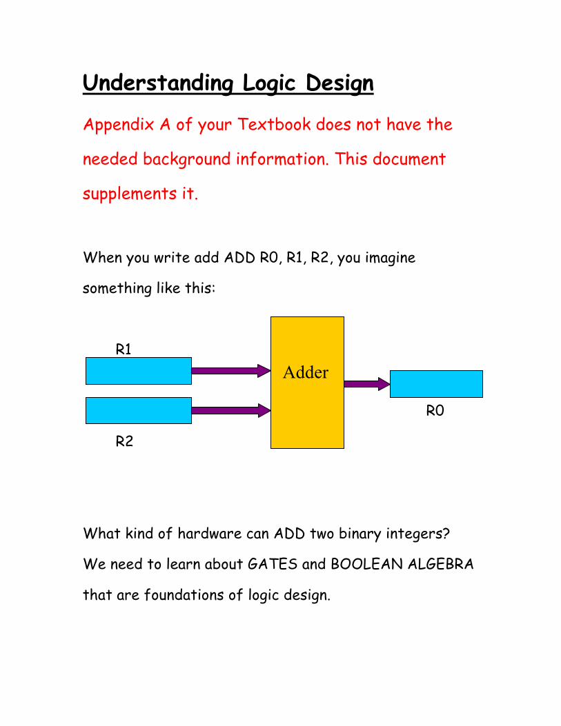
Understanding Logic Design
Appendix A of your Textbook does not have the
needed background information. This document
supplements it.
When you write add ADD R0, R1, R2, you imagine
something like this:
R1
R0
R2
What kind of hardware can ADD two binary integers?
We need to learn about GATES and BOOLEAN ALGEBRA
that are foundations of logic design.
Adder
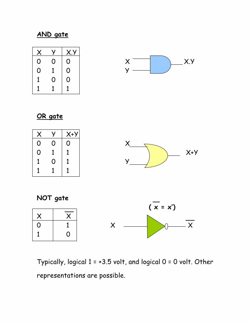
AND gate X Y X.Y 0 0 0 X X.Y 0 1 0 Y 1 0 0 1 1 1 OR gate X Y X+Y 0 0 0 X 0 1 1 X+Y 1 0 1 Y 1 1 1 NOT gate ( x = x’) X X 0 1 X X 1 0 Typically, logical 1 = +3.5 volt, and logical 0 = 0 volt. Other
representations are possible.

Analysis of logical circuits
X X.Y
F
Y X.Y
What is the value of F when X=0 and Y=1?
Draw a truth table.
X Y F
0
0
1
1
0
1
0
1
0
1
1
0
This is the exclusive or (XOR) function. In algebraic
form F= X.Y + X.Y
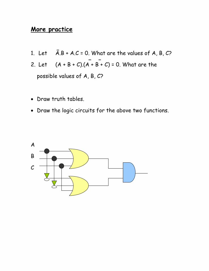
More practice
1. Let A.B + A.C = 0. What are the values of A, B, C?
2. Let (A + B + C).(A + B + C) = 0. What are the
possible values of A, B, C?
• Draw truth tables.
• Draw the logic circuits for the above two functions.
A
B
C
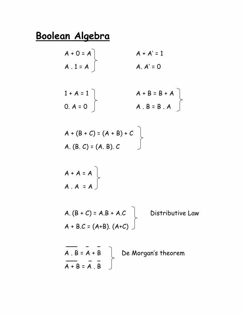
Boolean Algebra A + 0 = A A + A’ = 1
A . 1 = A A. A’ = 0
1 + A = 1 A + B = B + A
0. A = 0 A . B = B . A
A + (B + C) = (A + B) + C
A. (B. C) = (A. B). C
A + A = A
A . A = A
A. (B + C) = A.B + A.C Distributive Law
A + B.C = (A+B). (A+C)
A . B = A + B De Morgan’s theorem
A + B = A . B
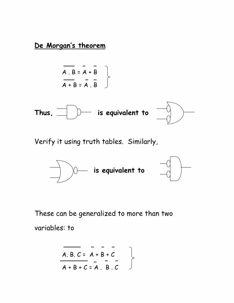
De Morgan’s theorem
A . B = A + B
A + B = A . B
Thus, is equivalent to
Verify it using truth tables. Similarly,
is equivalent to
These can be generalized to more than two
variables: to
A. B. C = A + B + C
A + B + C = A . B . C
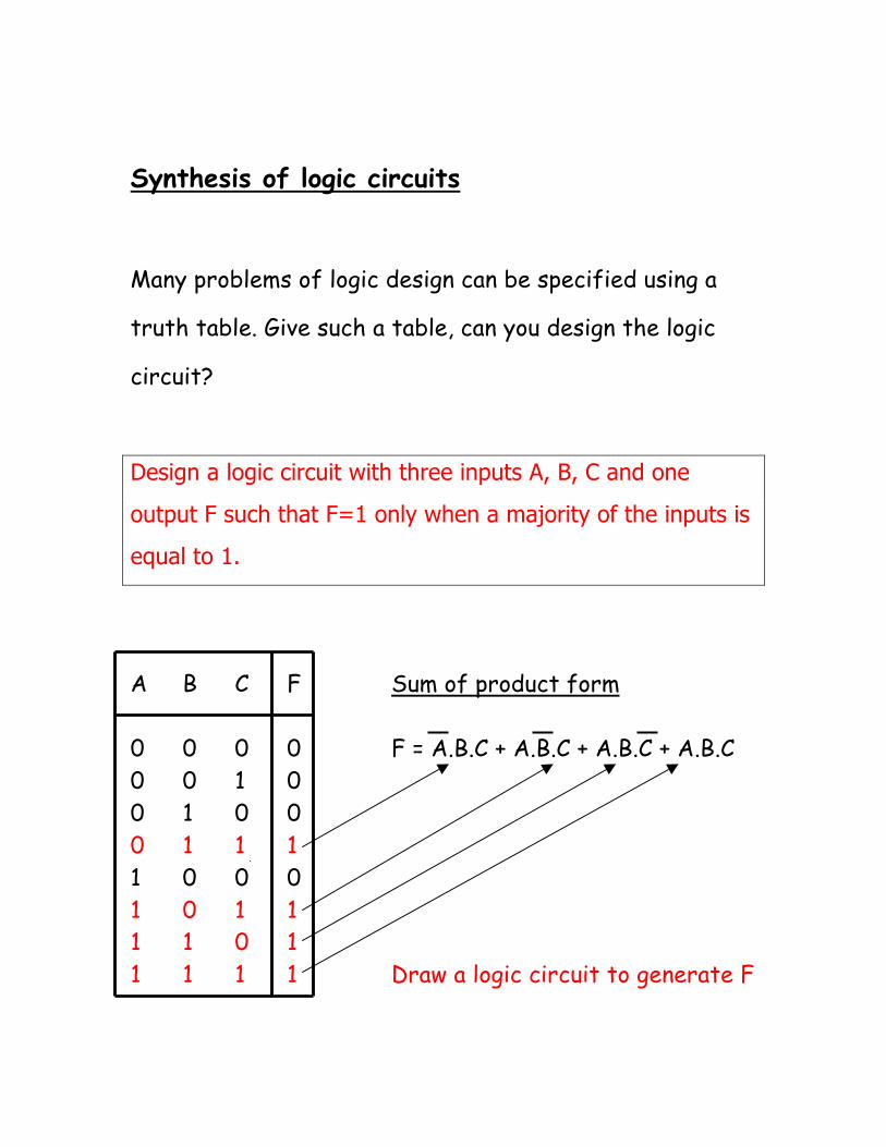
Synthesis of logic circuits
Many problems of logic design can be specified using a
truth table. Give such a table, can you design the logic
circuit?
Design a logic circuit with three inputs A, B, C and one
output F such that F=1 only when a majority of the inputs is
equal to 1.
A B C F Sum of product form 0 0 0 0 F = A.B.C + A.B.C + A.B.C + A.B.C 0 0 1 0 0 1 0 0 0 1 1 1 1 0 0 0 1 0 1 1 1 1 0 1 1 1 1 1 Draw a logic circuit to generate F
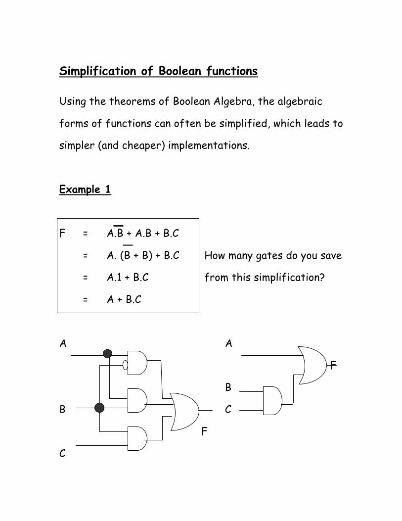
Simplification of Boolean functions Using the theorems of Boolean Algebra, the algebraic
forms of functions can often be simplified, which leads to
simpler (and cheaper) implementations.
Example 1
F = A.B + A.B + B.C
= A. (B + B) + B.C How many gates do you save
= A.1 + B.C from this simplification?
= A + B.C
A A
F
B
B C
F
C

Example 2
F = A.B.C + A.B.C + A.B.C + A.B.C = A.B.C + A.B.C + A.B.C + A.B.C + A.B.C + A.B.C = (A.B.C + A.B.C) + (A.B.C + A.B.C) + (A.B.C + A.B.C) = (A + A). B.C + (B + B). C.A + (C + C). A.B
= B.C + C.A + A.B
Example 3 Show that A + A.B = A
A + AB
= A.1 + A.B
= A. (1 + B)
= A. 1
= A

Other types of gates
A A
A.B B A+B
B
NAND gate NOR gate
Be familiar with the truth tables of these gates.
A
B A+ B = A.B + A.B
Exclusive OR (XOR) gate
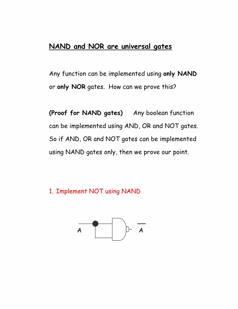
NAND and NOR are universal gates
Any function can be implemented using only NAND
or only NOR gates. How can we prove this?
(Proof for NAND gates) Any boolean function
can be implemented using AND, OR and NOT gates.
So if AND, OR and NOT gates can be implemented
using NAND gates only, then we prove our point.
1. Implement NOT using NAND
A A
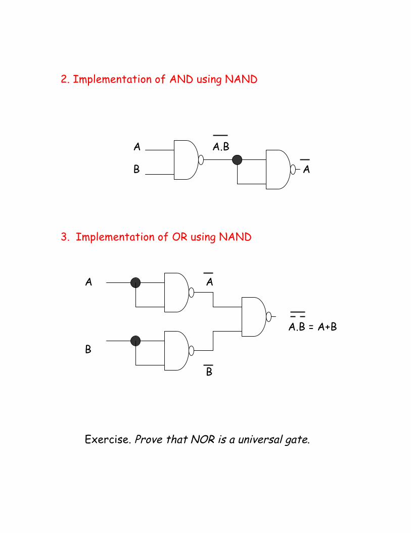
2. Implementation of AND using NAND
A A.B
B A
3. Implementation of OR using NAND
A A
A.B = A+B
B
B
Exercise. Prove that NOR is a universal gate.
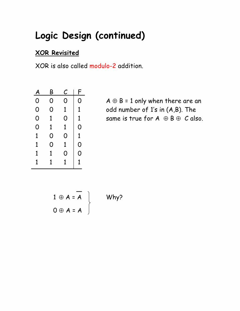
Logic Design (continued) XOR Revisited
XOR is also called modulo-2 addition.
A B C F 0 0 0 0 A ⊕ B = 1 only when there are an 0 0 1 1 odd number of 1’s in (A,B). The 0 1 0 1 same is true for A ⊕ B ⊕ C also. 0 1 1 0 1 0 0 1 1 0 1 0 1 1 0 0 1 1 1 1
1 ⊕ A = A Why?
0 ⊕ A = A
Logic Design Examples
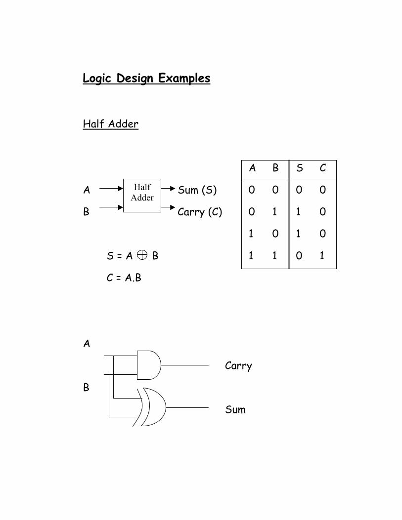
Half Adder
A B S C
A Sum (S) 0 0 0 0
B Carry (C) 0 1 1 0
1 0 1 0
S = A B 1 1 0 1
C = A.B
A
Carry
B
Sum
Half Adder

Full Adder
Sum (S) A B Cin S Cout
A 0 0 0 0 0
B 0 0 1 1 0
Cin Carry (Cout) 0 1 0 1 0
0 1 1 0 1
1 0 0 1 0
1 0 1 0 1
1 1 0 0 1
1 1 1 1 1
S = A B Cin
Cout = A.B + B.Cin + A.Cin
Design a full adder using two half-adders (and a
few gates if necessary)
Can you design a 1-bit subtracter?
Full
Adder
Decoders
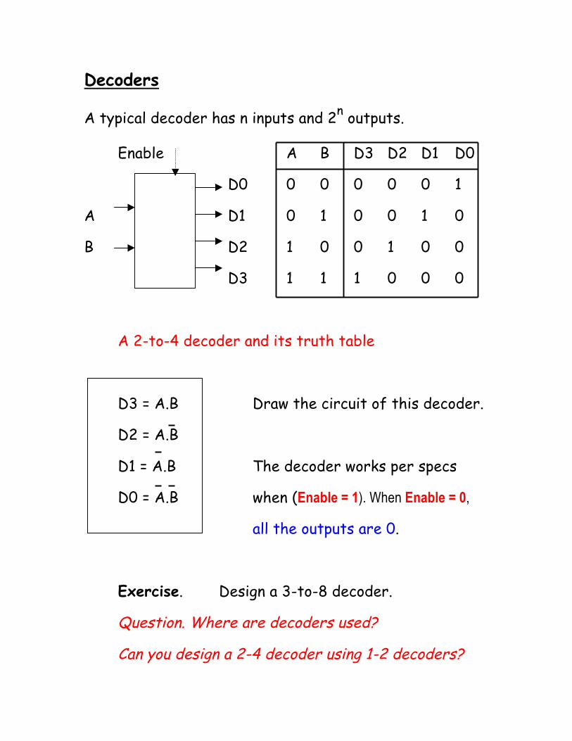
A typical decoder has n inputs and 2n outputs.
Enable A B D3 D2 D1 D0
D0 0 0 0 0 0 1
A D1 0 1 0 0 1 0
B D2 1 0 0 1 0 0
D3 1 1 1 0 0 0
A 2-to-4 decoder and its truth table
D3 = A.B Draw the circuit of this decoder.
D2 = A.B
D1 = A.B The decoder works per specs
D0 = A.B when (Enable = 1). When Enable = 0,
all the outputs are 0.
Exercise. Design a 3-to-8 decoder.
Question. Where are decoders used?
Can you design a 2-4 decoder using 1-2 decoders?
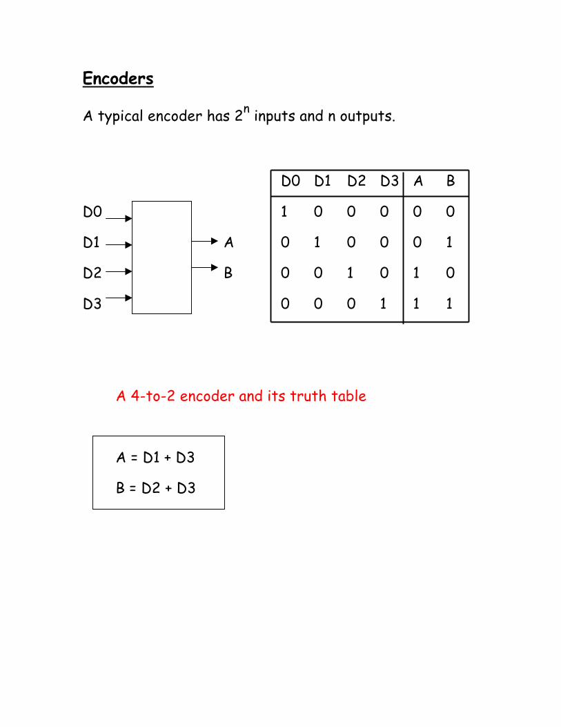
Encoders
A typical encoder has 2n inputs and n outputs.
D0 D1 D2 D3 A B
D0 1 0 0 0 0 0
D1 A 0 1 0 0 0 1
D2 B 0 0 1 0 1 0
D3 0 0 0 1 1 1
A 4-to-2 encoder and its truth table
A = D1 + D3
B = D2 + D3
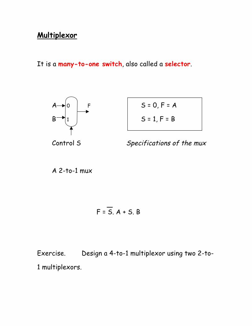
Multiplexor
It is a many-to-one switch, also called a selector.
A 0 F S = 0, F = A
B 1 S = 1, F = B
Control S Specifications of the mux
A 2-to-1 mux
F = S. A + S. B
Exercise. Design a 4-to-1 multiplexor using two 2-to-
1 multiplexors.
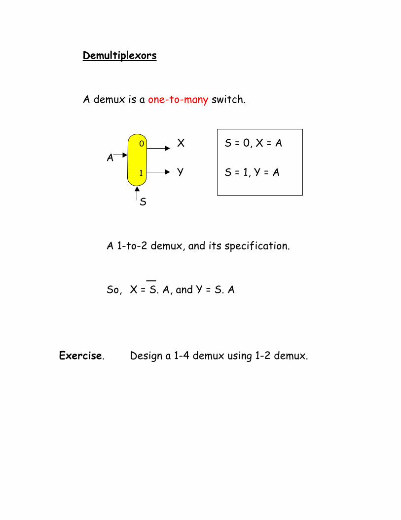
Demultiplexors
A demux is a one-to-many switch.
0 X S = 0, X = A A 1 Y S = 1, Y = A
S
A 1-to-2 demux, and its specification.
So, X = S. A, and Y = S. A
Exercise. Design a 1-4 demux using 1-2 demux.

A 1-bit ALU Operation
Operation = 00 implies AND A Result
Operation = 01 implies OR B
Operation = 10 implies ADD
Operation
Carry in
A
B 00
01 Result
10
Carry out
♦ Understand how this circuit works.
Adder
?

♦ Converting an adder into a subtractor
A - B (here - means arithmetic subtraction)
= A + 2’s complement of B
= A + 1’s complement of B + 1
operation
Carry in
A
B 00
01 Result
0 10
1
11
B invert Carry out
1-bit adder/subtractor
For subtraction, B invert = 1 and Carry in = 1
Adder

A 32-bit ALU
B invert C in operation
A0
B0 Result 0
C in
A1
B1 Result 1
..
..
A31
B31 Result 31
overflow
ALU
Cout
ALU
Cout
ALU
Cout
Combinational vs. Sequential Circuits
Combinational circuits
The output depends only on the current values of
the inputs and not on the past values. Examples are
adders, subtractors, and all the circuits that we have
studied so far
Sequential circuits
The output depends not only on the current values
of the inputs, but also on their past values. These hold
the secret of how to memorize information. We will study
sequential circuits later.