unfolding t - eit.lth.se · dsp design unfolding viktor Öwall, dept. of electrical and information...
TRANSCRIPT

DSP Design
Unfolding
Viktor Öwall, Dept. of Electrical and Information Technology, Lund University, Sweden-www.eit.lth.se
DSP Design
UnfoldingUnfoldingUnfolding creates a program with more than one
iteration, J=unfolding factorg
Unfolding is a structured way to achieve parallel processingp g
Applications– sample period reduction reach Tsample period reduction, reach– Parallel processing– Bit-serial and Digit-serial
∞T
Unfolding = Loop unrolling– assembly programming– compiler theory
Viktor Öwall, Dept. of Electrical and Information Technology, Lund University, Sweden-www.eit.lth.se
p y
DSP Design
Example: Loop unrolling+Example: Loop unrollingSoftware Pipelining
operCC
GSM S h d
1
32
1
3
oper
2
CC1
23
121 GSM Speechcoder
• Org. C-code = 250k cc7653
3213 32
31
23
• Mod. C-code = 90k cc
• Hand Opt = 50k cc
87 3
1
• Hand Opt. = 50k ccIteration 1
Iteration 2
Iteration 3
Higher order
Viktor Öwall, Dept. of Electrical and Information Technology, Lund University, Sweden-www.eit.lth.se
Iteration 2 Iterations
DSP Design
Unfolding ≡ Parallel Processing(1)
2-unfolded
A B
2D
(1) (1)
A0 B0
(1) (1) 0,2,4,….
2D
A0 B0=> A2 B2=> A4 B4=>…..A1 B1=> A3 B3=> A5 B5=>…..
D
(1) (1) 1,3,5,….
T’∞= 2ut
2 nodes & 2 edgesT∞= (1+1)/2 = 1ut
A1 B1
D
( )
4 nodes & 4 edgesT’
∞= 2ut4 nodes & 4 edges
T∞= 2/2 = 1ut• In a ‘J ’ unfolded system each delay is J-slow if input to a delay element is x(kJ + m)
Viktor Öwall, Dept. of Electrical and Information Technology, Lund University, Sweden-www.eit.lth.se
put to a de ay e e e t s ( J )the output is x((k-1)J + m) = x(kJ + m – J ). J samples

DSP Design
Unfolding, exampley(n)
x(n)y( )
a9D
( ) ( ) ( )nxnayny +−= 9Unfolding J=2, 2-times parallel
( ) ( ) ( )⎧ ( ) ( ) ( )( ) ( ) ( )⎩
⎨⎧
++−=++−=
1282122922
kxkaykykxkayky
Viktor Öwall, Dept. of Electrical and Information Technology, Lund University, Sweden-www.eit.lth.se
( ) ( ) ( )⎩ ++=+ 128212 kxkayky
DSP Design
Unfolding, example
( ) ( ) ( )( ) ( ) ( )⎩
⎨⎧
++++−=
1282122922
kkkkxkayky
( ) ( ) ( )⎩ ++−=+ 128212 kxkayky
J
( ) ( ) ( )( ) ( ) ( )⎩
⎨⎧
++++++−=
120)4(21221)5(22
kkkkxkayky
Viktor Öwall, Dept. of Electrical and Information Technology, Lund University, Sweden-www.eit.lth.se
( ) ( ) ( )⎩ +++−=+ 120)4(212 kxkayky
DSP Design
Unfolding exampleUnfolding, example( ) ( ) ( )( ) ( ) ( )⎨
⎧ ++−= 21)5(22 kxkayky
y(2k)
( ) ( ) ( )⎩⎨ +++−=+ 120)4(212 kxkayky
x(2k) a5D
y( )
5D Not trivial even for a simple graph!
x(2k+1) a4Dgraph!
Viktor Öwall, Dept. of Electrical and Information Technology, Lund University, Sweden-www.eit.lth.sey(2k+1)
DSP Design
Definitions
⎣ ⎦x is the floor of x, largest integer x≤
⎡ ⎤x i th ili f x ll t i t x≥⎡ ⎤x is the ceiling of x, smallest integer x≥
ba% remainder after ba
Viktor Öwall, Dept. of Electrical and Information Technology, Lund University, Sweden-www.eit.lth.se
DSP Design
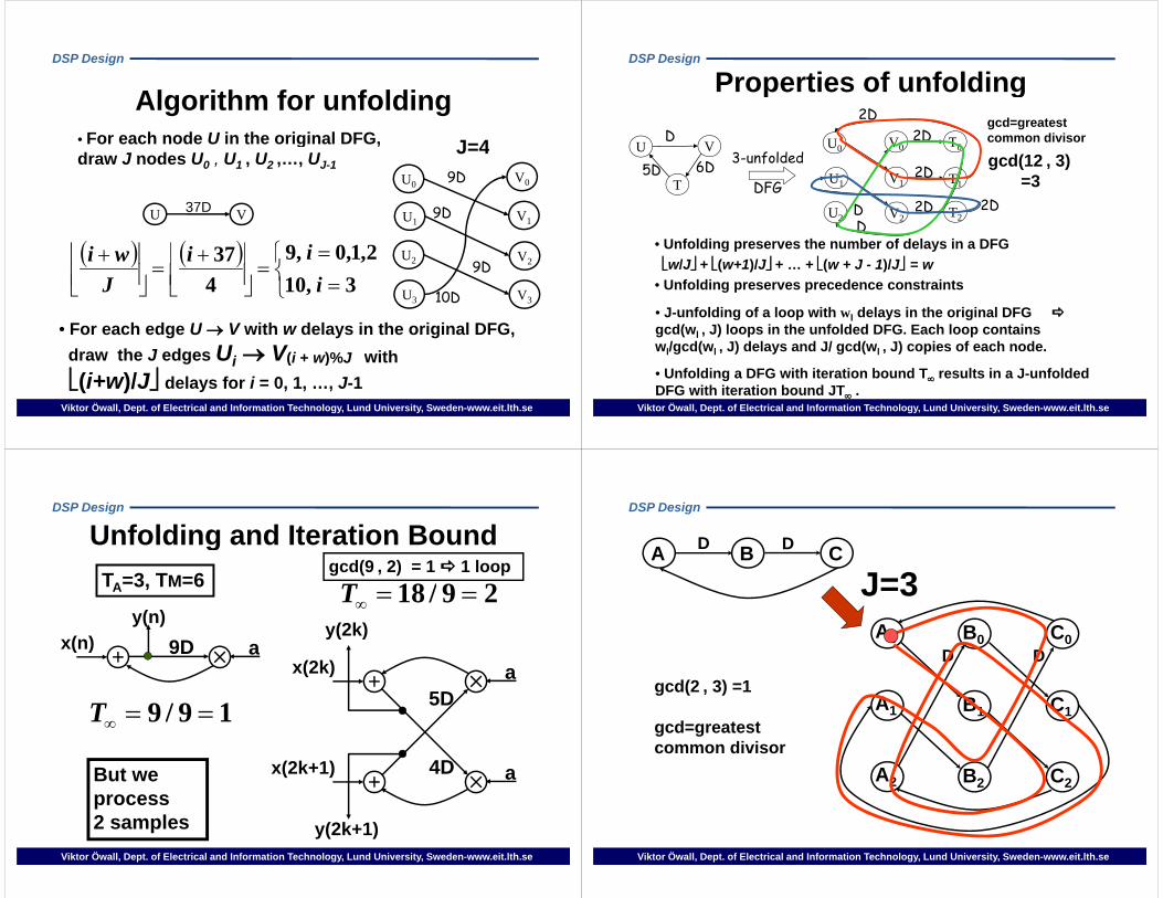
Algorithm for unfolding• For each node U in the original DFG, J 4
9D
For each node U in the original DFG, draw J nodes U0 , U1 , U2 ,…, UJ-1
U0 V0
J=4
U V37D 9D
U
U1
V
V1
( ) ( ) ⎧ =⎥⎢ +⎥⎢ + 210937 iiwi9D
10DU3
U2
V3
V2( ) ( )⎩⎨⎧
==
=⎥⎦⎥
⎢⎣⎢ +
=⎥⎦⎥
⎢⎣⎢ +
3,102,1,0,9
437
iii
Jwi
• For each edge U → V with w delays in the original DFG,draw the J edges Ui → V(i + w)%J with
Viktor Öwall, Dept. of Electrical and Information Technology, Lund University, Sweden-www.eit.lth.se
g i (i w)%J with ⎣(i+w)/J⎦ delays for i = 0, 1, …, J-1
DSP Design
Properties of unfoldingProperties of unfolding
U VD U V T2D
2D gcd=greatestcommon divisor
U
T
V
5D 6DU0
U1
V0
V1
T0
T12D
3-unfolded
DFG
gcd(12 , 3)=3
U2 V2 T22D
DD 2D
• Unfolding preserves the number of delays in a DFG⎣w/J⎦ + ⎣(w+1)/J⎦ + … + ⎣(w + J - 1)/J⎦ = w
• Unfolding preserves precedence constraints
f f G• J-unfolding of a loop with wl delays in the original DFG gcd(wl , J) loops in the unfolded DFG. Each loop contains wl/gcd(wl , J) delays and J/ gcd(wl , J) copies of each node.
Viktor Öwall, Dept. of Electrical and Information Technology, Lund University, Sweden-www.eit.lth.se
• Unfolding a DFG with iteration bound T∞ results in a J-unfolded DFG with iteration bound JT∞ .
DSP Design
Unfolding and Iteration BoundUnfolding and Iteration Bound
29/18TTA=3, TM=6gcd(9 , 2) = 1 1 loop
x(n)y(n)
a9Dy(2k)
29/18 ==∞Tx(n) a9D
x(2k) a5D19/9 ==∞T 5D
x(2k+1) a4DBut we process
Viktor Öwall, Dept. of Electrical and Information Technology, Lund University, Sweden-www.eit.lth.se
y(2k+1)2 samples
DSP Design
D DA CBD D
J=3A0 C0B0
J 3
D D
A CBgcd(2 , 3) =1
A1 C1B1gcd=greatest common divisor
A2 C2B2
Viktor Öwall, Dept. of Electrical and Information Technology, Lund University, Sweden-www.eit.lth.se

DSP Design
The Critical PathThe Critical PathIf edge with w<J (J-w) paths with zero
delay and w paths with 1 delay
A CBD DA0 C0B0
D D
A CBCan lead to A1 C1B1Can lead to increased
critical path!A2 C2B2
critical path!
Edge with w>=J will not
Viktor Öwall, Dept. of Electrical and Information Technology, Lund University, Sweden-www.eit.lth.se
gcreate new critical path!
DSP Design
Sample Period Reduction
• Case 1 : A node in the DFG having computation time greater than T∞.
• Case 2 : Iteration bound is not an integer.
• Case 3 : Longest node computation is g plarger than the iteration bound T∞, and T∞is not an integer
Viktor Öwall, Dept. of Electrical and Information Technology, Lund University, Sweden-www.eit.lth.se
DSP Design
Sample Period Reduction: case 1Sample Period Reduction: case 1
Qb2 S
(4)
Q
Q
b1 Q T(4)(1)
D
X(n) y(n)
Q
P R U(0) (0)
2D
IIR-filter from Lab1P R U
(1)
Viktor Öwall, Dept. of Electrical and Information Technology, Lund University, Sweden-www.eit.lth.se
DSP Design
Sample Period Reduction: case 1The original DFG cannot have sample period equal to the iteration bound because a node computation time is more than iteration bound
Sample Period Reduction: case 1bound because a node computation time is more than iteration bound
S(4)
⎪⎬⎫⎪
⎨⎧ lt
6S
Q T(4)(1)
D ⎪⎭
⎪⎬
⎪⎩
⎪⎨
∈=∞
lwl
LlT max3
Q T
(0) (0)2D
⎭⎩
366max =⎬⎫
⎨⎧=
P R U(1) 6
32
,3
max⎭⎬
⎩⎨
∈Ll
Viktor Öwall, Dept. of Electrical and Information Technology, Lund University, Sweden-www.eit.lth.se
2 <4, max node time

DSP Design
Sample Period(4)
SSample PeriodReduction: case 1 (4)(1)
T
S0
Q
If the computation time of
(2)(0) (0)D
2D
U
T0Q0
RPpa node ‘U’, tu, is greater than the iteration bound T then ⎡t /T ⎤ - (4)
(1) D
U0R0P0
But twoSamples!T∞, then ⎡tu/T ∞⎤ -
unfolding should be used.
t = 4 and T = 3
(4)
(4)(1)
S14Samples!
3tu = 4 and T∞ = 3
⎡ ⎤(0) (0)
(4)(1)
D
T1Q1
6
3
Viktor Öwall, Dept. of Electrical and Information Technology, Lund University, Sweden-www.eit.lth.se
⎡4/3⎤ = 2 - unfolding( )
(1)
( )
P1 U1R1
6
DSP Design
Sample Period Reduction: case 2The original DFG cannot have sample period equal to the iteration
bound because the iteration bound is not an integer
Sample Period Reduction: case 2g
4⎪⎫⎪⎧ ltS T V(1)
DU(1)(1)(1)
D
34max =
⎪⎭
⎪⎬⎫
⎪⎩
⎪⎨⎧
∈=∞
lwlt
LlT
S T VU
DD
If a critical loop bound is of the form tl/wl where tl and wl are mutually co-prime, then wl-unfolding should be used.mutually co prime, then wl unfolding should be used.
Viktor Öwall, Dept. of Electrical and Information Technology, Lund University, Sweden-www.eit.lth.se
Unfolding of 3
DSP Design
Sample Period Reduction: case 2 (2)Sample Period Reduction: case 2 (2)(1) (1)(1)(1)
S0 V2U1T1
D
S0 V2U1T1
S T V(1)
DU(1)(1)(1)
D(1)
D(1)(1)(1)
S1 V0U2T2
4=TD
(1) (1)(1)(1)DS VUT4=∞T DS2 V1U0T0
and 3 samples gives
Viktor Öwall, Dept. of Electrical and Information Technology, Lund University, Sweden-www.eit.lth.se
minimum sample period 4/3
DSP Design
Sample Period Reduction: case 3The original DFG cannot have sample period
l t th it ti b d b th
Sample Period Reduction: case 3
equal to the iteration bound because the longest node computation is larger than the i i b d d i iiteration bound T∞, and T∞ is not an integer
The minimum J that achieves the iteration bound is the minimun value of J such that is an integer and is greater or equal to the
∞JT
Viktor Öwall, Dept. of Electrical and Information Technology, Lund University, Sweden-www.eit.lth.se
g g qlongest node computation time
DSP Design
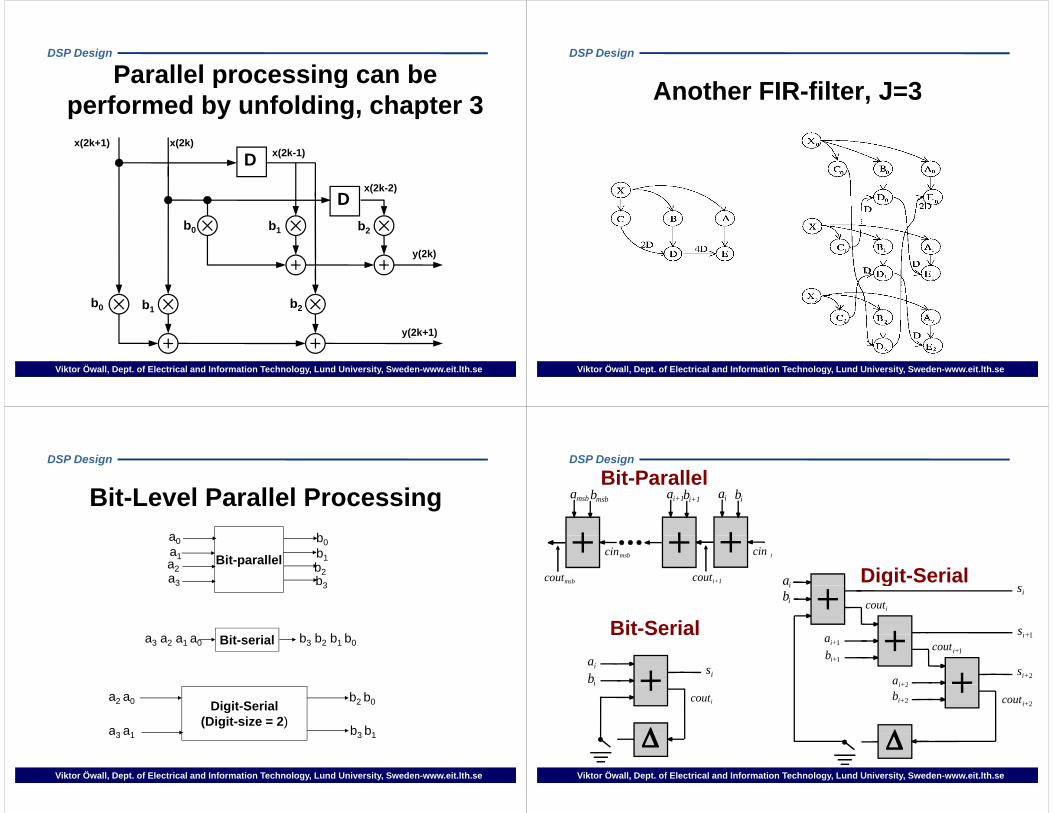
Parallel processing can beParallel processing can be performed by unfolding, chapter 3
D x(2k-1)x(2k)x(2k+1)
Db0
x(2k-2)
b1 b2b0
y(2k)
b1 b2
b0 b1 b2
Viktor Öwall, Dept. of Electrical and Information Technology, Lund University, Sweden-www.eit.lth.se
y(2k+1)
DSP Design
Another FIR-filter, J=3
Viktor Öwall, Dept. of Electrical and Information Technology, Lund University, Sweden-www.eit.lth.se
DSP Design
Bit-Level Parallel Processinga b
Bit-parallel
a0a1a2a3
b0b1b2b33 3
b b b bBit-seriala3 a2 a1 a0 b3 b2 b1 b0
Digit-Serial(Digit-size = 2)
a2 a0
a3 a1
b2 b0
b3 b1
Viktor Öwall, Dept. of Electrical and Information Technology, Lund University, Sweden-www.eit.lth.se
a3 a1 b3 b1
DSP Design
Bit-Paralleli+1bi+1a ibiamsbbmsba
Digit-Serialicin
i+1cout
msbcin
msbcoutia g
Bit-Serial
i
ib is
1+is
icout
Bit Serialiaib is
1+ia1+ib
2+ia
1+is
2+is
1+icout
i
icout
Δ Δ
2+ia2+ib
2+icout
Viktor Öwall, Dept. of Electrical and Information Technology, Lund University, Sweden-www.eit.lth.se
Δ Δ

DSP Design
Bit-serial adderBit-serial adderBit-serial can be seen as a time-multiplexed architecture,in this example on addition (i e 1 iteration) takes 4cc
Bit i la3 a2 a1 a0 s3 s2 s1 s0
in this example on addition (i.e. 1 iteration) takes 4cc.
Bit-serialadder
Db3 b2 b1 b0
4l+1,2,34l+00
Switch for carry signal
Viktor Öwall, Dept. of Electrical and Information Technology, Lund University, Sweden-www.eit.lth.se
How to unfold switches?
DSP Design
Unfolding of Switches• The following assumptions are made when unfolding an edge U→VThe following assumptions are made when unfolding an edge U→V
containing a switch :The wordlength W is a multiple of the unfolding factor J, i.e. W = W’J.All edges into and out of the switch have no delays.All edges into and out of the switch have no delays.
• With the above two assumptions an edge U→V can be unfolded as follows :
Write the switching instance asWrite the switching instance as
Wl + u = J( W’l + ⎣u/J⎦ ) + (u%J)Draw an edge from the node Uu%J Vu%J, % %
which is switched at time instance ( W’l + ⎣u/J⎦) .
Wl+u
Viktor Öwall, Dept. of Electrical and Information Technology, Lund University, Sweden-www.eit.lth.se
U V
DSP Design
Example: Unfolding of Switches, J=3
U V
U V9l+1,5
U0 V0
U1 V1
W it th it hi i t
1 1
U2 V2Write the switching instance as
Wl + u = J( W’l + ⎣u/J⎦ ) + (u%J)9l+1=3(3l + ⎣1/3⎦ ) + (1%3) = 3(3l + 0) + 1 Edges
b t9l 1 3(3l ⎣1/3⎦ ) (1%3) 3(3l 0) 19l+5=3(3l + ⎣5/3⎦ ) + (5%3) = 3(3l + 1) + 2
betweenNodes
Switched at
Viktor Öwall, Dept. of Electrical and Information Technology, Lund University, Sweden-www.eit.lth.se
time instances
DSP Design
Example: Unfolding of Switches, J=3
U V
U V9l+1,5
U0 V0
U1 V1
W it th it hi i t
1 1
U2 V2Write the switching instance as
Wl + u = J( W’l + ⎣u/J⎦ ) + (u%J)9l+1=3(3l + ⎣1/3⎦ ) + (1%3) = 3(3l + 0) + 1 Edges
b t9l 1 3(3l ⎣1/3⎦ ) (1%3) 3(3l 0) 19l+5=3(3l + ⎣5/3⎦ ) + (5%3) = 3(3l + 1) + 2
Draw an edge from the node Uu%J Vu%J, I.e.
betweenNodes
Viktor Öwall, Dept. of Electrical and Information Technology, Lund University, Sweden-www.eit.lth.se
u%J u%J
U1 V1 and U2 V2

DSP Design
Example: Unfolding of Switches, J=3
U V
U V9l+1,5
U0 V0
U1 V1
(3l+0)
⎣ ⎦
1 1
U2 V2
(3l+1)
9l+1=3(3l + ⎣1/3⎦ ) + (1%3) = 3(3l + 0) + 19l+1=3(3l + ⎣5/3⎦ ) + (5%3) = 3(3l + 1) + 2
Switched atSwitched at time instances
switched at time instance ( W’l + ⎣u/J⎦), I.e.
Viktor Öwall, Dept. of Electrical and Information Technology, Lund University, Sweden-www.eit.lth.se
U1 V1 at (3l+0) and U2 V2 at (3l+1)
DSP Design
Example :Switch with multiple instances
12l + 1, 7, 9, 11U0 V0
Unfolding by 3
U V U1 V1
U2 V2Wl + u = J( W’l + ⎣u/J⎦ ) + (u%J)
To unfold the DFG by J=3, the switching instances are as follows12l + 1 = 3(4l + 0) + 112l + 7 = 3(4l + 2) + 112l 9 3(4l 3) 0
Viktor Öwall, Dept. of Electrical and Information Technology, Lund University, Sweden-www.eit.lth.se
12l + 9 = 3(4l + 3) + 012l + 11 = 3(4l + 3) + 2
DSP Design
Example : 4l + 3Switch with multiple instances
12l + 1, 7, 9, 11U0 V0
4l + 0,2Unfolding by 3
U V U1 V14l + 3
U2 V2Wl + u = J( W’l + ⎣u/J⎦ ) + (u%J)
Switched at time instances12l + 1 = 3(4l + 0) + 112l + 7 = 3(4l + 2) + 112l 9 3(4l 3) 0
Viktor Öwall, Dept. of Electrical and Information Technology, Lund University, Sweden-www.eit.lth.se
12l + 9 = 3(4l + 3) + 012l + 11 = 3(4l + 3) + 2
DSP Design
Switches with DelaysUnfolding a DFG containing an edge having a switch and a positive
number of delays is done by introducing a dummy node.
A2D
6l + 1, 5 A D2D 6l + 1, 5
Inserting
B
C
6l + 0, 2, 3, 4B
C
6l + 0, 2, 3, 4
Inserting
Dummy node
Viktor Öwall, Dept. of Electrical and Information Technology, Lund University, Sweden-www.eit.lth.se

DSP Design
A S
Bit-serial AdderO t tA S Output
XINPUTS DD dDB
4l+0 4l+1 2 3
Dummy node
Z
4l+0 4l+1,2,3CarryReset
Viktor Öwall, Dept. of Electrical and Information Technology, Lund University, Sweden-www.eit.lth.se
Z CarryCarry = 0
DSP Design
A0 S0
Unfold Bit-serial Adder, J=2A1 S1A0 S0
X0
A1 S1
X1
D0B0 D1B1
Z0 Z1
For each node U in the original DFG, draw J nodes U0 , U1 , U2 ,…, UJ-1
Viktor Öwall, Dept. of Electrical and Information Technology, Lund University, Sweden-www.eit.lth.se
DSP Design
A0 S0
Unfold Bit-serial Adder, J=2A1 S1A0 S0
X0
A1 S1
X1
D0B0 D1B1
Z0 Z1F h d U V ith d l i th i i l DFGFor each edge U → V with w delays in the original DFG,
draw the J edges Ui → V(i + w)%J with ⎣(i+w)/J⎦ delays for i = 0, 1, …, J-1
Viktor Öwall, Dept. of Electrical and Information Technology, Lund University, Sweden-www.eit.lth.se
If edge has w=0 Ui → Vi with 0 delays
DSP Design
A0 S0
Unfold Bit-serial Adder, J=2A1 S1A0 S0
X0
A1 S1
X1
D0B0 D1B1
DZ0 Z1
F h d U V ith d l i th i i l DFG
D
For each edge U → V with w delays in the original DFG,draw the J edges Ui → V(i + w)%J with ⎣(i+w)/J⎦ delays for i = 0, 1, …, J-1
Viktor Öwall, Dept. of Electrical and Information Technology, Lund University, Sweden-www.eit.lth.se
X D for i=0 X0 → D1 with 0 delays and X D for i=1 X1 → D0 with 1 delays

DSP Design
Unfold the Switch, J=2A0 S00 0
X0
D0B0
4l+0 4l+1,2,3Z X4l+0 2(2l+0)+0
D X4l+1 2(2l+0)+1
Z0
4l+0 2(2l+0)+0 4l+1 2(2l+0)+14l+2 2(2l+1)+04l+3 2(2l+1)+1
Write the switching instance asWl + u = J( W’l + ⎣u/J⎦ ) + (u%J)
Viktor Öwall, Dept. of Electrical and Information Technology, Lund University, Sweden-www.eit.lth.se
Wl + u = J( W l + ⎣u/J⎦ ) + (u%J)
DSP Design
Unfold the Switch, J=2A0 S00 0
X0
D0B0
4l+0 4l+1,2,3Z X4l+0 2(2l+0)+0
D X4l+1 2(2l+0)+1
Z0
4l+0 2(2l+0)+0 4l+1 2(2l+0)+14l+2 2(2l+1)+04l+3 2(2l+1)+1
Z0 X0 at time 2l+0 D0 X0 at time 2l+1
Viktor Öwall, Dept. of Electrical and Information Technology, Lund University, Sweden-www.eit.lth.se
DSP Design
Unfold the Switch, J=2A0 S00 0
X0
D0B0
4l+0 4l+1,2,3Z X4l+0 2(2l+0)+0
D X4l+1 2(2l+0)+1
Z0
4l+0 2(2l+0)+0 4l+1 2(2l+0)+14l+2 2(2l+1)+04l+3 2(2l+1)+1
Z0 X0 at time 2l+0 D0 X0 at time 2l+1
D X t ti 2l+0 1
Viktor Öwall, Dept. of Electrical and Information Technology, Lund University, Sweden-www.eit.lth.se
D1 X1 at time 2l+0,1i.e. always closed
DSP Design
A0 S0
Unfold the Switch, J=2A1 S1A0 S0
X0
A1 S1
X1
D0B0 D1B1
D2l+0 2l+1
Z0 Z1
D2l+0 2l 1
Dead Node
D1 X1 at time 2l+0,1i.e. always closedZ0 X0 at time 2l+0
D X t ti 2l+1
Viktor Öwall, Dept. of Electrical and Information Technology, Lund University, Sweden-www.eit.lth.se
D0 X0 at time 2l+1

DSP Design
A0 S0
Remove Dead and Dummy NodesA1 S1A0 S0
X0
A1 S1
X1
B0 B1
D2l+0 2l+1
Z0
D2l+0 2l 1
D1 X1 at time 2l+0,1i.e. always closedZ0 X0 at time 2l+0
D X t ti 2l+1
Viktor Öwall, Dept. of Electrical and Information Technology, Lund University, Sweden-www.eit.lth.se
D0 X0 at time 2l+1
DSP Design
A0 S0
The Digit Serial AdderA1 S1A0 S0
X0
A1 S1
X1
B0 B1
D2l+0 2l+1
Z0
D2l+0 2l 1
Carry withiniterationCarry next iteration
Viktor Öwall, Dept. of Electrical and Information Technology, Lund University, Sweden-www.eit.lth.se
D=1
DSP Design
Fully Parallel Adder, i.e.J=4LSB MSB
A0 S0 A1 S1
X1X0
A2 S2 A3 S3
X3X2
D0B0
Z
D1B1
Z
D2B2
Z
D3B3
ZZ0 Z1 Z2 Z3
DDFor each node U in the original DFG, draw J nodes U0 , U1 , U2 ,…, UJ-1For each edge U → V with w delays in the original DFG
Viktor Öwall, Dept. of Electrical and Information Technology, Lund University, Sweden-www.eit.lth.se
For each edge U → V with w delays in the original DFG,draw the J edges Ui → V(i + w)%J with ⎣(i+w)/J⎦ delays for i = 0, 1, …, J-1
DSP Design
Unfold the Switch, J=4A0 S00 0
X0
D0B0
4l+0 4l+1,2,3Z X4l+0 4(1l+0)+0
D X4l+1 4(1l+0)+1
Z0
4l+0 4(1l+0)+0 4l+1 4(1l+0)+14l+2 4(1l+0)+24l+3 4(1l+0)+3
Write the switching instance asWl + u = J( W’l + ⎣u/J⎦ ) + (u%J)
Viktor Öwall, Dept. of Electrical and Information Technology, Lund University, Sweden-www.eit.lth.se
Wl + u = J( W l + ⎣u/J⎦ ) + (u%J)

DSP Design
Unfold the Switch, J=4A0 S00 0
X0
D0B0
4l+0 4l+1,2,3Z X4l+0 4(1l+0)+0
D X4l+1 4(1l+0)+1
Z0
4l+0 4(1l+0)+0 4l+1 4(1l+0)+14l+2 4(1l+0)+24l+3 4(1l+0)+3
Only 1 time instance 0, i.e. fully parallel
Z X D X D X and D X
Viktor Öwall, Dept. of Electrical and Information Technology, Lund University, Sweden-www.eit.lth.se
Z0 X0, D1 X1, D2 X2 and D3 X3
DSP Design
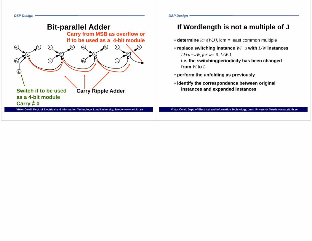
Bit-parallel Adder
A0 S0 A1 S1
X1X0
A2 S2 A3 S3
X3X2
D0B0
Z
D1B1
Z
D2B2
Z
D3B3
ZZ0 Z1 Z2 Z3
DDOnly 1 time instance 0, i.e. fully parallel
Viktor Öwall, Dept. of Electrical and Information Technology, Lund University, Sweden-www.eit.lth.se
Z0 X0, D1 X1, D2 X2 and D3 X3
DSP Design
Bit-parallel AdderLSB MSB
A0 S0 A1 S1
X1X0
A2 S2 A3 S3
X3X2
D0B0
Z
D1B1
Z
D2B2
Z
D3B3
ZZ0 Z1 Z2 Z3
DD”Dead” nodes
Viktor Öwall, Dept. of Electrical and Information Technology, Lund University, Sweden-www.eit.lth.se
Dead nodes
DSP Design
Remove ”Dead” and Dummy Nodes
A0 S0 A1 S1
X1X0
A2 S2 A3 S3
X3X2
D0B0
Z
D1B1
Z
D2B2
Z
D3B3
ZZ0 Z1 Z2 Z3
DD”Dead” nodescan be removed Dummy nodes
Viktor Öwall, Dept. of Electrical and Information Technology, Lund University, Sweden-www.eit.lth.se
ycan be removed
DSP Design
Bit-parallel AdderCarry from MSB as overflow or if t b d 4 bit d l
A0 S0 A1 S1 A2 S2 A3 S3
if to be used as a 4-bit module
B0 B1
X1X0
B2 B3
X3X2
Z0
Carry Ripple AdderSwitch if to be used as a 4 bit module
Viktor Öwall, Dept. of Electrical and Information Technology, Lund University, Sweden-www.eit.lth.se
as a 4-bit moduleCarry = 0
DSP Design
If Wordlength is not a multiple of J
• determine lcm{W,J}, lcm = least common multiple
• replace switching instance Wl+u with L/W instances l f /Ll+u+wW, for w= 0..L/W-1
i.e. the switchingperiodicity has been changed from W to Lfrom W to L
• perform the unfolding as previously
identify the correspondence between original• identify the correspondence between original instances and expanded instances
Viktor Öwall, Dept. of Electrical and Information Technology, Lund University, Sweden-www.eit.lth.se