unifying principle for active devices: charge control ... · unifying principle for active devices:...
TRANSCRIPT

ES 330 Electronics II Supplemental Topic #1 (August 2015)
Unifying Principle for Active Devices: Charge Control Principle
Donald Estreich
An active device is an electron device, such as a transistor, capable of delivering
power amplification by converting dc bias power into time varying signal power. It
delivers a greater energy to its load than if the device were absent. The charge control
framework [1-3] presents a unified understanding of the operation of all electron devices
and simplifies the comparison of the several active devices used in compound
semiconductor analog and digital integrated circuits.
Figure 1. Generic charge control device consisting of three electrodes embedded around a charge transport region.
Consider the generic electron device shown in Fig. 1. It consists of three
electrodes encompassing a charge transport region. The transport region is capable of
supporting charge flow (the electrons shown in the figure) between an emitting electrode
and a collecting electrode. A third electrode, called the control electrode, is used to
-
-
-
-
(electrons)
Charge -Q
Collecting
Electrode Emitting
Electrode
Controlling
Electrode Charge +Qc
Transport Region
+ + + +

2
establish the electron concentration within the transport region. Placing a control charge,
QC, on the control electrode establishes a controlled charge, denoted as -Q, in the
transport region. The operation of active devices depends upon the charge control
principle [1]:
Each charge placed upon the control electrode can at most introduce an equal
and opposite charge in the transport region between the emitting and
collecting electrode.
At most we have the relationship, │-Q│ = │QC│. Any parasitic coupling of the control
charge to charge on the other electrodes, or remote parts of the device, will decrease the
controlled charge in the transport region, that is, │-Q│ < │QC│more generally. For
example, charge coupling between the control electrode and the collecting electrode
forms a feedback or output capacitance, say Co. Time variation of QC leads to the
modulation of the current flow between emitting and collecting electrodes.
The generic structure in Fig. 1 could represent any one of a number of active
devices (e.g., vacuum tubes, unipolar transistors, bipolar transistors, photoconductors,
etc.). Hence, charge control analysis is very broad in scope and it applies to all electronic
transistors.
Starting with the charge control principle, we associate two characteristic time
constants with an active device, thereby, leading to a first-order description of its
behavior. Application of a potential difference between the emitting and collecting
electrodes, say VCC, establishes an electric field in the transport region, although this
applied field is not always needed when diffusion or internal fields from doping profiles
are effective. Electrons in the transport region respond to the electric field and move

3
across this region with a transit time r. The transit time1 is the first of the two important
characteristic times used in charge control modelling. With charge -Q in the transit
region, the static (dc) current Io between emitting and collecting electrodes is
Io = -Q/r = Qc/r (1)
A simple interpretation of r is as follows: r is equal to the length l of the transport region
divided by the average velocity of transit (i.e., r = l/v). From this perspective a charge
of -Q (coulombs) is swept out the collecting electrode every r seconds.
Figure 2. Generic charge control device of Fig. 2.2.1 connected to input and output resistors, Rin and RL, respectively, with bias voltage and input signal applied.
Consider Fig. 2 showing the common-emitting electrode connection of the active
device of Fig. 2.2.1 connected to input and output (i.e., load) resistances, say Rin and RL,
1The transit time r is best interpreted as an average transit time per carrier (in our case the electron). We
note that 1/r is common to all devices – it is related to a device’s ultimate capability to process information.
-
-
-
-
Collecting
Electrode Emitting
Electrode
Controlling
Electrode
Transport
Region
Ci
VCC
vin
+ -
- RL vout
+
Rin
+ + + +

4
respectively. The second characteristic time of importance can now be defined – it is the
“lifetime” time constant and we denote it by the symbol . It is a measure of how long a
charge placed on the control electrode will remain on the control terminal. The “lifetime”
time constant is established in one of several ways depending upon the physics of the
active device and its connection environment. The controlling charge may “leak away”
by (1) discharging through the external resistor Rin as typically happens with FET
devices, (2) recombining with intermixed oppositely charged carriers within the device
(e.g., base recombination in a bipolar transistor), or (3) discharging through an internal
shunt leakage path within the device. The dc current flowing to replenish the lost control
charge is
Iin = -Q/ = Qc/ (2)
The static (dc) current gain GI of a device is defined as the current delivered to
the output divided by the current replenishing the control charge during the same time
period. Where in seconds charge -Q is both lost and replenished, charge Qc times the
ratio /r has been supplied to the output resistor RL. In symbols, the static current gain is
GI = Io/Iin = /r (3)
provided -Q = QC holds.
In the dynamic case the process of small-signal amplification consists of an
incremental variation of the control charge Qc directly resulting in an incremental change
in the controlled charge, -Q. The resulting variation in output current flowing in the load
resistor translates into a time varying voltage vo. The charge control formalism holds just
as well for large-signal situations. In the large-signal case the changes in control charge

5
are no longer small incremental changes. Charge control analysis under large charge
variations is less accurate due to the simplicity of the model, but still very useful for
approximate switching calculations in digital circuits.
An important dynamic parameter is the input capacitance Ci of the active device.
Capacitance Ci is a measure of the work required to introduce a charge carrier in the
transport region. Capacitance Ci is given by the change in charge Q from a corresponding
change in input voltage vin. It is desirable to maximize Ci in an active device. The
transconductance gm is calculated from
gI
v
I
Q
Q
vm
o
in v
o
ino
(4)
The first partial derivative on the right-hand-side of Eq. (2.2.4) is simply (1/r) and the
second partial derivative is Ci . Hence, the transconductance gm is the ratio
gm
i
r
C
(5)
A physical interpretation of gm is the ratio of the work required to introduce a charge
carrier to the average transit time of a charge carrier in the transport region. The
transconductance is one of the most commonly used device parameters in circuit design
and analysis.
In addition to Ci another capacitance, say Co, is introduced and associated with
the collecting electrode. Capacitance Co accounts for charge on the collecting electrode
coupled to either static charge in the transport region or charge on the control electrode.
A non-zero Co indicates that the coupling between the controlling electrode and the
charge in transit is less than unity (i.e.,-Q < QC).
6
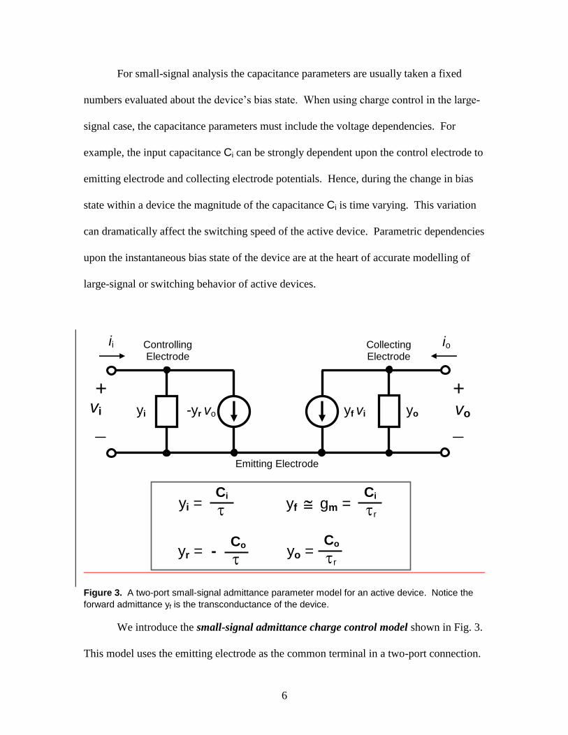
For small-signal analysis the capacitance parameters are usually taken a fixed
numbers evaluated about the device’s bias state. When using charge control in the large-
signal case, the capacitance parameters must include the voltage dependencies. For
example, the input capacitance Ci can be strongly dependent upon the control electrode to
emitting electrode and collecting electrode potentials. Hence, during the change in bias
state within a device the magnitude of the capacitance Ci is time varying. This variation
can dramatically affect the switching speed of the active device. Parametric dependencies
upon the instantaneous bias state of the device are at the heart of accurate modelling of
large-signal or switching behavior of active devices.
Figure 3. A two-port small-signal admittance parameter model for an active device. Notice the
forward admittance yf is the transconductance of the device.
We introduce the small-signal admittance charge control model shown in Fig. 3.
This model uses the emitting electrode as the common terminal in a two-port connection.
yo = Co
r
yi = Ci
yf gm = Ci
r
yr = - Co
yf vi -yr vo yo yi vo +
vi +
Controlling Electrode
Collecting Electrode
Emitting Electrode
io ii

7
The transconductance gm is the magnitude of the real part of the forward admittance yf
and is represented as a voltage-controlled current source positioned from collecting-to-
emitting electrode. The input admittance, denoted by yi, is equivalent to (Ci/), where
is the control charge “lifetime” time constant. Parameter yi can be expressed in the form
(gi + sCi) where s = j. An output admittance, similarly denoted by yo, is given by
(Co/r) where r is the transit time and, in general yo = (go + sCo) in general. Finally, the
output-to-input feedback admittance yr is included using a voltage-controlled current
source at the input. Often yr is small enough to approximate as zero (the model is then
said to be unilateral).
Consider the frequency dependence of the dynamic (ac) current gain Gi. The
low-frequency current gain is interpreted as follows: An incremental charge qc is
introduced on the control electrode with “lifetime” . This produces a corresponding
incremental charge -q in the transport region. Charge -q is swept across the transport
region every “transit time” r seconds. In time charge -q crosses the transit region r

8
times, which is identically equal to the low-frequency current gain.
Figure 4. Circuit used to calculate the small-signal current gain Gi for our active device.
The “lifetime” associated with the control electrode arises from charge “leaking
off” the controlling electrode. This is modeled as an RC time constant at the input of the
equivalent circuit shown in Fig. 4(a) with equal to RinCi. The break frequency B
associated with the control electrode is (it’s 3dB below the low frequency value)
B
in iR
1 1
C
(6)
When the charge on the control electrode varies at a rate less than B, Gi is equal to /r
because charge “leaks off” the controlling electrode faster than 1/. Alternatively, when
gm vi Ci yo gi vi +
Short- circuit
io ii
/r
log Gi
0 dB log
-20 dB/decade
T
B
(a)
(b)

9
is greater than B, Gi decreases with increasing because the applied signal charge
varies more rapidly than 1/. Hence, Gi is inversely proportional to
G i
r
T 1
(7)
where T is the common-emitter unity current gain frequency. At T (= 2fT) the ac
current gain equals unity as illustrated in Fig. 4(b).
Now consider the current gain-bandwidth product Gi f. Purely capacitive input
impedance can’t define a bandwidth. However, a finite, real impedance always appears at
the input terminal in any practical application. Let Ri be the effective input resistance if
the device (i.e., Ri will be equal to (1/gi) in parallel with the external input resistance Rin).
Since the input current is equal to qc/ and the output current is equal to q/r, the current
gain-bandwidth product is
G fq
qi
r
c
/
/
2 (8)
For B, at =1/, and assuming |qc| = |-q|,
G fi
r
T
1
2 2
fT (9)
fTorT ) is a widely quoted parameter used to compare or “benchmark” active devices.
Sometimes fTorT ) is interpreted as a measure of the maximum speed a device can
drive a replica of itself. It is easy to compute and historically has been easy to measure
with bridges and later using S-parameter test equipment. However, fT does have
interpretative limitations because it is defined as current into a short-circuit output.

10
Therefore, it ignores the effect of both input resistance and output capacitance upon
actual circuit performance.
Likewise, voltage and power gain expressions can be derived. It is necessary to
define the output impedance before either can be quantified however. Let Ro be the
effective output resistance at the output terminal of the active device. We shall make the
assumption that input and output RC time constants are identical, that is, RiCi = RoCo.
That may not be true in general, but we must assume something to define these output
parameters and it not too far from reality in many applications. The voltage gain Gv can
be expressed in terms of Gi,
,ov i i
i
RG G G
R i
o
C
C (10)
where Ro is the parallel equivalent output resistance from all resistances at the output
node.
The power gain Gp is computed from the product of GiGv along with the power
gain-bandwidth product. These results are listed in Table 1 as summarized from
Johnson and Rose [1]. These simple expressions are valid for all devices as interpreted
from the charge control perspective. They provide for a first-order comparison, in terms
of a few simple parameters, among the active devices commonly available. From an
examination of Table 1 it is evident that maximizing Ci and minimizing r leads to higher
transconductance, higher parametric gains and greater frequency response. This is an
important observation in understanding how to improve upon the performance of any
active device.

11
Whereas fThas limitations, the frequency at which the maximum power gain
extrapolates to unity, denoted by max, is a more useful indicator of the frequency limit of
the device’s active region. The primary limitation of max is that it is very difficult to
measure directly and is therefore usually extrapolated from S-parameter measurements in
which the extrapolation is an approximation.
The simple charge control model is useful because of the physical insight it gives
in understanding active devices. First, all active devices have internal capacitance Ci
from the presence of charge on the controlling electrode and in the transit region. Every
active device experiences a -20 dB/decade gain falloff because of the existence of
capacitance Ci. In a field-effect transistor, Ci is established by the coupling of the charge
on the gate electrode to the charge in the channel. In contrast, in a bipolar junction
transistor Ci consists of both the controlling charge and the controlled charge (i.e., the
minority carrier charge in transit) coexisting simultaneously in the base region. For this
reason Ci is generally much greater in a bipolar transistor than in a field-effect transistor –
this is the principle reason bipolar transistors area capable of achieving much greater
transconductance gm than field-effect devices. Transistor designers try to maximize Ci as
much as possible while still achieving the values needed for other transistor parameters.

12
References
[1] E. O. Johnson and A. Rose, “Simple general analysis of amplifier devices with
emitter, control, and collector functions,” Proceedings of the IRE, 47, 407, 1959.
[2] E. M. Cherry, and D. E. Hooper, Amplifying Devices and Low-Pass Amplifier
Design, Wiley, New York, 1968, Chapters 2 and 5.
[3] R. Beaufoy, and J. J. Sparkes, “The junction transistor as a charge-controlled device,”
ATE Journal, 13, 310, 1957.
Table 1. After Johnson & Rose [1]
Parameter Symbol Expression
Transconductance gm CCi
r
T i
Current Amplification Gi 1
r
T
Voltage Amplification Gv 1
r
i
o
T i
o
C
C
C
C
Power Amplification Gp = GiGv 12 2
2
2
r
i
o
T i
o
C
C
C
C
Current Gain-Bandwidth Product Gif 1
r
T
Voltage Gain-Bandwidth Product Gvf 1
r
i
o
T
i
o
C
C
C
C
Power Gain-Bandwidth Product Gpf2 1
2
2
r
i
o
T
i
o
C
C
C
C
Note: Table assumes RiCi = RoCo.
These notes were taken from D. B. Estreich, “Compound Semiconductor Devices for
Analog and Digital Circuits,” Chapter 72, in The VLSI Handbook, 2nd
edition, edited by
Wai-Kai Chen, CRC Press (Taylor & Francis Group), Boca Raton, FL, 2007; pages 72-4
to 72-9. ISBN 978-0-8493-4199-1