globalproductsupport.ansaldo-sts.com union switch & signal revision not~ce this revision to...
TRANSCRIPT

IUNION SWITCH & SIGNAL I (ffiJ SERVICE MANUAL 6321 A member. of the ANSALOO Group 5800 CORPORATE DRIVE. PITTSBURGH, PA 15237 . .
Description, Operation and Maintenance
AUDIO FREQUENCY TRAIN DETECTION AND WAYSIDE CAB SIGNALING SYSTEM
AF-500
THIS SERVICE MANUAL SUPERSEDES SM6321 DATED MARCH, 1984
June, 1985 (Rev. tW3) ID0047F/DN00320 B-6187~0-2654-1
COPYRIGHT :1993, UNION SWITCH & SlµNAL INC. PRINTED IN USA
ANS ALDO TrasDQrti


ffi UNION SWITCH & SIGNAL
REVISION NOT~CE
This revision to SM-6321 dated June 1985 reflects minor changes to the transmitter board (N451570-43xx) for better gain control. Specifically, R4 was changed from 7.SK to 6.8K and the value for Rll was changed on some of the boards. This change with internal changes to the minibond provides for increased operating power. The new bond carries part no. N451003-ll02, and the bond with coupling unit part no. N451486-0702. The previous suffix numbers were -1101 and -0701 respectively. The new bond is compatible with existing coupling unit (N451003-1201).
The bond change has made the transmitter more efficient so that additional power can be extracted without undue thermal stress. To take advantage of this additional power capability, the transmitter power supply voltage may be increased from 24 to 30 Vdc. With the previous design, signal clipping was found to cause interference when the amplifier was set at maximum output particularly if the power supply voltage at the board was less than 24 Vdc. With the new design, the gain is scaled so that clipping will not occur at a supply voltage of 28 Vdc. With power supplies set at 30 Vdc an allowance of 2V line drop is thus acceptable.
The design changes do not affect interchangeability of minibonds and transmitters. Only in the extreme c~se where additional signal power is needed is it required to use the new board, but it may be operated from either transmitter.
Revised pages of this manual are listed below by page number and date of revision:
PAGB NOMBBR I Title Page A Page 1-7 1-8 2-1 2-3/2-4 2-5/2-6 2-7/2-8 2-9/2-10 3-2 3-2A 3-2B 3-3 3-4 3-7 4-8
REVISION' 6/87 6/87 6/87 6/87 6/87 6/87 6/87 6/87 6/87 9/93 9/93 9/93 6/87 6/87 6/87 6/87
DA'l'B PAGB NOMBER 4-13/4-14 4-19/4-20 5-4 5-7/5-8 6-12 6-13 6-14 6-15 6-16 6-18· Appendix TP Appendix Rev. Page A-12 A-13
A (Rev. 9-93)
I REVISION' DATE 6/87 6/87 6/87 6/87 6/87 6/87 6/87 6/87 6/87 6/87 6/87 6/87
6/87 6/87


Section
I.
1.1 1.2 1.2.1 1.2.2 1.3 1.4 1.4.1 1.4.2 1.4.3 1.4.4 1.5 1. 5.1 1.5. 2 1.5.3
II.
2.1 2.2 2.2.1 2.2.2 2.2.3 2.2.4
III.
3.1 3.2 3.2.1 3.2.2 3.2.3 3.2.3.1 3.2.3.2 3.2.3.3 3.2.3.4 3.2.3.5 3.2.3.6 3.3 3.4
IV.
4.1 4.2 4.2.l 4.2.2 4.2.3 4.3 4.3.1 4.3.2
CONTENTS
GENERAL INFORMATION
OVERALL PURPOSE SCOPE OF OPERATION Track Occupancy Detection Function Cab Signaling FUnction PHYSICAL DESCRIPTION ASSOCIATED SYSTEM COMPONENTS Minibond and Tuning Unit Power Supplies Vital Relays Speed Selection Switch SPECIFICATIONS AF-500TW card Files System Equipment !fack Circuit
SYSTEM APPLICATION
INTRODUCTION TYPICAL SYSTEM APPLICATIONS Normal Track Circuit cab Signal Loops cab Signal overlay Receiver-Only Point
INSTALLATION AND ADJUSTMENTS
INSTALLATION ADJUSTMENTS Recommended Test Equipment Preparation for Adjustments Adjustment Procedures Bond Jumper Selection Cable Length Compensation Transmission Bias Adjustment Train Detection Signal Level Adjustment cab Signal Level Adjustment Receiver-Point Adjustment Procedure TRAIN DETECTION MINIMUM PERFORMANCE TEST RECORDING DATA
FUNCTIONAL DESCRIPTION
INTRODUCTION FUNCTIONAL BLOCK DIAGRAM DESCRIPTION Train Detection Function Broken Rail Detection subfunction Cab Signal Transmission Function CIRCUIT DESCRIPTIONS oscillator PCB Code Rate Generator PCB
i
UNION SWITCH & SIGNAL ffi
1-1
1-1 1-1 1-2 1-2 1-2 1-6 1-6 1-7 1-7 1-7 1-7 1-7 1-8 1-8
2-1
2-1 2-1 2-1 2-1 2-1 2-2
3-1
3-1 3-1 3-1 3-1 3-2 3-2 3-2 3-2 3-5 3-6 3-7 3-11 3-11
4-1
4-1 4-1 4-1 4-3 4-3 4-3 4-5 4-5
UNION SWITCH & SIGNAL
contents (Cont'd.)
Section
4.3.3 4.3.4 4.3.5
v
5.1 5.2 5.2.1 5.2.2 5.2.2.1 5.2.2.2 5.2.2.3 5.2.3 5.2.3.1 5.2.3.2 5.2.4 5.3 5.4 5.5
VI
6.1 6.2
6.3 6.3.l 6.3.2 6.3.3 6.3.3.1 6.3.4 6.3.4.1 6.3.4.2 6.3.5 6.3.5.1 6.3.5.2 6.4 6.5
VII
7.1 7.2 7.3 7.4
Transmitter PCB Receiver PCB Minibond Unit
FIELD MAINTENANCE AND TROUBLESHOOTING
INTRODUCTION PREVENTIVE (SCHEDULED) MAINTENANCE Importance of Preventive Maintenance Cleaning Equipment Cleaning Mate,rial Required Cleaning Procedure Routine Inspection Annually Semiannually Minimum Performance Tests TROUBLESHOOTING FAULT ISOLATION AND FLOW DIAGRAMS CORRECTIVE MAINTENANCE
SHOP MAINTENANCE
INTRODUCTION RECOMMENDED TEST EQUIPMENT AND DISCRETE COMPONENTS FOR SHOP MAINTENANCE TESTING/TROUBLESHOOTING Troubleshooting Information Oscillator PCB Code Rate Generator PCB Test Adjustment Procedures Transmitter PCB Test Cab Signal Channel Initial Phase Train Detection Channel Initial Phase Receiver PCB Test Sensitivity Check Relay Timing Check COMPONENT REPLACEMENT NOTES POST-REPAIR INSPECTION PROCEDURES
PARTS LIST
INTRODUCTION FIELD LEVEL COMPONENTS SHOP LEVEL COMPONENTS PARTS LIST USE
APPENDIX A - PARTS LIST APPENDIX B - TUNED MINIBOND
ii
4-6 4-8 4-15/16
5-1
5-1 5-1 5-1 5-1 5-2 5-2 5-2 5-3 5-3 5-4 5-4 5-4 5-5 5-6
6-1
6-1
6-1 6-2 6-2 6-2 6-5 6-7 6-12 6-14 6-17 6-19 6-21 6-25 6-28 6-29
7-1
7-1 7-1 7-2 7-2

UNION SWITCH & SIGNAL W
Contents (Cont'd.)
Figure
1-1 1-2 1-3 1-4 2-1
2-2
2-3
2-4
3-1 3-2 3-3A 3-3B 3-4 4-1 4-2 4-3 4-4 4-5 4-6 4-7 5-1 5-2 6-1 6-2 6-3 6-4 6-5 6-6 6-7 6-8 6-9 6-10 6-11
3-1 3-2 3-3
3-4 5-1 5-2 6-1 6-2
ILLUSTRATIONS
AF-SOOTW System, Equipment Interrelationships AF-500TW System, Simplified Block Diagram AF-500TW Typical card File and Power Transistor Board (Front View) AF-500TW Typical card File (Rear View) Typical AF-SOOTW system Application Wiring Diagram for a Single
Track Circuit In Continuous Rail Territory Without Insulated Joints
Typical AF-500TW System Application for Speed Command Transmission Loop
Typical AF-500TW System Application Wiring Diagram Showing Cab Signal overlay
Typical AF-500TW System Application Wiring Diagram for a Track Circuit in Continuous Rail Territory Plus Receive-Only Point
Tuning Unit Wiring Diagram Junction Box Wiring Diagram Calculation of Receive Point Connection Calculation of Receive Point connection Track Circuit Data Sheet AF-500TW System, Simplified Functional Block Diagram Transmitter Output Signal Format Oscillator, PCB Schematic Diagram Code Rate Generator PCB schematic Diagram Transmitter PCB Schematic Diagram Receiver PCB Schematic Diagram Minibond Schematic Diagram AF-500TW System Train Detection, Fault Isolation Flow Diagram AF-500TW System Cab Signaling, Fault Isolation Flow Diagram Oscillator PCB Test Setup Code Rate Generator PCB Test Setup Typical Code Rate Generator Data Sheet Filter Output Transmitter PCB, Test Setup Transmitter PCB, Modulation Evvelope Receiver PCB Test Setup Input Test Signal Typical Filter Input Receiver PCB Test setup for Measuring Relay Pickup and Drop Times Relay Pickup and Drop Away Times
TABLES
Recommended Test Equipment for system Adjustments and Tests summary of Test Points, Indicators and Switches Recommended capacitance values for Varying Cable Lenghts
Between the Minibond and Equipment Room Receive Point Connections Cleaning Materials Troubleshooting Symptoms Recommended Test Equipment and components for Shop Maintenance Oscillator PCB Frequency Allocations
iii
v 1-3 1-5 1-6
2-3
2-5
2-7
2-9 3-4 3-8 3-10 3-10 3-12 4-2 4-4 4-9 4-11 4-13 4-17 4-19 5-7 5-10 6-4 6-6 6-9 6-12 6-15 6-18 6-20 6-22 6-24 6-26 6-27
3-1 3-3
3-5 3-10 5-2 5-6 6-1 6-3

m UNION SWITCH & SIGNAL
Tables (Cont'd.)
6-3 6-4 6-5 6-6 6-7 6-8
Code Rate Ranges Calibration Range for Code Rates as Measured on TP6 Transmitter PCB, Test Setup, Resistance Values Transmitter PCB, V Min. and V Max. Output Ranges Train Detection Frequencies for Receiver PCBs Resistance Values (R4 + R30)/32
iv
6-7 6-11 6-14 6-16 6-22 6-23

<:
TYPICAL POWER SUPPLY RACK
24 voe TRANSMIT PWR
24 voe OSCILLATOR PWR
24 voe RECEIVER PWR
TYPICAL AF-500TW TRACK CIRCUITS RACK
TRACK CIRCUIT REPEATER RELAY ENABLE
SPEED COMMAND CODE
SELECT AND ENABLE
"TRANSMITTER MODULATED TRAIN DETECTION AND CAB SIGNAL FREQUENCIES
"RECEIVER MODULATED TRAIN DETECTION FREQUENCIES
TYPICAL VITAL RELAY RACK
Figure l-1. AF-SOOTW System, Equipment Interrelationships
c: z s z
i :c QO
"' ci z l> ,...
E


UNION SWITCH & SIGNAL \lJ
SECTION I
GENERAL INFORMATION
1.1 PURPOSE
The AF-500TW Audio Frequency Train Detection and Cab Signaling system (Figure 1-1) continuously detects vehicle location within track circuit blocks and also transmits speed command cab signals and other control information to the vehicles. Whereas train detection (block occupancy) occurs continuously, the transmission of cab signals is controlled by logic circuits external to the AF-500TW System. The cab signal code rate to be transmitted is also determined by external vital relay logic circuits and is based upon occupancy of other track circuits, civil speed restrictions, and other factors.
In addition to the essential functions of track occupancy and cab signaling, the AF-500TW System, when properly applied and adjusted, is capable of detecting broken rails.
1.2 SCOPE OF OPERATION (See Figure 1-2)
In the automatic territory that lies between interlockings, the jointless mainline rails are subdivided into a number of audio frequency (AF) detector track sections. In the modern rail transit signaling system, the length and location of these detector track sections is determined by the control limit diagrams which are established to provide the required headway and to take care of restricted speed zones. The AF-500TW Systems achieves continuous vehicle detection with a single-ended, double r•il AF track circuit. Insulated joints are not required except at interlockings, or at locations where precise track circuit definition is needed. The track circuit is intended for use in de propulsion rail transit systems.
The essential functions of track circuit occupancy and cab signaling are implemented by transmitter and receiver circuits contained on separate printed circuit boards (PCBs} housed in card files in a central instrument house or equipment room. Each card file occupies the full width of a 19-inch equipment cabinet and contains an Oscillator PCB and a Code Rate Generator PCB for each of the two track circuits it houses. The Oscillator PCB generates the cab signal frequency and one of eight possible track circuit output frequencies, depending upon the particular track circuit being serviced, and sends these signals to the transmitter circuit. In addition, the transmitter circuit also requires a squarewave code rate input, representing commanded train speed, from a Code Rate Generator PCB. Power transistors associated with the Transmitter PCB are located on a separate circuit board mounted to a p~nel assembly sitting directly behind the card file.
6321, P• 1-1

m UNION SWITCH & SIGNAL
1.2.1 Track Occupancy Detection Function
When an AF track circuit is not occupied, a 4550 Hz cab oscillator input to the transmitter circuit is disabled, and only a train detection frequency is modulated by the squarewave code rate input on alternate half-cycles. This signal is applied to the wayside minibond at the track circuit exit boundary. The minibond unit at the track circuit boundary is tuned to two or three frequencies; namely, the cab signal frequency (4550 Hz), the specific track circuit transmitter frequency (one of eight), and/or the. track circuit receiver frequency for the adjacent track circuit. The transmitted track circuit frequency, therefore, is coupled from the transmitter to the minibond which, in turn, applies the signal to the rails.
While the track circuit is unoccupied, the train detection frequency is picked up at its entrance boundary by a minibond also tuned to the same track circuit frequency (as well as the adjacent track circuit frequency). This track signal is coupled to tqe Receiver PCB in the same card file. The receiver signal is amplified, demodulated, rectified and level detected, and the resultant de output signal causes a vital track circuit relay to energize, thereby indicating the track circuit is unoccupied.
If a train enters the track circuit boundary, the transmitter signal is shunted by the train's front axle away from the entrance minibond. Therefore, the receiver input signal falls below its minimum operating threshold level, causing the vital track circuit relay to deenergize, indicating track circuit occupancy.
1.2.2 Cab Signaling Function
When a train eaters the track circuit, external vital relay logic provides a cab enable voltage to the Transmitter PCB. As a result, the cab signal of 4550 Hz is now also modulated by the speed command code rate. Therefore, the transmitter produces a composite signal, with the train detection frequency modulated by one-half cycle of the code rate, and the cab signal of 4550 Hz modulated by the other half-cycle. The 4550 Hz component of this signal is recognized by the cab pick-up coils and is supplied to the cab signaling control circuits for automatic train operation (ATO) and protection (ATP).
1.3 PHYSICAL DESCRIPTION
The AF-500TW System equipment can be divided according to its physical location in a typical installation. The trackside equipment consists of a minibond and tuning unit mounted on ties between the rails.
The remainder of the system equipment is mounted in 19-inch racks, usually located in a central instrument house or an equipment room. All of the electronic circuits for each track circuit are contained on modular PCBs which are installed in a card file within the rack. The transmitter portion of a particular track circuit requires three PCBs (Transmitter PCB, Oscillator PCB and Code Rate Generator PCB), while the receiver portion requires only the Receiver PCB. Therefore, one complete track circuit consists of a minimum of four PCBs. The 19-inch card file is capable of accomodating two complete track circuits, or 8 PCBs (see Figure 1-3 and 1-4).
6321, p. 1-2

F4
UNION SWITCH & SIGNAL t::i::J
~ NORMAL DIRECTION OF TRAFFIC
I
I MB1 I F1 MB2 I F2 MB3 I F3
I
• ll I I
\
,-....---+---~-----=~-----=___,-1--1--,- ---:i
RECEIVER F4
LEGEND
'
MB - MINIBOND
I I I I I I I I I I I
CAB SIGNAL _ 4550HZ
TRANSMITTER F1 TRAIN DETECTION
F1
'l
SELECTED CODE RATE
CODE RATE GENERATOR
l
RECEIVER F1
OSCILLATOR
L __ ,_ - -- --ONE-HALF OF CARD FILE
CAB SIGNAL ENABLE VITAL RELAY LOGIC
CODE RATE SELECT LOGIC
F -TRAIN DETECTION FREQUENCY
,. 1
I I I I I I I
GA13 SIGNAL 4550HZ
TRANSMITTER F2 TRAIN DETECTION
F2
I ' SELECTED CODE RATE
RECEIVER F2
I I I I I I I I
TRANSMITTER F3
I CODE RATE GENERATOR
OSCILLATOR I I I I
I I I I
I
ONE-HALF OF CARD FILE _J __ _
- - ---
TR1
CAB SIGNAL ENABLE VITAL RELAY LOGIC
CODE RATE SELECT LOGIC
_J
TR2
Figure 1-2. AF-SOO'l'W System, Simplified Block Diagram
6321, p. 1-3/1-4

POWER TRANSISTOR BOARD FOR TWO COMPLETE TRACK C.IRG.!,!JTS
(ATTACHES TO REAR OF CARDFILE CABINET)
PCB CONNECTORS (NOT SHOWN-REFER TO
'sHEET 2)
-'-----~ TRANSMITTER CODE RA TE PCB GENERATOR
PCB
- - --- ...
ONE COMPLETE TRACK CIRCUIT
UNION SWITCH & SIGNAL ID
"l-~ ___ .._ ·1.1. \ \· - :_j\"-':"J:-i. RECEIVER
~c~ . . --- - . . - ... CODE RATE TRANSMITTER OSCILLATOR· GENERATOR PCB PCB PCB
ONE COMPLETE TRACK CIRCUIT
Figure 1-3. AF-500TW Typical Card File and Power Transistor Board (Front View), (Sheet 1)
6321, p. 1-5

UNION SWITCH & SIGNAL
PCB CONNECTOR POINTS
34 WAY TERMINAL TB2 (ONE TRACK CIRCUIT)
34 WAY TERMINAL TB1 (ONE TRACK CIRCUIT)
Figure 1-4. AF-500TW Typical Card File (Rear View)
The 19-inch card file is designed for mounting in a standard communications cabinet. A typical cabinet or rack configuration includes a terminal board, vital track relays and mounting bases, plug connectors and a number of 19-inch card files. The back plane of the card file contains the power transistor assembly associated with the Transmitter PCB.
1.4 ASSOCIATED SYSTEM COMPONENTS
The AF-500TW System requires several external system components that are necessary for proper implementaton and operation. These components include the track circuit minibond, three separate de power supplies for the AF-500TW System PCBs, vital track circuit relays and the speed selection switch.
1.4.1 Minibond and Tuning Unit
The track circuit Minibond is a multi-winding transformer which couples th·= system signals to the rails. The primary winding consists of two turns of 1-1/4 inch diameter copper bar and is connected directly across the running rails. This primary is coupled to the secondary windings, each of which is wound on a
6321, p. 1-6

UNION SWITCH & SIGNAL \J,J
separate toroid. There are three secondary windings - one for the train detection transmitter signal, one for the train detection receiver signal, and one for the cab signal transmitter signal.
Each of these secondaries is parallel-tuned to a different frequency. While the cab· transmitter winding is always tuned to 4550 Hz., the train detection windings must each be tunable to any of the ·eight train detection frequencies. The Tuning Unit contains all of the capacitors needed for this multiple tuning, as well as jumper straps for selecting the tuning frequencies for each minibond during installation.
The Minibond and Tuning Unit are separate components plug connected by a multiconductor cable. Both units are mounted across the ties between the rails.
1.4.2 Power supplies
I Three separate de power supplies are required for each equipment house or room containing an AF-500TW System. Each power supply must be filtered, regulated, and include an overvoltage protection (OVP) circuit. One power supply services all train cletection receiver circuits, one power supply services all carrier oscillators and code rate generators, and one power supply services all transmitter circuits. The maximum current required per power supply for each track circuit is: trans~:itter - 2.5 amperes; oscil·Iator and code rate generator - 25 milliamperes; and receiver - 100 milliamperes. This current requirement for the transmitter is maximum; in a location with ten or more track circuits, the average current per track circuit transmitter is approximately 1.0 ampere.
1.4.3 Vital Relays
Vital Relays of the type PN-1508 with a 400-ohm coil can be used for track circuit occupancy detection at the receiver output.
1.4.4 Speed Selection Switch
Speed command selection is accomplished automatically through vital relay logic. In addition, each track circuit has a rotary speed selection switch to allow manual restrictions on the top speed for each block. Each track circuit also has a toggle switch for turning off all cab signaling within that block.
1.5 SPECIFICATIONS
1.5.1 AF-500TW Card Files
Cabinet Dimensions: 19-l/16"W x 6-l/64H x 10-l/2"D
Track Circuit Frequencies: Track 1 Track 2
fl 1900 HZ f2 2100 Hz f7 3370 HZ f6 3100 Hz f5 2820 HZ f4 2580 Hz f8 3660 HZ f3 3900 Hz
(Rev. 6-87) 6321, p. 1-7

UNION SWITCH & SIGNAL
Cab Oscillator Frequencies:
Code Rates (Speed Commands):
Transmitter Characteristics:
Maximum Output Power
output Impedance (At Track)
Receiver Characteristics:
carrier Filter Bandwidth
output Voltage to Track Relay
Relay Pick-Up Time
Relay Drop-Away Time
1.5.2 System Equipment
Vital Relays
I Power Supplies
AF Minibond
1.5.3 Track Circuit
Shunting Sensitivity
Maximum Track Circuit Length
6321, p. 1-8
4550 Hz
Cl 75 cpm C2 120 cpm C3 180 cpm C4 270 cpm cs 410 cpm C6 648 cpm
35 watts dependent adjustment).
(15 mph) (25 mph) (35 mph) (55 mph) (cutout) (70 mph)
rms on
( actual power track circuit
0. 4 ohms to O. 9 ohms, depending on carrier frequency
+50 Hz maximum
-7.0 Vdc minimum at 400 ohms (PN-1508 relay)
1.0 to 1.5 seconds
Less than 0.6 seconds
PN-1508 with 400-ohm coil
24 Vdc for receivers, oscillators, and code rate generators.
30 Vdc for transmitters. Each with filtered regulated output
and overvoltage protection (OVP).
See SM-6352
Not less than 0.06 ohm resistive for a properly adjusted circuit
1500 feet (457 meters) at 5 ohm minimum ac ballast resistance at operating carrier frequency
(Rev. 6-87)

UNION SWITCH & SIGNAL \,JJ
SECTION II
SYSTEM APPLICATION
2.1 INTRODUCTION
In order to operate as intended, the AF-500TW System must be properly applied and adjusted. The following paragraph describes information based upon typical system applications. Because of the complexity of certain applications, particularly in and around interlocking crossovers, detailed application of the system is dependent upon specific requirements and drawings peculiar to the transit line under consideration. Section III, Installation and Adjustment, outlines the adjustment procedures required after the system is installed.
2.2 TYPICAL SYSTEM APPLICATIONS
2.2.1 Normal Track Circuit
As previousiy mentioned, the electronic circuits for one AF-500TW track circuit are contained on four PCBs that are housed in one-half of a 19-inch wide card file. Figure 2-1 illustrates a typical system layout of a single track circuit in jointless mainline territory. The interconnections shown include external power supply connections.
I Note: The transmitters operate from a 30 Vdc power source, a 24 Vdc source feeds only the receivers. The coders and carrier oscillators are common to a second 24 Vdc source.
2.2.2 Cab Signal Loops
Figure 2-2 shows a typical application wiring diagram for a speed command transmission loop application. In this configuration, train detection is accomplished by means of AC power frequency track circuits, and only the cab signal is transmitted by the AF-500TW equipment. The cab signal is sent through a minibond and tuning unit to a wire loop that runs parallel to the rails. There is no need for a Receiver PCB, and the oscillator PCB need only supply the cab signal frequency.
2.2.3 Cab Signal Overlay
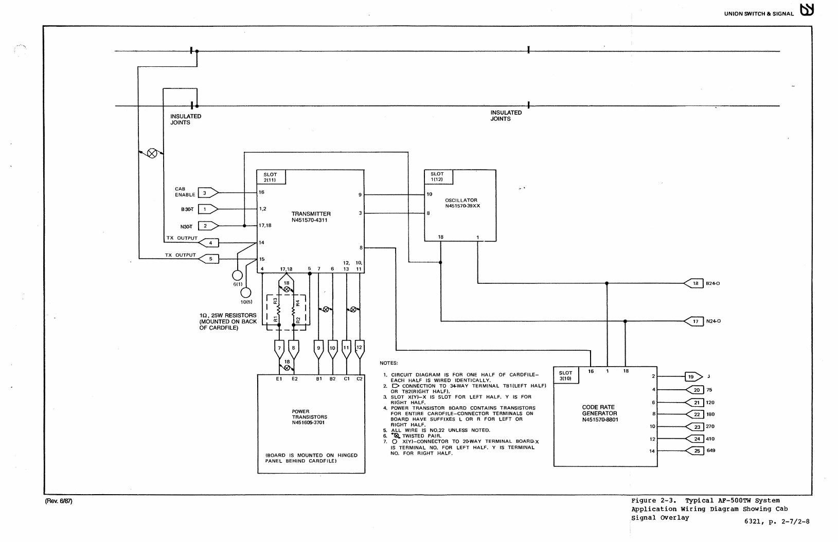
This is another means of transmitting cab signals in areas where train detection is by AC power frequency track circuits. Figure 2-3 shows a typical application. A special Transmitter PCB is required and its output connects directly to the rails, eliminating the need for a minibond and tuning unit.
(Rev. 6-87) 6321, p. 2-1

m UNION SWITCH & SIGNAL
2.2.4 Receiver-Only Point
This equipment acts as a second, high-definition receiver when used in conjunction with a normal track circuit. A typical application is shown in Figure 2-4. The wayside equipment consists of a 10-foot long multi-conductor wire loop mounted between the rails, and a steel junction box containing a matching transformer and terminal strips. Only one PCB is required - a special high-sensitivity receiver. When properly adjusted, the Receive-Only Point will achieve shunting definition of 5 to 10 feet.
6321, p. 2-2

(Rev.6/~
TX
TUNING UNIT
CAB ENABLE
B30-T
N30:r
OUTPUT
TX OUTPUT
SLOT 2(11)
16
#18 1,2
#18 17,18
14
15
4
10, 25W RESISTORS (MOUNTED ON BACK OF CARDFILE
• MINIBOND
9
TRANSMITTER 3 N451570-43XX
8
12, 10. 17,18 5 7 6 13 11
18
E1 E2 81 82 C1 C2
POWER TRANSISTORS N451605-3701
(BOARD IS MOUNTED ON HINGED PANEL BEHIND CARDFILE)
MINIBOND
SLOT 1(12)
,.. ' 10
OSCILLATOR N451570-39XX
8
18
NOTES:
1. CIRCUIT DIAGRAM IS FOR ONE HALF OF CARDFILEEACH HALF IS WIRED IDENTICALLY.
2. D CONNECTION TO 34-WAY TERMINAL TB1{LEFT HALF) OR TB2(RIGHT HALF).
3. SLOT X(Y)-X IS SLOT FOR LEFT HALF. Y IS FOR RIGHT HALF.
4. POWER TRANSISTOR BOARD CONTAINS TRANSISTORS FOR ENTIRE CARDFILE-CONNECTOR TERMINALS ON BOARD HAVE SUFFIXES L OR R FOR LEFT OR RIGHT HALF.
5. ALL WIRE IS N0.22 UNLESS NOTED. 6. 'TWISTED PAIR. 7. Q X(Y)-CONNECTOR TO 20-WAY TERMINAL BOARD-X
IS TERMINAL NO. FOR LEFT HALF. Y IS TERMINAL NO. FOR RIGHT HALF.
8. EXTERNAL CAPACITOR TO COMPENSATE FOR VARYING CABLE CAPACITANCE BETWEEN MINIBOND AND ROOM EQUIPMENT.
SLOT 5(8)
SLOT 3(10)
•
11
13
RECEIVER 1,2
N451570-41 XX
18
17
15
16 18 2
4
6 CODE RATE GENERATOR 8 N451570-8801
10
12
14
TUNING UNIT
SEE NOTE 8
RX INPUT
RX INPUT
B24·R
N24-R
RELAY+
UNION SWITCH & SIGNAL ~
RELAY -
824-0
J
75
120
180
270
410
648
Figure 2-1. Typical AF-500TW System Application Wiring Diagram for a Single Track Circuit In Continuous Rail Territory Without Insulated Joints 6321, p. 2-3/2-4

(Rev. 6/87)
CAB ENABLE
B30-T
N30-T
TRANSMITTER OUTPUT
TUNING UNIT
MINI BOND
SEE NOTE 8 10(5)
1Q, 25W RESISTORS (MOUNTED ON BACK OF CARDFILE
SLOT 2(11)
16 9
1,2 TRANSMITTER N451570-43XX
17,18
u 8
15 12, 10,
4 17,18 5 7 6 13 11
18
E1 E2 81 82 C1 C2
POWER TRANSISTORS N451605-3701
(BOARD IS MOUNTED ON HINGED PANEL BEHIND CARDFILE)
UNION SWITCH & SIGNAL ~
SLOT 1(12)
10
OSCILLATOR N451570.39XX
18
~ '
SLOT 16 18
3(10) 2
4
6 CODE RATE GENERATOR 8 N451570-8801
10
12
14
NOTES:
1. CIRCUIT DIAGRAM IS FOR ONE HALF OF CARDFILE-EACH HALF IS WIRED IDENTICALLY. 2. C>CONNECTION TO 34-WAY TERMINAL TB1(LEFT HALF) OR TB2(RIGHT HALF). 3. SLOT X(Y)-X IS SLOT FOR LEFT HALF. Y IS SLOT FOR RIGHT HALF. 4. POWER TRANSISTOR BOARD CONTAINS TRANSISTORS FOR ENTIRE CARDFILE-CONNECTOR
TERMINALS ON BOARD HAVE SUFFIXES L OR R FOR LEFT OR RIGHT HALF. 5. ALL WIRE IS N0.22 UNLESS NOTED. 6. QS).TWISTED PAIR. 7. 0 X(Y)-CONNECTION TO 20-WAY TERMINAL BOARD-X IS TERMINAL NO. FOR LEFT HALF.
Y IS TERMINAL NO'. FOR RIGHT HALF. 8. EXTERNAL CAPACITOR TO COMPENSATE FOR VARYING CABLE CAPACITANCE BETWEEN- MINIBOND AND ROOM
EQUIPMENT.
Figure 2-2. Typical AF-500TW System Application for Speed Command
J
75
120
180
270
410
649
Transmission Loop 6321, p. 2-5/2-6
(Rev. 6Ml)
INSULATED JOINTS
CAB ENABLE
830-T
N30-T
TX OUTPUT
TX OUTPUT
10(5)
1 Q, 25W RESISTORS (MOUNTED ON BACK OF CARDFILE)
SLOT 2(11 l
16 9
1,2 TRANSMITTER 3
N451570-4311 17,18
14 8
15 12, 10,
4 17,18 5 7 6 13 11
18
E1 E2 81 82 C1 C2
POWER TRANSISTORS N451605·3701
{BOARD IS MOUNTED ON HINGED PANEL BEHIND CARDFILEJ
SLOT 1(12)
10
8
18
OSCILLATOR N451570-39XX
INSULATED JOINTS
,. .
NOTES:
1. CIRCUIT DIAGRAM IS FOR ONE HALF OF CARDFJLE-EACH HALF IS WIRED IDENTICALLY.
2. D CONNECTION TO 34-WAY TERMINAL TB1(LEFT HALF) OR TB2(RIGHT HALF).
3. SLOT X(Yl-X IS SLOT FOR LEFT HALF. Y IS FOR RIGHT HALF.
4. POWER TRANSISTOR BOARD CONTAINS TRANSISTORS FOR ENTIRE CARDFJLE-CONNECTOR TERMINALS ON BOARD HAVE SUFFIXES L OR R FOR LEFT OR RIGHT HALF.
5. ALL WIRE IS N0.22 UNLESS NOTED. 6. ~ TWISTED PAIR. 7. 0 X{Yl-CONNECTOR TO 20-WAY TERMINAL BOARD-X
IS TERMINAL NO. FOR LEFT HALF. Y IS TERMINAL NO. FOR RIGHT HALF.
SLOT 16 18
3110)
CODE RATE GENERATOR N451570-8801
UNION SWITCH & SIGNAL ~
824-0
N24-0
2 J
4 75
6 120
8 180
10 270
12 410
14 649
Figure 2-3. Typical AF-500TW system Application Wiring Diagram Showing Cab Signal overlay 6321, p. 2-7/2-8

(Rev. 6/ffl)
TUNING UNIT
CAB ENABLE
630-T
N30-T
TX OUTPUT
TX OUTPUT
SLOT 2{11)
• MINIBOND
SLOT 1(12)
SLOT 5(8)
MULTICONDUCTOR LOOP
JUNCTION BOX
11 13 __ .......
MlNIBOND
SLOT 5(8)
• TUNING UNIT
SEE NOTE 8
UNION SWITCH & SIGNAL tij
>----+---t 1.2
OSCILLATOR N451570-39XX
RECEIVER N451570-75XX
B24R 1,2 1----<
RECEIVER N451570-41XX
1,2,-...---c 29 824-R
10(5)
m, 25W RESISTORS {MOUNTED ON BACK OF CARDFILE
TRANSMITTER N451570-43XX
31------t--~8
18
81-----,
E1
12. 10. 5 7 6 13 11
E2 81 82 Cl C2
POWER TRANSISTORS N451605·3701
(BOARD IS MOUNTED ON HINGED PANEL BEHIND CARDFILE)
NOTES:
1. CIRCUIT DIAGRAM IS FOR ONE HALF OF CARDFILEEACH HALF IS WIRED IDENTICALLY.
2. D CONNECTION TO 34-WAY TERMINAL TBl(LEFT HALF) OR TB2(RIGHT HALF!.
3. SLOT X(Y)-X IS SLOT FOR LEFT HALF. Y IS FOR RIGHT HALF.
4. POWER TRANSISTOR BOARD CONTAINS TRANSISTORS FOR ENTIRE CARDFILE-CONNECTOR TERMINALS ON BOARD HAVE SUFFIXES L OR R FOR LEFT OR RIGHT HALF.
5. ALL WIRE IS N0.22 UNLESS NOTED. 6. ~ TWISTED PAIR. 7. 0 X(Y)-CONNECTOR TO 20-WAY TERMINAL BOARD-X
IS TERMINAL NO. FOR LEFT HALF. Y IS TERMINAL NO. FOR RIGHT HALF.
8. EXTERNAL CAPACITOR TO COMPENSATE FOR VARYING CABLE CAPACITANCE BETWEEN MINIBOND ANO ROOM EQUIPMENT.
SLOT 3(10)
18 18----c 30 N24-R
17 17 1-------1 RELAY •
RELAY+
15 15 1-------1 RELAY
RELAY -
16 18
CODE RATE GENERATOR N451570-8801
18 824-0
17 N24-0
2
4 75
6 120
8 180
10 270
12 410
14 649
Figure 2-4. Typical AF-500TW System Application Wiring Wiring Diagram for a Track Circuit In Continuous Rail Territory Plus Receive-Only Point 6321, p. 2-9/2-10

•• UNION SWITCH a SIGNAL CIJ
SECTION III
. INSTALLATION AND ADJUSTMENTS
3.1 INSTALLATION
In general, the electronic circuits making up the AF-SOOTW System are contained in card files that are housed in equipment cabinets in a central instrument house or equipment room. Depending upon the length of ttack being serviced, a number of individual track circuits may be present as part of an overall automatic block and train detection subsystem. Therefore, installation of these track circuits depends upon the particular rail transit line drawings which specify the location and method of installation for these track circuits. Section II describes and illustrates a typical application of the AF-SOOTW system.
3.2 ADJUSTMENTS
Once the AF--~OOTW System is installed in a particular track circuit environment, it must be properly adjusted for correct train detection and cab signaling levels. These adjustment procedures are performed on the wayside minibond, card file and PCBs making up the track circuit electronic circuits. Once these adjustments have been made, the overall system is tested to demonstrate that the track circuit is functionally operational and to provide a performance check of system operating parameters. During performance of the adjustment procedures, refer to Figure 2-1.
3.2.l Recommended Test Equipment
The recommended test equipment required to adjust and test the AF-SOOTW System is listed in Table 3-1.
Table 3-1. Recommended Test Equipment for System Adjustments and Tests
suggested Manufacturer Test Equipment Model/Part No.
Osei lloscope Tektronix 4658 Frequency/Period counter Hewlett Packard 5307A Digital Multimeter Fluke 8050A 0.06 Ohm Track Shunt Universally Keyed card Extenders US&S N398028
3.2.2 Preparation for Adjustments
The following adjustments and test procedure should be conducted under high ballast conditions. The Transmitter PCBs for adjacent track circuits (except where track circuits are isolated by insulated joints} are to be unplugged during these adjustments and tests. Where necessary, this requires the unplugging of these boards in the adjacent relay rooms.
6321, p. 3-1

ID UNION SWITCH & SIGNAL
The card file for the track circuit being adjusted must contain a transmitter, receiver, oscillator, and code rate generator PCB, all with the proper train detection frequency.
3.2.3 Adjustment procedures
Certain test points and controls on printed circuit boards (PCBs) are not accessible unless they are placed on extender boards. Table 3-2 contains a list of these test points, indicator LEDs and switches. It is assumed in the following paragraphs that PCBs required for these adjustments are connected to the extender boards. After adjustments are complete, the PCB must be placed in its appropriate card slot.
3.2.3.1 Bond Jumper Selection. Make sure that all bonds associated with the track circuit being adjusted have been tuned to the proper transmit and receive frequencies. Tuning the bonds involves cutting the appropriate jumper wires inside the bond tuning unit (Figure 3-1 or see label on inside cover of bond tuning unit).
3.2.3.2 Cable Length Compensation, This adjustment compensates for varying line capacitance of the cable between the equipment room and the minibond. It is not required for direct cab signal injection in the rails (i.e., where the -4311 Transmitter PCB is used).
3.2.3.3
WARNING I Hazardous voltages may exist on the bond tuning panel and on the terminals on the exposed backplane of the card file. Care must be taken to avoid electrical shock. This adjustment should be performed only by trained maintenance personnel.
a. Determine the approximate length of the cable between the mini bond and its Receiver PCB.
b. Using this length and the capacitance values given in Table 3-3, attach th~ appropriate capacitor across the receiver input terminals at the 20-way terminal board on the back of the card file. Recommended capacitors are Electrocube Series 950B, rated at 270 volts rms.
Transmitter Power Amplifier Bias Adjustment. (See Figure A-4)
NO'l'E
Only when the AF track circuit is installed, or when a Transmitter (Power Amplifier) PCB or a power transistor is replaced to repair the track circuit, is the Power Amplifier Transistor Bias (de potential difference between the the emitter voltages of the two power transistors) measured and adjusted.
6321, p. 3-2 (Rev. 9-93)

UNION SWITCH & SIGNAL b':f
During this procedure, the Oscillator PCB is unplugged and the CABoff-TRACK switch SW3 on the Transmitter PCB is put in the TRACK position to ensure no ac signal is being handled by the Transmitter PCB. The de emitter voltage of one of the power transistors is then adjusted to lSOmV de. The other power transistor's emitter voltage is then measured to ensure it is no more than ±lSmV of the other emitter voltage (between 135 and 165mV de).
When the bias adjustment is made, at the time of the track circuit's installation or repair, the power transistors are cool. When they have been warmed-up, their characteristics will change and the bias voltages can vary substantially and are no longer significant. Because of this fact, when the track frequency output and/or cab signal output are tested and adjusted, the bias is NO'l' to be measured or adjusted.
To adjust the bias under conditions stated in the above note, proceed as follows:
~.· Adjust the Transmitter PCB switches as follows:
(1) Rotate the Bias Potentiometer R21 fully counter clockwise (CCW) .
(2) Rotate the Cab Coarse Switch Sl and the Track Coarse Switch S2 to the •1• position (fully clockwise).
(3) Place the Track/Cab Switch S3 in the "TRACK" position.
(Rev. 9-93) 6321, p. 3-2A

~ UNION SWITCH & SIGNAL
This page intentionally left blank.
6321, p. 3-2B (Rev. 9-93)

I
UNION SWITCH & SIGNAL U.,
Table 3-2
The following is a summary of test points, indicator LEDs, and switches on the AF-500 circuit boards. Except where indicated, these components are located at the outer edges of the circuit boards.
Oscillator
Receiver
Transmitter
Code Generator
TPl TP2 TP3 TP4 TPS
TPl TP2 TP3 LEDl
R31
TP5 LEDl TP2 TP7 TP6 TPl TPlO TP4 TP9 TP8
*TP13 *TP14 *Sl *S2 *S3 *RS
*Rl2
TPl TP2 TP3 TP4 LEDl
Red Yellow Yellow Yellow Black
Red Green Black
Green
Red White ~l White J Orange Black
B240 (+24 Vdc) Not used Train detection carrier reference osillator Cab carrier osillator (4550 Hz) N240 CO Vdc)
B24R C+24 Vdc) Receiver filter output N24R CO Vdc) Track relay indicator (relay energized when LED is lit) Receiver sensitivity adjustment
Train detection carrier reference input Flashes at code rate being transmitted B30T (+30 Vdc)
Input to power transistor stage
Cab enable N30T (0 Vdc)
Blue Cab carrier reference input
Yellow~ Transmitter output YellowJ
Red Green Yellow Black
} Power transistor bias measurement points
Coarse cab signal level adjustment switch Coarse train detection level adjustment Continous/coded test switch Fine cab signal level adjustment potentiometer Fine train detection adjustment potentiometer
B240 (+24 Vdc) Not Used Code Generator output N240 (0 Vdc)
signal
Flashes at selected code rate
level
"'These components not mounted on edge of board. For exact locations, refer to circuit board drawings in Appendix A.
(Rev. 6-87) 6321, p. 3-3

O'I w N ..... ..
"Cl . w I
"'"
........ ~ (1)
< . O'I I
CX)
-..J
"1 ..... IQ i:: .., (1)
w I ..... . ~ i:: :::s ..... :::s
IQ
0 :::s .... 11"
:;:: ..... .., ..... :::s
IQ
l;j ..... Ill IQ .., Ill ::I
I N451486·0702 WIRING DIAGRAM r,;:=.-...-=-.--~..--.=-.. ;::;=• ~~-~~ , r a • W • W a k • W .I! • W a W , r~X~ll( -~II[ .§§ .. ~-W:~a -~--~--,
8 Pins_/ '--------f-4----L== of pin connector
z .... ... a: ~
1 .n
SLOTTED END
EB
EB
WARNING HIGH VOLTAGE
WAYSIDE CABLE :.c
y
I :5 ID
llC u c
cip I I ~ ........ z .,_c:i::,c - ....... a: :CCll:IDQ 31:
N451605-3102 IRECI
I
N451605-3101 ITRAN SI
N451605·3201 ICABI
Do not adjust or remove printed circuit boards unless the power is off. Power can be supplied through the wayside cable or the rail connections of the bond.
FREQUENCY SELECTION· cut buss wire segments.
L
... !::: :c 31:
7
EB
WAYSIDE CABLE
.. Mlnibond
. N451003-1102
•
• 1)-
D • •
Coupling unit N451003·1202
1900 HZ NO CUT REQUIRED.
I
__J
~ c z s z \II
;ii ;:: :i:: Qo
\II
ci z > ,...

UNION SWITCH & SIGNAL
Table 3-3. Recommended capacitance Values for Varying Cable Lengths Between the Minibond and Equipment Room
Cable Length (ft.) Capacitor (uf.)
0 - 800 .092 (.082 in parallel with .01) 800 - 1600 .082
1600 - 2700 .068 2700 - 3800 .047 3800 - 4800 .033 4800 - 6300 .015
b. Temporarily unplug the Oscillator PCB.
c.,.. Using a digital multimeter, measure the de biases (millivolts) of the two transmitter power transistors by measuring first between TP 13 (+) and TP 10 (-), and then between TP 14 (+) and TP 10 (-).
d. Rotate the Bias Potentiometer, if necessary, until the average of the two bias measurements is 150mV, +15 mv.
e. Place the Track/Cab Switch S3 in the center position and plug in the Oscillator PCB.
3.2.3.4 Train Detection Signal Level Adjustment
a. Set the following conditions prior to adjustment:
(1) Generate lowest code rate (75 cpm) by connecting a jumpP.r from pin 2 to pin 4 on the Code Rate Generator PCB.
(2) Track/Cab switch S3 on the Transmitter PCB in the center position.
b. Adjust the Receiver Sensitivity Potentiometer R31 (mounted on front edge of Receiver PCB) fully ccw.
c. On the Transmitter PCB, set the Track Coarse switch S2 to position •1• and rotate the Track Fine Potentiometer Rl2 fully ccw.
d. Increase the Track coarse switch one increment at a time until the track relay picks up (pickup is indicated by illumination of the light emitting diode (LED) on the Receiver PCB: then back up one setting (the track relay should drop). Leave at this setting.
e. cause the relay to just pick up by slowly turning the Track Fine Potentiometer cw.
f. Place the Track/Cab switch to the •TRACK• position.
6321, p. 3-5

33 UNION SWITCH & SIGNAL
3.2.3.5
g. Measure the receive input voltage level across pins 11 and 13 of the Receiver PCB. This level must be between 2.2 and 3.0 volts peak-to-peak when the Receiver Sensitivity Potentiometer is adjusted fully ccw.
h. Measure the Transmitter output level across TP 8 and TP 9 of the Transmitter PCB.
i. Multiply this value by 2.5 (150% overdrive). (Note: When receiver is connected to multibond, i.e. two bonds connected across the rails in parallel at substations, multiply the value at step h by 1.5 instead.)
j. Increase the transmitter output level by adjusting the Track coarse Switch and the Track Fine Potentiometer until the calculated overdrive voltage is measured.
cab Signal Level Adjustment
a. Set up conditions prior to adjustment:
Cl) Cab coarse Switch at position •1• and Cab Fine Potentiometer turned fully ccw.
(2) Generate lowest code rate by using the code rate selector switch or by connecting a jumper from pin 2 to 4 on the Code Rate Generator PCB.
(3) Track/Cab Switch in the "CAB• position.
NOTE
Where cab signaling is supplied for double direction running, a transmitter will send a cab signal out along the two blocks bordering its rail connection points (except at insulated joint locations). Therefore, the cab signal adjustment must be made for the longer of the two blocks. The entering end of the block is that end where the train will first receive cab signaling (farthest point from the signal transmission to the rails), while the exiting end is the location from which cab signaling is being transmitted. During the following adjustment, the minibond for the transmitter being adjusted is considered the exiting end.
b. Enable the cab carrier signal by connecting a jumper from pin 1 to pin 16 on the Transmitter PCB.
6321, p. 3-6

3.2.3.6
a.
b.
c.
d.
e.
UNION SWITCH & SIGNAL UJ
NOTE Because of the high frequency involved, make sure that the oscilloscope is properly calibrated and that its probe is properly frequency compensated.
For a standard track circuit, monitor the input to the receiver PCB at the entering end of the longer side. Be sure to unplug the corresponding transmitter at this location. Use an oscilloscope across pins 11 and 13 of the receiver PCB and adjust for 8 volts peak-to-peak for the 4550 Hz cab signal; this corresponds to 100 milliamperes of rail current.
For cab loop circuits, monitor the outputs of the Transmitte~ PCB (across pins 14 and 15) and adjust Cab coarse switch and cab Fine potentiometer to obtain maximum undistorted output.
For cab signal overlay on ac track circuits, first place an 0.06 ohm shunt across the rails at the end of the track circuit farthest from the transmitter. Adjust the Transmitter PCB cab coarse switch and Cab Fine potentiometer to obtain the equivalent of 100 ma rms rail current as measured by a 4550 Hz signal strength coil.
f. Reinstall the Receiver PCB without the extender board.
g. set the Transmitter Track/Cab switch to the center position.
h. Remove the cab signal enable jumper from between pins 1 and 16.
Receive-Point Adjustment Procedure
Wiring (See Figure 3-2)
Prior to adjustment, verify the following:
(1) 16 conductors of the multi-conductor cables are being used. The wires from one end of the cable must be connected to terminals lA through 16A, and the wires from the other end of the cable must be connected to the corresponding terminals lB through 168. Check the color coding on the wires to make sure that terminals lA and lB are attached to the two ends of the same wire, and so on for terminals 2A and 28, 3A and 3B, etc.
(2) Jumper straps must be in place on terminal boards TBl, TB2, and TB3 (18 straps total).
(3) There must be a wire between terminal Rl on terminal board TB3 and terminal con the -9401 printed circuit board.
(Rev. 6-87) 6321, p. 3-7

~ UNION SWITCH & SIGNAL
T61 T62
16A 15A 14A 13A 12A 11A 10A 9A SA 7A 6A
I I I I 'I I II I I I 0
v- -166 158 148 138 128 118 108 98 88 78 68 T1 ·- .,,,. ....
". -- --- ---- _.,,,.
-- ---- . --I -- ----
TO RECEIVER I , ....
BOARD .,,,..,,,. . ...... ' .
---- .... -- ....
.... -- ..... - (j 0 0 0 0 o' "'() 0 t"'l .J -. -S1 S2 S3 S4 SS S6 S7 SS P2 P1
·7301
·9401 T83
A 8 c SA 4A 3A 2A 1A
I I I I I 58, 48 38
' 26 18 ,,. R1 TO RAIL
*TAP TO BE SELECTED DURING ADJUSTMENT PROCEDURE
Figure 3-2. Junction Box Wiring Diagram
6321, p. 3-8

UNION SWITCH & SIGNAL
(4)) There must be a wire between terminal Tl on terminal board TB2 and terminal Pl on the -7301 printed circuit board.
(5) Terminal A on the -9401 printed circuit board must be connected to one rail.
(6) Terminal Sl on the -7301 printed circuit board must be connected to one input terminal of the Receiver printed circuit board.
(7) The Receiver PCB must be of the -75xx series and of the proper frequency.
c. Adjustment Procedure
(1) Referring to Figure 3-3A or 3-38, measure the distances from the Transmit minibond to the Receive Point rail connections (Ll) and from the Transmit minibond to the Receive minibond (L2).
(2) Calculate the ratio Ll/L2. Use this number and Table 3-4 to ~' determine the proper terminals for the second rail connection, the
P2 connection, and the second Receiver connection.
(3) Bias the power transistors for the Transmitter as in a normal track circuit. Set the Track Coarse switch to position 1 and Track Fine potentiometer fully counterclockwise.
(4) Slowly increase the Transmitter output voltage until the Receive Point (RP) track picks up. If the normal track relay picks up before the RP relay, turn down the transmitter and move the second receiver connection down one terminal (for example, from S6 to SS). Repeat this step until the RP relay picks up before the normal track relay.
(5) Slowly increase the Transmitter output voltage until the normal track relay just picks up (the RP relay should already be up). Turn the receiver sensitivity potentiometer on the Receive Point receiver clockwise until the RP relay drops. Turn the potentiometer counter-clockwise until the RP relay just picks up.
(6) Switch the Transmitter to continous Track and measure the Transmitter voltage. set the Transmitter voltage to 2.5 times this pickup voltage (150% overdrive). switch the Transmitter back to coded output (both relays should pick-up).
(7) Using a 0.06 ohm track shunt, measure the Receive Point pre-shunt distance. This is the distance from the RP rail connections at which the RP relay drops. Starting at a point approximately 20 feet from the RP rail connectons (nearer to the Receiver minibond), move the shunt closer to the RP rail connections until the RP relay drops. This pre-shunt distance should be between 5 and 10 feet. If the pre-shunt distance is not within these limits, it will be necessary to experiment with different signal levels (Transmitter output voltage.and RP Receiver sensitivity) and/or connections different from those suggested in Table 3-4.
6321, p. 3-9

m UNION SWITCH & SIGNAL
(8) Test the normal track circuit as usual and adjust the cab signal level using the standard track circuit adjustment procedure.
TRANSMIT MINIBOND
¢
RECEIVE POINT
Ll/L2
o.oo - 0.25
0.26 - 0.50
0.51 - 0.75
0.76 - 1.25
6321, p. 3-10
: ....
L1
L2
TRANSMIT MINIBOND
RECEIVE POINT
2 -1
Figure 3-3A
Figure 3-3B Calculation of Receive Point Connection
Table 3-4
Second Rail P2 connection Connection
28 108
38 12B
4B 148
4B 168
RECEIVE MINIBOND
~
RECEIVE MINIBOND
¢ -I
Second Receiver Connection
SS
S6
S7
S8

UNION SWITCH & SIGNAL w 3.3 TRAIN DETECTION MINIMUM PERFORMANCE TEST
Inunediately following the post-installation adjustments (and during scheduled maintenance intervals), the following train detection minimum performance test must be performed to verify the integrity of the AF-SOOTW System track circuits. (Refer to recommended test equipment list in Table 3-1.)
a. Generate the lowest code rate by connecting a jumper from pin 2 to pin 4 on the Code Rate Generator PCB.
b. Verify that the proper track relay picks up.
c. With the 0.06-ohm track shunt, verify that the track relay drops while shunting the rails at:
(1) the receive end rail connections; (2) the transmit end rail connections; (3) approximately at the midpoint of the track circuit.
3.4 RECORDING DATA
After a track circuit is adjusted and tested, it is recommended that data be taken and recorded, using a data sheet as shown in Figure 3-4. This data recording process serves as a reminder to make sure all the adjusting procedures were followed and the records will assist if troubleshooting is later required. The following procedure should be followed for data recording (disconnect adjacent track circuit before recording data):
a. Place the Track/Cab Switch to the •TRACK• position.
b. Measure and record the transmitter output voltage between TPS and TP9 of the Transmitter PCB •.
b. Measure and record the receiver input voltage between pins 11 and 13 of the Receiver PCB.
d. Measure and record the voltage of the filtered receiver signal between Receiver TP2 (green) and TP3 (black).
e. connect the frequency counter across TP8 and TP9 of the Transmitter PCB and record the measured value of carrier frequency.
f. Place the Track/Cab switch to the •cAB• position.
g. Enable the cab signal carrier by placing a jumper across pins 1 and 16 of the Transmitter PCB.
h. Measure and record the Transmitter output voltage between TP8 and TP9 of the Transmitter PCB.
6321, p. 3-11

Figure 3-4. Track Cir cu it Data Sheet
Track Circuit No.
Track Cab Track Cab Filter Adjusted Track Cab Xmtr. Xmtr. Rcvr. Rcvr. out Loop Relay
Date By Freq. Freq. Volt. Volt. Volt. Volt. Volt current Volt.
.
!
I
I ! .
!
I . i
. f
. I I I
I I
i i I

UNION SWITCH & SIGNAL ~
i. Measure and record the Receiver input voltage between pins 11 and 13 of the Receiver PCB.
j. connect the frequency counter across TP8 and TP9 of the Transmitter PCB and record the measured value of carrier frequency.
k. Disable the cab carrier signal by removing the jumper across pin l and pin 16 of the Transmitter PCB.
1. Place the Track/Cab switch on the Transmitter PCB to the center position.
m. Measure the de voltage across the track relay coil and record it.
n. For cab loop circuits, record only the cab transmitter output voltage and the loop current.
6321, p. 3-13


UNION SWITCH a SIGNAL ~
SECTION IV
FUNCTIONAL DESCRIPTION
4.1 INTRODUCTION
This section presents a functional description of the AF-500'1W System and is divided into two parts. The first part discusses the functions of the system on a simplified functional block diagram level. The second part of this section provides detailed circuit descriptions of the PCBs making up the system and are referenced to PCB schematic diagr~ms.
4.2 FUNCTIONAL BLOCK DIAGRAM DESCRIPTION
The major functions of the AF-500'1W System are twofold; namely, train detection and the transmission of cab signal information. The ancillary subfunction of broken rail detection is included.
4.2.1 Train Detection Function (See Figures 2-1 and 4-1)
Figure 4-1 illustrates a simplified function application of the AF-500'1W System. Transmitter Tl is transmitting a coded carrier frequency fl to receiver Rl. Similarly, transmitter T2 is transmitting a coded frequency f2 to receiver R2. Receiver R4 is receiving frequency f4 from an unseen transmitter to the left, and transmitter T3 is sending coded carrier frequency f3 to an unseen receiver on the right. (Refer to paragraph 1.5.1 for train detection carrier frequencies.)
The code applied in each track circuit block is the same as that which would be selected if a cab signal were being transmitted. This code usually depends on traffic conditions and civil speed restrictions, and the code rate is selected by vital relay logic which is external to the electronic equipment in the card file. When a vehicle is present in a block, as shown in Figure 4-1, its axles shunt current away from the receiver in that track circuit. As a result, the vital track relay (in this case TR2) drops from its normally energized state. The vehicle is thus detected as being within the block (track circuit TC).
Without insulated joints at the track circuit boundaries, the track circuit shunts a short distance before the lead axle actually crosses the minibond rail connection location: this is referred to as pre-shunt distance. Similarly, as the train leaves the block, the track circuit remains shunted until the trailing axle has passed a short distance beyond the minibond rail connections; this distance is called the post-shunt distance. The actual pre-shunt and post-shunt distances are dependent on ballast resistance, frequency, and equipment design. The AF-500'1W System is designed to control these distances to permit close headway operation normal to modern transit environments, while satisfying all other functional requirements. Pre-shunt and post-shunt distances of 40 feet or less are typical for the AF-500'1W System.
6321, p. 4-1

°' w N ..... ... 'O . .,,. I
N
F4 PR --...
-TA
---,----, I I I
R4 I I I __ ...... __ J
I TR4 I LEGEND:
T- TRANSMITIER R- RECEIVER
NORMAL .... ---- DIRECTION
MB1 MB2 I OF TRAFFIC
I I I F1 PR I F2 PR
I --... I __... r .,
TB TC
% OF CARDFILE
I r-- ----- --~ r-- -------- ----, I I I I : T1 R1 I I T2 R2 I I I I I
__ ...,_ __ J L __ ------- __ _J L--.--
\ cs I TR1 I \
cs ~
F- FREQUENCY TR- TRACK RELAY MB- MINIBOND PR- PROPULSION RETURN (CROSSBONDI
Figure 4-1. AF-SOOTW System, Simplified Functional Block Diagram
MB3
I I I I
TD
F3 --...
r.--:r--1 I L
T3
I\ cs
m c z 6 z I ~ ::r: 11!1 en a z > r

UNION SWITCH & SIGNAL ffi 4.2.2 Broken Rail Detection Subfunction
Broken rail detection is dependent largely on proper application of the AF-500TW system and on the design of the external propulsion power return system. Broken rail detection can be obtained provided the following conditions are met:
a. Each AF-500TW System track circuit must be properly installed and adjusted.
b. While parallel tracks must be cross-bonded at least every 2500 ft. they may not be cross-bonded more frequent than every other track circuit. Regardless of the number of intervening track circuits, cross-bonding may not occur at less than 1400-foot intervals.
4.2.3 Cab Signal Transmission Function (See Figures 2-1 and 4-2)
The cab signal is generated by the Oscillator PCB and consists of a 4550 Hz sinewave; tbis signal is applied to the Transmitter PCB where it is transmitted together with the train detection frequency at an externally specified code rate representing a speed command. (Refer to paragraph 1.5.1.) The speed command is selected by vital relay logic (usually part of an automatic block subsystem) which connects a specific code rate generator input enable line to 24 Vdc. Six code rates are available for cab signals; one code rate for signaling the vehicle to switch to yard mode (cutout), and five code rates for actual speed commands.
In order to transmit a 4550 Hz. cab signal, a vital relay or relays separate from the speed command selection vital relays, is necessary to enable transmission (code or cab enable). This.signal is 24 Vdc and normally initiates a cab signal when the track circuit is occupied. The transmitted signal format is such that the train detection carrier and cab signal carrier frequencies occupy alternate half-cycles of the code rate squarewave as shown on Figure 4-2. Although the two signals are shown as having equal amplitudes, the amplitude of each carrier frequency is independently adjustable on the Transmitter PCB.
4.3 CIRCUIT DESCRIPTIONS
The following paragraphs present detailed circuit descriptions and are referenced to PCB schematic diagrams. Intimate knowledge of their operation is essential for maintenance personnel to fully understand, troubleshoot and maintain the AF-SOOTW System both at the system level and during PCB shop maintenance. In addition, a description is also provided for the minibond.
6321, p. 4-3

m UNION SWITCH & SIGNAL
SPEED COMMAND CODE RATE
TRAIN DETECTION SIGNAL
COMPOSITE SIGNAL
6321, p. 4-4
Figure 4-2. Transmitter Output Signal Format

UNION SWITCH & SIGNAL OJ
4.3.1 Oscillator PCB
The Oscillator PCB (Figure 4-3) provides the proper frequency ac signals to the Transmitter PCB. The Transmitter PCB amplifies these signals and drives a track minibond. The oscillator on circuit A is the cab signaling frequency and the oscillator on circuit Bis the track or train detection frequency. Circuit c is not used. The circuit is a Colpitts Oscillator with feedback provided by Zener diode Dl. The circuit will not oscillate unless the Zener is in conduction. This lowers the impedance of the Zener thus creating a feedback path. The primary of Tl and C4 make up the tuned circuit that provides the proper frequency of oscillation. Zener diode D2 provides the de level for the output signal. Transistor 02 is an emitter follower providing a low impedance drive for the output.
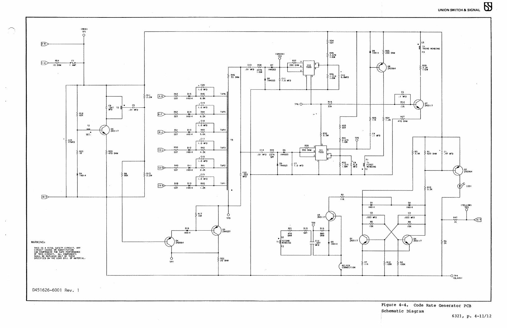
4.3.2 Code Rate Generator PCB
The purpose of this board (Figure 4-4) is to supply a wayside transmitter with a 50-50 squarewave code of the proper frequency, depending on which code selection input pin i~ energized. The code frequencies are 75, 120, 180, 270, 410 and 648 cycles per minute. The output on PCB pin 16 is a square wave with an amplitude of approximately 20 volts zero to peak. A detailed description of the circuit operation follows:
Transistor Q9, transformer T2, and capacitor C9 form a feedback oscillator with a sinusoidal output at 6 KHz. This 6 KHz signal is fed into a linear amplifier (Q4 and 05) which in turn drives the autotransformer T3. Power supply voltage (+24 Vdc) from PCB terminal 2,B is fed to relays which control the code selection. These relays connect the code select terminal (2,B) to one of the taps on the autotransformer (T3) which supplies de power for the linear amplifier. Since the ac voltage out of 05 (TP9) is constant, the output from the top of T3 depends on which tap is energized. When PCB pin 4 is energized, this produces the minimum voltage and code rate (75 CPM), and when PCB pin 14 is energized the maximum voltage and code rate (648 CPM) are produced.
The output voltage from T3 is taken by Cl4 and Cl3 to the two duplicate RC oscillators. The charging resistors are R38 and R39, which are ahead of the rectifiers, so the rate of charge of timing capacitors C7 and Cll is controlled by the average voltage from T3. Considering one of the two similar circuits, the master oscillator IC2 is an astable, unsymmetrical relaxation oscillator which uses a MOS version of the 555 timer chip to allow minimal loading of the high impedance time constant components. As is typical with 555's, the threshold points are at 1/3 and 2/3 of power supply. A low charging current, appropriate to the low code rates, is supplied to Cll via R38, while a quick discharge current through R37 gives times of under 1 ms. During the discharge, the output on pin 3 is low, and this pulse is taken as the useful output. Thus, ell charges slowly in a time determined by the code voltage selected, and discharges rapidly, giving pulses at twice the code rate. since the rate is determined by Cll, voltage relative to the chips internal reference, manufacturing adjustment of frequency is conveniently performed in the divider to pins 4, 8, which was originally needed to reduce supply voltage to below ratings for the chips.
6321, p. 4-5

m UNION SWITCH & SIGNAL
The second oscillator !Cl is similar to the first, except that a small portion of the output from IC2 is fed via R30 to its internal reference divider at pin 5. This means that if the two were started together but !Cl was slightly lower in frequency than IC2, it would not otherwise have •fired• when IC2 did, causing it to fire, and lock in. If it's independent frequency had been higher, it would have fired before recei_ving the sync pulse. If much lower, the magnitude of the sync pulse would not lower the reference enough relative to the voltage on C7. Therefore, for a given ratio of the resistance of the internal reference divider to that of R30, the two oscillators will lock tog.ether only if their independent frequencies are within a defined limit of disagreement, which has been arranged to be about 10%. The magnitude of the sync pulse must not be allowed to increase, so since R30 is a high value, guard lines are placed under it to break up leakage paths.
Transformer Tl has a square loop saturable core. In order to get an output once it is saturated, it is necessary to both remove the saturating ampere-turns and
· to supply some ampere-turns in the opposite direction. Since the output of master oscillator'1c2 is normally high, Q7 is saturated, providing enough current through R29 to saturate the core. When the master oscillator output goes momentarily negative, during the discharge mode, Q7 is cut off. If during this period the slave oscillator is in sync and also fires, Q8 will be momentarily saturated, driving the core of Tl in the opposite direction, (note phasing dots on windings), and a negative pulse will appear on its output winding. Without this coincidence, no significant output will occur, although there may be a very narrow spike coupled through Tl independent of the core. For this reason, a safe low pass filter, R21, Cl2 is used to allow only the intended pulse to pass. To allow for some variation in cores, a SOT resistor Rl9 is provided to adjust output. Some emitter degeneration is used in Q7 and QB to reduce sensitivity to small noise pulses.
The output of Tl drives grounded base stage Q3 which, via R2, resets flip-flop Ql, Q6. This arrangement requires a sizable signal (about 2V) from Tl to reset the flip-flop, so that small pulses which might leak through, even when the master and slave were out of sync, will not operate the flip-flop. In order to avoid an increase in sensitivity that could occur in the unlikely combination of a high resistance connection to the base of Q3 and collector-base leakage, a Kelvin connection to the base is used.
It was pointed out earlier that the code oscillators put out pulses at twice code frequency. It can now be seen that when these operate the flip-flop, the correct frequency at exactly 50-50 duty cycle will be produced at pin 16. If one of the code oscillators fails to a high enough frequency that the two go out of sync, there will be occasional pulse coincidences, which will produce a semi-random low frequency code rate.
4.3.3 Transmitter PCB
The AF-500TW System Transmitter PCB (Figure 4-5) accepts one or two carrier signals and a code rate signal. Its output is a modulated and amplified signal which is normally applied to the rails. The basic transmitter generates only a cab signal. The other transmitters generate a train detection signal as well as a cab signal.
The cab and wayside input circuits are similar. Treating the cab channel, a sinewave carrier signal from the Oscillator PCB is applied to pin 9. The
6321, p. 4-6

UNION SWITCH & SIGNAL W
carrier signal is a 2 volt p-p sinewave superimposed on a 13 volt de bias. Ql buffers the carrier signal. R2 and R3 divide the de bias to about 3 volts, but C3 bypasses the ac carrier signal so that it is not diminished. Q2 and associated components perform both modulation and amplification of the carrier signal. ASsume for the moment Q3 is switched on and is fully conducting. Then, the ac impedance of both Q3 and Dl is negligible, and the gain of Q2 is determined by the ratio of its collector impedance to the sum of R4 and RS.
The gain of Q2 can be varied in steps by selecting taps on transformer Tl with switch Sl. Between steps, RS provides a smooth change in gain. Thus, Sl and RS are used to set the cab signal output level to the track. Transformer Tl is designed so that the switch selected ranges will have a small overlap at each end of the adjustment range of RS. In addition, Tl and CS form a resonant circuit so that gain only occurs at 4550 Hz., the cab signal frequency.
The operation of the train detection channel is exactly analogous to the cab channel: T2 and C6 are tuned to the train detection frequency, and Rll and Rl2 are tabulated to ensure the proper adjustment range for each of the eight train detection frequencies.
~ . The above description is true when Q3 (or Q6) is conducting. If Q3 is not conducting, then diode Dl is reverse-biased by resistor R7. The effective emitter resistance is very high, so that the gain of Q2 is reduced to zero. Note also that Q3 and Q6 are always in opposite states, so that only one signal, either cab or train detection, is transmitted at any given time. By applying a square wave voltage to pin 8, Q3 is forced to switch on and off, and Q6 switches with 180 degree phase difference. The result is that the cab signal is transmitted in alternate bursts. The advantage of this arrangement, is that the cab and train detection signals are modulated at exactly the same frequency, with independent level adjustment for each, and yet the overall amplifier size can remain small.
Since at any instant only one of the two signals is present, the output power amplifier is time-shared between the two signals.
Transistors Q7 and Q8 perform a double function. Q7 is driven by the modulated cab signal and Q8 by the modulated train detection signal. Because Q9 and QlO are high-gain Darlington power transistors, Q7 and Q8 easily provide sufficient drive power so that no intermediate amplification is necessary. For the cab-signal-only board (on applications not requiring AF train detection), both Q7 and Q8 are necessary to maintain balanced de currents into the bases of Q9 and QlO. In this case, a jumper must be in place at points W&X and Y&Z near switch S2 to properly bias Q8.
Because of thermal considerations, Q9 and QlO are physically located with their heatsinks on a separate printed circuit board. For the same reason, the 1-ohm emitter resistors are mounted directly to the back frame of the card file in which the transmitter board is installed. These externally located parts are identified by dashed boxes on the circuit diagram.
The output amplifier is a class B push-pull design capable of about 35 watts output in the frequency range from 1 to 6 Khz. R20, D4, D6, D7, and R21 permit adjustment of the operating de base bias, while SPl and SP2 protect the power
6321, p. 4-7

m UNION SWITCH & SIGNAL
transistors from surges originating on the tracks or connecting cable. The output transformer T3 matches the amplifier to the minibond unit which actually transfers the signal to the rails.
I The power supply for the board is 30 Vdc. A separate de supply terminal allows the cab signal channel to be switched on and off independently from the train detection channels. Switch S3 turns either channel on continuously regardless of the input code rate. This is useful for adjustment of the track circuit in service.
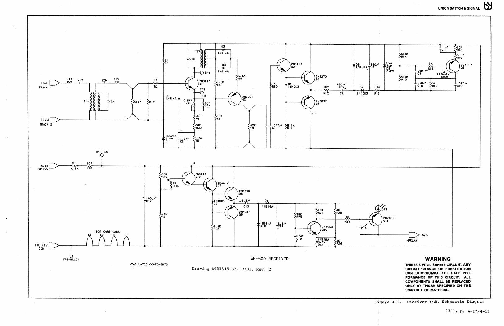
4.3.4 Receiver PCB
The Receiver PCB is illustrated in Figure 4-6. Ll, L2, Tl, Cl, C2, CJ, and Rl comprise a narrowband three pole Butterworth band pass filter to reject extraneous signals and noise present on the track. Transistor Ql and associated components amplify the filtered input signal. Zener diode Dl provides a noise free base bias·' source for Ql and diode D2 protects Ql from reverse voltage surges that may be coupled through the .input filter. Resistors R4 and R30 are selected on test to establish the voltage gain of this amplifier stage and sets the overall receiver sensitivity. The primary of transformer T2 is tuned to the receiver operating frequency by capacitor C4. The amplified signal is stepped up in voltage level by T2 and is full wave rectified by diodes D3 and D4. Resistor R8 is the secondary load for T2 since the emitter of Q2 is at ac ground potential. Q2 further amplifies the detected signal and four lead capacitor C6 removes the carrier component from the detected signal. The signal applied to the base of Q3 is a de voltage pulsating at the input code rate. Q3, Q4 and QS further amplify the signal which is then capacitively coupled through C7 to a half wave voltage doubler consisting of diodes D6, D7 and capacitor ca. Thus, when a coded input signal of the correct carrier frequency is applied to the receiver input terminals, a positive voltage with respect to the +24 Vdc rail is developed that is proportional to the input signal amplitude. Transistor Q6 and associated components comprise a safety type electronic level detector which provides an output signal only if the de voltage across C8 is above 6.5 volts. This level detector consists of a Colpitts oscillator operating at 20 KHz, with the feedback provided by Zener diode, D8. When the de voltage across D8 is less than its Zener voltage, it appears as a high impedance which prevents Q6 from oscillating. When the de voltage is sufficiently high to force D8 into Zener breakdown, its dynamic impedance decreases very sharply allowing Q6 to oscillate.
The output of the level detector is amplified by Ql2, Q7, Q8, and Q9, and then capacitively coupled through Cl3 to a half wave voltage doubler consisting of DlO, Dll, and Cl4. The de voltage developed across Cl4 is negative with respect to COM, and is used to operate an external PN-150B relay. The circuitry consisting of QlO, Qll and associated components provides a nominal 1 second delay on relay pick-up. When the level detector oscillator turns on, the voltage across Cl3 rises very quickly to about 10 volts. This causes the Zener diode Dl2 to conduct through R25 placing 3.7 Vdc on the emitter of QlO. QlO is therefore turned off until ClS charges through R23 to about 3.0 volts. The time constant for Cl5 and R23 is selected to require this delay to be about 1 second.
When Cl5 reaches 3.0 volts, QlO turns on which forces Qll to turn on. This action applies the available negative voltage to the external relay. LED Dl3 is in series with the relay coil and provides a visual indication of relay energization. Cl6 protects Qll from the inductive spike developed across the relay coil when Qll switches off. Cl 7 and R28 decouple the receiver from noise present on the de power supply.
6321, p. 4-8 (Rev. 6-87)

TPS )!BKI
---------------
---"------------
RIB. 10•
RIC
+ CIB so,,,-
+ CIC so,,,-
33K R2B
33K R2C
Drawing 0451315 Sh. 9501, Rev. 2
DIB LVA462 (6.2Vl
. m462 !6.2VI
R3B SIOK
,>R4B 200K
R3C SIOK
R4C 200K
f ~2B
IC3B T'o33,,,-
CJRCUIT B
I J.c2c r lex T.033,,,
CIRCUIT c
>R5B 3K
R.6.B
IK
CSB rpr
RSC 3K
R6C
iK
TlB • -· QIB
2N31 I 7
TIC * --· QIC
2N31 I 7
"'
C4B .
R7B . "\.)TL2
>Rae
S.O. T.
R9B
R7C •
RSC
S.O. T.
R9C
RIOB IOK
1" ?~~648 ( 13VI
RIOC !OK
TIB -·
TIC -·
Rill!
IK
RI IC
IK
026 2N31 I 7
RJ2B IOK
Q2C 2N3117
Rl2C IOK
NOTE,
UNION SWITCH & SIGNAL
a,J RI 36
330°
WARNING THIS IS A VITAL SAFETY CIRCUIT. ANY CIRCUIT CHANGE OR SUHSTITUTION CAN COMPROM:SE THE SAFE PER· FORMANCE OF THIS Cl~CUIT. All ".:OMPONENTS SHALL BE REPLACED ONLY BY THOSE SPECIFIED ON THE US&S BILL OF MATERIAL.
6,F Rl3C
RANGE FOR S.O. T, VALUE RB + R9 IS BETWEEN I SK 8 SOK.
•- TABULATED ITEMS
Figure 4-3. Oscillator, PCB Schematic Diagram
6321, p. 4-9/10
WARNING:
C23 47MFD
lREDl TPI
Rl8 62K
R23 IK
04 IN914
THIS JS A VITAL SAFETY CIRCUIT· ANY CIRCUIT CHANGE OR SUBSTITUTION CAN COIJPROMISE THE SAFE PERFORMANCE OF THIS CIRCUIT. ALL COMPONENTS SHALL BE REPLACED ONLY BY THOSE SPECIFIED ON THE uses BILL OF MATERIAL.
0451626-6001 Rev.
C9 • .047 T2 c,...---1 MFD
RB 56K
RI I 2.2M
Rl3 2.2M
12-N
14-R
TP7
R49
SOT
R48
SOT
04 2N3964
DI I
IN914
010
IN914
016
IN914
2-2K
I .2K
Rl7 ISK
R46 33 OHM
T3
TAPI
TP9
05 2N4037
R22 20 OHM
Cl3
.01 MFD
Cl4 R39
.01 MFO 237K ~w
C22 .022 MFD
Tl
R37
390 OHM G
8
3 Cl I 1.0 MFO
TP6
:~ ..
R28
06 390 OHM
I N4003
05 C7 I N4003 1.0 MFD
R21
470 OHM
S2
SECOND WINDING
F2
<134 SOT
R35 2.67K I /8W
R36 I .21K i.,sw
Rl5
33K
R30 3.3M
03 2N3117
03 IN914
CIO 6.BMFO
R33 SOT
R31 2.67K 1/BW
R32 ·cs I ,21K 6.8 I/SW MFO
R2
I IK
QI 2N3117
KELVIN CONNECTION
R26 I IK
C4 ., MFO
Fl
Tl FIRST WINDING . SI
DI
IN914
C2
.033 MFD
RS
ISK
08 2N3964
R24 I .2K
Rl2 IOOK
CG
470 OHM
02
IN914
R4 IOOK
C3
ISK
Figure 4-4.
UNION SWITCH & SIGNAL
S3
Tl THIRD WINDING
F3
R29 3.3K l/2W
07 2N3117
R3 RI Cl 3.9K 620 OHM .47 MFD
02 2N3964
RIO 3.3K
R47 16-T
IK
06 2N3117 R6
2K
Code Rate Generator PCB Schematic Diagram
6321, p. 4-11/12

TPI
Fl (0)
CAB 0.25A
ENABLE ( 16,T>
+ Cl lo~ TP4
(BU>
CAB CARRIER
R23 t9.K> 30°
R2 IOK
R3 3K
R22 R7 S. IK 6.2K
05 CODE IN914A R6 RATE ~-----1-----'W'----+--~-ti
GENERATOJ\s,Jl S. IK
CAB 53
WAYS IDE
(Rev. 6/f!l) .
TPI I
02 2N3117
CAB FINE
DI IN914A
03 2N3117
08
IN914A
I N4003 I N4003
100• 07 06 04
( 12,N) 13,P
TP6 <WI
SPI V39ZA6
14,Dl xx <S,EI
TP14 TPl3 SP2
V39ZA6
R20 2K
I /2W
( 10,L) II ,M
T3
fl CJ-SMFD("Jl.115 O>MP. USED TP8 ~ TP9 OW - 4311 Oi.lLV)
tYl l <Y>
115,SXl4,RI
Drawing 0451626 Sh. 0801, Rev. 1
03 IN914A
J2
TP3
05
RIZ
04 TPS IG>.
UNION SWITCH & SIGNAL ffi
H---'V'v'-----WAYSIDE CARRIER
T2 TRACK
COARSE
RII
TRACK FINE
~;--, 2,4K I
I I I I I I I
R9
RIO
06 I 2N3117
Figure 4-5.
13,C>
WARNING THIS IS A VITAL SAFETY CIRCUIT. ANY CIRCUIT CHANGE OR SUBSTITUTION CAN COMPROMISE THE SAFE PER· FORMANCE OF THIS CIRCUIT. ALL COMPONENTS SHALL BE REPLACED ONLY BY THOSE SPECIFIED ON THE US&S BILL OF MATERIAL.
NOfE REFER 10 PARTS LIST FOR VALUES Nor SHOWN.
Transmitter PCB, Schematic Diagram
6321, p. 4-13/4-14

UNION SWITCH a SIGNAL U,I
The Receive Only PCB (-75xx} is the same as the Receiver PCB (-4lxx} except that several component values are changed to produce a ten fold increase in sensitivity.
4.3.5 Minibond Unit
The minibond (Figure 4-7) is a transformer with several windings on a toroidal magnetic structure. The primary consists of two turns of copper with a cross-sectional area greater than two million circular mills. This winding is connected to the rails and must carry de propulsion return current. This winding is center-tapped for connection to other minibonds on the same or adjacent track, or to the propulsion rectifier return conductors. Since the de current flows in through terminals Pl and P2 and out the center tap, the de magnetic fluxes in the core oppose each other and tend to cancel.
The secondary windings consist of many turns of much smaller wire around the toroidal cores. These windings are connected to the electronics in the train control room via a twisted pair cable. Transformer action between the primary and secondary windings allows signals to be exchanged between the track and the train control room equipment.
6321, p~ 4-15/4-16

~ ....
LI* Cl ll 13,P~
TRACK I
11,M TRACK 2
IA,28 +24VOC
l7U, 18V COM
Fl
0.5A
TP3-BLACK
10° R28
POT CORE CANS T2 l2 Tl LI
IK
R2
+ I OOµI' 17
3K R3
02 IN914A
IN5235
+
6,BV 1.5µr DI C5
20K R20
24K R21
•
*TABULATED COMPONENTS
•
03
IN914A
04
I .SK R6
30K R7
I .SK R22
2N3964 02
2N2270 08
+6.8JJI" 01 l
IK RIO
2N3117 03
05 I N4003
.041JJf 5. IK C6 RI I
Cl3 IN914A
2N4037 09
IN914A .aµr 010 Cl4 ...
AF-500 RECEIVER
75K R23
21pf 15 ...
Drawing 0451315 Sh. 9701, Rev. 2
2N2270 04
10°
Rl2
2N4037 05
~.
860µr 40V+
C7.
IK R25
IK R26
06 IN4003
+
07
IN4003
150JJI" ca
I .SK
R!3
LVA 462 08 6.2V
2N2102 QI I
-RELAY
• 56JJf CIO
15,S
UNION SWITCH & SIGNAL ~
2N3117 06
WARNING THIS IS A VITAL SAFETY CIRCUIT. ANY CIRCUIT CHANG!: OR SUBSTITUllON CAN COMPROMISE THE SAFE PER· FORMANCE OF THIS CIRCUIT. ALL COMPONENTS SHALL BE REPLACED ONLY BY THOSE SPECIFIED ON THE US&S BILL OF MATERIAL.
Figure 4-6. Receiver PCB, Schematic Diagram
6321, p. 4-17/4-18

RAIL CONNECTIONS
2T
52T
155T
204T 204T
TRACK TRANSMITTER
TRACK RECEIVER
UNION SWITCH & SIGNAL '1,,,IJ
CAB TRANSMITTER
TO TRANSMITTER AND RECEIVER
Figure 4-7. Minibond Schematic Diagram
(Rev. 6-87) 6321, p. 4-19/4-20

"'.

UNION SWITCH a SIGNAL ID
SECTION V
FIELD MAINTENANCE AND TROUBLESHOOTING
5.1 INTRODUCTION
Field service maintenance and troubleshooting for the AF-500TW system is accomplished at two levels; preventive (scheduled) maintenance and corrective maintenance. Both of these maintenance concepts are important, especially the former, since it decreases the possibility of equipment downtime. The maintenance tasks outlined in this section apply to the AF-500'1W System electronics in the cabinet card files and the system power supplies. For maintenance procedures relative to the minibond, refer to Appendix B.
5.2 PREVENTIVE (SCHEDULED) MAINTENANCE
Preventive maintenance is a scheduled process whereby the AF-500'1W System components ate inspected, cleaned, and tested on a periodic basis to ensure that all functions are operational, to detect future probable causes of equipment malfunction, and to preclude the possibility of a system breakdown that could seriously impair operation of the rail transit line. The following paragraphs describe cleaning, inspection, and minimum performance test procedures for the AF-500TW System.
5.2.1 Importance of Preventive Maintenance
The responsibility of maintenance personnel is to keep the AF-500TW system in a satisfactory operating state; when an equipment failure occurs, the fault must be quickly corrected. However, the most important phase of maintenance is the prevention of failures before they occur, rather than the location and correction of a failure after it has occurred.
Prevention of failures in the AF-500TW System is accomplished by regular inspections, tests, and servicings that are performed as specified in t~is section. Regular and thorough preventive maintenance is simply good housekeeping. It includes cleanings, inspections and tests. Additionally, it includes keeping accurate records of when preventive maintenance routines are performed and their results. The records can be used to establish a thorough maintenance pattern, and detect equipment and circuit performance deterioration. This detection permits corrective action to be taken before deterioration eventually causes a failure that could halt train traffic.
5.2.2 Cleaning
Cleaning of equipment is necessary to remove dirt and other substances that, if allowed to accumulate, can cause corrosion or otherwise impair proper operation. In some instances, if equipment surfaces are extremely dirty, cleaning permits routine inspections (paragraph 5.2.3) to be performed properly by exposing equipment surfaces.
6321, p. 5-1

ffi UNION SWITCH & SIGNAL
5.2.2.1 Equipment Cleaning
The AF-500TW System equipment cabinets, and power supplies installed in the equipment room need to be cleaned, as required, every three months. However, they must all be cleaned at least once a year.
5.2.2.2 Material Required
Table 5-1 lists the cleaning materials required to clean the AF-500TW System equipment and their uses.
Table 5-1. Cleaning Materials
NAME
Household Cleaner (mild liquid)
Lint-free Cloths
Soft Bristle Brush
Compressed Air in Aerosol Can
5.2.2.3 Cleaning Procedure
MANUFACTURER
Commercial
Commercial
Commercial
Commercial
USE
Cleaning exterior surfaces
Cleaning and drying exterior surfaces
Removing dust and foreign matter from terminal blocks, electrical connections, and equipment surfaces
Blow foreign matter and dust from electrical surfaces
Clean the AF-500TW System cabinets, and power supplies as follows:
WARNING
Hazardous voltages and current may be present. Exercise caution when working near exposed terminals. Never use wet cloths near exposed electrical terminals.
a. Remove dust and dirt from accessible surfaces, using soft bristle brush.
b. Blow out dust and dirt from inaccessible areas around terminal block, fuse holders and other areas where live electrical conductors are exposed.
6321, p. 5-2

UNION SWITCH Ii SIGNAL \lJ
c. Wipe power supply surfaces and cabinet exterior and interior surfaces (not exposed electrical conductors) with a lint free cloth dampened with a solution of water and household cleaner, so that all dirt and foreign matter are removed.
d. Dry dampened surface with lint-free cloth.
CAUTION
When using compressed air to blow out dirt and dust particles from card fi1es, always direct air at an angle relative to the PCBs otherwise, loose or damaged components could result.
e. Using compressed air or soft bristle brush, remove dust and dirt particles from cabinet card file.
f. Collect all accumulated dust and dirt and discard outside equipment room in accordance with railroad directives.
5.2.3 Routine Inspection
5.2.3.1 Annually
A routine inspection consists of observing the appearance and actions of each equipment item under inspection. Appropriate cleaning of the item, as described in paragraph 5.2.2 may have to be accomplished before the inspection can be made. In addition, it is necessary for maintenance personnel accomplishing the inspection to know the manner in which the equipment is supposed to function. During the inspection, the appearance, smell, sound and feel of the device can then be used to make a judgement as to whether the device appears to be functioning properly or an obvious faulty condition exists. At least once a year, the AF-500TW System power supplies, cabinets and their components should be subjected to a cursory inspection (preferably at the time of cleaning). To perform a routine inspection of the AF-500TW System power supplies and cabinet equipment, make the following checks and observations.
a. Power supply housings and cabinet exterior are clean and free of scratches, chipped paint, and spots of corrosion.
b. Cable connections to power supplies and at rear of card files are tight; wires are secure and free of nicks, cuts and fraying.
c. All card file PCbs are securely mounted in guides and bottomed in card edge connectors.
d. PCB components are securely mounted and show no visible signs of deterioration.
6321, p. 5-3

UNION SWITCH & SIGNAL
5.2.3.2 Semiannually
A routine inspection of the rear of the cardfiles in the vicinity of the _Code Rate Generator PCB must be performed twice each year for the following:
a. cables are tied and secured to the frame.
b. wire connections to the PCB connector are secure and free of nicks, cuts and fraying to prevent possible shorted pins.
c. the area around the connector is free of dust, dirt and foreign material.
5.2.4 Minimum Performance Tests
Minimum performance tests demonstrate that AF-500TW System functonal circuits and equipment items are functioning properly. A performance test can consist of either performing normal operating procedures and observing that required equipment responses are correct, or of using test equipment to measure the equipment responses. Unacceptable conditions identified during tests must be corrected immediately. Performance tests for the AF-500TW System should be accomplished on a periodic six-month basis to ensure that all functions meet m1n1mum performance criteria. Refer to section 3.2 and 3.3 for AF-500TW track circuit test and data recording procedures.
WARNING
MAINTAINERS SHOULD NOT SIMPLY TURN UP THE TRANSMITTER WHEN TROUBLE IS ENCOUNTERED. THE ADJUSTMENT PROCEDURE OUTLINED IN THIS MANUAL IS BASED ON RELIABLE OPERATION, AND OVERENERGIZATION IS UNNECESSARY AND COMPROMISES SYSTEM SAFETY. IN THOSE CASES WHERE SIGNAL CLIPPING OR DISTORTION IS PRODUCED BY OVERENERGIZATION, INTERMITTENT TRACK CIRCUIT DROP-OUT IS LIKELY.
5.3 TROUBLESHOOTING
Data and procedures that can assist maintenance personnel in localizing AF-500TW System faults to the lowest replaceable unit (LRU) or associated wiring are contained in this section. The troubleshooting procedures are presented in the form of fault isolation logic diagrams and are based on the results, or lack of results, observed during the minimum performance tests in Section III.
Troubleshooting procedures are developed to guide maintenance personnel in the logical sequence to be used in isolating a fault. They are prepared by analysis of normal indications (or operation) versus abnormal indications or symptoms. Most of the initial system fault indications or symptoms are those observed external to the AF track circuit electronics, such as the operation of vital relays. Additional indications can then be obtained from AF track circuit PCB LED indications within the equipment card file. Localization of some faults include the use of test equipment.
6321, p. 5-4 (Rev. 6-87)
The test equipment recommended for field maintenance and troubleshooting of the AP-SOOTW System is listed in Table 3-1.
In addition to the test equipment listed in Table 3-1, maintenance personnel should also have available at least one spare board for each unique board in track circuit card files. This will permit board substitution and facilitate repair when a fault has been localized to a PCB. When substituting circuit boards, make sure that the new board is the correct part, that it is operating properly, and that it is correctly installed in the card file. Part number information for each of the various PCBs can be located in Appendix A.
5.4 FAULT ISOLATION AND PLOW DIAGRAMS
Troubleshooting procedures have been developed to guide maintenance personnel in the logical order of isolating a fault. The analysis of normal indications in relation to faulty indications is stressed, and this information is presented in the form of fault isolation flow diagrams.
The symptoms of trouble are contained in Table 5-2 together with a reference to the fault~isolation flow diagram that contains the appropriate troubleshooting information. The fault isolation flow diagrams assume the following conditions:
a. When a relay is the suspected cause of the trouble, it must be removed and its coil and/or contacts must be tested before the relay is replaced.
b. To check a fuse, power is turned off, and the fuse is removed and checked with an ohmmeter for continuity.
c. When checking a relay energizing path, use a voltage test.
d. To check the operation of a minibond, its tuning unit, and associated wiring, use the following procedure:
(1) By unplugging Oscillator PCBs, disable the transmitter for the minibond to be tested as well as both adjacent transmitters.
(2) Disconnect the minibond from its transmitter at the cable entrance rack.
(3) Connect a frequency counter, oscilloscope, and sinewave signal generator across the two cable leads going to the minibond.
( 4) Turn the signal generator amplitude up half-way and observe the oscilloscope while slowly varying the signal generator frequency from 1 KHz to 6 KHz. The signal amplitude on the oscilloscope will vary with frequency and should reach a peak three times, corresponding to the three tuned frequencies of the minibond. Note these three frequencies. Each should be within 10% of the nominal frequencies for that particular minibond.
6321, p. 5-5

UNION SWITCH & SIGNAL
If replacing all circuit boards and checking both minibonds fails to fix a particular track circui~, then there is either a problem with the rack wiring or with the cardfile itself.
Table 5-2. Troubleshooting Symptoms
SYMPTOM PROCEDURE
AF track relay down when block unoccupied Figure 5-1
Train operator receives "O" speed Figure 5-2 command when track circuit is entered and adjacent track blocks are unoccupied
5.5 CORRECTIVE MAINTENANCE
Corrective maintenance is an unscheduled process whereby an AF-500TW System malfunction, which has been localized through the fault analysis process! results in removal/replacement of an LRU and testing of the system after corrective maintenance is complete. The following procedure outlines a brief removal/replacement process for the card file PCBs in the system cabinets. For corrective maintenance procedures relative to the external track circuit equipment, refer to the applicable service manual. Individual board adjustments are performed at the shop maintenance level (Refer to Section VI). Remove and replace card file PCBs as follows:
a. At front card file, place thumb on outer tabs of upper and lower board ejector on PCB in question, and simultaneously press board ejector tabs inward until PCB unplugs from card file connector.
b. With one hand, withdraw PCB straight out from board guides and remove PCB from card ftle.
c. Install replacement PCB in board guides and slide in until PCB contacts card file connector.
d. Place thumb over inner tabs of' board ejectors and press in firmly until PCB connector bot~oms in card file connector.
6321, p. 5-6

AF TRACK CIRCUIT RELAY DEENERGIZED WHEN BLOCK UNOCCUPIED {SEE NOTE 1)
NOTES:
-IS TRANSMITTER PCB LED FLASHING?
NO
A
SHEET 2
YES
1. REMOVE TRANSMITTER PCB's FROM ADJACENT TRACK CIRCUITS. 2. IT IS ASSUMED THAT ADJACENT TRACK CIRCUITS AND AF
POWER SUPPLIES ARE OPERATING PROPERLY. 3. MAKE CERTAIN RECEIVER SENSITIVITY POTENTIOMETER IS
FULLY CCW.
IS RECEIVER PCB LED LIT?
NO
MEASURE RECEIVE INPUT VOLTAGE LEVEL BETWEEN TB1 OR
YES
TB2 TERMINALS 31 YES AND 32 AS APPROPRIATEi-----t TO TRACK CIRCUIT. IS MEASUREMENT BETWEEN 2.2 AND 3,0V P-P? {SEE NOTE 3).
MEASURE TRANSMITTER PCB OUTPUT BETWEEN TB1 OR TB2 TERMINALS 4 AND 5. IS MEASURE- YES MENT CLOSE TO LAST ADJUSTED VALUE? {REFER TO PARA. 3.2.3.4).
NO
IS 1.9 TO 5.3VDC MEASURED ACROSS TRACK RELAY COIL {BETWEEN PINS 15 AND 18 OF RECEIVER PCB)?
NO
FAULT PROBABLY DEFECTIVE RECEIVER PCB. REMOVE AND REPLACE WITH KNOWN GOOD RECEIVER PCB TEST DEFECTIVE RECEIVER PCB PER PARA. 6.3.5.
RECEIVER PCB IS DEFECTIVE. TEST PER PARA. 6.3.5.
FAULT DEFECTIVE MINIBOND, TRACK CONNECTIONS, BROKEN RAIL, OR ASSOCIATED WIRING.
YES FAULT PROBABLY DEFECTIVE TRACK RELAY OR ASSOCIATED WIRING.
-
REMOVE TRANSMITTER PCB AND REPLACE WITH KNOWN GOOD TRANSMITTER PCB WITH CORRECT PART NO. SUFFIX FOR TRACK FREQ USED. IS AN AC OUTPUT MEASURED BE";WEEN TP8 AND TP9?
NO
POWER TRANSISTORS BOARD DEFECTIVE. REMOVE AND REPLACE.
YES
UNION SWITCH & SIGNAL m
TRANSMITTER PCB WAS DEFECTIVE. ADJUST NEW PCB PER PARAGRAPHS 3.2.3.3, 3.2.3.4 AND 3.2.3.5.
Figure 5-1. AF-500'1W System Train Detection, Fault Isolation Flow Diagram (1 of 2)
6321, p. 5-7/5-8

FROM SHEET 1
UNIUN:)Wll\;H&l:iluNAL ~
PLACE CAB/WAYSIDE OSCILLATOR PCB SWITCH ON TRANS-
MITTER PCB TO NO DEFECTIVE. A WAYSIDE. REMOVE AND
IS TRANSMITTER REPLACE WITH KNOWN
LED LIT? GOOD PCB.
YES
RETURN CAB/WAYSIDE SWITCH TO MID POSITION, ATTACH YES FAULT IS IN JUMPER BETWEEN TB1 EXTERNAL CODE OR TB2 TERMINALS RATE SELECT CIRCUIT. 19 AND 20, IS TRANSMITTER LED LIT?
NO
CODE GENERATOR PCB IS DEFECTIVE. REMOVE AND REPLACE WITH KNOWN GOOD CODE GENERATOR PCB.
Figure 5-1. AF-SOO'IW System Train Detection, Fault Isolation Flow Diagram (2 of 2)
6321, p. 5-9

UNION SWITCH & SIGNAL
TRAIN RECEIVES 'ZERO' SPEED COMMAND WHEN TRACK CIRCUIT IS ENTERED
...
AND ADACENT TRACK BLOCKS ARE UNOCCUPIED SPEED COMMANDS NORMAL IN ADJACENT TRACK BLOCKS,
6321, p. 5-10
-TURN OFF 824-T VOLTAGE TO TRANSMITTER PCB AND CONNECT A JUMPER BETWEEN TB1 OR- TB2 TERMINALS 1 AND 3 TURN ON 824-T VOLTAGE. IS A SPEED COMMAND OTHER THAN 'ZERO' PRESENT?
NO
MEASURE TRANSMITTER PCB OUTPUT BETWEEN TB1 OR TB2 TERMINALS 4 ANO 5. IS MEASUREMENT CLOSE TO RECORDED OPERATING VALUES? (SEE NOTE.)
NO
WITH TRANSMITTER PCB ON CARD EXTENDER, IS 2.2 +0.2V (p-pJ BETWEEN PINS 9 AND 18?
NO
YES
YES
YES
FAULT IN EXTERNAL CAB ENABLE RELAY LOGIC AND/OR ASSOCIATED WIRING.
FAULT DEFECTIVE ·MINIBOND, TRACK CONNECTIONS, BROKEN RAIL, OR ASSOCIATED ROOM TO WAYSIDE WIRING.
REMOVE ANO REPLACE W<TH KNOWN GOOD TRANSMITTER PCB. (CORRECT PCB FOR TRAIN DETECTION FREQUENCY.) YES MEASURE NEW -
,-----, TRANSMITTER PCB OUTPUT BETWEEN TB1 OR TB2 TERMINALS 4 ANO 5. IS MEASUREMENT CLOSE TO RECORDED OPERATING VALUE? (SEE NOTE.)
NO
NOTE:
FAULT WAS DEFECTIVE TRANSMITTER PCB. ADJUST NEW PCB PER PARAGRAPHS 3.2.3.3, 3.2.3.4 AND 3.2.3.5.
FAULT DEFECTIVE CAB SIGNAL OSCILLATOR CIRCUIT. REPLACE OSCILLATOR PCB WITH KNOWN GOOD PCB. TEST PER PARAGRAPH 6.3.2
POWER TRANSISTOR BOARD DEFECTIVE. REMOVE AND REPLACE. A DJ UST PER PARAGRAPH 3.2.3.3, 3.2.3.4 AND
REFER TO PARAGRAPH 3.4 STEP C.
Figure 5-2.
3.2.3.5
AF-500TW System Cab Signaling, Fault Isolation Flow Diagram

UNION SWITCH a SIGNAL UJ
SECTION VI SHOP MAINTENANCE
6.1 INTRODUCTION
This section presents shop maintenance test procedures for the LRUs of the AF-SOOTW System which have been found defective during field maintenance and troubleshooting. Included is a listing of recommended test equipment and components: PCB and discrete component level troubleshooting procedures including adjustment and repair procedures.
6.2 RECOMMENDED TEST EQUIPMENT AND DISCRETE COMPONENTS FOR SHOP MAINTENANCE
The recommended test equipment and discrete components required for shop maintenance and troubleshooting is listed in Table 6-1. Maintenance personnel should be thoroughly familiar with their use and application. Test equipment with equivalent specifications may be substituted. Under no circumstances should equipment with inferior specifications be used.
Table 6.1. Recommended Test Equipment and Components for Shop Maintenance
Test Equipment or component
24 Vdc Power Supply
Frequency counter
Digital Voltmeter
Oscilloscope
Resistor Decade Box (0-lOOK ohms) (0-200K ohms)
Multimeter
Signal Generator
Power Transistor PCB
Code Rate Generator PCB
Resistor, 5.lK, 1/2 watt
Resistor, llK, 1/2 watt
Resistor, 13K, 1/2 watt
Switch, Rotary, 1 Pole, 7 Positions
Vital Relay, PN-1508, 400-ohm coil
Manufacturer Designation
Harrison 6202B, 6204A Hewlett-Packard 6266A or B
Hewlett-Packard 5307A or 5230
Fluke 8000A or B
Tektronix T912
Heath IN3117 Clarostat 240C
Simpson 260
Wavetek 146, Exact 504
US&S N451605-3701
US&S N451570-8801
US&S J721179
US&S J721258
US&S J735254
US&S N322500-901
6321, p. 6-1

m UNION SWITCH & SIGNAL
Table 6.1 (Cont'd.)
Test Equipment or Component Manufacturer Designation
Capacitor, 1 microfarad, 200V US&S J706813
Switch, SPST toggle US&S 725681
Resistor, 620 ohm, 1/2 watt US&S J721253
Receiver Board Test Set
Impedance Bridge GR 1608A
Hi-Pot Tester. Associated Research 404
"
6.3 TESTING/TROUBLESHOOTING
Servicing of the PCBs should be performed by qualified maintenance personnel who have a through understanding of AF-500TW System operation and specifically, the circuit operation of the PCBs that are part of the AF-500TW System. They must also be thoroughly experienced in the use and application of the test equipment listed in Table 6-1.
6.3.1 Troubleshooting Information
In the following paragraphs, the PCBs are adjusted and/or tested on the bench . using appropriate test equipment and bench test setups. These procedures
include applicable adjustments and calibration information, since all that may be wrong with a PCB is the need for adjustment. If the proper indications are observed when checking the PCB in question, adjustment may be unnecessary. By performing these procedures, using the test equipment and normal indications specified at respective test points, maintenance personnel can isolate a fault to a PCB component (transistor, integrated circuit, transformer, etc.) by the logical process of elimination. When the fault has been isolated to a particular component, or group of components on a board, the faulty component(s) is replaced. The PCB is then. rechecked for normal operation to make sure the fault has been corrected. As an aid in troubleshooting the PCBs on the bench, it is recommended that standard track. circuit card files (19-inch) be used as the PCB mounting base, with card extenders to facilitate PCB interconnections, when required, and the connection of test equipment.
6.3.2 Oscillator PCB (See Figure 6-1)
a. Recommended Test Equipment:
(1) 24 Vdc Power Supply
(2) Frequency counter
6321, p. 6-2

UNION SWITCH 6 SIGNAL ~
(3) Digital Voltmeter
(4) Oscilloscope
(5) Resistor Decade Box (0-lOOK ohms)
b. Test Procedure
NOTE
During the following Test Procedure, if any signal is not specified, perform the Adjustment Procedure (paragraph c).
(1) connect the Oscillator PCB in the test setup as shown in Figure 6-1.
(2) Connect a 24 .±.. 1 Vdc power supply to the PCB, with positive lead on pin 1 and negative lead on pin 18.
(3) Connect a frequency counter to the output of circuit •A• (pin 10) and the common to pin 18.
(4) The frequency output, as indicated on the counter, should be as listed in Table 6-2 for the part number of the PCB under test.
(5) connect the digital voltmeter across the output and measure the ac voltage. It should be 0.73 + 0.03V ac.
(6) connect the oscilloscope across the output and verify the following conditions:
{a) a 2 .±. 0.2V (p-p) sinewave with no noticable distortion.
(b) a de level of 13 + 2V.
(7) Repeat steps (3) to (7) for circuit •e• with the output on pin 8.
Table 6-2. Oscillator PCB Frequency Allocations
PCB N451570- Circuit A HZ Circuit B Hz Circuit c
-3901 4550 1900 Not Used -3902 4550 2100 -3903 4550 3900 -3904 4550 2580 -3905 4550 2820 -3906 4550 3100 -3907 4550 3370 -3908 4550 3660
'V -3909 4550 ----
6321, p. 6-3

m UNION SWITCH & SIGNAL
I I I I I I I I I I I I
I I I
I RBS I
,,.Q Q,~ -c=J- I I I TL2
-cJ-• I R98 I I 8'~' 8 I I
T1A I I I I I I
I ,a 10 8 , I I c) I B I
CKT I ,) A I _....,,. .
,_.,,. OUTPUTS - POWER FREQUENCY SUPPLY
COUNTER 24VDC :'.: 1VOC
-
Figure 6-1. Oscillator PCB Test setup
c. Adjustment Procedure
NOTE
During the following Adjustment Procedure, if any signal cannot be obtained, troubleshoot the associated circuitry to isolate the faulty component(s); i.e., resistors, capacitors, transistors, etc. After replacing the faulty component(s), repeat the Test Procedure.
(1) Connect the Oscillator PCB in the test setup as shown in Figure 6-1.
(2) Connect a 24 .±. 1 Vdc power supply to the PCB, with positive lead on pin 1 and negative lead on pin 18.
(3) Remove resistors R8A and R9A if circuit •A• was faulty (R8B and R9B for circuit •B•), set the resistor decade box to 40K ohms and connect it between pins 18 and TLl (Turret Lug 1) for circuit •A•, (TL2 for circuit •B•).
6321, p. 6-4

UNION SWITCH & SIGNAL Cl1
(4) connect the frequency counter to the output of pin 10 for circuit •A•, (pin 8 for circuit •B•) and common to pin 18.
(5) Break the RTV seal on Transformer, TlA for circuit •A• (TlB for circuit •a•) and tune for correct frequency, +2 Hz, per Table 6-2. When the correct frequency is obtained, seal the tuning slug with RTV (A41701).
(6) Connect the digital voltmeter across the appropriate output and adjust the resistor decade box to obtain an ouput of 0.73 +0.02V ac. Solder in the next lowest value 1/4 watt, 5%, carbon resistor for R8 (A or B, whichever is appropriate for the circuit being adjusted).
(7) Disconnect the decade box from R8 and connect it in place of R9 (A or a). Adjust the resistance to obtain an output of 0.73 +0.02Vac. Solder in the closest value 1/4 watt, 5%, carbon resistor for R9 (A or B). The total resistance (R8 + R9) should be between lOK and 40K ohms.
(8) connect the oscilloscope across the output and verify the following conditions:
(a) A 2 + 0.2V (P-P) sinewave with no noticeable distortion.
6.3.3 Code Rate Generator PCB Test
a. Recommended Test Equipment:
(1) 24 Vdc Power supply (2) Frequency counter (3) Digital Voltmeter (4) Oscilloscope ( 5) Resistor Decade Box ( 2) (6) Multimeter (7) Resistor, 5.lK, 1/2 watt (8) Switch, Rotary, 1 Pole, 7 Positions
b. Test Procedure
NOTE
During the following Test Procedure, if any signal is not specified, perform the Adjustment Procedures (Section 6.3.3.1).
(1) connect the code Rate Generator PCB in test setup illustrated in Figure 6-2.
(2) connect a 24 .:!:. 0.2 Vdc power supply to the PCB.
(3) Connect a frequency counter and oscilloscope to the output of the PCB, pin 16 and ground, pin 18.
6321, p. 6-5

m UNION SWITCH & SIGNAL
• +. ~4, \I l)C.
16 POWf:-1' - SUPPLV AF· '!>00
CoD&, AATE:-
Cir E-~&-RA TO A... 2. GC>r>li SELEC.T
4 i5CPM ~o coo&
"14-~I '!>7 o • &!O I
' l'lO CPM
1&0 CPM
10 ~ .
12 4.10 CPM
14 "48CPM
IG.
Figure 6-2. Code Rate Generator PCB Test Setup
(4) Set the Code Select switch to 75 CPM, or instead of a switch a jumper can be connected from pin 2 to pin 4 (75 CPM). The code rate should be within +2% as specified in Table 6-3.
(5) The signal on the oscilloscope should be a squarewave with an amplitude of 18.5 .±. 2 V (P-P), and the base line of the squarewave should be at 0.0 + 0.2 V.
(6) Repeat steps 4 and 5, except set the switch to each of the code rates.
(7) Select the 75 CPM code rate. Set the power supply output to 21.0 .±. 0.05 Vdc. The code rate should remain within+ 2%. Then set the power supply output to 27.0 + 0.5 Vdc and the code rate should remain within+ 2% also.
6321, p. 6-6

UNION SWITCH 6 SIGNAL w Table 6-3. Code Rate Ranges
Nominal Code Rate Frequency Period Code Rate Range Range Range.:!:. 2% CPM + 2% CPM + 2% Hz Millisec. - -
75 73.5 - 76.5 1.23 - 1.28 784.0 - 816.0 120 117.6 - 122.4 1.96 - 2.04 490.0 - 510.0 180 176.4 - 183.6 2.94 - 3.06 326.7 - 340.0 270 264.6 - 275.4 4.41 - 4.59 217.7 - 226.7 410 401.8 - 418.2 6.69 - 6.97 143.4 - 149.3 648 635.0 - 661.0 10.58 - 11.02 90.7 - 94.4
6.3.3.1 Adjustment Procedures
NOTE
During the following Adjustment Procedure, if any signal cannot be obtained, troubleshoot the associated circuitry to isolate the faulty component(s); i.e., resistors, capacitors, transistors, etc. After replacing the faulty component(s) repeat the Test Procedure.
a. Feedback Oscillator Adjustment
(1) connect the Code Generator PCB in the test setup as shown in Figure 6-2.
(2) connect the 24 .:!:. 0.2 Vdc power supply to the PCB.
(3) Set the Code Select switch to NO CODE and connect the oscilloscope to TP9 and scope ground to PCB pin 18. The voltage should be less than JV (P-P).
(4) Set the Code Select switch to 648 CPM, connect the digital voltmeter to TP7 and ground, and set the meter to the 200 mv ac scale.
(5) Adjust the slug in the transformer T3 to obtain a m1n1mum reading (null) on the voltmeter. Set the null to within 1.0 mv of the minimum reading. The minimum reading should be between 80 and 100 mv.
NOTE
If a definite minimum reading is not obtainable, adjust the slug of transformer T2 to obtain it. A definite minimum must be obtained without both slugs having to be at their extremes.
6321, p. 6-7

m UNION SWITCH & SIGNAL
(6) seal the slug(s) with RTV (A41652).
(7) The voltage on TP9, with respect to ground, should be 23 + 2V (P-P).
(8) Connect the frequency counter to TP9 and ground (PCB pin 18). The measured frequency should be 6,000 + 1000 Hz.
b. RC oscillator Adjustment
(1) Connect the Code Rate Generator PCB in the test setup as shown in Figure 6-2.
(2) Connect temporary jumpers across each SOT (Select On Test) resistors R48 through R53.
(3) Connect the frequency counter to TP6 and ground, and set the counter to read cycles per minute (CPM).
(4) Set the Code Select switch to 75 CPM.
(5) Disconnect resistor R34 and replace it with a resistor decade box.
(6) Connect the 24 + 0.2 Vdc power supply to the PCB.
(7) Adjust the decade box to obtain a reading of 150 + 1%, - 0% on the counter.
NOTE
As the value of R34 is increased, the frequency of the code rate will also increase. The frequency measured at TP6 is twice the actual output code rate of the PCB.
(8) See Figure 6-3 for a typical data sheet and record the value of R34. This value shou1d be under l.5K ohms.
(9) Repeat the previous procedure for the remaining five code rates. Select the code rate and refer to the data sheet for the code rate range. Record each value for R34.
(10) Refer to the data sheet and circle the largest value just found for R34. Select the nearest standard value 1/4 watt, 5%, carbon resistor. If this standard value is more than 20 ohms smaller than the circled value, use the next largest standard value resistor. Solder the resistor in for R34 and record the value on the data sheet.
6321, p. 6-8

Serial No.
Date
Step 8. Code Select
75 CPM
120 CPM
180 CPM ! .. "'
270 CPM
410 CPM
648 CPM
AF-500 Code Rate Generator Data Sheet N451570-8801
Rev. No.
Code Rate Range
150 - 151.5 CPM
240 - 242.4 CPM
360 - 363.6 CPM
540 - 545.4 CPM
820 - 828.2 CPM
1296 - 1309 CPM
Value of SOT resistor used
R34 R MIN. RAVE ------R33 R MAX.
UNION SWITCH a SIGNAL ~
R34
------
Step 12. Frequency counter Reading on TP6 ---------~ R53 Rl9 -----R52 -----RSl -----R50 -----R49 -----R48 -----
Figure 6-3. Typical Code Rate Gen.erator Data Sheet
6321, p. 6-9

m UNION SWITCH & SIGNAL
(11) Set the Code Select switch to the code rate associated with the circled value of R34. The frequency counter should be within -1%, +3% of the specified code rate as tabulated below:
Code Select Nominal Range -1%, +3%
75 150 .148.5 - 154.5 120 240 237.6 - 247.2 180 360 356.4 - 370.8 270 540 534.6 - 556.2 410 820 811.8 - 844.6 648 1296 1283 - 1335
(12) Set·the Code Select switch to 270 CPM, note the reading on the frequency counter and record on the data sheet.
(13) Move the counter from TP6 to TP5. Disconnect resistor R33 and replace it with a resistor decade box.
(14) Adjust the decade box to the same value as R34. The counter should read the same as just recorded on TP6, to within+ 3 CPM.
(15) Reduce the decade box resistance until the frequency is lowered by 10 CPM of the frequency on TP6. Find this value to the nearest 10 ohms and record on the data sheet as Rmin.
(16) Increase the decade box resistance until the frequency is raised by 10 CPM of the frequency on TP6. Find this value to the nearest 10 ohms and record on the data sheet as Rmax. Typically Rmin will be around 200 ohms and Rmax around 600 ohms.
(17) The value of R33 will be the average value between Rmin and Rmax. Use the following equation to find the average resistance.
Ravg = Rmin + Rmax 2
Record Ravg on the data sheet.
(18) Select a standard value 1/4 watt, 5%, carbon resistor that is nearest to the average value and solder in for R33. The code frequency should be within +3% of the reading recorded in step (12).
c. Code Rate Select Adjustment
6321, p. 6-10
NOTE
Depending on previous adjustments or component replacements, only one or all of the SOT resistors, R48 through R53 may need to be changed, so refer to Table 6-4 and check the frequency calibration before removing the resistor.

SOT
R53 R52 R51 R50 R49 R48
UNION SWITCH Ir SIGNAL tij
(1) Connect the Code Rate Generator PCB in the test setup as shown in Figure 6-2.
(2) Connect the 24 +0.2V de power supply to the PCB.
(3) Connect the frequency counter to TP6.
(4) set the Code select switch to 75 CPM.
(5) Refer to Table 6-4, and if necessary, remove R53 and replace with a resistor decade box.
(6) Adjust the resistance to obtain a code rate of 150 +1% CPM. Select the nearest standard value 1/4 watt, 5% carbon resistor and solder in for R53. Recheck the code rate and record the R value on the data sheet.
(7) Repeat steps 4-6 for each code rate and record the value of the SOT resistor values on the data sheet.
Table 6-4. Calibration Range for Code Rates as Measured on TP6
Frequency (Hz) Frequency (CPM) Period (mSec.)
Nominal Range +/- 1% Nominal Range+/- 1% Nominal Range+/- 1%
2.50 2.48 - 2.53 150.0 148.5 - 151.5 400.00 396.0 - 404.0 4.00 3.96 - 4.04 240.0 237.6 - 242.4 250.00 247.5 - 252.5 6.00 5.94 - 6.06 360.0 356.4 - 363.6 166.67 165.0 - 168.3 9.00 8.91 - 9.09 540.0 534.6 - 545.4 111.11 110.0 - 112. 2
13.67 13.53 - 13.81 820.0 811.8 - 828.2 73.17 72.4 -21.60 21.38 - 21.82 1296.0 1283.0 - 1309.0 46.30 45.8 -
d. Low Pass Filter Adjustment
(1) connect the Code Rate Generator PCB in the test setup as shown in Figure 6-2.
(2) Connect the 24 +0.2 Vdc power supply to the PCB.
(3) Connect the oscilloscope to TP8 and refer to Figure 6-4 for scope settings.
(4) Remove resistor Rl9 and replace with a resistor decade box.
(5) Set the Code select switch to 180 CPM and adjust the decade box until the negative portion of the scope waveform is 2 + O.lv as shown in Figure 6-4.
(6) Select the nearest standard value 1/4 watt, 5% carbon resistor, with a maximum value of 1000 ohms, and solder in place for R19. Record the value on the data sheet~
6321, p. 6-11
73.9 46.8

I
UNION SWITCH & SIGNAL
(7) On the scope, measure the pulse width of the negative going pulse, •T• in Figure 6-4. The width should be between 0.15 and 0.45 msec •
. .. --.. ----... ... . .... ... 1v /01v • ~
... I N:: .. . I• I'", . . • I • ' I
. . . -Ov -,. ·--\ --... ...
..J ... -2v ....
t-T r-+ . .. . .... ... .. "' ..
0.2 rr.see/r>,v
Figure 6-4. Filter output
6.3.4 Transmitter PCB Test (see Figure 6-5)
Troubleshooting/testing of the Transmitter PCB consists of checking two channels; namely, the cab signal channel and the train detection channel.
NOTE
· Checks relating to the train detection channel cannot be performed for the N451570-4310 and -4311 PCBs which have only a cab signal channel.
a. Recommended Test Equipment:
(1)
( 2) (3) (4) (5) ( 6) (7)
(8) (9) (10) ( 11) (12)
6321, p. 6-12
30 Vdc Power Supply Oscilloscope Digital Voltmeter Signal Generator Power Decade Resistor Power Transistor PCB - N451605-3701 Code Rate Generator PCB - N451570-8801 (2) Resistors, 1-ohm, 25 watt - J735519-0221 Resistor, llK, 1/2 watt - J721258 Resistor, 13K, 1/2 watt - J735254 Capacitor, 1 microfarad, 200V - J706813 Switch, SPST Toggle - J725861
(Rev. 6-87)

I
UNION SWITCH & SIGNAL U)
b. Test Procedure NOTE
If the board under test does not meet any of the following requirements, perform the appropriate channel initial phase adjustment (Par. 6.3.4.1 or 6.3.4.2).
Cl) connect the Transmitter PCB to the circuit shown in Figure 6-5. Set switches Sl and S2 on PCB to position •1• and rotate both R5 (CAB FINE) and Rl2 (TRACK FINE} fully counterclockwise (CCW).
(2) Set the signal generator to 4550 +5 Hz at 2.0 +0.lV p-p (0.672 -0.742V rms). connect point 'A' of-Figure 6-5 t<>pin 9 (CAB IN) of the Transmitter PCB.
( 3) On the test setup, open the 'CAB SWITCH' and turn on the power supply. Adjust power supply output to 30.0 ±0.5 Vdc. Adjust the decade resistor to the resistance given in Table 6-5 for Cab Signal Channel. If necessary, adjust R2 (Bias) to obtain an
~. average value of 150 ±4 millivolts of the two voltages measured across each of the two 1-ohm resistors. Close the "CAB• switch.
( 4) Connect the signal generator output ( Point 'A') to pin 9 of the Transmitter PCB. Place Switch S3 on the PCB in the 'CAB' position.
(5) Measure therms ac voltage across the decade resistor. This value should fall in the range given to switch position 1 in the 'V min' column under '4550 Hz in Table 6-6. Record the measured value on an applicable test record sheet. Repeat the procedure for position 2, 3, 4 and 5. Return switch Sl on the PCB to position 1.
(6) Adjust RS (CAB FINE) fully clockwise (CW) (maximum output). Measure therms ac voltage across the decade resistor. This value should fall in the range given for switch position 1 in the 'V max' column under '4550 Hz' in Table 6-6. Record the measured value on the applicable test record sheet. Repeat for position 2, 3, 4 and 5. Return switch Sl on the PCB to position 1.
(7) Disconnect point 'A' from pin 9. Adjust to the specified train detection frequency (within ±5 Hz) from Table 6-5. Adjust the output voltage to 2.0 ±0.lV p-p (0.672 - 0.742V rms) and connect point 'A' to pin 3. Adjust the decade resistor setting to the train detection channel resistance in Table 6-5. On the PCB, set switch SW3 to the TRACK position.
( 8) Measure the ac rms output voltage across the _decade resistor. This value should fall in the range given for switch position 1 in the 'V min' column under the appropriate train detection frequency in Table 6-6. Record this value in the appropriate place on an applicable test record sheet. Repeat for switch position 2, 3, 4 and 5. Return switch S2 on the PCB to position 1.
(Rev. 6-87) 6321, p. 6-13

I
UNION SWITCH & SIGNAL
I
I
Table 6-5. Transmitter PCB, Test Setup, Resistance Values
Board suffix Cab Signal Channel Train Detection Channel N451570- Frequency (Hz) Resistance Frequency (Hz) Resistance
4302 4550 160 1900 65 4303 4550 160 2100 I 78 4305 4550 160 2580 94 4306 45-SO 160 2820 100 4307 4550 160 3100 I 112 4308 4550 160 3370 i 125 ;
I 4309 4550 160 3660 140 4304 - 4550 160 3900 165 4310 4550 160 I ---- I --I
I :
(9) Ad,~ust R12 (TRACK FINE) fully clockwise (maximum output voltage). Measure the ac rms output voltage across the decade resistor. This value should fall in the range given for switch position 1 in the 'V max' column for the appropriate train detection frequency in Table 6-6. Record this value in the appropriate place on an applicable test record sheet. Repeat for switch positions 2, 3, 4 and 5. Return switch S2 on the PCB to position 1, and switch S3 to the center position.
6.3.4.1 Cab Signal Channel Initial Phase (See Figure 6-5)
a. Test Equipment Required: Same as paragraph 6.3.4a.
b. Test Procedure
NOTE
During the following Adjustment Procedure, if any signal cannot be obtained, troubleshoot the associated circuitry to isolate the faulty component(s); i.e., resistors, capacitors, transistors, etc. After replacing the faulty component(s) repeat the measurements procedure.
(1) Connect PCB in test setup as shown in Figure 6-5.
(2) Before turning on power supply, set switch Sl (CAB COARSE) on Transmitter PCB to position 1. Rotate RS (CAB FINE) and R21 (BIAS) controls fully counterclockwise (CCW). On the PCB, set switch S3 to the center position.
(3) Turn on power supply and adjust to 28 +0.1 Vdc. Adjust signal generator to 4550 +5 Hz at 2 ± O.lv p-p (0.672 - 0.742V rms) output !eve 1, but do not connect to transmitter yet. Set power decade resistor to value given in Table 6-5.
6321, p. 6-14 (Rev. 6-87)
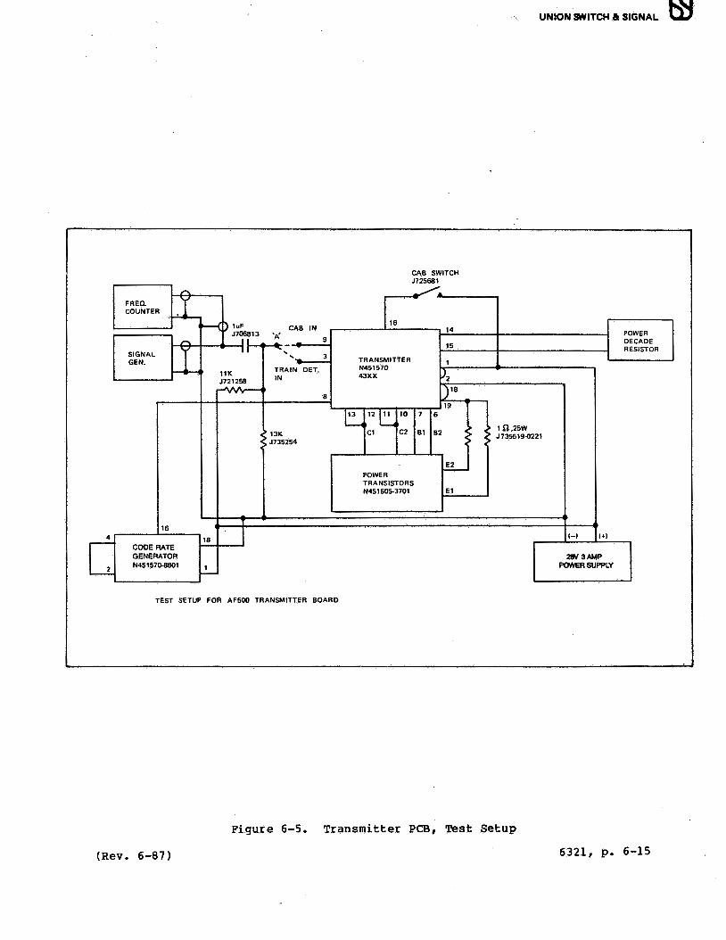
UNION SWITCH & SIGNAL t:t:I
CAB SWITCH J7256B1 - .
tL f 1s
~
FREQ. COUNTER
H ) 1uF CAB IN 14 J706813 '/!( POWER - 11 - ~
9 DECADE 11 ~ - 15 RESISTOR
SIGNAL lL ' , __ 3 TRANSMITTER GEN. 1 TRAIN DET. N451570
>2 11K IN 43XX
J72125B ... 118 VY
8 19
~ 12t_ 10 7 6
•• • 1n.2sw •> 13K Cl C2 81 82 .· ·: J735519-0221 ·: J735254 ~
£__ POWER TRANSISTORS N451605-3701 El
T 16
I 4 18 1-1 l+I
c CODE RATE GENERATOR 28V 3AMP N451570-8801 1 POWER SUPPLY -
TEST SETUP FOR AF500 TRANSMITTER BOARD
Figure 6-5. Transmitter PCB, Test Setup
(Rev. 6-87) 6321, p. 6-15

m UNION SWITCH & SIGNAL
Table 6-6. Transmitter PCB, Vmin. and Vmax. output Ranges
The maximum and minimum voltages for each switch position should be the same for each transmitter-board suffix as follows:
I
I l Cab Channel Detection Channel I
I Sl Pos. , ' (160 Ohm Load) (Load Per Table 6.5)
Vmin vmax Vmin Vmax ··-
1 0.8 - 1.1 2.0 - 2.9 I 0.6 - 1.2 2.0 - 2.8 2 1.6 - 2.3 4.3 - 5.9 l 1.2 - 2.4 4.2 - 5.8 3 3.7 - 4.9 10.5 - 13.4 2.6 - 5.2 10 - 12.5 4 8.7 - 10.9 22 - 30
I 6 - 11 20 - 26
5 19.5 - 24 50 - 60 13 - 23 44 - 54
6321, p. 6-16 (Rev. 6-87)

UNION SWITCH & SIGNAL OJ
(4) Close CAB SWITCH (Figure 6-5) and connect digital multimeter across one of the 1 ohm, 25 watt resistors. set meter to read de millivolts. If necessary, adjust R21 (BIAS) clockwise to obtain an average value of 150 .:!:. 4 millivolts of the two voltages measured across each of the two 1 ohm resistors.
(5) Connect signal generator output (point A on Figure 6-5) to pin 9 of board being tested. Set switch S3 on the PCB to CAB position.
(6) Connect digital multimeter across transmitter output (TP8, TP9) and set for ac volts. Connect an oscilloscope across same points and observe that output is a sinewave with no obvious distortion. Adjust slug in pot core Tl for maximum output voltage.
(7) Set switch S3 on PCB to TRACK position. Output voltage should drop below 200 millivolts rms. Set S3 to center position. output voltage should appear as in Figure 6-6. On the PCB, LEDl should flash at the code rate.
(8)' Rotate RS (CAB FINE) fully CW; output voltage should be approximately 2.5 times its previous level. Rotate R5 (CAB FINE) fully ccw.
(9) Step Sl (CAB COARSE) from position 1 to position 2. Output voltage should increase by approximately 2 times its previous level. Repeat for positions 3, 4 and 5. Each position should increase output by a factor of approximately 2 times, except for the -4311 PCB which will have the same output for positions 3, 4 and 5.
(10) With switch Slat position 5, rotate RS (CAB FINE) fully CW to obtain maximum output voltage. Set S3 to CAB position. Open CAB SWITCH (Figure 6-5). Output voltage should decrease to less than O.lV rms.
(11) Turn off power supply. This completes initial test of cab signal channel.
6.3.4.2 Train Detection Channel Initial Phase
a. Test Equipment Required: Same as paragraph 6.3.4.a.
b. Test Procedure
NOTE
During the following Adjustment Procedure, if any signal cannot be obtained, troubleshoot the associated circuitry to isolate the faulty component(s); i.e., resistors, capacitors, transistors, etc. After replacing the faulty component(s) repeat the measurements procedure.
6321, p. 6-17

m UNION SWITCH & SIGNAL
I
CODE RATE I (75 CPM)
MODULATEDttttttttttttt1ittfflttttttttttffft~~~~~-fil~ltl+t~l+++l+++fl#Mlt-~~~~~WAVEFORM
Figure 6-6. Transmitter PCB Modulation Envelope
(1) Before turning on power supply, set switch S2 (TRACK COARSE) to position 1, and set switch S3 to center position. Rotate Rl2 (TRACK FINE) fully CCW. If BIAS control (R21) was set during a check of cab signal channel, then it need not be readjusted. Otherwise, rotate it fully ccw.
(2) Turn on power supply and adjust to 28 +0.1 Vdc. Adjust signal generator to train detection frequency (within _:t5 Hz) per Table 6-5. Adjust its level to 2 _:tO.l Vp-p (0.672 - 0.742V rms), but do not connect to Transmitter PCB yet. set power decade resistor to value given in Table 6-5.
(3) If BIAS control (R21) does not require adjustment, then skip to step (4). Otherwise, adjust the bias according to the procedure in paragraph 6.3.4.1.b.(4).
C 4) connect signal generator output (point A on Figure 6-5) to pin 3 of board being tested. Set switch S3 to TRACK position.
(5) Connect digital multimeter across transmitter output ( (TP8, TP9) and set for ac volts. Connect an oscilloscope across same points and observe that output is a sinewave with no obvious distortion. Adjust slug in pot core T2 for maximum output voltage.
6321, p. 6-18 (Rev. 6-87)

UNION SWITCH & SIGNAL
(6) Set switch SJ to CAB position. Output voltage should drop below 200 millivolts rms. Set SJ to center position. output voltage should be coded (modulated), and modulation envelope should appear as in Figure 6-6.
(7) Rotate Rl2 (TRACK FINE) fully cw. Output voltage should be approximately 2 times its previous level. Rotate Rl2 (TRACK FINE} fully ccw.
(8) step switch S2 (TRACK COARSE) from position 1 to position 2. Output voltage should increase by approximately 2 times its previous level. Repeat for positions 3, 4 ands. Each position should increase output by a factor of approximately 2 times.
(9) Return switch S2 to position 1. This completes test of train detection channel.
6.3.5 Receiver PCB Test : ....
The Receiver PCB test consists of checking the sensitivity, relay timing, adjusting the sensitivity and bandpass filter. These tests apply to both Receiver PCB's, N451570-41XX and N451570-75XX, except where differences occur the values in parenthesis will apply to the -75XX series of PCB's.
a. Recommended Test Equipment:
(1) 24 Vdc Power supply
(2) Frequency counter
(3) Digital Voltmeter
(4} Oscilloscope
( 5) Signal Generator
(6) Resistor Decade Box
(7) Vital Relay PN-150B
(8) 620-0hm, 1/2 watt Resistor
(9) Receiver Board Test Set
6321, p. 6-19

ffi UNION SWITCH & SIGNAL
AF-500 RECEIVER N451570.41XX
~ .
I 1s 15 13 11 1
UJ721253
+ 620S"2 A
v
SIGNAL a
GENERATOR -j l
+
OSCILLOSCOPE + - 24VDC .! 1V
POWER SUPPLY
+ -
TRACK RELAY PN-1508 400S"2
-
Figure 6-7. Receiver PCB Test setup
6321, p. 6-20

UNION SWITCH & SIGNAL b':J 6.3.5.1 Sensitivity Check
~· Test Procedure
NOTE
During the following Test Procedure, if any signal is not as specified, it may be necessary to perform the Adjustment Procedure (paragraph b.)
(1) Connect the Receiver PCB to the circuit shown in Figure 6-7. connect a digital voltmeter to the PCB input pins 11 and 13.
(2) On the signal generator, set the train detection frequency for a sinewave at a frequency within.:!::. 2 Hz as given in Table 6-7 for the specified PCB under test. Set the auxiliary frequency for a squarewave of 75 .:!::. 2 cycles per minute (CPM) to produce a signal as shown in Figure 6-8.
(3f' Slowly increase the output of the signal generator until the vital track relay picks (energizes).
(4) Stop the coding and measure the input ac voltage level. The voltage should be 0.93 + 0.03V rms (0.093 .:!::. 0.003V rms for -75Xx series).
(5) Set the auxiliary frequency for a code rate of 648 + 5 CPM.
(6) Slowly increase the output of the signal generator until the relay picks up.
(7) stop the coding and measure the input ac voltage level. This voltage should be between 0.5 and 0.93V rms (0.050 and 0.093V rms).
b. Sensitivity Adjustment
NOTE
During the following Adjustment Procedure, if any signal is not as specified, perform the Bandpass Filter Adjustment Procedure (paragraph c.)
(1) Connect the Receiver PCB to the circuit shown in Figure 6-7. connect a digital voltmeter to the PCB input pins 11 and 13.
(2) On the signal generator, set the train detection frequency for a sinewave at a frequency within.:!::. 2 Hz as given in Table 6-7 for the specified PCB under test. Set the auxiliary frequency for a squarewave of 75 .:!::. 2 cycles per minute (CPM) to produce a signal as shown in Figure 6-8.
(3) Adjust resistor R31 fully counterclockwise (CCW). Replace resistors R4 and R30 (they are in series) with a resistor decade box and set it for lK ohms.
6321, p. 6-21

UNION SWITCH & SIGNAL
Table 6-7. Train Detection Frequencies for Receiver PCBs
6321, p. 6-22
PCB Suffix
-4102 -7502 -4103 -7503 -4104 -7504 -4105 -7505 -4106 -7506 -4107 -7507 -4108 -7508 -4109 -7509
Frequency_ (.Hz)
1900 2100 2580 28_20
.3100 3370 3660 3900
MODULATION ___ ___. FREQUENCY
IS 75(CPM)
Figure 6-8. Input Test Signal

UNION SWITCH & SIGNAL ffi (4) Set the signal generator for a continuous signal {no coding) and
adjust the output amplitude for 0.93 + O.OlV ac (0.093 + 0.001 Vac). - -
(5) Start coding the signal generator output. Slowly lower the decade box resistance until the vital track relay picks (energizes).
(6) Solder in the next lowest standard value, 1/4 watt, 5% carbon resistor for R4.
NOTE
Resistors R4 and R30 must be an approved safety type (Allen Bradley) composition resistor.
(7) connect the decade box in place of R30. Slowly lower the decade box resistance until the vital track relay picks.
(~) Solder in the closest value, 1/4 watt, 5% carbon resistor. The total resistance (R4 + R30) should be between 200 and 1,200 ohms.
(9) using Table 6-8 and the total resistance of R4 and R30, select and install R32.
Table 6-8. Resistance Values (R4 + R30)/R32
combined Resistance (R4 + R30) R32
greater than 800 ohms no resistor required 650 ohms to 800 ohms 20K ohms, J735054 500 ohms to 649 ohms 8.2K ohms, J735058 400 ohms to 499 ohms 5.lK ohms, J735301 less than 400 ohms 3.3K ohms, J735138
(10) Adjust R31 fully clockwise (CW). Increase the input signal slowly until the relay picks. Stop the coding and measure the input ac voltage using the digital voltmeter. The voltage should be greater than s.ov rms (between 0.50 and 0.70V rms for -75XX series).
(11) Adjust R31 fully ccw. Change the code from 75 CPM to 648 .±. 5 CPM. Lower the input signal amplitude until the vital track relay drops (deenergizes) and then slowly increase the signal until the relay picks.
(12) Stop the coding and measure the input voltage. This voltage should be between 0.5 and 0.93V rms (0.050 and 0.093V rms).
6321, p. 6-23

m UNION SWITCH & SIGNAL
c. Bandpass Filter Adjustment
NOTE
During the following Adjustment Procedure, if any signal cannot be obtained, troubleshoot the associated circuitry to isolate the faulty component(s): i.e., resistors, capacitors, transistors, etc. After replacing the faulty component(s) repeat the Test Procedure.
(1) connect the Receiver PCB to the circuit shown in Figure 6-7. Connect an oscilloscope to the PCB input pins 11 and 13.
(2) On the signal generator, set the train detection frequency within + 2 Hz as given in Table 6-7 for the specified PCB under test. set the amplitude to 2.6 .±. 0.1 Vac, P-P.
(3) Place a jumper across capacitor c2. Set the scope for maximum resolution by turning the vertical position control full ccw and adjusting the vertical gain and time base to produce a waveform approximately as shown in Figure 6-9.
(4) Adjust the tuning slug in inductor Ll for a minimum voltage on the scope.
(5) Remove the jumper across C2 and disconnect one end of C3. Adjust the slug in transformer Tl for a maximum voltage on the scope.
(6) Reconnect C3 and place a jumper across resistor Rl. Adjust the tuning slug in L2 for a minimum voltage on the scope. Remove the jumper across Rl.
Figure 6-9. Typical Filter Input 6321, p. 6-24

6.3.5.2
a.
UNION SWITCH & SIGNAL ~
CAUTION
In the next step, the oscilloscope ground must be totally isolated from ac common and power supply common.
(7) Connect the oscilloscope probe to TP4 and the probe ground lead to TPl. Adjust the tuning slug in T2 for a maximum voltage on the scope.
(8) Adjust the tuning slug in T3 fully clockwise until it stops at the bottom.
(9) Seal the tuning slugs in Ll, L2, Tl, T2 and T3 with clear RTV (A41701).
Relay Timing Check
Test Procedure
NOTE
During the following Adjustment Procedure, if any signal cannot be obtained, troubleshoot the associated circuitry to isolate the faulty component(s): i.e., resistors, capacitors, transistors, etc. After replacing the faulty component(s) repeat the Test Procedure.
(1) connect the Receiver PCB to the circuit shown in Figure 6-10.
(2) On the signal generator, set the train detection frequency within + 2 Hz as given in Table 6-7 for the specified PCB under test. Set the amplitude to 2.32 .:!:. 0.03V rms, (0.23 .:!:. 0.005V rms). Set the auxiliary frequency for 75 CPM.
(3) Set the scope for storage, single sweep, external trigger with positive slope and horizontal sweep to 0.2 sec./div.
(4) Close switch Sl and verify that the sweep on the scope starts, and begins at the first ve~tical graticule. Open switch Sl, erase the scope trace, reset the sweep and repeat as necessary to verify the scope setup. See Figure 6-11.
(5) When the scope is set up, momentarily short capacitor C8 to discharge any stored energy. Close switch Sl and measure the time from the beginning of the trace to the time the trace goes high. This is the relay pickup time. Repeat several times to get an average time. The average pickup time should be between 1.2 and 1.95 seconds.
6321, p. 6-25

b'j UNION SWITCH & SIGNAL
TRACK RELAY PN-1508 400Q
SIGNAL GENERATOR
D STORAGE SCOPE
6321, p. 6-26
!"',
I 1s
-
+
+
-
TRIG.
CHANNEL 1
AF-500 RECEIVER N451570.41 XX
15 13 11
\0 \ u SI \_ J.
9 ()
1
+
-
Figure 6-10. Receiver PCB Test Setup for Measuring Relay Pickup and Drop Times
24VDC !1V
POWER SUPPLY
TRACK RELAY
- 1F
i _1H -• • 18

UNION SWITCH a SIGNAL w
24V
,. . RELAY CONTACT I ov
I I ,,.. PICK ~ I TIME
'
RELAY CONTACT' 24V
I I ov I i I 14
DROP ~ TIME
Figure 6-11. Relay Pickup and Drop Away Times
6321, p. 6-27

UNION SWITCH & SIGNAL
(6) Erase the scope trace, reset the sweep, switch to negative slope trigger, open switch Sl and verify the sweep starts and begins at the first vertical graticule. Close Sl, erase the scope trace, reset the sweep and repeat as necessary to verify the scope setup.
(7) When the scope is set up, open Sl and measure the time from the beginning of the trace to the time the trace goes low. This is the relay dropaway time. Repeat several.times to get an average time. The average dropaway time should be less than 1.3 seconds.
(8) Close Sl and measure the de voltage across the relay coil, terminals +A and -A. The voltage should be between 7 and 9 Vdc.
(9) Repeat steps (5) through (8) except set the signal generator for 648 CPM code rate.
6.4 COMPONENT~REPLACEMENT NOTES
Repair of the AF-500 PCBs consists primarily of replacing board components which have been found to be defective through the troubleshooting process. Observe the following procedure when replacing components.
a. Always use a heat-sink, such as needle-nose pliers or alligator clips on the leads of the component to be removed/replaced to prevent component damage.
b. Ose a low-wattage soldering iron (60 watts maximum) with pencil tip for unsoldering component leads.
c. Scrape away spraycoat from around component and leads prior to unsoldering component.
d. After component replacement, apply spray or brush coat of CONAP CE-1163 Polyurethane (or equivalent) to repaired area.
6321, p. 6-28

UNION SWITCH & SIGNAL b'j
6.5 POST-REPAIR INSPECTION PROCEDURES
Upon completion of any maintenance to the AF-500 PCBs, PCB inspection should be performed as follows:
a. All components and material must agree with bill of material and must be correctly installed in accordance with assembly drawings. (Refer to Appendix A.)
b. All devices with polarity indicated must agree with markings on circuit board. This includes diodes, electrolytic capacitors, transistors, and !Cs. Diode polarity is indicated by a band at its cathode, electrolytic capacitors by a•+• symbol, and transistors and ICs by respective arrangement of their lead wires and orientation notch or symbol.
c. All solder connections must be bright and free of flux. A dull, wrinkled appearance indicates a cold solder joint.
d. Tra~sformers connected to circuit board with wires must agree with color code or numbering system, where appropriate.
e. All PCBs must be identified as to circuit board nomenclature, part number, and serial number; all identification must be correct and legible.
f. All mechanical fasteners, such as machine screws and nuts, must be secure and assembled in proper sequence according to drawings (Appendix A)•
g. All PCB jumper wiring should conform to circuit diagram for color code, and all wires should be free of abrasions and nicks in their insulation.
6321, p. 6-29


UNION SWITCH & SIGNAL OJ
SECTION VII
PARTS LIST
7.1 INTRODUCTION
This section provides a listing of all printed circuit boards for field level maintenance and a complete listing of all component parts (Appendix A) for shop level maintenance.
7.2 FIELD LEVEL COMPONENTS
The following is a list of printed circuit boards that are replaceable at field level. For printed circuit board location refer to Figure 1-3.
a. Oscillator PCB 1900 Hz N451570-3901 2100 Hz -3902 3900 Hz -3903 2580 Hz -3904 2820 Hz -3905 3100 Hz -3906 3370 Hz -3907 3660 Hz -3908 Cab Only -3909
b. Code Rate Generator N451570-8801 c. Receiver PCB 1900 Hz N451570-4102
2100 Hz -4103 2580 Hz -4104 2820 Hz -4105 3100 Hz -4106 3370 Hz -4107 3660 Hz -4108 3900 Hz -4109
d. Receive Only PCB 1900 Hz N451570-7502 2100 Hz -7503 2580 Hz -7504 2820 Hz -7505 3100 Hz -7506 3370 Hz -7507 3660 Hz -7508 3900 Hz -7509
e. Transmitter PCB 1900 Hz N451570-4302 2100 Hz -4303 3900 Hz -4304 2580 Hz -4305 2820 Hz -4306 3100 Hz -4307 3370 Hz -4308 3660 Hz -4309 Cab Only -4310
f. Power Transistor PCB N451605-3701
6321, p. 7-1

ffi UNION SWITCH & SIGNAL
In addition to the printed circuit boards, other components that are field replaceable are as follows:
a. b. c. d.
AF-500 cardfile AF Tuned Minibond PN-lSOB, Vital Track Relay Junction Box, Receive Only
7.3 SHOP LEVEL COMPONENTS
N451082-1002 N451486-0701 N322500-901 N451102-2001
A complete detailed parts list for shop level maintenance is contained in Appendix A.
7.4 PARTS LIST USE
Mechanical and certain electrical parts are identified by an item number that is keyed to an illustration. Determine part to be replaced and order by part number and description.
Electronic parts are identified by Reference Designations. These designations are used on the schematic diagrams to identify the specific part. This same designation is used to identify and locate that part on the applicable printed circuit board. Determine part to be replaced and order by part number and description.
6321, p. 7-2

SERVICE MANUAL 6321 Appendix A
PARTS LIST
AUDIO FREQUENCY TRAIN DETECTION AND WAYSIDE CAB SIGNALING SYSTEM
AF-500
THIS SERVICE MANUAL SUPERSEDES SM6321 DATED MARCH, 1984
June, 1985 (Rev. 6/ffl) 100047F/DN0032D B-6/87-50-2654-1
PRINTED IN USA
UNION SWITCH & SIGNAL AMERICAN STANDARD INC • PO BOX 420 • PGH., PA 15230

m UNION SWITCH & SIGNAL
REVISION INDEX
Revised pages of this manual are listed below by page number and date of revision:
l I
Page Number
A-12 A-13
Revision Date
6/87 6/87
Page Number Revision Date

Item No.
1 2 3 4 5
_,.,,,.,, • ........ "',,fill '7J'Ul'll"I&. ,,.........
Track Circuit card File Assembly (N451082-1002) (See Figure A-1)
Quantity Part Number Description
2 M451083-4901 I I Bracket, End
1 M451083-5001 support, Top Guide 1 M451083-5101 Support, Bottom Guide 1 N451083-9901 Panel, Connector
30 J490029 Rivet, Pop, 11s• Dia.
:.- "
Alum.
6321, p. A-1

m UNION SWITCH & SIGNAL
Item No.
1 2 3 4 5
NN.C'rOA: Po'SfTI
Track Circuit card File Assembly (N451082-1002) (See Figure A-1)
Quantity Part Number Description
2 1 1 l
30
M451083-4901 Bracket, End M451083-5001 Support, Top Guide M451083-510l Support, Bottom Guide M451083-9901 Panel, Connector J490029 Rivet, 1/8 Alum., Pop
[~ - ------ -~~
:: -------·-----------~ii~ [·~-----------·--------~i~t II •1 '! ,, . .. ,, .. ------ - - ---· .
----11,k(_ ....... _) _____ _ ··--· ....J
----------------fti~--------·~---oo< 1-------------~n?~-------·~---~
"
rrrn r r r r r i . l ~: -~-=-~JE~:J=L~Ll:=:--+_!:+~:-_-t:::=i'=-==LL~U? __ ·~-* lIJ
Drawing R451082 Sh. 10, Rev. 5
Figure A-1. Track Circuit Card File Assembly

Item No.
5 10 15 20 25 30 35 40 45 50 55 60 65 70 75
Panel
Connector Panel (N451083-9901) (See. Figure A-lA)
Desc r ipt ion
PC Card Edge Connector Rivet, Pop, 1/8• Dia. Alum. washer, SST Junction Block Screw, 4-40 x 1/2 Bind. Hd. #4 washer, Pln. Fl. St. #4 washer, Lock, Med. Stl. Nut, 4-40, Hex, Stl. Resistor, 1 ohm, 25 watt Rivet, Pop, 3/32• Dia. Receptacle Housing, 18 Pos. Terminal Board, 10 Term., 2 Sec.
:r' Insulation Tubing Screw, 4-40 x 7/8 Rd. Hd. Stl.
-•••-•• V••• I VI 1 .... VI_,._._ .._,..
Part Number
M451083-9902 J706740 J490048 M435121-002 J776658 J050999 J047640 J047765 J480006 J735519-0221 J490014 J713804-0002 M451143-1402 M437233 J525089
6321, p. A-3

m UNION SWITCH Ii SIGNAL
,-~---, I I )__ ___ ---1,
_j i_
F451083-99 Rev.
Figure A-lA. Connector Panel 6321, p. A-4

UNION SWITCH & SIGNAL \,,IJ
oscillator Printed Circuit Board (N451570-39xx) (See Figure A-2)
Basic Components Parts List
Reference Designation Quantity Part Number Description
RlA,RlB 2 J735057 Resistor, 10 ohm, 1/4 W R2A,R2B 2 J735037 Resistor, 33K, 1/4 W R3A,R3B 2 J735405 Resistor, 510K, 1/4 W R4A,R4B 2 J735519-0227 Resistor, 200K, 1/4 W R5A,R5B 2 J735052 Resistor, 3K, 1/4 W R6A,R6B,RllA,RllB 4 J735031 Resistor, lK, 1/4 W Rl0A,RlOB,Rl2A,Rl2B 4 J735053 Resistor, lOK, 1/4 W Rl3A,Rl3B 2 J735060 Resistor, 330K, 1/4 W R7A l J735138 Resistor, 3.3K, 1/4 W
ClA,ClB 2 J709145-0043 Capacitor, 50 MFD, 40V C2A !r 'I 1 J709054 Capacitor, .68 MFD, 200V C3A,C38 2 J709145-0357 Capacitor, .033 MFD, 200V C4A 1 J706549 Capacitor, .033 MFD, 200V C5A,C58 2 J706387 Capacitor, 1 MFD, 35V
DlA,DlB 2 •J726150-0079 Diode, LVA462 D2A,D2B 2 J723062 Diode, 1N964B QlA,QlB,Q2A,Q2B 4 J731398-0079 Transistor, 2N3117
4 J792437 Transistor, Mounting Pad
R8A,R8B,R9A,R9B 4 -- Resistor, Select on Test
TPl 1 J713306-0006 Jack, Test (Red) TP2,3,4 3 J713306-0005 Jack, Test (Yellow) TPS l J713306-0008 Jack, Test (Black) TLl,2,3 3 J731432 Turret Lug
Tl A 1 N451030-5312 Inductor, Pot Core
Fl 1 J071045 Fuse, 1/2 Amp. Fl 2 J576794 Clip, Fuse
6321, p. A-5
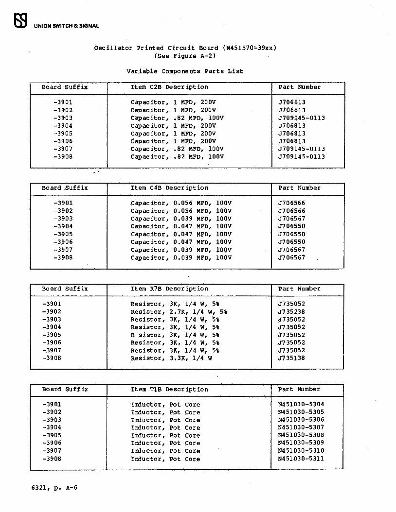
m UNION SWITCH & SIGNAL
Board Suffix
-3901 -3902 -3903 -3904 -3905 -3906 -3907 -3908
Board Suffix
-3901 -3902 -3903 -3904 -3905 -3906 -3907 -3908
Board Suffix
-3901 -3902 -3903 -3904 -3905 -3906 -3907 -3908
Board Suffix
-3901 -3902 -3903 -3904 -3905 -3906 -3907 -3908
6321, p. A-6
Oscillator Printed Circuit Board (N451570~39xx) (See Figure A-2)
Variable Components Parts List
Item C2B Description
capacitor, 1 MFD, 200V Capacitor, 1 MFD, 200V Capacitor, .82 MFD, lOOV Capacitor, 1 MFD, 200V Capacitor, 1 MFD, 200V Capacitor, 1 MFD, 200V Capacitor, .82 MFD, lOOV Capacitor, .82 MFD, lOOV
: ....
Item C4B Description
Capacitor, 0.056 MFD, lOOV Capacitor, 0.056 MFD, lOOV Capacitor, 0.039 MFD, lOOV Capacitor, 0.047 MFD, lOOV Capacitor, 0.047 MFD, lOOV Capacitor, 0.047 MFD, lOOV capacitor, 0.039 MFD, lOOV Capacitor, 0.039 MFD, lOOV
Item R7B Description
Resistor, 3K, 1/4 w, 5% Resistor, 2.7K, 1/4 w, 5% Resistor, 3K, 1/4 w, 5% Resistor, 3K, 1/4 w, 5% R si.stor, 3K, 1/4 w, 5% Resistor, 3K, 1/4 W, 5% Resistor, 3K, 1/4 W, 5% Resistor, 3.3K, 1/4 W
Item TlB Description
Irrluctor, Pot Core Irrluctor, Pot Core Irrluctor, Pot Core Irrluctor, Pot core Irrluctor, Pot Core Irrluctor, Pot Core Irrluctor, Pot Core Irrluctor, Pot Core
Part Number
J706813 J706813 J709145-0113 J706813 J706813 J706813 J709145-0113 J709145-0ll3
Part Number
J706566 J706566 J706567 J706550 J706550 J706550 J706567 J706567
Part Number
J735052 J735238 J735052 J735052 J735052 J735052 J735052 J735138
Part Number
N451030-5304 N451030-5305 N451030-5306 N451030-5307 N451030-5308 N451030-5309 N451030-5310 N451030-5311

l"il ..... IQ c:: .., ID
:r "' •
0 (II 0 ..... ..... ..... Ill g .., "ti .., ..... ::,
~ Q,
(') ..... .., 0 c:: ..... rt
8' Pl
""' Q,
g: (II
CTI m w O" N ..... ..... '< .. 'ti • > I
-.J
~
-[RIC]-~ - .- - - -CIRCLJIT_C_ - -HZ, - - - - - - - - - -uct- - LJ I -[ J- 0
u u 02C o CIC u, r-- + ., (o,o-
c C3C QIC ~ ~ o· 0 ,-1,a:: ~
J + [ J RSC / o " r1, r1, A ~ o / o / FI I o-[ J-o o o I 1TL3 riu i..__,
L \......-,v r1,o Y -
DI Co-{[ J-o [ J J RSC ~ ~~LJ 19~0
yo: R3Co-[ J-o · o-[ J-o r1, Y l,JO
O
R4Co-[ J-o C4C 0-[ • J-o ~ o
O
R9C ii: ~
TP I C2C ~ er: [ J ______________________ o TIC o-[, J-:oR2B CIRCUIT B HZ cocococo r1ico----------
[ J RIBo:_r J-o • U:ll'-COO'l l"'l(o'\ o CO '- CIB a::a::a::a:: - _1_ -
L C3B o o o o ya::\ 0 con -
[ JTP2
0 I + [ J QI B r1, r1, r1, r1, n o (./
0
/ o r1, a:: r1i I I'
0 " 028 ii: O O O y
TP3 C2B RSB , ----> y y y y u~ cori o o [ J y ID I Bo-{[ J-o J o-[ J-o C4B O O O O u ~ A~ ~
[ JTP4~IR3Ba-[ ]-o L J O a::y l,JO
er: I R4Bo-[ J-o TL2 + 0 0
TP5 _ :_ Tl B
o-[R2AJ-o - - - - -C IRCLJ IT -A - - -HZ, - - ~ ;:: - + - - Q2A r1,Rl3A- - - - - -
CI A + C3A ,9 i \ ~ ~ TLI ( 0
~ 0
C J [ J RSA O O r1i r1i AQ ~o/~o
o-[ J-o \..... .-,v I I o r1, C2A L O
y. DIAo-{[ J-o [ J J ~ ~ LJCSA r1i ~~
-[ J-o R8Ao-[ ]- O
R4A 0 -[ J-o C4A R9Ao-[ J-o o ;. -
9 · OSCILLATOR PCB ~ ~ ii:
N451570-39 REV, ii: 0
EB
[~~~
1 ···· .
EB I
TIA _!J
t:I 11
~ I-'· :::,
IQ
l':tj .i:,. u, ..... U1 -.J C>
en ::r . w
~ ..
' . w
c z 0 z I ~ ::r::
• 0 a z > ,-
E

m UNION SWITCH & SIGNAL
Receiver Printed Circuit Board (N451570-4lxx) (N451570-75xx) (See Figure A-3)
Reference Designation
R2,Rl0,R16,R25, R26,R27 R3,R17 R5,R6,R22 R7 R8 R9 (-41xx) R9 (-75xx) Rll R13 R14 Rl5 (-41xx) Rl5 {-75xx) R18 Rl9 R20 R21 R23 R24 R12,R28 R31
cs C6 (-41xx) c6 {-75xx) C7 Cl7 C9,Cl2 ClO Cll Cl3,C14 Cl5 C16
Dl D2,3,4,10,ll DS,6,7,9 D8 Dl2
LED!
6321, p. A-8
Basic components Parts List
Quantity
1 1 2
6 2 3 1 1 1 1 1 1 1 1 1 1 1 1 1 1 1 2 1
1 1 1 1 1 2 1 1 2 1 1
1 5 4 1 1
1
Part Number
N451570-4101 N451570-7501 J560839
J735031 J735052 J735063 J735068 J735043 J735519-0360 J735519-0466 J735301 J735139 J735519-0227 J735405 J735404 J735388 J735519-0073 J735054 J735366 J735216 J735053 J720881 J620850-0090
J706421 J706762 J709145 J709145-0479 J706986 J709145-0480 J706848 J706436 J706501 J706678 J706120
J726150-0057 J726031 J723555 J726150-0079 J726150-0071
J726150-0062
Description
Basic ·PCB (Complete) Basic PCB (Complete) Ejector w/Pin
Resistor, lK, 1/4 W Resistor, 3K, 1/4 w Resistor, I.SK, 1/4 w Resistor, 30K, 1/4 W Resistor, 5.6K, 1/4 w Resistor, 22K, 4 Term. Resistor, 220K, 4 Term. Resistor, 5.lK, 1/4 w Resistor, l.8K, 1/4 w Resistor, 200K, 1/4 w Resistor, 510K, 1/4 W Resistor, llOK, 1/4 w Resistor, 13K, 1/4 W Resistor, 300 Ohm, 1/4 W Resistor, 20K, 1/4 W Resistor, 24K, 1/4 w Resistor, 75K, 1/4 W Resistor, lOK, 1/4 w Resistor, 10 Ohm, 1/2 w Potentiometer, SK, 1/2 w
Capacitor, 1.5 MFD, 35V Capacitor, .047 MFD, 4 Term. Capacitor, .0047 MFD, 4 Term. Capacitor, 860 MFD, 40V Capacitor, 100 MFD, 40V Capacitor, .027 MFD, lOOV Capacitor, .56 MFD, 200V Capacitor, .1 MFD, 50V Capacitor, 6.8 MFD, 35V Capacitor, 27 MFD, 20V Capacitor, 1 MFD, lOOV
Diode, 1N5235 Diode, 1N914A Diode, 1N4003 Diode, LVA462 Diode, IN748A
Diode, Light Emitting

Receiver Printed circuit Board cont'd.
Reference Designation Quantity Part Number Description
Fl 1 J071045 Fuse, l/2A, 3AG Fl 2 J576794 Clip, Fuse
TPl 1 J713306-0006 Jae!<, Test TP2 1 J713306 Jack, Test TP3 1 J713306-0008 Jack, Test TP4 1 J731396 Terminal, solder
Ql,3,6,12 4 J731398-0079 Transistor, 2N3117 Q2,10 2 J731398-0050 Transistor, 2N3964 Q4,7,8 3 J731186 Transistor, 2N2270 Q9,5 2 J731291 Transistor, 2N4037 Qll 1 J731304 Transistor, 2N2102 Ql,2,3,6,10,12 6 J792437 Mounting Pad Q4,5,7,8,,9,ll 6 J792072 Mounting Pad
T3 1 N451030-6303 Inductor, Pot Core
ca 1 J706391 Capacitor, 150 MFD,
R4,30,32 3 -- Resistor, Select on
Receiver Printed Circuit Board (N451570-4lxx) (N451570-75xx) (See Figure A-3)
Variable Components Parts List
15V
Test
Board Suffix Item Rl Description Part Number
-4102 -7502 Resistor, 3.3K 1/4 W J735138 -4103 -7503 Resistor, 22K 1/4 W J735093 -4104 -7504 Resistor, lOK, 1/4 W J735053 -4105 -7505 Resistor, 8.2K, 1/4 W J735058 -4106 -7506 None ---4107 -7507 None ---4108 -7508 Resistor, 33K, 1/4 w J735037 -4109 -7509 Resistor, 13K, 1/4 w J735388
6321, p. A-9
I

m UNION SWITCH & SIGNAL
Receiver Printed Circuit Board variable Components Parts List (Cont'd.)
Board Suffix Item Ll,L2,Cl & C3 Description Part Number
-4102 -7502 Pot core inductors with capacitors N451030-5417 -4103 -7503 Pot core inductors with capacitors N451030-5418 -4104 -7504 Pot core inductors with capacitQrs N451030-5419 -4105 -7505 Pot core inductors with capacitors N451030-5420 -4106 -7506 Pot core inductors with capacitors N451030-5421 -4107 -7507 Pot core inductors with capacitors N451030-5422 -4108 -7508 Pot core inductors with capacitors N451030-5423 -4109 -7509 Pot core inductors with capacitors N451030-5424
.. '
Board Suffix Item Tl, C2 Description Part Number
-4102 -7502 Transformer with capacitor N451030-5425 -4103 -7503 Transformer with capacitor N451030-5426 -4104 -7504 Transformer with capacitor N451030-5427 -4105 -7505 Transformer with capacitor N451030-5428 -4106 -7506 Transformer with capacitor N451030-5429 -4107 -7507 Transformer with capacitor N451030-5430 -4108 -7508 Transformer with capacitor N451030-5431 -4109 -7509 Transformer with capacitor N451030-5432
Board Suffix Item T2,C4 Description Part Number
-4102 -7502 Transformer with capacitor N451030-5516 -4103 -7503 Transformer with capacitor N451030-5517 -4104 -7504 Transformer with capacitor N451030-5518 -4105 -7505 Transformer with capacitor N451030-5519 -4106 -7506 Transformer with capacitor N451030-5520 -4107 -7507 Transformer with capacitor N451030-5521 -4108 -7508 Transformer with capacitor N451030-5522 -4109 -7509 Transformer with capacitor N451030-5523
Board Suffix Item R29 Description Part Number
-4102 -7502 Resistor, 330, l/4W, 5%' 4 Term. J735519-0518 -4103 -7503 Resistor, 470, l/4W, 5%, 4 Term. J735519-0519 -4104 -7504 Resistor, 470, l/4W, 5%' 4 Term. J735519-0520 -4105 -7505 Resistor, 680, l/4W, 5%, 4 Term. J735519-0354 -4106 -7506 Resistor, 680, l/4W, 5%, 4 Term. J735519-0354 -4107 -7507 Resistor, 820, l/4W, 5%, 4 Term. J735519-0522 -4108 -7508 Resistor, 820, l/4W, 5%, 4 Term. J735519-0522 -4109 -7509 Resistor, lK, l/4W, 5%, 4 Term. J735519-0523
6321, p. A-10

l'lljj ..... IQ c: .., (D
:r w •
~ (D ..... <: (D .., '"C .., ..... ::, rl' (D Q.,
() ..... .., 0 c: ..... rt
D:I 0 Sll .., Q.,
),I fl) fl) (D
s-..... "<
O'I w N ...... ... 'O . > I ......
......
~[
Cl6 J ~o-/25J-o/:,N40515c:70-41 REV.:JAF-50?lCVf:. rr--Fl-i'l$1 °;;':r LO
O r1-, R2 8 l_J-- --L_J R23;-~-' ]-1 ° /:: I I R6 ( 0 '\ 0 I
o-[ J-o Cl 5 QI O 1 O:Y L_ _J o-[ J-a ~ 0
;Q2 r1-, L--,
- R27 \i --, ~0
::- 1-:, COIR412 C6 ova°'1-[ J- 0 R1 I or9 ~ R7 ~: a I I \ I 'i 0 > 0 0 a {I O 05 r1-, Y
L'.D. 1 ""'-1-:, o I o o ~ I 4 R8 o '"' q:7 0 o \-[ J}-~26 . 05 o-[ J-o y Q
C ~ a'~ R I 5 o -[ ]- o o {I ]- o LED I "'-
0
A D 12 l rc 04 o{I J-oD7 08 ° .
~ ;=([ _jJO + o-[ J-o o{I J-o TP I+~ Jo IL (?' <~ C7 R 13 R30 06 o o
[ ~ C 13 a 0
i.L da° 4} 1C -"J C8 o-[ J-o r1-, r1-, - r-1-,cn ~ ~ 0 I +
0 0 0 02 R3
o-( 0 0 o"y n 'n ··- C)c,o ) (}) r'"'lrir,R4 Nt?Y R2 I
O O O QI o: o o
[ J ~~~o ~~o<(s=JD9 I C5uy~o;~rfln
TP2 I O O O ;f07 L I R5%~0~~ C3
r0 I' ~~r, ~ -~ --.0 I ~ ~ LJ R31 T3 12 o /. \ R29 - '- C9 ° // c J I ~ ~ ,1,"' ~f :::;o/
r-- L _J y
- Cl2<""', ~~ ~ ) r1-, 0 O~l.O 0::: r-1-,_ ~ ,en " o / ~
_o-[ J-oR 18 --- '
r r ~ 1, ~ I I= D3o{I J-o [ ~. u D4 ° -fI J- 0 ,t' --1c2
@ ~~;;:;;;;;;;;;;;;;;;;;;~================
n Tl LJc1
L2
L I"'
I"' :: ____ TI.,
I"'
; I :1~ ..._ ___ -l._J, a::
rz I :1:
lcn~ I
:"°Ill ~
,1::.f-'·
.!""'-5
; I ~:
::u li:j
LI _)L'.D. ,~§ ~,1::.25
c 4 c 4
! -~ .. Cf. f :z ), ,.
f

UNION SWITCH & SIGNAL .
Transmitter Printed Circuit Board (N451570-43xx) (See Figure A~4) Basic Components Parts List
Reference I Designation Quantity Part Number Description
l N451570-4301 Basic PCB (Complete) 2 J560839 Ejector w/Pin
TPl l J713306-0001 Jack, Test (Orange) Rl3 l J735301 Resistor, 5.lK, 1/4 w Rl4 l J735070 Resistor, 2.4K, 1/4 W TP4 l J713306-0007 Jack, Test (Blue) TP6,7 2 J713306-0002 Jack, Test (White) TPB,9 2 J713306-0005 Jack, Test (Yellow) TPlO l J713306-0008 Jack, Test (Black) TPll,13,14 3 J731396 Lug, Turret
Rl 1 J735054 Resistor, 20K, 1/4 W R2 ~ . 1 J735053 Resistor, lOK, 1/4 W
I R3 1 J7350S2 Resistor, 3K, 1/4 W R4 1 J73S032 Resistor, 6.BK, 1/4 W R6,22 2 J735301 Resistor, 5.lK, 1/4 w R7 1 J735Sl4 Resistor, 6.2K, 1/4 w RlS 1 J73S040 Resistor, !SOK, 1/4 W Rl6,17,25,26 4 J735050 Resistor, 100 Ohm, 1/4 w RS 1 J620850-0058 Pot., lOK, 3/4 W Rl8,19,20 3 . J721080 Resistor, 2K, 1/2 W R21 1 J620850-0067 Pot., 100 Ohm, 3/4 W R23 1 J73SS19-0389 Resistor, 30 Ohm, 1/4 w
Ql,2,3,6 4 J731398-0079 Transistor, 2N3117 Q7,8 2 J731186 Transistor, 2N2270
Dl,3,5,8 4 J726031 Diode, 1N914A LEDl 1 J726150-0062 Diode, Light Emitting 04,6,7 3 J723SSS Diode, 1N4003
Cl 1 J702139 Cap., 10 MFD, SOV C2 1 J706986 Cap., 100 MFD, 40V C3 l J709144-0018 Cap., 1 MFD, 20V cs -- Cap., (Furnished with Tl)
S3 1 J725707-0146 Switch, Toggle SPDT Sl 1 J725707-0057 Switch, Rotary SPl,2 2 J790876 Varistor IV39ZA6
Q7,Q8 2 J792072 Pad, Mounting Ql,2,3,6 4 J792437 Pad, Mounting
Fl,2 4 JS76794 Clip, Fuse Fl 1 J710006 Fuse, .2SA, 2SOV F2 1 J071185 Fuse, SA, 2SOV
Tl 1 N4Sl030-5323 Inductor, Pot core TP2 1 J713306-0006 Jack, Test (Red) T3 1 N451030-4623 Inductor, Pot Core
6321, p. A-12 (Rev. 6-87)

I
I
UNION SWITCH & SIGNAL \.&,I
NOTE
The following items pertain to board suffixes -4302 through -4309 only.
Reference Designation
C6
R8 R9 RlO
Q4,5
C4 S2 02 TP5 TP3 ~.. \
Q5,4
Board Suffix
-4302 -4303 -4304 -4305 -4306 -4307 -4308 -4309 -4310
(Rev. 6-87)
I
Quantity Part Number Description
1
I Cap., (Furnished with
1
I J735054 ! Resistor, 20K, 1/4 W
1 J735053 Resistor, lOK, 1/4 W 1 J735052 Resistor, 3K, 1/4 W
I 2 J731398-0079 Xstr., 2N3117 I
I 1 J709144-0018 Cap., 1 MFD, 20V 1 J725707-0057 Switch, Rotary 1 J726031 Diode, 1N914A 1 J713306 Jack, Test (Green) 1 J731396 Turret Lug 2 J792437 xstr., Mtg. Pad
Transmitter Printed Circuit Board (N451570-43xx) (See Figure A-4)
Variable components Parts List
Item Rll Description Part Number
Resistor, l.5K 1/4 W J735063 Resistor, l.8K 1/4 W J735139 Resistor, 3.9K, 1/4 w J735066 Resistor, 2.2K, 1/4 w J735236 Resistor, 2.4K, 1/4 w J735070 Resistor, 3.3K, 1/4 w J735138 Resistor, 3.6K, 1/4 w J735033 Resistor, 4.3K, 1/4 w J735046
None
T2,
6321, P• A-13

m UNION SWITCH & SIGNAL
Transmitter Printed Circuit Board Variable Components Parts List (Cont'd.)
Board Suffix Item Rl2 Description
-4302 Potentiometer, 2K, 3/4 W -4303 Potentiometer, 2K, 3/4 W -4304 Potentiometer, lOK, 3/4 W -4305 Potentiometer, SK, 3/4 W -4306 Potentiometer, SK, 3/4 w -4307 Potentiometer, SK, 3/4 w -4308 Potentiometer, SK, 3/4 w -4309 Potentiometer, SK, 3/4 w -4310 None
, Board Suffix Item R24 Description
-4302 Resistor, 30 ohm, 1/4 w -4303 Resistor, 30 ohm, 1/4 w -4304 Resistor, 24 ohm, 1/4 w -4305 Resistor, 24 ohm, 1/4 w -4306 Resistor, 24 ohm, 1/4 w -4307 Resistor, 24 ohm, 1/4 w -4308 Resistor, 24 ohm, 1/4 w -4309 Resistor, 24 ohm, 1/4 w -4310 None
Board Suffix Item T2 with C6 Description
-4302 Transformer with capacitor -4303 Transformer with capacitor -4304 Transformer with capacitor -4305 Transformer with capacitor -4306 Transformer with capacitor -4307 Transformer with capacitor -4308 Transformer with capacitor -4309 Transformer with capacitor -4310 None
6321, P• A-14
Part Number
J620850-0068 J620850-0068 J620850-0058 J620850-0064 J620850-0064 J620850-0064 J620850-0064 J6208S0-0064
--
Part Number
J735519-0389 J735Sl9-0389 J735519-0388 J735519-0388 J735519-0388 J735519-0388 J735519-0388 J735519-0388
--
Part Number
N4Sl030-531S N451030-5316 N451030-5317 N451030-5318 N451030-5319 N451030-5320 N451030-5321 N451030-5322
--

>- z ..., .. ' UI
en -C> UI C> ....,
C> -t I :ID .. >-w z en • ::::. :ir:I .... ,., ,., < :ir:I •
UNION SWITCH & SIGNAL \JJ
T2 § ~ c: --:=;:t
~06 (~x a:::i 02
- '\.. .I CR:l \ J C :J Rll
w '- / '~"~"'+ C ::J R23 R24 C ::J ~ U ULJ:
~ I I =:J:: ~= R3 C5'' ::7\ l D3 QtP3
C C:J :J ~ _) Y E~,...\ j [[ ::J R20
RI nn 1'-.__/ n [ ] 0
"' "" RI + ·C3 : .. - C J R16 1 [[ ::J 08
C:J ~ c ~ u c :n o• 26 0 c JI 06
'12:J O O R~5 J 08 a: :J 07
[] ~ ,.. fl TP11 R19 R21 ??
07 C J [_ -_::::i: • ...
L! vi Drawing F451570 Sh. 43A11
Rev. 4 L
[ ::] R18 ~7:J
Figure A-4. Transmitter Printed Circuit Board Assembly
6321, p. A-15

m UNION SWITCH & SIGNAL
Reference
Code Rate Generator PCB (N451570-8801) (See Figure A-5)
Designation Quantity Part Number Description
Rl 1 J735049 Resistor, 620 Ohms, 5%, 1/4 R2,7,14,26 4 J735214 Resistor, llK, 5%, 1/4 W R3 1 J735066 Resistor, 3.9K, 5%, 1/4 W R4,12 2 J735137 Resistor, lOOK, 5%, l/4W R5,9,17 3 J735061 Resistor, 15K, 5%, l/4W R6 1 J735048 Resistor, 2K, 5%, l/4W R8 1 J735044 Resistor, 56K, 5%, l/4W RlO 1 J735138 Resistor, 3,3K, 5%, l/4W Rll,13 2 J735215 Resistor, 2.2M, 5%, l/4W Rl5 1 J735037 Resistor, 33K, 5%, l/4W R30
,. . 1 J735519-0261 Resistor, 3.3M, 5%, l/4W Rl6 1 J735047 Resistor, 680 ohm, 5%, l/4W R18 1 J735245 Resistor, 62K, 5%, l/4W R20,21,27 3 J735141 Resistor, 470 ohm, 5%, l/4W R22 1 J735519-0411 Resistor, 20 ohm, 5%, l/4W R23,47 2 J735031 Resistor, lK, 5%, l/4W R24,40 2 J735042 Resistor, 1.2K, 5%, l/4W R25 1 J735217 Resistor, 200 ohm, 5%, l/4W R28,37 2 J735236 Resistor, 390 ohm, 5%, l/4W R29 l J720888 Resistor, 3.3K, 5%, l/4W R31,35 2 J735519-0125 Resistor, 2.67K, 1%, 1/SW R32,36 2 J735519-0117 Resistor, 1. 21K, 1%, 1/SW R38,39 2 J735519-0212 Resistor, 237K, 1%, 1/BW R41 l J735237 Resistor, 2.2K, 5%, l/4W R42 1 J735046 Resistor, 4.3K, 5%, l/4W R43 1 J735043 Resistor, 5.6K, 5%, l/4W R44 1 J735514 Resistor, 6.2K, 5%, l/4W R45 1 J735032 Resistor, 6.8K, 5%, l/4W R46 1 J735519-0057 Resistor, 33 Ohm, 5%, 1/4 w R54 1 J735057 Resistor, 10 Ohm, 5%, 1/4 w Dl-4, 9-16 12 J726031 Diode, 1N914A D5-8 4 J723555 Diode, 1N4003 !Cl, 2 2 J715029-0372 Int. Ckt. -7555 Cl 1 J706893 capacitor, 0.47 MFD, 50V C2,3 2 J706417 Capacitor, 0.033 MFD, 50V C4,6 2 J709145-0330 capacitor, 0.1 MFD, 50V C5,13,14 3 J709145-0166 capacitor, 0.01 MFD, lOOV C7, 11 2 J709145-0431 capacitor, 1.0 MFD, 50V cs, 10 2 J706501 Capacitor, 6.8 MFD, 35V C9 1 J706550 capacitor, 0.047 MFD, lOOV Cl2 1 J706762 capacitor, 0.047 MFD, lOOV, Cl5-20 6 J706387 capacitor, 1.0 MFD, 35V C22 1 J709145-0173 capacitor, 0.02 MFD, 400V C23 1 J709145-0288 capacitor, 47 MFD, 50V
6321, p. A-16
w
I
4 Term.

UNION SWITCH & SIGNAL OJ
Code Rate Generator PCB (N451570-8801) (Cont'd.)
Reference Designation
TP4 TP3 TP2 TPl TPS-9 LED 1 Ql,3,6,7,9 Q2,4,8 QS Tl T2 T3 Ql-4, QS Tl Tl Tl Tl Tl Fl Fl Tl
6-9 :r 11
Rl9,33,34, 48-53
Quantity
1 1 1 1 5 l 5 3 1 1 l l 8 1 l 1 1 1 1 2 1 2
9
Part Number
J713306-0008 J713306-0005 J713306 J713306-0006 J713824 J726150-0062 J731398-0079 J731398 J731291 N451597-0619 N451030-4714 N451030-5726 J792437 J792072 J525017 M390942 J047662 J047996 J048148 J576794 J710007 Ml82810
Description
Test Jack (Black) Test Jack (Yellow) Test Jack (Green) Test Jack (Red) Test Point (Ring Type_) Light Emitting Diode Transistor, 2N3117 Transistor, 2N3964 Transistor, 2N4037 Torroid Pot Core Inductor Pot Core Inductor Mounting Pad Mounting Pad Screw, 6-32 x 3/4 Bushing #6 Lock washer i6 Plain washer Nut, #6, Hex Fu?e Clip Fuse, 1 Amp. Felt washer
s.o.T. (Select On Test)
6321, p. A-17

OI w N ..... ... 'O . > I .....
ex,
..., to>• IQ c: ..., (t)
> I
U1 . g 0. (t)
: r1" (I)
i ::, (t) ..., '11 r1" 0 ..., IQ n 03
,, .i:,. Ul
Ul -.J 0 I
0) 0)
;;o (l)
< .
r:== Fl ~ rr- -r-, TP9
IC2
' R36 CB ~ r / '\ R33 + I jt12 .!_P~ J: '---> ~ f 1·~5 { J} ·"~ t:::: J ~
CII ~ ] [ R~j1 { }~ [ J C7
~~LJ- -t__J r1inn
~~ ...,_ CD
"'r-_.,. "'v, ..... n 0 ::0
I fT1
y ::0
"' ....
- - R31 / '\ 27 [ J Clo ICI • 18
~ R37 -[ ]- r : ~ [ C9 J R30 [ '-J t : !6 ~ 09 R29 [-C ]- / '\ C4 09
I O I c F2 ] as,...:> 25 r- 1 52 51Q7/ " c3 - TPI L_
R39 Fl'...:> [ ] C1 c23LJ ~~22
T3
01.5
-( :0- -( J- R46 [ J 53 ( '\ -( 1- TP2 -[ ]- R45 T2 F3 R24 r- I
R53 [ ] r' J C: [ J 06 i / TP3 L_ 01
4 -[ ]} i..,_ C20 CD - - / ""'\. 04 C2 r--r ]- 08 -[ J]- TP7 f \ / '\ 02/ " a I/ ~ [ • L_ I
R52
[ J - R44 \ . ;) I j TP4 r' J ,--, ,--, <,...... ,.....:> / '\ ,.....:> ' J R r,r )
DI 3
-[ ]} i..,_ CI 9 CI 4 .___, .___, CI 3 05 03 -[ ]- RI 2 -[ 1 ]- LED I L R51 [ J -s-J-J R43 07 -i: ]} -(' ]- R22 -[ ')_~16 -[ ]- RII -[[ ]- DI -[R6]-
DI 2 -[ ]} i..,_ . Cl B D6 -[ ])- -( J- R21 -([ J- 03 -[ ]- RIO -( ]- R~
R50 [ J -[ ]- R42 05 -[[ ]- -[ ]- R20 -[ ]} 016 -[ ]} 02 [ ] Cl
DI I -[ ])- c J Cl7 R23 -( ]- [ .. J Rl9 -[ ]- Rl5 -( ]- R9 -( ]- R4
R49 [ J -[ ]- R41 04 -t ]} -( ]- RIB -( ]- Rl4 -( ]- RS -( ]- R3
010 -( ]} ·CJ Cl 6 -[_ ]- Rl7 -( ]- [] .-, -( ]- R2
~
v, fTI :CZ
CD CD
~·
-c J- C ] c15 tq CODE RATE GENERATOR [ J -[ ]- R40 . Rl3 C6 CS -( ]- RI_)
W@ N45 I 570-8801 REV. e
EB c z 6 z I ~ :z: • irn i5 ~ ,-

UNION SWITCH & SIGNAL \lJ
POWER TRANSISTOR PRINTED CIRCUIT BOARD (N451605-3701) (See Figure A-6)
Reference Designation
TBl TBl TBl TBl TBl HSl, HS2 HSl, HS2 HSl, HS2 HSl, HS2 HSl, HS2"", HSl, HS2 HSl, HS2 HSl, HS2 HSl, HS2 HSl, HS2
Basic Components Parts List
Quantity
6 1 2 2 4 2 2 4 4 8
16 8 8 8 4 4
Part Number
J792798 J725710-0020 J525088 J047765 J047640 J480006 J792508-0018 J731398-0074 J725876 J052565 J047500 J047733 J048172 J525061 J525083 J772119
Description
Starrloff (6-32 Thd) Terminal Strip Screw, #4-40 x 3/4 Rd. Stl. Washer, #4 LK, Stl. Washer, #4 Pl, Stl. Nut, #4-40 Hex, Stl. Heat Sink Transistor, 2N6578 (T0-3) Socket, Transistor (T0-3) Screw, #10-32 x 1/2 Rd, Stl. Washer, #10 Pl, Stl. Washer, #10 LK, Stl. Nut, U0-32 Hex, Stl. Screw, #6-32 x 5/8 Rd., Stl. j Screw, #4-40 x 3/16 Rd., Stl. l Insulation, Mica
6321, p. A-19
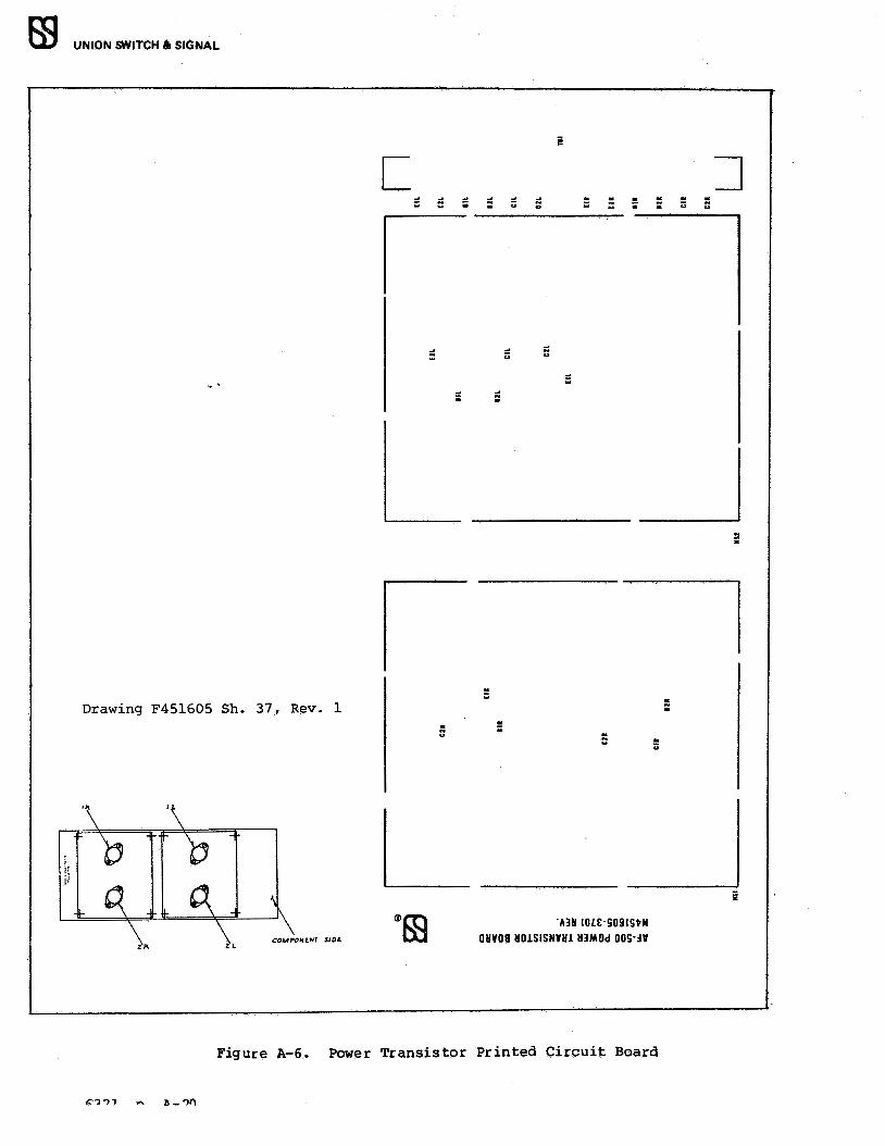
m UNION SWITCH & SIGNAL
Drawing F451605 Sh. 37, Rev. 1
COMPONLHT $101.
L --
I -.. w
. N ..
L
-N -
-N --..
.. ..
-.. ..
-w . . .
N . -;:; . ..
_ _J
. - . N w
·,ml IOH:-!i091!itN OIIV08 IIOl.SISNYll! 113MOd OO!i·.:IY
. ..
Figure A-6. Power Transistor Printed Circuit Board

UNION.SWITCH & SIGNAL W
Receive Only Junction Box (N451102-2001) (See Figure A-7)
Item Quantity Description Part Number
5 1 BOX N451107-4701 10 2 Ventilator N070109 15 4 Nut, 112•, Lock J048414 20 2 Gasket Assembly, 112· !PS J470033 25 4 Terminal Board J077873 30 8 Screw, 10-32 x 1/2 J052355 35 48 Nut, 14-24, Hex, Brass J480300 40 96 Nut, 14-24, Hex, Brass J480301 45 144 washer, 17/64• x 9/16 9 J047818 50 2 cover Plate M451107-4801 55 8 Screw, 1/4-20 x 3/4, Hex J050016 60 8 washer, 1/4, St!. Lock J047775 65 2 Gasket M451107-2705 70 4 Cable Grip, DHF-6 J712019 75 ~. 1 Padlock/Chain J562066 80 2 washer, #10, Flat, St!. J475077 85 1 Rivet, 3/16• x 1/2" J049550 90 1 Junction Box PCB N451605-9401
1 Resistor, 3 ohm, SW (Part of Item 90) J735519-0179 2 Capacitor, 50 MFD., 50V (Part of Item 90) J709145-0402 1 PCB (Part of Item 90) J776617-0035
100 1 Tag M451559-9801 105 1 Tag M451559-9802 110 1 Tag M451559-9803 115 1 Tag M451559-9804 120 .l Tag M451559-9805 125 1 Tag M451559-9806 130 1 Tag M451559-9807 135 1 Tag M451559-9808 140 2 Connector M047290 145 1 Mounting Plate M451107-4901 150 2 Shock Mount J751329 155 1 Receive Only PCB N451605-7301 160 2 Screw, 8-32 x 1, Rd. Hd. J052604 165 6 washer, #8 Flat, Pl. St!. J047745 170 2 washer, #8 Lock J047681 175 8 Screw, 4-40 x 5/16, Rdh. J525057 180 8 washer, #4 Lock J047765 185 8 Nut, 4-40, Hex, St!. J480006 190 2 Nut, 8-32, Hex, Stl. J048166
~
6321, P• A-21

UNION SWITCH & SIGNAL
.... ,.,
~ ID c( + ~ '° N
~
1: ID c(
1: +' ID ,... ..,
N
~ + ID c( + ID a, .... ..,
I
~ + + 81 ~ + ID ....
~ •0• ~ ID . II') !
-le> ~
c( -$-0-$- !!! ~ -
~ ~ + + ID
~ I I
c(
I: +I ID
~)(
:! !2
~ CD
I +, :!
c( + + ID \!! !!?
~
F451102-20 Rev. 2
Figure A-7. Receive Only Junction Box
6321, p. A-22

Reference Designation
Tl TB!
Receiver Only PCB (N451605-7301) (See Figure A-8)
Quantity Description
1 Inductor 1 Terminal Board 2 Screw, 4-40 x 3/4 2 washer, #4 Lock 4 washer, i4 Flat 2 Nut, 4-40, Hex
U~ION SWITCH & SIGNAL W
Part Number
N451030-4803 J725710-0020 J525088 J047765 J047640 J480006
6321, p. A-23

m UNION SWITCH & SIGNAL
Pl
P2
SS
S7
S6
SS
S4
S3
S2
SI
0451605-73 Rev. 0
6321, p. A-24
Tl
Figure A-8. Receive Only PCB
> w 0::::
>-__JQ zrr, Or--
I >LO uo 0:::: ~ I -
COLO u <;:j
o...z @)