unisonic technologies co., · pdf filelr9103 cmos ic unisonic technologies co., ltd 2 of 5 ...
TRANSCRIPT
UNISONIC TECHNOLOGIES CO., LTD
LR9103 CMOS IC
www.unisonic.com.tw 1 of 5 Copyright © 2017 Unisonic Technologies Co., Ltd QW-R102-062.J
LOW NOISE 150mA LDO REGULATOR
DESCRIPTION
The UTC LR9103 is a typical LDO (linear regulator) with the features of high output voltage accuracy, low supply current, low ON-resistance, and high ripple rejection.
During operation of the UTC LR9103, the dropout voltage is very low and the response of line transient and load transient are very well.
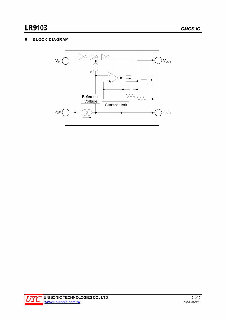
Internally, there’re many functions of UTC LR9103 which can be seen in the block figure. There are a voltage reference unit, an error amplifier, resistor-net for voltage setting, a current limit circuit, and a chip enable circuit in each UTC LR9103.
The UTC LR9103 can be used as an ideal of the power supply for hand-held communication equipment, such as: power source for portable communication equipment, power source for electrical appliances, for example, cameras, VCRs and camcorders and power source for battery-powered equipment.
FEATURES
* Ultra Supply Current: 36µA (Typ.) * Standby Mode: 0.1µA (Typ.) * Very Low Dropout Voltage: 0.13V (Typ.) @ IOUT =150mA, VOUT =2.85V * Ripple Rejection: 75dB (Typ.) @ f=1kHz,VOUT=2.85V * Temperature-Drift Coefficient of Output Voltage:
±50ppm/°C (Typ.)
* Well Line Regulation: 0.02%/ V (Typ.) *Output Voltage Accuracy: ±1.0%
* Internal Fold Back Protection Circuit: 50mA (Typ.) (Current at short mode) *CIN=COUT=1.0µF or more (Ceramic capacitors) are recommended to be used with this IC
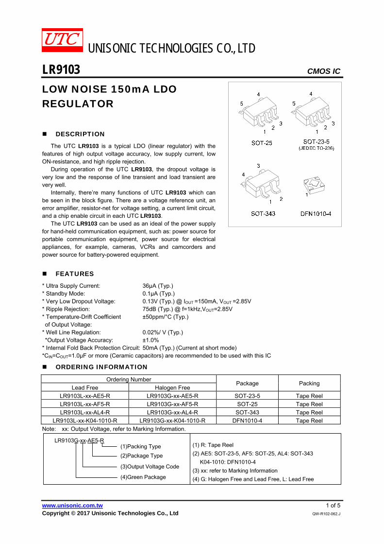
ORDERING INFORMATION
Ordering Number
Lead Free Halogen Free Package Packing
LR9103L-xx-AE5-R LR9103G-xx-AE5-R SOT-23-5 Tape Reel
LR9103L-xx-AF5-R LR9103G-xx-AF5-R SOT-25 Tape Reel
LR9103L-xx-AL4-R LR9103G-xx-AL4-R SOT-343 Tape Reel
LR9103L-xx-K04-1010-R LR9103G-xx-K04-1010-R DFN1010-4 Tape Reel
Note: xx: Output Voltage, refer to Marking Information.
(1) R: Tape Reel
(2) AE5: SOT-23-5, AF5: SOT-25, AL4: SOT-343
K04-1010: DFN1010-4
(3) xx: refer to Marking Information
(4) G: Halogen Free and Lead Free, L: Lead Free
LR9103G-xx-AE5-R(1)Packing Type
(2)Package Type
(3)Output Voltage Code
(4)Green Package
LR9103 CMOS IC
UNISONIC TECHNOLOGIES CO., LTD 2 of 5 www.unisonic.com.tw QW-R102-062.J
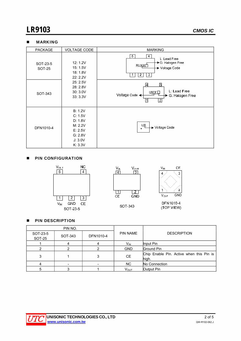
MARKING
PACKAGE VOLTAGE CODE MARKING
SOT-23-5 SOT-25
SOT-343
12: 1.2V 15: 1.5V 18: 1.8V 22: 2.2V 25: 2.5V 28: 2.8V 30: 3.0V 33: 3.3V
DFN1010-4
B: 1.2V C: 1.5V D: 1.8V M: 2.2V E: 2.5V G: 2.8V J: 3.0V K: 3.3V
PIN CONFIGURATION
PIN DESCRIPTION
PIN NO.
SOT-23-5 SOT-25
SOT-343 DFN1010-4 PIN NAME DESCRIPTION
1 4 4 VIN Input Pin
2 2 2 GND Ground Pin
3 1 3 CE Chip Enable Pin. Active when this Pin is high.
4 - - NC No Connection
5 3 1 VOUT Output Pin
LR9103 CMOS IC
UNISONIC TECHNOLOGIES CO., LTD 3 of 5 www.unisonic.com.tw QW-R102-062.J
BLOCK DIAGRAM
+
-
Current Limit
Reference Voltage
GND
VOUT
CE
VIN
LR9103 CMOS IC
UNISONIC TECHNOLOGIES CO., LTD 4 of 5 www.unisonic.com.tw QW-R102-062.J
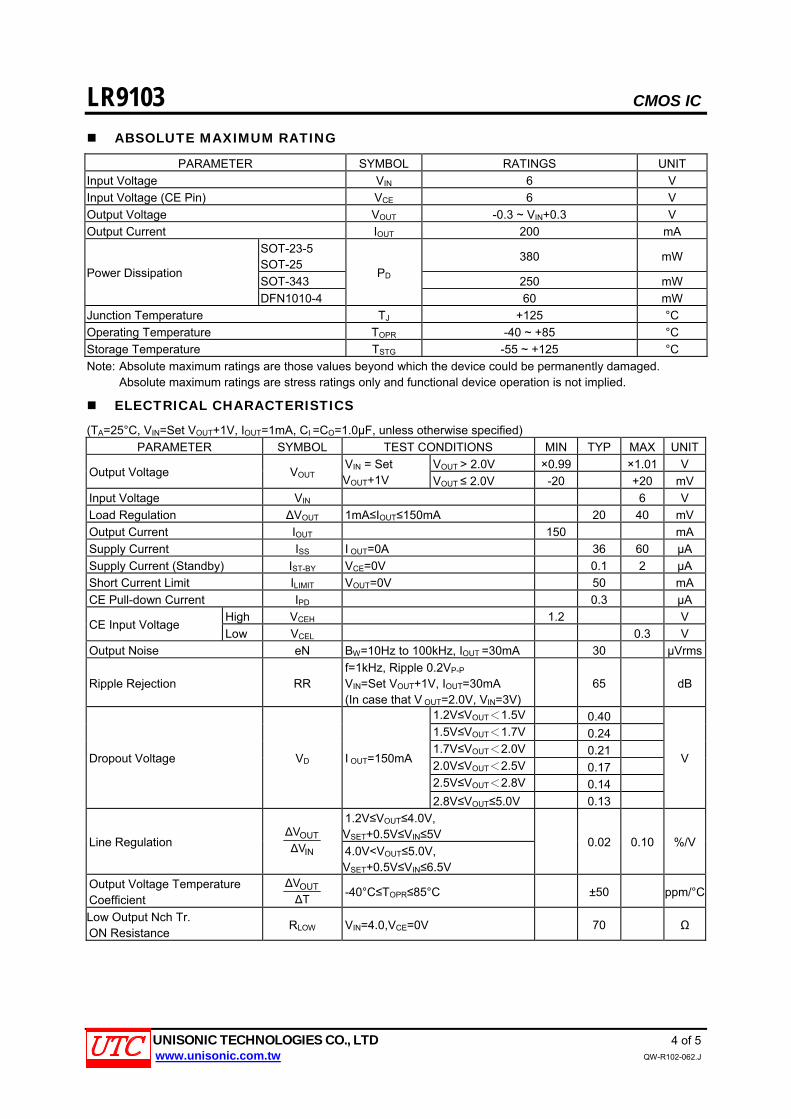
ABSOLUTE MAXIMUM RATING
PARAMETER SYMBOL RATINGS UNIT
Input Voltage VIN 6 V
Input Voltage (CE Pin) VCE 6 V
Output Voltage VOUT -0.3 ~ VIN+0.3 V
Output Current IOUT 200 mA
SOT-23-5 SOT-25
380 mW
SOT-343 250 mW Power Dissipation
DFN1010-4
PD
60 mW
Junction Temperature TJ +125 °С
Operating Temperature TOPR -40 ~ +85 °С
Storage Temperature TSTG -55 ~ +125 °С
Note: Absolute maximum ratings are those values beyond which the device could be permanently damaged. Absolute maximum ratings are stress ratings only and functional device operation is not implied.
ELECTRICAL CHARACTERISTICS
(TA=25°С, VIN=Set VOUT+1V, IOUT=1mA, CI =CO=1.0µF, unless otherwise specified)
PARAMETER SYMBOL TEST CONDITIONS MIN TYP MAX UNIT
VOUT > 2.0V ×0.99 ×1.01 V Output Voltage VOUT
VIN = Set VOUT+1V VOUT ≤ 2.0V -20 +20 mV
Input Voltage VIN 6 V
Load Regulation ∆VOUT 1mA≤IOUT≤150mA 20 40 mV
Output Current IOUT 150 mA
Supply Current ISS I OUT=0A 36 60 µA
Supply Current (Standby) IST-BY VCE=0V 0.1 2 µA
Short Current Limit ILIMIT VOUT=0V 50 mA
CE Pull-down Current IPD 0.3 µA
High VCEH 1.2 V CE Input Voltage
Low VCEL 0.3 V
Output Noise eN BW=10Hz to 100kHz, IOUT =30mA 30 µVrms
Ripple Rejection RR f=1kHz, Ripple 0.2VP-P VIN=Set VOUT+1V, IOUT=30mA (In case that V OUT=2.0V, VIN=3V)
65 dB
1.2V≤VOUT<1.5V 0.40 1.5V≤VOUT<1.7V 0.24 1.7V≤VOUT<2.0V 0.21 2.0V≤VOUT<2.5V 0.17 2.5V≤VOUT<2.8V 0.14
Dropout Voltage VD I OUT=150mA
2.8V≤VOUT≤5.0V 0.13
V
1.2V≤VOUT≤4.0V, VSET+0.5V≤VIN≤5V
Line Regulation IN
OUT
∆V
∆V
4.0V<VOUT≤5.0V, VSET+0.5V≤VIN≤6.5V
0.02 0.10 %/V
Output Voltage Temperature Coefficient ∆T
∆VOUT -40°С≤TOPR≤85°С ±50 ppm/°С
Low Output Nch Tr. ON Resistance
RLOW VIN=4.0,VCE=0V 70 Ω
LR9103 CMOS IC
UNISONIC TECHNOLOGIES CO., LTD 5 of 5 www.unisonic.com.tw QW-R102-062.J
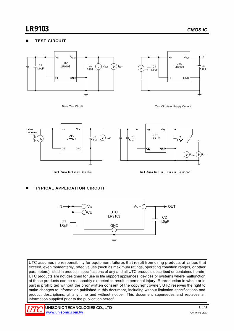
TEST CIRCUIT
C11.0µF
VIN VOUT
GNDCE
UTC LR9103 C2
1.0µFVOUTV IOUT
Basic Test Circuit Test Circuit for Supply Current
C11.0µF
VIN VOUT
GNDCE
UTC LR9103
AC2
1.0µFISS
TYPICAL APPLICATION CIRCUIT
UTCLR9103
GND
OUT
CE
VININ
C21.0μF
VOUT
C11.0μF
UTC assumes no responsibility for equipment failures that result from using products at values that exceed, even momentarily, rated values (such as maximum ratings, operating condition ranges, or other parameters) listed in products specifications of any and all UTC products described or contained herein. UTC products are not designed for use in life support appliances, devices or systems where malfunction of these products can be reasonably expected to result in personal injury. Reproduction in whole or in part is prohibited without the prior written consent of the copyright owner. UTC reserves the right to make changes to information published in this document, including without limitation specifications and product descriptions, at any time and without notice. This document supersedes and replaces all information supplied prior to the publication hereof.