unit-2 part-1: basic computer organization and design unit-ii part-1.pdf · the instruction read...
TRANSCRIPT

Pag
e1
Unit-2
Part-1: BASIC COMPUTER ORGANIZATION AND DESIGN
CONTENTS:
Instruction Codes
Computer Registers
Computer Instructions
Timing And Control
Instruction Cycle
Register – Reference Instructions
Memory – Reference Instructions
Input – Output And Interrupt
1. Instruction Codes:
The organization of the computer is defined by its internal registers, the timing and control structure, and the set of instructions that it uses.
Internal organization of a computer is defined by the sequence of micro-operations it performs on
data stored in its registers.
Computer can be instructed about the specific sequence of operations it must perform.
User controls this process by means of a Program.
Program: set of instructions that specify the operations, operands, and the sequence by which
processing has to occur.
Instruction: a binary code that specifies a sequence of micro-operations for the computer. The computer reads each instruction from memory and places it in a control register. The control
then interprets the binary code of the instruction and proceeds to execute it by issuing a sequence of micro-operations. – Instruction Cycle
Instruction Code: group of bits that instruct the computer to perform specific operation.
Instruction code is usually divided into two parts: Opcode and address(operand)
Operation Code (opcode):
group of bits that define the operation
Eg: add, subtract, multiply, shift, complement.
No. of bits required for opcode depends on no. of operations available in computer.
n bit opcode >= 2n (or less) operations
Address (operand):
specifies the location of operands (registers or memory words)
Memory words are specified by their address
Registers are specified by their k-bit binary code

Pag
e2
k-bit address >= 2k registers
Stored Program Organization:
The ability to store and execute instructions is the most important property of a general-purpose computer. That type of stored program concept is called stored program organization.
The simplest way to organize a computer is to have one processor register and an instruction code format with two parts. The first part specifies the operation to be performed and the second specifies an address.
The below figure shows the stored program organization
Instructions are stored in one section of memory and data in another. For a memory unit with 4096 words we need 12 bits to specify an address since 212 = 4096. If we store each instruction code in one 16-bit memory word, we have available four bits for the
operation code (abbreviated opcode) to specify one out of 16 possible operations, and 12 bits to specify the address of an operand.
Accumulator (AC): Computers that have a single-processor register usually assign to it the name accumulator
and label it AC. The operation is performed with the memory operand and the content of AC.
Addressing of Operand:
Sometimes convenient to use the address bits of an instruction code not as an address but as the actual operand.
When the second part of an instruction code specifies an operand, the instruction is said to have an immediate operand.
When the second part specifies the address of an operand, the instruction is said to have a direct address.
When second part of the instruction designate an address of a memory word in which the address of the operand is found such instruction have indirect address.
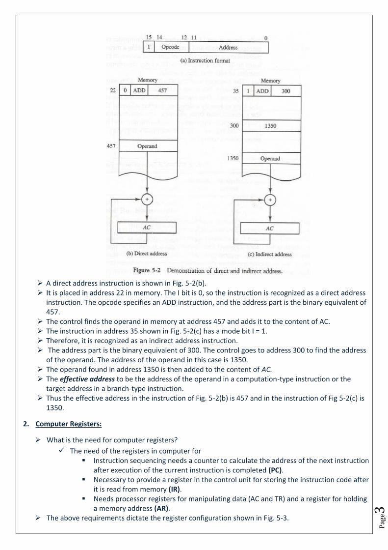
One bit of the instruction code can be used to distinguish between a direct and an indirect address. The instruction code format shown in Fig. 5-2(a). It consists of a 3-bit operation code, a 12-bit
address, and an indirect address mode bit designated by I. The mode bit is 0 for a direct address and 1 for an indirect address.
Pag
e3
A direct address instruction is shown in Fig. 5-2(b). It is placed in address 22 in memory. The I bit is 0, so the instruction is recognized as a direct address
instruction. The opcode specifies an ADD instruction, and the address part is the binary equivalent of 457.
The control finds the operand in memory at address 457 and adds it to the content of AC. The instruction in address 35 shown in Fig. 5-2(c) has a mode bit I = 1. Therefore, it is recognized as an indirect address instruction. The address part is the binary equivalent of 300. The control goes to address 300 to find the address
of the operand. The address of the operand in this case is 1350. The operand found in address 1350 is then added to the content of AC. The effective address to be the address of the operand in a computation-type instruction or the
target address in a branch-type instruction. Thus the effective address in the instruction of Fig. 5-2(b) is 457 and in the instruction of Fig 5-2(c) is
1350.
2. Computer Registers:
What is the need for computer registers?
The need of the registers in computer for Instruction sequencing needs a counter to calculate the address of the next instruction
after execution of the current instruction is completed (PC). Necessary to provide a register in the control unit for storing the instruction code after
it is read from memory (IR). Needs processor registers for manipulating data (AC and TR) and a register for holding
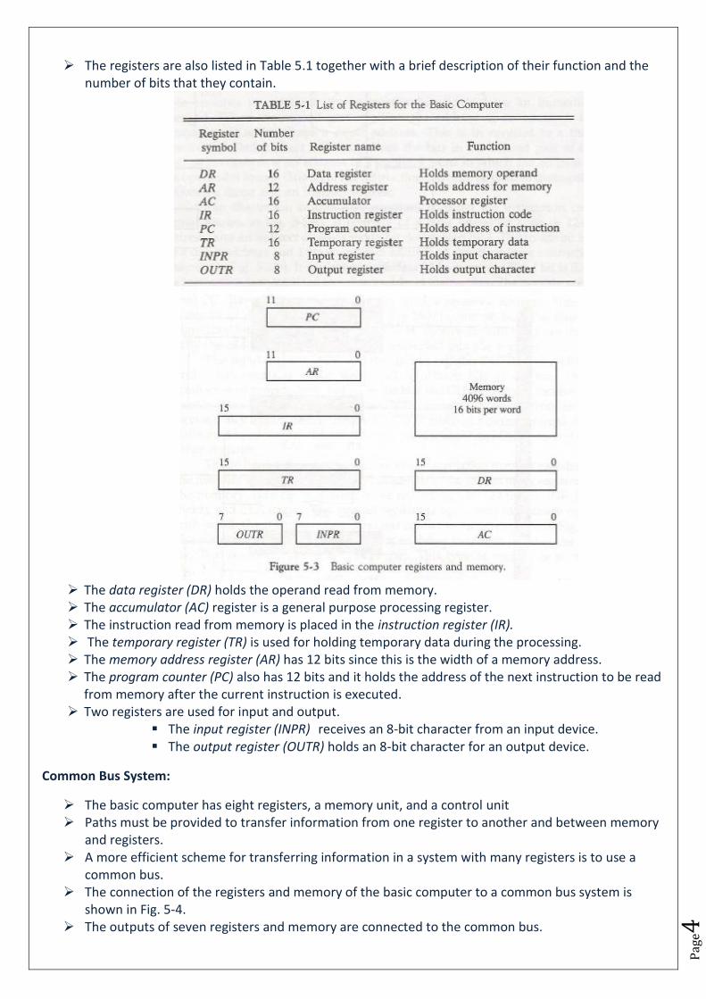
a memory address (AR). The above requirements dictate the register configuration shown in Fig. 5-3.
Pag
e4
The registers are also listed in Table 5.1 together with a brief description of their function and the number of bits that they contain.
The data register (DR) holds the operand read from memory. The accumulator (AC) register is a general purpose processing register. The instruction read from memory is placed in the instruction register (IR). The temporary register (TR) is used for holding temporary data during the processing. The memory address register (AR) has 12 bits since this is the width of a memory address. The program counter (PC) also has 12 bits and it holds the address of the next instruction to be read
from memory after the current instruction is executed. Two registers are used for input and output.
The input register (INPR) receives an 8-bit character from an input device. The output register (OUTR) holds an 8-bit character for an output device.
Common Bus System:
The basic computer has eight registers, a memory unit, and a control unit Paths must be provided to transfer information from one register to another and between memory
and registers. A more efficient scheme for transferring information in a system with many registers is to use a
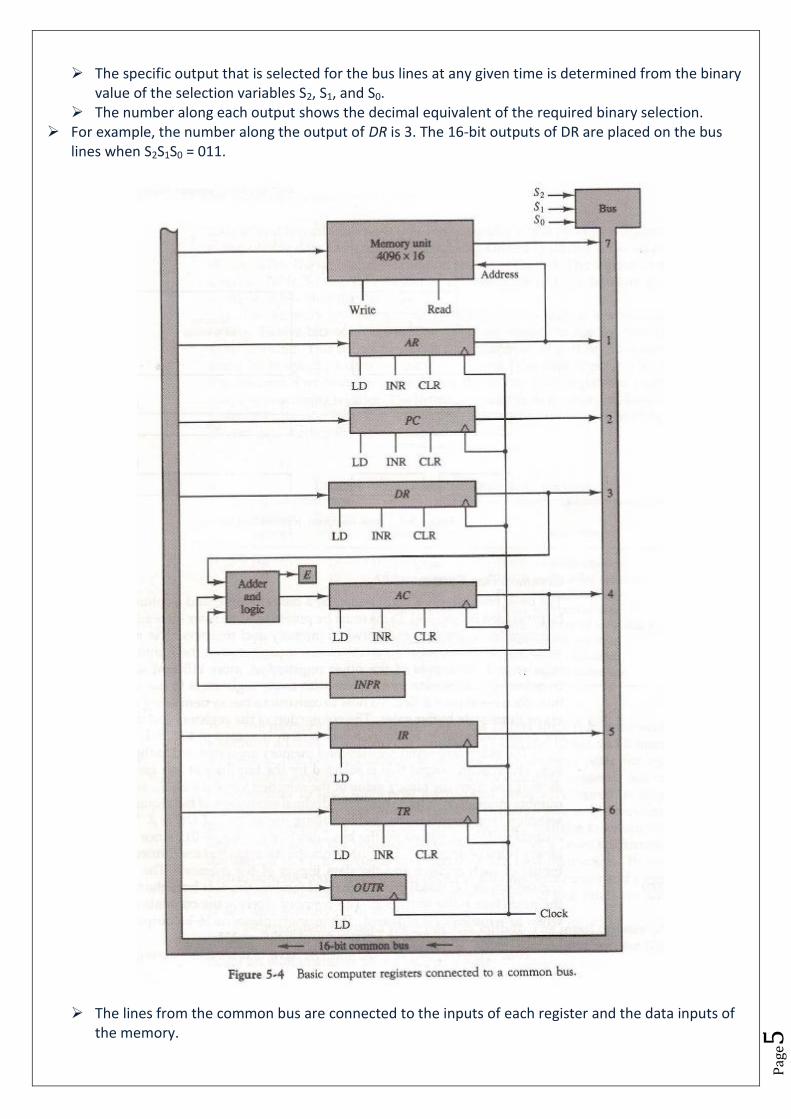
common bus. The connection of the registers and memory of the basic computer to a common bus system is
shown in Fig. 5-4. The outputs of seven registers and memory are connected to the common bus.
Pag
e5
The specific output that is selected for the bus lines at any given time is determined from the binary value of the selection variables S2, S1, and S0.
The number along each output shows the decimal equivalent of the required binary selection. For example, the number along the output of DR is 3. The 16-bit outputs of DR are placed on the bus
lines when S2S1S0 = 011.
The lines from the common bus are connected to the inputs of each register and the data inputs of the memory.
Pag
e6
The particular register whose LD (load) input is enabled receives the data from the bus during the next clock pulse transition.
The memory receives the contents of the bus when its write input is activated. The memory places its 16-bit output onto the bus when the read input is activated and S2S1S0 = 111. Two registers, AR and PC, have 12 bits each since they hold a memory address. When the contents of AR or PC are applied to the 16-bit common bus, the four most significant bits
are set to 0's. When AR or PC receives information from the bus, only the 12 least significant bits are transferred
into the register. The input register INPR and the output register OUTR have 8 bits each. They communicate with the eight least significant bits in the bus. INPR is connected to provide information to the bus but OUTR can only receive information from the
bus. This is because INPR receives a character from an input device which is then transferred to AC. OUTR receives a character from AC and delivers it to an output device. Five registers have three control inputs: LD (load), INR (increment), and CLR (clear). This type of register is equivalent to a binary counter with parallel load and synchronous clear. Two registers have only a LD input. The input data and output data of the memory are connected to the common bus, but the memory
address is connected to AR. Therefore, AR must always be used to specify a memory address. The 16 inputs of AC come from an adder and logic circuit. This circuit has three sets of inputs.
o One set of 16-bit inputs come from the outputs of AC. o Another set of 16-bit inputs come from the data register DR. o The result of an addition is transferred to AC and the end carry-out of the addition is
transferred to flip-flop E (extended AC bit). o A third set of 8-bit inputs come from the input register INPR.
The content of any register can be applied onto the bus and an operation can be performed in the adder and logic circuit during the same clock cycle.
For example, the two microoperations DRAC and AC DR can be executed at the same time. This can be done by placing the content of AC on the bus (with S2S1S0 = 100), enabling the LD (load)
input of DR, transferring the content of DR through the adder and logic circuit into AC, and enabling the LD (load) input of AC, all during the same clock cycle.
3. Computer Instructions:
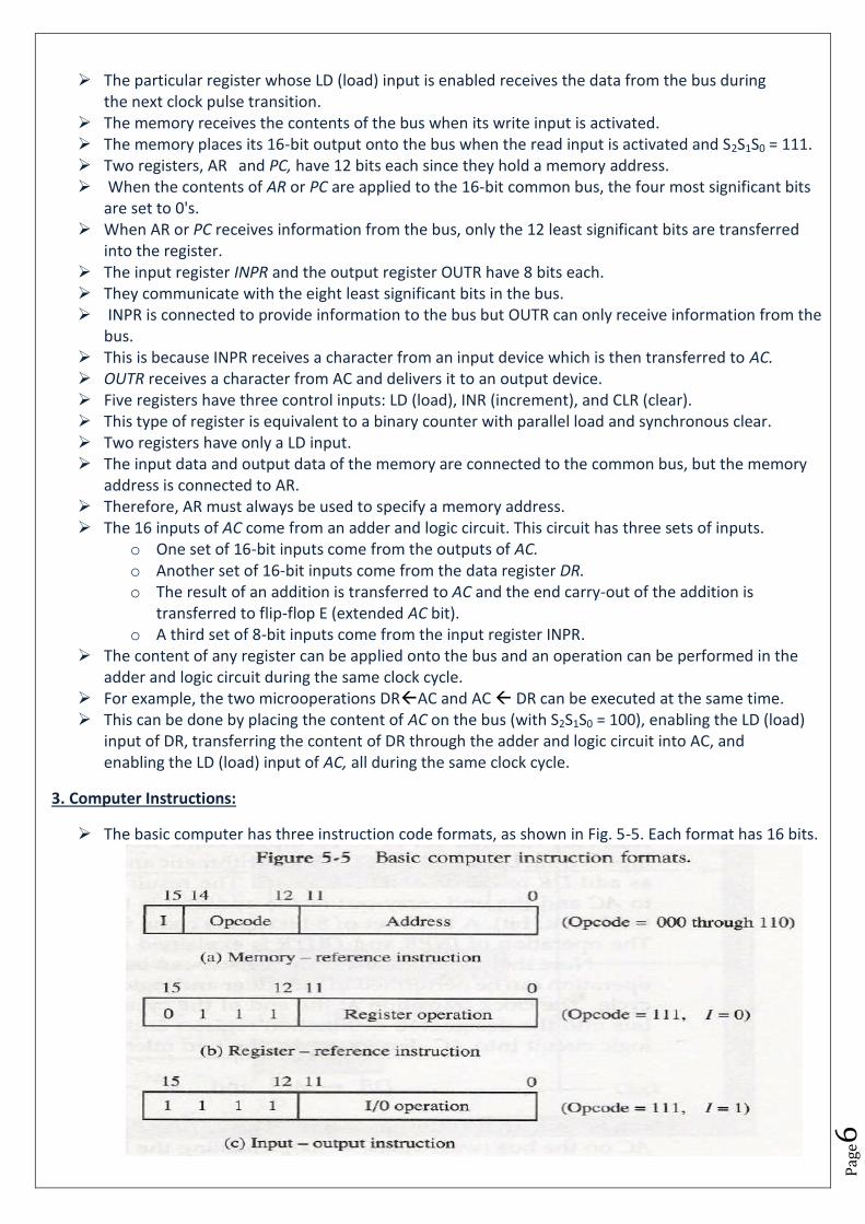
The basic computer has three instruction code formats, as shown in Fig. 5-5. Each format has 16 bits.

Pag
e7
The operation code (opcode) part of the instruction contains three bits and the meaning of the remaining 13 bits depends on the operation code encountered.
A memory-reference instruction uses 12 bits to specify an address and one bit to specify the addressing mode I.
I is equal to 0 for direct address and to 1 for indirect address. The register-reference instructions are recognized by the operation code 1.11 with a 0 in the leftmost
bit (bit 15) of the instruction. A register-reference instruction specifies an operation on the AC register. So an operand from
memory is not needed. Therefore, the other 12 bits are used to specify the operation to be executed. An input—output instruction does not need a reference to memory and is recognized by the
operation code 111 with a 1 in the leftmost bit of the instruction. The remaining 12 bits are used to specify the type of input—output operation. The instructions for the computer are listed in Table 5-2.

Pag
e8
The symbol designation is a three-letter word and represents an abbreviation intended for programmers and users.
The hexadecimal code is equal to the equivalent hexadecimal number of the binary code used for the instruction.
Instruction Set Completeness:
A computer should have a set of instructions so that the user can construct machine language programs to evaluate any function.
The set of instructions are said to be complete if the computer includes a sufficient number of instructions in each of the following categories:
o Arithmetic, logical, and shift instructions o Data Instructions (for moving information to and from memory and processor registers) o Program control or Brach o Input and output instructions
There is one arithmetic instruction, ADD, and two related instructions, complement AC(CMA) and increment AC(INC). With these three instructions we can add and subtract binary numbers when negative numbers are in signed-2's complement representation.
The circulate instructions, CIR and CIL; can be used for arithmetic shifts as well as any other type of shifts desired.
There are three logic operations: AND, complement AC (CMA), and clear AC(CLA). The AND and complement provide a NAND operation.
Moving information from memory to AC is accomplished with the load AC (LDA) instruction. Storing information from AC into memory is done with the store AC (STA) instruction.
The branch instructions BUN, BSA, and ISZ, together with the four skip instructions, provide capabilities for program control and checking of status conditions.
The input (INP} and output (OUT) instructions cause information to be transferred between the computer and external devices.
4. Timing and Control:
The timing for all registers in the basic computer is controlled by a master clock generator. The clock pulses are applied to all flip-flops and registers in the system, including the flip-flops and
registers in the control unit. The clock pulses do not change the state of a register unless the register is enabled by a control
signal. The control signals are generated in the control unit and provide control inputs for the multiplexers
in the common bus, control inputs in processor registers, and microoperations for the accumulator. There are two major types of control organization:
o Hardwired control o Microprogrammed control
The differences between hardwired and microprogrammed control are
Hardwired control Microprogrammed control
The control logic is implemented with gates, flip-flops, decoders, and other digital circuits.
The control information is stored in a control memory. The control memory is programmed to initiate the required sequence of microoperations.
The advantage that it can be optimized to produce a fast mode of operation.
Compared with the hardwired control operation is slow.
Requires changes in the wiring among the various components if the design has to be modified or changed.
Required changes or modifications can be done by updating the microprogram in control memory.

Pag
e9
The block diagram of the hardwired control unit is shown in Fig. 5-6. It consists of two decoders, a sequence counter, and a number of control logic gates. An instruction read from memory is placed in the instruction register (IR). It is divided into three
parts: The I bit, the operation code, and bits 0 through 11. The operation code in bits 12 through 14 are decoded with a 3 x 8 decoder. The eight outputs of
the decoder are designated by the symbols D0 through D7. Bit 15 of the instruction is transferred to a flip-flop designated by the symbol I. Bits 0 through 11 are applied to the control logic gates. The 4-bit sequence counter can count in binary from 0 through 15.
The outputs of the counter are decoded into 16 timing signals T0 through T15. The sequence counter SC can be incremented or cleared synchronously. The counter is incremented to provide the sequence of timing signals out of the 4 x 16 decoder. As an example, consider the case where SC is incremented to provide timing signals T0, T1, T2, T3 and
T4 in sequence. At time T4, SC is cleared to 0 if decoder output D3 is active. This is expressed symbolically by the statement
D3T4: SC0
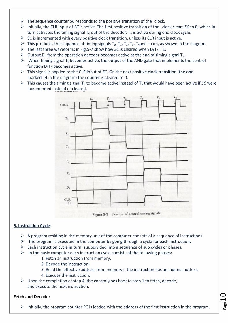
The timing diagram of Fig. 5-7 shows the time relationship of the control signals.
Pag
e10
The sequence counter SC responds to the positive transition of the clock. Initially, the CLR input of SC is active. The first positive transition of the clock clears SC to 0, which in
turn activates the timing signal T0 out of the decoder. T0 is active during one clock cycle. SC is incremented with every positive clock transition, unless its CLR input is active. This produces the sequence of timing signals T0, T1, T2, T3, T4and so on, as shown in the diagram. The last three waveforms in Fig.5-7 show how SC is cleared when D3T4 = 1. Output D3 from the operation decoder becomes active at the end of timing signal T2. When timing signal T4 becomes active, the output of the AND gate that implements the control
function D3T4 becomes active. This signal is applied to the CLR input of SC. On the next positive clock transition (the one
marked T4 in the diagram) the counter is cleared to 0. This causes the timing signal T0 to become active instead of T5 that would have been active if SC were
incremented instead of cleared.
5. Instruction Cycle:
A program residing in the memory unit of the computer consists of a sequence of instructions. The program is executed in the computer by going through a cycle for each instruction. Each instruction cycle in turn is subdivided into a sequence of sub cycles or phases. In the basic computer each instruction cycle consists of the following phases:
1. Fetch an instruction from memory. 2. Decode the instruction. 3. Read the effective address from memory if the instruction has an indirect address. 4. Execute the instruction.
Upon the completion of step 4, the control goes back to step 1 to fetch, decode, and execute the next instruction.
Fetch and Decode:
Initially, the program counter PC is loaded with the address of the first instruction in the program.

Pag
e11
The sequence counter SC is cleared to 0, providing a decoded timing signal T0. The microoperations for the fetch and decode phases can be specified by the following register
transfer statements.
Figure 5-8 shows how the first two register transfer statements are implemented in the bus system. To provide the data path for the transfer of PC to AR we must apply timing signal T0 to achieve the
following connection: o Place the content of PC onto the bus by making the bus selection inputs S2, S1, S0 equal to 010. o Transfer the content of the bus to AR by enabling the LD input of AR.
In order to implement the second statement it is necessary to use timing signal T1 to provide the following connections in the bus system.
o Enable the read input of memory. o Place the content of memory onto the bus by making S2S1S0=111. o Transfer the content of the bus to IR by enabling the LD input of IR. o Increment PC by enabling the INR input of PC.
Multiple input OR gates are included in the diagram because there are other control functions that will initiate similar operations.
Determine the Type of Instruction:
The timing signal that is active after the decoding is T3. During time T3, the control unit determine the type of instruction that was read from the memory. The flowchart of fig.5-9 shows the initial configurations for the instruction cycle and also how the
control determines the instruction cycle type after the decoding. Decoder output D7 is equal to 1 if the operation code is equal to binary 111. If D7=1, the instruction must be a register-reference or input-output type. If D7 = 0, the operation code must be one of the other seven values 000 through 110, specifying a
memory-reference instruction.

Pag
e12
Control then inspects the value of the first bit of the instruction, which is now available in flip-flop I. If D7 = 0 and I = 1, indicates a memory-reference instruction with an indirect address. So it is then
necessary to read the effective address from memory. If D7 = 0 and I = 0, indicates a memory-reference instruction with a direct address. If D7 = 1 and I = 0, indicates a register-reference instruction. If D7 = 01and I = 1, indicates an input-output instruction. The three instruction types are subdivided into four separate paths. The selected operation is activated with the clock transition associated with timing signal T3. This can be symbolized as follows:

Pag
e13
Register-Reference Instructions:
Register-reference instructions are recognized by the control when D7 = 1 and I=0. These instructions use bits 0 through 11 of the instruction code to specify one of 12 instructions. These 12 bits are available in IR (0-11). The control functions and microoperations for the register-reference instructions are listed in Table
5-3. These instructions are executed with the clock transition associated with timing variable T3. Control function needs the Boolean relation D7I’T3, which we designate for convenience by the
symbol r. By assigning the symbol Bi to bit i of IR, all control functions can be simply denoted by rBi.
For example, the instruction CLA has the hexadecimal code 7800, which gives the binary equivalent
0111 1000 0000 0000. The first bit is a zero and is equivalent to I’. The next three bits constitute the operation code and are recognized from decoder output D7. Bit 11 in IR is 1 and is recognized from B11. The control function that initiates the microoperation for
this instruction is D7I’T3 B11 = rB11. The execution of a register-reference instruction is completed at time T3. The sequence counter SC is cleared to 0 and the control goes back to fetch the next instruction with
timing signal T0. The first seven register-reference instructions perform clear, complement, circular shift, and
increment microoperations on the AC or E registers. The next four instructions cause a skip of the next instruction in sequence when
a stated condition is satisfied. The skipping of the instruction is achieved by incrementing PC once again.
The condition control statements must be recognized as part of the control conditions. The AC is positive when the sign bit in AC(15) = 0; it is negative when AC(15) = 1. The content of AC is
zero (AC = 0) if all the flip-flops of the register are zero. The HLT instruction clears a start-stop flip-flop S and stops the sequence counter from counting.
6. Memory-Reference Instructions:
Table 5-4 lists the seven memory-reference instructions. The decoded output Di for i = 0, 1, 2, 3, 4, 5, and 6 from the operation decoder that belongs to each
instruction is included in the table. The effective address of the instruction is in the address register AR and was placed there during
timing signal T2 when I= 0, or during timing signal T3 when I = 1. The execution of the memory-reference instructions starts with timing signal T4.

Pag
e14
The symbolic description of each instruction is specified in the table in terms of register transfer notation.
AND to AC:
This is an instruction that performs the AND logic operation on pairs of bits in AC and the memory word specified by the effective address.
The result of the operation is transferred to AC. The microoperations that execute this instruction are:
ADD to AC:
This instruction adds the content of the memory word specified by the effective address to the value of AC.
The sum is transferred into AC and the output carry Cout is transferred to the E (extended accumulator) flip-flop.
The microoperations needed to execute this instruction are
LDA: Load to AC
This instruction transfers the memory word specified by the effective address to AC. The microoperations needed to execute this instruction are
STA: Store AC
This instruction stores the content of AC into the memory word specified by the effective address.

Pag
e15
Since the output of AC is applied to the bus and the data input of memory is connected to the bus, we can execute this instruction with one microoperation.
BUN: Branch Unconditionally
This instruction transfers the program to the instruction specified by the effective address. The BUN instruction allows the programmer to specify an instruction out of sequence and we say
that the program branches (or jumps) unconditionally. The instruction is executed with one microoperation:
BSA: Branch and Save Return Address
This instruction is useful for branching to a portion of the program called a subroutine or procedure. When executed, the BSA instruction stores the address of the next instruction in sequence (which is
available in PC) into a memory location specified by the effective address. The effective address plus one is then transferred to PC to serve as the address of the first
instruction in the subroutine. This operation was specified with the following register transfer:
A numerical example that demonstrates how this instruction is used with a subroutine is shown in
Fig. 5-10.
The BSA instruction is assumed to be in memory at address 20. The I bit is 0 and the address part of the instruction has the binary equivalent of 135. After the fetch and decode phases, PC contains 21, which is the address of the next instruction in the
program (referred to as the return address). AR holds the effective address 135. This is shown in part (a) of the figure. The BSA instruction performs the following numerical operation:
The result of this operation is shown in part (b) of the figure. The return address21 is stored in memory location 135 and control continues with the subroutine
program starting from address 136. The return to the original program (at address 21) is accomplished by means of an indirect BUN
instruction placed at the end of the subroutine.

Pag
e16
When this instruction is executed, control goes to the indirect phase to read the effective address at location 135, where it finds the previously saved address 21.
When the BUN instruction is executed, the effective address 21 is transferred to PC. The next instruction cycle finds PC with the value 21, so control continues to execute the instruction
at the return address. The BSA instruction must be executed with a sequence of two microoperations:
ISZ: Increment and Skip if Zero
This instruction increment the word specified by the effective address, and if the incremented value is equal to 0, PC is incremented by 1 to skip the next instruction in the program.
Since it is not possible to increment a word inside the memory, it is necessary to read the word into DR, increment DR, and store the word back into memory.
This is done with the following sequence of microoperations:
Control Flowchart:
A flowchart showing all microoperations for the execution of the seven memory-reference instructions is shown in Fig. 5.11.
Pag
e17
7. Input-Output and Interrupt:
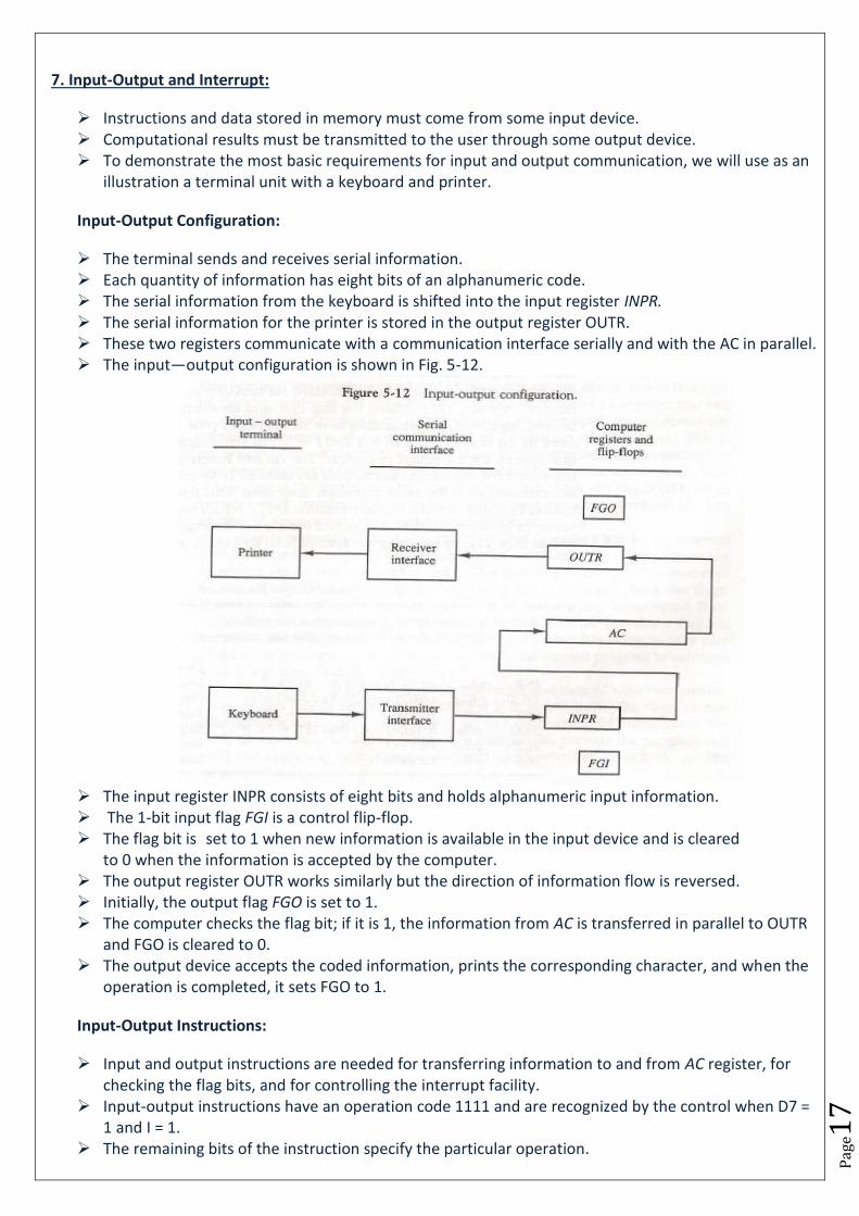
Instructions and data stored in memory must come from some input device. Computational results must be transmitted to the user through some output device. To demonstrate the most basic requirements for input and output communication, we will use as an
illustration a terminal unit with a keyboard and printer.
Input-Output Configuration:
The terminal sends and receives serial information. Each quantity of information has eight bits of an alphanumeric code. The serial information from the keyboard is shifted into the input register INPR. The serial information for the printer is stored in the output register OUTR. These two registers communicate with a communication interface serially and with the AC in parallel. The input—output configuration is shown in Fig. 5-12.
The input register INPR consists of eight bits and holds alphanumeric input information. The 1-bit input flag FGI is a control flip-flop. The flag bit is set to 1 when new information is available in the input device and is cleared
to 0 when the information is accepted by the computer. The output register OUTR works similarly but the direction of information flow is reversed. Initially, the output flag FGO is set to 1. The computer checks the flag bit; if it is 1, the information from AC is transferred in parallel to OUTR
and FGO is cleared to 0. The output device accepts the coded information, prints the corresponding character, and when the
operation is completed, it sets FGO to 1.
Input-Output Instructions:
Input and output instructions are needed for transferring information to and from AC register, for checking the flag bits, and for controlling the interrupt facility.
Input-output instructions have an operation code 1111 and are recognized by the control when D7 = 1 and I = 1.
The remaining bits of the instruction specify the particular operation.

Pag
e18
The control functions and microoperations for the input-output instructions are listed in Table 5-5.
These instructions are executed with the clock transition associated with timing signal T3. Each control function needs a Boolean relation D7IT3, which we designate for convenience by the
symbol p. The control function is distinguished by one of the bits in IR (6-11). By assigning the symbol Bi to bit i of IR, all control functions can be denoted by pBi for i = 6 though
11. The sequence counter SC is cleared to 0 when p = D7IT3 = 1. The last two instructions set and clear an interrupt enable flip-flop IEN.
Program Interrupt:
The computer keeps checking the flag bit, and when it finds it set, it initiates an information transfer. The difference of information flow rate between the computer and that of the input—output device
makes this type of transfer inefficient. An alternative to the programmed controlled procedure is to let the external device inform the
computer when it is ready for the transfer. In the meantime the computer can be busy with other tasks. This type of transfer uses the interrupt
facility. While the computer is running a program, it does not check the flags. When a flag is set, the computer is momentarily interrupted from the current program. The computer deviates momentarily from what it is doing to perform of the input or output transfer. It then returns to the current program to continue what it was doing before the interrupt. The interrupt enable flip-flop IEN can be set and cleared with two instructions.
o When IEN is cleared to 0 (with the IOF instruction), the flags cannot interrupt the computer. o When IEN is set to (with the ION instruction), the computer can be interrupted.
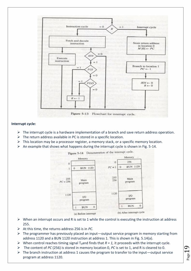
The way that the interrupt is handled by the computer can be explained by means of the flowchart of Fig. 5-13.
An interrupt flip-flop R is included in the computer. When R = 0, the computer goes through an instruction cycle.
During the execute phase of the instruction cycle IEN is checked by the control. If it is 0, it indicates that the programmer does not want to use the interrupt,so control continues
with the next instruction cycle. If IEN is 1, control checks the flag bits. If both flags are 0, it indicates that neither the input nor the
output registers are ready for transfer of information. In this case, control continues with the next instruction cycle.
If either flag is set to 1 while 1EN = 1, flip-flop R is set to 1. At the end of the execute phase, control checks the value of R, and if it is equal to 1, it goes to an interrupt cycle instead of an instruction cycle.
Pag
e19
Interrupt cycle:
The interrupt cycle is a hardware implementation of a branch and save return address operation. The return address available in PC is stored in a specific location. This location may be a processor register, a memory stack, or a specific memory location. An example that shows what happens during the interrupt cycle is shown in Fig. 5-14.
When an interrupt occurs and R is set to 1 while the control is executing the instruction at address
255. At this time, the returns address 256 is in PC. The programmer has previously placed an input—output service program in memory starting from
address 1120 and a BUN 1120 instruction at address 1. This is shown in Fig. 5.14(a). When control reaches timing signal T0and finds that R = 1, it proceeds with the interrupt cycle. The content of PC (256) is stored in memory location 0, PC is set to 1, and R is cleared to 0. The branch instruction at address 1 causes the program to transfer to the input—output service
program at address 1120.

Pag
e20
This program checks the flags, determines which flag is set, and then transfers the required input or output information.
Once this is done, the instruction ION is executed to set IEN to 1 (to enable further interrupts), and the program returns to the location where it was interrupted.
This is shown in Fig. 5-14(b).