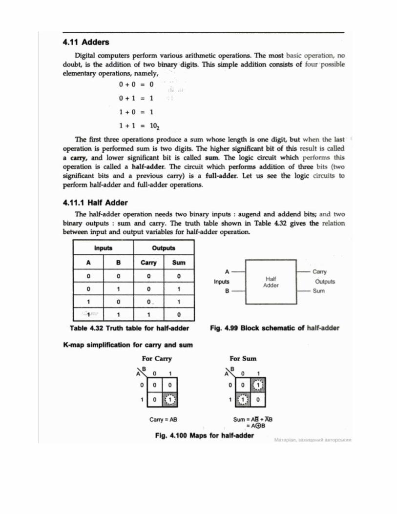
unit v combinational & sequential logic …...structural modeling structural modeling involves...
TRANSCRIPT

UNIT–V
COMBINATIONAL & SEQUENTIAL LOGIC DESIGN: Adders, Subtractors, Decoders, Encoders,
Multiplexers, Demultiplexers, EX-OR gates, Parity Circuits and Comparators. Latches, Flip-Flops and their
VHDL models.
PROGRAM STRUCTURE:
In the text file of a vhdl program, the entity
declaration and architecture definition are separated.
Thus, a VHDL entity is simply a declaration of a module's
inputs and outputs, while a VHDL architecture is a
detailed description of the module's internal behavior or
structure.
VHDL defines many special character strings,
called reserved words or keywords. Our example includes
several-entity, port, is, in, out, end, architecture, begin,
when, else, and not.
User-defined identifiers begin with a letter and
contain letters, digits, and underscores. VHDL's reserved words and identifiers are not case
sensitive.
Besides naming the entity, the purpose of
the entity declaration is to define its
external interface signals or ports in its
port declaration part.
entity-name - A user-selected
identifier to name the entity.
signal-names - A comma-separated list of one or more user-selected identifiers to name
external-interface signals.
mode - One of four reserved words, specifying the signal direction:
in - The signal is an input to the entity.
Out - The signal is an output of the entity. Note that the value of such a signal cannot be
"read" inside the entity's architecture, only by other entities that use it.
buffer - The signal is an output of the entity, and its value can also be read inside the
entity's architecture.
inout - The signal can be used as an input or an output of the entity. This mode is typically
used for three-state input/ output pins on PLDs.

signal-type -A built-in or user-defined signal type. We'll have a lot to say about types in the
next subsection.
The entity's internal operation is specified in its architecture definition.
An architecture's external interface signals (ports) are
inherited from the port-declaration part of its
corresponding entity declaration. An architecture may
also include signals and other declarations that are
local to that architecture.
signal declaration-It gives the same information
about a signal as in a port declaration, except that no
mode is specified:
signal signal-names : signal-type;
Modeling
The Very High Speed Integrated Circuit Hardware Description Language (VHDL) modeling language supports three kinds of
modeling styles: dataflow, structural and behavioral.
Dataflow Modeling
Dataflow modeling can be used to describe combinational circuits. The basic mechanism used is the concurrent assignment.
In a concurrent assignment, a value is assigned to a signal. The syntax of a concurrent assignment statement is: LHS_signal
<= RHS_expression; Where LHS_signal is a destination net of one or more bit, and RHS_expression is an expression consisting
of various operators. The target in the expression can be one of the following: 1. A scalar net (e.g. 1st and 2nd examples
above) 2. A vector net 3. Constant bit-select of a vector 4. Constant part-select of a vector 5. Combinations of any of the
above The assignment operations involve the basic Boolean functions (operators): and, or, xor, nand, nor and xnor. These
are (by default) two inputs and one output. The example below shows dataflow modelling for a two input/one output circuit.
entity AND_gate is
port (a: in std_logic;
b: in std_logic;
c: out std_logic );
architecture AND_gate_dataflow_arch of AND_gate is
begin
c <= a and b;
end AND_gate_dataflow_arch;
Behavioral Modeling
Behavioral modeling is used to describe complex circuits. In VHDL, behavioral modeling is done in the architecture block.
Within the architecture block, processes are defined to model sequential circuits. The mechanisms (statements) for
modeling the behavior of a design are:

-The following process is only used to initialize signals in a design at the beginning of runtime.
Process begin
a <= ‘1’; b <= ‘0’;
…
wait;
end process;
A module may contain an arbitrary number of process statements and these may contain one or more statements within
them. The statements appearing within the process statement body are categorized as procedural statements. The
processes are executed in a concurrent manner (i.e. the order in which they appear in the model does not matter) with
respect to each other whereas the procedural statements are executed in a sequential manner (i.e. the order in which
they appear does matter). A procedural_statement is one of the following:
1. Procedural assignments
2. Conditional statements
3. Case statements
4. Loop statements
5. Wait statements
Here is an example of a 2-to-1 multiplexer model. Note that begin and end statements in this example are redundant. The
code is also truncated for better readability
Structural Modeling
Structural modeling involves connecting instantiated components to define the functionality of a circuit.
Component instantiations can be of other modules and/or device primitives. Using gate-level allow the
construction of simple combinatorial circuits.

DECODERS:
A decoder is a multiple-input, multiple-output logic circuit that
converts coded inputs into coded outputs, where the input and
output codes are different. The input code generally has fewer
bits than the output code, and there is a one-to one mapping from
input code words into output code words. In a one-to-one
mapping, each input code word produces a different output code
word.
The general structure of a decoder circuit is shown in
Figure 1. The enable inputs, if present, must be asserted for
the decoder to perform its normal mapping function.
Otherwise, the decoder maps all input code words into a single,
―disabled,‖ output code word.
The most commonly used output code is a 1-out-of-m code, which contains m bits, where one bit is asserted at
any time. Thus, in a 1-out-of-4 code with active-high outputs, the code words are 0001, 0010, 0100, and 1000. With
active-low outputs, the code words are 1110, 1101, 1011, and 0111.
BINARY DECODERS
The most common decoder circuit is an n-to-2n decoder or
binary decoder. Such a decoder has an n-bit binary input code
and a 1-out-of-2n output code. A binary decoder is used when
you need to activate exactly one of 2n outputs based on an n-
bit input value.
Table 1 is the truth table of a 2-to-4 decoder. The input code
word I1,I0 represents an integer in the range 0–3. The output
code word Y3,Y2,Y1,Y0 has Yi equal to 1 if and only if the
input code word is the binary representation of i and the
enable input EN is 1. If EN is 0, then all of the outputs are 0.
A gate-level circuit for the 2-to-4 decoder is shown in Figure
2 Each AND gate decodes one combination of the input code
word I1,I0.
74x138 3-to-8 Decoder

The 74x138 is a commercially
available MSI 3-to-8 decoder
whose gate-level circuit diagram
and symbol are shown in Figure
7; its truth table is given in Table.
Like the 74x139, the 74x138 has
active-low outputs, and it has
three enable inputs (G1, /G2A,
/G2B), all of which must be
asserted for the selected output to
be asserted.
The logic function of the
74X138 is straightforward—an
output is asserted if and only if the
decoder is enabled and the output
is selected.
Thus, we can easily write logic equations
for an internal output signal such as Y5 in
terms of the internal input signals:
However,
because of the
inversion
bubbles, we have the following relations between internal and external signals:
Therefore, if we’re interested, we can write the following equation for the external output signal Y5_L in terms of
external input signals:
On the surface, this equation doesn’t resemble what you might expect for a decoder, since it is a logical sum
rather than a product. However, if you practice bubble-to-bubble logic design, you don’t have to worry
about this; you just give the output signal an active-low name and remember that it’s active low when you
connect it to other inputs.
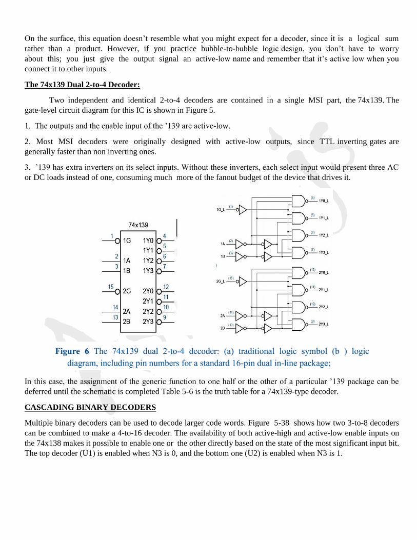
The 74x139 Dual 2-to-4 Decoder:
Two independent and identical 2-to-4 decoders are contained in a single MSI part, the 74x139. The
gate-level circuit diagram for this IC is shown in Figure 5.
1. The outputs and the enable input of the ’139 are active-low.
2. Most MSI decoders were originally designed with active-low outputs, since TTL inverting gates are
generally faster than non inverting ones.
3. ’139 has extra inverters on its select inputs. Without these inverters, each select input would present three AC
or DC loads instead of one, consuming much more of the fanout budget of the device that drives it.
In this case, the assignment of the generic function to one half or the other of a particular ’139 package can be
deferred until the schematic is completed Table 5-6 is the truth table for a 74x139-type decoder.
CASCADING BINARY DECODERS
Multiple binary decoders can be used to decode larger code words. Figure 5-38 shows how two 3-to-8 decoders
can be combined to make a 4-to-16 decoder. The availability of both active-high and active-low enable inputs on
the 74x138 makes it possible to enable one or the other directly based on the state of the most significant input bit.
The top decoder (U1) is enabled when N3 is 0, and the bottom one (U2) is enabled when N3 is 1.

SEVEN-SEGMENT DECODERS
Look at your wrist and you’ll probably see a seven-segment display. This type of display, which normally uses
light-emitting diodes (LEDs) or liquid-crystal display (LCD) elements, is used in watches, calculators, and
instruments to display decimal data.

A seven-segment decoder has 4-bit BCD as its input code and the
"sevenencoder 2n-to-n encoder binary encoder segment code," which is . graphically
depicted in Figure 6-44(b ), as its output code. Table 6-26 is a Verilog program for a
seven-segment decoder with 4-bit BCD input A-D (D being the MSB), active-high
enable input EN, and segment outputs SEGA-SEGG. Note the use of concatenation
and an auxiliary variable SEGS to make the program more readable. The program can
be easily modified for different encodings and features, for example, to add "tails" to
digits 6 and 9 (Exercise 6.47) or to display hexadecimal digits A-F instead of treating
these input combinations as "don't cares"


ENCODERS
A decoder’s output code normally has more bits than its input code. If the device’s output code has fewer bits than
the input code, the device is usually called an encoder. Probably the simplest encoder to build is a 2n-to-n or binary
encoder. As shown in Figure 6-45(a), it has just the opposite function as a binary decoder— its input code is the 1-
out-of-2n code and its output code is n-bit binary.
The corresponding logic circuit is shown in (b). In general, a 2n-to-n encoder can be built from n 2n 1-input OR
gates. Bit i of the input code is connected to OR gate j if bit j in the binary representation of i is 1.
PRIORITY ENCODERS
The 1-out-of-2n coded outputs of an n-bit binary decoder are generally
used to control a set of 2n devices, where at most one device is supposed to be
active at any time. Conversely, consider a system with 2n inputs, each of
which indicates a request for service. This structure is often found in
microprocessor input/output subsystems, where the inputs might be interrupt
requests.

the encoding device produces the number of the highest-priority requestor.
Such a device is called a priority encoder. Input I7 has the highest priority.
Outputs A2–A0 contain the number of the highest-priority asserted input, if any.
The IDLE output is asserted if no inputs are asserted.
In order to write logic equations for the priority encoder’s outputs,
we first define eight intermediate variables H0–H7, such that Hi is 1 if and
only if Ii is the highest priority 1 input: Using these signals, the equations for
the A2–A0 outputs are similar to the ones for a simple binary encoder:
THE 74X148 PRIORITY ENCODER
The 74x148 is a commercially available, MSI 8-input priority encoder it has an
enable input, EI_L, that must be asserted for any of its outputs to be asserted.
The complete truth table is given in Table 5-22. Instead of an IDLE output, the
’148 has a GS_L output that is asserted when the device is enabled and one
or more of the request inputs is asserted. The manufacturer calls this “Group
Select” but it’s easier to remember as “Got Something” The EO_L signal is an
enable output designed to be connected to the EI_L input of another ’148 that
handles lower-priority requests. /EO is asserted if EI_L is asserted but no
request input is asserted; thus, a lower-priority ’148 may be enabled.
Figure 6-49 shows how four 74x148s can be connected in this way to accept 32 request inputs and produce a 5-bit
output, RA4-RAO, indicating the highest-priority requestor. Since the A2-AO outputs of at most one' 148 will be
enabled at any time, the outputs of the individual' 148s can be ORed to produce RA2-RAO. Likewise, the individual
GS_L outputs can be
combined in a 4-to-2
encoder to produce RA4
and RA3. The RGS
output is asserted if any
GS output is asserted.

MULTIPLEXERS
A multiplexer is a digital switch—it connects data from one of n sources to
its output. Figure 5-61(a) shows the inputs and outputs of an n-input, b-bit
multiplexer. There are n sources of data, each of which is b bits wide. A
multiplexer is often called a mux for short. A multiplexer can use addressing
bits to select one of several input bits to be the output. A selector chooses a
single data input and passes it to the mux output.it has one output
selected at a time.
Figure shows a switch circuit that is roughly equivalent to the multiplexer.
However, unlike a mechanical switch, a multiplexer is a unidirectional
device: information flows only from inputs (on the left) to outputs (on the
right. Multiplexers are obviously useful devices in any application in which data must be switched from
multiple sources to a destination. A common application in computers is the multiplexer between the processor’s
registers and its arithmetic logic unit (ALU). For example, consider a 16-bit processor in which each
instruction has a 3-bit field that specifies one of eight registers to use. This 3-bit field is connected to the
select inputs of an 8-input, 16-bit multiplexer. The multiplexer’s data inputs are connected to the eight registers,
and its data outputs are connected to the ALU to execute the instruction using the selected register.
STANDARD MSI MULTIPLEXERS
The sizes of commercially available MSI multiplexers are limited by the number of pins available in an
inexpensive IC package. Commonly used muxes come in 16-pin packages. Shown in fig which selects
among eight 1-bit inputs. The select inputs are named C, B, and A, where C is most significant numerically.
The enable input EN_L is active low; both active-high (Y) and active-low (Y_L) versions of the output are
provided.

At the other extreme of muxes in 16-pin packages, we have the 74x157, shown in Figure, which selects between
two 4-bit inputs. Just to confuse things, the manufacturer has named the select input S and the active-low enable
input G_L. Also note that the data sources are named A and B.

STANDARD MSI MAGNITUDE COMPARATORS
Comparator applications are common enough that magnitude
comparators have been developed commercially as MSI parts. The 74x85
is a 4-bit comparator with the logic symbol shown in Figure 6-78. It
provides a greater-than output (AGTBOUT) and a less-than output (AL
TBOUT) as well as an equal output (AEQBOUT). The '85 also has
cascading inputs (AGTBIN, ALTBIN, AEQBIN) for combining multiple
'85s to create comparators for more than four bits. Both the cascading inputs
and the outputs are arranged in a l-out-of-3 code, since in normal operation
exactly one input and one output should be asserted.

Several 8-bit MSI comparators are also available. The simplest of these is the
74x682, whose logic symbol is shown in Figure 6-80 and whose internal logic diagram is
shown in Figure 6-82 on the next page. The top half of the circuit checks the two 8-bit
input words for equality. Each XNOR-gate output is asserted if its inputs are equal, and
the PEQQ_L output is asserted if all eight input-bit pairs are equal. The bottom half of the
circuit compares the input words arithmetically and asserts PGTQ_L if P[7--0] >


7


PARITY CIRCUITS:
This is called an odd-parity circuit, because its output is 1 if an odd number of its inputs are 1. The circuit in (b) is also an
oddparity circuit, but it's faster because its gates are arranged in a treelike structure. If the output of either circuit is inverted,
we get an even-parity circuit, whose output is 1 if an even number of its inputs are 1.
74X280 9-BIT PARITY GENERATOR
To detect errors in the transmission and storage of data. In an evenparity code, the parity bit is chosen so that the total
number of 1 bits in a code word is even. Parity circuits like the 74x280 are used both to generate the correct value of the
parity bit when a code word is stored or transmitted and to check the parity bit when a code word is retrieved or received.

XOR GATE
Exclusive-OR and Exclusive-NOR Gates An Exclusive-OR (XOR) gate is a 2-input gate whose output is I if exactly one of
its inputs is 1. Stated another way, an XOR gate produces a I output if its inputs are different. An Exclusive NOR (XNOR)
or Equivalence gate is just the opposite-it produces a 1 output if its inputs are the same. A truth table for these functions is
shown in Table 6-54.
