unit-v linear regulators
TRANSCRIPT
WWW.VIDYARTHIPLUS.COM
WWW.VIDYARTHIPLUS.COM V+TEAM
UNIT-V
LINEAR REGULATORS
All electronic circuits need a dc power supply for their operation. To obtain this dc voltage
from 230 V ac mains supply, we need to use rectifier.
Therefore the filters are used to obtain a ―steady‖ dc voltage from the pulsating one.
The filtered dc voltage is then applied to a regulator which will try to keep the dc output
voltage constant in the event of voltage fluctuations or load variation.
We know the combination of rectifier & filter can produce a dc voltage. But the problem with
this type of dc power supply is that its output voltage will not remain constant in the event of
fluctuations in an ac input or changes in the load current(IL).
The output of unregulated power supply is connected at the input of voltage regulator circuit.
The voltage regulator is a specially designed circuit to keep the output voltage constant.
It does not remain exactly constant. It changes slightly due to changes in certain parameters.
Factors affecting the output voltage:
i) IL (Load Current)
ii) VIN (Input Voltage)
iii) T (Temperature)
IC Voltage Regulators:
They are basically series regulators with all the basic blocks present inside the IC.
Therefore it is easier to use IC voltage regulator instead of discrete voltage regulators.
Important features of IC Regulators:
1. Programmable output
2. Facility to boost the voltage/current
3. Internally provided short circuit current limiting

WWW.VIDYARTHIPLUS.COM
WWW.VIDYARTHIPLUS.COM V+TEAM
4. Thermal shutdown
5. Floating operation to facilitate higher voltage output
Classifications of IC voltage regulators:
IC Voltage Regulator
Fixed Volt Reg. Adjustable O/P Volt Reg Switching Reg
Positive/negative
Fixed & Adjustable output Voltage Regulators are known as Linear Regulator.
A series pass transistor is used and it operates always in its active region.
Switching Regulator:
1. Series Pass Transistor acts as a switch.
2. The amount of power dissipation in it decreases considerably.
3. Power saving result is higher efficiency compared to that of linear.
Adjustable Voltage Regulator:
Advantages of Adjustable Voltage Regulator over fixed voltage regulator are,
1. Adjustable output voltage from 1.2v to 57 v
2. Output current 0.10 to 1.5 A
3. Better load & line regulation
4. Improved overload protection
5. Improved reliability under the 100% thermal overloading
Adjustable Positive Voltage Regulator (LM317):

WWW.VIDYARTHIPLUS.COM
WWW.VIDYARTHIPLUS.COM V+TEAM
LM317 series adjustable 3 terminal positive voltage regulator, the three terminals are Vin,
Vout & adjustment (ADJ).
LM317 requires only 2 external resistors to set the output voltage.
LM317 produces a voltage of 1.25v between its output & adjustment terminals. This voltage is
called as Vref.
Vref (Reference Voltage) is a constant, hence current I1 flows through R1 will also be
constant. Because resistor R1 sets current I1. It is called ―current set‖ or ―program resistor‖.
Resistor R2 is called as ―Output set‖ resistors, hence current through this resistor is the sum of
I1 & Iadj
LM317 is designed in such as that Iadj is very small & constant with changes in line voltage &
load current.
The output voltage Vo is, Vo=R1I1+(I1+Iadj)R2 ------------- (1)
Where I1= Vref/R1
Vo =(Vref/R1)R1 + Vref/R1 + Iadj R2
= Vref + (Vref/R1)R2 + Iadj R2
Vo = Vref [1 + R2/R1] + Iadj R2 ------------- (2)
R1 = Current (I1) set resistor

WWW.VIDYARTHIPLUS.COM
WWW.VIDYARTHIPLUS.COM V+TEAM
R2 = output (Vo) set resistor

WWW.VIDYARTHIPLUS.COM
WWW.VIDYARTHIPLUS.COM V+TEAM
Vref = 1.25v which is a constant voltage between output and ADJ terminals.
Current Iadj is very small. Therefore the second term in (2) can be neglected.
Thus the final expression for the output voltage is given by
Vo= 1.25v[1 + R2/R1] -------------- (3)
Eqn (3) indicates that we can vary the output voltage by varying the resistance R2.
The value of R1 is normally kept constant at 240 ohms for all practical applications.
Practical Regulator using LM317:
If LM317 is far away from the input power supply, then 0.1μf disc type or 1μf tantalum
capacitor should be used at the input of LM317.
The output capacitor Co is optional. Co should be in the range of 1 to 1000μf.

WWW.VIDYARTHIPLUS.COM
WWW.VIDYARTHIPLUS.COM V+TEAM
The adjustment terminal is bypassed with a capacitor C2 this will improve the ripple rejection
ratio as high as 80 dB is obtainable at any output level.
When the filter capacitor is used, it is necessary to use the protective diodes.
These diodes do not allow the capacitor C2 to discharge through the low current point of the
regulator.
These diodes are required only for high output voltages (above 25v) & for higher values of
output capacitance 25μf and above.
IC 723 – GENERAL PURPOSE REGULATOR
Disadvantages of fixed voltage regulator:
1. Do not have the shot circuit protection
2. Output voltage is not adjustable
These limitations can be overcomes in IC723.
Features of IC723:
1. Unregulated dc supply voltage at the input between 9.5V & 40V
2. Adjustable regulated output voltage between 2 to 3V.
3. Maximum load current of 150 mA (ILmax = 150mA).
4. With the additional transistor used, ILmax upto 10A is obtainable.
5. Positive or Negative supply operation
6. Internal Power dissipation of 800mW.
7. Built in short circuit protection.
8. Very low temperature drift.
9. High ripple rejection.
The simplified functional block diagram can be divided in to 4 blocks.

WWW.VIDYARTHIPLUS.COM
WWW.VIDYARTHIPLUS.COM V+TEAM
1. Reference generating block

WWW.VIDYARTHIPLUS.COM
WWW.VIDYARTHIPLUS.COM V+TEAM
2. Error Amplifier
3. Series Pass transistor
4. Circuitry to limit the current
1. Reference Generating block:
The temperature compensated Zener diode, constant current source & voltage
reference amplifier together from the reference generating block. The Zener diode is used
to generate a fixed reference voltage internally. Constant current source will make the
Zener diode to operate at affixed point & it is applied to the Non – inverting terminal of
error amplifier. The Unregulated input voltage ±Vcc is applied to the voltage reference
amplifier as well as error amplifier.
2. Error Amplifier:
Error amplifier is a high gain differential amplifier with 2 input
(inverting & Non-inverting). The Non-inverting terminal is connected
to the internally generated reference voltage. The Inverting terminal is
connected to the full regulated output voltage.
Fig: Functional block diagram of IC723
WWW.VIDYARTHIPLUS.COM
WWW.VIDYARTHIPLUS.COM V+TEAM
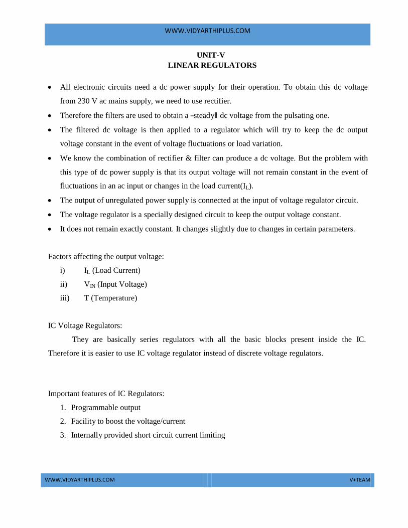
Fig : Pin diagram of IC723
3. Series Pass Transistor:
Q1 is the internal series pass transistor which is driven by
the error amplifier. This transistor actually acts as a variable resistor
& regulates the output voltage. The collector of transistor Q1 is
connected to the Un-regulated power supply. The maximum collector
voltage of Q1 is limited to 36Volts. The maximum current which can
be supplied by Q1 is 150mA.
4. Circuitry to limit the current:
The internal transistor Q2 is used for current sensing & limiting. Q2 is
normally OFF transistor. It turns ON when the IL exceeds a predetermined limit.
Low voltage , Low current is capable of supplying load voltage which is equal to or
between 2 to 7Volts.
WWW.VIDYARTHIPLUS.COM
WWW.VIDYARTHIPLUS.COM V+TEAM
Vload = 2 to 7V
Iload = 150mA
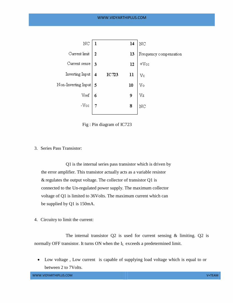
IC723 as a LOW voltage LOW current :
Fig: Typical circuit connection diagram
R1 & R2 from a potential divider between Vref & Gnd.
The Voltage across R2 is connected to the Non – inverting terminal of the regulator IC

WWW.VIDYARTHIPLUS.COM
WWW.VIDYARTHIPLUS.COM V+TEAM
Vnon-inv = R2
R1 R2
Vref
Gain of the internal error amplifier is large
Vnon-inv = Vin
Therefore the Vo is connected to the Inverting terminal through R3 & RSC must also be
equal to Vnon-inv
Vo = Vnon-inv = R2
R1 R2
Vref
R1 & R2 can be in the range of 1 KΩ to 10KΩ & value of R3 is given by
R3 = R1ll R2 =
R1R2
R R2
Rsc (current sensing resistor) is connected between Cs & CL. The voltage drop across Rsc
is proportional to the IL.
This resistor supplies the output voltage in the range of 2 to 7 volts, but the load current
can be higher than 150mA.
The current sourcing capacity is increased by including a transistor Q in the circuit.
The output voltage , Vo = R2
R1 R2
Vref

WWW.VIDYARTHIPLUS.COM
WWW.VIDYARTHIPLUS.COM V+TEAM
IC723 as a HIGH voltage LOW Current:
This circuit is capable of supplying a regulated output voltage between the range of 7 to
37 volts with a maximum load current of 150 mA.
The Non – inverting terminal is now connected to Vref through resistance R3.
The value of R1 & R2 are adjusted in order to get a voltage of Vref at the inverting
terminal at the desired output.
Vin = Vref =
R2 Vo
R1 R2
Vo =
R1 R2
R2
Or
Vref
Vo = [1 +
R1 ] Vref
R2

WWW.VIDYARTHIPLUS.COM
WWW.VIDYARTHIPLUS.COM V+TEAM
IC723 as a HIGH voltage HIGH Current:
Fig: Typical circuit connection diagram
An external transistor Q is added in the circuit for high voltage low current regulator to
improve its current sourcing capacity.
For this circuit the output voltage varies between 7 & 37V.
Transistor Q increase the current sourcing capacity thus IL(MAX) ia greater than 150mA.
The output voltage Vo is given by ,
V0=(R2/R1+R2)Vref
The value of Rsc is given by Rsc = 0.6
ILimit

WWW.VIDYARTHIPLUS.COM
WWW.VIDYARTHIPLUS.COM V+TEAM
SWITCHING REGULATOR:
An example of general purpose regulator is Motorola‘s MC1723. It can be
used in many different ways, for example, as a fixed positive or negative output voltage
regulator, variable regulator or switching regulator because of its flexibility.
To minimize the power dissipation during switching, the external transistor used must be a
switching power transistor.
To improve the efficiency of a regulator, the series pass transistor is used as a switch
rather than as a variable resistor as in the linear mode.
A regulator constructed to operate in this manner is called a series switching regulator.
In such regulators the series pass transistor is switched between cut off & saturation at a
high frequency which produces a pulse width modulated (PWM) square wave output.
This output is filtered through a low pass LC filter to produce an average dc output
voltage.
Thus the output voltage is proportional to the pulse width and frequency.
The efficiency of a series switching regulator is independent of the input &
output differential & can approach 95%
WWW.VIDYARTHIPLUS.COM
WWW.VIDYARTHIPLUS.COM V+TEAM
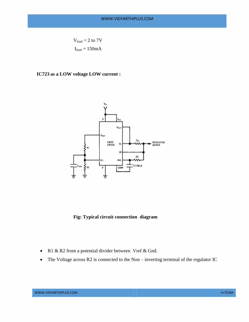
Fig : Basic Switching regulator
A basic switching regulator consists of 4 major components,
1. Voltage source Vin
2. Switch S1
3. Pulse generator Vpulse
4. Filter F1
1. Voltage Source Vin:
It may be any dc supply – a battery or an unregulated or a regulated voltage. The
voltage source must satisfy the following requirements.
It must supply the required output power & the losses associated with the
switching regulator.
It must be large enough to supply sufficient dynamic range for line & load
regulations.
It must be sufficiently high to meet the minimum requirement of the regulator system
to be designed.
It may be required to store energy for a specified amount of time during power
failures.
2. Switch S1:
It is typically a transistor or thyristor connected as a power switch & is operated in the
saturated mode. The pulse generator output alternately turns the switch ON & OFF
3. Pulse generator Vpulse:
WWW.VIDYARTHIPLUS.COM
WWW.VIDYARTHIPLUS.COM V+TEAM
It provides an asymmetrical square wave varying in either frequency or pulse width called
frequency modulation or pulse width modulation respectively. The most effective frequency
range for the pulse generator for optimum efficiency 20 KHz. This frequency is inaudible to
the human ear & also well within the switching speeds of most inexpensive transistors &
diodes.
The duty cucly of the pulse wave form determines the relationship between the
input & output voltages. The duty cycle is the ratio of the on time ton, to the period
T of the pulse waveform.
Duty cycle = ton
ton toff
Switching regulator can operate in any of 3 modes
= ton
= ton f. T
Where ton = On-time of the pulse waveform
toff=off-time of the pulse wave form
T = time period = ton + toff
= 1/frequency or
T = 1/f
Typical operating frequencies of switching regulator range from 10 to 50khz.
Lower operating frequency improve efficiency & reduce electrical noise, but
require large filter components (inductors & capacitors).
4. Filter F1:
WWW.VIDYARTHIPLUS.COM
WWW.VIDYARTHIPLUS.COM V+TEAM
It converts the pulse waveform from the output of the switch into a dc voltage.
Since this switching mechanism allows a conversion similar to transformers, the switching
regulator is often referred to as a dc transformer.
The output voltage Vo of the switching regulator is a function of duty cycle & the
input voltage Vin.
Vo is expressed as follows,
Vo = ton
Vin T
WWW.VIDYARTHIPLUS.COM
WWW.VIDYARTHIPLUS.COM V+TEAM
This equation indicates that, if time period T is constant, Vo is directly proportional to
the ON-time, ton for a given value of Vin. This method of changing the output
voltage by varying ton is referred to as a pulse width modulation.
Similarly, if ton is held constant, the output voltage Vo is inversely proportional to
the period T or directly proportional to the frequency of the pulse waveform. This
method of varying the output voltage is referred to as frequency modulation (FM).
i) Step – Down
ii) Step – Up
iii) Polarity inverting
MONOLITHIC SWITCHING REGULATOR [µA78S40]:
The µA78S40 consists of a temperature compensated voltage reference, duty cycle
controllable oscillator with an active current limit circuit, a high gain comparator, a high- current,
high voltage output switch, a power switching diode & an uncommitted op-amp.
Important features of the µA78S40 switching regulators are:
Step up, down & Inverting operation
Operation from 2.5 to 40V input
80dB line & load regulations
Output adjustable from 1.3 to 40V
Peak current to 1.5A without external resistors
Variable frequency, variable duty cycle device
The internal switching frequency is set by the timing capacitor CT, connected between pin12 &
ground pin 11. the initial duty cycle is 6:1. The switching frequency & duty cycle can be modified
by the current limit circuitry, IPKsense, pin14, 7 the comparator, pin9 & 10.

WWW.VIDYARTHIPLUS.COM
WWW.VIDYARTHIPLUS.COM V+TEAM

WWW.VIDYARTHIPLUS.COM
WWW.VIDYARTHIPLUS.COM V+TEAM
Comparator:
The comparator modifies the OFF time of the output switch transistor Q1 & Q2. In the step
– up & step down modes, the non-inverting input(pin9) of the comparator is connected to the
voltage reference of 1.3V (pin8) & the inverting input (pin10) is connected to the output terminal
via the voltage divider network.
Fig: Functional block diagram of µA78S40

WWW.VIDYARTHIPLUS.COM
WWW.VIDYARTHIPLUS.COM V+TEAM
In the Inverting mode the non – inverting input is connected to both the voltage
reference & the output terminal through 2 resistors & the inverting terminal is connected
to ground.
When the output voltage is correct, the comparator output is in high state & has no effect
on the circuit operation.
However, if the output is too high & the voltage at the inverting terminal is higher than
that at the non-inverting terminal , then the comparator output goes low.
In the LOW state the comparator inhibits the turn on of the output switching transistors.
This means that, as long as the comparator output is low, the system is in off time.
As the output current rises or the output voltage falls, the off time of the system
decreases.
Consequently, as the output current nears its maximum IoMAX, the off time approaches its
minimum value.

WWW.VIDYARTHIPLUS.COM
WWW.VIDYARTHIPLUS.COM V+TEAM
In all 3 modes (Step down, step up, Inverting), the current limit circuit is completed by connecting
a sense resistor Rsc, between IPK sense & Vcc.
The current limit circuit is activated when a 330mV potential appears across Rsc.
Rsc is selected such that 330mV appears across it when the desired peak current IPK,
flows through it.
When the peak current is reached, the current limit circuit is turned on.
The forward voltage drop, VD, across the internal power diode is used to determine the
value of inductor L off time & efficiency of the switching regulator.
Another important quantity used in the design of a switching regulator is the saturation
voltage Vs
In the step down mode an ―output saturation volt‖ is 1.1V typical, 1.3VMAX.
In the step up mode an ―Output saturation volt‖ is 0.45V typical, 0.7 maximum.
Rsc = 330mV
DesiredPeakCurrent
The desired peak current value is reached, the current limiting circuit turns ON
& immediately terminates the ON time & starts OFF time.
As we increase IL (load current), Vout will decreased, to compensate for this, the ON time
of the output is increased automatically.
If the IL decreased then Vout increased, to compensate for this, the OFF time of the output
is increased automatically.
(i) Step – Down Switching Regulator:
CT is the timing capacitor which decides the switching frequency.

WWW.VIDYARTHIPLUS.COM
WWW.VIDYARTHIPLUS.COM V+TEAM
Rsc is the current sensing resistance. Its value is given by
Rsc = 330mV
DesiredPeakCurrent
The Non-inverting terminal of the internal op-amp(pin9) is connected to the 1.3V
reference (pin8).
Resistances R1 & R2 from a potential divider, across the output voltage Vo. Their
value should be such that the potential at the inverting input of the op-amp should
be equal to 1.3V ref when Vo is at its desired level.
R2 V(-) = 1.3V = Vo
R1 R2

WWW.VIDYARTHIPLUS.COM
WWW.VIDYARTHIPLUS.COM V+TEAM
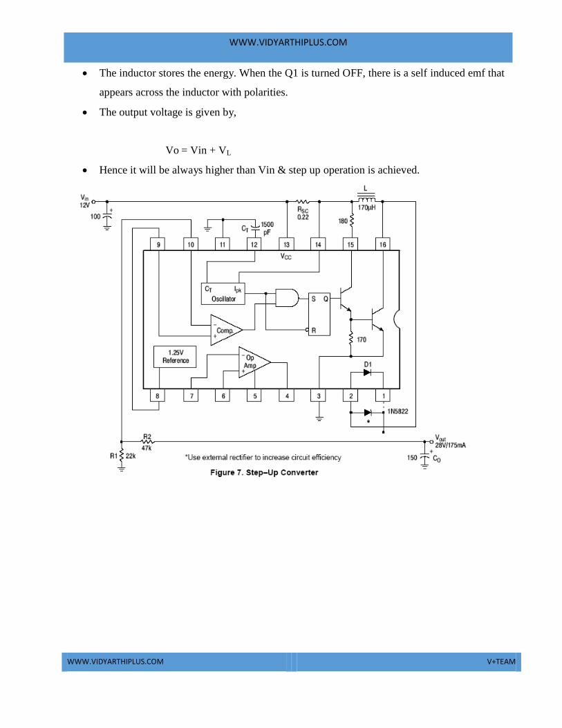
(ii) Step – Up Switching Regulator:
Note that inductor is connected between the collectors of Q1 & Q2.
When Q1 is ON, the output is shorted & the collector current of Q1 flows through L.
The diode D1 is reverse biased & Co supplies the load current.
WWW.VIDYARTHIPLUS.COM
WWW.VIDYARTHIPLUS.COM V+TEAM
The inductor stores the energy. When the Q1 is turned OFF, there is a self induced emf that
appears across the inductor with polarities.
The output voltage is given by,
Vo = Vin + VL
Hence it will be always higher than Vin & step up operation is achieved.

WWW.VIDYARTHIPLUS.COM
WWW.VIDYARTHIPLUS.COM V+TEAM
With Q1 ON with Q1 oFF
(iii) Inverting Switching Regulator:
Inverting switching regulator converts a positive input voltage into a negative
output voltage which is higher in magnitude.

WWW.VIDYARTHIPLUS.COM
WWW.VIDYARTHIPLUS.COM V+TEAM
POWER AUDIO AMPLIFIER IC LM380:
Features of LM380:
1. Internally fixed gain of 50 (34dB)
2. Output is automatically self centring to one half of the supply voltage.
3. Output is short circuit proof with internal thermal limiting.
4. Input stage allows the input to be ground referenced or ac coupled.
5. Wide supply voltage range (5 to 22V).
6. High peak current capability.
7. High impedence.
8. Low total harmonic distortion
9. Bandwidth of 100KHz at Pout = 2W & RL = 8Ω
Introduction:
Small signal amplifier are essentially voltage amplifier that supply their loads with larger
amplifier signal voltage.
On the other hand , large signal or power amplifier supply a large signal current to current
operated loads such as speakers & motors.

WWW.VIDYARTHIPLUS.COM
WWW.VIDYARTHIPLUS.COM V+TEAM
In audio applications, however, the amplifier called upon to deliver much higher current
than that suppkied by general purpose op-amps. This means that loads such as speakers & motors
requiring substantial currents cannot be driven directly by the output of general purpose opo-amps.
However there are two possible solutions,
To use discrete or monolithic power transistors called power boosters at the output of the
op-amp
To use specialized ICs designed as power amplifiers.
Fig : Functional block diagram of Audio Power Amplifier

WWW.VIDYARTHIPLUS.COM
WWW.VIDYARTHIPLUS.COM V+TEAM
Fig: Pin diagram
Fig : Block diagram

WWW.VIDYARTHIPLUS.COM
WWW.VIDYARTHIPLUS.COM V+TEAM
LM380 circuit description:
It is connected of 4 stages,
(i) PNP emitter follower
(ii) Different amplifier
(iii) Common emitter
(iv) Emitter follower
(i) PNP Emitter follower:
The input stage is emitter follower composed of PNP transistors Q1 & Q2 which drives the
PNP Q3-Q4 differential pair.
The choice of PNP input transistors Q1 & Q2 allows the input to be referenced to ground
i.e., the input can be direct coupled to either the inverting & non-inverting terminals of the
amplifier.
(ii) Differential Amplifier:
The current in the PNP differential pair Q3-Q4 is established by Q7, R3 & +V.
The current mirror formed by transistor Q7, Q8 & associated resistors then establishes the
collector current of Q9.
Transistor Q5 & Q6 constitute of collector loads for the PNP differential pair.
The output of the differential amplifier is taken at the junction of Q4 & Q6 transistors & is
applied as an input to the common emitter voltage gain.
(iii) Common Emitter:
Common Emitter amplifier stage is formed by transistor Q9 with D1, D2 & Q8 as a current
source load.

WWW.VIDYARTHIPLUS.COM
WWW.VIDYARTHIPLUS.COM V+TEAM
The capacitor C between the base & collector of Q9 provides internal compensation &
helps to establish the upper cutoff frequency of 100 KHz.
Since Q7 & Q8 form a current mirror, the current through D1 & D2 is approximately the
same as the current through R3.
D1 & D2 are temperature compensating diodes for transistors Q10 & Q11 in that D1 & D2
have the same characteristics as the base-emitter junctions of Q11. Therefore the current
through Q10 & (Q11-Q12) is approximately equal to the current through diodes D1 & D2.
(iv) (Output stage) - Emitter follower:
Emitter follower formed by NPN transistor Q10 & Q11. The combination of PNP transistor
Q11 & NPN transistor Q12 has the power capability of an NPN transistors but the
characteristics of a PNP transistor.
The negative dc feedback applied through R5 balances the differential amplifier so that the
dc output voltage is stabilized at +V/2;
To decouple the input stage from the supply voltage +V, by pass capacitor in order of
micro farad should be connected between the by pass terminal (pin 1) & ground (pin 7).
The overall internal gain of the amplifier is fixed at 50. However gain can be increased by
using positive feedback.
OPTOCOUPLERS/OPTOISOLATORS:
Optocouplers or Optoisolators is a combination of light source & light detector in the same
package.
They are used to couple signal from one point to other optically, by providing a completer
electric isolation between them. This kind of isolation is provided between a low power control
circuit & high power output circuit, to protect the control circuit.
Depending on the type of light source & detector used we can get a variety of optocouplers.
They are as follows,
(i) LED – LDR optocoupler

WWW.VIDYARTHIPLUS.COM
WWW.VIDYARTHIPLUS.COM V+TEAM
(ii) LED – Photodiode optocoupler
(iii) LED – Phototransistor optocoupler
Characteristics of optocoupler:
(i) Current Transfer Ratio (CTR)
(ii) Isolation Voltage
(iii) Response Time
(iv) Common Mode Rejection
(i) Current Transfer Ratio:
It is defined as the ratio of output collector current (Ic) to the input
forward current (If)
CTR = Ic/If * 100%
Its value depends on the devices used as source & detector.
(ii) Isolation voltage between input & output:
It is the maximum voltage which can exist differentially between the
input & output without affecting the electrical isolation voltage is
specified in K Vrms with a relative humidity of 40 to 60%.
(iii)Response Time:
Response time indicates how fast an optocoupler can change its output
state. Response time largely depends on the detector transistor, input
current & load resistance.
(iv)Common mode Rejection:
Eventhough the optocouplers are electrically isolated for dc & low frequency signals, an
impulsive input signal (the signal which changes suddenly) can give rise to a displacement current

WWW.VIDYARTHIPLUS.COM
WWW.VIDYARTHIPLUS.COM V+TEAM
Ic= Cf*dv/dt. This current can flow between input & output due to the capacitance Cf existing
between input & output. This allow the noise to appear in the output.

WWW.VIDYARTHIPLUS.COM
WWW.VIDYARTHIPLUS.COM V+TEAM
Types of optocoupler:
(i) LED – Photodiode optocoupler:
LED photodiode shown in figure, here the infrared LED acts as a light source & photodiode is
used as a detector.
The advantage of using the photodiode is its high linearity. When the pulse at the input goes
high, the LED turns ON. It emits light. This light is focused on the photodiode.
In response to this light the photocurrent will start flowing though the photodiode. As soon as
the input pulse reduces to zero, the LED turns OFF & the photocurrent through the photodiode
reduces to zero. Thus the pulse at the input is coupled to the output side.

WWW.VIDYARTHIPLUS.COM
WWW.VIDYARTHIPLUS.COM V+TEAM
(ii) LED – Phototransistor Optocoupler:
The LED phototransistor optocoupler shown in figure. An infrared LED acts as a light source
and the phototransistor acts as a photo detector.
This is the most popularly used optocoupler, because it does not need any additional
amplification.
When the pulse at the input goes high, the LED turns ON. The light emitted by the LED is
focused on the CB junction of the phototransistor.

WWW.VIDYARTHIPLUS.COM
WWW.VIDYARTHIPLUS.COM V+TEAM
In response to this light photocurrent starts flowing which acts as a base current for the
phototransistor.
The collector current of phototransistor starts flowing. As soon as the input pulse reduces to
zero, the LED turns OFF & the collector current of phototransistor reduces to zero. Thus the
pulse at the input is optically coupled to the output side.
Advantages of Optocoupler:
Control circuits are well protected due to electrical isolation.
Wideband signal transmission is possible.
Due to unidirectional signal transfer, noise from the output side does not get coupled to the
input side.
Interfacing with logic circuits is easily possible.
It is small size & light weight device.
Disadvantages:
Slow speed.
Possibility of signal coupling for high power signals.
Applications:
Optocouplers are used basically to isolate low power circuits from high
power circuits.
At the same time the control signals are coupled from the control circuits to the high power
circuits.
Some of such applications are,
(i) AC to DC converters used for DC motor speed control
(ii) High power choppers
(iii) High power inverters
One of the most important applications of an optocoupler is to couple the base driving signals
to a power transistor connected in a DC-DC chopper.
Note that the input & output waveforms are 180º out of phase as the output is taken at the

WWW.VIDYARTHIPLUS.COM
WWW.VIDYARTHIPLUS.COM V+TEAM
collector of the phototransistor.
Optocoupler IC:
The optocouplers are available in the IC form MCT2E is the standard optocoupler IC
which is used popularly in many electronic application.
This input is applied between pin 1& pin 2. An infrared light emitting diode is connected
between these pins.
The infrared radiation from the LED gets focused on the internal phototransistor.
The base of the phototransistor is generally left open. But sometimes a high value pull down
resistance is connected from the Base to ground to improve the sensitivity.
The block diagram shows the opto-electronic-integrated ciruit (OEIC) and the major
components of a fiber-optic communication facility.

WWW.VIDYARTHIPLUS.COM
WWW.VIDYARTHIPLUS.COM V+TEAM
FUNCTION GENERATOR IC 8038:
Fig: Functional block diagram of Function generator
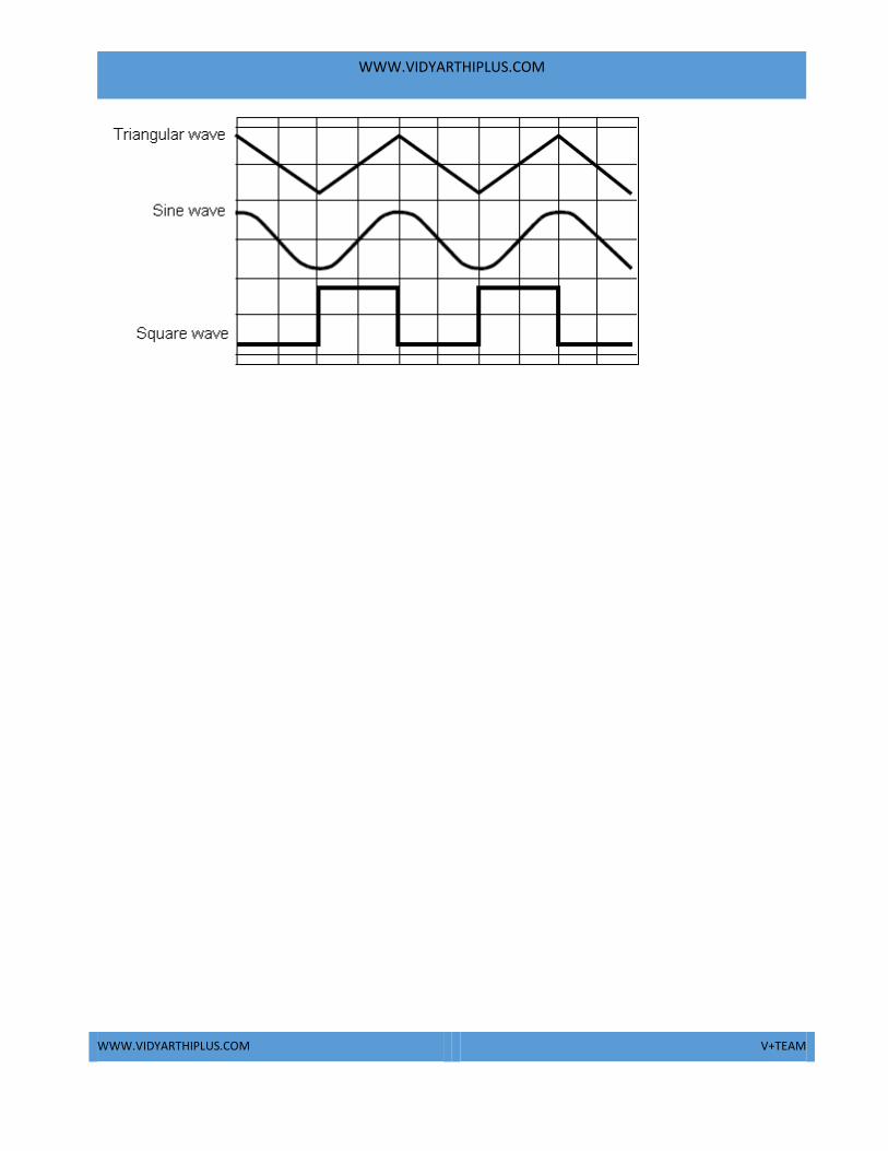
Output Waveform:
WWW.VIDYARTHIPLUS.COM
WWW.VIDYARTHIPLUS.COM V+TEAM
WWW.VIDYARTHIPLUS.COM
WWW.VIDYARTHIPLUS.COM V+TEAM
It consists of two current sources, two comparators, two buffers, one FF and a sine wave converter.
Pin description:
Pin 1 & Pin 12: Sine wave adjusts:
The distortion in the sine wave output can be reduced by adjusting the 100KΩ pots
connected between pin12 & pin11 and between pin 1 & 6.
Pin 2 Sine Wave Output:
Sine wave output is available at this pin. The amplitude of this sine wave is 0.22 Vcc.
Where ± 5V ≤ Vcc ≤ ± 15 V.
Pin 3 Triangular Wave output:
Triangular wave is available at this pin. The amplitude of the triangular wave is 0.33Vcc.
Where ± 5V ≤ Vcc ≤ ± 15 V.
Pin 4 & Pin 5 Duty cycle / Frequency adjust:
The symmetry of all the output wave forms & 50% duty cycle for the square wave output
is adjusted by the external resistors connected from Vcc to pin 4. These external resistors &
capacitors at pin 10 will decide the frequency of the output wave forms.
Pin 6 + Vcc:
Positive supply voltage the value of which is between 10 & 30V is applied to this pin.
Pin 7 : FM Bias:
This pin along with pin no8 is used to TEST the IC 8038.
Pin9 : Square Wave Output:
A square wave output is available at this pin. It is an open collector output so that this pin
can be connected through the load to different power supply voltages. This arrangement is very

WWW.VIDYARTHIPLUS.COM
WWW.VIDYARTHIPLUS.COM V+TEAM
useful in making the square wave output.
Pin 10 : Timing Capacitors:
The external capacitor C connected to this pin will decide the output frequency along with
the resistors connected to pin 4 & 5.
Pin 11 : -VEE or Ground:
If a single polarity supply is to be used then this pin is connected to supply ground & if (±)
supply voltages are to be used then (-) supply is connected to this pin.
Pin 13 & Pin 14: NC (No Connection)
Important features of IC 8038:
1. All the outputs are simultaneously available.
2. Frequency range : 0.001Hz to 500kHz
3. Low distortion in the output wave forms.
4. Low frequency drift due to change in temperature.
5. Easy to use.
Parameters:
(i) Frequency of the output wave form:
The output frequency dependent on the values of resistors R1 & R2 along with the external
capacitor C connected at pin 10.
If RA= RB = R & if RC is adjusted for 50% duty cycle then
fo = 0.3
RC
; RA
= R1, RB
= R3, RC
= R2
(ii) Duty cycle / Frequency Adjust : (Pin 4 & 5):
Duty cycle as well as the frequency of the output wave form can be adjusted by controlling the

WWW.VIDYARTHIPLUS.COM
WWW.VIDYARTHIPLUS.COM V+TEAM
values of external resistors at pin 4 & 5.
The values of resistors RA & RB connected between Vcc * pin 4 & 5 respectively along
with the capacitor connected at pin 10 decide the frequency of the wave form.
The values of RA & RB should be in the range of 1kΩ to 1MΩ.
(iii) FM Bias:
The FM Bias input (pin7) corresponds to the junction of resistors R1 & R2.
The voltage Vin is the voltage between Vcc & pin8 and it decides the output frequency.
The output frequency is proportional to Vin as given by the following expression
For RA = RB (50% duty cycle).
fo = 1.5Vin
CRAVcc
; where C is the timing capacitor
With pin 7 & 8 connected to each other the output frequency is given by
fo = 0.3
RC
where R = RA = RB for 50% duty cycle.
This is because Vin =
(iv) FM Sweep input (pin 8):
R1
R1 R2
Vcc
This input should be connected to pin 7, if we want a constant output frequency.
But if the output frequency is supposed to vary, then a variable dc voltage should be
applied to this pin.
The voltage between Vcc & pin 8 is called Vin and it decides the output frequency as,
1.5 Vin
fo = ---------------

WWW.VIDYARTHIPLUS.COM
WWW.VIDYARTHIPLUS.COM V+TEAM
C RA Vcc
A potentiometer can be connected to this pin to obtain the required variable voltage required to
change the output frequency.

WWW.VIDYARTHIPLUS.COM
WWW.VIDYARTHIPLUS.COM V+TEAM