univ ersit y of alb erta v ol t a ge references...
TRANSCRIPT

University of Alberta
VOLTAGE REFERENCES USING MUTUALCOMPENSATION OF MOBILITY AND THRESHOLD
VOLTAGE TEMPERATURE EFFECTS
by
Laleh Najafizadeh
A thesis submitted to the Faculty of Graduate Studies and Research in partial
fulfillment of the requirements for the degree of Master of Science
Department of Electrical and Computer Engineering
Edmonton, Alberta
Spring 2004

University of Alberta
Faculty of Graduate Studies and Research
The undersigned certify that they have read, and recommended to the Faculty of Graduate
Studies and Research for acceptance, a thesis titled Voltage References Using Mutual
Compensation of Mobility and Threshold Voltage Temperature Effects submit-
ted by Laleh Najafizadeh in partial fulfillment of the degree of Master of Science.
—————————————
Dr. Igor M. Filanovsky
—————————————
Dr. Bruce F. Cockburn
—————————————
Dr. Xiaodong Wang

Abstract
A voltage reference is an essential building block of many analog and digital circuits.
The performance of a reference is gauged by the maximum variation in its allowable
operating conditions. One of the most important specifications of a reference is its
temperature drift. Therefore, special attention should be paid by the designer to the
thermal behavior of a voltage reference.
In this thesis, three new voltage reference circuits are proposed and designed in
0.18-µm technology. Our goal has been to design CMOS voltage references with
better temperature stability compared to that of existing voltage references. First,
a voltage reference is presented which takes advantage of summing the gate-source
voltages of two diode-connected transistors biased by temperature-stable currents.
The temperature coefficient of the output voltage of this reference is shown to be
28 ppm/C over the temperature range of -50C to 150C. Next, the temperature
behavior of the gate-source voltage of a CMOS transistor biased by a current, which
is proportional to absolute temperature (PTAT), is investigated. It is shown that the
temperature coefficient of the gate-source voltage of the transistor can be altered by
adjusting the parameters of the PTAT current source. This idea is then applied to the
design of two temperature-independent voltage references. The first reference consists
of a PTAT current source and a diode-connected transistor. Simulation results show
that the temperature coefficient of this reference voltage is 4 ppm/C over the range

of -50C to 150C. The second reference takes advantage of summing the gate-source
voltages of two NMOS transistors biased by PTAT currents. The last two references
show a temperature coefficient of 4 ppm/C over the range of -50C to 150C and
can operate with a power supply below 1 V. The simulation results for this voltage
reference show a temperature coefficient of 4 ppm/C over the range of -50C to
150C. The operation of all the circuits are also justified analytically.

Acknowledgments
This thesis would not transpire to exist without the help, support and love of a
number of people to whom I will always be indebted.
I would like to express my sincere thanks to my supervisor Dr. Igor Filanovsky
for his valuable guidance, encouragement, technical advice and financial support. I
would also like to thank Dr. Bruce Cockburn for carefully reading the thesis and for
his insightful comments and advice.
I am indebted to my dearest parents for their invaluable and never-ending support,
love and encouragement. My father has always been an example to follow as an honest
and hardworking scientist and my mother has been a continuous source of love and
moral support. They have always provided me not only great hopes but also strong
motivations for building a better future. Many thanks to my wonderful brother and
sister, Ali and Ladan, who with sending their daily emails, have always lighten up my
days. Last, but certainly not least, I wish to thank my beloved husband, Sasan, for his
endless love, unconditional support and true friendship . His love and understanding
have been continuous sources of strength and encouragement to me. Only he knows
how much I am indebted to him.
The tools for the design and fabrication of the circuits used in this thesis, have
been provided by the Canadian Microelectronics Corporation (CMC).

Contents
1 Introduction 1
1.1 Motivation . . . . . . . . . . . . . . . . . . . . . . . . . . . . . . . . . 1
1.2 Thesis Outline and Contribution . . . . . . . . . . . . . . . . . . . . . 3
2 The Basics 6
2.1 Basic Semiconductor Effects . . . . . . . . . . . . . . . . . . . . . . . 6
2.2 Threshold Voltage . . . . . . . . . . . . . . . . . . . . . . . . . . . . . 9
2.3 Carrier Mobility . . . . . . . . . . . . . . . . . . . . . . . . . . . . . . 13
2.4 Zero Temperature Coefficient Point . . . . . . . . . . . . . . . . . . . 16
2.5 Conclusion . . . . . . . . . . . . . . . . . . . . . . . . . . . . . . . . . 18
3 Current References 19
3.1 PTAT Current References . . . . . . . . . . . . . . . . . . . . . . . . 20
3.2 CTAT Current References . . . . . . . . . . . . . . . . . . . . . . . . 27
3.3 Temperature-Independent Current References . . . . . . . . . . . . . 30
3.4 PTAT2 Current References . . . . . . . . . . . . . . . . . . . . . . . . 31
3.5 Conclusion . . . . . . . . . . . . . . . . . . . . . . . . . . . . . . . . . 34
4 Voltage References 35
4.1 Bandgap References . . . . . . . . . . . . . . . . . . . . . . . . . . . . 36

4.1.1 General Idea . . . . . . . . . . . . . . . . . . . . . . . . . . . . 38
4.1.2 First-Order Compensation . . . . . . . . . . . . . . . . . . . . 40
4.1.3 Second-Order Compensation . . . . . . . . . . . . . . . . . . . 46
4.1.3.1 Curvature Compensation Using Squared PTAT Voltage 47
4.1.3.2 Curvature Compensation Using Temperature-Dependent
Resistor Ratio . . . . . . . . . . . . . . . . . . . . . 49
4.1.3.3 Curvature Compensation Using Nonlinear Currents . 51
4.1.4 Low-Voltage Low-Power Bandgap References . . . . . . . . . . 54
4.2 CMOS non-Bandgap Voltage References . . . . . . . . . . . . . . . . 57
4.2.1 CMOS Voltage References Based on Threshold Voltage Sub-
traction . . . . . . . . . . . . . . . . . . . . . . . . . . . . . . 58
4.2.2 CMOS Voltage References Based on the Weighted Difference of
Gate-Source Voltages . . . . . . . . . . . . . . . . . . . . . . . 60
4.2.3 CMOS Voltage Reference Based on the Mutual Compensation
of Mobility and Threshold Voltage . . . . . . . . . . . . . . . 63
4.3 Conclusion . . . . . . . . . . . . . . . . . . . . . . . . . . . . . . . . . 64
5 New non-Bandgap CMOS Voltage References 66
5.1 Generation of a Virtual ZTC point . . . . . . . . . . . . . . . . . . . 67
5.1.1 Circuit Design and Analysis . . . . . . . . . . . . . . . . . . . 71
5.1.2 Simulation Results . . . . . . . . . . . . . . . . . . . . . . . . 74
5.2 Diode-Connected Operation with PTAT Drain Current . . . . . . . . 78
5.3 A Simple Voltage Reference Using a PTAT Current Source . . . . . . 82
5.3.1 Circuit Design and Analysis . . . . . . . . . . . . . . . . . . . 82
5.3.2 Simulation Results . . . . . . . . . . . . . . . . . . . . . . . . 85
5.4 A Sub-1-V Voltage Reference . . . . . . . . . . . . . . . . . . . . . . 87

5.4.1 Circuit Design and Analysis . . . . . . . . . . . . . . . . . . . 88
5.4.2 Simulation Results . . . . . . . . . . . . . . . . . . . . . . . . 89
5.5 Performance Comparison of Various Voltage References . . . . . . . . 94
5.6 Conclusion . . . . . . . . . . . . . . . . . . . . . . . . . . . . . . . . . 96
6 Conclusion 97
References 100
Vita 106

List of Tables
5.1 Transistor and resistor sizes for the circuit shown in Figure 5.2 . . . . 72
5.2 Transistor and resistor sizes for the circuit shown in Figure 5.8 . . . . 84
5.3 Transistor and resistor sizes for the circuit shown in Figure 5.10 . . . 88
5.4 Comparison of Various Voltage References . . . . . . . . . . . . . . . . . 95

List of Figures
2.1 Silicon bandgap energy as a function of temperature . . . . . . . . . . 7
2.2 Electron density as a function of temperature for a Si sample with a
donor concentration of ND = 1015cm−3 (after [10]) . . . . . . . . . . . 8
2.3 Threshold voltage of an NMOS transistor (W/L=2/1) as a function of
temperature . . . . . . . . . . . . . . . . . . . . . . . . . . . . . . . . 12
2.4 Change of αV T with the length of an NMOS transistor with W=5 . . 13
2.5 Mobility as a function of temperature . . . . . . . . . . . . . . . . . . 15
2.6 Transconductance characteristic for an NMOS transistor . . . . . . . 17
3.1 PTAT current generator (after [19]) . . . . . . . . . . . . . . . . . . . 22
3.2 (a) Substrate npn transistor (b) Substrate pnp transistor (after [3]) . 24
3.3 CMOS PTAT current generator (after [1]) . . . . . . . . . . . . . . . 26
3.4 CTAT current generator using VBE (after [17]) . . . . . . . . . . . . . 28
3.5 CMOS CTAT current generator using the threshold voltage (after [18]) 29
3.6 Temperature-independent current reference (after [1]) . . . . . . . . . 31
3.7 Bipolar PTAT2 current reference (after [1]) . . . . . . . . . . . . . . . 32
3.8 CMOS PTAT2 current reference (after [1]) . . . . . . . . . . . . . . . 33
4.1 The base-emitter voltage as a function of temperature for several values
of θ . . . . . . . . . . . . . . . . . . . . . . . . . . . . . . . . . . . . . 40

4.2 Two conceptual implementation of a temperature-compensated refer-
ence generator (after [17]) . . . . . . . . . . . . . . . . . . . . . . . . 41
4.3 Typical CMOS bandgap reference based on voltage processing (after
[38]) . . . . . . . . . . . . . . . . . . . . . . . . . . . . . . . . . . . . 43
4.4 Typical CMOS bandgap reference based on current processing (after
[17]) . . . . . . . . . . . . . . . . . . . . . . . . . . . . . . . . . . . . 45
4.5 Curvature-compensation concept using a PTAT2 voltage (after [1]) . . 47
4.6 Schematic of the curvature-compensated BGR using square PTAT volt-
age compensation (after [3]) . . . . . . . . . . . . . . . . . . . . . . . 48
4.7 Schematic of the curvature-compensated BGR based on resistor ratio
technique (after [39]) . . . . . . . . . . . . . . . . . . . . . . . . . . . 50
4.8 Generation of the non-linear current (a) The circuit, (b) Currents (after
[33]) . . . . . . . . . . . . . . . . . . . . . . . . . . . . . . . . . . . . 52
4.9 Piecewise-linear curvature-corrected bandgap reference a) The circuit
b) Temperature-dependent waveforms (after [33]) . . . . . . . . . . . 53
4.10 Cross section of a DTMOS transistor(after [40]) . . . . . . . . . . . . 56
4.11 Low-voltage bandgap circuit schematic using DTMOS transistors (af-
ter [40]) . . . . . . . . . . . . . . . . . . . . . . . . . . . . . . . . . . 57
4.12 Schematic of the voltage reference based on threshold subtraction (after
[43]) . . . . . . . . . . . . . . . . . . . . . . . . . . . . . . . . . . . . 58
4.13 Schematic of the voltage reference based on weighted difference of gate-
source voltages (after [46]) . . . . . . . . . . . . . . . . . . . . . . . . 61
4.14 Schematic of the voltage reference using ZTC point (after [48]) . . . . 64
5.1 Simulated transconductance characteristics of an NMOS transistor . . 68
5.2 Voltage reference using constant bias currents . . . . . . . . . . . . . 71

5.3 Simulation results for IB, I7 and I8 for the circuit shown in Figure 5.2 75
5.4 Simulation results for VGS7, VGS8 and Vref for the circuit shown in
Figure 5.2 . . . . . . . . . . . . . . . . . . . . . . . . . . . . . . . . . 76
5.5 Simulation results for the start-up circuit in Figure 5.2 . . . . . . . . 77
5.6 Simulated transconductance characteristics of an NMOS transistor . . 80
5.7 Simulated transconductance characteristics of an NMOS transistor . . 81
5.8 Voltage reference using a diode-connected transistor biased with a
PTAT current source . . . . . . . . . . . . . . . . . . . . . . . . . . . 84
5.9 Simulation results for IB, ID6 and VGS6 for the circuit shown in Figure
5.8 . . . . . . . . . . . . . . . . . . . . . . . . . . . . . . . . . . . . . 86
5.10 A Sub-1-V voltage reference . . . . . . . . . . . . . . . . . . . . . . . 87
5.11 Temperature dependencies of IB, I7 and I8 for the circuit shown in
Figure 5.10 . . . . . . . . . . . . . . . . . . . . . . . . . . . . . . . . 90
5.12 Temperature dependencies of VGS7, VGS8 and Vref for the circuit shown
in Figure 5.10 . . . . . . . . . . . . . . . . . . . . . . . . . . . . . . . 92
5.13 Change in Vref due to the variation in power supply, for the circuit
shown in Figure 5.10, T = T0 = 27C . . . . . . . . . . . . . . . . . . 93

Acronyms
A/D analog to digital
BGR bandgap reference
BJT bipolar junction transistor
CM current mode
CTAT complementary to absolute temperature
CMOS complementary metal oxide semiconductor
D/A digital to analog
DRAM dynamic random access memory
DTMOS dynamic threshold metal oxide semiconductor transistors
FET field effect transistor
MOS metal oxide semiconductor
PLL phase locked loop
PTAT proportional to absolute temperature
TC temperature coefficient
TI temperature independent
ZTC zero temperature coefficient

List of Symbols
Cox Gate oxide capacitor
Eg Energy bandgap
Eg0 Extrapolated zero-degree bandgap energy
IB The bias current
IC The collector current
ID The drain current
Is The saturation current
Js Saturation current density
k Boltzmann constant
kT Thermal energy
L Length of a MOS transistor gate
m Mobility parameter
m0 Free electron mass
mde Electron effective mass
mdh Hole effective mass
nc Carrier concentration
ni Intrinsic carrier concentration
NA Acceptor concentration
ND Donor concentration

NI Impurity concentration
Np Carrier concentration in the polysilicon gate
Ns Substrate doping
q Electron charge
Qi The implanted charge per unit area
Qss The surface-state charge density per unit area
RB The bias resistor
T Absolute temperature
tox Gate-oxide thickness
T0 Correction term owing to the threshold shift implant
V0
VBE The base-emitter voltage
VDD The power supply voltage
VDDminMinimum required power supply
VDS The drain-source voltage
VDSsatThe saturated drain-source voltage
VG0 The bandgap voltage of silicon extrapolated to 0K
VGS The gate-source voltage
Vref The reference voltage
VSB The source-body voltage
VT Thermal voltage
VTH Threshold voltage
VTHp PMOS threshold voltage
VTHn NMOS threshold voltage
W Width of a MOS transistor gate

αR1 First order temperature coefficient of a resistor
αR2 Second order temperature coefficient of a resistor
αV T Temperature coefficient of Threshold Voltage
µ Carrier mobility
µe Electron mobility
µh Hole mobility
µI Carrier mobility impeded by impurity scattering
µL Carrier mobility impeded by lattice scattering
φb1 Barrier lowering voltage
φF Fermi level
φms Metal-semiconductor work function differnece

Chapter 1
Introduction
1.1 Motivation
Most, if not all, electrical circuits use a reference, be it voltage, current or time. A ref-
erence in a circuit establishes a stable point used by other sub-circuits to generated
predictable and repeatable results. This reference point should not change signifi-
cantly under various operating conditions. Temperature is an important parameter
which affects the performance of references. Special attention should therefore be
paid by the designer to the temperature behavior of the reference. The typical metric
used for variations of the reference voltage across temperature is the temperature
coefficient (TC) and it is normally expressed in parts-per-million per degree Celsius
(ppm/C),
TCref =1
Reference
∂Reference
∂Temperature, (1.1)
where the reference is either in volts, amps, or seconds [1].
Current references are used in most of the basic building blocks. Usually, the
current in different basic blocks results from mirroring of one or more references.
Therefore, it is important that the master current of the system to be power-supply
1

independent and designed with the required accuracy. Current references are also
used for the design of voltage references. A current reference typically does not need
to be temperature-independent, however, its temperature coefficient should be well
characterized and controlled.
Voltage references have been used in various fields of application, for example in
digital to analog (D/A) converters, the automotive industry and in battery-operated
DRAMs [2]. In D/A converters, depending on the digital input word, the analog
voltage is a fraction of the internal reference voltage. As for many applications this
digital to analog conversion should not depend on temperature, so the reference volt-
age has to be temperature-independent. Nowadays, high resolution D/A converters
are being used and consequently the reference voltage must be very stable as each
variation in the reference voltage is directly sensed in the D/A-converter output.
In the automotive industry electronic circuits are used to realize larger systems
with more functions. However, the automotive environment, is very extreme and
the temperature variations can be in the range of -15C to 105C. A supply voltage
regulator handles the stabilization of the supply voltage in the car and the reference
for this regulator must be able to withstand the extreme automotive environment [2].
Similarly, in battery-operated DRAMs, voltage references are used for power-supply
voltage stabilization. In this case, the power consumption is of prime importance.
Bandgap voltage references are the most popular precise references used in var-
ious circuits. A bandgap voltage reference (BGR) has high power rejection and its
output voltage is very stable against temperature and process variations. It can be
implemented using available, vertical or lateral BJTs in any standard CMOS tech-
nology [3],[4]. However, when the supply voltage falls below 1 V, the performance of
a conventional bandgap reference degrades [5]. As an alternative, voltage references
2

can also be implemented in MOS technology using the threshold voltage difference
[6]. But this solution requires multi-threshold transistors which are not applicable in
standard low-cost CMOS technologies since additional fabrication steps are needed.
The development of other techniques for the design of low-voltage CMOS voltage
references is therefore needed, a CMOS voltage reference whose performance is com-
parable to the performance of bandgap references.
1.2 Thesis Outline and Contribution
To successfully design a CMOS current/voltage reference, one must have a thorough
understanding of the temperature behavior of MOS transistors. Therefore, in Chap-
ter 2, we briefly describe the temperature dependency of some basic semiconductor
physical properties (energy bandgap, intrinsic carrier concentration, impurity carrier
concentration and Fermi potential) and the effects of temperature on MOS transis-
tor parameters (threshold voltage and carrier mobility). The equations which are
generally used to describe the temperature behavior of the CMOS threshold voltage
and mobility are presented. The presence of the zero temperature coefficient (ZTC)
point in the transconductance characteristics of a CMOS transistor is studied and the
conditions under which such a point can exist are investigated.
In Chapter 3, we will study the techniques used for the design of different types
of current references. Generally, current references based on their temperature per-
formances are categorized into 4 groups. A proportional-to-absolute temperature
current reference, as the name implies, generates a current which is linearly propor-
tional to temperature. In a complementary-to-absolute temperature (CTAT) refer-
ence, the complement of a PTAT reference, generates a current which decreases as the
3

temperature increases. Temperature-independent current references are another cat-
egory, and are usually designed based on properly combining temperature-dependent
currents or using available voltage references. The last group of current references
generate a square PTAT current (PTAT2) which is proportional to the square of the
temperature. The design methods and the operation basics of these current references
are studied in this chapter.
In Chapter 4 we will review the theory and the issues, with respect to tempera-
ture, that surround the design of different groups of voltage references. We begin by
reviewing the techniques used for the design of most widely used voltage references
in electronics circuit, i.e., the bandgap references. To get a clear insight, the basic
function of bandgap references is studied first, including a general description of the
temperature compensation. Then, as the basic structure is found, the techniques
used for the design of first-order bandgap references will be studied. Thereafter,
some special structures, such as quadratic temperature compensation, second-order
curvature-compensated reference using resistor ratios and piecewise-linear curvature
correction to improve the temperature behavior of bandgap references will be given.
Also, the methods used for the design of low-voltage BGR are studied. Finally, we
present techniques used for the implementation of CMOS non-bandgap voltage refer-
ences (such as references based on threshold-voltage difference, weighted gate-source
voltage difference and ZTC point) which have performance comparable to the perfor-
mance of BGR.
In Chapter 5, it is shown that the temperature dependency of the gate-source
voltage of a CMOS transistor biased with a PTAT current source can be altered by
adjusting the parameters of the PTAT current source. A circuit consisting of a diode-
connected transistor biased by a PTAT current source is designed and implemented
4

in 0.18-µm CMOS technology. The parameters of the current source have been cho-
sen in order to obtain a temperature-independent gate-source voltage. The circuit is
simulated successfully and the simulation results are also given. A sub-1-V CMOS
voltage reference, which takes advantage of summing the gate-source voltages of two
NMOS transistors operating in the saturation region, is also presented. Both transis-
tors are working below the zero temperature coefficient point and, thus, the voltage
reference is able to operate with a low supply voltage. This circuit is implemented in
a standard 0.18-µm CMOS process and the simulation results are given. To the best
of the author’s knowledge, this is a new approach for the design of CMOS voltage
references. The performances of the proposed voltage references are compared with
other voltage references in the literature and it is shown that our voltage references
have a comparable performance with the bandgap voltage references and a better
performance than the non-bandgap ones.
Finally, the conclusions and a summary of the thesis are given in Chapter 6.
5

Chapter 2
The Basics
In this chapter, we consider some basic properties of semiconductor materials with
emphasis on the temperature dependencies of these properties. This is followed by
the discussion of the temperature dependency of the threshold voltage and the carrier
mobility in a MOS transistor. Then the zero temperature coefficient (ZTC) point in
CMOS transistors will be presented and the conditions under which this point exists
are investigated.
2.1 Basic Semiconductor Effects
In this section, we review the temperature dependencies of some basic properties of
semiconductor materials.
Energy Bandgap: The difference in energy between the valence band and the
conduction band is called the energy bandgap and is denoted by Eg. The temperature
dependency of Eg of silicon is given by [7]
Eg(T ) = 1.170−4.73× 10⁻⁴T 2
T + 636. (2.1)
where T is the absolute temperature in K. Figure 2.1 shows the temperature de-
6

0 100 200 300 400 500 600 700 800 900 10000.85
0.9
0.95
1
1.05
1.1
1.15
1.2
1.25
Temperature (K)
Ban
dgap
Ene
rgy
(ev)
Military Range
Figure 2.1: Silicon bandgap energy as a function of temperature
pendency of the silicon bandgap energy. As it can be seen, even for the relatively
broad military temperature range of −55C to 125C (218K-398K), Eg has a weak
temperature dependence.
Intrinsic Carrier Concentration: The concentration ni of intrinsic electrons
and holes depends on the amount of energy needed to break a bond (e.g., the en-
ergy bandgap) and on the amount of energy available (e.g., the thermal energy as
characterized by the temperature) [8]. The mathematical relationship between these
parameters is given by [9]
ni = 4.9× 10¹⁵(
mdemdh
m20
)3/4
T 3/2exp
(−Eg
2kT
)
= AT 3/2exp
(−Eg
2kT
)
(2.2)
where k is the Boltzmann’s constant, mde and mdh are the electron and hole effective
masses and m0 is the free electron mass.
7

Carrier Concentration: When impurity atoms are added and at relatively el-
evated temperature, when most donors and acceptors are ionized, carrier concentra-
tion, nc, can be expressed by [10]
nc =
1
2
[
(ND −NA) +√
(ND −NA)2 + 4n2i
]
(n-type)
1
2
[
(NA −ND) +√
(ND −NA)2 + 4n2i
]
(p-type)
(2.3)
where ND and NA are donor and acceptor concentration, respectively. As long as the
magnitude of the net impurity concentration |ND − NA| is much larger than ni, the
intrinsic carrier concentration, will be approximately equal to the substrate doping
concentration (i.e.,(ND −NA) for n-type and (NA −ND) for p-type).
E l e
c t r
o n d
e n
s i t
y
Temperature (K)
0 400
3
2
1
0 100 200 300 500 600
15 10
Extrinsic region
Freeze-out region
Intrinsic region
x
Intrinsic temperature
Figure 2.2: Electron density as a function of temperature for a Si sample with a donor
concentration of ND = 1015cm−3 (after [10])
Figure 2.2 shows the carrier concentration in Si as a function of temperature for
a donor concentration of ND = 1015cm−3. When the temperature is low, the ther-
mal energy is not sufficient to ionize all the impurities and so the carrier density is
less than the donor concentration. This region is known as freeze-out region. As
8

the temperature increases, all impurities are ionized and nc = ND. This condition
will remain over a wide temperature range and is known as extrinsic region. How-
ever, as the temperature is increased further, the intrinsic carrier concentration, ni,
is increased as well and we reach a point where the intrinsic carrier concentration
becomes comparable to ND. The temperature at which the intrinsic carrier concen-
tration becomes equal to ND, is called the intrinsic temperature. It is apparent that
the intrinsic temperature can be delayed by increasing the impurity density.
Fermi Level: For an intrinsic semiconductor, the Fermi level lies about midway
between the valence and conduction bands. The Fermi level in n-type materials is
closer to the conduction band while for p-type material it is closer to the valence
band. The value of the Fermi level depends on temperature due to the temperature
dependence of ni and the thermal voltage, VT =kTq, and is expressed by
φF (T ) = ±kT
qln
(
ncni(T )
)
(2.4)
where the positive or negative sign refers to n-type or p-type semiconductors, respec-
tively.
2.2 Threshold Voltage
A commonly used expression for the threshold voltage of the MOS transistor is given
by [11]
VTH = φms ±Qss
Cox
+ 2φF +∆VT (Ni)± γ(Ns, tox, L,W )√
2φF + V0 + |VSB| (2.5)
where the positive or negative sign refers to n-channel or p-channel devices, respec-
tively. In this equation: φms is the metal-silicon work function difference, Qss is the
surface-state charge density per unit area, Cox is the gate-oxide capacitance per unit
9

area, φF is the Fermi potential of the substrate, ∆VT (Ni) is the threshold shift owing
to a channel implant Ni with depth, di, and γ is the body-effect constant that de-
pends on the substrate doping Ns, the gate-oxide thickness tox, the channel length L
and width W . Finally, V0(Ni, Ns, di) is a correction term owing to the threshold shift
implant. For enhancement devices with a ∆VT shifting implant of the same type as
the substrate, V0 has a sign opposite to that of φF .
The major contributions to the variation of threshold voltage with temperature are
the Fermi level, φF , and the gate-semiconductor work function difference, φms. The
Fermi level is expressed by equation (2.4). For a silicon gate doped oppositely to the
substrate, the contact potential is essentially determined by the pn product. There-
fore, for an n-type doped gate, the gate-semiconductor work function is expressed as
[12]
φms(T ) =
−kTqln
(
NsNp
n2i
)
(NMOS)
−kTqln
(
Ns
Np
)
(PMOS)
(2.6)
where Np is the carrier concentration in the polysilicon gate. The temperature-
dependent terms in Equation (2.6) are the intrinsic carrier concentration, ni, and the
thermal voltage,kT
q. The influence of the work function on the temperature behavior
of the threshold voltage is often neglected in the literature [9]. But it has been shown
that assuming a temperature-independent φms affects the accuracy in predicting the
threshold voltage temperature behavior, especially at temperatures above 373K.
The minor contributions to the variation of threshold voltage with temperature
are the variation in oxide capacitance, as well as the ionization of surface states [7].
To a first-order approximation these effects are very small and can be safely ignored.
It has been shown in [13] that the threshold voltage decreases approximately
10

−50 0 50 100 150 2000.2
0.24
0.28
0.32
0.36
0.4
0.44
Thr
esho
ld V
olta
ge, (
V)
Temperature, ( °C)
Figure 2.3: Threshold voltage of an NMOS transistor (W/L=2/1) as a function of
temperature
linearly with an increase in temperature. Equation (2.7), given below, is usually used
to show the temperature dependency of threshold voltage
VTH(T ) = VTH(T0)− αV T (T − T0). (2.7)
Figure 2.3 shows that the threshold voltage is a linear function of temperature. To
generate Figure 2.3 a NMOS transistor, operating in saturation, is simulated and the
plot of√ID =
√
K(T )(VGS−VTH) versus VGS is obtained for different temperatures,
where ID is the drain current, VGS is the gate-source voltage and K(T ) depends on
the transistor parameters. Then, using extrapolation of the simulated data, the value
of the threshold voltage, VTH , is obtained for different temperatures and is plotted as
a function of temperature in Figure 2.3.
As the plot shows the temperature dependency of the threshold voltage can be
closely approximated as a linear function of temperature. The temperature coeffi-
cient of the threshold voltage (TCVT), αV T , is generally calculated by differentiating
11

equation (2.5) with respect to the temperature. Considering the fact that φF and φms
are the major factors which may cause a temperature dependence in the threshold
voltage, αV T will be equal to
αV T = |∂VTH∂T
| = |∂φms∂T
+ 2∂φF∂T
+γ
√
2φF + V0 + |VSB|∂φF∂T
|. (2.8)
Assuming (2.2), whereEG0
q= 1.21V is the extrapolated zero-degree band gap [14],
and using (2.6), one can find that for an n-type doped gate
∂φms∂T
=1
T
[
φms +EG0
q+3kT
q
]
. (2.9)
Using (2.4), the temperature coefficient of φF is given by
∂φF∂T
=1
T
[
φF −(
EG0
2q+3kT
2q
)]
. (2.10)
Therefore, the temperature coefficient of the threshold voltage becomes
αV T = |∂VTH∂T
| = |φmsT+ 2
φFT+
γ(Ns, tox, L,W )√
2φF + V0 + |VSB|| (2.11)
The value of αV T varies [13], [15] from 1 mV/C to 4 mV/C. A most frequently used
figure is 2 mV/C [14]. Although the value of αV T is assumed to be constant, there
are a number of factors which affect its value. As equation (2.11) shows, the value
of the temperature coefficient of threshold voltage depends on the value of |VSB|.
Higher back biases leads to a smaller value of TCVT. The length of the transistor
also affects the value of the threshold voltage temperature coefficient. For a short
channel transistor, the magnitude of TCVT is smaller due to the fact that part of the
depletion charge associated with channel formation is depleted from the source and
drain rather than from the gate. This effect leads to a reduction of the body effect, γ,
resulting in the decrease of the temperature coefficient of the threshold voltage [11].
The dependency of TCVT on the length of transistor, is shown in Figure 2.4. As it
12

0 0.5 1 1.5 2 2.5 39.5
9
8.5
8
7.5
7
6.5
6
5.5
Length,(µm)
α VT (
V/° C
)
× 10−4
Figure 2.4: Change of αV T with the length of an NMOS transistor with W=5
can be seen, only for the channel lengths greater than 2µm can αV T be considered as
a constant value.
2.3 Carrier Mobility
For nonpolar semiconductors, such as Si and Ge, the carrier mobility is affected
by two basic scattering mechanisms: lattice scattering and impurity scattering [8],
[10]. Lattice scattering results from thermal vibrations of the lattice atoms at any
temperature above absolute zero. The interaction between the carriers and the lattice
allow some energy to be transferred, leading to scattering. The mobility of carriers
impeded by lattice scattering, µL, is given by [10]
µL ∼ (m∗)(−5/2)T (−3/2) (2.12)
where m∗ is the conductivity effect mass.
Impurity scattering is caused by distortion in the lattice, due to impurities such
13

as dopants. The mobility of carriers impeded by impurity scattering can be described
by [10]
µI ∼ (m∗)−1/2N−1I T 3/2 (2.13)
where NI is the concentration of impurities. Equation (2.13) shows that as the im-
purity concentration increases, the mobility decreases. Also, as predicted by both
equations (2.12) and (2.13), the mobility decreases as m∗ increases. Therefore, for a
given impurity concentration, the electron mobility is larger than the hole mobility.
At low temperatures, the carriers have low kinetic energy and their time of passage
past ionized impurities is longer than at high temperature. Therefore, at low temper-
atures, impurity scattering dominates. As the temperature is increased, the carriers
move faster, they remain near the impurity atom for a shorter time and therefore
the collisions due to impurity scattering become less significant than the collisions
with the neutral atoms of lattice. Thus, at high temperature, lattice scattering is the
major scattering process and the carrier mobility will be proportional to T −3
2 . The
combined mobility, which includes the two mechanisms above, is given by [8]
1
µ=
(
1
µL+1
µI
)
. (2.14)
In the analysis of semiconductor devices it is often necessary to know the magni-
tude of the mobility for different doping densities and temperatures. Although this
information is available from experimental figures [10], it is more convenient to have
the data embodied in an equation which gives a good fit to the experimental data.
Figure 2.5 shows the simulations of such equation (eq. (2.15)) presented in [8] for 3
different impurity concentrations.
µe = 88(T
300)−0.57 +
7.4× 10⁸ × T−2.33
1 + [N/(1.26× 1017 × (T/300)2.3)]0.88× (T/300)−0.146(2.15)
14

101
102
103
102
103
104
105
Temperature,(K)
µ e(cm
2 /V. s
)
ND=1017 cm−3
ND=1016 cm−3
ND=1014 cm−3
Figure 2.5: Mobility as a function of temperature
µh = 54.3(T
300)−0.57+
1.36× 10⁸ × T−2.23
1 + [N/(2.35× 1017 × (T/300)2.4)]0.88× (T/300)−0.146(2.16)
The curves in Figure 2.5 are a good fit to the experimental results given in [10]. As
it can be seen, for lightly doped samples (e.g., the sample with doping of 1014), lattice
scattering dominates and the mobility decreases with temperature as is predicted
by equation (2.12). However, the measured slope is different from (− 32) because
of the presence of other scattering mechanisms. The effect of impurity scattering
becomes more significant at low temperatures for heavily doped samples and the
mobility increases as the temperature increases. It can also be seen that, for a given
temperature, the mobility decreases as the impurity concentration increases because
of enhanced impurity scattering. This investigation shows that the slopes of the
plots of mobility versus temperature could be different from − 32, the number which
is given in equation (2.12). A more general expression which is used to describe the
15

temperature dependency of the mobility is given by
µ(T ) = µ(T0)
(
T
T0
)
−m
(2.17)
where µ(T0) is the mobility at the reference temperature, T0, and 1 ≤ m ≤ 2.5.
2.4 Zero Temperature Coefficient Point
The drain current of an NMOS transistor in the saturation region is given by [16]
ID =1
2µnCox
W
L(VGS − VTH)
2. (2.18)
In equation(2.18) the threshold voltage and the mobility are the main temperature-
dependent parameters. As it was discussed earlier, as the temperature increases, both
the threshold voltage and the mobility decrease. But the decrease of VTH and the
decrease of µn have opposing effects on the drain current; a lower threshold voltage
tends to increase the drain current, but a lower mobility tends to decrease it. At some
value of VGS, this mutual compensation of mobility and threshold voltage results in
a zero temperature coefficient, (ZTC), at a particular bias point of a MOS transistor.
Figure 2.6 shows the simulated transconductance characteristics, with temperature
as a parameter, for a NMOS transistor in 0.18µm CMOS technology. It can be seen
that the transconductance characteristics have a common intercept point, which is
clearly shown in the figure.
The conditions under which this compensation occurs and the stability of the
ZTC point were investigated in detail in [14]. The gate-source voltage for which the
drain current becomes temperature independent, at T = T1, is obtained by setting
the derivative of equation (2.18) with respect to the temperature, to zero, i.e.,
∂ID∂T
|T=T1 = 0 (2.19)
16

0.55 0.6 0.65 0.7 0.75 0.80
20
40
60
80
100
Gate−Source Voltage, (V)
Dra
in C
urre
nt, (
µA)
T1=−50T2=0T3=50T4=100T5=150
ZTC
T1
T2
T3 T4 T5
Figure 2.6: Transconductance characteristic for an NMOS transistor
which results in
VGS = VTH(T1) +
[
2µn∂VTH/∂T
∂µn/∂T
]
|T=T1. (2.20)
By substituting equations (2.7) and (2.17) into (2.20), the desired gate-source voltage
is obtained
VGS = VTH(T0)− αV TT1
(
1− 2
m
)
+ αV TT0. (2.21)
A temperature-independent voltage will exist if m = 2. This voltage is equal to [14]
VGS = VGSF = VTH(T0)− αV TT0 (2.22)
and the drain current related to this bias voltage is equal to [14]
ID = IDF =µn(T0)T
20Cox
2
(
W
L
)
α2V T . (2.23)
Therefore, as reported in [14], when m = 2, the transconductance characteristics
obtained at different temperatures have a common intercept point, known as the ZTC
point, with parameters (VGSF , IDF ). As it was mentioned in the previous section, the
17

value of m depends on the doping concentration and can become equal to 2. In the
forthcoming chapters, we show that the ZTC point can be used for the design of
temperature-independent voltage references.
2.5 Conclusion
In this chapter, some basic properties of semiconductor materials and their tempera-
ture dependencies were discussed. The threshold voltage and the mobility of a MOS
transistor and their temperature behavior were studied. These two parameters are
the major temperature-dependent parameters which affect the temperature behavior
of a MOS transistor. It was shown that the mutual compensation of mobility and
threshold voltage may result in the ZTC bias point of a MOS transistor. Also, the
conditions under which a ZTC point exists were investigated.
18
Chapter 3
Current References
Current references are essential part of most analog and digital circuits. Amplifiers,
phase-locked loops (PLLs) and oscillators are a few examples of the circuit appli-
cations of current references. These circuits are the fundamental building blocks of
cellular phones, pagers, laptops and many other consumer electronic products.
The processing of current signals is done faster than the processing of voltage
signals and, therefore, for a given technology, the circuits designed using current-mode
approach operate faster than their voltage-mode counterparts. Moreover, the current
value controls the transconductance of transistors and, in turn, affect the static and
dynamic characteristics of circuits. Also, the performance of current sources influences
the power consumption, which is an important parameter in many applications.
Often the current in different parts of a circuit results from the mirroring of one
or more references. It is therefore important to study different techniques used for
the design of current references and to recognize their functional limitations and to
estimate the costs and benefits of each technique for the best design choice.
19

There are 4 types of current references which are commonly used in circuit de-
signs. One type of current references generates a proportional-to-absolute tempera-
ture (PTAT) current, a current which is linearly proportional to temperature. Since
the PTAT relation is predictable, and linear over a wide range of currents, this kind of
current reference is the most frequently used reference. A complementary-to-absolute
temperature (CTAT) current is also used as a reference current. A CTAT, the com-
plement of PTAT, is often used in conjunction with curvature correction schemes
for the design of precise voltage references [1], [17], [18], [19], [4]. Temperature-
independent current references are usually designed based on properly combining
temperature-dependent currents or using available voltage references. Square PTAT
current (PTAT 2) references are another useful type of current references. The gener-
ated currents by these references are proportional to the square of the temperature.
As we will see in the next chapter, this quadratic dependence to the temperature can
be used to construct second-order voltage references.
In this chapter the techniques used for the design of these types of current refer-
ences are studied and the benefits and disadvantages of each technique are discussed.
3.1 PTAT Current References
As the name implies, a PTAT current reference generates a current which increases
as the temperature increases. Generally, these type of current references are obtained
by forcing a PTAT built-in voltage across a resistor.
The difference of the base-emitter voltage of two bipolar transistors is proportional
to the temperature and can be used for the design of PTAT current references.
The relationship between the base-emitter voltage of an npn transistor and its
20

collector current is expressed by [1]
VBE = VT ln
(
ICJSA
)
=kT
qln
(
ICJSA
)
(3.1)
where IC is the collector current, VT =kTqis the thermal voltage, JS is the saturation
current density, k is Boltzman’s constant, q is the electron charge, A is the emitter
area and T is the absolute temperature. Using (3.1), the difference of the base-emitter
voltages of two BJT transistors, Q1 and Q2, can be written as
VBE1 − VBE2 = VT ln
(
IC1
A1Js
A2JSIC2
)
=kT
qln
(
IC1
A1
A2
IC2
)
(3.2)
where IC1 and IC2 are the collector currents of transistors Q1 and Q2, respectively.
Equation (3.2) shows that the difference of two base-emitter voltages is proportional
to the absolute temperature.
Figure 3.1 shows a PTAT current reference circuit using the difference of two
base-emitter voltages [19]. Transistors M1 and M2 form a current mirror, developing
equal currents for transistors Q1 and Q2, i.e., I1 = I2. Following Kirchhoff’s voltage
law and equation (3.1), one can write
I1R = VEB2 − VEB1 =kT
qln(
I2A2
A1
I1). (3.3)
The current through M5 must then be
IPTAT =kT
qR
(W/L)5(W/L)1
ln(n) (3.4)
where n = A1
A2is the emitter-area ratio of Q1 to Q2 (A1 is larger than A2). One
advantage of the PTAT current source in Figure 3.1 is that the current generated by
this reference is, as a first approximation, independent of the power supply voltage.
One drawback of this circuit is that it has an additional stable operating point, which
is when I1 is equal to zero. A start-up circuit is required to prevent the circuit from
21

I PTAT
M 5
Q 2 Q 1
R
M 4 M 3
M 2 M 1
V DD
V SS
I
Figure 3.1: PTAT current generator (after [19])
22

settling in this state. Basically, the start-up circuit eliminates a possible zero current
condition by injecting current at a suitable node and forces the circuit to move from
the zero state to the correct point of operation [17].
In a conventional CMOS process, the necessary bipolar transistors can be realized
using the substrate as part of the transistor. They can be fabricated with the substrate
acting as the collector, the well diffusion as the base and the source/drain diffusion
as the emitter (Figure 3.2). Since the collector is the substrate, n-well technology
can be used for the realization of pnp transistors and p-well technology permits the
realization of npn transistors [17].
PTAT currents can also be implemented using pure CMOS transistors. Figure
3.3 shows one possible pure CMOS design for the implementation of PTAT current
generator [1]. The mirror block with mirroring factor equal to 1, provides equal
currents in each branches. Using KVL for the voltage loop consisting of transistors
M1 and M2 and resistor R, one can write
RI = VGS1 − VGS2 (3.5)
and therefore, the following PTAT current, IPTAT , is obtained
IPTAT = I =VGS1 − VGS2
R(3.6)
The CMOS transistors, M1 and M2, should operate either in the subthreshold or
saturation regions, so that the generated current becomes proportional to the absolute
temperature. In what follows we describe the operation of the circuit in these two
cases.
Subthreshold Region: In subthreshold region, a MOS transistor operates as a
bipolar transistor and the current ID changes exponentially with variations in VGS,
similarly to a bipolar transistor. The VGS of a MOS transistor operating in the
23

n +
p-well
p + p +
Emitter Base
Collector ( VDD )
n- substrate
(a)
p +
n-well
n + n +
Emitter Base
Collector ( VSS )
p- substrate
(b)
Figure 3.2: (a) Substrate npn transistor (b) Substrate pnp transistor (after [3])
24

subthreshold region is given by [16]
VGS = nVT ln
(
ID(W/L)It
)
+ VTH − nVT ln(1− e−VDS
VT ) (3.7)
where n and It depend on process parameters, W is the width of the transistor, L is
the length of the transisto and VDS is the drain-source voltage. Substituting (3.7) in
(3.6), the PTAT current is found to be
IPTAT = I =nVTRln
(
(W/L)2(W/L)1
)
, (3.8)
which is proportional to the absolute temperature, T .
One drawback of this circuit, when the transistors M1 and M2 are operating in
the subthreshold region, is that the temperature-range within the circuit can operate
is limited. This is due to the presence of the leakage currents. The leakage currents
have positive temperature dependency and increase as the temperature increases.
Therefore, they can override the drain current of the MOS transistor operating in the
subthreshold region at moderately high temperatures [1] and this affect the perfor-
mance of the circuit.
Saturation Region: The same circuit can be used with the transistors working
in the saturation region. In the saturation region the gate-source voltage of a MOS
transistor is expressed as
VGS = VTH +
√
2IDµCox(W/L)
. (3.9)
Substituting (3.9) in (3.6) and solving for IPTAT , one can write [20]
IPTAT = I =2
µCoxR2
(
1√
(W/L)1− 1√
(W/L)2
)2
. (3.10)
We assume that R is a temperature-dependent resistor and its temperature depen-
dence is expressed as R = R0(1 + αR1(T − T0) + αR2(T − T0)2) where αR1 and αR2
25

I PTAT
M 2 M 1
R
Mirror
1 : 1 : 1
I
Figure 3.3: CMOS PTAT current generator (after [1])
are the first and second-order temperature coefficients of the resistor, R. Then, using
equation (2.17) for the temperature dependence of the mobility, µ, the Taylor series
of equation (3.10) is equal to
IPTAT =
(
IPTAT0
R0
2)
1 + (mT0
− 2αR1)(T − T0)
+
(
−2αR2 + 3α2R1 +
m(m− 1)2T 2
0
+m2
T 20
− 2mαR1
T0
)
(T − T0)2+O((T − T0)
3)
(3.11)
where IPTAT0 =2
Coxµ0R20
(
1√(W/L)1
− 1√(W/L)2
)2
and T0 is the reference temperature.
Using a first-degree approximation, the current IPTAT can be written as
IPTAT ' IPTAT0(1 + γ(T − T0)) (3.12)
where γ = (mT0− 2αR1). Equation (3.12) shows that the temperature coefficient of
the current IPTAT can be controlled by the value of the αR1 and it will be positive if
αR1 <m
2T0, which is usually the case.
A drawback of this circuit is that it has an additional stable operating point,
similar to the circuit in Figure 3.1. Therefore, a start-up circuit is required to prevent
26

the circuit from settling in this unwanted state.
3.2 CTAT Current References
Another useful current reference is a reference that generates a current which is
complementary-to-absolute temperature (CTAT). As we will see in the next chap-
ter, this type of current reference is used in the design of bandgap voltage references.
A simple method to generate a CTAT current is to force a CTAT voltage across a
resistor. The base-emitter voltage of a bipolar transistor and the threshold voltage
of a CMOS transistor are two voltages which have negative temperature coefficients
and thus can be used for generating CTAT currents.
Figure 3.4 shows a possible design for the CTAT current generators using the
base-emitter voltage. The amplifier ensures that the voltages at nodes A and B are
equal. Therefore, the base-emitter voltage is forced across the resistor and a CTAT
current is generated which is given by
Iref =VEBR
. (3.13)
The temperature coefficient of the base-emitter voltage is equal to -2.2 mV/C at room
temperature [17]. The temperature coefficient of the resistor R should be so small
that it can be neglected, so that the the current Iref shows a negative temperature
dependence.
The threshold voltage of a MOS transistor is another built-in voltage with negative
temperature dependence and can be used for the design of CMOS CTAT current
references. A possible design for such a circuit is shown in Figure 3.5. TransistorsM1
throughM5 form the threshold extractor [21]. Assuming matched transistors, so that
each PFET transistor has the same threshold voltage, the voltage across the drain
27

Q 1
M 2 M 1
R
I ref
V DD
A B
Figure 3.4: CTAT current generator using VBE (after [17])
and source of transistor M3 can be written as
VSD3 = VSG3 − VSD2. (3.14)
If transistorM1 operates in saturation andM2 in the triode region, then VSD2 is given
by
VSD2 =√2I
[√
1
K1
+3
K2
−√
1
K1
]
(3.15)
where Ki = µpCox(WL)i, i = 1, 2, 3. By making the width-to-length ratio of M3, three
times that of M1 and M2, i.e, K1 = K2 = K3/3, and substituting (3.15) in (3.14), the
drain-source voltage of transistor M3 is expressed as
VSD3 = |VTHp|+√
6I
3K1
−√
2I
K1
+6I
K1
+
√
2I
K1
= |VTHp|. (3.16)
This extracted threshold voltage is then buffered and applied to the resistor R to
create the ICTAT current which is given by
ICTAT =|VTHp|R
. (3.17)
28

I CTAT
I 2I
|V THp |
M 1
M 2
M 3
M 4 M 5
M 6
R
V DD
V bias
Figure 3.5: CMOS CTAT current generator using the threshold voltage (after [18])
29

One disadvantage of this circuit is that since the temperature coefficient of the thresh-
old voltage is somewhat process-dependent, the behavior of the output current will
dependent on the process as well. The temperature coefficient of the resistor should
be small so that it will not affect the temperature behavior of the reference current.
3.3 Temperature-Independent Current References
Temperature-independent current generators are useful for biasing the circuits with
fixed current densities across the desired temperature range. They are also used
in the design of temperature-independent voltage references. One way to design a
temperature-independent current reference is to add PTAT and CTAT currents ap-
propriately. The sum of these currents usually will yield to a quasi-temperature
independent current (to a first-order compensation). Figure 3.6 illustrates one pos-
sible design for summing the PTAT and CTAT currents. In this circuit, IPTAT is
generated by the loop consisting of transistors Q1 and Q2 and resistor R1 and the
CTAT current is created by transistor Q3 and resistor R2. It is again assumed that
the temperature coefficients of the resistors are very low. The PTAT and CTAT
currents are then summed and a temperature-independent current is obtained.
Another method for the design of temperature-independent current generators is
to use the circuit shown in Figure 3.3, when transistors M1 and M2 are operating
in the saturation region. The operation of the circuit was discussed in previous
section. According to (3.11), in order to achieve first-order compensation, the first-
order temperature coefficient of the resistor should satisfy the following condition
αR1 =m
2T0
. (3.18)
30

Q 1 Q 2
R 1
Mirror
1 : 1 : 1
R 2 I PTAT I CTAT
Q 3
I OUT
: 1
Figure 3.6: Temperature-independent current reference (after [1])
For second-order compensation, the second-order temperature coefficient of the resis-
tor also should be equal to
αR2 =m
2T 20
(1− 5m2). (3.19)
The third technique for the design of a temperature-independent current reference
is to force a temperature-independent voltage across a resistor with a very small
temperature coefficient. This technique requires a temperature-independent voltage
reference, which is not easily implemented.
3.4 PTAT2 Current References
PTAT2 current references generate a current which is proportional to the square of
the temperature. As we will see in the next chapter, this type of current reference can
be used for the design of curvature-compensated voltage references. A simple method
of implementing a PTAT2 current reference is to force a PTAT voltage through a
resistor which shows a PTAT dependence. This method however depends on the
technology.
31

1 : 1
Mirror
I OUT
Q 4
Q 3 Q 2
Q 1 Q 5
I PTAT
I CTAT
V DD
A A
A
A 1
Figure 3.7: Bipolar PTAT2 current reference (after [1])
Multiplier circuits can also yield in generating a PTAT2. Figure 3.7 shows a
PTAT2 current reference designed with BJT transistors. Applying KVL for the loop
consisting of transistors Q1, Q2, Q3 and Q4 and using equation (3.1) for each base-
emitter voltage one can find that
Iout = IC4 =IC1IC2
IC3
=I2PTAT
IPTAT
A+ ICTAT
(3.20)
whereA is the emitter area of transistorsQ1-Q4. If the circuit is designed in such a way
that the sum of ICTAT and IPTAT/A will be equal in the desired temperature range,
then Iout in equation (3.20) will be proportional to the square of the temperature.
Figure 3.8 illustrates a CMOS implementation for a PTAT2 current generator. In
this circuit, transistors M1 and M2 operate in subthreshold region, transistors M3 in
the saturation region andM4 operates in the triode region. Using KVL for the voltage
loop composed of transistors M1, M2 and M4, the output current can be expressed
32

M 1
M 3
Mirror
1 : 1 : 1
M 2
I OUT
: 1
M 4
Figure 3.8: CMOS PTAT2 current reference (after [1])
as
ID1 =VGS2 − VGS1
RDS4
=nVTRDS4
ln
(
(W/L)1(W/L)2
)
(3.21)
where RDS4 is the output resistance of transistor M4 and is given by
RDS4 =1
K4(VGS4 − VTH)(3.22)
whereK4 = µCox(WL)4. The mirroring factors, provided by the mirror block, are equal
to 1. Therefore, ID3=ID1=ID2=Iout. Also, since transistor M3 operates in saturation
one can write
VGS3 = VGS4 = VTH +
√
2IoutK3
(3.23)
where K3 = µCox(WL)3. Using equation (3.21) and (3.22) the output current can be
expressed as
Iout =2n2K2
4
K3
V 2T ln
2
(
(W/L)1(W/L)2
)
. (3.24)
Ki, i = 3, 4 depends on mobility. If in a technology the mobility parameter m is small
and the mobility could be considered constant over the desired temperature range,
the current Iout would be proportional to the square of the temperature.
33

3.5 Conclusion
Current references are essential building blocks of analog and digital circuits. The cir-
cuits designed for current processing operate at higher speed compare to their coun-
terpart voltage-based implemented circuits. The current also influences the power
consumption and static and dynamic properties of the circuit and therefore special
attention should be paid to the design of the reference current generator.
The techniques used for the design of four different type of current references were
studied in this chapter. A PTAT current reference generates a current proportional
to temperature. It was shown that forcing a built-in PTAT voltage, such as the
difference between the base-emitter voltages of two transistors, across a resistor can
be used for generating a PTAT current. The current generated by a CTAT current
reference, has a negative temperature coefficient. The threshold voltage of MOS
transistor or the base-emitter voltage of a bipolar transistor can be used for the design
of such reference. The proper combination of CTAT and PTAT current references
results in a temperature-independent current. Finally the design methods used for
generation of PTAT2 current references were discussed. This type of current reference
has applications in the design of precise voltage references.
34

Chapter 4
Voltage References
Voltage references find applications in a variety of circuits and systems including lin-
ear and switching regulators, Analog to Digital (A/D) and Digital to Analog (D/A)
converters, voltage to frequency converters, power supply supervisory circuits, power
converters and other circuits requiring an accurate reference voltage [17]. An ideal
voltage reference must be, inherently, well-defined and its output voltage should be
independent of temperature, power supply variations, load variations and other op-
erating conditions.
As it was seen in the previous chapter, the design of most current references is
based on forcing a voltage across a resistor. Integrated resistors have the tolerance on
the order of 10 to 20% [1]. This tolerance directly translates to the overall tolerance
of the current reference, making it difficult to realize precise integrated current refer-
ences. But the accuracy of the voltage references, is typically higher and their output
voltage is more predictable, forcing the circuit designers to prefer them to current
references.
This chapter discusses the theory and issues, with respect to temperature, that
surround the design of a voltage reference. A voltage reference can be categorized
35

into different performance levels (i.e., zero-order, first-order, or second-order). Zero-
order references usually are designed using a Zener or a forward-biased diode and
typically are not temperature compensated and will not be discussed here. For the
first-order voltage references, the first-order term of the polynomial relationship of
the output voltage with respect to temperature is canceled. Second-order as well
as high-order voltage references, compensate one or more higher-order temperature
dependent terms. These accurate voltage references are used for applications such as
high-performance data converters and low-voltage power supply systems [1].
The chapter starts with a section on the design of the most popular voltage refer-
ences, i.e., the bandgap voltage references. The basic idea of the design of a bandgap
reference will be followed by a review on the history of its development. Then the
techniques which are used for the design of first-order, second-order and low-voltage
low-power bandgap references will be studied.
The bandgap voltage reference is bipolar in nature and when the supply voltage
is below the bandgap voltage, i.e., about 1.2V, a conventional bandgap reference
does not operate well [5], [22]. Therefore IC designers are challenged with designing
circuits that can be implemented in low cost CMOS technology and with performance
comparable to the performance of the bandgap voltage references. The methods which
are used for the design of non-bandgap CMOS voltage references will be also studied.
4.1 Bandgap References
For many years, bandgap references have been used as voltage references in various
fields of application, for instance in the automotive industry [23], battery-operated
dynamic-random access memories (DRAMs) [24] and many other circuits. A bandgap
36

voltage reference has high power rejection and its output voltage is very stable against
temperature and process variations.
All of the bandgap references used in this diversity of applications are based on
the idea of Hilbiber in 1964 [25]. In his paper, he proposed to add and subtract
several base-emitter voltages with different first-order behaviors for the temperature
compensation of a base-emitter voltage. Because of using several base-emitter volt-
ages, the required power supply voltage was large. In 1965, Widlar found a PTAT
voltage by using the difference of two junction voltages [26]. In 1971, Widlar used
this PTAT voltage for the compensation of the temperature behavior of base-emitter
voltage in the design of a bandgap reference [27] which required a lower power sup-
ply compared to Hilbiber’s proposal. Later, a number of articles describing several
designs for the bandgap references appeared [28], [29], [30]. Most of the proposed
topologies were based on Hilbiber or Widlar proposals or a combination of them.
But all of the proposed references were only first-order compensated. In 1978, Wid-
lar proposed a bandgap reference with an attempt for the second-order temperature
compensation [31]. In his design he used different temperature behaviors for the
collector currents generating the base-emitter voltages. Later on many high-order
temperature compensation techniques, such as quadratic temperature compensation
proposed by Song et al. [3], exponential temperature compensation developed by Lee
et al. [32], piecewise-linear curvature correction presented by Rincon-Mora et al. [33],
second-order curvature-compensated reference using resistor ratio designed by Lewis
and Brokaw [34], were proposed.
Bandgap references started to be implemented in CMOS technology in the late
seventies when weak-inversion MOS transistors became available [35]. A bipolar
substrate transistor was used to generate the base-emitter voltage. Later on the
37

design of CMOS bandgap references was improved and parasitic BJTs were exploited
in n-well and p-well [3],[4].
4.1.1 General Idea
By definition, a bandgap reference is a voltage reference of which the output voltage
is referred to the bandgap energy of the used semiconductor. As it was discussed in
Chapter 2, the bandgap energy has a weak temperature dependency. Therefore if
the output voltage of a reference is referred to the bandgap voltage, a true reference
voltage is obtained. (In the rest of this chapter, it is assumed that the bandgap voltage
is constant over the desired temperature range and is equal to VG0, the extrapolated
bandgap voltage at 0K,). For the realization of a bandgap reference, at least one
component must be available of which a port voltage is related to the bandgap energy.
Since the base-emitter voltage of a bipolar transistor is related to the bandgap energy,
the bipolar transistor is the core component of most bandgap references. Bipolar
transistors can also be implemented in CMOS technology using the substrate (Figure
3.2).
Following [36], we now obtain the relation between the base-emitter voltage and
the bandgap energy. The base-emitter voltage, VBE, of the bipolar transistor can be
expressed as
VBE(T ) =kT
qln
(
IC(T )
Is(T )
)
(4.1)
where T is the absolute temperature, q is the electron charge (1.6× 10⁻¹⁹)C, k is the
Boltzmann constant (1.38 ∗ 10−23J/K), IC(T ) is the collector current and IS(T ) is
the saturation current. Is(T ) is described as
IS(T ) = Dqni(T )2T 1−n (4.2)
38

where D and n are constants and ni(T ) is the intrinsic carrier concentration described
by (2.2). Substituting (2.2) and (4.2) into (4.1) we obtain
VBE(T ) =kT
qln
(
IC(T )
qD′T η
)
+Eg
q=kT
qln
(
IC(T )
qD′T η
)
+ VG0. (4.3)
In (4.3) D′ = DA2 and η = 4 − n are constants. Now assume that the collector
current, with which the transistor is biased, is described by
IC(T ) = IC0
(
T
T0
)θ
(4.4)
where IC0 is the current at the reference temperature T0, θ is the order of the tem-
perature behavior of the current (for the constant current θ = 0 and for the PTAT
current θ = 1). Using (4.4), equation (4.3) is simplified to
VBE(T ) = VG0 − [VG0 − VBE(T0)]T
T0
− kT
q(η − θ)ln
(
T
T0
)
(4.5)
where VBE(T0) is the base-emitter voltage at the reference temperature T0. Equation
(4.5) is depicted in Fig 4.1 for several values of θ. It can be seen that the temperature
dependence of the base-emitter voltage is negative.
The basic idea of all the bandgap references is the same: Compensate the temper-
ature dependency of the base-emitter voltage with a complementary voltage, Vcomp,
so that the sum of VBE and Vcomp becomes equal to VG0 over the total temperature
range. The implementation, technology and the ways of compensation varies for
different schems.
In equation (4.5), (T.lnT ) is the nonlinear temperature dependence factor of VBE.
The Taylor series of VBE(T ) is given by
VBE(T ) = a0 + a1T + a2T2 + a3T
3 + ...+ anTn +O(T n) (4.6)
where ai, i = 0, · · · , n are the Taylor series coefficients. First-order temperature
compensation involves the cancellation of the term T while high-order temperature
39

0 50 100 150 200 250 300 350 4000.5
0.6
0.7
0.8
0.9
1
1.1
1.2
Temperature,°K
VB
E, V
θ = 0
θ = 1
θ = 2
Figure 4.1: The base-emitter voltage as a function of temperature for several values
of θ
compensation involves the cancellation of high-order T terms. The techniques which
are used for the design of first-order bandgap references, is the topic of the next
section.
4.1.2 First-Order Compensation
The thermal voltage VT = kT/q has a positive temperature coefficient equal to 0.086
mV/C, and can be used for the first-order compensation of the temperature depen-
dence of base-emitter voltage in the design of bandgap references. The coefficient, a1
in equation (4.6) at room temperature is almost -2.2 mV/C. Therefore, first-order
temperature compensation at room temperature is obtained by properly combining
VBE and VT , i.e.,
VREF = VBE +mVT (4.7)
where m is equal to (2.2/0.086) = 25.6 [17].
40

m T V Voltage Generator
bias I
D V BE V
ref V
(or )
BE V Based Current Generator
T V Based Current Generator
Current Amplifier
R
ref V
a) b)
Figure 4.2: Two conceptual implementation of a temperature-compensated reference
generator (after [17])
Most of the first-order bandgap references are implemented using one of the two
techniques shown in Figure 4.2.
The first scheme directly implements equation (4.7), i.e, two voltages proportional
to VBE and VT are added properly in order to obtain a temperature-independent
reference. In the second method two currents, one proportional to VBE and an-
other one proportional to VT , are properly scaled and summed up. The summed
current, which is temperature-independent, will go through a resistor, generating a
temperature-independent voltage. This configuration is also known as current-mode
(CM) bandgap voltage reference [37].
To generate a voltage proportional to VT , the base-emitter voltage difference of
two bipolar transistor can be used. Using (4.1), the base-emitter voltage difference
of two BJT transistors with two different emitter areas can be written as
4VBE = VBE1(T )− VBE2(T ) =kT
qln
(
IC1
A1Js(T )
A2Js(T )
IC2
)
=kT
qln
(
IC1
A1
A2
IC2
)
(4.8)
where Js(T ) = (Is(T )/Area) is the saturation current density and A1 and A2 are the
41

emitter areas of the two transistors.
Figure 4.3 shows an implementation of the bandgap reference using the voltage
processing technique. The circuit operates as follow: Transistors M3 and M4 form a
current mirror which defines a given ratio between the currents inQ1 andQ2 (normally
the mirror factor is 1). The operational amplifier and the associated feedback loop
drives the voltages of nodes 1 and 2 to an equal value (i.e., VEB2). Thus, the voltage
drop across the resistor R1 is equal to the base-emitter voltage difference of transistor
Q2 and transistor Q1. Current I1 is given by
I1 =4VEBR1
=VTR1
ln
(
I2A2
A1
I1
)
(4.9)
where A1 and A2 are the emitter areas of transistors Q1 and Q2, respectively. The
output voltage, Vref , is given by
Vref = R2I2 + VEB2. (4.10)
When the mirroring factor is 1, the currents I1 and I2 are equal and are given in
equation (4.9). Substituting (4.9) in (4.10), Vref can be written as
Vref = R2VTR1
ln
(
A1
A2
)
+ VEB2. (4.11)
Therefore, for first order compensation, the resistor ratio, R2/R1 and the ratio of
the emitter areas, A1 and A2, should satisfy
a1 +kR2
qR1
ln
(
A1
A2
)
= 0, (4.12)
where a1 is the first-order temperature coefficient of VBE in (4.6).
Figure 4.4 shows an implementation of a current-mode bandgap reference. Tran-
sistors M3-M5 form the current mirror with the mirroring factor equal to 1. The
operational amplifier drives the voltages of nodes 1 and 2 equal to VEB2. Therefore,
42

1 Q 2 Q
1 R
2 R
3 M 4 M
ref V
1 2
1 I
2 I
Figure 4.3: Typical CMOS bandgap reference based on voltage processing (after [38])
43

the voltage across the resistor R1 is equal to the emitter-base voltage difference of
transistors Q2 and Q1 and the current I1 will be proportional to VT and is given by
I1 =VEB2 − VEB1
R1
=VTR1
ln
(
A1
A2
)
. (4.13)
The emitter-base voltage of transistor Q2, across the resistor R2, generates current
I2 =VEB
R2, with negative temperature coefficient. The sum of currents I1 and I2 is
then equal to
I1 + I2 =kT
qR1
ln
(
A1
A2
)
+VEBR2
. (4.14)
The temperature behavior of VBE is given in (4.6). If
a1
R2
+k
qR1
ln
(
A1
A2
)
= 0 (4.15)
then I1 + I2 will be temperature-independent to a first approximation. This current
is flowed into resistor R3, generating a first-order temperature compensated voltage,
Vref , which is equal to
Vref = VEBR3
R2
+ VTR3
R1
ln
(
A1
A2
)
. (4.16)
Note that all the resistors should be made from the same material to ensure compen-
sation of the temperature coefficient.
As equation (4.16) shows, the circuit can easily achieve a gain or attenuation of
the generated bandgap voltage by scaling the value of resistor R3. This will affect the
value of minimum required power supply for the circuit to operate.
The transistors forming the current mirror in the circuits shown in Figures 4.3
and 4.4 should operate in the saturation region. Thus, the minimum supply voltage
must be maintained in order to prevent the transistors M3-M5 from being forced to
operate in triode region. Therefore, for both circuits, the minimum required power
supply is expressed by
VDDmin= Vref + VSDsat. (4.17)
44

1 Q 2 Q
1 R
4 M 3 M
ref V 1 2
1 I
2 R
3 R 2 R 1 I
2 I 1 I 2 I
5 M
2 I + 1 I 2 I + 1 I 2 I +
Figure 4.4: Typical CMOS bandgap reference based on current processing (after [17])
For the circuit in Figure 4.3 the typical value for Vref is 1.25V and the value
of VSDsat ranges from 0.1V to 0.3V . Thus, the theoretical value for the minimum
required power supply is 1.4V . However, since Vref can be scaled down for the CM
bandgap reference, the circuit in Figure 4.4 can be designed with a lower power supply
compared to a bandgap reference based on voltage processing.
Offset is one of the main concerns in the design of bandgap references. In the
circuits shown in Figures 4.3 and 4.4, the operation of the Op-Amp is to keep the
voltages of nodes 1 and 2 to an equal value. This is generally true if the gain of the
operational amplifier is sufficiently large. However, in real circuits, a possible offset
always exists though it can be minimized with suitable cell design. In both circuits
of Figures 4.3 and 4.4, considering the systematic offset voltage of VOS, the current
45

I1 is defined by the condition
4VEB + VOS = R1I1. (4.18)
If the value of the offset is comparable to the value of 4VEB, then the offset will
significantly affect the performance of the circuit. One way to reduce the effect of
VOS on Vref is to increase the value of 4VEB. This can be done by increasing the
ratio (A1/A2) in equation (4.9) or (4.13), e.g., replacing the single BJT transistors
with an array of bipolar transistors. Laser trimming is another option but it is a
costly solution.
The circuits described so far are designed to compensate the first coefficient of
the temperature-dependence of VBE. Due to the presence of high-order temperature
coefficients, the output voltage is not precise. The design of second-order temperature
compensated BGR is discussed in the next section.
4.1.3 Second-Order Compensation
Typical first-order bandgap references are not adequate for high-performance systems
such as data and power converters. Therefore, higher-order references are in great
demand for such precise applications and this has been resulted in the development
of many high-order temperature compensation techniques [3], [32],[33],[34],[39]. Since
first-order references only compensate the linear term, thereby leaving the character-
istic curvature-variation across temperature, higher-order references are also known
as curvature-corrected references. Several approaches have been suggested for cur-
vature correction. One straightforward solution is to make the quantity (η − θ) in
equation (4.5) equal to zero. In this case, there would be no nonlinear temperature-
dependent term in (4.5). This could be achieved by using a very strongly temperature-
dependent bias current. But the design of high-order temperature dependent current
46

V o
l t a g
e
Temperature
ref V
BE V
PTAT V
2 PTAT V
= ref V BE V + PTAT V 2 PTAT
V +
Figure 4.5: Curvature-compensation concept using a PTAT2 voltage (after [1])
sources could be complicated. The basic idea behind the design of many curvature-
compensated references is to simply add a curvature-correcting component which
increases with temperature in a nonlinear fashion. In this section, we review some
of the techniques based on this approach that are used for the design of curvature-
compensated bandgap references.
4.1.3.1 Curvature Compensation Using Squared PTAT Voltage
The design of many precise BGRs are based on the cancellation of the second-order
term in the Taylor-series expansion of the base-emitter voltage (equation (4.6)). The
classical method for doing such compensation is through the addition of a squared
PTAT voltage, to the output voltage relation of a first-order bandgap reference [1].
Figure 4.5 shows the concept of curvature compensation achieved by adding a PTAT2
to the first-order temperature compensated BGR. Since the PTAT2 term is small for
the first-half of the temperature range, the output waveform shows the curvature of
a first-order bandgap reference. However, as the temperature increases the squared
47

PTAT Current
Generator
Temp. Independent
Current Generator
Gain Block G
T I
T I
0 I 0 I
D I
ref V
3 Q
2 Q 1 Q A : 1
Figure 4.6: Schematic of the curvature-compensated BGR using square PTAT voltage
compensation (after [3])
PTAT term becomes considerably large and is used to cancel the increasingly negative
temperature dependence of the base-emitter voltage. Consequently, the curvature
depicted by Vref in Figure 4.5 results.
One implementation of this technique is illustrated in Figure 4.6 [3]. The current
I0 and the bias current ID shown in this figure are temperature-independent and the
PTAT current IT is given by
IT = αVT + β (4.19)
where α and β are constant coefficients. The output voltage, Vref , can be expressed
as
Vref = VEB3 +G(VEB2 − VEB1) = VEB3 +G4 VEB (4.20)
where
4VEB = VT ln
(
AI0 + ITI0 − IT
)
, (4.21)
48

A is the emitter area ratio of Q1 and Q2 and G is the gain. The Taylor series expansion
of equation(4.21) will result in
4VEB = VT lnA+ 2VT
(
ITI0
)
+2
3VT
(
ITI0
)3
+O
(
(ITI0)4)
(4.22)
Substituting (4.19) into (4.22), and neglecting higher order terms, (4.20) can be writ-
ten as
Vref = VEB3 +GVT lnA+G2α
I0V 2T + VE (4.23)
where VE is the error voltage and is less than 1 mV at room temperature [3]. As
it can be seen, a PTAT2 voltage is appeared in equation (4.23). The temperature
dependence of VEB3 is given by (4.6). If a2+G2αI0= 0, then second-order temperature
compensation is obtained. The experimental results show an average temperature
drifts of 13.1 and 25.6 ppm/C over the commercial and military temperature ranges,
respectively.
4.1.3.2 Curvature Compensation Using Temperature-Dependent Resis-
tor Ratio
Another technique for the cancellation of high-order components of the base-emitter
voltage is to generate the nonlinear component by exploiting the temperature-dependence
of different resistors in a given process technology [1].
Figure 4.7 shows a circuit implemented based on this technique, where the tem-
perature coefficient of different resistors is used to compensate the higher-order com-
ponents present in a first-degree bandgap cell [39]. In this circuit, resistors R1, R2
and R4 are implemented using the same material and resistor R3 is implemented by
a different material.
The PTAT current, I, is generated by transistors Q1, Q2 and resistor R1 and is
49

) ( 1 N Q ) 1 ( 2 Q
1 R
2 R
3 M 4 M
ref V
I
3 R 4 R
Figure 4.7: Schematic of the curvature-compensated BGR based on resistor ratio
technique (after [39])
50

given by
I =VT ln(N)
R1
(4.24)
where N is the emitter-area ratio of Q1 and Q2. The current I is passed through
resistors R2 and R3 and so the output voltage Vref is expressed as
Vref = VEB2 +
[
R2
R1
ln(N)
]
VT +
[
R3
R1
ln(N)
]
VT . (4.25)
The resistor ratio R2/R1 is temperature-independent since both resistors are imple-
mented by the same material. However, the ratio R3/R1 is temperature-dependent
due to material difference and so the third term in equation (4.25) generates the
desired nonlinear component which leads to curvature-compensation of the output
voltage. For the temperature trimming, an optimum R3/R1 should be found such
that the nonlinear error voltage becomes minimum. Then, the linear temperature de-
pendence of the output voltage should be minimized by finding an optimum R2/R1.
Experimental measurements show an average temperature drift of 5.3 ppm/C in the
temperature range of 0C-100C [39].
The advantages of this technique over using typical PTAT2 are simplicity and cost
effectiveness. Only one additional resistor is required to convert a first-order bandgap
reference into a second-order circuit. However, there is one significant disadvantage.
The performance of the circuit is highly dependent on the process and the temperature
characteristics of the resistor ratio, (R3/R1), which vary substantially from process
to process due to the inherent differences in technology [1].
4.1.3.3 Curvature Compensation Using Nonlinear Currents
A nonlinear current can also be used for generating the curvature-correcting compo-
nent. This nonlinear current can be exponential [32] or piecewise linear [33]. Fig-
ure 4.8 shows a circuit used for generating a piecewise-linear current [33]. Transis-
51

I M1
I V BE K 1 I PTAT
M 1 M 2 1 : K 2
I NL
M 3 M 4
C I NL
C u r
r e n
t
Temperature
PTAT I K 1 BE V I K 2
NL I
( a )
( b )
0
Figure 4.8: Generation of the non-linear current (a) The circuit, (b) Currents (after
[33])
52

C u r r
e n t
Temperature
ref V
BE V I
PTAT I
NL I
CI NL
R 3
R 2
R 1
AI VBE
BI PTAT
V ref
(a) (b)
Figure 4.9: Piecewise-linear curvature-corrected bandgap reference a) The circuit b)
Temperature-dependent waveforms (after [33])
tor M2 is biased with K1IPTAT current.For the first lower half of the temperature,
(when K2IV BE < K1IPTAT ), transistor M2 is forced to operate in the triode region
(IM1 = K1IPTAT ). Consequently, M3 does not conduct any current and INL is equal
to zero. For the upper half of the temperature range, K1IPTAT becomes larger than
the K2IV BE. Therefore, M2 becomes saturated and supplies IM1 = K2IV BE, forcing
M3 to source the difference of K2IV BE and K1IPTAT . The resulting current INL is
nonlinear and can be described by
INL =
0 (IVBE≥ IPTAT )
K1IPTAT −K2IVBE(IVBE
< IPTAT )
(4.26)
where K1 and K2 are constants defined by the ratios of the mirroring transistors
defining IPTAT and IVBE.
Curvature correction can be obtained by combining the three temperature-dependent
currents, IV BE, IPTAT and INL. A simple BGR circuit based on this approach is shown
53

in Figure 4.9(a)[33]. For this reference, the output voltage is given by
Vref = AIV BE[R1 +R2 +R3] +BIPTAT [R1 +R2] + CINLR1. (4.27)
The typical behavior of the output voltage of the circuit in Figure 4.9(a) is shown
graphically in Figure 4.9(b). For the lower half of the temperature range, the current
INL is equal to zero and the circuit behaves essentially like a first-order bandgap
reference. For the upper half of the temperature range, the combination of the three
currents diminishes the nonlinear effect of the base-emitter voltage. Experimental
measurements show an average temperature drift of 20 ppm/C in the temperature
range of (-15-90)C [33].
4.1.4 Low-Voltage Low-Power Bandgap References
In recent years, low power design is attracting much attention due to the emerging
needs for battery-powered portable devices and systems. With the systems emphasis
on low-power operation, the supply voltage is typically much lower than the nominal
supply voltage for the process and is often defined by the minimum voltage of a battery
[40]. According to the International Technology Roadmap for Semiconductors [41],
in the year 2010, the mainstream supply voltage will be around 0.6 V. However, since
the output voltage of the conventional BGR is 1.25, which is nearly the same voltage
as the bandgap of silicon, the minimum power supply voltage needs to be greater
than 1 V. Several approaches have been proposed to overcome this problem. In what
follows, we will review some of the major methods used for the design of low-voltage
low-power bandgap references.
A straightforward solution for low-voltage BGR design is to make the output
voltage of the bandgap reference less than the bandgap of the silicon. One way to
54

950 IEEE JOURNAL OF SOLID-STATE CIRCUITS, VOL. 34, NO. 7, JULY 1999
relation in the previous expression for yields
Due to the term in this relationship, zero temperaturecoefficient of the circuit’s output voltage cannot be obtainedwith this type of circuit over a wide temperature range.However, is in first order independent of temperature if
where:
the temperature at which ;
typically one (PTAT biasing of the diodes in thecircuit).
The remaining temperature dependency due to the termis about 4 mV over a temperature range of 40 to 120 C.This error usually is nondominant in the accuracy of CMOSbandgap references when taking process spread/mismatch ef-fects into account.
III. LOW-VOLTAGE BANDGAPS WITH DTMOST’S
A. Introduction
When properly designed, bandgap reference circuits givean output voltage that is somewhat higher than the materialbandgap extrapolated to 0 K; for mainstream CMOS processes
1220 mV. Typical bandgap reference circuits need atleast an extra voltage headroom of 100–300 mV for properoperation, e.g., for the implementation of the current sourcesin the circuit in Fig. 1. The minimum supply voltage for thetypical bandgap circuit is then approximately
mV V
With newer CMOS processes, the nominal supply voltagedecreases. In 0.5- m CMOS processes, the nominal supplyvoltage is 3.3 V; for 0.25- m CMOS, it is 2.5 V, and for0.15 m CMOS the supply voltage will be 1.5 V and willcontinue to decrease with each newer process generation [6].Clearly, conventional bandgap reference circuits are feasiblein CMOS processes until the 0.15- m CMOS generation,provided that the circuit runs at the nominal process supplyvoltage. For newer CMOS processes, the traditional bandgapreference circuit cannot be used: the supply voltage is toolow. The actual situation is even worse for bandgap referencecircuits in systems that are operated on supply voltages belowthe nominal process value to decrease the power consumptionof the digital core. For example, a number of IC’s currentlyrealized in 0.35- m CMOS operate on just one battery (0.9–1.2V), which implies that conventional bandgap reference circuitscannot be used in these systems.
B. Possible Solutions for Low
To be able to operate bandgap references at supply voltageslower than the material bandgap, a straightforward solutionis to make bandgap reference circuits with an output voltage
Fig. 2. Cross section of a DTMOST.
lower than the silicon material bandgap. If first-order temper-ature insensitivity is to be ensured, this implies that some typeof diode must be used that either actually or apparently hasa low material bandgap. Following are three ways to achievethis.
1) Introducing a low-bandgap material (e.g., germanium) tomake the low-bandgap diodes in the bandgap referencecircuit. This option is very expensive, is not available ina standard CMOS process, and is not discussed in thispaper.
2) Using a fraction of the voltages across the diodes insteadof the total voltages, by resistive subdivision [7], [13].By doing so, the bandgap as “seen” by the circuit is alsoonly a fraction of the material bandgap.
3) Using the total voltage across the diodes but composingthe electrical field across the junction from the externallyapplied voltage and an electrostatic field. In this way,the bandgap “seen” by the circuit equals the materialbandgap lowered by the electrostatic field.
For the method to achieve a virtual low bandgap usingresistive subdivision, one needs a number of resistors. Forlow-power applications, these resistors need to be high ohmic,which results in considerable area consumption. The secondmethod for virtually lowering the material bandgap, using anelectrostatic field, is used in this section. Theoretically, thismethod requires less area and consumes less power than thefirst one because no resistors have to be used, nor does powerhave to be spent in apparently lowering the bandgap. Oneway to implement this second method is by replacing thenormal diodes by MOS diodes with an interconnected gate andbackgate. This device is then a so-called dynamic thresholdMOS transistor, or DTMOST diode [3], [5], which is explainedin more detail in the next section.
C. A Virtual Low- Device—The DTMOST
A cross section of a dynamic threshold MOS transistor isshown in Fig. 2. On layout level, this device is basically aMOS transistor with an interconnected well and gate. For twin-well p-substrate CMOS processes, only the P-type DTMOST’scan be used due to the fact that their N-wells can be controlled:the P-well of N-type DTMOST’s has a low-ohmic path to theP-substrate.
Figure 4.10: Cross section of a DTMOS transistor(after [40])
achieve this, is to use a low-bandgap material (e.g., germanium) for the diodes in
the bandgap reference circuit. However, this option is expensive and is not available
in a standard CMOS process [40]. As it was shown earlier, the output voltage of
bandgap references using current processing can become lower than 1.25 V due to
the presence of resistor ratios in equation (4.16). Therefore the second solution could
be the use of a fraction of the voltage across the diodes by resistive subdivision [4],
[5], [38] and [42]. However, the method of resistive subdivision requires a number of
resistors, which need to be high-resistance for low-power applications. This will result
in considerable area consumption.
A third technique for low-power, low-voltage bandgap reference design is to vir-
tually lower the material bandgap, using an electrostatic field. To implement this
method one has to replace the normal diodes by dynamic threshold MOS transistors
(DTMOST) as it is proposed in [40].
A cross-section of DTMOST is shown in Figure 4.10. As it can be seen, this device
is basically a MOS transistor with an interconnected body and gate and its operation
is similar to weak-inversion MOS operation. This device can be looked upon in two
55

V ref
Figure 4.11: Low-voltage bandgap circuit schematic using DTMOS transistors (after
[40])
ways. First, it can be seen as a lateral bipolar transistor with an extra gate over the
base, and second, it can be viewed as a MOS whose threshold voltage is dynamically
controlled by the Vgs voltage. The apparent material bandgap in the DTMOS is given
by
Vgap,apparent = Vgap0 − φb1 (4.28)
where φb1 is the barrier lowering voltage. This apparent bandgap can be approximated
by a constant (the apparent material bandgap extrapolated to 0 K) which has been
reported to be equal to 0.6 V for a standard 0.35-µm technology and a linearly
temperature dependent term [40]. A DTMOS bandgap reference can be designed
using the same topology of a conventional CMOS BGR. Figure 4.11 shows an example
of such circuit. The DTMOS diodes are shown with the gate-backgate connection.
The input stage of the folded cascode opamp is also implemented with DTMOS
transistors which allows operation at low supply voltages. A low voltage current
56

mirror is used for the output stage of the opamp. The experimental results show that
the output voltage and the minimum required power supply for the circuit are 0.65
V and 0.85 V, respectively. The variation of the output voltage over the temperature
range of -25C to 100C is 57 ppm/C. Nevertheless, this method of low voltage BGR
design has a number of drawbacks. The DTMOS transistors require a large layout
and have a large gate capacitance. Also, DTMOS is a non-standard device and this
makes the circuit less reproducible.
4.2 CMOS non-Bandgap Voltage References
In the previous sections we studied the theory and the techniques used for the design
of bandgap voltage references. It was shown that the output voltage of a bandgap
reference has high power rejection and a very small temperature coefficient and is sta-
ble against process variations. However, IC design is now dominated by low power,
low voltage objectives, making CMOS the technology of choice. The bandgap voltage
reference is bipolar in nature and so when the supply voltage is below 1V a conven-
tional bandgap reference does not show good stability [5], [22] and [43]. Therefore,
IC designers are challenged with designing circuits that can be implemented in low
cost CMOS technology and their performances are comparable to the performance of
the bandgap voltage references.
In this section, we discuss the methods used for the design of CMOS non-bandgap
voltage references. The issues, with respect to temperature, that surround the design
in each technique are also studied.
57

4.2.1 CMOS Voltage References Based on Threshold Voltage
Subtraction
The first step to realize a voltage reference is to find a stable unit voltage, such as
the bandgap voltage used in bandgap voltage references [6]. One typical parameter
in CMOS process, is the threshold voltage. However, as it was discussed in Chapter
2, the threshold voltage is temperature dependent and cannot be used as a reference
over a wide temperature range.
In a multi-threshold technology, where transistors with different threshold-voltages
are fabricated, a subtraction of two threshold voltages may result in the cancellation
of temperature-sensitive parameters of the threshold voltages. Therefore, threshold-
voltage subtraction can be used for the design of CMOS voltage reference [6], [44].
The simplified structure of such voltage reference is shown in Figure 4.12. Similar
structures can be used by NMOS transistors. Transistor M1 has a larger threshold
voltage than M2. Assuming equal current for both transistors and using
VGS = VTH +
√
I
K(4.29)
where K =√
(µCox(W/L))/2, for a saturated MOS transistor, the reference voltage
is given by
Vref = |VGS1| − |VGS2| = |VTH1| − |VTH2|+√I
[
1√K1
− 1√K2
]
. (4.30)
Considering all possible variations in (4.30), the temperature dependency of the ref-
erence voltage is given by
∂Vref∂T
=∂(|VTH1| − |VTH2|)
∂T+
1
2√I
(
1√K1
− 1√K2
)
∂I
∂T
+
√I
2
(
1
µ2
√K2
∂µ2
∂T− 1
µ1
√K1
∂µ1
∂T
)
.
(4.31)
58

V ref
V DD
M 2 M 1
M 3 M 4
I I
Figure 4.12: Schematic of the voltage reference based on threshold subtraction (after
[43])
In (4.31), the drain current, the mobility, and the threshold voltage are the three
temperature-dependent factors. The drain current varies with temperature because
of its dependence on the threshold voltage and the mobility. If the transconductance
parameters of two transistors are the same, i.e., K1 = K2, the effect of temperature
variations of the drain current on the reference voltage will be eliminated. In practice,
exact matching of transistor parameters may not be easy and a low bias current is
generally used to minimize the effect of the drain current on the reference voltage. For
further improvement of the temperature behavior of the reference voltage, the drain
currents can be set at the ZTC point of the transistors, where they are independent
of temperature [6]. In order to reduce the variation of the reference voltage due to the
temperature dependence of the mobility, the absolute values of the mobilities of the
transistors, as well as their temperature dependence, must be made the same [44].
Therefore, with proper circuit design and using a good process for the realization
59

of the transistors, the output voltage can be simplified to
Vref ≈ |VTH1| − |VTH2|. (4.32)
A low temperature coefficient reference voltage is achieved with good process control
that makes the TC of the threshold voltages of transistors M1 and M2 sufficiently
close to each other.
In summary, this technique of implementing voltage references, requires: 1) ex-
tra fabrication steps to implement multi-threshold-voltage devices, 2) good process
control to make temperature coefficient of the threshold voltages close to each other,
and 3) preferably a temperature-independent low-magnitude bias current to improve
the temperature behavior of the output voltage [45]. The temperature-dependence
of the reference voltage is strongly affected by the process variation and bias current
level. Another disadvantage of these references is that the output voltage is based on
the threshold voltage and cannot be controlled accurately. However, this is of little
importance rather than its temperature dependence since it can be adjusted by laser
trimming or compensated by system design [44].
4.2.2 CMOS Voltage References Based on the Weighted Dif-
ference of Gate-Source Voltages
A CMOS voltage reference based on gate-source voltage difference between a PMOS
and a NMOS transistor is presented in [46]. The main advantage of this reference is
that it can be realized in a standard CMOS process.
The proposed circuit is shown in Figure 4.13. TransistorsMs1-Ms3 form the start-
up circuit. The bias circuit is similar to the circuit shown in Figure 3.3 and consists
of transistors M1-M4 and resistor RB. The bias circuit generates the bias current
60

V ref
M1
M4
M5
M N
I B
M2
M3
VDD
M s 1
M s 3
M s 2
R B
R 1
I B MI B
M P
R 2
Figure 4.13: Schematic of the voltage reference based on weighted difference of gate-
source voltages (after [46])
61

IB(T ) which is given by
IB(T ) =2
µp(T0)CoxR2B
1√
(WL)2
− 1√
(WL)1
2(
T
T0
)mp
= IB(T0)
(
T
T0
)mp
. (4.33)
The reference core circuit is formed by transistors MN and MP and resistors R1 and
R2. From the circuit the reference voltage is given by
Vref =
(
1 +R1
R2
)
.VGSn − |VGSp|. (4.34)
For proper operation of this circuit, all the transistors, especiallyMP andMN , should
be biased in saturation. The temperature dependence of the output voltage is ob-
tained by differentiating (4.34) with respect to the temperature. Using (4.29) for a
saturated MOS transistor, the temperature coefficient of the reference voltage is given
by
∂Vref∂T
=
(
1 +R1
R2
)
∂VGSn∂T
− ∂|VGSp|∂T
=
[
−(
1 +R1
R2
)
αV Tn + αV Tp
]
+mp
T0
√
2MIB(T0)
µp(T0)Cox(WL)p
×[
(
1 +R1
R2
)(
1
2+
mn
2mp
)
√
µp(T0)(WL)p
µn(T0)(WL)n
(
T
T0
)
mp+mn−2
2
−(
T
T0
)mp−1]
(4.35)
where M is the mirroring factor (as shown in Figure 4.13), αV Tn and αV Tp are the
temperature coefficients of the threshold voltages of PMOS and NMOS transistors,
and mp and mn are the mobility exponents of PMOS and NMOS transistors, respec-
tively. In order to obtain a temperature-independent output voltage, the linear term
should be set to zero by the resistor ratio, which is given by
R1
R2
=αpαn− 1. (4.36)
62
The high-order term can be set to zero at the T = Tr, (Tr is the room temperature)
by transistor size ratio, which is given by
(
WL
)
p(
WL
)
n
=
µn(T0)µp(T0)
(
Tr
T0
)mp−mn
(
αV Tp
αV Tn
)2 (12+ mn
2mp
)2 . (4.37)
The minimum required power supply should be considered at the lowest operating
temperature, Tmin, where VTHn and |VTHp| are maximum, and it is given by
VDDmin =
(
R1
R2
+ 1
)
VGSn(Tmin) + |VDS5(sat)| (4.38)
which shows that the circuit is able to operate with low-power supply voltage when
low-threshold voltage devices are available.
The experimental results in [46] show an average temperature drift of 36.9 ppm/C
over the temperature range of 0C-100C. This circuit is reproducible in any CMOS
technology.
4.2.3 CMOS Voltage Reference Based on the Mutual Com-
pensation of Mobility and Threshold Voltage
As it was discussed earlier for a MOS transistor, the mobility and the threshold
voltage are the two parameters that have a strong temperature dependence. It was
also shown that mutual compensation of the mobility and the threshold voltage results
in a temperature stable bias point of a MOS transistor. This effect has been used
for the design of CMOS voltage references [47], [48]. The circuit proposed in [48], is
similar to the voltage references using Zener diodes and is shown in Figure 4.14. In
this circuit, for transistor M1
ID1 = VGS1R2
R1R3
. (4.39)
63

M 1
M 9
M 3 M 2
M 5 M 4
M 8 M 7 M 6
R 3 R 2
R 1
V DD
V Out
I Bias
Figure 4.14: Schematic of the voltage reference using ZTC point (after [48])
One should choose the resistors R1, R2 and R3 so that ID1 = IDF and VGS1 = VGSF .
Assuming that the temperature behavior of the resistors is described as Ri = Ri0(1+
ki∆T ), (i=1,2,3), and using (4.39), the variation of ID1 due to the resistor temperature
dependencies is obtained as
ID1 +∆ID1 = IDF +∆ID1 ≈ VGSFR20
R10R30
[1 + (k2 − k1 − k3)∆T ]. (4.40)
This variation becomes zero when k2 = k1 + k3. This circuit was implemented in
0.35-µm technology. The polysilicon resistor is used for the realization of resistor R1
and R3 and R2 were implemented using n+-diffusion layer. Experimental results show
an average temperature drift of 10 ppm/C.
64

4.3 Conclusion
Voltage references are essential building blocks of many analog and digital circuits.
The bandgap references is the most popular voltage reference used in circuit design.
This reference provides an output voltage with low sensitivity to the temperature and
process variations. Bandgap references are bipolar in nature but can be implemented
in CMOS technology as well by replacing the BJT transistors with parasitic vertical
bipolar junction transistor formed in a p-well or n-well. In this chapter, the basic
principles behind the design of bandgap reference were discussed. The techniques
used to improve the temperature-behavior of a bandgap reference output voltage,
such as quadratic temperature compensation, second-order curvature-compensated
reference using resistor ratio and piecewise-linear curvature correction, as well as
methods for the design of low-voltage BGR were studied. Finally, we presented the
techniques used for the implementation of CMOS non-bandgap voltage references
with the performance comparable to the performance of BGR.
65

Chapter 5
New non-Bandgap CMOS Voltage
References
In Chapter 4, we reviewed several techniques used in the design of voltage references.
It was mentioned that the bandgap reference is the most widely used reference since
its output voltage is stable against temperature and process variations. However,
when the power supply is below 1 V, the performance of a conventional bandgap
reference degrades. A number of methods which have been used for the design of
low-voltage bandgap references were introduced, but these techniques required non-
standard devices or complex circuits. It was also mentioned that the presence of ZTC
point in the transconductance characteristics of a MOS transistor has been used for
the design of CMOS voltage references. However, for low voltage design the power
supply might be lower than the ZTC point.
In this chapter, we first propose a voltage reference using transistors with a ZTC
point, biased with constant currents. Then, the temperature behavior of the gate-
source voltage of a CMOS transistor biased with a PTAT current source will be
investigated. This will be followed by designing two CMOS voltage references in
0.18-µm technology using transistors biased with PTAT currents.
66

5.1 Generation of a Virtual ZTC point
It was shown in Chapter 2 that the transconductance characteristics of a MOS tran-
sistor at different temperatures will have a common intercept point called the ZTC
point. It was shown analytically that this point exists when the mobility parameter,
m, is equal to 2 [14]. However, the value of m dependens on many factors, one of
which is the dopant concentration. Consequently, m might not be equal to 2 and in
such cases the transconductance characteristics has a bottleneck and an exact point
of temperature compensation does not exist. To show this, a single NMOS transistor
was simulated in 0.18-µm technology and the resulting transconductance character-
istics are shown in Figure 5.1. One can see clearly from Figure 5.1(b) that an exact
point of temperature compensation does not exist.
This figure also shows that when the transistor is biased with a constant current,
ID, above the ZTC point vicinity, the gate-source voltage has a positive tempera-
ture dependency and when it is biased with a temperature-stable constant current
below the ZTC point vicinity, the gate-source voltage has a negative temperature
dependency.
The idea of a virtual ZTC point is that by summing the gate-source voltages
of two diode-connected transistors, biased by temperature-stable constant currents,
one below the ZTC vicinity and another above the ZTC vicinity, one can obtain a
temperature independent voltage.
To explain the idea theoretically, the temperature coefficient of the gate-source
voltage of a MOS transistor biased with a constant current should be derived.
67

0.55 0.6 0.65 0.7 0.75 0.80
20
40
60
80
100
Gate−Source Voltage, V
Dra
in C
urre
nt,
µ A
Transconductance Characteristics
0.7 0.702 0.704 0.706 0.708 0.71 0.712 0.714 0.71650
51
52
53
54
55
Gate−Source Voltage, V
Dra
in C
urre
nt,
µ A
Tansconductance Characteristics ( in the ZTC vicinity )
T1=−50T2=0T3=50T4=100T5=150
ZTC Vicinity T1 T2 T3 T4 T5
(a)
(b)
T1 T2 T3 T4 T5
Figure 5.1: Simulated transconductance characteristics of an NMOS transistor
68

Let a diode-connected transistor be biased with a constant current ID. The gate-
source voltage of such a transistor is given by [20]
VGS(T ) = VTH(T ) +K ′
√
ID/µ(T ) (5.1)
where K ′ =√
2
Cox(WL ). The temperature dependency of the threshold voltage and
the mobility were given in (2.7) and (2.17), respectively and will be repeated here for
convenience. The threshold voltage depends on the temperature as
VTH(T ) = VTH0 − αV T (T − T0) (5.2)
where VTH0 is the threshold voltage at T = T0 and αV T is a positive constant. The
temperature dependency of the mobility is given by
µ(T ) = µ0
(
T
T0
)
−m
(5.3)
wherem is a positive constant. Substituting (5.2) and (5.3) into (5.1), the gate-source
voltage can be written as
VGS(T ) = VTH0 − αV T (T − T0) +K(T
T0
)m2
√
ID (5.4)
where K = K ′/√µ0. In order to find the temperature coefficient of the gate-source
voltage we increase the temperature from T0 to T0 + δT , where δT is small, and we
find the change of the gate-source voltage. Using (5.4), the gate-source voltage at
T = T0 is equal to
VGS(T0) = VTH0 +K√
ID. (5.5)
When the temperature is increased to T0 + δT , the gate-source voltage is equal to
VGS(T0 + δT ) = VTH0 − αV T δT +K(1 +δT
T0
)m2
√
ID. (5.6)
69
Subtracting (5.5) from (5.6), we find the change in the gate-source voltage with
temperature as
δVGS =VGS(T0 + δT )− VGS(T0)
= −αV T δT + λ[(1 +δT
T0
)m2 − 1]
(5.7)
where λ = K√ID . The Taylor series of (1 +
δTT0)
m2 is found to be
(1 +δT
T0
)m2 = 1 +
1
2
m
T0
δT +1
4
m(0.5m− 1)T 2
0
δT 2 +O(δT 3). (5.8)
Since δT is small, the high-order terms in (5.8) can be neglected. Therefore, equation
(5.8) can be simplified to
(1 +δT
T0
)m2 ∼= 1 + m
2
δT
T0
. (5.9)
Substituting (5.9) in (5.7), the temperature coefficient of the gate-source voltage to
the first-order approximation is obtained as
δVGSδT
∼= (−αV T +λ
2
m
T0
). (5.10)
Equation (5.10) shows that the temperature dependence of the gate-source voltage
of a MOS transistor biased by a constant current can be controlled by parameter
λ, i.e., the value of the bias current. The gate-source voltage will be temperature-
independent if the bias current is set to
IDZ = ID = [2T0αV TKm
]2 =2T 2
0α2V T
mµ0Cox(
W
L). (5.11)
Ifm = 2, then equation (5.11) will give the ZTC point current IDF , defined in equation
(2.23). When the current ID is larger than IDZ , the temperature coefficient of the
gate-source voltage is positive, and when ID is smaller than IDZ , the temperature
coefficient of the gate-source voltage is negative.
70
5.1.1 Circuit Design and Analysis
To verify that a virtual ZTC point can be generated, we designed a circuit consisting
of two NMOS diode-connected transistors, one biased with a constant current below
the ZTC vicinity and another above the ZTC vicinity. The circuit is shown in Figure
5.2 and the value of the resistor, RB, and the sizes of the transistors are given in
Table 5.1. Transistors (M1 −M4) and resistor RB form the current source which is
based on the architecture shown in Figure 3.3. All the transistors are operating in
the saturation region. The circuit is designed in such a way that the diode-connected
transistor M7 is biased with a current I7 which is less than IDF and transistor M8
is biased with I8, which is larger than IDF . Using KVL, for the loop consisting of
transistors (M3 −M4) and Resistor RB, one can write
RBIB = VSG4 − VSG3 =
√
IBK ′
4
µ(T )−√
IBK ′
3
µ(T ), (5.12)
where K ′ =√
2
Cox(WL ), i = 3, 4. Solving (5.12) for IB we obtain
IB =2
µ(T )CoxR2B
(
1√
(W/L)4− 1√
(W/L)3
)2
. (5.13)
The temperature dependence of the resistor is given by
RB = R0(1 + αR1(T − T0) + αR2(T − T0)2) (5.14)
where αR1 and αR2 are the first and second-order temperature coefficients of the
resistor. Substituting (2.17) for the temperature dependence of the mobility and
equation (5.14) for the temperature dependency of RB in (5.13), the Taylor series
expansion of equation (5.13) will be equal to
IB =
(
IB0
R0
2)
1 + (mT0
− 2αR1)(T − T0)
+
(
−2αR2 + 3α2R1 +
m(m− 1)2T 2
0
+m2
T 20
− 2mαR1
T0
)
(T − T0)2+O((T − T0)
3)
(5.15)
71

Table 5.1: Transistor and resistor sizes for the circuit shown in Figure 5.2
Ms1 Ms2 Ms3 M1 M2 M3 M4
3µ2µ
0.42µ2µ
3µ2µ
15µ2µ
11µ2µ
7µ2µ
7µ2µ
M5 M6 M7 M8 RB R1 R2
11µ2µ
16.2µ2µ
8µ2µ
8µ2µ
2kΩ 20kΩ 20kΩ
V ref
M3
M2
M5 M6
M8 M7
V-1 V-2 I B
M4
M1
VDD
M s 1
M s 3
M s 2
R 1 R 2
I 8 I 7
R B
Figure 5.2: Voltage reference using constant bias currents
72

where IB0 =2
Coxµ0R20
(
1√(W/L)4
− 1√(W/L)3
)2
and T0 is the reference temperature.
Consequently, to a first-order approximation, the current IB can be written as
IB ' IB0(1 + γ(T − T0)) (5.16)
where γ = (mT0− 2αR1). Hence, the current source will generate a temperature-
independent (TI) current when
αR1 =m
2T0
. (5.17)
TransistorsM5 andM6 mirror the current IB and supply TI currents to the transistors
M7 and M8.
The output voltage in the circuit shown in Figure 5.2 is given by
Vref =VGS7
1 + (R1/R2)+
VGS8
1 + (R2/R1). (5.18)
Since the output voltage depends on the ratio of resistors R1 and R2, the sensitivity
of the output voltage to the variations of R1 and R2 is reduced. We assumed that
R1=R2. All the resistors are realized using an N+ nonsilicide diffusion layer with
αR1 = 1.47 × 10⁻³deg−1 and αR2 = 0.832 × 10⁻⁶deg−2. By taking the derivative of
(5.18) with respect to the temperature, we can find that the temperature coefficient
of the reference voltage is
δVrefδT
=0.5
(
δVGS7
δT+δVGS8
δT
)
= −2αV T +m
2T0
(λ7 + λ8)
(5.19)
where λ7 = K7
√
(W/L)5(W/L)4
IB0, λ8 = K8
√
(W/L)6(W/L)4
IB0 and Ki = K ′
i/õ0(i = 7, 8). Tran-
sistors M7 and M8 have the same length and width, and therefore, K7 = K8. Using
(5.19), if the sizes of transistors M5 and M6 are chosen to satisfy√
(
W
L
)
5
+
√
(
W
L
)
6
=4T0αV T
mK7
√IB0
√
(W
L)4 (5.20)
then the reference voltage will be temperature-independent.
73

5.1.2 Simulation Results
The circuit in Figure 5.2 was simulated over the temperature range −50C to 150C
using a power supply voltage of 1.8 V. Figure 5.3 shows the simulation results for the
currents, IB, I7 and I8. As it can be seen, the changes of the currents, IB, I7 and I8
over the temperature range -50C-150C are less than 3µA.
Figure 5.4 shows the simulation results for the gate-source voltages of transistors
M7, M8 and the output voltage Vref . The change in the output voltage, obtained in
simulation, is 4mV over the temperature range of −50C to 150C and its tempera-
ture stability is equal to 28 ppm/C. Since the temperature-dependence of the bias
current is not exactly zero, a nonlinear temperature-dependent error voltage appears
at the reference output voltage. The results of simulation verify that the circuit op-
erates according to the analysis given above and a temperature-stable voltage can be
obtained.
Equation (5.12), has an additional solution, and that is IB = 0. If the current
source falls into this state, the generated current will be zero and the circuit will not
work. Therefore, a start-up circuit is required to prevent the circuit from remaining in
the zero-current state. A start-up circuit ensures a non-zero current state by flowing
a small amount of current to the current generator. An additional requirement is
that the start-up circuit must not interfere with the normal operation of the reference
once the desired operating point is reached. In Figure 5.2, transistors (Ms1 −Ms3)
form the start-up circuit which operates as follows. When the gate voltage of M3 is
high, transistor Ms2 turns on and pulls down the gate voltage of transistor Ms3. This
causes transistor Ms3 to turn on and pull up the gate-drain connection of transistor
M1. As a result, transistors (M1 −M3) will turn on and the current reference will
be out of its zero-state mode. Consequently, the gate-voltage of transistor M4 drops,
74

−50 0 50 100 15039
40
41
42
Temperature, oC
I B,µ
A
−50 0 50 100 15040
41
42
43
Temperature, oC
I 7,µA
−50 0 50 100 15056
57
58
59
60
Temperature, oC
I 8,µA
Figure 5.3: Simulation results for IB, I7 and I8 for the circuit shown in Figure 5.2
transistor Ms1 turns on, pulling up the gate voltage of transistor Ms3 and turning it
off.
To verify the performance of the start-up circuit, we replaced the power supply
by a step voltage and performed a transient simulation. The waveforms are shown in
Figure 5.5 and confirm the correct operation of the start-up circuit.
75

−50 0 50 100 150665
670
675
680
685
Temperature, oC
V1,m
V
−50 0 50 100 150715
720
725
730
735
Temperature, oC
V2,m
V
−50 0 50 100 150700
702
704
706
Temperature, oC
Vre
f,mV
Figure 5.4: Simulation results for VGS7, VGS8 and Vref for the circuit shown in Figure
5.2
76

0 0.1 0.2 0.3 0.4 0.5 0.6 0.7 0.8 0.9 10
1
2
Time, µ Second
VD
D,V
0 0.1 0.2 0.3 0.4 0.5 0.6 0.7 0.8 0.9 1−1
0
1
2
Time, µ Second
Dar
in v
olt
age
o
f M
s1/M
s2, V
0 0.1 0.2 0.3 0.4 0.5 0.6 0.7 0.8 0.9 1−1
0
1
2
Time, µ Second
Dra
in v
olt
age
of
M2, V
0 0.1 0.2 0.3 0.4 0.5 0.6 0.7 0.8 0.9 1−1
0
1
2
Time, µ Second
Dra
in v
olt
age
of
Ms3
, V
Figure 5.5: Simulation results for the start-up circuit in Figure 5.2
77

5.2 Diode-Connected Operation with PTAT Drain
Current
In this section, we investigate the temperature behavior of the gate-source voltage of
a MOS transistor when its drain current is proportional to the absolute temperature.
Let us consider a diode-connected n-channel transistor biased by an external PTAT
current, ID(T ), which is expressed by
ID(T ) = ID0[1 + γ(T − T0)] (5.21)
where γ is a positive constant and T0 is the reference temperature. The gate-source
voltage, VGS, is equal to [20]
VGS(T ) = VTH(T ) +K ′
√
ID(T )/µ(T ) (5.22)
where K ′ =√
2
Cox(WL ). The temperature behavior of the threshold voltage and the
mobility were given in (5.2) and (5.3), respectively. Substituting (5.2) and (5.3) into
(5.22), the gate-source voltage can be written as
VGS(T ) = VTH0 − αV T (T − T0) +K(T
T0
)m2
√
ID(T ) (5.23)
where K = K ′/√µ0. In order to find the temperature coefficient of the gate-source
voltage, we increase the temperature from T0 by a small amount of δT to T0+δT and
we find the change of the gate-source voltage. Using (5.23), at T = T0 the gate-source
voltage is equal to
VGS(T0) = VTH0 +K√
ID(T0). (5.24)
When the temperature is increased to T0 + δT , the gate-source voltage is equal to
VGS(T0 + δT ) = VTH0 − αV T δT +K(1 +δT
T0
)m2
√
ID0(1 + γδT ). (5.25)
78
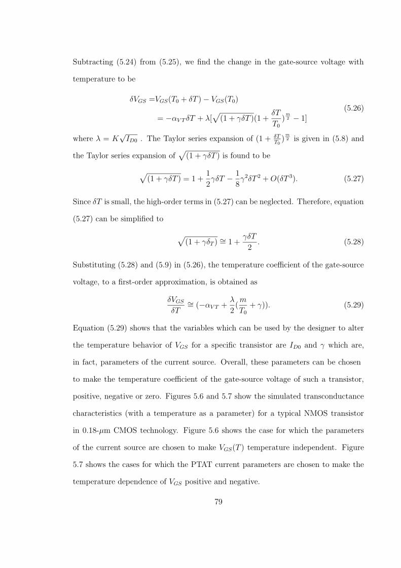
Subtracting (5.24) from (5.25), we find the change in the gate-source voltage with
temperature to be
δVGS =VGS(T0 + δT )− VGS(T0)
= −αV T δT + λ[√
(1 + γδT )(1 +δT
T0
)m2 − 1]
(5.26)
where λ = K√ID0 . The Taylor series expansion of (1 +
δTT0)
m2 is given in (5.8) and
the Taylor series expansion of√
(1 + γδT ) is found to be
√
(1 + γδT ) = 1 +1
2γδT − 1
8γ2δT 2 +O(δT 3). (5.27)
Since δT is small, the high-order terms in (5.27) can be neglected. Therefore, equation
(5.27) can be simplified to
√
(1 + γδT ) ∼= 1 +γδT
2. (5.28)
Substituting (5.28) and (5.9) in (5.26), the temperature coefficient of the gate-source
voltage, to a first-order approximation, is obtained as
δVGSδT
∼= (−αV T +λ
2(m
T0
+ γ)). (5.29)
Equation (5.29) shows that the variables which can be used by the designer to alter
the temperature behavior of VGS for a specific transistor are ID0 and γ which are,
in fact, parameters of the current source. Overall, these parameters can be chosen
to make the temperature coefficient of the gate-source voltage of such a transistor,
positive, negative or zero. Figures 5.6 and 5.7 show the simulated transconductance
characteristics (with a temperature as a parameter) for a typical NMOS transistor
in 0.18-µm CMOS technology. Figure 5.6 shows the case for which the parameters
of the current source are chosen to make VGS(T ) temperature independent. Figure
5.7 shows the cases for which the PTAT current parameters are chosen to make the
temperature dependence of VGS positive and negative.
79

0.55 0.6 0.65 0.7 0.75 0.80
20
40
60
80
100
Gate−Source Voltage, V
Dra
in C
urre
nt, u
A
Transconductance Characteristics
T1=−50T2=0T3=50T4=100T5=150
ZTC
Vgs is temperature independent
T1
T2
T3 T4 T5
Figure 5.6: Simulated transconductance characteristics of an NMOS transistor
80

0.55 0.6 0.65 0.7 0.75 0.80
20
40
60
80
100
Gate−Source Voltage, V
Dra
in C
urre
nt, u
A
Transconductance Characteristics
T1=−50T2=0T3=50T4=100T5=150
ZTC
Vgs is increasing with Temperature
Vgs is decreasing with temperature
T1
T2
T3 T4 T5
Figure 5.7: Simulated transconductance characteristics of an NMOS transistor
81

5.3 A Simple Voltage Reference Using a PTAT
Current Source
It was shown in the previous section that the designer can alter the temperature
coefficient of the gate-source voltage of a diode-connected transistor biased with a
PTAT current, by changing the PTAT current source parameters. Therefore, accord-
ing to (5.29), in order to have a temperature-independent VGS for a diode-connected
transistor biased with a PTAT current, the current parameters λ and γ should satisfy
λ
2(m
T0
+ γ) = αV T . (5.30)
This condition can be used to design a simple CMOS voltage reference, as explained
in the next section.
5.3.1 Circuit Design and Analysis
A circuit consisting of a PTAT current reference and a diode-connected NMOS tran-
sistor is designed in 0.18-µm TSMC technology. The circuit is shown in Figure 5.8.
The value of the resistor, RB, and the sizes of the transistors are given in Table 5.2.
Transistors (M1 −M4) and Resistor RB form the current reference circuit. The cur-
rent reference circuit is similar to the current reference used in Figure 5.2. The only
difference is that the current in the circuit shown in Figure 5.8 is generated by the
gate-source voltage difference of two NMOS transistors, while in the circuit shown
in Figure 5.2, the current is generated by the gate-source voltage difference of two
PMOS transistors. The operation is similar and both current references generate a
current which is given by
IB = IB0(1 + γ(T − T0)) (5.31)
82

where
γ =m
T0
− 2αR1. (5.32)
Note that in the Figure 5.2 a constant current was required, i.e., γ ' 0, while in
the circuit shown in Figure 5.8 a PTAT current is required, i.e., γ > 0. In (5.32), m is
in the range of (1.5-2) for the electron mobility and assuming T0 = 27C, αR1 should
be less than 0.0278/C in order to have γ > 0. We used N+ non-silicide diffusion
with αR1 = 1.47× 10⁻³deg−1 and αR2 = 0.832× 10⁻⁶deg−2 for the realization of the
resistor.
In Figure 5.8, transistors (Ms1 −Ms3) form the start-up circuit. The structure is
different from the one used in Figure 5.2. When the power supply is turned on, Ms1
is initially on and operates in the triode region and transistor Ms2 is off. The voltage
at the gate of Ms3 is high and therefore, its drain is down, pulling the gate of M2
down as well. As soon as the gate-drain voltage of transistor M4 increases, the drain
voltage of transistor Ms2 decreases, which turns off transistor Ms3.
In Figure 5.8, transistor M5 mirrors the current IB by a factor of(W/L)5(W/L)1
. As a
result, the current that biases transistor M6 is given by
ID6 = ID60[1 + γ(T − T0)] (5.33)
where ID60 =(W/L)5(W/L)1
IB0 and γ is given by (5.32). To obtain a temperature-independent
VGS6, the parameters of the current ID6 should satisfy (5.30), where λ = K6
√ID60.
Using (5.32), (5.30) and (5.33), the design equation is obtained as
√
(WL)5
(WL)1=
αV T
K6
√IB0(
mT0− αR1)
. (5.34)
Therefore, if the sizes of transistorsM1 andM5 satisfy (5.34), the gate-source voltage,
VGS6, will be temperature-independent.
83

Table 5.2: Transistor and resistor sizes for the circuit shown in Figure 5.8
Ms1 Ms2 Ms3 M1 M2
.42µ2µ
10µ2µ
3µ2µ
8µ2µ
8µ2µ
M3 M4 M5 M6 RB
5.5µ2µ
4µ2µ
18.4µ2µ
8µ2µ
2kΩ
M1
M4
M5
M6
V GS6
I B
M2
M3
VDD
M s 1
M s 3
M s 2
R B
I D6
V out
Figure 5.8: Voltage reference using a diode-connected transistor biased with a PTAT
current source
84
The above analysis is based on the assumption that all the MOS transistors are
operating in the saturation region. Thus the minimum supply voltage must be main-
tained in order to prevent the current source M5 from being forced to operate in the
triode region. Since VTHn and |VTHp| have negative temperature coefficients, the mini-
mum required power supply should be evaluated at the lowest operating temperature.
That is,
VDDmin = (VTHn)max + |VDS5(sat)|. (5.35)
Note that the circuit can be easily designed with the saturation voltage, |VDS5(sat)|
less than 0.2 V and therefore, the minimum required power supply can be less than
1 V.
5.3.2 Simulation Results
The circuit shown in Figure 5.8 was simulated in the temperature range of −50C to
150C using a power supply voltage of 1.8 V. Figure 5.9 shows the simulation results
for the PTAT currents, IB and I6 and the gate-source voltage VGS6. Note that currents
IB and I6 increase as the temperature increases and they can be approximated as a
linear function of temperature with the temperature coefficient of γ = 1.85×10⁻³/C.
However, as (5.15) shows, IB includes higher-order temperature terms that results in
not an exact linearalization of PTAT currents.
The change in the gate-source voltage of transistor M6 is 500µV only, over the
temperature range of −50C to 150C and its temperature stability is equal to 4
ppm/C. Since the temperature-dependency of the threshold voltage and bias current
are not perfectly linear in the whole temperature range, a nonlinear residue appearing
on the VGS6 waveform. The results of simulation verify that the circuit operates
according to the analysis given above.
85

−50 0 50 100 15010
12
14
16
Temperature, C
IB, u
A
−50 0 50 100 15025
30
35
40
Temperature, C
ID6,
uA
−50 0 50 100 150640.4
640.6
640.8
641
VG
S6,
mV
Temperature, C
Figure 5.9: Simulation results for IB, ID6 and VGS6 for the circuit shown in Figure
5.8
86
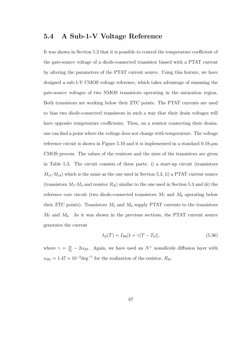
5.4 A Sub-1-V Voltage Reference
It was shown in Section 5.2 that it is possible to control the temperature coefficient of
the gate-source voltage of a diode-connected transistor biased with a PTAT current
by altering the parameters of the PTAT current source. Using this feature, we have
designed a sub-1-V CMOS voltage reference, which takes advantage of summing the
gate-source voltages of two NMOS transistors operating in the saturation region.
Both transistors are working below their ZTC points. The PTAT currents are used
to bias two diode-connected transistors in such a way that their drain voltages will
have opposite temperature coefficients. Then, on a resistor connecting their drains,
one can find a point where the voltage does not change with temperature. The voltage
reference circuit is shown in Figure 5.10 and it is implemented in a standard 0.18-µm
CMOS process. The values of the resistors and the sizes of the transistors are given
in Table 5.3. The circuit consists of three parts: i) a start-up circuit (transistors
Ms1-Ms3) which is the same as the one used in Section 5.3, ii) a PTAT current source
(transistorsM1-M4 and resistor RB) similar to the one used in Section 5.3 and iii) the
reference core circuit (two diode-connected transistors M7 and M8 operating below
their ZTC points). Transistors M5 and M6 supply PTAT currents to the transistors
M7 and M8. As it was shown in the previous sections, the PTAT current source
generates the current
IB(T ) = IB0[1 + γ(T − T0)], (5.36)
where γ = mT0− 2αR1. Again, we have used an N+ nonsilicide diffusion layer with
αR1 = 1.47× 10⁻³deg−1 for the realization of the resistor, RB.
87

Table 5.3: Transistor and resistor sizes for the circuit shown in Figure 5.10
Ms1 Ms2 Ms3 M1 M2 M3 M4
.42µ2µ
10µ2µ
3µ2µ
8µ2µ
8µ2µ
5.5µ2µ
4µ2µ
M5 M6 M7 M8 RB R1 R2
12.4µ2µ
25µ2µ
8µ2µ
8µ2µ
2kΩ 20kΩ 20kΩ
V ref
M1
M4
M5 M6
M8 M7
V-1 V-2 I B
M2
M3
VDD
M s 1
M s 3
M s 2
R B
R 1 R 2
I 8 I 7
Figure 5.10: A Sub-1-V voltage reference
88

5.4.1 Circuit Design and Analysis
In Figure 5.10, the output voltage reference is given by
Vref =VGS7
1 + R1
R2
+VGS8
1 + R2
R1
. (5.37)
Note that the reference voltage depends on the ratio of the resistors R1 and R2 and,
therefore, the sensitivity of the temperature coefficient of the output voltage to the
variation of R1 and R2 ratio (due to doping gradient, non-optimized layout and high
stress area of die) is reduced.
The temperature coefficient of the output voltage is obtained by taking the deriva-
tive of equation (5.37) with respect to the temperature. Doing so and using (5.29),
the temperature coefficient of the output voltage will be equal to
δVrefδT
=1
1 + (R1/R2)
(
δVGS7
δT
)
+1
1 + (R2/R1)
(
δVGS8
δT
)
= −αV T +(
λ7
1 + (R1/R2)+
λ8
1 + (R2/R1)
)(
m
2T0
+γ
2
) (5.38)
where λ7 = K7
√
(W/L)5(W/L)1
IB0, λ8 = K8
√
(W/L)6(W/L)1
IB0 and γ =mT0− 2αR1. If the sizes of
transistors M5 and M6 are chosen to satisfy√
(
WL
)
5
1 + (R1/R2)+
√
(
WL
)
6
1 + (R2/R1)=
αV T
√
(
WL
)
1
(mT0− αR1)(K ′
7
√IB0)
(5.39)
then the reference voltage will be temperature-independent. The minimum required
power supply is given by
VDDmin= (VTHn)max + |VDS5(sat)| (5.40)
and the circuit can be easily designed with VDS(sat) of less than 0.2 V.
5.4.2 Simulation Results
The circuit shown in Figure 5.10 was simulated in the temperature range of −50C
to 150C using a power supply voltage of 1.8 V. Figure 5.11 shows the simulation
89

results for the PTAT currents, IB, I7 and I7. As it can be seen, the currents IB,
I6 and I7 increase as the temperature increases and they can be approximated as a
linear function of temperature with a temperature coefficient of γ = 1.85× 10⁻³/C.
However, (5.15) includes higher-order terms that results in not an exact linearalization
of the PTAT currents.
Figure 5.12 shows the simulation results for the gate-source voltages of transistors
M7 and M8 and the output voltage Vref . The change in the output voltage, obtained
in simulation, is only 0.5mV, over the temperature range of −50C to 150C and its
temperature stability is 4 ppm/C. Since the temperature-dependence of the threshold
voltage and bias current are not perfectly linear over the whole temperature range,
a nonlinear temperature-dependent error voltage appears at the reference output
voltage. The results of simulation verify that the circuit operates according to the
analysis given above.
Another important parameter which should be considered in the design of voltage
references is called power supply rejection ratio (PSRR). It applies to the changes
in the reference voltage that result from variations in the power supply [17]. Figure
5.13 shows the change of the output voltage, Vref , while the power supply, VDD
changes from 0 V to 2 V. The circuit was designed for the supply 1.8 V. When the
power supply deviates by ±10% from 1.8 V, the change in the output voltage is
approximately ±4mV. Although the change in the output voltage seems to be small
but it can be improved using suitable circuit solutions. In this project, we intended to
focus on temperature stabilization and no attempts were made to improve the PSRR
factor.
90

−50 0 50 100 15010
12
14
16
Temperature, oC
I B, µ
A
−50 0 50 100 15018
20
22
24
26
Temperature, oC
I 7, µA
−50 0 50 100 15030
35
40
45
Temperature, oC
I 8, µA
Figure 5.11: Temperature dependencies of IB, I7 and I8 for the circuit shown in
Figure 5.10
91
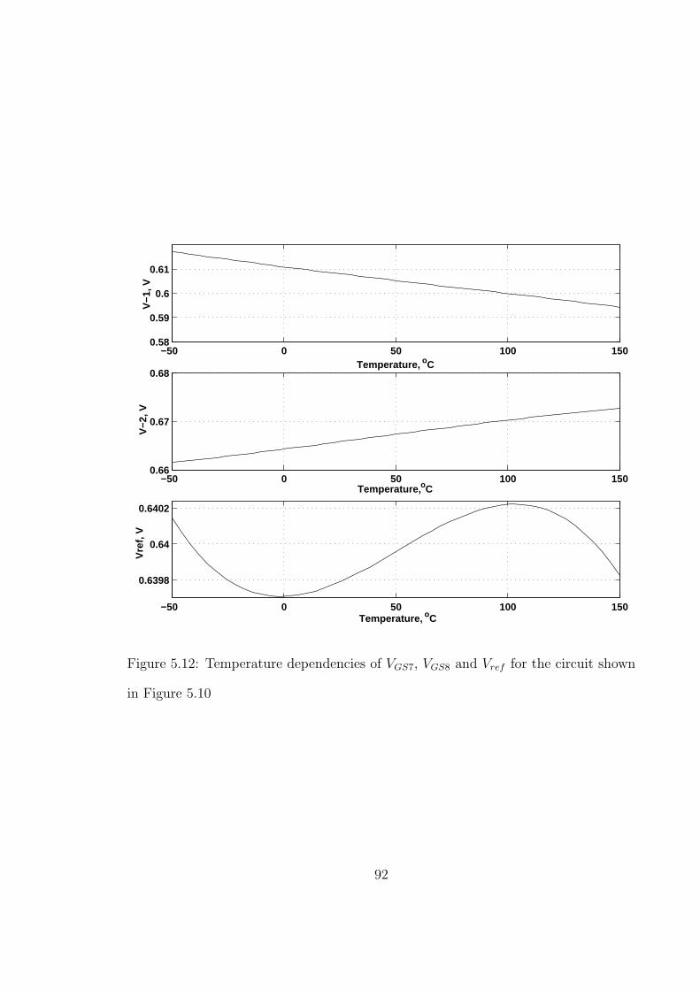
−50 0 50 100 1500.58
0.59
0.6
0.61
Temperature, oC
V−1
, V
−50 0 50 100 1500.66
0.67
0.68
Temperature, oC
V−2
, V
−50 0 50 100 150
0.6398
0.64
0.6402
Temperature, oC
Vre
f, V
Figure 5.12: Temperature dependencies of VGS7, VGS8 and Vref for the circuit shown
in Figure 5.10
92

0 0.2 0.4 0.6 0.8 1 1.2 1.4 1.6 1.8 20
100
200
300
400
500
600
700
VDD
, V
Vre
f,mV
Figure 5.13: Change in Vref due to the variation in power supply, for the circuit shown
in Figure 5.10, T = T0 = 27C
93

5.5 Performance Comparison of Various Voltage
References
A comparison of the voltage references proposed and studied in this thesis is tabu-
lated in Table 5.4. For each design technique, the technology used to implement the
voltage reference, the required power supply, VDD, the output voltage, Vref and the
temperature coefficient of the reference voltage are given. Table 5.4 shows that the
voltage references proposed in Section 5.3 and 5.4 have a much better temperature
performance compared to the other non-bandgap references those of [44], [46] and
[14]. Also one can see from Table 5.4 that the temperature performance of the cir-
cuits proposed in Sections 5.3 and 5.4 are comparable to the curvature compensated
bandgap references of [3], [39] and [33]. The proposed references can be implemented
in a standard CMOS technology unlike the voltage references of [44], which need ex-
tra fabrication steps for implementation. Also our voltage references can be designed
for low voltage operation, while the voltage references [5] needs low threshold voltage
devices for low voltage operation.
94

Table 5.4: Comparison of Various Voltage References
Design Technique Technology VDD Vref TC(ppm/C)
First-order BGR
using current processing [5] 0.4-µm CMOS 2.1 V 0.515 V ± 59(27C-125C)
Curvature-Compensated BGR
using V 2PTAT [3] 6-µm CMOS - 1.192 V 25.6 (-55C-125C)
Curvature-Compensated BGR
using TC of resistors [39] 0.6-µm CMOS 2 V 1.14 V 5.3 (0C-100C)
Curvature-Compensated BGR
using nonlinear current [33] 2-µm CMOS 1.1 V 0.595 V 20 (-15C-90C)
CMOS Voltage Reference
using DTMOS devices [40] 0.35-µm CMOS 0.85 V 0.650 V 57 (-50C-75C)
CMOS Voltage Reference
using VTH subtraction [44] SOI-MOS - 2.38 V 33.8 (-50C-75C)
CMOS Voltage Reference
using VGS subtraction [46] 0.6-µm CMOS 1.4 V 0.313 V 36.9 (0C-100C)
CMOS Voltage Reference
using ZTC point[14] 0.35-µm CMOS 3.3 V 0.799 V 13 (-20C-100C)
CMOS Voltage Reference
presented in Section 5.1 0.18-µm CMOS 1.8 V 0.703 V 28 (-50C-150C)
CMOS Voltage Reference
presented in Section 5.3 0.18-µm CMOS 1.8 V 0.640 V 4 (-50C-150C)
CMOS Voltage Reference
presented in Section 5.4 0.18-µm CMOS 1.8 V 0.640 V 4 (-50C-150C)
95

5.6 Conclusion
In this chapter, three new voltage reference circuits were proposed and designed in
0.18-µm technology. First, a voltage reference was presented which takes advantage
of summing the gate-source voltages of two diode-connected transistors biased by
temperature-stable currents. The temperature coefficient of the output voltage of
this reference was shown to be 28 ppm/C over the temperature range of -50C to
150C. It was also shown that the temperature dependence of the gate-source voltage
of a CMOS transistor biased with a PTAT current source can be controlled by the
parameters of the PTAT current source. Based on this idea, two voltage references
were designed and implemented in 0.18-µm technology. The temperature dependence
of the reference voltage in both circuits was found to be 4 ppm/C over the range
of -50C to 150C. Finally, the performance of the proposed voltage references was
compared with other voltage references in the literature and it was concluded that our
voltage references have a performance comparable with the bandgap voltage references
and a better performance than the non-bandgap ones.
96

Chapter 6
Conclusion
Current and voltage references find applications in a variety of analog and digital
circuits and systems. Designing a reference merits the scrutiny of several factors.
Temperature-drift is one of the most important issues with which to contend.
The temperature drift of the current references must be well characterized and
controlled. There are four types of current references used in circuit designs. The
most frequently used current reference is a PTAT current reference which generates a
current which is linearly proportional to temperature. A CTAT current, the comple-
ment of PTAT, is also used as a reference current. Temperature-independent current
references are usually designed based on properly combining temperature-dependent
currents or using available voltage references. Finally, a PTAT2 reference is another
useful type of a current reference which generates a current that is proportional to
the square of the temperature.
Voltage references are divided into three categories when considering temperature
compensation. A zero-order reference simply is a naturally existing voltage (such as
a Zener diode) that does not fluctuate significantly with operating conditions. There
is no effort on the part of the designer to improve the existing tolerance of the given
97

voltage. When the accuracy is improved by attempting to cancel the first-order term
of the polynomial relationship with respect to temperature, the order of the reference
is increased by 1. Finally, curvature-corrected references improve the accuracy by
cancelling the second-order and higher-order components of the given voltage. The
most widely used first-order or higher-order voltage reference is a bandgap reference.
Its output voltage is referred to the bandgap energy of silicon and is stable against
temperature and process variations. Bandgap references are bipolar in nature but can
also be implemented in any standard CMOS technology, using parasitic vertical BJTs.
As an alternative, voltage references in MOS technology can also be implemented
using the threshold voltage difference. However, this technique is not applicable in
standard low-cost CMOS technologies since additional fabrication steps are needed.
Exploiting the presence of the ZTC point has also been proposed and used for the
design of CMOS voltage references, but this technique might not be suitable for low
voltage design. In this thesis, the techniques used for the design of these references,
as well as the advantages and disadvantages of each method were studied.
The main contributions of this thesis are highlighted below.
1. A new CMOS voltage reference using two diode-connected NMOS transistors bi-
ased by constant currents has been designed and implemented in 0.18-µm technol-
ogy. The circuit was designed using gate-source voltage summation of two NMOS
transistors, which show opposite temperature behaviors. The temperature coeffi-
cient of the output voltage of this reference has been found to be 28 ppm/C over
the temperature range of -50C to 150C.
2. The temperature behavior of the gate-source voltage of a CMOS transistor biased
by a PTAT current source has been investigated analytically. It was shown that
98

the temperature-coefficient of the gate-source voltage of the transistor can be con-
trolled by the parameters of the PTAT current source. This idea can be used for
the design of CMOS voltage reference.
3. A new CMOS voltage reference consisting of a PTAT current source and a diode-
connected NMOS transistor has been proposed and realized in 0.18-µm technol-
ogy. The parameters of the PTAT current source have been chosen so that the
gate-source voltage of the diode-connected transistor shows minimum temperature
dependence. Simulation results have shown a temperature coefficient of 4 ppm/C
over the range of -50C to 150C.
4. A new CMOS voltage reference, which takes advantage of summing the gate-
source voltages of two diode-connected transistors biased by PTAT currents, has
been implemented in 0.18-µm technology. The diode-connected transistors have
been biased below their ZTC points and, therefore, this circuit is able to operate
with sub-1-V power supply. The circuit has been simulated over the temperature
range of -50C to 150C and the reference voltage shows a temperature coefficient
of 4 ppm/C.
5. The performances of the proposed voltage references were compared with other
voltage references in the literature and it was shown that our voltage references
have a performance comparable with the bandgap voltage references and a better
performance than the non-bandgap ones.
99

References
[1] G. A. Rincon-Mora, Voltage References, From diodes to precision high-order
bandgap circuits. NJ, U.S.A.: IEEE Press and Wiley Interscience, 2002.
[2] C. Toumazou, G. Moschytz, and B. Gilbert, Trade-Offs in Analog Circuit Design,
The Designer’s Companion. Kluwer Academic Publisher, 2002.
[3] B. Song and P. Gray, “A precision curvature-compensated CMOS bandgap ref-
erence,” IEEE Journal of Solid-State Circuits, vol. 18, no. 6, pp. 634–643, Dec.
1983.
[4] K. Leung and P. Mok, “A sub-1-V 15-ppm/C CMOS bandgap voltage reference
without requiring low threshold voltage device,” IEEE Journal of Solid-State
Circuits, vol. 37, no. 4, pp. 526–530, Apr. 2002.
[5] H. Banba, H. Shiga, A. Umezawa, T. Miyaba, T. Tanzawa, S. Atsumi, and
K. Sakui, “A CMOS bandgap reference circuit with sub-1-V operation,” IEEE
Journal of Solid-State Circuits, vol. 34, no. 5, pp. 670–674, May 1999.
[6] R. A. Blauschild, P. A. Tucci, R. S. Muller, and R. G. Meyer, “A new NMOS
temperature-stable voltage reference,” IEEE Journal of Solid-State Circuits, vol.
13, no. 6, pp. 767–774, Dec. 1978.
100

[7] J. C. Harvey, “Techniques for a high temperature CMOS operational amplifier,”
M.S. thesis, Case Western Reservce University, Jan. 1998.
[8] D. L. Pulfrey and N. G. Tarr, Intoduction to Microelectronic Devices. New Jersey:
Prentice Hall, 1989.
[9] S. M. Sze, Physics of Semiconductor Devices. New Jersey: John Wiley and Sons,
1981.
[10] S. M. Sze, Semiconductor Devices, Physics and Technology, 2nd ed. New York:
John Wiley and Sons, 2002.
[11] F. M. Klaassen and W. Hes, “On the temperature coefficient of the MOSFET
threshold voltage,” Solid State Electron, vol. 29, no. 8, pp. 787–789, 1986.
[12] Z. D. Prijic, “Analysis of temperature dependence of CMOS transistors’ thresh-
old voltage,” Microelectronic Reliable, vol. 31, no. 1, pp. 33–37, 1991.
[13] Y. P. Tsividis, Operational and Modeling of the MOS Transistor. New York:
McGraw-Hill, 1987.
[14] I. M. Filanovsky and A. Allam, “Mutual compensation of mobility and threshold
voltage temperature effects with applications in CMOS circuits,” IEEE Trans-
actions on Circuits and Systems-I, vol. 48, no. 7, pp. 876–883, July 2001.
[15] K. R. Laker and W. M. C. Sansen, Design of Analog Integrated Circuits and
Systems. New York: McGraw-Hill, 1994.
[16] P. R. Gray and R. G. Meyer, Analysis and Design of Analog Integrated Circuits,
3rd ed. New York: John Wiley and Sons, 2001.
101

[17] F. Maloberti, Analog Design for CMOS VLSI Systems. The Netherlands: Kluwer
Academic Publishers, 2001.
[18] W. T. Harrison, J. A. Connelly, and R. Stair, “An improved current-mode CMOS
voltage refrence,” in Proc. Southwest Symposium on Mixed-Signal Design, Feb.
2001, pp. 23–27.
[19] R. Stair, J. A. Connelly, and M. Pulkin, “A current-mode CMOS voltage re-
frence,” in Proc. Southwest Symposium on Mixed-Signal Design, Feb. 2000, pp.
23–26.
[20] D. Johns and K. Martin, Analog Integrated Circuit Design. New York: John
Wiley and Sons, 1997.
[21] I. M. Filanovsky, “An input-free VT extractor circuit using a series connection
of three transistors,” Int. J. Electronics, vol. 82, no. 5, pp. 527–532, 1997.
[22] P. Malcovati, F. Maloberti, M. Pruzzi, and C. Fiocchi, “Curvature compensated
BiCMOS bandgap with 1 V supply voltage,” in Proc. IEEE European Solid-State
Circuits Conference (ESSCIRC ’00), 2000, pp. 52–55.
[23] M. Martins and J. Dias, “CMOS shunt regulator with bandgap reference for
automotive environment,” IEE Proceeding Circuits Devices and Systems, vol.
141, pp. 157–161, June 1994.
[24] H. Tanaka, “Sub 1-µA dynamic reference voltage generator for battery operated
DRAMs,” IEEE Journal of Solid-State Circuits, vol. 29, no. 4, pp. 448–453, Apr.
1994.
[25] D. Hilbiber, “A new semiconductor voltage standard,” ISSCC Digest Technical
Papers, vol. 7, pp. 32–33, 1964.
102

[26] R. Widlar, “Some circuit design techniques for linear integrated circuits,” IEEE
Transactions on Circuits and Systems, vol. 12, no. 4, pp. 586–590, Dec. 1965.
[27] R. Widlar, “New developments in IC voltage regulators,” IEEE Journal of
Solid-State Circuits, vol. 6, no. 1, pp. 2–7, Feb. 1971.
[28] K. Kuijk, “A precision reference voltage source,” IEEE Journal of Solid-State
Circuits, vol. 8, no. 3, pp. 222–226, June 1973.
[29] A. Brokaw, “A simple three-terminal IC bandgap reference,” IEEE Journal of
Solid-State Circuits, vol. 9, no. 6, pp. 388–393, Dec. 1974.
[30] G. Meijer and J. Verhoeff, “An integrated bandgap reference,” IEEE Journal of
Solid-State Circuits, vol. 11, no. 3, pp. 403–406, June 1976.
[31] R. J. Widlar, “Low voltage techniques,” IEEE Journal of Solid-State Circuits,
vol. 13, pp. 838–846, Dec. 1978.
[32] I. Lee, G. Kim, and W. Kim, “Exponential curvature-compensated BiCMOS
bandgap reference,” IEEE Journal of Solid-State Circuits, vol. 29, no. 11, pp.
1396–1403, Nov. 1994.
[33] G. Rincon-Mora and P. Allen, “A 1.1 V current-mode and piecewise-linear cur-
vature corrected bandgap reference,” IEEE Journal of Solid-State Circuits, vol.
33, no. 10, pp. 1551–1554, Oct. 1998.
[34] S. Lewsi and A. Brokaw, “Curvature correction of bipolar bandgap references,”
U.S patent 4 808 908, Feb. 1989.
103

[35] E. Vittoz and J. Fellrath, “CMOS analog integrated circuits based on weak
inversion operation,” IEEE Journal of Solid-State Circuits, vol. 12, no. 6, pp.
224–231, June 1977.
[36] Y. Tsividis, “Accurate analysis of temperature effects in IC-VBE characteristics
with application to bandgap reference sources,” IEEE Journal of Solid-State
Circuits, vol. 15, no. 6, pp. 1076–1084, Dec. 1980.
[37] A. Boni, “Op-Amps and startup circuits for CMOS bandgap references with
near 1-V supply,” IEEE Journal of Solid-State Circuits, vol. 37, no. 10, pp.
1339–1343, Oct. 2002.
[38] Y. Jiang and E. K. Lee, “Design of low-volatge bandgap reference using tran-
simpedance amplifier,” IEEE Transactions on Circuits and Systems-II, vol. II,
pp. 552–555, June 2000.
[39] K. Leung, P. Mok, and C. Leung, “A 2-V 23µA 5.3-ppm/C Curvature-
Compensated CMOS Bandgap Voltage Reference,” IEEE Journal of Solid-State
Circuits, vol. 38, no. 3, pp. 561–564, Mar. 2003.
[40] A. Annema, “Low-power bandgap references featuring DTMOST’s,” IEEE
Journal of Solid-State Circuits, vol. 34, no. 7, pp. 949–955, July 1999.
[41] http://public.itrs.net/, “The ITRS Home page,” .
[42] H. Neuteboom, B. J. Kup, and M. Janssens, “A DSP-based hearing instrument
IC,” IEEE Journal of Solid-State Circuits, vol. 32, pp. 1790–1806, Nov. 1997.
[43] M. Ugajin, K. Suzuki, and T. Tsukaraha, “A 0.6-V supply, voltage-reference
circuit based on threshold-voltage-summation architecture in fully-depleted
104

CMOS/SOI,” IEICE Transactions on Electronics, vol. E85-C, no. 8, pp. 1588–
1595, August 2002.
[44] H. J. Song and C. Kim, “A temperature-stabilized SOI voltage reference based on
threshold voltage difference between enhancemenr and depletion NMOSFET’s,”
IEEE Journal of Solid-State Circuits, vol. 28, no. 6, pp. 671–677, June 1993.
[45] K. N. Leung and P. K. T. Mok, “A CMOS voltage reference based on weighted
difference of gate-source voltages between PMOS and NMOS transistors for low
dropout regulators,” in Proc. IEEE European Solid-State Circuits Conference
(ESSCIRC ’01), 2001, pp. 88–91.
[46] K. N. Leung and P. K. T. Mok, “A CMOS voltage reference based on weighted
∆VGS for CMOS low-dropout linear regulator,” IEEE Journal of Solid-State
Circuits, vol. 38, no. 1, pp. 146–150, Jan. 2003.
[47] T. Manku and Y. Wang, “Temperature-independent output voltage generated
by threshold voltage of an NMOS transistor,” IEE Electronics Letters, vol. 31,
no. 12, pp. 935–936, June 1995.
[48] I. M. Filanovsky, “Voltage reference using mutual compensation of mobility and
threshold voltage temperature effects,” in Proc. IEEE International Symposium
on Circuits and Systems (ISCAS ’00), 2000, pp. 197–200.
105

Vita
Laleh Najafizadeh
EDUCATION
September 2001 – October 2003
University of Alberta M.Sc. Electrical and Computer Engineering
September 1995 – June 1999
Isfahan University of Technology B.Sc. Electrical and Computer Engineering
WORK EXPERIENCE
Research Assistant, University of Alberta,
Department of Electrical and Computer Engineering, 2001-present
Teaching Assistant, University of Alberta,
Department of Electrical and Computer Engineering, 2001-present
Electronics Engineer, Isfahan Telecommunication Company,
Isfahan, Iran, 1999-2001
106

AWARDS
Delta Kappa Gamma World Fellowship (2003-2004)
Alberta Ingenuity Fund (2004)
PUBLICATIONS
I. M. Filanovsky, and L. Najafizadeh, ”Zeroing in on a zero-temperature coefficient
point,” Proc. 45th IEEE Midwest Symp. Circuits and Systems, Vol. 1, pp.271-274,
Tulsa, OK, August 2002.
L. Najafizadeh, and I. M. Filanovsky, ”Towards a sub-1-V CMOS voltage reference”,
Submitted to IEEE International Symposium on Circuits and Systems 2004.
L. Najafizadeh, and I. M. Filanovsky, ”A simple voltage reference using transistor
with ZTC point and PTAT current source”, Submitted to IEEE International Sym-
posium on Circuits and Systems 2004.
107