universit`a degli studi di padova dipartimento di fisica ed
TRANSCRIPT
Universita degli Studi di PadovaDipartimento di Fisica ed Astronomia “G.
Galilei”
Tesi di Laurea Magistrale in Fisica
Plasmonic Nano-Hole Arrays for QuantumEfficiency Enhancement of Er3+ Photoemission
Laureando:Luca Zanotto
Relatore:Prof. Giovanni Mattei
Correlatore:Dott.ssa Tiziana Cesca
Anno Accademico 2014/2015

Abstract
The purpose of the present thesis is the study of the interaction ofplasmonic nanostructures with an emitter in close proximity. The inves-tigation was carried out following different approaches but always withthe aim of inserting the experimental results in the framework of newor existing theoretical models in order to better understand the pho-tophysical nature of the interaction. To this aim in the framework ofthis thesis plasmonic nanohole arrays have been synthesised and coupledto Er-doped silica layers. The choice of Erbium as emitting source wasdriven by the great technological importance of this rare earth in photon-ics and optoelectronics, connected to the characteristic emission at 1540nm that matches the window of minimum transmission loss for silica. Forthis reason the first step of the research activity was devoted to the op-timization of the Er3+ photoluminescent properties in silica. When anemitter is placed near an interface, its optical properties will be modified.To describe this variation different contributions have to be taken intoaccount: the variation of the local density of state due to the reflectionfrom the interface, the coupling of the emitted radiation with propagatingsurface plasmons on the metal-dielectric interface and the dissipation inthe overlayer. Nanostructuring the overlayer offers further opportunitiesfor changing the optical properties of a nearby emitter. Among differentplasmonic nanostructures, nanohole arrays (NHAs) can represent the idealcandidate for this purpose due to their extraordinary optical transmission(EOT): at specific frequencies determined by the hole periodicity, the lighttransmitted through the NHA is orders of magnitude higher than the onepredicted with the classical diffraction theory. When the EOT peak wastailored with the emission wavelength of the emitter strong plasmoniccoupling was demonstrated, leading to lifetime shortening with almost nodissipation in the overlayer. Finally, all the obtained results allowed thedevelopment of predictive models that can be used in the design of noveldevices for different photonic applications.
2

Lo scopo del presente lavoro di tesi e l’analisi dell’interazione di na-nostrutture plasmoniche con un emettitore. Lo studio e stato condottoseguendo diversi approcci, ma sempre con il fine di confrontare i risultatisperimentali con modelli teorici sia gia noti che nuovi, in modo da com-prendere appieno la natura foto-fisica dell’interazione. In questo sensonell’ambito della presente tesi sono state sintetizzati nanohole array plas-monici ed accoppiati con film sottili di silice drogata con erbio. La sceltadell’erbio come emettitore e stata dettata dalla sua grande importanzatecnologica nella fotonica e nell’optoelettronica, associata alla caratter-istica emissione radiativa a 1540 nm, che si trova nella finestra di min-imo assorbimento ottico della silice. Per questa ragione il primo passodell’attivita di ricerca e stato volto all’ottimizzazione delle proprieta difotoluminescenza dello ione erbio in silice. Quando un emettitore e postoin prossimita di un film sottile le sue proprieta ottiche vengono modifi-cate. Per descrivere tale variazione e necessario tenere conto di contributidifferenti: la variazione della densit locale degli stati dovuta alla rifles-sione all’interfaccia, l’accoppiamento della radiazione emessa con plas-moni di superficie propaganti sull’interfaccia metallo-dielettrico e infinela dissipazione nel film. La nanostrutturazione del film puo offrire ul-teriori opportunit nella modifica delle propriet ottiche di un emettitore.Tra le diverse nanostrutture plasmoniche, i nanohole arrays (NHAs) pos-sono essere visti come i candidati ideali per questo scopo grazie alla lorotrasmissione ottica straordinaria (EOT): a determinate lunghezze d’ondadefinite dalla periodicit dei buchi e dalle proprieta dielettriche dei mate-riali coinvolti, la luce trasmessa attraverso il NHA e ordini di grandezzapiu grande rispetto a quella predetta dalla teoria classica della diffrazione.Quando il picco della EOT e risonante con la lunghezza d’onda di emis-sione dell’emettitore, e stato dimostrato un forte accoppiamento plasmon-ico che porta ad un marcato accorciamento del tempo di vita nella quasiassenza di dissipazione nella nanostruttura. Infine, tutti questi risultatihanno permesso lo sviluppo di modelli predittivi che possono essere uti-lizzati nella progettazione di nuovi dispositivi per diverse applicazioni fo-toniche.
3

Contents
Introduction 7
1 Interaction between metallic nano-structures and electromag-netic radiation 101.1 Electronic properties of metals . . . . . . . . . . . . . . . . . . . 10
1.1.1 Drude Model . . . . . . . . . . . . . . . . . . . . . . . . . 131.1.2 Lorentz-Drude model . . . . . . . . . . . . . . . . . . . . 14
1.2 Plasmon polaritons . . . . . . . . . . . . . . . . . . . . . . . . . . 161.2.1 Volume plasmons . . . . . . . . . . . . . . . . . . . . . . . 161.2.2 Surface plasmon polaritons . . . . . . . . . . . . . . . . . 161.2.3 Localized surface plasmons . . . . . . . . . . . . . . . . . 19
1.3 Nanohole arrays and the EOT . . . . . . . . . . . . . . . . . . . . 201.3.1 Transmission by sub-wavelength apertures . . . . . . . . . 201.3.2 Grating coupling . . . . . . . . . . . . . . . . . . . . . . . 211.3.3 Extraordinary transmission in nanohole arrays . . . . . . 22
2 Nanohole array fabrication 252.1 Nanosphere Litography . . . . . . . . . . . . . . . . . . . . . . . 252.2 Reactive ion etching . . . . . . . . . . . . . . . . . . . . . . . . . 282.3 Metal deposition . . . . . . . . . . . . . . . . . . . . . . . . . . . 29
3 Characterization and results 313.1 FEM simulations . . . . . . . . . . . . . . . . . . . . . . . . . . . 313.2 Sample synthesis and features . . . . . . . . . . . . . . . . . . . . 32
3.2.1 Nanosphere masks . . . . . . . . . . . . . . . . . . . . . . 323.2.2 Reactive ion etching . . . . . . . . . . . . . . . . . . . . . 343.2.3 Metal deposition . . . . . . . . . . . . . . . . . . . . . . . 35
3.3 NHA characterization . . . . . . . . . . . . . . . . . . . . . . . . 363.4 Conclusions . . . . . . . . . . . . . . . . . . . . . . . . . . . . . . 39
4 Er:SiO2 films 404.1 Er3+ optical properties . . . . . . . . . . . . . . . . . . . . . . . . 404.2 Er:SiO2 film synthesis . . . . . . . . . . . . . . . . . . . . . . . . 414.3 Measurements on Er:SiO2 films . . . . . . . . . . . . . . . . . . . 42
4.3.1 Thermal activation . . . . . . . . . . . . . . . . . . . . . . 434.3.2 Er3+ spectrum . . . . . . . . . . . . . . . . . . . . . . . . 434.3.3 Er concentration . . . . . . . . . . . . . . . . . . . . . . . 444.3.4 Emission cross section . . . . . . . . . . . . . . . . . . . . 45
5 Interaction between Erbium and interfaces 475.1 Theoretical model . . . . . . . . . . . . . . . . . . . . . . . . . . 475.2 Er3+ lifetime with CPS model . . . . . . . . . . . . . . . . . . . . 495.3 Radiative and non-radiative lifetime . . . . . . . . . . . . . . . . 505.4 Metallic overlayer . . . . . . . . . . . . . . . . . . . . . . . . . . . 51
5
5.5 Power dissipation . . . . . . . . . . . . . . . . . . . . . . . . . . . 51
6 Control of Erbium emission lifetime by interaction with Nanoholearrays 546.1 Interaction between Er and NHA . . . . . . . . . . . . . . . . . . 54
6.1.1 Sample synthesis . . . . . . . . . . . . . . . . . . . . . . . 546.2 Characterization and measurements . . . . . . . . . . . . . . . . 576.3 Finite Element Method simulations . . . . . . . . . . . . . . . . . 596.4 Experimental results and discussion . . . . . . . . . . . . . . . . 62
7 Conclusions 67
6
Introduction
The interest in the so called nanoscale materials has been gaining great impor-tance in the scientific community during the last decades, due to the discoverof new properties arising as the size of a system ranges between few and hun-dreds of nanometres. These peculiar features are not present in materials withmacroscopic size, but also disappear at the atomic scale. In particular, a lot ofmorphological and chemical characteristics, that are intrinsic at the macroscopicscale, become dependent on the size, shape and dielectric environment.
The first acknowledgement of the importance of the nanoscale is attributedto Richard Feynman, in his lecture ”There is plenty of room at the bottom”[1], where he first suggested that the properties of materials and devices atnanometre range would present future opportunities.
The meaning of the term Nanotechnology could be explained with the wordsof N. Taniguchi [2], the first to use this term in 1974: Nanotechnology mainlyconsists of the processing of separation, consolidation, and deformation of ma-terials by one atom or by one molecule. Since then a lot of techniques for pro-cessing materials in the way described by Taniguchi have been developed andproduced important innovations in many fields, as biological sensors, surfacecoating, catalysis, computer science, optics, and many others.
One of the most fascinating fields in nanoscience is the study of the inter-action of light with metallic nanostructures, since it exhibits unique propertiesabsent in the macro-world. The study of the optical properties of radiation at thenanoscale, goes under the name of nanophotonics. In particular the branch thathandles with the interaction between the interfaces of nanostructured metals (inparticular noble metals) and electromagnetic radiation, is named Plasmonics.The purpose of the research in this field is to have a control on the confinementof light over distances smaller than the wavelength and over the consequentenhancement of the optical near-field [3].
Among the various possible applicative scopes of plasmonics, the one onwhich this thesis work focuses, is the interaction between an emitter of elec-tromagnetic radiation and a plasmonic nanostructure placed in close proximity.This configuration allows the interface to modify the decay rate of the emit-ter, thanks to the coupling in the near-field with Surface Plasmon Polaritons(SPPs), i.e. propagating electromagnetic waves confined at the surface of ametal [3].
In principle the excitation of SPPs is not allowed on a flat interface due to amismatch between the momentum of impinging radiation and the propagationconstant of the SPP, but thanks to the wide range of wave-vectors available inclose proximity (d � λem) of a dipole-like emitter, the coupling with SPPs innear-field becomes possible and this increases the de-excitation probability.
Moreover, once obtained the excitation of surface modes, they could re-excite the emitter or at least couple out into far-field radiation if a grating thatmatches the momentum is present. This grating properties can be achievednanostructuring the metal interface in an ordered way with the periodical prop-erties of a lattice. This allows to obtain the necessary coupling and thus to get
7
an increased efficiency of the photo-emission.This work focuses on the study of the optical properties of so-called nanohole
arrays, i.e. ordered lattices of nanometric holes on a thin film of a noble metal.As first observed by Ebbesen et al. in 1998 [4] the characteristic feature ofthese structures is to give rise to an extraordinary optical transmission (EOT)at a particular resonant wavelength, i.e. the transmitted intensity of from theholes is much higher than the intensity impinging on the total holes’ area. Theposition of the resonance can be chosen by varying the lattice parameter of thenanohole array.
There are multiple possible applications of nanohole arrays, most of them notyet investigated. This study is focused on the possible application of orderedarrays of holes in the coupling with the emitted radiation from erbium ions(Er3+) embedded in a silica matrix. If the ions are placed in close proximityof a metal interface, the local photonic density of state is modified [5] and thisproduces a variation in the radiative lifetime of the state of the emitter, thanksto the near-field coupling with SPPs. Moreover the grating properties of thelattice of holes permits to couple-out the SPPs to the far-field.
The choice of the erbium as the emitter is related to its technological im-portance connected to the characteristic emission at 1540 nm, that matches thewindow of minimum transmission loss for silica. Erbium doped fiber amplifiersare in fact widely used to compensate losses in the transmission of optical sig-nals over long distances. However, the Er-doped glass technological applicationsare limited by the small excitation cross-section and the long lifetime of the Erexcited state [6]. Thus finding a way to enhance the efficiency of the emissioncan lead to important improvement in the optical communication field.
The work is divided in two main parts: the first concerns the theoreticaldescription of the plasmonic properties, the fabrication and characterizationof nanohole arrays (sec. 1, 2, 3), and the second on the optical features oferbium and the study of the influence of nanohole arrays on the efficiency of itsphoto-emission properties (sec. 4, 5, 6).
8

1 Interaction between metallic nano-structuresand electromagnetic radiation
1.1 Electronic properties of metals
The interaction of metals with electromagnetic fields can be understood in aclassical framework based on Maxwell’s equations. Following [3] it’s shown thateven metallic nano-structures down to the order of a few nanometres can bedescribed without a need to resort to quantum mechanics, since high density offree carriers results in minute spacings of the electron energy levels, comparedto thermal excitation.
Thanks to the strong dependence of the optical properties on frequency, agreat variety of optical phenomena occurs in metals. For low frequencies, up tofar-infra-red, metals are highly reflective and do not allow electromagnetic wavesto propagate through them. In this regime the perfect conductor approximationof infinite or fixed finite conductivity is often valid, since only negligible part ofthe radiation penetrates into the metal. As frequency rises towards near-infra-red and visible part of the spectrum, field penetration increases significantly,leading to considerable dissipation, and make it difficult to scale the behaviourof the metal from the low frequency regime. Finally, at ultraviolet frequencies,metals acquire dielectric character and allow the propagation of electromagneticradiation, with refractive index and absorption depending on electronic struc-ture. Alkali metals exhibit an almost free-electron-like response and becometransparent to UV radiation, noble metals instead, show a strong absorption inUV range, caused by inter-band transitions.
The fundamental quantity to describe optical and dispersive properties, ina classical way, is the complex dielectic function ε(ω), which can be calculatedtheoretically and measured experimentally.
The start of the study of electromagnetic response of metals are the macro-scopic Maxwell’s equations:
∇ ·D = ρext (1.1)
∇ ·B = 0 (1.2)
∇×E = −∂B
∂t(1.3)
∇×H = Jext +∂D
∂t(1.4)
These equations link the macroscopic fields, electric E, magnetic B, dielectricdisplacement D and magnetic induction H, with the external charge densityρext and the external current density Jext. Clearly there are internal currentand charge density too, so that in total ρtot = ρext + ρ and Jtot = Jext + J.Constitutive equations lead to introduce two more fields, polarization P and
10
magnetization M, connected to the others via:
D = ε0E + P (1.5)
H =1
µ0B−M (1.6)
Magnetic response represented by M is not considered for purely plasmonicsystems, since only non-magnetic media are treated. Polarization P describesthe electric dipole moment per unit volume and it’s related to the internal chargedensity via ∇ ·P = −ρ. Charge conservation (∇ · J = −∂ρ∂t ) imposes that:
J =∂P
∂t(1.7)
With this approach the macroscopic electric field includes all polarizationeffects.
Now if the medium is linear, isotropic and non-magnetic, D and H areproportional to E and B, and the relations between them can be expressedusing relative permittivity ε and magnetic permeability µ:
D = ε0εE (1.8)
B = µ0µH (1.9)
The last constitutive relationship needed is:
J = σE (1.10)
where σ is the conductivity.Equations (1.8) and (1.10) are correct only for linear medium, without spatial
and temporal dispersion, but for metal, whose properties depend on frequency,the non-locality in space and time is to br taken into account , generalizing thelinear relationships:
D(r, t) = ε0
∫dt′dr’ε(r - r’, t - t’)E(r’, t’) (1.11)
J(r, t) =
∫dt′dr’σ(r - r’, t - t’)E(r′, t′) (1.12)
Taking the Fourier Transform of (1.11), the fields are decomposed into in-dividual plane-wave components of wave vector K and angular frequency ω,obtaining:
D(K, ω) = ε0ε(K, ω)E(K, ω) (1.13)
J(K, ω) = σ(K, ω)E(K, ω) (1.14)
After these considerations the relation between conductivity and relativepermittivity (from now on called the dielectric function) can be written:
ε(K, ω) = 1 +iσ(K, ω)
ε0ω(1.15)
11
Due to this intimate relationship either quantity can be used to describeelectromagnetic phenomena. Historically at optical frequencies is preferable touse the dielectric function ε(K, ω), and since this work investigates propertiesin NIR-Vis range, so only dielectric function will be considered.
While studying the interaction of light with metals, a simplification in thelimit of a spatially local response can be introduced. This is valid as long as thewavelength λ of the EM radiation in the material is significantly larger than alltypical dimensions of the medium, such the unit cell size and mean free path ofelectrons. This condition is fulfilled up to UV frequencies (λ . 100nm). Underthis assumption ε(K = 0, ω) = ε(ω).
In general ε is a complex valued function, depending on the angular frequencyω, which is real: ε(ω) = ε1(ω) + iε2(ω) can be written. Experimentally ε canbe determinate via reflectivity measurements, thanks to the relation with thecomplex refractive index n = n(ω) + ik(ω):
n =√ε. (1.16)
The imaginary part of the refractive index k = ε22n , is called the extinction
coefficient and determines the optical absorption of EM radiation propagatingthrough a medium. It’s proportional to the absorption coefficient α of the Beer’slaw of attenuation in a medium (I(x) = I0e
−αx) by the relation:
α(x) =2k(ω)ω
c(1.17)
Therefore, the imaginary part ε2 of the dielectric function determines theamount of absorption. For |ε1| � |ε2|, the real part n of the refractive index,quantifying the lowering of the phase velocity of the propagating waves due tothe polarization of the material, is mainly determined by ε1.
It’s useful to look for travelling-wave solutions of Maxwell’s equations inabsence of external stimuli. Combining the curl equations (1.1) yields the waveequation:
∇×∇×E = −µ0∂2D
∂t2(1.18)
K(K ·E)−K2E = −ε(K, ω)ω2
c2E (1.19)
in the time and Fourier domains, respectively. Two cases need to distinguished,depending on the polarization direction of the electric field vector. For trans-verse waves, K ·E = 0, leading to the generic dispersion relation:
K2 = ε(K, ω)ω2
c2(1.20)
For longitudinal waves, we obtain:
ε(K, ω) = 0 (1.21)
12
signifying that the longitudinal collective oscillations can occur at frequenciescorresponding to zeros of ε(ω).
1.1.1 Drude Model
As pointed out before, the dielectric function ε(ω) describes most of the in-formation about the interaction between metals and EM radiation. In a largefrequency range, including NIR and VIS, the simple Drude model of free elec-tron gas permits to calculate the dielectric function. This a plasma mode inwhich an electron gas of density n is supposed to move against a fixed lattice ofpositive ions. It’s to note that this approach has limited validity for noble met-als, because of inter-band transitions, that occur at visible frequencies: this kindof transitions need more sophisticated model, treated in section 1.1.2. In thismodel electrons are supposed to be free particles, neglecting details of latticepotential and electron-electron interactions, the only assumption is that somefeatures of the band structure are incorporated into the effective optical massm of the electron.
If an EM radiation is applied to the metal, electrons oscillate according tothe external field, and their motion is damped via collisions against the ions,with a collision frequency γ = 1
τ . At room temperature the relaxation time τof the free electron gas is typically ≈ 10−14s, and the frequency ≈ 100MHz.
Considering a free electron and a driving electric field E a simple equationof motion is obtained:
mx +mγx = −eE (1.22)
Assuming a time harmonic time dependence for the external electric field,E(t) = E0e
−iωt, the steady state solution has the same harmonic dependencex(t) = x0e
−iωt, where x0 is a complex value, which incorporates any phase shiftbetween driving field and response via:
x(t) =e
m(ω2 + iγω)E(t) (1.23)
Being x(t) single electron displacement, the electric dipole moment p(t) =−ex(t) can be written. Combining the effect of all n electrons in a unit volume,macroscopic polarization P writes:
P = −nex = − ne2
m(ω2 + iγω)E (1.24)
Inserting this in (1.5) the displacement D results:
D = ε0(1−ω2p
ω2 + iγω)E (1.25)
where the plasma frequency of the gas ω2p = ne2
ε0mwas introduced. From this the
dielectric function of the Drude model is obtained:
13
ε(ω) = 1−ω2p
ω2 + iγω= (1−
ω2p
ω2 + γ2) + i(
ω2pγ
ω(ω2 + γ2)) = ε1(ω) + iε2(ω) (1.26)
Different regimes can now be distinguished by varying ω compared to ωp.The model gives good results for ω < ωp, but fails in the regime of high fre-quencies ω � ωp, where ε(ω) → 1 is expected. In fact real metals and inparticular noble metals (like Au, Ag, Cu), important in plasmonics, have thefilled d band close to the Fermi surface, and this produce a high polarization.Taking into account this additional polarization of the ion cores by adding aterm P∞ = ε0(ε∞ − 1)E to (1.5), where P now represent the polarization dueto free electrons only. With this correction dielectric function becomes:
ε(ω) = (ε∞ −ω2p
ω2 + γ2) + i(
ω2pγ
ω(ω2 + γ2)) (1.27)
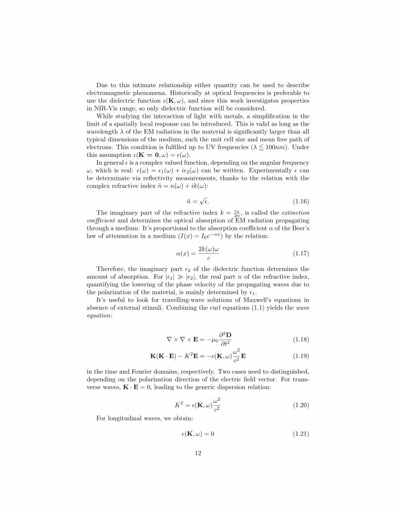
where ε∞ ' 1÷ 10. Validity of this free electron approach is shown in 1 whereexperimental data from Johnson and Christy [7] are compared to the dielectricfunction of Drude model. Model agrees with experimental measurements as longas inter-band transitions are negligible, in particular for copper and gold below2eV (600nm) and for silver below 4eV (300nm). The occurrence of inter-bandtransition above this energies leads to an increase of absorption, linked to ε2.
Clearly an advantage of having analytical formula for dielectric function isthat it can be easily included in numerical solvers for Maxwell’s equations.
Im
Re
2 4 6
20
10
0
10
Energy eV
Die
lect
ric
Func
tion
(a) Copper
Im
Re
2 4 6
20
10
0
10
Energy eV
Die
lect
ric
Func
tion
(b) Silver
Im
Re
2 4 6
20
10
0
10
Energy eV
Die
lect
ric
Func
tion
(c) Gold
Figure 1: Solid line represents dielectric function ε(ω) from Drude model fittedto experimental data from Johnson and Christy [7] (dotted line)
1.1.2 Lorentz-Drude model
It has been pointed out that for noble metals the Drude model is not adequatefor describing the dielectric function at high frequencies. Above the band edgethresholds, incident radiation is efficient in inducing inter-band transitions inthe bounded d electrons, below the Fermi surface, to higher bands, yieldingabsorption and competition between excitations of s and d electrons.
14
Au(ε∞ = 1.1156, σ/ε0 = 1355.01s−1) Ag(ε∞ = 1.4783, σ/ε0 = 3157.56s−1)
Ai[eV] Bi[eV2] Ci[eV2] Ai[eV] Bi[eV2] Ci[eV2]i = 1 −8.577 · 104 −1.156 · 104 5.557 · 107 −1.160 · 105 −3050 3.634 · 108
i = 2 −2.875 0.0 2.079 · 103 −4.252 −0.8385 112.2i = 3 −997.6 −3090 6.921 · 105 −0.4960 −13.85 1.815i = 4 −1.630 −4.409 26.15 −2.118 −10.23 14.31
Table 1: Coefficients of L4 model for Au and Ag
The model inadequacy can be overcome by adding a term in the equation ofmotion (1.22):
mx +mγx +mω20x = −eE (1.28)
Inter-band transitions are included considering the bounded electrons as os-cillators with resonance frequency ω0. This frequency corresponds to a certaininter-band transition with ~ω0 energy. If other inter-band transitions are con-sidered, there will be the same number of equations like (1.28) to solve. Eachof this equations leads to a Lorentz-oscillator term of the form:
Aiω2i − ω2 − iγiω
(1.29)
to add up to the dielectric function yet calculated for free-electrons. Here ω isthe radiation frequency, while ωi is the resonance frequency of the i-th inter-band transition [8]. If N inter-band transitions are considered, the dielectricfunction results:
ε(ω) = ε∞ −ω2p
ω2 + iγω+
N∑i=1
Aiω2i − ω2 − iγiω
(1.30)
Reminding the relationship between ε and σ and renaming coefficients, di-electric function becomes:
ε(ω) = ε∞ −iσ
ε0ω+
N∑i=1
Ciω2 + iAiω +Bi
(1.31)
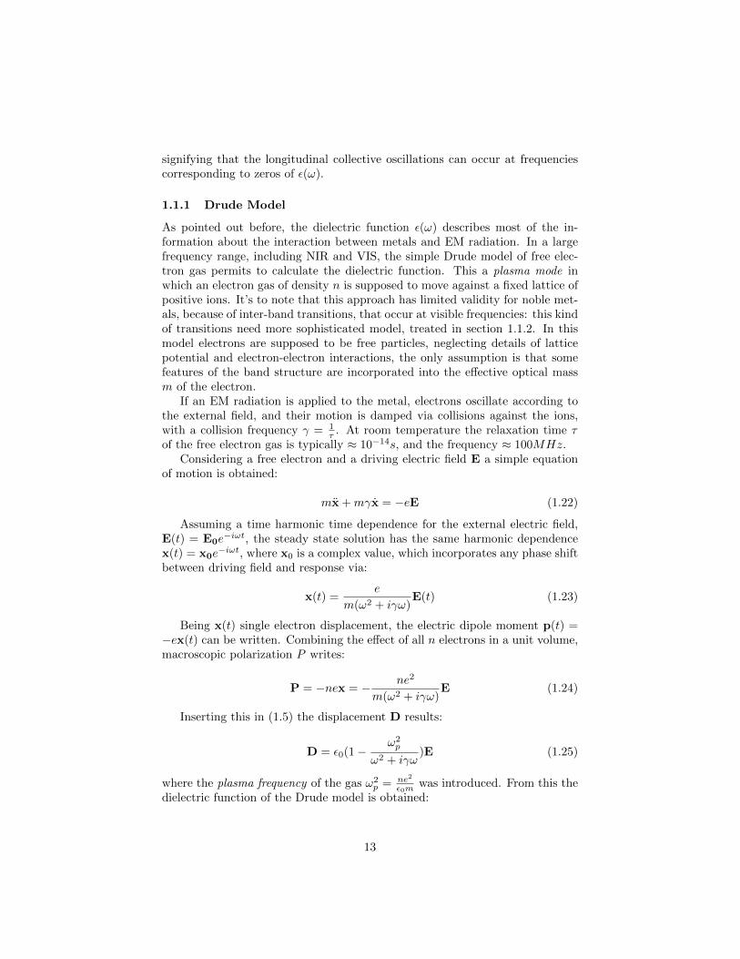
Coefficients were calculated by Nordlander and Hao [9] taking account of fourtransitions (L4 model) and are shown in 1. It appears from 2 that analyticaldielectric function fits very well experimental data, and it become helpful fornumerical calculations.
15
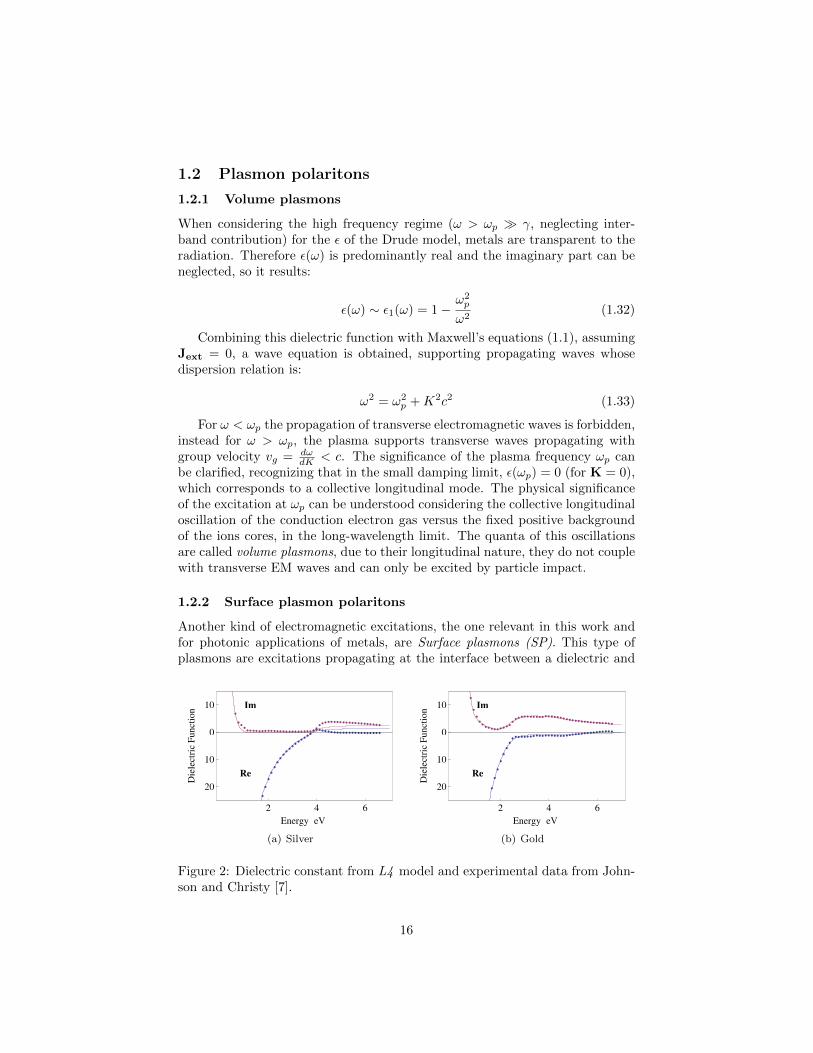
1.2 Plasmon polaritons
1.2.1 Volume plasmons
When considering the high frequency regime (ω > ωp � γ, neglecting inter-band contribution) for the ε of the Drude model, metals are transparent to theradiation. Therefore ε(ω) is predominantly real and the imaginary part can beneglected, so it results:
ε(ω) ∼ ε1(ω) = 1−ω2p
ω2(1.32)
Combining this dielectric function with Maxwell’s equations (1.1), assumingJext = 0, a wave equation is obtained, supporting propagating waves whosedispersion relation is:
ω2 = ω2p +K2c2 (1.33)
For ω < ωp the propagation of transverse electromagnetic waves is forbidden,instead for ω > ωp, the plasma supports transverse waves propagating withgroup velocity vg = dω
dK < c. The significance of the plasma frequency ωp canbe clarified, recognizing that in the small damping limit, ε(ωp) = 0 (for K = 0),which corresponds to a collective longitudinal mode. The physical significanceof the excitation at ωp can be understood considering the collective longitudinaloscillation of the conduction electron gas versus the fixed positive backgroundof the ions cores, in the long-wavelength limit. The quanta of this oscillationsare called volume plasmons, due to their longitudinal nature, they do not couplewith transverse EM waves and can only be excited by particle impact.
1.2.2 Surface plasmon polaritons
Another kind of electromagnetic excitations, the one relevant in this work andfor photonic applications of metals, are Surface plasmons (SP). This type ofplasmons are excitations propagating at the interface between a dielectric and
Im
Re
2 4 6
20
10
0
10
Energy eV
Die
lect
ric
Func
tion
(a) Silver
Im
Re
2 4 6
20
10
0
10
Energy eV
Die
lect
ric
Func
tion
(b) Gold
Figure 2: Dielectric constant from L4 model and experimental data from John-son and Christy [7].
16
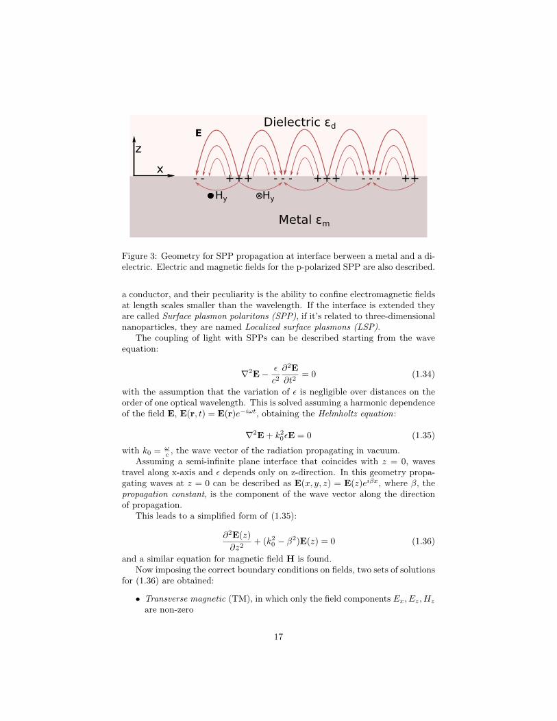
x
z
- - +++ - - - +++ - - - ++
EDielectric εd
Metal εm
Hy ⊗Hy
Figure 3: Geometry for SPP propagation at interface berween a metal and a di-electric. Electric and magnetic fields for the p-polarized SPP are also described.
a conductor, and their peculiarity is the ability to confine electromagnetic fieldsat length scales smaller than the wavelength. If the interface is extended theyare called Surface plasmon polaritons (SPP), if it’s related to three-dimensionalnanoparticles, they are named Localized surface plasmons (LSP).
The coupling of light with SPPs can be described starting from the waveequation:
∇2E− ε
c2∂2E
∂t2= 0 (1.34)
with the assumption that the variation of ε is negligible over distances on theorder of one optical wavelength. This is solved assuming a harmonic dependenceof the field E, E(r, t) = E(r)e−iωt, obtaining the Helmholtz equation:
∇2E + k20εE = 0 (1.35)
with k0 = ωc , the wave vector of the radiation propagating in vacuum.
Assuming a semi-infinite plane interface that coincides with z = 0, wavestravel along x-axis and ε depends only on z-direction. In this geometry propa-gating waves at z = 0 can be described as E(x, y, z) = E(z)eiβx, where β, thepropagation constant, is the component of the wave vector along the directionof propagation.
This leads to a simplified form of (1.35):
∂2E(z)
∂z2+ (k2
0 − β2)E(z) = 0 (1.36)
and a similar equation for magnetic field H is found.Now imposing the correct boundary conditions on fields, two sets of solutions
for (1.36) are obtained:
• Transverse magnetic (TM), in which only the field components Ex, Ez, Hz
are non-zero
17
• Transverse electric (TE), where only Hx, Hz, Ey being non-zero
Once defined the scattering plane, where incident and reflected wave-vectors lay,TM has the magnetic field perpendicular to this plane, TE the electric one.
Now if the considered single flat interface is between a dielectric, non absorb-ing medium (z > 0) with positive, real dielectric constant εd and an adjacentconducing half space (z < 0) described by a dielectric function εm(ω), with therequirement of metallic character, Re[εm(ω)] < 0 and solutions required are con-fined to the interface, i.e. with exponential decay in perpendicular z-direction,only TM modes are allowed, finding the dispersion relation:
β =
√εmεdεm + εd
(1.37)
where εm and εd are the dielectric functions of the metal and the dielectric.Now this relation can be studied in two cases, for metals with or without
attenuation:
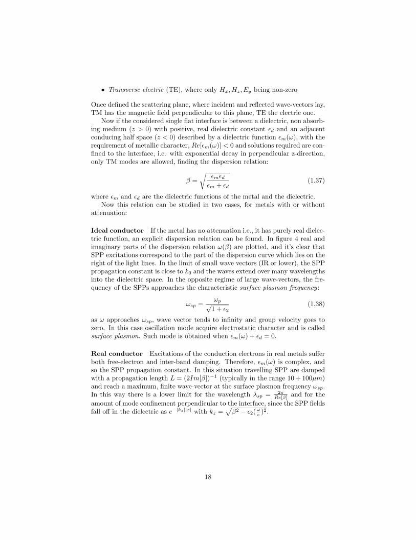
Ideal conductor If the metal has no attenuation i.e., it has purely real dielec-tric function, an explicit dispersion relation can be found. In figure 4 real andimaginary parts of the dispersion relation ω(β) are plotted, and it’s clear thatSPP excitations correspond to the part of the dispersion curve which lies on theright of the light lines. In the limit of small wave vectors (IR or lower), the SPPpropagation constant is close to k0 and the waves extend over many wavelengthsinto the dielectric space. In the opposite regime of large wave-vectors, the fre-quency of the SPPs approaches the characteristic surface plasmon frequency :
ωsp =ωp√
1 + ε2(1.38)
as ω approaches ωsp, wave vector tends to infinity and group velocity goes tozero. In this case oscillation mode acquire electrostatic character and is calledsurface plasmon. Such mode is obtained when εm(ω) + εd = 0.
Real conductor Excitations of the conduction electrons in real metals sufferboth free-electron and inter-band damping. Therefore, εm(ω) is complex, andso the SPP propagation constant. In this situation travelling SPP are dampedwith a propagation length L = (2Im[β])−1 (typically in the range 10÷ 100µm)and reach a maximum, finite wave-vector at the surface plasmon frequency ωsp.In this way there is a lower limit for the wavelength λsp = 2π
Re[β] and for the
amount of mode confinement perpendicular to the interface, since the SPP fieldsfall off in the dielectric as e−|kz||z| with kz =
√β2 − ε2(ωc )2.
18
Wave vectorβc/ωp
Freq
uenc
yω
/ωp
1
1
0.2
0.4
0.6
0.8
air silica
00
ωsp,air
ωsp,silica
Figure 4: Dispersion relation at air/Drude metal and silica/Drude metal inter-faces for dispersionless metals. Solid and dashed curves represent respectivelyRe{β} and Im{β} while straight lines represent light lines ω = kc/n
It’s important to stress the fact that SPP cannot be excited direct withthree-dimensional light beams, since the propagation constant β is greater thanthe wave vector k inside the dielectric, leading to evanescent decay on both sidesof the interface. There are various techniques for coupling radiation with SPPslike prism coupling and grating coupling. This last coupling will be used in thepresent work and described in the following.
1.2.3 Localized surface plasmons
Another type of surface plasmons can be defined, characterized by non propa-gating charge density oscillations, thus called Localized surface plasmons. LSParise when oscillations are confined to metallic nanoparticles or nanostructures.When light interacts with metallic particles, smaller than the incident wave-length, the electrons of a nanostructure can couple to the electromagnetic field.The curved surface of the particle exerts a restoring force on electrons, so thatresonances may arise when the particle is placed in an oscillating EM field. Thisleads to field enhancement both inside the particle and outside, in the adjacentsub-wavelength region. In contrast to SPPs, LPSs can be excited by directlight, without particular technique. The frequency of the resonance depends onthe metal, the shape and the size of the particle, and also from the dielectricconstant of the medium embedding the nanoparticles. In general there is notanalytic model describing this resonances. For spherical particles the Mie theory[10] allows a full treatment of the scattering problem by a single non-interactingspherical particle, expanding solution in spherical multi-pole partial waves. In
19
Wave vector Re{β}[107m-1]
Freq
uenc
yω
[101
5H
z]
2
4
6
8
10
00 2 4 6 8
air silica
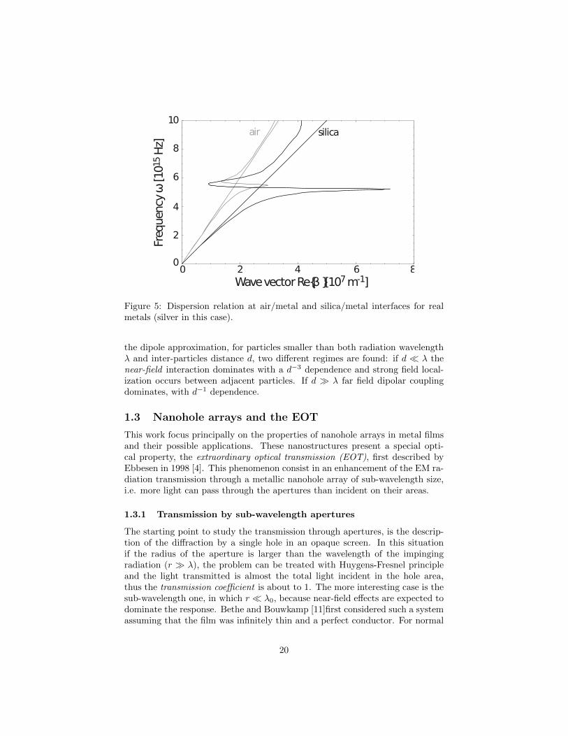
Figure 5: Dispersion relation at air/metal and silica/metal interfaces for realmetals (silver in this case).
the dipole approximation, for particles smaller than both radiation wavelengthλ and inter-particles distance d, two different regimes are found: if d � λ thenear-field interaction dominates with a d−3 dependence and strong field local-ization occurs between adjacent particles. If d � λ far field dipolar couplingdominates, with d−1 dependence.
1.3 Nanohole arrays and the EOT
This work focus principally on the properties of nanohole arrays in metal filmsand their possible applications. These nanostructures present a special opti-cal property, the extraordinary optical transmission (EOT), first described byEbbesen in 1998 [4]. This phenomenon consist in an enhancement of the EM ra-diation transmission through a metallic nanohole array of sub-wavelength size,i.e. more light can pass through the apertures than incident on their areas.
1.3.1 Transmission by sub-wavelength apertures
The starting point to study the transmission through apertures, is the descrip-tion of the diffraction by a single hole in an opaque screen. In this situationif the radius of the aperture is larger than the wavelength of the impingingradiation (r � λ), the problem can be treated with Huygens-Fresnel principleand the light transmitted is almost the total light incident in the hole area,thus the transmission coefficient is about to 1. The more interesting case is thesub-wavelength one, in which r � λ0, because near-field effects are expected todominate the response. Bethe and Bouwkamp [11]first considered such a systemassuming that the film was infinitely thin and a perfect conductor. For normal
20
incidence the aperture can be described as a small magnetic dipole located inthe plane of the hole and the transmission coefficient becomes:
T =64
27π2(k0r)
4 (1.39)
where k0 = 2π/λ0. The scaling with (r/λ0)4 implies very weak total trans-mission and is in agreement with Rayleigh’s theory of the scattering by smallobjects.
If the hypothesis of infinitely thin screen is relaxed, assuming a finite thick-ness h, via numerical simulation [12]it is found that the transmission coefficientis exponentially attenuated with h. At least if the real character of the metalis taken into account, with finite conductivity, the screen is not perfect opaque,but if h is on the order of several skin depths, radiation tunnelling is prevented.
Bethe also predicted that the light would be diffracted as it emerges fromthe hole in an angular pattern that depends on the orientation relative to thepolarization of the incident light. If the diffraction pattern is scanned along thedirection of the incoming polarization the intensity should be constant, while inperpendicular direction, the intensity decreases with increasing angle [11].
Mesurements of transmission and diffraction from a single sub-wavelengthaperture revealed unexpected features: less diffraction intensity and the presenceof a peak in the transmission spectrum (Wood’s anomalies) [13]. The appearanceof these resonant peaks can be understood as the excitation of SP modes at theedges of the hole, in particular LSPs in this case. In general it is often thepresence of some type of resonance that leads to transmission enhancement[14].
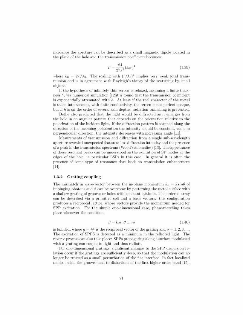
1.3.2 Grating coupling
The mismatch in wave-vector between the in-plane momentum kx = ksinθ ofimpinging photons and β can be overcome by patterning the metal surface witha shallow grating of grooves or holes with constant lattice a. The ordered arraycan be described via a primitive cell and a basis vectors: this configurationproduces a reciprocal lattice, whose vectors provide the momentum needed forSPP excitation. For the simple one-dimensional case, phase-matching takesplace whenever the condition:
β = ksinθ ± νg (1.40)
is fulfilled, where g = 2πa is the reciprocal vector of the grating and ν = 1, 2, 3, ....
The excitation of SPPS is detected as a minimum in the reflected light. Thereverse process can also take place: SPPs propagating along a surface modulatedwith a grating can couple to light and thus radiate.
For one-dimensional gratings, significant changes to the SPP dispersion re-lation occur if the gratings are sufficiently deep, so that the modulation can nolonger be treated as a small perturbation of the flat interface. In fact localizedmodes inside the grooves lead to distortions of the first higher-order band [15].
21
θk sin(θ)
Figure 6: Grating coupling between light and SPPs.
1.3.3 Extraordinary transmission in nanohole arrays
As pointed out before, metallic structures can convert light into SPs by providingthe necessary momentum conservation for the coupling process. If a screen withregular, periodic lattice of holes is structured, the phase-matching conditionsimposed by the grating leads to a well-defined structuring of the transmissionspectrum T (λ0), with peaks at the wavelengths where excitation of SPPs takesplace. At these wavelengths, more light can tunnel through the aperture thanincident on their area, since light impinging on the metal screen is channeledtrough the aperture via generation and propagation of SPPs. This is the socalled extraordinary optical transmission, EOT.
This enhanced transmission is the result of a resonant coupling of the EMradiation which impinges the metal, with standing surface plasmons on bothsides of the film. The process can be divided into three steps: the couplingof light to SPs on the incident surface, transmission through the holes to thesecond surface and re-emission from the second surface. The intensity of SPelectromagnetic fields above each holes compensates for the otherwise inefficienttransmission through each individual hole.
The observed structure of T (λ) can be explained by assuming that gratingcoupling to SPPs takes place, with the phase matching condition:
β = kx ± nGx ±mGy = ksin(θ) + (n+m)2π
a(1.41)
where k is the incident wave-vector and θ the incidence angle, Gx and Gy arebasis wave-vectors of the reciprocal lattice and n,m are Miller indexes whichdefine scattering order, thus direction of propagation of the excited SPP.
Considering the case of a two-dimensional triangular array, the peak posi-tions λmax at normal incidence are given in a first approximation by the Bloch-wave SPP relation [16, 17]:
λSPP =a√
n2 +mn+m2
√εmεdεm + εd
(1.42)
22
where a is the period of the array. As this result is valid for negligible holes’diameter and the associated scattering losses, it neglects the interference thatgives rise to a resonance red-shift, so more accurate relation would be necessary.
To quantify the extraordinary transmission is worth to define a normalizedtransmission coefficient Tnorm as the ratio between transmittance TNHA andthe sum of that for the single holes TSHj :
Tnorm =TNHA∑j TSHj
(1.43)
When extraordinary transmission occurs Tnorm becomes greater than 1 forthe wavelength at which there is a resonance between EM radiation and SPPs.
Features of NHA The SPs generated in the array will propagate along de-fined symmetry axes with their own polarization depending on the (n,m) num-ber of the mode, and then is been re-emitted to far-field. Interesting is theway in which this happens: one can suppose that the SPP emerging from theholes propagates on the metal surface and are scattered by the array of holes,so the strength of the enhancement depends on the number of scattering cen-tres encountered by the SPP within his decay-length. Instead a study [18] onmini-arrays demonstrates that is only the local environment which influencesthe extraordinary transmission, because excited SPPs are confined to the im-mediate surroundings of the emerging hole and scattering from only nearestneighbours, generating standing waves.
Furthermore relation (1.42) is valid for a single interface between two semi-infinite layers, but the nanohole array presents two interfaces, that can bothsustain SP modes. So if the two surfaces are in contact with different materials,the transmission spectrum contains two sets of peaks, each set belonging to oneof the surfaces.
An interesting feature of the nanohole arrays is that, as it’s clear from (1.42)despite the rough approximation, there is a linear relationship between the pe-riodicity of the array a and the position of the peak, so tuning this trait permitsto choose the position of the peak.
Other important properties to control the transmission spectra are:
Thickness h Two cases need to be distinguish: if the skin depth δ is larger orof the order t, SPPs excited by incident radiation on front interface mightcouple with SPPs on the other, only if adjacent dielectric is the same.If t � δ, as happens in this work for Vis-NIR, there is no transmissionthrough the metal film and the radiation can only tunnelling through theholes via SPPs.
Hole diameter d If the diameter is large enough to allow propagating modes,transmission could be modulated via resonances of wave-guide modes.But when d ≤ λ/2 only tunnelling modes are allowed. In this work thiscondition is generally fulfilled, since d . 800nm and typical resonance isat λ = 1540nm.
23
Holes diameter is also important in determining the line-width of thepeaks, in fact reducing the diameter makes the Wood’s anomalies shaperand contributes to obtain well-defined peak, but reduces the transmission[18].
Hole simmetry Different spectra are observed with square rather than cir-cular holes, in particular square holes spectra strongly depend on thepolarization of the impinging light [14].
LSP modes Another phenomenon to point out is the rise of localized surfaceplasmons modes on the rim of each hole, due to the strong localization of thefield. The emission spectrum is influenced in two ways by this hot-spots: hole’seffective diameter results increased and with it the cut-off wavelength limit forpropagating modes allowed inside the hole, and field enhancement at the rim,which can increase the transmission. Besides, a study of Degiron and Ebbesen[19] pointed out that the contribution of the LSP modes is less important thanthat of propagating SPP.
24
2 Nanohole array fabrication
There are many techniques used to produce nanohole arrays. One fundamentalfeature they must have is the possibility of controlling dimensional parametersof the nanohole array during the synthesis. The one adopted in this work is alsoa cost-effective way, characteristic which can be important in the eventually usefor mass-fabrication of NHA based devices.
2.1 Nanosphere Litography
Nanosphere lithography (NSL) is an inexpensive, simple to implement, highthroughput, self assembly technique capable of producing an unexpectedly largevariety of nanoparticle arrays with controlled shape, size, and inter-particlespacing. It is based on the self-assembly of a monolayer of size-mono-dispersespherical nanoparticles of polystyrene to form a colloidal crystal on the substratesurface. NSL particle diameters ranging from 40 nm to several microns and thesize of the polycrystalline monolayers can extend up to several cm2, and thisis one of the main advantages of this technique [20, 21]. These monolayers,arranged with HCP crystalline structure, can be used as efficient templates tofabricate 2-D ordered nanostructure arrays in particular as a mask for the metaldeposition [22].
Mechanism of masks formation Closed-packed monolayers of colloidalspheres can be produced by spreading particles solution on a solid surface andevaporating the solvent. The formation of the monolayers of colloidal spheres isdue to the lateral capillarity forces that acts when the spheres protrude from thesolvent. The spheres are pushed together and nucleate an ordered mono-layer,flow of solvent brings in more spheres and the mono-layer grows. The nature ofthe forces governing the ordering is revealed by the fact that 2D crystallizationalways starts when the thickness of the water layer becomes equal to the particlediameter.
Observations suggest a two-stage mechanism: at first stage, a nucleus ofordered phase forms. Spherical particles partially immersed in a liquid layerdeform the liquid-gas interface, giving rise to strong and long-range inter-particlecapillarity forces. These attractive forces are caused by two effect: pressureeffect caused by hydrostatic pressure and surface force effect due to the spatialvariation of the slope of the liquid surface. Energy of capillarity attractioncan be much larger than the thermal energy, kBT , even with sub-micrometerparticles, and interaction is a long range force, whose effect extend at distancesgreater than 1000 particles radii.
Once the nucleus is formed, the second stage of crystal growth starts throughdirectional motion of particles toward the ordered array. This motion is causedby a convective water flux which carries along the particles toward the orderedphase. Once ordered regions are formed, the thinning of the water layer insidethem is slowed due to hydrophilicity of the particles. The evaporation fromthe menisci between the particles, clustered in a nucleus, increases the local
25
curvature and hence the local sucking capillarity pressure. A convective influxtends to compensate the water evaporation and carries the particles toward theclusters, where they remain attached to the domains, pressed by hydrodynamicpressure and captured by capillarity attraction [23].
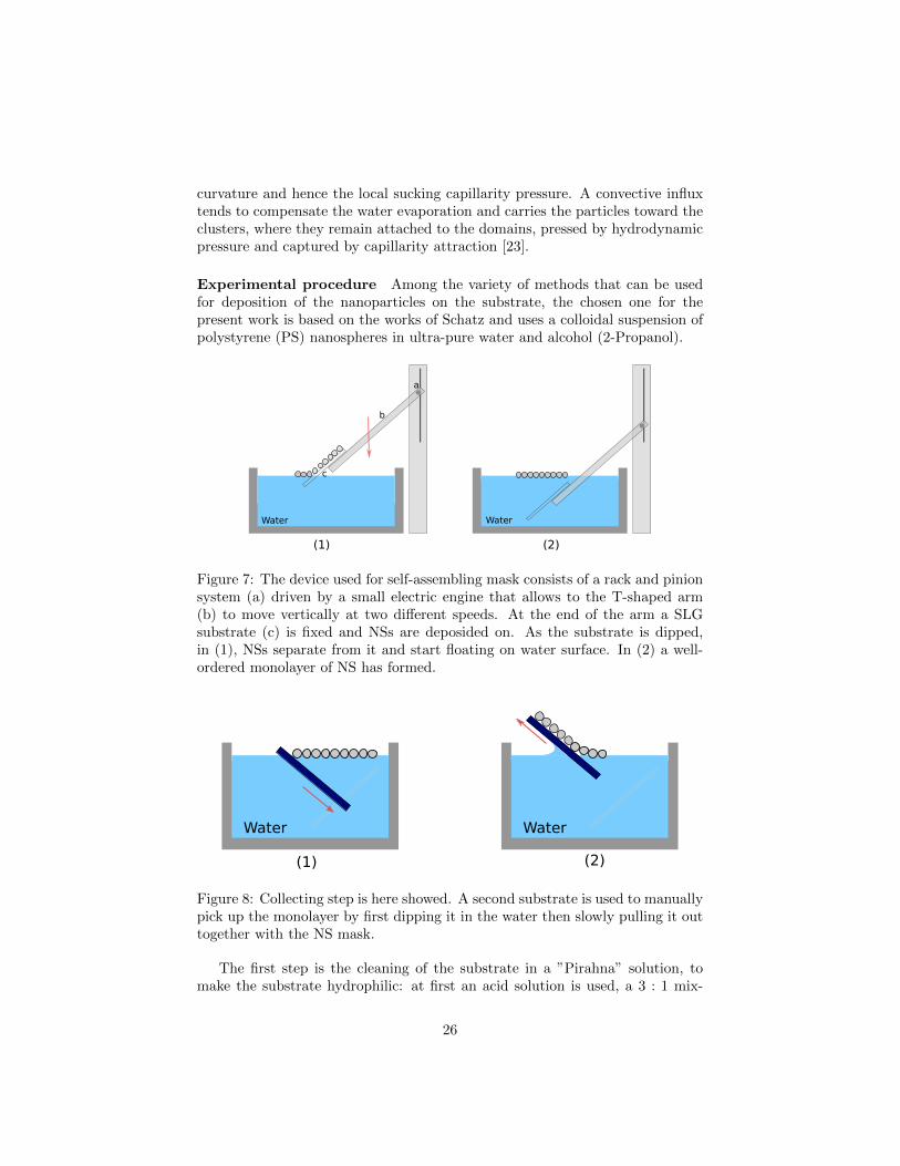
Experimental procedure Among the variety of methods that can be usedfor deposition of the nanoparticles on the substrate, the chosen one for thepresent work is based on the works of Schatz and uses a colloidal suspension ofpolystyrene (PS) nanospheres in ultra-pure water and alcohol (2-Propanol).
a
b
Water
c
(1) (2)
Water
Figure 7: The device used for self-assembling mask consists of a rack and pinionsystem (a) driven by a small electric engine that allows to the T-shaped arm(b) to move vertically at two different speeds. At the end of the arm a SLGsubstrate (c) is fixed and NSs are deposided on. As the substrate is dipped,in (1), NSs separate from it and start floating on water surface. In (2) a well-ordered monolayer of NS has formed.
Water Water
(1) (2)
Figure 8: Collecting step is here showed. A second substrate is used to manuallypick up the monolayer by first dipping it in the water then slowly pulling it outtogether with the NS mask.
The first step is the cleaning of the substrate in a ”Pirahna” solution, tomake the substrate hydrophilic: at first an acid solution is used, a 3 : 1 mix-
26
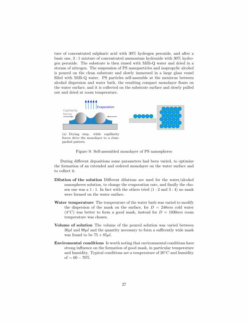
ture of concentrated sulphuric acid with 30% hydrogen peroxide, and after abasic one, 3 : 1 mixture of concentrated ammonium hydroxide with 30% hydro-gen peroxide. The substrate is then rinsed with Milli-Q water and dried in astream of nitrogen. The suspension of PS nanoparticles and isopropylic alcoholis poured on the clean substrate and slowly immersed in a large glass vesselfilled with Milli-Q water. PS particles self-assemble at the meniscus betweenalcohol dispersion and water bath, the resulting compact monolayer floats onthe water surface, and it is collected on the substrate surface and slowly pulledout and dried at room temperature.
EvaporationCapillarity forces
(a) Drying step, while capillarityforces drive the monolayer to a close-packed pattern.
Figure 9: Self-assembled monolayer of PS nanospheres
During different depositions some parameters had been varied, to optimizethe formation of an extended and ordered monolayer on the water surface andto collect it.
Dilution of the solution Different dilutions are used for the water/alcoholnanospheres solution, to change the evaporation rate, and finally the cho-sen one was a 1 : 1. In fact with the others tried (1 : 2 and 3 : 4) no maskwere formed on the water surface.
Water temperature The temperature of the water bath was varied to modifythe dispersion of the mask on the surface, for D = 248nm cold water(4◦C) was better to form a good mask, instead for D = 1030nm roomtemperature was chosen.
Volume of solution The volume of the poured solution was varied between30µl and 90µl and the quantity necessary to form a sufficently wide maskwas found to be 75÷ 85µl.
Enviromental conditions Is worth noting that environmental conditions havestrong influence on the formation of good mask, in particular temperatureand humidity. Typical conditions are a temperature of 20◦C and humidityof ∼ 60− 70%.
27
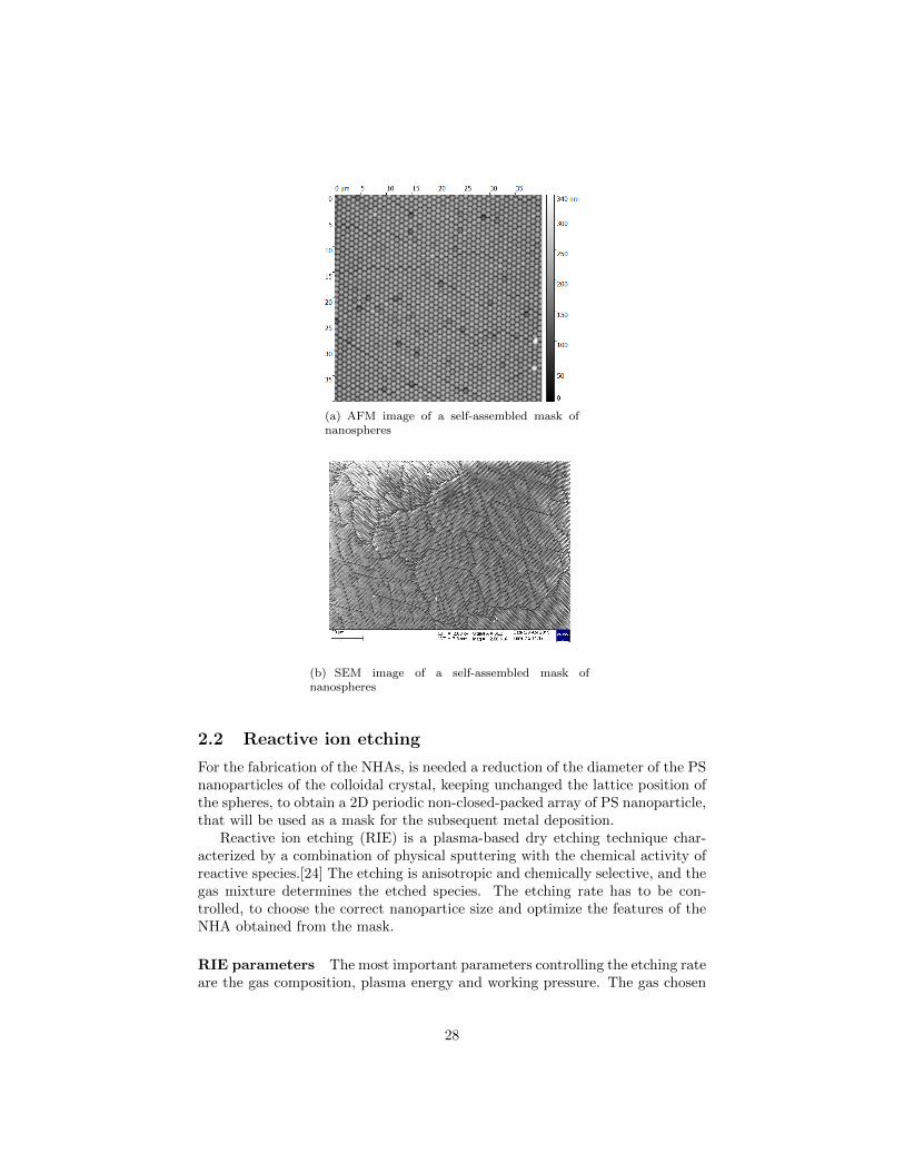
(a) AFM image of a self-assembled mask ofnanospheres
(b) SEM image of a self-assembled mask ofnanospheres
2.2 Reactive ion etching
For the fabrication of the NHAs, is needed a reduction of the diameter of the PSnanoparticles of the colloidal crystal, keeping unchanged the lattice position ofthe spheres, to obtain a 2D periodic non-closed-packed array of PS nanoparticle,that will be used as a mask for the subsequent metal deposition.
Reactive ion etching (RIE) is a plasma-based dry etching technique char-acterized by a combination of physical sputtering with the chemical activity ofreactive species.[24] The etching is anisotropic and chemically selective, and thegas mixture determines the etched species. The etching rate has to be con-trolled, to choose the correct nanopartice size and optimize the features of theNHA obtained from the mask.
RIE parameters The most important parameters controlling the etching rateare the gas composition, plasma energy and working pressure. The gas chosen
28
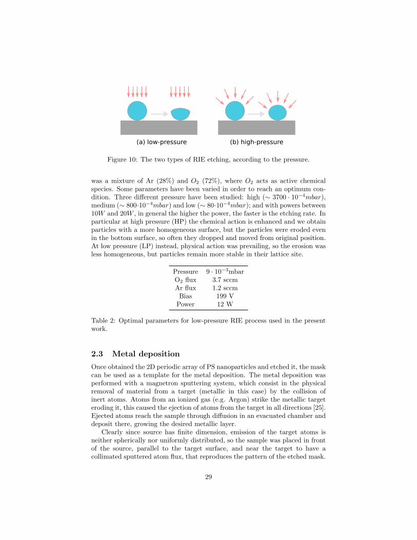
(a) low-pressure (b) high-pressure
Figure 10: The two types of RIE etching, according to the pressure.
was a mixture of Ar (28%) and O2 (72%), where O2 acts as active chemicalspecies. Some parameters have been varied in order to reach an optimum con-dition. Three different pressure have been studied: high (∼ 3700 · 10−4mbar),medium (∼ 800·10−4mbar) and low (∼ 80·10−4mbar); and with powers between10W and 20W , in general the higher the power, the faster is the etching rate. Inparticular at high pressure (HP) the chemical action is enhanced and we obtainparticles with a more homogeneous surface, but the particles were eroded evenin the bottom surface, so often they dropped and moved from original position.At low pressure (LP) instead, physical action was prevailing, so the erosion wasless homogeneous, but particles remain more stable in their lattice site.
Pressure 9 · 10−3mbarO2 flux 3.7 sccmAr flux 1.2 sccm
Bias 199 VPower 12 W
Table 2: Optimal parameters for low-pressure RIE process used in the presentwork.
2.3 Metal deposition
Once obtained the 2D periodic array of PS nanoparticles and etched it, the maskcan be used as a template for the metal deposition. The metal deposition wasperformed with a magnetron sputtering system, which consist in the physicalremoval of material from a target (metallic in this case) by the collision ofinert atoms. Atoms from an ionized gas (e.g. Argon) strike the metallic targeteroding it, this caused the ejection of atoms from the target in all directions [25].Ejected atoms reach the sample through diffusion in an evacuated chamber anddeposit there, growing the desired metallic layer.
Clearly since source has finite dimension, emission of the target atoms isneither spherically nor uniformly distributed, so the sample was placed in frontof the source, parallel to the target surface, and near the target to have acollimated sputtered atom flux, that reproduces the pattern of the etched mask.
29
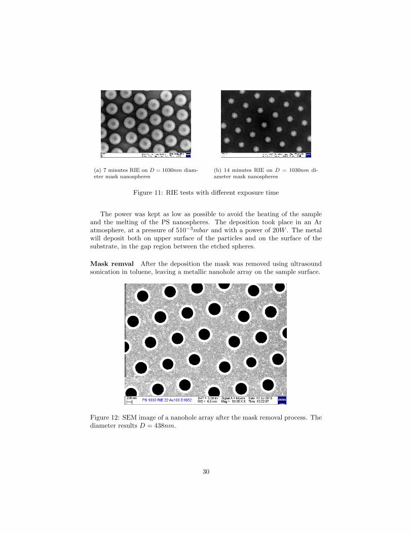
(a) 7 minutes RIE on D = 1030nm diam-eter mask nanospheres
(b) 14 minutes RIE on D = 1030nm di-ameter mask nanospheres
Figure 11: RIE tests with different exposure time
The power was kept as low as possible to avoid the heating of the sampleand the melting of the PS nanospheres. The deposition took place in an Aratmosphere, at a pressure of 510−3mbar and with a power of 20W . The metalwill deposit both on upper surface of the particles and on the surface of thesubstrate, in the gap region between the etched spheres.
Mask remval After the deposition the mask was removed using ultrasoundsonication in toluene, leaving a metallic nanohole array on the sample surface.
Figure 12: SEM image of a nanohole array after the mask removal process. Thediameter results D = 438nm.
30
3 Characterization and results
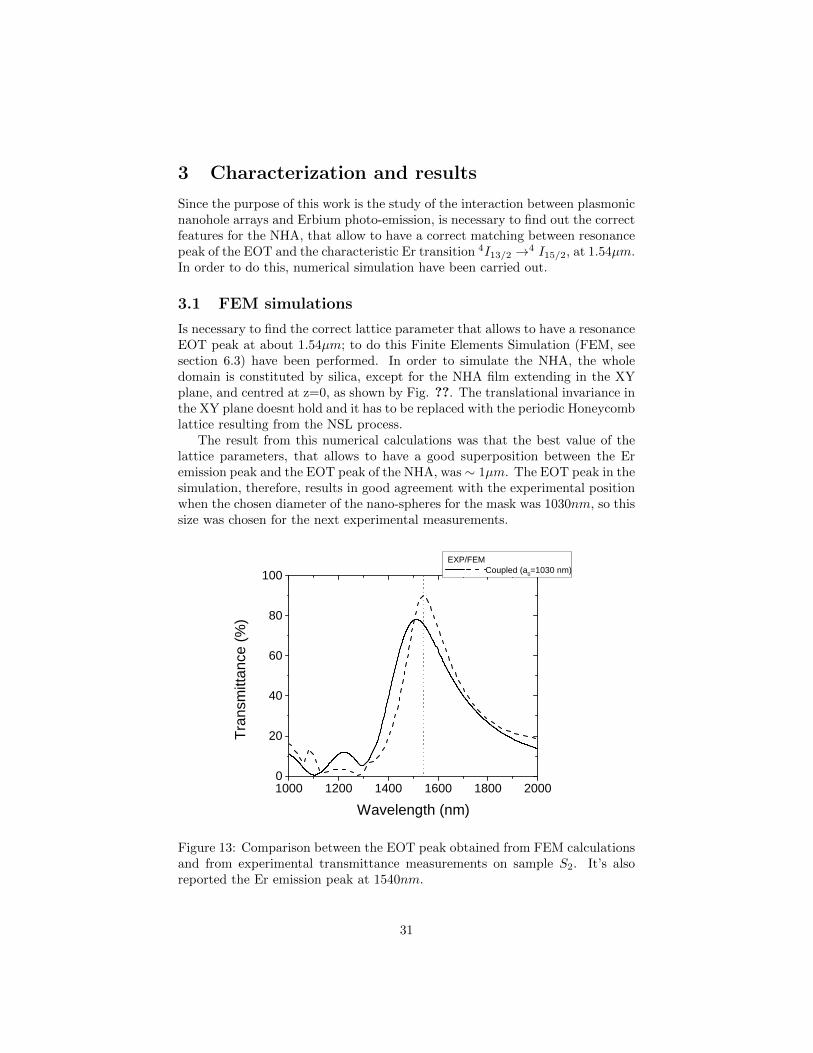
Since the purpose of this work is the study of the interaction between plasmonicnanohole arrays and Erbium photo-emission, is necessary to find out the correctfeatures for the NHA, that allow to have a correct matching between resonancepeak of the EOT and the characteristic Er transition 4I13/2 →4 I15/2, at 1.54µm.In order to do this, numerical simulation have been carried out.
3.1 FEM simulations
Is necessary to find the correct lattice parameter that allows to have a resonanceEOT peak at about 1.54µm; to do this Finite Elements Simulation (FEM, seesection 6.3) have been performed. In order to simulate the NHA, the wholedomain is constituted by silica, except for the NHA film extending in the XYplane, and centred at z=0, as shown by Fig. ??. The translational invariance inthe XY plane doesnt hold and it has to be replaced with the periodic Honeycomblattice resulting from the NSL process.
The result from this numerical calculations was that the best value of thelattice parameters, that allows to have a good superposition between the Eremission peak and the EOT peak of the NHA, was ∼ 1µm. The EOT peak in thesimulation, therefore, results in good agreement with the experimental positionwhen the chosen diameter of the nano-spheres for the mask was 1030nm, so thissize was chosen for the next experimental measurements.
1 0 0 0 1 2 0 0 1 4 0 0 1 6 0 0 1 8 0 0 2 0 0 00
2 0
4 0
6 0
8 0
1 0 0
Trans
mitta
nce (
%)
W a v e l e n g t h ( n m )
E X P / F E M C o u p l e d ( a 0 = 1 0 3 0 n m )
Figure 13: Comparison between the EOT peak obtained from FEM calculationsand from experimental transmittance measurements on sample S2. It’s alsoreported the Er emission peak at 1540nm.
31

3.2 Sample synthesis and features
3.2.1 Nanosphere masks
For the preparation of the NSL masks, polystyrene nanoparticles from Micropar-ticles GmbH were used, in particular mono-disperse nanospheres of diameter of(1030 ± 12)nm in aqueous solution. The solution of nanoparticles suspensionwas prepared with isopropyl alchol (2-propanol).
For the mask synthesis three kind of substrate were used: Soda Lime Glass(SLG), hyper-pure silica glass (HSQ 300) and mono-crystalline silicon waferwith < 100 > lattice orientation. SLG slabs were used only for the immersionwhile silicon and silica glass as substrate for the self-assembling of the masks.
After the cleaning in the ”piranha” solutions, before the acid one for 1 hourtreatment followed by the basic for a 20 minutes one, the substrates are readyfor the self-assembly process.
A motorized dipper, shown in fig 14 was used for the immersion: the SLGsubstrate was fixed to the end of the T-shaped arm, the solution was pouredover it, and it was slowly dipped into the water. Nanoparticles floating form aclosed-packed mask, which was picked up using Si or SiO2 slab and let drying.
Figure 14: The mechanism employed for the self assembly.
Characterization In order to check the quality of the masks, two types ofmeasurements were done, optical and morphological. Optical measurementswere done using a Jasco V-670 UV-VIS-NIR spectrophotometer, by illumi-nating the sample with normally incident non-polarized light. Morphologicalcharacterizations were done by Atomic Force Microscopy (AFM) employing aNT-MDT Solver PRO-M microscope and by Scanning Electron Microscopy us-ing Zeiss SIGMA HD SEM-FEG microscope. The absorbance spectra of the PSnanospheres masks were acquired, as in figure 15. The absorbance A is linkedto the transmittance T (in percent) by the following relationship:
A = 100(2− log10(T )) (3.1)
32
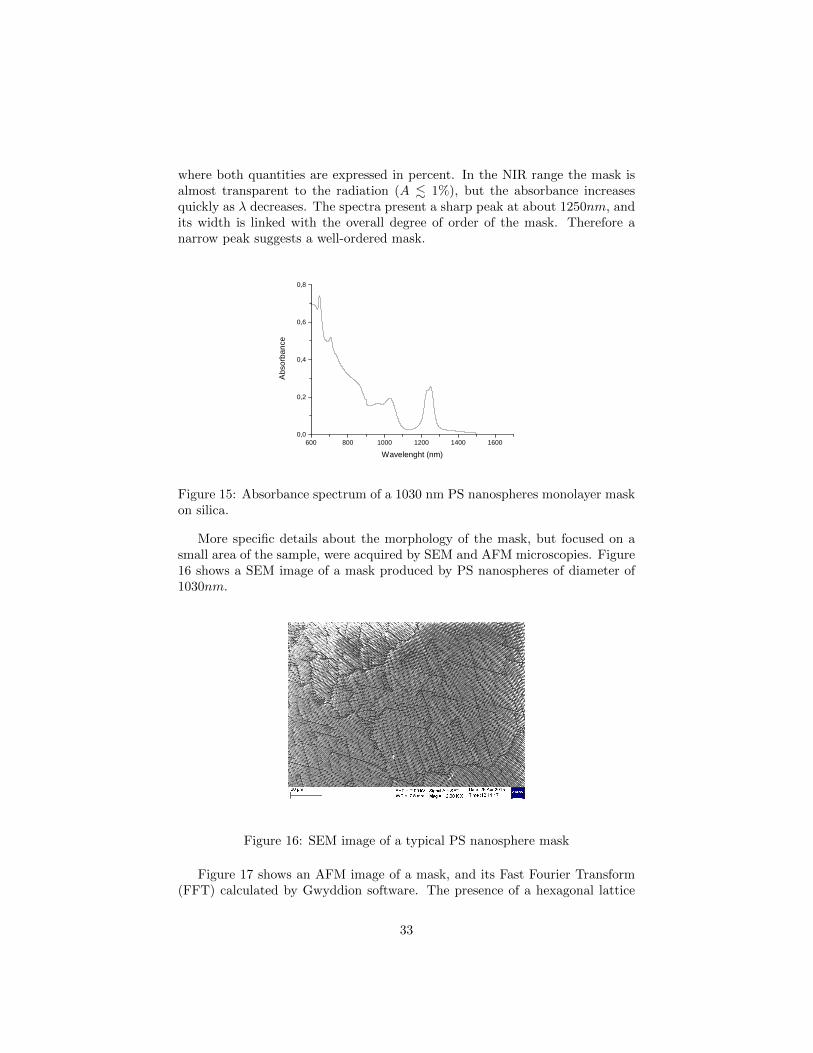
where both quantities are expressed in percent. In the NIR range the mask isalmost transparent to the radiation (A . 1%), but the absorbance increasesquickly as λ decreases. The spectra present a sharp peak at about 1250nm, andits width is linked with the overall degree of order of the mask. Therefore anarrow peak suggests a well-ordered mask.
6 0 0 8 0 0 1 0 0 0 1 2 0 0 1 4 0 0 1 6 0 00 , 0
0 , 2
0 , 4
0 , 6
0 , 8Ab
sorba
nce
W a v e l e n g h t ( n m )
Figure 15: Absorbance spectrum of a 1030 nm PS nanospheres monolayer maskon silica.
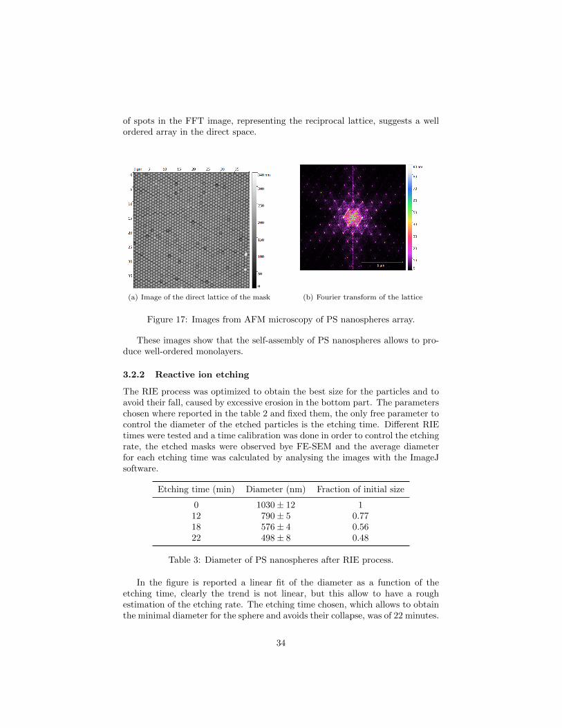
More specific details about the morphology of the mask, but focused on asmall area of the sample, were acquired by SEM and AFM microscopies. Figure16 shows a SEM image of a mask produced by PS nanospheres of diameter of1030nm.
Figure 16: SEM image of a typical PS nanosphere mask
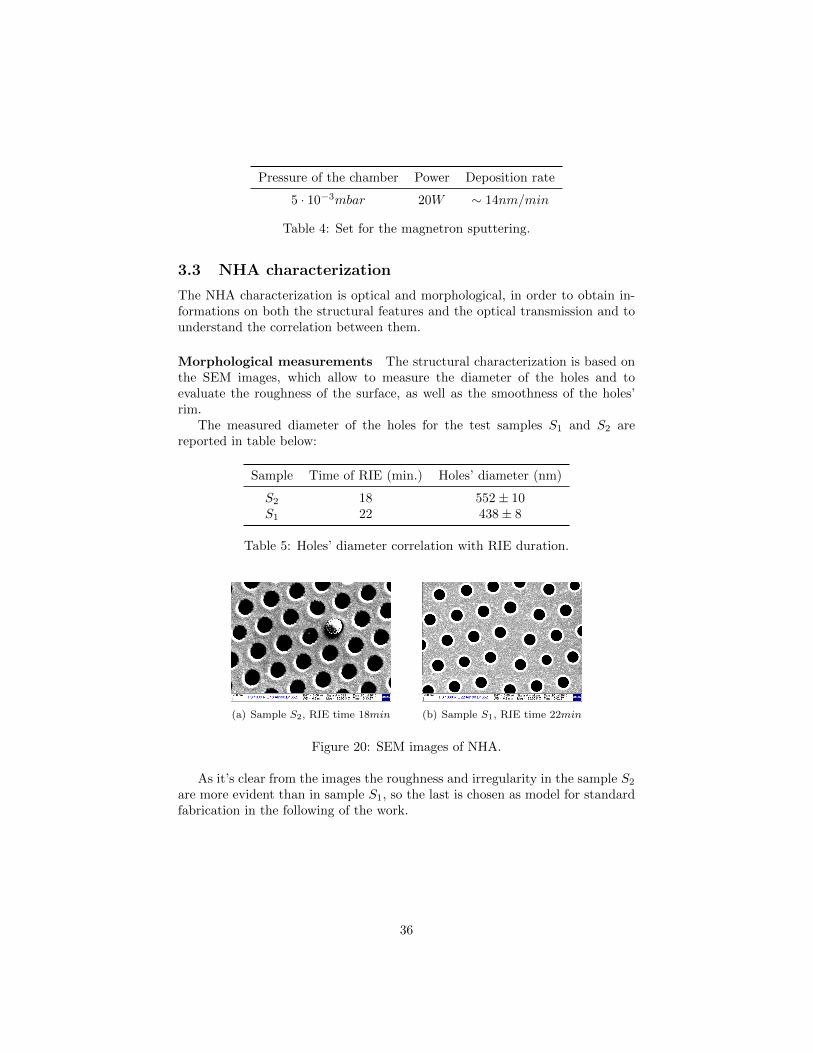
Figure 17 shows an AFM image of a mask, and its Fast Fourier Transform(FFT) calculated by Gwyddion software. The presence of a hexagonal lattice
33
of spots in the FFT image, representing the reciprocal lattice, suggests a wellordered array in the direct space.
(a) Image of the direct lattice of the mask (b) Fourier transform of the lattice
Figure 17: Images from AFM microscopy of PS nanospheres array.
These images show that the self-assembly of PS nanospheres allows to pro-duce well-ordered monolayers.
3.2.2 Reactive ion etching
The RIE process was optimized to obtain the best size for the particles and toavoid their fall, caused by excessive erosion in the bottom part. The parameterschosen where reported in the table 2 and fixed them, the only free parameter tocontrol the diameter of the etched particles is the etching time. Different RIEtimes were tested and a time calibration was done in order to control the etchingrate, the etched masks were observed bye FE-SEM and the average diameterfor each etching time was calculated by analysing the images with the ImageJsoftware.
Etching time (min) Diameter (nm) Fraction of initial size
0 1030± 12 112 790± 5 0.7718 576± 4 0.5622 498± 8 0.48
Table 3: Diameter of PS nanospheres after RIE process.
In the figure is reported a linear fit of the diameter as a function of theetching time, clearly the trend is not linear, but this allow to have a roughestimation of the etching rate. The etching time chosen, which allows to obtainthe minimal diameter for the sphere and avoids their collapse, was of 22 minutes.
34

0 5 1 0 1 5 2 0 2 5
5 0 0
6 0 0
7 0 0
8 0 0
9 0 0
1 0 0 0
1 1 0 0 D i a m e t e r L i n e a r f i t
Diame
ter (n
m)E t c h i n g t i m e ( m i n )
Figure 18: Plot of etched diameter against etching time.
(a) AFM profile of NHA (S1) (b) AFM image of NHA (S1)
Figure 19: AFM characterization of S1.
3.2.3 Metal deposition
The metal film used for the samples is a gold film of ∼ 100nm deposited by themagnetron sputtering with an RF source. This thickness allow to ensure a quitegood opacity to the film, at the typical frequencies used in this work of about1.5µm. The skin depth can be calculated as the reciprocal of the extinctioncoefficient (1.17), obtaining:
δ =1
α≈ 12nm (3.2)
Considering as a good optically thick film the case in which it is at least 5δthick, a 100nm thickness is enough to have a good screen.
The fixed parameters for deposition are reported in the table below:The deposition time chosen for the samples in this work is of 6p45q and
produced a thickness of (93± 2)nm for the sample S1 used for the next charac-terizations. The thickness was measured with the AFM.
35
Pressure of the chamber Power Deposition rate
5 · 10−3mbar 20W ∼ 14nm/min
Table 4: Set for the magnetron sputtering.
3.3 NHA characterization
The NHA characterization is optical and morphological, in order to obtain in-formations on both the structural features and the optical transmission and tounderstand the correlation between them.
Morphological measurements The structural characterization is based onthe SEM images, which allow to measure the diameter of the holes and toevaluate the roughness of the surface, as well as the smoothness of the holes’rim.
The measured diameter of the holes for the test samples S1 and S2 arereported in table below:
Sample Time of RIE (min.) Holes’ diameter (nm)
S2 18 552± 10S1 22 438± 8
Table 5: Holes’ diameter correlation with RIE duration.
(a) Sample S2, RIE time 18min (b) Sample S1, RIE time 22min
Figure 20: SEM images of NHA.
As it’s clear from the images the roughness and irregularity in the sample S2
are more evident than in sample S1, so the last is chosen as model for standardfabrication in the following of the work.
36
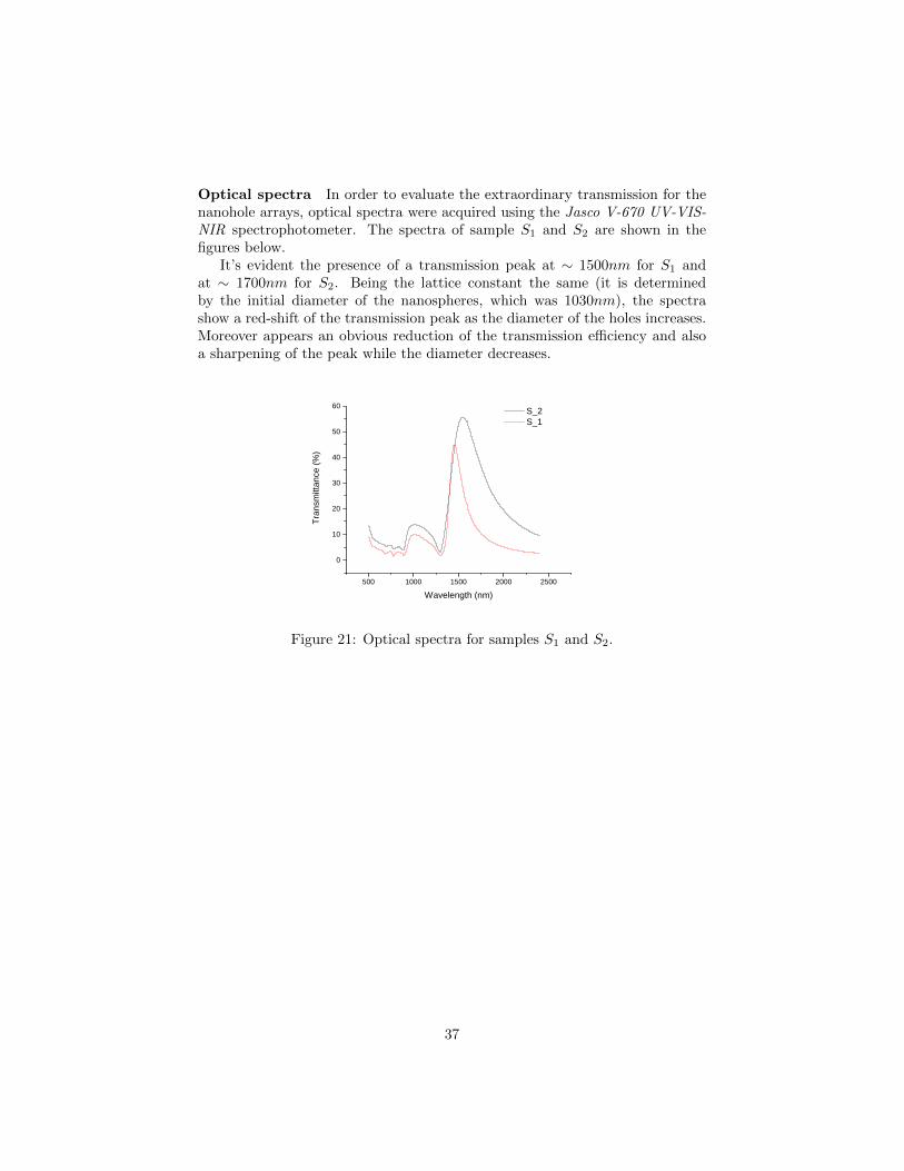
Optical spectra In order to evaluate the extraordinary transmission for thenanohole arrays, optical spectra were acquired using the Jasco V-670 UV-VIS-NIR spectrophotometer. The spectra of sample S1 and S2 are shown in thefigures below.
It’s evident the presence of a transmission peak at ∼ 1500nm for S1 andat ∼ 1700nm for S2. Being the lattice constant the same (it is determinedby the initial diameter of the nanospheres, which was 1030nm), the spectrashow a red-shift of the transmission peak as the diameter of the holes increases.Moreover appears an obvious reduction of the transmission efficiency and alsoa sharpening of the peak while the diameter decreases.
5 0 0 1 0 0 0 1 5 0 0 2 0 0 0 2 5 0 0
0
1 0
2 0
3 0
4 0
5 0
6 0 S _ 2 S _ 1
Trans
mitta
nce (
%)
W a v e l e n g t h ( n m )
Figure 21: Optical spectra for samples S1 and S2.
37
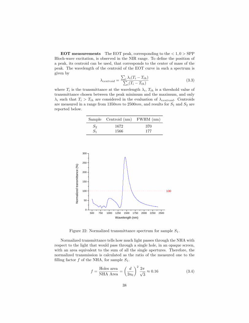
EOT measurements The EOT peak, corresponding to the < 1, 0 > SPPBloch-wave excitation, is observed in the NIR range. To define the position ofa peak, its centroid can be used, that corresponds to the center of mass of thepeak. The wavelength of the centroid of the EOT curve in such a spectrum isgiven by
λcentroid =
∑i λi(Ti − Tth)∑i(Ti − Tth)
(3.3)
where Ti is the transmittance at the wavelength λi, Tth is a threshold value oftransmittance chosen between the peak minimum and the maximum, and onlyλi such that Ti > Tth are considered in the evaluation of λcentroid. Centroidsare measured in a range from 1350nm to 2500nm, and results for S1 and S2 arereported below.
Sample Centroid (nm) FWHM (nm)
S2 1672 370S1 1566 177
5 0 0 7 5 0 1 0 0 0 1 2 5 0 1 5 0 0 1 7 5 0 2 0 0 0 2 2 5 0 2 5 0 00
5 0
1 0 0
1 5 0
2 0 0
2 5 0
3 0 0
Norm
alized
trans
mitta
nce (
%)
W a v e l e n g t h ( n m )
1 0 0
Figure 22: Normalized transmittance spectrum for sample S1.
Normalized transmittance tells how much light passes through the NHA withrespect to the light that would pass through a single hole, in an opaque screen,with an area equivalent to the sum of all the single apertures. Therefore, thenormalized transmission is calculated as the ratio of the measured one to thefilling factor f of the NHA, for sample S1.
f =Holes area
NHA Area=
(d
2a0
)22π√
3≈ 0.16 (3.4)
38
where d is the hole diameter and a0 is the periodicity of the array. It meansthat, neglecting plasmonic properties, 16% of the incident light would be trans-mitted. Dividing the transmittance spectrum by f , the plot from figure ?? isobtained. Transmittances above 100% can be observed and this stresses thatan extraordinary transmission occurs through the NHA.
3.4 Conclusions
The presence of an extraordinary optical transmission resonance through plas-monic nanohole arrays has been demonstrated. This EOT is due to the couplingbetween impinging EM radiation and SPP Bloch-waves, which can propagatethrough the holes and being re-emitted to the far-field.
The conditions for fabrication of the nano-structure have been optimized forthe matching between the EOT resonance and the Er3+ typical emission peakat 1.54µm, in order to study the mechanism of interaction between emitters andnano-structures, and evaluate the possible modifications in the photo-emissionefficiency.
39
4 Er:SiO2 films
Erbium doped materials are of strategic interest in the field of optical commu-nication technology for their application in many photonic devices [6, 26–28].This importance is related to the sharp room temperature luminescent emissionat 1540nm of the Er3+ ions, that matches the window of minimum losses insilica optical fibres. This chapter will focus on the synthesis and the character-ization of Er-doped silica thin films via co-sputtering, investigating the effectsof the preparation parameters in order to optimize the photo-luminescence ofEr3+ ions embedded in the silica matrix.
4.1 Er3+ optical properties
Erbium is a rare earth element in the Lanthanides series, with atomic number68. The electronic configuration of the neutral Er atoms is [Xe]−4f126s2, whilethe most common form of Er embedded in a solid is the ionic trivalent stateEr3+, which has an electronic configuration [Xe] − 4f11. Since Er ionizationinvolves the removal of two weakly bounded 6s electrons and one of the 4f shell,Er3+ ion has an incompletely filled 4f electron shell shielded from external fieldsby outer-lying filled 5s25p6 shells from the [Xe] configuration. The electrostaticshielding of the 4f electron shell reduces the perturbation due to the chargesof surrounding ligands and makes this shell quite atomic-like. Due to this factatomic energy levels and hence spectroscopic properties can be understood froma consideration of the free ions [29].
Figure 23: (a) Energy levels of Er3+ labelled with the Russell-Saunders nota-tion. For each state the GSA column lists the wavelength of the ground-stateabsorption transition terminating on it. (b) Absorption spectrum of Er-dopedsilicate glass. Absorbtion values at the peaks of the strong bands at 380 and520 nm are 1.5 and 1.0, respectively [26].
40
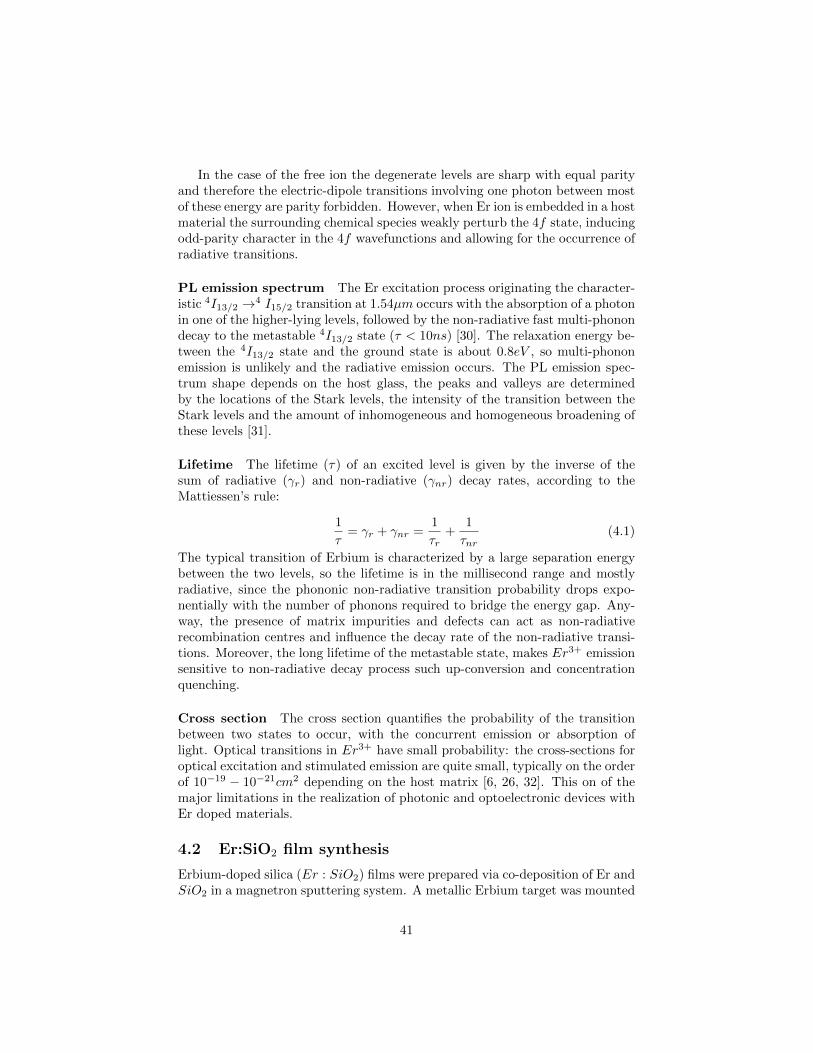
In the case of the free ion the degenerate levels are sharp with equal parityand therefore the electric-dipole transitions involving one photon between mostof these energy are parity forbidden. However, when Er ion is embedded in a hostmaterial the surrounding chemical species weakly perturb the 4f state, inducingodd-parity character in the 4f wavefunctions and allowing for the occurrence ofradiative transitions.
PL emission spectrum The Er excitation process originating the character-istic 4I13/2 →4 I15/2 transition at 1.54µm occurs with the absorption of a photonin one of the higher-lying levels, followed by the non-radiative fast multi-phonondecay to the metastable 4I13/2 state (τ < 10ns) [30]. The relaxation energy be-tween the 4I13/2 state and the ground state is about 0.8eV , so multi-phononemission is unlikely and the radiative emission occurs. The PL emission spec-trum shape depends on the host glass, the peaks and valleys are determinedby the locations of the Stark levels, the intensity of the transition between theStark levels and the amount of inhomogeneous and homogeneous broadening ofthese levels [31].
Lifetime The lifetime (τ) of an excited level is given by the inverse of thesum of radiative (γr) and non-radiative (γnr) decay rates, according to theMattiessen’s rule:
1
τ= γr + γnr =
1
τr+
1
τnr(4.1)
The typical transition of Erbium is characterized by a large separation energybetween the two levels, so the lifetime is in the millisecond range and mostlyradiative, since the phononic non-radiative transition probability drops expo-nentially with the number of phonons required to bridge the energy gap. Any-way, the presence of matrix impurities and defects can act as non-radiativerecombination centres and influence the decay rate of the non-radiative transi-tions. Moreover, the long lifetime of the metastable state, makes Er3+ emissionsensitive to non-radiative decay process such up-conversion and concentrationquenching.
Cross section The cross section quantifies the probability of the transitionbetween two states to occur, with the concurrent emission or absorption oflight. Optical transitions in Er3+ have small probability: the cross-sections foroptical excitation and stimulated emission are quite small, typically on the orderof 10−19 − 10−21cm2 depending on the host matrix [6, 26, 32]. This on of themajor limitations in the realization of photonic and optoelectronic devices withEr doped materials.
4.2 Er:SiO2 film synthesis
Erbium-doped silica (Er : SiO2) films were prepared via co-deposition of Er andSiO2 in a magnetron sputtering system. A metallic Erbium target was mounted
41
on a magnetron Direct Current (DC) source while the SiO2 one was placed on amagnetron Radio Frequency (RF) source. As sputtering gas a mixture of Ar andO2 was used (95%Ar+5%O2), operating at room temperature and at a pressureof 5 · 10−5mbar, which is the lowest one to sustain the plasma and to minimizethe re-sputtering phenomenon. The reactive atmosphere was chosen to preventa slight oxygen under-stoichiometry observed in pure argon depositions. Thedeposition was performed at 250W for the RF source (to prevent overheatingof the sample) and at 3W for the DC one. The concentration of Er varieslinearly with the power of the DC source and the film thickness shown a lineardependence with the deposition time at constant RF power.
4.3 Measurements on Er:SiO2 films
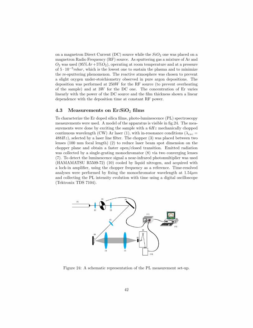
To characterize the Er doped silica films, photo-luminescence (PL) spectroscopymeasurements were used. A model of the apparatus is visible in fig.24. The mea-surements were done by exciting the sample with a 6Hz mechanically choppedcontinuous wavelength (CW) Ar laser (1), with in-resonance conditions (λexc =488Hz), selected by a laser line filter. The chopper (3) was placed between twolenses (100 mm focal length) (2) to reduce laser beam spot dimension on thechopper plane and obtain a faster open/closed transition. Emitted radiationwas collected by a single-grating monochromator (8) via two converging lenses(7). To detect the luminescence signal a near-infrared photomultiplier was used(HAMAMATSU R5509-72) (10) cooled by liquid nitrogen, and acquired witha lock-in amplifier, using the chopper frequency as a reference. Time-resolvedanalyses were performed by fixing the monochromator wavelength at 1.54µmand collecting the PL intensity evolution with time using a digital oscilloscope(Tektronix TDS 7104).
Figure 24: A schematic representation of the PL measurement set-up.
42
4.3.1 Thermal activation
After the deposition no luminescence signal was detectable in IR region, be-cause of the local disorder around the Er ions. Defects like dangling bonds,vacancies, bond angle and length distortion in the silica network can act asnon-radiative de-excitation centres, dampening the Er3+ emission. Annealingabove the temperature of 400◦C is required to recover host matrix defects and torestore the octahedral coordination of 6 oxygen atoms around the Er ions [33].Temperature and atmosphere of the thermal annealing influence the restoringof the defects in the silica matrix and the promotion of the oxygen coordinationaround Er ions. In a simple picture the PL intensity (IPL) can be described bythe relation:
IPL ∝ Nactη (4.2)
where Nact is the concentration of optically active Er ions and η is the quantumefficiency of the luminescence process, given by:
q =γrad
γrad + γnr=
τ
τrad(4.3)
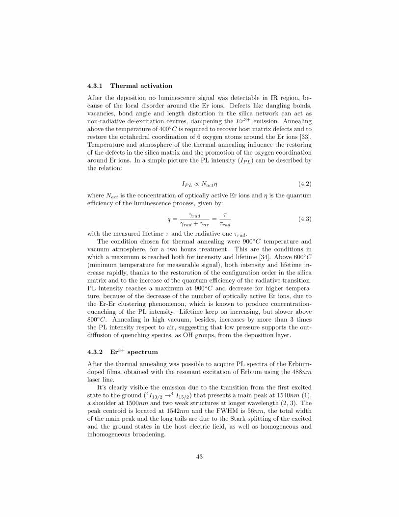
with the measured lifetime τ and the radiative one τrad.The condition chosen for thermal annealing were 900◦C temperature and
vacuum atmosphere, for a two hours treatment. This are the conditions inwhich a maximum is reached both for intensity and lifetime [34]. Above 600◦C(minimum temperature for measurable signal), both intensity and lifetime in-crease rapidly, thanks to the restoration of the configuration order in the silicamatrix and to the increase of the quantum efficiency of the radiative transition.PL intensity reaches a maximum at 900◦C and decrease for higher tempera-ture, because of the decrease of the number of optically active Er ions, due tothe Er-Er clustering phenomenon, which is known to produce concentration-quenching of the PL intensity. Lifetime keep on increasing, but slower above800◦C. Annealing in high vacuum, besides, increases by more than 3 timesthe PL intensity respect to air, suggesting that low pressure supports the out-diffusion of quenching species, as OH groups, from the deposition layer.
4.3.2 Er3+ spectrum
After the thermal annealing was possible to acquire PL spectra of the Erbium-doped films, obtained with the resonant excitation of Erbium using the 488nmlaser line.
It’s clearly visible the emission due to the transition from the first excitedstate to the ground (4I13/2 →4 I15/2) that presents a main peak at 1540nm (1),a shoulder at 1500nm and two weak structures at longer wavelength (2, 3). Thepeak centroid is located at 1542nm and the FWHM is 56nm, the total widthof the main peak and the long tails are due to the Stark splitting of the excitedand the ground states in the host electric field, as well as homogeneous andinhomogeneous broadening.
43
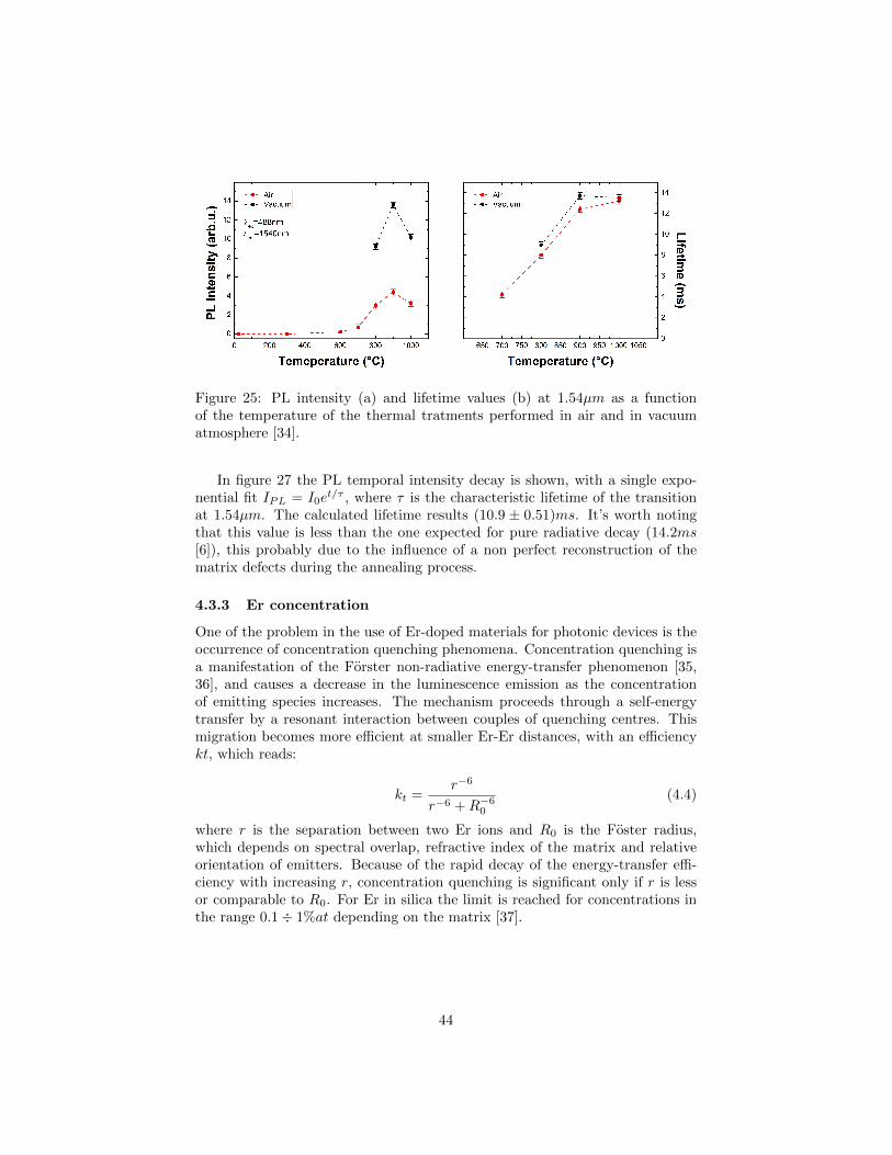
Figure 25: PL intensity (a) and lifetime values (b) at 1.54µm as a functionof the temperature of the thermal tratments performed in air and in vacuumatmosphere [34].
In figure 27 the PL temporal intensity decay is shown, with a single expo-nential fit IPL = I0e
t/τ , where τ is the characteristic lifetime of the transitionat 1.54µm. The calculated lifetime results (10.9 ± 0.51)ms. It’s worth notingthat this value is less than the one expected for pure radiative decay (14.2ms[6]), this probably due to the influence of a non perfect reconstruction of thematrix defects during the annealing process.
4.3.3 Er concentration
One of the problem in the use of Er-doped materials for photonic devices is theoccurrence of concentration quenching phenomena. Concentration quenching isa manifestation of the Forster non-radiative energy-transfer phenomenon [35,36], and causes a decrease in the luminescence emission as the concentrationof emitting species increases. The mechanism proceeds through a self-energytransfer by a resonant interaction between couples of quenching centres. Thismigration becomes more efficient at smaller Er-Er distances, with an efficiencykt, which reads:
kt =r−6
r−6 +R−60
(4.4)
where r is the separation between two Er ions and R0 is the Foster radius,which depends on spectral overlap, refractive index of the matrix and relativeorientation of emitters. Because of the rapid decay of the energy-transfer effi-ciency with increasing r, concentration quenching is significant only if r is lessor comparable to R0. For Er in silica the limit is reached for concentrations inthe range 0.1÷ 1%at depending on the matrix [37].
44
1 4 0 0 1 4 5 0 1 5 0 0 1 5 5 0 1 6 0 0 1 6 5 0 1 7 0 0
0 , 0
0 , 2
0 , 4
0 , 6
0 , 8
1 , 0
Emiss
ion (A
rbitra
ry un
.)
W a v e l e n g t h ( n m )
4 1 2 3
Figure 26: Main photo-emission peak for Er3+. The various components of thepeak are labelled.
4.3.4 Emission cross section
A fundamental parameter to characterize the optical properties of Er-dopedsystems is the emission cross-section. If the fluorescent bandwidth, the sponta-neous lifetime and the degeneracy of the excited and ground states are known,the cross section can be estimated via the Fuchtbaner-Ladenberg equation[38]:
σ21 =λ2
8πµ2A21g(ν) (4.5)
where 1 and 2 are the ground and excited states respectively, and λ the wave-length of the peak, g(ν) is the line shape of the emission spectrum, A21 theEinstein coefficient for spontaneous emission and µ the refractive index. Con-sidering only radiative channel, the Einstein coefficient for spontaneous emissionbecomes the measured decay rate (A21 = 1
τ ). For what concern the line shape,it has not a simple form in general, so defining the effective linewidth:
Ipk∆λeff =
∫ ∞0
I(λ)dλ (4.6)
the line shape function can be written:
g(ν) =Ipk∫Idν
=λ2
c
1
∆λeff(4.7)
and the Fucthbauer-Landberg equation:
σ21 =λ4
8πµ2c
1
τ∆λeff(4.8)
45
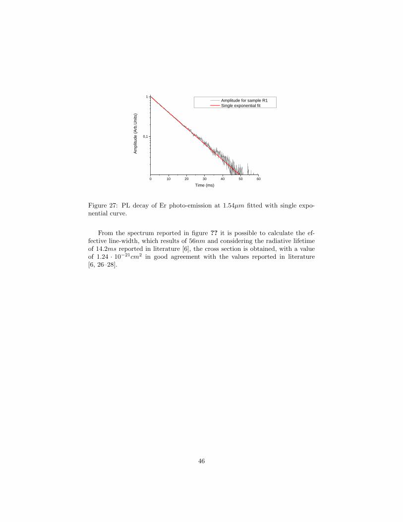
0 1 0 2 0 3 0 4 0 5 0 6 0
0 , 1
1
Amplit
ude (
Arb.Un
its)
T i m e ( m s )
A m p l i t u d e f o r s a m p l e R 1 S i n g l e e x p o n e n t i a l f i t
Figure 27: PL decay of Er photo-emission at 1.54µm fitted with single expo-nential curve.
From the spectrum reported in figure ?? it is possible to calculate the ef-fective line-width, which results of 56nm and considering the radiative lifetimeof 14.2ms reported in literature [6], the cross section is obtained, with a valueof 1.24 · 10−21cm2 in good agreement with the values reported in literature[6, 26–28].
46
5 Interaction between Erbium and interfaces
The long lifetime associated with the transition 4I13/2 →4 I15/2 of Er ions insilica limits the possibility of obtaining photonic and optoelectronic devices,because the long permanence of the ion in the excited state promotes non-radiative decay processes such as energy migration, cooperative up-conversionand concentration quenching.
It’s known that the change in local photonic density of state (LDOS) mayinfluence the decay rate of an emitter [5] and putting an interface at a distanced close to an emitter (d < λ) is the simplest way to influence the local photonicdensity of states [39–43]. In this section the case of Er3+ ions in silica interactingwith thin films is explored, and in particular the possible coupling betweenemitted radiation and SPPs at 1.54µm.
5.1 Theoretical model
The decay rate (Γi,j) of a spontaneous emission process between excited state iand ground state j, as photo-luminescence, is given by the Fermi’s golden rule[44]:
Γi,j =2π
~|Mi,j |2ρj (5.1)
where Mi,j is the matrix element of the transition, linked to the wave-functionsof the energy levels and ρj is the density of states of the optical field at thetransition frequency (LDOS). The presence of an interface in proximity of anemitter can modify both the LDOS and the matrix element, but the secondwill be modified only if the overlap between the wavefunctions of an ion andan atom in the film is significant i.e., if atoms are nearest neighbours. Sponta-neous emission is a typical quantum mechanical process where LDOS are seensubstantially as vacuum fluctuations, but the classical point of view, in whichdensity of states is seen as the ability of the surrounding structures to supportemission, is equivalent and provide the same quantitative results [45, 46].
In the classical point of view, the emitter is considered as a forced dipoleoscillator and the influence of the surface is taken into account by determiningthe total EM field acting on the dipole, including the dipole back-reflected fieldfrom the surface. The distance between the emitter and the surface is a fun-damental parameter for the control of the lifetime, because the amplitude andphase of the reflected field determine if the emission is enhanced or suppressed.Besides, for a complete description of the phenomenon energy loss via transferto the interface (coupling with SPPs) is to be considered. The analytical solu-tion to this problem is given by Chance, Prock and Silbey (CPS model) [47, 48].Considering the emitter as a forced damped dipole oscillator, the equation ofmotion becomes:
d2µ
dt2+ γ0
dµ
dt+ ω2µ =
e2
mER (5.2)
47
where µ is the dipole momentum, ω is the oscillator frequency without damping,m the effective mass, ER the reflected field at dipole position and γ0 the dampingconstant in the absence of the reflecting surface. The dipole momentum andthe reflected field oscillate with the same (complex) frequency:
µ = µ0e−i[ω+∆ω]te
−γt2 (5.3)
ER = E0e−i[ω+∆ω]te
−γt2 (5.4)
where ∆ω and γ are the frequency shift and the decay rate in the presence ofan interface. Using (5.3) and (5.4) and neglecting terms which contain γ2 or(e2/µ0m)E0, that are very small compared to ω2 [49], eq. (5.2) yields:
∆ω =γ2
8ω+
[e2
2µ0mω
]Re(E0) (5.5)
γ = γ0 +
[e2
2µ0mω
]Im(E0) (5.6)
The frequency shift is quite small [48]. Equation (5.6) shows that the changeof the decay rate of an emitter close to an interface is dictated by the out-of-phase component of the reflected field. Now what is to do is the calculation ofthe reflected electric field at the dipole position [50]. Once obtained it the decayrate for any dipole orientation can be derived combining perpendicular (γt) andparallel (γp) dipole components with respect to the interface:
γrt = γr0
{1− 3
2Im
[ ∫ ∞0
Rpu3
a1exp(−4πn1a1z/λ)du
]}(5.7)
γrp = γr0
{1 +
3
4Im
[ ∫ ∞0
[(1− u2)Rp +Rt
] ua1exp(−4πn1a1z/λ)du
]}(5.8)
where u is the component of the wave-vector (of the dipole field) in the planeinterface, normalized with respect to the far-field wave-vector k1 of the dipoleradiation field in medium 1 surrounding the emitter (u = kx/k1), n1 is therefractive index, z the distance between the emitter and the interface, λ theemitting wavelength. The parameter a1 = −i
√1− u2 is related to the perpen-
dicular component of the wave-vector at the interface, while Rp and Rt are theFresnel coefficients for p- and s-polarized light at the interface:
Rt =a1 − a2
a1 + a2, Rp =
ε1a2 − ε2a1
ε1a2 + ε2a1(5.9)
with ε1 the dielectric function of the medium embedding the emitter, ε2 the
complex one of the material beyond the interface and a2 = −i√
ε2ε1− u2.
48
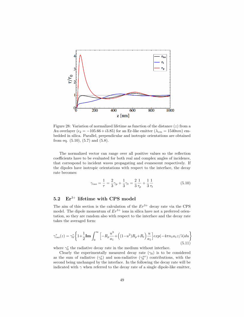
Figure 28: Variation of normalized lifetime as function of the distance (z) from aAu overlayer (ε2 = −105.66 + i3.85) for an Er-like emitter (λem = 1540nm) em-bedded in silica. Parallel, perpendicular and isotropic orientations are obtainedfrom eq. (5.10), (5.7) and (5.8).
The normalized vector can range over all positive values so the reflectioncoefficients have to be evaluated for both real and complex angles of incidence,that correspond to incident waves propagating and evanescent respectively. Ifthe dipoles have isotropic orientations with respect to the interface, the decayrate becomes:
γiso =1
τ=
2
3γp +
1
3γt =
2
3
1
τp+
1
3
1
τt(5.10)
5.2 Er3+ lifetime with CPS model
The aim of this section is the calculation of the Er3+ decay rate via the CPSmodel. The dipole momentum of Er3+ ions in silica have not a preferred orien-tation, so they are random also with respect to the interface and the decay ratetakes the averaged form:
γriso(z) = γr0
{1+
1
2Im
∫ ∞0
[−Rp
u3
a1+(
(1−u2)Rp+Rt
) ua1
]exp(−4πn1a1z/λ)du
}(5.11)
where γr0 the radiative decay rate in the medium without interface.Clearly the experimentally measured decay rate (γ0) is to be considered
as the sum of radiative (γr0) and non-radiative (γnr0 ) contributions, with thesecond being unchanged by the interface. In the following the decay rate will beindicated with γ when referred to the decay rate of a single dipole-like emitter,
49
and with Γ when referred to the integrated decay rate over a distribution ofemitters. The Er-doped film has a finite thickness, so the Er distribution in thefilm is to be taken into account. Since atomic diffusion is negligible during theannealing [34], the concentration profile is assumed to be:
y =
{f0, z ∈ [z0, z0 + zEr]0, z /∈ [z0, z0 + zEr]
(5.12)
where z0 = zmin is the distance of the Er : SiO2 film from the interface, zErthe thickness of the film and f0 the constant value of Er concentration.
It’s now possible to calculate the time dependence of the PL intensity:
IPL(t) = I0
∫ ∞0
f(z) exp[γriso(z)t]dz = I0f0
∫ zEr
z0
exp[γriso(z)t]dz (5.13)
with γriso the decay rate for an emitter at a distance z from the interface and I0the stationary emission intensity. The dependence is not perfectly exponential,so the determination of the radiative decay rate (Γriso,calc) was performed fittingthe first 20ms (where there was good agreement) of the normalized function,with a single exponential curve. If the non-radiative decay rate (Γnr0 ) is keptconstant the calculated Er lifetime becomes τcalc = 1/(Γiso,calc + Γnr0 ).
Figure 29: Comparison between time dependence of the PL intensity calculatedwith CPS model and a single exponential.
5.3 Radiative and non-radiative lifetime
For the determination of the two components, radiative and non-radiative, of thelifetime it is necessary an experimental measurements of the total lifetime. The
50
presence of the dielectric medium, with purely real component of the dielectricfunction, does not influence the radiative lifetime of an emitter in close proximityof a dielectric-dielectric interface, since dissipative contribution is linked to thecomplex part of the dielectric function. At low Er concentration, the decayrate (Γ0) of the 4I13/2 →4 I15/2 transition in a relaxed SiO2 lattice is 70s−1
(τ r0 = 14.2ms), mainly due to radiative emission (Γ0 = Γr0) [6]. With this valuein (5.11) and the procedure described previously, the radiative decay (Γrcalc) canbe obtained for the reference samples. The difference between the experimentalvalue and the calculated one is the non-radiative decay rate Γnr.
The calculation of radiative efficiency (q) is done from the calculated andexperimental decay rates:
q =Γr
Γr + Γnr=
Γriso,calcΓexp
(5.14)
5.4 Metallic overlayer
The lifetime modification for the transition at 1540nm has been studied first fora gold film, which is a noble, plasmonic metal [34]. The study of this configu-ration is extremely useful both to study the influence of a dissipative mediumin the process of photo-emission (see section 2.5) and to test the accuracy ofnumerical simulations used in susequent NHA analysis. In fact there is notyet a satisfactory analytical model developed to describe the NHA interactionwith an emitter, due to the complexity of the NHA structure. Finite ElementSimulations (FEM) have been carried out to try to understand the behaviourof the NHA interacting with an Er-like emitter, assuming every ion to be anemitting dipole (see section 3.3). These simulations have been replicated for agold thin film, for which exists the analytical solution from the CPS model andthe results have been compared, as shown in fig. 30.
The FEM results are in perfect agreement with the previsions of the CPSmodel, so they have been used to obtain a simulation of the NHA behaviour.
5.5 Power dissipation
In this section the different ways in which the decay can occur for an excitedEr3+ in proximity of an interface are analysed. In a geometry with an in-finitely extended plane above the emitter and another below it, if the energyflux through these two planes is calculated it is possible to obtain a rigorous sep-aration between the energy flowing away by far-field (F↑) and energy transferredto the interface (F↓). The flux is calculated integrating the normal componentof the complex Pointing vector (S∗) over the plane [48].
Dividing then the energy flux by the total energy radiated by the dipole, theprobabilities of the two mechanism (γ↑, γ↓) are given by:
51
Figure 30: Comparison between simulation (FEM) and the CPS model for thevariation of the normalized decay rate of an Er-like emitter (λem = 1540nm) asa function of the distance from a gold film [34].
γ↑ = Γr0
{1 +
1
2Im
∫ 1
0
[−Rp
u3
a1+(
(1− u2)Rp +Rt
) ua1
]exp(−4πn1a1z/λ)du
}(5.15)
γ↑ = Γr0
{1
2Im
∫ ∞1
[−Rp
u3
a1+(
(1− u2)Rp +Rt
) ua1
]exp(−4πn1a1z/λ)du
}(5.16)
And:
γ↑(z) + γ↓(z) = γriso(z) (5.17)
As a first approximation, γ↑ may be seen as radiative decay rate (γr) andγ↓ as non-radiative one (γnr). Now the far-field radiative efficiency (qf ) iscomputable: it represents the energy of photons which couples directly to far-field radiation, divided by the total energy emitted by the dipole. The far-fieldefficiency is thus given by:
qf =γr(z)
γ(z) + γnr(z)=
γ↑(z)
γ↑(z) + γ↓(z)(5.18)
Clearly qf is not the effective radiative efficiency of the emitter, because ofthe presence of the contribution of surface plasmon polaritons which are consid-ered as non-radiative decay channels, since they are expected to dissipate energyin the plane below the emitter. Actually SPPs are EM propagating modes on
52
the metal-dielectric interface that can couple out into far-field radiation or re-excite an Er ion close to the interface, thus contributing to the total emittedradiation [51].
To have a better understanding on how the energy leaves an excited dipole,it’s important considering with more accuracy the behaviour of the near-field,which extends at most at a distance λem from the emitter. The near field emittedfrom a dipole contains components with a large range of wave-vectors k, butonly if k < k1 it will propagate directly into the far-field (k1 is the far-field wave-vector in the matrix containing the dipole). Near to a planar surface, a largewide range of kx (the wave-vector in the plane of the interface) exist too, theemitted radiation can couple to modes having in-plane momenta greater thank1, like SPPs in case of metal films, modes not accessible to incident waves.
The power dissipation of a dipole in the presence of a metal interface can bewritten as a sum of three different contributions [52]:
P = Pphoton+ PSPP + PLSW (5.19)
where Pphoton is the power radiated via photons, PSPP via surface plasmonsand PLSW via the so called lossy surface waves. If the emitters are randomlyoriented, at a certain distance from the interface, the power dissipation spectrumcan be obtained from the imaginary part of the integrand in (5.11) as a functionof the normalized wave-vector [45].
At small distances (z < λ/50) the non-radiative contribution due to thecoupling with LSW is dominant. Going farther from the interface the LSWcontribution decreases rapidly and becomes negligible. SPPs coupling vanisheswith the distance but remains detectable to a range comparable to the λem.
To calculate the contribution of the SPP modes to the total decay rate,integration of the peak above the light line as function of u, has been performed.After this, also the non-radiative contribution has been calculated:
γLSW = γnr − γSPP (5.20)
and thus the near-field radiative efficiency:
q∗F (z) =γr + γSPP
γr + γSPP + γLSW(5.21)
In an ideal case in which all the energy associated to the surface plasmonscan be coupled-out, γSPP can be considered an actual radiative decay channelalso in the far-field.
If the depth of the Er-doped layer is accounted, Γr, ΓSPP and ΓLSW can beevaluated.
53
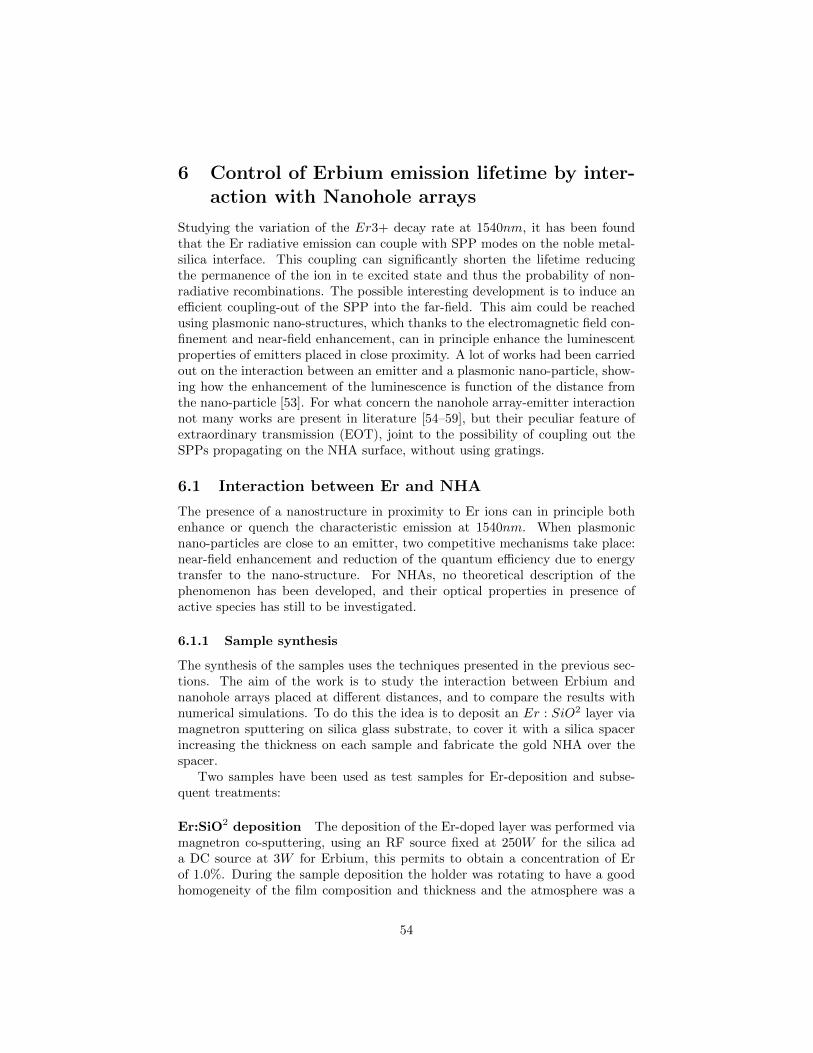
6 Control of Erbium emission lifetime by inter-action with Nanohole arrays
Studying the variation of the Er3+ decay rate at 1540nm, it has been foundthat the Er radiative emission can couple with SPP modes on the noble metal-silica interface. This coupling can significantly shorten the lifetime reducingthe permanence of the ion in te excited state and thus the probability of non-radiative recombinations. The possible interesting development is to induce anefficient coupling-out of the SPP into the far-field. This aim could be reachedusing plasmonic nano-structures, which thanks to the electromagnetic field con-finement and near-field enhancement, can in principle enhance the luminescentproperties of emitters placed in close proximity. A lot of works had been carriedout on the interaction between an emitter and a plasmonic nano-particle, show-ing how the enhancement of the luminescence is function of the distance fromthe nano-particle [53]. For what concern the nanohole array-emitter interactionnot many works are present in literature [54–59], but their peculiar feature ofextraordinary transmission (EOT), joint to the possibility of coupling out theSPPs propagating on the NHA surface, without using gratings.
6.1 Interaction between Er and NHA
The presence of a nanostructure in proximity to Er ions can in principle bothenhance or quench the characteristic emission at 1540nm. When plasmonicnano-particles are close to an emitter, two competitive mechanisms take place:near-field enhancement and reduction of the quantum efficiency due to energytransfer to the nano-structure. For NHAs, no theoretical description of thephenomenon has been developed, and their optical properties in presence ofactive species has still to be investigated.
6.1.1 Sample synthesis
The synthesis of the samples uses the techniques presented in the previous sec-tions. The aim of the work is to study the interaction between Erbium andnanohole arrays placed at different distances, and to compare the results withnumerical simulations. To do this the idea is to deposit an Er : SiO2 layer viamagnetron sputtering on silica glass substrate, to cover it with a silica spacerincreasing the thickness on each sample and fabricate the gold NHA over thespacer.
Two samples have been used as test samples for Er-deposition and subse-quent treatments:
Er:SiO2 deposition The deposition of the Er-doped layer was performed viamagnetron co-sputtering, using an RF source fixed at 250W for the silica ada DC source at 3W for Erbium, this permits to obtain a concentration of Erof 1.0%. During the sample deposition the holder was rotating to have a goodhomogeneity of the film composition and thickness and the atmosphere was a
54
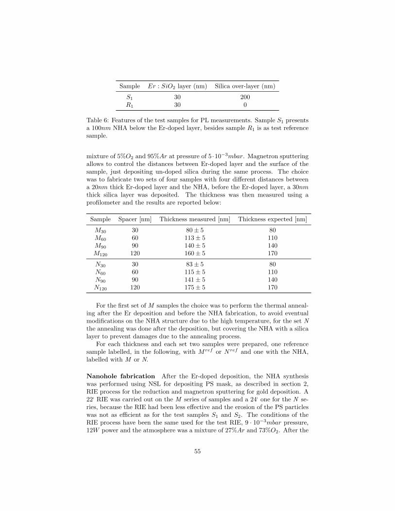
Sample Er : SiO2 layer (nm) Silica over-layer (nm)
S1 30 200R1 30 0
Table 6: Features of the test samples for PL measurements. Sample S1 presentsa 100nm NHA below the Er-doped layer, besides sample R1 is as test referencesample.
mixture of 5%O2 and 95%Ar at pressure of 5 ·10−3mbar. Magnetron sputteringallows to control the distances between Er-doped layer and the surface of thesample, just depositing un-doped silica during the same process. The choicewas to fabricate two sets of four samples with four different distances betweena 20nm thick Er-doped layer and the NHA, before the Er-doped layer, a 30nmthick silica layer was deposited. The thickness was then measured using aprofilometer and the results are reported below:
Sample Spacer [nm] Thickness measured [nm] Thickness expected [nm]
M30 30 80± 5 80M60 60 113± 5 110M90 90 140± 5 140M120 120 160± 5 170
N30 30 83± 5 80N60 60 115± 5 110N90 90 141± 5 140N120 120 175± 5 170
For the first set of M samples the choice was to perform the thermal anneal-ing after the Er deposition and before the NHA fabrication, to avoid eventualmodifications on the NHA structure due to the high temperature, for the set Nthe annealing was done after the deposition, but covering the NHA with a silicalayer to prevent damages due to the annealing process.
For each thickness and each set two samples were prepared, one referencesample labelled, in the following, with Mref or Nref and one with the NHA,labelled with M or N.
Nanohole fabrication After the Er-doped deposition, the NHA synthesiswas performed using NSL for depositing PS mask, as described in section 2,RIE process for the reduction and magnetron sputtering for gold deposition. A22p RIE was carried out on the M series of samples and a 24p one for the N se-ries, because the RIE had been less effective and the erosion of the PS particleswas not as efficient as for the test samples S1 and S2. The conditions of theRIE process have been the same used for the test RIE, 9 · 10−3mbar pressure,12W power and the atmosphere was a mixture of 27%Ar and 73%O2. After the
55
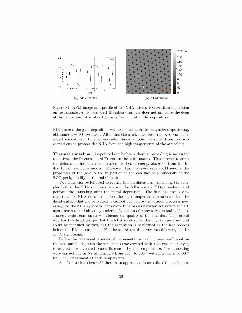
(a) AFM profile (b) AFM image
Figure 31: AFM image and profile of the NHA after a 200nm silica depositionon test sample S1. Is clear that the silica overlayer does not influence the deepof the holes, since it is of ∼ 100nm before and after the deposition.
RIE process the gold deposition was executed with the magnetron sputtering,obtaining a ∼ 100nm layer. After this the mask have been removed via ultra-sound sonication in toluene, and after this a ∼ 150nm of silica deposition wascarried out to protect the NHA from the high temperature of the annealing.
Thermal annealing As pointed out before a thermal annealing is necessaryto activate the Pl emission of Er ions in the silica matrix. This process restoresthe defects in the matrix and avoids the loss of energy absorbed from the Erdue to non-radiative modes. Moreover, high temperatures could modify theproperties of the gold NHA, in particular the can induce a blue-shift of theEOT peak, modifying the holes’ lattice.
Two ways can be followed to reduce this modifications: annealing the sam-ples before the NHA synthesis or cover the NHA with a SiO2 over-layer andperform the annealing after the metal deposition. The first has the advan-tage that the NHA does not suffers the high temperature treatment, but thedisadvantage that the activation is carried out before the various processes nec-essary for the NHA synthesis, thus more time passes between activation and PLmeasurements and also they undergo the action of many solvents and acid sub-stances, which can somehow influence the quality of the emission. The secondway has the disadvantage that the NHA must suffer the high temperature andcould be modified by this, but the activation is performed as the last processbefore the PL measurement. For the set M the first way was followed, for theset N the second.
Before the treatment a series of incremental annealing were performed onthe test sample S1, with the nanohole array covered with a 200nm silica layer,to evaluate the eventual blue-shift caused by the temperature. The annealingwere carried out in N2 atmosphere from 300◦ to 900◦, with increment of 100◦
for 1 hour treatment at each temperature.As it’s clear from figure 32 there is an appreciable blue-shift of the peak pass-
56
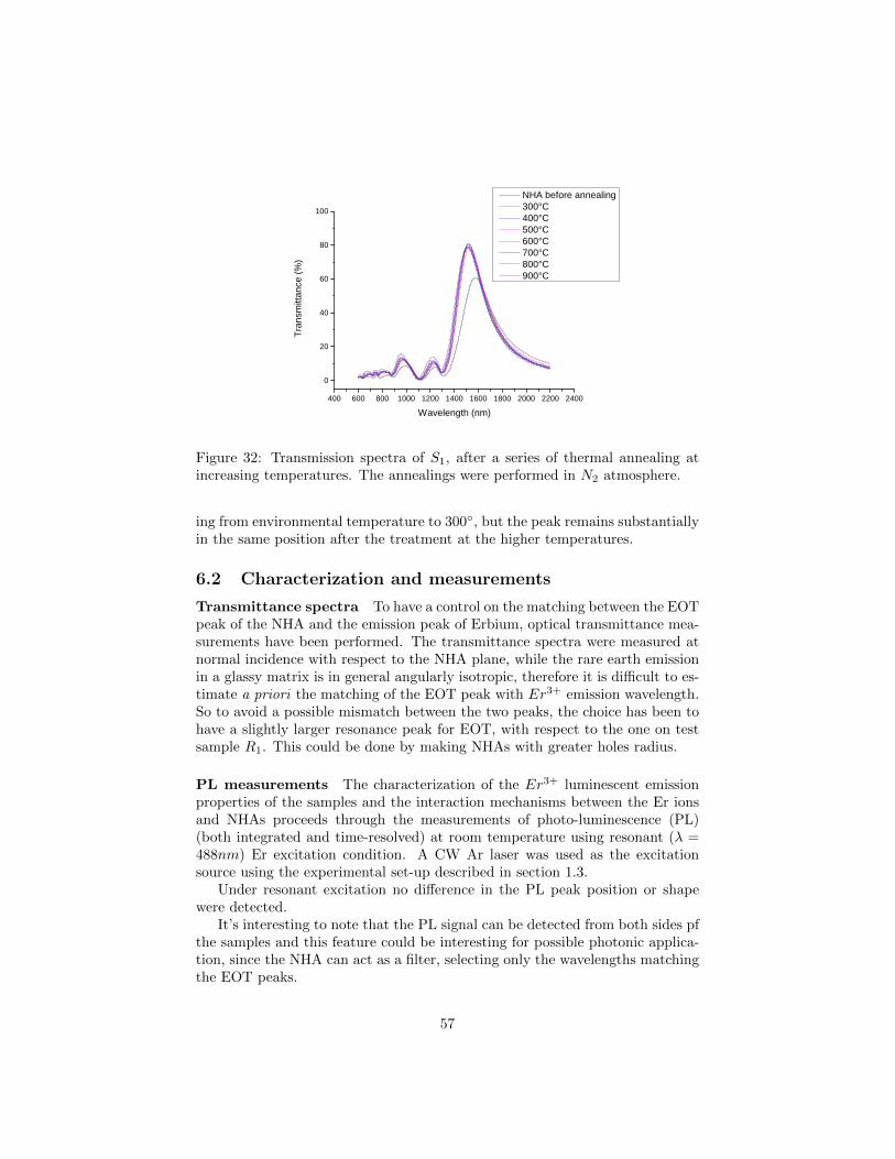
4 0 0 6 0 0 8 0 0 1 0 0 0 1 2 0 0 1 4 0 0 1 6 0 0 1 8 0 0 2 0 0 0 2 2 0 0 2 4 0 00
2 0
4 0
6 0
8 0
1 0 0
Trans
mitta
nce (
%)
W a v e l e n g t h ( n m )
N H A b e f o r e a n n e a l i n g 3 0 0 ° C 4 0 0 ° C 5 0 0 ° C 6 0 0 ° C 7 0 0 ° C 8 0 0 ° C 9 0 0 ° C
Figure 32: Transmission spectra of S1, after a series of thermal annealing atincreasing temperatures. The annealings were performed in N2 atmosphere.
ing from environmental temperature to 300◦, but the peak remains substantiallyin the same position after the treatment at the higher temperatures.
6.2 Characterization and measurements
Transmittance spectra To have a control on the matching between the EOTpeak of the NHA and the emission peak of Erbium, optical transmittance mea-surements have been performed. The transmittance spectra were measured atnormal incidence with respect to the NHA plane, while the rare earth emissionin a glassy matrix is in general angularly isotropic, therefore it is difficult to es-timate a priori the matching of the EOT peak with Er3+ emission wavelength.So to avoid a possible mismatch between the two peaks, the choice has been tohave a slightly larger resonance peak for EOT, with respect to the one on testsample R1. This could be done by making NHAs with greater holes radius.
PL measurements The characterization of the Er3+ luminescent emissionproperties of the samples and the interaction mechanisms between the Er ionsand NHAs proceeds through the measurements of photo-luminescence (PL)(both integrated and time-resolved) at room temperature using resonant (λ =488nm) Er excitation condition. A CW Ar laser was used as the excitationsource using the experimental set-up described in section 1.3.
Under resonant excitation no difference in the PL peak position or shapewere detected.
It’s interesting to note that the PL signal can be detected from both sides pfthe samples and this feature could be interesting for possible photonic applica-tion, since the NHA can act as a filter, selecting only the wavelengths matchingthe EOT peaks.
57
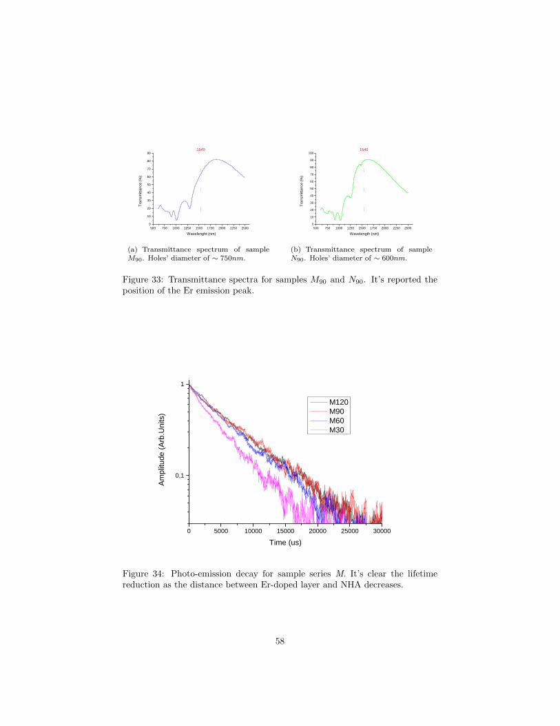
5 0 0 7 5 0 1 0 0 0 1 2 5 0 1 5 0 0 1 7 5 0 2 0 0 0 2 2 5 0 2 5 0 00
1 02 03 04 05 06 07 08 09 0
Trans
mitta
nce (
%)
W a v e l e n g h t ( n m )
1 5 4 0
(a) Transmittance spectrum of sampleM90. Holes’ diameter of ∼ 750nm.
5 0 0 7 5 0 1 0 0 0 1 2 5 0 1 5 0 0 1 7 5 0 2 0 0 0 2 2 5 0 2 5 0 00
1 02 03 04 05 06 07 08 09 0
1 0 0
Trans
mitta
nce (
%)
W a v e l e n g t h ( n m )
1 5 4 0
(b) Transmittance spectrum of sampleN90. Holes’ diameter of ∼ 600nm.
Figure 33: Transmittance spectra for samples M90 and N90. It’s reported theposition of the Er emission peak.
0 5 0 0 0 1 0 0 0 0 1 5 0 0 0 2 0 0 0 0 2 5 0 0 0 3 0 0 0 0
0 , 1
1
Amplit
ude (
Arb.Un
its)
T i m e ( u s )
M 1 2 0 M 9 0 M 6 0 M 3 0
Figure 34: Photo-emission decay for sample series M. It’s clear the lifetimereduction as the distance between Er-doped layer and NHA decreases.
58
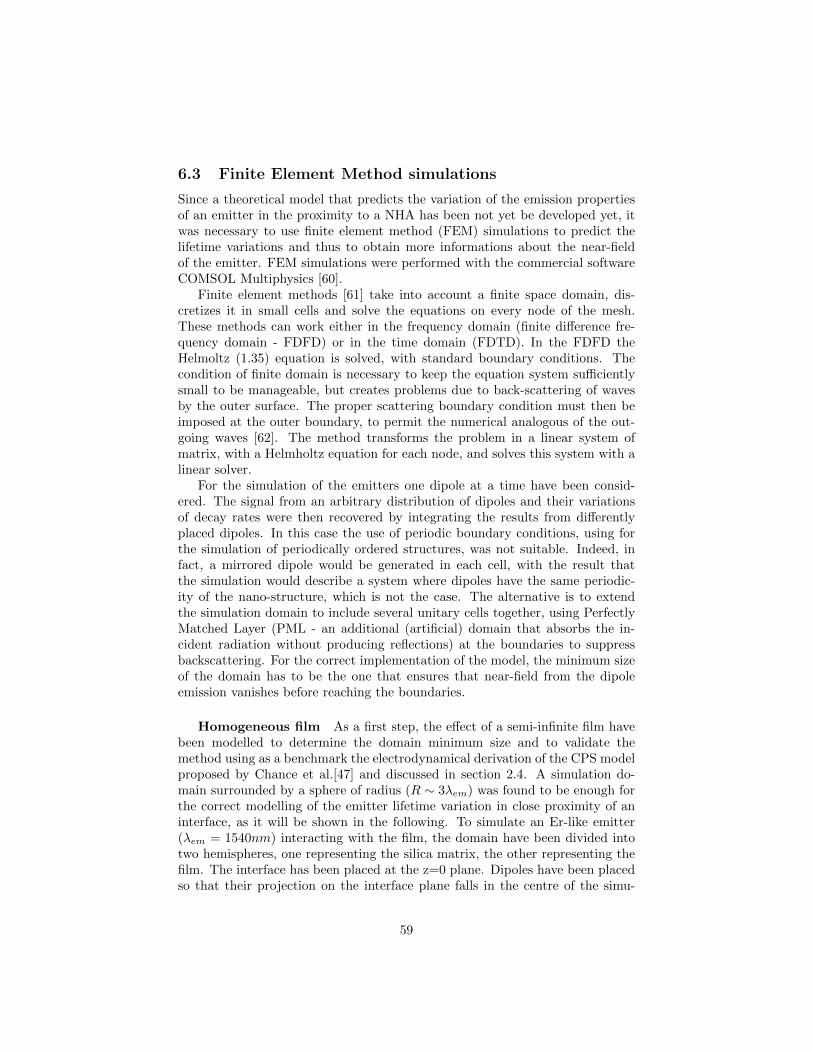
6.3 Finite Element Method simulations
Since a theoretical model that predicts the variation of the emission propertiesof an emitter in the proximity to a NHA has been not yet be developed yet, itwas necessary to use finite element method (FEM) simulations to predict thelifetime variations and thus to obtain more informations about the near-fieldof the emitter. FEM simulations were performed with the commercial softwareCOMSOL Multiphysics [60].
Finite element methods [61] take into account a finite space domain, dis-cretizes it in small cells and solve the equations on every node of the mesh.These methods can work either in the frequency domain (finite difference fre-quency domain - FDFD) or in the time domain (FDTD). In the FDFD theHelmoltz (1.35) equation is solved, with standard boundary conditions. Thecondition of finite domain is necessary to keep the equation system sufficientlysmall to be manageable, but creates problems due to back-scattering of wavesby the outer surface. The proper scattering boundary condition must then beimposed at the outer boundary, to permit the numerical analogous of the out-going waves [62]. The method transforms the problem in a linear system ofmatrix, with a Helmholtz equation for each node, and solves this system with alinear solver.
For the simulation of the emitters one dipole at a time have been consid-ered. The signal from an arbitrary distribution of dipoles and their variationsof decay rates were then recovered by integrating the results from differentlyplaced dipoles. In this case the use of periodic boundary conditions, using forthe simulation of periodically ordered structures, was not suitable. Indeed, infact, a mirrored dipole would be generated in each cell, with the result thatthe simulation would describe a system where dipoles have the same periodic-ity of the nano-structure, which is not the case. The alternative is to extendthe simulation domain to include several unitary cells together, using PerfectlyMatched Layer (PML - an additional (artificial) domain that absorbs the in-cident radiation without producing reflections) at the boundaries to suppressbackscattering. For the correct implementation of the model, the minimum sizeof the domain has to be the one that ensures that near-field from the dipoleemission vanishes before reaching the boundaries.
Homogeneous film As a first step, the effect of a semi-infinite film havebeen modelled to determine the domain minimum size and to validate themethod using as a benchmark the electrodynamical derivation of the CPS modelproposed by Chance et al.[47] and discussed in section 2.4. A simulation do-main surrounded by a sphere of radius (R ∼ 3λem) was found to be enough forthe correct modelling of the emitter lifetime variation in close proximity of aninterface, as it will be shown in the following. To simulate an Er-like emitter(λem = 1540nm) interacting with the film, the domain have been divided intotwo hemispheres, one representing the silica matrix, the other representing thefilm. The interface has been placed at the z=0 plane. Dipoles have been placedso that their projection on the interface plane falls in the centre of the simu-
59

(a) Side-view (b) Perspective view
Figure 35: Wireframe views of the NHA-emitter interction model.
lated sphere (x = 0, y = 0). The z coordinate of the dipoles (i.e., the distancefrom the interface) has been varied from 1 nm to 1000 nm. For each z position,the decay rate for a dipole with parallel (γp) and perpendicular (γt) orientationwith respect to the interface was calculated. The normalized decay rate wasevaluated by integrating the Poynting vector (S) on a closed surface (Σ) encir-cling the dipole (and not any part with absorbitive material) and dividing bythe decay rate (γr0 calculated without the interface:
γr
γr0=
∫Σ
Sdσ∫Σ
S0dσ(6.1)
In figure 30 there is a comparison between γt and γp both calculated withFEM simulation and analytic electrodynamic model (CPS), and the numericalcalculations result in good agreement with the analytical prevision. To takeinto account the Er distribution in the z direction typical for the Er:SiO2 co-sputtered films, the procedure described in section 2.4 has been used, leadingas expected to the same calculated lifetime values.
Nanohole array The simulations of the emitter-NHA interaction havebeen carried out in an analogous way. In this case, the whole simulated domainis constituted by silica, except for the NHA film extending in the XY plane, andcentred at z=0, as shown by Fig. 35. Unlike the film geometry, the translationalinvariance in the XY plane doesnt hold any more and it has to be replaced withthe periodic Honeycomb lattice resulting from the NSL process.
As already discussed, the periodic boundary conditions can not be used forthe correct evaluation of the decay variation due to the replication of the emitter.Thus, 19 XY unit cells have been modelled, in order to obtain the domain sizedetermined for the film geometry. Because the periodicity of the lattice, the
60
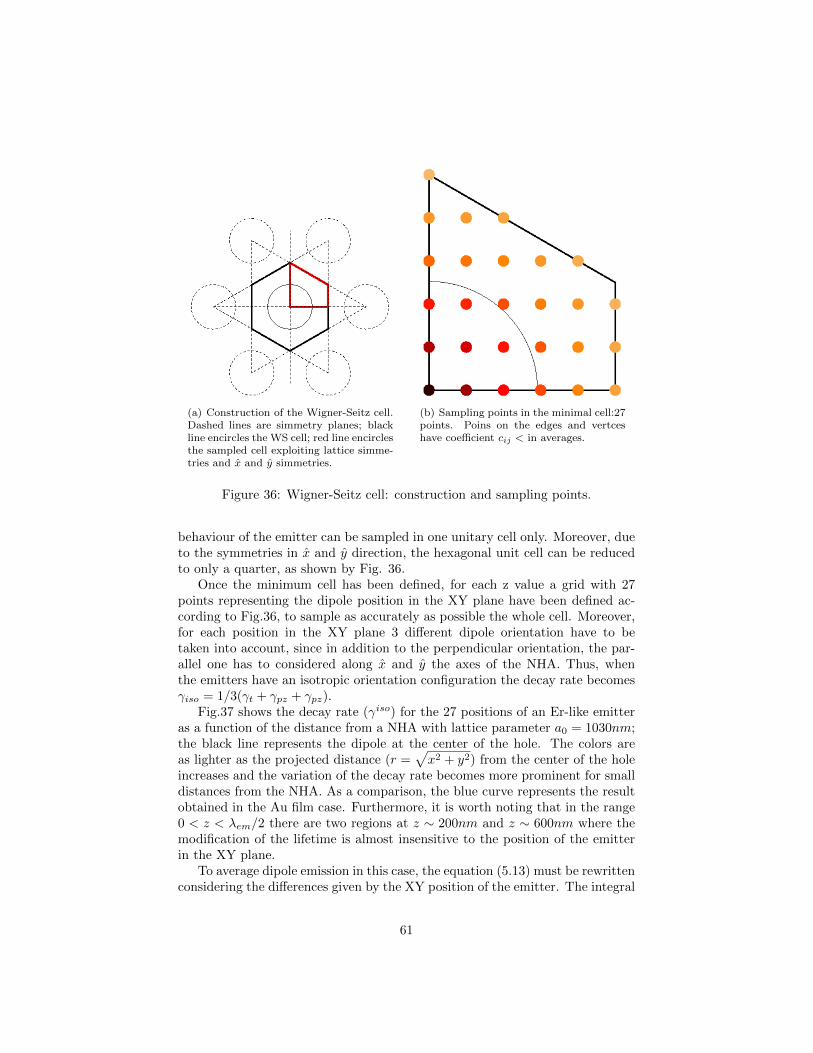
(a) Construction of the Wigner-Seitz cell.Dashed lines are simmetry planes; blackline encircles the WS cell; red line encirclesthe sampled cell exploiting lattice simme-tries and x and y simmetries.
(b) Sampling points in the minimal cell:27points. Poins on the edges and vertceshave coefficient cij < in averages.
Figure 36: Wigner-Seitz cell: construction and sampling points.
behaviour of the emitter can be sampled in one unitary cell only. Moreover, dueto the symmetries in x and y direction, the hexagonal unit cell can be reducedto only a quarter, as shown by Fig. 36.
Once the minimum cell has been defined, for each z value a grid with 27points representing the dipole position in the XY plane have been defined ac-cording to Fig.36, to sample as accurately as possible the whole cell. Moreover,for each position in the XY plane 3 different dipole orientation have to betaken into account, since in addition to the perpendicular orientation, the par-allel one has to considered along x and y the axes of the NHA. Thus, whenthe emitters have an isotropic orientation configuration the decay rate becomesγiso = 1/3(γt + γpz + γpz).
Fig.37 shows the decay rate (γiso) for the 27 positions of an Er-like emitteras a function of the distance from a NHA with lattice parameter a0 = 1030nm;the black line represents the dipole at the center of the hole. The colors areas lighter as the projected distance (r =
√x2 + y2) from the center of the hole
increases and the variation of the decay rate becomes more prominent for smalldistances from the NHA. As a comparison, the blue curve represents the resultobtained in the Au film case. Furthermore, it is worth noting that in the range0 < z < λem/2 there are two regions at z ∼ 200nm and z ∼ 600nm where themodification of the lifetime is almost insensitive to the position of the emitterin the XY plane.
To average dipole emission in this case, the equation (5.13) must be rewrittenconsidering the differences given by the XY position of the emitter. The integral
61

0 1 0 0 2 0 0 3 0 0 4 0 0 5 0 0 6 0 0 7 0 05 06 07 08 09 0
1 0 01 1 01 2 01 3 01 4 01 5 0
Γ r (s-1 )
D e p t h ( n m )
r0 a 0 / 2
Figure 37: Simulated γr(z) for emitter placed at different positions in the XYplane for a a0 = 1030nm NHA. The color map indicates the distance from thecentre of a hole in the WS cell, as in fig. 36(b).
is still present in the z direction, while in the XY plane, the integration issubstituted by a sum over the 27 emitter positions sampled in the minimum celland denoted by the couple of i and j indices:
IPL(t) = I0A∑i,j
cij
∫ +∞
0
f(xi, yi, z)e−γiso(xi,yi,z)tdz (6.2)
where the coefficients cij account for the normalization of the points shared byadjacent cells and A = 1∑
i,j cijis a global normalization factor.
6.4 Experimental results and discussion
The goal of this work was to evaluate if the interaction between a Er : SiO2
film and a gold plasmonic nanohole array can induce a variation in the photo-emission efficiency of excited Erbium ions, and how this variation is correlatedto the distance between the Er-doped layer and the NHA.
In order to obtain the emission efficiency:
q =Γr
Γr + Γnr(6.3)
the total decay rate Γexp = Γr + Γnr is needed.For each sample of the set M and N the Er3+ lifetime was extracted from
the PL measurements. The hypothesis was that the photo-luminescence decaycould be fitted by a single exponential curve IPL(t) = Aet/τ + y0, thus the
62
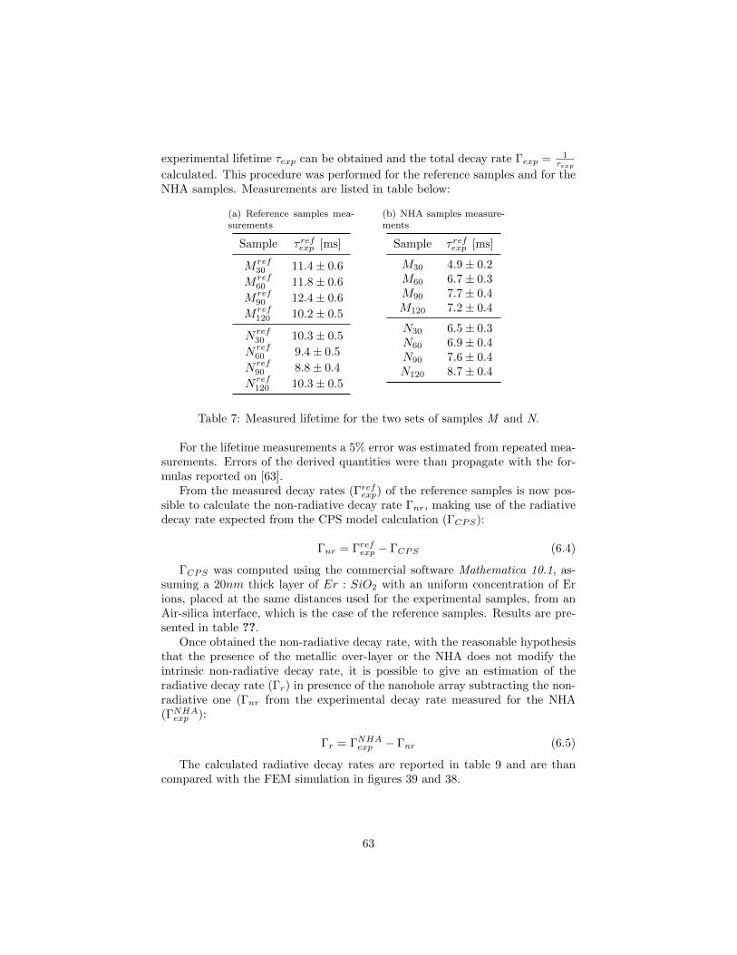
experimental lifetime τexp can be obtained and the total decay rate Γexp = 1τexp
calculated. This procedure was performed for the reference samples and for theNHA samples. Measurements are listed in table below:
(a) Reference samples mea-surements
Sample τ refexp [ms]
Mref30 11.4± 0.6
Mref60 11.8± 0.6
Mref90 12.4± 0.6
Mref120 10.2± 0.5
Nref30 10.3± 0.5
Nref60 9.4± 0.5
Nref90 8.8± 0.4
Nref120 10.3± 0.5
(b) NHA samples measure-ments
Sample τ refexp [ms]
M30 4.9± 0.2M60 6.7± 0.3M90 7.7± 0.4M120 7.2± 0.4
N30 6.5± 0.3N60 6.9± 0.4N90 7.6± 0.4N120 8.7± 0.4
Table 7: Measured lifetime for the two sets of samples M and N.
For the lifetime measurements a 5% error was estimated from repeated mea-surements. Errors of the derived quantities were than propagate with the for-mulas reported on [63].
From the measured decay rates (Γrefexp) of the reference samples is now pos-sible to calculate the non-radiative decay rate Γnr, making use of the radiativedecay rate expected from the CPS model calculation (ΓCPS):
Γnr = Γrefexp − ΓCPS (6.4)
ΓCPS was computed using the commercial software Mathematica 10.1, as-suming a 20nm thick layer of Er : SiO2 with an uniform concentration of Erions, placed at the same distances used for the experimental samples, from anAir-silica interface, which is the case of the reference samples. Results are pre-sented in table ??.
Once obtained the non-radiative decay rate, with the reasonable hypothesisthat the presence of the metallic over-layer or the NHA does not modify theintrinsic non-radiative decay rate, it is possible to give an estimation of theradiative decay rate (Γr) in presence of the nanohole array subtracting the non-radiative one (Γnr from the experimental decay rate measured for the NHA(ΓNHAexp ):
Γr = ΓNHAexp − Γnr (6.5)
The calculated radiative decay rates are reported in table 9 and are thancompared with the FEM simulation in figures 39 and 38.
63
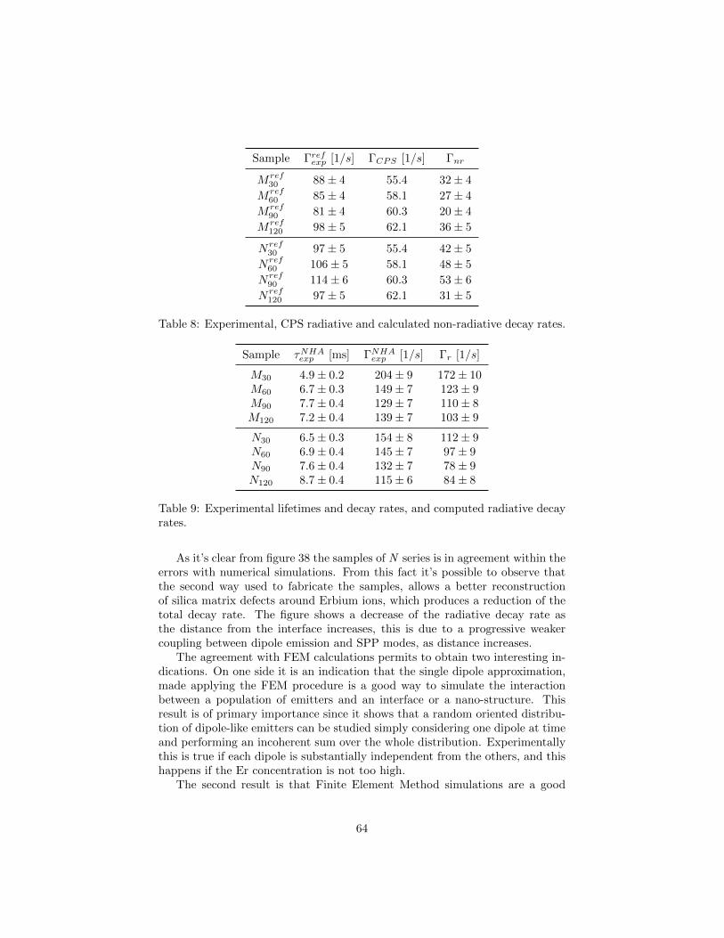
Sample Γrefexp [1/s] ΓCPS [1/s] Γnr
Mref30 88± 4 55.4 32± 4
Mref60 85± 4 58.1 27± 4
Mref90 81± 4 60.3 20± 4
Mref120 98± 5 62.1 36± 5
Nref30 97± 5 55.4 42± 5
Nref60 106± 5 58.1 48± 5
Nref90 114± 6 60.3 53± 6
Nref120 97± 5 62.1 31± 5
Table 8: Experimental, CPS radiative and calculated non-radiative decay rates.
Sample τNHAexp [ms] ΓNHAexp [1/s] Γr [1/s]
M30 4.9± 0.2 204± 9 172± 10M60 6.7± 0.3 149± 7 123± 9M90 7.7± 0.4 129± 7 110± 8M120 7.2± 0.4 139± 7 103± 9
N30 6.5± 0.3 154± 8 112± 9N60 6.9± 0.4 145± 7 97± 9N90 7.6± 0.4 132± 7 78± 9N120 8.7± 0.4 115± 6 84± 8
Table 9: Experimental lifetimes and decay rates, and computed radiative decayrates.
As it’s clear from figure 38 the samples of N series is in agreement within theerrors with numerical simulations. From this fact it’s possible to observe thatthe second way used to fabricate the samples, allows a better reconstructionof silica matrix defects around Erbium ions, which produces a reduction of thetotal decay rate. The figure shows a decrease of the radiative decay rate asthe distance from the interface increases, this is due to a progressive weakercoupling between dipole emission and SPP modes, as distance increases.
The agreement with FEM calculations permits to obtain two interesting in-dications. On one side it is an indication that the single dipole approximation,made applying the FEM procedure is a good way to simulate the interactionbetween a population of emitters and an interface or a nano-structure. Thisresult is of primary importance since it shows that a random oriented distribu-tion of dipole-like emitters can be studied simply considering one dipole at timeand performing an incoherent sum over the whole distribution. Experimentallythis is true if each dipole is substantially independent from the others, and thishappens if the Er concentration is not too high.
The second result is that Finite Element Method simulations are a good
64

0 5 0 1 0 0 1 5 0 2 0 0 2 5 0
7 0
8 0
9 0
1 0 0
1 1 0
1 2 0
1 3 0
Γ(1/s
)
D i s t a n c e ( n m )
N u m e r i c a l s i m u l a t i o n o f Γ E x p r a d i a t i v e Γ
Figure 38: Comparison between FEM simulation of radiative decay rate andexperimental radiative decay rate for set N.
way of modeling the behaviour of the electromagnetic field and can be used tostudy various systems, in particular the cases in which there is a lack of effectiveanalytical models, as in case of NHAs.
For what concern the M of samples, as it can be seen in figure 39 thetrend followed by the experimental points is in quite good agreement with thesimulated curve, but the measured decay rate are higher than the expected ones.This is due to a higher non-radiative component of the decay rate. This couldbe caused by different factors like a less efficient action of the annealing process,which fixed the matrix defects worse than in the case of N series, or because ofa major occurrence of the concentration the quenching phenomenon caused bynot optimal configuration of the environment around the Er ions.
In conclusion is possible to calculate the efficiency of the photo-emission forEr ions in presence of the nanohole array at the interface and for the referencesamples, results in table 10.
As it can be seen, for each sample there is an improvement of the efficiencyof the emission for the Er-ions, this confirms the role of plasmonic nanoholearray in helping the emission process, by coupling in the near-field the radiationemitted with the SPP modes, and with the subsequent re-emission into thefar-field thanks to the grating properties of the lattice of holes.
65
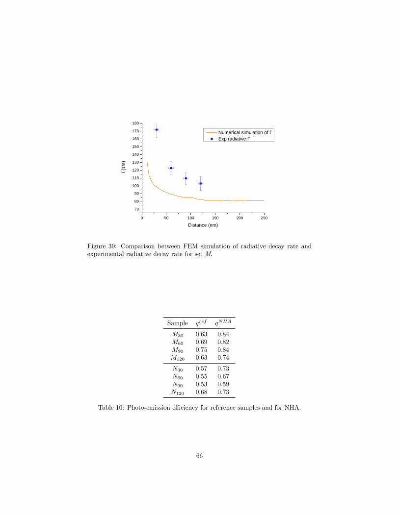
0 5 0 1 0 0 1 5 0 2 0 0 2 5 07 08 09 0
1 0 01 1 01 2 01 3 01 4 01 5 01 6 01 7 01 8 0
Γ(1/s)
D i s t a n c e ( n m )
N u m e r i c a l s i m u l a t i o n o f Γ E x p r a d i a t i v e Γ
Figure 39: Comparison between FEM simulation of radiative decay rate andexperimental radiative decay rate for set M.
Sample qref qNHA
M30 0.63 0.84M60 0.69 0.82M90 0.75 0.84M120 0.63 0.74
N30 0.57 0.73N60 0.55 0.67N90 0.53 0.59N120 0.68 0.73
Table 10: Photo-emission efficiency for reference samples and for NHA.
66
7 Conclusions
In this work the properties of plasmonic nanohole arrays have been studied, thepresence of the extraordinary optical transmission resonance has been verifiedand the dependence of its position on the lattice parameter has been pointedout. The dependence of the peak shape and position on holes’ diameter hasalso been studied, finding that by increasing the nanohole diameter the peakundergoes a red-shift and strong broadening.
Nanosphere litography has been presented and optimize as a versatile andcost-effective method for producing nanostructures, making use of single-layermasks of polystyrene nanospheres. In particular used in combination with re-active ion etching processes (RIE) it resulted useful in producing ordered struc-tures like arrays of nanoholes and obtaining a fine tuning of the diameter of theholes, without varying the lattice parameter.
In the present work, nanohole arrays have been applied to the study of themodification of the decay rate of an emitter in proximity to an interface. Er-bium was chosen as the emitter because of its great importance in the field ofoptical communication. The variation of the Er lifetime has been verified inthe presence of nanohole arrays, which brings to an enhancement of the photo-luminescent emission, thanks to the strong coupling in the near-field betweendipolar emission of Er ions and SPP Bloch waves on the interface between thenanohole array and the silica matrix in which the ions are embedded.
The trend of variation of the decay rate with the distance between the Er-doped layer and the nanohole array is in good agreement with the results ofFinite Element Simulations carried out to supply the lack of analytical modelsfor the description of these systems. The agreement between simulations andexperimental results is a validations of the approximation used in the numericalsimulation, in which the solution for the problem of interaction is found con-sidering each ion singularly and then performing an incoherent sum over thewhole distribution. This approximation could be used in general to study a lotof of systems in which there is the presence of dipole-like emitters randomlydistributed.
The study carried out in this thesis work presents many possible future devel-opments. In particular optimizing the matching between the EOT peak and theEr emission wavelength and examining in depth the variation of photolumines-cence intensity and lifetime changing the angle of incidence or the polarizationof the exciting light, could lead to a deeper understanding of the mechanisms ofinteraction between nanostructures and emitters, and to an optimized controlof their properties.
67
References
[1] R. P. Feynman. There’s plenty of room at the bottom. Engineering andScience, 23:22–36, 1960.
[2] N. Taniguchi et al. On the basic concept of nanotechnology. Proceedingsof the International Conference on Production Engineering, Part II, pages18–23, 1974.
[3] S. A. Maier. Plasmonics: fundamental and application. Springer, 2007.
[4] T. W. Ebbesen, H. J. Lezec, H. F. Ghaemi, T. Thio, and P. A. Wolff.Extraordinary optical transmission through sub-wavelength hole arrays.Nature, 391:667–669, 1998.
[5] E. M. Purcell. Spontaneous emission probabilities at radio frequencies.Phys. Rev., 69(681), 1946.
[6] A. Polman. Erbium implanted thin film photonic materials. Journal ofApplied Physics, 82:1–39, 1997.
[7] P.B. Johnson and R.W. Christy. Optical constants of the noble metals.Phys. Rev. B, 6(12):4370–4379, 1972.
[8] Alexander Vial, Anne-Sophie Grimault, Demetrio Macias, DominiqueBarchiesi, and Marc Lamy de la Chapelle. Improved analytical fit of golddispersion: Application to the modeling of extinction spectra with a finite-difference time-domain method. Phys. Rev. B, 71(085416), 2005.
[9] F. Hao and P. Nordlander. Efficient dielectric function for fdtd simulationof the optical properties of silver and gold nanoparticles. Chem. Phys. Lett.,446:115–118, 2007.
[10] Gustav Mie. Beitrage zur optik truber medien, speziell kolloidaler metal-losungen. Ann. Phys., 330(3):377–445, 1908.
[11] H. A. Bethe. Theory of diffraction by small holes. Phys. Rev., 66(7:8),2007.
[12] A. Roberts. Electromagnetic theory of diffraction by a circular aperture ina thick, perfectly conducting screen. J. Opt. Soc. Am. A, 4(10):19701983,1987.
[13] A. Degiron, H.J. Lezec, and T.W. Ebbesen N. Yamamoto. Optical transmis-sion properties of a single subwavelength aperture in a real metal. OpticalCommunication, 239:61–66, 2004.
[14] C. Genet and T. W. Ebbesen. Light in tiny holes. Nature, 445:39–46, 2007.
[15] I. R. Hooper and J. R. Sambles. Dispersion of surface plasmon polaritonson short-pitch metal gratings. Phys. Rev. B, 65(165432), 2002.
68
[16] Shih-Hui Chang, Stephen Gray, and George Schatz. Surface plasmon gener-ation and light transmission by isolated nanoholes and arrays of nanoholesin thin metal films. Opt. Express, 13(8):3150–3165, 2005.
[17] H. F. Ghaemi, Tineke Thio, D. E. Grupp, T. W. Ebbesen, and H. J.Lezec. Surface plasmons enhance optical transmission through subwave-length holes. Phys. Rev. B, 58(11):6779–6782, 1998.
[18] T. Thio, H. F. Ghaemi, H. J. Lezec, P. A. Wolff, and T. W. Ebbesen.Surface-plasmon-enhanced trasmission through hole arrays in cr films. J.Opt. Soc. Am. B, 16(10), 1999.
[19] A. Degiron and T. W. Ebbesen. The role of localized surface plasmonmodes in the enhanced transmission of periodic subwavelength apertures.J. Optics A: Pure and Applied Optics, 7(2), 2005.
[20] Christy L. Haynes and Richard P. Van Duyne. Nanosphere lithography:A versatile nanofabrication tool for studies of size-dependent nanoparticleoptics. J. Phys. Chem. B, 105(24), 2001.
[21] Frank Burmeister, Claudia Schaffle, Thomas Matthes, Johannes BonebergMatthias Bohmisch, and Paul Leiderer. Colloid monolayers as versatilelithographic masks. Langmuir, 13:2983–2987, 1997.
[22] Liang Li, Tianyou Zhai, Haibo Zeng, Xiaosheng Fang, Yoshio Bando, andDmitri Golberg. Polystyrene sphere-assisted one-dimensional nanostruc-ture arrays: synthesis and applications. J. Mat. Chem., 21(40), 2011.
[23] N. D. Denkov, O. D. Velev, P. A. Kralchevsky, I. B. Ivanov, H. Yoshimura,and K. Nagayama. Two-dimensional crystallization. Nature, 361, 1993.
[24] S. M. Rossnagel, J. J. Cuomo, and W. D. Westwood. Handbook of plasmaprocessing technology. Noyes Publications, 1990.
[25] D. M. Mattox. Handbook of physical vapor deposition (PVD) processing.William Andrew Elsevier Science distributor, Norwich, N.Y. Oxford, 2010.
[26] W. J. Miniscalco. Erbium-doped glasses for fiber amplifiers at 1500 nm. J.Lightwave Technol., 9:234–250, 1991.
[27] A. M. Glass. Fiber optics. Physics Today, 46(34), 1993.
[28] E. Desurvire. The golden age of optical fiber amplifiers. Physicis Today,47(20), 1994.
[29] S. Hufner. Optical spectra of the transparent rare earth compounds. Aca-demic Press, 1978.
[30] C. Layne, W. Lowdermilk, and M. J. Weber. Multiphonon relaxation ofrare-earth ions in oxide glasses. Phys. Rev. B, 16(10), 1977.
69

[31] P. M. Becker, A.A. Olsson, and J. R. Simpson. Erbium-doped fiber ampli-fiers: fundamental and technology. Academic Press, 1999.
[32] A. Kenyon. Recent developments in rare-earth doped materials for opto-electronics. Progr. Quant. Electron., 26(225), 2002.
[33] E. Cattaruzza, G. Battaglin, F. Visentin, and E. Trave. Er-doped filmsby rf magnetron co-sputtering. J. Non-Crystalline Solids, 355:1128–1131,2009.
[34] B. Kalinic, T. Cesca, N. Michieli, C. Scian, G. Battaglin, P. Mazzoldi, andG. Mattei. Controlling the emission rate of ions by dielectric coupling withthin films. J. Phys. Chem. C, 2015.
[35] A. Polman. Erbium as a probe of everything? Physica B: CondensedMatter, 300:78–90, 2001.
[36] T. Forster. Zwischenmolekulare energiewanderung und fluoreszenz. Ann.Phys., page 55, 1948.
[37] E. Snoeks, P. Kik, and A. Polman. Recent developments in rare-earthdoped materials fo optoeleptronics. Prog. Quant. Electron., 26(225), 2002.
[38] W. L. Barnes, E. J. Tarbox R. I. Laming, and P. Morkel. Absorption andemission cross section of er doped silica fibers. Quantum electronics, IEEEJ. of, 27:1004–1010, 1991.
[39] K. Drexhage, M. Fleck, H. Kuhn, F. Schafer, and W. Sperling. Beein-flussung der fluoreszenz eines europium-chelates durch einen spiegel. Ber.Bunsenges. Phys. Chem., 70(1179), 1966.
[40] K. H. Drexhage, H. Kuhn, and F. P. Schfer. Variation of the fluorescence de-cay time of a molecule in front of a mirror. Berichte der Bunsengesellschaftfr physikalische Chemie, 72:329, 1986.
[41] K. H. Drexhage. Monomolecular layers and light. Scientific American,222:108–119, 1970.
[42] K. Drexhage. Influence of a dielectric interface on fluorescence decay time.Journal of Luminescence, 1-2:693–701, 1970.
[43] K. H. Drexhage. Interaction of light with monomolecular dye layers. Else-vier, pages 163–232, 1974.
[44] E. Fermi. Quantum theory of radiation. Reviews of modern physics, 4:87–132, 1932.
[45] W. Barnes. Fluorescence near interfaces: the role of photonic mode density.Journal of modern optics, 45:661–699, 1998.
70
[46] M. Yeung and T. Gustafson. Spontaneous emission near an absorbingdielectric surface. Phys. Rev. A, 54(5227), 1986.
[47] R. Chance, A. Miller, A. Prock, and R. Silbey. Fluorescence and energytransfer near interfaces: The complete and quantitative description of theeu/mirror systems. The Journal of Chemical Physics, 63(1589), 1975.
[48] R. Chance, A. Prock, and R. Silbey. Molecular fluorescence and energytransfer near interfaces. Adv. Chem. Phys, 37(65), 1978.
[49] R. Chance, A. Prock, and R. Silbey. Comments on the classical theory ofenergy transfer. The Journal of Chemical Physics, 62(2245), 1975.
[50] K. G. Sullivan and D. G. Hall. Enhancement and inhibition of electromag-netic radiation in plane-layered media. i.plane-wave spectrum approach tomodeling classical effects. J. Opt. Soc. Am. B, 14:1149–1159, 1997.
[51] P. Andrew and W. L. Barnes. Molecular fluorescence above metallic grat-ings. Phys. Rev. B, 64(125405), 2001.
[52] G. Ford and W. Weber. Electromagnetic interactions of molecules withmetal surfaces. Physics Reports, 113:195–287, 1984.
[53] P. Anger, P. Bharadwaj, and L. Novotny. Enhancement and quenching ofsinglemolecule fluorescence. Physical review letters, 96(113002), 2006.
[54] M. Saboktakin, X. Ye, U. K. Chettiar, N. Engheta, C. B. Murray, andC. R. Kagan. Plasmonic enhancement of nanophosphor upconversion lu-minescence in au nanohole arrays. ACS nano, 7:7186–7192, 2013.
[55] Y. Mochizuki, M. Fujii, S. Hayashi, T. Tsuruoka, and K. Akamatsu. En-hancement of photoluminescence from silicon nanocrystals by metal nanos-tructures made by nanosphere lithography. Journal of Applied Physics,106(013517), 2009.
[56] A. G. Brolo, S. C. Kwok, M. G. Moffitt, R. Gordon, J. Riordon, and K. L.Kavanagh. Enhanced fluorescence from arrays of nanoholes in a gold film.Journal of the American Chemical Society, pages 14936–14941, 2005.
[57] A. G. Brolo, S. C. Kwok, M. D. Cooper, M. G. Moffitt, C.-W. Wang,R. Gordon, J. Riordon, and K. L. Kavanagh. Surface plasmon-quantumdot coupling from arrays of nanoholes. The Journal of Physical ChemistryB, 110:8307–8313, 2006.
[58] E. Verhagen, L. Kuipers, and A. Polman. Field enhancement in metal-lic subwavelength aperture arrays probedby erbium upconversion lumines-cence. Opt. Express, 17:14586–14598, 2009.
[59] R. J. Moerland, L. Eguiluz, and M. Kaivola. Shaping single emitter emis-sion with metallic hole arrays: strong focusing of dipolar radiation. Opt.Express, 21:4578–4590, 2013.
71
[60] C. Multiphysics and C. M. H. T. Module,. Comsol multiphysics users guide,comsol multiphysics 3 edition, 2010.
[61] M. Morgan and K. Mei. Finite-element computation of scattering by inho-mogeneous penetrable bodies of revolution. IEEE Transactions on Anten-nas and Propagation, 27(2):202–214, 1979.
[62] R. Mittra and O. Ramahi. Absorbing boundary conditions for the direct so-lution of partial differential equations arising in electromagnetic scatteringproblems. Finite Element and Finite Difference Methods in Electromag-netic Scattering, 2, 1990.
[63] M. Loreti. Teoria degli errori e fondamenti di statistica. Ed. Privata, 2006.
72
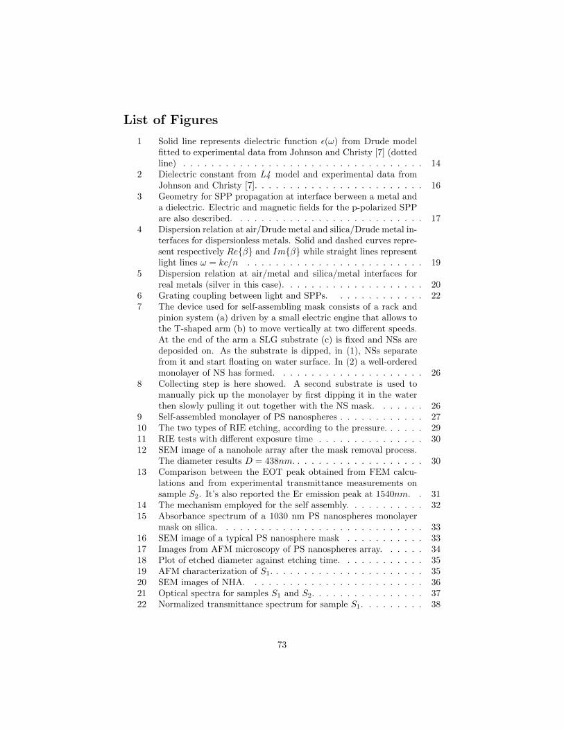
List of Figures
1 Solid line represents dielectric function ε(ω) from Drude modelfitted to experimental data from Johnson and Christy [7] (dottedline) . . . . . . . . . . . . . . . . . . . . . . . . . . . . . . . . . . 14
2 Dielectric constant from L4 model and experimental data fromJohnson and Christy [7]. . . . . . . . . . . . . . . . . . . . . . . . 16
3 Geometry for SPP propagation at interface berween a metal anda dielectric. Electric and magnetic fields for the p-polarized SPPare also described. . . . . . . . . . . . . . . . . . . . . . . . . . . 17
4 Dispersion relation at air/Drude metal and silica/Drude metal in-terfaces for dispersionless metals. Solid and dashed curves repre-sent respectively Re{β} and Im{β} while straight lines representlight lines ω = kc/n . . . . . . . . . . . . . . . . . . . . . . . . . 19
5 Dispersion relation at air/metal and silica/metal interfaces forreal metals (silver in this case). . . . . . . . . . . . . . . . . . . . 20
6 Grating coupling between light and SPPs. . . . . . . . . . . . . 227 The device used for self-assembling mask consists of a rack and
pinion system (a) driven by a small electric engine that allows tothe T-shaped arm (b) to move vertically at two different speeds.At the end of the arm a SLG substrate (c) is fixed and NSs aredeposided on. As the substrate is dipped, in (1), NSs separatefrom it and start floating on water surface. In (2) a well-orderedmonolayer of NS has formed. . . . . . . . . . . . . . . . . . . . . 26
8 Collecting step is here showed. A second substrate is used tomanually pick up the monolayer by first dipping it in the waterthen slowly pulling it out together with the NS mask. . . . . . . 26
9 Self-assembled monolayer of PS nanospheres . . . . . . . . . . . . 2710 The two types of RIE etching, according to the pressure. . . . . . 2911 RIE tests with different exposure time . . . . . . . . . . . . . . . 3012 SEM image of a nanohole array after the mask removal process.
The diameter results D = 438nm. . . . . . . . . . . . . . . . . . . 3013 Comparison between the EOT peak obtained from FEM calcu-
lations and from experimental transmittance measurements onsample S2. It’s also reported the Er emission peak at 1540nm. . 31
14 The mechanism employed for the self assembly. . . . . . . . . . . 3215 Absorbance spectrum of a 1030 nm PS nanospheres monolayer
mask on silica. . . . . . . . . . . . . . . . . . . . . . . . . . . . . 3316 SEM image of a typical PS nanosphere mask . . . . . . . . . . . 3317 Images from AFM microscopy of PS nanospheres array. . . . . . 3418 Plot of etched diameter against etching time. . . . . . . . . . . . 3519 AFM characterization of S1. . . . . . . . . . . . . . . . . . . . . . 3520 SEM images of NHA. . . . . . . . . . . . . . . . . . . . . . . . . 3621 Optical spectra for samples S1 and S2. . . . . . . . . . . . . . . . 3722 Normalized transmittance spectrum for sample S1. . . . . . . . . 38
73
23 (a) Energy levels of Er3+ labelled with the Russell-Saunders no-tation. For each state the GSA column lists the wavelength ofthe ground-state absorption transition terminating on it. (b) Ab-sorption spectrum of Er-doped silicate glass. Absorbtion valuesat the peaks of the strong bands at 380 and 520 nm are 1.5 and1.0, respectively [26]. . . . . . . . . . . . . . . . . . . . . . . . . . 40
24 A schematic representation of the PL measurement set-up. . . . . 4225 PL intensity (a) and lifetime values (b) at 1.54µm as a function
of the temperature of the thermal tratments performed in air andin vacuum atmosphere [34]. . . . . . . . . . . . . . . . . . . . . . 44
26 Main photo-emission peak for Er3+. The various components ofthe peak are labelled. . . . . . . . . . . . . . . . . . . . . . . . . . 45
27 PL decay of Er photo-emission at 1.54µm fitted with single ex-ponential curve. . . . . . . . . . . . . . . . . . . . . . . . . . . . . 46
28 Variation of normalized lifetime as function of the distance (z)from a Au overlayer (ε2 = −105.66 + i3.85) for an Er-like emitter(λem = 1540nm) embedded in silica. Parallel, perpendicular andisotropic orientations are obtained from eq. (5.10), (5.7) and (5.8). 49
29 Comparison between time dependence of the PL intensity calcu-lated with CPS model and a single exponential. . . . . . . . . . . 50
30 Comparison between simulation (FEM) and the CPS model forthe variation of the normalized decay rate of an Er-like emitter(λem = 1540nm) as a function of the distance from a gold film [34]. 52
31 AFM image and profile of the NHA after a 200nm silica deposi-tion on test sample S1. Is clear that the silica overlayer does notinfluence the deep of the holes, since it is of ∼ 100nm before andafter the deposition. . . . . . . . . . . . . . . . . . . . . . . . . . 56
32 Transmission spectra of S1, after a series of thermal annealing atincreasing temperatures. The annealings were performed in N2
atmosphere. . . . . . . . . . . . . . . . . . . . . . . . . . . . . . . 5733 Transmittance spectra for samples M90 and N90. It’s reported
the position of the Er emission peak. . . . . . . . . . . . . . . . . 5834 Photo-emission decay for sample series M. It’s clear the lifetime
reduction as the distance between Er-doped layer and NHA de-creases. . . . . . . . . . . . . . . . . . . . . . . . . . . . . . . . . 58
35 Wireframe views of the NHA-emitter interction model. . . . . . . 6036 Wigner-Seitz cell: construction and sampling points. . . . . . . . 6137 Simulated γr(z) for emitter placed at different positions in the
XY plane for a a0 = 1030nm NHA. The color map indicates thedistance from the centre of a hole in the WS cell, as in fig. 36(b). 62
38 Comparison between FEM simulation of radiative decay rate andexperimental radiative decay rate for set N. . . . . . . . . . . . . 65
39 Comparison between FEM simulation of radiative decay rate andexperimental radiative decay rate for set M. . . . . . . . . . . . . 66
74
List of Tables
1 Coefficients of L4 model for Au and Ag . . . . . . . . . . . . . . 152 Optimal parameters for low-pressure RIE process used in the
present work. . . . . . . . . . . . . . . . . . . . . . . . . . . . . . 293 Diameter of PS nanospheres after RIE process. . . . . . . . . . . 344 Set for the magnetron sputtering. . . . . . . . . . . . . . . . . . . 365 Holes’ diameter correlation with RIE duration. . . . . . . . . . . 366 Features of the test samples for PL measurements. Sample S1
presents a 100nm NHA below the Er-doped layer, besides sampleR1 is as test reference sample. . . . . . . . . . . . . . . . . . . . . 55
7 Measured lifetime for the two sets of samples M and N. . . . . . 638 Experimental, CPS radiative and calculated non-radiative decay
rates. . . . . . . . . . . . . . . . . . . . . . . . . . . . . . . . . . . 649 Experimental lifetimes and decay rates, and computed radiative
decay rates. . . . . . . . . . . . . . . . . . . . . . . . . . . . . . . 6410 Photo-emission efficiency for reference samples and for NHA. . . 66
75