university of groningen ferroelectric control of the spin
TRANSCRIPT

University of Groningen
Ferroelectric Control of the Spin Texture in GeTeRinaldi, Christian; Varotto, Sara; Asa, Marco; Slawinska, Jagoda; Fujii, Jun; Vinai, Giovanni;Cecchi, Stefano; Di Sante, Domenico; Calarco, Raffaella; Vobornik, IvanaPublished in:Nano Letters
DOI:10.1021/acs.nanolett.7b04829
IMPORTANT NOTE: You are advised to consult the publisher's version (publisher's PDF) if you wish to cite fromit. Please check the document version below.
Document VersionPublisher's PDF, also known as Version of record
Publication date:2018
Link to publication in University of Groningen/UMCG research database
Citation for published version (APA):Rinaldi, C., Varotto, S., Asa, M., Slawinska, J., Fujii, J., Vinai, G., Cecchi, S., Di Sante, D., Calarco, R.,Vobornik, I., Panaccione, G., Picozzi, S., & Bertacco, R. (2018). Ferroelectric Control of the Spin Texture inGeTe. Nano Letters, 18(5), 2751-2758. https://doi.org/10.1021/acs.nanolett.7b04829
CopyrightOther than for strictly personal use, it is not permitted to download or to forward/distribute the text or part of it without the consent of theauthor(s) and/or copyright holder(s), unless the work is under an open content license (like Creative Commons).
The publication may also be distributed here under the terms of Article 25fa of the Dutch Copyright Act, indicated by the “Taverne” license.More information can be found on the University of Groningen website: https://www.rug.nl/library/open-access/self-archiving-pure/taverne-amendment.
Take-down policyIf you believe that this document breaches copyright please contact us providing details, and we will remove access to the work immediatelyand investigate your claim.
Downloaded from the University of Groningen/UMCG research database (Pure): http://www.rug.nl/research/portal. For technical reasons thenumber of authors shown on this cover page is limited to 10 maximum.
Download date: 20-11-2021

Ferroelectric Control of the Spin Texture in GeTeChristian Rinaldi,*,†,‡ Sara Varotto,† Marco Asa,† Jagoda Sławinska,§ Jun Fujii,∥ Giovanni Vinai,∥
Stefano Cecchi,⊥ Domenico Di Sante,# Raffaella Calarco,⊥ Ivana Vobornik,∥ Giancarlo Panaccione,∥
Silvia Picozzi,§ and Riccardo Bertacco*,†,‡
†Department of Physics, Politecnico di Milano, 20133 Milano, Italy‡IFN-CNR, Politecnico di Milano, 20133 Milano, Italy§Consiglio Nazionale delle Ricerche CNR-SPIN, Sede Temporanea di Chieti, c/o Univ. “G. D’Annunzio”, 66100 Chieti, Italy∥CNR-IOM, Laboratorio TASC in Area Science Park - Basovizza, 34149 Trieste, Italy⊥Paul-Drude-Institut fur Festkorperelektronik, Hausvogteiplatz 5-7, 10117 Berlin, Germany#Institut fur Theoretische Physik und Astrophysik, Universitat Wurzburg, Am Hubland Campus Sud, Wurzburg 97074, Germany
*S Supporting Information
ABSTRACT: The electric and nonvolatile control of the spin texturein semiconductors would represent a fundamental step toward novelelectronic devices combining memory and computing functionalities.Recently, GeTe has been theoretically proposed as the fathercompound of a new class of materials, namely ferroelectric Rashbasemiconductors. They display bulk bands with giant Rashba-likesplitting due to the inversion symmetry breaking arising from theferroelectric polarization, thus allowing for the ferroelectric control ofthe spin. Here, we provide the experimental demonstration of thecorrelation between ferroelectricity and spin texture. A surface-engineering strategy is used to set two opposite predefined uniformferroelectric polarizations, inward and outward, as monitored bypiezoresponse force microscopy. Spin and angular resolved photoemission experiments show that these GeTe(111) surfacesdisplay opposite sense of circulation of spin in bulk Rashba bands. Furthermore, we demonstrate the crafting of nonvolatileferroelectric patterns in GeTe films at the nanoscale by using the conductive tip of an atomic force microscope. Based on theintimate link between ferroelectric polarization and spin in GeTe, ferroelectric patterning paves the way to the investigation ofdevices with engineered spin configurations.
KEYWORDS: Germanium telluride, Rashba effect, ferroelectricity, spin−orbitronics
While Moore’s law seems to approach its limit of validity,the search for new paradigms allowing the further
improvement of the computing capabilities of electronic devicesis entering a final rush. Spintronics is a promising route in thisperspective, but so far, its success stories are limited to the fieldof memories. To enter the area of computing, devices capableof manipulating the information encoded in the spin areneeded. In this sense, a lot of effort is currently carried out inthe fields of spin logic,1 magnon spintronics,2,3 and semi-conductor spintronics.4−7 Nevertheless, about 20 years after thepioneering idea of “spin transistor” proposed by Datta andDas,8 many practical limitations still prevent the implementa-tion of effective transistors based on spin properties.9 Thedream remains to manipulate spins within semiconductorsdevices to exploit the full potential of materials with a gap forcharge control, without use of auxiliary ferromagnetic materialsand magnetic fields. Beyond magnetic semiconductors,10 whichstill suffer from low-temperature operation and the need ofexternal magnetic fields to control the spin texture, newmaterials and concepts are necessary. In this context, the
recently introduced class of ferroelectric Rashba semiconduc-tors (FERSCs),11 whose father compound is α-GeTe,12 ishighly promising. They are semiconductors and also ferro-electrics, so that the remanent ferroelectric polarization vectorbreaks the inversion symmetry and determines a giant bulkRashba k-dependent spin-splitting of the bands.13 Remarkably,density functional theory (DFT) simulations predict that thespin direction in each sub-band should reverse upon inversionof the ferroelectric polarization, thereby allowing its electricalcontrol. In perspective, these unique features could be exploitedin novel devices14,15 integrating memory and computingfunctionalities within the very same channel of a spin-transistor.16 While ferroelectric hysteresis provides the memoryfunctionality, spin-dependent transport phenomena in spintextures defined by ferroelectric domains can implementcomputing, within the very same devices.
Received: November 15, 2017Revised: January 20, 2018Published: January 30, 2018
Letter
pubs.acs.org/NanoLettCite This: Nano Lett. 2018, 18, 2751−2758
© 2018 American Chemical Society 2751 DOI: 10.1021/acs.nanolett.7b04829Nano Lett. 2018, 18, 2751−2758
This is an open access article published under a Creative Commons Non-Commercial NoDerivative Works (CC-BY-NC-ND) Attribution License, which permits copying andredistribution of the article, and creation of adaptations, all for non-commercial purposes.
Dow
nloa
ded
via
UN
IV G
RO
NIN
GE
N o
n Se
ptem
ber
2, 2
020
at 1
3:48
:29
(UT
C).
See
http
s://p
ubs.
acs.
org/
shar
ingg
uide
lines
for
opt
ions
on
how
to le
gitim
atel
y sh
are
publ
ishe
d ar
ticle
s.

In this paper, we address a fundamental issue on theroadmap toward the exploitation of FERSCs: the nonvolatile,but reversible, electric control of the spin texture in α-GeTethin films down to the nanoscale, thus paving the way to thedefinition of unconventional spin configurations in semi-conductors. The electric switching of the ferroelectric (FE)polarization has been already demonstrated in GeTe(111)films13 and more recently in GeTe nanowires.17 However, anexperimental proof of the reversal of the spin texture (theclockwise or counterclockwise sense of circulation of spins inbulk Rashba-like bands) for opposite FE polarization is stillmissing. So far, only a link between the direction of the FEpolarization and the spin orientation in the surface Rashba sub-bands has been reported.13 More recently, the impact ofmagnetic fields on the spin texture of Mn-doped GeTe filmshas been investigated but always for fixed FE polarization.18
Here, we experimentally establish the intimate link betweenthe orientation of the remanent ferroelectric polarization andthe circulation of spin texture associated with Rashba bands inGeTe(111) thin films. First, we describe a surface engineeringstrategy to prepare in situ α-GeTe(111) films with uniformpristine ferroelectric polarization, outward or inward. Then, byspin- and angular-resolved photoemission spectroscopy (S-ARPES), we provide evidence for opposite sense of spincirculation of bulk Rashba bands in the two surfaces preparedwith opposite FE polarization. Our results suggest thepossibility of crafting the spin texture at the nanoscale inGeTe via ferroelectric patterning. In this route, we demonstratethe reversible writing of an array of nanostripes with inward andoutward FE polarization, assumed to have opposite spinconfigurations. This represents a first example of engineeredmeta-material based on a ferroelectric Rashba semiconductor,suitable to implement the concept of Rashba barriers. Inperspective, our results pave the way to the exploitation ofGeTe in unconventional spintronic devices with pure electriccontrol of their operation and reconfigurable computingfunctionalities.The first step toward the demonstration of the link between
FE state and spin texture in GeTe by S-ARPES is theinitialization of the whole film, leading to a uniform pristine FEpolarization pointing inward or outward. This also correspondsto the “clean blackboard” state preliminary to any patterning. Inthis scope, we developed a method for preparing α-GeTe(111)surfaces with opposite FE polarization, associated with differentterminations. Rhombohedral α-GeTe(111) results from thestacking of Ge and Te planes, which are not equidistant andthus give rise to a net electric dipole, being Te moreelectronegative than Ge.19,20
As the energetically favored termination is generated by thebreaking of long (rather than short) bonds, a Te terminatedsurface is expected to display a dipole pointing outward (Pout),while a Ge-terminated one will have a net dipole inward (Pin),as depicted in panels a and a′ of Figure 1. Even thoughcalculations predict the Te-terminated GeTe(111) to be morestable than the Ge-terminated one by 60 meV Å−2, this surfaceenergy difference is largely reduced by the presence ofreconstructions,21 vacancies, and other kind of defects, thussuggesting the possibility of stabilizing both terminations in realsurfaces.GeTe(111) films, 23 nm thick, were grown by molecular
beam epitaxy (MBE) on Si(111) and then capped with 20 nmof Te to prevent contamination due to exposure to atmosphere.A reliable protocol for controlled Te-desorption in ultrahigh
vacuum (UHV) has been first optimized to obtain Ge- and Te-rich surfaces with opposite polarization, as checked by X-rayphotoemission spectroscopy (XPS) with Al−Kα radiation andpiezoresponse force microscopy (PFM) (for details, seesections 1 and 2 of the Supporting Information). An annealingof 1 h at about 240 °C produces a Te-rich surface displaying apristine polarization Pout, while the same annealing at 260 °Ccauses a complete desorption of Te (the more volatile species)and produces a Ge-rich surface with Pin. Crucial for this paper,the same method has been applied to samples prepared in situfor S-ARPES, to demonstrate that opposite FE polarizationstates are associated with inverse spin texture. After insertion invacuum at the APE beamline, the samples were annealed atabout 240 and 260 °C for 1 h, controlling the heater current.According to the recipe previously optimized (for details seesection 2 of the Supporting Information), we obtained a firstsample (STe) with a Te-rich surface and a second one (SGe)with a Ge-rich surface, as confirmed by the in situ analysis ofthe XPS spectra taken at 800 eV photon energy (see section 3of the Supporting Information). In fact, from the relativeintensity of the Ge 3d and Te 4d peaks, normalized to the
Figure 1. GeTe(111) surfaces with opposite FE polarization. (a, a′)Sketch of the Ge and Te planes for the Te and Ge termination,respectively. The distances given on the left refer to the unrelaxedinterlayer distances. Only the topmost surface atoms of the slab areshown. The black rectangle denotes a bulk hexagonal unit cell used inDFT calculations as a building block to construct the (111) surface(rhombohedral setting, corresponding to the (0001) in the hexagonalsetting). The net FE polarization Pout (Pin) (white arrows) arises fromthe interatomic dipoles shown with blue and red arrows. (b, b′)Piezoresponse-phase images recorded on STe (SGe) after poling withthe tip at +7 V (−7 V) and −7 V (+7 V) over two concentric squaresof 1.5 and 0.5 μm per side. The scale bar corresponds to 0.5 μm. (c, c′)PFM-phase signal showing the pristine polarization state and theferroelectric hysteresis loop, as measured ex-situ on STe and SGe afterthe S-ARPES experiment. The controlled thermal desorption of the Tecapping layer leads to a virgin-state FE polarization Pout and Pin in thetwo samples, respectively.
Nano Letters Letter
DOI: 10.1021/acs.nanolett.7b04829Nano Lett. 2018, 18, 2751−2758
2752
analyzer transmission and tabulated atomic photoemissioncross-sections, the average stoichiometries of STe and SGe areGe0.39Te0.61 and Ge0.46Te0.54, respectively. The uncertainty onthe relative stoichiometry is ± 0.02, and it mainly arises fromthe error on the estimation of the peaks’ area. Within thephotoemission probing depth (∼17 Å at 800 eV photonenergy), STe is clearly Te-rich, while the Ge concentration inSGe is slightly above that of GeTe films, which typically displays10% Ge vacancies (Ge0.45Te0.55),
22,23 thus pointing toward a Geenrichment of SGe. Data taken with Al−Kα radiation (1486.6eV), after the beamtime, confirm that STe (SGe) is Te (Ge) richat surface (see section 2 of the Supporting Information).Furthermore, the deconvolution of XPS spectra, using surfaceand bulk components (section 2 of the SupportingInformation), shows that the Te (Ge) enrichment is localizedat surface. Based on these considerations, in the following wewill compare our ARPES data from STe and SGe with densityfunctional theory simulations of Ge- and Te-terminatedsurfaces. In fact, these truncated bulk systems represent thesimplest models of Te- and Ge-rich surfaces with outward andinward FE polarization.The virgin ferroelectric state of Te- and Ge-rich samples has
been widely investigated by PFM, both during the optimizationof the surface strategy for poling (section 1 of the SupportingInformation) and after the beamtime, on samples STe and SGe.Here in particular, we report on these two samples, whosepristine FE state is crucial for the establishment of the link
between FE polarization and spin texture. In Figure 1b (1b′),we show the phase signal recorded on STe (SGe) after writing alarge square with +7 V (−7 V) bias on the AFM tip and then aninner square with opposite bias. FE patterns are stable overmore than 24 h (section 1 of the Supporting Information), thusindicating the robustness of ferroelectricity in GeTe films. Theinner square displays the same contrast (PFM phase) of theunpoled area, indicating an outward (inward) virgin ferro-electric polarization in STe (SGe). To confirm these findings, wemeasured the virgin curve and the full ferroelectric hysteresisloops by sweeping the PFM tip voltage. A pair of characteristicloops measured on STe and SGe are reported in panels c and c′of Figure 1 as representative of the average response of theentire sample area probed by S-ARPES (see section 1 of theSupporting Information for details on the statistical analysis).The virgin curve measured for STe indicates the initial state isclose to that obtained for negative saturating voltages, while theopposite holds for the sample SGe. This is a clear indication thatSTe and SGe present two opposite outward and inward virgin FEpolarizations. These samples are ideal candidates for investigat-ing the connection between FE polarization and spin texture.In Figure 2, we show the bands dispersion and the
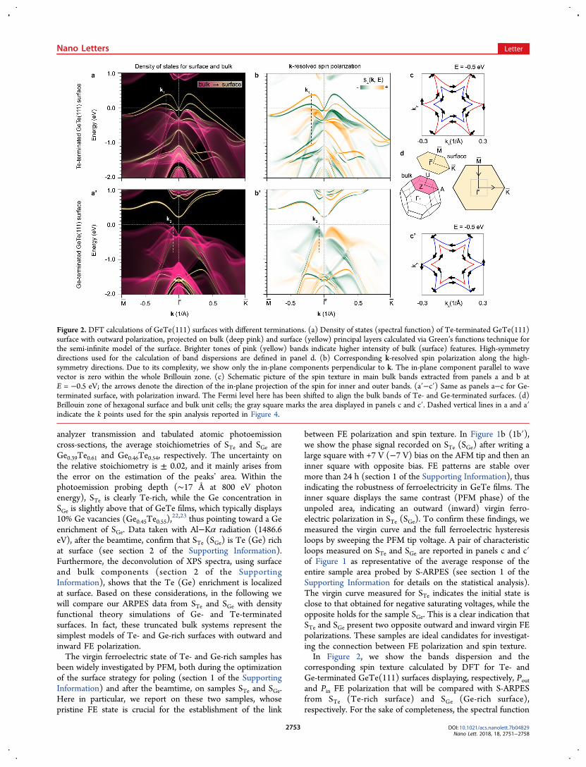
corresponding spin texture calculated by DFT for Te- andGe-terminated GeTe(111) surfaces displaying, respectively, Poutand Pin FE polarization that will be compared with S-ARPESfrom STe (Te-rich surface) and SGe (Ge-rich surface),respectively. For the sake of completeness, the spectral function
Figure 2. DFT calculations of GeTe(111) surfaces with different terminations. (a) Density of states (spectral function) of Te-terminated GeTe(111)surface with outward polarization, projected on bulk (deep pink) and surface (yellow) principal layers calculated via Green’s functions technique forthe semi-infinite model of the surface. Brighter tones of pink (yellow) bands indicate higher intensity of bulk (surface) features. High-symmetrydirections used for the calculation of band dispersions are defined in panel d. (b) Corresponding k-resolved spin polarization along the high-symmetry directions. Due to its complexity, we show only the in-plane components perpendicular to k. The in-plane component parallel to wavevector is zero within the whole Brillouin zone. (c) Schematic picture of the spin texture in main bulk bands extracted from panels a and b atE = −0.5 eV; the arrows denote the direction of the in-plane projection of the spin for inner and outer bands. (a′−c′) Same as panels a−c for Ge-terminated surface, with polarization inward. The Fermi level here has been shifted to align the bulk bands of Te- and Ge-terminated surfaces. (d)Brillouin zone of hexagonal surface and bulk unit cells; the gray square marks the area displayed in panels c and c′. Dashed vertical lines in a and a′indicate the k points used for the spin analysis reported in Figure 4.
Nano Letters Letter
DOI: 10.1021/acs.nanolett.7b04829Nano Lett. 2018, 18, 2751−2758
2753
for the energetically unfavorable configurations (i.e., Te-terminated surface with Pin and Ge-terminated surface withPout) are reported in section 3 of the Supporting Information.In agreement with previous works,21,24 we refer to bulkcoordinates in terms of the rhombohedral setting (a = b = c =4.37 Å and α = β = γ = 57.9°), such that the ferroelectricpolarization points along the [111] direction of the real spaceand the Rashba-like dispersion of bulk bands is seen on the{111} planes of the reciprocal space around Z. However, tosimulate surface aspects we adopt the more common hexagonalsetting to construct the slabs (Figure 1, panels a and a′), withthe ferroelectric polarization pointing along the [0001]direction. However, throughout the text, we will refer to thesample surface as GeTe(111) defined with respect to therhombohedral cell.The bulk high-symmetry directions ZU and ZA, together
with the corresponding surface directions ΓM and ΓK, areshown in Figure 2d. The FE polarization is parallel to ΓZdirection of the reciprocal space, i.e., the (111) direction of thecrystal. Band dispersions along high-symmetry directions arepresented in Figure 2a for STe and Figure 2a′ for SGe, afterprojection of the spectral function on the surface layers and on
the bulk in the semi-infinite model, to single out surface andbulk-like contributions.The k-resolved spin polarization is reported in panel b for STe
and b′ for SGe, in which the non-null spin componentsperpendicular to the wave vector are shown along the high-symmetry bulk (surface) ZA (ΓK) and ZU (ΓM) directions.While the shape of bulk Rashba sub-bands is not affected by FEpolarization reversal, their spin texture is reversed, according tothe main concept of FERSCs. This is evident from thecomparison of the isoenergy cuts, taken at 0.5 eV below the topof the valence band, reported in panels c and c′, where arrowsindicate the local spin direction. However, surface bands withRashba splitting are very different for the two terminations. Inthe Te-terminated one (Pout) they display a clear Rashba-likesplitting and cross the Fermi energy at higher wave vectors withrespect to the bulk bands. In the Ge-terminated one (Pin),instead, the Rashba splitting of the surface bands in the gap islargely suppressed and surface bands shift toward theconduction band, without crossing the Fermi level at highmomenta.The remarkable difference between surface Rashba like bands
predicted by DFT for Te- and Ge-termination has an
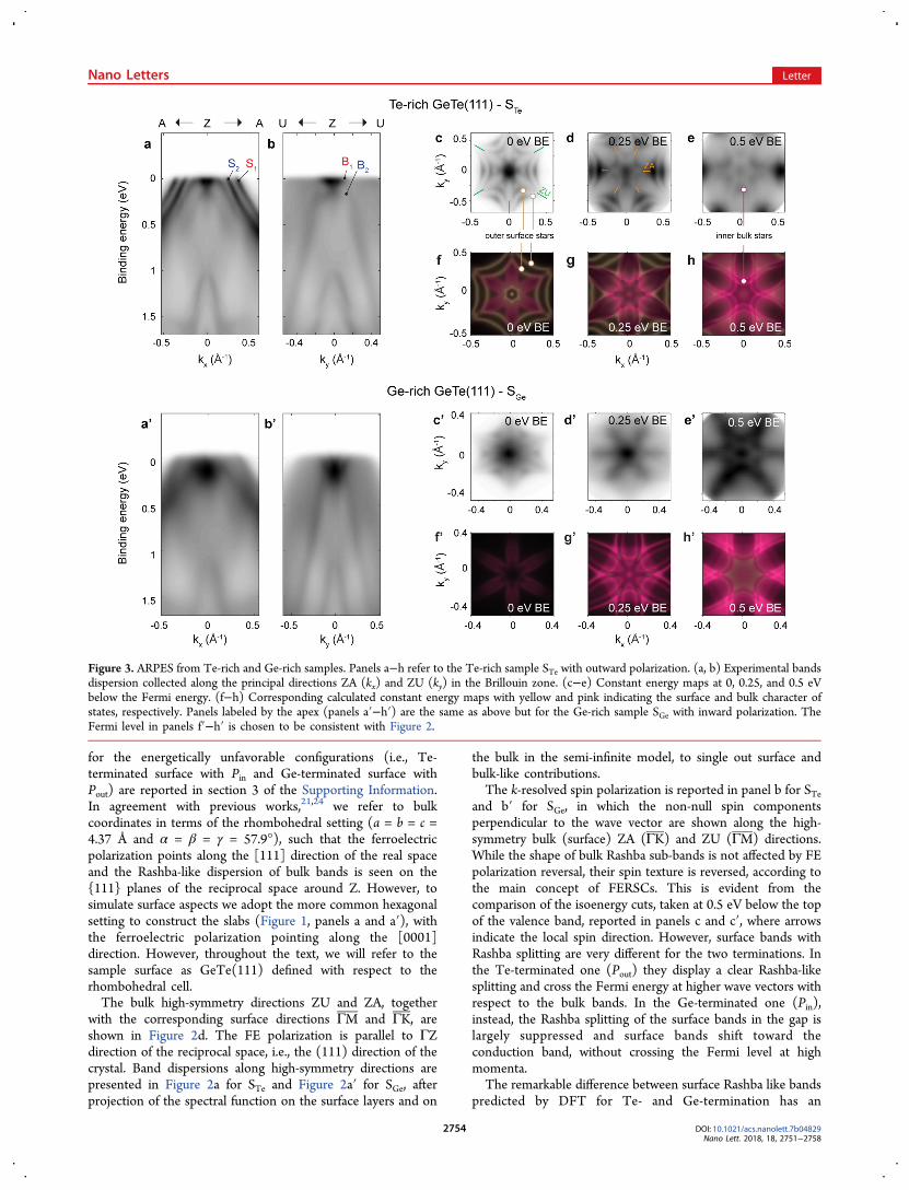
Figure 3. ARPES from Te-rich and Ge-rich samples. Panels a−h refer to the Te-rich sample STe with outward polarization. (a, b) Experimental bandsdispersion collected along the principal directions ZA (kx) and ZU (ky) in the Brillouin zone. (c−e) Constant energy maps at 0, 0.25, and 0.5 eVbelow the Fermi energy. (f−h) Corresponding calculated constant energy maps with yellow and pink indicating the surface and bulk character ofstates, respectively. Panels labeled by the apex (panels a′−h′) are the same as above but for the Ge-rich sample SGe with inward polarization. TheFermi level in panels f′−h′ is chosen to be consistent with Figure 2.
Nano Letters Letter
DOI: 10.1021/acs.nanolett.7b04829Nano Lett. 2018, 18, 2751−2758
2754
experimental counterpart in ARPES data reported in Figure 3for STe (panels a−h) and SGe (a′−h′). Panels a and b in Figure3 present the experimental band dispersions along ZA and ZUfor STe. Corresponding isoenergy cuts at 0, 0.25, and 0.5 eV BEin panels c−e of Figure 3 are compared with theoretical onesfor a Te-terminated surface. In the following we will use asimplified distinction between “surface” and “bulk” Rashbastates. Having in mind that ARPES at 20 eV probes just a fewatomic layers underneath the sample surface, we identify as bulkstates those displaying a sizable photon energy or kzdispersion.13 Rigorously, these are not true bulk states butcan be viewed as surface-bulk resonances24 or simply states
with sizable projection on bulk states, so they mainly reflect thebulk behavior.25
Both band dispersions and isoenergy cuts from sample STeare very similar to data available in the literature for Te-terminated α-GeTe(111).13,24,25 In agreement with DFTcalculations, prominent surface bands with Rashba splitting(S1, S2) are seen at large momenta, especially along the ZAdirection. A pair of outer spin split bands with 6-fold symmetryand “arms” along the equivalent ZU directions are clearlyvisible in the isoenergy cuts of panels c and d of Figure 3(marked by green ticks). However, at 0.25 eV BE (Figure 3d),an inner 6-fold star (orange ticks) appears, rotated by 30degrees with respect to the surface one, i.e., with arms along
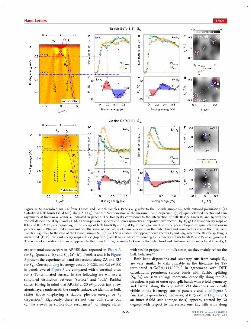
Figure 4. Spin-resolved ARPES from Te-rich and Ge-rich samples. Panels a−g refer to the Te-rich sample STe with outward polarization. (a)Calculated bulk bands (solid line) along ZU (ky) over the 2nd derivative of the measured band dispersion. (b, c) Spin-polarized spectra and spinasymmetry at fixed wave vector k1 indicated in panel a. The two peaks correspond to the intersection of bulk Rashba bands B1 and B2 with thevertical dashed line at k1 (panel a). (d, e) Spin-polarized spectra and spin asymmetry at opposite wave vector −k1. (f, g) Constant energy maps at0.18 and 0.5 eV BE, corresponding to the energy of bulk bands B1 and B2 at k1, in nice agreement with the peaks of opposite spin polarizations inpanels c and e. Blue and red arrows indicate the sense of circulation of spins: clockwise in the outer band and counterclockwise in the inner one.Panels a′−g′ refer to the case of the Ge-rich sample SGe. (b′−e′) Spin analysis for opposite wave vectors k2 and −k2, where the Rashba splitting ismaximized. (f′, g′) Constant energy maps at 0 eV (top of B1) and 0.26 eV BE, corresponding to the energy of bulk bands B1 and B2 at k2 (panel a′).The sense of circulation of spins is opposite to that found for STe: counterclockwise in the outer band and clockwise in the inner band (panel g′).
Nano Letters Letter
DOI: 10.1021/acs.nanolett.7b04829Nano Lett. 2018, 18, 2751−2758
2755

ZA. This is ascribed to the bulk-like bands (B1 and B2) evidentin the band dispersion along ZU of panel b. The isoenergy cutat 0.5 eV (Figure 3e), instead, mainly reflects the symmetry ofthe bulk inner star because at this BE, the cut of states withsurface character occurs at higher momenta.The scenario for the SGe sample is completely different
because surface states are almost absent, in agreement withDFT simulations. Indeed the prominent surface Rashba bandsS1 and S2 along ZA in Figure 3a are missing in panel a′, whilebulk bands B1 and B2 along ZU
12 are similar in panels b and b′.The absence of S1 and S2 surface states is even more evidentfrom the Fermi energy cut of panel 3c′, which does not displaythe outer 6-fold double star of panel c. Besides, the isoenergycut at 0.25 eV (panel d′) already reflects the symmetry of bulkstates, such as the inner star in Figure 3d,e from sample STe, i.e.,with arms along ZA.To summarize, ARPES data from samples STe and SGe show
band dispersions in good agreement with those calculated for aTe-terminated (Pout) and Ge-terminated (Pin) surface,respectively. This represents a self-consistent proof of thereliability of our method for preparing GeTe(111) surfaces withopposite FE polarization.In the following, we discuss the connection between the spin
texture of bulk Rashba bands and the FE polarization, which isthe key concept of FERSC materials. Figure 4 reports spin-resolved ARPES data from STe and SGe.In fact, the Rashba splitting of surface bands can be largely
affected, or even suppressed, by proximity with other materialsin a multilayer26 or by the surface electric field due to screeningcharges. In sample STe, which displays both surface and bulkRashba bands, we performed spin-polarized scans at fixedmomenta (k1, −k1) marked in panels f and g of Figure 4, alongthe equivalent ZU direction at 30 degrees with respect to kx.Even though these are not the points where the Rashbasplitting is maximized, for ± k1, only bulk bands B1,2 areexpected to contribute to the photoemission signal at BEgreater than 0.2 eV (see Figure 2a,b). The spin polarizedspectra and corresponding spin-polarization are reported inpanels b and c for k1 and d and e for −k1. With reference to thepolarimeter quantization axis set along the negative direction ofky, at k1, we find a positive peak in the spin polarization at about0.2 eV and a negative one at about 0.5 eV (panel c),corresponding to the crossing of the outer and inner band B1and B2, respectively. The opposite occurs at −k1, as expectedfor GeTe Rashba bands.12,24,25 The sense of circulation of spinsresulting from our data is sketched in Figure 4f,g by arrowssuperimposed to the isoenergy cuts taken at 0.18 and 0.5 eV. Inagreement with DFT calculations, for a Te-terminated (Pout)surface the sense of circulation of spins is clockwise for theouter band and counterclockwise for the inner one.For SGe, the analysis of the spin texture of bulk bands is
simpler, due to the lack of surface bands. In this case, we chooseopposite k points (k2, −k2), along ky (ZU direction), where themaximum Rashba energy splitting (ER) of bulk bands B1,2 isexpected (see Figures 2a′ and 4a′). The quantization axis of thespin polarimeter was set orthogonal to the wave vectors towardthe positive kx direction. Spin-polarized spectra in Figure 4b′display two prominent peaks with opposite spin, arising fromthe crossing of B1 and B2 bands at k2. Their energy splitting ofabout 200 meV is in good agreement with the expected value ofthe Rashba energy ER, according to theoretical predictions12
and recent experimental findings.24,25 Noteworthy is the factthat the sign of the spin polarization of the two peaks reverts
when moving from k2 to −k2, as it appears from the comparisonof panels b′−e′ in Figure 4. To determine the sense ofcirculation of spins in the outer and inner bands, we simplynote that in panel c′, the peak at lower BE (outer band) has anegative polarization with respect to the quantization axis, i.e.,the spin is directed along the negative direction of kx(counterclockwise rotation). The opposite holds for the peakat higher BE (inner band), so that the sense of circulation of thespin there is clockwise. The corresponding spin texture issketched in panels f′ and g′. For a more-detailed vectorialanalysis of the spin texture, see section 4 of the SupportingInformation.Crucial for the demonstration of the basic concept of
FERSCs, the sense of circulation of spin in the inner and outerbands is opposite in samples STe (Figure 4g) and SGe (Figure4g’), which display outward and inward FE polarization,respectively. This means that the spin texture is locked to theFE polarization because it reverts when the FE polarization isswitched.Having demonstrated the locking between ferroelectric
polarization and spin textures, in the following we focus onthe nanopatterning of ferroelectric domains. Figure 5 reports an
example of a peculiar ferroelectric pattern written in a GeTefilm, i.e., an array of lines with 600 nm spacing, having FEpolarization inward (Pin), in a sample with uniform FEpolarization outward (Pout). This pattern has been definedstarting from a sample with uniform Pout, obtained by applyingthe surface engineering method outlined above for producing aTe-rich surface, over which a sequence of lines with oppositepolarization has been written by sweeping the conductive tip ofthe AFM with a positive bias of +10 V. For a sweep rate of 3μm/s, we get an average line width of about 300 nm as a resultof the characteristic GeTe FE viscosity.It is noteworthy that the pattern is stable over more than 24
h, thus pointing to the possibility of using this kind of FEpatterns in spintronic devices exploiting the propagation ofelectrons in structure with engineered in-plane domains with
Figure 5. FE domains and spin texture patterning at the nanoscale. (a)Sketch of the writing procedure to obtain a sequence of Rashbabarriers using the conductive tip of an AFM on a sample with pristinepolarization outward, prepared as for sample STe above or by sweepingthe tip with a negative voltage (Vtip = −10 V). Lines of inwardpolarization are written with opposite bias (Vtip = 10 V). The distancebetween lines is 600 nm, and their width about 300 nm. (b) PFM-phase signal measured along the y direction, perpendicular to the lines.(c) PFM-phase image of the ferroelectric domain pattern.
Nano Letters Letter
DOI: 10.1021/acs.nanolett.7b04829Nano Lett. 2018, 18, 2751−2758
2756

opposite spin texture. Even though the direct observation of thespin in these FE nanodomains is prevented by experimentallimitations of spectroscopic techniques, our S-ARPES analysisindicates that patterning of FE domains with inward or outwardpolarization provides a way to define also spin textures withopposite sense of rotation of spins in the Rashba bands. The FEstructure of Figure 5 thus corresponds to the typical Rashbabarrier device, where lines with opposite FE polarization areassociated with opposite sense of circulation of spins in theRashba bands. According to the theory of Rashba barriers,27−29
a modulation of the resistivity for current flowing perpendic-ularly to the lines is expected with respect to the case ofuniform FE polarization. Noteworthy, such a modulation isnonvolatile but reversible, as the uniform polarization state canbe restored by electric poling. In perspective, similar structurescan be designed and implemented in devices with gateelectrodes, suitable for an easy and real-time manipulation ofthe spin texture and, in turn, of the electric conductivity. Thisrepresents the basic building block of a circuit elementcombining memory and computing, where the information iswritten in the nonvolatile ferroelectric and spin-texture patternand computing takes place via the modulation of some spin-dependent transport property.To summarize, in this Letter, we demonstrated the
ferroelectric control of the spin-texture in GeTe. We developeda surface engineering strategy to prepare in situ a uniformferroelectric polarization state, inward or outward. Through S-ARPES, we provided evidence for the intimate correlationbetween ferroelectric polarization and spin circulation inRashba bands, i.e., the basis toward the possibility of craftingthe spin texture via ferroelectric patterning. In this direction, byusing the conductive tip of an atomic force microscope, wewrote a sequence of ferroelectric domains with inward andoutward polarization expected to implement the structure of aRashba barrier device. Noteworthy, FE domains are stable overtime but can be electrically manipulated in a reversible way.These achievements pave the way to the realization of deviceswith gate electrodes for the real time reconfiguration of the spinstructure in view of computing applications. Our findingsindicate that a full electric control of the spin in asemiconductor is feasible without magnetic fields or adjacentmagnetic layers. This represents a fundamental achievementtoward the deployment of GeTe in spintronic devicesexploiting the rich physics of Rashba effect and the additionaldegree of freedom arising from the electric reconfigurability ofthe spin texture.
■ ASSOCIATED CONTENT
*S Supporting InformationThe Supporting Information is available free of charge on theACS Publications website at DOI: 10.1021/acs.nano-lett.7b04829.
Additional information about the methods (samplegrowth, DFT calculations, angular resolved photo-emission spectroscopy, and piezoresponse force micros-copy), engineering of Te- and Ge-rich GeTe(111)surfaces with opposite polarization, detailed XPScharacterization of Te-rich and Ge-rich samples, vectorialanalysis of the spin texture of GeTe, and DFTcalculations of GeTe(111) surfaces with unstableterminations. (PDF)
■ AUTHOR INFORMATIONCorresponding Authors*E-mail: [email protected]. Phone: +39-02-2399-9661.*E-mail: [email protected]. Phone: +39-02-2399-9663.ORCIDChristian Rinaldi: 0000-0001-6930-211XGiovanni Vinai: 0000-0003-4882-663XStefano Cecchi: 0000-0002-2243-7268Raffaella Calarco: 0000-0002-5008-1617Author ContributionsR.B. conceived the experiment and coordinated the researchwork with the help of C.R.; S.C. and R.C. planned the GeTesample growth; S.C performed the growth and structuralcharacterization. C.R. and S.V. optimized the surface engineer-ing strategy and performed PFM experiments. C.R., S.V., M.A.,and R.B. carried out S-ARPES and XPS experiments. J.F., G.V.,and G.P. provided assistance during the beamtime. J.S., D.D.S.,and S.P. performed DFT calculations. R.B., C.R., G.P., I.V., J.S.,and S.P. wrote the paper.NotesThe authors declare no competing financial interest.
■ ACKNOWLEDGMENTSWe are grateful for helpful discussions with G. Rossi and M.Cantoni. C.R., S.V., M.A., and R.B. acknowledge financialsupport by the Cariplo Foundation grant no. 2013-0726(MAGISTER) and grant no. 2013-0623 (SEARCH IV). C.R.also acknowledge the financial support by Fondazione Cariploand Regione Lombardia via the project ECOS (grant no. 2017-1622). This work has been partly performed in the frameworkof the nanoscience foundry and fine analysis (NFFA-MIURItaly) project. R.C. and S.C. thank S. Behnke and C. Stemmlerfor technical support at the MBE and the Leibniz Gemeinschaftwithin the Leibniz Competition on a project entitled “Epitaxialphase change superlattices designed for investigation of non-thermal switching” for partial funding. D.D.S. acknowledges theDeutsche Forschungsgemeinschaft (SFB 1170 ToCoTronics)and the ERC-StG-336012-Thomale-TOPOLECTRICS. Thiswork was partially performed at Polifab, the micro- andnanofabrication facility of Politecnico di Milano.
■ REFERENCES(1) Allwood, D. A. Science (Washington, DC, U. S.) 2005, 309 (5741),1688−1692.(2) Karenowska, A. D.; Chumak, A. V.; Serga, A. A.; Hillebrands, B.Handbook of Spintronics; Springer: Dordrecht Heidelberg; 2015; Vol.11, pp 1505−1549.(3) Albisetti, E.; Petti, D.; Pancaldi, M.; Madami, M.; Tacchi, S.;Curtis, J.; King, W. P.; Papp, A.; Csaba, G.; Porod, W.; Vavassori, P.;Riedo, E.; Bertacco, R. Nat. Nanotechnol. 2016, 11 (6), 545−551.(4) Jansen, R. Nat. Mater. 2012, 11 (5), 400−408.(5) Rinaldi, C.; Cantoni, M.; Petti, D.; Sottocorno, A.; Leone, M.;Caffrey, N. M.; Sanvito, S.; Bertacco, R. Adv. Mater. 2012, 24 (22),3037−3041.(6) Sanvito, S. Nat. Phys. 2010, 6 (8), 562−564.(7) Ciudad, D.; Gobbi, M.; Kinane, C. J.; Eich, M.; Moodera, J. S.;Hueso, L. E. Adv. Mater. 2014, 26 (45), 7561−7567.(8) Datta, S.; Das, B. Appl. Phys. Lett. 1990, 56 (7), 665−667.(9) Xu, Y.; Awschalom, D. D.; Nitta, J. Handbook of Spintronics, 1sted.; Springer Publishing Company: New York, 2015.(10) Dietl, T. Nat. Mater. 2010, 9 (12), 965−974.(11) Picozzi, S. Front. Phys. 2014, 2, 1−5.
Nano Letters Letter
DOI: 10.1021/acs.nanolett.7b04829Nano Lett. 2018, 18, 2751−2758
2757

(12) Di Sante, D.; Barone, P.; Bertacco, R.; Picozzi, S. Adv. Mater.2013, 25 (4), 509−513.(13) Liebmann, M.; Rinaldi, C.; Di Sante, D.; Kellner, J.; Pauly, C.;Wang, R. N.; Boschker, J. E.; Giussani, A.; Bertoli, S.; Cantoni, M.;Baldrati, L.; Asa, M.; Vobornik, I.; Panaccione, G.; Marchenko, D.;Sanchez-Barriga, J.; Rader, O.; Calarco, R.; Picozzi, S.; Bertacco, R.;Morgenstern, M. Adv. Mater. 2016, 28 (3), 560−565.(14) Manchon, A.; Koo, H. C.; Nitta, J.; Frolov, S. M.; Duine, R. A.Nat. Mater. 2015, 14 (9), 871−882.(15) Hoffmann, A.; Bader, S. D. Phys. Rev. Appl. 2015, 4 (4), 47001.(16) Rinaldi, C.; Rojas-Sanchez, J. C.; Wang, R. N.; Fu, Y.; Oyarzun,S.; Vila, L.; Bertoli, S.; Asa, M.; Baldrati, L.; Cantoni, M.; George, J. M.;Calarco, R.; Fert, A.; Bertacco, R. APL Mater. 2016, 4 (3), 32501.(17) Nukala, P.; Ren, M.; Agarwal, R.; Berger, J.; Liu, G.; Johnson, A.T. C.; Agarwal, R. Nat. Commun. 2017, 8 (1), 15033.(18) Krempasky, J.; Weber, A. P.; Pilet, N.; Warnicke, P.; Ebert, H.;Muff, S.; Bisti, F.; Fanciulli, M.; Volfova, H.; Springholz, G.; et al. Nat.Commun. 2016, 7 (May), 13071.(19) Chattopadhyay, T.; Boucherle, J. X.; VonSchnering, H. G. J.Phys. C: Solid State Phys. 1987, 20 (10), 1431−1440.(20) Rabe, K. M.; Joannopoulos, J. D. Phys. Rev. B: Condens. MatterMater. Phys. 1987, 36 (12), 6631−6639.(21) Deringer, V. L.; Lumeij, M.; Dronskowski, R. J. Phys. Chem. C2012, 116 (29), 15801−15811.(22) Wuttig, M.; Lusebrink, D.; Wamwangi, D.; Wełnic, W.;Gilleßen, M.; Dronskowski, R. Nat. Mater. 2007, 6 (2), 122−128.(23) Perumal, K. Epitaxial Growth of Ge-Sb-Te based Phase ChangeMaterials, Humboldt-Universita t zu Berlin, 2013.(24) Krempasky, J.; Muff, S.; Pilet, N.; Landolt, G.; Radovi, M.; Shi,M.; Kriegner, D.; Hol, V.; Braun, J.; Dil, J. H.; et al. Phys. Rev. B:Condens. Matter Mater. Phys. 2016, 94, 205111.(25) Elmers, H. J.; Wallauer, R.; Liebmann, M.; Kellner, J.;Morgenstern, M.; Wang, R. N.; Boschker, J. E.; Calarco, R.;Sanchez-Barriga, J.; Rader, O.; Kutnyakhov, D.; Chernov, S. V.;Medjanik, K.; Tusche, C.; Ellguth, M.; Volfova, H.; Borek, S.; Braun, J.;Minar, J.; Ebert, H.; Schonhense, G. Phys. Rev. B: Condens. MatterMater. Phys. 2016, 94 (20), 201403.(26) Oyarzun, S.; Nandy, A. K.; Rortais, F.; Rojas-Sanchez, J. C.; Dau,M. T.; Noel, P.; Laczkowski, P.; Pouget, S.; Okuno, H.; Vila, L.;Vergnaud, C.; Beigne, C.; Marty, A.; Attane, J. P.; Gambarelli, S.;George, J. M.; Jaffres, H.; Blugel, S.; Jamet, M. Nat. Commun. 2016, 7,13857.(27) Gong, S. J.; Yang, Z. Q. J. Appl. Phys. 2007, 102(3).03370610.1063/1.2767373(28) Xiao, X. B.; Li, X. M.; Chen, Y. G. Phys. B 2009, 404 (21),4159−4161.(29) Zhang, L.; Brusheim, P.; Xu, H. Q. Phys. Rev. B: Condens. MatterMater. Phys. 2005, 72 (4), 45347.
Nano Letters Letter
DOI: 10.1021/acs.nanolett.7b04829Nano Lett. 2018, 18, 2751−2758
2758