university of technology materials engineering department ...€¦ · university of technology...
TRANSCRIPT
University of Technology
Materials Engineering Department
Lecturer Name : Assistant Lecture Sura Salim Ahmed
Subject Name : Electronic and Magnetic Materials
Brunch : Building and Ceramic Materials Engineering
Stage : 3rd
Semester : 1st
Semester Topic : Electrical Properties of Mateials
Topic-1 Outline
1 Introduction
2 Electrical Properties (Conductivity)
3 Resistivity in Metal and Alloy
4 Band Structures of Solids
5 Superconductivity
6 Applications of Superconductivity
7 Semiconductors
8 Semiconductors
9 Insulators and Dielectric Properties
10 Polarization in Dielectrics
11 Electrostriction, Piezoelectricity, and Ferroelectricity

Lecture 2: Resistivity and Band Structures Electrical Properties of Materials
Page 2
References
1) Rolf E. Hummel, Understanding Materials Science – History * Properties *
Application, Second Edition, © Springer – Verlag New York, LLC, 2004.
2) Rolf E. Hummel, Eectronic Properties of Materials, Fourth Edition, © Springer
Science + Business Media, LLC, 2011.
3) William D. Callister and David G. Rethwisch, Materials Science and
Engineering: An Introduction, Seventh Edition, © John Wiley & Sons, Inc.,
2007.
4) Donald R. Askeland – Pradeep P. Phulé, The Science and Engineering of
Materials, Ch. 18: Electronic Materials, Fourth Edition, Power Point Lectures.
5) Brain S. Mitchell, An Introduction to Materials Engineering and Science,
© John Wiley & Sons, Inc., Hoboken, New Jersey, 2004.
Lecture 2: Resistivity and Band Structures Electrical Properties of Materials
Page 3
3 Electrical Resistivity of Metals
As mentioned previously, most metals are extremely good conductors of
electricity because of the large numbers of free electrons. Thus n has a large value in the
conductivity expression, Eq. (6) in lecture – 1.
At this point it is convenient to discuss conduction in metals in terms of the
resistivity, the reciprocal of conductivity.
Since crystalline defects serve as scattering centers for conduction electrons in
metals, increasing their number raises the resistivity (or lowers the conductivity). The
concentration of these imperfections depends on temperature, composition, and the
degree of cold work of a metal specimen. In fact, it has been observed experimentally
that the total resistivity of a metal is the sum of the contributions from thermal
vibrations, impurities, and plastic deformation. This may be represented in
mathematical form as follows:
in which ρth, ρimp and ρdef represent the individual thermal, impurity, and deformation
resistivity contributions, respectively. Eq. (7) is sometimes known as Matthiessen’s
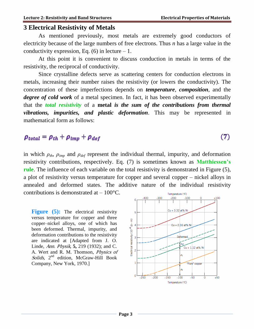
rule. The influence of each variable on the total resistivity is demonstrated in Figure (5),
a plot of resistivity versus temperature for copper and several copper – nickel alloys in
annealed and deformed states. The additive nature of the individual resistivity
contributions is demonstrated at – 100°C.
Figure (5): The electrical resistivity
versus temperature for copper and three
copper–nickel alloys, one of which has
been deformed. Thermal, impurity, and
deformation contributions to the resistivity
are indicated at [Adapted from J. O.
Linde, Ann. Physik, 5, 219 (1932); and C.
A. Wert and R. M. Thomson, Physics of Solids, 2
nd edition, McGraw-Hill Book
Company, New York, 1970.]

Lecture 2: Resistivity and Band Structures Electrical Properties of Materials
Page 4
Influence of Temperature
When the temperature of a metal
increases, thermal energy causes the
atoms to vibrate, Figure (6). At any
instant, the atom may not be in its
equilibrium position, and it therefore
interacts with and scatters electrons.
The mean free path decreases, the
mobility of electrons is reduced, and
the resistivity increases. The change in
resistivity of pure metal as a function of
temperature, thus,
where ρth the resistivity at any temperature T, ρRT the resistivity at room temperature
(i.e., 25°C), ΔT =(T – TRT)is the difference between the temperature of interest and
room temperature, and α is the temperature resistivity coefficient. This dependence of
the thermal resistivity component on temperature is due to the increase with temperature
in thermal vibrations and other lattice irregularities (e.g., vacancies), which serve as
electron – scattering centers. So, the relationship between resistivity and temperature is
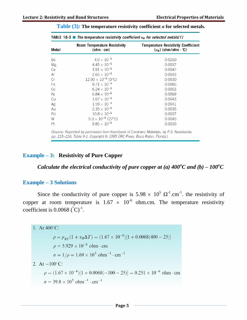
linear over a wide temperature range, Figure (7). Table (3), given some examples of the
temperature resistivity coefficient.
Figure (6): Movement of an electron through
(a) a perfect crystal, (b) a crystal heated to a high
temperature, and (c) a crystal containing atomic
level defects. Scattering of the electrons reduces
the mobility and conductivity.
Figure (7): The effect of temperature on the
electrical resistivity of a metal with a perfect
crystal structure. The slope of the curve is the
temperature resistivity coefficient.
Lecture 2: Resistivity and Band Structures Electrical Properties of Materials
Page 5
Table (3): The temperature resistivity coefficient α for selected metals.
Example – 3: Resistivity of Pure Copper
Calculate the electrical conductivity of pure copper at (a) 400oC and (b) – 100
oC
Example – 3 Solutions
Since the conductivity of pure copper is 5.98 105 Ω
-1.cm
-1. the resistivity of
copper at room temperature is 1.67 10-6
ohm.cm. The temperature resistivity
coefficient is 0.0068 (°C)
-1.
Lecture 2: Resistivity and Band Structures Electrical Properties of Materials
Page 6
Influence of Impurities
For additions of a single impurity that forms a solid solution, the impurity
resistivity ρimp is related to the impurity concentration cimp in terms of the atom fraction
as follows:
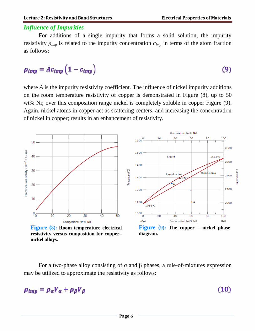
where A is the impurity resistivity coefficient. The influence of nickel impurity additions
on the room temperature resistivity of copper is demonstrated in Figure (8), up to 50
wt% Ni; over this composition range nickel is completely soluble in copper Figure (9).
Again, nickel atoms in copper act as scattering centers, and increasing the concentration
of nickel in copper; results in an enhancement of resistivity.
For a two-phase alloy consisting of α and β phases, a rule-of-mixtures expression
may be utilized to approximate the resistivity as follows:
Figure (8): Room temperature electrical
resistivity versus composition for copper–
nickel alloys.
Figure (9): The copper – nickel phase
diagram.
Lecture 2: Resistivity and Band Structures Electrical Properties of Materials
Page 7
where the V’s and ρ’s represent volume fractions and individual resistivity for the
respective phases.
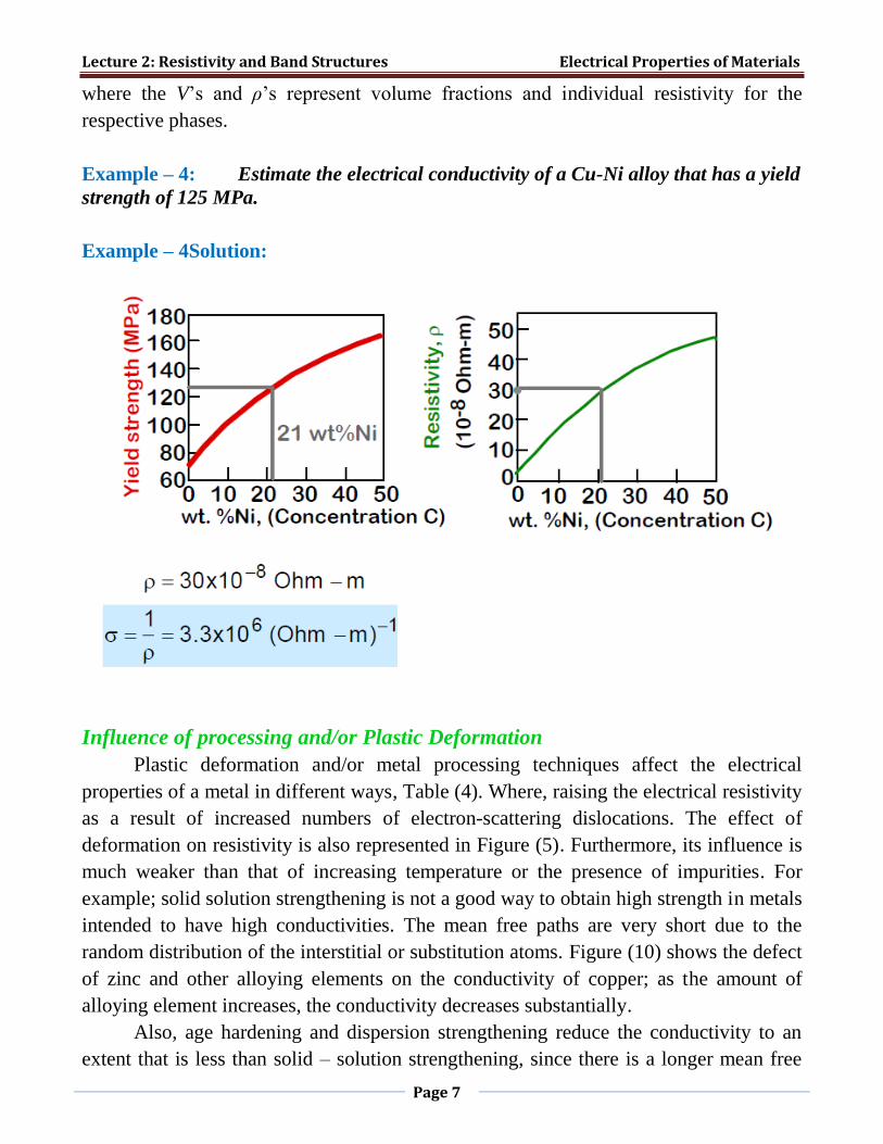
Example – 4: Estimate the electrical conductivity of a Cu-Ni alloy that has a yield
strength of 125 MPa.
Example – 4Solution:
Influence of processing and/or Plastic Deformation
Plastic deformation and/or metal processing techniques affect the electrical
properties of a metal in different ways, Table (4). Where, raising the electrical resistivity
as a result of increased numbers of electron-scattering dislocations. The effect of
deformation on resistivity is also represented in Figure (5). Furthermore, its influence is
much weaker than that of increasing temperature or the presence of impurities. For
example; solid solution strengthening is not a good way to obtain high strength in metals
intended to have high conductivities. The mean free paths are very short due to the
random distribution of the interstitial or substitution atoms. Figure (10) shows the defect
of zinc and other alloying elements on the conductivity of copper; as the amount of
alloying element increases, the conductivity decreases substantially.
Also, age hardening and dispersion strengthening reduce the conductivity to an
extent that is less than solid – solution strengthening, since there is a longer mean free

Lecture 2: Resistivity and Band Structures Electrical Properties of Materials
Page 8
path between precipitates, as compared with the path between point defects. Strain
hardening and grain – size control has even less effect on conductivity, Figure (10) and
Table (4).
Table (4):
Figure (10): (a) the effect of solid-solution strengthening and cold working on the
electrical conductivity of copper, and (b) the effect of addition of selected elements
on the electrical conductivity of copper.
Lecture 2: Resistivity and Band Structures Electrical Properties of Materials
Page 9
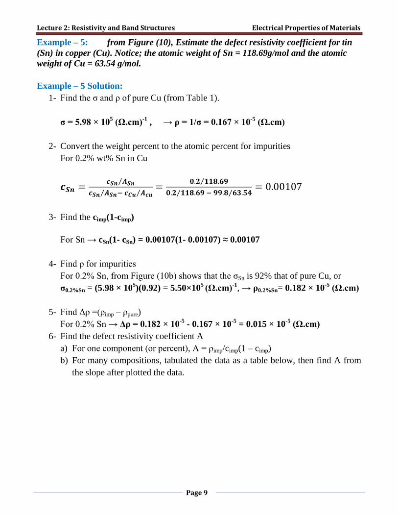
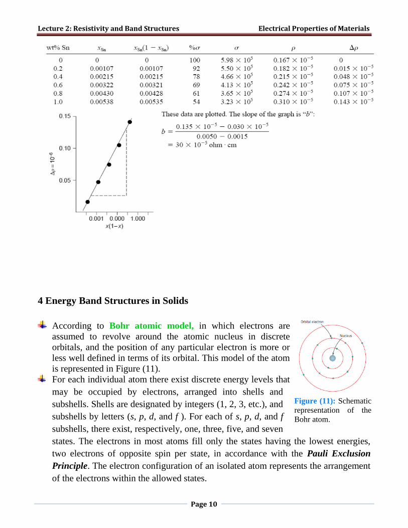
Example – 5: from Figure (10), Estimate the defect resistivity coefficient for tin
(Sn) in copper (Cu). Notice; the atomic weight of Sn = 118.69g/mol and the atomic
weight of Cu = 63.54 g/mol.
Example – 5 Solution:
1- Find the σ and ρ of pure Cu (from Table 1).
σ = 5.98 × 10⁵ (Ω.cm)
-1 , → ρ = 1/σ = 0.167 × 10
-5 (Ω.cm)
2- Convert the weight percent to the atomic percent for impurities
For 0.2% wt% Sn in Cu
⁄
⁄ ⁄
⁄
⁄ ⁄
3- Find the cimp(1-cimp)
For Sn → cSn(1- cSn) = 0.00107(1- 0.00107) ≈ 0.00107
4- Find ρ for impurities
For 0.2% Sn, from Figure (10b) shows that the σSn is 92% that of pure Cu, or
σ0.2%Sn = (5.98 × 10⁵)(0.92) = 5.50×10
5 (Ω.cm)
-1, → ρ0.2%Sn= 0.182 × 10
-5 (Ω.cm)
5- Find Δρ =(ρimp – ρpure)
For 0.2% Sn → Δρ = 0.182 × 10⁻⁵
- 0.167 × 10-5
= 0.015 × 10⁻⁵
(Ω.cm)
6- Find the defect resistivity coefficient A
a) For one component (or percent), A = ρimp/cimp(1 – cimp)
b) For many compositions, tabulated the data as a table below, then find A from
the slope after plotted the data.
Lecture 2: Resistivity and Band Structures Electrical Properties of Materials
Page 10
4 Energy Band Structures in Solids
According to Bohr atomic model, in which electrons are
assumed to revolve around the atomic nucleus in discrete
orbitals, and the position of any particular electron is more or
less well defined in terms of its orbital. This model of the atom
is represented in Figure (11). For each individual atom there exist discrete energy levels that
may be occupied by electrons, arranged into shells and
subshells. Shells are designated by integers (1, 2, 3, etc.), and
subshells by letters (s, p, d, and f ). For each of s, p, d, and f
subshells, there exist, respectively, one, three, five, and seven
states. The electrons in most atoms fill only the states having the lowest energies,
two electrons of opposite spin per state, in accordance with the Pauli Exclusion
Principle. The electron configuration of an isolated atom represents the arrangement
of the electrons within the allowed states.
Figure (11): Schematic
representation of the
Bohr atom.
Lecture 2: Resistivity and Band Structures Electrical Properties of Materials
Page 11
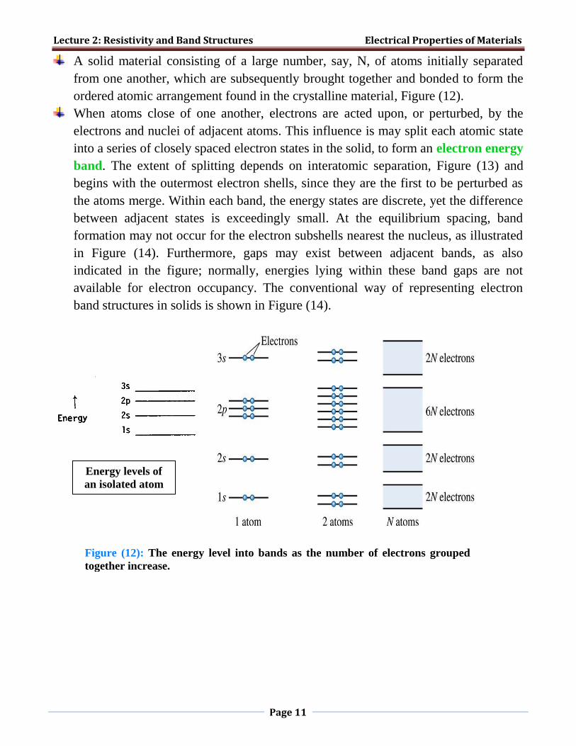
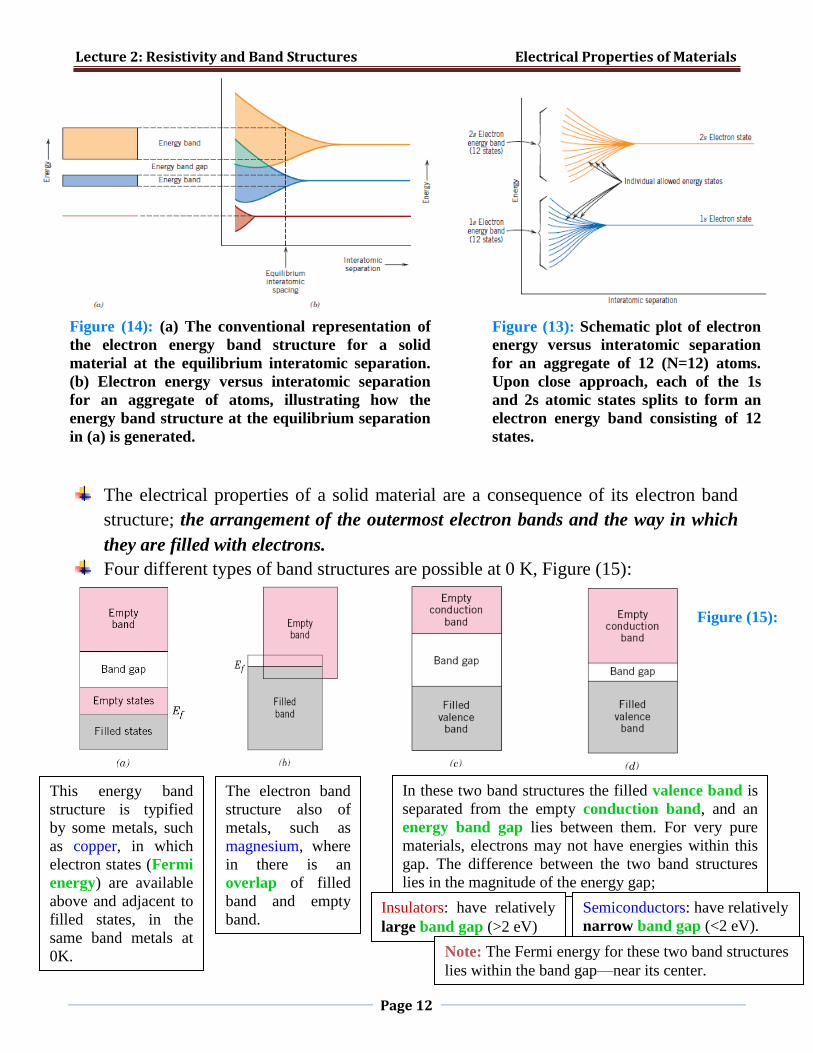
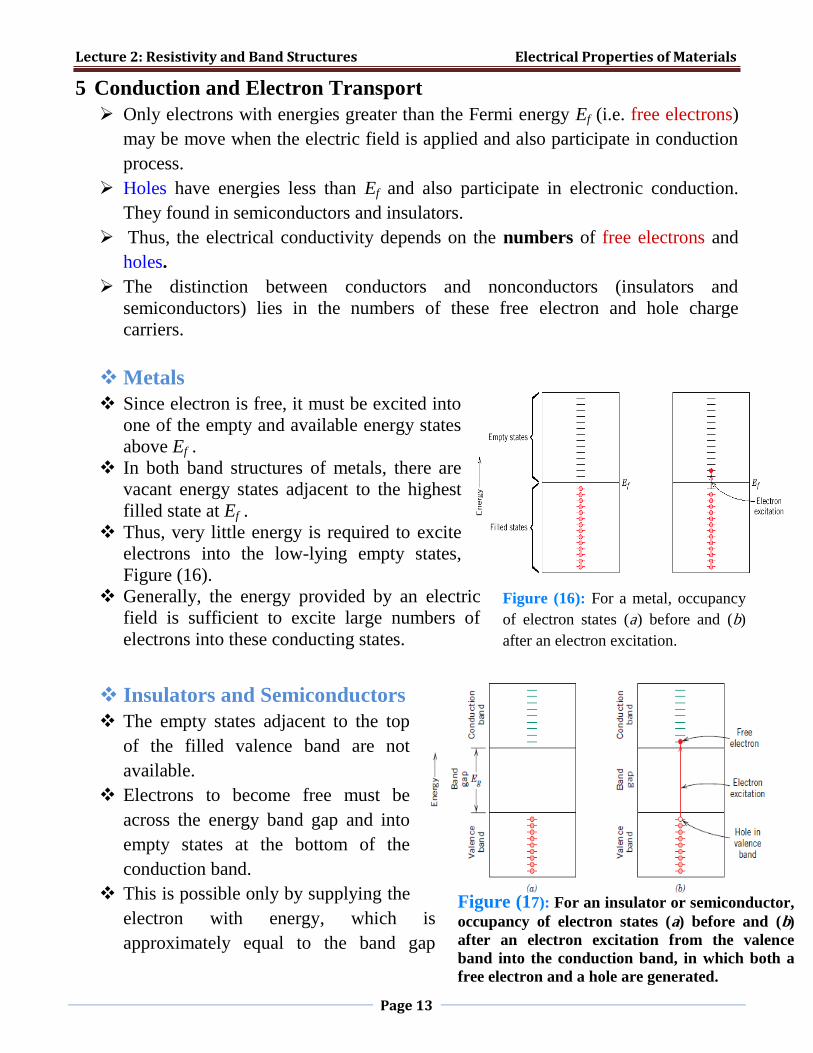
A solid material consisting of a large number, say, N, of atoms initially separated
from one another, which are subsequently brought together and bonded to form the
ordered atomic arrangement found in the crystalline material, Figure (12).
When atoms close of one another, electrons are acted upon, or perturbed, by the
electrons and nuclei of adjacent atoms. This influence is may split each atomic state
into a series of closely spaced electron states in the solid, to form an electron energy
band. The extent of splitting depends on interatomic separation, Figure (13) and
begins with the outermost electron shells, since they are the first to be perturbed as
the atoms merge. Within each band, the energy states are discrete, yet the difference
between adjacent states is exceedingly small. At the equilibrium spacing, band
formation may not occur for the electron subshells nearest the nucleus, as illustrated
in Figure (14). Furthermore, gaps may exist between adjacent bands, as also
indicated in the figure; normally, energies lying within these band gaps are not
available for electron occupancy. The conventional way of representing electron
band structures in solids is shown in Figure (14).
Energy levels of
an isolated atom
Figure (12): The energy level into bands as the number of electrons grouped
together increase.
Lecture 2: Resistivity and Band Structures Electrical Properties of Materials
Page 12
The electrical properties of a solid material are a consequence of its electron band
structure; the arrangement of the outermost electron bands and the way in which
they are filled with electrons.
Four different types of band structures are possible at 0 K, Figure (15):
Figure (13): Schematic plot of electron
energy versus interatomic separation
for an aggregate of 12 (N=12) atoms.
Upon close approach, each of the 1s
and 2s atomic states splits to form an
electron energy band consisting of 12
states.
Figure (14): (a) The conventional representation of
the electron energy band structure for a solid
material at the equilibrium interatomic separation.
(b) Electron energy versus interatomic separation
for an aggregate of atoms, illustrating how the
energy band structure at the equilibrium separation
in (a) is generated.
This energy band
structure is typified
by some metals, such
as copper, in which
electron states (Fermi
energy) are available
above and adjacent to
filled states, in the
same band metals at
0K.
The electron band
structure also of
metals, such as
magnesium, where
in there is an
overlap of filled
band and empty
band.
In these two band structures the filled valence band is
separated from the empty conduction band, and an
energy band gap lies between them. For very pure
materials, electrons may not have energies within this
gap. The difference between the two band structures
lies in the magnitude of the energy gap;
Insulators: have relatively
large band gap (>2 eV)
Semiconductors: have relatively
narrow band gap (<2 eV).
Note: The Fermi energy for these two band structures
lies within the band gap—near its center.
Figure (15):
Lecture 2: Resistivity and Band Structures Electrical Properties of Materials
Page 13
5 Conduction and Electron Transport
Only electrons with energies greater than the Fermi energy Ef (i.e. free electrons)
may be move when the electric field is applied and also participate in conduction
process.
Holes have energies less than Ef and also participate in electronic conduction.
They found in semiconductors and insulators.
Thus, the electrical conductivity depends on the numbers of free electrons and
holes.
The distinction between conductors and nonconductors (insulators and
semiconductors) lies in the numbers of these free electron and hole charge
carriers.
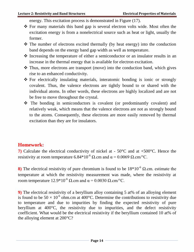
Metals
Since electron is free, it must be excited into
one of the empty and available energy states
above Ef .
In both band structures of metals, there are
vacant energy states adjacent to the highest
filled state at Ef .
Thus, very little energy is required to excite
electrons into the low-lying empty states,
Figure (16).
Generally, the energy provided by an electric
field is sufficient to excite large numbers of
electrons into these conducting states.
Insulators and Semiconductors
The empty states adjacent to the top
of the filled valence band are not
available.
Electrons to become free must be
across the energy band gap and into
empty states at the bottom of the
conduction band.
This is possible only by supplying the
electron with energy, which is
approximately equal to the band gap
Figure (16): For a metal, occupancy
of electron states (a) before and (b)
after an electron excitation.
Figure (17): For an insulator or semiconductor,
occupancy of electron states (a) before and (b)
after an electron excitation from the valence
band into the conduction band, in which both a
free electron and a hole are generated.
Lecture 2: Resistivity and Band Structures Electrical Properties of Materials
Page 14
energy. This excitation process is demonstrated in Figure (17).
For many materials this band gap is several electron volts wide. Most often the
excitation energy is from a nonelectrical source such as heat or light, usually the
former.
The number of electrons excited thermally (by heat energy) into the conduction
band depends on the energy band gap width as well as temperature.
Increasing the temperature of either a semiconductor or an insulator results in an
increase in the thermal energy that is available for electron excitation.
Thus, more electrons are transport (move) into the conduction band, which gives
rise to an enhanced conductivity.
For electrically insulating materials, interatomic bonding is ionic or strongly
covalent. Thus, the valence electrons are tightly bound to or shared with the
individual atoms. In other words, these electrons are highly localized and are not
be free to move throughout the crystal.
The bonding in semiconductors is covalent (or predominantly covalent) and
relatively weak, which means that the valence electrons are not as strongly bound
to the atoms. Consequently, these electrons are more easily removed by thermal
excitation than they are for insulators.
Homework:
7) Calculate the electrical conductivity of nickel at - 50°C and at +500°C. Hence the
resistivity at room temperature 6.84*10-6
Ω.cm and α = 0.0069 Ω.cm/°C.
8) The electrical resistivity of pure chromium is found to be 18*10-6
Ω.cm. estimate the
temperature at which the resistivity measurement was made, where the resistivity at
room temperature 12.9*10-6
Ω.cm and α = 0.0030 Ω.cm/°C.
9) The electrical resistivity of a beryllium alloy containing 5 at% of an alloying element
is found to be 50 × 10-6
ohm.cm at 400°C. Determine the contributions to resistivity due
to temperature and due to impurities by finding the expected resistivity of pure
beryllium at 400°C, the resistivity due to impurities, and the defect resistivity
coefficient. What would be the electrical resistivity if the beryllium contained 10 at% of
the alloying element at 200°C?